2. Memory and bus architecture
2.1 System architecture
The STM32U3 series architecture relies on an Arm Cortex-M33 core optimized for execution thanks to an instruction cache having a direct access to the embedded flash memory.
This architecture also features a 32-bit multilayer AHB bus matrix that interconnects:
- • up to 9 masters:
- – Fast C-bus, connecting Cortex-M33 with Arm TrustZone mainline and FPU core to the internal SRAMs and flash memory through the instruction cache
- – Slow C-bus, connecting Cortex-M33 with Arm TrustZone mainline and FPU core to the OCTOSPI1 external memory through the instruction cache
- – Cortex-M33 with Arm TrustZone mainline and FPU core S-bus (up to four masters connected to two internal SRAMs without latency), and to peripherals and OCTOSPI1 external memory
- – GPDMA1 (general purpose DMA featuring two master ports)
- – SDMMC1
- • up to 8 slaves:
- – internal flash memory
- – internal SRAM1
- – internal SRAM2
- – internal SRAM3
- – internal SRAM4
- – AHB1 peripherals including AHB to APB bridges and APB peripherals (connected to APB1 and APB2)
- – AHB2 peripherals
- – OCTOSPI1
The bus matrix provides access from a master to a slave, enabling concurrent access and efficient operation even when several high-speed peripherals work simultaneously. This architecture is shown in the figure below.
Figure 1. System architecture
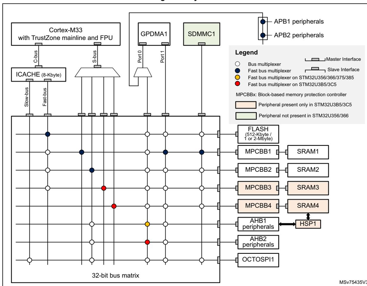
The diagram illustrates the system architecture of the STM32U3 series microcontroller. At the core is the Cortex-M33 with TrustZone mainline and FPU, connected to a 32-bit bus matrix via three buses: the C-bus (through ICACHE), the Slow-bus (through ICACHE), and the S-bus. The bus matrix is a grid of horizontal and vertical lines with various connection points marked by colored circles representing different types of bus multiplexers: white for a standard bus multiplexer, blue for a fast bus multiplexer, yellow for a fast bus multiplexer on STM32U356/366/375/385, and red for a fast bus multiplexer on STM32U3B5/3C5. The matrix connects to several peripheral blocks: FLASH (512-Kbyte / 1 or 2-Mbyte), MPCBB1 through MPCBB4 (Block-based memory protection controller), SRAM1 through SRAM4, AHB1 and AHB2 peripherals, HSP1, and OCTOSPI1. GPDMA1 is connected to the matrix via Port 0 and Port 1. SDMMC1 is also connected to the matrix. A legend on the right side defines the symbols for bus multiplexers, master/slave interfaces, and the color-coding for different STM32U3 variants. It also notes that some peripherals are present only in STM32U3B5/3C5 (orange) and others are not present in STM32U356/366 (green). The diagram is labeled MSV75435V3 in the bottom right corner.
2.1.1 Fast C-bus
This bus connects the C-bus of the Cortex-M33 core to the internal flash memory and to the bus matrix via the instruction cache. This bus is used for instruction fetch and data access to the internal memories mapped in the code region. This bus targets the internal flash memory and the internal SRAMs (SRAM1, SRAM2, and SRAM3).
SRAM1, SRAM2, and SRAM3 are accessible on this bus with a continuous mapping.
2.1.2 Slow C-bus
This bus connects the C-bus of the Cortex-M33 core to the bus matrix via the instruction cache. This bus is used for instruction fetch and data access to the external memories mapped in the code region. This bus targets the external memories (OCTOSPI).
2.1.3 S-bus
This bus connects the system bus of the Cortex-M33 core to the bus matrix. This bus is used by the core to access data located in a peripheral or SRAM area. This bus targets the internal SRAMs (SRAM1, SRAM2, SRAM3, and SRAM4), the AHB1 peripherals including the APB1 and APB2 peripherals, and the AHB2 peripherals.
SRAM1, SRAM2, SRAM3, and SRAM4 are accessible on this bus with a continuous mapping.
Note: The bus matrix has a zero latency when accessing SRAM1, SRAM2, SRAM3, and SRAM4.
2.1.4 GPDMA-bus
These buses connect the two AHB master interfaces of the GPDMA to the bus matrix. These buses target the internal flash memory, the internal SRAMs (SRAM1, SRAM2, SRAM3, and SRAM4), the AHB1 peripherals including the APB1 and APB2 peripherals, the AHB2 peripherals, the APB3 peripherals and the external memories through OCTOSPI.
2.1.5 SDMMC1 controller DMA bus
This bus connects the SDMMC1 DMA master interface to the bus matrix. This bus is used only by the SDMMC1 DMA to load/store data from/to the memory. This bus targets the data memories: internal flash memory, internal SRAMs (SRAM1, SRAM2, SRAM3, and SRAM4) and external memories through OCTOSPI.
2.1.6 Bus matrix
The bus matrix manages the access arbitration between masters. The arbitration uses a round-robin algorithm. This bus matrix features a fast bus multiplexer used to connect each master to a given slave without latency (see Figure 1 ). For the same master, other slaves undergo a latency of at least one cycle at each new access.
2.1.7 AHB/APB bridges
The three AHB/APB bridges provide full synchronous connections between the AHB and the APB buses, allowing flexible selection of the peripheral frequency.
Refer to Memory and bus architecture for the address mapping of the peripherals connected to these bridges.
After each device reset, all peripheral clocks are disabled (except for the internal SRAMs and flash memory interfaces). Before using a peripheral, its clock must be enabled in the RCC_AHBxENR and RCC_APBxENR registers.
Note: When an 8- or 16-bit access is performed on an APB register, the access is transformed into a 32-bit access: the bridge duplicates the 8- or 16-bit data to feed the 32-bit vector.
2.2 Arm TrustZone security architecture
The security architecture is based on Arm TrustZone with the Armv8-M mainline extension.
The TrustZone security is activated by the TZEN option bit in the FLASH_OPTR register.
When the TrustZone is enabled, the SAU (security-attribution unit) and IDAU (implementation-defined-attribution unit) defines the access permissions based on secure and nonsecure states.
- • SAU: Up to eight SAU configurable regions are available for security attribution.
- • IDAU: provides a first memory partition as nonsecure or nonsecure callable attributes. The IDAU memory map partition is not configurable and fixed by hardware implementation (refer to Figure 1 and to Table 4 in Section 2.3.2: Memory map and
register boundary addresses ). It is then combined with the results from the SAU security attribution and the higher security state is selected.
Based on IDAU security attribution, the flash memory, system SRAMs, and peripherals memory space are aliased twice for secure and nonsecure states. The external memories space is not aliased.
The table below shows an example of typical eight SAU regions mapping based on IDAU regions. The user can split and choose the secure, nonsecure or NSC regions for external memories as needed.
Table 1. Example of memory map security attribution versus SAU configuration regions
| Region description | Address range | IDAU security attribution | SAU security attribution typical configuration | Final security attribution |
|---|---|---|---|---|
| Code - external memories | 0x0000_0000 0x07FF_FFFF | Nonsecure | Secure, nonsecure or NSC (1) | Secure, nonsecure, or NSC |
| Code - flash memory and SRAM | 0x0800_0000 0x0BFF_FFFF | Nonsecure | Nonsecure | Nonsecure |
| 0x0C00_0000 0x0FFF_FFFF | NSC | Secure or NSC | Secure or NSC | |
| Code - external memories | 0x1000_0000 0x17FF_FFFF | Nonsecure | Nonsecure | Nonsecure |
| 0x1800_0000 0x1FFF_FFFF | ||||
| SRAM | 0x2000_0000 0x2FFF_FFFFF | Nonsecure | ||
| 0x3000_0000 0x3FFF_FFFFF | NSC | Secure or NSC | Secure or NSC | |
| Peripherals | 0x4000_0000 0x4FFF_FFFFF | Nonsecure | Nonsecure | Nonsecure |
| 0x5000_0000 0x5FFF_FFFFF | NSC | Secure or NSC | Secure or NSC | |
| External memories | 0x6000_0000 0xDFFF_FFFF | Nonsecure | Secure, nonsecure or NSC | Secure, nonsecure or NSC |
1. NSC = nonsecure callable
2.2.1 Default Arm TrustZone security state
When the TrustZone security is activated by the TZEN option bit in the FLASH_OPTR, the default system security state is detailed below:
- • CPU:
- – Cortex-M33 is in secure state after reset. The boot address must be at a secure address.
- • Memory map:
- – SAU is fully secure after reset. Consequently, all memory map is fully secure. Up to height SAU configurable regions are available for security attribution.
- • Flash memory:
- – The flash memory security area is defined by watermark user options.
- – Flash block-based security attributions are nonsecure after reset.
- • SRAMs:
- – All SRAMs are secure after reset. MPCBBx (block-based memory protection controller) are secure.
- – On STM32U3B5/3C5 devices, SRAM4 is secure after reset but can be accessed directly by nonsecure HSP1.
- • External memories:
- – OCTOSPI does not support any TrustZone protection.
- • Peripherals (see
Table 2
and
Table 3
for a list of securable and TrustZone-aware peripherals)
- – Securables peripherals are nonsecure after reset.
- – TrustZone-aware peripherals are nonsecure after reset. Their secure configuration registers are secure.
- • All GPIOs secure after reset
- • Interrupts:
- – NVIC: All interrupts are secure after reset. NVIC is banked for secure and nonsecure state.
- – TZIC: All illegal access interrupts are disabled after reset (see Section 2.2: Arm TrustZone security architecture ).
2.2.2 Arm TrustZone peripheral classification
When the TrustZone security is active, a peripheral can be either securable or TrustZone-aware type as follows:
- • Securables: peripheral protected by an AHB/APB firewall gate that is controlled from TZSC controller to define security properties
- • TrustZone-aware: peripheral connected directly to AHB or APB bus and implementing a specific TrustZone behavior such as a subset of registers being secure.
Refer to Section 2.2: Arm TrustZone security architecture for more details.
The tables below list the securable and TrustZone-aware peripherals within the system.
Table 2. Securables peripherals by TZSC
| Bus | Peripheral | STM32U356/366 | STM32U375/385 | STM32U3B5/3C5 |
|---|---|---|---|---|
| AHB2 | DAC1 | X | X | X |
| OCTOSPI1 | X | X | X | |
| SDMMC1 | - | X | X | |
| CCB | X | X | X | |
| SAES | X | X | X | |
| PKA (+RAM) | X | X | X | |
| RNG | X | X | X | |
| HASH | X | X | X | |
| AES | X | X | X | |
| ADC2 | X | X | X | |
| ADC1 | X | X | X |
Table 2. Securable peripherals by TZSC (continued)
| Bus | Peripheral | STM32U356/366 | STM32U375/385 | STM32U3B5/3C5 |
|---|---|---|---|---|
| AHB1 | ADF1 | - | X | X |
| ICACHE registers | X | X | X | |
| RAMCFG | X | X | X | |
| TSC | X | X | X | |
| CRC | X | X | X | |
| HSP1 | - | - | X | |
| APB3 | LCD | X | - | - |
| COMP | X | X | X | |
| LPTIM4 | X | X | X | |
| LPTIM3 | X | X | X | |
| LPTIM1 | X | X | X | |
| I2C3 | X | X | X | |
| LPUART1 | X | X | X | |
| APB2 | I3C2 | - | X | X |
| USB | X | X | X | |
| SAI1 | - | X | X | |
| TIM17 | X | X | X | |
| TIM16 | X | X | X | |
| TIM15 | X | X | X | |
| TIM12 | - | - | X | |
| USART1 | X | X | X | |
| SPI1 | X | X | X | |
| TIM8 | - | - | X | |
| TIM1 | X | X | X |
Table 2. Securable peripherals by TZSC (continued)
| Bus | Peripheral | STM32U356/366 | STM32U375/385 | STM32U3B5/3C5 |
|---|---|---|---|---|
| APB1 | VREFBUF | X | X | X |
| OPAMP | X | X | X | |
| I3C1 | X | X | X | |
| FDCAN2 | - | - | X | |
| FDCAN1 | - | X | X | |
| LPTIM2 | X | X | X | |
| CRS | X | X | X | |
| I2C4 | - | - | X | |
| I2C2 | - | X | X | |
| I2C1 | X | X | X | |
| UART5 | X | X | X | |
| UART4 | X | X | X | |
| USART3 | X | X | X | |
| USART2 | - | - | X | |
| SPI4 | - | - | X | |
| SPI3 | X | X | X | |
| SPI2 | X | X | X | |
| IWDG | X | X | X | |
| WWDG | X | X | X | |
| TIM7 | X | X | X | |
| TIM6 | X | X | X | |
| TIM4 | X | X | X | |
| TIM3 | X | X | X | |
| TIM2 | X | X | X |
Table 3. TrustZone aware peripherals
| Bus | Peripheral | STM32U356/366 | STM32U375/385 | STM32U3B5/3C5 |
|---|---|---|---|---|
| AHB2 | GPIOH | X | X | X |
| GPIOG | - | X | X | |
| GPIOF | - | - | X | |
| GPIOE | X | X | X | |
| GPIO_D | X | X | X | |
| GPIOC | X | X | X | |
| GPIOB | X | X | X | |
| GPIOA | X | X | X |
| Bus | Peripheral | STM32U356/366 | STM32U375/385 | STM32U3B5/3C5 |
|---|---|---|---|---|
| AHB1 | GTZC1 | X | X | X |
| ICACHE | X | X | X | |
| FLASH | X | X | X | |
| EXTI | X | X | X | |
| GPDMA1 | X | X | X | |
| RCC | X | X | X | |
| PWR | X | X | X | |
| APB3 | SYSCFG | X | X | X |
| APB1 | TAMP | X | X | X |
| RTC | X | X | X |
2.3 Memory organization
2.3.1 Introduction
Program memory, data memory, registers and I/O ports are organized within the same linear 4-Gbyte address space.
The bytes are coded in memory in Little Endian format. The lowest numbered byte in a word is considered the word's least significant byte and the highest numbered byte the most significant.
2.3.2 Memory map and register boundary addresses
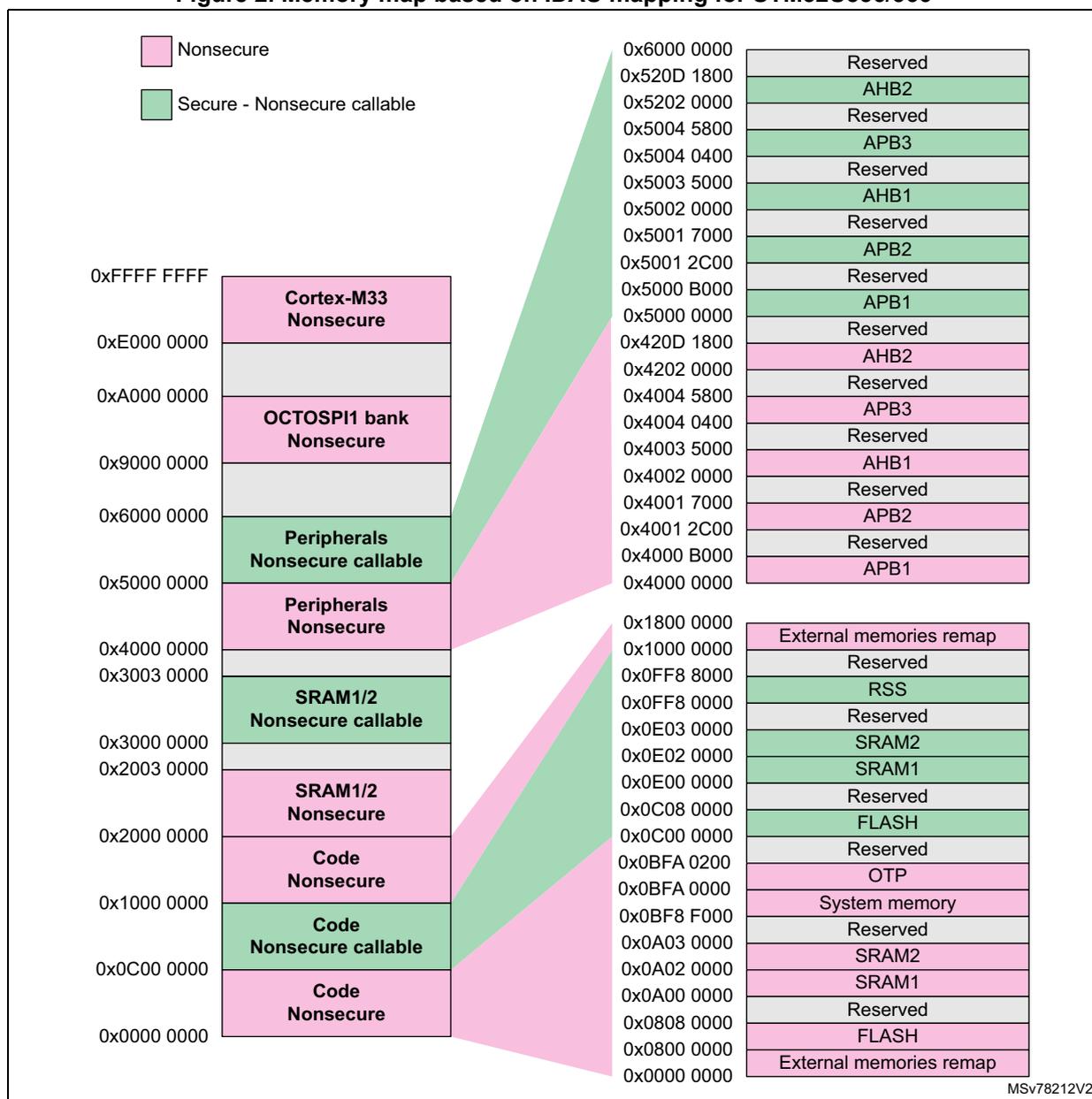
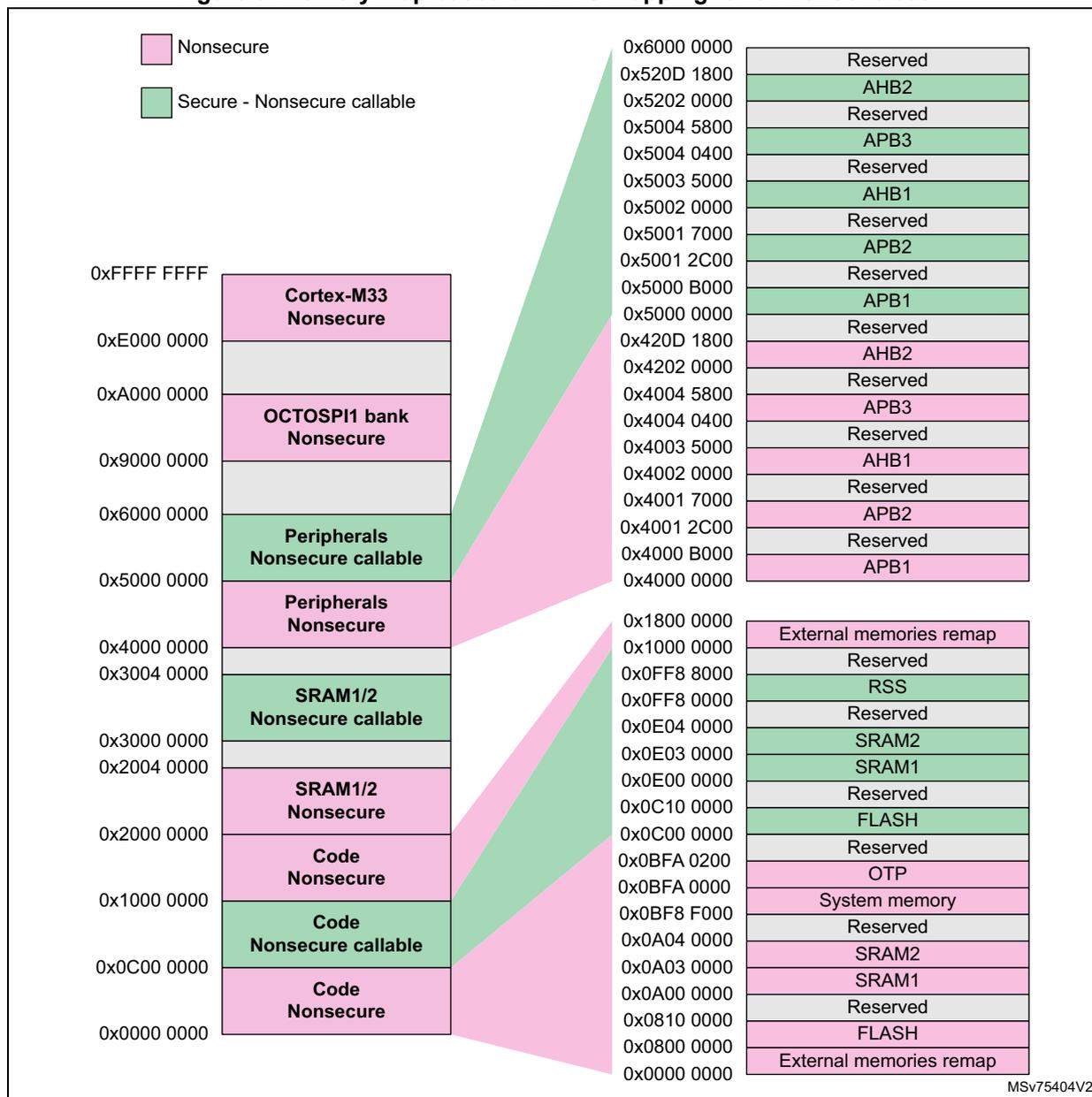
Figure 2. Memory map based on IDAU mapping for STM32U356/366
Legend:
- Nonsecure (Pink)
- Secure - Nonsecure callable (Green)
| Address Range | Memory Region / Peripheral | Security Attribute |
|---|---|---|
| 0x0000 0000 - 0x0000 0000 | External memories remap | Nonsecure |
| 0x0800 0000 - 0x0808 0000 | FLASH | Nonsecure |
| 0x0A00 0000 - 0x0A02 0000 | SRAM1 | Nonsecure |
| 0x0A03 0000 - 0x0A0A 0000 | SRAM2 | Nonsecure |
| 0x0BFA 0000 - 0x0BFA 0200 | OTP | Nonsecure |
| 0x0C00 0000 - 0x0C08 0000 | FLASH | Nonsecure |
| 0x0E00 0000 - 0x0E02 0000 | SRAM1 | Nonsecure |
| 0x0E03 0000 - 0x0E0E 0000 | SRAM2 | Nonsecure |
| 0x0FF8 0000 - 0x0FF8 8000 | RSS | Secure - Nonsecure callable |
| 0x1000 0000 - 0x1800 0000 | External memories remap | Nonsecure |
| 0x4000 0000 - 0x4000 0000 | APB1 | Nonsecure |
| 0x4001 2C00 - 0x4001 7000 | APB2 | Nonsecure |
| 0x4002 0000 - 0x4002 0000 | Reserved | Nonsecure |
| 0x4003 5000 - 0x4003 5000 | AHB1 | Nonsecure |
| 0x4004 0400 - 0x4004 0400 | Reserved | Nonsecure |
| 0x4004 5800 - 0x4004 5800 | APB3 | Nonsecure |
| 0x4202 0000 - 0x4202 0000 | Reserved | Nonsecure |
| 0x420D 1800 - 0x420D 1800 | AHB2 | Nonsecure |
| 0x5000 0000 - 0x5000 0000 | APB1 | Nonsecure |
| 0x5001 2C00 - 0x5001 7000 | APB2 | Nonsecure |
| 0x5002 0000 - 0x5002 0000 | Reserved | Nonsecure |
| 0x5003 5000 - 0x5003 5000 | AHB1 | Nonsecure |
| 0x5004 0400 - 0x5004 0400 | Reserved | Nonsecure |
| 0x5004 5800 - 0x5004 5800 | APB3 | Nonsecure |
| 0x5202 0000 - 0x5202 0000 | Reserved | Nonsecure |
| 0x520D 1800 - 0x520D 1800 | AHB2 | Nonsecure |
| 0x6000 0000 - 0x6000 0000 | Reserved | Nonsecure |
Memory map details:
- 0x0000 0000 - 0x0000 0000: External memories remap (Nonsecure)
- 0x0800 0000 - 0x0808 0000: FLASH (Nonsecure)
- 0x0A00 0000 - 0x0A02 0000: SRAM1 (Nonsecure)
- 0x0A03 0000 - 0x0A0A 0000: SRAM2 (Nonsecure)
- 0x0BFA 0000 - 0x0BFA 0200: OTP (Nonsecure)
- 0x0C00 0000 - 0x0C08 0000: FLASH (Nonsecure)
- 0x0E00 0000 - 0x0E02 0000: SRAM1 (Nonsecure)
- 0x0E03 0000 - 0x0E0E 0000: SRAM2 (Nonsecure)
- 0x0FF8 0000 - 0x0FF8 8000: RSS (Secure - Nonsecure callable)
- 0x1000 0000 - 0x1800 0000: External memories remap (Nonsecure)
- 0x4000 0000 - 0x4000 0000: APB1 (Nonsecure)
- 0x4001 2C00 - 0x4001 7000: APB2 (Nonsecure)
- 0x4002 0000 - 0x4002 0000: Reserved (Nonsecure)
- 0x4003 5000 - 0x4003 5000: AHB1 (Nonsecure)
- 0x4004 0400 - 0x4004 0400: Reserved (Nonsecure)
- 0x4004 5800 - 0x4004 5800: APB3 (Nonsecure)
- 0x4202 0000 - 0x4202 0000: Reserved (Nonsecure)
- 0x420D 1800 - 0x420D 1800: AHB2 (Nonsecure)
- 0x5000 0000 - 0x5000 0000: APB1 (Nonsecure)
- 0x5001 2C00 - 0x5001 7000: APB2 (Nonsecure)
- 0x5002 0000 - 0x5002 0000: Reserved (Nonsecure)
- 0x5003 5000 - 0x5003 5000: AHB1 (Nonsecure)
- 0x5004 0400 - 0x5004 0400: Reserved (Nonsecure)
- 0x5004 5800 - 0x5004 5800: APB3 (Nonsecure)
- 0x5202 0000 - 0x5202 0000: Reserved (Nonsecure)
- 0x520D 1800 - 0x520D 1800: AHB2 (Nonsecure)
- 0x6000 0000 - 0x6000 0000: Reserved (Nonsecure)
Secure - Nonsecure callable
The diagram illustrates the memory map for the STM32U375/385 microcontroller, showing the mapping of physical memory to logical addresses and the security attributes of each region.
Logical Address Space (Left Side):
- 0xFFFF FFFF - 0xE000 0000: Cortex-M33 Nonsecure
- 0xE000 0000 - 0xA000 0000: Reserved (Grey)
- 0xA000 0000 - 0x9000 0000: OCTOSPI1 bank Nonsecure
- 0x9000 0000 - 0x6000 0000: Reserved (Grey)
- 0x6000 0000 - 0x5000 0000: Peripherals Nonsecure callable (Green)
- 0x5000 0000 - 0x4000 0000: Peripherals Nonsecure (Pink)
- 0x4000 0000 - 0x3004 0000: Reserved (Grey)
- 0x3004 0000 - 0x3000 0000: SRAM1/2 Nonsecure callable (Green)
- 0x3000 0000 - 0x2004 0000: Reserved (Grey)
- 0x2004 0000 - 0x2000 0000: SRAM1/2 Nonsecure (Pink)
- 0x2000 0000 - 0x1000 0000: Code Nonsecure (Pink)
- 0x1000 0000 - 0x0C00 0000: Code Nonsecure callable (Green)
- 0x0C00 0000 - 0x0000 0000: Code Nonsecure (Pink)
Physical Memory Map (Right Side Detail):
- 0x6000 0000 - 0x520D 1800: Reserved
- 0x520D 1800 - 0x5202 0000: AHB2 (Green)
- 0x5202 0000 - 0x5004 5800: Reserved
- 0x5004 5800 - 0x5004 0400: APB3 (Green)
- 0x5004 0400 - 0x5003 5000: Reserved
- 0x5003 5000 - 0x5002 0000: AHB1 (Green)
- 0x5002 0000 - 0x5001 7000: Reserved
- 0x5001 7000 - 0x5001 2C00: APB2 (Green)
- 0x5001 2C00 - 0x5000 B000: Reserved
- 0x5000 B000 - 0x5000 0000: APB1 (Green)
- 0x5000 0000 - 0x420D 1800: Reserved
- 0x420D 1800 - 0x4202 0000: AHB2 (Pink)
- 0x4202 0000 - 0x4004 5800: Reserved
- 0x4004 5800 - 0x4004 0400: APB3 (Pink)
- 0x4004 0400 - 0x4003 5000: Reserved
- 0x4003 5000 - 0x4002 0000: AHB1 (Pink)
- 0x4002 0000 - 0x4001 7000: Reserved
- 0x4001 7000 - 0x4001 2C00: APB2 (Pink)
- 0x4001 2C00 - 0x4000 B000: Reserved
- 0x4000 B000 - 0x4000 0000: APB1 (Pink)
- 0x1800 0000 - 0x1000 0000: External memories remap (Pink)
- 0x1000 0000 - 0x0FF8 8000: Reserved
- 0x0FF8 8000 - 0x0FF8 0000: RSS (Green)
- 0x0FF8 0000 - 0x0E04 0000: Reserved
- 0x0E04 0000 - 0x0E03 0000: SRAM2 (Green)
- 0x0E03 0000 - 0x0E00 0000: SRAM1 (Green)
- 0x0E00 0000 - 0x0C10 0000: Reserved
- 0x0C10 0000 - 0x0C00 0000: FLASH (Green)
- 0x0C00 0000 - 0x0BFA 0200: Reserved
- 0x0BFA 0200 - 0x0BFA 0000: OTP (Pink)
- 0x0BFA 0000 - 0x0BF8 F000: System memory (Pink)
- 0x0BF8 F000 - 0x0A04 0000: Reserved
- 0x0A04 0000 - 0x0A03 0000: SRAM2 (Pink)
- 0x0A03 0000 - 0x0A00 0000: SRAM1 (Pink)
- 0x0A00 0000 - 0x0810 0000: Reserved
- 0x0810 0000 - 0x0800 0000: FLASH (Pink)
- 0x0800 0000 - 0x0000 0000: External memories remap (Pink)
MSv75404V2
Figure 4. Memory map based on IDAU mapping for STM323B5/3C5
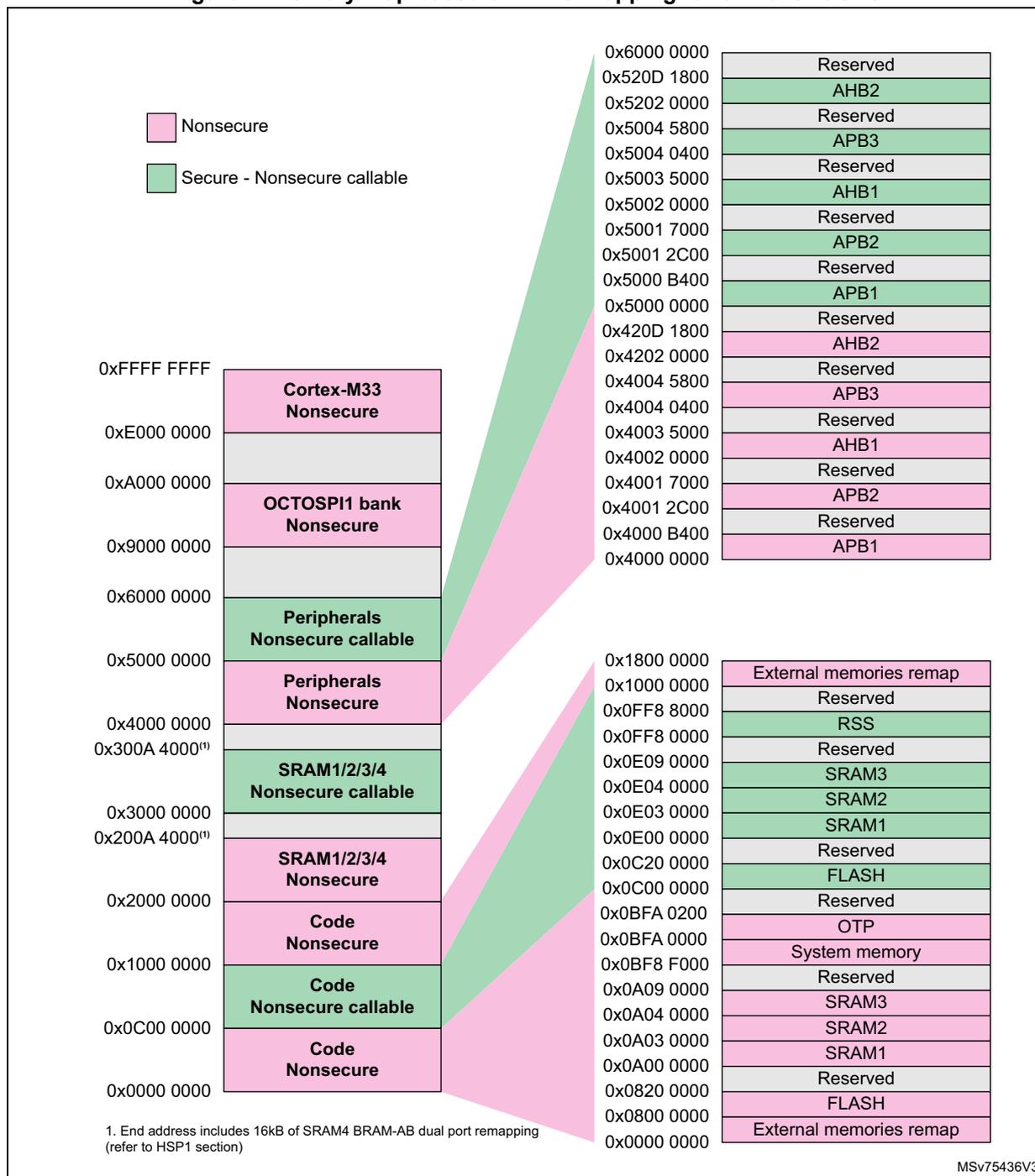
Legend:
- Nonsecure (Pink)
- Secure - Nonsecure callable (Green)
Memory Map:
| Address Range | Memory Type | Security Attribute |
|---|---|---|
| 0xFFFF FFFF | Cortex-M33 | Nonsecure |
| 0xE000 0000 | Reserved | Reserved |
| 0xA000 0000 | OCTOSPI1 bank | Nonsecure |
| 0x9000 0000 | Reserved | Reserved |
| 0x6000 0000 | Peripherals | Nonsecure callable |
| 0x5000 0000 | Peripherals | Nonsecure |
| 0x4000 0000 | Reserved | Reserved |
| 0x300A 4000 (1) | SRAM1/2/3/4 | Nonsecure callable |
| 0x3000 0000 | Reserved | Reserved |
| 0x200A 4000 (1) | SRAM1/2/3/4 | Nonsecure |
| 0x2000 0000 | Code | Nonsecure |
| 0x1000 0000 | Code | Nonsecure callable |
| 0x0C00 0000 | Code | Nonsecure |
| 0x0000 0000 | Code | Nonsecure |
Peripheral and System Memory Map:
| Address Range | Memory Type |
|---|---|
| 0x6000 0000 | Reserved |
| 0x520D 1800 | AHB2 |
| 0x5202 0000 | Reserved |
| 0x5004 5800 | APB3 |
| 0x5004 0400 | Reserved |
| 0x5003 5000 | AHB1 |
| 0x5002 0000 | Reserved |
| 0x5001 7000 | APB2 |
| 0x5001 2C00 | Reserved |
| 0x5000 B400 | APB1 |
| 0x5000 0000 | Reserved |
| 0x420D 1800 | AHB2 |
| 0x4202 0000 | Reserved |
| 0x4004 5800 | APB3 |
| 0x4004 0400 | Reserved |
| 0x4003 5000 | AHB1 |
| 0x4002 0000 | Reserved |
| 0x4001 7000 | APB2 |
| 0x4001 2C00 | Reserved |
| 0x4000 B400 | APB1 |
| 0x4000 0000 | Reserved |
System Memory Map:
| Address Range | Memory Type |
|---|---|
| 0x1800 0000 | External memories remap |
| 0x1000 0000 | Reserved |
| 0x0FF8 8000 | RSS |
| 0x0FF8 0000 | Reserved |
| 0x0E09 0000 | SRAM3 |
| 0x0E04 0000 | SRAM2 |
| 0x0E03 0000 | SRAM1 |
| 0x0E00 0000 | Reserved |
| 0x0C20 0000 | FLASH |
| 0x0C00 0000 | Reserved |
| 0x0BFA 0200 | OTP |
| 0x0BFA 0000 | System memory |
| 0x0BF8 F000 | Reserved |
| 0x0A09 0000 | SRAM3 |
| 0x0A04 0000 | SRAM2 |
| 0x0A03 0000 | SRAM1 |
| 0x0A00 0000 | Reserved |
| 0x0820 0000 | FLASH |
| 0x0800 0000 | External memories remap |
| 0x0000 0000 | External memories remap |
1. End address includes 16kB of SRAM4 BRAM-AB dual port remapping (refer to HSP1 section)
MSv75436V3
All memory map areas that are not allocated to on-chip memories and peripherals are considered “Reserved”. The following table gives the boundary addresses of the peripherals available in the devices.
Table 4. Memory map and peripheral register boundary addresses
| Bus | Secure boundary address | Nonsecure boundary address | Size (bytes) | Peripheral | Peripheral register map section number | STM32U356/366 | STM32U375/385 | STM32U3B5/3C5 |
|---|---|---|---|---|---|---|---|---|
| X | X | X | ||||||
| AHB2 | 0x520D 1800 - 0x5FFF FFFF | 0x420D 1800 - 0x4FFF FFFF | 223 M | Reserved | - | X | X | X |
| 0x520D 1400 - 0x520D 17FF | 0x420D 1400 - 0x420D 17FF | 1 K | OCTOSPI1 | 20.7.28 | X | X | X | |
| 0x520C F400 - 0x520D 13FF | 0x420C F400 - 0x420D 13FF | 8 K | Reserved | - | X | X | X | |
| 0x520C F000 - 0x520C F3FF | 0x420C F000 - 0x420C F3FF | 1 K | DLYBOS1 | 22.5.3 | X | X | X | |
| 0x520C 8800 - 0x520C EFFF | 0x420C 8800 - 0x420C EFFF | 26 K | Reserved | - | X | X | X | |
| 0x520C 8400 - 0x520C 87FF | 0x420C 8400 - 0x420C 87FF | 1 K | DLYBSD1 | 22.5.3 | X | X | X | |
| 0x520C 8000 - 0x520C 83FF | 0x420C 8000 - 0x420C 83FF | 1 K | SDMMC1 | 21.10.21 | - | X | X | |
| 0x520C 7C00 - 0x520C 7FFF | 0x420C 7C00 - 0x420C 7FFF | 1 K | CCB | 31.7.4 | X | X | X | |
| 0x520C 4000 - 0x520C 7BFF | 0x420C 4000 - 0x420C 7BFF | 15 K | Reserved | - | X | X | X | |
| 0x520C 2000 - 0x520C 3FFF | 0x420C 2000 - 0x420C 3FFF | 8 K | PKA +RAM | 36.8.5 | X | X | X | |
| 0x520C 1000 - 0x520C 1FFF | 0x420C 1000 - 0x420C 1FFF | 4 K | Reserved | - | X | X | X | |
| 0x520C 0C00 - 0x520C 0FFF | 0x420C 0C00 - 0x420C 0FFF | 1 K | SAES | 34.8.21 | X | X | X | |
| 0x520C 0800 - 0x520C 0BFF | 0x420C 0800 - 0x420C 0BFF | 1 K | RNG | 32.7.9 | X | X | X | |
| 0x520C 0400 - 0x520C 07FF | 0x420C 0400 - 0x420C 07FF | 1 K | HASH | 35.6.8 | X | X | X | |
| 0x520C 0000 - 0x520C 03FF | 0x420C 0000 - 0x420C 03FF | 1 K | AES | 33.8.21 | X | X | X | |
| 0x5202 8800 - 0x520B FFFF | 0x4202 8800 - 0x420B FFFF | 606 K | Reserved | - | X | X | X | |
| 0x5202 8400 - 0x5202 87FF | 0x4202 8400 - 0x4202 87FF | 1 K | DAC1 | 24.7.22 | X | X | X | |
| 0x5202 8300 - 0x5202 83FF | 0x4202 8300 - 0x4202 83FF | 256 | ADC12 | 23.8.1 | X | X | X | |
| 0x5202 8200 - 0x5202 82FF | 0x4202 8200 - 0x4202 82FF | 256 | Reserved | - | X | X | X | |
| 0x5202 8100 - 0x5202 81FF | 0x4202 8100 - 0x4202 81FF | 256 | ADC2 | 23.7.28 | X | X | X | |
| 0x5202 8000 - 0x5202 80FF | 0x4202 8000 - 0x4202 80FF | 256 | ADC1 | 23.7.3 | X | X | X | |
| 0x5202 2000 - 0x5202 7FFF | 0x4202 2000 - 0x4202 7FFF | 24 K | Reserved | - | X | X | X | |
| 0x5202 1C00 - 0x5202 1FFF | 0x4202 1C00 - 0x4202 1FFF | 1 K | GPIOH | 12.6.14 | X | X | X | |
| 0x5202 1800 - 0x5202 1BFF | 0x4202 1800 - 0x4202 1BFF | 1 K | GPIOG | - | X | X | ||
| 0x5202 1400 - 0x5202 17FF | 0x4202 1400 - 0x4202 17FF | 1 K | GPIOF | - | - | X | ||
| 0x5202 1000 - 0x5202 13FF | 0x4202 1000 - 0x4202 13FF | 1 K | GPIOE | X | X | X | ||
| 0x5202 0C00 - 0x5202 0FFF | 0x4202 0C00 - 0x4202 0FFF | 1 K | GPIO D | X | X | X | ||
| 0x5202 0800 - 0x5202 0BFF | 0x4202 0800 - 0x4202 0BFF | 1 K | GPIOC | X | X | X | ||
| 0x5202 0400 - 0x5202 07FF | 0x4202 0400 - 0x4202 07FF | 1 K | GPIOB | X | X | X | ||
| 0x5202 0000 - 0x5202 03FF | 0x4202 0000 - 0x4202 03FF | 1 K | GPIOA | X | X | X |
Table 4. Memory map and peripheral register boundary addresses (continued)
| Bus | Secure boundary address | Nonsecure boundary address | Size (bytes) | Peripheral | Peripheral register map section number | STM32U356/366 | STM32U375/385 | STM32U3B5/3C5 |
|---|---|---|---|---|---|---|---|---|
| APB3 | 0x5004 8400 - 0x5201 FFFF | 0x4004 8400 - 0x4201 FFFF | 31 M | Reserved | - | X | X | X |
| 0x5004 8000 - 0x5004 83FF | 0x4004 8000 - 0x4004 83FF | 1 K | LCD | 29.6.8 | X | - | - | |
| 0x5004 5800 - 0x5004 7FFF | 0x4004 5800 - 0x4004 7FFF | 9 K | Reserved | - | X | X | X | |
| 0x5004 5400 - 0x5004 57FF | 0x4004 5400 - 0x4004 57FF | 1 K | COMP | 26.6.3 | X | X | X | |
| 0x5004 5000 - 0x5004 53FF | 0x4004 5000 - 0x4004 53FF | 1 K | Reserved | - | X | X | X | |
| 0x5004 4C00 - 0x5004 4FFF | 0x4004 4C00 - 0x4004 4FFF | 1 K | LPTIM4 | 42.7.19 | X | X | X | |
| 0x5004 4800 - 0x5004 4BFF | 0x4004 4800 - 0x4004 4BFF | 1 K | LPTIM3 | X | X | X | ||
| 0x5004 4400 - 0x5004 47FF | 0x4004 4400 - 0x4004 47FF | 1 K | LPTIM1 | X | X | X | ||
| 0x5004 2C00 - 0x5004 43FF | 0x4004 2C00 - 0x4004 43FF | 6 K | Reserved | - | X | X | X | |
| 0x5004 2800 - 0x5004 2BFF | 0x4004 2800 - 0x4004 2BFF | 1 K | I2C3 | 48.9.13 | X | X | X | |
| 0x5004 2400 - 0x5004 27FF | 0x4004 2400 - 0x4004 27FF | 1 K | LPUART1 | 52.7.15 | X | X | X | |
| 0x5004 0800 - 0x5004 23FF | 0x4004 0800 - 0x4004 23FF | 7 K | Reserved | - | X | X | X | |
| 0x5004 0400 - 0x5004 07FF | 0x4004 0400 - 0x4004 07FF | 1 K | SYSCFG | 13.3.11 | X | X | X | |
| 0x5004 0000 - 0x5004 03FF | 0x4004 0000 - 0x4004 03FF | 1 K | Reserved | - | X | X | X | |
| 0x5003 5000 - 0x5003 FFFF | 0x4003 5000 - 0x4003 FFFF | 44 K | Reserved | - | X | X | X | |
| AHB1 | 0x5003 4000 - 0x5003 4FFF | 0x4003 4000 - 0x4003 4FFF | 4 K | ADF1 | 28.8.17 | X | X | X |
| 0x5003 3C00 - 0x5003 3FFF | 0x4003 3C00 - 0x4003 3FFF | 1 K | Reserved | - | X | X | X | |
| 0x5003 3800 - 0x5003 3BFF | 0x4003 3800 - 0x4003 3BFF | 1 K | GTZC1 MPCBB4 | 5.7.5 | - | - | X | |
| 0x5003 3400 - 0x5003 37FF | 0x4003 3400 - 0x4003 37FF | 1 K | GTZC1 MPCBB3 | 5.6.5 | - | - | X | |
| 0x5003 3000 - 0x5003 33FF | 0x4003 3000 - 0x4003 33FF | 1 K | GTZC1 MPCBB2 | 5.5.5 | X | X | X | |
| 0x5003 2C00 - 0x5003 2FFF | 0x4003 2C00 - 0x4003 2FFF | 1 K | GTZC1 MPCBB1 | 5.4.5 | X | X | X | |
| 0x5003 2800 - 0x5003 2BFF | 0x4003 2800 - 0x4003 2BFF | 1 K | GTZC1 TZIC | 5.3.13 | X | X | X | |
| 0x5003 2400 - 0x5003 27FF | 0x4003 2400 - 0x4003 27FF | 1 K | GTZC1 TZSC | 5.2.8 | X | X | X | |
| 0x5003 2000 - 0x5003 23FF | 0x4003 2000 - 0x4003 23FF | 1 K | EXTI | 17.4.12 | X | X | X | |
| 0x5003 1000 - 0x5003 1FFF | 0x4003 1000 - 0x4003 1FFF | 4 K | Reserved | - | X | X | X | |
| 0x5003 0C00 - 0x5003 0FFF | 0x4003 0C00 - 0x4003 0FFF | 1 K | RCC | 10.5.1 | X | X | X | |
| 0x5003 0800 - 0x5003 0BFF | 0x4003 0800 - 0x4003 0BFF | 1 K | PWR | 9.5.36 | X | X | X | |
| 0x5003 0400 - 0x5003 07FF | 0x4003 0400 - 0x4003 07FF | 1 K | ICACHE | 8.7.8 | X | X | X | |
| 0x5002 C400 - 0x5003 03FF | 0x4002 C400 - 0x4003 03FF | 16 K | Reserved | - | X | X | X | |
| 0x5002 C000 - 0x5002 C3FF | 0x4002 C000 - 0x4002 C3FF | 1 K | HSP1 | 19.7.54 | - | - | X |
Table 4. Memory map and peripheral register boundary addresses (continued)
| Bus | Secure boundary address | Nonsecure boundary address | Size (bytes) | Peripheral | Peripheral register map section number | STM32U356/366 | STM32U375/385 | STM32U3B5/3C5 |
|---|---|---|---|---|---|---|---|---|
| X | X | X | ||||||
| AHB1 | 0x5002 7000 - 0x5002 BFFF | 0x4002 7000 - 0x4002 BFFF | 20 K | Reserved | - | X | X | X |
| 0x5002 6000 - 0x5002 6FFF | 0x4002 6000 - 0x4002 6FFF | 4 K | RAMCFG | 6.6.10 | X | X | X | |
| 0x5002 4400 - 0x5002 5FFF | 0x4002 4400 - 0x4002 5FFF | 7 K | Reserved | - | X | X | X | |
| 0x5002 4000 - 0x5002 43FF | 0x4002 4000 - 0x4002 43FF | 1 K | TSC | 30.7.11 | X | X | X | |
| 0x5002 3400 - 0x5002 3FFF | 0x4002 3400 - 0x4002 3FFF | 3 K | Reserved | - | X | X | X | |
| 0x5002 3000 - 0x5002 33FF | 0x4002 3000 - 0x4002 33FF | 1 K | CRC | 18.4.6 | X | X | X | |
| 0x5002 2400 - 0x5002 2FFF | 0x4002 2400 - 0x4002 2FFF | 3 K | Reserved | - | X | X | X | |
| 0x5002 2000 - 0x5002 23FF | 0x4002 2000 - 0x4002 23FF | 1 K | FLASH | 7.10.1 | X | X | X | |
| 0x5002 1000 - 0x5002 1FFF | 0x4002 1000 - 0x4002 1FFF | 4 K | Reserved | - | X | X | X | |
| 0x5002 0000 - 0x5002 0FFF | 0x4002 0000 - 0x4002 0FFF | 4 K | GPDMA1 | 15.8.20 | X | X | X | |
| APB2 | 0x5001 7000 - 0x5001 FFFF | 0x4001 7000 - 0x4001 FFFF | 36 K | Reserved | - | X | X | X |
| 0x5001 6C00 - 0x5001 6FFF | 0x4001 6C00 - 0x4001 6FFF | 1 K | I3C2 | 49.16.30 | - | X | X | |
| 0x5001 6400 - 0x5001 6BFF | 0x4001 6400 - 0x4001 6BFF | 2 K | USB RAM | 56.6.8 | X | X | X | |
| 0x5001 6000 - 0x5001 63FF | 0x4001 6000 - 0x4001 63FF | 1 K | USB | X | X | X | ||
| 0x5001 5800 - 0x5001 5FFF | 0x4001 5800 - 0x4001 5FFF | 2 K | Reserved | - | X | X | X | |
| 0x5001 5400 - 0x5001 57FF | 0x4001 5400 - 0x4001 57FF | 1 K | SAI1 | 54.6.19 | X | X | ||
| 0x5001 4C00 - 0x5001 53FF | 0x4001 4C00 - 0x4001 53FF | 2 K | Reserved | - | X | X | X | |
| 0x5001 4800 - 0x5001 4BFF | 0x4001 4800 - 0x4001 4BFF | 1 K | TIM17 | 41.8.22 | X | X | X | |
| 0x5001 4400 - 0x5001 47FF | 0x4001 4400 - 0x4001 47FF | 1 K | TIM16 | X | X | X | ||
| 0x5001 4000 - 0x5001 43FF | 0x4001 4000 - 0x4001 43FF | 1 K | TIM15 | 41.7.23 | X | X | X | |
| 0x5001 3C00 - 0x5001 3FFF | 0x4001 3C00 - 0x4001 3FFF | 1 K | TIM12 | 40.6.16 | - | - | X | |
| 0x5001 3800 - 0x5001 3BFF | 0x4001 3800 - 0x4001 3BFF | 1 K | USART1 | 51.8.17 | X | X | X | |
| 0x5001 3400 - 0x5001 37FF | 0x4001 3400 - 0x4001 37FF | 1 K | TIM8 | 37.6.31 | - | - | X | |
| 0x5001 3000 - 0x5001 33FF | 0x4001 3000 - 0x4001 33FF | 1 K | SPI1 | 53.8.15 | X | X | X | |
| 0x5001 2C00 - 0x5001 2FFF | 0x4001 2C00 - 0x4001 2FFF | 1 K | TIM1 | 37.6.31 | X | X | X | |
| 0x5001 0000 - 0x5001 2BFF | 0x4001 0000 - 0x4001 2BFF | 11 K | Reserved | - | X | X | X |
Table 4. Memory map and peripheral register boundary addresses (continued)
| Bus | Secure boundary address | Nonsecure boundary address | Size (bytes) | Peripheral | Peripheral register map section number | STM32U356/366 | STM32U375/385 | STM32U3B5/3C5 |
|---|---|---|---|---|---|---|---|---|
| APB1 | 0x5000 B400 - 0x5000 FFFF | 0x4000 B400 - 0x4000 FFFF | 19 K | Reserved | - | X | X | X |
| 0x5000 B000 - 0x5000 B3FF | 0x4000 B000 - 0x4000 B3FF | 1 K | FDCAN SRAM | - | - | - | X | |
| 0x5000 AC00 - 0x5000 AFFF | 0x4000 AC00 - 0x4000 AFFF | 1 K | FDCAN SRAM | - | - | X | X | |
| 0x5000 A800 - 0x5000 ABFF | 0x4000 A800 - 0x4000 ABFF | 1 K | FDCAN2 | 55.5.38 | - | - | X | |
| 0x5000 A400 - 0x5000 A7FF | 0x4000 A400 - 0x4000 A7FF | 1 K | FDCAN1 | - | X | X | ||
| 0x5000 9800 - 0x5000 A3FF | 0x4000 9800 - 0x4000 A3FF | 3 K | Reserved | - | X | X | X | |
| 0x5000 9400 - 0x5000 97FF | 0x4000 9400 - 0x4000 97FF | 1 K | LPTIM2 | 42.7.19 | X | X | X | |
| 0x5000 8800 - 0x5000 93FF | 0x4000 8800 - 0x4000 93FF | 3 K | Reserved | - | X | X | X | |
| 0x5000 8400 - 0x5000 87FF | 0x4000 8400 - 0x4000 87FF | 1 K | I2C4 | 48.9.13 | - | - | X | |
| 0x5000 8000 - 0x5000 83FF | 0x4000 8000 - 0x4000 83FF | 1 K | Reserved | - | X | X | X | |
| 0x5000 7C00 - 0x5000 7FFF | 0x4000 7C00 - 0x4000 7FFF | 1 K | TAMP | 47.6.15 | X | X | X | |
| 0x5000 7800 - 0x5000 7BFF | 0x4000 7800 - 0x4000 7BFF | 1 K | RTC | 46.6.28 | X | X | X | |
| 0x5000 7400 - 0x5000 77FF | 0x4000 7400 - 0x4000 77FF | 1 K | VREFBUF | 25.5.3 | X | X | X | |
| 0x5000 7000 - 0x5000 73FF | 0x4000 7000 - 0x4000 73FF | 1 K | OPAMP | 27.5.7 | X | X | X | |
| 0x5000 6400 - 0x5000 6FFF | 0x4000 6400 - 0x4000 6FFF | 3 K | Reserved | - | X | X | X | |
| 0x5000 6000 - 0x5000 63FF | 0x4000 6000 - 0x4000 63FF | 1 K | CRS | 11.7.5 | X | X | X | |
| 0x5000 5C00 - 0x5000 5FFF | 0x4000 5C00 - 0x4000 5FFF | 1 K | I3C1 | 49.16.30 | X | X | X | |
| 0x5000 5800 - 0x5000 5BFF | 0x4000 5800 - 0x4000 5BFF | 1 K | I2C2 | 48.9.13 | - | X | X | |
| 0x5000 5400 - 0x5000 57FF | 0x4000 5400 - 0x4000 57FF | 1 K | I2C1 | X | X | X | ||
| 0x5000 5000 - 0x5000 53FF | 0x4000 5000 - 0x4000 53FF | 1 K | UART5 | 51.8.17 | X | X | X | |
| 0x5000 4C00 - 0x5000 4FFF | 0x4000 4C00 - 0x4000 4FFF | 1 K | UART4 | X | X | X | ||
| 0x5000 4800 - 0x5000 4BFF | 0x4000 4800 - 0x4000 4BFF | 1 K | USART3 | X | X | X | ||
| 0x5000 4400 - 0x5000 47FF | 0x4000 4400 - 0x4000 47FF | 1 K | USART2 | - | - | X | ||
| 0x5000 3C00 - 0x5000 43FF | 0x4000 3C00 - 0x4000 43FF | 2 K | Reserved | - | X | X | X | |
| 0x5000 3800 - 0x5000 3BFF | 0x4000 3800 - 0x4000 3BFF | 1 K | SPI2 | 53.8.15 | X | X | X | |
| 0x5000 3400 - 0x5000 37FF | 0x4000 3400 - 0x4000 37FF | 1 K | Reserved | - | X | X | X | |
| 0x5000 3000 - 0x5000 33FF | 0x4000 3000 - 0x4000 33FF | 1 K | IWDG | 44.7.7 | X | X | X | |
| 0x5000 2C00 - 0x5000 2FFF | 0x4000 2C00 - 0x4000 2FFF | 1 K | WWDG | 45.6.4 | X | X | X | |
| 0x5000 2800 - 0x5000 2BFF | 0x4000 2800 - 0x4000 2BFF | 1 K | Reserved | - | X | X | X | |
| APB1 | 0x5000 2400 - 0x5000 27FF | 0x4000 2400 - 0x4000 27FF | 1 K | SPI4 | 53.8.15 | - | - | X |
| 0x5000 2000 - 0x5000 23FF | 0x4000 2000 - 0x4000 23FF | 1 K | SPI3 | X | X | X | ||
| 0x5000 1800 - 0x5000 1FFF | 0x4000 1800 - 0x4000 1FFF | 2 K | Reserved | - | X | X | X | |
| 0x5000 1400 - 0x5000 17FF | 0x4000 1400 - 0x4000 17FF | 1 K | TIM7 | 39.4.9 | X | X | X | |
| 0x5000 1000 - 0x5000 13FF | 0x4000 1000 - 0x4000 13FF | 1 K | TIM6 | X | X | X | ||
| 0x5000 0C00 - 0x5000 0FFF | 0x4000 0C00 - 0x4000 0FFF | 1 K | Reserved | - | X | X | X | |
| 0x5000 0800 - 0x5000 0BFF | 0x4000 0800 - 0x4000 0BFF | 1 K | TIM4 | 38.5.25 | X | X | X | |
| 0x5000 0400 - 0x5000 07FF | 0x4000 0400 - 0x4000 07FF | 1 K | TIM3 | X | X | X | ||
| 0x5000 0000 - 0x5000 03FF | 0x4000 0000 - 0x4000 03FF | 1 K | TIM2 | - | X | X | X |
2.3.3 Embedded SRAMs
The devices feature following SRAMs configuration:
Table 5. SRAM sizes
| SRAM | STM32U356/366 | STM32U375/385 | STM32U3B5/3C5 |
|---|---|---|---|
| SRAM1 | 128 Kbytes | 192 Kbytes | |
| SRAM2 | 64 Kbytes | ||
| SRAM3 | - | - | 320 Kbytes |
| SRAM4 | - | - | 64 Kbytes |
| TOTAL | 192 Kbytes | 256 Kbytes | 640 Kbytes |
These SRAMs can be accessed as bytes, half-words (16 bits), or full words (32 bits). These memories can be addressed both by CPU and DMAs.
The CPU can access the SRAM1 and SRAM2 through the system bus or through the C-bus depending on the selected address.
On STM32U3B5/3C5 devices, the last 32 Kbytes of SRAM4 can be accessed as dual port RAM on the next 16 Kbytes address range: from 0x200A 0000 to 0x200A 3FFF or from 0x300A 0000 to 0x300A 3FFF).
When the TrustZone security is enabled, all SRAMs are secure after reset. The SRAM can be programmed as nonsecure with a block granularity. For more details, refer to Section 5: Global TrustZone controller (GTZC) .
SRAM features are detailed in Section 6.3.1: Internal SRAMs features .
2.3.4 Flash memory overview
The flash memory is composed of two distinct physical areas:
- • the main flash memory block, that contains the application program and user data
- • the information block, that is composed of the following parts:
- – option bytes for hardware and memory protection user configuration
- – system memory that contains ST proprietary code
- – OTP (one-time programmable) area
The flash memory interface implements instruction access and data access based on the AHB protocol. It also implements the logic necessary to carry out the flash memory operations (program/erase) controlled through the flash memory registers plus security access control features. Refer to Section 7: Embedded flash memory (FLASH) for more details.