78. Debug support (DBG)
78.1 DBG introduction
A comprehensive set of debug features is provided to support software development and system integration:
- • Independent breakpoint debugging of CPU core in the system
- • Code execution tracing
- • Software instrumentation
- • Cross-triggering
The debug features can be controlled via a JTAG/serial-wire debug access port (SWJ-DP), using industry standard debugging tools.
A trace port allows data to be captured for logging and analysis.
The debug features are based on the following Arm ® CoreSight ™ components:
- • SWJ-DP: JTAG/serial-wire debug port
- • AXI-AP: AXI access port
- • AHB-AP: AHB access port
- • APB-AP: APB access port
- • ITM: instrumentation trace macrocell
- • DWT: data watchpoint and trace
- • ETM: Embedded Trace Macrocell
- • ETF: embedded trace FIFO
- • ETR: embedded trace router
- • TPIU: trace port interface unit
- • SWO: serial-wire output
- • CTI: cross-trigger interface
- • CTM: cross-trigger matrix
- • Timestamp generator
- • STM: system trace macrocell
These components are described in Section 78.11 and Section 78.12 . More information can be found in the Arm documents referenced in Section 78.13 .
Debug use cases
The trace and debug system are designed to support a variety of typical use cases:
- • Low-cost software trace
A limited trace capability is available over the single-wire debug output. This supports code instrumentation using “printf”, tracing of data and address watchpoints, interrupt detection and program counter sampling.
- • External debugging
The software can be debugged using equipment connected to the JTAG/SWD debug port. This allows breakpoint and watchpoint settings, code stopping, and memory access.
- • Self-hosted debugging
Debug resources can be accessed by software running on the processor. This allows autonomous fault analysis, and communication with external tools via a functional interface (such as USB or UART). Halting the CPU is not possible.
- • Tracing code execution from via the trace port
The trace information is sent to a trace port analyzer in real time. An ID embedded in the trace allows the analyzer to identify the source of each information packet.
- • Code and hardware instrumentation via the trace port
The software data from the processor, memory content via DMA, and hardware event trace information can be generated using the STM. The information is combined with the processor trace stream, and output to a trace port analyzer in real time.
- • Capturing trace continuously into the ETF programmed as a circular buffer (ETB)
The combined trace information can be stored on-chip in a private circular buffer. The trace storage can be started and stopped by a debugger command, a software command, an external trigger signal, or an internal event.
- • Capturing trace continuously into a system memory
Thanks to the ETR, the combined trace information can be sent to a system memory. The trace storage can be started and stopped by a debugger command, a software command, an external trigger signal, or an internal event.
- • Reading the stored trace with the debugger
The debugger can read the contents of the recorded trace data via the debug port. This is slower than the trace port, but allows basic trace functionality on the debugger without the cost of a trace port analyzer.
- • Self-hosted trace analysis
The recorded trace data can be read by the Cortex-M55. This powerful feature allows built-in test software to monitor code execution in real time, analyze and identify faults, and autonomously handle exceptions.
- • Uploading stored trace
The stored trace can also be uploaded to a host machine using one of the communication interfaces (such as USB, USART, SPI, I2C, Ethernet, or CAN). This is especially useful if the trace port is not accessible, for example remote monitoring and failure analysis of a deployed product.
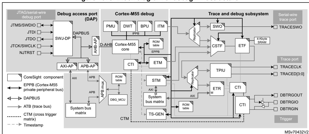
78.2 DBG functional description
The debug infrastructure is composed of three subsystems:
- • The Cortex-M55 incorporates the following CoreSight components:
- – SCS (system control space): contains registers used to identify and halt the processor. It accesses core data registers, and other debug features included in the processor core.
- – DWT: generates trace or debug events on access to specific addresses
- – BPU (breakpoint unit): allows the processor to be halted at specific addresses
- – ITM: generates software instrumentation trace, and adds timestamp, synchronization, and DWT event trace packets
- – ETM: generates non-intrusive program flow trace
- – PMU (performance monitoring unit): counts events for performance analysis
- – CTI: allows cross-triggering between different trace and debug components
- – processor ROM table: allows a debugger to discover CoreSight components in the Cortex-M55
- • The trace and debug subsystem includes the following CoreSight components:
- – ITM replicator: routes the ITM trace to both SWO and trace funnel
- – SWO: provides a single-wire asynchronous trace port for low-bandwidth trace coming from the ITM
- – CSTF (CoreSight trace funnel): merges trace from STM, ITM, and ETM
- – ETF: smooths the trace stream by buffering in a local memory
- – ETR replicator: routes trace from the CSTF to both ETR and TPIU
- – ETR: routes trace to a buffer in the system RAM
- – TPIU: provides a parallel trace port up to 16-bit wide for high-bandwidth trace coming from both ITM and ETM
- – CTI: allows cross triggering between different trace and debug components
- – system ROM table: allows a debugger to discover CoreSight components in the trace and debug subsystem
- – DBGMCU (MCU debug unit): controls the debug authentication, the low-power mode emulation, and freezes certain peripherals in debug mode and other features
- – STM: allows AXI bus masters to write trace data
- • The DAP (debug access port) allows an external debugger to access the debug and trace functionality. It contains the following CoreSight components:
- – SWJ-DP: implements a JTAG interface as well as a serial-wire debug (SWD) interface together with debug port (DP) registers
- – AHB-AP: AHB bus master that provides access to the trace and debug components in the Cortex-M55
- – APB-AP: APB bus master that provides access to the trace and debug subsystem
78.3 DBG block diagram
Figure 1075. Block diagram of debug infrastructure
78.4 DBG pins
Table 855. SWJ-DP pins
| Pin name | JTAG debug port | SWD debug port | Pin assignment | ||
|---|---|---|---|---|---|
| Type | Description | Type | Description | ||
| JTMS/SWDIO | I | JTAG test mode select | I/O | Serial-wire data in/out | Refer to the product datasheet |
| JTCK/SWCLK | I | JTAG test clock | I | Serial-wire clock | |
| JTDI | I | JTAG test data input | - | - | |
| JTDO | O | JTAG test data output | - | - | |
| NJTRST | I | JTAG test reset | - | - | |
Table 856. Trace port pins
| Pin name | Type | Description | Pin assignment |
|---|---|---|---|
| TRACED[3:0] | O | Trace synchronous data out (can be 1, 2, or 4 pins) | Refer to the product datasheet |
| TRACECLK | O | Trace clock |
Table 857. Serial-wire trace port pins
| Pin name | Type | Description | Pin assignment |
|---|---|---|---|
| TRACESWO | O | Trace asynchronous data out | Refer to the product datasheet (1) |
1. TRACESWO is multiplexed with JTDO. This means that single-wire trace is only available when using the JTAG port in serial-wire debug interface mode, not when using JTAG.
Table 858. Trigger pins
| Pin name | Type | Description | Pin assignment |
|---|---|---|---|
| DBTRGIN | I | External trigger input to CTI | Refer to the product datasheet |
| DBTRGOUT | O | External trigger output from CTI | |
| DBTRGIO | I/O | External bi-directional trigger (1) |
- 1. DBTRGIO can be configured as an input or an output by DBTRGOEN in DBGMCU_CR. If configured as an input, it is connected to DBTRGIN. If configured as an output, it is connected to DBTRGOUT. This is because DBTRGIN and DBTRGOUT may not be available on some packages.
78.5 DBG power, clock, and reset
78.5.1 DBG power domains
Debug components are located in the core power domain. This means that a debug session is disconnected if the core is powered down (for example in Standby mode).
Debug and low-power modes
The device includes power saving features that allow the core power domain to be switched off, or stopped when not required. If the power is switched off, or the core is not clocked, all debug components are inaccessible to the debugger. To avoid this, a power-saving mode emulation is implemented.
If emulation is enabled for a domain, the domain still enters power-saving mode, but its clock and power are maintained: the domain behaves as in power-saving mode, but the debugger does not lose the connection.
This emulation mode is programmed in the DBGMCU (see Section 78.12.20 ).
78.5.2 DBG clocks
The debugger supplies the clock for the debug port (swtclk) via the debug interface pin JTCK/SWCLK. This clock is used to register the serial input data in both serial-wire and JTAG modes, as well as to operate state machines and internal logic of the debug port. This clock must therefore continue to toggle for at least five cycles after the end of an access, to ensure that the debug port returns to the idle state.
The SWJ-DP contains an asynchronous interface to the system debug clock domain (ck_sys_dbg). All debug and trace components are in this same clock domain.
The ck_sys_dbg clock is enabled by the debugger using CDBGPWRUPREQ in DP_CTRLSTAT. It can also be enabled by software setting DBGCLKEN in DBGMCU_CR. This clock must be enabled before the debugger or software can access any of the debug features on the device. Disable this clock when debug and trace are not used, to reduce power consumption.
The TPIU output clock (ck_trace, also called traceclk) is generated by the RCC. Its frequency can be programmed to match the I/O port capability. This clock is also used to drive the SWO. It can only be enabled by setting TRACECLKEN in DBGMCU_CR.
Note: ck_trace must be activated whenever tracing is required, even if neither the TPIU nor the SWO are used (for example, when using the ETR as a software buffer). This avoids
filling up the SWO FIFO, which may then block the trace output from the ITM in the Cortex-M55.
The debug and trace components included in the processor are clocked with the processor clock.
78.5.3 Debug reset
The SWJ-DP is reset by a power-on reset (POR), and when waking up from Standby mode.
The debug and trace components, including the Cortex-M55 debug part, can be reset in three different ways:
- • Over the DAP by setting CDBGIRSTREQ in DP_CTRLSTAT
Setting this bit asserts the debug reset request signal (cdbgrstreq) connected to the RCC. The RCC then activates rcc_dbg_rst, and returns a handshake signal (cdbgrstack) to acknowledge the DAP request. This acknowledge can be read by the debugger on CDBGIRSTACK in DP_CTRLSTAT. The rcc_dbg_rst is active as long as CDBGIRSTREQ is set.
- • By the application setting DBGIRST in RCC_MISCRSTR
When this bit is set, the rcc_dbg_rst is activated. It is released when DBGIRST is cleared.
- • When a POR occurs
The rcc_dbg_rst is activated after a power-on reset, or when the product exits Standby mode.
Figure 1076. Debug reset control logic
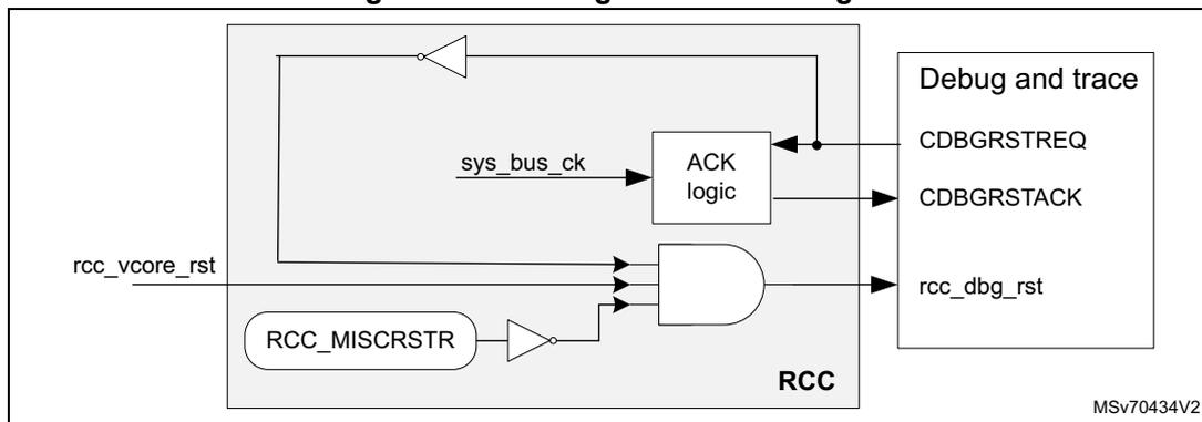
The diagram illustrates the debug reset control logic. On the left, the RCC block contains an RCC_MISCRSTR register. An external rcc_vcore_rst signal and the inverted output of the RCC_MISCRSTR register are inputs to an AND gate. The output of this AND gate is the rcc_dbg_rst signal, which is sent to the Debug and trace block. The Debug and trace block contains CDBGIRSTREQ and CDBGIRSTACK signals. The CDBGIRSTREQ signal is connected to the AND gate through a buffer. The CDBGIRSTACK signal is connected to the AND gate through a buffer. A sys_bus_ck signal is connected to an ACK logic block, which is also connected to the CDBGIRSTREQ and CDBGIRSTACK signals. The ACK logic block is connected to the CDBGIRSTREQ signal through a buffer.
The rcc_dbg_rst can be applied only when the processor is in a quiescent state (when all system transactions have been completed, or when the processor is in debug mode).
78.6 Security
The trace and debug components allow a high degree of access to the processor, and system during product development. To protect user code, and to ensure that debug features cannot be used to alter or compromise the normal operation of the finished product, these features can be disabled, or limited in scope. For example, a secure software debug and trace can be disabled without preventing the debug of non-secure code.
78.6.1 BSEC control over debug
The BSEC features the following registers dedicated to debug:
- • BSEC_AP_UNLOCK register
It can be used to open the debug access port to the Cortex-M55 (AP1) when a specific value is written in it. This register drives ap_unlocked[7:0] signals toward the debug logic that decodes these signals to open the access port if the expected value is met.
- • BSEC_DBGCR register
It can be used to enable the non-secure/secure debug when a specific value is written in it. This register drives dbg_unlocked_sec[7:0] and dbg_unlocked[7:0] signals toward the debug logic that decodes these signals to determine the values of the authentication signals (see the next section), enabling or not the debug for full secure or only non-secure world.
The BSEC also defines the HDPL (hide protection level) from which the debug is enabled. Its hardware ensures that dbg_unlocked and dbg_unlocked_sec automatically adopt the specific values as soon as the appropriate HDPL is reached.
On an open device, these registers are automatically set to the values that open the debug (refer to Section 4: Boot and security control (BSEC) for details on these registers.)
78.6.2 Authentication signals
The following authentication signals are used by a CoreSight system to determine which features are enabled or disabled. These signals are derived from the BSEC_DBGCR register value. This applies not only when the debug authentication sequence is executed, but also during the regular debug in open, closed, or closed secure states (refer to Section 3: System security for details on these states):
- •
dbgen
: global enable for all debug and trace features
0: All debug features are disabled.
1: Debug features in non-secure mode are enabled. Debug features in secure mode depend on the spiden state. - •
spiden
: enables debug in secure privileged mode when dbgen = 1.
0: Debug features are disabled in secure privileged mode. External access to secure system interconnect is disabled.
1: Debug features are enabled in secure privileged mode. External access to secure system interconnect is enabled. - •
niden
: enables trace and performance monitoring (non invasive debug).
0: Trace generation is disabled.
1: Trace generation in non-secure mode is enabled. Trace generation in non-secure mode depends on the spiden state. - •
spniden
: enables trace and performance monitoring in secure privileged mode when niden = 1.
0: Trace generation is disabled in secure privileged mode
1: Trace generation is enabled in secure privileged mode
For detailed information on the Arm Coresight debug infrastructure, refer to the relevant component section, or to the relevant Arm technical documentation, which describes the dbgen, niden, spiden and spniden signals. When the BSEC_DBGCR register is configured
to enable debug (either secure or non-secure), the dbgen and niden signals are set. The spiden and spniden signals are only set if secure debug is enabled.
The initial states of the signals are set at POR, according to Table 859 . Signal states can be modified through an authentication process, by a trusted software with secure and privileged access rights, in collaboration with the debugger (see Section 78.7 for more details on the authentication process).
Table 859. Authentication signal initial states
| Device state | Authentication signal default state | Description |
|---|---|---|
| Open or Closed_Unlocked DEV BOOT | All 1 | All debug and trace enabled at boot-up. |
| Closed | All 0 | All debug and trace disabled at boot-up. Secure software must enable debug as required after booting. |
78.7 Debug authentication
78.7.1 Main characteristics
The debug authentication relies on the fact that, even when debug is disabled, there is always an access port available (the APB-AP, AP0) to support communication between the host (debugger) and the device (STM32 product).
Debug rights (controlled by BSEC) are reset by a POR.
The debug authentication starts only at boot (HDPL1). This implies that a debugger hot plug is not possible on a closed part.
In BSEC-open state, the debugger can configure debug peripherals, and has full access to the system without the need for an authentication (but not to the fuse secrets, and unmapped ROM code).
During bootROM execution (HDPL0), the debug is automatically disabled via hardware.
When the debug is opened via a certificate, the debugger can proceed with debug infrastructure configuration. The debug certificate contains debugger access rights (secure, non-secure, HDPL).
When the debug is disabled, the debugger can still proceed with debug infrastructure 'discovery', but can only see the authentication mailbox. Other debug and trace features are disabled.
78.7.2 Debug authentication protocol
Principle
The protocol implements a challenge response mechanism based on asymmetric cryptography to authenticate the host. It relies on a key pair, with a public key stored in the device, and a private key from the host library, used to sign a random value (the challenge) generated by the device.
The protocol implements a bidirectional communication between the debugger (host) and the SoC (device) through a mailbox interface located in the DBGMCU.
The host can write to the mailbox via the JTAG/SWD interface. It expects to get responses and messages from the device via the same mailbox.
The debug authentication protocol is launched on a POR of the device, when an “open request” message is posted by the host. The protocol is based on the following steps:
- 1. Initial message: posted by the host, combined with a reset to launch the debug authentication process on the device
- 2. Challenge message: The device generates a random value, to be signed by the host, when sending back the response.
- 3. Response: The host sends a message to the device proving its authenticity. This is done using a tool to generate a token.
After a first sequence of mutual authentication to align (on protocol version, or device type for example), the device generates a random value that must be signed by the host with a private key when building the response.
The device verifies the signed response including the random value using a public key embedded in the device.
Status mailbox
A mailbox status information is provided to inform host or device that a message is available for reading. This is especially useful when one side sends a message larger than 32 bits. For instance, when the device sends such a long message, it checks that the host has read each 32-bit element before writing a new one by polling the clear of DEVICE_ACK.
The DBGMCU_DBG_AUTH_ACK register is used for that purpose. This register is read only for the host and the device:
- • HOST_ACK: this bit is set when the host writes a message in DBGMCU_DBG_AUTH_HOST. It indicates that a new message is present in the mailbox. This bit is reset when the device reads DBGMCU_DBG_AUTH_HOST. The device can poll this bit to know when the host has written a message.
- • DEVICE_ACK: this bit is set when the device writes a message in DBGMCU_DBG_AUTH_DEV, and reset when the host reads it. The host can poll this bit to know when the device has written a new message.
78.8 Chip-level TAP controller (CLTAPC)
The JTAG interface is connected to the internal scan chain of the device. It is used for testing as well as for debug. The first component in the scan chain is the chip-level TAP controller, which implements a TAP state machine based on IEEE Std 1149.1-1990. It allows access to the built-in manufacturing test features.
The CLTAPC must be bypassed in order to access the debug support functions provided by the SWJ-DP. This is done by prefixing SWJ-DP instructions with the CLTAPC bypass instruction sequence (0b11111).
78.9 Serial-wire and JTAG debug port (SWJ-DP)
The SWJ-DP is a CoreSight component that implements an external access port for connecting debugging equipment.
Two types of interface can be configured:
- • 5-pin standard JTAG interface (JTAG-DP)
- • 2-pin (clock + data) serial-wire debug port (SW-DP)
The two modes are mutually exclusive, since they share the same I/O pins.
By default, the JTAG-DP is selected after a system or POR. The five I/O pins are configured by hardware in debug alternative function mode. The SWJ-DP incorporates pull-up resistors on JTDI, JTMS/SWDIO, and NJTRST, as well as a pull-down resistor on JTCK/SWCLK.
A debugger can select the SW-DP by transmitting the following serial data sequence on JTMS/SWDIO:
...(50 or more ones)...,0,1,1,1,1,0,0,1,1,1,1,0,0,1,1,1,...(50 or more ones)...
JTCK/SWCLK must be cycled for each data bit.
In SW-DP mode, the unused JTAG pins (JTDI, JTDO, and NJTRST) can be used for other functions.
Note: All SWJ port I/Os can be reconfigured to other functions by software, but debugging is no longer possible.
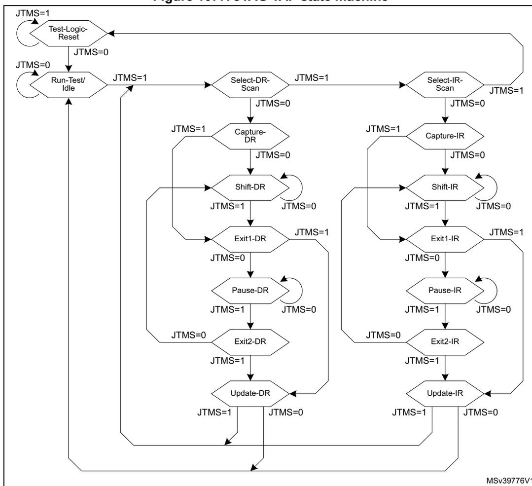
78.9.1 JTAG debug port
The JTAG-DP implements a TAP state machine (TAPSM) based on IEEE Std 1149.1-1990, and shown in Figure 1077 . It controls two scan chains: one associated with an instruction register (IR), and one with a number of data registers (DR).
Figure 1077. JTAG TAP state machine
stateDiagram-v2
    [*] --> Test-Logic-Reset: JTMS=1
    Test-Logic-Reset --> Run-Test/Idle: JTMS=0
    Run-Test/Idle --> Select-DR-Scan: JTMS=1
    Run-Test/Idle --> Select-IR-Scan: JTMS=1
    Select-DR-Scan --> Capture-DR: JTMS=0
    Select-DR-Scan --> Select-IR-Scan: JTMS=1
    Capture-DR --> Shift-DR: JTMS=0
    Capture-DR --> Select-DR-Scan: JTMS=1
    Shift-DR --> Shift-DR: JTMS=0
    Shift-DR --> Exit1-DR: JTMS=1
    Exit1-DR --> Select-DR-Scan: JTMS=1
    Exit1-DR --> Select-IR-Scan: JTMS=1
    Exit1-DR --> Pause-DR: JTMS=0
    Exit1-DR --> Exit2-DR: JTMS=0
    Exit1-DR --> Update-DR: JTMS=0
    Pause-DR --> Shift-DR: JTMS=0
    Pause-DR --> Select-DR-Scan: JTMS=1
    Pause-DR --> Select-IR-Scan: JTMS=1
    Pause-DR --> Exit2-DR: JTMS=0
    Pause-DR --> Update-DR: JTMS=0
    Exit2-DR --> Select-DR-Scan: JTMS=1
    Exit2-DR --> Select-IR-Scan: JTMS=1
    Exit2-DR --> Update-DR: JTMS=0
    Update-DR --> Run-Test/Idle: JTMS=1
    Update-DR --> Select-DR-Scan: JTMS=0
    Select-IR-Scan --> Capture-IR: JTMS=0
    Select-IR-Scan --> Select-DR-Scan: JTMS=1
    Capture-IR --> Shift-IR: JTMS=0
    Capture-IR --> Select-IR-Scan: JTMS=1
    Shift-IR --> Shift-IR: JTMS=0
    Shift-IR --> Exit1-IR: JTMS=1
    Exit1-IR --> Select-IR-Scan: JTMS=1
    Exit1-IR --> Pause-IR: JTMS=0
    Exit1-IR --> Exit2-IR: JTMS=0
    Exit1-IR --> Update-IR: JTMS=0
    Pause-IR --> Shift-IR: JTMS=0
    Pause-IR --> Select-IR-Scan: JTMS=1
    Pause-IR --> Exit2-IR: JTMS=0
    Pause-IR --> Update-IR: JTMS=0
    Exit2-IR --> Select-IR-Scan: JTMS=1
    Exit2-IR --> Update-IR: JTMS=0
    Update-IR --> Run-Test/Idle: JTMS=1
    Update-IR --> Select-DR-Scan: JTMS=0
MSV39776V1
When the TAPSM goes through the Capture-IR state, 0b0001 is transferred into the IR scan chain connected between JTDI and JTDO.
While the TAPSM is in the Shift-IR state, the IR scan chain shifts one bit for each JTCK rising edge. This means that on the first tick:
- • The LSB of the IR scan chain is output on JTDO.
- • Bit [n] of the IR scan chain is transferred to bit [n-1].
- • The value on JTDI is transferred to the MSB of the IR scan chain.
When the TAPSM goes through the Update-IR state, the value scanned in the IR scan chain is transferred to the instruction register.
When the TAPSM goes through the Capture-DR state, a value is transferred from one of DR to one of the DR scan chains, connected between JTDI and JTDO.
The value held in the instruction register determines which DR and associated DR scan chain are selected.
Data are then shifted while the TAPSM is in the Shift-DR state, in the same way as the IR shift in the Shift-IR state.
When the TAPSM goes through the Update-DR state, the value scanned in the DR scan chain is transferred to the selected DR.
When the TAPSM is in the Run-Test/Idle state, no special actions occur. The IDCODE instruction is loaded in IR.
When active, the NJTRST signal resets the state machine asynchronously to the test-logic-reset state.
The table below lists DRs corresponding to the 4-bit IR instructions.
Table 860. JTAG-DP data registers
| Instruction register | Data register | Scan chain length | Description |
|---|---|---|---|
| 0000 to 0111 | (BYPASS) | 1 | Not implemented: BYPASS selected |
| 1000 | ABORT | 35 | Abort register – Bits 34:1 = reserved – Bit 0 = APABORT: write 1 to generate an AP abort |
| 1001 | (BYPASS) | 1 | Reserved: BYPASS selected |
| 1010 | DPACC | 35 | Debug port access register Initiates the debug port and allows access to a debug port register. – When transferring data IN: Bits 34:3 = DATA[31:0] = 32-bit data to transfer for a write request Bits 2:1 = A[3:2] = 2-bit address of a debug port register. Bit 0 = RnW = read request (1) or write request (0). – When transferring data OUT: Bits 34:3 = DATA[31:0] = 32-bit data which is read following a read request Bits 2:0 = ACK[2:0] = 3-bit acknowledge: 0b010= OK/fault 0b000 = Wait Other = reserved |
| 1011 | APACC | 35 | Access port access register Initiates an access port and allows access to an access port register. – When transferring data IN: Bits 34:3 = DATA[31:0] = 32-bit data to shift in for a write request Bits 2:1 = A[3:2] = 2-bit sub-address of an access port register. Bit 0 = RnW= read request (1) or write request (0). – When transferring data OUT: Bits 34:3 = DATA[31:0] = 32-bit data which is read following a read request Bits 2:0 = ACK[2:0] = 3-bit acknowledge: 010b = OK/Fault 001b = Wait Other = reserved |
| 1100 | (BYPASS) | 1 | Reserved: BYPASS selected |
| 1101 | (BYPASS) | 1 | Reserved: BYPASS selected |
Table 860. JTAG-DP data registers (continued)
| Instruction register | Data register | Scan chain length | Description |
|---|---|---|---|
| 1110 | IDCODE | 32 | ID code 0x6BA00477: Arm JTAG debug port ID code |
| 1111 | BYPASS | 1 | Bypass A single JTCK cycle delay is inserted between JTDI and JTDO |
For more details on DR registers and the JTAG debug protocol, refer to the Arm Debug Interface Architecture Specification [1].
78.9.2 SWD debug port
The serial-wire debug protocol uses the two following pins:
- • SWCLK: clock from the host (debugger) to the device (STM32 product)
- • SWDIO: bidirectional serial data (with internal pull-up)
Serial data are transferred LSB first, synchronously with the clock. A transfer comprises the following phases:
- 1. packet request (8 bits) transmitted by the host
- 2. acknowledge response (3 bits) transmitted by the target
- 3. data transfer (33 bits) transmitted by the host (for a write) or the device (for a read)
The data transfer only occurs if the acknowledge response is OK.
If the direction of the data is reversed between each phase, a single clock cycle turn-around time is inserted.
Table 861. Packet request
| Bit(s) | Name | Description |
|---|---|---|
| 0 | Start | Must be 1 |
| 1 | APnDP | 0: DP register access (see
Table 864
for a list of DP registers) 1: AP register access (see Section 78.10 ) |
| 2 | RnW | 0: Write request 1: Read request |
| 4:3 | A(3:2) | Address field of DP or AP register (refer to Table 864 and Section 78.10 ) |
| 5 | Parity | Single bit parity of preceding bits |
| 6 | Stop | 0 |
| 7 | Park | Not driven by host. Must be read as 1 by the device. |
Table 862. ACK response
| Bitfield | Name | Description |
|---|---|---|
| 2:0 | ACK | 0b000: Fault 0b010: Wait 0b100: OK |
Table 863. Data transfer
| Bitfield | Name | Description |
|---|---|---|
| 31:0 | WDATA or RDATA | Write or read data |
| 32 | Parity | Single bit parity of 32 data bits |
Figure 1078 shows successful write and read transfers.
Figure 1078. SWD successful data transfer
![Timing diagram showing SWD successful data transfer. It illustrates the SWCLK line (a square wave) and the SWDIO line (a bidirectional data line). The diagram shows two transfers: a Write transfer and a Read transfer. The Write transfer starts with a Start bit (1), followed by APnDP (x), RnW (0), A[2] (x), A[3] (x), Parity (x), Stop (0), Park (1), Over (/), ACK[0] (1), ACK[1] (0), ACK[2] (0), Over (/), WDATA[0] (x), WDATA[1] (x), WDATA[2] (x), followed by a gap, then WDATA[29] (x), WDATA[30] (x), WDATA[31] (x), and Parity (x). The Read transfer starts with a Start bit (1), followed by APnDP (x), RnW (1), A[2] (x), A[3] (x), Parity (x), Stop (0), Park (1), Over (/), ACK[0] (1), ACK[1] (0), ACK[2] (0), RDATA[0] (x), RDATA[1] (x), RDATA[2] (x), followed by a gap, then RDATA[29] (x), RDATA[30] (x), RDATA[31] (x), Parity (x), and Over (/).](/RM0486-STM32N6x5-x7/0944d031d54b656f31ce542d3576a615_img.jpg)
Legend
- SWDIO driven by host
- SWDIO driven by target
Bit values: 1 – value is 1
0 – value is 0
x – value is 1 or 0
/ – transfer of SWDIO line possession
MSv39777V1
For any FAULT or WAIT ACK response from the device, the data transfer phase is canceled, unless overrun detection is enabled. If and overrun detection is enabled, data are ignored by the device (for a write), or not driven (for a read).
A line reset must be generated by the host when it is first connected, or following a protocol error. The line reset consists of 50 or more SWCLK cycles with SWDIO high, followed by two SWCLK cycles with SWDIO low.
For more details on the serial-wire debug protocol, refer to the Arm Debug Interface Architecture Specification [1].
Note: The SWJ-DP implements SWD protocol version 2.
78.9.3 Debug port registers
The SW-DP and JTAG-DP access the debug port (DP) registers, listed in Table 864 .
The debugger can access DP registers as follows:
- 1. Program DPBANKSEL in DP_SELECT to select the register bank to be accessed (see Table 864 ).
- 2. If using JTAG, program A[3:2] in the DPACC register with the register address within the bank. Program the R/W bit to select a read or a write. For a write, program the DATA field with the write data.
If using SWD, the A[3:2] and R/W fields are part of the packet request word sent to the SW-DP with the APnDP bit reset (see Table 861 ). The write data are sent in the data phase.
Table 864. Debug port registers
| Address | A[3:2] value | R/W | Description |
|---|---|---|---|
| 0x0 | 00 | R | DP_PIDR register (2) . Contains the IDCODE for the debug port. |
| W | DP_ABORT register (1) . Aborts the current AP transaction. This register is also used to clear the error flags in DP_CTRL/STAT. | ||
| 0x4 | 01 | R/W | If DPBANKSEL[3:0] = 0x0 in DP_SELECT: DP_CTRLSTAT register. Controls the DP and provides status information. |
| If DPBANKSEL[3:0] = 0x1 in DP_SELECT: DP_DLCR register (2) . Controls the operating mode of the SWD data link. | |||
| If DPBANKSEL[3:0] = 0x2 in DP_SELECT: DP_TARGETID register. Provides target identification information. | |||
| If DPBANKSEL[3:0] = 0x3 in DP_SELECT: DLPIDR register (2) . Provides the SWD protocol version. | |||
| 0x8 | 10 | R | RESEND register (2) . Returns the value that was returned by the last AP read or DP_RDBUFF read, used in the event of a corrupted read transfer. |
| W | DP_SELECT register. Selects the access port, access port register bank, and DP register at address 0x4. | ||
| 0xC | 11 | R | DP_RDBUFF register – Via JTAG-DP, enables the debugger to get the final result after a sequence of operations (without requesting new JTAG-DP operation). – Via SW-DP, contains the result of the preceding AP read access, allowing a new AP access to be avoided. |
| W | DP_TARGETSEL register
(2)
. On a write to DP_TARGETSEL immediately following a line reset sequence, the target is selected if the following conditions are both met: – Bits [31:28] match bits [31:28] in DP_DLPIDR. – Bits [27:0] match bits [27:0] in DP_TARGETID. Writing any other value deselects the target. Debug tools must write 0xFFFFFFFF to deselect all targets. This is an invalid DP_TARGETID value. All other invalid DP_TARGETID values are reserved. |
1. Access to the AP ABORT register from the JTAG-DP is done using the ABORT instruction.
2. Only accessible via SW-DP. Register is “reserved” via JTAG-DP.
Debug port identification register (DP_PIDR)
Address offset: 0x0
Reset value: 0x6BA0 2477
| 31 | 30 | 29 | 28 | 27 | 26 | 25 | 24 | 23 | 22 | 21 | 20 | 19 | 18 | 17 | 16 |
|---|---|---|---|---|---|---|---|---|---|---|---|---|---|---|---|
| REVISION[3:0] | PARTNO[7:0] | Res. | Res. | Res. | MIN | ||||||||||
| r | r | r | r | r | r | r | r | r | r | r | r | r | |||
| 15 | 14 | 13 | 12 | 11 | 10 | 9 | 8 | 7 | 6 | 5 | 4 | 3 | 2 | 1 | 0 |
| VERSION[3:0] | DESIGNER[10:0] | Res. | |||||||||||||
| r | r | r | r | r | r | r | r | r | r | r | r | r | r | r | |
Bits 31:28 REVISION[3:0] : Revision code
0x6
Bits 27:20 PARTNO[7:0] : Debug port part number
0xBA
Bits 19:17 Reserved, must be kept at reset value.
Bit 16 MIN : Minimal debug port (MINDP) implementation
0: MINDP not implemented (transaction counter and pushed operations are supported)
Bits 15:12 VERSION[3:0] : DP architecture version
0x2: DPv2
Bits 11:1 DESIGNER[10:0] : JEDEC designer identity code
0x23B: Arm
Bit 0 Reserved, must be kept at reset value.
Debug port abort register (DP_ABORT)
Address offset: 0x0
Reset value: 0x0000 0000
| 31 | 30 | 29 | 28 | 27 | 26 | 25 | 24 | 23 | 22 | 21 | 20 | 19 | 18 | 17 | 16 |
|---|---|---|---|---|---|---|---|---|---|---|---|---|---|---|---|
| Res. | Res. | Res. | Res. | Res. | Res. | Res. | Res. | Res. | Res. | Res. | Res. | Res. | Res. | Res. | Res. |
| 15 | 14 | 13 | 12 | 11 | 10 | 9 | 8 | 7 | 6 | 5 | 4 | 3 | 2 | 1 | 0 |
| Res. | Res. | Res. | Res. | Res. | Res. | Res. | Res. | Res. | Res. | Res. | ORUN ERRCLR | WDER RCLR | STKER RCLR | STKCM PCLR | DAP ABORT |
| w | w | w | w | w |
Bits 31:5 Reserved, must be kept at reset value.
Bit 4 ORUNERRCLR : Overrun error clear bit
0: No effect
1: Clear STICKYORUN in DP_CTRLSTAT.
Bit 3 WDERRCLR : Write data error clear bit
0: No effect
1: Clear WDATAERR in DP_CTRLSTAT.
Bit 2 STKERRCLR : Sticky error clear bit
0: No effect
1: Clear STICKYERR in DP_CTRLSTAT.
Bit 1 STKCMPCLR : Sticky compare clear bit
0: No effect
1: Clear STICKYCMP in DP_CTRLSTAT.
Bit 0 DAPABORT : Abort current AP transaction
The transaction is aborted if an excessive number of WAIT responses are returned.
This indicates that the transaction has stalled.
0: No effect
1: Abort the transaction.
Debug port control/status register (DP_CTRLSTAT)
Address offset: 0x4
Reset value: 0x0000 0000
| 31 | 30 | 29 | 28 | 27 | 26 | 25 | 24 | 23 | 22 | 21 | 20 | 19 | 18 | 17 | 16 |
|---|---|---|---|---|---|---|---|---|---|---|---|---|---|---|---|
| CSYSP WRUP ACK | CSYSP WRUP REQ | CDBG PWRU PACK | CDBG PWRU PREQ | CDBG RSTAC K | CDBG RSTRE Q | Res. | Res. | TRNCNT[11:4] | |||||||
| r | rw | r | rw | r | rw | rw | rw | rw | rw | rw | rw | rw | rw | ||
| 15 | 14 | 13 | 12 | 11 | 10 | 9 | 8 | 7 | 6 | 5 | 4 | 3 | 2 | 1 | 0 |
| TRNCNT[3:0] | MASKLANE[3:0] | WDATA ERR | READ OK | STICK YERR | STICK YCMP | TRNMODE[1:0] | STICKY ORUN | ORUND ETECT | |||||||
| rw | rw | rw | rw | rw | rw | rw | rw | r | r | rw | w | w | w | w | w |
Bit 31 CSYSPWRUPACK : System domain power-up status bit - not used in this device
Bit 30 CSYSPWRUPREQ : System domain power-up control bit - not used in this device
Bit 29 CDBGPWRUPACK : Debug domain power-up status bit
This bit is read-only. It returns the status of the debug domain power-up acknowledge signal from the power controller.
0: domain powered down
1: domain powered up
Bit 28 CDBGPWRUPREQ : Debug domain power-up/down control bit
This bit controls the debug domain power-up/down request signal to the power controller.
0: power-down requested
1: power-up requested
Bit 27 CDBGIRSTACK : Debug domain reset status bit - not used in this device
Bit 26 CDBGIRSTREQ : Debug domain reset control bit - not used in this device
Bits 25:24 Reserved, must be kept at reset value.
Bits 23:12 TRNCNT[11:0] : Transaction counter
To program a sequence of transactions to incremental addresses via an AP, this field is loaded with the number of transactions to perform. It is decremented on successful completion of each transaction.
Bits 11:8 MASKLANE[3:0]: Pushed-compare and pushed-verify masking bitsThe field indicates the bytes to be masked in pushed-compare and pushed-verify operations (TRNMODE = 1 or 2 in this register). In the pushed operations, the word supplied in an AP write transaction is compared with the current value at the target AP address.
1xxx: Include byte lane 3 in comparisons.
x1xx: Include byte lane 2 in comparisons.
xx1x: Include byte lane 1 in comparisons.
xxx1: Include byte lane 0 in comparisons.
Bit 7 WDATAERR: Write data error in SW-DPThe bit indicates one of the following:
- – a parity or a framing error on the data phase of a write operation
- – a write operation that had been accepted by the DP, and then discarded without being submitted to the AP
This bit is read-only. It is reset by writing 1 to WDERRCLR in DP_ABORT.
0: No error
1: Error has occurred.
Note: This bit is reserved in JTAG-DP.
Bit 6 READOK: AP read response in SW-DPThis bit indicates the response to the last AP read access. It is read-only.
0: Read not ok
1: Read ok
Note: This bit is reserved in JTAG-DP.
Bit 5 STICKYERR: Transaction error (read-only in SW-DP, R/W in JTAG-DP)This bit indicates that an error occurred during an AP transaction. In SW-DP, this bit is reset by writing 1 to STKERRCLR in DP_ABORT. In JTAG-DP, this bit is reset by programming it to 1.
0: No error
1: Error has occurred.
Bit 4 STICKYCMP: Compare match (read-only in SW-DP, R/W in JTAG-DP)This bit indicates that a match occurred in a pushed operation. In SW-DP, this bit is reset by writing 1 to STKCMPCLR in DP_ABORT. In JTAG-DP, this bit is reset by programming it to 1.
0: Match if TRNMODE = 0x1; no match if TRNMODE = 0x2
1: No match if TRNMODE = 0x1; match if TRNMODE = 0x2
Bits 3:2 TRNMODE[1:0]: Transfer mode for AP write operationsFor read operations, this field must be set to 0x0.
0x0: Normal operation - AP transactions are passed directly to the AP.
0x1: Pushed-verify operation. The DP stores the write data and performs a read transaction at the target AP address. The result of the read operation is compared with the stored data. If they do not match, the STICKYCMP bit is set in this register.
0x2: Pushed-compare operation. The DP stores the write data and performs a read transaction at the target AP address. The result of the read is compared with the stored data. If they match, the STICKYCMP bit is set.
0x3: Reserved
Note: In pushed operations, only the data bytes indicated by the MASKLANE field are included in the comparison.
Bit 1 STICKYORUN : Overrun (read-only in SW-DP, R/W in JTAG-DP)
This bit indicates that an overrun occurred (a new transaction received before previous transaction completed). This bit is only set if ORUNDETECT is set in this register. In SW-DP, this bit is reset by writing 1 to ORUNERRCLR in DP_ABORT. In JTAG-DP, this bit is reset by writing a 1 to it.
0: No overrun
1: Overrun occurred.
Bit 0 ORUNDETECT : Overrun detection mode enable
0: Overrun detection disabled
1: Overrun detection enabled. In the event of an overrun, the STICKYORUN bit is set and subsequent transactions are blocked until STICKYORUN is cleared.
Debug port data link control register (DP_DLCR)
Address offset: 0x4
Reset value: 0x0000 0040
| 31 | 30 | 29 | 28 | 27 | 26 | 25 | 24 | 23 | 22 | 21 | 20 | 19 | 18 | 17 | 16 |
|---|---|---|---|---|---|---|---|---|---|---|---|---|---|---|---|
| Res. | Res. | Res. | Res. | Res. | Res. | Res. | Res. | Res. | Res. | Res. | Res. | Res. | Res. | Res. | Res. |
| 15 | 14 | 13 | 12 | 11 | 10 | 9 | 8 | 7 | 6 | 5 | 4 | 3 | 2 | 1 | 0 |
| Res. | Res. | Res. | Res. | Res. | Res. | TURNROUND[1:0] | Res. | Res. | Res. | Res. | Res. | Res. | Res. | Res. | Res. |
| rw | rw |
Bits 31:10 Reserved, must be kept at reset value.
Bits 9:8 TURNROUND[1:0] : Tristate period for SWDIO
0x0: 1 data bit period
0x1: 2 data bit periods
0x2: 3 data bit periods
0x3: 4 data bit periods
Bits 7:0 Reserved, must be kept at reset value.
Debug port target identification register (DP_TARGETID)
Address offset: 0x4
Reset value: 0x0486 0041
| 31 | 30 | 29 | 28 | 27 | 26 | 25 | 24 | 23 | 22 | 21 | 20 | 19 | 18 | 17 | 16 |
|---|---|---|---|---|---|---|---|---|---|---|---|---|---|---|---|
| TREVISION[3:0] | TPARTNO[15:4] | ||||||||||||||
| r | r | r | r | r | r | r | r | r | r | r | r | r | r | r | r |
| 15 | 14 | 13 | 12 | 11 | 10 | 9 | 8 | 7 | 6 | 5 | 4 | 3 | 2 | 1 | 0 |
| TPARTNO[3:0] | TDESIGNER[10:0] | Res. | |||||||||||||
| r | r | r | r | r | r | r | r | r | r | r | r | r | r | r | |
Bits 31:28 TREVISION[3:0] : Device revision number
0x0: revision 1
Bits 27:12 TPARTNO[15:0] : Target part number
0x4860: STM32N6x5/x7xx
Bits 11:1 TDESIGNER[10:0] : Target designer JEDEC code
0x020: STMicroelectronics
Bit 0 Reserved, must be kept at reset value.
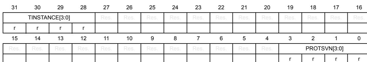
Debug port data link protocol identification register (DP_DLPIDR)
Address offset: 0x4
Reset value: 0x0000 0001
| 31 | 30 | 29 | 28 | 27 | 26 | 25 | 24 | 23 | 22 | 21 | 20 | 19 | 18 | 17 | 16 |
| TINSTANCE[3:0] | Res. | Res. | Res. | Res. | Res. | Res. | Res. | Res. | Res. | Res. | Res. | Res. | |||
| r | r | r | r | ||||||||||||
| 15 | 14 | 13 | 12 | 11 | 10 | 9 | 8 | 7 | 6 | 5 | 4 | 3 | 2 | 1 | 0 |
| Res. | Res. | Res. | Res. | Res. | Res. | Res. | Res. | Res. | Res. | Res. | Res. | PROTSVN[3:0] | |||
| r | r | r | r | ||||||||||||
Bits 31:28 TINSTANCE[3:0] : Target instance number
These bits define the instance number for this device in a multi-drop system: 0x0.
Bits 27:4 Reserved, must be kept at reset value.
Bits 3:0 PROTSVN[3:0] : Serial-wire debug protocol version
0x1: Version 2
Debug port resend register (DP_RESEND)
Address offset: 0x8
Reset value: 0x0000 0000
| 31 | 30 | 29 | 28 | 27 | 26 | 25 | 24 | 23 | 22 | 21 | 20 | 19 | 18 | 17 | 16 |
| RESEND[31:16] | |||||||||||||||
| r | r | r | r | r | r | r | r | r | r | r | r | r | r | r | r |
| 15 | 14 | 13 | 12 | 11 | 10 | 9 | 8 | 7 | 6 | 5 | 4 | 3 | 2 | 1 | 0 |
| RESEND[15:0] | |||||||||||||||
| r | r | r | r | r | r | r | r | r | r | r | r | r | r | r | r |
Bits 31:0 RESEND[31:0] : Last AP read or DP RDBUFF read value
These bits contain the value that was returned by the last AP read or DP RDBUFF read. Used in the event of a corrupted read transfer.
Debug port access port select register (DP_SELECT)
Address offset: 0x8
Reset value: 0xXXXX XXXX
| 31 | 30 | 29 | 28 | 27 | 26 | 25 | 24 | 23 | 22 | 21 | 20 | 19 | 18 | 17 | 16 |
|---|---|---|---|---|---|---|---|---|---|---|---|---|---|---|---|
| APSEL[7:0] | Res. | Res. | Res. | Res. | Res. | Res. | Res. | Res. | |||||||
| w | w | w | w | w | w | w | w | ||||||||
| 15 | 14 | 13 | 12 | 11 | 10 | 9 | 8 | 7 | 6 | 5 | 4 | 3 | 2 | 1 | 0 |
| Res. | Res. | Res. | Res. | Res. | Res. | Res. | Res. | APBANKSEL[3:0] | DPBANKSEL[3:0] | ||||||
| w | w | w | w | w | w | w | w | ||||||||
Bits 31:24 APSEL[7:0] : Access port select bits
These bits select the access port for the next transaction.
0x00: AP0 - System debug access port (APB-AP)
0x01: AP1 - Cortex-M55 debug access port (AHB-AP)
Others: reserved
Bits 23:8 Reserved, must be kept at reset value.
Bits 7:4 APBANKSEL[3:0] : AP register bank select bits
These bits select the 4-word register bank on the active AP for the next transaction.
Bits 3:0 DPBANKSEL[3:0] : DP register bank select bits
These bits select the register at address 0x4 of the debug port.
0x0: DP_CTRLSTAT register
0x1: DP_DLCR register
0x2: DP_TARGETID register
0x3: DP_DLPIDR register
Others: reserved
Debug port read buffer register (DP_RDBUFF)
Address offset: 0xC
Reset value: 0x0000 0000
| 31 | 30 | 29 | 28 | 27 | 26 | 25 | 24 | 23 | 22 | 21 | 20 | 19 | 18 | 17 | 16 |
|---|---|---|---|---|---|---|---|---|---|---|---|---|---|---|---|
| RDBUFF[31:16] | |||||||||||||||
| r | r | r | r | r | r | r | r | r | r | r | r | r | r | r | r |
| 15 | 14 | 13 | 12 | 11 | 10 | 9 | 8 | 7 | 6 | 5 | 4 | 3 | 2 | 1 | 0 |
| RDBUFF[15:0] | |||||||||||||||
| r | r | r | r | r | r | r | r | r | r | r | r | r | r | r | r |
Bits 31:0 RDBUFF[31:0] : Last AP read value
The field contains the value returned by the last AP read access. There are two ways to retrieve the value returned by an AP read access:
- – Perform a second read access to the same address, which initiates a new transaction on the corresponding bus./
- – Read the value returned by the last AP read access from the DP_RDBUFF register, in which case no new AP transaction occurs.
Debug port target identification register (DP_TARGETSEL)
Address offset: 0xC
Reset value: 0xXXXX XXXX
| 31 | 30 | 29 | 28 | 27 | 26 | 25 | 24 | 23 | 22 | 21 | 20 | 19 | 18 | 17 | 16 |
| TINSTANCE[3:0] | TPARTNO[15:4] | ||||||||||||||
| w | w | w | w | w | w | w | w | w | w | w | w | w | w | w | w |
| 15 | 14 | 13 | 12 | 11 | 10 | 9 | 8 | 7 | 6 | 5 | 4 | 3 | 2 | 1 | 0 |
| TPARTNO[3:0] | TDESIGNER[10:0] | Res. | |||||||||||||
| w | w | w | w | w | w | w | w | w | w | w | w | w | w | w | |
Bits 31:28 TINSTANCE[3:0] : Target instance number
This field defines the instance number for the target device in a multi-drop system. It must be programmed with the same value as TINSTANCE in DP_DLPIDR in order to select this device.
Bits 27:12 TPARTNO[15:0] : Target part number
This field defines the part number for the target device. It must be programmed with the same value as TPARTNO in DP_TARGETID in order to select this device.
Bits 11:1 TDESIGNER[10:0] : Target designer JEDEC code
This field defines the JEDEC code for the target device. It must be programmed with the same value as TDESIGNER in DP_TARGETID in order to select this device.
Bit 0 Reserved, must be kept at reset value.
Debug port register map
These registers are not on the CPU memory bus. They are only accessed through SW-DP and JTAG-DP debug interfaces.
The debug port address offset is 4-bit wide, where the two most significant bits are defined in the JTAG-DP register DPACC or SW-DP packet request A[3:2] field. The two least significant bits are 00.
Table 865. Debug port register map and reset values
| Offset | Register name | 31 | 30 | 29 | 28 | 27 | 26 | 25 | 24 | 23 | 22 | 21 | 20 | 19 | 18 | 17 | 16 | 15 | 14 | 13 | 12 | 11 | 10 | 9 | 8 | 7 | 6 | 5 | 4 | 3 | 2 | 1 | 0 | ||
|---|---|---|---|---|---|---|---|---|---|---|---|---|---|---|---|---|---|---|---|---|---|---|---|---|---|---|---|---|---|---|---|---|---|---|---|
| 0x0 | DP_DPIDR | REVISION [3:0] | PARTNO[7:0] | Res. | Res. | Res. | MIN | VERSION [3:0] | DESIGNER[10:0] | Res. | |||||||||||||||||||||||||
| Reset value | 0 | 1 | 1 | 0 | 1 | 0 | 1 | 1 | 1 | 1 | 0 | 1 | 0 | 0 | 0 | 0 | 1 | 0 | 0 | 1 | 0 | 0 | 0 | 1 | 1 | 1 | 0 | 1 | 1 | ||||||
| 0x0 | DP_ABORT | Res. | Res. | Res. | Res. | Res. | Res. | Res. | Res. | Res. | Res. | Res. | Res. | Res. | Res. | Res. | Res. | Res. | Res. | Res. | Res. | Res. | Res. | Res. | Res. | Res. | Res. | Res. | Res. | ORUNERRCLR | WDERRCLR | STKERRCLR | STKCMPCLR | DAPABORT | |
| Reset value | 0 | 0 | 0 | 0 | 0 | ||||||||||||||||||||||||||||||
| 0x4 (1) | DP_CTRLSTAT | CSYSPWRUPACK | CSYSPWRUPREQ | CDBGPWRUPACK | CDBGPWRUPREQ | CDBGRSTACK | CDBGRSTREQ | Res. | Res. | TRNCNT[11:0] | MASKLANE[3:0] | WDATAERR | READOK | STICKYERR | STICKYCMP | TRNMODE[1:0] | STICKYORUN | ORUNDETECT | |||||||||||||||||
| Reset value | 0 | 0 | 0 | 0 | 0 | 0 | 0 | 0 | 0 | 0 | 0 | 0 | 0 | 0 | 0 | 0 | 0 | 0 | 0 | 0 | 0 | 0 | 0 | 0 | 0 | 0 | 0 | 0 | 0 | 0 | 0 | ||||
| 0x4 (2) | DP_DLCR | Res. | Res. | Res. | Res. | Res. | Res. | Res. | Res. | Res. | Res. | Res. | Res. | Res. | Res. | Res. | Res. | Res. | Res. | Res. | Res. | Res. | Res. | TURNROUND [1:0] | Res. | Res. | Res. | Res. | Res. | Res. | Res. | Res. | Res. | Res. | |
| Reset value | 0 | 0 | 0 | ||||||||||||||||||||||||||||||||
Table 865. Debug port register map and reset values (continued)
| Offset | Register name | 31 | 30 | 29 | 28 | 27 | 26 | 25 | 24 | 23 | 22 | 21 | 20 | 19 | 18 | 17 | 16 | 15 | 14 | 13 | 12 | 11 | 10 | 9 | 8 | 7 | 6 | 5 | 4 | 3 | 2 | 1 | 0 | |
|---|---|---|---|---|---|---|---|---|---|---|---|---|---|---|---|---|---|---|---|---|---|---|---|---|---|---|---|---|---|---|---|---|---|---|
| 0x4 (3) | DP_TARGETID | TREVSION [3:0] | TPARTNO[15:0] | TDESIGNER[10:0] | Res | |||||||||||||||||||||||||||||
| Reset value | 0 | 0 | 0 | 0 | 0 | 1 | 0 | 0 | 1 | 0 | 0 | 0 | 0 | 1 | 1 | 0 | 0 | 0 | 0 | 0 | 0 | 0 | 0 | 0 | 0 | 1 | 0 | 0 | 0 | 0 | 0 | 0 | 1 | |
| 0x4 (4) | DP_DLPIDR | TINSTANCE [3:0] | Res | PROTSVN [3:0] | ||||||||||||||||||||||||||||||
| Reset value | 0 | 0 | 0 | 0 | 0 0 0 1 | |||||||||||||||||||||||||||||
| 0x8 | DP_RESEND | RESEND[31:0] | ||||||||||||||||||||||||||||||||
| Reset value | 0 | 0 | 0 | 0 | 0 | 0 | 0 | 0 | 0 | 0 | 0 | 0 | 0 | 0 | 0 | 0 | 0 | 0 | 0 | 0 | 0 | 0 | 0 | 0 | 0 | 0 | 0 | 0 | 0 | 0 | 0 | 0 | ||
| 0x8 | DP_SELECT | APSEL[7:0] | DPBANKSEL [3:0] | |||||||||||||||||||||||||||||||
| Reset value | X | X | X | X | X | X | X | X | Res | Res | Res | Res | Res | Res | Res | Res | Res | Res | Res | Res | Res | Res | Res | Res | Res | Res | Res | Res | Res | Res | Res | Res | ||
| 0xC | DP_RDBUFF | RDBUFF[31:0] | ||||||||||||||||||||||||||||||||
| Reset value | 0 | 0 | 0 | 0 | 0 | 0 | 0 | 0 | 0 | 0 | 0 | 0 | 0 | 0 | 0 | 0 | 0 | 0 | 0 | 0 | 0 | 0 | 0 | 0 | 0 | 0 | 0 | 0 | 0 | 0 | 0 | 0 | ||
| 0xC | DP_TARGETSEL | TINSTANCE [3:0] | TPARTNO[15:4] | TPARTNO [3:0] | Res | |||||||||||||||||||||||||||||
| Reset value | X | X | X | X | X | X | X | X | X | X | X | X | X | X | X | X | X | X | X | X | X | X | X | X | X | X | X | X | X | X | X | X | ||
- 1. DPBANKSEL[3:0] = 0x0
- 2. DPBANKSEL[3:0] = 0x1
- 3. DPBANKSEL[3:0] = 0x2
- 4. DPBANKSEL[3:0] = 0x3
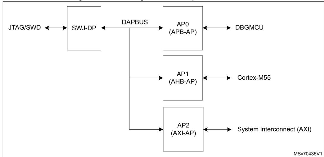
78.10 Access ports
There are three access ports (AP) attached to the DP.
Figure 1079. Debug and access port connections
    graph LR
      JTAG_SWD[JTAG/SWD] <--> SWJ_DP[SWJ-DP]
      SWJ_DP <--> DAPBUS[DAPBUS]
      DAPBUS --> AP0[AP0
(APB-AP)]
      DAPBUS --> AP1[AP1
(AHB-AP)]
      DAPBUS --> AP2[AP2
(AXI-AP)]
      AP0 <--> DBGMCU[DBGMCU]
      AP1 <--> Cortex_M55[Cortex-M55]
      AP2 <--> System_Interconnect[System interconnect (AXI)]
- • AP0 debug access port to DBGMCU (APB-AP): is always accessible during reset so that a debugger can initiate an authentication process even if it is a closed device.
- • AP1 Cortex-M55 access port (AHB-AP): allows access to the debug and trace features integrated in the Cortex-M55 processor via its PPB bus, and all other debug
components located on the EPPB interface (external private peripheral bus). In a closed device, AP1 is locked until the debug authentication process is complete.
- • AP2 system bus access port (AXI-AP): Allows access to the system bus matrix, which gives visibility of all the memory and peripherals accessible via the AXI interconnect. In a closed device, AP2 is locked until the debug authentication process is complete.
All access ports are of MEM-AP type: debug and trace component registers are mapped in the address space of the associated debug bus. The AP is seen by the debugger as a set of 32-bit registers organized in banks of four registers each. Some of these registers are used to configure or monitor the AP itself, while others are used to perform a transfer on the bus.
The address of the AP registers is composed of:
- • bits [7:4]: content of the DP_SELECT register's APBANKSEL field
- • bits [3:2]: content of the A(3:2) field of the APACC data register in the JTAG-DP (see Table 860 ) or of the SW-DP packet request (see Table 861 ), depending on the debug interface used
- • bits [1:0]: Always set to 0
The content of APSEL field in DP_SELECT defines which MEM-AP is being accessed.
The debugger can access the AP registers as follows:
- • Program APSEL field in DP_SELECT to choose one of the APs, and APBANKSEL field to select the register bank to be accessed.
- • If using JTAG, program A[3:2] field in the APACC register with the register address within the bank. Program the RnW bit to select a read or a write. For a write, program the DATA field with the write data.
If using SWD, the A(3:2) and RnW fields are part of the packet request word sent to the SW-DP with the APnDP bit set (see Table 861 ). The write data are sent in the data phase.
The debugger can access the memory-mapped debug component registers through the MEM-AP registers (using the AP register access procedure described above) as follows:
- 1. Program the transaction target address in APx_TAR.
- 2. Program APx_CSW, if necessary, with the transfer parameters (AddrInc for example).
- 3. Write to or read from APx_DRW to initiate a bus transaction at the address held in the APx_TAR register. Alternatively, a read or write to banked data register BDN triggers an access to address TAR[31:4] + n (this allows an access to the next four consecutive addresses without changing the address in APx_TAR).
For more detailed information on the MEM-AP, refer to the Arm Debug Interface Architecture Specification [1] .
Authentication
The effect of the authentication signals for AP1 and AP2 is shown in Table 866 .
Table 866. AP1-2 authentication behavior
| spiden | Others | Behavior |
|---|---|---|
| 0 | X | Secure transfers blocked. Any attempt to perform a secure transfer results in an error. Nonsecure transfers are enabled. |
| 1 | Both non-secure and secure transfers are enabled. |
78.10.1 AP0 registers
Access port 0 control/status word register (AP0_CSW)
Address offset: 0x0
Reset value: 0x8000 0002
| 31 | 30 | 29 | 28 | 27 | 26 | 25 | 24 | 23 | 22 | 21 | 20 | 19 | 18 | 17 | 16 |
|---|---|---|---|---|---|---|---|---|---|---|---|---|---|---|---|
| DBGSW ENABLE | Res. | Res. | Res. | Res. | Res. | Res. | Res. | Res. | Res. | Res. | Res. | Res. | Res. | Res. | Res. |
| rw | |||||||||||||||
| 15 | 14 | 13 | 12 | 11 | 10 | 9 | 8 | 7 | 6 | 5 | 4 | 3 | 2 | 1 | 0 |
| Res. | Res. | Res. | Res. | MODE[3:0] | TRINP ROG | DEVIC EEN | ADDRINC[1:0] | Res. | SIZE[2:0] | ||||||
| rw | rw | rw | rw | r | r | rw | rw | r | r | r | |||||
Bit 31 DBGSWENABLE : Software debug enable
This bit enables or disables software access to the APB bus via the APB interconnect. It must always be set to 1 to enable software access to the DBGMCU.
0 Disable software access.
1 Enable software access.
Bits 30:12 Reserved, must be kept at reset value.
Bits 11:8 MODE[3:0] : Mode of operation
0x0: Normal download or upload model.
Others: reserved
Bit 7 TRINPROG : Transfer in progress
This bit indicates that an AP bus transfer is in progress.
0: No transfer in progress
1: Bus transfer in progress
Bit 6 DEVICEEN : Device enable
This bit defines whether the AP can be accessed or not.
1: AP access enabled
Bits 5:4 ADDRINC[1:0] : Auto-increment mode bits
These bits define whether the TAR address is automatically incremented after a transaction.
0x0: No auto-increment
0x1: Address is incremented by the size in bytes of the transaction (SIZE in this register).
Others: reserved
Bit 3 Reserved, must be kept at reset value.
Bits 2:0 SIZE[2:0] : Size of next memory access transaction
0x2: Word (32-bit)
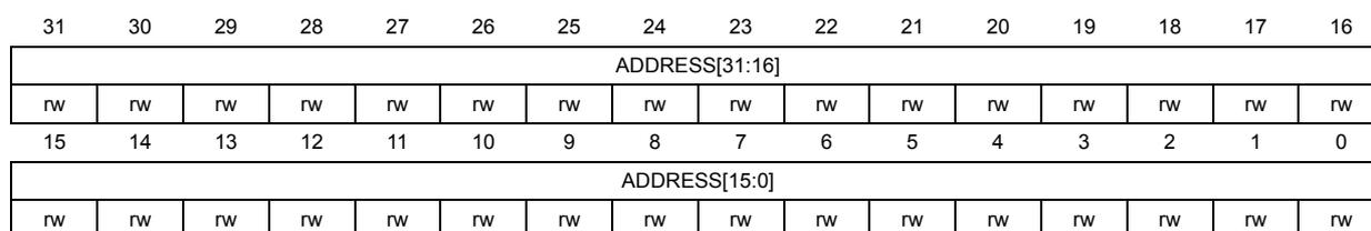
AP0 transfer address register (AP0_TAR)
Address offset: 0x04
Reset value: 0x0000 0000
| 31 | 30 | 29 | 28 | 27 | 26 | 25 | 24 | 23 | 22 | 21 | 20 | 19 | 18 | 17 | 16 |
| ADDRESS[31:16] | |||||||||||||||
| rw | rw | rw | rw | rw | rw | rw | rw | rw | rw | rw | rw | rw | rw | rw | rw |
| 15 | 14 | 13 | 12 | 11 | 10 | 9 | 8 | 7 | 6 | 5 | 4 | 3 | 2 | 1 | 0 |
| ADDRESS[15:0] | |||||||||||||||
| rw | rw | rw | rw | rw | rw | rw | rw | rw | rw | rw | rw | rw | rw | rw | rw |
Bits 31:0 ADDRESS[31:0] : address of the current transfer
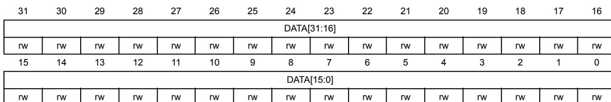
AP0 data read/write register (AP0_DRW)
Address offset: 0x0C
Reset value: 0x0000 0000

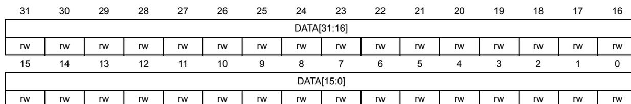
| 31 | 30 | 29 | 28 | 27 | 26 | 25 | 24 | 23 | 22 | 21 | 20 | 19 | 18 | 17 | 16 |
| DATA[31:16] | |||||||||||||||
| rw | rw | rw | rw | rw | rw | rw | rw | rw | rw | rw | rw | rw | rw | rw | rw |
| 15 | 14 | 13 | 12 | 11 | 10 | 9 | 8 | 7 | 6 | 5 | 4 | 3 | 2 | 1 | 0 |
| DATA[15:0] | |||||||||||||||
| rw | rw | rw | rw | rw | rw | rw | rw | rw | rw | rw | rw | rw | rw | rw | rw |
Bits 31:0 DATA[31:0] : read/write data for current transfer
In write mode, this is the write data value. In read mode, this is the read data value.
AP0 banked data register x (AP0_BDx)
Address offset: 0x10 + 0x4 * x (x = 0 to 3)
Reset value: 0x0000 0000
| 31 | 30 | 29 | 28 | 27 | 26 | 25 | 24 | 23 | 22 | 21 | 20 | 19 | 18 | 17 | 16 |
| DATA[31:16] | |||||||||||||||
| rw | rw | rw | rw | rw | rw | rw | rw | rw | rw | rw | rw | rw | rw | rw | rw |
| 15 | 14 | 13 | 12 | 11 | 10 | 9 | 8 | 7 | 6 | 5 | 4 | 3 | 2 | 1 | 0 |
| DATA[15:0] | |||||||||||||||
| rw | rw | rw | rw | rw | rw | rw | rw | rw | rw | rw | rw | rw | rw | rw | rw |
Bits 31:0 DATA[31:0] : Read/write data for current transfer
The transaction address is \( TAR[31:4] \ll 4 + 0x4 * x \) .
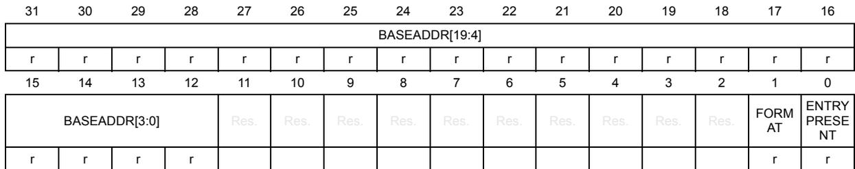
AP0 base address register (AP0_BASE)
Address offset: 0xF8
Reset value: 0x8000 0003
| 31 | 30 | 29 | 28 | 27 | 26 | 25 | 24 | 23 | 22 | 21 | 20 | 19 | 18 | 17 | 16 |
|---|---|---|---|---|---|---|---|---|---|---|---|---|---|---|---|
| BASEADDR[19:4] | |||||||||||||||
| r | r | r | r | r | r | r | r | r | r | r | r | r | r | r | r |
| 15 | 14 | 13 | 12 | 11 | 10 | 9 | 8 | 7 | 6 | 5 | 4 | 3 | 2 | 1 | 0 |
| BASEADDR[3:0] | Res. | Res. | Res. | Res. | Res. | Res. | Res. | Res. | Res. | FORM AT | ENTRY PRESE NT | ||||
| r | r | r | r | r | r | ||||||||||
Bits 31:12 BASEADDR[19:0] : Base address (bits 31 to 12) of the AP ROM table
The twelve LSBs are 0 since the ROM table must be aligned on a 4-Kbyte boundary.
0x800000: ROM table base address is 0x8000 0000
Bits 11:2 Reserved, must be kept at reset value.
Bit 1 FORMAT : Base-address register format
1: Arm debug interface v5
Bit 0 ENTRYPRESENT : Debug component present status
This bit indicates that debug components are present on the access port bus:
1: Debug components are present.
AP0 identification register (AP0_IDR)
Address offset: 0xFC
Reset value: 0x5477 0002 (AP0)
| 31 | 30 | 29 | 28 | 27 | 26 | 25 | 24 | 23 | 22 | 21 | 20 | 19 | 18 | 17 | 16 |
|---|---|---|---|---|---|---|---|---|---|---|---|---|---|---|---|
| REVISION[3:0] | JEDECBANK[3:0] | JEDECCODE[6:0] | MEMA P | ||||||||||||
| r | r | r | r | r | r | r | r | r | r | r | r | r | r | r | r |
| 15 | 14 | 13 | 12 | 11 | 10 | 9 | 8 | 7 | 6 | 5 | 4 | 3 | 2 | 1 | 0 |
| Res. | Res. | Res. | Res. | Res. | Res. | Res. | Res. | IDENTITY[7:0] | |||||||
| r | r | r | r | r | r | r | r | ||||||||
Bits 31:28 REVISION[3:0] : Arm core revision
0x5: r1p0
Bits 27:24 JEDECBANK[3:0] : JEDEC bank
0x4: Arm
Bits 23:17 JEDECCODE[6:0] : JEDEC code
0x3B: Arm
Bit 16 MEMAP : Memory access port
1: Standard register map
Bits 15:8 Reserved, must be kept at reset value.
Bits 7:0 IDENTITY[7:0] : AP type identification
0x02: APB-AP
AP0 register map
These registers are not on the CPU memory bus. They are only accessed through SW-DP and JTAG-DP debug interfaces.
The access port address is 8-bit wide, defined by APBANKSEL[3:0] in DP_SELECT and by JTAG-DP register DPACC or SW-DP packet request A[3:2] field.
Table 867. AP0 register map and reset values
| Offset | Register name | 31 | 30 | 29 | 28 | 27 | 26 | 25 | 24 | 23 | 22 | 21 | 20 | 19 | 18 | 17 | 16 | 15 | 14 | 13 | 12 | 11 | 10 | 9 | 8 | 7 | 6 | 5 | 4 | 3 | 2 | 1 | 0 | ||
|---|---|---|---|---|---|---|---|---|---|---|---|---|---|---|---|---|---|---|---|---|---|---|---|---|---|---|---|---|---|---|---|---|---|---|---|
| 0x00 | AP0_CSW | DBGSWENABLE | Res. | Res. | Res. | Res. | Res. | Res. | Res. | Res. | Res. | Res. | Res. | Res. | Res. | Res. | Res. | Res. | Res. | Res. | Res. | MODE[3:0] | TRINPROG | DEVICEEN | ADDRINC[1:0] | Res. | SIZE[2:0] | ||||||||
| Reset value | 1 | 0 | 0 | 0 | 0 | 0 | 0 | 0 | 0 | 0 | 0 | 0 | 1 | 0 | |||||||||||||||||||||
| 0x04 | AP0_TAR | ADDRESS[31:0] | |||||||||||||||||||||||||||||||||
| 0x08 | Reserved | Reserved | |||||||||||||||||||||||||||||||||
| 0x0C | AP0_DRW | DATA[31:0] | |||||||||||||||||||||||||||||||||
| 0x10 + 0x4 * x (x = 0 to 3) | AP0_BDx | DATA[31:0] | |||||||||||||||||||||||||||||||||
| 0x20-0xF4 | Reserved | Reserved | |||||||||||||||||||||||||||||||||
| 0xF8 | AP0_BASE | BASEADDR[19:0] | Res. | Res. | Res. | Res. | Res. | Res. | Res. | Res. | Res. | Res. | Res. | Res. | FORMAT | ENTRYPRESENT | |||||||||||||||||||
| Reset value | 1 | 0 | 0 | 0 | 0 | 0 | 0 | 0 | 0 | 0 | 0 | 0 | 0 | 0 | 0 | 0 | 0 | 0 | 0 | 0 | 1 | 1 | |||||||||||||
| 0xFC | AP0_IDR | REVISION[3:0] | JEDECBANK[3:0] | JEDECCODE[6:0] | MEMAP | Res. | Res. | Res. | Res. | Res. | Res. | Res. | Res. | Res. | IDENTITY[7:0] | ||||||||||||||||||||
| Reset value | 0 | 1 | 0 | 1 | 0 | 1 | 0 | 0 | 1 | 1 | 1 | 1 | 0 | 1 | 1 | 1 | |||||||||||||||||||
78.10.2 AP1 registers
Access port 1 control/status word register (AP1_CSW)
Address offset: 0x0
Reset value: 0x4000 0002
| 31 | 30 | 29 | 28 | 27 | 26 | 25 | 24 | 23 | 22 | 21 | 20 | 19 | 18 | 17 | 16 |
|---|---|---|---|---|---|---|---|---|---|---|---|---|---|---|---|
| Res. | SPROT | Res. | PROT[4:0] | SPISTA TUS | Res. | Res. | Res. | Res. | Res. | Res. | Res. | ||||
| rw | rw | rw | rw | rw | rw | r | |||||||||
| 15 | 14 | 13 | 12 | 11 | 10 | 9 | 8 | 7 | 6 | 5 | 4 | 3 | 2 | 1 | 0 |
| Res. | Res. | Res. | Res. | MODE[3:0] | TRINP ROG | DBGST ATUS | ADDRINC[1:0] | Res. | SIZE[2:0] | ||||||
| rw | rw | rw | rw | r | r | rw | rw | rw | rw | rw | |||||
Bit 31 Reserved, must be kept at reset value.
Bit 30 SPROT : Secure transfer request
This bit sets the protection attribute HPROT[6] of the bus transfer.
0: If spiden is high, secure transfer. If spiden is low, no transfer.
1: Nonsecure transfer
Bit 29 Reserved, must be kept at reset value.
Bits 28:24 PROT[4:0] : Bus transfer protection
This field sets the protection attributes HPROT[4:0] of the bus transfer.
xxxx0: Instruction fetch
xxxx1: Data access
xxx0x: User mode
xxx1x: Privileged mode
xx0xx: Non-bufferable
xx1xx: Bufferable
x0xxx: Non-cacheable
x1xxx: Cacheable
0xxxx: Non-exclusive
1xxxx: Exclusive
Bit 23 SPISTATUS : Status of spiden authentication signal
This bit determines whether the debugger can access secure memory.
0: Secure AHB transfers not supported
1: Secure AHB transfers allowed
Bits 22:12 Reserved, must be kept at reset value.
Bits 11:8 MODE[3:0] : Specifies the mode of operation
0x0: Normal download or upload mode
Others: reserved
Bit 7 TRINPROG : Transfer in progress
This bit indicates that an AP bus transfer is in progress.
0: No transfer in progress
1: Bus transfer in progress
Bit 6 DBGSTATUS : Debug status
Indicates the state of the dbgen authentication signal
0: No AHB transfers permitted
1: AHB transfers permitted
Bits 5:4 ADDRINC[1:0] : Auto-increment mode
These bits define whether the TAR address is automatically incremented after a transaction.
0x0: No auto-increment
0x1: Address incremented by the size in bytes of the transaction (SIZE field)
0x2: Packed transfers enabled. A 32-bit AP access generates a 1 x 32-bit, 2 x 16-bit, or
4 x 8-bit bus transaction corresponding to the programmed transaction size. Data are packed or unpacked accordingly.
0x3: Reserved
Bit 3 Reserved, must be kept at reset value.
Bits 2:0 SIZE[2:0] : Size of next memory access transaction
0x0: Byte (8-bit)
0x1: Half-word (16-bit)
0x2: Word (32-bit)
Others: Reserved
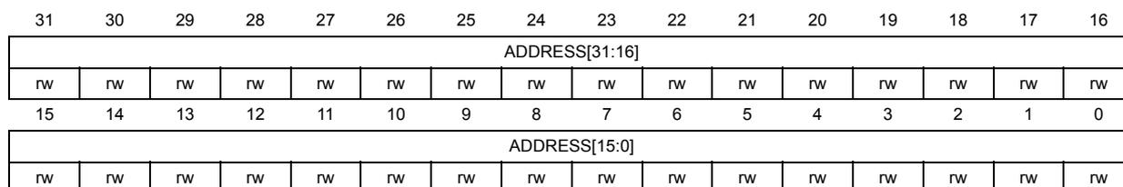
AP1 transfer address register (AP1_TAR)
Address offset: 0x04
Reset value: 0x0000 0000
| 31 | 30 | 29 | 28 | 27 | 26 | 25 | 24 | 23 | 22 | 21 | 20 | 19 | 18 | 17 | 16 |
|---|---|---|---|---|---|---|---|---|---|---|---|---|---|---|---|
| ADDRESS[31:16] | |||||||||||||||
| rw | rw | rw | rw | rw | rw | rw | rw | rw | rw | rw | rw | rw | rw | rw | rw |
| 15 | 14 | 13 | 12 | 11 | 10 | 9 | 8 | 7 | 6 | 5 | 4 | 3 | 2 | 1 | 0 |
| ADDRESS[15:0] | |||||||||||||||
| rw | rw | rw | rw | rw | rw | rw | rw | rw | rw | rw | rw | rw | rw | rw | rw |
Bits 31:0 ADDRESS[31:0] : Address of the current transfer
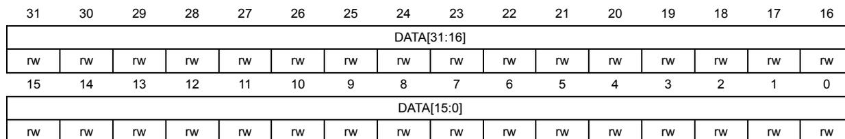
AP1 data read/write register (AP1_DRW)
Address offset: 0x0C
Reset value: 0x0000 0000

| 31 | 30 | 29 | 28 | 27 | 26 | 25 | 24 | 23 | 22 | 21 | 20 | 19 | 18 | 17 | 16 |
|---|---|---|---|---|---|---|---|---|---|---|---|---|---|---|---|
| DATA[31:16] | |||||||||||||||
| rw | rw | rw | rw | rw | rw | rw | rw | rw | rw | rw | rw | rw | rw | rw | rw |
| 15 | 14 | 13 | 12 | 11 | 10 | 9 | 8 | 7 | 6 | 5 | 4 | 3 | 2 | 1 | 0 |
| DATA[15:0] | |||||||||||||||
| rw | rw | rw | rw | rw | rw | rw | rw | rw | rw | rw | rw | rw | rw | rw | rw |
Bits 31:0 DATA[31:0] : Read/write data for current transfer
In write mode, this is the write data value. In read mode, this is the read data value.
AP1 banked data register x (AP1_BDx)
Address offset: 0x10 + 0x4 * x (x = 0 to 3)
Reset value: 0x0000 0000
| 31 | 30 | 29 | 28 | 27 | 26 | 25 | 24 | 23 | 22 | 21 | 20 | 19 | 18 | 17 | 16 |
|---|---|---|---|---|---|---|---|---|---|---|---|---|---|---|---|
| DATA[31:16] | |||||||||||||||
| rw | rw | rw | rw | rw | rw | rw | rw | rw | rw | rw | rw | rw | rw | rw | rw |
| 15 | 14 | 13 | 12 | 11 | 10 | 9 | 8 | 7 | 6 | 5 | 4 | 3 | 2 | 1 | 0 |
| DATA[15:0] | |||||||||||||||
| rw | rw | rw | rw | rw | rw | rw | rw | rw | rw | rw | rw | rw | rw | rw | rw |
Bits 31:0 DATA[31:0] : read/write data for current transfer
The transaction address is TAR[31:4] << 4 + 0x4 * x.
AP1 base address register (AP1_BASE)
Address offset: 0xF8
Reset value: 0xE00F E003
| 31 | 30 | 29 | 28 | 27 | 26 | 25 | 24 | 23 | 22 | 21 | 20 | 19 | 18 | 17 | 16 |
|---|---|---|---|---|---|---|---|---|---|---|---|---|---|---|---|
| BASEADDR[19:4] | |||||||||||||||
| r | r | r | r | r | r | r | r | r | r | r | r | r | r | r | r |
| 15 | 14 | 13 | 12 | 11 | 10 | 9 | 8 | 7 | 6 | 5 | 4 | 3 | 2 | 1 | 0 |
| BASEADDR[3:0] | Res. | Res. | Res. | Res. | Res. | Res. | Res. | Res. | Res. | Res. | FORM AT | ENTRY PRESENT | |||
| r | r | r | r | r | r | ||||||||||
Bits 31:12 BASEADDR[19:0] : Base address (bits 31 to 12) of the AP ROM table
The twelve LSBs are 0 since the ROM table must be aligned on a 4-Kbyte boundary.
0xE00FE: ROM table base address is at 0xE00F E000.
Bits 11:2 Reserved, must be kept at reset value.
Bit 1 FORMAT : Base address register format
1: Arm debug interface v5.
Bit 0 ENTRYPRESENT : Debug component present status
This bit indicates that debug components are present on the access port bus:
1: Debug components are present.
AP1 identification register (AP1_IDR)
Address offset: 0xFC
Reset value: 0x8477 0001 (AP1)
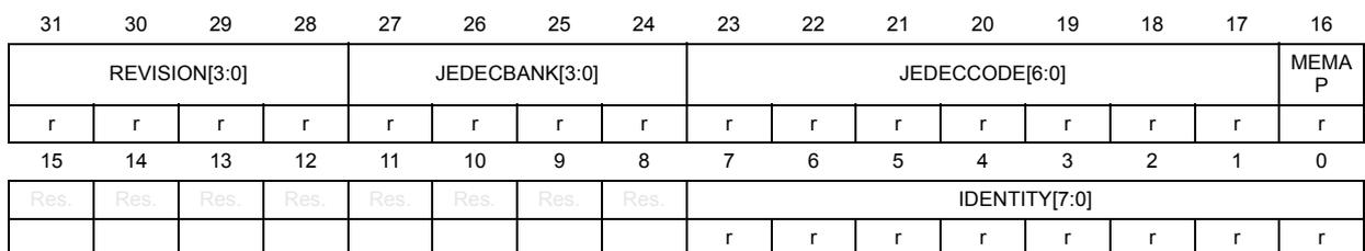
| 31 | 30 | 29 | 28 | 27 | 26 | 25 | 24 | 23 | 22 | 21 | 20 | 19 | 18 | 17 | 16 |
|---|---|---|---|---|---|---|---|---|---|---|---|---|---|---|---|
| REVISION[3:0] | JEDECBANK[3:0] | JEDECCODE[6:0] | MEMA P | ||||||||||||
| r | r | r | r | r | r | r | r | r | r | r | r | r | r | r | r |
| 15 | 14 | 13 | 12 | 11 | 10 | 9 | 8 | 7 | 6 | 5 | 4 | 3 | 2 | 1 | 0 |
| Res. | Res. | Res. | Res. | Res. | Res. | Res. | Res. | IDENTITY[7:0] | |||||||
| r | r | r | r | r | r | r | r | ||||||||
Bits 31:28 REVISION[3:0] : Arm core revision
0x8: r0p9
Bits 27:24 JEDECBANK[3:0] : JEDEC bank
0x4: Arm
Bits 23:17 JEDECCODE[6:0] : JEDEC code
0x3B: Arm
Bit 16
MEMAP
: Memory access port
1: Standard register map
Bits 15:8 Reserved, must be kept at reset value.
Bits 7:0
IDENTITY[7:0]
: AP type identification
0x01: AHB-AP
AP1 register map
These registers are not on the CPU memory bus. They are accessed only through SW-DP and JTAG-DP debug interfaces.
The access port address is 8-bit wide, defined by APBANKSEL[3:0] in DP_SELECTR, and by JTAG-DP register DPACC or SW-DP packet request A[3:2] field.
Table 868. AP1 register map and reset values
| Offset | Register name | 31 | 30 | 29 | 28 | 27 | 26 | 25 | 24 | 23 | 22 | 21 | 20 | 19 | 18 | 17 | 16 | 15 | 14 | 13 | 12 | 11 | 10 | 9 | 8 | 7 | 6 | 5 | 4 | 3 | 2 | 1 | 0 |
|---|---|---|---|---|---|---|---|---|---|---|---|---|---|---|---|---|---|---|---|---|---|---|---|---|---|---|---|---|---|---|---|---|---|
| 0x00 | AP1_CSW | Res. | SPROT | Res. | PROT[4:0] | SPISSTATUS | Res. | Res. | Res. | Res. | Res. | Res. | Res. | Res. | Res. | Res. | Res. | MODE[3:0] | TRINPROG | DEVICEEN | ADDRINC[1:0] | Res. | SIZE[2:0] | ||||||||||
| Reset value | 1 | 0 | 0 | 0 | 0 | 0 | 0 | 0 | 0 | 0 | 0 | 0 | 0 | 0 | 0 | 0 | 0 | 0 | 1 | 0 | |||||||||||||
| 0x04 | AP1_TAR | ADDRESS[31:0] | |||||||||||||||||||||||||||||||
| 0x08 | Reserved | Reserved | |||||||||||||||||||||||||||||||
| 0x0C | AP1_DRW | DATA[31:0] | |||||||||||||||||||||||||||||||
| Reset value | 0 | 0 | 0 | 0 | 0 | 0 | 0 | 0 | 0 | 0 | 0 | 0 | 0 | 0 | 0 | 0 | 0 | 0 | 0 | 0 | 0 | 0 | 0 | 0 | 0 | 0 | 0 | 0 | 0 | 0 | 0 | 0 | |
| 0x10 + 0x4 * x (x = 0 to 3) | AP1_BDx | DATA[31:0] | |||||||||||||||||||||||||||||||
| Reset value | 0 | 0 | 0 | 0 | 0 | 0 | 0 | 0 | 0 | 0 | 0 | 0 | 0 | 0 | 0 | 0 | 0 | 0 | 0 | 0 | 0 | 0 | 0 | 0 | 0 | 0 | 0 | 0 | 0 | 0 | 0 | 0 | |
| 0x20-0xF4 | Reserved | Reserved | |||||||||||||||||||||||||||||||
| 0xF8 | AP1_BASE | BASEADDR[19:0] | Res. | Res. | Res. | Res. | Res. | Res. | Res. | Res. | Res. | Res. | Res. | FORMAT | ENTRYPRESENT | ||||||||||||||||||
| Reset value | 1 | 1 | 1 | 0 | 0 | 0 | 0 | 0 | 0 | 0 | 0 | 0 | 1 | 1 | 1 | 1 | 1 | 1 | 1 | 0 | 1 | 1 | |||||||||||
| 0xFC | AP1_IDR | REVISION[3:0] | JEDECBANK[3:0] | JEDECCODE[6:0] | MEMAP | Res. | Res. | Res. | Res. | Res. | Res. | Res. | Res. | IDENTITY[7:0] | |||||||||||||||||||
| Reset value | 1 | 0 | 0 | 0 | 1 | 0 | 0 | 0 | 1 | 1 | 1 | 0 | 1 | 1 | 1 | 1 | 0 | 0 | 0 | 0 | 0 | 0 | 0 | 1 | |||||||||
78.10.3 AP2 registers
AP2 control/status word register (AP2_CSW)
Address offset: 0x0
Reset value: 0x30X0 60X2
| 31 | 30 | 29 | 28 | 27 | 26 | 25 | 24 | 23 | 22 | 21 | 20 | 19 | 18 | 17 | 16 |
|---|---|---|---|---|---|---|---|---|---|---|---|---|---|---|---|
| Res. | PROT[2:0] | CACHE[3:0] | SPISTA TUS | Res. | Res. | Res. | Res. | Res. | Res. | Res. | |||||
| rw | rw | rw | rw | rw | rw | rw | r | ||||||||
| 15 | 14 | 13 | 12 | 11 | 10 | 9 | 8 | 7 | 6 | 5 | 4 | 3 | 2 | 1 | 0 |
|---|---|---|---|---|---|---|---|---|---|---|---|---|---|---|---|
| Res. | DOMAIN[1:0] | ACEEN ABLE | MODE[3:0] | TRINP ROG | DBGST ATUS | ADDRINC[1:0] | Res. | SIZE[2:0] | |||||||
| rw | rw | rw | rw | rw | rw | rw | r | r | rw | rw | rw | rw | rw | ||
Bit 31 Reserved, must be kept at reset value.
Bits 30:28 PROT[2:0] : Access permissions
This field sets ARPROT[2:0] or AWPROT[2:0] attributes of the bus transfer.
xx0: Unprivileged access
xx1: Privileged access
x0x: Secure access
x1x: Nonsecure access
0xx: Data access
1xx: Instruction access
Bits 27:24 CACHE[3:0] : Memory type
This field sets ARCACHE[3:0] or AWCACHE[3:0] attributes of the bus transfer (see AMBA AXI and ACE Protocol Specification [7]).
Bit 23 SPISTATUS : Status of spider authentication signal
This bit determines whether the debugger can access secure memory.
0: Secure AXI transfers not supported
1: Secure AXI transfers are allowed.
Bits 22:15 Reserved, must be kept at reset value.
Bits 14:13 DOMAIN[1:0] : Shareable transaction encoding for ACE
0: Non-shareable
1: Shareable, inner domain, includes additional masters.
2: Shareable, outer domain, also includes inner or additional masters.
3: Shareable, system domain, all masters included
Bit 12 ACEENABLE : Enable ACE transactions, including barriers
0: Disable
1: Enable
Bits 11:8 MODE[3:0] : Specify mode of operation
0x0: Normal download or upload
0x1: Barrier transaction
Others: Reserved
Bit 7 TRINPROG : Transfer in progress
This bit indicates that an AP bus transfer is in progress.
0: No transfer in progress
1: Bus transfer in progress
Bit 6 DBGSTATUS : Debug status
This bit indicates the state of the dbgen authentication signal
0: No AXI transfers permitted
1: AXI transfers are permitted.
Bits 5:4 ADDRINC[1:0] : Auto-increment mode
These bits define whether the TAR address is automatically incremented after a transaction.
0x0: No auto-increment
0x1: Address is incremented by the size in bytes of the transaction (SIZE field).
0x2: Packed transfers enabled. A 32-bit AP access generates a 1 x 32-bit, 2 x 16-bit or 4 x 8-bit bus transaction corresponding to the programmed transaction size. The data is packed or unpacked accordingly.
0x3: Reserved
Bit 3 Reserved, must be kept at reset value.
Bits 2:0 SIZE[2:0] : Size of next memory access transaction
0x0: Byte (8-bit)
0x1: Half-word (16-bit)
0x2: Word (32-bit)
0x3: Double word (64-bit)
Others: Reserved
AP2 transfer address register (AP2_TAR)
Address offset: 0x04
Reset value: 0x0000 0000
| 31 | 30 | 29 | 28 | 27 | 26 | 25 | 24 | 23 | 22 | 21 | 20 | 19 | 18 | 17 | 16 |
| ADDRESS[31:16] | |||||||||||||||
| rw | rw | rw | rw | rw | rw | rw | rw | rw | rw | rw | rw | rw | rw | rw | rw |
| 15 | 14 | 13 | 12 | 11 | 10 | 9 | 8 | 7 | 6 | 5 | 4 | 3 | 2 | 1 | 0 |
| ADDRESS[15:0] | |||||||||||||||
| rw | rw | rw | rw | rw | rw | rw | rw | rw | rw | rw | rw | rw | rw | rw | rw |
Bits 31:0 ADDRESS[31:0] : Address of the current transfer
AP2 data read/write register (AP2_DRW)
Address offset: 0x0C
Reset value: 0x0000 0000
| 31 | 30 | 29 | 28 | 27 | 26 | 25 | 24 | 23 | 22 | 21 | 20 | 19 | 18 | 17 | 16 |
| DATA[31:16] | |||||||||||||||
| rw | rw | rw | rw | rw | rw | rw | rw | rw | rw | rw | rw | rw | rw | rw | rw |
| 15 | 14 | 13 | 12 | 11 | 10 | 9 | 8 | 7 | 6 | 5 | 4 | 3 | 2 | 1 | 0 |
| DATA[15:0] | |||||||||||||||
| rw | rw | rw | rw | rw | rw | rw | rw | rw | rw | rw | rw | rw | rw | rw | rw |
Bits 31:0 DATA[31:0] : Read/write data for current transfer
In write mode, this is the write data value. In read mode, this is the read data value.
For 64-bit transfers, two accesses must be made to DRW for a single 64-bit AXI access.
The first access in read mode initiates the read on the AXI bus and returns the lower 32-bit word of data. The second access returns the upper 32-bit word. In write mode, the first access contains the lower 32-bit word of data, the second access contains the upper 32-bit word and initiates the write on the AXI bus.
AP2 banked data register x (AP2_BDx)
Address offset: \( 0x10 + 0x4 \times x \) ( \( x = 0 \) to \( 3 \) )
Reset value: 0x0000 0000
| 31 | 30 | 29 | 28 | 27 | 26 | 25 | 24 | 23 | 22 | 21 | 20 | 19 | 18 | 17 | 16 |
|---|---|---|---|---|---|---|---|---|---|---|---|---|---|---|---|
| DATA[31:16] | |||||||||||||||
| rw | rw | rw | rw | rw | rw | rw | rw | rw | rw | rw | rw | rw | rw | rw | rw |
| 15 | 14 | 13 | 12 | 11 | 10 | 9 | 8 | 7 | 6 | 5 | 4 | 3 | 2 | 1 | 0 |
| DATA[15:0] | |||||||||||||||
| rw | rw | rw | rw | rw | rw | rw | rw | rw | rw | rw | rw | rw | rw | rw | rw |
Bits 31:0
DATA[31:0]
: Read/write data for current transfer
The transaction address is
\(
TAR[31:4] \ll 4 + 0x4 \times x
\)
.
64-bit banked data transactions are not supported
AP2 configuration register (AP2_CONFIG)
Address offset: 0xF4
Reset value: 0x0000 0002
| 31 | 30 | 29 | 28 | 27 | 26 | 25 | 24 | 23 | 22 | 21 | 20 | 19 | 18 | 17 | 16 |
|---|---|---|---|---|---|---|---|---|---|---|---|---|---|---|---|
| Res. | Res. | Res. | Res. | Res. | Res. | Res. | Res. | Res. | Res. | Res. | Res. | Res. | Res. | Res. | Res. |
| 15 | 14 | 13 | 12 | 11 | 10 | 9 | 8 | 7 | 6 | 5 | 4 | 3 | 2 | 1 | 0 |
| Res. | Res. | Res. | Res. | Res. | Res. | Res. | Res. | Res. | Res. | Res. | Res. | Res. | LD | LA | BE |
| r | r | r | |||||||||||||
Bits 31:3 Reserved, must be kept at reset value.
- Bit 2
LD
: Large data support
1: 64-bit data transfers supported - Bit 1
LA
: Long address support
0: 32-bit address only - Bit 0
BE
: Big-endian
0: Little-endian
AP2 base address register (AP2_BASE)
Address offset: 0xF8
Reset value: 0x0000 0002
| 31 | 30 | 29 | 28 | 27 | 26 | 25 | 24 | 23 | 22 | 21 | 20 | 19 | 18 | 17 | 16 |
|---|---|---|---|---|---|---|---|---|---|---|---|---|---|---|---|
| BASEADDR[19:4] | |||||||||||||||
| r | r | r | r | r | r | r | r | r | r | r | r | r | r | r | r |
| 15 | 14 | 13 | 12 | 11 | 10 | 9 | 8 | 7 | 6 | 5 | 4 | 3 | 2 | 1 | 0 |
| BASEADDR[3:0] | Res. | Res. | Res. | Res. | Res. | Res. | Res. | Res. | Res. | Res. | FORMAT | ENTRY PRESENT | |||
| r | r | r | r | r | r | ||||||||||
Bits 31:12
BASEADDR[19:0]
: Base address (bits 31 to 12) of the AP ROM table
Not applicable, no ROM table present
Bits 11:2 Reserved, must be kept at reset value.
Bit 1
FORMAT
: Base address register format
1: Arm debug interface v5
Bit 0
ENTRYPRESENT
: Debug component present status
This bit indicates that debug components are present on the access port bus:
0: No debug components are present.
AP2 identification register (AP2_IDR)
Address offset: 0xFC
Reset value: 0x4477 0004
| 31 | 30 | 29 | 28 | 27 | 26 | 25 | 24 | 23 | 22 | 21 | 20 | 19 | 18 | 17 | 16 |
|---|---|---|---|---|---|---|---|---|---|---|---|---|---|---|---|
| REVISION[3:0] | JEDECBANK[3:0] | JEDECCODE[6:0] | MEMA P | ||||||||||||
| r | r | r | r | r | r | r | r | r | r | r | r | r | r | r | r |
| 15 | 14 | 13 | 12 | 11 | 10 | 9 | 8 | 7 | 6 | 5 | 4 | 3 | 2 | 1 | 0 |
| Res. | Res. | Res. | Res. | Res. | Res. | Res. | Res. | IDENTITY[7:0] | |||||||
| r | r | r | r | r | r | r | r | ||||||||
Bits 31:28
REVISION[3:0]
: Arm core revision
0x4: r1p1
Bits 27:24
JEDECBANK[3:0]
: JEDEC bank
0x4: Arm
Bits 23:17
JEDECCODE[6:0]
: JEDEC code
0x3B: Arm
Bit 16
MEMAP
: Memory access port
1: Standard register map
Bits 15:8 Reserved, must be kept at reset value.
Bits 7:0
IDENTITY[7:0]
: AP type identification
0x04: AXB-AP
AP2 register map
These registers are not on the CPU memory bus. They are accessed only through SW-DP and JTAG-DP debug interfaces.
The access port address is 8-bit wide, defined by APBANKSEL[3:0] in DP_SELECTR, and by JTAG-DP register DPACC or SW-DP packet request A[3:2] field.
Table 869. AP2 register map and reset values
| Offset | Register name | 31 | 30 | 29 | 28 | 27 | 26 | 25 | 24 | 23 | 22 | 21 | 20 | 19 | 18 | 17 | 16 | 15 | 14 | 13 | 12 | 11 | 10 | 9 | 8 | 7 | 6 | 5 | 4 | 3 | 2 | 1 | 0 | ||
|---|---|---|---|---|---|---|---|---|---|---|---|---|---|---|---|---|---|---|---|---|---|---|---|---|---|---|---|---|---|---|---|---|---|---|---|
| 0x00 | AP2_CSW | Res | PROT[2:0] | CACHE[3:0] | SPSTATUS | Res | Res | Res | Res | Res | Res | Res | Res | DOMAIN[2:0] | ACEENABLE | MODE[3:0] | TRINPROG | DBGSTATUS | ADDRINC[1:0] | Res | SIZE[2:0] | ||||||||||||||
| Reset value | 0 | 1 | 1 | 0 | 0 | 0 | 0 | X | 1 | 1 | 0 | 0 | 0 | 0 | 0 | X | X | X | X | 0 | 1 | 0 | |||||||||||||
| 0x04 | AP2_TAR | ADDRESS[31:0] | |||||||||||||||||||||||||||||||||
| 0x08 | Reserved | Reserved | |||||||||||||||||||||||||||||||||
| 0x0C | AP2_DRW | DATA[31:0] | |||||||||||||||||||||||||||||||||
| 0x10 + 0x4 * x (x = 0 to 3) | AP2_BDx | DATA[31:0] | |||||||||||||||||||||||||||||||||
| 0x20-0xF0 | Reserved | Reserved | |||||||||||||||||||||||||||||||||
| 0xF4 | AP2_CONFIG | Res | Res | Res | Res | Res | Res | Res | Res | Res | Res | Res | Res | Res | Res | Res | Res | Res | Res | Res | Res | Res | Res | Res | Res | Res | Res | Res | Res | LD | LA | BE | |||
| Reset value | 0 | 1 | 0 | ||||||||||||||||||||||||||||||||
| 0xF8 | AP_BASE | BASEADDR[19:0] | Res | Res | Res | Res | Res | Res | Res | Res | Res | Res | FORMAT | ENTRYPRESENT | |||||||||||||||||||||
| Reset value | 0 | 0 | 0 | 0 | 0 | 0 | 0 | 0 | 0 | 0 | 0 | 0 | 0 | 0 | 0 | 0 | 0 | 0 | 0 | 1 | 0 | ||||||||||||||
| 0xFC | AP_IDR | REVISION[3:0] | JEDECBANK[3:0] | JEDECCODE[6:0] | MEMAP | Res | Res | Res | Res | Res | Res | Res | Res | Res | Res | Res | Res | Res | Res | Res | Res | Res | Res | Res | IDENTITY[7:0] | ||||||||||
| Reset value | 0 | 1 | 0 | 0 | 0 | 1 | 0 | 0 | 0 | 1 | 1 | 1 | 0 | 1 | 1 | 1 | 0 | 0 | 0 | 0 | 1 | 0 | 0 | ||||||||||||
78.10.4 ROM tables
The ROM table is a CoreSight component that contains the base addresses of all the CoreSight debug components accessible via the access port to which they are attached. These tables allow a debugger to discover the topology of the CoreSight system automatically.
The system ROM table is pointed to by the AP0 base register. It contains the base address pointer for the DBGMCU.
The system ROM table occupies a 4-Kbyte, 32-bit wide chunk of address space, from 0x8000 0000 to 0x8000 0FFC when accessed by the debugger.
Alternatively, it can be accessed by the CPU at address range 0x4400 0000 to 0x4400 0FFF.
Table 870. System ROM table| Address offset in ROM table | Component name | Component base address (debugger) | Component base address (system bus) | Component address offset | Size (Kbytes) | Entry |
|---|---|---|---|---|---|---|
| 0x000 | DBGMCU | 0x8000 1000 | 0x4400 1000 | 0x1000 | 4 | 0x0000 1003 |
| 0x004 | DFT register (1) | 0x8000 2000 | 0x4400 2000 | 0x2000 | 4 | 0x0000 2002 |
| 0x008 | Top of table | - | - | - | - | 0x0000 0000 |
| 0x00C to 0xFC8 | Reserved | - | - | - | - | 0x0000 0000 |
| 0xFCC to 0xFFC | ROM table registers | - | - | - | - | - |
1. Not CoreSight compatible. Bit 0 is reset to indicate that there are no CoreSight registers in this component.
The MCU ROM table is pointed to by the AP1 base register. It contains the base address pointer for the Cortex-M55 ROM table and for the trace subsystem ROM table.
It occupies a 4-Kbyte, 32-bit wide chunk of address space, from 0xE00F E000 to 0xE00F EFFF.
Table 871. MCU ROM table| Address offset in ROM table | Component name | Component base address | Component address offset | Size (Kbytes) | Entry |
|---|---|---|---|---|---|
| 0x000 | Cortex-M55 processor ROM table ( Table 873 ) | 0xE00F F000 | 0x0000 1000 | 4 | 0x0000 1003 |
| 0x004 | Trace subsystem ROM table ( Table 880 ) | 0xE008 0000 | 0xFFF8 2000 | 4 | 0xFFF8 2003 |
| 0x008 | Top of table | - | - | - | 0x0000 0000 |
| 0x00C to 0xFC8 | Reserved | - | - | - | 0x0000 0000 |
| 0xFCC to 0xFFC | ROM table registers | - | - | - | - |
The top of ROM tables contains a number of read-only registers, including the standard CoreSight component and peripheral identity registers (see Section 78.10.5 ).
Each debug component occupies one or more 4-Kbyte blocks of address space. This block of address space is referred to as the debug register file for the component.
The component address offset field of a ROM table entry points to the start of the last 4-Kbyte block of the address space of the component. This block always contains the component and peripheral ID registers for the component, starting at offset 0xFD0 from the start of the block. The 4-Kbyte count field PIDR4 [7:4], specifies the number of 4-Kbyte blocks for the component.
The process for finding the start of the address space for a component is:
- 1. Read the ROM-table entry for the component and extract its Address_Offset[18:0] from bits [31:12] of the ROM-table entry.
- 2. Use the address offset, together with the base address of the ROM table, ROM_Base_Address, to calculate the base address of the component:
The Component_Base_Address is the start address of the 4-Kbyte address space containing the CoreSight identity registers for the component.
- 3. Read the peripheral ID4 (PIDR4) register for the component. The address of this register is:
- 4. Extract the SIZE[7:4] field from the value of the peripheral ID4 register. This gives the number of 4-Kbyte sections of address space occupied by the component.
- 5. Use the SIZE field value to calculate the start address of the address space for the component:
\( \text{Component\_Start\_Address} = \text{Component\_Base\_Address} - \text{SIZE} \times 0\text{x1000} \) . If the field value is 0b0000, which corresponds to one 4-Kbyte section, the address space for the component starts at Component_Base_Address obtained at stage 2.
For more information on the use of the ROM tables, refer to the Arm Debug Interface Architecture Specification [1].
78.10.5 System/MCU ROM registers
SYSROM memory type register (SYSROM_MEMTYPE)
Address offset: 0xFCC
Reset value: 0x0000 0000
| 31 | 30 | 29 | 28 | 27 | 26 | 25 | 24 | 23 | 22 | 21 | 20 | 19 | 18 | 17 | 16 |
|---|---|---|---|---|---|---|---|---|---|---|---|---|---|---|---|
| Res. | Res. | Res. | Res. | Res. | Res. | Res. | Res. | Res. | Res. | Res. | Res. | Res. | Res. | Res. | Res. |
| 15 | 14 | 13 | 12 | 11 | 10 | 9 | 8 | 7 | 6 | 5 | 4 | 3 | 2 | 1 | 0 |
| Res. | Res. | Res. | Res. | Res. | Res. | Res. | Res. | Res. | Res. | Res. | Res. | Res. | Res. | Res. | SYSTM r |
Bits 31:1 Reserved, must be kept at reset value.
Bit 0 SYSTM : System memory
0: No system memory is present on this bus.
SYSROM CoreSight peripheral identity register 4 (SYSROM_PIDR4)
Address offset: 0xFD0
Reset value: 0x0000 0000
| 31 | 30 | 29 | 28 | 27 | 26 | 25 | 24 | 23 | 22 | 21 | 20 | 19 | 18 | 17 | 16 |
|---|---|---|---|---|---|---|---|---|---|---|---|---|---|---|---|
| Res. | Res. | Res. | Res. | Res. | Res. | Res. | Res. | Res. | Res. | Res. | Res. | Res. | Res. | Res. | Res. |
| 15 | 14 | 13 | 12 | 11 | 10 | 9 | 8 | 7 | 6 | 5 | 4 | 3 | 2 | 1 | 0 |
| Res. | Res. | Res. | Res. | Res. | Res. | Res. | Res. | SIZE[3:0] | JEP106CON[3:0] | ||||||
| r | r | r | r | r | r | r | r | ||||||||
Bits 31:8 Reserved, must be kept at reset value.
Bits 7:4 SIZE[3:0] : Register file size
0x0: Register file occupies a single 4-Kbyte region.
Bits 3:0 JEP106CON[3:0] : JEP106 continuation code
0x0: STMicroelectronics JEDEC continuation code
SYSROM CoreSight peripheral identity register 0 (SYSROM_PIDR0)
Address offset: 0xFE0
Reset value: 0x0000 0099
| 31 | 30 | 29 | 28 | 27 | 26 | 25 | 24 | 23 | 22 | 21 | 20 | 19 | 18 | 17 | 16 |
|---|---|---|---|---|---|---|---|---|---|---|---|---|---|---|---|
| Res. | Res. | Res. | Res. | Res. | Res. | Res. | Res. | Res. | Res. | Res. | Res. | Res. | Res. | Res. | Res. |
| 15 | 14 | 13 | 12 | 11 | 10 | 9 | 8 | 7 | 6 | 5 | 4 | 3 | 2 | 1 | 0 |
| Res. | Res. | Res. | Res. | Res. | Res. | Res. | Res. | PARTNUM[7:0] | |||||||
| r | r | r | r | r | r | r | r | ||||||||
Bits 31:8 Reserved, must be kept at reset value.
Bits 7:0 PARTNUM[7:0] : Device part number field, bits [7:0]
0x86: STM32N6 device
SYSROM CoreSight peripheral identity register 1 (SYSROM_PIDR1)
Address offset: 0xFE4
Reset value: 0x0000 0004
| 31 | 30 | 29 | 28 | 27 | 26 | 25 | 24 | 23 | 22 | 21 | 20 | 19 | 18 | 17 | 16 |
|---|---|---|---|---|---|---|---|---|---|---|---|---|---|---|---|
| Res. | Res. | Res. | Res. | Res. | Res. | Res. | Res. | Res. | Res. | Res. | Res. | Res. | Res. | Res. | Res. |
| 15 | 14 | 13 | 12 | 11 | 10 | 9 | 8 | 7 | 6 | 5 | 4 | 3 | 2 | 1 | 0 |
| Res. | Res. | Res. | Res. | Res. | Res. | Res. | Res. | JEP106ID[3:0] | PARTNUM[11:8] | ||||||
| r | r | r | r | r | r | r | r | ||||||||
Bits 31:8 Reserved, must be kept at reset value.
Bits 7:4 JEP106ID[3:0] : JEP106 identity code field, bits [3:0]
0x0: STMicroelectronics JEDEC code
Bits 3:0 PARTNUM[11:8] : Device part number field, bits [11:8]
0x4: STM32N6x5/x7xx device
SYSROM CoreSight peripheral identity register 2 (SYSROM_PIDR2)Address offset: 0xFE8
Reset value: 0x0000 001A
| 31 | 30 | 29 | 28 | 27 | 26 | 25 | 24 | 23 | 22 | 21 | 20 | 19 | 18 | 17 | 16 |
|---|---|---|---|---|---|---|---|---|---|---|---|---|---|---|---|
| Res. | Res. | Res. | Res. | Res. | Res. | Res. | Res. | Res. | Res. | Res. | Res. | Res. | Res. | Res. | Res. |
| 15 | 14 | 13 | 12 | 11 | 10 | 9 | 8 | 7 | 6 | 5 | 4 | 3 | 2 | 1 | 0 |
| Res. | Res. | Res. | Res. | Res. | Res. | Res. | Res. | REVISION[3:0] | JEDEC | JEP106ID[6:4] | |||||
| r | r | r | r | r | r | r | r | ||||||||
Bits 31:8 Reserved, must be kept at reset value.
Bits 7:4 REVISION[3:0] : Device revision number0x0: Not used
Bit 3 JEDEC : JEDEC assigned value1: Designer ID specified by JEDEC
Bits 2:0 JEP106ID[6:4] : JEP106 identity code field, bits [6:4]0x2: STMicroelectronics JEDEC code
SYSROM CoreSight peripheral identity register 3 (SYSROM_PIDR3)Address offset: 0xFEC
Reset value: 0x0000 0000
| 31 | 30 | 29 | 28 | 27 | 26 | 25 | 24 | 23 | 22 | 21 | 20 | 19 | 18 | 17 | 16 |
|---|---|---|---|---|---|---|---|---|---|---|---|---|---|---|---|
| Res. | Res. | Res. | Res. | Res. | Res. | Res. | Res. | Res. | Res. | Res. | Res. | Res. | Res. | Res. | Res. |
| 15 | 14 | 13 | 12 | 11 | 10 | 9 | 8 | 7 | 6 | 5 | 4 | 3 | 2 | 1 | 0 |
| Res. | Res. | Res. | Res. | Res. | Res. | Res. | Res. | REVAND[3:0] | CMOD[3:0] | ||||||
| r | r | r | r | r | r | r | r | ||||||||
Bits 31:8 Reserved, must be kept at reset value.
Bits 7:4 REVAND[3:0] : Metal fix version0x0: No metal fix
Bits 3:0 CMOD[3:0] : Customer modified0x0: No customer modifications
SYSROM CoreSight component identity register 0 (SYSROM_CIDR0)Address offset: 0xFF0
Reset value: 0x0000 000D
| 31 | 30 | 29 | 28 | 27 | 26 | 25 | 24 | 23 | 22 | 21 | 20 | 19 | 18 | 17 | 16 |
|---|---|---|---|---|---|---|---|---|---|---|---|---|---|---|---|
| Res. | Res. | Res. | Res. | Res. | Res. | Res. | Res. | Res. | Res. | Res. | Res. | Res. | Res. | Res. | Res. |
| 15 | 14 | 13 | 12 | 11 | 10 | 9 | 8 | 7 | 6 | 5 | 4 | 3 | 2 | 1 | 0 |
| Res. | Res. | Res. | Res. | Res. | Res. | Res. | Res. | PREAMBLE[7:0] | |||||||
| r | r | r | r | r | r | r | r | ||||||||
Bits 31:8 Reserved, must be kept at reset value.
Bits 7:0 PREAMBLE[7:0] : Component ID field, bits [7:0]
0x0D: Common ID value
SYSROM CoreSight component identity register 1 (SYSROM_CIDR1)
Address offset: 0xFF4
Reset value: 0x0000 0010
| 31 | 30 | 29 | 28 | 27 | 26 | 25 | 24 | 23 | 22 | 21 | 20 | 19 | 18 | 17 | 16 |
|---|---|---|---|---|---|---|---|---|---|---|---|---|---|---|---|
| Res. | Res. | Res. | Res. | Res. | Res. | Res. | Res. | Res. | Res. | Res. | Res. | Res. | Res. | Res. | Res. |
| 15 | 14 | 13 | 12 | 11 | 10 | 9 | 8 | 7 | 6 | 5 | 4 | 3 | 2 | 1 | 0 |
| Res. | Res. | Res. | Res. | Res. | Res. | Res. | Res. | CLASS[3:0] | PREAMBLE[11:8] | ||||||
| r | r | r | r | r | r | r | r | ||||||||
Bits 31:8 Reserved, must be kept at reset value.
Bits 7:4 CLASS[3:0] : Component ID field, bits [15:12] - component class
0x1: ROM table component
Bits 3:0 PREAMBLE[11:8] : Component ID field, bits [11:8]
0x0: Common ID value
SYSROM CoreSight component identity register 2 (SYSROM_CIDR2)
Address offset: 0xFF8
Reset value: 0x0000 0005
| 31 | 30 | 29 | 28 | 27 | 26 | 25 | 24 | 23 | 22 | 21 | 20 | 19 | 18 | 17 | 16 |
|---|---|---|---|---|---|---|---|---|---|---|---|---|---|---|---|
| Res. | Res. | Res. | Res. | Res. | Res. | Res. | Res. | Res. | Res. | Res. | Res. | Res. | Res. | Res. | Res. |
| 15 | 14 | 13 | 12 | 11 | 10 | 9 | 8 | 7 | 6 | 5 | 4 | 3 | 2 | 1 | 0 |
| Res. | Res. | Res. | Res. | Res. | Res. | Res. | Res. | PREAMBLE[19:12] | |||||||
| r | r | r | r | r | r | r | r | ||||||||
Bits 31:8 Reserved, must be kept at reset value.
Bits 7:0 PREAMBLE[19:12] : Component ID field, bits [23:16]
0x05: Common ID value
SYSROM CoreSight component identity register 3 (SYSROM_CIDR3)
Address offset: 0xFFC
Reset value: 0x0000 00B1
| 31 | 30 | 29 | 28 | 27 | 26 | 25 | 24 | 23 | 22 | 21 | 20 | 19 | 18 | 17 | 16 |
|---|---|---|---|---|---|---|---|---|---|---|---|---|---|---|---|
| Res. | Res. | Res. | Res. | Res. | Res. | Res. | Res. | Res. | Res. | Res. | Res. | Res. | Res. | Res. | Res. |
| 15 | 14 | 13 | 12 | 11 | 10 | 9 | 8 | 7 | 6 | 5 | 4 | 3 | 2 | 1 | 0 |
| Res. | Res. | Res. | Res. | Res. | Res. | Res. | Res. | PREAMBLE[27:20] | |||||||
| r | r | r | r | r | r | r | r | ||||||||
Bits 31:8 Reserved, must be kept at reset value.
Bits 7:0
PREAMBLE[27:20]
: Component ID field, bits [31:24]
0xB1: Common ID value
System ROM register map
Table 872. System ROM table register map and reset values
| Offset | Register name | 31 | 30 | 29 | 28 | 27 | 26 | 25 | 24 | 23 | 22 | 21 | 20 | 19 | 18 | 17 | 16 | 15 | 14 | 13 | 12 | 11 | 10 | 9 | 8 | 7 | 6 | 5 | 4 | 3 | 2 | 1 | 0 |
|---|---|---|---|---|---|---|---|---|---|---|---|---|---|---|---|---|---|---|---|---|---|---|---|---|---|---|---|---|---|---|---|---|---|
| 0xFCC | SYSROM_MEMTYPE | Res. | SYSMEM | ||||||||||||||||||||||||||||||
| Reset value | 0 | ||||||||||||||||||||||||||||||||
| 0xFD0 | SYSROM_PIDR4 | Res. | SIZE[3:0] | JEP106CON[3:0] | |||||||||||||||||||||||||||||
| Reset value | 0 | 0 | 0 | 0 | 0 | 0 | 0 | 0 | |||||||||||||||||||||||||
| 0xFD4-0xFDC | Reserved | Reserved | |||||||||||||||||||||||||||||||
| 0xFE0 | SYSROM_PIDR0 | Res. | PARTNUM[7:0] | ||||||||||||||||||||||||||||||
| Reset value | 1 | 0 | 0 | 0 | 0 | 0 | 1 | 1 | 1 | 0 | |||||||||||||||||||||||
| 0xFE4 | SYSROM_PIDR1 | Res. | JEP106ID[3:0] | PARTNUM[11:8] | |||||||||||||||||||||||||||||
| Reset value | 0 | 0 | 0 | 0 | 0 | 1 | 0 | 0 | 0 | 0 | |||||||||||||||||||||||
| 0xFE8 | SYSROM_PIDR2 | Res. | REVISION[3:0] | JEDEC | JEP106ID[6:4] | ||||||||||||||||||||||||||||
| Reset value | 0 | 0 | 0 | 0 | 1 | 0 | 1 | 0 | 0 | 0 | |||||||||||||||||||||||
| 0xFEC | SYSROM_PIDR3 | Res. | REVAND[3:0] | CMOD[3:0] | |||||||||||||||||||||||||||||
| Reset value | 0 | 0 | 0 | 0 | 0 | 0 | 0 | 0 | 0 | 0 | |||||||||||||||||||||||
| 0xFF0 | SYSROM_CIDR0 | Res. | PREAMBLE[7:0] | ||||||||||||||||||||||||||||||
| Reset value | 0 | 0 | 0 | 0 | 1 | 1 | 1 | 0 | 1 | 1 | |||||||||||||||||||||||
| 0xFF4 | SYSROM_CIDR1 | Res. | CLASS[3:0] | PREAMBLE[11:8] | |||||||||||||||||||||||||||||
| Reset value | 0 | 0 | 0 | 1 | 0 | 0 | 0 | 0 | 0 | 0 | |||||||||||||||||||||||
| 0xFF8 | SYSROM_CIDR2 | Res. | PREAMBLE[19:12] | ||||||||||||||||||||||||||||||
| Reset value | 0 | 0 | 0 | 0 | 0 | 1 | 0 | 1 | 0 | 0 | |||||||||||||||||||||||
Table 872. System ROM table register map and reset values (continued)
| Offset | Register name | 31 | 30 | 29 | 28 | 27 | 26 | 25 | 24 | 23 | 22 | 21 | 20 | 19 | 18 | 17 | 16 | 15 | 14 | 13 | 12 | 11 | 10 | 9 | 8 | 7 | 6 | 5 | 4 | 3 | 2 | 1 | 0 |
|---|---|---|---|---|---|---|---|---|---|---|---|---|---|---|---|---|---|---|---|---|---|---|---|---|---|---|---|---|---|---|---|---|---|
| 0xFFC | SYSROM_CIDR3 | PREAMBLE[27:20] | |||||||||||||||||||||||||||||||
| Reset value | 1 | 0 | 1 | 1 | 0 | 0 | 0 | 1 | |||||||||||||||||||||||||
78.11 Cortex-M55 debug features
The Cortex-M55 integrates the following CoreSight components:
- • Cortex-M55 ROM table
- • Cortex-M55 SCS (system control space)
- • BPU (breakpoint unit)
- • DWT (data watchpoint and trace unit)
- • ITM (instrumentation trace macrocell)
- • ETM (Embedded Trace Macrocell)
- • CTI (cross trigger interface)
These components are accessible by the debugger via the Cortex-M55 AHB-AP.
78.11.1 Processor ROM table
The MCU ROM table in the Cortex-M55 sub-system pointed to by the BASE register in the Cortex-M55 AHB-AP links to the Cortex-M55 processor ROM table.
Table 873 contains the base address pointer for the SCS registers, which allows the debugger to identify the CPU core, as well as for the FPB, DWT, ITM, ETM, and CTI.
The Cortex-M55 processor ROM table occupies a 4-Kbyte, 32-bit wide chunk of address space, from 0xE00FF000 to 0xE00FFFFC.
Table 873. Processor ROM table
| Address in ROM table | Component name | Component base address | Component address offset | Size (Kbytes) | Entry |
|---|---|---|---|---|---|
| 0xE00F F000 | SCS | 0xE000 E000 | 0xFFF0 F000 | 4 | 0xFFF0 F003 |
| 0xE00F F004 | DWT | 0xE000 1000 | 0xFFF0 2000 | 4 | 0xFFF0 2003 |
| 0xE00F F008 | FPB | 0xE000 2000 | 0xFFF0 3000 | 4 | 0xFFF0 3003 |
| 0xE00F F00C | ITM | 0xE000 0000 | 0xFFF0 1000 | 4 | 0xFFF0 1003 |
| 0xE00F F010 | TPIU (1) | 0xE004 0000 | 0xFFF4 1000 | 4 | 0xFFF4 1002 |
| 0xE00F F014 | ETM | 0xE004 1000 | 0xFFF4 2000 | 4 | 0xFFF4 2003 |
| 0xE00F E018 | PMU | 0xE000 3000 | 0xFFF0 4000 | 4 | 0xFFF0 4003 |
| 0xE00F E01C | CTI | 0xE004 2000 | 0xFFF4 3000 | 4 | 0xFFF4 3003 |
| 0xE00F F020 | PMC-100 (2) | 0xE004 6000 | 0xFFF4 7000 | 4 | 0xFFF4 7002 |
| 0xE00F F024 | Top of table | - | - | - | 0x0000 0000 |
Table 873. Processor ROM table (continued)
| Address in ROM table | Component name | Component base address | Component address offset | Size (Kbytes) | Entry |
|---|---|---|---|---|---|
| 0xE00F F024 to 0xE00F FFC8 | Reserved | - | - | - | 0x0000 0000 |
| 0xE00FF FCC to 0xE00F FFC | ROM table registers | - | - | - | - |
- 1. The TPIU is included in this table by default, but bit 0 is reset to indicate that it is not present.
- 2. The PMC-100 is included in this table by default, but bit 0 is reset to indicate that it is not present.
The topology for the debug components in the Cortex-M55 subsystem is shown in Figure 1080 .
Figure 1080. Cortex-M55 debug topology
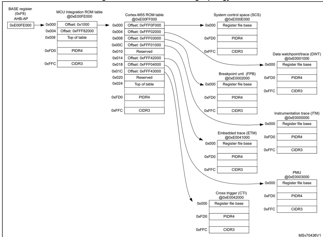
The diagram illustrates the debug topology for the Cortex-M55 subsystem. It shows the hierarchy of debug components connected via the AHB-AP. The BASE register (0xE00FE000) points to the MCU Integration ROM table at 0xE00FE000. This table contains entries for the Cortex-M55 ROM table and other components. The Cortex-M55 ROM table at 0xE00FF000 contains entries for the System control space (SCS), Data watchpoint/trace (DWT), Breakpoint unit (FPB), Instrumentation trace (ITM), Embedded trace (ETM), PMU, and Cross trigger (CTI). Each component has its own set of registers, including Register file base, PIDR4, and CIDR3.
78.11.2 Processor ROM registers
Processor ROM memory type register (CPUROM_MEMTYPE)
Address offset: 0xFCC
Reset value: 0x0000 0001
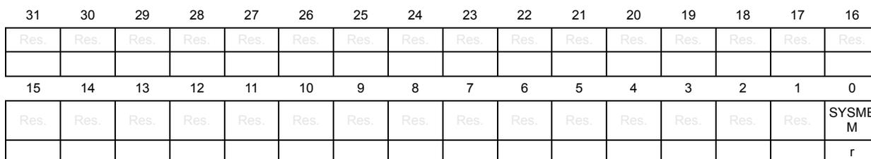
| 31 | 30 | 29 | 28 | 27 | 26 | 25 | 24 | 23 | 22 | 21 | 20 | 19 | 18 | 17 | 16 |
|---|---|---|---|---|---|---|---|---|---|---|---|---|---|---|---|
| Res. | Res. | Res. | Res. | Res. | Res. | Res. | Res. | Res. | Res. | Res. | Res. | Res. | Res. | Res. | Res. |
| 15 | 14 | 13 | 12 | 11 | 10 | 9 | 8 | 7 | 6 | 5 | 4 | 3 | 2 | 1 | 0 |
| Res. | Res. | Res. | Res. | Res. | Res. | Res. | Res. | Res. | Res. | Res. | Res. | Res. | Res. | Res. | SYSTM M |
| r |
Bits 31:1 Reserved, must be kept at reset value.
Bit 0 SYSTMEM : System memory presence
1: System memory is present on this bus.
Processor ROM CoreSight peripheral identity register 4 (CPUROM_PIDR4)
Address offset: 0xFD0
Reset value: 0x0000 0004
| 31 | 30 | 29 | 28 | 27 | 26 | 25 | 24 | 23 | 22 | 21 | 20 | 19 | 18 | 17 | 16 |
|---|---|---|---|---|---|---|---|---|---|---|---|---|---|---|---|
| Res. | Res. | Res. | Res. | Res. | Res. | Res. | Res. | Res. | Res. | Res. | Res. | Res. | Res. | Res. | Res. |
| 15 | 14 | 13 | 12 | 11 | 10 | 9 | 8 | 7 | 6 | 5 | 4 | 3 | 2 | 1 | 0 |
| Res. | Res. | Res. | Res. | Res. | Res. | Res. | Res. | SIZE[3:0] | JEP106CON[3:0] | ||||||
| r | r | r | r | r | r | r | r | ||||||||
Bits 31:8 Reserved, must be kept at reset value.
Bits 7:4 SIZE[3:0] : Register file size
0x0: Register file occupies a single 4-Kbyte region.
Bits 3:0 JEP106CON[3:0] : JEP106 continuation code
0x4: Arm JEDEC continuation code
Processor ROM CoreSight peripheral identity register 0 (CPUROM_PIDR0)
Address offset: 0xFE0
Reset value: 0x0000 00D2
| 31 | 30 | 29 | 28 | 27 | 26 | 25 | 24 | 23 | 22 | 21 | 20 | 19 | 18 | 17 | 16 |
|---|---|---|---|---|---|---|---|---|---|---|---|---|---|---|---|
| Res. | Res. | Res. | Res. | Res. | Res. | Res. | Res. | Res. | Res. | Res. | Res. | Res. | Res. | Res. | Res. |
| 15 | 14 | 13 | 12 | 11 | 10 | 9 | 8 | 7 | 6 | 5 | 4 | 3 | 2 | 1 | 0 |
| Res. | Res. | Res. | Res. | Res. | Res. | Res. | Res. | PARTNUM[7:0] | |||||||
| r | r | r | r | r | r | r | r | ||||||||
Bits 31:8 Reserved, must be kept at reset value.
Bits 7:0
PARTNUM[7:0]
: Part number field, bits [7:0]
0xD2: Cortex-M55 processor ROM table
Processor ROM CoreSight peripheral identity register 1 (CPUROM_PIDR1)
Address offset: 0xFE4
Reset value: 0x0000 00B4
| 31 | 30 | 29 | 28 | 27 | 26 | 25 | 24 | 23 | 22 | 21 | 20 | 19 | 18 | 17 | 16 |
|---|---|---|---|---|---|---|---|---|---|---|---|---|---|---|---|
| Res. | Res. | Res. | Res. | Res. | Res. | Res. | Res. | Res. | Res. | Res. | Res. | Res. | Res. | Res. | Res. |
| 15 | 14 | 13 | 12 | 11 | 10 | 9 | 8 | 7 | 6 | 5 | 4 | 3 | 2 | 1 | 0 |
| Res. | Res. | Res. | Res. | Res. | Res. | Res. | Res. | JEP106ID[3:0] | PARTNUM[11:8] | ||||||
| r | r | r | r | r | r | r | r | ||||||||
Bits 31:8 Reserved, must be kept at reset value.
Bits 7:4
JEP106ID[3:0]
: JEP106 identity code field, bits [3:0]
0xB: Arm JEDEC code
Bits 3:0
PARTNUM[11:8]
: Part number field, bits [11:8]
0x4: Cortex-M55 processor ROM table
Processor ROM CoreSight peripheral identity register 2 (CPUROM_PIDR2)
Address offset: 0xFE8
Reset value: 0x0000 000B
| 31 | 30 | 29 | 28 | 27 | 26 | 25 | 24 | 23 | 22 | 21 | 20 | 19 | 18 | 17 | 16 |
|---|---|---|---|---|---|---|---|---|---|---|---|---|---|---|---|
| Res. | Res. | Res. | Res. | Res. | Res. | Res. | Res. | Res. | Res. | Res. | Res. | Res. | Res. | Res. | Res. |
| 15 | 14 | 13 | 12 | 11 | 10 | 9 | 8 | 7 | 6 | 5 | 4 | 3 | 2 | 1 | 0 |
| Res. | Res. | Res. | Res. | Res. | Res. | Res. | Res. | REVISION[3:0] | JEDEC | JEP106ID[6:4] | |||||
| r | r | r | r | r | r | r | r | ||||||||
Bits 31:8 Reserved, must be kept at reset value.
Bits 7:4
REVISION[3:0]
: Component revision number
0x0: rev r0p0
Bit 3
JEDEC
: JEDEC assigned value
1: Designer ID specified by JEDEC
Bits 2:0
JEP106ID[6:4]
: JEP106 identity code field, bits [6:4]
0x3: Arm JEDEC code
Processor ROM CoreSight peripheral identity register 3 (CPUROM_PIDR3)
Address offset: 0xFEC
Reset value: 0x0000 0000
| 31 | 30 | 29 | 28 | 27 | 26 | 25 | 24 | 23 | 22 | 21 | 20 | 19 | 18 | 17 | 16 |
|---|---|---|---|---|---|---|---|---|---|---|---|---|---|---|---|
| Res. | Res. | Res. | Res. | Res. | Res. | Res. | Res. | Res. | Res. | Res. | Res. | Res. | Res. | Res. | Res. |
| 15 | 14 | 13 | 12 | 11 | 10 | 9 | 8 | 7 | 6 | 5 | 4 | 3 | 2 | 1 | 0 |
| Res. | Res. | Res. | Res. | Res. | Res. | Res. | Res. | REVAND[3:0] | CMOD[3:0] | ||||||
| r | r | r | r | r | r | r | r | ||||||||
Bits 31:8 Reserved, must be kept at reset value.
Bits 7:4 REVAND[3:0] : Metal fix version
0x0: No metal fix
Bits 3:0 CMOD[3:0] : Customer modified
0x0: No customer modifications
Processor ROM CoreSight component identity register 0 (CPUROM_CIDR0)
Address offset: 0xFF0
Reset value: 0x0000 000D
| 31 | 30 | 29 | 28 | 27 | 26 | 25 | 24 | 23 | 22 | 21 | 20 | 19 | 18 | 17 | 16 |
|---|---|---|---|---|---|---|---|---|---|---|---|---|---|---|---|
| Res. | Res. | Res. | Res. | Res. | Res. | Res. | Res. | Res. | Res. | Res. | Res. | Res. | Res. | Res. | Res. |
| 15 | 14 | 13 | 12 | 11 | 10 | 9 | 8 | 7 | 6 | 5 | 4 | 3 | 2 | 1 | 0 |
| Res. | Res. | Res. | Res. | Res. | Res. | Res. | Res. | PREAMBLE[7:0] | |||||||
| r | r | r | r | r | r | r | r | ||||||||
Bits 31:8 Reserved, must be kept at reset value.
Bits 7:0 PREAMBLE[7:0] : Component ID field, bits [7:0]
0x0D: Common ID value
Processor ROM CoreSight component identity register 1 (CPUROM_CIDR1)
Address offset: 0xFF4
Reset value: 0x0000 0010
| 31 | 30 | 29 | 28 | 27 | 26 | 25 | 24 | 23 | 22 | 21 | 20 | 19 | 18 | 17 | 16 |
|---|---|---|---|---|---|---|---|---|---|---|---|---|---|---|---|
| Res. | Res. | Res. | Res. | Res. | Res. | Res. | Res. | Res. | Res. | Res. | Res. | Res. | Res. | Res. | Res. |
| 15 | 14 | 13 | 12 | 11 | 10 | 9 | 8 | 7 | 6 | 5 | 4 | 3 | 2 | 1 | 0 |
| Res. | Res. | Res. | Res. | Res. | Res. | Res. | Res. | CLASS[3:0] | PREAMBLE[11:8] | ||||||
| r | r | r | r | r | r | r | r | ||||||||
Bits 31:8 Reserved, must be kept at reset value.
Bits 7:4 CLASS[3:0] : Component ID field, bits [15:12] - component class
0x1: ROM table component
Bits 3:0 PREAMBLE[11:8] : Component ID field, bits [11:8]
0x0: Common ID value
Processor ROM CoreSight component identity register 2 (CPUROM_CIDR2)
Address offset: 0xFF8
Reset value: 0x0000 0005
| 31 | 30 | 29 | 28 | 27 | 26 | 25 | 24 | 23 | 22 | 21 | 20 | 19 | 18 | 17 | 16 |
|---|---|---|---|---|---|---|---|---|---|---|---|---|---|---|---|
| Res. | Res. | Res. | Res. | Res. | Res. | Res. | Res. | Res. | Res. | Res. | Res. | Res. | Res. | Res. | Res. |
| 15 | 14 | 13 | 12 | 11 | 10 | 9 | 8 | 7 | 6 | 5 | 4 | 3 | 2 | 1 | 0 |
| Res. | Res. | Res. | Res. | Res. | Res. | Res. | Res. | PREAMBLE[19:12] | |||||||
| r | r | r | r | r | r | r | r | ||||||||
Bits 31:8 Reserved, must be kept at reset value.
Bits 7:0 PREAMBLE[19:12] : Component ID field, bits [23:16]
0x05: Common ID value
Processor ROM CoreSight component identity register 3 (CPUROM_CIDR3)
Address offset: 0xFFC
Reset value: 0x0000 00B1
| 31 | 30 | 29 | 28 | 27 | 26 | 25 | 24 | 23 | 22 | 21 | 20 | 19 | 18 | 17 | 16 |
|---|---|---|---|---|---|---|---|---|---|---|---|---|---|---|---|
| Res. | Res. | Res. | Res. | Res. | Res. | Res. | Res. | Res. | Res. | Res. | Res. | Res. | Res. | Res. | Res. |
| 15 | 14 | 13 | 12 | 11 | 10 | 9 | 8 | 7 | 6 | 5 | 4 | 3 | 2 | 1 | 0 |
| Res. | Res. | Res. | Res. | Res. | Res. | Res. | Res. | PREAMBLE[27:20] | |||||||
| r | r | r | r | r | r | r | r | ||||||||
Bits 31:8 Reserved, must be kept at reset value.
Bits 7:0 PREAMBLE[27:20] : Component ID field, bits [31:24]
0xB1: Common ID value
Processor ROM register map
Table 874. Processor ROM register map and reset values
| Offset | Register name | 31 | 30 | 29 | 28 | 27 | 26 | 25 | 24 | 23 | 22 | 21 | 20 | 19 | 18 | 17 | 16 | 15 | 14 | 13 | 12 | 11 | 10 | 9 | 8 | 7 | 6 | 5 | 4 | 3 | 2 | 1 | 0 | |
|---|---|---|---|---|---|---|---|---|---|---|---|---|---|---|---|---|---|---|---|---|---|---|---|---|---|---|---|---|---|---|---|---|---|---|
| 0xFCC | CPUROM_MEMTYPE | Res. | Res. | Res. | Res. | Res. | Res. | Res. | Res. | Res. | Res. | Res. | Res. | Res. | Res. | Res. | Res. | Res. | Res. | Res. | Res. | Res. | Res. | Res. | Res. | Res. | Res. | Res. | Res. | Res. | Res. | Res. | Res. | SYSTEM |
| Reset value | 1 | |||||||||||||||||||||||||||||||||
| 0xFD0 | CPUROM_PIDR4 | Res. | Res. | Res. | Res. | Res. | Res. | Res. | Res. | Res. | Res. | Res. | Res. | Res. | Res. | Res. | Res. | Res. | Res. | Res. | Res. | Res. | Res. | Res. | Res. | SIZE[3:0] | JEP106CON [3:0] | |||||||
| Reset value | 0 | 0 | 0 | 0 | 0 | 1 | 0 | 0 | ||||||||||||||||||||||||||
| 0xFD4-0xFDC | Reserved | Reserved | ||||||||||||||||||||||||||||||||
| 0xFE0 | CPUROM_PIDR0 | Res. | Res. | Res. | Res. | Res. | Res. | Res. | Res. | Res. | Res. | Res. | Res. | Res. | Res. | Res. | Res. | Res. | Res. | Res. | Res. | Res. | Res. | Res. | Res. | PARTNUM[7:0] | ||||||||
| Reset value | 1 | 1 | 0 | 1 | 0 | 0 | 1 | 0 | ||||||||||||||||||||||||||
Table 874. Processor ROM register map and reset values (continued)
| Offset | Register name | 31 | 30 | 29 | 28 | 27 | 26 | 25 | 24 | 23 | 22 | 21 | 20 | 19 | 18 | 17 | 16 | 15 | 14 | 13 | 12 | 11 | 10 | 9 | 8 | 7 | 6 | 5 | 4 | 3 | 2 | 1 | 0 |
|---|---|---|---|---|---|---|---|---|---|---|---|---|---|---|---|---|---|---|---|---|---|---|---|---|---|---|---|---|---|---|---|---|---|
| 0xFE4 | CPUROM_PIDR1 | Res. | Res. | Res. | Res. | Res. | Res. | Res. | Res. | Res. | Res. | Res. | Res. | Res. | Res. | Res. | Res. | Res. | Res. | Res. | Res. | Res. | Res. | Res. | Res. | JEP106ID [3:0] | PARTNUM [11:8] | ||||||
| Reset value | 1 | 0 | 1 | 1 | 0 | 1 | 0 | 0 | |||||||||||||||||||||||||
| 0xFE8 | CPUROM_PIDR2 | Res. | Res. | Res. | Res. | Res. | Res. | Res. | Res. | Res. | Res. | Res. | Res. | Res. | Res. | Res. | Res. | Res. | Res. | Res. | Res. | Res. | Res. | Res. | REVISION [3:0] | JEDEC [6:4] | JEP106ID [6:4] | ||||||
| Reset value | 0 | 0 | 0 | 0 | 1 | 0 | 1 | 1 | |||||||||||||||||||||||||
| 0xFEC | CPUROM_PIDR3 | Res. | Res. | Res. | Res. | Res. | Res. | Res. | Res. | Res. | Res. | Res. | Res. | Res. | Res. | Res. | Res. | Res. | Res. | Res. | Res. | Res. | Res. | Res. | REVAND[3:0] | CMOD[3:0] | |||||||
| Reset value | 0 | 0 | 0 | 0 | 0 | 0 | 0 | 0 | |||||||||||||||||||||||||
| 0xFF0 | CPUROM_CIDR0 | Res. | Res. | Res. | Res. | Res. | Res. | Res. | Res. | Res. | Res. | Res. | Res. | Res. | Res. | Res. | Res. | Res. | Res. | Res. | Res. | Res. | Res. | Res. | PREAMBLE[7:0] | ||||||||
| Reset value | 0 | 0 | 0 | 0 | 1 | 1 | 0 | 1 | |||||||||||||||||||||||||
| 0xFF4 | CPUROM_CIDR1 | Res. | Res. | Res. | Res. | Res. | Res. | Res. | Res. | Res. | Res. | Res. | Res. | Res. | Res. | Res. | Res. | Res. | Res. | Res. | Res. | Res. | Res. | Res. | CLASS[3:0] | PREAMBLE [11:8] | |||||||
| Reset value | 0 | 0 | 0 | 1 | 0 | 0 | 0 | 0 | |||||||||||||||||||||||||
| 0xFF8 | CPUROM_CIDR2 | Res. | Res. | Res. | Res. | Res. | Res. | Res. | Res. | Res. | Res. | Res. | Res. | Res. | Res. | Res. | Res. | Res. | Res. | Res. | Res. | Res. | Res. | Res. | PREAMBLE[19:12] | ||||||||
| Reset value | 0 | 0 | 0 | 0 | 0 | 1 | 0 | 1 | |||||||||||||||||||||||||
| 0xFFC | CPUROM_CIDR3 | Res. | Res. | Res. | Res. | Res. | Res. | Res. | Res. | Res. | Res. | Res. | Res. | Res. | Res. | Res. | Res. | Res. | Res. | Res. | Res. | Res. | Res. | Res. | PREAMBLE[27:20] | ||||||||
| Reset value | 1 | 0 | 1 | 1 | 0 | 0 | 0 | 1 | |||||||||||||||||||||||||
78.11.3 Data watchpoint and trace unit (DWT)
The DWT provides eight comparators that can be used as:
- • watchpoint
- • ETM trigger
- • PC sampling trigger
- • data address sampling trigger
- • data comparator (available on comparator 1 only)
- • clock cycle counter comparator (available on comparator 0 only)
It also contains counters for:
- • clock cycles
- • folded instructions
- • LSU (load store unit) operations
- • sleep cycles
- • number of cycles per instruction
- • interrupt overhead
A DWT comparator compares one of the following with the value held in its DWT_COMP:
- • a data address
- • an instruction address
- • a data value
- • the cycle count value (for comparator 0 only)
For address matching, the comparator can use a mask, so it matches a range of addresses.
On a successful match, the comparator generates one of the following:
- • one or more DWT data trace packets, containing one or more of:
- – the address of the instruction that caused a data access
- – an address offset, bits[15:0] of the data access address
- – the matched data value.
- • a watchpoint debug event, on either the PC value, or the accessed data address
- • a CMPMATCH[N] event that signals the match outside the DWT unit
A watchpoint debug event either generates a DebugMonitor exception, or causes the processor to halt execution and enter debug state.
For more details on how to use the DWT, refer to the Arm Cortex-M55 Processor Technical Reference Manual [4].
78.11.4 Cortex-M55 DWT registers
The register file base address for the DWT is defined in Table 873: Processor ROM table .
DWT control register (DWT_CTRL)
Address offset: 0x000
Reset value: 0x8000 0000
| 31 | 30 | 29 | 28 | 27 | 26 | 25 | 24 | 23 | 22 | 21 | 20 | 19 | 18 | 17 | 16 |
|---|---|---|---|---|---|---|---|---|---|---|---|---|---|---|---|
| NUMCOMP[3:0] | NOTRCPKT | NOEXTTRIG | NOCYCCNT | NOPRFCNT | CYCDISS | CYCEVTENA | FOLDEVTENA | LSUEVTENA | SLEEPEVTENA | EXCEVTENA | CPIEVVTENA | EXCTRCEVENA | |||
| r | r | r | r | r | r | r | r | rw | rw | rw | rw | rw | rw | rw | rw |
| 15 | 14 | 13 | 12 | 11 | 10 | 9 | 8 | 7 | 6 | 5 | 4 | 3 | 2 | 1 | 0 |
| Res. | PCSAMPLEN A | SYNCTAP[1:0] | CYCTAP P | POSTINIT[3:0] | POSTRESET[3:0] | CYCCNTENA | |||||||||
| rw | rw | rw | rw | rw | rw | rw | rw | rw | rw | rw | rw | rw | |||
Bits 31:28 NUMCOMP[3:0] : Number of implemented comparators (read-only)
0x8: Eight comparators
Bit 27 NOTRCPKT : Trace sampling and exception tracing support (read-only)
0: Supported
Bit 26 NOEXTTRIG : External match signal, CMPMATCH support (read-only)
0: Supported
Bit 25 NOCYCCNT : Cycle counter support (read-only)
0: Supported
Bit 24 NOPRFCNT : Profiling counter support (read-only)
0: Supported
Bit 23 CYCDISS : Cycle counter disabled secure
0: No effect
1: Cycle counter is not incremented when the processor is in secure state
- Bit 22
CYCEVTENA
: Enable POSTCNT underflow event counter packet generation
0: Disabled
1: Enabled - Bit 21
FOLDEVTENA
: Enable folded instruction counter overflow event generation
0: Disabled
1: Enabled - Bit 20
LSUEVTENA
: Enable LSU counter overflow event generation
0: Disabled
1: Enabled - Bit 19
SLEEPEVTENA
: Enable sleep counter overflow event generation
0: Disabled
1: Enabled - Bit 18
EXCEVTENA
: Enable exception overhead counter overflow event generation
0: Disabled
1: Enabled - Bit 17
CPIEVTENA
: Enable CPI counter overflow event generation
0: Disabled
1: Enabled - Bit 16
EXCTRCENA
: Enable exception trace generation
0: Disabled
1: Enabled - Bits 15:13 Reserved, must be kept at reset value.
- Bit 12
PCSAMPLENA
: POSTCNT counter use enable
Enables the use of POSTCNT counter as a timer for periodic PC sample packet generation.
0: Disabled
1: Enabled - Bits 11:10
SYNCTAP[1:0]
: Position of synchronization packet counter tap on CYCCNT counter
This selection determines the synchronization packet rate.
0x0: Disabled - no synchronization packets
0x1: Tap at CYCCNT[24]
0x2: Tap at CYCCNT[26]
0x3: Tap at CYCCNT[28] - Bit 9
CYCTAP
: Position of the POSTCNT tap on the CYCCNT counter
0: Tap at CYCCNT[6]
1: Tap at CYCCNT[10] - Bits 8:5
POSTINIT[3:0]
: Initial value of the POSTCNT counter
Writes to this field are ignored if POSTCNT counter is enabled (CYCEVTENA or PCSAMPLENA must be reset prior to writing POSTINIT). - Bits 4:1 POSTRESET[3:0] : Reload value of the POSTCNT counter.
- Bit 0
CYCCNTENA
: CYCCNT counter enable
0: Disabled
1: Enabled
Address offset: 0x004
Reset value: 0x0000 0000
| 31 | 30 | 29 | 28 | 27 | 26 | 25 | 24 | 23 | 22 | 21 | 20 | 19 | 18 | 17 | 16 |
| CYCCNT[31:16] | |||||||||||||||
| rw | rw | rw | rw | rw | rw | rw | rw | rw | rw | rw | rw | rw | rw | rw | rw |
| 15 | 14 | 13 | 12 | 11 | 10 | 9 | 8 | 7 | 6 | 5 | 4 | 3 | 2 | 1 | 0 |
| CYCCNT[15:0] | |||||||||||||||
| rw | rw | rw | rw | rw | rw | rw | rw | rw | rw | rw | rw | rw | rw | rw | rw |
Address offset: 0x008
Reset value: 0x0000 0000
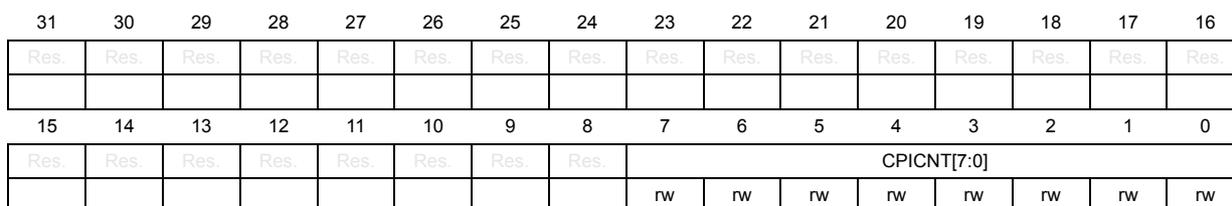
| 31 | 30 | 29 | 28 | 27 | 26 | 25 | 24 | 23 | 22 | 21 | 20 | 19 | 18 | 17 | 16 |
| Res. | Res. | Res. | Res. | Res. | Res. | Res. | Res. | Res. | Res. | Res. | Res. | Res. | Res. | Res. | Res. |
| 15 | 14 | 13 | 12 | 11 | 10 | 9 | 8 | 7 | 6 | 5 | 4 | 3 | 2 | 1 | 0 |
| Res. | Res. | Res. | Res. | Res. | Res. | Res. | Res. | CPICNT[7:0] | |||||||
| rw | rw | rw | rw | rw | rw | rw | rw | ||||||||
Bits 31:8 Reserved, must be kept at reset value.
Bits 7:0 CPICNT[7:0] : CPI counterCounts additional cycles required to execute multi-cycle instructions, except those recorded by DWT_LSUCNT, and counts any instruction fetch stalls.
DWT exception count register (DWT_EXCCNT)Address offset: 0x00C
Reset value: 0x0000 0000
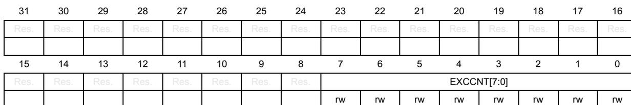
| 31 | 30 | 29 | 28 | 27 | 26 | 25 | 24 | 23 | 22 | 21 | 20 | 19 | 18 | 17 | 16 |
| Res. | Res. | Res. | Res. | Res. | Res. | Res. | Res. | Res. | Res. | Res. | Res. | Res. | Res. | Res. | Res. |
| 15 | 14 | 13 | 12 | 11 | 10 | 9 | 8 | 7 | 6 | 5 | 4 | 3 | 2 | 1 | 0 |
| Res. | Res. | Res. | Res. | Res. | Res. | Res. | Res. | EXCCNT[7:0] | |||||||
| rw | rw | rw | rw | rw | rw | rw | rw | ||||||||
Bits 31:8 Reserved, must be kept at reset value.
Bits 7:0 EXCCNT[7:0] : Exception overhead cycle counterCounts the number of cycles spent in exception processing.
DWT sleep count register (DWT_SLEEPCNT)Address offset: 0x010
Reset value: 0x0000 0000
| 31 | 30 | 29 | 28 | 27 | 26 | 25 | 24 | 23 | 22 | 21 | 20 | 19 | 18 | 17 | 16 |
|---|---|---|---|---|---|---|---|---|---|---|---|---|---|---|---|
| Res. | Res. | Res. | Res. | Res. | Res. | Res. | Res. | Res. | Res. | Res. | Res. | Res. | Res. | Res. | Res. |
| 15 | 14 | 13 | 12 | 11 | 10 | 9 | 8 | 7 | 6 | 5 | 4 | 3 | 2 | 1 | 0 |
| Res. | Res. | Res. | Res. | Res. | Res. | Res. | Res. | SLEEPCNT[7:0] | |||||||
| rw | rw | rw | rw | rw | rw | rw | rw | ||||||||
Bits 31:8 Reserved, must be kept at reset value.
Bits 7:0 SLEEPCNT[7:0] : Sleep cycle counterCounts the number of cycles spent in sleep mode (WFI, WFE, sleep-on-exit).
DWT LSU count register (DWT_LSUCNT)Address offset: 0x014
Reset value: 0x0000 0000
| 31 | 30 | 29 | 28 | 27 | 26 | 25 | 24 | 23 | 22 | 21 | 20 | 19 | 18 | 17 | 16 |
|---|---|---|---|---|---|---|---|---|---|---|---|---|---|---|---|
| Res. | Res. | Res. | Res. | Res. | Res. | Res. | Res. | Res. | Res. | Res. | Res. | Res. | Res. | Res. | Res. |
| 15 | 14 | 13 | 12 | 11 | 10 | 9 | 8 | 7 | 6 | 5 | 4 | 3 | 2 | 1 | 0 |
| Res. | Res. | Res. | Res. | Res. | Res. | Res. | Res. | LSUCNT[7:0] | |||||||
| rw | rw | rw | rw | rw | rw | rw | rw | ||||||||
Bits 31:8 Reserved, must be kept at reset value.
Bits 7:0 LSUCNT[7:0] : Load store counterCounts additional cycles required to execute load and store instructions.
DWT fold count register (DWT_FOLDCNT)Address offset: 0x018
Reset value: 0x0000 0000
| 31 | 30 | 29 | 28 | 27 | 26 | 25 | 24 | 23 | 22 | 21 | 20 | 19 | 18 | 17 | 16 |
|---|---|---|---|---|---|---|---|---|---|---|---|---|---|---|---|
| Res. | Res. | Res. | Res. | Res. | Res. | Res. | Res. | Res. | Res. | Res. | Res. | Res. | Res. | Res. | Res. |
| 15 | 14 | 13 | 12 | 11 | 10 | 9 | 8 | 7 | 6 | 5 | 4 | 3 | 2 | 1 | 0 |
| Res. | Res. | Res. | Res. | Res. | Res. | Res. | Res. | FOLDCNT[7:0] | |||||||
| rw | rw | rw | rw | rw | rw | rw | rw | ||||||||
Bits 31:8 Reserved, must be kept at reset value.
Bits 7:0 FOLDCNT[7:0] : Folded instruction counterIncrements on each instruction that takes 0 cycles (in parallel with another instruction).
DWT program counter sample register (DWT_PCSR)
Address offset: 0x01C
Reset value: 0xXXXX XXXX
| 31 | 30 | 29 | 28 | 27 | 26 | 25 | 24 | 23 | 22 | 21 | 20 | 19 | 18 | 17 | 16 |
|---|---|---|---|---|---|---|---|---|---|---|---|---|---|---|---|
| EIASAMPLE[31:16] | |||||||||||||||
| r | r | r | r | r | r | r | r | r | r | r | r | r | r | r | r |
| 15 | 14 | 13 | 12 | 11 | 10 | 9 | 8 | 7 | 6 | 5 | 4 | 3 | 2 | 1 | 0 |
| EIASAMPLE[15:0] | |||||||||||||||
| r | r | r | r | r | r | r | r | r | r | r | r | r | r | r | r |
Bits 31:0
EIASAMPLE[31:0]
: Executed instruction address sample value
Samples the current value of the program counter.
DWT comparator register x (DWT_COMPx)
Address offset: 0x020 + 0x10 * x (x = 0 to 7)
Reset value: 0x0000 0000
| 31 | 30 | 29 | 28 | 27 | 26 | 25 | 24 | 23 | 22 | 21 | 20 | 19 | 18 | 17 | 16 |
|---|---|---|---|---|---|---|---|---|---|---|---|---|---|---|---|
| COMP[31:16] | |||||||||||||||
| rw | rw | rw | rw | rw | rw | rw | rw | rw | rw | rw | rw | rw | rw | rw | rw |
| 15 | 14 | 13 | 12 | 11 | 10 | 9 | 8 | 7 | 6 | 5 | 4 | 3 | 2 | 1 | 0 |
| COMP[15:0] | |||||||||||||||
| rw | rw | rw | rw | rw | rw | rw | rw | rw | rw | rw | rw | rw | rw | rw | rw |
Bits 31:0 COMP[31:0] : Reference value for comparison
DWT function register x (DWT_FUNCTx)
Address offset: 0x028 + 0x10 * x (x = 0 to 7)
Reset value: 0x5800 0000, 0xF000 0000, 0x5000 0000, 0xF000 0000, 0x5000 0000, 0xD000 0000, 0x5000 0000, 0xD000 0000
| 31 | 30 | 29 | 28 | 27 | 26 | 25 | 24 | 23 | 22 | 21 | 20 | 19 | 18 | 17 | 16 |
|---|---|---|---|---|---|---|---|---|---|---|---|---|---|---|---|
| ID[4:0] | Res. | Res. | MATCH ED | Res. | Res. | Res. | Res. | Res. | Res. | Res. | Res. | ||||
| r | r | r | r | r | r | ||||||||||
| 15 | 14 | 13 | 12 | 11 | 10 | 9 | 8 | 7 | 6 | 5 | 4 | 3 | 2 | 1 | 0 |
| Res. | Res. | Res. | Res. | DATAVSIZE[1:0] | Res. | Res. | Res. | Res. | ACTION[1:0] | MATCH[3:0] | |||||
| rw | rw | rw | rw | rw | rw | rw | rw | ||||||||
Bits 31:27 ID[4:0] : Identify capability (read-only)
Identifies the MATCH[3:0] capabilities for the comparator.
0x08: Data address, and data address with value
0x09: Cycle counter, data address, and data address with value
0x0A: Instruction address, data address, and data address with value
0x0B: Cycle counter, instruction address, data address and data address with value
0x18: Data address, data address limit, and data address with value
0x1A: Instruction address, instruction address limit, data address, data address limit, and data address with value
0x1C: Data address, data address limit, data value, linked data value, and data address with value
0x1E: Instruction address, instruction address limit, data address, data address limit, data value, linked data value, and data address with value
Others: Reserved
Bits 26:25 Reserved, must be kept at reset value.
Bit 24 MATCHED : Comparator match (read-only)
Indicates if a comparator match has occurred since the register was last read.
0: No match
1: Match occurred
Bits 23:12 Reserved, must be kept at reset value.
Bits 11:10 DATAVSIZE[1:0] : Size of required data comparison
For data value matching, specifies the size of the required data comparison.
0: Byte
1: Half word
2: Word
3: Reserved
Bits 9:6 Reserved, must be kept at reset value.
Bits 5:4 ACTION[1:0] : Action on match
Defines the action when a match occurs
0: Trigger only
1: Generate debug event
2: For a cycle counter, instruction address, data address, data value or linked data value comparator, generate a data trace match packet. For a data address with value comparator, generate a data trace data value packet
3: For a data address limit comparator, generate a data trace data address packet. For a cycle counter, instruction address limit, or data address comparator, generate a data trace PC value packet. For a data address with value comparator, generate both a data trace PC value packet and a data trace data value packet.
Bits 3:0 MATCH[3:0] : Match typeControls the type of match generated by this comparator (see ID[4:0] for valid types).
- 0: Disabled. Never generates a match
- 1: Cycle counter. Matches if DWT_CYCCNT equals the comparator value. The comparator is checked each time DWT_CYCCNT is written to, directly or indirectly.
- 2: Instruction address. If not linked to, an instruction matches if the address of the first byte of the instruction matches the comparator address.
- 3: Instruction address limit. When comparator <n-1> is configured as instruction address (0b0010), an access generates a match if the first byte of the instruction lies between the lower address (specified by the comparator <n-1>), and the limit address (specified by this comparator, <n>). Both the lower and the limit address are inclusive to the address range.
- 4: Data address. If not linked to by a data address limit comparator, an access matches if any accessed byte lies between the comparator address, and a limit defined by the DATAVSIZE field.
- 5: Data address, writes. As 4, except that only write accesses generate a match.
- 6: Data address, reads. As 0b0100, except that only read accesses generate a match.
- 7: Data address limit. An access generates a match when all of the following are true:
- – Comparator <n-1> is configured as one of data address (4-6), or data address with value (12-14).
- – Any accessed byte lies between the lower address (specified by comparator <n-1>), and the limit address (specified by this comparator <n>).
- – Both the lower address, and limit address are inclusive to the range.
- 8: Data value. An access matches if the value accessed matches the comparator value.
- 9: Data value, writes. As 8, except that only write accesses generate a match.
- 10: Data value, reads. As 0b1000, except that only read accesses generate a match.
- 11: Linked data value. An access generates a match when all of the following are true:
- – Comparator <n-1> is configured as data address (4-6), or data address with value (12-14).
- – DATAVSIZE for the two comparators <n> and <n-1> are equal.
- – The value accessed matches the comparator value specified by comparator <n>.
- – Any accessed byte lies between the lower address (specified by comparator <n-1>), and limit defined by the DATAVSIZE field.
- – Both the lower address, and the limit address are inclusive to the range.
- 12: Data address with value. As 4, except that the data value is traced
- 13: Data address with value, writes. As 12, except that only write accesses generate a match
- 14: Data address with value, reads. As 12, except that only read accesses generate a match
- 15: Reserved
DWT comparator value mask register x (DWT_VMASKx)
Address offset: 0x02C + 0x10 * x (x = 1,3)
Reset value: 0x0000 0000
| 31 | 30 | 29 | 28 | 27 | 26 | 25 | 24 | 23 | 22 | 21 | 20 | 19 | 18 | 17 | 16 |
|---|---|---|---|---|---|---|---|---|---|---|---|---|---|---|---|
| VMASK[31:16] | |||||||||||||||
| rw | rw | rw | rw | rw | rw | rw | rw | rw | rw | rw | rw | rw | rw | rw | rw |
| 15 | 14 | 13 | 12 | 11 | 10 | 9 | 8 | 7 | 6 | 5 | 4 | 3 | 2 | 1 | 0 |
| VMASK[15:0] | |||||||||||||||
| rw | rw | rw | rw | rw | rw | rw | rw | rw | rw | rw | rw | rw | rw | rw | rw |
Bits 31:0 VMASK[31:0] : Data value mask.
Mask value for use in the comparison with load or store data. This only applies to comparators which support data value matching.
For every bit m, if VMASK[m] = 0, the comparison matches only if DWT_COMPx[m] matches bit [m] of the candidate data value. If VMASK[m] = 1, the comparison ignores bit [m] of the candidate data value.
DWT device type architecture register (DWT_DEVARCH)
Address offset: 0xFBC
Reset value: 0x4771 1A02
| 31 | 30 | 29 | 28 | 27 | 26 | 25 | 24 | 23 | 22 | 21 | 20 | 19 | 18 | 17 | 16 |
|---|---|---|---|---|---|---|---|---|---|---|---|---|---|---|---|
| ARCHITECT[10:0] | PRESENT | REVISION[3:0] | |||||||||||||
| r | r | r | r | r | r | r | r | r | r | r | r | r | r | r | r |
| 15 | 14 | 13 | 12 | 11 | 10 | 9 | 8 | 7 | 6 | 5 | 4 | 3 | 2 | 1 | 0 |
| ARCHVER[3:0] | ARCHPART[11:0] | ||||||||||||||
| r | r | r | r | r | r | r | r | r | r | r | r | r | r | r | r |
Bits 31:21 ARCHITECT[10:0] : Architect JEDEC code
0x23B: Arm JEDEC code
Bit 20 PRESENT : DEVARCH register present
1: Present
Bits 19:16 REVISION[3:0] : Architecture revision
0x1: DWT architecture v2.1
Bits 15:12 ARCHVER[3:0] : Architecture version
0x1: DWT architecture v2
Bits 11:0 ARCHPART[11:0] : Architecture
0xA02: DWT architecture
DWT device type register (DWT_DEVTYPE)
Address offset: 0xFCC
Reset value: 0x0000 0000
| 31 | 30 | 29 | 28 | 27 | 26 | 25 | 24 | 23 | 22 | 21 | 20 | 19 | 18 | 17 | 16 |
|---|---|---|---|---|---|---|---|---|---|---|---|---|---|---|---|
| Res. | Res. | Res. | Res. | Res. | Res. | Res. | Res. | Res. | Res. | Res. | Res. | Res. | Res. | Res. | Res. |
| 15 | 14 | 13 | 12 | 11 | 10 | 9 | 8 | 7 | 6 | 5 | 4 | 3 | 2 | 1 | 0 |
| Res. | Res. | Res. | Res. | Res. | Res. | Res. | Res. | SUB[3:0] | MAJOR[3:0] | ||||||
| r | r | r | r | r | r | r | r | ||||||||
Bits 31:8 Reserved, must be kept at reset value.
Bits 7:4 SUB[3:0] : Component subtype
0x0: Other
Bits 3:0
MAJOR[3:0]
: Component major type
0x0: Miscellaneous
DWT CoreSight peripheral identity register 4 (DWT_PIDR4)
Address offset: 0xFD0
Reset value: 0x0000 0004
| 31 | 30 | 29 | 28 | 27 | 26 | 25 | 24 | 23 | 22 | 21 | 20 | 19 | 18 | 17 | 16 |
|---|---|---|---|---|---|---|---|---|---|---|---|---|---|---|---|
| Res. | Res. | Res. | Res. | Res. | Res. | Res. | Res. | Res. | Res. | Res. | Res. | Res. | Res. | Res. | Res. |
| 15 | 14 | 13 | 12 | 11 | 10 | 9 | 8 | 7 | 6 | 5 | 4 | 3 | 2 | 1 | 0 |
| Res. | Res. | Res. | Res. | Res. | Res. | Res. | Res. | SIZE[3:0] | JEP106CON[3:0] | ||||||
| r | r | r | r | r | r | r | r | ||||||||
Bits 31:8 Reserved, must be kept at reset value.
Bits 7:4
SIZE[3:0]
: Register file size
0x0: Register file occupies a single 4-Kbyte region.
Bits 3:0
JEP106CON[3:0]
: JEP106 continuation code
0x4: Arm JEDEC code
DWT CoreSight peripheral identity register 0 (DWT_PIDR0)
Address offset: 0xFE0
Reset value: 0x0000 0002
| 31 | 30 | 29 | 28 | 27 | 26 | 25 | 24 | 23 | 22 | 21 | 20 | 19 | 18 | 17 | 16 |
|---|---|---|---|---|---|---|---|---|---|---|---|---|---|---|---|
| Res. | Res. | Res. | Res. | Res. | Res. | Res. | Res. | Res. | Res. | Res. | Res. | Res. | Res. | Res. | Res. |
| 15 | 14 | 13 | 12 | 11 | 10 | 9 | 8 | 7 | 6 | 5 | 4 | 3 | 2 | 1 | 0 |
| Res. | Res. | Res. | Res. | Res. | Res. | Res. | Res. | PARTNUM[7:0] | |||||||
| r | r | r | r | r | r | r | r | ||||||||
Bits 31:8 Reserved, must be kept at reset value.
Bits 7:0
PARTNUM[7:0]
: Part number field, bits [7:0]
0x02: DWT part number
DWT CoreSight peripheral identity register 1 (DWT_PIDR1)
Address offset: 0xFE4
Reset value: 0x0000 00B0
| 31 | 30 | 29 | 28 | 27 | 26 | 25 | 24 | 23 | 22 | 21 | 20 | 19 | 18 | 17 | 16 |
|---|---|---|---|---|---|---|---|---|---|---|---|---|---|---|---|
| Res. | Res. | Res. | Res. | Res. | Res. | Res. | Res. | Res. | Res. | Res. | Res. | Res. | Res. | Res. | Res. |
| 15 | 14 | 13 | 12 | 11 | 10 | 9 | 8 | 7 | 6 | 5 | 4 | 3 | 2 | 1 | 0 |
| Res. | Res. | Res. | Res. | Res. | Res. | Res. | Res. | JEP106ID[3:0] | PARTNUM[11:8] | ||||||
| r | r | r | r | r | r | r | r | ||||||||
Bits 31:8 Reserved, must be kept at reset value.
Bits 7:4 JEP106ID[3:0] : JEP106 identity code field, bits [3:0]
0xB: Arm JEDEC code
Bits 3:0 PARTNUM[11:8] : Part number field, bits [11:8]
0x0: DWT part number
DWT CoreSight peripheral identity register 2 (DWT_PIDR2)
Address offset: 0xFE8
Reset value: 0x0000 000B
| 31 | 30 | 29 | 28 | 27 | 26 | 25 | 24 | 23 | 22 | 21 | 20 | 19 | 18 | 17 | 16 |
|---|---|---|---|---|---|---|---|---|---|---|---|---|---|---|---|
| Res. | Res. | Res. | Res. | Res. | Res. | Res. | Res. | Res. | Res. | Res. | Res. | Res. | Res. | Res. | Res. |
| 15 | 14 | 13 | 12 | 11 | 10 | 9 | 8 | 7 | 6 | 5 | 4 | 3 | 2 | 1 | 0 |
| Res. | Res. | Res. | Res. | Res. | Res. | Res. | Res. | REVISION[3:0] | JEDEC | JEP106ID[6:4] | |||||
Bits 31:8 Reserved, must be kept at reset value.
Bits 7:4 REVISION[3:0] : Component revision number
0x0: r0p0
Bit 3 JEDEC : JEDEC assigned value
1: Designer ID specified by JEDEC
Bits 2:0 JEP106ID[6:4] : JEP106 identity code field, bits [6:4]
0x3: Arm JEDEC code
DWT CoreSight peripheral identity register 3 (DWT_PIDR3)
Address offset: 0xFEC
Reset value: 0x0000 0000
| 31 | 30 | 29 | 28 | 27 | 26 | 25 | 24 | 23 | 22 | 21 | 20 | 19 | 18 | 17 | 16 |
|---|---|---|---|---|---|---|---|---|---|---|---|---|---|---|---|
| Res. | Res. | Res. | Res. | Res. | Res. | Res. | Res. | Res. | Res. | Res. | Res. | Res. | Res. | Res. | Res. |
| 15 | 14 | 13 | 12 | 11 | 10 | 9 | 8 | 7 | 6 | 5 | 4 | 3 | 2 | 1 | 0 |
| Res. | Res. | Res. | Res. | Res. | Res. | Res. | Res. | REVAND[3:0] | CMOD[3:0] | ||||||
Bits 31:8 Reserved, must be kept at reset value.
Bits 7:4 REVAND[3:0] : Metal fix version
0x0: No metal fix
Bits 3:0 CMOD[3:0] : Customer modified
0x0: No customer modifications
DWT CoreSight component identity register 0 (DWT_CIDR0)
Address offset: 0xFF0
Reset value: 0x0000 000D
| 31 | 30 | 29 | 28 | 27 | 26 | 25 | 24 | 23 | 22 | 21 | 20 | 19 | 18 | 17 | 16 |
|---|---|---|---|---|---|---|---|---|---|---|---|---|---|---|---|
| Res. | Res. | Res. | Res. | Res. | Res. | Res. | Res. | Res. | Res. | Res. | Res. | Res. | Res. | Res. | Res. |
| 15 | 14 | 13 | 12 | 11 | 10 | 9 | 8 | 7 | 6 | 5 | 4 | 3 | 2 | 1 | 0 |
| Res. | Res. | Res. | Res. | Res. | Res. | Res. | Res. | PREAMBLE[7:0] | |||||||
| r | r | r | r | r | r | r | r | ||||||||
Bits 31:8 Reserved, must be kept at reset value.
Bits 7:0 PREAMBLE[7:0] : Component ID field, bits [7:0]
0x0D: Common ID value
DWT CoreSight component identity register 1 (DWT_CIDR1)
Address offset: 0xFF4
Reset value: 0x0000 00E0
| 31 | 30 | 29 | 28 | 27 | 26 | 25 | 24 | 23 | 22 | 21 | 20 | 19 | 18 | 17 | 16 |
|---|---|---|---|---|---|---|---|---|---|---|---|---|---|---|---|
| Res. | Res. | Res. | Res. | Res. | Res. | Res. | Res. | Res. | Res. | Res. | Res. | Res. | Res. | Res. | Res. |
| 15 | 14 | 13 | 12 | 11 | 10 | 9 | 8 | 7 | 6 | 5 | 4 | 3 | 2 | 1 | 0 |
| Res. | Res. | Res. | Res. | Res. | Res. | Res. | Res. | CLASS[3:0] | PREAMBLE[11:8] | ||||||
| r | r | r | r | r | r | r | r | ||||||||
Bits 31:8 Reserved, must be kept at reset value.
Bits 7:4 CLASS[3:0] : Component ID field, bits [15:12] - component class
0xE: Trace generator component
Bits 3:0 PREAMBLE[11:8] : Component ID field, bits [11:8]
0x0: Common ID value
DWT CoreSight component identity register 2 (DWT_CIDR2)
Address offset: 0xFF8
Reset value: 0x0000 0005
| 31 | 30 | 29 | 28 | 27 | 26 | 25 | 24 | 23 | 22 | 21 | 20 | 19 | 18 | 17 | 16 |
|---|---|---|---|---|---|---|---|---|---|---|---|---|---|---|---|
| Res. | Res. | Res. | Res. | Res. | Res. | Res. | Res. | Res. | Res. | Res. | Res. | Res. | Res. | Res. | Res. |
| 15 | 14 | 13 | 12 | 11 | 10 | 9 | 8 | 7 | 6 | 5 | 4 | 3 | 2 | 1 | 0 |
| Res. | Res. | Res. | Res. | Res. | Res. | Res. | Res. | PREAMBLE[19:12] | |||||||
| r | r | r | r | r | r | r | r | ||||||||
Bits 31:8 Reserved, must be kept at reset value.
Bits 7:0 PREAMBLE[19:12] : Component ID field, bits [23:16]
0x05: Common ID value
DWT CoreSight component identity register 3 (DWT_CIDR3)
Address offset: 0xFFC
Reset value: 0x0000 00B1
| 31 | 30 | 29 | 28 | 27 | 26 | 25 | 24 | 23 | 22 | 21 | 20 | 19 | 18 | 17 | 16 |
|---|---|---|---|---|---|---|---|---|---|---|---|---|---|---|---|
| Res. | Res. | Res. | Res. | Res. | Res. | Res. | Res. | Res. | Res. | Res. | Res. | Res. | Res. | Res. | Res. |
| 15 | 14 | 13 | 12 | 11 | 10 | 9 | 8 | 7 | 6 | 5 | 4 | 3 | 2 | 1 | 0 |
| Res. | Res. | Res. | Res. | Res. | Res. | Res. | Res. | PREAMBLE[27:20] | |||||||
| r | r | r | r | r | r | r | r | ||||||||
Bits 31:8 Reserved, must be kept at reset value.
Bits 7:0 PREAMBLE[27:20] : Component ID field, bits [31:24]
0xB1: Common ID value
DWT register map
Table 875. DWT register map and reset values
| Offset | Register name | 31 | 30 | 29 | 28 | 27 | 26 | 25 | 24 | 23 | 22 | 21 | 20 | 19 | 18 | 17 | 16 | 15 | 14 | 13 | 12 | 11 | 10 | 9 | 8 | 7 | 6 | 5 | 4 | 3 | 2 | 1 | 0 |
|---|---|---|---|---|---|---|---|---|---|---|---|---|---|---|---|---|---|---|---|---|---|---|---|---|---|---|---|---|---|---|---|---|---|
| 0x000 | DWT_CTRL | NUMCOMP [3:0] | NOTRCPKT | NOEXTTRIG | NOCYCCNT | NOPRFCNT | CYCDISS | CYCEVTENA | FOLDEVTENA | LSUEVTENA | SLEEPEVTENA | EXCEVTENA | CPIVTENA | EXCTRCENA | Res. | Res. | Res. | PCSAMPTENA | SYNCTAP[1:0] | CYCTAP | POSINIT[3:0] | POSTPRESET [3:0] | CYCCNTENA | ||||||||||
| Reset value | 1 | 0 | 0 | 0 | 0 | 0 | 0 | 0 | 0 | 0 | 0 | 0 | 0 | 0 | 0 | 0 | 0 | 0 | 0 | 0 | 0 | 0 | 0 | 0 | 0 | 0 | 0 | 0 | 0 | 0 | 0 | ||
| 0x004 | DWT_CYCCNT | CYCCNT[31:0] | |||||||||||||||||||||||||||||||
| Reset value | 0 | 0 | 0 | 0 | 0 | 0 | 0 | 0 | 0 | 0 | 0 | 0 | 0 | 0 | 0 | 0 | 0 | 0 | 0 | 0 | 0 | 0 | 0 | 0 | 0 | 0 | 0 | 0 | 0 | 0 | 0 | ||
| 0x008 | DWT_CPICNT | Res. | Res. | Res. | Res. | Res. | Res. | Res. | Res. | Res. | Res. | Res. | Res. | Res. | Res. | Res. | Res. | Res. | Res. | Res. | Res. | Res. | Res. | Res. | Res. | CPICNT[7:0] | |||||||
| Reset value | 0 | 0 | 0 | 0 | 0 | 0 | 0 | ||||||||||||||||||||||||||
| 0x00C | DWT_EXCCNT | Res. | Res. | Res. | Res. | Res. | Res. | Res. | Res. | Res. | Res. | Res. | Res. | Res. | Res. | Res. | Res. | Res. | Res. | Res. | Res. | Res. | Res. | Res. | Res. | EXCCNT[7:0] | |||||||
| Reset value | 0 | 0 | 0 | 0 | 0 | 0 | 0 | ||||||||||||||||||||||||||
| 0x010 | DWT_SLEEPcnt | Res. | Res. | Res. | Res. | Res. | Res. | Res. | Res. | Res. | Res. | Res. | Res. | Res. | Res. | Res. | Res. | Res. | Res. | Res. | Res. | Res. | Res. | Res. | Res. | SLEEPcnt[7:0] | |||||||
| Reset value | 0 | 0 | 0 | 0 | 0 | 0 | 0 | ||||||||||||||||||||||||||
Table 875. DWT register map and reset values (continued)
| Offset | Register name | 31 | 30 | 29 | 28 | 27 | 26 | 25 | 24 | 23 | 22 | 21 | 20 | 19 | 18 | 17 | 16 | 15 | 14 | 13 | 12 | 11 | 10 | 9 | 8 | 7 | 6 | 5 | 4 | 3 | 2 | 1 | 0 |
|---|---|---|---|---|---|---|---|---|---|---|---|---|---|---|---|---|---|---|---|---|---|---|---|---|---|---|---|---|---|---|---|---|---|
| 0x014 | DWT_LSUCNT | Res | Res | Res | Res | Res | Res | Res | Res | Res | Res | Res | Res | Res | Res | Res | Res | Res | Res | Res | Res | Res | Res | LSUCNT[7:0] | |||||||||
| Reset value | 0 | 0 | 0 | 0 | 0 | 0 | 0 | 0 | 0 | 0 | |||||||||||||||||||||||
| 0x018 | DWT_FOLDCNT | Res | Res | Res | Res | Res | Res | Res | Res | Res | Res | Res | Res | Res | Res | Res | Res | Res | Res | Res | Res | Res | Res | FOLDCNT[7:0] | |||||||||
| Reset value | 0 | 0 | 0 | 0 | 0 | 0 | 0 | 0 | 0 | 0 | |||||||||||||||||||||||
| 0x01C | DWT_PCSR | EIASAMPLE[31:0] | |||||||||||||||||||||||||||||||
| Reset value | X | X | X | X | X | X | X | X | X | X | X | X | X | X | X | X | X | X | X | X | X | X | X | X | X | X | X | X | X | X | X | X | X |
| 0x020 | DWT_COMP0 | COMP[31:0] | |||||||||||||||||||||||||||||||
| Reset value | 0 | 0 | 0 | 0 | 0 | 0 | 0 | 0 | 0 | 0 | 0 | 0 | 0 | 0 | 0 | 0 | 0 | 0 | 0 | 0 | 0 | 0 | 0 | 0 | 0 | 0 | 0 | 0 | 0 | 0 | 0 | 0 | |
| 0x024 | Reserved | Reserved | |||||||||||||||||||||||||||||||
| 0x028 | DWT_FUNCT0 | ID[4:0] | Res | Res | MATCHED | Res | Res | Res | Res | Res | Res | Res | Res | Res | Res | Res | Res | Res | Res | Res | Res | DATA/SIZE [1:0] | Res | Res | Res | Res | Res | Res | Res | ACTION [1:0] | MATCH[3:0] | ||
| Reset value | 0 | 1 | 0 | 1 | 1 | 0 | 0 | 0 | 0 | 0 | 0 | 0 | |||||||||||||||||||||
| 0x02C | Reserved | Reserved | |||||||||||||||||||||||||||||||
| 0x030 | DWT_COMP1 | COMP[31:0] | |||||||||||||||||||||||||||||||
| Reset value | 0 | 0 | 0 | 0 | 0 | 0 | 0 | 0 | 0 | 0 | 0 | 0 | 0 | 0 | 0 | 0 | 0 | 0 | 0 | 0 | 0 | 0 | 0 | 0 | 0 | 0 | 0 | 0 | 0 | 0 | 0 | 0 | |
| 0x034 | Reserved | Reserved | |||||||||||||||||||||||||||||||
| 0x038 | DWT_FUNCT1 | ID[4:0] | Res | Res | MATCHED | Res | Res | Res | Res | Res | Res | Res | Res | Res | Res | Res | Res | Res | Res | Res | Res | DATA/SIZE [1:0] | Res | Res | Res | Res | Res | Res | Res | ACTION [1:0] | MATCH[3:0] | ||
| Reset value | 1 | 1 | 1 | 1 | 0 | 0 | 0 | 0 | 0 | 0 | 0 | 0 | |||||||||||||||||||||
| 0x03C | DWT_VMASK1 | VMASK[31:0] | |||||||||||||||||||||||||||||||
| Reset value | 0 | 0 | 0 | 0 | 0 | 0 | 0 | 0 | 0 | 0 | 0 | 0 | 0 | 0 | 0 | 0 | 0 | 0 | 0 | 0 | 0 | 0 | 0 | 0 | 0 | 0 | 0 | 0 | 0 | 0 | 0 | 0 | |
| 0x040 | DWT_COMP2 | COMP[31:0] | |||||||||||||||||||||||||||||||
| Reset value | 0 | 0 | 0 | 0 | 0 | 0 | 0 | 0 | 0 | 0 | 0 | 0 | 0 | 0 | 0 | 0 | 0 | 0 | 0 | 0 | 0 | 0 | 0 | 0 | 0 | 0 | 0 | 0 | 0 | 0 | 0 | 0 | |
| 0x044 | Reserved | Reserved | |||||||||||||||||||||||||||||||
| 0x048 | DWT_FUNCT2 | ID[4:0] | Res | Res | MATCHED | Res | Res | Res | Res | Res | Res | Res | Res | Res | Res | Res | Res | Res | Res | Res | Res | DATA/SIZE [1:0] | Res | Res | Res | Res | Res | Res | Res | ACTION [1:0] | MATCH[3:0] | ||
| Reset value | 0 | 1 | 0 | 1 | 0 | 0 | 0 | 0 | 0 | 0 | 0 | 0 | |||||||||||||||||||||
| 0x04C | Reserved | Reserved | |||||||||||||||||||||||||||||||
| 0x050 | DWT_COMP3 | COMP[31:0] | |||||||||||||||||||||||||||||||
| Reset value | 0 | 0 | 0 | 0 | 0 | 0 | 0 | 0 | 0 | 0 | 0 | 0 | 0 | 0 | 0 | 0 | 0 | 0 | 0 | 0 | 0 | 0 | 0 | 0 | 0 | 0 | 0 | 0 | 0 | 0 | 0 | 0 | |
| 0x054 | Reserved | Reserved | |||||||||||||||||||||||||||||||
| 0x058 | DWT_FUNCT3 | ID[4:0] | Res | Res | MATCHED | Res | Res | Res | Res | Res | Res | Res | Res | Res | Res | Res | Res | Res | Res | Res | Res | DATA/SIZE [1:0] | Res | Res | Res | Res | Res | Res | Res | ACTION [1:0] | MATCH[3:0] | ||
| Reset value | 1 | 1 | 0 | 1 | 0 | 0 | 0 | 0 | 0 | 0 | 0 | 0 | |||||||||||||||||||||
| 0x05C | DWT_VMASK3 | VMASK[31:0] | |||||||||||||||||||||||||||||||
| Reset value | 0 | 0 | 0 | 0 | 0 | 0 | 0 | 0 | 0 | 0 | 0 | 0 | 0 | 0 | 0 | 0 | 0 | 0 | 0 | 0 | 0 | 0 | 0 | 0 | 0 | 0 | 0 | 0 | 0 | 0 | 0 | 0 | |
| 0x060 | DWT_COMP4 | COMP[31:0] | |||||||||||||||||||||||||||||||
| Reset value | 0 | 0 | 0 | 0 | 0 | 0 | 0 | 0 | 0 | 0 | 0 | 0 | 0 | 0 | 0 | 0 | 0 | 0 | 0 | 0 | 0 | 0 | 0 | 0 | 0 | 0 | 0 | 0 | 0 | 0 | 0 | 0 | |
| 0x064 | Reserved | Reserved | |||||||||||||||||||||||||||||||
Table 875. DWT register map and reset values (continued)
| Offset | Register name | 31 | 30 | 29 | 28 | 27 | 26 | 25 | 24 | 23 | 22 | 21 | 20 | 19 | 18 | 17 | 16 | 15 | 14 | 13 | 12 | 11 | 10 | 9 | 8 | 7 | 6 | 5 | 4 | 3 | 2 | 1 | 0 |
|---|---|---|---|---|---|---|---|---|---|---|---|---|---|---|---|---|---|---|---|---|---|---|---|---|---|---|---|---|---|---|---|---|---|
| 0x068 | DWT_FUNCT4 | ID[4:0] | Res. | Res. | MATCHED | Res. | Res. | Res. | Res. | Res. | Res. | Res. | Res. | Res. | Res. | Res. | Res. | Res. | DATA/SIZE [1:0] | Res. | Res. | Res. | Res. | Res. | ACTION [1:0] | MATCH[3:0] | |||||||
| Reset value | 0 | 1 | 0 | 1 | 0 | 0 | 0 | 0 | 0 | 0 | 0 | 0 | 0 | 0 | |||||||||||||||||||
| 0x06C | Reserved | Reserved | |||||||||||||||||||||||||||||||
| 0x070 | DWT_COMP5 | COMP[31:0] | |||||||||||||||||||||||||||||||
| Reset value | 0 | 0 | 0 | 0 | 0 | 0 | 0 | 0 | 0 | 0 | 0 | 0 | 0 | 0 | 0 | 0 | 0 | 0 | 0 | 0 | 0 | 0 | 0 | 0 | 0 | 0 | 0 | 0 | 0 | 0 | 0 | 0 | |
| 0x074 | Reserved | Reserved | |||||||||||||||||||||||||||||||
| 0x078 | DWT_FUNCT5 | ID[4:0] | Res. | Res. | MATCHED | Res. | Res. | Res. | Res. | Res. | Res. | Res. | Res. | Res. | Res. | Res. | Res. | Res. | DATA/SIZE [1:0] | Res. | Res. | Res. | Res. | Res. | ACTION [1:0] | MATCH[3:0] | |||||||
| Reset value | 1 | 1 | 0 | 1 | 0 | 0 | 0 | 0 | 0 | 0 | 0 | 0 | 0 | 0 | |||||||||||||||||||
| 0x07C | Reserved | Reserved | |||||||||||||||||||||||||||||||
| 0x080 | DWT_COMP6 | COMP[31:0] | |||||||||||||||||||||||||||||||
| Reset value | 0 | 0 | 0 | 0 | 0 | 0 | 0 | 0 | 0 | 0 | 0 | 0 | 0 | 0 | 0 | 0 | 0 | 0 | 0 | 0 | 0 | 0 | 0 | 0 | 0 | 0 | 0 | 0 | 0 | 0 | 0 | 0 | |
| 0x084 | Reserved | Reserved | |||||||||||||||||||||||||||||||
| 0x088 | DWT_FUNCT6 | ID[4:0] | Res. | Res. | MATCHED | Res. | Res. | Res. | Res. | Res. | Res. | Res. | Res. | Res. | Res. | Res. | Res. | Res. | DATA/SIZE [1:0] | Res. | Res. | Res. | Res. | Res. | ACTION [1:0] | MATCH[3:0] | |||||||
| Reset value | 0 | 1 | 0 | 1 | 0 | 0 | 0 | 0 | 0 | 0 | 0 | 0 | 0 | 0 | |||||||||||||||||||
| 0x08C | Reserved | Reserved | |||||||||||||||||||||||||||||||
| 0x090 | DWT_COMP7 | COMP[31:0] | |||||||||||||||||||||||||||||||
| Reset value | 0 | 0 | 0 | 0 | 0 | 0 | 0 | 0 | 0 | 0 | 0 | 0 | 0 | 0 | 0 | 0 | 0 | 0 | 0 | 0 | 0 | 0 | 0 | 0 | 0 | 0 | 0 | 0 | 0 | 0 | 0 | 0 | |
| 0x094 | Reserved | Reserved | |||||||||||||||||||||||||||||||
| 0x098 | DWT_FUNCT7 | ID[4:0] | Res. | Res. | MATCHED | Res. | Res. | Res. | Res. | Res. | Res. | Res. | Res. | Res. | Res. | Res. | Res. | Res. | DATA/SIZE [1:0] | Res. | Res. | Res. | Res. | Res. | ACTION [1:0] | MATCH[3:0] | |||||||
| Reset value | 1 | 1 | 0 | 1 | 0 | 0 | 0 | 0 | 0 | 0 | 0 | 0 | 0 | 0 | |||||||||||||||||||
| 0x09C-0xFB8 | Reserved | Reserved | |||||||||||||||||||||||||||||||
| 0xFB8 | DWT_DEVARCH | ARCHITECT[10:0] | PRESENT | REVISION [3:0] | ARCHVER [3:0] | ARCHPART[11:0] | |||||||||||||||||||||||||||
| Reset value | 0 | 1 | 0 | 0 | 0 | 1 | 1 | 1 | 0 | 1 | 1 | 1 | 0 | 0 | 0 | 1 | 0 | 0 | 0 | 1 | 1 | 0 | 1 | 0 | 0 | 0 | 0 | 0 | 0 | 0 | 1 | 0 | |
| 0xFC0-0xFC8 | Reserved | Reserved | |||||||||||||||||||||||||||||||
| 0xFC8 | DWT_DEVTYPE | Res. | Res. | Res. | Res. | Res. | Res. | Res. | Res. | Res. | Res. | Res. | Res. | Res. | Res. | Res. | Res. | Res. | Res. | Res. | Res. | Res. | Res. | Res. | Res. | Res. | Res. | SUB[3:0] | MAJOR[3:0] | ||||
| Reset value | 0 | 0 | 0 | 0 | 0 | 0 | |||||||||||||||||||||||||||
| 0xFD0 | DWT_PIDR4 | Res. | Res. | Res. | Res. | Res. | Res. | Res. | Res. | Res. | Res. | Res. | Res. | Res. | Res. | Res. | Res. | Res. | Res. | Res. | Res. | Res. | Res. | Res. | Res. | Res. | Res. | SIZE[3:0] | JEP106CON [3:0] | ||||
| Reset value | 0 | 0 | 0 | 0 | 1 | 0 | |||||||||||||||||||||||||||
| 0xFD4-0xFDC | Reserved | Reserved | |||||||||||||||||||||||||||||||
| 0xFE0 | DWT_PIDR0 | Res. | Res. | Res. | Res. | Res. | Res. | Res. | Res. | Res. | Res. | Res. | Res. | Res. | Res. | Res. | Res. | Res. | Res. | Res. | Res. | Res. | Res. | Res. | Res. | Res. | Res. | PARTNUM[7:0] | |||||
| Reset value | 0 | 0 | 1 | 0 | 0 | 1 | |||||||||||||||||||||||||||
Table 875. DWT register map and reset values (continued)
| Offset | Register name | 31 | 30 | 29 | 28 | 27 | 26 | 25 | 24 | 23 | 22 | 21 | 20 | 19 | 18 | 17 | 16 | 15 | 14 | 13 | 12 | 11 | 10 | 9 | 8 | 7 | 6 | 5 | 4 | 3 | 2 | 1 | 0 | |
|---|---|---|---|---|---|---|---|---|---|---|---|---|---|---|---|---|---|---|---|---|---|---|---|---|---|---|---|---|---|---|---|---|---|---|
| 0xFE4 | DWT_PIDR1 | Res. | Res. | Res. | Res. | Res. | Res. | Res. | Res. | Res. | Res. | Res. | Res. | Res. | Res. | Res. | Res. | Res. | Res. | Res. | Res. | Res. | Res. | Res. | Res. | Res. | JEP106ID [3:0] | PARTNUM [11:8] | ||||||
| Reset value | 1 | 0 | 1 | 1 | 1 | 1 | 0 | 0 | 1 | |||||||||||||||||||||||||
| 0xFE8 | DWT_PIDR2 | Res. | Res. | Res. | Res. | Res. | Res. | Res. | Res. | Res. | Res. | Res. | Res. | Res. | Res. | Res. | Res. | Res. | Res. | Res. | Res. | Res. | Res. | Res. | Res. | Res. | REVISION [3:0] | JEDEC | JEP106ID [6:4] | |||||
| Reset value | 0 | 0 | 0 | 0 | 0 | 1 | 0 | 1 | 1 | |||||||||||||||||||||||||
| 0xFEC | DWT_PIDR3 | Res. | Res. | Res. | Res. | Res. | Res. | Res. | Res. | Res. | Res. | Res. | Res. | Res. | Res. | Res. | Res. | Res. | Res. | Res. | Res. | Res. | Res. | Res. | Res. | Res. | REVAND[3:0] | CMOD[3:0] | ||||||
| Reset value | 0 | 0 | 0 | 0 | 0 | 0 | 0 | 0 | 0 | |||||||||||||||||||||||||
| 0xFF0 | DWT_CIDR0 | Res. | Res. | Res. | Res. | Res. | Res. | Res. | Res. | Res. | Res. | Res. | Res. | Res. | Res. | Res. | Res. | Res. | Res. | Res. | Res. | Res. | Res. | Res. | Res. | PREAMBLE[7:0] | ||||||||
| Reset value | 0 | 0 | 0 | 0 | 0 | 1 | 1 | 0 | 1 | |||||||||||||||||||||||||
| 0xFF4 | DWT_CIDR1 | Res. | Res. | Res. | Res. | Res. | Res. | Res. | Res. | Res. | Res. | Res. | Res. | Res. | Res. | Res. | Res. | Res. | Res. | Res. | Res. | Res. | Res. | Res. | Res. | Res. | CLASS[3:0] | PREAMBLE [11:8] | ||||||
| Reset value | 0 | 1 | 1 | 1 | 1 | 0 | 0 | 0 | 0 | |||||||||||||||||||||||||
| 0xFF8 | DWT_CIDR2 | Res. | Res. | Res. | Res. | Res. | Res. | Res. | Res. | Res. | Res. | Res. | Res. | Res. | Res. | Res. | Res. | Res. | Res. | Res. | Res. | Res. | Res. | Res. | Res. | PREAMBLE[19:12] | ||||||||
| Reset value | 0 | 0 | 0 | 0 | 0 | 0 | 1 | 0 | 1 | |||||||||||||||||||||||||
| 0xFFC | DWT_CIDR3 | Res. | Res. | Res. | Res. | Res. | Res. | Res. | Res. | Res. | Res. | Res. | Res. | Res. | Res. | Res. | Res. | Res. | Res. | Res. | Res. | Res. | Res. | Res. | Res. | PREAMBLE[27:20] | ||||||||
| Reset value | 1 | 0 | 1 | 1 | 1 | 0 | 0 | 0 | 1 | |||||||||||||||||||||||||
78.11.5 Cortex-M55 performance monitoring unit (PMU)
The PMU enables software to get information about events that are taking place in the processor, and can be used for performance analysis and system debug.
The PMU supports eight 16-bit event counters, and one 32-bit cycle counter. Each event counter can count one event from the list of PMU events in the Arm Cortex-M55 Processor Technical Reference Manual [4]. The PMU also supports a chain function, which allows the PMU to cascade two of the 16-bit counters into one 32-bit counter. Only odd event counters support the chain feature. PMU counters increment if the corresponding enable bit is set in PMU_CNTENSET.
The PMU cycle counter PMU_CCNTR is an alias of the DWT_CYCCNT register. All derived functions of the counter are available whenever either the DWT or the PMU enables the cycle counter.
Generating interrupts
If a counter is configured to generate an interrupt when it overflows, a debug monitor exception becomes pending: MON_PEND bit is set to 1 in the Debug Exception and Monitor Control Register (DEMCR) of the Cortex-M55 core debug registers. At the same time, the PMU bit in the Cortex-M55 Debug Fault Status Register (DFSR) is set to 1. The associated overflow bit programmed by PMU_OVSSET and PMU_OVSCLR indicates which counter triggered the exception.
The interrupts are enabled if their corresponding bit programmed by PMU_INTENSET, and PMU_INTENCLR is set and DEMCR.MON_EN is 1.
Exporting trace
The PMU can export trace whenever the lower 8 bits of the counters overflow. The PMU issues an event counter packet with the appropriate counter flag set to 1. This occurs on counter increment only, not on software or debugger write. For each counter n, if the lower 8 bits of that counter overflows, the associated OVn bit of the event counter packet is set.
If multiple counters overflow during the same period, multiple bits may be set.
The PMU can serve as an event source for the CTI.
78.11.6 Cortex-M55 PMU registers
The register file base address for the PMU is defined in Table 873: Processor ROM table .
PMU event counter register x (PMU_EVCNTRx)
Address offset: 0x000 + 0x4 * x (x = 0 to 7)
Reset value: 0x0000 XXXX
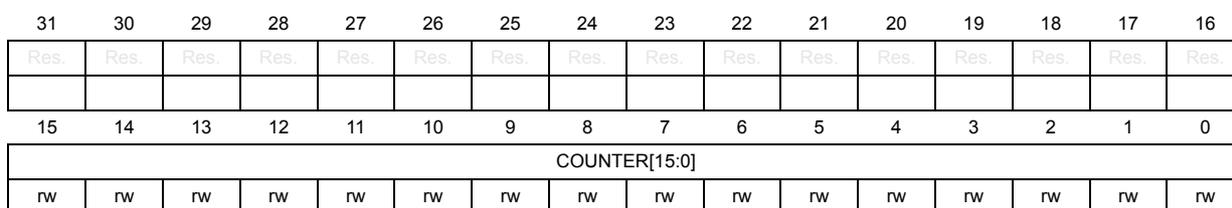
| 31 | 30 | 29 | 28 | 27 | 26 | 25 | 24 | 23 | 22 | 21 | 20 | 19 | 18 | 17 | 16 |
| Res. | Res. | Res. | Res. | Res. | Res. | Res. | Res. | Res. | Res. | Res. | Res. | Res. | Res. | Res. | Res. |
| 15 | 14 | 13 | 12 | 11 | 10 | 9 | 8 | 7 | 6 | 5 | 4 | 3 | 2 | 1 | 0 |
| COUNTER[15:0] | |||||||||||||||
| rw | rw | rw | rw | rw | rw | rw | rw | rw | rw | rw | rw | rw | rw | rw | rw |
Bits 31:16 Reserved, must be kept at reset value.
Bits 15:0 COUNTER[15:0] : Event counter
The counter increments whenever the selected event occurs.
PMU cycle counter register (PMU_CCNTR)
Address offset: 0x07C
Reset value: 0xXXXX XXXX
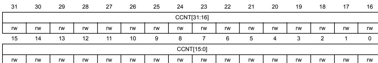
| 31 | 30 | 29 | 28 | 27 | 26 | 25 | 24 | 23 | 22 | 21 | 20 | 19 | 18 | 17 | 16 |
| CCNT[31:16] | |||||||||||||||
| rw | rw | rw | rw | rw | rw | rw | rw | rw | rw | rw | rw | rw | rw | rw | rw |
| 15 | 14 | 13 | 12 | 11 | 10 | 9 | 8 | 7 | 6 | 5 | 4 | 3 | 2 | 1 | 0 |
| CCNT[15:0] | |||||||||||||||
| rw | rw | rw | rw | rw | rw | rw | rw | rw | rw | rw | rw | rw | rw | rw | rw |
Bits 31:0 CCNT[31:0] : Cycle count
The counter increments every processor clock cycle.
PMU event type and filter register (PMU_EVTYPERx)
Address offset: 0x400 + 0x4 * x (x = 0 to 7)
Reset value: 0x0000 XXXX
| 31 | 30 | 29 | 28 | 27 | 26 | 25 | 24 | 23 | 22 | 21 | 20 | 19 | 18 | 17 | 16 |
|---|---|---|---|---|---|---|---|---|---|---|---|---|---|---|---|
| Res. | Res. | Res. | Res. | Res. | Res. | Res. | Res. | Res. | Res. | Res. | Res. | Res. | Res. | Res. | Res. |
| 15 | 14 | 13 | 12 | 11 | 10 | 9 | 8 | 7 | 6 | 5 | 4 | 3 | 2 | 1 | 0 |
| EVTCOUNT[15:0] | |||||||||||||||
| rw | rw | rw | rw | rw | rw | rw | rw | rw | rw | rw | rw | rw | rw | rw | rw |
Bits 31:16 Reserved, must be kept at reset value.
Bits 15:0 EVTCOUNT[15:0] : Event to count
The number of the event that is counted by event counter PMU_EVCNTRx.
PMU count enable set register (PMU_CNTENSET)
Address offset: 0xC00
Reset value: 0x0000 0000
| 31 | 30 | 29 | 28 | 27 | 26 | 25 | 24 | 23 | 22 | 21 | 20 | 19 | 18 | 17 | 16 |
|---|---|---|---|---|---|---|---|---|---|---|---|---|---|---|---|
| C | Res. | Res. | Res. | Res. | Res. | Res. | Res. | Res. | Res. | Res. | Res. | Res. | Res. | Res. | Res. |
| rw | |||||||||||||||
| 15 | 14 | 13 | 12 | 11 | 10 | 9 | 8 | 7 | 6 | 5 | 4 | 3 | 2 | 1 | 0 |
| Res. | Res. | Res. | Res. | Res. | Res. | Res. | Res. | PN[7:0] | |||||||
| rw | rw | rw | rw | rw | rw | rw | rw | ||||||||
Bit 31
C
: Cycle-count enable
Condition: write operation
0: No effect
1: Enable cycle counter.
Condition: read operation
0: Cycle counter disabled
1: Cycle counter enabled
Bits 30:8 Reserved, must be kept at reset value.
Bits 7:0
PN[7:0]
: Event counter enable
Condition: write operation
Writing a 1 to bit n enables event counter PMU_EVCNTRn. Writing a 0 has no effect.
Condition: read operation
When bit n is 0, event counter PMU_EVCNTRn is disabled.
When bit n is 1, event counter PMU_EVCNTRn is enabled.
PMU count enable clear register (PMU_CNTENCLR)
Address offset: 0xC20
Reset value: 0x0000 0000
| 31 | 30 | 29 | 28 | 27 | 26 | 25 | 24 | 23 | 22 | 21 | 20 | 19 | 18 | 17 | 16 |
|---|---|---|---|---|---|---|---|---|---|---|---|---|---|---|---|
| C | Res. | Res. | Res. | Res. | Res. | Res. | Res. | Res. | Res. | Res. | Res. | Res. | Res. | Res. | Res. |
| rw | |||||||||||||||
| 15 | 14 | 13 | 12 | 11 | 10 | 9 | 8 | 7 | 6 | 5 | 4 | 3 | 2 | 1 | 0 |
| Res. | Res. | Res. | Res. | Res. | Res. | Res. | Res. | PN[7:0] | |||||||
| rw | rw | rw | rw | rw | rw | rw | rw | ||||||||
Bit 31 C : Cycle-count disable
Condition: write operation
0: No effect
1: Disable cycle counter.
Condition: read operation
0: Cycle counter disabled
1: Cycle counter enabled
Bits 30:8 Reserved, must be kept at reset value.
Bits 7:0 PN[7:0] : Event counter disable
Condition: write operation
Writing a 1 to bit n disables event counter PMU_EVCNTRn. Writing a 0 has no effect.
Condition: read operation
When bit n is 0, event counter PMU_EVCNTRn is disabled.
When bit n is 1, event counter PMU_EVCNTRn is enabled.
PMU count interrupt set register (PMU_INTENSET)
Address offset: 0xC40
Reset value: 0x0000 0000
| 31 | 30 | 29 | 28 | 27 | 26 | 25 | 24 | 23 | 22 | 21 | 20 | 19 | 18 | 17 | 16 |
|---|---|---|---|---|---|---|---|---|---|---|---|---|---|---|---|
| C | Res. | Res. | Res. | Res. | Res. | Res. | Res. | Res. | Res. | Res. | Res. | Res. | Res. | Res. | Res. |
| rw | |||||||||||||||
| 15 | 14 | 13 | 12 | 11 | 10 | 9 | 8 | 7 | 6 | 5 | 4 | 3 | 2 | 1 | 0 |
| Res. | Res. | Res. | Res. | Res. | Res. | Res. | Res. | PN[7:0] | |||||||
| rw | rw | rw | rw | rw | rw | rw | rw | ||||||||
Bit 31 C : Cycle-counter-overflow interrupt request enable
Condition: write operation
0: No effect
1: Enable cycle-counter-overflow interrupt request.
Condition: read operation
0: Cycle-counter-overflow interrupt request disabled
1: Cycle-counter-overflow interrupt request enabled
Bits 30:8 Reserved, must be kept at reset value.
Bits 7:0 PN[7:0] : Event-counter interrupt request enable
Condition: write operation
Writing a one to bit n enables the interrupt request for event counter PMU_EVCNTRn.
Writing a 0 has no effect.
Condition: read operation
When bit n is 0, the event-counter interrupt request for PMU_EVCNTRn is disabled.
When bit n is 1, the event-counter interrupt request for PMU_EVCNTRn is enabled.
PMU count interrupt clear register (PMU_INTENCLR)
Address offset: 0xC60
Reset value: 0x0000 0000
| 31 | 30 | 29 | 28 | 27 | 26 | 25 | 24 | 23 | 22 | 21 | 20 | 19 | 18 | 17 | 16 |
|---|---|---|---|---|---|---|---|---|---|---|---|---|---|---|---|
| C | Res. | Res. | Res. | Res. | Res. | Res. | Res. | Res. | Res. | Res. | Res. | Res. | Res. | Res. | Res. |
| rw | |||||||||||||||
| 15 | 14 | 13 | 12 | 11 | 10 | 9 | 8 | 7 | 6 | 5 | 4 | 3 | 2 | 1 | 0 |
| Res. | Res. | Res. | Res. | Res. | Res. | Res. | Res. | PN[7:0] | |||||||
| rw | rw | rw | rw | rw | rw | rw | rw | ||||||||
Bit 31 C : Cycle-counter-overflow interrupt request disable
Condition: write operation
0: No effect
1: Disable cycle-counter-overflow interrupt request.
Condition: read operation
0: Cycle-counter-overflow interrupt request disabled
1: Cycle-counter-overflow interrupt request enabled
Bits 30:8 Reserved, must be kept at reset value.
Bits 7:0 PN[7:0] : Event-counter interrupt request disable
Condition: write operation
Writing a one to bit n disables the interrupt request for event counter PMU_EVCNTRn.
Writing a 0 has no effect.
Condition: read operation
When bit n is 0, the event-counter interrupt request for PMU_EVCNTRn is disabled.
When bit n is 1, the event-counter interrupt request for PMU_EVCNTRn is enabled.
PMU overflow flag status clear register (PMU_OVSCLR)
Address offset: 0xC80
Reset value: 0x0000 0000
| 31 | 30 | 29 | 28 | 27 | 26 | 25 | 24 | 23 | 22 | 21 | 20 | 19 | 18 | 17 | 16 |
|---|---|---|---|---|---|---|---|---|---|---|---|---|---|---|---|
| C | Res. | Res. | Res. | Res. | Res. | Res. | Res. | Res. | Res. | Res. | Res. | Res. | Res. | Res. | Res. |
| rw | |||||||||||||||
| 15 | 14 | 13 | 12 | 11 | 10 | 9 | 8 | 7 | 6 | 5 | 4 | 3 | 2 | 1 | 0 |
| Res. | Res. | Res. | Res. | Res. | Res. | Res. | Res. | PN[7:0] | |||||||
| rw | rw | rw | rw | rw | rw | rw | rw | ||||||||
Bit 31 C : Cycle-counter-overflow flag clear
- Condition: write operation
- 0: No effect
- 1: Clear cycle-counter-overflow flag.
- Condition: read operation
- 0: Cycle counter has not overflowed.
- 1: Cycle counter has overflowed.
Bits 30:8 Reserved, must be kept at reset value.
Bits 7:0 PN[7:0] : Even- counter-overflow flag clear
- Condition: write operation
- Writing a one to bit n clears the overflow flag for event counter PMU_EVCNTRn. Writing a 0 has no effect
- Condition: read operation
- When bit n is 0, the event counter for PMU_EVCNTRn has not overflowed.
- When bit n is 1, the event counter for PMU_EVCNTRn has overflowed.
PMU software increment register (PMU_SWINC)
Address offset: 0xCA0
Reset value: 0x0000 0000
| 31 | 30 | 29 | 28 | 27 | 26 | 25 | 24 | 23 | 22 | 21 | 20 | 19 | 18 | 17 | 16 |
|---|---|---|---|---|---|---|---|---|---|---|---|---|---|---|---|
| Res. | Res. | Res. | Res. | Res. | Res. | Res. | Res. | Res. | Res. | Res. | Res. | Res. | Res. | Res. | Res. |
| 15 | 14 | 13 | 12 | 11 | 10 | 9 | 8 | 7 | 6 | 5 | 4 | 3 | 2 | 1 | 0 |
| Res. | Res. | Res. | Res. | Res. | Res. | Res. | Res. | PN[7:0] | |||||||
| w | w | w | w | w | w | w | w | ||||||||
Bits 31:8 Reserved, must be kept at reset value.
Bits 7:0 PN[7:0] : Event counter software increment
Writing a one to bit n increments event counter PMU_EVCNTRn, if it is configured for software increments. Writing a 0 has no effect.
PMU overflow flag status set register (PMU_OVSSET)
Address offset: 0xCC0
Reset value: 0x0000 0000
| 31 | 30 | 29 | 28 | 27 | 26 | 25 | 24 | 23 | 22 | 21 | 20 | 19 | 18 | 17 | 16 |
|---|---|---|---|---|---|---|---|---|---|---|---|---|---|---|---|
| C | Res. | Res. | Res. | Res. | Res. | Res. | Res. | Res. | Res. | Res. | Res. | Res. | Res. | Res. | Res. |
| rw | |||||||||||||||
| 15 | 14 | 13 | 12 | 11 | 10 | 9 | 8 | 7 | 6 | 5 | 4 | 3 | 2 | 1 | 0 |
| Res. | Res. | Res. | Res. | Res. | Res. | Res. | Res. | PN[7:0] | |||||||
| rw | rw | rw | rw | rw | rw | rw | rw | ||||||||
Bit 31 C : Cycle-counter-overflow flag set
Condition: write operation
0: No effect
1: Set cycle-counter-overflow flag.
Condition: read operation
0: Cycle counter has not overflowed.
1: Cycle counter has overflowed.
Bits 30:8 Reserved, must be kept at reset value.
Bits 7:0 PN[7:0] : Event-counter-overflow flag set
Condition: write operation
Writing a one to bit n sets the overflow flag for event counter PMU_EVCNTRn. Writing a 0 has no effect
Condition: read operation
When bit n is 0, the event counter for PMU_EVCNTRn has not overflowed.
When bit n is 1, the event counter for PMU_EVCNTRn has overflowed.
PMU type register (PMU_TYPE)
Address offset: 0xE00
Reset value: 0x00A0 5F08
| 31 | 30 | 29 | 28 | 27 | 26 | 25 | 24 | 23 | 22 | 21 | 20 | 19 | 18 | 17 | 16 |
|---|---|---|---|---|---|---|---|---|---|---|---|---|---|---|---|
| Res. | Res. | Res. | Res. | Res. | Res. | Res. | Res. | TRO | Res. | FZO | Res. | Res. | Res. | Res. | Res. |
| r | r | ||||||||||||||
| 15 | 14 | 13 | 12 | 11 | 10 | 9 | 8 | 7 | 6 | 5 | 4 | 3 | 2 | 1 | 0 |
| Res. | CC | SIZE[5:0] | N[7:0] | ||||||||||||
| r | r | r | r | r | r | r | r | r | r | r | r | r | r | r | |
Bits 31:24 Reserved, must be kept at reset value.
Bit 23 TRO : Trace on overflow support
1: Trace on overflow supported
Bit 22 Reserved, must be kept at reset value.
Bit 21 FZO : Freeze on overflow support
1: Freeze on overflow mechanism supported
Bits 20:15 Reserved, must be kept at reset value.
Bit 14 CC : Cycle counter present
1: Dedicated cycle counter is present.
Bits 13:8 SIZE[5:0] : Counter size
This field indicates the spacing of counters in the memory-map.
0x1F: 32 bits
Bits 7:0 N[7:0] : Number of event counters
0x8
PMU type register (PMU_CTRL)
Address offset: 0xE04
Reset value: 0x0000 XXXX
| 31 | 30 | 29 | 28 | 27 | 26 | 25 | 24 | 23 | 22 | 21 | 20 | 19 | 18 | 17 | 16 |
|---|---|---|---|---|---|---|---|---|---|---|---|---|---|---|---|
| Res. | Res. | Res. | Res. | Res. | Res. | Res. | Res. | Res. | Res. | Res. | Res. | Res. | Res. | Res. | Res. |
| 15 | 14 | 13 | 12 | 11 | 10 | 9 | 8 | 7 | 6 | 5 | 4 | 3 | 2 | 1 | 0 |
| Res. | Res. | Res. | Res. | TRO | Res. | FZO | Res. | Res. | Res. | DP | Res. | Res. | C | P | E |
| rw | rw | rw | w | w | rw |
Bits 31:12 Reserved, must be kept at reset value.
Bit 11 TRO : Trace on overflow enable
0: Trace on overflow disabled
1: Trace when any of the event counters overflows an 8-bit value
Bit 10 Reserved, must be kept at reset value.
Bit 9 FZO : Freeze on overflow enable
0: Event counters continue counting while the overflow flag is set.
1: Event counters stop while the overflow flag is set.
Bits 8:6 Reserved, must be kept at reset value.
Bit 5 DP : Controls whether the cycle counter is disabled in secure state
. This bit is an alias of CYCDISS in DWT_CTRL.
0: No effect
1: Cycle counter is not incremented when the processor is in secure state.
Bits 4:3 Reserved, must be kept at reset value.
Bit 2 C : Cycle counter reset
0: No effect
1: Reset PMU_CCNTR to 0.
Bit 1 P : Event counter reset
0: No effect
1: Reset all event counters, not including PMU_CCNTR, to 0.
Bit 0 E : Event counter enable
0: All counters, including PMU_CCNTR, are disabled.
1: All counters are enabled by PMU_CNTENSET.
PMU overflow flag status set register (PMU_AUTHSTAT)
Address offset: 0xFB8
Reset value: 0x0000 00XX
| 31 | 30 | 29 | 28 | 27 | 26 | 25 | 24 | 23 | 22 | 21 | 20 | 19 | 18 | 17 | 16 |
|---|---|---|---|---|---|---|---|---|---|---|---|---|---|---|---|
| Res. | Res. | Res. | Res. | Res. | Res. | Res. | Res. | Res. | Res. | Res. | Res. | Res. | Res. | Res. | Res. |
| 15 | 14 | 13 | 12 | 11 | 10 | 9 | 8 | 7 | 6 | 5 | 4 | 3 | 2 | 1 | 0 |
| Res. | Res. | Res. | Res. | Res. | Res. | Res. | Res. | SNID[1:0] | SID[1:0] | NSNID[1:0] | NSID[1:0] | ||||
| r | r | r | r | r | r | r | r |
Bits 31:8 Reserved, must be kept at reset value.
- Bits 7:6
SNID[1:0]
: Secure non-invasive debug
- 10: Secure non-invasive debug prohibited
- 11: Secure non-invasive debug allowed
- Bits 5:4
SID[1:0]
: Secure invasive debug
- 10: Secure invasive debug prohibited
- 11: Secure invasive debug allowed
- Bits 3:2
NSNID[1:0]
: Nonsecure non-invasive debug
- 10: Nonsecure non-invasive debug prohibited
- 11: Nonsecure non-invasive debug allowed
- Bits 1:0
NSID[1:0]
: Nonsecure invasive debug
- 10: Nonsecure invasive debug prohibited
- 11: Nonsecure invasive debug allowed
PMU device type architecture register (PMU_DEVARCH)
Address offset: 0xFBC
Reset value: 0x4770 0A06
| 31 | 30 | 29 | 28 | 27 | 26 | 25 | 24 | 23 | 22 | 21 | 20 | 19 | 18 | 17 | 16 |
|---|---|---|---|---|---|---|---|---|---|---|---|---|---|---|---|
| ARCHITECT[10:0] | PRESENT | REVISION[3:0] | |||||||||||||
| r | r | r | r | r | r | r | r | r | r | r | r | r | r | r | r |
| 15 | 14 | 13 | 12 | 11 | 10 | 9 | 8 | 7 | 6 | 5 | 4 | 3 | 2 | 1 | 0 |
| ARCHVER[3:0] | ARCHPART[11:0] | ||||||||||||||
| r | r | r | r | r | r | r | r | r | r | r | r | r | r | r | r |
- Bits 31:21
ARCHITECT[10:0]
: Architect JEDEC code
- 0x23B: Arm JEDEC code
- Bit 20
PRESENT
: DEVARCH register present
- 1: Present
- Bits 19:16
REVISION[3:0]
: Architecture revision
- 0x0: PMU architecture minor revision
- Bits 15:12
ARCHVER[3:0]
: Architecture version
- 0x0: PMU architecture version
- Bits 11:0
ARCHPART[11:0]
: Architecture
- 0xA06: PMU architecture part number
PMU device type register (PMU_DEVTYPE)
Address offset: 0xFCC
Reset value: 0x0000 0016
| 31 | 30 | 29 | 28 | 27 | 26 | 25 | 24 | 23 | 22 | 21 | 20 | 19 | 18 | 17 | 16 |
|---|---|---|---|---|---|---|---|---|---|---|---|---|---|---|---|
| Res. | Res. | Res. | Res. | Res. | Res. | Res. | Res. | Res. | Res. | Res. | Res. | Res. | Res. | Res. | Res. |
| 15 | 14 | 13 | 12 | 11 | 10 | 9 | 8 | 7 | 6 | 5 | 4 | 3 | 2 | 1 | 0 |
| Res. | Res. | Res. | Res. | Res. | Res. | Res. | Res. | SUB[3:0] | MAJOR[3:0] | ||||||
| r | r | r | r | r | r | r | r | ||||||||
Bits 31:8 Reserved, must be kept at reset value.
Bits 7:4 SUB[3:0] : Component subtype
0x1
Bits 3:0 MAJOR[3:0] : Component major type
0x6
PMU CoreSight peripheral identity register 4 (PMU_PIDR4)
Address offset: 0xFD0
Reset value: 0x0000 0004
| 31 | 30 | 29 | 28 | 27 | 26 | 25 | 24 | 23 | 22 | 21 | 20 | 19 | 18 | 17 | 16 |
|---|---|---|---|---|---|---|---|---|---|---|---|---|---|---|---|
| Res. | Res. | Res. | Res. | Res. | Res. | Res. | Res. | Res. | Res. | Res. | Res. | Res. | Res. | Res. | Res. |
| 15 | 14 | 13 | 12 | 11 | 10 | 9 | 8 | 7 | 6 | 5 | 4 | 3 | 2 | 1 | 0 |
| Res. | Res. | Res. | Res. | Res. | Res. | Res. | Res. | SIZE[3:0] | JEP106CON[3:0] | ||||||
| r | r | r | r | r | r | r | r | ||||||||
Bits 31:8 Reserved, must be kept at reset value.
Bits 7:4 SIZE[3:0] : Register file size
0x0: Register file occupies a single 4-Kbyte region.
Bits 3:0 JEP106CON[3:0] : JEP106 continuation code
0x4: Arm JEDEC code
PMU CoreSight peripheral identity register 0 (PMU_PIDR0)
Address offset: 0xFE0
Reset value: 0x0000 0023
| 31 | 30 | 29 | 28 | 27 | 26 | 25 | 24 | 23 | 22 | 21 | 20 | 19 | 18 | 17 | 16 |
|---|---|---|---|---|---|---|---|---|---|---|---|---|---|---|---|
| Res. | Res. | Res. | Res. | Res. | Res. | Res. | Res. | Res. | Res. | Res. | Res. | Res. | Res. | Res. | Res. |
| 15 | 14 | 13 | 12 | 11 | 10 | 9 | 8 | 7 | 6 | 5 | 4 | 3 | 2 | 1 | 0 |
| Res. | Res. | Res. | Res. | Res. | Res. | Res. | Res. | PARTNUM[7:0] | |||||||
| r | r | r | r | r | r | r | r | ||||||||
Bits 31:8 Reserved, must be kept at reset value.
Bits 7:0 PARTNUM[7:0] : Part number field, bits [7:0]
0x23: PMU part number
PMU CoreSight peripheral identity register 1 (PMU_PIDR1)
Address offset: 0xFE4
Reset value: 0x0000 00BD
| 31 | 30 | 29 | 28 | 27 | 26 | 25 | 24 | 23 | 22 | 21 | 20 | 19 | 18 | 17 | 16 |
|---|---|---|---|---|---|---|---|---|---|---|---|---|---|---|---|
| Res. | Res. | Res. | Res. | Res. | Res. | Res. | Res. | Res. | Res. | Res. | Res. | Res. | Res. | Res. | Res. |
| 15 | 14 | 13 | 12 | 11 | 10 | 9 | 8 | 7 | 6 | 5 | 4 | 3 | 2 | 1 | 0 |
| Res. | Res. | Res. | Res. | Res. | Res. | Res. | Res. | JEP106ID[3:0] | PARTNUM[11:8] | ||||||
| r | r | r | r | r | r | r | r | ||||||||
Bits 31:8 Reserved, must be kept at reset value.
Bits 7:4 JEP106ID[3:0] : JEP106 identity code field, bits [3:0]
0xB: Arm JEDEC code
Bits 3:0 PARTNUM[11:8] : Part number field, bits [11:8]
0xD: PMU part number
PMU CoreSight peripheral identity register 2 (PMU_PIDR2)
Address offset: 0xFE8
Reset value: 0x0000 000B
| 31 | 30 | 29 | 28 | 27 | 26 | 25 | 24 | 23 | 22 | 21 | 20 | 19 | 18 | 17 | 16 |
|---|---|---|---|---|---|---|---|---|---|---|---|---|---|---|---|
| Res. | Res. | Res. | Res. | Res. | Res. | Res. | Res. | Res. | Res. | Res. | Res. | Res. | Res. | Res. | Res. |
| 15 | 14 | 13 | 12 | 11 | 10 | 9 | 8 | 7 | 6 | 5 | 4 | 3 | 2 | 1 | 0 |
| Res. | Res. | Res. | Res. | Res. | Res. | Res. | Res. | REVISION[3:0] | JEDEC | JEP106ID[6:4] | |||||
| r | r | r | r | r | r | r | r | ||||||||
Bits 31:8 Reserved, must be kept at reset value.
Bits 7:4 REVISION[3:0] : Component revision number
0x0: r0p0
Bit 3 JEDEC : JEDEC assigned value
1: Designer ID specified by JEDEC
Bits 2:0 JEP106ID[6:4] : JEP106 identity code field, bits [6:4]
0x3: Arm JEDEC code
PMU CoreSight peripheral identity register 3 (PMU_PIDR3)
Address offset: 0xFEC
Reset value: 0x0000 0000
| 31 | 30 | 29 | 28 | 27 | 26 | 25 | 24 | 23 | 22 | 21 | 20 | 19 | 18 | 17 | 16 |
|---|---|---|---|---|---|---|---|---|---|---|---|---|---|---|---|
| Res. | Res. | Res. | Res. | Res. | Res. | Res. | Res. | Res. | Res. | Res. | Res. | Res. | Res. | Res. | Res. |
| 15 | 14 | 13 | 12 | 11 | 10 | 9 | 8 | 7 | 6 | 5 | 4 | 3 | 2 | 1 | 0 |
| Res. | Res. | Res. | Res. | Res. | Res. | Res. | Res. | REVAND[3:0] | CMOD[3:0] | ||||||
| r | r | r | r | r | r | r | r | ||||||||
Bits 31:8 Reserved, must be kept at reset value.
Bits 7:4 REVAND[3:0] : Metal fix version
0x0: No metal fix
Bits 3:0 CMOD[3:0] : Customer modified
0x0: No customer modifications
PMU CoreSight component identity register 0 (PMU_CIDR0)
Address offset: 0xFF0
Reset value: 0x0000 000D
| 31 | 30 | 29 | 28 | 27 | 26 | 25 | 24 | 23 | 22 | 21 | 20 | 19 | 18 | 17 | 16 |
|---|---|---|---|---|---|---|---|---|---|---|---|---|---|---|---|
| Res. | Res. | Res. | Res. | Res. | Res. | Res. | Res. | Res. | Res. | Res. | Res. | Res. | Res. | Res. | Res. |
| 15 | 14 | 13 | 12 | 11 | 10 | 9 | 8 | 7 | 6 | 5 | 4 | 3 | 2 | 1 | 0 |
| Res. | Res. | Res. | Res. | Res. | Res. | Res. | Res. | PREAMBLE[7:0] | |||||||
| r | r | r | r | r | r | r | r | ||||||||
Bits 31:8 Reserved, must be kept at reset value.
Bits 7:0 PREAMBLE[7:0] : Component ID field, bits [7:0]
0x0D: Common ID value
PMU CoreSight component identity register 1 (PMU_CIDR1)
Address offset: 0xFF4
Reset value: 0x0000 0090
| 31 | 30 | 29 | 28 | 27 | 26 | 25 | 24 | 23 | 22 | 21 | 20 | 19 | 18 | 17 | 16 |
|---|---|---|---|---|---|---|---|---|---|---|---|---|---|---|---|
| Res. | Res. | Res. | Res. | Res. | Res. | Res. | Res. | Res. | Res. | Res. | Res. | Res. | Res. | Res. | Res. |
| 15 | 14 | 13 | 12 | 11 | 10 | 9 | 8 | 7 | 6 | 5 | 4 | 3 | 2 | 1 | 0 |
| Res. | Res. | Res. | Res. | Res. | Res. | Res. | Res. | CLASS[3:0] | PREAMBLE[11:8] | ||||||
| r | r | r | r | r | r | r | r | ||||||||
Bits 31:8 Reserved, must be kept at reset value.
Bits 7:4 CLASS[3:0] : Component ID field, bits [15:12] - component class
0x9: PMU
Bits 3:0 PREAMBLE[11:8] : Component ID field, bits [11:8]
0x0: Common ID value
PMU CoreSight component identity register 2 (PMU_CIDR2)
Address offset: 0xFF8
Reset value: 0x0000 0005
| 31 | 30 | 29 | 28 | 27 | 26 | 25 | 24 | 23 | 22 | 21 | 20 | 19 | 18 | 17 | 16 |
|---|---|---|---|---|---|---|---|---|---|---|---|---|---|---|---|
| Res. | Res. | Res. | Res. | Res. | Res. | Res. | Res. | Res. | Res. | Res. | Res. | Res. | Res. | Res. | Res. |
| 15 | 14 | 13 | 12 | 11 | 10 | 9 | 8 | 7 | 6 | 5 | 4 | 3 | 2 | 1 | 0 |
| Res. | Res. | Res. | Res. | Res. | Res. | Res. | Res. | ||||||||
| r | r | r | r | r | r | r | r |
Bits 31:8 Reserved, must be kept at reset value.
Bits 7:0 PREAMBLE[19:12] : Component ID field, bits [23:16]
0x05: Common ID value
PMU CoreSight component identity register 3 (PMU_CIDR3)
Address offset: 0xFFC
Reset value: 0x0000 00B1
| 31 | 30 | 29 | 28 | 27 | 26 | 25 | 24 | 23 | 22 | 21 | 20 | 19 | 18 | 17 | 16 |
|---|---|---|---|---|---|---|---|---|---|---|---|---|---|---|---|
| Res. | Res. | Res. | Res. | Res. | Res. | Res. | Res. | Res. | Res. | Res. | Res. | Res. | Res. | Res. | Res. |
| 15 | 14 | 13 | 12 | 11 | 10 | 9 | 8 | 7 | 6 | 5 | 4 | 3 | 2 | 1 | 0 |
| Res. | Res. | Res. | Res. | Res. | Res. | Res. | Res. | ||||||||
| r | r | r | r | r | r | r | r |
Bits 31:8 Reserved, must be kept at reset value.
Bits 7:0 PREAMBLE[27:20] : Component ID field, bits [31:24]
0xB1: Common ID value
PMU register map
Table 876. PMU register map and reset values
| Offset | Register name | 31 | 30 | 29 | 28 | 27 | 26 | 25 | 24 | 23 | 22 | 21 | 20 | 19 | 18 | 17 | 16 | 15 | 14 | 13 | 12 | 11 | 10 | 9 | 8 | 7 | 6 | 5 | 4 | 3 | 2 | 1 | 0 |
|---|---|---|---|---|---|---|---|---|---|---|---|---|---|---|---|---|---|---|---|---|---|---|---|---|---|---|---|---|---|---|---|---|---|
| Res. | Res. | Res. | Res. | Res. | Res. | Res. | Res. | Res. | Res. | Res. | Res. | Res. | Res. | Res. | Res. | Res. | Res. | Res. | Res. | Res. | Res. | Res. | Res. | Res. | Res. | Res. | Res. | Res. | Res. | Res. | Res. | ||
| 0x000 + 0x4 * x (x=0 to 7) Last address: 0x01C | PMU_EVCNTRx | COUNTER[15:0] | |||||||||||||||||||||||||||||||
| Reset value | 0 | 0 | 0 | 0 | 0 | 0 | 0 | 0 | 0 | 0 | 0 | 0 | 0 | 0 | 0 | ||||||||||||||||||
| 0x020-0x078 | Reserved | Reserved | |||||||||||||||||||||||||||||||
| 0x07C | PMU_CCNTR | CCNT[31:0] | |||||||||||||||||||||||||||||||
| Reset value | X | X | X | X | X | X | X | X | X | X | X | X | X | X | X | X | X | X | X | X | X | X | X | X | X | X | X | X | X | X | X | ||
| 0x080-0x3FC | Reserved | Reserved | |||||||||||||||||||||||||||||||
Table 876. PMU register map and reset values (continued)
| Offset | Register name | 31 | 30 | 29 | 28 | 27 | 26 | 25 | 24 | 23 | 22 | 21 | 20 | 19 | 18 | 17 | 16 | 15 | 14 | 13 | 12 | 11 | 10 | 9 | 8 | 7 | 6 | 5 | 4 | 3 | 2 | 1 | 0 |
|---|---|---|---|---|---|---|---|---|---|---|---|---|---|---|---|---|---|---|---|---|---|---|---|---|---|---|---|---|---|---|---|---|---|
| 0x400 + 0x4 * x (x=0 to 7) Last address: 0x41C | PMU_EVTYPEx | Res | Res | Res | Res | Res | Res | Res | Res | Res | Res | Res | Res | Res | Res | Res | Res | EVT CNT[15:0] | |||||||||||||||
| Reset value | X | X | X | X | X | X | X | X | X | X | X | X | X | X | X | ||||||||||||||||||
| 0x420-0xBFC | Reserved | Reserved | |||||||||||||||||||||||||||||||
| 0xC00 | PMU_CNTENSET | C | Res | Res | Res | Res | Res | Res | Res | Res | Res | Res | Res | Res | Res | Res | Res | Res | Res | Res | Res | Res | Res | Res | Res | PN[7:0] | |||||||
| Reset value | 0 | 0 | 0 | 0 | 0 | 0 | 0 | 0 | |||||||||||||||||||||||||
| 0xC04-0xC1C | Reserved | Reserved | |||||||||||||||||||||||||||||||
| 0xC20 | PMU_CNTENCLR | C | Res | Res | Res | Res | Res | Res | Res | Res | Res | Res | Res | Res | Res | Res | Res | Res | Res | Res | Res | Res | Res | Res | Res | PN[7:0] | |||||||
| Reset value | 0 | 0 | 0 | 0 | 0 | 0 | 0 | 0 | |||||||||||||||||||||||||
| 0xC24-0xC3C | Reserved | Reserved | |||||||||||||||||||||||||||||||
| 0xC40 | PMU_INTENSET | C | Res | Res | Res | Res | Res | Res | Res | Res | Res | Res | Res | Res | Res | Res | Res | Res | Res | Res | Res | Res | Res | Res | Res | PN[7:0] | |||||||
| Reset value | 0 | 0 | 0 | 0 | 0 | 0 | 0 | 0 | |||||||||||||||||||||||||
| 0xC44-0xC5C | Reserved | Reserved | |||||||||||||||||||||||||||||||
| 0xC60 | PMU_INTENCLR | C | Res | Res | Res | Res | Res | Res | Res | Res | Res | Res | Res | Res | Res | Res | Res | Res | Res | Res | Res | Res | Res | Res | Res | PN[7:0] | |||||||
| Reset value | 0 | 0 | 0 | 0 | 0 | 0 | 0 | 0 | |||||||||||||||||||||||||
| 0xC64-0xC7C | Reserved | Reserved | |||||||||||||||||||||||||||||||
| 0xC80 | PMU_OVSCLR | C | Res | Res | Res | Res | Res | Res | Res | Res | Res | Res | Res | Res | Res | Res | Res | Res | Res | Res | Res | Res | Res | Res | Res | PN[7:0] | |||||||
| Reset value | 0 | 0 | 0 | 0 | 0 | 0 | 0 | 0 | |||||||||||||||||||||||||
| 0xC84-0xC9C | Reserved | Reserved | |||||||||||||||||||||||||||||||
| 0xCA0 | PMU_SWINC | C | Res | Res | Res | Res | Res | Res | Res | Res | Res | Res | Res | Res | Res | Res | Res | Res | Res | Res | Res | Res | Res | Res | Res | PN[7:0] | |||||||
| Reset value | 0 | 0 | 0 | 0 | 0 | 0 | 0 | 0 | |||||||||||||||||||||||||
| 0xCA4-0xCBC | Reserved | Reserved | |||||||||||||||||||||||||||||||
| 0xCC0 | PMU_OVSSET | C | Res | Res | Res | Res | Res | Res | Res | Res | Res | Res | Res | Res | Res | Res | Res | Res | Res | Res | Res | Res | Res | Res | Res | PN[7:0] | |||||||
| Reset value | 0 | 0 | 0 | 0 | 0 | 0 | 0 | 0 | |||||||||||||||||||||||||
| 0xCC4-0xDFC | Reserved | Reserved | |||||||||||||||||||||||||||||||
| 0xE00 | PMU_TYPE | Res | Res | Res | Res | Res | Res | Res | TR0 | Res | FZ0 | Res | Res | Res | Res | Res | Res | Res | Res | Res | Res | Res | Res | Res | CC | SIZE[5:0] | N[7:0] | ||||||
| Reset value | 1 | 1 | 1 | 0 | 1 | 1 | 1 | 1 | 1 | 0 | 0 | ||||||||||||||||||||||
| 0xE04 | PMU_CTRL | Res | Res | Res | Res | Res | Res | Res | Res | Res | Res | Res | Res | Res | Res | Res | Res | Res | Res | Res | Res | TR0 | Res | FZ0 | Res | Res | Res | DP | Res | Res | C | P | |
| Reset value | X | X | X | X | X | ||||||||||||||||||||||||||||
| 0xE04-0xFB4 | Reserved | Reserved | |||||||||||||||||||||||||||||||
| 0xFB8 | PMU_AUTHSTAT | Res | Res | Res | Res | Res | Res | Res | Res | Res | Res | Res | Res | Res | Res | Res | Res | Res | Res | Res | Res | Res | Res | Res | Res | SNID [1:0] | Res | Res | SID [1:0] | Res | Res | NSNID [1:0] | NSID [1:0] |
| Reset value | X | X | X | X | X | X | X | X | |||||||||||||||||||||||||
Table 876. PMU register map and reset values (continued)
| Offset | Register name | 31 | 30 | 29 | 28 | 27 | 26 | 25 | 24 | 23 | 22 | 21 | 20 | 19 | 18 | 17 | 16 | 15 | 14 | 13 | 12 | 11 | 10 | 9 | 8 | 7 | 6 | 5 | 4 | 3 | 2 | 1 | 0 |
|---|---|---|---|---|---|---|---|---|---|---|---|---|---|---|---|---|---|---|---|---|---|---|---|---|---|---|---|---|---|---|---|---|---|
| 0xFBC | PMU_DEVARCH | ARCHITECT[10:0] | PRESENT | REVISION [3:0] | ARCHVER [3:0] | ARCHPART[11:0] | |||||||||||||||||||||||||||
| Reset value | 0 | 1 | 0 | 0 | 0 | 1 | 1 | 1 | 0 | 1 | 1 | 1 | 0 | 0 | 0 | 0 | 0 | 0 | 0 | 0 | 1 | 0 | 1 | 0 | 0 | 0 | 0 | 0 | 0 | 0 | 1 | 1 | 0 |
| 0xFC0-0xFC8 | Reserved | Reserved | |||||||||||||||||||||||||||||||
| 0xFCC | PMU_DEVTYPE | Res. | Res. | Res. | Res. | Res. | Res. | Res. | Res. | Res. | Res. | Res. | Res. | Res. | Res. | Res. | Res. | Res. | Res. | Res. | Res. | Res. | Res. | Res. | Res. | SUB[3:0] | MAJOR[3:0] | ||||||
| Reset value | 0 | 0 | 0 | 1 | 0 | 1 | 1 | 0 | |||||||||||||||||||||||||
| 0xFD0 | PMU_PIDR4 | Res. | Res. | Res. | Res. | Res. | Res. | Res. | Res. | Res. | Res. | Res. | Res. | Res. | Res. | Res. | Res. | Res. | Res. | Res. | Res. | Res. | Res. | Res. | Res. | SIZE[3:0] | JEP106CON [3:0] | ||||||
| Reset value | 0 | 0 | 0 | 0 | 0 | 1 | 0 | 0 | |||||||||||||||||||||||||
| 0xFD4-0xFDC | Reserved | Reserved | |||||||||||||||||||||||||||||||
| 0xFE0 | PMU_PIDR0 | Res. | Res. | Res. | Res. | Res. | Res. | Res. | Res. | Res. | Res. | Res. | Res. | Res. | Res. | Res. | Res. | Res. | Res. | Res. | Res. | Res. | Res. | Res. | Res. | PARTNUM[7:0] | |||||||
| Reset value | 0 | 0 | 1 | 0 | 0 | 0 | 1 | 1 | |||||||||||||||||||||||||
| 0xFE4 | PMU_PIDR1 | Res. | Res. | Res. | Res. | Res. | Res. | Res. | Res. | Res. | Res. | Res. | Res. | Res. | Res. | Res. | Res. | Res. | Res. | Res. | Res. | Res. | Res. | Res. | Res. | JEP106ID [3:0] | PARTNUM [11:8] | ||||||
| Reset value | 1 | 0 | 1 | 1 | 1 | 1 | 0 | 1 | |||||||||||||||||||||||||
| 0xFE8 | PMU_PIDR2 | Res. | Res. | Res. | Res. | Res. | Res. | Res. | Res. | Res. | Res. | Res. | Res. | Res. | Res. | Res. | Res. | Res. | Res. | Res. | Res. | Res. | Res. | Res. | Res. | REVISION [3:0] | JEDEC | JEP106ID [6:4] | |||||
| Reset value | 0 | 0 | 0 | 0 | 1 | 0 | 1 | 1 | |||||||||||||||||||||||||
| 0xFEC | PMU_PIDR3 | Res. | Res. | Res. | Res. | Res. | Res. | Res. | Res. | Res. | Res. | Res. | Res. | Res. | Res. | Res. | Res. | Res. | Res. | Res. | Res. | Res. | Res. | Res. | Res. | REVAND[3:0] | CMOD[3:0] | ||||||
| Reset value | 0 | 0 | 0 | 0 | 0 | 0 | 0 | 0 | |||||||||||||||||||||||||
| 0xFF0 | PMU_CIDR0 | Res. | Res. | Res. | Res. | Res. | Res. | Res. | Res. | Res. | Res. | Res. | Res. | Res. | Res. | Res. | Res. | Res. | Res. | Res. | Res. | Res. | Res. | Res. | Res. | PREAMBLE[7:0] | |||||||
| Reset value | 0 | 0 | 0 | 0 | 1 | 1 | 0 | 1 | |||||||||||||||||||||||||
| 0xFF4 | PMU_CIDR1 | Res. | Res. | Res. | Res. | Res. | Res. | Res. | Res. | Res. | Res. | Res. | Res. | Res. | Res. | Res. | Res. | Res. | Res. | Res. | Res. | Res. | Res. | Res. | Res. | CLASS[3:0] | PREAMBLE [11:8] | ||||||
| Reset value | 1 | 0 | 0 | 1 | 0 | 0 | 0 | 0 | |||||||||||||||||||||||||
| 0xFF8 | PMU_CIDR2 | Res. | Res. | Res. | Res. | Res. | Res. | Res. | Res. | Res. | Res. | Res. | Res. | Res. | Res. | Res. | Res. | Res. | Res. | Res. | Res. | Res. | Res. | Res. | Res. | PREAMBLE[19:12] | |||||||
| Reset value | 0 | 0 | 0 | 0 | 0 | 1 | 0 | 1 | |||||||||||||||||||||||||
| 0xFFC | PMU_CIDR3 | Res. | Res. | Res. | Res. | Res. | Res. | Res. | Res. | Res. | Res. | Res. | Res. | Res. | Res. | Res. | Res. | Res. | Res. | Res. | Res. | Res. | Res. | Res. | Res. | PREAMBLE[27:20] | |||||||
| Reset value | 1 | 0 | 1 | 1 | 0 | 0 | 0 | 1 | |||||||||||||||||||||||||
78.11.7 Instrumentation trace macrocell (ITM)
The ITM generates trace information as packets. There are four sources that can generate packets. If multiple sources generate packets at the same time, the ITM arbitrates the order in which packets are output. The four sources in decreasing order of priority are:
- • Software trace (highest priority)
The software can write directly to any of 32 x 32-bit ITM stimulus registers to generate packets. The permission level for each port can be programmed. When software writes to an enabled stimulus port, the ITM combines the port identity, the write access size, and data written, into a packet that it writes to a FIFO. The ITM outputs packets from the FIFO onto the trace bus. Reading a stimulus port register returns the status of the stimulus register (empty or pending) in bit 0.
- • Hardware trace
The DWT generates trace packets in response to a data trace event, a PC sample or a performance profiling counter wraparound. The ITM outputs these packets on the trace bus.
- • Local timestamping
The ITM contains a 21-bit counter clocked by the (pre-divided) processor clock. The counter value is output in a timestamp packet on the trace bus. The counter is reset every time a timestamp packet is generated. The timestamps thus indicate the time elapsed since the previous timestamp packet.
- • Global system timestamping (lower priority)
Timestamps can also be generated using the system-wide 64-bit count value coming from the timestamp generator component.
For more details on how to use the ITM, refer to the Arm Cortex-M55 Processor Technical Reference Manual [4].
78.11.8 Cortex-M55 ITM registers
The register file base address for the ITM is defined in Table 873: Processor ROM table .
ITM stimulus register x (ITM_STIMx)
Address offset: \( 0x000 + 0x4 * x \) ( \( x = 0 \) to \( 31 \) )
Reset value: 0xXXXX XXXX
| 31 | 30 | 29 | 28 | 27 | 26 | 25 | 24 | 23 | 22 | 21 | 20 | 19 | 18 | 17 | 16 |
|---|---|---|---|---|---|---|---|---|---|---|---|---|---|---|---|
| STIMULUS[31:16] | |||||||||||||||
| rw | rw | rw | rw | rw | rw | rw | rw | rw | rw | rw | rw | rw | rw | rw | rw |
| 15 | 14 | 13 | 12 | 11 | 10 | 9 | 8 | 7 | 6 | 5 | 4 | 3 | 2 | 1 | 0 |
| STIMULUS[15:0] | |||||||||||||||
| rw | rw | rw | rw | rw | rw | rw | rw | rw | rw | rw | rw | rw | rw | rw | rw |
Bits 31:0 STIMULUS[31:0] : Software event packet/disabled/fifoready
Write data are output on the trace bus as a software event packet.
When reading, bit 0 is a fifoready indicator:
0: Stimulus port buffer is full (or port is disabled).
1: Stimulus port can accept new write data.
When reading, bit 1 is a disabled indicator:
0: Stimulus port and ITM are enabled.
1: Stimulus port or ITM are disabled.
ITM trace enable register (ITM_TER)
Address offset: 0xE00
Reset value: 0x0000 0000
| 31 | 30 | 29 | 28 | 27 | 26 | 25 | 24 | 23 | 22 | 21 | 20 | 19 | 18 | 17 | 16 |
| STIMENA[31:16] | |||||||||||||||
| rw | rw | rw | rw | rw | rw | rw | rw | rw | rw | rw | rw | rw | rw | rw | rw |
| 15 | 14 | 13 | 12 | 11 | 10 | 9 | 8 | 7 | 6 | 5 | 4 | 3 | 2 | 1 | 0 |
| STIMENA[15:0] | |||||||||||||||
| rw | rw | rw | rw | rw | rw | rw | rw | rw | rw | rw | rw | rw | rw | rw | rw |
Bits 31:0 STIMENA[31:0] : Stimulus port enable
Each bit n (31:0) enables the stimulus port associated with ITM_STIMn register.
0: Port disabled
1: Port enabled
ITM trace privilege registers (ITM_TPR)
Address offset: 0xE40
Reset value: 0x0000 0000
| 31 | 30 | 29 | 28 | 27 | 26 | 25 | 24 | 23 | 22 | 21 | 20 | 19 | 18 | 17 | 16 |
| Res. | Res. | Res. | Res. | Res. | Res. | Res. | Res. | Res. | Res. | Res. | Res. | Res. | Res. | Res. | Res. |
| 15 | 14 | 13 | 12 | 11 | 10 | 9 | 8 | 7 | 6 | 5 | 4 | 3 | 2 | 1 | 0 |
| Res. | Res. | Res. | Res. | Res. | Res. | Res. | Res. | Res. | Res. | Res. | Res. | PRIVMASK[3:0] | |||
| rw | rw | rw | rw | ||||||||||||
Bits 31:4 Reserved, must be kept at reset value.
Bits 3:0 PRIVMASK[3:0] : Enable unprivileged access to ITM stimulus ports
Each bit controls eight stimulus ports:
xxx0: Unprivileged access permitted on ports 0 to 7
xxx1: Only privileged access permitted on ports 0 to 7
xx0x: Unprivileged access permitted on ports 8 to 15
xx1x: Only privileged access permitted on ports 8 to 15
x0xx: Unprivileged access permitted on ports 16 to 23
x1xx: Only privileged access permitted on ports 16 to 23
0xxx: Unprivileged access permitted on ports 24 to 31
1xxx: Only privileged access permitted on ports 24 to 31
ITM trace control register (ITM_TCR)
Address offset: 0xE80
Reset value: 0x0000 0000
| 31 | 30 | 29 | 28 | 27 | 26 | 25 | 24 | 23 | 22 | 21 | 20 | 19 | 18 | 17 | 16 |
| Res. | Res. | Res. | Res. | Res. | Res. | Res. | Res. | BUSY | TRACEBUSID[6:0] | ||||||
| rw | rw | rw | rw | rw | rw | rw | rw | ||||||||
| 15 | 14 | 13 | 12 | 11 | 10 | 9 | 8 | 7 | 6 | 5 | 4 | 3 | 2 | 1 | 0 |
| Res. | Res. | Res. | Res. | GTSFREQ[1:0] | TSPRESCALE [1:0] | Res. | Res. | STALL ENA | SWO ENA | TX ENA | SYNC ENA | TS ENA | ITM ENA | ||
| rw | rw | rw | rw | rw | r | rw | rw | rw | rw | ||||||
Bits 31:24 Reserved, must be kept at reset value.
Bit 23 BUSY : ITM busy
Indicates whether the ITM is currently processing events (read-only):
0: Not busy
1: Busy
Bits 22:16 TRACEBUSID[6:0] : Identifier for multi-source trace stream formatting
If multi-source trace is in use, the debugger must write a non-0 value to this field.
Note: Different IDs must be used for each trace source in the system.
Bits 15:12 Reserved, must be kept at reset value.
Bits 11:10 GTSFREQ[1:0] : Global timestamp frequency
Defines how often the ITM generates a global timestamp, based on the global timestamp clock frequency, or disables generation of global timestamps.
0x0: Disable generation of global timestamps.
0x1: Generate timestamp request whenever the ITM detects a change in global timestamp counter bits [63:7]; this is approximately every 128 cycles.
0x2: Generate timestamp request whenever the ITM detects a change in global timestamp counter bits [63:13]; this is approximately every 8192 cycles.
0x3: Generate a timestamp after every packet, if the output FIFO is empty.
Bits 9:8 TSPRESCALE[1:0] : Local timestamp prescale
Prescaler used with the trace packet reference clock.
0x0: No prescaling
0x1: Divide by 4.
0x2: Divide by 16.
0x3: Divide by 64.
Bits 7:6 Reserved, must be kept at reset value.
Bit 5 STALLena : Stall the processor to guarantee delivery of trace packets
0: Drop hardware source packets, and generate an overflow packet if the ITM output is stalled.
1: Stall the processor to guarantee delivery of trace packets.
Bit 4 SWOena : Asynchronous clocking enable for the timestamp counter (read-only)
0: Timestamp counter uses the processor clock.
Bit 3 TXena : Hardware event packet forwarding enable
This bit enables forwarding of hardware event packets from the DWT unit to the trace port.
0: Disabled
1: Enabled
Bit 2 SYNCena : Synchronization packet transmission enable
If a debugger sets this bit, it must also configure SYNCTAP in DWT_CTRL for the correct synchronization speed.
0: Disabled
1: Enabled
Bit 1 TXena : Local timestamp generation enable
0: Disabled
1: Enabled
Bit 0 ITMena : ITM enable
0: Disabled
1: Enabled
ITM device type architecture register (ITM_DEVARCH)
Address offset: 0xFBC
Reset value: 0x4770 1A01
| 31 | 30 | 29 | 28 | 27 | 26 | 25 | 24 | 23 | 22 | 21 | 20 | 19 | 18 | 17 | 16 |
|---|---|---|---|---|---|---|---|---|---|---|---|---|---|---|---|
| ARCHITECT[10:0] | PRESENT | REVISION[3:0] | |||||||||||||
| r | r | r | r | r | r | r | r | r | r | r | r | r | r | r | r |
| 15 | 14 | 13 | 12 | 11 | 10 | 9 | 8 | 7 | 6 | 5 | 4 | 3 | 2 | 1 | 0 |
| ARCHVER[3:0] | ARCHPART[11:0] | ||||||||||||||
| r | r | r | r | r | r | r | r | r | r | r | r | r | r | r | r |
Bits 31:21
ARCHITECT[10:0]
: Architect JEDEC code
0x23B: Arm JEDEC code
Bit 20
PRESENT
: DEVARCH register present
1: Present
Bits 19:16
REVISION[3:0]
: Architecture revision
0x0: ITM architecture v2.0
Bits 15:12
ARCHVER[3:0]
: Architecture version
0x1: ITM architecture v2
Bits 11:0
ARCHPART[11:0]
: Architecture
0xA01: ITM architecture
ITM device type register (ITM_DEVTYPE)
Address offset: 0xFCC
Reset value: 0x0000 0043
| 31 | 30 | 29 | 28 | 27 | 26 | 25 | 24 | 23 | 22 | 21 | 20 | 19 | 18 | 17 | 16 |
|---|---|---|---|---|---|---|---|---|---|---|---|---|---|---|---|
| Res. | Res. | Res. | Res. | Res. | Res. | Res. | Res. | Res. | Res. | Res. | Res. | Res. | Res. | Res. | Res. |
| 15 | 14 | 13 | 12 | 11 | 10 | 9 | 8 | 7 | 6 | 5 | 4 | 3 | 2 | 1 | 0 |
| Res. | Res. | Res. | Res. | Res. | Res. | Res. | Res. | SUB[3:0] | MAJOR[3:0] | ||||||
| r | r | r | r | r | r | r | r | ||||||||
Bits 31:8 Reserved, must be kept at reset value.
Bits 7:4
SUB[3:0]
: Component subtype
0x4: Associated with a bus, stimulus derived from bus activity.
Bits 3:0
MAJOR[3:0]
: Component major type
0x3: Trace source
ITM CoreSight peripheral identity register 4 (ITM_PIDR4)
Address offset: 0xFD0
Reset value: 0x0000 0004
| 31 | 30 | 29 | 28 | 27 | 26 | 25 | 24 | 23 | 22 | 21 | 20 | 19 | 18 | 17 | 16 |
|---|---|---|---|---|---|---|---|---|---|---|---|---|---|---|---|
| Res. | Res. | Res. | Res. | Res. | Res. | Res. | Res. | Res. | Res. | Res. | Res. | Res. | Res. | Res. | Res. |
| 15 | 14 | 13 | 12 | 11 | 10 | 9 | 8 | 7 | 6 | 5 | 4 | 3 | 2 | 1 | 0 |
| Res. | Res. | Res. | Res. | Res. | Res. | Res. | Res. | SIZE[3:0] | JEP106CON[3:0] | ||||||
| r | r | r | r | r | r | r | r | ||||||||
Bits 31:8 Reserved, must be kept at reset value.
Bits 7:4 SIZE[3:0] : Register file size
0x0: Register file occupies a single 4-Kbyte region.
Bits 3:0 JEP106CON[3:0] : JEP106 continuation code
0x4: Arm JEDEC code
ITM CoreSight peripheral identity register 0 (ITM_PIDR0)
Address offset: 0xFE0
Reset value: 0x0000 0001
| 31 | 30 | 29 | 28 | 27 | 26 | 25 | 24 | 23 | 22 | 21 | 20 | 19 | 18 | 17 | 16 |
|---|---|---|---|---|---|---|---|---|---|---|---|---|---|---|---|
| Res. | Res. | Res. | Res. | Res. | Res. | Res. | Res. | Res. | Res. | Res. | Res. | Res. | Res. | Res. | Res. |
| 15 | 14 | 13 | 12 | 11 | 10 | 9 | 8 | 7 | 6 | 5 | 4 | 3 | 2 | 1 | 0 |
| Res. | Res. | Res. | Res. | Res. | Res. | Res. | Res. | PARTNUM[7:0] | |||||||
| r | r | r | r | r | r | r | r | ||||||||
Bits 31:8 Reserved, must be kept at reset value.
Bits 7:0 PARTNUM[7:0] : Part number field, bits [7:0]
0x01: ITM part number
ITM CoreSight peripheral identity register 1 (ITM_PIDR1)
Address offset: 0xFE4
Reset value: 0x0000 00B0
| 31 | 30 | 29 | 28 | 27 | 26 | 25 | 24 | 23 | 22 | 21 | 20 | 19 | 18 | 17 | 16 |
|---|---|---|---|---|---|---|---|---|---|---|---|---|---|---|---|
| Res. | Res. | Res. | Res. | Res. | Res. | Res. | Res. | Res. | Res. | Res. | Res. | Res. | Res. | Res. | Res. |
| 15 | 14 | 13 | 12 | 11 | 10 | 9 | 8 | 7 | 6 | 5 | 4 | 3 | 2 | 1 | 0 |
| Res. | Res. | Res. | Res. | Res. | Res. | Res. | Res. | JEP106ID[3:0] | PARTNUM[11:8] | ||||||
| r | r | r | r | r | r | r | r | ||||||||
Bits 31:8 Reserved, must be kept at reset value.
Bits 7:4 JEP106ID[3:0] : JEP106 identity code field, bits [3:0]
0xB: Arm JEDEC code
Bits 3:0 PARTNUM[11:8] : Part number field, bits [11:8]
0x1: ITM part number
ITM CoreSight peripheral identity register 2 (ITM_PIDR2)Address offset: 0xFE8
Reset value: 0x0000 000B
| 31 | 30 | 29 | 28 | 27 | 26 | 25 | 24 | 23 | 22 | 21 | 20 | 19 | 18 | 17 | 16 |
|---|---|---|---|---|---|---|---|---|---|---|---|---|---|---|---|
| Res. | Res. | Res. | Res. | Res. | Res. | Res. | Res. | Res. | Res. | Res. | Res. | Res. | Res. | Res. | Res. |
| 15 | 14 | 13 | 12 | 11 | 10 | 9 | 8 | 7 | 6 | 5 | 4 | 3 | 2 | 1 | 0 |
| Res. | Res. | Res. | Res. | Res. | Res. | Res. | Res. | REVISION[3:0] | JEDEC | JEP106ID[6:4] | |||||
| r | r | r | r | r | r | r | r | ||||||||
Bits 31:8 Reserved, must be kept at reset value.
Bits 7:4 REVISION[3:0] : Component revision number0x0: r0p0
Bit 3 JEDEC : JEDEC assigned value1: Designer ID specified by JEDEC
Bits 2:0 JEP106ID[6:4] : JEP106 identity code field, bits [6:4]0x3: Arm JEDEC code
ITM CoreSight peripheral identity register 3 (ITM_PIDR3)Address offset: 0xFEC
Reset value: 0x0000 0000
| 31 | 30 | 29 | 28 | 27 | 26 | 25 | 24 | 23 | 22 | 21 | 20 | 19 | 18 | 17 | 16 |
|---|---|---|---|---|---|---|---|---|---|---|---|---|---|---|---|
| Res. | Res. | Res. | Res. | Res. | Res. | Res. | Res. | Res. | Res. | Res. | Res. | Res. | Res. | Res. | Res. |
| 15 | 14 | 13 | 12 | 11 | 10 | 9 | 8 | 7 | 6 | 5 | 4 | 3 | 2 | 1 | 0 |
| Res. | Res. | Res. | Res. | Res. | Res. | Res. | Res. | REVAND[3:0] | CMOD[3:0] | ||||||
| r | r | r | r | r | r | r | r | ||||||||
Bits 31:8 Reserved, must be kept at reset value.
Bits 7:4 REVAND[3:0] : Metal fix version0x0: No metal fix
Bits 3:0 CMOD[3:0] : Customer modified0x0: No customer modifications
ITM CoreSight component identity register 0 (ITM_CIDR0)Address offset: 0xFF0
Reset value: 0x0000 000D
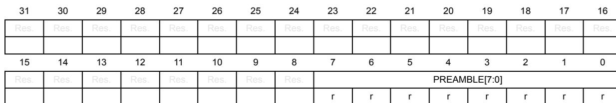
| 31 | 30 | 29 | 28 | 27 | 26 | 25 | 24 | 23 | 22 | 21 | 20 | 19 | 18 | 17 | 16 |
| Res. | Res. | Res. | Res. | Res. | Res. | Res. | Res. | Res. | Res. | Res. | Res. | Res. | Res. | Res. | Res. |
| 15 | 14 | 13 | 12 | 11 | 10 | 9 | 8 | 7 | 6 | 5 | 4 | 3 | 2 | 1 | 0 |
| Res. | Res. | Res. | Res. | Res. | Res. | Res. | Res. | PREAMBLE[7:0] | |||||||
| r | r | r | r | r | r | r | r | ||||||||
Bits 31:8 Reserved, must be kept at reset value.
Bits 7:0 PREAMBLE[7:0] : Component ID field, bits [7:0]
0x0D: Common ID value
ITM CoreSight component identity register 1 (ITM_CIDR1)
Address offset: 0xFF4
Reset value: 0x0000 00E0
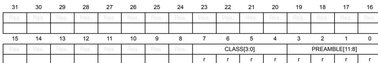
| 31 | 30 | 29 | 28 | 27 | 26 | 25 | 24 | 23 | 22 | 21 | 20 | 19 | 18 | 17 | 16 |
| Res. | Res. | Res. | Res. | Res. | Res. | Res. | Res. | Res. | Res. | Res. | Res. | Res. | Res. | Res. | Res. |
| 15 | 14 | 13 | 12 | 11 | 10 | 9 | 8 | 7 | 6 | 5 | 4 | 3 | 2 | 1 | 0 |
| Res. | Res. | Res. | Res. | Res. | Res. | Res. | Res. | CLASS[3:0] | PREAMBLE[11:8] | ||||||
| r | r | r | r | r | r | r | r | ||||||||
Bits 31:8 Reserved, must be kept at reset value.
Bits 7:4 CLASS[3:0] : Component ID field, bits [15:12] - component class
0xE: Trace generator component
Bits 3:0 PREAMBLE[11:8] : Component ID field, bits [11:8]
0x0: Common ID value
ITM CoreSight component identity register 2 (ITM_CIDR2)
Address offset: 0xFF8
Reset value: 0x0000 0005
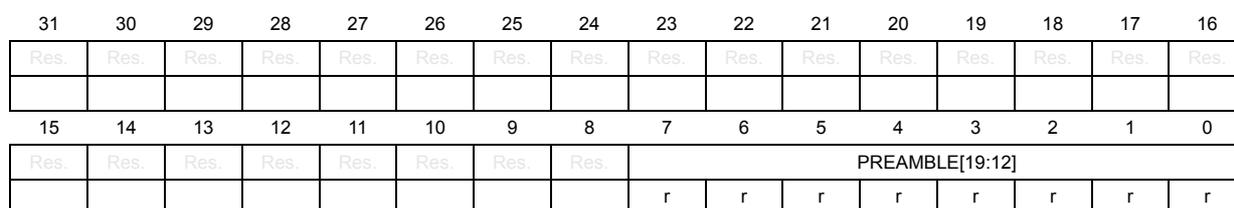
| 31 | 30 | 29 | 28 | 27 | 26 | 25 | 24 | 23 | 22 | 21 | 20 | 19 | 18 | 17 | 16 |
| Res. | Res. | Res. | Res. | Res. | Res. | Res. | Res. | Res. | Res. | Res. | Res. | Res. | Res. | Res. | Res. |
| 15 | 14 | 13 | 12 | 11 | 10 | 9 | 8 | 7 | 6 | 5 | 4 | 3 | 2 | 1 | 0 |
| Res. | Res. | Res. | Res. | Res. | Res. | Res. | Res. | PREAMBLE[19:12] | |||||||
| r | r | r | r | r | r | r | r | ||||||||
Bits 31:8 Reserved, must be kept at reset value.
Bits 7:0 PREAMBLE[19:12] : Component ID field, bits [23:16]
0x05: Common ID value
ITM CoreSight component identity register 3 (ITM_CIDR3)
Address offset: 0xFFC
Reset value: 0x0000 00B1
| 31 | 30 | 29 | 28 | 27 | 26 | 25 | 24 | 23 | 22 | 21 | 20 | 19 | 18 | 17 | 16 |
|---|---|---|---|---|---|---|---|---|---|---|---|---|---|---|---|
| Res. | Res. | Res. | Res. | Res. | Res. | Res. | Res. | Res. | Res. | Res. | Res. | Res. | Res. | Res. | Res. |
| 15 | 14 | 13 | 12 | 11 | 10 | 9 | 8 | 7 | 6 | 5 | 4 | 3 | 2 | 1 | 0 |
| Res. | Res. | Res. | Res. | Res. | Res. | Res. | Res. | PREAMBLE[27:20] | |||||||
| r | r | r | r | r | r | r | r | ||||||||
Bits 31:8 Reserved, must be kept at reset value.
Bits 7:0 PREAMBLE[27:20] : Component ID field, bits [31:24]
0xB1: Common ID value
ITM register map
Table 877. ITM register map and reset values
| Offset | Register name | 31 | 30 | 29 | 28 | 27 | 26 | 25 | 24 | 23 | 22 | 21 | 20 | 19 | 18 | 17 | 16 | 15 | 14 | 13 | 12 | 11 | 10 | 9 | 8 | 7 | 6 | 5 | 4 | 3 | 2 | 1 | 0 | ||||
|---|---|---|---|---|---|---|---|---|---|---|---|---|---|---|---|---|---|---|---|---|---|---|---|---|---|---|---|---|---|---|---|---|---|---|---|---|---|
| 0x000 + 0x4 * x (x=0 to 31) Last address: 0x07C | ITM_STIMx | STIMULUS[31:0] | |||||||||||||||||||||||||||||||||||
| Reset value | X | X | X | X | X | X | X | X | X | X | X | X | X | X | X | X | X | X | X | X | X | X | X | X | X | X | X | X | X | X | X | X | |||||
| 0x080-0xDFC | Reserved | Reserved | |||||||||||||||||||||||||||||||||||
| 0xE00 | ITM_TER | STIMENA[31:0] | |||||||||||||||||||||||||||||||||||
| Reset value | 0 | 0 | 0 | 0 | 0 | 0 | 0 | 0 | 0 | 0 | 0 | 0 | 0 | 0 | 0 | 0 | 0 | 0 | 0 | 0 | 0 | 0 | 0 | 0 | 0 | 0 | 0 | 0 | 0 | 0 | 0 | 0 | |||||
| 0xE04-0xE3C | Reserved | Reserved | |||||||||||||||||||||||||||||||||||
| 0xE40 | ITM_TPR | Res. | Res. | Res. | Res. | Res. | Res. | Res. | Res. | Res. | Res. | Res. | Res. | Res. | Res. | Res. | Res. | Res. | Res. | Res. | Res. | Res. | Res. | Res. | Res. | Res. | Res. | Res. | Res. | PRIVMASK [3:0] | |||||||
| Reset value | 0 | 0 | 0 | 0 | |||||||||||||||||||||||||||||||||
| 0xE44-0xE7C | Reserved | Reserved | |||||||||||||||||||||||||||||||||||
| 0xE80 | ITM_TCR | Res. | Res. | Res. | Res. | Res. | Res. | Res. | Res. | BUSY | TRACEBUSID[6:0] | Res. | Res. | Res. | Res. | GTSFREQ[1:0] | TSPRESCALE [1:0] | Res. | Res. | STALLENA | SWOENA | TXENA | SYNCENA | TSENA | ITMENA | ||||||||||||
| Reset value | 0 | 0 | 0 | 0 | 0 | 0 | 0 | 0 | 0 | 0 | 0 | 0 | 0 | 0 | 0 | 0 | 0 | 0 | |||||||||||||||||||
| 0xE84-0xFB8 | Reserved | Reserved | |||||||||||||||||||||||||||||||||||
| 0xFBC | ITM_DEVARCH | ARCHITECT[10:0] | PRESENT | REVISION [3:0] | ARCHVER [3:0] | ARCHPART[11:0] | |||||||||||||||||||||||||||||||
| Reset value | 0 | 1 | 0 | 0 | 0 | 1 | 1 | 1 | 0 | 1 | 1 | 1 | 0 | 0 | 0 | 0 | 0 | 0 | 0 | 1 | 1 | 0 | 1 | 0 | 0 | 0 | 0 | 0 | 0 | 0 | 0 | 1 | |||||
| 0xFC0-0xFC8 | Reserved | Reserved | |||||||||||||||||||||||||||||||||||
| 0xFCC | ITM_DEVTYPE | Res. | Res. | Res. | Res. | Res. | Res. | Res. | Res. | Res. | Res. | Res. | Res. | Res. | Res. | Res. | Res. | Res. | Res. | Res. | Res. | Res. | Res. | Res. | Res. | Res. | Res. | Res. | Res. | SUB[3:0] | MAJOR[3:0] | ||||||
| Reset value | 0 | 1 | 0 | 0 | 0 | 0 | 1 | 1 | |||||||||||||||||||||||||||||
Table 877. ITM register map and reset values (continued)
| Offset | Register name | 31 | 30 | 29 | 28 | 27 | 26 | 25 | 24 | 23 | 22 | 21 | 20 | 19 | 18 | 17 | 16 | 15 | 14 | 13 | 12 | 11 | 10 | 9 | 8 | 7 | 6 | 5 | 4 | 3 | 2 | 1 | 0 |
|---|---|---|---|---|---|---|---|---|---|---|---|---|---|---|---|---|---|---|---|---|---|---|---|---|---|---|---|---|---|---|---|---|---|
| 0xFD0 | ITM_PIDR4 | Res | Res | Res | Res | Res | Res | Res | Res | Res | Res | Res | Res | Res | Res | Res | Res | Res | Res | Res | Res | Res | Res | Res | Res | SIZE[3:0] | JEP106CON[3:0] | ||||||
| Reset value | 0 | 0 | 0 | 0 | 0 | 1 | 0 | 0 | 0 | ||||||||||||||||||||||||
| 0xFD4- 0xFDC | Reserved | Reserved | |||||||||||||||||||||||||||||||
| 0xFE0 | ITM_PIDR0 | Res | Res | Res | Res | Res | Res | Res | Res | Res | Res | Res | Res | Res | Res | Res | Res | Res | Res | Res | Res | Res | Res | Res | Res | PARTNUM[7:0] | |||||||
| Reset value | 0 | 0 | 0 | 0 | 0 | 0 | 0 | 1 | |||||||||||||||||||||||||
| 0xFE4 | ITM_PIDR1 | Res | Res | Res | Res | Res | Res | Res | Res | Res | Res | Res | Res | Res | Res | Res | Res | Res | Res | Res | Res | Res | Res | Res | Res | JEP106ID[3:0] | PARTNUM[11:8] | ||||||
| Reset value | 1 | 0 | 1 | 1 | 0 | 0 | 0 | 0 | |||||||||||||||||||||||||
| 0xFE8 | ITM_PIDR2 | Res | Res | Res | Res | Res | Res | Res | Res | Res | Res | Res | Res | Res | Res | Res | Res | Res | Res | Res | Res | Res | Res | Res | Res | REVISION[3:0] | JEDID[1:0] | JEP106ID[6:4] | |||||
| Reset value | 0 | 0 | 0 | 0 | 1 | 0 | 1 | 1 | |||||||||||||||||||||||||
| 0xFEC | ITM_PIDR3 | Res | Res | Res | Res | Res | Res | Res | Res | Res | Res | Res | Res | Res | Res | Res | Res | Res | Res | Res | Res | Res | Res | Res | Res | REVAND[3:0] | CMOD[3:0] | ||||||
| Reset value | 0 | 0 | 0 | 0 | 0 | 0 | 0 | 0 | |||||||||||||||||||||||||
| 0xFF0 | ITM_CIDR0 | Res | Res | Res | Res | Res | Res | Res | Res | Res | Res | Res | Res | Res | Res | Res | Res | Res | Res | Res | Res | Res | Res | Res | Res | PREAMBLE[7:0] | |||||||
| Reset value | 0 | 0 | 0 | 0 | 1 | 1 | 0 | 1 | |||||||||||||||||||||||||
| 0xFF4 | ITM_CIDR1 | Res | Res | Res | Res | Res | Res | Res | Res | Res | Res | Res | Res | Res | Res | Res | Res | Res | Res | Res | Res | Res | Res | Res | Res | CLASS[3:0] | PREAMBLE[11:8] | ||||||
| Reset value | 1 | 1 | 1 | 0 | 0 | 0 | 0 | 0 | |||||||||||||||||||||||||
| 0xFF8 | ITM_CIDR2 | Res | Res | Res | Res | Res | Res | Res | Res | Res | Res | Res | Res | Res | Res | Res | Res | Res | Res | Res | Res | Res | Res | Res | Res | PREAMBLE[19:12] | |||||||
| Reset value | 0 | 0 | 0 | 0 | 0 | 1 | 0 | 1 | |||||||||||||||||||||||||
| 0xFFC | ITM_CIDR3 | Res | Res | Res | Res | Res | Res | Res | Res | Res | Res | Res | Res | Res | Res | Res | Res | Res | Res | Res | Res | Res | Res | Res | Res | PREAMBLE[27:20] | |||||||
| Reset value | 1 | 0 | 1 | 1 | 0 | 0 | 0 | 1 | |||||||||||||||||||||||||
78.11.9 Breakpoint Unit (BPU)
The BPU allows hardware breakpoints to be set. It contains eight comparators which monitor the instruction fetch address. If a match occurs, the instruction comparators can be configured to generate a breakpoint instruction.
78.11.10 Cortex-M55 BPU registers
The register file base address for the BPU is defined in Table 873: Processor ROM table .
BPU control register (BPU_CTRL)
Address offset: 0x000
Reset value: 0x1000 0080
| 31 | 30 | 29 | 28 | 27 | 26 | 25 | 24 | 23 | 22 | 21 | 20 | 19 | 18 | 17 | 16 |
|---|---|---|---|---|---|---|---|---|---|---|---|---|---|---|---|
| REV[3:0] | Res. | Res. | Res. | Res. | Res. | Res. | Res. | Res. | Res. | Res. | Res. | Res. | |||
| r | r | r | r | ||||||||||||
| 15 | 14 | 13 | 12 | 11 | 10 | 9 | 8 | 7 | 6 | 5 | 4 | 3 | 2 | 1 | 0 |
| Res. | NUM_CODE[6:4] | NUM_LIT[3:0] | NUM_CODE[3:0] | Res. | Res. | KEY | ENABLE | ||||||||
| r | r | r | r | r | r | r | r | r | r | r | rw | rw | |||
Bits 31:28 REV[3:0] : BPU architecture revision
1: Revision 2
Bits 27:15 Reserved, must be kept at reset value.
Bits 14:12 NUM_CODE[6:4] : Instruction address comparator number (three MSBs)
This read-only field holds the three MSBs of the number of instruction address comparators supported.
0x0: the MSBs of the number are all 0.
Bits 11:8 NUM_LIT[3:0] : Number of literal address comparators supported (read-only)
0x0: No literal comparators supported
Bits 7:4 NUM_CODE[3:0] : Instruction address comparator number (four LSBs)
This read-only field holds the four LSBs of the number of instruction address comparators supported.
0x8: Eight instruction comparators supported
Bits 3:2 Reserved, must be kept at reset value.
Bit 1 KEY : Write protect key
A write to BPU_CTRL register is ignored if this bit is not set to 1.
Bit 0 ENABLE : BPU enable
0: Disabled
1: Enabled
BPU remap register (BPU_REMAP)
Address offset: 0x004
Reset value: 0x0000 0000
| 31 | 30 | 29 | 28 | 27 | 26 | 25 | 24 | 23 | 22 | 21 | 20 | 19 | 18 | 17 | 16 |
|---|---|---|---|---|---|---|---|---|---|---|---|---|---|---|---|
| Res. | Res. | RMPSPT | REMAP[23:11] | ||||||||||||
| r | rw | rw | rw | rw | rw | rw | rw | rw | rw | rw | rw | rw | rw | ||
| 15 | 14 | 13 | 12 | 11 | 10 | 9 | 8 | 7 | 6 | 5 | 4 | 3 | 2 | 1 | 0 |
| REMAP[10:0] | Res. | Res. | Res. | Res. | Res. | ||||||||||
| rw | rw | rw | rw | rw | rw | rw | rw | rw | rw | rw | |||||
Bits 31:30 Reserved, must be kept at reset value.
Bit 29 RMPSPT : Flash patch remap support (read-only)
0: Remapping not supported
Bits 28:5 REMAP[23:0] : Not supported
Bits 4:0 Reserved, must be kept at reset value.
BPU comparator registers (BPU_COMPx)
Address offset: 0x008 + 0x4 * x (x = 0 to 7)
Reset value: 0x0000 0000
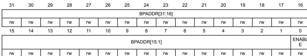
| 31 | 30 | 29 | 28 | 27 | 26 | 25 | 24 | 23 | 22 | 21 | 20 | 19 | 18 | 17 | 16 |
| BPADDR[31:16] | |||||||||||||||
| rw | rw | rw | rw | rw | rw | rw | rw | rw | rw | rw | rw | rw | rw | rw | rw |
| 15 | 14 | 13 | 12 | 11 | 10 | 9 | 8 | 7 | 6 | 5 | 4 | 3 | 2 | 1 | 0 |
| BPADDR[15:1] | ENABLE | ||||||||||||||
| rw | rw | rw | rw | rw | rw | rw | rw | rw | rw | rw | rw | rw | rw | rw | rw |
Bits 31:1 BPADDR[31:1] : Breakpoint address
Specifies bits[31:1] of the breakpoint instruction address.
Bit 0 ENABLE : Comparator enable
The comparator is only enabled if both this bit and BPU ENABLE in BPU_CTRL are set.
0: Disabled
1: Enabled
BPU device type architecture register (BPU_DEVARCH)
Address offset: 0xFBC
Reset value: 0x4770 1A03
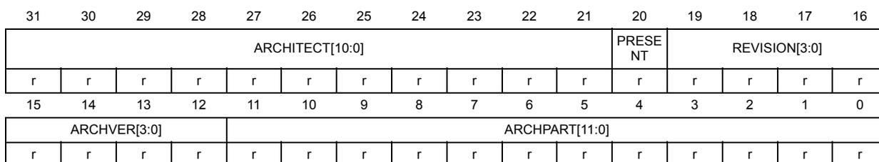
| 31 | 30 | 29 | 28 | 27 | 26 | 25 | 24 | 23 | 22 | 21 | 20 | 19 | 18 | 17 | 16 |
| ARCHITECT[10:0] | PRESENT | REVISION[3:0] | |||||||||||||
| r | r | r | r | r | r | r | r | r | r | r | r | r | r | r | r |
| 15 | 14 | 13 | 12 | 11 | 10 | 9 | 8 | 7 | 6 | 5 | 4 | 3 | 2 | 1 | 0 |
| ARCHVER[3:0] | ARCHPART[11:0] | ||||||||||||||
| r | r | r | r | r | r | r | r | r | r | r | r | r | r | r | r |
Bits 31:21 ARCHITECT[10:0] : Architect JEDEC code
0x23B: Arm JEDEC code
Bit 20 PRESENT : DEVARCH register present
1: Present
Bits 19:16 REVISION[3:0] : Architecture revision
0x0: BPU architecture v2.0
Bits 15:12 ARCHVER[3:0] : Architecture version
0x1: BPU architecture v2
Bits 11:0 ARCHPART[11:0] : Architecture
0xA03: BPU architecture
BPU CoreSight peripheral identity register 4 (BPU_PIDR4)
Address offset: 0xFD0
Reset value: 0x0000 0004
| 31 | 30 | 29 | 28 | 27 | 26 | 25 | 24 | 23 | 22 | 21 | 20 | 19 | 18 | 17 | 16 |
|---|---|---|---|---|---|---|---|---|---|---|---|---|---|---|---|
| Res. | Res. | Res. | Res. | Res. | Res. | Res. | Res. | Res. | Res. | Res. | Res. | Res. | Res. | Res. | Res. |
| 15 | 14 | 13 | 12 | 11 | 10 | 9 | 8 | 7 | 6 | 5 | 4 | 3 | 2 | 1 | 0 |
| Res. | Res. | Res. | Res. | Res. | Res. | Res. | Res. | SIZE[3:0] | JEP106CON[3:0] | ||||||
| r | r | r | r | r | r | r | r | ||||||||
Bits 31:8 Reserved, must be kept at reset value.
Bits 7:4 SIZE[3:0] : Register file size
0x0: Register file occupies a single 4-Kbyte region.
Bits 3:0 JEP106CON[3:0] : JEP106 continuation code
0x4: Arm JEDEC code
BPU CoreSight peripheral identity register 0 (BPU_PIDR0)
Address offset: 0xFE0
Reset value: 0x0000 0023
| 31 | 30 | 29 | 28 | 27 | 26 | 25 | 24 | 23 | 22 | 21 | 20 | 19 | 18 | 17 | 16 |
|---|---|---|---|---|---|---|---|---|---|---|---|---|---|---|---|
| Res. | Res. | Res. | Res. | Res. | Res. | Res. | Res. | Res. | Res. | Res. | Res. | Res. | Res. | Res. | Res. |
| 15 | 14 | 13 | 12 | 11 | 10 | 9 | 8 | 7 | 6 | 5 | 4 | 3 | 2 | 1 | 0 |
| Res. | Res. | Res. | Res. | Res. | Res. | Res. | Res. | PARTNUM[7:0] | |||||||
| r | r | r | r | r | r | r | r | ||||||||
Bits 31:8 Reserved, must be kept at reset value.
Bits 7:0 PARTNUM[7:0] : Part number field, bits [7:0]
0x23: BPU part number
BPU CoreSight peripheral identity register 1 (BPU_PIDR1)
Address offset: 0xFE4
Reset value: 0x0000 00BD
| 31 | 30 | 29 | 28 | 27 | 26 | 25 | 24 | 23 | 22 | 21 | 20 | 19 | 18 | 17 | 16 |
|---|---|---|---|---|---|---|---|---|---|---|---|---|---|---|---|
| Res. | Res. | Res. | Res. | Res. | Res. | Res. | Res. | Res. | Res. | Res. | Res. | Res. | Res. | Res. | Res. |
| 15 | 14 | 13 | 12 | 11 | 10 | 9 | 8 | 7 | 6 | 5 | 4 | 3 | 2 | 1 | 0 |
| Res. | Res. | Res. | Res. | Res. | Res. | Res. | Res. | JEP106ID[3:0] | PARTNUM[11:8] | ||||||
| r | r | r | r | r | r | r | r | ||||||||
Bits 31:8 Reserved, must be kept at reset value.
Bits 7:4 JEP106ID[3:0] : JEP106 identity code field, bits [3:0]
0xB: Arm JEDEC code
Bits 3:0 PARTNUM[11:8] : Part number field, bits [11:8]
0xD: BPU part number
BPU CoreSight peripheral identity register 2 (BPU_PIDR2)Address offset: 0xFE8
Reset value: 0x0000 000B
| 31 | 30 | 29 | 28 | 27 | 26 | 25 | 24 | 23 | 22 | 21 | 20 | 19 | 18 | 17 | 16 |
|---|---|---|---|---|---|---|---|---|---|---|---|---|---|---|---|
| Res. | Res. | Res. | Res. | Res. | Res. | Res. | Res. | Res. | Res. | Res. | Res. | Res. | Res. | Res. | Res. |
| 15 | 14 | 13 | 12 | 11 | 10 | 9 | 8 | 7 | 6 | 5 | 4 | 3 | 2 | 1 | 0 |
| Res. | Res. | Res. | Res. | Res. | Res. | Res. | Res. | REVISION[3:0] | JEDEC | JEP106ID[6:4] | |||||
| r | r | r | r | r | r | r | r | ||||||||
Bits 31:8 Reserved, must be kept at reset value.
Bits 7:4 REVISION[3:0] : Component revision number0x0: r0p0
Bit 3 JEDEC : JEDEC assigned value1: Designer ID specified by JEDEC
Bits 2:0 JEP106ID[6:4] : JEP106 identity code field, bits [6:4]0x3: Arm JEDEC code
BPU CoreSight peripheral identity register 3 (BPU_PIDR3)Address offset: 0xFEC
Reset value: 0x0000 0000
| 31 | 30 | 29 | 28 | 27 | 26 | 25 | 24 | 23 | 22 | 21 | 20 | 19 | 18 | 17 | 16 |
|---|---|---|---|---|---|---|---|---|---|---|---|---|---|---|---|
| Res. | Res. | Res. | Res. | Res. | Res. | Res. | Res. | Res. | Res. | Res. | Res. | Res. | Res. | Res. | Res. |
| 15 | 14 | 13 | 12 | 11 | 10 | 9 | 8 | 7 | 6 | 5 | 4 | 3 | 2 | 1 | 0 |
| Res. | Res. | Res. | Res. | Res. | Res. | Res. | Res. | REVAND[3:0] | CMOD[3:0] | ||||||
| r | r | r | r | r | r | r | r | ||||||||
Bits 31:8 Reserved, must be kept at reset value.
Bits 7:4 REVAND[3:0] : Metal fix version0x0: No metal fix
Bits 3:0 CMOD[3:0] : Customer modified0x0: No customer modifications
BPU CoreSight component identity register 0 (BPU_CIDR0)Address offset: 0xFF0
Reset value: 0x0000 000D
| 31 | 30 | 29 | 28 | 27 | 26 | 25 | 24 | 23 | 22 | 21 | 20 | 19 | 18 | 17 | 16 |
|---|---|---|---|---|---|---|---|---|---|---|---|---|---|---|---|
| Res. | Res. | Res. | Res. | Res. | Res. | Res. | Res. | Res. | Res. | Res. | Res. | Res. | Res. | Res. | Res. |
| 15 | 14 | 13 | 12 | 11 | 10 | 9 | 8 | 7 | 6 | 5 | 4 | 3 | 2 | 1 | 0 |
| Res. | Res. | Res. | Res. | Res. | Res. | Res. | Res. | PREAMBLE[7:0] | |||||||
| r | r | r | r | r | r | r | r | ||||||||
Bits 31:8 Reserved, must be kept at reset value.
Bits 7:0 PREAMBLE[7:0] : Component ID field, bits [7:0]
0x0D: Common ID value
BPU CoreSight component identity register 1 (BPU_CIDR1)
Address offset: 0xFF4
Reset value: 0x0000 0090
| 31 | 30 | 29 | 28 | 27 | 26 | 25 | 24 | 23 | 22 | 21 | 20 | 19 | 18 | 17 | 16 |
|---|---|---|---|---|---|---|---|---|---|---|---|---|---|---|---|
| Res. | Res. | Res. | Res. | Res. | Res. | Res. | Res. | Res. | Res. | Res. | Res. | Res. | Res. | Res. | Res. |
| 15 | 14 | 13 | 12 | 11 | 10 | 9 | 8 | 7 | 6 | 5 | 4 | 3 | 2 | 1 | 0 |
| Res. | Res. | Res. | Res. | Res. | Res. | Res. | Res. | CLASS[3:0] | PREAMBLE[11:8] | ||||||
| r | r | r | r | r | r | r | r | ||||||||
Bits 31:8 Reserved, must be kept at reset value.
Bits 7:4 CLASS[3:0] : Component ID field, bits [15:12] - component class
0x9: BPU
Bits 3:0 PREAMBLE[11:8] : Component ID field, bits [11:8]
0x0: Common ID value
BPU CoreSight component identity register 2 (BPU_CIDR2)
Address offset: 0xFF8
Reset value: 0x0000 0005
| 31 | 30 | 29 | 28 | 27 | 26 | 25 | 24 | 23 | 22 | 21 | 20 | 19 | 18 | 17 | 16 |
|---|---|---|---|---|---|---|---|---|---|---|---|---|---|---|---|
| Res. | Res. | Res. | Res. | Res. | Res. | Res. | Res. | Res. | Res. | Res. | Res. | Res. | Res. | Res. | Res. |
| 15 | 14 | 13 | 12 | 11 | 10 | 9 | 8 | 7 | 6 | 5 | 4 | 3 | 2 | 1 | 0 |
| Res. | Res. | Res. | Res. | Res. | Res. | Res. | Res. | PREAMBLE[19:12] | |||||||
| r | r | r | r | r | r | r | r | ||||||||
Bits 31:8 Reserved, must be kept at reset value.
Bits 7:0 PREAMBLE[19:12] : Component ID field, bits [23:16]
0x05: Common ID value
BPU CoreSight component identity register 3 (BPU_CIDR3)
Address offset: 0xFFC
Reset value: 0x0000 00B1
| 31 | 30 | 29 | 28 | 27 | 26 | 25 | 24 | 23 | 22 | 21 | 20 | 19 | 18 | 17 | 16 |
|---|---|---|---|---|---|---|---|---|---|---|---|---|---|---|---|
| Res. | Res. | Res. | Res. | Res. | Res. | Res. | Res. | Res. | Res. | Res. | Res. | Res. | Res. | Res. | Res. |
| 15 | 14 | 13 | 12 | 11 | 10 | 9 | 8 | 7 | 6 | 5 | 4 | 3 | 2 | 1 | 0 |
| Res. | Res. | Res. | Res. | Res. | Res. | Res. | Res. | PREAMBLE[27:20] | |||||||
| r | r | r | r | r | r | r | r | ||||||||
Bits 31:8 Reserved, must be kept at reset value.
Bits 7:0 PREAMBLE[27:20] : Component ID field, bits [31:24]
0xB1: Common ID value
BPU register map
Table 878. BPU register map and reset values
| Offset | Register name | 31 | 30 | 29 | 28 | 27 | 26 | 25 | 24 | 23 | 22 | 21 | 20 | 19 | 18 | 17 | 16 | 15 | 14 | 13 | 12 | 11 | 10 | 9 | 8 | 7 | 6 | 5 | 4 | 3 | 2 | 1 | 0 | |
|---|---|---|---|---|---|---|---|---|---|---|---|---|---|---|---|---|---|---|---|---|---|---|---|---|---|---|---|---|---|---|---|---|---|---|
| 0x000 | BPU_CTRL | REV[3:0] | Res. | Res. | Res. | Res. | Res. | Res. | Res. | Res. | Res. | Res. | Res. | Res. | Res. | Res. | NUM_CODE [6:4] | NUM_LIT [3:0] | NUM_CODE [3:0] | Res. | Res. | KEY | ENABLE | |||||||||||
| Reset value | 0 | 0 | 0 | 1 | 0 | 0 | 0 | 0 | 0 | 0 | 0 | 0 | 1 | 0 | 0 | 0 | 0 | 0 | ||||||||||||||||
| 0x004 | BPU_REMAP | Res. | Res. | RMPSP | REMAP[23:0] | Res. | Res. | Res. | Res. | Res. | ||||||||||||||||||||||||
| Reset value | 0 | 0 | 0 | 0 | 0 | 0 | 0 | 0 | 0 | 0 | 0 | 0 | 0 | 0 | 0 | 0 | 0 | 0 | 0 | 0 | 0 | 0 | 0 | 0 | 0 | 0 | 0 | 0 | 0 | 0 | 0 | 0 | ||
| 0x008 + 0x4 * x (x=0 to 7) Last address: 0x020 | BPU_COMPx | BPADDR[31:1] | Res. | ENABLE | ||||||||||||||||||||||||||||||
| Reset value | 0 | 0 | 0 | 0 | 0 | 0 | 0 | 0 | 0 | 0 | 0 | 0 | 0 | 0 | 0 | 0 | 0 | 0 | 0 | 0 | 0 | 0 | 0 | 0 | 0 | 0 | 0 | 0 | 0 | 0 | 0 | 0 | 0 | |
| 0x024- 0xFB8 | Reserved | Reserved | ||||||||||||||||||||||||||||||||
| 0xFBC | BPU_DEVARCH | ARCHITECT[10:0] | PRESENT | REVISION [3:0] | ARCHVER [3:0] | ARCHPART[11:0] | ||||||||||||||||||||||||||||
| Reset value | 0 | 1 | 0 | 0 | 0 | 1 | 1 | 1 | 0 | 1 | 1 | 1 | 0 | 0 | 0 | 0 | 0 | 0 | 0 | 0 | 1 | 1 | 0 | 1 | 0 | 0 | 0 | 0 | 0 | 0 | 0 | 1 | 1 | |
| 0xFC0- 0xFC8 | Reserved | Reserved | ||||||||||||||||||||||||||||||||
| 0xFD0 | BPU_PIDR4 | Res. | Res. | Res. | Res. | Res. | Res. | Res. | Res. | Res. | Res. | Res. | Res. | Res. | Res. | Res. | Res. | Res. | Res. | Res. | Res. | Res. | Res. | Res. | Res. | SIZE[3:0] | JEP106CON [3:0] | |||||||
| Reset value | 0 | 0 | 0 | 0 | 0 | 1 | 0 | 0 | ||||||||||||||||||||||||||
| 0xFD4- 0xFDC | Reserved | Reserved | ||||||||||||||||||||||||||||||||
| 0xFE0 | BPU_PIDR0 | Res. | Res. | Res. | Res. | Res. | Res. | Res. | Res. | Res. | Res. | Res. | Res. | Res. | Res. | Res. | Res. | Res. | Res. | Res. | Res. | Res. | Res. | Res. | Res. | PARTNUM[7:0] | ||||||||
| Reset value | 0 | 0 | 1 | 0 | 0 | 0 | 1 | 1 | ||||||||||||||||||||||||||
Table 878. BPU register map and reset values (continued)
| Offset | Register name | 31 | 30 | 29 | 28 | 27 | 26 | 25 | 24 | 23 | 22 | 21 | 20 | 19 | 18 | 17 | 16 | 15 | 14 | 13 | 12 | 11 | 10 | 9 | 8 | 7 | 6 | 5 | 4 | 3 | 2 | 1 | 0 | |
|---|---|---|---|---|---|---|---|---|---|---|---|---|---|---|---|---|---|---|---|---|---|---|---|---|---|---|---|---|---|---|---|---|---|---|
| 0xFE4 | BPU_PIDR1 | Res. | Res. | Res. | Res. | Res. | Res. | Res. | Res. | Res. | Res. | Res. | Res. | Res. | Res. | Res. | Res. | Res. | Res. | Res. | Res. | Res. | Res. | Res. | Res. | Res. | JEP106ID [3:0] | PARTNUM [11:8] | ||||||
| Reset value | 1 | 0 | 1 | 1 | 1 | 1 | 0 | 1 | 1 | |||||||||||||||||||||||||
| 0xFE8 | BPU_PIDR2 | Res. | Res. | Res. | Res. | Res. | Res. | Res. | Res. | Res. | Res. | Res. | Res. | Res. | Res. | Res. | Res. | Res. | Res. | Res. | Res. | Res. | Res. | Res. | Res. | Res. | REVISION [3:0] | JEDEC [6:4] | JEP106ID [6:4] | |||||
| Reset value | 0 | 0 | 0 | 0 | 1 | 0 | 1 | 1 | 1 | |||||||||||||||||||||||||
| 0xFEC | BPU_PIDR3 | Res. | Res. | Res. | Res. | Res. | Res. | Res. | Res. | Res. | Res. | Res. | Res. | Res. | Res. | Res. | Res. | Res. | Res. | Res. | Res. | Res. | Res. | Res. | Res. | Res. | REVAND[3:0] | CMOD[3:0] | ||||||
| Reset value | 0 | 0 | 0 | 0 | 0 | 0 | 0 | 0 | 0 | |||||||||||||||||||||||||
| 0xFF0 | BPU_CIDR0 | Res. | Res. | Res. | Res. | Res. | Res. | Res. | Res. | Res. | Res. | Res. | Res. | Res. | Res. | Res. | Res. | Res. | Res. | Res. | Res. | Res. | Res. | Res. | Res. | PREAMBLE[7:0] | ||||||||
| Reset value | 0 | 0 | 0 | 0 | 1 | 1 | 0 | 1 | 1 | |||||||||||||||||||||||||
| 0xFF4 | BPU_CIDR1 | Res. | Res. | Res. | Res. | Res. | Res. | Res. | Res. | Res. | Res. | Res. | Res. | Res. | Res. | Res. | Res. | Res. | Res. | Res. | Res. | Res. | Res. | Res. | Res. | CLASS[3:0] | PREAMBLE [11:8] | |||||||
| Reset value | 1 | 0 | 0 | 1 | 0 | 0 | 0 | 0 | 0 | |||||||||||||||||||||||||
| 0xFF8 | BPU_CIDR2 | Res. | Res. | Res. | Res. | Res. | Res. | Res. | Res. | Res. | Res. | Res. | Res. | Res. | Res. | Res. | Res. | Res. | Res. | Res. | Res. | Res. | Res. | Res. | Res. | PREAMBLE[19:12] | ||||||||
| Reset value | 0 | 0 | 0 | 0 | 0 | 1 | 0 | 1 | 1 | |||||||||||||||||||||||||
| 0xFFC | BPU_CIDR3 | Res. | Res. | Res. | Res. | Res. | Res. | Res. | Res. | Res. | Res. | Res. | Res. | Res. | Res. | Res. | Res. | Res. | Res. | Res. | Res. | Res. | Res. | Res. | Res. | PREAMBLE[27:20] | ||||||||
| Reset value | 1 | 0 | 1 | 1 | 0 | 0 | 0 | 0 | 1 | |||||||||||||||||||||||||
78.11.11 Embedded Trace Macrocell (ETM)
The Cortex-M55 ETM is a CoreSight component closely coupled to the CPU. The ETM generates trace packets that allow the execution of the Cortex-M55 core to be traced.
Note: Data accesses are not included in the trace information.
The ETM receives information from the CPU over the processor trace interface, including:
- • the number of instructions executed in the same cycle
- • changes in program flow
- • the current processor instruction state
- • addresses of memory locations accessed by load and store instructions
- • type, direction and size of a transfer
- • condition code information
- • exception information
- • wait for interrupt state information
For more information, refer to the Arm CoreSight ETM-M55 Technical Reference Manual [5].
78.11.12 Cortex-M55 ETM registers
The register file base address for the ETM is defined in Table 873: Processor ROM table .
ETM programming control register (ETM_PRGCTL)
Address offset: 0x004
Reset value: 0x0000 0000
| 31 | 30 | 29 | 28 | 27 | 26 | 25 | 24 | 23 | 22 | 21 | 20 | 19 | 18 | 17 | 16 |
|---|---|---|---|---|---|---|---|---|---|---|---|---|---|---|---|
| Res. | Res. | Res. | Res. | Res. | Res. | Res. | Res. | Res. | Res. | Res. | Res. | Res. | Res. | Res. | Res. |
| 15 | 14 | 13 | 12 | 11 | 10 | 9 | 8 | 7 | 6 | 5 | 4 | 3 | 2 | 1 | 0 |
| Res. | Res. | Res. | Res. | Res. | Res. | Res. | Res. | Res. | Res. | Res. | Res. | Res. | Res. | Res. | EN |
| rw |
Bits 31:1 Reserved, must be kept at reset value.
Bit 0 EN : Trace program enable
0: Trace unit disabled
1: Trace unit enabled
ETM status register (ETM_STAT)
Address offset: 0x00C
Reset value: 0x0000 0000
| 31 | 30 | 29 | 28 | 27 | 26 | 25 | 24 | 23 | 22 | 21 | 20 | 19 | 18 | 17 | 16 |
|---|---|---|---|---|---|---|---|---|---|---|---|---|---|---|---|
| Res. | Res. | Res. | Res. | Res. | Res. | Res. | Res. | Res. | Res. | Res. | Res. | Res. | Res. | Res. | Res. |
| 15 | 14 | 13 | 12 | 11 | 10 | 9 | 8 | 7 | 6 | 5 | 4 | 3 | 2 | 1 | 0 |
| Res. | Res. | Res. | Res. | Res. | Res. | Res. | Res. | Res. | Res. | Res. | Res. | Res. | Res. | PMSTABLE | IDLE |
| r | r |
Bits 31:2 Reserved, must be kept at reset value.
Bit 1 PMSTABLE : Programmers model stable
This bit indicates whether ETM registers are stable and can be read.
0: Registers not stable
1: Registers stable
Bit 0 IDLE : Trace unit inactive
0: ETM not idle
1: ETM idle
ETM trace configuration register (ETM_CONFIG)
Address offset: 0x010
Reset value: 0x0000 0000
| 31 | 30 | 29 | 28 | 27 | 26 | 25 | 24 | 23 | 22 | 21 | 20 | 19 | 18 | 17 | 16 |
|---|---|---|---|---|---|---|---|---|---|---|---|---|---|---|---|
| Res. | Res. | Res. | Res. | Res. | Res. | Res. | Res. | Res. | Res. | Res. | Res. | Res. | Res. | Res. | Res. |
| 15 | 14 | 13 | 12 | 11 | 10 | 9 | 8 | 7 | 6 | 5 | 4 | 3 | 2 | 1 | 0 |
| Res. | Res. | Res. | RS | TS | COND[2:0] | Res. | Res. | Res. | CCI | BB | INSTP0[1:0] | Res. | |||
| rw | rw | rw | rw | rw | rw | rw | r | r | |||||||
Bits 31:13 Reserved, must be kept at reset value.
- Bit 12
RS
: Return stack enable
- 0: Disabled
- 1: Enabled
- Bit 11
TS
: Global timestamp tracing
- 0: Disabled
- 1: Enabled
- Bits 10:8
COND[2:0]
: Conditional instruction tracing
- 0x0: Conditional instruction tracing disabled
- 0x1: Conditional load instructions are traced.
- 0x2: Conditional store instructions are traced.
- 0x3: Conditional load and store instructions are traced.
- 0x7: All conditional instructions are traced.
- Others: Reserved
- Bits 7:5 Reserved, must be kept at reset value.
- Bit 4
CCI
: Cycle counting in instruction trace
- 0: Disabled
- 1: Enabled
- Bit 3
BB
: Branch broadcast mode
- 0: Disabled
- 1: Enabled
- Bits 2:1
INSTP0[1:0]
:
- This bitfield determines which instructions are P0 instructions (read-only)
- 0x0: Only branches are P0 instructions.
- Bit 0 Reserved, must be kept at reset value.
ETM event control 0 register (ETM_EVENTCTL0)
Address offset: 0x020
Reset value: 0x0000 0000
Writes to this register are accepted on when the trace unit is disabled.
| 31 | 30 | 29 | 28 | 27 | 26 | 25 | 24 | 23 | 22 | 21 | 20 | 19 | 18 | 17 | 16 |
|---|---|---|---|---|---|---|---|---|---|---|---|---|---|---|---|
| Res. | Res. | Res. | Res. | Res. | Res. | Res. | Res. | Res. | Res. | Res. | Res. | Res. | Res. | Res. | Res. |
| 15 | 14 | 13 | 12 | 11 | 10 | 9 | 8 | 7 | 6 | 5 | 4 | 3 | 2 | 1 | 0 |
| EVENT1[7:0] | EVENT0[7:0] | ||||||||||||||
| rw | rw | rw | rw | rw | rw | rw | rw | rw | rw | rw | rw | rw | rw | rw | rw |
- Bits 31:16 Reserved, must be kept at reset value.
- Bits 15:8 EVENT1[7:0] : Event selector 1
- Bits 7:0 EVENT0[7:0] : Event selector 0
ETM event control 1 register (ETM_EVENTCTL1)
Address offset: 0x024
Reset value: 0x0000 0000
Writes to this register are accepted on when the trace unit is disabled.
| 31 | 30 | 29 | 28 | 27 | 26 | 25 | 24 | 23 | 22 | 21 | 20 | 19 | 18 | 17 | 16 |
|---|---|---|---|---|---|---|---|---|---|---|---|---|---|---|---|
| Res. | Res. | Res. | Res. | Res. | Res. | Res. | Res. | Res. | Res. | Res. | Res. | Res. | Res. | Res. | Res. |
| 15 | 14 | 13 | 12 | 11 | 10 | 9 | 8 | 7 | 6 | 5 | 4 | 3 | 2 | 1 | 0 |
| Res. | Res. | Res. | LPOVER RIDE | ATB | Res. | Res. | Res. | Res. | Res. | Res. | Res. | Res. | Res. | INSTEN[1:0] | |
| rw | rw | rw | rw |
Bits 31:13 Reserved, must be kept at reset value.
Bit 12 LPOVERRIDE : Low-power state behavior override
0: Low-power state normal behavior
1: Entry to low-power state does not affect resources and event trace generation.
Bit 11 ATB : ATB trigger enable
0: Disabled
1: Enabled
Bits 10:2 Reserved, must be kept at reset value.
Bits 1:0 INSTEN[1:0] : Instruction trace event element enable
Each bit corresponds to an event:
x0: Event 0 does not cause an event element.
x1: Event 0 causes an event element.
0x: Event 1 does not cause an event element.
1x: Event 1 causes an event element.
ETM stall control register (ETM_STALLCTL)
Address offset: 0x02C
Reset value: 0x0000 0000
Writes to this register are accepted on when the trace unit is disabled.
| 31 | 30 | 29 | 28 | 27 | 26 | 25 | 24 | 23 | 22 | 21 | 20 | 19 | 18 | 17 | 16 |
|---|---|---|---|---|---|---|---|---|---|---|---|---|---|---|---|
| Res. | Res. | Res. | Res. | Res. | Res. | Res. | Res. | Res. | Res. | Res. | Res. | Res. | Res. | Res. | Res. |
| 15 | 14 | 13 | 12 | 11 | 10 | 9 | 8 | 7 | 6 | 5 | 4 | 3 | 2 | 1 | 0 |
| Res. | Res. | Res. | Res. | Res. | Res. | Res. | ISTALL | Res. | Res. | Res. | Res. | LEVEL[1:0] | Res. | Res. | |
| rw | rw | rw |
Bits 31:9 Reserved, must be kept at reset value.
Bit 8 ISTALL : Stall processor based on instruction trace buffer space
0: Do not stall processor.
1: Stall processor.
Bits 7:4 Reserved, must be kept at reset value.
Bits 3:2 LEVEL[1:0] : Stalling threshold level
A low level minimizes the amount of processor stalling, with a higher risk of FIFO overflow.
A high level minimizes the risk of FIFO overflow but increases the amount of processor stalling.
Bits 1:0 Reserved, must be kept at reset value.
ETM global timestamp control register (ETM_TSCTL)
Address offset: 0x030
Reset value: 0x0000 0000
Writes to this register are accepted on when the trace unit is disabled.
| 31 | 30 | 29 | 28 | 27 | 26 | 25 | 24 | 23 | 22 | 21 | 20 | 19 | 18 | 17 | 16 |
|---|---|---|---|---|---|---|---|---|---|---|---|---|---|---|---|
| Res. | Res. | Res. | Res. | Res. | Res. | Res. | Res. | Res. | Res. | Res. | Res. | Res. | Res. | Res. | Res. |
| 15 | 14 | 13 | 12 | 11 | 10 | 9 | 8 | 7 | 6 | 5 | 4 | 3 | 2 | 1 | 0 |
| Res. | Res. | Res. | Res. | Res. | Res. | Res. | Res. | ||||||||
| rw | rw | rw | rw | rw | rw | rw | rw | ||||||||
| EVENT[7:0] | |||||||||||||||
Bits 31:8 Reserved, must be kept at reset value.
Bits 7:0 EVENT[7:0] : Event selector
When the selected event is triggered, the ETM inserts a global timestamp into the trace streams.
ETM synchronization period register (ETM_SYNCP)
Address offset: 0x034
Reset value: 0x0000 000A
| 31 | 30 | 29 | 28 | 27 | 26 | 25 | 24 | 23 | 22 | 21 | 20 | 19 | 18 | 17 | 16 |
|---|---|---|---|---|---|---|---|---|---|---|---|---|---|---|---|
| Res. | Res. | Res. | Res. | Res. | Res. | Res. | Res. | Res. | Res. | Res. | Res. | Res. | Res. | Res. | Res. |
| 15 | 14 | 13 | 12 | 11 | 10 | 9 | 8 | 7 | 6 | 5 | 4 | 3 | 2 | 1 | 0 |
| Res. | Res. | Res. | Res. | Res. | Res. | Res. | Res. | Res. | Res. | Res. | |||||
| r | r | r | r | r | |||||||||||
| PERIOD[4:0] | |||||||||||||||
Bits 31:5 Reserved, must be kept at reset value.
Bits 4:0 PERIOD[4:0] : Trace bytes between synchronization requests
This bitfield defines the number of bytes of trace information between trace synchronization requests.
0xA: 1024 bytes
ETM cycle count control register (ETM_CCCTL)
Address offset: 0x038
Reset value: 0x0000 0000
| 31 | 30 | 29 | 28 | 27 | 26 | 25 | 24 | 23 | 22 | 21 | 20 | 19 | 18 | 17 | 16 |
|---|---|---|---|---|---|---|---|---|---|---|---|---|---|---|---|
| Res. | Res. | Res. | Res. | Res. | Res. | Res. | Res. | Res. | Res. | Res. | Res. | Res. | Res. | Res. | Res. |
| 15 | 14 | 13 | 12 | 11 | 10 | 9 | 8 | 7 | 6 | 5 | 4 | 3 | 2 | 1 | 0 |
| Res. | Res. | Res. | Res. | THRESHOLD[11:0] | |||||||||||
| rw | rw | rw | rw | rw | rw | rw | rw | rw | rw | rw | rw | ||||
Bits 31:12 Reserved, must be kept at reset value.
Bits 11:0 THRESHOLD[11:0] : Threshold value for instruction trace cycle counting
The threshold represents the minimum interval between cycle count trace packets.
0x0 - 0x03: Reserved
Other: Threshold
ETM trace ID register (ETM_TRACEID)
Address offset: 0x040
Reset value: 0x0000 0000
| 31 | 30 | 29 | 28 | 27 | 26 | 25 | 24 | 23 | 22 | 21 | 20 | 19 | 18 | 17 | 16 |
|---|---|---|---|---|---|---|---|---|---|---|---|---|---|---|---|
| Res. | Res. | Res. | Res. | Res. | Res. | Res. | Res. | Res. | Res. | Res. | Res. | Res. | Res. | Res. | Res. |
| 15 | 14 | 13 | 12 | 11 | 10 | 9 | 8 | 7 | 6 | 5 | 4 | 3 | 2 | 1 | 0 |
| Res. | Res. | Res. | Res. | Res. | Res. | Res. | Res. | Res. | TRACEID[6:0] | ||||||
| rw | rw | rw | rw | rw | rw | rw | |||||||||
Bits 31:7 Reserved, must be kept at reset value.
Bits 6:0 TRACEID[6:0] : Trace ID
0x01 to 0x6F: Valid ID
Others: Reserved
ETM ViewInst main control register (ETM_VICTL)
Address offset: 0x080
Reset value: 0x0000 0000
| 31 | 30 | 29 | 28 | 27 | 26 | 25 | 24 | 23 | 22 | 21 | 20 | 19 | 18 | 17 | 16 |
|---|---|---|---|---|---|---|---|---|---|---|---|---|---|---|---|
| Res. | Res. | Res. | Res. | Res. | Res. | Res. | Res. | Res. | Res. | Res. | Res. | EXLEV EL_S3 | Res. | Res. | EXLEV EL_S0 |
| rw | rw | ||||||||||||||
| 15 | 14 | 13 | 12 | 11 | 10 | 9 | 8 | 7 | 6 | 5 | 4 | 3 | 2 | 1 | 0 |
| Res. | Res. | Res. | Res. | TRCER R | TRCRE SET | SSSTA TUS | Res. | EVENT[7:0] | |||||||
| rw | rw | rw | rw | rw | rw | rw | rw | rw | rw | rw | |||||
Bits 31:20 Reserved, must be kept at reset value.
Bit 19 EXLEVEL_S3 : Trace disable, exception level 3 (handler mode)
This bit disables tracing in the specified exception level in secure state for exception level 3.
0: Enable ViewInst in this exception level.
1: Disable ViewInst in this exception level.
Bits 18:17 Reserved, must be kept at reset value.
Bit 16 EXLEVEL_S0 : Trace disable, exception level 0 (thread mode)
This bit disables tracing in the specified exception level in secure state for exception level 0.
0: Enable ViewInst in this exception level.
1: Disable ViewInst in this exception level.
Bits 15:12 Reserved, must be kept at reset value.
Bit 11 TRCERR : Tracing of system error exception
This bit selects whether a system error exception must always be traced.
0: System error exception is traced only if the instruction or exception immediately before the system error exception is traced.
1: System error exception is always traced regardless of the value of ViewInst.
Bit 10 TRCRESET : Tracing of reset exception
This bit selects whether a reset exception must always be traced.
0: Reset exception is traced only if the instruction or exception immediately before the reset exception is traced.
1: Reset exception is always traced regardless of the value of ViewInst.
Bit 9 SSSTATUS : Current status of the start/stop logic
0: Stop state
1: Started state
Bit 8 Reserved, must be kept at reset value.
Bits 7:0 EVENT[7:0] : Event selector
Whenever the resource selected by this bitfield becomes active, the ViewInst function becomes active.
ETM ViewInst start/stop processor comparator control register (ETM_VIPCSSCTL)
Address offset: 0x08C
Reset value: 0x0000 0000
| 31 | 30 | 29 | 28 | 27 | 26 | 25 | 24 | 23 | 22 | 21 | 20 | 19 | 18 | 17 | 16 |
|---|---|---|---|---|---|---|---|---|---|---|---|---|---|---|---|
| Res | Res | Res | Res | Res | Res | Res | Res | STOP[7:0] | |||||||
| rw | rw | rw | rw | rw | rw | rw | rw | ||||||||
| 15 | 14 | 13 | 12 | 11 | 10 | 9 | 8 | 7 | 6 | 5 | 4 | 3 | 2 | 1 | 0 |
| Res. | Res. | Res. | Res. | Res. | Res. | Res. | Res. | START[7:0] | |||||||
| rw | rw | rw | rw | rw | rw | rw | rw | ||||||||
Bits 31:24 Reserved, must be kept at reset value.
Bits 23:16 STOP[7:0] : Processor comparator input selector to stop trace
This bitfield selects which processor comparator inputs are in use with ViewInst start-stop control, to stop the trace. One bit is provided for each processor comparator input.
Bits 15:8 Reserved, must be kept at reset value.
Bits 7:0 START[7:0] : Processor comparator input selector to start trace
This bitfield selects which processor comparator inputs are in use with ViewInst start-stop control, to start the trace. One bit is provided for each processor comparator input.
ETM external input selection register (ETM_EXTINSEL)
Address offset: 0x120
Reset value: 0x0000 0000
| 31 | 30 | 29 | 28 | 27 | 26 | 25 | 24 | 23 | 22 | 21 | 20 | 19 | 18 | 17 | 16 |
|---|---|---|---|---|---|---|---|---|---|---|---|---|---|---|---|
| SEL3[7:0] | SEL2[7:0] | ||||||||||||||
| rw | rw | rw | rw | rw | rw | rw | rw | rw | rw | rw | rw | rw | rw | rw | rw |
| 15 | 14 | 13 | 12 | 11 | 10 | 9 | 8 | 7 | 6 | 5 | 4 | 3 | 2 | 1 | 0 |
| SEL1[7:0] | SEL0[7:0] | ||||||||||||||
| rw | rw | rw | rw | rw | rw | rw | rw | rw | rw | rw | rw | rw | rw | rw | rw |
Bits 31:24 SEL3[7:0] : This bitfield selects an external input to use as a resource.
Bits 23:16 SEL2[7:0] : This bitfield selects an external input to use as a resource.
Bits 15:8 SEL1[7:0] : This bitfield selects an external input to use as a resource.
Bits 7:0 SEL0[7:0] : This bitfield selects an external input to use as a resource.
ETM counter reload value register (ETM_CNTRLDV)
Address offset: 0x140
Reset value: 0x0000 0000
| 31 | 30 | 29 | 28 | 27 | 26 | 25 | 24 | 23 | 22 | 21 | 20 | 19 | 18 | 17 | 16 |
|---|---|---|---|---|---|---|---|---|---|---|---|---|---|---|---|
| Res. | Res. | Res. | Res. | Res. | Res. | Res. | Res. | Res. | Res. | Res. | Res. | Res. | Res. | Res. | Res. |
| 15 | 14 | 13 | 12 | 11 | 10 | 9 | 8 | 7 | 6 | 5 | 4 | 3 | 2 | 1 | 0 |
| VALUE[15:0] | |||||||||||||||
| rw | rw | rw | rw | rw | rw | rw | rw | rw | rw | rw | rw | rw | rw | rw | rw |
Bits 31:16 Reserved, must be kept at reset value.
Bits 15:0 VALUE[15:0] : Counter reload value
This value is loaded into the counter each time the reload event occurs.
ETM ID register 8 (ETM_IDR8)
Address offset: 0x180
Reset value: 0x0000 0000
| 31 | 30 | 29 | 28 | 27 | 26 | 25 | 24 | 23 | 22 | 21 | 20 | 19 | 18 | 17 | 16 |
| MAXSPEC[31:16] | |||||||||||||||
| r | r | r | r | r | r | r | r | r | r | r | r | r | r | r | r |
| 15 | 14 | 13 | 12 | 11 | 10 | 9 | 8 | 7 | 6 | 5 | 4 | 3 | 2 | 1 | 0 |
| MAXSPEC[15:0] | |||||||||||||||
| r | r | r | r | r | r | r | r | r | r | r | r | r | r | r | r |
Bits 31:0 MAXSPEC[31:0] : Maximum speculation depth
This bitfield indicates the maximum speculation depth of the instruction trace stream. This is the maximum number of P0 elements that have not been committed in the trace stream at any one time.
0x0: Maximum trace speculation depth is 0.
ETM ID register 9 (ETM_IDR9)
Address offset: 0x184
Reset value: 0x0000 0000
| 31 | 30 | 29 | 28 | 27 | 26 | 25 | 24 | 23 | 22 | 21 | 20 | 19 | 18 | 17 | 16 |
| NUMP0KEY[31:16] | |||||||||||||||
| r | r | r | r | r | r | r | r | r | r | r | r | r | r | r | r |
| 15 | 14 | 13 | 12 | 11 | 10 | 9 | 8 | 7 | 6 | 5 | 4 | 3 | 2 | 1 | 0 |
| NUMP0KEY[15:0] | |||||||||||||||
| r | r | r | r | r | r | r | r | r | r | r | r | r | r | r | r |
Bits 31:0 NUMP0KEY[31:0] : Number of P0 right-hand keys used
0x0: No P0 keys used in instruction trace only configuration
ETM ID register 10 (ETM_IDR10)
Address offset: 0x188
Reset value: 0x0000 0000
| 31 | 30 | 29 | 28 | 27 | 26 | 25 | 24 | 23 | 22 | 21 | 20 | 19 | 18 | 17 | 16 |
| NUMP1KEY[31:16] | |||||||||||||||
| r | r | r | r | r | r | r | r | r | r | r | r | r | r | r | r |
| 15 | 14 | 13 | 12 | 11 | 10 | 9 | 8 | 7 | 6 | 5 | 4 | 3 | 2 | 1 | 0 |
| NUMP1KEY[15:0] | |||||||||||||||
| r | r | r | r | r | r | r | r | r | r | r | r | r | r | r | r |
Bits 31:0 NUMP1KEY[31:0] : Total number of P1 right-hand keys
This bitfield indicates the total number of P1 right-hand keys, including normal and special keys.
0x0: No P1 keys used in instruction trace only configuration
ETM ID register 11 (ETM_IDR11)
Address offset: 0x18C
Reset value: 0x0000 0000
| 31 | 30 | 29 | 28 | 27 | 26 | 25 | 24 | 23 | 22 | 21 | 20 | 19 | 18 | 17 | 16 |
| NUMP1SPC[31:16] | |||||||||||||||
| r | r | r | r | r | r | r | r | r | r | r | r | r | r | r | r |
| 15 | 14 | 13 | 12 | 11 | 10 | 9 | 8 | 7 | 6 | 5 | 4 | 3 | 2 | 1 | 0 |
| NUMP1SPC[15:0] | |||||||||||||||
| r | r | r | r | r | r | r | r | r | r | r | r | r | r | r | r |
Bits 31:0
NUMP1SPC[31:0]
: Total number of special P1 right-hand keys used
0x0: No special P1 keys used
ETM ID register 12 (ETM_IDR12)
Address offset: 0x190
Reset value: 0x0000 0001

| 31 | 30 | 29 | 28 | 27 | 26 | 25 | 24 | 23 | 22 | 21 | 20 | 19 | 18 | 17 | 16 |
| NUMCONDKEY[31:16] | |||||||||||||||
| r | r | r | r | r | r | r | r | r | r | r | r | r | r | r | r |
| 15 | 14 | 13 | 12 | 11 | 10 | 9 | 8 | 7 | 6 | 5 | 4 | 3 | 2 | 1 | 0 |
| NUMCONDKEY[15:0] | |||||||||||||||
| r | r | r | r | r | r | r | r | r | r | r | r | r | r | r | r |
Bits 31:0
NUMCONDKEY[31:0]
:
This bitfield indicates the total number of conditional instruction right-hand keys, including normal and special keys.
0x1: One conditional instruction right hand-key implemented
ETM ID register 13 (ETM_IDR13)
Address offset: 0x194
Reset value: 0x0000 0000

| 31 | 30 | 29 | 28 | 27 | 26 | 25 | 24 | 23 | 22 | 21 | 20 | 19 | 18 | 17 | 16 |
| NUMCONDSPC[31:16] | |||||||||||||||
| r | r | r | r | r | r | r | r | r | r | r | r | r | r | r | r |
| 15 | 14 | 13 | 12 | 11 | 10 | 9 | 8 | 7 | 6 | 5 | 4 | 3 | 2 | 1 | 0 |
| NUMCONDSPC[15:0] | |||||||||||||||
| r | r | r | r | r | r | r | r | r | r | r | r | r | r | r | r |
Bits 31:0
NUMCONDSPC[31:0]
: Number of special conditional instruction right-hand keys
0x0: No special conditional instruction right hand-keys implemented
ETM ID register 0 (ETM_IDR0)
Address offset: 0x1E0
Reset value: 0x2800 06E1
| 31 | 30 | 29 | 28 | 27 | 26 | 25 | 24 | 23 | 22 | 21 | 20 | 19 | 18 | 17 | 16 |
|---|---|---|---|---|---|---|---|---|---|---|---|---|---|---|---|
| Res. | Res. | COMM OPT | TSSIZE[4:0] | Res. | Res. | Res. | Res. | BF[1:0] | TRCEX DATA | QSUPP [1] | |||||
| r | r | r | r | r | r | r | r | r | r | ||||||
| 15 | 14 | 13 | 12 | 11 | 10 | 9 | 8 | 7 | 6 | 5 | 4 | 3 | 2 | 1 | 0 |
|---|---|---|---|---|---|---|---|---|---|---|---|---|---|---|---|
| QSUPP [0] | Res. | CONDTYPE[1:0] | NUMEVENT[1:0] | RETST ACK | Res. | TRCCC I | TRCC OND | TRCBB | TRCDATA[1:0] | INSTP0[1:0] | Res. | ||||
| r | r | r | r | r | r | r | r | r | r | r | r | r | |||
Bits 31:30 Reserved, must be kept at reset value.
Bit 29 COMMOPT : Meaning of the commit field in some packets
1: Commit mode 1
Bits 28:24 TSSIZE[4:0] : Global timestamp size
0x08: Maximum of 64-bit global timestamp implemented
Bits 23:20 Reserved, must be kept at reset value.
Bits 19:18 BF[1:0] : Branch future support
0x0: Not supported
Bit 17 TRCEXDATA :
This bit indicates support for tracing of data transfers for exceptions and exception returns.
0: Not supported
Bits 16:15 QSUPP[1:0] : Q element support
0x0: Not supported
Bit 14 Reserved, must be kept at reset value.
Bits 13:12 CONDTYPE[1:0] : Conditional result tracing type
0x0: ETM indicates only if a conditional instruction passes or fails its condition code check.
Bits 11:10 NUMEVENT[1:0] : Number of events supported in the trace
0x1: Two events supported
Bit 9 RETSTACK : Return stack support
1: Two entry return stack supported
Bit 8 Reserved, must be kept at reset value.
Bit 7 TRCCCI : Support for cycle counting in the instruction trace
1: Cycle counting in the instruction trace is implemented.
Bit 6 TRCCOND : Support for conditional instruction tracing
1: Conditional instruction trace is implemented.
Bit 5 TRCBB : Support for branch broadcast tracing
1: Branch broadcast trace is implemented.
Bits 4:3 TRCDATA[1:0] : Support for data tracing
0x0: Not supported
Bits 2:1 INSTP0[1:0] : Support for tracing of load and store instructions as P0 elements
0x0: Not supported
Bit 0 Reserved, must be kept at reset value.
ETM ID register 1 (ETM_IDR1)
Address offset: 0x1E4
Reset value: 0x4100 F450
| 31 | 30 | 29 | 28 | 27 | 26 | 25 | 24 | 23 | 22 | 21 | 20 | 19 | 18 | 17 | 16 |
|---|---|---|---|---|---|---|---|---|---|---|---|---|---|---|---|
| DESIGNER[7:0] | Res. | Res. | Res. | Res. | Res. | Res. | Res. | Res. | |||||||
| r | r | r | r | r | r | r | r | ||||||||
| 15 | 14 | 13 | 12 | 11 | 10 | 9 | 8 | 7 | 6 | 5 | 4 | 3 | 2 | 1 | 0 |
| Res. | Res. | Res. | Res. | TRCARCHMAJ[3:0] | TRCARCHMIN[3:0] | REVISION[3:0] | |||||||||
| r | r | r | r | r | r | r | r | r | r | r | r | ||||
Bits 31:24 DESIGNER[7:0] : Trace unit designer entity
0x41: Arm
Bits 23:12 Reserved, must be kept at reset value.
Bits 11:8 TRCARCHMAJ[3:0] : Major trace unit architecture version number
0x4: ETM v4
Bits 7:4 TRCARCHMIN[3:0] : Minor trace unit architecture version number
0x5: Minor version 5
Bits 3:0 REVISION[3:0] : Implementation revision number
0x0: Rev 0
ETM ID register 2 (ETM_IDR2)
Address offset: 0x1E8
Reset value: 0x0000 0004
| 31 | 30 | 29 | 28 | 27 | 26 | 25 | 24 | 23 | 22 | 21 | 20 | 19 | 18 | 17 | 16 |
|---|---|---|---|---|---|---|---|---|---|---|---|---|---|---|---|
| Res. | Res. | Res. | CCSIZE[3:0] | DVSIZE[4:0] | DASIZE[4:1] | ||||||||||
| r | r | r | r | r | r | r | r | r | r | r | r | r | |||
| 15 | 14 | 13 | 12 | 11 | 10 | 9 | 8 | 7 | 6 | 5 | 4 | 3 | 2 | 1 | 0 |
| DASIZE[0] | VMIDSIZE[4:0] | CIDSIZE[4:0] | IASIZE[4:0] | ||||||||||||
| r | r | r | r | r | r | r | r | r | r | r | r | r | r | r | r |
Bits 31:29 Reserved, must be kept at reset value.
Bits 28:25 CCSIZE[3:0] : Cycle counter size
This bitfield indicates the size of the cycle counter in bits minus 12.
0x0: Cycle counter is 12 bits
Bits 24:20 DVSIZE[4:0] : Data value size in bytes
0x0: Data value size is not supported in instruction only configuration.
Bits 19:15 DASIZE[4:0] : Data address size in bytes
0x0: Data address size is not supported in instruction only configuration.
Bits 14:10 VMIDSIZE[4:0] : Virtual machine ID size
0x0: Virtual machine ID tracing not implemented
Bits 9:5 CIDSIZE[4:0] : Context ID size
0x0: Context ID tracing not implemented
Bits 4:0 IASIZE[4:0] : Instruction address size
0x4: 32-bit maximum address size
ETM ID register 3 (ETM_IDR3)
Address offset: 0x1EC
Reset value: 0x0509 0004
| 31 | 30 | 29 | 28 | 27 | 26 | 25 | 24 | 23 | 22 | 21 | 20 | 19 | 18 | 17 | 16 |
|---|---|---|---|---|---|---|---|---|---|---|---|---|---|---|---|
| NOOVERFLOW | NUMPROC[2:0] | SYSTALL | STALLCTL | SYNCP | TRCERR | Res. | Res. | Res. | Res. | EXLEVEL_S[3:0] | |||||
| r | r | r | r | r | r | r | r | r | r | r | r | ||||
| 15 | 14 | 13 | 12 | 11 | 10 | 9 | 8 | 7 | 6 | 5 | 4 | 3 | 2 | 1 | 0 |
| Res. | Res. | Res. | Res. | CCITMIN[11:0] | |||||||||||
| r | r | r | r | r | r | r | r | r | r | r | r | ||||
Bit 31 NOOVERFLOW : Support of NOOVERFLOW
This bitfield indicates whether the NOOVERFLOW of trace stall control is implemented.
0: Not implemented
Bits 30:28 NUMPROC[2:0] : Number of processors available for tracing
0x00: Only one processor can be traced.
Bit 27 SYSTALL : System support for stall control of the processor
0: Stall control of the processor is supported.
Bit 26 STALLCTL : Stall control support
1: Trace stall control (STALLCTL register) is implemented.
Bit 25 SYNCP : Trace synchronization period support
1: ETM_SYNCP is read-only for instruction trace only configuration. The trace synchronization period is fixed.
Bit 24 TRCERR : Support of ETM_VICTL.TRCERR
Indicates whether ETM_VICTL.TRCERR is implemented.
1: TRCERR is implemented.
Bits 23:20 Reserved, must be kept at reset value.
Bits 19:16 EXLEVEL_S[3:0] : Support of privilege levels
Privilege levels are implemented; one bit for each level.
0x9: Privilege levels thread and handler are implemented.
Bits 15:12 Reserved, must be kept at reset value.
Bits 11:0 CCITMIN[11:0] : Instruction trace cycle counting minimum threshold
Minimum value that can be programmed in ETM_CCCTL.THRESHOLD
0x4: Minimum threshold is 4 instruction trace cycle
ETM ID register 4 (ETM_IDR4)
Address offset: 0x1F0
Reset value: 0x0011 8000
| 31 | 30 | 29 | 28 | 27 | 26 | 25 | 24 | 23 | 22 | 21 | 20 | 19 | 18 | 17 | 16 |
|---|---|---|---|---|---|---|---|---|---|---|---|---|---|---|---|
| NUMVMIDC[3:0] | NUMCIDC[3:0] | NUMSSCC[3:0] | NUMRSPAIR[3:0] | ||||||||||||
| r | r | r | r | r | r | r | r | r | r | r | r | r | r | r | r |
| 15 | 14 | 13 | 12 | 11 | 10 | 9 | 8 | 7 | 6 | 5 | 4 | 3 | 2 | 1 | 0 |
| NUMPC[3:0] | Res. | Res. | Res. | SUPPADDC | NUMDVC[3:0] | NUMACPAIRS[3:0] | |||||||||
| r | r | r | r | r | r | r | r | r | r | r | r | r | |||
Bits 31:28 NUMVMIDC[3:0] : Number of virtual machine ID comparators implemented
0x0: None
Bits 27:24 NUMCIDC[3:0] : Number of context ID comparators implemented
0x0: None
Bits 23:20 NUMSSCC[3:0] : Number of single-shot comparator controls implemented
0x1: One
Bits 19:16 NUMRSPAIR[3:0] : Number of resource selection pairs implemented
0x1: Two
Bits 15:12 NUMPC[3:0] : Number of processor comparator inputs implemented in DWT
0x8: Eight
Bits 11:9 Reserved, must be kept at reset value.
Bit 8 SUPPADDC : Support of data address comparisons
0: Not implemented
Bits 7:4 NUMDVC[3:0] : Number of data value comparators implemented
0x0: None
Bits 3:0 NUMACPAIRS[3:0] : Number of address comparator pairs implemented.
0x0: None
ETM ID register 5 (ETM_IDR5)
Address offset: 0x1F4
Reset value: 0x90C7 0084
| 31 | 30 | 29 | 28 | 27 | 26 | 25 | 24 | 23 | 22 | 21 | 20 | 19 | 18 | 17 | 16 |
|---|---|---|---|---|---|---|---|---|---|---|---|---|---|---|---|
| REDFUNCNTR | NUMCNTR[2:0] | NUMSEQSTATE[2:0] | Res. | LPOVERIDE | ATBTRIG | TRACEIDSIZE[5:0] | |||||||||
| r | r | r | r | r | r | r | r | r | r | r | r | r | r | r | |
| 15 | 14 | 13 | 12 | 11 | 10 | 9 | 8 | 7 | 6 | 5 | 4 | 3 | 2 | 1 | 0 |
| Res. | Res. | Res. | Res. | NUMEXTINSEL[2:0] | NUMEXTIN[8:0] | ||||||||||
| r | r | r | r | r | r | r | r | r | r | r | r | ||||
Bit 31 REDFUNCNTR : Support of reduced function counter
1: Implemented
Bits 30:28 NUMCNTR[2:0] : Number of counters implemented
0x1: One counter implemented
- Bits 27:25
NUMSEQSTATE[2:0]
: Number of sequencer states implemented
0x0: None - Bit 24 Reserved, must be kept at reset value.
- Bit 23
LPOVERRIDE
: Support of low-power state override
1: Implemented - Bit 22
ATBTRIG
: Support of ATB trigger
1: Implemented - Bits 21:16
TRACEIDSIZE[5:0]
: Number of trace ID bits
0x07: Seven-bit trace ID implemented. - Bits 15:12 Reserved, must be kept at reset value.
- Bits 11:9
NUMEXTINSEL[2:0]
: Number of implemented external input selectors
0x4: Four external input selectors implemented - Bits 8:0
NUMEXTIN[8:0]
: Number of implemented external inputs
0x4: Four external inputs implemented
ETM resource selection register 2 (ETM_RSCTL2)
Address offset: 0x208
Reset value: 0x0000 0000
| 31 | 30 | 29 | 28 | 27 | 26 | 25 | 24 | 23 | 22 | 21 | 20 | 19 | 18 | 17 | 16 |
|---|---|---|---|---|---|---|---|---|---|---|---|---|---|---|---|
| Res. | Res. | Res. | Res. | Res. | Res. | Res. | Res. | Res. | Res. | PAIRINV | INV | Res. | Res. | GROUP[1:0] | |
| rw | rw | rw | rw | ||||||||||||
| 15 | 14 | 13 | 12 | 11 | 10 | 9 | 8 | 7 | 6 | 5 | 4 | 3 | 2 | 1 | 0 |
| Res. | Res. | Res. | Res. | Res. | Res. | Res. | Res. | SELECT[7:0] | |||||||
| rw | rw | rw | rw | rw | rw | rw | rw | ||||||||
- Bits 31:22 Reserved, must be kept at reset value.
- Bit 21
PAIRINV
: Inversion of result of a combined pair of resources
0: Not inverted
1: Inverted - Bit 20
INV
: Inversion of the selected resources
0: Not inverted
1: Inverted - Bits 19:18 Reserved, must be kept at reset value.
- Bits 17:16
GROUP[1:0]
: Selects a group of resources for SELECT
0x0: External inputs
0x1: Processor comparator inputs
0x2: Counter at 0
0x3: Single-shot comparator control 0 - Bits 15:8 Reserved, must be kept at reset value.
Bits 7:0 SELECT[7:0] : Resource selector from group
This bitfield selects one or more resources from the group selected in GROUP. One bit is provided per resource from the group.
If GROUP = 0x0, SELECT[3:0] select from external input 3 to 0. SELECT[7:4] are not used.
If GROUP = 0x1, SELECT[7:0] select from comparator input 7 to 0.
If GROUP = 0x2, SELECT[0] selects counter at 0. SELECT[7:1] are not used.
If GROUP = 0x3, SELECT[0] selects single-shot comparator 0. SELECT[7:1] are not used.
ETM resource selection register 3 (ETM_RSCTL3)
Address offset: 0x20C
Reset value: 0x0000 0000
| 31 | 30 | 29 | 28 | 27 | 26 | 25 | 24 | 23 | 22 | 21 | 20 | 19 | 18 17 16 | ||
|---|---|---|---|---|---|---|---|---|---|---|---|---|---|---|---|
| Res. | Res. | Res. | Res. | Res. | Res. | Res. | Res. | Res. | Res. | Res. | INV | Res. | GROUP[2:0] | ||
| rw | rw | rw | rw | ||||||||||||
| 15 | 14 | 13 | 12 | 11 | 10 | 9 | 8 | 7 6 5 4 3 2 1 0 | |||||||
|---|---|---|---|---|---|---|---|---|---|---|---|---|---|---|---|
| Res. | Res. | Res. | Res. | Res. | Res. | Res. | Res. | SELECT[7:0] | |||||||
| rw | rw | rw | rw | rw | rw | rw | rw | ||||||||
Bits 31:21 Reserved, must be kept at reset value.
Bit 20 INV : Inversion of the selected resources
- 0: Not inverted
- 1: Inverted
Bit 19 Reserved, must be kept at reset value.
Bits 18:16 GROUP[2:0] : Selects a group of resources for SELECT
- 0x0: External inputs
- 0x1: Processor comparator inputs
- 0x2: Counter at 0
- 0x3: Single-shot comparator control 0
Bits 15:8 Reserved, must be kept at reset value.
Bits 7:0 SELECT[7:0] : Resource selector from group
Selects one or more resources from the group selected in GROUP. One bit is provided per resource from the group.
If GROUP = 0x0, SELECT[3:0] select from external input 3 to 0. SELECT[7:4] are not used.
If GROUP = 0x1, SELECT[7:0] select from comparator input 7 to 0.
If GROUP = 0x2, SELECT[0] selects counter at 0. SELECT[7:1] are not used.
If GROUP = 0x3, SELECT[0] selects single-shot comparator 0. SELECT[7:1] are not used.
ETM single-shot comparator control register 0 (ETM_SSCC0)
Address offset: 0x280
Reset value: 0x0000 0000
| 31 | 30 | 29 | 28 | 27 | 26 | 25 | 24 | 23 | 22 | 21 | 20 | 19 | 18 | 17 | 16 |
|---|---|---|---|---|---|---|---|---|---|---|---|---|---|---|---|
| Res. | Res. | Res. | Res. | Res. | Res. | Res. | RST | Res. | Res. | Res. | Res. | Res. | Res. | Res. | Res. |
| 15 | 14 | 13 | 12 | 11 | 10 | 9 | 8 | 7 | 6 | 5 | 4 | 3 | 2 | 1 | 0 |
| Res. | Res. | Res. | Res. | Res. | Res. | Res. | Res. | Res. | Res. | Res. | Res. | Res. | Res. | Res. | Res. |
| rw |
Bits 31:25 Reserved, must be kept at reset value.
Bit 24 RST : Single-shot comparator resource reset enable
Enables the single-shot comparator resource to be reset when it occurs, which enables another comparator match to be detected.
0: Disabled
1: Reset enabled; multiple matches can occur
Bits 23:0 Reserved, must be kept at reset value.
ETM single-shot comparator status register 0 (ETM_SSCS0)
Address offset: 0x2A0
Reset value: 0x0000 0008
| 31 | 30 | 29 | 28 | 27 | 26 | 25 | 24 | 23 | 22 | 21 | 20 | 19 | 18 | 17 | 16 |
|---|---|---|---|---|---|---|---|---|---|---|---|---|---|---|---|
| STATUS | Res. | Res. | Res. | Res. | Res. | Res. | Res. | Res. | Res. | Res. | Res. | Res. | Res. | Res. | Res. |
| 15 | 14 | 13 | 12 | 11 | 10 | 9 | 8 | 7 | 6 | 5 | 4 | 3 | 2 | 1 | 0 |
| Res. | Res. | Res. | Res. | Res. | Res. | Res. | Res. | Res. | Res. | Res. | Res. | PC | DV | DA | INST |
| r | r | r | r |
Bit 31 STATUS : Single-shot status
This bit indicates whether any of the selected comparators have matched. If RST = 0 in ETM_SSCC0, this bit must be written with 0 to enable single-shot comparator control.
0: No match occurred
1: Match occurred at least once.
Bits 30:4 Reserved, must be kept at reset value.
Bit 3 PC : Processor comparator
Indicates that the single-shot comparator is sensitive to processor comparator inputs.
1: Single-shot comparator is sensitive to processor comparator inputs.
Bit 2 DV : Data value comparator support
0: Single-shot data value comparisons not supported
Bit 1 DA : Data address comparator support
0: Single-shot data address comparisons not supported
Bit 0 INST : Instruction address comparator support
0: Single-shot instruction address comparisons not supported
ETM single-shot processor comparator input control register (ETM_SSPIC0)
Address offset: 0x2C0
Reset value: 0x0000 0000
| 31 | 30 | 29 | 28 | 27 | 26 | 25 | 24 | 23 | 22 | 21 | 20 | 19 | 18 | 17 | 16 |
|---|---|---|---|---|---|---|---|---|---|---|---|---|---|---|---|
| Res. | Res. | Res. | Res. | Res. | Res. | Res. | Res. | Res. | Res. | Res. | Res. | Res. | Res. | Res. | Res. |
| 15 | 14 | 13 | 12 | 11 | 10 | 9 | 8 | 7 | 6 | 5 | 4 | 3 | 2 | 1 | 0 |
| Res. | Res. | Res. | Res. | Res. | Res. | Res. | Res. | PC[7:0] | |||||||
| rw | rw | rw | rw | rw | rw | rw | rw | ||||||||
Bits 31:8 Reserved, must be kept at reset value.
Bits 7:0 PC[7:0] : Comparator input selector for single-shot control
This bitfield selects one or more processor comparator inputs for single-shot control. One bit is provided for each processor comparator input.
ETM power-down control register (ETM_PDC)
Address offset: 0x310
Reset value: 0x0000 0000
| 31 | 30 | 29 | 28 | 27 | 26 | 25 | 24 | 23 | 22 | 21 | 20 | 19 | 18 | 17 | 16 |
|---|---|---|---|---|---|---|---|---|---|---|---|---|---|---|---|
| Res. | Res. | Res. | Res. | Res. | Res. | Res. | Res. | Res. | Res. | Res. | Res. | Res. | Res. | Res. | Res. |
| 15 | 14 | 13 | 12 | 11 | 10 | 9 | 8 | 7 | 6 | 5 | 4 | 3 | 2 | 1 | 0 |
| Res. | Res. | Res. | Res. | Res. | Res. | Res. | Res. | Res. | Res. | Res. | Res. | PU | Res. | Res. | Res. |
| r |
Bits 31:4 Reserved, must be kept at reset value.
Bit 3 PU : Power-up request
This bitfield requests to maintain power to the ETM, and to access to the trace registers.
0: Power not requested
1: Power requested
Bits 2:0 Reserved, must be kept at reset value.
ETM power-down status register (ETM_PDS)
Address offset: 0x314
Reset value: 0x0000 0003
| 31 | 30 | 29 | 28 | 27 | 26 | 25 | 24 | 23 | 22 | 21 | 20 | 19 | 18 | 17 | 16 |
|---|---|---|---|---|---|---|---|---|---|---|---|---|---|---|---|
| Res. | Res. | Res. | Res. | Res. | Res. | Res. | Res. | Res. | Res. | Res. | Res. | Res. | Res. | Res. | Res. |
| 15 | 14 | 13 | 12 | 11 | 10 | 9 | 8 | 7 | 6 | 5 | 4 | 3 | 2 | 1 | 0 |
| Res. | Res. | Res. | Res. | Res. | Res. | Res. | Res. | Res. | Res. | Res. | Res. | Res. | Res. | STICK YPD | POWE R |
| r | r |
Bits 31:2 Reserved, must be kept at reset value.
Bit 1 STICKYPD : Sticky power-down state
This bit is set to 1 when power to ETM registers is removed, to indicate that programming state has been lost. It is cleared after a read of this register.
0: Trace register power uninterrupted since the last read of this register
1: Trace register power interrupted since the last read of this register
Bit 0 POWER : ETM powered up
1: ETM is powered up. All registers are accessible.
ETM claim tag set register (ETM_CLAIMSET)
Address offset: 0xFA0
Reset value: 0x0000 000F
| 31 | 30 | 29 | 28 | 27 | 26 | 25 | 24 | 23 | 22 | 21 | 20 | 19 | 18 | 17 | 16 |
|---|---|---|---|---|---|---|---|---|---|---|---|---|---|---|---|
| Res. | Res. | Res. | Res. | Res. | Res. | Res. | Res. | Res. | Res. | Res. | Res. | Res. | Res. | Res. | Res. |
| 15 | 14 | 13 | 12 | 11 | 10 | 9 | 8 | 7 | 6 | 5 | 4 | 3 | 2 | 1 | 0 |
| Res. | Res. | Res. | Res. | Res. | Res. | Res. | Res. | Res. | Res. | Res. | Res. | CLAIMSET[3:0] | |||
| rw | rw | rw | rw | ||||||||||||
Bits 31:4 Reserved, must be kept at reset value.
Bits 3:0 CLAIMSET[3:0] : Set claim tag bits
Write:
0000: No effect
xxx1: Set bit 0
xx1x: Set bit 1
x1xx: Set bit 2
1xxx: Set bit 3
Read:
0xF: Indicate there are four bits in claim tag.
ETM claim tag clear register (ETM_CLAIMCLR)
Address offset: 0xFA4
Reset value: 0x0000 0000
| 31 | 30 | 29 | 28 | 27 | 26 | 25 | 24 | 23 | 22 | 21 | 20 | 19 | 18 | 17 | 16 |
|---|---|---|---|---|---|---|---|---|---|---|---|---|---|---|---|
| Res. | Res. | Res. | Res. | Res. | Res. | Res. | Res. | Res. | Res. | Res. | Res. | Res. | Res. | Res. | Res. |
| 15 | 14 | 13 | 12 | 11 | 10 | 9 | 8 | 7 | 6 | 5 | 4 | 3 | 2 | 1 | 0 |
| Res. | Res. | Res. | Res. | Res. | Res. | Res. | Res. | Res. | Res. | Res. | Res. | CLAIMCLR[3:0] | |||
| rw | rw | rw | rw | ||||||||||||
Bits 31:4 Reserved, must be kept at reset value.
Bits 3:0 CLAIMCLR[3:0] : Reset claim tag bits
Write:
0000: No effect
xxx1: Clear bit 0
xx1x: Clear bit 1
x1xx: Clear bit 2
1xxx: Clear bit 3
Read: Returns current value of claim tag.
ETM authentication status register (ETM_AUTHSTAT)
Address offset: 0xFB8
Reset value: 0x0000 00XX
| 31 | 30 | 29 | 28 | 27 | 26 | 25 | 24 | 23 | 22 | 21 | 20 | 19 | 18 | 17 | 16 |
|---|---|---|---|---|---|---|---|---|---|---|---|---|---|---|---|
| Res. | Res. | Res. | Res. | Res. | Res. | Res. | Res. | Res. | Res. | Res. | Res. | Res. | Res. | Res. | Res. |
| 15 | 14 | 13 | 12 | 11 | 10 | 9 | 8 | 7 | 6 | 5 | 4 | 3 | 2 | 1 | 0 |
| Res. | SNID[1:0] | SID[1:0] | NSNID[1:0] | NSID[1:0] | |||||||||||
| r | r | r | r | r | r | r | r | ||||||||
Bits 31:8 Reserved, must be kept at reset value.
Bits 7:6
SNID[1:0]
: Security level for secure non-invasive debug
0x2: Disabled
0x3: Enabled
Bits 5:4
SID[1:0]
: Security level for secure invasive debug
0x0: Not implemented
Bits 3:2
NSNID[1:0]
: Security level for nonsecure non-invasive debug
0x2: Disabled
0x3: Enabled
Bits 1:0
NSID[1:0]
: Security level for nonsecure invasive debug
0x0: Not implemented
ETM CoreSight device architecture register (ETM_DEVARCH)
Address offset: 0xFBC
Reset value: 0x4775 4A13
| 31 | 30 | 29 | 28 | 27 | 26 | 25 | 24 | 23 | 22 | 21 | 20 | 19 | 18 | 17 | 16 |
|---|---|---|---|---|---|---|---|---|---|---|---|---|---|---|---|
| ARCHITECT[10:0] | PRESENT | REVISION[3:0] | |||||||||||||
| r | r | r | r | r | r | r | r | r | r | r | r | r | r | r | r |
| 15 | 14 | 13 | 12 | 11 | 10 | 9 | 8 | 7 | 6 | 5 | 4 | 3 | 2 | 1 | 0 |
| ARCHID[15:0] | |||||||||||||||
| r | r | r | r | r | r | r | r | r | r | r | r | r | r | r | r |
Bits 31:21
ARCHITECT[10:0]
: Component architect
0x23B: Arm
Bit 20 PRESENT : Indicates the presence of this register
1: Present
Bits 19:16 REVISION[3:0] : Architecture revision
0x5: Rev 4.5
Bits 15:0 ARCHID[15:0] : Architecture ID
0x4A13: ETMv4.5 component
ETM CoreSight device type identity register (ETM_DEVTYPE)
Address offset: 0xFCC
Reset value: 0x0000 0013
| 31 | 30 | 29 | 28 | 27 | 26 | 25 | 24 | 23 | 22 | 21 | 20 | 19 | 18 | 17 | 16 |
|---|---|---|---|---|---|---|---|---|---|---|---|---|---|---|---|
| Res. | Res. | Res. | Res. | Res. | Res. | Res. | Res. | Res. | Res. | Res. | Res. | Res. | Res. | Res. | Res. |
| 15 | 14 | 13 | 12 | 11 | 10 | 9 | 8 | 7 | 6 | 5 | 4 | 3 | 2 | 1 | 0 |
| Res. | Res. | Res. | Res. | Res. | Res. | Res. | Res. | SUBTYPE[3:0] | MAJORTYPE[3:0] | ||||||
| r | r | r | r | r | r | r | r | ||||||||
Bits 31:8 Reserved, must be kept at reset value.
Bits 7:4 SUBTYPE[3:0] : Device subtype identifier
0x1: Processor trace
Bits 3:0 MAJORTYPE[3:0] : Device main type identifier
0x3: Trace source
ETM CoreSight peripheral identity register 4 (ETM_PIDR4)
Address offset: 0xFD0
Reset value: 0x0000 0004
| 31 | 30 | 29 | 28 | 27 | 26 | 25 | 24 | 23 | 22 | 21 | 20 | 19 | 18 | 17 | 16 |
|---|---|---|---|---|---|---|---|---|---|---|---|---|---|---|---|
| Res. | Res. | Res. | Res. | Res. | Res. | Res. | Res. | Res. | Res. | Res. | Res. | Res. | Res. | Res. | Res. |
| 15 | 14 | 13 | 12 | 11 | 10 | 9 | 8 | 7 | 6 | 5 | 4 | 3 | 2 | 1 | 0 |
| Res. | Res. | Res. | Res. | Res. | Res. | Res. | Res. | SIZE[3:0] | JEP106CON[3:0] | ||||||
| r | r | r | r | r | r | r | r | ||||||||
Bits 31:8 Reserved, must be kept at reset value.
Bits 7:4 SIZE[3:0] : Register file size
0x0: Register file occupies a single 4-Kbyte region.
Bits 3:0 JEP106CON[3:0] : JEP106 continuation code
0x4: Arm JEDEC code
ETM CoreSight peripheral identity register 0 (ETM_PIDR0)
Address offset: 0xFE0
Reset value: 0x0000 0023
| 31 | 30 | 29 | 28 | 27 | 26 | 25 | 24 | 23 | 22 | 21 | 20 | 19 | 18 | 17 | 16 |
|---|---|---|---|---|---|---|---|---|---|---|---|---|---|---|---|
| Res. | Res. | Res. | Res. | Res. | Res. | Res. | Res. | Res. | Res. | Res. | Res. | Res. | Res. | Res. | Res. |
| 15 | 14 | 13 | 12 | 11 | 10 | 9 | 8 | 7 | 6 | 5 | 4 | 3 | 2 | 1 | 0 |
| Res. | Res. | Res. | Res. | Res. | Res. | Res. | Res. | PARTNUM[7:0] | |||||||
| r | r | r | r | r | r | r | r | ||||||||
Bits 31:8 Reserved, must be kept at reset value.
Bits 7:0 PARTNUM[7:0] : Part number field, field, bits [7:0]
0x23: ETM part number
ETM CoreSight peripheral identity register 1 (ETM_PIDR1)
Address offset: 0xFE4
Reset value: 0x0000 00BD
| 31 | 30 | 29 | 28 | 27 | 26 | 25 | 24 | 23 | 22 | 21 | 20 | 19 | 18 | 17 | 16 |
|---|---|---|---|---|---|---|---|---|---|---|---|---|---|---|---|
| Res. | Res. | Res. | Res. | Res. | Res. | Res. | Res. | Res. | Res. | Res. | Res. | Res. | Res. | Res. | Res. |
| 15 | 14 | 13 | 12 | 11 | 10 | 9 | 8 | 7 | 6 | 5 | 4 | 3 | 2 | 1 | 0 |
| Res. | Res. | Res. | Res. | Res. | Res. | Res. | Res. | JEP106ID[3:0] | PARTNUM[11:8] | ||||||
| r | r | r | r | r | r | r | r | ||||||||
Bits 31:8 Reserved, must be kept at reset value.
Bits 7:4 JEP106ID[3:0] : JEP106 identity code field, bits [3:0]
0xB: Arm JEDEC code
Bits 3:0 PARTNUM[11:8] : Part number field, bits [11:8]
0xD: ETM part number
ETM CoreSight peripheral identity register 2 (ETM_PIDR2)
Address offset: 0xFE8
Reset value: 0x0000 001B
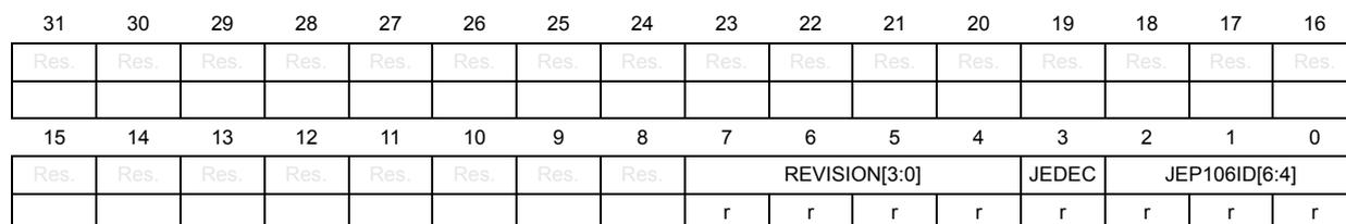
| 31 | 30 | 29 | 28 | 27 | 26 | 25 | 24 | 23 | 22 | 21 | 20 | 19 | 18 | 17 | 16 | |
|---|---|---|---|---|---|---|---|---|---|---|---|---|---|---|---|---|
| Res. | Res. | Res. | Res. | Res. | Res. | Res. | Res. | Res. | Res. | Res. | Res. | Res. | Res. | Res. | Res. | |
| 15 | 14 | 13 | 12 | 11 | 10 | 9 | 8 | 7 | 6 | 5 | 4 | 3 | 2 | 1 | 0 | |
| Res. | Res. | Res. | Res. | Res. | Res. | Res. | Res. | REVISION[3:0] | JEDEC | JEP106ID[6:4] | ||||||
| r | r | r | r | r | r | r | r | |||||||||
Bits 31:8 Reserved, must be kept at reset value.
Bits 7:4 REVISION[3:0] : Component revision number
0x1: rev 1
Bit 3 JEDEC : JEDEC assigned value
1: Designer ID specified by JEDEC
Bits 2:0 JEP106ID[6:4] : JEP106 identity code field, bits [6:4]
0x3: Arm JEDEC code
ETM CoreSight peripheral identity register 3 (ETM_PIDR3)
Address offset: 0xFEC
Reset value: 0x0000 0000
| 31 | 30 | 29 | 28 | 27 | 26 | 25 | 24 | 23 | 22 | 21 | 20 | 19 | 18 | 17 | 16 |
|---|---|---|---|---|---|---|---|---|---|---|---|---|---|---|---|
| Res. | Res. | Res. | Res. | Res. | Res. | Res. | Res. | Res. | Res. | Res. | Res. | Res. | Res. | Res. | Res. |
| 15 | 14 | 13 | 12 | 11 | 10 | 9 | 8 | 7 | 6 | 5 | 4 | 3 | 2 | 1 | 0 |
| Res. | Res. | Res. | Res. | Res. | Res. | Res. | Res. | REVAND[3:0] | CMOD[3:0] | ||||||
| r | r | r | r | r | r | r | r | ||||||||
Bits 31:8 Reserved, must be kept at reset value.
Bits 7:4 REVAND[3:0] : Metal fix version
0x0: No metal fix
Bits 3:0 CMOD[3:0] : Customer modified
0x0: No customer modifications
ETM CoreSight component identity register 0 (ETM_CIDR0)
Address offset: 0xFF0
Reset value: 0x0000 000D
| 31 | 30 | 29 | 28 | 27 | 26 | 25 | 24 | 23 | 22 | 21 | 20 | 19 | 18 | 17 | 16 |
|---|---|---|---|---|---|---|---|---|---|---|---|---|---|---|---|
| Res. | Res. | Res. | Res. | Res. | Res. | Res. | Res. | Res. | Res. | Res. | Res. | Res. | Res. | Res. | Res. |
| 15 | 14 | 13 | 12 | 11 | 10 | 9 | 8 | 7 | 6 | 5 | 4 | 3 | 2 | 1 | 0 |
| Res. | Res. | Res. | Res. | Res. | Res. | Res. | Res. | PREAMBLE[7:0] | |||||||
| r | r | r | r | r | r | r | r | ||||||||
Bits 31:8 Reserved, must be kept at reset value.
Bits 7:0 PREAMBLE[7:0] : Component ID field, bits [7:0]
0x0D: Common ID value
ETM CoreSight component identity register 1 (ETM_CIDR1)
Address offset: 0xFF4
Reset value: 0x0000 0090
| 31 | 30 | 29 | 28 | 27 | 26 | 25 | 24 | 23 | 22 | 21 | 20 | 19 | 18 | 17 | 16 |
|---|---|---|---|---|---|---|---|---|---|---|---|---|---|---|---|
| Res. | Res. | Res. | Res. | Res. | Res. | Res. | Res. | Res. | Res. | Res. | Res. | Res. | Res. | Res. | Res. |
| 15 | 14 | 13 | 12 | 11 | 10 | 9 | 8 | 7 | 6 | 5 | 4 | 3 | 2 | 1 | 0 |
| Res. | Res. | Res. | Res. | Res. | Res. | Res. | Res. | ||||||||
| CLASS[3:0] | PREAMBLE[11:8] | ||||||||||||||
| r | r | r | r | r | r | r | r | ||||||||
Bits 31:8 Reserved, must be kept at reset value.
Bits 7:4 CLASS[3:0] : Component ID field, bits [15:12] - component class
0x9: Debug component with CoreSight-compatible registers
Bits 3:0 PREAMBLE[11:8] : Component ID field, bits [11:8]
0x0: Common ID value
ETM CoreSight component identity register 2 (ETM_CIDR2)
Address offset: 0xFF8
Reset value: 0x0000 0005
| 31 | 30 | 29 | 28 | 27 | 26 | 25 | 24 | 23 | 22 | 21 | 20 | 19 | 18 | 17 | 16 |
|---|---|---|---|---|---|---|---|---|---|---|---|---|---|---|---|
| Res. | Res. | Res. | Res. | Res. | Res. | Res. | Res. | Res. | Res. | Res. | Res. | Res. | Res. | Res. | Res. |
| 15 | 14 | 13 | 12 | 11 | 10 | 9 | 8 | 7 | 6 | 5 | 4 | 3 | 2 | 1 | 0 |
| Res. | Res. | Res. | Res. | Res. | Res. | Res. | Res. | ||||||||
| PREAMBLE[19:12] | |||||||||||||||
| r | r | r | r | r | r | r | r | ||||||||
Bits 31:8 Reserved, must be kept at reset value.
Bits 7:0 PREAMBLE[19:12] : Component ID field, bits [23:16]
0x05: Common ID value
ETM CoreSight component identity register 3 (ETM_CIDR3)
Address offset: 0xFFC
Reset value: 0x0000 00B1
| 31 | 30 | 29 | 28 | 27 | 26 | 25 | 24 | 23 | 22 | 21 | 20 | 19 | 18 | 17 | 16 |
|---|---|---|---|---|---|---|---|---|---|---|---|---|---|---|---|
| Res. | Res. | Res. | Res. | Res. | Res. | Res. | Res. | Res. | Res. | Res. | Res. | Res. | Res. | Res. | Res. |
| 15 | 14 | 13 | 12 | 11 | 10 | 9 | 8 | 7 | 6 | 5 | 4 | 3 | 2 | 1 | 0 |
| Res. | Res. | Res. | Res. | Res. | Res. | Res. | Res. | ||||||||
| PREAMBLE[27:20] | |||||||||||||||
| r | r | r | r | r | r | r | r | ||||||||
Bits 31:8 Reserved, must be kept at reset value.
Bits 7:0 PREAMBLE[27:20] : Component ID field, bits [31:24]
0xB1: Common ID value
ETM register map
Table 879. ETM register map and reset values
| Offset | Register name | 31 | 30 | 29 | 28 | 27 | 26 | 25 | 24 | 23 | 22 | 21 | 20 | 19 | 18 | 17 | 16 | 15 | 14 | 13 | 12 | 11 | 10 | 9 | 8 | 7 | 6 | 5 | 4 | 3 | 2 | 1 | 0 | |
|---|---|---|---|---|---|---|---|---|---|---|---|---|---|---|---|---|---|---|---|---|---|---|---|---|---|---|---|---|---|---|---|---|---|---|
| 0x004 | ETM_PRCCTL | Res. | Res. | Res. | Res. | Res. | Res. | Res. | Res. | Res. | Res. | Res. | Res. | Res. | Res. | Res. | Res. | Res. | Res. | Res. | Res. | Res. | Res. | Res. | Res. | Res. | Res. | Res. | Res. | Res. | Res. | Res. | Res. | EN |
| Reset value | 0 | |||||||||||||||||||||||||||||||||
| 0x008 | Reserved | Reserved | ||||||||||||||||||||||||||||||||
| 0x00C | ETM_STAT | Res. | Res. | Res. | Res. | Res. | Res. | Res. | Res. | Res. | Res. | Res. | Res. | Res. | Res. | Res. | Res. | Res. | Res. | Res. | Res. | Res. | Res. | Res. | Res. | Res. | Res. | Res. | Res. | Res. | Res. | Res. | PMSTABLE IDLE | |
| Reset value | 0 | |||||||||||||||||||||||||||||||||
| 0x010 | ETM_CONFIG | Res. | Res. | Res. | Res. | Res. | Res. | Res. | Res. | Res. | Res. | Res. | Res. | Res. | Res. | Res. | Res. | Res. | Res. | Res. | RS TS | COND [2:0] | Res. | Res. | Res. | Res. | CCI | BB | INSTP0 [1:0] | Res. | ||||
| Reset value | 0 | 0 | 0 | 0 | 0 | 0 | 0 | 0 | 0 | 0 | ||||||||||||||||||||||||
| 0x014- 0x01C | Reserved | Reserved | ||||||||||||||||||||||||||||||||
| 0x020 | ETM_EVENTCTL0 | Res. | Res. | Res. | Res. | Res. | Res. | Res. | Res. | Res. | Res. | Res. | Res. | Res. | Res. | Res. | Res. | EVENT1[7:0] | ||||||||||||||||
| Reset value | 0 | 0 | 0 | 0 | 0 | 0 | 0 | 0 | 0 | 0 | 0 | 0 | 0 | 0 | 0 | |||||||||||||||||||
| 0x024 | ETM_EVENTCTL1 | Res. | Res. | Res. | Res. | Res. | Res. | Res. | Res. | Res. | Res. | Res. | Res. | Res. | Res. | Res. | Res. | Res. | Res. | Res. | LP POVERRIDE ATB | Res. | Res. | Res. | Res. | Res. | Res. | Res. | Res. | Res. | INSTEN[3:0] | Res. | ||
| Reset value | 0 | 0 | 0 | 0 | 0 | |||||||||||||||||||||||||||||
| 0x02C | ETM_STALLCTL | Res. | Res. | Res. | Res. | Res. | Res. | Res. | Res. | Res. | Res. | Res. | Res. | Res. | Res. | Res. | Res. | Res. | Res. | Res. | Res. | Res. | Res. | Res. | STALL | Res. | Res. | Res. | Res. | LEVEL [1:0] | Res. | Res. | ||
| Reset value | 0 | 0 | 0 | |||||||||||||||||||||||||||||||
| 0x030 | ETM_TSCTL | Res. | Res. | Res. | Res. | Res. | Res. | Res. | Res. | Res. | Res. | Res. | Res. | Res. | Res. | Res. | Res. | Res. | Res. | Res. | Res. | Res. | Res. | Res. | Res. | EVENT[7:0] | ||||||||
| Reset value | 0 | 0 | 0 | 0 | 0 | 0 | 0 | 0 | ||||||||||||||||||||||||||
| 0x034 | ETM_SYNCP | Res. | Res. | Res. | Res. | Res. | Res. | Res. | Res. | Res. | Res. | Res. | Res. | Res. | Res. | Res. | Res. | Res. | Res. | Res. | Res. | Res. | Res. | Res. | Res. | Res. | Res. | PERIOD[4:0] | ||||||
| Reset value | 0 | 1 | 0 | 1 | 0 | |||||||||||||||||||||||||||||
| 0x038 | ETM_CCCTL | Res. | Res. | Res. | Res. | Res. | Res. | Res. | Res. | Res. | Res. | Res. | Res. | Res. | Res. | Res. | Res. | Res. | Res. | Res. | THRESHOLD[11:0] | |||||||||||||
| Reset value | 0 | 0 | 0 | 0 | 0 | 0 | 0 | 0 | 0 | 0 | 0 | 0 | ||||||||||||||||||||||
| 0x03C | Reserved | Reserved | ||||||||||||||||||||||||||||||||
| 0x040 | ETM_TRACEID | Res. | Res. | Res. | Res. | Res. | Res. | Res. | Res. | Res. | Res. | Res. | Res. | Res. | Res. | Res. | Res. | Res. | Res. | Res. | Res. | Res. | Res. | Res. | Res. | Res. | Res. | TRACEID[6:0] | ||||||
| Reset value | 0 | 0 | 0 | 0 | 0 | |||||||||||||||||||||||||||||
| 0x044 - 0x07C | Reserved | Reserved | ||||||||||||||||||||||||||||||||
| 0x080 | ETM_VICTL | Res. | Res. | Res. | Res. | Res. | Res. | Res. | Res. | Res. | Res. | Res. | Res. | EXLEVEL_S3 | Res. | EXLEVEL_S0 | Res. | Res. | Res. | Res. | TRCERR | TRCRESET | SSSTATUS | Res. | EVENT[7:0] | |||||||||
| Reset value | 0 | 0 | 0 | 0 | 0 | 0 | 0 | 0 | 0 | 0 | 0 | 0 | 0 | |||||||||||||||||||||
| 0x084- 0x088 | Reserved | Reserved | ||||||||||||||||||||||||||||||||
| 0x08C | ETM_VIPCSSCTL | Res. | Res. | Res. | Res. | Res. | Res. | Res. | Res. | STOP[3:0] | Res. | Res. | Res. | Res. | Res. | Res. | Res. | Res. | START[3:0] | |||||||||||||||
| Reset value | 0 | 0 | 0 | 0 | 0 | 0 | 0 | 0 | 0 | 0 | 0 | 0 | 0 | 0 | 0 | |||||||||||||||||||
Table 879. ETM register map and reset values (continued)
| Offset | Register name | 31 | 30 | 29 | 28 | 27 | 26 | 25 | 24 | 23 | 22 | 21 | 20 | 19 | 18 | 17 | 16 | 15 | 14 | 13 | 12 | 11 | 10 | 9 | 8 | 7 | 6 | 5 | 4 | 3 | 2 | 1 | 0 |
|---|---|---|---|---|---|---|---|---|---|---|---|---|---|---|---|---|---|---|---|---|---|---|---|---|---|---|---|---|---|---|---|---|---|
| 0x090-0x12C | Reserved | Reserved | |||||||||||||||||||||||||||||||
| 0x120 | ETM_EXTINSEL | SEL3[7:0] | SEL2[7:0] | SEL1[7:0] | SEL0[7:0] | ||||||||||||||||||||||||||||
| Reset value | 0 | 0 | 0 | 0 | 0 | 0 | 0 | 0 | 0 | 0 | 0 | 0 | 0 | 0 | 0 | 0 | 0 | 0 | 0 | 0 | 0 | 0 | 0 | 0 | 0 | 0 | 0 | 0 | 0 | 0 | 0 | 0 | |
| 0x124-0x13C | Reserved | Reserved | |||||||||||||||||||||||||||||||
| 0x140 | ETM_CNTRLDV | Res. | Res. | Res. | Res. | Res. | Res. | Res. | Res. | Res. | Res. | Res. | Res. | Res. | Res. | Res. | Res. | VALUE[15:0] | |||||||||||||||
| Reset value | 0 | 0 | 0 | 0 | 0 | 0 | 0 | 0 | 0 | 0 | 0 | 0 | 0 | 0 | 0 | 0 | |||||||||||||||||
| 0x144-0x17C | Reserved | Reserved | |||||||||||||||||||||||||||||||
| 0x180 | ETM_IDR8 | MAXSPEC[31:0] | |||||||||||||||||||||||||||||||
| Reset value | 0 | 0 | 0 | 0 | 0 | 0 | 0 | 0 | 0 | 0 | 0 | 0 | 0 | 0 | 0 | 0 | 0 | 0 | 0 | 0 | 0 | 0 | 0 | 0 | 0 | 0 | 0 | 0 | 0 | 0 | 1 | 0 | |
| 0x184 | ETM_IDR9 | NUMP0KEY[31:0] | |||||||||||||||||||||||||||||||
| Reset value | 0 | 0 | 0 | 0 | 0 | 0 | 0 | 0 | 0 | 0 | 0 | 0 | 0 | 0 | 0 | 0 | 0 | 0 | 0 | 0 | 0 | 0 | 0 | 0 | 0 | 0 | 0 | 0 | 0 | 0 | 0 | 0 | |
| 0x188 | ETM_IDR10 | NUMP1KEY[31:0] | |||||||||||||||||||||||||||||||
| Reset value | 0 | 0 | 0 | 0 | 0 | 0 | 0 | 0 | 0 | 0 | 0 | 0 | 0 | 0 | 0 | 0 | 0 | 0 | 0 | 0 | 0 | 0 | 0 | 0 | 0 | 0 | 0 | 0 | 0 | 0 | 0 | 0 | |
| 0x18C | ETM_IDR11 | NUMP1SPC[31:0] | |||||||||||||||||||||||||||||||
| Reset value | 0 | 0 | 0 | 0 | 0 | 0 | 0 | 0 | 0 | 0 | 0 | 0 | 0 | 0 | 0 | 0 | 0 | 0 | 0 | 0 | 0 | 0 | 0 | 0 | 0 | 0 | 0 | 0 | 0 | 0 | 0 | 0 | |
| 0x190 | ETM_IDR12 | NUMCONDKEY[31:0] | |||||||||||||||||||||||||||||||
| Reset value | 0 | 0 | 0 | 0 | 0 | 0 | 0 | 0 | 0 | 0 | 0 | 0 | 0 | 0 | 0 | 0 | 0 | 0 | 0 | 0 | 0 | 0 | 0 | 0 | 0 | 0 | 0 | 0 | 0 | 0 | 0 | 1 | |
| 0x194 | ETM_IDR13 | NUMCONDSPC[31:0] | |||||||||||||||||||||||||||||||
| Reset value | 0 | 0 | 0 | 0 | 0 | 0 | 0 | 0 | 0 | 0 | 0 | 0 | 0 | 0 | 0 | 0 | 0 | 0 | 0 | 0 | 0 | 0 | 0 | 0 | 0 | 0 | 0 | 0 | 0 | 0 | 0 | 0 | |
| 0x198-0x1DC | Reserved | Reserved | |||||||||||||||||||||||||||||||
| 0x1E0 | ETM_IDR0 | Res. | Res. | COMMOPT | TSSIZE[4:0] | Res. | Res. | Res. | Res. | BF[1:0] | TRCEXDATA | QSUPP[1:0] | Res. | CONDTYPE [1:0] | NUMEVENT [1:0] | RETSTACK | Res. | TRCCCI | TRCCOND | TRCBB | TRCDATA[1:0] | INSTP[1:0] | Res. | ||||||||||
| Reset value | 1 | 0 | 1 | 0 | 0 | 0 | 0 | 0 | 0 | 0 | 0 | 0 | 0 | 0 | 1 | 1 | 1 | 1 | 1 | 0 | 0 | 0 | 0 | ||||||||||
| 0x1E4 | ETM_IDR1 | DESIGNER[7:0] | Res. | Res. | Res. | Res. | Res. | Res. | Res. | Res. | Res. | TRCARCHMAJ [3:0] | TRCARCHMIN [3:0] | Res. | Res. | Res. | REVISION [3:0] | ||||||||||||||||
| Reset value | 0 | 1 | 0 | 0 | 0 | 0 | 0 | 1 | 0 | 1 | 0 | 0 | 0 | 1 | 0 | 1 | 0 | 0 | 0 | 0 | |||||||||||||
| 0x1E8 | ETM_IDR2 | Res. | Res. | Res. | CCSIZE[3:0] | DVSIZE[4:0] | DASIZE[4:0] | VMIDSIZE[4:0] | CIDSIZE[4:0] | IASIZE[4:0] | |||||||||||||||||||||||
| Reset value | 0 | 0 | 0 | 0 | 0 | 0 | 0 | 0 | 0 | 0 | 0 | 0 | 0 | 0 | 0 | 0 | 0 | 0 | 0 | 0 | 0 | 0 | 0 | 0 | 0 | 0 | 1 | 0 | 0 | ||||
| 0x1EC | ETM_IDR3 | NOOVERFLOW | NUMPROC[2:0] | SYSSTALL | STALLCTL | SYNCPR | TRCERR | Res. | Res. | Res. | Res. | EXLEVEL_S [3:0] | Res. | Res. | NUMPROC [4:3] | CCITMIN[11:0] | |||||||||||||||||
| Reset value | 0 | 0 | 0 | 0 | 0 | 1 | 0 | 1 | 1 | 0 | 0 | 1 | 0 | 0 | 0 | 0 | 0 | 0 | 0 | 0 | 0 | 0 | 0 | 0 | 1 | 0 | |||||||
| 0x1F0 | ETM_IDR4 | NUMVMIDC [3:0] | NUMCIDC [3:0] | NUMSSCC [3:0] | NUMRSPAIR [3:0] | NUMPC[3:0] | Res. | Res. | Res. | SUPPDAC | NUMDVC [3:0] | NUMACPAIRS [3:0] | |||||||||||||||||||||
| Reset value | 0 | 0 | 0 | 0 | 0 | 0 | 0 | 0 | 0 | 0 | 0 | 1 | 0 | 0 | 0 | 1 | 1 | 0 | 0 | 0 | 0 | 0 | 0 | 0 | 0 | 0 | 0 | 0 | 0 | ||||
Table 879. ETM register map and reset values (continued)
| Offset | Register name | 31 | 30 | 29 | 28 | 27 | 26 | 25 | 24 | 23 | 22 | 21 | 20 | 19 | 18 | 17 | 16 | 15 | 14 | 13 | 12 | 11 | 10 | 9 | 8 | 7 | 6 | 5 | 4 | 3 | 2 | 1 | 0 |
|---|---|---|---|---|---|---|---|---|---|---|---|---|---|---|---|---|---|---|---|---|---|---|---|---|---|---|---|---|---|---|---|---|---|
| 0x1F4 | ETM_IDR5 | REDFUNCNTR | NUMCNTR[2:0] | NUMSEQSTATE [2:0] | Res. | LPOVERRIDE | ATBTRIG | TRACEIDSIZE[5:0] | Res. | Res. | Res. | Res. | NUMEXTINSEL [2:0] | NUMEXTIN[8:0] | |||||||||||||||||||
| Reset value | 1 | 0 | 0 | 1 | 0 | 0 | 0 | 1 | 1 | 0 | 0 | 0 | 1 | 1 | 1 | 1 | 0 | 0 | 0 | 0 | 0 | 0 | 0 | 0 | 0 | 1 | 0 | 0 | |||||
| 0x1F8-0x204 | Reserved | Reserved | |||||||||||||||||||||||||||||||
| 0x208 | ETM_RSCTL2 | Res. | Res. | Res. | Res. | Res. | Res. | Res. | Res. | Res. | Res. | PAIRINV | INV | Res. | GROUP [2:0] | Res. | Res. | Res. | Res. | Res. | Res. | Res. | SELECT[7:0] | ||||||||||
| Reset value | 0 | 0 | 0 | 0 | 0 | 0 | 0 | 0 | 0 | 0 | 0 | 0 | 0 | ||||||||||||||||||||
| 0x20C | ETM_RSCTL3 | Res. | Res. | Res. | Res. | Res. | Res. | Res. | Res. | Res. | Res. | INV | Res. | Res. | GROUP [2:0] | Res. | Res. | Res. | Res. | Res. | Res. | Res. | SELECT[7:0] | ||||||||||
| Reset value | 0 | 0 | 0 | 0 | 0 | 0 | 0 | 0 | 0 | 0 | 0 | 0 | |||||||||||||||||||||
| 0x210-0x27C | Reserved | Reserved | |||||||||||||||||||||||||||||||
| 0x280 | ETM_SSCC0 | Res. | Res. | Res. | Res. | Res. | Res. | Res. | Res. | RST | Res. | Res. | Res. | Res. | Res. | Res. | Res. | Res. | Res. | Res. | Res. | Res. | Res. | Res. | Res. | Res. | Res. | Res. | Res. | Res. | Res. | Res. | Res. |
| Reset value | 0 | ||||||||||||||||||||||||||||||||
| 0x284-0x29C | Reserved | Reserved | |||||||||||||||||||||||||||||||
| 0x2A0 | ETM_SSCS0 | STATUS | Res. | Res. | Res. | Res. | Res. | Res. | Res. | Res. | Res. | Res. | Res. | Res. | Res. | Res. | Res. | Res. | Res. | Res. | Res. | Res. | Res. | Res. | Res. | Res. | Res. | Res. | Res. | PC | DV | DA | INST |
| Reset value | 0 | 1 | 0 | 0 | 0 | ||||||||||||||||||||||||||||
| 0x2A4-0x2BC | Reserved | Reserved | |||||||||||||||||||||||||||||||
| 0x2C0 | ETM_SSPIC0 | Res. | Res. | Res. | Res. | Res. | Res. | Res. | Res. | Res. | Res. | Res. | Res. | Res. | Res. | Res. | Res. | Res. | Res. | Res. | Res. | Res. | Res. | Res. | PC[7:0] | ||||||||
| Reset value | 0 | 0 | 0 | 0 | 0 | 0 | 0 | 0 | |||||||||||||||||||||||||
| 0x2C4-0x30C | Reserved | Reserved | |||||||||||||||||||||||||||||||
| 0x310 | ETM_PDC | Res. | Res. | Res. | Res. | Res. | Res. | Res. | Res. | Res. | Res. | Res. | Res. | Res. | Res. | Res. | Res. | Res. | Res. | Res. | Res. | Res. | Res. | Res. | Res. | Res. | Res. | Res. | Res. | PU | Res. | Res. | Res. |
| Reset value | 0 | ||||||||||||||||||||||||||||||||
| 0x314 | ETM_PDS | Res. | Res. | Res. | Res. | Res. | Res. | Res. | Res. | Res. | Res. | Res. | Res. | Res. | Res. | Res. | Res. | Res. | Res. | Res. | Res. | Res. | Res. | Res. | Res. | Res. | Res. | Res. | Res. | Res. | Res. | STICKYPD | POWER |
| Reset value | 1 | 1 | |||||||||||||||||||||||||||||||
| 0x318-0xF9C | Reserved | Reserved | |||||||||||||||||||||||||||||||
| 0xFA0 | ETM_CLAIMSET | Res. | Res. | Res. | Res. | Res. | Res. | Res. | Res. | Res. | Res. | Res. | Res. | Res. | Res. | Res. | Res. | Res. | Res. | Res. | Res. | Res. | Res. | Res. | Res. | Res. | Res. | Res. | Res. | CLAIMSET [3:0] | |||
| Reset value | 1 | 1 | 1 | 1 | |||||||||||||||||||||||||||||
| 0xFA4 | ETM_CLAIMCLR | Res. | Res. | Res. | Res. | Res. | Res. | Res. | Res. | Res. | Res. | Res. | Res. | Res. | Res. | Res. | Res. | Res. | Res. | Res. | Res. | Res. | Res. | Res. | Res. | Res. | Res. | Res. | Res. | CLAIMCLR [3:0] | |||
| Reset value | 0 | 0 | 0 | 0 | |||||||||||||||||||||||||||||
| 0xFA8-0xFB4 | Reserved | Reserved | |||||||||||||||||||||||||||||||
| 0xFB8 | ETM_AUTHSTAT | Res. | Res. | Res. | Res. | Res. | Res. | Res. | Res. | Res. | Res. | Res. | Res. | Res. | Res. | Res. | Res. | Res. | Res. | Res. | Res. | Res. | Res. | Res. | Res. | SNID [1:0] | SID [1:0] | NSNID [1:0] | NSID [1:0] | ||||
| Reset value | X | X | X | X | X | X | X | X | |||||||||||||||||||||||||
Table 879. ETM register map and reset values (continued)
| Offset | Register name | 31 | 30 | 29 | 28 | 27 | 26 | 25 | 24 | 23 | 22 | 21 | 20 | 19 | 18 | 17 | 16 | 15 | 14 | 13 | 12 | 11 | 10 | 9 | 8 | 7 | 6 | 5 | 4 | 3 | 2 | 1 | 0 |
|---|---|---|---|---|---|---|---|---|---|---|---|---|---|---|---|---|---|---|---|---|---|---|---|---|---|---|---|---|---|---|---|---|---|
| 0xFBC | ETM_DEVARCH | ARCHITECT[10:0] | PRESENT | REVISION [3:0] | ARCHID[15:0] | ||||||||||||||||||||||||||||
| Reset value | 0 | 1 | 0 | 0 | 0 | 1 | 1 | 1 | 0 | 1 | 1 | 1 | 0 | 1 | 0 | 1 | 0 | 0 | 1 | 0 | 1 | 0 | 1 | 0 | 0 | 0 | 0 | 1 | 0 | 0 | 1 | 1 | |
| 0xFC0- 0xFC8 | Reserved | Reserved | |||||||||||||||||||||||||||||||
| 0xFCC | ETM_DEVTYPE | Res. | Res. | Res. | Res. | Res. | Res. | Res. | Res. | Res. | Res. | Res. | Res. | Res. | Res. | Res. | Res. | Res. | Res. | Res. | Res. | Res. | Res. | Res. | SUBTYPE [3:0] | MAJORTYPE [3:0] | |||||||
| Reset value | 0 | 0 | 0 | 0 | 0 | 0 | 0 | 0 | 0 | 0 | 0 | 0 | 0 | 0 | 0 | 0 | 0 | 0 | 0 | 0 | 0 | 0 | 0 | 0 | 0 | 0 | 1 | 0 | 0 | 1 | 1 | ||
| 0xFD0 | ETM_PIDR4 | Res. | Res. | Res. | Res. | Res. | Res. | Res. | Res. | Res. | Res. | Res. | Res. | Res. | Res. | Res. | Res. | Res. | Res. | Res. | Res. | Res. | Res. | Res. | SIZE[3:0] | JEP106CON [3:0] | |||||||
| Reset value | 0 | 0 | 0 | 0 | 0 | 1 | 0 | 0 | |||||||||||||||||||||||||
| 0xFD4 - 0xFDC | Reserved | Reserved | |||||||||||||||||||||||||||||||
| 0xFE0 | ETM_PIDR0 | Res. | Res. | Res. | Res. | Res. | Res. | Res. | Res. | Res. | Res. | Res. | Res. | Res. | Res. | Res. | Res. | Res. | Res. | Res. | Res. | Res. | Res. | Res. | PARTNUM[7:0] | ||||||||
| Reset value | 0 | 0 | 1 | 0 | 0 | 0 | 1 | 1 | |||||||||||||||||||||||||
| 0xFE4 | ETM_PIDR1 | Res. | Res. | Res. | Res. | Res. | Res. | Res. | Res. | Res. | Res. | Res. | Res. | Res. | Res. | Res. | Res. | Res. | Res. | Res. | Res. | Res. | Res. | Res. | JEP106ID [3:0] | PARTNUM [11:8] | |||||||
| Reset value | 1 | 0 | 1 | 1 | 1 | 1 | 0 | 1 | |||||||||||||||||||||||||
| 0xFE8 | ETM_PIDR2 | Res. | Res. | Res. | Res. | Res. | Res. | Res. | Res. | Res. | Res. | Res. | Res. | Res. | Res. | Res. | Res. | Res. | Res. | Res. | Res. | Res. | Res. | Res. | REVISION [3:0] | JEDEC | JEP106ID [6:4] | ||||||
| Reset value | 0 | 0 | 0 | 0 | 1 | 0 | 1 | 1 | |||||||||||||||||||||||||
| 0xFEC | ETM_PIDR3 | Res. | Res. | Res. | Res. | Res. | Res. | Res. | Res. | Res. | Res. | Res. | Res. | Res. | Res. | Res. | Res. | Res. | Res. | Res. | Res. | Res. | Res. | Res. | REVAND[3:0] | CMOD[3:0] | |||||||
| Reset value | 0 | 0 | 0 | 0 | 0 | 0 | 0 | 0 | |||||||||||||||||||||||||
| 0xFF0 | ETM_CIDR0 | Res. | Res. | Res. | Res. | Res. | Res. | Res. | Res. | Res. | Res. | Res. | Res. | Res. | Res. | Res. | Res. | Res. | Res. | Res. | Res. | Res. | Res. | Res. | PREAMBLE[7:0] | ||||||||
| Reset value | 0 | 0 | 0 | 0 | 1 | 1 | 0 | 1 | |||||||||||||||||||||||||
| 0xFF4 | ETM_CIDR1 | Res. | Res. | Res. | Res. | Res. | Res. | Res. | Res. | Res. | Res. | Res. | Res. | Res. | Res. | Res. | Res. | Res. | Res. | Res. | Res. | Res. | Res. | Res. | CLASS[3:0] | PREAMBLE [11:8] | |||||||
| Reset value | 1 | 0 | 0 | 1 | 0 | 0 | 0 | 0 | |||||||||||||||||||||||||
| 0xFF8 | ETM_CIDR2 | Res. | Res. | Res. | Res. | Res. | Res. | Res. | Res. | Res. | Res. | Res. | Res. | Res. | Res. | Res. | Res. | Res. | Res. | Res. | Res. | Res. | Res. | Res. | PREAMBLE[19:12] | ||||||||
| Reset value | 0 | 0 | 0 | 0 | 0 | 1 | 0 | 1 | |||||||||||||||||||||||||
| 0xFFC | ETM_CIDR3 | Res. | Res. | Res. | Res. | Res. | Res. | Res. | Res. | Res. | Res. | Res. | Res. | Res. | Res. | Res. | Res. | Res. | Res. | Res. | Res. | Res. | Res. | Res. | PREAMBLE[27:20] | ||||||||
| Reset value | 1 | 0 | 1 | 1 | 0 | 0 | 0 | 1 | |||||||||||||||||||||||||
78.11.13 Cross trigger interface (CTI)
See Section 78.12.4 .
78.12 Trace and debug subsystem
The trace and debug subsystem includes the following CoreSight components:
- • trace subsystem ROM table
- • global trace timestamp generator (TSGEN)
- • system cross-trigger interface (CTI)
- • cross-trigger matrix (CTM)
- • trace port interface unit (TPIU)
- • trace bus funnel (CSTF)
- • embedded trace FIFO (ETF)
- • embedded trace router (ETR)
- • replicator
- • system trace macrocell (STM)
- • serial-wire output (SWO)
The MCU ROM table in the Cortex-M55 subsystem pointed to by the BASE register in the Cortex-M55 AHB-AP links to the trace subsystem ROM table. This secondary ROM table contains the base address pointer for the CoreSight trace components.
These components are accessible by the debugger and the Cortex-M55 processor via the system AHB-AP and its associated EPPB debug bus.
Table 880. Trace subsystem ROM table
| Address in ROM table | Component name | Component base address | Component address offset | Size (Kbytes) | Entry |
|---|---|---|---|---|---|
| 0xE008 0000 | Funnel | 0xE008 1000 | 0x0000 1000 | 4 | 0x0000 1003 |
| 0xE008 0004 | ETF | 0xE008 2000 | 0x0000 2000 | 4 | 0x0000 2003 |
| 0xE008 0008 | ETR | 0xE008 3000 | 0x0000 3000 | 4 | 0x0000 3003 |
| 0xE008 000C | TPIU | 0xE008 4000 | 0x0000 4000 | 4 | 0x0000 4003 |
| 0xE008 0010 | Replicator | 0xE008 5000 | 0x0000 5000 | 4 | 0x0000 5003 |
| 0xE008 0014 | Timestamp generator | 0xE008 6000 | 0x0000 6000 | 4 | 0x0000 6003 |
| 0xE008 0018 | STM | 0xE008 7000 | 0x0000 7000 | 4 | 0x0000 7003 |
| 0xE008 001C | CTI0 | 0xE008 8000 | 0x0000 8000 | 4 | 0x0000 8003 |
| 0xE008 0020 | CTI1 | 0xE008 9000 | 0x0000 9000 | 4 | 0x0000 9003 |
| 0xE008 0024 | SWO | 0xE008 A000 | 0x0000 A000 | 4 | 0x0000 A003 |
| 0xE008 0028 | Top of table | - | - | - | 0x0000 0000 |
| 0xE008 002C to 0xE008 00C8 | Reserved | - | - | - | 0x0000 0000 |
| 0xE008 0FCC to 0xE008 0FFC | ROM table registers | - | - | - | - |
The topology for the CoreSight components in the trace an/d debug subsystem is shown in Figure 1081 .
Figure 1081. Trace subsystem CoreSight topology
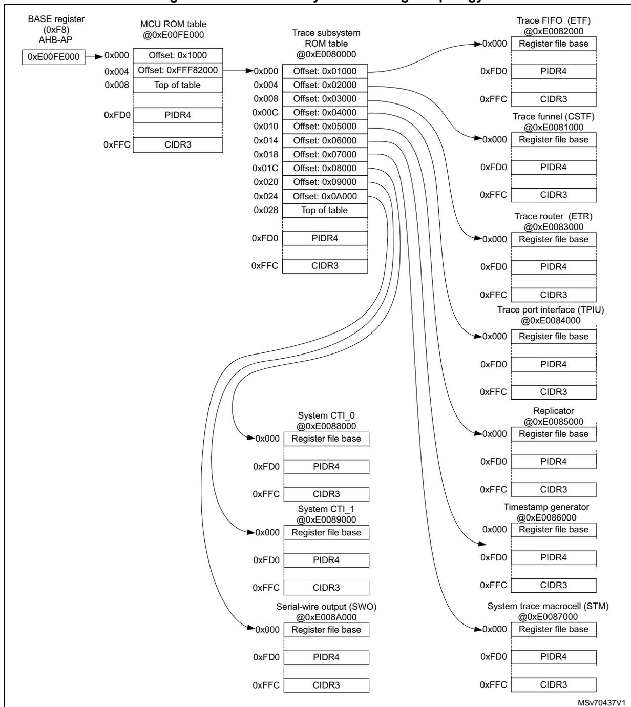
The diagram illustrates the CoreSight trace subsystem topology. It shows the following components and their connections:
- BASE register (0xF8) AHB-AP at address 0xE00FE000 . It points to the MCU ROM table at @0xE00FE000 .
- MCU ROM table @0xE00FE000 contains entries for Offset: 0x1000 , Offset: 0xFFF82000 , and Top of table . It points to the Trace subsystem ROM table at @0xE0080000 .
- Trace subsystem ROM table @0xE0080000 contains entries for various offsets ( 0x1000 , 0x2000 , 0x3000 , 0x4000 , 0x5000 , 0x6000 , 0x7000 , 0x8000 , 0x9000 , 0xA000 ) and Top of table . It also includes PIDR4 and CIDR3 registers.
- From the
Trace subsystem ROM table
, connections lead to several CoreSight components:
- Trace FIFO (ETF) @0xE0082000
- Trace funnel (CSTF) @0xE0081000
- Trace router (ETR) @0xE0083000
- Trace port interface (TPIU) @0xE0084000
- System CTL_0 @0xE0088000
- System CTL_1 @0xE0089000
- Serial-wire output (SWO) @0xE008A000
- Replicator @0xE0085000
- Timestamp generator @0xE0086000
- System trace macrocell (STM) @0xE0087000
- Each CoreSight component has a Register file base at 0x000 , PIDR4 at 0xFD0 , and CIDR3 at 0xFFC .
MSv70437V1
78.12.1 Trace subsystem ROM table registers
Trace subsystem ROM memory type register (TSSROM_MEMTYPE)
Address offset: 0xFCC
Reset value: 0x0000 0001
| 31 | 30 | 29 | 28 | 27 | 26 | 25 | 24 | 23 | 22 | 21 | 20 | 19 | 18 | 17 | 16 |
|---|---|---|---|---|---|---|---|---|---|---|---|---|---|---|---|
| Res. | Res. | Res. | Res. | Res. | Res. | Res. | Res. | Res. | Res. | Res. | Res. | Res. | Res. | Res. | Res. |
| 15 | 14 | 13 | 12 | 11 | 10 | 9 | 8 | 7 | 6 | 5 | 4 | 3 | 2 | 1 | 0 |
| Res. | Res. | Res. | Res. | Res. | Res. | Res. | Res. | Res. | Res. | Res. | Res. | Res. | Res. | Res. | SYSTEM MEM |
| r |
Bits 31:1 Reserved, must be kept at reset value.
Bit 0 SYSTEM : System memory presence
1: System memory is present on this bus.
Trace subsystem ROM CoreSight peripheral identity register 4 (TSSROM_PIDR4)
Address offset: 0xFD0
Reset value: 0x0000 0000
| 31 | 30 | 29 | 28 | 27 | 26 | 25 | 24 | 23 | 22 | 21 | 20 | 19 | 18 | 17 | 16 |
|---|---|---|---|---|---|---|---|---|---|---|---|---|---|---|---|
| Res. | Res. | Res. | Res. | Res. | Res. | Res. | Res. | Res. | Res. | Res. | Res. | Res. | Res. | Res. | Res. |
| 15 | 14 | 13 | 12 | 11 | 10 | 9 | 8 | 7 | 6 | 5 | 4 | 3 | 2 | 1 | 0 |
| Res. | Res. | Res. | Res. | Res. | Res. | Res. | Res. | SIZE[3:0] | JEP106CON[3:0] | ||||||
| r | r | r | r | r | r | r | r | ||||||||
Bits 31:8 Reserved, must be kept at reset value.
Bits 7:4 SIZE[3:0] : Register file size
0x0: Register file occupies a single 4-Kbyte region.
Bits 3:0 JEP106CON[3:0] : JEP106 continuation code
0x0: Arm JEDEC continuation code
Trace subsystem ROM CoreSight peripheral identity register 0 (TSSROM_PIDR0)
Address offset: 0xFE0
Reset value: 0x0000 0086
| 31 | 30 | 29 | 28 | 27 | 26 | 25 | 24 | 23 | 22 | 21 | 20 | 19 | 18 | 17 | 16 |
|---|---|---|---|---|---|---|---|---|---|---|---|---|---|---|---|
| Res. | Res. | Res. | Res. | Res. | Res. | Res. | Res. | Res. | Res. | Res. | Res. | Res. | Res. | Res. | Res. |
| 15 | 14 | 13 | 12 | 11 | 10 | 9 | 8 | 7 | 6 | 5 | 4 | 3 | 2 | 1 | 0 |
| Res. | Res. | Res. | Res. | Res. | Res. | Res. | Res. | PARTNUM[7:0] | |||||||
| r | r | r | r | r | r | r | r | ||||||||
Bits 31:8 Reserved, must be kept at reset value.
Bits 7:0 PARTNUM[7:0] : Part number field, bits [7:0]0x86: STM32N6
Trace subsystem ROM CoreSight peripheral identity register 1 (TSSROM_PIDR1)
Address offset: 0xFE4
Reset value: 0x0000 0004
| 31 | 30 | 29 | 28 | 27 | 26 | 25 | 24 | 23 | 22 | 21 | 20 | 19 | 18 | 17 | 16 |
|---|---|---|---|---|---|---|---|---|---|---|---|---|---|---|---|
| Res. | Res. | Res. | Res. | Res. | Res. | Res. | Res. | Res. | Res. | Res. | Res. | Res. | Res. | Res. | Res. |
| 15 | 14 | 13 | 12 | 11 | 10 | 9 | 8 | 7 | 6 | 5 | 4 | 3 | 2 | 1 | 0 |
| Res. | Res. | Res. | Res. | Res. | Res. | Res. | Res. | JEP106ID[3:0] | PARTNUM[11:8] | ||||||
| r | r | r | r | r | r | r | r | ||||||||
Bits 31:8 Reserved, must be kept at reset value.
Bits 7:4 JEP106ID[3:0] : JEP106 identity code field, bits [3:0]0x0: Arm JEDEC code
Bits 3:0 PARTNUM[11:8] : Part number field, bits [11:8]0x4: STM32N6x5/x7xx
Trace subsystem ROM CoreSight peripheral identity register 2 (TSSROM_PIDR2)
Address offset: 0xFE8
Reset value: 0x0000 000A
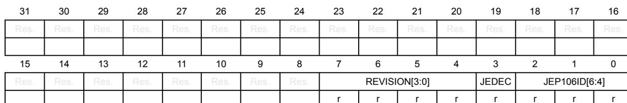
| 31 | 30 | 29 | 28 | 27 | 26 | 25 | 24 | 23 | 22 | 21 | 20 | 19 | 18 | 17 | 16 | |
|---|---|---|---|---|---|---|---|---|---|---|---|---|---|---|---|---|
| Res. | Res. | Res. | Res. | Res. | Res. | Res. | Res. | Res. | Res. | Res. | Res. | Res. | Res. | Res. | Res. | |
| 15 | 14 | 13 | 12 | 11 | 10 | 9 | 8 | 7 | 6 | 5 | 4 | 3 | 2 | 1 | 0 | |
| Res. | Res. | Res. | Res. | Res. | Res. | Res. | Res. | REVISION[3:0] | JEDEC | JEP106ID[6:4] | ||||||
| r | r | r | r | r | r | r | r | |||||||||
Bits 31:8 Reserved, must be kept at reset value.
Bits 7:4 REVISION[3:0] : Component revision number
0x0: rev 1
Bit 3 JEDEC : JEDEC assigned value
1: Designer ID specified by JEDEC
Bits 2:0 JEP106ID[6:4] : JEP106 identity code field, bits [6:4]
0x2: STMicroelectronics JEDEC code
Trace subsystem ROM CoreSight peripheral identity register 3
(TSSROM_PIDR3)
Address offset: 0xFEC
Reset value: 0x0000 0000
| 31 | 30 | 29 | 28 | 27 | 26 | 25 | 24 | 23 | 22 | 21 | 20 | 19 | 18 | 17 | 16 |
|---|---|---|---|---|---|---|---|---|---|---|---|---|---|---|---|
| Res. | Res. | Res. | Res. | Res. | Res. | Res. | Res. | Res. | Res. | Res. | Res. | Res. | Res. | Res. | Res. |
| 15 | 14 | 13 | 12 | 11 | 10 | 9 | 8 | 7 | 6 | 5 | 4 | 3 | 2 | 1 | 0 |
| Res. | Res. | Res. | Res. | Res. | Res. | Res. | Res. | REVAND[3:0] | CMOD[3:0] | ||||||
| r | r | r | r | r | r | r | r | ||||||||
Bits 31:8 Reserved, must be kept at reset value.
Bits 7:4 REVAND[3:0] : Metal fix version
0x0: No metal fix
Bits 3:0 CMOD[3:0] : Customer modified
0x0: No customer modifications
Trace subsystem ROM CoreSight component identity register 0
(TSSROM_CIDR0)
Address offset: 0xFF0
Reset value: 0x0000 000D
| 31 | 30 | 29 | 28 | 27 | 26 | 25 | 24 | 23 | 22 | 21 | 20 | 19 | 18 | 17 | 16 |
|---|---|---|---|---|---|---|---|---|---|---|---|---|---|---|---|
| Res. | Res. | Res. | Res. | Res. | Res. | Res. | Res. | Res. | Res. | Res. | Res. | Res. | Res. | Res. | Res. |
| 15 | 14 | 13 | 12 | 11 | 10 | 9 | 8 | 7 | 6 | 5 | 4 | 3 | 2 | 1 | 0 |
| Res. | Res. | Res. | Res. | Res. | Res. | Res. | Res. | PREAMBLE[7:0] | |||||||
| r | r | r | r | r | r | r | r | ||||||||
Bits 31:8 Reserved, must be kept at reset value.
Bits 7:0 PREAMBLE[7:0] : Component ID field, bits [7:0]
0x0D: Common ID value
Trace subsystem ROM CoreSight component identity register 1
(TSSROM_CIDR1)
Address offset: 0xFF4
Reset value: 0x0000 0010
| 31 | 30 | 29 | 28 | 27 | 26 | 25 | 24 | 23 | 22 | 21 | 20 | 19 | 18 | 17 | 16 |
|---|---|---|---|---|---|---|---|---|---|---|---|---|---|---|---|
| Res. | Res. | Res. | Res. | Res. | Res. | Res. | Res. | Res. | Res. | Res. | Res. | Res. | Res. | Res. | Res. |
| 15 | 14 | 13 | 12 | 11 | 10 | 9 | 8 | 7 | 6 | 5 | 4 | 3 | 2 | 1 | 0 |
|---|---|---|---|---|---|---|---|---|---|---|---|---|---|---|---|
| Res. | Res. | Res. | Res. | Res. | Res. | Res. | Res. | CLASS[3:0] | PREAMBLE[11:8] | ||||||
| r | r | r | r | r | r | r | r | ||||||||
Bits 31:8 Reserved, must be kept at reset value.
Bits 7:4 CLASS[3:0] : Component ID field, bits [15:12] - component class
0x1: ROM table component
Bits 3:0 PREAMBLE[11:8] : Component ID field, bits [11:8]
0x0: Common ID value
Trace subsystem ROM CoreSight component identity register 2
(TSSROM_CIDR2)
Address offset: 0xFF8
Reset value: 0x0000 0005
| 31 | 30 | 29 | 28 | 27 | 26 | 25 | 24 | 23 | 22 | 21 | 20 | 19 | 18 | 17 | 16 |
|---|---|---|---|---|---|---|---|---|---|---|---|---|---|---|---|
| Res. | Res. | Res. | Res. | Res. | Res. | Res. | Res. | Res. | Res. | Res. | Res. | Res. | Res. | Res. | Res. |
| 15 | 14 | 13 | 12 | 11 | 10 | 9 | 8 | 7 | 6 | 5 | 4 | 3 | 2 | 1 | 0 |
|---|---|---|---|---|---|---|---|---|---|---|---|---|---|---|---|
| Res. | Res. | Res. | Res. | Res. | Res. | Res. | Res. | PREAMBLE[19:12] | |||||||
| r | r | r | r | r | r | r | r | ||||||||
Bits 31:8 Reserved, must be kept at reset value.
Bits 7:0 PREAMBLE[19:12] : Component ID field, bits [23:16]
0x05: Common ID value
Trace subsystem ROM CoreSight component identity register 3
(TSSROM_CIDR3)
Address offset: 0xFFC
Reset value: 0x0000 00B1

| 31 | 30 | 29 | 28 | 27 | 26 | 25 | 24 | 23 | 22 | 21 | 20 | 19 | 18 | 17 | 16 |
|---|---|---|---|---|---|---|---|---|---|---|---|---|---|---|---|
| Res. | Res. | Res. | Res. | Res. | Res. | Res. | Res. | Res. | Res. | Res. | Res. | Res. | Res. | Res. | Res. |
| 15 | 14 | 13 | 12 | 11 | 10 | 9 | 8 | 7 | 6 | 5 | 4 | 3 | 2 | 1 | 0 |
|---|---|---|---|---|---|---|---|---|---|---|---|---|---|---|---|
| Res. | Res. | Res. | Res. | Res. | Res. | Res. | Res. | PREAMBLE[27:20] | |||||||
| r | r | r | r | r | r | r | r | ||||||||
Bits 31:8 Reserved, must be kept at reset value.
Bits 7:0
PREAMBLE[27:20]
: Component ID field, bits [31:24]
0xB1: Common ID value
Trace subsystem ROM table register map
Table 881. Trace subsystem ROM table register map and reset values
| Offset | Register name | 31 | 30 | 29 | 28 | 27 | 26 | 25 | 24 | 23 | 22 | 21 | 20 | 19 | 18 | 17 | 16 | 15 | 14 | 13 | 12 | 11 | 10 | 9 | 8 | 7 | 6 | 5 | 4 | 3 | 2 | 1 | 0 | |
|---|---|---|---|---|---|---|---|---|---|---|---|---|---|---|---|---|---|---|---|---|---|---|---|---|---|---|---|---|---|---|---|---|---|---|
| 0xFCC | TSSROM_MEMTYPE | Res. | Res. | Res. | Res. | Res. | Res. | Res. | Res. | Res. | Res. | Res. | Res. | Res. | Res. | Res. | Res. | Res. | Res. | Res. | Res. | Res. | Res. | Res. | Res. | Res. | Res. | Res. | Res. | Res. | Res. | Res. | Res. | SYSTEM |
| Reset value | 1 | |||||||||||||||||||||||||||||||||
| 0xFD0 | TSSROM_PIDR4 | Res. | Res. | Res. | Res. | Res. | Res. | Res. | Res. | Res. | Res. | Res. | Res. | Res. | Res. | Res. | Res. | Res. | Res. | Res. | Res. | Res. | Res. | Res. | Res. | SIZE[3:0] | JEP106CON [3:0] | |||||||
| Reset value | 0 | 0 | 0 | 0 | 0 | 0 | 0 | 0 | ||||||||||||||||||||||||||
| 0xFD4-0xFDC | Reserved | Reserved | ||||||||||||||||||||||||||||||||
| 0xFE0 | TSSROM_PIDR0 | Res. | Res. | Res. | Res. | Res. | Res. | Res. | Res. | Res. | Res. | Res. | Res. | Res. | Res. | Res. | Res. | Res. | Res. | Res. | Res. | Res. | Res. | Res. | Res. | PARTNUM[7:0] | ||||||||
| Reset value | 1 | 0 | 0 | 0 | 0 | 0 | 1 | 1 | ||||||||||||||||||||||||||
| 0xFE4 | TSSROM_PIDR1 | Res. | Res. | Res. | Res. | Res. | Res. | Res. | Res. | Res. | Res. | Res. | Res. | Res. | Res. | Res. | Res. | Res. | Res. | Res. | Res. | Res. | Res. | Res. | JEP106ID [3:0] | PARTNUM [11:8] | ||||||||
| Reset value | 0 | 0 | 0 | 0 | 0 | 1 | 1 | 0 | ||||||||||||||||||||||||||
| 0xFE8 | TSSROM_PIDR2 | Res. | Res. | Res. | Res. | Res. | Res. | Res. | Res. | Res. | Res. | Res. | Res. | Res. | Res. | Res. | Res. | Res. | Res. | Res. | Res. | Res. | Res. | Res. | REVISION [3:0] | JEDEC | JEP106ID [6:4] | |||||||
| Reset value | 0 | 0 | 0 | 1 | 0 | 1 | 0 | |||||||||||||||||||||||||||
| 0xFEC | TSSROM_PIDR3 | Res. | Res. | Res. | Res. | Res. | Res. | Res. | Res. | Res. | Res. | Res. | Res. | Res. | Res. | Res. | Res. | Res. | Res. | Res. | Res. | Res. | Res. | Res. | REVAND[3:0] | CMOD[3:0] | ||||||||
| Reset value | 0 | 0 | 0 | 0 | 0 | 0 | 0 | 0 | ||||||||||||||||||||||||||
| 0xFF0 | TSSROM_CIDR0 | Res. | Res. | Res. | Res. | Res. | Res. | Res. | Res. | Res. | Res. | Res. | Res. | Res. | Res. | Res. | Res. | Res. | Res. | Res. | Res. | Res. | Res. | Res. | PREAMBLE[7:0] | |||||||||
| Reset value | 0 | 0 | 0 | 0 | 1 | 1 | 0 | 1 | ||||||||||||||||||||||||||
| 0xFF4 | TSSROM_CIDR1 | Res. | Res. | Res. | Res. | Res. | Res. | Res. | Res. | Res. | Res. | Res. | Res. | Res. | Res. | Res. | Res. | Res. | Res. | Res. | Res. | Res. | Res. | Res. | CLASS[3:0] | PREAMBLE [11:8] | ||||||||
| Reset value | 0 | 0 | 0 | 1 | 0 | 0 | 0 | 0 | ||||||||||||||||||||||||||
| 0xFF8 | TSSROM_CIDR2 | Res. | Res. | Res. | Res. | Res. | Res. | Res. | Res. | Res. | Res. | Res. | Res. | Res. | Res. | Res. | Res. | Res. | Res. | Res. | Res. | Res. | Res. | Res. | PREAMBLE[19:12] | |||||||||
| Reset value | 0 | 0 | 0 | 0 | 0 | 1 | 0 | 1 | ||||||||||||||||||||||||||
| 0xFFC | TSSROM_CIDR3 | Res. | Res. | Res. | Res. | Res. | Res. | Res. | Res. | Res. | Res. | Res. | Res. | Res. | Res. | Res. | Res. | Res. | Res. | Res. | Res. | Res. | Res. | Res. | PREAMBLE[27:20] | |||||||||
| Reset value | 1 | 0 | 1 | 1 | 0 | 0 | 0 | 1 | ||||||||||||||||||||||||||
78.12.2 Global timestamp generator (TSGEN)
The CoreSight TSGEN contains a 64-bit counter that provides a common timing reference for all the trace sources in the system, namely the ETM, ITM, and STM. These components insert timestamps in the trace streams that allow the trace analyzer to recover the chronological order of trace packets, which can be lost when multiple trace sources are multiplexed into one stream at the funnel.
The TSGEN registers are accessible over the EPPB, and allow the debugger or debug software to perform the following:
- • to start and stop the timestamp incrementing.
- • to cause the timestamp counter to stop when the Cortex-M55 has entered in debug state (when hltdbg input goes active).
- • to read the current timestamp value.
- • to change the current timestamp value. The timestamp counter must be halted while it is changed. When the timestamp value is changed, the timestamp generator resynchronizes all the trace sources.
- • to change the reported timestamp increment.
The TSGEN has its own clock domain ck_ker_tsgen. The timestamp is distributed to the Cortex-M55 to provide time information for the trace macrocell, and to the STM to provide time information for stamping its messages. To simplify the timestamp distribution over clock domain boundaries, the 64-bit timestamp is encoded in 7 bits, then decoded in the destination domain. The timestamp distribution is shown in Figure 1082 .
Whenever the frequency of the TSGEN or Cortex-M55 changes, the ETM of the Cortex-M55 processor receives a pulse on its tsclkchange input, to insert a marker in the trace stream as a hint that there is discontinuity in time represented by timestamps.
For more information on the CoreSight timestamp generator component, refer to the Arm CoreSight SoC-400 Technical Reference Manual [2] .
Figure 1082. CoreSight timestamp distribution
![Figure 1082. CoreSight timestamp distribution diagram. The diagram shows the flow of timestamp data from the Timestamp generator (containing a Counter [63:0]) through various components. The generator is controlled by hltdbg and Debug APB (EPPB). The 64-bit counter output is encoded by a Timestamp encoder into a 7-bit signal, which is then replicated by a Timestamp replicator. One path goes to a Timestamp decoder, which outputs a 64-bit value to the STM. Another path from the replicator enters the Cortex-M55 subsystem domain, where it is decoded by another Timestamp decoder into a 64-bit value, which is then processed by a Timestamp interpolator and sent to the ETM and ITM of the Cortex-M55. The diagram is labeled MSV70438V1.](/RM0486-STM32N6x5-x7/82c4c684da48d72c97bce4591b41e3d7_img.jpg)
graph LR
    hltdbg --> TG[Timestamp generator]
    EPPB[Debug APB EPPB] --> TG
    subgraph TG_Box [Timestamp generator]
        Counter[Counter 63:0]
    end
    Counter -- 64 --> TE[Timestamp encoder]
    TE -- 7 --> TR[Timestamp replicator]
    TR -- 7 --> TD1[Timestamp decoder]
    TD1 -- 64 --> STM[STM]
    TR -- 7 --> TD2[Timestamp decoder]
    subgraph CM55_Domain [Cortex-M55 subsystem domain]
        TD2 -- 64 --> TI[Timestamp interpolator]
        subgraph CM55 [Cortex-M55]
            TI -- 64 --> ETM[ETM]
            TI -- 64 --> ITM[ITM]
        end
    end
78.12.3 TSGEN registers
The register file base address for the TSGEN is defined in Table 880: Trace subsystem ROM table .
TSGEN counter control register (TSG_CNTCR)
Address offset: 0x000
Reset value: 0x0000 0000
| 31 | 30 | 29 | 28 | 27 | 26 | 25 | 24 | 23 | 22 | 21 | 20 | 19 | 18 | 17 | 16 |
|---|---|---|---|---|---|---|---|---|---|---|---|---|---|---|---|
| Res. | Res. | Res. | Res. | Res. | Res. | Res. | Res. | Res. | Res. | Res. | Res. | Res. | Res. | Res. | Res. |
| 15 | 14 | 13 | 12 | 11 | 10 | 9 | 8 | 7 | 6 | 5 | 4 | 3 | 2 | 1 | 0 |
| Res. | Res. | Res. | Res. | Res. | Res. | Res. | Res. | Res. | Res. | Res. | Res. | Res. | Res. | HDBG | EN |
| rw | rw |
Bits 31:2 Reserved, must be kept at reset value.
Bit 1 HDBG : Halt on debug
- 0: Normal operation
- 1: Halts counter when system-wide debug state is detected (hltdbg goes active).
Bit 0 EN : Enable
- 0: Counter disabled
- 1: Counter enabled and incrementing
TSGEN counter status register (TSG_CNTSR)
Address offset: 0x004
Reset value: 0x0000 0000
| 31 | 30 | 29 | 28 | 27 | 26 | 25 | 24 | 23 | 22 | 21 | 20 | 19 | 18 | 17 | 16 |
|---|---|---|---|---|---|---|---|---|---|---|---|---|---|---|---|
| Res. | Res. | Res. | Res. | Res. | Res. | Res. | Res. | Res. | Res. | Res. | Res. | Res. | Res. | Res. | Res. |
| 15 | 14 | 13 | 12 | 11 | 10 | 9 | 8 | 7 | 6 | 5 | 4 | 3 | 2 | 1 | 0 |
| Res. | Res. | Res. | Res. | Res. | Res. | Res. | Res. | Res. | Res. | Res. | Res. | Res. | Res. | DBGH | Res. |
| r |
Bits 31:2 Reserved, must be kept at reset value.
Bit 1 DBGH : Debug halted
- 0: Normal operation
- 1: Counter halted due to system-wide debug state
Bit 0 Reserved, must be kept at reset value.
TSGEN current counter value lower register (TSG_CNTCVL)
Address offset: 0x008
Reset value: 0x0000 0000
| 31 | 30 | 29 | 28 | 27 | 26 | 25 | 24 | 23 | 22 | 21 | 20 | 19 | 18 | 17 | 16 |
|---|---|---|---|---|---|---|---|---|---|---|---|---|---|---|---|
| CNTCVU_L_32[31:16] | |||||||||||||||
| rw | rw | rw | rw | rw | rw | rw | rw | rw | rw | rw | rw | rw | rw | rw | rw |
| 15 | 14 | 13 | 12 | 11 | 10 | 9 | 8 | 7 | 6 | 5 | 4 | 3 | 2 | 1 | 0 |
| CNTCVU_L_32[15:0] | |||||||||||||||
| rw | rw | rw | rw | rw | rw | rw | rw | rw | rw | rw | rw | rw | rw | rw | rw |
Bits 31:0 CNTCVU_L_32[31:0] : Timestamp counter current value (least significant 32 bits)
To change the current timestamp value, write the least significant 32 bits of the new value to this register before writing the most significant 32 bits to TSG_CNTCVU. The timestamp value is not changed until the TSG_CNTCVU register is written to.
Note: EN must be cleared in TSG_CNTCR before writing to this register TSG_CNTCVL.
TSGEN current counter value upper register (TSG_CNTCVU)
Address offset: 0x00C
Reset value: 0x0000 0000
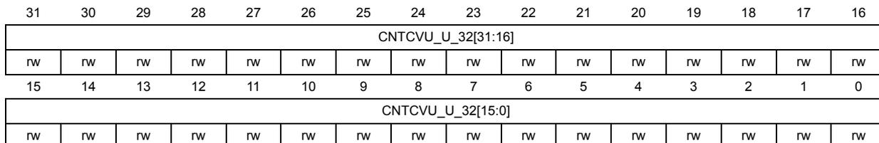
| 31 | 30 | 29 | 28 | 27 | 26 | 25 | 24 | 23 | 22 | 21 | 20 | 19 | 18 | 17 | 16 |
| CNTCVU_U_32[31:16] | |||||||||||||||
| rw | rw | rw | rw | rw | rw | rw | rw | rw | rw | rw | rw | rw | rw | rw | rw |
| 15 | 14 | 13 | 12 | 11 | 10 | 9 | 8 | 7 | 6 | 5 | 4 | 3 | 2 | 1 | 0 |
| CNTCVU_U_32[15:0] | |||||||||||||||
| rw | rw | rw | rw | rw | rw | rw | rw | rw | rw | rw | rw | rw | rw | rw | rw |
Bits 31:0 CNTCVU_U_32[31:0] : Timestamp counter current value (most significant 32 bits)
To change the current timestamp value, write the least significant 32 bits of the new value to TSG_CNTCVL before writing the most significant 32 bits to this register. The 64-bit timestamp value is updated with the value from both writes when this register is written to.
Note: EN must be cleared in TSG_CNTCR before writing to this register TSG_CNTCVU.
TSGEN base frequency ID register (TSG_CNTFID0)
Address offset: 0x020
Reset value: 0x0000 0000

| 31 | 30 | 29 | 28 | 27 | 26 | 25 | 24 | 23 | 22 | 21 | 20 | 19 | 18 | 17 | 16 |
| FREQ[31:16] | |||||||||||||||
| rw | rw | rw | rw | rw | rw | rw | rw | rw | rw | rw | rw | rw | rw | rw | rw |
| 15 | 14 | 13 | 12 | 11 | 10 | 9 | 8 | 7 | 6 | 5 | 4 | 3 | 2 | 1 | 0 |
| FREQ[15:0] | |||||||||||||||
| rw | rw | rw | rw | rw | rw | rw | rw | rw | rw | rw | rw | rw | rw | rw | rw |
Bits 31:0 FREQ[31:0] : Increment frequency of TSG counter (in Hz)
This field must be programmed with the trace generator clock frequency whenever it changes.
TSGEN CoreSight peripheral identity register 4 (TSG_PIDR4)
Address offset: 0xFD0
Reset value: 0x0000 0004
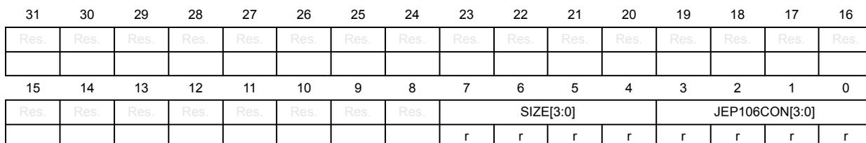
| 31 | 30 | 29 | 28 | 27 | 26 | 25 | 24 | 23 | 22 | 21 | 20 | 19 | 18 | 17 | 16 |
| Res. | Res. | Res. | Res. | Res. | Res. | Res. | Res. | Res. | Res. | Res. | Res. | Res. | Res. | Res. | Res. |
| 15 | 14 | 13 | 12 | 11 | 10 | 9 | 8 | 7 | 6 | 5 | 4 | 3 | 2 | 1 | 0 |
| Res. | Res. | Res. | Res. | Res. | Res. | Res. | Res. | SIZE[3:0] | JEP106CON[3:0] | ||||||
| r | r | r | r | r | r | r | r | ||||||||
Bits 31:8 Reserved, must be kept at reset value.
Bits 7:4 SIZE[3:0] : Register file size
0x0: register file occupies a single 4-Kbyte region.
Bits 3:0 JEP106CON[3:0] : JEP106 continuation code
0x4: Arm JEDEC code
TSGEN CoreSight peripheral identity register 0 (TSG_PIDR0)Address offset: 0xFE0
Reset value: 0x0000 0001
| 31 | 30 | 29 | 28 | 27 | 26 | 25 | 24 | 23 | 22 | 21 | 20 | 19 | 18 | 17 | 16 |
|---|---|---|---|---|---|---|---|---|---|---|---|---|---|---|---|
| Res. | Res. | Res. | Res. | Res. | Res. | Res. | Res. | Res. | Res. | Res. | Res. | Res. | Res. | Res. | Res. |
| 15 | 14 | 13 | 12 | 11 | 10 | 9 | 8 | 7 | 6 | 5 | 4 | 3 | 2 | 1 | 0 |
| Res. | Res. | Res. | Res. | Res. | Res. | Res. | Res. | PARTNUM[7:0] | |||||||
| r | r | r | r | r | r | r | r | ||||||||
Bits 31:8 Reserved, must be kept at reset value.
Bits 7:0 PARTNUM[7:0] : Part number bits [7:0]0x01: TSGEN part number
TSGEN CoreSight peripheral identity register 1 (TSG_PIDR1)Address offset: 0xFE4
Reset value: 0x0000 00B1
| 31 | 30 | 29 | 28 | 27 | 26 | 25 | 24 | 23 | 22 | 21 | 20 | 19 | 18 | 17 | 16 |
|---|---|---|---|---|---|---|---|---|---|---|---|---|---|---|---|
| Res. | Res. | Res. | Res. | Res. | Res. | Res. | Res. | Res. | Res. | Res. | Res. | Res. | Res. | Res. | Res. |
| 15 | 14 | 13 | 12 | 11 | 10 | 9 | 8 | 7 | 6 | 5 | 4 | 3 | 2 | 1 | 0 |
| Res. | Res. | Res. | Res. | Res. | Res. | Res. | Res. | JEP106ID[3:0] | PARTNUM[11:8] | ||||||
| r | r | r | r | r | r | r | r | ||||||||
Bits 31:8 Reserved, must be kept at reset value.
Bits 7:4 JEP106ID[3:0] : JEP106 identity code bits [3:0]0xB: Arm JEDEC code
Bits 3:0 PARTNUM[11:8] : part number bits [11:8]0x1: TSGEN part number
TSGEN CoreSight peripheral identity register 2 (TSG_PIDR2)Address offset: 0xFE8
Reset value: 0x0000 001B
| 31 | 30 | 29 | 28 | 27 | 26 | 25 | 24 | 23 | 22 | 21 | 20 | 19 | 18 | 17 | 16 |
|---|---|---|---|---|---|---|---|---|---|---|---|---|---|---|---|
| Res. | Res. | Res. | Res. | Res. | Res. | Res. | Res. | Res. | Res. | Res. | Res. | Res. | Res. | Res. | Res. |
| 15 | 14 | 13 | 12 | 11 | 10 | 9 | 8 | 7 | 6 | 5 | 4 | 3 | 2 | 1 | 0 |
| Res. | Res. | Res. | Res. | Res. | Res. | Res. | Res. | REVISION[3:0] | JEDEC | JEP106ID[6:4] | |||||
| r | r | r | r | r | r | r | r | ||||||||
Bits 31:8 Reserved, must be kept at reset value.
Bits 7:4 REVISION[3:0] : Component revision number
0x1: r0p1
Bit 3 JEDEC : JEDEC assigned value
0x1: Designer ID specified by JEDEC
Bits 2:0 JEP106ID[6:4] : JEP106 identity code bits [6:4]
0x3: Arm JEDEC code
TSGEN CoreSight peripheral identity register 3 (TSG_PIDR3)
Address offset: 0xFEC
Reset value: 0x0000 0000
| 31 | 30 | 29 | 28 | 27 | 26 | 25 | 24 | 23 | 22 | 21 | 20 | 19 | 18 | 17 | 16 |
|---|---|---|---|---|---|---|---|---|---|---|---|---|---|---|---|
| Res. | Res. | Res. | Res. | Res. | Res. | Res. | Res. | Res. | Res. | Res. | Res. | Res. | Res. | Res. | Res. |
| 15 | 14 | 13 | 12 | 11 | 10 | 9 | 8 | 7 | 6 | 5 | 4 | 3 | 2 | 1 | 0 |
| Res. | Res. | Res. | Res. | Res. | Res. | Res. | Res. | REVAND[3:0] | CMOD[3:0] | ||||||
| r | r | r | r | r | r | r | r | ||||||||
Bits 31:8 Reserved, must be kept at reset value.
Bits 7:4 REVAND[3:0] : Metal fix version
0x0: No metal fix
Bits 3:0 CMOD[3:0] : Customer modified
0x0: no customer modifications
TSGEN CoreSight component identity register 0 (TSG_CIDR0)
Address offset: 0xFF0
Reset value: 0x0000 000D
| 31 | 30 | 29 | 28 | 27 | 26 | 25 | 24 | 23 | 22 | 21 | 20 | 19 | 18 | 17 | 16 |
|---|---|---|---|---|---|---|---|---|---|---|---|---|---|---|---|
| Res. | Res. | Res. | Res. | Res. | Res. | Res. | Res. | Res. | Res. | Res. | Res. | Res. | Res. | Res. | Res. |
| 15 | 14 | 13 | 12 | 11 | 10 | 9 | 8 | 7 | 6 | 5 | 4 | 3 | 2 | 1 | 0 |
| Res. | Res. | Res. | Res. | Res. | Res. | Res. | Res. | PREAMBLE[7:0] | |||||||
| r | r | r | r | r | r | r | r | ||||||||
Bits 31:8 Reserved, must be kept at reset value.
Bits 7:0 PREAMBLE[7:0] : component ID bits [7:0]
0x0D: common ID value
TSGEN CoreSight peripheral identity register 1 (TSG_CIDR1)
Address offset: 0xFF4
Reset value: 0x0000 00F0
| 31 | 30 | 29 | 28 | 27 | 26 | 25 | 24 | 23 | 22 | 21 | 20 | 19 | 18 | 17 | 16 |
|---|---|---|---|---|---|---|---|---|---|---|---|---|---|---|---|
| Res. | Res. | Res. | Res. | Res. | Res. | Res. | Res. | Res. | Res. | Res. | Res. | Res. | Res. | Res. | Res. |
| 15 | 14 | 13 | 12 | 11 | 10 | 9 | 8 | 7 | 6 | 5 | 4 | 3 | 2 | 1 | 0 |
| Res. | Res. | Res. | Res. | Res. | Res. | Res. | Res. | ||||||||
| CLASS[3:0] | PREAMBLE[11:8] | ||||||||||||||
| r | r | r | r | r | r | r | r | ||||||||
Bits 31:8 Reserved, must be kept at reset value.
Bits 7:4 CLASS[3:0] : Component ID bits [15:12] - component class
0xF: CoreSight Soc-400 component
Bits 3:0 PREAMBLE[11:8] : Component ID bits [11:8]
0x0: Common ID value
TSGEN CoreSight component identity register 2 (TSG_CIDR2)
Address offset: 0xFF8
Reset value: 0x0000 0005
| 31 | 30 | 29 | 28 | 27 | 26 | 25 | 24 | 23 | 22 | 21 | 20 | 19 | 18 | 17 | 16 |
|---|---|---|---|---|---|---|---|---|---|---|---|---|---|---|---|
| Res. | Res. | Res. | Res. | Res. | Res. | Res. | Res. | Res. | Res. | Res. | Res. | Res. | Res. | Res. | Res. |
| 15 | 14 | 13 | 12 | 11 | 10 | 9 | 8 | 7 | 6 | 5 | 4 | 3 | 2 | 1 | 0 |
| Res. | Res. | Res. | Res. | Res. | Res. | Res. | Res. | ||||||||
| PREAMBLE[19:12] | |||||||||||||||
| r | r | r | r | r | r | r | r | ||||||||
Bits 31:8 Reserved, must be kept at reset value.
Bits 7:0 PREAMBLE[19:12] : component ID bits [23:16]
0x05: common ID value
TSGEN CoreSight component identity register 3 (TSG_CIDR3)
Address offset: 0xFFC
Reset value: 0x0000 00B1
| 31 | 30 | 29 | 28 | 27 | 26 | 25 | 24 | 23 | 22 | 21 | 20 | 19 | 18 | 17 | 16 |
|---|---|---|---|---|---|---|---|---|---|---|---|---|---|---|---|
| Res. | Res. | Res. | Res. | Res. | Res. | Res. | Res. | Res. | Res. | Res. | Res. | Res. | Res. | Res. | Res. |
| 15 | 14 | 13 | 12 | 11 | 10 | 9 | 8 | 7 | 6 | 5 | 4 | 3 | 2 | 1 | 0 |
| Res. | Res. | Res. | Res. | Res. | Res. | Res. | Res. | ||||||||
| PREAMBLE[27:20] | |||||||||||||||
| r | r | r | r | r | r | r | r | ||||||||
Bits 31:8 Reserved, must be kept at reset value.
Bits 7:0 PREAMBLE[27:20] : Component ID bits [31:24]
0xB1: Common ID value
TSGEN register map
Table 882. TSGEN register map and reset values
| Offset | Register name | 31 | 30 | 29 | 28 | 27 | 26 | 25 | 24 | 23 | 22 | 21 | 20 | 19 | 18 | 17 | 16 | 15 | 14 | 13 | 12 | 11 | 10 | 9 | 8 | 7 | 6 | 5 | 4 | 3 | 2 | 1 | 0 |
|---|---|---|---|---|---|---|---|---|---|---|---|---|---|---|---|---|---|---|---|---|---|---|---|---|---|---|---|---|---|---|---|---|---|
| 0x000 | TSG_CNTCR | Res. | Res. | Res. | Res. | Res. | Res. | Res. | Res. | Res. | Res. | Res. | Res. | Res. | Res. | Res. | Res. | Res. | Res. | Res. | Res. | Res. | Res. | Res. | Res. | Res. | Res. | Res. | Res. | Res. | Res. | HDBG | EN |
| Reset value | 0 | 0 | |||||||||||||||||||||||||||||||
| 0x004 | TSG_CNTSR | Res. | Res. | Res. | Res. | Res. | Res. | Res. | Res. | Res. | Res. | Res. | Res. | Res. | Res. | Res. | Res. | Res. | Res. | Res. | Res. | Res. | Res. | Res. | Res. | Res. | Res. | Res. | Res. | Res. | Res. | DBGH | Res. |
| Reset value | 0 | ||||||||||||||||||||||||||||||||
| 0x008 | TSG_CNTCVL | CNTCVU_L_32[31:0] | |||||||||||||||||||||||||||||||
| Reset value | 0 | 0 | 0 | 0 | 0 | 0 | 0 | 0 | 0 | 0 | 0 | 0 | 0 | 0 | 0 | 0 | 0 | 0 | 0 | 0 | 0 | 0 | 0 | 0 | 0 | 0 | 0 | 0 | 0 | 0 | 0 | 0 | |
| 0x00C | TSG_CNTCVU | CNTCVU_U_32[31:0] | |||||||||||||||||||||||||||||||
| Reset value | 0 | 0 | 0 | 0 | 0 | 0 | 0 | 0 | 0 | 0 | 0 | 0 | 0 | 0 | 0 | 0 | 0 | 0 | 0 | 0 | 0 | 0 | 0 | 0 | 0 | 0 | 0 | 0 | 0 | 0 | 0 | 0 | |
| 0x020 | TSG_CNTFID0 | FREQ[31:0] | |||||||||||||||||||||||||||||||
| Reset value | 0 | 0 | 0 | 0 | 0 | 0 | 0 | 0 | 0 | 0 | 0 | 0 | 0 | 0 | 0 | 0 | 0 | 0 | 0 | 0 | 0 | 0 | 0 | 0 | 0 | 0 | 0 | 0 | 0 | 0 | 0 | 0 | |
| 0x024- 0xFCC | Reserved | Reserved | |||||||||||||||||||||||||||||||
| 0xFD0 | TSG_PIDR4 | Res. | SIZE[3:0] | JEP106CON [3:0] | |||||||||||||||||||||||||||||
| Reset value | 0 | 0 | 0 | 0 | 0 | 1 | 0 | 0 | |||||||||||||||||||||||||
| 0xFD4- 0xFDC | Reserved | Reserved | |||||||||||||||||||||||||||||||
| 0xFE0 | TSG_PIDR0 | Res. | PARTNUM[7:0] | ||||||||||||||||||||||||||||||
| Reset value | 0 | 0 | 0 | 0 | 0 | 0 | 0 | 1 | |||||||||||||||||||||||||
| 0xFE4 | TSG_PIDR1 | Res. | JEP106ID [3:0] | PARTNUM [11:8] | |||||||||||||||||||||||||||||
| Reset value | 1 | 0 | 1 | 1 | 0 | 0 | 0 | 1 | |||||||||||||||||||||||||
| 0xFE8 | TSG_PIDR2 | Res. | REVISION [3:0] | JEDEC | JEP106ID [6:4] | ||||||||||||||||||||||||||||
| Reset value | 0 | 0 | 0 | 1 | 1 | 0 | 1 | 1 | |||||||||||||||||||||||||
| 0xFEC | TSG_PIDR3 | Res. | REVAND [3:0] | CMOD[3:0] | |||||||||||||||||||||||||||||
| Reset value | 0 | 0 | 0 | 0 | 0 | 0 | 0 | 0 | |||||||||||||||||||||||||
| 0xFF0 | TSG_CIDR0 | Res. | PREAMBLE[7:0] | ||||||||||||||||||||||||||||||
| Reset value | 0 | 0 | 0 | 0 | 1 | 1 | 0 | 1 | |||||||||||||||||||||||||
| 0xFF4 | TSG_CIDR1 | Res. | CLASS[3:0] | PREAMBLE [11:8] | |||||||||||||||||||||||||||||
| Reset value | 1 | 1 | 1 | 1 | 0 | 0 | 0 | 0 | |||||||||||||||||||||||||
Table 882. TSGEN register map and reset values (continued)
| Offset | Register name | 31 | 30 | 29 | 28 | 27 | 26 | 25 | 24 | 23 | 22 | 21 | 20 | 19 | 18 | 17 | 16 | 15 | 14 | 13 | 12 | 11 | 10 | 9 | 8 | 7 | 6 | 5 | 4 | 3 | 2 | 1 | 0 |
|---|---|---|---|---|---|---|---|---|---|---|---|---|---|---|---|---|---|---|---|---|---|---|---|---|---|---|---|---|---|---|---|---|---|
| 0xFF8 | TSG_CIDR2 | Res. | Res. | Res. | Res. | Res. | Res. | Res. | Res. | Res. | Res. | Res. | Res. | Res. | Res. | Res. | Res. | Res. | Res. | Res. | Res. | Res. | Res. | Res. | Res. | PREAMBLE[19:12] | |||||||
| Reset value | 0 | 0 | 0 | 0 | 0 | 1 | 0 | 1 | |||||||||||||||||||||||||
| 0xFFC | TSG_CIDR3 | Res. | Res. | Res. | Res. | Res. | Res. | Res. | Res. | Res. | Res. | Res. | Res. | Res. | Res. | Res. | Res. | Res. | Res. | Res. | Res. | Res. | Res. | Res. | Res. | PREAMBLE[27:20] | |||||||
| Reset value | 1 | 0 | 1 | 1 | 0 | 0 | 0 | 1 | |||||||||||||||||||||||||
78.12.4 Cross trigger interface (CTI) and matrix (CTM)
The CTI and CTM together form the CoreSight embedded cross trigger feature. There are three CTI components: two in the trace and debug subsystem, and one dedicated to the Cortex-M55.
The CTIs are connected to each other via the CTM. The trace and debug subsystem CTIs and the Cortex-M55 CTI are accessible on the PPB (private peripheral bus) via the Cortex-M55.
Figure 1083. Embedded cross trigger
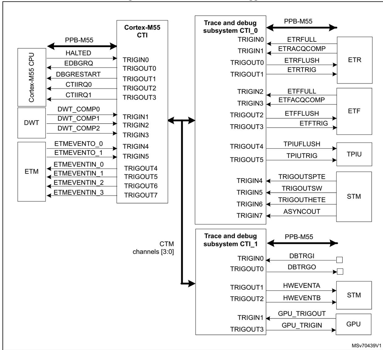
The diagram illustrates the embedded cross trigger architecture. On the left, the Cortex-M55 CPU, DWT, and ETM are shown. The CPU has signals HALTED, EDBGREQ, DBGRESTART, CTIIRQ0, and CTIIRQ1. The DWT has signals DWT_COMP0, DWT_COMP1, and DWT_COMP2. The ETM has signals ETMEVENTO_0, ETMEVENTO_1, ETMEVENTIN_0, ETMEVENTIN_1, ETMEVENTIN_2, and ETMEVENTIN_3. These signals are connected to the Cortex-M55 CTI. The CTI has eight trigger inputs (TRIGIN0-TRIGIN7) and eight trigger outputs (TRIGOUT0-TRIGOUT7). The CTI is connected to the Trace and debug subsystem CTI_0 and CTI_1 via CTM channels [3:0]. CTI_0 has eight trigger inputs (TRIGIN0-TRIGIN7) and eight trigger outputs (TRIGOUT0-TRIGOUT7). CTI_1 has four trigger inputs (TRIGIN0-TRIGIN3) and four trigger outputs (TRIGOUT0-TRIGOUT3). The subsystems are connected to various components: ETR, ETF, TPIU, STM, and GPU. The diagram also shows connections to PPB-M55 and MSv70439V1.
The CTIs allow events from various sources to trigger debug and/or trace activity. For example, a transition detected on an external trigger input can start code trace.
Each CTI has up to eight trigger inputs and eight trigger outputs. Any input can be connected to any output, on the same CTI, or on another CTI via the CTM.
The trigger input and output signals for each CTI are listed in the following tables.
Table 883. Trace and debug subsystem CTI_0 inputs| - | Source signal | Source component | Comments |
|---|---|---|---|
| 0 | ETRFULL | ETR | ETR full flag: allows a debug event to be generated when the trace buffer is full. |
| 1 | ETRACQCOMP | ETR | ETR capture finished: allows a debug event to be generated when trace acquisition is complete. |
| 2 | ETFFULL | ETF | ETF full flag: allows a debug event to be generated when the trace FIFO is full. |
| 3 | ETFACQCOMP | ETF | ETF capture finished: allows a debug event to be generated when the trace FIFO is empty. |
| 4 | TRIGOUTSPTE | STM | The STM asserts this signal for one clock cycle when a trigger event is detected on a match using the STMSPTER. |
| 5 | TRIGOUTSW | STM | The STM asserts this signal for one clock cycle when a trigger event is generated on writes to a TRIG location in the extended stimulus port registers. |
| 6 | TRIGOUTHETE | STM | The STM asserts this signal for one clock cycle when a trigger event is detected on a match using the STMHETER. |
| 7 | ASYNCOUT | STM | Alignment synchronization signal. The STM asserts this signal for one clock cycle when an ASYNC-VERSION-FREQ sequence is output on the ATB interface, and the ASYNCOUT signal can be used for cross-triggering. |
| - | Output signal | Destination component | Comments |
|---|---|---|---|
| 0 | ETRFLUSH | ETR | ETR flush trigger: causes the trace sources to be flushed into destination memory. |
| 1 | ETRTRIG | ETR | ETR trigger: causes various kinds of flush, stops the TMC, and causes additional trigger insertion. |
| 2 | ETFFLUSH | ETF | ETF flush trigger: causes the trace FIFO to be flushed. |
| 3 | ETFTRIG | ETF | ETF enable trigger: starts filling the trace FIFO. |
| 4 | TPIUFLUSH | TPIU | Trace port flush trigger: causes the TPIU FIFO to be flushed. |
| 5 | TPIUTRIG | TPIU | Trace Port enable trigger: starts trace output on the external trace port. |
| 6 | - | - | Not used |
| 7 | - | - | Not used |
| - | Source signal | Source component | Comments |
|---|---|---|---|
| 0 | DBTRIGI | GPIO | External trigger input: allows an external signal to generate a debug event. |
| 1 | GPU_TRIGOUT | GPU | Trigger out from GPU |
| 2 | - | - | Not used |
| 3 | - | - | Not used |
| 4 | - | - | Not used |
Table 885. Trace and debug subsystem CTI_1 inputs (continued)
| - | Source signal | Source component | Comments |
|---|---|---|---|
| 5 | - | - | Not used |
| 6 | - | - | Not used |
| 7 | - | - | Not used |
Table 886. Trace and debug subsystem CTI_1 outputs
| - | Output signal | Destination component | Comments |
|---|---|---|---|
| 0 | DBTRIGO | GPIO | External I/O trigger output: allows monitoring events on the external DBTRIGO pin. |
| 1 | HWEVENTA | STM | STM hardware event |
| 2 | HWEVENTB | STM | STM hardware event |
| 3 | GPU_TRIGIN | GPU | Trigger in to GPU |
| 4 | - | - | Not used |
| 5 | - | - | Not used |
| 6 | - | - | Not used |
| 7 | - | - | Not used |
Table 887. Cortex-M55 CTI inputs
| - | Source signal | Source component | Comments |
|---|---|---|---|
| 0 | HALTED | M55 CPU | Pulsed high when the core enters in debug state |
| 1 | DWTCOMP_0 | M55 DWT | DWT comparator output |
| 2 | DWTCOMP_1 | M55 DWT | DWT comparator output |
| 3 | DWTCOMP_2 | M55 DWT | DWT comparator output |
| 4 | ETMEVENTO_0 | M55 ETM | ETM event output |
| 5 | ETMEVENTO_1 | M55 ETM | ETM event output |
| 6 | - | - | Not used |
| 7 | - | - | Not used |
Table 888. Cortex-M55 CTI outputs
| - | Source signal | Destination component | Comments |
|---|---|---|---|
| 0 | EDBGRQ | M55 CPU | CPU halt request - puts CPU in debug mode |
| 1 | DBGRESTART | M55 CPU | CPU restart request - CPU exits debug mode |
| 2 | IRQ0 | M55 NVIC | CTI interrupt |
| 3 | IRQ1 | M55 NVIC | CTI interrupt |
Table 888. Cortex-M55 CTI outputs (continued)
| - | Source signal | Destination component | Comments |
|---|---|---|---|
| 4 | ETMEVENTIN_0 | M55 ETM | ETM event input |
| 5 | ETMEVENTIN_1 | M55 ETM | ETM event input |
| 6 | ETMEVENTIN_2 | M55 ETM | ETM event input |
| 7 | ETMEVENTIN_3 | M55 ETM | ETM event input |
There are four event channels in a cross trigger matrix, which allows up to four, parallel, bidirectional connections between trigger inputs and outputs on different CTIs.
To connect input number \( m \) on CTI \( x \) to output number \( n \) on CTI \( y \) , the input must be connected to an event channel \( p \) using the CTIINEN \( m \) register of CTI \( x \) . The same channel \( p \) must be connected to the output using the CTIOUTEN \( n \) register of CTI \( y \) .
Note: This applies even if the input and output belong to the same CTI.
An input can be connected to more than one channel (up to four). An input can then be routed to several outputs. Similarly, an output can be connected to several inputs. It is also possible to connect several inputs/outputs to the same channel.
Figure 1084. Mapping trigger inputs to outputs
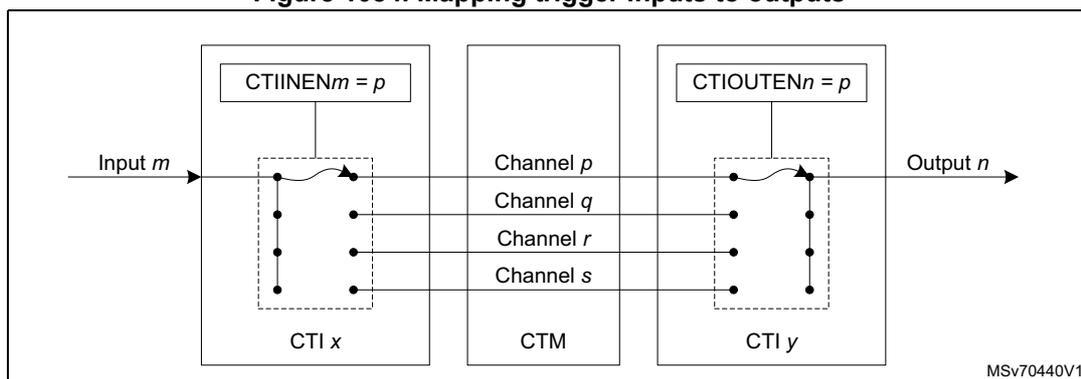
The diagram shows the internal architecture of the Cross Trigger Interface (CTI) for mapping inputs to outputs. On the left, 'Input m' enters a block labeled 'CTI x'. Inside this block, a register labeled 'CTIINEN \( m = p \) ' is connected to a switch mechanism. This switch can connect 'Input m' to one of four channels in the central 'CTM' (Cross Trigger Matrix) block, specifically 'Channel p'. The other three channels are labeled 'Channel q', 'Channel r', and 'Channel s'. On the right, another block labeled 'CTI y' contains a register labeled 'CTIOUTEN \( n = p \) '. This register is connected to a switch mechanism that can connect 'Channel p' from the CTM to 'Output n'. The diagram illustrates that the same channel 'p' is used for both the input and output connection. A small code 'MSV70440V1' is visible in the bottom right corner of the diagram area.
For more information on the cross-trigger interface CoreSight component, refer to the Arm CoreSight SoC-400 Technical Reference Manual [2].
78.12.5 CTI registers
The register file base addresses for CTI_0 and CTI_1 in the trace and debug subsystem are defined in Table 880. The register file base address for the Cortex-M55 CTI is defined in Table 873. Registers are the same for each CTI.
CTI control register (CTI_CONTROL)
Address offset: 0x000
Reset value: 0x0000 0000
| 31 | 30 | 29 | 28 | 27 | 26 | 25 | 24 | 23 | 22 | 21 | 20 | 19 | 18 | 17 | 16 |
|---|---|---|---|---|---|---|---|---|---|---|---|---|---|---|---|
| Res. | Res. | Res. | Res. | Res. | Res. | Res. | Res. | Res. | Res. | Res. | Res. | Res. | Res. | Res. | Res. |
| 15 | 14 | 13 | 12 | 11 | 10 | 9 | 8 | 7 | 6 | 5 | 4 | 3 | 2 | 1 | 0 |
| Res. | Res. | Res. | Res. | Res. | Res. | Res. | Res. | Res. | Res. | Res. | Res. | Res. | Res. | Res. | GLBEN |
| rw |
Bits 31:1 Reserved, must be kept at reset value.
Bit 0 GLBEN : Global enable
0: Cross-triggering disabled
1: Cross-triggering enabled
CTI trigger acknowledge register (CTI_INTACK)
Address offset: 0x010
Reset value: 0x0000 0000
| 31 | 30 | 29 | 28 | 27 | 26 | 25 | 24 | 23 | 22 | 21 | 20 | 19 | 18 | 17 | 16 |
|---|---|---|---|---|---|---|---|---|---|---|---|---|---|---|---|
| Res. | Res. | Res. | Res. | Res. | Res. | Res. | Res. | Res. | Res. | Res. | Res. | Res. | Res. | Res. | Res. |
| 15 | 14 | 13 | 12 | 11 | 10 | 9 | 8 | 7 | 6 | 5 | 4 | 3 | 2 | 1 | 0 |
| Res. | Res. | Res. | Res. | Res. | Res. | Res. | Res. | INTACK[7:0] | |||||||
| rw | rw | rw | rw | rw | rw | rw | rw | ||||||||
Bits 31:8 Reserved, must be kept at reset value.
Bits 7:0 INTACK[7:0] : Trigger acknowledge
There is one bit of this register for each CTITRIGOUT output. When a one is written to a bit, the corresponding CTITRIGOUT output is acknowledged, causing it to be cleared.
CTI application trigger set register (CTI_APPSET)
Address offset: 0x014
Reset value: 0x0000 0000
| 31 | 30 | 29 | 28 | 27 | 26 | 25 | 24 | 23 | 22 | 21 | 20 | 19 | 18 | 17 | 16 |
|---|---|---|---|---|---|---|---|---|---|---|---|---|---|---|---|
| Res. | Res. | Res. | Res. | Res. | Res. | Res. | Res. | Res. | Res. | Res. | Res. | Res. | Res. | Res. | Res. |
| 15 | 14 | 13 | 12 | 11 | 10 | 9 | 8 | 7 | 6 | 5 | 4 | 3 | 2 | 1 | 0 |
| Res. | Res. | Res. | Res. | Res. | Res. | Res. | Res. | Res. | Res. | Res. | Res. | APPSET[3:0] | |||
| rw | rw | rw | rw | ||||||||||||
Bits 31:4 Reserved, must be kept at reset value.
Bits 3:0 APPSET[3:0] : Channel event set
Read:
- xxx0: Channel 0 event inactive
- xxx1: Channel 0 event active
- xx0x: Channel 1 event inactive
- xx1x: Channel 1 event active
- x0xx: Channel 2 event inactive
- x1xx: Channel 2 event active
- 0xxx: Channel 3 event inactive
- 1xxx: Channel 3 event active
Write:
- xxx0: No effect
- xxx1: Set event on channel 0.
- xx0x: No effect
- xx1x: Set event on channel 1.
- x0xx: No effect
- x1xx: Set event on channel 2.
- 0xxx: No effect
- 1xxx: Set event on channel 3.
CTI application trigger clear register (CTI_APPCLEAR)
Address offset: 0x018
Reset value: 0x0000 0000
| 31 | 30 | 29 | 28 | 27 | 26 | 25 | 24 | 23 | 22 | 21 | 20 | 19 | 18 | 17 | 16 |
|---|---|---|---|---|---|---|---|---|---|---|---|---|---|---|---|
| Res. | Res. | Res. | Res. | Res. | Res. | Res. | Res. | Res. | Res. | Res. | Res. | Res. | Res. | Res. | Res. |
| 15 | 14 | 13 | 12 | 11 | 10 | 9 | 8 | 7 | 6 | 5 | 4 | 3 | 2 | 1 | 0 |
| Res. | Res. | Res. | Res. | Res. | Res. | Res. | Res. | Res. | Res. | Res. | Res. | APPCLEAR[3:0] | |||
| w | w | w | w | ||||||||||||
Bits 31:4 Reserved, must be kept at reset value.
Bits 3:0 APPCLEAR[3:0] : Channel event clear
- xxx0: No effect
- xxx1: Clear event on channel 0.
- xx0x: No effect
- xx1x: Clear event on channel 1.
- x0xx: No effect
- x1xx: Clear event on channel 2.
- 0xxx: No effect
- 1xxx: Clear event on channel 3.
CTI application pulse register (CTI_APPPULSE)
Address offset: 0x01C
Reset value: 0x0000 0000
| 31 | 30 | 29 | 28 | 27 | 26 | 25 | 24 | 23 | 22 | 21 | 20 | 19 | 18 | 17 | 16 |
|---|---|---|---|---|---|---|---|---|---|---|---|---|---|---|---|
| Res. | Res. | Res. | Res. | Res. | Res. | Res. | Res. | Res. | Res. | Res. | Res. | Res. | Res. | Res. | Res. |
| 15 | 14 | 13 | 12 | 11 | 10 | 9 | 8 | 7 | 6 | 5 | 4 | 3 | 2 | 1 | 0 |
| Res. | Res. | Res. | Res. | Res. | Res. | Res. | Res. | Res. | Res. | Res. | Res. | APPPULSE[3:0] | |||
| w | w | w | w | ||||||||||||
Bits 31:4 Reserved, must be kept at reset value.
Bits 3:0 APPPULSE[3:0] : Pulse channel event
This bitfield clears itself immediately.
xxx0: No effect
xxx1: Generate pulse on channel 0.
xx0x: No effect
xx1x: Generate pulse on channel 1.
x0xx: No effect
x1xx: Generate pulse on channel 2.
0xxx: No effect
1xxx: Generate pulse on channel 3.
CTI trigger IN x enable register (CTI_INENx)
Address offset: 0x020 + 0x4 * x (x = 0 to 7)
Reset value: 0x0000 0000
| 31 | 30 | 29 | 28 | 27 | 26 | 25 | 24 | 23 | 22 | 21 | 20 | 19 | 18 | 17 | 16 |
|---|---|---|---|---|---|---|---|---|---|---|---|---|---|---|---|
| Res. | Res. | Res. | Res. | Res. | Res. | Res. | Res. | Res. | Res. | Res. | Res. | Res. | Res. | Res. | Res. |
| 15 | 14 | 13 | 12 | 11 | 10 | 9 | 8 | 7 | 6 | 5 | 4 | 3 | 2 | 1 | 0 |
| Res. | Res. | Res. | Res. | Res. | Res. | Res. | Res. | Res. | Res. | Res. | Res. | TRIGINEN[3:0] | |||
Bits 31:4 Reserved, must be kept at reset value.
Bits 3:0 TRIGINEN[3:0] : Cross-trigger event enable
This bitfield enables or disables a cross-trigger event on each of the four channels when CTITRIGINx is activated (x = 0 to 7).
xxx0: Trigger n does not generate events on channel 0.
xxx1: Trigger n generates events on channel 0.
xx0x: Trigger n does not generate events on channel 1.
xx1x: Trigger n generates events on channel 1.
x0xx: Trigger n does not generate events on channel 2.
x1xx: Trigger n generates events on channel 2.
0xxx: Trigger n does not generate events on channel 3.
1xxx: Trigger n generates events on channel 3.
CTI trigger OUT x enable register (CTI_OUTENx)
Address offset: 0x0A0 + 0x4 * x (x = 0 to 7)
Reset value: 0x0000 0000
| 31 | 30 | 29 | 28 | 27 | 26 | 25 | 24 | 23 | 22 | 21 | 20 | 19 | 18 | 17 | 16 |
|---|---|---|---|---|---|---|---|---|---|---|---|---|---|---|---|
| Res. | Res. | Res. | Res. | Res. | Res. | Res. | Res. | Res. | Res. | Res. | Res. | Res. | Res. | Res. | Res. |
| 15 | 14 | 13 | 12 | 11 | 10 | 9 | 8 | 7 | 6 | 5 | 4 | 3 | 2 | 1 | 0 |
| Res. | Res. | Res. | Res. | Res. | Res. | Res. | Res. | Res. | Res. | Res. | Res. | TRIGOUTEN[3:0] | |||
| rw | rw | rw | rw | ||||||||||||
Bits 31:4 Reserved, must be kept at reset value.
Bits 3:0 TRIGOUTEN[3:0] : Enable trigger upon event
For each channel, this bitfield defines whether an event on that channel generates a trigger on CTITRIGOUTx (x = 0 to 7).
xxx0: Channel 0 events do not generate triggers on trigger output n.
xx11: Channel 0 events generate triggers on trigger output n.
xx0x: Channel 1 events do not generate triggers on trigger output n.
xx1x: Channel 1 events generate triggers on trigger output n.
x0xx: Channel 2 events do not generate triggers on trigger output n.
x1xx: Channel 2 events generate triggers on trigger output n.
0xxx: Channel 3 events generate triggers on trigger output n.
CTI trigger IN status register (CTI_TRGISTS)
Address offset: 0x130
Reset value: 0x0000 0000
| 31 | 30 | 29 | 28 | 27 | 26 | 25 | 24 | 23 | 22 | 21 | 20 | 19 | 18 | 17 | 16 |
|---|---|---|---|---|---|---|---|---|---|---|---|---|---|---|---|
| Res. | Res. | Res. | Res. | Res. | Res. | Res. | Res. | Res. | Res. | Res. | Res. | Res. | Res. | Res. | Res. |
| 15 | 14 | 13 | 12 | 11 | 10 | 9 | 8 | 7 | 6 | 5 | 4 | 3 | 2 | 1 | 0 |
| Res. | Res. | Res. | Res. | Res. | Res. | Res. | Res. | TRIGINSTATUS[7:0] | |||||||
| r | r | r | r | r | r | r | r | ||||||||
Bits 31:8 Reserved, must be kept at reset value.
Bits 7:0 TRIGINSTATUS[7:0] : Trigger input status
There is one bit of this bitfield for each CTITRIGIN input. When a bit is set to 1, it indicates that the corresponding trigger input is active. When it is set to 0, the corresponding trigger input is inactive.
CTI trigger OUT status register (CTI_TRGOSTS)
Address offset: 0x134
Reset value: 0x0000 0000
| 31 | 30 | 29 | 28 | 27 | 26 | 25 | 24 | 23 | 22 | 21 | 20 | 19 | 18 | 17 | 16 |
|---|---|---|---|---|---|---|---|---|---|---|---|---|---|---|---|
| Res. | Res. | Res. | Res. | Res. | Res. | Res. | Res. | Res. | Res. | Res. | Res. | Res. | Res. | Res. | Res. |
| 15 | 14 | 13 | 12 | 11 | 10 | 9 | 8 | 7 | 6 | 5 | 4 | 3 | 2 | 1 | 0 |
| Res. | Res. | Res. | Res. | Res. | Res. | Res. | Res. | TRIGOUTSTATUS[7:0] | |||||||
| r | r | r | r | r | r | r | r | ||||||||
Bits 31:8 Reserved, must be kept at reset value.
Bits 7:0 TRIGOUTSTATUS[7:0] : Trigger output status
There is one bit of this bitfield for each CTITRIGOUT output. When a bit is set to 1, it indicates that the corresponding trigger output is active. When it is set to 0, the corresponding trigger output is inactive.
CTI channel IN status register (CTI_CHINSTS)
Address offset: 0x138
Reset value: 0x0000 0000
| 31 | 30 | 29 | 28 | 27 | 26 | 25 | 24 | 23 | 22 | 21 | 20 | 19 | 18 | 17 | 16 |
|---|---|---|---|---|---|---|---|---|---|---|---|---|---|---|---|
| Res. | Res. | Res. | Res. | Res. | Res. | Res. | Res. | Res. | Res. | Res. | Res. | Res. | Res. | Res. | Res. |
| 15 | 14 | 13 | 12 | 11 | 10 | 9 | 8 | 7 | 6 | 5 | 4 | 3 | 2 | 1 | 0 |
| Res. | Res. | Res. | Res. | Res. | Res. | Res. | Res. | Res. | Res. | Res. | Res. | CHINSTATUS[3:0] | |||
| r | r | r | r | ||||||||||||
Bits 31:4 Reserved, must be kept at reset value.
Bits 3:0 CHINSTATUS[3:0] : Channel input status
There is one bit of this bitfield for each channel input. When a bit is set to 1, it indicates that the corresponding channel input is active. When it is set to 0, the corresponding channel input is inactive.
CTI channel OUT status register (CTI_CHOUTSTS)
Address offset: 0x13C
Reset value: 0x0000 0000
| 31 | 30 | 29 | 28 | 27 | 26 | 25 | 24 | 23 | 22 | 21 | 20 | 19 | 18 | 17 | 16 |
|---|---|---|---|---|---|---|---|---|---|---|---|---|---|---|---|
| Res. | Res. | Res. | Res. | Res. | Res. | Res. | Res. | Res. | Res. | Res. | Res. | Res. | Res. | Res. | Res. |
| 15 | 14 | 13 | 12 | 11 | 10 | 9 | 8 | 7 | 6 | 5 | 4 | 3 | 2 | 1 | 0 |
| Res. | Res. | Res. | Res. | Res. | Res. | Res. | Res. | Res. | Res. | Res. | Res. | CHOUTSTATUS[3:0] | |||
| r | r | r | r | ||||||||||||
Bits 31:4 Reserved, must be kept at reset value.
Bits 3:0 CHOUTSTATUS[3:0] : Channel output status
There is one bit of this bitfield for each channel output. When a bit is set to 1, it indicates that the corresponding channel output is active. When it is set to 0, the corresponding channel output is inactive.
CTI channel gate register (CTI_GATE)
Address offset: 0x140
Reset value: 0x0000 000F
| 31 | 30 | 29 | 28 | 27 | 26 | 25 | 24 | 23 | 22 | 21 | 20 | 19 | 18 | 17 | 16 |
|---|---|---|---|---|---|---|---|---|---|---|---|---|---|---|---|
| Res. | Res. | Res. | Res. | Res. | Res. | Res. | Res. | Res. | Res. | Res. | Res. | Res. | Res. | Res. | Res. |
| 15 | 14 | 13 | 12 | 11 | 10 | 9 | 8 | 7 | 6 | 5 | 4 | 3 | 2 | 1 | 0 |
| Res. | Res. | Res. | Res. | Res. | Res. | Res. | Res. | Res. | Res. | Res. | Res. | GATEEN[3:0] | |||
| rw | rw | rw | rw | ||||||||||||
Bits 31:4 Reserved, must be kept at reset value.
Bits 3:0 GATEEN[3:0] : Channel output enable
For each channel, a bit defines whether an event on that channel can propagate over the CTM to other CTIs.
xxx0: Channel 0 events do not propagate.
xxx1: Channel 0 events propagate.
xx0x: Channel 1 events do not propagate.
xx1x: Channel 1 events propagate.
x0xx: Channel 2 events do not propagate.
x1xx: Channel 2 events propagate.
0xxx: Channel 3 events do not propagate.
1xxx: Channel 3 events propagate.
CTI claim tag set register (CTI_CLAIMSET)
Address offset: 0xFA0
Reset value: 0x0000 000F
| 31 | 30 | 29 | 28 | 27 | 26 | 25 | 24 | 23 | 22 | 21 | 20 | 19 | 18 | 17 | 16 |
|---|---|---|---|---|---|---|---|---|---|---|---|---|---|---|---|
| Res. | Res. | Res. | Res. | Res. | Res. | Res. | Res. | Res. | Res. | Res. | Res. | Res. | Res. | Res. | Res. |
| 15 | 14 | 13 | 12 | 11 | 10 | 9 | 8 | 7 | 6 | 5 | 4 | 3 | 2 | 1 | 0 |
| Res. | Res. | Res. | Res. | Res. | Res. | Res. | Res. | Res. | Res. | Res. | Res. | CLAIMSET[3:0] | |||
Bits 31:4 Reserved, must be kept at reset value.
Bits 3:0 CLAIMSET[3:0] : Set claim tag bits
Write:
0000: No effect
xxx1: Set bit 0.
xx1x: Set bit 1.
x1xx: Set bit 2.
1xxx: Set bit 3.
Read:
0xF: Indicate there are four bits in claim tag.
CTI claim tag clear register (CTI_CLAIMCLR)
Address offset: 0xFA4
Reset value: 0x0000 0000
| 31 | 30 | 29 | 28 | 27 | 26 | 25 | 24 | 23 | 22 | 21 | 20 | 19 | 18 | 17 | 16 |
|---|---|---|---|---|---|---|---|---|---|---|---|---|---|---|---|
| Res. | Res. | Res. | Res. | Res. | Res. | Res. | Res. | Res. | Res. | Res. | Res. | Res. | Res. | Res. | Res. |
| 15 | 14 | 13 | 12 | 11 | 10 | 9 | 8 | 7 | 6 | 5 | 4 | 3 | 2 | 1 | 0 |
| Res. | Res. | Res. | Res. | Res. | Res. | Res. | Res. | Res. | Res. | Res. | Res. | CLAIMCLR[3:0] | |||
| rw | rw | rw | rw | ||||||||||||
Bits 31:4 Reserved, must be kept at reset value.
Bits 3:0 CLAIMCLR[3:0] : Reset claim tag bits
Write:
0000: No effect
xxx1: Clear bit 0.
xx1x: Clear bit 1.
x1xx: Clear bit 2.
1xxx: Clear bit 3.
Read: Return current value of claim tag.
CTI lock access register (CTI_LAR)
Address offset: 0xFB0
Reset value: 0xFFFF XXXX
| 31 | 30 | 29 | 28 | 27 | 26 | 25 | 24 | 23 | 22 | 21 | 20 | 19 | 18 | 17 | 16 |
|---|---|---|---|---|---|---|---|---|---|---|---|---|---|---|---|
| ACCESS_W[31:16] | |||||||||||||||
| w | w | w | w | w | w | w | w | w | w | w | w | w | w | w | w |
| 15 | 14 | 13 | 12 | 11 | 10 | 9 | 8 | 7 | 6 | 5 | 4 | 3 | 2 | 1 | 0 |
| ACCESS_W[15:0] | |||||||||||||||
| w | w | w | w | w | w | w | w | w | w | w | w | w | w | w | w |
Bits 31:0 ACCESS_W[31:0] : CTI register write access enable
This bitfield enables write access to some CTI registers by the processor core (debuggers do not need to unlock the component).
0xC5ACCE55: Enable write access.
Other values: Disable write access.
CTI lock status register (CTI_LSR)
Address offset: 0xFB4
Reset value: 0x0000 0003
| 31 | 30 | 29 | 28 | 27 | 26 | 25 | 24 | 23 | 22 | 21 | 20 | 19 | 18 | 17 | 16 |
|---|---|---|---|---|---|---|---|---|---|---|---|---|---|---|---|
| Res. | Res. | Res. | Res. | Res. | Res. | Res. | Res. | Res. | Res. | Res. | Res. | Res. | Res. | Res. | Res. |
| 15 | 14 | 13 | 12 | 11 | 10 | 9 | 8 | 7 | 6 | 5 | 4 | 3 | 2 | 1 | 0 |
| Res. | Res. | Res. | Res. | Res. | Res. | Res. | Res. | Res. | Res. | Res. | Res. | Res. | LOCKTYPE | LOCKGRANT | LOCKEXIST |
| r | r | r |
Bits 31:3 Reserved, must be kept at reset value.
Bit 2 LOCKTYPE : Size of the CTI_LAR register
0: 32 bits
Bit 1 LOCKGRANT : Current status of lock
This bit always returns 0 when read by an external debugger.
0: Write access is permitted.
1: Write access is blocked. Only read access is permitted.
Bit 0 LOCKEXIST : Existence of lock control mechanism
The bit indicates whether a lock control mechanism exists. It always returns 0 when read by an external debugger.
0: No lock control mechanism exists.
1: Lock control mechanism is implemented.
CTI authentication status register (CTI_AUTHSTAT)
Address offset: 0xFB8
Reset value: 0x0000 000A
| 31 | 30 | 29 | 28 | 27 | 26 | 25 | 24 | 23 | 22 | 21 | 20 | 19 | 18 | 17 | 16 |
|---|---|---|---|---|---|---|---|---|---|---|---|---|---|---|---|
| Res. | Res. | Res. | Res. | Res. | Res. | Res. | Res. | Res. | Res. | Res. | Res. | Res. | Res. | Res. | Res. |
| 15 | 14 | 13 | 12 | 11 | 10 | 9 | 8 | 7 | 6 | 5 | 4 | 3 | 2 | 1 | 0 |
| Res. | Res. | Res. | Res. | Res. | Res. | Res. | Res. | SNID[1:0] | SID[1:0] | NSNID[1:0] | NSID[1:0] | ||||
| r | r | r | r | r | r | r | r |
Bits 31:8 Reserved, must be kept at reset value.
Bits 7:6 SNID[1:0] : Security level for secure non-invasive debug
0x0: Not implemented
Bits 5:4 SID[1:0] : Security level for secure invasive debug
0x0: Not implemented
Bits 3:2 NSNID[1:0] : Security level for nonsecure non-invasive debug
0x2: Disabled
0x3: Enabled
Bits 1:0 NSID[1:0] : Security level for nonsecure invasive debug
0x2: Disabled
0x3: Enabled
CTI device configuration register (CTI_DEVID)
Address offset: 0xFC8
Reset value: 0x0004 0800
| 31 | 30 | 29 | 28 | 27 | 26 | 25 | 24 | 23 | 22 | 21 | 20 | 19 | 18 | 17 | 16 |
|---|---|---|---|---|---|---|---|---|---|---|---|---|---|---|---|
| Res. | Res. | Res. | Res. | Res. | Res. | Res. | Res. | Res. | Res. | Res. | Res. | NUMCH[3:0] | |||
| r | r | r | r | ||||||||||||
| 15 | 14 | 13 | 12 | 11 | 10 | 9 | 8 | 7 | 6 | 5 | 4 | 3 | 2 | 1 | 0 |
| NUMTRIG[7:0] | Res. | Res. | Res. | EXTMUXNUM[4:0] | |||||||||||
| r | r | r | r | r | r | r | r | r | r | r | r | r |
Bits 31:20 Reserved, must be kept at reset value.
Bits 19:16 NUMCH[3:0] : Number of ECT channels available
0x4: Four channels
Bits 15:8 NUMTRIG[7:0] : Number of ECT triggers available
0x8: Eight trigger inputs and eight trigger outputs
Bits 7:5 Reserved, must be kept at reset value.
Bits 4:0 EXTMUXNUM[4:0] : Number of trigger input/output multiplexers
0x0: None
CTI device type identifier register (CTI_DEVTYPE)
Address offset: 0xFCC
Reset value: 0x0000 0014
| 31 | 30 | 29 | 28 | 27 | 26 | 25 | 24 | 23 | 22 | 21 | 20 | 19 | 18 | 17 | 16 |
|---|---|---|---|---|---|---|---|---|---|---|---|---|---|---|---|
| Res. | Res. | Res. | Res. | Res. | Res. | Res. | Res. | Res. | Res. | Res. | Res. | Res. | Res. | Res. | Res. |
| 15 | 14 | 13 | 12 | 11 | 10 | 9 | 8 | 7 | 6 | 5 | 4 | 3 | 2 | 1 | 0 |
| Res. | Res. | Res. | Res. | Res. | Res. | Res. | Res. | SUBTYPE[3:0] | MAJORTYPE[3:0] | ||||||
| r | r | r | r | r | r | r | r | ||||||||
Bits 31:8 Reserved, must be kept at reset value.
Bits 7:4 SUBTYPE[3:0] : Sub-classification
0x1: This bitfield indicates that this component is a cross-triggering component.
Bits 3:0 MAJORTYPE[3:0] : Major classification
0x4: This bitfield indicates that this component allows a debugger to control other components in a CoreSight SoC-400 system.
CTI CoreSight peripheral identity register 4 (CTI_PIDR4)
Address offset: 0xFD0
Reset value: 0x0000 0004
| 31 | 30 | 29 | 28 | 27 | 26 | 25 | 24 | 23 | 22 | 21 | 20 | 19 | 18 | 17 | 16 |
|---|---|---|---|---|---|---|---|---|---|---|---|---|---|---|---|
| Res. | Res. | Res. | Res. | Res. | Res. | Res. | Res. | Res. | Res. | Res. | Res. | Res. | Res. | Res. | Res. |
| 15 | 14 | 13 | 12 | 11 | 10 | 9 | 8 | 7 | 6 | 5 | 4 | 3 | 2 | 1 | 0 |
| Res. | Res. | Res. | Res. | Res. | Res. | Res. | Res. | SIZE[3:0] | JEP106CON[3:0] | ||||||
| r | r | r | r | r | r | r | r | ||||||||
Bits 31:8 Reserved, must be kept at reset value.
Bits 7:4 SIZE[3:0] : Register file size
0x0: Register file occupies a single 4-Kbyte region.
Bits 3:0 JEP106CON[3:0] : JEP106 continuation code
0x4: Arm JEDEC code
CTI CoreSight peripheral identity register 0 (CTI_PIDR0)
Address offset: 0xFE0
Reset value: 0x0000 0006
| 31 | 30 | 29 | 28 | 27 | 26 | 25 | 24 | 23 | 22 | 21 | 20 | 19 | 18 | 17 | 16 |
|---|---|---|---|---|---|---|---|---|---|---|---|---|---|---|---|
| Res. | Res. | Res. | Res. | Res. | Res. | Res. | Res. | Res. | Res. | Res. | Res. | Res. | Res. | Res. | Res. |
| 15 | 14 | 13 | 12 | 11 | 10 | 9 | 8 | 7 | 6 | 5 | 4 | 3 | 2 | 1 | 0 |
| Res. | Res. | Res. | Res. | Res. | Res. | Res. | Res. | PARTNUM[7:0] | |||||||
| r | r | r | r | r | r | r | r | ||||||||
Bits 31:8 Reserved, must be kept at reset value.
Bits 7:0 PARTNUM[7:0] : Part number field, bits [7:0]
0x06: CTI part number
CTI CoreSight peripheral identity register 1 (CTI_PIDR1)
Address offset: 0xFE4
Reset value: 0x0000 00B9
| 31 | 30 | 29 | 28 | 27 | 26 | 25 | 24 | 23 | 22 | 21 | 20 | 19 | 18 | 17 | 16 |
|---|---|---|---|---|---|---|---|---|---|---|---|---|---|---|---|
| Res. | Res. | Res. | Res. | Res. | Res. | Res. | Res. | Res. | Res. | Res. | Res. | Res. | Res. | Res. | Res. |
| 15 | 14 | 13 | 12 | 11 | 10 | 9 | 8 | 7 | 6 | 5 | 4 | 3 | 2 | 1 | 0 |
| Res. | Res. | Res. | Res. | Res. | Res. | Res. | Res. | JEP106ID[3:0] | PARTNUM[11:8] | ||||||
| r | r | r | r | r | r | r | r | ||||||||
Bits 31:8 Reserved, must be kept at reset value.
Bits 7:4 JEP106ID[3:0] : JEP106 identity code field, bits [3:0]
0xB: Arm JEDEC code
Bits 3:0 PARTNUM[11:8] : Part number field, bits [11:8]
0x9: CTI part number
CTI CoreSight peripheral identity register 2 (CTI_PIDR2)
Address offset: 0xFE8
Reset value: 0x0000 005B
| 31 | 30 | 29 | 28 | 27 | 26 | 25 | 24 | 23 | 22 | 21 | 20 | 19 | 18 | 17 | 16 |
|---|---|---|---|---|---|---|---|---|---|---|---|---|---|---|---|
| Res. | Res. | Res. | Res. | Res. | Res. | Res. | Res. | Res. | Res. | Res. | Res. | Res. | Res. | Res. | Res. |
| 15 | 14 | 13 | 12 | 11 | 10 | 9 | 8 | 7 | 6 | 5 | 4 | 3 | 2 | 1 | 0 |
| Res. | Res. | Res. | Res. | Res. | Res. | Res. | Res. | REVISION[3:0] | JEDEC | JEP106ID[6:4] | |||||
| r | r | r | r | r | r | r | r | ||||||||
Bits 31:8 Reserved, must be kept at reset value.
Bits 7:4 REVISION[3:0] : Component revision number
0x5: r1p0
Bit 3 JEDEC : JEDEC assigned value
1: Designer ID specified by JEDEC
Bits 2:0 JEP106ID[6:4] : JEP106 identity code field, bits [6:4]
0x3: Arm JEDEC code
CTI CoreSight peripheral identity register 3 (CTI_PIDR3)
Address offset: 0xFEC
Reset value: 0x0000 0000
| 31 | 30 | 29 | 28 | 27 | 26 | 25 | 24 | 23 | 22 | 21 | 20 | 19 | 18 | 17 | 16 |
|---|---|---|---|---|---|---|---|---|---|---|---|---|---|---|---|
| Res. | Res. | Res. | Res. | Res. | Res. | Res. | Res. | Res. | Res. | Res. | Res. | Res. | Res. | Res. | Res. |
| 15 | 14 | 13 | 12 | 11 | 10 | 9 | 8 | 7 | 6 | 5 | 4 | 3 | 2 | 1 | 0 |
| Res. | Res. | Res. | Res. | Res. | Res. | Res. | Res. | REVAND[3:0] | CMOD[3:0] | ||||||
| r | r | r | r | r | r | r | r | ||||||||
Bits 31:8 Reserved, must be kept at reset value.
Bits 7:4 REVAND[3:0] : Metal fix version
0x0: No metal fix
Bits 3:0 CMOD[3:0] : Customer modified
0x0: No customer modifications
CTI CoreSight component identity register 0 (CTI_CIDR0)
Address offset: 0xFF0
Reset value: 0x0000 000D
| 31 | 30 | 29 | 28 | 27 | 26 | 25 | 24 | 23 | 22 | 21 | 20 | 19 | 18 | 17 | 16 |
|---|---|---|---|---|---|---|---|---|---|---|---|---|---|---|---|
| Res. | Res. | Res. | Res. | Res. | Res. | Res. | Res. | Res. | Res. | Res. | Res. | Res. | Res. | Res. | Res. |
| 15 | 14 | 13 | 12 | 11 | 10 | 9 | 8 | 7 | 6 | 5 | 4 | 3 | 2 | 1 | 0 |
| Res. | Res. | Res. | Res. | Res. | Res. | Res. | Res. | PREAMBLE[7:0] | |||||||
| r | r | r | r | r | r | r | r | ||||||||
Bits 31:8 Reserved, must be kept at reset value.
Bits 7:0 PREAMBLE[7:0] : Component ID field, bits [7:0]
0x0D: Common ID value
CTI CoreSight component identity register 1 (CTI_CIDR1)
Address offset: 0xFF4
Reset value: 0x0000 0090
| 31 | 30 | 29 | 28 | 27 | 26 | 25 | 24 | 23 | 22 | 21 | 20 | 19 | 18 | 17 | 16 |
|---|---|---|---|---|---|---|---|---|---|---|---|---|---|---|---|
| Res. | Res. | Res. | Res. | Res. | Res. | Res. | Res. | Res. | Res. | Res. | Res. | Res. | Res. | Res. | Res. |
| 15 | 14 | 13 | 12 | 11 | 10 | 9 | 8 | 7 | 6 | 5 | 4 | 3 | 2 | 1 | 0 |
| Res. | Res. | Res. | Res. | Res. | Res. | Res. | Res. | ||||||||
| CLASS[3:0] | PREAMBLE[11:8] | ||||||||||||||
| r | r | r | r | r | r | r | r | ||||||||
Bits 31:8 Reserved, must be kept at reset value.
Bits 7:4 CLASS[3:0] : Component ID field, bits [15:12] - component class
0x9: CoreSight component
Bits 3:0 PREAMBLE[11:8] : Component ID field, bits [11:8]
0x0: Common ID value
CTI CoreSight component identity register 2 (CTI_CIDR2)
Address offset: 0xFF8
Reset value: 0x0000 0005
| 31 | 30 | 29 | 28 | 27 | 26 | 25 | 24 | 23 | 22 | 21 | 20 | 19 | 18 | 17 | 16 |
|---|---|---|---|---|---|---|---|---|---|---|---|---|---|---|---|
| Res. | Res. | Res. | Res. | Res. | Res. | Res. | Res. | Res. | Res. | Res. | Res. | Res. | Res. | Res. | Res. |
| 15 | 14 | 13 | 12 | 11 | 10 | 9 | 8 | 7 | 6 | 5 | 4 | 3 | 2 | 1 | 0 |
| Res. | Res. | Res. | Res. | Res. | Res. | Res. | Res. | ||||||||
| PREAMBLE[19:12] | |||||||||||||||
| r | r | r | r | r | r | r | r | ||||||||
Bits 31:8 Reserved, must be kept at reset value.
Bits 7:0 PREAMBLE[19:12] : Component ID field, bits [23:16]
0x05: Common ID value
CTI CoreSight component identity register 3 (CTI_CIDR3)
Address offset: 0xFFC
Reset value: 0x0000 00B1
| 31 | 30 | 29 | 28 | 27 | 26 | 25 | 24 | 23 | 22 | 21 | 20 | 19 | 18 | 17 | 16 |
|---|---|---|---|---|---|---|---|---|---|---|---|---|---|---|---|
| Res. | Res. | Res. | Res. | Res. | Res. | Res. | Res. | Res. | Res. | Res. | Res. | Res. | Res. | Res. | Res. |
| 15 | 14 | 13 | 12 | 11 | 10 | 9 | 8 | 7 | 6 | 5 | 4 | 3 | 2 | 1 | 0 |
| Res. | Res. | Res. | Res. | Res. | Res. | Res. | Res. | ||||||||
| PREAMBLE[27:20] | |||||||||||||||
| r | r | r | r | r | r | r | r | ||||||||
Bits 31:8 Reserved, must be kept at reset value.
Bits 7:0 PREAMBLE[27:20] : Component ID field, bits [31:24]
0xB1: Common ID value
CTI register map
Table 889. CTI register map and reset values
| Offset | Register name | 31 | 30 | 29 | 28 | 27 | 26 | 25 | 24 | 23 | 22 | 21 | 20 | 19 | 18 | 17 | 16 | 15 | 14 | 13 | 12 | 11 | 10 | 9 | 8 | 7 | 6 | 5 | 4 | 3 | 2 | 1 | 0 |
|---|---|---|---|---|---|---|---|---|---|---|---|---|---|---|---|---|---|---|---|---|---|---|---|---|---|---|---|---|---|---|---|---|---|
| 0x000 | CTI_CONTROL | Res | Res | Res | Res | Res | Res | Res | Res | Res | Res | Res | Res | Res | Res | Res | Res | Res | Res | Res | Res | Res | Res | Res | Res | Res | Res | Res | Res | Res | Res | Res | GLBEN |
| Reset value | 0 | ||||||||||||||||||||||||||||||||
| 0x010 | CTI_INTACK | Res | Res | Res | Res | Res | Res | Res | Res | Res | Res | Res | Res | Res | Res | Res | Res | Res | Res | Res | Res | Res | Res | Res | Res | Res | Res | Res | Res | Res | Res | Res | INTACK[7:0] |
| Reset value | 0 | 0 | 0 | 0 | 0 | 0 | |||||||||||||||||||||||||||
| 0x014 | CTI_APPSET | Res | Res | Res | Res | Res | Res | Res | Res | Res | Res | Res | Res | Res | Res | Res | Res | Res | Res | Res | Res | Res | Res | Res | Res | Res | Res | Res | Res | Res | Res | Res | APPSET[3:0] |
| Reset value | 0 | 0 | |||||||||||||||||||||||||||||||
| 0x018 | CTI_APPCLEAR | Res | Res | Res | Res | Res | Res | Res | Res | Res | Res | Res | Res | Res | Res | Res | Res | Res | Res | Res | Res | Res | Res | Res | Res | Res | Res | Res | Res | Res | Res | Res | APPCLEAR [3:0] |
| Reset value | 0 | 0 | |||||||||||||||||||||||||||||||
| 0x01C | CTI_APPPULSE | Res | Res | Res | Res | Res | Res | Res | Res | Res | Res | Res | Res | Res | Res | Res | Res | Res | Res | Res | Res | Res | Res | Res | Res | Res | Res | Res | Res | Res | Res | Res | APPULSE [3:0] |
| Reset value | 0 | 0 | |||||||||||||||||||||||||||||||
| 0x020 + 0x4 * x (x=0 to 7) Last address: 0x03C | CTI_INENx | Res | Res | Res | Res | Res | Res | Res | Res | Res | Res | Res | Res | Res | Res | Res | Res | Res | Res | Res | Res | Res | Res | Res | Res | Res | Res | Res | Res | Res | Res | TRIGINEN [3:0] | |
| Reset value | 0 | 0 | |||||||||||||||||||||||||||||||
| 0x040- 0x09C | Reserved | Reserved | |||||||||||||||||||||||||||||||
| 0x0A0 + 0x4 * x (x=0 to 7) Last address: 0x0BC | CTI_OUTENx | Res | Res | Res | Res | Res | Res | Res | Res | Res | Res | Res | Res | Res | Res | Res | Res | Res | Res | Res | Res | Res | Res | Res | Res | Res | Res | Res | Res | Res | Res | TRIGOUTEN [3:0] | |
| Reset value | 0 | 0 | |||||||||||||||||||||||||||||||
| 0x0C0- 0x12C | Reserved | Reserved | |||||||||||||||||||||||||||||||
| 0x130 | CTI_TRIGISTS | Res | Res | Res | Res | Res | Res | Res | Res | Res | Res | Res | Res | Res | Res | Res | Res | Res | Res | Res | Res | Res | Res | Res | Res | Res | Res | Res | Res | Res | Res | Res | TRIGINSTATUS[7:0] |
| Reset value | 0 | 0 | 0 | 0 | 0 | 0 | |||||||||||||||||||||||||||
| 0x134 | CTI_TRIGOSTS | Res | Res | Res | Res | Res | Res | Res | Res | Res | Res | Res | Res | Res | Res | Res | Res | Res | Res | Res | Res | Res | Res | Res | Res | Res | Res | Res | Res | Res | Res | Res | TRIGOUTSTATUS[7:0] |
| Reset value | 0 | 0 | 0 | 0 | 0 | 0 | |||||||||||||||||||||||||||
| 0x138 | CTI_CHINSTS | Res | Res | Res | Res | Res | Res | Res | Res | Res | Res | Res | Res | Res | Res | Res | Res | Res | Res | Res | Res | Res | Res | Res | Res | Res | Res | Res | Res | Res | Res | Res | CHINSTATUS [3:0] |
| Reset value | 0 | 0 | |||||||||||||||||||||||||||||||
| 0x13C | CTI_CHOUTSTS | Res | Res | Res | Res | Res | Res | Res | Res | Res | Res | Res | Res | Res | Res | Res | Res | Res | Res | Res | Res | Res | Res | Res | Res | Res | Res | Res | Res | Res | Res | Res | CHOUTSTATUS [3:0] |
| Reset value | 0 | 0 | |||||||||||||||||||||||||||||||
| 0x140 | CTI_GATE | Res | Res | Res | Res | Res | Res | Res | Res | Res | Res | Res | Res | Res | Res | Res | Res | Res | Res | Res | Res | Res | Res | Res | Res | Res | Res | Res | Res | Res | Res | Res | GATEEN[3:0] |
| Reset value | 1 | 1 | |||||||||||||||||||||||||||||||
| 0x144- 0xF9C | Reserved | Reserved | |||||||||||||||||||||||||||||||
Table 889. CTI register map and reset values (continued)
| Offset | Register name | 31 | 30 | 29 | 28 | 27 | 26 | 25 | 24 | 23 | 22 | 21 | 20 | 19 | 18 | 17 | 16 | 15 | 14 | 13 | 12 | 11 | 10 | 9 | 8 | 7 | 6 | 5 | 4 | 3 | 2 | 1 | 0 |
|---|---|---|---|---|---|---|---|---|---|---|---|---|---|---|---|---|---|---|---|---|---|---|---|---|---|---|---|---|---|---|---|---|---|
| 0xFA0 | CTI_CLAIMSET | Res. | Res. | Res. | Res. | Res. | Res. | Res. | Res. | Res. | Res. | Res. | Res. | Res. | Res. | Res. | Res. | Res. | Res. | Res. | Res. | Res. | Res. | Res. | Res. | Res. | Res. | Res. | Res. | CLAIMSET [3:0] | |||
| Reset value | 1 | 1 | 1 | 1 | |||||||||||||||||||||||||||||
| 0xFA4 | CTI_CLAIMCLR | Res. | Res. | Res. | Res. | Res. | Res. | Res. | Res. | Res. | Res. | Res. | Res. | Res. | Res. | Res. | Res. | Res. | Res. | Res. | Res. | Res. | Res. | Res. | Res. | Res. | Res. | Res. | Res. | CLAIMCLR [3:0] | |||
| Reset value | 0 | 0 | 0 | 0 | |||||||||||||||||||||||||||||
| 0xFA8-0xFAC | Reserved | Reserved | |||||||||||||||||||||||||||||||
| 0xFB0 | CTI_LAR | ACCESS_W[31:0] | |||||||||||||||||||||||||||||||
| Reset value | X | X | X | X | X | X | X | X | X | X | X | X | X | X | X | X | X | X | X | X | X | X | X | X | X | X | X | X | X | X | X | X | |
| 0xFB4 | CTI_LSR | Res. | Res. | Res. | Res. | Res. | Res. | Res. | Res. | Res. | Res. | Res. | Res. | Res. | Res. | Res. | Res. | Res. | Res. | Res. | Res. | Res. | Res. | Res. | Res. | Res. | Res. | Res. | Res. | Res. | LOCKTYPE | LOCKGRANT | LOCKEXIST |
| Reset value | 0 | 1 | 1 | ||||||||||||||||||||||||||||||
| 0xFB8 | CTI_AUTHSTAT | Res. | Res. | Res. | Res. | Res. | Res. | Res. | Res. | Res. | Res. | Res. | Res. | Res. | Res. | Res. | Res. | Res. | Res. | Res. | Res. | Res. | Res. | Res. | Res. | SNID[1:0] | SID[1:0] | NSNID[1:0] | NSID[1:0] | ||||
| Reset value | 0 | 0 | 0 | 0 | 1 | 0 | 1 | 0 | |||||||||||||||||||||||||
| 0xFC8 | CTI_DEVID | Res. | Res. | Res. | Res. | Res. | Res. | Res. | Res. | Res. | Res. | Res. | Res. | NUMCH[3:0] | NUMTRIG[7:0] | Res. | Res. | Res. | EXMUXNUM [4:0] | ||||||||||||||
| Reset value | 0 | 1 | 0 | 0 | 0 | 0 | 0 | 0 | 1 | 0 | 0 | 0 | 0 | 0 | 0 | 0 | 0 | ||||||||||||||||
| 0xFCC | CTI_DEVTYPE | Res. | Res. | Res. | Res. | Res. | Res. | Res. | Res. | Res. | Res. | Res. | Res. | Res. | Res. | Res. | Res. | Res. | Res. | Res. | Res. | Res. | Res. | Res. | Res. | SUBTYPE [3:0] | MAJORTYPE [3:0] | ||||||
| Reset value | 0 | 0 | 0 | 1 | 0 | 1 | 0 | 0 | |||||||||||||||||||||||||
| 0xFD0 | CTI_PIDR4 | Res. | Res. | Res. | Res. | Res. | Res. | Res. | Res. | Res. | Res. | Res. | Res. | Res. | Res. | Res. | Res. | Res. | Res. | Res. | Res. | Res. | Res. | Res. | Res. | SIZE[3:0] | JEP106CON [3:0] | ||||||
| Reset value | 0 | 0 | 0 | 0 | 0 | 1 | 0 | 0 | |||||||||||||||||||||||||
| 0xFD4-0xFDC | Reserved | Reserved | |||||||||||||||||||||||||||||||
| 0xFE0 | CTI_PIDR0 | Res. | Res. | Res. | Res. | Res. | Res. | Res. | Res. | Res. | Res. | Res. | Res. | Res. | Res. | Res. | Res. | Res. | Res. | Res. | Res. | Res. | Res. | Res. | Res. | PARTNUM[7:0] | |||||||
| Reset value | 0 | 0 | 0 | 0 | 0 | 1 | 1 | 0 | |||||||||||||||||||||||||
| 0xFE4 | CTI_PIDR1 | Res. | Res. | Res. | Res. | Res. | Res. | Res. | Res. | Res. | Res. | Res. | Res. | Res. | Res. | Res. | Res. | Res. | Res. | Res. | Res. | Res. | Res. | Res. | Res. | JEP106ID [3:0] | PARTNUM [11:8] | ||||||
| Reset value | 1 | 0 | 1 | 1 | 1 | 0 | 0 | 1 | |||||||||||||||||||||||||
| 0xFE8 | CTI_PIDR2 | Res. | Res. | Res. | Res. | Res. | Res. | Res. | Res. | Res. | Res. | Res. | Res. | Res. | Res. | Res. | Res. | Res. | Res. | Res. | Res. | Res. | Res. | Res. | Res. | REVISION [3:0] | JEDEC | JEP106ID [6:4] | |||||
| Reset value | 0 | 1 | 0 | 1 | 1 | 0 | 1 | 1 | |||||||||||||||||||||||||
| 0xFEC | CTI_PIDR3 | Res. | Res. | Res. | Res. | Res. | Res. | Res. | Res. | Res. | Res. | Res. | Res. | Res. | Res. | Res. | Res. | Res. | Res. | Res. | Res. | Res. | Res. | Res. | Res. | REVAND[3:0] | CMOD[3:0] | ||||||
| Reset value | 0 | 0 | 0 | 0 | 0 | 0 | 0 | 0 | |||||||||||||||||||||||||
| 0xFF0 | CTI_CIDR0 | Res. | Res. | Res. | Res. | Res. | Res. | Res. | Res. | Res. | Res. | Res. | Res. | Res. | Res. | Res. | Res. | Res. | Res. | Res. | Res. | Res. | Res. | Res. | Res. | PREAMBLE[7:0] | |||||||
| Reset value | 0 | 0 | 0 | 0 | 1 | 1 | 0 | 1 | |||||||||||||||||||||||||
| 0xFF4 | CTI_CIDR1 | Res. | Res. | Res. | Res. | Res. | Res. | Res. | Res. | Res. | Res. | Res. | Res. | Res. | Res. | Res. | Res. | Res. | Res. | Res. | Res. | Res. | Res. | Res. | Res. | CLASS[3:0] | PREAMBLE [11:8] | ||||||
| Reset value | 1 | 0 | 0 | 1 | 0 | 0 | 0 | 0 | |||||||||||||||||||||||||
| 0xFF8 | CTI_CIDR2 | Res. | Res. | Res. | Res. | Res. | Res. | Res. | Res. | Res. | Res. | Res. | Res. | Res. | Res. | Res. | Res. | Res. | Res. | Res. | Res. | Res. | Res. | Res. | Res. | PREAMBLE[19:12] | |||||||
| Reset value | 0 | 0 | 0 | 0 | 0 | 1 | 0 | 1 | |||||||||||||||||||||||||
Table 889. CTI register map and reset values (continued)
| Offset | Register name | 31 | 30 | 29 | 28 | 27 | 26 | 25 | 24 | 23 | 22 | 21 | 20 | 19 | 18 | 17 | 16 | 15 | 14 | 13 | 12 | 11 | 10 | 9 | 8 | 7 | 6 | 5 | 4 | 3 | 2 | 1 | 0 |
|---|---|---|---|---|---|---|---|---|---|---|---|---|---|---|---|---|---|---|---|---|---|---|---|---|---|---|---|---|---|---|---|---|---|
| 0xFFC | CTI_CIDR3 | PREAMBLE[27:20] | |||||||||||||||||||||||||||||||
| Reset value | 1 | 0 | 1 | 1 | 0 | 0 | 0 | 1 | |||||||||||||||||||||||||
78.12.6 Trace funnel (CSTF)
The trace funnel is a CoreSight component that combines ATB buses from the three trace sources into one single ATB. The CSTF has three ATB slave ports and one ATB master port. An arbiter selects the slave ports according to a programmable priority.
The slave ports are connected as follows:
- • S0: Cortex-M55 ETM
- • S1: Cortex-M55 ITM
- • S2: STM
CSTF registers allow the slave ports to be individually enabled, and their priority settings to be configured. The priorities can be modified only when trace is disabled. The arbitration works as follows:
- 1. The arbiter selects the slave port with the highest assigned priority that has data valid.
- 2. Up to MIN_HOLD_TIME transfers are passed from the selected slave to the master port, where MIN_HOLD_TIME is programmable in CSTF_CTRL.
- 3. A new arbitration is then performed.
High priority must be assigned to slave ports connected to sources with a small amount of buffering, or where data loss cannot be tolerated. Low priority must be assigned to less critical sources or those with large buffers.
For more information on the ATB funnel CoreSight component, refer to the Arm CoreSight SoC-400 Technical Reference Manual [2].
78.12.7 Trace funnel registers
The register file base address for the CSTF is defined in Table 880: Trace subsystem ROM table .
CSTF control register (CSTF_CTRL)
Address offset: 0x000
Reset value: 0x0000 0300
| 31 | 30 | 29 | 28 | 27 | 26 | 25 | 24 | 23 | 22 | 21 | 20 | 19 | 18 | 17 | 16 |
|---|---|---|---|---|---|---|---|---|---|---|---|---|---|---|---|
| Res. | Res. | Res. | Res. | Res. | Res. | Res. | Res. | Res. | Res. | Res. | Res. | Res. | Res. | Res. | Res. |
| 15 | 14 | 13 | 12 | 11 | 10 | 9 | 8 | 7 | 6 | 5 | 4 | 3 | 2 | 1 | 0 |
| 15 | 14 | 13 | 12 | MIN_HOLD_TIME[3:0] | 7 | 6 | 5 | 4 | 3 | 2 | 1 | 0 | |||
|---|---|---|---|---|---|---|---|---|---|---|---|---|---|---|---|
| Res. | Res. | Res. | Res. | Res. | Res. | Res. | Res. | Res. | ENS2 | ENS1 | ENS0 | ||||
| rw | rw | rw | rw | rw | rw | rw | |||||||||
Bits 31:12 Reserved, must be kept at reset value.
Bits 11:8 MIN_HOLD_TIME[3:0] : Number of transactions between arbitrations
- 0x0: 1 transaction
- :
- 0xE: 15 transactions
- 0xF: Reserved
Bits 7:3 Reserved, must be kept at reset value.
Bit 2 ENS2 : S2 slave port enable
- 0: Disable port.
- 1: Enable port.
Bit 1 ENS1 : S1 slave port enable
- 0: Disable port.
- 1: Enable port.
Bit 0 ENS0 : S0 slave port enable
- 0: Disable port.
- 1: Enable port.
CSTF priority register (CSTF_PRIORITY)
Address offset: 0x004
Reset value: 0x0000 0000
| 31 | 30 | 29 | 28 | 27 | 26 | 25 | 24 | 23 | 22 | 21 | 20 | 19 | 18 | 17 | 16 |
|---|---|---|---|---|---|---|---|---|---|---|---|---|---|---|---|
| Res. | Res. | Res. | Res. | Res. | Res. | Res. | Res. | Res. | Res. | Res. | Res. | Res. | Res. | Res. | Res. |
| 15 | 14 | 13 | 12 | 11 | 10 | 9 | 8 | 7 | 6 | 5 | 4 | 3 | 2 | 1 | 0 |
| Res. | Res. | Res. | Res. | Res. | Res. | Res. | PRIPORT2[2:0] | PRIPORT1[2:0] | PRIPORT0[2:0] | ||||||
| rw | rw | rw | rw | rw | rw | rw | rw | rw | |||||||
Bits 31:9 Reserved, must be kept at reset value.
Bits 8:6 PRIPORT2[2:0] : S1 slave port priority
- 0: Highest priority
- :
- 7: Lowest priority
Bits 5:3 PRIPORT1[2:0] : S1 slave port priority
- 0: Highest priority
- :
- 7: Lowest priority
Bits 2:0 PRIPORT0[2:0] : S0 slave port priority
- 0: Highest priority
- :
- 7: Lowest priority
CSTF claim tag set register (CSTF_CLAIMSET)
Address offset: 0xFA0
Reset value: 0x0000 000F
| 31 | 30 | 29 | 28 | 27 | 26 | 25 | 24 | 23 | 22 | 21 | 20 | 19 | 18 | 17 | 16 |
|---|---|---|---|---|---|---|---|---|---|---|---|---|---|---|---|
| Res. | Res. | Res. | Res. | Res. | Res. | Res. | Res. | Res. | Res. | Res. | Res. | Res. | Res. | Res. | Res. |
| 15 | 14 | 13 | 12 | 11 | 10 | 9 | 8 | 7 | 6 | 5 | 4 | 3 | 2 | 1 | 0 |
| Res. | Res. | Res. | Res. | Res. | Res. | Res. | Res. | Res. | Res. | Res. | Res. | CLAIMSET[3:0] | |||
| rw | rw | rw | rw | ||||||||||||
Bits 31:4 Reserved, must be kept at reset value.
Bits 3:0 CLAIMSET[3:0] : Set claim tag
Write:
0000: No effect
xxx1: Set bit 0.
xx1x: Set bit 1.
x1xx: Set bit 2.
1xxx: Set bit 3.
Read:
0xF: Indicate there are four bits in claim tag.
CSTF claim tag clear register (CSTF_CLAIMCLR)
Address offset: 0xFA4
Reset value: 0x0000 0000
| 31 | 30 | 29 | 28 | 27 | 26 | 25 | 24 | 23 | 22 | 21 | 20 | 19 | 18 | 17 | 16 |
|---|---|---|---|---|---|---|---|---|---|---|---|---|---|---|---|
| Res. | Res. | Res. | Res. | Res. | Res. | Res. | Res. | Res. | Res. | Res. | Res. | Res. | Res. | Res. | Res. |
| 15 | 14 | 13 | 12 | 11 | 10 | 9 | 8 | 7 | 6 | 5 | 4 | 3 | 2 | 1 | 0 |
| Res. | Res. | Res. | Res. | Res. | Res. | Res. | Res. | Res. | Res. | Res. | Res. | CLAIMCLR[3:0] | |||
Bits 31:4 Reserved, must be kept at reset value.
Bits 3:0 CLAIMCLR[3:0] : Reset claim tag
Write:
0000: No effect
xxx1: Clear bit 0.
xx1x: Clear bit 1.
x1xx: Clear bit 2.
1xxx: Clear bit 3.
Read: Return current value of claim tag.
CSTF lock access register (CSTF_LAR)
Address offset: 0xFB0
Reset value: 0xXXXX XXXX

| 31 | 30 | 29 | 28 | 27 | 26 | 25 | 24 | 23 | 22 | 21 | 20 | 19 | 18 | 17 | 16 |
| ACCESS_W[31:16] | |||||||||||||||
| w | w | w | w | w | w | w | w | w | w | w | w | w | w | w | w |
| 15 | 14 | 13 | 12 | 11 | 10 | 9 | 8 | 7 | 6 | 5 | 4 | 3 | 2 | 1 | 0 |
| ACCESS_W[15:0] | |||||||||||||||
| w | w | w | w | w | w | w | w | w | w | w | w | w | w | w | w |
Bits 31:0 ACCESS_W[31:0] : CSTF register write access enable
The field enables write access to some CSTF registers by the processor cores (debuggers do not need to unlock the component).
0xC5ACCE55: Enable write access.
Other values: Disable write access.
CSTF lock status register (CSTF_LSR)
Address offset: 0xFB4
Reset value: 0x0000 0003
| 31 | 30 | 29 | 28 | 27 | 26 | 25 | 24 | 23 | 22 | 21 | 20 | 19 | 18 | 17 | 16 |
| Res. | Res. | Res. | Res. | Res. | Res. | Res. | Res. | Res. | Res. | Res. | Res. | Res. | Res. | Res. | Res. |
| 15 | 14 | 13 | 12 | 11 | 10 | 9 | 8 | 7 | 6 | 5 | 4 | 3 | 2 | 1 | 0 |
| Res. | Res. | Res. | Res. | Res. | Res. | Res. | Res. | Res. | Res. | Res. | Res. | Res. | LOCKTYPE | LOCKGRANT | LOCKEXIST |
| r | r | r |
Bits 31:3 Reserved, must be kept at reset value.
Bit 2 LOCKTYPE : Size of the CSTF_LAR register
0: 32 bits
Bit 1 LOCKGRANT : Current status of lock
This bit always returns 0 when read by an external debugger.
0: Write access is permitted.
1: Write access is blocked. Only read access is permitted.
Bit 0 LOCKEXIST : Existence of lock control mechanism
The bit indicates whether a lock control mechanism exists. It always returns 0 when read by an external debugger.
0: No lock control mechanism exists.
1: Lock control mechanism is implemented.
CSTF authentication status register (CSTF_AUTHSTAT)
Address offset: 0xFB8
Reset value: 0x0000 0000
| 31 | 30 | 29 | 28 | 27 | 26 | 25 | 24 | 23 | 22 | 21 | 20 | 19 | 18 | 17 | 16 |
|---|---|---|---|---|---|---|---|---|---|---|---|---|---|---|---|
| Res. | Res. | Res. | Res. | Res. | Res. | Res. | Res. | Res. | Res. | Res. | Res. | Res. | Res. | Res. | Res. |
| 15 | 14 | 13 | 12 | 11 | 10 | 9 | 8 | 7 | 6 | 5 | 4 | 3 | 2 | 1 | 0 |
| Res. | Res. | Res. | Res. | Res. | Res. | Res. | Res. | SNID[1:0] | SID[1:0] | NSNID[1:0] | NSID[1:0] | ||||
| r | r | r | r | r | r | r | r | ||||||||
Bits 31:8 Reserved, must be kept at reset value.
Bits 7:6 SNID[1:0] : Security level for secure non-invasive debug
0x0: Not implemented
Bits 5:4 SID[1:0] : Security level for secure invasive debug
0x0: Not implemented
Bits 3:2 NSNID[1:0] : Security level for nonsecure non-invasive debug
0x0: Not implemented
Bits 1:0 NSID[1:0] : Security level for nonsecure invasive debug
0x0: Not implemented
CSTF CoreSight device identity register (CSTF_DEVID)
Address offset: 0xFC8
Reset value: 0x0000 0033
| 31 | 30 | 29 | 28 | 27 | 26 | 25 | 24 | 23 | 22 | 21 | 20 | 19 | 18 | 17 | 16 |
|---|---|---|---|---|---|---|---|---|---|---|---|---|---|---|---|
| Res. | Res. | Res. | Res. | Res. | Res. | Res. | Res. | Res. | Res. | Res. | Res. | Res. | Res. | Res. | Res. |
| 15 | 14 | 13 | 12 | 11 | 10 | 9 | 8 | 7 | 6 | 5 | 4 | 3 | 2 | 1 | 0 |
| Res. | Res. | Res. | Res. | Res. | Res. | Res. | Res. | SCHEME[3:0] | PORTCNT[3:0] | ||||||
| r | r | r | r | r | r | r | r | ||||||||
Bits 31:8 Reserved, must be kept at reset value.
Bits 7:4 SCHEME[3:0] : Priority scheme
0x3: Program the slave ports to have higher or lower priority with respect to each other.
Bits 3:0 PORTCNT[3:0] : Number of input ports connected
0x3: Two input ports
CSTF CoreSight device type identity register (CSTF_DEVTYPE)
Address offset: 0xFCC
Reset value: 0x0000 0012
| 31 | 30 | 29 | 28 | 27 | 26 | 25 | 24 | 23 | 22 | 21 | 20 | 19 | 18 | 17 | 16 |
|---|---|---|---|---|---|---|---|---|---|---|---|---|---|---|---|
| Res. | Res. | Res. | Res. | Res. | Res. | Res. | Res. | Res. | Res. | Res. | Res. | Res. | Res. | Res. | Res. |
| 15 | 14 | 13 | 12 | 11 | 10 | 9 | 8 | 7 | 6 | 5 | 4 | 3 | 2 | 1 | 0 |
| Res. | Res. | Res. | Res. | Res. | Res. | Res. | Res. | DEVTYPEID[7:0] | |||||||
| r | r | r | r | r | r | r | r | ||||||||
Bits 31:8 Reserved, must be kept at reset value.
Bits 7:0
DEVTYPEID[7:0]
: Device type identifier
0x12: Trace funnel
CSTF CoreSight peripheral identity register 4 (CSTF_PIDR4)
Address offset: 0xFD0
Reset value: 0x0000 0004
| 31 | 30 | 29 | 28 | 27 | 26 | 25 | 24 | 23 | 22 | 21 | 20 | 19 | 18 | 17 | 16 |
|---|---|---|---|---|---|---|---|---|---|---|---|---|---|---|---|
| Res. | Res. | Res. | Res. | Res. | Res. | Res. | Res. | Res. | Res. | Res. | Res. | Res. | Res. | Res. | Res. |
| 15 | 14 | 13 | 12 | 11 | 10 | 9 | 8 | 7 | 6 | 5 | 4 | 3 | 2 | 1 | 0 |
| Res. | Res. | Res. | Res. | Res. | Res. | Res. | Res. | SIZE[3:0] | JEP106CON[3:0] | ||||||
| r | r | r | r | r | r | r | r | ||||||||
Bits 31:8 Reserved, must be kept at reset value.
Bits 7:4
SIZE[3:0]
: Register file size
0x0: Register file occupies a single 4-Kbyte region.
Bits 3:0
JEP106CON[3:0]
: JEP106 continuation code
0x4: Arm JEDEC code
CSTF CoreSight peripheral identity register 0 (CSTF_PIDR0)
Address offset: 0xFE0
Reset value: 0x0000 0008
| 31 | 30 | 29 | 28 | 27 | 26 | 25 | 24 | 23 | 22 | 21 | 20 | 19 | 18 | 17 | 16 |
|---|---|---|---|---|---|---|---|---|---|---|---|---|---|---|---|
| Res. | Res. | Res. | Res. | Res. | Res. | Res. | Res. | Res. | Res. | Res. | Res. | Res. | Res. | Res. | Res. |
| 15 | 14 | 13 | 12 | 11 | 10 | 9 | 8 | 7 | 6 | 5 | 4 | 3 | 2 | 1 | 0 |
| Res. | Res. | Res. | Res. | Res. | Res. | Res. | Res. | PARTNUM[7:0] | |||||||
| r | r | r | r | r | r | r | r | ||||||||
Bits 31:8 Reserved, must be kept at reset value.
Bits 7:0
PARTNUM[7:0]
: Part number field, bits [7:0]
0x08: CSTF part number
CSTF CoreSight peripheral identity register 1 (CSTF_PIDR1)
Address offset: 0xFE4
Reset value: 0x0000 00B9
| 31 | 30 | 29 | 28 | 27 | 26 | 25 | 24 | 23 | 22 | 21 | 20 | 19 | 18 | 17 | 16 |
|---|---|---|---|---|---|---|---|---|---|---|---|---|---|---|---|
| Res. | Res. | Res. | Res. | Res. | Res. | Res. | Res. | Res. | Res. | Res. | Res. | Res. | Res. | Res. | Res. |
| 15 | 14 | 13 | 12 | 11 | 10 | 9 | 8 | 7 | 6 | 5 | 4 | 3 | 2 | 1 | 0 |
| Res. | Res. | Res. | Res. | Res. | Res. | Res. | Res. | JEP106ID[3:0] | PARTNUM[11:8] | ||||||
| r | r | r | r | r | r | r | r | ||||||||
Bits 31:8 Reserved, must be kept at reset value.
Bits 7:4 JEP106ID[3:0] : JEP106 identity code field, bits [3:0]
0xB: Arm JEDEC code
Bits 3:0 PARTNUM[11:8] : Part number field, bits [11:8]
0x9: CSTF part number
CSTF CoreSight peripheral identity register 2 (CSTF_PIDR2)
Address offset: 0xFE8
Reset value: 0x0000 003B
| 31 | 30 | 29 | 28 | 27 | 26 | 25 | 24 | 23 | 22 | 21 | 20 | 19 | 18 | 17 | 16 |
|---|---|---|---|---|---|---|---|---|---|---|---|---|---|---|---|
| Res. | Res. | Res. | Res. | Res. | Res. | Res. | Res. | Res. | Res. | Res. | Res. | Res. | Res. | Res. | Res. |
| 15 | 14 | 13 | 12 | 11 | 10 | 9 | 8 | 7 | 6 | 5 | 4 | 3 | 2 | 1 | 0 |
| Res. | Res. | Res. | Res. | Res. | Res. | Res. | Res. | REVISION[3:0] | JEDEC | JEP106ID[6:4] | |||||
| r | r | r | r | r | r | r | r | ||||||||
Bits 31:8 Reserved, must be kept at reset value.
Bits 7:4 REVISION[3:0] : Component revision number
0x3: r1p1
Bit 3 JEDEC : JEDEC assigned value
1: Designer ID specified by JEDEC
Bits 2:0 JEP106ID[6:4] : JEP106 identity code field, bits [6:4]
0x3: Arm JEDEC code
CSTF CoreSight peripheral identity register 3 (CSTF_PIDR3)
Address offset: 0xFEC
Reset value: 0x0000 0000
| 31 | 30 | 29 | 28 | 27 | 26 | 25 | 24 | 23 | 22 | 21 | 20 | 19 | 18 | 17 | 16 |
|---|---|---|---|---|---|---|---|---|---|---|---|---|---|---|---|
| Res. | Res. | Res. | Res. | Res. | Res. | Res. | Res. | Res. | Res. | Res. | Res. | Res. | Res. | Res. | Res. |
| 15 | 14 | 13 | 12 | 11 | 10 | 9 | 8 | 7 | 6 | 5 | 4 | 3 | 2 | 1 | 0 |
| Res. | Res. | Res. | Res. | Res. | Res. | Res. | Res. | REVAND[3:0] | CMOD[3:0] | ||||||
| r | r | r | r | r | r | r | r | ||||||||
Bits 31:8 Reserved, must be kept at reset value.
Bits 7:4 REVAND[3:0] : Metal fix version
0x0: No metal fix
Bits 3:0 CMOD[3:0] : Customer modified
0x0: No customer modifications
CSTF CoreSight component identity register 0 (CSTF_CIDR0)
Address offset: 0xFF0
Reset value: 0x0000 000D
| 31 | 30 | 29 | 28 | 27 | 26 | 25 | 24 | 23 | 22 | 21 | 20 | 19 | 18 | 17 | 16 |
|---|---|---|---|---|---|---|---|---|---|---|---|---|---|---|---|
| Res. | Res. | Res. | Res. | Res. | Res. | Res. | Res. | Res. | Res. | Res. | Res. | Res. | Res. | Res. | Res. |
| 15 | 14 | 13 | 12 | 11 | 10 | 9 | 8 | 7 | 6 | 5 | 4 | 3 | 2 | 1 | 0 |
| Res. | Res. | Res. | Res. | Res. | Res. | Res. | Res. | PREAMBLE[7:0] | |||||||
| r | r | r | r | r | r | r | r | ||||||||
Bits 31:8 Reserved, must be kept at reset value.
Bits 7:0 PREAMBLE[7:0] : Component ID field, bits [7:0]
0x0D: Common ID value
CSTF CoreSight component identity register 1 (CSTF_CIDR1)
Address offset: 0xFF4
Reset value: 0x0000 0090
| 31 | 30 | 29 | 28 | 27 | 26 | 25 | 24 | 23 | 22 | 21 | 20 | 19 | 18 | 17 | 16 |
|---|---|---|---|---|---|---|---|---|---|---|---|---|---|---|---|
| Res. | Res. | Res. | Res. | Res. | Res. | Res. | Res. | Res. | Res. | Res. | Res. | Res. | Res. | Res. | Res. |
| 15 | 14 | 13 | 12 | 11 | 10 | 9 | 8 | 7 | 6 | 5 | 4 | 3 | 2 | 1 | 0 |
| Res. | Res. | Res. | Res. | Res. | Res. | Res. | Res. | CLASS[3:0] | PREAMBLE[11:8] | ||||||
| r | r | r | r | r | r | r | r | ||||||||
Bits 31:8 Reserved, must be kept at reset value.
Bits 7:4 CLASS[3:0] : Component ID field, bits [15:12] - component class
0x9: CoreSight component
Bits 3:0 PREAMBLE[11:8] : Component ID field, bits [11:8]
0x0: Common ID value
CSTF CoreSight component identity register 2 (CSTF_CIDR2)
Address offset: 0xFF8
Reset value: 0x0000 0005
| 31 | 30 | 29 | 28 | 27 | 26 | 25 | 24 | 23 | 22 | 21 | 20 | 19 | 18 | 17 | 16 |
|---|---|---|---|---|---|---|---|---|---|---|---|---|---|---|---|
| Res. | Res. | Res. | Res. | Res. | Res. | Res. | Res. | Res. | Res. | Res. | Res. | Res. | Res. | Res. | Res. |
| 15 | 14 | 13 | 12 | 11 | 10 | 9 | 8 | 7 | 6 | 5 | 4 | 3 | 2 | 1 | 0 |
| Res. | Res. | Res. | Res. | Res. | Res. | Res. | Res. | PREAMBLE[19:12] | |||||||
| r | r | r | r | r | r | r | r | ||||||||
Bits 31:8 Reserved, must be kept at reset value.
Bits 7:0 PREAMBLE[19:12] : Component ID field, bits [23:16]
0x05: Common ID value
CSTF CoreSight component identity register 3 (CSTF_CIDR3)
Address offset: 0xFFC
Reset value: 0x0000 00B1
| 31 | 30 | 29 | 28 | 27 | 26 | 25 | 24 | 23 | 22 | 21 | 20 | 19 | 18 | 17 | 16 |
|---|---|---|---|---|---|---|---|---|---|---|---|---|---|---|---|
| Res. | Res. | Res. | Res. | Res. | Res. | Res. | Res. | Res. | Res. | Res. | Res. | Res. | Res. | Res. | Res. |
| 15 | 14 | 13 | 12 | 11 | 10 | 9 | 8 | 7 | 6 | 5 | 4 | 3 | 2 | 1 | 0 |
| Res. | Res. | Res. | Res. | Res. | Res. | Res. | Res. | PREAMBLE[27:20] | |||||||
| r | r | r | r | r | r | r | r | ||||||||
Bits 31:8 Reserved, must be kept at reset value.
Bits 7:0 PREAMBLE[27:20] : Component ID field, bits [31:24]
0xB1: Common ID value
CSTF register map
Table 890. CSTF register map and reset values
| Offset | Register name | 31 | 30 | 29 | 28 | 27 | 26 | 25 | 24 | 23 | 22 | 21 | 20 | 19 | 18 | 17 | 16 | 15 | 14 | 13 | 12 | 11 | 10 | 9 | 8 | 7 | 6 | 5 | 4 | 3 | 2 | 1 | 0 |
|---|---|---|---|---|---|---|---|---|---|---|---|---|---|---|---|---|---|---|---|---|---|---|---|---|---|---|---|---|---|---|---|---|---|
| 0x000 | CSTF_CTRL | Res. | Res. | Res. | Res. | Res. | Res. | Res. | Res. | Res. | Res. | Res. | Res. | Res. | Res. | Res. | Res. | Res. | Res. | Res. | Res. | Res. | MIN_HOLD_TIME [3:0] | Res. | Res. | Res. | Res. | Res. | ENS2 | ENS1 | ENS0 | ||
| Reset value | 0 | 0 | 1 | 1 | 0 | 0 | 0 | ||||||||||||||||||||||||||
| 0x004 | CSTF_PRIORITY | Res. | Res. | Res. | Res. | Res. | Res. | Res. | Res. | Res. | Res. | Res. | Res. | Res. | Res. | Res. | Res. | Res. | Res. | Res. | Res. | Res. | Res. | Res. | PRIPORT2 [2:0] | PRIPORT1 [2:0] | PRIPORT0 [2:0] | ||||||
| Reset value | 0 | 0 | 0 | 0 | 0 | 0 | 0 | 0 | 0 | ||||||||||||||||||||||||
| 0x008-0xF9C | Reserved | Reserved | |||||||||||||||||||||||||||||||
| 0xFA0 | CSTF_CLAIMSET | Res. | Res. | Res. | Res. | Res. | Res. | Res. | Res. | Res. | Res. | Res. | Res. | Res. | Res. | Res. | Res. | Res. | Res. | Res. | Res. | Res. | Res. | Res. | Res. | Res. | Res. | Res. | Res. | Res. | CLAIMSET [3:0] | ||
| Reset value | 1 | 1 | 1 | 1 | |||||||||||||||||||||||||||||
Table 890. CSTF register map and reset values (continued)
| Offset | Register name | 31 | 30 | 29 | 28 | 27 | 26 | 25 | 24 | 23 | 22 | 21 | 20 | 19 | 18 | 17 | 16 | 15 | 14 | 13 | 12 | 11 | 10 | 9 | 8 | 7 | 6 | 5 | 4 | 3 | 2 | 1 | 0 | ||
|---|---|---|---|---|---|---|---|---|---|---|---|---|---|---|---|---|---|---|---|---|---|---|---|---|---|---|---|---|---|---|---|---|---|---|---|
| 0xFA4 | CSTF_CLAIMCLR | Res | Res | Res | Res | Res | Res | Res | Res | Res | Res | Res | Res | Res | Res | Res | Res | Res | Res | Res | Res | Res | Res | Res | Res | Res | Res | Res | Res | Res | CLAIMCLR [3:0] | ||||
| Reset value | 0 | 0 | 0 | 0 | |||||||||||||||||||||||||||||||
| 0xFA8-0xFAC | Reserved | Reserved | |||||||||||||||||||||||||||||||||
| 0xFB0 | CSTF_LAR | ACCESS_W[31:0] | |||||||||||||||||||||||||||||||||
| Reset value | X | X | X | X | X | X | X | X | X | X | X | X | X | X | X | X | X | X | X | X | X | X | X | X | X | X | X | X | X | X | X | X | |||
| 0xFB4 | CSTF_LSR | Res | Res | Res | Res | Res | Res | Res | Res | Res | Res | Res | Res | Res | Res | Res | Res | Res | Res | Res | Res | Res | Res | Res | Res | Res | Res | Res | Res | Res | LOCKTYPE | LOCKGRANT | LOCKEXIST | ||
| Reset value | 0 | 1 | 1 | ||||||||||||||||||||||||||||||||
| 0xFB8 | CSTF_AUTHSTAT | Res | Res | Res | Res | Res | Res | Res | Res | Res | Res | Res | Res | Res | Res | Res | Res | Res | Res | Res | Res | Res | Res | Res | Res | Res | Res | Res | Res | Res | SNID [1:0] | SID [1:0] | NSNID [1:0] | NSID [1:0] | |
| Reset value | 0 | 0 | 0 | 0 | |||||||||||||||||||||||||||||||
| 0xFC8 | CSTF_DEVID | Res | Res | Res | Res | Res | Res | Res | Res | Res | Res | Res | Res | Res | Res | Res | Res | Res | Res | Res | Res | Res | Res | Res | Res | Res | Res | Res | Res | Res | SCHEME[3:0] | PORTCNT [3:0] | |||
| Reset value | 0 | 0 | 1 | 1 | |||||||||||||||||||||||||||||||
| 0xFCC | CSTF_DEVTYPE | Res | Res | Res | Res | Res | Res | Res | Res | Res | Res | Res | Res | Res | Res | Res | Res | Res | Res | Res | Res | Res | Res | Res | Res | Res | Res | Res | Res | Res | Res | Res | Res | DEVTYPEID[7:0] | |
| Reset value | 0 | 0 | 0 | 1 | |||||||||||||||||||||||||||||||
| 0xFD0 | CSTF_PIDR4 | Res | Res | Res | Res | Res | Res | Res | Res | Res | Res | Res | Res | Res | Res | Res | Res | Res | Res | Res | Res | Res | Res | Res | Res | Res | Res | Res | Res | Res | Res | SIZE[3:0] | JEP106CON [3:0] | ||
| Reset value | 0 | 0 | 0 | 0 | |||||||||||||||||||||||||||||||
| 0xFD4-0xFDC | Reserved | Reserved | |||||||||||||||||||||||||||||||||
| 0xFE0 | CSTF_PIDR0 | Res | Res | Res | Res | Res | Res | Res | Res | Res | Res | Res | Res | Res | Res | Res | Res | Res | Res | Res | Res | Res | Res | Res | Res | Res | Res | Res | Res | Res | Res | Res | Res | PARTNUM[7:0] | |
| Reset value | 0 | 0 | 0 | 0 | |||||||||||||||||||||||||||||||
| 0xFE4 | CSTF_PIDR1 | Res | Res | Res | Res | Res | Res | Res | Res | Res | Res | Res | Res | Res | Res | Res | Res | Res | Res | Res | Res | Res | Res | Res | Res | Res | Res | Res | Res | Res | Res | JEP106ID [3:0] | PARTNUM [11:8] | ||
| Reset value | 1 | 0 | 1 | 1 | |||||||||||||||||||||||||||||||
| 0xFE8 | CSTF_PIDR2 | Res | Res | Res | Res | Res | Res | Res | Res | Res | Res | Res | Res | Res | Res | Res | Res | Res | Res | Res | Res | Res | Res | Res | Res | Res | Res | Res | Res | Res | Res | REVISION [3:0] | JEDEC [6:4] | JEP106ID [6:4] | |
| Reset value | 0 | 0 | 1 | 1 | |||||||||||||||||||||||||||||||
| 0xFEC | CSTF_PIDR3 | Res | Res | Res | Res | Res | Res | Res | Res | Res | Res | Res | Res | Res | Res | Res | Res | Res | Res | Res | Res | Res | Res | Res | Res | Res | Res | Res | Res | Res | Res | REVAND[3:0] | CMOD[3:0] | ||
| Reset value | 0 | 0 | 0 | 0 | |||||||||||||||||||||||||||||||
| 0xFF0 | CSTF_CIDR0 | Res | Res | Res | Res | Res | Res | Res | Res | Res | Res | Res | Res | Res | Res | Res | Res | Res | Res | Res | Res | Res | Res | Res | Res | Res | Res | Res | Res | Res | Res | Res | Res | PREAMBLE[7:0] | |
| Reset value | 0 | 0 | 0 | 0 | |||||||||||||||||||||||||||||||
| 0xFF4 | CSTF_CIDR1 | Res | Res | Res | Res | Res | Res | Res | Res | Res | Res | Res | Res | Res | Res | Res | Res | Res | Res | Res | Res | Res | Res | Res | Res | Res | Res | Res | Res | Res | Res | Res | Res | CLASS[3:0] | |
| Reset value | 1 | 0 | 0 | 1 | |||||||||||||||||||||||||||||||
| 0xFF8 | CSTF_CIDR2 | Res | Res | Res | Res | Res | Res | Res | Res | Res | Res | Res | Res | Res | Res | Res | Res | Res | Res | Res | Res | Res | Res | Res | Res | Res | Res | Res | Res | Res | Res | Res | Res | PREAMBLE[19:12] | |
| Reset value | 0 | 0 | 0 | 0 | |||||||||||||||||||||||||||||||
| 0xFFC | CSTF_CIDR3 | Res | Res | Res | Res | Res | Res | Res | Res | Res | Res | Res | Res | Res | Res | Res | Res | Res | Res | Res | Res | Res | Res | Res | Res | Res | Res | Res | Res | Res | Res | Res | Res | PREAMBLE[27:20] | |
| Reset value | 1 | 0 | 1 | 1 | |||||||||||||||||||||||||||||||
78.12.8 Embedded trace FIFO (ETF)
The ETF is a 4-Kbyte memory, which captures trace data from three trace sources: the ETM/ITM of the Cortex-M55, and the STM. The ETF is a configuration of the CoreSight trace memory controller component.
The ETF can be used in three modes (selected in ETF_MODE register):
- • hardware-FIFO mode
The trace memory is used as a FIFO that is drained through the ATB master interface. Trace data are captured into the trace RAM, and when full, the incoming trace stream is stalled. When the trace buffer is not empty, trace data are drained out through the ATB master interface to the TPIU.
In this mode, the FIFO role is to smooth the flow of trace information arriving at the trace port. Since trace data can be very bursty in nature, the peak data rate can easily exceed the port capability, resulting in an overflow. The ETF allows a steady data rate at the trace port, which can then be sized according to the average rate rather than the peak. The trace is stored off-chip in real time by the trace port analyzer tool, and so the trace log can be very large.
- • software-FIFO mode
The trace memory is used as a FIFO that can be read through ETF_RRD while the trace is being captured. Trace data are captured into the trace RAM, and when full, the incoming trace stream is stalled.
This mode allows the trace to be transferred by DMA into a system memory, or to a high-speed interface (such as SPI or USB), or monitored by software running on the core.
Note: Unlike the hardware-FIFO mode, this mode is invasive, since it uses system resources shared by the processors.
- • circular-buffer mode (embedded trace buffer)
The trace memory is used as a circular buffer. Trace data are captured into the trace memory starting from the location pointed to by ETF_RWP. Even when the trace memory is full, incoming trace data continue to be overwritten in the trace memory until a stop condition occurs.
In this mode, the ETF stores trace data on-chip: the trace log size is limited to the ETF SRAM size (64 kbytes in this case). Being a circular buffer, if the FIFO becomes full, incoming trace data overwrite oldest stored data (which are lost). The trace buffer contents represent then the most recent activity of the processor: up to the point when the buffer was stopped, rather than all the activity since the trace was started.
There are four possible methods to read out the buffer contents once the trace has stopped:
- – via the trace port: with the TPIU enabled, the contents of the buffer are output over the trace port. This can be done by setting DRAINBUF in ETF_FFCR.
- – via the ETR: the buffer can be sent out to memory such as SRAM. With the ETR enabled, this can be done by setting DRAINBUF in ETF_FFCR.
- – via the debug port: the debugger can read the buffer via ETF_RRD register, which is accessible over the debug APB.
- – by software: the processor can read the buffer via ETF_RRD, as the debug APB is accessible from the system bus. This can also be performed by software triggered DMA transfers. No hardware DMA request is available so FULL in ETF_STS can
be used to trigger an interrupt to the Cortex-M55 via the cross trigger. The software can then read ETF_CBUFLVL to find out the number of data to be read.
For more information on the trace memory controller CoreSight component, refer to the Arm CoreSight Trace Memory Controller Technical Reference Manual [3].
78.12.9 Embedded trace FIFO registers
ETF RAM size register (ETF_RSZ)
Address offset: 0x004
Reset value: 0x0000 0400
| 31 | 30 | 29 | 28 | 27 | 26 | 25 | 24 | 23 | 22 | 21 | 20 | 19 | 18 | 17 | 16 |
|---|---|---|---|---|---|---|---|---|---|---|---|---|---|---|---|
| Res. | RSZ[30:16] | ||||||||||||||
| r | r | r | r | r | r | r | r | r | r | r | r | r | r | r | |
| 15 | 14 | 13 | 12 | 11 | 10 | 9 | 8 | 7 | 6 | 5 | 4 | 3 | 2 | 1 | 0 |
| RSZ[15:0] | |||||||||||||||
| r | r | r | r | r | r | r | r | r | r | r | r | r | r | r | r |
Bit 31 Reserved, must be kept at reset value.
Bits 30:0
RSZ[30:0]
: size of the RAM in 32-bit words
0x400: 4 Kbytes
ETF status register (ETF_STS)
Address offset: 0x00C
Reset value: 0x0000 001C
| 31 | 30 | 29 | 28 | 27 | 26 | 25 | 24 | 23 | 22 | 21 | 20 | 19 | 18 | 17 | 16 |
|---|---|---|---|---|---|---|---|---|---|---|---|---|---|---|---|
| Res. | Res. | Res. | Res. | Res. | Res. | Res. | Res. | Res. | Res. | Res. | Res. | Res. | Res. | Res. | Res. |
| 15 | 14 | 13 | 12 | 11 | 10 | 9 | 8 | 7 | 6 | 5 | 4 | 3 | 2 | 1 | 0 |
| Res. | Res. | Res. | Res. | Res. | Res. | Res. | Res. | Res. | Res. | Res. | EMPTY | FTEMP TY | READY | TRIGD | FULL |
| r | r | r | r | r |
Bits 31:5 Reserved, must be kept at reset value.
Bit 4 EMPTY : Trace FIFO empty
This bit is valid only when TCEN is set in ETF_CTL. This EMPTY bit is read as 0 when TCEN = 0.
0: Trace FIFO contains data.
1: Trace FIFO is empty.
Note: This bit does not inform about ETF pipeline emptiness which is indicated by FTEMPY.
Bit 3 FTEMPY : Formatter empty
This bit is set when trace capture has stopped, and all internal pipelines and buffers have drained. Unlike READY, it is not affected by buffer drains. The ACQCOMP output reflects the value of this bit.
Bit 2 READY : ETF ready
This bit is set when the trace capture has stopped, and all internal pipelines and buffers have drained (stopped or disabled mode).
Bit 1 TRIGD : Triggered
This bit is set when the trace capture is in progress and the TMC has detected a trigger event. This bit is cleared when leaving disabled state.
This bit is operational only in the circular-buffer mode. In all other modes, this bit is always low.
This bit does not indicate that a trigger is embedded in formatted output trace data from the TMC. The trigger indication on the output trace stream is determined by ETF_FFCR programming.
Bit 0 FULL : Trace buffer full
In circular-buffer mode, this flag is set when the RAM write pointer wraps around the top of the buffer, and remains set until TCEN in ETF_CTL is cleared and set.
In software- and hardware-FIFO modes, this flag indicates that the current space in the trace memory is less than or equal to the value programmed in ETF_BUFWM, that is,
Fill level
\(
\geq
\)
MEM_SIZE - BUFWM.
This bit is cleared when leaving the disabled state. The FULL output reflects the value of this bit.
ETF RAM read data register (ETF_RRD)
Address offset: 0x010
Reset value: 0xXXXX XXXX
| 31 | 30 | 29 | 28 | 27 | 26 | 25 | 24 | 23 | 22 | 21 | 20 | 19 | 18 | 17 | 16 |
|---|---|---|---|---|---|---|---|---|---|---|---|---|---|---|---|
| RRD[31:16] | |||||||||||||||
| r | r | r | r | r | r | r | r | r | r | r | r | r | r | r | r |
| 15 | 14 | 13 | 12 | 11 | 10 | 9 | 8 | 7 | 6 | 5 | 4 | 3 | 2 | 1 | 0 |
| RRD[15:0] | |||||||||||||||
| r | r | r | r | r | r | r | r | r | r | r | r | r | r | r | r |
Bits 31:0 RRD[31:0] : RAM read data
- | Circular-buffer mode: When in stopped state and the buffer is not empty, reading this register returns the next word of data from the trace buffer. When all of the trace buffer has been read, EMPTY is set in ETF_STS, and subsequent reads return 0xFFFF FFFF. Reading this register when not in stopped state returns 0xFFFF FFFF.
- | Software-FIFO mode: Reading this register returns data from the FIFO. If this register is read when the FIFO is empty, 0xFFFF FFFF is returned.
- | Hardware-FIFO mode: Reading this register returns 0xFFFF FFFF.
ETF RAM read pointer register (ETF_RRP)
Address offset: 0x014
Reset value: 0x0000 0000
| 31 | 30 | 29 | 28 | 27 | 26 | 25 | 24 | 23 | 22 | 21 | 20 | 19 | 18 | 17 | 16 |
|---|---|---|---|---|---|---|---|---|---|---|---|---|---|---|---|
| Res. | Res. | Res. | Res. | Res. | Res. | Res. | Res. | Res. | Res. | Res. | Res. | Res. | Res. | Res. | Res. |
| 15 | 14 | 13 | 12 | 11 | 10 | 9 | 8 | 7 | 6 | 5 | 4 | 3 | 2 | 1 | 0 |
| Res. | Res. | Res. | RRP[12:0] | ||||||||||||
| rw | rw | rw | rw | rw | rw | rw | rw | rw | rw | rw | rw | rw | |||
Bits 31:13 Reserved, must be kept at reset value.
Bits 12:0 RRP[12:0] : RAM read pointer
This bitfield contains the value of the read pointer that is used to read entries from the trace memory over the APB interface via ETF_RRD. The pointer can be programmed with a byte address, 64-bit aligned (bits 0 to 3 must be 0). The pointer is incremented by eight each time a full 64-bit FIFO entry is written. When the pointer reaches its maximum value, it wraps around.
This register can be written only in disabled state. It can be read in disabled state, in stopped state in circular-buffer mode and software-FIFO mode, and also in running and stopping states in software-FIFO mode.
ETF RAM write pointer register (ETF_RWP)
Address offset: 0x018
Reset value: 0x0000 0000
| 31 | 30 | 29 | 28 | 27 | 26 | 25 | 24 | 23 | 22 | 21 | 20 | 19 | 18 | 17 | 16 |
|---|---|---|---|---|---|---|---|---|---|---|---|---|---|---|---|
| Res. | Res. | Res. | Res. | Res. | Res. | Res. | Res. | Res. | Res. | Res. | Res. | Res. | Res. | Res. | Res. |
| 15 | 14 | 13 | 12 | 11 | 10 | 9 | 8 | 7 | 6 | 5 | 4 | 3 | 2 | 1 | 0 |
| Res. | Res. | Res. | RWP[12:0] | ||||||||||||
| rw | rw | rw | rw | rw | rw | rw | rw | rw | rw | rw | rw | rw | |||
Bits 31:13 Reserved, must be kept at reset value.
Bits 12:0 RWP[12:0] : RAM write pointer
This bitfield contains the value of the write pointer that is used to write entries into the trace memory over the APB interface via the ETF_RWD register. The pointer can be programmed with a byte address, 64-bit aligned (meaning that bits 0 to 3 must be 0). The pointer is incremented by eight each time a full 64-bit FIFO entry is read. When the pointer reaches its maximum value, it wraps around.
This register can be written only in disabled state. It can be read in disabled state, in stopped state in circular-buffer mode and software-FIFO mode, and also in running and stopping states in software-FIFO mode.
ETF trigger counter register (ETF_TRG)
Address offset: 0x01C
Reset value: 0x0000 0000
| 31 | 30 | 29 | 28 | 27 | 26 | 25 | 24 | 23 | 22 | 21 | 20 | 19 | 18 | 17 | 16 |
|---|---|---|---|---|---|---|---|---|---|---|---|---|---|---|---|
| Res. | Res. | Res. | Res. | Res. | Res. | Res. | Res. | Res. | Res. | Res. | Res. | Res. | Res. | Res. | Res. |
| 15 | 14 | 13 | 12 | 11 | 10 | 9 | 8 | 7 | 6 | 5 | 4 | 3 | 2 | 1 | 0 |
| Res. | Res. | Res. | Res. | Res. | TRG[10:0] | ||||||||||
| rw | rw | rw | rw | rw | rw | rw | rw | rw | rw | rw | |||||
Bits 31:11 Reserved, must be kept at reset value.
Bits 10:0 TRG[10:0] : trigger counter
In circular-buffer mode, this bitfield specifies the number of 32-bit words to capture in the trace RAM following the detection of either a rising edge on the TRIGIN input, or a trigger packet in the incoming trace stream (ATID = 0x7D). On capturing the specified number of data words, a trigger event occurs. The effect of a trigger event on the ETF behavior is controlled by ETF_FFCR register.
The number of 32-bit words written into the trace RAM following the trigger is the value stored in this register, plus one. This register is ignored when the ETF is in software- or hardware-FIFO mode. When the trigger counter starts counting, any additional triggers, either on TRIGIN or in the incoming trace stream, are ignored until the counter reaches 0. When the trigger counter has reached 0, it remains at 0 until it is reprogrammed with a write to this register.
This register is cleared when READY is set to 1, so that the state of the counter when trace capture has stopped does not affect a subsequent trace capture session. Writing to this register when not in disabled state results in unpredictable behavior.
A read access to this register is permitted at any time when in disabled state, or in circular-buffer mode. A read access returns the current value of the trigger counter.
ETF control register (ETF_CTL)
Address offset: 0x020
Reset value: 0x0000 0000
| 31 | 30 | 29 | 28 | 27 | 26 | 25 | 24 | 23 | 22 | 21 | 20 | 19 | 18 | 17 | 16 |
|---|---|---|---|---|---|---|---|---|---|---|---|---|---|---|---|
| Res. | Res. | Res. | Res. | Res. | Res. | Res. | Res. | Res. | Res. | Res. | Res. | Res. | Res. | Res. | Res. |
| 15 | 14 | 13 | 12 | 11 | 10 | 9 | 8 | 7 | 6 | 5 | 4 | 3 | 2 | 1 | 0 |
| Res. | Res. | Res. | Res. | Res. | Res. | Res. | Res. | Res. | Res. | Res. | Res. | Res. | Res. | Res. | TCEN |
| rw |
Bits 31:1 Reserved, must be kept at reset value.
Bit 0 TCEN : Trace capture enable
When writing:
0: This bit disables the trace capture (moves from running, stopping, or stopped state into disabling or disabled state).
1: This bit enables the trace capture (moves from disabled state into running state).
Note: When reading, this bit is low in disabling or disabled state. It is high otherwise.
ETF RAM write data register (ETF_RWD)
Address offset: 0x024
Reset value: 0xXXXX XXXX
| 31 | 30 | 29 | 28 | 27 | 26 | 25 | 24 | 23 | 22 | 21 | 20 | 19 | 18 | 17 | 16 |
| RWD[31:16] | |||||||||||||||
| w | w | w | w | w | w | w | w | w | w | w | w | w | w | w | w |
| 15 | 14 | 13 | 12 | 11 | 10 | 9 | 8 | 7 | 6 | 5 | 4 | 3 | 2 | 1 | 0 |
| RWD[15:0] | |||||||||||||||
| w | w | w | w | w | w | w | w | w | w | w | w | w | w | w | w |
Bits 31:0 RWD[31:0] : RAM write data
When in disabled state, a write to this register stores data at the location pointed to by ETF_RWP. Writes to this register when not in disabled state are ignored. When a full memory width (64 bits) of data is written, data are written to the memory, and the RAM write pointer is incremented to the next memory word.
Note: This register is used for test purposes.
ETF mode register (ETF_MODE)
Address offset: 0x028
Reset value: 0x0000 0000
| 31 | 30 | 29 | 28 | 27 | 26 | 25 | 24 | 23 | 22 | 21 | 20 | 19 | 18 | 17 | 16 |
| Res. | Res. | Res. | Res. | Res. | Res. | Res. | Res. | Res. | Res. | Res. | Res. | Res. | Res. | Res. | Res. |
| 15 | 14 | 13 | 12 | 11 | 10 | 9 | 8 | 7 | 6 | 5 | 4 | 3 | 2 | 1 | 0 |
| Res. | Res. | Res. | Res. | Res. | Res. | Res. | Res. | Res. | Res. | Res. | Res. | Res. | Res. | MODE[1:0] | |
| rw | rw |
Bits 31:2 Reserved, must be kept at reset value.
Bits 1:0 MODE[1:0] : operation mode
- 0: Circular-buffer mode. The trace memory is used as a circular buffer. Trace data are captured into the trace memory starting from the location pointed to by the write pointer register. Even when the trace memory is full, incoming trace data continue to be overwritten into the trace memory until a stop condition occurs.
- 1: Software-FIFO mode. The trace memory is used as a FIFO that can be read through ETF_RRD while trace is being captured. Trace data are captured into the trace RAM, and when full, the incoming trace stream is stalled.
- 2: Hardware-FIFO mode. The trace memory is used as a FIFO that is drained through the ATB master interface. Trace data are captured into the trace RAM, and when full, the incoming trace stream is stalled. When the trace buffer is not empty, trace data are drained out through the ATB master interface to the TPIU.
- 3: Reserved
ETF latched buffer fill level register (ETF_LBUFLVL)
Address offset: 0x02C
Reset value: 0x0000 0000
| 31 | 30 | 29 | 28 | 27 | 26 | 25 | 24 | 23 | 22 | 21 | 20 | 19 | 18 | 17 | 16 |
|---|---|---|---|---|---|---|---|---|---|---|---|---|---|---|---|
| Res. | Res. | Res. | Res. | Res. | Res. | Res. | Res. | Res. | Res. | Res. | Res. | Res. | Res. | Res. | Res. |
| 15 | 14 | 13 | 12 | 11 | 10 | 9 | 8 | 7 | 6 | 5 | 4 | 3 | 2 | 1 | 0 |
| Res. | Res. | Res. | Res. | LBUFLEVEL[11:0] | |||||||||||
| r | r | r | r | r | r | r | r | r | r | r | r | ||||
Bits 31:12 Reserved, must be kept at reset value.
Bits 11:0 LBUFLEVEL[11:0] : latched buffer fill level
Reading this register returns the maximum fill level of the trace memory in 32-bit words since this register was last read. Reading this register also results in its contents being updated to the current fill level.
When entering disabled state, this register retains its last value. While in disabled state, reads from this register do not affect its value. When exiting disabled state, this register is cleared.
This register is used for performance analysis of the trace system.
ETF current buffer fill level register (ETF_CBUFLVL)
Address offset: 0x030
Reset value: 0x0000 0000
| 31 | 30 | 29 | 28 | 27 | 26 | 25 | 24 | 23 | 22 | 21 | 20 | 19 | 18 | 17 | 16 |
|---|---|---|---|---|---|---|---|---|---|---|---|---|---|---|---|
| Res. | Res. | Res. | Res. | Res. | Res. | Res. | Res. | Res. | Res. | Res. | Res. | Res. | Res. | Res. | Res. |
| 15 | 14 | 13 | 12 | 11 | 10 | 9 | 8 | 7 | 6 | 5 | 4 | 3 | 2 | 1 | 0 |
| Res. | Res. | Res. | Res. | CBUFLEVEL[11:0] | |||||||||||
| r | r | r | r | r | r | r | r | r | r | r | r | ||||
Bits 31:12 Reserved, must be kept at reset value.
Bits 11:0 CBUFLEVEL[11:0] : current buffer fill level
Reading this register returns the current fill level of the trace memory in 32-bit words.
This register is cleared when TCEN = 0 in ETF_CTL.
ETF buffer level watermark register (ETF_BUFWM)
Address offset: 0x034
Reset value: 0x0000 0000
| 31 | 30 | 29 | 28 | 27 | 26 | 25 | 24 | 23 | 22 | 21 | 20 | 19 | 18 | 17 | 16 |
|---|---|---|---|---|---|---|---|---|---|---|---|---|---|---|---|
| Res. | Res. | Res. | Res. | Res. | Res. | Res. | Res. | Res. | Res. | Res. | Res. | Res. | Res. | Res. | Res. |
| 15 | 14 | 13 | 12 | 11 | 10 | 9 | 8 | 7 | 6 | 5 | 4 | 3 | 2 | 1 | 0 |
| Res. | Res. | Res. | Res. | Res. | BUFWM[10:0] | ||||||||||
| rw | rw | rw | rw | rw | rw | rw | rw | rw | rw | rw | |||||
Bits 31:11 Reserved, must be kept at reset value.
Bits 10:0 BUFWM[10:0] : buffer level watermark
The value programmed in this register indicates the required threshold vacancy level in 32-bit words in the trace memory. When the space in the FIFO is less than or equal to this value (Fill level \( \geq \) MEM_SIZE - BUFWM), the FULL output is pulled high, and the FULL bit is set in ETF_STS.
This register is used only in software- and hardware-FIFO modes. In circular-buffer mode, this functionality can be obtained by programming ETF_RWP to the required vacancy trigger level, so that when the pointer wraps around, the FULL bit is set indicating that the vacancy level has fallen below the required level.
The maximum value that can be written into this register is MEM_SIZE - 1; in this case, the FULL output is asserted after the first 32-bit word is written to trace memory.
Writing to this register other than when in disabled state results in unpredictable behavior.
ETF formatter and flush status register (ETF_FFSR)
Address offset: 0x300
Reset value: 0x0000 0002
| 31 | 30 | 29 | 28 | 27 | 26 | 25 | 24 | 23 | 22 | 21 | 20 | 19 | 18 | 17 | 16 |
|---|---|---|---|---|---|---|---|---|---|---|---|---|---|---|---|
| Res. | Res. | Res. | Res. | Res. | Res. | Res. | Res. | Res. | Res. | Res. | Res. | Res. | Res. | Res. | Res. |
| 15 | 14 | 13 | 12 | 11 | 10 | 9 | 8 | 7 | 6 | 5 | 4 | 3 | 2 | 1 | 0 |
| Res. | Res. | Res. | Res. | Res. | Res. | Res. | Res. | Res. | Res. | Res. | Res. | Res. | Res. | FTSTO PPED | FLINP ROG |
| rw | rw |
Bits 31:2 Reserved, must be kept at reset value.
Bit 1 FTSTOPPED : formatter stopped
This bit behaves in the same way as FTEMPTY in the ETF_STS register.
Bit 0 FLINPROG : flush in progress
This bit indicates whether a flush on the ATB slave port is in progress. It reflects the status of the AFVALIDS output. A flush can be initiated by the flush control bits in ETF_FFCR, or requested by the ATB master port.
0: No flush in progress
1: Flush in progress
ETF formatter and flush control register (ETF_FFCR)
Address offset: 0x304
Reset value: 0x0000 0000
| 31 | 30 | 29 | 28 | 27 | 26 | 25 | 24 | 23 | 22 | 21 | 20 | 19 | 18 | 17 | 16 |
|---|---|---|---|---|---|---|---|---|---|---|---|---|---|---|---|
| Res. | Res. | Res. | Res. | Res. | Res. | Res. | Res. | Res. | Res. | Res. | Res. | Res. | Res. | Res. | Res. |
| 15 | 14 | 13 | 12 | 11 | 10 | 9 | 8 | 7 | 6 | 5 | 4 | 3 | 2 | 1 | 0 |
| Res. | DRAIN BUF | STPON TRGEV | STOPO NFL | Res. | TRIGO NFL | TRGO NTRGE V | TRGO NTRGI N | Res. | FLUSH MAN | FONTR GEV | FONFL IN | Res. | Res. | ENTI | ENFT |
| rw | rw | rw | rw | rw | rw | rw | rw | rw | rw | rw |
Bits 31:15 Reserved, must be kept at reset value.
Bit 14 DRAINBUF : Drain buffer
This bit is used to enable draining of the trace data through the ATB master interface after the formatter has stopped. This is useful in circular-buffer mode to capture trace data in the trace memory, and then to drain the captured trace through the ATB master interface.
Writing a one to this bit when in stopped state starts the drain of the contents of the trace buffer through the ATB master interface. This bit always reads as 0. READY in ETF_STS goes low while the drain is in progress.
This bit is functional only when the ETF is in circular-buffer mode and formatting is enabled (if ENFT = 1 in ETF_FFCR). Setting this bit when the ETF is in any other mode, or when not in stopped state, results in unpredictable behavior.
When trace capture is complete in circular-buffer mode, all of the captured trace must be retrieved from the trace memory through the same mechanism, either read trace data out through ETF_RRD reads, or drain trace data by setting the DRAINBUF bit.
Setting DRAINBUF after some of the captured trace has been read out through ETF_RRD results in an unpredictable behavior.
Bit 13 STPONTRGEV : Stop on trigger event
0: No effect
1: Stop trace capture when a trigger event occurs.
Note: Enabling the ETF in software- or hardware-FIFO mode with this bit set, results in an unpredictable behavior.
Bit 12 STOPONFL : Stop on flush
0: No effect
1: Stop trace capture when the flush is complete.
If a flush is initiated by the ATB master interface, its completion does not lead to a formatter stop, regardless of the value programmed in this bit.
Bit 11 Reserved, must be kept at reset value.
Bit 10 TRIGONFL : Trigger on flush
0: No effect
1: Indicate a trigger in the trace stream when the flush is complete.
If ENFT and ENTI are both cleared in ETF_FFCR, this bit is ignored and no trigger is inserted into the trace stream.
If a flush is initiated by the ATB master interface, its completion does not lead to a trigger indication regardless of the value programmed in this bit.
Bit 9 TRGONTRGEV : Trigger on trigger event
0: No effect
1: Indicate a trigger in the trace stream when trigger event occurs.
If ENFT and ENTI are both cleared in ETF_FFCR, this bit is ignored and no trigger is inserted into the trace stream.
Note: This bit is not supported in software- or hardware-FIFO mode.
Bit 8 TRGONTRGIN : Trigger on trigger in
0: No effect
1: Indicate a trigger in the trace stream when a rising edge is detected on the TRIGIN input.
If ENFT and ENTI are both cleared in ETF_FFCR, this bit is ignored and no trigger is inserted into the trace stream.
Bit 7 Reserved, must be kept at reset value.
Bit 6 FLUSHMAN : Manual flush
0: No effect
1: Flush the trace FIFO and pipeline.
This bit is cleared automatically when the flush completes. If TCEN = 0 in ETF_CTL, writes to this bit are ignored.
Bit 5 FONTRGEV : flush on trigger event
0: no effect
1: Flushes the trace FIFO and pipeline if a trigger event occurs.
Note: This bit is not supported in software- or hardware-FIFO mode. If STPONTRGEV is set in this register, this bit is ignored.
Bit 4 FONFLIN : Flush on flush in
0: No effect
1: Flush the trace FIFO and pipeline when a rising edge is detected on FLUSHIN input.
Bits 3:2 Reserved, must be kept at reset value.
Bit 1 ENTI : Enable trigger insertion
Setting this bit enables the insertion of triggers in the formatted trace stream. A trigger is indicated by inserting one byte of data 0x00 with ATID = 0x7D in the trace stream. Trigger indication on the trace stream is additionally controlled by TRIGONFL, TRGONTRGEV, and TRGONTRGIN in ETF_FFCR. This bit can only be changed when READY = 1, and TCEN = 0. This bit takes effect only when ENFT = 1 in this register. If ENTI bit is set to high when ENFT = 0, it results in formatting being enabled.
Bit 0 ENFT : Enable formatting
0: Formatting is disabled. Incoming trace data are assumed to be from a single trace source.
1: Formatting is enabled.
If multiple ATIDs are received by the ETF when the trace capture is enabled and the formatter is disabled, trace data are interleaved. Disabling of formatting is supported only in circular-buffer mode. If the ETF is enabled in a mode other than circular-buffer mode with ENFT = 0, the formatting is enabled. If the ENTI bit is set to high when ENFT = 0, the formatting is enabled.
Note: This bit is ignored when in disabled state.
ETF periodic synchronization counter register (ETF_PSCR)
Address offset: 0x308
Reset value: 0x0000 000A
| 31 | 30 | 29 | 28 | 27 | 26 | 25 | 24 | 23 | 22 | 21 | 20 | 19 | 18 | 17 | 16 |
|---|---|---|---|---|---|---|---|---|---|---|---|---|---|---|---|
| Res. | Res. | Res. | Res. | Res. | Res. | Res. | Res. | Res. | Res. | Res. | Res. | Res. | Res. | Res. | Res. |
| 15 | 14 | 13 | 12 | 11 | 10 | 9 | 8 | 7 | 6 | 5 | 4 | 3 | 2 | 1 | 0 |
| Res. | Res. | Res. | Res. | Res. | Res. | Res. | Res. | Res. | Res. | Res. | PSCOUNT[4:0] | ||||
| rw | rw | rw | rw | rw | |||||||||||
Bits 31:5 Reserved, must be kept at reset value.
Bits 4:0 PSCOUNT[4:0] : Synchronization counter reload value
This bitfield determines the reload value of the synchronization counter. The reload value takes effect the next time the counter reaches 0. Reads from this register return the reload value programmed into this register. This register is set to 0xA on reset, corresponding to a synchronization period of 1024 bytes.
0x0: Synchronization disabled
0x7-0x1B: Synchronization period is \( 2^{\text{PSCOUNT}} \) bytes.
Others: Reserved
ETF claim tag set register (ETF_CLAIMSET)
Address offset: 0xFA0
Reset value: 0x0000 000F
| 31 | 30 | 29 | 28 | 27 | 26 | 25 | 24 | 23 | 22 | 21 | 20 | 19 | 18 | 17 | 16 |
|---|---|---|---|---|---|---|---|---|---|---|---|---|---|---|---|
| Res. | Res. | Res. | Res. | Res. | Res. | Res. | Res. | Res. | Res. | Res. | Res. | Res. | Res. | Res. | Res. |
| 15 | 14 | 13 | 12 | 11 | 10 | 9 | 8 | 7 | 6 | 5 | 4 | 3 | 2 | 1 | 0 |
| Res. | Res. | Res. | Res. | Res. | Res. | Res. | Res. | Res. | Res. | Res. | Res. | CLAIMSET[3:0] | |||
| rw | rw | rw | rw | ||||||||||||
Bits 31:4 Reserved, must be kept at reset value.
Bits 3:0 CLAIMSET[3:0] : Claim tag bit set
Write:
0000: No effect
xxx1: Set bit 0.
xx1x: Set bit 1.
x1xx: Set bit 2.
1xxx: Set bit 3.
Read:
0xF: Indicate there are four bits in claim tag.
ETF claim tag clear register (ETF_CLAIMCLR)
Address offset: 0xFA4
Reset value: 0x0000 0000
| 31 | 30 | 29 | 28 | 27 | 26 | 25 | 24 | 23 | 22 | 21 | 20 | 19 | 18 | 17 | 16 |
|---|---|---|---|---|---|---|---|---|---|---|---|---|---|---|---|
| Res. | Res. | Res. | Res. | Res. | Res. | Res. | Res. | Res. | Res. | Res. | Res. | Res. | Res. | Res. | Res. |
| 15 | 14 | 13 | 12 | 11 | 10 | 9 | 8 | 7 | 6 | 5 | 4 | 3 | 2 | 1 | 0 |
| Res. | Res. | Res. | Res. | Res. | Res. | Res. | Res. | Res. | Res. | Res. | Res. | CLAIMCLR[3:0] | |||
| rw | rw | rw | rw | ||||||||||||
Bits 31:4 Reserved, must be kept at reset value.
Bits 3:0 CLAIMCLR[3:0] : Claim tag bit reset
Write:
0000: No effect
xxx1: Clear bit 0.
xx1x: Clear bit 1.
x1xx: Clear bit 2.
1xxx: Clear bit 3.
Read: Return current value of claim tag.
ETF lock access register (ETF_LAR)
Address offset: 0xFB0
Reset value: 0xFFFF XXXX
| 31 | 30 | 29 | 28 | 27 | 26 | 25 | 24 | 23 | 22 | 21 | 20 | 19 | 18 | 17 | 16 |
|---|---|---|---|---|---|---|---|---|---|---|---|---|---|---|---|
| ACCESS_W[31:16] | |||||||||||||||
| w | w | w | w | w | w | w | w | w | w | w | w | w | w | w | w |
| 15 | 14 | 13 | 12 | 11 | 10 | 9 | 8 | 7 | 6 | 5 | 4 | 3 | 2 | 1 | 0 |
| ACCESS_W[15:0] | |||||||||||||||
| w | w | w | w | w | w | w | w | w | w | w | w | w | w | w | w |
Bits 31:0 ACCESS_W[31:0] : ETF register write access enable
This bitfield enables write access to some ETF registers by the processor core (debuggers do not need to unlock the component).
0xC5ACCE55: Enable write access.
Other values: Disable write access.
ETF lock status register (ETF_LSR)
Address offset: 0xFB4
Reset value: 0x0000 0003
| 31 | 30 | 29 | 28 | 27 | 26 | 25 | 24 | 23 | 22 | 21 | 20 | 19 | 18 | 17 | 16 |
|---|---|---|---|---|---|---|---|---|---|---|---|---|---|---|---|
| Res. | Res. | Res. | Res. | Res. | Res. | Res. | Res. | Res. | Res. | Res. | Res. | Res. | Res. | Res. | Res. |
| 15 | 14 | 13 | 12 | 11 | 10 | 9 | 8 | 7 | 6 | 5 | 4 | 3 | 2 | 1 | 0 |
| Res. | Res. | Res. | Res. | Res. | Res. | Res. | Res. | Res. | Res. | Res. | Res. | Res. | LOCKTYPE | LOCKGRANT | LOCKEXIST |
| r | r | r |
Bits 31:3 Reserved, must be kept at reset value.
Bit 2 LOCKTYPE : ETF_LAR register size
This bit indicates the ETF_LAR size.
0: 32-bit
Bit 1 LOCKGRANT : Current lock status
This bit is always read as 0 by an external debugger.
0: Write access is permitted.
1: Write access is blocked. Only reads are permitted.
Bit 0 LOCKEXIST : Lock control existence
This bit indicates whether a lock control mechanism exists. This bit is always read as 0 by an external debugger.
0: No lock-control mechanism exists.
1: A lock-control mechanism is implemented.
ETF authentication status register (ETF_AUTHSTAT)
Address offset: 0xFB8
Reset value: 0x0000 0000
| 31 | 30 | 29 | 28 | 27 | 26 | 25 | 24 | 23 | 22 | 21 | 20 | 19 | 18 | 17 | 16 |
|---|---|---|---|---|---|---|---|---|---|---|---|---|---|---|---|
| Res. | Res. | Res. | Res. | Res. | Res. | Res. | Res. | Res. | Res. | Res. | Res. | Res. | Res. | Res. | Res. |
| 15 | 14 | 13 | 12 | 11 | 10 | 9 | 8 | 7 | 6 | 5 | 4 | 3 | 2 | 1 | 0 |
| Res. | Res. | Res. | Res. | Res. | Res. | Res. | Res. | SNID[1:0] | SID[1:0] | NSNID[1:0] | NSID[1:0] | ||||
| r | r | r | r | r | r | r | r |
Bits 31:8 Reserved, must be kept at reset value.
Bits 7:6 SNID[1:0] : Security level for secure non-invasive debug
0x0: Not implemented
Bits 5:4 SID[1:0] : Security level for secure invasive debug
0x0: Not implemented
Bits 3:2 NSNID[1:0] : Security level for nonsecure non-invasive debug
0x0: Not implemented
Bits 1:0 NSID[1:0] : Security level for nonsecure invasive debug
0x0: Not implemented
ETF device configuration register (ETF_DEVID)
Address offset: 0xFC8
Reset value: 0x0000 0380
| 31 | 30 | 29 | 28 | 27 | 26 | 25 | 24 | 23 | 22 | 21 | 20 | 19 | 18 | 17 | 16 |
|---|---|---|---|---|---|---|---|---|---|---|---|---|---|---|---|
| Res. | Res. | Res. | Res. | Res. | Res. | Res. | Res. | Res. | Res. | Res. | Res. | Res. | Res. | Res. | Res. |
| 15 | 14 | 13 | 12 | 11 | 10 | 9 | 8 | 7 | 6 | 5 | 4 | 3 | 2 | 1 | 0 |
| Res. | Res. | Res. | Res. | Res. | MEMWIDTH[2:0] | CONFIGTYP[1:0] | CLKSC HEM | ATBINPORTCNT[4:0] | |||||||
| r | r | r | r | r | r | r | r | r | r | r | |||||
Bits 31:11 Reserved, must be kept at reset value.
Bits 10:8 MEMWIDTH[2:0] : Memory interface data bus width
0x3: 64 bits (corresponds to 32-bit ATB data)
Bits 7:6 CONFIGTYP[1:0] : Configuration type of component (ETB, ETR, or ETF)
0x2: ETF
Bit 5
CLKSCHEM
: RAM clocking scheme (synchronous or asynchronous)
0x0: Synchronous
Bits 4:0
ATBINPORTCNT[4:0]
: Number/type of ATB input port multiplexing
0x0: None
ETF device type identifier register (ETF_DEVTYPE)
Address offset: 0xFCC
Reset value: 0x0000 0032
| 31 | 30 | 29 | 28 | 27 | 26 | 25 | 24 | 23 | 22 | 21 | 20 | 19 | 18 | 17 | 16 |
|---|---|---|---|---|---|---|---|---|---|---|---|---|---|---|---|
| Res. | Res. | Res. | Res. | Res. | Res. | Res. | Res. | Res. | Res. | Res. | Res. | Res. | Res. | Res. | Res. |
| 15 | 14 | 13 | 12 | 11 | 10 | 9 | 8 | 7 | 6 | 5 | 4 | 3 | 2 | 1 | 0 |
| Res. | Res. | Res. | Res. | Res. | Res. | Res. | Res. | SUBTYPE[3:0] | MAJORTYPE[3:0] | ||||||
| r | r | r | r | r | r | r | r | ||||||||
Bits 31:8 Reserved, must be kept at reset value.
Bits 7:4
SUBTYPE[3:0]
: Sub-classification
0x3: Capture trace data from the ATB slave interface into the RAM that can be drained through the ATB master interface.
Bits 3:0
MAJORTYPE[3:0]
: Major classification
0x2: Component is a trace link because it has an ATB master interface through which trace data can be drained out in hardware-FIFO mode.
ETF CoreSight peripheral identity register 4 (ETF_PIDR4)
Address offset: 0xFD0
Reset value: 0x0000 0004
| 31 | 30 | 29 | 28 | 27 | 26 | 25 | 24 | 23 | 22 | 21 | 20 | 19 | 18 | 17 | 16 |
|---|---|---|---|---|---|---|---|---|---|---|---|---|---|---|---|
| Res. | Res. | Res. | Res. | Res. | Res. | Res. | Res. | Res. | Res. | Res. | Res. | Res. | Res. | Res. | Res. |
| 15 | 14 | 13 | 12 | 11 | 10 | 9 | 8 | 7 | 6 | 5 | 4 | 3 | 2 | 1 | 0 |
| Res. | Res. | Res. | Res. | Res. | Res. | Res. | Res. | SIZE[3:0] | JEP106CON[3:0] | ||||||
| r | r | r | r | r | r | r | r | ||||||||
Bits 31:8 Reserved, must be kept at reset value.
Bits 7:4
SIZE[3:0]
: Register file size
0x0: Register file occupies a single 4-Kbyte region.
Bits 3:0
JEP106CON[3:0]
: JEP106 continuation code
0x4: Arm JEDEC code
ETF CoreSight peripheral identity register 0 (ETF_PIDR0)
Address offset: 0xFE0
Reset value: 0x0000 0061
| 31 | 30 | 29 | 28 | 27 | 26 | 25 | 24 | 23 | 22 | 21 | 20 | 19 | 18 | 17 | 16 |
|---|---|---|---|---|---|---|---|---|---|---|---|---|---|---|---|
| Res. | Res. | Res. | Res. | Res. | Res. | Res. | Res. | Res. | Res. | Res. | Res. | Res. | Res. | Res. | Res. |
| 15 | 14 | 13 | 12 | 11 | 10 | 9 | 8 | 7 | 6 | 5 | 4 | 3 | 2 | 1 | 0 |
| Res. | Res. | Res. | Res. | Res. | Res. | Res. | Res. | PARTNUM[7:0] | |||||||
| r | r | r | r | r | r | r | r | ||||||||
Bits 31:8 Reserved, must be kept at reset value.
Bits 7:0 PARTNUM[7:0] : Part number bits [7:0]
0x61: ETF part number
ETF CoreSight peripheral identity register 1 (ETF_PIDR1)
Address offset: 0xFE4
Reset value: 0x0000 00B9
| 31 | 30 | 29 | 28 | 27 | 26 | 25 | 24 | 23 | 22 | 21 | 20 | 19 | 18 | 17 | 16 |
|---|---|---|---|---|---|---|---|---|---|---|---|---|---|---|---|
| Res. | Res. | Res. | Res. | Res. | Res. | Res. | Res. | Res. | Res. | Res. | Res. | Res. | Res. | Res. | Res. |
| 15 | 14 | 13 | 12 | 11 | 10 | 9 | 8 | 7 | 6 | 5 | 4 | 3 | 2 | 1 | 0 |
| Res. | Res. | Res. | Res. | Res. | Res. | Res. | Res. | JEP106ID[3:0] | PARTNUM[11:8] | ||||||
| r | r | r | r | r | r | r | r | ||||||||
Bits 31:8 Reserved, must be kept at reset value.
Bits 7:4 JEP106ID[3:0] : JEP106 identity code bits [3:0]
0xB: Arm JEDEC code
Bits 3:0 PARTNUM[11:8] : Part number bits [11:8]
0x9: ETF part number
ETF CoreSight peripheral identity register 2 (ETF_PIDR2)
Address offset: 0xFE8
Reset value: 0x0000 001F
| 31 | 30 | 29 | 28 | 27 | 26 | 25 | 24 | 23 | 22 | 21 | 20 | 19 | 18 | 17 | 16 |
|---|---|---|---|---|---|---|---|---|---|---|---|---|---|---|---|
| Res. | Res. | Res. | Res. | Res. | Res. | Res. | Res. | Res. | Res. | Res. | Res. | Res. | Res. | Res. | Res. |
| 15 | 14 | 13 | 12 | 11 | 10 | 9 | 8 | 7 | 6 | 5 | 4 | 3 | 2 | 1 | 0 |
| Res. | Res. | Res. | Res. | Res. | Res. | Res. | Res. | REVISION[3:0] | JEDEC | JEP106ID[6:4] | |||||
| r | r | r | r | r | r | r | r | ||||||||
Bits 31:8 Reserved, must be kept at reset value.
Bits 7:4 REVISION[3:0] : Component revision number
0x1: r0p1
Bit 3 JEDEC : JEDEC assigned value
0x1: Designer ID specified by JEDEC
Bits 2:0
JEP106ID[6:4]
: JEP106 identity code bits [6:4]
0x3: Arm JEDEC code
ETF CoreSight peripheral identity register 3 (ETF_PIDR3)
Address offset: 0xFEC
Reset value: 0x0000 0000
| 31 | 30 | 29 | 28 | 27 | 26 | 25 | 24 | 23 | 22 | 21 | 20 | 19 | 18 | 17 | 16 |
|---|---|---|---|---|---|---|---|---|---|---|---|---|---|---|---|
| Res. | Res. | Res. | Res. | Res. | Res. | Res. | Res. | Res. | Res. | Res. | Res. | Res. | Res. | Res. | Res. |
| 15 | 14 | 13 | 12 | 11 | 10 | 9 | 8 | 7 | 6 | 5 | 4 | 3 | 2 | 1 | 0 |
| Res. | Res. | Res. | Res. | Res. | Res. | Res. | Res. | REVAND[3:0] | CMOD[3:0] | ||||||
| r | r | r | r | r | r | r | r | ||||||||
Bits 31:8 Reserved, must be kept at reset value.
Bits 7:4
REVAND[3:0]
: Metal fix version
0x0: No metal fix
Bits 3:0
CMOD[3:0]
: Customer modified
0x0: No customer modifications
ETF CoreSight component identity register 0 (ETF_CIDR0)
Address offset: 0xFF0
Reset value: 0x0000 000D
| 31 | 30 | 29 | 28 | 27 | 26 | 25 | 24 | 23 | 22 | 21 | 20 | 19 | 18 | 17 | 16 |
|---|---|---|---|---|---|---|---|---|---|---|---|---|---|---|---|
| Res. | Res. | Res. | Res. | Res. | Res. | Res. | Res. | Res. | Res. | Res. | Res. | Res. | Res. | Res. | Res. |
| 15 | 14 | 13 | 12 | 11 | 10 | 9 | 8 | 7 | 6 | 5 | 4 | 3 | 2 | 1 | 0 |
| Res. | Res. | Res. | Res. | Res. | Res. | Res. | Res. | PREAMBLE[7:0] | |||||||
| r | r | r | r | r | r | r | r | ||||||||
Bits 31:8 Reserved, must be kept at reset value.
Bits 7:0
PREAMBLE[7:0]
: Component ID bits [7:0]
0x0D: Common ID value
ETF CoreSight peripheral identity register 1 (ETF_CIDR1)
Address offset: 0xFF4
Reset value: 0x0000 0090
| 31 | 30 | 29 | 28 | 27 | 26 | 25 | 24 | 23 | 22 | 21 | 20 | 19 | 18 | 17 | 16 |
|---|---|---|---|---|---|---|---|---|---|---|---|---|---|---|---|
| Res. | Res. | Res. | Res. | Res. | Res. | Res. | Res. | Res. | Res. | Res. | Res. | Res. | Res. | Res. | Res. |
| 15 | 14 | 13 | 12 | 11 | 10 | 9 | 8 | 7 | 6 | 5 | 4 | 3 | 2 | 1 | 0 |
| Res. | Res. | Res. | Res. | Res. | Res. | Res. | Res. | ||||||||
| CLASS[3:0] | PREAMBLE[11:8] | ||||||||||||||
| r | r | r | r | r | r | r | r | ||||||||
Bits 31:8 Reserved, must be kept at reset value.
Bits 7:4 CLASS[3:0] : Component ID bits [15:12] - component class
0x9: CoreSight component
Bits 3:0 PREAMBLE[11:8] : Component ID bits [11:8]
0x0: Common ID value
ETF CoreSight component identity register 2 (ETF_CIDR2)
Address offset: 0xFF8
Reset value: 0x0000 0005
| 31 | 30 | 29 | 28 | 27 | 26 | 25 | 24 | 23 | 22 | 21 | 20 | 19 | 18 | 17 | 16 |
|---|---|---|---|---|---|---|---|---|---|---|---|---|---|---|---|
| Res. | Res. | Res. | Res. | Res. | Res. | Res. | Res. | Res. | Res. | Res. | Res. | Res. | Res. | Res. | Res. |
| 15 | 14 | 13 | 12 | 11 | 10 | 9 | 8 | 7 | 6 | 5 | 4 | 3 | 2 | 1 | 0 |
| Res. | Res. | Res. | Res. | Res. | Res. | Res. | Res. | ||||||||
| PREAMBLE[19:12] | |||||||||||||||
| r | r | r | r | r | r | r | r | ||||||||
Bits 31:8 Reserved, must be kept at reset value.
Bits 7:0 PREAMBLE[19:12] : Component ID bits [23:16]
0x05: Common ID value
ETF CoreSight component identity register 3 (ETF_CIDR3)
Address offset: 0xFFC
Reset value: 0x0000 00B1
| 31 | 30 | 29 | 28 | 27 | 26 | 25 | 24 | 23 | 22 | 21 | 20 | 19 | 18 | 17 | 16 |
|---|---|---|---|---|---|---|---|---|---|---|---|---|---|---|---|
| Res. | Res. | Res. | Res. | Res. | Res. | Res. | Res. | Res. | Res. | Res. | Res. | Res. | Res. | Res. | Res. |
| 15 | 14 | 13 | 12 | 11 | 10 | 9 | 8 | 7 | 6 | 5 | 4 | 3 | 2 | 1 | 0 |
| Res. | Res. | Res. | Res. | Res. | Res. | Res. | Res. | ||||||||
| PREAMBLE[27:20] | |||||||||||||||
| r | r | r | r | r | r | r | r | ||||||||
Bits 31:8 Reserved, must be kept at reset value.
Bits 7:0 PREAMBLE[27:20] : Component ID bits [31:24]
0xB1: Common ID value
ETF register map
Table 891. ETF register map and reset values
| Offset | Register name | 31 | 30 | 29 | 28 | 27 | 26 | 25 | 24 | 23 | 22 | 21 | 20 | 19 | 18 | 17 | 16 | 15 | 14 | 13 | 12 | 11 | 10 | 9 | 8 | 7 | 6 | 5 | 4 | 3 | 2 | 1 | 0 |
|---|---|---|---|---|---|---|---|---|---|---|---|---|---|---|---|---|---|---|---|---|---|---|---|---|---|---|---|---|---|---|---|---|---|
| 0x004 | ETF_RSZ | Res. | RSZ[30:0] | ||||||||||||||||||||||||||||||
| Reset value | 0 | 0 | 0 | 0 | 0 | 0 | 0 | 0 | 0 | 0 | 0 | 0 | 0 | 0 | 0 | 0 | 0 | 0 | 0 | 0 | 1 | 0 | 0 | 0 | 0 | 0 | 0 | 0 | 0 | 0 | 0 | ||
| 0x00C | ETF_STS | Res. | Res. | Res. | Res. | Res. | Res. | Res. | Res. | Res. | Res. | Res. | Res. | Res. | Res. | Res. | Res. | Res. | Res. | Res. | Res. | Res. | Res. | Res. | Res. | Res. | Res. | EMPTY | FTEMPTY | READY | TRIGD | FULL | |
| Reset value | 1 | 1 | 1 | 0 | 0 | ||||||||||||||||||||||||||||
| 0x010 | ETF_RRD | RRD[31:0] | |||||||||||||||||||||||||||||||
| Reset value | X | X | X | X | X | X | X | X | X | X | X | X | X | X | X | X | X | X | X | X | X | X | X | X | X | X | X | X | X | X | X | X | |
| 0x014 | ETF_RRP | Res. | Res. | Res. | Res. | Res. | Res. | Res. | Res. | Res. | Res. | Res. | Res. | Res. | Res. | Res. | Res. | Res. | Res. | Res. | RRP[12:0] | ||||||||||||
| Reset value | 0 | 0 | 0 | 0 | 0 | 0 | 0 | 0 | 0 | 0 | 0 | 0 | 0 | ||||||||||||||||||||
| 0x018 | ETF_RWP | Res. | Res. | Res. | Res. | Res. | Res. | Res. | Res. | Res. | Res. | Res. | Res. | Res. | Res. | Res. | Res. | Res. | Res. | Res. | RWP[12:0] | ||||||||||||
| Reset value | 0 | 0 | 0 | 0 | 0 | 0 | 0 | 0 | 0 | 0 | 0 | 0 | 0 | ||||||||||||||||||||
| 0x01C | ETF_TRG | Res. | Res. | Res. | Res. | Res. | Res. | Res. | Res. | Res. | Res. | Res. | Res. | Res. | Res. | Res. | Res. | Res. | Res. | Res. | Res. | Res. | TRG[10:0] | ||||||||||
| Reset value | 0 | 0 | 0 | 0 | 0 | 0 | 0 | 0 | 0 | 0 | 0 | ||||||||||||||||||||||
| 0x020 | ETF_CTL | Res. | Res. | Res. | Res. | Res. | Res. | Res. | Res. | Res. | Res. | Res. | Res. | Res. | Res. | Res. | Res. | Res. | Res. | Res. | Res. | Res. | Res. | Res. | Res. | Res. | Res. | Res. | Res. | Res. | Res. | Res. | TCEN |
| Reset value | 0 | ||||||||||||||||||||||||||||||||
| 0x024 | ETF_RWD | RWD[31:0] | |||||||||||||||||||||||||||||||
| Reset value | X | X | X | X | X | X | X | X | X | X | X | X | X | X | X | X | X | X | X | X | X | X | X | X | X | X | X | X | X | X | X | X | |
| 0x028 | ETF_MODE | Res. | Res. | Res. | Res. | Res. | Res. | Res. | Res. | Res. | Res. | Res. | Res. | Res. | Res. | Res. | Res. | Res. | Res. | Res. | Res. | Res. | Res. | Res. | Res. | Res. | Res. | Res. | Res. | Res. | Res. | MODE [1:0] | |
| Reset value | 0 | 0 | |||||||||||||||||||||||||||||||
| 0x02C | ETF_LBUFLVL | Res. | Res. | Res. | Res. | Res. | Res. | Res. | Res. | Res. | Res. | Res. | Res. | Res. | Res. | Res. | Res. | Res. | Res. | Res. | Res. | LBUFLEVEL[11:0] | |||||||||||
| Reset value | 0 | 0 | 0 | 0 | 0 | 0 | 0 | 0 | 0 | 0 | 0 | 0 | |||||||||||||||||||||
| 0x030 | ETF_CBUFLVL | Res. | Res. | Res. | Res. | Res. | Res. | Res. | Res. | Res. | Res. | Res. | Res. | Res. | Res. | Res. | Res. | Res. | Res. | Res. | Res. | CBUFLEVEL[11:0] | |||||||||||
| Reset value | 0 | 0 | 0 | 0 | 0 | 0 | 0 | 0 | 0 | 0 | 0 | 0 | |||||||||||||||||||||
| 0x034 | ETF_BUFWM | Res. | Res. | Res. | Res. | Res. | Res. | Res. | Res. | Res. | Res. | Res. | Res. | Res. | Res. | Res. | Res. | Res. | Res. | Res. | Res. | Res. | BUFWM[10:0] | ||||||||||
| Reset value | 0 | 0 | 0 | 0 | 0 | 0 | 0 | 0 | 0 | 0 | 0 | ||||||||||||||||||||||
| 0x300 | ETF_FFSR | Res. | Res. | Res. | Res. | Res. | Res. | Res. | Res. | Res. | Res. | Res. | Res. | Res. | Res. | Res. | Res. | Res. | Res. | Res. | Res. | Res. | Res. | Res. | Res. | Res. | Res. | Res. | Res. | Res. | Res. | FTSTOPPED | FLINPROG |
| Reset value | 1 | 0 | |||||||||||||||||||||||||||||||
Table 891. ETF register map and reset values (continued)
| Offset | Register name | 31 | 30 | 29 | 28 | 27 | 26 | 25 | 24 | 23 | 22 | 21 | 20 | 19 | 18 | 17 | 16 | 15 | 14 | 13 | 12 | 11 | 10 | 9 | 8 | 7 | 6 | 5 | 4 | 3 | 2 | 1 | 0 | |
|---|---|---|---|---|---|---|---|---|---|---|---|---|---|---|---|---|---|---|---|---|---|---|---|---|---|---|---|---|---|---|---|---|---|---|
| 0x304 | ETF_FFCR | Res. | Res. | Res. | Res. | Res. | Res. | Res. | Res. | Res. | Res. | Res. | Res. | Res. | Res. | Res. | Res. | Res. | Res. | Res. | Res. | Res. | Res. | Res. | Res. | Res. | Res. | Res. | Res. | Res. | Res. | Res. | Res. | Res. |
| Reset value | 0 | 0 | 0 | 0 | 0 | 0 | 0 | 0 | 0 | 0 | 0 | 0 | 0 | 0 | ||||||||||||||||||||
| 0x308 | ETF_PSCR | Res. | Res. | Res. | Res. | Res. | Res. | Res. | Res. | Res. | Res. | Res. | Res. | Res. | Res. | Res. | Res. | Res. | Res. | Res. | Res. | Res. | Res. | Res. | Res. | Res. | Res. | Res. | Res. | Res. | Res. | Res. | Res. | |
| Reset value | 0 | 1 | 0 | 1 | ||||||||||||||||||||||||||||||
| 0x30C-0xF9C | Reserved | Reserved | ||||||||||||||||||||||||||||||||
| 0xFA0 | ETF_CLAIMSET | Res. | Res. | Res. | Res. | Res. | Res. | Res. | Res. | Res. | Res. | Res. | Res. | Res. | Res. | Res. | Res. | Res. | Res. | Res. | Res. | Res. | Res. | Res. | Res. | Res. | Res. | Res. | Res. | Res. | Res. | Res. | Res. | |
| Reset value | 1 | 1 | 1 | 1 | ||||||||||||||||||||||||||||||
| 0xFA4 | ETF_CLAIMCLR | Res. | Res. | Res. | Res. | Res. | Res. | Res. | Res. | Res. | Res. | Res. | Res. | Res. | Res. | Res. | Res. | Res. | Res. | Res. | Res. | Res. | Res. | Res. | Res. | Res. | Res. | Res. | Res. | Res. | Res. | Res. | Res. | |
| Reset value | 0 | 0 | 0 | 0 | ||||||||||||||||||||||||||||||
| 0xFB0 | ETF_LAR | ACCESS_W[31:0] | ||||||||||||||||||||||||||||||||
| Reset value | X | X | X | X | X | X | X | X | X | X | X | X | X | X | X | X | X | X | X | X | X | X | X | X | X | X | X | X | X | X | X | X | ||
| 0xFB4 | ETF_LSR | Res. | Res. | Res. | Res. | Res. | Res. | Res. | Res. | Res. | Res. | Res. | Res. | Res. | Res. | Res. | Res. | Res. | Res. | Res. | Res. | Res. | Res. | Res. | Res. | Res. | Res. | Res. | Res. | Res. | Res. | Res. | Res. | |
| Reset value | 0 | 1 | 1 | 1 | ||||||||||||||||||||||||||||||
| 0xFB8 | ETF_AUTHSTAT | Res. | Res. | Res. | Res. | Res. | Res. | Res. | Res. | Res. | Res. | Res. | Res. | Res. | Res. | Res. | Res. | Res. | Res. | Res. | Res. | Res. | Res. | Res. | Res. | Res. | Res. | Res. | Res. | Res. | Res. | Res. | Res. | |
| Reset value | 0 | 0 | 0 | 0 | ||||||||||||||||||||||||||||||
| 0xFC8 | ETF_DEVID | Res. | Res. | Res. | Res. | Res. | Res. | Res. | Res. | Res. | Res. | Res. | Res. | Res. | Res. | Res. | Res. | Res. | Res. | Res. | Res. | Res. | Res. | Res. | Res. | Res. | Res. | Res. | Res. | Res. | Res. | Res. | Res. | |
| Reset value | 0 | 1 | 1 | 1 | 0 | 0 | 0 | 0 | 0 | 0 | ||||||||||||||||||||||||
| 0xFD0 | ETF_DEVTYPE | Res. | Res. | Res. | Res. | Res. | Res. | Res. | Res. | Res. | Res. | Res. | Res. | Res. | Res. | Res. | Res. | Res. | Res. | Res. | Res. | Res. | Res. | Res. | Res. | Res. | Res. | Res. | Res. | Res. | Res. | Res. | Res. | |
| Reset value | 0 | 0 | 1 | 1 | ||||||||||||||||||||||||||||||
| 0xFD0 | ETF_PIDR4 | Res. | Res. | Res. | Res. | Res. | Res. | Res. | Res. | Res. | Res. | Res. | Res. | Res. | Res. | Res. | Res. | Res. | Res. | Res. | Res. | Res. | Res. | Res. | Res. | Res. | Res. | Res. | Res. | Res. | Res. | Res. | Res. | |
| Reset value | 0 | 0 | 0 | 0 | ||||||||||||||||||||||||||||||
| 0xFD4-0xFDC | Reserved | Reserved | ||||||||||||||||||||||||||||||||
Table 891. ETF register map and reset values (continued)
| Offset | Register name | 31 | 30 | 29 | 28 | 27 | 26 | 25 | 24 | 23 | 22 | 21 | 20 | 19 | 18 | 17 | 16 | 15 | 14 | 13 | 12 | 11 | 10 | 9 | 8 | 7 | 6 | 5 | 4 | 3 | 2 | 1 | 0 | |
|---|---|---|---|---|---|---|---|---|---|---|---|---|---|---|---|---|---|---|---|---|---|---|---|---|---|---|---|---|---|---|---|---|---|---|
| 0xFE0 | ETF_PIDR0 | Res. | Res. | Res. | Res. | Res. | Res. | Res. | Res. | Res. | Res. | Res. | Res. | Res. | Res. | Res. | Res. | Res. | Res. | Res. | Res. | Res. | Res. | Res. | Res. | PARTNUM[7:0] | ||||||||
| Reset value | 0 | 1 | 1 | 0 | 0 | 0 | 0 | 0 | 1 | |||||||||||||||||||||||||
| 0xFE4 | ETF_PIDR1 | Res. | Res. | Res. | Res. | Res. | Res. | Res. | Res. | Res. | Res. | Res. | Res. | Res. | Res. | Res. | Res. | Res. | Res. | Res. | Res. | Res. | Res. | Res. | JEP106ID[3:0] | PARTNUM[11:8] | ||||||||
| Reset value | 1 | 0 | 1 | 1 | 1 | 1 | 0 | 0 | 1 | |||||||||||||||||||||||||
| 0xFE8 | ETF_PIDR2 | Res. | Res. | Res. | Res. | Res. | Res. | Res. | Res. | Res. | Res. | Res. | Res. | Res. | Res. | Res. | Res. | Res. | Res. | Res. | Res. | Res. | Res. | Res. | REVISION[3:0] | JEDEC | JEP106ID[6:4] | |||||||
| Reset value | 0 | 0 | 0 | 0 | 1 | 1 | 1 | 0 | 1 | |||||||||||||||||||||||||
| 0xFEC | ETF_PIDR3 | Res. | Res. | Res. | Res. | Res. | Res. | Res. | Res. | Res. | Res. | Res. | Res. | Res. | Res. | Res. | Res. | Res. | Res. | Res. | Res. | Res. | Res. | Res. | REVAND[3:0] | CMOD[3:0] | ||||||||
| Reset value | 0 | 0 | 0 | 0 | 0 | 0 | 0 | 0 | 0 | |||||||||||||||||||||||||
| 0xFF0 | ETF_CIDR0 | Res. | Res. | Res. | Res. | Res. | Res. | Res. | Res. | Res. | Res. | Res. | Res. | Res. | Res. | Res. | Res. | Res. | Res. | Res. | Res. | Res. | Res. | Res. | PREAMBLE[7:0] | |||||||||
| Reset value | 0 | 0 | 0 | 0 | 0 | 1 | 1 | 0 | 1 | |||||||||||||||||||||||||
| 0xFF4 | ETF_CIDR1 | Res. | Res. | Res. | Res. | Res. | Res. | Res. | Res. | Res. | Res. | Res. | Res. | Res. | Res. | Res. | Res. | Res. | Res. | Res. | Res. | Res. | Res. | Res. | CLASS[3:0] | PREAMBLE[11:8] | ||||||||
| Reset value | 1 | 0 | 0 | 0 | 1 | 0 | 0 | 0 | 0 | |||||||||||||||||||||||||
| 0xFF8 | ETF_CIDR2 | Res. | Res. | Res. | Res. | Res. | Res. | Res. | Res. | Res. | Res. | Res. | Res. | Res. | Res. | Res. | Res. | Res. | Res. | Res. | Res. | Res. | Res. | Res. | PREAMBLE[19:12] | |||||||||
| Reset value | 0 | 0 | 0 | 0 | 0 | 0 | 1 | 0 | 1 | |||||||||||||||||||||||||
| 0xFFC | ETF_CIDR3 | Res. | Res. | Res. | Res. | Res. | Res. | Res. | Res. | Res. | Res. | Res. | Res. | Res. | Res. | Res. | Res. | Res. | Res. | Res. | Res. | Res. | Res. | Res. | PREAMBLE[27:20] | |||||||||
| Reset value | 1 | 0 | 1 | 1 | 1 | 0 | 0 | 0 | 1 | |||||||||||||||||||||||||
78.12.10 Embedded trace router (ETR)
The ETR allows trace data from the Arm trace bus to be sent to external memory, using a DMA scatter/gather interface over an AXI bus.
The ETR also supports programmable burst options for an optimum efficiency of the system interconnect and memory controller. Trace capture can be intrusive to system performance, because less memory is available to the rest of the system, and because the bandwidth must be shared between the ETR and regular system functions. However, the depth of trace capture available is likely to be much larger than available when storing in the ETF and a trace port is not required. Reading of the AXI based trace buffer can either be done directly over the AXI from a normal bus master or through the ETR as if it is an ETB.
The ETR is configured at design time, but some registers accessible through its programming interface allow a few parameters to be modified. In particular, the following:
- • The AXI control register contains a field indicating the maximum number of data transfers that can occur within each burst initiated by the TMC on the AXI master interface.
- • Data buffer address low and high registers contain the 32-bit address used to locate the trace buffer in the system memory.
- • The formatter and flush control register that enables trace data to be TWP formatted with only frames (no padding or syncs). When disabled, data are raw data from the ATB input, without the ID.
From a security perspective, the ETR is associated with a RIMU that controls its master access to the interconnect. Refer to Section 6: Resource isolation framework security controller (RIFSC) for more details on the RIMU.
The ETR is a configuration of the CoreSight trace memory controller (TMC) component. It allows trace generated by the Cortex-Mxx core to be stored in a buffer in the on-chip system RAM. The ETR implements a 64-bit AXI bus master together with read and write pointers to manage the buffer.
The ETR supports programmable burst options for an optimum efficiency of the system interconnect and memory controller. Trace capture can be intrusive to system performance, because less memory is available to the rest of the system, and because the bandwidth must be shared between the ETR and regular system functions. However, the depth of trace capture available is likely to be much larger than available when storing in the ETF and a trace port is not required. Reading of the AXI based trace buffer can either be done directly over the AXI from a normal bus master or through the ETR as if it is an ETB.
The ETR is configured at design time, but some registers accessible through its programming interface allow a few parameters to be modified. In particular, the following:
- • The AXI control register contains a field indicating the maximum number of data transfers that can occur within each burst initiated by the TMC on the AXI master interface.
- • Data buffer address low and high registers contain the 32-bit address used to locate the trace buffer in the system memory.
- • The formatter and flush control register enables trace data to be TWP formatted with only frames (no padding or syncs). When disabled, data are raw data from the ATB input, without the ID.
From a security perspective, the ETR is associated with a RIMU that controls its master access to the interconnect. Refer to the Resource isolation framework chapter for more details on the RIMU.
The following subsections give an overview of the TMC configured as an ETR. For more information on the TMC, refer to the Arm CoreSight Trace Memory Controller Technical Reference Manual [3] .
ETR mode
Two types of buffer are supported (selected in ETR_MODE):
- • software FIFO
The trace is stored in the buffer and can be read in the same order as it is written. When the buffer is full, the trace is stalled until a read is performed to free up space. - • circular buffer
The trace is stored in a circular buffer. When the buffer is full, incoming trace data overwrite the oldest stored data, and the oldest stored data is lost. The trace buffer contents represent the most recent activity of the processor, up to the point when the buffer was stopped, rather than all the activity since the trace was started.
The debugger or the processor can read the buffer via ETF_RRD that is accessible over the system APB-D.
Reading via ETR_RRD maintains the read and write pointers, allowing the ETR to keep track of the unread data remaining in the buffer, and manage the FULL/EMPTY flags correctly. The write bandwidth is greater than the read bandwidth, so filtering may be applied to the trace generation to avoid losing trace packets.
The buffer can be read directly from the SRAM. This does not affect the read and write pointers, so must be done when trace has stopped. After reading the contents of the buffer, it must be disabled to reset the pointers to the initial (empty) state.
ETR state machine
The ETR can be moved to any one of these states:
- •
Disabled
This state is entered after a reset, or when trace capture is disabled by setting TCEN = 0 in ETR_CTL. The ETR must only be programmed in this state. - •
Running
Trace capture is performed in this state. It is entered by enabling trace capture (TCEN = 1) while in disabled state. - •
Stopped
Trace capture is stopped in this state, but the contents of the buffer can be read out. This state is entered after a stop event (trigger or flush). - •
Disabling
This is a transition state while disabling trace capture. - •
Stopping
This is a transition state while stopping trace capture.
The state transition diagram is shown in the figure below.
Figure 1085. ETR state transition diagram
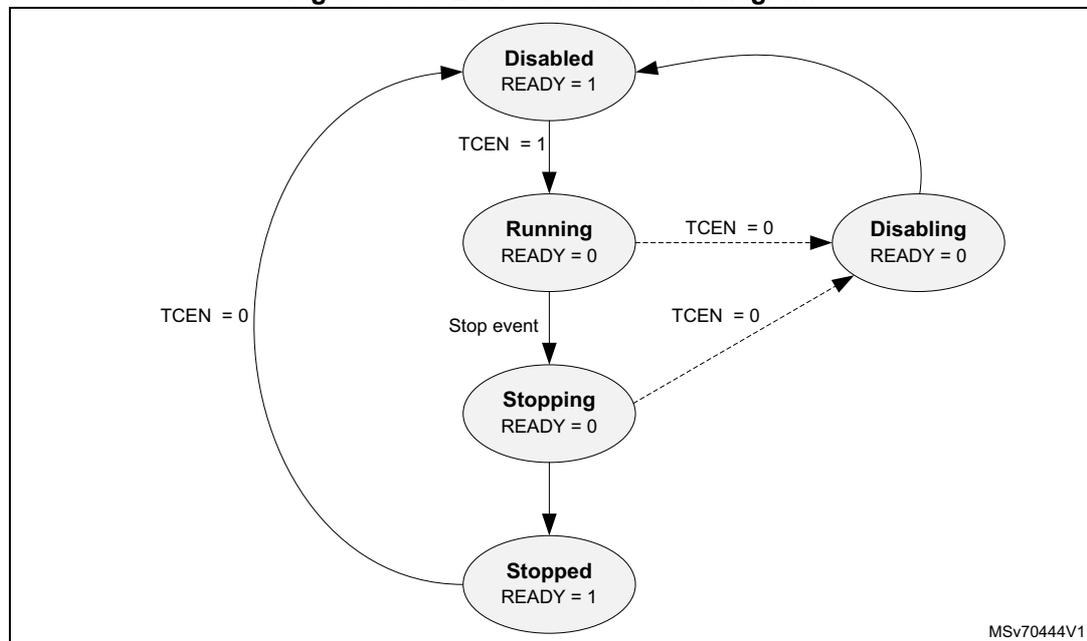
stateDiagram-v2
    [*] --> Disabled
    Disabled --> Running : TCEN = 1
    Running --> Disabling : TCEN = 0
    Running --> Stopping : Stop event
    Disabling --> Disabled
    Disabling --> Stopping : TCEN = 0
    Stopping --> Stopped
    Stopped --> Disabled : TCEN = 0
The diagram illustrates the state transitions of the ETR state machine. It consists of five states represented by ovals: Disabled (READY = 1), Running (READY = 0), Disabling (READY = 0), Stopping (READY = 0), and Stopped (READY = 1). Transitions are as follows: an arrow from the initial state to Disabled ; a solid arrow from Disabled to Running labeled TCEN = 1 ; a solid arrow from Running to Disabling labeled TCEN = 0 ; a solid arrow from Running to Stopping labeled Stop event ; a solid arrow from Disabling to Disabled ; a dashed arrow from Disabling to Stopping labeled TCEN = 0 ; a solid arrow from Stopping to Stopped ; and a large curved solid arrow from Stopped to Disabled labeled TCEN = 0 . The text MSV70444V1 is in the bottom right corner.
Scatter-gather operation
The trace buffer can be implemented as one continuous memory with a single base address (ETR_AXICTL.SGMODE = 0), or as multiple 4-Kbyte sections of RAM, in scatter-gather mode (ETR_AXICTL.SGMODE = 1). In the latter case, a linked list of page tables defines the base address of each section. The ETR_DBALO register is programmed with the base address of the buffer, in normal mode. In scatter-gather mode it contains the address of the first entry in the first page table.
The size of page tables is up to 4 Kbytes. Each 32-bit entry has the following format:
Table 892. ETR scatter-gather page format
| Bit range | Content | Description |
|---|---|---|
| Bits 31:4 | Address[39:12] | Base address of a 4-Kbyte section of RAM |
| Bits 3:2 | 00 | Not used |
| Bits 1:0 | 00 | Reserved |
| 01 | Entry points to the last 4-Kbyte section of the trace buffer | |
| 10 | Entry points to a 4-Kbyte section of the trace buffer | |
| 11 | Entry points to another page table |
Note: Trace-buffer addresses are 40-bit wide. However, only 32-bit addressing is used, and the 8 most significant bits are ignored.
The figure below illustrates a scatter-gather operation.
Figure 1086. Scatter-gather operation
The diagram illustrates the scatter-gather operation. The ETR_DBALO register contains the PT0 base address, which points to Page table PT0. Page table PT0 contains entries for PT0 section 0 base address, PT0 section 1 base address, PT0 section X base address, and a link entry pointing to Page table PT1. Page table PT1 contains entries for PT1 section 0 base address and PT1 section Y base address, with the last entry pointing to the final 4-Kbyte section. The diagram shows the mapping of these sections into the address space.
| Page Table | Entry | ADDRESS[39:12] | Entry type | Address space |
|---|---|---|---|---|
| Page table PT0 | PT0 section 0 base address | b31...b4 | 0 0 10 | 4-Kbyte section |
| PT0 section 1 base address | b31...b4 | 0 0 10 | 4-Kbyte section | |
| PT0 section X base address | b31...b4 | 0 0 10 | 4-Kbyte section | |
| Link (PT1 base address) | b31...b4 | 0 0 11 | ||
| Page table PT1 | PT1 section 0 base address | b31...b4 | 0 0 10 | 4-Kbyte section |
| PT1 section Y base address | b31...b4 | 0 0 01 | 4-Kbyte section | |
| Last entry | b31...b4 | 0 0 01 | 4-Kbyte section |
MSv70445V1
Trigger and flush events
Two input signals (trigin and flushin) come from the CTI and can be asserted by software or by a cross trigger coming from another CoreSight component via the cross trigger matrix.
When trigin is asserted, or when a trigger packet is detected on the ATB interface (ATID = 0x7D), a counter is loaded with the value in ETR_TRG, and starts decrementing by one each time a trace word is written into the trace buffer. When the counter reaches 0, a trigger event is generated (in circular-buffer mode only). The trigger event can be programmed in ETR_FFCR:
- • to insert a trigger in the trace stream
- • to flush the ETR internal buffers, and to issue a flush request to empty any upstream buffers on the ATB
- • to stop the trace capture (stop event)
A trigger packet can also be inserted in the trace stream at the moment a rising edge is detected on trigin.
When flushin is asserted, or when the FLUSHMAN = 1 in ETR_FFCR, the same actions can be programmed to occur as for the trigger event.
Authentication
The ETR behaviour is affected by the authentication signals dbgen and spiden.
If dbgen is low, no AXI accesses are possible. Any attempted AXI access behaves as if an immediate error response had been returned, and sets MEMERR in ETR_STS. No transactions are issued on the AXI master port.
If spiden is low, no secure AXI accesses are possible. Any attempted AXI access while PROTCTRLBIT[1] is cleared in ETR_AXICTL behaves as if an immediate error response has been returned, and sets MEMERR in ETR_STS. No transactions are issued on the AXI master port.
78.12.11 ETR registers
The register file base address for the ETR is defined in Table 880 .
ETR RAM size register (ETR_RSZ)
Address offset: 0x004
Reset value: 0x0000 0000
| 31 | 30 | 29 | 28 | 27 | 26 | 25 | 24 | 23 | 22 | 21 | 20 | 19 | 18 | 17 | 16 |
|---|---|---|---|---|---|---|---|---|---|---|---|---|---|---|---|
| Res. | RSZ[30:16] | ||||||||||||||
| rw | rw | rw | rw | rw | rw | rw | rw | rw | rw | rw | rw | rw | rw | rw | |
| 15 | 14 | 13 | 12 | 11 | 10 | 9 | 8 | 7 | 6 | 5 | 4 | 3 | 2 | 1 | 0 |
| RSZ[15:0] | |||||||||||||||
| rw | rw | rw | rw | rw | rw | rw | rw | rw | rw | rw | rw | rw | rw | rw | rw |
Bit 31 Reserved, must be kept at reset value.
Bits 30:0 RSZ[30:0] : RAM size.
The number of 32-bit words of RAM allocated to the buffer. If scatter gather operation is programmed, this register is ignored.
The maximum size is 4 Gbytes, the minimum size is 512 bytes in software-FIFO mode or 4 bytes in circular-buffer mode.
ETR status register (ETR_STS)
Address offset: 0x00C
Reset value: 0x0000 001C
| 31 | 30 | 29 | 28 | 27 | 26 | 25 | 24 | 23 | 22 | 21 | 20 | 19 | 18 | 17 | 16 |
|---|---|---|---|---|---|---|---|---|---|---|---|---|---|---|---|
| Res. | Res. | Res. | Res. | Res. | Res. | Res. | Res. | Res. | Res. | Res. | Res. | Res. | Res. | Res. | Res. |
| 15 | 14 | 13 | 12 | 11 | 10 | 9 | 8 | 7 | 6 | 5 | 4 | 3 | 2 | 1 | 0 |
| Res. | Res. | Res. | Res. | Res. | Res. | Res. | Res. | Res. | Res. | MEME RR | EMPTY | FTEMP TY | READY | TRIGD | FULL |
| r | r | r | r | r | r |
Bits 31:6 Reserved, must be kept at reset value.
Bit 5 MEMERR : AXI bus error
This bit indicates that an error has occurred on the AXI master interface. The error may be because of an error response from an AXI slave or because of the status of the authentication interface inputs prevents a transaction from taking place.
0: No error
1: Error
Bit 4 EMPTY : Trace buffer empty
This bit is valid only when TCEN in ETR_CTL is high. This bit reads as 0 when TCEN is low.
0: Trace buffer contains data.
1: Trace buffer is empty.
Note: Empty trace buffer does not mean that the ETR pipeline is empty. The latter is indicated by FTEMPY.
Bit 3 FTEMPY : Formatter empty
This bit is set when a trace capture has stopped, and all internal pipelines and buffers have been drained. The acqcomp output reflects the value of this bit.
Bit 2 READY : ETR ready
This bit is set when a trace capture has stopped, and all internal pipelines and buffers have been drained (stopped or disabled state), and the AXI interface is not busy.
Bit 1 TRIGD : Triggered
This bit is set when a trace capture is in progress, and the TMC has detected a trigger event. This bit is cleared when leaving disabled state. This bit is operational only in circular-buffer mode. In all other modes, this bit is always low.
Bit 0 FULL : Trace buffer full
In circular-buffer mode, this flag is set when the RAM write pointer wraps around the top of the buffer, and remains set until TCEN of ETR_CTL is cleared and set.
In software-FIFO mode, this flag indicates that the current space in the trace memory is less than or equal to the value programmed in ETR_BUFWM (CBUFLVL \( \geq \) RSZ - BUFWM).
If the TMC is programmed for scatter-gather operation, this bit indicates whether the trace memory is currently full regardless of the value programmed in ETR_BUFWM.
This bit is cleared when leaving disabled state. The FULL output reflects the value of this bit.
ETR RAM read data register (ETR_RRD)
Address offset: 0x010
Reset value: 0xXXXX XXXX
| 31 | 30 | 29 | 28 | 27 | 26 | 25 | 24 | 23 | 22 | 21 | 20 | 19 | 18 | 17 | 16 |
|---|---|---|---|---|---|---|---|---|---|---|---|---|---|---|---|
| RRD[31:16] | |||||||||||||||
| r | r | r | r | r | r | r | r | r | r | r | r | r | r | r | r |
| 15 | 14 | 13 | 12 | 11 | 10 | 9 | 8 | 7 | 6 | 5 | 4 | 3 | 2 | 1 | 0 |
| RRD[15:0] | |||||||||||||||
| r | r | r | r | r | r | r | r | r | r | r | r | r | r | r | r |
Bits 31:0 RRD[31:0] : RAM read data
Circular-buffer mode:
When in stopped state and the buffer is not empty, reading this register returns the next word of data from the trace buffer (two reads are required to retrieve one 64-bit word of data).
When the whole trace buffer has been read, EMPTY is set in ETR_STS, and subsequent reads return 0xFFFFFFFF. Reading this register when not in stopped state returns 0xFFFFFFFF.
Software-FIFO mode:
Reading this register returns data from the FIFO. If this register is read when the FIFO is empty, 0xFFFFFFFF is returned.
If MEMERR is set in ETR_STS, reading this register returns an error response on the APB bus.
ETR RAM read pointer register (ETR_RRP)
Address offset: 0x014
Reset value: 0x0000 0000
| 31 | 30 | 29 | 28 | 27 | 26 | 25 | 24 | 23 | 22 | 21 | 20 | 19 | 18 | 17 | 16 |
|---|---|---|---|---|---|---|---|---|---|---|---|---|---|---|---|
| RRP[31:16] | |||||||||||||||
| rw | rw | rw | rw | rw | rw | rw | rw | rw | rw | rw | rw | rw | rw | rw | rw |
| 15 | 14 | 13 | 12 | 11 | 10 | 9 | 8 | 7 | 6 | 5 | 4 | 3 | 2 | 1 | 0 |
| RRP[15:0] | |||||||||||||||
| rw | rw | rw | rw | rw | rw | rw | rw | rw | rw | rw | rw | rw | rw | rw | rw |
Bits 31:0 RRP[31:0] : RAM read pointer
This register contains the value of the read pointer that is used to read entries from the trace memory over the APB interface via the ETR_RRD register. The pointer can be programmed with a byte address, 64-bit aligned (bits 0 to 2 must be 0). The pointer is incremented by eight each time a 64-bit buffer entry has been written. When the pointer reaches its maximum value, it wraps around.
This register can be written to only while in disabled state, to set the value of the trace memory address from which data are fetched on a subsequent RRD read. It can be read in disabled state, in stopped state in circular-buffer and software-FIFO modes, and also in running and stopping states in software-FIFO mode.
ETR RAM write pointer register (ETR_RWP)
Address offset: 0x018
Reset value: 0x0000 0000
| 31 | 30 | 29 | 28 | 27 | 26 | 25 | 24 | 23 | 22 | 21 | 20 | 19 | 18 | 17 | 16 |
|---|---|---|---|---|---|---|---|---|---|---|---|---|---|---|---|
| RWP[31:16] | |||||||||||||||
| rw | rw | rw | rw | rw | rw | rw | rw | rw | rw | rw | rw | rw | rw | rw | rw |
| 15 | 14 | 13 | 12 | 11 | 10 | 9 | 8 | 7 | 6 | 5 | 4 | 3 | 2 | 1 | 0 |
| RWP[15:0] | |||||||||||||||
| rw | rw | rw | rw | rw | rw | rw | rw | rw | rw | rw | rw | rw | rw | rw | rw |
Bits 31:0 RWP[31:0] : RAM write pointer
This register contains the value of the write pointer that is used to write entries into the trace memory. The pointer can be programmed with a byte address, 64-bit aligned (that is, bits 0 to 2 should be 0). The pointer is incremented by 8 each time a new entry is written. When the pointer reaches its maximum value, it wraps around.
This register can be written to only while in Disabled state. It can be read in Disabled state, in Stopped state in circular-buffer and software-FIFO modes, and also in Running and Stopping states in software-FIFO mode.
ETR trigger counter register (ETR_TRG)
Address offset: 0x01C
Reset value: 0x0000 0000
| 31 | 30 | 29 | 28 | 27 | 26 | 25 | 24 | 23 | 22 | 21 | 20 | 19 | 18 | 17 | 16 |
|---|---|---|---|---|---|---|---|---|---|---|---|---|---|---|---|
| TRG[31:16] | |||||||||||||||
| rw | rw | rw | rw | rw | rw | rw | rw | rw | rw | rw | rw | rw | rw | rw | rw |
| 15 | 14 | 13 | 12 | 11 | 10 | 9 | 8 | 7 | 6 | 5 | 4 | 3 | 2 | 1 | 0 |
| TRG[15:0] | |||||||||||||||
| rw | rw | rw | rw | rw | rw | rw | rw | rw | rw | rw | rw | rw | rw | rw | rw |
Bits 31:0 TRG[31:0] : Trigger counter
In circular-buffer mode, this field specifies the number of 32-bit words to capture in the trace buffer following the detection of either a rising edge on the TRIGIN input or a trigger packet in the incoming trace stream, ATID = 0x7D. On capturing the specified number of data words, a trigger event occurs. The effect of a trigger event on the ETR behavior is controlled by the ETR_FFCR register.
The number of 32-bit words written into the trace buffer following the trigger is the value stored in this register, plus one. This register is ignored when the ETR is in software-FIFO mode. When the trigger counter starts counting, any additional triggers, either on TRIGIN or in the incoming trace stream, are ignored until the counter reaches 0. When the trigger counter has reached 0, it remains at 0 until it is reprogrammed with a write to this register.
This register is cleared when READY goes high, so that the state of the counter when trace capture has stopped does not affect a subsequent trace capture session. Writing to this register when not in disabled state results in unpredictable behavior.
A read access to this register is permitted at any time when in disabled state, or in circular-buffer mode. A read access returns the current value of the trigger counter.
ETR control register (ETR_CTL)
Address offset: 0x020
Reset value: 0x0000 0000
| 31 | 30 | 29 | 28 | 27 | 26 | 25 | 24 | 23 | 22 | 21 | 20 | 19 | 18 | 17 | 16 |
|---|---|---|---|---|---|---|---|---|---|---|---|---|---|---|---|
| Res. | Res. | Res. | Res. | Res. | Res. | Res. | Res. | Res. | Res. | Res. | Res. | Res. | Res. | Res. | Res. |
| 15 | 14 | 13 | 12 | 11 | 10 | 9 | 8 | 7 | 6 | 5 | 4 | 3 | 2 | 1 | 0 |
| Res. | Res. | Res. | Res. | Res. | Res. | Res. | Res. | Res. | Res. | Res. | Res. | Res. | Res. | Res. | TCEN |
| rw | |||||||||||||||
Bits 31:1 Reserved, must be kept at reset value.
Bit 0 TCEN : Trace capture enable
When writing:
0: Disables trace capture (moves from running, stopping or stopped state into disabling or disabled state).
1: Enables trace capture (moves from disabled state to running state).
When reading, this bit is low when in disabling or disabled states, and high otherwise.
ETR RAM write data register (ETR_RWD)
Address offset: 0x024
Reset value: 0xXXXX XXXX
| 31 | 30 | 29 | 28 | 27 | 26 | 25 | 24 | 23 | 22 | 21 | 20 | 19 | 18 | 17 | 16 |
|---|---|---|---|---|---|---|---|---|---|---|---|---|---|---|---|
| RWD[31:16] | |||||||||||||||
| w | w | w | w | w | w | w | w | w | w | w | w | w | w | w | w |
| 15 | 14 | 13 | 12 | 11 | 10 | 9 | 8 | 7 | 6 | 5 | 4 | 3 | 2 | 1 | 0 |
| RWD[15:0] | |||||||||||||||
| w | w | w | w | w | w | w | w | w | w | w | w | w | w | w | w |
When in disabled state, a write to this register stores data at the location pointed to by the ETR_RWP. Writes to this register when not in disabled state are ignored. When a full memory width (64 bits) of data is written, data are written to memory and the RAM write pointer is incremented to the next memory word.
This register is used for test purposes.
ETR mode register (ETR_MODE)Address offset: 0x028
Reset value: 0x0000 0000
| 31 | 30 | 29 | 28 | 27 | 26 | 25 | 24 | 23 | 22 | 21 | 20 | 19 | 18 | 17 | 16 |
|---|---|---|---|---|---|---|---|---|---|---|---|---|---|---|---|
| Res. | Res. | Res. | Res. | Res. | Res. | Res. | Res. | Res. | Res. | Res. | Res. | Res. | Res. | Res. | Res. |
| 15 | 14 | 13 | 12 | 11 | 10 | 9 | 8 | 7 | 6 | 5 | 4 | 3 | 2 | 1 | 0 |
| Res. | Res. | Res. | Res. | Res. | Res. | Res. | Res. | Res. | Res. | Res. | Res. | Res. | Res. | MODE[1:0] | |
| rw | rw | ||||||||||||||
Bits 31:2 Reserved, must be kept at reset value.
Bits 1:0 MODE[1:0] : Operation mode0x0: Circular-buffer mode
In this mode, trace data are captured in the trace buffer memory starting from the location pointed to by the write pointer register. Even when the trace buffer is full, incoming trace data continue to be overwritten into the trace memory until a stop condition has occurred.
0x1: Software-FIFO mode
In this mode, the trace buffer is a FIFO that can be read through ETR_RRD while a trace is being captured. Trace data are captured in the trace buffer memory and when full, the incoming trace stream is stalled.
Others: Reserved
ETR latched buffer fill level register (ETR_LBUFLVL)Address offset: 0x02C
Reset value: 0x0000 0000
| 31 | 30 | 29 | 28 | 27 | 26 | 25 | 24 | 23 | 22 | 21 | 20 | 19 | 18 | 17 | 16 |
|---|---|---|---|---|---|---|---|---|---|---|---|---|---|---|---|
| LBUFLEVEL[31:16] | |||||||||||||||
| r | r | r | r | r | r | r | r | r | r | r | r | r | r | r | r |
| 15 | 14 | 13 | 12 | 11 | 10 | 9 | 8 | 7 | 6 | 5 | 4 | 3 | 2 | 1 | 0 |
| LBUFLEVEL[15:0] | |||||||||||||||
| r | r | r | r | r | r | r | r | r | r | r | r | r | r | r | r |
Bits 31:0 LBUFLEVEL[31:0] : Latched buffer fill level
Reading this register returns the maximum fill level of the trace buffer in 32-bit words since this register was last read. Reading this register also results in its contents being updated to the current fill level.
When entering disabled state, this register retains its last value. While in disabled state, reads from this register do not affect its value. When exiting disabled state, this register is cleared.
This register does not apply when the ETR is programmed for scatter/gather operation.
In this case, reading this register returns 0x00000000.
This register is used for performance analysis of the trace system.
ETR current buffer fill level register (ETR_CBUFLVL)
Address offset: 0x030
Reset value: 0x0000 0000
| 31 | 30 | 29 | 28 | 27 | 26 | 25 | 24 | 23 | 22 | 21 | 20 | 19 | 18 | 17 | 16 |
| CBUFLEVEL[31:16] | |||||||||||||||
| r | r | r | r | r | r | r | r | r | r | r | r | r | r | r | r |
| 15 | 14 | 13 | 12 | 11 | 10 | 9 | 8 | 7 | 6 | 5 | 4 | 3 | 2 | 1 | 0 |
| CBUFLEVEL[15:0] | |||||||||||||||
| r | r | r | r | r | r | r | r | r | r | r | r | r | r | r | r |
Bits 31:0 CBUFLEVEL[31:0] : Current buffer fill level
Reading this register returns the current fill level of the trace buffer in 32-bit words.
This register does not apply when the ETR is programmed for scatter/gather operation.
In this case, reading this register returns 0x00000000.
This register is cleared when TCEN is low.
ETR buffer level watermark register (ETR_BUFWM)
Address offset: 0x034
Reset value: 0x0000 0000
| 31 | 30 | 29 | 28 | 27 | 26 | 25 | 24 | 23 | 22 | 21 | 20 | 19 | 18 | 17 | 16 |
| BUFWM[31:16] | |||||||||||||||
| rw | rw | rw | rw | rw | rw | rw | rw | rw | rw | rw | rw | rw | rw | rw | rw |
| 15 | 14 | 13 | 12 | 11 | 10 | 9 | 8 | 7 | 6 | 5 | 4 | 3 | 2 | 1 | 0 |
| BUFWM[15:0] | |||||||||||||||
| rw | rw | rw | rw | rw | rw | rw | rw | rw | rw | rw | rw | rw | rw | rw | rw |
Bits 31:0 BUFWM[31:0] : Buffer level watermark
The value programmed in this register indicates the required threshold vacancy level of the trace memory in 32-bit words. When the space in the FIFO is less than or equal to this value ( \( CBUFLEVEL \geq RSZ - BUFWM \) ), the full output is pulled high and FULL is set in ETR_STS.
This register is used only in software-FIFO mode. In circular-buffer mode, this functionality can be obtained by programming ETR_RWP to the required vacancy trigger level, so that when the pointer wraps around, the FULL bit is set indicating that the vacancy level has fallen below the required level.
The maximum value that can be written into this register is RAM size (RSZ) - 1. In this case, the full output is asserted after the first 32-bit word is written to the buffer.
Writing to this register other than when in disabled state results in unpredictable behavior.
ETR AXI control register (ETR_AXICTL)
Address offset: 0x110
Reset value: 0x0000 0000
| 31 | 30 | 29 | 28 | 27 | 26 | 25 | 24 | 23 | 22 | 21 | 20 | 19 | 18 | 17 | 16 |
|---|---|---|---|---|---|---|---|---|---|---|---|---|---|---|---|
| Res. | Res. | Res. | Res. | Res. | Res. | Res. | Res. | Res. | Res. | Res. | Res. | Res. | Res. | Res. | Res. |
| 15 | 14 | 13 | 12 | 11 | 10 | 9 | 8 | 7 | 6 | 5 | 4 | 3 | 2 | 1 | 0 |
| Res. | Res. | Res. | Res. | WRBURSTLEN[3:0] | SGMO DE | Res. | CACHCTRLBIT[3:0] | PROTCTRLBIT[1:0] | |||||||
| rw | rw | rw | rw | rw | rw | rw | rw | rw | rw | rw | |||||
Bits 31:12 Reserved, must be kept at reset value.
Bits 11:8 WRBURSTLEN[3:0] : Write burst length
This field indicates the maximum number of data transfers that can occur within each burst initiated by the ETR on the AXI master interface. The write burst initiated on the AXI can be of a smaller length that the programmed value in the case when the formatter has stopped because of a stop condition occurred. Programming this field to a burst length value greater than the write buffer depth, results in a burst length that is equal to the write buffer depth.
The burst length programmed must be compatible with the trace buffer size and the AXI data width: the total number of bytes of data transferred in a burst is not greater than the trace buffer size or, if scatter-gather operation is enabled, is not greater than 4 Kbytes.
Programming an incompatible burst length results in an unpredictable behavior.
It is recommended that this value is set to no more than half the write buffer depth. It is also recommended that this value is set to enable an AXI burst of at least one frame of trace data.
0x0: one data transfer per burst (default)
0x1-0xF: maximum of (WRBURSTLEN + 1) data transfers per burst
Bit 7 SGMODE : Scatter-gather mode
This bit indicates whether trace memory is accessed as a single buffer in system memory or as a linked-list based scatter-gather memory. This bit is ignored when in disabled state.
0: Trace memory is a single contiguous block of system memory.
1: Trace memory is spread over multiple blocks of system memory based on a linked-list mechanism.
Bit 6 Reserved, must be kept at reset value.
Bits 5:2 CACHECTRLBIT[3:0] : Cache control
These bits control the value driven on ARCACHEM[3:0] or AWCACHEM[3:0] signals on the AXI master interface when performing AXI transfers.
xxx0: Non-bufferable
xxx1: Bufferable
000x: Non-cacheable
001x: Cacheable, no allocate on read, no allocate on write
011x: Cacheable, allocate on read, no allocate on write
101x: Cacheable, no allocate on read, allocate on write
111x: Cacheable, allocate on read, allocate on write
Others: Reserved
Bits 1:0 PROTCTRLBIT[1:0] : Protection control bits.
These bits control the value driven on ARPROTM[3:0] or AWPROTM[3:0] signals on the AXI master interface when performing AXI transfers.
x0: Normal access
x1: Privileged access
0x: Secure access
1x: Nonsecure access
ETR data buffer address low register (ETR_DBALO)
Address offset: 0x118
Reset value: 0x0000 0000
| 31 | 30 | 29 | 28 | 27 | 26 | 25 | 24 | 23 | 22 | 21 | 20 | 19 | 18 | 17 | 16 |
|---|---|---|---|---|---|---|---|---|---|---|---|---|---|---|---|
| BUFADDRLO[31:16] | |||||||||||||||
| rw | rw | rw | rw | rw | rw | rw | rw | rw | rw | rw | rw | rw | rw | rw | rw |
| 15 | 14 | 13 | 12 | 11 | 10 | 9 | 8 | 7 | 6 | 5 | 4 | 3 | 2 | 1 | 0 |
| BUFADDRLO[15:0] | |||||||||||||||
| rw | rw | rw | rw | rw | rw | rw | rw | rw | rw | rw | rw | rw | rw | rw | rw |
Bits 31:0 BUFADDRLO[31:0] : Buffer address low
If SGMODE = 0 in ETR_AXICTL, the content of this register is the base address of the trace buffer in system memory.
If SGMODE = 1, the content of this register is the address of first page table entry in the linked list.
This register can only be programmed in disabled state.
ETR formatter and flush status register (ETR_FFSR)
Address offset: 0x300
Reset value: 0x0000 0002
| 31 | 30 | 29 | 28 | 27 | 26 | 25 | 24 | 23 | 22 | 21 | 20 | 19 | 18 | 17 | 16 |
|---|---|---|---|---|---|---|---|---|---|---|---|---|---|---|---|
| Res. | Res. | Res. | Res. | Res. | Res. | Res. | Res. | Res. | Res. | Res. | Res. | Res. | Res. | Res. | Res. |
| 15 | 14 | 13 | 12 | 11 | 10 | 9 | 8 | 7 | 6 | 5 | 4 | 3 | 2 | 1 | 0 |
| Res. | Res. | Res. | Res. | Res. | Res. | Res. | Res. | Res. | Res. | Res. | Res. | Res. | Res. | FTSTO PPED r | FLINP ROG r |
Bits 31:2 Reserved, must be kept at reset value.
Bit 1 FTSTOPPED : Formatter stopped
This bit behaves in the same way as FTEMPTY in ETR_STS.
Bit 0 FLINPROG : Flush in progress
This bit indicates whether a flush on the ATB slave port is in progress. It reflects the status of the AFVALIDS output. A flush can be initiated by the flush control bits in ETR_FFCR.
0: No flush in progress
1: Flush in progress
ETR formatter and flush control register (ETR_FFCR)
Address offset: 0x304
Reset value: 0x0000 0000
| 31 | 30 | 29 | 28 | 27 | 26 | 25 | 24 | 23 | 22 | 21 | 20 | 19 | 18 | 17 | 16 |
|---|---|---|---|---|---|---|---|---|---|---|---|---|---|---|---|
| Res. | Res. | Res. | Res. | Res. | Res. | Res. | Res. | Res. | Res. | Res. | Res. | Res. | Res. | Res. | Res. |
| 15 | 14 | 13 | 12 | 11 | 10 | 9 | 8 | 7 | 6 | 5 | 4 | 3 | 2 | 1 | 0 |
| Res. | Res. | STPON TRGEV | STOP0 NFL | Res. | TRIGO NFL | TRGO NTRGE V | TRGO NTRGI N | Res. | FLUSH MAN | FONTR GEV | FONFL IN | Res. | Res. | ENTI | ENFT |
| rw | rw | rw | rw | rw | rw | rw | rw | rw | rw |
Bits 31:14 Reserved, must be kept at reset value.
Bit 13 STPONTRGEV : Stop on trigger event
0: No effect
1: Stops trace capture when a trigger event occurs.
Enabling the ETR in software-FIFO mode with this bit set results in unpredictable behavior.
Bit 12 STOPONFL : Stop on flush
0: No effect
1: Stops trace capture when flush is completed.
Bit 11 Reserved, must be kept at reset value.
Bit 10 TRIGONFL : Trigger on flush
0: No effect
1: Indicates a trigger in the trace stream when flush is completed.
If ENFT and ENTI are clear, this bit is ignored and no trigger is inserted into the trace stream.
Bit 9 TRGONTRGEV : Trigger on trigger event
0: No effect
1: Indicates a trigger in the trace stream when a trigger event occurs.
If ENFT and ENTI are both clear, this bit is ignored and no trigger is inserted into the trace stream. This bit is not supported in software-FIFO mode.
Bit 8 TRGONTRGIN : Trigger on trigger in
0: No effect
1: Indicates a trigger in the trace stream when a rising edge is detected on the TRIGIN input.
If ENFT and ENTI are clear, this bit is ignored and no trigger is inserted into the trace stream.
Bit 7 Reserved, must be kept at reset value.
Bit 6 FLUSHMAN : Manual flush
0: No effect
1: Flushes the trace FIFO and pipeline.
This bit is cleared automatically when the flush is complete. If TCEN = 0 in ETR_CTL, writes to this bit are ignored.
Bit 5 FONTTRGEV : Flush on trigger event
0: No effect
1: Flushes the trace FIFO and pipeline if a trigger event occurs.
This bit is not supported in software-FIFO mode. If STPONTRGEV is set, this bit is ignored.
Bit 4 FONFLIN : Flush on flush in
0: No effect
1: Flushes the trace FIFO and pipeline when a rising edge is detected on the FLUSHIN input.
Bits 3:2 Reserved, must be kept at reset value.
Bit 1 ENTI : Enable trigger insertion
Setting this bit enables the insertion of triggers in the formatted trace stream. A trigger is indicated by inserting one byte of data 0x00 with ATID = 0x7D in the trace stream. Trigger indication on the trace stream is further controlled by TRIGONFL, TRGONTRGEV, and TRGONTRGIN in FFCR. This bit can be changed only when READY is high and TCEN is low. It takes effect only when ENFT in this register is set. If ENTI is set high when ENFT is low, it results in formatting being enabled.
Bit 0 ENFT : Enable formatting
0: Formatting is disabled. Incoming trace data are assumed to be from a single trace source.
1: Formatting is enabled.
If multiple ATIDs are received by the ETR when trace capture is enabled and the formatter is disabled, an interleaving of trace data occurs. Disabling of formatting is supported only in circular-buffer mode. If the ETR is enabled in a mode other than circular-buffer mode with ENFT low, then formatting is enabled. If ENTI bit is set to high when ENFT is low, formatting is enabled.
This bit is ignored when in disabled state.
ETR periodic synchronization counter register (ETR_PSCR)
Address offset: 0x308
Reset value: 0x0000 000A
| 31 | 30 | 29 | 28 | 27 | 26 | 25 | 24 | 23 | 22 | 21 | 20 | 19 | 18 | 17 | 16 |
|---|---|---|---|---|---|---|---|---|---|---|---|---|---|---|---|
| Res | Res | Res | Res | Res | Res | Res | Res | Res | Res | Res | Res | Res | Res | Res | Res |
| 15 | 14 | 13 | 12 | 11 | 10 | 9 | 8 | 7 | 6 | 5 | 4 | 3 | 2 | 1 | 0 |
| Res. | Res. | Res. | Res. | Res. | Res. | Res. | Res. | Res. | Res. | Res. | PSCOUNT[4:0] | ||||
| rw | rw | rw | rw | rw | |||||||||||
Bits 31:5 Reserved, must be kept at reset value.
Bits 4:0 PSCOUNT[4:0] : Synchronization counter reload value
Determines the reload value of the synchronization counter. The reload value takes effect the next time the counter reaches 0. Reads from this register return the reload value programmed in this register. This register is set to 0xA on reset, corresponding to a synchronization period of 1024 bytes.
0x0: Synchronization disabled
0x7-0x1B: Synchronization period is \( 2^{\text{PSCOUNT}} \) bytes
Others: Reserved
ETR claim tag set register (ETR_CLAIMSET)
Address offset: 0xFA0
Reset value: 0x0000 000F
| 31 | 30 | 29 | 28 | 27 | 26 | 25 | 24 | 23 | 22 | 21 | 20 | 19 | 18 | 17 | 16 |
|---|---|---|---|---|---|---|---|---|---|---|---|---|---|---|---|
| Res. | Res. | Res. | Res. | Res. | Res. | Res. | Res. | Res. | Res. | Res. | Res. | Res. | Res. | Res. | Res. |
| 15 | 14 | 13 | 12 | 11 | 10 | 9 | 8 | 7 | 6 | 5 | 4 | 3 | 2 | 1 | 0 |
| Res. | Res. | Res. | Res. | Res. | Res. | Res. | Res. | Res. | Res. | Res. | Res. | CLAIMSET[3:0] | |||
| rw | rw | rw | rw | ||||||||||||
Bits 31:4 Reserved, must be kept at reset value.
Bits 3:0 CLAIMSET[3:0] : Set claim tag bits
Write:
0000: No effect
xxx1: Set bit 0.
xx1x: Set bit 1.
x1xx: Set bit 2.
1xxx: Set bit 3.
Read:
0xF: Indicates there are four bits in claim tag.
ETR claim tag clear register (ETR_CLAIMCLR)
Address offset: 0xFA4
Reset value: 0x0000 0000
| 31 | 30 | 29 | 28 | 27 | 26 | 25 | 24 | 23 | 22 | 21 | 20 | 19 | 18 | 17 | 16 |
|---|---|---|---|---|---|---|---|---|---|---|---|---|---|---|---|
| Res. | Res. | Res. | Res. | Res. | Res. | Res. | Res. | Res. | Res. | Res. | Res. | Res. | Res. | Res. | Res. |
| 15 | 14 | 13 | 12 | 11 | 10 | 9 | 8 | 7 | 6 | 5 | 4 | 3 | 2 | 1 | 0 |
| Res. | Res. | Res. | Res. | Res. | Res. | Res. | Res. | Res. | Res. | Res. | Res. | CLAIMCLR[3:0] | |||
| rw | rw | rw | rw | ||||||||||||
Bits 31:4 Reserved, must be kept at reset value.
Bits 3:0 CLAIMCLR[3:0] : Reset claim tag bits
Write:
0000: No effect
xxx1: Clear bit 0.
xx1x: Clear bit 1.
x1xx: Clear bit 2.
1xxx: Clear bit 3.
Read: Returns current value of claim tag.
ETR lock access register (ETR_LAR)
Address offset: 0xFB0
Reset value: 0xXXXX XXXX
| 31 | 30 | 29 | 28 | 27 | 26 | 25 | 24 | 23 | 22 | 21 | 20 | 19 | 18 | 17 | 16 |
|---|---|---|---|---|---|---|---|---|---|---|---|---|---|---|---|
| ACCESS_W[31:16] | |||||||||||||||
| w | w | w | w | w | w | w | w | w | w | w | w | w | w | w | w |
| 15 | 14 | 13 | 12 | 11 | 10 | 9 | 8 | 7 | 6 | 5 | 4 | 3 | 2 | 1 | 0 |
| ACCESS_W[15:0] | |||||||||||||||
| w | w | w | w | w | w | w | w | w | w | w | w | w | w | w | w |
Bits 31:0 ACCESS_W[31:0] : ETR register access enable
Enables write access to all ETR registers by the processor core (debuggers do not need to unlock the component)
0xC5ACCE55: Enable write access.
Other values: Disable write access.
ETR lock status register (ETR_LSR)
Address offset: 0xFB4
Reset value: 0x0000 0003
| 31 | 30 | 29 | 28 | 27 | 26 | 25 | 24 | 23 | 22 | 21 | 20 | 19 | 18 | 17 | 16 |
|---|---|---|---|---|---|---|---|---|---|---|---|---|---|---|---|
| [Reserved] | |||||||||||||||
| Res. | Res. | Res. | Res. | Res. | Res. | Res. | Res. | Res. | Res. | Res. | Res. | Res. | Res. | Res. | Res. |
| 15 | 14 | 13 | 12 | 11 | 10 | 9 | 8 | 7 | 6 | 5 | 4 | 3 | 2 | 1 | 0 |
| [Reserved] | |||||||||||||||
| Res. | Res. | Res. | Res. | Res. | Res. | Res. | Res. | Res. | Res. | Res. | Res. | Res. | LOCKTYPE | LOCKGRANT | LOCKEXIST |
| r | r | r | |||||||||||||
Bits 31:3 Reserved, must be kept at reset value.
Bit 2 LOCKTYPE : Size of ETR_LAR register
0: 32 bits
Bit 1 LOCKGRANT : Current status of lock
This bit always returns 0 when read by an external debugger.
0: Write access is permitted.
1: Write access is blocked to all registers except ETR_LAR. Only read access is permitted.
Bit 0 LOCKEXIST : Existence of lock control mechanism
The bit indicates whether a lock control mechanism exists. It always returns 0 when read by an external debugger.
0: No lock control mechanism exists.
1: Lock control mechanism is implemented.
ETR authentication status register (ETR_AUTHSTAT)
Address offset: 0xFB8
Reset value: 0x0000 00XX
| 31 | 30 | 29 | 28 | 27 | 26 | 25 | 24 | 23 | 22 | 21 | 20 | 19 | 18 | 17 | 16 |
|---|---|---|---|---|---|---|---|---|---|---|---|---|---|---|---|
| Res. | Res. | Res. | Res. | Res. | Res. | Res. | Res. | Res. | Res. | Res. | Res. | Res. | Res. | Res. | Res. |
| 15 | 14 | 13 | 12 | 11 | 10 | 9 | 8 | 7 | 6 | 5 | 4 | 3 | 2 | 1 | 0 |
| Res. | Res. | Res. | Res. | Res. | Res. | Res. | Res. | SNID[1:0] | SID[1:0] | NSNID[1:0] | NSID[1:0] | ||||
| r | r | r | r | r | r | r | r |
Bits 31:8 Reserved, must be kept at reset value.
Bits 7:6 SNID[1:0] : Security level for secure non-invasive debug
0x0: Not implemented
Bits 5:4 SID[1:0] : Security level for secure invasive debug
0x2: Functionality disabled. This return value occurs when spiden = 0 or dbgen = 0.
0x3: Functionality enabled. This return value occurs when spiden = 1 and dbgen = 1.
Bits 3:2 NSNID[1:0] : Security level for nonsecure non-invasive debug
0x0: Not implemented
Bits 1:0 NSID[1:0] : Security level for nonsecure invasive debug
0x2: Functionality disabled. This return value occurs when dbgen = 0.
0x3: Functionality enabled. This return value occurs when dbgen = 1.
ETR device configuration register (ETR_DEVID)
Address offset: 0xFC8
Reset value: 0x0000 2B40
| 31 | 30 | 29 | 28 | 27 | 26 | 25 | 24 | 23 | 22 | 21 | 20 | 19 | 18 | 17 | 16 |
|---|---|---|---|---|---|---|---|---|---|---|---|---|---|---|---|
| Res. | Res. | Res. | Res. | Res. | Res. | Res. | Res. | Res. | Res. | Res. | Res. | Res. | Res. | Res. | Res. |
| 15 | 14 | 13 | 12 | 11 | 10 | 9 | 8 | 7 | 6 | 5 | 4 | 3 | 2 | 1 | 0 |
| Res. | Res. | WBUF_DEPTH[2:0] | MEMWIDTH[2:0] | CONFIGTYP[1:0] | CLKSC HEM | ATBINPORTCNT[4:0] | |||||||||
| r | r | r | r | r | r | r | r | r | r | r | r | r | r | ||
Bits 31:14 Reserved, must be kept at reset value.
Bits 13:11 WBUF_DEPTH[2:0] : Write buffer depth
Indicates, in powers of two, the number of entries in the ETR internal write buffer. Each entry is 32 bits.
0x5: 32 entries
Bits 10:8 MEMWIDTH[2:0] : Memory interface data bus width
0x3: 64 bits
Bits 7:6 CONFIGTYP[1:0] : Configuration type of component (ETB, ETR or ETF)
0x1: ETR
Bit 5 CLKSCHEM : RAM clocking scheme (synchronous or asynchronous)
0: Synchronous
Bits 4:0 ATBINPORTCNT[4:0] : Number/type of ATB input port multiplexing
0x0: None
ETR device type identifier register (ETR_DEVTYPE)
Address offset: 0xFCC
Reset value: 0x0000 0021
| 31 | 30 | 29 | 28 | 27 | 26 | 25 | 24 | 23 | 22 | 21 | 20 | 19 | 18 | 17 | 16 |
|---|---|---|---|---|---|---|---|---|---|---|---|---|---|---|---|
| Res. | Res. | Res. | Res. | Res. | Res. | Res. | Res. | Res. | Res. | Res. | Res. | Res. | Res. | Res. | Res. |
| 15 | 14 | 13 | 12 | 11 | 10 | 9 | 8 | 7 | 6 | 5 | 4 | 3 | 2 | 1 | 0 |
| Res. | Res. | Res. | Res. | Res. | Res. | Res. | Res. | SUBTYPE[3:0] | MAJORTYPE[3:0] | ||||||
| r | r | r | r | r | r | r | r | ||||||||
Bits 31:8 Reserved, must be kept at reset value.
Bits 7:4 SUBTYPE[3:0] : Sub-classification
0x2: Captures the ATB slave interface trace data in RAM which can then be read through an APB interface.
Bits 3:0 MAJORTYPE[3:0] : Major classification
0x1: The component is a trace sink.
ETR CoreSight peripheral identity register 4 (ETR_PIDR4)
Address offset: 0xFD0
Reset value: 0x0000 0004
| 31 | 30 | 29 | 28 | 27 | 26 | 25 | 24 | 23 | 22 | 21 | 20 | 19 | 18 | 17 | 16 |
|---|---|---|---|---|---|---|---|---|---|---|---|---|---|---|---|
| Res. | Res. | Res. | Res. | Res. | Res. | Res. | Res. | Res. | Res. | Res. | Res. | Res. | Res. | Res. | Res. |
| 15 | 14 | 13 | 12 | 11 | 10 | 9 | 8 | 7 | 6 | 5 | 4 | 3 | 2 | 1 | 0 |
| Res. | Res. | Res. | Res. | Res. | Res. | Res. | Res. | SIZE[3:0] | JEP106CON[3:0] | ||||||
| r | r | r | r | r | r | r | r | ||||||||
Bits 31:8 Reserved, must be kept at reset value.
Bits 7:4 SIZE[3:0] : Register file size
0x0: Register file occupies a single 4-Kbyte region.
Bits 3:0 JEP106CON[3:0] : JEP106 continuation code
0x4: Arm JEDEC code
ETR CoreSight peripheral identity register 0 (ETR_PIDR0)
Address offset: 0xFE0
Reset value: 0x0000 0061
| 31 | 30 | 29 | 28 | 27 | 26 | 25 | 24 | 23 | 22 | 21 | 20 | 19 | 18 | 17 | 16 |
|---|---|---|---|---|---|---|---|---|---|---|---|---|---|---|---|
| Res. | Res. | Res. | Res. | Res. | Res. | Res. | Res. | Res. | Res. | Res. | Res. | Res. | Res. | Res. | Res. |
| 15 | 14 | 13 | 12 | 11 | 10 | 9 | 8 | 7 | 6 | 5 | 4 | 3 | 2 | 1 | 0 |
| Res. | Res. | Res. | Res. | Res. | Res. | Res. | Res. | PARTNUM[7:0] | |||||||
| r | r | r | r | r | r | r | r | ||||||||
Bits 31:8 Reserved, must be kept at reset value.
Bits 7:0 PARTNUM[7:0] : Part number field, bits [7:0]
0x61: ETR part number
ETR CoreSight peripheral identity register 1 (ETR_PIDR1)
Address offset: 0xFE4
Reset value: 0x0000 00B9
| 31 | 30 | 29 | 28 | 27 | 26 | 25 | 24 | 23 | 22 | 21 | 20 | 19 | 18 | 17 | 16 |
|---|---|---|---|---|---|---|---|---|---|---|---|---|---|---|---|
| Res. | Res. | Res. | Res. | Res. | Res. | Res. | Res. | Res. | Res. | Res. | Res. | Res. | Res. | Res. | Res. |
| 15 | 14 | 13 | 12 | 11 | 10 | 9 | 8 | 7 | 6 | 5 | 4 | 3 | 2 | 1 | 0 |
| Res. | Res. | Res. | Res. | Res. | Res. | Res. | Res. | JEP106ID[3:0] | PARTNUM[11:8] | ||||||
| r | r | r | r | r | r | r | r | ||||||||
Bits 31:8 Reserved, must be kept at reset value.
Bits 7:4 JEP106ID[3:0] : JEP106 identity code field, bits [3:0]
0xB: Arm JEDEC code
Bits 3:0 PARTNUM[11:8] : Part number field, bits [11:8]
0x9: ETR part number
ETR CoreSight peripheral identity register 2 (ETR_PIDR2)
Address offset: 0xFE8
Reset value: 0x0000 001B
| 31 | 30 | 29 | 28 | 27 | 26 | 25 | 24 | 23 | 22 | 21 | 20 | 19 | 18 | 17 | 16 |
|---|---|---|---|---|---|---|---|---|---|---|---|---|---|---|---|
| Res. | Res. | Res. | Res. | Res. | Res. | Res. | Res. | Res. | Res. | Res. | Res. | Res. | Res. | Res. | Res. |
| 15 | 14 | 13 | 12 | 11 | 10 | 9 | 8 | 7 | 6 | 5 | 4 | 3 | 2 | 1 | 0 |
| Res. | Res. | Res. | Res. | Res. | Res. | Res. | Res. | REVISION[3:0] | JEDEC | JEP106ID[6:4] | |||||
| r | r | r | r | r | r | r | r | ||||||||
Bits 31:8 Reserved, must be kept at reset value.
Bits 7:4 REVISION[3:0] : Component revision number
0x1: r0p1
Bit 3 JEDEC : JEDEC assigned value
1: Designer ID specified by JEDEC
Bits 2:0 JEP106ID[6:4] : JEP106 identity code field, bits [6:4]
0x3: Arm JEDEC code
ETR CoreSight peripheral identity register 3 (ETR_PIDR3)
Address offset: 0xFEC
Reset value: 0x0000 0000
| 31 | 30 | 29 | 28 | 27 | 26 | 25 | 24 | 23 | 22 | 21 | 20 | 19 | 18 | 17 | 16 |
|---|---|---|---|---|---|---|---|---|---|---|---|---|---|---|---|
| Res. | Res. | Res. | Res. | Res. | Res. | Res. | Res. | Res. | Res. | Res. | Res. | Res. | Res. | Res. | Res. |
| 15 | 14 | 13 | 12 | 11 | 10 | 9 | 8 | 7 | 6 | 5 | 4 | 3 | 2 | 1 | 0 |
| Res. | Res. | Res. | Res. | Res. | Res. | Res. | Res. | REVAND[3:0] | CMOD[3:0] | ||||||
Bits 31:8 Reserved, must be kept at reset value.
Bits 7:4 REVAND[3:0] : Metal fix version
0x0: No metal fix
Bits 3:0 CMOD[3:0] : Customer modified
0x0: No customer modifications
ETR CoreSight component identity register 0 (ETR_CIDR0)
Address offset: 0xFF0
Reset value: 0x0000 000D
| 31 | 30 | 29 | 28 | 27 | 26 | 25 | 24 | 23 | 22 | 21 | 20 | 19 | 18 | 17 | 16 |
|---|---|---|---|---|---|---|---|---|---|---|---|---|---|---|---|
| Res. | Res. | Res. | Res. | Res. | Res. | Res. | Res. | Res. | Res. | Res. | Res. | Res. | Res. | Res. | Res. |
| 15 | 14 | 13 | 12 | 11 | 10 | 9 | 8 | 7 | 6 | 5 | 4 | 3 | 2 | 1 | 0 |
| Res. | Res. | Res. | Res. | Res. | Res. | Res. | Res. | PREAMBLE[7:0] | |||||||
Bits 31:8 Reserved, must be kept at reset value.
Bits 7:0 PREAMBLE[7:0] : Component ID field, bits [7:0]
0x0D: Common ID value
ETR CoreSight component identity register 1 (ETR_CIDR1)
Address offset: 0xFF4
Reset value: 0x0000 0090
| 31 | 30 | 29 | 28 | 27 | 26 | 25 | 24 | 23 | 22 | 21 | 20 | 19 | 18 | 17 | 16 |
|---|---|---|---|---|---|---|---|---|---|---|---|---|---|---|---|
| Res. | Res. | Res. | Res. | Res. | Res. | Res. | Res. | Res. | Res. | Res. | Res. | Res. | Res. | Res. | Res. |
| 15 | 14 | 13 | 12 | 11 | 10 | 9 | 8 | 7 | 6 | 5 | 4 | 3 | 2 | 1 | 0 |
| Res. | Res. | Res. | Res. | Res. | Res. | Res. | Res. | CLASS[3:0] | PREAMBLE[11:8] | ||||||
| r | r | r | r | r | r | r | r | ||||||||
Bits 31:8 Reserved, must be kept at reset value.
Bits 7:4 CLASS[3:0] : Component ID field, bits [15:12] - component class
0x9: CoreSight component
Bits 3:0 PREAMBLE[11:8] : Component ID field, bits [11:8]
0x0: Common ID value
ETR CoreSight component identity register 2 (ETR_CIDR2)
Address offset: 0xFF8
Reset value: 0x0000 0005
| 31 | 30 | 29 | 28 | 27 | 26 | 25 | 24 | 23 | 22 | 21 | 20 | 19 | 18 | 17 | 16 |
|---|---|---|---|---|---|---|---|---|---|---|---|---|---|---|---|
| Res. | Res. | Res. | Res. | Res. | Res. | Res. | Res. | Res. | Res. | Res. | Res. | Res. | Res. | Res. | Res. |
| 15 | 14 | 13 | 12 | 11 | 10 | 9 | 8 | 7 | 6 | 5 | 4 | 3 | 2 | 1 | 0 |
| Res. | Res. | Res. | Res. | Res. | Res. | Res. | Res. | PREAMBLE[19:12] | |||||||
| r | r | r | r | r | r | r | r | ||||||||
Bits 31:8 Reserved, must be kept at reset value.
Bits 7:0 PREAMBLE[19:12] : Component ID field, bits [23:16]
0x05: Common ID value
ETR CoreSight component identity register 3 (ETR_CIDR3)
Address offset: 0xFFC
Reset value: 0x0000 00B1
| 31 | 30 | 29 | 28 | 27 | 26 | 25 | 24 | 23 | 22 | 21 | 20 | 19 | 18 | 17 | 16 |
| Res. | Res. | Res. | Res. | Res. | Res. | Res. | Res. | Res. | Res. | Res. | Res. | Res. | Res. | Res. | Res. |
| 15 | 14 | 13 | 12 | 11 | 10 | 9 | 8 | 7 | 6 | 5 | 4 | 3 | 2 | 1 | 0 |
| Res. | Res. | Res. | Res. | Res. | Res. | Res. | Res. | PREAMBLE[27:20] | |||||||
| r | r | r | r | r | r | r | r | ||||||||
Bits 31:8 Reserved, must be kept at reset value.
Bits 7:0 PREAMBLE[27:20] : Component ID field, bits [31:24]
0xB1: Common ID value
ETR register map
Table 893. ETR register map and reset values
| Offset | Register name | 31 | 30 | 29 | 28 | 27 | 26 | 25 | 24 | 23 | 22 | 21 | 20 | 19 | 18 | 17 | 16 | 15 | 14 | 13 | 12 | 11 | 10 | 9 | 8 | 7 | 6 | 5 | 4 | 3 | 2 | 1 | 0 |
|---|---|---|---|---|---|---|---|---|---|---|---|---|---|---|---|---|---|---|---|---|---|---|---|---|---|---|---|---|---|---|---|---|---|
| 0x004 | ETR_RSZ | RSZ[30:0] | |||||||||||||||||||||||||||||||
| Reset value | 0 | 0 | 0 | 0 | 0 | 0 | 0 | 0 | 0 | 0 | 0 | 0 | 0 | 0 | 0 | 0 | 0 | 0 | 0 | 0 | 0 | 0 | 0 | 0 | 0 | 0 | 0 | 0 | 0 | 0 | 0 | ||
| 0x008 | Reserved | Reserved | |||||||||||||||||||||||||||||||
| 0x00C | ETR_STS | Res. | Res. | Res. | Res. | Res. | Res. | Res. | Res. | Res. | Res. | Res. | Res. | Res. | Res. | Res. | Res. | Res. | Res. | Res. | Res. | Res. | Res. | Res. | Res. | Res. | Res. | Res. | Res. | Res. | Res. | Res. | Res. |
| Reset value | 0 | 1 | |||||||||||||||||||||||||||||||
| 0x010 | ETR_RRD | RRD[31:0] | |||||||||||||||||||||||||||||||
| Reset value | X | X | X | X | X | X | X | X | X | X | X | X | X | X | X | X | X | X | X | X | X | X | X | X | X | X | X | X | X | X | X | ||
| 0x014 | ETR_RRP | RRP[31:0] | |||||||||||||||||||||||||||||||
| Reset value | 0 | 0 | 0 | 0 | 0 | 0 | 0 | 0 | 0 | 0 | 0 | 0 | 0 | 0 | 0 | 0 | 0 | 0 | 0 | 0 | 0 | 0 | 0 | 0 | 0 | 0 | 0 | 0 | 0 | 0 | 0 | 0 | |
| 0x018 | ETR_RWP | RWP[31:0] | |||||||||||||||||||||||||||||||
| Reset value | 0 | 0 | 0 | 0 | 0 | 0 | 0 | 0 | 0 | 0 | 0 | 0 | 0 | 0 | 0 | 0 | 0 | 0 | 0 | 0 | 0 | 0 | 0 | 0 | 0 | 0 | 0 | 0 | 0 | 0 | 0 | 0 | |
| 0x01C | ETR_TRG | TRG[31:0] | |||||||||||||||||||||||||||||||
| Reset value | 0 | 0 | 0 | 0 | 0 | 0 | 0 | 0 | 0 | 0 | 0 | 0 | 0 | 0 | 0 | 0 | 0 | 0 | 0 | 0 | 0 | 0 | 0 | 0 | 0 | 0 | 0 | 0 | 0 | 0 | 0 | 0 | |
| 0x020 | ETR_CTL | Res. | Res. | Res. | Res. | Res. | Res. | Res. | Res. | Res. | Res. | Res. | Res. | Res. | Res. | Res. | Res. | Res. | Res. | Res. | Res. | Res. | Res. | Res. | Res. | Res. | Res. | Res. | Res. | Res. | Res. | Res. | TCEN |
| Reset value | 0 | ||||||||||||||||||||||||||||||||
| 0x024 | ETR_RWD | RWD[31:0] | |||||||||||||||||||||||||||||||
| Reset value | X | X | X | X | X | X | X | X | X | X | X | X | X | X | X | X | X | X | X | X | X | X | X | X | X | X | X | X | X | X | X | ||
| 0x028 | ETR_MODE | Res. | Res. | Res. | Res. | Res. | Res. | Res. | Res. | Res. | Res. | Res. | Res. | Res. | Res. | Res. | Res. | Res. | Res. | Res. | Res. | Res. | Res. | Res. | Res. | Res. | Res. | Res. | Res. | Res. | Res. | Res. | MODE [1:0] |
| Reset value | 0 | ||||||||||||||||||||||||||||||||
| 0x02C | ETR_LBUFLVL | LBUFLVL[31:0] | |||||||||||||||||||||||||||||||
| Reset value | 0 | 0 | 0 | 0 | 0 | 0 | 0 | 0 | 0 | 0 | 0 | 0 | 0 | 0 | 0 | 0 | 0 | 0 | 0 | 0 | 0 | 0 | 0 | 0 | 0 | 0 | 0 | 0 | 0 | 0 | 0 | 0 | |
| 0x030 | ETR_CBUFLVL | CBUFLVL[31:0] | |||||||||||||||||||||||||||||||
| Reset value | 0 | 0 | 0 | 0 | 0 | 0 | 0 | 0 | 0 | 0 | 0 | 0 | 0 | 0 | 0 | 0 | 0 | 0 | 0 | 0 | 0 | 0 | 0 | 0 | 0 | 0 | 0 | 0 | 0 | 0 | 0 | 0 | |
| 0x034 | ETR_BUFWM | BUFWM[31:0] | |||||||||||||||||||||||||||||||
| Reset value | 0 | 0 | 0 | 0 | 0 | 0 | 0 | 0 | 0 | 0 | 0 | 0 | 0 | 0 | 0 | 0 | 0 | 0 | 0 | 0 | 0 | 0 | 0 | 0 | 0 | 0 | 0 | 0 | 0 | 0 | 0 | 0 | |
| 0x038-0x10C | Reserved | Reserved | |||||||||||||||||||||||||||||||
Table 893. ETR register map and reset values (continued)
| Offset | Register name | 31 | 30 | 29 | 28 | 27 | 26 | 25 | 24 | 23 | 22 | 21 | 20 | 19 | 18 | 17 | 16 | 15 | 14 | 13 | 12 | 11 | 10 | 9 | 8 | 7 | 6 | 5 | 4 | 3 | 2 | 1 | 0 |
|---|---|---|---|---|---|---|---|---|---|---|---|---|---|---|---|---|---|---|---|---|---|---|---|---|---|---|---|---|---|---|---|---|---|
| 0x110 | ETR_AXICTL | Res. | Res. | Res. | Res. | Res. | Res. | Res. | Res. | Res. | Res. | Res. | Res. | Res. | Res. | Res. | Res. | Res. | Res. | Res. | Res. | Res. | WRBURSTLEN [3:0] | Res. | Res. | SGMODE | Res. | Res. | CACHECTRLBIT [3:0] | Res. | Res. | Res. | PROTCOLBIT [1:0] |
| Reset value | 0 | 0 | 0 | 0 | 0 | 0 | 0 | 0 | 0 | 0 | 0 | ||||||||||||||||||||||
| 0x114 | Reserved | Reserved | |||||||||||||||||||||||||||||||
| 0x118 | ETR_DBALO | BUFADDRLO[31:0] | |||||||||||||||||||||||||||||||
| Reset value | 0 | 0 | 0 | 0 | 0 | 0 | 0 | 0 | 0 | 0 | 0 | 0 | 0 | 0 | 0 | 0 | 0 | 0 | 0 | 0 | 0 | 0 | 0 | 0 | 0 | 0 | 0 | 0 | 0 | 0 | 0 | 0 | |
| 0x11C- 0x2FC | Reserved | Reserved | |||||||||||||||||||||||||||||||
| 0x300 | ETR_FFSR | Res. | Res. | Res. | Res. | Res. | Res. | Res. | Res. | Res. | Res. | Res. | Res. | Res. | Res. | Res. | Res. | Res. | Res. | Res. | Res. | Res. | Res. | Res. | Res. | Res. | Res. | Res. | Res. | Res. | Res. | Res. | FTSTOPPED FLINPROG |
| Reset value | 1 0 | ||||||||||||||||||||||||||||||||
| 0x304 | ETR_FFCR | Res. | Res. | Res. | Res. | Res. | Res. | Res. | Res. | Res. | Res. | Res. | Res. | Res. | Res. | Res. | Res. | Res. | Res. | STPONTRGEV | STOPONFL | Res. | TRGONFL | TRGONRGEV | TRGONTRGIN | Res. | FLUSHMAN | FONTRGEV | FONFLIN | Res. | Res. | ENTI | ENFT |
| Reset value | 0 | 0 | 0 | 0 | 0 | 0 | 0 | 0 | 0 | 0 | |||||||||||||||||||||||
| 0x308 | ETR_PSCR | Res. | Res. | Res. | Res. | Res. | Res. | Res. | Res. | Res. | Res. | Res. | Res. | Res. | Res. | Res. | Res. | Res. | Res. | Res. | Res. | Res. | Res. | Res. | Res. | Res. | Res. | Res. | Res. | Res. | Res. | Res. | PSCOUNT[4:0] |
| Reset value | 0 | 1 | 0 | 1 0 | |||||||||||||||||||||||||||||
| 0x30C- 0xF9C | Reserved | Reserved | |||||||||||||||||||||||||||||||
| 0xFA0 | ETR_CLAIMSET | Res. | Res. | Res. | Res. | Res. | Res. | Res. | Res. | Res. | Res. | Res. | Res. | Res. | Res. | Res. | Res. | Res. | Res. | Res. | Res. | Res. | Res. | Res. | Res. | Res. | Res. | Res. | Res. | Res. | Res. | Res. | CLAIMSET [3:0] |
| Reset value | 1 1 1 1 | ||||||||||||||||||||||||||||||||
| 0xFA4 | ETR_CLAIMCLR | Res. | Res. | Res. | Res. | Res. | Res. | Res. | Res. | Res. | Res. | Res. | Res. | Res. | Res. | Res. | Res. | Res. | Res. | Res. | Res. | Res. | Res. | Res. | Res. | Res. | Res. | Res. | Res. | Res. | Res. | Res. | CLAIMCLR [3:0] |
| Reset value | 0 0 0 0 | ||||||||||||||||||||||||||||||||
| 0xFA8- 0xFAC | Reserved | Reserved | |||||||||||||||||||||||||||||||
| 0xFB0 | ETR_LAR | ACCESS_W[31:0] | |||||||||||||||||||||||||||||||
| Reset value | X | X | X | X | X | X | X | X | X | X | X | X | X | X | X | X | X | X | X | X | X | X | X | X | X | X | X | X | X | X | X | X | |
| 0xFB4 | ETR_LSR | Res. | Res. | Res. | Res. | Res. | Res. | Res. | Res. | Res. | Res. | Res. | Res. | Res. | Res. | Res. | Res. | Res. | Res. | Res. | Res. | Res. | Res. | Res. | Res. | Res. | Res. | Res. | Res. | Res. | Res. | LOCKTYPE LOCKGRANT LOCKEXIST | |
| Reset value | 0 1 1 | ||||||||||||||||||||||||||||||||
| 0xFB8 | ETR_AUTHSTAT | Res. | Res. | Res. | Res. | Res. | Res. | Res. | Res. | Res. | Res. | Res. | Res. | Res. | Res. | Res. | Res. | Res. | Res. | Res. | Res. | Res. | Res. | Res. | Res. | SNID[1:0] | Res. | Res. | SID[1:0] | Res. | Res. | NSNID[1:0] | NSID[1:0] |
| Reset value | X | X | X | X | X | X | X | X | |||||||||||||||||||||||||
| 0xFBC- 0xFC4 | Reserved | Reserved | |||||||||||||||||||||||||||||||
Table 893. ETR register map and reset values (continued)
| Offset | Register name | 31 | 30 | 29 | 28 | 27 | 26 | 25 | 24 | 23 | 22 | 21 | 20 | 19 | 18 | 17 | 16 | 15 | 14 | 13 | 12 | 11 | 10 | 9 | 8 | 7 | 6 | 5 | 4 | 3 | 2 | 1 | 0 |
|---|---|---|---|---|---|---|---|---|---|---|---|---|---|---|---|---|---|---|---|---|---|---|---|---|---|---|---|---|---|---|---|---|---|
| 0xFC8 | ETR_DEVID | Res. | WBUF_DEPTH [2:0] | MEMWDTH [2:0] | CONFIGTYPE1[1:0] | CLKSCHEM | ATBINPORTCNT [4:0] | ||||||||||||||||||||||||||
| Reset value | 1 | 0 | 1 | 0 | 1 | 1 | 0 | 1 | 0 | 0 | 0 | 0 | 0 | 0 | |||||||||||||||||||
| 0xFC8 | ETR_DEVTYPE | Res. | SUBTYPE [3:0] | MAJORTYPE [3:0] | |||||||||||||||||||||||||||||
| Reset value | 0 | 0 | 1 | 0 | 0 | 0 | 0 | 0 | 0 | 0 | 0 | 0 | 1 | ||||||||||||||||||||
| 0xFD0 | ETR_PIDR4 | Res. | SIZE[3:0] | JEP106CON [3:0] | |||||||||||||||||||||||||||||
| Reset value | 0 | 0 | 0 | 0 | 0 | 1 | 0 | 0 | 0 | 0 | 1 | 0 | 0 | ||||||||||||||||||||
| 0xFD4-0xFDC | Reserved | Reserved | |||||||||||||||||||||||||||||||
| 0xFE0 | ETR_PIDR0 | Res. | PARTNUM[7:0] | ||||||||||||||||||||||||||||||
| Reset value | 0 | 1 | 1 | 0 | 0 | 0 | 0 | 0 | 1 | ||||||||||||||||||||||||
| 0xFE4 | ETR_PIDR1 | Res. | JEP106ID [3:0] | PARTNUM [11:8] | |||||||||||||||||||||||||||||
| Reset value | 1 | 0 | 1 | 1 | 1 | 0 | 0 | 0 | 1 | ||||||||||||||||||||||||
| 0xFE8 | ETR_PIDR2 | Res. | REVISION [3:0] | JEDEC | JEP106ID [6:4] | ||||||||||||||||||||||||||||
| Reset value | 0 | 0 | 0 | 1 | 1 | 0 | 1 | 1 | |||||||||||||||||||||||||
| 0xFEC | ETR_PIDR3 | Res. | REVAND[3:0] | CMOD[3:0] | |||||||||||||||||||||||||||||
| Reset value | 0 | 0 | 0 | 0 | 0 | 0 | 0 | 0 | 0 | 0 | 0 | 0 | 0 | ||||||||||||||||||||
| 0xFF0 | ETR_CIDR0 | Res. | PREAMBLE[7:0] | ||||||||||||||||||||||||||||||
| Reset value | 0 | 0 | 0 | 0 | 1 | 1 | 0 | 1 | |||||||||||||||||||||||||
| 0xFF4 | ETR_CIDR1 | Res. | CLASS[3:0] | PREAMBLE [11:8] | |||||||||||||||||||||||||||||
| Reset value | 1 | 0 | 0 | 1 | 0 | 0 | 0 | 0 | 0 | 0 | 0 | 0 | 0 | ||||||||||||||||||||
| 0xFF8 | ETR_CIDR2 | Res. | PREAMBLE[19:12] | ||||||||||||||||||||||||||||||
| Reset value | 0 | 0 | 0 | 0 | 0 | 1 | 0 | 1 | |||||||||||||||||||||||||
| 0xFFC | ETR_CIDR3 | Res. | PREAMBLE[27:20] | ||||||||||||||||||||||||||||||
| Reset value | 1 | 0 | 1 | 1 | 0 | 0 | 0 | 0 | 1 | ||||||||||||||||||||||||
78.12.12 Trace port interface unit (TPIU)
The TPIU CoreSight component formats the trace stream and outputs it on the external trace port signals. The TPIU has a single ATB slave port for incoming trace data. The trace port is a synchronous parallel port, comprising a clock output, TRACECLK, and four data outputs, TRACED[3:0]. The trace port width is programmable in the 1 to 4 range. Using a smaller port width reduces the number of test points/connector pins needed, and frees up I/Os for other purposes. This restricts the bandwidth of the trace port, and hence quantity of trace information that can be output in real time. The trace clock must be enabled by setting TRACECLKEN in DBGMCU_CR before a trace is sent to the TPIU.
Trace data are output on TRACED[15:0] synchronously with the rising and falling edges of TRACECLK. TRACECLK is synchronous with tracecklin, at half the frequency.
This means that TRACECLK is asynchronous with respect to the ATB clock.
The asynchronism is handled by a FIFO in the TPIU, which also regulates the flow of data from the ETF. If the trace port bandwidth is not sufficient to handle the amount of trace data, the ETF buffer can overflow, and trace data can be missed. In this case, the tracecklin frequency can be increased, or the port size increased, up to a maximum of four pins, depending on the device package. Alternatively, the ETM can be programmed to filter unnecessary information.
For more information on the trace port interface CoreSight component, refer to the Arm CoreSight SoC-400 Technical Reference Manual [2].
78.12.13 TPIU registers
The register file base address for the TPIU is defined in Table 880: Trace subsystem ROM table .
TPIU supported port size register (TPIU_SUPPSIZE)
Address offset: 0x000
Reset value: 0x0000 0003
| 31 | 30 | 29 | 28 | 27 | 26 | 25 | 24 | 23 | 22 | 21 | 20 | 19 | 18 | 17 | 16 |
|---|---|---|---|---|---|---|---|---|---|---|---|---|---|---|---|
| PORTSIZE[31:16] | |||||||||||||||
| r | r | r | r | r | r | r | r | r | r | r | r | r | r | r | r |
| 15 | 14 | 13 | 12 | 11 | 10 | 9 | 8 | 7 | 6 | 5 | 4 | 3 | 2 | 1 | 0 |
| PORTSIZE[15:0] | |||||||||||||||
| r | r | r | r | r | r | r | r | r | r | r | r | r | r | r | r |
Bits 31:0 PORTSIZE[31:0] : Trace port size
This bitfield indicates supported trace port sizes, from 1 to 32 pins. Bit n-1 when set indicates that port size n is supported.
0x0000 0003: Port sizes 1 to 4 supported.
TPIU current port size register (TPIU_CURPSIZE)
Address offset: 0x004
Reset value: 0x0000 0001
| 31 | 30 | 29 | 28 | 27 | 26 | 25 | 24 | 23 | 22 | 21 | 20 | 19 | 18 | 17 | 16 |
|---|---|---|---|---|---|---|---|---|---|---|---|---|---|---|---|
| PORTSIZE[31:16] | |||||||||||||||
| rw | rw | rw | rw | rw | rw | rw | rw | rw | rw | rw | rw | rw | rw | rw | rw |
| 15 | 14 | 13 | 12 | 11 | 10 | 9 | 8 | 7 | 6 | 5 | 4 | 3 | 2 | 1 | 0 |
| PORTSIZE[15:0] | |||||||||||||||
| rw | rw | rw | rw | rw | rw | rw | rw | rw | rw | rw | rw | rw | rw | rw | rw |
Bits 31:0 PORTSIZE[31:0] : Current trace port size
Setting bit n-1 indicates that the current port size is n-pin wide. The value of n must be within the range of supported port sizes (1-16). Only one bit can be set, or unpredictable behavior may result. This register must only be modified when the formatter is stopped.
TPIU supported trigger modes register (TPIU_SUPTRGM)
Address offset: 0x100
Reset value: 0x0000 011F
| 31 | 30 | 29 | 28 | 27 | 26 | 25 | 24 | 23 | 22 | 21 | 20 | 19 | 18 | 17 | 16 |
|---|---|---|---|---|---|---|---|---|---|---|---|---|---|---|---|
| Res. | Res. | Res. | Res. | Res. | Res. | Res. | Res. | Res. | Res. | Res. | Res. | Res. | Res. | TRGRUN | TRIGD |
| r | r | ||||||||||||||
| 15 | 14 | 13 | 12 | 11 | 10 | 9 | 8 | 7 | 6 | 5 | 4 | 3 | 2 | 1 | 0 |
| Res. | Res. | Res. | Res. | Res. | Res. | Res. | TCOUNT8 | Res. | Res. | Res. | MULT64K | MULT256 | MULT16 | MULT4 | MULT2 |
| r | r | r | r | r | r |
Bits 31:18 Reserved, must be kept at reset value.
Bit 17 TRGRUN : Trigger running
0: Trigger has not occurred, or counter is at 0.
1: Trigger has occurred, and counter is not at 0.
Bit 16 TRIGD : Triggered
0: Trigger has not occurred.
1: Trigger has occurred, and counter has reached 0.
Bits 15:9 Reserved, must be kept at reset value.
Bit 8 TCOUNT8 : 8-bit counter register
1: Implemented
Bits 7:5 Reserved, must be kept at reset value.
Bit 4 MULT64K : Multiplying the trigger counter by 65536
1: Supported
Bit 3 MULT256 : Multiplying the trigger counter by 256
1: Supported
Bit 2 MULT16 : Multiplying the trigger counter by 16
1: Supported
Bit 1 MULT4 : Multiplying the trigger counter by 4
1: Supported
Bit 0 MULT2 : Multiplying the trigger counter by 2
1: Supported
TPIU trigger counter value register (TPIU_TRGCNT)
Address offset: 0x104
Reset value: 0x0000 0000
| 31 | 30 | 29 | 28 | 27 | 26 | 25 | 24 | 23 | 22 | 21 | 20 | 19 | 18 | 17 | 16 |
|---|---|---|---|---|---|---|---|---|---|---|---|---|---|---|---|
| Res. | Res. | Res. | Res. | Res. | Res. | Res. | Res. | Res. | Res. | Res. | Res. | Res. | Res. | Res. | Res. |
| 15 | 14 | 13 | 12 | 11 | 10 | 9 | 8 | 7 | 6 | 5 | 4 | 3 | 2 | 1 | 0 |
| Res. | Res. | Res. | Res. | Res. | Res. | Res. | Res. | TRIGCOUNT[7:0] | |||||||
| rw | rw | rw | rw | rw | rw | rw | rw | ||||||||
Bits 31:8 Reserved, must be kept at reset value.
Bits 7:0 TRIGCOUNT[7:0] : Enable trigger delay indication
This bitfield is used to delay the indication of triggers to any externally connected trace capture or storage devices. This counter is only 8-bit wide, and is intended to be used only with the counter multipliers in the trigger multiplier register (0x108). When a trigger is started, this value, in conjunction with the multiplier, specifies the number of words before the trigger is indicated. When the trigger counter reaches 0, the value written here is reloaded. Writing to this register causes the trigger counter value to reset but does not reset any value on the multiplier. Reading this register returns the preset value, not the current count.
TPIU trigger multiplier register (TPIU_TRGMULT)
Address offset: 0x108
Reset value: 0x0000 0000
| 31 | 30 | 29 | 28 | 27 | 26 | 25 | 24 | 23 | 22 | 21 | 20 | 19 | 18 | 17 | 16 |
|---|---|---|---|---|---|---|---|---|---|---|---|---|---|---|---|
| Res. | Res. | Res. | Res. | Res. | Res. | Res. | Res. | Res. | Res. | Res. | Res. | Res. | Res. | Res. | Res. |
| 15 | 14 | 13 | 12 | 11 | 10 | 9 | 8 | 7 | 6 | 5 | 4 | 3 | 2 | 1 | 0 |
| Res. | Res. | Res. | Res. | Res. | Res. | Res. | Res. | Res. | Res. | Res. | MULT6 4K | MULT2 56 | MULT1 6 | MULT4 | MULT2 |
| rw | rw | rw | rw | rw |
Bits 31:5 Reserved, must be kept at reset value.
Bit 4 MULT64K : Multiply the trigger counter by 65536
0: Disabled
1: Enabled
Bit 3 MULT256 : Multiply the trigger counter by 256
0: Disabled
1: Enabled
Bit 2 MULT16 : Multiply the trigger counter by 16
0: Disabled
1: Enabled
Bit 1 MULT4 : Multiply the trigger counter by 4
0: Disabled
1: Enabled
Bit 0 MULT2 : Multiply the trigger counter by 2
0: Disabled
1: Enabled
TPIU supported test patterns/modes register (TPIU_SUPTPM)
Address offset: 0x200
Reset value: 0x0003 000F
| 31 | 30 | 29 | 28 | 27 | 26 | 25 | 24 | 23 | 22 | 21 | 20 | 19 | 18 | 17 | 16 |
|---|---|---|---|---|---|---|---|---|---|---|---|---|---|---|---|
| Res. | Res. | Res. | Res. | Res. | Res. | Res. | Res. | Res. | Res. | Res. | Res. | Res. | Res. | PCONT EN | PTIME EN |
| r | r | ||||||||||||||
| 15 | 14 | 13 | 12 | 11 | 10 | 9 | 8 | 7 | 6 | 5 | 4 | 3 | 2 | 1 | 0 |
| Res. | Res. | Res. | Res. | Res. | Res. | Res. | Res. | Res. | Res. | Res. | Res. | PATF0 | PATA5 | PATW0 | PATW1 |
| r | r | r | r |
Bits 31:18 Reserved, must be kept at reset value.
Bit 17 PCONTEN : Continuous mode
1: Supported
Bit 16 PTIMEEN : Timed mode
1: Supported
Bits 15:4 Reserved, must be kept at reset value.
Bit 3 PATF0 : FF/00 pattern
This bit indicates whether the FF/00 pattern is supported as output over the trace port.
1: Supported
Bit 2 PATA5 : AA/55 pattern
This bit indicates whether the AA/55 pattern is supported as output over the trace port.
1: Supported
Bit 1 PATW0 : Walking 0 pattern
This bit indicates whether the walking 0 pattern is supported as output over the trace port.
1: Supported
Bit 0 PATW1 : Walking one pattern
This bit indicates whether the walking one pattern is supported as output over the trace port.
1: Supported
TPIU current test pattern/mode register (TPIU_CURTPM)
Address offset: 0x204
Reset value: 0x0000 0000
| 31 | 30 | 29 | 28 | 27 | 26 | 25 | 24 | 23 | 22 | 21 | 20 | 19 | 18 | 17 | 16 |
|---|---|---|---|---|---|---|---|---|---|---|---|---|---|---|---|
| Res. | Res. | Res. | Res. | Res. | Res. | Res. | Res. | Res. | Res. | Res. | Res. | Res. | Res. | PCONT EN | PTIME EN |
| rw | rw | ||||||||||||||
| 15 | 14 | 13 | 12 | 11 | 10 | 9 | 8 | 7 | 6 | 5 | 4 | 3 | 2 | 1 | 0 |
| Res. | Res. | Res. | Res. | Res. | Res. | Res. | Res. | Res. | Res. | Res. | Res. | PATF0 | PATA5 | PATW0 | PATW1 |
| rw | rw | rw | rw |
Bits 31:18 Reserved, must be kept at reset value.
Bit 17 PCONTEN : Continuous mode enable
0: Disabled
1: Enabled
Bit 16 PTIMEEN : Timed mode enable
0: Disabled
1: Enabled
Bits 15:4 Reserved, must be kept at reset value.
Bit 3 PATF0 : FF/00 pattern enable
This bit indicates whether the FF/00 pattern is enabled as output over the trace port.
0: Disabled
1: Enabled
Bit 2 PATA5 : AA/55 pattern is enable
This bit indicates whether the AA/55 pattern is enabled as output over the trace port.
0: Disabled
1: Enabled
Bit 1 PATW0 : Walking 0 pattern enable
This bit indicates whether the walking 0 pattern is enabled as output over the trace port.
0: Disabled
1: Enabled
Bit 0 PATW1 : Walking one pattern enable
Indicates whether the walking one pattern is enabled as output over the trace port.
0: Disabled
1: Enabled
TPIU test pattern repeat counter register (TPIU_TPRCR)
Address offset: 0x208
Reset value: 0x0000 0000
| 31 | 30 | 29 | 28 | 27 | 26 | 25 | 24 | 23 | 22 | 21 | 20 | 19 | 18 | 17 | 16 |
|---|---|---|---|---|---|---|---|---|---|---|---|---|---|---|---|
| Res. | Res. | Res. | Res. | Res. | Res. | Res. | Res. | Res. | Res. | Res. | Res. | Res. | Res. | Res. | Res. |
| 15 | 14 | 13 | 12 | 11 | 10 | 9 | 8 | 7 | 6 | 5 | 4 | 3 | 2 | 1 | 0 |
| Res. | Res. | Res. | Res. | Res. | Res. | Res. | Res. | PATTCOUNT[7:0] | |||||||
| rw | rw | rw | rw | rw | rw | rw | rw | ||||||||
Bits 31:8 Reserved, must be kept at reset value.
Bits 7:0 PATTCOUNT[7:0] : Number of traceclk cycles
The field provides an 8-bit counter value to indicate the number of traceclk cycles for which a pattern runs before it switches to the next pattern.
TPIU formatter and flush status register (TPIU_FFSR)
Address offset: 0x300
Reset value: 0x0000 0002
| 31 | 30 | 29 | 28 | 27 | 26 | 25 | 24 | 23 | 22 | 21 | 20 | 19 | 18 | 17 | 16 |
|---|---|---|---|---|---|---|---|---|---|---|---|---|---|---|---|
| Res. | Res. | Res. | Res. | Res. | Res. | Res. | Res. | Res. | Res. | Res. | Res. | Res. | Res. | Res. | Res. |
| 15 | 14 | 13 | 12 | 11 | 10 | 9 | 8 | 7 | 6 | 5 | 4 | 3 | 2 | 1 | 0 |
| Res. | Res. | Res. | Res. | Res. | Res. | Res. | Res. | Res. | Res. | Res. | Res. | Res. | TCPRESENT | FTSTOPPED | FLINPROG |
| r | r | r |
Bits 31:3 Reserved, must be kept at reset value.
Bit 2 TCPPRESENT : TRACECTL output pin availability
This bit indicates whether the optional TRACECTL output pin is available.
0: TRACECTL pin is not present in this device.
Bit 1 FTSTOPPED : Formatter stopped
The formatter has received a stop request signal. Trace data and post-ambles are sent.
Any additional trace data on the ATB interface are ignored.
0: Formatter has not stopped.
1: Formatter has stopped.
Bit 0 FLINPROG : Flush in progress
This bit indicates whether a flush on the ATB slave port is in progress. This bit reflects the status of the AFVALIDS output. A flush can be initiated by the flush control bits in TPIU_FFCR.
0: No flush in progress
1: Flush in progress
TPIU formatter and flush control register (TPIU_FFCR)
Address offset: 0x304
Reset value: 0x0000 0000
| 31 | 30 | 29 | 28 | 27 | 26 | 25 | 24 | 23 | 22 | 21 | 20 | 19 | 18 | 17 | 16 |
|---|---|---|---|---|---|---|---|---|---|---|---|---|---|---|---|
| Res. | Res. | Res. | Res. | Res. | Res. | Res. | Res. | Res. | Res. | Res. | Res. | Res. | Res. | Res. | Res. |
| 15 | 14 | 13 | 12 | 11 | 10 | 9 | 8 | 7 | 6 | 5 | 4 | 3 | 2 | 1 | 0 |
| Res. | Res. | STOPTRIG | STOPFL | Res. | TRIGFL | TRIGVT | TRIGIN | Res. | FONMAN | FONTRIG | FONFLIN | Res. | Res. | ENFCOINT | ENFTC |
| rw | rw | rw | rw | rw | rw | rw | rw | rw | rw |
Bits 31:14 Reserved, must be kept at reset value.
Bit 13 STOPTRIG : Stop on trigger event
0: No effect
1: Stop formatter when a trigger event occurs.
Bit 12 STOPFL : Stop on flush
0: No effect
1: Stop formatter when flush is completed.
Bit 11 Reserved, must be kept at reset value.
Bit 10 TRIGFL : Trigger on flush
0: No effect
1: Indicate a trigger in the trace stream when flush is completed.
Bit 9 TRIGEV : Trigger on trigger event
0: No effect
1: Indicate a trigger in the trace stream when trigger event occurs.
Bit 8 TRIGIN : Trigger on trigger in
0: No effect
1: Indicate a trigger in the trace stream when the TRIGIN input from the system CTI is asserted.
Bit 7 Reserved, must be kept at reset value.
Bit 6 FONMAN : Manual flush
0: No effect
1: Flush the trace.
Note: This bit is automatically cleared when the flush completes.
Bit 5 FONTRIG : Flush on trigger event
A trigger event occurs when the trigger counter reaches 0, or, if the trigger counter is 0, when the TRIGIN input from the system CTI is high.
0: No effect
1: Flush the trace if a trigger event occurs.
Bit 4 FONFLIN : Flush on flush in
0: No effect
1: Flush the trace if the FLUSHIN input from the system CTI is asserted.
Bits 3:2 Reserved, must be kept at reset value.
Bit 1 ENFCONT : Continuous formatting enable
0: Disabled
1: Enabled
Bit 0 ENFTC : Embedding of triggers in formatted trace
0: Formatting is disabled.
1: Formatting is enabled.
TPIU formatter synchronization counter register (TPIU_FSCR)
Address offset: 0x400
Reset value: 0x0000 0040
| 31 | 30 | 29 | 28 | 27 | 26 | 25 | 24 | 23 | 22 | 21 | 20 | 19 | 18 | 17 | 16 |
|---|---|---|---|---|---|---|---|---|---|---|---|---|---|---|---|
| Res. | Res. | Res. | Res. | Res. | Res. | Res. | Res. | Res. | Res. | Res. | Res. | Res. | Res. | Res. | Res. |
| 15 | 14 | 13 | 12 | 11 | 10 | 9 | 8 | 7 | 6 | 5 | 4 | 3 | 2 | 1 | 0 |
| Res. | Res. | Res. | Res. | CYCCOUNT[11:0] | |||||||||||
| rw | rw | rw | rw | rw | rw | rw | rw | rw | rw | rw | rw | ||||
Bits 31:12 Reserved, must be kept at reset value.
Bits 11:0 CYCCOUNT[11:0] : Effective use of TPAs
This bitfield enables the effective use of different-sized TPAs without wasting large amounts of storage capacity of the capture device. This counter contains the number of formatter frames since the last synchronization packet of 128 bits. It is a 12-bit counter with a maximum count value of 4096. This equates to a synchronization every 65536 bytes (4096 packets x 16 bytes per packet). The default is set up for a synchronization packet every 1024 bytes (every 64 formatter frames). If the formatter is configured for continuous mode, full, and half-word sync frames are inserted during normal operation. The count value is then the maximum number of complete frames between full synchronization packets.
TPIU claim tag set register (TPIU_CLAIMSET)
Address offset: 0xFA0
Reset value: 0x0000 000F
| 31 | 30 | 29 | 28 | 27 | 26 | 25 | 24 | 23 | 22 | 21 | 20 | 19 | 18 | 17 | 16 |
|---|---|---|---|---|---|---|---|---|---|---|---|---|---|---|---|
| Res. | Res. | Res. | Res. | Res. | Res. | Res. | Res. | Res. | Res. | Res. | Res. | Res. | Res. | Res. | Res. |
| 15 | 14 | 13 | 12 | 11 | 10 | 9 | 8 | 7 | 6 | 5 | 4 | 3 | 2 | 1 | 0 |
| Res. | Res. | Res. | Res. | Res. | Res. | Res. | Res. | Res. | Res. | Res. | Res. | CLAIMSET[3:0] | |||
| rw | rw | rw | rw | ||||||||||||
Bits 31:4 Reserved, must be kept at reset value.
Bits 3:0 CLAIMSET[3:0] : Set claim tag bits
Write:
0000: No effect
xxx1: Set bit 0.
xx1x: Set bit 1.
x1xx: Set bit 2.
1xxx: Set bit 3.
Read:
0xF: Indicate there are four bits in claim tag.
TPIU claim tag clear register (TPIU_CLAIMCLR)
Address offset: 0xFA4
Reset value: 0x0000 0000
| 31 | 30 | 29 | 28 | 27 | 26 | 25 | 24 | 23 | 22 | 21 | 20 | 19 | 18 | 17 | 16 |
|---|---|---|---|---|---|---|---|---|---|---|---|---|---|---|---|
| Res. | Res. | Res. | Res. | Res. | Res. | Res. | Res. | Res. | Res. | Res. | Res. | Res. | Res. | Res. | Res. |
| 15 | 14 | 13 | 12 | 11 | 10 | 9 | 8 | 7 | 6 | 5 | 4 | 3 | 2 | 1 | 0 |
| Res. | Res. | Res. | Res. | Res. | Res. | Res. | Res. | Res. | Res. | Res. | Res. | CLAIMCLR[3:0] | |||
| rw | rw | rw | rw | ||||||||||||
Bits 31:4 Reserved, must be kept at reset value.
Bits 3:0 CLAIMCLR[3:0] : Reset claim tag bits
Write:
0000: No effect
xxx1: Clear bit 0.
xx1x: Clear bit 1.
x1xx: Clear bit 2.
1xxx: Clear bit 3.
Read: Return current value of claim tag.
TPIU lock access register (TPIU_LAR)
Address offset: 0xFB0
Reset value: 0xFFFF XXXX
| 31 | 30 | 29 | 28 | 27 | 26 | 25 | 24 | 23 | 22 | 21 | 20 | 19 | 18 | 17 | 16 |
|---|---|---|---|---|---|---|---|---|---|---|---|---|---|---|---|
| ACCESS_W[31:16] | |||||||||||||||
| w | w | w | w | w | w | w | w | w | w | w | w | w | w | w | w |
| 15 | 14 | 13 | 12 | 11 | 10 | 9 | 8 | 7 | 6 | 5 | 4 | 3 | 2 | 1 | 0 |
| ACCESS_W[15:0] | |||||||||||||||
| w | w | w | w | w | w | w | w | w | w | w | w | w | w | w | w |
Bits 31:0 ACCESS_W[31:0] : TPIU register access enable
This bitfield enables write access to some TPIU registers by the processor cores (debuggers do not need to unlock the component).
0xC5ACCE55: Enable write access.
Other values: Disable write access.
TPIU lock status register (TPIU_LSR)
Address offset: 0xFB4
Reset value: 0x0000 0003
| 31 | 30 | 29 | 28 | 27 | 26 | 25 | 24 | 23 | 22 | 21 | 20 | 19 | 18 | 17 | 16 |
|---|---|---|---|---|---|---|---|---|---|---|---|---|---|---|---|
| Res. | Res. | Res. | Res. | Res. | Res. | Res. | Res. | Res. | Res. | Res. | Res. | Res. | Res. | Res. | Res. |
| 15 | 14 | 13 | 12 | 11 | 10 | 9 | 8 | 7 | 6 | 5 | 4 | 3 | 2 | 1 | 0 |
| Res. | Res. | Res. | Res. | Res. | Res. | Res. | Res. | Res. | Res. | Res. | Res. | Res. | LOCKTYPE | LOCKGRANT | LOCKEXIST |
| r | r | r |
Bits 31:3 Reserved, must be kept at reset value.
Bit 2 LOCKTYPE : Size of the TPIU_LAR register
0: 32-bit
Bit 1 LOCKGRANT : Current status of lock
This bit always returns 0 when read by an external debugger.
0: Write access is permitted.
1: Write access is blocked. Only read access is permitted.
Bit 0 LOCKEXIST : Implementation of a lock control mechanism
The bit indicates whether a lock control mechanism is implemented. It always returns 0 when read by an external debugger.
0: No lock control mechanism is available.
1: Lock control mechanism is implemented.
TPIU authentication status register (TPIU_AUTHSTAT)
Address offset: 0xFB8
Reset value: 0x0000 0000
| 31 | 30 | 29 | 28 | 27 | 26 | 25 | 24 | 23 | 22 | 21 | 20 | 19 | 18 | 17 | 16 |
|---|---|---|---|---|---|---|---|---|---|---|---|---|---|---|---|
| Res. | Res. | Res. | Res. | Res. | Res. | Res. | Res. | Res. | Res. | Res. | Res. | Res. | Res. | Res. | Res. |
| 15 | 14 | 13 | 12 | 11 | 10 | 9 | 8 | 7 | 6 | 5 | 4 | 3 | 2 | 1 | 0 |
| Res. | Res. | Res. | Res. | Res. | Res. | Res. | Res. | SNID[1:0] | SID[1:0] | NSNID[1:0] | NSID[1:0] | ||||
| r | r | r | r | r | r | r | r |
Bits 31:8 Reserved, must be kept at reset value.
Bits 7:6
SNID[1:0]
: Security level for secure non-invasive debug
0x0: Not implemented
Bits 5:4
SID[1:0]
: Security level for secure invasive debug
0x0: Not implemented
Bits 3:2
NSNID[1:0]
: Security level for nonsecure non-invasive debug
0x0: Not implemented
Bits 1:0
NSID[1:0]
: Security level for nonsecure invasive debug
0x0: Not implemented
TPIU device configuration register (TPIU_DEVID)
Address offset: 0xFC8
Reset value: 0x0000 00A0
| 31 | 30 | 29 | 28 | 27 | 26 | 25 | 24 | 23 | 22 | 21 | 20 | 19 | 18 | 17 | 16 |
|---|---|---|---|---|---|---|---|---|---|---|---|---|---|---|---|
| Res. | Res. | Res. | Res. | Res. | Res. | Res. | Res. | Res. | Res. | Res. | Res. | Res. | Res. | Res. | Res. |
| 15 | 14 | 13 | 12 | 11 | 10 | 9 | 8 | 7 | 6 | 5 | 4 | 3 | 2 | 1 | 0 |
| Res. | Res. | Res. | Res. | SWOUARTNRZ | SWOMAN | TCLKDATA | FIFOSIZE[2:0] | CLKRETLAT | MAXNUM[4:0] | ||||||
| r | r | r | r | r | r | r | r | r | r | r | r | ||||
Bits 31:12 Reserved, must be kept at reset value.
Bit 11
SWOUARTNRZ
: SWO UART or NRZ support
0: Not supported
Bit 10
SWOMAN
: SWO Manchester format support
0: Not supported
Bit 9 TCLKDATA : Trace clock plus data support
0: Not supported
Bits 8:6 FIFOSIZE[2:0] : FIFO size in powers of two
0x2: FIFO size = 4 (16 bytes)
Bit 5 CLKRELAT : ATB clock and tracecklin relation
This bit indicates the relationship between the ATB clock and tracecklin (synchronous or asynchronous)
1: Asynchronous
Bits 4:0 MAXNUM[4:0] : Number/type of ATB input port multiplexing
0x0: None
TPIU device type identifier register (TPIU_DEVTYPE)
Address offset: 0xFCC
Reset value: 0x0000 0011
| 31 | 30 | 29 | 28 | 27 | 26 | 25 | 24 | 23 | 22 | 21 | 20 | 19 | 18 | 17 | 16 |
|---|---|---|---|---|---|---|---|---|---|---|---|---|---|---|---|
| Res. | Res. | Res. | Res. | Res. | Res. | Res. | Res. | Res. | Res. | Res. | Res. | Res. | Res. | Res. | Res. |
| 15 | 14 | 13 | 12 | 11 | 10 | 9 | 8 | 7 | 6 | 5 | 4 | 3 | 2 | 1 | 0 |
| Res. | Res. | Res. | Res. | Res. | Res. | Res. | Res. | SUBTYPE[3:0] | MAJORTYPE[3:0] | ||||||
| r | r | r | r | r | r | r | r | ||||||||
Bits 31:8 Reserved, must be kept at reset value.
Bits 7:4 SUBTYPE[3:0] : Sub-classification
0x1: Trace port component
Bits 3:0 MAJORTYPE[3:0] : Major classification
0x1: Trace sink component
TPIU CoreSight peripheral identity register 4 (TPIU_PIDR4)
Address offset: 0xFD0
Reset value: 0x0000 0004
| 31 | 30 | 29 | 28 | 27 | 26 | 25 | 24 | 23 | 22 | 21 | 20 | 19 | 18 | 17 | 16 |
|---|---|---|---|---|---|---|---|---|---|---|---|---|---|---|---|
| Res. | Res. | Res. | Res. | Res. | Res. | Res. | Res. | Res. | Res. | Res. | Res. | Res. | Res. | Res. | Res. |
| 15 | 14 | 13 | 12 | 11 | 10 | 9 | 8 | 7 | 6 | 5 | 4 | 3 | 2 | 1 | 0 |
| Res. | Res. | Res. | Res. | Res. | Res. | Res. | Res. | SIZE[3:0] | JEP106CON[3:0] | ||||||
| r | r | r | r | r | r | r | r | ||||||||
Bits 31:8 Reserved, must be kept at reset value.
Bits 7:4 SIZE[3:0] : Register file size
0x0: Register file occupies a single 4-Kbyte region.
Bits 3:0 JEP106CON[3:0] : JEP106 continuation code
0x4: Arm JEDEC code
TPIU CoreSight peripheral identity register 0 (TPIU_PIDR0)
Address offset: 0xFE0
Reset value: 0x0000 0012
| 31 | 30 | 29 | 28 | 27 | 26 | 25 | 24 | 23 | 22 | 21 | 20 | 19 | 18 | 17 | 16 |
|---|---|---|---|---|---|---|---|---|---|---|---|---|---|---|---|
| Res. | Res. | Res. | Res. | Res. | Res. | Res. | Res. | Res. | Res. | Res. | Res. | Res. | Res. | Res. | Res. |
| 15 | 14 | 13 | 12 | 11 | 10 | 9 | 8 | 7 | 6 | 5 | 4 | 3 | 2 | 1 | 0 |
| Res. | Res. | Res. | Res. | Res. | Res. | Res. | Res. | PARTNUM[7:0] | |||||||
| r | r | r | r | r | r | r | r | ||||||||
Bits 31:8 Reserved, must be kept at reset value.
Bits 7:0 PARTNUM[7:0] : Part number field, bits [7:0]
0x12: TPIU part number
TPIU CoreSight peripheral identity register 1 (TPIU_PIDR1)
Address offset: 0xFE4
Reset value: 0x0000 00B9
| 31 | 30 | 29 | 28 | 27 | 26 | 25 | 24 | 23 | 22 | 21 | 20 | 19 | 18 | 17 | 16 |
|---|---|---|---|---|---|---|---|---|---|---|---|---|---|---|---|
| Res. | Res. | Res. | Res. | Res. | Res. | Res. | Res. | Res. | Res. | Res. | Res. | Res. | Res. | Res. | Res. |
| 15 | 14 | 13 | 12 | 11 | 10 | 9 | 8 | 7 | 6 | 5 | 4 | 3 | 2 | 1 | 0 |
| Res. | Res. | Res. | Res. | Res. | Res. | Res. | Res. | JEP106ID[3:0] | PARTNUM[11:8] | ||||||
| r | r | r | r | r | r | r | r | ||||||||
Bits 31:8 Reserved, must be kept at reset value.
Bits 7:4 JEP106ID[3:0] : JEP106 identity code field, bits [3:0]
0xB: Arm JEDEC code
Bits 3:0 PARTNUM[11:8] : Part number field, bits [11:8]
0x9: TPIU part number
TPIU CoreSight peripheral identity register 2 (TPIU_PIDR2)
Address offset: 0xFE8
Reset value: 0x0000 005B
| 31 | 30 | 29 | 28 | 27 | 26 | 25 | 24 | 23 | 22 | 21 | 20 | 19 | 18 | 17 | 16 |
|---|---|---|---|---|---|---|---|---|---|---|---|---|---|---|---|
| Res. | Res. | Res. | Res. | Res. | Res. | Res. | Res. | Res. | Res. | Res. | Res. | Res. | Res. | Res. | Res. |
| 15 | 14 | 13 | 12 | 11 | 10 | 9 | 8 | 7 | 6 | 5 | 4 | 3 | 2 | 1 | 0 |
| Res. | Res. | Res. | Res. | Res. | Res. | Res. | Res. | REVISION[3:0] | JEDEC | JEP106ID[6:4] | |||||
| r | r | r | r | r | r | r | r | ||||||||
Bits 31:8 Reserved, must be kept at reset value.
Bits 7:4 REVISION[3:0] : Component revision number
0x5: r1p0
Bit 3 JEDEC : JEDEC assigned value
1: Designer ID specified by JEDEC
Bits 2:0 JEP106ID[6:4] : JEP106 identity code field, bits [6:4]
0x3: Arm JEDEC code
TPIU CoreSight peripheral identity register 3 (TPIU_PIDR3)
Address offset: 0xFEC
Reset value: 0x0000 0000
| 31 | 30 | 29 | 28 | 27 | 26 | 25 | 24 | 23 | 22 | 21 | 20 | 19 | 18 | 17 | 16 |
|---|---|---|---|---|---|---|---|---|---|---|---|---|---|---|---|
| Res. | Res. | Res. | Res. | Res. | Res. | Res. | Res. | Res. | Res. | Res. | Res. | Res. | Res. | Res. | Res. |
| 15 | 14 | 13 | 12 | 11 | 10 | 9 | 8 | 7 | 6 | 5 | 4 | 3 | 2 | 1 | 0 |
| Res. | Res. | Res. | Res. | Res. | Res. | Res. | Res. | REVAND[3:0] | CMOD[3:0] | ||||||
| r | r | r | r | r | r | r | r | ||||||||
Bits 31:8 Reserved, must be kept at reset value.
Bits 7:4 REVAND[3:0] : Metal fix version
0x0: No metal fix
Bits 3:0 CMOD[3:0] : Customer modified
0x0: No customer modifications
TPIU CoreSight component identity register 0 (TPIU_CIDR0)
Address offset: 0xFF0
Reset value: 0x0000 000D
| 31 | 30 | 29 | 28 | 27 | 26 | 25 | 24 | 23 | 22 | 21 | 20 | 19 | 18 | 17 | 16 |
|---|---|---|---|---|---|---|---|---|---|---|---|---|---|---|---|
| Res. | Res. | Res. | Res. | Res. | Res. | Res. | Res. | Res. | Res. | Res. | Res. | Res. | Res. | Res. | Res. |
| 15 | 14 | 13 | 12 | 11 | 10 | 9 | 8 | 7 | 6 | 5 | 4 | 3 | 2 | 1 | 0 |
| Res. | Res. | Res. | Res. | Res. | Res. | Res. | Res. | PREAMBLE[7:0] | |||||||
| r | r | r | r | r | r | r | r | ||||||||
Bits 31:8 Reserved, must be kept at reset value.
Bits 7:0 PREAMBLE[7:0] : Component ID field, bits [7:0]
0x0D: Common ID value
TPIU CoreSight component identity register 1 (TPIU_CIDR1)
Address offset: 0xFF4
Reset value: 0x0000 0090
| 31 | 30 | 29 | 28 | 27 | 26 | 25 | 24 | 23 | 22 | 21 | 20 | 19 | 18 | 17 | 16 |
|---|---|---|---|---|---|---|---|---|---|---|---|---|---|---|---|
| Res. | Res. | Res. | Res. | Res. | Res. | Res. | Res. | Res. | Res. | Res. | Res. | Res. | Res. | Res. | Res. |
| 15 | 14 | 13 | 12 | 11 | 10 | 9 | 8 | 7 | 6 | 5 | 4 | 3 | 2 | 1 | 0 |
| Res. | Res. | Res. | Res. | Res. | Res. | Res. | Res. | ||||||||
| CLASS[3:0] | PREAMBLE[11:8] | ||||||||||||||
| r | r | r | r | r | r | r | r | ||||||||
Bits 31:8 Reserved, must be kept at reset value.
Bits 7:4 CLASS[3:0] : Component ID field, bits [15:12] - component class
0x9: CoreSight component
Bits 3:0 PREAMBLE[11:8] : Component ID field, bits [11:8]
0x0: Common ID value
TPIU CoreSight component identity register 2 (TPIU_CIDR2)
Address offset: 0xFF8
Reset value: 0x0000 0005
| 31 | 30 | 29 | 28 | 27 | 26 | 25 | 24 | 23 | 22 | 21 | 20 | 19 | 18 | 17 | 16 |
|---|---|---|---|---|---|---|---|---|---|---|---|---|---|---|---|
| Res. | Res. | Res. | Res. | Res. | Res. | Res. | Res. | Res. | Res. | Res. | Res. | Res. | Res. | Res. | Res. |
| 15 | 14 | 13 | 12 | 11 | 10 | 9 | 8 | 7 | 6 | 5 | 4 | 3 | 2 | 1 | 0 |
| Res. | Res. | Res. | Res. | Res. | Res. | Res. | Res. | ||||||||
| PREAMBLE[19:12] | |||||||||||||||
| r | r | r | r | r | r | r | r | ||||||||
Bits 31:8 Reserved, must be kept at reset value.
Bits 7:0 PREAMBLE[19:12] : Component ID field, bits [23:16]
0x05: Common ID value
TPIU CoreSight component identity register 3 (TPIU_CIDR3)
Address offset: 0xFFC
Reset value: 0x0000 00B1
| 31 | 30 | 29 | 28 | 27 | 26 | 25 | 24 | 23 | 22 | 21 | 20 | 19 | 18 | 17 | 16 |
|---|---|---|---|---|---|---|---|---|---|---|---|---|---|---|---|
| Res. | Res. | Res. | Res. | Res. | Res. | Res. | Res. | Res. | Res. | Res. | Res. | Res. | Res. | Res. | Res. |
| 15 | 14 | 13 | 12 | 11 | 10 | 9 | 8 | 7 | 6 | 5 | 4 | 3 | 2 | 1 | 0 |
| Res. | Res. | Res. | Res. | Res. | Res. | Res. | Res. | ||||||||
| PREAMBLE[27:20] | |||||||||||||||
| r | r | r | r | r | r | r | r | ||||||||
Bits 31:8 Reserved, must be kept at reset value.
Bits 7:0 PREAMBLE[27:20] : Component ID field, bits [31:24]
0xB1: Common ID value
TPIU register map
Table 894. TPIU register map and reset values
| Offset | Register name | 31 | 30 | 29 | 28 | 27 | 26 | 25 | 24 | 23 | 22 | 21 | 20 | 19 | 18 | 17 | 16 | 15 | 14 | 13 | 12 | 11 | 10 | 9 | 8 | 7 | 6 | 5 | 4 | 3 | 2 | 1 | 0 | |
|---|---|---|---|---|---|---|---|---|---|---|---|---|---|---|---|---|---|---|---|---|---|---|---|---|---|---|---|---|---|---|---|---|---|---|
| 0x000 | TPIU_SUPPSIZE | PORTSIZE[31:0] | ||||||||||||||||||||||||||||||||
| Reset value | 0 | 0 | 0 | 0 | 0 | 0 | 0 | 0 | 0 | 0 | 0 | 0 | 0 | 0 | 0 | 0 | 0 | 0 | 0 | 0 | 0 | 0 | 0 | 0 | 0 | 0 | 0 | 0 | 0 | 0 | 0 | 1 | 1 | |
| 0x004 | TPIU_CURPSIZE | PORTSIZE[31:0] | ||||||||||||||||||||||||||||||||
| Reset value | 0 | 0 | 0 | 0 | 0 | 0 | 0 | 0 | 0 | 0 | 0 | 0 | 0 | 0 | 0 | 0 | 0 | 0 | 0 | 0 | 0 | 0 | 0 | 0 | 0 | 0 | 0 | 0 | 0 | 0 | 0 | 1 | ||
| 0x008-0x0FC | Reserved | Reserved | ||||||||||||||||||||||||||||||||
| 0x100 | TPIU_SUPTRGM | Res. | Res. | Res. | Res. | Res. | Res. | Res. | Res. | Res. | Res. | Res. | Res. | Res. | Res. | TRGRUN | TRIGD | Res. | Res. | Res. | Res. | Res. | Res. | Res. | TCOUNT8 | Res. | Res. | Res. | MULT64K | MULT256 | MULT16 | MULT4 | MULT2 | |
| Reset value | 0 | 0 | 1 | 1 | 1 | 1 | 1 | 1 | ||||||||||||||||||||||||||
| 0x104 | TPIU_TRGCNT | Res. | Res. | Res. | Res. | Res. | Res. | Res. | Res. | Res. | Res. | Res. | Res. | Res. | Res. | Res. | Res. | Res. | Res. | Res. | Res. | Res. | Res. | Res. | TRIGCOUNT[7:0] | |||||||||
| Reset value | 0 | 0 | 0 | 0 | 0 | 0 | 0 | 0 | 0 | |||||||||||||||||||||||||
| 0x108 | TPIU_TRGMULT | Res. | Res. | Res. | Res. | Res. | Res. | Res. | Res. | Res. | Res. | Res. | Res. | Res. | Res. | Res. | Res. | Res. | Res. | Res. | Res. | Res. | Res. | Res. | Res. | Res. | Res. | Res. | MULT64K | MULT256 | MULT16 | MULT4 | MULT2 | |
| Reset value | 0 | 0 | 0 | 0 | 0 | |||||||||||||||||||||||||||||
| 0x10C-0x1FC | Reserved | Reserved | ||||||||||||||||||||||||||||||||
| 0x200 | TPIU_SUPTPM | Res. | Res. | Res. | Res. | Res. | Res. | Res. | Res. | Res. | Res. | Res. | Res. | Res. | Res. | PCONTEN | PTIMEEN | Res. | Res. | Res. | Res. | Res. | Res. | Res. | Res. | Res. | Res. | Res. | Res. | Res. | PATF0 | PATA5 | PATW0 | PATW1 |
| Reset value | 1 | 1 | 1 | 1 | 1 | 1 | ||||||||||||||||||||||||||||
| 0x204 | TPIU_CURTPM | Res. | Res. | Res. | Res. | Res. | Res. | Res. | Res. | Res. | Res. | Res. | Res. | Res. | Res. | PCONTEN | PTIMEEN | Res. | Res. | Res. | Res. | Res. | Res. | Res. | Res. | Res. | Res. | Res. | Res. | Res. | PATF0 | PATA5 | PATW0 | PATW1 |
| Reset value | 0 | 0 | 0 | 0 | 0 | 0 | ||||||||||||||||||||||||||||
| 0x208 | TPIU_TPRCR | Res. | Res. | Res. | Res. | Res. | Res. | Res. | Res. | Res. | Res. | Res. | Res. | Res. | Res. | Res. | Res. | Res. | Res. | Res. | Res. | Res. | Res. | Res. | PATTCOUNT[7:0] | |||||||||
| Reset value | 0 | 0 | 0 | 0 | 0 | 0 | 0 | 0 | 0 | |||||||||||||||||||||||||
| 0x20C-0x2FC | Reserved | Reserved | ||||||||||||||||||||||||||||||||
| 0x300 | TPIU_FFSR | Res. | Res. | Res. | Res. | Res. | Res. | Res. | Res. | Res. | Res. | Res. | Res. | Res. | Res. | Res. | Res. | Res. | Res. | Res. | Res. | Res. | Res. | Res. | Res. | Res. | Res. | Res. | Res. | Res. | TCPRESENT | FTSTOPPED | FLINPROG | |
| Reset value | 0 | 1 | 0 | |||||||||||||||||||||||||||||||
| 0x304 | TPIU_FFCR | Res. | Res. | Res. | Res. | Res. | Res. | Res. | Res. | Res. | Res. | Res. | Res. | Res. | Res. | Res. | Res. | Res. | Res. | STOPTRIG | STOPFL | Res. | TRIGFL | TRIGEVT | TRIGIN | Res. | Res. | FONMAN | FONTRIG | FONFLIN | Res. | ENFCONT | ENFTC | |
| Reset value | 0 | 0 | 0 | 0 | 0 | 0 | 0 | 0 | 0 | 0 | ||||||||||||||||||||||||
| 0x308-0x30C | Reserved | Reserved | ||||||||||||||||||||||||||||||||
| 0x400 | TPIU_FSCR | Res. | Res. | Res. | Res. | Res. | Res. | Res. | Res. | Res. | Res. | Res. | Res. | Res. | Res. | Res. | Res. | Res. | Res. | Res. | Res. | CYCCOUNT[11:0] | ||||||||||||
| Reset value | 0 | 0 | 0 | 0 | 0 | 1 | 0 | 0 | 0 | 0 | 0 | |||||||||||||||||||||||
| 0x404-0xF9C | Reserved | Reserved | ||||||||||||||||||||||||||||||||
Table 894. TPIU register map and reset values (continued)
| Offset | Register name | 31 | 30 | 29 | 28 | 27 | 26 | 25 | 24 | 23 | 22 | 21 | 20 | 19 | 18 | 17 | 16 | 15 | 14 | 13 | 12 | 11 | 10 | 9 | 8 | 7 | 6 | 5 | 4 | 3 | 2 | 1 | 0 |
|---|---|---|---|---|---|---|---|---|---|---|---|---|---|---|---|---|---|---|---|---|---|---|---|---|---|---|---|---|---|---|---|---|---|
| 0xFA0 | TPIU_CLAIMSET | Res. | Res. | Res. | Res. | Res. | Res. | Res. | Res. | Res. | Res. | Res. | Res. | Res. | Res. | Res. | Res. | Res. | Res. | Res. | Res. | Res. | Res. | Res. | Res. | Res. | Res. | Res. | Res. | Res. | Res. | CLAIMSET [3:0] | |
| Reset value | 1 | 1 | 1 | 1 | |||||||||||||||||||||||||||||
| 0xFA4 | TPIU_CLAIMCLR | Res. | Res. | Res. | Res. | Res. | Res. | Res. | Res. | Res. | Res. | Res. | Res. | Res. | Res. | Res. | Res. | Res. | Res. | Res. | Res. | Res. | Res. | Res. | Res. | Res. | Res. | Res. | Res. | Res. | Res. | CLAIMCLR [3:0] | |
| Reset value | 0 | 0 | 0 | 0 | |||||||||||||||||||||||||||||
| 0xFA8-0xFAC | Reserved | Reserved | |||||||||||||||||||||||||||||||
| 0xFB0 | TPIU_LAR | ACCESS_W[31:0] | |||||||||||||||||||||||||||||||
| Reset value | X | X | X | X | X | X | X | X | X | X | X | X | X | X | X | X | X | X | X | X | X | X | X | X | X | X | X | X | X | X | X | ||
| 0xFB4 | TPIU_LSR | Res. | Res. | Res. | Res. | Res. | Res. | Res. | Res. | Res. | Res. | Res. | Res. | Res. | Res. | Res. | Res. | Res. | Res. | Res. | Res. | Res. | Res. | Res. | Res. | Res. | Res. | Res. | Res. | Res. | LOCKTYPE | LOCKGRANT | LOCKEXIST |
| Reset value | 0 | 1 | 1 | ||||||||||||||||||||||||||||||
| 0xFB8 | TPIU_AUTHSTAT | Res. | Res. | Res. | Res. | Res. | Res. | Res. | Res. | Res. | Res. | Res. | Res. | Res. | Res. | Res. | Res. | Res. | Res. | Res. | Res. | Res. | Res. | Res. | Res. | SNID[1:0] | Res. | Res. | Res. | Res. | Res. | NSNID[1:0] | NSID[1:0] |
| Reset value | 0 | 0 | 0 | 0 | 0 | 0 | 0 | 0 | |||||||||||||||||||||||||
| 0xFBC-0xFC4 | Reserved | Reserved | |||||||||||||||||||||||||||||||
| 0xFC8 | TPIU_DEVID | Res. | Res. | Res. | Res. | Res. | Res. | Res. | Res. | Res. | Res. | Res. | Res. | Res. | Res. | Res. | Res. | Res. | Res. | Res. | Res. | SWOURTNRZ | SWOMAN | Res. | Res. | Res. | Res. | Res. | Res. | Res. | MAXNUM[4:0] | ||
| Reset value | 0 | 0 | 0 | 0 | 1 | 0 | 1 | 0 | 0 | 0 | 0 | ||||||||||||||||||||||
| 0xFCC | TPIU_DEVTYPE | Res. | Res. | Res. | Res. | Res. | Res. | Res. | Res. | Res. | Res. | Res. | Res. | Res. | Res. | Res. | Res. | Res. | Res. | Res. | Res. | Res. | Res. | Res. | Res. | Res. | Res. | Res. | Res. | SUBTYPE [3:0] | MAJORTYP [3:0] | ||
| Reset value | 0 | 0 | 0 | 1 | |||||||||||||||||||||||||||||
| 0xFD0 | TPIU_PIDR4 | Res. | Res. | Res. | Res. | Res. | Res. | Res. | Res. | Res. | Res. | Res. | Res. | Res. | Res. | Res. | Res. | Res. | Res. | Res. | Res. | Res. | Res. | Res. | Res. | Res. | Res. | Res. | Res. | SIZE[3:0] | JEP106CON [3:0] | ||
| Reset value | 0 | 0 | 0 | 0 | |||||||||||||||||||||||||||||
| 0xFD4-0xFDC | Reserved | Reserved | |||||||||||||||||||||||||||||||
| 0xFE0 | TPIU_PIDR0 | Res. | Res. | Res. | Res. | Res. | Res. | Res. | Res. | Res. | Res. | Res. | Res. | Res. | Res. | Res. | Res. | Res. | Res. | Res. | Res. | Res. | Res. | Res. | Res. | Res. | Res. | Res. | Res. | Res. | PARTNUM[7:0] | ||
| Reset value | 0 | 0 | 0 | 1 | |||||||||||||||||||||||||||||
| 0xFE4 | TPIU_PIDR1 | Res. | Res. | Res. | Res. | Res. | Res. | Res. | Res. | Res. | Res. | Res. | Res. | Res. | Res. | Res. | Res. | Res. | Res. | Res. | Res. | Res. | Res. | Res. | Res. | Res. | Res. | Res. | Res. | JEP106ID [3:0] | PARTNUM [11:8] | ||
| Reset value | 1 | 0 | 1 | 1 | |||||||||||||||||||||||||||||
| 0xFE8 | TPIU_PIDR2 | Res. | Res. | Res. | Res. | Res. | Res. | Res. | Res. | Res. | Res. | Res. | Res. | Res. | Res. | Res. | Res. | Res. | Res. | Res. | Res. | Res. | Res. | Res. | Res. | Res. | Res. | Res. | Res. | REVISION [3:0] | JEP106ID [6:4] | ||
| Reset value | 0 | 1 | 0 | 1 | |||||||||||||||||||||||||||||
| 0xFEC | TPIU_PIDR3 | Res. | Res. | Res. | Res. | Res. | Res. | Res. | Res. | Res. | Res. | Res. | Res. | Res. | Res. | Res. | Res. | Res. | Res. | Res. | Res. | Res. | Res. | Res. | Res. | Res. | Res. | Res. | Res. | REVAND[3:0] | CMOD[3:0] | ||
| Reset value | 0 | 0 | 0 | 0 | |||||||||||||||||||||||||||||
| 0xFF0 | TPIU_CIDR0 | Res. | Res. | Res. | Res. | Res. | Res. | Res. | Res. | Res. | Res. | Res. | Res. | Res. | Res. | Res. | Res. | Res. | Res. | Res. | Res. | Res. | Res. | Res. | Res. | Res. | Res. | Res. | Res. | Res. | PREAMBLE[7:0] | ||
| Reset value | 0 | 0 | 0 | 1 | |||||||||||||||||||||||||||||
Table 894. TPIU register map and reset values (continued)
| Offset | Register name | 31 | 30 | 29 | 28 | 27 | 26 | 25 | 24 | 23 | 22 | 21 | 20 | 19 | 18 | 17 | 16 | 15 | 14 | 13 | 12 | 11 | 10 | 9 | 8 | 7 | 6 | 5 | 4 | 3 | 2 | 1 | 0 |
|---|---|---|---|---|---|---|---|---|---|---|---|---|---|---|---|---|---|---|---|---|---|---|---|---|---|---|---|---|---|---|---|---|---|
| 0xFF4 | TPIU_CIDR1 | Res | Res | Res | Res | Res | Res | Res | Res | Res | Res | Res | Res | Res | Res | Res | Res | Res | Res | Res | Res | Res | Res | Res | Res | Res | CLASS[3:0] | PREAMBLE [11:8] | |||||
| Reset value | 1 | 0 | 0 | 1 | 0 | 0 | 0 | 0 | |||||||||||||||||||||||||
| 0xFF8 | TPIU_CIDR2 | Res | Res | Res | Res | Res | Res | Res | Res | Res | Res | Res | Res | Res | Res | Res | Res | Res | Res | Res | Res | Res | Res | Res | Res | PREAMBLE[19:12] | |||||||
| Reset value | 0 | 0 | 0 | 0 | 0 | 1 | 0 | 1 | |||||||||||||||||||||||||
| 0xFFC | TPIU_CIDR3 | Res | Res | Res | Res | Res | Res | Res | Res | Res | Res | Res | Res | Res | Res | Res | Res | Res | Res | Res | Res | Res | Res | Res | Res | PREAMBLE[27:20] | |||||||
| Reset value | 1 | 0 | 1 | 1 | 0 | 0 | 0 | 1 | |||||||||||||||||||||||||
78.12.14 Trace replicator (REP)
The trace replicator CoreSight component splits the ATB bus into two branches: trace data can be routed to two different sinks. The replicator has two ATB master ports, and one ATB slave port. The trace packets received on the slave port are duplicated and output on the master ports.
There are two replicators in the trace and debug subsystem:
- • ITM replicator
Routes the trace coming from the ITM to the SWO and to the trace funnel (CSTF). - • ETR replicator
Routes the combined ETM and ITM trace to the embedded trace router (ETR), and to the trace port interface (TPIU), as shown in the table below. The slave port is connected to the CSTF.
Table 895. ETR replicator allocation
| ATB port | Trace sink |
|---|---|
| #0 | ETR |
| #1 | TPIU |
As data are received from the trace source, it is passed on to all trace sinks at the same time. By default, the replicator does not accept more data from the trace source until all trace sinks have accepted data. This has the impact of reducing the throughput of the replicator to match that of the slowest trace sink. The ETR replicator has an APB bus interface and a register set that allows filtering of the trace forwarded to each branch.
The trace packets output on each master port can be filtered according to the source ID, by programming REP_IDFILTER[1:0] registers.
For more information on the ATB replicator CoreSight component, refer to the Arm CoreSight SoC-400 Technical Reference Manual [2].
78.12.15 Trace replicator registers
The register file base address for the replicator is defined in Table 880.
Replicator ID filter register 0 (REP_IDFILTER0)
Address offset: 0x000
Reset value: 0x0000 0000
| 31 | 30 | 29 | 28 | 27 | 26 | 25 | 24 | 23 | 22 | 21 | 20 | 19 | 18 | 17 | 16 |
|---|---|---|---|---|---|---|---|---|---|---|---|---|---|---|---|
| Res. | Res. | Res. | Res. | Res. | Res. | Res. | Res. | Res. | Res. | Res. | Res. | Res. | Res. | Res. | Res. |
| 15 | 14 | 13 | 12 | 11 | 10 | 9 | 8 | 7 | 6 | 5 | 4 | 3 | 2 | 1 | 0 |
| Res. | Res. | Res. | Res. | Res. | Res. | Res. | Res. | ID0_70 _7F | ID0_60 _6F | ID0_50 _5F | ID0_40 _4F | ID0_30 _3F | ID0_20 _2F | ID0_10 _1F | ID0_0_ F |
| rw | rw | rw | rw | rw | rw | rw | rw |
Bits 31:8 Reserved, must be kept at reset value.
Bit 7 ID0_70_7F : Enable or disable ID filtering for IDs 0x70-0x7F0: Transactions with these IDs are passed on to ATB master port 0.
1: Transactions with these IDs are discarded on master port 0.
Bit 6 ID0_60_6F : Enable or disable ID filtering for IDs 0x60-0x6F0: Transactions with these IDs are passed on to ATB master port 0.
1: Transactions with these IDs are discarded on master port 0.
Bit 5 ID0_50_5F : Enable or disable ID filtering for IDs 0x50-0x5F0: Transactions with these IDs are passed on to ATB master port 0.
1: Transactions with these IDs are discarded on master port 0.
Bit 4 ID0_40_4F : Enable or disable ID filtering for IDs 0x40-0x4F0: Transactions with these IDs are passed on to ATB master port 0.
1: Transactions with these IDs are discarded on master port 0.
Bit 3 ID0_30_3F : Enable or disable ID filtering for IDs 0x30-0x3F0: Transactions with these IDs are passed on to ATB master port 0.
1: Transactions with these IDs are discarded on master port 0.
Bit 2 ID0_20_2F : Enable or disable ID filtering for IDs 0x20-0x2F0: Transactions with these IDs are passed on to ATB master port 0.
1: Transactions with these IDs are discarded on master port 0.
Bit 1 ID0_10_1F : Enable or disable ID filtering for IDs 0x10-0x1F0: Transactions with these IDs are passed on to ATB master port 0.
1: Transactions with these IDs are discarded on master port 0.
Bit 0 ID0_0_F : Enable or disable ID filtering for IDs 0x0-0xF0: Transactions with these IDs are passed on to ATB master port 0.
1: Transactions with these IDs are discarded on master port 0.
Replicator ID filter register 1 (REP_IDFILTER1)Address offset: 0x004
Reset value: 0x0000 0000
| 31 | 30 | 29 | 28 | 27 | 26 | 25 | 24 | 23 | 22 | 21 | 20 | 19 | 18 | 17 | 16 |
|---|---|---|---|---|---|---|---|---|---|---|---|---|---|---|---|
| Res. | Res. | Res. | Res. | Res. | Res. | Res. | Res. | Res. | Res. | Res. | Res. | Res. | Res. | Res. | Res. |
| 15 | 14 | 13 | 12 | 11 | 10 | 9 | 8 | 7 | 6 | 5 | 4 | 3 | 2 | 1 | 0 |
| Res. | Res. | Res. | Res. | Res. | Res. | Res. | Res. | ID1_70_7F | ID1_60_6F | ID1_50_5F | ID1_40_4F | ID1_30_3F | ID1_20_2F | ID1_10_1F | ID1_0_F |
| rw | rw | rw | rw | rw | rw | rw | rw |
Bits 31:8 Reserved, must be kept at reset value.
Bit 7 ID1_70_7F : Enable or disable ID filtering for IDs 0x70-0x7F
0: Transactions with these IDs are passed on to ATB master port 1.
1: Transactions with these IDs are discarded on master port 1.
Bit 6 ID1_60_6F : Enable or disable ID filtering for IDs 0x60-0x6F
0: Transactions with these IDs are passed on to ATB master port 1.
1: Transactions with these IDs are discarded on master port 1.
Bit 5 ID1_50_5F : Enable or disable ID filtering for IDs 0x50-0x5F
0: Transactions with these IDs are passed on to ATB master port 1.
1: Transactions with these IDs are discarded on master port 1.
Bit 4 ID1_40_4F : Enable or disable ID filtering for IDs 0x40-0x4F
0: Transactions with these IDs are passed on to ATB master port 1.
1: Transactions with these IDs are discarded on master port 1.
Bit 3 ID1_30_3F : Enable or disable ID filtering for IDs 0x30-0x3F
0: Transactions with these IDs are passed on to ATB master port 1.
1: Transactions with these IDs are discarded on master port 1.
Bit 2 ID1_20_2F : Enable or disable ID filtering for IDs 0x20-0x2F
0: Transactions with these IDs are passed on to ATB master port 1.
1: Transactions with these IDs are discarded on master port 1.
Bit 1 ID1_10_1F : Enable or disable ID filtering for IDs 0x10-0x1F
0: Transactions with these IDs are passed on to ATB master port 1.
1: Transactions with these IDs are discarded on master port 1.
Bit 0 ID1_0_F : Enable or disable ID filtering for IDs 0x0-0xF
0: Transactions with these IDs are passed on to ATB master port 1.
1: Transactions with these IDs are discarded on master port 1.
Replicator claim tag set register (REP_CLAIMSET)
Address offset: 0xFA0
Reset value: 0x0000 000F
| 31 | 30 | 29 | 28 | 27 | 26 | 25 | 24 | 23 | 22 | 21 | 20 | 19 | 18 | 17 | 16 |
|---|---|---|---|---|---|---|---|---|---|---|---|---|---|---|---|
| Res. | Res. | Res. | Res. | Res. | Res. | Res. | Res. | Res. | Res. | Res. | Res. | Res. | Res. | Res. | Res. |
| 15 | 14 | 13 | 12 | 11 | 10 | 9 | 8 | 7 | 6 | 5 | 4 | 3 | 2 | 1 | 0 |
| Res. | Res. | Res. | Res. | Res. | Res. | Res. | Res. | Res. | Res. | Res. | Res. | CLAIMSET[3:0] | |||
| rw | rw | rw | rw | ||||||||||||
Bits 31:4 Reserved, must be kept at reset value.
Bits 3:0 CLAIMSET[3:0] : Set claim tag bits
Write:
- 0000: No effect
- xxx1: Set bit 0.
- xx1x: Set bit 1.
- x1xx: Set bit 2.
- 1xxx: Set bit 3.
Read:
0xF: Indicates there are four bits in claim tag.
Replicator claim tag clear register (REP_CLAIMCLR)
Address offset: 0xFA4
Reset value: 0x0000 0000
| 31 | 30 | 29 | 28 | 27 | 26 | 25 | 24 | 23 | 22 | 21 | 20 | 19 | 18 | 17 | 16 |
|---|---|---|---|---|---|---|---|---|---|---|---|---|---|---|---|
| Res. | Res. | Res. | Res. | Res. | Res. | Res. | Res. | Res. | Res. | Res. | Res. | Res. | Res. | Res. | Res. |
| 15 | 14 | 13 | 12 | 11 | 10 | 9 | 8 | 7 | 6 | 5 | 4 | 3 | 2 | 1 | 0 |
| Res. | Res. | Res. | Res. | Res. | Res. | Res. | Res. | Res. | Res. | Res. | Res. | CLAIMCLR[3:0] | |||
| rw | rw | rw | rw | ||||||||||||
Bits 31:4 Reserved, must be kept at reset value.
Bits 3:0 CLAIMCLR[3:0] : Reset claim tag bits
Write:
- 0000: No effect
- xxx1: Clear bit 0.
- xx1x: Clear bit 1.
- x1xx: Clear bit 2.
- 1xxx: Clear bit 3.
Read: Returns current value of claim tag.
Replicator lock access register (REP_LAR)
Address offset: 0xFB0
Reset value: 0xXXXX XXXX
| 31 | 30 | 29 | 28 | 27 | 26 | 25 | 24 | 23 | 22 | 21 | 20 | 19 | 18 | 17 | 16 |
|---|---|---|---|---|---|---|---|---|---|---|---|---|---|---|---|
| ACCESS_W[31:16] | |||||||||||||||
| w | w | w | w | w | w | w | w | w | w | w | w | w | w | w | w |
| 15 | 14 | 13 | 12 | 11 | 10 | 9 | 8 | 7 | 6 | 5 | 4 | 3 | 2 | 1 | 0 |
| ACCESS_W[15:0] | |||||||||||||||
| w | w | w | w | w | w | w | w | w | w | w | w | w | w | w | w |
Bits 31:0 ACCESS_W[31:0] : CSTF register write access enable
The field enables write access to some CSTF registers by the processor cores (debuggers do not need to unlock the component).
0xC5ACCE55: Enable write access.
Other values: Disable write access.
Replicator lock status register (REP_LSR)
Address offset: 0xFB4
Reset value: 0x0000 0003
| 31 | 30 | 29 | 28 | 27 | 26 | 25 | 24 | 23 | 22 | 21 | 20 | 19 | 18 | 17 | 16 |
|---|---|---|---|---|---|---|---|---|---|---|---|---|---|---|---|
| Res. | Res. | Res. | Res. | Res. | Res. | Res. | Res. | Res. | Res. | Res. | Res. | Res. | Res. | Res. | Res. |
| 15 | 14 | 13 | 12 | 11 | 10 | 9 | 8 | 7 | 6 | 5 | 4 | 3 | 2 | 1 | 0 |
| Res. | Res. | Res. | Res. | Res. | Res. | Res. | Res. | Res. | Res. | Res. | Res. | Res. | LOCKTYPE | LOCKGRANT | LOCKEXIST |
| r | r | r |
Bits 31:3 Reserved, must be kept at reset value.
Bit 2 LOCKTYPE : Size of the CSTF_LAR register
0: 32 bits
Bit 1 LOCKGRANT : Current status of lock
This bit always returns 0 when read by an external debugger.
0: Write access is permitted.
1: Write access is blocked. Only read access is permitted.
Bit 0 LOCKEXIST : Existence of lock control mechanism
The bit indicates whether a lock control mechanism exists. It always returns 0 when read by an external debugger.
0: No lock control mechanism exists.
1: Lock control mechanism is implemented.
Replicator authentication status register (REP_AUTHSTAT)
Address offset: 0xFB8
Reset value: 0x0000 0000
| 31 | 30 | 29 | 28 | 27 | 26 | 25 | 24 | 23 | 22 | 21 | 20 | 19 | 18 | 17 | 16 |
|---|---|---|---|---|---|---|---|---|---|---|---|---|---|---|---|
| Res. | Res. | Res. | Res. | Res. | Res. | Res. | Res. | Res. | Res. | Res. | Res. | Res. | Res. | Res. | Res. |
| 15 | 14 | 13 | 12 | 11 | 10 | 9 | 8 | 7 | 6 | 5 | 4 | 3 | 2 | 1 | 0 |
| Res. | Res. | Res. | Res. | Res. | Res. | Res. | Res. | SNID[1:0] | SID[1:0] | NSNID[1:0] | NSID[1:0] | ||||
| r | r | r | r | r | r | r | r |
Bits 31:8 Reserved, must be kept at reset value.
Bits 7:6 SNID[1:0] : Security level for secure non-invasive debug
0x0: Not implemented
Bits 5:4
SID[1:0]
: Security level for secure invasive debug
0x0: Not implemented
Bits 3:2
NSNID[1:0]
: Security level for nonsecure non-invasive debug
0x0: Not implemented
Bits 1:0
NSID[1:0]
: Security level for nonsecure invasive debug
0x0: Not implemented
Replicator CoreSight device identity register (REP_DEVID)
Address offset: 0xFC8
Reset value: 0x0000 0002
| 31 | 30 | 29 | 28 | 27 | 26 | 25 | 24 | 23 | 22 | 21 | 20 | 19 | 18 | 17 | 16 |
|---|---|---|---|---|---|---|---|---|---|---|---|---|---|---|---|
| Res. | Res. | Res. | Res. | Res. | Res. | Res. | Res. | Res. | Res. | Res. | Res. | Res. | Res. | Res. | Res. |
| 15 | 14 | 13 | 12 | 11 | 10 | 9 | 8 | 7 | 6 | 5 | 4 | 3 | 2 | 1 | 0 |
| Res. | Res. | Res. | Res. | Res. | Res. | Res. | Res. | Res. | Res. | Res. | Res. | PORTNUM[3:0] | |||
| r | r | r | r | ||||||||||||
Bits 31:4 Reserved, must be kept at reset value.
Bits 3:0
PORTNUM[3:0]
: Number of master ports implemented
0x2: Two master ports
Replicator CoreSight device type identity register (REP_DEVTYPE)
Address offset: 0xFCC
Reset value: 0x0000 0022
| 31 | 30 | 29 | 28 | 27 | 26 | 25 | 24 | 23 | 22 | 21 | 20 | 19 | 18 | 17 | 16 |
|---|---|---|---|---|---|---|---|---|---|---|---|---|---|---|---|
| Res. | Res. | Res. | Res. | Res. | Res. | Res. | Res. | Res. | Res. | Res. | Res. | Res. | Res. | Res. | Res. |
| 15 | 14 | 13 | 12 | 11 | 10 | 9 | 8 | 7 | 6 | 5 | 4 | 3 | 2 | 1 | 0 |
| Res. | Res. | Res. | Res. | Res. | Res. | Res. | Res. | DEVTYPEID[7:0] | |||||||
| r | r | r | r | r | r | r | r | ||||||||
Bits 31:8 Reserved, must be kept at reset value.
Bits 7:0
DEVTYPEID[7:0]
: Device type identifier
0x22: Trace replicator
Replicator CoreSight peripheral identity register 4 (REP_PIDR4)
Address offset: 0xFD0
Reset value: 0x0000 0004
| 31 | 30 | 29 | 28 | 27 | 26 | 25 | 24 | 23 | 22 | 21 | 20 | 19 | 18 | 17 | 16 |
|---|---|---|---|---|---|---|---|---|---|---|---|---|---|---|---|
| Res. | Res. | Res. | Res. | Res. | Res. | Res. | Res. | Res. | Res. | Res. | Res. | Res. | Res. | Res. | Res. |
| 15 | 14 | 13 | 12 | 11 | 10 | 9 | 8 | 7 | 6 | 5 | 4 | 3 | 2 | 1 | 0 |
| Res. | Res. | Res. | Res. | Res. | Res. | Res. | Res. | SIZE[3:0] | JEP106CON[3:0] | ||||||
| r | r | r | r | r | r | r | r | ||||||||
Bits 31:8 Reserved, must be kept at reset value.
Bits 7:4 SIZE[3:0] : Register file size
0x0: Register file occupies a single 4-Kbyte region.
Bits 3:0 JEP106CON[3:0] : JEP106 continuation code
0x4: Arm JEDEC code
Replicator CoreSight peripheral identity register 0 (REP_PIDR0)
Address offset: 0xFE0
Reset value: 0x0000 0009
| 31 | 30 | 29 | 28 | 27 | 26 | 25 | 24 | 23 | 22 | 21 | 20 | 19 | 18 | 17 | 16 |
|---|---|---|---|---|---|---|---|---|---|---|---|---|---|---|---|
| Res. | Res. | Res. | Res. | Res. | Res. | Res. | Res. | Res. | Res. | Res. | Res. | Res. | Res. | Res. | Res. |
| 15 | 14 | 13 | 12 | 11 | 10 | 9 | 8 | 7 | 6 | 5 | 4 | 3 | 2 | 1 | 0 |
| Res. | Res. | Res. | Res. | Res. | Res. | Res. | Res. | PARTNUM[7:0] | |||||||
| r | r | r | r | r | r | r | r | ||||||||
Bits 31:8 Reserved, must be kept at reset value.
Bits 7:0 PARTNUM[7:0] : Part number field, bits [7:0]
0x09: Replicator part number
Replicator CoreSight peripheral identity register 1 (REP_PIDR1)
Address offset: 0xFE4
Reset value: 0x0000 00B9
| 31 | 30 | 29 | 28 | 27 | 26 | 25 | 24 | 23 | 22 | 21 | 20 | 19 | 18 | 17 | 16 |
|---|---|---|---|---|---|---|---|---|---|---|---|---|---|---|---|
| Res. | Res. | Res. | Res. | Res. | Res. | Res. | Res. | Res. | Res. | Res. | Res. | Res. | Res. | Res. | Res. |
| 15 | 14 | 13 | 12 | 11 | 10 | 9 | 8 | 7 | 6 | 5 | 4 | 3 | 2 | 1 | 0 |
| Res. | Res. | Res. | Res. | Res. | Res. | Res. | Res. | JEP106ID[3:0] | PARTNUM[11:8] | ||||||
| r | r | r | r | r | r | r | r | ||||||||
Bits 31:8 Reserved, must be kept at reset value.
Bits 7:4 JEP106ID[3:0] : JEP106 identity code field, bits [3:0]
0xB: Arm JEDEC code
Bits 3:0 PARTNUM[11:8] : Part number field, bits [11:8]
0x9: REP part number
Replicator CoreSight peripheral identity register 2 (REP_PIDR2)
Address offset: 0xFE8
Reset value: 0x0000 002B
| 31 | 30 | 29 | 28 | 27 | 26 | 25 | 24 | 23 | 22 | 21 | 20 | 19 | 18 | 17 | 16 |
|---|---|---|---|---|---|---|---|---|---|---|---|---|---|---|---|
| Res. | Res. | Res. | Res. | Res. | Res. | Res. | Res. | Res. | Res. | Res. | Res. | Res. | Res. | Res. | Res. |
| 15 | 14 | 13 | 12 | 11 | 10 | 9 | 8 | 7 | 6 | 5 | 4 | 3 | 2 | 1 | 0 |
| Res. | Res. | Res. | Res. | Res. | Res. | Res. | Res. | REVISION[3:0] | JEDEC | JEP106ID[6:4] | |||||
| r | r | r | r | r | r | r | r | ||||||||
Bits 31:8 Reserved, must be kept at reset value.
Bits 7:4 REVISION[3:0] : Component revision number
0x2: r0p1
Bit 3 JEDEC : JEDEC assigned value
1: Designer ID specified by JEDEC
Bits 2:0 JEP106ID[6:4] : JEP106 identity code field, bits [6:4]
0x3: Arm JEDEC code
Replicator CoreSight peripheral identity register 3 (REP_PIDR3)
Address offset: 0xFEC
Reset value: 0x0000 0000
| 31 | 30 | 29 | 28 | 27 | 26 | 25 | 24 | 23 | 22 | 21 | 20 | 19 | 18 | 17 | 16 |
|---|---|---|---|---|---|---|---|---|---|---|---|---|---|---|---|
| Res. | Res. | Res. | Res. | Res. | Res. | Res. | Res. | Res. | Res. | Res. | Res. | Res. | Res. | Res. | Res. |
| 15 | 14 | 13 | 12 | 11 | 10 | 9 | 8 | 7 | 6 | 5 | 4 | 3 | 2 | 1 | 0 |
| Res. | Res. | Res. | Res. | Res. | Res. | Res. | Res. | REVAND[3:0] | CMOD[3:0] | ||||||
| r | r | r | r | r | r | r | r | ||||||||
Bits 31:8 Reserved, must be kept at reset value.
Bits 7:4 REVAND[3:0] : Metal fix version
0x0: No metal fix
Bits 3:0 CMOD[3:0] : Customer modified
0x0: No customer modifications
Replicator CoreSight component identity register 0 (REP_CIDR0)
Address offset: 0xFF0
Reset value: 0x0000 000D
| 31 | 30 | 29 | 28 | 27 | 26 | 25 | 24 | 23 | 22 | 21 | 20 | 19 | 18 | 17 | 16 |
|---|---|---|---|---|---|---|---|---|---|---|---|---|---|---|---|
| Res. | Res. | Res. | Res. | Res. | Res. | Res. | Res. | Res. | Res. | Res. | Res. | Res. | Res. | Res. | Res. |
| 15 | 14 | 13 | 12 | 11 | 10 | 9 | 8 | 7 | 6 | 5 | 4 | 3 | 2 | 1 | 0 |
| Res. | Res. | Res. | Res. | Res. | Res. | Res. | Res. | PREAMBLE[7:0] | |||||||
| r | r | r | r | r | r | r | r | ||||||||
Bits 31:8 Reserved, must be kept at reset value.
Bits 7:0 PREAMBLE[7:0] : Component ID field, bits [7:0]
0x0D: Common ID value
Replicator CoreSight component identity register 1 (REP_CIDR1)
Address offset: 0xFF4
Reset value: 0x0000 0090
| 31 | 30 | 29 | 28 | 27 | 26 | 25 | 24 | 23 | 22 | 21 | 20 | 19 | 18 | 17 | 16 |
|---|---|---|---|---|---|---|---|---|---|---|---|---|---|---|---|
| Res. | Res. | Res. | Res. | Res. | Res. | Res. | Res. | Res. | Res. | Res. | Res. | Res. | Res. | Res. | Res. |
| 15 | 14 | 13 | 12 | 11 | 10 | 9 | 8 | 7 | 6 | 5 | 4 | 3 | 2 | 1 | 0 |
| Res. | Res. | Res. | Res. | Res. | Res. | Res. | Res. | CLASS[3:0] | PREAMBLE[11:8] | ||||||
| r | r | r | r | r | r | r | r | ||||||||
Bits 31:8 Reserved, must be kept at reset value.
Bits 7:4 CLASS[3:0] : Component ID field, bits [15:12] - component class
0x9: CoreSight component
Bits 3:0 PREAMBLE[11:8] : Component ID field, bits [11:8]
0x0: Common ID value
Replicator CoreSight component identity register 2 (REP_CIDR2)
Address offset: 0xFF8
Reset value: 0x0000 0005
| 31 | 30 | 29 | 28 | 27 | 26 | 25 | 24 | 23 | 22 | 21 | 20 | 19 | 18 | 17 | 16 |
|---|---|---|---|---|---|---|---|---|---|---|---|---|---|---|---|
| Res. | Res. | Res. | Res. | Res. | Res. | Res. | Res. | Res. | Res. | Res. | Res. | Res. | Res. | Res. | Res. |
| 15 | 14 | 13 | 12 | 11 | 10 | 9 | 8 | 7 | 6 | 5 | 4 | 3 | 2 | 1 | 0 |
| Res. | Res. | Res. | Res. | Res. | Res. | Res. | Res. | PREAMBLE[19:12] | |||||||
| r | r | r | r | r | r | r | r | ||||||||
Bits 31:8 Reserved, must be kept at reset value.
Bits 7:0 PREAMBLE[19:12] : Component ID field, bits [23:16]
0x05: Common ID value
Replicator CoreSight component identity register 3 (REP_CIDR3)
Address offset: 0xFFC
Reset value: 0x0000 00B1
| 31 | 30 | 29 | 28 | 27 | 26 | 25 | 24 | 23 | 22 | 21 | 20 | 19 | 18 | 17 | 16 |
|---|---|---|---|---|---|---|---|---|---|---|---|---|---|---|---|
| Res. | Res. | Res. | Res. | Res. | Res. | Res. | Res. | Res. | Res. | Res. | Res. | Res. | Res. | Res. | Res. |
| 15 | 14 | 13 | 12 | 11 | 10 | 9 | 8 | 7 | 6 | 5 | 4 | 3 | 2 | 1 | 0 |
| Res. | Res. | Res. | Res. | Res. | Res. | Res. | Res. | PREAMBLE[27:20] | |||||||
| r | r | r | r | r | r | r | r | ||||||||
Bits 31:8 Reserved, must be kept at reset value.
Bits 7:0 PREAMBLE[27:20] : Component ID field, bits [31:24]
0xB1: Common ID value
Trace replicator register map
Table 896. Replicator register map and reset values
| Offset | Register name | 31 | 30 | 29 | 28 | 27 | 26 | 25 | 24 | 23 | 22 | 21 | 20 | 19 | 18 | 17 | 16 | 15 | 14 | 13 | 12 | 11 | 10 | 9 | 8 | 7 | 6 | 5 | 4 | 3 | 2 | 1 | 0 | |||
|---|---|---|---|---|---|---|---|---|---|---|---|---|---|---|---|---|---|---|---|---|---|---|---|---|---|---|---|---|---|---|---|---|---|---|---|---|
| 0x000 | REP_IDFILTER0 | Res. | Res. | Res. | Res. | Res. | Res. | Res. | Res. | Res. | Res. | Res. | Res. | Res. | Res. | Res. | Res. | Res. | Res. | Res. | Res. | Res. | Res. | Res. | Res. | Res. | Res. | ID0_70_7F | ID0_60_6F | ID0_50_5F | ID0_40_4F | ID0_30_3F | ID0_20_2F | ID0_10_1F | ID0_0_F | |
| Reset value | 0 | 0 | 0 | 0 | 0 | 0 | 0 | 0 | ||||||||||||||||||||||||||||
| 0x004 | REP_IDFILTER1 | Res. | Res. | Res. | Res. | Res. | Res. | Res. | Res. | Res. | Res. | Res. | Res. | Res. | Res. | Res. | Res. | Res. | Res. | Res. | Res. | Res. | Res. | Res. | Res. | Res. | Res. | ID1_70_7F | ID1_60_6F | ID1_50_5F | ID1_40_4F | ID1_30_3F | ID1_20_2F | ID1_10_1F | ID1_0_F | |
| Reset value | 0 | 0 | 0 | 0 | 0 | 0 | 0 | 0 | ||||||||||||||||||||||||||||
| 0x008 - 0xF9C | Reserved | Reserved | ||||||||||||||||||||||||||||||||||
| 0xFA0 | REP_CLAIMSET | Res. | Res. | Res. | Res. | Res. | Res. | Res. | Res. | Res. | Res. | Res. | Res. | Res. | Res. | Res. | Res. | Res. | Res. | Res. | Res. | Res. | Res. | Res. | Res. | Res. | Res. | Res. | Res. | Res. | Res. | Res. | CLAIMSET [3:0] | |||
| Reset value | 1 | 1 | 1 | 1 | ||||||||||||||||||||||||||||||||
| 0xFA4 | REP_CLAIMCLR | Res. | Res. | Res. | Res. | Res. | Res. | Res. | Res. | Res. | Res. | Res. | Res. | Res. | Res. | Res. | Res. | Res. | Res. | Res. | Res. | Res. | Res. | Res. | Res. | Res. | Res. | Res. | Res. | Res. | Res. | Res. | CLAIMCLR [3:0] | |||
| Reset value | 0 | 0 | 0 | 0 | ||||||||||||||||||||||||||||||||
| 0xFA8 - 0xFAC | Reserved | Reserved | ||||||||||||||||||||||||||||||||||
| 0xFB0 | REP_LAR | ACCESS_W[31:0] | ||||||||||||||||||||||||||||||||||
| Reset value | X | X | X | X | X | X | X | X | X | X | X | X | X | X | X | X | X | X | X | X | X | X | X | X | X | X | X | X | X | X | X | X | ||||
| 0xFB4 | REP_LSR | Res. | Res. | Res. | Res. | Res. | Res. | Res. | Res. | Res. | Res. | Res. | Res. | Res. | Res. | Res. | Res. | Res. | Res. | Res. | Res. | Res. | Res. | Res. | Res. | Res. | Res. | Res. | Res. | Res. | Res. | Res. | LOCTYPE | LOCKGRANT | LOCKEXIST | |
| Reset value | 0 | 1 | 1 | |||||||||||||||||||||||||||||||||
Table 896. Replicator register map and reset values (continued)
| Offset | Register name | 31 | 30 | 29 | 28 | 27 | 26 | 25 | 24 | 23 | 22 | 21 | 20 | 19 | 18 | 17 | 16 | 15 | 14 | 13 | 12 | 11 | 10 | 9 | 8 | 7 | 6 | 5 | 4 | 3 | 2 | 1 | 0 | |
|---|---|---|---|---|---|---|---|---|---|---|---|---|---|---|---|---|---|---|---|---|---|---|---|---|---|---|---|---|---|---|---|---|---|---|
| 0xFB8 | REP_AUTHSTAT | Res. | Res. | Res. | Res. | Res. | Res. | Res. | Res. | Res. | Res. | Res. | Res. | Res. | Res. | Res. | Res. | Res. | Res. | Res. | Res. | Res. | Res. | Res. | Res. | SNID[1:0] | ||||||||
| Reset value | 0 | 0 | 0 | 0 | 0 | 0 | 0 | 0 | 0 | |||||||||||||||||||||||||
| 0xFC8 | REP_DEVID | Res. | Res. | Res. | Res. | Res. | Res. | Res. | Res. | Res. | Res. | Res. | Res. | Res. | Res. | Res. | Res. | Res. | Res. | Res. | Res. | Res. | Res. | Res. | Res. | Res. | Res. | Res. | Res. | Res. | Res. | PORTNUM [3:0] | ||
| Reset value | 0 | 0 | 1 | 0 | ||||||||||||||||||||||||||||||
| 0xFCC | REP_DEVTYPE | Res. | Res. | Res. | Res. | Res. | Res. | Res. | Res. | Res. | Res. | Res. | Res. | Res. | Res. | Res. | Res. | Res. | Res. | Res. | Res. | Res. | Res. | Res. | Res. | DEVTYPEID[7:0] | ||||||||
| Reset value | 0 | 0 | 1 | 0 | 0 | 0 | 1 | 0 | ||||||||||||||||||||||||||
| 0xFD0 | REP_PIDR4 | Res. | Res. | Res. | Res. | Res. | Res. | Res. | Res. | Res. | Res. | Res. | Res. | Res. | Res. | Res. | Res. | Res. | Res. | Res. | Res. | Res. | Res. | Res. | Res. | SIZE[3:0] | JEP106CON [3:0] | |||||||
| Reset value | 0 | 0 | 0 | 0 | 0 | 1 | 0 | 0 | ||||||||||||||||||||||||||
| 0xFD4- 0xFDC | Reserved | Reserved | ||||||||||||||||||||||||||||||||
| 0xFE0 | REP_PIDR0 | Res. | Res. | Res. | Res. | Res. | Res. | Res. | Res. | Res. | Res. | Res. | Res. | Res. | Res. | Res. | Res. | Res. | Res. | Res. | Res. | Res. | Res. | Res. | Res. | PARTNUM[7:0] | ||||||||
| Reset value | 0 | 0 | 0 | 0 | 1 | 1 | 0 | 1 | ||||||||||||||||||||||||||
| 0xFE4 | REP_PIDR1 | Res. | Res. | Res. | Res. | Res. | Res. | Res. | Res. | Res. | Res. | Res. | Res. | Res. | Res. | Res. | Res. | Res. | Res. | Res. | Res. | Res. | Res. | Res. | Res. | JEP106ID [3:0] | PARTNUM [11:8] | |||||||
| Reset value | 1 | 0 | 1 | 1 | 1 | 0 | 0 | 1 | ||||||||||||||||||||||||||
| 0xFE8 | REP_PIDR2 | Res. | Res. | Res. | Res. | Res. | Res. | Res. | Res. | Res. | Res. | Res. | Res. | Res. | Res. | Res. | Res. | Res. | Res. | Res. | Res. | Res. | Res. | Res. | Res. | REVISION [3:0] | JEDEC | JEP106ID [6:4] | ||||||
| Reset value | 0 | 0 | 1 | 1 | 0 | 1 | 1 | |||||||||||||||||||||||||||
| 0xFEC | REP_PIDR3 | Res. | Res. | Res. | Res. | Res. | Res. | Res. | Res. | Res. | Res. | Res. | Res. | Res. | Res. | Res. | Res. | Res. | Res. | Res. | Res. | Res. | Res. | Res. | Res. | REVAND[3:0] | CMOD[3:0] | |||||||
| Reset value | 0 | 0 | 0 | 0 | 0 | 0 | 0 | 0 | ||||||||||||||||||||||||||
| 0xFF0 | REP_CIDR0 | Res. | Res. | Res. | Res. | Res. | Res. | Res. | Res. | Res. | Res. | Res. | Res. | Res. | Res. | Res. | Res. | Res. | Res. | Res. | Res. | Res. | Res. | Res. | Res. | PREAMBLE[7:0] | ||||||||
| Reset value | 0 | 0 | 0 | 0 | 1 | 1 | 0 | 1 | ||||||||||||||||||||||||||
| 0xFF4 | REP_CIDR1 | Res. | Res. | Res. | Res. | Res. | Res. | Res. | Res. | Res. | Res. | Res. | Res. | Res. | Res. | Res. | Res. | Res. | Res. | Res. | Res. | Res. | Res. | Res. | Res. | CLASS[3:0] | PREAMBLE [11:8] | |||||||
| Reset value | 1 | 0 | 0 | 1 | 0 | 0 | 0 | 0 | ||||||||||||||||||||||||||
| 0xFF8 | REP_CIDR2 | Res. | Res. | Res. | Res. | Res. | Res. | Res. | Res. | Res. | Res. | Res. | Res. | Res. | Res. | Res. | Res. | Res. | Res. | Res. | Res. | Res. | Res. | Res. | Res. | PREAMBLE[19:12] | ||||||||
| Reset value | 0 | 0 | 0 | 0 | 0 | 1 | 0 | 1 | ||||||||||||||||||||||||||
| 0xFFC | REP_CIDR3 | Res. | Res. | Res. | Res. | Res. | Res. | Res. | Res. | Res. | Res. | Res. | Res. | Res. | Res. | Res. | Res. | Res. | Res. | Res. | Res. | Res. | Res. | Res. | Res. | PREAMBLE[27:20] | ||||||||
| Reset value | 1 | 0 | 1 | 1 | 1 | 0 | 0 | 1 | ||||||||||||||||||||||||||
78.12.16 Serial-wire output (SWO)
The SWO is a CoreSight component that formats the trace stream from the Cortex-M55 processor ITM and outputs it on the single wire TRACESWO output.
Compared to the TPIU, the SWO contains:
- • no formatter
- • no pattern generator
- • an 8-bit ATB input
- • no synchronous trace output, that is, no TRACEDATA or TRACECLK pins
- • no support for flush, because this is not required
- • no support for triggering
The SWO output supports Manchester encoded and UART NRZ formats.
For more information about the serial-wire output CoreSight component, refer to the Arm CoreSight components Technical Reference Manual [8].
78.12.17 SWO registers
The register file base address for the SWO is defined in Table 880: Trace subsystem ROM table .
SWO current output divisor register (SWO_CODR)
Address offset: 0x010
Reset value: 0x0000 0000
| 31 | 30 | 29 | 28 | 27 | 26 | 25 | 24 | 23 | 22 | 21 | 20 | 19 | 18 | 17 | 16 |
|---|---|---|---|---|---|---|---|---|---|---|---|---|---|---|---|
| Res. | Res. | Res. | Res. | Res. | Res. | Res. | Res. | Res. | Res. | Res. | Res. | Res. | Res. | Res. | Res. |
| 15 | 14 | 13 | 12 | 11 | 10 | 9 | 8 | 7 | 6 | 5 | 4 | 3 | 2 | 1 | 0 |
| Res. | Res. | Res. | PRESCALER[12:0] | ||||||||||||
| rw | rw | rw | rw | rw | rw | rw | rw | rw | rw | rw | rw | rw | |||
Bits 31:13 Reserved, must be kept at reset value.
Bits 12:0 PRESCALER[12:0] : SWO baud rate scaling
The baud rate is the trace clock frequency divided by (PRESCALER - 1). The baud rate changes instantly, so it is recommended to stop the trace source and wait until the port is idle before writing to this register.
SWO selected pin protocol register (SWO_SPPR)
Address offset: 0x0F0
Reset value: 0x0000 0001
| 31 | 30 | 29 | 28 | 27 | 26 | 25 | 24 | 23 | 22 | 21 | 20 | 19 | 18 | 17 | 16 |
|---|---|---|---|---|---|---|---|---|---|---|---|---|---|---|---|
| Res. | Res. | Res. | Res. | Res. | Res. | Res. | Res. | Res. | Res. | Res. | Res. | Res. | Res. | Res. | Res. |
| 15 | 14 | 13 | 12 | 11 | 10 | 9 | 8 | 7 | 6 | 5 | 4 | 3 | 2 | 1 | 0 |
| Res. | Res. | Res. | Res. | Res. | Res. | Res. | Res. | Res. | Res. | Res. | Res. | Res. | Res. | PPROT[1:0] | |
| rw | rw |
Bits 31:2 Reserved, must be kept at reset value.
Bits 1:0 PPROT[1:0] : Pin protocol
0x1: Manchester
0x2: NRZ
Others: Reserved
SWO formatter and flush status register (SWO_FFSR)
Address offset: 0x300
Reset value: 0x0000 0008
| 31 | 30 | 29 | 28 | 27 | 26 | 25 | 24 | 23 | 22 | 21 | 20 | 19 | 18 | 17 | 16 |
|---|---|---|---|---|---|---|---|---|---|---|---|---|---|---|---|
| Res. | Res. | Res. | Res. | Res. | Res. | Res. | Res. | Res. | Res. | Res. | Res. | Res. | Res. | Res. | Res. |
| 15 | 14 | 13 | 12 | 11 | 10 | 9 | 8 | 7 | 6 | 5 | 4 | 3 | 2 | 1 | 0 |
| Res. | Res. | Res. | Res. | Res. | Res. | Res. | Res. | Res. | Res. | Res. | Res. | FTNON STOP | TCPPRE SENT | FTSTO PPED | FLINP ROG |
| r | r | r | r |
Bits 31:4 Reserved, must be kept at reset value.
Bit 3 FTNONSTOP : Change of settings without stopping formatter
1: Change of settings is allowed with formatter running.
Bit 2 TCPPRESENT : TRACECTL pin present on SWO
0: TRACECTL pin not present
Bit 1 FTSTOPPED : Formatter stopped
0: Formatter running
The bit always returns 0 as the SWO formatter cannot be stopped in this device.
Bit 0 FLINPROG : Flush in progress
0: Flush is not in progress
The bit always returns 0 as SWO flushing is not supported in this device.
SWO claim tag set register (SWO_CLAIMSET)
Address offset: 0xFA0
Reset value: 0x0000 000F
| 31 | 30 | 29 | 28 | 27 | 26 | 25 | 24 | 23 | 22 | 21 | 20 | 19 | 18 | 17 | 16 |
|---|---|---|---|---|---|---|---|---|---|---|---|---|---|---|---|
| Res. | Res. | Res. | Res. | Res. | Res. | Res. | Res. | Res. | Res. | Res. | Res. | Res. | Res. | Res. | Res. |
| 15 | 14 | 13 | 12 | 11 | 10 | 9 | 8 | 7 | 6 | 5 | 4 | 3 | 2 | 1 | 0 |
| Res. | Res. | Res. | Res. | Res. | Res. | Res. | Res. | Res. | Res. | Res. | Res. | CLAIMSET[3:0] | |||
| rw | rw | rw | rw | ||||||||||||
Bits 31:4 Reserved, must be kept at reset value.
Bits 3:0 CLAIMSET[3:0] : Set claim tag bits
Write:
0000: No effect
xxx1: Set bit 0.
xx1x: Set bit 1.
x1xx: Set bit 2.
1xxx: Set bit 3.
Read:
0xF: Indicates there are four bits in claim tag.
SWO claim tag clear register (SWO_CLAIMCLR)
Address offset: 0xFA4
Reset value: 0x0000 0000
| 31 | 30 | 29 | 28 | 27 | 26 | 25 | 24 | 23 | 22 | 21 | 20 | 19 | 18 | 17 | 16 |
|---|---|---|---|---|---|---|---|---|---|---|---|---|---|---|---|
| Res. | Res. | Res. | Res. | Res. | Res. | Res. | Res. | Res. | Res. | Res. | Res. | Res. | Res. | Res. | Res. |
| 15 | 14 | 13 | 12 | 11 | 10 | 9 | 8 | 7 | 6 | 5 | 4 | 3 | 2 | 1 | 0 |
| Res. | Res. | Res. | Res. | Res. | Res. | Res. | Res. | Res. | Res. | Res. | Res. | CLAIMCLR[3:0] | |||
| rw | rw | rw | rw | ||||||||||||
Bits 31:4 Reserved, must be kept at reset value.
Bits 3:0 CLAIMCLR[3:0] : Reset claim tag bits
Write:
0000: No effect
xxx1: Clear bit 0.
xx1x: Clear bit 1.
x1xx: Clear bit 2.
1xxx: Clear bit 3.
Read: Returns current value of claim tag.
SWO lock access register (SWO_LAR)
Address offset: 0xFB0
Reset value: 0xXXXX XXXX
| 31 | 30 | 29 | 28 | 27 | 26 | 25 | 24 | 23 | 22 | 21 | 20 | 19 | 18 | 17 | 16 |
|---|---|---|---|---|---|---|---|---|---|---|---|---|---|---|---|
| ACCESS_W[31:16] | |||||||||||||||
| w | w | w | w | w | w | w | w | w | w | w | w | w | w | w | w |
| 15 | 14 | 13 | 12 | 11 | 10 | 9 | 8 | 7 | 6 | 5 | 4 | 3 | 2 | 1 | 0 |
| ACCESS_W[15:0] | |||||||||||||||
| w | w | w | w | w | w | w | w | w | w | w | w | w | w | w | w |
Bits 31:0 ACCESS_W[31:0] : SWO register write access enable
Enables write access to some SWO registers by the processor cores (debuggers do not need to unlock the component)
0xC5ACCE55: Enable write access.
Other values: Disable write access.
SWO lock status register (SWO_LSR)
Address offset: 0xFB4
Reset value: 0x0000 0003
| 31 | 30 | 29 | 28 | 27 | 26 | 25 | 24 | 23 | 22 | 21 | 20 | 19 | 18 | 17 | 16 |
|---|---|---|---|---|---|---|---|---|---|---|---|---|---|---|---|
| Res. | Res. | Res. | Res. | Res. | Res. | Res. | Res. | Res. | Res. | Res. | Res. | Res. | Res. | Res. | Res. |
| 15 | 14 | 13 | 12 | 11 | 10 | 9 | 8 | 7 | 6 | 5 | 4 | 3 | 2 | 1 | 0 |
| Res. | Res. | Res. | Res. | Res. | Res. | Res. | Res. | Res. | Res. | Res. | Res. | Res. | LOCKTYPE | LOCKGRANT | LOCKEXIST |
| r | r | r |
Bits 31:3 Reserved, must be kept at reset value.
Bit 2 LOCKTYPE : Size of the SWO_LAR register
0: 32 bits
Bit 1 LOCKGRANT : Current status of lock
This bit always returns 0 when read by an external debugger.
0: Write access is permitted.
1: Write access is blocked. Only read access is permitted.
Bit 0 LOCKEXIST : Implementation of a lock control mechanism
The bit indicates whether a lock control mechanism is implemented. It always returns 0 when read by an external debugger.
0: No lock control mechanism available
1: Lock control mechanism is implemented.
SWO authentication status register (SWO_AUTHSTAT)
Address offset: 0xFB8
Reset value: 0x0000 0000
| 31 | 30 | 29 | 28 | 27 | 26 | 25 | 24 | 23 | 22 | 21 | 20 | 19 | 18 | 17 | 16 |
|---|---|---|---|---|---|---|---|---|---|---|---|---|---|---|---|
| Res. | Res. | Res. | Res. | Res. | Res. | Res. | Res. | Res. | Res. | Res. | Res. | Res. | Res. | Res. | Res. |
| 15 | 14 | 13 | 12 | 11 | 10 | 9 | 8 | 7 | 6 | 5 | 4 | 3 | 2 | 1 | 0 |
| Res. | Res. | Res. | Res. | Res. | Res. | Res. | Res. | SNID[1:0] | SID[1:0] | NSNID[1:0] | NSID[1:0] | ||||
| r | r | r | r | r | r | r | r |
Bits 31:8 Reserved, must be kept at reset value.
Bits 7:6 SNID[1:0] : Security level for secure non-invasive debug
0x0: Not implemented
Bits 5:4 SID[1:0] : Security level for secure invasive debug
0x0: Not implemented
Bits 3:2 NSNID[1:0] : Security level for nonsecure non-invasive debug
0x0: Not implemented
Bits 1:0 NSID[1:0] : Security level for nonsecure invasive debug
0x0: Not implemented
SWO device configuration register (SWO_DEVID)Address offset: 0xFC8
Reset value: 0x0000 0EA0
| 31 | 30 | 29 | 28 | 27 | 26 | 25 | 24 | 23 | 22 | 21 | 20 | 19 | 18 | 17 | 16 |
|---|---|---|---|---|---|---|---|---|---|---|---|---|---|---|---|
| Res. | Res. | Res. | Res. | Res. | Res. | Res. | Res. | Res. | Res. | Res. | Res. | Res. | Res. | Res. | Res. |
| 15 | 14 | 13 | 12 | 11 | 10 | 9 | 8 | 7 | 6 | 5 | 4 | 3 | 2 | 1 | 0 |
| Res. | Res. | Res. | Res. | SWOUARTNRZ | SWOMAN | TCLKDATA | FIFOSIZE[2:0] | CLKRELAT | MUXNUM[4:0] | ||||||
| r | r | r | r | r | r | r | r | r | r | r | r | ||||
Bits 31:12 Reserved, must be kept at reset value.
Bit 11 SWOUARTNRZ : SWO UART or NRZ1: Supported
Bit 10 SWOMAN : SWO Manchester format1: Supported
Bit 9 TCLKDATA : Trace clock plus data1: Supported
Bits 8:6 FIFOSIZE[2:0] : FIFO size in powers of two0x2: FIFO size = 4 (16 bytes)
Bit 5 CLKRELAT : ATB clock to traceckin relationThis bit indicates the relationship between the ATB clock and traceckin (synchronous or asynchronous).
1: Asynchronous
Bits 4:0 MUXNUM[4:0] : Number/type of ATB input port multiplexing0x0: None
SWO device type identifier register (SWO_DEVTYPE)Address offset: 0xFCC
Reset value: 0x0000 0011
| 31 | 30 | 29 | 28 | 27 | 26 | 25 | 24 | 23 | 22 | 21 | 20 | 19 | 18 | 17 | 16 |
|---|---|---|---|---|---|---|---|---|---|---|---|---|---|---|---|
| Res. | Res. | Res. | Res. | Res. | Res. | Res. | Res. | Res. | Res. | Res. | Res. | Res. | Res. | Res. | Res. |
| 15 | 14 | 13 | 12 | 11 | 10 | 9 | 8 | 7 | 6 | 5 | 4 | 3 | 2 | 1 | 0 |
| Res. | Res. | Res. | Res. | Res. | Res. | Res. | Res. | SUBTYPE[3:0] | MAJORTYPE[3:0] | ||||||
| r | r | r | r | r | r | r | r | ||||||||
Bits 31:8 Reserved, must be kept at reset value.
Bits 7:4 SUBTYPE[3:0] : Subclassification0x1: Trace port component
Bits 3:0 MAJORTYPE[3:0] : Major classification0x1: Trace sink component
SWO CoreSight peripheral identity register 4 (SWO_PIDR4)
Address offset: 0xFD0
Reset value: 0x0000 0004
| 31 | 30 | 29 | 28 | 27 | 26 | 25 | 24 | 23 | 22 | 21 | 20 | 19 | 18 | 17 | 16 |
|---|---|---|---|---|---|---|---|---|---|---|---|---|---|---|---|
| Res. | Res. | Res. | Res. | Res. | Res. | Res. | Res. | Res. | Res. | Res. | Res. | Res. | Res. | Res. | Res. |
| 15 | 14 | 13 | 12 | 11 | 10 | 9 | 8 | 7 | 6 | 5 | 4 | 3 | 2 | 1 | 0 |
| Res. | Res. | Res. | Res. | Res. | Res. | Res. | Res. | SIZE[3:0] | JEP106CON[3:0] | ||||||
| r | r | r | r | r | r | r | r | ||||||||
Bits 31:8 Reserved, must be kept at reset value.
Bits 7:4 SIZE[3:0] : Register file size
0x0: Register file occupies a single 4-Kbyte region.
Bits 3:0 JEP106CON[3:0] : JEP106 continuation code
0x4: Arm JEDEC code
SWO CoreSight peripheral identity register 0 (SWO_PIDR0)
Address offset: 0xFE0
Reset value: 0x0000 0014
| 31 | 30 | 29 | 28 | 27 | 26 | 25 | 24 | 23 | 22 | 21 | 20 | 19 | 18 | 17 | 16 |
|---|---|---|---|---|---|---|---|---|---|---|---|---|---|---|---|
| Res. | Res. | Res. | Res. | Res. | Res. | Res. | Res. | Res. | Res. | Res. | Res. | Res. | Res. | Res. | Res. |
| 15 | 14 | 13 | 12 | 11 | 10 | 9 | 8 | 7 | 6 | 5 | 4 | 3 | 2 | 1 | 0 |
| Res. | Res. | Res. | Res. | Res. | Res. | Res. | Res. | PARTNUM[7:0] | |||||||
| r | r | r | r | r | r | r | r | ||||||||
Bits 31:8 Reserved, must be kept at reset value.
Bits 7:0 PARTNUM[7:0] : Part number field, bits [7:0]
0x14: SWO part number
SWO CoreSight peripheral identity register 1 (SWO_PIDR1)
Address offset: 0xFE4
Reset value: 0x0000 00B9
| 31 | 30 | 29 | 28 | 27 | 26 | 25 | 24 | 23 | 22 | 21 | 20 | 19 | 18 | 17 | 16 |
|---|---|---|---|---|---|---|---|---|---|---|---|---|---|---|---|
| Res. | Res. | Res. | Res. | Res. | Res. | Res. | Res. | Res. | Res. | Res. | Res. | Res. | Res. | Res. | Res. |
| 15 | 14 | 13 | 12 | 11 | 10 | 9 | 8 | 7 | 6 | 5 | 4 | 3 | 2 | 1 | 0 |
| Res. | Res. | Res. | Res. | Res. | Res. | Res. | Res. | JEP106ID[3:0] | PARTNUM[11:8] | ||||||
| r | r | r | r | r | r | r | r | ||||||||
Bits 31:8 Reserved, must be kept at reset value.
Bits 7:4 JEP106ID[3:0] : JEP106 identity code field, bits [3:0]
0xB: Arm JEDEC code
Bits 3:0 PARTNUM[11:8] : Part number field, bits [11:8]
0x9: SWO part number
SWO CoreSight peripheral identity register 2 (SWO_PIDR2)
Address offset: 0xFE8
Reset value: 0x0000 002B
| 31 | 30 | 29 | 28 | 27 | 26 | 25 | 24 | 23 | 22 | 21 | 20 | 19 | 18 | 17 | 16 |
|---|---|---|---|---|---|---|---|---|---|---|---|---|---|---|---|
| Res. | Res. | Res. | Res. | Res. | Res. | Res. | Res. | Res. | Res. | Res. | Res. | Res. | Res. | Res. | Res. |
| 15 | 14 | 13 | 12 | 11 | 10 | 9 | 8 | 7 | 6 | 5 | 4 | 3 | 2 | 1 | 0 |
| Res. | Res. | Res. | Res. | Res. | Res. | Res. | Res. | REVISION[3:0] | JEDEC | JEP106ID[6:4] | |||||
| r | r | r | r | r | r | r | r | ||||||||
Bits 31:8 Reserved, must be kept at reset value.
Bits 7:4 REVISION[3:0] : Component revision number
0x2: r0p2
Bit 3 JEDEC : JEDEC assigned value
1: Designer ID specified by JEDEC
Bits 2:0 JEP106ID[6:4] : JEP106 identity code field, bits [6:4]
0x3: Arm JEDEC code
SWO CoreSight peripheral identity register 3 (SWO_PIDR3)
Address offset: 0xFEC
Reset value: 0x0000 0000
| 31 | 30 | 29 | 28 | 27 | 26 | 25 | 24 | 23 | 22 | 21 | 20 | 19 | 18 | 17 | 16 |
|---|---|---|---|---|---|---|---|---|---|---|---|---|---|---|---|
| Res. | Res. | Res. | Res. | Res. | Res. | Res. | Res. | Res. | Res. | Res. | Res. | Res. | Res. | Res. | Res. |
| 15 | 14 | 13 | 12 | 11 | 10 | 9 | 8 | 7 | 6 | 5 | 4 | 3 | 2 | 1 | 0 |
| Res. | Res. | Res. | Res. | Res. | Res. | Res. | Res. | REVAND[3:0] | CMOD[3:0] | ||||||
| r | r | r | r | r | r | r | r | ||||||||
Bits 31:8 Reserved, must be kept at reset value.
Bits 7:4 REVAND[3:0] : Metal fix version
0x0: No metal fix
Bits 3:0 CMOD[3:0] : Customer modified
0x0: No customer modifications
SWO CoreSight component identity register 0 (SWO_CIDR0)
Address offset: 0xFF0
Reset value: 0x0000 000D
| 31 | 30 | 29 | 28 | 27 | 26 | 25 | 24 | 23 | 22 | 21 | 20 | 19 | 18 | 17 | 16 |
|---|---|---|---|---|---|---|---|---|---|---|---|---|---|---|---|
| Res. | Res. | Res. | Res. | Res. | Res. | Res. | Res. | Res. | Res. | Res. | Res. | Res. | Res. | Res. | Res. |
| 15 | 14 | 13 | 12 | 11 | 10 | 9 | 8 | 7 | 6 | 5 | 4 | 3 | 2 | 1 | 0 |
| Res. | Res. | Res. | Res. | Res. | Res. | Res. | Res. | PREAMBLE[7:0] | |||||||
| r | r | r | r | r | r | r | r | ||||||||
Bits 31:8 Reserved, must be kept at reset value.
Bits 7:0 PREAMBLE[7:0] : Component ID field, bits [7:0]
0x0D: Common ID value
SWO CoreSight component identity register 1 (SWO_CIDR1)
Address offset: 0xFF4
Reset value: 0x0000 0090
| 31 | 30 | 29 | 28 | 27 | 26 | 25 | 24 | 23 | 22 | 21 | 20 | 19 | 18 | 17 | 16 |
|---|---|---|---|---|---|---|---|---|---|---|---|---|---|---|---|
| Res. | Res. | Res. | Res. | Res. | Res. | Res. | Res. | Res. | Res. | Res. | Res. | Res. | Res. | Res. | Res. |
| 15 | 14 | 13 | 12 | 11 | 10 | 9 | 8 | 7 | 6 | 5 | 4 | 3 | 2 | 1 | 0 |
| Res. | Res. | Res. | Res. | Res. | Res. | Res. | Res. | CLASS[3:0] | PREAMBLE[11:8] | ||||||
| r | r | r | r | r | r | r | r | ||||||||
Bits 31:8 Reserved, must be kept at reset value.
Bits 7:4 CLASS[3:0] : Component ID field, bits [15:12] - component class
0x9: CoreSight component
Bits 3:0 PREAMBLE[11:8] : Component ID field, bits [11:8]
0x0: Common ID value
SWO CoreSight component identity register 2 (SWO_CIDR2)
Address offset: 0xFF8
Reset value: 0x0000 0005
| 31 | 30 | 29 | 28 | 27 | 26 | 25 | 24 | 23 | 22 | 21 | 20 | 19 | 18 | 17 | 16 |
|---|---|---|---|---|---|---|---|---|---|---|---|---|---|---|---|
| Res. | Res. | Res. | Res. | Res. | Res. | Res. | Res. | Res. | Res. | Res. | Res. | Res. | Res. | Res. | Res. |
| 15 | 14 | 13 | 12 | 11 | 10 | 9 | 8 | 7 | 6 | 5 | 4 | 3 | 2 | 1 | 0 |
| Res. | Res. | Res. | Res. | Res. | Res. | Res. | Res. | PREAMBLE[19:12] | |||||||
| r | r | r | r | r | r | r | r | ||||||||
Bits 31:8 Reserved, must be kept at reset value.
Bits 7:0
PREAMBLE[19:12]
: Component ID field, bits [23:16]
0x05: Common ID value
SWO CoreSight component identity register 3 (SWO_CIDR3)
Address offset: 0xFFC
Reset value: 0x0000 00B1
| 31 | 30 | 29 | 28 | 27 | 26 | 25 | 24 | 23 | 22 | 21 | 20 | 19 | 18 | 17 | 16 |
|---|---|---|---|---|---|---|---|---|---|---|---|---|---|---|---|
| Res. | Res. | Res. | Res. | Res. | Res. | Res. | Res. | Res. | Res. | Res. | Res. | Res. | Res. | Res. | Res. |
| 15 | 14 | 13 | 12 | 11 | 10 | 9 | 8 | 7 | 6 | 5 | 4 | 3 | 2 | 1 | 0 |
| Res. | Res. | Res. | Res. | Res. | Res. | Res. | Res. | PREAMBLE[27:20] | |||||||
| r | r | r | r | r | r | r | r | ||||||||
Bits 31:8 Reserved, must be kept at reset value.
Bits 7:0
PREAMBLE[27:20]
: Component ID field, bits [31:24]
0xB1: Common ID value
SWO register map
Table 897. SWO register map and reset values
| Offset | Register name | 31 | 30 | 29 | 28 | 27 | 26 | 25 | 24 | 23 | 22 | 21 | 20 | 19 | 18 | 17 | 16 | 15 | 14 | 13 | 12 | 11 | 10 | 9 | 8 | 7 | 6 | 5 | 4 | 3 | 2 | 1 | 0 | ||
|---|---|---|---|---|---|---|---|---|---|---|---|---|---|---|---|---|---|---|---|---|---|---|---|---|---|---|---|---|---|---|---|---|---|---|---|
| 0x010 | SWO_CODR | Res. | Res. | Res. | Res. | Res. | Res. | Res. | Res. | Res. | Res. | Res. | Res. | Res. | Res. | Res. | Res. | Res. | Res. | Res. | PRESCALER[12:0] | ||||||||||||||
| Reset value | 0 | 0 | 0 | 0 | 0 | 0 | 0 | 0 | 0 | 0 | 0 | 0 | 0 | 0 | |||||||||||||||||||||
| 0x014-0x0EC | Reserved | Reserved | |||||||||||||||||||||||||||||||||
| 0x0F0 | SWO_SPPR | Res. | Res. | Res. | Res. | Res. | Res. | Res. | Res. | Res. | Res. | Res. | Res. | Res. | Res. | Res. | Res. | Res. | Res. | Res. | Res. | Res. | Res. | Res. | Res. | Res. | Res. | Res. | Res. | Res. | Res. | PPROT[1:0] | |||
| Reset value | 0 | 1 | |||||||||||||||||||||||||||||||||
| 0x0F4-0x2FC | Reserved | Reserved | |||||||||||||||||||||||||||||||||
| 0x300 | SWO_FFSR | Res. | Res. | Res. | Res. | Res. | Res. | Res. | Res. | Res. | Res. | Res. | Res. | Res. | Res. | Res. | Res. | Res. | Res. | Res. | Res. | Res. | Res. | Res. | Res. | Res. | Res. | Res. | Res. | Res. | Res. | FTNONSTOP | TCPPRESENT | FTSTOPPED | FLINPROG |
| Reset value | 1 | 0 | 0 | 0 | |||||||||||||||||||||||||||||||
| 0x304-0xF9C | Reserved | Reserved | |||||||||||||||||||||||||||||||||
| 0xFA0 | SWO_CLAIMSET | Res. | Res. | Res. | Res. | Res. | Res. | Res. | Res. | Res. | Res. | Res. | Res. | Res. | Res. | Res. | Res. | Res. | Res. | Res. | Res. | Res. | Res. | Res. | Res. | Res. | Res. | Res. | Res. | Res. | Res. | CLAIMSET [3:0] | |||
| Reset value | 1 | 1 | 1 | 1 | |||||||||||||||||||||||||||||||
| 0xFA4 | SWO_CLAIMCLR | Res. | Res. | Res. | Res. | Res. | Res. | Res. | Res. | Res. | Res. | Res. | Res. | Res. | Res. | Res. | Res. | Res. | Res. | Res. | Res. | Res. | Res. | Res. | Res. | Res. | Res. | Res. | Res. | Res. | Res. | CLAIMCLR [3:0] | |||
| Reset value | 0 | 0 | 0 | 0 | |||||||||||||||||||||||||||||||
| 0xFA8 to 0xFAC | Reserved | Reserved | |||||||||||||||||||||||||||||||||
Table 897. SWO register map and reset values (continued)
| Offset | Register name | 31 | 30 | 29 | 28 | 27 | 26 | 25 | 24 | 23 | 22 | 21 | 20 | 19 | 18 | 17 | 16 | 15 | 14 | 13 | 12 | 11 | 10 | 9 | 8 | 7 | 6 | 5 | 4 | 3 | 2 | 1 | 0 |
|---|---|---|---|---|---|---|---|---|---|---|---|---|---|---|---|---|---|---|---|---|---|---|---|---|---|---|---|---|---|---|---|---|---|
| 0xFB0 | SWO_LAR | ACCESS_W[31:0] | |||||||||||||||||||||||||||||||
| Reset value | X | X | X | X | X | X | X | X | X | X | X | X | X | X | X | X | X | X | X | X | X | X | X | X | X | X | X | X | X | X | X | X | |
| 0xFB4 | SWO_LSR | Res. | Res. | Res. | Res. | Res. | Res. | Res. | Res. | Res. | Res. | Res. | Res. | Res. | Res. | Res. | Res. | Res. | Res. | Res. | Res. | Res. | Res. | Res. | Res. | Res. | Res. | Res. | Res. | Res. | LOCKTYPE | LOCKGRANT | LOCKEXIST |
| Reset value | 0 | 1 | 1 | ||||||||||||||||||||||||||||||
| 0xFB8 | SWO_AUTHSTAT | Res. | Res. | Res. | Res. | Res. | Res. | Res. | Res. | Res. | Res. | Res. | Res. | Res. | Res. | Res. | Res. | Res. | Res. | Res. | Res. | Res. | Res. | Res. | Res. | SNID[1:0] | Res. | Res. | Res. | Res. | NSNID[1:0] | Res. | NSID[1:0] |
| Reset value | 0 | 0 | 0 | 0 | 0 | 0 | 0 | 0 | |||||||||||||||||||||||||
| 0xFBC- 0xFC4 | Reserved | Reserved | |||||||||||||||||||||||||||||||
| 0xFC8 | SWO_DEVID | Res. | Res. | Res. | Res. | Res. | Res. | Res. | Res. | Res. | Res. | Res. | Res. | Res. | Res. | Res. | Res. | Res. | Res. | Res. | Res. | SWOUARTNRZ | SWOMAN | Res. | Res. | FIFOSIZE [2:0] | Res. | CLKRELAT | MAXNUM[4:0] | ||||
| Reset value | 0 | 0 | 0 | 0 | 0 | 0 | 0 | 0 | 0 | 0 | 0 | 0 | 0 | 0 | 0 | 0 | 0 | 0 | 0 | 0 | 1 | 1 | 1 | 0 | 1 | 0 | 1 | 0 | 0 | 0 | 0 | ||
| 0xFCC | SWO_DEVTYPE | Res. | Res. | Res. | Res. | Res. | Res. | Res. | Res. | Res. | Res. | Res. | Res. | Res. | Res. | Res. | Res. | Res. | Res. | Res. | Res. | Res. | Res. | Res. | Res. | Res. | SUBTYPE [3:0] | MAJORTYPE [3:0] | |||||
| Reset value | 0 | 0 | 0 | 0 | 0 | 0 | 0 | 0 | 0 | 0 | 0 | 0 | 0 | 0 | 0 | 0 | 0 | 0 | 0 | 0 | 0 | 0 | 0 | 0 | 0 | 0 | 0 | 1 | 0 | 0 | 1 | ||
| 0xFD0 | SWO_PIDR4 | Res. | Res. | Res. | Res. | Res. | Res. | Res. | Res. | Res. | Res. | Res. | Res. | Res. | Res. | Res. | Res. | Res. | Res. | Res. | Res. | Res. | Res. | Res. | Res. | Res. | SIZE[3:0] | JEP106CON [3:0] | |||||
| Reset value | 0 | 0 | 0 | 0 | 0 | 0 | 0 | 0 | 0 | 0 | 0 | 0 | 0 | 0 | 0 | 0 | 0 | 0 | 0 | 0 | 0 | 0 | 0 | 0 | 0 | 0 | 0 | 0 | 0 | 1 | 0 | ||
| 0xFD4- 0xFDC | Reserved | Reserved | |||||||||||||||||||||||||||||||
| 0xFE0 | SWO_PIDR0 | Res. | Res. | Res. | Res. | Res. | Res. | Res. | Res. | Res. | Res. | Res. | Res. | Res. | Res. | Res. | Res. | Res. | Res. | Res. | Res. | Res. | Res. | Res. | Res. | Res. | Res. | Res. | PARTNUM[7:0] | ||||
| Reset value | 0 | 0 | 0 | 1 | 0 | ||||||||||||||||||||||||||||
| 0xFE4 | SWO_PIDR1 | Res. | Res. | Res. | Res. | Res. | Res. | Res. | Res. | Res. | Res. | Res. | Res. | Res. | Res. | Res. | Res. | Res. | Res. | Res. | Res. | Res. | Res. | Res. | Res. | Res. | Res. | JEP106ID [3:0] | PARTNUM [11:8] | ||||
| Reset value | 1 | 0 | 1 | 1 | 1 | ||||||||||||||||||||||||||||
| 0xFE8 | SWO_PIDR2 | Res. | Res. | Res. | Res. | Res. | Res. | Res. | Res. | Res. | Res. | Res. | Res. | Res. | Res. | Res. | Res. | Res. | Res. | Res. | Res. | Res. | Res. | Res. | Res. | Res. | Res. | REVISION [3:0] | JEDEC | JEP106ID [6:4] | |||
| Reset value | 0 | 0 | 1 | 0 | 1 | ||||||||||||||||||||||||||||
| 0xFEC | SWO_PIDR3 | Res. | Res. | Res. | Res. | Res. | Res. | Res. | Res. | Res. | Res. | Res. | Res. | Res. | Res. | Res. | Res. | Res. | Res. | Res. | Res. | Res. | Res. | Res. | Res. | Res. | Res. | REVAND[3:0] | CMOD[3:0] | ||||
| Reset value | 0 | 0 | 0 | 0 | 0 | ||||||||||||||||||||||||||||
| 0xFF0 | SWO_CIDR0 | Res. | Res. | Res. | Res. | Res. | Res. | Res. | Res. | Res. | Res. | Res. | Res. | Res. | Res. | Res. | Res. | Res. | Res. | Res. | Res. | Res. | Res. | Res. | Res. | Res. | Res. | PREAMBLE[7:0] | |||||
| Reset value | 0 | 0 | 0 | 1 | 1 | ||||||||||||||||||||||||||||
| 0xFF4 | SWO_CIDR1 | Res. | Res. | Res. | Res. | Res. | Res. | Res. | Res. | Res. | Res. | Res. | Res. | Res. | Res. | Res. | Res. | Res. | Res. | Res. | Res. | Res. | Res. | Res. | Res. | Res. | Res. | CLASS[3:0] | PREAMBLE [11:8] | ||||
| Reset value | 1 | 0 | 0 | 1 | 0 | ||||||||||||||||||||||||||||
| 0xFF8 | SWO_CIDR2 | Res. | Res. | Res. | Res. | Res. | Res. | Res. | Res. | Res. | Res. | Res. | Res. | Res. | Res. | Res. | Res. | Res. | Res. | Res. | Res. | Res. | Res. | Res. | Res. | Res. | Res. | PREAMBLE[19:12] | |||||
| Reset value | 0 | 0 | 0 | 0 | 1 | ||||||||||||||||||||||||||||
| 0xFFC | SWO_CIDR3 | Res. | Res. | Res. | Res. | Res. | Res. | Res. | Res. | Res. | Res. | Res. | Res. | Res. | Res. | Res. | Res. | Res. | Res. | Res. | Res. | Res. | Res. | Res. | Res. | Res. | Res. | PREAMBLE[27:20] | |||||
| Reset value | 1 | 0 | 1 | 1 | 1 | ||||||||||||||||||||||||||||
78.12.18 System trace macrocell (STM)
The system trace macrocell is a CoreSight component which allows instrumentation data generated by software to be incorporated in the trace output. The software writes instrumentation data to the STM via a memory-mapped port on the AXI system interconnect. Data are formatted and time-stamped for output on the ATB trace bus, where they are merged with the trace coming from other sources (ETM, ITM).
Figure 1087. System trace macrocell
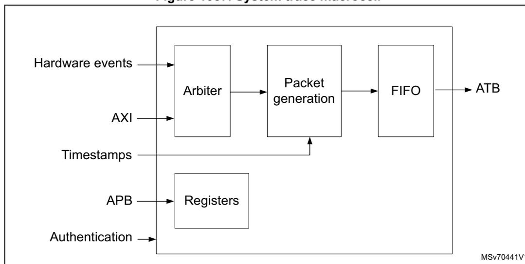
    graph LR
    HE[Hardware events] --> Arbiter
    AXI[AXI] --> Arbiter
    TS[Timestamps] --> PG[Packet generation]
    APB[APB] --> Reg[Registers]
    Auth[Authentication] --> Reg
    Arbiter --> PG
    Reg --> PG
    PG --> FIFO
    FIFO --> ATB
Detailed description: The diagram shows the internal architecture of the STM. On the left, input signals include 'Hardware events', 'AXI', 'Timestamps', 'APB', and 'Authentication'. 'Hardware events' and 'AXI' feed into an 'Arbiter' block. The 'Arbiter' output goes to a 'Packet generation' block. 'Timestamps' also feed directly into 'Packet generation'. 'APB' and 'Authentication' feed into a 'Registers' block, which in turn provides control/data to the 'Packet generation' block. The 'Packet generation' block outputs to a 'FIFO', which finally outputs to the 'ATB' bus on the right. The entire logic is enclosed in a boundary box labeled MSv70441V1.
The STM is configured with the following values to minimize the footprint in gates count:
- • DATA_FIFO_DEPTH = 4
- • CHN_FIFO_DEPTH = 4
- • HW_EVOBIF_PRESENT = TRUE
The various AXI masters can generate trace by writing to the extended stimulus ports of the STM via its AXI slave port, mapped in a 1-Mbyte window of address space (see Section 2.3: Memory organization ). A 256-byte extended stimulus port comprises 16 x 64-bit locations or registers. Writes to different locations generate different types of trace packets, as shown in the table below.
The base address for stimulus port n is the STM base address + n × 256. A master can use any number of the 4096 available stimulus ports mapped in the 1-Mbyte window.
Table 898. STM extended stimulus port memory map
| Address offset | Name | Description |
|---|---|---|
| 0x00 | G_DMTS | Data, marked with timestamp, guaranteed |
| 0x08 | G_DM | Data, marked, guaranteed |
| 0x10 | G_DTS | Data, with timestamp, guaranteed |
| 0x18 | G_D | Data, guaranteed |
| 0x20-0x58 | - | Reserved |
| 0x60 | G_FLAGTS | Flag with timestamp, guaranteed |
| 0x68 | G_FLAG | Flag, guaranteed |
| Address offset | Name | Description |
|---|---|---|
| 0x70 | G_TRIGTS | Trigger with timestamp, guaranteed |
| 0x78 | G_TRIG | Trigger, guaranteed |
| 0x80 | I_DMTS | Data, marked with timestamp, invariant timing |
| 0x88 | I_DM | Data, marked, invariant timing |
| 0x90 | I_DTS | Data, with timestamp, invariant timing |
| 0x98 | I_D | Data, invariant timing |
| 0xA0-0xD8 | - | Reserved |
| 0xE0 | I_FLAGTS | Flag with timestamp, invariant timing |
| 0xE8 | I_FLAG | Flag, invariant timing |
| 0xF0 | I_TRIGTS | Trigger with timestamp, invariant timing |
| 0xF8 | I_TRIG | Trigger, invariant timing |
The trace packets contain the 8-bit identity of the master that triggered them. This identity is decoded from the nonsecure master ID carried on the AWID wires of the AXI interconnect. The ID also includes the security status of the master at the time.
The ID is mapped as follows:
- • Bit [7] = 0
- • Bit [6] = secure/nonsecure state
- • Bit [5:0] = master ID
A list of valid IDs and how they map to the originating master is given in the table below.
Table 899. STM trace packet ID mapping to AXI masters| Master | Secure access ID | Nonsecure access ID |
|---|---|---|
| Cortex-M55 | 0x00 | 0x40 |
| HPDMA1 | 0x01 | 0x41 |
| AXI-AP | 0x02 | 0x42 |
The STM can also generate trace packets or triggers when certain hardware events are detected. Events can be selected from one of two banks, each bank containing up to 32 events. The bank is selected in the STM_HEBSR register, and the 32 events can be individually enabled in STM_HETER register. All events are edge sensitive.
The events for each banks are shown in Table 900 .
Table 900. Hardware event mapping
| Bank | Event | EXTMUX(7:0) = 0 | - | Bank | Event | EXTMUX(7:0) = 0 |
|---|---|---|---|---|---|---|
| HEBS = 0 | 0 | HWEVENTA ↑ | - | HEBS = 1 | 0 | HPDMA0_ch0_irq |
| 1 | HWEVENTA ↓ | - | 1 | HPDMA0_ch1_irq | ||
| 2 | HWEVENTB ↑ | - | 2 | HPDMA0_ch2_irq | ||
| 3 | HWEVENTB ↓ | - | 3 | HPDMA0_ch3_irq | ||
| 4 | - | - | 4 | HPDMA0_ch4_irq | ||
| 5 | NPU_DBG[0] | - | 5 | HPDMA0_ch5_irq | ||
| 6 | NPU_DBG[1] | - | 6 | HPDMA0_ch6_irq | ||
| 7 | NPU_DBG[2] | - | 7 | HPDMA0_ch7_irq | ||
| 8 | NPU_DBG[3] | - | 8 | HPDMA0_ch8_irq | ||
| 9 | NPU_DBG[4] | - | 9 | HPDMA0_ch9_irq | ||
| 10 | NPU_DBG[5] | - | 10 | HPDMA0_ch10_irq | ||
| 11 | NPU_DBG[6] | - | 11 | HPDMA0_ch11_irq | ||
| 12 | NPU_DBG[7] | - | 12 | HPDMA0_ch12_irq | ||
| 13 | - | - | 13 | HPDMA0_ch13_irq | ||
| 14 | GPU_irq | - | 14 | HPDMA0_ch14_irq | ||
| 15 | - | - | 15 | HPDMA0_ch15_irq | ||
| 16 | EXTI0_irq | - | 16 | GPDMA0_ch0_irq | ||
| 17 | EXTI1_irq | - | 17 | GPDMA0_ch1_irq | ||
| 18 | EXTI2_irq | - | 18 | GPDMA0_ch2_irq | ||
| 19 | EXTI3_irq | - | 19 | GPDMA0_ch3_irq | ||
| 20 | EXTI4_irq | - | 20 | GPDMA0_ch4_irq | ||
| 21 | EXTI5_irq | - | 21 | GPDMA0_ch5_irq | ||
| 22 | EXTI6_irq | - | 22 | GPDMA0_ch6_irq | ||
| 23 | EXTI7_irq | - | 23 | GPDMA0_ch7_irq | ||
| 24 | EXTI8_irq | - | 24 | GPDMA0_ch8_irq | ||
| 25 | EXTI9_irq | - | 25 | GPDMA0_ch9_irq | ||
| 26 | EXTI10_irq | - | 26 | GPDMA0_ch10_irq | ||
| 27 | EXTI11_irq | - | 27 | GPDMA0_ch11_irq | ||
| 28 | EXTI12_irq | - | 28 | GPDMA0_ch12_irq | ||
| 29 | EXTI13_irq | - | 29 | GPDMA0_ch13_irq | ||
| 30 | EXTI14_irq | - | 30 | GPDMA0_ch14_irq | ||
| 31 | EXTI15_irq | - | 31 | GPDMA0_ch15_irq |
For more information on the system trace macrocell, refer to the Arm CoreSight STM-500 System Trace Macrocell Technical Reference Manual [6].
78.12.19 STM registers
The register file base address for the STM is defined in Table 880 .
STM hardware event enable register (STM_HEER)
Address offset: 0xD00
Reset value: 0x0000 0000
| 31 | 30 | 29 | 28 | 27 | 26 | 25 | 24 | 23 | 22 | 21 | 20 | 19 | 18 | 17 | 16 |
|---|---|---|---|---|---|---|---|---|---|---|---|---|---|---|---|
| HEE[31:16] | |||||||||||||||
| rw | rw | rw | rw | rw | rw | rw | rw | rw | rw | rw | rw | rw | rw | rw | rw |
| 15 | 14 | 13 | 12 | 11 | 10 | 9 | 8 | 7 | 6 | 5 | 4 | 3 | 2 | 1 | 0 |
| HEE[15:0] | |||||||||||||||
| rw | rw | rw | rw | rw | rw | rw | rw | rw | rw | rw | rw | rw | rw | rw | rw |
Bits 31:0 HEE[31:0] : Hardware event enable
HEE is used to enable hardware events to generate trace. The register defines one bit per hardware event.
0: Hardware event disabled
1: Hardware event enabled
STM hardware event trigger enable register (STM_HETER)
Address offset: 0xD20
Reset value: 0x0000 0000
| 31 | 30 | 29 | 28 | 27 | 26 | 25 | 24 | 23 | 22 | 21 | 20 | 19 | 18 | 17 | 16 |
|---|---|---|---|---|---|---|---|---|---|---|---|---|---|---|---|
| HETE[31:16] | |||||||||||||||
| rw | rw | rw | rw | rw | rw | rw | rw | rw | rw | rw | rw | rw | rw | rw | rw |
| 15 | 14 | 13 | 12 | 11 | 10 | 9 | 8 | 7 | 6 | 5 | 4 | 3 | 2 | 1 | 0 |
| HETE[15:0] | |||||||||||||||
| rw | rw | rw | rw | rw | rw | rw | rw | rw | rw | rw | rw | rw | rw | rw | rw |
Bits 31:0 HETE[31:0] : Trigger generation enable
HETE is a bit mask used to enable trigger generation on hardware events. This bitfield defines one bit per hardware event.
0: Disabled
1: Enabled
STM hardware event bank select register (STM_HEBSR)
Address offset: 0xD60
Reset value: 0x0000 0000
| 31 | 30 | 29 | 28 | 27 | 26 | 25 | 24 | 23 | 22 | 21 | 20 | 19 | 18 | 17 | 16 |
|---|---|---|---|---|---|---|---|---|---|---|---|---|---|---|---|
| Res. | Res. | Res. | Res. | Res. | Res. | Res. | Res. | Res. | Res. | Res. | Res. | Res. | Res. | Res. | Res. |
| 15 | 14 | 13 | 12 | 11 | 10 | 9 | 8 | 7 | 6 | 5 | 4 | 3 | 2 | 1 | 0 |
| Res. | Res. | Res. | Res. | Res. | Res. | Res. | Res. | Res. | Res. | Res. | Res. | Res. | Res. | Res. | HEBS |
| rw |
Bits 31:1 Reserved, must be kept at reset value.
Bit 0 HEBS : Hardware event bank selector
HEBS is used to select the bank of 32 hardware events to control (see Table 900 ).
0: Bank 0
1: Bank 1
STM hardware event main control register (STM_HEMCR)
Address offset: 0xD64
Reset value: 0x0000 0000
| 31 | 30 | 29 | 28 | 27 | 26 | 25 | 24 | 23 | 22 | 21 | 20 | 19 | 18 | 17 | 16 |
|---|---|---|---|---|---|---|---|---|---|---|---|---|---|---|---|
| Res. | Res. | Res. | Res. | Res. | Res. | Res. | Res. | Res. | Res. | Res. | Res. | Res. | Res. | Res. | Res. |
| 15 | 14 | 13 | 12 | 11 | 10 | 9 | 8 | 7 | 6 | 5 | 4 | 3 | 2 | 1 | 0 |
| Res. | Res. | Res. | Res. | Res. | Res. | Res. | Res. | ATBTRIGEN | TRIGCLEAR | TRIGSTATUS | TRIGCTL | Res. | ERRDETECT | COMPEN | EN |
| rw | rw | r | rw | r | rw | rw |
Bits 31:8 Reserved, must be kept at reset value.
Bit 7 ATBTRIGEN : ATB trace trigger enable
When set, this bit enables the STM to use the ATID value of 0x7D when a trigger event on match using STMHETER occurs.
0: Do not output ATB trace triggers.
1: Use ATB trace triggers.
Bit 6 TRIGCLEAR : Clear trigger status
When TRIGCTL indicates single-shot mode, this bit is used to clear TRIGSTATUS.
Writing a 1 to this bit when in multi-shot mode is unpredictable.
0: No effect
1: Clear TRIGSTATUS (if equal to 1).
Bit 5 TRIGSTATUS : trigger status
When TRIGCTL indicates single-shot mode, this indicates whether the single trigger has occurred.
0: Trigger has not occurred.
1: Trigger has occurred.
Bit 4 TRIGCTL : Trigger control
0: Triggers are multi-shot.
1: Triggers are single-shot.
Bit 3 Reserved, must be kept at reset value.
Bit 2 ERRDETECT : Error detection
This bit enables error detection on the hardware event tracing.
0: Disabled
1: Enabled
Bit 1 COMPEN : Compression enable
This bit enables leading 0 suppression of hardware event data values in the trace stream.
0: Disabled
1: Enabled
Bit 0 EN : Hardware event tracing enable
0: Disabled
1: Enabled
STM hardware event external multiplex control register (STM_HEEXTMUXR)
Address offset: 0xD68
Reset value: 0x0000 0000
| 31 | 30 | 29 | 28 | 27 | 26 | 25 | 24 | 23 | 22 | 21 | 20 | 19 | 18 | 17 | 16 |
|---|---|---|---|---|---|---|---|---|---|---|---|---|---|---|---|
| Res. | Res. | Res. | Res. | Res. | Res. | Res. | Res. | Res. | Res. | Res. | Res. | Res. | Res. | Res. | Res. |
| 15 | 14 | 13 | 12 | 11 | 10 | 9 | 8 | 7 | 6 | 5 | 4 | 3 | 2 | 1 | 0 |
| Res. | Res. | Res. | Res. | Res. | Res. | Res. | Res. | EXTMUX[7:0] | |||||||
| rw | rw | rw | rw | rw | rw | rw | rw | ||||||||
Bits 31:8 Reserved, must be kept at reset value.
Bits 7:0 EXTMUX[7:0] : Signals for events selector
This bitfield selects the signals to be mapped onto the 64 hardware events that can be traced by the STM (refer to Table 900 ).
STM hardware event master number register (STM_HEMASTR)
Address offset: 0xDF4
Reset value: 0x0000 0080
| 31 | 30 | 29 | 28 | 27 | 26 | 25 | 24 | 23 | 22 | 21 | 20 | 19 | 18 | 17 | 16 |
|---|---|---|---|---|---|---|---|---|---|---|---|---|---|---|---|
| Res. | Res. | Res. | Res. | Res. | Res. | Res. | Res. | Res. | Res. | Res. | Res. | Res. | Res. | Res. | Res. |
| 15 | 14 | 13 | 12 | 11 | 10 | 9 | 8 | 7 | 6 | 5 | 4 | 3 | 2 | 1 | 0 |
| MASTER[15:0] | |||||||||||||||
| r | r | r | r | r | r | r | r | r | r | r | r | r | r | r | r |
Bits 31:16 Reserved, must be kept at reset value.
Bits 15:0 MASTER[15:0] : STPv2 master number
This bitfield indicates the STPv2 master number of hardware event trace. This number is the master number presented in STPv2.
0x80: Hardware events are associated with master 0x80.
Others: reserved
STM hardware event features 1 register (STM_HEFEAT1R)Address offset: 0xDF8
Reset value: 0x3020 0035
| 31 | 30 | 29 | 28 | 27 | 26 | 25 | 24 | 23 | 22 | 21 | 20 | 19 | 18 | 17 | 16 |
|---|---|---|---|---|---|---|---|---|---|---|---|---|---|---|---|
| Res. | HEEXTMUXSIZE[2:0] | Res. | Res. | Res. | Res. | NUMHE[8:1] | |||||||||
| r | r | r | r | r | r | r | r | r | r | r | |||||
| 15 | 14 | 13 | 12 | 11 | 10 | 9 | 8 | 7 | 6 | 5 | 4 | 3 | 2 | 1 | 0 |
| NUMHE[0] | Res. | Res. | Res. | Res. | Res. | Res. | Res. | Res. | Res. | HECOMP[1:0] | HEMASTR | HEERR | Res. | HETER | |
| r | r | r | r | r | r | ||||||||||
Bit 31 Reserved, must be kept at reset value.
Bits 30:28 HEEXTMUXSIZE[2:0] : EXTMUX bitfield size
This bitfield indicates the size of EXTMUX bitfield in STM_HEEXTMUXR.
0x3: 8-bit wide (up to 256 multiplexers)
Others: Reserved
Bits 27:24 Reserved, must be kept at reset value.
Bits 23:15 NUMHE[8:0] : Number of hardware events supported by the STM
0x40: 64 hardware events
Bits 14:6 Reserved, must be kept at reset value.
Bits 5:4 HECOMP[1:0] : Data compression on hardware event tracing support
0x3: Data compression support is programmable. COMPEN in STM_HEMCR is implemented.
Bit 3 HEMASTR : STMHEMASTR support
0: STMHEMASTR is read-only.
Bit 2 HEERR : Hardware event error detection support
1: Hardware event error detection implemented. ERRDETECT in STM_HEMCR is implemented.
Bit 1 Reserved, must be kept at reset value.
Bit 0 HETER : STM_HETER support
1: Implemented
STM hardware event features ID register (STM_HEIDR)Address offset: 0xDFC
Reset value: 0x0000 0011
| 31 | 30 | 29 | 28 | 27 | 26 | 25 | 24 | 23 | 22 | 21 | 20 | 19 | 18 | 17 | 16 |
|---|---|---|---|---|---|---|---|---|---|---|---|---|---|---|---|
| Res. | Res. | Res. | Res. | Res. | Res. | Res. | Res. | Res. | Res. | Res. | Res. | Res. | Res. | Res. | Res. |
| 15 | 14 | 13 | 12 | 11 | 10 | 9 | 8 | 7 | 6 | 5 | 4 | 3 | 2 | 1 | 0 |
| Res. | Res. | Res. | Res. | VENDSPEC[3:0] | CLASSREV[3:0] | CLASS[3:0] | |||||||||
| r | r | r | r | r | r | r | r | r | r | r | r | ||||
Bits 31:12 Reserved, must be kept at reset value.
Bits 11:8 VENDSPEC[3:0] : Vendor specific
This bitfield identifies any vendor specific modifications or mappings.
0: Vendor specific information
Others: Reserved
Bits 7:4 CLASSREV[3:0] : Programmer model revision
1: Revision
Others: Reserved
Bits 3:0 CLASS[3:0] : Programmer model
1: Hardware event control
Others: Reserved
STM stimulus port enable register (STM_SPER)
Address offset: 0xE00
Reset value: 0x0000 0000
This register is used to enable the stimulus registers to generate the trace.
| 31 | 30 | 29 | 28 | 27 | 26 | 25 | 24 | 23 | 22 | 21 | 20 | 19 | 18 | 17 | 16 |
| SPE[31:16] | |||||||||||||||
| rw | rw | rw | rw | rw | rw | rw | rw | rw | rw | rw | rw | rw | rw | rw | rw |
| 15 | 14 | 13 | 12 | 11 | 10 | 9 | 8 | 7 | 6 | 5 | 4 | 3 | 2 | 1 | 0 |
| SPE[15:0] | |||||||||||||||
| rw | rw | rw | rw | rw | rw | rw | rw | rw | rw | rw | rw | rw | rw | rw | rw |
Bits 31:0 SPE[31:0] : Stimulus port enable
This register is used to enable STM registers to generate the trace. It defines one bit per stimulus register. Writing one enables the appropriate stimulus port. Writing 0 disables the appropriate stimulus port. This register is used in conjunction with STM_SPSCR.
0: Disabled
1: Enabled
STM stimulus port trigger enable register (STM_SPTER)
Address offset: 0xE20
Reset value: 0x0000 0000
This register is used to enable trigger generation on writes to enabled stimulus port registers.
| 31 | 30 | 29 | 28 | 27 | 26 | 25 | 24 | 23 | 22 | 21 | 20 | 19 | 18 | 17 | 16 |
| SPTE[31:16] | |||||||||||||||
| rw | rw | rw | rw | rw | rw | rw | rw | rw | rw | rw | rw | rw | rw | rw | rw |
| 15 | 14 | 13 | 12 | 11 | 10 | 9 | 8 | 7 | 6 | 5 | 4 | 3 | 2 | 1 | 0 |
| SPTE[15:0] | |||||||||||||||
| rw | rw | rw | rw | rw | rw | rw | rw | rw | rw | rw | rw | rw | rw | rw | rw |
Bits 31:0 SPTE[31:0] : Trigger generation bit mask
This register is a bit mask used to enable the trigger generation on writes to enabled stimulus port registers. It defines one bit per stimulus port register.
0: Disabled
1: Enabled
STM stimulus port select configuration register (STM_SPSCR)
Address offset: 0xE60
Reset value: 0x0000 0000
This register allows a debugger to program which stimulus ports the STM_SPER and STM_SPTER registers apply to.
| 31 | 30 | 29 | 28 | 27 | 26 | 25 | 24 | 23 | 22 | 21 | 20 | 19 | 18 | 17 | 16 |
|---|---|---|---|---|---|---|---|---|---|---|---|---|---|---|---|
| Res. | Res. | Res. | Res. | PORTSEL[7:0] | Res. | Res. | Res. | Res. | |||||||
| rw | rw | rw | rw | rw | rw | rw | rw | ||||||||
| 15 | 14 | 13 | 12 | 11 | 10 | 9 | 8 | 7 | 6 | 5 | 4 | 3 | 2 | 1 | 0 |
| Res. | Res. | Res. | Res. | Res. | Res. | Res. | Res. | Res. | Res. | Res. | Res. | Res. | Res. | PORTCTL[1:0] | |
| rw | rw | ||||||||||||||
Bits 31:28 Reserved, must be kept at reset value.
Bits 27:20 PORTSEL[7:0] : Stimulus port selector
This bitfield defines which group of 32 stimulus ports, the STM_SPTER and/or STM_SPER registers apply to.
0000000: Reserved
nnnn nnn1: Select 1 group, 0bnnn nnnn.
nnnn nn10: Select 2 groups, 0bnnn nnn0 to 0bnnn nnn1.
nnnn n100: Select 4 groups, 0bnnn nn00 to 0bnnn nn11.
..
n100 0000: Select 64 groups, 0bn00 0000 to 0bn11 1111.
1000 0000: Select all 128 groups.
Bits 19:2 Reserved, must be kept at reset value.
Bits 1:0 PORTCTL[1:0] : Port selection control mode
This bitfield defines how the port selection programmed in PORTSEL[7:0] is applied.
0x0: Port selection not used. STM_PER and STM_PTER apply to all groups.
0x1: Port selection applies only to STM_SPTER. STM_PER applies to all groups
0x2: Reserved
0x3: Port selection applies to both STM_SPER and STM_SPTER registers.
STM stimulus port master select configuration register (STM_SPMSCR)
Address offset: 0xE64
Reset value: 0x0000 0000
This register allows a debugger to program which masters the STM_SPSCR register applies to.
| 31 | 30 | 29 | 28 | 27 | 26 | 25 | 24 | 23 | 22 | 21 | 20 | 19 | 18 | 17 | 16 |
|---|---|---|---|---|---|---|---|---|---|---|---|---|---|---|---|
| Res | Res | Res | Res | Res | Res | Res | Res | Res | MASTSEL[7:1] | ||||||
| rw | rw | rw | rw | rw | rw | rw | |||||||||
| 15 | 14 | 13 | 12 | 11 | 10 | 9 | 8 | 7 | 6 | 5 | 4 | 3 | 2 | 1 | 0 |
| MASTSEL[0] | Res. | Res. | Res. | Res. | Res. | Res. | Res. | Res. | Res. | Res. | Res. | Res. | Res. | Res. | MASTCTL |
| rw | rw | ||||||||||||||
Bits 31:23 Reserved, must be kept at reset value.
Bits 22:15 MASTSEL[7:0] : Master selection
This bitfield defines which masters the STM_SPSCR register applies to. Six masters are supported (see Table 899 for the master ID mapping).
0000 0001: Select master 0x00.
0000 0011: Select master 0x01.
0000 0101: Select master 0x02.
0000 0010: Select master 0x00 and master 0x01.
0000 0100: Select master 0x00, master 0x01 and master 0x02.
1000 0001: Select master 0x40.
1000 0011: Select master 0x41.
1000 0101: Select master 0x42.
1000 0010: Select master 0x40 and master 0x41.
1000 0100: Select master 0x40, master 0x41 and master 0x42.
1000 0000: Select all masters.
Others: Reserved
Bits 14:1 Reserved, must be kept at reset value.
Bit 0 MASTCTL : Master control mode
This bitfield defines how the master is applied.
0: Master selection not used. STM_SPSCR applies to all masters.
1: Master selection applies to STM_SPSCR.
STM stimulus port override control register (STM_SPOVERRIDER)
Address offset: 0xE68
Reset value: 0x0000 0000
This register allows a debugger to override various features of the STM.
| 31 | 30 | 29 | 28 | 27 | 26 | 25 | 24 | 23 | 22 | 21 | 20 | 19 | 18 | 17 | 16 |
|---|---|---|---|---|---|---|---|---|---|---|---|---|---|---|---|
| Res | Res | Res | Res | PORTSEL[12:1] | |||||||||||
| rw | rw | rw | rw | rw | rw | rw | rw | rw | rw | rw | rw | ||||
| 15 | 14 | 13 | 12 | 11 | 10 | 9 | 8 | 7 | 6 | 5 | 4 | 3 | 2 | 1 | 0 |
| PORTSEL[0] | Res. | Res. | Res. | Res. | Res. | Res. | Res. | Res. | Res. | Res. | Res. | Res. | OVERTS | OVERCTL[1:0] | |
| rw | rw | rw | rw | ||||||||||||
Bits 31:28 Reserved, must be kept at reset value.
Bits 27:15 PORTSEL[12:0] : Port override select
This bitfield defines which stimulus ports the override controls apply to.
0000 0000 0000 0: Reserved
nnnn nnnn nnnn 1: Select port 0bnnnn nnnn nnnn.
nnnn nnnn nnn1 0: Select ports 0bnnnn nnnn nnn0 to 0bnnnn nnnn nnn1.
nnnn nnnn nn10 0: Select ports 0bnnnn nnnn nn00 to 0bnnnn nnnn nn11.
..
n100 0000 0000: Select ports 0bn000 0000 0000 to 0bn111 1111 1111.
1000 0000 0000: Select all 4096 ports.
Bits 14:3 Reserved, must be kept at reset value.
Bit 2 OVERTS : Override timestamp request
This override requests all stimulus port writes that cause trace to be traced with a timestamp (when possible). As with normal operation, this does not ensure that all packets are generated with timestamps. This bitfield is independent from OVERCTL and PORTSEL.
0: Override disabled
1: Override enabled
Bits 1:0 OVERCTL[1:0] : Override control mode
This bitfield defines how the port selection is applied.
0x0: Override controls disabled
0x1: Ports selected by PORTSEL always behave as guaranteed transactions.
0x2: Ports selected by PORTSEL always behave as invariant timing transactions
0x3: Reserved
STM stimulus port master override control register (STM_SPMOVERRIDER)
Address offset: 0xE6C
Reset value: 0x0000 0000
This register allows a debugger to select which masters STM_SPOVERRIDER applies to.
| 31 | 30 | 29 | 28 | 27 | 26 | 25 | 24 | 23 | 22 | 21 | 20 | 19 | 18 | 17 | 16 |
|---|---|---|---|---|---|---|---|---|---|---|---|---|---|---|---|
| Res. | Res. | Res. | Res. | Res. | Res. | Res. | Res. | Res. | MASTSEL[7:1] | ||||||
| rw | rw | rw | rw | rw | rw | rw | |||||||||
| 15 | 14 | 13 | 12 | 11 | 10 | 9 | 8 | 7 | 6 | 5 | 4 | 3 | 2 | 1 | 0 |
| MASTS EL[0] | Res. | Res. | Res. | Res. | Res. | Res. | Res. | Res. | Res. | Res. | Res. | Res. | Res. | Res. | MASTC TL |
| rw | rw | ||||||||||||||
Bits 31:23 Reserved, must be kept at reset value.
Bits 22:15 MASTSEL[7:0] : Master port override selection
This bitfield defines which master ports the override controls apply to. Six masters are supported (see Table 899 for the master ID mapping).
0000 0001: Select master 0x00.
0000 0011: Select master 0x01.
0000 0101: Select master 0x02.
0000 0010: Select master 0x00 and master 0x01.
0000 0100: Select master 0x00, master 0x01 and master 0x02.
1000 0001: Select master 0x40.
1000 0011: Select master 0x41.
1000 0101: Select master 0x42.
1000 0010: Select master 0x40 and master 0x41.
1000 0100: Select master 0x40, master 0x41 and master 0x42.
1000 0000: Select all masters.
Others: Reserved
Bits 14:1 Reserved, must be kept at reset value.
Bit 0 MASTCTL : Master selection control mode
This bitfield defines how the master selection is applied.
0: Override controls disabled. STM_SPOVERRIDER applies equally to all masters.
1: Master selection enabled. STM_SPOVERRIDER applies to the masters selected by MASTSEL[7:0].
STM stimulus port trigger control and status register (STM_SPTRIGCSR)
Address offset: 0xE70
Reset value: 0x0000 0000
This register is used to control the STM triggers induced by STM_SPTER.
| 31 | 30 | 29 | 28 | 27 | 26 | 25 | 24 | 23 | 22 | 21 | 20 | 19 | 18 | 17 | 16 |
|---|---|---|---|---|---|---|---|---|---|---|---|---|---|---|---|
| Res. | Res. | Res. | Res. | Res. | Res. | Res. | Res. | Res. | Res. | Res. | Res. | Res. | Res. | Res. | Res. |
| 15 | 14 | 13 | 12 | 11 | 10 | 9 | 8 | 7 | 6 | 5 | 4 | 3 | 2 | 1 | 0 |
| Res. | Res. | Res. | Res. | Res. | Res. | Res. | Res. | Res. | Res. | Res. | ATBTRIGEN_D IR | ATBTRIGEN_T E | TRIGC LEAR | TRIGS TATUS | TRIGC TL |
| rw | rw | w | r | rw |
Bits 31:5 Reserved, must be kept at reset value.
Bit 4 ATBTRIGEN_DIR : ATB trace on write to TRIG
When set, this bit enables the STM to use the ATID value of 0x7D when a trigger event on writes to TRIG location occurs.
0: Does not output ATB trace triggers on write to TRIG location.
1: Outputs ATB trace trigger for trigger on write to TRIG location.
Bit 3 ATBTRIGEN_TE : ATB trace-trigger output
When set, this bit enables the STM to use the ATID value of 0x7D when a trigger event on match using STM_SPTER occurs.
0: Does not output ATB trace trigger for trigger on match using STM_SPTER.
1: Outputs ATB trace trigger for trigger on match using STM_SPTER.
Bit 2 TRIGCLEAR : trigger status clear
When TRIGCTL indicates single-shot mode, this TRIGCLEAR bit is used to clear TRIGSTATUS. Writing a one to this bit when in multi-shot mode leads to an unpredictable behavior.
0: No effect
1: Clear TRIGSTATUS if TRIGSTATUS = 1.
Bit 1 TRIGSTATUS : Trigger status
When TRIGCTL indicates single-shot mode, this TRIGSTATUS bit indicates whether the single trigger has occurred.
0: Trigger has not occurred.
1: Trigger has occurred.
Bit 0 TRIGCTL : Trigger control
0: Triggers are multi-shot.
1: Triggers are single-shot.
STM trace control and status register (STM_TCSR)
Address offset: 0xE80
Reset value: 0x0000 0004
| 31 | 30 | 29 | 28 | 27 | 26 | 25 | 24 | 23 | 22 | 21 | 20 | 19 | 18 | 17 | 16 |
|---|---|---|---|---|---|---|---|---|---|---|---|---|---|---|---|
| Res. | Res. | Res. | Res. | Res. | Res. | Res. | Res. | BUSY | TRACEID[6:0] | ||||||
| r | rw | rw | rw | rw | rw | rw | rw | ||||||||
| 15 | 14 | 13 | 12 | 11 | 10 | 9 | 8 | 7 | 6 | 5 | 4 | 3 | 2 | 1 | 0 |
| Res. | Res. | Res. | Res. | Res. | Res. | Res. | Res. | Res. | Res. | COMP EN | Res. | Res. | SYNCE N | TSEN | EN |
| rw | r | rw | rw | ||||||||||||
Bits 31:24 Reserved, must be kept at reset value.
Bit 23 BUSY : STM busy
This bit indicates if the STM is busy (for example because STM trace FIFO is not empty).
0: STM is not busy.
1: STM is busy.
Bits 22:16 TRACEID[6:0] : ATB Trace ID
Bits 15:6 Reserved, must be kept at reset value.
Bit 5 COMPEN : Compression enable for stimulus ports
0: Compression disabled. Data transfers are transmitted at the size of the transaction.
1: Compression enabled. Data transfers are compressed to save bandwidth.
Bits 4:3 Reserved, must be kept at reset value.
Bit 2 SYNCEN : STM_SYNCR implementation
1: Implemented
Bit 1 TSEN : Timestamp requests enable
This bit controls if timestamp requests are ignored or taken into account.
0: Timestamping disabled. Requests for timestamp generation are ignored, and stimulus port writes selecting timestamping are treated as if it were not selected.
1: Timestamping enabled. If stimulus writes select timestamping, a timestamp is output according to STPv2.
Bit 0 EN : Global STM enable
0: STM disabled
1: STM enabled
STM timestamp stimulus register (STM_TSSTIMR)
Address offset: 0xE84
Reset value: 0x0000 0000
| 31 | 30 | 29 | 28 | 27 | 26 | 25 | 24 | 23 | 22 | 21 | 20 | 19 | 18 | 17 | 16 |
|---|---|---|---|---|---|---|---|---|---|---|---|---|---|---|---|
| Res. | Res. | Res. | Res. | Res. | Res. | Res. | Res. | Res. | Res. | Res. | Res. | Res. | Res. | Res. | Res. |
| 15 | 14 | 13 | 12 | 11 | 10 | 9 | 8 | 7 | 6 | 5 | 4 | 3 | 2 | 1 | 0 |
| Res. | Res. | Res. | Res. | Res. | Res. | Res. | Res. | Res. | Res. | Res. | Res. | Res. | Res. | Res. | FORCE TS |
| w |
Bits 31:1 Reserved, must be kept at reset value.
Bit 0 FORCETS : Force timestamp stimulus
Write a one to this bit requests the next stimulus port write which causes trace to be upgraded to have a timestamp. Writes this bit as 0 are ignored.
1: Force timestamp stimulus
STM timestamp frequency register (STM_TSFREQR)
Address offset: 0xE8C
Reset value: 0x0000 0000
This register is used to indicate the frequency of the timestamp counter. The unit of measurement is increments per second. When the STPv2 protocol is used, this register contains the value output in FREQ and FREQ_TS packets. The timestamp frequency is output in the STPv2 protocol at every synchronization point when TSEN = 1 in STM_TCSR.
| 31 | 30 | 29 | 28 | 27 | 26 | 25 | 24 | 23 | 22 | 21 | 20 | 19 | 18 | 17 | 16 |
|---|---|---|---|---|---|---|---|---|---|---|---|---|---|---|---|
| FREQ[31:16] | |||||||||||||||
| rw | rw | rw | rw | rw | rw | rw | rw | rw | rw | rw | rw | rw | rw | rw | rw |
| 15 | 14 | 13 | 12 | 11 | 10 | 9 | 8 | 7 | 6 | 5 | 4 | 3 | 2 | 1 | 0 |
| FREQ[15:0] | |||||||||||||||
| rw | rw | rw | rw | rw | rw | rw | rw | rw | rw | rw | rw | rw | rw | rw | rw |
Bits 31:0 FREQ[31:0] : Timestamp frequency
This bitfield indicates the frequency of the timestamp counter (in Hz).
STM synchronization control register (STM_SYNCN)
Address offset: 0xE90
Reset value: 0x0000 0000
This register controls the interval between synchronization packets as a function of the number of bytes of trace generated. It provides a hint of the desired synchronization
frequency since implementations are permitted to be inaccurate. Writing 0x0000 0000 to this register disables the synchronization counter. However any other implementation defined synchronization mechanism continues to operate independently (refer to the next register STM_AUXCR).
| 31 | 30 | 29 | 28 | 27 | 26 | 25 | 24 | 23 | 22 | 21 | 20 | 19 | 18 | 17 | 16 |
|---|---|---|---|---|---|---|---|---|---|---|---|---|---|---|---|
| Res. | Res. | Res. | Res. | Res. | Res. | Res. | Res. | Res. | Res. | Res. | Res. | Res. | Res. | Res. | Res. |
| 15 | 14 | 13 | 12 | 11 | 10 | 9 | 8 | 7 | 6 | 5 | 4 | 3 | 2 | 1 | 0 |
| Res. | Res. | Res. | MODE | COUNT[8:0] | Res. | Res. | Res. | ||||||||
| rw | rw | rw | rw | rw | rw | rw | rw | rw | rw | ||||||
Bits 31:13 Reserved, must be kept at reset value.
Bit 12 MODE : Mode control
0: COUNT[8:0] defines a value N. Synchronization period is 8 x N bytes.
1: COUNT[8:4] defines a value N. Synchronization period is 2 N bytes. N must be in the range of 12 to 27 inclusive. Other values lead to unpredictable results.
Bits 11:3 COUNT[8:0] : Number of bytes between synchronization packets
This bitfield indicates the counter value for the number of bytes between synchronization packets.
Bits 2:0 Reserved, must be kept at reset value.
STM auxiliary control register (STM_AUXCR)
Address offset: 0xE94
Reset value: 0x0000 0000
This register is used for implementation defined STM controls.
| 31 | 30 | 29 | 28 | 27 | 26 | 25 | 24 | 23 | 22 | 21 | 20 | 19 | 18 | 17 | 16 |
|---|---|---|---|---|---|---|---|---|---|---|---|---|---|---|---|
| Res. | Res. | Res. | Res. | Res. | Res. | Res. | Res. | Res. | Res. | Res. | Res. | Res. | Res. | Res. | Res. |
| 15 | 14 | 13 | 12 | 11 | 10 | 9 | 8 | 7 | 6 | 5 | 4 | 3 | 2 | 1 | 0 |
| Res. | Res. | Res. | Res. | Res. | Res. | Res. | Res. | QHWE VOVER RIDE | Res. | Res. | Res. | Res. | PRIORI NVDIS | ASYNC PE | FIFOA F |
| rw | rw | rw | rw |
Bits 31:8 Reserved, must be kept at reset value.
Bit 7 QHWEVOVERRIDE : Override control for the Q-Channels
0: No override. Q-Channel is able to accept a quiescence request when hardware event tracing is enabled.
1: Override. Q-Channel denies a quiescence request when hardware event tracing is enabled.
Bits 6:3 Reserved, must be kept at reset value.
Bit 2 PRIORINVDIS : AXI versus hardware flush arbitration
This bit controls the arbitration between AXI and hardware during flush.
0: Priority inversion. When AXI flush is finished, the hardware gets priority until hardware flush is done.
1: Priority inversion disabled. AXI always has priority over hardware.
Bit 1 ASYNCPE : ASYNC priority
0: ASYNC priority is always lower than trace.
1: ASYNC priority increases on second synchronization request.
Bit 0 FIFOAF : Auto-flush
0: Disabled
1: Enabled
STM features 1 register (STM_FEAT1R)
Address offset: 0xEA0
Reset value: 0x0065 87D1
This register indicates the features of the STM in conjunction with STM_FEAT2R and STM_FEAT3R.
| 31 | 30 | 29 | 28 | 27 | 26 | 25 | 24 | 23 | 22 | 21 | 20 | 19 | 18 | 17 | 16 |
|---|---|---|---|---|---|---|---|---|---|---|---|---|---|---|---|
| Res. | Res. | Res. | Res. | Res. | Res. | Res. | Res. | SWOEN[1:0] | SYNCEN[1:0] | HWTEN[1:0] | TSPRESCALE[1:0] | ||||
| r | r | r | r | r | r | r | r | ||||||||
| 15 | 14 | 13 | 12 | 11 | 10 | 9 | 8 | 7 | 6 | 5 | 4 | 3 | 2 | 1 | 0 |
| TRIGCTL[1:0] | TRACEBUS[3:0] | SYNC[1:0] | FORCE TS | TSFRE Q | TS[1:0] | PROT[3:0] | |||||||||
| r | r | r | r | r | r | r | r | r | r | r | r | r | r | r | r |
Bits 31:24 Reserved, must be kept at reset value.
Bits 23:22 SWOEN[1:0] : SWOEN support
Support of SWOEN in STM_TCSR.
0x1: SWOEN in STM_TCSR is not implemented.
Bits 21:20 SYNCEN[1:0] : SYNCEN support
Support of SYNCEN in STM_TCSR.
0x2: SYNCEN in STM_TCSR is implemented but always reads as 1.
Bits 19:18 HWTEN[1:0] : HWTEN support
Support of HWTEN in STM_TCSR.
0x1: HWTEN in STM_TCSR is not implemented.
Bits 17:16 TSPRESCALE[1:0] : Timestamp prescale support
0x1: Not implemented.
Bits 15:14 TRIGCTL[1:0] : Trigger control support
0x2: Multi-shot and single-shot triggers supported. STM_TRIGCSR is implemented.
Bits 13:10 TRACEBUS[3:0] : Trace bus support
0x1: CoreSight ATB plus ATB trigger support implemented. TRACEID in STM_TCSR, and ATBTRIGEN_DIR and ATBTRIGEN_TE in STM_SPTRIGCSR, are implemented.
- Bits 9:8
SYNC[1:0]
: STM_SYNCR support
0x3: STM_SYNCR implemented with MODE control - Bit 7
FORCETS
: STM_TSSTIMR support
1: FORCETS in STM_TSSTIMR is implemented. - Bit 6
TSFREQ
: Timestamp frequency indication configuration
1: STM_TSFREQR is read-write. - Bits 5:4
TS[1:0]
: Timestamp support
0x1: Absolute timestamps implemented - Bits 3:0
PROT[3:0]
: Protocol
0x1: STPv2 protocol
STM features 2 register (STM_FEAT2R)
Address offset: 0xEA4
Reset value: 0x0001 14F2
This register indicates the features of the STM in conjunction with STM_FEAT1R and STM_FEAT3R.
| 31 | 30 | 29 | 28 | 27 | 26 | 25 | 24 | 23 | 22 | 21 | 20 | 19 | 18 | 17 | 16 |
|---|---|---|---|---|---|---|---|---|---|---|---|---|---|---|---|
| Res. | Res. | Res. | Res. | Res. | Res. | Res. | Res. | Res. | Res. | Res. | Res. | Res. | Res. | SPTYPE[1:0] | |
| r | r | ||||||||||||||
| 15 | 14 | 13 | 12 | 11 | 10 | 9 | 8 | 7 | 6 | 5 | 4 | 3 | 2 | 1 | 0 |
| DSIZE[3:0] | Res. | SPTRTYPE[1:0] | PRIVMASK[1:0] | SPOVERRIDE | SPCOMP[1:0] | Res. | SPER | SPTER[1:0] | |||||||
| r | r | r | r | r | r | r | r | r | r | r | r | r | r | ||
- Bits 31:18 Reserved, must be kept at reset value.
- Bits 17:16
SPTYPE[1:0]
: Stimulus port type support
0x1: Only extended stimulus ports implemented - Bits 15:12
DSIZE[3:0]
: Fundamental data size
0x1: 64-bit data - Bit 11 Reserved, must be kept at reset value.
- Bits 10:9
SPTRTYPE[1:0]
: Stimulus port transaction type support
0x2: Both invariant timing and guaranteed transactions are supported. - Bits 8:7
PRIVMASK[1:0]
: STM_PRIVMASKR support
0x1: STM_PRIVMASKR is not implemented. - Bit 6
SPOVERRIDE
: STM_OVERRIDER support
1: STM_SPOVERRIDER and STM_SPMOVERRIDER are implemented. - Bits 5:4
SPCOMP[1:0]
: Data compression on stimulus ports support
0x3: Data compression support is programmable. COMPEN in STM_TCSR is implemented. - Bit 3 Reserved, must be kept at reset value.
- Bit 2
SPER
: STM_SPER presence
0: STM_SPER is implemented.
Bits 1:0
SPTER[1:0]
: STM_SPTER support
0x2: STM_SPTER is implemented.
STM features 3 register (STM_FEAT3R)
Address offset: 0xEA8
Reset value: 0x0000 007F
This register indicates the features of the STM in conjunction with STM_FEAT1R and STM_FEAT2R.
| 31 | 30 | 29 | 28 | 27 | 26 | 25 | 24 | 23 | 22 | 21 | 20 | 19 | 18 | 17 | 16 |
|---|---|---|---|---|---|---|---|---|---|---|---|---|---|---|---|
| Res. | Res. | Res. | Res. | Res. | Res. | Res. | Res. | Res. | Res. | Res. | Res. | Res. | Res. | Res. | Res. |
| 15 | 14 | 13 | 12 | 11 | 10 | 9 | 8 | 7 | 6 | 5 | 4 | 3 | 2 | 1 | 0 |
| Res. | Res. | Res. | Res. | Res. | Res. | Res. | Res. | Res. | NUMMAST[6:0] | ||||||
| r | r | r | r | r | r | r | |||||||||
Bits 31:7 Reserved, must be kept at reset value.
Bits 6:0
NUMMAST[6:0]
: Number of stimulus ports masters implemented, minus 1
0x7F: 128 masters are implemented (only three masters are connected).
STM claim tag set register (STM_CLAIMSET)
Address offset: 0xFA0
Reset value: 0x0000 000F
This register is used in conjunction with STM_CLAIMCLR. It forms one half of the claim tag value. This location allows individual bits to be set (write), and returns the number of bits that can be set (read).
| 31 | 30 | 29 | 28 | 27 | 26 | 25 | 24 | 23 | 22 | 21 | 20 | 19 | 18 | 17 | 16 |
|---|---|---|---|---|---|---|---|---|---|---|---|---|---|---|---|
| Res. | Res. | Res. | Res. | Res. | Res. | Res. | Res. | Res. | Res. | Res. | Res. | Res. | Res. | Res. | Res. |
| 15 | 14 | 13 | 12 | 11 | 10 | 9 | 8 | 7 | 6 | 5 | 4 | 3 | 2 | 1 | 0 |
| Res. | Res. | Res. | Res. | Res. | Res. | Res. | Res. | Res. | Res. | Res. | Res. | SET[3:0] | |||
| rw | rw | rw | rw | ||||||||||||
Bits 31:4 Reserved, must be kept at reset value.
Bits 3:0
SET[3:0]
: Claim tag bit implementation
0xF: Claim tag bits are present within the claim tag field.
STM claim tag clear register (STM_CLAIMCLR)
Address offset: 0xFA4
Reset value: 0x0000 0000
This register is used in conjunction with STM_CLAIMSET. It forms one half of the claim tag value. This location enables individual bits to be cleared (write), and returns the current claim tag value (read).
| 31 | 30 | 29 | 28 | 27 | 26 | 25 | 24 | 23 | 22 | 21 | 20 | 19 | 18 | 17 | 16 |
|---|---|---|---|---|---|---|---|---|---|---|---|---|---|---|---|
| Res. | Res. | Res. | Res. | Res. | Res. | Res. | Res. | Res. | Res. | Res. | Res. | Res. | Res. | Res. | Res. |
| 15 | 14 | 13 | 12 | 11 | 10 | 9 | 8 | 7 | 6 | 5 | 4 | 3 | 2 | 1 | 0 |
| Res. | Res. | Res. | Res. | Res. | Res. | Res. | Res. | Res. | Res. | Res. | Res. | CLR[3:0] | |||
| rw | rw | rw | rw | ||||||||||||
Bits 31:4 Reserved, must be kept at reset value.
Bits 3:0 CLR[3:0] : Claim tag current setting
STM lock access register (STM_LAR)
Address offset: 0xFB0
Reset value: 0x0000 0000
| 31 | 30 | 29 | 28 | 27 | 26 | 25 | 24 | 23 | 22 | 21 | 20 | 19 | 18 | 17 | 16 |
|---|---|---|---|---|---|---|---|---|---|---|---|---|---|---|---|
| KEY[31:16] | |||||||||||||||
| w | w | w | w | w | w | w | w | w | w | w | w | w | w | w | w |
| 15 | 14 | 13 | 12 | 11 | 10 | 9 | 8 | 7 | 6 | 5 | 4 | 3 | 2 | 1 | 0 |
| KEY[15:0] | |||||||||||||||
| w | w | w | w | w | w | w | w | w | w | w | w | w | w | w | w |
Bits 31:0 KEY[31:0] : Device register write-access enable
A write of 0xC5ACCE55 enables further write access to the device. An invalid write removes write access.
0xC5ACCE55: Unlocks the protection register to enable write access.
STM lock status register (STM_LSR)
Address offset: 0xFB4
Reset value: 0x0000 0003
This register indicates the status of the lock control mechanism that prevents accidental writes by the code under debug. The lock mechanism does not impact accesses to the extended stimulus port registers. This register is needed even in the absence of any lock access control mechanism. Where this register is present and locked, the lock mechanism blocks the write accesses to any register but the STM_LAR. The lock mechanism is only present for accesses with PADDRDBG31 signal low.
| 31 | 30 | 29 | 28 | 27 | 26 | 25 | 24 | 23 | 22 | 21 | 20 | 19 | 18 | 17 | 16 |
|---|---|---|---|---|---|---|---|---|---|---|---|---|---|---|---|
| Res. | Res. | Res. | Res. | Res. | Res. | Res. | Res. | Res. | Res. | Res. | Res. | Res. | Res. | Res. | Res. |
| 15 | 14 | 13 | 12 | 11 | 10 | 9 | 8 | 7 | 6 | 5 | 4 | 3 | 2 | 1 | 0 |
| Res. | Res. | Res. | Res. | Res. | Res. | Res. | Res. | Res. | Res. | Res. | Res. | Res. | NTT | SLK | SLI |
| r | r | r |
Bits 31:3 Reserved, must be kept at reset value.
Bit 2 NTT : STM_LAR size indicator
This bit indicates if the STM implements the STM_LAR as 8 or 32 bits.
0: 32 bits
Bit 1 SLK : Lock current status
0: Enable write access to the STM. For read accesses to STM_LSR when the PADDRDBG31 signal is high, this bit is always 0.
1: Block write access to the STM. The STM ignores all write accesses to the registers when the PADDRDBG31 signal is low. Reads are permitted.
Bit 0 SLI : lock control mechanism existence
Indicates that a lock control mechanism exists for this device.
0: No lock control mechanism exists. The STM ignores writes to the STM_LAR. For read accesses to STM_LSR when the PADDRDBG31 signal is high, this bit is always 0.
1: Lock control mechanism is present. For read accesses to STM_LSR when the PADDRDBG31 signal is low, this bit is always 1.
STM authentication status register (STM_AUTHSTATUS)
Address offset: 0xFB8
Reset value: 0x0000 00AA
This register reports the required security level and current status of the authentication interface.
| 31 | 30 | 29 | 28 | 27 | 26 | 25 | 24 | 23 | 22 | 21 | 20 | 19 | 18 | 17 | 16 |
|---|---|---|---|---|---|---|---|---|---|---|---|---|---|---|---|
| Res. | Res. | Res. | Res. | Res. | Res. | Res. | Res. | Res. | Res. | Res. | Res. | Res. | Res. | Res. | Res. |
| 15 | 14 | 13 | 12 | 11 | 10 | 9 | 8 | 7 | 6 | 5 | 4 | 3 | 2 | 1 | 0 |
| Res. | Res. | Res. | Res. | Res. | Res. | Res. | Res. | SNID[1:0] | SID[1:0] | NSNID[1:0] | NSID[1:0] | ||||
| r | r | r | r | r | r | r | r |
Bits 31:8 Reserved, must be kept at reset value.
Bits 7:6 SNID[1:0] : Security level for secure non-invasive debug
0x2: Disabled
0x3: Enabled
Bits 5:4 SID[1:0] : Security level for secure invasive debug
0x2: Disabled
0x3: Enabled
Bits 3:2 NSNID[1:0] : Security level for nonsecure non-invasive debug
0x2: Disabled
0x3: Enabled
Bits 1:0 NSID[1:0] : Security level for nonsecure invasive debug
0x2: Disabled
0x3: Enabled
STM device architecture register (STM_DEVARCH)
Address offset: 0xFBC
Reset value: 0x4771 0A63
This register indicates the architect and architecture of the STM.
| 31 | 30 | 29 | 28 | 27 | 26 | 25 | 24 | 23 | 22 | 21 | 20 | 19 | 18 | 17 | 16 |
| ARCHITECT[10:0] | PRESENT | REVISION[3:0] | |||||||||||||
| r | r | r | r | r | r | r | r | r | r | r | r | r | r | r | r |
| 15 | 14 | 13 | 12 | 11 | 10 | 9 | 8 | 7 | 6 | 5 | 4 | 3 | 2 | 1 | 0 |
| Res. | ARCHID[14:0] | ||||||||||||||
| r | r | r | r | r | r | r | r | r | r | r | r | r | r | r | |
Bits 31:21 ARCHITECT[10:0] : component architect
This bitfield defines the architect of the component. Bits[31:28] indicate the DEP106 continuation code of the architect. Bits[27:21] indicate the JEP106 identification code of the architect. Refer to the Standard Manufacturers Identification Code for information about JEP106.
0x23B: the architect of the STM-500 is Arm.
Bit 20 PRESENT : STM_DEVARCH register presence
1: The STM_DEVARCH register is present.
Bits 19:16 REVISION[3:0] : Architecture revision
This bitfield returns the revision of the architecture that ARCHID specifies.
0x1: STMv1.1 architecture (for the STM-500)
Bit 15 Reserved, must be kept at reset value.
Bits 14:0 ARCHID[14:0] : Architecture ID
This bitfield returns a value that identifies the architecture of the component.
0x0A63: STMv1 architecture (for the STM-500)
STM device configuration register (STM_DEVID)
Address offset: 0xFC8
Reset value: 0x0001 0000
This register indicates the capabilities of the CoreSight STM.
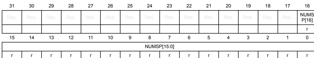
| 31 | 30 | 29 | 28 | 27 | 26 | 25 | 24 | 23 | 22 | 21 | 20 | 19 | 18 | 17 | 16 |
| Res. | Res. | Res. | Res. | Res. | Res. | Res. | Res. | Res. | Res. | Res. | Res. | Res. | Res. | Res. | NUMSP[16:0] |
| r | |||||||||||||||
| 15 | 14 | 13 | 12 | 11 | 10 | 9 | 8 | 7 | 6 | 5 | 4 | 3 | 2 | 1 | 0 |
| NUMSP[15:0] | |||||||||||||||
| r | r | r | r | r | r | r | r | r | r | r | r | r | r | r | r |
Bits 31:17 Reserved, must be kept at reset value.
Bits 16:0 NUMSP[16:0] : Number of stimulus ports implemented
0x10000: 65 536 stimulus ports are implemented (however only 4096 are accessible).
STM device type identifier register (STM_DEVTYPE)
Address offset: 0xFCC
Reset value: 0x0000 0063
This register provides a debugger with component information when the part number is not recognized. The debugger can then report this information.
| 31 | 30 | 29 | 28 | 27 | 26 | 25 | 24 | 23 | 22 | 21 | 20 | 19 | 18 | 17 | 16 |
|---|---|---|---|---|---|---|---|---|---|---|---|---|---|---|---|
| Res. | Res. | Res. | Res. | Res. | Res. | Res. | Res. | Res. | Res. | Res. | Res. | Res. | Res. | Res. | Res. |
| 15 | 14 | 13 | 12 | 11 | 10 | 9 | 8 | 7 | 6 | 5 | 4 | 3 | 2 | 1 | 0 |
| Res. | Res. | Res. | Res. | Res. | Res. | Res. | Res. | SUB[3:0] | MAJOR[3:0] | ||||||
| r | r | r | r | r | r | r | r | ||||||||
Bits 31:8 Reserved, must be kept at reset value.
Bits 7:4 SUB[3:0] : Sub-classification within the major category
0x6: CoreSight STM. The component generates trace based on software and hardware stimulus.
Bits 3:0 MAJOR[3:0] : Major classification for debug or trace component
0x3: The component is a trace source.
STM peripheral ID4 register (STM_PIDR4)
Address offset: 0xFD0
Reset value: 0x0000 0004
This register belongs to the set of peripheral identification registers. It contains part of the designer identity and the memory footprint indicator.
| 31 | 30 | 29 | 28 | 27 | 26 | 25 | 24 | 23 | 22 | 21 | 20 | 19 | 18 | 17 | 16 |
|---|---|---|---|---|---|---|---|---|---|---|---|---|---|---|---|
| Res. | Res. | Res. | Res. | Res. | Res. | Res. | Res. | Res. | Res. | Res. | Res. | Res. | Res. | Res. | Res. |
| 15 | 14 | 13 | 12 | 11 | 10 | 9 | 8 | 7 | 6 | 5 | 4 | 3 | 2 | 1 | 0 |
| Res. | Res. | Res. | Res. | Res. | Res. | Res. | Res. | SIZE[3:0] | DES_2[3:0] | ||||||
| r | r | r | r | r | r | r | r | ||||||||
Bits 31:8 Reserved, must be kept at reset value.
Bits 7:4 SIZE[3:0] : Component memory-size indicator
This bitfield indicates the total contiguous size of the memory window used by the component, in powers of two from the standard 4 Kbytes. If a component only requires the standard 4 Kbytes, this bitfield must be read as 0x0.
For 8 Kbytes, it is set to 0x1. For 16 Kbytes, it set to 0x2. For 32 Kbytes, it is set to 0x3, and similarly for larger memory windows.
0x0: The device only occupies 4 Kbytes of the memory.
Bits 3:0 DES_2[3:0] : JEDEC continuation code
This bitfield indicates the designer of the component, together with the identity code.
0x4: Indicate that Arm JEDEC identity code is on the 5 th bank.
STM peripheral ID0 register (STM_PIDR0)
Address offset: 0xFE0
Reset value: 0x0000 0063
This register belongs to the set of peripheral identification registers. It contains part of the designer specific part number.
| 31 | 30 | 29 | 28 | 27 | 26 | 25 | 24 | 23 | 22 | 21 | 20 | 19 | 18 | 17 | 16 |
| Res. | Res. | Res. | Res. | Res. | Res. | Res. | Res. | Res. | Res. | Res. | Res. | Res. | Res. | Res. | Res. |
| 15 | 14 | 13 | 12 | 11 | 10 | 9 | 8 | 7 | 6 | 5 | 4 | 3 | 2 | 1 | 0 |
| Res. | Res. | Res. | Res. | Res. | Res. | Res. | Res. | PART_0[7:0] | |||||||
| r | r | r | r | r | r | r | r | ||||||||
Bits 31:8 Reserved, must be kept at reset value.
Bits 7:0 PART_0[7:0] : bits [7:0] of the component part number
This bitfield is specified by the designer of the component.
0x63: CoreSight STM part number[7:0]. Eight least significant bits of the part number (0x963).
STM peripheral ID1 register (STM_PIDR1)
Address offset: 0xFE4
Reset value: 0x0000 00B9
This register belongs to the set of peripheral identification registers. It contains part of the designer specific part number and part of the designer identity.
| 31 | 30 | 29 | 28 | 27 | 26 | 25 | 24 | 23 | 22 | 21 | 20 | 19 | 18 | 17 | 16 |
| Res. | Res. | Res. | Res. | Res. | Res. | Res. | Res. | Res. | Res. | Res. | Res. | Res. | Res. | Res. | Res. |
| 15 | 14 | 13 | 12 | 11 | 10 | 9 | 8 | 7 | 6 | 5 | 4 | 3 | 2 | 1 | 0 |
| Res. | Res. | Res. | Res. | Res. | Res. | Res. | Res. | DES_0[3:0] | PART_1[3:0] | ||||||
| r | r | r | r | r | r | r | r | ||||||||
Bits 31:8 Reserved, must be kept at reset value.
Bits 7:4 DES_0[3:0] : bits [3:0] of the JEDEC identity code
This bitfield indicates the designer of the component, together with the continuation code.
0xB: least significant four bits of the JEP106 identity code
Bits 3:0 PART_1[3:0] : bits [11:8] of the component part number
Specified by the designer of the component.
0x9: CoreSight STM part number[11:8]. Most significant four bits of the part number (0x963).
STM peripheral ID2 register (STM_PIDR2)
Address offset: 0xFE8
Reset value: 0x0000 001B
This register belongs to the set of peripheral identification registers. It contains part of the designer identity and the product revision.
| 31 | 30 | 29 | 28 | 27 | 26 | 25 | 24 | 23 | 22 | 21 | 20 | 19 | 18 | 17 | 16 |
| Res. | Res. | Res. | Res. | Res. | Res. | Res. | Res. | Res. | Res. | Res. | Res. | Res. | Res. | Res. | Res. |
| 15 | 14 | 13 | 12 | 11 | 10 | 9 | 8 | 7 | 6 | 5 | 4 | 3 | 2 | 1 | 0 |
| Res. | Res. | Res. | Res. | Res. | Res. | Res. | Res. | REVISION[3:0] | JEDEC | DES_1[2:0] | |||||
| r | r | r | r | r | r | r | r | ||||||||
Bits 31:8 Reserved, must be kept at reset value.
Bits 7:4 REVISION[3:0] : Incremental component design version
An incremental value starting from 0x0 for the first design of this component. The value increases by one at both major and minor revisions, and is used as a look-up to establish the exact major and minor revisions.
0x1: This device is at r0p1.
Bit 3 JEDEC : JEDEC assigned value usage
This bit indicates the use of a JEDEC assigned value. This bit is always set.
1: The designer ID is specified by JEDEC (refer to http://www.jedec.org ).
Bits 2:0 DES_1[2:0] : bits [6:4] of the JEDEC identity code
This bitfield indicates the designer of the component, together with the continuation code.
0x3: Most significant three bits of the JEP106 identity code
STM peripheral ID3 register (STM_PIDR3)
Address offset: 0xFEC
Reset value: 0x0000 0000
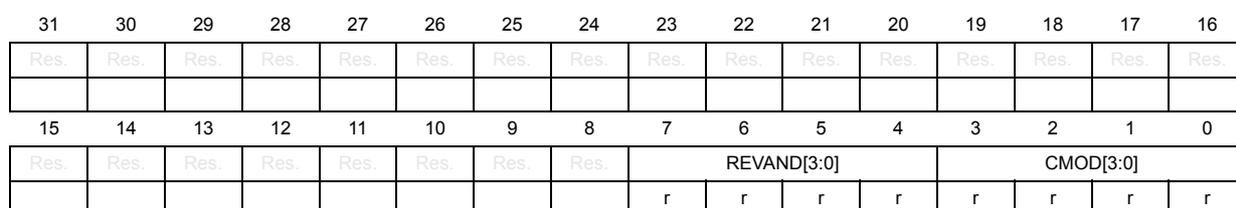
| 31 | 30 | 29 | 28 | 27 | 26 | 25 | 24 | 23 | 22 | 21 | 20 | 19 | 18 | 17 | 16 |
| Res. | Res. | Res. | Res. | Res. | Res. | Res. | Res. | Res. | Res. | Res. | Res. | Res. | Res. | Res. | Res. |
| 15 | 14 | 13 | 12 | 11 | 10 | 9 | 8 | 7 | 6 | 5 | 4 | 3 | 2 | 1 | 0 |
| Res. | Res. | Res. | Res. | Res. | Res. | Res. | Res. | REVAND[3:0] | CMOD[3:0] | ||||||
| r | r | r | r | r | r | r | r | ||||||||
Bits 31:8 Reserved, must be kept at reset value.
Bits 7:4 REVAND[3:0] : Minor fix indicator
This bitfield indicates minor errata fixes specific to the design, for example metal fixes after implementation. In most cases, this field is 0x0. Arm recommends that the component designers ensure that this bitfield can be changed by a metal fix if required (for example by driving this bitfield from registers that reset to 0).
0x0: No metal fix in the component
Bits 3:0 CMOD[3:0] : Customer modification indicator
When the component is a reusable peripheral, this value indicates if the customer has modified the behavior of the component. In most cases this field is 0x0.
0x0: No modification made
STM component ID0 register (STM_CIDR0)
Address offset: 0xFF0
Reset value: 0x0000 000D
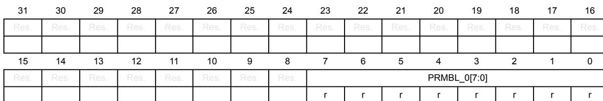
| 31 | 30 | 29 | 28 | 27 | 26 | 25 | 24 | 23 | 22 | 21 | 20 | 19 | 18 | 17 | 16 |
|---|---|---|---|---|---|---|---|---|---|---|---|---|---|---|---|
| Res. | Res. | Res. | Res. | Res. | Res. | Res. | Res. | Res. | Res. | Res. | Res. | Res. | Res. | Res. | Res. |
| 15 | 14 | 13 | 12 | 11 | 10 | 9 | 8 | 7 | 6 | 5 | 4 | 3 | 2 | 1 | 0 |
| Res. | Res. | Res. | Res. | Res. | Res. | Res. | Res. | PRMBL_0[7:0] | |||||||
| r | r | r | r | r | r | r | r | ||||||||
Bits 31:8 Reserved, must be kept at reset value.
Bits 7:0 PRMBL_0[7:0] : bits [31:24] of component identificationThis bitfield indicates that the identification registers are present.
0x0D: Identification value
STM component ID1 register (STM_CIDR1)Address offset: 0xFF4
Reset value: 0x0000 0090
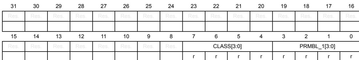
| 31 | 30 | 29 | 28 | 27 | 26 | 25 | 24 | 23 | 22 | 21 | 20 | 19 | 18 | 17 | 16 |
|---|---|---|---|---|---|---|---|---|---|---|---|---|---|---|---|
| Res. | Res. | Res. | Res. | Res. | Res. | Res. | Res. | Res. | Res. | Res. | Res. | Res. | Res. | Res. | Res. |
| 15 | 14 | 13 | 12 | 11 | 10 | 9 | 8 | 7 | 6 | 5 | 4 | 3 | 2 | 1 | 0 |
| Res. | Res. | Res. | Res. | Res. | Res. | Res. | Res. | CLASS[3:0] | PRMBL_1[3:0] | ||||||
| r | r | r | r | r | r | r | r | ||||||||
Bits 31:8 Reserved, must be kept at reset value.
Bits 7:4 CLASS[3:0] : Component classThis bitfield indicates the component class (for example, ROM table or CoreSight).
0x9: CoreSight component
Bits 3:0 PRMBL_1[3:0] : bits [19:16] of component identificationThis bitfield indicates that the identification registers are present.
0x0: Identification value
STM component ID2 register (STM_CIDR2)Address offset: 0xFF8
Reset value: 0x0000 0005
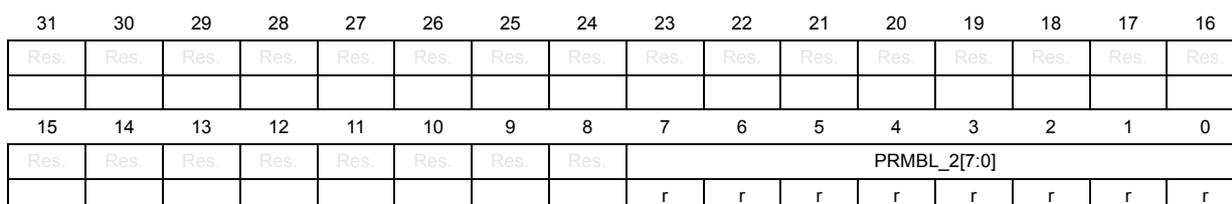
| 31 | 30 | 29 | 28 | 27 | 26 | 25 | 24 | 23 | 22 | 21 | 20 | 19 | 18 | 17 | 16 |
|---|---|---|---|---|---|---|---|---|---|---|---|---|---|---|---|
| Res. | Res. | Res. | Res. | Res. | Res. | Res. | Res. | Res. | Res. | Res. | Res. | Res. | Res. | Res. | Res. |
| 15 | 14 | 13 | 12 | 11 | 10 | 9 | 8 | 7 | 6 | 5 | 4 | 3 | 2 | 1 | 0 |
| Res. | Res. | Res. | Res. | Res. | Res. | Res. | Res. | PRMBL_2[7:0] | |||||||
| r | r | r | r | r | r | r | r | ||||||||
Bits 31:8 Reserved, must be kept at reset value.
Bits 7:0 PRMBL_2[7:0] : bits [15:8] of component identification
This bitfield indicates that the identification registers are present.
0x05: Identification value
STM component ID3 register (STM_CIDR3)
Address offset: 0xFFC
Reset value: 0x0000 00B1
| 31 | 30 | 29 | 28 | 27 | 26 | 25 | 24 | 23 | 22 | 21 | 20 | 19 | 18 | 17 | 16 |
|---|---|---|---|---|---|---|---|---|---|---|---|---|---|---|---|
| Res. | Res. | Res. | Res. | Res. | Res. | Res. | Res. | Res. | Res. | Res. | Res. | Res. | Res. | Res. | Res. |
| 15 | 14 | 13 | 12 | 11 | 10 | 9 | 8 | 7 | 6 | 5 | 4 | 3 | 2 | 1 | 0 |
| Res. | Res. | Res. | Res. | Res. | Res. | Res. | Res. | PRMBL_3[7:0] | |||||||
| r | r | r | r | r | r | r | r | ||||||||
Bits 31:8 Reserved, must be kept at reset value.
Bits 7:0 PRMBL_3[7:0] : bits [7:0] of component identification
This bitfield indicates that the identification registers are present.
0xB1: Identification value
STM register map
Table 901. STM register map and reset values
| Offset | Register name | 31 | 30 | 29 | 28 | 27 | 26 | 25 | 24 | 23 | 22 | 21 | 20 | 19 | 18 | 17 | 16 | 15 | 14 | 13 | 12 | 11 | 10 | 9 | 8 | 7 | 6 | 5 | 4 | 3 | 2 | 1 | 0 |
|---|---|---|---|---|---|---|---|---|---|---|---|---|---|---|---|---|---|---|---|---|---|---|---|---|---|---|---|---|---|---|---|---|---|
| 0xD00 | STM_HEER | HEE[31:0] | |||||||||||||||||||||||||||||||
| Reset value | 0 | 0 | 0 | 0 | 0 | 0 | 0 | 0 | 0 | 0 | 0 | 0 | 0 | 0 | 0 | 0 | 0 | 0 | 0 | 0 | 0 | 0 | 0 | 0 | 0 | 0 | 0 | 0 | 0 | 0 | 0 | 0 | |
| 0xD04-0xD1C | Reserved | Reserved | |||||||||||||||||||||||||||||||
| 0xD20 | STM_HETER | HETE[31:0] | |||||||||||||||||||||||||||||||
| Reset value | 0 | 0 | 0 | 0 | 0 | 0 | 0 | 0 | 0 | 0 | 0 | 0 | 0 | 0 | 0 | 0 | 0 | 0 | 0 | 0 | 0 | 0 | 0 | 0 | 0 | 0 | 0 | 0 | 0 | 0 | 0 | 0 | |
| 0xD24-0xD5C | Reserved | Reserved | |||||||||||||||||||||||||||||||
| 0xD60 | STM_HEBSR | Res. | Res. | Res. | Res. | Res. | Res. | Res. | Res. | Res. | Res. | Res. | Res. | Res. | Res. | Res. | Res. | Res. | Res. | Res. | Res. | Res. | Res. | Res. | Res. | Res. | Res. | Res. | Res. | Res. | Res. | Res. | HEBS |
| Reset value | 0 | ||||||||||||||||||||||||||||||||
| 0xD64 | STM_HEMCR | Res. | Res. | Res. | Res. | Res. | Res. | Res. | Res. | Res. | Res. | Res. | Res. | Res. | Res. | Res. | Res. | Res. | Res. | Res. | Res. | Res. | Res. | Res. | Res. | ATBTRIGEN | TRIGCLEAR | TRIGSTATUS | TRIGCTL | Res. | ERRDETECT | COMPEN | EN |
| Reset value | 0 | 0 | 0 | 0 | 0 | 0 | 0 | ||||||||||||||||||||||||||
| 0xD68 | STM_HEEXTMUXR | Res. | Res. | Res. | Res. | Res. | Res. | Res. | Res. | Res. | Res. | Res. | Res. | Res. | Res. | Res. | Res. | Res. | Res. | Res. | Res. | Res. | Res. | Res. | Res. | EXTMUX[7:0] | |||||||
| Reset value | 0 | 0 | 0 | 0 | 0 | 0 | 0 | 0 | |||||||||||||||||||||||||
Table 901. STM register map and reset values (continued)
| Offset | Register name | 31 | 30 | 29 | 28 | 27 | 26 | 25 | 24 | 23 | 22 | 21 | 20 | 19 | 18 | 17 | 16 | 15 | 14 | 13 | 12 | 11 | 10 | 9 | 8 | 7 | 6 | 5 | 4 | 3 | 2 | 1 | 0 |
|---|---|---|---|---|---|---|---|---|---|---|---|---|---|---|---|---|---|---|---|---|---|---|---|---|---|---|---|---|---|---|---|---|---|
| 0xD6C-0xDF0 | Reserved | Reserved | |||||||||||||||||||||||||||||||
| 0xDF4 | STM_HEMASTR | Res | Res | Res | Res | Res | Res | Res | Res | Res | Res | Res | Res | Res | Res | Res | Res | MASTER[15:0] | |||||||||||||||
| Reset value | 0 | 0 | 0 | 0 | 0 | 0 | 0 | 0 | 0 | 0 | 1 | 0 | 0 | 0 | 0 | ||||||||||||||||||
| 0xDF8 | STM_HEFEAT1R | Res | HEEXTMUXSIZE [2:0] | Res | Res | Res | Res | NUMHE[8:0] | Res | Res | Res | Res | Res | Res | Res | Res | Res | HECOMP[1:0] | HEMASTR | HEERR | Res | HETER | |||||||||||
| Reset value | 0 | 1 | 1 | 0 | 0 | 1 | 0 | 0 | 0 | 0 | 0 | 0 | 1 | 1 | 0 | 1 | 1 | ||||||||||||||||
| 0xDFC | STM_HEIDR | Res | Res | Res | Res | Res | Res | Res | Res | Res | Res | Res | Res | Res | Res | Res | Res | Res | Res | Res | Res | VENDSPEC [3:0] | CLASSREV [3:0] | CLASS[3:0] | |||||||||
| Reset value | 0 | 0 | 0 | 0 | 0 | 0 | 0 | 1 | 0 | 0 | 0 | 1 | |||||||||||||||||||||
| 0xE00 | STM_SPER | SPE[31:0] | |||||||||||||||||||||||||||||||
| Reset value | 0 | 0 | 0 | 0 | 0 | 0 | 0 | 0 | 0 | 0 | 0 | 0 | 0 | 0 | 0 | 0 | 0 | 0 | 0 | 0 | 0 | 0 | 0 | 0 | 0 | 0 | 0 | 0 | 0 | 0 | 0 | 0 | |
| 0xE04-0xE1C | Reserved | Reserved | |||||||||||||||||||||||||||||||
| 0xE20 | STM_SPTER | SPTE[31:0] | |||||||||||||||||||||||||||||||
| Reset value | 0 | 0 | 0 | 0 | 0 | 0 | 0 | 0 | 0 | 0 | 0 | 0 | 0 | 0 | 0 | 0 | 0 | 0 | 0 | 0 | 0 | 0 | 0 | 0 | 0 | 0 | 0 | 0 | 0 | 0 | 0 | 0 | |
| 0xE24-0xE5C | Reserved | Reserved | |||||||||||||||||||||||||||||||
| 0xE60 | STM_SPCR | Res | Res | Res | Res | PORTSEL[7:0] | Res | Res | Res | Res | Res | Res | Res | Res | Res | Res | Res | Res | Res | Res | Res | Res | Res | Res | Res | PORTCTL [1:0] | |||||||
| Reset value | 0 | 0 | 0 | 0 | 0 | 0 | 0 | 0 | |||||||||||||||||||||||||
| 0xE64 | STM_SPMSR | Res | Res | Res | Res | Res | Res | Res | Res | MASTSEL[7:0] | Res | Res | Res | Res | Res | Res | Res | Res | Res | Res | Res | Res | Res | Res | MASTCTL | ||||||||
| Reset value | 0 | 0 | 0 | 0 | 0 | 0 | 0 | 0 | 0 | ||||||||||||||||||||||||
| 0xE68 | STM_SPOVERRIDER | Res | Res | Res | Res | PORTSEL[12:0] | Res | Res | Res | Res | Res | Res | Res | Res | Res | Res | Res | Res | OVERTS | OVERCTL[1:0] | |||||||||||||
| Reset value | 0 | 0 | 0 | 0 | 0 | 0 | 0 | 0 | 0 | 0 | 0 | 0 | 0 | 0 | |||||||||||||||||||
| 0xE6C | STM_SPMOVERRIDER | Res | Res | Res | Res | Res | Res | Res | Res | MASTSEL[7:0] | Res | Res | Res | Res | Res | Res | Res | Res | Res | Res | Res | Res | Res | Res | MASTCTL | ||||||||
| Reset value | 0 | 0 | 0 | 0 | 0 | 0 | 0 | 0 | 0 | ||||||||||||||||||||||||
| 0xE70 | STM_SPTRIGCSR | Res | Res | Res | Res | Res | Res | Res | Res | Res | Res | Res | Res | Res | Res | Res | Res | Res | Res | Res | Res | Res | Res | Res | Res | Res | Res | Res | ATBTRIGEN DIR | ATBTRIGEN TE | TRIGCLEAR | TRIGSTATUS | TRIGCTL |
| Reset value | 0 | 0 | 0 | 0 | 0 | ||||||||||||||||||||||||||||
| Offset | Register name | 31 | 30 | 29 | 28 | 27 | 26 | 25 | 24 | 23 | 22 | 21 | 20 | 19 | 18 | 17 | 16 | 15 | 14 | 13 | 12 | 11 | 10 | 9 | 8 | 7 | 6 | 5 | 4 | 3 | 2 | 1 | 0 |
|---|---|---|---|---|---|---|---|---|---|---|---|---|---|---|---|---|---|---|---|---|---|---|---|---|---|---|---|---|---|---|---|---|---|
| 0xE74-0xE7C | Reserved | Reserved | |||||||||||||||||||||||||||||||
| 0xE80 | STM_TCSR | Res. | Res. | Res. | Res. | Res. | Res. | Res. | Res. | BUSY | TRACEID[6:0] | Res. | Res. | Res. | Res. | Res. | Res. | Res. | Res. | Res. | Res. | COMPEN | Res. | Res. | SYNCEN | TSEN | EN | ||||||
| Reset value | 0 | 0 | 0 | 0 | 0 | 0 | 0 | 0 | 0 | 1 | 0 | 0 | |||||||||||||||||||||
| 0xE84 | STM_TSSTIMR | Res. | Res. | Res. | Res. | Res. | Res. | Res. | Res. | Res. | Res. | Res. | Res. | Res. | Res. | Res. | Res. | Res. | Res. | Res. | Res. | Res. | Res. | Res. | Res. | Res. | Res. | Res. | Res. | Res. | Res. | Res. | FORCETS |
| Reset value | 0 | ||||||||||||||||||||||||||||||||
| 0xE88 | Reserved | Reserved | |||||||||||||||||||||||||||||||
| 0xE8C | STM_TSFREQR | FREQ[31:0] | |||||||||||||||||||||||||||||||
| Reset value | 0 | 0 | 0 | 0 | 0 | 0 | 0 | 0 | 0 | 0 | 0 | 0 | 0 | 0 | 0 | 0 | 0 | 0 | 0 | 0 | 0 | 0 | 0 | 0 | 0 | 0 | 0 | 0 | 0 | 0 | 0 | 0 | |
| 0xE90 | STM_SYNCR | Res. | Res. | Res. | Res. | Res. | Res. | Res. | Res. | Res. | Res. | Res. | Res. | Res. | Res. | Res. | Res. | Res. | Res. | MODE | COUNT[8:0] | Res. | Res. | Res. | Res. | ||||||||
| Reset value | 0 | 0 | 0 | 0 | 0 | 0 | 0 | 0 | 0 | 0 | |||||||||||||||||||||||
| 0xE94 | STM_AUXCR | Res. | Res. | Res. | Res. | Res. | Res. | Res. | Res. | Res. | Res. | Res. | Res. | Res. | Res. | Res. | Res. | Res. | Res. | Res. | Res. | Res. | Res. | Res. | QHWEVOVERRIDE | Res. | Res. | Res. | Res. | PRIORNVDIS | ASYNCPE | FIFOAF | |
| Reset value | 0 | 0 | 0 | 0 | |||||||||||||||||||||||||||||
| 0xE98-0xE9C | Reserved | Reserved | |||||||||||||||||||||||||||||||
| 0xEA0 | STM_FEAT1R | Res. | Res. | Res. | Res. | Res. | Res. | Res. | Res. | SWOEN[1:0] | SYNCEN[1:0] | HWTEN[1:0] | TSPRESCALE [1:0] | TRIGCTL[1:0] | TRACEBUS [3:0] | SYNC[1:0] | FORCETS | TSFREQ | TS [1:0] | PROT[3:0] | |||||||||||||
| Reset value | 0 | 1 | 1 | 0 | 0 | 1 | 0 | 1 | 1 | 0 | 0 | 0 | 0 | 1 | 1 | 1 | 1 | 1 | 0 | 1 | 0 | 0 | 0 | 1 | |||||||||
| 0xEA4 | STM_FEAT2R | Res. | Res. | Res. | Res. | Res. | Res. | Res. | Res. | Res. | Res. | Res. | Res. | Res. | Res. | SPTYPE[1:0] | DSIZE[3:0] | Res. | SPTRTYPE [1:0] | PRIVMASK [1:0] | SPOVERRIDE | SPCOMP[1:0] | Res. | SPER | SPTER[1:0] | ||||||||
| Reset value | 0 | 1 | 0 | 0 | 0 | 1 | 1 | 0 | 0 | 1 | 1 | 1 | 1 | 0 | 1 | 0 | |||||||||||||||||
| 0xEA8 | STM_FEAT3R | Res. | Res. | Res. | Res. | Res. | Res. | Res. | Res. | Res. | Res. | Res. | Res. | Res. | Res. | Res. | Res. | Res. | Res. | Res. | Res. | Res. | Res. | Res. | Res. | Res. | NUMMAST[6:0] | ||||||
| Reset value | 1 | 1 | 1 | 1 | 1 | 1 | 1 | ||||||||||||||||||||||||||
| 0xEAC-0xF9C | Reserved | Reserved | |||||||||||||||||||||||||||||||
| 0xFA0 | STM_CLAIMSET | Res. | Res. | Res. | Res. | Res. | Res. | Res. | Res. | Res. | Res. | Res. | Res. | Res. | Res. | Res. | Res. | Res. | Res. | Res. | Res. | Res. | Res. | Res. | Res. | Res. | Res. | Res. | Res. | SET[3:0] | |||
| Reset value | 1 | 1 | 1 | 1 | |||||||||||||||||||||||||||||
| 0xFA4 | STM_CLAIMCLR | Res. | Res. | Res. | Res. | Res. | Res. | Res. | Res. | Res. | Res. | Res. | Res. | Res. | Res. | Res. | Res. | Res. | Res. | Res. | Res. | Res. | Res. | Res. | Res. | Res. | Res. | Res. | Res. | CLR[3:0] | |||
| Reset value | 0 | 0 | 0 | 0 | |||||||||||||||||||||||||||||
Table 901. STM register map and reset values (continued)
| Offset | Register name | 31 | 30 | 29 | 28 | 27 | 26 | 25 | 24 | 23 | 22 | 21 | 20 | 19 | 18 | 17 | 16 | 15 | 14 | 13 | 12 | 11 | 10 | 9 | 8 | 7 | 6 | 5 | 4 | 3 | 2 | 1 | 0 |
|---|---|---|---|---|---|---|---|---|---|---|---|---|---|---|---|---|---|---|---|---|---|---|---|---|---|---|---|---|---|---|---|---|---|
| 0xFA8-0xFAC | Reserved | Reserved | |||||||||||||||||||||||||||||||
| 0xFB0 | STM_LAR | KEY[31:0] | |||||||||||||||||||||||||||||||
| Reset value | 0 | 0 | 0 | 0 | 0 | 0 | 0 | 0 | 0 | 0 | 0 | 0 | 0 | 0 | 0 | 0 | 0 | 0 | 0 | 0 | 0 | 0 | 0 | 0 | 0 | 0 | 0 | 0 | 0 | 0 | 0 | 0 | |
| 0xFB4 | STM_LSR | Res. | Res. | Res. | Res. | Res. | Res. | Res. | Res. | Res. | Res. | Res. | Res. | Res. | Res. | Res. | Res. | Res. | Res. | Res. | Res. | Res. | Res. | Res. | Res. | Res. | Res. | Res. | Res. | Res. | NTT | SLK | SLI |
| Reset value | 0 | 1 | 1 | ||||||||||||||||||||||||||||||
| 0xFB8 | STM_AUTHSTATUS | Res. | Res. | Res. | Res. | Res. | Res. | Res. | Res. | Res. | Res. | Res. | Res. | Res. | Res. | Res. | Res. | Res. | Res. | Res. | Res. | Res. | Res. | Res. | Res. | Res. | Res. | SNID [1:0] | SID [1:0] | NSID [1:0] | NSID [1:0] | ||
| Reset value | 1 | 0 | 1 | 0 | 1 | 0 | |||||||||||||||||||||||||||
| 0xFBC | STM_DEVARCH | ARCHITECT[10:0] | PRESENT | REVISION [3:0] | Res. | ARCHID[14:0] | |||||||||||||||||||||||||||
| Reset value | 0 | 1 | 0 | 0 | 0 | 1 | 1 | 1 | 0 | 1 | 1 | 1 | 0 | 0 | 0 | 1 | 0 | 0 | 0 | 1 | 0 | 1 | 0 | 0 | 1 | 1 | 0 | 0 | 0 | 1 | 1 | ||
| 0xFC0-0xFC4 | Reserved | Reserved | |||||||||||||||||||||||||||||||
| 0xFC8 | STM_DEVID | Res. | Res. | Res. | Res. | Res. | Res. | Res. | Res. | Res. | Res. | Res. | Res. | Res. | Res. | Res. | NUMSP[16:0] | ||||||||||||||||
| Reset value | 1 | 0 | 0 | 0 | 0 | 0 | 0 | 0 | 0 | 0 | 0 | 0 | 0 | 0 | 0 | 0 | 0 | ||||||||||||||||
| 0xFCC | STM_DEVTYPE | Res. | Res. | Res. | Res. | Res. | Res. | Res. | Res. | Res. | Res. | Res. | Res. | Res. | Res. | Res. | Res. | Res. | Res. | Res. | Res. | Res. | Res. | Res. | Res. | SUB[3:0] | MAJOR[3:0] | ||||||
| Reset value | 0 | 1 | 1 | 0 | 0 | 0 | 1 | 1 | |||||||||||||||||||||||||
| 0xFD0 | STM_PIDR4 | Res. | Res. | Res. | Res. | Res. | Res. | Res. | Res. | Res. | Res. | Res. | Res. | Res. | Res. | Res. | Res. | Res. | Res. | Res. | Res. | Res. | Res. | Res. | Res. | SIZE[3:0] | DES_2[3:0] | ||||||
| Reset value | 0 | 0 | 0 | 0 | 0 | 1 | 0 | 0 | |||||||||||||||||||||||||
| 0xFD4-0xFDC | Reserved | Reserved | |||||||||||||||||||||||||||||||
| 0xFE0 | STM_PIDR0 | Res. | Res. | Res. | Res. | Res. | Res. | Res. | Res. | Res. | Res. | Res. | Res. | Res. | Res. | Res. | Res. | Res. | Res. | Res. | Res. | Res. | Res. | Res. | Res. | PART_0[7:0] | |||||||
| Reset value | 0 | 1 | 1 | 0 | 0 | 0 | 1 | 1 | |||||||||||||||||||||||||
| 0xFE4 | STM_PIDR1 | Res. | Res. | Res. | Res. | Res. | Res. | Res. | Res. | Res. | Res. | Res. | Res. | Res. | Res. | Res. | Res. | Res. | Res. | Res. | Res. | Res. | Res. | Res. | Res. | DES_0[3:0] | PART_1 [3:0] | ||||||
| Reset value | 1 | 0 | 1 | 1 | 1 | 0 | 0 | 1 | |||||||||||||||||||||||||
| 0xFE8 | STM_PIDR2 | Res. | Res. | Res. | Res. | Res. | Res. | Res. | Res. | Res. | Res. | Res. | Res. | Res. | Res. | Res. | Res. | Res. | Res. | Res. | Res. | Res. | Res. | Res. | Res. | REVISION [3:0] | JEDEC | DES_1 [2:0] | |||||
| Reset value | 0 | 0 | 0 | 1 | 1 | 0 | 1 | 1 | |||||||||||||||||||||||||
| 0xFEC | STM_PIDR3 | Res. | Res. | Res. | Res. | Res. | Res. | Res. | Res. | Res. | Res. | Res. | Res. | Res. | Res. | Res. | Res. | Res. | Res. | Res. | Res. | Res. | Res. | Res. | Res. | REVAND [3:0] | CMOD[3:0] | ||||||
| Reset value | 0 | 0 | 0 | 0 | 0 | 0 | 0 | 0 | |||||||||||||||||||||||||
| 0xFF0 | STM_CIDR0 | Res. | Res. | Res. | Res. | Res. | Res. | Res. | Res. | Res. | Res. | Res. | Res. | Res. | Res. | Res. | Res. | Res. | Res. | Res. | Res. | Res. | Res. | Res. | Res. | PRMBL_0[7:0] | |||||||
| Reset value | 0 | 0 | 0 | 0 | 1 | 1 | 0 | 1 | |||||||||||||||||||||||||
| 0xFF4 | STM_CIDR1 | Res. | Res. | Res. | Res. | Res. | Res. | Res. | Res. | Res. | Res. | Res. | Res. | Res. | Res. | Res. | Res. | Res. | Res. | Res. | Res. | Res. | Res. | Res. | Res. | CLASS[3:0] | PRMBL_1 [3:0] | ||||||
| Reset value | 1 | 0 | 0 | 1 | 0 | 0 | 0 | 0 | |||||||||||||||||||||||||
Table 901. STM register map and reset values (continued)
| Offset | Register name | 31 | 30 | 29 | 28 | 27 | 26 | 25 | 24 | 23 | 22 | 21 | 20 | 19 | 18 | 17 | 16 | 15 | 14 | 13 | 12 | 11 | 10 | 9 | 8 | 7 | 6 | 5 | 4 | 3 | 2 | 1 | 0 |
|---|---|---|---|---|---|---|---|---|---|---|---|---|---|---|---|---|---|---|---|---|---|---|---|---|---|---|---|---|---|---|---|---|---|
| 0xFF8 | STM_CIDR2 | Res | Res | Res | Res | Res | Res | Res | Res | Res | Res | Res | Res | Res | Res | Res | Res | Res | Res | Res | Res | Res | Res | Res | Res | PRMBL_2[7:0] | |||||||
| Reset value | 0 | 0 | 0 | 0 | 0 | 1 | 0 | 1 | |||||||||||||||||||||||||
| 0xFFC | STM_CIDR3 | Res | Res | Res | Res | Res | Res | Res | Res | Res | Res | Res | Res | Res | Res | Res | Res | Res | Res | Res | Res | Res | Res | Res | Res | PRMBL_3[7:0] | |||||||
| Reset value | 1 | 0 | 1 | 1 | 0 | 0 | 0 | 1 | |||||||||||||||||||||||||
78.12.20 Microcontroller debug unit (DBGMCU)
The DBGMCU is a component containing a number of registers which control the power and clock behavior in debug mode. Specifically it allows the debugger, or debug software:
- • to maintain the clock and power to the processor and/or peripherals when in low-power modes (Sleep, Stop, or Standby)
- • to maintain the clock and power to the system debug and trace components when in low-power modes
- • to stop the clock to certain peripherals (CAN, SMBUS timeout, watchdogs, timers, RTC, DMAs) when the processor is halted in debug mode
Legacy DBGMCU features (dbg/trace_en, dbg_sleep/stop/stby, dbg_freeze) are disabled when debug is closed. Only registers required for authentication procedure are accessible.
Low-power mode emulation in debug
When entering a low-power state (Sleep, Stop, Standby), the clock to the processor, the system clock or, in the case of Standby, the core power supply can be switched off. This prevents any debug accesses to the unclocked domains.
To simplify debugging of applications which use these power saving features, the clock and power can be maintained or not, according to the setting of DBG_STANDBY, DBG_STOP, and DBG_SLEEP bits in DBGMCU_CR.
There are no restrictions from a security perspective to access these control bits, as the overall system behavior is not modified, except that the power and clocks remain on.
If the system enters one of the power saving modes, and the corresponding register bit is set, the system state in the EXTI is not affected: the system enters and exits the low-power state as normal. However the clock and power remain active, allowing the debugger full access.
Note: If the TPIU is used, loss of trace data can occur if the system goes into Standby mode, and switches off the core power before the TPIU FIFO is empty. The software can check the FIFO state to avoid this. If the DBG_STANDBY bit is set while using the trace port, the trace continues to flush during Standby mode, and no specific software action is required.
Peripheral clock “freeze” in debug
When the processor is halted in debug state, by default the peripherals continue to operate. The system state, at the moment the breakpoint was taken, is overwritten and cannot be recovered. Furthermore, certain peripherals require software intervention on a regular basis, or they can time out, and generate a reset (watchdogs, for example).
By setting the corresponding bits in the DBGMCU peripheral freeze registers, certain peripherals clocks can be stopped automatically as soon as processor enters debug state. The clocks remain stopped until the processor is restarted.
The following peripherals support this feature:
- • all DMA engines (HPDMA3 and GPDMA1)
- • all timers (TIMx, LPTIMx)
- • all I2C/I3C peripherals (to prevent SMBus timeout)
- • FDCAN
- • all watchdog timers (WWDGx, IWDGx)
- • real time clock (RTC)
The peripheral accesses can be controlled from a RISUP for peripherals (see Section 6: Resource isolation framework security controller (RIFSC) for more details).
DBGMCU freeze register bits inherit the security level of the peripheral from the RISUP, or from the peripheral itself if it is TrustZone-aware (such as DMA) as follows:
- • When spiden = 1 (secure privilege debug enabled), all debug freeze bits can be modified.
- • When spiden = 0 (secure privilege debug disabled), only the bits corresponding to non-secure peripherals can be modified.
78.12.21 DBGMCU registers
The register file base address for the DBGMCU is defined in Table 870 .
The DBGMCU registers are reset only by a power-on-reset.
DBGMCU identity code register (DBGMCU_IDCODE)
Address offset: 0x000
Reset value: 0xXXXX 6XXX
| 31 | 30 | 29 | 28 | 27 | 26 | 25 | 24 | 23 | 22 | 21 | 20 | 19 | 18 | 17 | 16 |
|---|---|---|---|---|---|---|---|---|---|---|---|---|---|---|---|
| REV_ID[15:0] | |||||||||||||||
| r | r | r | r | r | r | r | r | r | r | r | r | r | r | r | r |
| 15 | 14 | 13 | 12 | 11 | 10 | 9 | 8 | 7 | 6 | 5 | 4 | 3 | 2 | 1 | 0 |
| Res. | Res. | Res. | Res. | DEV_ID[11:0] | |||||||||||
| r | r | r | r | r | r | r | r | r | r | r | r | ||||
Bits 31:16 REV_ID[15:0] : Revision
0x1000: revision A
0x2000: revision B
Bits 15:12 Reserved, must be kept at reset value.
Bits 11:0 DEV_ID[11:0] : Device ID
0x486: STM32N6x5/x7xx
DBGMCU configuration register (DBGMCU_CR)
Address offset: 0x004
Reset value: 0x8000 0000
| 31 | 30 | 29 | 28 | 27 | 26 | 25 | 24 | 23 | 22 | 21 | 20 | 19 | 18 | 17 | 16 |
|---|---|---|---|---|---|---|---|---|---|---|---|---|---|---|---|
| HLT_TS GEN_EN | Res. | Res. | DBTR GOEN | Res. | Res. | Res. | Res. | Res. | Res. | TRACE CLKEN | DBGCL KEN | Res. | Res. | Res. | Res. |
| rw | rw | rw | rw |
| 15 | 14 | 13 | 12 | 11 | 10 | 9 | 8 | 7 | 6 | 5 | 4 | 3 | 2 | 1 | 0 |
|---|---|---|---|---|---|---|---|---|---|---|---|---|---|---|---|
| Res. | Res. | Res. | Res. | Res. | Res. | Res. | Res. | Res. | Res. | Res. | Res. | Res. | DBG_ST ANDBY | DBG_S TOP | DBG_S LEEP |
| rw | rw | rw |
Bit 31 HLT_TSGEN_EN : TSGEN halt enable
1: TSGEN stops counting when processor is in halt.
0: TSGEN keeps on counting when processor is in halt.
Bits 30:29 Reserved, must be kept at reset value.
Bit 28 DBTRGOEN : DBTRGIO connection control
0: DBTRGIO connected to DBTRGIN
1: DBTRGIO connected to DBTRGOUT
Bits 27:22 Reserved, must be kept at reset value.
Bit 21 TRACECLKEN : TPIU export clock enable through software
0: TPIU clock is off.
1: TPIU clock is on.
Bit 20 DBGCLKEN : Debug clock enable through software
0: Debug clock is off.
1: Debug clock is on.
Bits 19:3 Reserved, must be kept at reset value.
Bit 2 DBG_STANDBY : Debug in Standby mode
0: Normal operation. All clocks are disabled. The V DD domain is automatically powered down in Standby mode.
1: Automatic clock stop/power down disabled. All active clocks and oscillators continue to run during Standby mode. The V DD domain supply is maintained, allowing full debug capability.
Note: On exit from Standby mode, a system reset is performed.
Bit 1 DBG_STOP : Debug in Stop mode
0: Normal operation. All clocks are disabled automatically in Stop mode.
1: Automatic clock stop disabled. All active clocks and oscillators continue to run during Stop mode, allowing full debug capability.
Note: On exit from Stop mode, the clock settings is set to the Stop mode exit state.
Bit 0 DBG_SLEEP : Debug in Sleep mode
0: Normal operation. Peripheral clocks are automatically stopped in Sleep mode.
1: Automatic clock stop disabled. Peripheral clocks continue to run, allowing full debug capability.
DBGMCU APB1L peripheral freeze register (DBGMCU_APB1LFZR)
Address offset: 0x010
Reset value: 0x0000 0000
| 31 | 30 | 29 | 28 | 27 | 26 | 25 | 24 | 23 | 22 | 21 | 20 | 19 | 18 | 17 | 16 |
|---|---|---|---|---|---|---|---|---|---|---|---|---|---|---|---|
| Res. | Res. | Res. | Res. | Res. | Res. | DBG_I3C2_STOP | DBG_I3C1_STOP | DBG_I2C3_STOP | DBG_I2C2_STOP | DBG_I2C1_STOP | Res. | Res. | Res. | Res. | Res. |
| rw | rw | rw | rw | rw |
| 15 | 14 | 13 | 12 | 11 | 10 | 9 | 8 | 7 | 6 | 5 | 4 | 3 | 2 | 1 | 0 |
|---|---|---|---|---|---|---|---|---|---|---|---|---|---|---|---|
| Res. | Res. | DBG_TIM11_STOP | DBG_TIM10_STOP | DBG_WDG1_STOP | Res. | DBG_LPTIM1_STOP | DBG_TIM14_STOP | DBG_TIM13_STOP | DBG_TIM12_STOP | DBG_TIM7_STOP | DBG_TIM6_STOP | DBG_TIM5_STOP | DBG_TIM4_STOP | DBG_TIM3_STOP | DBG_TIM2_STOP |
| rw | rw | rw | rw | rw | rw | rw | rw | rw | rw | rw | rw | rw |
Bits 31:26 Reserved, must be kept at reset value.
Bit 25 DBG_I3C2_STOP : I3C2 SMBUS timeout stop in debug
0: Normal operation. I3C2 SMBUS timeout continues to operate while Cortex-M55 is in debug mode.
1: Stop in debug. I3C2 SMBUS timeout is frozen while Cortex-M55 is in debug mode.
Bit 24 DBG_I3C1_STOP : I3C1 SMBUS timeout stop in debug
0: Normal operation. I3C1 SMBUS timeout continues to operate while Cortex-M55 is in debug mode.
1: Stop in debug. I3C1 SMBUS timeout is frozen while Cortex-M55 is in debug mode.
Bit 23 DBG_I2C3_STOP : I2C3 SMBUS timeout stop in debug
0: Normal operation. I2C3 SMBUS timeout continues to operate while Cortex-M55 is in debug mode.
1: Stop in debug. I2C3 SMBUS timeout is frozen while Cortex-M55 is in debug mode.
Bit 22 DBG_I2C2_STOP : I2C2 SMBUS timeout stop in debug
0: Normal operation. I2C2 SMBUS timeout continues to operate while Cortex-M55 is in debug mode.
1: Stop in debug. I2C2 SMBUS timeout is frozen while Cortex-M55 is in debug mode.
Bit 21 DBG_I2C1_STOP : I2C1 SMBUS timeout stop in debug
0: Normal operation. I2C1 SMBUS timeout continues to operate while Cortex-M55 is in debug mode.
1: Stop in debug. I2C1 SMBUS timeout is frozen while Cortex-M55 is in debug mode.
Bits 20:14 Reserved, must be kept at reset value.
Bit 13 DBG_TIM11_STOP : TIM11 stop in debug
0: Normal operation. TIM11 continues to operate while Cortex-M55 is in debug mode.
1: Stop in debug. TIM11 is frozen while Cortex-M55 is in debug mode.
Bit 12 DBG_TIM10_STOP : TIM10 stop in debug
0: Normal operation. TIM10 continues to operate while Cortex-M55 is in debug mode.
1: Stop in debug. TIM10 is frozen while Cortex-M55 is in debug mode.
Bit 11 DBG_WWDG1_STOP : WWDG1 stop in debug
0: Normal operation. WWDG1 continues to operate while Cortex-M55 is in debug mode.
1: Stop in debug. WWDG1 is frozen while Cortex-M55 is in debug mode.
Bit 10 Reserved, must be kept at reset value.
Bit 9 DBG_LPTIM1_STOP : LPTIM1 stop in debug
0: Normal operation. LPTIM1 continues to operate while Cortex-M55 is in debug mode.
1: Stop in debug. LPTIM1 is frozen while Cortex-M55 is in debug mode.
Bit 8 DBG_TIM14_STOP : TIM14 stop in debug
0: Normal operation. TIM14 continues to operate while Cortex-M55 is in debug mode.
1: Stop in debug. TIM14 is frozen while Cortex-M55 is in debug mode.
Bit 7 DBG_TIM13_STOP : TIM13 stop in debug
0: Normal operation. TIM13 continues to operate while Cortex-M55 is in debug mode.
1: Stop in debug. TIM13 is frozen while Cortex-M55 is in debug mode.
Bit 6 DBG_TIM12_STOP : TIM12 stop in debug
0: Normal operation. TIM12 continues to operate while Cortex-M55 is in debug mode.
1: Stop in debug. TIM12 is frozen while Cortex-M55 is in debug mode.
Bit 5 DBG_TIM7_STOP : TIM7 stop in debug
0: Normal operation. TIM7 continues to operate while Cortex-M55 is in debug mode.
1: Stop in debug. TIM7 is frozen while Cortex-M55 is in debug mode.
Bit 4 DBG_TIM6_STOP : TIM6 stop in debug
0: Normal operation. TIM6 continues to operate while Cortex-M55 is in debug mode.
1: Stop in debug. TIM6 is frozen while Cortex-M55 is in debug mode.
Bit 3 DBG_TIM5_STOP : TIM5 stop in debug
0: Normal operation. TIM5 continues to operate while Cortex-M55 is in debug mode.
1: Stop in debug. TIM5 is frozen while Cortex-M55 is in debug mode.
Bit 2 DBG_TIM4_STOP : TIM4 stop in debug
0: Normal operation. TIM4 continues to operate while Cortex-M55 is in debug mode.
1: Stop in debug. TIM4 is frozen while Cortex-M55 is in debug mode.
Bit 1 DBG_TIM3_STOP : TIM3 stop in debug
0: Normal operation. TIM3 continues to operate while Cortex-M55 is in debug mode.
1: Stop in debug. TIM3 is frozen while Cortex-M55 is in debug mode.
Bit 0 DBG_TIM2_STOP : TIM2 stop in debug
0: Normal operation. TIM2 continues to operate while Cortex-M55 is in debug mode.
1: Stop in debug. TIM2 is frozen while Cortex-M55 is in debug mode.
DBGMCU_APB1H peripheral freeze register (DBGMCU_APB1HFZR)
Address offset: 0x014
Reset value: 0x0000 0000
| 31 | 30 | 29 | 28 | 27 | 26 | 25 | 24 | 23 | 22 | 21 | 20 | 19 | 18 | 17 | 16 |
|---|---|---|---|---|---|---|---|---|---|---|---|---|---|---|---|
| Res. | Res. | Res. | Res. | Res. | Res. | Res. | Res. | Res. | Res. | Res. | Res. | Res. | Res. | Res. | Res. |
| 15 | 14 | 13 | 12 | 11 | 10 | 9 | 8 | 7 | 6 | 5 | 4 | 3 | 2 | 1 | 0 |
| Res. | Res. | Res. | Res. | Res. | Res. | Res. | DBG_FDCAN_STOP | Res. | Res. | Res. | Res. | Res. | Res. | Res. | Res. |
| rw |
Bits 31:9 Reserved, must be kept at reset value.
Bit 8 DBG_FDCAN_STOP : FDCAN stop in debug
0: Normal operation. FDCAN continues to operate while Cortex-M55 is in debug mode.
1: Stop in debug. FDCAN is frozen while Cortex-M55 is in debug mode.
Bits 7:0 Reserved, must be kept at reset value.
DBGMCU APB2 peripheral freeze register (DBGMCU_APB2FZR)
Address offset: 0x018
Reset value: 0x0000 0000
| 31 | 30 | 29 | 28 | 27 | 26 | 25 | 24 | 23 | 22 | 21 | 20 | 19 | 18 | 17 | 16 |
|---|---|---|---|---|---|---|---|---|---|---|---|---|---|---|---|
| Res. | Res. | Res. | Res. | Res. | Res. | Res. | Res. | Res. | Res. | Res. | Res. | DBG_TIM9_STOP | DBG_TIM17_STOP | DBG_TIM16_STOP | DBG_TIM15_STOP |
| rw | rw | rw | rw | ||||||||||||
| 15 | 14 | 13 | 12 | 11 | 10 | 9 | 8 | 7 | 6 | 5 | 4 | 3 | 2 | 1 | 0 |
| DBG_TIM18_STOP | Res. | Res. | Res. | Res. | Res. | Res. | Res. | Res. | Res. | Res. | Res. | Res. | Res. | DBG_TIM8_STOP | DBG_TIM1_STOP |
| rw | rw | rw |
Bits 31:20 Reserved, must be kept at reset value.
Bit 19 DBG_TIM9_STOP : TIM9 stop in debug
0: Normal operation. TIM9 continues to operate while Cortex-M55 is in debug mode.
1: Stop in debug. TIM9 is frozen while Cortex-M55 is in debug mode.
Bit 18 DBG_TIM17_STOP : TIM17 stop in debug
0: Normal operation. TIM17 continues to operate while Cortex-M55 is in debug mode.
1: Stop in debug. TIM17 is frozen while Cortex-M55 is in debug mode.
Bit 17 DBG_TIM16_STOP : TIM16 stop in debug
0: Normal operation. TIM16 continues to operate while Cortex-M55 is in debug mode.
1: Stop in debug. TIM16 is frozen while Cortex-M55 is in debug mode.
Bit 16 DBG_TIM15_STOP : TIM15 stop in debug
0: Normal operation. TIM15 continues to operate while Cortex-M55 is in debug mode.
1: Stop in debug. TIM15 is frozen while Cortex-M55 is in debug mode.
Bit 15 DBG_TIM18_STOP : TIM18 stop in debug
0: Normal operation. TIM18 continues to operate while Cortex-M55 is in debug mode.
1: Stop in debug. TIM18 is frozen while Cortex-M55 is in debug mode.
Bits 14:2 Reserved, must be kept at reset value.
Bit 1 DBG_TIM8_STOP : TIM8 stop in debug
0: Normal operation. TIM8 continues to operate while Cortex-M55 is in debug mode.
1: Stop in debug. TIM8 is frozen while Cortex-M55 is in debug mode.
Bit 0 DBG_TIM1_STOP : TIM1 stop in debug
0: Normal operation. TIM1 continues to operate while Cortex-M55 is in debug mode.
1: Stop in debug. TIM1 is frozen while Cortex-M55 is in debug mode.
DBGMCU APB4 peripheral freeze register (DBGMCU_APB4FZR)
Address offset: 0x01C
Reset value: 0x0000 0000
| 31 | 30 | 29 | 28 | 27 | 26 | 25 | 24 | 23 | 22 | 21 | 20 | 19 | 18 | 17 | 16 |
|---|---|---|---|---|---|---|---|---|---|---|---|---|---|---|---|
| Res. | Res. | Res. | Res. | Res. | Res. | Res. | Res. | Res. | Res. | Res. | Res. | Res. | DBG_I WDG_ STOP | Res. | DBG_R TC_ST OP |
| rw | rw | ||||||||||||||
| 15 | 14 | 13 | 12 | 11 | 10 | 9 | 8 | 7 | 6 | 5 | 4 | 3 | 2 | 1 | 0 |
| Res. | Res. | Res. | DBG_L PTIM5_ STOP | DBG_L PTIM4_ STOP | DBG_L PTIM3_ STOP | DBG_L PTIM2_ STOP | DBG_I 2C4_S TOP | Res. | Res. | Res. | Res. | Res. | Res. | Res. | Res. |
| rw | rw | rw | rw | rw |
Bits 31:19 Reserved, must be kept at reset value.
Bit 18 DBG_IWDG_STOP : WWDG stop in debug
0: Normal operation. IWDG continues to operate while Cortex-M55 is in debug mode.
1: Stop in debug. IWDG is frozen while Cortex-M55 is in debug mode.
Bit 17 Reserved, must be kept at reset value.
Bit 16 DBG_RTC_STOP : RTC clock is suspended in debug
0: Normal operation. RTC clock continues to operate while Cortex-M55 is in debug mode.
1: Stop in debug. RTC clock is suspended while Cortex-M55 is in debug mode.
Bits 15:13 Reserved, must be kept at reset value.
Bit 12 DBG_LPTIM5_STOP : LPTIM5 stop in debug
0: Normal operation. LPTIM5 continues to operate while Cortex-M55 is in debug mode.
1: Stop in debug. LPTIM5 is frozen while Cortex-M55 is in debug mode.
Bit 11 DBG_LPTIM4_STOP : LPTIM4 stop in debug
0: Normal operation. LPTIM4 continues to operate while Cortex-M55 is in debug mode.
1: Stop in debug. LPTIM4 is frozen while Cortex-M55 is in debug mode.
Bit 10 DBG_LPTIM3_STOP : LPTIM3 stop in debug
0: Normal operation. LPTIM3 continues to operate while Cortex-M55 is in debug mode.
1: Stop in debug. LPTIM3 is frozen while Cortex-M55 is in debug mode.
Bit 9 DBG_LPTIM2_STOP : LPTIM2 stop in debug
0: Normal operation. LPTIM2 continues to operate while Cortex-M55 is in debug mode.
1: Stop in debug. LPTIM2 is frozen while Cortex-M55 is in debug mode.
Bit 8 DBG_I2C4_STOP : I2C4 stop in debug
0: Normal operation. I2C4 continues to operate while Cortex-M55 is in debug mode.
1: Stop in debug. I2C4 is frozen while Cortex-M55 is in debug mode.
Bits 7:0 Reserved, must be kept at reset value.
DBGMCU_APB5 peripheral freeze register (DBGMCU_APB5FZR)
Address offset: 0x020
Reset value: 0x0000 0000
| 31 | 30 | 29 | 28 | 27 | 26 | 25 | 24 | 23 | 22 | 21 | 20 | 19 | 18 | 17 | 16 |
|---|---|---|---|---|---|---|---|---|---|---|---|---|---|---|---|
| Res. | Res. | Res. | Res. | Res. | Res. | Res. | Res. | Res. | Res. | Res. | Res. | Res. | Res. | Res. | Res. |
| 15 | 14 | 13 | 12 | 11 | 10 | 9 | 8 | 7 | 6 | 5 | 4 | 3 | 2 | 1 | 0 |
| Res. | Res. | Res. | Res. | Res. | Res. | Res. | Res. | Res. | Res. | Res. | DBG_G FXTIM _STOP | Res. | Res. | Res. | Res. |
| rw | |||||||||||||||
Bits 31:5 Reserved, must be kept at reset value.
Bit 4 DBG_GFXTIM_STOP : GFXTIM stop in debug
0: Normal operation. GFXTIM continues counting while Cortex-M55 is in debug mode.
1: Stop in debug. GFXTIM is frozen while Cortex-M55 is in debug mode.
Bits 3:0 Reserved, must be kept at reset value.
DBGMCU AHB1 peripheral freeze register (DBGMCU_AHB1FZR)
Address offset: 0x024
Reset value: 0x0000 0000
| 31 | 30 | 29 | 28 | 27 | 26 | 25 | 24 | 23 | 22 | 21 | 20 | 19 | 18 | 17 | 16 |
|---|---|---|---|---|---|---|---|---|---|---|---|---|---|---|---|
| Res. | Res. | Res. | Res. | Res. | Res. | Res. | Res. | Res. | Res. | Res. | Res. | Res. | Res. | Res. | Res. |
| 15 | 14 | 13 | 12 | 11 | 10 | 9 | 8 | 7 | 6 | 5 | 4 | 3 | 2 | 1 | 0 |
| DBG_G PDMA1 _CH15 _STOP | DBG_G PDMA1 _CH14 _STOP | DBG_G PDMA1 _CH13 _STOP | DBG_G PDMA1 _CH12 _STOP | DBG_G PDMA1 _CH11 _STOP | DBG_G PDMA1 _CH10 _STOP | DBG_G PDMA1 _CH9 _STOP | DBG_G PDMA1 _CH8 _STOP | DBG_G PDMA1 _CH7 _STOP | DBG_G PDMA1 _CH6 _STOP | DBG_G PDMA1 _CH5 _STOP | DBG_G PDMA1 _CH4 _STOP | DBG_G PDMA1 _CH3 _STOP | DBG_G PDMA1 _CH2 _STOP | DBG_G PDMA1 _CH1 _STOP | DBG_G PDMA1 _CH0 _STOP |
| rw | rw | rw | rw | rw | rw | rw | rw | rw | rw | rw | rw | rw | rw | rw | rw |
Bits 31:16 Reserved, must be kept at reset value.
Bits 15:0 DBG_GPDMA1_CHn_STOP : GPDMA1_CHn suspend in debug (n = 15 to 0)
0: Normal operation. GPDMA1_CHn continues to operate while Cortex-M55 is in debug mode.
1: Stop in debug. GPDMA1_CHn is suspended while Cortex-M55 is in debug mode.
DBGMCU AHB5 peripheral freeze register (DBGMCU_AHB5FZR)
Address offset: 0x028
Reset value: 0x0000 0000
| 31 | 30 | 29 | 28 | 27 | 26 | 25 | 24 | 23 | 22 | 21 | 20 | 19 | 18 | 17 | 16 |
|---|---|---|---|---|---|---|---|---|---|---|---|---|---|---|---|
| Res. | Res. | Res. | Res. | Res. | Res. | Res. | Res. | Res. | Res. | Res. | Res. | Res. | Res. | Res. | DBG_N PU_ST OP |
| rw | |||||||||||||||
| 15 | 14 | 13 | 12 | 11 | 10 | 9 | 8 | 7 | 6 | 5 | 4 | 3 | 2 | 1 | 0 |
| DBG_H PDMA1 _CH15 _STOP | DBG_H PDMA1 _CH14 _STOP | DBG_H PDMA1 _CH13 _STOP | DBG_H PDMA1 _CH12 _STOP | DBG_H PDMA1 _CH11 _STOP | DBG_H PDMA1 _CH10 _STOP | DBG_H PDMA1 _CH9 _STOP | DBG_H PDMA1 _CH8 _STOP | DBG_H PDMA1 _CH7 _STOP | DBG_H PDMA1 _CH6 _STOP | DBG_H PDMA1 _CH5 _STOP | DBG_H PDMA1 _CH4 _STOP | DBG_H PDMA1 _CH3 _STOP | DBG_H PDMA1 _CH2 _STOP | DBG_H PDMA1 _CH1 _STOP | DBG_H PDMA1 _CH0 _STOP |
| rw | rw | rw | rw | rw | rw | rw | rw | rw | rw | rw | rw | rw | rw | rw | rw |
Bits 31:17 Reserved, must be kept at reset value.
Bit 16 DBG_NPU_STOP : NPU stop in debug mode
0: Normal operation. The NPU continues to operate while Cortex-M55 is in debug mode.
1: Stop in debug. NPU is suspended while Cortex-M55 is in debug mode.
Bits 15:0 DBG_HPDMA1_CHn_STOP : HPDMA3_CHn suspend in debug (n = 15 to 0)
0: Normal operation. HPDMA3_CHn continues to operate while Cortex-M55 is in debug mode.
1: Stop in debug. HPDMA3_CHn is suspended while Cortex-M55 is in debug mode.
DBGMCU status register (DBGMCU_SR)
Address offset: 0x0FC
Reset value: 0x0001 0003
| 31 | 30 | 29 | 28 | 27 | 26 | 25 | 24 | 23 | 22 | 21 | 20 | 19 | 18 | 17 | 16 |
|---|---|---|---|---|---|---|---|---|---|---|---|---|---|---|---|
| Res. | Res. | Res. | Res. | Res. | Res. | Res. | Res. | Res. | Res. | Res. | Res. | Res. | Res. | AP1_ENABLE | AP0_ENABLE |
| r | r | ||||||||||||||
| 15 | 14 | 13 | 12 | 11 | 10 | 9 | 8 | 7 | 6 | 5 | 4 | 3 | 2 | 1 | 0 |
| Res. | Res. | Res. | Res. | Res. | Res. | Res. | Res. | Res. | Res. | Res. | Res. | Res. | Res. | AP1_PRESENT | AP0_PRESENT |
| r | r |
Bits 31:18 Reserved, must be kept at reset value.
Bit 17 AP1_ENABLE : Access point 1 enable
0: AP disabled (debug access locked)
1: AP enabled (debug access open)
Bit 16 AP0_ENABLE : Access point 0 enable
1: Always enable
Bits 15:2 Reserved, must be kept at reset value.
Bit 1 AP1_PRESENT : Access point 1 presence
1: AP present
Bit 0 AP0_PRESENT : Access point 0 presence
1: AP present
DBGMCU host authentication register (DBGMCU_DBG_AUTH_HOST)
Address offset: 0x100
Reset value: 0x0000 0000
| 31 | 30 | 29 | 28 | 27 | 26 | 25 | 24 | 23 | 22 | 21 | 20 | 19 | 18 | 17 | 16 |
|---|---|---|---|---|---|---|---|---|---|---|---|---|---|---|---|
| MESSAGE[31:16] | |||||||||||||||
| rw | rw | rw | rw | rw | rw | rw | rw | rw | rw | rw | rw | rw | rw | rw | rw |
| 15 | 14 | 13 | 12 | 11 | 10 | 9 | 8 | 7 | 6 | 5 | 4 | 3 | 2 | 1 | 0 |
| MESSAGE[15:0] | |||||||||||||||
| rw | rw | rw | rw | rw | rw | rw | rw | rw | rw | rw | rw | rw | rw | rw | rw |
Bits 31:0
MESSAGE[31:0]
: Mailbox between debugger and processor
Read/write from debugger; read only from processor
DBGMCU device authentication register (DBGMCU_DBG_AUTH_DEV)
Address offset: 0x104
Reset value: 0x0000 0000
| 31 | 30 | 29 | 28 | 27 | 26 | 25 | 24 | 23 | 22 | 21 | 20 | 19 | 18 | 17 | 16 |
| MESSAGE[31:16] | |||||||||||||||
| rw | rw | rw | rw | rw | rw | rw | rw | rw | rw | rw | rw | rw | rw | rw | rw |
| 15 | 14 | 13 | 12 | 11 | 10 | 9 | 8 | 7 | 6 | 5 | 4 | 3 | 2 | 1 | 0 |
| MESSAGE[15:0] | |||||||||||||||
| rw | rw | rw | rw | rw | rw | rw | rs | rw | rw | rw | rw | rw | rw | rw | rs |
Bits 31:0
MESSAGE[31:0]
: Mailbox between debugger and processor
Read/write from processor, read only from debugger
DBGMCU message read acknowledge authentication register (DBGMCU_DBG_AUTH_ACK)
Address offset: 0x108
Reset value: 0x0000 0000
| 31 | 30 | 29 | 28 | 27 | 26 | 25 | 24 | 23 | 22 | 21 | 20 | 19 | 18 | 17 | 16 |
| Res. | Res. | Res. | Res. | Res. | Res. | Res. | Res. | Res. | Res. | Res. | Res. | Res. | Res. | Res. | Res. |
| 15 | 14 | 13 | 12 | 11 | 10 | 9 | 8 | 7 | 6 | 5 | 4 | 3 | 2 | 1 | 0 |
| Res. | Res. | Res. | Res. | Res. | Res. | Res. | Res. | Res. | Res. | Res. | Res. | Res. | Res. | DEVICE_ACK | HOST_ACK |
| r | r | ||||||||||||||
Bits 31:2 Reserved, must be kept at reset value.
Bit 1
DEVICE_ACK
: Access status to DBG_AUTH_DEV register
1: Processor has written DBG_AUTH_DEV
0: Debugger has read DBG_AUTH_DEV
Bit 0
HOST_ACK
: Access status to DBG_AUTH_HOST register
1: Debugger has written DBG_AUTH_HOST
0: Processor has read DBG_AUTH_HOST
DBGMCU register map
Table 902. DBGMCU register map and reset values
| Offset | Register name | 31 | 30 | 29 | 28 | 27 | 26 | 25 | 24 | 23 | 22 | 21 | 20 | 19 | 18 | 17 | 16 | 15 | 14 | 13 | 12 | 11 | 10 | 9 | 8 | 7 | 6 | 5 | 4 | 3 | 2 | 1 | 0 |
|---|---|---|---|---|---|---|---|---|---|---|---|---|---|---|---|---|---|---|---|---|---|---|---|---|---|---|---|---|---|---|---|---|---|
| 0x000 | DBGMCU_IDCODE | REV_ID[15:0] | DEV_ID[11:0] | ||||||||||||||||||||||||||||||
| Reset value | X | X | X | X | X | X | X | X | X | X | X | X | X | X | X | X | X | X | X | X | X | X | X | X | X | X | X | X | |||||
Table 902. DBGMCU register map and reset values (continued)
| Offset | Register name | 31 | 30 | 29 | 28 | 27 | 26 | 25 | 24 | 23 | 22 | 21 | 20 | 19 | 18 | 17 | 16 | 15 | 14 | 13 | 12 | 11 | 10 | 9 | 8 | 7 | 6 | 5 | 4 | 3 | 2 | 1 | 0 |
|---|---|---|---|---|---|---|---|---|---|---|---|---|---|---|---|---|---|---|---|---|---|---|---|---|---|---|---|---|---|---|---|---|---|
| 0x004 | DBGMCU_CR | HLT_TSGEN_EN | Res. | Res. | DBTRGOEN | Res. | Res. | Res. | Res. | Res. | TRACECLKEN | DBGCLKEN | Res. | Res. | Res. | Res. | Res. | Res. | Res. | Res. | Res. | Res. | Res. | Res. | Res. | Res. | Res. | Res. | Res. | Res. | DBG_STANDBY | DBG_STOP | DBG_SLEEP |
| Reset value | 1 | 0 | 0 | 0 | 0 | 0 | 0 | ||||||||||||||||||||||||||
| 0x008- 0x00C | Reserved | Reserved | |||||||||||||||||||||||||||||||
| 0x010 | DBGMCU_ APB1LFZR | Res. | Res. | Res. | Res. | Res. | Res. | DBG_I3C2_STOP | DBG_I3C1_STOP | DBG_I2C3_STOP | DBG_I2C2_STOP | DBG_I2C1_STOP | Res. | Res. | Res. | Res. | Res. | Res. | Res. | DBG_TIM11_STOP | DBG_TIM10_STOP | DBG_WWDG1_STOP | Res. | DBG_LPTIM1_STOP | DBG_TIM14_STOP | DBG_TIM13_STOP | DBG_TIM12_STOP | DBG_TIM7_STOP | DBG_TIM6_STOP | DBG_TIM5_STOP | DBG_TIM4_STOP | DBG_TIM3_STOP | DBG_TIM2_STOP |
| Reset value | 0 | 0 | 0 | 0 | 0 | 0 | 0 | 0 | 0 | 0 | 0 | 0 | 0 | 0 | 0 | 0 | 0 | 0 | |||||||||||||||
| 0x014 | DBGMCU_ APB1HFZR | Res. | Res. | Res. | Res. | Res. | Res. | Res. | Res. | Res. | Res. | Res. | Res. | Res. | Res. | Res. | Res. | Res. | Res. | Res. | Res. | Res. | Res. | Res. | DBG_FDCAN_STOP | Res. | Res. | Res. | Res. | Res. | Res. | Res. | Res. |
| Reset value | 0 | ||||||||||||||||||||||||||||||||
| 0x018 | DBGMCU_ APB2FZR | Res. | Res. | Res. | Res. | Res. | Res. | Res. | Res. | Res. | Res. | Res. | Res. | DBG_TIM9_STOP | DBG_TIM17_STOP | DBG_TIM16_STOP | DBG_TIM15_STOP | DBG_TIM18_STOP | Res. | Res. | Res. | Res. | Res. | Res. | Res. | Res. | Res. | Res. | Res. | Res. | Res. | DBG_TIM8_STOP | DBG_TIM1_STOP |
| Reset value | 0 | 0 | 0 | 0 | 0 | 0 | 0 | ||||||||||||||||||||||||||
| 0x01C | DBGMCU_ APB4FZR | Res. | Res. | Res. | Res. | Res. | Res. | Res. | Res. | Res. | Res. | Res. | Res. | Res. | DBG_IWDG_STOP | Res. | DBG_RTC_STOP | Res. | Res. | Res. | DBG_LPTIM5_STOP | DBG_LPTIM4_STOP | DBG_LPTIM3_STOP | DBG_LPTIM2_STOP | DBG_I3C4_STOP | Res. | Res. | Res. | Res. | Res. | Res. | Res. | Res. |
| Reset value | 0 | 0 | 0 | 0 | 0 | 0 | 0 | ||||||||||||||||||||||||||
| 0x020 | DBGMCU_ APB5FZR | Res. | Res. | Res. | Res. | Res. | Res. | Res. | Res. | Res. | Res. | Res. | Res. | Res. | Res. | Res. | Res. | Res. | Res. | Res. | Res. | Res. | Res. | Res. | Res. | Res. | Res. | Res. | Res. | DBG_GFXTIM_STOP | Res. | Res. | Res. |
| Reset value | 0 | ||||||||||||||||||||||||||||||||
Table 902. DBGMCU register map and reset values (continued)
| Offset | Register name | 31 | 30 | 29 | 28 | 27 | 26 | 25 | 24 | 23 | 22 | 21 | 20 | 19 | 18 | 17 | 16 | 15 | 14 | 13 | 12 | 11 | 10 | 9 | 8 | 7 | 6 | 5 | 4 | 3 | 2 | 1 | 0 |
|---|---|---|---|---|---|---|---|---|---|---|---|---|---|---|---|---|---|---|---|---|---|---|---|---|---|---|---|---|---|---|---|---|---|
| 0x024 | DBGMCU_AHB1FZR | Res. | Res. | Res. | Res. | Res. | Res. | Res. | Res. | Res. | Res. | Res. | Res. | Res. | Res. | Res. | Res. | DBG_GPDMA1_CH15_STOP | DBG_GPDMA1_CH14_STOP | DBG_GPDMA1_CH13_STOP | DBG_GPDMA1_CH12_STOP | DBG_GPDMA1_CH11_STOP | DBG_GPDMA1_CH10_STOP | DBG_GPDMA1_CH9_STOP | DBG_GPDMA1_CH8_STOP | DBG_GPDMA1_CH7_STOP | DBG_GPDMA1_CH6_STOP | DBG_GPDMA1_CH5_STOP | DBG_GPDMA1_CH4_STOP | DBG_GPDMA1_CH3_STOP | DBG_GPDMA1_CH2_STOP | DBG_GPDMA1_CH1_STOP | DBG_GPDMA1_CH0_STOP |
| Reset value | 0 | 0 | 0 | 0 | 0 | 0 | 0 | 0 | 0 | 0 | 0 | 0 | 0 | 0 | 0 | 0 | |||||||||||||||||
| 0x028 | DBGMCU_AHB5FZR | Res. | Res. | Res. | Res. | Res. | Res. | Res. | Res. | Res. | Res. | Res. | Res. | Res. | Res. | Res. | DBG_NPU_STOP | DBG_HPDMA1_CH15_STOP | DBG_HPDMA1_CH14_STOP | DBG_HPDMA1_CH13_STOP | DBG_HPDMA1_CH12_STOP | DBG_HPDMA1_CH11_STOP | DBG_HPDMA1_CH10_STOP | DBG_HPDMA1_CH9_STOP | DBG_HPDMA1_CH8_STOP | DBG_HPDMA1_CH7_STOP | DBG_HPDMA1_CH6_STOP | DBG_HPDMA1_CH5_STOP | DBG_HPDMA1_CH4_STOP | DBG_HPDMA1_CH3_STOP | DBG_HPDMA1_CH2_STOP | DBG_HPDMA1_CH1_STOP | DBG_HPDMA1_CH0_STOP |
| Reset value | 0 | 0 | 0 | 0 | 0 | 0 | 0 | 0 | 0 | 0 | 0 | 0 | 0 | 0 | 0 | 0 | 0 | ||||||||||||||||
| 0x02C-0x0F8 | Reserved | Reserved | |||||||||||||||||||||||||||||||
| 0x0FC | DBGMCU_SR | Res. | Res. | Res. | Res. | Res. | Res. | Res. | Res. | Res. | Res. | Res. | Res. | Res. | Res. | Res. | AP1_ENABLE | AP0_ENABLE | Res. | Res. | Res. | Res. | Res. | Res. | Res. | Res. | Res. | Res. | Res. | Res. | Res. | AP1_PRESENT | AP0_PRESENT |
| Reset value | 0 | 1 | 1 | 1 | |||||||||||||||||||||||||||||
| 0x100 | DBGMCU_DBG_AUTH_HOST | MESSAGE[31:0] | |||||||||||||||||||||||||||||||
| Reset value | 0 | 0 | 0 | 0 | 0 | 0 | 0 | 0 | 0 | 0 | 0 | 0 | 0 | 0 | 0 | 0 | 0 | 0 | 0 | 0 | 0 | 0 | 0 | 0 | 0 | 0 | 0 | 0 | 0 | 0 | 0 | 0 | |
| 0x104 | DBGMCU_DBG_AUTH_DEV | MESSAGE[31:0] | |||||||||||||||||||||||||||||||
| Reset value | 0 | 0 | 0 | 0 | 0 | 0 | 0 | 0 | 0 | 0 | 0 | 0 | 0 | 0 | 0 | 0 | 0 | 0 | 0 | 0 | 0 | 0 | 0 | 0 | 0 | 0 | 0 | 0 | 0 | 0 | 0 | 0 | |
| 0x108 | DBGMCU_DBG_AUTH_ACK | Res. | Res. | Res. | Res. | Res. | Res. | Res. | Res. | Res. | Res. | Res. | Res. | Res. | Res. | Res. | Res. | Res. | Res. | Res. | Res. | Res. | Res. | Res. | Res. | Res. | Res. | Res. | Res. | Res. | Res. | DEVICE_ACK | HOST_ACK |
| Reset value | 0 | 0 | |||||||||||||||||||||||||||||||
78.13 References
- 1. IHI 0031C (ID080813) - Arm Debug Interface Architecture Specification ADIv5.0 to ADIv5.2, Issue C, 8th Aug 2013.
- 2. DDI 0480F (ID100313) - Arm CoreSight SoC-400 r3p1 Technical Reference Manual, Issue F, 26th Sept 2013.
- 3. DDI 0461B (ID010111) - Arm CoreSight Trace Memory Controller r0p1 Technical Reference Manual, Issue B, 10 Dec 2010
- 4. Arm Cortex-M55 Processor r0p1 Technical Reference Manual, Issue 0001-05, 31 March 2020
- 5. Arm CoreSight ETM-M55 r0p2 Technical Reference Manual, Issue 0002-01, 17 July 2020
- 6. DDI 0528B (ID062514) - Arm CoreSight STM-500 System Trace Macrocell r0p1 Technical Reference Manual, Issue B, 11 March 2014
- 7. IHI 0022E (ID022613) - AMBA AXI and ACE Protocol Specification, Issue E, 22 February 2013
- 8. DDI 0314H - Arm CoreSight Components Technical Reference Manual, Issue H, 10 July 2009