77. Hardware debug port (HDP)
77.1 HDP introduction
The hardware debug port (HDP) is used to observe internal signals, thanks to some multiplexers: up to 16 signals for each of 8-bit output.
77.2 HDP functional description
HDP main features:
- • 8 output signals
- • 15 input signals for each output signal
- • 8 software programmable signals for pinout agnostic code debugging (one for each output signal)
- • output disabling by security signal
The HDP is mainly composed of eight multiplexers under software control through HDP_CTRL. Each multiplexer can output an observed signal on an output pin. The observed signal is selected among a pool of 15 interesting signals for each multiplexer. For each multiplexer, a software programmable signal can be observed.
Table 853 presents for each of the muxes which signal can be selected.
The HDP value at the main multiplexer output can be read by software thanks to HDP_VAL. During the debug, it is often useful to output some signals that are controlled by the software: they can be used to precisely observe a code sequence, or to indicate the current executed task. The debug set #15 is reserved for this purpose: it provides on HDP outputs, the HDP_GPOVAL value. This register is associated with HDP_GPOSET and HDP_GPOCLR, used to toggle signals without a read-modify-write sequence.
Some debug sets expose internal data that require to be protected: HDPEN signal, when low, forces low all HDP block outputs.
Note: Internal signals may toggle at a rate higher than pins can support: their observability may then be compromised.
Table 853. Muxing of HDP signals
| HDP_MUX | HDP7 MUX7[3:0] | HDP6 MUX6[3:0] | HDP5 MUX5[3:0] | HDP4 MUX4[3:0] | HDP3 MUX3[3:0] | HDP2 MUX2[3:0] | HDP1 MUX1[3:0] | HDP0 MUX0[3:0] |
|---|---|---|---|---|---|---|---|---|
| 0 | - | - | - | PWR SEL_VTH_ VDDCORE | - | - | - | PWR pwrwake _sys |
| 1 | - | - | - | CPU SLEEPING | - | - | CPU HALTED | CPU SLEEP DEEP |
Table 853. Muxing of HDP signals (continued)
| HDP_MUX | HDP7 MUX7[3:0] | HDP6 MUX6[3:0] | HDP5 MUX5[3:0] | HDP4 MUX4[3:0] | HDP3 MUX3[3:0] | HDP2 MUX2[3:0] | HDP1 MUX1[3:0] | HDP0 MUX0[3:0] |
|---|---|---|---|---|---|---|---|---|
| 2 | BSEC_dbg_unlocked[7] | BSEC_dbg_unlocked[6] | BSEC_dbg_unlocked[5] | BSEC_dbg_unlocked[4] | BSEC_dbg_unlocked[3] | BSEC_dbg_unlocked[2] | BSEC_dbg_unlocked[1] | BSEC_dbg_unlocked[0] |
| 3 | BSEC_dbg_unlocked_sec[7] | BSEC_dbg_unlocked_sec[6] | BSEC_dbg_unlocked_sec[5] | BSEC_dbg_unlocked_sec[4] | BSEC_dbg_unlocked_sec[3] | BSEC_dbg_unlocked_sec[2] | BSEC_dbg_unlocked_sec[1] | BSEC_dbg_unlocked_sec[0] |
| 4 | BSEC_ap_unlocked[7] | BSEC_ap_unlocked[6] | BSEC_ap_unlocked[5] | BSEC_ap_unlocked[4] | BSEC_ap_unlocked[3] | BSEC_ap_unlocked[2] | BSEC_ap_unlocked[1] | BSEC_ap_unlocked[0] |
| 5 | - | - | - | - | - | - | EXTI1 sys_wakeup | - |
| 6 | - | - | ETH_ASYN_C_IT | ETH_SYNC_IT | - | - | - | RCC_pwrds_sys |
| 7 | SMPS_HDP[7] | SMPS_HDP[6] | SMPS_HDP[5] | SMPS_HDP[4] | SMPS_HDP[3] | SMPS_HDP[2] | SMPS_HDP[1] | SMPS_HDP[0] |
| 8 | LSE_CKDV08SW | HSE_CKDV18m/V08m | SDMMC DLL 2_Lock | SDMMC DLL L1_Lock | PLL4_lock | PLL3_lock | PLL2_lock | PLL1_lock |
| 9 | GFXTIM_EVT[3] | GFXTIM_EVT[2] | GFXTIM_EVT[1] | GFXTIM_EVT[0] | GPU2D_GP_FLAG[3] | GPU2D_GP_FLAG[2] | GFXTIM_EVT[3] | GFXTIM_EVT[2] |
| 10 | MSS_HDP[7] | MSS_HDP[6] | MSS_HDP[5] | MSS_HDP[4] | MSS_HDP[3] | MSS_HDP[2] | MSS_HDP[7] | MSS_HDP[6] |
| 11 | - | - | MSS_HDP[13] | MSS_HDP[12] | MSS_HDP[11] | MSS_HDP[10] | - | - |
| 12 | USB_HDP[7] | USB_HDP[6] | USB_HDP[5] | USB_HDP[4] | USB_HDP[3] | USB_HDP[2] | USB_HDP[7] | USB_HDP[6] |
| 13 | - | - | USB_HDP[13] | USB_HDP[12] | USB_HDP[11] | USB_HDP[10] | - | - |
| 14 | - | - | CAMSS_dcmipp1_evt_frameend[2] | CAMSS_dcmipp1_evt_frameend[1] | CAMSS_dcmipp1_evt_frameend[0] | CAMSS_dcmipp1_evt_lineend[2] | - | - |
| 15 | gpoval[7] | gpoval[6] | gpoval[5] | gpoval[4] | gpoval[3] | gpoval[2] | gpoval[7] | gpoval[6] |
77.3 HDP block diagram
Figure 1074. HDP block diagram
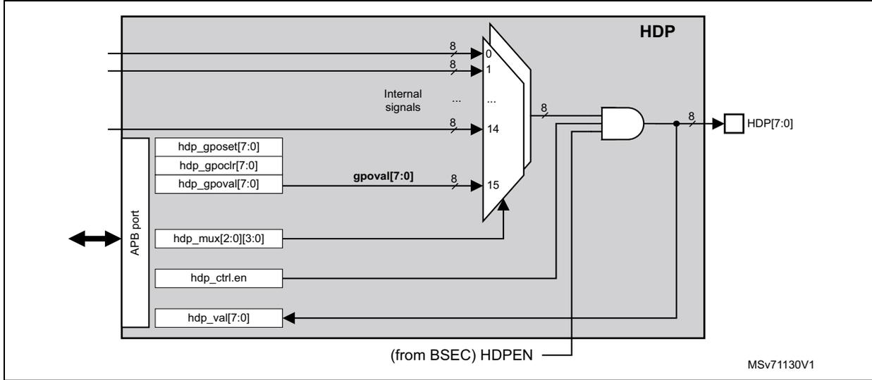
The diagram illustrates the internal architecture of the HDP block. On the left, an APB port is connected to several internal components:
hdp_gposet[7:0]
,
hdp_gpoclrl[7:0]
,
hdp_gpoval[7:0]
,
hdp_mux[2:0][3:0]
,
hdp_ctrl.en
, and
hdp_val[7:0]
. The
hdp_gpoval[7:0]
signal is labeled as
gpoval[7:0]
. Above these, several 'Internal signals' are shown entering a multiplexer. The multiplexer has inputs 0, 1, ..., 14, and 15. Input 15 is connected to
gpoval[7:0]
. The output of the multiplexer, which is 8 bits wide, is connected to one input of an AND gate. The other input of the AND gate is
hdp_ctrl.en
. The output of the AND gate is an 8-bit signal that is connected to the
HDP[7:0]
output pin. A signal labeled '(from BSEC) HDPEN' is also connected to the
hdp_ctrl.en
input. The diagram is labeled 'MSV71130V1' in the bottom right corner.
77.4 HDP register description
77.4.1 HDP control register (HDP_CTRL)
Address offset: 0x000
Reset value: 0x0000 0000
| 31 | 30 | 29 | 28 | 27 | 26 | 25 | 24 | 23 | 22 | 21 | 20 | 19 | 18 | 17 | 16 |
|---|---|---|---|---|---|---|---|---|---|---|---|---|---|---|---|
| Res. | Res. | Res. | Res. | Res. | Res. | Res. | Res. | Res. | Res. | Res. | Res. | Res. | Res. | Res. | Res. |
| 15 | 14 | 13 | 12 | 11 | 10 | 9 | 8 | 7 | 6 | 5 | 4 | 3 | 2 | 1 | 0 |
| Res. | Res. | Res. | Res. | Res. | Res. | Res. | Res. | Res. | Res. | Res. | Res. | Res. | Res. | Res. | EN |
| rw |
Bits 31:1 Reserved, must be kept at reset value.
Bit 0 EN: Enable HDP, valid if enabled in BSEC
77.4.2 HDP multiplexer control register (HDP_MUX)
Address offset: 0x004
Reset value: 0x0000 0000
| 31 | 30 | 29 | 28 | 27 | 26 | 25 | 24 | 23 | 22 | 21 | 20 | 19 | 18 | 17 | 16 |
|---|---|---|---|---|---|---|---|---|---|---|---|---|---|---|---|
| MUX7[3:0] | MUX6[3:0] | MUX5[3:0] | MUX4[3:0] | ||||||||||||
| rw | rw | rw | rw | rw | rw | rw | rw | rw | rw | rw | rw | rw | rw | rw | rw |
| 15 | 14 | 13 | 12 | 11 | 10 | 9 | 8 | 7 | 6 | 5 | 4 | 3 | 2 | 1 | 0 |
| MUX3[3:0] | MUX2[3:0] | MUX1[3:0] | MUX0[3:0] | ||||||||||||
| rw | rw | rw | rw | rw | rw | rw | rw | rw | rw | rw | rw | rw | rw | rw | rw |
Bits 31:0 MUXy[3:0] : Select the HDPy output among the 16 available signals (y = 7 to 0)
77.4.3 HDP read back value register (HDP_VAL)
Address offset: 0x010
Reset value: 0x0000 0000
| 31 | 30 | 29 | 28 | 27 | 26 | 25 | 24 | 23 | 22 | 21 | 20 | 19 | 18 | 17 | 16 |
|---|---|---|---|---|---|---|---|---|---|---|---|---|---|---|---|
| Res. | Res. | Res. | Res. | Res. | Res. | Res. | Res. | Res. | Res. | Res. | Res. | Res. | Res. | Res. | Res. |
| 15 | 14 | 13 | 12 | 11 | 10 | 9 | 8 | 7 | 6 | 5 | 4 | 3 | 2 | 1 | 0 |
| Res. | Res. | Res. | Res. | Res. | Res. | Res. | Res. | HDPVAL[7:0] | |||||||
| r | r | r | r | r | r | r | r | ||||||||
Bits 31:8 Reserved, must be kept at reset value.
Bits 7:0 HDPVAL[7:0] : Value of the HDP signals
77.4.4 HDP general-purpose output set register (HDP_GPOSET)
Address offset: 0x014
Reset value: 0x0000 0000
| 31 | 30 | 29 | 28 | 27 | 26 | 25 | 24 | 23 | 22 | 21 | 20 | 19 | 18 | 17 | 16 |
|---|---|---|---|---|---|---|---|---|---|---|---|---|---|---|---|
| Res. | Res. | Res. | Res. | Res. | Res. | Res. | Res. | Res. | Res. | Res. | Res. | Res. | Res. | Res. | Res. |
| 15 | 14 | 13 | 12 | 11 | 10 | 9 | 8 | 7 | 6 | 5 | 4 | 3 | 2 | 1 | 0 |
| Res. | Res. | Res. | Res. | Res. | Res. | Res. | Res. | HDPGPOSET[7:0] | |||||||
| w | w | w | w | w | w | w | w | ||||||||
Bits 31:8 Reserved, must be kept at reset value.
Bits 7:0
HDPGPOSET[7:0]
: When a bit is written to 1, the corresponding HDP GPO is set
Writing a bit to 0 has no effect.
77.4.5 HDP general purpose output clear register (HDP_GPOCLR)
Address offset: 0x018
Reset value: 0x0000 0000
| 31 | 30 | 29 | 28 | 27 | 26 | 25 | 24 | 23 | 22 | 21 | 20 | 19 | 18 | 17 | 16 |
|---|---|---|---|---|---|---|---|---|---|---|---|---|---|---|---|
| Res. | Res. | Res. | Res. | Res. | Res. | Res. | Res. | Res. | Res. | Res. | Res. | Res. | Res. | Res. | Res. |
| 15 | 14 | 13 | 12 | 11 | 10 | 9 | 8 | 7 | 6 | 5 | 4 | 3 | 2 | 1 | 0 |
| Res. | Res. | Res. | Res. | Res. | Res. | Res. | Res. | HDPGPOCLR[7:0] | |||||||
| w | w | w | w | w | w | w | w | ||||||||
Bits 31:8 Reserved, must be kept at reset value.
Bits 7:0 HDPGPOCLR[7:0] : When a bit is written to 1, the corresponding HDP GPO is cleared. Writing a bit to 0 has no effect.
77.4.6 HDP general purpose output value register (HDP_GPOVAL)
Address offset: 0x01C
Reset value: 0x0000 0000
| 31 | 30 | 29 | 28 | 27 | 26 | 25 | 24 | 23 | 22 | 21 | 20 | 19 | 18 | 17 | 16 |
|---|---|---|---|---|---|---|---|---|---|---|---|---|---|---|---|
| Res. | Res. | Res. | Res. | Res. | Res. | Res. | Res. | Res. | Res. | Res. | Res. | Res. | Res. | Res. | Res. |
| 15 | 14 | 13 | 12 | 11 | 10 | 9 | 8 | 7 | 6 | 5 | 4 | 3 | 2 | 1 | 0 |
| Res. | Res. | Res. | Res. | Res. | Res. | Res. | Res. | HDPGPOVAL[7:0] | |||||||
| rw | rw | rw | rw | rw | rw | rw | rw | ||||||||
Bits 31:8 Reserved, must be kept at reset value.
Bits 7:0 HDPGPOVAL[7:0] : When written, define the value of the HDP GPO. When read, provide the current GPO value.
77.4.7 HDP register map
Table 854. HDP register map and reset values
| Offset | Register name | 31 | 30 | 29 | 28 | 27 | 26 | 25 | 24 | 23 | 22 | 21 | 20 | 19 | 18 | 17 | 16 | 15 | 14 | 13 | 12 | 11 | 10 | 9 | 8 | 7 | 6 | 5 | 4 | 3 | 2 | 1 | 0 |
|---|---|---|---|---|---|---|---|---|---|---|---|---|---|---|---|---|---|---|---|---|---|---|---|---|---|---|---|---|---|---|---|---|---|
| Res. | Res. | Res. | Res. | Res. | Res. | Res. | Res. | Res. | Res. | Res. | Res. | Res. | Res. | Res. | Res. | Res. | Res. | Res. | Res. | Res. | Res. | Res. | Res. | Res. | Res. | Res. | Res. | Res. | Res. | Res. | EN | ||
| 0x000 | HDP_CTRL | ||||||||||||||||||||||||||||||||
| Reset value | 0 | ||||||||||||||||||||||||||||||||
| 0x004 | HDP_MUX | MUX7[3:0] | MUX6[3:0] | MUX5[3:0] | MUX4[3:0] | MUX3[3:0] | MUX2[3:0] | MUX1[3:0] | MUX0[3:0] | ||||||||||||||||||||||||
| Reset value | 0 | 0 | 0 | 0 | 0 | 0 | 0 | 0 | 0 | 0 | 0 | 0 | 0 | 0 | 0 | 0 | 0 | 0 | 0 | 0 | 0 | 0 | 0 | 0 | 0 | 0 | 0 | 0 | 0 | 0 | 0 | 0 | |
| 0x008 - 0x00C | Reserved | Reserved | |||||||||||||||||||||||||||||||
| 0x010 | HDP_VAL | Res. | Res. | Res. | Res. | Res. | Res. | Res. | Res. | Res. | Res. | Res. | Res. | Res. | Res. | Res. | Res. | Res. | Res. | Res. | Res. | Res. | Res. | Res. | Res. | HDPVAL[7:0] | |||||||
| Reset value | 0 | 0 | 0 | 0 | 0 | 0 | 0 | 0 | |||||||||||||||||||||||||
Table 854. HDP register map and reset values
| Offset | Register name | 31 | 30 | 29 | 28 | 27 | 26 | 25 | 24 | 23 | 22 | 21 | 20 | 19 | 18 | 17 | 16 | 15 | 14 | 13 | 12 | 11 | 10 | 9 | 8 | 7 | 6 | 5 | 4 | 3 | 2 | 1 | 0 | |
|---|---|---|---|---|---|---|---|---|---|---|---|---|---|---|---|---|---|---|---|---|---|---|---|---|---|---|---|---|---|---|---|---|---|---|
| 0x014 | HDP_GPOSET | Res. | Res. | Res. | Res. | Res. | Res. | Res. | Res. | Res. | Res. | Res. | Res. | Res. | Res. | Res. | Res. | Res. | Res. | Res. | Res. | Res. | Res. | Res. | Res. | HDPGPOSET[7:0] | ||||||||
| Reset value | 0 | 0 | 0 | 0 | 0 | 0 | 0 | 0 | 0 | |||||||||||||||||||||||||
| 0x018 | HDP_GPOCLR | Res. | Res. | Res. | Res. | Res. | Res. | Res. | Res. | Res. | Res. | Res. | Res. | Res. | Res. | Res. | Res. | Res. | Res. | Res. | Res. | Res. | Res. | Res. | Res. | HDPGPOCLR[7:0] | ||||||||
| Reset value | 0 | 0 | 0 | 0 | 0 | 0 | 0 | 0 | 0 | |||||||||||||||||||||||||
| 0x01C | HDP_GPOVAL | Res. | Res. | Res. | Res. | Res. | Res. | Res. | Res. | Res. | Res. | Res. | Res. | Res. | Res. | Res. | Res. | Res. | Res. | Res. | Res. | Res. | Res. | Res. | Res. | HDPGPOVAL[7:0] | ||||||||
| Reset value | 0 | 0 | 0 | 0 | 0 | 0 | 0 | 0 | 0 | |||||||||||||||||||||||||
Refer to Section 2.3 for the register boundary addresses.