76. Ethernet (ETH): gigabit media access control (GMAC) with DMA controller
76.1 Ethernet introduction
Portions Copyright (c) Synopsys, Inc. All rights reserved. Used with permission.
The Ethernet peripheral enables to transmit and receive data over Ethernet in compliance with the IEEE 802.3-2015 standard.
The peripheral is configurable to meet the needs of a large variety of consumer and industrial applications, including AV nodes and TSN (time sensitive networking) nodes.
76.2 Ethernet main features
The Ethernet peripheral embeds a dedicated DMA for direct memory interface, a media access controller (MAC) and a PHY interface block supporting several formats.
76.2.1 Standard compliance
The Ethernet peripheral is compliant with the following standards:
- • IEEE 802.3-2015 for Ethernet MAC and media independent interface (MII)
- • IEEE 1588-2008 for precision networked clock synchronization (PTP)
- • IEEE 802.1AS-2011 and 802.1-Qav-2009 for Audio Video (AV) traffic
- • IEEE 802.3az-2010 for Energy Efficient Ethernet (EEE)
- • IEEE 802.1Qbv-2015, 802.1Qbu-2016, and 802.1AS-Rev D5.0 for Time-Sensitive Networking (TSN) traffic
- • AMBA 2.0 for AHB slave port
- • AMBA4 for AXI master port
- • RGMII specification version 2.6 from HP/Marvell
- • RMII specification version 1.2 from RMII consortium
Caution: The gigabit media independent interface (GMII) is only available internally to supply the RGMII adapter. No GMII signals are available off-chip.
76.2.2 MAC features
MAC Tx and Rx common features
- • Separate transmission, reception, and control interfaces to the application
- • 10, 100, and 1000 Mbit/s data transfer rates with the following PHY interfaces:
- – IEEE 802.3-compliant MII interface to communicate with an external Fast Ethernet PHY
- – RGMII interface to communicate with an external gigabit PHY
- – RMII interface to communicate with an external Fast Ethernet PHY
- • Half-duplex operation:
- – CSMA/CD protocol support
- – Flow control using back pressure (based on implementation-specific white papers and UNH Ethernet Clause 4 MAC Test Suite - Annex D)
- – Packet bursting and packet extension in 1000 Mbps Half-duplex operation
- • Standard IEEE 802.3az-2010 for Energy Efficient Ethernet in MII and reduced gigabit media independent interface (RGMII) PHYs
- • 64-bit data transfer interface on the application side
- • Full-duplex flow control operations (IEEE 802.3x Pause packets and Priority flow control)
- • Network statistics with RMON or MIB counters (partial support of RFC2819/RFC2665)
- • Ethernet packet timestamping as described in IEEE 1588-2002 and IEEE 1588-2008 (64-bit timestamps given in the Tx or Rx status of PTP packet). Both one-step and two-step timestamping are supported in Tx direction.
- • Flexibility to control up to two pulse-per-second (PPS) output signals (eth_otp_pps_outx and ETH_PPS_OUT)
- • MDIO (Clause 22 and Clause 45) master interface for PHY device configuration and management
MAC Tx features
- • Preamble and start-of-frame data (SFD) insertion
- • Separate 32-bit status for each packet transmitted from the application
- • Automatic CRC and pad generation controllable on a per-frame basis
- • Programmable packet length to support Standard or Jumbo Ethernet packets of up to 16 Kbytes
- • Programmable Inter Packet Gap (40–96 bit times in steps of 8)
- • IEEE 802.3x Flow Control automatic transmission of zero-quanta Pause packet when flow control input transitions from assertion to de-assertion (in Full-duplex mode)
- • Source address field insertion or replacement, and VLAN insertion, replacement, and deletion in transmitted packets with per-packet or static-global control
- • Insertion, replacement, or deletion of up to two VLAN tags
- • Option to transmit packets with reduced preamble size in Full-duplex mode
- • Insert, replace, or delete queue/channel-based VLAN tags
- • Frame preemption for MAC Tx
MAC Rx features
- • Automatic Pad and CRC stripping options
- • Option to disable automatic CRC checking
- • Preamble and SFD deletion
- • Separate 112-bit or 128-bit status
- • Programmable watchdog timeout limit
- • Flexible address filtering modes:
- – Four 48-bit perfect (DA) address filters with masks for each byte
- – Four 48-bit SA address comparison check with masks for each byte
- – 64 bit Hash filter for multicast and unicast (DA) addresses
- • Option to pass all multicast addressed packets
- • Promiscuous mode to pass all packets without any filtering for network monitoring
- • Pass all incoming packets (as per filter) with a status report
- • Additional packet filtering:
- – VLAN tag-based: Perfect match and Hash-based filtering based either on the outer or inner VLAN tag
- – Layer 3 and Layer 4-based: TCP or UDP over IPv4 or IPv6
- – Extended VLAN tag based filtering with four filter selection
- • IEEE 802.1Q VLAN tag detection and option to delete the VLAN tags in received packets
- • Detection of remote wake-up packets and AMD magic packets
- • Optional forwarding of received Pause packets to the application (in Full-duplex mode)
- • Layer 3/Layer 4 checksum offload for received packets
- • Stripping of up to two VLAN tags and providing the tags in the status
- • Frame preemption for MAC Rx
76.2.3 Transaction layer (MTL) features
MTL Tx and Rx common features
- • 64-bit transaction layer block (bridges the application and the MAC)
- • Optimization for packet-oriented transfers with packets delimiters
- • Programmable burst length, up to half the size of the MTL Rx queue or Tx queue size, to support burst data transfer in the EQOS-MTL configuration
- • Programmable threshold capability for each queue (default of 64 bytes)
MTL Tx features
- • 4096-byte transmit FIFO with programmable threshold capability
- • Two Tx queues on the transmit path with a common memory for all Tx queues
- • Store-and-forward mechanism or threshold mode (cut-through) for transmission to the MAC
- • Programmable queue size in configurations with multiple queues. Each queue size can be programmed in terms of 256 bytes
- • Automatic retransmission of collision packets in Half-duplex mode
- • Discard packets on late collision, excessive collisions, excessive deferral, and under-run conditions with appropriate status
- • Module to calculate and insert IPv4 header checksum and TCP, UDP, or ICMP checksum on frames transmitted in Store-and-forward mode
- • Statistics by generating pulses for packets dropped (because of underflow) in the Tx FIFO
- • Optional statistics related to bandwidth consumption for each queue of up to 16 blocks over a 125 µs period
- • Packet-level control for
- – VLAN tag insertion or replacement
- – Ethernet source address insertion
- – Layer 3/Layer 4 checksum insertion control
- – One-step timestamp
- – Timestamp control
- – CRC and pad control
- • Following scheduling algorithms in configurations with multiple queues
- – Weighted round robin (WRR)
- – Strict priority (SP)
- – Credit-based shaper (CBS)
- – Enhancement to scheduled traffic (EST)
- – Time-based scheduling (TBS)
MTL Rx features
- • 4096-byte receive FIFO with configurable threshold
- • Two Rx queues on the receive path with a common memory for all Rx queues
- • Programmable Rx queue threshold (default fixed at 64 bytes) in threshold (or cut-through) mode
- • Option to filter all error packets on reception and not forward them to the application in the store-and-forward mode
- • Option to forward the undersized good packets
- • Statistics by generating pulses for packets dropped (because of overflow) in the Rx FIFO
- • Automatic generation of Pause packet control or backpressure signal to the MAC based on the Rx Queue fill level
- • Arbitration among queues when multiple queues are present. The following arbitration schemes are supported:
- – Weighted round robin (WRR)
- – Weighted Strict priority (WSP)
- – Strict priority (SP)
76.2.4 DMA block features
The DMA block exchanges data between the peripheral and the system memory. DMA transfers are driven by software descriptors structure. The application can use a set of registers (see Section 76.11.2: Ethernet DMA registers ) to control the DMA operations. The DMA block supports the following features:
- • 64-bit data transfers
- • Separate DMA channel in the transmit path for each queue
- • Separate DMA channel in the receive path for each queue
- • Optimization for packet-oriented DMA transfers with packet delimiters
- • Byte-aligned addressing for data buffer support
- • Dual-buffer (ring) descriptor support
- • Descriptor architecture allowing large blocks of data transfer with minimum CPU intervention (each descriptor can transfer up to 32 Kbytes of data)
- • Comprehensive status reporting normal operation and transfer errors
- • Individual programmable burst length for Tx DMA and Rx DMA engines for optimal host bus utilization
- • Programmable interrupt options for different operational conditions
- • Per-packet transmit or receive complete interrupt control
- • Round-robin or fixed-priority arbitration between the receive and transmit engines
- • Fixed-priority, weighted-strict-priority or weighted-round-robin arbitration for data read requests from multiple transmit DMA engines
- • Start and Stop modes
- • Separate ports for host control access and host data interface (AXI)
- • Tx DMA channels with TCP segmentation offload (TSO) feature enabled
- • Routing of received packets to the DMA channels based on the DA or VLAN priority in multichannel DMA configurations
- • Time-sensitive conditional packet transmission by comparing the slot time or IEEE 1588 time information provided in the descriptor (useful for AV applications)
- • Programmable control for transmit descriptor posted writes to improve the throughput
76.2.5 Bus interface features
AXI master interface
The AXI master interface features are the following:
- • Interfaces with the application through AXI4 compatible interface
- • 32-bit address width
- • 64-bit data
- • OKAY, SLVERR, and DECERR responses
- • Software-selected type of AXI burst (fixed and variable length burst) in AXI master interface; extended length fixed bursts of 32, 64, 128, and 256
- • Handshaking on AXI read and write data channels
AHB slave interface
The AHB slave interface supports the following features:
- • Interfaces with the application through AHB
- • AHB slave interface (32-bit) for CSR access
- • All AHB burst types
The AHB slave interface does not generate the following responses:
- • Split
- • Retry
76.2.6 Audio and video features
The Ethernet peripheral can be used in Audio Video (AV) mode. The supported features are compliant with the industry standards for AV traffic:
- • Separate channels or queues for AV data transfer in 100 Mbps and 1000 Mbps modes
- • Multiple Rx queues on the receive paths for AV traffic, and multiple Tx queues on the Transmit path for AV traffic
- • IEEE 802.1-Qav specified credit-based shaper (CBS) algorithm for Transmit channels
- • Single Tx FIFO and Rx FIFO (MTL) for all selected queues
- • Programmable Slot Interval with range from 1 µs to 4096 µs and granularity of 1 µs.
76.2.7 Time sensitive networking features
The Ethernet peripheral supports the following time sensitive networking (TSN) features:
- • IEEE 802.1Qbv-2015, Enhancements to Scheduling Traffic
- • IEEE802.1Qbu/802.3br, Frame preemption and Interspersing Express Traffic
76.2.8 Generic queuing features
The Ethernet peripheral supports the following features for generic queuing:
- • Programmable control for routing receive packets with Multicast/Broadcast destination address to a programmable receive queue
- • Support routing of untagged receive packets to a programmable receive queue
- • Programmable control for routing VLAN tagged and untagged IEEE 1588 PTP over Ethernet receive packets to a same or separate programmable receive queue
- • Programmable control for routing Unicast/Multicast receive packets that fail the destination address filter to a separate programmable receive queues
76.3 Ethernet pins and internal signals
Table 762 lists the Ethernet inputs and output signals connected to package pins or balls. Active pins depend on the PHY type selected (MII, RMII or RGMII) and on the device configuration.
Table 763 shows the internal Ethernet signals.
Table 762. Ethernet peripheral pins
| Port name | Digital port type | Description |
|---|---|---|
| ETH_COL | Input | Collision detection signal, MII only. |
| ETH_CRS | Input | Carrier sense signal, MII only |
| ETH_REF_CLK | Input | RMII reference clock |
| ETH_RX_CLK | Input | MII/RGMII timing reference for Rx data transfers |
| ETH_RXD[3:0] | Input | Receive data. 4 pins for MII and RGMII, 2 for RMII. |
| ETH_RX_DV | Input | Receive data valid |
Table 762. Ethernet peripheral pins (continued)
| Port name | Digital port type | Description |
|---|---|---|
| ETH_CRS_DV | Input | RMII: Carrier Sense (CRS) and RX_Data Valid (RX_DV) multiplexed on alternate clock cycles. In 10 Mbit/s mode, it alternates every 10 clock cycles. |
| ETH_RX_CTL | Input | After demultiplexing, this pin provides ETH_RX_DV on the rising edge of ETH_RX_CLK, and ETH_RX_ER (logical XOR between ETH_RX_CTL values on rising edge and falling edge of ETH_RX_CLK). |
| ETH_RX_ER | Input | Receive error |
| ETH_TX_CLK | Input | MII timing reference for Tx data transfers |
| ETH_GTX_CLK | Output | RGMII timing reference for Tx data transfers |
| ETH_TXD[3:0] | Output | Transmit data. 4 pins for MII and RGMII, 2 for RMII. |
| ETH_TX_EN | Output | Transmit data enable |
| ETH_TX_CTL | Output | Multiplexing of ETH_TX_EN on the rising edge of ETH_TX_CLK, and a logical XOR between ETH_TX_EN and ETH_TX_ER values on falling edge of ETH_TX_CLK |
| ETH_TX_ER | Output | Transmit error |
| ETH_MDC | Output | Management data clock |
| ETH_MDIO | Input/output | Management data |
| ETH_PHY_INTN | Input | PHY interrupt |
| ETH_PPS_OUT | Output | PTP pulse-per-second output 0 |
| ETH_PTP_AUX_TS (1) | Input | Trigger input for the auxiliary snapshots of the PTP system time |
1. This pin is not available on all devices.
Table 763. Ethernet internal input/output signals
| Signal name | Signal type | Description |
|---|---|---|
| eth_hclk | Digital input | AHB clock |
| eth_aclk | Digital input | AXI clock |
| eth_sbd_intr_it | Digital output | Main Ethernet interrupt |
| lpi_intr_o | Digital output | Sideband signal generated when the transmitter or receiver enters or exits the LPI state. |
| pmt_intr_o | Digital output | Sideband signal generated when a valid remote wake-up packet is received |
| eth_tx_clk | Digital input | Tx kernel clock |
| eth_rx_clk | Digital input | Rx kernel clock |
| eth_rmii_ref_clk | Digital input | RMII reference kernel clock |
| eth_ptp_pps_out1 | Digital output | PTP pulse-per-second signal |
| mac_speed_o[1:0] | Digital output | MAC speed information used by the RCC |
Table 763. Ethernet internal input/output signals (continued)
| Signal name | Signal type | Description |
|---|---|---|
| clk_ptp_ref_i | Digital input | PTP reference clock input |
| eth_ptp_trig[3:0] | Digital input | Trigger input for auxiliary snapshots of the PTP system time |
76.4 Ethernet architecture
The Ethernet peripheral is composed of 4 main functional modules:
- • The control and status register module (CSR) that controls the registers access through AHB 32-bit slave interface
- • The direct memory access interface (DMA)
This is the logical DMA module with two physical channel for reception and two for transmission. It controls the data transfers between MAC and system memory through the AMBA AXI4 64-bit master interface. - • The media access control module (MAC) in charge of implementing the Ethernet protocol
- • The MAC transaction layer (MTL) in charge of controlling the data flow between application and MAC.
A protocol adaption module is added to support the RMII or the RGMII PHY Media Independent Interfaces.
Caution: The gigabit media independent interface (GMII) is only available internally to supply the RGMII adapter. No GMII signals are available off-chip.
Figure 1019. Ethernet high-level block diagram
![Figure 1019. Ethernet high-level block diagram. The diagram shows the internal architecture of the Ethernet MAC. On the left, a 64-bit AXI Master and a 32-bit AHB Slave are connected to a DMA Arbitrer and a CSR (Control and Status Register). The DMA Arbitrer is connected to two DMA channels (Ch.0 and Ch.1), each with Tx and Rx engines. These channels are connected to 4KB Tx and Rx FIFOs, which in turn connect to the MAC Tx and MAC Rx blocks. The MAC blocks are connected to a GMII/MII interface, which includes a RGMII/RMII block and a Select block. The Select block is connected to the PHY I/F. Various clock and control signals are shown: eth_aclk, eth_hclk, eth_sbd_intr_it, lpi_intr_o, pmt_intr_o, mac_speed_o[1:0], clk_ptp_ref_i, eth_ptp_trig[3:0], and ETH_PTP_AUX_TS. Output signals include eth_tx_clk, eth_ref_clk, eth_rx_clk, ETH_PPS_OUT, and eth_ptp_pps_out1. The diagram is labeled MSv71200V4.](/RM0486-STM32N6x5-x7/9072ca12a447da802bf2911032481e25_img.jpg)
- 1. For a definition of the internal signals, refer to Table 763 .
- 2. Refer to RCC chapter “Clock distribution for Ethernet” for a detailed description of the Ethernet clock architecture.
- 3. The ETH_PTP_AUX_TS pin is not available on all devices.
76.4.1 DMA controller
The DMA has independent transmit (Tx) and receive (Rx) engines. The Tx engine transfers data from the system memory to the MAC Transaction Layer (MTL), whereas the Rx engine transfers data from the device port (PHY) to the system memory.
The controller uses descriptors to efficiently move data from source to destination with minimal application CPU intervention. The DMA is designed for packet-oriented data transfers such as packets in Ethernet. The controller can be programmed to interrupt the application CPU for situations such as Packet transmit and receive Transfer completion, and other normal or error conditions.
DMA data structures
The DMA and the application communicate through the following two data structures:
- • Control and Status registers (CSR)
- • Descriptor lists and data buffers
The DMA transfers the data packets received by the MAC to the Rx buffer in system memory and Tx data packets from the Tx buffer in the system memory. The descriptors that reside in the system memory contain the pointers to these buffers.
The base address of each list is written to the respective Tx and Rx registers: Channel x Tx descriptor list address register (ETH_DMACxTXDLAR) and Channel x Rx descriptor list address register (ETH_DMACxRXDLAR) .
The descriptor list is forward linked and the next descriptor is always considered at a fixed offset to the current one. The number of descriptors in the list is programmed in the respective Tx/Rx, Channel x Tx descriptor ring length register (ETH_DMACxTXRLR) and Channel x Rx descriptor ring length register (ETH_DMACxRXRLR) .
Once the DMA processes the last descriptor in the list, it automatically jumps back to the descriptor in the List address register to create a descriptor ring. The descriptor lists reside in the physical memory address space of the application. Each descriptor can point to a maximum of two buffers. This enables two buffers to be used and physically addressed, rather than contiguous buffers in memory.
A data buffer resides in the application physical memory space and consists of an entire packet or part of a packet, but cannot exceed a single packet. Buffers contain only data. The buffer status is saved in the descriptor. Data chaining refers to packets that span multiple data buffers. However, a single descriptor cannot span multiple packets. The DMA skips to the data buffer of next packet when EOP is detected.
Descriptors are specified in Section 76.10: Descriptors .
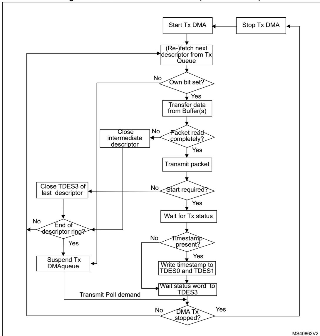
DMA transmission in default mode
The Tx DMA engine in default mode proceeds as follows:
- 1. The application sets up the Transmit descriptor (TDES0–TDES3) and sets the Own bit (TDES0[31]) after setting up the corresponding data buffer(s) with Ethernet Packet data.
- 2. The application shifts the descriptor tail pointer offset value of the Transmit channel.
- 3. While in the Run state, the DMA runs an arbitration cycle to select the next Tx DMA channel from which the packets requiring transmission should be processed.
- 4. The DMA fetches the descriptor from the application memory.
- 5. If the DMA detects one of the following conditions, the transmission from that channel is suspended, bit 2 and 16 of the corresponding DMA channel Status register are set, and the Tx engine proceeds to step 11:
- – The descriptor is flagged as owned by the application (TDES3 [31] = 0).
- – The descriptor tail pointer is equal to the current descriptor pointer in Ring Descriptor list mode.
- – An error condition occurs.
- 6. If the acquired descriptor is flagged as owned by the DMA (TDES3[31] = 1), the DMA decodes the Transmit Data Buffer address from the acquired descriptor.
- 7. The DMA fetches the Transmit data from the system memory and transfers the data to the MTL for transmission.
- 8. If an Ethernet packet is stored over data buffers in multiple descriptors, the DMA closes the intermediate descriptor and fetches the next descriptor. Steps 3 through 7 are repeated until the end-of-Ethernet-packet data is transferred to the MTL.
- 9. When packet transmission is complete, if IEEE 1588 timestamp feature was enabled for the packet (as indicated in the Tx status), the timestamp value obtained from MTL is written to the Tx descriptor (TDES0 and TDES1) that contains the EOP buffer. The status information is written to this Tx descriptor (TDES3). The application now owns
this descriptor because the Own bit is cleared during this step. If the timestamp feature is disabled for this packet, the DMA does not alter TDES0 and TDES1 contents.
- 10. Bit 0 of Channel x status register (ETH_DMACxSR) is set after completing transmission of a packet that has Interrupt on Completion (TDES2[31]) set in its Last Descriptor. The DMA engine returns to step 3.
- 11. In the Suspend state, the DMA tries to acquire the descriptor again (and thereby return to step 3). A poll demand command is triggered by writing any value to the Channel x Tx descriptor tail pointer register (ETH_DMACxTXDTPR) when it receives a Transmit Poll demand and the underflow interrupt status bit is cleared. If the application stopped the DMA by clearing Bit 0 of Transmit control register of corresponding DMA channel, the DMA enters the Stop state.
Figure 1020. DMA transmission flow (standard mode)
graph TD
    StartTx[Start Tx DMA] --> Fetch[(Re-)fetch next descriptor from Tx Queue]
    StopTx[Stop Tx DMA] --> Fetch
    Fetch --> OwnBit{Own bit set?}
    OwnBit -- No --> EndRing{End of descriptor ring?}
    OwnBit -- Yes --> Transfer[Transfer data from Buffer(s)]
    Transfer --> PacketRead{Packet read completely?}
    PacketRead -- No --> CloseInt[Close intermediate descriptor]
    PacketRead -- Yes --> Transmit[Transmit packet]
    Transmit --> StartReq{Start required?}
    StartReq -- No --> EndRing
    StartReq -- Yes --> WaitTx[Wait for Tx status]
    WaitTx --> Timestamp{Timestamp present?}
    Timestamp -- No --> EndRing
    Timestamp -- Yes --> WriteTS[Write timestamp to TDES0 and TDES1]
    WriteTS --> WaitStatus[Wait status word to TDES3]
    WaitStatus --> DMAStopped{DMA Tx stopped?}
    DMAStopped -- Yes --> StopTx
    DMAStopped -- No --> PollDemand[Transmit Poll demand]
    PollDemand --> Fetch
    EndRing -- Yes --> Suspend[Suspend Tx DMAqueue]
    EndRing -- No --> CloseLast[Close TDES3 of last descriptor]
    CloseLast --> Fetch
CloseInt --> FetchMS40862V2
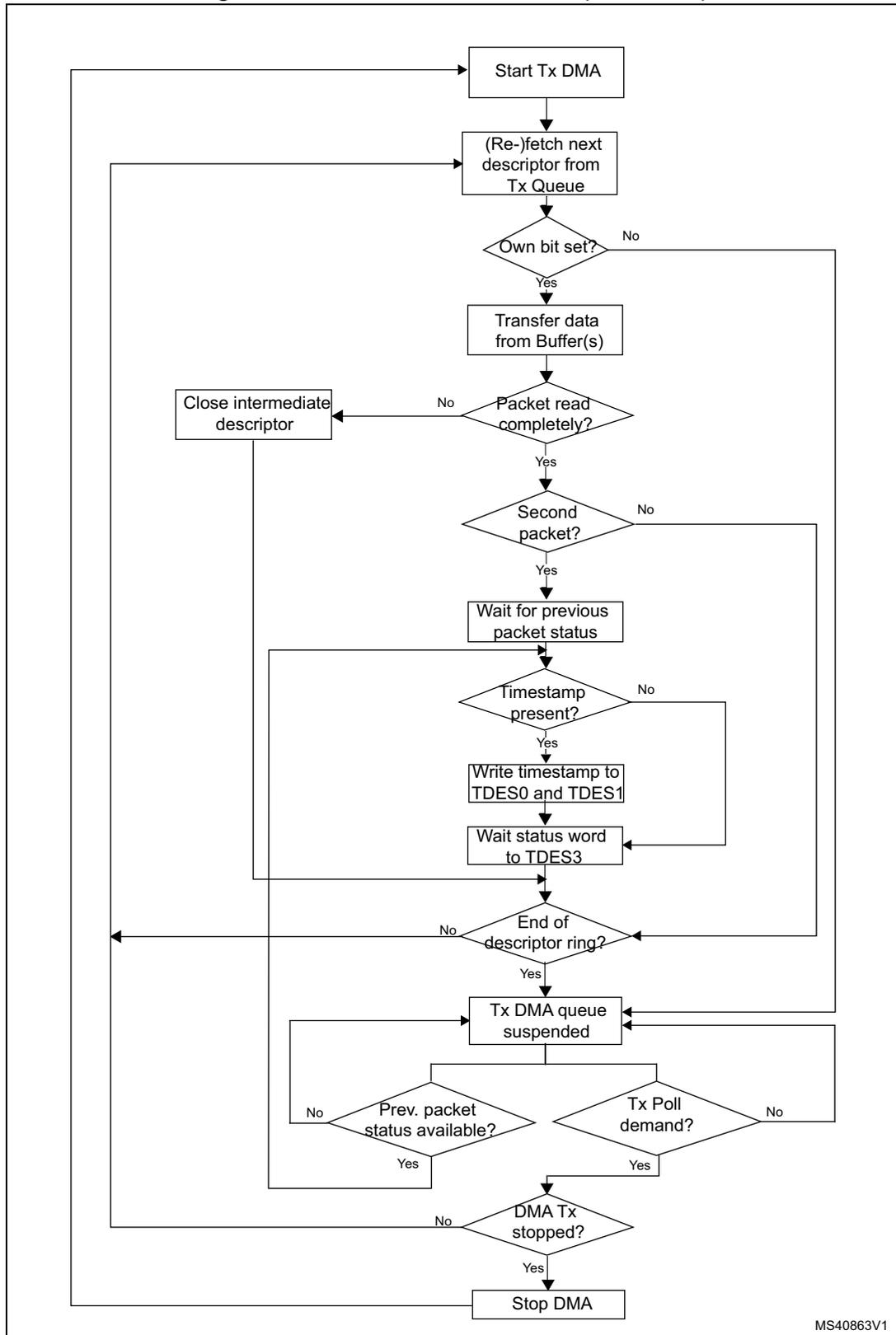
DMA transmission in OSP (operate on second packet) mode
In Run state, if bit 4 is set in the Channel x transmit control register (ETH_DMACxTXCR) , the Transmit process can simultaneously acquire two packets without closing the Status descriptor of the first packet. While the Transmit process completes the first packet transfer, it immediately polls the Transmit descriptor list for the second packet. If the second packet is valid, the Transmit process transfers this packet before writing the status information of the first packet.
In OSP mode, DMA transmission in the Run state operates as described in the following sequence:
- 1. The DMA executes steps 1 to 7 of the DMA transmission sequence in default mode (see Section : DMA transmission in default mode ).
- 2. The DMA fetches the next descriptor without closing previous packet last descriptor.
- 3. If the DMA owns the acquired descriptor, the DMA decodes the transmit buffer address in this descriptor. If the DMA does not own the descriptor, the DMA goes into Suspend mode and jumps to step 7.
- 4. The DMA fetches the Transmit packet from the system memory and transfers the packet to the MTL until the EOP data is transferred, closing the intermediate descriptors if this packet is split across multiple descriptors.
- 5. The DMA waits for the packet transmission status and timestamp of previous packet. When the status is available, the DMA writes the timestamp to TDES0 and TDES1 if such timestamp was captured (as indicated by a status bit). The DMA writes the status, with a cleared Own bit, to the corresponding TDES3, thus closing the descriptor. If Timestamp feature is not enabled for the previous packet, the DMA does not alter the contents of TDES2 and TDES3.
- 6. The Transmit interrupt is set (if enabled). The DMA fetches the next descriptor and proceeds to step 3 (when Status is normal). If the previous transmission status shows an underflow error, the DMA goes into Suspend mode (step 7).
- 7. In Suspend mode, if a pending status and timestamp are received from the MTL, the DMA performs the following operations:
- a) The DMA writes the timestamp (if enabled for the current packet) to TDES2 and TDES3.
- a) The DMA writes the status to the corresponding TDES3.
- a) The DMA sets the relevant interrupts and returns to Suspend mode.
- 8. The DMA can exit Suspend mode and enter the Run state (it goes either to step 1 or to step 2 depending on pending status) only after receiving a Transmit Poll demand in the transmit descriptor tail pointer register of corresponding channel.
A description of the basic DMA transmission flow in OSP mode is given in Figure 1022: Receive DMA flow .
Figure 1021. DMA transmission flow (OSP mode)
graph TD
    Start[Start Tx DMA] --> Fetch[(Re-)fetch next descriptor from Tx Queue]
    Fetch --> OwnBit{Own bit set?}
    OwnBit -- No --> EndRing{End of descriptor ring?}
    OwnBit -- Yes --> Transfer[Transfer data from Buffer(s)]
    Transfer --> ReadComplete{Packet read completely?}
    ReadComplete -- No --> CloseDesc[Close intermediate descriptor]
    ReadComplete -- Yes --> SecondPacket{Second packet?}
    SecondPacket -- No --> EndRing
    SecondPacket -- Yes --> WaitStatus[Wait for previous packet status]
    WaitStatus --> TimestampPresent{Timestamp present?}
    TimestampPresent -- No --> EndRing
    TimestampPresent -- Yes --> WriteTimestamp[Write timestamp to TDES0 and TDES1]
    WriteTimestamp --> WaitStatusWord[Wait status word to TDES3]
    WaitStatusWord --> EndRing
    EndRing -- No --> Fetch
    EndRing -- Yes --> Suspended[Tx DMA queue suspended]
    Suspended --> PrevPacketStatus{Prev. packet status available?}
    PrevPacketStatus -- Yes --> DMAStopped{DMA Tx stopped?}
    PrevPacketStatus -- No --> TxDMAQueueSuspended[Tx DMA queue suspended]
    TxDMAQueueSuspended --> TxDemand{Tx Poll demand?}
    TxDemand -- Yes --> DMAStopped
    TxDemand -- No --> DMAStopped
    DMAStopped -- Yes --> StopDMA[Stop DMA]
    DMAStopped -- No --> Fetch
    CloseDesc --> EndRing
    MS40863V1[MS40863V1]
    style MS40863V1 fill:none,stroke:none
The flowchart illustrates the DMA transmission process in OSP mode. It begins with 'Start Tx DMA', followed by '(Re-)fetch next descriptor from Tx Queue'. A decision 'Own bit set?' follows; if 'No', it proceeds to 'End of descriptor ring?'; if 'Yes', it goes to 'Transfer data from Buffer(s)'. From 'Transfer data from Buffer(s)', a decision 'Packet read completely?' follows; if 'No', it goes to 'Close intermediate descriptor' and then to 'End of descriptor ring?'; if 'Yes', it proceeds to 'Second packet?'. If 'Second packet?' is 'No', it goes to 'End of descriptor ring?'; if 'Yes', it goes to 'Wait for previous packet status'. From 'Wait for previous packet status', a decision 'Timestamp present?' follows; if 'No', it goes to 'End of descriptor ring?'; if 'Yes', it goes to 'Write timestamp to TDES0 and TDES1', then 'Wait status word to TDES3', and finally to 'End of descriptor ring?'. From 'End of descriptor ring?', if 'No', it loops back to '(Re-)fetch next descriptor from Tx Queue'; if 'Yes', it goes to 'Tx DMA queue suspended'. From 'Tx DMA queue suspended', a decision 'Prev. packet status available?' follows; if 'Yes', it goes to 'DMA Tx stopped?'; if 'No', it loops back to 'Tx DMA queue suspended'. From 'Tx DMA queue suspended', a decision 'Tx Poll demand?' follows; if 'Yes', it goes to 'DMA Tx stopped?'; if 'No', it goes to 'DMA Tx stopped?'. From 'DMA Tx stopped?', if 'Yes', it goes to 'Stop DMA'; if 'No', it loops back to '(Re-)fetch next descriptor from Tx Queue'. A label 'MS40863V1' is present in the bottom right corner.
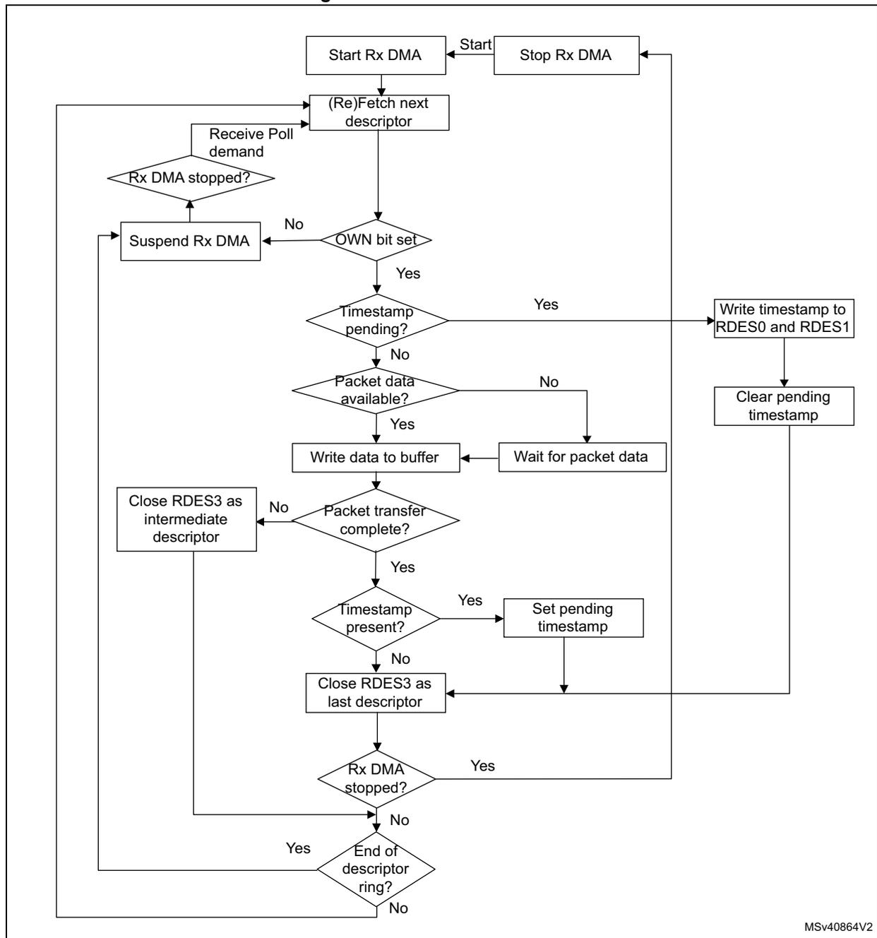
DMA reception
In the receive path, the DMA reads a packet from the MTL receive queue and writes it to the packet data buffers of the corresponding DMA channel.
The DMA Rx descriptor ring structure is described in Section 76.10: Descriptors .
The reception sequence for Rx DMA engine is as follows (see also Figure 1022: Receive DMA flow ):
- 1. The application sets up the Rx descriptors (RDES0-RDES3) and the Own bit (RDES3[31]). The application should set the correct value in the receive descriptor tail pointer register of corresponding DMA channel to indicate the location of the last valid descriptor for the DMA. If the tail pointer points to descriptor N, the last valid descriptor for the DMA is descriptor N - 1.
- 2. When bit 0 of Channel x receive control register (ETH_DMAxCxRXCR) is set, the DMA enters the Run state. The DMA looks for free descriptors based on the Rx Current Descriptor and Descriptor tail pointer register values. The descriptors referenced between the current descriptor and the tail pointer registers are available for the DMA. If there are no free descriptors, the DMA channel enters the Suspend state and goes to step 11.
- 3. The DMA fetches the next available descriptor in the ring and decodes the receive data buffer address from acquired descriptors.
- 4. If IEEE 1588 timestamping is enabled and the timestamp is available for the previous packet, the DMA writes the timestamp (if available) to the RDES0 and RDES1 of current descriptor and sets the CTXT field (RDES3[30]).
- 5. The DMA processes the incoming packets and stores them in the data buffers of acquired descriptor.
- 6. If the current packet transfer is not complete, the DMA closes the current descriptor as intermediate and goes to step 10.
- 7. The DMA retrieves the status of the receive frame from the MTL and writes the status word to current descriptor with the Own bit cleared and the Last descriptor bit set.
- 8. The DMA writes the Frame Length to RDES3 and the VLAN tag to RDES0. The DMA also writes the MAC control frame opcode, OAM control frame code, and extended status information (if available) to RDES1 of the last descriptor.
- 9. The DMA stores the timestamp (if available). The DMA writes the context descriptor after the last descriptor for the current packet (in the next available descriptor).
- 10. If more descriptors are available in the Rx DMA descriptor ring, go to step 3, otherwise go to the Suspend state (step 11).
- 11. The receive DMA exits the Suspend state when a receive Poll demand is given, and the application updates the channel receive descriptor tail pointer register to indicate the location of the last valid descriptor for DMA. Then, the engine proceeds to step 2 and fetches again the next descriptor.
Note: Refer to Section : Descriptor tail pointer handling examples for updating the correct value in receive descriptor tail pointer register.
Figure 1022. Receive DMA flow
graph TD
    Start[Start Rx DMA] -- Start --> Stop[Stop Rx DMA]
    Stop --> Fetch[(Re)Fetch next descriptor]
    Fetch --> Poll{Receive Poll demand}
    Poll --> Stopped{Rx DMA stopped?}
    Stopped -- No --> OWN{OWN bit set}
    OWN -- No --> Suspend[Suspend Rx DMA]
    OWN -- Yes --> TimestampPending{Timestamp pending?}
    TimestampPending -- Yes --> WriteTimestamp[Write timestamp to RDES0 and RDES1]
    WriteTimestamp --> ClearTimestamp[Clear pending timestamp]
    TimestampPending -- No --> PacketData{Packet data available?}
    PacketData -- No --> Wait[Wait for packet data]
    PacketData -- Yes --> WriteData[Write data to buffer]
    Wait --> WriteData
    WriteData --> TransferComplete{Packet transfer complete?}
    TransferComplete -- No --> CloseIntermediate[Close RDES3 as intermediate descriptor]
    TransferComplete -- Yes --> TimestampPresent{Timestamp present?}
    TimestampPresent -- Yes --> SetPending[Set pending timestamp]
    SetPending --> Stopped
    TimestampPresent -- No --> CloseLast[Close RDES3 as last descriptor]
    CloseLast --> Stopped
    CloseIntermediate --> RingEnd{End of descriptor ring?}
    Stopped -- No --> RingEnd
    RingEnd -- Yes --> Suspend
    RingEnd -- No --> Fetch
MSv40864V2
Priority scheme for Tx DMA and Rx DMA
The DMA arbiter performs the arbitration between the Tx and Rx paths of DMA channel 0 to access descriptors and data buffers.
If the Tx DMA and Rx DMA of a given channel are enabled, the DMA which gets the bus when the channel gets control of the bus must be specified. The priority between the corresponding Tx DMA and Rx DMA can be configured through the TXPR field of the DMA mode register (ETH_DMAMR) .
76.4.2 MTL
The MAC Transaction Layer (MTL) provides the FIFO memory interface to buffer and regulate the packets between the application system memory and the MAC. It also enables the data to be transferred between the application clock and MAC clock domains. The MTL layer features two 64-bit wide data paths: the Transmit path and the receive path.
- •
Transmit path
The application or internal DMA pushes the Ethernet packets read from the application or system memory into the corresponding queue in Tx FIFO. The packet is then popped out and transferred to the MAC when the queue threshold is reached (threshold mode) or complete packet is in the queue (store-and-forward mode). When EOP is transferred, the status of the transmission is taken from the MAC and transferred back to the application or internal DMA. The Tx queue size is 4096 bytes. - •
Receive path
The MTL Rx module receives the packets from the MAC and pushes them into the Rx queue. The status (fill level) of the queue is indicated to the application or to DMA when it crosses the configured receive threshold (RTC bits[1:0] defined in the operating mode register of the corresponding queue), or when the complete packet was received. The MTL also indicates the queue fill level so that the DMA can initiate preconfigured burst transfers towards the master interface. The Rx queue size is 4096 bytes.
76.4.3 MAC
The MAC is responsible of the Ethernet protocol processing. In Transmission mode, it receives data from MTL before transferring it to the PHY interface. In Reception mode, the MAC receives data from the PHY interface before transferring them to the Rx FIFO of the MTL module.
This section briefly describes transmission and reception sequences.
MAC transmission
The transmission sequence is as follows:
- 1. Transmission is initiated when the MTL application pushes in data with the SOP (Start of packet) signal asserted.
- 2. When the SOP signal is detected, the MAC accepts the data and begins the transmission to the GMII or MII.
- 3. When the EOP (End of packet) is transferred to the MAC, the MAC does one of the following:
- – The MAC completes the normal transmission and provides the transmission status to the MTL.
- – If a normal collision (in Half-duplex mode) occurs during transmission, the MAC provides the Transmit status to the MTL, with the Retry bit set. The MAC provides the Retry request till one of the following is true:
- the packet was successfully transmitted;
- the maximum number of Retry requests expires. In this case, the MAC aborts the packet transmission with Excessive Collision Transmit status. The MAC accepts and drops all further data until the next SOP is received. The MTL block should retransmit the same packet from SOP when a Retry request (in the Status) is observed from the MAC.
- – If any one of the following event happens, the MAC aborts the packet transmission:
- no carrier (Half-duplex mode)
- loss of carrier (Half-duplex mode)
- excessive deferral (Half-duplex mode)
- late collisions (Half-duplex mode)
- jabber
the MAC accepts and drops all further data until the next SOP is received.
- 4. The MAC issues an underflow status if the MTL is not able to provide the data continuously during the transmission. The MAC accepts and drops all further data until the next SOP is received.
- 5. During the normal transfer of a packet from MTL, if the MAC receives a SOP without getting an EOP for the previous packet, it ignores the SOP and considers the new packet as continuation of the previous packet.
Figure 1023: Overview of MAC transmission flow illustrates the MAC transmission process flow.
Figure 1023. Overview of MAC transmission flow
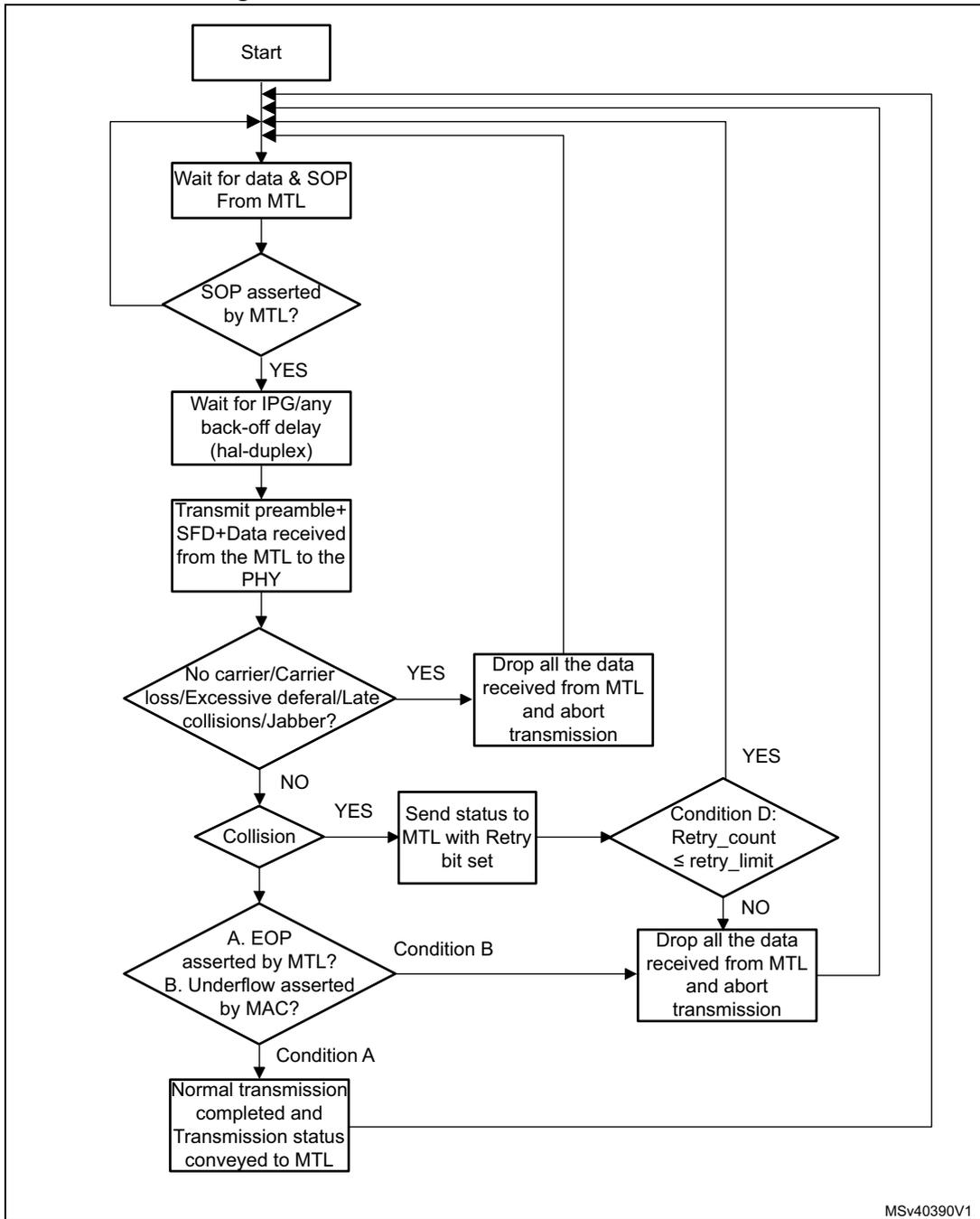
graph TD; Start[Start] --> WaitSOP[Wait for data & SOP From MTL]; WaitSOP --> SOPAsserted{SOP asserted by MTL?}; SOPAsserted -- YES --> WaitIPG[Wait for IPG/any back-off delay hal-duplex]; SOPAsserted -- NO --> WaitSOP; WaitIPG --> Transmit[Transmit preamble+SFD+Data received from the MTL to the PHY]; Transmit --> NoCarrier{No carrier/Carrier loss/Excessive defer/Late collisions/Jabber?}; NoCarrier -- YES --> DropData1[Drop all the data received from MTL and abort transmission]; NoCarrier -- NO --> Collision{Collision}; Collision -- YES --> SendStatus[Send status to MTL with Retry bit set]; SendStatus --> ConditionD{Condition D: Retry_count ≤ retry_limit}; ConditionD -- YES --> WaitSOP; ConditionD -- NO --> DropData2[Drop all the data received from MTL and abort transmission]; Collision -- NO --> EOPUnderflow{A. EOP asserted by MTL? B. Underflow asserted by MAC?}; EOPUnderflow -- Condition A --> NormalTrans[Normal transmission completed and Transmission status conveyed to MTL]; EOPUnderflow -- Condition B --> DropData2; NormalTrans --> WaitSOP; DropData1 --> WaitSOP; DropData2 --> WaitSOP;MSv40390V1
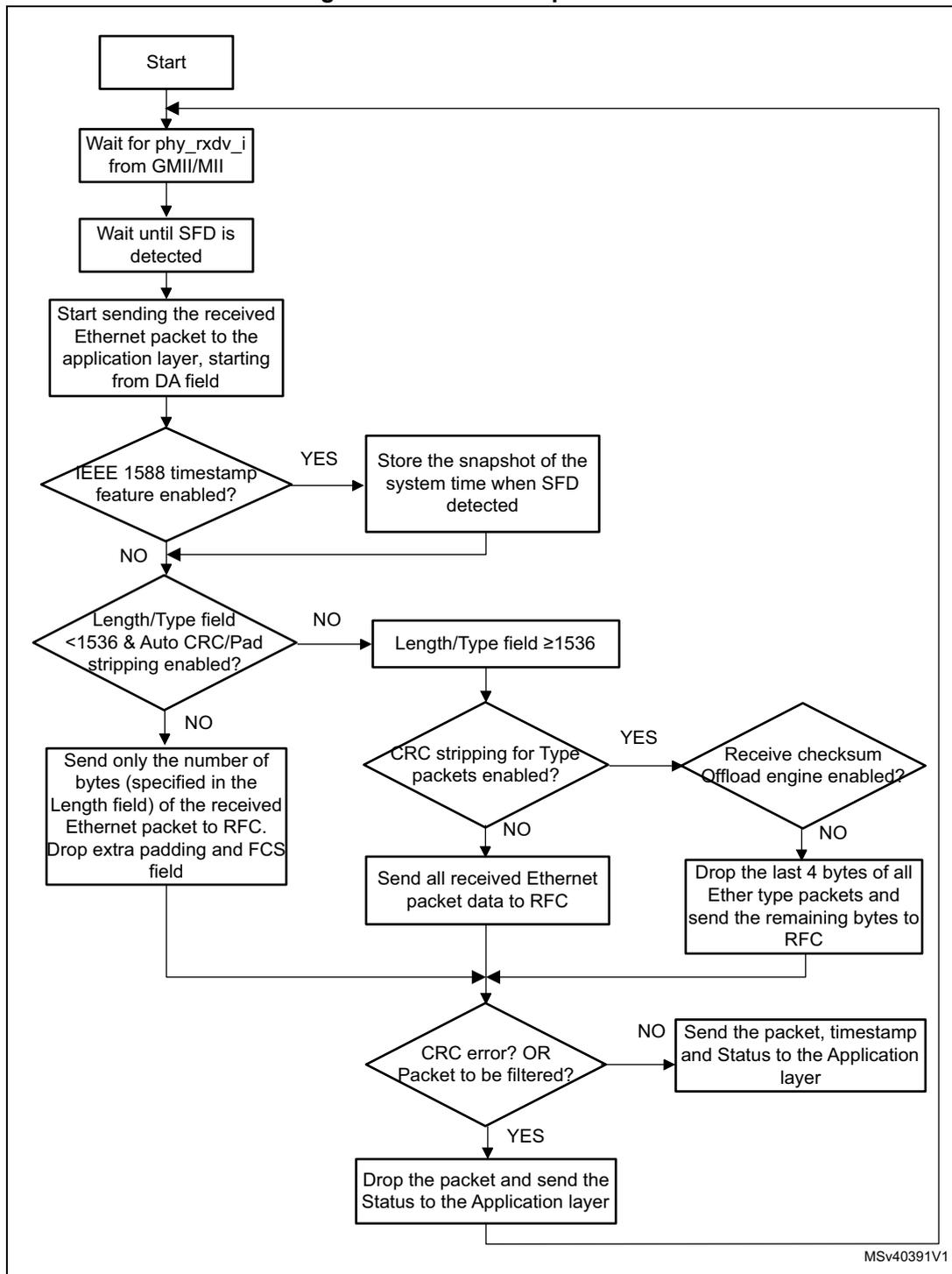
MAC reception
A receive operation is initiated when the MAC detects an SFD on GMII. The MAC strips the preamble and SFD before proceeding to process the packet. The header fields are checked for filtering and the FCS field used to verify the CRC for the packet. The received packet is stored in a shallow buffer until the address filtering is performed. The packet is dropped in the MAC if it fails the address filter.
The reception sequence is as follows:
- 1. When the receive data valid signal (RxDV) of GMII or MII becomes active, the receive State Machine (RSM) starts looking for the SFD field (0x5D byte).
The state machine drops received packets until it detects SFD.
- 2. When SFD is detected, the state machine starts sending the data of Ethernet packet to the RPC module, beginning with the first byte following the SFD (destination address).
- 3. If IEEE 1588 timestamp feature is enabled, the MAC takes a snapshot of the system time at which SFD of any packet is detected on GMII or MII. If this packet is not dropped during MAC filtering, the timestamp is passed to the application. The receive state machine decodes the Length/Type field of the Ethernet packet being received.
If the Length/Type field is less than 1,536 and if the MAC is programmed for the Auto CRC/Pad Stripping (bit 20 of the Operating mode configuration register (ETH_MACCR) ), the state machine sends the packet data up to the count specified in the Length/Type field and starts dropping bytes (including the FCS field). The state machine decodes the Length/Type field and checks for the Length interpretation.
- 4. If the Length/Type field is greater than or equal to 1,536, the RPE module sends all received Ethernet packet data to the RFC module if you have not enabled the CRC stripping for Type packet in Bit 21 of the Operating mode configuration register (ETH_MACCR) . However, if the CRC stripping has been enabled for Type packets and not enabled the receive checksum offload engine, the MAC strips and drops the last 4 bytes of all packets of ether type before forwarding the packets to the application.
- 5. By default, the MAC is programmed for watchdog timer to be enabled, that is, packets above 2,048 (10,240 if Jumbo Packet is enabled) bytes (DA + SA + LT + DATA + PAD + FCS) are cut off at the RPE module. In addition, you can use a programmable watchdog timer (bit 16 of Watchdog timeout register (ETH_MACWTR) ) to override the fixed timeout of 2,048 or 10,240 bytes. You can disable the watchdog timer by programming bit 19 of Operating mode configuration register (ETH_MACCR) . However, even if the watchdog timer is disabled, a packet greater than 32 Kbytes is cut off and a watchdog timeout status is given.
Figure 1024. MAC reception flow
graph TD
    Start([Start]) --> Wait1[Wait for phy_rxdv_i from GMII/MII]
    Wait1 --> Wait2[Wait until SFD is detected]
    Wait2 --> SendDA[Start sending the received Ethernet packet to the application layer, starting from DA field]
    SendDA --> IEEE1588{IEEE 1588 timestamp feature enabled?}
    IEEE1588 -- YES --> StoreTime[Store the snapshot of the system time when SFD detected]
    IEEE1588 -- NO --> LengthType{Length/Type field <1536 & Auto CRC/Pad stripping enabled?}
    StoreTime --> LengthType
    LengthType -- NO --> LengthGE1536[Length/Type field ≥1536]
    LengthType -- NO --> SendOnly[Send only the number of bytes (specified in the Length field) of the received Ethernet packet to RFC. Drop extra padding and FCS field]
    LengthGE1536 --> CRCStrip{CRC stripping for Type packets enabled?}
    CRCStrip -- YES --> ChecksumOffload{Receive checksum Offload engine enabled?}
    CRCStrip -- NO --> SendAll[Send all received Ethernet packet data to RFC]
    ChecksumOffload -- YES --> DropLast4[Drop the last 4 bytes of all Ether type packets and send the remaining bytes to RFC]
    ChecksumOffload -- NO --> DropLast4
    SendOnly --> CRCError{CRC error? OR Packet to be filtered?}
    SendAll --> CRCError
    DropLast4 --> CRCError
    CRCError -- NO --> SendPacket[Send the packet, timestamp and Status to the Application layer]
    CRCError -- YES --> DropPacket[Drop the packet and send the Status to the Application layer]
    DropPacket --> Start
    SendPacket --> Start
    DropLast4 --> Start
    SendAll --> Start
    SendOnly --> Start
MSv40391V1
76.4.4 Multiple channels and queues support
This chapter describes how the Ethernet peripheral core supports multiple queues and channels.
Two queues on Rx side and two queues on Tx side are supported. Two DMA channels are implemented on Tx side, one channel per queue. Two DMA channels are implemented on Rx side, one channel per queue.
The multiple queues enable to support the Audio video bridging (AVB) protocol.
Multiple queues and channels support in the Transmit path
The number of Tx DMA channels is equal to the number of Tx queues, and is direct one-to-one mapping. This enables the interleaving of packet/data transfer of multiple Tx DMA on the host/system bus, and each Tx queue is reserved for the corresponding Tx DMA. Therefore, the integrity of packet transfer by each Tx DMA is maintained in the Tx queue and enables efficient utilization of the host bus for data transfers among multiple Tx DMA without depending on the packet length, Transmit buffer availability and so on.
If two Tx DMAs are allowed to transfer data into the same Tx queue, when a Tx DMA starts a packet transfer, the other Tx DMA cannot transfer data to the same Tx queue unless the previous packet transfer is complete. This means that the second DMA remains idle until the first packet transferred is complete, which is effectively a one-to-one mapping of the Tx DMA to the Tx queue.
The Ethernet peripheral supports multiple Tx channels. The priority scheme between both channels is fixed priority. In fixed priority scheme, the channel with the highest priority always wins the arbitration when it requests the bus, as shown in Table 764 .
Table 764. Fixed priority scheme for DMA channels
| Priority level | Channel |
|---|---|
| 0 | Channel 0 |
| 1 | Channel 1 |
The fixed priority scheme does not necessarily cause the “starving” of lower priority channels for the AXI bus because of the capabilities of the AXI protocol and characteristics of the TxDMA, described as follows:
- • Read command requests from a TxDMA for a burst of data transfers are driven on a separate AXI channel, and their execution takes one clock cycle. The actual data transfer starts on a separate AXI channel only after the request is accepted. It takes several clock cycles to complete with relatively large read access latencies.
- • The AXI master is free to issue subsequent requests even before the previous data transfers are complete.
- • A TxDMA requests another data transfer only after the data transfer corresponding to its previous request is complete and transferred to the MTL Tx queue and space is available in Tx queue to accept the next request.
- • The Ethernet peripheral can be programmed to control the maximum number of outstanding requests, requested burst sizes by DMA, and the burst sizes of each data transfer on the AXI bus.
Considering the previous points, the Ethernet peripheral can be programmed so that the requests of all TxDMAs are placed and executed on the AXI bus before the data transfer of the first TxDMA is complete and it raises the next request to the arbiter. For example, in a 64-bit AXI data bus, proceed as follows:
- 1. TxDMA PBL = 64 (512 bytes).
- 2. Number of outstanding AXI read requests = 16.
- 3. Maximum burst length on AXI (BLEN) = 32 (256 bytes).
- 4. Number of active TxDMAs = 8.
Assuming that all TxDMAs place a request simultaneously and get serviced by the fixed priority algorithm, all the requests are placed on the AXI bus in a window of 32 clocks (two clocks per AXI request, two AXI burst requests per TxDMA request). The data transfer of the first request takes 32 clock cycles + the read-access latencies (assuming that there are tens of cycles). So, the TxDMA arbiter is already IDLE and has completed servicing all the TxDMA requests before this data transfer completes.
Effectively, all the TxDMA channels get equal access to AXI bus and the corresponding Tx queues get filled up at the same rate. The data gets read out from the Tx queues as per the traffic class scheduler in the MTL. So at a steady state, the bandwidth for each channel is controlled by the priorities and settings of the traffic scheduler in the MTL.
Programming guidelines for multiple queues and channels in the Transmit path
See Section 76.9.8: Programming guidelines for multichannel multiqueue operation on page 4128 .
Multiple queues and channels support in the receive path
The Ethernet controller supports independent selection of the number of Rx DMA channels and the number of Rx queues in the MTL Rx buffer. Therefore, the packets from any Rx queue can be serviced by any of the Rx DMA. As all the packets of Rx queues are stored in a shared RxFIFO buffer in MTL, the Rx scheduler selects the Rx queue whose packet data are to be transferred to the destination Rx DMA, which then forwards the packet data to the host memory. The sequence of events in time is as follows:
- 1. Each Rx DMA indicates whether it is ready to transfer data, that is, when the Rx DMA has fetched the descriptor and has a receiver buffer ready to accept the packet data. Each Rx DMA also indicates the number of words that it can transfer, based on the space available in the Rx buffer and the value programmed in the RXPBL[5:0] bitfield of its Channel x receive control register (ETH_DMACxRXCR) .
- 2. The MTL Rx scheduler matches the number of bytes/packets available for transfer at the top of all Rx queues with the corresponding Rx DMA ready status and the number of bytes requested by it.
- 3. If there are multiple successful matches, the scheduler selects the Rx queue to be serviced, based on the arbitration schemes (Strict priority or Weighted Strict priority) decided by the RAA field of the Operating mode register (ETH_MTLOMR) . In the Weighted Strict priority scheme, the weight of each Rx queue is set in the RXQ_WEGT[2:0] bitfield of the corresponding Rx queue x control register (ETH_MTLRXQxCR) .
- 4. The MTL Rx controller fetches the data of the selected Rx queue from the shared RxFIFO memory and starts the transfer of the requested PBL number of bytes to the
DMA block or until the end of packet and the corresponding Rx status is transferred (whichever is first).
- 5. After completing the current request, the scheduler repeats the process by starting a new arbitration cycle. However, it selects the same Rx queue for servicing, if the end of packet is not transferred and the RXQ_FRM_ARBIT field of the Rx queue x control register (ETH_MTLRXQxCR) is 1, for the Rx queue.
Rx queue to DMA mapping
The packets in the MTL Rx queues can be routed to any of the multiple DMA channels, by programming the Rx queue and the Rx queue and DMA channel mapping register (ETH_MTLRXQDMAMR) .
Two types of Rx queue-to-DMA mapping are possible through programming: static mapping and dynamic (per packet) mapping.
- • Static mapping
In Static mapping mode, all the packets of an Rx queue are connected to a specific DMA channel. For example, all the packets from Rx Queue 0 can be routed to a DMA channel by programming Q0MDMACH and Q0DDMACH of the Rx queue and DMA channel mapping register (ETH_MTLRXQDMAMR) .
Similarly, packets from other Rx queues can be routed to any DMA channel by programming the register fields corresponding to each queue.
- • Dynamic (per packet) mapping
In Dynamic (per packet) mapping mode, the destination DMA channel is decided by the MAC core receiver for each packet.
In this mode, the destination DMA channel of a packet being read from a Rx queue is not constant but decided independently for each packet. For example, by setting the Q1DDMACH bit of the Rx queue and DMA channel mapping register (ETH_MTLRXQDMAMR) , the static mapping is disabled for Rx Queue 1 and the value in Q1MDMACH is ignored. The destination DMA channel is decided by the MAC receiver for each packet, depending on the following, in decreasing order of priority:
- – L3-L4 filter based DMA selection
When the Layer 3 and Layer 4 packet filtering is enabled, the TCP/UDP and IP header fields of the received packet are matched against the corresponding values programmed and enabled for comparison in the MAC L3 and L4 address control register. If the match is successful, the DMA channel number programmed in the DMCHNx bits of the L3 and L4 control 0 register (ETH_MACL3L4C0R) and L3 and L4 control 1 register (ETH_MACL3L4C1R) is selected as the destination DMA channel number provided DMCHEN bit of the same register is set.
If none of the L3-L4 registers give a comparison match, the Ethernet peripheral proceeds to the next step.
- – Extended VLAN based DMA selection
Extended routing is applicable only if the VLAN filter has passed. Routing is only based on perfect filter result. Each perfect filter has a DMA channel enable and a DMA channel number field which can be programmed. Routing is applicable for a filter only if the DMA channel enable bit is set.
The frame is routed to the smallest matching filter DMA channel provided it is enabled. If that filter DMA channel number is not enabled, the frame gets routed to Channel 0. For example, if a frame VLAN tag matches filter 1, then the MAC checks if filter 1 DMA channel number is enabled through programming. If yes, the
frame gets routed to the programmed value; otherwise it gets routed to DMA. When the inverse filter is enabled, the frame is routed to the least mismatched filter DMA channel number provided it is enabled. If the DMA channel enable bit is not set, then the frame is routed based on DA-based addressing or to Channel 0. If Hash filter is also enabled, it is used to determine the filter result only. Routing still depends on the enabled perfect filters. If none of the perfect filters are enabled or if all of them are bypassed, the VLAN filter based routing is not done. The frame is routed through DA-based addressing or to Channel 0. If all the perfect filters give a fail result and the Hash filter has passed, VLAN filter result is a pass. However, routing is based on DA-based addressing or to Channel 0. The behavior is similar when the inverse filtering is enabled.
- – Ethernet DA-based DMA selection
The DA address of the received packet is compared against the programmed DA values in MAC address registers. If the address matches any of the programmed values, the corresponding DCS field (when enabled) determines the destination DMA channel number.
If none of the previous operations is able to make a successful match/decision, then the packet is routed to DMA Channel 0 by default.
Programming guidelines for multiple queues and channels in the receive path
See Section 76.9.8: Programming guidelines for multichannel multiqueue operation on page 4128 .
Selection of the tag priorities assigned to Rx queues
The VLAN tag priorities can be assigned to Rx queues by programming the PSRQ field in the corresponding Rx queue control 2 register (ETH_MACRXQC2R) . The bit corresponding to the VLAN tag priority can be set in the PSRQ field to assign the corresponding priority to the Rx queue. As an example, to assign VLAN tag priority 3 to Rx queue 0, set bit3 of PSRQ field in the Rx queue control 2 register (ETH_MACRXQC2R) . The VLAN tag priority assigned to a given Rx queue must be unique. This means that multiple Rx queues cannot be assigned the same VLAN tag priority. However, multiple VLAN tag priorities can be assigned to the same Rx queue.
The settings in the PSRQ field is used for VLAN tagged Rx packet routing to Rx queues as well as for PFC based Tx flow control. The received VLAN tagged Rx packet is routed to the Rx queue that matches the VLAN tag priority. In PFC-based Tx flow control, the PSRQ field corresponding to a particular Rx queue is used to enable VLAN tag priorities in the PFC packet that is transmitted when the corresponding Rx queue threshold levels are reached.
Distribution of Rx packets from MAC to Rx queues
The Ethernet peripheral provides multiple Rx queues to support classification and distribution of ingress packets. The MAC receiver pushes the ingress packets to the Rx queues based on packet type (such as tagged, untagged, multicast, PTP, AVB), tag priorities, MAC packet filter results, preemptable or express packet, and so on. The distribution is controlled by the settings of:
- • Rx Queue control register (ETH_MACRXQCR)
- • Rx queue control 0 register (ETH_MACRXQC0R)
- • Rx queue control 1 register (ETH_MACRXQC1R)
- • Rx queue control 2 register (ETH_MACRXQC2R)
- • Packet filtering control register (ETH_MACPFR)
Additionally, the Ethernet peripheral supports distribution of ingress packets based on user-defined Type field of the ingress packets when TBRQE bit of the Rx queue control 1 register (ETH_MACRXQC1R) is enabled. Up to eight types for matching can be programmed in the MAC type-based Rx queue mapping register (ETH_MAC_TMRQR) which is accessible through MAC indirect access control register (ETH_MAC_IACR) . The ETH_MAC_TMRQR register contains
- • TYP[15:0] field: 16-bit type
- • TMRQ[2:0] bitfield: Rx queue number to which ingress packet is pushed when its Type field matches TYP.
- • PFEX field: this bit indicates whether the TYP is applicable for express packets or preemptable packets.
Based on the packet filter settings, the MAC receiver decides either to drop or forward the ingress packet (for more details, see Section 76.5.4: Packet filtering ). However, the results of Layer 3 and Layer 4 filtering, mentioned in Section : Layer 3 and Layer 4 filtering , are not considered for the distribution of ingress packets into the Rx queues. Only the results of DA/SA/VLAN filters mentioned in Section : MAC source or destination address filtering and Section : VLAN filtering are applicable.
The filtering of the broadcast packets is exclusively controlled by the DBF bit of the Packet filtering control register (ETH_MACPFR) . The filtering of multicast packets is controlled by the PM bit of the Packet filtering control register (ETH_MACPFR) , in addition to the DA/SA match.
By default, packets that fail any of the DA/SA filters, are dropped by the MAC receiver. However, packets that fail the DA/SA/VLAN filter can still be forwarded to the application when the RA field of the Packet filtering control register (ETH_MACPFR) is 1. Even when RA field is 0, VLAN filter fail packets can be forwarded if the VTFR field of the Packet filtering control register (ETH_MACPFR) is 0.
The ingress packets go through the following operations in decreasing order of priority.
- 1. RA = 0: ingress packets are dropped if any of the following conditions is true.
- – DA/SA filter fail
- – VLAN filter fail and VTFR field of the Packet filtering control register (ETH_MACPFR) is 1
- 2. RA = 1: ingress packets that fail the DA/SA filter are also forwarded to the Rx queue as mentioned in Table 765 .
Table 765. Routing DA/SA failed packets to Rx queue
| Packet type | TSN type | Destination Rx queue determined by |
|---|---|---|
| Broadcast/Multicast | Express | if MFFQE = 1, MFFQ; else if VFFQE = 1, VFFQ; (only for tagged packets) else RxQ0 |
| Unicast | Express | if UFFQE = 1, UFFQ; else if VFFQE = 1, VFFQ; (only for tagged packets) else RxQ0 |
| All | Preemptable | FPRQ field |
- 3. RA = 1 and VTFR = 0: ingress tagged packets that pass the DA/SA filter but fail the VLAN filter are forwarded to the Rx queue as mentioned in Table 766 .
| TSN packet type | Destination Rx queue determined by |
|---|---|
| Express | if VFFQE = 1, VFFQ; else RxQ0 |
| Preemptable | RQ field |
- 4. Ingress packets that pass the DA/SA/VLAN filters are forwarded to the Rx queue.
- – Table 767 shows the routing priority in the decreasing order when OMCBCQ field of the Rx queue control 0 register (ETH_MACRXQC0R) is 0.
| Packet type | TSN type | Tagged | Destination Rx queue determined by |
|---|---|---|---|
| Broadcast/Multicast | Express | Yes | if MBCQEN = 1, MBCQ; else if TBRQE = 1, TBRQ; else PSRQ |
| No | if MBCQEN = 1, MBCQ; else if TBRQE = 1, TBRQ; else UPQ | ||
| Unicast AVTP control | Express | No | AVCPQ |
| Yes | if TACPQE = 1, AVCPQ; else PSRQ | ||
| Unicast PTP over Ethernet | Express | No | PTPQ |
| Yes | PTPQ or PSRQ based on the value of TPQC. | ||
| Remaining Unicast | Express | No | If TBRQE = 1, TBRQ; else UPQ |
| Yes | If TBRQE = 1, TBRQ; else PSRQ | ||
| All Packets | Preemptable | No | If TBRQE = 1, TBRQ; else FPRQ |
| Yes | If TBRQE = 1, TBRQ; else PSRQ |
- – Table 768 shows the routing priority in the decreasing order when OMCBCQ field of the Rx queue control 1 register (ETH_MACRXQC1R) is 1.
| Packet type | TSN type | Tagged | Destination Rx queue determined by |
|---|---|---|---|
| All AVTP Control | Express | No | AVCPQ |
| Yes | if TACPQE = 1, AVCPQ; else PSRQ | ||
| All PTP over Ethernet | Express | No | PTPQ |
| Yes | PTPQ or PSRQ based on TPQC | ||
| Remaining Broadcast/Multicast | Express | Yes | if MBCQEN = 1, MBCQ; else if TBRQE = 1, TBRQ; else PSRQ |
| No | if MBCQEN = 1, MBCQ; else if TBRQE = 1, TBRQ; else UPQ |
| Packet type | TSN type | Tagged | Destination Rx queue determined by |
|---|---|---|---|
| Remaining Unicast | Express | No | if TBRQE = 1, TBRQ; else UPQ |
| Yes | if TBRQE = 1, TBRQ; else PSRQ | ||
| All Packets | Preemptable | No | if TBRQE = 1, TBRQ; else FPRQ |
| Yes | if TBRQE = 1, TBRQ; else PSRQ |
Note: The fields mentioned in Table 765 through Table 768 belong to Rx queue control 0 register (ETH_MACRXQC0R) , Rx queue control 1 register (ETH_MACRXQC1R) and Rx queue control 2 register (ETH_MACRXQC2R) .
Note: If the RxQ pointed by the various fields in Table 765 through Table 768 is not enabled in the Rx queue control 0 register (ETH_MACRXQC0R) as per the packet type, the packet is written to
- • RxQ0 for Express packets
- • FPRQ field for Preemptable packets
If RxQ0/FPRQ is not enabled, the packet is dropped.
Note: If the AV8021ASMEN field of the Timestamp control register (ETH_MACTSCR) is 1, MAC receiver checks only for untagged PTP packet. Packets tagged with PTP payload are considered as Remaining (Unicast/Broadcast/Multicast) tagged packets in Table 765 through Table 768 .
The priority field of the outer VLAN tag is considered for routing.
AV feature
The Ethernet peripheral supports the AV data transfer in 100-Mbps and 1000-Mbps modes. The AV feature enables transmission of time-sensitive traffic over bridged local area networks (LANs). The following standards define various aspects of the AV feature implementation:
- • IEEE 802.1Qav-2009: enables the bridges to provide time-sensitive and loss-sensitive real-time audio video data transmission (AV traffic). It specifies the priority regeneration and controlled bandwidth queue draining algorithms that are used in bridges and AV traffic sources.
- • IEEE 802.1Qat-2009: enables the network resources to be reserved for specific traffic streams traversing a bridged local area network.
- • IEEE 802.1AS-2011: specifies the protocol and procedures used to ensure that the synchronization requirements are met for time-sensitive applications such as audio and video across bridged and virtual-bridged LANs consisting of LAN media where the transmission delays are fixed and symmetrical. For example, IEEE 802.3 Full-duplex links include the maintenance of synchronized time during normal operation followed by addition, removal, or failure of network components and network reconfiguration.
While the AVB standards were originally designed for audio and video over standard Ethernet, extending these to control streams would additionally benefit the industrial and automotive sectors. Time sensitive networking (TSN) is a set of standards developed by the Time Sensitive Networking Task Group with the intent to extend the future AVB enhancements to other sectors that could benefit.
Bridges are increasingly used to interconnect devices that support scheduled applications (for example, industrial automation, process control and vehicle control). The IEEE 802.1Qbv-2015 (Enhancements to Scheduling Traffic) provides performance assurances of latency and delivery variation to enable these applications in an engineered LAN while maintaining the existing guarantees for the credit-based shaper and best-effort traffic.
The IEEE 802.3br (Interspersing Traffic) and IEEE 802.1Qbu (frame preemption) enables the suspension of a large preemptable packet being transmitted by the MAC layer to enable one or more express packets to be transmitted before the transmission of the preemptable packet is resumed. This provides the capability to schedule express traffic packets with minimal delays/latencies or at predictable times with efficient utilization of the line bandwidth.
As per the IEEE specification for 802.1Qbv, 802.1Qbu, and 802.3br, the TSN features are supported only in the following modes:
- • Full duplex
- • 100 Mbps or higher link speed
- • Pause or no flow control
- • When Qbv schedule is enabled for time-sensitive traffic, Pause or PFC is likely to interfere with the Qbv schedules. So, it is recommended not to enable PFC/PAUSE when Qbv scheduler is enabled.
- • Multiple Tx queues (for Qbv) enabled
- • One or more Express queues and one or more preemption queues on both transmit and receive (for Qbu/802.3br) enabled.
Transmit path functions
When the AV feature is selected, the Transmit paths of Tx queues are enabled by default.
The Transmit path of queue 0 supports the strict priority algorithm, and it is used for best-effort traffic. For a queue, the strict priority algorithm determines that a packet is available for transmission if the queue contains one or more packets. When the threshold mode for MTL Tx FIFO is enabled, the strict priority algorithm determines that a packet is available for transmission if the queue contains a partial packet of size equal to the programmed threshold limit.
The Transmit path of the AVB Tx queue supports traffic management by using the credit-based shaper algorithm. For a queue, the credit-based shaper algorithm determines that a queue is available for transmission if the following conditions are true:
- • The queue contains one or more packets.
- • The credit for the queue is positive as per the algorithm.
When the credit-based shaper algorithm is disabled for a queue, the channel uses the default strict priority algorithm.
Each Transmit DMA has a separate descriptor chain for fetching the transmit data. The Transmit channel that gets the access to the system bus depends on the DMA arbiter.
The Transmit path has a shared FIFO (MTL layer) for each queue. The data fetched by the DMA is put in the respective part of the FIFO. The MTL Tx Queue Scheduler controls which part of the FIFO data is transmitted by the MAC. If the credit-based shaper algorithm is enabled for queue 1, the queue is selected if the packet is available in the channel and has a positive or zero credit.
If the credit-based shaper algorithm is disabled for a given Tx queue, the packet to be transmitted is selected based on the fixed priority scheme as described in Table 769 .
Table 769. Weight for DMA channels
| TCW field | Transmit channel weight |
|---|---|
| 000 | 1 |
| 001 | 2 |
Receive path functions
When the AV feature is enabled, the receive path of Queue 0 is enabled by default. The whole traffic is received on this channel. The receive paths of additional queues can be enabled. By enabling the receive paths of multiple channels, the received data can be demultiplexed to send the packets into separate receive channels.
To differentiate between the AV and non-AV traffic, the MAC provides a status that indicates if the received packet is an AV packet as well as the corresponding VLAN Priority tag value. This status is updated in the Extended Status field of the receive descriptor as explained in Section 76.10.4: Receive descriptor . All received packets with an EtherType field of 0x22F0 are detected as AV packets. The AV packets can be of the following two types:
- AV data packets
AV data packets are always tagged. Tagged AV data packets are received following the programmed priority value. To specify the channel to which an AV packet with a given priority must be sent, program bits[15:8] in the transmit flow control register of the corresponding queue.
- AV control packets
The AV control packets can be either tagged or untagged. By default, untagged AV control packets are received on queue 0. To receive these packets on queue 1, program bits[2:0] of the Rx queue control 1 register (ETH_MACRXQC1R) . Similarly to the AV data packets, tagged AV control packets are received following the programmed priority value.
In addition to the AV packets, you can receive the untagged PTP packets on any queue. By default, the PTP packets (tagged or untagged) are received on queue 0. To receive these packets on any other queue, program bits[6:4] of the Rx queue control 1 register (ETH_MACRXQC1R) .
Credit-based shaper algorithm
The Queue Scheduler uses the credit-based shaper algorithm to arbitrate the AV traffic in all queues and the legacy Ethernet traffic in queue 0. Queue 1 can be programmed to use the credit-based shaper algorithm.
The following sections provide information on the credit-based shaper algorithm implementation:
- Credit value
- idleSlopeCredit and sendSlopeCredit values
- Bandwidth status
The credit value is accumulated every transmit clock cycle, that is every 40 ns in 100-Mbps mode and every 8 ns in 1000-Mbps mode. The credit to be added or subtracted per cycle can be fractional depending on the required idleSlope and sendSlope values, as described in Table 770 .
Table 770. Example of credit value per transmit cycle| Mode | portTransmitRate, idleSlope, sendSlope | Credit value |
|---|---|---|
| 100 Mbps |
|
|
The DMA stores the queue traffic in the respective part of the Tx FIFO depending on the slot number in the transmit descriptor (if enabled) or the bandwidth availability on the AMBA application bus.
The credit for a queue builds up only when the packet is available, but it cannot be transmitted because the MAC is sending a packet from another queue. The Ethernet peripheral supports another mode in which the credit can build up in advance for a queue in which no packet is available in respective part of the FIFO. This enables sending a burst of high priority traffic in a queue as soon as the data is available. This mode can be enabled through the CC bit of the CBS control register ( Tx queue 1 ETS control register (ETH_MTLTXQ1ECR) ).
- • When reset, the accumulated credit parameter in the credit-based shaper algorithm is set to zero if there is positive credit, and there is no packet to transmit in a queue. The credit does not accumulate when there is no packet waiting in a queue and other queues are transmitting.
- • When set, the accumulated credit parameter in the credit-based shaper algorithm is not reset to zero if there is positive credit and no packet to transmit in a queue. The credit accumulates even when there is no packet waiting in a queue and other queues are transmitting.
The software must program the idleSlopeCredit and sendSlopeCredit values. The programmed values should be the credit accumulated or drained per clock cycle scaled by 1024 (such as \( 2.8 \times 1024 = 2867 \) and \( 1.2 \times 1024 = 1229 \) ). In addition, the software must program the hiCredit and loCredit values, scaled by 1024, to adjust for scaling of the idleSlopeCredit and sendSlopeCredit values. This means that if computed hiCredit and loCredit values are 12,000 bits and 3,036 bits respectively, the values to be programmed in the hiCredit and loCredit registers of the corresponding channel are \( 12000 \times 1024 \) bits and two's complement of \( 3036 \times 1024 \) , respectively.
Bandwidth status
The hardware maintains the status of the actual bandwidth consumed by each higher priority queue in the CBS status registers. This enables the software to estimate the average bandwidth consumed by numerically higher traffic classes as compared to the reserved bandwidth.
The CBS status register ( Tx queue x ETS status register (ETH_MTLTXQxESR) ) gives the average number of bits transmitted during the previous programmed slot interval (1, 2, 4, 8, or 16 slots of 125 µs) in a queue. The status register is updated even if the credit-based shaper algorithm is not enabled for a queue. The number of slots over which the average bits transmitted per slot are computed is programmed in bits[6:4] of the CBS control register of the respective queue. For example, if you have programmed two slots, the average bits are computed over slot numbers 0–1, 2–3, 4–5, and so on.
The value programmed in the idleSlopeCredit register of a queue is proportional to the bandwidth reserved for the queue. The software can allocate any bandwidth that is not used by the higher priority queue to the reserved bandwidth of the lower priority queue.
A lower priority queue, which is using the credit-based shaper algorithm, cannot use the unused reserved bandwidth of any higher priority queue that is using the credit-based shaper algorithm. However, a lower priority queue, which is using the strict-priority algorithm, can use the unused reserved bandwidth of any higher priority queue that uses the credit-based shaper algorithm. For example, queue 1 and queue 2 use the credit-based shaper algorithm (with reserved bandwidth of 50% and 25%, respectively) and queue 0 uses the strict-priority algorithm. If queue 1 uses only 40% of reserved bandwidth, the remaining 10% is used by queue 0. Queue 2 cannot exceed the reserved bandwidth of 25%.
Slot number function
When the AV feature is enabled, the slot number function can be used to schedule the data fetching from the system memory by the DMA. This feature is useful when the source AV data needs to be transmitted at specific intervals.
The slot number at which the DMA should fetch the data from system memory can be programmed in the transmit descriptor Word 3 (TDES3). This 4-bit field enables the application to schedule data fetching at up to 16 slots with a programmable slot interval that ranges from 1 µs to 4096 µs and a granularity of 1 µs. This field is applicable only to the AV channels.
When the DMA fetches a Tx descriptor, it compares the slot number of the Tx descriptor with the internally generated reference slot interval. The slot interval is a counter that is updated based on a programmable slot interval (with range from 1 µs to 4096 µs) of the IEEE 1588 system time. In addition, the slot interval counter is initialized to zero when the seconds field of the system time is incremented, that is, when the subsecond counter rolls over. The DMA fetches the data only if it matches the current slot or the next slot. The DMA remains in the descriptor fetch state until a match is found.
To enable the DMA to fetch data only if it matches the current slot or the next two slots, program bit 1 of the Channel x slot function control status register (ETH_DMACxSFCSR) of the corresponding DMA channel.
If the slot number in the descriptor is less than the reference slot number, the DMA considers it as a future slot.
The slot number check can be enabled by setting bit 0 in the Channel x slot function control status register (ETH_DMACxSFCR) of corresponding DMA channel. If this check is disabled, the packets are fetched immediately after the descriptor is read. In addition, bits [19:16] indicate the value of the reference slot number in DMA.
Programming guidelines for AV feature
See Section : Initializing the DMA on page 4137 .
See Section : Enabling slot number checking on page 4138 .
See Section : Enabling average bits per slot reporting on page 4138 .
Queue modes
A Tx queue can be enabled for generic or AV traffic. When multiple Tx queues are enabled for generic traffic, queuing is based on WRR or WSP algorithms.
When a Tx queue is enabled for AVB traffic, queuing is based on CBS or SP algorithms.
A Rx queue can be enabled for generic or AV traffic. A particular queue enabled for generic or AV based routing is determined by the RXQ0EN and RXQ1EN fields in the Rx queue control 0 register (ETH_MACRXQC0R) .
Below an explanation on how Rx queues are enabled based on the selected features:
- • Multiple Rx queues
When multiple Rx queues are selected, all queues are enabled for generic queuing based on the VLAN tag priority. The VLAN tag priority should match the PSRQ[7:0] bitfield of the Rx queue control 2 register (ETH_MACRXQC2R) . By default untagged packets are routed to receive queue specified in UPQ field of Rx queue control 1 register (ETH_MACRXQC1R) . Queue 0 is the default value of UPQ[2:0] bitfield. The default value can be overridden with any other value, for the UPQ[2:0] bitfield. The Rx packets can also be routed to a particular DMA channel based on the DCS field of the perfectly-matched MAC Address register ( MAC address x high register (ETH_MACAxHR) ).
- • Multiple Rx queues with AV feature
When AV is enabled for all selected Rx queues, the queuing is done based on the VLAN tag priority. The VLAN tag priority should match the PSRQ[7:0] bitfield of the Rx queue control 2 register (ETH_MACRXQC2R) . The Rx packets can also be routed to a particular DMA channel based on the DCS field of perfectly-matched MAC Address register ( MAC address x high register (ETH_MACAxHR) ). The AV control packets (tagged or untagged) are routed based on the AVCPQ[2:0] bitfield of the Rx queue control 1 register (ETH_MACRXQC1R) . The PTP over Ethernet packets are routed based on the PTPQ[2:0] bitfield of the Rx queue control 1 register (ETH_MACRXQC1R) .
76.5 Ethernet functional description: MAC
76.5.1 Double VLAN processing
The Ethernet peripheral supports the double VLAN (Virtual LAN) tagging feature in which the MAC can process up to two VLAN tags (inner and outer).
The MAC supports the following:
- • Insertion, replacement, or deletion of up to two VLAN tags in the Transmit path
- • Packet filtering and stripping based on any one of the two VLAN Tags in the receive path. Stripping and providing up to two VLAN Tags in the receive path as a part of the receive status
Transmit path
Table 771: Double VLAN processing features in Tx path describes the features supported by the MAC on the Transmit side.
Table 771. Double VLAN processing features in Tx path
| Feature | Description |
|---|---|
| Support for C-VLAN and S-VLAN tag types | The inner or outer VLAN tag can be of C-VLAN and S-VLAN type. The VLAN type is specified through the CSVL bit of VLAN inclusion register (ETH_MACVIR) and Inner VLAN inclusion register (ETH_MACIVIR) , respectively. The Ethernet peripheral supports processing of any sequence of outer and inner VLAN tags. However, it does not support the C-VLAN S-VLAN sequence. The MAC does not check whether the packet provided by the application has a valid sequence of the VLAN Tag types or the insertion or replacement operation results in invalid sequence of VLAN Tag type. Therefore, the application must provide correct sequence of VLAN Tag types and program the MAC in such a way that it results in correct sequence of VLAN Tag types in the transmitted packet. The application must ensure the following:
|
| VLAN tag deletion | VLAN tag deletion can be enabled for outer or inner tag through VLC field in the VLAN inclusion register (ETH_MACVIR) or Inner VLAN inclusion register (ETH_MACIVIR) , respectively. When VLAN deletion is enabled, the MAC deletes the tag present at the corresponding position. When a packet has only one tag, it is considered as the outer tag. If inner tag deletion is enabled and the packet has only one tag, the MAC does not delete the tag. |
| VLAN tag insertion or replacement | VLAN tag insertion or replacement can be enabled for outer or inner tag through VLC field in the VLAN inclusion register (ETH_MACVIR) or Inner VLAN inclusion register (ETH_MACIVIR) , respectively. When VLAN tag insertion or replacement is enabled, the VLTI bit in the previous register is used to determine whether the VLAN tag should be taken from the register or the control word. |
Receive path
Table 772: Double VLAN processing in Rx path describes the features supported by the MAC on the receive side and the corresponding bits in the VLAN tag Control register (ETH_MACVTCR) .
Table 772. Double VLAN processing in Rx path
| Feature | Description |
|---|---|
| Outer or inner VLAN tag-based filtering | The MAC can filter packets based on the outer or inner VLAN tag through the ERIVLT bit. |
| C-VLAN or S-VLAN tag-based filtering | The MAC can filter packets based on the C-VLAN or S-VLAN type based on the ERSVLM bit. |
| Outer and Inner VLAN tag stripping | The MAC can strip the outer and inner VLAN Tags from received frame based on the EVLS and EIVLS bits. |
| 16-bit outer and inner VLAN tag and type in Rx status | The MAC can provide the 16-bit outer and inner VLAN Tag and Type in the Rx status based on the EVLRXS and EIVLRXS bits, respectively. |
| Disabling or skipping checking of outer VLAN tag type | The MAC can disable or skip checking of outer VLAN Tag type to match C-VLAN or S-VLAN based on the DOVLTC bit. |
76.5.2 Source address and VLAN insertion, replacement, or deletion
Source address insertion or replacement
The software can use the SA (source address) insertion or replacement feature to instruct the MAC to do the following for Tx packets:
- • Insert the content of the MAC Address registers in the SA field
- • Replace the content of the SA field with the content of the MAC Address registers
When SA insertion is enabled, the application must ensure that the packets sent to the MAC do not have the SA field. The MAC does not check whether the SA field is present in the Transmit packet and it inserts the content of MAC Address Registers in the SA field. Similarly, when SA replacement is enabled, the application must ensure that the SA field is present in the packets sent to the MAC. The MAC replaces the six bytes following the Destination Address field in the Transmit packet with the content of the MAC Address Registers.
SA insertion or replacement feature can be enabled for all Transmit packets or selective packets:
- • Enabling SA insertion or replacement for all packets
To enable this feature for all packets, program the SARC field of the Operating mode configuration register (ETH_MACCR) . - • Enabling SA insertion or replacement for selective packets
To enable this feature for selective packets, use the following program the SA Insertion Control field (bits[25:23] of transmit descriptor Word 3/TDES3, refer to Section 76.10.3: Transmit descriptor ) in the first Transmit descriptor of the packet. When Bit 25 of TDES3 is set, the SA Insertion Control field indicates insertion or replacement by MAC
Address1 registers. When bit 25 of TDES3 is reset, it indicates insertion or replacement by MAC Address 0 registers.
If MAC Address1 registers are not enabled, the MAC Address0 registers are used for insertion or replacement whatever of the value of the most-significant bit of the SA Insertion Control field.
VLAN insertion, replacement, or deletion
The software can use the VLAN insertion, replacement, or deletion feature to instruct the MAC to do the following for Tx packets:
- • Delete the VLAN Type and VLAN Tag fields
- • Insert or replace the VLAN Type and VLAN Tag fields
Insertion or replacement is performed based on the setting of VLTI bit in the VLAN inclusion register (ETH_MACVIR) as described in Table 773: VLAN insertion or replacement based on VLTI bit .
Table 773. VLAN insertion or replacement based on VLTI bit
| Condition | Description |
|---|---|
| VLTI bit is set | The MAC inserts or replaces the following: VLAN Type field (C-VLAN or S-VLAN as indicated by the CSVL bit of VLAN inclusion register (ETH_MACVIR) ) VLAN Tag field with VT field of Transmit context descriptor of the packet |
| VLTI bit is reset | The MAC inserts or replaces the following: VLAN Type field (C-VLAN or S-VLAN as indicated by the CSVL bit of VLAN inclusion register (ETH_MACVIR) ) VLAN Tag field with the VLT field of VLAN inclusion register (ETH_MACVIR) |
When VLAN replacement or deletion is enabled, the MAC checks if the VLAN Type field (0x8100 or 0x88A8) is present after the DA and SA fields in the Transmit packet. The replace or delete operation does not occur if the VLAN Type field is not detected in two bytes following the DA and SA fields. However, when VLAN insertion is enabled, the MAC does not check the presence of VLAN Type field in the Transmit packet and just inserts the VLAN Type and VLAN Tag fields.
You can enable the VLAN insertion, replacement, or deletion feature for all Tx packets or selective packets:
- • To enable this feature for all packets, program the VLC and VLP fields of VLAN inclusion register (ETH_MACVIR) .
- • To enable this feature for selective packets, program the VTIR field of TDES2 Normal Descriptor (see Table 823: TDES2 normal descriptor (read format) ).
In addition, the VLP (VLAN Priority control) bit must be reset in VLAN inclusion register (ETH_MACVIR) (for outer VLAN) and Inner VLAN inclusion register (ETH_MACVIR) (in inner VLAN) for the MAC to take the control inputs from the host, depending on the configuration.
76.5.3 Queue/channel-based VLAN tag insertion on Tx
The peripheral supports channel/queue based VLAN tag insertion on all transmitted packets.
Accessing queue/channel specific VLAN tag registers
Queue/channel specific VLAN tag registers are accessed using indirect addressing through the VLAN inclusion register ( VLAN inclusion register (ETH_MACVIR) ). VLAN type and tag value can be independently programmed for each queue/channel.
Enabling queue/channel based VLAN tag insertion on Tx
To enable this feature, set the CBTI bitfield in the VLAN inclusion register ( VLAN inclusion register (ETH_MACVIR) ). The VLAN tag is then inserted on every packet that is transmitted from a queue/channel, with the programmed tag value taken from queue/channel specific VLAN tag register
Programming guidelines for channel based VLAN tag insertion
See Section 76.9.19: Programming sequence for queue/channel- based VLAN inclusion register on page 4145 .
76.5.4 Packet filtering
The MAC supports the following types of filtering for Rx packets:
- • MAC source or destination address filtering : the Address Filtering Module (AFM) checks the source address and destination address fields of each incoming packet.
- • VLAN filtering : the MAC supports the VLAN tag-based and VLAN Hash filtering.
- • Layer 3 and Layer 4 filtering : Layer 3 filtering refers to IP source address and destination address filtering. Layer 4 filtering refers to source port and destination port filtering.
The three filter types can be cascaded. Figure 1025 shows the filtering sequence for Rx packets.
Figure 1025. Packet filtering sequence
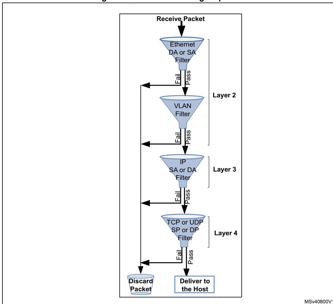
graph TD
    Start[Receive Packet] --> F1[Ethernet DA or SA Filter]
    F1 -- Fail --> Discard[Discard Packet]
    F1 -- Pass --> F2[VLAN Filter]
    F2 -- Fail --> Discard
    F2 -- Pass --> F3[IP SA or DA Filter]
    F3 -- Fail --> Discard
    F3 -- Pass --> F4[TCP or UDP SP or DP Filter]
    F4 -- Fail --> Discard
    F4 -- Pass --> Host[Deliver to the Host]
The sequence shown in Figure 1025 is valid when all the filters (L2, VLAN, L3, L4) are active. If any of the Layer filters are not enabled, that filter is bypassed and the subsequent filter is applied. A packet that fails any of the filters is discarded. However, the discarded packet can be forwarded to the host based on the register control.
For example, when RA bit of Packet filtering control register (ETH_MACPFR) is set to 1, all the discarded packets are forwarded to the host but with their packet status indicating the specific filter failure. If RA bit is cleared to 0, VTPE and IPPE bits of Packet filtering control register (ETH_MACPFR) control if the packets that fail the VLAN filter and Layer 3-4 filter should be discarded or forwarded to the host.
MAC source or destination address filtering
The MAC address filtering module checks the source address (SA) and destination address (DA) fields of each incoming packet.
Unicast destination address filtering
The MAC supports 4 MAC addresses for unicast perfect filtering. If perfect filtering is selected (HUC bit of Packet filtering control register (ETH_MACPFR) is reset), the MAC compares all 48 bits of received unicast address with the programmed MAC address for any match. The default MacAddr0 is always enabled.
The MacAddr1 to MacAddr3 addresses are selected with an individual enable bit. You can mask each byte during comparison with corresponding received DA byte by setting the corresponding Mask Byte Control bit in MAC address x high register (ETH_MACAxHR) . This enables group address filtering for the DA.
In Hash filtering mode (when HUC bit is set), the MAC performs imperfect filtering for unicast addresses using a 64-bit Hash table. For Hash filtering, the MAC uses the upper 6 bits CRC of the received destination address to index the content of the Hash table. A value of 00000 selects bit 0 of selected register, and a value of 11111 selects bit 63 of Hash Table register. If the corresponding bit (indicated by the 6-bit CRC) is set to 1, the unicast packet is considered to have passed the Hash filter; otherwise, the packet is considered to have failed the Hash filter.
Multicast destination address filtering
To program the MAC to pass all multicast packets, set the PM bit in Packet filtering control register (ETH_MACPFR) . If the PM bit is reset, the MAC performs the filtering for multicast addresses based on the HMC bit of the Packet filtering control register (ETH_MACPFR) .
In Perfect filtering mode, the multicast address is compared with the programmed MAC destination address registers. Group address filtering is also supported.
In Hash filtering mode, the MAC performs imperfect filtering using a 64-bit Hash table. The MAC uses the upper 6-bits CRC of received multicast address to index the content of the Hash table. A value of 000000 selects bit 0 of selected register and a value of 111111 selects bit 63 of the Hash Table register. If the corresponding bit is set to 1, the multicast packet is considered to have passed the Hash filter. Otherwise, the packet is considered to have failed the Hash filter.
Hash or Perfect address filtering
To configure the DA filter to pass a packet when its DA matches either the Hash filter or the Perfect filter, set the HPF bit and the corresponding HUC or HMC bits in Packet filtering control register (ETH_MACPFR) . This is applicable to both unicast and multicast packets. If the HPF bit is reset, only one of the filters (Hash or Perfect) is applied to receive packet.
Broadcast address filtering
The MAC does not filter any broadcast packets by default. To program the MAC to reject all broadcast packets, set the DBF bit in Packet filtering control register (ETH_MACPFR) .
Unicast source address filtering
The MAC can perform perfect filtering based on the source address field of received packets. By default, the MAC compares the SA field with the values programmed in the SA registers. You can configure the MAC Address registers to use SA instead of DA for comparison by setting bit 30 of MAC address x high register (ETH_MACAxHR) .
The MAC also supports group filtering with SA. You can filter a group of addresses by masking one or more bytes of the address. The MAC drops the packets that fail the SA filter if the SAF bit is set in Packet filtering control register (ETH_MACPFR) . Otherwise, the result of the SA filter is given as a status bit in the receive Status word (see Table 775 ). When the SAF bit is set, the SA filter and DA filter result is ANDed to decide whether the packet needs to be forwarded. This means that the packet is dropped if either filter fails. The packet is forwarded to the application only if the packet passes both filters in-order.
Inverse filtering
For DA and SA filtering, you can invert the filter-match result at the final output by setting the DAIF and SAIF bits of Packet filtering control register (ETH_MACPFR) . The DAIF bit is applicable for both Unicast and Multicast DA packets. The result of the unicast or multicast destination address filter is inverted in this mode. Similarly, when the SAIF bit is set, the result of unicast SA filter is reversed.
Table 774 and Table 775 summarize the DA and SA filtering based on the type of packets received.
Note: When the RA bit of Packet filtering control register (ETH_MACPFR) is set, all packets are forwarded to the system along with the correct result of the address filtering in the Rx status.
Table 774. Destination address filtering
| Packet type | PR | HPF | HUC | DAIF | HMC | PM | DBF | DA filter operation |
|---|---|---|---|---|---|---|---|---|
| Broadcast | 1 | X | X | X | X | X | X | Pass |
| 0 | X | X | X | X | X | 0 | Pass | |
| 0 | X | X | X | X | X | 1 | Fail | |
| Unicast | 1 | X | X | X | X | X | X | Pass all packets |
| 0 | X | 0 | 0 | X | X | X | Pass on Perfect/Group filter match | |
| 0 | X | 0 | 1 | X | X | X | Fail on Perfect/Group filter match | |
| 0 | 0 | 1 | 0 | X | X | X | Pass on Hash filter match | |
| 0 | 0 | 1 | 1 | X | X | X | Fail on Hash filter match | |
| 0 | 1 | 1 | 0 | X | X | X | Pass on Hash or Perfect/Group filter match | |
| 0 | 1 | 1 | 1 | X | X | X | Fail on Hash or Perfect/Group filter match | |
| Multicast | 1 | X | X | X | X | X | X | Pass all packets |
| X | X | X | X | X | 1 | X | Pass all packets | |
| 0 | X | X | 0 | 0 | 0 | X | Pass on Perfect/Group filter match and drop Pause packets if PCF = 0x | |
| 0 | 0 | X | 0 | 1 | 0 | X | Pass on Hash filter match and drop Pause packets if PCF = 0x | |
| 0 | 1 | X | 0 | 1 | 0 | X | Pass on Hash or Perfect/Group filter match and drop Pause packets if PCF = 0x | |
| Multicast | 0 | X | X | 1 | 0 | 0 | X | Fail on Perfect/Group filter match and drop Pause packets if PCF = 0x |
| 0 | 0 | X | 1 | 1 | 0 | X | Fail on Hash filter match and drop Pause packets if PCF = 0x | |
| 0 | 1 | X | 1 | 1 | 0 | X | Fail on Hash or Perfect/Group filter match and drop Pause packets if PCF = 0x |
Table 775. Source address filtering
| Packet type | PR | SAIF | SAF | SA filter operation |
|---|---|---|---|---|
| Unicast | 1 | X | X | Pass all packets. |
| 0 | 0 | 0 | Pass status on Perfect or Group filter match but do not drop packets that fail | |
| 0 | 1 | 0 | Fail status on Perfect or Group filter match but do not drop packet | |
| 0 | 0 | 1 | Pass on Perfect or Group filter match and drop packets that fail | |
| 0 | 1 | 1 | Fail on Perfect or Group filter match and drop packets that fail |
VLAN filtering
The MAC supports Perfect and Hash VLAN filtering. Refer to Section 76.9.17: Programming guidelines to perform VLAN filtering on the receiver for detailed programming steps.
VLAN tag Perfect filtering
In VLAN tag Perfect filtering, the MAC compares the VLAN tag of received packet and provides the VLAN packet status to the application. Based on the programmed mode, the MAC compares the lower 12 bits or all 16 bits of received VLAN tag to determine the perfect match.
If VLAN tag Perfect filtering is enabled, the MAC forwards the VLAN-tagged packets along with VLAN tag match status and drops the VLAN packets that do not match. You can also enable the inverse matching for VLAN packets by setting the VTIM bit of VLAN tag Control register (ETH_MACVTCR) . In addition, you can enable matching of S-VLAN tagged packets along with the default C-VLAN tagged packets by setting the ESVL bit of VLAN tag Control register (ETH_MACVTCR) . The VLAN packet status bit (bit 10 of RDES0) indicates the VLAN tag match status for the matched packets.
Note: The source or destination address (if enabled) has precedence over the VLAN tag filters. This means that a packet that fails the source or destination address filter is dropped irrespective of the VLAN tag filter results.
VLAN tag Hash filtering
The 16-bit VLAN Hash Table is used for group address filtering based on the VLAN tag. The VLAN tag Hash filtering feature can be enabled using the VTHM (VLAN tag Hash Table match enable) bit of the VLAN tag Control register (ETH_MACVTCR) . If the VTHM bit is set, the most significant four bits of CRC-32 of VLAN tag are used to index the content of the VLAN Hash Table register. A value of 1 in the VLAN Hash Table register, corresponding to the index, indicates that the VLAN tag of the packet matched and the packet should be forwarded. A value of 0 indicates that VLAN-tagged packet should be dropped.
Note: The 16 or 12 bits of VLAN Tag are considered for CRC-32 computation based on ETV bit in ETH_MACVTR register.
When ETV bit is reset, most significant four bits of CRC-32 of VLAN Tag are inverted and used to index the content of VLAN Hash table register (ETH_MACVHTR) .
When ETV bit is set, most significant four bits of CRC-32 of VLAN Tag are directly used to index the content of VLAN tag Control register (ETH_MACVTCR) .
The MAC also supports the inverse matching for VLAN packets. In the inverse matching mode, when the VLAN tag of a packet matches the Perfect or Hash filter, the packet should be dropped. If the VLAN perfect and VLAN Hash match are enabled, a packet is considered as matched if either the VLAN Hash or the VLAN perfect filter matches. When inverse
match is set, a packet is forwarded only when both perfect and Hash filters indicate mismatch.
Table 776 shows the different possibilities for VLAN matching and the final VLAN match status. When the RA bit of Packet filtering control register (ETH_MACPFR) is set, all packets are received and the VLAN match status is indicated in the VF bit of RDES2 normal descriptor (write-back format) . When the RA bit is not set and the VTFE bit is set in Packet filtering control register (ETH_MACPFR) , the packet is dropped if the final VLAN match status is Fail. In Table 776 , value X means that this column can have any value.
When VLAN VID is programmed to 0 in the VL field of VLAN tag Control register (ETH_MACVTCR) , all VLAN-tagged packets are considered as perfect matched but the status of the VLAN Hash match depends on the VTHM and VTIM bits in VLAN tag Control register (ETH_MACVTCR) .
Table 776. VLAN match status (1)
| VID | VLAN perfect filter match result | VTHM bit | VLAN hash filter match result | VTIM bit | Final VLAN match status |
|---|---|---|---|---|---|
| VID = 0 | Pass | 0 | X | X | Pass |
| Pass | 1 | X | 0 | Pass | |
| Pass | 1 | Fail | 1 | Pass | |
| Pass | 1 | Pass | 1 | Fail | |
| VID!= 0 | Pass | X | X | 0 | Pass |
| Fail | 0 | X | 0 | Fail | |
| Fail | 1 | Fail | 0 | Fail | |
| Fail | 1 | Pass | 0 | Pass | |
| Fail | 0 | X | 1 | Pass | |
| Pass | X | X | 1 | Fail | |
| Fail | 1 | Pass | 1 | Fail | |
| Fail | 1 | Fail | 1 | Pass |
1. In this table, 'X' represents any value.
Extended receive VLAN filtering and routing
The MAC receiver can classify the received packets based on VLAN tag, and steer them to a specific Rx DMA channel. The MAC compares the VLAN tag of the received frame with all the enabled and relevant filters, and provides a filtering result. If any of the perfect filters give a pass result and if the respective filter DMA channel number is enabled, the frame is routed to that DMA channel.
In addition to filtering, routing can also be done. For more details about routing, see Extended VLAN-based DMA selection in Section 76.4.4: Multiple channels and queues support .
Comparison modes
For each VLAN tag filter, the application has the following comparison options:
- • It can program the MAC to compare an outer VLAN tag or an inner VLAN tag with the programmed VID.
- • It can choose if 12 or 16 bits of the VID field need to be compared.
- • Type check can be disabled or enabled for each filter. If enabled, the application can choose if the VID comparison is for SVLAN or CVLAN type frames only.
For example, if a filter is enabled for 16-bit comparison, SVLAN type, and Outer VLAN tag, any single or double VLAN-tagged frames with Outer SVLAN tags are compared with this filter, and a pass or fail result is obtained.
Note: The inner VLAN tag comparison is applicable only if Double VLAN tag processing is enabled in VLAN tag Control register (ETH_MACVTCR) .
Filtering
When the Extended RX VLAN filtering and routing feature is enabled, the application can enable both perfect and Hash filtering. The overall VLAN filter result is based on the perfect filter result and the Hash filter result (if enabled). The filter result is passed to the application as part of the status bits.
Perfect filtering is done based on the MAC VLAN tag filters defined in VLAN tag data register (ETH_MACVTDR) . For each VLAN tag filter, the MAC compares the relevant VLAN tag ID and provides a result. If any one of the VLAN tag filters gives a match, the frame is considered to have passed the VLAN tag filters. If the frame mismatches all the filters, the frame is considered to have failed the VLAN filter. This behavior is applicable only when the inverse filtering is not enabled in the VLAN tag Control register (ETH_MACVTCR) .
If inverse filtering is enabled and the frame has mismatched all the relevant filters, then it is considered to have passed the VLAN filter. If the frame matches any one of the relevant filters, then it is considered as a fail. If none of the enabled filters can perform a comparison or if none of the filters are enabled, then the frame is bypassed to the application.
The overall filter result and the values programmed in the VTFE and RA bitfields of the Packet filtering control register (ETH_MACPFR) determine if the frame must be dropped or forwarded to the application:
- • When RA = 1 or VTFE = 0
The MAC forwards the frame, irrespective of the filter result. - • When RA = 0 and VTFE = 1
The MAC forwards the frame only if the VLAN tag filter status is pass. After forwarding a frame to the application, the relevant filter result is indicated through the status bits.
Programming guidelines for Extended VLAN filtering and routing on reception
VLAN filter status
The Extended receive VLAN filtering and routing feature provides two status bits to indicate the comparison result of the VLAN tags.
By default, the MAC indicates the VLAN filter status through one bit in the status (VF) in RDES2. When the Extended receive VLAN filtering and routing is enabled, two status bits
are used to indicate the comparison result of VLAN tags. The Outer VLAN tag filter pass and Inner VLAN tag filter pass bits are defined in the following positions in various configurations. The status indicated through these bits is highly dependent on how the fields are programmed:
- • In RDES2:
- – Bit 15: Outer VLAN tag filter status
- – Bit 14: Inner VLAN tag filter status
- • Outer VLAN tag filter status (OTS)
- – In perfect filtering, without inverse filtering enabled, if this bit is set, it indicates that the frame Outer VLAN tag has matched one of the VLAN tag filters.
- – If this bit is reset, it indicates that the frame Outer VLAN tag has either failed the relevant Outer VLAN tag filters or bypassed them.
- – If none of the filters are enabled for Outer VLAN tag comparison, then this bit is reset.
- – If inverse filtering is enabled and this bit is set, then the frame VLAN tag has passed all the relevant VLAN tag filters. If it is reset, then it has failed at least one of the filters or bypassed all the filters programmed for Outer VLAN tag comparison.
- – This bit is valid for both Single and Double VLAN-tagged frames.
- • Inner VLAN Tag Filter Status (ITS)
- – In perfect filtering, without inverse filtering enabled, if this bit is set, it indicates that the frame Inner VLAN tag has matched one of the VLAN tag filters.
- – If this bit is reset, it indicates that the frame Inner VLAN tag has either failed the relevant Inner VLAN tag filters or bypassed them.
- – If none of the filters are enabled for Inner VLAN tag comparison, then this bit is reset.
- – If inverse filtering is enabled and this bit is set, then the frame VLAN tag has passed all the relevant VLAN tag filters. If it is reset, then it has failed at least one of the filters or bypassed all the filters programmed for Inner VLAN tag comparison.
- – This bit is valid for only Double VLAN-tagged frames, when Double VLAN processing is enabled.
The application must monitor the status bits and the programming to determine if the frame has passed or failed the VLAN filter.
Table 777 and Table 778 show the possible filter combinations and the corresponding filter results. These tables explain the scenarios when Double VLAN processing and Hash VLAN filter are enabled.
Table 777 shows the possible values of OTS and ITS status bits when at least one perfect filter is enabled.
Legend for Table 777 :
- • VTIM - VLAN Tag Inverse Match Enable: bit 17 of VLAN tag Control register (ETH_MACVTCR) .
- • HFO - Hash Filter enabled for Outer VLAN Tag Comparison: bit 26 and bit 27 of VLAN tag Control register (ETH_MACVTCR) .
- • HFI - Hash Filter enabled for Inner VLAN Tag Comparison: bit 26 and bit 27 of VLAN tag Control register (ETH_MACVTCR) .
- • PFO - Perfect filter comparison enabled for Outer VLAN Tag: any of the MAC VLAN tag filters in VLAN tag data register (ETH_MACVTDR) is enabled (bit 16 is set) and programmed for Outer VLAN tag comparison (bit 20 is set to 0).
- • PFI - Perfect Filter comparison enabled for Inner VLAN Tag: any of the MAC VLAN tag filters in VLAN tag data register (ETH_MACVTDR) is enabled (bit 16 is set) and programmed for Inner VLAN tag comparison (bit 20 is set to 1).
- • OTS - Outer VLAN tag filter status
- • ITS - Inner VLAN tag filter status
Table 777. OTS and ITS bit values with at least one perfect filter enabled
| VTIM | HFO | HFI | PFO | PFI | OTS | ITS |
|---|---|---|---|---|---|---|
| 0 | 0 | 0 | 0 | 1 | 0 | 1/0 |
| 0 | 0 | 0 | 1 | 0 | 1/0 | 0 |
| 0 | 0 | 0 | 1 | 1 | 1/0 | 1/0 |
| 0 | 1 | 0 | 1 | 1 | 1/0 | 1/0 |
| 0 | 1 | 0 | 1 | 0 | 1/0 | 0 |
| 0 | 1 | 0 | 0 | 1 | 1/0 | 1/0 |
| 0 | 0 | 1 | 1 | 1 | 1/0 | 1/0 |
| 0 | 0 | 1 | 1 | 0 | 1/0 | 1/0 |
| 0 | 0 | 1 | 0 | 1 | 0 | 1/0 |
| 1 | 0 | 0 | 0 | 1 | 0 | 1/0 |
| 1 | 0 | 0 | 1 | 0 | 1/0 | 0 |
| 1 | 0 | 0 | 1 | 1 | 1/0 | 1/0 |
| 1 | 1 | 0 | 1 | 1 | 1/0 | 1/0 |
| 1 | 1 | 0 | 1 | 0 | 1/0 | 0 |
| 1 | 1 | 0 | 0 | 1 | 1/0 | 1/0 |
| 1 | 0 | 1 | 1 | 1 | 1/0 | 1/0 |
| 1 | 0 | 1 | 1 | 0 | 1/0 | 1/0 |
| 1 | 0 | 1 | 0 | 1 | 0 | 1/0 |
Table 778 shows the possible values of OTS and ITS status bits when none of the perfect filters are enabled and only the VLAN Hash filter is enabled.
Table 778. OTS and ITS bit values with only VLAN Hash filter enabled| VTIM | HFO | HFI | OTS | ITS |
|---|---|---|---|---|
| 0 | 0 | 0 | 0 | 0 |
| 0 | 1 | 0 | 1/0 | 0 |
| 0 | 0 | 1 | 1/0 | 1/0 |
| 1 | 0 | 0 | 1/0 | 0 |
| 1 | 1 | 0 | 1/0 | 0 |
| 1 | 0 | 1 | 1/0 | 1/0 |
- • When no perfect filters are enabled, any VLAN packet is considered to have bypassed the perfect filter.
- • When VLAN Hash filter is enabled for one of the tags, the respective status bit depends on the result of the filter. Status bits are set to 0 when VLAN Hash filter is not enabled.
- • The value 1/0 for the ITS/OTS field indicates that the final result depends on the result of the enabled relevant filter.
The second row of Table 778 indicates that at least one perfect filter is enabled for Outer VLAN tag comparison and none of the filters are enabled for Inner VLAN tag comparison. Inverse VLAN filtering is not enabled. The bit OTS is given as 1/0. If the received frame passes at the least one of the enabled Outer VLAN tag filters, then the bit is set to 1. If the frame does not pass any of the enabled Outer VLAN tag filters, then the bit is set to 0.
Example 2The last row of Table 778 indicates that inverse filtering is enabled, Hash filter and at least one perfect filter is enabled for Inner VLAN tag comparison. If the received frame Inner VLAN tag mismatches with both the Hash filter and all the enabled perfect filters, then the frame has the ITS bit set to 1. Otherwise, the bit is set to 0. OTS bit is set to 0 as comparison is not performed.
VLAN strippingEach of the VLAN tags has individual control over stripping. The programming options of always strip, never strip, strip on pass and strip on fail are available. Inner or Outer VLAN tag stripping is based on the pass or fail results of the individual tag. If a tag is bypassed by all the relevant filters, stripping is not applicable for the tag.
- • If strip-on-pass is enabled for the outer VLAN tag, stripping is done only if the Outer VLAN tag has passed the relevant filters. The Outer VLAN tag filter result bit is set.
- • If strip-on-fail is enabled for the outer VLAN tag, stripping is done only if the Outer VLAN tag has failed the relevant filters. The Outer VLAN Tag Filter Result Bit is reset.
- • If the Outer VLAN tag of the received frame is bypassed by the entire filter (no comparison has been made), the tag is not stripped, though the status bit is still 0.
- • As multiple filters are enabled, it is possible that the received VLAN frame matches more than one filters. The VLAN tag value is not always deterministic from the filter status bits.
- • If the application strips the VLAN tag based on the filter result, it might lose the VID. So, if stripping is enabled for any of the tags, the tag can be put in the status. The
application must enable the respective "VLAN Tag in Status" bit[24] or bit[31] in the VLAN tag Control register (ETH_MACVTCR) .
VLAN filter fail packet queue
When VLAN filtering is enabled, the VLAN filter fail packets can be routed to a programmable queue (VFFQ) when RA = 1 or VTFT = 0 and the enable bit (VFFQE) for the queue is set:
- • RA and VTFT bits are implemented in Packet filtering control register (ETH_MACPFR) .
- • VFFQ and VFFQE fields are implemented in Rx Queue control register (ETH_MACRXQCR) .
The packets that pass the VLAN filtering are routed based on the VLAN tag priority field. The VLAN tag priorities can be assigned to Rx queues by programming the PSRQ bitfield in Rx queue control 2 register (ETH_MACRXQC2R) . The packets that fail the VLAN filter are discarded if RA = 0 or VTFT = 1. However when RA = 1 or VTFT = 0, the VLAN filter fail packets are still forwarded to the application. In such a scenario, when the VLAN Filter Fail Queue Enable (VFFQE) bit is set, the VLAN filter fail packets are forwarded to the Rx queue number programmed in the VFFQ bit. If VFFQE = 0, the Rx queue number is determined by the VLAN priority mapping as per the PSRQ bitfield.
Table 779 shows the Rx queue routing table for Unicast tagged packets, with DA/SA filter enabled.
Table 779. Rx Queue routing table for Unicast-tagged packets (1)
| RA | VTFT | SA/DA filter result | VLAN filter result | VFFQE | Queue routing |
|---|---|---|---|---|---|
| X | X | PASS | PASS | X | PSRQ |
| 0 | 0 | PASS | FAIL | 0 | PSRQ |
| 0 | 0 | PASS | FAIL | 1 | VFFQ |
| 0 | X | FAIL | X | X | DROPPED |
| 0 | 1 | PASS | FAIL | X | DROPPED |
| 1 | X | FAIL | X | 0 | UFFQ (2) /PSRQ |
| 1 | X | FAIL | X | 1 | UFFQ (2) /VFFQ |
| 1 | X | PASS | FAIL | 0 | PSRQ |
| 1 | X | PASS | FAIL | 1 | VFFQ |
1. X = Don't care condition.
2. When UFFQE is enabled, else PSRQ.
Layer 3 and Layer 4 filtering
The MAC supports Layer 3 and Layer 4 based packet filtering. The Layer 3 filtering refers to the IP Source or Destination Address filtering in the IPv4 or IPv6 packets whereas Layer 4 filtering refers to the Source or Destination Port number filtering in TCP or UDP.
The Layer 3 and Layer 4 packet filtering feature automatically enables the IPC Full Checksum Offload Engine on the receive side. For Layer 3 or Layer 4 filtering operation, you must set the IPC bit of the Operating mode configuration register (ETH_MACCR) to enable the Rx Checksum Offload engine.
When Layer 3 and Layer 4 filtering is enabled, the packets are filtered in the following way:
- • Matched packets
The MAC forwards the packets that match all enabled fields to the application along with the status. The MAC gives the matched field status only if the IPC bit of Operating mode configuration register (ETH_MACCR) is set and one of the following conditions is true:
- – All enabled Layer 3 and Layer 4 fields match.
- – At least one of the enabled field matches and other fields are bypassed or disabled
When multiple Layer 3 and Layer 4 filters are enabled, any filter match is considered as a match. If more than one filter matches, the MAC provides the status of the lowest filter where Filter 0 is the lowest filter and Filter 3 is the highest filter. For example, if Filter 0 and Filter 1 match, the MAC gives the status corresponding to filter 0.
Note: The source or destination address and VLAN tag filters (if enabled) have precedence over Layer 3 and Layer 4 filter. This means that a packet which fails the source or destination address or VLAN tag filter is dropped irrespective of the Layer 3 and Layer 4 filter results.
- • Unmatched packets
The MAC drops the packets that do not match any of the enabled fields. You can use the inverse match feature to block or drop a packet with specific TCP or UDP over IP fields and forward all other packets. The aborted or partial packets are dropped in the MTL Rx FIFO. If the Rx FIFO operates in the Threshold (cut-through) mode and the threshold is programmed to a small value. Such packet transfer to the application starts before the failed Layer 3 and Layer 4 filter results are available, the application may receive a partial packet with appropriate abort status.
- • Non-TCP or UDP IP Packets
By default, all non-TCP or UDP IP packets are bypassed from the Layer 3 and Layer 4 filters. You can optionally program the MAC to drop all non-TCP or UDP over IP packets.
Layer 3 filtering
The MAC supports perfect matching or inverse matching for IP Source Address and Destination Address. In addition, you can match the complete IP address or mask the lower bits matching, that is, compare all bits of the address except the specified lower mask bits.
For IPv6 packets filtering, you can enable the last four data registers of a register set to contain the 128-bit IP Source Address or IP Destination Address. The IP Source Address or Destination Address should be programmed in the order defined in the IPv6 specification, that is, the first byte of the IP Source Address or Destination Address in the received packet is in the higher byte of the register and the subsequent registers follow the same order.
For IPv4 packet filtering, you can enable the second and third data registers of a register set to contain the 32-bit IP Source Address and IP Destination Address. The remaining two data registers are reserved. The IP Source Address or Destination Address should be programmed in the order defined in the IPv4 specification, that is, the first byte of IP Source Address and Destination Address in the received packet in the higher byte of the respective register.
Layer 4 filtering
The MAC supports perfect matching or inverse matching for TCP or UDP Source and Destination Port numbers. However, you can program only one type (TCP or UDP) at a time. The first data register contains the 16-bit Source and Destination Port numbers of TCP or UDP, that is, the lower 16 bits for Source Port number and higher 16 bits for Destination Port number.
The TCP or UDP Source and Destination Port numbers should be programmed in the order defined in the TCP or UDP specification, that is, the first byte of TCP or UDP Source and Destination Port number in the received packet is in the higher byte of the register.
Layer 3 and Layer 4 filters register set
The MAC implements two sets of registers for Layer 3 and Layer 4 based packet filtering. In a register set, there is a control register, such as L3 and L4 control 0 register (ETH_MACL3L4C0R) , to control the packet filtering. In addition, there are five address registers to program the Layer 3 and Layer 4 fields to be matched, such as:
- • Layer4 address filter 0 register (ETH_MACL4A0R)
- • Layer3 address 0 filter 0 register (ETH_MACL3A00R)
- • Layer3 address 1 filter 0 register (ETH_MACL3A10R)
- • Layer3 address 2 filter 0 register (ETH_MACL3A20R)
- • Layer3 address 3 filter 0 register (ETH_MACL3A30R)
The second, and independent set of registers are: L3 and L4 control 1 register (ETH_MACL3L4C1R) , Layer 4 address filter 1 register (ETH_MACL4A1R) , Layer3 address 0 filter 1 Register (ETH_MACL3A01R) , Layer3 address 1 filter 1 register (ETH_MACL3A11R) , Layer3 address 2 filter 1 Register (ETH_MACL3A21R) and Layer3 address 3 filter 1 register (ETH_MACL3A31R) .
76.5.5 IEEE 1588 timestamp support
The IEEE 1588 standard defines a precision time protocol (PTP) which allows precise synchronization of clocks in measurement and control systems implemented with technologies such as network communication, local computing, and distributed objects. The PTP applies to systems communicating by local area networks supporting multicast messaging, including (but not limited to) Ethernet. This protocol enables heterogeneous systems that include clocks of varying inherent precision, resolution, and stability to synchronize. The protocol supports system-wide synchronization accuracy in the submicrosecond range with minimal network and local clock computing resources.
This chapter contains the following sections:
- • IEEE 1588 timestamp support
- • IEEE 1588 system time source
- • IEEE 1588 auxiliary snapshots
- • Flexible pulse-per-second output
- • PTP timestamp offload function
- • One-step timestamp"
IEEE 1588 timestamp support
The Ethernet peripheral supports the IEEE 1588-2002 (version 1) and IEEE 1588-2008 (version 2). The IEEE 1588-2002 supports PTP transported over UDP/IP. The IEEE 1588 2008 supports PTP transported over Ethernet. The peripheral provides programmable support for both standards. It supports the following features:
- • Support of both timestamp formats
- • Optional snapshot of all packets or only PTP type packets
- • Optional snapshot of only event messages
- • Optional snapshot based on the clock type: ordinary, boundary, end-to-end transparent, and peer-to-peer transparent
- • Optional selection of the node to act as master or slave for ordinary and boundary clock
- • Identification of the PTP message type, version, and PTP payload in packets sent directly over Ethernet and sends the status
- • Optional measurement subsecond time in digital or binary format
Clock types
The MAC supports the following clock types defined in the IEEE 1588-2008 specifications:
- • Ordinary clock
The ordinary clock of a domain supports a single copy of the protocol. It has a single PTP state and a single physical port. In typical industrial automation applications, an ordinary clock is associated with an application device such as a sensor or an actuator. In telecom applications, the ordinary clock can be associated with a timing demarcation device.
The ordinary clock can be a grandmaster or a slave clock. It supports the following features:
- – Transmission and reception of PTP messages. The timestamp snapshot can be controlled as described in Timestamp control register (ETH_MACTSCR) .
- – Maintenance of the data sets such as timestamp values.
The table below shows the messages for which you can take the timestamp snapshot on the receive side for master and slave nodes.
Table 780. Ordinary clock: PTP messages for snapshot
| Master | Slave |
|---|---|
| Delay_Req | SYNC |
For an ordinary clock, you can take the snapshot of either of the following PTP message types: version 1 or version 2. You cannot take the snapshots for both PTP message types. You can take the snapshot by setting the TSVER2ENA bit and selecting the snapshot mode in Timestamp control register (ETH_MACTSCR) .
- • Boundary clock
The boundary clock typically has several physical ports which communicate with the network. The messages related to synchronization, master-slave hierarchy, and signaling end in the protocol engine of the boundary clock. Such messages are not forwarded. The PTP message type status given by the MAC helps to identify the type of message and take appropriate action.
The boundary clock is similar to the ordinary clock except for the following features:
- – The clock data sets are common to all ports of the boundary clock.
- – The local clock is common to all ports of the boundary clock.
- • End-to-end transparent clock
The end-to-end transparent clock supports the end-to-end delay measurement mechanism between the slave clocks and the master clock. The end-to-end transparent clock forwards all messages like normal bridge, router, or repeater. The residence time of a PTP packet is the time taken by the PTP packet from the ingress port to the egress port.
The residence time of a SYNC packet inside the end-to-end transparent clock is updated in the correction field of the associated Follow_Up PTP packet before it is transmitted. Similarly, the residence time of a Delay_Req packet, inside the end-to-end transparent clock, is updated in the correction field of the associated Delay_Resp PTP packet before it is transmitted. Therefore, the snapshot needs to be taken at both ingress and egress ports only for the messages mentioned in Table 781 . You can take the snapshot by setting the SNAPTYPSEL bits to 10 in the Timestamp control register (ETH_MACTSCR) .
Table 781. End-to-end transparent clock: PTP messages for snapshot
| PTP messages |
|---|
| SYNC |
| Delay_Req |
- • Peer-to-peer transparent clock
In the peer-to-peer transparent clock, the computation of the link delay is based on an exchange of Pdelay_Req, Pdelay_Resp, and Pdelay_Resp_Follow_Up messages with the link peer.
The peer-to-peer transparent clock differs from the end-to-end transparent clock in the way it corrects and handles the PTP timing messages. In all other aspects, it is identical to the end-to-end transparent clock.
The residence time of the Pdelay_Req and the associated Pdelay_Resp packets is added and inserted into the correction field of the associated Pdelay_Resp_Followup packet. Therefore, support for taking snapshot for the event messages related to Pdelay is added as shown in Table 789 .
Table 782. Peer-to-peer transparent clock: PTP messages for snapshot
| PTP messages |
|---|
| SYNC |
| Pdelay_Req |
| Pdelay_Resp |
You can take the snapshot by setting the SNAPTYPESEL bit to 11 in Timestamp control register (ETH_MACTSCR) .
Delay request-response mechanism
The system or network is classified into the master and slave nodes for distributing the timing and clock information. Figure 1026 shows the process that PTP uses for synchronizing a slave node with a master node by exchanging PTP messages.
Figure 1026. Networked time synchronization
sequenceDiagram
    participant Master as Master clock time
    participant Slave as Slave clock time
    Note over Slave: Data at slave clock
    Master->>Slave: Sync message (t1)
    Note right of Slave: t2
    Master->>Slave: Follow_up message containing value of t1 (t2m)
    Note right of Slave: t1, t2
    Slave->>Master: Delay_Req message (t3m)
    Note right of Slave: t1, t2, t3
    Master->>Slave: Delay_Resp message containing value of t4 (t4)
    Note right of Slave: t1, t2, t3, t4
The diagram illustrates the networked time synchronization process. Vertical lines represent the Master and Slave clock timelines. Arrows indicate message flow. On the right, a dashed box tracks the data accumulated at the slave clock: first \( t_2 \) , then \( t_1, t_2 \) , then \( t_1, t_2, t_3 \) , and finally \( t_1, t_2, t_3, t_4 \) . Labels \( t_1 \) , \( t_{2m} \) , \( t_{3m} \) , and \( t_4 \) mark specific points on the Master timeline. Labels \( t_2 \) and \( t_3 \) mark points on the Slave timeline. The bottom right corner contains the identifier ai15669b.
As shown in Figure 1026 , the PTP uses the following process:
- 1. The master broadcasts the PTP Sync messages to all its nodes. The Sync message contains the reference time information of the master. This message leaves the system of the master at \( t_1 \) . This time must be captured for Ethernet ports at GMII or MII.
- 2. The slave receives the SYNC message and also captures the exact time, \( t_2 \) , using its timing reference.
- 3. The master sends a Follow_up message to the slave, which contains \( t_1 \) information for later use.
- 4. The slave sends a Delay_Req message to the master and notes the exact time, \( t_3 \) , at which this packet leaves the GMII or MII interface.
- 5. The master receives the message, capturing the exact time \( t_4 \) , at which the message enters its system.
- 6. The master sends the \( t_4 \) information to the slave in the Delay_Resp message.
- 7. The slave uses the four values of \( t_1 \) , \( t_2 \) , \( t_3 \) , and \( t_4 \) to synchronize its local timing reference with the timing reference of the master.
Most of the PTP implementation is done in the software above the UDP layer. However, the hardware support is required to capture the exact time when specific PTP packets enter or leave the Ethernet port at the GMII or MII interface. This timing information must be captured and returned to the software for proper implementation of PTP with high accuracy.
Peer-to-peer PTP transparent clock (P2P TC) message support
The IEEE 1588-2008 standard supports peer-to-peer PTP (Pdelay) message in addition to the Sync, Delay Request, Follow_up, and Delay Response messages. Figure 1027 shows the method to calculate the propagation delay in clocks supporting peer-to-peer path correction.
Figure 1027. Propagation delay calculation in clocks supporting peer-to-peer path correction
The diagram illustrates the sequence of events for propagation delay calculation between two PTP ports.
1.
PTP Port1 delay requester time
: At timestamp
\(
t_1
\)
, Port1 sends a
Pdelay_Req
message. The time taken for this message to reach Port2 is labeled
\(
t_{\text{Port1} \rightarrow \text{Port2}}
\)
.
2.
PTP Port2 responder time
: Port2 receives the
Pdelay_Req
at timestamp
\(
t_2
\)
. It then generates a response at timestamp
\(
t_3
\)
.
3.
Return Path
: The
Pdelay_Resp
message travels from Port2 back to Port1, taking a time labeled
\(
t_{\text{Port2} \rightarrow \text{Port1}}
\)
. Port1 receives it at timestamp
\(
t_4
\)
.
4.
Follow-up
: Port2 also sends a
Pdelay_Resp_Follow_Up
message containing timestamps
\(
t_2
\)
and
\(
t_3
\)
. Port1 receives this message at timestamp
\(
t_4
\)
.
5.
Timestamps
: A dashed box on the right side, titled 'Timestamp known by delay requester', contains the values
\(
t_1, t_2, t_3, t_4
\)
.
6.
Time Axis
: A downward-pointing arrow at the bottom is labeled 'time'.
As shown in Figure 1027 , the propagation delay is calculated as follows:
- 1. Port 1 issues a Pdelay_Req message and generates a timestamp ( \( t_1 \) ) for the Pdelay_Req message.
- 2. Port 2 receives the Pdelay_Req message and generates a timestamp ( \( t_2 \) ) for this message.
- 3. Port 2 returns a Pdelay_Resp message and generates a timestamp ( \( t_3 \) ) for this message.
To minimize errors caused by frequency offset between the two ports, Port 2 returns the Pdelay_Resp message as quickly as possible after the receipt of the Pdelay_Req message. Port 2 returns any one of the following:
- – Difference between the timestamps \( t_2 \) and \( t_3 \) in the Pdelay_Resp message
- – Difference between the timestamps \( t_2 \) and \( t_3 \) in the Pdelay_Resp_Follow_Up message
- – Timestamps \( t_2 \) and \( t_3 \) in the Pdelay_Resp and Pdelay_Resp_Follow_Up messages, respectively
- 4. Port 1 generates a timestamp ( \( t_4 \) ) on receiving the Pdelay_Resp message.
- 5. Port 1 uses all four timestamps to compute the mean link delay.
Timestamp correction
According to the IEEE 1588 specifications, a timestamp must be captured when the message timestamp point (leading edge of the first bit of the octet immediately following the Start Frame Delimiter octet) crosses the boundary between the node and the network.
As the MAC takes the timestamp at an internal point far from the actual boundary of the node and network, this captured timestamp is corrected/updated for the ingress/egress path latency (including the delay in the PHY layers). Further correction is done for the inaccuracies/errors introduced due to the clock (GMII Tx, Rx clock) being different at the capture point as compared to the PTP clock ( \( clk\_ptp\_ref\_i \) ) that is used to generate the time. The resultant CDC (clock domain crossing) circuits add an error that depends on the clock period of the GMII and PTP clocks.
Ingress correction
In the receive side, the timestamp captured at the internal snapshot point is delayed (later in time) as compared to the time at which that packet SFD bit is received at the port boundary. Therefore, the captured timestamp must be reduced by the ingress latency and the errors in CDC sampling. This correction value must be determined/calculated by the software and written into the Timestamp ingress correction nanosecond register (ETH_MACTSICNR) .
The correction value consists of the following three components:
- 1. External latency in the PHY layer between boundary point and the input of the core
If the PHY is compliant with the IEEE 802.3 Clause 45 MMD registers, it has registers indicating the maximum and minimum ingress latency. The software can read these registers and determine the average ingress latency in the PHY. Alternatively (if the PHY does not support these registers), the ingress latency must be determined from the PHY datasheet or timing characteristics. - 2. Internal latency from the input of the core to the internal capture point
The internal ingress latency can be read from the Timestamp ingress latency register (ETH_MACTSILR) . This is a read-only register that gives the latency in scaledNanoseconds format as defined in IEEE 1588 Clause 5.3.2. The latency differs based on the active PHY interface (such as MII or RMII) and the operating speed. Therefore, the software must read this register after any speed change in the MAC, to determine the current internal latency. - 3. CDC synchronization
The CDC synchronization error is almost equal to twice the clock-period of the PTP clock ( \( clk\_ptp\_ref\_i \) ).
The values determined from these three components should be added by the software and must be written into the TSIC field of the Timestamp ingress correction nanosecond register (ETH_MACTSICNR) .
Note: The value written to the register must be negative (two's complement), because it has to be subtracted from the captured timestamp. The MAC receiver adds the value in this register to the captured timestamp and then gives the resultant value as the timestamp of the received packet.
When TSCTRLSSR bit in Timestamp control register (ETH_MACTSCR) is set, the nanoseconds field of the captured timestamp is in decimal format with a granularity of 1 ns. So bit 31 of TSIC must be set to 1 (for negative value) and bits 30 to 0 must be programmed with " \( 10^9 - \text{total ingress\_correction\_value[nanosecond part]} \) " represented in binary. For example, if the required correction value is \( -5 \) ns, then the value is 0xBB9A C9FB.
When TSCTRLSSR bit in Timestamp control register (ETH_MACTSCR) is reset, the nanoseconds field of the captured timestamp is in binary format with a granularity of \( \sim 0.466 \) ns. Therefore, bits[30:0] must be written with " \( 2^{31} - \text{total ingress\_correction\_value} \) " represented in binary with bit[31] = 1.
Egress correction
In the Transmit side, the timestamp captured at the internal snapshot point is earlier (advanced in time) as compared to the time at which that packet SFD bit is output at the port boundary. Therefore, the captured timestamp must be compensated by the egress latency and the errors in CDC sampling. This correction value must be determined/calculated by the software and written into the Timestamp egress correction nanosecond register (ETH_MACTSECNR) .
The correction value consists of the following three components:
- 1. External latency in the PHY layer between the output of the core and the boundary of the port and the network
If the PHY is compliant with the IEEE 802.3 Clause 45 MMD registers, it has registers indicating the maximum and minimum egress latency. The software can read these registers and determine the average egress latency in the PHY. Alternatively (if the PHY does not support these registers), the egress latency must be determined from the PHY datasheet or timing characteristics.
- 2. Internal latency from the internal capture point and the output of the core
This internal egress latency can be read from the Timestamp egress latency register (ETH_MACTSELR) . This is a read-only register that gives the latency in scaledNanoseconds format as defined in IEEE 1588 Clause 5.3.2. The latency differs based on the active PHY interface and the operating speed. Therefore, the software must read this register after any speed change in the MAC, to determine the current internal latency.
- 3. CDC synchronization error
The timestamp correction because of synchronization is compensated by adding
Table 783 lists the egress and ingress latency values for various PHY interfaces:
Table 783. Egress and ingress latency for PHY interfaces| PHY interface | Egress latency | Ingress latency | |
|---|---|---|---|
| RGMII | 1 Gbps | 12 | 12 |
| RGMII | 100 Mbps | 40 | 40 |
| RGMII | 10 Mbps | 400 | 400 |
| RMII | 100 Mbit/s | 40 | 120 |
| RMII | 10 Mbit/s | 400 | 800 |
Frequency range of reference timing clock
The timestamp information are transferred across asynchronous clock domains, from the MAC clock domain to the application clock domain. Therefore, a minimum delay is required between two consecutive timestamp captures. This delay is four clock cycles of GMII or MII and three clock cycles of PTP clocks. If the delay between two timestamp captures is less than this delay, the MAC does not take a timestamp snapshot for the second packet.
The PTP clock frequency limitations are the following:
- Maximum PTP clock frequency
The maximum PTP clock frequency is limited by the maximum resolution of the reference time (10 ns at 100 MHz). In addition, the resolution or granularity of the reference time source determines the accuracy of the synchronization. Therefore, a higher PTP clock frequency gives better system performance.
- Minimum PTP clock frequency
The minimum PTP clock frequency depends on the time required between two consecutive SFD bytes and the time taken for synchronizing the time with the GMII or MII clock domain. This relationship is given by the following equation:
The GMII or MII clock frequency is fixed by IEEE specifications. Therefore, the minimum PTP clock frequency required for proper operation depends on the operating mode and operating speed of the MAC as shown in Table 784 .
Table 784. Minimum PTP clock frequency example| Mode | Minimum gap between two SFDs | Minimum PTP frequency with internal timestamp |
|---|---|---|
| 10 Mbit/s full-duplex | 168 MII clocks (128 clocks for a 64-byte packet + 24 clocks of min IFG + 16 clocks of preamble) | 5 MHz |
| 10 Mbit/s half-duplex | 48 MII clocks (8 clocks for a JAM pattern sent just after SFD because of collision + 24 IFG + 16 preamble) | 5 MHz |
| 100 Mbit/s full duplex | 168 MII clocks (128 clocks for a 64-byte packet + 24 clocks of min IFG + 16 clocks of preamble) | 5 MHz |
Table 784. Minimum PTP clock frequency example (continued)
| Mode | Minimum gap between two SFDs | Minimum PTP frequency with internal timestamp |
|---|---|---|
| 100 Mbit/s half-duplex | 48 MII clocks (8 clocks for a JAM pattern sent just after SFD because of collision + 24 IFG + 16 preamble) | 5 MHz |
| 1000 Mbps Full-duplex | 84 GMII clocks (64 clocks for a 64-byte packet + 12 clocks of min IFG + 8 clocks of preamble) | 5 MHz |
| 1000 Mbps Half-duplex | 24 GMII clocks (4 clocks for a JAM pattern sent just after SFD because of collision + 12 IFG + 8 preamble) | 18.75 MHz |
PTP processing and control
Table 785 shows the common message header for the PTP messages. This format is taken from the IEEE 1588-2008 specifications.
Table 785. Message format defined in IEEE 1588-2008
| Bits | Octet | Offset | |||||||
|---|---|---|---|---|---|---|---|---|---|
| 7 | 6 | 5 | 4 | 3 | 2 | 1 | 0 | ||
| transportSpecific | messageType | 1 | 0 | ||||||
| Reserved | versionPTP | 1 | 1 | ||||||
| messageLength | 2 | 2 | |||||||
| domainNumber | 1 | 4 | |||||||
| Reserved | 1 | 5 | |||||||
| flagField | 2 | 6 | |||||||
| correctionField | 8 | 8 | |||||||
| Reserved | 4 | 16 | |||||||
| sourcePortIdentity | 10 | 20 | |||||||
| sequenceId | 2 | 30 | |||||||
| controlField (1) | 1 | 32 | |||||||
| logMessageInterval | 1 | 33 | |||||||
1. The controlField is used in version 1. In version 2, the messageType field is used for detecting different message types.
Some fields of the Ethernet payload can be used to detect the PTP packet type and control the snapshot to be taken. These fields are different for the following PTP packets:
- • PTP packets over IPv4
- • PTP frames over IPv6
- • PTP packets over Ethernet
PTP packets over IPv4
Table 786 provides information about the fields that are matched to control the snapshot for the PTP packets sent over UDP over IPv4 for IEEE 1588 version 1 and 2. The octet positions for the tagged packets are offset by 4. This is based on the IEEE 1588-2008, Annex D and the message format defined in Table 785 .
Table 786. Message format defined in IEEE 1588-2008
| Matched field | Octet position | Matched value | Description |
|---|---|---|---|
| MAC packet type | 12, 13 | 0x0800 | IPv4 datagram |
| IP version and header length | 14 | 0x45 | IP version is IPv4 |
| Layer 4 protocol | 23 | 0x11 | UDP |
| IP multicast address (IEEE 1588 version 1) | 30, 31, 32, 33 | 0xE0, 0x00, 0x01, 0x81 (or 0x82 or 0x83 or 0x84) | Multicast IPv4 addresses allowed: 224.0.1.129 224.0.1.130 224.0.1.131 224.0.1.132 |
| IP multicast address (IEEE 1588 version 2) | 30, 31, 32, 33 | 0xE0, 0x00, 0x01, 0x81 (Hex) 0xE0, 0x00, 0x00, 0x6B (Hex) | PTP Primary multicast address: 224.0.1.129 PTP Pdelay multicast address: 224.0.0.107 |
| UDP destination port | 36, 37 | 0x013F, 0x0140 | 0x013F: PTP event messages
(1) 0x0140: PTP general messages |
| PTP control field (IEEE 1588 version 1) | 74 | 0x00, 0x01, 0x02, 0x03, 0x04 | 0x00: SYNC 0x01: Delay_Req 0x02: Follow_Up 0x03: Delay_Resp 0x04: Management |
| PTP message type field (IEEE 1588 version 2) | 42 (nibble) | 0x0, 0x1, 0x2, 0x3, 0x8, 0x9, 0xB, 0xC, 0xD | 0x0: SYNC 0x1: Delay_Req 0x2: Pdelay_Req 0x3: Pdelay_Resp 0x8: Follow_Up 0x9: Delay_Resp 0xA: Pdelay_Resp_Follow_Up 0xB: Announce 0xC: Signaling 0xD: Management |
| PTP version | 43 (nibble) | 0x1 or 0x2 | 0x1: Supports PTP version 1 0x2: Supports PTP version 2 |
1. PTP event messages are SYNC, Delay_Req (IEEE 1588 version 1 and 2) or Pdelay_Req, Pdelay_Resp (IEEE 1588 version 2 only)
PTP frames over IPv6
Table 787 provides information about the fields that are matched to control the snapshots for the PTP packets sent over UDP over IPv6 for IEEE 1588 version 1 and 2. The octet positions for the tagged packets are offset by 4. This is based on the IEEE 1588-2008, Annex D and the message format defined in Table 785 .
Table 787. IPv6-UDP PTP packet fields required for control and status
| Matched field | Octet position | Matched value | Description |
|---|---|---|---|
| MAC packet type | 12, 13 | 0x86DD | IP datagram |
| IP version | 14 (bits [7:4]) | 0x6 | IP version is IPv6 |
| Layer 4 protocol | 20 (1) | 0x11 | UDP |
| PTP multicast address | 38 – 53 | FF0x:0:0:0:0:0:181 (Hex) FF02:0:0:0:0:0:6B (Hex) | PTP primary multicast address: FF0x:0:0:0:0:0:0:0:181 (Hex) PTP Pdelay multicast address: FF02:0:0:0:0:0:0:0:6B (Hex) |
| UDP destination port | 56, 57a | 0x013F, 0x140 | 0x013F: PTP event message 0x0140: PTP general messages |
| PTP control field (IEEE 1588 version 1) | 94a | 0x00, 0x01, 0x02, 0x03, or 0x04 | 0x00: SYNC 0x01: Delay_Req 0x02: Follow_Up 0x03: Delay_Resp 0x04: Management (version1) |
| PTP message type field (IEEE 1588 version 2) | 62a (nibble) | 0x0, 0x1, 0x2, 0x3, 0x8, 0x9, 0xB, 0xC, or 0xD | 0x0: SYNC 0x1: Delay_Req 0x2: Pdelay_Req 0x3: Pdelay_Resp 0x8: Follow_Up 0x9: Delay_Resp 0xA: Pdelay_Resp_Follow_Up 0xB: Announce 0xC: Signaling 0xD: Management |
| PTP Version | 63 (nibble) | 0x1 or 0x2 | 0x1: Supports PTP version 1 0x2: Supports PTP version 2 |
- 1. The Extension header is not defined for PTP packets.
PTP packets over Ethernet
Table 788 provides information about the fields that are matched to control the snapshots for the PTP packets sent over Ethernet for IEEE 1588 version 1 and 2. The octet positions for the tagged packets are offset by 4. This is based on the IEEE 1588-2008, Annex D and the message format.
Table 788. Ethernet PTP packet fields required for control and status
| Matched field | Octet position | Matched value | Description |
|---|---|---|---|
| MAC destination multicast address (1) | 0–5 | 01-1B-19-00-00-00 01-80-C2-00-00-0E | All PTP messages can use any of the following multicast addresses
(2)
: 01-1B-19-00-00-00 01-80-C2-00-00-0E (3) |
| MAC packet type | 12, 13 | 0x88F7 | PTP Ethernet packet |
| PTP control field (IEEE 1588 version 1) | 46 | 0x00, 0x01, 0x02, 0x03, or 0x04 | 0x00: SYNC 0x01: Delay_Req 0x02: Follow_Up 0x03: Delay_Resp 0x04: Management |
| PTP message type field (IEEE 1588 version 2) | 14 (nibble) | 0x0, 0x1, 0x2, 0x3, 0x8, 0x9, 0xB, 0xC, or 0xD | 0x0: SYNC 0x1: Delay_Req 0x2: Pdelay_Req 0x3: Pdelay_Resp 0x8: Follow_Up 0x9: Delay_Resp 0xA: Pdelay_Resp_Follow_Up 0xB: Announce 0xC: Signaling 0xD: Management |
| PTP version | 15 (nibble) | 0x1 or 0x2 | 0x1: Supports PTP version 1 0x2: Supports PTP version 2 |
- 1. The unicast address match of destination addresses (DA), programmed in MAC address 0 to 31, is used if the TSENMACADDR bit of Timestamp control register (ETH_MACTSCR) is set.
- 2. IEEE 1588-2008, Annex F
- 3. The MAC does not consider the PTP version 1 messages with Peer delay multicast address (01-80-C2-00-00-0E) as valid PTP messages.
Transmit path functions
The MAC captures a timestamp when the start packet delimiter (SFD) of a packet is sent on the GMII or MII interface. The packets, for which a timestamp has to be captured, can be controlled on per-packet basis. Each Transmit packet can be marked to indicate whether a timestamp should be captured for it.
The MAC does not process the transmitted packets to identify the PTP packets. The packets for which a timestamp has to be captured must be specified. The packets can be defined by using the control bits in the transmit descriptor (see Section 76.10.3: Transmit descriptor ). The MAC returns the timestamp to the software inside the corresponding
Transmit descriptor, thus automatically connecting the timestamp to the specific PTP packet.
The 64-bit timestamp information is written to the TDES0 and TDES1 fields. The TDES0 field holds the 32 least significant bits of the timestamp.
Receive path functions
The MAC can be programmed to capture the timestamp of all packets received on the GMII or MII interface or to process packets to identify the valid PTP messages. The snapshot of the time to be sent to the application can be controlled by using the following options of the Timestamp control register (ETH_MACTSCR) :
- • Enable snapshot for all packets
- • Enable snapshot for IEEE 1588 version 1 or version 2 timestamp
- • Enable snapshot for PTP packets transmitted directly over Ethernet or UDP-IP-Ethernet
- • Enable timestamp snapshot for the received packet for IPv4 or IPv6
- • Enable timestamp snapshot only for EVENT messages (SYNC, DELAY_REQ, PDELAY_REQ, or PDELAY_RESP)
- • Enable the node to be a master or slave and select the snapshot type
This feature controls the type of messages for which snapshots are taken.
Note: The peripheral also supports the PTP messages over VLAN packets.
Table 789 indicates the PTP messages for which a snapshot is taken depending on the SNAPTYPSEL field in Timestamp control register (ETH_MACTSCR) .
Table 789. Timestamp snapshot dependency on ETH_MACTSCR bits
| SNAPTYPSEL | TSMSTRENA | TSEVNTENA | PTP messages |
|---|---|---|---|
| 00 | X | 0 | SYNC, Follow_Up, Delay_Req, Delay_Resp |
| 00 | 0 | 1 | SYNC |
| 00 | 1 | 1 | Delay_Req |
| 01 | X | 0 | SYNC, Follow_Up, Delay_Req, Delay_Resp, Pdelay_Req, Pdelay_Resp, Pdelay_Resp_Follow_Up |
| 01 | 0 | 1 | SYNC, Pdelay_Req, Pdelay_Resp |
| 01 | 1 | 1 | Delay_Req, Pdelay_Req, Pdelay_Resp |
| 10 | X | X | SYNC, Delay_Req |
| 11 | X | X | Pdelay_Req, Pdelay_Resp |
The DMA returns the timestamp to the software application inside the corresponding receive descriptor. The extended status, containing the timestamp message status and the IPC status, is written in the RDES1 normal descriptor and the snapshot of the timestamp is written in RDES0 and RDES1 fields of the context descriptor. The RDES0 field holds the 32 least significant bits of the timestamp.
Programming guidelines for IEEE 1588 timestamping (system time correction)
IEEE 1588 system time source
To get a snapshot of the time, the MAC requires a reference time in 64-bit format as defined in the IEEE 1588-2002 (80-bit format as defined in the IEEE 1588-2008).
Description of IEEE 1588 system time source
The peripheral uses the reference clock input and uses it to internally generate the Reference time (also called the system time) and capture timestamps.
The timestamp has the following fields:
- • UInteger48 seconds field
The seconds field is the integer portion of the timestamp in units of seconds. It is 48-bit wide. For example, 2.0000000001 seconds are represented as seconds Field = 0x0000 0000 0002.
- • UInteger32 nanosecondsField
The nanoseconds field is the fractional portion of the timestamp in units of nanoseconds. For example, 2.0000000001 seconds are represented as nanoSeconds = 0x0000 0001.
The nanoseconds field supports the following two modes:
- – Digital rollover mode: In this mode, the maximum value in the nanoseconds field is 0x3B9A C9FF, that is, \( (10e9-1) \) nanoseconds.
- – Binary rollover mode: In this mode, the nanoseconds field rolls over and increments the seconds field after value 0x7FFF FFFF. Accuracy is \( \sim 0.466 \) ns per bit.
These modes can be set through TSCTRLSSR bit in Timestamp control register (ETH_MACSCR) .
System time register module
The 64-bit PTP time is updated using the PTP input reference clock, clk_ptp_ref_i. This PTP time is used as a source to take snapshots (timestamps) of the Ethernet frames being transmitted or received at the GMII.
The system time counter can be initialized or corrected using either the coarse or the fine correction method.
In the coarse correction method, the initial value or the offset value is written to the timestamp update register. For initialization, the system time counter is programmed with the value in the timestamp update registers, whereas for system time correction the offset value (timestamp update register) is added to or subtracted from the system time.
In the fine correction method, the slave clock (reference clock) frequency drift with respect to the master clock (as defined in IEEE 1588-2002 specifications) is corrected over a period of time, unlike in the coarse correction method where it is corrected in a single clock cycle. The longer correction time helps maintain linear time and does not introduce drastic changes (or a large jitter) in the reference time between PTP Sync message intervals. In this method, an accumulator sums up the contents of the Addend register as shown in Figure 1028 . The arithmetic carry that the accumulator generates is used as a pulse to
increment the system time counter. The accumulator and the addend are 32-bit registers. The accumulator acts as a high-precision frequency multiplier or divider.
This system time update algorithm is shown in Figure 1028 .
Figure 1028. System time update using fine correction method

graph TD
    Addend[Addend register] -- Addend update --> Adder1[+]
    Addend --> Adder1
    Adder1 --> Accumulator[Accumulator register]
    Accumulator --> Adder1
    Accumulator --> IncSub[Increment Subsecond register]
    IncSub --> Subsecond[Subsecond register]
    Subsecond --> Adder2[+]
    Subsecond --> IncSec[Increment Second register]
    IncSec --> Second[Second register]
    Second --> Out[ ]
    Const[Constant value] --> Adder2
    Adder2 --> Subsecond
    style Out fill:none,stroke:none
The system time update logic requires a 50 MHz clock frequency to achieve 20 ns accuracy. The frequency division is the ratio of the reference clock frequency to the required clock frequency. For example, if the reference clock ( clk_ptp_ref_i ) is 66 MHz, this ratio is calculated as \( 66 \text{ MHz} / 50 \text{ MHz} = 1.32 \) . Therefore, the default addend value to be set in the register is \( 2^{32} / 1.32 \) , 0xC1F07C1F.
If the reference clock drifts lower, for example, to 65 MHz, the ratio is \( 65 / 50 \) , that is 1.3 and the value to set in the addend register is \( 2^{32} / 1.30 \) , or 0xC4EC 4EC4.
If the clock drifts higher, for example to 67 MHz, the addend register must be set to 0xBF0B 7672. When there is not clock drift, the default addend value of 0xC1F0 7C1F ( \( 2^{32} / 1.32 \) ) must be programmed.
In Figure 1028 , the constant value used to accumulate the subsecond register is decimal 43, which achieves a system time accuracy of 20 ns (in other words, it is incremented in 20 ns steps).
The software must calculate the drift in frequency based on the SYNC messages and accordingly update the Addend register.
Initially, the slave clock is set with FreqCompensationValue0 in the Addend register. This value is as follows:
If MasterToSlaveDelay is initially assumed to be the same for consecutive Sync messages, the algorithm given in this section must be applied. After a few Sync cycles, frequency lock occurs. The slave clock can then determine a precise MasterToSlaveDelay value and re-synchronize with the master using the new value.
The algorithm is as follows:
- 1. At time MasterSyncTime n the master sends the slave clock a SYNC message. The slave receives this message when its local clock is SlaveClockTime n and computes MasterClockTime n as follows:
- 2. The master clock counts for current Sync cycle, MasterClockCount n is
(assuming that MasterToSlaveDelay is the same for Sync cycles n and n – 1)
- 3. The slave clock count for current Sync cycle, SlaveClockCount n is
- 4. The difference between master and slave clock counts for current Sync cycle, ClockDiffCount n is
- 5. The frequency-scaling factor for slave clock, FreqScaleFactor n is
- 6. The frequency compensation value for Addend register, FreqCompensationValue n is
In theory, this algorithm achieves the lock in one Sync cycle. However, it may take several cycles, because of changing network propagation delays and operating conditions. This algorithm is self-correcting. If the slave clock is initially set to an incorrect value by the master, the algorithm corrects it at the cost of additional Sync cycles.
Refer to Section 76.9.10: Programming guidelines for IEEE 1588 timestamping for detailed programming steps.
IEEE 1588 auxiliary snapshots
The auxiliary snapshot feature enables to store a snapshot of the system time based on an external event. The event is considered to be the rising edge of the eth_ptp_trgx (where x = 1 to 4) sideband signal.
Up to four auxiliary snapshot inputs can be configured and up to four snapshots can be stored. A FIFO is accessible through registers: Auxiliary timestamp seconds register (ETH_MACATSSR) and Auxiliary timestamp nanoseconds register (ETH_MACATSNR) .
The snapshots taken for any input are stored in a common FIFO; only 64 bits are kept. The application can read the Timestamp status register (ETH_MACTSSR) to know the timestamp of which input is available for reading at the top of this FIFO.
When a snapshot is stored, the MAC indicates this to the application with an interrupt. The value of the snapshot is read through a FIFO register access. If the FIFO becomes full and an external trigger to take the snapshot is asserted, a snapshot trigger-missed status (ATSSTM) is set in the Timestamp status register (ETH_MACTSSR) . This indicates that the latest auxiliary snapshot of the timestamp is not stored in the FIFO. The latest snapshot is not written to the FIFO when it is full.
When an application reads the 64-bit timestamp from the FIFO, the space becomes available to store the next snapshot. You can clear a FIFO by setting the ATSFC bit in Auxiliary control register (ETH_MACACR) . When multiple snapshots are present in the FIFO, the count is indicated in bits[27:25] of Timestamp status register (ETH_MACTSSR) .
Flexible pulse-per-second output
The MAC supports either a fixed pulse-per-second output mode (also called fixed mode) or a flexible pulse-per-second output mode for the ETH_PPS_OUT and eth_ptp_pps_out1 outputs:
- • Fixed pulse-per-second output
In this mode, only the frequency of the PPS output can be changed by setting the PPSCTRL0 field in the PPS control register (ETH_MACPPSCR) .
- • Flexible pulse-per-second output
In this mode, the software has the flexibility to program the start or stop time, width, and interval of the pulse generated on the eth_ptp_pps_out output:
The start and stop times are programmed through PPS x target time seconds register (ETH_MACPPSTTSxR) and PPS x target time nanoseconds register (ETH_MACPPSTTNxR) .
The PPS width and interval are programmed in terms of granularity of system time (number of the units of subsecond increment value) through PPS x width register (ETH_MACPPSWxR) and PPS x interval register (ETH_MACPPSIXR) , respectively.
Note: By default, the peripheral is in Fixed mode and indicates one second interval. When Fixed mode is selected by clearing PPSEN0 to 0 in the PPS control register (ETH_MACPPSCR) :
- • the output on all PPS outputs is controlled by the value programmed in the PPSCTRL_PPSCMD field. Independent control of individual PPS output is not supported in Fixed mode.
- • PPS x target time seconds register (ETH_MACPPSTTSxR) and PPS x target time nanoseconds register (ETH_MACPPSTTNxR) are used only for generating target time reached interrupt; they are not used for PPS output generation.
- • TRGTMODSEL0/1/2/3 must be programmed to 0.
- • the frequency of the PPS output can be changed by setting the PPSCTRL0 field in the PPS control register (ETH_MACPPSCR) .
Description of flexible pulse-per-second (PPS) output
The peripheral supports the following features with the flexible PPS outputs:
- • Control of up to two independent PPS outputs, available externally (ETH_PPS_OUT) and internally (eth_ptp_pps_out1)
- • Programming the start or stop time in terms of system time.
- • Programming the start point of the single pulse and start and stop points of the pulse train in terms of 64-bit system time. The Target Time registers are used to program the start and stop time.
- • Programming the stop time in advance, that is, the stop time can be programmed before the actual start time has elapsed.
- • Programming the width between the rising edge and corresponding falling edge of PPS signal output in terms of number of units of subsecond increment value programmed in the Subsecond increment register (ETH_MACSSIR) . The pulse width can be programmed from 1 to 232–1 units of subsecond increment value.
- • Programming the interval, between the rising edges of PPS signal, in terms of number of units of subsecond increment value. You can program the interval between pulses from 1 to 232–1 units of subsecond increment value.
- • Option to cancel the programmed PPS start or stop request.
- • Error if the start or stop time being programmed has already elapsed.
Note: The PTP reference clock mentioned in the following sections is the clock at which the system time is updated. When the TSCFUPDT bit of Timestamp control register (ETH_MACTSCR) is set to 0, this clock is similar to the clk_ptp_ref_i clock. In Fine correction mode, this is the clock tick at which the system time is updated (using Subsecond increment register (ETH_MACSSIR) ) (as shown in Figure 1028).
Refer to Section 76.9.14: Programming guidelines for flexible pulse-per-second (PPS) output for further details on how configuring flexible pulse output.
PPS start and stop times
The initial start time can be programmed in the Target Time registers.
Each flexible PPS output is associated to independent Target Time registers, PPS x target time seconds register (ETH_MACPPSTTSxR) and PPS x target time nanoseconds register (ETH_MACPPSTTNxR) .
If required, the start or stop time can be programmed again. However, this can be done only after the earlier programmed value is synchronized with the PTP clock domain. Bit 31 of PPS x target time nanoseconds register (ETH_MACPPSTTNxR) indicates that the synchronization is complete. This enables to program the start or stop time in advance even before the earlier stop or start time has elapsed.
To ensure proper PPS signal output, it is recommended to program advanced system time for the start or stop time. If the application programs a start or stop time that has already elapsed, the MAC sets an error status bit indicating the programming error. If enabled, the MAC also sets the Target Time Reached interrupt event. The application can cancel the start or stop request only if the corresponding start or stop time has not elapsed. If the time has elapsed, the cancel command has no effect.
PPS width and interval
The PPS width and interval are programmed in terms of granularity of system time, that is, number of the units of subsecond increment value. For example, to obtain a PPS pulse width of 40 ns and an interval of 100 ns with a PTP reference clock of 50 MHz, program the width and interval to values 2 and 5, respectively. Smaller granularity can be achieved by using a faster PTP reference clock.
Before giving the command to trigger a pulse or pulse train on the PPS output, program or update the interval and width of the PPS signal output.
Each flexible PPS output is associated to independent interval and width registers, PPS x interval register (ETH_MACPPS1xR) and PPS x width register (ETH_MACPPSWxR) .
PTP timestamp offload function
This feature enables the automatic generation of specific PTP packets to be performed, when the MAC operates as a specific node in the PTP network.
These packets can be generated periodically or triggered by the host software. In other modes, this feature can parse the incoming PTP packets on the receiver, and automatically generate and respond to the required PTP packets. It helps to offload certain PTP node functions with better accuracy and lower response latency.
The PTP offload feature is selected through PTP offload control register (ETH_MACPOCR) . 80-bit PTP node identity is configured through the following three registers: PTP source port identity 0 register (ETH_MACSPI0R) , PTP Source port identity 1 register (ETH_MACSPI1R) and PTP Source port identity 2 register (ETH_MACSPI2R) .
Description of PTP offload function
Depending on the programmed mode, the MAC generates PTP Ethernet messages periodically or from the application, or based on reception of a particular PTP message. Table 790 indicates the PTP message generation criteria.
Table 790. PTP message generation criteria
| Programming | Mode | Criteria for generation of PTP messages | PTP message type generated | ||
|---|---|---|---|---|---|
| SNAPTYPESEL | TSMSTRENA | TSEVNTENA | |||
| 00 | 0 | 1 | Ordinary or Boundary Slave | SYNC message reception | Delay_Req |
| 00 | 1 | 1 | Ordinary or Boundary Master | Periodic or on trigger from application | SYNC |
| Delay_Req message reception | Delay_Resp | ||||
Table 790. PTP message generation criteria (continued)
| Programming | Mode | Criteria for generation of PTP messages | PTP message type generated | ||
|---|---|---|---|---|---|
| SNAPTYPSEL | TSMSTRENA | TSEVNTENA | |||
| 01 | 0 | 1 | Transparent Slave | Periodic or on trigger from application | Pdelay_Req |
| Pdelay_Req message reception | Pdelay_Resp | ||||
| SYNC message reception | Delay_Req | ||||
| 01 | 1 | 1 | Transparent Master | Periodic or on trigger from application | Pdelay_Req |
| Pdelay_Req message reception | Pdelay_Resp | ||||
| Periodic or on trigger from application | SYNC | ||||
| Delay_Req message reception | Delay_Resp | ||||
| 11 | X | X | Peer-to-Peer Transparent | Periodic or on trigger from application | Pdelay_Req |
| Pdelay_Req message reception | Pdelay_Resp | ||||
| All other programming combinations are invalid for the PTP offload feature. | |||||
Note: Clocks supporting peer delay mechanism must not generate delay request/delay response messages, according to IEEE 1588-2008 specifications. However, the peripheral controller supports this for flexibility, with a programmable control bit (DRRDIS) in the PTP offload control register (ETH_MACPOCR) .
The DRRDIS bit can be used to control the response generation for delay request/delay response message. For example, in transparent slave mode, delay request is generated in response to received SYNC only when the bit is reset.
When the MAC is set as an Ordinary or Boundary Slave clock in the PTP network, it can respond to the reception of SYNC messages with an automatic generation and transmission of the corresponding Delay_Req message. Similarly, various other modes of operation are explained in Table 790 .
The MAC supports the multicast communication model for the generation of SYNC and Pdelay_Req PTP messages. For instance, the Destination Address field of the generated PTP over Ethernet packet is the defined special multicast addresses (0x011B 1900 0000 for
all except peer delay mechanism messages and 0x0180 C200 000E for peer delay mechanism messages).
When the MAC responds to received SYNC, Delay_Req and Pdelay_Req PTP messages with special multicast destination address, it also uses the corresponding special multicast address in the DA field of the automatically generated Delay_Req, Delay_Resp, and Pdelay_Resp PTP messages, respectively.
When the MAC responds to received SYNC, Delay_Req and Pdelay_Req PTP messages with unicast destination address, it takes the SA field of the received packets and makes them as the DA field of the automatically generated Delay_Req, Delay_Resp, and Pdelay_Resp PTP messages, respectively.
At the same time, all the received PTP messages are forwarded to the application along with Rx status, indicating whether the response was generated by the MAC, if it satisfies the packet filtering logic of the MAC receiver
When the MAC automatically generates a PdelayReq or responds with a Delay_Req, the egress timestamp of these two PTP messages are provided in the Tx TS status (Tx Timestamp Status register and interrupt generated).
In addition to messageType and versionPTP fields match for basic PTP over Ethernet message detection, the following additional fields are matched to qualify the received PTP message type:
- 1. The domainNumber field is checked for a match against the value programmed in the CSR.
- 2. The twoStepFlag in flagField field is checked for one-step indication (0b0).
- 3. The transportSpecific field is checked for Default PTP over Ethernet (0b0000) or 802.1AS mode (0b1111) when enabled.
PTP packet generation
This section explains the format and content of the automatically generated PTP packets by the MAC when this mode is enabled. It provides the template of the common PTP message header, as well as the detailed description of the fields of the specific PTP packets generated.
Table 791. Common PTP message header fields
| Bits | Octets | Offset | ||||||||
|---|---|---|---|---|---|---|---|---|---|---|
| 7 | 6 | 5 | 4 | 3 | 2 | 1 | 0 | |||
| transportSpecific | messageType | 1 | 0 | |||||||
| Reserved | versionPTP | 1 | 1 | |||||||
| messageLength | 2 | 2 | ||||||||
| domainNumber | 1 | 4 | ||||||||
| Reserved | 1 | 5 | ||||||||
| flagField | 2 | 6 | ||||||||
| correctionField | 8 | 8 | ||||||||
| Reserved | 4 | 16 | ||||||||
| sourcePortIdentity | 10 | 20 | ||||||||
Table 791. Common PTP message header fields (continued)
| Bits | Octets | Offset | |||||||
|---|---|---|---|---|---|---|---|---|---|
| 7 | 6 | 5 | 4 | 3 | 2 | 1 | 0 | ||
| sequenceId | 2 | 30 | |||||||
| sequenceId | 2 | 30 | |||||||
| controlField | 1 | 32 | |||||||
| logMessageInterval | 1 | 33 | |||||||
PTP message header fields
- • messageType
The following encoded values are used for PTP message types:
- – SYNC: 0000
- – Delay_Req: 0001
- – Pdelay_Req: 0010
- – Pdelay_Resp: 0011
- – Delay_Resp: 1001
- • transportSpecific
The following transport protocol encoding is used:
- – Default PTP over Ethernet: 0000
- – 802.1AS mode: 0001
- • versionPTP
It is always set to 2 because PTP version 2 is supported.
- • domainNumber
This field contains the value from the PTP offload control register (ETH_MACPOCR) .
- • flagField
The following values are used:
- – alternateMasterFlag (Octet 0 bit 0): 0 for SYNC and Delay_Resp
- – twoStepFlag (Octet 0 bit 1): 0 for SYNC and Pdelay_Resp
- – unicastFlag (Octet 0 bit 2): 0 for Multicast Address, 1 for Unicast Address
- • correctionField
For more information, see Table 792 .
- • sourcePortIdentity
This field takes the value programmed in the PTP source port identity 0 register (ETH_MACSPI0R) , PTP Source port identity 1 register (ETH_MACSPI1R) and PTP Source port identity 2 register (ETH_MACSPI2R) .
- • sequenceId
Pdelay_Req and Delay_Req use the same sequenceId field from received Pdelay_Resp and Delay_Resp PTP messages. For SYNC/Delay_Req, Pdelay_Req, a separate sequenceId counter is maintained. These sequenceId counters get incremented by 1 every time the corresponding message is generated and transmitted.
- • controlField
The following encoded values are used for controlField:
- – SYNC: 0000 0000
- – Delay_Req: 0000 0001
- – Pdelay_Req: 0000 0010
- – Pdelay_Resp: 0000 0101
- – Delay_Resp: 0000 0011
- •
logMessageInterval
- – SYNC:
This field contains logSyncInterval from the corresponding MAC_Log_Message_Interval register. - – Delay_Resp:
This field contains the sum of DRSYNCR and logSyncInterval value taken from the Log message interval register (ETH_MACLMIR) for a multicast PTP message and 0111 1111 for unicast PTP message. - – Delay_Req, Pdelay_Req and Pdelay_Resp: 0111 1111
where \( \text{logSyncInterval} = \log_2(\text{Mean Value of Interval in seconds}) \)
- – SYNC:
The MAC supports values of –15 to 15 for logSyncInterval fields, which translates to a range from 32.768 micro second ( \( 2^{-15} \) ) to 215 second. For a given value of log sync interval (N), the time interval between two SYNC packets is given by the following:
- • \( 2^{(30+N)} \) ns, when N is negative (–1 to –15)
- • \( 2^N \) seconds, when N is positive (0 to 15)
For example:
- • When logSyncInterval is programmed to 1, the interval is \( 2^1 \) ; therefore, the SYNC message is sent once every 2 seconds.
- • When logSyncInterval is programmed to -1, the interval is \( 2^{-1} = 0.536 \) seconds; therefore, the SYNC message is sent once every 536 milliseconds. The value is 0.536 seconds, because \( 2^{-30} = 1 \) ns.
- • When logSyncInterval is programmed to –5, the interval is \( 2^{-5} = 33.55 \) ms; therefore, the SYNC message is sent once every 33.55 ms.
Note: The MAC uses the PTP system time to generate the intervals for periodic packet transmission. For negative values of log message interval programmed, the generated period may deviate from the value given by the equation \( 2^{(30+N)} \) , because of the non-binary nature of the nanoseconds field of the system time.
PTP message-specific fields
The message-specific fields are the following:
- • messageLength
There is no suffix supported, so this field contains the length of the PTP message that includes 34-byte PTP common header and the body specific to the message type.
For SYNC and Delay_Req packets, this field contains 44, whereas for Delay_Resp, Pdelay_Req and Pdelay_Resp, it contains 54.
- • originTimestamp
This field is the captured egress timestamp for SYNC, Delay_Req, and Pdelay_Req PTP messages.
- • receiveTimestamp
For Delay_Resp PTP message, this is the ingress timestamp of the corresponding received Delay_Req PTP message.
- • requestingPortIdentity
For Delay_Resp and Pdelay_Resp PTP messages, this is the sourcePortIdentity field taken from the corresponding received Delay_Req and Pdelay_Req PTP messages.
- • requestReceiptTimestamp
For the Pdelay_Resp PTP message, this field is set to 0.
One-step timestamp
The MAC supports the one-step timestamp feature that enables to identify the offset in the packet and inserts the timestamp received from the application at that offset.
MAC Transmit PTP mode for one-step timestamp
Depending upon the type of message and its mode, the MAC updates the following fields of Transmit PTP packets:
- • correctionField in the PTP header of messages
- • originTimestamp in SYNC, Delay_Req, and Pdelay_Req messages
Table 792 shows how the PTP mode is selected based on the settings of SNAPTYPSEL, TSMSTRENA, and TSEVNTENA bits of the Timestamp control register (ETH_MACTSCR) and the fields that are updated for the incoming PTP packets based on the message type in that mode, during the one-step timestamping operation.
Table 792. MAC Transmit PTP mode and one-step timestamping operation
| Programming | Mode | Per packet control (1) | Messages processed on transmission | ||||
|---|---|---|---|---|---|---|---|
| SNAPTYP SEL | TSMSTR ENA | TSEVNT ENA | TTSE (2) | OSTC (3) | TTS (4) | ||
| X | X | X | N/A | 1 | X | X | Timestamp is captured and returned to application |
| X | X | X | N/A | X | 0 | X | OST operation is not performed (PTP packet is not modified) |
Table 792. MAC Transmit PTP mode and one-step timestamping operation (continued)
| Programming | Mode | Per packet control (1) | Messages processed on transmission | ||||
|---|---|---|---|---|---|---|---|
| SNAPTYP SEL | TSMSTR ENA | TSEVNT ENA | TTSE (2) | OSTC (3) | TTS (4) | ||
| 00 | X | 0 | End-to-end transparent | 0 | 1 | Ingress TS | Sync (correction field for residence time and ingress asymmetric correction) |
| Delay_Req (correction field for residence time and egress asymmetric correction) | |||||||
| 00 | 0 | 1 | Ordinary or Boundary Slave | 1 | 1 | X | Delay_Req (originTimestamp field) Delay_Req (correction field for egress asymmetric correction) |
| 00 | 1 | 1 | Ordinary or Boundary Master | 0 | 1 | X | Sync (originTimestamp field) Sync (correction field for subnanosecond correction) |
| 01 | X | 0 | End-to-end Transparent with support for peer delay mechanism | 0 | 1 | Ingress TS | Sync (correction field for residence time and ingress asymmetric correction) |
| Ingress TS | Pdelay_Req (correction field for residence time and egress asymmetric correction) | ||||||
| Ingress TS | Pdelay_Resp (correction field for residence time and ingress asymmetric correction) | ||||||
| 01 | 0 | 1 | Ordinary or Boundary Slave with support for peer delay mechanism or Peer-to-peer transparent | 0 | 1 | Ingress TS | Sync (correction field for residence time and ingress asymmetric correction) (applicable only for Peer to Peer transparent clock operation) |
| 1 | 1 | X | Delay_Req (originTimestamp field) Delay_Req (correction field for egress asymmetric correction) | ||||
| 1 | 1 | X | Pdelay_Req (originTimestamp field) Pdelay_Req (correction field for egress asymmetric correction) | ||||
| 0 | 1 | Ingress TS for Pdelay_Req | Pdelay_Resp (correction field for turnaround time and ingress asymmetric correction) | ||||
Table 792. MAC Transmit PTP mode and one-step timestamping operation (continued)
| Programming | Mode | Per packet control (1) | Messages processed on transmission | ||||
|---|---|---|---|---|---|---|---|
| SNAPTYP SEL | TSMSTR ENA | TSEVNT ENA | TTSE (2) | OSTC (3) | TTS (4) | ||
| 01 | 1 | 1 | Ordinary or Boundary Master with support for peer delay mechanism | 0 | 1 | X | Sync (originTimestamp field) Sync (correction field for subnanosecond correction) |
| 1 | 1 | X | Pdelay_Req (originTimestamp field) Pdelay_Req (correction field for egress asymmetric correction) | ||||
| 0 | 1 | Ingress TS for Pdelay_Req | Pdelay_Resp (correction field for turnaround time and ingress asymmetric correction) | ||||
| 10 | X | X | End-to-end transparent | 0 | 1 | Ingress TS | Sync (correction field for residence time and ingress asymmetric correction) |
| Ingress TS | Delay_Req (correction field for residence time and egress asymmetric correction) | ||||||
| 11 | X | X | Peer-to-peer transparent | 0 | 1 | Ingress TS | Sync (correction field for residence time and ingress asymmetric correction) |
| 1 | 1 | X | Pdelay_Req (originTimestamp field) Pdelay_Req (correction field for egress asymmetric correction) | ||||
| 0 | 1 | Ingress TS for Pdelay_Req | Pdelay_Resp (correction field for turnaround time and ingress asymmetric correction) | ||||
1. The per-packet control values provided here are the recommended settings used by devices in typical PTP operation and for the programmed mode.
2. TTSE represents TTSE bit of TDES2 transmit normal descriptor. The TTSE function is independent from the OST function and the programmed operation mode for OST. The MAC captures and returns the timestamp when the TTSE bit is set.
3. OSTC represents OSTC bit of TDES3 transmit context descriptor
4. TTS represents the timestamp value provided in the TTSH, TTSL fields of TDES0 and TDES1 transmit normal descriptor (write-back format).
Note: Residence time/ turnaround time is calculated as the difference between the captured timestamp (egress timestamp) and the ingress timestamp. Clocks supporting peer delay mechanism do not use delay request or response, but it is included in OST for flexibility.
Enabling one-step timestamp
The one-step timestamp feature can be enabled for a given packet by setting bit 20 (OSTC) in TDES3 context descriptor. To update the correction field in certain PTP packets, the ingress timestamp must be given in the TSSL and TSSH fields.
The one-step timestamp feature is supported only for the PTP over Ethernet packets. It is not supported for PTP over IPv4/IPv6 packets.
76.5.6 Time sensitive networking (TSN)
This section describes how the Ethernet peripheral core supports time sensitive network (TSN) features.
TSN is a set of standards, developed by the IEEE 802.1 work group, which define the mechanisms for the time-sensitive transmission of data over Ethernet.
The present section describes:
- • Enhancements for scheduled traffic (EST)
- • Frame preemption (FPE)
- • Time-based scheduling (TBS)
Enhancements for scheduled traffic (EST)
The IEEE 802.1Qbv-2015 defines the schedule for each queue on every egress port that makes the peripheral aware of the traffic arrival schedule. This information can be used to block lower priority traffic from being transmitted in this time window/slot. This ensures that scheduled traffic is forwarded from sender to receiver through all the network nodes with a deterministic delay.
Figure 1029. Time aware shaper implementation for traffic scheduling
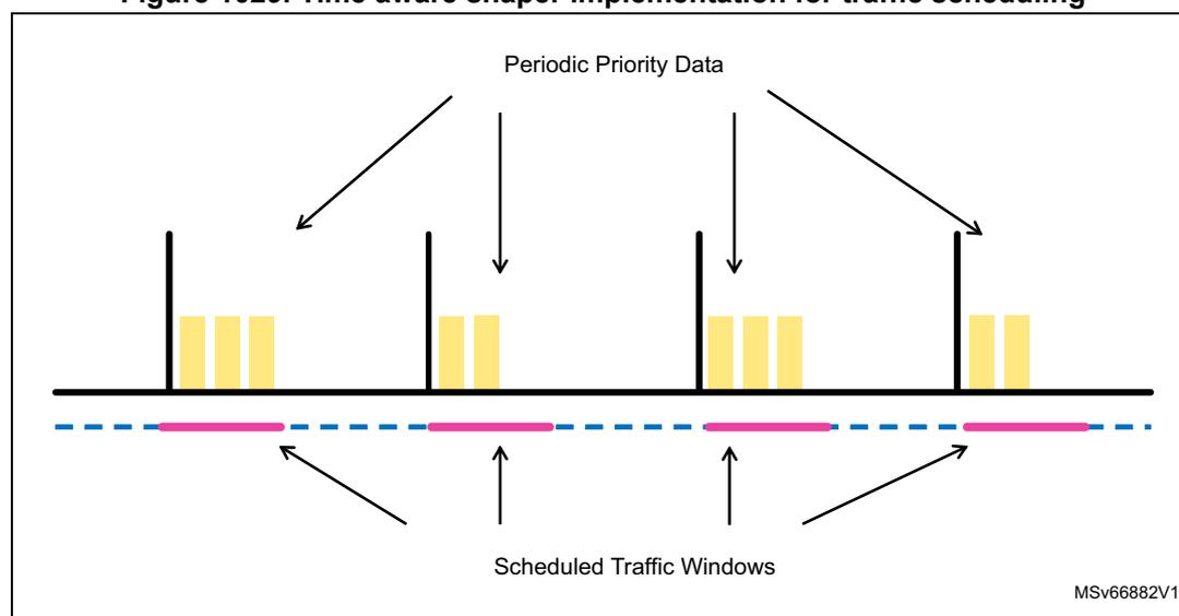
One of the important requirements to achieve a low latency is to make sure there are no interfering frames during the scheduled windows that are reserved to high priority traffic. The use of scheduled traffic imposes limitations while starting a transmission.
As shown in Figure 1030 , if an interfering frame transmission begins just before the start of a reserved time period, the transmission can be extended into the reserved window and potentially interfere with higher priority traffic. Therefore, a guard band whose size is equal to the largest possible interfering frame is required before the window starts.
Figure 1030. Implementing a guard band to avoid delays due to interfering frames
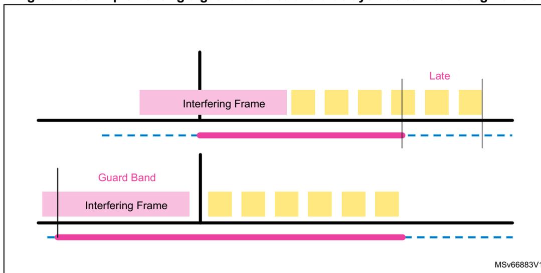
A larger guard band equates to a less efficient use of network bandwidth. However, with the implementation of IEEE802.1Qbu (frame preemption), this issue is addressed. Frame preemption breaks the interfering frame into smaller fragments. Therefore, the guard band needs to be only as large as the largest possible interfering fragment instead of the largest possible interfering frame.
During the guard band, only the frames for which the entire frame can be complete before the next gate close event are permitted. This ensures that the high priority traffic can always start at the beginning of the window reserved for it.
The transmit scheduling embeds the following feature to be able to support EST:
- • Gate control list (GCL)
- • Enforced gate controls in the scheduler
- • Gate open duty cycle taken into account in the computation of the idleSlope (CBS)
Gate control list implementation (GCL)
Figure 1031 shows the block diagram extracted from the IEEE 802.1Qbv specifications that illustrates how the gate control list governs the gate close (C) and open (O) events based on the schedule provided for each event.
The GCL consists of two parts:
- • Time interval
It defines the time (expressed in ns) during which the gate controls are valid and should be applied before reading the next gate controls from the list. The maximum time interval is 16 ms. The left shift of the time interval up to 7 bits is supported to be able to apply a multiplication factor ranging from 1 to 128 ns (in steps of \( 2^n \) ). The maximum value (post shifting) of this field must be 999,999,999 ns. - • Gate control
Defines the Open (O) represented by logic 1 or Close (C) represented by logic 0 state for the gate of each traffic class (TC).
Figure 1031. GCL governing gate close and open events block diagram (from IEEE 802.1 Qbv specifications)
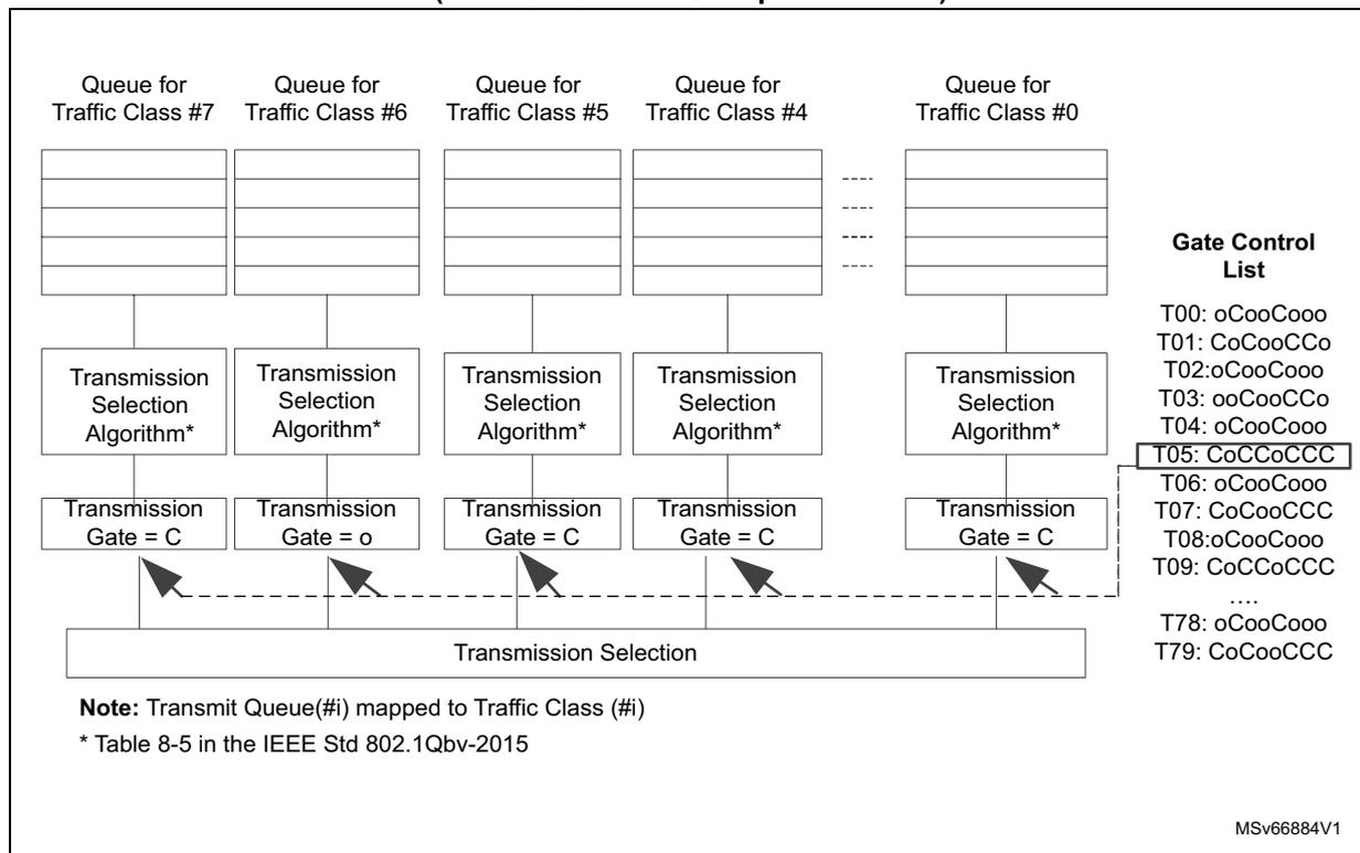
Gate Control List
- T00: oCooCooo
- T01: CoCooCCo
- T02: oCooCooo
- T03: ooCooCCo
- T04: oCooCooo
- T05: CoCCoCCC
- T06: oCooCooo
- T07: CoCooCCC
- T08: oCooCooo
- T09: CoCCoCCC
- ...
- T78: oCooCooo
- T79: CoCooCCC
Note:
Transmit Queue(#i) mapped to Traffic Class (#i)
* Table 8-5 in the IEEE Std 802.1Qbv-2015
MSv66884V1
The implementation of GCL consists of the following two gate-control lists:
- • Hardware owned list (HWOL), which can be accessed only by hardware
- • Software owned list (SWOL), which can be accessed only by software
The access to these lists is mutually exclusive. The ownership of the list is set by hardware in the SWOL field of EST Status register (ETH_MTLESTSR) . Table 793 shows how the GCL is implemented.
Table 793. External memory used for holding the two gate-control lists
| Gate control (up to 8 bits) | Time interval in ns | Gate-control list |
|---|---|---|
| 00CCCCCC | T0 | HWOL or SWOL |
| 0000CCCC | T1 | |
| CCCC00CC | T2 | |
| CCCCCC00 | T3 | |
| 1 | 1 | |
| 1 | 1 | |
| 0C0C0C00 | ||
| 0000CCCC | Last T |
Table 793. External memory used for holding the two gate-control lists (continued)
| Gate control (up to 8 bits) | Time interval in ns | Gate-control list |
|---|---|---|
| 0000CCCC | T0 | SWOL or HWOL |
| 0000CCCC | T1 | |
| 00CCCCCC | T2 | |
| 0000CCCC | T3 | |
| I | I | |
| I | I | |
| 0C0CCCCC | ||
| 00CCCCCC | Last T |
Four registers are related to the gate control lists (one for each GCL). These registers are implemented through Indirect addressing using EST Gate Control List register (ETH_MTLESTGCLCR) and EST Gate Control List Data register (ETH_MTLESTGCLDR) .
- • 64-bit base time register (BTR)
The base time register is a 64-bit register that holds the start time to execute the GCL. The format of the BTR is the same as the PTP format (upper 32-bit holds time in seconds and lower 32-bit hold time in ns).
Once the execution of a given list starts, the peripheral can update the BTR value to indicate the next list execution start time.
- • 40-bit cycle time (CTR)
The cycle time register is a 40-bit register that holds the time at which the execution of the GCL should be repeated. The cycle time register consists of an 8-bit value in seconds and a 32-bit value in ns (similar to the PTP time format with truncated second register).
For a given GCL, the start time is given by the below formula:
where N is an integer value representing the iteration number starting from 0 for the first iteration.
If the GCL execution takes longer than the cycle time, then the list is truncated at the cycle time and the subsequent loop starts at the cycle time.
- • 32-bit time extension (TER)
The time extension register (TER) is a 32-bit register that holds the amount of time (in ns) of which current GCL can be extended before switching to the new GCL. This is useful to avoid small fragments of the current list before switching to a new list. The time extension value is coded on 31 bits and stored in a 32-bit register, with the most significant bit forced to 0.
- •
7-bit [gate control] list length (LLR)
(where n depends on the configured GCL depth)
The list length register (LLR) is a 7-bit register that holds the integer value of the GCL length, which corresponds to the number of valid rows in each GCL. The processing of the GCL stops after the number of rows read is equal to the LLR value.
Transmission gating
A bridge or an end station can be used to allow transmission from each TC that is yet to be scheduled relative to a known timescale. To achieve this, a transmission gate is associated to each TC. The state of the transmission gate determines if the queued frames can be selected for transmission.
The state of a TC transmission gate can be in one of the following:
- • Open
Queued frames are selected for transmission according to the definition of the transmission selection algorithm associated to the TC. - • Closed
Queued frames are not selected for transmission.
A frame on a traffic class queue is not available for transmission if the transmission gate is in closed state or if there is insufficient time available for transmitting the whole frame before the next gate-close event associated to this queue.
The peripheral has visibility on the current schedule of gate controls and the immediate next schedule of the gate controls. As a result, the maximum gate open period does not exceed the sum of the two time intervals since a frame is selected for transmission only if the gate is currently open and the duration of gate open interval is greater than the time taken to transfer the entire frame.
The implementation must know the frame size before the transmission, so that transmission overruns can be avoided and only the frames that can complete are scheduled. This can be achieved by:
- • programming the OVHD field ([5:0] bits) of EST Extended Control register (ETH_MTELECR) with fixed overhead of the IPG or EIPG, preamble, and scheduler delay
- • automatically predicting the variable overhead due to the offloads enabled for a packet in the MAC transmitter.
Consider the following while programming the EST related fields to ensure correct packet scheduling:
- • Speed: 1 Gbps/100 Mbps
- • PTOV (in ns): 9 PTP clock cycles
- • CTOV (in ns): 3 PTP + 3 Transmit clock cycles
- • The slot interval per packet (in ns) is given by the following formula:
The overhead and scheduler delays in bytes are equal to \( 17 \text{ Tx} + (10 + X) \) application clock cycles, where \( X = 2 \) if VLAN tag insertion is enabled, \( X = 0 \) otherwise.
The peripheral adequately compensates for the data transfer delays from the buffer to the line by offsetting the current time with all the relevant delays (provided by the CTOV field of EST Control register (ETH_MTLESTCR) ). This ensures that the provided schedule is always accurately implemented at the line.
Note: An overhead is added to the packet size to take into account the scheduler delay, IPG or EIPG, and preamble overheads on the line. The gate open window should therefore be able to accommodate at least \( 128 + \text{overhead} \) bytes to transmit a 128-byte frame.
In 100-Mbps mode of operation, the rounding down error is about 0.4 %. For example, the gate open duration should be at least 1035 bytes for transmitting 1000-byte frames at a speed of 100 Mbps (31 bytes for scheduler delay and 4 bytes for rounding down error).
The minimum time interval for GCL entry is the following:
Idle slope computation updates
When EST is enabled, the credit is accumulated only when the gate is open. The effective data rate of the idleSlope must therefore be increased to reflect the duty cycle for the transmission gate associated to the queue.
The idle slope (idleSlope) is computed based on the gate open time (GateOpenTime) and operating cycle time (OperCycleTime) values. Program the idleSlope registers (one per CBS enabled TC) based on the following equation:
Operational details of GCL
Set the switch to software list through the SSWL bitfield in EST Control register (ETH_MTLESTCR) , so that the hardware can access the programmed gate control list. The first set of gate controls is applied when the current time is equal to the value in the base time register (BTR) and is held until the programmed time interval value.
To avoid transmission overruns, an additional gate control event is always read ahead from the list. This enables the GCL to determine the next gate close events (if any) for the TCs that are open.
The scheduling is based only on the gate open state and time interval of the current and subsequent schedule. An internal accumulator is used to add the time intervals when gate controls are applied. The sum of BTR + accumulator holds the time at which the next set of gate controls are planned to be applied.
Figure 1032. GCL and associated registers - BaseTime and CycleTime
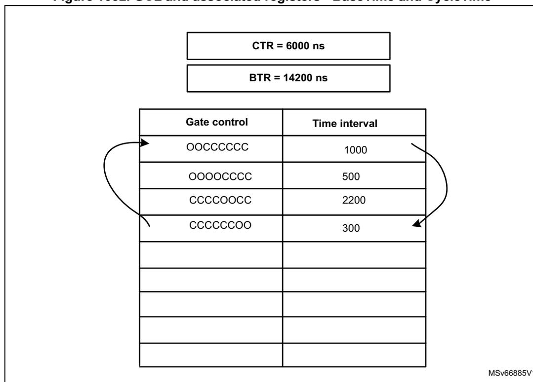
CTR = 6000 ns
BTR = 14200 ns
| Gate control | Time interval |
|---|---|
| O0CCCCCC | 1000 |
| OOOOCCCC | 500 |
| CCCCCOCC | 2200 |
| CCCCCCOO | 300 |
MSV66885V1
The GCL is read progressively from the first row adhering to the schedule. The read operations continue until the list length (defined in the LLR register) is reached. The execution of the list restarts at BTR + CTR time. At this point the BTR is incremented by the value in CTR to mark the beginning of a new cycle. In the absence of gate controls, all the gates are deemed to be in open state during the execution of the list.
In cases where the list execution time is greater than the CycleTime, the list is truncated and the next iteration starts when the current time equals BTR + CTR.
Table 794. GCL and associated registers - BTR and CTR
| Current time | Gate control applied | Accumulator value | BTR (with updates) |
|---|---|---|---|
| 14200 | O0CCCCCC | 1000 | 14200 |
| 15200 | OOOOCCCC | 1500 | 14200 |
| 15700 | CCCCCOCC | 3700 | 14200 |
| 17900 | CCCCCCOO | 4000 | 14200 |
| 18200 | OOOOOOOO | 0 | 20200 |
| 20200 | O0CCCCCC | 1000 | 20200 |
| 21200 | OOOOCCCC | 1500 | 20200 |
In the example given in Table 794 , the execution starts at 14200 and the first set of gate controls, O0CCCCCC is immediately applied. Since the time interval is 1000 ns, the next set of gate controls is applied at 14200 (BTR) + 1000 (accumulator) = 15200 ns as shown in Table 794 . Since there are no gate controls available after the execution of the last gate
control and before the next iteration of the loop, the gates are deemed to be in open state during that time period as shown at time 18200 in Table 794 .
Figure 1033. GCL and associated registers - BaseTime and CycleTime list execution time > CycleTime
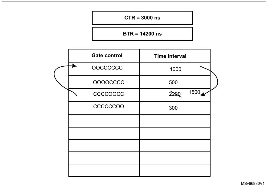
CTR = 3000 ns
BTR = 14200 ns
| Gate control | Time interval |
|---|---|
| OOCCCCCC | 1000 |
| OOOOCCCC | 500 |
| CCCCOCCC | |
| CCCCCCOO | 300 |
MSV66886V1
Since the list execution takes longer than the allocated CycleTime, the list is truncated and the list is started from the BTR+CTR as shown in Table 795 .
Table 795. GCL and associated registers - BTR and CTR, execution time > CycleTime
| Current time | Gate control applied | Accumulator value | BTR (with updates) |
|---|---|---|---|
| 14200 | OOCCCCCC | 1000 | 14200 |
| 15200 | OOOOCCCC | 1500 | 14200 |
| 15700 | CCCCOCCC | 3700 | 14200 |
| 17200 | OOCCCCCC | 1000 | 17200 |
| 18200 | OOOOCCCC | 1500 | 17200 |
| 18700 | CCCCOCCC | 3700 | 17200 |
While applying the third set of gate controls, BTR + CycleTime (17200 ns) is lower than BTR + accumulator (17900), so the list is truncated and execution switches to a new iteration at 17200.
Installing a new GCL
When a new software-programmed GCL is available and must be executed at the new BTR value, the switch to the new GCL can be done in one of the following ways:
- • New base time aligned with current schedule
- • New base time unaligned with current schedule
New base time aligned with current schedule
If the cycle time value for the new gating cycle is the same as the cycle time of the current gating cycle, and if the BTR chosen for the new gating cycle (new BTR) is an integer multiple of the current cycle time (+ current BTR), then the new gating cycle exactly lines up with the old gating cycle, that is, the cycle start times for the new gating cycle are the same as they would have been for the old configuration. This can be considered as the ideal case and enables the new gating cycle to be installed and executed with no timing issues. The peripheral completes the execution of an iteration of the current list and switches to the new list at the beginning of the BaseTime listed in the new list.
If (New BaseTime \( \geq \) Current time) ConfigChangeTime = New BaseTime
Else If (New BaseTime < Current Time)
- 1. Set the BTRError (BTRE bit in ETHMTLESTR)
- 2. ConfigChangeTime = New BaseTime + N \( \times \) New CycleTime
where N is the smallest integer for which the relation ConfigChangeTime \( \geq \) CurrentTime and ( \( N \leq 8 \) ) is TRUE.
When N is higher than 8, the hardware cannot auto-recover and the loop count value in BTR error loop count (BTRL bitfield in ETH_MTLESTSR) is set to 0b1111 1111 requiring the software to reprogram the new base time.
Figure 1034 illustrates the installation of the new GCL along with the time lines.
Figure 1034. Switching to a new configuration that is aligned with the existing configuration
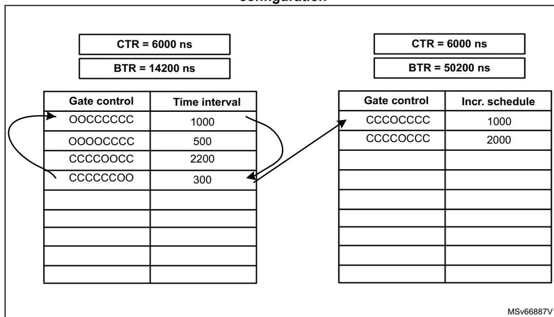
| Gate control | Time interval |
|---|---|
| OOCCCCCC | 1000 |
| OOOOCCCC | 500 |
| CCCC00CC | 2200 |
| CCCCCC00 | 300 |
| Gate control | Incr. schedule |
|---|---|
| CCCOCCCC | 1000 |
| CCCC0CCC | 2000 |
MSV66887V1
In the example given in Table 796 , after the sixth iteration of the first GCL, the BTR values of the old and new GCL are equal. At that point the new GCL is processed as a natural extension to the existing GCL.
Table 796. GCL and associated registers - BTR and CTR
| Current time | Gate control applied | Accumulator value | BTR (with updates) |
|---|---|---|---|
| 44200 | 00CCCCCC | 1000 | 44200 |
| 45200 | 0000CCCC | 1500 | 44200 |
| 45700 | CCCC00CC | 3700 | 44200 |
| 47900 | CCCCCC00 | 4000 | 44200 |
| 48200 | 00000000 | 0 | 50200 |
| 50200 | CCCC00CC | 1000 | 50200 |
| 51200 | CCCC00CC | 3000 | 50200 |
| 53200 | 00000000 | 0 | 56200 |
New base time unaligned with current schedule
If the new CycleTime differs from the current CycleTime or the new BaseTime is in the future and is not an integer multiple of current CycleTime, then the old and new cycles do not line up. When a new BaseTime is reached (that is when the new configuration is installed and starts to execute), the last old cycle is normally truncated to start the first new cycle. This can be undesirable if it results in a very short last old cycle. It would be better to simply extend the penultimate old cycle by that small amount, rather than starting a very short cycle. The cycle time extension register (TER, related to the current configuration list) enables this extension of the last old cycle to be done in a defined way. If the last complete old cycle ends normally in less than the current cycle time extension (TER in ns) before the new BaseTime, then the last complete cycle before the new BaseTime is reached is extended so that it ends at the new BaseTime.
Figure 1035. Switching to the new list by truncating the current list
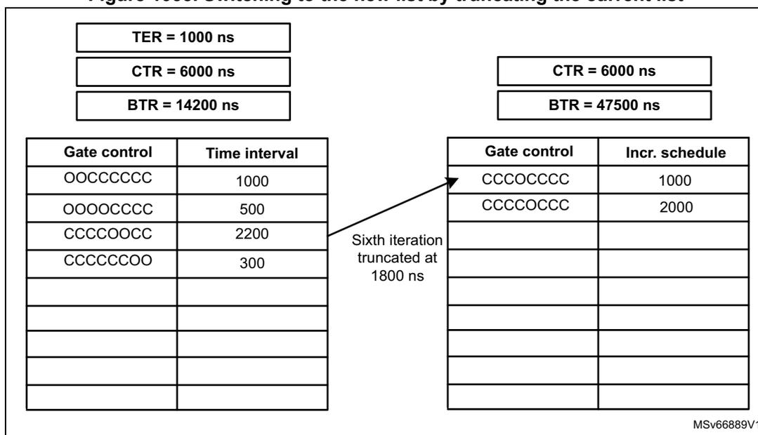
TER = 1000 ns
CTR = 6000 ns
BTR = 14200 ns
| Gate control | Time interval |
|---|---|
| OOCCCCCC | 1000 |
| OOOOCCCC | 500 |
| CCCCOCCC | 2200 |
| CCCCCCOO | 300 |
Sixth iteration truncated at 1800 ns
CTR = 6000 ns
BTR = 47500 ns
| Gate control | Incr. schedule |
|---|---|
| CCCCOCCC | 1000 |
| CCCCOCCC | 2000 |
MSV66889V1
At the end of the fifth iteration, current time + cycle time extension (TER) < New BTR, so the sixth iteration of the current configuration has started. During the sixth iteration of the current list, when the new BTR value is smaller than the next schedule in the current list, it switches to the new list.
Table 797. Extending to new list by truncating the current list
| Current time | Gate control applied | Accumulator value | BTR (with updates) |
|---|---|---|---|
| 44200 | OOCCCCCC | 1000 | 44200 |
| 45200 | OOOOCCCC | 1500 | 44200 |
| 45700 | CCCCOCCC | 3700 | 44200 |
| 47500 | CCCCOCCC | 4000 | 44200 |
| 48500 | CCCCOCCC | 0 | 50200 |
| 50500 | OOOOOCCC | 1000 | 50200 |
Figure 1036 shows an example where the current configuration list is extended instead of starting a new iteration since the extension time of 800 ns is less than the allowed cycle extension time (TER) of 1000 ns.
Figure 1036. Switching to new list by extending the current list
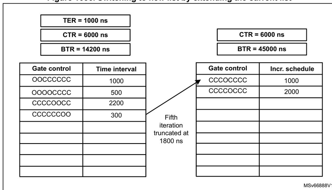
TER = 1000 ns
CTR = 6000 ns
BTR = 14200 ns
| Gate control | Time interval |
|---|---|
| 00CCCCCC | 1000 |
| 0000CCCC | 500 |
| CCCC00CC | 2200 |
| CCCCCC00 | 300 |
Fifth iteration truncated at 1800 ns
CTR = 6000 ns
BTR = 45000 ns
| Gate control | Incr. schedule |
|---|---|
| CCCOCCCC | 1000 |
| CCCCOCCC | 2000 |
MSV66888V1
Table 798. Switching to new list by extending the current list
| Current time | Gate control applied | Accumulator value | BTR (with updates) |
|---|---|---|---|
| 38200 | 00CCCCCC | 1000 | 38200 |
| 39200 | 0000CCCC | 1500 | 38200 |
| 39700 | CCCC00CC | 3700 | 38200 |
| 41900 | CCCCCC00 | 4000 | 38200 |
| 42200 | 00000000 | 0 | 44200 |
| 45000 | CCCOCCCC | 1000 | 45000 |
| 46000 | CCCCOCCC | 3000 | 45000 |
| 48000 | 00000000 | 0 | 51000 |
Impact of transmit scheduling algorithms on EST
When EST is used in isolation, the Gate Control List manages the final open/close state of the queues along with the checks carried out by the transmission selection algorithm in MTL. Since the gate controls operate on a predefined repetitive schedule, it is recommended to use strict priority or credit based shaper (CBS) scheduling algorithms.
Other algorithms such as the weighted round robin (WRR), deficit weighted round robin (DWRR) and weighted fair queuing (WFQ) implement the masking of the queues based on the current winning queue. The algorithm is applied only to the group of queues that open simultaneously. To ensure the queues whose gates are open get priority, these algorithms are modified to treat gate open queues and gate closed queues as separate groups, giving priority to gate open queues.
For example, consider four queues (Q3, Q2, Q1, Q0) with respective weights 4:3:2:1. Q3 and Q2 are in open state in one slot, while Q1 and Q0 are in open state in another slot. In this case, the scheduler works as follows:
- 1. In the first slot, Q3 and Q2 are serviced in the ratio of 4:3 for the duration during which the slot is open.
- 2. In the second slot, Q1 and Q0 are serviced in the ratio of 2:1.
- 3. Fresh arbitration is started every time a slot is opened.
In other words, the traffic does not get distributed in the intended ratio of 4:3:2:1; but as two groups with different ratios, and only for the duration of the slot when the gates are open continuously.
EST programming guidelines
For details about programming guidelines for EST, see Section 76.9.20: Programming guidelines for EST on page 4146 .
Frame preemption (FPE)
Frame preemption overview
One of the important requirements of IEEE 802.1Qbv-2015 standard is to ensure there are no interfering frames during the scheduled windows that are reserved for high priority traffic. To achieve this goal, a guard band, whose size is equal to the largest possible interfering frame, is required before the window starts. However a larger guard band equates to a less efficient use of network bandwidth.
Frame preemption compliant with IEEE802.1Qbu enables reducing the guard band by breaking the interfering frame into smaller fragments. Therefore, the guard band needs to be only as large as the largest possible interfering fragment instead of the largest possible interfering frame.
Note: Internal loopback is not supported for preempted frames
Description of the frame preemption
Preemption enables one or more higher priority (express) frames to interrupt the transmission of a lower priority (preemptable) frame. The preemptable frame transmission is resumed and completed after the express frame transmission is complete. The following two abstractions of the MAC are used to support frame preemption:
- • A preemptable MAC (pMAC), which carries the preemptable traffic
- • An express MAC (eMAC), which carries the express traffic
Only the part of the MAC that holds the state during preemption is replicated and represented as pMAC and eMAC. There are two ways for the MAC to put on hold the transmission of the preemptable traffic in the presence of express traffic:
- • The MTL scheduler interrupts the preemptable traffic that is currently being transmitted.
When the preemption capability is enabled, the MAC interrupts the transmission and reception of preemptable frames. A preempted fragment can be followed by zero or more express frames, before the continuation fragments. The preemptable frame can be fragmented any number of times. However, the minimum final and non-final fragment length criterion must be met.
Interleaving of more than one preemptable packet is not permitted. This implies that if a preemptable packet is fragmented by an express packet, another preemptable packet
cannot be transferred until all the remaining fragments of the first preempted packet are transferred.
- • The MTL scheduler prevents starting the transmission of preemptable traffic
When the preemption capability is disabled, the pMAC entity is disabled and only express traffic is transmitted or received.
Note: Queue0 can be an express queue when FPE is enabled and EST is disabled.
Enabling frame preemption
Enable the frame preemption feature by setting EFPE field of FPE control and status register (ETH_MACFPECSR) .
Modifying GCL to support FPE
In the EST-only configuration, the GCL entry has 24 bits of time interval and 8 high order bits representing the gate open/close state requirements as shown in Table 799 .
Table 799. Gate control list when FPE is disabled
| Gate control | Time interval (ns) |
|---|---|
| 00000000 | T0 |
| 00000000 | T1 |
| CCCC0000 | T2 |
| CCCC0000 | T3 |
| I | I |
| I | I |
| 0C0C0C00 | T126 |
| 00000000 | T127 |
EST only supports SetGate operations, which implies that the gates are set either to open or close at a given time interval.
However, when both FPE and EST are enabled, the GCL also supports Set-and-Hold-MAC and Set-and-release-MAC operations, in addition to the SetGate operation.
To support hold and release operations, the format of the GCL is slightly changed while configuring and enabling FPE. The first Queue (Q0) is always programmed to carry preemption traffic and therefore it is always open. The bit corresponding to Q0 is renamed as Release/Hold MAC control.
The TX queues whose packets are preemptable are identified by setting the PEC field of FPE control and status register (ETH_MACFPECSR) . The GCL bit of the corresponding queue is ignored and considered as always open. As a result, even if the software writes a 0 (C), it is ignored for such queues.
Table 800. Gate control list when FPE is enabled
| Gate control (up to 7 bits) | Release/Hold indication | Time interval (ns): 16, 20 or 24 bits |
|---|---|---|
| CCCC0000 | 0 | T0 |
| CCCC0000 | 0 | T1 |
Table 800. Gate control list when FPE is enabled (continued)
| Gate control (up to 7 bits) | Release/Hold indication | Time interval (ns): 16, 20 or 24 bits |
|---|---|---|
| 0CCCC000 | 1 | T2 |
| 0C0CC000 | 1 | T3 |
| 0C0C0000 | 1 | T4 |
| 0CC00000 | 0 | T5 |
| 0CCCC000 | 0 | T6 |
When the Release/Hold bit transitions from a 0 to 1, a Set-and-Hold-MAC operation is performed. This marks the cease of the preemptable traffic. This is achieved by sending a Hold request to MTL ha ns in advance (where ha is the time interval mentioned in the Hold advance (HADV) field of FPE Frame Preemption Advance register (ETH_MTLFPEAR) ). When the Release/Hold bit transitions from a '1' to '0', a Set-and-Release-MAC operation is performed. This marks the resuming of the preemptable traffic. This is achieved by sending a Release request to MTL ra ns in advance (where ra is the time interval mentioned in the Release Advance (RADV) field of FPE Frame Preemption Advance register (ETH_MTLFPEAR) ). The preemptable traffic is blocked for the time duration the Release/Hold bit is set to a '1' in the gate control list.
Note: HADV is the advance time to initiate the hold state. Ideally HADV should be programmed to a value of minimum fragment size, which should be smaller than the time interval (minimum fragment size + IPG + Preamble overheads in ns).
Impact of preemption on CBS algorithm
When the CBS algorithm is used, the definition of Transmit is as follows:
- • TRUE for the duration of frame transmission from the queue;
- • FALSE when frame transmission from the queue is complete.
When the CBS algorithm is used along with frame preemption, the value of Transmit is TRUE only during the frame transmission by the MAC. If the frame transmission is delayed or interrupted (for instance, a preemptable frame transmission is interrupted to allow the transmission of an express frame from a different queue, or the start of an express frame is delayed because a preemptable frame is being transmitted), the value of Transmit is FALSE until the transmission of the frame begins or is resumed.
In addition, the value of Transmit is FALSE during the transmission of any overhead resulting from a frame preemption. For example, additional frame overhead (mCRC, Fragment Count) that is added to the preemptable frame.
At any given time, if there are no frames in the queue, the value of Transmit is FALSE, and the credit is positive, the credit value is set to zero if there is no preemptable frame from the queue for which transmission is in progress but has been interrupted.
mPacket Format
When the preemption capability is enabled, MAC sends mPackets to the PHY. An mPacket can be:
- • An express packet
- • A preemptable packet
- • An initial fragment of a preemptable packet
- • A continuation fragment of a preemptable packet
Figure 1037 shows the format of the mPacket. It contains an express packet, a complete preemptable packet or the initial fragment of a preemptable packet. Figure 1037 (b) shows the format of an mPacket containing a continuation fragment of a packet.
Figure 1037. mPacket formats
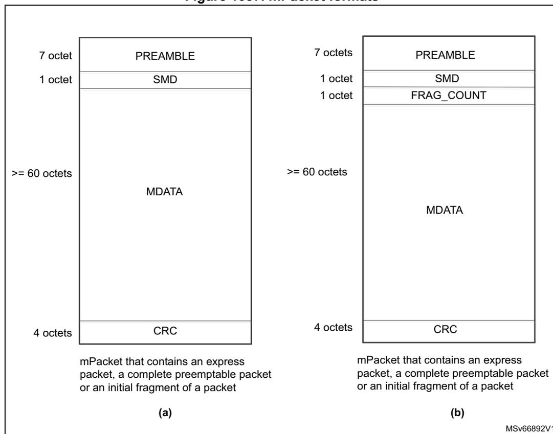
Figure 1037 illustrates two mPacket formats, (a) and (b), showing their internal structure in terms of octets and fields.
Format (a):
- 7 octet: PREAMBLE
- 1 octet: SMD
- >= 60 octets: MDATA
- 4 octets: CRC
mPacket that contains an express packet, a complete preemptable packet or an initial fragment of a packet
Format (b):
- 7 octets: PREAMBLE
- 1 octet: SMD
- 1 octet: FRAG_COUNT
- >= 60 octets: MDATA
- 4 octets: CRC
mPacket that contains an express packet, a complete preemptable packet or an initial fragment of a packet
Preamble
The preamble in the mPacket shown in Figure 1037 (a) contains seven octets. The preamble in the mPacket shown in Figure 1037 (b) contains six octets. Each octet contains the value 0x55, transmitted from left to right, 10101010.
Start mPacket Delimiter (SMD)
The value of the SMD indicates whether the mPacket contains an express packet, the start of a preemptable packet (initial fragment or complete packet), or any continuation fragments of a preemptable packet. Table 801 shows the valid SMD values.
Table 801. Valid SMD Values of mPacket| mPacket type | Notation | Frame count | Value |
|---|---|---|---|
| verify packet | SMD-V | - | 0x07 |
| Respond packet | SMD-R | - | 0x19 |
| Express packet | SMD-E | - | 0xD5 |
| Preemptable packet start | SMD-S0 | 0 | 0xE6 |
| SMD-S1 | 1 | 0x4C | |
| SMD-S2 | 2 | 0x7F | |
| SMD-S3 | 3 | 0xB3 | |
| Continuation fragment | SMD-C0 | 0 | 0x61 |
| SMD-C1 | 1 | 0x52 | |
| SMD-C2 | 2 | 0x9E | |
| SMD-C3 | 3 | 0x2A |
A frag_count is a modulo-4 counter that increments for each continuation fragment of the preemptable packet. The frag_count protects against mPacket reassembly errors by enabling detection of the loss of up to three packet fragments.
The frag_count field is present only in mPackets with SMD-C notation (continuation fragment). The frag_count is zero in the first continuation fragment of each preemptable packet.
Table 802. Valid frag_count values| frag_count | Value |
|---|---|
| 0 | 0xE6 |
| 1 | 0x4C |
| 2 | 0x7F |
| 3 | 0xB3 |
The contents of the packet from the MAC, starting with the first byte after the SFD to the last byte before the FCS, are sent in the mData fields of one or more mPackets for that frame. The minimum size of the mData field is 60 bytes.
CRCThe CRC field contains a cyclic redundancy check (CRC) and provides an indication on the final mPacket of a frame. In the final mPacket of a frame, the CRC field contains the last four octets of the MAC frame (FCS field).
For other mPackets, the CRC field contains an mCRC value. The mCRC is calculated on the octets of the packet from the first octet of the frame (octet following the SFD of
preemption frames) to the last octet of the packet transmitted in that mPacket, by performing an XOR of the calculated 32-bit CRC value of the fragment with 0x0000FFFF.
Summary of Packet Formats
- • Express packet
Seven bytes of preamble, SMD-E, data and CRC - • Complete Preemptable packet
Seven bytes of preamble, current preemptable packet SMD, data, CRC - • Initial fragment (non-final) of preemptable packet
Seven bytes of preamble, current preemptable packet SMD, data, mCRC - • Continuation fragments (non-final) of preemptable packet
Six bytes of preamble, current preemptable continuation fragment SMD, current preemptable continuation fragment FC, data, mCRC - • Final fragment of preemptable packet
Six bytes of preamble, current preemptable continuation fragment SMD, current preemptable continuation fragment FC, data, CRC
Note: When frame preemption is enabled, the MAC receiver communicates the exceptions related to received preempted fragments (such as incorrect fragment sequencing or missed fragment) to the MTL layer by reporting it as CRC error. The software should not set the DCRCC (Disable CRC Checking for Received Packets) bit of Extended operating mode configuration register (ETH_MACECR) to 1, otherwise the MTL layer might forward the unintended preempted fragments to the application.
Table 803. Current and Previous SMD Values
| Previous preemptable packet SMD | Current preemptable packet SMD |
|---|---|
| SMD-S0 | SMD-S1 |
| SMD-S1 | SMD-S2 |
| SMD-S2 | SMD-S3 |
| SMD-S3 | SMD-S0 |
Table 804. Current and previous SMD values
| Previous preemptable fragment SMD | Previous preemptable fragment FC | Current preemptable continuation fragment SMD | Current preemptable continuation fragment FC |
|---|---|---|---|
| SMD-S0 | NA | SMD-C0 | FC0 |
| SMD-S1 | NA | SMD-C1 | FC0 |
| SMD-S2 | NA | SMD-C2 | FC0 |
| SMD-S3 | NA | SMD-C3 | FC0 |
| SMD-C0 | FC0 | SMD-C0 | FC1 |
| SMD-C0 | FC1 | SMD-C0 | FC2 |
| SMD-C0 | FC2 | SMD-C0 | FC3 |
| SMD-C0 | FC3 | SMD-C0 | FC0 |
Table 804. Current and previous SMD values (continued)
| Previous preemptable fragment SMD | Previous preemptable fragment FC | Current preemptable continuation fragment SMD | Current preemptable continuation fragment FC |
|---|---|---|---|
| SMD-C1 | FC0 | SMD-C1 | FC1 |
| SMD-C1 | FC1 | SMD-C1 | FC2 |
| SMD-C1 | FC2 | SMD-C1 | FC3 |
| SMD-C1 | FC3 | SMD-C1 | FC0 |
| SMD-C2 | FC0 | SMD-C2 | FC1 |
| SMD-C2 | FC1 | SMD-C2 | FC2 |
| SMD-C2 | FC2 | SMD-C2 | FC3 |
| SMD-C2 | FC3 | SMD-C2 | FC0 |
| SMD-C3 | FC0 | SMD-C3 | FC1 |
| SMD-C3 | FC1 | SMD-C3 | FC2 |
| SMD-C3 | FC2 | SMD-C3 | FC3 |
| SMD-C3 | FC3 | SMD-C3 | FC0 |
Transmit preemption
MTL Tx preemption
To support preemption, the MAC should have more than one TX queue with at least one queue designated as express queue, plus one queue designated as preemption queue. When FPE is enabled (EFPE set to 1 in FPE control and status register (ETH_MACFPECSR) ), the MTL preempts a preemptable frame. When a Hold request is asserted (EST configured and enabled), express frames are available for transmission, that is frames are present in the MTL FIFO and qualified for arbitration, after ensuring that the minimum mPacket mData field size is met. Therefore, preemption occurs only if at least 60 bytes of the preemptable frame have been transmitted and at least 64 bytes (including the frame CRC) remain to be transmitted.
The earliest starting position of preemption is controlled by the AFSZ field of FPE control and status register (ETH_MACFPECSR) . Preemption does not occur until at least \( 64 \times (1 + \text{AFSZ}) - 4 \) bytes of the preemptable frame have been sent.
When preemption occurs, all the preemptable queues are blocked and only the express queues are allowed to arbitrate (if more than one express queue has traffic) and transmit.
The continuation fragment of the preempted frame is the first frame to be transmitted after a Release request is asserted (EST configured and enabled) and all the express traffic transmission completes.
Note: All the PTP packets should be transmitted as express packets.
MTL should wait for the previous fragment status to be received before resuming the continuation fragments of a preempted frame.
MAC Tx preemption
The MAC supports the preemption by implementing the functionality required to generate the mPackets as described in Section : mPacket Format .
When the preemption is enabled, the MAC replaces the SFD of a preemption packet with an SMD-S value. A 2-bit rolling frame count is encoded in the SMD-S value.
The SMD-E value is the same as the SFD value, so the SFD of an express packet does not need to be replaced.
Receive preemption
MAC receive preemption
When FPE is enabled, the MAC receiver passes the incoming packets and differentiates between express packets and preemptable packets. An SMD containing an SMD-E indicates express packet while and SMD containing an SMD-S indicates the first mPacket of a preemptable packet.
If an mPacket containing an SMD-S is received when the reception of the previous preempted packet has not be completed, the MAC sets a CRC error status for the previously received partial packet.
When an SMD-S is detected, the MAC records the frame count indicated by the SMD, and begins sending data on the MRI interface.
The MAC checks the last four bytes of the mPacket. If they do not match CRC, it indicates the end of the packet with or without a CRC error as per the CRC check result. If the last four octets of the mPacket match, it indicates that the packet was preempted.
An SMD containing an SMD-C indicates an mPacket that continues the data for a preempted packet. Upon receiving an SMD value of SMD-C, the MAC checks the following:
- • A preempted packet is in progress.
- • The frame count indicated by the SMD matches the frame count of the packet in progress.
- • The frag_count value indicates the next fragment count.
If any of these checks fails, the mPacket is discarded and the MAC sets a CRC error status for the partially received packet.
If all the checks pass, the next fragment count is incremented modulo 4.
When a packet is preempted, the MAC saves the state of the partially received packet (such as filter check status, timestamp, length fields) and can process any received express packets before the continuation fragment is received.
Data alignment
When a received frame cannot be fragmented on any byte boundary, the MAC retains the unaligned bytes of data in the previous fragment and resends them with the next fragment as shown in Figure 1038 .
Figure 1038. MAC data alignment feature
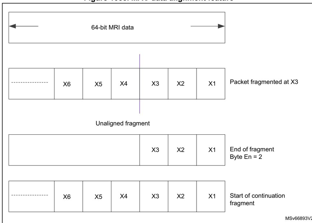
64-bit MRI data
Packet fragmented at X3
Unaligned fragment
End of fragment
Byte En = 2
Start of continuation
fragment
MSv68893V2
The MTL can choose to ignore the partial data (based on byte enable value) that comes with end of fragment and use instead the data-width-aligned data received in the first beat of the next continuation fragment.
MTL receive preemption
The MTL Rx must have at least two Rx queues to support FPE function since the preemptable packets and the express packets must be routed to separate Rx queues. The destination Rx queue of a received packet is controlled by ETH_MACRXQCiR registers. Program these registers so that preemptable traffic and express traffic are not routed to the same Rx queue. As the queue mapping for tagged packets is based on VLAN user-priority field, this implies that priority of preemptable and express packets are mutually exclusive. In other words, packets of a certain priority (traffic class) are either express or preemptable but cannot be both.
For the preemptable frames, in addition to the PSRQ (Priority Selected in Rx queue) based queue routing, a programmable frame preemption residue queue (FPRQ) is supported to route all the other received preemption packets (untagged, SA/ DA or VLAN filter fails forwarded due to RA being set or VTFE being reset).
Table 805. Preemption control values on MRI interface for various frame types| Preemption packet type | Queue routing |
|---|---|
| AV tagged packets passing the SA/DA and VLAN filters | PSRQ (1) |
| Generic tagged packets passing the SA/DA and VLAN filters | PSRQ (2) |
| Tagged packets failing the SA/DA and VLAN filters without clearing RA to 0 or setting VTIFE to 1 | Dropped |
| All other packets OR when RA is set to 1 | FPRQ |
- 1. Only if the queue is enabled for AV feature.
- 2. Only if the queue is enabled for Generic feature.
The express frames use Queue 0 as a default queue. As a result, Queue 0 must not be used for receiving preemption frames in case of filter failures.
When a fragment is received, it is pushed into its destination Rx queue. When this packet is preempted and is followed by an express packet, it is pushed/stored in a different Rx queue. The MTL saves the context of the preempted frame and processes one or more express frames. When the continuation fragment arrives, it restores the saved context and pushes the remainder of the fragmented frame into its Rx queue.
MTL receive arbitration
On the DMA interface, data is fetched from the MTL Rx FIFO based on the arbitration selected in Operating mode register (ETH_MTLOMR) . Frame based arbitration can be used only when all the MTL preemption queues operate in Store and Forward mode. Otherwise, there is a loss of bandwidth on the ARI interface since all the fragments of a preemptable packet are not available. Therefore, express packets received between the fragments are blocked until all the fragments are received and transferred; this defeats the purpose of express traffic.
When operating either in Threshold (cut through) or Store and Forward operating mode, PBL-based arbitration is recommended over frame-based arbitration. If PBL-based arbitration is used, the watermark check is always performed as well as the arbitration/transfer of data in terms of chunks of PBL size of data, which is almost similar to the concepts of fragments. Therefore the express queue packets is also blocked for less time since the DMA interface transfers the data without loss of efficiency.
Received preemption frames support in offload engines
When FPE is enabled, all the packets processed by the offload engines (ARP, PTO) and PMT, PTP, PAUSE, and PFC packets must be received as express/normal packets. These offload engine logic and functions do not recognize preemption frames.
Verify and respond mPackets
When FPE function is present, the MAC can receive and detect the Verify and Respond mPackets, even when FPE is not enabled by software. When the MAC detects valid verify/respond mPackets, it notifies the software by setting the RVER and RRSP fields of FPE control and status register (ETH_MACFPECSR) , respectively. Optionally an interrupt can be generated. As such packets have empty (all-zero) data payload, they are dropped inside the MAC and not forwarded to the MRI.
The software can set the SVER and SRSP fields of FPE control and status register (ETH_MACFPECSR) to request the MAC to transmit Verify and Respond mPackets respectively. Upon successful transmission of these frames, the MAC clears the SVER/SRSP bits and sets the TVER and TRSP bitfields in FPE control and status register (ETH_MACFPECSR) . Optionally an interrupt can be generated when these events occur.
- Note:
- 1. For the preemption frames received with CRC error indication, ignore the following status fields: Packet length, Dribble error indication, Runt frame indication.
- 2. When FPE is configured, the forward undersized good packets (FUP) bit of ETH_MTLOMR register should not be set.
- 3. When FPE is configured, do not disable CRC checking on receive. This is required because, FPE error fragments are identified internally using CRC checks. For more details, refer to the DCRCC bitfield in Extended operating mode configuration register (ETH_MACECR) .
- 4. Express and preemption traffic must be routed to different DMAs.
Frame preemption and MMC counter and interrupt registers
The following MMC counters and associated Interrupt registers are present in the MAC.
Table 806. MMC Counters and Associated Interrupt Registers
| Frame assembly error counter | Description | Associated MMC counter |
|---|---|---|
| Frame assembly error counter | 32-bit counter providing the number of MAC frames with reassembly errors on the receiver due to a mismatch in the fragment count value. | MMC Rx packet assembly error register (ETH_RX_PACKET_ASM_ERR) |
| Frame SMD error counter | 32-bit counter providing the number of received MAC frames rejected because they arrived with an SMD-C when there was no preceding preempted frame | MMC Rx packet SMD error register (ETH_RX_PACKET_SMD_ERR) |
| Frame assembly OK counter | 32-bit counter providing the number of MAC frames that were successfully reassembled | MMC Rx packet assembly OK register (ETH_RX_PACKET_ASM_OKR) |
| MAC Rx fragment counter | 32-bit counter providing the number of additional mPackets received due to preemption | MMC Rx FPE fragments counter register (ETH_RX_FPE_FRAG_CR) |
| MAC Tx fragment counter | 32-bit counter providing the number of additional mPackets transmitted due to preemption | MMC FPE Tx fragment counter register (ETH_MMC_FPE_TX_FCR) |
| Hold request counter | 32-bit counter containing the number of hold requests sent to the MAC | MMC Tx hold request counter register (ETH_MMC_TX_HRCR) |
The following additional registers are associated to MMC interrupts for the MMC error counters:
- • MMC FPE Tx interrupt status register (ETH_MMC_FPE_TX_ISR)
- • MMC FPE Tx interrupt mask register (ETH_MMC_FPE_TX_IMR)
- • MMC FPE Rx interrupt status register (ETH_MMC_FPE_RX_ISR)
- • MMC FPE Rx interrupt mask register (ETH_MMC_FPE_RX_IMR)
Time-based scheduling (TBS)
The time-based scheduling feature is suitable for traffic whose periodicity and rate are predictable. To improve the quality-of-service of such traffic:
- • The transmit DMA fetches the packet from the host memory for transmission at designated time. This helps the software to set up the Transmit descriptors in advance, even before the packet is ready and available. It reduces the overhead on the software and avoids constant monitoring of the time and preparing descriptors just in time when the packet is targeted to be transmitted.
- • The MAC transmits the packets only at the designated/predetermined time even if the packets are fetched in advance. This helps maintaining a constant transmission rate that can be consumed by the receiver, therefore avoiding congestion and excessive buffering in the network.
Description of time-based scheduling
The time-based scheduling feature supports fetching and launching of an Ethernet packet at (or after) a predetermined time. The time-based scheduling is supported only in the following modes and configurations:
- • Full duplex mode
- • Link speed of 100 Mbps or higher
Note: Do not enable time-based scheduling for channels on which the TSO feature is enabled. The ESTM mode bit setting impacts the time-based scheduling feature only when the DUT processes the GCL list.
The slot number is meaningful only after the GCL is active. So, start the GCL list before enabling the time-based scheduling (TBS) and enhancements to scheduled traffic (EST) features. If the GCL is not started, all gates are deemed open. In addition, if the packets do not make progress, the Tx queue creates back pressure.
Definitions
The following are the definitions specific to the time-based scheduling feature:
- • Launch time: time beyond which the MTL can schedule the packet for transmission.
- • GCL slot number (GSN)
- • Launch expiry time: time beyond which the packet is dropped by the MTL.
- • Fetch time: time beyond which the Tx DMA can schedule a packet fetch from the host memory.
Launch time
The launch time is specified in the enhanced normal descriptor in the DMA configuration. For more details, refer to Section 76.10.5: Enhanced descriptor for time-based scheduling .
When the launch time is specified, it is valid only for the specific frame that is scheduled for transmission. The launch time is reset after the transmission of one frame.
The following are the two launch time formats:
- • Normal/absolute format
In this format, the launch time is an absolute time value at which the packet is launched for transmission. The launch time is interpreted in the normal/absolute format if the ESTM bit of the TBS control register (ETH_MTLTBSCR) is cleared.
The launch time is a 32-bit value where the most-significant eight bits represent the time in seconds and the remaining 24 bits the time in 256 ns. The launch time is compared with the IEEE 1588-based system/PTP time (bits[39:8]) and rolls over after 256 seconds.
The maximum value of the lower 32 bits of system time is 999,999,999 in decimal (0x3B9A C9FF), and it wraps to 0 when reaching this value (representing a full second). Therefore, the maximum value of the lower 24 bits of the launch time (after multiplying by 256) must be 0x3B9AC9.
As the maximum value of the launch time is 256 seconds:
- – The launch time is greater than the current system time when its value is between System Time[39:8] and System Time[39:8] + 128 s.
- – The launch time is less than the current system time when its value is between System Time[39:8] + 128 s and System Time[39:8] + 256 s, because this is a modulo 256 computation.
- • EST/offset format
In this format, the launch time is an offset value relative to the time indicated by the base time register (BTR) of the GCL list provided in the GCL slot number (GSN). The value in the BTR is always updated to the start time of the current loop of the GCL.
For each packet, the GSN and the launch time values are specified in the Enhanced Transmit descriptor in the DMA configurations, or as control word in the MTL configurations.
The launch time offset is a 32-bit value where the upper eight bits represent the time in seconds and the remaining 24 bits the time in 256 ns that is added to the BTR value corresponding to the GCL slot number. The value of the launch time offset must be smaller than the value of the cycle time (it is specified in the CTR register that is implemented when EST is enabled).
If the CTR is greater than or equal to 1 s, the maximum value of the lower 24 bits of launch time offset should be 999 999 999 in decimal (0x3B9A C9FF).
In this format, the launch time is a 64-bit value, which is interpreted as follows:
It is compared with the System Time[63:0].
GSN BTR is the base time value at which the launch GSN loop started execution.
GCL slot number (GSN)
The GCL slot number (GSN) is a modulo 16 count of the GCL loop count. The count is incremented for every new GCL loop. The installation of a new GCL list does not impact the count. The current GCL slot number can be obtained by reading the CGSN field of the EST Status register (ETH_MTLESTSR) .
The maximum value of GSN is 15. Therefore GSN values between the current GSN (CGSN field of EST Status register (ETH_MTLESTSR) ) and CGSN + 8 represent the current or future slots; all the other GSN values are interpreted as elapsed slots or past slots. The GSN value must consequently be between CGSN and CGSN + 8, for a correct interpretation of time.
Launch expiry time- • Normal/absolute mode
In Normal mode, when the LEOV (launch expiry offset valid bit of TBS control register (ETH_MTLTBSCR) ) is set, the Launch Expiry Offset (LEOS field of TBS control register (ETH_MTLTBSCR) ) determines the maximum amount of time during which a frame is eligible for launch, starting from the time at which the frame becomes eligible for launch.
The Launch Expiry Offset is a 24-bit value defined in 256 ns units, with a maximum value of 999,999,999 ns (0x3B9A C9FF).
The packet with a specific launch time is considered eligible for transmission when the launch time is less than the system time and (if LEOV is set) the system time is less than the launch expiry time.
When the system time is greater than the launch expiry time, the frame is categorized as expired and is dropped from the MTL FIFO.
Note: For correct interpretation and meaningful operation, the fetch, launch, and launch expiry times should never be set to a value higher than the current system time + 128 s, since such a value is interpreted as time that has already elapsed.
In Full duplex mode, the frames dropped from the MTL FIFO have the Error Summary (bit 15) and Excessive Deferral (bit 3) of the Tx status set.
- • EST/offset mode
In EST mode of operation, when the LEOV field of the TBS control register (ETH_MTLTBSCR) is set, the Launch Expiry GSN Offset (LEGOS field of the TBS control register (ETH_MTLTBSCR) ) and Launch Expiry Offset (LEOS field of TBS control register (ETH_MTLTBSCR) ) determine the maximum amount of time during which a frame remains eligible for launch, starting from the time at which the frame becomes eligible for launch.
LEGOS holds the GSN offset (multiples of CTR time) and LEOS holds the maximum value of CTR (subCTR values) in ns.
The Launch Expiry Offset is a 24-bit value defined in units of 256 ns, with a maximum value which is the smaller of 999,999,999 ns and CTR - 1 ns.
The Launch Expiry GSN is computed as follows:
Where:
CCMA is the CTR carry due to modulo addition. This value is 1 if \( ((\text{Launch Time Offset} + \text{LEOS}) \ll 8) \) is equal to or greater than CTR.
- – When CCMA = 1: \( \text{Launch Expiry Offset} = (\text{Launch Time Offset} + \text{LEOS}) - \text{CTR} \) .
- – When CCMA = 0, \( \text{Launch Expiry Offset} = (\text{Launch Time Offset} + \text{LEOS}) \) .
The launch expiry time is computed as follows:
When LEOV is not set, the launch expiry time is not checked.
When LEOV is set:
- • If the system time is greater than the launch expiry time, the frame is dropped from the MTL FIFO. The frame is considered as expired.
- • If the launch time is smaller than the system time and the launch expiry time is greater than the system time, the frame is considered eligible for launch.
Note: The maximum value of LEGOS is 7. This implies that when LEOV is set, the frame has a maximum life time of less than 8 GCL loop iterations after it becomes eligible for launch. The slot number of the first GCL list executed each time after EST is enabled, is zero.
Fetch time
The fetch time can also be indicated by the software for each packet. This is done by setting the FTOV field of DMA TBS Control Register x (ETH_DMATBSCTRL0R).
If the FTOV field is not set, the Fetch Time Offset is not valid and the DMA fetches packets without any time constraints.
The fetch time accounts for all possible delays in the DMA fetch operation and ensures that the frame is present in the MTL FIFO before the launch time.
- • Normal/absolute mode
In Normal mode, the fetch time is derived/calculated by reducing the time specified in the Fetch Time Offset (FTOS) field of DMA TBS Control Register x (ETH_DMATBSCTRL0R) from the given launch time.
In Normal mode of operation, the fetch launch time is computed as follows:
The fetch time is a 32-bit value. It is compared against System Time[39:8] to determine the eligibility for fetching the frame:
- – The fetch time is defined as greater than the system time if the fetch time is in the range of System Time[39:8] and System Time[39:8] + 128 s. The frame is considered as not-eligible for fetch.
- – The fetch time is defined as smaller than the system time if the fetch time is in the range of System Time[39:8] + 128 s and System Time[39:8] + 256 s. The frame is considered as eligible for fetch.
This is a modulo 256 computation.
- • EST/offset mode
In EST/offset mode, the Fetch GSN Offset (FGOS field of DMA TBS Control Register x (ETH_DMATBSCTRL0R) provides the slot number offset to be deducted from the launch GSN. In this case, the FTOS value should be the smaller of 999,999,999 ns and CTR – 1 ns.
If Launch Time Offset \( \geq \) FTOS:
- – Fetch Time Offset = ((Launch Time Offset – FTOS) \( \times \) 256 ns)
- – CBFS (CTR Borrow for Fetch Subtraction) = 0
If Launch Time Offset \( < \) FTOS:
- – Fetch Time Offset = CTR + ((Launch Time Offset – FTOS) \( \times \) 256 ns)
- – CBFS (CTR Borrow for Fetch Subtraction) = 1
The Fetch GSN is computed as follows:
- – Fetch GSN = Launch GSN – FGOS – CBFS
- – Fetch Time = Fetch GSN BTR[63:0] + Fetch Time Offset
Note: The frame is marked eligible for DMA fetch when the fetch time is smaller than the system time.
The maximum value of FGOS is 7. This implies that when FTOV is set, the frame can be fetched at a maximum of 8 GCL loop iterations before it becomes eligible for Launch.
- • DMA operation sequence
The following is the sequence of operation when FTOV is set:
- a) Fetch the first enhanced normal descriptor (FD is set).
- b) If LTV is set and fetch enabled, compute the fetch time based on the launch time. Wait for the system time to be greater than the fetch time
- c) Read the frame (data) from the host memory and transfer it to the MTL FIFO.
- d) Close the normal descriptor.
- e) Fetch the next normal descriptor (if the previous descriptor was not the last).
- f) Repeat steps d to f until the last descriptor of the frame (LD is set).
After the last descriptor of a frame, the next enhanced normal descriptor should be programmed with a new launch time and with LTV bit set. Otherwise, the subsequent frames are processed without any time restrictions.
- • Impact on the transmission selection algorithm
The time-based scheduler does not directly influence the transmission selection algorithm but has an indirect influence as it determines if a queue is eligible to participate in the scheduling.
If a frame of a specific queue has a valid launch time, the time-based scheduler ensures that the frame participates in transmit scheduling (TRC scheduler) only after the launch time has elapsed.
The gating done by the time-based scheduler is only for the scheduling (picking frame for transmission). It might not alter any other characteristics and behavior of the frame. For example, the frame waiting for the launch time to elapse continues to gain credits in CBS, and the CBS credits are not lost as the frame is marked as available but not ready. Strict priority and CBS are recommended transmit scheduling algorithms for the TBS implementation because scheduling for TBS enabled queues is more predictable.
Figure 1039. Time-based scheduler implementation
The diagram illustrates the time-based scheduler implementation. On the left, eight queues labeled Q7, Q6, Q5, Q4, Q3, Q2, Q1, and Q0 are shown, each with an arrow pointing into a central block labeled 'Time-based scheduler'. From the right side of this block, eight arrows point into a second block on the right labeled 'TRC scheduler'.
For details about programming guidelines, see Section 76.9.21: Programming the launch time in time-based scheduling .
Time-based scheduling flowFigure 1040 shows the time-based scheduling flow.
Figure 1040. Time-based scheduling flow
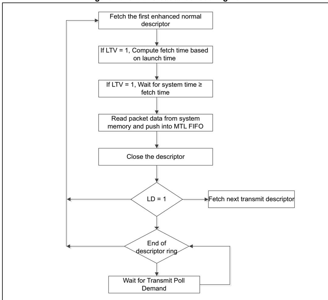
graph TD; A[Fetch the first enhanced normal descriptor] --> B[If LTV = 1, Compute fetch time based on launch time]; B --> C[If LTV = 1, Wait for system time ≥ fetch time]; C --> D[Read packet data from system memory and push into MTL FIFO]; D --> E[Close the descriptor]; E --> F{LD = 1}; F --> G[Fetch next transmit descriptor]; F --> H{End of descriptor ring}; G --> H; H --> I[Wait for Transmit Poll Demand]; I --> A;The flowchart illustrates the time-based scheduling process. It begins with 'Fetch the first enhanced normal descriptor', followed by a conditional step 'If LTV = 1, Compute fetch time based on launch time'. If LTV is 1, it proceeds to 'If LTV = 1, Wait for system time ≥ fetch time'. The next step is 'Read packet data from system memory and push into MTL FIFO', followed by 'Close the descriptor'. A decision diamond 'LD = 1' follows. If 'LD = 1' is true, it goes to 'Fetch next transmit descriptor'. If 'LD = 1' is false, it goes to 'End of descriptor ring'. Both 'Fetch next transmit descriptor' and 'End of descriptor ring' lead to a second decision diamond 'End of descriptor ring'. If 'End of descriptor ring' is true, it goes to 'Wait for Transmit Poll Demand', which loops back to the start. If 'End of descriptor ring' is false, it loops back to the 'LD = 1' decision.
76.5.7 Checksum offload engine
Communication protocols such as TCP and UDP implement checksum fields, which help determine the integrity of data transmitted over a network. The most widespread use of Ethernet is to encapsulate TCP and UDP over IP datagrams. The MAC has a Checksum Offload Engine (COE) to support checksum calculation and insertion in the Transmit path, as well as error detection in the receive path.
Transmit checksum offload engine
In the transmit path, the MAC calculates the checksum and inserts it in the Tx packet. This feature helps reducing the load on the software and can improve the overall system throughput.
The COE module supports two types of checksum calculation and insertion. The checksum engine can be controlled for each packet by setting the CIC bits (TDES3 bits[17:16]).
Note: The checksum for TCP, UDP, or ICMP is calculated over a complete packet, and then inserted into its corresponding header field. Because of this requirement, the Tx FIFO
automatically operates in the Store-and-forward mode even if the MAC is configured in Threshold (cut-through) mode.
Make sure that the Tx FIFO is deep enough to store a complete packet before that packet is transferred to the MAC transmitter, the reason being that when space is not available to accept the programmed burst length of data, then the MTL Tx FIFO starts reading to avoid deadlock. In such a case, the COE fails as the start of the packet header is read out before the payload checksum can be calculated and inserted. Therefore, the checksum insertion must be enabled only in the packets that are less than the number of bytes, given by the following equation:
where
TxQSize corresponds to the TQS bitfield of Tx queue x operating mode register (ETH_MTLTXQxOMR)
PBL corresponds to the TxPBL bitfield of Channel x transmit control register (ETH_DMACTXCR)
Refer to IETF specifications RFC 791, RFC 793, RFC 768, RFC 792, RFC 2460, and RFC 4443 for IPv4, TCP, UDP, ICMP, IPv6, and ICMPv6 packet header specifications, respectively.
IP header checksum engine
In IPv4 datagrams, the integrity of the header fields is indicated by the 16-bit Header Checksum field (the eleventh and twelfth bytes of the IPv4 datagram). The COE detects an IPv4 datagram when the Type field of Ethernet packet has the value 0x0800 and the Version field of IP datagram has the value 0x4. The checksum field of the input packet is ignored during calculation and replaced with the calculated value.
Note: IPv6 headers do not have a checksum field. Therefore, the COE does not modify the IPv6 header fields.
The result of this IP header checksum calculation is indicated by the IP Header Error status bit in the Transmit status (bit 0 in Table 828: TDES3 normal descriptor (write-back format) ).
This status bit is set whenever the values of the Ethernet Type field and the Version field of IP header are not consistent, or when the Ethernet packet does not have enough data, as indicated by the IP header Length field. In other words, this bit is set when an IP header error is asserted under the following circumstances:
- • For IPv4 datagrams:
- – The received Ethernet type is 0x0800, but the Version field of IP header is not equal to 0x4.
- – The IPv4 Header Length field indicates a value less than 0x5 (20 bytes).
- – The total packet length is less than the value given in the IPv4 Header Length field.
- • For IPv6 datagrams:
- – The Ethernet type is 0x86DD but the IP header Version field is not equal to 0x6.
- – The packet ends before the IPv6 header (40 bytes) or extension header (as given in the corresponding Header Length field in an extension header) is completely received.
TCP/UDP/ICMP checksum engine
The TCP/UDP/ICMP Checksum Engine processes the IPv4 or IPv6 header (including extension headers) and determines whether the encapsulated payload is TCP, UDP, or ICMP. The checksum is calculated for the TCP, UDP, or ICMP payload and inserted into its corresponding field in the header. The Tx COE can work in the following two modes:
- • The TCP, UDP, or ICMPv6 pseudo-header is not included in the checksum calculation and is assumed to be present in the Checksum field of the input packet. This engine includes the Checksum field in the checksum calculation, and then replaces the Checksum field with the final calculated checksum.
- • The engine ignores the Checksum field, includes the TCP, UDP, or ICMPv6 pseudo-header data into the checksum calculation, and overwrites the checksum field with the final calculated value.
Note: For ICMP-over-IPv4 packets, the Checksum field in the ICMP packet must always be 0x0000 in both modes, because pseudo-headers are not defined for such packets. If it does not equal 0x0000, an incorrect checksum may be inserted into the packet.
The result of this operation is indicated by the Payload Checksum Error status bit in the Transmit Status vector (bit 12 in Table 828: TDES3 normal descriptor (write-back format) ). This engine sets the Payload Checksum Error status bit when it detects that the packet has been forwarded to the MAC transmitter engine in the store-and-forward mode without the end of packet (EOP) being written to the FIFO, or when the packet ends before the number of bytes indicated by the Payload Length field in the IP Header is received. When the packet is longer than the indicated payload length, the COE ignores them as stuff bytes, and no error is reported. When this engine detects the first type of error, it does not modify the TCP, UDP, or ICMP header. For the second error type, it still inserts the calculated checksum into the corresponding header field.
Table 807 describes the functions supported by Transmit Checksum Offload engine based on the packet type. When the MAC does not insert the checksum, it is indicated as “No” in the table.
Note: Do not enable checksum insertion for IPv4 or IPv6 packets that are greater than the frame size constraint specified in Section : Transmit checksum offload engine because it might result in incorrect checksum insertion or unexpected behavior.
Table 807. Transmit checksum offload engine functions for different packet types
| Packet type | Hardware IP header checksum insertion | Hardware TCP/UDP checksum insertion |
|---|---|---|
| Non-IPv4 or IPv6 packet | No | No |
| IPv4 packet is greater than 1,522 bytes (2,000 bytes when IEEE 802.3ad support for 2K packets is enabled in the MAC) but less than or equal to the frame size constraint specified in Section : Transmit checksum offload engine . | Yes | Yes |
| IPv6 packet is greater than 1,522 bytes (2,000 bytes when IEEE 802.3ad support for 2K packets is enabled in MAC) but less than or equal to the frame size constraint specified in Section : Transmit checksum offload engine . | Not applicable | Yes |
| Packet type | Hardware IP header checksum insertion | Hardware TCP/UDP checksum insertion |
|---|---|---|
| IPv4 with TCP, UDP, or ICMP | Yes | Yes |
| IPv4 packet has IP options (IP header is longer than 20 bytes) | Yes | Yes |
| Packet is an IPv4 fragment | Yes | No |
| IPv6 packet with the following next header fields in main or extension headers: – Hop-by-hop options (in IPv6 main header) – Hop-by-hop options (in IPv6 extension header) – Destinations options – Routing (with segment left 0) – Routing (with segment left > 0) – TCP, UDP, or ICMP – Authentication – Any other next header field in main or extension headers | – Not applicable – Not applicable – Not applicable – Not applicable – Not applicable – Not applicable – Not applicable – Not applicable | – Yes – No – Yes – No – No – Yes – No – No |
| IPv4 packet has TCP header with Options fields | Yes | Yes |
| IPv4 Tunnels: – IPv4 packet in an IPv4 tunnel – IPv6 packet in an IPv4 tunnel | – Yes (IPv4 tunnel header) – Yes (IPv4 tunnel header) | – No – No |
| IPv6 Tunnels: – IPv4 packet in an IPv6 tunnel – IPv6 packet in an IPv6 tunnel | – Not applicable – Not applicable | – No – No |
| IPv4 packet has 802.3ac tag (with C-VLAN tag or S-VLAN Tag when enabled). | Yes | Yes |
| IPv6 packet has 802.3ac tag (with C-VLAN tag or S-VLAN Tag when enabled). | Not applicable | Yes |
| IPv4 frames with security features (such as encapsulated security payload) | Yes | No |
| IPv6 frames with security features (such as encapsulated security payload) | Not applicable | No |
Receive checksum offload engine
The receive checksum offload engine is used to detect errors in IP packets by calculating the header checksum and further matching it with the received header checksum. This engine also identifies a TCP, UDP, or ICMP payload in received IP packets and calculates the checksum of such payloads appropriately.
The receive checksum offload engine (Rx COE) can be enabled by setting the IPC bit of Operating mode configuration register (ETH_MACCR) . When this bit is set, both IPv4 and IPv6 packet in the received Ethernet packets are detected and processed for data integrity. The MAC receiver identifies IPv4 or IPv6 packets by checking for value 0x0800 or 0x86DD, respectively, in the Type field of the received Ethernet packet. This identification is applicable to single VLAN-tagged packets. It is also applicable to double VLAN-tagged packets when the EDVLP bit of the VLAN tag Control register (ETH_MACVTCR) is set.
The Rx COE calculates the IPv4 header checksums and checks that they match the received IPv4 header checksums. The result of this operation (pass or fail) is given to the RFC module for insertion into the receive status word. The IP Header Error bit is set for any mismatch between the indicated payload type (Ethernet Type field) and the IP header version, or when the received packet does not have enough bytes, as indicated by the Length field of the IPv4 header (or when fewer than 20 bytes are available in an IPv4 or IPv6 header).
Packets with TCP/IP errors (header or payload) are dropped in MTL when DIS_TCP_EF bit of the Rx queue x operating mode register (ETH_MTLRXQxOMR) is reset and FEP bit is set.
This engine also identifies a TCP, UDP, or ICMP payload in the received IP datagrams (IPv4 or IPv6) and calculates the checksum of such payloads properly, as defined in the TCP, UDP, or ICMP specifications. This engine includes the TCP, UDP, or ICMPv6 pseudo-header bytes for checksum calculation and checks whether the received checksum field matches the calculated value. The result of this operation is given as a Payload Checksum Error bit in the receive status word. This status bit is also set if the length of the TCP, UDP, or ICMP payload does not match the expected payload length given in the IP header.
Table 808: Receive checksum offload engine functions for different packet types describes the functions supported by the Rx COE based on the packet type. When the payload of an IP packet is not processed (indicated as "No" in the table), the information (whether the checksum engine is bypassed or not) is given in the receive status.
Note: The MAC does not append any payload checksum bytes to the received Ethernet packets.
Table 808. Receive checksum offload engine functions for different packet types
| Packet type | Hardware IP header checksum checking | Hardware TCP/UDP/ICMP checksum checking |
|---|---|---|
| Non-IPv4 or IPv6 | No | No |
| IPv4 packet is greater than 1,522 bytes (2,000 bytes when IEEE 802.3ad support for 2K packets is enabled in the MAC) | Yes | Yes |
| IPv6 packet is greater than 1,522 bytes (2,000 bytes when IEEE 802.3ad Support for 2K packets is enabled in the MAC) | Not applicable | Yes |
| IPv4 with TCP, UDP, or ICMP | Yes | Yes |
| IPv4 header's protocol field contains a protocol other than TCP, UDP, or ICMP | Yes | No |
| IPv4 packet has IP options (IP header is longer than 20 bytes) | Yes | Yes |
| Packet is an IPv4 fragment | Yes | No |
| IPv6 packet with the following next header fields in main or extension headers: – Hop-by-hop options (in IPv6 main header) – Hop-by-hop options (in IPv6 extension header) – Destinations options – Routing (with segment left 0) – Routing (with segment left > 0) – TCP, UDP, or ICMP – Any other next header field in main or extension headers | – Not applicable – Not applicable – Not applicable – Not applicable – Not applicable – Not applicable – Not applicable – Not applicable | – Yes – No – Yes – Yes – No – Yes – No |
| IPv4 packet has TCP header with Options fields | Yes | Yes |
| IPv4 Tunnels: – IPv4 packet in an IPv4 tunnel – IPv6 packet in an IPv4 tunnel | – Yes (IPv4 tunnel header) – Yes (IPv4 tunnel header) | – No – No |
| IPv6 Tunnels: – IPv4 packet in an IPv6 tunnel – IPv6 packet in an IPv6 tunnel | – Not applicable – Not applicable | – No – No |
| IPv4 packet has 802.3ac tag (with C-VLAN Tag or S-VLAN Tag when enabled). | Yes | Yes |
| IPv6 packet has 802.3ac tag (with C-VLAN Tag or S-VLAN Tag when enabled). | Not applicable | Yes |
| IPv4 frames with security features (such as encapsulated security payload) | Yes | No |
| IPv6 frames with security features (such as encapsulated security payload) | Not applicable | No |
76.5.8 TCP segmentation offload
The MAC supports the TCP segmentation offload (TSO) feature in which the DMA splits a large TCP packet into multiple small packets and passes these packets to the MTL as shown in Figure 1041 .
This feature is enabled by programming the TSE bit of corresponding ETH_DMACxCR register (see Channel x transmit control register (ETH_DMACxTXCR) ). It is only supported when the MAC operates in Full-duplex mode.
For detailed programming steps, refer to Section 76.9.16: Programming guidelines for TSO .
Figure 1041. TCP segmentation offload overview
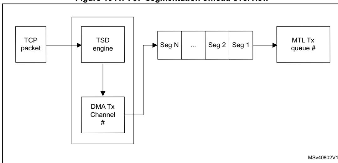
graph LR
    TCP[TCP packet] --> TSD[TSD engine]
    subgraph DMA_Block [ ]
        TSD --> DMA_CH[DMA Tx Channel #]
    end
    TSD --> SegN[Seg N]
    SegN --> Dots[...]
    Dots --> Seg2[Seg 2]
    Seg2 --> Seg1[Seg 1]
    Seg1 --> MTL[MTL Tx queue #]
The diagram shows the flow of data during TCP segmentation offload. A 'TCP packet' enters from the left and is processed by a 'TSD engine'. The 'TSD engine' is part of a larger block that also contains 'DMA Tx Channel #'. The TSD engine outputs a series of segments, labeled 'Seg N', '...', 'Seg 2', and 'Seg 1', which are then passed to the 'MTL Tx queue #'.
MSv40802V1
DMA operation with TSO feature
Figure 1042 shows the TSO flow.
Figure 1042. TCP segmentation offload flow
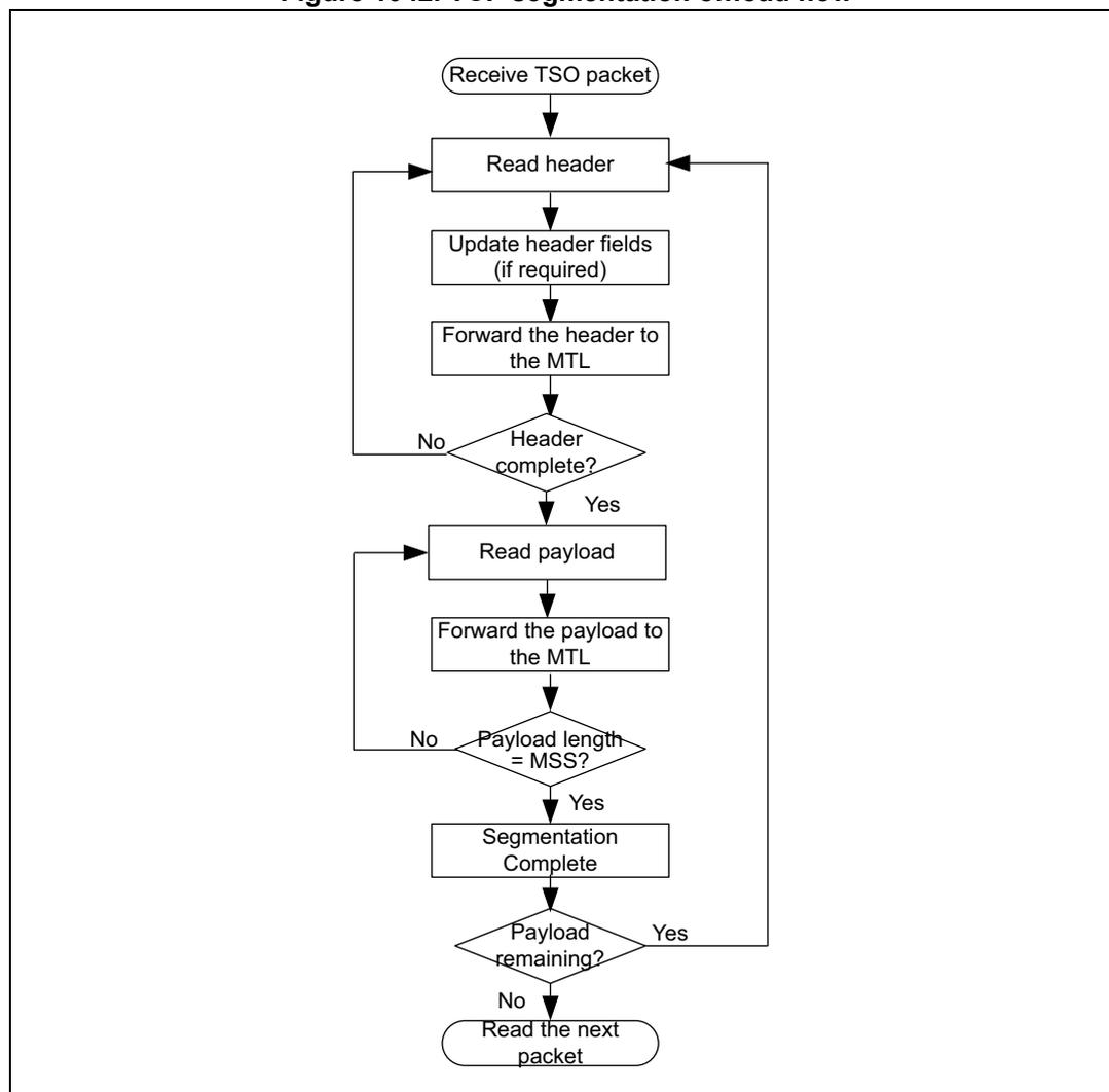
graph TD; A([Receive TSO packet]) --> B[Read header]; B --> C[Update header fields (if required)]; C --> D[Forward the header to the MTL]; D --> E{Header complete?}; E -- No --> B; E -- Yes --> F[Read payload]; F --> G[Forward the payload to the MTL]; G --> H{Payload length = MSS?}; H -- No --> F; H -- Yes --> I[Segmentation Complete]; I --> J{Payload remaining?}; J -- Yes --> B; J -- No --> K([Read the next packet])The flowchart illustrates the TCP segmentation offload (TSO) process. It begins with 'Receive TSO packet', followed by 'Read header', 'Update header fields (if required)', and 'Forward the header to the MTL'. A decision 'Header complete?' follows; if 'No', it loops back to 'Read header'; if 'Yes', it proceeds to 'Read payload', 'Forward the payload to the MTL', and 'Payload length = MSS?'. If 'No', it loops back to 'Read payload'; if 'Yes', it proceeds to 'Segmentation Complete' and 'Payload remaining?'. If 'Yes', it loops back to 'Read header'; if 'No', it proceeds to 'Read the next packet'.
For the TSO feature, the Tx DMA operation is as follows:
- 1. The application sets up the Transmit descriptor (TDES0-TDES3) and sets the Own bit (TDES3[31]) after setting up the corresponding data buffer(s) with Ethernet packet data.
- 2. The application increases the offset value of the descriptor tail pointer of the DMA Tx channel.
- 3. While in the Run state, the DMA fetches the next available descriptor and performs one of the following actions:
- – If the descriptor is a context descriptor and the context is not between the first and last descriptors of a packet, the DMA stores the context values.
- – If the descriptor is a context descriptor and the context is between the first and last descriptors of a packet, the DMA closes the context descriptor indicating a Context Descriptor Error (TDES3[23]) and fetches the next descriptor.
- – If the descriptor is a normal descriptor, the DMA checks the TSE bit. If the TSE bit is not set, the DMA continues with the default mode of operation or OSF operation (if enabled).
- 4. The DMA calculates the number of segments from the TCP payload length (TDES3[17:0]) and the MSS value.
- 5. The DMA goes through channel arbitration to fetch the data buffers. The DMA fetches the header and payload separately.
- 6. For the first segment, the DMA fetches the header from the system memory and stores it in the TSO memory (if present and when the length of header is not greater than the TSO memory size). If the current segmented packet is not the first segment, it fetches again the header buffer in system memory, as done for the first segment. In such cases, the DMA does not close the first descriptor containing the header buffer until the header for last segment is fetched.
- 7. The required fields in the header bytes are modified/updated as per the segmentation requirements and written into the corresponding MTL Tx queue.
- 8. The DMA then takes the payload buffer pointer, fetches the MSS number of payload bytes from the system memory, and directly pushes it into the MTL Tx queue. If the buffer(s) in the descriptor do(es) not have enough data for the MSS payload (except for the last segment), the DMA closes this descriptor.
- 9. The DMA jumps to Step 3 and repeats the process until the last segment is written into the Tx queue.
- 10. The DMA closes the last descriptor and the first descriptor (containing the header buffer when it is not stored in TSO memory), and then moves on to the next packet transfer.
The DMA repeats all these steps if more descriptors are available. When no more descriptor are available, the DMA enters the suspend state.
Note: The TSO engine determines whether to perform TSO or USO operation based on the THL field (TCP Header Length) in TDES3 of first Normal Tx descriptor for the packet. The value of 2 indicates USO and any value greater than or equal to 5 indicates TSO.
TCP/IP header fields
While segmenting a TCP packet, the DMA automatically updates the TCP/IP header fields. Table 809 describes how the TCP and IP headers are updated.
Table 809. TSO: TCP and IP header fields
| Packet sequence | TCP header | IP header |
|---|---|---|
| First packet |
| IPv4 Header
|
| Subsequent packets |
| IPv4 Header
|
| Last packet |
| IPv4 Header
|
Header and payload fields of segmented packets
After segmentation, the split packets use the same header as the parent TCP packet for header fields other than the ones described in Table 809: TSO: TCP and IP header fields . Figure 1043: Header and payload fields of segmented packets shows how same header is used for the header fields of segmented packets.
The application must create the header in Buffer 1 of the first descriptor of the packet to be segmented and provide the header length in TDES2 of the first descriptor (FD = 1). When the FD bit is set, the DMA reads the header from the header buffer to which the TDES0 is pointing. Buffer 2 of the first descriptor can be used for payload and TDES0 and TDES1 of subsequent descriptors. For subsequent descriptors (FD = 0), the address to which the TDES0 and TDES1 are pointing is treated as payload buffer address of the same packet.
Figure 1043. Header and payload fields of segmented packets
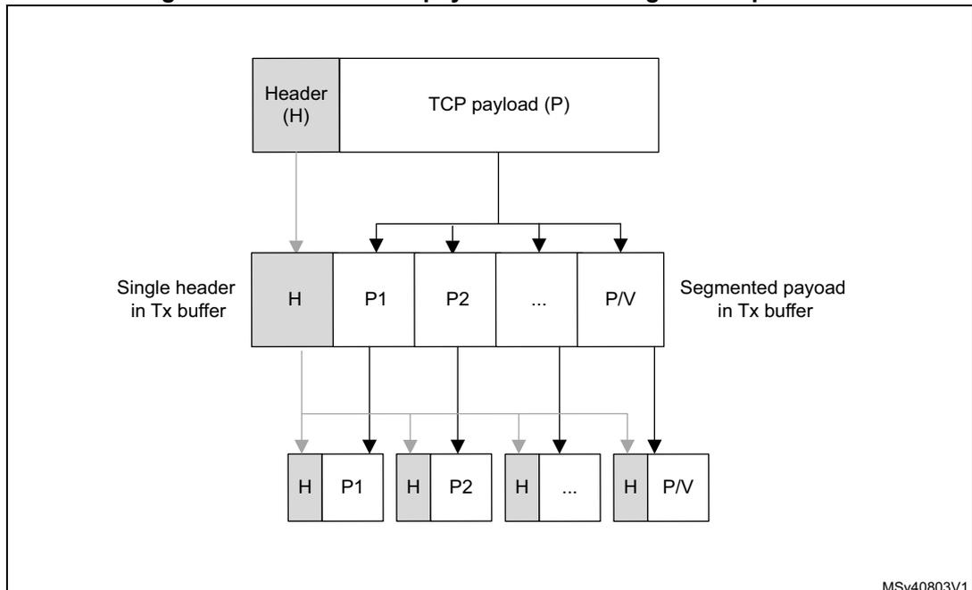
graph TD
    subgraph "Original Packet"
    H[Header H] --- P[TCP payload P]
    end

    H --> H_Tx[H]
    P --> P1[P1]
    P --> P2[P2]
    P --> P_dots[...]
    P --> PV[P/V]

    subgraph "Single header in Tx buffer"
    H_Tx
    end

    subgraph "Segmented payload in Tx buffer"
    P1 --- P2 --- P_dots --- PV
    end

    H_Tx --> SP1_H[H]
    P1 --> SP1_P[P1]

    H_Tx --> SP2_H[H]
    P2 --> SP2_P[P2]

    H_Tx --> SPV_H[H]
    PV --> SPV_P[P/V]

    subgraph "Segmented Packets"
    SP1[H | P1]
    SP2[H | P2]
    SP_dots[H | ...]
    SPV[H | P/V]
    end
The diagram illustrates the process of packet segmentation. At the top, a single packet structure is shown with a 'Header (H)' and a 'TCP payload (P)'. Below this, the 'Single header in Tx buffer' (H) and 'Segmented payload in Tx buffer' (P1, P2, ..., P/V) are shown. Arrows indicate the flow of data from the top level to the segmented level, and then to the final segmented packets (H, P1), (H, P2), (H, ...), (H, P/V). The diagram shows that the single header is copied into each segmented packet, while the payload is split into multiple segments.
Context descriptor sequence
The context descriptor can provide the maximum segment size (MSS) value for segmentation. The application must provide the context descriptor before the normal descriptor to be used for the corresponding TCP packet. If the application needs to provide a new MSS, it must create the context descriptor in the descriptor list before the first normal descriptor of the packet to be segmented with the new MSS value. The MSS value in the context descriptor is valid only if the TCMSSV bit of TDES3 in context descriptor is set and the OSTC bit is reset (refer to Section 76.10.3: Transmit descriptor ).
When the application provides a context descriptor with a valid MSS value, the DMA internally stores the MSS value and uses this value for all subsequent packets for which the TSO is enabled through the TSE bit of TDES3 normal descriptor.
If the application places a context descriptor in the middle of a packet (between the first and last descriptors of a packet), the DMA does the following:
- 1. The DMA ignores the context and closes the descriptor.
- 2. The DMA indicates the error in descriptor status.
- 3. The DMA generates an interrupt if the CDEE bit is set in the Interrupt enable register corresponding to a DMA channel (see Channel x interrupt enable register (ETH_DMACxIER) ).
The application can read the interrupt status through CDE bit of Status register corresponding to a DMA channel (see Channel x status register (ETH_DMACxSR) ).
Building the Descriptor and the packet for the TSO feature
To enable segmentation for a packet, the application must set the TSE bit of TDES3 of first normal descriptor (see Section 76.10.3: Transmit descriptor ). If the TSE bit is set in TDES3 for a non TCP/IP packet, the DMA behavior is unpredictable.
The application must program the length of the TCP packet payload in TDES3[17:0] and the TCP header in TDES3[22:19]. The maximum length of TCP packet payload that can be segmented is 256 Kbytes.
Note: The TDES3[22:19] bitfield is used as slot number in case of AV configurations. If both TSO and AV are enabled for the same DMA Tx channel (TSE bit is set in Channel x transmit control register (ETH_DMACxTXCR) ), then do not enable slot checking for that DMA Tx channel (do not set ESC bit in Channel x slot function control status register (ETH_DMACxSFCR) ).
The header of the packet including Ethernet header, L3 header and L4 header should be provided in Buffer1 of the first normal descriptor of the TSO packet. Only buffer 1 of the first normal descriptor of a packet enabled for TSO is taken as the buffer containing the header.
The TCP payload can begin from buffer 2 of the first normal descriptor and continue to buffer 1 and buffer 2 of second normal descriptor and subsequent descriptors.
The TCP payload may span across multiple buffers and multiple descriptors. The size of buffers containing the TCP payload should add up to be equal to the TCP payload length provided in TDES3[17:0] of the first normal descriptor.
The MAC always calculates and appends CRC and inserts Padding (if required) for all packets segmented by the DMA. If the TSE bit of TDES3 is enabled, the CRC PAD Control (CPC) field of TDES3 is reserved. To determine the size of a TCP packet after segmentation, the DMA uses the Maximum Segment Size (MSS) provided by the application through context descriptor. The DMA segments only those packets which have payload size greater than MSS. The application must provide the MSS by either programming the MSS value in ETH_DMACxCR (see Channel x control register (ETH_DMACxCR) ) or by providing a context descriptor. The DMA uses the last programmed value of MSS or the last MSS value provided through context (whichever is provided later).
The header length plus the MSS size (which is equal to the size of each TCP segment) should not exceed 16383 bytes otherwise the MAC transmitter truncates the packet after 16383 bytes causing a CRC error.
The header length plus MSS size plus programmed PBL value in ETH_DMACxTXCR register (see Channel x transmit control register (ETH_DMACxTXCR) ) should be lesser than the Tx queue size programmed in TQS field of ETH_MTLTXQOMR register (see Tx queue x
operating mode register (ETH_MTLTXQxOMR) ). A MSS plus header equal to half the programmed Tx queue size is recommended.
The DMA also supports segmentation of VLAN-tagged TCP/IP frames. If the TCP packet has a VLAN tag, then the same tag is used for all the segments irrespective of the VLAN tag type provided (C-VLAN or S-VLAN). The VLAN tag insert/replace control bits are used for all segments.
If the Double VLAN feature is selected, then the DMA passes both tags for all segments irrespective of the VLAN tag types provided (C-VLAN or S-VLAN). The VLAN tag Insert/Replace control bits for both tags is applicable to all segments. If the Double VLAN feature is not selected, then the application must not set the TSE bit in TDES3 for a TCP/IP packet with two tags. The DMA behavior in this scenario is unpredictable.
If the TSE bit is set in TDES3 for the packet and TCP header length provided is less than 5 (meaning this is an invalid TCP header because it is less than 20 bytes), the DMA does not perform segmentation, instead it transmits the entire packet as a single packet. In this scenario, the CRC pad control bits are forced by DMA to 00 (MAC does CRC and padding) and checksum insertion control bits are forced to 11 (hardware does the checksum calculation for both header and payload).
76.5.9 IPv4 ARP offload
The MAC supports the Address Recognition Protocol (ARP) Offload for IPv4 packets. This feature allows to process the IPv4 ARP request packet in the receive path and to generate the corresponding ARP response packet in the transmit path.
The MAC generates the ARP reply packets for appropriate ARP request packets. ARP packets for IPv4 are L2 layer packets with Length/Type of 0x0806.
The ARP offloading sequence is as follows:
- 1. The MAC receiver gets an ARP request if the request Target Protocol Address matches the IPv4 address programmed in the MAC L3 register.
- 2. The MAC generates an ARP reply packet.
- 3. The MAC copies the Sender Hardware Address field in the ARP request to the following fields:
- – DA field of the Ethernet packet header
- – Target Hardware Address field of the ARP reply packet
- 4. The MAC copies the Sender Protocol Address field in the ARP request to the Target Protocol Address field in the ARP reply packet.
- 5. The MAC places its MAC address in the following fields:
- – SA field of the Ethernet packet header
- – Sender Hardware Address field of the ARP reply packet
- 6. The MAC copies the Target Protocol Address field in the ARP request to the Sender Protocol Address field in the ARP reply packet.
- 7. The MAC sets the opcode field in ARP reply packet to 2 indicating ARP reply.
- 8. The MAC recalculates the CRC and performs padding for the generated ARP reply packet.
- 9. The MAC transmitter sends the ARP reply
The MAC processes only one ARP request at a time. It does not store the fields of multiple ARP requests. If the MAC receives an ARP request when it is already processing an earlier
ARP request, the MAC does not generate the ARP reply for new ARP request. The MAC forwards the new ARP request packet to the application with ARP Reply Not Generated status bit set (bit 34). However, in power-down mode, if the MAC receives an ARP request when it is already processing an earlier ARP request, the MAC drops the new ARP request. If the Disable CRC check (DCRCC) bit of the Extended operating mode configuration register (ETH_MACECR) is set, then the MAC does not check for valid CRC of a ARP request packet. It can generate an ARP response packet if the other conditions are valid. The ARP request packet must always have a valid CRC.
Note: When the received ARP request is less than the 64-byte packet length, the MAC does not send an ARP response. It is treated as a normal packet and forwarded to the application based on the MAC filter settings.
76.5.10 Loopback
The MAC supports loopback of transmitted packets to its receiver.
Guidelines for using loopback mode
Below some guidelines for using the loopback mode:
- • Enable loopback only with the Full-duplex mode. In Half-duplex mode, the carrier sense signal or collision signal inputs get sampled which may result into issues such as packet dropping.
- • If the loopback mode is enabled without connecting a PHY chip, externally generate the Tx and Rx clocks and provide these clocks to the MAC.
- • Do not loop back big packets since they may get corrupted in the loopback FIFO.
The transmit and receive clocks can have an asynchronous timing relationship. Therefore, an asynchronous FIFO is used to make the loopback path of the transmitted data to the receive path. The FIFO is free-running to write on the write clock (eth_tx_clk) and read on every read clock (eth_rx_clk). At the start of each packet read from the FIFO, the write and read pointers are reinitialized to have an offset of two or four (in 10/100 Mbit/s mode). This avoids overflow or underflow during a packet transfer, and ensures that the overflow or underflow occurs only during the IPG period between the packets. The FIFO depth of five or nine is sufficient to prevent data corruption for packet sizes up to 9,022 bytes with a difference of 200 ppm between (G)MII transmit and receive clock frequencies.
Therefore, bigger packets should not be looped back because they may get corrupted in this loopback FIFO.
At the end of every received packet, the receive Protocol Engine module generates received packet status and sends it to the receive Packet Controller module. The control, missed packet, and filter fail status are added to the receive status in the receive Packet Controller module. The MAC does not process ARP or PMT packets that are looped back.
Enabling loopback mode
To enable this feature, program the LM bit of the Operating mode configuration register (ETH_MACCR) . Loopback can be enabled for all PHY interfaces. The data is always looped back through internal asynchronous FIFO on to the internal receive MII or GMII interface, irrespective of which PHY interface is selected.
The loopback data is also passed through the corresponding transmit PHY interface block, onto the Ethernet line.
Note: During loopback, the data/packet is reflected on the gmii_txd signal. Preemption is not supported in loopback mode.
76.5.11 Flow control
The transmit flow control involves transmitting Pause packets in Full-duplex mode and back-pressure in Half-duplex mode to control the flow of packets from the remote end. This section describes the flow control for transmit and receive paths.
Flow control in Full-duplex mode
In Full-duplex mode, the MAC uses IEEE 802.3x Pause packets for flow control. Table 810 describes the fields of a Pause packet.
Table 810. Pause packet fields
| Field | Description |
|---|---|
| DA | Contains the special multicast address |
| SA | Contains the MAC address 0 |
| Type | Contains 8808 |
| MAC Control opcode | Contains 0001 for IEEE 802.3x Pause Control packets |
| PT | Contains Pause time specified in the PT field of the Tx Queue 0 flow control register (ETH_MACQ0TXFCR) |
When the FCB bit is set, the MAC generates and transmits a single Pause packet. If the FCB bit is set again after the Pause packet transmission is complete, the MAC sends another Pause packet irrespective of whether the pause time is complete or not. To extend the pause or terminate the pause prior to the time specified in the previously-transmitted Pause packet, the application should program the Pause Time register with appropriate value and then again set the FCB bit.
Flow control in Half-duplex mode
In Half-duplex mode, the MAC uses the deferral mechanism for the flow control (backpressure). When the application requests to stop receiving packets, the MAC sends a JAM pattern of 32 bytes when it senses a packet reception, provided the transmit flow control is enabled. This results in a collision and the remote station backs off. If the application requests a packet to be transmitted, it is scheduled and transmitted even when the backpressure is activated. If the backpressure is kept activated for a long time (and more than 16 consecutive collision events occur), the remote stations abort the transmission because of excessive collisions.
Table 811 describes the flow control in the Tx path for Queue 0 based on the setting of the following bits:
- • EHFC bit of Rx queue x operating mode register (ETH_MTLRXQxOMR)
- • TFE bit of Tx Queue 0 flow control register (ETH_MACQ0TXFCR)
- • DM bit of Operating mode configuration register (ETH_MACCR)
Flow control is similar for all queues.
Table 811. Tx MAC flow control
| EHFC | TFE | DM | Description |
|---|---|---|---|
| X | 0 | X | The MAC transmitter does not perform the flow control or backpressure operation. |
| 0 | 1 | 0 | The MAC transmitter performs backpressure when Bit 0 of Tx Queue 0 flow control register (ETH_MACQ0TXFCR) is set. |
| 1 | 1 | 0 | The MAC transmitter performs backpressure when Bit 0 of Tx Queue 0 flow control register (ETH_MACQ0TXFCR) is set. In addition, the MAC Tx performs backpressure when Rx queue level crosses the threshold set by Bits[10:8] of Rx queue x operating mode register (ETH_MTLRXQxOMR) . |
| 0 | 1 | 1 | The MAC transmitter sends the Pause packet when Bit 0 of Tx Queue 0 flow control register (ETH_MACQ0TXFCR) is set. |
| 1 | 1 | 1 | The MAC transmitter sends the Pause packet when Bit 0 of Tx Queue 0 flow control register (ETH_MACQ0TXFCR) is set. In addition, the MAC Tx sends a Pause packet when Rx queue level crosses the threshold set by Bits[10:8] of Rx queue x operating mode register (ETH_MTLRXQxOMR) . |
Transmit flow control
The transmit flow control is enabled when TFE bit is set in Tx Queue 0 flow control register (ETH_MACQ0TXFCR) .
Flow control trigger
The application can request the MAC to send a Pause packet or initiate back-pressure by setting the FCB bit in the corresponding Tx Queue 0 flow control register (ETH_MACQ0TXFCR) .
The flow control is also triggered based on Rx Queue Threshold: the flow control operation of the MAC is enabled when the EHFC bit in the corresponding Rx queue x operating mode register (ETH_MTLRXQxOMR) is set. The flow control signal to the MAC is asserted when the fill level of the Rx queue crosses the threshold configured in RFA field of Rx queue x operating mode register (ETH_MTLRXQxOMR) . This flow control signal is de-asserted when the fill-level of the queue is lower than the threshold configured in the RFD field.
Note: The RFA sets the threshold at which the flow control is triggered and the MAC schedules to send a PAUSE frame to be sent by the local transmitter.
The remote transmitter can continue to send packets until it receives this PAUSE packet. As a result, the RXQ needs space to take in this data even after the flow control is triggered, in order to avoid overflow and loss of packets.
The maximum space required is calculated theoretically. It can be 2 max-sized packets + a little more assuming that the read from the RxFIFO is not occurring during this whole time.
Theoretically, this makes \( RFA = 4 \) or more, which implies that \( RxQ \) must have a minimum size of 4 Kbytes.
Practically, the system works with \( RFA = 2 \) (full size – 2 Kbytes, with very little probability of overflow).
The RFA bitfield in Rx queue x operating mode register (ETH_MTLRXQxOMR) is used for activating the flow control. These bits control the threshold (fill-level of Rx queue ) at which the flow control is activated.
With an RXQ size of 4 Kbytes, RFA must be set to 2 Kbytes to receive the whole packet.
Receive flow control
In the receive path, the flow control is functional only in full-duplex mode. If any Pause packet is received in half-duplex mode, the packet is considered as a normal control packet.
Description of receive flow control
Table 812 describes the flow control in the Rx path based on the setting of the following bits:
- • RFE bit of Rx flow control register (ETH_MACRXFCR)
- • DM bit of Operating mode configuration register (ETH_MACCR)
Table 812. Rx MAC flow control
| RFE | DM | Description |
|---|---|---|
| 0 | x | The MAC receiver does not detect the received Pause packets. |
| 1 | 0 | The MAC receiver does not detect the received Pause packets but recognizes such packets as Control packets. |
| 1 | 1 | The MAC receiver detects or processes the Pause packets and responds to such packets by stopping the MAC transmitter. |
The following sequence describes the Rx flow control:
- 1. The MAC checks the destination address (DA) of the received Pause packet for either of the following:
- – Multicast destination address: the DA matches the unique multicast address specified for the control packet (0x0180 C200 0001).
- – Unicast destination address: the DA matches the content of the MAC Address 0 registers (
MAC address 0 high register (ETH_MACA0HR)
and
MAC address x low register (ETH_MACAxLR)
) and the UP bit of
Rx flow control register (ETH_MACRXFCR)
is set.
If the UP bit is set, the MAC processes Pause packets with unicast destination address in addition to the unique multicast address.
- 2. The MAC decodes the following fields of the received packet:
- – Type field: this field is checked for 0x8808.
- – Opcode field: this field is checked for 0x0001 (Pause packet).
- – Pause time: the Pause time (for Pause packet) is captured to determine the time for which the transmitter needs to be blocked.
- 3. If the byte count of the status indicates 64 bytes and there is no CRC error, the MAC transmitter pauses the transmission of any data packet for the duration of the decoded Pause Time value multiplied by the slot time (64 byte times).
If subsequent Pause packets are received before the earlier Pause Time expires, the MAC updates the Pause Timer with new value.
Enabling receive flow control
Set the RFE bit in the Rx flow control register (ETH_MACRXFCR) to enable the Pause flow control.
76.5.12 MAC management counters
The peripheral supports storing the statistics about the received and transmitted packets in registers that are accessible through the application.
The counters in the MAC management counters (MMC) module can be viewed as an extension of the register address space of the CSR module. The MMC module maintains a set of registers for gathering statistics on the received and transmitted packets. The register set includes a control register for controlling the behavior of the registers, two 32-bit registers containing interrupts generated (receive and transmit), and two 32-bit registers containing masks for the Interrupt register (receive and transmit). These registers are accessible from the Application through the AHB slave interface in the same way the CSR registers are accessed. The organization of these registers is shown in Section 76.11.4: Ethernet MAC and MMC registers .
The MMC counters are free running. There is no separate enable for the counters to start. A particular MMC counter starts counting when corresponding packet is received or transmitted.
The receive MMC counters are updated for packets that are passed by the Address Filter (AFM) block. The statistics of packets dropped by the AFM module, are not updated unless they are runt packets of less than 6 bytes (DA bytes are not received fully). To get statistics of all packets, set bit 0 in the Packet filtering control register (ETH_MACPFR) . The MMC module gathers statistics on encapsulated IPv4, IPv6, TCP, UDP, or ICMP payloads in received Ethernet packets.
In addition to control registers, two sets of registers are implemented:
- • Six registers used for collision, error, and good packet counters:
- – Tx single collision good packets register (ETH_TX_SINGLE_COLLISION_GOOD_PACKETS)
- – Tx multiple collision good packets register (ETH_TX_MULTIPLE_COLLISION_GOOD_PACKETS)
- – Tx packet count good register (ETH_TX_PACKET_COUNT_GOOD)
- – Rx CRC error packets register (ETH_RX_CRC_ERROR_PACKETS)
- – Rx alignment error packets register (ETH_RX_ALIGNMENT_ERROR_PACKETS)
- – Rx unicast packets good register (ETH_RX_UNICAST_PACKETS_GOOD)
- • Four registers to record LPI mode transition:
- – Tx LPI microsecond timer register (ETH_TX_LPI_USEC_CNTR)
- – Tx LPI transition counter register (ETH_TX_LPI_TRAN_CNTR)
- – Rx LPI microsecond counter register (ETH_RX_LPI_USEC_CNTR)
- – Rx LPI transition counter register (ETH_RX_LPI_TRAN_CNTR)
Definitions
The following terminology is used in MMC register descriptions:
- • Transmitted packets are considered “good” if transmitted successfully. In other words, a transmitted packet is good if the packets transmission is not aborted because of any of the following errors:
- – Jabber timeout
- – No carrier or loss of carrier
- – Late collision
- – Packet underflow
- – Excessive deferral
- – Excessive collision
- • Received packets are considered “good” if none of the following errors exists:
- – CRC error
- – Runt packet (shorter than 64 bytes)
- – Alignment error (in 10/100 Mbit/s only)
- – Length error (non-Type packet only)
- – Out of range (non-Type packet only, longer than 1518 bytes)
- – GMII_RXER input error
- • The maximum transmit frame size depends on the frame type, as follows:
- – Untagged frame maxsize = 1,518
- – VLAN frame maxsize = 1,522
- – Jumbo frame maxsize = 9,018
- – JumboVLAN frame maxsize = 9,022
- • The maximum receive packet size depends on the packet type and control bits (JE, S2KP, GPSLCE and EDVLP), as shown in the Table 813 .
Table 813. Size of the maximum receive packet
| JE | S2KP | GPSLCE | EDVLP | Untagged frame maximum size in bytes | Single VLAN frame maximum size in bytes | Double VLAN Frame maximum size in bytes |
|---|---|---|---|---|---|---|
| 1 | X | X | 1 | 9018 | 9022 | 9026 |
| 0 | 1 | X | X | 2000 | 2000 | 2000 |
| 0 | 0 | 1 | 1 | GPSL | GPSL+4 | GPSL+8 |
| 0 | 0 | 0 | 1 | 1518 | 1522 | 1526 |
| 1 | X | X | 0 | 9018 | 9022 | 9022 |
| 0 | 0 | 1 | 0 | GPSL | GPSL+4 | GPSL+4 |
| 0 | 0 | 0 | 0 | 1518 | 1522 | 1522 |
76.5.13 Interrupts generated by the MAC
Interrupts can be generated from the MAC as a result of various events. These interrupt events are combined with the events in the DMA on the eth_sbd_intr_it signal. The MAC interrupts are of level type, that is, the interrupt remains asserted (high) until it is cleared by the application or software.
The Interrupt status register (ETH_MACISR) describes the events that can cause an interrupt from the MAC. The MAC interrupts are enabled by default. Each event can be prevented from asserting the interrupt on the eth_sbd_intr_it signals by setting the corresponding mask bits in the Interrupt enable register (ETH_MACIER) .
The interrupt register bits only indicate the block from which the event is reported. You must read the corresponding status registers and other registers to clear the interrupt.
76.5.14 MAC and MMC register descriptions
Refer to Section 76.11.4: Ethernet MAC and MMC registers .
76.6 Ethernet functional description: PHY interfaces
The Ethernet peripheral support several PHY interfaces. The root interface is the MII/GMII one. All other interfaces are derived from it as shown in Figure 1044 .
Figure 1044. Supported PHY interfaces
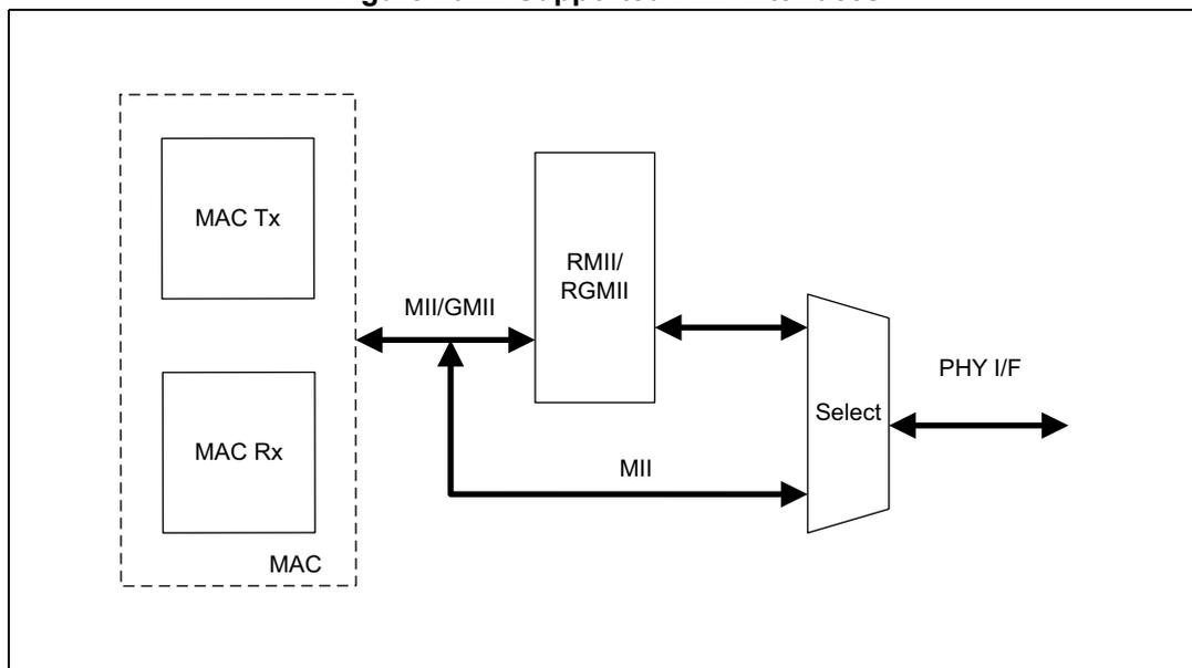
The diagram illustrates the internal architecture of the Ethernet peripheral's PHY interfaces. On the left, a dashed box labeled 'MAC' contains two sub-blocks: 'MAC Tx' (top) and 'MAC Rx' (bottom). A bidirectional arrow labeled 'MII/GMII' connects the MAC to a central block labeled 'RMII/RGMII'. From the 'RMII/RGMII' block, a bidirectional arrow points to a 'Select' block. Additionally, a unidirectional arrow labeled 'MII' originates from the 'MAC Rx' block and points to the 'Select' block. Finally, a bidirectional arrow labeled 'PHY I/F' connects the 'Select' block to the external PHY interface.
This section describes the SMA module used for PHY control and different PHY interfaces. It contains the following sections:
- • Station management agent (SMA)
- • Media independent interface (MII)
- • Reduced media independent interface (RMII)
- • Reduced gigabit media independent interface (RGMII)
76.6.1 Station management agent (SMA)
The application can access the PHY registers through the station management agent (SMA) module. The SMA includes a two-wire station management interface (MIM).
The SMA module supports accessing up to 32 PHYs. The application can address one of the 32 registers from any 32 PHYs. Only one register in one PHY can be addressed at a time. The application sends the control data to the PHY and receives status information from the PHY through the SMA module, as shown in Figure 1045 .
Figure 1045. SMA Interface block
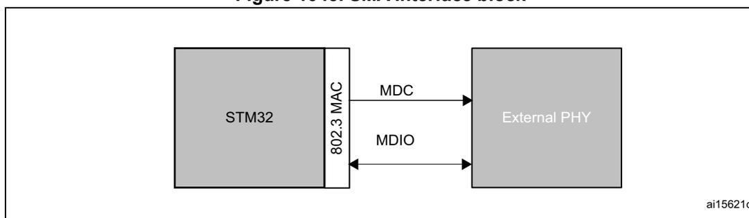
The diagram illustrates the SMA Interface block. On the left, a block labeled 'STM32' contains a vertical section labeled '802.3 MAC'. To the right of the MAC is a block labeled 'External PHY'. Two horizontal lines connect the MAC to the PHY: the top line is labeled 'MDC' and the bottom line is labeled 'MDIO'. Both lines have arrows pointing towards the External PHY block. In the bottom right corner of the diagram, the text 'ai15621c' is present.
SMA functional overview
The MAC initiates the management write or read operation with respect to the MDC clock. The MDC clock is derived from the CSR clock (eth_hclk). The maximum operating frequency of the ETH_MDC pin is 2.5 MHz, as specified in IEEE 802.3 specifications. However, a different divider can be selected if the system supports higher clock frequencies. The division factor depends on the clock range setting through CR[3:0] in the MDIO address register (ETH_MACMDIOAR) register. The MDC clock is selected as follows:
Table 814. MDC clock selection
| Selection | MDC clock |
|---|---|
| 0000 | eth_hclk/42 |
| 0001 | eth_hclk/62 |
| 0010 | eth_hclk/16 |
| 0011 | eth_hclk/26 |
| 0100 | eth_hclk/102 |
| 0101 | eth_hclk/124 |
| 0110 | eth_hclk/204 |
| 0111 | eth_hclk/324 |
| 1000 | eth_hclk/4 |
| 1001 | eth_hclk/6 |
| 1010 | eth_hclk/8 |
| 1011 | eth_hclk/10 |
| 1100 | eth_hclk/12 |
| 1101 | eth_hclk/14 |
| 1110 | eth_hclk/16 |
| 1111 | eth_hclk/18 |
The data exchange between the MAC and the PHY is performed through a three-state buffer and brought out as ETH_MDIO line connected to the PHY.
Figure 1046 shows the structure of a Clause 45 MDIO packet, while Table 815 provides a detailed description of the packet fields.
Figure 1046. MDIO packet structure (Clause 45)
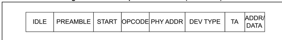
| IDLE | PREAMBLE | START | OPCODE | PHY ADDR | DEV TYPE | TA | ADDR/ DATA |
Table 815. MDIO Clause 45 frame structure
| Field | Description |
|---|---|
| IDLE | The ETH_MDIO line is three-state; there is no clock on ETH_MDC. |
| PREAMBLE | 32 continuous bits of value 1 |
| START | Start of packet is 0b00 |
| OPCODE |
|
| PHY ADDR | 5-bit address select for one of 32 PHYs |
| DEV TYPE | 5-bit device type |
| TA | Turnaround
|
| DATA | 16-bit value: for an address cycle (OPCODE = 0b00), this frame contains the address of the register to be accessed on the next cycle. For the data cycle of a write frame, this field contains the data to be written to the register. For read or post-read increment address frames, this field contains the contents of the register read from the PHY.
|
The frame structure for Clause 22 frames is also supported. The C45E bit in MDIO address register (ETH_MACMDIOAR) can be programmed to enable Clause 22 or Clause 45 mode of operation. Figure 1047 shows the structure of a Clause 22 MDIO packet, while Table 816 provides a detailed description of the packet fields.
Figure 1047. MDIO packet structure (Clause 22)
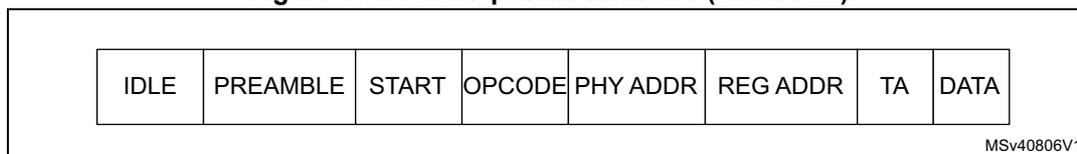
The diagram shows a sequence of eight fields in an MDIO packet: IDLE, PREAMBLE, START, OPCODE, PHY ADDR, REG ADDR, TA, and DATA. The fields are arranged horizontally in a single row. The text 'MSV40806V1' is located in the bottom right corner of the diagram.
Table 816. MDIO Clause 22 frame structure
| Field | Description |
|---|---|
| IDLE | The ETH_MDIO line is three-state; there is no clock on ETH_MDC. |
| PREAMBLE | 32 continuous bits of value 1 |
| START | Start of packet is 0b01 |
| OPCODE | 0b10 for Read and 0b01 for Write |
| PHY ADDR | 5-bit address select for one of 32 PHYs |
| REG ADDR | Register address in the selected PHY |
| TA | Turnaround – 0bZ0: Read and post-read increment address – 0b10: Write and address MDIO accesses where Z is the tri-state level |
| DATA | Any 16-bit value. In a Write operation, the MAC drives ETH_MDIO. In a Read operation, the PHY drives it. |
In addition to normal read and write operations, the SMA also supports post-read increment address while operating in Clause 45 mode.
GMII/MII management write operations
After the station management agent receives the PHY address and the write data from the MAC CSR module, the SMA starts a write operation to the PHY registers.
Figure 1048 illustrates the flow for a write operation from the SMA module to the PHY registers.
Figure 1048. SMA write operation flow
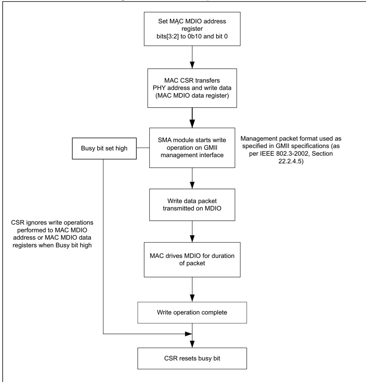
graph TD; A[Set MAC MDIO address register bits[3:2] to 0b10 and bit 0] --> B[MAC CSR transfers PHY address and write data (MAC MDIO data register)]; B --> C[SMA module starts write operation on GMII management interface]; C --> D[Write data packet transmitted on MDIO]; D --> E[MAC drives MDIO for duration of packet]; E --> F[Write operation complete]; F --> G[CSR resets busy bit]; C --> H[Busy bit set high]; H --> I[CSR ignores write operations performed to MAC MDIO address or MAC MDIO data registers when Busy bit high]; I --> G;
Management packet format used as specified in GMII specifications (as per IEEE 802.3-2002, Section 22.2.4.5)
CSR ignores write operations performed to MAC MDIO address or MAC MDIO data registers when Busy bit high
When bits[3:2] are set to 01 and bit 0 to 1 in the MDIO address register (ETH_MACMDIOAR) , the MAC CSR module transfers the PHY address, the register address in PHY, and the write data ( MDIO data register (ETH_MACMDIODR) ) to the SMA to initiate a Write operation into the PHY registers. At this point, the SMA module starts a Write operation on the GMII management Interface using the management packet format specified in the GMII specifications (as per IEEE 802.3-2002 specifications, Section 22.2.4.5 ).
When the SMA module starts a Write operation, the write data packet is transmitted on the MDIO line. The MAC drives the MDIO line for complete duration of the packet. The Busy bit is set high until the write operation is complete. The CSR ignores the Write operations per-
formed to the MDIO address register (ETH_MACMDIOAR) or the MDIO data register (ETH_MACMDIODR) during this period (the Busy bit is high). When the Write operation is complete, the SMA module indicates this to the CSR, and the CSR resets the Busy bit. The packet format for the Write operation is as follows:
Figure 1049. Write data packet
| IDLE | PREAMBLE | START | OPCODE | PHY ADDR | REG ADDR | TA | DATA | IDLE |
|---|---|---|---|---|---|---|---|---|
| Z | 1111..11 | 01 | 01 | AAAAA | RRRRR | 10 | DDD...DDD | Z |
MSV40807V1
GMII/MII management read operation
When bits[3:2] are set to 11 and bit 0 to 1 in the MDIO address register (ETH_MACMDIOAR) , the MAC CSR module transfers the PHY address and the register address in PHY to the SMA to initiate a Read operation in the PHY registers. At this point, the SMA module starts a Read operation on the GMII/MII management interface using the management packet format specified in the GMII/MII specifications (as per IEEE 802.3-2002 specifications, Section 22.2.4.5 ).
When the SMA module starts a Read operation on the MDIO, the CSR ignores the Write operations to the MDIO address register (ETH_MACMDIOAR) or MDIO data register (ETH_MACMDIODR) register during this period (the Busy bit is high) and the transaction is completed without any error on the MCI interface. When the Read operation is complete, the SMA indicates this to the CSR. The CSR resets the Busy bit and updates the MDIO data register (ETH_MACMDIODR) with the data read from the PHY. The MAC drives the MDIO line for the complete duration of the frame except during the Data fields when the PHY is driving the MDIO line. For more information about the communication from the application to the PHYs, see the Reconciliation Sublayer and Media Independent Interface Specifications sections of the IEEE 802.3z, 1000BASE Ethernet.
The packet format for the Read operation is as follows:
Figure 1050. Read data packet
| IDLE | PREAMBLE | START | OPCODE | PHY ADDR | REG ADDR | TA | DATA | IDLE |
|---|---|---|---|---|---|---|---|---|
| Z | 1111..11 | 01 | 10 | AAAAA | RRRRR | Z0 | DDD...DDD | Z |
MSV40808V1
Preamble suppression
The IEEE standard specifies 32-bit preamble (all-ones) for the MDIO frames. The peripheral provides controls to support preamble suppression. It transmits MDIO frames with only 1 preamble bit. The preamble suppression can be enabled by setting the PSE bit in MDIO address register (ETH_MACMDIOAR) .
Trailing clocks and back-to-back transactions
The peripheral drives the ETH_MDC clock for the duration of the MDIO frame. There is no clock driven during the idle period. The trailing clock feature can be used if the PHY needs the ETH_MDC clock to be active for some cycles after the MDIO frame. The NTC[2:0] bitfield in MDIO address register (ETH_MACMDIOAR) allows the programming of trailing clocks from 0 to 7.
The peripheral supports back-to-back transactions which allow starting the next MDIO frame even before the trailing clocks are complete for previous MDIO frame. This feature can be enabled by setting BTB bit in MDIO address register (ETH_MACMDIOAR) when the trailing clock feature is also enabled. When back-to-back transactions are enabled, the GMII busy bit (GB) is cleared immediately after MDIO frame completion. This allows the software to issue the next command, which is executed by the peripheral while trailing clocks are still on for the previous MDIO frame. When (GB) transactions are not enabled, the GMII busy bit is cleared after the trailing clocks are complete for the MDIO frame.
Interrupt for MDIO transaction completion
The peripheral can generate an interrupt on completion of MDIO read or write transactions. Therefore, the application need not poll the GMII busy bit of the MDIO address register (ETH_MACMDIOAR) to know the completion of MDIO commands.
76.6.2 Media independent interface (MII)
The media-independent interface (MII) defines the interconnection between the MAC sublayer and the PHY for data transfer at 10 Mbit/s and 100 Mbit/s.
MII signals are given in Figure 1051: Media independent interface (MII) signals .
Figure 1051. Media independent interface (MII) signals
![Diagram of the Media Independent Interface (MII) signals between an STM32 MCU (802.3 MAC) and an External PHY. The diagram shows the following signals: TX_CLK (continuous clock from PHY to MAC), TXD[3:0] (transmit data from MAC to PHY), TX_EN (transmission enable from MAC to PHY), TX_ER (optional transmit error from MAC to PHY), RX_CLK (continuous clock from PHY to MAC), RXD[3:0] (receive data from PHY to MAC), RX_DV (receive data valid from PHY to MAC), RX_ER (receive error from PHY to MAC), CRS (carrier sense from PHY to MAC), and COL (collision from PHY to MAC).](/RM0486-STM32N6x5-x7/1de99f7305903d0c1ab786b80b4eb8a7_img.jpg)
The diagram illustrates the interconnection between an STM32 MCU containing an 802.3 MAC and an External PHY. The signals are as follows:
- TX_CLK : Continuous clock signal from the External PHY to the 802.3 MAC.
- TXD[3:0] : Transmit data signals from the 802.3 MAC to the External PHY.
- TX_EN : Transmission enable signal from the 802.3 MAC to the External PHY.
- TX_ER (optional) : Transmit error signal from the 802.3 MAC to the External PHY.
- RX_CLK : Continuous clock signal from the External PHY to the 802.3 MAC.
- RXD[3:0] : Receive data signals from the External PHY to the 802.3 MAC.
- RX_DV : Receive data valid signal from the External PHY to the 802.3 MAC.
- RX_ER : Receive error signal from the External PHY to the 802.3 MAC.
- CRS : Carrier sense signal from the External PHY to the 802.3 MAC.
- COL : Collision signal from the External PHY to the 802.3 MAC.
MSv40809V2
- • TX_CLK : continuous clock that provides the timing reference for Tx data transfers. The nominal frequency is 2.5 MHz at 10 Mbit/s and 25 MHz at 100 Mbit/s.
- •
TXD[3:0]
: transmit data.
TXD is a bundle of 4 data signals driven synchronously by the MAC sublayer and qualified (valid data) on the assertion of the TX_EN signal. TXD[0] is the least significant bit, TXD[3] is the most significant bit. While TX_EN is deasserted, the transmit data must have no effect upon the PHY. - • TX_EN : transmission enable signal indicating that the MAC is presenting nibbles on the MII for transmission. It must be asserted synchronously (TX_CLK) with the first nibble of the preamble and must remain asserted while all nibbles to be transmitted are presented to the MII.
- • TX_ER (optional) : required only for Energy Efficient Ethernet (EEE). The transmit error is indicated by inverting the CRC. The remote station can detect the Transmit error through incorrect CRC.
- • RX_CLK : continuous clock that provides the timing reference for Rx data transfers. The nominal frequency is 2.5 MHz at 10 Mbit/s, 25 MHz at 100 Mbit/s.
- •
RXD[3:0]
: receive data
RXD is a bundle of 4 data signals driven synchronously by the PHY and qualified (valid data) on the assertion of the RX_DV signal. RXD[0] is the least significant bit, RXD[3] is the most significant bit. While RX_EN is deasserted and RX_ER is asserted, a specific RXD[3:0] value is used to transfer specific information from the PHY.
- • RX_DV: receive data valid
This signal indicates that the PHY is presenting recovered and decoded nibbles on the MII for reception. It must be asserted synchronously (RX_CLK) with the first recovered nibble of the frame and must remain asserted through the final recovered nibble. It must be deasserted prior to the first clock cycle that follows the final nibble. In order to receive the frame correctly, the RX_DV signal must encompass the frame, starting no later than the SFD field.
- • RX_ER: receive error
This signal must be asserted for one or more clock periods (RX_CLK) to indicate to the MAC sublayer that an error was detected somewhere in the frame. This error condition must be qualified by RX_DV assertion.
- • CRS: carrier sense.
This signal is asserted by the PHY when either the transmit or receive medium is non idle. It is deasserted by the PHY when both transmit and receive media are idle. The PHY must ensure that the CS signal remains asserted throughout the duration of a collision condition. This signal is not required to transition synchronously with respect to the Tx and Rx clocks. In Full-duplex mode the state of this signal is don't care for the MAC sublayer.
- • COL: collision detection signal
This signal must be asserted by the PHY upon detection of a collision on the medium and must remain asserted while the collision condition persists. This signal is not required to transition synchronously with respect to the Tx and Rx clocks. In Full-duplex mode, the state of this signal is don't care for the MAC sublayer.
76.6.3 Reduced media independent interface (RMII)
The reduced media independent interface (RMII) specification reduces the pin count between Ethernet PHYs and STM32 MCU (only in 10/100 mode). According to the IEEE 802.3u, an MII contains 16 pins for data and control. RMII specification reduces the pin count to 7.
Part of the Ethernet peripheral, the RMII module is instantiated at the MAC output. This helps in translating the MII of the MAC into the RMII. The RMII block has the following characteristics:
- • Supports 10 Mbit/s and 100 Mbit/s operating rates. It does not support the 1000 Mbit/s operation.
- • Provides independent 2-bits wide transmit and receive paths by sourcing two clock references externally.
RMII block diagram
Figure 1052: RMII block diagram shows the position of the RMII block relative to the MAC and RMII PHY. The RMII block is placed in front of the MAC to translate the MII signals to RMII signals.
Figure 1052. RMII block diagram
![RMII block diagram showing the connection between an STM32 MCU with an 802.3 MAC, an RMII Block, and an External PHY. The MAC connects to the RMII Block via an MII interface. The RMII Block connects to the External PHY via RMII_REF_CLK, TXD[1:0], TX_EN, RXD[1:0], and CRS_DV signals. The diagram is labeled MSv40811V2.](/RM0486-STM32N6x5-x7/670bba1019aa3a05e0814427d7861c60_img.jpg)
The diagram illustrates the internal architecture of the Ethernet interface. On the left, a box represents the 'STM32 MCU' containing the '802.3 MAC'. This MAC is connected to a central 'RMII Block' via a bidirectional 'MII' interface. The 'RMII Block' is connected to an 'External PHY' on the right through five lines: 'RMII_REF_CLK' (input to the block), 'TXD[1:0]' (output from the block), 'TX_EN' (output from the block), 'RXD[1:0]' (input to the block), and 'CRS_DV' (input to the block). The entire assembly is enclosed in a larger frame. The identifier 'MSv40811V2' is located in the bottom right corner of the diagram frame.
- • RMII_REF_CLK: continuous 50 MHz reference clock input
- • TXD[1:0]: transmit data
- • TX_EN: transmit data enable.
When high, this bit indicates that valid data are being transmitted on TXD[1:0]. - • RXD[1:0]: receive data
- • CRS_DV: carrier Sense (CRS) and RX_Data Valid (RX_DV) multiplexed on alternate clock cycles. In 10 Mbit/s mode, it alternates every 10 clock cycles.
Transmit bit order
Each nibble from the MII interface must be transmitted on the RMII interface di-bit at a time with the order of di-bit transmission shown in Figure 1053: Transmission bit order . The lower order bits (D1 and D0) are transmitted first followed by higher order bits (D2 and D3).
Figure 1053. Transmission bit order
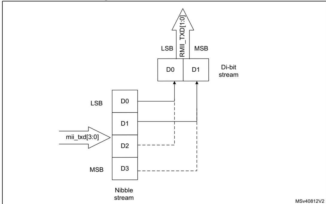
The diagram illustrates the mapping of a 4-bit nibble stream from the MII interface to a 2-bit di-bit stream on the RMII interface. On the left, a vertical stack of four boxes represents the nibble stream bits: D0 (LSB), D1, D2, and D3 (MSB). An arrow labeled
mii_txd[3:0]
points to this stack. Below the stack is the label "Nibble stream". On the right, a vertical stack of two boxes represents the di-bit stream: D0 (LSB) and D1 (MSB). An arrow labeled
RMII_TXD[1:0]
points upwards from this stack. To the right of this stack is the label "Di-bit stream". Solid lines connect the nibble bits to the di-bit bits: D0 (nibble) to D0 (di-bit) and D1 (nibble) to D1 (di-bit). Dashed lines connect the remaining nibble bits: D2 (nibble) to D0 (di-bit) and D3 (nibble) to D1 (di-bit).
MSV40812V2
Receive bit order
Each nibble is transmitted to the MII interface from the di-bit received from the RMII interface in the nibble transmission order shown in Figure 1054: Receive bit order . The lower order bits (D0 and D1) are received first, followed by the higher order bits (D2 and D3).
Figure 1054. Receive bit order
![Diagram illustrating the receive bit order. A 'Di-bit stream' from 'RMII_RXD[1:0]' (LSB to MSB) is shown entering a nibble stream. The nibble stream consists of four bits: D0, D1, D2, and D3. D0 and D1 are the lower order bits (LSB), and D2 and D3 are the higher order bits (MSB). The nibble stream is output as 'mii_rxd[3:0]'. The diagram shows the mapping of the di-bit stream to the nibble stream: D0 and D1 are received first, followed by D2 and D3. The nibble stream is output as mii_rxd[3:0].](/RM0486-STM32N6x5-x7/4285a8e6257d469600f2f840e70ed14d_img.jpg)
The diagram shows the receive bit order. At the top, a 'Di-bit stream' from 'RMII_RXD[1:0]' (LSB to MSB) is shown. Below this, a nibble stream is depicted with four bits: D0, D1, D2, and D3. D0 and D1 are labeled as 'LSB' (Least Significant Bit) and D2 and D3 as 'MSB' (Most Significant Bit). Arrows indicate the flow of data: D0 and D1 are received first, followed by D2 and D3. The nibble stream is output as 'mii_rxd[3:0]'. The diagram is labeled 'Nibble stream' at the bottom and 'MSv40813V2' in the bottom right corner.
76.6.4 Reduced gigabit media independent interface (RGMII)
The reduced gigabit media independent interface (RGMII) specification reduces the pin count of the interconnection between the MAC and the PHY for GMII and MII interfaces. To achieve this, the data path and control signals are reduced and multiplexed together with both edges of the transmit and receive clocks. For Gigabit operation, the clocks operate at 125 MHz; for 10/100 operation, the clock rates are 2.5/25 MHz.
The RGMII module is instantiated between the GMII of the MAC and the PHY to translate the control and data signals between the GMII and RGMII protocols. The RGMII block has the following characteristics:
- • Support of 10, 100 and 1000 Mbps operation rates.
- • No extra clock required since both edges of the incoming clocks are used.
- • Extraction of the in-band (link speed, link status, and duplex mode) status signals from the PHY and provides them to the MAC for link detection.
RGMI block diagram
Figure 1055: RGMI block diagram and interface signals shows the position of the RGMI block relative to the MAC and RGMI PHY. The RGMI block is placed between the GMII and the PHY to translate the GMII signals to RGMI signals.
Figure 1055. RGMI block diagram and interface signals
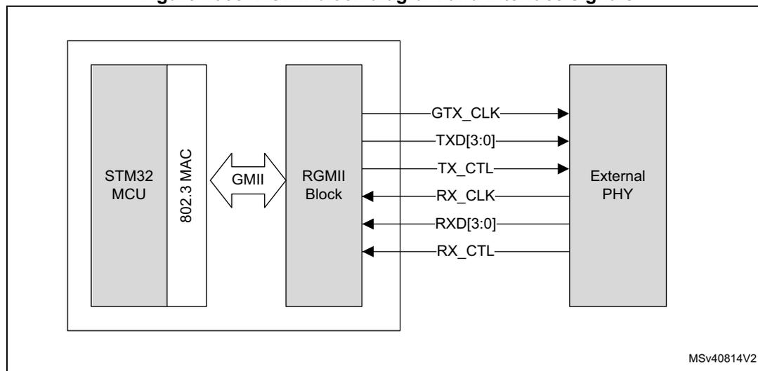
The diagram illustrates the internal architecture of an STM32 MCU and its external connections for Ethernet. Inside the MCU, the '802.3 MAC' block is connected to an 'RGMI Block' via a 'GMII' interface. The 'RGMI Block' is then connected to an 'External PHY' through a series of interface signals. The signals from the MAC to the RGMI Block are labeled 'GMII'. The signals between the RGMI Block and the External PHY are: GTX_CLK, TXD[3:0], TX_CTL, RX_CLK, RXD[3:0], and RX_CTL. The External PHY is shown as a separate block outside the MCU. The diagram is labeled 'MSv40814V2' in the bottom right corner.
- • Transmit path: this block translates all GMII transmit signals to RGMI signals. The block registers all GMII input signals at the rising edge of eth_gmii_gtx_clk and generates all RGMI transmit signals at the rising and falling edges of eth_gmii_gtx_clk.
- • Receive path: this block translates all RGMI receive signals to GMII receive signals. The block registers all RGMI input signals at the rising and falling edges of eth_rx_clk and generates all GMII receive signals at the rising edge of eth_rx_clk.
- • GTX_CLK: RGMI clock for Tx data transfers, 125 MHz, 25 MHz or 2.5 MHz
- • TXD[3:0]: transmit data
- • TX_CTL: multiplexing of TX_EN on the rising edge of GTX_CLK, and a logical XOR between TX_EN and TX_ER values on falling edge of GTX_CLK
- • RX_CLK: RGMI clock for Rx data transfers
- • RXD[3:0]: receive data
- • RX_CTL: after demultiplexing, this pin provides ETH_RX_DV on the rising edge of ETH_RX_CLK, and ETH_RX_ER (logical XOR between ETH_RX_CTL values on rising edge and falling edge of ETH_RX_CLK).
Signal conversion
The RGMII block performs data conversions in both directions.
Transmit data conversion
As defined in the RGMII specification, multiplexing of data and control in Gigabit mode is accomplished by using both edges of the Transmit clock. The RGMII block accepts the 8-bit GMII transmit data from the MAC GMII (gmii_txd[7:0]) on the rising edge of eth_gmii_gtx_clk. For Gigabit operation, the RGMII block then converts gmii_txd[7:0] to two 4-bit nibbles and transmits the data on the RGMII transmit data port (rgmii_txd_o[3:0]) as follows:
- • At the rising edge of eth_gmii_gtx_clk, rgmii_txd_o[3:0] contains gmii_txd[3:0]
- • At the falling edge of eth_gmii_gtx_clk, rgmii_txd_o[3:0] contains gmii_txd[7:4]
For 10/100 mode, the Transmit data to the PHY is 4 bits. Therefore, for 10/100 mode, the RGMII block drives the gmii_txd[3:0] data to the PHY on rgmii_txd_o[3:0] at the rising edge of eth_gmii_gtx_clk.
Receive data conversion
In 1000-Mbps mode, the RGMII block registers the 4-bit data on the rgmii_rxd_i[3:0] signal at both edges of the Receive clock (eth_rx_clk) and transfers the resulting 8-bit data to the MAC GMII on the rising edge of eth_rx_clk clock, as follows:
- • gmii_rxd[3:0] is the value received on rgmii_rxd_i[3:0] at the rising edge of eth_rx_clk
- • gmii_rxd[7:4] is the value received on rgmii_rxd_i[3:0] at the falling edge of eth_rx_clk
In 10/100 mode, the RGMII block registers the 4-bit data on rgmii_rxd_i[3:0] only at the rising edge of eth_rx_clk and transfers the data to the MAC GMII on the rising edge of eth_rx_clk, as follows:
- • gmii_rxd[3:0] is the value received on rgmii_rxd_i[3:0] at the rising edge of eth_rx_clk.
- • gmii_rxd[7:4] is 0x0.
76.7 Ethernet low-power modes
76.7.1 Low-power management
The Ethernet peripheral supports the following techniques to save power:
- • Magic packet
- • Remote wake-up
The magic packet and remote wake-up techniques are used to save power in the host system when it is in low-power mode, and has to be woken up only at the reception of specific packets from the Ethernet network. In low-power mode, the clocks on most of the host logic, along with the majority of the peripherals (except the MAC receiver logic), can be disabled. On receiving the specific packets from the network, the MAC generates the trigger to wake up the host system and come back to normal state. Refer to the power control (PWR) section of the reference manual for the list of the system operating modes that support Ethernet low-power modes.
The Energy Efficient Ethernet (EEE) mode is compliant with the IEEE 802.3az-2010 standard. It is primarily targeted to save power in the Ethernet port when there is no traffic on the line. In this mode, the host indicates to the far-end that it does not have any packets to transmit in the near future and puts the transmitter port (MAC controller, PCS and PHY
layers) in low-power mode. Similarly, the receiver port can also be put in low-power mode when the far-end host indicates that it does not have any traffic to transfer. This allows significant saving of power in the Ethernet port (mainly in the PHY) with intermittent and burst traffic profile. The triggering of entry and exit out of the EEE mode is controlled by the MAC and is supported within the peripheral.
Simultaneous operation of the EEE mode along with any or both the other power saving modes is also supported.
Description of magic packet mode
This section describes how to save power through magic packet detection.
Note: The magic packet feature is based on the magic packet technology white paper from Advanced Micro Device (AMD).
The watchdog timeout limit for a magic packet is 2,048 bytes irrespective of the value programmed in WD bit in Operating mode configuration register (ETH_MACCCR) and PWE bit in Watchdog timeout register (ETH_MACWTR).
In the magic-packet-based power saving mode, the reception of a valid magic packet by the MAC receiver triggers an exit from low-power mode. The MAC enters power saving mode when PWRDWN bit of PMT control status register (ETH_MACPCSR) is programmed to 1. Exit from the magic-packet-based power saving mode is enabled by setting the MGKPKTEN bit of PMT control status register (ETH_MACPCSR) to 1.
The magic packet contains a unique pattern at any offset after the Destination address, Source address, and Length/Type fields. In addition to the unique pattern matching, the MAC receiver also checks for the following, to detect the received packet as a valid magic packet:
- • The packet must be addressed to it (Destination Address of the received packet should perfect match the MAC address 0 high register (ETH_MACA0HR) and MAC Address 0 low register (ETH_MACA0LR) ) or with multicast/broadcast address.
- • The packet must not have any length error, FCS error, dribble bit error, GMII error, and collision.
- • The packet must not be runt (length including Ethernet header and FCS is at least 64 bytes).
Magic packet data format
The content of the unique pattern in magic packets is described as follows:
- • Six bytes of all-ones (0xFF FF FF FF FF FF) called synchronization stream. There can be more than six bytes of 0xFF, but only the last six are considered.
- • The synchronization stream is immediately followed by 16 repetitions of the Destination address field of the packet ( MAC address 0 high register (ETH_MACA0HR) and the MAC Address 0 low register (ETH_MACA0LR) ) or multicast/broadcast address.
- • No break or interruption between synchronization stream and first repetition of Destination address field or within its 16 repetitions.
If the MAC address of a node is 0x00 11 22 33 44 55, the MAC scans for the following data sequence:
Destination Address Source Address Length/Type..... FF FF FF FF FF FF
00 11 22 33 44 55 00 11 22 33 44 55 00 11 22 33 44 55 00 11 22 33 44 55
00 11 22 33 44 55 00 11 22 33 44 55 00 11 22 33 44 55 00 11 22 33 44 55
00 11 22 33 44 55 00 11 22 33 44 55 00 11 22 33 44 55 00 11 22 33 44 55
00 11 22 33 44 55 00 11 22 33 44 55 00 11 22 33 44 55 00 11 22 33 44 55
...CRC
Description of remote wake-up packet mode
This section describes the power saving mode based on remote wake-up packet.
Note: The remote wake-up packet feature implementation is based on the Device Class Power Management Reference Specification and various implementation-specific white papers. The watchdog timeout limit for a magic packet is 2,048 bytes irrespective of the value programmed in WD bit in Operating mode configuration register (ETH_MACCCR) and PWE bit in Watchdog timeout register (ETH_MACWTR).
In the remote-wake-up-magic-packet-based power saving mode, the reception of expected remote wake-up packet by the MAC receiver triggers the exit from low-power mode. The MAC enters power saving mode when PWRDWN bit in PMT control status register (ETH_MACPCSR) is programmed to 1. Exit from the remote-wake-up-magic-packet-based power saving mode is enabled by programming RWKPKTEN bit of PMT control status register (ETH_MACPCSR) to 1.
The MAC implements a filter lookup table (programmed through Remote wake-up packet filter register (ETH_MACRWKPFR) in which CRC, offset, and byte mask of the pattern embedded in remote wake-up packet and the filter operation commands are programmed.
The pattern embedded in the remote wake-up packet is located at any offset after the Destination address and Source address fields. In addition to the CRC match for the pattern, the MAC receiver also checks the following, to detect the received packet as a valid remote wake-up packet:
- • The packet must be addressed to it (Destination Address of the received packet should perfect match the MAC address 0 high register (ETH_MACA0HR) and MAC Address 0 low register (ETH_MACA0LR)) or with multicast/broadcast address.
- • The packet must not have any length error, FCS error, dribble bit error, GMII error, and collision.
- • The packet must not be runt (length including Ethernet header and FCS is at least 64 bytes).
When a valid remote wake-up packet is received, the MAC receiver sets the RWKPRCVD bit in PMT control status register (ETH_MACPCSR) and triggers the interrupt on pmt_intr_o output port. The PMTIS bit in Interrupt status register (ETH_MACISR) is set when power-gating is not enabled in low-power mode. An interrupt is triggered to the application on the sbd_intr_o output port when interrupt is enabled (PMTIE bit in Interrupt enable register (ETH_MACIER) is set) and CSR clock is not gated off in low-power mode.
Remote wake-up packet filters
When the remote-wake-up-based power saving mode is enabled, four remote wake-up filters can be selected. The structure of the remote wake-up filters is shown in Table 817: Remote wake-up packet filter register.
Table 817. Remote wake-up packet filter register
| ETH_MACRWKPFR value | Field | |||||||
|---|---|---|---|---|---|---|---|---|
| 0 | Filter 0 byte mask | |||||||
| 1 | Filter 1 byte mask | |||||||
| 2 | Filter 2 byte mask | |||||||
| 3 | Filter 3 byte mask | |||||||
| 4 | Reserved | Filter 3 command | Reserved | Filter 2 command | Reserved | Filter 1 command | Reserved | Filter 0 command |
| 5 | Filter 3 offset | Filter 2 offset | Filter 1 offset | Filter 0 offset | ||||
| 6 | Filter 1 CRC - 16 | Filter 0 CRC - 16 | ||||||
| 7 | Filter 3 CRC - 16 | Filter 2 CRC - 16 | ||||||
The remote wake-up filter fields are described in Table 818: Description of the remote wake-up filter fields .
Table 818. Description of the remote wake-up filter fields
| Register | Description |
|---|---|
| Filter i Byte mask | The filter i byte mask register defines the bytes of the packet that are examined by filter i (0, 1, 2 or 3) to determine whether or not a packet is a wake-up packet.
|
| Filter i Command | The 4-bit filter i command controls the filter i operation.
|
Table 818. Description of the remote wake-up filter fields (continued)
| Register | Description |
|---|---|
| Filter i Offset | This filter i offset register defines the offset (within the packet) from which the filter i examines the packets.
|
| Filter i CRC-16 | This filter i CRC-16 register contains the CRC_16 value calculated from the pattern and also the byte mask programmed to the wake-up filter register block.
The pointer and the mask are used together to locate the bytes to be used in the CRC16 calculations. |
- 1. The And_ Previous bit setting is applicable within a set of four filters. Setting And_ Previous bit of a filter that is not enabled has no effect, that is setting And_ Previous bit of lowest number filter in the set of four filters has no effect. For example, setting And_ Previous bit of Filter 0 has no effect. If And_ Previous bit is set for a given filter to form an AND chained filter, the AND chain breaks when it finds a disabled filter. For example: If Filter 2 And_ Previous bit is set (bit 1 in Filter 2 command is set) but Filter 1 is not enabled (bit 0 in Filter 1 command is reset), then only Filter 2 result is considered. If Filter 2 And_ Previous bit is set (bit 1 in Filter 2 command is set), Filter 3 And_ Previous bit is set (bit 1 in Filter 3 command is set), but Filter 1 is not enabled (bit 0 in Filter 1 command is reset), then only Filter 2 result ANDed with Filter 3 result is considered. If Filter 2 And_ Previous bit is set (bit 1 in Filter 2 command is set), Filter 3 And_ Previous bit is set (bit 1 in Filter 3 command is set), but Filter 2 is not enabled (bit 0 in Filter 2 command is reset), then since setting Filter 2 And_ Previous bit has no effect, only Filter 1 result ORed with Filter 3 result is considered.
If filters chained by And_ Previous bit setting have complementary programming, then a frame may never pass the AND chained filter. For example, if Filter 2 And_ Previous bit is set (bit 1 in Filter 2 command is set), Filter 1 Address_Type bit is set (bit 3 in Filter 1 command is set) indicating multicast detection and Filter 2 Address_Type bit is reset (bit 3 in Filter 2 command is reset) indicating unicast detection or vice versa, then a remote wake-up frame does not pass the AND chained filter as a remote wake-up frame cannot be of both unicast and multicast address types.
The remote wake-up filter registers are implemented as eight indirect access registers (wkuppktfilter_reg#i) for four remote wake-up filters, and accessed by the application through Remote wake-up packet filter register (ETH_MACRWKPFR) . The entire set of wkuppktfilter_reg registers must be written to program the remote wake-up filters. The wkuppktfilter_reg register is programmed by sequentially writing the eight register values in Remote wake-up packet filter register (ETH_MACRWKPFR) for wkuppktfilter_reg0 to wkuppktfilter_reg3, respectively. The wkuppktfilter_reg register is read in a similar way. The MAC updates the wkuppktfilter_reg register current pointer value in RWKPTR field of PMT control status register (ETH_MACPCSR) .
Note: If the Remote wake-up packet filter register (ETH_MACRWKPFR) is accessed in byte or half-word mode, the internal counter to access the appropriate wkuppktfilter_reg is incremented when the CPU accesses Lane 3.
When Remote wake-up packet filter register (ETH_MACRWKPFR) is written, the content is transferred from CSR clock domain to PHY receive clock domain after the write operation. There should not be any further write to the Remote wake-up packet filter register (ETH_MACRWKPFR) until the first write is updated in PHY receive clock domain. Otherwise, the second write operation does not get updated to the PHY receive clock domain. Therefore, the delay between two write operations to the Remote wake-up packet filter register (ETH_MACRWKPFR) should be at least 4 cycles of the PHY receive clock.
PMT interrupt
The PMT interrupt signal is asserted when a valid remote wake-up packet is received.
Table 819 lists the remote wake-up scenarios in which PMT interrupt is generated.
Table 819. Remote wake-up packet and PMT interrupt generation (1)
| Filter i Command | Frame Type and CRC Status | Interrupt Generation | |||
|---|---|---|---|---|---|
| CAST | INV | EN | Received Frame Cast Type | CRC Status | RWK INTR |
| 0 | 0 | 1 | Unicast | MATCH | Remote Wake-up packet is detected and PMT interrupt is generated |
| 0 | 1 | 1 | Unicast | MISMATCH | Remote Wake-up packet is detected and PMT interrupt is generated |
| 1 | 0 | 1 | Multicast | MATCH | Remote Wake-up packet is detected and PMT interrupt is generated |
| 1 | 1 | 1 | Multicast | MISMATCH | Remote Wake-up packet is detected and PMT interrupt is generated |
- 1. In all other combinations, the Remote Wake-up packet is not detected and PMT interrupt is not generated.
In addition to
sbd_intr_o
signal, the
pmt_intr_o
(synchronous to Rx clock) signal is asserted. The
pmt_intr_o
signal, synchronous to the Rx clock domain, is provided so that the application clock can be stopped by software when the MAC is in the power-down mode. It is ORed with
lpi_intr_o
signal (see
Section : LPI interrupt
) and tied to the EXTI peripheral.
As the
pmt_intr_o
signal is generated in the PHY Rx clock domain, it is not cleared immediately when the
PMT control status register (ETH_MACPCSR)
is read. This is because the resultant clear signal has to cross to the PHY Rx clock domain, and then clear the interrupt source. This delay is at least 4 clock cycles of Rx clock and can be significant when the peripheral is operating in the 10 Mbit/s mode. When the application clears the PWRDWN bit in
Remote wake-up packet filter register (ETH_MACRWKPFR)
, the MAC comes out of the power-down mode, but this event does not generate the PMT interrupt.
Power-down sequence
The software must perform the following tasks to initiate the power-down sequence:
- • Disable the Transmit DMA (if applicable) by clearing the ST bit of the Channel x transmit control register (ETH_DMAxCxTXCR) .
- • Wait for any previous frame transmissions to complete. You can check this by reading TFCSTS[1:0] and TPESTS bits in Debug register (ETH_MACDR) and TXQSTS bit in Tx queue x debug register (ETH_MTLTXQxDR) of all MTL Tx Queues.
- • Disable the MAC transmitter and MAC receiver by clearing TE and RE bits in Operating mode configuration register (ETH_MACCR) .
- • Wait till the Receive DMA empties all frames from the Rx FIFO. You can check this by reading PRXQ[13:0] in Rx queue x debug register (ETH_MTLRXQxDR) of all Rx Queues. If these bits are zero, it indicates that the Rx FIFO is empty.
- • Configure the magic packet (MGKPKTEN) and/or remote wake-up (RWKPKTEN) detection in the PMT control status register (ETH_MACPCSR) .
- • Set bit 31 (ARPEN) in the Operating mode configuration register (ETH_MACCR) .
- • Enable the MAC receiver by setting RE bit and then set PWRDOWN bit in the PMT control status register (ETH_MACPCSR) to initiate the power-down sequence in MAC.
Note: If the feature is enabled and the MAC transmitter is in the LPI mode when it is put into the power-down mode, then the MII interface gets clamped to assert the LPI pattern. If the MAC transmitter is not in the LPI mode when it is put into the power-down mode, the GMII or MII interface gets clamped to all-zero.
Power-up sequence
The MAC wakes up on receiving the magic packet or remote wake-up frame. The power-up sequence is as follows:
- • The MAC asserts pmt_intr_o. When only clock-gating is employed in low-power mode, the pmt_intr_o signal can be used to start the clocks that were gated-off after entering low-power mode.
- • The software performs the following tasks:
- – De-assert the pmt_intr_o by reading the PMT control status register (ETH_MACPCSR) .
- – Perform a write operation (with reset values) to the PMT control status register (ETH_MACPCSR) and the Remote wake-up packet filter register (ETH_MACRWKPFR) so that the corresponding values in the always-on block gets synchronized. Otherwise, the values of these registers are different.
- – Perform write operations to the Operating mode configuration register (ETH_MACCR) , MAC address 0 high register (ETH_MACA0HR) and MAC Address 0 low register (ETH_MACA0LR) to synchronize the values in the CSR module and the respective bits in the always-on block. Otherwise, the MAC receiver is on even though the Receive Enable bit is set to 0.
After completing these steps, the software must initialize all registers, enable the transmitter, and program the DMA (in DMA configurations) to resume the normal operation.
76.7.2 Energy-efficient Ethernet (EEE)
EEE is an operational mode that enables the IEEE 802.3 Media Access Control (MAC) sublayer along with a family of physical layers to operate in Low-power idle (LPI) mode. The
EEE operational mode supports the IEEE 802.3 MAC operation at 100 Mbit/s and 1000 Mbps. The peripheral supports the IEEE 802.3az-2010 for EEE.
The LPI mode allows saving power by switching off the parts of the communication device functionality when there is no data to be transmitted and received. The systems on both sides of the link can disable some functionalities to save power during the periods of low-link utilization. The MAC controls whether the system should enter or exit the LPI mode and communicates this to the PHY.
The EEE specifies the capabilities negotiation methods that the link partners can use to determine whether EEE is supported, and then select the set of parameters that are common to both devices.
Transmit path functions
The transmit path functions include tasks that the MAC must perform to make the PHY enter the LPI state.
In the transmit path, the software must set the LPIEN bit of the LPI control and status register (ETH_MACLCSR) to indicate to the MAC to stop transmission and initiate the LPI protocol. The MAC completes the transmission in progress, generates its transmission status, and starts transmitting the LPI pattern instead of the IDLE pattern if the link status has been up continuously for a period specified in the LPI LS TIMER LST[9:0] bitfield of LPI timers control register (ETH_MACLTCR) . The PHY Link Status PLS bit of the LPI control and status register (ETH_MACLCSR) indicates the link status of the PHY.
Note: The EEE feature is not supported when the MAC is configured to use the RMII.
According to the standard (IEEE 802.3az-2010), the PHY must not stop the TxCLK clock during the LPI state in the MII (10 or 100) mode. However, the MAC can stop the GTX_CLK clock during the LPI state in the GMII (1000) mode.
To make the PHY enter the LPI state, the MAC performs the following tasks:
- 1. De-asserts TX_EN.
- 2. Asserts TX_ER.
- 3. Sets TXD[3:0] to 0x1 (for 100 Mbit/s) or TXD[7:0] to 0x01 (for 1,000 Mbps).
- 4. Updates the status (TLPIEN bit of LPI control and status register (ETH_MACLCSR) ) and generates an interrupt.
Note: The MAC maintains the same state of the TX_EN, TX_ER, and TXD signals for the entire duration during which the PHY remains in the LPI state.
To bring the PHY out of the LPI state, that is when the software resets the LPIEN bit, the MAC performs the following tasks:
- 1. Stops transmitting the LPI pattern and starts transmitting the IDLE pattern.
- 2. Starts the LPI TW TIMER:
The MAC cannot start the transmission until the wake-up time specified for the PHY expires. The auto-negotiated wake-up interval is programmed in the TWT field of the LPI timers control register (ETH_MACLTCR) . - 3. Updates the LPI exit status (TLPIEX bit of the LPI control and status register (ETH_MACLCSR) ) and generates an interrupt.
Figure 1056 shows the behavior of TX_EN, TX_ER, and TXD[3:0] signals during the LPI mode transitions.
Note: The MAC does not stop the TX_CLK clock. The application can stop this clock (as shown in Figure 1056) if the PHY supports it and when the MAC sets the sbd_tx_clk_gating_ctrl_o signal to 1. The sbd_tx_clk_gating_ctrl_o signal is asserted after nine Tx Clock Cycles, one Pulse Synchronizer delay, and one CSR clock cycle. The assertion of the sbd_tx_clk_gating_ctrl_o signal depends on the LPITCSE bit of the LPI control and status register (ETH_MACLCSR) and can be done automatically as shown on Figure 1057.
If RGMII Interface is selected, the Tx clock is required for transmitting the LPI pattern and so the Tx Clock cannot be gated.
If the MAC is in the Tx LPI mode and the Tx clock is stopped, the application should not write to CSR registers that are synchronized to Tx clock domain.
If the MAC is in the LPI mode and the application issues a soft reset or hard reset, the MAC transmitter comes out of the LPI mode.
Figure 1056. LPI transitions (Transmit, 100 Mbs)
![Timing diagram for LPI transitions (Transmit, 100 Mbs) showing signals sbd_tx_clk_gating_ctrl_o, TX_CLK, TX_EN, TXD [3:0], TX_ER, and PLS_CARRIER indication over time.](/RM0486-STM32N6x5-x7/8bfcb76ab3f53016bf8ae87f3e99983c_img.jpg)
The diagram illustrates the timing for LPI transitions during transmission at 100 Mbps. It shows the relationship between several signals over time:
- sbd_tx_clk_gating_ctrl_o: A signal that goes high to gate the TX_CLK. A double slash indicates a delay. A horizontal double-headed arrow labeled "≥ 9 cycles" shows the time from the assertion of this signal to the stopping of TX_CLK.
- TX_CLK: A clock signal that stops when sbd_tx_clk_gating_ctrl_o is high. It resumes when the signal goes low.
- TX_EN: Transmit Enable signal. It goes high when data transmission begins.
- TXD [3:0]: Data lines. They show a value of "0x1" during active transmission and a sequence of "x x x x" (LPI pattern) when exiting LPI mode.
- TX_ER: Transmit Error signal. It goes low to "Enter LPI mode" and high to "Exit LPI mode".
- PLS_CARRIER indication: A dashed line with triangle markers. "CARRIER_ON" is indicated when TX_EN is high, and "CARRIER_OFF" is indicated when TX_EN is low. A horizontal double-headed arrow labeled "Wake Time" indicates the duration from the start of the LPI pattern until the carrier is off.
Figure 1057. LPI Tx clock gating (when LPITCSE = 1)
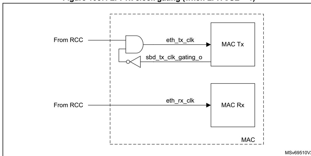
Automated entry/exit from LPI mode in transmit path
The MAC transmitter can be programmed to enter and exit LPI Idle mode automatically based on whether it is Idle for a specific period of time or has a packet to transfer. These modes are enabled and controlled by the LPI control and status register (ETH_MACLCSR) .
When LPITXA and LPIEN of LPI control and status register (ETH_MACLCSR) are set, the MAC transmitter enters LPI Idle state when the MAC transmit path (including the MTL layers and DMA layers) are idle. The MAC transmitter exits the LPI Idle state and clears the LPITXEN bit as soon as any of functions in the TX path (DMA, MTL or MAC) becomes non-idle due to initiation of a packet transfer.
In addition, when LPITE is also set, the MAC transmitter enters LPI Idle state only if the Transmit path remains in idle state (no activity) for the time period indicated by the value in LPI entry timer register (ETH_MACLETR) . In this mode also, the MAC transmitter exits the LPI Idle state as soon as any of the functions becomes non-idle. However, the LPIEN bit is not cleared but remains active so that reentry to LPI Idle state is possible without any software intervention when the MAC becomes idle again.
When both LPITE and LPITXA bits are cleared, the application can directly control the entry and exit of LPI Idle state by programming the LPIEN bit.
Receive path functions
The receive path functions include the tasks that the PHY and MAC must perform when the PHY receives signals from the link partner to exit the LPI state.
In the receive path, when the PHY receives the signals from the link partner to enter into the LPI state, the PHY and MAC perform the following tasks:
- 1. The PHY asserts RX_ER.
- 2. The PHY sets RXD[3:0] to 0x1 (for 100 Mbit/s) or RXD[7:0] to 0x01 (for 1,000 Mbps).
- 3. The PHY de-asserts RX_DV.
- 4. The MAC updates the RLPIEN bit of the LPI control and status register (ETH_MACLCSR) and immediately generates an interrupt.
Note: The PHY maintains the same state of the RX_ER, RXD, and RX_DV signals for the entire duration during which it remains in the LPI state.
If the LPI pattern is detected for a very short duration (that is, less than two cycles of Rx clock), the MAC does not enter the Rx LPI mode.
If the duration between the end of the current Rx LPI pattern and the start of the next Rx LPI pattern is very short (that is, less than two Rx clock cycles), then the MAC exits and enters again the Rx LPI mode. The MAC does not trigger the Rx LPI Exit and Entry interrupts.
When the PHY receives signals from the link partner to exit the LPI state, the PHY and MAC perform the following tasks:
- 1. The PHY de-asserts RX_ER and returns to a normal inter-packet state.
- 2. The MAC updates the RLPIEX bit of the LPI control and status register (ETH_MACLCSR) and generates an interrupt immediately. The sideband signal lpi_intr_o (synchronous to Rx clock) is also asserted.
Figure 1058 shows the behavior of RX_ER, RX_DV, and RXD[3:0] signals during the LPI mode transitions.
Figure 1058. LPI transitions (receive, 100 Mbit/s)
![Timing diagram showing LPI transitions for RX_CLK, RX_DV, RXD[3:0], and RX_ER signals. The diagram illustrates the 'Enter LPI mode' and 'Exit LPI mode' events. RX_CLK is shown as a series of pulses that stop during the LPI mode. RX_DV is a constant high signal. RXD[3:0] shows a sequence of 'xx xx xx 0x1' followed by 'xx xx xx xx' during the LPI mode. RX_ER is a signal that goes high when entering LPI mode and goes low when exiting LPI mode. A double slash indicates a break in the timeline between the two LPI patterns. A horizontal double-headed arrow above the RX_CLK signal indicates a duration of '≥ 9 cycles' between the start of the first LPI pattern and the start of the second LPI pattern.](/RM0486-STM32N6x5-x7/e243ad554bd2dd3f1fcab7fb0823cbe1_img.jpg)
Note: If the RX_CLK_stoppable bit (in the PHY register written through MDIO) is asserted when the PHY is indicating LPI to the MAC, the PHY may halt the RX_CLK at any time more than nine clock cycles after the start of the LPI state as shown in Figure 1058 .
If the MAC is in LPI mode and the application issues a soft reset or hard reset, the MAC receiver exits from LPI mode during reset. If the LPI pattern is still received after the reset is de-asserted, the MAC receiver enters again the LPI state.
If the RX clock is stopped in the RX LPI mode, the application should not write to the CSR registers that are being synchronized to the RX clock domain.
When the PHY sends the LPI pattern, if EEE feature is enabled, the MAC automatically enters the LPI state. There is no software control to prevent the MAC from entering the LPI state.
LPI timers
The transmitter maintains the LPI LS TIMER, LPI TW TIMER, and LPI AUTO ENTRY TIMER timers.
The following LPI timers are loaded with the respective values from the LPI timers control register (ETH_MACLTCR) and LPI entry timer register (ETH_MACLETR) :
- • LPI LS TIMER
The LPI LS TIMER counts, in milliseconds, the time expired since the link status is up. You can enable the monitoring of the LUD bit of the PHYIF control status register (ETH_MACPHYCSR) by setting the PLSEN bit of LPI control and status register (ETH_MACLCSR) .
The link status is indicated to the MAC by the LNKSTS bit of the PHYIF control status register (ETH_MACPHYCSR) or the value programmed by the software in the PLS bit of the LPI control and status register (ETH_MACLCSR) . If the link status is not available in the PHYIF control status register (ETH_MACPHYCSR) , the software should get the PHY link status by reading the PHY register and accordingly update the PLS bit.
This timer is cleared every time the link goes down. It starts to increment when the link is up again and continues to increment until the value of the timer becomes equal to the terminal count. Once the terminal count is reached, the timer remains at the same value as long as the link is up. The terminal count is the value programmed in the LST[9:0] bitfield in the LPI timers control register (ETH_MACLTCR) . The GMII interface does not assert the LPI pattern unless the terminal count is reached. This ensures a minimum time for which no LPI pattern is asserted after a link is established with the remote station. This period is defined as 1 second in the IEEE 802.3-az-2010. The LPI LS TIMER is 10-bit wide. The software can program up to 1023 milliseconds.
- • LPI TW TIMER
The LPI TW TIMER counts, in microseconds, the time expired since the de-assertion of LPI. The terminal count should be programmed in Bit[15:0] of LPI timers control register (ETH_MACLTCR) . The terminal count of the timer is the value of resolved Transmit TW that is the auto-negotiated time after which the MAC can resume the normal transmit operation. After exiting the LPI mode, the MAC resumes its normal operation after the TW timer reaches the terminal count.
The MAC supports the LPI TW TIMER in units of microsecond. The LPI TW TIMER is 16-bit wide. Therefore, the software can program up to 65535 micro seconds.
- • LPI AUTO ENTRY TIMER
This timer counts in steps of eight microseconds, the time for which the MAC transmit path has to remain in idle state (no activity), before the MAC transmitter enters the LPI IDLE state and starts transmitting the LPI pattern. This timer is enabled when LPITE bit in LPI control and status register (ETH_MACLCSR) is set.
Note: Program the PLS bit of LPI control and status register (ETH_MACLCSR) to 1'b0 before switching between the GMII and MII modes. This resets the internal timers. If the mode is changed after the LPI LS TIMER or LPI TW TIMER starts, the change in the Tx clock frequency can result in incorrect timeout.
LPI interrupt
The MAC generates the LPI interrupt when the Tx or Rx side enters or exits the LPI state. The interrupt sbd_intr_o is asserted when the LPI interrupt status is set. The LPI interrupt can be cleared by reading the LPI control and status register (ETH_MACLCSR) .
When the MAC exits the Rx LPI state, then in addition to the
sbd_intr_o
, the sideband signal
lpi_intr_o
(synchronous to Rx clock) is asserted. The
lpi_intr_o
signal can be used to trigger the external clock-gating circuitry to restore the application clock to the MAC. The
lpi_intr_o
signal, synchronous to the Rx clock domain, is provided so that the application clock can be stopped by software when the MAC is in the LPI state. It is ORed with
pmt_intr_o
signal (see
Section : PMT interrupt
) and tied to the EXTI peripheral.
The
lpi_intr_o
signal is generated in the Rx clock domain. It may not be cleared immediately after the
LPI control and status register (ETH_MACLCSR)
is read. This is because the clear signal, generated in CSR clock domain, has to cross the Rx clock domain, and then clear the interrupt source. This delay is at least four clock cycles of Rx clock and can be significant when the peripheral is operating in the 10 Mbit/s mode.
Programming guidelines for Energy Efficient Ethernet
For detailed guidelines on the programming guidelines, see Section 76.9.13: Programming guidelines for Energy Efficient Ethernet (EEE) on page 4139 .
76.8 Ethernet interrupts
The Ethernet peripheral generates a single interrupt signal (eth_sbd_intr_it). This signal can be raised as a result of various events. These events are captured in status registers and interrupt enables are provided for each source of interrupt such that the interrupt signal is asserted for an event only when the corresponding interrupt enable is set.
The interrupt status and corresponding enable registers are organized in a hierarchical manner so that it is easier for software to traverse and identify the source of interrupt event quickly. When interrupt is asserted, the Interrupt status register (ETH_DMAISR) register is first level that indicates the major blocks for the interrupt event source. This register is read-only, and it contains bits corresponding to each DMA channel (TX & RX pair), the MTL, and the MAC. The software application must then read one (or more) of the following registers corresponding to the bits that are set:
- • ETH_DMAC0SR: channel 0 status (see Channel x status register (ETH_DMACxSR) )
- • ETH_DMAC1SR: channel 1 status (see Channel x status register (ETH_DMACxSR) )
- • ETH_MTLISR: interrupt status (see Interrupt status register (ETH_MTLISR) )
- • ETH_MACISR: interrupt status (see Interrupt status register (ETH_MACISR) )
76.8.1 DMA interrupts
Interrupt registers description
The ETH_DMAC0SR: Channel 0 Status register (see Channel x status register (ETH_DMACxSR) ) captures all the interrupt events of that TxDMA and RxDMA channel. The ETH_DMAC0IER: Channel 0 Interrupt Enable register (see Channel x interrupt enable register (ETH_DMACxIER) ) contains the corresponding enable bits for each of the interrupt event.
There are two groups of interrupts in the DMA channel namely Normal and Abnormal interrupts. They are indicated by Bits[15:14] of ETH_DMAC0SR register respectively. The normal group is for events that happen during the normal transfer of packets (TI: transmit interrupt, RI: receive interrupt, TBU: Transmit buffer unavailable) while the abnormal interrupt events are for error events.
Interrupts are not queued. If the same interrupt event occurs again before the driver responds to the previous one, no additional interrupts are generated. An interrupt is generated only once for multiple events. The driver must scan the Interrupt status register (ETH_DMAISR) for the cause of the interrupt and clear the source in the respective Status register. The interrupt is cleared only when all the bits of Interrupt status register (ETH_DMAISR) are cleared.
Periodic scheduling of transmit and receive interrupt
It is not preferable to generate interrupts for every packet transferred by DMA (RI and TI) for system throughput performance reasons. The Ethernet peripheral gives the flexibility to schedule the interrupt at regular intervals using two methods:
- 1. Set Interrupt on Completion bit in Transmit descriptor (TDES2[31] in Table 823: TDES2 normal descriptor (read format) ) once for every “required” number of packets to be transmitted.
- 2. Similarly, set the IOC (RDES3[30] in Table 836: RDES3 normal descriptor (read format) ) bit only at some specific intervals of Receive descriptors. This way, whenever
a received packet transfer to system memory is complete and any of the descriptors used for that packet transfer has the IOC bit set, only then the RI event is generated.
In addition to above, an interrupt timer (ETH_DMACxRXIWTR: Channel i Rx Interrupt Watchdog Timer) is given for flexible control and periodic scheduling of Receive interrupt. When this interrupt timer is programmed with a nonzero value, it gets activated as soon as the Rx DMA completes a transfer of a received packet to system memory without asserting the Receive interrupt because the corresponding interrupt of completion IOC bit (RDES3[30] in Table 836: RDES3 normal descriptor (read format) ) is not set. When this timer runs out as per the programmed value, RI bit is set and the interrupt is asserted if the corresponding RIE is enabled in ETH_DMAC0IER register (see Channel x interrupt enable register (ETH_DMACxIER) ). The timer is stopped and cleared before it expires, if the RI is set for a packet transfer whose descriptor's IOC was set. The timer is reactivated automatically after the next packet transfer is complete without the RI event being generated.
Per channel transfer complete interrupt
The Transmit Transfer complete interrupt (TI) and Receive Transfer complete interrupt (RI) is reflected in the Channel Status register ( Channel x status register (ETH_DMACxSR) ). The TI bit is set whenever the Tx DMA channel closes the descriptor in which the IOC bit is set (Interrupt On Completion - TDES2[31]). Similarly, the RI bit is set whenever the Rx DMA channel closes the descriptor with the LD bit set and, in any of the descriptors used for transferring that packet, IOC bit is set (Interrupt Enable on completion - RDES3[30]).
The interrupt signal is asserted for the Transfer complete interrupts only when the corresponding interrupts are enabled in the channel interrupt enable register ( Channel x interrupt enable register (ETH_DMACxIER) ).
The behavior of the RI/TI interrupts changes depending on the settings of INTM field (bits[17:16]) in the ETH_DMAMR register ( DMA mode register (ETH_DMAMR) ). Table 820 explains the behavior of the Transfer Complete interrupt.
Table 820. Transfer complete interrupt behavior
| Interrupt mode | Behavior of TI/RI and eth_sbd_intr_it |
|---|---|
| INTM=0 | The TI/RI status signals are set whenever the Transfer complete event is detected. The bits get cleared whenever the software driver writes 1 to these bits. The eth_sbd_intr_it is asserted whenever the corresponding interrupts are also enabled in ETH_DMACxIER register. |
| INTM=1 | The TI/RI is set as explained above. However, the eth_sbd_intr_it is not asserted for any RI/TI events. |
| INTM=2 | The RI/TI status bits are set whenever the Transfer Complete event is detected and gets reset whenever software driver clears those bits by writing 1. However, if another Transfer Complete event is detected before it is cleared (serviced) by the software, these status bits is automatically set again. However, the eth_sbd_intr_it is not generated based on TI/RI. |
76.8.2 MTL interrupts
MTL interrupt events are combined with the events in the DMA to generate the interrupt signal.
The register Interrupt status register (ETH_MTLISR) report the queue number responsible for the event. ETH_MTLQ0ICSR: Queue 0 Interrupt Control Status or ETH_MTLQ1ICSR: Queue 1 Interrupt Control Status must be read for event description.
The MTL interrupts are enabled by default. Each event can be prevented from asserting the interrupt by setting the corresponding mask bits in the Interrupt status register (ETH_MTLISR) register.
MTL interrupt signal is driven by one of these events on Queue 0 and Queue 1:
- • Receive Queue Overflow Interrupt
- • Transmit Queue Underflow
76.8.3 MAC interrupts
MAC interrupt events are combined with the events in the DMA to generate the interrupt signal.
The MAC interrupts are of level type, that is, the interrupt remains asserted (high) until it is cleared by the application or software.
The Interrupt status register (ETH_MACISR) describes the events that can cause an interrupt from the MAC. The MAC interrupts are enabled by default. Each event can be prevented from asserting the interrupt by setting the corresponding mask bits in the Interrupt status register (ETH_MACISR) .
The interrupt register bits only indicate the block from which the event is reported. You must read the corresponding status registers and other registers to clear the interrupt.
MAC interrupt signal is driven by one of these events:
- • Receive status interrupt
- • Transmit status interrupt
- • Timestamp interrupt status
- • MMC interrupt status
- – MMC receive checksum offload interrupt status
- – MMC transmit interrupt status
- – MMC Receive interrupt status
- • LPI interrupt status
- • PMT interrupt status
- • PHY interrupt
- • RGMII interrupt status
Note: Two sidebands signals are generated together with LPI and PMT interrupts: lpi_intr_o and pmt_intr_o. They are used for wake-up event detection at EXTI level.
76.9 Ethernet programming model
This chapter provides the instructions for initializing the DMA or MAC registers in the proper sequence. It contains the following sections:
- • DMA initialization (see Section 76.9.1 )
- • MTL initialization (see Section 76.9.2 )
- • MAC initialization (see Section 76.9.3 )
- • Performing normal receive and transmit operation (see Section 76.9.4 )
- • Stopping and starting transmission (see Section 76.9.5 )
- • Programming guidelines for multichannel multiqueue operation (see Section 76.9.8 )
- • Programming guidelines for GMII link state transitions (see Section 76.9.9 )
- • Programming guidelines for IEEE 1588 timestamping (see Section 76.9.10 )
- • Programming guidelines for AV feature (see Section 76.9.12 )
- • Programming guidelines for energy-efficient Ethernet (see Section 76.9.13 )
- • Programming guidelines for flexible pulse-per-second (PPS) output (see Section 76.9.14 )
- • Programming guidelines for IEEE 1588 auxiliary snapshot (see Section 76.9.15 )
- • Programming guidelines for TSO (see Section 76.9.16 )
- • Programming guidelines for VLAN filtering on the receiver (see Section 76.9.17 )
- • Programming guidelines for extended VLAN filtering and routing on reception (see Section 76.9.18 )
- • Programming guidelines for queue/channel-based VLAN inclusion register (see Section 76.9.19 )
- • Programming guidelines for EST (see Section 76.9.20 )
- • Programming the launch time in time-based scheduling (see Section 76.9.21 )
- • Enabling the frame preemption function (see Section 76.9.22 )
76.9.1 DMA initialization
Complete the following steps to initialize the DMA:
- 1. Provide a software reset to reset all MAC internal registers and logic (bit 0 of DMA mode register (ETH_DMAMR) ).
- 2. Wait for the completion of the reset process (poll bit 0 of the DMA mode register (ETH_DMAMR) , which is cleared when the reset operation is completed).
- 3. Program the following fields to initialize the
System bus mode register (ETH_DMASBMR)
:
- a) AAL, ONEKBBE, RD_OSR_LMT, and WR_OSR_LMT
- b) Fixed burst or undefined burst
- c) Outstanding requests limit value (OSR_LMT).
- d) If fixed length value is enabled, select the maximum burst length possible on the AXI Bus (bits [7:1])
- 4. Create a transmit and a receive descriptor list. In addition, ensure that the receive descriptors are owned by the DMA (set bit 31 of TDES3/RDES3 descriptor). For more information on descriptors, refer to Section 76.10: Descriptors .
Note: Descriptor address from start to end of the ring should not cross the 4GB boundary.
- 5. Program ETH_DMAC0TXRLR and ETH_DMAC0RXRLR registers (see Channel x Tx descriptor ring length register (ETH_DMACxTXRLR) and Channel x Rx descriptor ring length register (ETH_DMACxRXRLR) ). The programmed ring length must be at least 4.
- 6. Initialize receive and transmit descriptor list address with the base address of transmit and receive descriptor ( Channel x Tx descriptor list address register (ETH_DMACxTXDLAR) , Channel x Rx descriptor list address register (ETH_DMACxRXDLAR) ). In addition, program the transmit and receive tail pointer registers that inform the DMA about the available descriptors (see Channel x Tx descriptor tail pointer register (ETH_DMACxTXDTPR) and Channel x Rx descriptor tail pointer register (ETH_DMACxRXDTPR) ).
- 7. Program ETH_DMAC0CR, ETH_DMAC0TXCR and ETH_DMAC0RXCR registers (see Channel x control register (ETH_DMACxCR) , Channel x transmit control register (ETH_DMACxTXCR) and Channel x receive control register (ETH_DMACxRXCR) ) to configure the parameters such as the maximum burst-length (PBL) initiated by the DMA, descriptor skip lengths, OSP for TxDMA, RBSZ[13:0] for RxDMA, and so on.
- 8. Enable the interrupts by programming the ETH_DMAC0IER register (see Channel x interrupt enable register (ETH_DMACxIER) ).
- 9. Start the Receive and Transmit DMAs by setting SR (bit 0) of Channel x receive control register (ETH_DMACxRXCR) and ST (bit 0) of the ETH_DMAC0TXCR (see Channel x transmit control register (ETH_DMACxTXCR) ).
- 10. Repeat steps 4 to 9 for all the Tx DMA channels selected in the hardware.
76.9.2 MTL initialization
Complete the following steps to initialize the MTL registers:
- 1. Program the Tx Scheduling (SCHALG) and Receive Arbitration Algorithm (RAA) fields in Operating mode register (ETH_MTL0MR) to initialize the MTL operation when multiple Tx and Rx queues are used.
- 2. Program the Receive Queue to DMA mapping in Rx queue and DMA channel mapping register (ETH_MTLRXQDMAMR) .
- 3. Program the following fields to initialize the operating mode in
Tx queue x operating mode register (ETH_MTLTXQxOMR)
.
- a) Transmit Store And Forward (TSF) or Transmit Threshold Control (TTC) if the Threshold mode is used.
- b) Transmit Queue Enable (TXQEN) to value 2'b10 to enable Transmit Queue 0.
- c) Transmit Queue Size (TQS).
- 4. Program the following fields to initialize the operating mode in the ETH_MTLRXQxOMR register (see
Rx queue x operating mode register (ETH_MTLRXQxOMR)
):
- a) Receive Store and Forward (RSF) or RTC if Threshold mode is used.
- b) Flow Control Activation and De-activation thresholds for MTL Receive FIFO (RFA and RFD).
- c) Error Packet and undersized good Packet forwarding enable (FEP and FUP).
- d) Receive Queue Size (RQS).
- 5. Repeat the previous two steps for all the MTL Tx and Rx queues selected in the configuration
76.9.3 MAC initialization
The MAC configuration registers establish the operating mode of the MAC. If possible, these registers must be initialized before initializing the DMA. The following MAC Initialization operations can also be performed after DMA initialization. If the MAC initialization is complete before the DMA is configured, enable the MAC receiver (last step in the following sequence) only after the DMA is active. Otherwise, received frames fill the Rx FIFO and overflow.
- 1. Provide the MAC address registers: MAC address x low register (ETH_MACAxLR) , MAC address 0 high register (ETH_MACA0HR) and MAC address x high register (ETH_MACAxHR) .
- 2. Program the following fields to set the appropriate filters for the incoming frames in the
Packet filtering control register (ETH_MACPFR)
:
- a) Receive All.
- b) Promiscuous mode.
- c) Hash or Perfect Filter.
- d) Unicast, multicast, broadcast, and control frames filter settings.
- 3. Program the following fields for proper flow control in the
Tx Queue 0 flow control register (ETH_MACQ0TXFCR)
:
- a) Pause time and other Pause frame control bits.
- b) Transmit Flow control bits.
- c) Flow Control Busy.
- 4. Program the Interrupt enable register (ETH_MACIER) as required, if it is applicable for your configuration.
- 5. Program the appropriate fields in the Operating mode configuration register (ETH_MACCR) register. For example, Inter-packet gap while transmission and jabber disable.
- 6. Set bit 0 and 1 in Operating mode configuration register (ETH_MACCR) register to start the MAC transmitter and receiver.
To support Jumbo Transmit/Receive packets, follow these steps:
- • In the
Operating mode configuration register (ETH_MACCR)
- a) Set JE bit to 1.
- b) Set JD and WD bits to 0 to avoid giant packet error reporting.
- c) Set GPSLCE bit to 1
- d) Set GPSL bitfield of the Extended operating mode configuration register (ETH_MACECR) to a value > 9026
To support Transmit/Receive packets, up to 16K, follow these steps:
- • In the
Operating mode configuration register (ETH_MACCR)
- a) Set JD and WD bits to 1 to avoid giant packet error reporting.
- b) Set GPSLCE bit to 1.
- c) Set GPSL bitfield of the Extended operating mode configuration register (ETH_MACECR) to 16383.
76.9.4 Performing normal receive and transmit operation
For normal operation, complete the following steps:
- 1. For normal transmit and receive interrupts, read the interrupt status. Then, poll the descriptor by reading the status of the descriptor owned by the Host (either transmit or receive).
- 2. Set the descriptors to appropriate values. Make sure that transmit and receive descriptors are owned by the DMA to resume the transmission and reception of data.
- 3. If the descriptors are not owned by the DMA (or no descriptor is available), the DMA goes into Suspend state. The transmission or reception can be resumed by freeing the descriptors and writing the ETH_DMAG0TXDTPR (see Channel x Tx descriptor tail pointer register (ETH_DMAGxTXDTPR) ) and ETH_DMAG0RXDTPR (see Channel x Rx descriptor tail pointer register (ETH_DMAGxRXDTPR) ).
- 4. In debug mode, the values of the current host transmitter or receiver descriptor address pointer can be read in ETH_DMAG0CATXDR and ETH_DMAG0CARXDR registers (see Channel x current application transmit descriptor register (ETH_DMAGxCATXDR) and Channel x current application receive descriptor register (ETH_DMAGxCARXDR) ).
- 5. In debug mode, the values of the current host transmit buffer address pointer and receive buffer address pointer can be read in ETH_DMAG0CATXDR and ETH_DMAG0CARXDR registers (see Channel x current application transmit descriptor register (ETH_DMAGxCATXDR) and Channel x current application receive descriptor register (ETH_DMAGxCARXDR) ).
76.9.5 Stopping and starting transmission
Complete the following steps to pause the transmission for some time:
- 1. Disable the Transmit DMA (if applicable) by clearing Bit 0 (ST) of ETH_DMAG0TXCR register (see Channel x transmit control register (ETH_DMAGxTXCR) ).
- 2. Wait for any previous frame transmissions to complete. You can check this by reading the appropriate bits of Tx queue x debug register (ETH_MTLTXQxDR) (TRCSTS[1:0] is not 01 and TXQSTS = 0).
- 3. Disable the MAC transmitter and MAC receiver by clearing RE and TE bits of the Operating mode configuration register (ETH_MACCR) Register.
- 4. Disable the Receive DMA (if applicable), after making sure that the data in the Rx FIFO is transferred to the system memory (by reading the appropriate bits of Tx queue x debug register (ETH_MTLTXQxDR) , PRXQ=0 and RXQSTS[1:0] = 00).
- 5. Make sure that both Tx queue and Rx queue are empty (TXQSTS is 0 in Tx queue x debug register (ETH_MTLTXQxDR) and RXQSTS[1:0] is set to 00).
- 6. To restart the operation, first start the DMAs, and then enable the MAC transmitter and receiver.
Note: Do not change the configuration (such as duplex mode, speed, port, or loopback) when the MAC is actively transmitting or receiving. These parameters are changed by software only when the MAC transmitter and receiver are not active.
Similarly, do not change the DMA-related configuration when transmit and receive DMA are active.
76.9.6 Programming guidelines for switching to new descriptor list in RxDMA
Switching to a new descriptor list is different in the Rx DMA compared to the Tx DMA. Switching to a new descriptor list is permitted when the RxDMA is in Suspend state, as explained below:
- • Generally, RxDMA prepares the descriptors in advance.
- • If the RxDMA goes to Suspend state due to descriptors not being available, a major failure occurs (software is not able to free the filled-up descriptors/buffers). If this issue is not rectified immediately, frames are lost because of an RxFIFO overflow. Therefore, the software is allowed to create a new descriptor list and program the RxDMA to start using it immediately, without going into Stop state.
76.9.7 Programming guidelines for switching the AXI clock frequency
To dynamically change the AXI clock frequency (without applying soft reset or hard reset), follow these steps:
- 1. Disable the Transmit DMA (if applicable) and wait for any previous frame transmissions to complete. When the frame transmissions is complete, the Tx FIFO becomes empty and the Tx DMA enters Stop state. The Tx FIFO status is given in the Tx queue x debug register (ETH_MTLTXQxDR) and the status of DMA is given in Debug status register (ETH_DMADSR) .
- 2. Disable the MAC transmitter and the MAC receiver by clearing the appropriate bits in Operating mode configuration register (ETH_MACCR) .
- 3. Disable the Receive DMA (if applicable) after making sure that the data in the Rx FIFO is transferred to the system memory. The Rx FIFO empty status is given in Rx queue x debug register (ETH_MTLRXQxDR) .
- 4. Ensure that the application does not perform any register read or write operation.
- 5. Change the frequency of the AXI clock.
- 6. Enable the MAC transmitter or the MAC receiver and the Transmit or Receive DMA. These steps ensure that no valid data is present in the Tx FIFO or Rx FIFO at the time of clock frequency switching and prevent any data corruption.
76.9.8 Programming guidelines for multichannel multiqueue operation
Transmit path
- 1. Program the Transmit queue size in the TQS field in ETH_MTLTXQxOMR register. The size of the queue is determined by the value programmed in the TQS field.
During the Transmit operation, the number of channels is equal to the number of the queues. As a result, the channel to queue mapping is fixed.
- 2. To use a queue, the queue must be enabled by setting the TXQEN bit in the corresponding ETH_MTLTXQxOMR register. The ST bit in Channel x transmit control register (ETH_DMACxTXCR) and the corresponding TXQEN bit in ETH_MTLTXQxOMR register must be enabled.
- 3. Program the scheduling method in SCHALG bit of ETH_MTLOMR register.
- 4. If CBS algorithm is enabled on AV queue 1, ETH_MTLTXQ1ECR, ETH_MTLTXQ1SSCR, ETH_MTLTXQ1HCR and ETH_MTLTXQ1LCR registers also need to be programmed as required.
Receive path
- 1. Program the Receive queue size in the RQS field in ETH_MTLRXQxOMR register. The size of the queue is determined by the value programmed in the RQS field.
- 2. Enable the Receive queues 0 to 1 in the RXQ0EN to RXQ1EN fields of ETH_MACRXQ0CR register for AV.
Enable SR bit of statically or dynamically mapped Channel x receive control register (ETH_DMACxRXCR) and corresponding RXQiEN in Rx queue control 0 register (ETH_MACRXQC0R) . - 3. The MAC routes the Rx packets to the Rx queues depending on following packet types:
- a) AV PTP packets are routed according to the value of PTPQ in ETH_MACRXQC1R register
- b) AV untagged control packets are routed according to the value of AVCPQ in ETH_MACRXQC1R register.
- c) VLAN tag priority field in VLAN tagged packets
Program PSRQ1 and PSRQ0 of the ETH_MACRXQC2R register to configure the routing of tagged packets based on the USP (user priority) field of the received packets to the Rx queues 0 to 1. - d) The AV tagged control and data packets are also routed according to PSRQ field of the ETH_MACRXQC2R register.
Note: The priorities set in PSRQ0 and PSRQ1 must be unique.
- 4. If multiple RX DMA channels are enabled, the following programming should be done for proper arbitration and mapping:
- a) Program the RAA field of Operating mode register (ETH_MTLOMR) to select the arbitration algorithm to decide which Rx queue is read out from the RxFIFO memory.
- b) Program the Rx queue x control register (ETH_MTLRXQxCR) to decide the weights and the packet arbitration for each Rx queue.
- c) If static mapping is programmed in Rx queue and Rx queue and DMA channel mapping register (ETH_MTLRXQDMAMR) (QiDDMACH is reset to 0), bits QiMDMACH need to be programmed to select the channel for which each queue is mapped.
- d) Set RXQiDDMACH bit in Rx queue and Rx queue and DMA channel mapping register (ETH_MTLRXQDMAMR) to select dynamic mapping of packets in each Rx queue.
- e) In dynamic channel mapping, the routing of a packet to a specific RxDMA channel is decided by the value of DCS field in the lowest MAC address register.
Programming guidelines for recovering from DMA channel failure
When the DMA channel issues a bus error, follow the steps described below to recover from the failure.
Recovering from the receive DMA channel failure
Follow these steps if a bus error occurred in the Receive DMA channel:
- 1. Set the RPF bit to 1. This flushes all the packets one after the other. This step is optional. However, setting this bit prevents HOL (head-of-line) blocking in the Rx queues when packets sent to the RXDMA are stopped due to bus error.
- 2. Reprogram the specific registers of the DMA channel.
- 3. Start the DMA channel.
Recovering from the transmit DMA channel failure
- 1. Stop the specific DMA channel, even if it is in active state.
- 2. Flush the corresponding MTL queue.
- 3. Reprogram the specific registers of the DMA channel.
- 4. Start the DMA channel.
Note: Due to the known limitations, reprogramming the DMA channel registers might not always be successful to recover from a bus error. If the peripheral is not fully functional after reprogramming the DMA, as a workaround, issue a soft reset to recover from the bus error.
Programming guidelines for disabling receive queue
Follow these steps to disable specific receive queue:
- 1. Disable the receiver by setting the RE bit of the Operating mode configuration register (ETH_MACCR) to 0.
- 2. Read the Debug register (ETH_MACDR) (ensure that RPESTS and RFCFCSTS fields are 0) and Rx queue x debug register (ETH_MTLRXQxDR) of all the Rx queues.
- 3. When all Rx queue x debug register (ETH_MTLRXQxDR) are read as 0, disable the intended Rx queue by programming the corresponding fields in the Rx queue control 0 register (ETH_MACRXQC0R) .
- 4. Enable the receiver by setting the RE bit of Operating mode configuration register (ETH_MACCR) to 1.
76.9.9 Programming guidelines for GMII link state transitions
Transmit and receive clocks are running when the link is down
Complete the following steps when the link is down while the transmit and receive clocks are running:
- 1. Disable the Transmit DMA (if applicable) by clearing bit 0 (ST) of Channel x control register (ETH_DMAxCxCR) .
- 2. Disable the MAC receiver by clearing RE bit of Operating mode configuration register (ETH_MACCR) .
- 3. Wait for any previous frame transmissions to complete. You can check this by reading the appropriate bits of Tx queue x debug register (ETH_MTLTXQxDR) (TRCSTS[1:0] is not 01).
or
Flush the Tx FIFO for faster empty operation.
- 4. Disable the MAC transmitter by clearing TE bit of the Operating mode configuration register (ETH_MACCR) Register.
- 5. Make sure that both Tx and Rx queues are empty (TXQSTS is set to 0 in Tx queue x debug register (ETH_MTLTXQxDR) and RXQSTS[1:0] to 00 in Rx queue x debug register (ETH_MTLRXQxDR) ).
- 6. After the link is up, read the PHY registers to identify the latest configuration and program the MAC registers accordingly.
- 7. Restart the operation by starting the Tx DMA. Then enable the MAC transmitter and receiver.
The Rx DMA does not need to be enabled: since the receiver is disabled, there are no data in the Rx FIFO.
Transmit and receive clocks are stopped when the link is down
Complete the following steps when the link is down and the transmit and receive clocks are stopped:
- 1. Disable the MAC transmitter and receiver by clearing RE and TE bits in the Operating mode configuration register (ETH_MACCR) . This does not take immediate effect as the clocks are absent.
- 2. Wait till the link is up and the clocks are restored.
- 3. Wait until the transfer of any partial frame is complete if any was ongoing when the Transmit/Receive clock is stopped. This can be checked by reading the Debug register (ETH_MACDR) (all bits should be set to 0). Some old packets may still remain in the TXFIFO as the MAC transmitter is stopped.
- 4. Read the PHY registers to identify the latest operating mode and program the MAC registers accordingly.
- 5. Restart the MAC transmitter and receiver by setting RE and TE bits.
76.9.10 Programming guidelines for IEEE 1588 timestamping
Initializing the System time generation
The timestamp feature can be enabled by setting bit 0 of the Timestamp control register (ETH_MACTSCR) . However, it is essential that the timestamp counter is initialized after this bit is set. Complete the following steps to perform the peripheral initialization:
- 1. Mask the Timestamp Trigger interrupt by clearing bit 12 of Interrupt enable register (ETH_MACIER) .
- 2. Set bit 0 of Timestamp control register (ETH_MACTSCR) to enable timestamping.
- 3. Program Subsecond increment register (ETH_MACSSIR) based on the PTP clock frequency.
- 4. If you use the Fine Correction method, program Timestamp addend register (ETH_MACTSAR) and set bit 5 of Timestamp control register (ETH_MACTSCR) .
- 5. Poll the Timestamp control register (ETH_MACTSCR) until bit 5 is cleared.
- 6. Program bit 1 of Timestamp control register (ETH_MACTSCR) to select the Fine Update method (if required).
- 7. Program System time seconds update register (ETH_MACSTSUR) and System time nanoseconds update register (ETH_MACSTNUR) with the appropriate time value.
- 8. Set bit 2 in Timestamp control register (ETH_MACTSCR) .
The timestamp counter starts as soon as it is initialized with the value written in the timestamp update registers. If one-step timestamping is required:
- a) Enable one-step timestamping by programming bit 27 of the TDES3 Context Descriptor.
- b) Program Timestamp ingress asymmetric correction register (ETH_MACTSIACR) to update the correction field in PDelay_Req PTP messages.
- 9. Enable the MAC receiver and transmitter for proper timestamping.
Note: If timestamp operation is disabled by clearing bit 0 of Timestamp control register (ETH_MACTSCR), repeat all these steps to restart the timestamp operation.
System time correction
To synchronize or update the system time in one shot (coarse correction method), complete the following steps:
- 1. Set the offset (positive or negative) in the timestamp update registers ( System time seconds update register (ETH_MACSTSUR) and System time nanoseconds update register (ETH_MACSTNUR) ).
- 2. Set bit 3 (TSUPDT) of the Timestamp control register (ETH_MACTSCR) .
The value in the timestamp update registers is added to or subtracted from the system time when the TSUPDT bit is cleared.
To synchronize or update the system time to reduce system-time jitter (fine correction method), complete the following steps:
- 1. With the help of the algorithm described in Section : System time register module , calculate at which rate you intend to increment or decrement the system time.
- 2. Update the Timestamp addend register (ETH_MACTSAR) with the new value and set bit 5 of the Timestamp control register (ETH_MACTSCR) Register.
- 3. Wait for the time during which you want the new value of the Addend register to be active. This can be done by enabling the Timestamp Trigger interrupt after the system time reaches the target value.
- 4. Program the required target time in PPS x target time seconds register (ETH_MACPPSTTSxR) and PPS x target time nanoseconds register (ETH_MACPPSTTNxR) .
- 5. Enable the Timestamp interrupt in bit 12 of Interrupt enable register (ETH_MACIER) .
- 6. Set bit 3 in Register Timestamp control register (ETH_MACTSCR) .
- 7. When this trigger generates an interrupt, read Interrupt status register (ETH_MACISR) .
- 8. Reprogram Timestamp addend register (ETH_MACTSAR) with the old value and set bit 5 again.
76.9.11 Programming guidelines for PTP offload feature
Programming guidelines to enable automatic periodic generation of PTP sync messages
Follow these steps to enable automatic periodic generation of PTP sync messages:
- 1. Program SNAPTYPSEL, TSMSTRENA, and TSEVNTENA fields of Timestamp control register (ETH_MACTSCR) to 0, 1, and 1 respectively, to configure the node as Ordinary or Boundary Master (1, 1, and 1 for Transparent Master).
- 2. Program the PTOEN bit and DN field of PTP offload control register (ETH_MACPOCR) to enable PTP Offload feature and domain number to send in egress PTP Sync message.
- 3. Program the ASYNCEN bit of PTP offload control register (ETH_MACPOCR) to enable periodic generation of PTP Sync messages.
- 4. Program the 80-bit Source Port Identity in PTP source port identity 0 register (ETH_MACSPI0R) , PTP Source port identity 1 register (ETH_MACSPI1R) and PTP Source port identity 2 register (ETH_MACSPI2R) to send in egress PTP Sync message.
- 5. Program the LSI field of Log message interval register (ETH_MACLMIR) to program the periodicity of the PTP Sync messages.
For example, a value of 1 corresponds to \( 2^1 \) which translates to PTP Sync message every 2 seconds, and a value of 0xFF (twos complement of -1) corresponds to \( 2^{-1} \) which translates to PTP Sync message every 0.536 seconds.
- 6. Program the TSIE bit of Interrupt enable register (ETH_MACIER) to enable generation of Timestamp interrupt.
- 7. Wait for sbd_intr_o interrupt generated by setting TXTSSIS bit in Timestamp status register (ETH_MACTSSR) . It indicates that the timestamp for PTP Sync message is captured in Tx timestamp status seconds register (ETH_MACTXTSSSR) and Tx timestamp status nanoseconds register (ETH_MACTXTSSNR) .
Programming guidelines to enable periodic generation of PTP Pdelay_Req messages
Follow these steps to enable automatic periodic generation of PTP Pdelay_Req messages
- 1. Program SNAPTYPESEL, TSMSTRENA and TSEVNTENA fields of Timestamp control register (ETH_MACTSCR) to 1, 0, and 1 respectively to configure the node as Transparent Slave (1, 1, and 1 for Transparent Master OR 3, X, and X for Peer-to-Peer Transparent).
- 2. Program the PTOEN bit and DN field of PTP offload control register (ETH_MACPOCR) to enable PTP Offload feature and domain number to send in egress PTP Pdelay_Req message.
- 3. Program the APDREQEN bit of PTP offload control register (ETH_MACPOCR) to enable periodic generation of PTP Pdelay_Req messages.
- 4. Program the 80-bit Source Port Identity in PTP source port identity 0 register (ETH_MACSPI0R) , PTP Source port identity 1 register (ETH_MACSPI1R) and PTP Source port identity 2 register (ETH_MACSPI2R) to send in egress PTP Pdelay_Req message.
- 5. Program the LMPDRI field of
Log message interval register (ETH_MACLMIR)
to program the periodicity of the PTP Pdelay_Req messages.
For example, a value of 1 corresponds to \( 2^1 \) which translates to PTP Pdelay_Req message every 2 seconds, and a value of 0xFF (twos complement of -1) corresponds to \( 2^{-1} \) which translates to PTP Pdelay_Req message every 0.536 seconds. - 6. Program the TSIE bit of Interrupt enable register (ETH_MACIER) to enable generation of Timestamp interrupt.
- 7. Wait for
sbd_intr_ointerrupt generated by setting TXTSSIS bit in Timestamp status register (ETH_MACTSSR) . It indicates that the timestamp for PTP Sync message is captured in Tx timestamp status seconds register (ETH_MACTXTSSSR) and Tx timestamp status nanoseconds register (ETH_MACTXTSSNR) .
Programming guidelines to enable the generation of PTP response messages for Ordinary or Boundary Master mode
Follow these steps to enable the generation of PTP response messages for Ordinary or Boundary Master mode (Periodic PTP Sync messages generated and PTP Delay_Resp message generated in response to PTP Delay_Req message):
- 1. Program SNAPTYPESEL, TSMSTRENA and TSEVNTENA fields of Timestamp control register (ETH_MACTSCR) to 0, 1, and 1 respectively.
- 2. Program the PTOEN bit and DN field of PTP offload control register (ETH_MACPOCR) to enable PTP Offload feature and domain number to match with ingress PTP Delay_Req message and send in egress PTP Delay_Resp message.
- 3. Program the 80-bit Source Port Identity in PTP source port identity 0 register (ETH_MACSPI0R) , PTP Source port identity 1 register (ETH_MACSPI1R) and PTP Source port identity 2 register (ETH_MACSPI2R) to match with ingress PTP Delay_Req message and send in egress PTP Delay_Resp message.
- 4. Program the DRSYNCR and LSI fields in Log message interval register (ETH_MACLMIR) . The sum of both fields is updated in logMinDelayReqInterval field of PTP Delay_Resp message.
Programming guidelines to enable the generation of PTP response messages for Ordinary or Boundary Slave mode
Follow these steps to enable generation of PTP response messages for Ordinary or Boundary Slave mode (PTP Delay_Req message generated in response to PTP Sync message):
- 1. Program SNAWTYPSEL, TSMSTRENA and TSEVNTENA fields of Timestamp control register (ETH_MACTSCR) to 0, 0, and 1 respectively.
- 2. Program the PTOEN bit and DN field of PTP offload control register (ETH_MACPOCR) to enable PTP Offload feature and domain Number to match with ingress PTP Sync message and send in egress PTP Delay_Req message.
- 3. Program the 80-bit Source Port Identity in PTP source port identity 0 register (ETH_MACSPI0R) , PTP Source port identity 1 register (ETH_MACSPI1R) and PTP Source port identity 2 register (ETH_MACSPI2R) to match with ingress PTP Sync message and send in egress PTP Delay_Req message.
- 4. Program the DRSYNCR field in Log message interval register (ETH_MACLMIR) to indicate one PTP Delay_Req message is generated in response to how many received PTP Sync messages.
Programming guidelines to enable the generation of PTP response messages for Transparent Slave mode
Follow these steps to enable generation of PTP response messages for Transparent Slave mode (PTP Delay_Req message generated in response to PTP Sync message, PTP Pdelay_Resp message generated in response to PTP Pdelay_Req message and Periodic PTP Pdelay_Req messages generated)
- 1. Program SNAWTYPSEL, TSMSTRENA and TSEVNTENA fields of Timestamp control register (ETH_MACTSCR) to 1, 0, and 1 respectively.
- 2. Program the PTOEN bit and DN field of PTP offload control register (ETH_MACPOCR) to enable PTP Offload feature and domain Number to match with ingress PTP Sync or Pdelay_Req message and send in egress PTP Delay_Req or Pdelay_Resp or Pdelay_Req message.
- 3. Program the 80-bit Source Port Identity in PTP source port identity 0 register (ETH_MACSPI0R) , PTP Source port identity 1 register (ETH_MACSPI1R) and PTP Source port identity 2 register (ETH_MACSPI2R) to match with ingress PTP Sync or Pdelay_Req message and send in egress PTP Delay_Req or Pdelay_Resp or Pdelay_Req message.
- 4. Program the DRSYNCR and LMPDRI fields in Log message interval register (ETH_MACLMIR) to indicate one PTP Delay_Req message is generated in response to how many received PTP Sync messages and periodicity of the PTP Pdelay_Req messages.
- 5. Program the TSIE bit of Interrupt enable register (ETH_MACIER) to enable generation of Timestamp interrupt.
- 6. Wait for sbd_intr_o interrupt generated by setting TXTSSIS bit in Timestamp status register (ETH_MACTSSR) . It indicates that the timestamp for PTP Sync message is captured in Tx timestamp status seconds register (ETH_MACTXTSSSR) and Tx timestamp status nanoseconds register (ETH_MACTXTSSNR) for egress PTP Pdelay_Req and Pdelay_Resp messages.
Programming guidelines to enable the generation of PTP response messages for Transparent Master mode
Follow these steps to enable generation of PTP response messages for Transparent Master mode (PTP Delay_Resp message generated in response to PTP Delay_Req message, PTP Pdelay_Resp message generated in response to PTP Pdelay_Req message and Periodic PTP Pdelay_Req or Sync messages generated):
- 1. Program SNAPTYPSEL, TSMSTRENA and TSEVNTENA fields of Timestamp control register (ETH_MACTSCR) to 1, 1, and 1 respectively.
- 2. Program the PTOEN bit and DN field of PTP offload control register (ETH_MACPOCR) to enable PTP Offload feature and domain number to match with ingress PTP Delay_Req or Pdelay_Req message and send in egress PTP Delay_Resp or Pdelay_Resp or Pdelay_Req or Sync message.
- 3. Program the 80-bit Source Port Identity in PTP source port identity 0 register (ETH_MACSPI0R) , PTP Source port identity 1 register (ETH_MACSPI1R) and PTP Source port identity 2 register (ETH_MACSPI2R) to match with ingress PTP Delay_Req or Pdelay_Req message and send in egress PTP Delay_Resp or Pdelay_Resp or Pdelay_Req or Sync message.
- 4. Program the DRSYNCR, LSI and LMPDRI fields in Log message interval register (ETH_MACLMIR) , the sum of DRSYNCR and LSI is updated in logMinDelayReqInterval field of PTP Delay_Resp message and periodicity of the PTP Sync or Pdelay_Req messages.
- 5. Program the TSIE bit of Interrupt enable register (ETH_MACIER) to enable generation of Timestamp interrupt.
- 6. Wait for sbd_intr_o interrupt generated by setting TXTSSIS bit in Timestamp status register (ETH_MACTSSR) . It indicates that the timestamp for PTP Sync message is captured in Tx timestamp status seconds register (ETH_MACTXTSSSR) and Tx timestamp status nanoseconds register (ETH_MACTXTSSNR) for egress PTP Sync, Pdelay_Req and Pdelay_Resp messages.
Programming guidelines to enable the generation of PTP response messages for Peer-to-Peer Transparent mode
Follow these steps to enable generation of PTP response messages for Peer-to-Peer Transparent mode (PTP Pdelay_Resp message generated in response to PTP Pdelay_Req message and Periodic PTP Pdelay_Req messages generated):
- 1. Program the SNAPTYPSEL, TSMSTRENA and TSEVNTENA fields of Timestamp control register (ETH_MACTSCR) to 3, X, and X respectively.
- 2. Program the PTOEN bit and DN field of PTP offload control register (ETH_MACPOCR) to enable PTP Offload feature and domain Number to match with ingress PTP Pdelay_Req message and send in egress PTP Pdelay_Resp message.
- 3. Program the 80-bit Source Port Identity in PTP source port identity 0 register (ETH_MACSPI0R) , PTP Source port identity 1 register (ETH_MACSPI1R) and PTP Source port identity 2 register (ETH_MACSPI2R) to match with ingress PTP Pdelay_Req message and send in egress PTP Pdelay_Resp message.
- 4. Program the LMPDRI field in Log message interval register (ETH_MACLMIR) to indicate periodicity of the PTP Pdelay_Req messages
- 5. Program the TSIE bit of Interrupt enable register (ETH_MACIER) to enable generation of Timestamp interrupt
- 6. Wait for sbd_intr_o interrupt generated by setting TXTSSIS bit in Timestamp status register (ETH_MACTSSR) . It indicates that the timestamp for PTP Sync message is captured in Tx timestamp status seconds register (ETH_MACTXTSSSR) and Tx timestamp status nanoseconds register (ETH_MACTXTSSNR) for egress PTP Pdelay_Req and Pdelay_Resp messages.
76.9.12 Programming guidelines for AV feature
Initializing the DMA
Complete the following steps to initialize the DMA:
- 1. Provide a software reset to reset all registers and logic (bit 0 in ETH_DMAMR).
- 2. Wait for the completion of the reset process. Poll bit 0 of the ETH_DMAMR, which is cleared only when the reset operation is completed.
- 3. Program the fields to initialize the DMA register by setting the values in ETH_DMAMR register.
- 4. Create a proper descriptor list for transmit and receive. In addition, ensure that the DMA owns the transmit and receive descriptors. When OSF mode is used, at least two TX descriptors are required. For more information about descriptors, refer to Section 76.10: Descriptors .
- 5. Make sure that your software creates three or more different transmit or receive descriptors in the list before reusing any of the descriptors.
- 6. Program the transmit and receive Ring length registers ( Channel x Tx descriptor ring length register (ETH_DMACxTXRLR) and Channel x Rx descriptor ring length register (ETH_DMACxRXRLR) ). The ring length programmed must be at least 4.
- 7. Initialize the receive and transmit descriptor list address with the base address of the transmit and receive descriptor ( Channel x Tx descriptor list address register (ETH_DMACxTXDLAR) , Channel x Rx descriptor list address register (ETH_DMACxRXDLAR) ). In addition, program the transmit and receive tail pointer registers indicating the available descriptors to the DMA ( Channel x Tx descriptor tail pointer register (ETH_DMACxTXDTPR) and Channel x Rx descriptor tail pointer register (ETH_DMACxRXDTPR) ).
- 8. Program the following fields to initialize the operating mode in the ETH_MTLTXQOMR:
- a) Transmit Store And Forward (TSF)
- b) Transmit Threshold Control (TTC)
- c) Transmit Queue Enable (TXQEN) to value 10 to enable Transmit Queue0
- d) Transmit Queue Size (TQS)
- 9. Enable the interrupts by programming the EH_DMAC0IER.
- 10. Repeat steps 4 to 9 for all the Tx DMA and RX DMA channels.
- 11. Program the CBS control register, idleSlope, sendSlope, hiCredit, and loCredit registers of the AV queues.
- 12. Start the Receive and Transmit DMA by setting bit 0 of the ETH_DMAC0TXCR and bit 0 of the ETH_DMAC0RXCR (see Channel x transmit control register (ETH_DMACxTXCR) and Channel x receive control register (ETH_DMACxRXCR) ).
Enabling slot number checking
You can use the slot number check feature to specify the intervals at which the DMA Channels mapped to AV queues fetches the frames from the AHB/AXI system bus. This feature is useful to ensure a uniform and periodic transfer of the AV traffic from the host memory. It is available only when timestamping is enabled and the Subsecond increment register (ETH_MACSSIR) is programmed. Complete the following steps to enable the slot number checking:
- Note: The slot number checking steps should be complete after programming the CBS control register, idleSlope, sendSlope, hiCredit, and loCredit registers of the AV queues (step 11 of Section : Initializing the DMA ). and before starting the Receive and Transmit DMA (step 12).
- 1. Enable timestamping by following the steps described in Section : Initializing the System time generation .
- 2. Make sure that the SLOTNUM field (bits 22 to 19) of TDES3 Normal Descriptor (Read Format) contains a valid slot number. To do this, read the current reference slot number from the Channel x slot function control status register (ETH_DMACxSFCSR) .
- 3. Set bit 0 (ESC) of Channel x slot function control status register (ETH_DMACxSFCSR) to enable the slot number checking.
Enabling average bits per slot reporting
The CBS Status register of the additional AV channels provides information about the average bits that are transmitted in a slot. The software can asynchronously read this register to retrieve information about the average bits transmitted per slot. Complete the following steps to enable average bits per slot reporting:
- 1. Enable timestamping by following the steps described in Section : Initializing the System time generation .
- 2. Program SLC bits of the Tx queue 1 ETS control register (ETH_MTLTXQ1ECR) of a channel with number of slots over which the average transmitted bits per slot need to be computed.
- 3. Enable ABPSIE of the Queue x interrupt control status register (ETH_MTLQxICSR) of a channel to generate the average bits per slot interrupt.
Note: The frequency of this interrupt depends on the value programmed during previous step. For example, when you program value 0 in the SLC field, the interrupt is generated at every 125 microsecond.
When it is not required, you can disable this interrupt to stop the interrupt flooding.
- 4. Read ABS bits from Tx queue x ETS status register (ETH_MTLTXQxESR) of a channel on each interrupt.
The software can read the ABS bits in polling mode even if the ABPSIE bit is not enabled. When high, bit 1 (ABPSIS) of Queue x interrupt control status register (ETH_MTLQxICSR) indicates that a new value is updated in the ABS field.
Disabling flow control for AV-enabled queues
Transmit flow
Program the EHFC (Enable Hardware Flow Control) bit of corresponding Rx queue x operating mode register (ETH_MTLRXQxOMR) to 0.
76.9.13 Programming guidelines for Energy Efficient Ethernet (EEE)
Entering and exiting Tx LPI mode
EEE enables the IEEE 802.3 Media Access Control (MAC) sublayer along with a family of physical layers to operate in the Low-power idle (LPI) mode. In the Transmit path, the software must set the LPIEN bit of the LPI control and status register (ETH_MACLCSR) to indicate to the MAC to stop transmission and initiate the LPI protocol.
Complete the following steps during MAC initialization:
- 1. Read the PHY register through the MDIO interface and check if the remote end has the EEE capability. Then negotiate the timer values.
- 2. Program the PHY registers through the MDIO interface (including the RX_CLK_stoppable bit that indicates to the PHY whether to stop Rx clock in LPI mode or not).
- 3. Program bits 25 to 16 and bits 15 to 0 in LPI timers control register (ETH_MACLTCR) .
- 4. Read the PHY link status by using the MDIO interface and update bit 17 of LPI control and status register (ETH_MACLCSR) .
Update LPI control and status register (ETH_MACLCSR) accordingly. This update should be done whenever the link status in the PHY chip changes.
- 5. Program One-microsecond-tick counter register (ETH_MAC1USTCR) as per the frequency of the clock used for accessing the CSR slave port.
- 6. Program the LPIET bit in the LPI entry timer register (ETH_MACLETR) with the IDLE time for which the MAC should wait before entering the LPI state on its own.
- 7. Set LPITE and LPITXA (bits 20 to 19) of LPI control and status register (ETH_MACLCSR) to enable LPI auto-entry and MAC auto-exit from LPI state.
- 8. Set bit 16 of LPI control and status register (ETH_MACLCSR) to put the MAC transmitter in LPI state.
The MAC enters the LPI state when all scheduled packets are completed. It remains IDLE for the time indicated by LPIET bits. It sets the TLPIEN (bit 0) after entering LPI state.
- 9. When a packet transmission is scheduled (when the TxDMA exits IDLE state or when a packet is presented at ATI or MTI interface), the MAC transmitter automatically exits LPI state. It waits for TWT time before setting the TLPIEX interrupt status bit and then resume the packet transmission.
- 10. The MAC transmitter enters again LPI state if it remains IDLE for LPIET time. It then sets the TLPIEN bit and the entry-exit cycle continues.
- 11. Reset LPIEN bit if the application needs to override the auto-entry/exit modes and directly exit the MAC transmitter from LPI state.
Note: To make sure the MAC enters the LPI state only after the transmission of all the queued frames in the Tx FIFO is complete, set LPITXA bit in LPI control and status register (ETH_MACLCSR) .
To switch off the GMII Transmit clock during the LPI state, use the sbd_tx_clk_gating_ctrl_o signal to gate the clock input.
To switch off the CSR clock or power to the rest of the system during the LPI state, wait for the TLPIEN interrupt of LPI control and status register (ETH_MACLCSR) to be generated. Restore the clocks before performing step 6 when you want to come out of the LPI state.
Gating Off the CSR Clock in the LPI mode
You can gate off the CSR clock to save the power when the MAC is in the Low-Power Idle (LPI) mode.
Gating off the CSR clock in the Rx LPI mode
The following operations are performed when the MAC receives the LPI pattern from the PHY:
- 1. The MAC RX enters the LPI mode and the Rx LPI entry interrupt status (RLPIEN interrupt of LPI control and status register (ETH_MACLCSR) ) is set.
- 2. The interrupt pin (sbd_intr_o) is asserted. The sbd_intr_o interrupt is cleared when the host reads the LPI control and status register (ETH_MACLCSR) .
After the sbd_intr_o interrupt is asserted and the MAC Tx is also in the LPI mode, the CSR clock can be gated off. If the MAC TX is not in LPI mode when the CSR clock is gated off, the events on the MAC transmitter do not get reported or updated in the CSR. To restore the CSR clock, wait for the LPI exit indication from the PHY after which the MAC asserts the LPI exit interrupt on lpi_intr_o (synchronous to clk_rx_i). The lpi_intr_o interrupt is cleared when LPI control and status register (ETH_MACLCSR) is read.
Gating off the CSR clock in the Tx LPI mode
The following operations are performed when bit 16 (LPIEN) of LPI control and status register (ETH_MACLCSR) is set:
- 1. The Transmit LPI Entry interrupt (TLPIEN bit of LPI control and status register (ETH_MACLCSR) ) is set.
- 2. The interrupt pin (sbd_intr_o) is asserted. The sbd_intr_o interrupt is cleared when the host reads the LPI control and status register (ETH_MACLCSR) .
After the sbd_intr_o interrupt is asserted and the MAC RX is also in the LPI mode, the CSR clock can be gated off. If the MAC RX is not in LPI mode when the CSR clock is gated off, the events on the MAC receiver do not get reported or updated in the CSR. To restore the CSR clock, switch on the CSR clock when the MAC has exited TX LPI mode. After the CSR clock is resumed, reset bit 16 (LPIEN) of LPI control and status register (ETH_MACLCSR) to exit the MAC from LPI mode.
76.9.14 Programming guidelines for flexible pulse-per-second (PPS) output
Generating a single pulse on PPS
To generate a single pulse on PPS:
- 1. Program TRGTMODSEL[1:0] bit to 11 or 10 (for interrupt) in PPS control register (ETH_MACPPSCR) . This instructs the MAC to use the Target Time registers ( PPS x target time seconds register (ETH_MACPPSTTSxR) and PPS x target time nanoseconds register (ETH_MACPPSTTNxR) ) as start time of PPS signal output.
- 2. Program the start time value in the target time registers (register PPS x target time seconds register (ETH_MACPPSTTSxR) and PPS x target time nanoseconds register (ETH_MACPPSTTNxR) ).
- 3. Program the width of the PPS signal output in PPS x width register (ETH_MACPPSWxR) Register.
- 4. Program PPSCMD[3:0] of PPS control register (ETH_MACPPSCR) to 0001. This instructs the MAC to generate a single pulse on the PPS signal output at the time programmed in the Target Time registers.
Generating next pulse on PPS
When the PPSCMD is executed (PPSCMD bits = 0), you can cancel the pulse generation by giving the Cancel Start Command (PPSCMD=0011) before the programmed start time has elapsed. You can also program the behavior of the next pulse in advance. To program the next pulse:
- 1. Program the start time for the next pulse in the Target Time registers. This time should be higher than the time at which the falling edge occurs for the previous pulse.
- 2. Program the width of the next PPS signal output in PPS x width register (ETH_MACPPSWxR) .
- 3. Program PPSCMD[3:0] bits of PPS control register (ETH_MACPPSCR) to generate a single pulse after the previous pulse is deasserted. This instructs the MAC to generate a single pulse on the PPS signal output at the time programmed in Target Time registers.
If this command is given before the previous pulse becomes low, then the new command overwrites the previous command and the peripheral may generate only 1 extended pulse.
Generating a pulse train on PPS
To generate a pulse train on PPS:
- 1. Program TRGTMODSEL[1:0] bits to 11 or 10 (for interrupt) in PPS control register (ETH_MACPPSCR) . This instructs the MAC to use the Target Time registers ( PPS x target time seconds register (ETH_MACPPSTTSxR) and PPS x target time nanoseconds register (ETH_MACPPSTTNxR) ) for start time of the PPS signal output.
- 2. Program the start time value in the Target Time registers (register PPS x target time seconds register (ETH_MACPPSTTSxR) and PPS x target time nanoseconds register (ETH_MACPPSTTNxR) ).
- 3. Program the interval value between the train of pulses on the PPS signal output in PPS x interval register (ETH_MACPPSIxR) .
- 4. Program the width of the PPS signal output in PPS x width register (ETH_MACPPSWxR) .
- 5. Program PPSCMD[3:0] bits in PPS control register (ETH_MACPPSCR) to 0010. This instructs the MAC to generate a train of pulses on the PPS signal output at the start time programmed in Target Time registers.
By default, the PPS pulse train is free-running unless it is stopped by issuing a 'STOP Pulse train at time' or 'STOP Pulse Train immediately' commands.
- 6. Program the stop value in the Target Time registers. Ensure that TSTRBUSY bit in PPS x target time nanoseconds register (ETH_MACPPSTTNxR) is reset before programming the Target Time registers again.
- 7. Program the PPSCMD[3:0] bits in PPS control register (ETH_MACPPSCR) to 0100 to stop the train of pulses on PPS signal output after the programmed stop time specified at step 6 has elapsed.
The pulse train can be stopped at any time by programming 0101 in the PPSCMD[3:0] field.
Similarly, the Stop Pulse train command (given in Step 7) can be canceled by programming PPSCMD[3:0] bits to 0110 before the time (programmed at step 6) has elapsed.
The pulse train generation can be stopped by programming PPSCMD[3:0] to 0011 before the start time programmed at step 2) has elapsed.
Generating an interrupt without affecting the PPS
TRGTMODSEL[1:0] bits in PPS control register (ETH_MACPPSCR) enable you to program the Target Time registers ( PPS x target time seconds register (ETH_MACPPSTTSxR) and PPS x target time nanoseconds register (ETH_MACPPSTTNxR) ) to do any one of the following:
- • Generate only interrupts.
- • Generate interrupts and the PPS start and stop time.
- • Generate only PPS start and stop time.
To program the Target Time registers to generate only interrupt event:
- 1. Program TRGTMODSEL[1:0] bits of PPS control register (ETH_MACPPSCR) to 00 (for interrupt). This instructs the MAC to use the Target Time registers for target time interrupt.
- 2. Program a target time value in the Target Time registers. This instructs the MAC to generate an interrupt when the target time elapses.
If TRGTMODSEL[1:0] bits are changed (for example, to control the PPS), then the interrupt generation is overwritten with the new mode and new programmed Target Time register value.
Note: The TSTRGTERRO bit in Timestamp status register (ETH_MACTSSR) is set when the programmed target time is smaller (that is corresponds to a time in the past) compared to the system time in the System time seconds register (ETH_MACSTSR) and System time nanoseconds register (ETH_MACSTNR) .
An interrupt is generated ( sbd_intr_o ) if the TSIE bit in the Interrupt enable register (ETH_MACIER) is set.
Therefore, to avoid unwanted interrupts, the correct writing order is as follows:
- 1. PPS x target time nanoseconds register (ETH_MACPPSTTNxR) .
- 2. PPS x target time seconds register (ETH_MACPPSTTSxR) .
- 3. PPS x interval register (ETH_MACPPSIxR) .
- 4. PPS x width register (ETH_MACPPSWxR) .
- 5. PPSCTRL[3:0] and PPSEN0 bitfields of PPS control register (ETH_MACPPSCR) .
76.9.15 Programming guidelines for IEEE 1588 auxiliary snapshot
The IEEE 1588 auxiliary snapshot function is used to capture the auxiliary snapshot for a trigger event received on the ptp_aux_ts_trig_i input.
To program the IEEE 1588 auxiliary snapshot function, complete the following steps:
- 1. Program the TSIE bit in the Interrupt enable register (ETH_MACIER) to enable interrupt generation when the auxiliary snapshot is captured in the FIFO.
- 2. Program the ATSENX bit of the Auxiliary control register (ETH_MACACR) to enable the capture of the auxiliary snapshot based on the respective trigger input.
- 3. If the software does not want the captured auxiliary snapshot to be read, program the ATSFC bit of Auxiliary control register (ETH_MACACR) anytime to clear the auxiliary snapshot FIFO.
- 4. When TSIS is set or an interrupt is generated (due to TSIE programmed to 1), read the Timestamp status register (ETH_MACTSSR) , Tx timestamp status seconds register
( ETH_MACTXTSSSR ), and Auxiliary timestamp nanoseconds register (ETH_MACATSNR) to access the captured auxiliary snapshot.
Note: When the auxiliary snapshot is captured in the FIFO for a trigger event, the following bitfields are updated:
- • AUXTSTRIG (status bit indicating that an auxiliary snapshot has been captured), ATSSTN (trigger event input source identifying the first available entry in the FIFO), and ATSNS (indicating the number of auxiliary snapshots available in the FIFO) bitfields of the Timestamp status register (ETH_MACTSSR) .
- • TSIS (indicating that an interesting event occurred in the IEEE 1588 timestamp function) bitfield in the Interrupt status register (ETH_DMAISR) .
The AUXTSTRIG bit is cleared on read (or set when the RCWE bit of the CSR software control register (ETH_MACCSRSWCR) is set).
Note: When the captured auxiliary snapshot is ignored because that the FIFO is full, the ATSSTM bit, which indicates that a trigger has been missed, is set.
76.9.16 Programming guidelines for TSO
The TCP segmentation offload (TSO) engine is used to offload the TCP segmentation functions to the hardware. To program the TSO, set the TSE bit to enable TCP packet segmentation, and program descriptor fields to enable TSO for the current packet.
Follow the steps below to program TSO:
- 1. Program TSE bit of the corresponding Channel x transmit control register (ETH_DMACxTXCR) to enable TCP packet segmentation in that DMA.
- 2. In addition to the normal transfer descriptor setting, the following descriptor fields must be programmed to enable TSO for the current packet:
- a) Enable TSE of TDES3 (bit 18).
- b) Program the length of the unsegmented TCP/IP packet payload in bits 17 to 0 of TDES3, and the TCP header in bits 22 to 19 of TDES3.
- c) Program the maximum size of the segment in:
- – MSS[13:0] of Channel x control register (ETH_DMACxCR)
- – or MSS in the context descriptor
If MSS[13:0] field is programmed in both Channel x control register (ETH_DMACxCR) and in the context descriptor, the latest software programmed sequence is considered.
- 3. The unsegmented TCP/IP packet header should be stored in Buffer 1 of the first descriptor. This buffer must not hold any payload bytes. The payload is allocated to Buffer 2 and the buffers of the subsequent descriptors.
Caution: If TSE is enabled in TDES3 for a non-TCP-IP packet, the result is unpredictable.
76.9.17 Programming guidelines to perform VLAN filtering on the receiver
Follow the sequence below to perform VLAN filtering on the receiver:
- 1. Program
VLAN tag Control register (ETH_MACVTCR)
for the following bit to select the filtering method:
- – ETV: Enable 12-bit VLAN Tag Comparison or 16-bit VLAN Tag comparison.
- – VTHM: VLAN Tag Hash Table Match Enable.
- – ERIVLT: Enable inner VLAN Tag or outer VLAN Tag (to enable the inner or outer VLAN Tag filtering, Double VLAN Processing should enabled by setting EDVLP)
- – ERSVLM: Enable Receive S-VLAN Match or C-VLAN match (for S-VLAN processing to be enabled, set ESVL)
- – DOVLTC: Ignores VLAN Type for Tag Match
- – VTIM: to enable VLAN Tag Inverse Match instead of the normal VLAN Tag matching
- 2. Program VL bit in VLAN tag Control register (ETH_MACVTCR) for the 12-bit or 16-bit VLAN tag.
- 3. If VLAN tag Hash filtering is enabled, program
VLAN Hash table register (ETH_MACVHTR)
.
- – When the ETV bit is reset, the upper 4 bits of the calculated CRC-32 of VLAN tag are inverted and used to index the content of the VLAN Hash table register (ETH_MACVHTR) .
- – When ETV bit is set, the upper 4 bits of the calculated CRC-32 of VLAN tag are used to index the content of VLAN Hash table register (ETH_MACVHTR) .
For example, when ETV bit is set, a hash value of 0b1000 selects bit 8 of the VLAN Hash table. When ETV bit is reset, a hash value of 0b1000 selects bit 7 of the VLAN Hash table.
76.9.18 Programming guidelines for extended VLAN filtering and routing on reception
For the indirect access to the per VLAN Tag registers, follow these steps:
- • Write access
- a) Write the required data into the VLAN tag data register (ETH_MACVTDR) .
- b) Program the OFS field of VLAN tag Control register (ETH_MACVTCR) with the required filter register offset and command type to the CT field. For a write command, set this bit to 0.
- c) Write 1 to the OB field and wait until the OB bit is reset before performing the next write. This is to ensure that the appropriate VLAN Tag Filter Register has been programmed.
- • Read access
- a) Program the OFS field of the VLAN tag Control register (ETH_MACVTCR) with the required register offset and command type to the CT field. For a read command, set this bit to 1.
- b) Write 1 to the OB field and wait till the OB bit is reset. The appropriate VLAN Tag Filter register value is available in the VLAN tag data register (ETH_MACVTDR) .
76.9.19 Programming sequence for queue/channel-based VLAN inclusion register
Writing to the per queue/channel VLAN inclusion indirect registers
To write to the queue/channel-based VLAN inclusion register, complete the following steps.
Note: Indirect VLAN include registers are not accessed while setting the CBTI bit.
- 1. Set the CBTI bit of VLAN inclusion register (ETH_MACVIR) to 1, to enable queue/channel based VLAN tag insertion on all transmitted packets. This bit must be set before any indirect access to the queue/channel specific VLAN inclusion register [alternate] (ETH_MACVIR) .
- 2. Set the RDWR field of VLAN inclusion register (ETH_MACVIR) to 1, to indicate write access.
- 3. Program the VLAN tag and VLAN type to be inserted in the packets from a particular queue/channel in VLT[15:0] and CSVL fields of VLAN inclusion register (ETH_MACVIR) . The corresponding offset address in ADDR field (0 for queue/channel 0, 1 for queue/channel 1, and so on) must be set. Set the RDWR bit to 1 to indicate write access. The write to byte 0 of VLAN inclusion register (ETH_MACVIR) initiates access to indirect access VLAN inclusion register [alternate] (ETH_MACVIR) .
- 4. The BUSY bit of VLAN inclusion register (ETH_MACVIR) is set by the peripheral to indicate the progress of access to indirect access VLAN inclusion register [alternate] (ETH_MACVIR) . On completion of the access, the BUSY bit is cleared. The application must not attempt subsequent access to VLAN inclusion register [alternate] (ETH_MACVIR) when the BUSY bit is 1.
- 5. Repeat step 2 and step 3 to program VLAN tag and VLAN type to be inserted in packets from the remaining queues/channels. The application must ensure that the required VLAN tag and VLAN type for all the queues/channels are programmed; otherwise unintended VLAN tag and VLAN type might be inserted.
Read the per queue/channel VLAN inclusion indirect registers
To read the queue/channel-based VLAN inclusion register, complete the following steps:
- 1. Set the CBTI field of VLAN inclusion register (ETH_MACVIR) to 1, to enable queue/channel based VLAN tag insertion on all the transmitted packets. This bit must be set before indirect access to the queue/channel specific VLAN inclusion register [alternate] (ETH_MACVIR) .
- 2. Program the read offset address in the ADDR field (0 for queue/channel 0, 1 for queue/channel 1, and so on).
Set the RDWR bit to 0 to indicate read access. - 3. The BUSY field of VLAN inclusion register (ETH_MACVIR) is set by the peripheral to indicate the progress of access to the indirect access VLAN inclusion register [alternate] (ETH_MACVIR) . On completion of the access, the BUSY field is cleared. Bits[15:0] and bit [19] of VLAN inclusion register (ETH_MACVIR) contain the VLAN tag and VLAN type respectively, from the corresponding queue/channel/offset address.
- 4. Repeat step 2 and step 3 to read VLAN tag and VLAN type from the remaining queues/channels.
76.9.20 Programming guidelines for EST
Program the gate control values and time intervals in the software owned gate control list (SWOL) along with the other EST related registers that are described in Section 76.11.3: Ethernet MTL registers , to appropriate values. The following subsections provide step-by-step details for programming the GCL and the other EST related registers.
Programming the GCL and GCL-linked registers
Follow these steps to program the gate control list (GCL) and the four other registers implemented per GCL.
- 1. The GCL and the four other GCL-linked registers should be accessed through indirect addressing using the EST Gate Control List register (ETH_MTLESTGCLCR) and EST Gate Control List Data register (ETH_MTLESTGCLDR) . The SWOL bitfield of the EST Status register (ETH_MTLESTSR) indicates if GCL0 or GCL1 is owned by software.
- 2. To program the GCL, write the 32-bit write data to EST Gate Control List Data register (ETH_MTLESTGCLDR) . Then program EST Gate Control List Data register (ETH_MTLESTGCLDR) register to write the write address and other control information.
- 3. In the
EST Gate Control List Data register (ETH_MTLESTGCLDR)
, writing data consists of 8 bits of gate controls plus 24 bits of time interval. Gate close is indicated by programming a 0 and gate open is indicated by programming a 1. The data should be written in the following format:
{TC7, TC6, TC5, TC4, TC3, TC2, TC1, TC0, 24-bit time interval} where TCx = 0 or 1. - 4. In the EST Gate Control List Data register (ETH_MTLESTGCLDR) , program the SRWO bit to 1 (to start a write operation) and program the address and r/w bitfields appropriately.
- 5. Poll and check for the SRWO bit to be cleared by hardware to indicate the completion of the previous operation before initiating a new read/write operation using the same indirect addressing mode.
- 6. Repeat steps 3, 4, 5 until the programming of the GCL is complete.
- 7. Using the indirect addressing method, program the BTR, CTR, TER and LLR registers. Set the GCRR bit in the EST Gate Control List Data register (ETH_MTLESTGCLDR) appropriately. The GCRR bit interprets the address field as belonging to these registers (instead of the GCL).
After programming the GCL and the related registers, program the EST Control register (ETH_MTLESTCR) to allow the hardware to own and process the GCL. When the List length (as indicated in LLR) is 1, the associated time interval should be smaller than the value of the cycle time register. Otherwise, an error is reported (as detailed in the Error handling section) as a single set of gate controls adds no value in the TSN context.
Note: The time unit in all the GCL related registers is seconds and nanoseconds. In cases where internally generated PTP system time is used, the nanoseconds field must be programmed to use the Digital rollover mode (TSCTRLSSR bitfield of Timestamp control register (ETH_MACTSCR) set to 1).
Programming the EST registers
After completing the steps mentioned in Section : Programming the GCL and GCL-linked registers , program the EST Control register (ETH_MTLESTCR) .
- 1. Set the current time offset value and time internal left shift bitfields of the EST Control register (ETH_MTLESTCR) appropriately. In addition, set the enable EST (EEST) and switch to SWOL (SWOL) bits.
- 2. This enables the Ethernet controller to own and process the new GCL and switch to the new GCL at the BTR value. If enabled, the Ethernet controller generates an interrupt when the switch to the new list occurs.
- 3. Software must address any other interrupts received during the hardware execution of the GCL.
Set the SSWL field in the EST Control register (ETH_MTLESTCR) to hand off to the controller.
The SSWL bit is reset/cleared by the controller when it successfully switches to the new list. The controller also flips the SWOL bit to indicate the new GCL that the software owns.
To install a new GCL, program the GCL it owns (indicated by SWOL bit) as described in Section : Programming the GCL and GCL-linked registers and then program the EST Control register (ETH_MTLESTCR) as described above. Ensure that the new BTR is set to an appropriate value to avoid BTR error that might need software intervention in some cases.
To avoid transmission overruns, the packet length (frame size) information should be available at all times. Therefore, in the DMA configurations, program the packet length in the first descriptor of every Tx frame. Similarly, in the MTL configuration, provide the packet length in the control word.
76.9.21 Programming the launch time in time-based scheduling
The launch time is programmed in the enhanced normal transmit descriptors.
The OSTC and launch time features are mutually exclusive and must not be used together; in case of a conflict (if OSTC = LTV = 1 in MTL configuration), priority is given to OSTC and the launch time is ignored.
If a context descriptor is received with a valid OSTC value immediately before receiving a first normal descriptor with LTV bit set, then the LTV is ignored.
76.9.22 Enabling the frame preemption function
Receive-side programming
- 1. Enable at least two Rx queues by programming the appropriate values in the Rx queue control 0 register (ETH_MACRXQC0R) ; one queue for express and the other for preemption when preemption receive traffic is expected.
- 2. Program the Rx queue control 1 register (ETH_MACRXQC1R) , Rx queue control 2 register (ETH_MACRXQC2R) and Rx Queue control register (ETH_MACRXQCR) to
route the received packets to MTL Rx queues. Ensure that the preemptable traffic and express traffic are not routed to the same Rx queue.
As the queue mapping for tagged packets is based on VLAN user-priority field, the priority of preemptable and express packets must be exclusive to each other. In other words, packets of a certain priority (traffic class) are either express or preemptable but cannot be both.
- 3. Program the preemption residue queue (FPRQ[2:0] bitfield of the Rx queue control 1 register (ETH_MACRXQC1R) ) to route all non-classified received preemptive packets, so that these packets are not routed to the default or residue queue for express packets, which is Rx Queue 0.
Transmit-side programming
- 1. Enable at least two Tx queues by programming appropriate values in the TXQEN[1:0] bitfield of the Tx queue x operating mode register (ETH_MTLTXQxOMR) , one for express and the other for preemption (by setting the corresponding bit in the PEC bitfield of FPE Frame Preemption Control Status register (ETH_MTLFPECSR) ) when preemption receive traffic is expected.
- 2. Set the EFPE bit of the FPE control and status register (ETH_MACFPECSR) to enable the preemption function in the transmitter.
- 3. Program the AFSZ[1:0] bitfield of the FPE Frame Preemption Control Status register (ETH_MTLFPECSR) to set the minimum size of the non-final fragments.
- 4. When 802.1Qbv/EST (Enhancement to Scheduled Traffic) is also enabled, follow the programming guidelines for EST and GCL.
- 5. Program the Hold Advance (HADV[15:0]) and Release Advance (RADV[15:0]) bitfields of FPE Frame Preemption Advance register (ETH_MTLFPEAR) with how much early the hold and release, respectively, must be initiated, so that the hold and release happen at exactly the boundaries of GCL rows. The value of HADV[15:0] must be equal to the time required to transmit minimum_fragment_size + IPG/EIPG + Preamble (in nanosecond), so that the packet can be preempted before the hold window starts.
76.10 Descriptors
76.10.1 Descriptor overview
In the Ethernet peripheral, the DMA transfers data based on a linked list of descriptors. The application creates the descriptors in the system memory (SRAM). The following two types of descriptors are supported:
- •
Normal descriptors
The normal descriptors are used for packet data and to provide control information applicable to the packets to be transmitted. - •
Context descriptors
The context descriptors are used to provide control information applicable to the packet to be transmitted.
Each normal descriptor contains two buffers and two address pointers. These buffers enable the adapter port to be compatible with various types of memory management schemes.
There is no limit to the number of descriptors that can be used for a single packet.
76.10.2 Descriptor structure
The Ethernet peripheral supports the ring structure for DMA descriptors.
Figure 1059. Descriptor ring structure
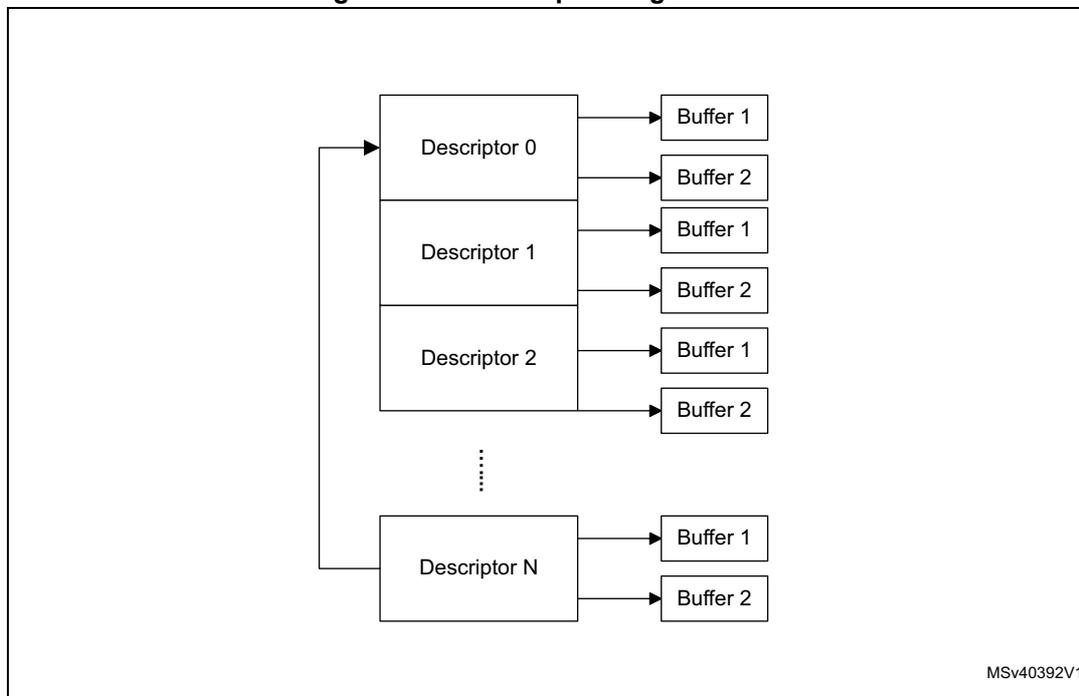
MSv40392V1
In a ring structure, descriptors are separated by the 64-bit word number programmed in the DSL field of the Channel x control register (ETH_DMACxCR) . The application needs to program the total ring length, that is the total number of descriptors in ring span, in the following registers of a DMA channel:
- • Channel x Tx descriptor ring length register (ETH_DMACxTXRLR)
- • Channel x Rx descriptor ring length register (ETH_DMACxRXRLR)
The Channel x Tx descriptor tail pointer register (ETH_DMACxTXDTPR) or Channel x Rx descriptor tail pointer register (ETH_DMACxRXDTPR) contains the pointer to the descriptor address (N). The base address and the current descriptor pointer decide the address of the current descriptor that the DMA can process. The descriptors up to one location less than the one indicated by the descriptor tail pointer (N – 1) are owned by the DMA. The DMA continues to process the descriptors until the following condition occurs:
Current Descriptor Pointer == Descriptor Tail Pointer;
The DMA enters the Suspend state when this condition occurs. The application must perform a write operation to the descriptor tail pointer register and update the tail pointer so that the following condition is met:
Descriptor Tail Pointer > Current Descriptor Pointer;
Note: When the application sets the descriptors into the end-of-descriptor ring, continues setting from the start of the descriptor list and updating the descriptor tail pointer, the above condition is not satisfied. The DMA detects such a case, processes the descriptors until the
end of the ring and then continues processing from the start of the descriptor list until the current descriptor pointer is equal to the descriptor tail pointer.
When the application programs the descriptor tail pointer beyond the end of the descriptor ring, the DMA interprets this as the availability of one more complete ring of descriptors, and after processing the last descriptor in the ring continues to process descriptors from the start of the descriptor list. If this is not intended, the application must program the descriptor tail pointer to the start of the descriptor list after setting the last descriptor in the ring.
The DMA automatically wraps around the base address when the end of ring is reached, as shown in Figure 1060: DMA descriptor ring .
Figure 1060. DMA descriptor ring
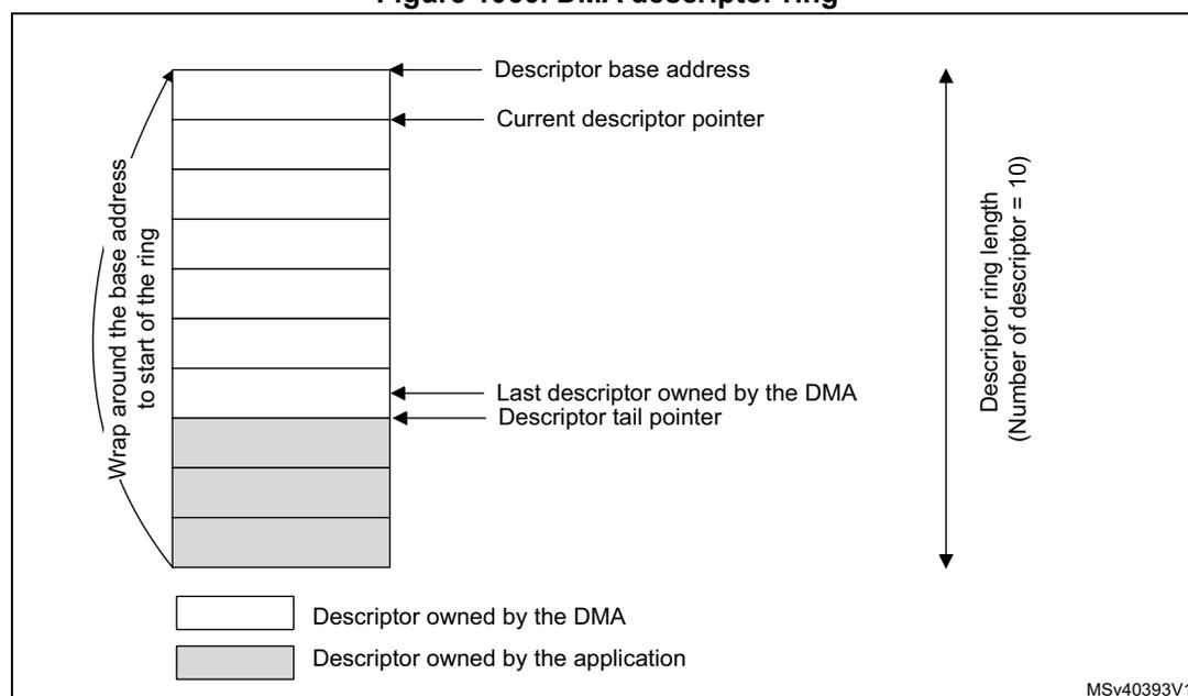
Descriptor base address
Current descriptor pointer
Wrap around the base address to start of the ring
Last descriptor owned by the DMA
Descriptor tail pointer
Descriptor ring length (Number of descriptor = 10)
Descriptor owned by the DMA
Descriptor owned by the application
MSv40393V1
For descriptors owned by the application, the OWN bit of DES3 is reset to 0.
For descriptors owned by the DMA, the OWN bit is set to 1.
At the beginning, if the application has only one descriptor, it sets the last descriptor address (tail pointer) to Descriptor Base Address + 1. The DMA then processes the first descriptor and waits for the application to increment the tail pointer.
Descriptor tail pointer handling examples
Figure 1061. Descriptor tail pointer example 1
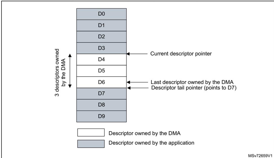
When the current descriptor pointer points to descriptor 4 (D4) and the descriptor tail pointer points to descriptor 7 (D7), the last descriptor owned by the DMA is descriptor 6 (D6) and there are three descriptors (D4, D5, D6) available for the DMA, as shown in Figure 1061: Descriptor tail pointer example 1 .
Figure 1062. Descriptor tail pointer example 2
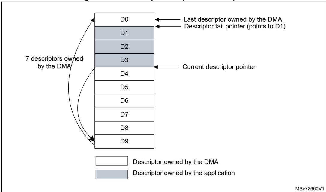
As shown in Figure 1062: Descriptor tail pointer example 2 , the application frees four descriptors (D7, D8, D9 and D0) and updates the descriptor tail pointer to point to descriptor
1 (D1). The last descriptor owned by the DMA is descriptor 0 (D0). The descriptors referenced between the current descriptor pointer (D4) and the descriptor tail pointer (D1) are available to the DMA.
76.10.3 Transmit descriptor
The Ethernet peripheral DMA requires at least one descriptor for a transmit packet. In addition to two buffers, two byte-count buffers, and two address pointers, the transmit descriptor features control fields which can be used to manage the MAC operation on per-transmit packet basis. The Transmit normal descriptor has the following two formats: Read format and Write-back format.
Transmit normal descriptor (read format)
Figure 1063 shows the Read format for Transmit normal descriptor. Table 821 to Table 824 provide a detailed description of all Transmit normal descriptors (read format).
Figure 1063. Transmit descriptor (read format)
![Diagram of the Transmit descriptor (read format) showing four 32-bit registers: TDES0, TDES1, TDES2, and TDES3. TDES0 contains Header or Buffer 1 Address[31:0]. TDES1 contains Buffer 2 Address [31:0] or Buffer 1 Address[63:32]. TDES2 contains IOC, TTSE, Buffer 2 Length[29:16], VTIR, and Header or Buffer 1 Length[13:0]. TDES3 contains OWN, Control[30:16], Control[30:18], Frame length[14:0], and Payload length[17:0].](/RM0486-STM32N6x5-x7/0adae4a3de2adbd5e6fa51b56cdcdecf_img.jpg)
The diagram illustrates the structure of the Transmit descriptor (read format) across four 32-bit registers (TDES0 to TDES3). Bit positions 31 and 0 are indicated at the top. TDES0 contains the 'Header or Buffer 1 Address[31:0]'. TDES1 contains 'Buffer 2 Address [31:0] or Buffer 1 Address[63:32]'. TDES2 is split into fields: IOC, TTSE, Buffer 2 Length[29:16], VTIR, and Header or Buffer 1 Length[13:0]. TDES3 is split into OWN, Control[30:16], Control[30:18], Frame length[14:0], and Payload length[17:0]. A dashed line separates Control[30:16] and Control[30:18]. Arrows indicate the bit ranges for Control[30:18], Frame length[14:0], and Payload length[17:0]. The identifier MSv40394V1 is in the bottom right.
- • TDES0 normal descriptor (read format)
Table 821. TDES0 normal descriptor (read format)
| Bit | Name | Description |
|---|---|---|
| 31:0 | BUF1AP | Buffer 1 Address Pointer or TSO Header Address Pointer These bits indicate either the physical address of Buffer 1 or the TSO Header Address pointer when the following bits are set: – TSE bit of TDES3 – FD bit of TDES3 |
- • TDES1 normal descriptor (read format)
Table 822. TDES1 normal descriptor (read format)
| Bit | Name | Description |
|---|---|---|
| 31:0 | BUF2AP | Buffer 2 or Buffer 1 Address Pointer: These bits indicate the physical address of Buffer 2 when a descriptor ring structure is used. There is no limitation to the buffer address alignment. |
- • TDES2 normal descriptor (read format)
| 31 | 30 | 29 | 28 | 27 | 26 | 25 | 24 | 23 | 22 | 21 | 20 | 19 | 18 | 17 | 16 |
| IOC | TTSE | B2L | |||||||||||||
| 15 | 14 | 13 | 12 | 11 | 10 | 9 | 8 | 7 | 6 | 5 | 4 | 3 | 2 | 1 | 0 |
| VTIR | HL or B1L | ||||||||||||||
Table 823. TDES2 normal descriptor (read format)
| Bits | Name | Description |
|---|---|---|
| 31 | IOC | Interrupt on completion: This bit sets the TI bit in the Channel x status register (ETH_DMACxSR) when the present packet transmission is complete. |
| 30 | TTSE | Transmit Timestamp Enable This bit enables the IEEE1588 timestamping for Transmit packet referenced by the descriptor. |
| 29:16 | B2L | Buffer 2 Length The driver sets this field. When set, this field indicates Buffer 2 length. |
| 15:14 | VTIR | VLAN Tag Insertion or Replacement: These bits request the MAC to perform VLAN tagging or untagging before transmitting the packets. The application must set the CRC Pad Control bits appropriately when VLAN tag insertion, replacement, or deletion is enabled for the packet. The values of these bits are as follows: 00: Do not add a VLAN tag. 01: Remove the VLAN tag from the packets before transmission. This option should be used only with the VLAN packets. 10: Insert a VLAN tag with the tag value programmed in the VLAN inclusion register (ETH_MACVIR) or context descriptor. 11: Replace the VLAN tag in packets with the tag value programmed in the VLAN inclusion register (ETH_MACVIR) or context descriptor. This option should be used only with the VLAN packets. |
Table 823. TDES2 normal descriptor (read format) (continued)
| Bits | Name | Description |
|---|---|---|
| 13:0 | HL or B1L | Header length or buffer 1 length For Header length, only bits [9:0] are taken into account. Bits 13 to 0 are applicable only to buffer 1 length. If the TCP Segmentation Offload feature is enabled through the TSE bit of TDES3, this field is equal to the header length. When the TSE bit is set in TDES3, the header length includes the length (expressed in bytes) from Ethernet Source address till the end of the TCP header. The maximum header length supported for TSO feature is 1023 bytes. If the TCP Segmentation Offload feature is not enabled, this field is equal to Buffer 1 length. |
- • TDES3 normal descriptor (read format)
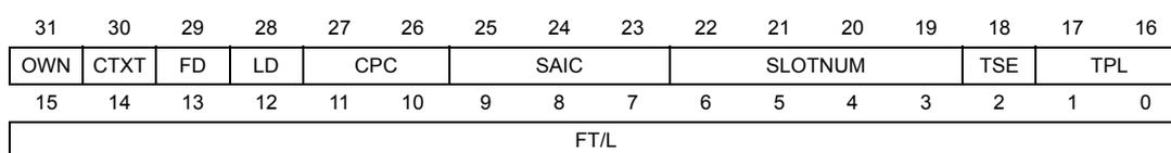
| 31 | 30 | 29 | 28 | 27 | 26 | 25 | 24 | 23 | 22 | 21 | 20 | 19 | 18 | 17 | 16 |
| OWN | CTXT | FD | LD | CPC | SAIC | SLOTNUM | TSE | TPL | |||||||
| 15 | 14 | 13 | 12 | 11 | 10 | 9 | 8 | 7 | 6 | 5 | 4 | 3 | 2 | 1 | 0 |
| FT/L | |||||||||||||||
Table 824. TDES3 normal descriptor (read format)
| Bits | Name | Description |
|---|---|---|
| 31 | OWN | Own bit 1: the DMA owns the descriptor. 0: the application owns the descriptor. The DMA clears this bit after it completes the transfer of data given in the associated buffer(s). |
| 30 | CTXT | Context Type This bit should be set to 0 for normal descriptor. |
| 29 | FD | First Descriptor When this bit is set, it indicates that the buffer contains the first segment of a packet. |
| 28 | LD | Last Descriptor When this bit is set, it indicates that the buffer contains the last segment of the packet. B1L or B2L field should have a non-zero value. |
Table 824. TDES3 normal descriptor (read format) (continued)
| Bits | Name | Description |
|---|---|---|
| 27:26 | CPC | CRC Pad Control This field controls the CRC and Pad Insertion for Tx packet. It is valid only when the first descriptor bit (TDES3[29]) is set. The values of bits[27:26] are the following: 00: CRC and Pad Insertion The MAC appends the cyclic redundancy check (CRC) at the end of the transmitted packets whose length greater than or equal to 60 bytes. The MAC automatically appends padding and CRC to a packet with length less than 60 bytes. 01: CRC Insertion (Disable Pad Insertion) The MAC appends the CRC at the end of the transmitted packet but it does not append padding. The application should ensure that the padding bytes are present in the packet being transferred from the Transmit buffer, that is, the packet being transferred from the Transmit Buffer is of length greater than or equal to 60 bytes. 10: Disable CRC Insertion The MAC does not append the CRC at the end of the transmitted packet. The application should ensure that the padding and CRC bytes are present in the packet being transferred from the Transmit Buffer. 11: CRC Replacement The MAC replaces the last four bytes of the transmitted packet with recalculated CRC bytes. The application should ensure that the padding and CRC bytes are present in the packet being transferred from the Transmit Buffer. When the TSE bit is set, the MAC ignores this field because the CRC and pad insertion is always done for segmentation. |
| 25:23 | SAIC | SA Insertion Control These bits request the MAC to add or replace the Source Address field in the Ethernet packet with the value given in the MAC Address 0 register. The application must appropriately set the CRC Pad Control bits when SA Insertion Control is enabled for the packet. Bit 25 specifies the MAC Address Register (1 or 0) value that is used for Source Address insertion or replacement. The following list describes the values of Bits[24:23]: 00: Do not include the source address 01: Include or insert the source address. For reliable transmission, the application must provide frames without source addresses. 10: Replace the source address. For reliable transmission, the application must provide frames with source addresses. 11: Reserved These bits are valid when the First Segment control bit (TDES3 [29]) is set. |
Table 824. TDES3 normal descriptor (read format) (continued)
| Bits | Name | Description |
|---|---|---|
| 22:19 | SLOTNUM or THL | SLOTNUM: Slot Number Control Bits in AV mode These bits indicate the slot interval in which the data should be fetched from the corresponding buffers addressed by TDES0 or TDES1. When the Transmit descriptor is fetched, the DMA compares the slot number value in this field with the slot interval maintained in the RSN field of Channel x slot function control status register (ETH_DMACxSFCSR) . It fetches the data from the buffers only if a value matches. These bits are valid only for the AV channels. THL: TCP Header Length If the TSE bit is set, this field contains the length of the TCP/UDP header. The minimum value of this field must be 5 for TCP header. THL value must be equal to 2 for UDP header. This field is valid only for the first descriptor |
| 18 | TSE | TCP Segmentation Enable When this bit is set, the DMA performs the TCP/UDP segmentation for a packet. This bit is valid only if the FD bit is set. |
| 17:16 | CIC/TPL | Checksum Insertion Control or TCP Payload Length These bits control the checksum calculation and insertion. They can take the following values: 00: Checksum insertion disabled. 01: Only IP header checksum calculation and insertion are enabled. 10: IP header checksum and payload checksum calculation and insertion are enabled, but pseudo-header checksum is not calculated in hardware. 11: IP header checksum and payload checksum calculation and insertion are enabled, and pseudo-header checksum is calculated in hardware. This field is valid when the TSE bit is reset. When the TSE bit is set, it contains the upper bits [17:16] of the TCP Payload length. This allows the TCP packet length field to be spanned across TDES3[17:0] to provide 256 Kbyte packet length support. |
| 15 | TPL | Reserved or TCP Payload Length When the TSE bit is reset, this bit is reserved. When the TSE bit is set, this is bit 15 of the TCP payload length [17:0]. |
| 14:0 | FL/TPL | Reserved or TCP Payload Length When the TSE bit is set, this field is equal to the lower 15 bits of the TCP payload length. This length does not include Ethernet header or TCP/UDP/IP header length. When the TSE bit is reset, this bit is reserved. |
Transmit normal descriptor (write-back format)
The write-back format is applicable only for the last descriptor of the corresponding packet. The LD bit (TDES3[28]) is set in the descriptor where the DMA writes back the status and timestamp information for the corresponding Transmit packet.
Figure 1064 shows the write-back format for Transmit normal descriptors. Table 825 to Table 828 provide a detailed description of all Transmit Normal descriptors (Write-Back Format).
Figure 1064. Transmit descriptor write-back format
![Diagram of Transmit descriptor write-back format showing four 32-bit registers: TDES0 (Timestamp Low), TDES1 (Timestamp high), TDES2 (Reserved), and TDES3 (OWN bit and Status[30:0]).](/RM0486-STM32N6x5-x7/b319f155d5e4e5f32c96d4d244d77b58_img.jpg)
The diagram illustrates the layout of the transmit descriptor write-back format. It consists of four 32-bit registers, each represented by a horizontal bar. The registers are labeled on the left: TDES0, TDES1, TDES2, and TDES3. The first three registers (TDES0, TDES1, TDES2) are 32-bit wide fields. TDES0 is labeled 'Timestamp Low', TDES1 is 'Timestamp high', and TDES2 is 'Reserved'. Bit positions 31 and 0 are indicated at the top. TDES3 is split into two parts: a single bit labeled 'OWN' on the left, and a 31-bit field labeled 'Status[30:0]' on the right. The identifier 'MSV40395V1' is in the bottom right corner.
- • TDES0 normal descriptor (write-back format)
| Bit | Name | Description |
|---|---|---|
| 31:0 | TTSL | Transmit Packet Timestamp Low The DMA updates this field with least significant 32 bits of the timestamp captured for the corresponding Transmit packet. The DMA writes the timestamp only if TTSE bit of TDES2 is set in the first descriptor of the packet. This field holds the timestamp only if the Last Segment bit (LS) in the descriptor is set and the Timestamp status (TTSS) bit is set. |
1. This format is only applicable to the last descriptor of a packet.
- • TDES1 normal descriptor (write-back format)
| Bit | Name | Description |
|---|---|---|
| 31:0 | TTSH | Transmit Packet Timestamp High The DMA updates this field with the most significant 32 bits of the timestamp captured for corresponding receive packet. The DMA writes the timestamp only if the TTSE bit of TDES2 is set in the first descriptor of the packet. This field has the timestamp only if the Last Segment bit (LS) in the descriptor is set and Timestamp status (TTSS) bit is set. |
1. This format is only applicable to the last descriptor of a packet.
- • TDES2 normal descriptor (write-back format)
| Bit | Description |
|---|---|
| 31:0 | Reserved |
1. This format is only applicable to the last descriptor of a packet.
- • TDES3 normal descriptor (write-back format)
| 31 | 30 | 29 | 28 | 27 | 26 | 25 | 24 | 23 | 22 | 21 | 20 | 19 | 18 | 17 | 16 |
| OWN | CTXT | FD | LD | Reserved | TTSS | Res. | |||||||||
| 15 | 14 | 13 | 12 | 11 | 10 | 9 | 8 | 7 | 6 | 5 | 4 | 3 | 2 | 1 | 0 |
| ES | JT | FF | PCE | LoC | NC | LC | EC | CC | ED | UF | DB IHE | ||||
| Bit | Name | Description |
|---|---|---|
| 31 | OWN | Own bit When this bit is set, it indicates that the DMA owns the descriptor. The DMA clears this bit when it completes the packet transmission. After the write-back is complete, this bit is set to 0. |
| 30 | CTXT | Context Type This bit should be set to 0 for normal descriptors. |
| 29 | FD | First Descriptor This bit indicates that the buffer contains the first segment of a packet. |
| 28 | LD | Last Descriptor This bit is set 1 for last descriptor of a packet. The DMA writes the status fields only in the last descriptor of the packet. |
| 27:24 | Reserved | |
| 23 | DE | Descriptor Error When this bit is set, it indicates that the descriptor content is incorrect. The DMA sets this bit during write-back while closing the descriptor. Descriptor errors can be: – Incorrect sequence from the context descriptor, such as a location after the first descriptor for a packet. – All 1s. – CTXT is set to 1 along with LD or FD bits set to 1. Note: When a Descriptor error occurs due to All 1s or CTXT, LD, and FD bits set to 1, the Transmit DMA closes the transmit descriptor with DE and LD bits set to 1. When IOC bit in TDES2 of corresponding first descriptor is set to 1, Transmit DMA sets the TI bit in the Channel x status register (ETH_DMACxSR). Based on CTXT, LD, and FD bits of the transmit descriptor, the subsequent descriptor might be considered as the First Descriptor (even if FD bit is not set) and partial packet is sent. |
| 22:18 | Reserved |
| Bit | Name | Description |
|---|---|---|
| 17 | TTSS | Tx Timestamp Status This status bit indicates that a timestamp has been captured for the corresponding transmit packet. When this bit is set, TDES0 and TDES1 have timestamp values that were captured for the Transmit packet. This field is valid only when the Last Segment control bit (TDES3 [28]) in a descriptor is set. |
| 16 | Reserved | |
| 15 | ES | Error Summary This bit indicates the logical OR of the following bits: TDES3[0]: IP Header Error TDES3[14]: Jabber timeout TDES3[13]: Packet Flush TDES3[12]: Payload Checksum Error TDES3[11]: Loss of Carrier TDES3[10]: No Carrier TDES3[9]: Late Collision TDES3[8]: Excessive Collision TDES3[3]: Excessive Deferral TDES3[2]: Underflow Error |
| 14 | JT | Jabber timeout This bit indicates that the MAC transmitter has experienced a jabber timeout. This bit is set only when the JD bit of the Operating mode configuration register (ETH_MACCR) is not set. |
| 13 | FF | Packet Flushed This bit indicates that the DMA or MTL flushed the packet because of a software flush command given by the CPU. |
| 12 | PCE | Payload Checksum Error This bit indicates that the Checksum Offload engine had a failure and did not insert any checksum into the encapsulated TCP, UDP, or ICMP payload. This failure can be either caused by insufficient bytes, as indicated by the Payload Length field of the IP Header, or by the MTL starting to forward the packet to the MAC transmitter in Store-and-Forward mode without the checksum having been calculated yet. This second error condition only occurs when the Transmit FIFO depth is less than the length of the Ethernet packet being transmitted to avoid deadlock, the MTL starts forwarding the packet when the FIFO is full, even in the store-and-forward mode. This error can also occur when a Bus error is detected during packet transfer. |
| 11 | LoC | Loss of Carrier This bit indicates that Loss of Carrier occurred during packet transmission (that is, the ETH_CRS signal was inactive for one or more transmit clock periods during packet transmission). This is valid only for the packets transmitted without collision and when the MAC operates in the Half-duplex mode. |
| Bit | Name | Description |
|---|---|---|
| 10 | NC | No Carrier This bit indicates that the carrier sense signal from the PHY was not asserted during transmission. |
| 9 | LC | Late Collision This bit indicates that packet transmission was aborted because a collision occurred after the collision window (64 byte times including Preamble in MII mode and 512 byte times including Preamble and Carrier Extension in GMII mode). This bit is not valid if Underflow Error is set. |
| 8 | EC | Excessive Collision This bit indicates that the transmission was aborted after 16 successive collisions while attempting to transmit the current packet. If the DR bit is set in the Operating mode configuration register (ETH_MACCR) , this bit is set after first collision and the transmission of the packet is aborted. |
| 7:4 | CC | Collision Count This 4-bit counter value indicates the number of collisions occurred before the packet was transmitted. The count is not valid when the EC bit is set. |
| 3 | ED | Excessive Deferral This bit indicates that the transmission ended because of excessive deferral of over 24,288 bit times (155,680 bits times in 1000-Mbps mode or Jumbo Packet enabled mode) if DC bit is set in the Operating mode configuration register (ETH_MACCR) . When TBS is enabled in Full duplex mode and this bit is set, it indicates that the frame has been dropped after the expiry time has elapsed. |
| 2 | UF | Underflow Error This bit indicates that the MAC aborted the packet because the data arrived late from the system memory. The underflow error can occur because of either of the following conditions: The DMA encountered an empty Transmit Buffer while transmitting the packet The application filled the MTL Tx FIFO slower than the MAC transmit rate The transmission process enters the Suspend state and sets the underflow bit corresponding to a queue in the ETH_MTLISR register. |
| Bit | Name | Description |
|---|---|---|
| 1 | DB | Deferred Bit This bit indicates that the MAC deferred before transmitting because of presence of carrier. This bit is valid only in the Half-duplex mode. |
| 0 | IHE | IP Header Error When IP Header Error is set, this bit indicates that the Checksum Offload engine detected an IP header error. If COE detects an IP header error, it still inserts an IPv4 header checksum if the Ethernet Type field indicates an IPv4 payload. In Full-duplex mode, when EST/Qbv is enabled and this bit is set, it indicates the frame drop status due to Frame Size error or Schedule Error. |
1. This format is only applicable to the last descriptor of a packet.
Transmit context descriptor
The Transmit context descriptor can be provided any time before a packet descriptor. The context is valid for the current packet and subsequent packets. The context descriptor is used to provide the timestamps for one-step timestamp correction, and VLAN Tag ID for VLAN insertion feature. Write-back is only done on a context descriptor to reset the OWN bit.
Note: The VLAN tag IDs and MSS values, which are provided by the application in a context descriptor with their corresponding Valid bits set, are stored internally by the DMA. When the outer or inner VLAN tag is provided with the Valid bit set, the DMA always passes the last valid VLAN tag to the MTL. The application cannot invalidate the valid VLAN tag stored by the DMA. The VLAN tag is inserted or replaced based on the control inputs provided for the packet. The Inner VLAN Tag Control input is used only for the packet that immediately follows the context descriptor. The application must provide a context descriptor before the normal descriptor of each packet for which the DMA should use the inner VLAN tag control input.
Figure 1065 shows the format for transmit context descriptors. Table 829 to Table 832 provide a detailed description of all transmit context descriptors.
Figure 1065. Transmit context descriptor format
![Diagram of Transmit context descriptor format showing four 32-bit words (TDES0-TDES3) with their respective fields. TDES0 contains Timestamp Low[31:0]. TDES1 contains Timestamp High[31:0]. TDES2 contains Inner VLAN tag[31:16], a reserved field, and Maximum segment size[13:0]. TDES3 contains OWN, Control[30:16], and VLAN tag[15:0]. Bit positions 31 and 0 are indicated at the top.](/RM0486-STM32N6x5-x7/7708beed294972b7fbc0b35d06912d34_img.jpg)
The diagram illustrates the layout of four 32-bit context descriptors (TDES0 to TDES3) used for transmitting packets. The bit positions are indicated from 31 down to 0 at the top. TDES0 and TDES1 are 32-bit timestamp words. TDES2 is split into an Inner VLAN tag (bits 31-16), a reserved field (bits 15-14), and a Maximum segment size (bits 13-0). TDES3 is split into an OWN bit (bit 31), a Control field (bits 30-16), and a VLAN tag (bits 15-0).
| Descriptor | Field | Bit Range |
|---|---|---|
| TDES0 | Timestamp Low | [31:0] |
| TDES1 | Timestamp High | [31:0] |
| TDES2 | Inner VLAN tag | [31:16] |
| TDES2 | Res | [15:14] |
| TDES2 | Maximum segment size | [13:0] |
| TDES3 | OWN | [31] |
| TDES3 | Control | [30:16] |
| TDES3 | VLAN tag | [15:0] |
MSV40396V2
- • TDES0 context descriptor (read format)
Table 829. TDES0 context descriptor
| Bit | Name | Description |
|---|---|---|
| 31:0 | TTSL | Transmit Packet Timestamp Low For one-step correction, the driver can provide the lower 32 bits of timestamp in this descriptor word. The DMA uses this value as the low word for doing one-step timestamp correction. This field is valid only if the OSTC and TCMSSV bits of TDES3 context descriptor are set. |
- • TDES1 context descriptor (read format)
Table 830. TDES1 context descriptor
| Bit | Name | Description |
|---|---|---|
| 31:0 | TTSH | Transmit Packet Timestamp High For one-step correction, the driver can provide the upper 32 bits of timestamp in this descriptor. The DMA uses this value as the high word for doing one-step timestamp correction. This field is valid only if the OSTC and TCMSSV bits of TDES3 context descriptor are set. |
- • TDES2 context descriptor (read format)
Table 831. TDES2 context descriptor
| Bit | Name | Description |
|---|---|---|
| 31:16 | IVT | Inner VLAN Tag When the IVLTV bit of TDES3 context descriptor is set and the TCMSSV and OSTC bits of TDES3 context descriptor are reset, TDES2[31:16] contains the inner VLAN Tag to be inserted in the subsequent Transmit packets. |
| 15:14 | Reserved | |
| 13:0 | MSS | Maximum Segment Size This segment size is used while segmenting the TCP/IP payload. This field is valid only if the TCMSSV bit of TDES3 context descriptor is set and the OSTC bit of the TDES3 context descriptor is reset. |
- • TDES3 context descriptor (read format)
| 31 | 30 | 29 | 28 | 27 | 26 | 25 | 24 | 23 | 22 | 21 | 20 | 19 | 18 | 17 | 16 |
| OWN | CTX | Reserved | OSTC | TCMSSV | Reserved | CDE | Reserved | IVLTV | VLT | ||||||
| 15 | 14 | 13 | 12 | 11 | 10 | 9 | 8 | 7 | 6 | 5 | 4 | 3 | 2 | 1 | 0 |
| VT | |||||||||||||||
Table 832. TDES3 context descriptor
| Bit | Name | Description |
|---|---|---|
| 31 | OWN | Own bit 1: the DMA owns the descriptor. 0: the application owns the descriptor. The DMA clears this bit immediately after a read operation. |
| 30 | CTX | Context Type This bit should be set to 1 for context descriptor. |
| 29:28 | Reserved | |
| 27 | OSTC | One-Step Timestamp Correction Enable When this bit is set, the DMA performs a one-step timestamp correction with reference to the timestamp values provided in TDES0 and TDES1. |
| 26 | TCMSSV | One-Step Timestamp Correction Input or MSS Valid When this bit and the OSTC bit are set, it indicates that the Timestamp Correction input provided in TDES0 and TDES1 is valid. When the OSTC bit is reset and this bit and the TSE bit of TDES3 are set in subsequent normal descriptor, it indicates that the MSS input in TDES2 is valid. |
| 25:24 | Reserved | |
Table 832. TDES3 context descriptor (continued)
| Bit | Name | Description |
|---|---|---|
| 23 | CDE | Context Descriptor Error When this bit is set, it indicates that the context descriptor is incorrect. The DMA sets this bit during write-back while closing the context descriptor. The Context Descriptor errors can be:
Note: When a Context Descriptor error occurs due to All 1s or CTXT, LD, and FD bits set to 1, the Transmit DMA closes the transmit descriptor with DE and LD bits set to 1. When IOC bit in TDES2 of corresponding first descriptor is set to 1, Transmit DMA sets the TI bit in the Channel x status register (ETH_DMACxSR). Based on CTXT, LD, and FD bits of the transmit descriptor, the subsequent descriptor might be considered as the First Descriptor (even if FD bit is not set) and partial packet is sent. This error is categorized as an abnormal event; recovery is only by issuing a software reset (DMA stopping-reconfiguring-restarting recovery mechanism is not supported) |
| 22:20 | Reserved | |
| 19:18 | IVTIR | Inner VLAN Tag Insert or Replace When these bits are set, they request the MAC to perform Inner VLAN tagging or untagging before transmitting the packets. If the packet is modified for VLAN tags, the MAC automatically recalculates and replaces the CRC bytes. This bitfield has the following values: 00: Do not add the inner VLAN tag. 01: Remove the inner VLAN tag from the packets before transmission. This option should be used only with the VLAN frames. 10: Insert an inner VLAN tag with the tag value programmed in the Inner VLAN inclusion register (ETH_MACVIR) or context descriptor. 11: Replace the inner VLAN tag in packets with the tag value programmed in the Inner VLAN inclusion register (ETH_MACVIR) or context descriptor. This option should be used only with the VLAN frames. |
| 17 | IVLTV | Inner VLAN Tag Valid When this bit is set, it indicates that the IVT field of TDES2 is valid. |
| 16 | VLTV | VLAN Tag Valid When this bit is set, it indicates that the VT field of TDES3 is valid. |
| 15:0 | VT | VLAN Tag This field contains the VLAN Tag to be inserted or replaced in the packet. This field is used as VLAN Tag only when the VLTI bit of the VLAN inclusion register (ETH_MACVIR) is reset. |
76.10.4 Receive descriptor
The DMA in the Ethernet peripheral attempts to read a descriptor only if the Tail pointer is different from the Base pointer or current pointer. It is recommended to have a descriptor ring with a length that can accommodate at least two complete packets received by the MAC; otherwise, the performance of the DMA is greatly impacted because of the unavailability of the descriptors. In such a situation, the MTL RxFIFO becomes full and starts dropping packets.
The following receive descriptors are present:
- • Normal descriptors with read and write-back formats
- • Context descriptors
All received descriptors are prepared by the software and given to the DMA as “normal” descriptors (see Figure 1066: Receive normal descriptor (read format) for a description of their content). The DMA reads this descriptor and, after transferring a received packet (or part of it) to the buffers indicated by the descriptor, the Rx DMA closes the descriptor with the corresponding packet status. The status format is given in Figure 1067: Receive normal descriptor (write-back format) .
For some packets, the normal descriptor bits are not sufficient to write the complete status. For such packets, the Rx DMA writes the extended status to the next descriptor (without processing or using the Buffers pointers embedded in that descriptor). The format and content of this write-back descriptor is described in Figure 1068: Receive context descriptor .
Receive normal descriptor (read format)
Figure 1066 shows the read format for receive normal descriptors. Table 833 to Table 836 provide a detailed description of all receive normal descriptors (read format).
Figure 1066. Receive normal descriptor (read format)
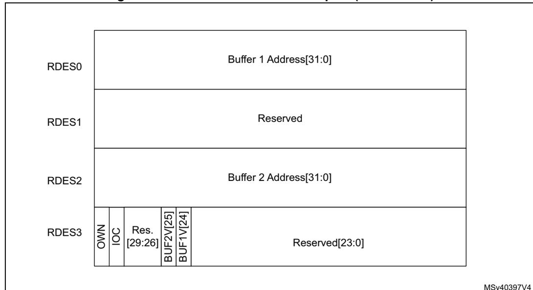
| RDES0 | Buffer 1 Address[31:0] | |||||
| RDES1 | Reserved | |||||
| RDES2 | Buffer 2 Address[31:0] | |||||
| RDES3 | OWN | IOC | Res. [29:26] | BUF2V[25] | BUF1V[24] | Reserved[23:0] |
MSV40397V4
Note: In the receive descriptor (read format), if the Buffer Address field contains only 0s, the MAC does not transfer data to this buffer and skips to the next buffer or next descriptor.
- • RDES0 normal descriptor (read format)
Table 833. RDES0 normal descriptor (read format)
| Bit | Name | Description |
|---|---|---|
| 31:0 | BUF1AP | Buffer 1 Address Pointer These bits indicate the physical address of Buffer 1. The application can program a byte-aligned address for this buffer, which means that the LS bits of this field can be non-zero. However, while transferring the start of packet, the DMA performs a write operation with RDES2[2:0]=0 in case of 64-/128-bit configuration) as zero. However, the packet data is shifted by the actual offset as given in the buffer address pointer. If the address pointer points to a buffer where the middle or last part of the packet is stored, the DMA ignores the offset address and writes to the full location as indicated by the data-width. |
- • RDES1 normal descriptor (read format)
Table 834. RDES1 normal descriptor (read format)
| Bit | Name | Description |
|---|---|---|
| 31:0 | Reserved | Field reserved. |
- • RDES2 normal descriptor (read format)
Table 835. RDES2 normal descriptor (read format)
| Bit | Name | Description |
|---|---|---|
| 31:0 | BUF2AP | Buffer 2 Address Pointer These bits indicate Buffer 2 physical address. The RxDMA uses the LS bits of the pointer address only while transferring the start bytes of a packet. If the BUF2AP is giving the address of a buffer in which the middle or last part of a packet is stored, the DMA ignores RDES2[2:0]=0 and writes to the complete location. |
- • RDES3 normal descriptor (read format)
| 31 | 30 | 29 | 28 | 27 | 26 | 25 | 24 | 23 | 22 | 21 | 20 | 19 | 18 | 17 | 16 |
| OWN | IOC | Reserved | BUF2V | BUF1V | Reserved | ||||||||||
| 15 | 14 | 13 | 12 | 11 | 10 | 9 | 8 | 7 | 6 | 5 | 4 | 3 | 2 | 1 | 0 |
| Reserved | |||||||||||||||
Table 836. RDES3 normal descriptor (read format)
| Bit | Name | Description |
|---|---|---|
| 31 | OWN | Own bit When this bit is set, it indicates that the DMA owns the descriptor. When this bit is reset, it indicates that the application owns the descriptor. The DMA clears this bit when either of the following conditions is true: – The DMA completes the packet reception – The buffers associated with the descriptor are full |
| 30 | IOC | Interrupt Enabled on Completion When this bit is set, an interrupt is issued to the application when the DMA closes this descriptor. |
| 29:26 | Reserved | |
| 25 | BUF2V | Buffer 2 Address Valid When this bit is set, it indicates to the DMA that the buffer 2 address specified in RDES2 is valid. The application must set this bit so that the DMA can use the address to which the Buffer 2 address in RDES0 is pointing, to write received packet data. |
| 24 | BUF1V | Buffer 1 Address Valid When set, this indicates to the DMA that the buffer 1 address specified in RDES0 is valid. The application must set this value if the address to which Buffer 1 address points in RDES0, can be used by the DMA to write received packet data. |
| 23:0 | Reserved |
Receive normal descriptor (write-back format)
Figure 1067 shows the write-back format for receive normal descriptors. Table 837 to Table 840 provide a detailed description of all receive normal descriptors (write-back format).
Figure 1067. Receive normal descriptor (write-back format)
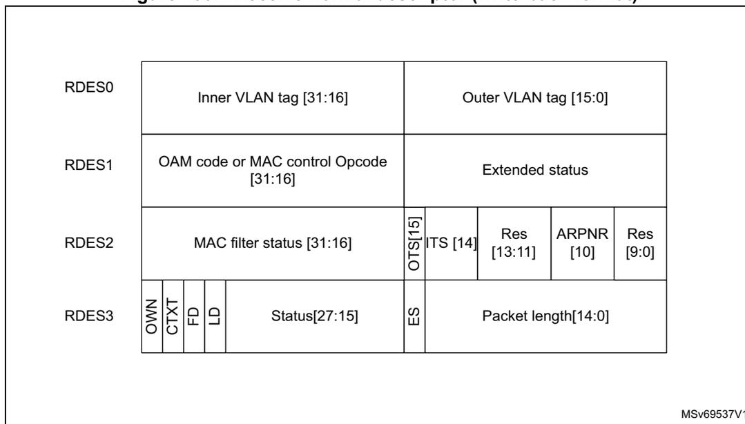
The diagram illustrates the structure of receive normal descriptors (RDES0 to RDES3). RDES0 contains Inner VLAN tag [31:16] and Outer VLAN tag [15:0]. RDES1 contains OAM code or MAC control Opcode [31:16] and Extended status. RDES2 contains MAC filter status [31:16], O (1 bit), TS [14], Res [13:11], ARPNR [10], and Res [9:0]. RDES3 contains OWN, CTXT, EP, and a 1-bit field (RSOV), Status [27:15], S (1 bit), and Packet length [14:0].
MSv69537V1
- • RDES0 normal descriptor (write-back format)
Table 837. RDES0 normal descriptor (write-back format)
| Bit | Name | Description |
|---|---|---|
| 31:16 | IVT | Inner VLAN Tag This field contains the Inner VLAN tag of the received packet if the RS0V bit of RDES3 is set. This is valid only when Double VLAN tag processing and VLAN tag stripping are enabled. |
| 15:0 | OVT | Outer VLAN Tag This field contains the Outer VLAN tag of the received packet if the RS0V bit of RDES3 is set. |
- • RDES1 normal descriptor (write-back format)
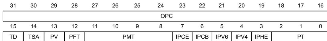
The diagram shows the bit fields for RDES1. Bits 31-16 are OPC. Bits 15-0 are divided into: TD (bit 15), TSA (bit 14), PV (bit 13), PFT (bit 12), PMT (bits 11-7), IPCE (bit 6), IPCB (bit 5), IPV6 (bit 4), IPV4 (bit 3), IPHE (bit 2), and PT (bits 1-0).
| Bit | Name | Description |
|---|---|---|
| 31:16 | OPC | OAM Subtype Code, or MAC Control Packet opcode OAM Subtype Code If bits[18:16] of RDES3 are set to 111, this field contains the OAM subtype and code fields. MAC Control Packet opcode If bits[18:16] of RDES3 are set to 110, this field contains the MAC Control packet opcode field. |
| 15 | TD | Timestamp Dropped This bit indicates that the timestamp was captured for this packet but got dropped in the MTL Rx FIFO because of overflow. |
| 14 | TSA | Timestamp Available When Timestamp is present, this bit indicates that the timestamp value is available in a context descriptor word 2 (RDES2) and word 1(RDES1). This is valid only when the Last Descriptor bit (RDES3 [28]) is set. The context descriptor is written in the next descriptor just after the last normal descriptor for a packet. |
| 13 | PV | PTP Version 1: Received PTP message in IEEE 1588 version 2 format 0: Received PTP message in IEEE 1588 version 1 format |
| 12 | PFT | PTP Packet Type This bit indicates that the PTP message is sent directly over Ethernet. |
| 11:8 | PMT | PTP Message Type These bits are encoded to give the type of the message received: 0000: No PTP message received 0001: SYNC (all clock types) 0010: Follow_Up (all clock types) 0011: Delay_Req (all clock types) 0100: Delay_Resp (all clock types) 0101: Pdelay_Req (in peer-to-peer transparent clock) 0110: Pdelay_Resp (in peer-to-peer transparent clock) 0111: Pdelay_Resp_Follow_Up (in peer-to-peer transparent clock) 1000: Announce 1001: Management 1010: Signaling 1011–1110: Reserved 1111: PTP packet with Reserved message type |
| 7 | IPCE | IP Payload Error When this bit is set, it indicates either of the following: – The 16-bit IP payload checksum (that is, the TCP, UDP, or ICMP checksum) calculated by the MAC does not match the corresponding checksum field in the received segment. – The TCP, UDP, or ICMP segment length does not match the payload length value in the IP Header field. – The TCP, UDP, or ICMP segment length is less than minimum allowed segment length for TCP, UDP, or ICMP. Bit 15 (ES) of RDES3 is not set when this bit is set. |
Table 838. RDES1 normal descriptor (write-back format) (1) (continued)
| Bit | Name | Description |
|---|---|---|
| 6 | IPCB | IP Checksum Bypassed This bit indicates that the checksum offload engine is bypassed. |
| 5 | IPV6 | IPv6 header Present This bit indicates that an IPv6 header is detected. |
| 4 | IPV4 | IPv4 Header Present This bit indicates that an IPv4 header is detected. |
| 3 | IPHE | IP Header Error
|
| 2:0 | PT | Payload Type These bits indicate the type of payload encapsulated in the IP datagram processed by the receive checksum offload engine (COE): 000: Unknown type or IP/AV payload not processed 001: UDP 010: TCP 011: ICMP 100: IGMP if IPv4 Header Present bit is set 110: AV Tagged Data Packet 111: AV Tagged Control Packet 101: AV Untagged Control Packet Others: reserved. If the COE does not process the payload of an IP datagram because there is an IP header error or fragmented IP, it sets these bits to 3'b000. |
1. The Status fields in write-back format are valid only for the last descriptor (RDES3[28] is set).
- • RDES2 normal descriptor (write-back format)
| 31 | 30 | 29 | 28 | 27 | 26 | 25 | 24 | 23 | 22 | 21 | 20 | 19 | 18 | 17 | 16 |
| L3L4FM | L4FM | L3FM | MADRM | HF | DAF | SAF | |||||||||
| 15 | 14 | 13 | 12 | 11 | 10 | 9 | 8 | 7 | 6 | 5 | 4 | 3 | 2 | 1 | 0 |
| OTS | ITS | Reserved | ARPRN | Reserved | |||||||||||
Table 839. RDES2 normal descriptor (write-back format)
| Bit | Name | Description |
|---|---|---|
| 31:29 | L3L4FM | Layer 3 and Layer 4 Filter Number Matched These bits indicate the number of the Layer 3 and Layer 4 Filter that matched the received packet: – 000: Filter 0 – 001: Filter 1 – 010: Filter 2 – 011: Filter 3 – 100: Filter 4 – 101: Filter 5 – 110: Filter 6 – 111: Filter 7 This field is valid only when bit 28 or bit 27 is set high. When more than one filter matches, these bits give the number of lowest filter. |
| 28 | L4FM | Layer 4 Filter Match When this bit is set, it indicates that the received packet matches one of the enabled Layer 4 Port Number fields. This status is given only when one of the following conditions is true: – Layer 3 fields are not enabled and all enabled Layer 4 fields match – All enabled Layer 3 and Layer 4 filter fields match When more than one filter matches, this bit gives the layer 4 filter status of filter indicated by bits[31:29]. |
| 27 | L3FM | Layer 3 Filter Match When this bit is set, it indicates that the received packet matches one of the enabled Layer 3 IP Address fields. This status is given only when one of the following conditions is true: – All enabled Layer 3 fields match and all enabled Layer 4 fields are bypassed – All enabled filter fields match When more than one filter matches, this bit gives the layer 3 filter status of filter indicated by bits[31:29]. |
| 26:19 | MADRM | MAC Address Match or Hash Value When the HF bit is reset, this field contains the MAC address register number that matched the Destination address of the received packet. This field is valid only if the DAF bit is reset. When the HF bit is set, this field contains the Hash value computed by the MAC. A packet passes the Hash filter when the bit corresponding to the Hash value is set in the Hash filter register. |
| 18 | HF | Hash Filter Status When this bit is set, it indicates that the packet passed the MAC address Hash filter. bits[26:19] indicate the Hash value. |
| 17 | DAF | Destination Address Filter Fail When this bit is set, it indicates that the packet failed the DA Filter in the MAC. |
| 16 | SAF | SA Address Filter Fail When this bit is set, it indicates that the packet failed the SA Filter in the MAC. |
Table 839. RDES2 normal descriptor (write-back format) (continued)
| Bit | Name | Description |
|---|---|---|
| 15 | OTS | Outer VLAN Tag Filter Status This bit is valid for both Single and Double VLAN tagged frames. |
| 14 | ITS | Inner VLAN Tag Filter Status This bit is valid only for Double VLAN tagged frames, when Double VLAN Processing is enabled. For more information, see the VLAN Filter Status section. |
| 13:11 | Reserved | |
| 10 | ARPNR | ARP Reply Not Generated When this bit is set, it indicates that the MAC did not generate the ARP Reply for received ARP Request packet. This bit is set when the MAC is busy transmitting ARP reply to earlier ARP request (only one ARP request is processed at a time). |
| 9:0 | Reserved | |
- • RDES3 normal descriptor (write-back format)
| 31 | 30 | 29 | 28 | 27 | 26 | 25 | 24 | 23 | 22 | 21 | 20 | 19 | 18 | 17 | 16 |
| OWN | CTXT | FD | LD | RS2V | RS1V | RS0V | CE | GP | RWT | OE | RE | DE | LT | ||
| 15 | 14 | 13 | 12 | 11 | 10 | 9 | 8 | 7 | 6 | 5 | 4 | 3 | 2 | 1 | 0 |
| ES | PL | ||||||||||||||
Table 840. RDES3 normal descriptor (write-back format)
| Bit | Name | Description |
|---|---|---|
| 31 | OWN | Own bit 1: The DMA owns the descriptor. 0: The application owns the descriptor. The DMA clears this bit when either of the following conditions is true: The DMA completes the packet reception The buffers associated with the descriptor are full |
| 30 | CTXT | Receive Context Descriptor When this bit is set, it indicates that the current descriptor is a context type descriptor. The DMA writes 0 to this bit for normal receive descriptor. When CTXT and FD bits are used together, {CTXT, FD} possible values are: 00: Intermediate Descriptor 01: First Descriptor 10: Reserved 11: Descriptor error (due to all 1s) Note: When a Descriptor error occurs, the receive DMA closes the receive descriptor indicating a Descriptor error. This receive descriptor is skipped and the buffer addresses are not used to write the packet data. The receive DMA sets the CDE field of the Channel x status register (ETH_DMACxSR) but does not set the RI field, even when IOC field is set, as this is not marked as last receive descriptor for the packet. The subsequent valid receive descriptor is used to write the packet data. |
| 29 | FD | First Descriptor When this bit is set, it indicates that this descriptor contains the first buffer of the packet. If the size of the first buffer is 0, the second buffer contains the beginning of the packet. If the size of the second buffer is also 0, the next descriptor contains the beginning of the packet. Refer to the CTXT bit description for details on how to use the CTXT bit and FD bit together. |
| 28 | LD | Last Descriptor When this bit is set, it indicates that the buffers to which this descriptor is pointing are the last buffers of the packet. |
| 27 | RS2V | Receive Status RDES2 Valid When this bit is set, it indicates that the status in RDES2 is valid and it is written by the DMA. This bit is valid only when the LD bit of RDES3 is set. |
| 26 | RS1V | Receive Status RDES1 Valid When this bit is set, it indicates that the status in RDES1 is valid and it is written by the DMA. This bit is valid only when the LD bit of RDES3 is set. |
| 25 | RS0V | Receive Status RDES0 Valid When this bit is set, it indicates that the status in RDES0 is valid and it is written by the DMA. This bit is valid only when the LD bit of RDES3 is set. |
Table 840. RDES3 normal descriptor (write-back format) (continued)
| Bit | Name | Description |
|---|---|---|
| 24 | CE | CRC error When this bit is set, it indicates that a Cyclic Redundancy Check (CRC) Error occurred on the received packet. This field is valid only when the LD bit of RDES3 is set. |
| 23 | GP | Giant packet When this bit is set, it indicates that the packet length exceeds the specified maximum Ethernet size of 1518, 1522, or 2000 bytes (9018 or 9022 bytes if jumbo packet enable is set). Giant packet indicates only the packet length. It does not cause any packet truncation. |
| 22 | RWT | Receive watchdog timeout When this bit is set, it indicates that the receive watchdog timer has expired while receiving the current packet. The current packet is truncated after watchdog timeout. |
| 21 | OE | Overflow error When this bit is set, it indicates that the received packet is damaged because of buffer overflow in Rx FIFO. This bit is set only when the DMA transfers a partial packet to the application. This happens only when the Rx FIFO is operating in the threshold mode. In the store-and-forward mode, all partial packets are dropped completely in Rx FIFO. |
| 20 | RE | Receive error When this bit is set, it indicates that the ETH_RX_ER signal is asserted while the ETH_RX_DV signal is asserted during packet reception. This error also includes carrier extension error in the GMII and Half-duplex mode. Error can be of less or no extension, or error (rxd!= 0f) during extension. |
| 19 | DE | Dribble bit error When this bit is set, it indicates that the received packet has a non-integer multiple of bytes (odd nibbles). This bit is valid only in the MII Mode. |
| 18:16 | LT | Length/type field This field indicates if the packet received is a length packet or a type packet. The encoding of the 3 bits is as follows: 000: The packet is a length packet 001: The packet is a type packet. 011: The packet is a ARP Request packet type 100: The packet is a type packet with VLAN Tag 101: The packet is a type packet with Double VLAN tag 110: The packet is a MAC Control packet type 111: The packet is a OAM packet type 010: Reserved |
Table 840. RDES3 normal descriptor (write-back format) (continued)
| Bit | Name | Description |
|---|---|---|
| 15 | ES | Error Summary When this bit is set, it indicates the logical OR of the following bits: RDES3[19]: Dribble Error RDES3[20]: Receive Error RDES3[21]: Overflow Error RDES3[22]: Watchdog timeout RDES3[23]: Giant Packet RDES3[24]: CRC Error This field is valid only when the LD bit of RDES3 is set. |
| 14:0 | PL | Packet Length These bits indicate the byte length of the received packet that was transferred to system memory (including CRC). This field is valid when both the LD bit of RDES3 is set and the Overflow Error bit is reset. The packet length also includes the two bytes appended to the Ethernet packet when IP checksum calculation is enabled and the received packet is not a MAC control packet. When LD bit of RDES3 is reset, this field contains the accumulated number of bytes (partial) that have been transferred for the current packet. |
Receive context descriptor
This descriptor is read-only for the application. This descriptor can be written only by the DMA.
The context descriptor provides information about the extended status related to the last received packet. Bit 30 of RDES3 indicates the context type descriptor.
Figure 1068 shows the format for receive context descriptors. Table 841 to Table 844 provide a detailed description of all receive context descriptors.
Figure 1068. Receive context descriptor
![Diagram of the Receive context descriptor structure. It shows four rows: RDES0 (Timestamp Low[31:0]), RDES1 (Timestamp High[31:0]), RDES2 (Reserved), and RDES3. RDES3 is split into three parts: OWN, CTXT, and Reserved[29:0].](/RM0486-STM32N6x5-x7/0546937a379438946efbebae984a231b_img.jpg)
| RDES0 | Timestamp Low[31:0] | |
| RDES1 | Timestamp High[31:0] | |
| RDES2 | Reserved | |
| RDES3 | OWN CTXT | Reserved[29:0] |
MSV40399V1
- • RDES0 context descriptor
Table 841. RDES0 context descriptor
| Bit | Name | Description |
|---|---|---|
| 31:0 | RTSL | Receive Packet Timestamp Low The DMA updates this field with least significant 32 bits of the timestamp captured for corresponding receive packet. When this field and the RTSH field of RDES1 show all-ones value, the timestamp must be considered as corrupt. |
- • RDES1 context descriptor
Table 842. RDES1 context descriptor
| Bit | Field | Description |
|---|---|---|
| 31:0 | RTSH | Receive Packet Timestamp High The DMA updates this field with most significant 32 bits of the timestamp captured for corresponding receive packet. When this field and the RTSL field of RDES0 show all-ones value, the timestamp must be considered as corrupt. |
- • RDES2 context descriptor
Table 843. RDES2 context descriptor
| Bit | Description |
|---|---|
| 31:0 | Reserved |
- • RDES3 context descriptor
Table 844. RDES3 context descriptor
| Bit | Name | Description |
|---|---|---|
| 31 | OWN | Own Bit 1: The DMA owns the descriptor 0: The application owns the descriptor. The DMA clears this bit when either of the following conditions is true: The DMA completes the packet reception The buffers associated with the descriptor are full |
| 30 | CTXT | Receive Context Descriptor When this bit is set, it indicates that the current descriptor is a context descriptor. The DMA writes 1'b1 to this bit for context descriptor. When CTXT and DE bits are used together, {CTXT, DE} possible values are: 00: Reserved 01: Reserved 10: Context Descriptor 11: Descriptor error When a Descriptor error occurs, the receive DMA closes the receive descriptor indicating a Descriptor error. This receive descriptor is skipped and the buffer addresses are not used to write the packet data The receive DMA sets the CDE bit in Channel x status register (ETH_DMAxCxSR) but does not set the RI field even when IOC is set, as this is not marked as last receive descriptor for the packet. The subsequent valid receive descriptor is used to write the packet data. |
| 29 | DE | Descriptor Error Refer to the CTXT bit description for details on how to use the E bit along with CTXT bit. |
| 28:0 | Reserved | |
76.10.5 Enhanced descriptor for time-based scheduling
The time-based scheduling feature needs 32-byte enhanced descriptors to be enabled on all the DMA channels that intend to use the feature. This is done by setting the EDSE bit of Channel x transmit control register (ETH_DMACxTXCR) .
The structure of the 32-byte descriptor for the context and the normal descriptor in read and write formats are described in the following sections.
Enhanced normal descriptor (read format)
Figure 1069. Enhanced normal descriptor (read format)
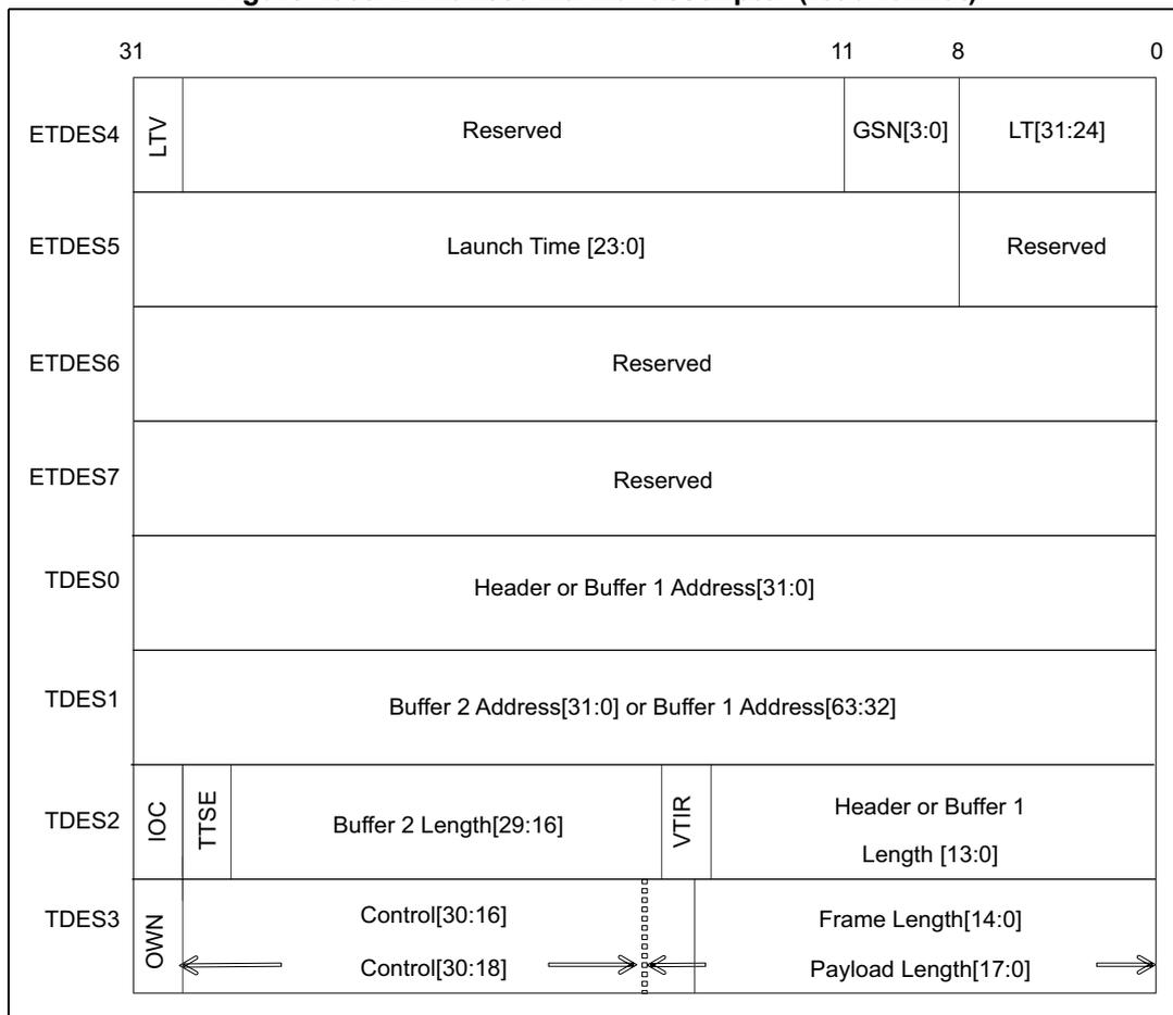
The diagram illustrates the structure of the enhanced normal descriptor in read format. It consists of several fields:
- ETDES4: Bit 31 is LTV. Bits 30-12 are Reserved. Bits 11-8 are GSN[3:0]. Bits 7-0 are LT[31:24].
- ETDES5: Bits 31-8 are Launch Time [23:0]. Bits 7-0 are Reserved.
- ETDES6: All 32 bits are Reserved.
- ETDES7: All 32 bits are Reserved.
- TDES0: All 32 bits are Header or Buffer 1 Address[31:0].
- TDES1: All 32 bits are Buffer 2 Address[31:0] or Buffer 1 Address[63:32].
- TDES2: Bit 31 is IOC. Bit 30 is TTSE. Bits 29-16 are Buffer 2 Length[29:16]. Bit 15 is VTIR. Bits 14-0 are Header or Buffer 1 Length [13:0].
- TDES3: Bit 31 is OWN. Bits 30-16 are Control[30:16]. Bits 15-0 are Frame Length[14:0].
Table 845. Enhanced normal descriptor (read format)
| Bit | Name | Description |
|---|---|---|
| 31 | LTV | Launch time valid indicates that the launch time (LT) and GSN fields present in the descriptor are valid. The LTV must be set only if the FD bit of the descriptor is not set. |
| 30:12 | Reserved. | |
| 11:8 | GSN | GCL slot number associated with the packet |
| 7:0 | LT | Launch time associated with the packet. |
For details of the other fields, see Table 821: TDES0 normal descriptor (read format) .
Enhanced normal descriptor (write format)
Figure 1070. Enhanced normal descriptor (write format)
| 31 | 11 | 8 | 0 | ||
|---|---|---|---|---|---|
| ETDES4 | LTV | Reserved | GSN[3:0] | LT[31:24] | |
| ETDES5 | Launch Time [23:0] | Reserved | |||
| ETDES6 | Reserved | ||||
| ETDES7 | Reserved | ||||
| TDES0 | Timestamp Low | ||||
| TDES1 | Timestamp High | ||||
| TDES2 | Reserved | ||||
| TDES3 | OWN | Status[30:0] | |||
For details on LTV, GSN, and LT fields, see Enhanced normal descriptor (read format) . For details on the other fields, see Table 825: TDES0 normal descriptor (write-back format) .
Note: In both write-back formats, no modifications can be done to the extended 16 bytes. The rest of the 16 bytes (TDESC0 to TDESC3) are written back as per the previous 16 bytes descriptor format.
The fetch time, when enabled, overrides the AV slot function.
When an unaligned new GCL list (with a different CTR) is installed, it is recommended not to have traffic during the installation of the new list. Any traffic during the switching of the lists might result in unpredictable behavior of fetch, launch, and launch expiry, as the CTR and BTR values get updated while the frame is being processed.
Enhanced context descriptor (read format)
Figure 1071. Enhanced context descriptor (read format)
| 31 | 0 | |||||||
|---|---|---|---|---|---|---|---|---|
| ETDES4 | Reserved | |||||||
| ETDES5 | Reserved | |||||||
| ETDES6 | Reserved | |||||||
| ETDES7 | Reserved | |||||||
| TDES0 | Timestamp Low [31:0] | |||||||
| TDES1 | Timestamp High [31:0] | |||||||
| TDES2 | Inner VLAN Tag[31:16] | Reserved | Maximum Segment Size[13:0] | |||||
| TDES3 | OWN | Control[30:16] | VLAN Tag [15:0] | |||||
For details of the various fields, see Transmit context descriptor .
Enhanced context descriptor (write format) Figure 1072. Enhanced context descriptor (write format)
The diagram illustrates the structure of an Enhanced context descriptor (write format). It consists of eight rows of 32-bit words, numbered 31 down to 0 at the top. The first seven rows (ETDES4 through TDES2) are each a single 32-bit word, all of which are Reserved. The eighth row (TDES3) is a 32-bit word divided into five fields: OWN (bit 31), CTXT (bit 30), a 28-bit Reserved field (bits 29-2), CDE (bit 1), and a 1-bit Reserved field (bit 0).
| 31 | 0 | ||||
|---|---|---|---|---|---|
| ETDES4 | Reserved | ||||
| ETDES5 | Reserved | ||||
| ETDES6 | Reserved | ||||
| ETDES7 | Reserved | ||||
| TDES0 | Reserved | ||||
| TDES1 | Reserved | ||||
| TDES2 | Reserved | ||||
| TDES3 | OWN | CTXT | Reserved | CDE | Reserved |
For details of the various fields, see Receive context descriptor .
76.11 Ethernet registers
76.11.1 Ethernet register maps
This section provides the following register maps:
- • DMA registers (see Section 76.11.2: Ethernet DMA registers )
- • MTL registers (see Section 76.11.3: Ethernet MTL registers )
- • MAC registers including MMC registers (see Section 76.11.4: Ethernet MAC and MMC registers )
76.11.2 Ethernet DMA registers
DMA mode register (ETH_DMAMR)
Address offset: 0x1000
Reset value: 0x0000 0000
The DMA mode register establishes the bus operating modes for the DMA.
| 31 | 30 | 29 | 28 | 27 | 26 | 25 | 24 | 23 | 22 | 21 | 20 | 19 | 18 | 17 | 16 |
|---|---|---|---|---|---|---|---|---|---|---|---|---|---|---|---|
| Res. | Res. | Res. | Res. | Res. | Res. | Res. | Res. | Res. | Res. | Res. | Res. | Res. | Res. | INTM[1:0] | |
| 15 | 14 | 13 | 12 | 11 | 10 | 9 | 8 | 7 | 6 | 5 | 4 | 3 | 2 | 1 | 0 |
| Res. | Res. | Res. | Res. | TXPR | Res. | Res. | DSPW | Res. | Res. | Res. | TAA2 | TAA1 | TAA0 | Res. | SWR |
| rw | rw | r | r | r | rw |
Bits 31:18 Reserved, must be kept at reset value.
Bits 17:16 INTM[1:0] : Interrupt Mode
This field defines the interrupt mode of the Ethernet peripheral.
The behavior of the interrupt signal and of the RI/TI bits in the ETH_DMACSR register changes depending on the INTM value (refer to Table 820: Transfer complete interrupt behavior ).
Bits 15:12 Reserved, must be kept at reset value.
Bit 11 TXPR : Transmit priority
When set, this bit indicates that the Tx DMA has higher priority than the Rx DMA during arbitration for the system-side bus.
Bits 10:9 Reserved, must be kept at reset value.
Bit 8 DSPW : Descriptor Posted Write
When this bit is set to
0: The descriptor writes are always non-posted.
1: The descriptor writes are non-posted only when IOC (Interrupt on completion) is set in last descriptor. Otherwise, the descriptor writes are always posted.
Bits 7:5 Reserved, must be kept at reset value.
Bits 4:2 TAA[2:0] : Transmit Arbitration Algorithm
This field is used to select the arbitration algorithm for the Transmit side when multiple Tx DMAs are selected.
000: Fixed priority. In fixed priority, Channel 0 has the lowest priority and the last channel has the highest priority.
001: Weighted Strict priority (WSP)
010: Weighted Round-Robin (WRR)
011 to 111: Reserved, must not be used.
Bit 1 Reserved, must be kept at reset value.
Bit 0 SWR : Software Reset
When this bit is set, the MAC and the DMA controller reset the logic and all internal registers of the DMA, MTL, and MAC. This bit is automatically cleared after the reset operation is complete in all clock domains. Before reprogramming any register, a value of zero should be read in this bit.
Note: The reset operation is complete only when all resets in all active clock domains are deasserted. Therefore, it is essential that all PHY inputs clocks (applicable for the selected PHY interface) are present for software reset completion. The time to complete the software reset operation depends on the frequency of the slowest active clock.
System bus mode register (ETH_DMASBMR)
Address offset: 0x1004
Reset value: 0x0101 0000
The System bus mode register controls the behavior of the AXI master. It mainly controls burst splitting and number of outstanding requests.
| 31 | 30 | 29 | 28 | 27 | 26 | 25 | 24 | 23 | 22 | 21 | 20 | 19 | 18 | 17 | 16 |
|---|---|---|---|---|---|---|---|---|---|---|---|---|---|---|---|
| EN_LPI | LPI_XIT_PKT | Res. | Res. | Res. | Res. | WR_OSR_LMT [1:0] | Res. | Res. | Res. | Res. | Res. | Res. | RD_OSR_LMT [1:0] | ||
| rw | rw | rw | rw | rw | rw | ||||||||||
| 15 | 14 | 13 | 12 | 11 | 10 | 9 | 8 | 7 | 6 | 5 | 4 | 3 | 2 | 1 | 0 |
| Res. | Res. | ONEKB BE | AAL | Res. | AALE | Res. | Res. | BLEN 256 | BLEN 128 | BLEN 64 | BLEN 32 | BLEN 16 | BLEN8 | BLEN4 | FB |
| rw | rw | rw | rw | rw | rw | rw | rw | rw | rw | rw | |||||
Bit 31 EN_LPI : Enable Low Power Interface (LPI)
When set to 1, this bit enables the LPI mode and accepts the LPI request from the AXI System Clock controller.
When set to 0, this bit disables the LPI mode and always denies the LPI request from the AXI System Clock controller.
Bit 30 LPI_XIT_PKT : Unlock on Magic Packet or Remote wake-up Packet
When set to 1, this bit enables the AXI master to come out of the LPI mode only when the magic packet or remote wake-up packet is received. When set to 0, this bit enables the AXI master to come out of the LPI mode when any packet is received.
Bits 29:26 Reserved, must be kept at reset value.
Bits 25:24 WR_OSR_LMT[1:0] : AXI Maximum Write Outstanding Request Limit
This value limits the maximum outstanding request on the AXI write interface. Maximum outstanding requests = WR_OSR_LMT + 1.
Bits 23:18 Reserved, must be kept at reset value.
Bits 17:16 RD_OSR_LMT[1:0] : AXI Maximum Read Outstanding Request Limit
This value limits the maximum outstanding request on the AXI read interface. Maximum outstanding requests = RD_OSR_LMT + 1
Bits 15:14 Reserved, must be kept at reset value.
Bit 13 ONEKBBE : 1 Kbyte Boundary Crossing Enable for the AXI Master
When set, the burst transfers performed by the AXI master do not cross 1 Kbyte boundary.
When reset, the burst transfers performed by the AXI master do not cross 4 Kbyte boundary.
Bit 12 AAL : Address-Aligned Beats
When this bit is set to 1, the master performs address-aligned burst transfers on Read and Write channels.
Bit 11 Reserved, must be kept at reset value.
Bit 10 AALE : Automatic AXI LPI enable
When set to 1, enables the AXI master to enter into LPI state when there is no activity in the Ethernet peripheral for a number of system clock cycles programmed in the LPIEI field of ETH_DMALPIEI register.
Bits 9:8 Reserved, must be kept at reset value.
Bit 7 BLEN256 : AXI Burst Length 256
When this bit is set to 1, the AXI master can select a burst length of 256 on the AXI interface.
Bit 6 BLEN128 : AXI Burst Length 128
When this bit is set to 1, the AXI master can select a burst length of 128 on the AXI interface.
Bit 5 BLEN64 : AXI Burst Length 64
When this bit is set to 1, the AXI master can select a burst length of 64 on the AXI interface.
Bit 4 BLEN32 : AXI Burst Length 32
When this bit is set to 1, the AXI master can select a burst length of 32 on the AXI interface.
Bit 3 BLEN16 : AXI Burst Length 16
When this bit is set to 1 or the FB bit is set to 0, the AXI master can select a burst length of 16 on the AXI interface.
When the FB bit is set to 0, setting this bit has no effect.
Bit 2 BLEN8 : AXI Burst Length 8
When this bit is set to 1 or the FB bit is set to 0, the AXI master can select a burst length of 8 on the AXI interface.
When the FB bit is set to 0, setting this bit has no effect.
Bit 1 BLEN4 : AXI Burst Length 4
When this bit is set to 1 or the FB bit is set to 0, the AXI master can select a burst length of 4 on the AXI interface.
When the FB bit is set to 0, setting this bit has no effect.
Bit 0 FB : Fixed Burst Length
When this bit is set to 1, the AXI master initiates burst transfers of specified lengths as given below.
- – Burst transfers of fixed burst lengths as indicated by the BLEN256, BLEN128, BLEN64, BLEN32, BLEN16, BLEN8, or BLEN4 field
- – Burst transfers of length 1: when this bit is set to 0, the AXI master initiates burst transfers that are equal to or less than the maximum allowed burst length programmed in Bits[7:1].
Interrupt status register (ETH_DMAISR)
Address offset: 0x1008
Reset value: 0x0000 0000
The application reads this interrupt status register during interrupt service routine or polling to determine the interrupt status of DMA channels, MTL queues, and the MAC.
| 31 | 30 | 29 | 28 | 27 | 26 | 25 | 24 | 23 | 22 | 21 | 20 | 19 | 18 | 17 | 16 |
|---|---|---|---|---|---|---|---|---|---|---|---|---|---|---|---|
| Res. | Res. | Res. | Res. | Res. | Res. | Res. | Res. | Res. | Res. | Res. | Res. | Res. | Res. | MACIS | MTLIS |
| 15 | 14 | 13 | 12 | 11 | 10 | 9 | 8 | 7 | 6 | 5 | 4 | 3 | 2 | 1 | 0 |
| Res. | Res. | Res. | Res. | Res. | Res. | Res. | Res. | Res. | Res. | Res. | Res. | Res. | Res. | DC1IS | DC0IS |
| r | r |
Bits 31:18 Reserved, must be kept at reset value.
Bit 17 MACIS: MAC interrupt status
This bit indicates an interrupt event in the MAC. To reset this bit to 1'b0, the software must read the corresponding register in the MAC to get the exact cause of the interrupt and clear its source.
Bit 16 MTLIS: MTL interrupt status
This bit indicates an interrupt event in the MTL. To reset this bit to 1'b0, the software must read the corresponding register in the MTL to get the exact cause of the interrupt and clear its source.
Bits 15:2 Reserved, must be kept at reset value.
Bit 1 DC1IS: DMA Channel 1 interrupt status
This bit indicates an interrupt event in DMA Channel 1. To reset this bit to 0, the software must read the corresponding register in DMA Channel 1 to get the exact cause of the interrupt and clear its source.
Bit 0 DC0IS: DMA Channel 0 interrupt status
This bit indicates an interrupt event in DMA Channel 0. To reset this bit to 0, the software must read the corresponding register in DMA Channel 0 to get the exact cause of the interrupt and clear its source.
Debug status register (ETH_DMADSR)
Address offset: 0x100C
Reset value: 0x0000 0000
The Debug status register gives the receive and transmit process status for DMA Channel 0 to 1 for debugging purpose.
| 31 | 30 | 29 | 28 | 27 | 26 | 25 | 24 | 23 | 22 | 21 | 20 | 19 | 18 | 17 | 16 |
|---|---|---|---|---|---|---|---|---|---|---|---|---|---|---|---|
| Res. | Res. | Res. | Res. | Res. | Res. | Res. | Res. | TPS1[3:0] | RPS1[3:0] | ||||||
| r | r | r | r | r | r | r | r | ||||||||
| 15 | 14 | 13 | 12 | 11 | 10 | 9 | 8 | 7 | 6 | 5 | 4 | 3 | 2 | 1 | 0 |
| TPS0[3:0] | RPS0[3:0] | Res. | Res. | Res. | Res. | Res. | Res. | AXRH STS | AXVHS TS | ||||||
| r | r | r | r | r | r | r | r | r | r | ||||||
Bits 31:24 Reserved, must be kept at reset value.
Bits 23:20 TPS1[3:0] : DMA Channel 1 Transmit Process State
This field indicates the Tx DMA FSM state for Channel 1. This field is similar to the TPS0 field.
Bits 19:16 RPS1[3:0] : DMA Channel 1 receive Process State
This field indicates the Rx DMA FSM state for Channel 1. This field is similar to the RPS0 field.
Bits 15:12 TPS0[3:0] : DMA Channel 0 Transmit Process State
This field indicates the Tx DMA FSM state for Channel 0:
000: Stopped (Reset or Stop Transmit Command issued)
001: Running (Fetching Tx Transfer Descriptor)
010: Running (Waiting for status)
011: Running (Reading Data from system memory buffer and queuing it to the Tx buffer (Tx FIFO))
100: Timestamp write state
101: Reserved for future use
110: Suspended (Tx Descriptor Unavailable or Tx Buffer Underflow)
111: Running (Closing Tx Descriptor)
The MSB of this field always returns 0. This field does not generate an interrupt.
Bits 11:8 RPS0[3:0] : DMA Channel 0 receive Process State
This field indicates the Rx DMA FSM state for Channel 0:
000: Stopped (Reset or Stop receive Command issued)
001: Running (Fetching Rx Transfer Descriptor)
010: Reserved for future use
011: Running (Waiting for Rx packet)
100: Suspended (Rx Descriptor Unavailable)
101: Running (Closing the Rx Descriptor)
110: Timestamp write state
111: Running (Transferring the received packet data from the Rx buffer to the system memory)
The MSB of this field always returns 0. This field does not generate an interrupt.
Bits 7:2 Reserved, must be kept at reset value.
Bit 1 AXRHSTS : AXI Master Read Channel Status
When high, this bit indicates that the read channel of the AXI master is active, and it is transferring the data.
Bit 0 AXWHSTS : AXI Master Write Channel
When high, this bit indicates that the write channel of the AXI master is active, and it is transferring data.
AXI4 transmit channel ACE control register (ETH_DMAA4TXACR)
Address offset: 0x1020
Reset value: 0x0000 0000
This register is used to control the AXI4 Cache Coherency Signals for read transactions by all the Transmit DMA channels. The following signals of the AXI4 interface are driven with different values as programmed for corresponding type (descriptor, buffer1, buffer2) of access:
- • arcache_m_o[3:0]
| 31 | 30 | 29 | 28 | 27 | 26 | 25 | 24 | 23 | 22 | 21 | 20 | 19 | 18 | 17 | 16 |
|---|---|---|---|---|---|---|---|---|---|---|---|---|---|---|---|
| Res. | Res. | Res. | Res. | Res. | Res. | Res. | Res. | Res. | Res. | Res. | Res. | THC[3:0] | |||
| rw | rw | rw | rw | ||||||||||||
| 15 | 14 | 13 | 12 | 11 | 10 | 9 | 8 | 7 | 6 | 5 | 4 | 3 | 2 | 1 | 0 |
| Res. | Res. | Res. | Res. | TEC[3:0] | Res. | Res. | Res. | Res. | TDRC[3:0] | ||||||
| rw | rw | rw | rw | rw | rw | rw | rw | ||||||||
Bits 31:20 Reserved, must be kept at reset value.
Bits 19:16 THC[3:0] : Transmit DMA First Packet Buffer or TSO Header Cache Control
When TSO is NOT enabled, This field is used to drive arcache_o[3:0] signal when Transmit DMA is accessing First Buffer of the Packet (First valid buffer with FD being set in the TDES3 of the Descriptor).
When TSO is enabled, This field is used to drive arcache_o[3:0] signal when the Transmit DMA is accessing the TSO Header data.
Bits 15:12 Reserved, must be kept at reset value.
Bits 11:8 TEC[3:0] : Transmit DMA Extended Packet Buffer or TSO Payload Cache Control
When TSO is NOT enabled, This field is used to drive arcache_o[3:0] signal when Transmit DMA is accessing the extended buffers (when packet is distributed across multiple buffers).
When TSO is enabled, This field is used to drive arcache_o[3:0] signal when the Transmit DMA is accessing the TSO payload data.
Bits 7:4 Reserved, must be kept at reset value.
Bits 3:0 TDRC[3:0] : Transmit DMA Read Descriptor Cache Control
This field is used to drive arcache_o[3:0] signal when Transmit DMA engines access the Descriptor.
AXI4 receive channel ACE control register (ETH_DMAA4RXACR)
Address offset: 0x1024
Reset value: 0x0000 0000
This register is used to control the AXI4 Cache Coherency Signals for write transactions by all the receive DMA channels. The following signals of the AXI4 interface are driven with different values as programmed for corresponding type (descriptor, buffer1, buffer2) of access:
- • awcache_m_o[3:0]
| 31 | 30 | 29 | 28 | 27 | 26 | 25 | 24 | 23 | 22 | 21 | 20 | 19 | 18 | 17 | 16 |
|---|---|---|---|---|---|---|---|---|---|---|---|---|---|---|---|
| Res. | Res. | Res. | Res. | RDC[3:0] | Res. | Res. | Res. | Res. | RHC[3:0] | ||||||
| rw | rw | rw | rw | rw | rw | rw | rw | ||||||||
| 15 | 14 | 13 | 12 | 11 | 10 | 9 | 8 | 7 | 6 | 5 | 4 | 3 | 2 | 1 | 0 |
| Res. | Res. | Res. | Res. | RPC[3:0] | Res. | Res. | Res. | Res. | RDWC[3:0] | ||||||
| rw | rw | rw | rw | rw | rw | rw | rw | ||||||||
Bits 31:28 Reserved, must be kept at reset value.
Bits 27:24 RDC[3:0] : Receive DMA Buffer Cache Control
This field is used to drive awcache_o[3:0] signal when receive DMA is accessing the Buffer when Header and payload are NOT separated.
Bits 23:20 Reserved, must be kept at reset value.
Bits 19:16 RHC[3:0] : Receive DMA Header Cache Control
This field is used to drive awcache_o[3:0] signal when receive DMA is accessing the header Buffer when Header and payload are separated.
Bits 15:12 Reserved, must be kept at reset value.
Bits 11:8 RPC[3:0] : Receive DMA Payload Cache Control
This field is used to drive awcache_o[3:0] signal when receive DMA is accessing the Payload Buffer when Header and payload are separated.
Bits 7:4 Reserved, must be kept at reset value.
Bits 3:0 RDWC[3:0] : Receive DMA Write Descriptor Cache Control
This field is used to drive awcache_o[3:0] signal when receive DMA accesses the Descriptor.
AXI4 descriptor ACE control register (ETH_DMAA4DACR)
Address offset: 0x1028
Reset value: 0x0000 0000
This register is used to control the AXI4 Cache Coherency Signals for Descriptor write transactions by all the TxDMA channels and Descriptor read transactions by all the RxDMA channels. It also controls the values to be driven on awprot_m_o and arprot_m_o.
| 31 | 30 | 29 | 28 | 27 | 26 | 25 | 24 | 23 | 22 | 21 | 20 | 19 | 18 | 17 | 16 |
|---|---|---|---|---|---|---|---|---|---|---|---|---|---|---|---|
| Res. | Res. | Res. | Res. | Res. | Res. | Res. | Res. | Res. | Res. | Res. | Res. | Res. | Res. | Res. | Res. |
| 15 | 14 | 13 | 12 | 11 | 10 | 9 | 8 | 7 | 6 | 5 | 4 | 3 | 2 | 1 | 0 |
| Res. | RDRC[3:0] | Res. | TDWD[1:0] | TDWC[3:0] | |||||||||||
| rw | rw | rw | rw | rw | rw | rw | rw | rw | rw | ||||||
Bits 31:12 Reserved, must be kept at reset value.
Bits 11:8 RDRC[3:0] : Receive DMA Read Descriptor Cache control
This field is used to drive arcache_o[3:0] signal when receive DMA engines read the Descriptor.
Bits 7:6 Reserved, must be kept at reset value.
Bits 5:4 TDWD[1:0] : Transmit DMA Write Descriptor Domain control
This field is used to drive awdomain_o[1:0] signal when Transmit DMA write to the Descriptor.
Bits 3:0 TDWC[3:0] : Transmit DMA Write Descriptor Cache control
This field is used to drive awcache_o[3:0] signal when Transmit DMA writes to the Descriptor.
AXI4 LPI Entry Interval register (ETH_DMALPIE)
Address offset: 0x1040
Reset value: 0x0000 0000
This register is used to control the AXI LPI entry interval.
| 31 | 30 | 29 | 28 | 27 | 26 | 25 | 24 | 23 | 22 | 21 | 20 | 19 | 18 | 17 | 16 |
|---|---|---|---|---|---|---|---|---|---|---|---|---|---|---|---|
| Res. | Res. | Res. | Res. | Res. | Res. | Res. | Res. | Res. | Res. | Res. | Res. | Res. | Res. | Res. | Res. |
| 15 | 14 | 13 | 12 | 11 | 10 | 9 | 8 | 7 | 6 | 5 | 4 | 3 | 2 | 1 | 0 |
| Res. | Res. | Res. | Res. | Res. | Res. | Res. | Res. | Res. | Res. | Res. | Res. | LPIE[3:0] | |||
| rw | rw | rw | rw | ||||||||||||
Bits 31:4 Reserved, must be kept at reset value.
Bits 3:0 LPIE[3:0] : LPI Entry Interval
Contains the number of system clock cycles, multiplied by 64, to wait for an activity in the peripheral to enter into the AXI low power state.
0 indicates 64 clock cycles.
DMA TBS control register 0 (ETH_DMATBSCTRL0R)
Address offset: 0x1050
Reset value: 0x0000 0000
This register controls time-based scheduling attributes.
| 31 | 30 | 29 | 28 | 27 | 26 | 25 | 24 | 23 | 22 | 21 | 20 | 19 | 18 | 17 | 16 |
|---|---|---|---|---|---|---|---|---|---|---|---|---|---|---|---|
| FTOS[23:8] | |||||||||||||||
| rw | rw | rw | rw | rw | rw | rw | rw | rw | rw | rw | rw | rw | rw | rw | rw |
| 15 | 14 | 13 | 12 | 11 | 10 | 9 | 8 | 7 | 6 | 5 | 4 | 3 | 2 | 1 | 0 |
| FTOS[7:0] | Res. | FGOS[2:0] | Res. | Res. | Res. | FTOV | |||||||||
| rw | rw | rw | rw | rw | rw | rw | rw | rw | rw | rw | rw | ||||
Bits 31:8 FTOS[23:0] : Fetch time offset
The value in units of 256 nanoseconds, that has to be deducted from the launch time to compute the fetch time.
The maximum value is 999,999,999 ns. It must be smaller than CTR - 1 when the ESTM mode is set since this value is a modulo CTR value.
Bit 7 Reserved, must be kept at reset value.
Bits 6:4 FGOS[2:0] : Fetch GSN offset
The number of GSN slots that must be deducted from the launch GSN to compute the fetch GSN. This value is valid only when FTOV is set.
Bits 3:1 Reserved, must be kept at reset value.
Bit 0 FTOV : Fetch time offset valid
When set, this bit indicates that the FTOS field is valid. When not set, it indicates that the fetch offset is not valid and the DMA engine can fetch the frames from host memory without any time restrictions.
0: Fetch time offset invalid
1: Fetch time offset valid
Channel x control register (ETH_DMACxCR)
Address offset: 0x1100 + 0x80 * x, (x = 0 to 1)
Reset value: 0x0000 0000
The DMA Channel x control register specifies the MSS value for segmentation, length to skip between two descriptors, and also the features such as header splitting and 8xPBL mode.
| 31 | 30 | 29 | 28 | 27 | 26 | 25 | 24 | 23 | 22 | 21 | 20 | 19 | 18 | 17 | 16 |
|---|---|---|---|---|---|---|---|---|---|---|---|---|---|---|---|
| Res. | Res. | Res. | Res. | Res. | Res. | Res. | Res. | Res. | Res. | Res. | DSL[2:0] | Res. | PBLX8 | ||
| rw | rw | rw | rw | ||||||||||||
| 15 | 14 | 13 | 12 | 11 | 10 | 9 | 8 | 7 | 6 | 5 | 4 | 3 | 2 | 1 | 0 |
| Res. | Res. | MSS[13:0] | |||||||||||||
| rw | rw | rw | rw | rw | rw | rw | rw | rw | rw | rw | rw | rw | rw | ||
Bits 31:21 Reserved, must be kept at reset value.
Bits 20:18 DSL[2:0] : Descriptor Skip Length
This bit specifies the 64-bit double-word number to skip between two unchained descriptors. The address skipping starts from the end of the current descriptor to the start of the next descriptor.
When the DSL value is equal to zero, the DMA takes the descriptor table as contiguous.
Bit 17 Reserved, must be kept at reset value.
Bit 16 PBLX8 : 8xPBL mode
When this bit is set, the PBL value programmed in Bits[21:16] in Channel x transmit control register (ETH_DMACxTXCR) and in Bits[21:16] in Channel x receive control register (ETH_DMACxRXCR) is multiplied eight times. Therefore, the DMA transfers the data in 8, 16, 32, 64, 128, and 256 beats depending on the PBL value.
Bits 15:14 Reserved, must be kept at reset value.
Bits 13:0 MSS[13:0] : Maximum Segment Size
This field specifies the maximum segment size that should be used while segmenting the packet. This field is valid only if the TSE bit of Channel x transmit control register (ETH_DMACxTXCR) is set.
The value programmed in this field must be more than the configured Data width in bytes. It is recommended to use a MSS value of 64 bytes or more.
Channel x transmit control register (ETH_DMACxTXCR)
Address offset: 0x1104 + 0x80 * x, (x = 0 to 1)
Reset value: 0x0000 0000
The DMA Channel x Transmit Control register controls the Tx features such as PBL, TCP segmentation, and Tx Channel weights.
| 31 | 30 | 29 | 28 | 27 | 26 | 25 | 24 | 23 | 22 | 21 | 20 | 19 | 18 | 17 | 16 |
|---|---|---|---|---|---|---|---|---|---|---|---|---|---|---|---|
| Res | Res | Res | EDSE | TQOS[3:0] | Res | Res | TXPBL[5:0] | ||||||||
| rw | rw | rw | rw | rw | rw | rw | rw | rw | rw | rw | |||||
| 15 | 14 | 13 | 12 | 11 | 10 | 9 | 8 | 7 | 6 | 5 | 4 | 3 | 2 | 1 | 0 |
| IPBL | Res. | Res. | TSE | Res. | Res. | Res. | Res. | Res. | Res. | Res. | OSF | TCW[2:0] | ST | ||
| rw | rw | rw | r | r | r | rw | |||||||||
Bits 31:29 Reserved, must be kept at reset value.
Bit 28 EDSE : Enhanced Descriptor Enable
When this bit is set, the corresponding channel uses 32-byte enhanced descriptors both for normal and context descriptors.
When reset, the corresponding channel uses the 16-byte descriptors.
Bits 27:24 TQOS[3:0] : Transmit QOS
This field is used to drive arqos_m_o[3:0] or awqos_m_o[3:0] output signals for all transactions of DMA Tx Channel x.
Bits 23:22 Reserved, must be kept at reset value.
Bits 21:16 TXPBL[5:0] : Transmit Programmable Burst Length
These bits indicate the maximum number of beats to be transferred in one DMA data transfer. This is the maximum value that is used in a single block Read or Write. The DMA always attempts to burst as specified in PBL each time it starts a burst transfer on the application bus. You can program PBL with any of the following values: 1, 2, 4, 8, 16, or 32. Any other value results in undefined behavior.
To transfer more than 32 beats, perform the following steps:
- Set the PBLx8 mode in ETH_DMACxCR.
- Set the TXPBL[5:0].
Note: The maximum value of TXPBL must be less than or equal to half the Tx Queue size (TQS field of Tx queue x operating mode register (ETH_MTLTXQxOMR) ) in terms of beats. This is required so that the Tx Queue has space to store at least another Tx PBL worth of data while the MTL Tx Queue Controller is transferring data to MAC. The total locations in Tx Queue of size 4096 bytes is 512, TXPBL and 8xPBL needs to be programmed to less than or equal to 512/2.
Bit 15 IPBL : Ignore PBL Requirement
When this bit is set, the DMA does not check for PBL number of locations in the MTL before initiating a transfer. If space is not available, the MTL might use handshaking to slow the DMA.
Note: This bit/mode must not be used when multiple Transmit DMA Channels are enabled as it might block other transmit and receive DMA Channels from accessing the Read Data Channel of AXI bus until space is available in Transmit Queue for current transfer.
Bits 14:13 Reserved, must be kept at reset value.
Bit 12 TSE : TCP Segmentation EnabledWhen this bit is set, the DMA performs the TCP segmentation for packets in Channel x. The TCP segmentation is done only for those packets for which the TSE bit (TDES0[19]) is set in the Tx Normal descriptor. When this bit is set, the TxPBL value must be greater than or equal to 4.
Bits 11:5 Reserved, must be kept at reset value.
Bit 4 OSF : Operate on Second PacketWhen this bit is set, it instructs the DMA to process the second packet of the Transmit data even before the status for the first packet is obtained.
Bits 3:1 TCW[2:0] : Transmit Channel WeightThis field indicates the weight assigned to the corresponding Transmit channel. When reset is complete, this field is set to 0 for all channels by default, resulting in equal weights to all channels.
Bit 0 ST : Start or Stop Transmission CommandWhen this bit is set, transmission is placed in the Running state. The DMA checks the Transmit list at the current position for a packet to be transmitted.
The DMA tries to acquire descriptor from either of the following positions:
- – The current position in the list: this is the base address of the Transmit list set by the ETH_DMACxTXDLAR register.
- – The position at which the transmission was previously stopped
If the DMA does not own the current descriptor, the transmission enters the Suspended state and the TBU bit of the ETH_DMACxSR is set. The Start Transmission command is effective only when the transmission is stopped. If the command is issued before setting the ETH_DMACxTXDLAR register, the DMA behavior is unpredictable.
When this bit is reset, the transmission process is placed in the Stopped state after completing the transmission of the current packet. The Next Descriptor position in the Transmit list is saved, and it becomes the current position when the transmission is restarted. To change the list address, you need to program ETH_DMACxTXDLAR register with a new value when this bit is reset. The new value is considered when this bit is set again. The stop transmission command is effective only when the transmission of the current packet is complete or the transmission is in the Suspended state.
Channel x receive control register (ETH_DMACxRXCR)
Address offset: 0x1108 + 0x80 * x, (x = 0 to 1)
Reset value: 0x0000 0000
The DMA channel x receive control register controls the Rx features such as PBL, buffer size, and extended status.
| 31 | 30 | 29 | 28 | 27 | 26 | 25 | 24 | 23 | 22 | 21 | 20 | 19 | 18 | 17 | 16 |
|---|---|---|---|---|---|---|---|---|---|---|---|---|---|---|---|
| RPF | Res. | Res. | Res. | RQOS[3:0] | Res. | Res. | RXPBL[5:0] | ||||||||
| rw | rw | rw | rw | rw | rw | rw | rw | rw | rw | rw | |||||
| 15 | 14 | 13 | 12 | 11 | 10 | 9 | 8 | 7 | 6 | 5 | 4 | 3 | 2 | 1 | 0 |
| Res. | RBSZ[13:0] | SR | |||||||||||||
| rw | rw | rw | rw | rw | rw | rw | rw | rw | rw | rw | rw | rw | rw | rw | |
When this bit is set to 1, the Ethernet peripheral automatically flushes the packet from the Rx queues destined to DMA Rx Channel x when the DMA Rx Channel x is stopped after a system bus error has occurred. When this bit remains set and the DMA is re-started by the software driver, the packets residing in the Rx Queues that were received when this RxDMA was stopped, are flushed out. The packets that are received by the MAC after the RxDMA is re-started are routed to the RxDMA. The flushing happens on the Read side of the Rx queue. When this bit is set to 0 the Ethernet peripheral does not flush the packet in the Rx queue destined to DMA Rx Channel x after the DMA is stopped due to a system bus error.
This might cause head-of-line blocking in the corresponding RxQueue.
Note: The stopping of packet flow from a Rx DMA Channel to the application by setting RPF works only when there is one-to-one mapping of Rx Queue to Rx DMA channels. In Dynamic mapping mode, setting RPF bit in ETH_DMACxRXCR register might flush packets from unintended Rx Queues which are destined to the stopped Rx DMA Channel.
Bits 30:28 Reserved, must be kept at reset value.
Bits 27:24 RQOS[3:0] : Rx AXI4 QOS.This field is used to drive arqos_m_o[3:0] or awqos_m_o[3:0] output signals for all transactions of DMA Rx Channel0.
Bits 23:22 Reserved, must be kept at reset value.
Bits 21:16 RXPBL[5:0] : Receive Programmable Burst LengthThese bits indicate the maximum number of beats to be transferred in one DMA data transfer. This is the maximum value that is used in a single block Read or Write. The DMA always attempts to burst as specified in PBL each time it starts a burst transfer on the application bus. You can program PBL with any of the following values: 1, 2, 4, 8, 16, or 32. Any other value results in undefined behavior.
To transfer more than 32 beats, perform the following steps:
- Set the PBLx8 mode in the ETH_DMAC0CR.
- Set the RXPBL[5:0].
Note: The maximum value of RXPBL must be less than or equal to half the Rx Queue size (RQS field of Rx queue x operating mode register (ETH_MTLRXQxOMR)) in terms of beats. This is required so that the Rx Queue has space to store at least another Rx PBL worth of data while the MTL Rx Queue Controller is transferring data to MAC. The total locations in Rx Queue of size 4096 bytes is 512, RXPBL and 8xPBL needs to be programmed to less than or equal to 512/2.
Bit 15 Reserved, must be kept at reset value.
Bits 14:1 RBSZ[13:0] : Receive Buffer sizeThis field indicates the size of the Rx buffers specified in bytes. The maximum buffer size is limited to 16 Kbytes.
Note: The buffer size must be a multiple of 8. This is required even if the value of buffer address pointer is not aligned to bus width. If the buffer size is not a multiple of 8, it may result into undefined behavior.
The LSB bits (2:0) are ignored and the DMA internally takes the LSB bits as all-zero. Therefore, these LSB bits are read-only (RO).
Bit 0 SR : Start or Stop receive
When this bit is set, the DMA tries to acquire the descriptor from the receive list and processes the incoming packets.
The DMA tries to acquire descriptor from either of the following positions:
- – The current position in the list: this is the address set by the Channel x Rx descriptor list address register (ETH_DMACxRXDLAR) .
- – The position at which the Rx process was previously stopped
If the DMA does not own the current descriptor, the reception is suspended and the RBU bit of the ETH_DMAC0SR is set. The Start Receive command is effective only when the reception is stopped. If the command is issued before setting the Channel x Rx descriptor list address register (ETH_DMACxRXDLAR) , the DMA behavior is unpredictable.
When this bit is reset, the Rx DMA operation is stopped after the transfer of the current packet. The next descriptor position in the receive list is saved, and it becomes the current position after the Rx process is restarted. The Stop Receive command is effective only when the Rx process is in the Running (waiting for Rx packet) or Suspended state.
Channel x Tx descriptor list address register (ETH_DMACxTXDLAR)
Address offset: 0x1114 +0x80 * x, (x = 0 to 1)
Reset value: 0x0000 0000
Channel x Tx descriptor list address register points the DMA to the start of the transmit descriptor list. The descriptor lists reside in the physical memory space of the application and must be Dword-aligned. The DMA internally converts it to bus width aligned address by making the corresponding LSB to low.
Writing to this register is permitted only when the Tx DMA has stopped, that is, the ST bit is cleared in ETH_DMACxTXCR register. When stopped, this register can be written with a new descriptor list address. When the ST bit is set, the DMA takes the newly-programmed descriptor base address. If this register is not changed when ST bit is cleared, the DMA takes the descriptor address where it was stopped earlier.
| 31 | 30 | 29 | 28 | 27 | 26 | 25 | 24 | 23 | 22 | 21 | 20 | 19 | 18 | 17 | 16 |
|---|---|---|---|---|---|---|---|---|---|---|---|---|---|---|---|
| TDESLA[31:16] | |||||||||||||||
| rw | rw | rw | rw | rw | rw | rw | rw | rw | rw | rw | rw | rw | rw | rw | rw |
| 15 | 14 | 13 | 12 | 11 | 10 | 9 | 8 | 7 | 6 | 5 | 4 | 3 | 2 | 1 | 0 |
| TDESLA[15:0] | |||||||||||||||
| rw | rw | rw | rw | rw | rw | rw | rw | rw | rw | rw | rw | rw | r | r | r |
Bits 31:0 TDESLA[31:0] : Start of Transmit List
This field contains the base address of the first descriptor in the Transmit descriptor list. The DMA ignores the LSB bits (2:0) for 64-bit bus width and internally takes these bits as all-zero. Therefore, these LSB bits are read-only (RO).
Channel x Rx descriptor list address register (ETH_DMACxRXDLAR)
Address offset: 0x111C + 0x80 * x, (x = 0 to 1)
Reset value: 0x0000 0000
The Channel x Rx descriptor list address register points the DMA to the start of receive descriptor list.
This register points to the start of the receive descriptor list. The descriptor lists reside in the physical memory space of the application and must be Dword-aligned. The DMA internally converts it to bus width aligned address by making the corresponding LS bits low. Writing to this register is permitted only when reception is stopped. When stopped, this register must be written to before the receive Start command is given. You can write to this register only when Rx DMA has stopped, that is, SR bit is set to zero in ETH_DMACxRXCR register. When stopped, this register can be written with a new descriptor list address.
When you set the SR bit to 1, the DMA takes the newly programmed descriptor base address.
| 31 | 30 | 29 | 28 | 27 | 26 | 25 | 24 | 23 | 22 | 21 | 20 | 19 | 18 | 17 | 16 |
| RDES[31:16] | |||||||||||||||
| rw | rw | rw | rw | rw | rw | rw | rw | rw | rw | rw | rw | rw | rw | rw | rw |
| 15 | 14 | 13 | 12 | 11 | 10 | 9 | 8 | 7 | 6 | 5 | 4 | 3 | 2 | 1 | 0 |
| RDES[15:0] | |||||||||||||||
| rw | rw | rw | rw | rw | rw | rw | rw | rw | rw | rw | rw | rw | r | r | r |
Bits 31:0 RDES[31:0] : Start of receive list
This field contains the base address of the first descriptor in the Rx Descriptor list. The DMA ignores the LSB bits (2:0) for 64-bit bus width and internally takes these bits as all-zero. Therefore, these LSB bits are read-only (RO).
Channel x Tx descriptor tail pointer register (ETH_DMACxTXDTPR) Address offset: \( 0x1120 + 0x80 * x \) ( \( x = 0 \) to \( 1 \) )Reset value: 0x0000 0000
The channel x Tx descriptor tail pointer register points to an offset from the base and indicates the location of the last valid descriptor.
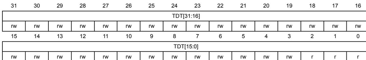
| 31 | 30 | 29 | 28 | 27 | 26 | 25 | 24 | 23 | 22 | 21 | 20 | 19 | 18 | 17 | 16 |
| TDT[31:16] | |||||||||||||||
| rw | rw | rw | rw | rw | rw | rw | rw | rw | rw | rw | rw | rw | rw | rw | rw |
| 15 | 14 | 13 | 12 | 11 | 10 | 9 | 8 | 7 | 6 | 5 | 4 | 3 | 2 | 1 | 0 |
| TDT[15:0] | |||||||||||||||
| rw | rw | rw | rw | rw | rw | rw | rw | rw | rw | rw | rw | rw | r | r | r |
This field contains the tail pointer for the Tx descriptor ring. The software writes the tail pointer to add more descriptors to the Tx channel. The hardware tries to transmit all packets referenced by the descriptors between the head and the tail pointer registers.
Channel x Rx descriptor tail pointer register (ETH_DMACxRXDTPR) Address offset: \( 0x1128 + 0x80 * x \) , ( \( x = 0 \) to \( 1 \) )Reset value: 0x0000 0000
The channel x Rx descriptor tail pointer points to an offset from the base and indicates the location of the last valid descriptor.
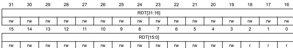
| 31 | 30 | 29 | 28 | 27 | 26 | 25 | 24 | 23 | 22 | 21 | 20 | 19 | 18 | 17 | 16 |
| RDT[31:16] | |||||||||||||||
| rw | rw | rw | rw | rw | rw | rw | rw | rw | rw | rw | rw | rw | rw | rw | rw |
| 15 | 14 | 13 | 12 | 11 | 10 | 9 | 8 | 7 | 6 | 5 | 4 | 3 | 2 | 1 | 0 |
| RDT[15:0] | |||||||||||||||
| rw | rw | rw | rw | rw | rw | rw | rw | rw | rw | rw | rw | rw | r | r | r |
This field contains the tail pointer for the Rx descriptor ring. The software writes the tail pointer to add more descriptors to the Rx channel. The hardware tries to write all received packets to the descriptors referenced between the head and the tail pointer registers.
Channel x Tx descriptor ring length register (ETH_DMACxTXRLR)
Address offset: \( 0x112C + 0x80 * x \) , ( \( x = 0 \) to \( 1 \) )
Reset value: 0x0000 0000
The Tx descriptor ring length register contains the length of the transmit descriptor ring.
| 31 | 30 | 29 | 28 | 27 | 26 | 25 | 24 | 23 | 22 | 21 | 20 | 19 | 18 | 17 | 16 |
|---|---|---|---|---|---|---|---|---|---|---|---|---|---|---|---|
| Res. | Res. | Res. | Res. | Res. | Res. | Res. | Res. | Res. | Res. | Res. | Res. | Res. | Res. | Res. | Res. |
| 15 | 14 | 13 | 12 | 11 | 10 | 9 | 8 | 7 | 6 | 5 | 4 | 3 | 2 | 1 | 0 |
| Res. | Res. | Res. | Res. | Res. | Res. | TDRL[9:0] | |||||||||
| rw | rw | rw | rw | rw | rw | rw | rw | rw | rw | ||||||
Bits 31:10 Reserved, must be kept at reset value.
Bits 9:0 TDRL[9:0] : Transmit descriptor ring length
This 10-bit field sets the maximum number of Tx descriptors in the circular descriptor ring.
TDRL[9:0] corresponds to the number of Tx descriptors minus one.
It can be programmed to any value up to 0x3FF (1024 descriptors).
A minimum ring descriptor length of four is recommended.
For example, program 0x9 to configure 10 descriptors.
Channel x Rx descriptor ring length register (ETH_DMACxRXRLR)
Address offset: \( 0x1130 + 0x80 * x \) , ( \( x = 0 \) to \( 1 \) )
Reset value: 0x0000 0000
The channel x Rx descriptor ring length register contains the length of the receive descriptor circular ring.
| 31 | 30 | 29 | 28 | 27 | 26 | 25 | 24 | 23 | 22 | 21 | 20 | 19 | 18 | 17 | 16 |
|---|---|---|---|---|---|---|---|---|---|---|---|---|---|---|---|
| Res. | Res. | Res. | Res. | Res. | Res. | Res. | Res. | ARBS[6:0] | Res. | ||||||
| rw | rw | rw | rw | rw | rw | rw | |||||||||
| 15 | 14 | 13 | 12 | 11 | 10 | 9 | 8 | 7 | 6 | 5 | 4 | 3 | 2 | 1 | 0 |
| Res. | Res. | Res. | Res. | Res. | Res. | RDRL[9:0] | |||||||||
| rw | rw | rw | rw | rw | rw | rw | rw | rw | rw | ||||||
Bits 31:24 Reserved, must be kept at reset value.
Bits 23:17 ARBS[6:0] : Alternate receive buffer size
Indicates size in bytes for Buffer 1 when ARBS[6:0] is programmed to a non-zero value.
When ARBS[6:0] = 0, Rx Buffer1 and Rx Buffer2 sizes are based on RBSZ[13:0] field of Channel x receive control register (ETH_DMACxRXCR) .
Bits 16:10 Reserved, must be kept at reset value.
Bits 9:0 RDRL[9:0] : Receive Descriptor Ring Length
This 10-bit field sets the maximum number of Rx descriptors in the circular descriptor ring.
RDRL[9:0] corresponds to the number of Rx descriptors minus one. It can be programmed to any value up to 0x3FF (1024 descriptors).
For example, program 0x9 to configure 10 descriptors.
Channel x interrupt enable register (ETH_DMACxIER)Address offset: 0x1134 + 0x80 * x, (x = 0 to 1)
Reset value: 0x0000 0000
The channel x interrupt enable register enables the interrupts reported by the Status register.
| 31 | 30 | 29 | 28 | 27 | 26 | 25 | 24 | 23 | 22 | 21 | 20 | 19 | 18 | 17 | 16 |
|---|---|---|---|---|---|---|---|---|---|---|---|---|---|---|---|
| Res | Res | Res | Res | Res | Res | Res | Res | Res | Res | Res | Res | Res | Res | Res | Res |
| 15 | 14 | 13 | 12 | 11 | 10 | 9 | 8 | 7 | 6 | 5 | 4 | 3 | 2 | 1 | 0 |
| NIE | AIE | CDEE | FBEE | ERIE | ETIE | RWTE | RSE | RBUE | RIE | Res. | Res. | Res. | TBUE | TXSE | TIE |
| rw | rw | rw | rw | rw | rw | rw | rw | rw | rw | rw | rw | rw |
Bits 31:16 Reserved, must be kept at reset value.
Bit 15 NIE: Normal Interrupt Summary Enable
When this bit is set, the normal interrupt summary is enabled. This bit enables the following interrupts in the Channel x status register (ETH_DMACxSR) :
Bit 0: Transmit interrupt
Bit 2: Transmit buffer unavailable
Bit 6: Receive interrupt
Bit 11: Early receive interrupt
When this bit is reset, the normal interrupt summary is disabled.
Bit 14 AIE: Abnormal Interrupt Summary Enable
When this bit is set, the abnormal interrupt summary is enabled. This bit enables the following interrupts in the Channel x status register (ETH_DMACxSR) :
Bit 1: Transmit process stopped
Bit 7: Rx buffer unavailable
Bit 8: Receive process stopped
Bit 9: Receive watchdog timeout
Bit 10: Early transmit interrupt
Bit 12: Fatal bus error
Bit 13: Context descriptor error
When this bit is reset, the abnormal interrupt summary is disabled.
Bit 13 CDEE: Context descriptor error enable
When this bit is set along with the AIE bit, the Context Descriptor error interrupt is enabled.
When this bit is reset, the Context Descriptor error interrupt is disabled.
Bit 12 FBEE: Fatal Bus Error enable
When this bit is set along with the AIE bit, the Fatal Bus error interrupt is enabled. When this bit is reset, the Fatal Bus Error error interrupt is disabled.
Bit 11 ERIE: Early receive interrupt enable
When this bit is set along with the NIE bit, the Early receive interrupt is enabled. When this bit is reset, the Early receive interrupt is disabled.
Bit 10 ETIE: Early Transmit Interrupt enable
When this bit is set along with the AIE bit, the Early Transmit interrupt is enabled. When this bit is reset, the Early Transmit interrupt is disabled.
Bit 9 RWTE : Receive watchdog timeout enable
When this bit is set along with the AIE bit, the receive watchdog timeout interrupt is enabled. When this bit is reset, the receive watchdog timeout interrupt is disabled.
Bit 8 RSE : Receive Stopped Enable
When this bit is set along with the AIE bit, the Receive Stopped Interrupt is enabled. When this bit is reset, the Receive Stopped interrupt is disabled.
Bit 7 RBUE : Receive Buffer Unavailable enable
When this bit is set along with the AIE bit, the Receive Buffer Unavailable interrupt is enabled. When this bit is reset, the Receive Buffer Unavailable interrupt is disabled.
Bit 6 RIE : Receive Interrupt enable
When this bit is set along with the NIE bit, the receive interrupt is enabled. When this bit is reset, the receive interrupt is disabled.
Bits 5:3 Reserved, must be kept at reset value.
Bit 2 TBUE : Transmit Buffer Unavailable enable
When this bit is set along with the NIE bit, the Transmit Buffer Unavailable interrupt is enabled. When this bit is reset, the Transmit Buffer Unavailable interrupt is disabled.
Bit 1 TXSE : Transmit Stopped enable
When this bit is set along with the AIE bit, the Transmission Stopped interrupt is enabled. When this bit is reset, the Transmission Stopped interrupt is disabled.
Bit 0 TIE : Transmit Interrupt enable
When this bit is set along with the NIE bit, the transmit interrupt is enabled. When this bit is reset, the transmit interrupt is disabled.
Figure 1073. Generation of ETH_DMAISR flags
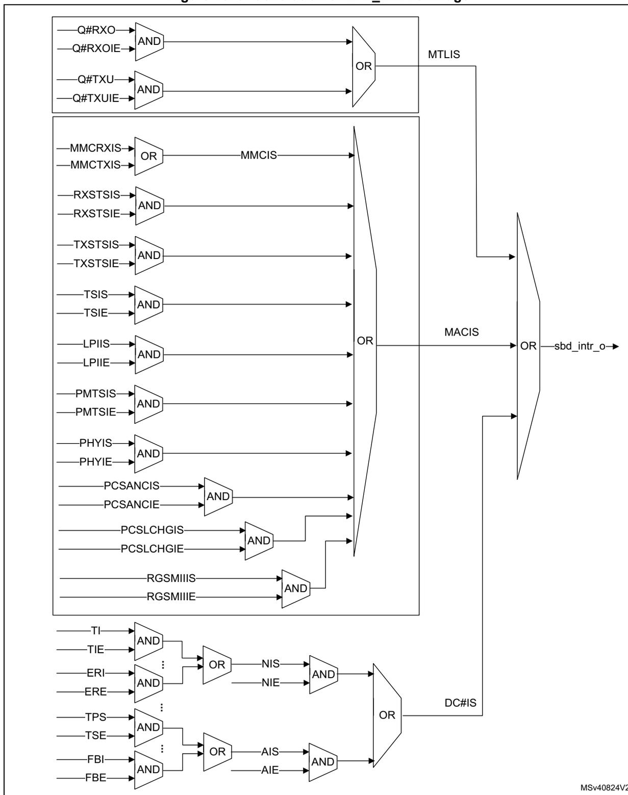
The diagram illustrates the logic for generating three interrupt flags: MTLIS, MACIS, and DC#IS, which are then ORed together to produce the final output sbd_intr_o .
- MTLIS Generation:
- Inputs Q#RXO and Q#RXOIE are ANDed.
- Inputs Q#TXU and Q#TXUIE are ANDed.
- These two results are ORed to produce MTLIS .
- MACIS Generation:
- MMCRXIS and MMCTXIS are ORed to produce MMCIS .
- RXSTSIS and RXSTSIE are ANDed.
- TXSTSIS and TXSTSIE are ANDed.
- TSIS and TSIE are ANDed.
- LPIS and LPPIE are ANDed.
- PMTSIS and PMTSIE are ANDed.
- PHIS and PHYIE are ANDed.
- PCSANCIS and PCSANCIE are ANDed.
- PCSLCHGIS and PCSLCHGIE are ANDed.
- RGSMIIIS and RGSMIIIE are ANDed.
- All these intermediate results are ORed together to produce MACIS .
- DC#IS Generation:
- TI and TIE are ANDed.
- ERI and ERE are ANDed.
- These are ORed (indicated by vertical ellipsis).
- The result is ANDed with NIS and NIE .
- TPS and TSE are ANDed.
- FBI and FBE are ANDed.
- These are ORed (indicated by vertical ellipsis).
- The result is ANDed with AIS and AIE .
- The outputs from the first and second paths are ORed to produce DC#IS .
Finally, MTLIS , MACIS , and DC#IS are ORed together to generate the output sbd_intr_o .
MSV40824V2
Channel x Rx interrupt watchdog timer register (ETH_DMACxRXIWTR)
Address offset: 0x1138 + 0x80 * x, (x = 0 to 1)
Reset value: 0x0000 0000
The receive interrupt watchdog timer register indicates the watchdog timeout for receive interrupt (RI) from the DMA. When this register is written with a non-zero value, it enables the watchdog timer for the RI bit of the Channel x status register (ETH_DMACxSR) .
| 31 | 30 | 29 | 28 | 27 | 26 | 25 | 24 | 23 | 22 | 21 | 20 | 19 | 18 | 17 | 16 |
| Res. | Res. | Res. | Res. | Res. | Res. | Res. | Res. | Res. | Res. | Res. | Res. | Res. | Res. | RWTU[1:0] | |
| rw | rw | ||||||||||||||
| 15 | 14 | 13 | 12 | 11 | 10 | 9 | 8 | 7 | 6 | 5 | 4 | 3 | 2 | 1 | 0 |
| Res. | Res. | Res. | Res. | Res. | Res. | Res. | Res. | RWT[7:0] | |||||||
| rw | rw | rw | rw | rw | rw | rw | rw | ||||||||
Bits 31:18 Reserved, must be kept at reset value.
Bits 17:16 RWTU[1:0] : Receive Interrupt Watchdog Timer Count Units
This bitfield indicates the number of system clock cycles corresponding to one unit in RWT[7:0] bitfield.
00: 256
01: 512
10: 1024
11: 2048
For example, when RWT[7:0] = 2 and RWTU[1:0] = 1, the watchdog timer is set for \( 2 \times 512 = 1024 \) system clock cycles.
Bits 15:8 Reserved, must be kept at reset value.
Bits 7:0 RWT[7:0] : Receive Interrupt Watchdog Timer Count
This bitfield indicates the number of system clock cycles, multiplied by factor indicated in RWTU field, for which the watchdog timer is set.
The watchdog timer is triggered with the programmed value after the Rx DMA completes the transfer of a packet for which the RI bit is not set in the ETH_DMACxSR, because of the setting of Interrupt Enable bit in the corresponding descriptor RDES3[30].
When the watchdog timer runs out, the RI bit is set and the timer is stopped. The watchdog timer is reset when the RI bit is set high because of automatic setting of RI as per the Interrupt Enable bit RDES3[30] of any received packet.
Channel x slot function control status register (ETH_DMACxSFCR)
Address offset: 0x113C + 0x80 * x, (x = 0 to 1)
Reset value: 0x0000 07C0
The Slot Function Control and Status register contains the control bits for slot function and the status for Transmit path.
| 31 | 30 | 29 | 28 | 27 | 26 | 25 | 24 | 23 | 22 | 21 | 20 | 19 | 18 | 17 | 16 |
|---|---|---|---|---|---|---|---|---|---|---|---|---|---|---|---|
| Res | Res | Res | Res | Res | Res | Res | Res | Res | Res | Res | Res | RSN[3:0] | |||
| r | r | r | r | ||||||||||||
| 15 | 14 | 13 | 12 | 11 | 10 | 9 | 8 | 7 | 6 | 5 | 4 | 3 | 2 | 1 | 0 |
| SIV[11:0] | Res. | Res. | ASC | ESC | |||||||||||
| rw | rw | rw | rw | rw | rw | rw | rw | rw | rw | rw | rw | rw | rw | ||
Bits 31:20 Reserved, must be kept at reset value.
Bits 19:16 RSN[3:0] : Reference Slot Number
This field gives the current value of the reference slot number in the DMA. It is used for slot comparison.
Bits 15:4 SIV[11:0] : Slot Interval Value
This field controls the period of the slot interval in which the TxDMA fetches the scheduled packets. A value of 0 specifies the slot interval of 1 µs while the maximum value 4095 specifies the slot interval of 4096 µs. The default/reset value is 0x07C which corresponds to slot interval of 125 µs.
Bits 3:2 Reserved, must be kept at reset value.
Bit 1 ASC : Advance Slot Check
When set, this bit enables the DMA to fetch the data from the buffer when the slot number (SLOTNUM) programmed in the Tx descriptor is
- – equal to the reference slot number given in the RSN field
- or
- – ahead of the reference slot number by up to two slots
This bit is applicable only when the ESC bit is set.
Bit 0 ESC : Enable Slot Comparison
When set, this bit enables the checking of the slot numbers programmed in the Tx descriptor with the current reference given in the RSN field. The DMA fetches the data from the corresponding buffer only when the slot number is
- – equal to the reference slot number
- or
- – ahead of the reference slot number by one slot
When reset, this bit disables the checking of the slot numbers. The DMA fetches the data immediately after the descriptor is processed.
Note: The UFO (UDP Fragmentation over IPv4)/TSO/USO should not be enabled along with TBS/AVB Slot number check. The UFO/TSO/USO involves multiple packets/segments/fragments transmission for single packet received from application and the slot number check are applicable for fetching of only first segment/fragment. As a result it might be difficult for the software to specify the slot number for subsequent packets.
Channel x current application transmit descriptor register (ETH_DMACxCATXDR)
Address offset: \( 0x1144 + 0x80 * x \) , ( \( x = 0 \) to \( 1 \) )
Reset value: 0x0000 0000
The channel x current application transmit descriptor register points to the current transmit descriptor read by the DMA.

| 31 | 30 | 29 | 28 | 27 | 26 | 25 | 24 | 23 | 22 | 21 | 20 | 19 | 18 | 17 | 16 |
| CURTDESAPTR[31:16] | |||||||||||||||
| r | r | r | r | r | r | r | r | r | r | r | r | r | r | r | r |
| 15 | 14 | 13 | 12 | 11 | 10 | 9 | 8 | 7 | 6 | 5 | 4 | 3 | 2 | 1 | 0 |
| CURTDESAPTR[15:0] | |||||||||||||||
| r | r | r | r | r | r | r | r | r | r | r | r | r | r | r | r |
Bits 31:0 CURTDESAPTR[31:0] : Application transmit descriptor address pointer
The DMA updates this pointer during Tx operation. This pointer is cleared on reset.
Channel x current application receive descriptor register (ETH_DMACxCARXDR)
Address offset: \( 0x114C + 0x80 * x \) , ( \( x = 0 \) to \( 1 \) )
Reset value: 0x0000 0000
The channel x current application receive descriptor register points to the current receive descriptor read by the DMA.

| 31 | 30 | 29 | 28 | 27 | 26 | 25 | 24 | 23 | 22 | 21 | 20 | 19 | 18 | 17 | 16 |
| CURRDESAPTR[31:16] | |||||||||||||||
| r | r | r | r | r | r | r | r | r | r | r | r | r | r | r | r |
| 15 | 14 | 13 | 12 | 11 | 10 | 9 | 8 | 7 | 6 | 5 | 4 | 3 | 2 | 1 | 0 |
| CURRDESAPTR[15:0] | |||||||||||||||
| r | r | r | r | r | r | r | r | r | r | r | r | r | r | r | r |
Bits 31:0 CURRDESAPTR[31:0] : Application receive descriptor address pointer
The DMA updates this pointer during Rx operation. This pointer is cleared on reset.
Channel x current application transmit buffer register (ETH_DMACxCATXBR) Address offset: \( 0x1154 + 0x80 \times x \) , ( \( x = 0 \) to \( 1 \) )Reset value: 0x0000 0000
The channel x current application transmit buffer address register points to the current Tx buffer address read by the DMA.

| 31 | 30 | 29 | 28 | 27 | 26 | 25 | 24 | 23 | 22 | 21 | 20 | 19 | 18 | 17 | 16 |
| CURTBUFAPTR[31:16] | |||||||||||||||
| r | r | r | r | r | r | r | r | r | r | r | r | r | r | r | r |
| 15 | 14 | 13 | 12 | 11 | 10 | 9 | 8 | 7 | 6 | 5 | 4 | 3 | 2 | 1 | 0 |
| CURTBUFAPTR[15:0] | |||||||||||||||
| r | r | r | r | r | r | r | r | r | r | r | r | r | r | r | r |
The DMA updates this pointer during Tx operation. This pointer is cleared on reset.
Channel x current application receive buffer register (ETH_DMACxCARXBR) Address offset: \( 0x115C + 0x80 \times x \) , ( \( x = 0 \) to \( 1 \) )Reset value: 0x0000 0000
The channel x current application receive buffer address register points to the current Rx buffer address read by the DMA.
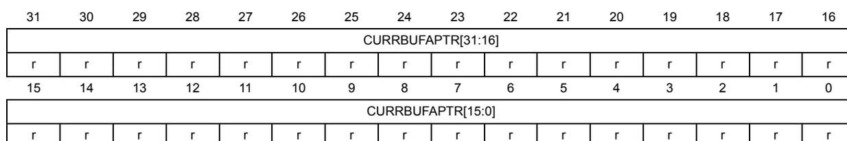
| 31 | 30 | 29 | 28 | 27 | 26 | 25 | 24 | 23 | 22 | 21 | 20 | 19 | 18 | 17 | 16 |
| CURRBUFAPTR[31:16] | |||||||||||||||
| r | r | r | r | r | r | r | r | r | r | r | r | r | r | r | r |
| 15 | 14 | 13 | 12 | 11 | 10 | 9 | 8 | 7 | 6 | 5 | 4 | 3 | 2 | 1 | 0 |
| CURRBUFAPTR[15:0] | |||||||||||||||
| r | r | r | r | r | r | r | r | r | r | r | r | r | r | r | r |
The DMA updates this pointer during Rx operation. This pointer is cleared on reset.
Channel x status register (ETH_DMACxSR) Address offset: \( 0x1160 + 0x80 \times x \) , ( \( x = 0 \) to \( 1 \) )Reset value: 0x0000 0000
The software driver (application) reads the status register during interrupt service routine or polling to determine the status of the DMA.
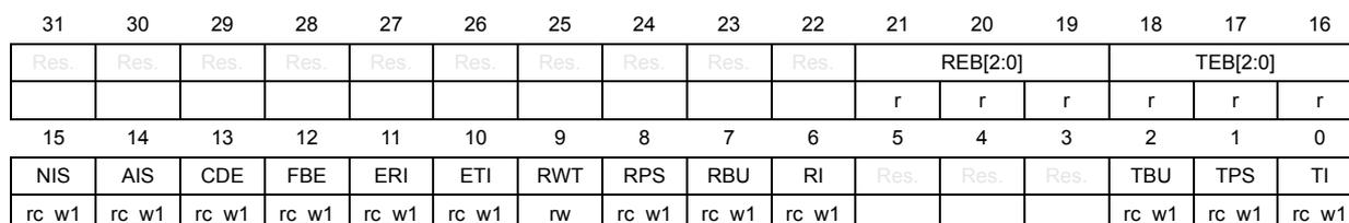
| 31 | 30 | 29 | 28 | 27 | 26 | 25 | 24 | 23 | 22 | 21 | 20 | 19 | 18 | 17 | 16 |
| Res. | Res. | Res. | Res. | Res. | Res. | Res. | Res. | Res. | Res. | REB[2:0] | TEB[2:0] | ||||
| r | r | r | r | r | r | ||||||||||
| 15 | 14 | 13 | 12 | 11 | 10 | 9 | 8 | 7 | 6 | 5 | 4 | 3 | 2 | 1 | 0 |
| NIS | AIS | CDE | FBE | ERI | ETI | RWT | RPS | RBU | RI | Res. | Res. | Res. | TBU | TPS | TI |
| rc_w1 | rc_w1 | rc_w1 | rc_w1 | rc_w1 | rc_w1 | rw | rc_w1 | rc_w1 | rc_w1 | rc_w1 | rc_w1 | rc_w1 | |||
Bits 31:22 Reserved, must be kept at reset value.
Bits 21:19 REB[2:0] : Rx DMA Error Bits
This field indicates the type of error that caused a bus error. For example, error response on the AXI interface.
Bit [2]: Error during data transfer by Rx DMA when 1, no error during data transfer by Rx DMA when 0.
Bit[1]: Error during descriptor access when 1, error during data buffer access when 0
Bit[0]: Error during read transfer when 1, error during write transfer when 0
This field is valid only when the FBE bit is set. This field does not generate an interrupt.
Bits 18:16 TEB[2:0] : Tx DMA Error Bits
This field indicates the type of error that caused a bus error. For example, error response on the AXI interface.
Bit[2]: Error during data transfer by Tx DMA when 1, no error during data transfer by Tx DMA when 0
Bit[1]: Error during descriptor access when 1, error during data buffer access when 0
Bit[0]: Error during read transfer when 1, Error during write transfer when 0
This field is valid only when the FBE bit is set. This field does not generate an interrupt.
Bit 15 NIS : Normal Interrupt Summary
Normal Interrupt Summary bit value is the logical OR of the following bits when the corresponding interrupt bits are enabled in the ETH_DMACxIER register:
Bit 0: Transmit interrupt
Bit 2: Transmit buffer unavailable
Bit 6: Receive interrupt
Bit 11: Early receive interrupt
Only unmasked bits (interrupts for which interrupt enable is set in ETH_DMACxIER register) affect the Normal Interrupt Summary bit.
This is a sticky bit. You must clear this bit (by writing 1 to this bit) each time a corresponding bit which causes NIS to be set is cleared.
Bit 14 AIS : Abnormal Interrupt Summary
Abnormal Interrupt Summary bit value is the logical OR of the following when the corresponding interrupt bits are enabled in the ETH_DMACxIER register:
Bit 1: Transmit process stopped
Bit 7: Receive buffer unavailable
Bit 8: Receive process stopped
Bit 10: Early transmit interrupt
Bit 12: Fatal bus error
Bit 13: Context descriptor error
Only unmasked bits affect the Abnormal Interrupt Summary bit.
This is a sticky bit. You must clear this bit (by writing 1 to this bit) each time a corresponding bit, which causes AIS to be set, is cleared.
Bit 13 CDE : Context descriptor error
This bit indicates that the DMA Tx/Rx engine received a descriptor error, which indicates invalid context in the middle of packet flow (intermediate descriptor) or all one's descriptor in Tx case and on Rx side it indicates DMA has read a descriptor with either of the buffer address as ones which is considered to be invalid.
Bit 12 FBE : Fatal bus error
This bit indicates that a bus error occurred (as described in the EB field). When this bit is set, the corresponding DMA channel engine disables all bus accesses.
Bit 11 ERI: Early receive interruptWhen set, this bit indicates that the RxDMA has completed the transfer of packet data to the memory. The RI bit of this register automatically clears this bit.
Bit 10 ETI: Early transmit interruptWhen set, this bit indicates that the TxDMA has completed the transfer of packet data to the MTL TXFIFO memory.
Bit 9 RWT: Receive watchdog timeoutThis bit is asserted when a packet with length greater than 2,048 bytes (10,240 bytes when Jumbo Packet mode is enabled) is received.
Bit 8 RPS: Receive process stoppedThis bit is asserted when the Rx process enters the Stopped state.
Bit 7 RBU: Receive buffer unavailableThis bit indicates that the application owns the next descriptor in the receive list, and the DMA cannot acquire it. The Rx process is suspended. To resume processing Rx descriptors, the application should change the ownership of the descriptor and issue a Receive Poll Demand command. If this command is not issued, the Rx process resumes when the next recognized incoming packet is received. In ring mode, the application should advance the receive descriptor tail pointer register of a channel. This bit is set only when the DMA owns the previous Rx descriptor.
Bit 6 RI: Receive interruptThis bit indicates that the packet reception is complete. When packet reception is complete, Bit 31 of RDES1 is reset in the last descriptor, and the specific packet status information is updated in the descriptor.
The reception remains in the Running state.
Bits 5:3 Reserved, must be kept at reset value.
Bit 2 TBU: Transmit buffer unavailableThis bit indicates that the application owns the next descriptor in the Transmit list, and the DMA cannot acquire it. Transmission is suspended. The TPSi field of the Debug status register (ETH_DMADSR) register explains the Transmit Process state transitions.
To resume processing the Transmit descriptors, the application should do the following:
- 1. Change the ownership of the descriptor by setting Bit 31 of TDES3.
- 2. Issue a Transmit Poll Demand command.
For ring mode, the application should advance the transmit descriptor tail pointer register of a channel.
Bit 1 TPS: Transmit process stoppedThis bit is set when the transmission is stopped.
Bit 0 TI: Transmit interruptThis bit indicates that the packet transmission is complete. When transmission is complete, Bit 31 of TDES3 is reset in the last descriptor, and the specific packet status information is updated in the descriptor.
Channel x missed frame count register (ETH_DMACxMFCR)
Address offset: 0x1164 + 0x80 * x, (x = 0 to 1)
Reset value: 0x0000 0000
This register has the number of packet counter that got dropped by the DMA either due to bus error or due to programming RPF field in Channel x receive control register (ETH_DMACxRXCR) register.
| 31 | 30 | 29 | 28 | 27 | 26 | 25 | 24 | 23 | 22 | 21 | 20 | 19 | 18 | 17 | 16 |
|---|---|---|---|---|---|---|---|---|---|---|---|---|---|---|---|
| Res. | Res. | Res. | Res. | Res. | Res. | Res. | Res. | Res. | Res. | Res. | Res. | Res. | Res. | Res. | Res. |
| 15 | 14 | 13 | 12 | 11 | 10 | 9 | 8 | 7 | 6 | 5 | 4 | 3 | 2 | 1 | 0 |
| MFCO | Res. | Res. | Res. | Res. | MFC[10:0] | ||||||||||
| rc_r | rc_r | rc_r | rc_r | rc_r | rc_r | rc_r | rc_r | rc_r | rc_r | rc_r | rc_r | ||||
Bits 31:16 Reserved, must be kept at reset value.
Bit 15 MFCO : Overflow status of the MFC Counter
When this bit is set then the MFC counter does not get incremented further. The bit gets cleared when this register is read.
Bits 14:11 Reserved, must be kept at reset value.
Bits 10:0 MFC[10:0] : Dropped packet counters
This counter indicates the number of packet counters that are dropped by the DMA either because of bus error or because of programming RPF field in Channel x receive control register (ETH_DMACxRXCR) . The counter gets cleared when this register is read.
Ethernet DMA register map and reset values
Table 846. ETH_DMA common register map and reset values
| Offset | Register name | 31 | 30 | 29 | 28 | 27 | 26 | 25 | 24 | 23 | 22 | 21 | 20 | 19 | 18 | 17 | 16 | 15 | 14 | 13 | 12 | 11 | 10 | 9 | 8 | 7 | 6 | 5 | 4 | 3 | 2 | 1 | 0 | ||
|---|---|---|---|---|---|---|---|---|---|---|---|---|---|---|---|---|---|---|---|---|---|---|---|---|---|---|---|---|---|---|---|---|---|---|---|
| 0x1000 | ETH_DMAMR | Res. | Res. | Res. | Res. | Res. | Res. | Res. | Res. | Res. | Res. | Res. | Res. | Res. | Res. | INTM[1:0] | Res. | Res. | Res. | Res. | TXPR | Res. | Res. | DSPW | Res. | Res. | Res. | Res. | TAA[2:0] | Res. | Res. | SWR | |||
| Reset value | 0 | 0 | 0 | 0 | 0 | 0 | 0 | 0 | |||||||||||||||||||||||||||
| 0x1004 | ETH_DMASBMR | EN_LPI | LPI_XIT_PKT | Res. | Res. | Res. | Res. | WR_OSR_LMT[1:0] | Res. | Res. | Res. | Res. | Res. | Res. | RD_OSR_LMT[1:0] | Res. | Res. | Res. | ONEKBBE | AAL | Res. | AALE | Res. | Res. | BLEN256 | BLEN128 | BLEN64 | BLEN32 | BLEN16 | BLEN8 | BLEN4 | FB | |||
| Reset value | 0 | 0 | 0 | 1 | 0 | 1 | 0 | 0 | 0 | 0 | 0 | 0 | 0 | 0 | 0 | 0 | 0 | ||||||||||||||||||
| 0x1008 | ETH_DMAISR | Res. | Res. | Res. | Res. | Res. | Res. | Res. | Res. | Res. | Res. | Res. | Res. | Res. | Res. | MACIS | MTLIS | Res. | Res. | Res. | Res. | Res. | Res. | Res. | Res. | Res. | Res. | Res. | Res. | Res. | Res. | DC1IS | DC0IS | ||
| Reset value | 0 | 0 | 0 | 0 | |||||||||||||||||||||||||||||||
Table 846. ETH_DMA common register map and reset values (continued)
| Offset | Register name | 31 | 30 | 29 | 28 | 27 | 26 | 25 | 24 | 23 | 22 | 21 | 20 | 19 | 18 | 17 | 16 | 15 | 14 | 13 | 12 | 11 | 10 | 9 | 8 | 7 | 6 | 5 | 4 | 3 | 2 | 1 | 0 | ||
|---|---|---|---|---|---|---|---|---|---|---|---|---|---|---|---|---|---|---|---|---|---|---|---|---|---|---|---|---|---|---|---|---|---|---|---|
| 0x100C | ETH_DMADSR | Res | Res | Res | Res | Res | Res | Res | Res | TPS1[3:0] | RPS1[3:0] | TPS0[3:0] | RPS0[3:0] | Res | Res | Res | Res | Res | Res | Res | Res | Res | AXRHSTS | AXWHSTS | |||||||||||
| Reset value | 0 | 0 | 0 | 0 | 0 | 0 | 0 | 0 | 0 | 0 | 0 | 0 | 0 | 0 | 0 | 0 | 0 | 0 | |||||||||||||||||
| 0x1010 - 0x101C | Reserved | ||||||||||||||||||||||||||||||||||
| 0x1020 | ETH_DMAA4TXACR | Res | Res | Res | Res | Res | Res | Res | Res | Res | Res | Res | Res | THC[3:0] | Res | Res | Res | Res | Res | TEC[3:0] | Res | Res | Res | Res | Res | Res | TDR[3:0] | ||||||||
| Reset value | 0 | 0 | 0 | 0 | 0 | 0 | 0 | 0 | 0 | 0 | 0 | 0 | |||||||||||||||||||||||
| 0x1024 | ETH_DMAA4RXACR | Res | Res | Res | Res | RDC[3:0] | Res | Res | Res | Res | Res | RHC[3:0] | Res | Res | Res | Res | Res | RPC[3:0] | Res | Res | Res | Res | Res | Res | RDWC[3:0] | ||||||||||
| Reset value | 0 | 0 | 0 | 0 | 0 | 0 | 0 | 0 | 0 | 0 | 0 | 0 | 0 | 0 | 0 | 0 | |||||||||||||||||||
| 0x1028 | ETH_DMAA4DACR | Res | Res | Res | Res | Res | Res | Res | Res | Res | Res | Res | Res | Res | Res | Res | Res | Res | Res | Res | Res | RDR[3:0] | Res | Res | Res | TDWD[1:0] | TDWC[3:0] | ||||||||
| Reset value | 0 | 0 | 0 | 0 | 0 | 0 | 0 | 0 | 0 | 0 | 0 | ||||||||||||||||||||||||
| 0x102C - 0x103C | Reserved | ||||||||||||||||||||||||||||||||||
| 0x1040 | ETH_DMALPIE | Res | Res | Res | Res | Res | Res | Res | Res | Res | Res | Res | Res | Res | Res | Res | Res | Res | Res | Res | Res | Res | Res | Res | Res | Res | Res | Res | Res | Res | LP[3:0] | ||||
| Reset value | 0 | 0 | 0 | 0 | |||||||||||||||||||||||||||||||
| 0x1044 - 0x104C | Reserved | ||||||||||||||||||||||||||||||||||
| 0x1050 | ETH_DMATBSC[3:0]R | FTOS[23:0] | FGOS[2:0] | Res | Res | Res | FTOV | ||||||||||||||||||||||||||||
| Reset value | 0 | 0 | 0 | 0 | 0 | 0 | 0 | 0 | 0 | 0 | 0 | 0 | 0 | 0 | 0 | 0 | 0 | 0 | 0 | 0 | 0 | 0 | 0 | 0 | 0 | 0 | 0 | 0 | 0 | 0 | 0 | 0 | 0 | ||
Table 847. ETH_DMA_CH0 register map and reset values
| Offset | Register name | 31 | 30 | 29 | 28 | 27 | 26 | 25 | 24 | 23 | 22 | 21 | 20 | 19 | 18 | 17 | 16 | 15 | 14 | 13 | 12 | 11 | 10 | 9 | 8 | 7 | 6 | 5 | 4 | 3 | 2 | 1 | 0 |
|---|---|---|---|---|---|---|---|---|---|---|---|---|---|---|---|---|---|---|---|---|---|---|---|---|---|---|---|---|---|---|---|---|---|
| 0x1100 | ETH_DMAC0CR | Res | Res | Res | Res | Res | Res | Res | Res | Res | Res | Res | DSL[2:0] | Res | PBLX8 | Res | Res | MSS[13:0] | |||||||||||||||
| Reset value | 0 | 0 | 0 | 0 | 0 | 0 | 0 | 0 | 0 | 0 | 0 | 0 | 0 | 0 | 0 | 0 | 0 | 0 | |||||||||||||||
| 0x1104 | ETH_DMAC0TXCR | Res | Res | EDSE | TQOS[3:0] | Res | Res | TXPBL[5:0] | IPBL | Res | Res | TSE | Res | Res | Res | Res | Res | Res | Res | Res | Res | Res | Res | Res | OSF | TOW[2:0] | ST | ||||||
| Reset value | 0 | 0 | 0 | 0 | 0 | 0 | 0 | 0 | 0 | 0 | 0 | 0 | 0 | 0 | 0 | 0 | 0 | ||||||||||||||||
Table 847. ETH_DMA_CH0 register map and reset values (continued)
| Offset | Register name | 31 | 30 | 29 | 28 | 27 | 26 | 25 | 24 | 23 | 22 | 21 | 20 | 19 | 18 | 17 | 16 | 15 | 14 | 13 | 12 | 11 | 10 | 9 | 8 | 7 | 6 | 5 | 4 | 3 | 2 | 1 | 0 |
|---|---|---|---|---|---|---|---|---|---|---|---|---|---|---|---|---|---|---|---|---|---|---|---|---|---|---|---|---|---|---|---|---|---|
| 0x1108 | ETH_DMAC0RXCR | RPF | Res | Res | Res | RQOS[3:0] | Res | Res | RXPBL[5:0] | Res | RBSZ[13:0] | Res | Res | Res | SR | ||||||||||||||||||
| Reset value | 0 | 0 | 0 | 0 | 0 | 0 | 0 | 0 | 0 | 0 | 0 | 0 | 0 | 0 | 0 | 0 | 0 | 0 | 0 | 0 | 0 | 0 | 0 | ||||||||||
| 0x110C-0x1110 | Reserved | ||||||||||||||||||||||||||||||||
| 0x1114 | ETH_DMAC0TXDLAR | TDESLA[31:0] | |||||||||||||||||||||||||||||||
| Reset value | 0 | 0 | 0 | 0 | 0 | 0 | 0 | 0 | 0 | 0 | 0 | 0 | 0 | 0 | 0 | 0 | 0 | 0 | 0 | 0 | 0 | 0 | 0 | 0 | 0 | 0 | 0 | 0 | 0 | 0 | 0 | ||
| 0x1118 | Reserved | ||||||||||||||||||||||||||||||||
| 0x111C | ETH_DMAC0RXDLAR | RDESLA[31:0] | |||||||||||||||||||||||||||||||
| Reset value | 0 | 0 | 0 | 0 | 0 | 0 | 0 | 0 | 0 | 0 | 0 | 0 | 0 | 0 | 0 | 0 | 0 | 0 | 0 | 0 | 0 | 0 | 0 | 0 | 0 | 0 | 0 | 0 | 0 | 0 | |||
| 0x1120 | ETH_DMAC0TDTXPR | TDT[31:0] | |||||||||||||||||||||||||||||||
| Reset value | 0 | 0 | 0 | 0 | 0 | 0 | 0 | 0 | 0 | 0 | 0 | 0 | 0 | 0 | 0 | 0 | 0 | 0 | 0 | 0 | 0 | 0 | 0 | 0 | 0 | 0 | 0 | 0 | 0 | 0 | |||
| 0x1124 | Reserved | ||||||||||||||||||||||||||||||||
| 0x1128 | ETH_DMAC0RXDTXPR | RDT[31:0] | |||||||||||||||||||||||||||||||
| Reset value | 0 | 0 | 0 | 0 | 0 | 0 | 0 | 0 | 0 | 0 | 0 | 0 | 0 | 0 | 0 | 0 | 0 | 0 | 0 | 0 | 0 | 0 | 0 | 0 | 0 | 0 | 0 | 0 | 0 | 0 | |||
| 0x112C | ETH_DMAC0TXRLR | Res | Res | Res | Res | Res | Res | Res | Res | Res | Res | Res | Res | Res | Res | Res | Res | Res | Res | Res | Res | Res | Res | TDRL[9:0] | |||||||||
| Reset value | 0 | 0 | 0 | 0 | 0 | 0 | 0 | 0 | 0 | ||||||||||||||||||||||||
| 0x1130 | ETH_DMAC0RXRLR | Res | Res | Res | Res | Res | Res | Res | Res | ARBS[6:0] | Res | Res | Res | Res | Res | Res | Res | Res | RDRL[9:0] | ||||||||||||||
| Reset value | 0 | 0 | 0 | 0 | 0 | 0 | 0 | 0 | 0 | 0 | 0 | 0 | 0 | 0 | 0 | 0 | |||||||||||||||||
| 0x1134 | ETH_DMAC0IER | Res | Res | Res | Res | Res | Res | Res | Res | Res | Res | Res | Res | Res | Res | Res | NIE | AIE | CDEE | FBEE | ERIE | ETIE | RWTE | RSE | RBUE | RIE | Res | Res | Res | TBUE | TXSE | TIE | |
| Reset value | 0 | 0 | 0 | 0 | 0 | 0 | 0 | 0 | 0 | 0 | 0 | 0 | 0 | 0 | |||||||||||||||||||
| 0x1138 | ETH_DMAC0RXIWTR | Res | Res | Res | Res | Res | Res | Res | Res | Res | Res | Res | Res | Res | Res | RWTU[1:0] | Res | Res | Res | Res | Res | Res | Res | RWT[7:0] | |||||||||
| Reset value | 0 | 0 | 0 | 0 | 0 | 0 | 0 | 0 | 0 | 0 | |||||||||||||||||||||||
| 0x113C | ETH_DMAC0SFCSR | Res | Res | Res | Res | Res | Res | Res | Res | Res | Res | Res | Res | RSN[3:0] | SIV[11:0] | Res | Res | ASC | ESC | ||||||||||||||
| Reset value | 0 | 0 | 0 | 0 | 0 | 0 | 0 | 0 | 1 | 1 | 1 | 1 | 1 | 0 | 0 | 0 | 0 | ||||||||||||||||
| 0x1140 | Reserved | ||||||||||||||||||||||||||||||||
| 0x1144 | ETH_DMAC0CATXDR | CURTDESAPTR[31:0] | |||||||||||||||||||||||||||||||
| Reset value | 0 | 0 | 0 | 0 | 0 | 0 | 0 | 0 | 0 | 0 | 0 | 0 | 0 | 0 | 0 | 0 | 0 | 0 | 0 | 0 | 0 | 0 | 0 | 0 | 0 | 0 | 0 | 0 | 0 | 0 | |||
| 0x1148 | Reserved | ||||||||||||||||||||||||||||||||
| 0x114C | ETH_DMAC0CARXDR | CURRDESAPTR[31:0] | |||||||||||||||||||||||||||||||
| Reset value | 0 | 0 | 0 | 0 | 0 | 0 | 0 | 0 | 0 | 0 | 0 | 0 | 0 | 0 | 0 | 0 | 0 | 0 | 0 | 0 | 0 | 0 | 0 | 0 | 0 | 0 | 0 | 0 | 0 | 0 | |||
| 0x1150 | Reserved | ||||||||||||||||||||||||||||||||
Table 847. ETH_DMA_CH0 register map and reset values (continued)
| Offset | Register name | 31 | 30 | 29 | 28 | 27 | 26 | 25 | 24 | 23 | 22 | 21 | 20 | 19 | 18 | 17 | 16 | 15 | 14 | 13 | 12 | 11 | 10 | 9 | 8 | 7 | 6 | 5 | 4 | 3 | 2 | 1 | 0 |
|---|---|---|---|---|---|---|---|---|---|---|---|---|---|---|---|---|---|---|---|---|---|---|---|---|---|---|---|---|---|---|---|---|---|
| 0x1154 | ETH_DMA0CATXBR | CURTBUPAPTR[31:0] | |||||||||||||||||||||||||||||||
| Reset value | 0 | 0 | 0 | 0 | 0 | 0 | 0 | 0 | 0 | 0 | 0 | 0 | 0 | 0 | 0 | 0 | 0 | 0 | 0 | 0 | 0 | 0 | 0 | 0 | 0 | 0 | 0 | 0 | 0 | 0 | 0 | 0 | |
| 0x1158 | Reserved | ||||||||||||||||||||||||||||||||
| 0x115C | ETH_DMA0CARXBR | CURRBUPAPTR[31:0] | |||||||||||||||||||||||||||||||
| Reset value | 0 | 0 | 0 | 0 | 0 | 0 | 0 | 0 | 0 | 0 | 0 | 0 | 0 | 0 | 0 | 0 | 0 | 0 | 0 | 0 | 0 | 0 | 0 | 0 | 0 | 0 | 0 | 0 | 0 | 0 | 0 | 0 | |
| 0x1160 | ETH_DMA0SR | Res | Res | Res | Res | Res | Res | Res | Res | Res | Res | REB[2:0] | TEB[2:0] | NIS | AIS | CDE | FBE | ERI | ETI | RWT | RPS | RBU | RI | Res | Res | Res | TBU | TPS | TI | ||||
| Reset value | 0 | 0 | 0 | 0 | 0 | 0 | 0 | 0 | 0 | 0 | 0 | 0 | 0 | 0 | 0 | 0 | 0 | 0 | 0 | ||||||||||||||
| 0x1164 | ETH_DMA0MFCR | Res | Res | Res | Res | Res | Res | Res | Res | Res | Res | Res | Res | Res | Res | Res | Res | MFCO | Res | Res | Res | Res | MFC[10:0] | ||||||||||
| Reset value | 0 | 0 | 0 | 0 | 0 | 0 | 0 | 0 | 0 | 0 | 0 | ||||||||||||||||||||||
Table 848. ETH_DMA_CH1 register map and reset values
| Offset | Register name | 31 | 30 | 29 | 28 | 27 | 26 | 25 | 24 | 23 | 22 | 21 | 20 | 19 | 18 | 17 | 16 | 15 | 14 | 13 | 12 | 11 | 10 | 9 | 8 | 7 | 6 | 5 | 4 | 3 | 2 | 1 | 0 | |||
|---|---|---|---|---|---|---|---|---|---|---|---|---|---|---|---|---|---|---|---|---|---|---|---|---|---|---|---|---|---|---|---|---|---|---|---|---|
| 0x1180 | ETH_DMA1CR | Res | Res | Res | Res | Res | Res | Res | Res | Res | Res | Res | DSL[2:0] | Res | PBLX8 | Res | Res | MSS[13:0] | ||||||||||||||||||
| Reset value | 0 | 0 | 0 | 0 | 0 | 0 | 0 | 0 | 0 | 0 | 0 | 0 | 0 | 0 | 0 | 0 | 0 | 0 | ||||||||||||||||||
| 0x1184 | ETH_DMA1TXCR | Res | Res | Res | EDSE | TQOS[3:0] | Res | Res | TXPBL[5:0] | IPBL | Res | Res | TSE | Res | Res | Res | Res | Res | Res | Res | OSF | TCW[2:0] | ST | |||||||||||||
| Reset value | 0 | 0 | 0 | 0 | 0 | 0 | 0 | 0 | 0 | 0 | 0 | 0 | 0 | 0 | 0 | 0 | 0 | |||||||||||||||||||
| 0x1188 | ETH_DMA1RXCR | RPF | Res | Res | Res | RQOS[3:0] | Res | Res | RXPBL[5:0] | Res | RBSZ[13:0] | Res | Res | Res | SR | |||||||||||||||||||||
| Reset value | 0 | 0 | 0 | 0 | 0 | 0 | 0 | 0 | 0 | 0 | 0 | 0 | 0 | 0 | 0 | 0 | 0 | 0 | 0 | 0 | 0 | 0 | 0 | 0 | 0 | |||||||||||
| 0x118C - 0x1190 | Reserved | |||||||||||||||||||||||||||||||||||
| 0x1194 | ETH_DMA1TXDLAR | TDESLA[31:0] | ||||||||||||||||||||||||||||||||||
| Reset value | 0 | 0 | 0 | 0 | 0 | 0 | 0 | 0 | 0 | 0 | 0 | 0 | 0 | 0 | 0 | 0 | 0 | 0 | 0 | 0 | 0 | 0 | 0 | 0 | 0 | 0 | 0 | 0 | 0 | 0 | 0 | 0 | ||||
| 0x1198 | Reserved | |||||||||||||||||||||||||||||||||||
| 0x119C | ETH_DMA1RXDLAR | RDESLA[31:0] | ||||||||||||||||||||||||||||||||||
| Reset value | 0 | 0 | 0 | 0 | 0 | 0 | 0 | 0 | 0 | 0 | 0 | 0 | 0 | 0 | 0 | 0 | 0 | 0 | 0 | 0 | 0 | 0 | 0 | 0 | 0 | 0 | 0 | 0 | 0 | 0 | 0 | 0 | ||||
| 0x11A0 | ETH_DMA1TXDTPR | TDT[31:0] | ||||||||||||||||||||||||||||||||||
| Reset value | 0 | 0 | 0 | 0 | 0 | 0 | 0 | 0 | 0 | 0 | 0 | 0 | 0 | 0 | 0 | 0 | 0 | 0 | 0 | 0 | 0 | 0 | 0 | 0 | 0 | 0 | 0 | 0 | 0 | 0 | 0 | 0 | ||||
| 0x11A4 | Reserved | |||||||||||||||||||||||||||||||||||
| 0x11A8 | ETH_DMA1RXDTPR | RDT[31:0] | ||||||||||||||||||||||||||||||||||
| Reset value | 0 | 0 | 0 | 0 | 0 | 0 | 0 | 0 | 0 | 0 | 0 | 0 | 0 | 0 | 0 | 0 | 0 | 0 | 0 | 0 | 0 | 0 | 0 | 0 | 0 | 0 | 0 | 0 | 0 | 0 | 0 | 0 | ||||
Table 848. ETH_DMA_CH1 register map and reset values (continued)
| Offset | Register name | 31 | 30 | 29 | 28 | 27 | 26 | 25 | 24 | 23 | 22 | 21 | 20 | 19 | 18 | 17 | 16 | 15 | 14 | 13 | 12 | 11 | 10 | 9 | 8 | 7 | 6 | 5 | 4 | 3 | 2 | 1 | 0 | ||
|---|---|---|---|---|---|---|---|---|---|---|---|---|---|---|---|---|---|---|---|---|---|---|---|---|---|---|---|---|---|---|---|---|---|---|---|
| 0x11AC | ETH_DMAC1TXRLR | Res. | Res. | Res. | Res. | Res. | Res. | Res. | Res. | Res. | Res. | Res. | Res. | Res. | Res. | Res. | Res. | Res. | Res. | Res. | Res. | Res. | Res. | TDRL[9:0] | |||||||||||
| Reset value | 0 | 0 | 0 | 0 | 0 | 0 | 0 | 0 | 0 | 0 | |||||||||||||||||||||||||
| 0x11B0 | ETH_DMAC1RXRLR | Res. | Res. | Res. | Res. | Res. | Res. | Res. | Res. | ARBS[6:0] | Res. | Res. | Res. | Res. | Res. | Res. | Res. | Res. | Res. | Res. | RDRL[9:0] | ||||||||||||||
| Reset value | 0 | 0 | 0 | 0 | 0 | 0 | 0 | 0 | 0 | 0 | 0 | 0 | 0 | 0 | 0 | 0 | 0 | ||||||||||||||||||
| 0x11B4 | ETH_DMAC1IER | Res. | Res. | Res. | Res. | Res. | Res. | Res. | Res. | Res. | Res. | Res. | Res. | Res. | Res. | Res. | Res. | NIE | AIE | CDEE | FBEE | ERIE | ETIE | RWTE | RSE | RBUE | RIE | Res. | Res. | Res. | TBUE | TXSE | TIE | ||
| Reset value | 0 | 0 | 0 | 0 | 0 | 0 | 0 | 0 | 0 | 0 | 0 | 0 | 0 | ||||||||||||||||||||||
| 0x11B8 | ETH_DMAC0RXWTR | Res. | Res. | Res. | Res. | Res. | Res. | Res. | Res. | Res. | Res. | Res. | Res. | Res. | RW TU[1:0] | Res. | Res. | Res. | Res. | Res. | Res. | Res. | Res. | RWT[7:0] | |||||||||||
| Reset value | 0 | 0 | 0 | 0 | 0 | 0 | 0 | 0 | |||||||||||||||||||||||||||
| 0x11BC | ETH_DMAC1SFCR | Res. | Res. | Res. | Res. | Res. | Res. | Res. | Res. | Res. | Res. | Res. | Res. | RSN[3:0] | SIV[11:0] | Res. | Res. | Res. | Res. | Res. | Res. | Res. | Res. | Res. | Res. | ASC | ESC | ||||||||
| Reset value | 0 | 0 | 0 | 0 | 0 | 0 | 0 | 0 | 0 | 0 | 0 | 0 | 0 | 0 | 0 | 0 | 0 | 0 | 0 | ||||||||||||||||
| 0x11C0 | Reserved | ||||||||||||||||||||||||||||||||||
| 0x11C4 | ETH_DMAC1CATXDR | CURTDESAPTR[31:0] | |||||||||||||||||||||||||||||||||
| Reset value | 0 | 0 | 0 | 0 | 0 | 0 | 0 | 0 | 0 | 0 | 0 | 0 | 0 | 0 | 0 | 0 | 0 | 0 | 0 | 0 | 0 | 0 | 0 | 0 | 0 | 0 | 0 | 0 | 0 | 0 | 0 | 0 | |||
| 0x11C8 | Reserved | ||||||||||||||||||||||||||||||||||
| 0x11CC | ETH_DMAC1CARXDR | CURRDESAPTR[31:0] | |||||||||||||||||||||||||||||||||
| Reset value | 0 | 0 | 0 | 0 | 0 | 0 | 0 | 0 | 0 | 0 | 0 | 0 | 0 | 0 | 0 | 0 | 0 | 0 | 0 | 0 | 0 | 0 | 0 | 0 | 0 | 0 | 0 | 0 | 0 | 0 | 0 | 0 | |||
| 0x11D0 | Reserved | ||||||||||||||||||||||||||||||||||
| 0x11D4 | ETH_DMAC1CATXBR | CURTBUFAPTR[31:0] | |||||||||||||||||||||||||||||||||
| Reset value | 0 | 0 | 0 | 0 | 0 | 0 | 0 | 0 | 0 | 0 | 0 | 0 | 0 | 0 | 0 | 0 | 0 | 0 | 0 | 0 | 0 | 0 | 0 | 0 | 0 | 0 | 0 | 0 | 0 | 0 | 0 | 0 | |||
| 0x11D8 | Reserved | ||||||||||||||||||||||||||||||||||
| 0x11DC | ETH_DMAC1CARXBR | CURRBUFAPTR[31:0] | |||||||||||||||||||||||||||||||||
| Reset value | 0 | 0 | 0 | 0 | 0 | 0 | 0 | 0 | 0 | 0 | 0 | 0 | 0 | 0 | 0 | 0 | 0 | 0 | 0 | 0 | 0 | 0 | 0 | 0 | 0 | 0 | 0 | 0 | 0 | 0 | 0 | 0 | |||
| 0x11E0 | ETH_DMAC1SR | Res. | Res. | Res. | Res. | Res. | Res. | Res. | Res. | Res. | Res. | REB[2:0] | TEB[2:0] | NIS | AIS | CDE | FBE | ERI | ETI | RWT | RPS | RBU | RI | Res. | Res. | Res. | TBU | TPS | TI | ||||||
| Reset value | 0 | 0 | 0 | 0 | 0 | 0 | 0 | 0 | 0 | 0 | 0 | 0 | 0 | 0 | 0 | 0 | 0 | 0 | 0 | 0 | |||||||||||||||
| 0x11E4 | ETH_DMAC1MFCR | Res. | Res. | Res. | Res. | Res. | Res. | Res. | Res. | Res. | Res. | Res. | Res. | Res. | Res. | Res. | Res. | MFCO | Res. | Res. | Res. | Res. | Res. | MFC[10:0] | |||||||||||
| Reset value | 0 | 0 | 0 | 0 | 0 | 0 | 0 | 0 | 0 | 0 | 0 | ||||||||||||||||||||||||
76.11.3 Ethernet MTL registers
Operating mode register (ETH_MTLOMR)
Address offset: 0x0C00
Reset value: 0x0000 0000
The operating mode register establishes the transmit and receive operating modes and commands.
| 31 | 30 | 29 | 28 | 27 | 26 | 25 | 24 | 23 | 22 | 21 | 20 | 19 | 18 | 17 | 16 |
|---|---|---|---|---|---|---|---|---|---|---|---|---|---|---|---|
| Res. | Res. | Res. | Res. | Res. | Res. | Res. | Res. | Res. | Res. | Res. | Res. | Res. | Res. | Res. | Res. |
| 15 | 14 | 13 | 12 | 11 | 10 | 9 | 8 | 7 | 6 | 5 | 4 | 3 | 2 | 1 | 0 |
| Res. | Res. | Res. | Res. | Res. | Res. | CNT CLR | CNT PRST | Res. | SCHALG[1:0] | Res. | Res. | RAA | DTX STS | Res. | |
| rw | rw | rw | rw | rw | rw | ||||||||||
Bits 31:10 Reserved, must be kept at reset value.
Bit 9 CNTCLR : Counters reset
When this bit is set, all counters are reset. This bit is cleared automatically after 1 clock cycle. If this bit is set along with CNTPRST bit, CNTPRST has precedence.
Bit 8 CNTPRST : Counters preset
When this bit is set:
- – Tx queue x underflow register (ETH_MTLTXQxUR) is initialized/preset to 0x7F0.
- – Missed Packet and Overflow Packet counters in Rx queue x missed packet and overflow counter register (ETH_MTLRXQxMPOCR) is initialized/preset to 0x7F0
This bit is cleared automatically.
Bit 7 Reserved, must be kept at reset value.
Bits 6:5 SCHALG[1:0] : Tx scheduling algorithm
This field indicates the algorithm for Tx scheduling:
00: Weighted round robin (WRR) algorithm
01 to 10: Reserved, must not be used.
11: Strict priority (SP) algorithm.
Bits 4:3 Reserved, must be kept at reset value.
Bit 2 RAA : Receive arbitration algorithm
This field is used to select the arbitration algorithm for the Rx side.
0: Strict priority (SP). Queue 0 has the lowest priority and the last queue has the highest priority.
1: Weighted strict priority (WSP)
Bit 1 DTXSTS : Drop transmit status
When this bit is set, the Tx packet status received from the MAC is dropped in the MTL.
When this bit is reset, the Tx packet status received from the MAC is forwarded to the application.
Bit 0 Reserved, must be kept at reset value.
Interrupt status register (ETH_MTLISR)
Address offset: 0x0C20
Reset value: 0x0000 0000
The software driver (application) reads this register during interrupt service routine or polling to determine the interrupt status of MTL queues and the MAC.
| 31 | 30 | 29 | 28 | 27 | 26 | 25 | 24 | 23 | 22 | 21 | 20 | 19 | 18 | 17 | 16 |
|---|---|---|---|---|---|---|---|---|---|---|---|---|---|---|---|
| Res. | Res. | Res. | Res. | Res. | Res. | Res. | Res. | Res. | Res. | Res. | Res. | Res. | ESTIS | Res. | Res. |
| 15 | 14 | 13 | 12 | 11 | 10 | 9 | 8 | 7 | 6 | 5 | 4 | 3 | 2 | 1 | 0 |
| Res. | Res. | Res. | Res. | Res. | Res. | Res. | Res. | Res. | Res. | Res. | Res. | Res. | Res. | Q1IS | Q0IS |
| r | r |
Bits 31:19 Reserved, must be kept at reset value.
Bit 18 ESTIS : EST (TAS- 802.1Qbv) Interrupt Status
This bit indicates an interrupt event during the operation of 802.1Qbv. To reset this bit, the application must clear the error/event that has caused the Interrupt.
Bits 17:2 Reserved, must be kept at reset value.
Bit 1 Q1IS : Queue 1 interrupt status
This bit indicates that an interrupt has been generated by Queue 1. To reset this bit, read ETH_MTLQ1CSR register to identify the interrupt cause and clear the source.
Bit 0 Q0IS : Queue 0 interrupt status
This bit indicates that an interrupt has been generated by Queue 0. To reset this bit, read ETH_MTLQ0CSR register to identify the interrupt cause and clear the source.
Rx queue and DMA channel mapping register (ETH_MTLRXQDMAMR)
Address offset: 0x0C30
Reset value: 0x0000 0000
| 31 | 30 | 29 | 28 | 27 | 26 | 25 | 24 | 23 | 22 | 21 | 20 | 19 | 18 | 17 | 16 |
|---|---|---|---|---|---|---|---|---|---|---|---|---|---|---|---|
| Res. | Res. | Res. | Res. | Res. | Res. | Res. | Res. | Res. | Res. | Res. | Res. | Res. | Res. | Res. | Res. |
| 15 | 14 | 13 | 12 | 11 | 10 | 9 | 8 | 7 | 6 | 5 | 4 | 3 | 2 | 1 | 0 |
| Res. | Res. | Res. | Q1DDMACH | Res. | Res. | Res. | Q1MDMACH | Res. | Res. | Res. | Q0DDMACH | Res. | Res. | Res. | Q0MDMACH |
| rw | rw | rw | rw |
Bits 31:13 Reserved, must be kept at reset value.
Bit 12 Q1DDMACH : Queue 1 Enabled for DA-based DMA Channel Selection
When set, this bit indicates that the packets received in Queue 1 are routed to a particular DMA channel as decided in the MAC receiver based on the DMA channel number programmed in the L3-L4 filter registers, or the Ethernet DA address.
When reset, this bit indicates that the packets received in Queue 1 are routed to the DMA Channel programmed in the Q1MDMACH bit.
Bits 11:9 Reserved, must be kept at reset value.
Bit 8 Q1MDMACH : Queue 1 Mapped to DMA Channel
This field controls the routing of the received packet in Queue 1 to the DMA channel:
0: DMA Channel 0
1: DMA Channel 1
This field is valid when the Q1DDMACH field is reset.
Bits 7:5 Reserved, must be kept at reset value.
Bit 4 Q0DDMACH : Queue 0 Enabled for DA-based DMA Channel Selection
When set, this bit indicates that the packets received in Queue 0 are routed to a particular DMA channel as decided in the MAC receiver based on the DMA channel number programmed in the L3-L4 filter registers, or the Ethernet DA address.
When reset, this bit indicates that the packets received in Queue 0 are routed to the DMA Channel programmed in the Q0MDMACH bit.
Bits 3:1 Reserved, must be kept at reset value.
Bit 0 Q0MDMACH : Queue 0 Mapped to DMA Channel
This field controls the routing of the received packet in Queue 0 to the DMA channel:
0: DMA Channel 0
1: DMA Channel 1
This field is valid when the Q0DDMACH field is reset.
TBS control register (ETH_MTLTBSCR)
Address offset: 0x0C40
Reset value: 0x0000 0000
This register controls the time-based scheduling operation.
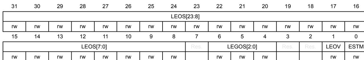
| 31 | 30 | 29 | 28 | 27 | 26 | 25 | 24 | 23 | 22 | 21 | 20 | 19 | 18 | 17 | 16 |
| LEOS[23:8] | |||||||||||||||
| rw | rw | rw | rw | rw | rw | rw | rw | rw | rw | rw | rw | rw | rw | rw | rw |
| 15 | 14 | 13 | 12 | 11 | 10 | 9 | 8 | 7 | 6 | 5 | 4 | 3 | 2 | 1 | 0 |
| LEOS[7:0] | Res. | LEGOS[2:0] | Res. | Res. | LEOV | ESTM | |||||||||
| rw | rw | rw | rw | rw | rw | rw | rw | rw | rw | rw | rw | rw | |||
Bits 31:8 LEOS[23:0]: Launch Expiry Offset
The value in units of 256 nanoseconds that has to be added to the launch time to compute the launch expiry time. The value is valid only when LEOV is set.
The maximum value is 999,999,999 ns. It must be smaller than CTR - 1 when the ESTM mode is set since this value is a modulo CTR value.
Bit 7 Reserved, must be kept at reset value.
Bits 6:4 LEGOS[2:0]: Launch Expiry GSN Offset
The number of GSN slots that has to be added to the launch GSN to compute the launch expiry time. This value is valid only when LEOV is set.
Bits 3:2 Reserved, must be kept at reset value.
Bit 1 LEOV: Launch expiry offset valid
When set, this bit indicates that the LEOS field is valid. When not set, it indicates that the launch expiry offset is not valid and that the MTL must not check for launch expiry time.
0: LEOS field invalid
1: LEOS field valid
Bit 0 ESTM: EST offset mode
When this bit is set, the launch time value used in time-based scheduling is interpreted as an EST offset value and is added to the base time register (BTR) of the current list.
When reset, the launch time value is used as an absolute value that must be compared with the system time [39:8].
0: EST offset mode disabled
1: EST offset mode enabled
EST Control register (ETH_MTLESTCR)Address offset: 0x0C50
Reset value: 0x0000 0000
This register controls the operation of Enhancements to Scheduled Transmission (IEEE802.1Qbv).
| 31 | 30 | 29 | 28 | 27 | 26 | 25 | 24 | 23 | 22 | 21 | 20 | 19 | 18 | 17 | 16 |
|---|---|---|---|---|---|---|---|---|---|---|---|---|---|---|---|
| PTOV[7:0] | CTOV[11:4] | ||||||||||||||
| rw | rw | rw | rw | rw | rw | rw | rw | rw | rw | rw | rw | rw | rw | rw | rw |
| 15 | 14 | 13 | 12 | 11 | 10 | 9 | 8 | 7 | 6 | 5 | 4 | 3 | 2 | 1 | 0 |
| CTOV[3:0] | Res. | TILS[2:0] | LCSE[1:0] | DFBS | DDBF | Res. | Res. | SSWL | EEST | ||||||
| rw | rw | rw | rw | rw | rw | rw | rw | rw | rw | rw | rw | rw | |||
The value of PTP Clock period multiplied by 6 in nanoseconds. This value is needed to avoid transmission overruns at the beginning of the installation of a new GCL.
Bits 23:12 CTOV[11:0]: Current Time Offset ValueProvides a 12 bit time offset value in nanosecond that is added to the current time to compensate for all the implementation pipeline delays such as the CDC sync delay, buffering delays, data path delays and so on. This offset helps to ensure that the impact of gate controls is visible on the line exactly at the predetermined schedule (or as close to the schedule as possible).
Bit 11 Reserved, must be kept at reset value.
Bits 10:8 TILS[2:0]: Time Interval Left Shift AmountThis field provides the left shift amount for the programmed Time Interval values used in the Gate Control Lists.
000: No left shift needed (equal to x1ns)
001: Left shift TI by 1 bit (equal to x2ns)
010: Left shift TI by 2 bits (equal to x4ns)
...
100: Left shift TI by 7 bits (equal to x128ns)
Bits 7:6 LCSE[1:0]: Loop Count to report Scheduling ErrorProgrammable number of GCL list iterations before reporting an HLBS error defined in EST Status register (ETH_MTLESTSR) .
00: 4 iterations
01: 8 iterations
10: 16 iterations
11: 32 iterations
Bit 5 DFBS: Drop Frames causing Scheduling ErrorWhen set frames reported to cause HOL Blocking due to not getting scheduled (HLBS field of EST Status register (ETH_MTLESTSR) ) after 4,8,16,32 (based on LCSE field of this register) GCL iterations are dropped.
0: Do not drop
1: Drop
Bit 4 DDBF : Do not Drop frames during Frame Size Error
When set, frames are not be dropped during Head-of-Line blocking due to Frame Size Error (HLBF field of EST Status register (ETH_MTLESTSR) ).
0: Drop
1: Do not drop
Bits 3:2 Reserved, must be kept at reset value.
Bit 1 SSWL : Switch to S/W owned list
When set, indicates that the software has programmed that list that it currently owns (SWOL) and the hardware should switch to the new list based on the new BTR. Hardware clears this bit when the switch to the SWOL happens to indicate the completion of the switch or when an BTR error (BTRE in EST Status register (ETH_MTLESTSR) ) is set. When BTRE is set this bit is cleared but SWOL is not updated as the switch was not successful.
Bit 0 EEST : Enable EST
When reset, the gate control list processing is halted and all gates are assumed to be in Open state. Should be set for the hardware to start processing the gate control lists. During the toggle from 0 to 1, the gate control list processing starts only after the SSWL bit is set.
0: EST disabled
1: EST enabled
EST Extended Control register (ETH_MTLESTECR)
Address offset: 0x0C54
Reset value: 0x0000 0000
This register indicates the number of Overhead bytes for EST related scheduling.
| 31 | 30 | 29 | 28 | 27 | 26 | 25 | 24 | 23 | 22 | 21 | 20 | 19 | 18 | 17 | 16 |
|---|---|---|---|---|---|---|---|---|---|---|---|---|---|---|---|
| Res. | Res. | Res. | Res. | Res. | Res. | Res. | Res. | Res. | Res. | Res. | Res. | Res. | Res. | Res. | Res. |
| 15 | 14 | 13 | 12 | 11 | 10 | 9 | 8 | 7 | 6 | 5 | 4 | 3 | 2 | 1 | 0 |
| Res. | Res. | Res. | Res. | Res. | Res. | Res. | Res. | Res. | Res. | OVHD[5:0] | |||||
| rw | rw | rw | rw | rw | rw | ||||||||||
Bits 31:6 Reserved, must be kept at reset value.
Bits 5:0 OVHD[5:0] : Overhead Bytes Value
This field indicates the fixed overhead for every packet to account for EST Scheduler Delay, IPG or EIPG, and Preamble bytes.
EST Status register (ETH_MTLESTSR)Address offset: 0x0C58
Reset value: 0x0000 0000
This register provides the Status related to Enhancements to Scheduled Transmission (IEEE802.1Qbv).
| 31 | 30 | 29 | 28 | 27 | 26 | 25 | 24 | 23 | 22 | 21 | 20 | 19 | 18 | 17 | 16 |
|---|---|---|---|---|---|---|---|---|---|---|---|---|---|---|---|
| Res. | Res. | Res. | Res. | Res. | Res. | Res. | Res. | Res. | Res. | Res. | Res. | CGSN[3:0] | |||
| r | r | r | r | ||||||||||||
| 15 | 14 | 13 | 12 | 11 | 10 | 9 | 8 | 7 | 6 | 5 | 4 | 3 | 2 | 1 | 0 |
| BTRL[7:0] | SWOL | Res. | Res. | CGCE | HLBS | HLBF | BTRE | SWLC | |||||||
| r | r | r | r | r | r | r | r | r | rc_w1 | r | r | rc_w1 | rc_w1 | ||
Bits 31:20 Reserved, must be kept at reset value.
Bits 19:16 CGSN[3:0] : Current GCL slot number
Indicates the slot number of the GCL list. The slot number is a modulo 16 count of the GCL list loops executed so far. Even if a new GCL list is installed, the count is incremental.
Bits 15:8 BTRL[7:0] : BTR Error Loop Count
Provides the minimum count (N) for which the equation \( \text{Current Time} \leq \text{New BTR} + (N \times \text{New Cycle Time}) \) becomes true. \( N = 0b11111111 \) indicates the iterations exceeded the value of 128 and the hardware was not able to update New BTR to be equal to or greater than Current Time. Software intervention is needed to update the New BTR. Value cleared when BTRE field of this register is cleared.
Bit 7 SWOL : S/W owned list
When 0, indicates Gate Control list number "0" is owned by software and when 1, indicates Gate Control list "1" is owned by the software. Any reads/writes by the software (using indirect access through EST Gate Control List register (ETH_MTLESTGCLCR) ) are directed to the list indicated by this value by default. The inverse of this value is treated as HWOL.
R/W operations performed by hardware are directed to the list pointed by HWOL by default.
- 0: Inactive
- 1: Active
Bits 6:5 Reserved, must be kept at reset value.
Bit 4 CGCE : Constant Gate Control Error
This error occurs when the list length (LLR) is 1 and the Cycle Time (CTR) is less than or equal to the programmed Time Interval (TI) value after the optional Left Shifting. This implies Gates are either always Closed or always Open based on the Gate Control values; the same effect can be achieved by other simpler (non TSN) programming mechanisms. Since the implementation does not support such a programming an error is reported.
Self-set to 1 on internal event. Setting 1 clears. Setting 0 has no effect.
- 0: Inactive
- 1: Active
Bit 3 HLBS : Head-Of-Line Blocking due to Scheduling
Set when the frame is not able to win arbitration and get scheduled even after 4 iterations of the GCL. Indicates to software a potential programming error. The one hot encoded values of the Queue Numbers that are not able to make progress are indicated in the
EST Schedule Error register (ETH_MTLESTSCHER)
. Bit cleared when
EST Schedule Error register (ETH_MTLESTSCHER)
is all zeros.
0: Inactive
1: Active
Bit 2 HLBF : Head-Of-Line Blocking due to Frame Size
Set when HOL Blocking is noticed on one or more Queues as a result of none of the Time Intervals of gate open in the GCL being greater than or equal to the duration needed for frame size (or frame fragment size when preemption is enabled) transmission. The one hot encoded Queue numbers that are experiencing HLBF are indicated in the EST frame size error register (ETH_MTLESTFSER) . Additionally, the first Queue number that experienced HLBF along with the frame size is captured in EST Frame size Capture register (ETH_MTLESTFSCR) . HLBF bit is cleared when EST frame size error register (ETH_MTLESTFSER) is all zeros.
Bit 1 BTRE : BTR Error
When 1, indicates a programming error in the BTR of SWOL where the programmed value is less than current time. If the BTRL = 0b11111111, SWOL is not updated and the software should reprogram the BTR to a value greater than the current time and then set SSWL to reinitiate the switch to SWOL. Else if the value of BTRL < 0b11111111, SWOL is updated and this field indicates the number of iterations (of + CycleTime) taken by hardware to update the BTR to a value greater than the Current Time.
Self-set to 1 on internal event. Setting 1 clears. Setting 0 has no effect.
0: Inactive
1: Active
Bit 0 SWLC : Switch to S/W owned list Complete
When 1, indicates the hardware has successfully switched to the SWOL, and the SWOL bit has been updated to that effect. Cleared when the SSWL of
EST Control register (ETH_MTLESTCR)
transitions from 0 to 1, or on a software write.
Self-set to 1 on internal event. Setting 1 clears. Setting 0 has no effect.
0: Inactive
1: Active
EST Schedule Error register (ETH_MTLESTSCHER)
Address offset: 0x0C60
Reset value: 0x0000 0000
This register provides the one hot encoded queue numbers that are having the scheduling related error (timeout)
| 31 | 30 | 29 | 28 | 27 | 26 | 25 | 24 | 23 | 22 | 21 | 20 | 19 | 18 | 17 | 16 |
|---|---|---|---|---|---|---|---|---|---|---|---|---|---|---|---|
| Res. | Res. | Res. | Res. | Res. | Res. | Res. | Res. | Res. | Res. | Res. | Res. | Res. | Res. | Res. | Res. |
| 15 | 14 | 13 | 12 | 11 | 10 | 9 | 8 | 7 | 6 | 5 | 4 | 3 | 2 | 1 | 0 |
| Res. | Res. | Res. | Res. | Res. | Res. | Res. | Res. | Res. | Res. | Res. | Res. | Res. | Res. | SEQN[1:0] | |
| rc_w1 | rc_w1 | ||||||||||||||
Bits 31:2 Reserved, must be kept at reset value.
Bits 1:0 SEQN[1:0] : Schedule Error Queue Number
The One Hot Encoded Queue Numbers that have experienced error/timeout described in HLBS field of EST Status register (ETH_MTLESTSR) .
Self-set to 1 on internal event. Setting 1 clears. Setting 0 has no effect.
EST frame size error register (ETH_MTLESTFSER)
Address offset: 0x0C64
Reset value: 0x0000 0000
This register provides the one hot encoded queue numbers that are having the Frame Size related error.
| 31 | 30 | 29 | 28 | 27 | 26 | 25 | 24 | 23 | 22 | 21 | 20 | 19 | 18 | 17 | 16 |
|---|---|---|---|---|---|---|---|---|---|---|---|---|---|---|---|
| Res. | Res. | Res. | Res. | Res. | Res. | Res. | Res. | Res. | Res. | Res. | Res. | Res. | Res. | Res. | Res. |
| 15 | 14 | 13 | 12 | 11 | 10 | 9 | 8 | 7 | 6 | 5 | 4 | 3 | 2 | 1 | 0 |
| Res. | Res. | Res. | Res. | Res. | Res. | Res. | Res. | Res. | Res. | Res. | Res. | Res. | Res. | FEQN[1:0] | |
| rc_w1 | rc_w1 |
Bits 31:2 Reserved, must be kept at reset value.
Bits 1:0 FEQN[1:0] : Frame Size Error Queue Number
The One Hot Encoded Queue Numbers that have experienced error described in HLBF field of status register.
Self-set to 1 on internal event. Setting 1 clears. Setting 0 has no effect.
EST Frame size Capture register (ETH_MTLESTFSCR)
Address offset: 0x0C68
Reset value: 0x0000 0000
This register captures the Frame Size and Queue Number of the first occurrence of the Frame Size related error. Up on clearing it captures the data of immediate next occurrence of a similar error.
| 31 | 30 | 29 | 28 | 27 | 26 | 25 | 24 | 23 | 22 | 21 | 20 | 19 | 18 | 17 | 16 |
|---|---|---|---|---|---|---|---|---|---|---|---|---|---|---|---|
| Res. | Res. | Res. | Res. | Res. | Res. | Res. | Res. | Res. | Res. | Res. | Res. | Res. | Res. | Res. | HBFQ |
| 15 | 14 | 13 | 12 | 11 | 10 | 9 | 8 | 7 | 6 | 5 | 4 | 3 | 2 | 1 | 0 |
| Res. | HBFS[14:0] | ||||||||||||||
| r | r | r | r | r | r | r | r | r | r | r | r | r | r | r | |
Bits 31:17 Reserved, must be kept at reset value.
Bit 16 HBFO : Queue Number of HLBF
Captures the binary value of the of the first Queue (number) experiencing HLBF error (see HLBF field of EST Status register (ETH_MTLESTSR) ). Value once written is not altered by any subsequent queue errors of similar nature. Once cleared the queue number of the next occurring HLBF error is captured.
Cleared when EST frame size error register (ETH_MTLESTFSER) is all zeros.
Bit 15 Reserved, must be kept at reset value.
Bits 14:0 HBFS[14:0] : Frame Size of HLBF
Captures the Frame Size of the dropped frame related to queue number indicated in HBFO field of this register. The content of this register should be considered invalid if this field is zero.
Cleared when EST frame size error register (ETH_MTLESTFSER) is all zeros.
EST Interrupt Enable register (ETH_MTLESTIER)
Address offset: 0x0C70
Reset value: 0x0000 0000
This register implements the Interrupt Enable bits for the various events that generate an interrupt. Bit positions have a 1 to 1 correlation with the status bit positions in EST Status register (ETH_MTLESTSR) .
| 31 | 30 | 29 | 28 | 27 | 26 | 25 | 24 | 23 | 22 | 21 | 20 | 19 | 18 | 17 | 16 |
|---|---|---|---|---|---|---|---|---|---|---|---|---|---|---|---|
| Res. | Res. | Res. | Res. | Res. | Res. | Res. | Res. | Res. | Res. | Res. | Res. | Res. | Res. | Res. | Res. |
| 15 | 14 | 13 | 12 | 11 | 10 | 9 | 8 | 7 | 6 | 5 | 4 | 3 | 2 | 1 | 0 |
| Res. | Res. | Res. | Res. | Res. | Res. | Res. | Res. | Res. | Res. | Res. | CGCE | IEHS | IEHF | IEBE | IECC |
| rw | rw | rw | rw | rw |
Bits 31:5 Reserved, must be kept at reset value.
Bit 4 CGCE : Interrupt Enable for CGCE
When set, this bit generates an interrupt when the Constant Gate Control Error occurs and is indicated in the status. When reset, this event does not generate an interrupt.
Bit 3 IEHS : Interrupt Enable for HLBS
When set, this bit generates an interrupt when the head-of-line blocking due to a scheduling issue and is indicated in the status. When reset, this event does not generate an interrupt.
Bit 2 IEHF : Interrupt Enable for HLBF
When set, this bit generates an interrupt when the head-of-line blocking due to Frame Size error occurs and is indicated in the status. When reset, this event does not generate an interrupt.
Bit 1 IEBE : Interrupt Enable for BTR Error
When set, this bit generates an interrupt when the BTR error occurs and is indicated in the status. When reset, this event does not generate an interrupt.
Bit 0 IECC : Interrupt Enable for Switch List
When set, this bit generates interrupt when the configuration change is successful and the hardware has switched to the new list. When reset, this event does not generate an interrupt.
EST Gate Control List register (ETH_MTLESTGCLCR)Address offset: 0x0C80
Reset value: 0x0000 0000
This register provides the control information for reading/writing to the Gate Control lists.
| 31 | 30 | 29 | 28 | 27 | 26 | 25 | 24 | 23 | 22 | 21 | 20 | 19 | 18 | 17 | 16 |
|---|---|---|---|---|---|---|---|---|---|---|---|---|---|---|---|
| Res. | Res. | Res. | Res. | Res. | Res. | Res. | Res. | Res. | Res. | Res. | Res. | Res. | Res. | Res. | Res. |
| 15 | 14 | 13 | 12 | 11 | 10 | 9 | 8 | 7 | 6 | 5 | 4 | 3 | 2 | 1 | 0 |
| Res. | Res. | ADDR[5:0] | Res. | Res. | DBGB | DBGM | Res. | GCRR | R1W0 | SRWO | |||||
| rw | rw | rw | rw | rw | rw | rw | rw | rw | rw | rc_w1 | |||||
Bits 31:14 Reserved, must be kept at reset value.
Bits 13:8 ADDR[5:0] : Gate Control List Address:Condition: GCRR = 0
This bitfield provides the address (row number) of the gate control list at which the R/W operation has to be performed. By default the gate control list pointed by SWOL of EST Status register (ETH_MTLESTSR) is selected for R/W, however if the DBGGM bit of this register is set, a debug mode access is given to read/write from DBGB.
Condition: GCRR = 1
By default the GCL related register set pointed by SWOL of EST Status register (ETH_MTLESTSR) is selected for R/W, however if the DBGGM bit of this register is set, a debug mode access is given to R/W from DBGB. Lower 3 bits are only used in this mode, higher order bits are treated as don't care.
000: BTR Low (31:0)
001: BTR High (63:31)
010: CTR Low (31:0)
011: CTR High (39:32)
100: TER (30:0)
101: LLR (6:0)
Others: Reserved, must not be used
Bits 7:6 Reserved, must be kept at reset value.
Bit 5 DBGB : Debug Mode Bank SelectWhen set to 0, this bit indicates that R/W in Debug mode should be directed to Bank 0 (GCL0 and corresponding Time-related registers). When set to 1, it indicates that R/W in Debug mode should be directed to Bank 1 (GCL1 and corresponding Time-related registers). This value is used when DBGGM is set and overrides by value of SWOL which is normally used.
0: Bank 0
1: Bank 1
Bit 4 DBGGM : Debug ModeWhen set to 1, this bit indicates R/W in Debug mode where the memory bank (for GCL and Time related registers) is explicitly provided by DBGB value, when set. When set to 0, SWOL bit is used to determine which bank to use.
Bit 3 Reserved, must be kept at reset value.
Bit 2 GCRR : Gate Control Related registersWhen set to 1, this bit indicates the R/W access is directed to the GCL related registers (BTR, CTR, TER, LLR) whose address is provided by GCRA. When 0, it indicates R/W operations should be directed to GCL from the address provided by GCLA.
Bit 1 R1W0 : Read 1, Write 0
1: Read operation
0: Write operation.
Bit 0 SRWO : Start read/write Operation
1: Indicates the start/progress of a read/write operation
Reset by hardware: Indicates the R/W operation has completed or an error has occurred (when bit 20 is set)
- – Reads: Data can be read from EST Gate Control List Data register (ETH_MTLESTGCLDR) after this bit is reset.
- – Writes: EST Gate Control List Data register (ETH_MTLESTGCLDR) should be programmed with write data before setting SRWO.
EST Gate Control List Data register (ETH_MTLESTGCLDR)
Address offset: 0x0C84
Reset value: 0x0000 0000
This register holds the read data or write data in case of reads and writes respectively.
| 31 | 30 | 29 | 28 | 27 | 26 | 25 | 24 | 23 | 22 | 21 | 20 | 19 | 18 | 17 | 16 |
|---|---|---|---|---|---|---|---|---|---|---|---|---|---|---|---|
| GCD[31:16] | |||||||||||||||
| rw | rw | rw | rw | rw | rw | rw | rw | rw | rw | rw | rw | rw | rw | rw | rw |
| 15 | 14 | 13 | 12 | 11 | 10 | 9 | 8 | 7 | 6 | 5 | 4 | 3 | 2 | 1 | 0 |
| GCD[15:0] | |||||||||||||||
| rw | rw | rw | rw | rw | rw | rw | rw | rw | rw | rw | rw | rw | rw | rw | rw |
Bits 31:0 GCD[31:0] : Gate Control Data
The data corresponding to the address selected in EST Gate Control List register (ETH_MTLESTGCLCR) . Used both for Read and Write operations.
FPE Frame Preemption Control Status register (ETH_MTLFPECSR)Address offset: 0x0C90
Reset value: 0x0000 0000
This register provides the control information for reading/writing to the Gate Control lists.
| 31 | 30 | 29 | 28 | 27 | 26 | 25 | 24 | 23 | 22 | 21 | 20 | 19 | 18 | 17 | 16 |
|---|---|---|---|---|---|---|---|---|---|---|---|---|---|---|---|
| Res. | Res. | Res. | HRS | Res. | Res. | Res. | Res. | Res. | Res. | Res. | Res. | Res. | Res. | Res. | Res. |
| 15 | 14 | 13 | 12 | 11 | 10 | 9 | 8 | 7 | 6 | 5 | 4 | 3 | 2 | 1 | 0 |
| Res. | Res. | Res. | Res. | Res. | Res. | PEC[1:0] | Res. | Res. | Res. | Res. | Res. | Res. | Res. | AFSZ[1:0] | |
| rw | rw | rw | rw |
Bits 31:29 Reserved, must be kept at reset value.
Bit 28 HRS : Hold/Release Status1: Indicates a Set-and-Hold-MAC operation was last executed and the pMAC is in Hold State.
0: Indicates a Set-and-Release-MAC operation was last executed and the pMAC is in Release State.
Bits 27:10 Reserved, must be kept at reset value.
Bits 9:8 PEC[1:0] : Preemption ClassificationWhen set, this bit indicates the corresponding Queue must be classified as preemptable, when 0, the Queue is classified as express. When both EST (Qbv) and Preemption are enabled, Queue 0 is always assumed to be preemptable. When EST (Qbv) is enabled Queues categorized as preemptable here are always assumed to be in “Open” state in the Gate Control List.
Bits 7:2 Reserved, must be kept at reset value.
Bits 1:0 AFSZ[1:0] : Additional Fragment SizeUsed to indicate, in units of 64 bytes, the minimum number of bytes over 64 bytes required in non-final fragments of preempted frames. The minimum non-final fragment size is \( (AFSZ+1) \times 64 \) bytes
FPE Frame Preemption Advance register (ETH_MTLFPEAR)Address offset: 0x0C94
Reset value: 0x0000 0000
This register holds the Hold and Release Advance time.
| 31 | 30 | 29 | 28 | 27 | 26 | 25 | 24 | 23 | 22 | 21 | 20 | 19 | 18 | 17 | 16 |
|---|---|---|---|---|---|---|---|---|---|---|---|---|---|---|---|
| RADV[15:0] | |||||||||||||||
| rw | rw | rw | rw | rw | rw | rw | rw | rw | rw | rw | rw | rw | rw | rw | rw |
| 15 | 14 | 13 | 12 | 11 | 10 | 9 | 8 | 7 | 6 | 5 | 4 | 3 | 2 | 1 | 0 |
| HADV[15:0] | |||||||||||||||
| rw | rw | rw | rw | rw | rw | rw | rw | rw | rw | rw | rw | rw | rw | rw | rw |
The maximum time in nanoseconds that can elapse between issuing a RELEASE to the MAC and the MAC being ready to resume transmission of preemptable frames, in the absence of there being any express frames available for transmission.
Bits 15:0 HADV[15:0] : Hold AdvanceThe maximum time in nanoseconds that can elapse between issuing a HOLD to the MAC and the MAC ceasing to transmit any preemptable frame that is in the process of transmission or any preemptable frames that are queued for transmission.
Tx queue x operating mode register (ETH_MTLTXQxOMR)Address offset: 0x0D00 + 0x40 * x, (x = 0 to 1)
Reset value: 0x0000 0000
The queue x transmit operating mode register establishes the transmit queue operating modes and commands.
| 31 | 30 | 29 | 28 | 27 | 26 | 25 | 24 | 23 | 22 | 21 | 20 | 19 | 18 | 17 | 16 |
|---|---|---|---|---|---|---|---|---|---|---|---|---|---|---|---|
| Res. | Res. | Res. | Res. | Res. | Res. | Res. | Res. | Res. | Res. | Res. | Res. | TQS[3:0] | |||
| rw | rw | rw | rw | ||||||||||||
| 15 | 14 | 13 | 12 | 11 | 10 | 9 | 8 | 7 | 6 | 5 | 4 | 3 | 2 | 1 | 0 |
| Res. | Res. | Res. | Res. | Res. | Res. | Res. | Res. | Res. | TTC[2:0] | TXQEN[1:0] | TSF | FTQ | |||
| rw | rw | rw | rw | rw | rw | rw | |||||||||
Bits 31:20 Reserved, must be kept at reset value.
Bits 19:16 TQS[3:0] : Transmit queue sizeThis field indicates the size of the allocated transmit queues in blocks of 256 bytes.
Queue size range from 256 bytes (TQS = 0b0000) to 4096 bytes (TQS = 0b1111).
Bits 15:7 Reserved, must be kept at reset value.
Bits 6:4 TTC[2:0] : Transmit threshold controlThese bits control the threshold level of the MTL Tx queue. The transmission starts when the packet size within the MTL Tx queue is larger than the threshold. In addition, full packets with length less than the threshold are also transmitted. These bits are used only when the TSF bit is reset.
000: 32
001: 64
010: 96
011: 128
100: 192
101: 256
110: 384
111: 512
This field is used to enable/disable the transmit queue 0.
00: Not enabled
01: Enable in AV mode
10: Enabled
Others: Reserved, must not be used.
Note: In multiple Tx queues configuration, all the queues are disabled by default. Enable the Tx queue by programming this field.
Bit 1 TSF : Transmit store and forwardWhen this bit is set, the transmission starts when a full packet resides in the MTL Tx queue. When this bit is set, the TTC values specified in Bits[6:4] of this register are ignored. This bit should be changed only when the transmission is stopped.
Bit 0 FTQ : Flush transmit queueWhen this bit is set, the Tx queue controller logic is reset to its default values. Therefore, all the data in the Tx queue is lost or flushed. This bit is internally reset when the flushing operation is complete. Until this bit is reset, you should not write to the ETH_MTLTXQ1OMR register. The data which is already accepted by the MAC transmitter is not flushed. It is scheduled for transmission and results in underflow and runt packet transmission.
Note: The flush operation is complete only when the Tx queue is empty and the application has accepted the pending Tx Status of all transmitted packets. To complete this flush operation, the PHY Tx clock (eth_tx_clk) should be active.
Tx queue x underflow register (ETH_MTLTXQxUR)Address offset: 0x0D04 + 0x40 * x, (x = 0 to 1)
Reset value: 0x0000 0000
The queue x underflow counter register contains the counter for packets aborted because of transmit queue underflow and packets missed because of receive queue packet flush
| 31 | 30 | 29 | 28 | 27 | 26 | 25 | 24 | 23 | 22 | 21 | 20 | 19 | 18 | 17 | 16 |
|---|---|---|---|---|---|---|---|---|---|---|---|---|---|---|---|
| Res. | Res. | Res. | Res. | Res. | Res. | Res. | Res. | Res. | Res. | Res. | Res. | Res. | Res. | Res. | Res. |
| 15 | 14 | 13 | 12 | 11 | 10 | 9 | 8 | 7 | 6 | 5 | 4 | 3 | 2 | 1 | 0 |
| Res. | Res. | Res. | Res. | UFCNT OVF | UFFRMCNT[10:0] | ||||||||||
| rc_r | rc_r | rc_r | rc_r | rc_r | rc_r | rc_r | rc_r | rc_r | rc_r | rc_r | rc_r | ||||
Bits 31:12 Reserved, must be kept at reset value.
Bit 11 UFCNTOVF : Overflow Bit for Underflow packet counter
This bit is set every time the Tx queue Underflow packet counter field overflows, that is, it has crossed the maximum count. In such a scenario, the overflow packet counter is reset to all-zeros and this bit indicates that the rollover happened.
Bits 10:0 UFFRMCNT[10:0] : Underflow packet counter
This field indicates the number of packets aborted by the controller because of Tx queue Underflow. This counter is incremented each time the MAC aborts outgoing packet because of underflow. The counter is cleared when this register is read.
Tx queue x debug register (ETH_MTLTXQxDR)
Address offset: 0x0D08 + 0x40 * x, (x = 0 to 1)
Reset value: 0x0000 0000
The queue x transmit debug register gives the debug status of various blocks related to the transmit queue.
| 31 | 30 | 29 | 28 | 27 | 26 | 25 | 24 | 23 | 22 | 21 | 20 | 19 | 18 | 17 | 16 |
|---|---|---|---|---|---|---|---|---|---|---|---|---|---|---|---|
| Res. | Res. | Res. | Res. | Res. | Res. | Res. | Res. | Res. | STXSTSF[2:0] | Res. | PTXQ[2:0] | ||||
| r | r | r | r | r | r | ||||||||||
| 15 | 14 | 13 | 12 | 11 | 10 | 9 | 8 | 7 | 6 | 5 | 4 | 3 | 2 | 1 | 0 |
|---|---|---|---|---|---|---|---|---|---|---|---|---|---|---|---|
| Res. | Res. | Res. | Res. | Res. | Res. | Res. | Res. | Res. | Res. | TXSTS FSTS | TXQ STS | TWC STS | TRCSTS[1:0] | ||
| r | r | r | r | r | r | ||||||||||
Bits 31:23 Reserved, must be kept at reset value.
Bits 22:20 STXSTSF[2:0] : Number of status words in Tx status FIFO of queue
This field indicates the current number of status in the Tx Status FIFO of this queue. When the DTXSTS bit of ETH_MTLLOMR register is set to 1, this field does not reflect the number of status words in Tx Status FIFO.
Bit 19 Reserved, must be kept at reset value.
Bits 18:16 PTXQ[2:0] : Number of packets in the transmit queue
This field indicates the current number of packets in the Tx queue. When the DTXSTS bit of Operating mode register (ETH_MTLLOMR) register is set to 1, this field does not reflect the number of packets in the transmit queue.
Bits 15:6 Reserved, must be kept at reset value.
Bit 5 TXSTSFSTS : MTL Tx status FIFO Full status
When high, this bit indicates that the MTL Tx Status FIFO is full. Therefore, the MTL cannot accept any more packets for transmission.
Bit 4 TXQSTS : MTL Tx queue not empty status
When this bit is high, it indicates that the MTL Tx queue is not empty and some data is left for transmission.
Bit 3 TWCSTS : MTL Tx queue write controller status
When high, this bit indicates that the MTL Tx queue Write Controller is active, and it is transferring the data to the Tx queue.
Bits 2:1 TRCSTS[1:0] : MTL Tx queue read controller status
This field indicates the state of the Tx Queue Read Controller:
00: Idle state
01: Read state (transferring data to the MAC transmitter)
10: Waiting for pending Tx Status from the MAC transmitter
11: Flushing the Tx queue because of the Packet Abort request from the MAC
Bit 0 TXQPAUSED : Transmit queue in pause
When this bit is high and the Rx flow control is enabled, it indicates that the Tx queue is in the Pause condition (in the Full-duplex only mode) because of the following:
- – Reception of the PFC packet for the priorities assigned to the Tx queue when PFC is enabled
- – Reception of 802.3x Pause packet when PFC is disabled
Tx queue x ETS status register (ETH_MTLTXQxESR)
Address offset: \( 0x0D14 + 0x40 * x \) , ( \( x = 0 \) to \( 1 \) )
Reset value: 0x0000 0000
The Queue x ETS Status register provides the average traffic transmitted in Queue x.
| 31 | 30 | 29 | 28 | 27 | 26 | 25 | 24 | 23 | 22 | 21 | 20 | 19 | 18 | 17 | 16 |
|---|---|---|---|---|---|---|---|---|---|---|---|---|---|---|---|
| Res. | Res. | Res. | Res. | Res. | Res. | Res. | Res. | ABS[23:16] | |||||||
| r | r | r | r | r | r | r | r | ||||||||
| 15 | 14 | 13 | 12 | 11 | 10 | 9 | 8 | 7 | 6 | 5 | 4 | 3 | 2 | 1 | 0 |
| ABS[15:0] | |||||||||||||||
| r | r | r | r | r | r | r | r | r | r | r | r | r | r | r | r |
Bits 31:24 Reserved, must be kept at reset value.
Bits 23:0 ABS[23:0] : Average Bits per Slot
This field contains the average transmitted bits per slot.
Queue x interrupt control status register (ETH_MTLQxICSR)
Address offset: \( 0x0D2C + 0x40 * x \) , ( \( x = 0 \) to \( 1 \) )
Reset value: 0x0000 0000
This register contains the interrupt enable and status bits for the queue x interrupts.
| 31 | 30 | 29 | 28 | 27 | 26 | 25 | 24 | 23 | 22 | 21 | 20 | 19 | 18 | 17 | 16 |
|---|---|---|---|---|---|---|---|---|---|---|---|---|---|---|---|
| Res. | Res. | Res. | Res. | Res. | Res. | Res. | RXOIE | Res. | Res. | Res. | Res. | Res. | Res. | Res. | RXOVFIS |
| rw | rc_w1 | ||||||||||||||
| 15 | 14 | 13 | 12 | 11 | 10 | 9 | 8 | 7 | 6 | 5 | 4 | 3 | 2 | 1 | 0 |
| Res. | Res. | Res. | Res. | Res. | Res. | ABPSIE | TXUIE | Res. | Res. | Res. | Res. | Res. | Res. | ABPSIS | TXUNFIS |
| rw | rw | rw | rc_w1 |
Bits 31:25 Reserved, must be kept at reset value.
Bit 24 RXOIE : Receive queue overflow interrupt enable
When this bit is set, the receive queue overflow interrupt is enabled. When this bit is reset, the Receive Queue Overflow interrupt is disabled.
Bits 23:17 Reserved, must be kept at reset value.
Bit 16 RXOVFIS : Receive queue overflow interrupt status
This bit indicates that the receive queue had an overflow while receiving the packet. If a partial packet is transferred to the application, the overflow status is set in RDES3[21]. This bit is cleared when the application writes 1 to this bit.
Bits 15:10 Reserved, must be kept at reset value.
Bit 9 ABPSIE : Average bits per slot interrupt enable
When this bit is set, the MAC asserts the eth_sbd_intr_it interrupt when the average bits per slot status is updated.
When this bit is cleared, the interrupt is not asserted for such an event.
Bit 8 TXUIE : Transmit queue underflow interrupt enable
When this bit is set, the transmit queue underflow interrupt is enabled. When this bit is reset, the Transmit Queue Underflow interrupt is disabled.
Bits 7:2 Reserved, must be kept at reset value.
Bit 1 ABPSIS : Average bits per slot interrupt status
When set, this bit indicates that the MAC has updated the ABS value. This bit is cleared when the application writes 1 to this bit.
Note: This bit is automatically set after 10 ms in 1000 Mbps mode (100 ms in 100 Mbps), once the reset is released, regardless of the Ethernet controller configuration.
Bit 0 TXUNFIS : Transmit queue underflow interrupt status
This bit indicates that the transmit queue had an underflow while transmitting the packet. Transmission is suspended and an Underflow Error TDES3[2] is set. This bit is cleared when the application writes 1 to this bit.
Rx queue x operating mode register (ETH_MTLRXQxOMR)
Address offset: 0x0D30 + 0x40 * x, (x = 0 to 1)
Reset value: 0x0000 0000
The queue x receive operating mode register establishes the receive queue operating modes and command.
| 31 | 30 | 29 | 28 | 27 | 26 | 25 | 24 | 23 | 22 | 21 | 20 | 19 | 18 | 17 | 16 |
|---|---|---|---|---|---|---|---|---|---|---|---|---|---|---|---|
| Res. | Res. | Res. | Res. | Res. | Res. | Res. | Res. | RQS[3:0] | Res. | Res. | RFD [2] | ||||
| rw | rw | rw | rw | rw | |||||||||||
| 15 | 14 | 13 | 12 | 11 | 10 | 9 | 8 | 7 | 6 | 5 | 4 | 3 | 2 | 1 | 0 |
| RFD[1:0] | Res. | Res. | Res. | RFA[2:0] | EHFC | DIS TCP_EF | RSF | FEP | FUP | Res. | |||||
| rw | rw | rw | rw | rw | rw | rw | rw | rw | rw | rw | rw | ||||
Bits 31:24 Reserved, must be kept at reset value.
Bits 23:20 RQS[3:0] : Receive Queue Size
This field indicates the size of the allocated receive queues in blocks of 256 bytes. The size of the queues is \( (RQS + 1) \times 256 \) bytes.
Bits 19:17 Reserved, must be kept at reset value.
Bits 16:14 RFD[2:0] : Threshold for Deactivating Flow Control (in Half-duplex and Full-duplex modes)
These bits control the threshold (fill-level of Rx queue) at which the flow control is deactivated after activation:
- 0: Full minus 1 Kbyte
- 1: Full minus 1.5 Kbyte
- 2: Full minus 2 Kbytes
- 3: Full minus 2.5 Kbytes
- 4: Full minus 3 Kbytes
- 5: Full minus 3.5 Kbytes
- Other values: reserved
The deactivation is effective only after flow control is asserted.
Note: The value must be programmed in such a way to make sure that the threshold is a positive number.
To have the flow control activated for a fill level of 3 Kbytes and deactivated when the fill level is 1 Kbyte, program:
\( RFD[2:0] = 0 \) (full – 1 Kbyte)
\( RFD[2:0] = 4 \) (full – 3 Kbytes)
Bits 13:11 Reserved, must be kept at reset value.
Bits 10:8 RFA[2:0] : Threshold for Activating Flow Control (in Half-duplex and Full-duplex)
These bits control the threshold (fill-level of Rx queue) at which the flow control is activated: For more information on encoding for this field, see RFD[2:0].
Bit 7 EHFC : Enable Hardware Flow Control
When this bit is set, the flow control signal operation, based on the fill-level of Rx queue, is enabled. When reset, the flow control operation is disabled.
Bit 6 DIS_TCP_EF : Disable Dropping of TCP/IP Checksum Error Packets
When this bit is set, the MAC does not drop the packets which only have the errors detected by the receive checksum offload engine. Such packets have errors only in the encapsulated payload. There are no errors (including FCS error) in the Ethernet packet received by the MAC.
When this bit is reset, all error packets are dropped if the FEP bit is reset.
Bit 5 RSF : Receive Queue Store and Forward
When this bit is set, the Ethernet peripheral reads a packet from the Rx queue only after the complete packet has been written to it, ignoring the RTC field of this register. When this bit is reset, the Rx queue operates in the Threshold (cut-through) mode, subject to the threshold specified by the RTC field of this register.
Bit 4 FEP : Forward Error Packets
When this bit is reset, the Rx queue drops packets with error status (CRC error, receive error, watchdog timeout, or overflow). However, if the start byte (write) pointer of a packet is already transferred to the read controller side (in Threshold mode), the packet is not dropped.
When this bit is set, all packets except the runt error packets are forwarded to the application or DMA. If the RSF bit is set and the Rx queue overflows when a partial packet is written, the packet is dropped irrespective of the setting of this bit. However, if the RSF bit is reset and the Rx queue overflows when a partial packet is written, a partial packet may be forwarded to the application or DMA.
Bit 3 FUP : Forward Undersized Good Packets
When this bit is set, the Rx queue forwards the undersized good packets (packets with no error and length less than 64 bytes), including pad-bytes and CRC. When this bit is reset, the Rx queue drops all packets of less than 64 bytes, unless a packet is already transferred because of the lower value of Rx Threshold, for example, RTC = 01.
Bit 2 Reserved, must be kept at reset value.
Bits 1:0 RTC[1:0] : Receive Queue Threshold Control
These bits control the threshold level of the MTL Rx queue (in bytes):
00: 64
01: 32
10: 96
11: 128
The received packet is transferred to the application or DMA when the packet size within the MTL Rx queue is larger than the threshold. In addition, full packets with length less than the threshold are automatically transferred.
This field is valid only when the RSF bit is zero. This field is ignored when the RSF bit is set to 1.
Rx queue x missed packet and overflow counter register (ETH_MTLRXQxMPOCR)
Address offset: 0x0D34 + 0x40 * x, (x = 0 to 1)
Reset value: 0x0000 0000
The Queue x missed packet and overflow counter registers contain the counter for packets missed because of Receive queue packet flush and packets discarded because of Receive queue overflow.
| 31 | 30 | 29 | 28 | 27 | 26 | 25 | 24 | 23 | 22 | 21 | 20 | 19 | 18 | 17 | 16 |
|---|---|---|---|---|---|---|---|---|---|---|---|---|---|---|---|
| Res. | Res. | Res. | Res. | MISCNT OVF | MISPKTCNT[10:0] | ||||||||||
| rc_r | rc_r | rc_r | rc_r | rc_r | rc_r | rc_r | rc_r | rc_r | rc_r | rc_r | rc_r | ||||
| 15 | 14 | 13 | 12 | 11 | 10 | 9 | 8 | 7 | 6 | 5 | 4 | 3 | 2 | 1 | 0 |
| Res. | Res. | Res. | Res. | OVFCN TOVF | OVFPKTCNT[10:0] | ||||||||||
| rc_r | rc_r | rc_r | rc_r | rc_r | rc_r | rc_r | rc_r | rc_r | rc_r | rc_r | rc_r | ||||
Bits 31:28 Reserved, must be kept at reset value.
Bit 27 MISCNTOVF : Missed packet counter Overflow Bit
When set, this bit indicates that the Rx Queue Missed packet counter crossed the maximum limit.
Bits 26:16 MISPKTCNT[10:0] : Missed packet counter
This field indicates the number of packets missed by the Ethernet peripheral because the application requested to flush the packets for this queue. This counter is reset when this register is read.
This counter is incremented by 1 when the DMA discards the packet because of buffer unavailability.
Bits 15:12 Reserved, must be kept at reset value.
Bit 11 OVFCNTOVF : Overflow Counter Overflow Bit
When set, this bit indicates that the Rx Queue Overflow packet counter field crossed the maximum limit.
Bits 10:0 OVFPKTCNT[10:0] : Overflow packet counter
This field indicates the number of packets discarded by the Ethernet peripheral because of Receive queue overflow. This counter is incremented each time the Ethernet peripheral discards an incoming packet because of overflow. This counter is reset when this register is read.
Rx queue x debug register (ETH_MTLRXQxDR)
Address offset: 0x0D38 + 0x40 * x, (x = 0 to 1)
Reset value: 0x0000 0000
The Queue x Receive Debug register gives the debug status of various blocks related to the Receive queue.
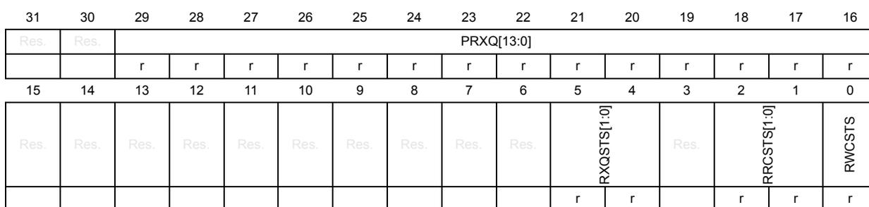
| 31 | 30 | 29 | 28 | 27 | 26 | 25 | 24 | 23 | 22 | 21 | 20 | 19 | 18 | 17 | 16 |
| Res. | Res. | PRXQ[13:0] | |||||||||||||
| r | r | r | r | r | r | r | r | r | r | r | r | r | r | ||
| 15 | 14 | 13 | 12 | 11 | 10 | 9 | 8 | 7 | 6 | 5 | 4 | 3 | 2 | 1 | 0 |
| Res. | Res. | Res. | Res. | Res. | Res. | Res. | Res. | Res. | Res. | RXQSTS[1:0] | Res. | RRCSTS[1:0] | RWCSTS | ||
| r | r | r | r | r | |||||||||||
Bits 31:30 Reserved, must be kept at reset value.
Bits 29:16 PRXQ[13:0] : Number of Packets in Receive Queue
This field indicates the current number of packets in the Rx queue. The theoretical maximum value for this field is 256 Kbyte/16 bytes = 16K Packets, that is, \( \text{Max\_Queue\_Size} / \text{Min\_Packet\_Size} \) .
Bits 15:6 Reserved, must be kept at reset value.
Bits 5:4 RXQSTS[1:0] : MTL Rx Queue Fill-Level Status
This field gives the status of the fill-level of the Rx queue:
00: Rx queue empty
01: Rx queue fill-level below flow-control deactivate threshold
10: Rx queue fill-level above flow-control activate threshold
11: Rx queue full
Bit 3 Reserved, must be kept at reset value.
Bits 2:1 RRCSTS[1:0] : MTL Rx Queue Read Controller State
This field gives the state of the Rx queue Read controller:
00: Idle state
01: Reading packet data
10: Reading packet status (or timestamp)
11: Flushing the packet data and status
Bit 0 RWCSTS : MTL Rx Queue Write Controller Active Status
When high, this bit indicates that the MTL Rx queue Write controller is active, and it is transferring a received packet to the Rx queue.
Rx queue x control register (ETH_MTLRXQxCR)Address offset: 0x0D3C + 0x40 * x, (x = 0 to 1)
Reset value: 0x0000 0000
The Queue Receive Control register controls the receive arbitration and passing of received packets to the application.
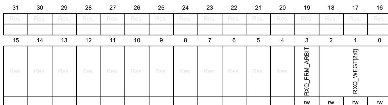
| 31 | 30 | 29 | 28 | 27 | 26 | 25 | 24 | 23 | 22 | 21 | 20 | 19 | 18 | 17 | 16 |
| Res. | Res. | Res. | Res. | Res. | Res. | Res. | Res. | Res. | Res. | Res. | Res. | Res. | Res. | Res. | Res. |
| 15 | 14 | 13 | 12 | 11 | 10 | 9 | 8 | 7 | 6 | 5 | 4 | 3 | 2 | 1 | 0 |
| Res. | Res. | Res. | Res. | Res. | Res. | Res. | Res. | Res. | Res. | Res. | Res. | RXQ_FRM_ARBIT | RXQ_WEGT[2:0] | ||
| rw | rw | rw | rw | ||||||||||||
Bits 31:4 Reserved, must be kept at reset value.
Bit 3 RXQ_FRM_ARBIT : Receive Queue Packet Arbitration
When this bit is set, the Ethernet peripheral drives the packet data to the DMA such that the entire packet data of currently-selected queue is transmitted before switching to other queue. When this bit is reset, the Ethernet peripheral drives the packet data to the DMA such that the following amount of data of currently-selected queue is transmitted before switching to other queue:
- – PBL amount of data
- or
- – complete data of a packet
The status and the timestamp are not a part of the PBL data. Therefore, the Ethernet peripheral drives the complete status (including timestamp status) during first PBL request for the packet (in store-and-forward mode) or the last PBL request for the packet (in Threshold mode).
Bits 2:0 RXQ_WEGT[2:0] : Receive Queue Weight
This field indicates the weight assigned to the Rx queue x. The weight is used as the number of continuous PBL requests or contiguous packets (depending on the RXQ_FRM_ARBIT) allocated to the queue in one arbitration cycle.
This field needs to be programmed with one value less than the required weight, that is, reset value of 0 indicates weight of 1, value of 1 indicates weight of 2, and so on.
Note: The change in value of RXQ_WEGT takes effect only after the completion of current service round or when there is change from RAA=SP to RAA=WSP algorithm. This approach is taken so that there is smooth transition. For the RXQ_WEGT value to take effect at the start, the Rx queue x control register (ETH_MTLRXQxCR) must be programmed before the Rx queue x operating mode register (ETH_MTLRXQxOMR) .
Tx queue 1 ETS control register (ETH_MTLTXQ1ECR)Address offset: 0x0D50
Reset value: 0x0000 0000
The Queue ETS Control register controls the enhanced transmission selection operation.
| 31 | 30 | 29 | 28 | 27 | 26 | 25 | 24 | 23 | 22 | 21 | 20 | 19 | 18 | 17 | 16 |
|---|---|---|---|---|---|---|---|---|---|---|---|---|---|---|---|
| Res. | Res. | Res. | Res. | Res. | Res. | Res. | Res. | Res. | Res. | Res. | Res. | Res. | Res. | Res. | Res. |
| 15 | 14 | 13 | 12 | 11 | 10 | 9 | 8 | 7 | 6 | 5 | 4 | 3 | 2 | 1 | 0 |
| Res. | Res. | Res. | Res. | Res. | Res. | Res. | Res. | Res. | SLC[2:0] | CC | AVALG | Res. | |||
| rw | rw | rw | rw | rw | |||||||||||
Bits 31:7 Reserved, must be kept at reset value.
Bits 6:4 SLC[2:0] : Slot CountIf the credit-based shaper algorithm is enabled, the software can program the number of slots (of 125 us duration) over which the average transmitted bits per slot, provided in Tx queue x ETS status register (ETH_MTLTXQxESR) , need to be computed for Queue 1. The encoding is as follows:
000: 1 Slot
001: 2 Slots
010: 4 Slots
011: 8 Slots
100: 16 Slots
101 to 111: Reserved, must not be used.
Bit 3 CC : Credit ControlWhen this bit is set, the accumulated credit parameter in the credit-based shaper algorithm logic is not reset to zero when there is positive credit and no packet to transmit in Channel 1. The credit accumulates even when there is no packet waiting in Channel 1 and another channel is transmitting.
When this bit is reset, the accumulated credit parameter in the credit-based shaper algorithm logic is set to zero when there is positive credit and no packet to transmit in Channel 1. When there is no packet waiting in Channel 1 and other channel is transmitting, no credit is accumulated.
Bit 2 AVALG : AV AlgorithmWhen Queue 1 is programmed for AV, this field configures the scheduling algorithm for this queue:
This bit when set, indicates credit based shaper algorithm (CBS) is selected for Queue 1 traffic. When reset, strict priority is selected.
Bits 1:0 Reserved, must be kept at reset value.
Tx queue x quantum weight register (ETH_MTLTXQxQWR)Address offset: 0x0D18 + 0x40 * x, (x = 0 to 1)
Reset value: 0x0000 0000
This register contains the weights for the Weighted Round Robin (WRR) or IdleSlopeCredit for the queue.
| 31 | 30 | 29 | 28 | 27 | 26 | 25 | 24 | 23 | 22 | 21 | 20 | 19 | 18 | 17 | 16 |
| Res. | Res. | Res. | Res. | Res. | Res. | Res. | Res. | Res. | Res. | Res. | Res. | Res. | Res. | Res. | Res. |
| 15 | 14 | 13 | 12 | 11 | 10 | 9 | 8 | 7 | 6 | 5 | 4 | 3 | 2 | 1 | 0 |
| Res. | Res. | ISCQW[13:0] | |||||||||||||
| rw | rw | rw | rw | rw | rw | rw | rw | rw | rw | rw | rw | rw | rw | ||
Bits 31:14 Reserved, must be kept at reset value.
Bits 13:0 ISCQW[13:0] : IdleSlopeCredit or Weights
idleSlopeCreditWhen AV feature is enabled, this field contains the idleSlopeCredit value required for the credit-based shaper algorithm for queue 1. This is the rate of change of credit in bits per cycle (40 ns for 100 Mbps; 8 ns for 1000 Mbps) when the credit is increasing. The software should program this field with computed credit in bits per cycle scaled by 1,024. The maximum value is portTransmitRate, that is, 0x2000 in 1000 Mbps mode and 0x1000 in 100 Mbps mode.
WeightsIf WRR algorithm is enabled for queue x generic traffic (not AVB), this field contains the weight for queue x. The maximum value is 0x64. Bits [13:7] must be written to zero.
Note: In multiple Queue configuration this field must be programmed to some non-zero value when multiple queues are enabled, or a single queue other than Queue 0 is enabled. This field need not be programmed when only Q0 is enabled. In general, when WRR algorithm is selected a non-zero value must be programmed on both receive and transmit. In receive, the register is Operating mode register (ETH_MTLOMR) .
The weights programmed do not correspond to the number of packets but the fraction of bandwidth or time allocated for particular queue w.r.t. total BW or time.
Tx queue 1 send slope credit register (ETH_MTLTXQ1SSCR)Address offset: 0x0D5C
Reset value: 0x0000 0000
The sendSlopeCredit register contains the sendSlope credit value required for the credit-based shaper algorithm for the Queue.
| 31 | 30 | 29 | 28 | 27 | 26 | 25 | 24 | 23 | 22 | 21 | 20 | 19 | 18 | 17 | 16 |
| Res. | Res. | Res. | Res. | Res. | Res. | Res. | Res. | Res. | Res. | Res. | Res. | Res. | Res. | Res. | Res. |
| 15 | 14 | 13 | 12 | 11 | 10 | 9 | 8 | 7 | 6 | 5 | 4 | 3 | 2 | 1 | 0 |
| Res. | Res. | SSC[13:0] | |||||||||||||
| rw | rw | rw | rw | rw | rw | rw | rw | rw | rw | rw | rw | rw | rw | ||
Bits 31:14 Reserved, must be kept at reset value.
Bits 13:0 SSC[13:0] : sendSlopeCredit Value
When AV operation is enabled, this field contains the sendSlopeCredit value required for credit-based shaper algorithm for queue 1. This is the rate of change of credit in bits per cycle (40 ns and 8 ns for 100 Mbps and 1000 Mbps respectively) when the credit decreases. The software should program this field with computed credit in bits per cycle scaled by 1 024. The maximum value is portTransmitRate, that is 0x2000 in 1000 Mbps mode and 0x1000 in 100 Mbps mode. This field should be programmed with absolute sendSlopeCredit value. The credit-based shaper logic subtracts it from the accumulated credit when queue 1 is selected for transmission.
Tx Queue 1 hiCredit register (ETH_MTLTXQ1HCR)
Address offset: 0x0D60
Reset value: 0x0000 0000
The hiCredit register contains the hiCredit value required for the credit-based shaper algorithm for the Queue.
| 31 | 30 | 29 | 28 | 27 | 26 | 25 | 24 | 23 | 22 | 21 | 20 | 19 | 18 | 17 | 16 |
|---|---|---|---|---|---|---|---|---|---|---|---|---|---|---|---|
| Res. | Res. | Res. | HC[28:16] | ||||||||||||
| rw | rw | rw | rw | rw | rw | rw | rw | rw | rw | rw | rw | rw | |||
| 15 | 14 | 13 | 12 | 11 | 10 | 9 | 8 | 7 | 6 | 5 | 4 | 3 | 2 | 1 | 0 |
| HC[15:0] | |||||||||||||||
| rw | rw | rw | rw | rw | rw | rw | rw | rw | rw | rw | rw | rw | rw | rw | rw |
Bits 31:29 Reserved, must be kept at reset value.
Bits 28:0 HC[28:0] : hiCredit Value
This field contains the hiCredit value required for the credit-based shaper algorithm when the AV feature is enabled. This is the maximum value that can be accumulated in the credit parameter. This is specified in bits scaled by 1 024.
The maximum value is maxInterferenceSize, that is, best-effort maximum packet size (16 384 bytes or 131 072 bits). The value to be specified is 131 072 × 1 024 = 134 217 728 or 0x0800 0000.
Tx queue 1 loCredit register (ETH_MTLTXQ1LCR)
Address offset: 0x0D64
Reset value: 0x0000 0000
The loCredit register contains the loCredit value required for the credit-based shaper algorithm for the Queue.
| 31 | 30 | 29 | 28 | 27 | 26 | 25 | 24 | 23 | 22 | 21 | 20 | 19 | 18 | 17 | 16 |
|---|---|---|---|---|---|---|---|---|---|---|---|---|---|---|---|
| Res. | Res. | Res. | LC[28:16] | ||||||||||||
| rw | rw | rw | rw | rw | rw | rw | rw | rw | rw | rw | rw | rw | |||
| 15 | 14 | 13 | 12 | 11 | 10 | 9 | 8 | 7 | 6 | 5 | 4 | 3 | 2 | 1 | 0 |
| LC[15:0] | |||||||||||||||
| rw | rw | rw | rw | rw | rw | rw | rw | rw | rw | rw | rw | rw | rw | rw | rw |
Bits 31:29 Reserved, must be kept at reset value.
Bits 28:0 LC[28:0] : loCredit ValueWhen AV operation is enabled, this field contains the loCredit value required for the credit-based shaper algorithm. This is the minimum value that can be accumulated in the credit parameter. This is specified in bits scaled by 1 024. The maximum value is maxFrameSize transmitted from this queue, that is, \( 16\,384 \times 8 \times 1\,024 = 134\,217\,728 \) or 0x0800 0000. Because it is a negative value, the programmed value is 2's complement of the value, that is, 0x1800 0000.
Ethernet MTL register map and reset values
Table 849. ETH_MTL register map and reset values
| Offset | Register name | 31 | 30 | 29 | 28 | 27 | 26 | 25 | 24 | 23 | 22 | 21 | 20 | 19 | 18 | 17 | 16 | 15 | 14 | 13 | 12 | 11 | 10 | 9 | 8 | 7 | 6 | 5 | 4 | 3 | 2 | 1 | 0 | |
|---|---|---|---|---|---|---|---|---|---|---|---|---|---|---|---|---|---|---|---|---|---|---|---|---|---|---|---|---|---|---|---|---|---|---|
| 0x0C00 | ETH_MTLOMR | Res. | Res. | Res. | Res. | Res. | Res. | Res. | Res. | Res. | Res. | Res. | Res. | Res. | Res. | Res. | Res. | Res. | Res. | Res. | Res. | Res. | Res. | CNTCLR | CNTPRST | Res. | SCHALG[1:0] | Res. | Res. | Res. | RAA | DTXSTS | Res. | |
| Reset value | 0 | 0 | 0 | 0 | 0 | 0 | ||||||||||||||||||||||||||||
| 0x0C04 - 0x0C1C | Reserved | |||||||||||||||||||||||||||||||||
| 0x0C20 | ETH_MTLISR | Res. | Res. | Res. | Res. | Res. | Res. | Res. | Res. | Res. | Res. | Res. | Res. | Res. | ESTIS | Res. | Res. | Res. | Res. | Res. | Res. | Res. | Res. | Res. | Res. | Res. | Res. | Res. | Res. | Res. | Res. | Q1IS | Q0IS | |
| Reset value | 0 | 0 | 0 | |||||||||||||||||||||||||||||||
| 0x0C24 - 0x0C2C | Reserved | |||||||||||||||||||||||||||||||||
| 0x0C30 | ETH_MTLRXQDMA MR | Res. | Res. | Res. | Res. | Res. | Res. | Res. | Res. | Res. | Res. | Res. | Res. | Res. | Res. | Res. | Res. | Res. | Q1DDMACH | Res. | Res. | Q1MDMACH | Res. | Res. | Res. | Q0DDMACH | Res. | Res. | Res. | Res. | Q0MDMACH | |||
| Reset value | 0 | 0 | 0 | 0 | ||||||||||||||||||||||||||||||
| 0x0C34 - 0x0C3C | Reserved | |||||||||||||||||||||||||||||||||
| 0x0C40 | ETH_MTLTBSCR | LEOS[23:0] | LEGOS[2:0] | Res. | Res. | LEOV | ESTM | |||||||||||||||||||||||||||
| Reset value | 0 | 0 | 0 | 0 | 0 | 0 | 0 | 0 | 0 | 0 | 0 | 0 | 0 | 0 | 0 | 0 | 0 | 0 | 0 | 0 | 0 | 0 | 0 | 0 | 0 | 0 | 0 | 0 | 0 | |||||
| 0x0C50 | ETH_MTLSTCR | PTOV[7:0] | CTOV[11:0] | Res. | TILS[2:0] | LCSE[1:0] | DFBS | DDBF | Res. | Res. | SSWL | EEST | ||||||||||||||||||||||
| Reset value | 0 | 0 | 0 | 0 | 0 | 0 | 0 | 0 | 0 | 0 | 0 | 0 | 0 | 0 | 0 | 0 | 0 | 0 | 0 | 0 | 0 | 0 | 0 | 0 | 0 | 0 | 0 | 0 | 0 | |||||
| 0x0C54 | ETH_MTLSTECR | Res. | Res. | Res. | Res. | Res. | Res. | Res. | Res. | Res. | Res. | Res. | Res. | Res. | Res. | Res. | Res. | Res. | Res. | Res. | Res. | Res. | Res. | Res. | Res. | Res. | Res. | OVHD[5:0] | ||||||
| Reset value | 0 | 0 | 0 | 0 | 0 | 0 | ||||||||||||||||||||||||||||
| 0x0C58 | ETH_MTLSTSR | Res. | Res. | Res. | Res. | Res. | Res. | Res. | Res. | Res. | Res. | Res. | Res. | CGSN[3:0] | BTRL[7:0] | SWOL | Res. | CGCE | HLBS | HLBF | BTRE | SWLC | ||||||||||||
| Reset value | 0 | 0 | 0 | 0 | 0 | 0 | 0 | 0 | 0 | 0 | 0 | 0 | 0 | 0 | 0 | 0 | 0 | 0 | ||||||||||||||||
| 0x0C5C | Reserved | |||||||||||||||||||||||||||||||||
| 0x0C60 | ETH_MTLSTSCHER | Res. | Res. | Res. | Res. | Res. | Res. | Res. | Res. | Res. | Res. | Res. | Res. | Res. | Res. | Res. | Res. | Res. | Res. | Res. | Res. | Res. | Res. | Res. | Res. | Res. | Res. | Res. | Res. | Res. | Res. | SEQN[1:0] | ||
| Reset value | 0 | 0 | ||||||||||||||||||||||||||||||||
Table 849. ETH_MTL register map and reset values (continued)
| Offset | Register name | 31 | 30 | 29 | 28 | 27 | 26 | 25 | 24 | 23 | 22 | 21 | 20 | 19 | 18 | 17 | 16 | 15 | 14 | 13 | 12 | 11 | 10 | 9 | 8 | 7 | 6 | 5 | 4 | 3 | 2 | 1 | 0 | |
|---|---|---|---|---|---|---|---|---|---|---|---|---|---|---|---|---|---|---|---|---|---|---|---|---|---|---|---|---|---|---|---|---|---|---|
| 0x0C64 | ETH_MTLSTFSER | Res | Res | Res | Res | Res | Res | Res | Res | Res | Res | Res | Res | Res | Res | Res | Res | Res | Res | Res | Res | Res | Res | Res | Res | Res | Res | Res | Res | Res | Res | Res | FEQN[1:0] | |
| Reset value | 0 0 | |||||||||||||||||||||||||||||||||
| 0x0C68 | ETH_MTLSTFSCR | Res | Res | Res | Res | Res | Res | Res | Res | Res | Res | Res | Res | Res | Res | Res | HBFQ | Res | HBFS[14:0] | |||||||||||||||
| Reset value | 0 | 0 | 0 | 0 | 0 | 0 | 0 | 0 | 0 | 0 | 0 | 0 | 0 | 0 | 0 0 | |||||||||||||||||||
| 0x0C6C | Reserved | |||||||||||||||||||||||||||||||||
| 0x0C70 | ETH_MTLSTIER | Res | Res | Res | Res | Res | Res | Res | Res | Res | Res | Res | Res | Res | Res | Res | Res | Res | Res | Res | Res | Res | Res | Res | Res | Res | Res | Res | Res | COGE | IEHS | IEHF | IEBE | IECC |
| Reset value | 0 | 0 | 0 | 0 0 | ||||||||||||||||||||||||||||||
| 0x0C74 - 0x0C7C | Reserved | |||||||||||||||||||||||||||||||||
| 0x0C80 | ETH_MTLSTGCLCR | Res | Res | Res | Res | Res | Res | Res | Res | Res | Res | Res | Res | Res | Res | Res | Res | Res | Res | ADDR[5:0] | Res | Res | Res | DBGB | DBGM | Res | GCCR | R1W0 | SRW0 | |||||
| Reset value | 0 | 0 | 0 | 0 | 0 | 0 | 0 | 0 | 0 | 0 0 | ||||||||||||||||||||||||
| 0x0C84 | ETH_MTLSTGCLDR | GCD[31:0] | ||||||||||||||||||||||||||||||||
| Reset value | 0 | 0 | 0 | 0 | 0 | 0 | 0 | 0 | 0 | 0 | 0 | 0 | 0 | 0 | 0 | 0 | 0 | 0 | 0 | 0 | 0 | 0 | 0 | 0 | 0 | 0 | 0 | 0 | 0 | 0 | 0 0 | |||
| 0x0C88-0x0C8C | Reserved | |||||||||||||||||||||||||||||||||
| 0x0C90 | ETH_MTLFPECSR | Res | Res | Res | HRS | Res | Res | Res | Res | Res | Res | Res | Res | Res | Res | Res | Res | Res | Res | Res | Res | PEC[1:0] | Res | Res | Res | Res | Res | Res | Res | Res | Res | AFSZ[1:0] | ||
| Reset value | 0 | 0 | 0 | 0 0 | ||||||||||||||||||||||||||||||
| 0x0C94 | ETH_MTLFPEAR | RADV[15:0] | ||||||||||||||||||||||||||||||||
| Reset value | 0 | 0 | 0 | 0 | 0 | 0 | 0 | 0 | 0 | 0 | 0 | 0 | 0 | 0 | 0 | 0 | 0 | 0 | 0 | 0 | 0 | 0 | 0 | 0 | 0 | 0 | 0 | 0 | 0 | 0 | 0 0 | |||
| 0x0C98 - 0x0CFC | Reserved | |||||||||||||||||||||||||||||||||
| 0x0D00 | ETH_MTLTXQOMR | Res | Res | Res | Res | Res | Res | Res | Res | Res | Res | Res | Res | TQS[3:0] | Res | Res | Res | Res | Res | Res | Res | Res | Res | Res | TTC[2:0] | TXQEN[1:0] | TSF | |||||||
| Reset value | 0 | 0 | 0 | 0 | 0 | 0 | 0 | 0 | 0 0 | |||||||||||||||||||||||||
| 0x0D04 | ETH_MTLTXQ0UR | Res | Res | Res | Res | Res | Res | Res | Res | Res | Res | Res | Res | Res | Res | Res | Res | Res | Res | Res | Res | UFCNTVF | UFFRMCNT[10:0] | |||||||||||
| Reset value | 0 | 0 | 0 | 0 | 0 | 0 | 0 | 0 | 0 | 0 | 0 0 | |||||||||||||||||||||||
| 0x0D08 | ETH_MTLTXQ0DR | Res | Res | Res | Res | Res | Res | Res | Res | Res | Res | Res | Res | Res | Res | Res | Res | Res | Res | Res | Res | Res | Res | Res | Res | Res | Res | TXSFSSTS | TXQSTS | TWCSTS | TRCSTS[1:0] | TXQPAUSED | ||
| Reset value | 0 | 0 | 0 | 0 | 0 0 | |||||||||||||||||||||||||||||
Table 849. ETH_MTL register map and reset values (continued)
| Offset | Register name | 31 | 30 | 29 | 28 | 27 | 26 | 25 | 24 | 23 | 22 | 21 | 20 | 19 | 18 | 17 | 16 | 15 | 14 | 13 | 12 | 11 | 10 | 9 | 8 | 7 | 6 | 5 | 4 | 3 | 2 | 1 | 0 | |
|---|---|---|---|---|---|---|---|---|---|---|---|---|---|---|---|---|---|---|---|---|---|---|---|---|---|---|---|---|---|---|---|---|---|---|
| 0x0D0C - 0x0D10 | Reserved | |||||||||||||||||||||||||||||||||
| 0x0D14 | ETH_MTLTXQ0ESR | Res. | Res. | Res. | Res. | Res. | Res. | Res. | Res. | ABS[23:0] | ||||||||||||||||||||||||
| Reset value | 0 | 0 | 0 | 0 | 0 | 0 | 0 | 0 | 0 | 0 | 0 | 0 | 0 | 0 | 0 | 0 | 0 | 0 | 0 | 0 | 0 | 0 | 0 | 0 | ||||||||||
| 0x0D18 | ETH_MTLTXQ0QWR | Res. | Res. | Res. | Res. | Res. | Res. | Res. | Res. | Res. | Res. | Res. | Res. | Res. | Res. | Res. | Res. | Res. | Res. | Res. | Res. | Res. | Res. | Res. | Res. | Res. | ISCQW[6:0] | |||||||
| Reset value | 0 | 0 | 0 | 0 | 0 | 0 | 0 | |||||||||||||||||||||||||||
| 0x0D28 | Reserved | |||||||||||||||||||||||||||||||||
| 0x0D2C | ETH_MTLQ0ICSR | Res. | Res. | Res. | Res. | Res. | Res. | Res. | RXOIE | Res. | Res. | Res. | Res. | Res. | Res. | RXOVFIS | Res. | Res. | Res. | Res. | Res. | Res. | ABPSIE | TXUIE | Res. | Res. | Res. | Res. | Res. | Res. | ABPSIS | TXUNFIS | ||
| Reset value | 0 | 0 | 0 | 0 | 0 | 0 | ||||||||||||||||||||||||||||
| 0x0D30 | ETH_MTLRXQ0OMR | Res. | Res. | Res. | Res. | Res. | Res. | Res. | Res. | RQS[3:0] | Res. | Res. | Res. | RFD[2:0] | Res. | Res. | Res. | Res. | RFA[2:0] | EHFC | DIS TCP EF | RSF | FEP | FUP | Res. | RTC[1:0] | ||||||||
| Reset value | 0 | 0 | 0 | 0 | 0 | 0 | 0 | 0 | 0 | 0 | 0 | 0 | 0 | 0 | 0 | 0 | 0 | 0 | ||||||||||||||||
| 0x0D34 | ETH_MTLRXQ0MPOCR | Res. | Res. | Res. | Res. | MISCNTOVF | MISPKTCNT[10:0] | Res. | Res. | Res. | Res. | OVFCNTOVF | OVFPKTCNT[10:0] | |||||||||||||||||||||
| Reset value | 0 | 0 | 0 | 0 | 0 | 0 | 0 | 0 | 0 | 0 | 0 | 0 | 0 | 0 | 0 | 0 | 0 | 0 | 0 | 0 | 0 | 0 | 0 | |||||||||||
| 0x0D38 | ETH_MTLRXQ0DR | Res. | Res. | PRXQ[13:0] | Res. | Res. | Res. | Res. | Res. | Res. | Res. | Res. | Res. | Res. | RXQSTS[1:0] | Res. | RRCSTS[1:0] | RWCSTS | ||||||||||||||||
| Reset value | 0 | 0 | 0 | 0 | 0 | 0 | 0 | 0 | 0 | 0 | 0 | 0 | 0 | 0 | 0 | 0 | 0 | 0 | 0 | |||||||||||||||
| 0x0D3C | ETH_MTLRXQ0CR | Res. | Res. | Res. | Res. | Res. | Res. | Res. | Res. | Res. | Res. | Res. | Res. | Res. | Res. | Res. | Res. | Res. | Res. | Res. | Res. | Res. | Res. | Res. | Res. | Res. | Res. | Res. | RXQ_FRM_ARBIT | RXQ_WEGT[2:0] | ||||
| Reset value | 0 | 0 | 0 | 0 | 0 | |||||||||||||||||||||||||||||
| 0x0D40 | ETH_MTLTXQ1OMR | Res. | Res. | Res. | Res. | Res. | Res. | Res. | Res. | Res. | Res. | Res. | Res. | TQS[3:0] | Res. | Res. | Res. | Res. | Res. | Res. | Res. | Res. | Res. | Res. | TTC[2:0] | TXQEN[1:0] | TSF | FTQ | ||||||
| Reset value | 0 | 0 | 0 | 0 | 0 | 0 | 0 | 0 | 0 | 0 | 0 | |||||||||||||||||||||||
| 0x0D44 | ETH_MTLTXQ1UR | Res. | Res. | Res. | Res. | Res. | Res. | Res. | Res. | Res. | Res. | Res. | Res. | Res. | Res. | Res. | Res. | Res. | Res. | Res. | Res. | UFCNTOVF | UFFRMCNT[10:0] | |||||||||||
| Reset value | 0 | 0 | 0 | 0 | 0 | 0 | 0 | 0 | 0 | 0 | 0 | 0 | ||||||||||||||||||||||
Table 849. ETH_MTL register map and reset values (continued)
| Offset | Register name | 31 | 30 | 29 | 28 | 27 | 26 | 25 | 24 | 23 | 22 | 21 | 20 | 19 | 18 | 17 | 16 | 15 | 14 | 13 | 12 | 11 | 10 | 9 | 8 | 7 | 6 | 5 | 4 | 3 | 2 | 1 | 0 |
|---|---|---|---|---|---|---|---|---|---|---|---|---|---|---|---|---|---|---|---|---|---|---|---|---|---|---|---|---|---|---|---|---|---|
| 0x0D48 | ETH_MTLTXQ1DR | Res | Res | Res | Res | Res | Res | Res | Res | Res | STXSTSF[2:0] | Res | Res | Res | PTXQ[2:0] | Res | Res | Res | Res | Res | Res | Res | Res | Res | Res | Res | Res | TXSTSFS[1:0] | TXQSTS | TWCSTS | TRCSTS[1:0] | Res | TXQPAUSED |
| Reset value | 0 | 0 | 0 | 0 | 0 | 0 | 0 | 0 | 0 | 0 | 0 | 0 | |||||||||||||||||||||
| 0x0D4C | Reserved | ||||||||||||||||||||||||||||||||
| 0x0D50 | ETH_MTLTXQ1ECR | Res | Res | Res | Res | Res | Res | Res | Res | Res | Res | Res | Res | Res | Res | Res | Res | Res | Res | Res | Res | Res | Res | Res | Res | Res | Res | SLC[2:0] | CC | AVALG | Res | Res | |
| Reset value | 0 | 0 | 0 | 0 | 0 | ||||||||||||||||||||||||||||
| 0x0D54 | ETH_MTLTXQ1ESR | Res | Res | Res | Res | Res | Res | Res | Res | ABS[23:0] | |||||||||||||||||||||||
| Reset value | 0 | 0 | 0 | 0 | 0 | 0 | 0 | 0 | 0 | 0 | 0 | 0 | 0 | 0 | 0 | 0 | 0 | 0 | 0 | 0 | 0 | 0 | 0 | ||||||||||
| 0x0D58 | ETH_MTLTXQ1QWR | Res | Res | Res | Res | Res | Res | Res | Res | Res | Res | Res | Res | Res | Res | Res | Res | Res | Res | ISCQW[13:0] | |||||||||||||
| Reset value | 0 | 0 | 0 | 0 | 0 | 0 | 0 | 0 | 0 | 0 | 0 | 0 | 0 | ||||||||||||||||||||
| 0x0D5C | ETH_MTLTXQ1SSCR | Res | Res | Res | Res | Res | Res | Res | Res | Res | Res | Res | Res | Res | Res | Res | Res | Res | Res | SSC[13:0] | |||||||||||||
| Reset value | 0 | 0 | 0 | 0 | 0 | 0 | 0 | 0 | 0 | 0 | 0 | 0 | 0 | ||||||||||||||||||||
| 0x0D60 | ETH_MTLTXQ1HCR | Res | Res | Res | HC[28:0] | ||||||||||||||||||||||||||||
| Reset value | 0 | 0 | 0 | 0 | 0 | 0 | 0 | 0 | 0 | 0 | 0 | 0 | 0 | 0 | 0 | 0 | 0 | 0 | 0 | 0 | 0 | 0 | 0 | 0 | 0 | 0 | 0 | 0 | |||||
| 0x0D64 | ETH_MTLTXQ1LCR | Res | Res | Res | LC[28:0] | ||||||||||||||||||||||||||||
| Reset value | 0 | 0 | 0 | 0 | 0 | 0 | 0 | 0 | 0 | 0 | 0 | 0 | 0 | 0 | 0 | 0 | 0 | 0 | 0 | 0 | 0 | 0 | 0 | 0 | 0 | 0 | 0 | 0 | |||||
| 0x0D68 | Reserved | ||||||||||||||||||||||||||||||||
| 0x0D6C | ETH_MTLQ1ICSR | Res | Res | Res | Res | Res | Res | Res | Res | RXOIE | Res | Res | Res | Res | Res | Res | RXOVFIS | Res | Res | Res | Res | Res | Res | ABPSIE | TXUIE | Res | Res | Res | Res | Res | Res | Res | ABPSIS TXUNFIS |
| Reset value | 0 | 0 | 0 | 0 | 0 | 0 | |||||||||||||||||||||||||||
| 0x0D70 | ETH_MTLRXQ1OMR | Res | Res | Res | Res | Res | Res | Res | Res | Res | RQS[3:0] | Res | Res | Res | RFD[2:0] | Res | Res | Res | Res | Res | Res | Res | RFA[2:0] | EHFC | DIS | TCP | EF | RSF | FEP | FJP | Res | RTC[1:0] | |
| Reset value | 0 | 0 | 0 | 0 | 0 | 0 | 0 | 0 | 0 | 0 | 0 | 0 | 0 | 0 | 0 | 0 | 0 | ||||||||||||||||
| 0x0D74 | ETH_MTLRXQ1MP OCR | Res | Res | Res | Res | MISCNTOVF | MISPKTCNT[10:0] | Res | Res | Res | Res | OVFCNTOVF | OVFPKTCNT[10:0] | ||||||||||||||||||||
| Reset value | 0 | 0 | 0 | 0 | 0 | 0 | 0 | 0 | 0 | 0 | 0 | 0 | 0 | 0 | 0 | 0 | 0 | 0 | 0 | 0 | 0 | 0 | 0 | ||||||||||
| 0x0D78 | ETH_MTLRXQ1DR | Res | Res | PRXQ[13:0] | Res | Res | Res | Res | Res | Res | Res | Res | Res | Res | RXQSTS[1:0] | Res | RRCSTS[1:0] | Res | RWCSTS | ||||||||||||||
| Reset value | 0 | 0 | 0 | 0 | 0 | 0 | 0 | 0 | 0 | 0 | 0 | 0 | 0 | 0 | 0 | 0 | 0 | 0 | |||||||||||||||
Table 849. ETH_MTL register map and reset values (continued)
| Offset | Register name | 31 | 30 | 29 | 28 | 27 | 26 | 25 | 24 | 23 | 22 | 21 | 20 | 19 | 18 | 17 | 16 | 15 | 14 | 13 | 12 | 11 | 10 | 9 | 8 | 7 | 6 | 5 | 4 | 3 | 2 | 1 | 0 |
|---|---|---|---|---|---|---|---|---|---|---|---|---|---|---|---|---|---|---|---|---|---|---|---|---|---|---|---|---|---|---|---|---|---|
| 0x0D7C | ETH_MTLRXQ1CR | Res | Res | Res | Res | Res | Res | Res | Res | Res | Res | Res | Res | Res | Res | Res | Res | Res | Res | Res | Res | Res | Res | Res | Res | Res | Res | Res | Res | RXQ_FRM_ARBIT | RXQ_WEGT[2:0] | 0 | 0 |
| Reset value | 0 |
Refer to Section 2.3: Memory organization for the register boundary addresses.
76.11.4 Ethernet MAC and MMC registers
Operating mode configuration register (ETH_MACCR)
Address offset: 0x0000
Reset value: 0x0000 0000
The MAC Configuration register establishes the operating mode of the MAC.
| 31 | 30 | 29 | 28 | 27 | 26 | 25 | 24 | 23 | 22 | 21 | 20 | 19 | 18 | 17 | 16 |
|---|---|---|---|---|---|---|---|---|---|---|---|---|---|---|---|
| ARPEN | SARC[2:0] | IPC | IPC[2:0] | GPSLCE | S2KP | CST | ACS | WD | BE | JD | JE | ||||
| rw | rw | rw | rw | rw | rw | rw | rw | rw | rw | rw | rw | rw | rw | rw | rw |
| 15 | 14 | 13 | 12 | 11 | 10 | 9 | 8 | 7 | 6 | 5 | 4 | 3 | 2 | 1 | 0 |
|---|---|---|---|---|---|---|---|---|---|---|---|---|---|---|---|
| PS | FES | DM | LM | ECRSFD | DO | DCRS | DR | Res | BL[1:0] | DC | PRELEN[1:0] | TE | RE | ||
| rw | rw | rw | rw | rw | rw | rw | rw | rw | rw | rw | rw | rw | rw | rw | |
Bit 31 ARPEN: ARP Offload Enable
When this bit is set, the MAC can recognize an incoming ARP request packet and schedules the ARP packet for transmission. It forwards the ARP packet to the application and also indicate the events in the RxStatus.
When this bit is reset, the MAC receiver does not recognize any ARP packet and indicates them as Type frame in the RxStatus.
Bits 30:28 SARC[2:0] : Source Address Insertion or Replacement ControlThis field controls the source address insertion or replacement for all transmitted packets. Bit 30 specifies which MAC Address register (0 or 1) is used for source address insertion or replacement based on the values of Bits[29:28]:
010: the MAC inserts the content of the MAC Address 0 registers ( MAC address 0 high register (ETH_MACA0HR) and MAC address x low register (ETH_MACAxLR) ) in the SA field of all transmitted packets.
011: the MAC replaces the content of the MAC Address 0 registers ( MAC address 0 high register (ETH_MACA0HR) and MAC address x low register (ETH_MACAxLR) ) in the SA field of all transmitted packets.
110: the MAC inserts the content of the MAC Address 1 registers ( MAC address x high register (ETH_MACAxHR) and MAC address x low register (ETH_MACAxLR) ) in the SA field of all transmitted packets
111: the MAC replaces the content of the MAC Address 1 registers ( MAC address x high register (ETH_MACAxHR) and MAC address x low register (ETH_MACAxLR) ) in the SA field of all transmitted packets.
Others: Reserved, must not be used.
Note: Changes to this field take effect only on the start of a packet. If you write to this register field when a packet is being transmitted, only the subsequent packet can use the updated value, that is, the current packet does not use the updated value.
Bit 27 IPC : Checksum OffloadWhen set, this bit enables the IPv4 header checksum checking and IPv4 or IPv6 TCP, UDP, or ICMP payload checksum checking. When this bit is reset, the COE function in the receiver is disabled.
The Layer 3 and Layer 4 Packet Filter feature automatically selects the IPC Full Checksum Offload Engine on the Receive side. When this feature is enabled, you must set the IPC bit.
Bits 26:24 IPG[2:0] : Inter-Packet GapThese bits control the minimum IPG between packets during transmission.
000: 96 bit times
001: 88 bit times
010: 80 bit times
...
111: 40 bit times
This range of minimum IPG is valid in Full-duplex mode.
In the Half-duplex mode, the minimum IPG can be configured only for 64-bit times (IPG = 100). Lower values are not considered.
When a JAM pattern is being transmitted because of backpressure activation, the MAC does not consider the minimum IPG.
The above function (IPG less than 96 bit times) is valid only when EIPGEN bit in ETH_MACECR register is reset. When EIPGEN is set, then the minimum IPG (greater than 96 bit times) is controlled as per the description given in EIPG field in ETH_MACECR register.
Bit 23 GPSLCE: Giant Packet Size Limit Control EnableWhen this bit is set, the MAC considers the value in GPSL field in ETH_MACECR register to declare a received packet as Giant packet. This field must be programmed to more than 1,518 bytes. Otherwise, the MAC considers 1,518 bytes as giant packet limit.
When this bit is reset, the MAC considers a received packet as Giant packet when its size is greater than 1,518 bytes (1522 bytes for tagged packet).
The watchdog timeout limit, Jumbo Packet Enable and 2K Packet Enable have higher precedence over this bit, that is the MAC considers a received packet as Giant packet when its size is greater than 9,018 bytes (9,022 bytes for tagged packet) with Jumbo Packet Enabled and greater than 2,000 bytes with 2K Packet Enabled. The watchdog timeout, if enabled, terminates the received packet when watchdog limit is reached. Therefore, the programmed giant packet limit should be less than the watchdog limit to get the giant packet status.
Bit 22 S2KP: IEEE 802.3as Support for 2K PacketsWhen this bit is set, the MAC considers all packets with up to 2,000 bytes length as normal packets. When the JE bit is not set, the MAC considers all received packets of size more than 2K bytes as Giant packets.
When this bit is reset and the JE bit is not set, the MAC considers all received packets of size more than 1,518 bytes (1,522 bytes for tagged) as giant packets. For more information about how the setting of this bit and the JE bit impact the Giant packet status, see Table 850: Giant Packet Status based on S2KP and JE Bits .
Note: When the JE bit is set, setting this bit has no effect on the giant packet status.
Bit 21 CST: CRC stripping for Type packetsWhen this bit is set, the last four bytes (FCS) of all packets of Ether type (type field greater than 1,536) are stripped and dropped before forwarding the packet to the application. This function is not valid when the IP Checksum Engine (Type 1) is enabled in the MAC receiver. This function is valid when Type 2 Checksum Offload Engine is enabled.
Note: For information about how the settings of the ACS bit and this bit impact the packet length, see Table 851: Packet Length based on the CST and ACS bits .
Bit 20 ACS: Automatic Pad or CRC StrippingWhen this bit is set, the MAC strips the Pad or FCS field on the incoming packets only if the value of the length field is less than 1,536 bytes. All received packets with length field greater than or equal to 1,536 bytes are passed to the application without stripping the Pad or FCS field.
When this bit is reset, the MAC passes all incoming packets to the application, without any modification.
Note: For information about how the settings of CST bit and this bit impact the packet length, see Table 851: Packet Length based on the CST and ACS bits .
Bit 19 WD: Watchdog DisableWhen this bit is set, the MAC disables the watchdog timer on the receiver. The MAC can receive packets of up to 16,383 bytes.
When this bit is reset, the MAC does not allow more than 2,048 bytes (10,240 if JE is set high) of the packet being received. The MAC cuts off any bytes received after 2,048 bytes.
Bit 18 BE: Packet Burst EnableWhen this bit is set, the MAC allows packet bursting during transmission in the GMII Half-duplex mode.
Bit 17 JD: Jabber DisableWhen this bit is set, the MAC disables the jabber timer on the transmitter. The MAC can transfer packets of up to 16,383 bytes.
When this bit is reset, if the application sends more than 2,048 bytes of data (10,240 if JE is set high) during transmission, the MAC does not send rest of the bytes in that packet.
Bit 16 JE: Jumbo Packet EnableWhen this bit is set, the MAC allows jumbo packets of 9,018 bytes (9,022 bytes for VLAN tagged packets) without reporting a giant packet error in the Rx packet status.
For more information about how the setting of this bit and the JE bit impact the Giant packet status, see Table 850: Giant Packet Status based on S2KP and JE Bits .
Bit 15 PS: Port SelectThis bit selects the Ethernet line speed.
0: For 1000 Mbps operations
1: For 10 or 100 Mbps operations
In 10 or 100 Mbps operations, this bit, along with Bit FES, selects the exact line speed.
Bit 14 FES: MAC SpeedThis bit selects the speed in the 10/100 Mbit/s mode:
0: 10 Mbit/s
1: 100 Mbit/s
Bit 13 DM: Duplex ModeWhen this bit is set, the MAC operates in the Full-duplex mode in which it can transmit and receive simultaneously.
Bit 12 LM: Loopback ModeWhen this bit is set, the MAC operates in the loopback mode at GMII or MII. The GMII Rx clock input (eth_rx_clk) is required for the loopback to work properly. This is because the Tx clock is not internally looped back.
Bit 11 ECRSFD: Enable Carrier Sense Before Transmission in Full-duplex modeWhen this bit is set, the MAC transmitter checks the CRS signal before packet transmission in the Full-duplex mode. The MAC starts the transmission only when the CRS signal is low.
When this bit is reset, the MAC transmitter ignores the status of the CRS signal.
Bit 10 DO: Disable Receive OwnWhen this bit is set, the MAC disables the reception of packets when the ETH_TX_EN is asserted in the Half-duplex mode. When this bit is reset, the MAC receives all packets given by the PHY.
This bit is not applicable in the Full-duplex mode. This bit is reserved and read-only (RO) with default value in the Full-duplex-only configurations.
Bit 9 DCRS: Disable Carrier Sense During TransmissionWhen this bit is set, the MAC transmitter ignores the GMII CRS signal during packet transmission in the Half-duplex mode. As a result, no errors are generated because of Loss of Carrier or No Carrier during transmission.
When this bit is reset, the MAC transmitter generates errors because of Carrier Sense. The MAC can even abort the transmission.
Bit 8 DR: Disable RetryWhen this bit is set, the MAC attempts only one transmission. When a collision occurs on the GMII or MII interface, the MAC ignores the current packet transmission and reports a Packet Abort with excessive collision error in the Tx packet status.
When this bit is reset, the MAC retries based on the settings of the BL field. This bit is applicable only in the Half-duplex mode.
Bit 7 Reserved, must be kept at reset value.Bits 6:5 BL[1:0] : Back-Off LimitThe back-off limit determines the random integer number ( \( r \) ) of slot time delays (4,096 bit times for 1000 Mbps; 512 bit times for 10/100 Mbit/s) for which the MAC waits before rescheduling a transmission attempt during retries after a collision:
00: \( k = \min(n, 10) \)
01: \( k = \min(n, 8) \)
10: \( k = \min(n, 4) \)
11: \( k = \min(n, 1) \)
where \( n \) = retransmission attempt
The random integer \( r \) takes the value in the range \( 0 \leq r < 2^k \) .
This bit is applicable only in the Half-duplex mode.
Bit 4 DC : Deferral checkWhen this bit is set, the deferral check function is enabled in the MAC. The MAC issues a Packet Abort status, along with the excessive deferral error bit set in the Tx packet status, when the Tx state machine is deferred for more than 24,288 bit times in 10 or 100 Mbit/s mode.
If the MAC is configured for 1000 Mbps operation, the threshold for deferral is 155,680 bits times. Deferral begins when the transmitter is ready to transmit, but it is prevented because of an active carrier sense signal (CRS) on GMII or MII.
The defer time is not cumulative. For example, if the transmitter defers for 10,000 bit times because the CRS signal is active and the CRS signal becomes inactive, the transmitter transmits and collision happens. Because of collision, the transmitter needs to back off and then defer again after back off completion. In such a scenario, the deferral timer is reset to 0, and it is restarted.
When this bit is reset, the deferral check function is disabled and the MAC defers until the CRS signal goes inactive.
This bit is applicable only in the Half-duplex mode.
Bits 3:2 PRELEN[1:0] : Preamble length for transmit packetsThese bits control the number of preamble bytes that are added to the beginning of every Tx packet. The preamble reduction occurs only when the MAC is operating in the Full-duplex mode.
00: 7 bytes of preamble
01: 5 bytes of preamble
10: 3 bytes of preamble
11: Reserved, must not be used
Bit 1 TE : Transmitter enableWhen this bit is set, the Tx state machine of the MAC is enabled for transmission on the GMII or MII interface. When this bit is reset, the MAC Tx state machine is disabled after it completes the transmission of the current packet. The Tx state machine does not transmit any more packets.
Bit 0 RE : Receiver enableWhen this bit is set, the Rx state machine of the MAC is enabled for receiving packets from the GMII or MII interface. When this bit is reset, the MAC Rx state machine is disabled after it completes the reception of the current packet. The Rx state machine does not receive any more packets from the GMII or MII interface.
Table 850 shows how the settings of S2KP and JE bits of the ETH_MACCR register impact the giant packet status.
Table 850. Giant Packet Status based on S2KP and JE Bits (1)
| Length/Type Field | Received Packet Length | S2KP | JE | Giant Packet Status |
|---|---|---|---|---|
| Untagged packet | > 1,518 | 0 | 0 | 1 |
| > 2,000 | 1 | 0 | 1 | |
| > 9,018 | x | 1 | 1 | |
| VLAN tagged packet | > 1,522 | 0 | 0 | 1 |
| > 2,000 | 1 | 0 | 1 | |
| > 9,022 | x | 1 | 1 |
1. For all other combinations, the Giant Packet status is 0.
Table 851 shows how the settings of the CST and ACS bits of the ETH_MACCR register impact whether CRC length is included in the packet length.
Table 851. Packet Length based on the CST and ACS bits
| Received Packet Length | CST | ACS | FCS Stripping Done |
|---|---|---|---|
| < 1,536 | x | 0 | No |
| x | 1 | Yes (for Ethernet packets) | |
| ≥ 1,536 | 0 | x | No |
| 1 | x | Yes (for Type packets) |
Extended operating mode configuration register (ETH_MACECR)
Address offset: 0x0004
Reset value: 0x0000 0000
The MAC Extended Configuration register establishes the operating mode of the MAC.
| 31 | 30 | 29 | 28 | 27 | 26 | 25 | 24 | 23 | 22 | 21 | 20 | 19 | 18 | 17 | 16 |
| Res. | APDIM | EIPG[4:0] | EIPGEN | Res. | Res. | Res. | Res. | Res. | USP | SPEN | DCRCC | ||||
| rw | rw | rw | rw | rw | rw | rw | rw | rw | rw | ||||||
| 15 | 14 | 13 | 12 | 11 | 10 | 9 | 8 | 7 | 6 | 5 | 4 | 3 | 2 | 1 | 0 |
| Res. | Res. | GPSL[13:0] | |||||||||||||
| rw | rw | rw | rw | rw | rw | rw | rw | rw | rw | rw | rw | rw | rw | ||
Bit 31 Reserved, must be kept at reset value.
Bit 30 APDIM : ARP Packet Drop if IP Address Mismatch
When this bit is set, Packet for which Target Protocol Address does not match IPv4 address is dropped in the MTL layer.
When this bit is reset, when target Protocol Address does not match, the packet is forwarded to MTL maintaining backward compatibility.
Bits 29:25 EIPG[4:0] : Extended Inter-Packet Gap
The value in this field is applicable when the EIPGEN bit is set. This field (as Most Significant bits) along with IPG field in Operating mode configuration register (ETH_MACCR) , gives the minimum IPG greater than 96 bit times in steps of 8 bit times. For example:
- – EIPG = 0 and IPG = 0 give 104 bit times
- – EIPG = 0 and IPG = 1 give 112 bit times
- – EIPG = 0 and IPG = 2 give 120 bit times
- – ..
- – EIPG = 7 and IPG = 31 give 2144 bit times
Bit 24 EIPGEN : Extended Inter-Packet Gap Enable
When this bit is set, the MAC interprets EIPG field and IPG field in Operating mode configuration register (ETH_MACCR) together as minimum IPG greater than 96 bit times in steps of 8 bit times.
When this bit is reset, the MAC ignores EIPG field and interprets IPG field in Operating mode configuration register (ETH_MACCR) as minimum IPG less than or equal to 96 bit times in steps of 8 bit times.
Note: The extended Inter-Packet Gap feature must be enabled when operating in Full-duplex mode only. There may be undesirable effects on back-pressure function and frame transmission if it is enabled in Half-duplex mode.
Bits 23:19 Reserved, must be kept at reset value.
Bit 18 USP : Unicast Slow Protocol Packet Detect
When this bit is set, the MAC detects the Slow Protocol packets with unicast address of the station specified in the MAC address 0 high register (ETH_MACA0HR) and MAC Address 0 low register (ETH_MACAxLR) . The MAC also detects the Slow Protocol packets with the Slow Protocols multicast address (01-80-C2-00-00-02).
When this bit is reset, the MAC detects only Slow Protocol packets with the Slow Protocol multicast address specified in the IEEE 802.3-2008, Section 5.
Bit 17 SPEN : Slow Protocol Detection Enable
When this bit is set, MAC processes the Slow Protocol packets (Ether Type 0x8809) and provides the Rx status. The MAC discards the Slow Protocol packets with invalid subtypes.
When this bit is reset, the MAC forwards all error-free Slow Protocol packets to the application. The MAC considers such packets as normal Type packets.
Bit 16 DCRCC : Disable CRC Checking for Received Packets
When this bit is set, the MAC receiver does not check the CRC field in the received packets.
When this bit is reset, the MAC receiver always checks the CRC field in the received packets.
Bits 15:14 Reserved, must be kept at reset value.
Bits 13:0 GPSL[13:0] : Giant Packet Size Limit
If the received packet size is greater than the value programmed in this field in units of bytes, the MAC declares the received packet as Giant packet. The value programmed in this field must be greater than or equal to 1,518 bytes. Any other programmed value is considered as 1,518 bytes.
For VLAN tagged packets, the MAC adds 4 bytes to the programmed value. For double VLAN tagged packets, the MAC adds 8 bytes to the programmed value. The value in this field is applicable when the GPSLCE bit is set in ETH_MACCR register.
Packet filtering control register (ETH_MACPFR)
Address offset: 0x0008
Reset value: 0x0000 0000
The MAC Packet Filter register contains the filter controls for receiving packets. Some of the controls from this register go to the address check block of the MAC which performs the first level of address filtering. The second level of filtering is performed on the incoming packet based on other controls such as Pass Bad Packets and Pass Control Packets.
| 31 | 30 | 29 | 28 | 27 | 26 | 25 | 24 | 23 | 22 | 21 | 20 | 19 | 18 | 17 | 16 |
|---|---|---|---|---|---|---|---|---|---|---|---|---|---|---|---|
| RA | Res | Res | Res | Res | Res | Res | Res | Res | Res | DNTU | IPFE | Res | Res | Res | VTFE |
| rw | rw | rw | rw | ||||||||||||
| 15 | 14 | 13 | 12 | 11 | 10 | 9 | 8 | 7 | 6 | 5 | 4 | 3 | 2 | 1 | 0 |
| Res. | Res. | Res. | Res. | Res. | HPF | SAF | SAIF | PCF[1:0] | DBF | PM | DAIF | HMC | HUC | PR | |
| rw | rw | rw | rw | rw | rw | rw | rw | rw | rw | rw | |||||
Bit 31 RA : Receive All
When this bit is set, the MAC receiver module passes all received packets to the application, irrespective of whether they pass the address filter or not. The result of the SA or DA filtering is updated (pass or fail) in the corresponding bit in the Rx Status Word.
When this bit is reset, the receiver module passes only those packets to the application that pass the SA or DA address filter.
Bits 30:22 Reserved, must be kept at reset value.
Bit 21 DNTU : Drop Non-TCP/UDP over IP Packets
When this bit is set, the MAC drops the non-TCP or UDP over IP packets. The MAC forward only those packets that are processed by the Layer 4 filter. When this bit is reset, the MAC forwards all non-TCP or UDP over IP packets.
Bit 20 IPFE : Layer 3 and Layer 4 Filter Enable
When this bit is set, the MAC drops packets that do not match the enabled Layer 3 and Layer 4 filters. If Layer 3 or Layer 4 filters are not enabled for matching, this bit does not have any effect.
When this bit is reset, the MAC forwards all packets irrespective of the match status of the Layer 3 and Layer 4 fields.
Bits 19:17 Reserved, must be kept at reset value.
Bit 16 VTFE : VLAN Tag Filter Enable
When this bit is set, the MAC drops the VLAN tagged packets that do not match the VLAN Tag. When this bit is reset, the MAC forwards all packets irrespective of the match status of the VLAN Tag.
Bits 15:11 Reserved, must be kept at reset value.
Bit 10 HPF : Hash or Perfect Filter
When this bit is set, the address filter passes a packet if it matches either the perfect filtering or Hash filtering as set by the HMC or HUC bit.
When this bit is reset and the HUC or HMC bit is set, the packet is passed only if it matches the Hash filter.
Bit 9 SAF : Source Address Filter Enable
When this bit is set, the MAC compares the SA field of the received packets with the values programmed in the enabled SA registers. If the comparison fails, the MAC drops the packet. When this bit is reset, the MAC forwards the received packet to the application with updated SAF bit of the Rx Status depending on the SA address comparison.
Note: According to the IEEE specification, Bit 47 of the SA is reserved. However, the MAC compares all 48 bits. The software driver should take this into consideration while programming the MAC address registers for SA.
Bit 8 SAIF : SA Inverse Filtering
When this bit is set, the Address Check block operates in the inverse filtering mode for SA address comparison. If the SA of a packet matches the values programmed in the SA registers, it is marked as failing the SAAddress filter.
When this bit is reset, if the SA of a packet does not match the values programmed in the SA registers, it is marked as failing the SAAddress filter.
Bits 7:6 PCF[1:0] : Pass Control Packets
These bits control the forwarding of all control packets (including unicast and multicast Pause packets).
00: The MAC filters all control packets from reaching the application.
01: The MAC forwards all control packets except Pause packets to the application even if they fail the Address filter.
10: The MAC forwards all control packets to the application even if they fail the Address filter.
11: The MAC forwards the control packets that pass the Address filter.
Bit 5 DBF : Disable Broadcast Packets
When this bit is set, the AFM module blocks all incoming broadcast packets. In addition, it overrides all other filter settings.
When this bit is reset, the AFM module passes all received broadcast packets.
Bit 4 PM : Pass All Multicast
When this bit is set, it indicates that all received packets with a multicast destination address (first bit in the destination address field is '1') are passed. When this bit is reset, filtering of multicast packet depends on HMC bit.
Bit 3 DAIF : DA Inverse Filtering
When this bit is set, the Address Check block operates in inverse filtering mode for the DA address comparison for both unicast and multicast packets. When this bit is reset, normal filtering of packets is performed.
Bit 2 HMC : Hash Multicast
When this bit is set, the MAC performs the destination address filtering of received multicast packets according to the Hash table.
When this bit is reset, the MAC performs the perfect destination address filtering for multicast packets, that is, it compares the DA field with the values programmed in DA registers.
Bit 1 HUC : Hash UnicastWhen this bit is set, the MAC performs the destination address filtering of unicast packets according to the Hash table.
When this bit is reset, the MAC performs a perfect destination address filtering for unicast packets, that is, it compares the DA field with the values programmed in DA registers.
Bit 0 PR : Promiscuous ModeWhen this bit is set, the Address Filtering module passes all incoming packets irrespective of the destination or source address. The SA or DA Filter Fails status bits of the Rx Status Word are always cleared when PR is set.
Watchdog timeout register (ETH_MACWTR)Address offset: 0x000C
Reset value: 0x0000 0000
The Watchdog timeout register controls the watchdog timeout for received packets.
| 31 | 30 | 29 | 28 | 27 | 26 | 25 | 24 | 23 | 22 | 21 | 20 | 19 | 18 | 17 | 16 |
|---|---|---|---|---|---|---|---|---|---|---|---|---|---|---|---|
| Res | Res | Res | Res | Res | Res | Res | Res | Res | Res | Res | Res | Res | Res | Res | Res |
| 15 | 14 | 13 | 12 | 11 | 10 | 9 | 8 | 7 | 6 | 5 | 4 | 3 | 2 | 1 | 0 |
| Res | Res | Res | Res | Res | Res | Res | PWE | Res | Res | Res | Res | WTO[3:0] | |||
| rw | rw | rw | rw | rw | |||||||||||
Bits 31:9 Reserved, must be kept at reset value.
Bit 8 PWE : Programmable Watchdog EnableWhen this bit is set and the WD bit of the Operating mode configuration register (ETH_MACCR) register is reset, the WTO field is used as watchdog timeout for a received packet. When this bit is cleared, the watchdog timeout for a received packet is controlled by setting of WD and JE bits in Operating mode configuration register (ETH_MACCR) register.
Bits 7:4 Reserved, must be kept at reset value.
Bits 3:0 WTO[3:0] : Watchdog timeoutWhen the PWE bit is set and the WD bit of the Operating mode configuration register (ETH_MACCR) register is reset, this field is used as watchdog timeout for a received packet. If the length of a received packet exceeds the value of this field, such packet is terminated and declared as an error packet.
Encoding is as follows:
0x0: 2 Kbytes
0x1: 3 Kbytes
0x2: 4 Kbytes
0x3: 5 Kbytes
..
0xC: 14 Kbytes
0xD: 15 Kbytes
0xE: 16383 Bytes
0xF: Reserved, must not be used
Note: When the PWE bit is set, the value in this field should be more than 1,522 (0x05F2). Otherwise, the IEEE 802.3-specified valid tagged packets are declared as error packets and then dropped.
Hash Table 0 register (ETH_MACHT0R)
Address offset: 0x0010
Reset value: 0x0000 0000
The Hash Table Register 0 contains the first lower 32 bits of the Hash table (64 bits).
The Hash table is used for group address filtering.
For Hash filtering, the content of the destination address in the incoming packet is passed through the CRC logic and the upper six bits of the CRC register are used to index the content of the Hash table. The most significant bits determines the register to be used (Hash Table Register 0 or 1) and the least significant five bits determine the bit within the register. For example, a hash value of 0b100000 selects Bit 0 of the Hash Table Register 1.
The Hash value of the destination address is calculated in the following way:
- 1. Calculate the 32-bit CRC for the DA (See IEEE 802.3, Section 3.2.8 for the steps to calculate CRC32).
- 2. Perform bitwise reversal for the value obtained in Step 1.
- 3. Take the upper 7 or 8 bits from the value obtained in Step 2.
If the corresponding bit value of the register is 1, the packet is accepted. Otherwise, it is rejected. If the PM bit is set in ETH_MACPFR, all multicast packets are accepted regardless of the multicast Hash values.
| 31 | 30 | 29 | 28 | 27 | 26 | 25 | 24 | 23 | 22 | 21 | 20 | 19 | 18 | 17 | 16 |
| HT31T0[31:16] | |||||||||||||||
| rw | rw | rw | rw | rw | rw | rw | rw | rw | rw | rw | rw | rw | rw | rw | rw |
| 15 | 14 | 13 | 12 | 11 | 10 | 9 | 8 | 7 | 6 | 5 | 4 | 3 | 2 | 1 | 0 |
| HT31T0[15:0] | |||||||||||||||
| rw | rw | rw | rw | rw | rw | rw | rw | rw | rw | rw | rw | rw | rw | rw | rw |
Bits 31:0 HT31T0[31:0] : MAC Hash Table First 32 Bits
This field contains the first 32 Bits [31:0] of the Hash table.
Hash Table 1 register (ETH_MACHT1R)Address offset: 0x0014
Reset value: 0x0000 0000
The Hash Table 1 register contains the upper 32 bits of the Hash table (64 bits).
The Hash table is used for group address filtering.
For Hash filtering, the content of the destination address in the incoming packet is passed through the CRC logic and the upper six bits of the CRC register are used to index the content of the Hash table. The most significant bits determines the register to be used (Hash Table Register 0 or 1) and the least significant five bits determine the bit within the register. For example, a hash value of 6'b100000 selects Bit 0 of the Hash Table Register 1.
The Hash value of the destination address is calculated in the following way:
- 1. Calculate the 32-bit CRC for the DA (See IEEE 802.3, Section 3.2.8 for the steps to calculate CRC32).
- 2. Perform bitwise reversal for the value obtained in Step 1.
- 3. Take the upper 7 or 8 bits from the value obtained in Step 2.
If the corresponding bit value of the register is 1, the packet is accepted. Otherwise, it is rejected. If the PM bit is set in ETH_MACPFR, all multicast packets are accepted regardless of the multicast Hash values.

| 31 | 30 | 29 | 28 | 27 | 26 | 25 | 24 | 23 | 22 | 21 | 20 | 19 | 18 | 17 | 16 |
| HT63T32[31:16] | |||||||||||||||
| rw | rw | rw | rw | rw | rw | rw | rw | rw | rw | rw | rw | rw | rw | rw | rw |
| 15 | 14 | 13 | 12 | 11 | 10 | 9 | 8 | 7 | 6 | 5 | 4 | 3 | 2 | 1 | 0 |
| HT63T32[15:0] | |||||||||||||||
| rw | rw | rw | rw | rw | rw | rw | rw | rw | rw | rw | rw | rw | rw | rw | rw |
Bits 31:0 HT63T32[31:0] : MAC Hash Table Second 32 Bits
This field contains the second 32 Bits [63:32] of the Hash table.
VLAN tag Control register (ETH_MACVTCR)
Address offset: 0x0050
Reset value: 0x0000 0000
This register is the redefined format of the MAC VLAN Tag Register. It is used for indirect addressing. It contains the address offset, command type and Busy Bit for CSR access of the Per VLAN Tag registers.
| 31 | 30 | 29 | 28 | 27 | 26 | 25 | 24 | 23 | 22 | 21 | 20 | 19 | 18 | 17 | 16 |
|---|---|---|---|---|---|---|---|---|---|---|---|---|---|---|---|
| EIVLRXS | Res. | EIVLS[1:0] | ERIVLT | EDVLP | VTHM | EVLRXS | Res. | EVLS[1:0] | DOVLT | ERSVLM | ESVL | VTHM | ETV | ||
| r/w | r/w | r/w | r/w | r/w | r/w | r/w | r/w | r/w | r/w | r/w | r/w | r/w | r/w | ||
| 15 | 14 | 13 | 12 | 11 | 10 | 9 | 8 | 7 | 6 | 5 | 4 | 3 | 2 | 1 | 0 |
| Res. | Res. | Res. | Res. | Res. | Res. | Res. | Res. | Res. | Res. | Res. | Res. | OFS[1:0] | CT | OB | |
| r/w | r/w | r/w | r/w | ||||||||||||
Bit 31 EIVLRXS: Enable Inner VLAN Tag in Rx Status
When this bit is set, the MAC provides the inner VLAN Tag in the Rx status. When this bit is reset, the MAC does not provide the inner VLAN Tag in Rx status.
Bit 30 Reserved, must be kept at reset value.
Bits 29:28 EIVLS[1:0]: Enable Inner VLAN Tag Stripping on Receive
This field indicates the stripping operation on inner VLAN Tag in received packet:
00: Do not strip
01: Strip if VLAN filter passes
10: Strip if VLAN filter fails
11: Always strip
Bit 27 ERIVLT: Enable Inner VLAN Tag
When this bit and the EDVLP field are set, the MAC receiver enables operation on the inner VLAN Tag (if present). When this bit is reset, the MAC receiver enables operation on the outer VLAN Tag (if present). The ERSVLM bit determines which VLAN type is enabled for filtering or matching. The ERSVLM bit and DOVLT bit determines which VLAN type is enabled for filtering.
Bit 26 EDVLP: Enable Double VLAN Processing
When this bit is set, the MAC enables processing of up to two VLAN Tags on Tx and Rx (if present). When this bit is reset, the MAC enables processing of up to one VLAN Tag on Tx and Rx (if present).
Bit 25 VTHM: VLAN Tag Hash Table Match Enable
When this bit is set, the most significant four bits of CRC of VLAN Tag are used to index the content of the ETH_MACVLANHTR register. A value of 1 in the VLAN Hash Table register, corresponding to the index, indicates that the packet matched the VLAN Hash table.
When the ETV bit is set, the CRC of the 12-bit VLAN Identifier (VID) is used for comparison.
When the ETV bit is reset, the CRC of the 16-bit VLAN tag is used for comparison.
When this bit is reset, the VLAN Hash Match operation is not performed.
Bit 24 EVLRXS: Enable VLAN Tag in Rx status
When this bit is set, MAC provides the outer VLAN Tag in the Rx status. When this bit is reset, the MAC does not provide the outer VLAN Tag in Rx status.
Bit 23 Reserved, must be kept at reset value.
Bits 22:21 EVLS[1:0] : Enable VLAN Tag Stripping on ReceiveThis field indicates the stripping operation on the outer VLAN Tag in received packet:
00: Do not strip
01: Strip if VLAN filter passes
10: Strip if VLAN filter fails
11: Always strip
Bit 20 DOVLT : Disable VLAN Type CheckWhen this bit is set, the MAC does not check whether the VLAN Tag specified by the ERIVLT bit is of type S-VLAN or C-VLAN.
When this bit is reset, the MAC filters or matches the VLAN Tag specified by the ERIVLT bit only when VLAN Tag type is similar to the one specified by the ERSVLM bit.
Bit 19 ERSVLM : Enable Receive S-VLAN MatchWhen this bit is set, the MAC receiver enables filtering or matching for S-VLAN (Type = 0x88A8) packets. When this bit is reset, the MAC receiver enables filtering or matching for C-VLAN (Type = 0x8100) packets.
The ERIVLT bit determines the VLAN tag position considered for filtering or matching.
Bit 18 ESVL : Enable S-VLANWhen this bit is set, the MAC transmitter and receiver consider the S-VLAN packets (Type = 0x88A8) as valid VLAN tagged packets.
Bit 17 VTIM : VLAN Tag Inverse Match EnableWhen this bit is set, this bit enables the VLAN Tag inverse matching. The packets without matching VLAN Tag are marked as matched. When reset, this bit enables the VLAN Tag perfect matching. The packets with matched VLAN Tag are marked as matched.
Bit 16 ETV : Enable 12-Bit VLAN Tag ComparisonWhen this bit is set, a 12-bit VLAN identifier is used for comparing and filtering instead of the complete 16-bit VLAN tag. Bits[11:0] of VLAN tag are compared with the corresponding field in the received VLAN-tagged packet. Similarly, when enabled, only 12 bits of the VLAN tag in the received packet are used for Hash-based VLAN filtering.
When this bit is reset, all 16 bits of the 15th and 16th bytes of the received VLAN packet are used for comparison and VLAN Hash filtering.
Bits 15:4 Reserved, must be kept at reset value.
Bits 3:2 OFS[1:0] : OffsetThis field holds the address offset of the MAC VLAN Tag Filter Register which the application is trying to access.
00:ETH_MACVTDR holds MAC VLAN Tag Filter0 content
01:ETH_MACVTDR holds MAC VLAN Tag Filter1 content
10:ETH_MACVTDR holds MAC VLAN Tag Filter2 content
11:ETH_MACVTDR holds MAC VLAN Tag Filter3 content
Bit 1 CT : Command TypeThis bit indicates if the current register access is a read or a write.
When set, it indicates a read operation. When reset, it indicates a write operation.
Bit 0 OB : Operation Busy
This bit is set along with a read or write command for initiating the indirect access to per VLAN Tag Filter register. This bit is reset when the read or write command to per VLAN Tag Filter indirect access register is complete. The next indirect register access can be initiated only after this bit is reset.
During a write operation, the bit is reset only after the data has been written into the Per VLAN Tag register.
During a read operation, the data should be read from the MAC_VLAN_Tag_Data register only after this bit is reset.
VLAN tag data register (ETH_MACVTDR)
Address offset: 0x0054
Reset value: 0x0000 0000
This register contains VLAN Tag filter 0..3 control information, as per OFS[1:0] bitfield setting in ETH_MACVTCR register. This register holds the read/write data for Indirect Access of the Per VLAN Tag registers. During the read access, this field contains valid read data only after the OB bit is reset.
During the write access, this field should be valid prior to setting the OB bit in the MAC_VLAN_Tag_Ctrl Register.
| 31 | 30 | 29 | 28 | 27 | 26 | 25 | 24 | 23 | 22 | 21 | 20 | 19 | 18 | 17 | 16 |
|---|---|---|---|---|---|---|---|---|---|---|---|---|---|---|---|
| Res. | Res. | Res. | Res. | Res. | Res. | DMACHN | DMACHEN | Res. | Res. | Res. | ERVILT | ERSVLM | DOVLTC | ETV | VEN |
| rw | rw | rw | rw | rw | rw | rw | |||||||||
| 15 | 14 | 13 | 12 | 11 | 10 | 9 | 8 | 7 | 6 | 5 | 4 | 3 | 2 | 1 | 0 |
| VID[15:0] | |||||||||||||||
| rw | rw | rw | rw | rw | rw | rw | rw | rw | rw | rw | rw | rw | rw | rw | rw |
Bits 31:26 Reserved, must be kept at reset value.
Bit 25 DMACHN : DMA Channel Number
The DMA Channel number to which the VLAN Tagged Frame is to be routed if it passes this VLAN Tag Filter is programmed in this field.
If the Routing based on VLAN Tag Filter is not necessary, this field need not be programmed.
Bit 24 DMACHEN : DMA Channel Number Enable
This bit is the Enable for the DMA Channel Number value programmed in the DMACHN field. When this bit is reset, the Routing does not occur based on VLAN Filter result. The frame is routed based on DA-based DMA Channel Routing.
Bits 23:21 Reserved, must be kept at reset value.
Bit 20 ERVILT : Enable Inner VLAN Tag Comparison
This bit is valid only when Double VLAN Tag enable of the Filter is set.
When this bit and the EDVLP field are set, the MAC receiver enables operation on the inner VLAN Tag (if present).
When this bit is reset, the MAC receiver enables operation on the outer VLAN Tag (if present).
Bit 19 ERSVLM: Enable S-VLAN Match for received FramesThis bit is valid only when VLAN Tag Enable of the Filter is set.
When this bit is set, the MAC receiver enables filtering or matching for S-VLAN (Type = 0x88A8) packets.
When this bit is reset, the MAC receiver enables filtering or matching for C-VLAN (Type = 0x8100) packets.
Bit 18 DOVLTTC: Disable VLAN Type ComparisonThis bit is valid only when VLAN Tag Enable of the Filter is set.
When this bit is set, the MAC does not check whether the VLAN Tag specified by the Enable Inner VLAN Tag Comparison bit is of type S-VLAN or C-VLAN.
When this bit is reset, the MAC filters or matches the VLAN Tag specified by the Enable Inner VLAN Tag Comparison bit only when the VLAN Tag type is similar to the one specified by the Enable S-VLAN Match for received frames bit.
Bit 17 ETV: 12-bit or 16-bit VLAN comparisonThis bit is valid only when VEN of the Filter is set.
When this bit is set, a 12-bit VLAN identifier is used for comparing and filtering instead of the complete 16-bit VLAN tag. Bits[11:0] of VLAN tag are compared to the corresponding field in the received VLAN-tagged packet.
0: 16-bit VLAN
1: 12-bit VLAN
Bit 16 VEN: VLAN Tag EnableThis bit is used to enable or disable the VLAN Tag.
When this bit is set, the MAC compares the VLAN Tag of received packet with the VLAN Tag ID.
When this bit is reset, no comparison is performed irrespective of the programming of the other fields.
Bits 15:0 VID[15:0]: VLAN Tag IDThis field holds the VLAN Tag value which is used by the MAC for perfect comparison. It is valid when VLAN Tag Enable is set.
VLAN Hash table register (ETH_MACVHTR)
Address offset: 0x0058
Reset value: 0x0000 0000
When the VTHM bit of VLAN tag Control register (ETH_MACVTCR) register is set, the 16-bit VLAN Hash Table register is used for group address filtering based on the VLAN tag. For Hash filtering, the content of the 16-bit VLAN tag or 12-bit VLAN ID (based on the ETV bit of VLAN tag Control register (ETH_MACVTCR) register) in the incoming packet is passed through the CRC logic. The upper four bits of the calculated CRC are used to index the contents of the VLAN Hash table. For example, a Hash value of 1000 selects Bit 8 of the VLAN Hash table.
The Hash value of the destination address is calculated in the following way:
- 1. Calculate the 32-bit CRC for the VLAN tag or ID (For steps to calculate CRC32, see Section 3.2.8 of IEEE 802.3).
- 2. Perform bitwise reversal for the value obtained in step 1.
- 3. Take the upper four bits from the value obtained in step 2.
| 31 | 30 | 29 | 28 | 27 | 26 | 25 | 24 | 23 | 22 | 21 | 20 | 19 | 18 | 17 | 16 |
|---|---|---|---|---|---|---|---|---|---|---|---|---|---|---|---|
| Res | Res | Res | Res | Res | Res | Res | Res | Res | Res | Res | Res | Res | Res | Res | Res |
| 15 | 14 | 13 | 12 | 11 | 10 | 9 | 8 | 7 | 6 | 5 | 4 | 3 | 2 | 1 | 0 |
| rw | rw | rw | rw | rw | rw | rw | rw | rw | rw | rw | rw | rw | rw | rw | rw |
| VLHT[15:0] | |||||||||||||||
Bits 31:16 Reserved, must be kept at reset value.
Bits 15:0 VLHT[15:0] : VLAN Hash Table
This field contains the 16-bit VLAN Hash Table.
VLAN inclusion register (ETH_MACVIR)
Address offset: 0x0060
Reset value: 0x0000 0000
The VLAN Tag Inclusion or Replacement register contains the VLAN tag for insertion or replacement in the transmit packets. It also contains the VLAN tag insertion controls.
| 31 | 30 | 29 | 28 | 27 | 26 | 25 | 24 | 23 | 22 | 21 | 20 | 19 | 18 | 17 | 16 |
|---|---|---|---|---|---|---|---|---|---|---|---|---|---|---|---|
| BUSY | RDWR | Res | Res | Res | Res | Res | ADDR | Res | Res | CBTI | VLTI | CSVL | VLP | VLC[1:0] | |
| r | rw | rw | rw | rw | rw | rw | |||||||||
| 15 | 14 | 13 | 12 | 11 | 10 | 9 | 8 | 7 | 6 | 5 | 4 | 3 | 2 | 1 | 0 |
| VLT[15:0] | |||||||||||||||
| rw | rw | rw | rw | rw | rw | rw | rw | rw | rw | rw | rw | rw | rw | rw | rw |
Bit 31 BUSY: Busy
This bit indicates the status of the read/write operation of indirect access to the queue/channel specific VLAN inclusion register.
For write operation write to a register is complete when this bit is reset. For read operation the read data is valid when the bit is reset.
No further writes are allowed to this register when this bit is set. This does not have any effect when CBTI is reset
Bit 30 RDWR: Read write control
This bit controls the read or write operation for indirectly accessing the queue/channel specific VLAN Inclusion register.
When set indicates write operation and when reset indicates read operation
This has no effect when CBTI is reset
Bits 29:25 Reserved, must be kept at reset value.
Bit 24 ADDR: Address
This bit selects one of the queue/channel specific VLAN Inclusion register for read/write access
This does not have any effect when CBTI is reset
0: VLAN tag for insertion in the transmit packets from Tx Queue 0
1: VLAN tag for insertion in the transmit packets from Tx Queue 1
Bits 23:22 Reserved, must be kept at reset value.
Bit 21 CBTI: Channel based tag insertion
When this bit is set, outer VLAN tag is inserted for every packets transmitted by the MAC.
The tag value is taken from the queue/channel specific VLAN tag register. This overrides VLTI, VLP, VLC and VLT fields of this register
When this bit is set, a write operation to byte 3 of this register initiates the read/write access to the indirect register.
When reset outer VLAN operation is based on the setting of VLTI, VLP, VLC and VLT fields of this register
Bit 20 VLTI: VLAN tag input
When this bit is set, it indicates that the VLAN tag to be inserted or replaced in Tx packet should be taken from the Tx descriptor.
Bit 19 CSVL : C-VLAN or S-VLANWhen this bit is set, S-VLAN type (0x88A8) is inserted or replaced in the 13th and 14th bytes of transmitted packets. When this bit is reset, C-VLAN type (0x8100) is inserted or replaced in the 13th and 14th bytes of transmitted packets.
0: C-LAN
1: S-LAN
Bit 18 VLP : VLAN priority controlWhen this bit is set, the control bits[17:16] are used for VLAN deletion, insertion, or replacement. When this bit is reset, bits[17:16] are ignored.
Bits 17:16 VLC[1:0] : VLAN tag control in transmit packets00: No VLAN tag deletion, insertion, or replacement
01: VLAN tag deletion. The MAC removes the VLAN type (bytes 13 and 14) and VLAN tag (bytes 15 and 16) of all transmitted packets with VLAN tags.
10: VLAN tag insertion. The MAC inserts VLT in bytes 15 and 16 of the packet after inserting the Type value (0x8100 or 0x88a8) in bytes 13 and 14. This operation is performed on all transmitted packets, irrespective of whether they already have a VLAN tag.
11: VLAN tag replacement. The MAC replaces VLT in bytes 15 and 16 of all VLAN-type transmitted packets (Bytes 13 and 14 are 0x8100 or 0x88a8).
Note: Changes to this field take effect only on the start of a packet. If you write this register field when a packet is being transmitted, only the subsequent packet can use the updated value, that is, the current packet does not use the updated value.
Bits 15:0 VLT[15:0] : VLAN tag for transmit packetsThis field contains the value of the VLAN tag to be inserted or replaced. The value must only be changed when the transmit lines are inactive or during the initialization phase.
The following list describes the bits of this field:
Bits[15:13]: User Priority
Bit 12: Canonical Format Indicator (CFI) or Drop Eligible Indicator (DEI)
Bits[11:0]: VLAN Identifier (VID) field of VLAN tag
VLAN inclusion register [alternate] (ETH_MACVIR)Address offset: 0x0060
Reset value: 0x0000 0000
The Tx Queue x VLAN Tag Inclusion register contains the VLAN tag for insertion in the transmit packets from Tx Queue x. It also contains the VLAN tag insertion controls. This is an indirect register accessible when the CBTI bit is set in VLAN inclusion register (ETH_MACVIR) .
| 31 | 30 | 29 | 28 | 27 | 26 | 25 | 24 | 23 | 22 | 21 | 20 | 19 | 18 | 17 | 16 |
| Res | Res | Res | Res | Res | Res | Res | Res | Res | Res | Res | Res | CSVL | Res | Res | Res |
| rw | |||||||||||||||
| 15 | 14 | 13 | 12 | 11 | 10 | 9 | 8 | 7 | 6 | 5 | 4 | 3 | 2 | 1 | 0 |
| VLT[15:0] | |||||||||||||||
| rw | rw | rw | rw | rw | rw | rw | rw | rw | rw | rw | rw | rw | rw | rw | rw |
Bits 31:20 Reserved, must be kept at reset value.
Bit 19 CSVL : C-VLAN or S-VLAN
When this bit is set, S-VLAN type (0x88A8) is inserted or replaced in the 13th and 14th bytes of transmitted packets. When this bit is reset, C-VLAN type (0x8100) is inserted or replaced in the 13th and 14th bytes of transmitted packets.
0: C-LAN
1: S-LAN
Bits 18:16 Reserved, must be kept at reset value.
Bits 15:0 VLT[15:0] : VLAN tag for transmit packets
This field contains the value of the VLAN tag to be inserted or replaced. The value must only be changed when the transmit lines are inactive or during the initialization phase.
The following list describes the bits of this field:
Bits[15:13]: User Priority
Bit 12: Canonical Format Indicator (CFI) or Drop Eligible Indicator (DEI)
Bits[11:0]: VLAN Identifier (VID) field of VLAN tag
Inner VLAN inclusion register (ETH_MACIVIR)
Address offset: 0x0064
Reset value: 0x0000 0000
The Inner VLAN Tag Inclusion or Replacement register contains the inner VLAN tag to be inserted or replaced in the transmit packet. It also contains the inner VLAN tag insertion controls.
| 31 | 30 | 29 | 28 | 27 | 26 | 25 | 24 | 23 | 22 | 21 | 20 | 19 | 18 | 17 | 16 |
| Res | Res | Res | Res | Res | Res | Res | Res | Res | Res | Res | VLTI | CSVL | VLP | VLC[1:0] | |
| rw | rw | rw | rw | rw | |||||||||||
| 15 | 14 | 13 | 12 | 11 | 10 | 9 | 8 | 7 | 6 | 5 | 4 | 3 | 2 | 1 | 0 |
| VLT[15:0] | |||||||||||||||
| rw | rw | rw | rw | rw | rw | rw | rw | rw | rw | rw | rw | rw | rw | rw | rw |
Bits 31:21 Reserved, must be kept at reset value.
Bit 20 VLTI : VLAN tag input
When this bit is set, it indicates that the VLAN tag to be inserted or replaced in Tx packet should be taken from the Tx descriptor
Bit 19 CSVL : C-VLAN or S-VLAN
When this bit is set, S-VLAN type (0x88A8) is inserted or replaced in the 13th and 14th bytes of transmitted packets. When this bit is reset, C-VLAN type (0x8100) is inserted or replaced in the 13th and 14th bytes of transmitted packets.
0: C-LAN
1: S-LAN
Bit 18 VLP : VLAN priority control
When this bit is set, the VLC field is used for VLAN deletion, insertion, or replacement. When this bit is reset, the VLC field is ignored.
Bits 17:16 VLC[1:0] : VLAN tag control in transmit packets
00: No VLAN tag deletion, insertion, or replacement
01: VLAN tag deletion
The MAC removes the VLAN type (bytes 17 and 18) and VLAN tag (bytes 19 and 20) of all transmitted packets with VLAN tags.
10: VLAN tag insertion
The MAC inserts VLT in bytes 19 and 20 of the packet after inserting the Type value (0x8100 or 0x88a8) in bytes 17 and 18. This operation is performed on all transmitted packets, irrespective of whether they already have a VLAN tag.
11: VLAN tag replacement
The MAC replaces VLT in bytes 19 and 20 of all VLAN-type transmitted packets (Bytes 17 and 18 are 0x8100 or 0x88a8).
Note: Changes to this field take effect only on the start of a packet. If you write to this register field when a packet is being transmitted, only the subsequent packet can use the updated value, that is, the current packet does not use the updated value.
Bits 15:0 VLT[15:0] : VLAN tag for transmit packets
This field contains the value of the VLAN tag to be inserted or replaced. The value must only be changed when the transmit lines are inactive or during the initialization phase.
The following list describes the bits of this field:
Bits[15:13]: User Priority
Bit 12: Canonical Format Indicator (CFI) or Drop Eligible Indicator (DEI)
Bits[11:0]: VLAN Identifier (VID) field of VLAN tag
Tx Queue 0 flow control register (ETH_MACQ0TXFCR)
Address offset: 0x0070
Reset value: 0x0000 0000
The flow control register controls the generation and reception of the control (Pause Command) packets by the flow control module of the MAC. A Write to a register with the Busy bit set to 1 triggers the Flow Control block to generate a Pause packet. The fields of the control packet are selected as specified in the 802.3x specification, and the Pause Time value from this register is used in the Pause Time field of the control packet. The Busy bit remains set until the control packet is transferred onto the cable. The application must make sure that the Busy bit is cleared before writing to the register.
| 31 | 30 | 29 | 28 | 27 | 26 | 25 | 24 | 23 | 22 | 21 | 20 | 19 | 18 | 17 | 16 |
| PT[15:0] | |||||||||||||||
| rw | rw | rw | rw | rw | rw | rw | rw | rw | rw | rw | rw | rw | rw | rw | rw |
| 15 | 14 | 13 | 12 | 11 | 10 | 9 | 8 | 7 | 6 | 5 | 4 | 3 | 2 | 1 | 0 |
| Res | Res | Res | Res | Res | Res | Res | Res | DZPQ | PLT[2:0] | Res | Res | TFE | FCB_B PA | ||
| rw | rw | rw | rw | rw | rw | ||||||||||
Bits 31:16 PT[15:0] : Pause Time
This field holds the value to be used in the Pause Time field in the Tx control packet. I
Bits 15:8 Reserved, must be kept at reset value.
Bit 7 DZPQ : Disable Zero-Quanta Pause
When this bit is set, it disables the automatic generation of the zero-quanta Pause packets.
When this bit is reset, normal operation with automatic zero-quanta Pause packet generation is enabled.
Bits 6:4 PLT[2:0] : Pause Low ThresholdThis field configures the threshold of the Pause timer at which the input flow is checked for automatic retransmission of the Pause packet.
The threshold values should be always less than the Pause Time configured in Bits[31:16]. For example, if PT = 100H (256 slot times), and PLT = 001, a second Pause packet is automatically transmitted at 228 (256-28) slot times after the first Pause packet is transmitted.
The following list provides the threshold values for different values:
000: Pause Time minus 4 Slot Times (PT -4 slot times)
001: Pause Time minus 28 Slot Times (PT -28 slot times)
010: Pause Time minus 36 Slot Times (PT -36 slot times)
011: Pause Time minus 144 Slot Times (PT -144 slot times)
100: Pause Time minus 256 Slot Times (PT -256 slot times)
101: Pause Time minus 512 Slot Times (PT -512 slot times)
110 to 111: Reserved, must not be used
The slot time is defined as the time taken to transmit 512 bits (64 bytes) on the GMII or MII interface.
This (approximate) computation is based on the packet size (64, 1518, 2000, 9018, 16384, or 32768) + 2 Pause Packet Size + IPG in Slot Times.
Bits 3:2 Reserved, must be kept at reset value.
Bit 1 TFE : Transmit Flow Control EnableFull-duplex mode: when this bit is set, the MAC enables the flow control operation to Tx Pause packets. When this bit is reset, the flow control operation in the MAC is disabled, and the MAC does not transmit any Pause packets.
Half-duplex mode: when this bit is set, the MAC enables the backpressure operation. When this bit is reset, the backpressure feature is disabled.
Bit 0 FCB_BPA : Flow Control Busy or Backpressure ActivateThis bit initiates a Pause packet in the Full-duplex mode and activates the backpressure function in the Half-duplex mode if the TFE bit is set.
Full-Duplex mode: this bit should be read as 0 before writing to this register. To initiate a Pause packet, the application must set this bit to 1. During Control packet transfer, this bit continues to be set to indicate that a packet transmission is in progress. When Pause packet transmission is complete, the MAC resets this bit to 0. You should not write to this register until this bit is cleared.
Half-duplex mode: When this bit is set (and TFE bit is set) in the Half-duplex mode, the MAC asserts the backpressure. During backpressure, when the MAC receives a new packet, the transmitter starts sending a JAM pattern resulting in a collision. When the MAC is configured for the Full-duplex mode, the BPA is automatically disabled.
Rx flow control register (ETH_MACRXFCR)Address offset: 0x0090
Reset value: 0x0000 0000
The Receive Flow Control register controls the pausing of MAC transmit based on the received Pause packet.
| 31 | 30 | 29 | 28 | 27 | 26 | 25 | 24 | 23 | 22 | 21 | 20 | 19 | 18 | 17 | 16 |
| Res | Res | Res | Res | Res | Res | Res | Res | Res | Res | Res | Res | Res | Res | Res | Res |
| 15 | 14 | 13 | 12 | 11 | 10 | 9 | 8 | 7 | 6 | 5 | 4 | 3 | 2 | 1 | 0 |
| Res | Res | Res | Res | Res | Res | Res | Res | Res | Res | Res | Res | Res | Res | UP | RFE |
| rw | rw |
Bits 31:2 Reserved, must be kept at reset value.
Bit 1 UP: Unicast Pause Packet DetectA pause packet is processed when it has the unique multicast address specified in the IEEE 802.3. When this bit is set, the MAC can also detect Pause packets with unicast address of the station. This unicast address should be as specified in MAC address 0 high register (ETH_MACA0HR) and MAC Address 0 low register MAC address x low register (ETH_MACAxLR) .
When this bit is reset, the MAC only detects Pause packets with unique multicast address.
Note: The MAC does not process a Pause packet if the multicast address is different from the unique multicast address. This is also applicable to the received PFC packet when the Priority Flow Control (PFC) is enabled. The unique multicast address (0x01 80 C2 00 00 01) is as specified in IEEE 802.1 Qbb-2011.
Bit 0 RFE: Receive Flow Control EnableWhen this bit is set and the MAC is operating in Full-duplex mode, the MAC decodes the received Pause packet and disables its transmitter for a specified (Pause) time. When this bit is reset or the MAC is operating in Half-duplex mode, the decode function of the Pause packet is disabled.
When PFC is enabled, flow control is enabled for PFC packets. The MAC decodes the received PFC packet and disables the transmit queue, with matching priorities, for a duration of received Pause time.
Rx Queue control register (ETH_MACRXQCR)
Address offset: 0x0094
Reset value: 0x0000 0000
The Receive Queue Control register controls the routing of unicast and multicast packets that fail the Destination or Source address filter to the Rx queues
| 31 | 30 | 29 | 28 | 27 | 26 | 25 | 24 | 23 | 22 | 21 | 20 | 19 | 18 | 17 | 16 |
|---|---|---|---|---|---|---|---|---|---|---|---|---|---|---|---|
| Res | Res | Res | Res | Res | Res | Res | Res | Res | Res | Res | Res | Res | Res | VFFQ | VFFQE |
| rw | rw | ||||||||||||||
| 15 | 14 | 13 | 12 | 11 | 10 | 9 | 8 | 7 | 6 | 5 | 4 | 3 | 2 | 1 | 0 |
| Res | Res | Res | Res | Res | Res | MFFQ | MFFQE | Res | Res | Res | Res | Res | Res | UFFQ | UFFQE |
| rw | rw | rw | rw |
Bits 31:18 Reserved, must be kept at reset value.
Bit 17 VFFQ: VLAN Tag Filter Fail Packets Queue
This field holds the Rx queue number to which the tagged packets failing the Destination or Source Address filter (and UFFQE/MFFQE not enabled) or failing the VLAN tag filter must be routed to. This field is valid only when the VFFQE bit is set.
0: Queue 0
1: Queue 1
Bit 16 VFFQE: VLAN Tag Filter Fail Packets Queuing Enable
When this bit is set, the tagged packets which fail the Destination or Source address filter or fail the VLAN tag filter are routed to the Rx Queue Number programmed in the VFFQ. When this bit is reset, the tagged packets which fail the Destination or Source Address filter or fail the VLAN tag filter are routed based on other routing options. This bit is valid only when the RA bit of the Packet filtering control register (ETH_MACPFR) is set.
0: Disabled
1: Enabled
Bits 15:10 Reserved, must be kept at reset value.
Bit 9 MFFQ: Multicast Address Filter Fail Packets Queue.
This field holds the Rx queue number to which the Multicast packets failing the Destination or Source Address filter are routed to. This field is valid only when the MFFQE bit is set.
0: Queue 0
1: Queue 1
Bit 8 MFFQE: Multicast Address Filter Fail Packets Queuing Enable.
When this bit is set, the Multicast packets which fail the Destination or Source address filter is routed to the Rx Queue Number programmed in the MFFQ.
When this bit is reset, the Multicast packets which fail the Destination or Source address filter is routed based on other routing options.
This bit is valid only when the RA bit of the Packet filtering control register (ETH_MACPFR) is set.
Bits 7:2 Reserved, must be kept at reset value.
Bit 1 UFFQ: Unicast Address Filter Fail Packets Queue.
This field holds the Rx queue number to which the Unicast packets failing the Destination or Source Address filter are routed to. This field is valid only when the UFFQE bit is set.
0: Queue 0
1: Queue 1
Bit 0 UFFQE : Unicast Address Filter Fail Packets Queuing Enable.
When this bit is set, the Unicast packets which fail the Destination or Source address filter is routed to the Rx Queue Number programmed in the UFFQ.
When this bit is reset, the Unicast packets which fail the Destination or Source Address filter is routed based on other routing options.
This bit is valid only when the RA bit of the Packet filtering control register (ETH_MACPFR) is set.
Rx queue control 0 register (ETH_MACRXQC0R)Address offset: 0x00A0
Reset value: 0x0000 0000
The Receive Queue Control 0 register controls the queue management in the MAC receiver.
Note: In multiple Rx queues configuration, all the queues are disabled by default. Enable the Rx queue by programming the corresponding field in this register.| 31 | 30 | 29 | 28 | 27 | 26 | 25 | 24 | 23 | 22 | 21 | 20 | 19 | 18 | 17 | 16 |
|---|---|---|---|---|---|---|---|---|---|---|---|---|---|---|---|
| Res. | Res. | Res. | Res. | Res. | Res. | Res. | Res. | Res. | Res. | Res. | Res. | Res. | Res. | Res. | Res. |
| 15 | 14 | 13 | 12 | 11 | 10 | 9 | 8 | 7 | 6 | 5 | 4 | 3 | 2 | 1 | 0 |
| Res. | Res. | Res. | Res. | Res. | Res. | Res. | Res. | Res. | Res. | Res. | Res. | RXQ1EN[1:0] | rw | RXQ0EN[1:0] | rw |
Bits 31:4 Reserved, must be kept at reset value.
Bits 3:2 RXQ1EN[1:0] : Receive Queue 1 EnableThis field indicates whether Rx queue 1 is enabled for AV or Generic traffic.
00: Not enabled
01: Queue 1 enabled for AV
10: Queue 1 enabled for Generic traffic
11: Reserved, must not be used
Bits 1:0 RXQ0EN[1:0] : Receive Queue 0 EnableThis field indicates whether Rx queue 0 is enabled for AV or Generic traffic.
00: Not enabled
01: Queue 0 enabled for AV
10: Queue 0 enabled for Generic traffic
11: Reserved, must not be used
Rx queue control 1 register (ETH_MACRXQC1R)Address offset: 0x00A4
Reset value: 0x0000 0000
The Receive Queue Control 1 register controls the routing of multicast, broadcast, AV and untagged packets to the Rx queues.
| 31 | 30 | 29 | 28 | 27 | 26 | 25 | 24 | 23 | 22 | 21 | 20 | 19 | 18 | 17 | 16 |
|---|---|---|---|---|---|---|---|---|---|---|---|---|---|---|---|
| Res. | Res. | TBRQE | OMCBCQ | Res. | FPRQ2 | FPRQ1 | FPRQ0 | TPQC[1:0] | TACPQE | MCBCQEN | Res. | MCBCQ[2:0] | |||
| rw | rw | rw | rw | rw | rw | rw | rw | rw | rw | rw | |||||
| 15 | 14 | 13 | 12 | 11 | 10 | 9 | 8 | 7 | 6 | 5 | 4 | 3 | 2 | 1 | 0 |
|---|---|---|---|---|---|---|---|---|---|---|---|---|---|---|---|
| Res. | UPQ[2:0] | Res. | Res. | Res. | Res. | Res. | PTPQ[2:0] | Res. | AVCPQ 2 | AVCPQ 1 | AVCPQ 0 | ||||
| rw | rw | rw | rw | rw | rw | rw | rw | rw | |||||||
Bits 31:30 Reserved, must be kept at reset value.
Bit 29 TBRQE : Type Field Based Rx Queuing Enable
When this bit is set, it enables Type field based Rx queuing where the Type field of received packet is compared with the programmed TYP field in ETH_MAC_TMRQR register and if a match occurs the packet is routed to the corresponding TMRQ field.
Bit 28 OMCBCQ : Overriding MC-BC queue priority select
1: Priority of MCBCQ is reduced and the received packet is first routed to PTPQ, AVCPQ, depending on packet type.
0: Received Multicast/Broadcast packet is routed to MCBCQ.
Bit 27 Reserved, must be kept at reset value.
Bits 26:24 FPRQ[2:0] : Frame Preemption Residue Queue
This field holds the Rx queue number to which the residual preemption frames must be forwarded. Preemption frames that are tagged and pass the SA/DA/VLAN filtering are routed based on PSRQ and all other frames are treated as residual frames and is routed to the queue number mentioned in this field. Queue 0 is used as a default queue for express frames, so this field cannot be programmed to a value 0.
000: Reserved, must not be used (Rx Queue 0)
001: Rx queue 1
Others: Reserved, must not be used
Bits 23:22 TPQC[1:0] : Tagged PTP over Ethernet Packets Queuing Control
This field controls the routing of the VLAN tagged PTPoE packets.
00: VLAN tagged PTPoE packets are routed as generic VLAN tagged packet (based on PSRQ for only non-AV enabled Rx queues).
01: VLAN tagged PTPoE packets are routed to Rx Queue specified by PTPQ field (this Rx Queue can be enabled for AV or non-AV traffic)
10: VLAN tagged PTPoE packets are routed to only AV enabled Rx queues based on PSRQ.
11: Reserved
Bit 21 TACPQE : Tagged AV Control Packets Queuing EnableWhen set, the MAC routes the received Tagged AV control packets to the Rx queue specified by AVCPQ field.
When reset, the MAC routes the received Tagged AV control packets based on the tag priority matching the PSRQ fields in ETH_MACRXQC2R register.
This field is reserved if Rx queues are not selected for AV feature.
Bit 20 MCBCQEN : Multicast and Broadcast Queue EnableThis bit specifies that Multicast or Broadcast packets routing to the Rx queue is enabled and the Multicast or Broadcast packets must be routed to Rx queue specified in MCBCQ field.
Bit 19 Reserved, must be kept at reset value.
Bits 18:16 MCBCQ[2:0] : Multicast and Broadcast QueueThis field specifies the Rx queue onto which Multicast or Broadcast packets are routed. Any Rx queue enabled for Generic/AV traffic can be used to route the Multicast or Broadcast packets.
000: Rx queue 0
001: Rx queue 1
Others: Reserved, must not be used
Bit 15 Reserved, must be kept at reset value.
Bits 14:12 UPQ[2:0] : Untagged Packet QueueThis field indicates the Rx queue to which Untagged Packets are to be routed. Any Rx queue enabled for Generic/AV traffic can be used to route the Untagged Packets.
000: Rx queue 0
001: Rx queue 1
Others: Reserved, must not be used
Bits 11:7 Reserved, must be kept at reset value.
Bits 6:4 PTPQ[2:0] : PTP Packets QueueThis field specifies the Rx queue on which the PTP packets sent over the Ethernet payload (not over IPv4 or IPv6) are routed.
000: Rx queue 0
001: Rx queue 1
Others: Reserved, must not be used
When the AV8021ASMEN bit of Timestamp control register (ETH_MACTSCR) is set, only untagged PTP over Ethernet packets are routed on an Rx queue. If the bit is not set, then based on programming of TPQC field, both tagged and untagged PTPoE packets can be routed to this Rx Queue.
Bit 3 Reserved, must be kept at reset value.
Bits 2:0 AVCPQ[2:0] : AV Untagged Control Packets QueueThis field specifies the Receive queue on which the received AV untagged control packets are routed:
000: Receive Queue 0
001: Receive Queue 1
Others: Reserved, must not be used
The AV tagged control and data packets are routed based on PSRQ field in the transmit flow control register of the corresponding queue.
This field is reserved if the receive queues are not selected for AV feature.
Rx queue control 2 register (ETH_MACRXQC2R)Address offset: 0x00A8
Reset value: 0x0000 0000
This register controls the routing of tagged packets based on the USP (user priority) field of the received packets to the Rx queue 0 and 1.
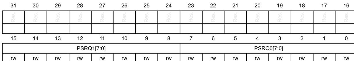
| 31 | 30 | 29 | 28 | 27 | 26 | 25 | 24 | 23 | 22 | 21 | 20 | 19 | 18 | 17 | 16 |
| Res | Res | Res | Res | Res | Res | Res | Res | Res | Res | Res | Res | Res | Res | Res | Res |
| 15 | 14 | 13 | 12 | 11 | 10 | 9 | 8 | 7 | 6 | 5 | 4 | 3 | 2 | 1 | 0 |
| PSRQ1[7:0] | PSRQ0[7:0] | ||||||||||||||
| rw | rw | rw | rw | rw | rw | rw | rw | rw | rw | rw | rw | rw | rw | rw | rw |
Bits 31:16 Reserved, must be kept at reset value.
Bits 15:8 PSRQ1[7:0] : Priorities Selected in the Receive Queue 1
This field defines the priorities assigned to Rx queue 1. All packets with priorities that match the values set in this field are routed to Rx queue 1.
For example, if PSRQ1[4] is set, packets with USP field equal to 4 are routed to Rx queue 1. The software must ensure that the content of this field is mutually exclusive to the PSRQ fields for other queues, that is, the same priority is not mapped to multiple Rx queues.
Bits 7:0 PSRQ0[7:0] : Priorities Selected in the Receive Queue 0
This field defines the priorities assigned to Rx queue 0. All packets with priorities that match the values set in this field are routed to Rx queue 0.
For example, if PSRQ0[5] is set, packets with USP field equal to 5 are routed to Rx queue 0. The software must ensure that the content of this field is mutually exclusive to the PSRQ fields for other queues, that is, the same priority is not mapped to multiple Rx queues.
Interrupt status register (ETH_MACISR)
Address offset: 0x00B0
Reset value: 0x0000 0000
The interrupt status register contains the status of interrupts.
| 31 | 30 | 29 | 28 | 27 | 26 | 25 | 24 | 23 | 22 | 21 | 20 | 19 | 18 | 17 | 16 |
|---|---|---|---|---|---|---|---|---|---|---|---|---|---|---|---|
| Res. | Res. | Res. | Res. | Res. | Res. | Res. | Res. | Res. | Res. | Res. | MFRIS | MFTIS | MDIOIS | FPEIS | Res. |
| r | r | rc_r | r | ||||||||||||
| 15 | 14 | 13 | 12 | 11 | 10 | 9 | 8 | 7 | 6 | 5 | 4 | 3 | 2 | 1 | 0 |
| Res. | RXSTSIS | TXSTSIS | TSIS | Res. | MMCTXIS | MMCRXIS | MMCCIS | Res. | Res. | LPIS | PMTIS | PHYS | Res. | Res. | RGSMIIS |
| rc_r | rc_r | rc_r | r | r | r | r | r | r | r |
Bits 31:21 Reserved, must be kept at reset value.
Bit 20 MFRIS : MMC FPE Receive interrupt status
This bit is set high when an interrupt is generated in the MMC FPE Rx interrupt status register (ETH_MMC_FPE_RX_ISR) . This bit is cleared when all bits in this interrupt register are cleared.
Bit 19 MFTIS : MMC FPE transmit interrupt status
This bit is set high when an interrupt is generated in the MMC FPE Tx interrupt status register (ETH_MMC_FPE_TX_ISR) . This bit is cleared when all bits in this interrupt register are cleared.
Bit 18 MDIOIS : MDIO interrupt status
This bit indicates an interrupt event after the completion of MDIO operation. To reset this bit, the application has to read this bit (or write it to 1 when RCWE bit in CSR software control register (ETH_MACCSRSWCR) register is set) register is set.
Bit 17 FPEIS : Frame preemption interrupt status
This bit indicates an interrupt event during the operation of Frame Preemption (Bits[19:16] of FPE control and status register (ETH_MACFPECSR) is set). To reset this bit, the application must clear the event in FPE control and status register (ETH_MACFPECSR) that has caused the Interrupt.
Bits 16:15 Reserved, must be kept at reset value.
Bit 14 RXSTSIS : Receive status interrupt
This bit indicates the status of received packets. This bit is set when the RWT bit is set in the Rx Tx status register (ETH_MACRXTXSR) . This bit is cleared when the corresponding interrupt source bit is read (or corresponding interrupt source bit is written to 1 when RCWE bit of CSR software control register (ETH_MACCSRSWCR) is set) in the ETH_MACISR register.
Bit 13 TXSTSIS: Transmit status interruptThis bit indicates the status of transmitted packets. This bit is set when any of the following bits is set in the Rx Tx status register (ETH_MACRXTXSR) :
- – Excessive Collision (EXCOL)
- – Late Collision (LCOL)
- – Excessive Deferral (EXDEF)
- – Loss of Carrier (LCARR)
- – No Carrier (NCARR)
- – Jabber timeout (TJT)
This bit is cleared when the corresponding interrupt source bit is read (or corresponding interrupt source bit is written to 1 when RCWE bit of CSR software control register (ETH_MACCSRSWCR) is set) in the ETH_MACISR register.
Bit 12 TSIS: Timestamp interrupt statusIf the Timestamp feature is enabled, this bit is set when any of the following conditions is true:
- – The system time value is equal to or exceeds the value specified in the Target Time High and Low registers.
- – There is an overflow in the Seconds register.
- – The Target Time Error occurred, that is, programmed target time already elapsed.
If the Auxiliary Snapshot feature is enabled, this bit is set when the auxiliary snapshot trigger is asserted.
When drop transmit status is enabled in MTL, this bit is set when the captured transmit timestamp is updated in the Tx timestamp status nanoseconds register (ETH_MACTXTSSNR) and Tx timestamp status seconds register (ETH_MACTXTSSSR) registers.
When PTP offload feature is enabled, this bit is set when the captured transmit timestamp is updated in the Tx timestamp status nanoseconds register (ETH_MACTXTSSNR) and Tx timestamp status seconds register (ETH_MACTXTSSSR) registers, for PTO generated Delay Request and Pdelay request packets.
This bit is cleared when the corresponding interrupt source bit is read (or corresponding interrupt source bit is written to 1 when RCWE bit of CSR software control register (ETH_MACCSRSWCR) is set) in the Timestamp status register (ETH_MACTSSR) .
Bit 11 Reserved, must be kept at reset value. Bit 10 MMCTXIS: MMC transmit interrupt statusThis bit is set high when an interrupt is generated in the MMC Tx interrupt register (ETH_MMC_TX_INTERRUPT) . This bit is cleared when all bits in this interrupt register are cleared.
Bit 9 MMCRXIS: MMC Receive interrupt statusThis bit is set high when an interrupt is generated in the MMC Rx interrupt register (ETH_MMC_RX_INTERRUPT) . This bit is cleared when all bits in this interrupt register are cleared.
Bit 8 MMCIS: MMC interrupt statusThis bit is set high when MMCTXIS or MMCRXIS is set high. This bit is cleared only when all these bits are low.
Bits 7:6 Reserved, must be kept at reset value. Bit 5 LPIIS: LPI interrupt statusThis bit is set for any LPI state entry or exit in the MAC transmitter or receiver. This bit is cleared when the TLPIEN bit of LPI control and status register (ETH_MACLCSR) is read.
Bit 4 PMTIS : PMT interrupt status
This bit is set when a Magic packet or Wake-on-LAN packet is received in the power-down mode (RWKPRCVD and MGKPRCVD bits in ETH_MACPCSR register). This bit is cleared when Bits[6:5] are cleared because of a Read operation to the PMT control status register (ETH_MACPCSR) .
Bit 3 PHYIS : PHY Interrupt
This bit is set when rising edge is detected on the ETH_PHY_INTN input. This bit is cleared when this register is read.
Bits 2:1 Reserved, must be kept at reset value.
Bit 0 RGSMIIS : RGMII interrupt status
This bit is set by any change in value of the Link Status of RGMII interface (LNKSTS bit in PHYIF control status register (ETH_MACPHYCSR) register). This bit is cleared when the ETH_MACPHYCSR register is read.
Interrupt enable register (ETH_MACIER)
Address offset: 0x00B4
Reset value: 0x0000 0000
The Interrupt Enable register contains the masks for generating the interrupts.
| 31 | 30 | 29 | 28 | 27 | 26 | 25 | 24 | 23 | 22 | 21 | 20 | 19 | 18 | 17 | 16 |
|---|---|---|---|---|---|---|---|---|---|---|---|---|---|---|---|
| Res. | Res. | Res. | Res. | Res. | Res. | Res. | Res. | Res. | Res. | Res. | Res. | Res. | MDIOIE | FPEIE | Res. |
| r/w | r/w | ||||||||||||||
| 15 | 14 | 13 | 12 | 11 | 10 | 9 | 8 | 7 | 6 | 5 | 4 | 3 | 2 | 1 | 0 |
| Res. | RXSTSIE | TXSTSIE | TSIE | Res. | Res. | Res. | Res. | Res. | Res. | LPIIE | PMTIE | PHYIE | Res. | Res. | RGSMIIE |
| r/w | r/w | r/w | r/w | r/w | r/w | r/w |
Bits 31:19 Reserved, must be kept at reset value.
Bit 18 MDIOIE : MDIO Interrupt Enable
When this bit is set, it enables the assertion of the interrupt when MDIOIS field is set in the Interrupt status register (ETH_MACISR) .
Bit 17 FPEIE : Frame Preemption Interrupt Enable
When this bit is set, it enables the assertion of the interrupt when FPEIS field is set in the Interrupt status register (ETH_MACISR) .
Bit 16 Reserved, must be kept at reset value.
Bit 15 Reserved, must be kept at reset value.
Bit 14 RXSTSIE : Receive Status Interrupt Enable
When this bit is set, it enables the assertion of the interrupt signal because of the setting of RXSTSIS bit in the Interrupt status register (ETH_MACISR) .
Bit 13 TXSTSIE : Transmit Status Interrupt Enable
When this bit is set, it enables the assertion of the interrupt signal because of the setting of TXSTSIS bit in the Interrupt status register (ETH_MACISR) .
Bit 12 TSIE : Timestamp Interrupt Enable
When this bit is set, it enables the assertion of the interrupt signal because of the setting of TSIS bit in Interrupt status register (ETH_MACISR) .
Bits 11:6 Reserved, must be kept at reset value.
Bit 5 LPIIE : LPI Interrupt Enable
When this bit is set, it enables the assertion of the interrupt signal because of the setting of LPIIS bit in Interrupt status register (ETH_MACISR) .
Bit 4 PMTIE : PMT Interrupt Enable
When this bit is set, it enables the assertion of the interrupt signal because of the setting of PMTIS bit in Interrupt status register (ETH_MACISR) .
Bit 3 PHYIE : PHY Interrupt Enable
When this bit is set, it enables the assertion of the interrupt signal because of the setting of PHYIS bit in Interrupt status register (ETH_MACISR) .
Bits 2:1 Reserved, must be kept at reset value.
Bit 0 RGSMIIIE : RGMII Interrupt Enable
When this bit is set, it enables the assertion of the interrupt signal because of the setting of RGSMIIIS bit in Interrupt status register (ETH_MACISR) .
Rx Tx status register (ETH_MACRXTXSR)
Address offset: 0x00B8
Reset value: 0x0000 0000
The receive transmit status register contains the receive and transmit error status.
| 31 | 30 | 29 | 28 | 27 | 26 | 25 | 24 | 23 | 22 | 21 | 20 | 19 | 18 | 17 | 16 |
|---|---|---|---|---|---|---|---|---|---|---|---|---|---|---|---|
| Res. | Res. | Res. | Res. | Res. | Res. | Res. | Res. | Res. | Res. | Res. | Res. | Res. | Res. | Res. | Res. |
| 15 | 14 | 13 | 12 | 11 | 10 | 9 | 8 | 7 | 6 | 5 | 4 | 3 | 2 | 1 | 0 |
| Res. | Res. | Res. | Res. | Res. | Res. | Res. | RWT | Res. | Res. | EXCOL | LCOL | EXDEF | LCARR | NCARR | TJT |
| rc_r | rc_r | rc_r | rc_r | rc_r | rc_r | rc_r |
Bits 31:9 Reserved, must be kept at reset value.
Bit 8 RWT : Receive watchdog timeout
This bit is set when a packet with length greater than 2,048 bytes is received (10, 240 bytes when Jumbo Packet mode is enabled) and the WD bit is reset in the Operating mode configuration register (ETH_MACCR) . This bit is set when a packet with length greater than 16,383 bytes is received and the WD bit is set in the Operating mode configuration register (ETH_MACCR) .
Cleared on read (or write of 1 when RCWE bit in CSR software control register (ETH_MACCSRSWCR) is set).
Bits 7:6 Reserved, must be kept at reset value.
Bit 5 EXCOL: Excessive CollisionsWhen the DTXSTS bit is set in the Operating mode register (ETH_MTLOMR) , this bit indicates that the transmission aborted after 16 successive collisions while attempting to transmit the current packet. If the DR bit is set in the Operating mode configuration register (ETH_MACCR) , this bit is set after the first collision and the packet transmission is aborted. Cleared on read (or write of 1 when RCWE bit in CSR software control register (ETH_MACCSRSWCR) is set).
Bit 4 LCOL: Late CollisionWhen the DTXSTS bit is set in the Operating mode register (ETH_MTLOMR) , this bit indicates that the packet transmission aborted because a collision occurred after the collision window (64 bytes including Preamble in MII mode; 512 bytes including Preamble and Carrier Extension in GMII mode).
This bit is not valid if the Underflow error occurs.
Cleared on read (or write of 1 when RCWE bit in CSR software control register (ETH_MACCSRSWCR) is set).
Bit 3 EXDEF: Excessive DeferralWhen the DTXSTS bit is set in the Operating mode register (ETH_MTLOMR) and the DC bit is set in the Operating mode configuration register (ETH_MACCR) , this bit indicates that the transmission ended because of excessive deferral of over 24,288 bit times (155,680 in 1000 Mbps mode or when Jumbo packet is enabled).
Cleared on read (or write of 1 when RCWE bit in CSR software control register (ETH_MACCSRSWCR) is set).
Bit 2 LCARR: Loss of CarrierWhen the DTXSTS bit is set in the Operating mode register (ETH_MTLOMR) , this bit indicates that the loss of carrier occurred during packet transmission, that is, the ETH_CRS signal was inactive for one or more transmission clock periods during packet transmission.
This bit is valid only for packets transmitted without collision.
Cleared on read (or write of 1 when RCWE bit in CSR software control register (ETH_MACCSRSWCR) is set).
Bit 1 NCARR: No CarrierWhen the DTXSTS bit is set in the Operating mode register (ETH_MTLOMR) , this bit indicates that the carrier signal from the PHY is not present at the end of preamble transmission.
Cleared on read (or write of 1 when RCWE bit in CSR software control register (ETH_MACCSRSWCR) is set).
Bit 0 TJT: Transmit Jabber timeoutThis bit indicates that the transmit jabber timer expired which happens when the packet size exceeds 2,048 bytes (10,240 bytes when the Jumbo packet is enabled) and JD bit is reset in the Operating mode configuration register (ETH_MACCR) . This bit is set when the packet size exceeds 16,383 bytes and the JD bit is set in the Operating mode configuration register (ETH_MACCR) .
Cleared on read (or write of 1 when RCWE bit in CSR software control register (ETH_MACCSRSWCR) is set).
PMT control status register (ETH_MACPCSR)Address offset: 0x00C0
Reset value: 0x0000 0000
| 31 | 30 | 29 | 28 | 27 | 26 | 25 | 24 | 23 | 22 | 21 | 20 | 19 | 18 | 17 | 16 |
|---|---|---|---|---|---|---|---|---|---|---|---|---|---|---|---|
| RWKFILTRST | Res. | Res. | RWKPTR[4:0] | Res. | Res. | Res. | Res. | Res. | Res. | Res. | Res. | ||||
| r/w | r | r | r | r | r | ||||||||||
| 15 | 14 | 13 | 12 | 11 | 10 | 9 | 8 | 7 | 6 | 5 | 4 | 3 | 2 | 1 | 0 |
| Res. | Res. | Res. | Res. | Res. | RWKPFE | GLBLUCAS | Res. | Res. | RWKPRCVD | MGKPRCVD | Res. | Res. | RWKPKTEN | MGKPKTEN | PWRDWN |
| r/w | r/w | r | rc_r | r/w | r/w | r/w | |||||||||
Bit 31 RWKFILTRST : Remote Wake-up Packet Filter Register Pointer Reset
When this bit is set, the remote wake-up packet filter register pointer is reset to 0. It is automatically cleared after 1 clock cycle.
Bits 30:29 Reserved, must be kept at reset value.
Bits 28:24 RWKPTR[4:0] : Remote wake-up FIFO Pointer
This field gives the current value (0 to 7) of the Remote wake-up Packet Filter register pointer. When the value of this pointer is equal to 7, the contents of the Remote wake-up Packet Filter Register are transferred to the eth_rx_clk domain when a Write occurs to that register.
Bits 23:11 Reserved, must be kept at reset value.
Bit 10 RWKPFE : Remote wake-up Packet Forwarding Enable
When this bit is set along with RWKPKTEN, the MAC receiver drops all received frames until it receives the expected wake-up frame. All frames after that event including the received wake-up frame are forwarded to application. This bit is then self-cleared on receiving the wake-up packet.
The application can also clear this bit before the expected wake-up frame is received. In such cases, the MAC reverts to the default behavior where packets received are forwarded to the application. This bit must only be set when RWKPKTEN is set high and PWRDWN is set low. The setting of this bit has no effect when PWRDWN is set high.
Note: If Magic Packet Enable and wake-up Frame Enable are both set along with setting of this bit and Magic Packet is received prior to wake-up frame, this bit is self-cleared on receiving Magic Packet, the received Magic packet is dropped, and all frames after received Magic Packet are forwarded to application.
Bit 9 GLBLUCAS : Global Unicast
When this bit set, any unicast packet filtered by the MAC (DAF) address recognition is detected as a remote wake-up packet.
Bits 8:7 Reserved, must be kept at reset value.
Bit 6 RWKPRCVD : Remote wake-up Packet Received
When this bit is set, it indicates that the power management event is generated because of the reception of a remote wake-up packet. This bit is cleared when this register is read.
Bit 5 MGKPRCVD : Magic Packet ReceivedWhen this bit is set, it indicates that the power management event is generated because of the reception of a magic packet. This bit is cleared when this register is read (or written to 1 when RCWE bit in CSR software control register (ETH_MACCSRSWCR) is set).
Bits 4:3 Reserved, must be kept at reset value.
Bit 2 RWKPKTEN : Remote wake-up Packet EnableWhen this bit is set, a power management event is generated when the MAC receives a remote wake-up packet.
Bit 1 MGKPKTEN : Magic Packet EnableWhen this bit is set, a power management event is generated when the MAC receives a magic packet.
Bit 0 PWRDWN : Power DownWhen this bit is set, the MAC receiver drops all received packets until it receives the expected magic packet or remote wake-up packet. This bit is then self-cleared and the power-down mode is disabled. The software can clear this bit before the expected magic packet or remote wake-up packet is received. The packets received by the MAC after this bit is cleared are forwarded to the application. This bit must only be set when the Magic Packet Enable, Global Unicast, or Remote wake-up Packet Enable bit is set high.
Note: You can gate-off the CSR clock during the power-down mode. However, when the CSR clock is gated-off, you cannot perform any read or write operations on this register. Therefore, the Software cannot clear this bit.
Remote wake-up packet filter register (ETH_MACRWKPFR)
Address offset: 0x00C4
Reset value: 0x0000 0000
| 31 | 30 | 29 | 28 | 27 | 26 | 25 | 24 | 23 | 22 | 21 | 20 | 19 | 18 | 17 | 16 |
|---|---|---|---|---|---|---|---|---|---|---|---|---|---|---|---|
| MACRWKPFR[31:16] | |||||||||||||||
| rw | rw | rw | rw | rw | rw | rw | rw | rw | rw | rw | rw | rw | rw | rw | rw |
| 15 | 14 | 13 | 12 | 11 | 10 | 9 | 8 | 7 | 6 | 5 | 4 | 3 | 2 | 1 | 0 |
| MACRWKPFR[15:0] | |||||||||||||||
| rw | rw | rw | rw | rw | rw | rw | rw | rw | rw | rw | rw | rw | rw | rw | rw |
Bits 31:0 MACRWKPFR[31:0] : Remote wake-up packet filter
Refer to Table 817 , Table 818 and Table 819 for details on register content and programming sequence.
The ETH_MACRWKPFR register at address 0x00C4 loads the wake-up Packet Filter register.
To load values in a wake-up Packet Filter register, the entire register (ETH_MACRWKPFR) must be written. The ETH_MACRWKPFR register is loaded by sequentially loading the eight, sixteen or thirty two register values in address (0x00C4) for ETH_MACRWKPFR value 0 to 7, respectively. The ETH_MACRWKPFR register is read in a similar way. The Ethernet peripheral updates the ETH_MACRWKPFR register current pointer value in Bits[26:24] of ETH_MACPCSR register.
LPI control and status register (ETH_MACLCSR)
Address offset: 0x00D0
Reset value: 0x0000 0000
The LPI Control and Status Register controls the LPI functions and provides the LPI interrupt status. The status bits are cleared when this register is read.
| 31 | 30 | 29 | 28 | 27 | 26 | 25 | 24 | 23 | 22 | 21 | 20 | 19 | 18 | 17 | 16 |
|---|---|---|---|---|---|---|---|---|---|---|---|---|---|---|---|
| Res. | Res. | Res. | Res. | Res. | Res. | Res. | Res. | Res. | Res. | LPITCSE | LPITE | LPITXA | PLSEN | PLS | LPIEN |
| rw | rw | rw | rw | rw | rw | ||||||||||
| 15 | 14 | 13 | 12 | 11 | 10 | 9 | 8 | 7 | 6 | 5 | 4 | 3 | 2 | 1 | 0 |
| Res. | Res. | Res. | Res. | Res. | Res. | RLPIST | TLPIST | Res. | Res. | Res. | Res. | RLPIEX | RLPIEN | TLPIEX | TLPIEN |
| r | r | r | r | r | r |
Bits 31:22 Reserved, must be kept at reset value.
Bit 21 LPITCSE : LPI Tx Clock Stop Enable
When this bit is set, the MAC asserts
sbd_tx_clk_gating_ctrl_o
signal high after it enters Tx LPI mode to indicate that the Tx clock to MAC can be stopped. When this bit is reset, the MAC does not assert
sbd_tx_clk_gating_ctrl_o
signal high after it enters Tx LPI mode. If RGMII Interface is selected, the Tx clock is required for transmitting the LPI pattern. The Tx Clock cannot be gated and so the LPITCSE bit cannot be programmed.
This bit controls the automatic entry of the MAC transmitter into and exit out of the LPI state. When LPITE, LPITXA and LPIEN bits are set, the MAC transmitter enters LPI state only when the complete MAC TX data path is IDLE for a period indicated by the ETH_MACLETR register.
After entering LPI state, if the data path becomes non-IDLE (due to a new packet being accepted for transmission), the transmitter exits LPI state but does not clear LPIEN bit. This enables the re-entry into LPI state when it is IDLE again.
When LPITE is 0, the LPI Auto timer is disabled and MAC transmitter enters LPI state based on the settings of LPITXA and LPIEN bit descriptions.
Bit 19 LPITXA: LPI Tx AutomateThis bit controls the behavior of the MAC when it is entering or coming out of the LPI mode on the transmit side.
If the LPITXA and LPIEN bits are set to 1, the MAC enters the LPI mode only after all outstanding packets (in the core) and pending packets (in the application interface) have been transmitted. The MAC comes out of the LPI mode when the application sends any packet for transmission or the application issues a Tx FIFO Flush command. In addition, the MAC automatically clears the LPIEN bit when it exits the LPI state. If Tx FIFO Flush is set in the FTQ bit of ETH_MTLTxQxOMR, when the MAC is in the LPI mode, it exits the LPI mode. When this bit is 0, the LPIEN bit directly controls behavior of the MAC when it is entering or coming out of the LPI mode.
Bit 18 PLSEN: PHY Link Status EnableThis bit enables the link status received on the RGMII Receive paths to be used for activating the LPI LS TIMER.
When this bit is set, the MAC uses the link-status bits of the ETH_MACPHYCSR register and the PLS bit for the LPI LS Timer trigger. When this bit is reset, the MAC ignores the link-status bits of the ETH_MACPHYCSR register and takes only the PLS bit.
Bit 17 PLS: PHY Link StatusThis bit indicates the link status of the PHY. The MAC transmitter asserts the LPI pattern only when the link status is up (OKAY) at least for the time indicated by the LPI LS TIMER.
When this bit is set, the link is considered to be okay (UP) and when this bit is reset, the link is considered to be down.
Bit 16 LPIEN: LPI EnableWhen this bit is set, it instructs the MAC transmitter to enter the LPI state. When this bit is reset, it instructs the MAC to exit the LPI state and resume normal transmission.
This bit is cleared when the LPITXA bit is set and the MAC exits the LPI state because of the arrival of a new packet for transmission.
Bits 15:10 Reserved, must be kept at reset value.
Bit 9 RLPIST: Receive LPI StateWhen this bit is set, it indicates that the MAC is receiving the LPI pattern on the GMII or MII interface.
Bit 8 TLPIST: Transmit LPI StateWhen this bit is set, it indicates that the MAC is transmitting the LPI pattern on the GMII or MII interface.
Bits 7:4 Reserved, must be kept at reset value.
Bit 3 RLPIEX : Receive LPI ExitWhen this bit is set, it indicates that the MAC receiver has stopped receiving the LPI pattern on the GMII or MII interface, exited the LPI state, and resumed the normal reception. This bit is cleared by a read into this register (or by writing it to 1 when RCWE bit in CSR software control register (ETH_MACCSRSWCR) is set).
Note: This bit may not be set if the MAC stops receiving the LPI pattern for a very short duration, such as, less than three clock cycles of CSR clock.
Bit 2 RLPIEN : Receive LPI EntryWhen this bit is set, it indicates that the MAC receiver has received an LPI pattern and entered the LPI state. This bit is cleared by a read into this register (or by writing it to 1 when RCWE bit in CSR software control register (ETH_MACCSRSWCR) is set).
Note: This bit may not be set if the MAC stops receiving the LPI pattern for a very short duration, such as, less than three clock cycles of CSR clock.
Bit 1 TLPIEX : Transmit LPI ExitWhen this bit is set, it indicates that the MAC transmitter exited the LPI state after the application cleared the LPIEN bit and the LPI TW Timer has expired. This bit is cleared by a read into this register (or by writing it to 1 when RCWE bit in CSR software control register (ETH_MACCSRSWCR) is set).
Bit 0 TLPIEN : Transmit LPI EntryWhen this bit is set, it indicates that the MAC transmitter has entered the LPI state because of the setting of the LPIEN bit. This bit is cleared by a read into this register (or by writing it to 1 when RCWE bit in CSR software control register (ETH_MACCSRSWCR) is set).
LPI timers control register (ETH_MACLTCR)Address offset: 0x00D4
Reset value: 0x03E8 0000
The LPI timers control register controls the timeout values in the LPI states. It specifies the time for which the MAC transmits the LPI pattern and also the time for which the MAC waits before resuming the normal transmission.
| 31 | 30 | 29 | 28 | 27 | 26 | 25 | 24 | 23 | 22 | 21 | 20 | 19 | 18 | 17 | 16 |
|---|---|---|---|---|---|---|---|---|---|---|---|---|---|---|---|
| Res | Res | Res | Res | Res | Res | LST[9:0] | |||||||||
| rw | rw | rw | rw | rw | rw | rw | rw | rw | rw | ||||||
| 15 | 14 | 13 | 12 | 11 | 10 | 9 | 8 | 7 | 6 | 5 | 4 | 3 | 2 | 1 | 0 |
| TWT[15:0] | |||||||||||||||
| rw | rw | rw | rw | rw | rw | rw | rw | rw | rw | rw | rw | rw | rw | rw | rw |
Bits 31:26 Reserved, must be kept at reset value.
Bits 25:16 LST[9:0] : LPI LS TimerThis field specifies the minimum time (in milliseconds) for which the link status from the PHY should be up (OKAY) before the LPI pattern can be transmitted to the PHY. The MAC does not transmit the LPI pattern even when the LPIEN bit is set unless the LPI LS Timer reaches the programmed terminal count. The default value of the LPI LS Timer is 1000 (1 s) as defined in the IEEE standard.
Bits 15:0 TWT[15:0] : LPI TW Timer
This field specifies the minimum time (in microseconds) for which the MAC waits after it stops transmitting the LPI pattern to the PHY and before it resumes the normal transmission. The TLPIEX status bit is set after the expiry of this timer.
LPI entry timer register (ETH_MACLETR)
Address offset: 0x00D8
Reset value: 0x0000 0000
This register controls the Tx LPI entry timer. This counter is enabled only when LPITE bit of LPI control and status register (ETH_MACCSR) register is set to 1.
| 31 | 30 | 29 | 28 | 27 | 26 | 25 | 24 | 23 | 22 | 21 | 20 | 19 | 18 | 17 | 16 |
|---|---|---|---|---|---|---|---|---|---|---|---|---|---|---|---|
| Res | Res | Res | Res | Res | Res | Res | Res | Res | Res | Res | Res | LPIET[19:16] | |||
| rw | rw | rw | rw | ||||||||||||
| 15 | 14 | 13 | 12 | 11 | 10 | 9 | 8 | 7 | 6 | 5 | 4 | 3 | 2 | 1 | 0 |
| LPIET[15:0] | |||||||||||||||
| rw | rw | rw | rw | rw | rw | rw | rw | rw | rw | rw | rw | rw | r | r | r |
Bits 31:20 Reserved, must be kept at reset value.
Bits 19:0 LPIET[19:0] : LPI Entry Timer
This field specifies the time in microseconds the MAC waits to enter LPI mode, after it has transmitted all the frames. This field is valid and used only when LPITE and LPITXA are set to 1.
Bits [2:0] are read-only so that the granularity of this timer is in steps of 8 micro-seconds.
One-microsecond-tick counter register (ETH_MAC1USTCR)
Address offset: 0x00DC
Reset value: 0x0000 0063
This register controls the generation of the Reference time (one-microsecond tick) for all the LPI timers. This timer has to be programmed by the software initially.
| 31 | 30 | 29 | 28 | 27 | 26 | 25 | 24 | 23 | 22 | 21 | 20 | 19 | 18 | 17 | 16 |
|---|---|---|---|---|---|---|---|---|---|---|---|---|---|---|---|
| Res | Res | Res | Res | Res | Res | Res | Res | Res | Res | Res | Res | Res | Res | Res | Res |
| 15 | 14 | 13 | 12 | 11 | 10 | 9 | 8 | 7 | 6 | 5 | 4 | 3 | 2 | 1 | 0 |
| Res | Res | Res | Res | TIC_1US_CNTR[11:0] | |||||||||||
| rw | rw | rw | rw | rw | rw | rw | rw | rw | rw | rw | rw | ||||
Bits 31:12 Reserved, must be kept at reset value.
Bits 11:0 TIC_1US_CNTR[11:0]: 1 µs tick Counter
The application must program this counter so that the number of clock cycles of CSR clock is 1 µs (subtract 1 from the value before programming).
For example if the CSR clock is 100 MHz then this field needs to be programmed to 100 - 1 = 99 (which is 0x63).
This is required to generate the 1 µs events that are used to update some of the EEE related counters.
PHYIF control status register (ETH_MACPHYCSR)
Address offset: 0x00F8
Reset value: 0x0000 0000
The PHY Interface Control and Status register indicates the status signals received by the RGMII interface from the PHY.
| 31 | 30 | 29 | 28 | 27 | 26 | 25 | 24 | 23 | 22 | 21 | 20 | 19 | 18 | 17 | 16 |
|---|---|---|---|---|---|---|---|---|---|---|---|---|---|---|---|
| Res. | Res. | Res. | Res. | Res. | Res. | Res. | Res. | Res. | Res. | Res. | Res. | LNKSTS | LNKSPEED[1:0] | LNKMOD | |
| r | r | r | |||||||||||||
| 15 | 14 | 13 | 12 | 11 | 10 | 9 | 8 | 7 | 6 | 5 | 4 | 3 | 2 | 1 | 0 |
| Res. | Res. | Res. | Res. | Res. | Res. | Res. | Res. | Res. | Res. | Res. | Res. | Res. | Res. | LUD | TC |
| rw | rw |
Bits 31:20 Reserved, must be kept at reset value.
Bit 19 LNKSTS : Link Status
This bit indicates whether the link is up or down.
0: Link down
1: Link up
Bits 18:17 LNKSPEED[1:0] : Link Speed
This bit indicates the current speed of the link:
00: 2.5 MHz
01: 25 MHz
10: 125 MHz
11: Reserved, must not be used
Bit 16 LNKMOD : Link Mode
This bit indicates the current operating mode of the link:
0: Half-duplex mode
1: Full-duplex mode
Bits 15:2 Reserved, must be kept at reset value.
Bit 1 LUD : Link Up or Down
This bit indicates whether the link is up or down during transmission of configuration in the RGMII interface.
0: Link Down
1: Link Up
Bit 0 TC : Transmit Configuration in RGMII
When set, this bit enables the transmission of duplex mode, link speed, and link up or down information to the PHY in the RGMII port. When this bit is reset, no such information is driven to the PHY (see Section 76.6.3: Reduced media independent interface (RMII) ).
Version register (ETH_MACVR)
Address offset: 0x0110
Reset value: 0x0000 2052
The version register identifies the version of the Ethernet peripheral.
| 31 | 30 | 29 | 28 | 27 | 26 | 25 | 24 | 23 | 22 | 21 | 20 | 19 | 18 | 17 | 16 |
|---|---|---|---|---|---|---|---|---|---|---|---|---|---|---|---|
| Res | Res | Res | Res | Res | Res | Res | Res | Res | Res | Res | Res | Res | Res | Res | Res |
| 15 | 14 | 13 | 12 | 11 | 10 | 9 | 8 | 7 | 6 | 5 | 4 | 3 | 2 | 1 | 0 |
| USERVER[7:0] | SNPSVER[7:0] | ||||||||||||||
| r | r | r | r | r | r | r | r | r | r | r | r | r | r | r | r |
Bits 31:16 Reserved, must be kept at reset value.
Bits 15:8 USERVER[7:0] : ST-defined version
Bits 7:0 SNPSVER[7:0] : IP version
Debug register (ETH_MACDR)
Address offset: 0x0114
Reset value: 0x0000 0000
The Debug register provides the debug status of various MAC blocks.
| 31 | 30 | 29 | 28 | 27 | 26 | 25 | 24 | 23 | 22 | 21 | 20 | 19 | 18 | 17 | 16 |
|---|---|---|---|---|---|---|---|---|---|---|---|---|---|---|---|
| Res. | Res. | Res. | Res. | Res. | Res. | Res. | Res. | Res. | Res. | Res. | Res. | Res. | |||
| TF | CF | ST | |||||||||||||
| r | r | r | |||||||||||||
| 15 | 14 | 13 | 12 | 11 | 10 | 9 | 8 | 7 | 6 | 5 | 4 | 3 | 2 | 1 | 0 |
| Res. | Res. | Res. | Res. | Res. | Res. | Res. | Res. | Res. | Res. | Res. | Res. | Res. | |||
| RF | CF | ST | |||||||||||||
| r | r | r |
Bits 31:19 Reserved, must be kept at reset value.
Bits 18:17 TFCSTS[1:0] : MAC transmit packet controller status
This field indicates the state of the MAC transmit packet controller module:
00: Idle state
01: Waiting for one of the following:
- – Status of the previous packet
- – IPG or backoff period to be over
10: Generating and transmitting a Pause control packet (in Full-duplex mode)
11: Transferring input packet for transmission
Bit 16 TPESTS : MAC GMII or MII transmit protocol engine status
When this bit is set, it indicates that the MAC GMII or MII transmit protocol engine is actively transmitting data, and it is not in the Idle state.
Bits 15:3 Reserved, must be kept at reset value.
Bits 2:1 RFCFCSTS[1:0] : MAC receive packet controller FIFO status
When this bit is set, this field indicates the active state of the small FIFO Read and Write controllers of the MAC receive packet controller module.
Bit 0 RPESTS : MAC GMII or MII receive protocol engine status
When this bit is set, it indicates that the MAC GMII or MII receive protocol engine is actively receiving data, and it is not in the Idle state.
HW feature 0 register (ETH_MACHWF0R)
Address offset: 0x011C
Reset value: 0x0A0D 73F7
This register indicates the presence of first set of the optional features or functions of the Ethernet peripheral. The software driver can use this register to dynamically enable or disable the programs related to the optional blocks.
| 31 | 30 | 29 | 28 | 27 | 26 | 25 | 24 | 23 | 22 | 21 | 20 | 19 | 18 | 17 | 16 |
|---|---|---|---|---|---|---|---|---|---|---|---|---|---|---|---|
| ACTPHYSEL[3:0] | SAVLANINS | TSSTSSEL[1:0] | MACADR64SEL | MACADR32SEL | ADDMACADRSEL[4:0] | Res. | RXCOESEL | ||||||||
| r | r | r | r | r | r | r | r | r | r | r | r | r | r | r | |
| 15 | 14 | 13 | 12 | 11 | 10 | 9 | 8 | 7 | 6 | 5 | 4 | 3 | 2 | 1 | 0 |
| Res. | TXCOESEL | EEESEL | TSSEL | Res. | ARPOFFSEL | MMCSEL | MGKSEL | RWKSEL | SMASEL | VLHASH | PCSSEL | HDSEL | GMIISEL | MIISEL | |
| r | r | r | r | r | r | r | r | r | r | r | r | r | |||
When you have multiple PHY interfaces in your configuration, this field indicates the sampled value of phy_intf_sel_i during reset de-assertion:
0x0: GMII or MII
0x1: RGMII
0x2: SGMII
0x3: TBI
0x4: RMII
0x5: RTBI
0x6: SMII
Others: Reserved, must not be used
Bit 27 SAVLANINS : Source Address or VLAN Insertion EnableThis bit is set to 1 when the Enable SA and VLAN Insertion on Tx option is selected
Bits 26:25 TSSTSSEL[1:0] : Timestamp System Time SourceThis bit indicates the source of the Timestamp system time:
01: Internal
10: External
11: Both
00: Reserved, must not be used
This bit is set to 1 when the Enable IEEE 1588 Timestamp Support option is selected
Bit 24 MACADR64SEL : MAC Addresses 64-127 SelectedThis bit is set to 1 when the Enable Additional 64 MAC Address Registers (64-127) option is selected
Bit 23 MACADR32SEL : MAC Addresses 32-63 SelectedThis bit is set to 1 when the Enable Additional 32 MAC Address Registers (32-63) option is selected
Bits 22:18 ADDMACADRSEL[4:0] : MAC Addresses 1-31 SelectedThis bit is set to 1 when the Enable Additional 1-31 MAC Address Registers option is selected
Bit 17 Reserved, must be kept at reset value.
Bit 16 RXCOESEL : Receive checksum offload EnabledThis bit is set to 1 when the enable receive TCP/IP checksum check option is selected
Bit 15 Reserved, must be kept at reset value.
Bit 14 TXCOESEL : Transmit Checksum Offload EnabledThis bit is set to 1 when the enable transmit TCP/IP checksum insertion option is selected
Bit 13 EEESEL : Energy Efficient Ethernet EnabledThis bit is set to 1 when the Enable Energy Efficient Ethernet (EEE) option is selected
Bit 12 TSSEL : IEEE 1588-2008 Timestamp EnabledThis bit is set to 1 when the Enable IEEE 1588 Timestamp Support option is selected
Bits 11:10 Reserved, must be kept at reset value.
Bit 9 ARPOFFSEL : ARP Offload EnabledThis bit is set to 1 when the Enable IPv4 ARP Offload option is selected
Bit 8 MMCSEL : RMON Module EnableThis bit is set to 1 when the Enable MAC management counters (MMC) option is selected
Bit 7 MGKSEL : PMT Magic Packet Enable
This bit is set to 1 when the Enable Magic Packet Detection option is selected
Bit 6 RWKSEL : PMT Remote Wake-up Packet Enable
This bit is set to 1 when the Enable Remote Wake-up Packet Detection option is selected
Bit 5 SMASEL : SMA (MDIO) Interface
This bit is set to 1 when the Enable Station Management (MDIO Interface) option is selected
Bit 4 VLHASH : VLAN Hash Filter Selected
This bit is set to 1 when the Enable VLAN Hash Table Based Filtering option is selected
Bit 3 PCSSEL : PCS Registers (TBI, SGMII, or RTBI PHY interface)
This bit is set to 1 when the TBI, SGMII, or RTBI PHY interface option is selected
Bit 2 HDSEL : Half-duplex Support
This bit is set to 1 when the Half-duplex mode is selected
Bit 1 GMIISEL : 1000 Mbit/s Support
This bit is set to 1 when 1000 Mbit/s is selected as operating mode.
Bit 0 MIISEL : 10 or 100 Mbit/s Support
This bit is set to 1 when 10/100 Mbit/s is selected as operating mode.
HW feature 1 register (ETH_MACHWF1R)
Address offset: 0x0120
Reset value: 0x1114 1965
This register indicates the presence of second set of the optional features or functions of the Ethernet peripheral. The software driver can use this register to dynamically enable or disable the programs related to the optional blocks.
| 31 | 30 | 29 | 28 | 27 | 26 | 25 | 24 | 23 | 22 | 21 | 20 | 19 | 18 | 17 | 16 |
|---|---|---|---|---|---|---|---|---|---|---|---|---|---|---|---|
| Res. | L3L4FNUM[3:0] | Res. | HASHTBLSZ[1:0] | POUOST | Res. | RAVSEL | AVSEL | DBGMEMA | TSOEN | SPHEN | DCBEN | ||||
| r | r | r | r | r | r | r | r | r | r | r | r | r | |||
| 15 | 14 | 13 | 12 | 11 | 10 | 9 | 8 | 7 | 6 | 5 | 4 | 3 | 2 | 1 | 0 |
| ADDR64[1:0] | ADVTHWORD | PTOEN | OSTEN | TXFIFOSIZE[4:0] | SPRAM | RXFIFOSIZE[4:0] | |||||||||
| r | r | r | r | r | r | r | r | r | r | r | r | r | r | r | r |
Bit 31 Reserved, must be kept at reset value.
Bits 30:27 L3L4FNUM[3:0] : Total number of L3 or L4 Filters
This field indicates the total number of L3 or L4 filters:
0000: No L3 or L4 Filter
0001: 1 L3 or L4 Filter
0010: 2 L3 or L4 Filters
..
1000: 8 L3 or L4
Bit 26 Reserved, must be kept at reset value.
Bits 25:24 HASHTBLSZ[1:0] : Hash Table Size
This field indicates the size of the Hash table:
00: No Hash table
01: 64
10: 128
11: 256
Bit 23 POUOST : One Step for PTP over UDP/IP Feature Enable
This bit is set to 1 when the Enable one step timestamp for PTP over UDP/IP feature is selected.
Bit 22 Reserved, must be kept at reset value.
Bit 21 RAVSEL : Rx Side Only AV Feature Enable
This bit is set to 1 when the Enable Audio video bridging option on Rx Side Only is selected.
Bit 20 AVSEL : AV Feature Enable
This bit is set to 1 when the Enable Audio video bridging option is selected.
Bit 19 DBGMEMA : DMA debug registers enable
This bit is set to 1 when the Debug Mode Enable option is selected
Bit 18 TSOEN : TCP segmentation offload enable
This bit is set to 1 when the Enable TCP Segmentation Offloading for TCP/IP Packets option is selected
Bit 17 SPHEN : Split header feature enable
This bit is set to 1 when the Enable Split Header Structure option is selected
Bit 16 DCBEN : DCB feature enable
This bit is set to 1 when the Enable Data Center Bridging option is selected
Bits 15:14 ADDR64[1:0] : Address width
This field indicates the configured address width.
00: 32 bits
Others: Reserved, must not be used
Bit 13 ADVTHWORD : IEEE 1588 High Word Register enable
This bit is set to 1 when the Add IEEE 1588 Higher Word Register option is selected
Bit 12 PTOEN : PTP offload enable
This bit is set to 1 when the Enable PTP Timestamp Offload Feature is selected.
Bit 11 OSTEN : One-step timestamping enable
This bit is set to 1 when the Enable One-Step Timestamp Feature is selected.
Bits 10:6 TXFIFOSIZE[4:0] : MTL transmit FIFO size
This field contains the configured value of MTL Tx FIFO in bytes expressed as Log to base 2 minus 7, that is, \( \log_2(\text{TXFIFO\_SIZE}) - 7 \) :
- 00000: 128 bytes
- 00001: 256 bytes
- 00010: 512 bytes
- 00011: 1,024 bytes
- 00100: 2,048 bytes
- 00101: 4,096 bytes
- 00110: 8,192 bytes
- 00111: 16,384 bytes
- 01000: 32 Kbytes
- 01001: 64 Kbytes
- 01010: 128 Kbytes
- 01011 to 11111: Reserved, must not be used
Bit 5 SPRAM : Single Port RAM Enable
This bit is set to 1 when the Use single port RAM feature is selected.
Bits 4:0 RXFIFOSIZE[4:0] : MTL receive FIFO Size
This field contains the configured value of MTL Rx FIFO in bytes expressed as Log to base 2 minus 7, that is, \( \log_2(\text{RXFIFO\_SIZE}) - 7 \) :
- 00000: 128 bytes
- 00001: 256 bytes
- 00010: 512 bytes
- 00011: 1,024 bytes
- 00100: 2,048 bytes
- 00101: 4,096 bytes
- 00110: 8,192 bytes
- 00111: 16,384 bytes
- 01000: 32 Kbytes
- 01001: 64 Kbytes
- 01010: 128 Kbytes
- 01011: 256 Kbytes
- 01100 to 11111: Reserved, must not be used
HW feature 2 register (ETH_MACHWF2R)
Address offset: 0x0124
Reset value: 0x4204 1041
This register indicates the presence of third set of the optional features or functions of the Ethernet peripheral. The software driver can use this register to dynamically enable or disable the programs related to the optional blocks.
| 31 | 30 | 29 | 28 | 27 | 26 | 25 | 24 | 23 | 22 | 21 | 20 | 19 | 18 | 17 | 16 |
|---|---|---|---|---|---|---|---|---|---|---|---|---|---|---|---|
| Res. | AUXSNAPNUM[2:0] | Res. | PPSOUTNUM[2:0] | TDCSZ[1:0] | TXCHCNT[3:0] | RDCSZ[1:0] | |||||||||
| r | r | r | r | r | r | r | r | r | r | r | r | r | r | ||
| 15 | 14 | 13 | 12 | 11 | 10 | 9 | 8 | 7 | 6 | 5 | 4 | 3 | 2 | 1 | 0 |
| RXCHCNT[3:0] | Res. | Res. | TXQCNT[3:0] | Res. | Res. | RXQCNT[3:0] | |||||||||
| r | r | r | r | r | r | r | r | r | r | r | r | ||||
- Bit 31 Reserved, must be kept at reset value.
- Bits 30:28
AUXSNAPNUM[2:0]
: Number of auxiliary snapshot inputs
This field indicates the number of auxiliary snapshot inputs:
000: No auxiliary input
001: 1 auxiliary input
010: 2 auxiliary inputs
011: 3 auxiliary inputs
100: 4 auxiliary inputs
101 to 111: Reserved, must not be used - Bit 27 Reserved, must be kept at reset value.
- Bits 26:24
PPSOUTNUM[2:0]
: Number of PPS outputs
This field indicates the number of PPS outputs:
000: No PPS output
001: 1 PPS output
010: 2 PPS outputs
011: 3 PPS outputs
100: 4 PPS outputs
101 to 111: Reserved, must not be used - Bits 23:22
TDCSZ[1:0]
: Tx DMA descriptor cache size in terms of 16-byte descriptors
00: Cache not configured
01: Four 16-byte descriptors
10: Eight 16-byte descriptors
11: Sixteen 16-byte descriptors - Bits 21:18
TXCHCNT[3:0]
: Number of DMA transmit channels
This field indicates the number of DMA transmit channels:
0000: 1 DMA Tx Channel
0001: 2 DMA Tx Channels
..
0111: 8 DMA Tx - Bits 17:16
RDCSZ[1:0]
: Rx DMA Descriptor Cache Size in terms of 16-byte descriptors
00: Cache not configured
01: Four 16-byte descriptors
10: Eight 16-byte descriptors
11: Sixteen 16-byte descriptors - Bits 15:12
RXCHCNT[3:0]
: Number of DMA receive channels
This field indicates the number of DMA receive channels:
0000: 1 DMA Rx Channel
0001: 2 DMA Rx Channels
..
0111: 8 DMA Rx - Bits 11:10 Reserved, must be kept at reset value.
- Bits 9:6
TXQCNT[3:0]
: Number of MTL transmit queues
This field indicates the number of MTL transmit queues:
0000: 1 MTL Tx queue
0001: 2 MTL Tx queues
..
0111: 8 MTL Tx
Bits 5:4 Reserved, must be kept at reset value.
Bits 3:0 RXQCNT[3:0] : Number of MTL receive queues
This field indicates the number of MTL receive queues:
0000: 1 MTL Rx queue
0001: 2 MTL Rx queues
..
0111: 8 MTL Rx
HW feature 3 register (ETH_MACHWF3R)
Address offset: 0x0128
Reset value: 0x0C33 0031
This register indicates the presence of fourth set the optional features or functions of the Ethernet peripheral. The software driver can use this register to dynamically enable or disable the programs related to the optional blocks.
| 31 | 30 | 29 | 28 | 27 | 26 | 25 | 24 | 23 | 22 | 21 | 20 | 19 | 18 | 17 | 16 | |||||
|---|---|---|---|---|---|---|---|---|---|---|---|---|---|---|---|---|---|---|---|---|
| Res. | Res. | ASP[1:0] | TBSEL | FPSEL | Res. | Res. | Res. | Res. | Res. | ESTWID[1:0] | ESTDEP[2:0] | Res. | Res. | Res. | ESTSEL | |||||
| r r | r | r | r r | r r r | r | |||||||||||||||
| 15 | 14 | 13 | 12 | 11 | 10 | 9 | 8 | 7 | 6 | 5 | 4 | 3 | 2 | 1 | 0 | |||||
| Res. | FRPES[1:0] | FRPBS[1:0] | FRPSEL | PDUPSEL | Res. | Res. | Res. | DVLAN | CBTSEL | Res. | NRVF[2:0] | Res. | Res. | |||||||
| r r | r r | r | r | r | r | r r r | r r | r r r | ||||||||||||
Bits 31:30 Reserved, must be kept at reset value.
Bits 29:28 ASP[1:0] : Automotive Safety Package
Following are the encoding for the different Safety features
00: None
01: ECC only
10: AS_NPPE
11: AS_PPE
Bit 27 TBSEL : Time-based scheduling Enable
This bit is set to 1 when the time-based scheduling feature is selected.
Bit 26 FPSEL : Frame Preemption Enable
This bit is set to 1 when the Enable Frame preemption feature is selected.
Bits 25:22 Reserved, must be kept at reset value.
Bits 21:20 ESTWID[1:0] : Width of the Time Interval field in the Gate Control List
This field indicates the width of the Configured Time Interval Field
00: No width
01: 16
10: 20
11: 24
Bits 19:17 ESTDEP[2:0] : Depth of the Gate Control List
This field indicates the depth of Gate Control list
000: No depth
001: 64
010: 128
011: 256
100: 512
101: 1024
110: Reserved, must not be used
Bit 16 ESTSEL : Enhancements to Scheduled Traffic Enable
This bit is set to 1 when the enable enhancements to scheduling traffic feature is selected.
Bit 15 Reserved, must be kept at reset value.
Bits 14:13 FRPES[1:0] : Flexible receive parser table entries size
This field indicates the maximum number of parser entries supported by flexible receive parser.
00: 64 entries
01: 128 entries
10: 256 entries
11: Reserved, must not be used
Bits 12:11 FRPBS[1:0] : Flexible receive parser buffer size
This field indicates the supported maximum number of bytes of the packet data to be parsed by flexible receive parser.
00: 64 bytes
01: 128 bytes
10: 256 bytes
11: Reserved, must not be used
Bit 10 FRPSEL : Flexible receive parser Selected
This bit is set to 1 when the Enable Flexible Programmable receive parser option is selected.
Bit 9 PDUPSEL : Broadcast/Multicast Packet Duplication
This bit is set to 1 when the Broadcast/Multicast Packet Duplication feature is selected.
Bits 8:6 Reserved, must be kept at reset value.
Bit 5 DVLAN : Double VLAN processing enable
This bit is set to 1 when Double VLAN processing is enabled.
Bit 4 CBTISEL : Queue/Channel based VLAN tag insertion on Tx enable
This bit is set to 1 when the Enable Queue/Channel based VLAN tag insertion on Tx feature is selected.
Bit 3 Reserved, must be kept at reset value.
Bits 2:0 NRVF[2:0] : Number of Extended VLAN Tag Filters Enabled
This field indicates the Number of Extended VLAN Tag Filters selected:
000: No Extended Rx VLAN Filters
001: 4 Extended Rx VLAN Filters
010: 8 Extended Rx VLAN Filters
011: 16 Extended Rx VLAN Filters
100: 24 Extended Rx VLAN Filters
101: 32 Extended Rx VLAN Filters
110 to 111: Reserved, must not be used
MDIO address register (ETH_MACMDIOAR)
Address offset: 0x0200
Reset value: 0x0000 0000
The MDIO address register controls the management cycles to external PHY through a management interface.
| 31 | 30 | 29 | 28 | 27 | 26 | 25 | 24 | 23 | 22 | 21 | 20 | 19 | 18 | 17 | 16 |
|---|---|---|---|---|---|---|---|---|---|---|---|---|---|---|---|
| Res. | Res. | Res. | Res. | PSE | BTB | PA[4:0] | RDA[4:0] | ||||||||
| rw | rw | rw | rw | rw | rw | rw | rw | rw | rw | rw | rw | ||||
| 15 | 14 | 13 | 12 | 11 | 10 | 9 | 8 | 7 | 6 | 5 | 4 | 3 | 2 | 1 | 0 |
| Res. | NTC[2:0] | CR[3:0] | Res. | Res. | Res. | SKAP | GOC[1:0] | C45E | GB | ||||||
| rw | rw | rw | rw | rw | rw | rw | rw | rw | rw | rw | rw | ||||
Bits 31:28 Reserved, must be kept at reset value.
Bit 27 PSE : Preamble suppression enable
When this bit is set, the SMA suppresses the 32-bit preamble and transmit MDIO frames with only 1 preamble bit.
When this bit is 0, the MDIO frame always has 32 bits of preamble as defined in the IEEE specifications.
Bit 26 BTB : Back-to-back transactions
When this bit is set and the NTC has value greater than 0, then the MAC informs the completion of a read or write command at the end of frame transfer (before the trailing clocks are transmitted). The software can thus initiate the next command which is executed immediately irrespective of the number trailing clocks generated for the previous frame.
When this bit is reset, then the read/write command completion (GMII busy is cleared) only after the trailing clocks are generated. In this mode, it is ensured that the NTC is always generated after each frame.
This bit must not be set when NTC=0.
Bits 25:21 PA[4:0] : Physical layer address
This field indicates which Clause 22 PHY devices (out of 32 devices) the MAC is accessing.
This field indicates which Clause 45 capable PHYs (out of 32 PHYs) the MAC is accessing.
Bits 20:16 RDA[4:0] : Register/Device address
These bits select the PHY register in selected Clause 22 PHY device. These bits select the Device (MMD) in selected Clause 45 capable PHY.
Bit 15 Reserved, must be kept at reset value.
Bits 14:12 NTC[2:0] : Number of training clocks
This field controls the number of trailing clock cycles generated on ETH_MDC after the end of transmission of MDIO frame. The valid values can be from 0 to 7. Programming the value to 011 indicates that there are additional three clock cycles on the MDC line after the end of MDIO frame transfer.
Bits 11:8 CR[3:0] : CSR clock rangeThe CSR Clock Range selection determines the frequency of the MDC clock according to the CSR clock frequency (eth_hclk):
0000: MDC clock = eth_hclk / 42
0001: MDC clock = eth_hclk / 62
0010: MDC clock = eth_hclk / 16
0011: MDC clock = eth_hclk / 26
0100: MDC clock = eth_hclk / 102
0101: MDC clock = eth_hclk / 124
0110: MDC clock = eth_hclk / 204
0111: MDC clock = eth_hclk / 324
The suggested range of CSR clock frequency applicable for each value (when Bit 11 = 0) ensures that the MDC clock is approximately between 1.0 MHz to 2.5 MHz frequency range. When Bit 11 is set, you can achieve a higher frequency of the MDC clock than the frequency limit of 2.5 MHz (specified in the IEEE 802.3) and program a clock divider of lower value. For example, when CSR clock is of 100 MHz frequency and you program these bits to 1010, the resultant MDC clock is of 12.5 MHz which is above the range specified in IEEE 802.3.
Program the following values only if the interfacing chips support faster MDC clocks:
1000: eth_hclk / 4
1001: eth_hclk / 6
1010: eth_hclk / 8
1011: eth_hclk / 10
1100: eth_hclk / 12
1101: eth_hclk / 14
1110: eth_hclk / 16
1111: eth_hclk / 18
Bits 7:5 Reserved, must be kept at reset value.
Bit 4 SKAP : Skip address packetWhen this bit is set, the SMA does not send the address packets before read, write, or post-read increment address packets. This bit is valid only when C45E is set.
Bits 3:2 GOC[1:0] : GMII operation commandThis bit indicates the operation command to the PHY.
00: Reserved, must not be used
01: Write
10: Post Read Increment Address for Clause 45 PHY
11: Read
When Clause 22 PHY is enabled, only Write and Read commands are valid.
Bit 1 C45E : Clause 45 PHY EnableWhen this bit is set, Clause 45 capable PHY is connected to MDIO. When this bit is reset, Clause 22 capable PHY is connected to MDIO.
Bit 0 GB : GMII BusyThe application sets this bit to instruct the SMA to initiate a Read or Write access to the MDIOS. The MAC clears this bit after the MDIO frame transfer is completed. Hence the software must not write or change any of the fields in MDIO address register (ETH_MACMDIOAR) and MDIO data register (ETH_MACMDIODR) as long as this bit is set.
For write transfers, the application must first write 16-bit data in the GD field (and also RA field when C45E is set) in MDIO data register (ETH_MACMDIODR) register before setting this bit. When C45E is set, it should also write into the RA field of MDIO data register (ETH_MACMDIODR) before initiating a read transfer. When a read transfer is completed (GMII busy=0), the data read from the PHY register is valid in the GD field of the MDIO data register (ETH_MACMDIODR) .
Note: Even if the addressed PHY is not present, there is no change in the functionality of this bit.
MDIO data register (ETH_MACMDIODR)Address offset: 0x0204
Reset value: 0x0000 0000
The MDIO data register stores the write data to be written to the PHY register located at the address specified in the MDIO address register (ETH_MACMDIOAR) . This register also stores the read data from the PHY register located at the address specified in the MDIO address register.
| 31 | 30 | 29 | 28 | 27 | 26 | 25 | 24 | 23 | 22 | 21 | 20 | 19 | 18 | 17 | 16 |
| RA[15:0] | |||||||||||||||
| rw | rw | rw | rw | rw | rw | rw | rw | rw | rw | rw | rw | rw | rw | rw | rw |
| 15 | 14 | 13 | 12 | 11 | 10 | 9 | 8 | 7 | 6 | 5 | 4 | 3 | 2 | 1 | 0 |
| GD[15:0] | |||||||||||||||
| rw | rw | rw | rw | rw | rw | rw | rw | rw | rw | rw | rw | rw | rw | rw | rw |
This field is valid only when C45E is set. It contains the Register Address in the PHY to which the MDIO frame is intended for.
Bits 15:0 GD[15:0] : GMII dataThis field contains the 16-bit data value read from the PHY after a Management Read operation or the 16-bit data value to be written to the PHY before a Management Write operation.
ARP address register (ETH_MACARPAR)Address offset: 0x0210
Reset value: 0x0000 0000
The ARP Address register contains the IPv4 Destination Address of the MAC.
| 31 | 30 | 29 | 28 | 27 | 26 | 25 | 24 | 23 | 22 | 21 | 20 | 19 | 18 | 17 | 16 |
| ARPPA[31:16] | |||||||||||||||
| rw | rw | rw | rw | rw | rw | rw | rw | rw | rw | rw | rw | rw | rw | rw | rw |
| 15 | 14 | 13 | 12 | 11 | 10 | 9 | 8 | 7 | 6 | 5 | 4 | 3 | 2 | 1 | 0 |
| ARPPA[15:0] | |||||||||||||||
| rw | rw | rw | rw | rw | rw | rw | rw | rw | rw | rw | rw | rw | rw | rw | rw |
Bits 31:0 ARPPA[31:0] : ARP Protocol Address
This field contains the IPv4 Destination Address of the MAC. This address is used for perfect match with the Protocol Address of Target field in the received ARP packet.
CSR software control register (ETH_MACCSRSWCR)Address offset: 0x0230
Reset value: 0x0000 0000
This register contains software-programmable controls for changing the CSR access response and status bits clearing.
| 31 | 30 | 29 | 28 | 27 | 26 | 25 | 24 | 23 | 22 | 21 | 20 | 19 | 18 | 17 | 16 |
| Res. | Res. | Res. | Res. | Res. | Res. | Res. | Res. | Res. | Res. | Res. | Res. | Res. | Res. | Res. | Res. |
| 15 | 14 | 13 | 12 | 11 | 10 | 9 | 8 | 7 | 6 | 5 | 4 | 3 | 2 | 1 | 0 |
| Res | Res | Res | Res | Res | Res | Res | SEEN | Res | Res | Res | Res | Res | Res | Res | RCWE |
| rw | rw |
Bits 31:9 Reserved, must be kept at reset value.
Bit 8 SEEN : Slave Error Response Enable
When this bit is set, the MAC responds with a Slave Error for accesses to reserved registers in CSR space.
When this bit is reset, the MAC responds with an Okay response to any register accessed from CSR space.
Bits 7:1 Reserved, must be kept at reset value.
Bit 0 RCWE : Register Clear on Write 1 Enable
When this bit is set, the access mode to some register fields changes to rc_w1 (clear on write) meaning that the application needs to set that respective bit to 1 to clear it.
When this bit is reset, the access mode to these register fields remains rc_r (clear on read).
FPE control and status register (ETH_MACFPECSR)
Address offset: 0x0234
Reset value: 0x0000 0000
This register controls the operation of Frame Preemption.
| 31 | 30 | 29 | 28 | 27 | 26 | 25 | 24 | 23 | 22 | 21 | 20 | 19 | 18 | 17 | 16 |
|---|---|---|---|---|---|---|---|---|---|---|---|---|---|---|---|
| Res. | Res. | Res. | Res. | Res. | Res. | Res. | Res. | Res. | Res. | Res. | Res. | TRSP | TVER | RRSP | RVER |
| rc_r | rc_r | rc_r | rc_r |
| 15 | 14 | 13 | 12 | 11 | 10 | 9 | 8 | 7 | 6 | 5 | 4 | 3 | 2 | 1 | 0 |
|---|---|---|---|---|---|---|---|---|---|---|---|---|---|---|---|
| Res. | Res. | Res. | Res. | Res. | Res. | Res. | Res. | Res. | Res. | Res. | Res. | Res. | SRSP | SVER | EFPE |
| rw | rw | rw |
Bits 31:20 Reserved, must be kept at reset value.
Bit 19 TRSP : Transmitted respond frame
Set when a Respond mPacket is transmitted (triggered by setting SRSP field). An interrupt can be generated for this event if FPEIE bit of Interrupt enable register (ETH_MACIER) is set.
Cleared on read (or write of 1 when RCWE bit in CSR software control register (ETH_MACCSRSWCR) is set).
Bit 18 TVER : Transmitted verify frame
Set when a Verify mPacket is transmitted (triggered by setting SVER field). An interrupt can be generated for this event if FPEIE bit of Interrupt enable register (ETH_MACIER) is set.
Cleared on read (or write of 1 when RCWE bit in CSR software control register (ETH_MACCSRSWCR) is set).
Bit 17 RRSP : Received respond frame
Set when a Respond mPacket is received. An interrupt can be generated for this event if FPEIE bit of Interrupt enable register (ETH_MACIER) is set.
Cleared on read (or write of 1 when RCWE bit in CSR software control register (ETH_MACCSRSWCR) is set).
Bit 16 RVER : Received verify frame
Set when a Verify mPacket is received. An interrupt can be generated for this event if FPEIE bit of Interrupt enable register (ETH_MACIER) is set.
Cleared on read (or write of 1 when RCWE bit in CSR software control register (ETH_MACCSRSWCR) is set).
Bits 15:3 Reserved, must be kept at reset value.
Bit 2 SRSP : Send Respond mPacket
When set, this bit indicates to the hardware that a Respond mPacket must be sent.
It is cleared by hardware after sending the Respond mPacket.
Writing 1 sets. Self-cleared.
Bit 1 SVER : Send Verify mPacket
When set, this bit indicates to the hardware that a Verify mPacket must be sent. Reset by hardware after sending the Verify mPacket.
Writing 1 sets. Self-cleared.
Bit 0 EFPE : Enable Tx Frame Preemption
When set, Frame Preemption Tx functionality is enabled.
MAC presentation time register (ETH_MACPRSTIMR)Address offset: 0x0240
Reset value: 0x0000 0000
This register contains the 32-bit binary rollover equivalent time of the PTP System Time expressed in ns.
| 31 | 30 | 29 | 28 | 27 | 26 | 25 | 24 | 23 | 22 | 21 | 20 | 19 | 18 | 17 | 16 |
| MPTN[31:16] | |||||||||||||||
| rw | rw | rw | rw | rw | rw | rw | rw | rw | rw | rw | rw | rw | rw | rw | rw |
| 15 | 14 | 13 | 12 | 11 | 10 | 9 | 8 | 7 | 6 | 5 | 4 | 3 | 2 | 1 | 0 |
| MPTN[15:0] | |||||||||||||||
| rw | rw | rw | rw | rw | rw | rw | rw | rw | rw | rw | rw | rw | rw | rw | rw |
Bits 31:0 MPTN[31:0] : MAC 1722 Presentation Time in ns
These bits indicate the value of the 32-bit binary rollover equivalent time of the PTP System Time in ns.
MAC presentation time update register (ETH_MACPRSTIMUR)Address offset: 0x0244
Reset value: 0x0000 0000
This register holds the 32-bit value of MAC 1722 Presentation Time in ns, that should be added to the current presentation time counter value. The initialization happens when TSINIT is set, and the update when the TSUPDT bit is set (TSINIT or TSUPDT bits in Timestamp control register (ETH_MACTSCR) ).

| 31 | 30 | 29 | 28 | 27 | 26 | 25 | 24 | 23 | 22 | 21 | 20 | 19 | 18 | 17 | 16 |
| MPTU[31:16] | |||||||||||||||
| rw | rw | rw | rw | rw | rw | rw | rw | rw | rw | rw | rw | rw | rw | rw | rw |
| 15 | 14 | 13 | 12 | 11 | 10 | 9 | 8 | 7 | 6 | 5 | 4 | 3 | 2 | 1 | 0 |
| MPTU[15:0] | |||||||||||||||
| rw | rw | rw | rw | rw | rw | rw | rw | rw | rw | rw | rw | rw | rw | rw | rw |
Bits 31:0 MPTU[31:0] : MAC 1722 Presentation Time Update
This field holds the initialization value or the update value for the presentation time. When used for update, this field holds the 32-bit value, in ns, that should be added to the current presentation time counter value. The initialization happens when TSINIT is set, and the update when the TSUPDT bit is set (TSINIT or TSUPDT bits in Timestamp control register (ETH_MACTSCR) ). When ADDSUB field of System time nanoseconds update register (ETH_MACSTNUR) is set, this value is directly used for subtraction.
MAC address 0 high register (ETH_MACA0HR)
Address offset: 0x0300
Reset value: 0x8000 FFFF
The MAC address0 high register holds the upper 16 bits of the first 6-byte MAC address of the station. The first DA byte that is received on the GMII interface corresponds to the LS byte (Bits [7:0]) of the MAC Address Low register. For example, if 0x11 22 33 44 55 66 is received (0x11 in lane 0 of the first column) on the GMII as the destination address, then the MacAddress0 Register [47:0] is compared with 0x66 55 44 33 22 11.
If the MAC address registers are configured to be double-synchronized to the GMII clock domains, then the synchronization is triggered only when Bits[31:24] (in little-endian mode) or Bits[7:0] (in big-endian mode) of the MAC Address0 Low Register are written. For proper synchronization updates, the consecutive writes to this Address Low Register should be performed after at least four clock cycles in the destination clock domain.
| 31 | 30 | 29 | 28 | 27 | 26 | 25 | 24 | 23 | 22 | 21 | 20 | 19 | 18 | 17 | 16 |
|---|---|---|---|---|---|---|---|---|---|---|---|---|---|---|---|
| AE | Res | Res | Res | Res | Res | Res | Res | Res | Res | Res | Res | Res | Res | Res | DCS |
| r | rw | ||||||||||||||
| 15 | 14 | 13 | 12 | 11 | 10 | 9 | 8 | 7 | 6 | 5 | 4 | 3 | 2 | 1 | 0 |
| ADDRHI[15:0] | |||||||||||||||
| rw | rw | rw | rw | rw | rw | rw | rw | rw | rw | rw | rw | rw | rw | rw | rw |
Bit 31 AE : Address Enable
This bit is always set to 1.
Bits 30:17 Reserved, must be kept at reset value.
Bit 16 DCS : DMA Channel Select
This field contains the binary representation of the DMA Channel number to which an Rx packet whose DA matches the MAC Address0 content is routed.
0: DMA Rx channel 0
1: DMA Rx channel 1
Bits 15:0 ADDRHI[15:0] : MAC Address0[47:32]
This field contains the upper 16 bits [47:32] of the first 6-byte MAC address. The MAC uses this field for filtering the received packets and inserting the MAC address in the transmit flow control (Pause) packets.
MAC address x low register (ETH_MACAxLR)
Address offset: 0x0304 + 0x8 * x, (x = 0 to 3)
Reset value: 0xFFFF FFFF
The MAC address x low register holds the lower 32 bits of the 6-byte first MAC address of the station.
| 31 | 30 | 29 | 28 | 27 | 26 | 25 | 24 | 23 | 22 | 21 | 20 | 19 | 18 | 17 | 16 |
| ADDRLO[31:16] | |||||||||||||||
| rw | rw | rw | rw | rw | rw | rw | rw | rw | rw | rw | rw | rw | rw | rw | rw |
| 15 | 14 | 13 | 12 | 11 | 10 | 9 | 8 | 7 | 6 | 5 | 4 | 3 | 2 | 1 | 0 |
| ADDRLO[15:0] | |||||||||||||||
| rw | rw | rw | rw | rw | rw | rw | rw | rw | rw | rw | rw | rw | rw | rw | rw |
Bits 31:0 ADDRLO[31:0] : MAC Address x [31:0] (x = 0 to 3)
This field contains the lower 32 bits of the first 6-byte MAC address. The MAC uses this field for filtering the received packets and inserting the MAC address in the transmit flow control (Pause) packets.
MAC address x high register (ETH_MACAxHR)
Address offset: 0x0308 + 0x8 * (x-1), (x = 1 to 3)
Reset value: 0x0000 FFFF
The MAC address x high register holds the upper 16 bits of the second 6-byte MAC address of the station.
| 31 | 30 | 29 | 28 | 27 | 26 | 25 | 24 | 23 | 22 | 21 | 20 | 19 | 18 | 17 | 16 |
| AE | SA | MBC[5:0] | Res | Res | Res | Res | Res | Res | Res | DCS | |||||
| rw | rw | rw | rw | rw | rw | rw | rw | rw | |||||||
| 15 | 14 | 13 | 12 | 11 | 10 | 9 | 8 | 7 | 6 | 5 | 4 | 3 | 2 | 1 | 0 |
| ADDRHI[15:0] | |||||||||||||||
| rw | rw | rw | rw | rw | rw | rw | rw | rw | rw | rw | rw | rw | rw | rw | rw |
Bit 31 AE : Address Enable
When this bit is set, the address filter module uses the second MAC address for perfect filtering. When this bit is reset, the address filter module ignores the address for filtering.
Bit 30 SA : Source Address
When this bit is set, the MAC Addressx[47:0] is used to compare with the SA fields of the received packet. When this bit is reset, the MAC Address x[47:0] is used to compare with the DA fields of the received packet.
0: DA
1: SA
Bits 29:24 MBC[5:0] : Mask Byte Control
These bits are mask control bits for comparing each of the MAC Address bytes. When set high, the MAC does not compare the corresponding byte of received DA or SA with the contents of MAC Address1 registers. Each bit controls the masking of the bytes as follows:
Bit 29: ETH_MACAxHR[15:8]
Bit 28: ETH_MACAxHR[7:0]
Bit 27: ETH_MACAxLR[31:24]
Bit 26: ETH_MACAxLR[23:16]
Bit 25: ETH_MACAxLR[15:8]
Bit 24: ETH_MACAxLR[7:0]
You can filter a group of addresses (known as group address filtering) by masking one or more bytes of the address.
Bits 23:17 Reserved, must be kept at reset value.
Bit 16 DCS : DMA Channel Select
This field contains the binary representation of the DMA Channel number to which an Rx packet whose DA matches the MAC Address0 content is routed.
0: DMA Rx channel 0
1: DMA Rx channel 1
Bits 15:0 ADDRHI[15:0] : MAC Address1 [47:32]
This field contains the upper 16 bits[47:32] of the second 6-byte MAC address.
MMC control register (ETH_MMC_CONTROL)Address offset: 0x0700
Reset value: 0x0000 0000
This register configures the MMC operating mode.
| 31 | 30 | 29 | 28 | 27 | 26 | 25 | 24 | 23 | 22 | 21 | 20 | 19 | 18 | 17 | 16 |
|---|---|---|---|---|---|---|---|---|---|---|---|---|---|---|---|
| Res. | Res. | Res. | Res. | Res. | Res. | Res. | Res. | Res. | Res. | Res. | Res. | Res. | Res. | Res. | Res. |
| 15 | 14 | 13 | 12 | 11 | 10 | 9 | 8 | 7 | 6 | 5 | 4 | 3 | 2 | 1 | 0 |
| Res. | Res. | Res. | Res. | Res. | Res. | Res. | UCDBC | Res. | Res. | CNTPRSTLVL | CNTPRST | CNTFREEZ | RSTONRD | CNTSTOPRO | CNTRST |
| rw | rw | rw | rw | rw | rw | rw |
Bits 31:9 Reserved, must be kept at reset value.
Bit 8 UCDBC : Update MMC Counters for Dropped Broadcast PacketsThe CNTRST bit has a higher priority than the CNTPRST bit. Therefore, when the software tries to set both bits in the same write cycle, all counters are cleared and the CNTPRST bit is not set.
When set, the MAC updates all related MMC Counters for Broadcast packets that are dropped because of the setting of the DBF bit of Packet filtering control register (ETH_MACPFR) .
When reset, the MMC Counters are not updated for dropped Broadcast packets.
Bits 7:6 Reserved, must be kept at reset value.
Bit 5 CNTPRSTLVL : Full-Half PresetWhen this bit is low and the CNTPRST bit is set, all MMC counters get preset to almost-half value. All octet counters get preset to 0x7FFF F800 (Half 2Kbytes) and all packet-counters get preset to 0x7FFF FFF0 (Half 16).
When this bit is high and the CNTPRST bit is set, all MMC counters get preset to almost-full value. All octet counters get preset to 0xFFFF F800 (Full 2Kbytes) and all packet-counters get preset to 0xFFFF FFF0 (Full 16).
For 16-bit counters, the almost-half preset values are 0x7800 and 0x7FF0 for the respective octet and packet counters. Similarly, the almost-full preset values for the 16-bit counters are 0xF800 and 0xFFF0.
Bit 4 CNTPRST : Counters PresetWhen this bit is set, all counters are initialized or preset to almost full or almost half according to the CNTPRSTLVL bit. This bit is cleared automatically after 1 clock cycle.
This bit, along with the CNTPRSTLVL bit, is useful for debugging and testing the assertion of interrupts because of MMC counter becoming half-full or full.
Bit 3 CNTFREEZ : MMC Counter FreezeWhen this bit is set, it freezes all MMC counters to their current value.
Until this bit is reset to 0, no MMC counter is updated because of any transmitted or received packet. If any MMC counter is read with the Reset on Read bit set, then that counter is also cleared in this mode.
Bit 2 RSTONRD : Reset on ReadWhen this bit is set, the MMC counters are reset to zero after Read (self-clearing after reset). The counters are cleared when the least significant byte lane (Bits[7:0]) is read.
Bit 1 CNTSTOPRO : Counter Stop Rollover
When this bit is set, the counter does not roll over to zero after reaching the maximum value.
Bit 0 CNTRST : Counters Reset
When this bit is set, all counters are reset. This bit is cleared automatically after 1 clock cycle.
MMC Rx interrupt register (ETH_MMC_RX_INTERRUPT)
Address offset: 0x0704
Reset value: 0x0000 0000
This register maintains the interrupts generated from all receive statistics counters.
The MMC receive interrupt register maintains the interrupts that are generated when the following occur:
- • Receive statistic counters reach half of their maximum values (0x8000 0000 for 32-bit counter and 0x8000 for 16-bit counter).
- • Receive statistic counters cross their maximum values (0xFFFF FFFF for 32-bit counter and 0xFFFF for 16-bit counter).
When the CNTSTOPRO is set in MMC control register (ETH_MMC_CONTROL) , interrupts are set but the counter remains at all-ones. The MMC receive interrupt register is a 32-bit register. An interrupt bit is cleared when the respective MMC counter that caused the interrupt is read. The least significant byte lane (Bits[7:0]) of the respective counter must be read to clear the interrupt bit.
| 31 | 30 | 29 | 28 | 27 | 26 | 25 | 24 | 23 | 22 | 21 | 20 | 19 | 18 | 17 | 16 |
|---|---|---|---|---|---|---|---|---|---|---|---|---|---|---|---|
| Res. | Res. | Res. | Res. | RXLPITRCIS | RXLIPIUSCIS | Res. | Res. | Res. | Res. | Res. | Res. | Res. | Res. | RXUCGPIS | Res. |
| rc_r | rc_r | rc_r | |||||||||||||
| 15 | 14 | 13 | 12 | 11 | 10 | 9 | 8 | 7 | 6 | 5 | 4 | 3 | 2 | 1 | 0 |
| Res. | Res. | Res. | Res. | Res. | Res. | Res. | Res. | Res. | RXALGNERPIS | RXRCERPIS | Res. | Res. | Res. | Res. | Res. |
| rc_r | rc_r |
Bits 31:28 Reserved, must be kept at reset value.
Bit 27 RXLPITRCIS : MMC receive LPI transition counter interrupt status
This bit is set when the Rx LPI transition counter register (ETH_RX_LPI_TRAN_CNTR) counter reaches half of the maximum value or the maximum value.
Bit 26 RXLIPIUSCIS : MMC receive LPI microsecond counter interrupt status
This bit is set when the Rx LPI microsecond counter register (ETH_RX_LPI_USEC_CNTR) counter reaches half of the maximum value or the maximum value.
Bits 25:18 Reserved, must be kept at reset value.
Bit 17 RXUCGPIS : MMC receive Unicast good packet counter interrupt status
This bit is set when the Rx unicast packets good register (ETH_RX_UNICAST_PACKETS_GOOD) counter reaches half of the maximum value or the maximum value.
Bits 16:7 Reserved, must be kept at reset value.
Bit 6 RXALGNERPIS : MMC receive alignment error packet counter interrupt status
This bit is set when the Rx alignment error packets register (ETH_RX_ALIGNMENT_ERROR_PACKETS) counter reaches half of the maximum value or the maximum value.
Bit 5 RXCRCERPIS : MMC receive CRC error packet counter interrupt status
This bit is set when the Rx CRC error packets register (ETH_RX_CRC_ERROR_PACKETS) counter reaches half of the maximum value or the maximum value.
Bits 4:0 Reserved, must be kept at reset value.
MMC Tx interrupt register (ETH_MMC_TX_INTERRUPT)
Address offset: 0x0708
Reset value: 0x0000 0000
This register maintains the interrupts generated from all transmit statistics counters.
The MMC transmit interrupt register maintains the interrupts generated when transmit statistic counters reach half their maximum values (0x8000 0000 for 32-bit counter and 0x8000 for 16 bit counter), and when they cross their maximum values (0xFFFF FFFF for 32-bit counter and 0xFFFF for 16-bit counter).
When CNTSTOPRO is set in MMC control register (ETH_MMC_CONTROL) , the interrupts are set but the counter remains at all-ones.
The MMC transmit interrupt register is a 32-bit register. An interrupt bit is cleared when the respective MMC counter that caused the interrupt is read.
The least significant byte lane (Bits[7:0]) of the respective counter must be read to clear the interrupt bit.
| 31 | 30 | 29 | 28 | 27 | 26 | 25 | 24 | 23 | 22 | 21 | 20 | 19 | 18 | 17 | 16 |
|---|---|---|---|---|---|---|---|---|---|---|---|---|---|---|---|
| Res. | Res. | Res. | Res. | TXLPITRCIS | TXLPIUSCIS | Res. | Res. | Res. | Res. | TXGPKTIS | Res. | Res. | Res. | Res. | Res. |
| rc_r | rc_r | rc_r | |||||||||||||
| 15 | 14 | 13 | 12 | 11 | 10 | 9 | 8 | 7 | 6 | 5 | 4 | 3 | 2 | 1 | 0 |
| TXMCOLGPIS | TXSCOLGPIS | Res. | Res. | Res. | Res. | Res. | Res. | Res. | Res. | Res. | Res. | Res. | Res. | Res. | Res. |
| rc_r | rc_r |
Bits 31:28 Reserved, must be kept at reset value.
Bit 27 TXLPITRCIS : MMC transmit LPI transition counter interrupt status
This bit is set when the Tx LPI transition counter register (ETH_TX_LPI_TRAN_CNTR) counter reaches half of the maximum value or the maximum value.
Bit 26 TXLPIUSCIS : MMC transmit LPI microsecond counter interrupt status
This bit is set when the Tx LPI microsecond timer register (ETH_TX_LPI_USEC_CNTR) counter reaches half of the maximum value or the maximum value.
Bits 25:22 Reserved, must be kept at reset value.
Bit 21 TXGPKTIS : MMC transmit good packet counter interrupt status
This bit is set when the Tx packet count good register (ETH_TX_PACKET_COUNT_GOOD) counter reaches half of the maximum value or the maximum value.
Bits 20:16 Reserved, must be kept at reset value.
Bit 15 TXMCOLGPIS : MMC transmit multiple collision good packet counter interrupt status
This bit is set when the Tx multiple collision good packets register (ETH_TX_MULTIPLE_COLLISION_GOOD_PACKETS) counter reaches half of the maximum value or the maximum value.
Bit 14 TXSCOLGPIS : MMC transmit single collision good packet counter interrupt status
This bit is set when the Tx single collision good packets register (ETH_TX_SINGLE_COLLISION_GOOD_PACKETS) counter reaches half of the maximum value or the maximum value.
Bits 13:0 Reserved, must be kept at reset value.
MMC Rx interrupt mask register (ETH_MMC_RX_INTERRUPT_MASK)
Address offset: 0x070C
Reset value: 0x0000 0000
The MMC receive interrupt mask register maintains the masks for the interrupts generated when receive statistic counters reach half of their maximum value or the maximum values.
| 31 | 30 | 29 | 28 | 27 | 26 | 25 | 24 | 23 | 22 | 21 | 20 | 19 | 18 | 17 | 16 |
|---|---|---|---|---|---|---|---|---|---|---|---|---|---|---|---|
| Res. | Res. | Res. | Res. | RXLPITRCIM | RXLIUSCIM | Res. | Res. | Res. | Res. | Res. | Res. | Res. | Res. | RXUCCPIM | Res. |
| nw | nw | nw | |||||||||||||
| 15 | 14 | 13 | 12 | 11 | 10 | 9 | 8 | 7 | 6 | 5 | 4 | 3 | 2 | 1 | 0 |
| Res. | Res. | Res. | Res. | Res. | Res. | Res. | Res. | Res. | RXALGNRPIM | RXRCERPIM | Res. | Res. | Res. | Res. | Res. |
| nw | nw |
Bits 31:28 Reserved, must be kept at reset value.
Bit 27 RXLPITRCIM : MMC receive LPI transition counter interrupt Mask
Setting this bit masks the interrupt when the Rx LPI transition counter register (ETH_RX_LPI_TRAN_CNTR) counter reaches half of the maximum value or the maximum value.
Bit 26 RXLIUSCIM : MMC receive LPI microsecond counter interrupt Mask
Setting this bit masks the interrupt when the Rx LPI microsecond counter register (ETH_RX_LPI_USEC_CNTR) counter reaches half of the maximum value or the maximum value.
Bits 25:18 Reserved, must be kept at reset value.
Bit 17 RXUCGPIM : MMC receive Unicast good packet counter interrupt mask
Setting this bit masks the interrupt when the Rx unicast packets good register (ETH_RX_UNICAST_PACKETS_GOOD) counter reaches half of the maximum value or the maximum value.
Bits 16:7 Reserved, must be kept at reset value.
Bit 6 RXALGNERPIM : MMC receive Alignment Error packet counter interrupt mask
Setting this bit masks the interrupt when the Rx alignment error packets register (ETH_RX_ALIGNMENT_ERROR_PACKETS) counter reaches half of the maximum value or the maximum value.
Bit 5 RXRCERPIM : MMC receive CRC Error packet counter interrupt mask
Setting this bit masks the interrupt when the Rx CRC error packets register (ETH_RX_CRC_ERROR_PACKETS) counter reaches half of the maximum value or the maximum value.
Bits 4:0 Reserved, must be kept at reset value.
MMC Tx interrupt mask register (ETH_MMC_TX_INTERRUPT_MASK)
Address offset: 0x0710
Reset value: 0x0000 0000
The MMC transmit interrupt mask register maintains the masks for the interrupts generated when the transmit statistic counters reach half of their maximum value or the maximum values. This register is 32-bit wide.
| 31 | 30 | 29 | 28 | 27 | 26 | 25 | 24 | 23 | 22 | 21 | 20 | 19 | 18 | 17 | 16 |
|---|---|---|---|---|---|---|---|---|---|---|---|---|---|---|---|
| Res. | Res. | Res. | Res. | TXLPITRCIM | TXLPIUSCIM | Res. | Res. | Res. | Res. | TXGPKTIM | Res. | Res. | Res. | Res. | Res. |
| r/w | r/w | r/w |
| 15 | 14 | 13 | 12 | 11 | 10 | 9 | 8 | 7 | 6 | 5 | 4 | 3 | 2 | 1 | 0 |
|---|---|---|---|---|---|---|---|---|---|---|---|---|---|---|---|
| TXMCOLGPIM | TXSCOLGPIM | Res. | Res. | Res. | Res. | Res. | Res. | Res. | Res. | Res. | Res. | Res. | Res. | Res. | Res. |
| r/w | r/w |
Bits 31:28 Reserved, must be kept at reset value.
Bit 27 TXLPITRCIM : MMC transmit LPI transition counter interrupt mask
Setting this bit masks the interrupt when the Tx LPI transition counter register (ETH_TX_LPI_TRAN_CNTR) counter reaches half of the maximum value or the maximum value.
Bit 26 TXLPIUSCIM : MMC transmit LPI microsecond counter interrupt mask
Setting this bit masks the interrupt when the Tx LPI microsecond timer register (ETH_TX_LPI_USEC_CNTR) counter reaches half of the maximum value or the maximum value.
Bits 25:22 Reserved, must be kept at reset value.
Bit 21 TXGPKTIM : MMC transmit good packet counter interrupt mask
Setting this bit masks the interrupt when the Tx packet count good register (ETH_TX_PACKET_COUNT_GOOD) counter reaches half of the maximum value or the maximum value.
Bits 20:16 Reserved, must be kept at reset value.
Bit 15 TXMCOLGPIM : MMC transmit multiple-collision good packet counter interrupt mask
Setting this bit masks the interrupt when the Tx multiple collision good packets register (ETH_TX_MULTIPLE_COLLISION_GOOD_PACKETS) counter reaches half of the maximum value or the maximum value.
Bit 14 TXSCOLGPIM : MMC transmit single-collision good packet counter interrupt mask
Setting this bit masks the interrupt when the Tx single collision good packets register (ETH_TX_SINGLE_COLLISION_GOOD_PACKETS) counter reaches half of the maximum value or the maximum value.
Bits 13:0 Reserved, must be kept at reset value.
Tx single collision good packets register
(ETH_TX_SINGLE_COLLISION_GOOD_PACKETS)
Address offset: 0x074C
Reset value: 0x0000 0000
This register provides the number of successfully transmitted packets by Ethernet peripheral after a single collision in the Half-duplex mode.
| 31 | 30 | 29 | 28 | 27 | 26 | 25 | 24 | 23 | 22 | 21 | 20 | 19 | 18 | 17 | 16 |
| TXSNGLCOLG[31:16] | |||||||||||||||
| r | r | r | r | r | r | r | r | r | r | r | r | r | r | r | r |
| 15 | 14 | 13 | 12 | 11 | 10 | 9 | 8 | 7 | 6 | 5 | 4 | 3 | 2 | 1 | 0 |
| TXSNGLCOLG[15:0] | |||||||||||||||
| r | r | r | r | r | r | r | r | r | r | r | r | r | r | r | r |
Bits 31:0 TXSNGLCOLG[31:0] : Tx Single Collision Good Packets
This field indicates the number of successfully transmitted packets after a single collision in the Half-duplex mode.
Tx multiple collision good packets register
(ETH_TX_MULTIPLE_COLLISION_GOOD_PACKETS)
Address offset: 0x0750
Reset value: 0x0000 0000
This register provides the number of successfully transmitted packets by Ethernet peripheral after multiple collisions in the Half-duplex mode.
| 31 | 30 | 29 | 28 | 27 | 26 | 25 | 24 | 23 | 22 | 21 | 20 | 19 | 18 | 17 | 16 |
| TXMULTCOLG[31:16] | |||||||||||||||
| r | r | r | r | r | r | r | r | r | r | r | r | r | r | r | r |
| 15 | 14 | 13 | 12 | 11 | 10 | 9 | 8 | 7 | 6 | 5 | 4 | 3 | 2 | 1 | 0 |
| TXMULTCOLG[15:0] | |||||||||||||||
| r | r | r | r | r | r | r | r | r | r | r | r | r | r | r | r |
Bits 31:0 TXMULTCOLG[31:0] : Tx Multiple Collision Good Packets
This field indicates the number of successfully transmitted packets after multiple collisions in the Half-duplex mode.
Tx packet count good register (ETH_TX_PACKET_COUNT_GOOD)
Address offset: 0x0768
Reset value: 0x0000 0000
This register provides the number of good packets transmitted by Ethernet peripheral.
| 31 | 30 | 29 | 28 | 27 | 26 | 25 | 24 | 23 | 22 | 21 | 20 | 19 | 18 | 17 | 16 |
| TXPKTG[31:16] | |||||||||||||||
| r | r | r | r | r | r | r | r | r | r | r | r | r | r | r | r |
| 15 | 14 | 13 | 12 | 11 | 10 | 9 | 8 | 7 | 6 | 5 | 4 | 3 | 2 | 1 | 0 |
| TXPKTG[15:0] | |||||||||||||||
| r | r | r | r | r | r | r | r | r | r | r | r | r | r | r | r |
Bits 31:0 TXPKTG[31:0] : Tx Packet Count Good
This field indicates the number of good packets transmitted.
Rx CRC error packets register (ETH_RX_CRC_ERROR_PACKETS)
Address offset: 0x0794
Reset value: 0x0000 0000
This register provides the number of packets received by Ethernet peripheral with CRC error.
| 31 | 30 | 29 | 28 | 27 | 26 | 25 | 24 | 23 | 22 | 21 | 20 | 19 | 18 | 17 | 16 |
| RXCRCERR[31:16] | |||||||||||||||
| r | r | r | r | r | r | r | r | r | r | r | r | r | r | r | r |
| 15 | 14 | 13 | 12 | 11 | 10 | 9 | 8 | 7 | 6 | 5 | 4 | 3 | 2 | 1 | 0 |
| RXCRCERR[15:0] | |||||||||||||||
| r | r | r | r | r | r | r | r | r | r | r | r | r | r | r | r |
Bits 31:0 RXCRCErr[31:0] : Rx CRC Error Packets
This field indicates the number of packets received with CRC error.
Rx alignment error packets register
(ETH_RX_ALIGNMENT_ERROR_PACKETS)
Address offset: 0x0798
Reset value: 0x0000 0000
This register provides the number of packets received by Ethernet peripheral with alignment (dribble) error. It is valid only in 10/100 mode.
| 31 | 30 | 29 | 28 | 27 | 26 | 25 | 24 | 23 | 22 | 21 | 20 | 19 | 18 | 17 | 16 |
| RXALGNERR[31:16] | |||||||||||||||
| r | r | r | r | r | r | r | r | r | r | r | r | r | r | r | r |
| 15 | 14 | 13 | 12 | 11 | 10 | 9 | 8 | 7 | 6 | 5 | 4 | 3 | 2 | 1 | 0 |
| RXALGNERR[15:0] | |||||||||||||||
| r | r | r | r | r | r | r | r | r | r | r | r | r | r | r | r |
Bits 31:0 RXALGNERR[31:0] : Rx Alignment Error Packets
This field indicates the number of packets received with alignment (dribble) error. It is valid only in 10/100 mode.
Rx unicast packets good register (ETH_RX_UNICAST_PACKETS_GOOD)
Address offset: 0x07C4
Reset value: 0x0000 0000
This register provides the number of good unicast packets received by Ethernet peripheral.
| 31 | 30 | 29 | 28 | 27 | 26 | 25 | 24 | 23 | 22 | 21 | 20 | 19 | 18 | 17 | 16 |
| RXUNICASTG[31:16] | |||||||||||||||
| r | r | r | r | r | r | r | r | r | r | r | r | r | r | r | r |
| 15 | 14 | 13 | 12 | 11 | 10 | 9 | 8 | 7 | 6 | 5 | 4 | 3 | 2 | 1 | 0 |
| RXUNICASTG[15:0] | |||||||||||||||
| r | r | r | r | r | r | r | r | r | r | r | r | r | r | r | r |
Bits 31:0 RXUNICASTG[31:0] : Rx Unicast Packets Good
This field indicates the number of good unicast packets received.
Tx LPI microsecond timer register (ETH_TX_LPI_USEC_CNTR)Address offset: 0x07EC
Reset value: 0x0000 0000
This register provides the number of microseconds Tx LPI is asserted by Ethernet peripheral.
| 31 | 30 | 29 | 28 | 27 | 26 | 25 | 24 | 23 | 22 | 21 | 20 | 19 | 18 | 17 | 16 |
| TXLPIUSC[31:16] | |||||||||||||||
| r | r | r | r | r | r | r | r | r | r | r | r | r | r | r | r |
| 15 | 14 | 13 | 12 | 11 | 10 | 9 | 8 | 7 | 6 | 5 | 4 | 3 | 2 | 1 | 0 |
| TXLPIUSC[15:0] | |||||||||||||||
| r | r | r | r | r | r | r | r | r | r | r | r | r | r | r | r |
This field indicates the number of microseconds Tx LPI is asserted. For every Tx LPI Entry and Exit, the Timer value can have an error of +/- 1 microsecond.
Tx LPI transition counter register (ETH_TX_LPI_TRAN_CNTR)Address offset: 0x07F0
Reset value: 0x0000 0000
This register provides the number of times Ethernet peripheral has entered Tx LPI.
| 31 | 30 | 29 | 28 | 27 | 26 | 25 | 24 | 23 | 22 | 21 | 20 | 19 | 18 | 17 | 16 |
| TXLPITRC[31:16] | |||||||||||||||
| r | r | r | r | r | r | r | r | r | r | r | r | r | r | r | r |
| 15 | 14 | 13 | 12 | 11 | 10 | 9 | 8 | 7 | 6 | 5 | 4 | 3 | 2 | 1 | 0 |
| TXLPITRC[15:0] | |||||||||||||||
| r | r | r | r | r | r | r | r | r | r | r | r | r | r | r | r |
This field indicates the number of times Tx LPI Entry has occurred. Even if Tx LPI Entry occurs in Automate mode (because of LPITXA bit set in the LPI control and status register (ETH_MACLCSR) ), the counter is incremented.
Rx LPI microsecond counter register (ETH_RX_LPI_USEC_CNTR)Address offset: 0x07F4
Reset value: 0x0000 0000
This register provides the number of microseconds Rx LPI is sampled by Ethernet peripheral.

| 31 | 30 | 29 | 28 | 27 | 26 | 25 | 24 | 23 | 22 | 21 | 20 | 19 | 18 | 17 | 16 |
| RXLPIUSC[31:16] | |||||||||||||||
| r | r | r | r | r | r | r | r | r | r | r | r | r | r | r | r |
| 15 | 14 | 13 | 12 | 11 | 10 | 9 | 8 | 7 | 6 | 5 | 4 | 3 | 2 | 1 | 0 |
| RXLPIUSC[15:0] | |||||||||||||||
| r | r | r | r | r | r | r | r | r | r | r | r | r | r | r | r |
Bits 31:0 RXLPIUSC[31:0] : Rx LPI Microseconds Counter
This field indicates the number of microseconds Rx LPI is asserted. For every Rx LPI Entry and Exit, the Timer value can have an error of +/- 1 microsecond.
Rx LPI transition counter register (ETH_RX_LPI_TRAN_CNTR)Address offset: 0x07F8
Reset value: 0x0000 0000
This register provides the number of times Ethernet peripheral has entered Rx LPI.

| 31 | 30 | 29 | 28 | 27 | 26 | 25 | 24 | 23 | 22 | 21 | 20 | 19 | 18 | 17 | 16 |
| RXLPI TRC[31:16] | |||||||||||||||
| r | r | r | r | r | r | r | r | r | r | r | r | r | r | r | r |
| 15 | 14 | 13 | 12 | 11 | 10 | 9 | 8 | 7 | 6 | 5 | 4 | 3 | 2 | 1 | 0 |
| RXLPI TRC[15:0] | |||||||||||||||
| r | r | r | r | r | r | r | r | r | r | r | r | r | r | r | r |
Bits 31:0 RXLPI TRC[31:0] : Rx LPI Transition counter
This field indicates the number of times Rx LPI Entry has occurred.
MMC FPE Tx interrupt status register (ETH_MMC_FPE_TX_ISR)Address offset: 0x08A0
Reset value: 0x0000 0000
This register maintains the interrupts generated from all FPE related transmit statistics counters when transmit statistic counters reach half their maximum values (0x8000 0000 for 32-bit counter and 0x8000 for 16-bit counter), and when they cross their maximum values (0xFFFF FFFF for 32-bit counter and 0xFFFF for 16-bit counter). When CNTSTOPRO bit is set in MMC control register (ETH_MMC_CONTROL) , the interrupts are set but the counter remains at all-ones. The MMC FPE transmit interrupt register is a 32-bit register. An interrupt bit is cleared when the respective MMC counter that caused the interrupt is read. The least significant byte lane (Bits[7:0]) of the respective counter must be read to clear the interrupt bit.
| 31 | 30 | 29 | 28 | 27 | 26 | 25 | 24 | 23 | 22 | 21 | 20 | 19 | 18 | 17 | 16 |
|---|---|---|---|---|---|---|---|---|---|---|---|---|---|---|---|
| Res | Res | Res | Res | Res | Res | Res | Res | Res | Res | Res | Res | Res | Res | Res | Res |
| 15 | 14 | 13 | 12 | 11 | 10 | 9 | 8 | 7 | 6 | 5 | 4 | 3 | 2 | 1 | 0 |
| Res | Res | Res | Res | Res | Res | Res | Res | Res | Res | Res | Res | Res | Res | HRCIS rc_r | FCIS rc_r |
Bits 31:2 Reserved, must be kept at reset value.
Bit 1 HRCIS : MMC Tx Hold Request Counter interrupt status
This bit is set when the MMC Tx hold request counter register (ETH_MMC_TX_HRCR) reaches half of the maximum value or the maximum value.
Bit 0 FCIS : MMC Tx FPE Fragment Counter Interrupt status
This bit is set when the MMC FPE Tx fragment counter register (ETH_MMC_FPE_TX_FCR) reaches half of the maximum value or the maximum value.
MMC FPE Tx interrupt mask register (ETH_MMC_FPE_TX_IMR)
Address offset: 0x08A4
Reset value: 0x0000 0000
This register maintains the masks for interrupts generated from all FPE related transmit statistics counters when FPE related receive statistic counters reach half of their maximum value or the maximum values.
| 31 | 30 | 29 | 28 | 27 | 26 | 25 | 24 | 23 | 22 | 21 | 20 | 19 | 18 | 17 | 16 |
|---|---|---|---|---|---|---|---|---|---|---|---|---|---|---|---|
| Res | Res | Res | Res | Res | Res | Res | Res | Res | Res | Res | Res | Res | Res | Res | Res |
| 15 | 14 | 13 | 12 | 11 | 10 | 9 | 8 | 7 | 6 | 5 | 4 | 3 | 2 | 1 | 0 |
| Res | Res | Res | Res | Res | Res | Res | Res | Res | Res | Res | Res | Res | Res | HRCIM | FCIM |
| rw | rw |
Bits 31:2 Reserved, must be kept at reset value.
Bit 1 HRCIM : MMC transmit hold request counter interrupt mask
Setting this bit masks the interrupt when the MMC Tx hold request counter register (ETH_MMC_TX_HRCR) reaches half of the maximum value or the maximum value.
Bit 0 FCIM : MMC transmit fragment counter interrupt mask
Setting this bit masks the interrupt when the MMC FPE Tx fragment counter register (ETH_MMC_FPE_TX_FCR) reaches half of the maximum value or the maximum value.
MMC FPE Tx fragment counter register (ETH_MMC_FPE_TX_FCR)
Address offset: 0x08A8
Reset value: 0x0000 0000
This register provides the number of additional mPackets transmitted due to preemption.
| 31 | 30 | 29 | 28 | 27 | 26 | 25 | 24 | 23 | 22 | 21 | 20 | 19 | 18 | 17 | 16 |
|---|---|---|---|---|---|---|---|---|---|---|---|---|---|---|---|
| TXFFC[31:16] | |||||||||||||||
| r | r | r | r | r | r | r | r | r | r | r | r | r | r | r | r |
| 15 | 14 | 13 | 12 | 11 | 10 | 9 | 8 | 7 | 6 | 5 | 4 | 3 | 2 | 1 | 0 |
| TXFFC[15:0] | |||||||||||||||
| r | r | r | r | r | r | r | r | r | r | r | r | r | r | r | r |
Bits 31:0 TXFFC[31:0] : Tx FPE Fragment counter
This field indicates the number of additional mPackets that has been transmitted due to preemption
MMC Tx hold request counter register (ETH_MMC_TX_HRCR)Address offset: 0x08AC
Reset value: 0x0000 0000
This register provides the count of number of times a hold request is issued to the MAC.
| 31 | 30 | 29 | 28 | 27 | 26 | 25 | 24 | 23 | 22 | 21 | 20 | 19 | 18 | 17 | 16 |
| TXHRC[31:16] | |||||||||||||||
| r | r | r | r | r | r | r | r | r | r | r | r | r | r | r | r |
| 15 | 14 | 13 | 12 | 11 | 10 | 9 | 8 | 7 | 6 | 5 | 4 | 3 | 2 | 1 | 0 |
| TXHRC[15:0] | |||||||||||||||
| r | r | r | r | r | r | r | r | r | r | r | r | r | r | r | r |
This field indicates count of number of a hold requests issued to the MAC.
MMC FPE Rx interrupt status register (ETH_MMC_FPE_RX_ISR)Address offset: 0x08C0
Reset value: 0x0000 0000
This register maintains the interrupts generated from all FPE related receive statistics counters when transmit statistic counters reach half their maximum values (0x8000 0000 for 32-bit counter and 0x8000 for 16-bit counter), and when they cross their maximum values (0xFFFF FFFF for 32-bit counter and 0xFFFF for 16-bit counter). When CNTSTOPRO bit is set in MMC control register (ETH_MMC_CONTROL) , the interrupts are set but the counter remains at all-ones. The MMC FPE receive interrupt register is a 32-bit register. An interrupt bit is cleared when the respective MMC counter that caused the interrupt is read.
| 31 | 30 | 29 | 28 | 27 | 26 | 25 | 24 | 23 | 22 | 21 | 20 | 19 | 18 | 17 | 16 |
| Res. | Res. | Res. | Res. | Res. | Res. | Res. | Res. | Res. | Res. | Res. | Res. | Res. | Res. | Res. | Res. |
| 15 | 14 | 13 | 12 | 11 | 10 | 9 | 8 | 7 | 6 | 5 | 4 | 3 | 2 | 1 | 0 |
| Res. | Res. | Res. | Res. | Res. | Res. | Res. | Res. | Res. | Res. | Res. | Res. | FCIS | PAOCIS | PSECIS | PAECIS |
| r | r | r | r |
Bits 31:4 Reserved, must be kept at reset value.
Bit 3 FCIS : MMC Rx FPE Fragment Counter interrupt statusThis bit is set when the MMC Rx FPE fragments counter register (ETH_RX_FPE_FRAG_CR) counter reaches half of the maximum value or the maximum value.
Bit 2 PAOCIS : MMC Rx Packet Assembly OK counter interrupt statusThis bit is set when the MMC Rx packet assembly OK register (ETH_RX_PACKET_ASM_OKR) counter reaches half of the maximum value or the maximum value.
Bit 1 PSECIS : MMC Rx Packet SMD Error counter interrupt statusThis bit is set when the MMC Rx packet SMD error register (ETH_RX_PACKET_SMD_ERR) counter reaches half of the maximum value or the maximum value.
Bit 0 PAECIS : MMC Rx Packet Assembly Error counter interrupt status
This bit is set when the MMC Rx packet assembly error register (ETH_RX_PACKET_ASM_ERR) counter reaches half of the maximum value or the maximum value.
MMC FPE Rx interrupt mask register (ETH_MMC_FPE_RX_IMR)
Address offset: 0x08C4
Reset value: 0x0000 0000
This register maintains the masks for interrupts generated from all FPE related receive statistics counters when FPE related receive statistic counters reach half of their maximum value or the maximum values.
| 31 | 30 | 29 | 28 | 27 | 26 | 25 | 24 | 23 | 22 | 21 | 20 | 19 | 18 | 17 | 16 |
|---|---|---|---|---|---|---|---|---|---|---|---|---|---|---|---|
| Res | Res | Res | Res | Res | Res | Res | Res | Res | Res | Res | Res | Res | Res | Res | Res |
| 15 | 14 | 13 | 12 | 11 | 10 | 9 | 8 | 7 | 6 | 5 | 4 | 3 | 2 | 1 | 0 |
| Res | Res | Res | Res | Res | Res | Res | Res | Res | Res | Res | Res | FCIM | PAOCIM | PSECIM | PAECIM |
| rw | rw | rw | rw |
Bits 31:4 Reserved, must be kept at reset value.
Bit 3 FCIM : MMC Rx FPE Fragment Counter interrupt mask
Setting this bit masks the interrupt when the MMC Rx FPE fragments counter register (ETH_RX_FPE_FRAG_CR) counter reaches half of the maximum value or the maximum value.
Bit 2 PAOCIM : MMC Rx packet Assembly OK Counter interrupt mask
Setting this bit masks the interrupt when the MMC Rx packet assembly OK register (ETH_RX_PACKET_ASM_OKR) counter reaches half of the maximum value or the maximum value.
Bit 1 PSECIM : MMC Rx Packet SMD Error Counter interrupt mask
Setting this bit masks the interrupt when the MMC Rx packet SMD error register (ETH_RX_PACKET_SMD_ERR) counter reaches half of the maximum value or the maximum value.
Bit 0 PAECIM : MMC Rx Packet Assembly Error Counter interrupt mask
Setting this bit masks the interrupt when the MMC Rx packet assembly error register (ETH_RX_PACKET_ASM_ERR) counter reaches half of the maximum value or the maximum value.
MMC Rx packet assembly error register (ETH_RX_PACKET_ASM_ERR)
Address offset: 0x08C8
Reset value: 0x0000 0000
This register provides the number of MAC frames with reassembly errors on the receiver, due to mismatch in the Fragment Count value.
| 31 | 30 | 29 | 28 | 27 | 26 | 25 | 24 | 23 | 22 | 21 | 20 | 19 | 18 | 17 | 16 |
| PAEC[31:16] | |||||||||||||||
| r | r | r | r | r | r | r | r | r | r | r | r | r | r | r | r |
| 15 | 14 | 13 | 12 | 11 | 10 | 9 | 8 | 7 | 6 | 5 | 4 | 3 | 2 | 1 | 0 |
| PAEC[15:0] | |||||||||||||||
| r | r | r | r | r | r | r | r | r | r | r | r | r | r | r | r |
Bits 31:0 PAEC[31:0] : Rx Packet Assembly Error Counter
This field indicates the number of MAC frames with reassembly errors on the receiver, due to mismatch in the Fragment Count value.
MMC Rx packet SMD error register (ETH_RX_PACKET_SMD_ERR)
Address offset: 0x08CC
Reset value: 0x0000 0000
This register provides the number of received MAC frames rejected due to unknown SMD value and MAC frame fragments rejected due to arriving with an SMD-C when there was no preceding preempted frame.

| 31 | 30 | 29 | 28 | 27 | 26 | 25 | 24 | 23 | 22 | 21 | 20 | 19 | 18 | 17 | 16 |
| PSEC[31:16] | |||||||||||||||
| r | r | r | r | r | r | r | r | r | r | r | r | r | r | r | r |
| 15 | 14 | 13 | 12 | 11 | 10 | 9 | 8 | 7 | 6 | 5 | 4 | 3 | 2 | 1 | 0 |
| PSEC[15:0] | |||||||||||||||
| r | r | r | r | r | r | r | r | r | r | r | r | r | r | r | r |
Bits 31:0 PSEC[31:0] : Rx Packet SMD Error Counter
This field indicates the number of MAC frames rejected due to unknown SMD value and MAC frame fragments rejected due to arriving with an SMD-C when there was no preceding preempted frame
MMC Rx packet assembly OK register (ETH_RX_PACKET_ASM_OKR)
Address offset: 0x08D0
Reset value: 0x0000 0000
This register provides the number of MAC frames that were successfully reassembled and delivered to MAC.
| 31 | 30 | 29 | 28 | 27 | 26 | 25 | 24 | 23 | 22 | 21 | 20 | 19 | 18 | 17 | 16 |
| PAOC[31:16] | |||||||||||||||
| r | r | r | r | r | r | r | r | r | r | r | r | r | r | r | r |
| 15 | 14 | 13 | 12 | 11 | 10 | 9 | 8 | 7 | 6 | 5 | 4 | 3 | 2 | 1 | 0 |
| PAOC[15:0] | |||||||||||||||
| r | r | r | r | r | r | r | r | r | r | r | r | r | r | r | r |
Bits 31:0 PAOC[31:0] : Rx Packet Assembly OK Counter
This field indicates the number of MAC frames that were successfully reassembled and delivered to MAC.
MMC Rx FPE fragments counter register (ETH_RX_FPE_FRAG_CR)
Address offset: 0x08D4
Reset value: 0x0000 0000
This register provides the number of additional mPackets received due to preemption.
| 31 | 30 | 29 | 28 | 27 | 26 | 25 | 24 | 23 | 22 | 21 | 20 | 19 | 18 | 17 | 16 |
|---|---|---|---|---|---|---|---|---|---|---|---|---|---|---|---|
| FFC[31:16] | |||||||||||||||
| r | r | r | r | r | r | r | r | r | r | r | r | r | r | r | r |
| 15 | 14 | 13 | 12 | 11 | 10 | 9 | 8 | 7 | 6 | 5 | 4 | 3 | 2 | 1 | 0 |
| FFC[15:0] | |||||||||||||||
| r | r | r | r | r | r | r | r | r | r | r | r | r | r | r | r |
Bits 31:0 FFC[31:0] : Rx FPE Fragment Counter
This field indicates the number of additional mPackets received due to preemption
L3 and L4 control 0 register (ETH_MACL3L4C0R)
Address offset: 0x0900
Reset value: 0x0000 0000
The Layer 3 and Layer 4 Control register controls the operations of filter 0 of Layer 3 and Layer 4.
| 31 | 30 | 29 | 28 | 27 | 26 | 25 | 24 | 23 | 22 | 21 | 20 | 19 | 18 | 17 | 16 |
|---|---|---|---|---|---|---|---|---|---|---|---|---|---|---|---|
| Res. | Res. | Res. | DMCHENO | Res. | Res. | Res. | DMCHNO | Res. | Res. | L4DPIM0 | L4DPIM0 | L4SPIM0 | L4SPIM0 | Res. | L4PEN0 |
| rw | rw | rw | rw | rw | rw | rw | |||||||||
| 15 | 14 | 13 | 12 | 11 | 10 | 9 | 8 | 7 | 6 | 5 | 4 | 3 | 2 | 1 | 0 |
| L3HDBM0[4:0] | L3HSBM0[4:0] | L3DAM0 | L3DAM0 | L3SAM0 | L3SAM0 | Res. | L3PEN0 | ||||||||
| rw | rw | rw | rw | rw | rw | rw | rw | rw | rw | rw | rw | rw | rw | rw | |
Bits 31:29 Reserved, must be kept at reset value.
Bit 28 DMCHENO : DMA Channel Select Enable
When set, this bit enables the selection of the DMA channel number for the packet that is passed by this L3_L4 filter. The DMA channel is indicated by the DMCHN bits. When this bit is reset, the DMA channel is not decided by this filter.
Bits 27:25 Reserved, must be kept at reset value.
- Bit 24
DMCHN0
: DMA Channel Number
When DMCHEN is set high, this field selects the DMA Channel number to which the packet passed by this filter is routed. The width of this field depends on the number of the DMA channels present in your configuration.
0: DMA channel 0
1: DMA channel 1 - Bits 23:22 Reserved, must be kept at reset value.
- Bit 21
L4DPIM0
: Layer 4 Destination Port Inverse Match Enable
When this bit is set, the Layer 4 Destination Port number field is enabled for inverse matching. When this bit is reset, the Layer 4 Destination Port number field is enabled for perfect matching.
This bit is valid and applicable only when the L4DPM0 bit is set high. - Bit 20
L4DPM0
: Layer 4 Destination Port Match Enable
When this bit is set, the Layer 4 Destination Port number field is enabled for matching. When this bit is reset, the MAC ignores the Layer 4 Destination Port number field for matching. - Bit 19
L4SPIM0
: Layer 4 Source Port Inverse Match Enable
When this bit is set, the Layer 4 Source Port number field is enabled for inverse matching. When this bit is reset, the Layer 4 Source Port number field is enabled for perfect matching.
This bit is valid and applicable only when the L4SPM0 bit is set high. - Bit 18
L4SPM0
: Layer 4 Source Port Match Enable
When this bit is set, the Layer 4 Source Port number field is enabled for matching. When this bit is reset, the MAC ignores the Layer 4 Source Port number field for matching. - Bit 17 Reserved, must be kept at reset value.
- Bit 16
L4PEN0
: Layer 4 Protocol Enable
When this bit is set, the Source and Destination Port number fields of UDP packets are used for matching. When this bit is reset, the Source and Destination Port number fields of TCP packets are used for matching.
The Layer 4 matching is done only when the L4SPM0 or L4DPM0 bit is set. - Bits 15:11
L3HDBM0[4:0]
: Layer 3 IP DA higher bits match
Condition: IPv4 packets
This field contains the number of higher bits of IP Destination Address that are masked in the IPv4 packets:
0: No bits are masked.
1: LSb[0] is masked
2: Two LSbs [1:0] are masked
..
31: All bits except MSb are masked.
Condition: IPv6 packets
Bits[12:11] of this field correspond to Bits[6:5] of L3HSBM0 which indicate the number of lower bits of IP Source or Destination Address that are masked in the IPv6 packets. Number of bits masked is given by concatenated values of the L3HDBM0[1:0] and L3HSBM0 bits:
0: No bits are masked.
1: LSb[0] is masked
2: Two LSbs [1:0] are masked
..
31: All bits except MSb are masked.
This field is valid and applicable only when the L3DAM0 or L3SAM0 bit is set.
Bits 10:6 L3HSBM0[4:0] : Layer 3 IP SA higher bits match
Condition: IPv4 packets
This field contains the number of lower bits of IP source address that are masked for matching in the IPv4 packets. The following list describes the values of this field:
0: No bits are masked.
1: LSb[0] is masked
2: Two LSbs [1:0] are masked
..
31: All bits except MSb are masked.
Condition: IPv6 packets:
This field contains Bits[4:0] of L3HSBM0. These bits indicate the number of higher bits of IP source or destination address matched in the IPv6 packets. This field is valid and applicable only when the L3DAM0 or L3SAM0 bit is set high.
Bit 5 L3DAIM0 : Layer 3 IP DA Inverse Match Enable
When this bit is set, the Layer 3 IP Destination Address field is enabled for inverse matching. When this bit is reset, the Layer 3 IP Destination Address field is enabled for perfect matching.
This bit is valid and applicable only when the L3DAM0 bit is set high.
Bit 4 L3DAM0 : Layer 3 IP DA Match Enable
When this bit is set, the Layer 3 IP Destination Address field is enabled for matching. When this bit is reset, the MAC ignores the Layer 3 IP Destination Address field for matching.
Note: When the L3PEN0 bit is set, you should set either this bit or the L3SAM0 bit because either IPv6 DA or SA can be checked for filtering.
Bit 3 L3SAIM0 : Layer 3 IP SA Inverse Match Enable
When this bit is set, the Layer 3 IP Source Address field is enabled for inverse matching. When this bit reset, the Layer 3 IP Source Address field is enabled for perfect matching.
This bit is valid and applicable only when the L3SAM0 bit is set.
Bit 2 L3SAM0 : Layer 3 IP SA Match Enable
When this bit is set, the Layer 3 IP Source Address field is enabled for matching. When this bit is reset, the MAC ignores the Layer 3 IP Source Address field for matching.
Note: When the L3PEN0 bit is set, you should set either this bit or the L3DAM0 bit because either IPv6 SA or DA can be checked for filtering.
Bit 1 Reserved, must be kept at reset value.
Bit 0 L3PEN0 : Layer 3 Protocol Enable
When this bit is set, the Layer 3 IP Source or Destination Address matching is enabled for IPv6 packets. When this bit is reset, the Layer 3 IP Source or Destination Address matching is enabled for IPv4 packets.
The Layer 3 matching is done only when the L3SAM0 or L3DAM0 bit is set.
Layer4 address filter 0 register (ETH_MACL4A0R)
Address offset: 0x0904
Reset value: 0x0000 0000
| 31 | 30 | 29 | 28 | 27 | 26 | 25 | 24 | 23 | 22 | 21 | 20 | 19 | 18 | 17 | 16 |
| L4DP0[15:0] | |||||||||||||||
| rw | rw | rw | rw | rw | rw | rw | rw | rw | rw | rw | rw | rw | rw | rw | rw |
| 15 | 14 | 13 | 12 | 11 | 10 | 9 | 8 | 7 | 6 | 5 | 4 | 3 | 2 | 1 | 0 |
| L4SP0[15:0] | |||||||||||||||
| rw | rw | rw | rw | rw | rw | rw | rw | rw | rw | rw | rw | rw | rw | rw | rw |
Bits 31:16 L4DP0[15:0]: Layer 4 Destination Port Number Field
When the L4PEN0 bit is reset and the L4DPM0 bit is set in the L3 and L4 control 0 register (ETH_MACL3L4C0R) , this field contains the value to be matched with the TCP Destination Port Number field in the IPv4 or IPv6 packets.
When the L4PEN0 and L4DPM0 bits are set in L3 and L4 control 0 register (ETH_MACL3L4C0R) , this field contains the value to be matched with the UDP Destination Port Number field in the IPv4 or IPv6 packets.
Bits 15:0 L4SP0[15:0]: Layer 4 Source Port Number Field
When the L4PEN0 bit is reset and the L4DPM0 bit is set in the L3 and L4 control 0 register (ETH_MACL3L4C0R) , this field contains the value to be matched with the TCP Source Port Number field in the IPv4 or IPv6 packets.
When the L4PEN0 and L4DPM0 bits are set in L3 and L4 control 0 register (ETH_MACL3L4C0R) , this field contains the value to be matched with the UDP Source Port Number field in the IPv4 or IPv6 packets.
Layer3 address 0 filter 0 register (ETH_MACL3A00R)
Address offset: 0x0910
Reset value: 0x0000 0000
For IPv4 packets, the Layer 3 Address 0 filter 0 register contains the 32-bit IP Source Address field. For IPv6 packets, it contains Bits[31:0] of the 128-bit IP Source Address or Destination Address field.
| 31 | 30 | 29 | 28 | 27 | 26 | 25 | 24 | 23 | 22 | 21 | 20 | 19 | 18 | 17 | 16 |
| L3A00[31:16] | |||||||||||||||
| rw | rw | rw | rw | rw | rw | rw | rw | rw | rw | rw | rw | rw | rw | rw | rw |
| 15 | 14 | 13 | 12 | 11 | 10 | 9 | 8 | 7 | 6 | 5 | 4 | 3 | 2 | 1 | 0 |
| L3A00[15:0] | |||||||||||||||
| rw | rw | rw | rw | rw | rw | rw | rw | rw | rw | rw | rw | rw | rw | rw | rw |
Bits 31:0 L3A00[31:0]: Layer 3 Address 0 Field
When the L3PEN0 and L3SAM0 bits are set in the L3 and L4 control 0 register (ETH_MACL3L4C0R) , this field contains the value to be matched with Bits[31:0] of the IP Source Address field in the IPv6 packets.
When the L3PEN0 and L3DAM0 bits are set in the L3 and L4 control 0 register (ETH_MACL3L4C0R) , this field contains the value to be matched with Bits[31:0] of the IP Destination Address field in the IPv6 packets.
When the L3PEN0 bit is reset and the L3SAM0 bit is set in the L3 and L4 control 0 register (ETH_MACL3L4C0R) , this field contains the value to be matched with the IP Source Address field in the IPv4 packets.
Layer3 address 1 filter 0 register (ETH_MACL3A10R)
Address offset: 0x0914
Reset value: 0x0000 0000
For IPv4 packets, the Layer 3 Address 1 filter 0 register contains the 32-bit IP Destination Address field. For IPv6 packets, it contains Bits[63:32] of the 128-bit IP Source Address or Destination Address field.
| 31 | 30 | 29 | 28 | 27 | 26 | 25 | 24 | 23 | 22 | 21 | 20 | 19 | 18 | 17 | 16 |
|---|---|---|---|---|---|---|---|---|---|---|---|---|---|---|---|
| L3A10[31:16] | |||||||||||||||
| rw | rw | rw | rw | rw | rw | rw | rw | rw | rw | rw | rw | rw | rw | rw | rw |
| 15 | 14 | 13 | 12 | 11 | 10 | 9 | 8 | 7 | 6 | 5 | 4 | 3 | 2 | 1 | 0 |
| L3A10[15:0] | |||||||||||||||
| rw | rw | rw | rw | rw | rw | rw | rw | rw | rw | rw | rw | rw | rw | rw | rw |
Bits 31:0 L3A10[31:0] : Layer 3 Address 1 Field
When the L3PEN0 and L3SAM0 bits are set in the L3 and L4 control 0 register (ETH_MACL3L4C0R) , this field contains the value to be matched with Bits[63:32] of the IP Source Address field in the IPv6 packets.
When the L3PEN0 and L3DAM0 bits are set in the L3 and L4 control 0 register (ETH_MACL3L4C0R) , this field contains the value to be matched with Bits[63:32] of the IP Destination Address field in the IPv6 packets.
When the L3PEN0 bit is reset and the L3SAM0 bit is set in the L3 and L4 control 0 register (ETH_MACL3L4C0R) , this field contains the value to be matched with the IP Destination Address field in the IPv4 packets.
Layer3 address 2 filter 0 register (ETH_MACL3A20R)
Address offset: 0x0918
Reset value: 0x0000 0000
The Layer 3 Address 2 filter 0 register is reserved for IPv4 packets. For IPv6 packets, it contains Bits[95:64] of 128-bit IP Source Address or Destination Address field.
| 31 | 30 | 29 | 28 | 27 | 26 | 25 | 24 | 23 | 22 | 21 | 20 | 19 | 18 | 17 | 16 |
|---|---|---|---|---|---|---|---|---|---|---|---|---|---|---|---|
| L3A20[31:16] | |||||||||||||||
| rw | rw | rw | rw | rw | rw | rw | rw | rw | rw | rw | rw | rw | rw | rw | rw |
| 15 | 14 | 13 | 12 | 11 | 10 | 9 | 8 | 7 | 6 | 5 | 4 | 3 | 2 | 1 | 0 |
| L3A20[15:0] | |||||||||||||||
| rw | rw | rw | rw | rw | rw | rw | rw | rw | rw | rw | rw | rw | rw | rw | rw |
Bits 31:0 L3A20[31:0] : Layer 3 Address 2 Field
When the L3PEN0 and L3SAM0 bits are set in the L3 and L4 control 0 register (ETH_MACL3L4C0R) , this field contains the value to be matched with Bits[95:64] of the IP Source Address field in the IPv6 packets.
When the L3PEN0 and L3DAM0 bits are set in the L3 and L4 control 0 register (ETH_MACL3L4C0R) , this field contains the value to be matched with Bits[95:64] of the IP Destination Address field in the IPv6 packets.
When the L3PEN0 bit is reset in the L3 and L4 control 0 register (ETH_MACL3L4C0R) , this field is not used.
Layer3 address 3 filter 0 register (ETH_MACL3A30R)
Address offset: 0x091C
Reset value: 0x0000 0000
The Layer 3 Address 3 filter 0 register is reserved for IPv4 packets. For IPv6 packets, it contains Bits[127:96] of 128-bit IP Source Address or Destination Address field.
| 31 | 30 | 29 | 28 | 27 | 26 | 25 | 24 | 23 | 22 | 21 | 20 | 19 | 18 | 17 | 16 |
|---|---|---|---|---|---|---|---|---|---|---|---|---|---|---|---|
| L3A30[31:16] | |||||||||||||||
| rw | rw | rw | rw | rw | rw | rw | rw | rw | rw | rw | rw | rw | rw | rw | rw |
| 15 | 14 | 13 | 12 | 11 | 10 | 9 | 8 | 7 | 6 | 5 | 4 | 3 | 2 | 1 | 0 |
| L3A30[15:0] | |||||||||||||||
| rw | rw | rw | rw | rw | rw | rw | rw | rw | rw | rw | rw | rw | rw | rw | rw |
Bits 31:0 L3A30[31:0] : Layer 3 Address 3 Field
When the L3PEN0 and L3SAM0 bits are set in the L3 and L4 control 0 register (ETH_MACL3L4C0R) , this field contains the value to be matched with Bits[127:96] of the IP Source Address field in the IPv6 packets.
When the L3PEN0 and L3DAM0 bits are set in the L3 and L4 control 0 register (ETH_MACL3L4C0R) , this field contains the value to be matched with Bits[127:96] of the IP Destination Address field in the IPv6 packets.
When the L3PEN0 bit is reset in the L3 and L4 control 0 register (ETH_MACL3L4C0R) , this field is not used.
L3 and L4 control 1 register (ETH_MACL3L4C1R)
Address offset: 0x0930
Reset value: 0x0000 0000
The Layer 3 and Layer 4 Control register controls the operations of filter 1 of Layer 3 and Layer 4.
| 31 | 30 | 29 | 28 | 27 | 26 | 25 | 24 | 23 | 22 | 21 | 20 | 19 | 18 | 17 | 16 |
|---|---|---|---|---|---|---|---|---|---|---|---|---|---|---|---|
| Res. | Res. | Res. | DMCHEN1 | Res. | Res. | Res. | DMCHN1 | Res. | Res. | L4DPIM1 | L4DPIM1 | L4SPIM1 | L4SPIM1 | Res. | L4PEN1 |
| rw | rw | rw | rw | rw | rw | rw | |||||||||
| 15 | 14 | 13 | 12 | 11 | 10 | 9 | 8 | 7 | 6 | 5 | 4 | 3 | 2 | 1 | 0 |
| L3HDBM1[4:0] | L3HSBM1[4:0] | L3DAM1 | L3DAM1 | L3SAM1 | L3SAM1 | Res. | L3PEN1 | ||||||||
| rw | rw | rw | rw | rw | rw | rw | rw | rw | rw | rw | rw | rw | rw | rw | |
Bits 31:29 Reserved, must be kept at reset value.
Bit 28 DMCHEN1 : DMA Channel Select Enable
When set, this bit enables the selection of the DMA channel number for the packet that is passed by this L3_L4 filter. The DMA channel is indicated by the DMCHN bits. When this bit is reset, the DMA channel is not decided by this filter.
Bits 27:25 Reserved, must be kept at reset value.
- Bit 24
DMCHN1
: DMA Channel Number
When DMCHEN is set high, this field selects the DMA Channel number to which the packet passed by this filter is routed. The width of this field depends on the number of the DMA channels present in your configuration. - Bits 23:22 Reserved, must be kept at reset value.
- Bit 21
L4DPIM1
: Layer 4 Destination Port Inverse Match Enable
When this bit is set, the Layer 4 Destination Port number field is enabled for inverse matching. When this bit is reset, the Layer 4 Destination Port number field is enabled for perfect matching.
This bit is valid and applicable only when the L4DPM1 bit is set high. - Bit 20
L4DPM1
: Layer 4 Destination Port Match Enable
When this bit is set, the Layer 4 Destination Port number field is enabled for matching. When this bit is reset, the MAC ignores the Layer 4 Destination Port number field for matching. - Bit 19
L4SPIM1
: Layer 4 Source Port Inverse Match Enable
When this bit is set, the Layer 4 Source Port number field is enabled for inverse matching. When this bit is reset, the Layer 4 Source Port number field is enabled for perfect matching.
This bit is valid and applicable only when the L4SPM1 bit is set high. - Bit 18
L4SPM1
: Layer 4 Source Port Match Enable
When this bit is set, the Layer 4 Source Port number field is enabled for matching. When this bit is reset, the MAC ignores the Layer 4 Source Port number field for matching. - Bit 17 Reserved, must be kept at reset value.
- Bit 16
L4PEN1
: Layer 4 Protocol Enable
When this bit is set, the Source and Destination Port number fields of UDP packets are used for matching. When this bit is reset, the Source and Destination Port number fields of TCP packets are used for matching.
The Layer 4 matching is done only when the L4SPM1 or L4DPM1 bit is set. - Bits 15:11
L3HDBM1[4:0]
: Layer 3 IP DA higher bits match
Condition: IPv4 packets
This field contains the number of lower bits of IP Destination Address that are masked for matching in the IPv4 packets. The following list describes the values of this field:
0: No bits are masked.
1: LSb[0] is masked
2: Two LSbs [1:0] are masked
..
31: All bits except MSb are masked.
Condition: IPv6 packets
Bits[12:11] of this field correspond to Bits[6:5] of L3HSBM1, which indicate the number of lower bits of IP Source or Destination Address that are masked in the IPv6 packets. The following list describes the concatenated values of the L3HDBM1[1:0] and L3HSBM1 bits:
0: No bits are masked
1: LSb[0] is masked
2: Two LSbs [1:0] are masked
..
127: All bits except MSb are masked
This field is valid and applicable only when the L3DAM1 or L3SAM1 bit is set.
Condition: IPv4 packets
This field contains the number of lower bits of IP Source Address that are masked for matching in the IPv4 packets. The following list describes the values of this field:
0: No bits are masked.
1: LSb[0] is masked
2: Two LSbs [1:0] are masked
..
31: All bits except MSb are masked.
Condition: IPv6 packets
This field contains Bits[4:0] of L3HSEBM1. These bits indicate the number of higher bits of IP Source or Destination Address matched in the IPv6 packets. This field is valid and applicable only when the L3DAM1 or L3SAM1 bit is set high.
Bit 5 L3DAIM1 : Layer 3 IP DA Inverse Match EnableWhen this bit is set, the Layer 3 IP Destination Address field is enabled for inverse matching.
When this bit is reset, the Layer 3 IP Destination Address field is enabled for perfect matching.
This bit is valid and applicable only when the L3DAM1 bit is set high.
Bit 4 L3DAM1 : Layer 3 IP DA Match EnableWhen this bit is set, the Layer 3 IP Destination Address field is enabled for matching. When this bit is reset, the MAC ignores the Layer 3 IP Destination Address field for matching.
Note: When the L3PEN1 bit is set, you should set either this bit or the L3SAM1 bit because either IPv6 DA or SA can be checked for filtering.
Bit 3 L3SAIM1 : Layer 3 IP SA Inverse Match EnableWhen this bit is set, the Layer 3 IP Source Address field is enabled for inverse matching.
When this bit reset, the Layer 3 IP Source Address field is enabled for perfect matching.
This bit is valid and applicable only when the L3SAM1 bit is set.
Bit 2 L3SAM1 : Layer 3 IP SA Match EnableWhen this bit is set, the Layer 3 IP Source Address field is enabled for matching. When this bit is reset, the MAC ignores the Layer 3 IP Source Address field for matching.
Note: When the L3PEN1 bit is set, you should set either this bit or the L3DAM1 bit because either IPv6 SA or DA can be checked for filtering.
Bit 1 Reserved, must be kept at reset value.
Bit 0 L3PEN1 : Layer 3 Protocol EnableWhen this bit is set, the Layer 3 IP Source or Destination Address matching is enabled for IPv6 packets. When this bit is reset, the Layer 3 IP Source or Destination Address matching is enabled for IPv4 packets.
The Layer 3 matching is done only when the L3SAM1 or L3DAM1 bit is set.
Layer 4 address filter 1 register (ETH_MACL4A1R)Address offset: 0x0934
Reset value: 0x0000 0000
| 31 | 30 | 29 | 28 | 27 | 26 | 25 | 24 | 23 | 22 | 21 | 20 | 19 | 18 | 17 | 16 |
| L4DP1[15:0] | |||||||||||||||
| rw | rw | rw | rw | rw | rw | rw | rw | rw | rw | rw | rw | rw | rw | rw | rw |
| 15 | 14 | 13 | 12 | 11 | 10 | 9 | 8 | 7 | 6 | 5 | 4 | 3 | 2 | 1 | 0 |
| L4SP1[15:0] | |||||||||||||||
| rw | rw | rw | rw | rw | rw | rw | rw | rw | rw | rw | rw | rw | rw | rw | rw |
Bits 31:16 L4DP1[15:0] : Layer 4 Destination Port Number Field
When the L4PEN1 bit is reset and the L4DPM1 bit is set in the L3 and L4 control 1 register (ETH_MACL3L4C1R) , this field contains the value to be matched with the TCP Destination Port Number field in the IPv4 or IPv6 packets.
When the L4PEN1 and L4DPM1 bits are set in L3 and L4 control 1 register (ETH_MACL3L4C1R) , this field contains the value to be matched with the UDP Destination Port Number field in the IPv4 or IPv6 packets.
Bits 15:0 L4SP1[15:0] : Layer 4 Source Port Number Field
When the L4PEN1 bit is reset and the L4DPM1 bit is set in the L3 and L4 control 1 register (ETH_MACL3L4C1R) , this field contains the value to be matched with the TCP Source Port Number field in the IPv4 or IPv6 packets.
When the L4PEN1 and L4DPM1 bits are set in L3 and L4 control 1 register (ETH_MACL3L4C1R) , this field contains the value to be matched with the UDP Source Port Number field in the IPv4 or IPv6 packets.
Layer3 address 0 filter 1 Register (ETH_MACL3A01R)
Address offset: 0x0940
Reset value: 0x0000 0000
For IPv4 packets, the Layer 3 Address 0 filter 1 register contains the 32-bit IP Source Address field. For IPv6 packets, it contains Bits[31:0] of the 128-bit IP Source Address or Destination Address field.
| 31 | 30 | 29 | 28 | 27 | 26 | 25 | 24 | 23 | 22 | 21 | 20 | 19 | 18 | 17 | 16 |
| L3A01[31:16] | |||||||||||||||
| rw | rw | rw | rw | rw | rw | rw | rw | rw | rw | rw | rw | rw | rw | rw | rw |
| 15 | 14 | 13 | 12 | 11 | 10 | 9 | 8 | 7 | 6 | 5 | 4 | 3 | 2 | 1 | 0 |
| L3A01[15:0] | |||||||||||||||
| rw | rw | rw | rw | rw | rw | rw | rw | rw | rw | rw | rw | rw | rw | rw | rw |
Bits 31:0 L3A01[31:0] : Layer 3 Address 0 Field
When the L3PEN1 and L3SAM1 bits are set in the L3 and L4 control 1 register (ETH_MACL3L4C1R) , this field contains the value to be matched with Bits[31:0] of the IP Source Address field in the IPv6 packets.
When the L3PEN1 and L3DAM1 bits are set in the L3 and L4 control 1 register (ETH_MACL3L4C1R) , this field contains the value to be matched with Bits[31:0] of the IP Destination Address field in the IPv6 packets.
When the L3PEN1 bit is reset and the L3SAM1 bit is set in the L3 and L4 control 1 register (ETH_MACL3L4C1R) , this field contains the value to be matched with the IP Source Address field in the IPv4 packets.
Layer3 address 1 filter 1 register (ETH_MACL3A11R)
Address offset: 0x0944
Reset value: 0x0000 0000
For IPv4 packets, the Layer 3 Address 1 filter 1 register contains the 32-bit IP Destination Address field. For IPv6 packets, it contains Bits[63:32] of the 128-bit IP Source Address or Destination Address field.
| 31 | 30 | 29 | 28 | 27 | 26 | 25 | 24 | 23 | 22 | 21 | 20 | 19 | 18 | 17 | 16 |
| L3A11[31:16] | |||||||||||||||
| rw | rw | rw | rw | rw | rw | rw | rw | rw | rw | rw | rw | rw | rw | rw | rw |
| 15 | 14 | 13 | 12 | 11 | 10 | 9 | 8 | 7 | 6 | 5 | 4 | 3 | 2 | 1 | 0 |
| L3A11[15:0] | |||||||||||||||
| rw | rw | rw | rw | rw | rw | rw | rw | rw | rw | rw | rw | rw | rw | rw | rw |
Bits 31:0 L3A11[31:0] : Layer 3 Address 1 Field
When the L3PEN1 and L3SAM1 bits are set in the L3 and L4 control 1 register (ETH_MACL3L4C1R) , this field contains the value to be matched with Bits[63:32] of the IP Source Address field in the IPv6 packets.
When the L3PEN1 and L3DAM1 bits are set in the L3 and L4 control 1 register (ETH_MACL3L4C1R) , this field contains the value to be matched with Bits[63:32] of the IP Destination Address field in the IPv6 packets.
When the L3PEN1 bit is reset and the L3SAM1 bit is set in the L3 and L4 control 1 register (ETH_MACL3L4C1R) , this field contains the value to be matched with the IP Destination Address field in the IPv4 packets.
Layer3 address 2 filter 1 Register (ETH_MACL3A21R)
Address offset: 0x0948
Reset value: 0x0000 0000
The Layer 3 Address 2 filter 1 register is reserved for IPv4 packets. For IPv6 packets, it contains Bits[95:64] of 128-bit IP Source Address or Destination Address field.
| 31 | 30 | 29 | 28 | 27 | 26 | 25 | 24 | 23 | 22 | 21 | 20 | 19 | 18 | 17 | 16 |
| L3A21[31:16] | |||||||||||||||
| rw | rw | rw | rw | rw | rw | rw | rw | rw | rw | rw | rw | rw | rw | rw | rw |
| 15 | 14 | 13 | 12 | 11 | 10 | 9 | 8 | 7 | 6 | 5 | 4 | 3 | 2 | 1 | 0 |
| L3A21[15:0] | |||||||||||||||
| rw | rw | rw | rw | rw | rw | rw | rw | rw | rw | rw | rw | rw | rw | rw | rw |
Bits 31:0 L3A21[31:0] : Layer 3 Address 2 Field
When the L3PEN1 and L3SAM1 bits are set in the L3 and L4 control 1 register (ETH_MACL3L4C1R) , this field contains the value to be matched with Bits[95:64] of the IP Source Address field in the IPv6 packets.
When the L3PEN1 and L3DAM1 bits are set in the L3 and L4 control 1 register (ETH_MACL3L4C1R) , this field contains the value to be matched with Bits[95:64] of the IP Destination Address field in the IPv6 packets.
When the L3PEN1 bit is reset in the L3 and L4 control 1 register (ETH_MACL3L4C1R) , this field is not used.
Layer3 address 3 filter 1 register (ETH_MACL3A31R)
Address offset: 0x94C
Reset value: 0x0000 0000
The Layer 3 Address 3 filter 1 register is reserved for IPv4 packets. For IPv6 packets, it contains Bits[127:96] of 128-bit IP Source Address or Destination Address field.
| 31 | 30 | 29 | 28 | 27 | 26 | 25 | 24 | 23 | 22 | 21 | 20 | 19 | 18 | 17 | 16 |
|---|---|---|---|---|---|---|---|---|---|---|---|---|---|---|---|
| L3A31[31:16] | |||||||||||||||
| rw | rw | rw | rw | rw | rw | rw | rw | rw | rw | rw | rw | rw | rw | rw | rw |
| 15 | 14 | 13 | 12 | 11 | 10 | 9 | 8 | 7 | 6 | 5 | 4 | 3 | 2 | 1 | 0 |
| L3A31[15:0] | |||||||||||||||
| rw | rw | rw | rw | rw | rw | rw | rw | rw | rw | rw | rw | rw | rw | rw | rw |
Bits 31:0 L3A31[31:0] : Layer 3 Address 3 Field
When the L3PEN1 and L3SAM1 bits are set in the L3 and L4 control 1 register (ETH_MACL3L4C1R) , this field contains the value to be matched with Bits[127:96] of the IP Source Address field in the IPv6 packets.
When the L3PEN1 and L3DAM1 bits are set in the L3 and L4 control 1 register (ETH_MACL3L4C1R) , this field contains the value to be matched with Bits[127:96] of the IP Destination Address field in the IPv6 packets.
When the L3PEN1 bit is reset in the L3 and L4 control 1 register (ETH_MACL3L4C1R) , this field is not used.
MAC indirect access control register (ETH_MAC_IACR)
Address offset: 0x0A70
Reset value: 0x0000 0000
This register provides the Indirect Access control and status for the MAC type-based Rx queue mapping register (ETH_MAC_TMRQR) .
| 31 | 30 | 29 | 28 | 27 | 26 | 25 | 24 | 23 | 22 | 21 | 20 | 19 | 18 | 17 | 16 |
|---|---|---|---|---|---|---|---|---|---|---|---|---|---|---|---|
| Res. | Res. | Res. | Res. | Res. | Res. | Res. | Res. | Res. | Res. | Res. | Res. | MSEL[3:0] | |||
| rw | rw | rw | rw | ||||||||||||
| 15 | 14 | 13 | 12 | 11 | 10 | 9 | 8 | 7 | 6 | 5 | 4 | 3 | 2 | 1 | 0 |
| AOFF[7:0] | Res. | Res. | AUTO | Res. | Res. | Res. | COM | OB | |||||||
| rw | rw | rw | rw | rw | rw | rw | rw | rw | rw | rw | |||||
Bits 31:20 Reserved, must be kept at reset value.
Bits 19:16 MSEL[3:0] : Mode SelectThis field is used for indirect accesses to the MAC type-based Rx queue mapping register (ETH_MAC_TMRQR) . It must be set when initiating a read/write to the MAC type-based Rx queue mapping register (ETH_MAC_TMRQR) and should not be changed until the OB bit is reset.
0000:Typ_RXQ_ (Type-based RXQ mapping)
0001-1111: Reserved for future use
Bits 15:8 AOFF[7:0] : Address OffsetThis field is used for indirect accesses to the MAC type-based Rx queue mapping register (ETH_MAC_TMRQR) . It must be set when initiating a read/write to the MAC type-based Rx queue mapping register (ETH_MAC_TMRQR) and should not be changed until the OB bit is reset.
00000000: IndReg0 (Indirect register 0)
00000001: IndReg1 (Indirect register 1)
...
00000111: IndReg7 (Indirect register 7)
00001000-11111111: Reserved, must not be used
Bits 7:6 Reserved, must be kept at reset value.
Bit 5 AUTO : Auto-increment1: AOFF is incremented by 1. The software should ensure not to cause a wrap condition.
Byte-wise read/write is not supported when auto-increment is enabled.
0: AOFF is not automatically incremented. The software should program the correct address offset for each access.
Bits 4:2 Reserved, must be kept at reset value.
Bit 1 COM : Command typeThis bit indicates the register access type:
1: Indicates a read operation.
0: Indicates a write operation.
Bit 0 OB : Operation Busy.This bit is set along with a read or write command to initiate an indirect access to the MAC type-based Rx queue mapping register (ETH_MAC_TMRQR) . This bit is reset when the read or write command to the MAC type-based Rx queue mapping register (ETH_MAC_TMRQR) is complete. The next indirect register access can be initiated only after this bit is reset.
During a write operation, the bit is reset only after the data has been written to the MAC type-based Rx queue mapping register (ETH_MAC_TMRQR) register. During a read operation, the data should be read from the MAC type-based Rx queue mapping register (ETH_MAC_TMRQR) only after this bit is reset.
MAC type-based Rx queue mapping register (ETH_MAC_TMRQR)
Address offset: 0x0A74
Reset value: 0x0000 0000
This register contains the type, associated queue number and packet type (Preemption/Express) related to Type-based RXQ mappings. It holds the data for eight indirect registers, defined by the AOFF[7:0] bitfield in the MAC indirect access control register (ETH_MAC_IACR) .
| 31 | 30 | 29 | 28 | 27 | 26 | 25 | 24 | 23 | 22 | 21 | 20 | 19 | 18 | 17 | 16 |
|---|---|---|---|---|---|---|---|---|---|---|---|---|---|---|---|
| Res. | Res. | Res. | Res. | Res. | Res. | Res. | Res. | Res. | Res. | Res. | PFEX | Res. | TMRQ[2:0] | ||
| rw | rw | rw | rw | ||||||||||||
| 15 | 14 | 13 | 12 | 11 | 10 | 9 | 8 | 7 | 6 | 5 | 4 | 3 | 2 | 1 | 0 |
| TYP[15:0] | |||||||||||||||
| rw | rw | rw | rw | rw | rw | rw | rw | rw | rw | rw | rw | rw | rw | rw | rw |
Bits 31:21 Reserved, must be kept at reset value.
Bit 20 PFEX : Preemption or Express Packet
This bit indicates if it is a preemption packet or express packet.
0: Express packet
1: Preemption packet
Bit 19 Reserved, must be kept at reset value.
Bits 18:16 TMRQ[2:0] : Type Match Rx Queue Number
Indicates the receive queue number to which the packet needs to be forwarded on detecting a type match.
Bits 15:0 TYP[15:0] : Type field Value
Indicates the type value of packet that needs to be compared with the received Ethernet packet. This field is valid when programmed to a value greater than or equal to 0x0600.
Timestamp control register (ETH_MACTSCR)
Address offset: 0x0B00
Reset value: 0x0000 2000
This register controls the operation of the System Time generator and processing of PTP packets for timestamping in the receiver.
| 31 | 30 | 29 | 28 | 27 | 26 | 25 | 24 | 23 | 22 | 21 | 20 | 19 | 18 | 17 | 16 |
|---|---|---|---|---|---|---|---|---|---|---|---|---|---|---|---|
| Res. | Res. | Res. | AV8021ASMEN | Res. | Res. | Res. | TXTSSSTM | Res. | Res. | Res. | Res. | Res. | TSENMACADDR | SNAPTYPESEL[1:0] | |
| rw | rw | rw | rw | rw | |||||||||||
| 15 | 14 | 13 | 12 | 11 | 10 | 9 | 8 | 7 | 6 | 5 | 4 | 3 | 2 | 1 | 0 |
| TSMSTRENA | TSEVTNENA | TSIPV4ENA | TSIPV6ENA | TSIPENA | TSVER2ENA | TSCTRLSSR | TSENALL | Res. | PTGE | TSADDRG | Res. | TSUPDT | TSINIT | TSCFUPDT | TSENA |
| rw | rw | rw | rw | rw | rw | rw | rw | rw | rw | rw | rw | rw | rw |
Bits 31:29 Reserved, must be kept at reset value.
Bit 28 AV8021ASMEN: AV 802.1AS Mode Enable
When this bit is set, the MAC processes only untagged PTP over Ethernet packets for providing PTP status and capturing timestamp snapshots, that is, IEEE 802.1AS operating mode.
When the PTP offload feature is enabled, for PTP offload, the transport-specific field in the PTP header is generated and checked based on the value of this bit.
Bits 27:25 Reserved, must be kept at reset value.
Bit 24 TXTSSSTM: Transmit Timestamp Status Mode
When this bit is set, the MAC overwrites the earlier transmit timestamp status even if it is not read by the software. The MAC indicates this by setting the TXTSSMIS bit of the Tx timestamp status nanoseconds register (ETH_MACTXTSSNR) register.
When this bit is reset, the MAC ignores the timestamp status of current packet if the timestamp status of previous packet is not read by the software. The MAC indicates this by setting the TXTSSMIS bit of the Tx timestamp status nanoseconds register (ETH_MACTXTSSNR) .
Bits 23:19 Reserved, must be kept at reset value.
Bit 18 TSENMACADDR: Enable MAC Address for PTP Packet Filtering
When this bit is set, the DA MAC address (that matches any MAC Address register) is used to filter the PTP packets when PTP is directly sent over Ethernet.
When this bit is set, received PTP packets with DA containing a special multicast or unicast address that matches the one programmed in MAC address registers are considered for processing as indicated below, when PTP is directly sent over Ethernet.
For normal timestamping operation, MAC address registers 0 to 31 is considered for unicast destination address matching.
For PTP offload, only MAC address register 0 is considered for unicast destination address matching.
Bits 17:16 SNAPTYPSEL[1:0] : Select PTP packets for Taking Snapshots
These bits, along with Bits 15 and 14, define the set of PTP packet types for which snapshot needs to be taken. The encoding is given in Table 789: Timestamp Snapshot Dependency on ETH_MACTSCR bits .
Bit 15 TSMSTRENA : Enable Snapshot for Messages Relevant to Master
When this bit is set, the snapshot is taken only for the messages that are relevant to the master node. Otherwise, the snapshot is taken for the messages relevant to the slave node.
Bit 14 TSEVNTENA : Enable Timestamp Snapshot for Event Messages
When this bit is set, the timestamp snapshot is taken only for event messages (SYNC, Delay_Req, Pdelay_Req, or Pdelay_Resp). When this bit is reset, the snapshot is taken for all messages except Announce, Management, and Signaling. For more information about the timestamp snapshots, see Table 789: Timestamp Snapshot Dependency on ETH_MACTSCR bits .
Bit 13 TSIPV4ENA : Enable Processing of PTP Packets Sent over IPv4-UDP
When this bit is set, the MAC receiver processes the PTP packets encapsulated in IPv4-UDP packets. When this bit is reset, the MAC ignores the PTP transported over IPv4-UDP packets. This bit is set by default.
Bit 12 TSIPV6ENA : Enable Processing of PTP Packets Sent over IPv6-UDP
When this bit is set, the MAC receiver processes the PTP packets encapsulated in IPv6-UDP packets. When this bit is clear, the MAC ignores the PTP transported over IPv6-UDP packets.
Bit 11 TSIPENA : Enable Processing of PTP over Ethernet Packets
When this bit is set, the MAC receiver processes the PTP packets encapsulated directly in the Ethernet packets. When this bit is reset, the MAC ignores the PTP over Ethernet packets.
Bit 10 TSVER2ENA : Enable PTP Packet Processing for Version 2 Format
When this bit is set, the IEEE 1588 version 2 format is used to process the PTP packets. When this bit is reset, the IEEE 1588 version 1 format is used to process the PTP packets. The IEEE 1588 formats are described in 'PTP Processing and Control'.
Bit 9 TSCTRLSSR : Timestamp Digital or Binary Rollover Control
When this bit is set, the Timestamp Low register rolls over after 0x3B9A C9FF value (that is, 1 nanosecond accuracy) and increments the timestamp (High) seconds. When this bit is reset, the rollover value of subsecond register is 0x7FFF FFFF. The subsecond increment must be programmed correctly depending on the PTP reference clock frequency and the value of this bit.
Bit 8 TSENALL : Enable Timestamp for All Packets
When this bit is set, the timestamp snapshot is enabled for all packets received by the MAC.
Bit 7 Reserved, must be kept at reset value.
Bit 6 PTGE : Presentation Time Generation Enable
When this bit is set the Presentation Time generation is enabled.
Bit 5 TSADDREG : Update Addend Register
When this bit is set, the content of the Timestamp Addend register is updated in the PTP block for fine correction. This bit is cleared when the update is complete. This bit should be zero before it is set.
Bit 4 Reserved, must be kept at reset value.
Bit 3 TSUPDT : Update TimestampWhen this bit is set, the system time is updated (added or subtracted) with the value specified in System time seconds update register (ETH_MACSTSUR) and System time nanoseconds update register (ETH_MACSTNUR) .
When Media Clock Generation and Recovery is enabled, ETH_MACPRSTIMUR should also be updated before setting this field.
This bit should be zero before updating it. This bit is reset when the update is complete in hardware.
Bit 2 TSINIT : Initialize TimestampWhen this bit is set, the system time is initialized (overwritten) with the value specified in the System time seconds update register (ETH_MACSTSUR) and System time nanoseconds update register (ETH_MACSTNUR) .
When Media Clock Generation and Recovery is enabled, MAC presentation time update register (ETH_MACPRSTIMUR) should also be updated before setting this field.
This bit should be zero before it is updated. This bit is reset when the initialization is complete.
Bit 1 TSCFUPDT : Fine or Coarse Timestamp UpdateWhen this bit is set, the Fine method is used to update system timestamp. When this bit is reset, Coarse method is used to update the system timestamp.
Bit 0 TSENA : Enable TimestampWhen this bit is set, the timestamp is added for transmit and receive packets. When disabled, timestamp is not added for transmit and receive packets and the Timestamp Generator is also suspended. You need to initialize the Timestamp (system time) after enabling this mode. On the receive side, the MAC processes the 1588 packets only if this bit is set.
Subsecond increment register (ETH_MACSSIR)
Address offset: 0x0B04
Reset value: 0x0000 0000
This register specifies the value to be added to the internal system time register every cycle of clk_ptp_ref_i clock.
| 31 | 30 | 29 | 28 | 27 | 26 | 25 | 24 | 23 | 22 | 21 | 20 | 19 | 18 | 17 | 16 |
|---|---|---|---|---|---|---|---|---|---|---|---|---|---|---|---|
| Res | Res | Res | Res | Res | Res | Res | Res | SSINC[7:0] | |||||||
| rw | rw | rw | rw | rw | rw | rw | rw | ||||||||
| 15 | 14 | 13 | 12 | 11 | 10 | 9 | 8 | 7 | 6 | 5 | 4 | 3 | 2 | 1 | 0 |
| Res | Res | Res | Res | Res | Res | Res | Res | Res | Res | Res | Res | Res | Res | Res | Res |
Bits 31:24 Reserved, must be kept at reset value.
Bits 23:16 SSINC[7:0] : Subsecond Increment ValueThe value programmed in this field is accumulated every clock cycle (of clk_ptp_i) with the contents of the subsecond register. For example, when the PTP clock is 50 MHz (period is 20 ns), you should program 20 (0x14) when the System Time Nanoseconds register has an accuracy of 1 ns [TSCTRLSSR bit is set in Timestamp control register (ETH_MACTSCR) ]. When TSCTRLSSR is cleared, the Nanoseconds register has a resolution of ~0.465 ns. In this case, you should program a value of 43 (0x2B) which is derived by 20 ns/0.465.
Bits 15:0 Reserved, must be kept at reset value.
System time seconds register (ETH_MACSTSR)
Address offset: 0x0B08
Reset value: 0x0000 0000
The System Time Seconds register, along with System Time Nanoseconds register, indicates the current value of the system time maintained by the MAC. Though it is updated on a continuous basis, there is some delay from the actual time because of clock domain transfer latencies (from clk_ptp_ref_i to CSR clock).
| 31 | 30 | 29 | 28 | 27 | 26 | 25 | 24 | 23 | 22 | 21 | 20 | 19 | 18 | 17 | 16 |
| TSS[31:16] | |||||||||||||||
| r | r | r | r | r | r | r | r | r | r | r | r | r | r | r | r |
| 15 | 14 | 13 | 12 | 11 | 10 | 9 | 8 | 7 | 6 | 5 | 4 | 3 | 2 | 1 | 0 |
| TSS[15:0] | |||||||||||||||
| r | r | r | r | r | r | r | r | r | r | r | r | r | r | r | r |
Bits 31:0 TSS[31:0] : Timestamp Second
The value in this field indicates the current value in seconds of the System Time maintained by the MAC.
System time nanoseconds register (ETH_MACSTNR)
Address offset: 0x0B0C
Reset value: 0x0000 0000
The System Time Nanoseconds register, along with System Time Seconds register, indicates the current value of the system time maintained by the MAC.
| 31 | 30 | 29 | 28 | 27 | 26 | 25 | 24 | 23 | 22 | 21 | 20 | 19 | 18 | 17 | 16 |
| Res. | TSSS[30:16] | ||||||||||||||
| r | r | r | r | r | r | r | r | r | r | r | r | r | r | r | |
| 15 | 14 | 13 | 12 | 11 | 10 | 9 | 8 | 7 | 6 | 5 | 4 | 3 | 2 | 1 | 0 |
| TSSS[15:0] | |||||||||||||||
| r | r | r | r | r | r | r | r | r | r | r | r | r | r | r | r |
Bit 31 Reserved, must be kept at reset value.
Bits 30:0 TSSS[30:0] : Timestamp subseconds
The value in this field has the subsecond representation of time, with an accuracy of 0.46 ns. When TSCTRLSSR is set in Timestamp control register (ETH_MACTSCR) , each bit represents 1 ns. The maximum value is 0x3B9A C9FF after which it rolls-over to zero.
System time seconds update register (ETH_MACSTSUR)
Address offset: 0x0B10
Reset value: 0x0000 0000
The System Time Seconds Update register, along with the System Time Nanoseconds update register, initializes or updates the system time maintained by the MAC. You must write both registers before setting the TSINIT or TSUPDT bits in Timestamp control register (ETH_MACTSCR) .
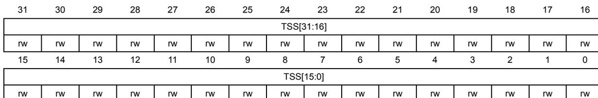
| 31 | 30 | 29 | 28 | 27 | 26 | 25 | 24 | 23 | 22 | 21 | 20 | 19 | 18 | 17 | 16 |
| TSS[31:16] | |||||||||||||||
| rw | rw | rw | rw | rw | rw | rw | rw | rw | rw | rw | rw | rw | rw | rw | rw |
| 15 | 14 | 13 | 12 | 11 | 10 | 9 | 8 | 7 | 6 | 5 | 4 | 3 | 2 | 1 | 0 |
| TSS[15:0] | |||||||||||||||
| rw | rw | rw | rw | rw | rw | rw | rw | rw | rw | rw | rw | rw | rw | rw | rw |
Bits 31:0 TSS[31:0] : Timestamp Seconds
The value in this field is the seconds part of the update.
When ADDSUB is reset, this field must be programmed with the seconds part of the update value.
When ADDSUB is set, this field must be programmed with the complement of the seconds part of the update value.
For example, to subtract 2.000000001 seconds from the system time, the TSS field in the ETH_MACSTSUR register must be 0xFFFF FFFE (that is, \( 2^{32} - 2 \) ).
Caution: When the ADDSUB bit is set, TSSS[30:0] field cannot be set to 0 in System time nanoseconds update register (ETH_MACSTNUR) . The TSSS bitfield must be programmed to 0x7FFF FFFF (resulting in -0.46 ns) even if 0 ns must be subtracted.
For example, to subtract 2.000000000 seconds from the system time, the TSS field in the System time seconds update register (ETH_MACSTSUR) must be 0xFFFF FFFE (that is, \( 2^{32} - 1 \) ) and the System time nanoseconds update register (ETH_MACSTNUR) must be 0xFFFF FFFF (ADDSUB = 1 and TSSS[30:0] field = 0x7FFF FFFF)
System time nanoseconds update register (ETH_MACSTNUR)
Address offset: 0x0B14
Reset value: 0x0000 0000
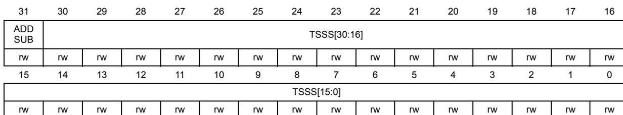
| 31 | 30 | 29 | 28 | 27 | 26 | 25 | 24 | 23 | 22 | 21 | 20 | 19 | 18 | 17 | 16 |
| ADD SUB | TSSS[30:16] | ||||||||||||||
| rw | rw | rw | rw | rw | rw | rw | rw | rw | rw | rw | rw | rw | rw | rw | rw |
| 15 | 14 | 13 | 12 | 11 | 10 | 9 | 8 | 7 | 6 | 5 | 4 | 3 | 2 | 1 | 0 |
| TSSS[15:0] | |||||||||||||||
| rw | rw | rw | rw | rw | rw | rw | rw | rw | rw | rw | rw | rw | rw | rw | rw |
Bit 31 ADDSUB : Add or Subtract Time
When this bit is set, the time value is subtracted with the contents of the update register.
When this bit is reset, the time value is added with the contents of the update register.
Bits 30:0 TSSS[30:0] : Timestamp subsecondsThe value in this field is the subseconds part of the update.
- – ADDSUB is 1: This field must be programmed with the complement of the subseconds part of the update value as described.
- – ADDSUB is 0: This field must be programmed with the subseconds part of the update value, with an accuracy based on the TSCTRLSSR bit of the
Timestamp control register (ETH_MACTSCR)
.
- – TSCTRLSSR field in the
Timestamp control register (ETH_MACTSCR)
is 1:
- - The programmed value must be \( 10^9 - \text{<subsecond value>} \) .
- - Each bit represents 1 ns and the programmed value should not exceed 0x3B9A C9FF.
- – TSCTRLSSR field in the
Timestamp control register (ETH_MACTSCR)
is 0:
- - The programmed value must be \( 2^{31} - \text{<subsecond\_value>} \) .
- - Each bit represents an accuracy of 0.46 ns.
- – TSCTRLSSR field in the
Timestamp control register (ETH_MACTSCR)
is 1:
For example, to subtract 2.000000001 seconds from the system time, then the TSSS field in the ETH_MACSTNUR register must be 0x7FFF FFFF (that is, \( 2^{31} - 1 \) ), when TSCTRLSSR bit in Timestamp control register (ETH_MACTSCR) is reset and 0x3B9A C9FF (that is, \( 10^9 - 1 \) ), when TSCTRLSSR bit in Timestamp control register (ETH_MACTSCR) is set.
Caution: When the ADDSUB bit is set, TSSS[30:0] field cannot be set to 0. The TSSS bitfield must be programmed to 0x7FFF FFFF (resulting in -0.46 ns) even if 0 ns must be subtracted.
For example, to subtract 2.000000000 seconds from the system time, System time nanoseconds update register (ETH_MACSTNUR) must be 0xFFFF FFFF (ADDSUB = 1 and TSSS[30:0] = 0) and the TSS field in the System time seconds update register (ETH_MACTSUR) must be 0xFFFF FFFE (that is, \( 2^{32} - 1 \) ).
Timestamp addend register (ETH_MACTSAR)
Address offset: 0x0B18
Reset value: 0x0000 0000
This register value is used only when the system time is configured for Fine Update mode (TSCFUPDT bit in the Timestamp control register (ETH_MACTSCR) ). The content of this register is added to a 32-bit accumulator in every clock cycle of clk_ptp_ref_i and the system time is updated whenever the accumulator overflows.
| 31 | 30 | 29 | 28 | 27 | 26 | 25 | 24 | 23 | 22 | 21 | 20 | 19 | 18 | 17 | 16 |
|---|---|---|---|---|---|---|---|---|---|---|---|---|---|---|---|
| TSAR[31:16] | |||||||||||||||
| rw | rw | rw | rw | rw | rw | rw | rw | rw | rw | rw | rw | rw | rw | rw | rw |
| 15 | 14 | 13 | 12 | 11 | 10 | 9 | 8 | 7 | 6 | 5 | 4 | 3 | 2 | 1 | 0 |
| TSAR[15:0] | |||||||||||||||
| rw | rw | rw | rw | rw | rw | rw | rw | rw | rw | rw | rw | rw | rw | rw | rw |
This field indicates the 32-bit time value to be added to the Accumulator register to achieve time synchronization.
Timestamp status register (ETH_MACTSSR)
Address offset: 0x0B20
Reset value: 0x0000 0000
All bits except Bits[27:25] gets cleared when the application reads this register.
| 31 | 30 | 29 | 28 | 27 | 26 | 25 | 24 | 23 | 22 | 21 | 20 | 19 | 18 | 17 | 16 |
|---|---|---|---|---|---|---|---|---|---|---|---|---|---|---|---|
| Res. | Res. | ATSNS[4:0] | ATSS TM | Res. | Res. | Res. | Res. | ATSSTN[3:0] | |||||||
| r | r | r | r | r | rc_r | rc_r | rc_r | rc_r | rc_r | ||||||
| 15 | 14 | 13 | 12 | 11 | 10 | 9 | 8 | 7 | 6 | 5 | 4 | 3 | 2 | 1 | 0 |
|---|---|---|---|---|---|---|---|---|---|---|---|---|---|---|---|
| TXT SSIS | Res. | Res. | Res. | Res. | Res. | Res. | Res. | Res. | Res. | TSTRG TERR1 | TSTAR GT1 | TSTRG TERR0 | AUXTS TRIG | TSTAR GT0 | TSSOV F |
| rc_r | rc_r | rc_r | rc_r | rc_r | rc_r | rc_r |
Bits 31:30 Reserved, must be kept at reset value.
Bits 29:25 ATSNS[4:0] : Number of Auxiliary Timestamp Snapshots
This field indicates the number of Snapshots available in the FIFO. A value equal to the depth of FIFO (4) indicates that the Auxiliary Snapshot FIFO is full. These bits are cleared (to 00000) when the Auxiliary snapshot FIFO clear bit is set.
Bit 24 ATSSM : Auxiliary Timestamp Snapshot Trigger Missed
This bit is set when the Auxiliary timestamp snapshot FIFO is full and external trigger was set. This indicates that the latest snapshot is not stored in the FIFO.
Bits 23:20 Reserved, must be kept at reset value.
Bits 19:16 ATSSTN[3:0] : Auxiliary Timestamp Snapshot Trigger Identifier
These bits identify the Auxiliary trigger inputs for which the timestamp available in the Auxiliary Snapshot Register is applicable. When more than one bit is set at the same time, it means that corresponding auxiliary triggers were sampled at the same clock. These bits are applicable only if the number of Auxiliary snapshots is more than one. One bit is assigned for each trigger as shown in the following list:
Bit 16: Auxiliary trigger 0
Bit 17: Auxiliary trigger 1
Bit 18: Auxiliary trigger 2
Bit 19: Auxiliary trigger 3
The software can read this register to find the triggers that are set when the timestamp is taken.
Bit 15 TXTSSIS : Tx Timestamp Status interrupt status
When drop transmit status is enabled in MTL, this bit is set when the captured transmit timestamp is updated in the Tx timestamp status nanoseconds register (ETH_MACTXTSSNR) and Tx timestamp status seconds register (ETH_MACTXTSSSR) .
When PTP offload feature is enabled, this bit is set when the captured transmit timestamp is updated in the Tx timestamp status nanoseconds register (ETH_MACTXTSSNR) and Tx timestamp status seconds register (ETH_MACTXTSSSR) , for PTO generated Delay Request and Pdelay request packets.
This bit is cleared when the Tx timestamp status seconds register (ETH_MACTXTSSSR) is read (or written to 1 when RCWE bit in CSR software control register (ETH_MACCSRWSWCR) is set).
Bits 14:6 Reserved, must be kept at reset value.
Bit 5 TSTRGTERR1: Timestamp Target Time ErrorThis bit is set when the latest target time programmed in the ETH_MACPPSTTS1R and ETH_MACPPSTTSN1R registers elapses. It is cleared when the application reads this bit (or writes it to 1 when RCWE bit in CSR software control register (ETH_MACCSRSWCR) is set).
Bit 4 TSTARTGT1: Timestamp Target Time ReachedWhen set, this bit indicates that the value of the system time is greater than or equal to the value specified in the ETH_MACPPSTTS1R and ETH_MACPPSTTSN1R registers.
This bit is cleared when the application reads this bit (or write it to 1 when RCWE bit in CSR software control register (ETH_MACCSRSWCR) is set)
Bit 3 TSTRGTERR0: Timestamp Target Time ErrorThis bit is set when the latest target time programmed in the ETH_MACPPSTTS0R and ETH_MACPPSTTSN0R elapses (see PPS x target time seconds register (ETH_MACPPSTTSxR) and PPS x target time nanoseconds register (ETH_MACPPSTTNxR) ).
This bit is cleared when the application reads this bit (or writes it to 1 when RCWE bit in CSR software control register (ETH_MACCSRSWCR) is set).
Bit 2 AUXTSTRIG: Auxiliary Timestamp Trigger SnapshotThis bit is set high when the auxiliary snapshot is written to the FIFO.
This bit is cleared when the application reads this bit (or writes it to 1 when RCWE bit in CSR software control register (ETH_MACCSRSWCR) is set).
Bit 1 TSTARTGT0: Timestamp Target Time ReachedWhen set, this bit indicates that the value of system time is greater than or equal to the value specified in the ETH_MACPPSTTS0R and ETH_MACPPSTTSN0R registers (see PPS x target time seconds register (ETH_MACPPSTTSxR) and PPS x target time nanoseconds register (ETH_MACPPSTTNxR) ).
This bit is cleared when the application reads this bit (or writes of 1 when RCWE bit in CSR software control register (ETH_MACCSRSWCR) is set)
Bit 0 TSSOVF: Timestamp Seconds OverflowWhen this bit is set, it indicates that the seconds value of the timestamp (when supporting version 2 format) has overflowed beyond 0xFFFF FFFF.
This bit is cleared when the application reads this bit (or writes it to 1 when RCWE bit in CSR software control register (ETH_MACCSRSWCR) is set)
Tx timestamp status nanoseconds register (ETH_MACTXTSSNR)
Address offset: 0x0B30
Reset value: 0x0000 0000
This register contains the nanosecond part of timestamp captured for transmit packets when Tx status is disabled. The Tx timestamp status nanoseconds register (ETH_MACTXTSSNR) register, along with Tx timestamp status seconds register (ETH_MACTXTSSSR) , gives the 64-bit timestamp captured for the PTP packet successfully transmitted by the MAC. This value is considered to be read by the application when the last byte of Tx timestamp status nanoseconds register (ETH_MACTXTSSNR) is read (bits[31:24]).
If the application does not read these registers and timestamp of another packet is captured, then either the current timestamp is lost (overwritten) or the new timestamp is lost (dropped), depending on the setting of the TXTSSTSM bit of the Timestamp control register (ETH_MACTSCR) . The status bit TXTSSIS bit [15] in Timestamp status register (ETH_MACTSSR) register is set when the MAC transmitter captures the timestamp.
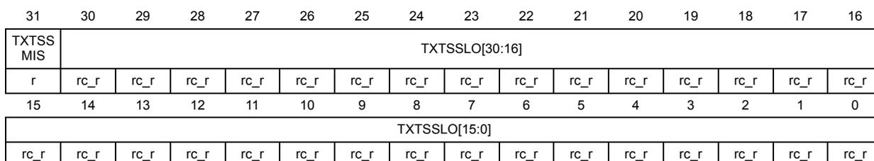
| 31 | 30 | 29 | 28 | 27 | 26 | 25 | 24 | 23 | 22 | 21 | 20 | 19 | 18 | 17 | 16 |
| TXTSS MIS | TXTSSLO[30:16] | ||||||||||||||
| r | rc_r | rc_r | rc_r | rc_r | rc_r | rc_r | rc_r | rc_r | rc_r | rc_r | rc_r | rc_r | rc_r | rc_r | rc_r |
| 15 | 14 | 13 | 12 | 11 | 10 | 9 | 8 | 7 | 6 | 5 | 4 | 3 | 2 | 1 | 0 |
| TXTSSLO[15:0] | |||||||||||||||
| rc_r | rc_r | rc_r | rc_r | rc_r | rc_r | rc_r | rc_r | rc_r | rc_r | rc_r | rc_r | rc_r | rc_r | rc_r | rc_r |
Bit 31 TXTSSMIS : Transmit Timestamp Status Missed
When this bit is set, it indicates one of the following:
- – The timestamp of the current packet is ignored if TXTSSTSM bit of the Timestamp control register (ETH_MACTSCR) is reset
- – The timestamp of the previous packet is overwritten with timestamp of the current packet if TXTSSTSM bit of the Timestamp control register (ETH_MACTSCR) is set.
Bits 30:0 TXTSSLO[30:0] : Transmit Timestamp Status Low
This field contains the 31 bits of the Nanoseconds field of the transmit packet's captured timestamp.
Tx timestamp status seconds register (ETH_MACTXTSSSR)
Address offset: 0x0B34
Reset value: 0x0000 0000
The register contains the higher 32 bits of the timestamp (in seconds) captured when a PTP packet is transmitted.
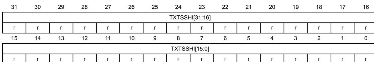
| 31 | 30 | 29 | 28 | 27 | 26 | 25 | 24 | 23 | 22 | 21 | 20 | 19 | 18 | 17 | 16 |
| TXTSSH[31:16] | |||||||||||||||
| r | r | r | r | r | r | r | r | r | r | r | r | r | r | r | r |
| 15 | 14 | 13 | 12 | 11 | 10 | 9 | 8 | 7 | 6 | 5 | 4 | 3 | 2 | 1 | 0 |
| TXTSSH[15:0] | |||||||||||||||
| r | r | r | r | r | r | r | r | r | r | r | r | r | r | r | r |
Bits 31:0 TXTSSHI[31:0] : Transmit Timestamp Status High
This field contains the lower 32 bits of the Seconds field of transmit packet's captured timestamp.
Auxiliary control register (ETH_MACACR)
Address offset: 0x0B40
Reset value: 0x0000 0000
The auxiliary timestamp control register controls the auxiliary timestamp snapshot.
| 31 | 30 | 29 | 28 | 27 | 26 | 25 | 24 | 23 | 22 | 21 | 20 | 19 | 18 | 17 | 16 |
|---|---|---|---|---|---|---|---|---|---|---|---|---|---|---|---|
| Res. | Res. | Res. | Res. | Res. | Res. | Res. | Res. | Res. | Res. | Res. | Res. | Res. | Res. | Res. | Res. |
| 15 | 14 | 13 | 12 | 11 | 10 | 9 | 8 | 7 | 6 | 5 | 4 | 3 | 2 | 1 | 0 |
| Res. | Res. | Res. | Res. | Res. | Res. | Res. | Res. | ATSEN3 | ATSEN2 | ATSEN1 | ATSEN0 | Res. | Res. | Res. | ATSFC |
| rw | rw | rw | rw | rw |
Bits 31:8 Reserved, must be kept at reset value.
Bit 7 ATSEN3 : Auxiliary Snapshot 3 Enable
- – This bit controls the capturing of Auxiliary Snapshot Trigger 3. When this bit is set, the auxiliary snapshot of the event on eth_ptp_trg3 input is enabled. When this bit is reset, the events on this input are ignored.
Bit 6 ATSEN2 : Auxiliary Snapshot 2 Enable
- – This bit controls the capturing of Auxiliary Snapshot Trigger 2. When this bit is set, the auxiliary snapshot of the event on eth_ptp_trg2 input is enabled. When this bit is reset, the events on this input are ignored.
Bit 5 ATSEN1 : Auxiliary Snapshot 1 Enable
- – This bit controls the capturing of Auxiliary Snapshot Trigger 1. When this bit is set, the auxiliary snapshot of the event on eth_ptp_trg1 input is enabled. When this bit is reset, the events on this input are ignored.
Bit 4 ATSEN0 : Auxiliary Snapshot 0 Enable
This bit controls the capturing of Auxiliary Snapshot Trigger 0. When this bit is set, the auxiliary snapshot of the event on eth_ptp_trg0 input is enabled. When this bit is reset, the events on this input are ignored.
Bits 3:1 Reserved, must be kept at reset value.
Bit 0 ATSFC : Auxiliary Snapshot FIFO Clear
When set, this bit resets the pointers of the Auxiliary Snapshot FIFO. This bit is cleared when the pointers are reset and the FIFO is empty. When this bit is high, the auxiliary snapshots are stored in the FIFO.
Auxiliary timestamp nanoseconds register (ETH_MACATSNR)
Address offset: 0x0B48
Reset value: 0x0000 0000
The Auxiliary timestamp nanoseconds register (ETH_MACATSNR) , along with Auxiliary timestamp seconds register (ETH_MACATSSR) , gives the 64-bit timestamp stored as auxiliary snapshot. These two registers form the read port of a 64-bit wide FIFO with a depth of 4 words.
You can store multiple snapshots in this FIFO. Bits[29:25] in Timestamp status register (ETH_MACTSSR) indicate the fill-level of the FIFO. The top of the FIFO is removed only when Auxiliary timestamp seconds register (ETH_MACATSSR) is read.
| 31 | 30 | 29 | 28 | 27 | 26 | 25 | 24 | 23 | 22 | 21 | 20 | 19 | 18 | 17 | 16 |
| Res | AUXTSLO[30:16] | ||||||||||||||
| r | r | r | r | r | r | r | r | r | r | r | r | r | r | r | |
| 15 | 14 | 13 | 12 | 11 | 10 | 9 | 8 | 7 | 6 | 5 | 4 | 3 | 2 | 1 | 0 |
| AUXTSLO[15:0] | |||||||||||||||
| r | r | r | r | r | r | r | r | r | r | r | r | r | r | r | r |
Bit 31 Reserved, must be kept at reset value.
Bits 30:0 AUXTSLO[30:0] : Auxiliary Timestamp
Contains the lower 31 bits (nanoseconds field) of the auxiliary timestamp.
Auxiliary timestamp seconds register (ETH_MACATSSR)
Address offset: 0x0B4C
Reset value: 0x0000 0000
The Auxiliary Timestamp Seconds register contains the lower 32 bits of the Seconds field of the auxiliary timestamp register.

| 31 | 30 | 29 | 28 | 27 | 26 | 25 | 24 | 23 | 22 | 21 | 20 | 19 | 18 | 17 | 16 |
| AUXTSHI[31:16] | |||||||||||||||
| r | r | r | r | r | r | r | r | r | r | r | r | r | r | r | r |
| 15 | 14 | 13 | 12 | 11 | 10 | 9 | 8 | 7 | 6 | 5 | 4 | 3 | 2 | 1 | 0 |
| AUXTSHI[15:0] | |||||||||||||||
| r | r | r | r | r | r | r | r | r | r | r | r | r | r | r | r |
Bits 31:0 AUXTSHI[31:0] : Auxiliary Timestamp
Contains the lower 32 bits of the Seconds field of the auxiliary timestamp.
Timestamp ingress asymmetric correction register (ETH_MACTSIACR)
Address offset: 0x0B50
Reset value: 0x0000 0000
The MAC Timestamp Ingress Asymmetry Correction register contains the Ingress Asymmetry Correction value to be used while updating correction field in PDelay_Resp PTP messages.
| 31 | 30 | 29 | 28 | 27 | 26 | 25 | 24 | 23 | 22 | 21 | 20 | 19 | 18 | 17 | 16 |
| OSTIAC[31:16] | |||||||||||||||
| rw | rw | rw | rw | rw | rw | rw | rw | rw | rw | rw | rw | rw | rw | rw | rw |
| 15 | 14 | 13 | 12 | 11 | 10 | 9 | 8 | 7 | 6 | 5 | 4 | 3 | 2 | 1 | 0 |
| OSTIAC[15:0] | |||||||||||||||
| rw | rw | rw | rw | rw | rw | rw | rw | rw | rw | rw | rw | rw | rw | rw | rw |
Bits 31:0 OSTIAC[31:0] : One-Step Timestamp Ingress Asymmetry Correction
This field contains the ingress path asymmetry value to be added to correctionField of Pdelay_Resp PTP packet. The programmed value should be in units of nanoseconds and multiplied by \( 2^{16} \) . For example, 2.5 ns is represented as 0x00028000.
The value can also be negative, which is represented in 2's complement form with bit 31 representing the sign bit.
Timestamp egress asymmetric correction register (ETH_MACTSEACR)
Address offset: 0x0B54
Reset value: 0x0000 0000
The MAC Timestamp Egress Asymmetry Correction register contains the Egress Asymmetry Correction value to be used while updating the correction field in PDelay_Req PTP messages.

| 31 | 30 | 29 | 28 | 27 | 26 | 25 | 24 | 23 | 22 | 21 | 20 | 19 | 18 | 17 | 16 |
| OSTEAC[31:16] | |||||||||||||||
| rw | rw | rw | rw | rw | rw | rw | rw | rw | rw | rw | rw | rw | rw | rw | rw |
| 15 | 14 | 13 | 12 | 11 | 10 | 9 | 8 | 7 | 6 | 5 | 4 | 3 | 2 | 1 | 0 |
| OSTEAC[15:0] | |||||||||||||||
| rw | rw | rw | rw | rw | rw | rw | rw | rw | rw | rw | rw | rw | rw | rw | rw |
Bits 31:0 OSTEAC[31:0] : One-Step Timestamp Egress Asymmetry Correction
This field contains the egress path asymmetry value to be subtracted from correctionField of Pdelay_Resp PTP packet. The programmed value must be the negated value in units of nanoseconds multiplied by \( 2^{16} \) .
For example, if the required correction is +2.5 ns, the programmed value must be 0xFFFD 8000, which is the 2's complement of 0x0002 8000 ( \( 2.5 \times 2^{16} \) ). Similarly, if the required correction is -3.3 ns, the programmed value is 0x0003 4CCC ( \( 3.3 \times 2^{16} \) ).
Timestamp ingress correction nanosecond register (ETH_MACTSICNR)Address offset: 0x0B58
Reset value: 0x0000 0000
This register contains the correction value in nanoseconds to be used with the captured timestamp value in the ingress path.
| 31 | 30 | 29 | 28 | 27 | 26 | 25 | 24 | 23 | 22 | 21 | 20 | 19 | 18 | 17 | 16 |
| TSIC[31:16] | |||||||||||||||
| rw | rw | rw | rw | rw | rw | rw | rw | rw | rw | rw | rw | rw | rw | rw | rw |
| 15 | 14 | 13 | 12 | 11 | 10 | 9 | 8 | 7 | 6 | 5 | 4 | 3 | 2 | 1 | 0 |
| TSIC[15:0] | |||||||||||||||
| rw | rw | rw | rw | rw | rw | rw | rw | rw | rw | rw | rw | rw | rw | rw | rw |
This field contains the ingress path correction value as defined by the Ingress Correction expression.
Timestamp egress correction nanosecond register (ETH_MACTSENR)Address offset: 0x0B5C
Reset value: 0x0000 0000
This register contains the correction value in nanoseconds to be used with the captured timestamp value in the egress path.
| 31 | 30 | 29 | 28 | 27 | 26 | 25 | 24 | 23 | 22 | 21 | 20 | 19 | 18 | 17 | 16 |
| TSEC[31:16] | |||||||||||||||
| rw | rw | rw | rw | rw | rw | rw | rw | rw | rw | rw | rw | rw | rw | rw | rw |
| 15 | 14 | 13 | 12 | 11 | 10 | 9 | 8 | 7 | 6 | 5 | 4 | 3 | 2 | 1 | 0 |
| TSEC[15:0] | |||||||||||||||
| rw | rw | rw | rw | rw | rw | rw | rw | rw | rw | rw | rw | rw | rw | rw | rw |
This field contains the nanoseconds part of the egress path correction value as defined by the Egress Correction expression.
Timestamp ingress latency register (ETH_MACTSILR)Address offset: 0x0B68
Reset value: 0x0000 0000
This register holds the ingress MAC latency.
| 31 | 30 | 29 | 28 | 27 | 26 | 25 | 24 | 23 | 22 | 21 | 20 | 19 | 18 | 17 | 16 |
| Res | Res | Res | Res | ITLNS[11:0] | |||||||||||
| r | r | r | r | r | r | r | r | r | r | r | r | ||||
| 15 | 14 | 13 | 12 | 11 | 10 | 9 | 8 | 7 | 6 | 5 | 4 | 3 | 2 | 1 | 0 |
| ITLSNS[7:0] | Res | Res | Res | Res | Res | Res | Res | Res | |||||||
| r | r | r | r | r | r | r | r | ||||||||
Bits 31:28 Reserved, must be kept at reset value.
Bits 27:16 ITLNS[11:0] : Ingress Timestamp Latency, in nanoseconds
This register holds the average latency (in nanoseconds) between the MAC input ports and the actual point (GMII/MII) where the ingress timestamp is taken. Ingress correction value is computed as described in Section : Ingress correction .
Bits 15:8 ITLSNS[7:0] : Ingress Timestamp Latency, in subnanoseconds
This register holds the average latency (in subnanoseconds) between the MAC input ports and the actual point (GMII/MII) where the ingress timestamp is taken. Ingress correction value is computed as described in Section : Ingress correction .
Bits 7:0 Reserved, must be kept at reset value.
Timestamp egress latency register (ETH_MACTSELR)
Address offset: 0x0B6C
Reset value: 0x0000 0000
This register holds the Egress MAC latency.
| 31 | 30 | 29 | 28 | 27 | 26 | 25 | 24 | 23 | 22 | 21 | 20 | 19 | 18 | 17 | 16 |
|---|---|---|---|---|---|---|---|---|---|---|---|---|---|---|---|
| Res. | Res. | Res. | Res. | ETLNS[11:0] | |||||||||||
| r | r | r | r | r | r | r | r | r | r | r | r | ||||
| 15 | 14 | 13 | 12 | 11 | 10 | 9 | 8 | 7 | 6 | 5 | 4 | 3 | 2 | 1 | 0 |
| ETLSNS[7:0] | Res. | Res. | Res. | Res. | Res. | Res. | Res. | Res. | |||||||
| r | r | r | r | r | r | r | r | ||||||||
Bits 31:28 Reserved, must be kept at reset value.
Bits 27:16 ETLNS[11:0] : Egress Timestamp Latency, in nanoseconds
This register holds the average latency in nanoseconds between the actual point (GMII/MII) where the egress timestamp is taken and the output ports of the MAC. Egress correction value is computed as described in Section : Egress correction .
Bits 15:8 ETLSNS[7:0] : Egress Timestamp Latency, in subnanoseconds
This register holds the average latency in subnanoseconds between the actual point (GMII/MII) where the egress timestamp is taken and the output ports of the MAC. Egress correction value is computed as described in Section : Egress correction .
Bits 7:0 Reserved, must be kept at reset value.
PPS control register (ETH_MACPPSCR)
Address offset: 0x0B70
Reset value: 0x0000 0000
| 31 | 30 | 29 | 28 | 27 | 26 | 25 | 24 | 23 | 22 | 21 | 20 | 19 | 18 | 17 | 16 |
|---|---|---|---|---|---|---|---|---|---|---|---|---|---|---|---|
| Res. | Res. | Res. | TIMESEL | Res. | Res. | Res. | Res. | Res. | Res. | Res. | Res. | Res. | Res. | Res. | Res. |
| rw | |||||||||||||||
| 15 | 14 | 13 | 12 | 11 | 10 | 9 | 8 | 7 | 6 | 5 | 4 | 3 | 2 | 1 | 0 |
| Res. | Res. | Res. | Res. | Res. | Res. | Res. | Res. | MCGRENO | TRGTMODSEL0[1:0] | PPSEN0 | PPSCTRL[3:0] | ||||
| rw | rw | rw | rw | rw | rw | rw | rw | ||||||||
Bits 31:29 Reserved, must be kept at reset value.
Bit 28 TIMESEL : Time Select
When this bit is set, 64 bit PTP time is used to capture time at MCGR trigger[0] input
When this bit is reset, presentation time is used to capture time at trigger input, maintaining backward compatibility
Bits 27:8 Reserved, must be kept at reset value.
Bit 7 MCGREN0 : MCGR Mode Enable for PPS0 Output
This field enables the 0th PPS instance to operate in PPS or MCGR mode. When set it operates in MCGR mode and on reset it operates in PPS mode.
0: PPS mode
1: MCGR mode
Bits 6:5 TRGTMODSEL0[1:0] : Target Time Register Mode for PPS Output
This field indicates the Target Time registers ( PPS x target time seconds register (ETH_MACPPSTTSxR) and PPS x target time nanoseconds register (ETH_MACPPSTTNxR) ) mode for PPS output signal:
00: Target Time registers are programmed only for generating the interrupt event.
01: Enables MCGR Interrupt whose status bit is indicated by TSTARGT0 bit in Timestamp status register (ETH_MACTSSR) register
10: Target Time registers are programmed for generating the interrupt event and starting or stopping the PPS output signal generation.
11: Target Time registers are programmed only for starting or stopping the PPS output signal generation. No interrupt is asserted.
Bit 4 PPSEN0 : Flexible PPS Output Mode Enable
When this bit is set, PPSCTRL[3:0] function as PPSCMD[3:0]. When this bit is reset, PPSCTRL[3:0] function as PPSCTRL (Fixed PPS mode).
Bits 3:0 PPSCTRL[3:0] : PPS Output Frequency Control
This field controls the frequency of the PPS output (eth_ptp_pps_out) signal. The default value of PPSCTRL is 0000, and the PPS output is 1 pulse (of width clk_ptp_i) every second. For other values of PPSCTRL, the PPS output becomes a generated clock of following frequencies:
0001: The binary rollover is 2 Hz, and the digital rollover is 1 Hz.
0010: The binary rollover is 4 Hz, and the digital rollover is 2 Hz.
0011: The binary rollover is 8 Hz, and the digital rollover is 4 Hz.
0100: The binary rollover is 16 Hz, and the digital rollover is 8 Hz.
..
1111: The binary rollover is 32.768 KHz and the digital rollover is 16.384 KHz.
Note: In the binary rollover mode, the PPS output (eth_ptp_pps_out) has a duty cycle of 50 percent with these frequencies. In the digital rollover mode, the PPS output frequency is an average number. The actual clock is of different frequency that gets synchronized every second. For example:
- – When PPSCTRL = 0001, the PPS (1 Hz) has a low period of 537 ms and a high period of 463 ms.
- –
When PPSCTRL = 0010, the PPS (2 Hz) is a sequence of
One clock of 50 percent duty cycle and 537 ms period
Second clock of 463 ms period (268 ms low and 195 ms high). - –
When PPSCTRL = 0011, the PPS (4 Hz) is a sequence of
Three clocks of 50 percent duty cycle and 268 ms period
Fourth clock of 195 ms period (134 ms low and 61 ms high)
This behavior is because of the non-linear toggling of bits in the digital rollover mode in the ETH_MACSTNR register.
PPS control register [alternate] (ETH_MACPPSCR)Address offset: 0x0B70
Reset value: 0x0000 0000
| 31 | 30 | 29 | 28 | 27 | 26 | 25 | 24 | 23 | 22 | 21 | 20 | 19 | 18 | 17 | 16 |
|---|---|---|---|---|---|---|---|---|---|---|---|---|---|---|---|
| Res. | Res. | Res. | TIMESEL | Res. | Res. | Res. | Res. | Res. | Res. | Res. | Res. | Res. | Res. | Res. | Res. |
| rw | |||||||||||||||
| 15 | 14 | 13 | 12 | 11 | 10 | 9 | 8 | 7 | 6 | 5 | 4 | 3 | 2 | 1 | 0 |
| MCGREN1 | TRGTMODSEL1 [1:0] | Res. | PPSCMD1[3:0] | MCGREN0 | TRGTMODSEL0 [1:0] | PPSEN0 | PPSCMD[3:0] | ||||||||
| rw | rw | rw | rw | rw | rw | rw | rw | rw | rw | rw | rw | rw | rw | rw | |
Bits 31:29 Reserved, must be kept at reset value.
Bit 28 TIMESEL : Time SelectWhen this bit is set, 64 bit PTP time is used to capture time at MCGR trigger[0] input
When this bit is reset, presentation time is used to capture time at trigger input, maintaining backward compatibility
Bits 27:16 Reserved, must be kept at reset value.
Bit 15 MCGREN1 : MCGR Mode Enable for PPS Output 1This field enables the 0th PPS instance to operate in PPS or MCGR mode. When set, it operates in MCGR mode and when reset it operates in PPS mode.
0: PPS mode
1: MCGR mode
Bits 14:13 TRGTMODSEL1[1:0] : Target Time Register Mode for PPS Output 1This field indicates the target time register ( PPS x target time seconds register (ETH_MACPPSTTSxR) and PPS x target time nanoseconds register (ETH_MACPPSTTNxR) ) mode for PPS output signal:00: Target time registers are programmed only for generating the interrupt event.
01: Enabled MCGR Interrupt whose status bit is indicated by TSTARGT1 bit in Timestamp status register (ETH_MACTSSR) register10: Target time registers are programmed for generating the interrupt event and starting or stopping the PPS output signal generation.
11: Target time registers are programmed only for starting or stopping the PPS output signal generation. No interrupt is asserted.
Bit 12 Reserved, must be kept at reset value.
Bits 11:8 PPSCMD1[3:0] : Flexible PPS Output 1 ControlThis field controls the flexible PPS output 1 signal. This field is similar to the PPSCMD[3:0] bitfield.
- – When MCGREN1 is set, PPSCMD1 indicated by the four bits [11:8] are taken as Presentation Time Control bits for media clock generation and recovery for comparator instance 1. This field is similar to the PPSCMD0 Presentation Time Control bits.
- – When MCGREN1 is cleared, only the three bits [10:8] are used as PPSCMD1 and the 4th bit must be cleared.
Bit 7 MCGREN0 : MCGR Mode Enable for PPS Output 0
This field enables the 0th PPS instance to operate in PPS or MCGR mode. When set it operates in MCGR mode and on reset it operates in PPS mode.
0: PPS mode
1: MCGR mode
Bits 6:5 TRGTMODESEL0[1:0] : Target Time Register Mode for PPS Output 0
This field indicates the Target Time registers ( PPS x target time seconds register (ETH_MACPPSTTSxR) and PPS x target time nanoseconds register (ETH_MACPPSTTNxR) ) mode for PPS output signal:
00: Target Time registers are programmed only for generating the interrupt event.
01: Enables MCGR Interrupt whose status bit is indicated by TSTARTGT0 bit in Timestamp status register (ETH_MACTSSR) register
10: Target Time registers are programmed for generating the interrupt event and starting or stopping the PPS output 0 signal generation.
11: Target Time registers are programmed only for starting or stopping the PPS output 0 signal generation. No interrupt is asserted.
Bit 4 PPSENO : Flexible PPS Output 0 Mode Enable
When this bit is set, Bits[3:0] function as PPSCMD[3:0]. When this bit is reset, Bits[3:0] function as PPSCTRL(Fixed PPS mode).
Bits 3:0 PPSCMD[3:0] : Flexible PPS Output 0 (eth_ptp_pps_out) Control
Programming these bits with a non-zero value instructs the MAC to initiate an event. When the command is transferred or synchronized to the PTP clock domain, these bits get cleared automatically. The software should ensure that these bits are programmed only when they are 'all zero'. The following list describes the values of PPSCMD0:
0000: No Command
0001: START Single Pulse.
This command generates single pulse rising at the start point defined in Target Time Registers (register 455 and 456) and of a duration defined in the PPS Width Register.
0010: START Pulse Train.
This command generates the train of pulses rising at the start point defined in the Target Time Registers and of a duration defined in the PPS Width Register and repeated at interval defined in the PPS Interval Register. By default, the PPS pulse train is free-running unless stopped by the 'Stop Pulse train at time' or 'Stop Pulse Train immediately' commands.
0011: Cancel START.
This command cancels the START Single Pulse and START Pulse Train commands if the system time has not crossed the programmed start time.
0100: STOP Pulse Train at time.
This command stops the train of pulses initiated by the START Pulse Train command (PPSCMD[3:0] = 0010) after the time programmed in the Target Time registers elapses.
0101: STOP Pulse Train immediately.
This command immediately stops the train of pulses initiated by the START Pulse Train command (PPSCMD[3:0] = 0010).
0110: Cancel STOP Pulse train.
This command cancels the STOP pulse train at time command if the programmed stop time has not elapsed. The PPS pulse train becomes free-running on the successful execution of this command.
0111 to 1111: Reserved, must not be used
PPS x target time seconds register (ETH_MACPPSTTSxR)Address offset: 0x0B80 + 0x10 *x, (x = 0 to 1)
Reset value: 0x0000 0000
The PPS output x Target Time Seconds register, along with PPS x target time nanoseconds register (ETH_MACPPSTTNxR) , is used to schedule an interrupt event (Bit TSSOVF of Timestamp status register (ETH_MACTSSR) ) when the system time exceeds the value programmed in these registers.
| 31 | 30 | 29 | 28 | 27 | 26 | 25 | 24 | 23 | 22 | 21 | 20 | 19 | 18 | 17 | 16 |
| TSTRH0[31:16] | |||||||||||||||
| rw | rw | rw | rw | rw | rw | rw | rw | rw | rw | rw | rw | rw | rw | rw | rw |
| 15 | 14 | 13 | 12 | 11 | 10 | 9 | 8 | 7 | 6 | 5 | 4 | 3 | 2 | 1 | 0 |
| TSTRH0[15:0] | |||||||||||||||
| rw | rw | rw | rw | rw | rw | rw | rw | rw | rw | rw | rw | rw | rw | rw | rw |
This field stores the time in seconds. When the timestamp value matches or exceeds both Target Timestamp registers, the MAC starts or stops the PPS signal output and generates an interrupt (if enabled) based on Target Time mode selected for the corresponding PPS output in the PPS control register (ETH_MACPPSCR) .
If the PTGE field of Timestamp control register (ETH_MACTSCR) is set with Presentation time control set in Recovery mode, then these bits indicate the TPT being programmed by the application and in Generation mode it indicates the CPT generated at the sampled trigger.
PPS x target time nanoseconds register (ETH_MACPPSTTNxR)Address offset: 0x0B84 + 0x10 *x, (x = 0 to 1)
Reset value: 0x0000 0000
| 31 | 30 | 29 | 28 | 27 | 26 | 25 | 24 | 23 | 22 | 21 | 20 | 19 | 18 | 17 | 16 |
| TRGTBUSY0 | TTSL0[30:16] | ||||||||||||||
| rw | rw | rw | rw | rw | rw | rw | rw | rw | rw | rw | rw | rw | rw | rw | rw |
| 15 | 14 | 13 | 12 | 11 | 10 | 9 | 8 | 7 | 6 | 5 | 4 | 3 | 2 | 1 | 0 |
| TTSL0[15:0] | |||||||||||||||
| rw | rw | rw | rw | rw | rw | rw | rw | rw | rw | rw | rw | rw | rw | rw | rw |
The MAC sets this bit when the PPSCMD0 field in the PPS control register (ETH_MACPPSCR) is programmed to 010 or 011. Programming the PPSCMD0 field to 010 or 011 instructs the MAC to synchronize the Target Time Registers to the PTP clock domain. The MAC clears this bit after synchronizing the Target Time Registers with the PTP clock domain. The application must not update the Target Time Registers when this bit is read as 1. Otherwise, the synchronization of the previous programmed time gets corrupted.
Bits 30:0 TTSL0[30:0] : Target Time Low for PPS Register
This register stores the time in (signed) nanoseconds. When the value of the timestamp matches the value in both Target Timestamp registers, the MAC starts or stops the PPS signal output and generates an interrupt (if enabled) based on the TRGTMODSEL0 field (Bits [6:5]) in PPS control register (ETH_MACPPSCR) .
When the TSCTRLSSR bit is reset in the Timestamp control register (ETH_MACTSCR) , this value should be (time in ns / 0.465). The actual start or stop time of the PPS signal output might have an error margin up to one unit of subsecond increment value.
When the TSCTRLSSR bit is set in the Timestamp control register (ETH_MACTSCR) , this value should not exceed 0x3B9A C9FF. The actual start or stop time of the PPS signal output may have an error margin up to one unit of subsecond increment value.
PPS x interval register (ETH_MACPPSxR)
Address offset: 0x0B88 + 0x10 *x, (x = 0 to 1)
Reset value: 0x0000 0000
The PPS Interval register contains the number of units of subsecond increment value between the rising edges of PPS output x.
| 31 | 30 | 29 | 28 | 27 | 26 | 25 | 24 | 23 | 22 | 21 | 20 | 19 | 18 | 17 | 16 |
| PPSINT0[31:16] | |||||||||||||||
| rw | rw | rw | rw | rw | rw | rw | rw | rw | rw | rw | rw | rw | rw | rw | rw |
| 15 | 14 | 13 | 12 | 11 | 10 | 9 | 8 | 7 | 6 | 5 | 4 | 3 | 2 | 1 | 0 |
| PPSINT0[15:0] | |||||||||||||||
| rw | rw | rw | rw | rw | rw | rw | rw | rw | rw | rw | rw | rw | rw | rw | rw |
Bits 31:0 PPSINT0[31:0] : PPS Output Signal Interval
These bits store the interval between the rising edges of PPS signal output. The interval is stored in terms of number of units of subsecond increment value.
You need to program one value less than the required interval. For example, if the PTP reference clock is 50 MHz (period of 20 ns), and desired interval between the rising edges of PPS signal output is 100 ns (that is, 5 units of subsecond increment value), you should program value 4 (5-1) in this register.
PPS x width register (ETH_MACPPSWxR)
Address offset: 0x0B8C + 0x10 *x, (x = 0 to 1)
Reset value: 0x0000 0000
The PPS Width register contains the number of units of subsecond increment value between the rising and corresponding falling edges of PPS output x.

| 31 | 30 | 29 | 28 | 27 | 26 | 25 | 24 | 23 | 22 | 21 | 20 | 19 | 18 | 17 | 16 |
| PPSWIDTH0[31:16] | |||||||||||||||
| rw | rw | rw | rw | rw | rw | rw | rw | rw | rw | rw | rw | rw | rw | rw | rw |
| 15 | 14 | 13 | 12 | 11 | 10 | 9 | 8 | 7 | 6 | 5 | 4 | 3 | 2 | 1 | 0 |
| PPSWIDTH0[15:0] | |||||||||||||||
| rw | rw | rw | rw | rw | rw | rw | rw | rw | rw | rw | rw | rw | rw | rw | rw |
Bits 31:0 PPSWIDTH0[31:0] : PPS Output Signal Width
These bits store the width between the rising edge and corresponding falling edge of PPS signal output. The width is stored in terms of number of units of subsecond increment value. You need to program one value less than the required interval. For example, if PTP reference clock is 50 MHz (period of 20 ns), and width between the rising and corresponding falling edges of PPS signal output is 80 ns (that is, four units of subsecond increment value), you should program value 3 (4-1) in this register.
Note: The value programmed in this register must be lesser than the value programmed in PPS x interval register (ETH_MACPPS \( \times \) R).
PTP offload control register (ETH_MACPOCR)
Address offset: 0x0BC0
Reset value: 0x0000 0000
This register controls the PTP Offload Engine operation.
| 31 | 30 | 29 | 28 | 27 | 26 | 25 | 24 | 23 | 22 | 21 | 20 | 19 | 18 | 17 | 16 |
|---|---|---|---|---|---|---|---|---|---|---|---|---|---|---|---|
| Res | Res | Res | Res | Res | Res | Res | Res | Res | Res | Res | Res | Res | Res | Res | Res |
| 15 | 14 | 13 | 12 | 11 | 10 | 9 | 8 | 7 | 6 | 5 | 4 | 3 | 2 | 1 | 0 |
| DN[7:0] | PDRDIS | DRRDIS | APDREQTRIG | ASYNCTRIG | Res. | APDREQEN | ASYNCE | PTOEN | |||||||
| rw | rw | rw | rw | rw | rw | rw | rw | rw | rw | rw | rw | rw | rw | rw | |
Bits 31:16 Reserved, must be kept at reset value.
Bits 15:8 DN[7:0] : Domain Number
This field indicates the domain Number in which the PTP node is operating.
Bit 7 PDRDIS : Disable Peer Delay Response response generation
When this bit is set, the Peer Delay Response (Pdelay_Resp) response is not generated for received Peer Delay Request (Pdelay_Req) request packet, as required by the programmed mode.
Setting this bit to 1 affects the normal PTP Offload operation and the time synchronization. So, this bit must be set only if there is problem with Pdelay_Resp generation in hardware and/or Pdelay_Resp generation is handled by software.
Bit 6 DRRDIS : Disable PTO Delay Request/Response response generation
When this bit is set, the Delay Request and Delay response are not generated for received SYNC and Delay request packet respectively, as required by the programmed mode.
Bit 5 APDREQTRIG : Automatic PTP Pdelay_Req message Trigger
When this bit is set, one PTP Pdelay_Req message is transmitted. This bit is automatically cleared after the PTP Pdelay_Req message is transmitted. The application should set the APDREQEN bit for this operation.
Bit 4 ASYNCTRIG : Automatic PTP SYNC message Trigger
When this bit is set, one PTP SYNC message is transmitted. This bit is automatically cleared after the PTP SYNC message is transmitted. The application should set the ASYNCE bit for this operation.
Bit 3 Reserved, must be kept at reset value.
Bit 2 APDREQEN : Automatic PTP Pdelay_Req message Enable
When this bit is set, PTP Pdelay_Req message is generated periodically based on interval programmed or trigger from application, when the MAC is programmed to be in Peer-to-Peer Transparent mode.
Bit 1 ASYNCEN : Automatic PTP SYNC message Enable
When this bit is set, PTP SYNC message is generated periodically based on interval programmed or trigger from application, when the MAC is programmed to be in Clock Master mode.
Bit 0 PTOEN : PTP Offload Enable
When this bit is set, the PTP Offload feature is enabled.
PTP source port identity 0 register (ETH_MACSPI0R)
Address offset: 0x0BC4
Reset value: 0x0000 0000
This register contains Bits[31:0] of the 80-bit Source Port Identity of the PTP node.
| 31 | 30 | 29 | 28 | 27 | 26 | 25 | 24 | 23 | 22 | 21 | 20 | 19 | 18 | 17 | 16 |
|---|---|---|---|---|---|---|---|---|---|---|---|---|---|---|---|
| SPI0[31:16] | |||||||||||||||
| rw | rw | rw | rw | rw | rw | rw | rw | rw | rw | rw | rw | rw | rw | rw | rw |
| 15 | 14 | 13 | 12 | 11 | 10 | 9 | 8 | 7 | 6 | 5 | 4 | 3 | 2 | 1 | 0 |
| SPI0[15:0] | |||||||||||||||
| rw | rw | rw | rw | rw | rw | rw | rw | rw | rw | rw | rw | rw | rw | rw | rw |
Bits 31:0 SPI0[31:0] : Source Port Identity 0
This field indicates bits [31:0] of sourcePortIdentity of PTP node.
PTP Source port identity 1 register (ETH_MACSPI1R)
Address offset: 0x0BC8
Reset value: 0x0000 0000
This register contains Bits[63:32] of the 80-bit Source Port Identity of the PTP node.
| 31 | 30 | 29 | 28 | 27 | 26 | 25 | 24 | 23 | 22 | 21 | 20 | 19 | 18 | 17 | 16 |
|---|---|---|---|---|---|---|---|---|---|---|---|---|---|---|---|
| SPI1[31:16] | |||||||||||||||
| rw | rw | rw | rw | rw | rw | rw | rw | rw | rw | rw | rw | rw | rw | rw | rw |
| 15 | 14 | 13 | 12 | 11 | 10 | 9 | 8 | 7 | 6 | 5 | 4 | 3 | 2 | 1 | 0 |
| SPI1[15:0] | |||||||||||||||
| rw | rw | rw | rw | rw | rw | rw | rw | rw | rw | rw | rw | rw | rw | rw | rw |
Bits 31:0 SPI1[31:0] : Source Port Identity 1
This field indicates bits [63:32] of sourcePortIdentity of PTP node.
PTP Source port identity 2 register (ETH_MACSPI2R)
Address offset: 0x0BCC
Reset value: 0x0000 0000
This register contains Bits[79:64] of the 80-bit Source Port Identity of the PTP node.
| 31 | 30 | 29 | 28 | 27 | 26 | 25 | 24 | 23 | 22 | 21 | 20 | 19 | 18 | 17 | 16 |
|---|---|---|---|---|---|---|---|---|---|---|---|---|---|---|---|
| Res | Res | Res | Res | Res | Res | Res | Res | Res | Res | Res | Res | Res | Res | Res | Res |
| 15 | 14 | 13 | 12 | 11 | 10 | 9 | 8 | 7 | 6 | 5 | 4 | 3 | 2 | 1 | 0 |
| SPI2[15:0] | |||||||||||||||
| rw | rw | rw | rw | rw | rw | rw | rw | rw | rw | rw | rw | rw | rw | rw | rw |
Bits 31:16 Reserved, must be kept at reset value.
Bits 15:0 SPI2[15:0] : Source Port Identity 2
This field indicates bits [79:64] of sourcePortIdentity of PTP node.
Log message interval register (ETH_MACLMIR)
Address offset: 0x0BD0
Reset value: 0x0000 0000
This register contains the periodic intervals for automatic PTP packet generation.
| 31 | 30 | 29 | 28 | 27 | 26 | 25 | 24 | 23 | 22 | 21 | 20 | 19 | 18 | 17 | 16 |
|---|---|---|---|---|---|---|---|---|---|---|---|---|---|---|---|
| LMPDRI[7:0] | Res | Res | Res | Res | Res | Res | Res | Res | |||||||
| rw | rw | rw | rw | rw | rw | rw | rw | ||||||||
| 15 | 14 | 13 | 12 | 11 | 10 | 9 | 8 | 7 | 6 | 5 | 4 | 3 | 2 | 1 | 0 |
| Res | Res | Res | Res | Res | DRSYNCR[2:0] | LSI[7:0] | |||||||||
| rw | rw | rw | rw | rw | rw | rw | rw | rw | rw | rw | |||||
Bits 31:24 LMPDRI[7:0] : Log Min Pdelay_Req Interval
This field indicates logMinPdelayReqInterval of PTP node. This is used to schedule the periodic Pdelay request packet transmission. Allowed values are -15 to 15. Negative value must be represented in 2's-complement form. For example, if the required value is -1, the value programmed must be 0xFF.
Bits 23:11 Reserved, must be kept at reset value.
Bits 10:8 DRSYNCR[2:0] :
Delay_Req to SYNC Ratio
In Slave mode, it is used for controlling frequency of Delay_Req messages transmitted.
0: DelayReq generated for every received SYNC
1: DelayReq generated every alternate reception of SYNC
2: for every 4 SYNC messages
3: for every 8 SYNC messages
4: for every 16 SYNC messages
5: for every 32 SYNC messages
Others: Reserved, must not be used
The master sends this information (logMinDelayReqInterval) in the DelayResp PTP messages to the slave. The reception processes this value from the received DelayResp messages and updates this field accordingly. In the Slave mode, the host must not write/update this register unless it has to override the received value. In Master mode, the sum of this field and logSyncInterval (LSI) field is provided in the logMinDelayReqInterval field of the generated multicast Delay_Resp PTP message.
Bits 7:0 LSI[7:0] :Log Sync Interval
This field indicates the periodicity of the automatically generated SYNC message when the PTP node is Master. Allowed values are -15 to 15. Negative value must be represented in 2's-complement form. For example, if the required value is -1, the value programmed must be 0xFF.
Ethernet MAC register map and reset values
Table 852. Ethernet MAC register map and reset values
| Offset | Register name | 31 | 30 | 29 | 28 | 27 | 26 | 25 | 24 | 23 | 22 | 21 | 20 | 19 | 18 | 17 | 16 | 15 | 14 | 13 | 12 | 11 | 10 | 9 | 8 | 7 | 6 | 5 | 4 | 3 | 2 | 1 | 0 |
|---|---|---|---|---|---|---|---|---|---|---|---|---|---|---|---|---|---|---|---|---|---|---|---|---|---|---|---|---|---|---|---|---|---|
| 0x0000 | ETH_MACCR | ARPEN | SARC[2:0] | IPC | IPG[2:0] | GPSLCE | S2KP | CST | ACS | WD | BE | JD | JE | PS | FES | DM | LM | ECRSFD | DO | DCRS | DR | Res. | BL[1:0] | DC | PRELEN[1:0] | TE | RE | ||||||
| Reset value | 0 | 0 | 0 | 0 | 0 | 0 | 0 | 0 | 0 | 0 | 0 | 0 | 0 | 0 | 0 | 0 | 0 | 0 | 0 | 0 | 0 | 0 | 0 | 0 | 0 | 0 | 0 | 0 | 0 | 0 | 0 | ||
| 0x0004 | ETH_MACECR | Res. | APDIM | EIPG[4:0] | EIPGEN | Res. | Res. | Res. | Res. | Res. | USP | SPEN | DCRCC | Res. | Res. | GPSL[13:0] | |||||||||||||||||
| Reset value | 0 | 0 | 0 | 0 | 0 | 0 | 0 | 0 | 0 | 0 | 0 | 0 | 0 | 0 | 0 | 0 | 0 | 0 | 0 | 0 | 0 | 0 | 0 | 0 | |||||||||
| 0x0008 | ETH_MACPFR | RA | Res. | Res. | Res. | Res. | Res. | Res. | Res. | Res. | Res. | DNTU | IPFE | Res. | Res. | VTFE | Res. | Res. | Res. | Res. | Res. | HPF | SAF | SAIF | PCF[1:0] | DBF | PM | DAIF | HMC | HUC | PR | ||
| Reset value | 0 | 0 | 0 | 0 | 0 | 0 | 0 | 0 | 0 | 0 | 0 | 0 | 0 | 0 | 0 | ||||||||||||||||||
| 0x000C | ETH_MACWTR | Res. | Res. | Res. | Res. | Res. | Res. | Res. | Res. | Res. | Res. | Res. | Res. | Res. | Res. | Res. | Res. | Res. | Res. | Res. | Res. | Res. | Res. | PWE | Res. | Res. | Res. | Res. | Res. | WTO[3:0] | |||
| Reset value | 0 | 0 | 0 | 0 | 0 | ||||||||||||||||||||||||||||
| 0x0010 | ETH_MACHTOR | HT31T0[31:0] | |||||||||||||||||||||||||||||||
| Reset value | 0 | 0 | 0 | 0 | 0 | 0 | 0 | 0 | 0 | 0 | 0 | 0 | 0 | 0 | 0 | 0 | 0 | 0 | 0 | 0 | 0 | 0 | 0 | 0 | 0 | 0 | 0 | 0 | 0 | 0 | 0 | 0 | |
| 0x0014 | ETH_MACHT1R | HT63T32[31:0] | |||||||||||||||||||||||||||||||
| Reset value | 0 | 0 | 0 | 0 | 0 | 0 | 0 | 0 | 0 | 0 | 0 | 0 | 0 | 0 | 0 | 0 | 0 | 0 | 0 | 0 | 0 | 0 | 0 | 0 | 0 | 0 | 0 | 0 | 0 | 0 | 0 | 0 | |
| 0x0018 - 0x004C | Reserved | ||||||||||||||||||||||||||||||||
| 0x0050 | ETH_MACVTCR | EIVLXRS | Res. | EIVLS[1:0] | ERIVLT | EDVLP | VTHM | EVLXRS | Res. | EVLS[1:0] | DOVLTC | ERSVLM | ESVL | VTIM | ETV | Res. | Res. | Res. | Res. | Res. | Res. | Res. | Res. | Res. | Res. | Res. | Res. | OFS[1:0] | CT | OB | |||
| Reset value | 0 | 0 | 0 | 0 | 0 | 0 | 0 | 0 | 0 | 0 | 0 | 0 | 0 | 0 | 0 | 0 | 0 | 0 | |||||||||||||||
| 0x0054 | ETH_MACVTDR | Res. | Res. | Res. | Res. | Res. | DMACHN | DMACHEN | Res. | Res. | Res. | ERIVLT | ERSVLM | DOVLTC | ETV | VEN | VID[15:0] | ||||||||||||||||
| Reset value | 0 | 0 | 0 | 0 | 0 | 0 | 0 | 0 | 0 | 0 | 0 | 0 | 0 | 0 | 0 | 0 | 0 | 0 | 0 | 0 | 0 | 0 | 0 | 0 | |||||||||
| 0x0058 | ETH_MACVHTR | Res. | Res. | Res. | Res. | Res. | Res. | Res. | Res. | Res. | Res. | Res. | Res. | Res. | Res. | Res. | VLHT[15:0] | ||||||||||||||||
| Reset value | 0 | 0 | 0 | 0 | 0 | 0 | 0 | 0 | 0 | 0 | 0 | 0 | 0 | 0 | 0 | 0 | |||||||||||||||||
| 0x005C | Reserved | ||||||||||||||||||||||||||||||||
| 0x0060 | ETH_MACVIR | BUSY | RDWR | Res. | Res. | Res. | Res. | Res. | ADDR | Res. | Res. | CBTI | VLTI | CSVL | VLP | VLC[1:0] | VLT[15:0] | ||||||||||||||||
| Reset value | 0 | 0 | 0 | 0 | 0 | 0 | 0 | 0 | 0 | 0 | 0 | 0 | 0 | 0 | 0 | 0 | 0 | 0 | 0 | 0 | 0 | 0 | 0 | 0 | 0 | ||||||||
| 0x0060 | ETH_MACVIR [alternate] | Res. | Res. | Res. | Res. | Res. | Res. | Res. | Res. | Res. | Res. | Res. | CSV | Res. | Res. | Res. | VLT[15:0] | ||||||||||||||||
| Reset value | 0 | 0 | 0 | 0 | 0 | 0 | 0 | 0 | 0 | 0 | 0 | 0 | 0 | 0 | 0 | 0 | 0 | ||||||||||||||||
Table 852. Ethernet MAC register map and reset values (continued)
| Offset | Register name | 31 | 30 | 29 | 28 | 27 | 26 | 25 | 24 | 23 | 22 | 21 | 20 | 19 | 18 | 17 | 16 | 15 | 14 | 13 | 12 | 11 | 10 | 9 | 8 | 7 | 6 | 5 | 4 | 3 | 2 | 1 | 0 | ||
|---|---|---|---|---|---|---|---|---|---|---|---|---|---|---|---|---|---|---|---|---|---|---|---|---|---|---|---|---|---|---|---|---|---|---|---|
| 0x0064 | ETH_MACIVIR | Res. | Res. | Res. | Res. | Res. | Res. | Res. | Res. | Res. | Res. | Res. | VLTI | CSVL | VLP | VLC[1:0] | VLT[15:0] | ||||||||||||||||||
| Reset value | 0 | 0 | 0 | 0 | 0 | 0 | 0 | 0 | 0 | 0 | 0 | 0 | 0 | 0 | 0 | 0 | 0 | 0 | 0 | 0 | 0 | ||||||||||||||
| 0x0068 - 0x006C | Reserved | ||||||||||||||||||||||||||||||||||
| 0x0070 | ETH_MACQ0TXFCR | PT[15:0] | Res. | Res. | Res. | Res. | Res. | Res. | Res. | Res. | Res. | DZPQ | PLT[2:0] | Res. | Res. | TFE | FCB_BP | ||||||||||||||||||
| Reset value | 0 | 0 | 0 | 0 | 0 | 0 | 0 | 0 | 0 | 0 | 0 | 0 | 0 | 0 | 0 | 0 | 0 | 0 | 0 | 0 | 0 | 0 | |||||||||||||
| 0x0074 - 0x008C | Reserved | ||||||||||||||||||||||||||||||||||
| 0x0090 | ETH_MACRXFCR | Res. | Res. | Res. | Res. | Res. | Res. | Res. | Res. | Res. | Res. | Res. | Res. | Res. | Res. | Res. | Res. | Res. | Res. | Res. | Res. | Res. | Res. | Res. | Res. | Res. | Res. | Res. | Res. | Res. | Res. | UP | RFE | ||
| Reset value | 0 | 0 | |||||||||||||||||||||||||||||||||
| 0x0094 | ETH_MACRXQCR | Res. | Res. | Res. | Res. | Res. | Res. | Res. | Res. | Res. | Res. | Res. | Res. | Res. | VFFQ | VFFQE | Res. | Res. | Res. | Res. | Res. | Res. | Res. | MFFQ | MFFQE | Res. | Res. | Res. | Res. | Res. | Res. | UFFQ | UFFQE | ||
| Reset value | 0 | 0 | 0 | 0 | 0 | 0 | |||||||||||||||||||||||||||||
| 0x0098 - 0x009C | Reserved | ||||||||||||||||||||||||||||||||||
| 0x00A0 | ETH_MACRXQCOR | Res. | Res. | Res. | Res. | Res. | Res. | Res. | Res. | Res. | Res. | Res. | Res. | Res. | Res. | Res. | Res. | Res. | Res. | Res. | Res. | Res. | Res. | Res. | Res. | Res. | Res. | Res. | Res. | Res. | Res. | RXQEN[1:0] | RXQ0EN[1:0] | ||
| Reset value | 0 | 0 | 0 | 0 | |||||||||||||||||||||||||||||||
| 0x00A4 | ETH_MACRXQC1R | Res. | Res. | TBRQE | OMCBCQ | Res. | Res. | FPRQ[2:0] | Res. | TPQC[1] | TPQC[0] | TACPQE | MCBCQEN | Res. | MCBCQ[2:0] | Res. | UPQ[2:0] | Res. | Res. | Res. | Res. | PTPQ[2:0] | Res. | AVCPQ[2:0] | |||||||||||
| Reset value | 0 | 0 | 0 | 0 | 0 | 0 | 0 | 0 | 0 | 0 | 0 | 0 | 0 | 0 | 0 | 0 | 0 | 0 | 0 | 0 | 0 | ||||||||||||||
| 0x00A8 | ETH_MACRXQC2R | Res. | Res. | Res. | Res. | Res. | Res. | Res. | Res. | Res. | Res. | Res. | Res. | Res. | Res. | Res. | Res. | PSRQ1[7:0] | PSRQ0[7:0] | ||||||||||||||||
| Reset value | 0 | 0 | 0 | 0 | 0 | 0 | 0 | 0 | 0 | 0 | 0 | 0 | 0 | 0 | 0 | 0 | |||||||||||||||||||
| 0x00AC | Reserved | ||||||||||||||||||||||||||||||||||
| 0x00B0 | ETH_MACISR | Res. | Res. | Res. | Res. | Res. | Res. | Res. | Res. | Res. | Res. | Res. | Res. | MFRIS | MFTIS | MDIOIS | FPEIS | Res. | Res. | RXSTSIS | TXSTSIS | TSIS | Res. | Res. | MMCTXIS | MMCRXIS | MMCCIS | Res. | Res. | Res. | LPIIS | PMTIS | PHYIS | Res. | RGSMIII |
| Reset value | 0 | 0 | 0 | 0 | 0 | 0 | 0 | 0 | 0 | 0 | 0 | 0 | 0 | 0 | |||||||||||||||||||||
| 0x00B4 | ETH_MACIER | Res. | Res. | Res. | Res. | Res. | Res. | Res. | Res. | Res. | Res. | Res. | Res. | Res. | MDIOIE | FPEIE | Res. | Res. | RXSTSIE | TXSTSIE | TSIE | Res. | Res. | Res. | Res. | Res. | Res. | Res. | Res. | Res. | LPIIE | PMTIE | PHYIE | Res. | RGSMIIIE |
| Reset value | 0 | 0 | 0 | 0 | 0 | 0 | 0 | 0 | 0 | ||||||||||||||||||||||||||
Table 852. Ethernet MAC register map and reset values (continued)
| Offset | Register name | 31 | 30 | 29 | 28 | 27 | 26 | 25 | 24 | 23 | 22 | 21 | 20 | 19 | 18 | 17 | 16 | 15 | 14 | 13 | 12 | 11 | 10 | 9 | 8 | 7 | 6 | 5 | 4 | 3 | 2 | 1 | 0 | ||
|---|---|---|---|---|---|---|---|---|---|---|---|---|---|---|---|---|---|---|---|---|---|---|---|---|---|---|---|---|---|---|---|---|---|---|---|
| 0x00B8 | ETH_MACRXTXSR | Res. | Res. | Res. | Res. | Res. | Res. | Res. | Res. | Res. | Res. | Res. | Res. | Res. | Res. | Res. | Res. | Res. | Res. | Res. | Res. | Res. | Res. | Res. | RWT | Res. | Res. | EXCOL | LCOL | EXDEF | LCARR | NCARR | TJT | ||
| Reset value | 0 | 0 | 0 | 0 | 0 | 0 | 0 | ||||||||||||||||||||||||||||
| 0x00BC | Reserved | ||||||||||||||||||||||||||||||||||
| 0x00C0 | ETH_MACPCSR | RWKFILTRS | Res. | Res. | RWKPTR[4:0] | Res. | Res. | Res. | Res. | Res. | Res. | Res. | Res. | Res. | Res. | Res. | Res. | Res. | Res. | RWKPFE | GLBLUCAS | Res. | Res. | RWKPRCVD | MGKPRCVD | Res. | Res. | RWKPKTEN | MGKPKTEN | PWRDWN | |||||
| Reset value | 0 | 0 | 0 | 0 | 0 | 0 | 0 | 0 | 0 | 0 | 0 | 0 | 0 | ||||||||||||||||||||||
| 0x00C4 | ETH_MACRWKPFR | MACRWKPFR[31:0] | |||||||||||||||||||||||||||||||||
| Reset value | 0 | 0 | 0 | 0 | 0 | 0 | 0 | 0 | 0 | 0 | 0 | 0 | 0 | 0 | 0 | 0 | 0 | 0 | 0 | 0 | 0 | 0 | 0 | 0 | 0 | 0 | 0 | 0 | 0 | 0 | 0 | 0 | |||
| 0x00C8 - 0x00CC | Reserved | ||||||||||||||||||||||||||||||||||
| 0x00D0 | ETH_MACLCSR | Res. | Res. | Res. | Res. | Res. | Res. | Res. | Res. | Res. | Res. | LPITCSE | LPITE | LPITXA | PLSEN | PLS | LPIEN | Res. | Res. | Res. | Res. | Res. | Res. | Res. | Res. | RLPIST | TLPIST | Res. | Res. | Res. | Res. | RLPIEX | RLPIEN | TLPIEX | TLPIEN |
| Reset value | 0 | 0 | 0 | 0 | 0 | 0 | 0 | 0 | 0 | 0 | 0 | 0 | |||||||||||||||||||||||
| 0x00D4 | ETH_MACLTCR | Res. | Res. | Res. | Res. | Res. | Res. | LST[9:0] | TWT[15:0] | ||||||||||||||||||||||||||
| Reset value | 1 | 1 | 1 | 1 | 1 | 0 | 1 | 0 | 0 | 0 | 0 | 0 | 0 | 0 | 0 | 0 | 0 | 0 | 0 | 0 | 0 | 0 | 0 | 0 | 0 | 0 | |||||||||
| 0x00D8 | ETH_MACLETR | Res. | Res. | Res. | Res. | Res. | Res. | Res. | Res. | Res. | Res. | Res. | Res. | LPIET[19:0] | |||||||||||||||||||||
| Reset value | 0 | 0 | 0 | 0 | 0 | 0 | 0 | 0 | 0 | 0 | 0 | 0 | 0 | 0 | 0 | 0 | 0 | 0 | 0 | 0 | |||||||||||||||
| 0x00DC | ETH_MAC1USTCR | Res. | Res. | Res. | Res. | Res. | Res. | Res. | Res. | Res. | Res. | Res. | Res. | Res. | Res. | Res. | Res. | Res. | Res. | Res. | Res. | TIC_1US_CNTR[11:0] | |||||||||||||
| Reset value | 0 | 0 | 0 | 0 | 0 | 1 | 1 | 0 | 0 | 0 | 1 | 1 | |||||||||||||||||||||||
| 0x00E0 - 0x00F4 | Reserved | ||||||||||||||||||||||||||||||||||
| 0x00F8 | ETH_MACPHYCSR | Res. | Res. | Res. | Res. | Res. | Res. | Res. | Res. | Res. | Res. | Res. | Res. | Res. | LNKSTS | LNKSPEED[1:0] | LNKMOD | Res. | Res. | Res. | Res. | Res. | Res. | Res. | Res. | Res. | Res. | Res. | Res. | Res. | Res. | LUD | TC | ||
| Reset value | 0 | 0 | 0 | 0 | 0 | 0 | |||||||||||||||||||||||||||||
| 0x00FC - 0x010C | Reserved | ||||||||||||||||||||||||||||||||||
| 0x0110 | ETH_MACVR | Res. | Res. | Res. | Res. | Res. | Res. | Res. | Res. | Res. | Res. | Res. | Res. | Res. | Res. | Res. | Res. | USERVER[7:0] | SNPSVER[7:0] | ||||||||||||||||
| Reset value | 0x0000 2052 | ||||||||||||||||||||||||||||||||||
| 0x0114 | ETH_MACDR | Res. | Res. | Res. | Res. | Res. | Res. | Res. | Res. | Res. | Res. | Res. | Res. | Res. | Res. | TFCSTS[1:0] | TPESTS | Res. | Res. | Res. | Res. | Res. | Res. | Res. | Res. | Res. | Res. | Res. | RFCFCSTS[1:0] | RPESTS | |||||
| Reset value | 0 | 0 | 0 | 0 | 0 | 0 | |||||||||||||||||||||||||||||
Table 852. Ethernet MAC register map and reset values (continued)
| Offset | Register name | 31 | 30 | 29 | 28 | 27 | 26 | 25 | 24 | 23 | 22 | 21 | 20 | 19 | 18 | 17 | 16 | 15 | 14 | 13 | 12 | 11 | 10 | 9 | 8 | 7 | 6 | 5 | 4 | 3 | 2 | 1 | 0 |
|---|---|---|---|---|---|---|---|---|---|---|---|---|---|---|---|---|---|---|---|---|---|---|---|---|---|---|---|---|---|---|---|---|---|
| 0x0118 | Reserved | ||||||||||||||||||||||||||||||||
| 0x011C | ETH_MACHWF0R | ACTPHYSEL[3:0] SAVLANINS TSSTSSEL[1:0] MACADR64SEL MACADR32SEL ADDMACADRSEL[4:0] RXCOESEL TXCOESEL EEESEL TSSEL ARPOFFSEL MMCSEL MGKSEL RWKSEL SMASEL VLHASH PCSSSEL HDSEL GMISEL MISEL | |||||||||||||||||||||||||||||||
| Reset value | 0x0A0D 73F7 | ||||||||||||||||||||||||||||||||
| 0x0120 | ETH_MACHWF1R | L3L4FNUM[3:0] HASHBLSZ[1:0] POUOST RAVSEL AVSEL DBGMEMA TSOEN SPHEN DCBEN ADDR64[1:0] ADVTHWORD PTOEN OSTEN TXFIFOSIZE[4:0] SPRAM RXFIFOSIZE[4:0] | |||||||||||||||||||||||||||||||
| Reset value | 0x1114 1965 | ||||||||||||||||||||||||||||||||
| 0x0124 | ETH_MACHWF2R | AUXSNAPNUM[2:0] PPSOUTNUM[2:0] TDCSZ[1:0] TXCHONT[3:0] RDCSZ[1:0] RXCHONT[3:0] TXQONT[3:0] RXQONT[3:0] | |||||||||||||||||||||||||||||||
| Reset value | 0x4204 1041 | ||||||||||||||||||||||||||||||||
| 0x0128 | ETH_MACHWF3R | ASP[1:0] TBSEL FPESEL ESTWD[1:0] ESTDEP[2:0] ESTSEL FRPES[1:0] FRPBS[1:0] FRPSEL PDUPSEL DVLAN CBTISEL NRVF[2:0] | |||||||||||||||||||||||||||||||
| Reset value | 0x0C33 0031 | ||||||||||||||||||||||||||||||||
| 0x012C - 0x01FC | Reserved | ||||||||||||||||||||||||||||||||
| 0x0200 | ETH_MACMDIOAR | PSE BTB PA[4:0] RDA[4:0] NTC[2:0] CR[3:0] SKAP GOC[1:0] C45E GB | |||||||||||||||||||||||||||||||
| Reset value | 0 0 0 0 0 0 0 0 0 0 0 0 0 0 0 0 0 0 0 0 0 0 0 0 0 0 0 0 0 0 0 0 0 0 0 0 | ||||||||||||||||||||||||||||||||
| 0x0204 | ETH_MACMDIODR | RA[15:0] | GD[15:0] | ||||||||||||||||||||||||||||||
| Reset value | 0 0 0 0 0 0 0 0 0 0 0 0 0 0 0 0 0 0 0 0 0 0 0 0 0 0 0 0 0 0 0 0 0 0 0 0 | ||||||||||||||||||||||||||||||||
| 0x0208 - 0x020C | Reserved | ||||||||||||||||||||||||||||||||
| 0x0210 | ETH_MACARPAR | ARPPA[31:0] | |||||||||||||||||||||||||||||||
| Reset value | 0 0 0 0 0 0 0 0 0 0 0 0 0 0 0 0 0 0 0 0 0 0 0 0 0 0 0 0 0 0 0 0 0 0 0 0 | ||||||||||||||||||||||||||||||||
| 0x0214 - 0x022C | Reserved | ||||||||||||||||||||||||||||||||
| 0x0230 | ETH_MACCSRSWCR | SEEN RCWE | |||||||||||||||||||||||||||||||
| Reset value | 0 0 | ||||||||||||||||||||||||||||||||
Table 852. Ethernet MAC register map and reset values (continued)
| Offset | Register name | 31 | 30 | 29 | 28 | 27 | 26 | 25 | 24 | 23 | 22 | 21 | 20 | 19 | 18 | 17 | 16 | 15 | 14 | 13 | 12 | 11 | 10 | 9 | 8 | 7 | 6 | 5 | 4 | 3 | 2 | 1 | 0 | |
|---|---|---|---|---|---|---|---|---|---|---|---|---|---|---|---|---|---|---|---|---|---|---|---|---|---|---|---|---|---|---|---|---|---|---|
| 0x0234 | ETH_MACFPECSR | Res. | Res. | Res. | Res. | Res. | Res. | Res. | Res. | Res. | Res. | Res. | Res. | TRSP | TVER | RRSP | RVER | Res. | Res. | Res. | Res. | Res. | Res. | Res. | Res. | Res. | Res. | Res. | Res. | Res. | Res. | SRSP | SVER | EFPE |
| Reset value | 0 | 0 | 0 | 0 | 0 | 0 | 0 | |||||||||||||||||||||||||||
| 0x0238-0x023C | Reserved | |||||||||||||||||||||||||||||||||
| 0x0240 | ETH_MACPRSTIMR | MPTN[31:0] | ||||||||||||||||||||||||||||||||
| Reset value | 0 | 0 | 0 | 0 | 0 | 0 | 0 | 0 | 0 | 0 | 0 | 0 | 0 | 0 | 0 | 0 | 0 | 0 | 0 | 0 | 0 | 0 | 0 | 0 | 0 | 0 | 0 | 0 | 0 | 0 | 0 | 0 | ||
| 0x0244 | ETH_MACPRSTIMUR | MPTU[31:0] | ||||||||||||||||||||||||||||||||
| Reset value | 0 | 0 | 0 | 0 | 0 | 0 | 0 | 0 | 0 | 0 | 0 | 0 | 0 | 0 | 0 | 0 | 0 | 0 | 0 | 0 | 0 | 0 | 0 | 0 | 0 | 0 | 0 | 0 | 0 | 0 | 0 | 0 | ||
| 0x0248-0x02FC | Reserved | |||||||||||||||||||||||||||||||||
| 0x0300 | ETH_MACA0HR | AE | Res. | Res. | Res. | Res. | Res. | Res. | Res. | Res. | Res. | Res. | Res. | Res. | Res. | Res. | DCS | ADDRH[15:0] | ||||||||||||||||
| Reset value | 1 | 0 | 1 | 1 | 1 | 1 | 1 | 1 | 1 | 1 | 1 | 1 | 1 | 1 | 1 | 1 | 1 | 1 | ||||||||||||||||
| 0x0304 | ETH_MACA0LR | ADDRLO[31:0] | ||||||||||||||||||||||||||||||||
| Reset value | 1 | 1 | 1 | 1 | 1 | 1 | 1 | 1 | 1 | 1 | 1 | 1 | 1 | 1 | 1 | 1 | 1 | 1 | 1 | 1 | 1 | 1 | 1 | 1 | 1 | 1 | 1 | 1 | 1 | 1 | 1 | 1 | ||
| 0x0308 | ETH_MACA1HR | AE | SA | MBC[5:0] | Res. | Res. | Res. | Res. | Res. | Res. | Res. | DCS | ADDRH[15:0] | |||||||||||||||||||||
| Reset value | 0 | 0 | 0 | 0 | 0 | 0 | 0 | 0 | 0 | 1 | 1 | 1 | 1 | 1 | 1 | 1 | 1 | 1 | 1 | 1 | 1 | 1 | 1 | 1 | ||||||||||
| 0x030C | ETH_MACA1LR | ADDRLO[31:0] | ||||||||||||||||||||||||||||||||
| Reset value | 1 | 1 | 1 | 1 | 1 | 1 | 1 | 1 | 1 | 1 | 1 | 1 | 1 | 1 | 1 | 1 | 1 | 1 | 1 | 1 | 1 | 1 | 1 | 1 | 1 | 1 | 1 | 1 | 1 | 1 | 1 | 1 | ||
| 0x0310 | ETH_MACA2HR | AE | SA | MBC[5:0] | Res. | Res. | Res. | Res. | Res. | Res. | Res. | DCS | ADDRH[15:0] | |||||||||||||||||||||
| Reset value | 0 | 0 | 0 | 0 | 0 | 0 | 0 | 0 | 0 | 1 | 1 | 1 | 1 | 1 | 1 | 1 | 1 | 1 | 1 | 1 | 1 | 1 | 1 | 1 | ||||||||||
| 0x0314 | ETH_MACA2LR | ADDRLO[31:0] | ||||||||||||||||||||||||||||||||
| Reset value | 1 | 1 | 1 | 1 | 1 | 1 | 1 | 1 | 1 | 1 | 1 | 1 | 1 | 1 | 1 | 1 | 1 | 1 | 1 | 1 | 1 | 1 | 1 | 1 | 1 | 1 | 1 | 1 | 1 | 1 | 1 | 1 | ||
| 0x0318 | ETH_MACA3HR | AE | SA | MBC[5:0] | Res. | Res. | Res. | Res. | Res. | Res. | Res. | DCS | ADDRH[15:0] | |||||||||||||||||||||
| Reset value | 0 | 0 | 0 | 0 | 0 | 0 | 0 | 0 | 0 | 1 | 1 | 1 | 1 | 1 | 1 | 1 | 1 | 1 | 1 | 1 | 1 | 1 | 1 | 1 | ||||||||||
| 0x031C | ETH_MACA3LR | ADDRLO[31:0] | ||||||||||||||||||||||||||||||||
| Reset value | 1 | 1 | 1 | 1 | 1 | 1 | 1 | 1 | 1 | 1 | 1 | 1 | 1 | 1 | 1 | 1 | 1 | 1 | 1 | 1 | 1 | 1 | 1 | 1 | 1 | 1 | 1 | 1 | 1 | 1 | 1 | 1 | ||
| 0x0320-0x06FC | Reserved | |||||||||||||||||||||||||||||||||
Table 852. Ethernet MAC register map and reset values (continued)
| Offset | Register name | 31 | 30 | 29 | 28 | 27 | 26 | 25 | 24 | 23 | 22 | 21 | 20 | 19 | 18 | 17 | 16 | 15 | 14 | 13 | 12 | 11 | 10 | 9 | 8 | 7 | 6 | 5 | 4 | 3 | 2 | 1 | 0 | |
|---|---|---|---|---|---|---|---|---|---|---|---|---|---|---|---|---|---|---|---|---|---|---|---|---|---|---|---|---|---|---|---|---|---|---|
| 0x0700 | ETH_MMC_CONTROL | Res. | Res. | Res. | Res. | Res. | Res. | Res. | Res. | Res. | Res. | Res. | Res. | Res. | Res. | Res. | Res. | Res. | Res. | Res. | Res. | Res. | Res. | Res. | UDBBC | Res. | Res. | CNTPRSTLVL | CNTPRST | CNTFREEZ | RSTONRD | CNISTOPPRO | CNTRST | |
| Reset value | 0 | 0 | 0 | 0 | 0 | 0 | 0 | |||||||||||||||||||||||||||
| 0x0704 | ETH_MMC_RX_INTERRUPT | Res. | Res. | Res. | Res. | RXLPITRCIS | RXLPUSCIS | Res. | Res. | Res. | Res. | Res. | Res. | Res. | Res. | RXUCCGPIS | Res. | Res. | Res. | Res. | Res. | Res. | Res. | Res. | Res. | Res. | Res. | RXALGNERPIS | RXRCERPIS | Res. | Res. | Res. | Res. | Res. |
| Reset value | 0 | 0 | 0 | 0 | 0 | |||||||||||||||||||||||||||||
| 0x0708 | ETH_MMC_TX_INTERRUPT | Res. | Res. | Res. | Res. | TXLPITRCIS | TXLPUSCIS | Res. | Res. | Res. | Res. | TXGPKTIS | Res. | Res. | Res. | Res. | Res. | Res. | TXMCOLGPIS | TXSCOLGPIS | Res. | Res. | Res. | Res. | Res. | Res. | Res. | Res. | Res. | Res. | Res. | Res. | Res. | Res. |
| Reset value | 0 | 0 | 0 | 0 | 0 | |||||||||||||||||||||||||||||
| 0x070C | ETH_MMC_RX_INTERRUPT_MASK | Res. | Res. | Res. | Res. | RXLPITRCIM | RXLPUSCIM | Res. | Res. | Res. | Res. | Res. | Res. | Res. | Res. | RXUCCGPM | Res. | Res. | Res. | Res. | Res. | Res. | Res. | Res. | Res. | Res. | Res. | RXALGNERPIM | RXRCERPIM | Res. | Res. | Res. | Res. | Res. |
| Reset value | 0 | 0 | 0 | 0 | 0 | |||||||||||||||||||||||||||||
| 0x0710 | ETH_MMC_TX_INTERRUPT_MASK | Res. | Res. | Res. | Res. | TXLPITRCIM | TXLPUSCIM | Res. | Res. | Res. | Res. | TXGPKTIM | Res. | Res. | Res. | Res. | Res. | Res. | TXMCOLGPM | TXSCOLGPM | Res. | Res. | Res. | Res. | Res. | Res. | Res. | Res. | Res. | Res. | Res. | Res. | Res. | Res. |
| Reset value | 0 | 0 | 0 | 0 | 0 | |||||||||||||||||||||||||||||
| 0x0714 - 0x0748 | Reserved | |||||||||||||||||||||||||||||||||
| 0x074C | ETH_TX_SINGLE_COLLISION_GOOD_PACKETS | TXSNGLCOLG[31:0] | ||||||||||||||||||||||||||||||||
| Reset value | 0 | 0 | 0 | 0 | 0 | 0 | 0 | 0 | 0 | 0 | 0 | 0 | 0 | 0 | 0 | 0 | 0 | 0 | 0 | 0 | 0 | 0 | 0 | 0 | 0 | 0 | 0 | 0 | 0 | 0 | 0 | 0 | ||
| 0x0750 | ETH_TX_MULTIPLE_COLLISION_GOOD_PACKETS | TXMULTCOLG[31:0] | ||||||||||||||||||||||||||||||||
| Reset value | 0 | 0 | 0 | 0 | 0 | 0 | 0 | 0 | 0 | 0 | 0 | 0 | 0 | 0 | 0 | 0 | 0 | 0 | 0 | 0 | 0 | 0 | 0 | 0 | 0 | 0 | 0 | 0 | 0 | 0 | 0 | 0 | ||
| 0x0754 - 0x0764 | Reserved | |||||||||||||||||||||||||||||||||
| 0x0768 | ETH_TX_PACKET_COUNT_GOOD | TXPKTG[31:0] | ||||||||||||||||||||||||||||||||
| Reset value | 0 | 0 | 0 | 0 | 0 | 0 | 0 | 0 | 0 | 0 | 0 | 0 | 0 | 0 | 0 | 0 | 0 | 0 | 0 | 0 | 0 | 0 | 0 | 0 | 0 | 0 | 0 | 0 | 0 | 0 | 0 | 0 | ||
| 0x076C - 0x0790 | Reserved | |||||||||||||||||||||||||||||||||
Table 852. Ethernet MAC register map and reset values (continued)
| Offset | Register name | 31 | 30 | 29 | 28 | 27 | 26 | 25 | 24 | 23 | 22 | 21 | 20 | 19 | 18 | 17 | 16 | 15 | 14 | 13 | 12 | 11 | 10 | 9 | 8 | 7 | 6 | 5 | 4 | 3 | 2 | 1 | 0 |
|---|---|---|---|---|---|---|---|---|---|---|---|---|---|---|---|---|---|---|---|---|---|---|---|---|---|---|---|---|---|---|---|---|---|
| 0x0794 | ETH_RX_CRC_ERROR_PACKETS | RXCRCERR[31:0] | |||||||||||||||||||||||||||||||
| Reset value | 0 | 0 | 0 | 0 | 0 | 0 | 0 | 0 | 0 | 0 | 0 | 0 | 0 | 0 | 0 | 0 | 0 | 0 | 0 | 0 | 0 | 0 | 0 | 0 | 0 | 0 | 0 | 0 | 0 | 0 | 0 | 0 | |
| 0x0798 | ETH_RX_ALIGNMENT_ERROR_PACKETS | RXALGNERR[31:0] | |||||||||||||||||||||||||||||||
| Reset value | 0 | 0 | 0 | 0 | 0 | 0 | 0 | 0 | 0 | 0 | 0 | 0 | 0 | 0 | 0 | 0 | 0 | 0 | 0 | 0 | 0 | 0 | 0 | 0 | 0 | 0 | 0 | 0 | 0 | 0 | 0 | 0 | |
| 0x079C - 0x07C0 | Reserved | ||||||||||||||||||||||||||||||||
| 0x07C4 | ETH_RX_UNICAST_PACKETS_GOOD | RXUNICASTG[31:0] | |||||||||||||||||||||||||||||||
| Reset value | 0 | 0 | 0 | 0 | 0 | 0 | 0 | 0 | 0 | 0 | 0 | 0 | 0 | 0 | 0 | 0 | 0 | 0 | 0 | 0 | 0 | 0 | 0 | 0 | 0 | 0 | 0 | 0 | 0 | 0 | 0 | 0 | |
| 0x07C8 - 0x07E8 | Reserved | ||||||||||||||||||||||||||||||||
| 0x07EC | ETH_TX_LPI_USEC_CNTR | TXLPIUSC[31:0] | |||||||||||||||||||||||||||||||
| Reset value | 0 | 0 | 0 | 0 | 0 | 0 | 0 | 0 | 0 | 0 | 0 | 0 | 0 | 0 | 0 | 0 | 0 | 0 | 0 | 0 | 0 | 0 | 0 | 0 | 0 | 0 | 0 | 0 | 0 | 0 | 0 | 0 | |
| 0x07F0 | ETH_TX_LPI_TRAN_CNTR | TXLPITRC[31:0] | |||||||||||||||||||||||||||||||
| Reset value | 0 | 0 | 0 | 0 | 0 | 0 | 0 | 0 | 0 | 0 | 0 | 0 | 0 | 0 | 0 | 0 | 0 | 0 | 0 | 0 | 0 | 0 | 0 | 0 | 0 | 0 | 0 | 0 | 0 | 0 | 0 | 0 | |
| 0x07F4 | ETH_RX_LPI_USEC_CNTR | RXLPIUSC[31:0] | |||||||||||||||||||||||||||||||
| Reset value | 0 | 0 | 0 | 0 | 0 | 0 | 0 | 0 | 0 | 0 | 0 | 0 | 0 | 0 | 0 | 0 | 0 | 0 | 0 | 0 | 0 | 0 | 0 | 0 | 0 | 0 | 0 | 0 | 0 | 0 | 0 | 0 | |
| 0x07F8 | ETH_RX_LPI_TRAN_CNTR | RXLPITRC[31:0] | |||||||||||||||||||||||||||||||
| Reset value | 0 | 0 | 0 | 0 | 0 | 0 | 0 | 0 | 0 | 0 | 0 | 0 | 0 | 0 | 0 | 0 | 0 | 0 | 0 | 0 | 0 | 0 | 0 | 0 | 0 | 0 | 0 | 0 | 0 | 0 | 0 | 0 | |
| 0x07FC - 0x089C | Reserved | ||||||||||||||||||||||||||||||||
| 0x08A0 | ETH_MMC_FPE_TX_ISR | Res. | Res. | Res. | Res. | Res. | Res. | Res. | Res. | Res. | Res. | Res. | Res. | Res. | Res. | Res. | Res. | Res. | Res. | Res. | Res. | Res. | Res. | Res. | Res. | Res. | Res. | Res. | Res. | Res. | Res. | HRCIS | FCIS |
| Reset value | 0 | 0 | |||||||||||||||||||||||||||||||
| 0x08A4 | ETH_MMC_FPE_TX_IMR | Res. | Res. | Res. | Res. | Res. | Res. | Res. | Res. | Res. | Res. | Res. | Res. | Res. | Res. | Res. | Res. | Res. | Res. | Res. | Res. | Res. | Res. | Res. | Res. | Res. | Res. | Res. | Res. | Res. | Res. | HRCIM | FCIM |
| Reset value | 0 | 0 | |||||||||||||||||||||||||||||||
| 0x08A8 | ETH_MMC_FPE_TX_FCR | TXFFC[31:0] | |||||||||||||||||||||||||||||||
| Reset value | 0 | 0 | 0 | 0 | 0 | 0 | 0 | 0 | 0 | 0 | 0 | 0 | 0 | 0 | 0 | 0 | 0 | 0 | 0 | 0 | 0 | 0 | 0 | 0 | 0 | 0 | 0 | 0 | 0 | 0 | 0 | 0 | |
| 0x08AC | ETH_MMC_TX_HRCR | TXHRC[31:0] | |||||||||||||||||||||||||||||||
| Reset value | 0 | 0 | 0 | 0 | 0 | 0 | 0 | 0 | 0 | 0 | 0 | 0 | 0 | 0 | 0 | 0 | 0 | 0 | 0 | 0 | 0 | 0 | 0 | 0 | 0 | 0 | 0 | 0 | 0 | 0 | 0 | 0 | |
| 0x08B0 - 0x08BC | Reserved | ||||||||||||||||||||||||||||||||
| 0x08C0 | ETH_MMC_FPE_RX_ISR | Res. | Res. | Res. | Res. | Res. | Res. | Res. | Res. | Res. | Res. | Res. | Res. | Res. | Res. | Res. | Res. | Res. | Res. | Res. | Res. | Res. | Res. | Res. | Res. | Res. | Res. | Res. | Res. | FCIS | PAOCIS | PSECIS | PAECIS |
| Reset value | 0 | 0 | 0 | 0 | |||||||||||||||||||||||||||||
| Offset | Register name | 31 | 30 | 29 | 28 | 27 | 26 | 25 | 24 | 23 | 22 | 21 | 20 | 19 | 18 | 17 | 16 | 15 | 14 | 13 | 12 | 11 | 10 | 9 | 8 | 7 | 6 | 5 | 4 | 3 | 2 | 1 | 0 |
|---|---|---|---|---|---|---|---|---|---|---|---|---|---|---|---|---|---|---|---|---|---|---|---|---|---|---|---|---|---|---|---|---|---|
| 0x08C4 | ETH_MMC_FPE_RX_IMR | Res. | Res. | Res. | Res. | Res. | Res. | Res. | Res. | Res. | Res. | Res. | Res. | Res. | Res. | Res. | Res. | Res. | Res. | Res. | Res. | Res. | Res. | Res. | Res. | Res. | Res. | Res. | Res. | FCIM | PAOCIM | PSECIM | PAECIM |
| Reset value | 0 | 0 | 0 | 0 | |||||||||||||||||||||||||||||
| 0x08C8 | ETH_RX_PACKET_ASM_ERR | PAEC[31:0] | |||||||||||||||||||||||||||||||
| Reset value | 0 | 0 | 0 | 0 | 0 | 0 | 0 | 0 | 0 | 0 | 0 | 0 | 0 | 0 | 0 | 0 | 0 | 0 | 0 | 0 | 0 | 0 | 0 | 0 | 0 | 0 | 0 | 0 | 0 | 0 | 0 | 0 | |
| 0x08CC | ETH_RX_PACKET_SMD_ERR | PSEC[31:0] | |||||||||||||||||||||||||||||||
| Reset value | 0 | 0 | 0 | 0 | 0 | 0 | 0 | 0 | 0 | 0 | 0 | 0 | 0 | 0 | 0 | 0 | 0 | 0 | 0 | 0 | 0 | 0 | 0 | 0 | 0 | 0 | 0 | 0 | 0 | 0 | 0 | 0 | |
| 0x08D0 | ETH_RX_PACKET_ASM_OKR | PAOC[31:0] | |||||||||||||||||||||||||||||||
| Reset value | 0 | 0 | 0 | 0 | 0 | 0 | 0 | 0 | 0 | 0 | 0 | 0 | 0 | 0 | 0 | 0 | 0 | 0 | 0 | 0 | 0 | 0 | 0 | 0 | 0 | 0 | 0 | 0 | 0 | 0 | 0 | 0 | |
| 0x08D4 | ETH_RX_FPE_FRAG_CR | FFC[31:0] | |||||||||||||||||||||||||||||||
| Reset value | 0 | 0 | 0 | 0 | 0 | 0 | 0 | 0 | 0 | 0 | 0 | 0 | 0 | 0 | 0 | 0 | 0 | 0 | 0 | 0 | 0 | 0 | 0 | 0 | 0 | 0 | 0 | 0 | 0 | 0 | 0 | 0 | |
| 0x08D8-0x08FC | Reserved | ||||||||||||||||||||||||||||||||
| 0x0900 | ETH_MACL3L4C0R | Res. | Res. | DMCHEN0 | Res. | Res. | Res. | DMCHN0 | Res. | Res. | L4DPIM0 | L4DPM0 | L4SPIM0 | L4SPM0 | Res. | L4PEN0 | L3HDBM0[4:0] | L3HSBM0[4:0] | L3DAIM0 | L3DAM0 | L3SAIM0 | L3SAM0 | Res. | L3PEN0 | |||||||||
| Reset value | 0 | 0 | 0 | 0 | 0 | 0 | 0 | 0 | 0 | 0 | 0 | 0 | 0 | 0 | 0 | 0 | 0 | 0 | 0 | 0 | 0 | ||||||||||||
| 0x0904 | ETH_MACL4A0R | L4DP0[15:0] | L4SP0[15:0] | ||||||||||||||||||||||||||||||
| Reset value | 0 | 0 | 0 | 0 | 0 | 0 | 0 | 0 | 0 | 0 | 0 | 0 | 0 | 0 | 0 | 0 | 0 | 0 | 0 | 0 | 0 | 0 | 0 | 0 | 0 | 0 | 0 | 0 | 0 | 0 | 0 | 0 | |
| 0x0908-0x090C | Reserved | ||||||||||||||||||||||||||||||||
| 0x0910 | ETH_MACL3A00R | L3A00[31:0] | |||||||||||||||||||||||||||||||
| Reset value | 0 | 0 | 0 | 0 | 0 | 0 | 0 | 0 | 0 | 0 | 0 | 0 | 0 | 0 | 0 | 0 | 0 | 0 | 0 | 0 | 0 | 0 | 0 | 0 | 0 | 0 | 0 | 0 | 0 | 0 | 0 | 0 | |
| 0x0914 | ETH_MACL3A10R | L3A10[31:0] | |||||||||||||||||||||||||||||||
| Reset value | 0 | 0 | 0 | 0 | 0 | 0 | 0 | 0 | 0 | 0 | 0 | 0 | 0 | 0 | 0 | 0 | 0 | 0 | 0 | 0 | 0 | 0 | 0 | 0 | 0 | 0 | 0 | 0 | 0 | 0 | 0 | 0 | |
| 0x0918 | ETH_MACL3A20R | L3A20[31:0] | |||||||||||||||||||||||||||||||
| Reset value | 0 | 0 | 0 | 0 | 0 | 0 | 0 | 0 | 0 | 0 | 0 | 0 | 0 | 0 | 0 | 0 | 0 | 0 | 0 | 0 | 0 | 0 | 0 | 0 | 0 | 0 | 0 | 0 | 0 | 0 | 0 | 0 | |
| 0x091C | ETH_MACL3A30R | L3A30[31:0] | |||||||||||||||||||||||||||||||
| Reset value | 0 | 0 | 0 | 0 | 0 | 0 | 0 | 0 | 0 | 0 | 0 | 0 | 0 | 0 | 0 | 0 | 0 | 0 | 0 | 0 | 0 | 0 | 0 | 0 | 0 | 0 | 0 | 0 | 0 | 0 | 0 | 0 | |
| 0x0920-0x092C | Reserved | ||||||||||||||||||||||||||||||||
| 0x0930 | ETH_MACL3L4C1R | Res. | Res. | DMCHEN1 | Res. | Res. | Res. | DMCHN1 | Res. | Res. | L4DPIM1 | L4DPM1 | L4SPIM1 | L4SPM1 | Res. | L4PEN1 | L3HDBM1[4:0] | L3HSBM1[4:0] | L3DAIM1 | L3DAM1 | L3SAIM1 | L3SAM1 | Res. | L3PEN1 | |||||||||
| Reset value | 0 | 0 | 0 | 0 | 0 | 0 | 0 | 0 | 0 | 0 | 0 | 0 | 0 | 0 | 0 | 0 | 0 | 0 | 0 | 0 | 0 | ||||||||||||
Table 852. Ethernet MAC register map and reset values (continued)
| Offset | Register name | 31 | 30 | 29 | 28 | 27 | 26 | 25 | 24 | 23 | 22 | 21 | 20 | 19 | 18 | 17 | 16 | 15 | 14 | 13 | 12 | 11 | 10 | 9 | 8 | 7 | 6 | 5 | 4 | 3 | 2 | 1 | 0 |
|---|---|---|---|---|---|---|---|---|---|---|---|---|---|---|---|---|---|---|---|---|---|---|---|---|---|---|---|---|---|---|---|---|---|
| 0x0934 | ETH_MACL4A1R | L4DP1[15:0] | L4SP1[15:0] | ||||||||||||||||||||||||||||||
| Reset value | 0 | 0 | 0 | 0 | 0 | 0 | 0 | 0 | 0 | 0 | 0 | 0 | 0 | 0 | 0 | 0 | 0 | 0 | 0 | 0 | 0 | 0 | 0 | 0 | 0 | 0 | 0 | 0 | 0 | 0 | 0 | 0 | |
| 0x0938 - 0x093C | Reserved | ||||||||||||||||||||||||||||||||
| 0x0940 | ETH_MACL3A01R | L3A01[31:0] | |||||||||||||||||||||||||||||||
| Reset value | 0 | 0 | 0 | 0 | 0 | 0 | 0 | 0 | 0 | 0 | 0 | 0 | 0 | 0 | 0 | 0 | 0 | 0 | 0 | 0 | 0 | 0 | 0 | 0 | 0 | 0 | 0 | 0 | 0 | 0 | 0 | 0 | |
| 0x0944 | ETH_MACL3A11R | L3A11[31:0] | |||||||||||||||||||||||||||||||
| Reset value | 0 | 0 | 0 | 0 | 0 | 0 | 0 | 0 | 0 | 0 | 0 | 0 | 0 | 0 | 0 | 0 | 0 | 0 | 0 | 0 | 0 | 0 | 0 | 0 | 0 | 0 | 0 | 0 | 0 | 0 | 0 | 0 | |
| 0x0948 | ETH_MACL3A21R | L3A21[31:0] | |||||||||||||||||||||||||||||||
| Reset value | 0 | 0 | 0 | 0 | 0 | 0 | 0 | 0 | 0 | 0 | 0 | 0 | 0 | 0 | 0 | 0 | 0 | 0 | 0 | 0 | 0 | 0 | 0 | 0 | 0 | 0 | 0 | 0 | 0 | 0 | 0 | 0 | |
| 0x094C | ETH_MACL3A31R | L3A31[31:0] | |||||||||||||||||||||||||||||||
| Reset value | 0 | 0 | 0 | 0 | 0 | 0 | 0 | 0 | 0 | 0 | 0 | 0 | 0 | 0 | 0 | 0 | 0 | 0 | 0 | 0 | 0 | 0 | 0 | 0 | 0 | 0 | 0 | 0 | 0 | 0 | 0 | 0 | |
| 0x0950 - 0x0A6C | Reserved | ||||||||||||||||||||||||||||||||
| 0x0A70 | ETH_MAC_IACR | Res. | Res. | Res. | Res. | Res. | Res. | Res. | Res. | Res. | Res. | Res. | Res. | MSEL[3:0] | AOFF[7:0] | Res. | Res. | AUTO | Res. | Res. | Res. | COM. | OB | ||||||||||
| Reset value | 0 | 0 | 0 | 0 | 0 | 0 | 0 | 0 | 0 | 0 | 0 | 0 | 0 | 0 | 0 | ||||||||||||||||||
| 0x0A74 | ETH_MAC_TMRQR | Res. | Res. | Res. | Res. | Res. | Res. | Res. | Res. | PFEX | Res. | Res. | TMRW[2:0] | TYP[15:0] | Res. | ||||||||||||||||||
| Reset value | 0 | 0 | 0 | 0 | 0 | 0 | 0 | 0 | 0 | 0 | 0 | 0 | 0 | 0 | 0 | 0 | 0 | 0 | 0 | 0 | |||||||||||||
| 0x0A78 - 0x0AFC | Reserved | ||||||||||||||||||||||||||||||||
| 0x0B00 | ETH_MACTSCR | Res. | Res. | Res. | AV8021ASMEN | Res. | Res. | Res. | TXSTSSM | Res. | Res. | Res. | TSENMACADDR | SNAPTYPSEL[1:0] | TSMSTRENA | TSEVNTENA | TSIPV4ENA | TSIPV6ENA | TSIPENA | TSVER2ENA | TSCTRLSSR | TSENALL | Res. | PTGE | TSADDREG | Res. | Res. | TSUPDT | TSINIT | TSCFUPDT | TSENA | ||
| Reset value | 0 | 0 | 0 | 0 | 0 | 0 | 0 | 1 | 0 | 0 | 0 | 0 | 0 | 0 | 0 | 0 | 0 | 0 | 0 | ||||||||||||||
| 0x0B04 | ETH_MACSSIR | Res. | Res. | Res. | Res. | Res. | Res. | Res. | Res. | SSINC[7:0] | Res. | Res. | Res. | Res. | Res. | Res. | Res. | Res. | Res. | Res. | Res. | Res. | Res. | Res. | Res. | Res. | |||||||
| Reset value | 0 | 0 | 0 | 0 | 0 | 0 | 0 | 0 | |||||||||||||||||||||||||
| 0x0B08 | ETH_MACSTSR | TSS[31:0] | |||||||||||||||||||||||||||||||
| Reset value | 0 | 0 | 0 | 0 | 0 | 0 | 0 | 0 | 0 | 0 | 0 | 0 | 0 | 0 | 0 | 0 | 0 | 0 | 0 | 0 | 0 | 0 | 0 | 0 | 0 | 0 | 0 | 0 | 0 | 0 | 0 | 0 | |
| 0x0B0C | ETH_MACSTNR | Res. | TSSS[30:0] | ||||||||||||||||||||||||||||||
| Reset value | 0 | 0 | 0 | 0 | 0 | 0 | 0 | 0 | 0 | 0 | 0 | 0 | 0 | 0 | 0 | 0 | 0 | 0 | 0 | 0 | 0 | 0 | 0 | 0 | 0 | 0 | 0 | 0 | 0 | 0 | 0 | ||
| 0x0B10 | ETH_MACSTSUR | TSS[31:0] | |||||||||||||||||||||||||||||||
| Reset value | 0 | 0 | 0 | 0 | 0 | 0 | 0 | 0 | 0 | 0 | 0 | 0 | 0 | 0 | 0 | 0 | 0 | 0 | 0 | 0 | 0 | 0 | 0 | 0 | 0 | 0 | 0 | 0 | 0 | 0 | 0 | 0 | |
| Offset | Register name | 31 | 30 | 29 | 28 | 27 | 26 | 25 | 24 | 23 | 22 | 21 | 20 | 19 | 18 | 17 | 16 | 15 | 14 | 13 | 12 | 11 | 10 | 9 | 8 | 7 | 6 | 5 | 4 | 3 | 2 | 1 | 0 |
|---|---|---|---|---|---|---|---|---|---|---|---|---|---|---|---|---|---|---|---|---|---|---|---|---|---|---|---|---|---|---|---|---|---|
| 0x0B14 | ETH_MACSTNUR | ADDSUB | TSSS[30:0] | ||||||||||||||||||||||||||||||
| Reset value | 0 | 0 | 0 | 0 | 0 | 0 | 0 | 0 | 0 | 0 | 0 | 0 | 0 | 0 | 0 | 0 | 0 | 0 | 0 | 0 | 0 | 0 | 0 | 0 | 0 | 0 | 0 | 0 | 0 | 0 | 0 | 0 | |
| 0x0B18 | ETH_MACTSAR | TSAR[31:0] | |||||||||||||||||||||||||||||||
| Reset value | 0 | 0 | 0 | 0 | 0 | 0 | 0 | 0 | 0 | 0 | 0 | 0 | 0 | 0 | 0 | 0 | 0 | 0 | 0 | 0 | 0 | 0 | 0 | 0 | 0 | 0 | 0 | 0 | 0 | 0 | 0 | 0 | |
| 0x0B1C | Reserved | ||||||||||||||||||||||||||||||||
| 0x0B20 | ETH_MACTSSR | Res. | Res. | ATSNS[4:0] | ATSTM | Res. | Res. | Res. | Res. | ATSSTN[3:0] | TXTSSIS | Res. | Res. | Res. | Res. | Res. | Res. | Res. | Res. | Res. | TSTRGTERR1 | TSTARGT1 | TSTRGTERR0 | AUXSTRIG | TSTARGT0 | TSSOVF | |||||||
| Reset value | 0 | 0 | 0 | 0 | 0 | 0 | 0 | 0 | 0 | 0 | 0 | 0 | 0 | 0 | 0 | 0 | 0 | ||||||||||||||||
| 0x0B24- 0x0B28 | Reserved | ||||||||||||||||||||||||||||||||
| 0x0B2C | Reserved | ||||||||||||||||||||||||||||||||
| 0x0B30 | ETH_ MACTXTSSNR | TXTSSMIS | TXTSSLO[30:0] | ||||||||||||||||||||||||||||||
| Reset value | 0 | 0 | 0 | 0 | 0 | 0 | 0 | 0 | 0 | 0 | 0 | 0 | 0 | 0 | 0 | 0 | 0 | 0 | 0 | 0 | 0 | 0 | 0 | 0 | 0 | 0 | 0 | 0 | 0 | 0 | 0 | 0 | |
| 0x0B34 | ETH_ MACTXTSSSR | TXTSSHI[31:0] | |||||||||||||||||||||||||||||||
| Reset value | 0 | 0 | 0 | 0 | 0 | 0 | 0 | 0 | 0 | 0 | 0 | 0 | 0 | 0 | 0 | 0 | 0 | 0 | 0 | 0 | 0 | 0 | 0 | 0 | 0 | 0 | 0 | 0 | 0 | 0 | 0 | 0 | |
| 0x0B38 - 0x0B3C | Reserved | ||||||||||||||||||||||||||||||||
| 0x0B40 | ETH_MACACR | Res. | Res. | Res. | Res. | Res. | Res. | Res. | Res. | Res. | Res. | Res. | Res. | Res. | Res. | Res. | Res. | Res. | Res. | Res. | Res. | Res. | Res. | Res. | Res. | ATSEN3 | ATSEN2 | ATSEN1 | ATSEN0 | Res. | Res. | Res. | ATSFC |
| Reset value | 0 | 0 | 0 | 0 | 0 | ||||||||||||||||||||||||||||
| 0x0B44 | Reserved | ||||||||||||||||||||||||||||||||
| 0x0B48 | ETH_MACATSNR | Res. | AUXTSLO[30:0] | ||||||||||||||||||||||||||||||
| Reset value | 0 | 0 | 0 | 0 | 0 | 0 | 0 | 0 | 0 | 0 | 0 | 0 | 0 | 0 | 0 | 0 | 0 | 0 | 0 | 0 | 0 | 0 | 0 | 0 | 0 | 0 | 0 | 0 | 0 | 0 | 0 | ||
| 0x0B4C | ETH_MACATSSR | AUXTSHI[31:0] | |||||||||||||||||||||||||||||||
| Reset value | 0 | 0 | 0 | 0 | 0 | 0 | 0 | 0 | 0 | 0 | 0 | 0 | 0 | 0 | 0 | 0 | 0 | 0 | 0 | 0 | 0 | 0 | 0 | 0 | 0 | 0 | 0 | 0 | 0 | 0 | 0 | 0 | |
| 0x0B50 | ETH_MACTSIACR | OSTIAC[31:0] | |||||||||||||||||||||||||||||||
| Reset value | 0 | 0 | 0 | 0 | 0 | 0 | 0 | 0 | 0 | 0 | 0 | 0 | 0 | 0 | 0 | 0 | 0 | 0 | 0 | 0 | 0 | 0 | 0 | 0 | 0 | 0 | 0 | 0 | 0 | 0 | 0 | 0 | |
| 0x0B54 | ETH_MACTSEACR | OSTEAC[31:0] | |||||||||||||||||||||||||||||||
| Reset value | 0 | 0 | 0 | 0 | 0 | 0 | 0 | 0 | 0 | 0 | 0 | 0 | 0 | 0 | 0 | 0 | 0 | 0 | 0 | 0 | 0 | 0 | 0 | 0 | 0 | 0 | 0 | 0 | 0 | 0 | 0 | 0 | |
| 0x0B58 | ETH_MACTSICNR | TSIC[31:0] | |||||||||||||||||||||||||||||||
| Reset value | 0 | 0 | 0 | 0 | 0 | 0 | 0 | 0 | 0 | 0 | 0 | 0 | 0 | 0 | 0 | 0 | 0 | 0 | 0 | 0 | 0 | 0 | 0 | 0 | 0 | 0 | 0 | 0 | 0 | 0 | 0 | 0 | |
Table 852. Ethernet MAC register map and reset values (continued)
| Offset | Register name | 31 | 30 | 29 | 28 | 27 | 26 | 25 | 24 | 23 | 22 | 21 | 20 | 19 | 18 | 17 | 16 | 15 | 14 | 13 | 12 | 11 | 10 | 9 | 8 | 7 | 6 | 5 | 4 | 3 | 2 | 1 | 0 | |
|---|---|---|---|---|---|---|---|---|---|---|---|---|---|---|---|---|---|---|---|---|---|---|---|---|---|---|---|---|---|---|---|---|---|---|
| 0x0B5C | ETH_MACTSECNR | TSEC[31:0] | ||||||||||||||||||||||||||||||||
| Reset value | 0 | 0 | 0 | 0 | 0 | 0 | 0 | 0 | 0 | 0 | 0 | 0 | 0 | 0 | 0 | 0 | 0 | 0 | 0 | 0 | 0 | 0 | 0 | 0 | 0 | 0 | 0 | 0 | 0 | 0 | 0 | 0 | ||
| 0x0B60 - 0x0B64 | Reserved | |||||||||||||||||||||||||||||||||
| 0x0B68 | ETH_MACTSILR | Res. | Res. | Res. | Res. | ITLNS[11:0] | ITLSNS[7:0] | Res. | Res. | Res. | Res. | Res. | Res. | Res. | Res. | |||||||||||||||||||
| Reset value | 0 | 0 | 0 | 0 | 0 | 0 | 0 | 0 | 0 | 0 | 0 | 0 | 0 | 0 | 0 | 0 | 0 | 0 | 0 | 0 | ||||||||||||||
| 0x0B6C | ETH_MACTSELR | Res. | Res. | Res. | Res. | ETLNS[11:0] | ETLSNS[7:0] | Res. | Res. | Res. | Res. | Res. | Res. | Res. | Res. | |||||||||||||||||||
| Reset value | 0 | 0 | 0 | 0 | 0 | 0 | 0 | 0 | 0 | 0 | 0 | 0 | 0 | 0 | 0 | 0 | 0 | 0 | 0 | 0 | ||||||||||||||
| 0x0B70 | ETH_MACPPSCR | Res. | Res. | Res. | TIMESEL | Res. | Res. | Res. | Res. | Res. | Res. | Res. | Res. | Res. | Res. | Res. | Res. | Res. | Res. | Res. | Res. | Res. | Res. | Res. | Res. | MCGRENO | TRGTMODSEL0[1:0] | Res. | PPSENO | PPSCTRL[3:0] | ||||
| Reset value | 0 | 0 | 0 | 0 | 0 | 0 | 0 | 0 | 0 | |||||||||||||||||||||||||
| 0x0B70 | ETH_MACPPSCR (alternate) | Res. | Res. | Res. | TIMESEL | Res. | Res. | Res. | Res. | Res. | Res. | Res. | Res. | Res. | Res. | Res. | Res. | MCGREN1 | TRGTMODSEL1[1:0] | Res. | PPSCMD1[3:0] | MCGRENO | TRGTMODSEL0[1:0] | Res. | PPSENO | PPSCMD[3:0] | ||||||||
| Reset value | 0 | 0 | 0 | 0 | 0 | 0 | 0 | 0 | 0 | 0 | 0 | 0 | 0 | 0 | 0 | 0 | ||||||||||||||||||
| 0x0B74 - 0x0B7C | Reserved | |||||||||||||||||||||||||||||||||
| 0x0B80 | ETH_MACPSTTS0R | TSTRH0[31:0] | ||||||||||||||||||||||||||||||||
| Reset value | 0 | 0 | 0 | 0 | 0 | 0 | 0 | 0 | 0 | 0 | 0 | 0 | 0 | 0 | 0 | 0 | 0 | 0 | 0 | 0 | 0 | 0 | 0 | 0 | 0 | 0 | 0 | 0 | 0 | 0 | 0 | 0 | ||
| 0x0B84 | ETH_MACPSTTN0R | TRGTBUSY0 | TTSL0[30:0] | |||||||||||||||||||||||||||||||
| Reset value | 0 | 0 | 0 | 0 | 0 | 0 | 0 | 0 | 0 | 0 | 0 | 0 | 0 | 0 | 0 | 0 | 0 | 0 | 0 | 0 | 0 | 0 | 0 | 0 | 0 | 0 | 0 | 0 | 0 | 0 | 0 | 0 | ||
| 0x0B88 | ETH_MACPPSIOR | PPSINT0[31:0] | ||||||||||||||||||||||||||||||||
| Reset value | 0 | 0 | 0 | 0 | 0 | 0 | 0 | 0 | 0 | 0 | 0 | 0 | 0 | 0 | 0 | 0 | 0 | 0 | 0 | 0 | 0 | 0 | 0 | 0 | 0 | 0 | 0 | 0 | 0 | 0 | 0 | 0 | ||
| 0x0B8C | ETH_MACPPSWOR | PPSWIDTH0[31:0] | ||||||||||||||||||||||||||||||||
| Reset value | 0 | 0 | 0 | 0 | 0 | 0 | 0 | 0 | 0 | 0 | 0 | 0 | 0 | 0 | 0 | 0 | 0 | 0 | 0 | 0 | 0 | 0 | 0 | 0 | 0 | 0 | 0 | 0 | 0 | 0 | 0 | 0 | ||
| 0x0B90 | ETH_MACPSTTS1R | TSTRH0[31:0] | ||||||||||||||||||||||||||||||||
| Reset value | 0 | 0 | 0 | 0 | 0 | 0 | 0 | 0 | 0 | 0 | 0 | 0 | 0 | 0 | 0 | 0 | 0 | 0 | 0 | 0 | 0 | 0 | 0 | 0 | 0 | 0 | 0 | 0 | 0 | 0 | 0 | 0 | ||
Table 852. Ethernet MAC register map and reset values (continued)
| Offset | Register name | 31 | 30 | 29 | 28 | 27 | 26 | 25 | 24 | 23 | 22 | 21 | 20 | 19 | 18 | 17 | 16 | 15 | 14 | 13 | 12 | 11 | 10 | 9 | 8 | 7 | 6 | 5 | 4 | 3 | 2 | 1 | 0 |
|---|---|---|---|---|---|---|---|---|---|---|---|---|---|---|---|---|---|---|---|---|---|---|---|---|---|---|---|---|---|---|---|---|---|
| 0x0B94 | ETH_MACPPSTTN1R | TRGTBUSY0 | TTSL0[30:0] | ||||||||||||||||||||||||||||||
| Reset value | 0 | 0 | 0 | 0 | 0 | 0 | 0 | 0 | 0 | 0 | 0 | 0 | 0 | 0 | 0 | 0 | 0 | 0 | 0 | 0 | 0 | 0 | 0 | 0 | 0 | 0 | 0 | 0 | 0 | 0 | 0 | 0 | |
| 0x0B98 | ETH_MACPPSI1R | PPSINT0[31:0] | |||||||||||||||||||||||||||||||
| Reset value | 0 | 0 | 0 | 0 | 0 | 0 | 0 | 0 | 0 | 0 | 0 | 0 | 0 | 0 | 0 | 0 | 0 | 0 | 0 | 0 | 0 | 0 | 0 | 0 | 0 | 0 | 0 | 0 | 0 | 0 | 0 | 0 | |
| 0x0B9C | ETH_MACPPSW1R | PPSWIDTH0[31:0] | |||||||||||||||||||||||||||||||
| Reset value | 0 | 0 | 0 | 0 | 0 | 0 | 0 | 0 | 0 | 0 | 0 | 0 | 0 | 0 | 0 | 0 | 0 | 0 | 0 | 0 | 0 | 0 | 0 | 0 | 0 | 0 | 0 | 0 | 0 | 0 | 0 | 0 | |
| 0x0BA0- 0x0BBC | Reserved | ||||||||||||||||||||||||||||||||
| 0x0BC0 | ETH_MACPOCR | Res. | Res. | Res. | Res. | Res. | Res. | Res. | Res. | Res. | Res. | Res. | Res. | Res. | Res. | Res. | Res. | DN[7:0] | PRDIS | DRDIS | APDREQTRIG | ASYNCNTRIG | Res. | APDREQEN | ASYNCEN | PTOEN | |||||||
| Reset value | 0 | 0 | 0 | 0 | 0 | 0 | 0 | 0 | 0 | 0 | 0 | 0 | 0 | 0 | 0 | ||||||||||||||||||
| 0x0BC4 | ETH_MACSPI0R | SPI0[31:0] | |||||||||||||||||||||||||||||||
| Reset value | 0 | 0 | 0 | 0 | 0 | 0 | 0 | 0 | 0 | 0 | 0 | 0 | 0 | 0 | 0 | 0 | 0 | 0 | 0 | 0 | 0 | 0 | 0 | 0 | 0 | 0 | 0 | 0 | 0 | 0 | 0 | 0 | |
| 0x0BC8 | ETH_MACSPI1R | SPI1[31:0] | |||||||||||||||||||||||||||||||
| Reset value | 0 | 0 | 0 | 0 | 0 | 0 | 0 | 0 | 0 | 0 | 0 | 0 | 0 | 0 | 0 | 0 | 0 | 0 | 0 | 0 | 0 | 0 | 0 | 0 | 0 | 0 | 0 | 0 | 0 | 0 | 0 | 0 | |
| 0x0BCC | ETH_MACSPI2R | Res. | Res. | Res. | Res. | Res. | Res. | Res. | Res. | Res. | Res. | Res. | Res. | Res. | Res. | Res. | Res. | SPI2[15:0] | |||||||||||||||
| Reset value | 0 | 0 | 0 | 0 | 0 | 0 | 0 | 0 | 0 | 0 | 0 | 0 | 0 | 0 | 0 | 0 | |||||||||||||||||
| 0x0BD0 | ETH_MACLMIR | LMPDR[7:0] | Res. | Res. | Res. | Res. | Res. | Res. | Res. | Res. | Res. | Res. | Res. | Res. | DRSYNCNR[2:0] | LSI[7:0] | |||||||||||||||||
| Reset value | 0 | 0 | 0 | 0 | 0 | 0 | 0 | 0 | 0 | 0 | 0 | 0 | 0 | 0 | 0 | 0 | 0 | 0 | 0 | 0 | |||||||||||||