75. USB Type-C ® /USB Power Delivery interface (UCPD)
75.1 UCPD introduction
The USB Type-C/USB Power Delivery interface complies with:
- • Universal Serial Bus Type-C Cable and Connector Specification: release 2.4, Oct 2024
- • Universal Serial Bus Power Delivery specifications:
- – revision 2.0, version 1.3, January 12, 2017
- – revision 3.2, version 1.1, October 2024
It integrates the physical layer of the Power Delivery (PD) specification, with CC signaling method (no VBUS), for operation with Type-C cables.
75.2 UCPD main features
- • Compliance with USB Type-C specification release 2.4
- • Compliance with USB Power Delivery specifications revision 2.0 and 3.2
- – Enabling advanced applications such as PPS (programmable power supply)
- • Stop mode low-power operation support
- • Built-in analog PHY
- – USB Type-C pull-up (Rp, all values) and pull-down (Rd) resistors
- – USB Power Delivery message transmission and reception
- • Digital controller
- – BMC (bi-phase mark coding) encode and decode
- – 4b5b encode and decode
- – USB Type-C level detection with de-bounce, generating interrupts
- – FRS signaling
- – DMA-compatible byte-level interface for USB Power Delivery payload, generating interrupts
- – USB Power Delivery clock pre-scaler / dividers
- – CRC generation/checking
- – Support of ordered sets, with a programmable ordered set mask at receive
- – Clock recovery from incoming Rx stream
75.3 UCPD implementation
The devices have one UCPD controller to support one USB Type-C port.
In the following table, “X” denotes supported , and “-” not supported .
Table 750. UCPD implementation
| UCPD feature | UCPD1 |
|---|---|
| UCPDx_FRSTX1/2 as alternate function pins | X |
| Fully automatic trimming | X (1) |
| Discrete-component PHY support | - |
- 1. No software trimming required.
75.4 UCPD functional description
The UCPD peripheral provides hardware support for the USB Power Delivery control interface specification, using I/Os specifically designed for that purpose.
The built-in PHY directly detects Type-C voltage levels, supports Power Delivery BIST carrier mode 2 (Tx only), and BIST test data (Tx and Rx).
For Power Delivery FRS Tx signaling, the device can be configured to control, through UCPD_FRSTX1/2 pins (alternate functions), external NMOS transistors that ensure low-resistance pull-down on CC lines.
The UCPD transmitter BMC (bi-phase mark) encodes and transmits data: preamble, SOP, payload data from protocol layer (after 4b5b-encoding), CRC, and EOP on the Type-C connector CC lines. It automatically inserts inter-frame gap and executes “Hard Reset”.
The UCPD receiver detects SOP, BMC-decodes the incoming stream, recovers the preamble, 4b5b-decodes payload data, detects EOP, and checks CRC. It automatically detects five K-code SOP and two Reset ordered sets, plus two software-defined patterns (allows for only three out of four K-codes being correctly received, as defined by the standard).
In Stop mode, the peripheral maintains the ability to detect incoming USB Power Delivery messages, which allows low-power operation.
75.4.1 UCPD block diagram
Figure 1008. UCPD block diagram
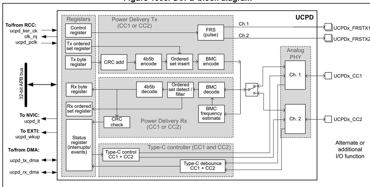
The following table lists external signals (alternate or additional I/O functions).
Table 751. UCPD signals on pins
| Pin name | Signal type | Description |
|---|---|---|
| UCPDx_FRSTX1 | Output | USB Type-C fast role swap (FRS) signaling, applicable to DRPs only. The signal (active high) drives an external NMOS transistor that pulls down the CC1 line. |
| UCPDx_FRSTX2 | Output | USB Type-C fast role swap (FRS) signaling, applicable to DRPs only. The signal (active high) drives an external NMOS transistor that pulls down the CC2 line. |
| UCPDx_CC1 | Input/output | USB Type-C configuration control line 1, to be routed to the USB Type-C connector CC1 terminal. |
| UCPDx_CC2 | Input/output | USB Type-C configuration control line 2, to be routed to the USB Type-C connector CC2 terminal. |
The following table lists key internal signals.
Table 752. UCPD internal signals
| Internal signal name | Signal type | Description |
|---|---|---|
| ucpd_pclk | Input | APB clock for registers |
| ucpd_ker_ck | Input | Kernel clock |
| ucpd_tx_dma | Input/Output | Rx DMA acknowledge / request |
| ucpd_rx_dma | Input/Output | Tx DMA acknowledge / request |
| ucpd_it | Output | Interrupt request (all interrupts OR-ed) connected to NVIC |
Table 752. UCPD internal signals (continued)
| Internal signal name | Signal type | Description |
|---|---|---|
| ucpd_wkup | Output | Wake-up request connected to EXTI |
| clk_rq | Output | Clock request connected to RCC |
75.4.2 UCPD reset and clocks
The peripheral has a single reset signal (APB bus reset).
The register section is clocked with the APB clock (ucpd_pclk).
The main functional part of the transmitter is clocked with ucpd_clk clock, pre-scaled from the ucpd_ker_ck clock according to the PSC_UCPDCLK[2:0] bitfield of the UCPD_CFGR1 register. The main functional part of the receiver is clocked with the ucpd_rx_clk recovered from the incoming bitstream.
The receiver is designed to work in the clock frequency range from 6 to 18 MHz. However, the optimum performance is ensured in the range from 6 to 12 MHz.
The following diagram shows the clocking and timing elements of the UCPD peripheral.
Figure 1009. Clock division and timing elements
![Figure 1009. Clock division and timing elements diagram. The diagram shows the internal clocking structure of the UCPD peripheral. A 'Clock division' block contains a 'Pre-scaler /1 to /16' which takes ucpd_ker_ck as input and is controlled by PSC_UCPDCLK[2:0]. Its output is ucpd_clk. This is followed by a 'Half bit' divider /1 to /64, controlled by HBITCLKDIV[5:0], which outputs hbit_clk (~ 600 kHz). The ucpd_clk is connected to a 'Registers' block and a 'BMC transmitter'. The hbit_clk is connected to a 'Counters' block containing 'tTransitionWindow' (2 to 32) controlled by TRANSWIN[4:0] and 'tInterFrameGap' (2 to 32) controlled by IFRGAP[4:0]. These counters are also connected to a 'BMC receiver'. The ucpd_pclk is connected to the 'Registers' block. The diagram is labeled MSv45536V3.](/RM0486-STM32N6x5-x7/df0701697cf51f8b89b1f028a31b8b18_img.jpg)
Refer to the USB PD specification in order to set appropriate delays. For tTransitionWindow and especially for tInterFrameGap , the clock frequency uncertainty must be taken into account so as to respect specified timings in all cases.
75.4.3 Physical layer protocol
The physical layer covers the signaling underlying the USB Power Delivery specification.
On the transmitter side its main function is to form packets according to the defined packet format including generally:
- • preamble
- • start of packet (SOP, ordered set)
- • payload header
- • payload data
- • cyclic redundancy check (CRC) information
- • end of packet (EOP)
Before going on the CC line, the data stream is BMC-encoded, respecting specified timing restrictions.
On the receive side, the principle task is to:
- • extract start of packet (SOP, ordered set) information
- • extract payload header
- • extract payload data
- • receive and check CRC
- • receive end of packet (EOP)
The receive is basically a reverse of the transmit process, thus starting with BMC data stream decoding.
Symbol encoding
Apart from the preamble all symbols are encoded with a 4b5b scheme according to the specification shown in the following table.
Table 753. 4b5b symbol encoding table
| Name | 4b | 5b | Symbol description |
|---|---|---|---|
| 0 | 0000 | 11110 | hex data 0 |
| 1 | 0001 | 01001 | hex data 1 |
| 2 | 0010 | 10100 | hex data 2 |
| 3 | 0011 | 10101 | hex data 3 |
| 4 | 0100 | 01010 | hex data 4 |
| 5 | 0101 | 01011 | hex data 5 |
| 6 | 0110 | 01110 | hex data 6 |
| 7 | 0111 | 01111 | hex data 7 |
| 8 | 1000 | 10010 | hex data 8 |
| 9 | 1001 | 10011 | hex data 9 |
| A | 1010 | 10110 | hex data A |
| B | 1011 | 10111 | hex data B |
| C | 1100 | 11010 | hex data C |
| D | 1101 | 11011 | hex data D |
| E | 1110 | 11100 | hex data E |
Table 753. 4b5b symbol encoding table (continued)
| Name | 4b | 5b | Symbol description |
|---|---|---|---|
| F | 1111 | 11101 | hex data F |
| Sync-1 | K-code | 11000 | Startsynch #1 |
| Sync-2 | K-code | 10001 | Startsynch #2 |
| RST-1 | K-code | 00111 | Hard Reset #1 |
| RST-2 | K-code | 11001 | Hard Reset #2 |
| EOP | K-code | 01101 | EOP |
| Reserved | Error | 00000 | Do Not Use |
| Reserved | Error | 00001 | Do Not Use |
| Reserved | Error | 00010 | Do Not Use |
| Reserved | Error | 00011 | Do Not Use |
| Reserved | Error | 00100 | Do Not Use |
| Reserved | Error | 00101 | Do Not Use |
| Sync-3 | K-code | 00110 | Startsynch #3 |
| Reserved | Error | 01000 | Do Not Use |
| Reserved | Error | 01100 | Do Not Use |
| Reserved | Error | 10000 | Do Not Use |
| Reserved | Error | 11111 | Do Not Use |
Ordered sets
An ordered set consists of four K-codes as shown in the following figure.
Figure 1010. K-code transmission
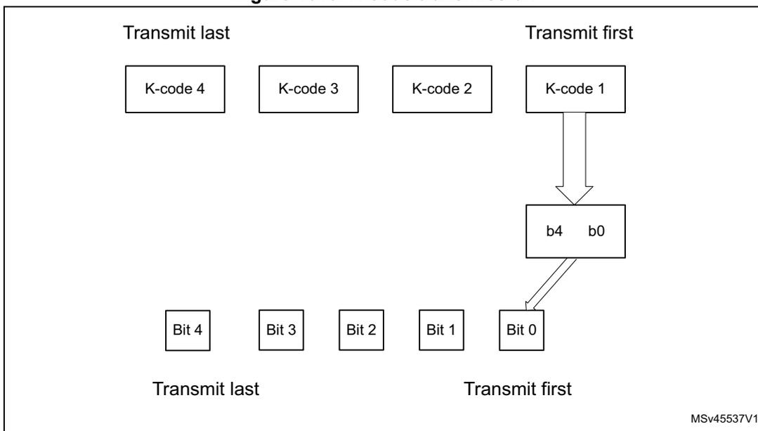
The diagram illustrates the transmission sequence for an ordered set. At the top, four boxes labeled 'K-code 4', 'K-code 3', 'K-code 2', and 'K-code 1' are arranged horizontally. Above 'K-code 4' is the label 'Transmit last', and above 'K-code 1' is 'Transmit first'. Below 'K-code 1', two boxes labeled 'b4' and 'b0' are shown, with 'b0' being transmitted first. Below these, five boxes labeled 'Bit 4', 'Bit 3', 'Bit 2', 'Bit 1', and 'Bit 0' are arranged horizontally. Below 'Bit 4' is 'Transmit last', and below 'Bit 0' is 'Transmit first'. Arrows indicate the flow from K-code 1 down to b0, and then down to Bit 0.
MSV45537V1
The following table lists the defined ordered sets, including all possible SOP* sequences. At the physical layer, the Hard Reset has higher priority than the other ordered sets so it can interrupt an ongoing Tx message.
Table 754. Ordered sets
| Ordered set name | K-code #1 | K-code #2 | K-code #3 | K-code #4 |
|---|---|---|---|---|
| SOP | Sync-1 | Sync-1 | Sync-1 | Sync-2 |
| SOP' | Sync-1 | Sync-1 | Sync-3 | Sync-3 |
| SOP'' | Sync-1 | Sync-3 | Sync-1 | Sync-3 |
| Hard Reset | RST-1 | RST-1 | RST-1 | RST-2 |
| Cable Reset | RST-1 | Sync-1 | RST-1 | Sync-3 |
| SOP'_Debug | Sync-1 | RST-2 | RST-2 | Sync-3 |
| SOP''_Debug | Sync-1 | RST-2 | Sync-3 | Sync-2 |
On reception, the physical layer must accept ordered sets with any combination of three correct K-codes out of four, as shown in the following table:
Table 755. Validation of ordered sets
| Status | 1st code | 2nd code | 3rd code | 4th code |
|---|---|---|---|---|
| Valid | Corrupt | K-code | K-code | K-code |
| Valid | K-code | Corrupt | K-code | K-code |
| Valid | K-code | K-code | Corrupt | K-code |
| Valid | K-code | K-code | K-code | Corrupt |
| Valid (perfect) | K-code | K-code | K-code | K-code |
| Not valid (example) | K-code | Corrupt | K-code | Corrupt |
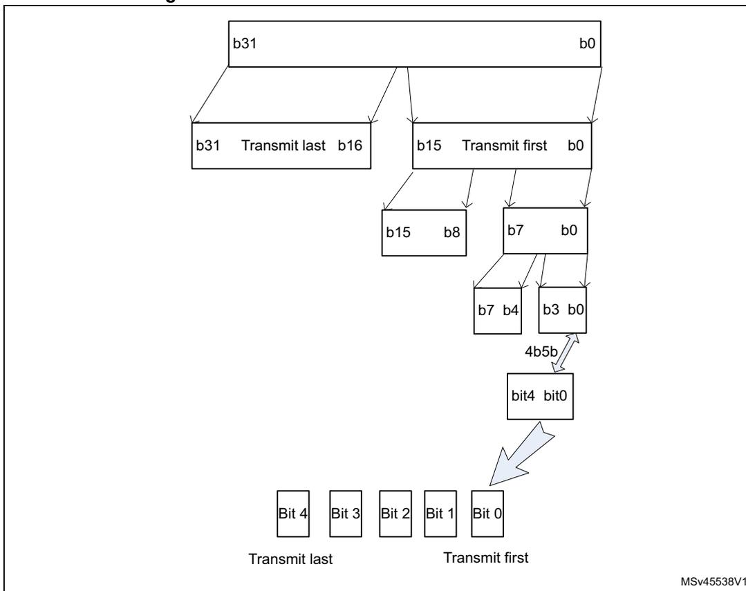
Bit ordering at transmission
Allowed transmission data units / data sizes are in the following table.
Table 756. Data size
| Data unit | Non-encoded | Encoded |
|---|---|---|
| Byte | 8-bits | 10-bits |
| Word | 16-bits | 20-bits |
| DWord | 32-bits | 40-bits |
The bit transmission order is shown in the following figure.
Figure 1011. Transmit order for various sizes of data
Packet format
Messages other than Hard Reset and Cable Reset
The packet format is shown in the following figure, with information on 4b5b encode and data source.
Figure 1012. Packet format
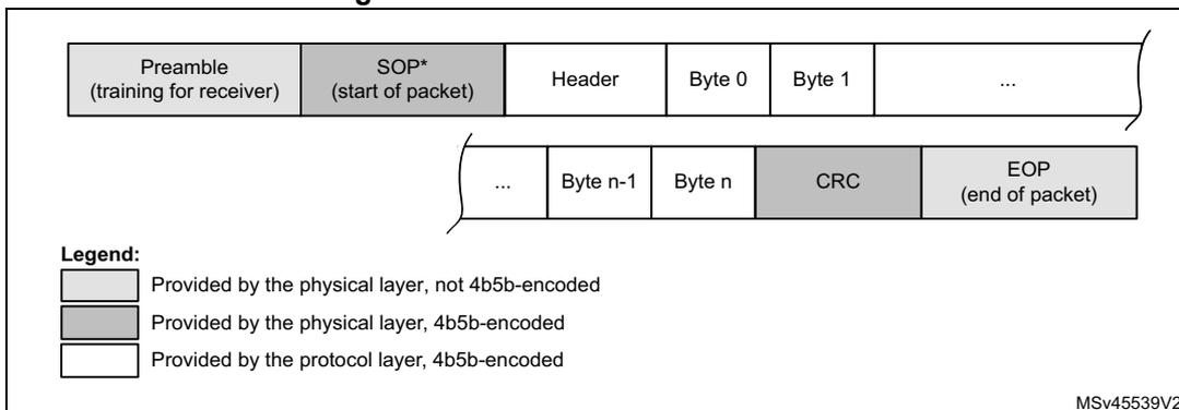
| Preamble (training for receiver) | SOP* (start of packet) | Header | Byte 0 | Byte 1 | ... |
| ... | Byte n-1 | Byte n | CRC | EOP (end of packet) | |
Legend:
- Provided by the physical layer, not 4b5b-encoded
- Provided by the physical layer, 4b5b-encoded
- Provided by the protocol layer, 4b5b-encoded
Hard Reset
The physical layer handles the Hard Reset signaling differently than the other types of message as it has higher priority to be able to interrupt an ongoing transfer.
The physical layer specification implies the following sequence in the case of an ongoing Tx message:
- 1. Terminate the message by sending an EOP K-code and discard the rest of the message.
- 2. Wait for tInterFrameGap time.
- 3. If the CC line is not idle, wait until it goes idle.
- 4. Send the preamble followed by the four K-codes of Hard Reset signaling.
- 5. Disable the CC channel (stop sending and receiving), reset the physical layer and inform the protocol layer that the physical layer is reset.
- 6. Re-enable the channel when requested by the protocol layer.
Figure 1013. Line format of Hard Reset

| Preamble (training for receiver) | RST-1 | RST-1 | RST-1 | RST-2 |
| Hard Reset ordered set | ||||
Legend:
- Provided by the physical layer, not 4b5b-encoded
- Provided by the physical layer, 4b5b-encoded
MSV45540V2
Cable Reset
Cable Reset shown in the following figure is similar in format to Hard Reset, but unlike Hard Reset it does not require a specific high-priority treatment.
Figure 1014. Line format of Cable Reset
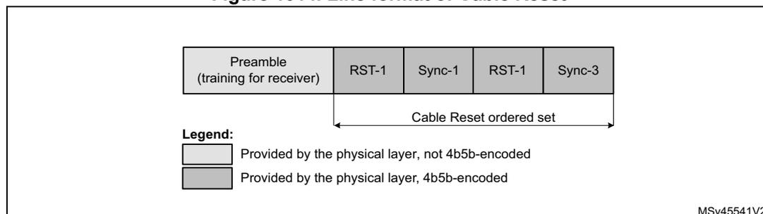
| Preamble (training for receiver) | RST-1 | Sync-1 | RST-1 | Sync-3 |
| Cable Reset ordered set | ||||
Legend:
- Provided by the physical layer, not 4b5b-encoded
- Provided by the physical layer, 4b5b-encoded
MSV45541V2
Collision avoidance
The physical layer respects the tInterFrameGap delay between end of last-transmitted bit of a Tx message, and the first bit of a following message.
It also checks the idle state of the CC line before starting transmission. The CC line is considered idle if it shows less than three ( nTransitionCount ) transitions within
tTransitionWindow (12 to 20 µs). The Power Delivery specification revision 3.1 also requires to manage the R p value (source) and monitor Type-C voltage level for these R p modifications (at the sink).
Physical layer signaling schemes
The bits are signaled with bi-phase mark coding (BMC).
BIST
Depending on the BIST action required by the protocol layer, either of the following can be run:
- • a Tx BIST pattern test, achieved by writing TXMODE and TXSEND
- • an Rx BIST pattern test, achieved by writing RXMODE to the correct value for RXBIST.
The two possible patterns supported in UCPD (corresponding to “BMC” mode) are:
- • BIST Test Data (192 bit pattern), applies to Tx and Rx. In the case of Rx, the message is received (but discarded rather than passing to the protocol layer, which must nevertheless still generate a GoodCRC Tx message in acknowledgment).
- • BIST Carrier Mode 2 (single pattern, infinite length message), applies to Tx only. As opposed to Tx, the receiver in this mode simply ignores the CC line during this state.
BIST test data pattern
The test data pattern is not viewed as a special case in UCPD.
The BIST test data packet frame format is shown in the following figure.
Figure 1015. BIST test data frame
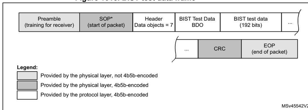
| Preamble (training for receiver) | SOP* (start of packet) | Header Data objects = 7 | BIST Test Data BDO | BIST test data (192 bits) | ... |
| ... | CRC | EOP (end of packet) | |||
Legend:
- Provided by the physical layer, not 4b5b-encoded
- Provided by the physical layer, 4b5b-encoded
- Provided by the protocol layer, 4b5b-encoded
MSV45542V2
This is a fixed length test data pattern. In reality the only aspect that marks its difference from the general packet format already shown in Figure 1012: Packet format is the contents of the Header. As UCPD receives the Tx Header contents via programming (it is simply viewed as part of the payload), it is only this programming (and not the block’s behavior) that differentiates the general packet from the BIST Test Data packet.
BIST Carrier Mode 2
When required, this BIST test mode sends an alternating pattern of 1010 that is continually repeated. As this mode is intended for signal analysis it is stable condition with (in V1.0 of the USB PD specification) no defined length. Starting from V1.1 of the USB PD specification, the protocol layer defines a counter that indicates when to exit this mode.
The way to quit the infinite 1010 sequence (according to requirements of the USB PD specification) is to disable the UCPD peripheral via the UCPDEN bit.
Figure 1016. BIST Carrier Mode 2 frame
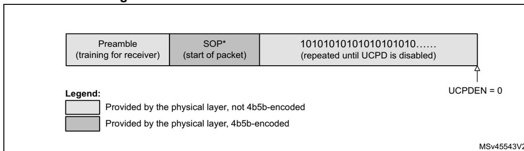
The diagram shows a frame structure for BIST Carrier Mode 2. It consists of three main parts: a 'Preamble (training for receiver)' (white box), an 'SOP* (start of packet)' (white box), and a '10101010101010101010..... (repeated until UCPD is disabled)' (grey box). An arrow points to the end of the repeated sequence with the text 'UCPDEN = 0'. A legend below the frame shows two boxes: a white box labeled 'Provided by the physical layer, not 4b5b-encoded' and a grey box labeled 'Provided by the physical layer, 4b5b-encoded'. The diagram is labeled MSv45543V2 in the bottom right corner.
75.4.4 UCPD BMC transmitter
The BMC transmitter comprises 4b5b encoding, CRC generation, and BMC encode, as shown in the following figure. Its output goes to the analog PHY through a channel switch.
Figure 1017. UCPD BMC transmitter architecture
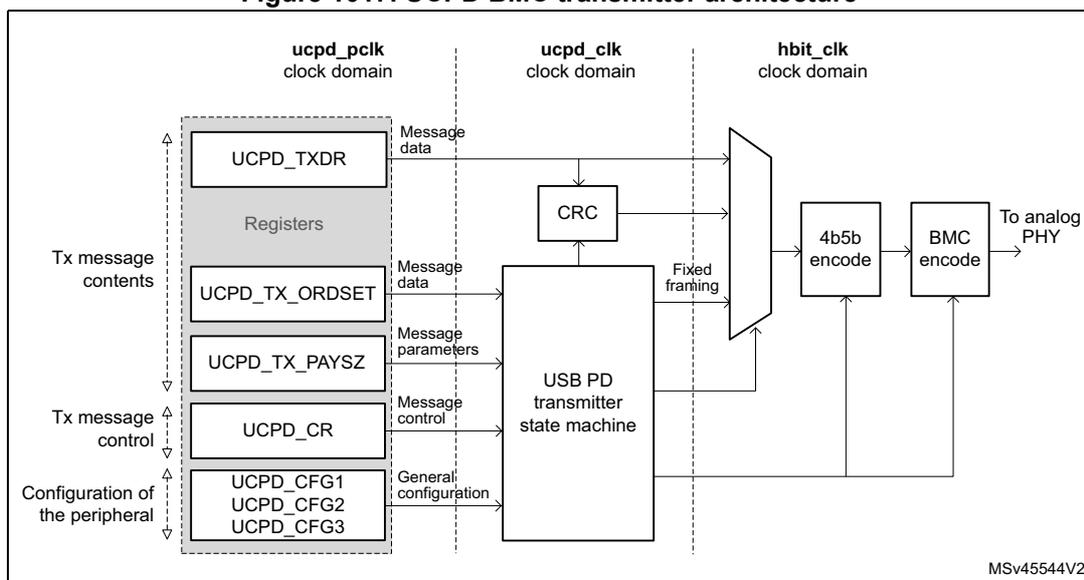
The diagram illustrates the UCPD BMC transmitter architecture, divided into three clock domains: 'ucpd_pclk' (left), 'ucpd_clk' (middle), and 'hbit_clk' (right). In the 'ucpd_pclk' domain, there are several registers: 'UCPD_TXDR' (Message data), 'UCPD_TX_ORDSET' (Message data), 'UCPD_TX_PAYSZ' (Message parameters), 'UCPD_CR' (Message control), and 'UCPD_CFG1', 'UCPD_CFG2', 'UCPD_CFG3' (General configuration). These registers are grouped into 'Tx message contents', 'Tx message control', and 'Configuration of the peripheral'. The 'Message data' from 'UCPD_TXDR' and 'UCPD_TX_ORDSET' is sent to a 'CRC' block and a 'USB PD transmitter state machine'. The 'Message parameters' from 'UCPD_TX_PAYSZ' and 'Message control' from 'UCPD_CR' are sent to the 'USB PD transmitter state machine'. The 'General configuration' from 'UCPD_CFG1', 'UCPD_CFG2', and 'UCPD_CFG3' is also sent to the 'USB PD transmitter state machine'. The 'USB PD transmitter state machine' outputs 'Fixed framing' to a multiplexer. The 'CRC' block also outputs to this multiplexer. The multiplexer selects between the 'Fixed framing' and the 'Message data' from 'UCPD_TXDR'. The output of the multiplexer goes to a '4b5b encode' block, which then goes to a 'BMC encode' block. The 'BMC encode' block outputs 'To analog PHY'. The 'hbit_clk' domain provides a clock to the '4b5b encode' and 'BMC encode' blocks. The diagram is labeled MSv45544V2 in the bottom right corner.
BMC encoder
The bi-phase mark coding method is defined in the IEC 60958-1 Digital Audio Interface Part:1 General Edition 3.0 2008-09 www.iec.ch specification.
The half-bit clock hbit_clk is derived from ucpd_clk through a simple divider controlled by the HBITCLKDIV[5:0] bitfield of the UCPD_CFGR1 register. This ensures the same duration of high and low half-bit periods (if neglecting a small difference due to different rising and falling edge duration and due to jitter), and the same bit duration (if neglecting jitter).
Transmitter timing and collision avoidance
Hardware support of collision avoidance is made as a function of the half bit time for the transmitter. Two counters are implemented:
- – tInterFrameGap : via IFRGAP (pre-defined value, can be altered)
- – tTransitionWindow : via TRANSWIN (pre-defined value, can be altered)
These two counters once set correctly generates the interframe gap.
Hard Reset in transmitter
In order to facilitate generation of a Hard Reset, a special code of TXMODE field is used. No other fields need to be written.
On writing the correct code, the hardware forces Hard Reset Tx under the correct (optimal) timings with respect to an ongoing Tx message, which (if still in progress) is cleanly terminated by truncating the current sequence and directly appending an EOP K-code sequence. No specific interrupt is generated relating to this truncation event.
Transmitter behavior in the case of errors
The under-run condition (TXUND interrupt) may happen by accident and in this case, the UCPD is starved of (the correct) Tx payload and is not able to complete the Tx message correctly. This is a serious error (for this to happen the software fails to respond in time). As a result the hardware ensures the CRC is incorrect at the end of the message, thus guaranteeing the message to be discarded at the receiver.
75.4.5 UCPD BMC receiver
The UCPD BMC receiver performs:
- • Clock recovery
- • Preamble detection / timing derivation
- • BMC decoding
- • 4b5b decoding
- • K-code ordered set recognition
- • CRC checking
- • SOP detection
- • EOP detection
The receiver is activated as soon as the UCPD peripheral is enabled (via UCPDEN), but it waits for an idle CC line state before attempting to receive a message.
The following figure shows the UCPD BMC receiver high-level architecture.
Figure 1018. UCPD BMC receiver architecture
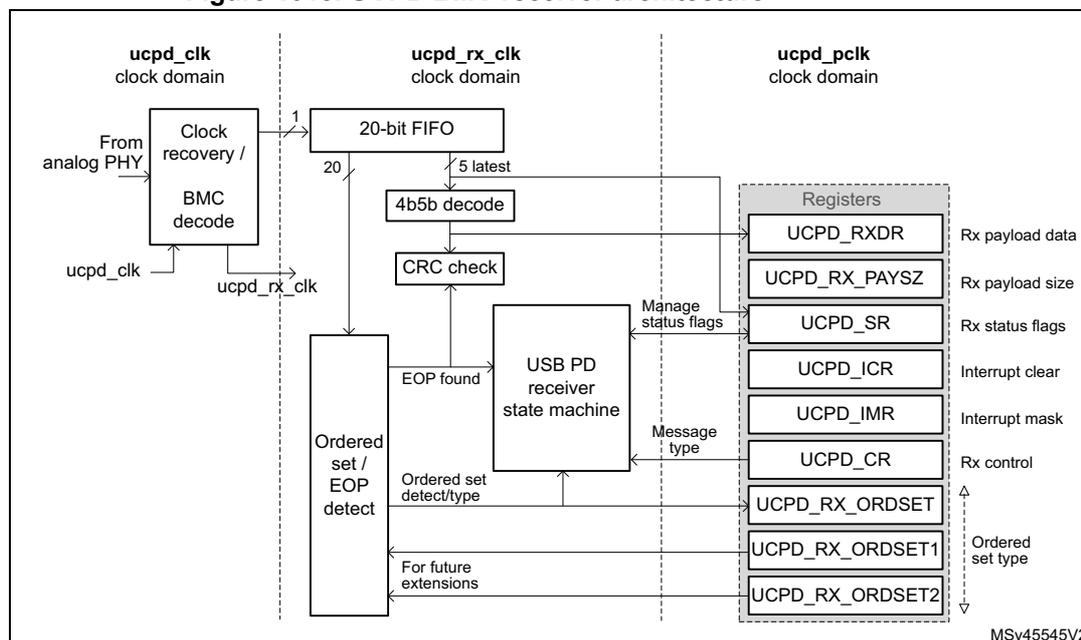
CRC checker
The received bits are fed into a CRC checker which evolves a 32-bit state during the received the payload bitstream. At the end the 32 bits of the CRC also fed into the logic
The EOP detection (5 bits) halts the process and a check is performed for the fixed residual state which confirms correct reception of the payload (in fact the residual is 0xC704DD78).
At this point the UCPD raises interrupt RXMSGEND. If the CRC was not correct then RXERR is set true and the receive data must be discarded.
Under normal operation, this interrupt would previously have been acknowledged and thus cleared. If this is not the case, a different interrupt RXOVR is generated in place of RXMSGEND.
Ordered set detection
This function detects the different ordered sets each consisting of four 5-bit K-codes.
Once we are in the preamble we opens a sliding window detection of the ordered set (4 words of 5 bits).
The ordered sets detected include all SOP* codes (SOP, SOP', and SOP''), but also Hard Reset, Cable Reset, SOP'_Debug, SOP''_Debug, and two extensions defined by registers UCPD_RX_ORDEXT1 and UCPD_RX_ORDEXT2.
EOP detection and Hard Reset exception handling
EOP is a fixed 5-bit K-code marking the end of a message.
The way in which a transmitter is required to send a Hard Reset (if a previous message transmit is still in progress) is that this previous message is truncated early with an EOP.
If Hard Reset were ignored, then the EOP detection can be done only at the expected time. However, due to the Hard Reset issue, the EOP detector must be active while an Rx
message is arriving. When an “early EOP” is detected, the truncated Rx message is immediately discarded.
Truncated or corrupted message exception
Once the ordered set has been detected, depending on the message, there may be data bytes to be received which is completed with a CRC and EOP. If at any point during these phases an error condition happens:
- • the line becomes static for a time significantly longer than one “UI” period (the exact threshold for this condition is not critical but the exception must occur before three UIs), or
- • the message goes to the end but it is not recognized (for example EOP is corrupted).
In both cases, the receiver quits the current message, raising RXMSGEND and RXERR flags.
Short preamble or incomplete ordered set exception
In the exceptional case of the receiver seeing less than half of the expected preamble, the frequency estimation allowing correct BMC-decode becomes impossible. Even if the full preamble is seen, allowing frequency estimation, but the ordered set is not fully received before the line becomes static, the receiver state machine does not start.
In both of these cases, the clock-recovery/BMC decoder re-starts, checking initially for an IDLE condition, followed by a preamble, and then estimating frequency.
75.4.6 UCPD Type-C pull-ups (Rp) and pull-downs (Rd)
UCPD offers simple control of these resistors via ANAMODE and ANASUBMODE[1:0]. In case only one of the CC lines is to be used, it is possible to optimize power consumption by disabling control on the other line, through the CCENABLE[1:0] bitfield.
When the MCU is unpowered, it does not signal “dead battery” (which must therefore be handled with external components).
After power arrives and the MCU boots, the desired behavior (for example source) must be programmed into ANAMODE and ANASUBMODE[1:0].
Use of Standby low-power mode is possible for sinks in the unattached state.
75.4.7 UCPD Type-C voltage monitoring and de-bouncing
For correct operation of the Type-C state machine and for detecting the cable orientation, the CC1/2 lines must be monitored for voltage level, while ignoring fast events such as peaks.
Thresholds between voltage levels on the CC1/2 lines are determined through PHY threshold detector settings.
The TYPEC_VSTATE_CC1/2[1:0] bitfields reflect the CC1/2 line levels processed with a hardware de-bouncing filter that suppresses high-speed line events such as peaks. The PHYCCSEL bit selects the line, CC1 or CC2, to be used for Power Delivery signaling.
For minimizing the power consumption, it is recommended to use the polling method, with the Type-C detectors only turned on for the instant of polling, rather than keeping the Type-C detectors permanently on and wake the device up from Stop mode upon CC1/2 line events.
75.4.8 UCPD fast role swap (FRS)
FRS signaling
The FRS condition (a pulse of a specific length), is generated upon setting the FRSTX bit.
For the duration of FRS condition, the currently active I/O configured as UCPD_FRSTX1 (or 2) (alternate function) controls, with high level, the gate of an external NMOS transistor that pulls the active CC line down.
75.4.9 UCPD DMA Interface
DMA is implemented in the UCPD and when it is enabled the byte-level interrupts to handle UCPD1_TXDR and UCPD1_RXDR registers (Tx and Rx data register, each one byte) are no longer needed.
By enabling bits TXDMAEN and/or RXDMAEN, DMA can be activated independently for Tx and/or Rx functionality.
75.4.10 Wake-up from Stop mode
For power consumption optimization, it is useful to use Stop mode and wait for events on CC lines to wake the MCU up.
In order for this to work, it must be first enabled by writing a 1 to WUPEN.
The events causing the wake-up can be:
- • Events on the BMC receiver (RXORDDDET, RXHRSTDDET), hardware enable PHYRXEN
- • Events on the Type-C detectors (TYPECEVT1, TYPECEVT2), hardware enables CC1TCDIS, CC2TCDIS
75.5 UCPD programming sequences
The normal sequence of use of the UCPD unit is:
- 1. Configure UCPD.
- 2. Enable UCPD.
- 3. Concurrently:
- – On demand from protocol layer, send Tx message
- – Intercept (poll or wait for interrupt) relevant Rx messages and recover detail to hand off to protocol layer
Repeat the last point infinitely.
75.5.1 Initialization phase
Use the following sequence for a clean startup:
- 1. Prepare all initial clock divider values, by writing the UCPD_CFG register.
- 2. Enable the unit, by setting the UCPDEN bit.
75.5.2 Type-C state machine handling
For the general application cases of source, sink, or dual-role port (the last alternating the source and the sink), the software must implement a corresponding USB Type-C state machine. The basic coding is in the following table.
Table 757. Coding for ANAMODE, ANASUBMODE and link with TYPEC_VSTATE_CCx
| ANAMODE | ANASUBMODE[1:0] | Notes | TYPEC_VSTATE_CCx[1:0] | |||
|---|---|---|---|---|---|---|
| 00 | 01 | 10 | 11 | |||
| 0: Source | 00: Disabled | Disabled | N/A | |||
| 01: Default USB Rp | - | vRa[Def] | vRd[Def] | vOPEN[Def] | N/A | |
| 10: 1.5A Rp | - | vRa[1.5] | vRd[1.5] | vOPEN[1.5] | ||
| 11: 3.0A Rp | - | vRa[3.0] | vRd[3.0] | vOPEN[3.0] | ||
| 1: Sink | xx | - | vRa | vRd-USB | vRd-1.5 | vRd-3.0 |
The CCENABLE[1:0] bitfield can disable pull-up/pull-downs on one of the CC lines.
Note: The Type-C state machine depends not only on CC line levels, but also on VBUS presence detection (sink mode) and, when in source mode, determines VCONN generation and VBUS state (ON/OFF/+voltage level); discharge). UCPD does not directly control VBUS generation circuitry nor VCONN load switch (enabling VCONN supply generator to be connected to the CC line), but the application needs these inputs and controls, to function correctly.
General programming sequence (with UCPD configured then enabled)
- 1. Set ANAMODE and ANASUBMODE[1:0] based on the current position in USB Type-C state machine (and also the current advertisement in the case of a source). This turns on the appropriate pull-ups/pull-downs on the CC lines, and defines the voltage levels that the TYPEC_VSTATE fields represent. Note that before programming, the PHY is effectively off.
- 2. Read TYPEC_VSTATE_CC1/2 to determine the initial Type-C state (for example whether the local source is connected to a remote sink).
- 3. In the case of no connection, wait for a connection event.
- 4. Assuming a connection is detected and assuming a local Power Delivery functionality is implemented, start sending/receiving Power Delivery messages.
- 5. When a new interrupt/event occurs on PHYEVT1/2 indicating a change in stable voltage, re-evaluate the implications and give this input to the Type-C state machine.
Case of a source that needs to change between one of the three possible Rp values (Default-USB / 1.5A / 3.0A) and the sink connected to it:
- • [Source] Simply reprogram ANASUBMODE[1:0]
- • [Sink behavior from that time] PHYEVT1/2 occurs and the TYPEC_VSTATE1/2 changes accordingly
Programming for a dual-role port (DRP) toggling from source to sink:
- • Simply re-program ANAMODE and ANASUBMODE[1:0] to start the new behavior
Detailed programming sequence (example):
Table 758. Type-C sequence (source: 3A); cable/sink connected (Rd on CC1; Ra on CC2)
| Type-C state | ANAMODE; ANASUBMODE[1:0] | CCENABLE | PHYCCSEL | RDCH | CC[x] VCONNEN (1) | Event => go to next line | Comments |
|---|---|---|---|---|---|---|---|
| Unattached. SRC | 0 (don't care) | PHYEVT 1: [VRd- 3A0] | Wait for sink attach detect ; seen on CC1 [EVT1] | ||||
| Attachwait. SRC | 0:Source; 11:Rp3A0 | 11:both enabled | 00: [neither] | PHYEVT 2: [VRa] | Attachwait started (100- 200 ms) ; now also see the Ra => requesting VCONN | ||
| Attached. SRC [VCONN => CC2] | 0:Source; 11:Rp3A0 [SinkTxOK] | 01: CC2 disable (possible and recommended due to external VCONN switch) | 0 [Rd on CC1] | 0: [Normal] | 10: [CC2 active] | Timer (100 ms) and no PHYEVT x | Local CC2 disconnected from PHY (VCONN switch connects VCONN source to CC2 externally; Continue to monitor PHYEVT1 |
| 0:Source; 10:Rp1A5 [SinkTxNG] | SW timers (SinkTxNG) | Source wants to initiate message sequence (SinkTxNG condition set first) | |||||
| 0:Source; 11:Rp3A0 [SinkTxOK] | PHYEVT 1: [VOpen- 3A0] | Source finished message sequence (SinkTxOK condition afterwards) | |||||
| Unattached wait. SRC | 1: [discharge] | > 0.8V detection | Discharge VCONN [CC2] actively [Rdch]; to < 0.8V | ||||
| Unattached. SRC | 0:Source; 11:Rp3A0 | 11:both enabled | 0 (do not care) | 0: [Normal] | 00: [neither] | [Details as first line of table] |
1. Two GPIOs to enable VCONN through external load switch components
75.5.3 USB PD transmit
On reception of a message from the protocol layer (that is, to be sent), prepare Tx message contents by writing the UCPD_TX_ORDSET and UCPD_TX_PAYSZ registers.
The message transmission is triggered by setting the TXSEND bit, with an appropriate value of the TXMODE bitfield.
When the data byte is transmitted, the TXIS flag is raised to request a new data write to the UCPD_TXDR register.
This re-iterates until the entire payload of data is transmitted.
Upon sending the CRC packet, the TXMSGSENT flag is set to indicate the completion of the message transmission.
Hard Reset transmission
As soon as it is known that a Hard Reset needs to be transmitted, setting the TXHRST bit of the UCPD_CR register forces the internal state machine to generate the correct sequence. The value of UCPD_TX_ORDSET does not require update in this precise case (the correct code for Hard Reset is sent by UCPD).
The USB Power Delivery specification requires that in the case of an ongoing message transmission, the Hard Reset takes precedence. In this case, for example, UCPD truncates the payload of the current message, appending EOP to the end. No notification is available via the registers (for example through the TXMSGSEND flag). This is justified by the fact that the Hard Reset takes precedence over any previous activity (for which it is therefore no longer important to know if it is completed).
Use of DMA for transmission
DMA (Direct Memory Access) can be enabled for transmission by setting the TXDMAEN bit in the UCPD_CR register.
For each message:
- • Prepare the whole message in memory (starting with two header bytes)
- • Program the DMA operation with a length corresponding to the two header bytes plus a number of data bytes corresponding to the number of data words multiplied by four
- • Write TXSEND to initiate the message transfer
- • If TXMSGDISC then go back to previous line (TXSEND)
- • Wait for DMA transfer complete interrupt (that is, when last Tx byte written to UCPD)
- • Double-check subsequent TXMSGSENT interrupt appears
75.5.4 USB PD receive
Notification of start of the receive message sequence is triggered by an interrupt on UCPD_SR (bit RXORDDDET).
The information is recovered by reading:
- • UCPD_RX_SOP (on interrupt RXORDDDET)
- • UCPD_RXDR (on interrupt RXNE, repeats for each byte)
- • UCPD_RXPAYSZ (on interrupt RXMSGEND)
The data previously read from UCPD_RXDR above must be discarded at this point if the RXERR flag is set.
If the CRC is valid, the received data is transferred to the protocol layer.
For debug purposes, it may be desirable to track statistics of the number of incorrect K-codes received (this is done only when 3/4 K-codes were valid as defined in the specification). This is facilitated through:
- • RXSOP3OF4 bit indicating the presence of at least one invalid K-code
- • RXSOPKINVALID bitfield identifying the order of invalid K-code in the ordered set
Use of DMA for reception
DMA (Direct Memory Access) can be enabled for reception by setting the RXDMAEN bit in the UCPD_CR register.
Whenever a Rx message is expected:
- • Program a DMA receive operation (and spare buffer) a little longer than the maximum possible message (length depends on extended message support).
- • After receiving RXORDDDET, DMA operation starts working in the background.
- • On reception of RXMSGEND interrupt, read RXPAYSZ.
- • Double-check RXPAYSZ vs. the number of DMA Rx bytes (must correspond but DMA read of RXDR is slightly after RXDR gets last byte).
- • Process the DMA Rx buffer.
- • Prepare next Rx DMA buffer as soon as possible in order to be ready.
75.6 UCPD low-power modes
A summary of low-power modes is shown below in Table 759: Effect of low power modes on the UCPD .
Table 759. Effect of low power modes on the UCPD
| Mode | Description |
|---|---|
| Sleep | No effect |
| Stop | Detection of events (Type-C, BMC Rx) remains operational and can wake up the MCU. |
| Standby | UCPD is not operating, and cannot wake up the MCU. Pull-downs remain active if configured. |
| Unpowered | Not functional. |
The UCPD is able to wake up the MCU from Stop mode when it recognizes a relevant event, either:
- • Type-C event relating to a change in the voltage range seen on either of the CC lines, visible in TYPEC_VSTATE_CCx
- • Power delivery receive message with an ordered set matching those filtered according to RXORDSETEN[8:0], visible by reading RXORDSET
Wake-up from Stop mode is enabled by setting the WUPEN bit in the UCPD_CFG2 register.
At UCPD level three types of event requiring kernel clock activity may occur during Stop mode:
- • Activity on the analog PHY voltage threshold detectors which can later be confirmed to be a stable change between voltage ranges defined in the Type-C specification
- • Activity on Power Delivery BMC receiver (coming from the selected CC line) which can potentially generate an Rx message event (that is, RXORDSET) later
In order to function correctly with the RCC, the clock request signal is activated (conditional on WUPEN) when there is asynchronous activity on:
- • Type-C voltage threshold detectors (coming from either CC line)
- • Power Delivery receiver signal (from the selected CC line)
75.7 UCPD interrupts
The table below lists the UCPD event flags, with the associated flag clear bits and interrupt enable bits.
Table 760. UCPD interrupt requests
| Interrupt event | Event flag | Event flag/Interrupt clearing method | Interrupt enable control bit |
|---|---|---|---|
| Type C voltage level change on CC2 | TYPECEVT2 | Set TYPECEVT2CF | TYPECEVT2IE |
| Type C voltage level change on CC1 | TYPECEVT1 | Set TYPECEVT1CF | TYPECEVT1IE |
| Rx message received | RXMSGEND | Set RXMSGENDCF | RXMSGENDIE |
| Rx data overflow | RXOVR | Set RXOVRCF | RXOVR |
| Rx Hard Reset detected | RXHRSTDET | Set RXHRSTDETCF | RXHRSTDETIE |
| Rx ordered set (4 K-codes) detected | RXORDDDET | Set RXORDDDETCF | RXORDDDETIE |
| Receive data register not empty | RXNE | Read data in UCPD_RXDR | RXNEIE |
| Tx data underrun | TXUND | Set TXUNDCF | TXUNDIE |
| Hard Reset sent | HRSTSENT | Set HRSTSENTCF | HRSTSENTIE |
| Hard Reset discarded | HRSTDISC | Set HRSTDISCCF | HRSTDISCIE |
| Transmit message aborted | TXMSGABT | Set TXMSGABTCF | TXMSGABTIE |
| Transmit message sent | TXMSGSENT | Set TXMSGSENTCF | TXMSGSENTIE |
| Transmit message discarded | TXMSGDISC | Set TXMSGDISCCF | TXMSGDISCIE |
| Transmit data required | TXIS | Write data to the UCPD_TXDR register | TXISIE |
When an interrupt from the UCPD is received, then the software has to check what is the source of the interrupt by reading the UCPD_SR register.
Depending on which bit is at 1, the ISR must handle that condition and clear the bit by a write to the appropriate bit of the UCPD_ICR register.
75.8 UCPD registers
75.8.1 UCPD configuration register 1 (UCPD_CFGR1)
Address offset: 0x000
Reset value: 0x0000 0000
General configuration of the peripheral. Writing to this register is only effective when UCPD is disabled (UCPDEN = 0).
| 31 | 30 | 29 | 28 | 27 | 26 | 25 | 24 | 23 | 22 | 21 | 20 | 19 | 18 | 17 | 16 |
|---|---|---|---|---|---|---|---|---|---|---|---|---|---|---|---|
| UCPDEN | RXDMAEN | TXDMAEN | RXORDSETEN[8:0] | PSC_UCPDCLK[2:0] | Res. | ||||||||||
| rw | rw | rw | rw | rw | rw | rw | rw | rw | rw | rw | rw | rw | rw | rw | |
| 15 | 14 | 13 | 12 | 11 | 10 | 9 | 8 | 7 | 6 | 5 | 4 | 3 | 2 | 1 | 0 |
| TRANSWIN[4:0] | IFRGAP[4:0] | HBITCLKDIV[5:0] | |||||||||||||
| rw | rw | rw | rw | rw | rw | rw | rw | rw | rw | rw | rw | rw | rw | rw | rw |
Bit 31 UCPDEN: UCPD peripheral enable
General enable of the UCPD peripheral.
0: Disable
1: Enable
Upon disabling, the peripheral instantly quits any ongoing activity and all control bits and bitfields default to their reset values. They must be set to their desired values each time the peripheral transits from disabled to enabled state.
Bit 30 RXDMAEN: Reception DMA mode enable
When set, the bit enables DMA mode for reception.
0: Disable
1: Enable
Bit 29 TXDMAEN: Transmission DMA mode enable
When set, the bit enables DMA mode for transmission.
0: Disable
1: Enable
Bits 28:20 RXORDSETEN[8:0]: Receiver ordered set enable
The bitfield determines the types of ordered sets that the receiver must detect. When set/cleared, each bit enables/disables a specific function:
0bXXXXXXXX1: SOP detect enabled
0bXXXXXXXX1X: SOP' detect enabled
0bXXXXXXX1XX: SOP'' detect enabled
0bXXXXX1XXX: Hard Reset detect enabled
0bXXXX1XXXX: Cable Detect reset enabled
0bXXX1XXXXX: SOP'_Debug enabled
0bXX1XXXXXX: SOP''_Debug enabled
0bX1XXXXXXX: SOP extension#1 enabled
0b1XXXXXX: SOP extension#2 enabled
Bits 19:17 PSC_UCPDCLK[2:0] : Pre-scaler division ratio for generating ucpd_clk
The bitfield determines the division ratio of a kernel clock pre-scaler producing UCPD peripheral clock (ucpd_clk).
0x0: 1 (bypass)
0x1: 2
0x2: 4
0x3: 8
0x4: 16
It is recommended to use the pre-scaler so as to set the ucpd_clk frequency in the range from 6 to 9 MHz.
Bit 16 Reserved, must be kept at reset value.
Bits 15:11 TRANSWIN[4:0] : Transition window duration
The bitfield determines the division ratio (the bitfield value minus one) of a hbit_clk divider producing tTransitionWindow interval.
0x00: Not supported
0x01: 2
0x09: 10 (recommended)
0x1F: 32
Set a value that produces an interval of 12 to 20 us, taking into account the ucpd_clk frequency and the HBITCLKDIV[5:0] bitfield setting.
Bits 10:6 IFRGAP[4:0] : Division ratio for producing inter-frame gap timer clock
The bitfield determines the division ratio (the bitfield value minus one) of a ucpd_clk divider producing inter-frame gap timer clock ( tInterFrameGap ).
0x00: Not supported
0x01: 2
0x0D: 14
0x0E: 15
0x0F: 16
0x1F: 32
The division ratio 15 is to apply for Tx clock at the USB PD 2.0 specification nominal value.
The division ratios below 15 are to apply for Tx clock below nominal, and the division ratios above 15 for Tx clock above nominal.
Bits 5:0 HBITCLKDIV[5:0] : Division ratio for producing half-bit clock
The bitfield determines the division ratio (the bitfield value plus one) of a ucpd_clk divider producing half-bit clock (hbit_clk).
0x00: 1 (bypass)
0x1A: 27
0x3F: 64
75.8.2 UCPD configuration register 2 (UCPD_CFGR2)
Address offset: 0x004
Reset value: 0x0000 0000
Configuration of the UCPD Rx signal filtering. Writing to this register is only effective when UCPD is disabled (UCPDEN = 0).
| 31 | 30 | 29 | 28 | 27 | 26 | 25 | 24 | 23 | 22 | 21 | 20 | 19 | 18 | 17 | 16 |
|---|---|---|---|---|---|---|---|---|---|---|---|---|---|---|---|
| Res. | Res. | Res. | Res. | Res. | Res. | Res. | Res. | Res. | Res. | Res. | Res. | Res. | Res. | Res. | Res. |
| 15 | 14 | 13 | 12 | 11 | 10 | 9 | 8 | 7 | 6 | 5 | 4 | 3 | 2 | 1 | 0 |
| Res. | Res. | Res. | Res. | Res. | Res. | Res. | Res. | Res. | Res. | Res. | Res. | WUPEN | FORCECLK | RXFILT2N3 | RXFILTDIS |
| rw | rw | rw | rw |
Bits 31:4 Reserved, must be kept at reset value.
Bit 3 WUPEN : Wake-up from Stop mode enable
Setting the bit enables the UCPD_ASYNC_INT signal.
0: Disable
1: Enable
Bit 2 FORCECLK : Force ClkReq clock request
0: Do not force clock request
1: Force clock request
Bit 1 RXFILT2N3 : BMC decoder Rx pre-filter sampling method
Number of consistent consecutive samples before confirming a new value.
0: 3 samples
1: 2 samples
Bit 0 RXFILTDIS : BMC decoder Rx pre-filter enable
0: Enable
1: Disable
The sampling clock is that of the receiver (that is, after pre-scaler).
75.8.3 UCPD control register (UCPD_CR)
Address offset: 0x00C
Reset value: 0x0000 0000
Writing to this register is only effective when the peripheral is enabled (UCPDEN = 1).
| 31 | 30 | 29 | 28 | 27 | 26 | 25 | 24 | 23 | 22 | 21 | 20 | 19 | 18 | 17 | 16 |
|---|---|---|---|---|---|---|---|---|---|---|---|---|---|---|---|
| Res. | Res. | Res. | Res. | Res. | Res. | Res. | Res. | Res. | Res. | CC2TC DIS | CC1TC DIS | Res. | RDCH | FRSTX | Res. |
| rw | rw | rw | rs | ||||||||||||
| 15 | 14 | 13 | 12 | 11 | 10 | 9 | 8 | 7 | 6 | 5 | 4 | 3 | 2 | 1 | 0 |
| Res. | Res. | Res. | Res. | CCENABLE[1:0] | ANAMODE | ANASUBMODE[1:0] | PHYCC SEL | PHYRX EN | RXMODE | TXHRS T | TXSEND | TXMODE[1:0] | |||
| rw | rw | rw | rw | rw | rw | rs | rs | rw | rw |
Bits 31:22 Reserved, must be kept at reset value.
- Bit 21
CC2TCDIS
: CC2 Type-C detector disable
The bit disables the Type-C detector on the CC2 line.
0: Enable
1: Disable
When enabled, the Type-C detector for CC2 is configured through ANAMODE and ANASUBMODE[1:0]. - Bit 20
CC1TCDIS
: CC1 Type-C detector disable
The bit disables the Type-C detector on the CC1 line.
0: Enable
1: Disable
When enabled, the Type-C detector for CC1 is configured through ANAMODE and ANASUBMODE[1:0]. - Bit 19 Reserved, must be kept at reset value.
- Bit 18
RDCH
: Rdch condition drive
The bit drives Rdch condition on the CC line selected through the PHYCSEL bit (thus associated with VCONN), by remaining set during the source-only UnattachedWait.SRC state, to respect the Type-C state. Refer to " USB Type-C ECN for Source VCONN Discharge ". The CCENABLE[1:0] bitfield must be set accordingly, too.
0: No effect
1: Rdch condition drive - Bit 17
FRSTX
: FRS Tx signaling enable.
Setting the bit enables FRS Tx signaling.
0: No effect
1: Enable
The bit is cleared by hardware after a delay respecting the USB Power Delivery specification Revision 3.1. - Bit 16 Reserved, must be kept at reset value.
- Bit 15 Reserved, must be kept at reset value.
- Bit 14 Reserved, must be kept at reset value.
- Bit 13 Reserved, must be kept at reset value.
- Bit 12 Reserved, must be kept at reset value.
- Bits 11:10
CCENABLE[1:0]
: CC line enable
This bitfield enables CC1 and CC2 line analog PHYs (pull-ups and pull-downs) according to ANAMODE and ANASUBMODE[1:0] setting.
0x0: Disable both PHYs
0x1: Enable CC1 PHY
0x2: Enable CC2 PHY
0x3: Enable CC1 and CC2 PHY
A single line PHY can be enabled when, for example, the other line is driven by VCONN via an external VCONN switch. Enabling both PHYs is the normal usage for sink/source. - Bit 9
ANAMODE
: Analog PHY operating mode
0: Source
1: Sink
The use of CC1 and CC2 depends on CCENABLE. Refer to Table 757: Coding for ANAMODE, ANASUBMODE and link with TYPEC_VSTATE_CCx for the effect of this bitfield in conjunction with ANASUBMODE[1:0].
Bits 8:7 ANASUBMODE[1:0] : Analog PHY sub-mode
Refer to Table 757: Coding for ANAMODE, ANASUBMODE and link with TYPEC_VSTATE_CCx for the effect of this bitfield.
Bit 6 PHYCCSEL : CC1/CC2 line selector for USB Power Delivery signaling
0: Use CC1 IO for Power Delivery communication
1: Use CC2 IO for Power Delivery communication
The selection depends on the cable orientation as discovered at attach.
Bit 5 PHYRXEN : USB Power Delivery receiver enable
0: Disable
1: Enable
Both CC1 and CC2 receivers are disabled when the bit is cleared. Only the CC receiver selected via the PHYCCSEL bit is enabled when the bit is set.
Bit 4 RXMODE : Receiver mode
Determines the mode of the receiver.
0: Normal receive mode
1: BIST receive mode (BIST test data mode)
When the bit is set, RXORDSET behaves normally, RXDR no longer receives bytes yet the CRC checking still proceeds as for a normal message. As this mode prevents reception of the header (containing MessageID), software has to auto-increment a received MessageID counter for inclusion in the GoodCRC acknowledge that must still be transmitted during this test.
Bit 3 TXHRST : Command to send a Tx Hard Reset
0: No effect
1: Start Tx Hard Reset message
The bit is cleared by hardware as soon as the message transmission begins or is discarded.
Bit 2 TXSEND : Command to send a Tx packet
0: No effect
1: Start Tx packet transmission
The bit is cleared by hardware as soon as the packet transmission begins or is discarded.
Bits 1:0 TXMODE[1:0] : Type of Tx packet
Writing the bitfield triggers the action as follows, depending on the value:
0x0: Transmission of Tx packet previously defined in other registers
0x1: Cable Reset sequence
0x2: BIST test sequence (BIST Carrier Mode 2)
Others: invalid
From V1.1 of the USB PD specification, there is a counter defined for the duration of the BIST Carrier Mode 2. To quit this mode correctly (after the "tBISTContMode" delay), disable the peripheral (UCPDEN = 0).
75.8.4 UCPD interrupt mask register (UCPD_IMR)
Address offset: 0x010
Reset value: 0x0000 0000
Writing to this register is only effective when the peripheral is enabled (UCPDEN = 1).
| 31 | 30 | 29 | 28 | 27 | 26 | 25 | 24 | 23 | 22 | 21 | 20 | 19 | 18 | 17 | 16 |
|---|---|---|---|---|---|---|---|---|---|---|---|---|---|---|---|
| Res. | Res. | Res. | Res. | Res. | Res. | Res. | Res. | Res. | Res. | Res. | Res. | Res. | Res. | Res. | Res. |
| 15 | 14 | 13 | 12 | 11 | 10 | 9 | 8 | 7 | 6 | 5 | 4 | 3 | 2 | 1 | 0 |
| TYPECEVT2IE | TYPECEVT1IE | Res. | RXMSGENDIE | RXOVR IE | RXHRSTD DETIE | RXOR DDETIE | RXNEIE | Res. | TXUND IE | HRSTS ENTIE | HRSTD ISCI E | TXMSG ABTI E | TXMSG SENT IE | TXMSG DISCI E | TXISIE |
| rw | rw | rw | rw | rw | rw | rw | rw | rw | rw | rw | rw | rw | rw |
Bits 31:16 Reserved, must be kept at reset value.
Bit 15 TYPECEVT2IE : TYPECEVT2 interrupt enable
0: Disable
1: Enable
Bit 14 TYPECEVT1IE : TYPECEVT1 interrupt enable
Bit 13 Reserved, must be kept at reset value.
Bit 12 RXMSGENDIE : RXMSGEND interrupt enable
0: Disable
1: Enable
Bit 11 RXOVR IE : RXOVR interrupt enable
0: Disable
1: Enable
Bit 10 RXHRSTD DETIE : RXHRSTD DET interrupt enable
0: Disable
1: Enable
Bit 9 RXOR DDETIE : RXOR DDET interrupt enable
0: Disable
1: Enable
Bit 8 RXNEIE : RXNE interrupt enable
0: Disable
1: Enable
Bit 7 Reserved, must be kept at reset value.
Bit 6 TXUND IE : TXUND interrupt enable
0: Disable
1: Enable
Bit 5 HRSTS SENTIE : HRSTS SENT interrupt enable
0: Disable
1: Enable
Bit 4 HRSTD DISCI E : HRSTD DISC interrupt enable
0: Disable
1: Enable
Bit 3 TXMSGABTIE : TXMSGABT interrupt enable
0: Disable
1: Enable
Bit 2 TXMSGSENTIE : TXMSGSENT interrupt enable
0: Disable
1: Enable
Bit 1 TXMSGDISCIE : TXMSGDISC interrupt enable
0: Disable
1: Enable
Bit 0 TXISIE : TXIS interrupt enable
0: Disable
1: Enable
75.8.5 UCPD status register (UCPD_SR)
Address offset: 0x014
Reset value: 0x0000 0000
The flags (single-bit status bitfields) are associated with interrupt request. Interrupt is generated if enabled by the corresponding bit of the UCPD_IMR register.
| 31 | 30 | 29 | 28 | 27 | 26 | 25 | 24 | 23 | 22 | 21 | 20 | 19 | 18 | 17 | 16 |
|---|---|---|---|---|---|---|---|---|---|---|---|---|---|---|---|
| Res. | Res. | Res. | Res. | Res. | Res. | Res. | Res. | Res. | Res. | Res. | Res. | TYPEC_VSTATE _CC2[1:0] | TYPEC_VSTATE _CC1[1:0] | ||
| r | r | r | r | ||||||||||||
| 15 | 14 | 13 | 12 | 11 | 10 | 9 | 8 | 7 | 6 | 5 | 4 | 3 | 2 | 1 | 0 |
| TYPEC EVT2 | TYPEC EVT1 | RXERR | RXMSG GEND | RXOV R | RXHRS TDET | RXOR DDDET | RXNE | Res. | TXUND | HRSTS ENT | HRSTD ISC | TXMSG GABT | TXMSG GSENT | TXMSG GDISC | TXIS |
| r | r | r | r | r | r | r | r | r | r | r | r | r | r | r | |
Bits 31:20 Reserved, must be kept at reset value.
Bits 19:18 TYPEC_VSTATE_CC2[1:0] : CC2 line voltage level
The status bitfield indicates the voltage level on the CC2 line in its steady state.
0x0: Lowest
0x1: Low
0x2: High
0x3: Highest
The voltage variation on the CC2 line during USB PD messages due to the BMC PHY modulation does not impact the bitfield value.
Bits 17:16 TYPEC_VSTATE_CC1[1:0] :
The status bitfield indicates the voltage level on the CC1 line in its steady state.
0x0: Lowest
0x1: Low
0x2: High
0x3: Highest
The voltage variation on the CC1 line during USB PD messages due to the BMC PHY modulation does not impact the bitfield value.
Bit 15 TYPECEVT2 : Type-C voltage level event on CC2 lineThe flag indicates a change of the TYPEC_VSTATE_CC2[1:0] bitfield value, which corresponds to a new Type-C event. It is cleared by setting the TYPECEVT2CF bit.
0: No new event
1: A new Type-C event
Bit 14 TYPECEVT1 : Type-C voltage level event on CC1 lineThe flag indicates a change of the TYPEC_VSTATE_CC1[1:0] bitfield value, which corresponds to a new Type-C event. It is cleared by setting the TYPECEVT2CF bit.
0: No new event
1: A new Type-C event
Bit 13 RXERR : Receive message errorThe flag indicates errors of the last Rx message declared (via RXMSGEND), such as incorrect CRC or truncated message (a line becoming static before EOP is met). It is asserted whenever the RXMSGEND flag is set.
0: No error detected
1: Error(s) detected
Bit 12 RXMSGEND : Rx message receivedThe flag indicates whether a message (except Hard Reset message) has been received, regardless the CRC value. The flag is cleared by setting the RXMSGENDCF bit.
0: No new Rx message received
1: A new Rx message received
The RXERR flag set when the RXMSGEND flag goes high indicates errors in the last-received message.
Bit 11 RXOVR : Rx data overflow detectionThe flag indicates Rx data buffer overflow. It is cleared by setting the RXOVRFCF bit.
0: No overflow
1: Overflow
The buffer overflow can occur if the received data are not read fast enough.
Bit 10 RXHRSTDET : Rx Hard Reset receipt detectionThe flag indicates the receipt of valid Hard Reset message. It is cleared by setting the RXHRSTDETCF bit.
0: Hard Reset not received
1: Hard Reset received
Bit 9 RXORDDET : Rx ordered set (4 K-codes) detectionThe flag indicates the detection of an ordered set. The relevant information is stored in the RXORDSET[2:0] bitfield of the UCPD_RX_ORDSET register. It is cleared by setting the RXORDDETCF bit.
0: No ordered set detected
1: A new ordered set detected
Bit 8 RXNE : Receive data register not empty detectionThe flag indicates that the UCPD_RXDR register is not empty. It is automatically cleared upon reading UCPD_RXDR.
0: Rx data register empty
1: Rx data register not empty
Bit 7 Reserved, must be kept at reset value.
Bit 6 TXUND: Tx data underrun detectionThe flag indicates that the Tx data register (UCPD_TXDR) was not written in time for a transmit message to execute normally. It is cleared by setting the TXUNDCF bit.
0: No Tx data underrun detected
1: Tx data underrun detected
Bit 5 HRSTSENT: Hard Reset message sentThe flag indicates that the Hard Reset message is sent. The flag is cleared by setting the HRSTSENTCF bit.
0: No Hard Reset message sent
1: Hard Reset message sent
Bit 4 HRSTDISC: Hard Reset discardedThe flag indicates that the Hard Reset message is discarded. The flag is cleared by setting the HRSTDISCCF bit.
0: No Hard Reset discarded
1: Hard Reset discarded
Bit 3 TXMSGABT: Transmit message abortThe flag indicates that a Tx message is aborted due to a subsequent Hard Reset message send request taking priority during transmit. It is cleared by setting the TXMSGABTCF bit.
0: No transmit message abort
1: Transmit message abort
Bit 2 TXMSGSENT: Message transmission completedThe flag indicates the completion of packet transmission. It is cleared by setting the TXMSGSENTCF bit.
0: No Tx message completed
1: Tx message completed
In the event of a message transmission interrupted by a Hard Reset, the flag is not raised.
Bit 1 TXMSGDISC: Message transmission discardedThe flag indicates that a message transmission was dropped. The flag is cleared by setting the TXMSGDISCCF bit.
0: No Tx message discarded
1: Tx message discarded
Transmission of a message can be dropped if there is a concurrent receive in progress or at excessive noise on the line. After a Tx message is discarded, the flag is only raised when the CC line becomes idle.
Bit 0 TXIS: Transmit interrupt statusThe flag indicates that the UCPD_TXDR register is empty and new data write is required (as the amount of data sent has not reached the payload size defined in the TXPAYSZ bitfield). The flag is cleared with the data write into the UCPD_TXDR register.
0: New Tx data write not required
1: New Tx data write required
75.8.6 UCPD interrupt clear register (UCPD_ICR)
Address offset: 0x018
Reset value: 0x0000 0000
Writing to this register is only effective when the peripheral is enabled (UCPDEN = 1).
| 31 | 30 | 29 | 28 | 27 | 26 | 25 | 24 | 23 | 22 | 21 | 20 | 19 | 18 | 17 | 16 |
|---|---|---|---|---|---|---|---|---|---|---|---|---|---|---|---|
| Res. | Res. | Res. | Res. | Res. | Res. | Res. | Res. | Res. | Res. | Res. | Res. | Res. | Res. | Res. | Res. |
| 15 | 14 | 13 | 12 | 11 | 10 | 9 | 8 | 7 | 6 | 5 | 4 | 3 | 2 | 1 | 0 |
| TYPECEVT2CF | TYPECEVT1CF | Res. | RXMSGENDCF | RXOVRFCF | RXHRSTDETCF | RXORDDETCF | Res. | Res. | TXUNDCF | HRSTSENTCF | HRSTDISCCF | TXMSGABTCF | TXMSGSENTCF | TXMSGDISCCF | Res. |
| w | w | w | w | w | w | w | w | w | w | w | w |
Bits 31:16 Reserved, must be kept at reset value.
Bit 15 TYPECEVT2CF : Type-C CC2 line event flag (TYPECEVT2) clear
Setting the bit clears the TYPECEVT2 flag in the UCPD_SR register
Bit 14 TYPECEVT1CF : Type-C CC1 event flag (TYPECEVT1) clear
Setting the bit clears the TYPECEVT1 flag in the UCPD_SR register
Bit 13 Reserved, must be kept at reset value.
Bit 12 RXMSGENDCF : Rx message received flag (RXMSGEND) clear
Setting the bit clears the RXMSGEND flag in the UCPD_SR register.
Bit 11 RXOVRFCF : Rx overflow flag (RXOVR) clear
Setting the bit clears the RXOVR flag in the UCPD_SR register.
Bit 10 RXHRSTDETCF : Rx Hard Reset detect flag (RXHRSTDET) clear
Setting the bit clears the RXHRSTDET flag in the UCPD_SR register.
Bit 9 RXORDDETCF : Rx ordered set detect flag (RXORDDET) clear
Setting the bit clears the RXORDDET flag in the UCPD_SR register.
Bits 8:7 Reserved, must be kept at reset value.
Bit 6 TXUNDCF : Tx underflow flag (TXUND) clear
Setting the bit clears the TXUND flag in the UCPD_SR register.
Bit 5 HRSTSENTCF : Hard reset send flag (HRSTSENT) clear
Setting the bit clears the HRSTSENT flag in the UCPD_SR register.
Bit 4 HRSTDISCCF : Hard reset discard flag (HRSTDISC) clear
Setting the bit clears the HRSTDISC flag in the UCPD_SR register.
Bit 3 TXMSGABTCF : Tx message abort flag (TXMSGABT) clear
Setting the bit clears the TXMSGABT flag in the UCPD_SR register.
Bit 2 TXMSGSENTCF : Tx message send flag (TXMSGSENT) clear
Setting the bit clears the TXMSGSENT flag in the UCPD_SR register.
Bit 1 TXMSGDISCCF : Tx message discard flag (TXMSGDISC) clear
Setting the bit clears the TXMSGDISC flag in the UCPD_SR register.
Bit 0 Reserved, must be kept at reset value.
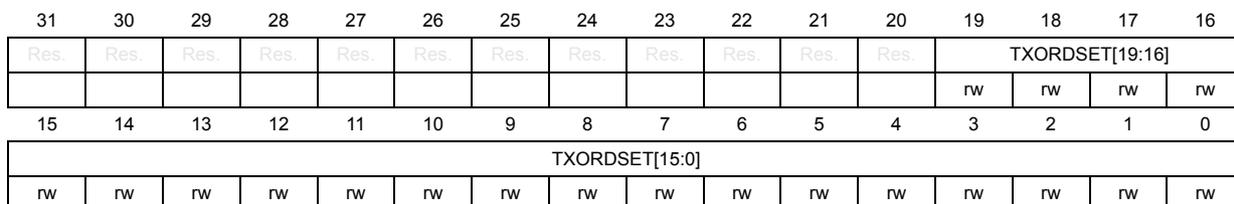
75.8.7 UCPD Tx ordered set type register (UCPD_TX_ORDSETR)
Address offset: 0x01C
Reset value: 0x0000 0000
Writing to this register is only effective when the peripheral is enabled (UCPDEN = 1) and no packet transmission is in progress (TXSEND and TXHRST bits are both low).
| 31 | 30 | 29 | 28 | 27 | 26 | 25 | 24 | 23 | 22 | 21 | 20 | 19 | 18 | 17 | 16 |
| Res. | Res. | Res. | Res. | Res. | Res. | Res. | Res. | Res. | Res. | Res. | Res. | TXORDSET[19:16] | |||
| rw | rw | rw | rw | ||||||||||||
| 15 | 14 | 13 | 12 | 11 | 10 | 9 | 8 | 7 | 6 | 5 | 4 | 3 | 2 | 1 | 0 |
| TXORDSET[15:0] | |||||||||||||||
| rw | rw | rw | rw | rw | rw | rw | rw | rw | rw | rw | rw | rw | rw | rw | rw |
Bits 31:20 Reserved, must be kept at reset value.
Bits 19:0 TXORDSET[19:0] : Ordered set to transmit
The bitfield determines a full 20-bit sequence to transmit, consisting of four K-codes, each of five bits, defining the packet to transmit. The bit 0 (bit 0 of K-code1) is the first, the bit 19 (bit 4 of K-code4) the last.
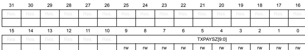
75.8.8 UCPD Tx payload size register (UCPD_TX_PAYSZR)
Address offset: 0x020
Reset value: 0x0000 0000
Writing to this register is only effective when the peripheral is enabled (UCPDEN = 1).
| 31 | 30 | 29 | 28 | 27 | 26 | 25 | 24 | 23 | 22 | 21 | 20 | 19 | 18 | 17 | 16 |
| Res. | Res. | Res. | Res. | Res. | Res. | Res. | Res. | Res. | Res. | Res. | Res. | Res. | Res. | Res. | Res. |
| 15 | 14 | 13 | 12 | 11 | 10 | 9 | 8 | 7 | 6 | 5 | 4 | 3 | 2 | 1 | 0 |
| Res. | Res. | Res. | Res. | Res. | Res. | TXPAYSZ[9:0] | |||||||||
| rw | rw | rw | rw | rw | rw | rw | rw | rw | rw | ||||||
Bits 31:10 Reserved, must be kept at reset value.
Bits 9:0 TXPAYSZ[9:0] : Payload size yet to transmit
The bitfield is modified by software and by hardware. It contains the number of bytes of a payload (including header but excluding CRC) yet to transmit: each time a data byte is written into the UCPD_TXDR register, the bitfield value decrements and the TXIS bit is set, except when the bitfield value reaches zero. The enumerated values are standard payload sizes before the start of transmission.
- 0x2: 2 bytes - the size of Control message from the protocol layer
- 0x6: 6 bytes - the shortest Data message allowed from the protocol layer
- 0x1E: 30 bytes - the longest non-extended Data message allowed from the protocol layer
- 0x106: 262 bytes - the longest possible extended message
- 0x3FF: 1024 bytes - the longest possible payload (for future expansion)
75.8.9 UCPD Tx data register (UCPD_TXDR)
Address offset: 0x024
Reset value: 0x0000 0000
Writing to this register is only effective when the peripheral is enabled (UCPDEN = 1).
| 31 | 30 | 29 | 28 | 27 | 26 | 25 | 24 | 23 | 22 | 21 | 20 | 19 | 18 | 17 | 16 |
|---|---|---|---|---|---|---|---|---|---|---|---|---|---|---|---|
| Res. | Res. | Res. | Res. | Res. | Res. | Res. | Res. | Res. | Res. | Res. | Res. | Res. | Res. | Res. | Res. |
| 15 | 14 | 13 | 12 | 11 | 10 | 9 | 8 | 7 | 6 | 5 | 4 | 3 | 2 | 1 | 0 |
| Res. | Res. | Res. | Res. | Res. | Res. | Res. | Res. | ||||||||
| rw | rw | rw | rw | rw | rw | rw | rw |
Bits 31:8 Reserved, must be kept at reset value.
Bits 7:0 TXDATA[7:0] : Data byte to transmit
75.8.10 UCPD Rx ordered set register (UCPD_RX_ORDSETR)
Address offset: 0x028
Reset value: 0x0000 0000
| 31 | 30 | 29 | 28 | 27 | 26 | 25 | 24 | 23 | 22 | 21 | 20 | 19 | 18 | 17 | 16 |
|---|---|---|---|---|---|---|---|---|---|---|---|---|---|---|---|
| Res. | Res. | Res. | Res. | Res. | Res. | Res. | Res. | Res. | Res. | Res. | Res. | Res. | Res. | Res. | Res. |
| 15 | 14 | 13 | 12 | 11 | 10 | 9 | 8 | 7 | 6 | 5 | 4 | 3 | 2 | 1 | 0 |
| Res. | Res. | Res. | Res. | Res. | Res. | Res. | Res. | Res. | |||||||
| rx | rx | rx | rx | rx | rx | rx |
Bits 31:7 Reserved, must be kept at reset value.
Bits 6:4 RXSOPKINVALID[2:0] :
The bitfield is for debug purposes only.
0x0: No K-code corrupted
0x1: First K-code corrupted
0x2: Second K-code corrupted
0x3: Third K-code corrupted
0x4: Fourth K-code corrupted
Others: Invalid
Bit 3 RXSOP3OF4 :
The bit indicates the number of correct K-codes. For debug purposes only.
0: 4 correct K-codes out of 4
1: 3 correct K-codes out of 4
Bits 2:0 RXORDSET[2:0] : Rx ordered set code detected
- 0x0: SOP code detected in receiver
- 0x1: SOP' code detected in receiver
- 0x2: SOP" code detected in receiver
- 0x3: SOP'_Debug detected in receiver
- 0x4: SOP"_Debug detected in receiver
- 0x5: Cable Reset detected in receiver
- 0x6: SOP extension#1 detected in receiver
- 0x7: SOP extension#2 detected in receiver
75.8.11 UCPD Rx payload size register (UCPD_RX_PAYSZR)
Address offset: 0x02C
Reset value: 0x0000 0000
| 31 | 30 | 29 | 28 | 27 | 26 | 25 | 24 | 23 | 22 | 21 | 20 | 19 | 18 | 17 | 16 |
|---|---|---|---|---|---|---|---|---|---|---|---|---|---|---|---|
| Res. | Res. | Res. | Res. | Res. | Res. | Res. | Res. | Res. | Res. | Res. | Res. | Res. | Res. | Res. | Res. |
| 15 | 14 | 13 | 12 | 11 | 10 | 9 | 8 | 7 | 6 | 5 | 4 | 3 | 2 | 1 | 0 |
| Res. | Res. | Res. | Res. | Res. | Res. | RXPAYSZ[9:0] | |||||||||
| r | r | r | r | r | r | r | r | r | r | ||||||
Bits 31:10 Reserved, must be kept at reset value.
Bits 9:0 RXPAYSZ[9:0] : Rx payload size received
This bitfield contains the number of bytes of a payload (including header but excluding CRC) received: each time a new data byte is received in the UCPD_RXDR register, the bitfield value increments and the RXMSGEND flag is set (and an interrupt generated if enabled).
0x2: 2 bytes - the size of Control message from the protocol layer
0x6: 6 bytes - the shortest Data message allowed from the protocol layer
0x1E: 30 bytes - the longest non-extended Data message allowed from the protocol layer
0x106: 262 bytes - the longest possible extended message
0x3FF: 1024 bytes - the longest possible payload (for future expansion)
The bitfield may return a spurious value when a byte reception is ongoing (the RXMSGEND flag is low).
75.8.12 UCPD receive data register (UCPD_RXDR)
Address offset: 0x030
Reset value: 0x0000 0000
| 31 | 30 | 29 | 28 | 27 | 26 | 25 | 24 | 23 | 22 | 21 | 20 | 19 | 18 | 17 | 16 |
|---|---|---|---|---|---|---|---|---|---|---|---|---|---|---|---|
| Res. | Res. | Res. | Res. | Res. | Res. | Res. | Res. | Res. | Res. | Res. | Res. | Res. | Res. | Res. | Res. |
| 15 | 14 | 13 | 12 | 11 | 10 | 9 | 8 | 7 | 6 | 5 | 4 | 3 | 2 | 1 | 0 |
| Res. | Res. | Res. | Res. | Res. | Res. | Res. | Res. | RXDATA[7:0] | |||||||
| r | r | r | r | r | r | r | r | ||||||||
Bits 31:8 Reserved, must be kept at reset value.
Bits 7:0 RXDATA[7:0] : Data byte received
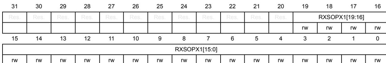
75.8.13 UCPD Rx ordered set extension register 1
(UCPD_RX_ORDEXTR1)
Address offset: 0x034
Reset value: 0x0000 0000
Writing to this register is only effective when the peripheral is disabled (UCPDEN = 0).
| 31 | 30 | 29 | 28 | 27 | 26 | 25 | 24 | 23 | 22 | 21 | 20 | 19 | 18 | 17 | 16 |
| Res. | Res. | Res. | Res. | Res. | Res. | Res. | Res. | Res. | Res. | Res. | Res. | RXSOPX1[19:16] | |||
| rw | rw | rw | rw | ||||||||||||
| 15 | 14 | 13 | 12 | 11 | 10 | 9 | 8 | 7 | 6 | 5 | 4 | 3 | 2 | 1 | 0 |
| RXSOPX1[15:0] | |||||||||||||||
| rw | rw | rw | rw | rw | rw | rw | rw | rw | rw | rw | rw | rw | rw | rw | rw |
Bits 31:20 Reserved, must be kept at reset value.
Bits 19:0 RXSOPX1[19:0] : Ordered set 1 received
The bitfield contains a full 20-bit sequence received, consisting of four K-codes, each of five bits. The bit 0 (bit 0 of K-code1) is receive first, the bit 19 (bit 4 of K-code4) last.
75.8.14 UCPD Rx ordered set extension register 2
(UCPD_RX_ORDEXTR2)
Address offset: 0x038
Reset value: 0x0000 0000
Writing to this register is only effective when the peripheral is disabled (UCPDEN = 0).
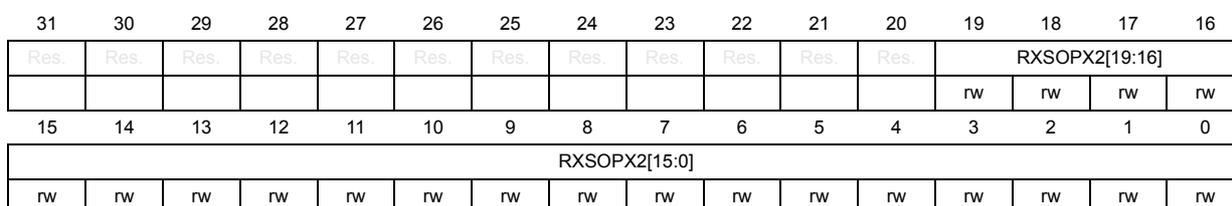
| 31 | 30 | 29 | 28 | 27 | 26 | 25 | 24 | 23 | 22 | 21 | 20 | 19 | 18 | 17 | 16 |
| Res. | Res. | Res. | Res. | Res. | Res. | Res. | Res. | Res. | Res. | Res. | Res. | RXSOPX2[19:16] | |||
| rw | rw | rw | rw | ||||||||||||
| 15 | 14 | 13 | 12 | 11 | 10 | 9 | 8 | 7 | 6 | 5 | 4 | 3 | 2 | 1 | 0 |
| RXSOPX2[15:0] | |||||||||||||||
| rw | rw | rw | rw | rw | rw | rw | rw | rw | rw | rw | rw | rw | rw | rw | rw |
Bits 31:20 Reserved, must be kept at reset value.
Bits 19:0 RXSOPX2[19:0] : Ordered set 2 received
The bitfield contains a full 20-bit sequence received, consisting of four K-codes, each of five bits. The bit 0 (bit 0 of K-code1) is receive first, the bit 19 (bit 4 of K-code4) last.
75.8.15 UCPD register map
Table 761. UCPD register map and reset values
| Offset | Register name | 31 | 30 | 29 | 28 | 27 | 26 | 25 | 24 | 23 | 22 | 21 | 20 | 19 | 18 | 17 | 16 | 15 | 14 | 13 | 12 | 11 | 10 | 9 | 8 | 7 | 6 | 5 | 4 | 3 | 2 | 1 | 0 | |||
|---|---|---|---|---|---|---|---|---|---|---|---|---|---|---|---|---|---|---|---|---|---|---|---|---|---|---|---|---|---|---|---|---|---|---|---|---|
| 0x000 | UCPD_CFGR1 | UCPDEN | RXDMAEN | TXDMAEN | Res. | RXORDSETEN[8:0] | PSC_UCPDCLK[2:0] | Res. | TRANSWIN[4:0] | IFRGAP[4:0] | HBITCLKDIV[5:0] | |||||||||||||||||||||||||
| Reset value | 0 | 0 | 0 | 0 | 0 | 0 | 0 | 0 | 0 | 0 | 0 | 0 | 0 | 0 | 0 | 0 | 0 | 0 | 0 | 0 | 0 | 0 | 0 | 0 | 0 | 0 | 0 | 0 | 0 | 0 | 0 | 0 | ||||
| 0x004 | UCPD_CFGR2 | Res. | Res. | Res. | Res. | Res. | Res. | Res. | Res. | Res. | Res. | Res. | Res. | Res. | Res. | Res. | Res. | Res. | Res. | Res. | Res. | Res. | Res. | Res. | Res. | Res. | Res. | Res. | Res. | WUPEN | FORCECLK | RXFILT2N3 | RXFILTDIS | |||
| Reset value | 0 | 0 | 0 | 0 | ||||||||||||||||||||||||||||||||
| 0x008 | Reserved | |||||||||||||||||||||||||||||||||||
| 0x00C | UCPD_CR | Res. | Res. | Res. | Res. | Res. | Res. | Res. | Res. | Res. | Res. | Res. | CC2TCDIS | CC1TCDIS | Res. | RDCH | FRSTX | Res. | Res. | Res. | Res. | Res. | CCENABLE[1:0] | Res. | ANAMODE | ANASUBMODE[1:0] | Res. | PHYCSEL | PHYRXEN | RXMODE | TXHRST | TXSEND | TXMODE[1:0] | |||
| Reset value | 0 | 0 | 0 | 0 | 0 | 0 | 0 | 0 | 0 | 0 | 0 | 0 | 0 | 0 | 0 | 0 | ||||||||||||||||||||
| 0x010 | UCPD_IMR | Res. | Res. | Res. | Res. | Res. | Res. | Res. | Res. | Res. | Res. | Res. | Res. | Res. | Res. | Res. | Res. | Res. | TYPECEVT2IE | TYPECEVT1IE | Res. | RXMSGENDIE | RXOVRIE | RXHRSTDETIE | RXORDDETIE | RXNEIE | Res. | TXUNDIE | HRSTSENTIE | HRSTDISCIE | TXMSGDETIE | TXMSGSENTIE | TXMSGDISCIE | TXISIE | ||
| Reset value | 0 | 0 | 0 | 0 | 0 | 0 | 0 | 0 | 0 | 0 | 0 | 0 | 0 | 0 | ||||||||||||||||||||||
| 0x014 | UCPD_SR | Res. | Res. | Res. | Res. | Res. | Res. | Res. | Res. | Res. | Res. | Res. | Res. | Res. | TYPEC_VSTATE_CC2[1:0] | TYPEC_VSTATE_CC1[1:0] | Res. | TYPECEVT2 | TYPECEVT1 | RXERR | RXMSGEND | RXOVR | RXHRSTDET | RXORDDET | RXNE | Res. | TXUND | HRSTSENT | HRSTDISC | TXMSGDET | TXMSGSENT | TXMSGDISC | TXIS | |||
| Reset value | 0 | 0 | 0 | 0 | 0 | 0 | 0 | 0 | 0 | 0 | 0 | 0 | 0 | 0 | 0 | 0 | 0 | 0 | 0 | |||||||||||||||||
| 0x018 | UCPD_ICR | Res. | Res. | Res. | Res. | Res. | Res. | Res. | Res. | Res. | Res. | Res. | Res. | Res. | Res. | Res. | Res. | TYPECEVT2CF | TYPECEVT1CF | Res. | RXMSGENDCF | RXOVRCF | RXHRSTDETCF | RXORDDETCF | Res. | Res. | TXUNDCF | HRSTSENTCF | HRSTDISCCF | TXMSGABTCF | TXMSGSENTCF | TXMSGDISCCF | Res. | |||
| Reset value | 0 | 0 | 0 | 0 | 0 | 0 | 0 | 0 | 0 | 0 | 0 | 0 | ||||||||||||||||||||||||
| 0x01C | UCPD_TX_ORDSETR | Res. | Res. | Res. | Res. | Res. | Res. | Res. | Res. | Res. | Res. | Res. | Res. | TXORDSET[19:0] | ||||||||||||||||||||||
| Reset value | 0 | 0 | 0 | 0 | 0 | 0 | 0 | 0 | 0 | 0 | 0 | 0 | 0 | 0 | 0 | 0 | 0 | 0 | 0 | |||||||||||||||||
Table 761. UCPD register map and reset values (continued)
| Offset | Register name | 31 | 30 | 29 | 28 | 27 | 26 | 25 | 24 | 23 | 22 | 21 | 20 | 19 | 18 | 17 | 16 | 15 | 14 | 13 | 12 | 11 | 10 | 9 | 8 | 7 | 6 | 5 | 4 | 3 | 2 | 1 | 0 |
|---|---|---|---|---|---|---|---|---|---|---|---|---|---|---|---|---|---|---|---|---|---|---|---|---|---|---|---|---|---|---|---|---|---|
| 0x020 | UCPD_TX_PAYSZR | Res | Res | Res | Res | Res | Res | Res | Res | Res | Res | Res | Res | Res | Res | Res | Res | Res | Res | Res | Res | Res | Res | TXPAYSZ[9:0] | |||||||||
| Reset value | 0 | 0 | 0 | 0 | 0 | 0 | 0 | 0 | 0 | 0 | |||||||||||||||||||||||
| 0x024 | UCPD_TXDR | Res | Res | Res | Res | Res | Res | Res | Res | Res | Res | Res | Res | Res | Res | Res | Res | Res | Res | Res | Res | Res | Res | TXDATA[7:0] | |||||||||
| Reset value | 0 | 0 | 0 | 0 | 0 | 0 | 0 | 0 | 0 | 0 | |||||||||||||||||||||||
| 0x028 | UCPD_RX_ORDSETR | Res | Res | Res | Res | Res | Res | Res | Res | Res | Res | Res | Res | Res | Res | Res | Res | Res | Res | Res | Res | Res | Res | RXSOPKINVALID[2:0] | RXSOP3OF4 | RXORDSET[2:0] | |||||||
| Reset value | |||||||||||||||||||||||||||||||||
| 0x02C | UCPD_RX_PAYSZR | Res | Res | Res | Res | Res | Res | Res | Res | Res | Res | Res | Res | Res | Res | Res | Res | Res | Res | Res | Res | Res | Res | RXPAYSZ[9:0] | |||||||||
| Reset value | 0 | 0 | 0 | 0 | 0 | 0 | 0 | 0 | 0 | 0 | |||||||||||||||||||||||
| 0x030 | UCPD_RXDR | Res | Res | Res | Res | Res | Res | Res | Res | Res | Res | Res | Res | Res | Res | Res | Res | Res | Res | Res | Res | Res | Res | RXDATA[7:0] | |||||||||
| Reset value | 0 | 0 | 0 | 0 | 0 | 0 | 0 | 0 | 0 | 0 | |||||||||||||||||||||||
| 0x034 | UCPD_RX_ORDEXTR1 | Res | Res | Res | Res | Res | Res | Res | Res | Res | Res | Res | Res | RXSOPX1[19:0] | |||||||||||||||||||
| Reset value | 0 | 0 | 0 | 0 | 0 | 0 | 0 | 0 | 0 | 0 | 0 | 0 | 0 | 0 | 0 | 0 | 0 | 0 | 0 | 0 | |||||||||||||
| 0x038 | UCPD_RX_ORDEXTR2 | Res | Res | Res | Res | Res | Res | Res | Res | Res | Res | Res | Res | RXSOPX2[19:0] | |||||||||||||||||||
| Reset value | 0 | 0 | 0 | 0 | 0 | 0 | 0 | 0 | 0 | 0 | 0 | 0 | 0 | 0 | 0 | 0 | 0 | 0 | 0 | 0 | |||||||||||||
| 0x03C - 0x3FF | Reserved | ||||||||||||||||||||||||||||||||
Refer to Section 2.3: Memory organization for the register boundary addresses.