72. USB subsystem (USBSS)
72.1 Overview
The USB subsystem includes two USB2 OTG high-speed ports and two channel configuration lines for Type-C and power delivery support. A high level block diagram is shown in Figure 972 .
The USB2 OTG high-speed ports support Full Speed and Low Speed modes when acting as Host, and Full Speed mode when acting as Device.
The configuration channels support Type-C and power delivery features in applications where one of the USB2 port is connected to a Type-C receptacle.
Figure 972. USB subsystem overview
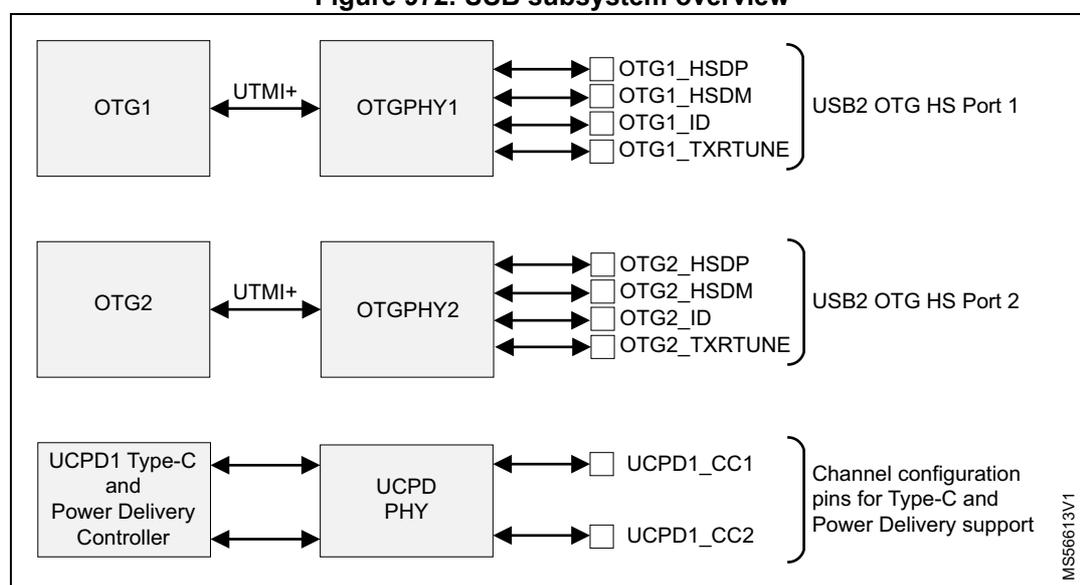
The diagram illustrates the internal architecture of the USB subsystem. It consists of three main functional blocks:
- USB2 OTG HS Port 1: Comprises the OTG1 controller connected via a UTMI+ interface to the OTGPHY1. OTGPHY1 is connected to four pins: OTG1_HSDP, OTG1_HSDM, OTG1_ID, and OTG1_TXRTUNE.
- USB2 OTG HS Port 2: Comprises the OTG2 controller connected via a UTMI+ interface to the OTGPHY2. OTGPHY2 is connected to four pins: OTG2_HSDP, OTG2_HSDM, OTG2_ID, and OTG2_TXRTUNE.
- Channel configuration pins for Type-C and Power Delivery support: Comprises the UCPD1 Type-C and Power Delivery Controller connected to the UCPD PHY, which in turn connects to two pins: UCPD1_CC1 and UCPD1_CC2.
A vertical label 'MS56613/V1' is present on the right side of the diagram.
72.2 USB2 OTG high-speed Port 1
72.2.1 USB2 OTG high-speed Port 1 main features
- • Can be configured statically as Host or Device (DRD configuration)
- • Dynamic switching between the two roles is not supported: Host Negotiation Protocol (HNP) and Session Request Protocol (SRP) are not supported
- • Embedded PHY, supporting high-speed (HS), Full Speed (FS) and Low Speed (LS) modes (LS mode is not supported when configured as Device)
- • LPM (Link Power Management) support
- • DMA engine with local 4-Kbyte buffer
- • Supports Battery Charging v1.2, with the exception of the Accessory Charger Adapter mode
- • Supports suspend, sleep, resume, and remote wake-up operations
- • Provides electrical parameter override bits for optimal interoperability
The supported standards are:
- • Universal Serial Bus Specification, Revision 2.0, USB Implementers Forum, Inc., April 27, 2000
- • Engineering Change Notice: USB2.0 Link Power Management Addendum, July 16, 2007
- • Battery Charging Specification, Revision 1.2, December 7, 2010
72.2.2 USB2 OTG high-speed Port 1 functional description
Figure 973. USB2 OTG high-speed Port 1 block diagram
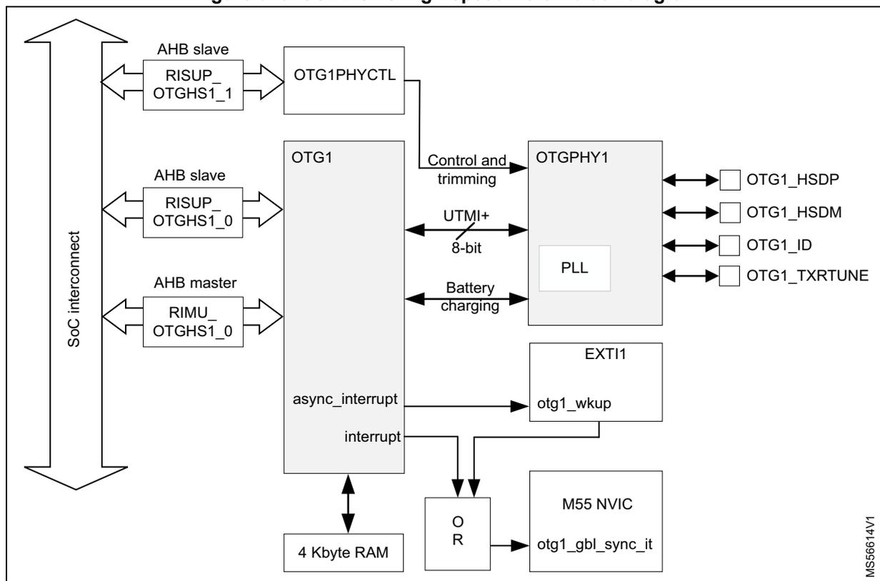
RISUP_OTGHS1_0 and RISUP_OTGHS1_1 correspond to the same RIFSC index, namely OTG1_HS. They are connected to the same sec/priv bits from the RIFSC, and their ilac outputs are OR-ed together, to go to the same IAC index.
USB2 OTG high-speed port pins and internal signals
Table 723. USB2 OTG high-speed Port 1 pins
| Signal name | Signal type | Description |
|---|---|---|
| OTG1_HSDP | 3V3 analog | USB D+ signal |
| OTG1_HSDM | USB D- signal | |
| OTG1_ID | 1V8 analog | USB Mini-Receptacle Identifier. Differentiates a mini-A from a mini-B plug. |
| OTG1_TXRTUNE | Transmitter resistor tune pin. Connects to GND through an external \( 200\pm 1\% \) \( \Omega \) resistor that adjusts the high-speed source impedance of OTGPHY1. |
Table 724. USB2 OTG high-speed Port 1 internal signals
| Signal name | Signal type | Description |
|---|---|---|
| OTG1 AHB Master | Digital | AHB Master interface to the SoC interconnect for memory access. AHBLite protocol, 32-bit data width. |
| OTG1 AHB Slave | Digital | AHB Slave interface to access OTG1 registers. AHBLite protocol, 32-bit data width. |
| OTG1PHYCTL AHB Slave | Digital | AHB Slave interface for access to OTG1PHYCTL registers. |
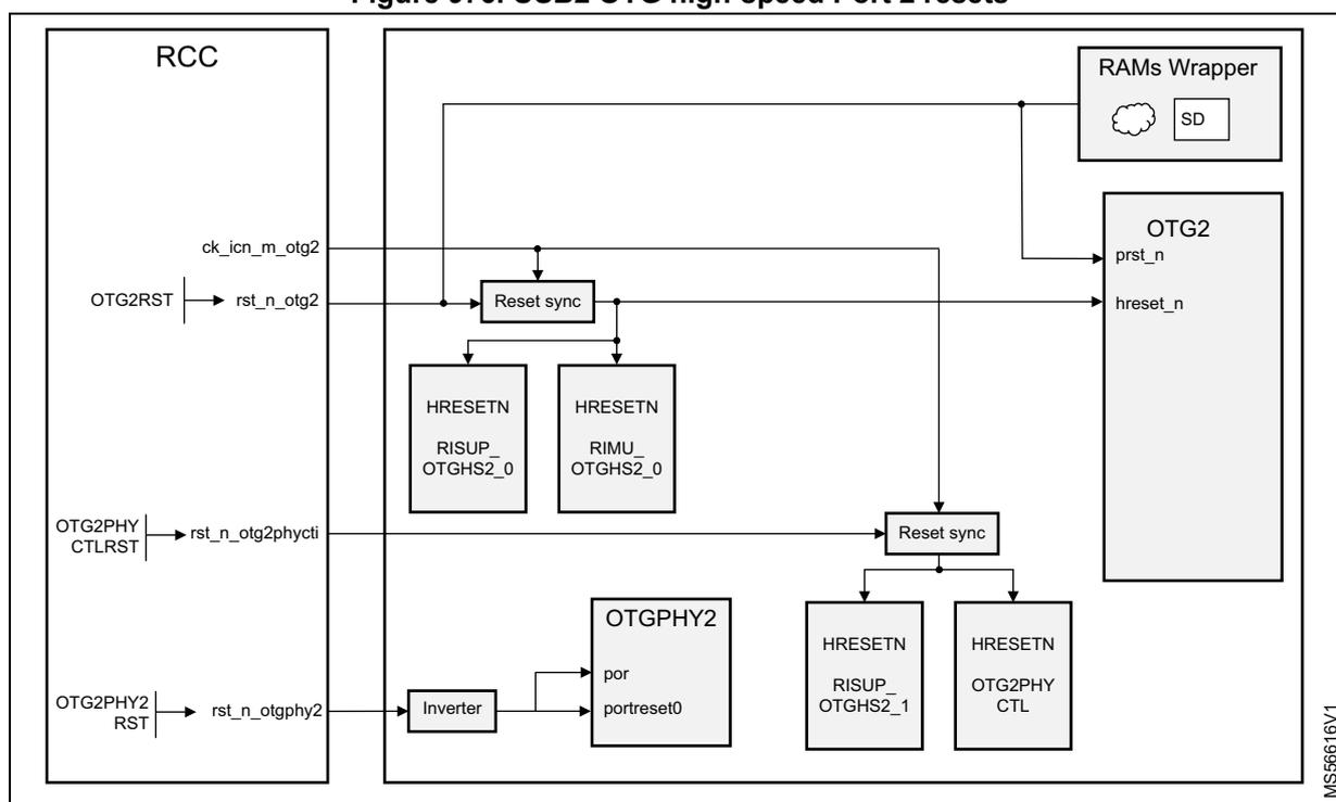
Figure 974. USB2 OTG high-speed Port 1 resets
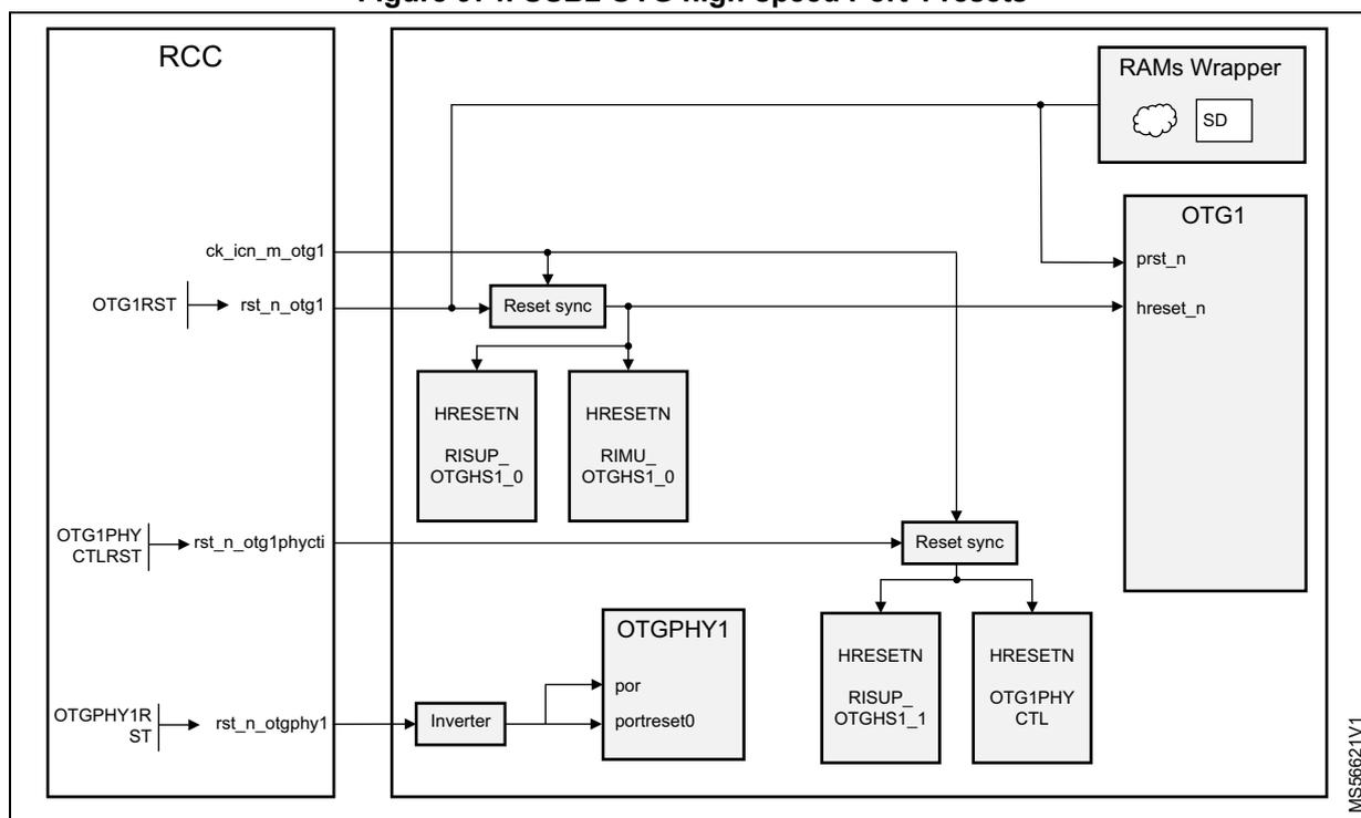
There are three resets for the USB2 OTG high-speed Port 1:
- •
rst_n_otg1, controlled by theOTG1RSTbit inRCC_AHB5RSTRregister. - •
rst_n_otg1phyctl, controlled by theOTG1PHYCTLRSTbit inRCC_AHB5RSTRregister. - •
rst_n_otgphy1, controlled by theOTGPHY1RSTbit inRCC_AHB5RSTRregister.
When configuring the USB2 OTG high-speed Port 1, the reset sequence is:
- 1.
rst_n_otgphy1,rst_n_otg1andrst_n_otg1phyctlresets are asserted - 2. clocks coming from RCC and HSE are enabled
- 3.
rst_n_otg1phyctlreset is released - 4. the frequency of
OTGPHY1reference clock is selected inOTG1PHYCTL_CRregister - 5.
OTGPHY1trimming bits are programmed (if needed) - 6.
rst_n_otgphy1is released - 7. wait 50 µs (
OTGPHY1PLL lock time and start of generation ofphylock0) - 8.
rst_n_otg1is released
Description of the USB2 OTG high-speed controller (OTG1)
Refer to Section 73: USB on-the-go high-speed (OTG) .
Description of the OTGPHY1
OTGPHY1 is controlled by OTG1PHYCTL registers. Refer to Section 74: USB HS PHY controller (USBPHYC) .
72.2.3 USB2 OTG high-speed Port 1 interrupts
The USB2 OTG high-speed Port 1 generates one interrupt and one wake-up event that can be used to take the system out of Stop mode.
Table 725. USB2 OTG high-speed Port 1 interrupt
| OTG1 interrupt | IP pin name | CPU interrupt |
|---|---|---|
| OTG1_GBL_SYNC_IT | OTG1/interrupt | OTG1_GBL_SYNC_IT |
Table 726. USB2 OTG high-speed Port 1 wake-up events
| OTG1 event | IP pin name | EXTI event |
|---|---|---|
| OTG1_WKUP | OTG1/async_interrupt | OTG1_WKUP |
72.2.4 Battery charging
The OTGPHY1 integrates the voltage and current sources, as well as the voltage comparators required to support Battery Charging v1.2. The relevant control bits are implemented in OTG_GCCFG register of the OTG1 controller.
The control sequence depends on whether the OTG HS port 1 is Host or Device.
Host case
If the application wants the Host port to behave as a Standard Downstream Port (SDP), the default values of H_CDPEN, H_CDPDETEN, H_VDMSRCEN bits in OTG_GCCFG register must be kept.
If the application wants the Host port to behave as a Charging Downstream Port (CDP), one of the following two control sequences must be implemented:
Control sequence 1:
- • Set the H_CDPEN bit to 1
- • Decode the disconnect information transmitted by the OTGPHY1 to the OTG1 controller (HOSTDISCONNECT0 output of OTGPHY1).
- – If disconnect = 1, set the H_VDMSRCEN bit to 1
- – else set the H_VDMSRCEN bit to 0
Control sequence 2:
- • Set the H_CDPEN bit to 1 and the H_CDPDETEN bit to 1
- • Monitor CHGDET and FSVPLUS status bits:
- – If CHGDET = 1 and FSVPLUS = 0, set the H_VDMSRCEN bit to 1
- – else, set the H_VDMSRCEN bit to 0
Device case
- • Data contact detection
- – Set the PD_DCDDET bit to 1. This enables a current source on OTG1_HSDP and pulls OTG1_HSDM low.
- – If FSVPLUS is at 0 for more than tDCD_DBNC (as defined in Battery Charging v1.2), Data Contact has happened. PD_DCDDET must be reset.
- • Primary detection
- – Set the PD_PDET bit to 1. This enables a voltage source on OTG1_HSDP and a voltage comparator on OTG1_HSDM.
- – If CHGDET = 0, the Device is connected to a Standard Downstream Port (SDP).
- – If CHGDET = 1, the Device is connected to a Charging Downstream Port (CDP) or a Dedicated Charging Port (DCP).
- – Reset PD_PDET.
- • Secondary detection
- – Set the PD_SDET bit to 1. This enables a voltage source on OTG1_HSDM and a voltage comparator on OTG1_HSDP.
- – If CHGDET = 0, the Device is connected to a Charging Downstream Port (CDP).
- – If CHGDET = 1, the Device is connected to a Dedicated Charging Port (DCP).
- – Reset PD_SDET.
72.2.5 ID management
If IDPULLUP_DIS control bit in OTG_GCCFG register is 0, the ID information is captured on OTG1_ID pin and provided by the OTGPHY1 to the OTG1 controller. If the OTG1_ID pin is unused and left floating, PULLDOWN_EN bit in the OTG_GCCFG register of OTG1 can be used to control the pull-down resistors on OTG1_HSDP and OTG1_HSDM pins.
72.2.6 VBUS detection
OTGPHY1 is configured in VBUS external comparator mode. As a consequence:
- • OTGDISABLE0 and DRVVBUS0 bits of OTG1PHYCTL_CR register must be kept to their reset values.
- • VBUSVLD and SESSVLD bits of OTG_GCCFG register must be ignored.
72.3 USB2 OTG high-speed Port 2
72.3.1 USB2 OTG high-speed Port 2 main features
Features are identical to those of the USB2 OTG high-speed Port 1.
72.3.2 USB2 OTG high-speed Port 2 functional description
Figure 975. USB2 OTG high-speed Port 2 block diagram
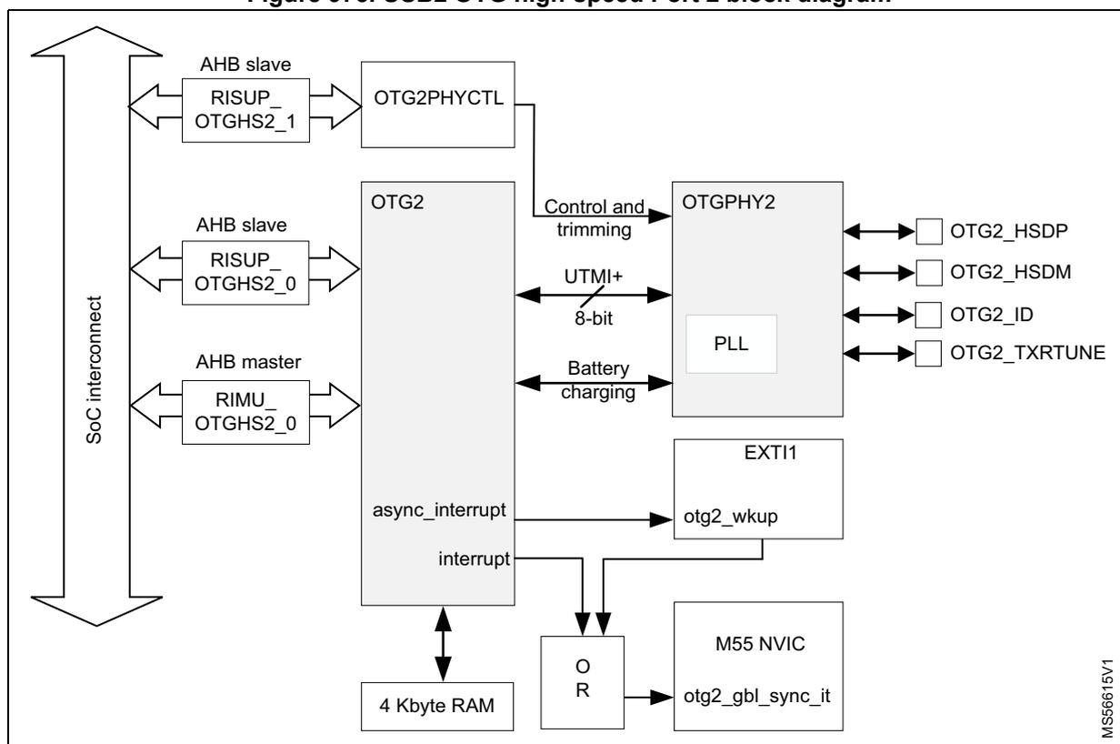
RISUP_OTGHS2_0 and RISUP_OTGHS2_1 correspond to the same RIFSC index (OTG2_HS). They are connected to the same sec/priv bits from the RIFSC, and their ilac outputs are OR-ed together, to go to the same IAC index.
Table 727. USB2 OTG high-speed Port 2 pins
| Signal name | Signal type | Description |
|---|---|---|
| OTG2_HSDP | 3V3 analog | USB D+ signal |
| OTG2_HSDM | USB D- signal | |
| OTG2_ID | 1V8 analog | USB Mini-Receptacle identifier. Differentiates a mini-A from a mini-B plug. |
| OTG2_TXRTUNE | Transmitter resistor tune pin. Connects to GND through an external 200 200±1% Ω resistor that adjusts the high-speed source impedance of OTGPHY2. |
Table 728. USB2 OTG high-speed Port 2 internal signals
| Signal name | Signal type | Description |
|---|---|---|
| OTG2 AHB Master | Digital | AHB Master interface to the SoC interconnect for memory access. AHBLite protocol, 32-bit data width. |
Table 728. USB2 OTG high-speed Port 2 internal signals (continued)
| Signal name | Signal type | Description |
|---|---|---|
| OTG2 AHB Slave | Digital | AHB Slave interface for access to OTG2 registers. AHBLite protocol, 32-bit data width. |
| OTG2PHYCTL AHB Slave | Digital | AHB Slave interface for access to OTG2PHYCTL registers. |
Figure 976. USB2 OTG high-speed Port 2 resets
There are three resets for the USB2 OTG high-speed Port 2:
- •
rst_n_otg2, controlled by theOTG2RSTbit inRCC_AHB5RSTRregister. - •
rst_n_otg2phyctl, controlled by theOTG2PHYCTLRSTbit inRCC_AHB5RSTRregister. - •
rst_n_otgphy2, controlled by theOTGPHY2RSTbit inRCC_AHB5RSTRregister.
When configuring the USB2 OTG high-speed Port 2, the reset sequence is:
- 1.
rst_n_otgphy2,rst_n_otg2andrst_n_otg2phyctlresets are asserted. - 2. clocks coming from RCC and HSE are enabled.
- 3.
rst_n_otg2phyctlreset is released - 4. the frequency of
OTGPHY2reference clock is selected inOTG2PHYCTL_CRregister. - 5.
OTGPHY2trimming bits are programmed (if needed) - 6.
rst_n_otgphy2is released - 7. wait 50 µs (
OTGPHY2PLL lock time and start of generation ofphylock0) - 8.
rst_n_otg2is released
Description of the USB2 OTG HS controller (OTG2)
Refer to Section 73: USB on-the-go high-speed (OTG) .
Description of the OTGPHY2
OTGPHY2 is controlled by OTG2PHYCTL registers. Refer to Section 74: USB HS PHY controller (USBPHYC) .
72.3.3 USB2 OTG high-speed Port 2 interrupts
The USB2 OTG high-speed Port 2 generates one interrupt and one wake-up event, which can be used to take the system out of Stop mode.
Table 729. USB2 OTG high-speed Port 2 interrupts
| OTG2 interrupt | IP pin name | CPU interrupt |
|---|---|---|
| OTG2_GBL_SYNC_IT | OTG2/interrupt | OTG2_GBL_SYNC_IT |
Table 730. USB2 OTG high-speed Port 2 wake-up events
| OTG2 event | IP pin name | EXTI event |
|---|---|---|
| OTG2_WKUP | OTG2/async_interrupt | OTG2_WKUP |
72.3.4 Battery charging
The OTGPHY2 integrates the voltage and current sources, as well as the voltage comparators required to support Battery Charging v1.2. The relevant control bits are implemented in OTG_GCCFG register of OTG2.
The control sequence is the same as for the USB2 OTG high-speed Port 1.
72.3.5 ID management
This is similar to the ID management for OTGPHY1. The control bits are in the OTG_GCCFG register of OTG2.
72.3.6 VBUS management
OTGPHY2 is configured in 'VBUS external comparator' mode. As a consequence:
- • OTGDISABLE0 and DRVVBUS0 bits in OTG2PHYCTL_CR register must be kept to their reset values.
The bits VBUSVLD and SESSVLD of OTG_GCCFG register must be ignored.
72.4 USB Type-C and power delivery interface
72.4.1 USB Type-C and power delivery interface main features
- • The USB Type-C and power delivery interface is made of CC1 and CC2 channel configuration pins. It enables the implementation of one Type-C port, associated to OTG HS Port 1 or to OTG HS Port 2.
- • It supports the CC signaling of the Type-C specification:
- – attachment detection
- – cable orientation resolution
- – source/sink role advertisement
- – detection of current modes
- • It supports the physical layer of the power delivery specification and enables power negotiation, power role swap and data role swap.
- • Generation of a Fast Role Swap request is supported: FRSTX1 and FRSTX2 signals from UCPD1 IP are mapped as alternate functions of GPIOs for control of external NMOS transistors.
- • detection of a Fast Role Swap request is not supported
- • ADC channel are used for VBUS comparison with thresholds defined in the standard
- • Support for sink, source or dual role power (DRP) platforms.
- • Independent DMA interface for Tx and Rx functionality.
- • Not supported: Dead battery support, Over voltage protection on CC signals and VBUS, Over current detection on VBUS, VCONN switches, VBUS switch gate control and discharge. These features must be supported with external components.
The standards supported are:
- • Universal Serial Bus Type-C Cable and Connector specification, release 2.0, August 2019
- • Universal Serial Bus Power Delivery specification:
- – Revision 2.0, v1.3, January 12 2017
- – Revision 3.0, v2.0, August 29 2019
72.4.2 USB Type-C and power delivery interface implementation
Figure 977 gives an overview of how OTG HS Port 1 connects to a Type-C receptacle.
Figure 977. USB Type-C implementation: OTG HS Port 1 example
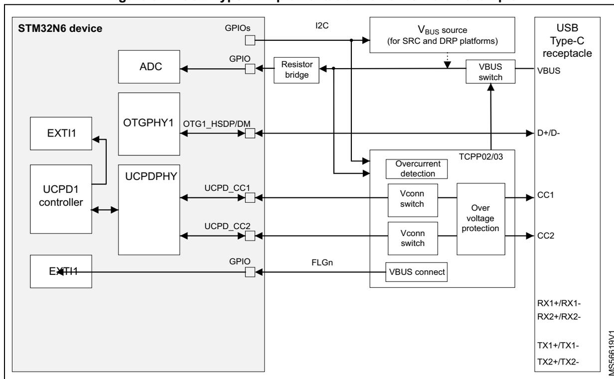
The CC I/Os (UCPDPHY) integrate the \( R_p \) and \( R_d \) resistors, and the voltage threshold comparators needed to define the local port attributes and detect the attributes of the remote port being attached.
The UCPD digital controller handles Type-C level detection with de-bounce, CRC generation/checking, 4b5b encode/decode, BMC encode/decode.
If needed, VBUS detection must be managed by an ADC channel or an external comparator. It cannot be managed by OTGPHY1 since it is forced in external comparator mode and not connected to VBUS.
VBUS comparison with \( V_{safe0v} \) and \( V_{safe5v} \) thresholds is performed by an ADC. An external resistor bridge is required to scale down VBUS to the 1V8 range of the ADC channel input.
An external component is required to protect the CC lines from overvoltage condition and VBUS line from overvoltage and overcurrent conditions. TCPP02/03 is well suited for this purpose and also implements Vconn switches, Dead battery support, the control for VBUS switch and VBUS discharge.
A VBUS source is required in source (SRC) and DRP platforms.
In a SRC or DRP platform, the device can be woken up from Stop mode by the UCPD digital controller upon asynchronous detection of events on the CC lines. In a sink (SNK) platform, the device can be woken up from Stdby mode by the detection of VBUS connection performed in TCPP02/03 and routed to a GPIO (FLG_n signal in the figure above).
Note: The Type-C interface can be associated either to OTG HS Port 1 or to OTG HS Port 2. If an application requires two Type-C ports, an external Type-C controller is required.
72.4.3 USB Type-C and power delivery interface functional description
Figure 978. USB Type-C and power delivery block diagram
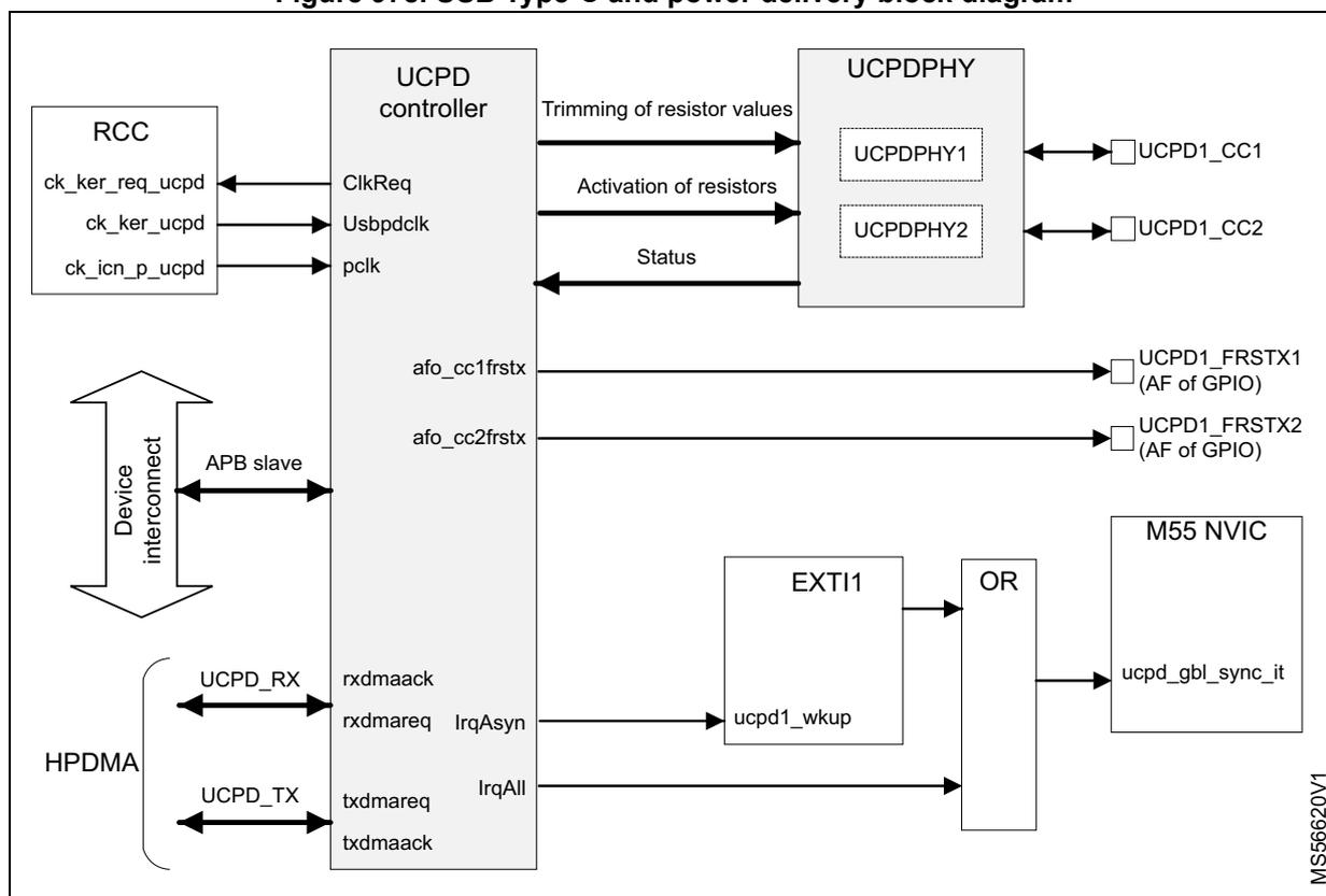
The diagram illustrates the internal architecture of the USB Type-C and power delivery interface. At the center is the
UCPD controller
, which is connected to the
Device interconnect
via an
APB slave
interface. The
RCC
block provides clock signals:
ck_ker_req_ucpd
(to
ClkReq
),
ck_ker_ucpd
(to
Usbpclk
), and
ck_icn_p_ucpd
(to
pclk
). The
UCPD controller
sends
Trimming of resistor values
,
Activation of resistors
, and receives a
Status
signal from the
UCPDPHY
block. The
UCPDPHY
block contains
UCPDPHY1
and
UCPDPHY2
, which are connected to external pins
UCPD1_CC1
and
UCPD1_CC2
respectively. The
UCPD controller
also outputs
af0_cc1frstx
and
af0_cc2frstx
to pins
UCPD1_FRSTX1
and
UCPD1_FRSTX2
(AF of GPIO). The
HPDMA
block is connected to the
UCPD controller
via
UCPD_RX
(
rxdmaack
,
rxdmareq
,
IrqAsyn
) and
UCPD_TX
(
txdmareq
,
txdmaack
,
IrqAll
) signals. The
EXTI1
block receives
ucpd1_wkup
from the
UCPD controller
and sends an interrupt signal to an
OR
gate. The
OR
gate also receives
IrqAll
from the
UCPD controller
and sends an interrupt signal to the
M55 NVIC
via
ucpd_gbl_sync_it
. A vertical label
MS56620V1
is present on the right side of the diagram.
Note: af0_cc1frstx and af0_cc2frstx connect directly to the pad ring without being OR-ed together. Be careful when using these alternate functions to control external transistors: UCPD1_FRSTX1 is associated with CC1, while UCPD1_FRSTX2 is associated with CC2.
USB Type-C and power delivery pins and internal signals
Table 731. USB Type-C and power delivery pins
| Signal name | Signal type | Description |
|---|---|---|
| UCPD1_CC1 | 3V3 analog, 5V tolerant | Channel configuration |
| UCPD1_CC2 | ||
| UCPD1_FRSTX1 | 1V8 digital | Alternate function of GPIO |
| UCPD1_FRSTX2 |
Table 732. USB Type-C and power delivery internal signals
| Signal name | Signal type | Description |
|---|---|---|
| UCPD APB Slave | Digital | APB Slave interface for access to the UCPD controller registers. 32-bit data width. |
| rxdmareq | Digital | Request of UCPD_RX DMA interface |
| Signal name | Signal type | Description |
|---|---|---|
| rxdmaack | Digital | Acknowledge of UCPD_RX DMA interface |
| txdmareq | Digital | Request of UCPD_TX DMA interface |
| txdmaack | Digital | Acknowledge of UCPD_TX DMA interface |
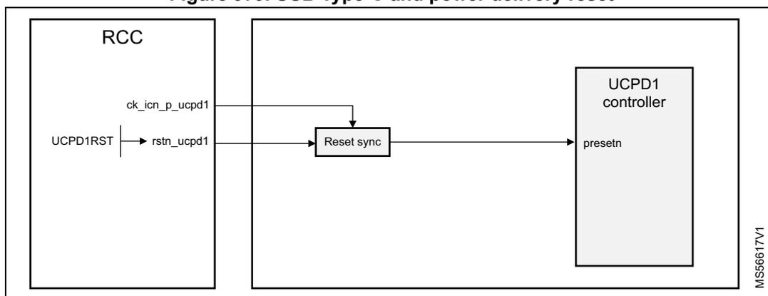
There is only one reset for the USB Type-C and power delivery interface:
- •
rstn_ucpd1, controlled by theUCPD1RSTbit inRCC_APB1HRSTRregister.
Description of the USB Type-C and power delivery controller (UCPD1)
Refer to Section 75: USB Type-C ® /USB Power Delivery interface (UCPD) .
72.4.4 USB Type-C and power delivery interrupts
The USB Type-C and power delivery interface involves one interrupt and one event generated by the UCPD controller.
Table 733. USB Type-C and power delivery interrupt| USB Type-C and PD interrupt | UCPD1 pin name | CPU interrupt |
|---|---|---|
| UCPD_GBL_SYNC_IT | IrqAll | UCPD_GBL_SYNC_IT |
| USB Type-C and PD event | UCPD1 pin name | EXTI event |
|---|---|---|
| UCPD1_WKUP | IrqAsyn | UCPD1_WKUP |
When the system is in Stop mode, it can be woken up by the UCPD1 WAKEUP event, generated when the UCPD1 controller detects some activity on one of the CC lines.
When the system is in Stdby mode, it can be woken up by an EXTI event generated by a GPIO. This is meant for Sink platforms where an external component detects VBUS presence and wakes up the device.
72.5 Debug signals
Signals of the OTG high-speed Port 1 and Port 2 are multiplexed and routed to the hardware debug port (HDP). The SELOTGDBG bit in OTG2PHYCTL_CR register controls the multiplexer. These debug signals are tapped on the UTMI+ interface between the OTG controller (OTG1, OTG2) and the USB2 PHYs (OTGPHY1, OTGPHY2). The list of debug signals is described in the Hardware Debug Port User Specifications (table 3).
Figure 980. Multiplexing of debug signals in the USB subsystem
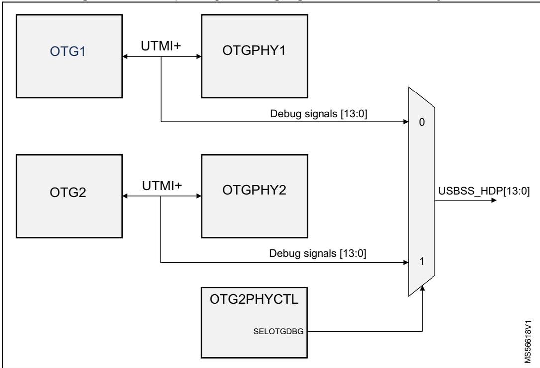
The diagram illustrates the internal architecture of the USB subsystem for debug signal routing. It features two OTG controllers, OTG1 and OTG2, each connected to a corresponding USB2 PHY, OTGPHY1 and OTGPHY2, via UTMI+ interfaces. From each UTMI+ interface, a 14-bit 'Debug signals [13:0]' bus is tapped and sent to a 2-to-1 multiplexer. The multiplexer's select input is controlled by the SELOTGDBG bit from the OTG2PHYCTL register. The output of the multiplexer is the USBSS_HDP[13:0] signal, which is routed to the hardware debug port. The diagram is labeled with 'MS56618V1' in the bottom right corner.