67. Serial peripheral interface (SPI)
67.1 SPI introduction
The serial peripheral interface (SPI) can be used to communicate with external devices while using the specific synchronous protocol. The SPI protocol supports half-duplex, full-duplex, and simplex synchronous, serial communication with external devices. The interface can be configured as master or slave and can operate in multislave or multimaster configurations. The device configured as master provides a communication clock (SCK) to the slave device. The slave select (NSS) and ready (RDY) signals can be applied optionally just to set up communication with a concrete slave and to ensure it handles the data flow properly. The Motorola data format is used by default, but some other specific modes are supported as well.
67.2 SPI main features
- • Full-duplex synchronous transfers on three lines
- • Half-duplex synchronous transfer on two lines (with bidirectional data line)
- • Simplex synchronous transfers on two lines (with unidirectional data line)
- • From 4-bit up to 32-bit data size selection
- • Multimaster or multislave mode capability
- • Dual clock domain, the peripheral kernel clock is independent from the APB bus clock
- • Baud rate prescaler up to kernel frequency/2 or bypass from RCC in master mode
- • Protection of configuration and setting
- • Slave select hardware or software management for both master and slave
- • Adjustable minimum delays between data and between NSS and data flow
- • Configurable NSS signal polarity and timing, MISO x MOSI swap capability
- • Programmable clock polarity and phase
- • Programmable data order with MSB-first or LSB-first shifting
- • Programmable number of data within a transfer to control NSS and CRC
- • Dedicated transmission and reception flags with interrupt capability
- • SPI Motorola and TI format support
- • Hardware CRC can verify the integrity of the communication at the end of a transfer by:
- – Adding CRC value in Tx mode
- – Automatic CRC error checking for Rx mode
- • Error detection with interrupt capability in case of data overrun, CRC error, data underrun, the mode fault, and frame error, depending on the operating mode
- • Two 8-bit width embedded Rx and Tx FIFOs (FIFO size depends on instances)
- • Configurable FIFO thresholds (to handle the data packets)
- • Capability to handle data streams by system DMA controller
- • Configurable behavior at slave underrun condition (support of cascaded circular buffers)
- • Optional status pin RDY signaling that the slave device is ready to handle the data flow
67.3 SPI implementation
The table below describes the SPI implementation.
Table 657. SPI features
| SPI feature | SPI1, SPI2, SPI3, SPI6 (full-featured instances) | SPI4, SPI5 (full-featured instances) |
|---|---|---|
| Data and CRC size | Configurable from 4 to 32 bits | Configurable from 4 to 16 bits |
| CRC computation | CRC polynomial length configurable from 5 to 33 bits | CRC polynomial length configurable from 5 to 17 bits |
| FIFO size | 16 x 8 bits | 8 x 8 bits |
| FIFO threshold | 1 - 16 data | 1 - 16 data |
| Number of data control (TSIZE) | Up to 65535 | Up to 65535 |
| I2S feature | Yes | No |
| Autonomous in Stop modes with wake-up capability | No | No |
| Autonomous in LP-Stop and Standby modes with wake-up capability | No | No |
Note: For detailed information about instance capabilities to exit from Stop and Standby modes, refer to Table 661: SPI wake-up and interrupt requests .
67.4 SPI functional description
67.4.1 SPI block diagram
The SPI enables synchronous, serial communications between the MCU and external devices. The application software can manage the communication by polling the status flag or using a dedicated SPI interrupt. The main SPI elements and their interactions are shown in Figure 880.
Figure 880. SPI/I2S block diagram
![Figure 880. SPI/I2S block diagram. This is a complex block diagram of the SPI/I2S peripheral. On the left, a '32-bit APB bus' connects to various internal components. External signals on the left include spi_wkup, spi_it, spi_pclk_req, spi_tx_dma, spi_rx_dma, spi_pclk, spi_ker_ck, and spi_ker_ck_req. The internal components are organized into three clock domains: 'spi_pclk clock domain' (containing COM Controller, SPI_TXDR, SPI_UDRDR, SPI_RXDR, SPI_CR1, SPI_CR2, SPI_CFG[2:1]), 'spi_ker_ck clock domain' (containing Clock Generator and Prescaler), and 'Serial interface clock domain' (containing IRQ Interface, DMA Interface, RDY Logic, NSS Logic, CRC Controller, TX Shift Reg, RX Shift Reg, and a transceiver). The transceiver connects to external pins: RDY, NSS / WS, MOSI / SDO, MISO / SDI, SCK / CK, and MCK. A legend at the bottom right indicates that bold text represents I2S signal names.](/RM0486-STM32N6x5-x7/9f187cf9488d9b37093f7c1b7f9b5fe5_img.jpg)
MSv67481V2
Bold: I2S signal names
The simplified scheme of Figure 880 shows three fully independent clock domains:
- • The spi_pclk clock domain
- • The spi_ker_ck kernel clock domain
- • The serial interface clock domain
All the control and status signals between these domains are strictly synchronized. There is no specific constraint concerning the frequency ratio between these clock signals. The user
has to consider a ratio compatible with the data flow speed to avoid data underrun or overrun events.
The spi_pclk clock signal feeds the peripheral bus interface. It must be active when accesses to the SPI registers are required.
The SPI working in slave mode handles a data flow using the serial interface clock derived from the external SCK signal provided by the external master SPI device. That is why the SPI slave is able to receive and send data even when the spi_pclk and spi_ker_ck clock signals are inactive. As a consequence, a specific slave logic working within the serial interface clock domain needs some additional traffic to be set up correctly (for example when underrun or overrun is evaluated, see Section 67.5.2 for details). This cannot be done when the bus becomes idle. In some specific cases, the slave even requires the clock generator working (see Section 67.5.1 ).
When the SPI works as a master, the RCC must provide the spi_ker_ck kernel clock to the peripheral during communication to feed the serial interface clock via the clock generator where it can be divided by prescaler or bypassed. The signal is then provided to the slaves via the SCK pin and internally to the serial interface domain of the master.
67.4.2 SPI pins and internal signals
Up to five I/O pins are dedicated to SPI communication with external devices.
- • MISO: master in / slave out data. In the general case, this pin is used to transmit data in slave mode and receive data in master mode.
- • MOSI: master out / slave in data. In the general case, this pin is used to transmit data in master mode and receive data in slave mode.
- • SCK: serial clock output pin for SPI masters and input pin for SPI slaves.
- •
NSS:
slave select pin. Depending on the SPI and NSS settings, this pin can be used to either:
- – Select an individual slave device for communication
- – Synchronize the data frame, or
- – Detect a conflict between multiple masters
See Section 67.4.7 for details.
- • RDY: optional status pin signaling slave FIFO occupancies and so the slave availability to continue the transfer without any risk of data flow corruption. It can be checked by the master to control the temporal suspension of the ongoing communication.
All these pins (except RDY) are shared in the I2S mode. This mode features an additional I2S specific MCK signal. For more details about I2S signals, see Section 67.9.2 .
The SPI bus enables the communication between one master device and one or more slave devices. The bus consists of at least two wires: one for the clock signal and the other for synchronous data transfer. Other signals are optional and can be added depending on the data exchange between SPI nodes and their communication control management.
Refer to Table 658 and Table 659 for the list of SPI input / output pins and internal signals.
Table 658. SPI/I2S input/output pins (1)| Pin name | I/O type | Description |
|---|---|---|
| MISO/SDI (2) | Input/output | Master data input / slave data output |
| MOSI/SDO (2) | Input/output | Master data output / slave data input |
| SCK/CK | Input/output | Master clock output / slave clock input |
| NSS/WS | Input/output | Master output / slave selection input |
| RDY | Input/output | SPI master input / slave FIFOs status occupancy output |
| MCK | Output | I2S master frequency output |
- 1. Refer to the section Section 67.9.2: Pin sharing with SPI function for details.
- 2. Functionality of MOSI/SDO and MISO/SDI pins can be swapped. Their directions may vary in SPI bidirectional half-duplex mode.
Description of SPI input/output signals
Table 659. SPI internal input/output signals| Signal name | Signal type | Description |
|---|---|---|
| spi_pclk | Input | SPI clock signal feeds the peripheral bus interface |
| spi_ker_ck | Input | SPI kernel clock |
| spi_ker_ck_req | Output | SPI kernel clock request |
| spi_pclk_req | Output | SPI clock request |
| spi_wkup | Output | SPI provides a wake-up interrupt |
| spi_it | Output | SPI global interrupt |
| spi_tx_dma | Input/output | SPI transmit DMA request |
| spi_rx_dma | Input/output | SPI receive DMA request |
67.4.3 SPI communication general aspects
The SPI allows the MCU to communicate using different configurations, depending on the device targeted and the application requirements. These configurations use two or three wires (with software slave select management) or three or four wires (with hardware slave select management). The communication is always initiated and controlled by the master. The master provides a clock signal on the SCK line and selects or synchronizes slaves for communication by NSS line when it is managed by hardware.
The data between the master and the slave flow synchronously on the MOSI and/or MISO lines.
67.4.4 Communications between one master and one slave
The communication flow can use one of three possible modes: the full-duplex (three wires) mode, half-duplex (two wires) mode, or the simplex (two wires) mode. The NSS signal is optional in single master-slave configuration and is often not connected between the two communication nodes. Nevertheless, the NSS signal can be helpful in this configuration to synchronize the data flow and it is used by default for some specific SPI modes (for example the TI mode).
The next optional RDY signal can help to ensure the correct management of all the transferred data at slave side.
Full-duplex communication
By default, the SPI is configured for full-duplex communication (bits COMM[1:0] = 00 in the SPI_CFG2 register). In this configuration, the shift registers of the master and slave are linked using two unidirectional lines between the MOSI and the MISO pins. During the SPI communication, the data are shifted synchronously on the SCK clock edges provided by the master. The master transmits the data to be sent to the slave via the MOSI line and receives data from the slave via the MISO line simultaneously. When the data frame transfer is complete (all the bits are shifted) the information between the master and slave is exchanged.
Figure 881. Full-duplex single master/ single slave application
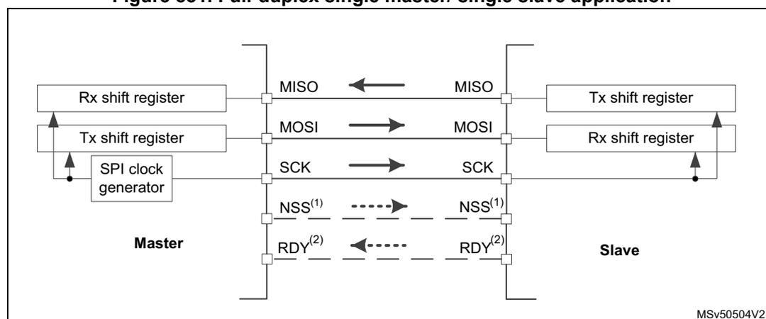
- 1. The NSS pin interconnection is optional. The slave can be configured to be permanently selected to operate in a single master-slave pair (see Section 67.4.7 ).
- 2. The RDY signal provided by the slave can be read by the master optionally.
Half-duplex communication
The SPI can communicate in half-duplex mode by setting COMM[1:0] = 11 in the SPI_CFG2 register. In this configuration, one single cross-connection line is used to link the shift registers of the master and slave together. During this communication, the data are synchronously shifted between the shift registers on the SCK clock edge in the transfer direction selected reciprocally by both master and slave with the HDDIR bit in their SPI_CR1 registers. Note that the SPI must be disabled when changing the direction of the communication. In this configuration, the MISO pin at master and the MOSI pin at slave are free for other application uses and act as GPIOs.
Figure 882. Half-duplex single master/ single slave application
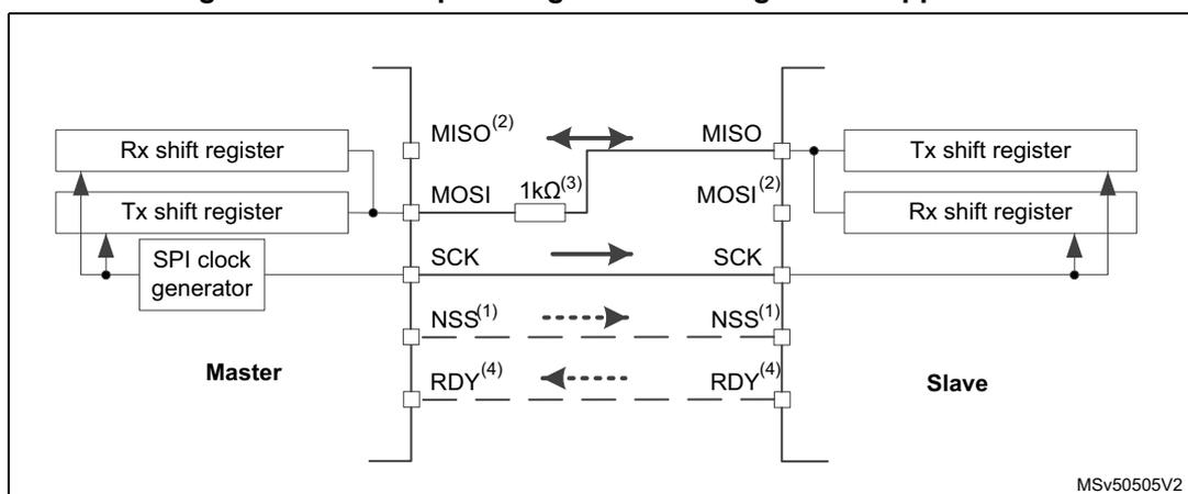
- 1. The NSS pin interconnection is optional. The slave can be configured to be permanently selected to operate in a single master-slave pair (see Section 67.4.7 ).
- 2. In this configuration, the MISO pin at master and MOSI pin at slave can be used as GPIOs
- 3. A critical situation can happen when the communication direction is not changed synchronously between two nodes working in bidirectional mode. The new transmitter accesses the common data line while the former transmitter still keeps an opposite value on the line (the value depends on the SPI configuration and communicated data). The nodes can conflict temporarily with opposite output levels on the line until the former transmitter changes its data direction setting. It is suggested to insert a serial resistance between MISO and MOSI pins in this mode to protect the conflicting outputs and limit the current flow between them.
- 4. The RDY signal provided by the slave can be read by the master optionally.
Simplex communications
The SPI can communicate in simplex mode by setting the SPI in transmit-only or in receive-only using the COMM[1:0] field in the SPI_CFG2 register. In this configuration, only one line is used for the transfer between the shift registers of the master and slave. The remaining MISO or MOSI pin pair is not used for communication and can be used as standard GPIOs.
- • Transmit-only mode: COMM[1:0] = 01
The master in transmit-only mode generates the clock as long as there are data available in the TxFIFO and the master transfer is ongoing.
The slave in transmit-only mode sends data as long as it receives a clock on the SCK pin and the NSS pin (or software managed internal signal) is active (see Section 67.4.7 ).
- • Receive-only mode: COMM[1:0] = 10
In master mode, the MOSI output is disabled and can be used as a GPIO. The clock signal is generated continuously as long as the SPI is enabled and the CSTART bit in the SPI_CR1 register is set. The clock is stopped either by software explicitly requesting this by setting the CSUSP bit in the SPI_CR1 register or automatically when the RxFIFO is full, when the MASRX bit in the SPI_CR1 is set.
In slave configuration, the MISO output is disabled and the pin can be used as a GPIO. The slave continues to receive data from the MOSI pin while its slave select signal is active (see Section 67.4.7 ).
Note: In whatever master and slave modes, the data pin dedicated for transmission can be replaced by the data pin dedicated for reception and vice versa by changing the IOSWP bit value in the SPI_CFG2 register (this bit can only be modified when the SPI is disabled).
Any simplex communication can be replaced by a variant of the half-duplex communication with a constant setting of the transfer direction (bidirectional mode is enabled, while the
HDDIR bit is never changed) or by full-duplex control when unused data line and corresponding data flow is ignored.
Figure 883. Simplex single master / single slave application
(master in transmit-only / slave in receive-only mode)
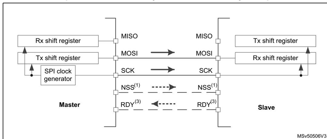
- 1. The NSS pin interconnection is optional. The slave can be configured to be permanently selected to operate in a single master-slave pair (see Section 67.4.7 ).
- 2. In this configuration, both the MISO pins can be used as GPIOs.
- 3. The RDY signal provided by the slave can be read by the master optionally.
67.4.5 Standard multislave communication
In a configuration with two or more independent slaves, the master uses a star topology with dedicated GPIO pins to manage the chip select lines for each slave separately (see Figure 884 ).
The master must select one of the slaves individually by pulling low the GPIO connected to the slave NSS input (only one slave can control data on a common MISO line at a given time).
When this is done, a communication between the master and the selected slave is established. In addition to the simplicity, the advantage of this topology is that a specific SPI configuration can be applied for each slave as all the communication sessions are performed separately just within a single master-slave pair. Optionally, when there is no need to read any information from slaves, the master can transmit the same information to the multiple slaves.
Figure 884. Master and three independent slaves connected in star topology
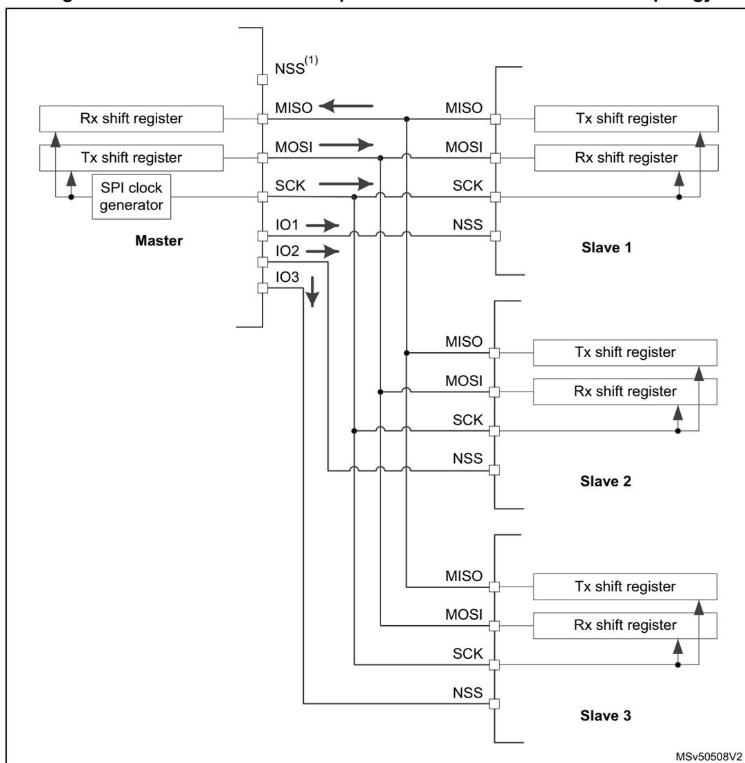
- 1. The master single NSS pin hardware output functionality cannot support this topology (to be replaced by a set of GPIOs under software control). The NSS pin is free for other application uses (such as GPIO or other alternate functions). Refer to Section 67.4.7 for details.
- 2. If the application cannot ensure that no more than a single NSS active signal is provided by the master at a given time, it is better to configure the MISO pins in an open-drain configuration with an external pull-up on the MISO line to prevent conflicts between the interconnected outputs of the slaves. Else, a push-pull configuration can be applied without an extra resistor (see I/O alternate function input/output (GPIO) section).
- 3. The RDY signals can be read by the master from the slaves optionally.
The master can handle the SPI communication with all the slaves at the same time when a circular topology is applied (see Figure 885 ). All the slaves behave like simple shift registers applied in serial chain under control of common slave select (NSS) and clock (SCK) signals. All the information is shifted simultaneously around the circle while returning back to the master. Sessions have fixed the length where the number of data frames transferred by the master is equal to the number of slaves.
Then when a first data frame is transferred in the chain, the master just sends the information dedicated for the last slave node in the chain, via the first slave node input, while the first information received by the master comes from the last node output at this time.
Correspondingly, the last transferred data finishing the session is dedicated for the first slave node while its first outgoing data just reaches the master input, after its circling around the chain passing through all the other slaves during the session.
The data format configuration and clock setting must be the same for all the nodes in the chain in this topology. As the receive and transmit shift registers are separated internally, a trick with intentional underrun must be applied to the TxFIFO slaves when the information is transferred between the receiver and the transmitter by hardware.
In this case, the transmission underrun feature is configured in a mode repeating the last received data frame (UDRCFG=1). A session can start optionally with a single data pattern written into the TxFIFO by each slave (usually slave status information is applied) before the session starts. In this case, the underrun happens in fact after this first data frame is transferred. To be able to clear the internal underrun condition immediately and restart the session by the TxFIFO content again, the user must disable and enable the SPI between the sessions and must fill the TxFIFO by a new single data pattern (to overcome the propagating delay of the clearing raised in case the underrun is cleared in a standard way by the UDRC bit).
Figure 885. Master and three slaves connected in circular (daisy chain) topology
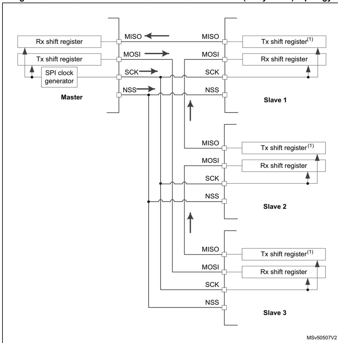
- 1. The underrun feature is used by the slaves in this configuration when the slaves are able to transmit data received previously into the Rx shift register once their TxFIFOs become empty.
- 2. The RDY signals can be read by the master optionally, either separately or configured as open drain outputs (while RDIOP = 0) and connected with a pull-up resistor as a common chain ready status overdriven by the slowest device.
67.4.6 Multimaster communication
Unless the SPI bus is not designed primarily for a multimaster capability, the user can use a built-in feature that detects a potential conflict between two nodes trying to master the bus at the same time. For this detection, the NSS pin is configured in hardware input mode. The connection of more than two SPI nodes working in this mode is impossible, as only one node can apply its output on a common data line at a given time.
When the nodes are not active, both stay in slave mode by default. Once a node wants to overtake control on the bus, it switches itself into master mode and applies active level on the slave select input of the other node via the dedicated GPIO pin. After the session is
complete, the active slave select signal is released and the node mastering the bus temporarily returns back to passive slave mode waiting for the next session to start.
If both nodes raise their mastering request at the same time, a bus conflict event appears (see mode fault MODF event). The user can apply some simple arbitration process (for example postpone the next attempt by different predefined timeouts applied to both nodes).
Figure 886. Multimaster application
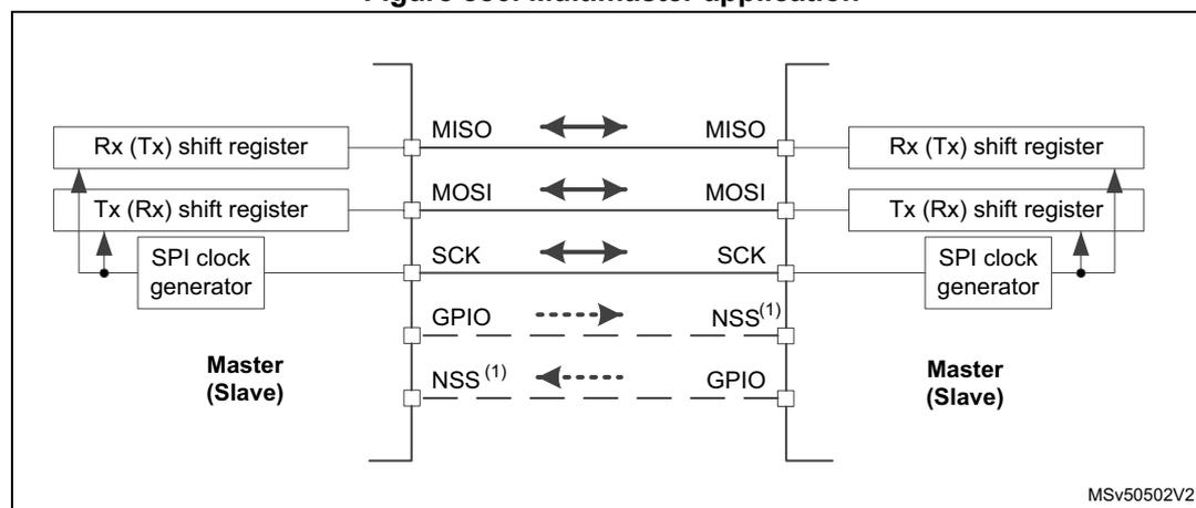
The diagram illustrates a multimaster SPI application with two nodes. Each node contains an 'Rx (Tx) shift register', a 'Tx (Rx) shift register', and an 'SPI clock generator'. The nodes are connected via three main lines: MISO (Master In Slave Out), MOSI (Master Out Slave In), and SCK (Serial Clock). The MISO and MOSI lines are bidirectional, while the SCK line is also bidirectional. The NSS (Slave Select) pin is connected between the two nodes. One node is labeled 'Master (Slave)' and the other 'Slave (Master)'. The diagram shows the internal components and the external connections for a multimaster setup. The text 'MSv50502V2' is visible in the bottom right corner of the diagram.
- 1. The NSS pin is configured at hardware input mode at both nodes. Its active level enables the MISO line output control since the passive node is configured as a slave.
- 2. The RDY signal is not used in this communication.
67.4.7 Slave select (NSS pin) management
In slave mode, the NSS works as a standard 'chip select' input and lets the slave communicate with the master. In master mode, the NSS can be used either as an output or an input. As an input it can prevent a multimaster bus collision, and as an output it can drive a slave select signal of a single slave. The NSS signal can be managed internally (software management of the NSS input) or externally when both the NSS input and output are associated with the NSS pin (hardware slave select management). The user can configure which level of this input/output external signal (present on the NSS pin) is considered as active by the SSIOP bit setting. NSS level is considered as active if it is equal to SSIOP.
The hardware or software slave select management can be set using the SSM bit in the SPI_CFG2 register:
- • Software slave select management (SSM = 1) : in this configuration, slave select information is driven internally by the SSI bit value in the SPI_CR1 register. The external NSS pin is free for other application uses (such as GPIO or other alternate functions).
- •
Hardware slave select management (SSM = 0)
: in this case, there are two possible configurations. The configuration used depends on the NSS output configuration (SSOE bit in the SPI_CFG2 register).
- – NSS output enable (SSOE = 1) : this configuration is only used when the MCU is set as master. The NSS pin is managed by the hardware. The functionality is tied to CSTART and EOT control. As a consequence, the master must apply the proper TSIZE > 0 setting to control the NSS output correctly. Even if SPI_AF is not applied at the NSS pin (it can be used as a standard GPIO then), keep anyway SSOE = 1 to ensure the default NSS input level and prevent any mode fault
evaluation at the input of the master NSS internal logic applicable at a multimaster topology exclusively.
- a) When SSOM = 0 and SP = 000, the NSS signal is driven to the active level as soon as the master transfer starts (CSTART = 1) and it is kept active until its EOT flag is set or the transmission is suspended.
- b) When SP = 001, a pulse is generated as defined by the TI mode.
- c) When SSOM = 1, SP = 000 and MIDI > 1 the NSS is pulsed inactive between data frames, and kept inactive for a number of SPI clock periods defined by the MIDI value decremented by one (from 1 to 14).
- d) NSS input is forced to nonactive state internally at master to prevent any mode fault.
- – NSS output disable (SSM = 0, SSOE = 0):
- a) If the microcontroller is acting as the master on the bus, this configuration allows multimaster capability. If the NSS pin is pulled into an active level in this mode, the SPI enters master mode fault state and the SPI device is automatically reconfigured in slave mode (MASTER = 0).
- b) In slave mode, the NSS pin works as a standard 'chip select' input and the slave is selected while the NSS line is at its active level.
Note: The purpose of automatic switching into slave mode when a mode fault occurs is to avoid the possible conflicts on data and clock lines. As the SPE is automatically reset in this condition, both Rx and Tx FIFOs are flushed and current data is lost.
When the SPI slave is enabled in the hardware slave select management mode, all the transfers are ignored even in case of the NSS is found at active level. They are ignored until the slave detects a start of the NSS signal (transition from nonactive to active level) just synchronizing the slave with the master. This is because the hardware management mode cannot be used when the external NSS pin is fixed. There is no such protection in the slave select software management. Then the SSI bit must be changed when there is no traffic on the bus and the SCK signal is in idle state level between transfers exclusively in this case.
Figure 887. Scheme of NSS control logic
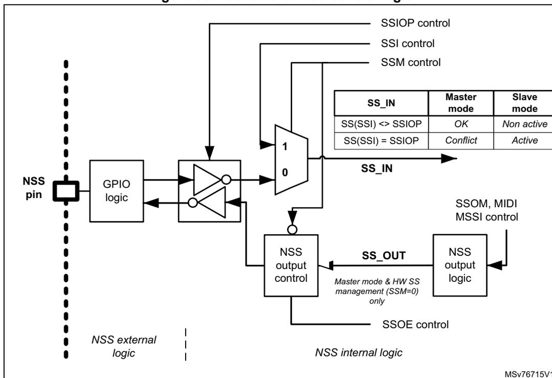
The diagram illustrates the internal logic for the NSS pin. On the left, the 'NSS pin' is connected to 'GPIO logic', which is part of 'NSS external logic'. The 'GPIO logic' output is inverted and connected to a 2-to-1 multiplexer. The multiplexer's inputs are labeled '1' and '0'. Input '1' is connected to 'SSIOP control', and input '0' is connected to 'SSI control'. The multiplexer output is 'SS_IN'. A table to the right shows the relationship between 'SS_IN', 'Master mode', and 'Slave mode':
| SS_IN | Master mode | Slave mode |
|---|---|---|
| SS(SSI) <> SSIOP | OK | Non active |
| SS(SSI) = SSIOP | Conflict | Active |
The 'SS_IN' signal is also connected to 'NSS output control'. The 'NSS output control' block is part of 'NSS internal logic' and receives 'SSOM, MIDI, MSSO control' and 'SSOE control' as inputs. It outputs 'SS_OUT' to 'NSS output logic', which in turn drives the 'NSS pin'.
When the hardware output NSS control is applied (SSM = 0, SSOE = 1), by configuration of the MIDI[3:0] and MSSO[3:0] bitfields, the user can control the timing of the NSS signal between data frames and can insert an extra delay at the beginning of every transfer (to separate the NSS and clock starts). This can be useful when the slave needs to slow down the flow to obtain sufficient room for correct data handling (see Figure 888).
Figure 888. Data flow timing control (SSOE = 1, SSOM = 0, SSM = 0)
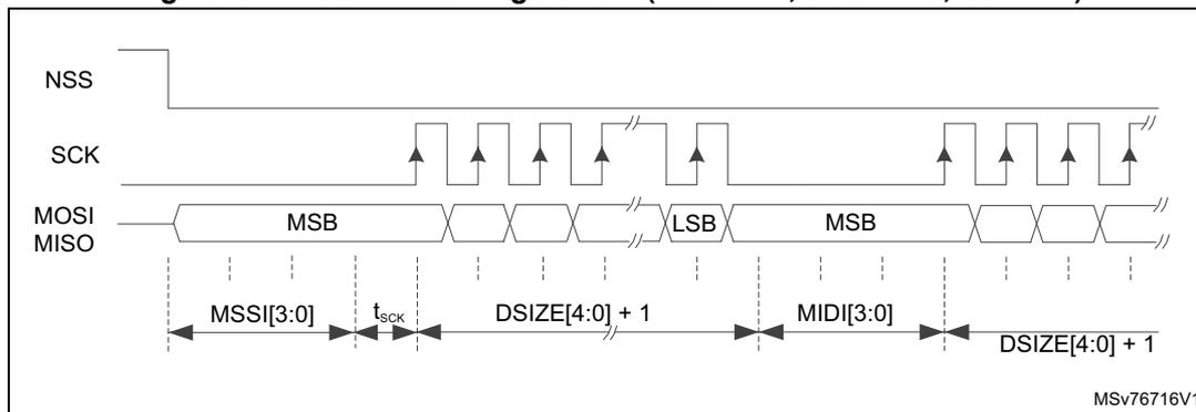
The timing diagram shows the relationship between the NSS, SCK, MOSI, and MISO signals during a data transfer. The NSS signal is shown as a horizontal line. The SCK signal is a periodic square wave. The MOSI and MISO signals are shown as a sequence of data frames, each consisting of a Most Significant Byte (MSB) and a Least Significant Byte (LSB). The timing parameters are defined as follows:
- MSSI[3:0] : The time interval from the falling edge of NSS to the first rising edge of SCK.
- t SCK : The period of the SCK signal.
- DSIZE[4:0] + 1 : The number of SCK periods for one data frame (MSB + LSB).
- MIDI[3:0] : The time interval from the last falling edge of SCK for the LSB to the next falling edge of NSS.
- 1. MSSO[3:0] = 0011, MIDI[3:0] = 0011 (SCK flow is continuous when MIDI[3:0] = 0).
- 2. CPHA = 0, CPOL = 0, SSIOP = 0, LSBFRST = 0.
Additionally, setting the SSOM bit invokes a specific mode, which interleaves pulses between data frames if there is a sufficient space to provide them (MIDI[3:0] must be set greater than one SPI period). Some configuration examples are shown in Figure 889.
Figure 889. NSS interleaving pulses between data (SSOE = 1, SSOM = 1, SSM = 0)
![Timing diagram for SPI mode I. Shows NSS, SCK, MOSI, and MISO signals. Data is transferred in bytes, with MSB first. NSS is active low. SCK is a square wave. MOSI and MISO are shown with MSB and LSB labels. Timing parameters include t_sck, MSS[3:0], DSIZE[4:0] + 1, and MIDI[3:0]. Timing diagram for SPI mode II. Similar to mode I but with different clock and data sampling phases. Timing parameters include t_sck/2, MSS[3:0], DSIZE[4:0] + 1, and MIDI[3:0]. Timing diagram for SPI mode III. Shows data transferred with LSB first. Timing parameters include t_sck, MSS[3:0], DSIZE[4:0] + 1, and MIDI[3:0]. Timing diagram for SPI mode IV. Similar to mode III but with different clock and data sampling phases. Timing parameters include t_sck/2, MSS[3:0], DSIZE[4:0] + 1, and MIDI[3:0].](/RM0486-STM32N6x5-x7/fa64ab72f0f4d1608728c44cbae28ba8_img.jpg)
I. CPHA=0, CPOL=0, SSIOP=0, LSBFRST=0
NSS
SCK
MOSI X MSB ... LSB X MSB ...
MISO X MSB ... LSB X MSB ...
MSS[3:0] \( t_{sck} \) DSIZE[4:0] + 1 MIDI[3:0] DSIZE[4:0] + 1
MIDI[3:0] - 1
II. CPHA=1, CPOL=0, SSIOP=0, LSBFRST=0
NSS
SCK
MOSI X MSB ... LSB X MSB ...
MISO X MSB ... LSB X MSB ...
MSS[3:0] \( t_{sck}/2 \) DSIZE[4:0] + 1 MIDI[3:0] DSIZE[4:0] + 1
MIDI[3:0] - 1
III. CPHA=0, CPOL=1, SSIOP=1, LSBFRST=1
NSS
SCK
MOSI X LSB ... MSB X LSB ...
MISO X LSB ... MSB X LSB ...
MSS[3:0] \( t_{sck} \) DSIZE[4:0] + 1 MIDI[3:0] DSIZE[4:0] + 1
MIDI[3:0] - 1
IV. CPHA=1, CPOL=1, SSIOP=1, LSBFRST=1
NSS
SCK
MOSI X LSB ... MSB X LSB ...
MISO X LSB ... MSB X LSB ...
MSS[3:0] \( t_{sck}/2 \) DSIZE[4:0] + 1 MIDI[3:0] DSIZE[4:0] + 1
MIDI[3:0] - 1
MSV76717V1
- 1. MSS[3:0] = 0010, MIDI[3:0] = 0010.
- 2. NSS interleaves between data when MIDI[3:0] > 1 wide of the interleaving pulse is always one SCK period less than the gap provided between the frames (defined by the MIDI parameter). If MIDI is set, the frames are separated by a single SCK period but no interleaving pulse appears on NSS.
67.4.8 Ready pin (RDY) management
The status of the slave capability to handle data can be checked on the RDY pin. By default, a low level indicates that the slave is not ready for transfer. The reason can be that the slave TxFIFO is empty, RxFIFO full or the SPI is disabled. An active level of the signal can be selected by the RDIOP bit. If the master continues or starts to communicate with the slave when it indicates a not ready status, it is highly probable that the transfer fails.
The logic to control the RDY output is rather complex, tied closely with the TSIZE and DSIZE settings. The RDY reaction is more pessimistic and sensitive to TxFIFO becoming nearly empty and/or RxFIFO nearly full during a frame transfer. This pessimistic logic is suppressed at the end of a transfer only when RDY stays active, despite TxFIFO becomes fully empty and/or RxFIFO becomes fully occupied. The target is to prevent any data corruption and inform the master in time that it is necessary to suspend the transfer temporarily until the next transferred data can be processed safely again. When the RDY signal input is enabled at master side, the master suspends the communication once the slave indicates not ready status. This prevents the master to complete the transfer of an ongoing frame, which just empties the slave TxFIFO or full fills its RxFIFO until a next data is written and/or read there (despite the frame still can be completed without any constraint). It can make a problem if the TSIZE = 0 configuration is applied at slave because slave then never evaluates the end of the transfer (which suppresses the not ready status just when the last data is sent). Then the user has to release the RxFIFO and/or write additional (even dummy) data to TxFIFO by software at slave side to release the not RDY signal, unblock ST master and so enable it to continue at the communication suspended at middle of a frame occasionally.
When RDY is not used by the master, it must be disabled (RDIOM = 0). Then an internal logic of the master simulates the slave status always ready. In this case, the RDIOP bit setting has no meaning.
Due to synchronization between clock domains and evaluation of the RDY logic on both master and slave sides, the RDY pin feature is not reliable and cannot be used when the size of data frames is configured shorter than 8 bits.
67.4.9 Communication formats
During SPI communication, receive and transmit operations are performed simultaneously. The serial clock (SCK) synchronizes the shifting and sampling of the information on the data lines. The communication format depends on the clock phase, the clock polarity, and the data frame format. To be able to communicate together, the master and slave devices must follow the same communication format and be synchronized correctly.
Clock phase and polarity controls
Four possible timing relationships can be chosen by software, using the CPOL and CPHA bits in the SPI_CFG2 register. The CPOL (clock polarity) bit controls the idle state value of the clock when no data is being transferred. This bit affects both master and slave modes. If CPOL is reset, the SCK pin has a low-level idle state. If CPOL is set, the SCK pin has a high-level idle state.
If the CPHA bit is set, the second edge on the SCK pin captures the first data bit transferred (falling edge if the CPOL bit is reset, rising edge if the CPOL bit is set). Data are latched on each occurrence of this clock transition type. If the CPHA bit is reset, the first edge on the SCK pin captures the first data bit transferred (falling edge if the CPOL bit is set, rising edge if the CPOL bit is reset). Data are latched on each occurrence of this clock transition type.
The combination of the CPOL (clock polarity) and CPHA (clock phase) bits selects the data capture clock edges (dotted lines in Figure 890).
Figure 890 shows an SPI full-duplex transfer with the four combinations of the CPHA and CPOL bits.
Note: Prior to changing the CPOL/CPHA bits the SPI must be disabled by resetting the SPE bit. The idle state of SCK must correspond to the polarity selected in the SPI_CFG2 register (by pulling the SCK pin up if CPOL = 1 or pulling it down if CPOL = 0).
Figure 890. Data clock timing diagram
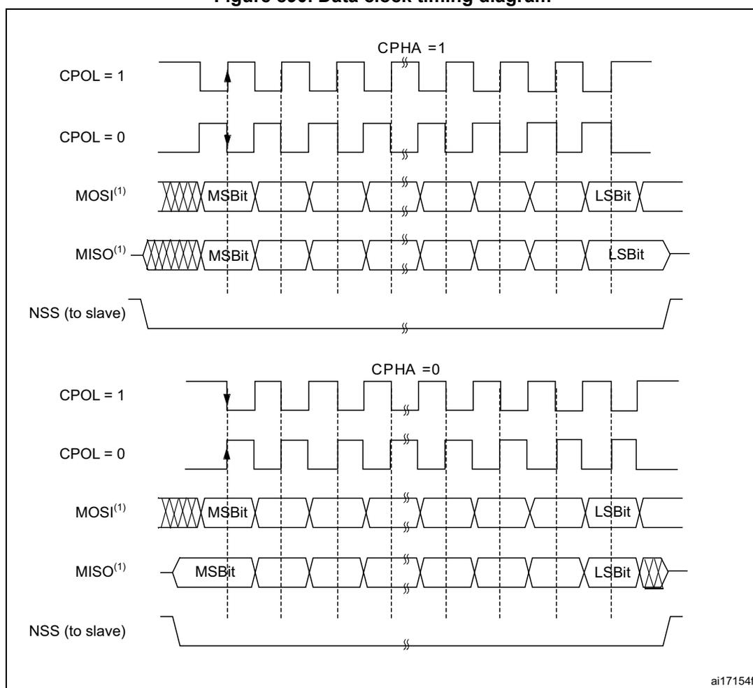
The diagram shows the timing for SPI full-duplex transfers. It is divided into two main sections based on the CPHA bit setting.
- CPHA = 1:
- CPOL = 1: The clock starts high. Data is captured on the falling edges of the clock. The MOSI signal is driven by the master, and the MISO signal is driven by the slave. The first data bit (MSB) is captured on the first falling edge.
- CPOL = 0: The clock starts low. Data is captured on the rising edges of the clock. The first data bit (MSB) is captured on the first rising edge.
- CPHA = 0:
- CPOL = 1: The clock starts high. Data is captured on the rising edges of the clock. The first data bit (MSB) is captured on the first rising edge.
- CPOL = 0: The clock starts low. Data is captured on the falling edges of the clock. The first data bit (MSB) is captured on the first falling edge.
The diagram also shows the NSS (to slave) signal, which is active low. The MOSI and MISO signals are shown with MSB and LSB labels. The order of data bits depends on the LSBFIRST bit setting.
- 1. The order of data bits depends on the LSBFIRST bit setting.
Data frame format
The SPI shift register can be set up to shift out MSB-first or LSB-first, depending on the value of the LSBFRST bit of the SPI_CFG2 register.
The data frame size is configured through the DSIZE bitfield of the SPI_CFG1 register to a range that depends on the SPI instance (see Section 67.3: SPI implementation ). The setting applies to both transmission and reception. The data bits in the SPI_TXDR/SPI_RXDR registers are right-aligned with 8, 16, or 32 bits, depending on the data size (see Figure 891 ). These registers can consequently be accessed by bytes, half-words, or words. FIFO accesses smaller than a single data are forbidden. When the FIFO occupancy flag is raised, a FIFO access greater than the FIFO threshold can lead to spurious data being read or written data being lost. When the access to/from the SPI_TXDR/SPI_RXDR registers is a multiple of the configured data size, data packing is applied automatically, while the lowest significant bits/bytes are communicated first. For more details, see Section 67.4.12: SPI data transmission and reception procedures .
Figure 891. Data alignment when data size is not equal to 8, 16 or 32 bits
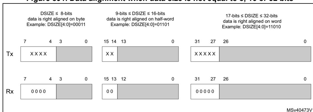
| DSIZE
\(
\leq
\)
8-bits data is right aligned on byte Example: DSIZE[4:0]=00011 | 9-bits
\(
\leq
\)
DSIZE
\(
\leq
\)
16-bits data is right aligned on half-word Example: DSIZE[4:0]=01101 | 17-bits
\(
\leq
\)
DSIZE
\(
\leq
\)
32-bits data is right aligned on word Example: DSIZE[4:0]=11010 | ||||
|---|---|---|---|---|---|---|
| 7 | 4 3 0 | 15 14 13 | 0 | 31 27 26 | 0 | |
| Tx | X X X X | X X | X X X X X | |||
| Rx | 0 0 0 0 | 0 0 | 0 0 0 0 0 | |||
MSV40473V1
67.4.10 Configuring the SPI
The configuration procedure is almost the same for the master and the slave. For specific mode setups, follow the dedicated chapters. When a standard communication must be initialized, perform these steps:
- Write the proper GPIO registers: configure GPIO alternate functions at MOSI, MISO, SCK, NSS, and RDY pins if applied.
- Write into the SPI_CFG1 and SPI_CFG2 registers and set up the proper values of all 'not reserved' bits and bitfields, prior to enabling the SPI, with the following exceptions:
- The SSOM, MASRX, SSOE, RDIOM, MBR[2:0], BPASS, MIDI[3:0], MSSI[3:0] bits are taken into account in master mode only, the MSSI[3:0] bits take effect when the SSOE bit is set, the RDIOP bit takes no effect when the RDIOM bit is not set in master mode. When the slave is configured in TI mode, the MBR[2:0] setting is also considered.
- UDRCFG is taken into account in slave mode only.
- CRCSIZE[4:0] bitfield must be configured if CRCEN is set.
- CPOL, CPHA, LSBFRST, SSOM, SSOE, SSIOP, SSM, RDIOP, RDIOM, MSSI, and MIDI are not required in TI mode.
- e) Once the AFCNTR bit is set in the SPI_CFG2 register, all the SPI outputs start to be propagated onto the associated GPIO pins regardless of the peripheral enable. So, any later configuration changes of the SPI_CFG1 and SPI_CFG2 registers can affect the level of signals on these pins.
- 3. Write to the SPI_CR2 register to select the length of the transfer, if it is not known TSIZE must be programmed to zero.
- 4. Write to the SPI_CRCPOLY and into the TCRCINI, RCRCINI, and CRC33_17 bits of the SPI_CR1 register to configure the CRC polynomial and CRC calculation if needed.
- 5. Configure DMA streams dedicated for the SPI Tx and Rx in DMA registers if the DMA streams are used (see Section 67.4.14: Communication using DMA (direct memory addressing) ).
- 6. Configure SSI, HDDIR, and MASRX in the SPI_CR1 register if required.
- 7. Program the IOLOCK bit in the SPI_CR1 register if the configuration protection is required (for safety).
67.4.11 Enabling the SPI
It is recommended to configure and enable the SPI slave before the master sends the clock. But there is no impact if the configuration and enabling procedure is done while traffic is ongoing on the bus, assuming that the NSS signal is managed by hardware at slave or kept inactive by the slave software when the software management of the NSS signal is applied (see Section 67.4.7 ). To prevent any risk of any data underrun, all the data to be sent have to be written to the slave transmitter data register before the master starts its clocking. The SCK signal must be settled to the idle state level corresponding to the selected polarity, before the SPI slave is selected by NSS, else the following transfer may be desynchronized.
When the SPI slave is enabled at the hardware slave select management mode, all the transfers are ignored even in case of the NSS is found at active level. They are ignored until the slave detects a start of the NSS signal (its transition from nonactive to active level) just synchronizing the slave with the master. That is why the hardware management mode cannot be used when the external NSS pin is fixed. There is no such protection at the slave select software management. In this case, the SSI bit must be changed when there is no traffic on the bus and the SCK signal is at idle state level between transfers exclusively in this case.
The master in full duplex (or in any transmit-only mode) starts to communicate when the SPI is enabled, the CSTART bit is set, and the TxFIFO is not empty, or with the next write to TxFIFO.
In any master receive-only mode, the master starts to communicate and the clock starts running after the SPI is enabled and the CSTART bit is set.
For handling DMA, see Section 67.4.14 .
67.4.12 SPI data transmission and reception procedures
The SPI can transfer data at a very high communication speed. Even though the data is FIFO buffered, handling a continuous data flow by servicing data frames individually leads to an enormous CPU or DMA load, in particular when the data size is small. This potentially leads to a significant limitation of the overall system performance, as well as communication errors such as data overrun or underrun that may be raised when the system latencies in servicing requests become comparable to single data frame transfer time.
The SPI offers advanced hardware control features to prevent these issues from occurring:
- • Decreasing the number of events requiring service by collecting the data frames into larger data packets
The number of data frames per packet (FIFO threshold) can be configured. The complete data packet generates a FIFO occupancy event, which is then handled within a single, compact, service.
- • Decreasing the number of CPU execution cycles required for the service, by applying the appropriate
data access
:
- – The widest access to the SPI data registers must be applied. This allows cumulative data to be handled by a single register read or write operation (data packing).
- – The number of read/write accesses necessary to complete the data packet must be aligned with the data frame size and the FIFO threshold.
- • Concurrent read and write services to handle full-duplex data flow based on common FIFO occupancy events.
- • Embedded hardware data counters to define the exact number of data involved in transfers.
Note: Using these features is optional. Nothing prevents the application from handling the data flow frame by frame.
The following sections give more details and describe specific cases for using these advanced hardware control features to handle data transfers.
Data packet control
The data frame size (number of bits in the frame) is defined through the DSIZE bitfield of the SPI_CFG1 register. The number of data frames per packet can be configured by selecting the FIFO threshold through the FTHLV bitfield of the SPI_CFG1 register. If the threshold value is set to zero, each completed data frame raises the FIFO occupancy event. The data packet occupancy must not exceed half of the FIFO size, which depends on the SPI instance of the product. The FIFO capacity (multiple of 8 bits) is consumed according to the following rules, depending on the data frame size:
- • Data frames from 4 to 8 bits occupy one byte of the FIFO.
- • Data frames from 9 to 16 bits occupy two bytes of the FIFO.
- • Data frames from 17 to 24 bits occupy three bytes of the FIFO.
- • Data frames from 25 to 32 bits occupy four bytes of the FIFO.
For example, if the FIFO capacity is 16 bytes, it accommodates up to five 24-bit frames. In this case, the data packet configuration must not exceed two data frames.
The SPI features two separate FIFOs to handle the reception and transmission data flow, the RxFIFO, and the TxFIFO. Their content can be handled by monitoring the occupancy
flags RXP, TXP, and DXP of the SPI_SR register according to the SPI mode (duplex or simplex):
- • If RXP is set, at least one complete data packet can be read from the RxFIFO.
- • If TXP is set, at least one complete data packet can be written to the TxFIFO.
- • If DXP is set, at least one complete data packet can be read from the RxFIFO and written to the TxFIFO at full-duplex mode.
These flags can be polled by software, or they can trigger an interrupt and/or a DMA request (if enabled through the RXPIE, TXPIE, and DXPIE bits of the SPI_EIR register or the RXDMAEN and TXDMAEN bits of the SPI_CFG1 register).
Once an occupancy flag is set, the software or the DMA must read and/or write a complete data packet before checking the flag again to verify if the next packet can be handled. This cycle can be repeated until the corresponding flag is read at zero.
Both RxFIFO and TxFIFO contents are flushed and cannot be accessed when the SPI is disabled (SPE cleared in the SPI_CR1 register).
Data packing versus data register access control
The content of the RxFIFO and TxFIFO can be accessed by reading/writing from/to the SPI data registers SPI_RXDR and SPI_TXDR, respectively. A read access from the SPI_RXDR register returns the oldest values stored in the RxFIFO that have not been read yet. A write access to the SPI_TXDR register stores the data written at the end of the send queue in the TxFIFO.
These data registers can be accessed by 8-, 16-, or 32-bit read and write CPU instructions, forced by the register address casting applied by the software. Data packing is performed automatically by hardware if the data access applied by the software is a multiple of the data size. It allows handling more than one data in parallel in a single data register access. Then the SPI operates using the lowest significant byte or half-word first. FIFO data accesses of less than the configured data size are forbidden. To avoid spurious data being read or written data being lost, a complete data packet (configured through the FIFO threshold) must be serviced when the corresponding FIFO occupancy flag is set. If the data pattern is not byte-, half-word, or word-aligned, only the valid data bits are stored right-aligned to the FIFO and transferred on the bus. Unused bits are discarded on the transmitter side and padded with zeros on the receiver side.
For example, if the data frame size fits into one byte, the data packing is used automatically when a 16-bit or 32-bit read/write access is performed by software from/to the SPI_RXDR/SPI_TXDR register. In this case, two respectively four data are handled by a single 16-bit respectively 32-bit access. Additionally, if such data frames are grouped into packets of four via the FIFO threshold setting, the packet to be serviced is signalized by raising the corresponding FIFO occupancy flag (TXP, RXP, or DXP). If the instance FIFO threshold is sufficient, a packet containing eight 8-bit data frames can be handled by two consecutive 32-bit accesses upon the same single threshold event. The most efficient data handling is achieved when the data packet size (defined by DSIZE and FTHLV bitfields) is aligned with the read/write access from/to the data registers.
Concurrent read and write services
In full-duplex mode, both TxFIFO and RxFIFO packet occupancies can be monitored through a common FIFO flag (DXP). When the DXP flag is set, the application performs the specified number of writes to SPI_TXDR to upload the content of one entire data packet for transmission, followed by the same number of reads from SPI_RXDR to download the
content of one received data packet. Once one data packet is uploaded and one packet is downloaded, the application software or the DMA checks again the DXP flag and repeats the data packet read and write operation sequence until DXP is read as zero.
The drawback of services based on DXP exclusively is that servicing the TxFIFO is delayed on purpose due to the SPI nature since the TXP events precedes the RXP ones. To allow continuous SCK clock flow on the master side and prevent underrun on the slave side, it is recommended to prefill a few data ahead to the TxFIFO at the transfer start, and wait until the transfer is complete to read the last received data.
Hardware data counter
If a hardware data counter is used (TSIZE bitfield of the SPI_CR2 register set to a nonzero value), the application software does not need to calculate the remaining number of data to be handled. The end of transfer automatically controls the CRC, as well as the hardware slave select management, when used. The user application does not need to ensure that the overall number of data is a multiple of the packet size. If the last data packet is incomplete, it is serviced in the same way as any full packet. The unused part of this last packet is not handled by the peripheral. Only the valid data are written into the TxFIFO and/or read from the RxFIFO, and the redundant writes and reads are discarded. When the hardware counter reaches zero, the EOT flag is raised, and the RXP flag is not set for the last data packet. If the last packet is not aligned with the packet size, the TXP and EOT occupancy events are not related to the configured packet size but to the number of remaining data calculated by hardware.
If TSIZE is kept at zero (for example due to an unpredictable number of data), only the number of transferred data corresponding to the FIFO thresholds is supported. If some data are not aligned with the configured packet size, they may remain pending and available in the RxFIFO. In this case, the FTHLV level is not reached and the RXP flag is not set. Then the number of remaining received data frames in the RxFIFO is indicated by the RXWNE and RXPLVL bitfields of the SPI_SR register. Nevertheless, the application software can still read the complete data packet from the RxFIFO and the redundant data are read as zero. To prevent such an unaligned data reception, the user must configure the FIFO threshold to a single data (FTHLV = 0). In this case, each data frame is serviced by its own RXP occupancy event.
Data transfer handling
Data are transferred using MOSI and MISO lines, depending on the SPI communication mode and associated configuration. The mode is configured through the COMM[1:0] bitfield of the SPI_CFG2 register. The HDDIR bit of the SPI_CR1 register controls the data flow direction in half-duplex mode. The communication flow is handled by the master via the NSS and SCK signals. The slave selected for the communication is fully subordinated to the master communication activity, no matter if it handles the data flow on time or not. The slave can only temporarily suspend the master communication by using the RDY signal. The active levels of RDY and NSS signals can be changed, or MISO and MOSI functionality swapped (via the RDIOP, SSIOP and IOSWP bits of the SPI_CFG2 register).
The SPI master transmitter can operate in full-duplex, simplex, or half-duplex mode. In full-duplex mode, data are received synchronously. The master starts the data transfer once the CSTART bit of the SPI_CR1 register is set, provided the SPI is enabled and the TxFIFO
content is not empty. The master then provides the serial clock signal continuously on the SCK pin until:
- • The total number of required data programmed in TSIZE is transferred, or
- • The transfer is suspended.
An automatic temporary suspension of the master transmission occurs when:
- • The slave does not assert the RDY signal, if it is used, or
- • The TxFIFO becomes empty, or
- • In full-duplex mode, the RxFIFO becomes full while the automatic suspension is enabled (MASRX set in the SPI_CR1 register).
When an automatic suspension occurs, the master stops providing the clock, and the transfer proceeds depending on the cause of the suspension, when:
- • The slave asserts RDY.
- • The master software or the DMA writes additional data to TxFIFO.
- • In full-duplex mode, the master software or the DMA releases the RxFIFO to enable it to accommodate new data.
The SPI master can receive data only when it operates in simplex receiver or half-duplex receiver mode. In these modes, the master starts the data transfer when the SPI is enabled, and the transfer is released by setting the CSTART bit. The serial clock signal is then provided continuously on the SCK pin by the master until:
- • The total number of required data programmed in TSIZE is received, or
- • The transfer is suspended by the master.
An automatic temporary suspension of the reception occurs when:
- • The slave does not assert the RDY signal, if it is used, or
- • The RxFIFO becomes full while the automatic suspension is enabled (MASRX bit set in the SPI_CR1 register).
When an automatic suspension occurs, the master stops providing the clock and the transfer proceeds depending on the cause of the suspension, when:
- • The slave asserts RDY.
- • The master software or the DMA releases the RxFIFO to enable it in order to accommodate new data.
A preferable way to terminate a transfer is to program the TSIZE bitfield to generate an EOT event. Hardware NSS signal or CRC handshake can then be controlled. To restart the internal state machine properly, it is recommended to disable the SPI and enable it again when the transfer is complete, even if the SPI configuration is not changed.
A transfer can be suspended at any time by setting the CSUSP bit of the SPI_CR1 register, which clears the CSTART bit. This software suspension control ensures the completion of any ongoing data frame. To restart the internal state machine properly, the SPI must be disabled and enabled again before the next transfer starts.
Oppositely, a temporary automatic suspension controlled by hardware typically results in a frozen and incomplete data frame transfer. This depends on baud rate setting, but usually, due to internal synchronization delays, the SCK signal stops when a few bits from the next data frame are already transferred on the bus. Once the suspension is released, the data frame transmission completes by transferring the remaining bits. That is why this automatic suspension is not quite reliable when the data frame size is less than eight bits. When shorter data frames are used, to prevent any data loss and assure proper RDY and/or
MASRX operation, the user can interleave and so extend the transfer time by inserting additional dummy clock cycles so that the period for a single data frame is higher or equal to eight SCK duration. This is done by setting the MIDI[3:0] bitfield of the SPI_CFG2 register.
Caution: If the SPE bit is cleared in master mode while the transfer is ongoing without any suspension, the clock is stopped even if the current frame transmission is not complete, and the content of the FIFOs is flushed and lost.
67.4.13 Disabling the SPI
To disable the SPI, it is mandatory to follow the disable procedures described in this paragraph.
In the master mode, it is important to do this before the system enters a low-power mode when the peripheral clock is stopped, otherwise, ongoing transfers may be corrupted.
In slave mode, the SPI communication can continue when the spi_pclk and spi_ker_ck clocks are stopped, without interruption, until any end of communication or data service request condition is reached. The spi_pclk can generally be stopped by setting the system into Stop mode. Refer to the RCC section for further information.
The master in full-duplex or transmit-only mode can finish any transfers when it stops providing data for transmission. In this case, the clock stops after the last data transfer. TXC flag can be polled (or interrupt enabled with EOTIE = 1) in order to wait for the last data frame to be sent.
When the master is in any receive-only mode, to stop the peripheral, the SPI communication must first be suspended, by setting the CSUSP bit.
The data received but not read remain stored in RxFIFO when the SPI is suspended.
After such a software suspension, SPI must always be disabled to restart the internal state machine properly.
When SPI is disabled, RxFIFO is flushed. To prevent losing unread data, the user must ensure that RxFIFO is empty when disabling the SPI, by reading all remaining data (as indicated by the RXP, RXWNE, and RXPLVL fields in the SPI_SR register).
The standard disable procedure is based on polling EOT and/or TXC status to check if a transmission session is (fully) completed. This check can be done in specific cases, too, when it is necessary to identify the end of ongoing transfers, for example:
- • When the master handles the NSS signal by a GPIO not related to SPI (for example at case of multislave star topology) and it has to provide a proper end-of-NSS pulse for the slave, or
- • When transfers from DMA or FIFO are completed while the last data frame or CRC frame transfer is still ongoing in the peripheral bus.
When TSIZE > 0, EOT and TXC signals are equal so polling of EOT is reliable at whatever SPI communication mode to check the end of the bus activity. When TSIZE = 0, the user has to check TXC, SUSP, or FIFO occupancy flags according to the applied SPI mode and the way of the data flow termination.
The correct disable procedure in master mode, except when receive-only mode is used, is:
- 1. Wait until TXC = 1 and/or EOT = 1 (no more data to transmit and last data frame sent). When CRC is used, it is sent automatically after the last data in the block is processed.
TXC/EOT is set when the CRC frame is complete in this case. When a transmission is suspended the software has to wait until the CSTART bit is cleared.
- 2. Read all RxFIFO data (until RXWNE = 0 and RXPLVL = 00).
- 3. Disable the SPI (SPE = 0).
The correct disable procedure for master receive-only modes is:
- 1. Wait on EOT or break the receive flow by suspending SPI (CSUSP = 1).
- 2. Wait until SUSP = 1 (the last data frame is processed) if the receive flow is suspended.
- 3. Read all RxFIFO data (until RXWNE = 0 and RXPLVL = 00).
- 4. Disable the SPI (SPE = 0).
In slave mode, any ongoing data are lost when disabling the SPI.
Controlling the I/Os
As soon as the SPI is disabled, the associated and enabled AF outputs can still be driven by the device depending on the AFCNTR bit of the SPI_CFG2 register. When active output control is applied (AFCNTR = 1) and SPI has just been disabled (SPE = 0), the enabled outputs associated with SPI control signals (like NSS and SCK at master and RDY at slave) can immediately toggle to inactive level (according to SSIOP and CPOL settings at master and RDIOP at slave respectively). Instead, the data line output (MOSI at master and MISO at slave) can immediately change its level depending on the actual TxFIFO content, with the effect of potentially making invalid and no more guaranteed the value of the latest transferred bit on the bus. If necessary, the user has to take care about proper data hold time at the data line and avoid any eventual fast SPI disable just after the last data transfer is complete.
Note: Despite stability of the latest bit is guaranteed by design during the sampling edge of the clock, some devices can require even extension of this data bit stability interval during the sampling. It can be done, for example by inserting a small software delay between EOT event occurrence and SPI disable action.
67.4.14 Communication using DMA (direct memory addressing)
To operate at its maximum speed and to facilitate the data register read/write process required to avoid overrun, the SPI features a DMA capability, which implements a simple request/acknowledge protocol.
A DMA access is requested when the TXDMAEN or RXDMAEN enable bits of the SPI_CFG1 register are set. Separate requests must be issued to the Tx and Rx buffers to fulfill the service of the defined packet.
- • In transmission, a series of DMA requests is triggered each time TXP is set. The DMA then performs a series of writes to the SPI_TXDR register.
- • In reception, a series of DMA requests is triggered each time RXP is set. The DMA then performs a series of reads from the SPI_RXDR register. When EOT is set at the end of the transfer and the last data packet is incomplete, then DMA request is activated automatically according to RXWNE and RXPLVL[1:0] setting to read the rest of data.
If the SPI is programmed in receive-only mode, UDR is never set.
If the SPI is programmed in a transmit mode, TXP and UDR can be eventually set at slave side, because transmit data may not be available. In this case, some data are sent on the TX line according with the UDR management selection.
When the SPI is used at a simplex mode, the user must enable the adequate DMA channel only while keeping the complementary unused channel disabled.
If the SPI is programmed in transmit-only mode, RXP and OVR are never set.
If the SPI is programmed in full-duplex mode, RXP and OVR are eventually set, because received data are not read.
In transmission mode, when the DMA or the user has written all the data to be transmitted (the TXTF flag is set in the SPI_SR register), the EOT (or TXC at case TSIZE = 0) flag can be monitored to ensure that the SPI communication is complete. This is required to avoid corrupting the last transmission before disabling the SPI or before disabling the spi_pclk in master mode. The software must first wait until EOT = 1 and/or TXC = 1.
When starting communication using DMA, to prevent DMA channel management raising error events, these steps must be followed in order:
- 1. Enable the DMA Rx buffer in the RXDMAEN bit of the SPI_CFG1 register, if DMA Rx is used.
- 2. Enable DMA requests for Tx and Rx in DMA registers, if the DMA is used.
- 3. Enable the DMA Tx buffer in the TXDMAEN bit of the SPI_CFG1 register, if DMA Tx is used.
- 4. Enable the SPI by setting the SPE bit.
To close communication, it is mandatory to follow these steps in order:
- 1. Disable DMA requests for Tx and Rx in the DMA registers, if the DMA issued.
- 2. Disable the SPI by following the SPI disable procedure.
- 3. Disable DMA Tx and Rx buffers by clearing the TXDMAEN and RXDMAEN bits of the SPI_CFG1 register, if DMA Tx and/or DMA Rx are used.
Data packing with DMA
If the transfers are managed by DMA (TXDMAEN and RXDMAEN set in the SPI_CFG1 register) the packing mode is enabled/disabled automatically depending on the PSIZE value configured for SPI TX and the SPI RX DMA channel.
The packing mode is enabled if the DMA channel PSIZE value is a multiple of the data size. Then the DMA automatically manages the sequences of write and read operations to/from the SPI data registers, based on FIFO occupancy flags, and depending on the FIFO threshold and data size configurations.
The DMA completes the transfer automatically according to the TSIZE field setting, whatever the data packing mode used, and even if the number of data to transfer is not a multiple of the DMA data size (16 bits or 32 bits) while the frame size is smaller.
Alternatively, the last data frames can be written by software, in the single/unpacked mode.
Configuring any DMA data access to less than the configured data size is forbidden. One complete data frame must be always accessed at minimum.
67.5 SPI specific modes and control
67.5.1 TI mode
With a specific SP[2:0] bitfield setting of the SPI_CFG2 register, the SPI can be configured compliant with the TI protocol. The SCK and NSS signals polarity, phase and flow, as well as the bit order are fixed, so the setting of CPOL, CPHA, LSBFRST, SSOM, SSOE, SSIOP, SSM, RDIOP, RDIOM, MSSI, and MIDI is not required when the SPI is in TI mode configuration. The NSS signal synchronizes the protocol by pulses over the LSB data bit as it is shown in Figure 892.
Figure 892. TI mode transfer
![Timing diagram for TI mode transfer showing NSS, SCK, MOSI, and MISO signals. The diagram illustrates the relationship between the Slave Select (NSS) signal, the Serial Clock (SCK), Master Out Slave In (MOSI), and Slave Out Master In (MISO) signals during a data transfer. The SCK signal is a periodic square wave. The MOSI signal is shown as a series of bytes, with the Most Significant Bit (MSB) and Least Significant Bit (LSB) indicated. The MISO signal is shown as a series of bytes, with the MSB and LSB indicated. The NSS signal is shown as a series of pulses. The data transfer is synchronized by the SCK signal. The diagram also shows the time interval for the data transfer, labeled as DSIZE[4:0] + 1, and the time interval for the MISO signal to become high-Z, labeled as TRELEASE.](/RM0486-STM32N6x5-x7/e6bc7bb36b8d2db8af8280dac25c8587_img.jpg)
In slave mode, the clock generator is used to define the time when the slave output at MISO pin becomes high-Z when the current transfer finishes. The master baud rate setting (MBR[2:0] of SPI_CFG1) is applied and any baud rate can be used to determine this moment with optimal flexibility. The delay for the MISO signal to become high-Z (T RELEASE ) depends on internal resynchronization, too, which takes the next additional 2-4 periods of the clock signal feeding the generator. It is given by the following formula:
If the slave detects a misplaced NSS pulse during a data transfer the TIFRE flag is set.
67.5.2 SPI error flags
An SPI interrupt is generated if one of the following error flags is set and the interrupt is enabled by setting the corresponding interrupt enable bit.
Overrun flag (OVR)
An overrun condition occurs when data are received by a master or slave and the RxFIFO has not enough space to store these received data. This can happen if the software or the DMA did not have enough time to read the previously received data (stored in the RxFIFO).
When an overrun condition occurs, the OVR flag is set and the newly received value does not overwrite the previous one in the RxFIFO. The newly received value is discarded and all
data transmitted subsequently are lost. The OVR flag triggers an interrupt if the OVRIE bit is set. Clearing the OVR bit is done by setting the OVRC bit of the SPI_IFCR register. Clearing the RxFIFO content by performing software reads before the OVR bit is cleared reduces the risk of any immediate repetition of its next overrun. It is suggested to release the RxFIFO space as much as possible, this means to read out all the available data packets based on RXP flag indication.
In master mode, the user can prevent the RxFIFO overrun by automatic communication suspend (MASRX bit).
Underrun flag (UDR)
In a slave-transmitting mode, the underrun condition is captured internally by hardware if no data is available for transmission in the slave TxFIFO commonly. The UDR flag setting is then propagated into the status register by hardware (see note below). UDR triggers an interrupt if the UDRIE bit is set.
Underrun detection logic and system behavior depend on the UDRCFG bit. When an underrun is detected by the slave, it can provide out either a constant pattern stored by the user at the UDRDR register or the data received previously from the master. When the first configuration (UDRCFG = 0) is applied, the underrun condition is evaluated whenever the master starts to communicate a new data frame while TxFIFO is empty. Then single additional dummy (accidental) data is always inserted between the last valid data and the constant pattern defined at the UDRDR register (see Figure 893 ). The second configuration (UDRCFG=1) can be used in circular topography structures (see Figure 885 ). Assuming that TxFIFO is not empty when the master starts the communication, the underrun condition is evaluated just once the FIFO becomes empty during the next data flow. Valid data from TxFIFO is then upended by the last received data immediately.
The standard transmission is reenabled once the software clears the UDR flag and this clearing is propagated into SPI logic by hardware. Writing some data to the TxFIFO before the UVR bit is cleared reduces the risk of any immediate repetition of its next underrun.
The data transferred by the slave is unpredictable especially when the transfer starts or continues while TxFIFO is empty and the underrun condition is either not yet captured or just cleared. Typically, this is the case when SPI is just enabled or when a transfer with a defined size just starts. First bits can be corrupted in this case, as well, when the slave software writes the first data into the empty TxFIFO too close prior to starting the data transfer (propagation of the data into TxFIFO takes a few APB clock cycles).
Figure 893. Optional configurations of the slave behavior when an underrun condition is detected
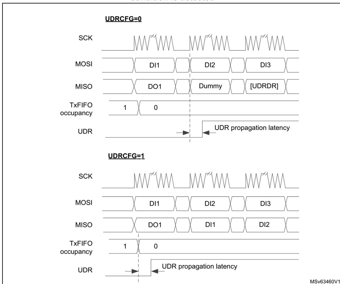
The diagram illustrates two optional configurations for slave behavior during an underrun condition in SPI. It is divided into two sections: UDRCFG=0 and UDRCFG=1 .
UDRCFG=0: This section shows the timing for the first configuration. The SCK (Serial Clock) line is shown as a continuous square wave. The MOSI (Master Out Slave In) line carries data DI1, DI2, and DI3. The MISO (Master In Slave Out) line carries DO1, a Dummy byte, and [UDRDR] (Underrun Data Register). The TxFIFO occupancy is shown as 1, then 0. The UDR (Underrun) flag is shown as a pulse that goes high when the TxFIFO becomes empty (0) and returns low after a "UDR propagation latency" period. A vertical dashed line marks the start of the second configuration.
UDRCFG=1: This section shows the timing for the second configuration. The SCK line is the same. The MOSI line carries DI1, DI2, and DI3. The MISO line carries DO1, DI1, and DI2. The TxFIFO occupancy is shown as 1, then 0. The UDR flag is shown as a pulse that goes high when the TxFIFO becomes empty (0) and returns low after a "UDR propagation latency" period. A vertical dashed line marks the start of the first configuration.
MSV63460V1
Note: The hardware propagation of an UDR event needs additional traffic on the bus. It always takes a few extra SPI clock cycles after the event happens (both underrun captured by hardware and cleared by software). If clearing of the UDR flag by software is applied close to the end of the data frame transfer or when the SCK line is at idle in between the frames, the next extra underrun pattern is sent initially by the slave before the valid data from TxFIFO becomes transferred again. The user can prevent this by SPI disable/enable action between sessions to restart the underrun logic and so initiate the next session by the valid data.
Mode fault (MODF)
Mode fault occurs when the master device has its internal NSS signal (NSS pin in slave select hardware mode, or SSI bit in slave select software mode) pulled low. This automatically affects the SPI interface in the following ways:
- • The MODF bit is set and the SPI interrupt is triggered if the MODFIE bit is set.
- • The SPE bit is forced to zero until the MODF bit is set. This disables the SPI and blocks all the peripheral outputs except the MODF interrupt request if enabled.
- • The MASTER bit is cleared, thus forcing the device into slave mode.
MODF is cleared by writing 1 to the MODFC bit of the SPI_IFCR register.
To avoid any multiple slave conflicts in a system comprising several MCUs, the NSS pin must be pulled to its nonactive level before reenabling the SPI, by setting the SPE bit.
As a security, the hardware does not allow the SPE bit to be set while the MODF bit is set. In a slave device, the MODF bit cannot be set except as the result of a previous multimaster conflict.
A correct software procedure when a master overtakes the bus in multimaster systems must be the following one:
- 1. Switch into master mode while SSOE = 0 (potential conflict can appear when another master occupies the bus. In this case, MODF is raised, which prevents any next node switching into master mode).
- 2. Put GPIO pin dedicated for another master slave select control into active level.
- 3. Perform a data transfer.
- 4. Put GPIO pin dedicated for another master slave select control into nonactive level.
- 5. Switch back to slave mode.
CRC error (CRCE)
This flag is used to verify the validity of the value received when the CRCEN bit of the SPI_CFG1 register is set. The CRCE flag of the SPI_SR register is set if the value received in the shift register does not match the receiver SPI_RXCRC value, after the last data is received (as defined by TSIZE). The CRCE flag triggers an interrupt if the CRCEIE bit is set. Clearing the bit CRCE is done by a writing 1 to the CRCEC bit of the SPI_IFCR register.
TI mode frame format error (TIFRE)
A TI mode frame format error is detected when an NSS pulse occurs during an ongoing communication when the SPI is operating in slave mode and configured to conform to the TI mode protocol. When this error occurs, the TIFRE flag is set in the SPI_SR register. The SPI is not disabled when an error occurs, the NSS pulse is ignored, and the SPI waits for the next NSS pulse before starting a new transfer. The data may be corrupted since the error detection may result in the loss of a few data frames.
The TIFRE flag is cleared by writing 1 to the TIFREC bit of the SPI_IFCR register. If the TIFREIE bit is set, an interrupt is generated on the NSS error detection. As data consistency is no longer guaranteed, communication must be reinitiated by software between master and slave.
67.5.3 CRC computation
Two separate CRC calculators are implemented to check the reliability of transmitted and received data. The CRC polynomial configuration depends on the instance. Refer to Section 67.3: SPI implementation for more information.
The length of the polynomial is defined by the most significant bit of the value stored in the SPI_CRCPOLY register. It must be greater than the data frame size (in bits) defined in the DSIZE[4:0] bitfield of the SPI_CFG1 register. To obtain a full-size polynomial, the polynomial length must exceed the maximum data size of the peripheral instance, and the CRC33_17 bit of the SPI_CR1 register must be set to select the most significant bit of the polynomial string.
For example, to select the standard CRC16-CCITT (XMODEM) polynomial \( x^{16} + x^{12} + x^5 + 1 \) :
- • For a 32-bit instance: write 0x11021 to the SPI_CRCPOLY register and clear the CRC33_17 bit.
- • For a 16-bit instance: to obtain the full size, write 0x1021, and set the CRC33_17 bit.
The CRC SIZE field of the SPI_CFG1 register then defines how many most significant bits from the CRC calculation registers are transferred and compared as CRC frame. It is defined independently from the data frame length, but it must be either equal or an integer multiple of the data frame size. Its size cannot exceed the maximum data size of the instance.
To fully benefit from the CRC calculation capability, the polynomial length setting must correspond to the CRC frame size, else the bits unused at the calculation are transferred and expected all zero at the end of the CRC frame if its size is set greater than the polynomial length.
CRC principle
The CRC calculation is enabled by setting the CRCEN bit of the SPI_CFG1 register before the SPI is enabled (SPE = 1). The CRC value is then calculated using the CRC polynomial defined by the CRCPOLY register and CRC33_17 bit. When SPI is enabled, the CRC polynomial can be changed but only in the case when there is no traffic on the bus.
The CRC computation is done, bit by bit, on the sampling clock edge defined by the CPHA and CPOL bits of the SPI_CR1 register. The calculated CRC value is checked automatically at the end of the data block defined by the SPI_CR2 register exclusively.
When a mismatch is detected between the CRC calculated internally on the received data and the CRC received from the transmitter, a CRCE flag is set to indicate a data corruption error. The right procedure for handling the CRC depends on the SPI configuration and the chosen transfer management.
CRC transfer management
Communication starts and continues normally until the last data frame has been sent or received in the SPI_DR register.
The length of the transfer must be defined by TSIZE. When the desired number of data is transferred, the TXCRC is transmitted and the data received on the line are compared to the RXCRC value.
Whatever the CRC SIZE configuration, TSIZE cannot be set to 0xFFFF for a full-featured instance, and to 0x3FF for a limited-featured instance, if CRC is enabled.
In transmission, the CRC computation is frozen during the CRC transfer and the TXCRC is transmitted, in a frame of length equal to the CRCSIZE field value.
In reception, the RXCRC is also frozen when the desired number of data is transferred. Information to be compared with the RXCRC register content is then received in a frame of length equal to the CRCSIZE value.
Once the CRC frame is complete, an automatic check is performed comparing the received CRC value and the value calculated in the SPI_RXCRC register. The software has to check the CRCE flag of the SPI_SR register to determine if the data transfers were corrupted or not. Software clears the CRCE flag by writing 1 to the CRCEC.
The user takes no care about any flushing redundant CRC information, it is done automatically.
Resetting the SPI_TXCRC and SPI_RXCRC values
The SPI_TXCRC and SPI_RXCRC values are initialized automatically when new data is sampled after a CRC phase. This allows the use of DMA circular mode to transfer data without any interruption (several data blocks covered by intermediate CRC checking phases). Initialization patterns for receiver and transmitter can be configured either to zero or to all ones in dependency on setting bits TCRCINI and RCRCINI of the SPI_CR1 register.
The CRC values are reset when the SPI is disabled.
67.6 SPI in low-power modes
Table 660. Effect of low-power modes on the SPI
| Mode | Description |
|---|---|
| Sleep | No effect. SPI interrupts cause the device to exit Sleep mode. |
| Stop (1) | The content of the SPI registers is kept. |
| Standby | The SPI instance is not functional in this mode. It is powered down, and must be reinitialized after exiting Standby mode. |
- 1. Refer to Section 67.3: SPI implementation for information about wake-up from Stop mode support per instance as well as Standby mode availability. If an instance is not functional in a Stop mode, it must be disabled before entering this Stop mode.
67.7 SPI interrupts
Table 661 gives an overview of the SPI events capable of generating interrupts if enabled. Some of them feature wake-up from low-power mode capability, additionally. Most of them can be enabled and disabled independently while using specific interrupt enable control bits. The flags associated with the events are cleared by specific methods. Refer to the description of SPI registers for more details about the event flags. When SPI is disabled, all the pending interrupt requests are blocked to prevent their propagation into the interrupt services, except the MODF interrupt request.
Table 661. SPI wake-up and interrupt requests
| Interrupt vector | Interrupt event | Event flag | Enable Control bit | Event clear method | Exit from Stop and Standby modes capability (1)(2) |
|---|---|---|---|---|---|
| SPI | TxFIFO ready to be loaded (space available for one data packet - FIFO threshold) | TXP | TXPIE | TXP cleared by hardware when TxFIFO contains less than FTHLV empty locations | Yes |
| Data received in RxFIFO (one data packet available - FIFO threshold) | RXP | RXPIE | RXP cleared by hardware when RxFIFO contains less than FTHLV samples | Yes | |
| Both TXP and RXP active | DXP | DXPIE | When TXP or RXP are cleared | Yes | |
| Transmission Transfer Filled | TXTF | TXTFIE | Writing TXTFC to 1 | No | |
| Underrun | UDR | UDRIE | Writing UDRC to 1 | Yes | |
| Overrun | OVR | OVRIE | Writing OVRC to 1 | Yes | |
| CRC Error | CRCE | CRCEIE | Writing CRCEC to 1 | Yes | |
| TI Frame Format Error | TIFRE | TIFREIE | Writing TIFREC to 1 | No | |
| Mode Fault | MODF | MODFIE | Writing MODFC to 1 | No | |
| End Of Transfer (full transfer sequence completed - based on TSIZE value) | EOT | EOTIE | Writing EOTC to 1 | Yes | |
| Master mode suspended | SUSP | Writing SUSPC to 1 | Yes | ||
| TxFIFO transmission complete (TxFIFO empty) | TXC (3) | TXC cleared by hardware when a transmission activity starts on the bus | No |
- 1. All the interrupt events can wake up the system from Sleep mode at each instance. For detailed information about instances capabilities to exit from concrete Stop and Standby mode refer to the Functionalities depending on the working mode table.
- 2. Refer to Section 67.3: SPI implementation for information about Standby mode availability.
- 3. The TXC flag behavior depends on the TSIZE setting. When TSIZE>0, the flag fully follows the EOT one including its clearing by EOTC.
67.8 I2S main features
- • Full duplex communication
- • Simplex communication (only transmitter or receiver)
- • Master or slave operations
- • 8-bit programmable linear prescaler
- • Data length can be 16, 24 or 32 bits (a)
- • Channel length can be 16 or 32 in master, any value in slave
- • Programmable clock polarity
- • Error flags signaling for improved reliability: Underrun, overrun, and frame errors
- • Embedded Rx and TxFIFOs
- • Supported I
2
S protocols:
- – I 2 S Philips standard
- – MSB-justified standard (left-justified)
- – LSB-justified standard (right-justified)
- – PCM standard (with short and long frame synchronization)
- • Data ordering programmable (LSb or MSb first)
- • DMA capability for transmission and reception
- • Master clock can be output to drive an external audio component:
- – \( F_{MCK} = 256 \times F_{WS} \) for all I2S modes
- – \( F_{MCK} = 128 \times F_{WS} \) for all PCM modes
Note: \( F_{MCK} \) is the master clock frequency and \( F_{WS} \) is the audio sampling frequency.
67.9 I2S functional description
67.9.1 I2S general description
The block diagram shown on Figure 880 also applies for I2S mode.
The SPI/I2S block can work in I2S/PCM mode, when the bit I2SMOD is set. A dedicated register (SPI_I2SCFGR) is available for configuring the dedicated I2S parameters, which include the clock generator, and the serial link interface.
The I2S/PCM function uses the clock generator to produce the communication clock when the SPI/I2S is set in master mode. This clock generator is also the source of the master clock output (MCK).
Resources such as RxFIFO, TxFIFO, DMA, and parts of interrupt signaling are shared with the SPI function. The low-power mode function is also available in I2S mode (refer to Section 67.6: SPI in low-power modes and Section 67.10: I2S interrupts ).
a. Not always available, refer to Section 67.3: SPI implementation in order to check if 24 and 32-bit data widths are supported.
67.9.2 Pin sharing with SPI function
The I2S shares four common pins with the SPI:
- • SDO: serial data output (mapped on the MOSI pin) to transmit the audio samples in master, and receive the audio sample in slave mode. Refer to Section : Serial data line swapping on page 3470 .
- • SDI: serial data input (mapped on the MISO pin) to receive the audio samples in master, and transmit the audio sample in slave mode. Refer to Section : Serial data line swapping on page 3470 .
- • WS: word select (mapped on the NSS pin). This is the frame synchronization. It is configured as output in master mode, and as input in slave mode.
- • CK: serial clock (mapped on the SCK pin). This is the serial bit clock. It is configured as output in master mode, and as input in slave mode.
An additional pin can be used when a master clock output is needed for some external audio devices:
- • MCK: master clock (mapped separately) is used when the I2S is configured in master mode.
67.9.3 Bitfields usable in I2S/PCM mode
When the I2S/PCM mode is selected (I2SMOD = '1'), some bitfields are no longer relevant, and must be forced to a specific value to guarantee the behavior of the I2S/PCM function. Table 662 shows the list of bits and fields available in the I2S/PCM mode, and indicates which must be forced to a specific value.
Table 662. Bitfields usable in PCM/I2S mode
| Register name | Bitfields usable in PCM/I2S Mode | Constraints on other bitfields |
|---|---|---|
| SPI/I2S control register 1 (SPI_CR1) | IOLOCK, CSUSP, CSTART, SPE | Other fields set to their reset values |
| SPI/I2S control register 2 (SPI_CR2) | - | Set to reset value |
| SPI/I2S configuration register 1 (SPI_CFG1) | TXDMAEN, RXDMAEN, FTHLV | Other fields set to their reset values |
| SPI/I2S configuration register 2 (SPI_CFG2) | AFCNTR, LSBFRST, IOSWP | Other fields set to their reset values |
| SPI/I2S interrupt enable register (SPI_IER) | TIFREIE, OVRIE, UDRIE, TXPIE, RXPIE | |
| SPI/I2S status register (SPI_SR) | SUSP, TIFRE, OVR, UDR, TXP, RXP | Other flags not relevant |
| SPI/I2S interrupt/status flags clear register (SPI_IFCR) | SUSPC, TIFREC, OVRC, UDRC | Other fields set to their reset values |
| SPI/I2S receive data register (SPI_RXDR) | The complete register | - |
Table 662. Bitfields usable in PCM/I2S mode (continued)
| Register name | Bitfields usable in PCM/I2S Mode | Constraints on other bitfields |
|---|---|---|
| SPI/I2S polynomial register (SPI_CRCPOLY) | - | Set to reset value |
| SPI/I2S transmitter CRC register (SPI_TXCRC) | - | |
| SPI/I2S receiver CRC register (SPI_RXCRC) | - | |
| SPI/I2S underrun data register (SPI_UDRDR) | - | |
| SPI/I2S configuration register (SPI_I2SCFGR) | The complete register | - |
67.9.4 Slave and master modes
The SPI/I2S block supports master and slave modes for both I2S and PCM protocols. In master mode, both CK, WS and MCK signals are set to output.
In slave mode, both CK and WS signals are set to input. The signal MCK cannot be used in slave mode.
To improve the robustness of the SPI/I2S block in slave mode, the peripheral resynchronizes each reception and transmission on WS signal. This means that:
- • In I2S Philips standard, the shift-in or shift-out of each data is triggered one bit clock after each transition of WS.
- • In I2S MSB-justified standard, the shift-in or shift-out of each data is triggered as soon as a transition of WS is detected.
- • In PCM short standard, the shift-in or shift-out of each data is triggered one bit clock after the active edge of WS.
- • In PCM long standard, the shift-in or shift-out of each data is triggered as soon as the active edge of WS is detected
Note: This resynchronization mechanism is not available for the I2S LSB-justified standard.
Note as well that there is no need to provide a kernel clock when the SPI/I2S is configured in slave mode.
67.9.5 Supported audio protocols
The I2S/PCM interface supports four audio standards, configurable using the I2SSTD[1:0] and PCMSYNC bits of the SPI_I2SCFGR register.
In the I2S protocol, the audio data are time-multiplexed on two channels: the left channel and the right channel. The WS signal is used to indicate which channel must be considered as the left, and which one is the right.
In I2S master mode, four frame formats are supported:
- • 16-bit data packed in a 16-bit channel
- • 16-bit data packed in a 32-bit channel
- • 24-bit data packed in a 32-bit channel (a)
- • 32-bit data packed in a 32-bit channel (a)
In PCM master mode, three frame formats are supported:
- • 16-bit data packed in a 16-bit channel
- • 16-bit data packed in a 32-bit channel
- • 24-bit data packed in a 32-bit channel (a)
The figure hereafter shows the main definition used in this section: data length, channel length and frame length.
Figure 894. Waveform examples
For simplicity sake, in the next figures, SDI represents the serial data input and SDO the serial data output. Refer to Section : Serial data line swapping for details about the direction control of serial data lines.
I 2 S Philips standard
The I2S Philips standard is selected by setting I2SSTD to 0b00. This standard is supported in master and slave mode.
In this standard, the WS signal toggles one CK clock cycle before the first bit (MSb in I2S Philips standard) is available. A falling edge transition of WS indicates that the next data transferred is the left channel, and a rising edge transition indicates that the next data transferred is the right channel.
a. Not always available, refer to Section 67.3: SPI implementation to check if 24 and 32-bit data widths are supported.
Figure 895. Master I2S Philips protocol waveforms (16/32-bit full accuracy)
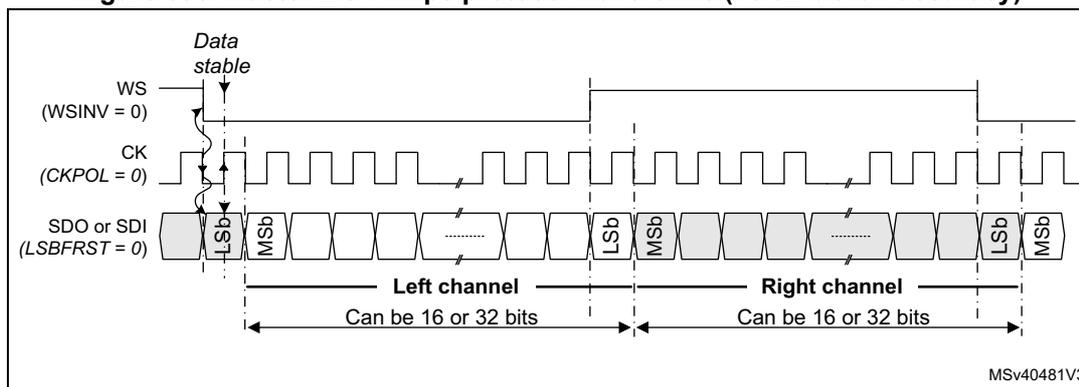
- 1. Data width of 24 and 32 bits are not always supported (DATLEN = 01 or 10). Refer to Section 67.3: SPI implementation for the supported data sizes.
CKPOL is cleared to match the I2S Philips protocol. See Selection of the CK sampling edge for information concerning the handling of the WS signal.
Figure 895 shows an example of waveform generated by the SPI/I2S in the case where the channel length is equal to the data length. More precisely, this is true when CHLEN = 0 and DATLEN = 0b00 or when CHLEN = 1 and DATLEN = 0b10.
See Control of the WS inversion for information concerning the handling of the WS signal.
Figure 896. I2S Philips standard waveforms
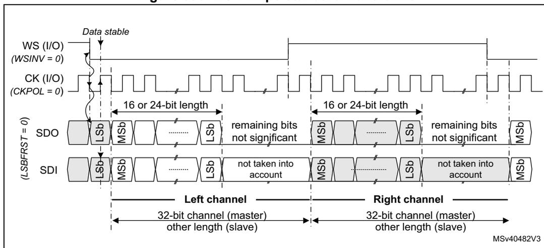
- 1. Data width of 24 and 32 bits are not always supported (DATLEN = 01 or 10). Refer to Section 67.3: SPI implementation for the supported data sizes.
In the case where the channel length is bigger than the data length, the remaining bits are not significant when the SPI/I2S is configured in transmit mode. This is applicable for both master and slave mode.
MSB-justified standard
For this standard, the WS signal toggles when the first data bit is provided. The data transferred represents the left channel if WS is high and the right channel if WS is low.
Figure 897. Master MSB-justified 16- or 32-bit full-accuracy length
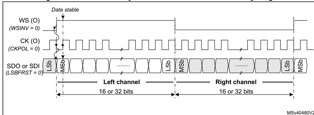
- 1. Data width of 24 and 32 bits are not always supported (DATLEN = 01 or 10). Refer to Section 67.3: SPI implementation to check the supported data size.
CKPOL is cleared to match the I2S MSB-justified protocol. See Selection of the CK sampling edge for information concerning the handling of the WS signal.
See Control of the WS inversion for information concerning the handling of the WS signal.
Figure 898. Master MSB-justified 16- or 24-bit data length
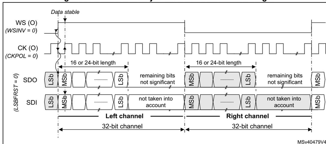
- 1. Data width of 24 and 32 bits are not always supported (DATLEN = 01 or 10). Refer to Section 67.3: SPI implementation to check the supported data size.
In the case where the channel length is bigger than the data length, the remaining bits are not significant when the SPI/I2S is configured in master transmit mode. In slave transmit mode, the remaining bits are forced to the value of the first bit of the next data to be generated to avoid timing issues (see Figure 899 ).
Figure 899. Slave MSB-justified 16-, 24- or 32-bit data length
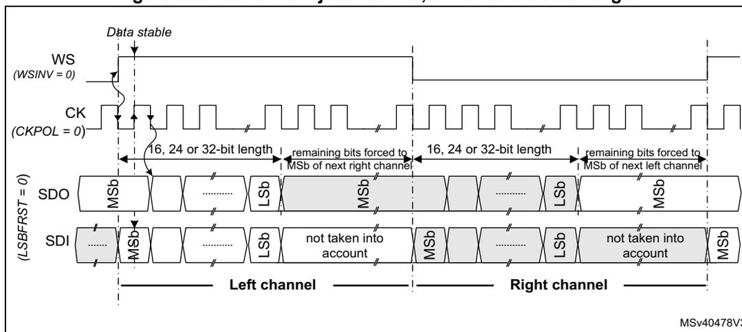
- 1. Data width of 24 and 32 bits are not always supported (DATLEN = 01 or 10). Refer to Section 67.3: SPI implementation to check the supported data size.
LSB-justified standard
This standard is similar to the MSB-justified standard in master mode (no difference for the 16- and 32-bit full-accuracy frame formats). The LSB-justified 16- or 32-bit full-accuracy format gives similar waveforms to MSB-justified mode (see Figure 897 ) because the channel and data have the same length.
Note: In the LSB-justified format, only 16- and 32-bit channel lengths are supported in master and slave mode. This is because it is not possible to transfer properly the data if the channel length is not known by the transmitter and receiver side.
Figure 900. LSB-justified 16 or 24-bit data length
- 1. Data width of 24 and 32 bits are not always supported (DATLEN = 01 or 10). Refer to Section 67.3: SPI implementation to check the supported data size.
CKPOL is cleared in order to match the I2S LSB-justified protocol. See Selection of the CK sampling edge for information concerning the handling of the WS signal.
See Control of the WS inversion for information concerning the handling of the WS signal.
PCM standard
For the PCM standard, there is no need to use channel-side information. The two PCM modes (short and long frame) are available and can be selected using the PCMSYNC bit of SPI_I2SCFGGR register.
In PCM long frame:
- • The assertion time of the WS signal is fixed to 13 cycles of CK in master mode,
- • The first data bit is received or transmitted as soon as the WS signal is asserted.
In PCM short frame:
- • The assertion time of the WS signal is fixed to one cycle of CK in master mode,
- • The first data bit is received or transmitted one cycle of CK after the WS assertion.
For both PCM modes:
- • The first data bit is MSb or LSb depending on the LSBFIRST bit value.
- • The CK sampling edge can be selected thanks to CKPOL bit.
- • The WS signal can be inverted thanks to the WSINV bit. See Control of the WS inversion for information concerning the handling of WS signal.
Figure 901. Master PCM when the frame length is equal the data length
A data size of 16 or 24 bits can be used when the channel length is set to 32 bits.
Figure 902. Master PCM standard waveforms (16 or 24-bit data length)
- 1. Data width of 24 and 32 bits are not always supported (DATLEN = 01 or 10). Refer to Section 67.3: SPI implementation to check the supported data size.
If the PCM protocol is used in slave mode, frame lengths can be different from 16 or 32 bits. As shown in Figure 903, in slave mode various pulse widths of WS can be accepted as the start of frame is detected by a rising edge of WS. The only constraint is that the WS must go back to its inactive state for at least one CK cycle.
Figure 903. Slave PCM waveforms
The figure contains two timing diagrams for Slave PCM waveforms. The top diagram is labeled 'PCM Short' and the bottom diagram is labeled 'PCM Long'. Both diagrams show four signals: WS (I) (Word Select, Inactive state = 0), CK (I) (Clock, CPOL = 0), SDO (LSBFRST = 0) (Serial Data Out), and SDI (Serial Data In). In the 'PCM Short' mode, the SDO signal is labeled 'Not significant' and the SDI signal is labeled 'Don't care'. In the 'PCM Long' mode, the SDO signal is forced to the value of the first bit of the next data to be generated if the TXFIFO contains the next data to be transmitted. Both diagrams show the data stability period, the falling edge of WS, and the 16 or 24-bit data length. The WS signal is active low, and the falling edge is used to start the frame. The CK signal is a square wave with CPOL = 0. The SDO and SDI signals are shown as a series of bits, with the MSb (Most Significant bit) and Lsb (Least Significant bit) indicated. The data length is 16 or 24 bits. The WS signal must go back to its inactive state for at least one CK cycle.
- 1. Data width of 24 and 32 bits are not always supported (DATLEN = 01 or 10). Refer to Section 67.3: SPI implementation to check the supported data size.
Note: In the case where the channel length is bigger than the data length, in slave PCM long, the transmission of the remaining bits is forced to the value of the first bit of the next data to be generated if the TXFIFO contains the next data to be transmitted. In slave mode, CHLEN must be always programmed properly (whatever FIXCH value). For example, if CHLEN is cleared (16-bit length), the data transfer is truncated to 16 bits even if DATLEN is different from 0. To avoid this situation, CHLEN must be set, if DATLEN = 1 or 2.
67.9.6 Additional serial interface flexibility
Variable frame length in slave
In slave mode, channel lengths different from 16 or 32 bits can be accepted, as long as the channel length is bigger than the data length. This is true for all protocols except for the I2S LSB-justified protocol.
Data ordering
For all data formats and communication standards, it is possible to select the data ordering (MSb or Lsb first) thanks to the bit LSBFIRST located into SPI/I2S configuration register 2 (SPI_CFG2) .
Selection of the CK sampling edge
The CKPOL bit located into SPI/I2S configuration register (SPI_I2SCFGR) allows the user to choose the sampling edge polarity of the CK for slave and master modes, for all protocols.
- • When CKPOL = 0, serial data SDO and WS (when master) are changed on the falling edge of CK and the serial data SDI and WS (when slave) are read on the rising edge.
- • When CKPOL = 1, serial data SDO and WS (when master) are changed on the rising edge of CK and the serial data SDI and WS (when slave) are read on the falling edge.
Control of the WS inversion
It is possible to invert the default WS signal polarity for master and slave modes, for all protocols, by setting WSINV. By default the WS polarity is the following:
- • In I2S Philips standard, WS is LOW for left channel, and HIGH for right channel
- • In MSB/LSB-justified mode, WS is HIGH for left channel, and LOW for right channel
- • In PCM mode, the start of frame is indicated by a rising edge of WS.
When WSINV is set, the WS polarity is inverted, then:
- • In I2S Philips standard, WS is HIGH for left channel, and LOW for right channel
- • In MSB/LSB-justified mode, WS is LOW for left channel, and HIGH for right channel
- • In PCM mode, the start of frame is indicated by a falling edge of WS.
WSINV is located in the SPI/I2S configuration register (SPI_I2SCFGR) .
Control of the I/Os
The SPI/I2S block allows the settling of the WS and CK signals to their inactive state before enabling the SPI/I2S thanks to the AFCNTR bit of SPI/I2S configuration register 2 (SPI_CFG2) .
This can be done by programming CKPOL and WSINV using the following sequence:
Assuming that AFCNTR is initially cleared:
- • Set I2SMOD = 1, (to inform the hardware that the CK and WS polarity is controlled via CKPOL and WSINV).
- • Set bits CKPOL and WSINV to the wanted value.
- • Set AFCNTR = 1.
Then the inactive level of CK and WS I/Os is set according to CKPOL and WSINV values, even if the SPI/I2S is not yet enabled. - • Then performs the activation sequence of the I2S/PCM
Table 663 shows the level of WS and CK signals, when the AFCNTR bit is set, and before the SPI/I2S block is enabled (that is inactive level). Note that the level of WS also depends on the protocol selected.
Table 663. WS and CK level before SPI/I2S is enabled when AFCNTR = 1| WSINV | I2SSTD | WS level before SPI/I2S is enabled | CKPOL | CK level before SPI/I2S is enabled | ||
|---|---|---|---|---|---|---|
| 0 | I2S Std (00) | → | High | 0 | → | Low |
| Others | → | Low | 1 | → | High | |
| 1 | I2S Std (00) | → | Low | |||
| Others | → | High |
Note: The bit AFCNTR must not be set when the SPI is in slave mode.
Serial data line swapping
The direction of SDI and SDO depends on the IOSWP bit of SPI/I2S configuration register 2 (SPI_CFG2) , and on the slave/master mode. Table 664 gives details on this feature.
Table 664. Serial data line swapping| Direction | IOSWP | Master mode | Slave mode | ||
|---|---|---|---|---|---|
| Input line | Output line | Input line | Output line | ||
| RX | 0 | SDI | - | SDO | - |
| 1 | SDO | - | SDI | - | |
| TX | 0 | - | SDO | - | SDI |
| 1 | - | SDI | - | SDO | |
| Full-duplex | 0 | SDI | SDO | SDO | SDI |
| 1 | SDO | SDI | SDI | SDO | |
67.9.7 Startup sequence
When the bit SPE is cleared, the user is not allowed to read and write from/to the SPI_RXDR and SPI_TXDR registers, but the access to other registers is allowed.
When the application wants to use the SPI/I2S block the user has to proceed as follows:
- 1. Ensure that the SPE is cleared, otherwise write SPE to 0.
- 2. Program all the configuration and control registers according to the wanted configuration. Refer to Section 67.9.16 for detailed programming examples.
- 3. Clear all the status flags by setting the USPC, TIFREC, OVRC, and UDRC bits of the SPI_IFCR register. Note that if the flag SUSP is not cleared (via the SUSPC bit) the CSTART control bit has no effect.
- 4. Set the SPE bit to activate the SPI/I2S block. When this bit is set, the serial interface is still disabled, but the DMA and interrupt services are working, allowing for example, the data transfer into the TxFIFO.
- 5. Set bit CSTART to activate the serial interface.
As shown in Figure 904 , in I2S Philips standard master TX, the generation of the WS and CK signals starts after a resynchronization delay (SYNC_DLY2) when CSTART goes to 1 and the TxFIFO is not empty. Note that the CK bit clock is activated four rising edges before
the falling edge of WS in order to ensure that the external slave device can detect properly WS transition. Other standards behave similarly.
Figure 904. Startup sequence, I2S Philips standard, master
--- Represents the signal interfaces in the case where AFCNTR is kept to 0
(1) Bit MCKOE is set to 1
MSv69574V3
- When MCKOE is set, the MCK is generated after a synchronization delay (SYNC_DLY1). For more information, see MCK generation in Section 67.9.9: Clock generator .
- Note that the level of WS and CK signals are controlled by the SPI/I2S block during the configuration phase as soon as the AFCNTR bit is set.
Note: Due to clock domain resynchronization, the CSTART bit is taken into account by the hardware after about three periods of CK clock (SYNC_DLY2).
In slave mode, once the bit CSTART is set, the data transfer starts when the start-of-frame condition is met:
- For the I2S Philips standard, the start-of-frame condition is a falling edge of the WS signal. The transmission/reception starts one bit clock later.
If WSINV = 1, then the start-of-frame condition is a rising edge. - For other protocols, the start-of-frame condition is a rising edge of the WS signal. The transmission/reception starts at the rising edge of WS for MSB-aligned protocol. The transmission/reception starts one bit clock later for PCM protocol.
If WSINV = 1, then the start-of-frame condition is a falling edge.
Figure 905 shows an example of startup sequence in I2S Philips standard, slave mode.
Figure 905. Startup sequence, I2S Philips standard, slave
The diagram shows the startup sequence for an I2S Philips standard slave. The signals shown are:
- WS(I) (Word Select Input): A signal that goes high during the 'Searching for the start of frame' phase.
- CK(I) (Clock Input): A continuous clock signal.
- SDO (Serial Data Output): Shows output data L1_OUT, R1_OUT, and L2_OUT starting after the start-of-frame condition is met.
- SDI (Serial Data Input): Shows input data L0_IN and R0_IN being received during the search phase. A note indicates these are 'Not stored into the RX-FIFO'.
- CSTART : A control signal that goes high when the start-of-frame condition is found.
- SPE (Serial Peripheral Enable): A signal that enables the I2S interface.
- SYNC_DLY : A time delay indicated as two periods of the CK clock.
Note: Due to clock domain resynchronization, the CSTART bit is taken into account by the hardware after two periods of CK clock (SYNC_DLY).
67.9.8 Stop sequence
The application can stop the I2S/PCM transfers by clearing the SPE bit. In that case the communication is stopped immediately, without waiting for the end of the current frame.
In master mode it is also possible to stop the I2S/PCM transfers at the end of the current frame. For that purpose, the user has to set the bit CSUSP, and polls the CSTART bit until it goes to 0. The CSTART bit goes to 0 when the current stereo (if an I2S mode was selected) or mono sample are completely shifted in or out. Then the SPE bit can be cleared.
Figure 906 shows an example of stop sequence in the case of master mode. The CSUSP bit is set during the transmission of the left sample, the transfer continue until the last bit of the right sample is transferred. Then CSTART and CSUSP go back to 0, CK and WS signals go back to their inactive state, and the user can clear the SPE bit.
In slave mode, CSUSP must be kept at 0.
Figure 906. Stop sequence, I2S Philips standard, master
The diagram shows the stop sequence for an I2S Philips standard master. The signals shown are:
- WS(O) (Word Select Output): Shows the active high state for left (L) and right (R) samples.
- CK(O) (Clock Output): A continuous clock signal.
- SDO (Serial Data Output): Shows the transmission of data bits (MSB, LSB) for left and right samples.
- CSUSP : A control signal that is set during the transmission of the left sample and goes back to 0 after the right sample is transmitted.
- CSTART : A control signal that goes back to 0 when the current sample is completely shifted out.
- SPE : A signal that is cleared to stop the I2S interface.
Note: In slave mode, the stop sequence is only controlled by the SPE bit.
67.9.9 Clock generator
When the I2S or PCM is configured in master mode, the user needs to program the clock generator in order to produce the frame synchronization (WS), the bit clock (CK) and the master clock (MCK) at the desired frequency.
If the I2S or PCM is used in slave mode, there is no need to configure the clock generator.
Figure 907. I 2 S clock generator architecture
![Figure 907. I2S clock generator architecture diagram. The diagram shows a CLKGEN block containing an 8-bit linear divider + reshaping stage. Inputs include spi_ker_ck, I2SDIV[7:0], ODD, and I2SMOD. The divider output goes through a ÷4 stage and then a ÷2 stage. The output of the ÷2 stage is connected to a multiplexer (MUX) with inputs 0 and 1. The MUX output is connected to the CK pin. The MCKOE signal is connected to an AND gate, which also takes the output of the ÷4 stage as input. The output of the AND gate is connected to the MCK pin. The CHLEN signal is connected to the MUX. The diagram is labeled MSV68394V1.](/RM0486-STM32N6x5-x7/cfeda9ffe8ee11cbf9adcad85b2db3e9_img.jpg)
The frequency generated on MCK, CK and WS depends mainly on I2SDIV, ODD, CHLEN, and MCKOE. The bit MCKOE indicates if a master clock need to be generated or not. The master clock has a frequency 256 or 128 times higher than the frame synchronization. This master clock is often required to provide a reference clock to external audio codecs.
Note: In master mode, there are no specific constraints on the ratio between the bus clock rate ( \( F_{pclk} \) ) and the bit clock ( \( F_{CK} \) ). The bus clock frequency must be high enough in order to support the data throughput.
When the master clock is generated (MCKOE = 1), the frequency of the frame synchronization is given by the following formula in I2S mode:
And by this formula in PCM mode:
In addition, the frequency of the MCK ( \( F_{MCK} \) ) is given by the formula:
When the master clock is disabled (MCKOE = 0), the frequency of the frame synchronization is given by the following formula in I2S mode:
And by this formula in PCM mode:
Where \( F_{\text{ws}} \) is the frequency of the frame synchronization, and \( F_{\text{i2s\_clk}} \) is the frequency of the kernel clock provided to the SPI/I2S block.
Note: CHLEN and ODD can be either 0 or 1.
When I2SDIV = 0, then {(2 x I2SDIV) + ODD} is forced to 1.
Note: MCK duty cycle is 50 %, even for odd division ratios, when the kernel clock duty cycle is 50 %. When the division ratio is set (I2SDIV = 0), the MCK duty cycle is the same as the duty cycle of the kernel clock.
Table 665 provides examples of clock generator programming for I2S modes.
MCK generation
The master clock MCK is generated when the following conditions are met:
- • I2SMOD must be equal to 1,
- • I2SCFG must select a master mode,
- • MCKOE must be set,
Table 665. CLKGEN programming examples for usual I2S frequencies
| i2s_clk (MHz) | Channel length (bits) | I2SDIV | ODD | MCK | Sampling rate: \( F_{\text{ws}} \) (kHz) |
|---|---|---|---|---|---|
| 12.288 | 16 | 12 | 0 | No | 16 |
| 12.288 | 32 | 6 | 0 | 16 | |
| 12.288 | 16 | 6 | 0 | 32 | |
| 12.288 | 32 | 3 | 0 | 32 | |
| 49.152 | 16 | 16 | 0 | 48 | |
| 49.152 | 32 | 8 | 0 | 48 | |
| 49.152 | 16 | 8 | 0 | 96 | |
| 49.152 | 32 | 4 | 0 | 96 | |
| 49.152 | 16 | 4 | 0 | 192 | |
| 49.152 | 32 | 2 | 0 | 192 |
Table 665. CLKGEN programming examples for usual I2S frequencies (continued)
| i2s_clk (MHz) | Channel length (bits) | I2SDIV | ODD | MCK | Sampling rate: F ws (kHz) |
|---|---|---|---|---|---|
| 4.096 | 16 or 32 | 0 | - | Yes | 16 |
| 24.576 | 16 or 32 | 3 | 0 | ||
| 49.152 | 16 or 32 | 3 | 0 | 32 | |
| 12.288 | 16 or 32 | 0 | - | ||
| 49.152 | 16 or 32 | 2 | 0 | 48 | |
| 61.44 | 16 or 32 | 2 | 1 | ||
| 98.304 | 16 or 32 | 2 | 0 | 96 | |
| 196.608 | 16 or 32 | 2 | 0 | 192 |
67.9.10 Internal FIFOs
The I2S interface can use a dedicated FIFO for the RX and the TX path. The samples to transmit can be written into the TxFIFO via the SPI_TXDR register. The reading of RxFIFO is performed via the SPI_RXDR register.
Data alignment and ordering
It is possible to select the data alignment into the SPI_RXDR and SPI_TXDR registers thanks to the DATFMT bit.
Note as well that the format of the data located into the SPI_RXDR or SPI_TXDR depends as well on the way those registers are accessed via the APB bus.
Figure 908 shows the allowed settings between APB access sizes, DATFMT, and DATLEN.
Note:
Caution must be taken when the APB access size is 32 bits, and DATLEN = 0. For read operation the RxFIFO must contain at least two data, otherwise the read data are invalid. In the same way, for write operation, the TxFIFO must have at least two empty locations, otherwise a data can be lost.
Figure 908. Data Format
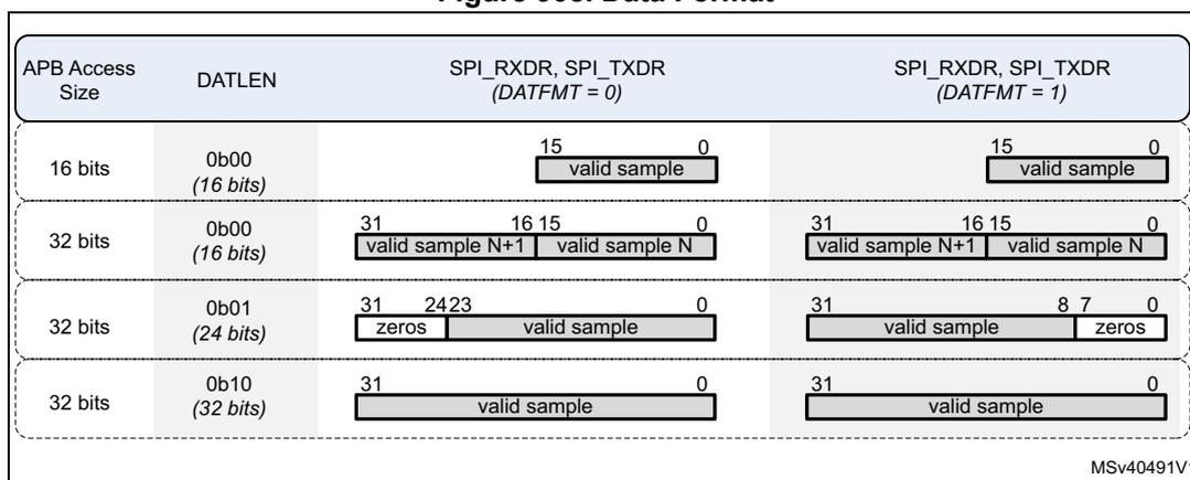
| APB Access Size | DATLEN | SPI_RXDR, SPI_TXDR (DATFMT = 0) | SPI_RXDR, SPI_TXDR (DATFMT = 1) | ||
|---|---|---|---|---|---|
| 16 bits | 0b00 (16 bits) | 15 | 0 | 15 | 0 |
| valid sample | valid sample | ||||
| 32 bits | 0b00 (16 bits) | 31 | 16 | 31 | 16 |
| valid sample N+1 | valid sample N | valid sample N+1 | valid sample N | ||
| 32 bits | 0b01 (24 bits) | 31 | 24 | 31 | 8 |
| zeros | valid sample | valid sample | zeros | ||
| 32 bits | 0b10 (32 bits) | 31 | 0 | 31 | 0 |
| valid sample | valid sample | ||||
MSV40491V1
- 1. In I2S mode, the sample N represents the left sample, and the sample N+1 is the right sample.
- 2. Data width of 24 and 32 bits are not always supported (DATLEN = 01 or 10). Refer to Section 67.3: SPI implementation to check the supported data size.
It is possible to generate an interrupt or a DMA request according to a programmable FIFO threshold levels. The FIFO threshold is common to RX and TxFIFOs can be adjusted via FTHLV.
In I2S mode, the left and right audio samples are interleaved into the FIFOs. It means that for transmit operations, the user has to start to fill-up the TxFIFO with a left sample, followed by a right sample, and so on. For receive mode, the first data read from the RxFIFO is supposed to represent a left channel, the next one is a right channel, and so on.
Note that the read and write pointers of the FIFOs are reset when the bit SPE is cleared.
Refer to Section 67.9.11 and Section 67.9.15 for additional information.
FIFO size optimization
The basic element of the FIFO is the byte. This allows an optimization of the FIFO locations. For example when the data size is fixed to 24 bits, each audio sample takes three basic FIFO elements.
For example, a FIFO with 16 basic elements can have a depth of:
- • 8 samples, if the DATLEN = 0 (16 bits),
- • 5 samples, if the DATLEN = 1 (24 bits) (a) ,
- • 4 samples, if the DATLEN = 2 (32 bits) (a) .
67.9.11 FIFO status flags
Two status flags are provided for the application to fully monitor the state of the I2S interface. Both flags can generate an interrupt request. The receive interrupt is generated if RXPIE bit is enabled, the transmit interrupt is generated if TXPIE bit is enabled. Those bits are located into the SPI_IER register.
TxFIFO threshold reached (TXP)
When set, this flag indicates that the TxFIFO contains at least FTHLV empty locations. Thus, FTHLV new data to be transmitted can be written to SPI_TXDR. The TXP flag is reset when the number of empty locations is lower than FTHLV. Note that TXP = 1, when the I2S is disabled (SPE bit is reset).
RxFIFO threshold reached (RXP)
When set, this flag indicates that there is at least FTHLV valid data into the RxFIFO, thus the user can read those data via SPI_RXDR. It is reset when the RxFIFO contains less than FTHLV data.
See Section 67.10 for additional information on the interrupt function in I2S mode.
67.9.12 Handling of underrun situation
In transmit mode, an underrun situation is detected when a new data needs to be loaded into the shift register while the TxFIFO is already empty. In such a situation the UDR flag is set, and at least one audio frame contains unexpected data.
a. Not always available, refer to Section 67.3: SPI implementation in order to check if 24 and 32-bit data widths are supported.
For I2S modes, there is a hardware mechanism to prevent misalignment situations (left and right channel swapped). When an underrun situation is detected, the last valid data present in the shift register is repeated if the real channel length matches the length selected by the CHLEN bit. In the other cases, an undefined data is repeated. Typically, if the block is programmed in slave TX mode, and the external master audio device is using channel lengths other than 16 or 32 bits, the repeated data value is undefined in case of underrun.
The following figure shows the case where an underrun occurs and the peripheral replays the last valid data on left and right channels as long as conditions of restart are not met. The transmission restarts:
- • When there is enough data into the TxFIFO, and
- • When the restart condition is met:
- – If the underrun occurs when a right channel data needs to be transmitted, the transmission restarts when a right channel needs to be transmitted, or
- – If the underrun occurs when a left channel data needs to be transmitted, the transmission restarts when a left channel needs to be transmitted.
Figure 909. Handling of underrun situation
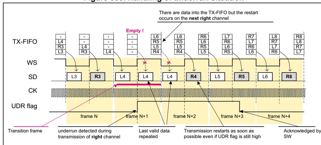
When the block is configured in one of the PCM modes, the transmission restarts at the start of the next frame, when there is enough data in the TxFIFO.
The UDR flag can trigger an interrupt if the UDRIE bit of the SPI_IER register is set. The UDR bit is cleared by setting the UDRC bit of the SPI_IFCR register.
Note:
An underrun situation can occur in master or slave mode. In master mode, when an underrun occurs, the WS, CK, and MCK signals are not gated.
Due to resynchronization, any change of the UDR flag is taken into account by the hardware after at least two periods of CK clock.
67.9.13 Handling of overrun situation
In receive mode, an overrun situation is detected when the shift register needs to store a new data into the RxFIFO, while the RxFIFO is full. In such a situation the OVR flag is set, and the incoming data is lost.
In I2S mode, there is a hardware mechanism in to prevent misalignment situations (left and right channel swapped). As shown in the following figure, when an overrun occurs, the peripheral stops writing data into the RxFIFO as long as restart conditions are not met.
The reception restarts when there is enough room into the RxFIFO. The block starts by writing next the right channel into the RxFIFO if the overrun occurs when a right channel data is received or by writing the next left channel if the overrun occurs when a left channel data is received.
Figure 910. Handling of overrun situation
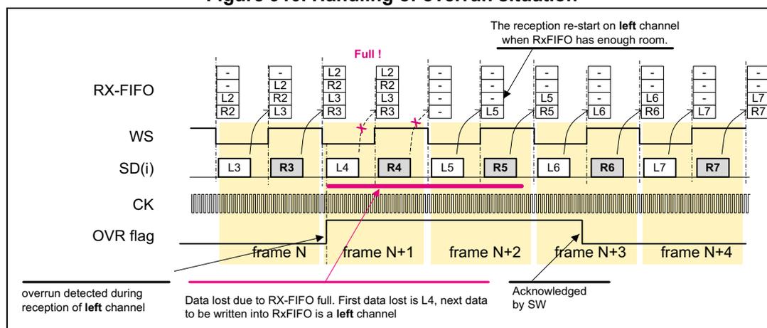
The diagram shows the handling of an overrun situation in SPI I2S mode. It displays the RX-FIFO, WS (Word Select), SD(i) (Serial Data input), CK (Clock), and OVR flag signals over five frames (N to N+4). In frame N+1, the RX-FIFO is full ('Full!'). When the right channel data R4 arrives, it cannot be written, causing an overrun. The left channel data L4 is lost. The OVR flag is set. Reception restarts in frame N+2 when the FIFO has enough room, starting with the right channel R5. The overrun is acknowledged by software (SW).
When the block is configured in PCM mode, after an overrun error, the block stops writing data in the RxFIFO as long as conditions of restart are not met. When there is enough room in the RxFIFO, the next received data are written in the RxFIFO.
An interrupt can be generated if the OVRIE bit of the SPI_IER register is set. The OVR bit is cleared by setting the OVRC bit of the SPI_IFCR register.
Note: An overrun situation can occur in master or slave mode. In master mode when an overrun occurs, the WS, CK, and MCK signals are not gated.
67.9.14 Frame error detection
When configured in slave mode, the SPI/I2S block detects two kinds of frame errors:
- • A frame synchronization is received while the shift-in or shift-out of the previous data is not complete (early frame error). This mode is selected with FIXCH = 0.
- • A frame synchronization occurs at an unexpected position. This mode is selected with FIXCH = 1.
In slave mode, if the frame length provided by the external master device is different from 32 or 64 bits, the user has to clear FIXCH. As the SPI/I2S synchronize each transfer with the WS there is no misalignment risk, but in a noisy environment, if a glitch occurs in the CK signal, a sample may be affected and the application is not aware of this.
If the frame length provided by the external master device is equal to 32 or 64 bits, then the user can set FIXCH and adjust accordingly CHLEN. As the SPI/I2S synchronize each transfer with the WS there is still no misalignment risk, and if the amount of bit clock between each channel boundary is different from CHLEN, the frame error flag (TIFRE) is set.
Figure 911 shows an example of frame error detection. The SPI/I2S block is in slave mode and the number of bit clock periods for the left channel are not enough to shift-in or shift-out the data. The figure shows that the ongoing transfer is interrupted and the next one is started in order to remain aligned to the WS signal.
Figure 911. Frame error detection, with FIXCH = 0
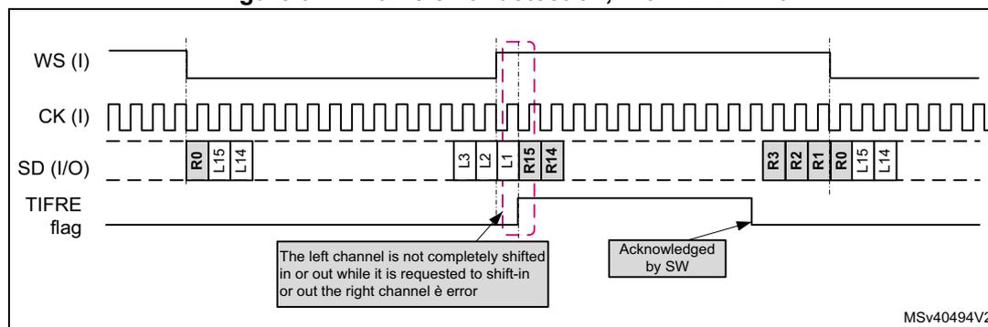
The diagram illustrates a frame error detection scenario. The WS (I) signal is high during the first frame and low during the second. The CK (I) signal is a continuous clock. The SD (I/O) signal shows data being shifted in/out: R0, L15, L14 in the first frame, and R3, R2, R1, R0, L15, L14 in the second frame. A frame error is detected when the WS signal changes before the data is fully shifted. The TIFRE flag is set and then cleared by software (SW). A callout box indicates: "The left channel is not completely shifted in or out while it is requested to shift-in or out the right channel è error". Another callout box indicates: "Acknowledged by SW". The diagram is labeled MSv40494V2.
An interrupt can be generated if the TIFREIE bit is set. The frame error flag (TIFRE) is cleared by writing the TIFREC bit of the SPI_IFCR register to 1.
It is possible to extend the coverage of the frame error flag by setting the bit FIXCH. When this bit is set, then the SPI/I2S is expecting fixed channel lengths in slave mode. This means that the expected channel length can be 16 or 32 bits, according to CHLEN. As shown in Figure 912, in this mode, the SPI/I2S block is able to detect if the WS signal is changing at the expected moment (too early or too late).
Note: Figure 911 and Figure 912 show the mechanism for the slave transmit mode, but this is also true for slave receive and slave full-duplex.
Figure 912. Frame error detection, with FIXCH = 1
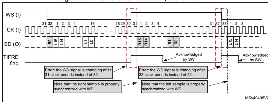
The diagram illustrates a frame error detection scenario with FIXCH = 1. The WS (I) signal is high for the first frame and low for the second. The CK (I) signal is a continuous clock. The SD (O) signal shows data being shifted in/out: R0, L15, L14 in the first frame, and R15, R14, R1, R0 in the second frame. A frame error is detected when the WS signal changes after 31 clock periods instead of 32. The TIFRE flag is set and then cleared by software (SW). Callout boxes indicate: "Error: the WS signal is changing after 31 clock periods instead of 32.", "Note that the right sample is properly synchronized with WS.", "Error: the WS signal is changing after 33 clock periods instead of 32.", "Note that the left sample is properly synchronized with WS.", and "Acknowledged by SW". The diagram is labeled MSv40495V2.
The frame error detection can be generally due to noisy environment disturbing the good reception of WS or CK signals.
Note: The SPI/I2S is not able to recover properly if an overrun and an early frame occur within the same frame. In this case the user has to disable and re-enable the SPI/I2S.
67.9.15 DMA interface
The I2S/PCM mode shares the same DMA requests lines than the SPI function. There is a separated DMA channel for TX and RX paths. Each DMA channel can be enabled via RXDMAEN and TXDMAEN bits of the SPI_CFG1 register.
In receive mode, the DMA interface is working as follows:
- 1. The hardware evaluates the RxFIFO level,
- 2. If the RxFIFO contains at least FTHLV samples, then FTHLV DMA requests are generated,
- – When the FTHLV DMA requests are completed, the hardware loops to step 1
- 3. If the RxFIFO contains less than FTHLV samples, no DMA request is generated, and the hardware loop to step 1
In transmit mode, the DMA interface is working as follows:
- 1. The hardware evaluates the TxFIFO level,
- 2. If the TxFIFO contains at least FTHLV empty locations, then FTHLV DMA requests are generated,
- – When the FTHLV DMA requests are completed, the hardware loops to step 1
- 3. If the TxFIFO contains less than FTHLV empty locations, no DMA request is generated, and the hardware loop to step 1
67.9.16 Programing examples
Master I2S Philips standard, full-duplex
This example shows how to program the interface for supporting the I2S Philips standard protocol in master full-duplex mode, with a sampling rate of 48 kHz, using the master clock. The assumption has been taken that the SPI/I2S is receiving a kernel clock (i2s_clk) of 61.44 MHz from the clock controller of the circuit. In the example above we took the assumption that the external audio codec needs to be programmed, for example via an I2C interface before starting the transfer. In addition, it is supposed that this external audio codec needs the MCK to accept I2C commands.
Procedure
- 1. Via the RCC block, enable the bus interface and the kernel clocks, assert and release the reset signal if needed.
- 2. Program the AFMUX in order to select the wanted I/Os. In the current example MCK, CK, WS, SDO, SDI are needed.
- 3. Program the clock generator to provide the MCK clock, and to have a frame synchronization rate at exactly 48 kHz. Set I2SDIV to 2, ODD to 1, and MCKOE to 1.
- 4. Program the serial interface protocol: CKPOL = 0, WSINV = 0, LSBFRST = 0, CHLEN = 1 (32 bits per channel) DATLEN = 1 (24 bits), I2SSTD = 0 (I2S Philips standard), I2SCFG = 5 (master full-duplex), I2SMOD = 1, for I2S/PCM mode.
- 5. Adjust the FIFO threshold by setting the wanted value into FTHLV. For example, if a threshold of two audio samples is required, FTHLV = 1.
- 6. If the application wishes to perform data transfer via DMA, set the bits TXDMAEN and RXDMAEN.
- 7. If needed, the application can then configure the external audio codec via an I2C interface.
- 8. Clear all interrupt enable fields located in the SPI_IER register.
- 9. Clear all status flags, by setting SUSPC, TIFREC, OVRC, UDRC of the SPI_IFCR register.
- 10. When the application wants to start the data transfer, set the SPE bit. Then:
- – If the data transfer uses DMA:
- a) Program the DMA peripheral: two channels, one for RX and one for TX.
- b) Initialize the memory buffer with valid audio samples for TX path.
- c) Enable the DMA channels.
- d) Enable interrupt events such as UDRIE and OVRIE if needed in order to detect transfer errors.
- e) Enable the DMA channel. If TXDMAEN was set, the TxFIFO is filled up.
- – If the data transfer is done via interrupt:
Enable the interrupt events UDRIE, OVRIE, TXPIE, and RXPIE (by writing 1). An interrupt request is immediately activated allowing the interrupt handler to fill-up the TxFIFO.
- – If the data transfer uses DMA:
- 11. Finally, the SPI/I2S serial interface can be enabled by setting the bit CSTART. CSTART bit is located into the SPI_CR1 register.
Stop procedure in master mode
- 1. Set the bit CSUSP, in order to stop ongoing transfers
- 2. Check the value of the CSTART bit until it goes to 0
- 3. Clear the SUSP flag by setting SUSPC
- 4. Stop DMA peripheral, bus clock...
- 5. Clear bit SPE in order to disable the SPI/I2S block
Slave I2S Philips standard, receive
This example shows how to program the interface for supporting the I2S Philips standard protocol in slave receiver mode, with a sampling rate of 48 kHz. Note that in slave mode the
SPI/I2S block cannot control the sample rate of the received samples. In this example we took the assumption that the external master device is delivering an I2S frame structure with a channel length of 24 bits. So, we cannot use the capability offered for frame error detection when FIXCH is set.
Procedure
- 1. Via the RCC block, enable the bus interface and the kernel clocks, assert and release the reset signal if needed,
- 2. Program the AFMUX in order to select the wanted I/Os. In the current example CK, WS, SDI,
- 3. Program the serial interface protocol: CKPOL = 0, WSINV = 0, LSBFRST = 0, FIXCH = 0 (because channel length is different from 16 and 32 bits), DATLEN = 0 (16 bits), I2SSTD = 0 (Philips protocol), I2SCFG = 1 (slave RX), I2SMOD = 1, for I2S mode.
- 4. Adjust the FIFO threshold by setting the wanted value into FTHLV. For example if a threshold of two audio samples is required, FTHLV = 1.
- 5. Clear all status flag registers.
- 6. Enable the flags that generate an interrupt such as OVRIE and TIFRE.
- 7. If the data transfer uses DMA:
- – Program the DMA peripheral: one RX channel
- – Enable the DMA channel,
- – In the SPI/I2S block, enable the DMA by setting the RXDMAEN bit.
- 8. If the data transfer is done via interrupt, then the user has to enable the interrupt by setting the RXPIE bit.
- 9. Set SPE.
- 10. Finally, the user can set the bit CSTART in order to enable the serial interface. The SPI/I2S starts to store data into the RxFIFO on the next occurrence of left data transmitted by the external master device.
Stop procedure in slave mode
- 1. Clear bit SPE in order to disable the SPI/I2S block
- 2. Stop DMA peripheral, bus clock...
67.10 I2S interrupts
In PCM/I2S mode an interrupt ( spi_it ) or a wake-up event signal ( spi_wkup ) can be generated according to the events described in the Table 666 .
Interrupt events can be enabled and disabled separately.
Table 666. I2S interrupt requests
| Interrupt vector | Interrupt event | Event flag | Event/Interrupt clearing method | Exit Sleep mode | Exit Stop modes | Exit Standby mode |
|---|---|---|---|---|---|---|
| SPI | TxFIFO threshold reached | TXP | When the TxFIFO contains less than FTHLV empty locations | Yes | Yes | No |
| RxFIFO threshold reached | RXP | When the RxFIFO contains less than FTHLV samples | ||||
| Overrun error | OVR | Write OVRC to 1 | ||||
| Underrun error | UDR | Write UDRC to 1 | ||||
| Frame error flag | TIFRE | Write TIFREC to 1 | No |
67.11 SPI/I2S registers
67.11.1 SPI/I2S control register 1 (SPI_CR1)
Address offset: 0x000
Reset value: 0x0000 0000
| 31 | 30 | 29 | 28 | 27 | 26 | 25 | 24 | 23 | 22 | 21 | 20 | 19 | 18 | 17 | 16 |
|---|---|---|---|---|---|---|---|---|---|---|---|---|---|---|---|
| Res. | Res. | Res. | Res. | Res. | Res. | Res. | Res. | Res. | Res. | Res. | Res. | Res. | Res. | Res. | IOLOCK |
| rs | |||||||||||||||
| 15 | 14 | 13 | 12 | 11 | 10 | 9 | 8 | 7 | 6 | 5 | 4 | 3 | 2 | 1 | 0 |
| TCRCINI | RCRCINI | CRC33_17 | SSI | HDDIR | CSUSP | CSTART | MASRX | Res. | Res. | Res. | Res. | Res. | Res. | Res. | SPE |
| rw | rw | rw | rw | rw | w | rs | rw | rw |
Bits 31:17 Reserved, must be kept at reset value.
Bit 16 IOLOCK : locking the AF configuration of associated I/Os
This bit can be changed by software only when SPI is disabled (SPE = 0). It is cleared by hardware if a MODF event occurs
When this bit is set, the SPI_CFG2 register content cannot be modified. This bit is write-protected when SPI is enabled (SPE = 1).
0: AF configuration is not locked
1: AF configuration is locked
Bit 15 TCRCINI : CRC calculation initialization pattern control for transmitter
0: all zero pattern is applied
1: all ones pattern is applied
Bit 14 RCRCINI : CRC calculation initialization pattern control for receiver
0: All zero pattern is applied
1: All ones pattern is applied
Bit 13 CRC33_17 : Full size (33-bit or 17-bit) CRC polynomial configuration
0: Full size (33-bit or 17-bit) CRC polynomial is not used
1: Full size (33-bit or 17-bit) CRC polynomial is used
Bit 12 SSI: Internal slave select signal input levelThis bit has an effect only when the SSM bit is set. The value of this bit is forced onto the peripheral NSS input internally and the I/O value of the NSS pin is ignored.
Bit 11 HDDIR: Rx/Tx direction at half-duplex modeIn half-duplex configuration the HDDIR bit establishes the Rx/Tx direction of the data transfer. This bit is ignored in Full-Duplex or any Simplex configuration.
0: SPI is receiver
1: SPI is transmitter
Bit 10 CSUSP: master suspend requestThis bit reads as zero.
In master mode, when this bit is set by software, the CSTART bit is reset at the end of the current frame and communication is suspended. The user has to check SUSP flag to check end of the frame transfer.
The master mode communication must be suspended (using this bit or keeping TXDR empty) before going to Low-power mode.
After software suspension, SUSP flag must be cleared and SPI disabled and re-enabled before the next transfer starts.
Bit 9 CSTART: master transfer startThis bit can be set by software if SPI is enabled only to start an SPI or I2S/PCM communication. In SPI mode, it is cleared by hardware when end of transfer (EOT) flag is set or when a transfer suspend request is accepted. In I2S/PCM mode, it is also cleared by hardware as described in the Section 67.9.8: Stop sequence .
In SPI mode, the bit is taken into account at master mode only. If transmission is enabled, communication starts or continues only if any data is available in the transmission FIFO.
0: master transfer is at idle
1: master transfer is ongoing or temporary suspended by automatic suspend
Bit 8 MASRX: master automatic suspension in Receive modeThis bit is set and cleared by software to control continuous SPI transfer in master receiver mode and automatic management in order to avoid overrun condition.
When SPI communication is suspended by hardware automatically, it may happen that few bits of next frame are already clocked out due to internal synchronization delay.
This is why, the automatic suspension is not quite reliable when size of data drops below 8 bits. In this case, a safe suspension can be achieved by combination with delay inserted between data frames applied when MIDI parameter keeps a non zero value; sum of data size and the interleaved SPI cycles must always produce interval at length of 8 SPI clock periods at minimum. After software clearing of the SUSP bit, the communication resumes and continues by subsequent bits transfer without any next constraint. Before the SUSP bit is cleared, the user must release the RxFIFO space as much as possible by reading out all the data packets available at RxFIFO based on the RXP flag indication to prevent any subsequent suspension.
0: SPI flow/clock generation is continuous, regardless of overrun condition. (data are lost)
1: SPI flow is suspended temporary on RxFIFO full condition, before reaching overrun condition. The SUSP flag is set when the SPI communication is suspended.
Bits 7:1 Reserved, must be kept at reset value.
Bit 0 SPE : serial peripheral enable
This bit is set by and cleared by software.
When SPE = 1, SPI data transfer is enabled, the SPI_CFG1 and SPI_CFG2 configuration registers, CRCPOLY, UDRDR, IOLOCK bit in the SPI_CR1 register are write protected. They can be changed only when SPE = 0.
When SPE = 0 any SPI operation is stopped and disabled, all the pending requests of the events with enabled interrupt are blocked except the MODF interrupt request (but their pending still propagates the request of the spi_pclk clock), the NSS output is deactivated at master, the RDY signal keeps not ready status at slave, the internal state machine is reseted, all the FIFOs content is flushed, CRC calculation initialized, receive data register is read zero. SPE is cleared and cannot be set when MODF error flag is active.
0: Serial peripheral disabled.
1: Serial peripheral enabled
67.11.2 SPI/I2S control register 2 (SPI_CR2)
Address offset: 0x004
Reset value: 0x0000 0000
| 31 | 30 | 29 | 28 | 27 | 26 | 25 | 24 | 23 | 22 | 21 | 20 | 19 | 18 | 17 | 16 |
|---|---|---|---|---|---|---|---|---|---|---|---|---|---|---|---|
| Res. | Res. | Res. | Res. | Res. | Res. | Res. | Res. | Res. | Res. | Res. | Res. | Res. | Res. | Res. | Res. |
| 15 | 14 | 13 | 12 | 11 | 10 | 9 | 8 | 7 | 6 | 5 | 4 | 3 | 2 | 1 | 0 |
| TSIZE[15:0] | |||||||||||||||
| rw | rw | rw | rw | rw | rw | rw | rw | rw | rw | rw | rw | rw | rw | rw | rw |
Bits 31:16 Reserved, must be kept at reset value.
Bits 15:0 TSIZE[15:0] : number of data at current transfer
When these bits are changed by software, the SPI must be disabled.
Endless transfer is initialized when CSTART is set while zero value is stored in TSIZE. TSIZE cannot be set to 0xFFFF for a full-featured instance and 0x3FF for a limited-featured instance, when CRC is enabled.
Note: TSIZE[15:10] bits are reserved for limited-featured instances, and must be kept at reset value.
67.11.3 SPI/I2S configuration register 1 (SPI_CFG1)
Address offset: 0x008
Reset value: 0x0007 0007
The content of this register is write protected when SPI is enabled.
| 31 | 30 | 29 | 28 | 27 | 26 | 25 | 24 | 23 | 22 | 21 | 20 | 19 | 18 | 17 | 16 |
|---|---|---|---|---|---|---|---|---|---|---|---|---|---|---|---|
| BPASS | MBR[2:0] | Res. | Res. | Res. | Res. | Res. | CRCEN | Res. | CRCSIZE[4:0] | ||||||
| rw | rw | rw | rw | rw | rw | rw | rw | rw | rw | ||||||
| 15 | 14 | 13 | 12 | 11 | 10 | 9 | 8 | 7 | 6 | 5 | 4 | 3 | 2 | 1 | 0 |
| TXDMA EN | RXDMA EN | Res. | Res. | Res. | Res. | UDRCFG | FTHLV[3:0] | DSIZE[4:0] | |||||||
| rw | rw | rw | rw | rw | rw | rw | rw | rw | rw | rw | rw | ||||
Bit 31 BPASS : bypass of the prescaler at master baud rate clock generator
0: bypass is disabled
1: bypass is enabled
Bits 30:28 MBR[2:0] : master baud rate prescaler setting
000: SPI master clock/2
001: SPI master clock/4
010: SPI master clock/8
011: SPI master clock/16
100: SPI master clock/32
101: SPI master clock/64
110: SPI master clock/128
111: SPI master clock/256
Note: MBR setting is considered at slave working at TI mode, too (see Section 67.5.1: TI mode ).
Bits 27:23 Reserved, must be kept at reset value.
Bit 22 CRCEN : hardware CRC computation enable
0: CRC calculation disabled
1: CRC calculation enabled
Bit 21 Reserved, must be kept at reset value.
Bits 20:16 CRCSIZE[4:0] : length of CRC frame to be transferred and compared
Most significant bits are taken into account from polynomial calculation when CRC result is transferred or compared. The length of the polynomial is not affected by this setting.
The value must be equal or a multiple of the data size configured through the DSIZE bitfield. Its maximum size corresponds to the instance maximum data size.
00000: not used
00001: not used
00010: not used
00011: 4 bits
00100: 5 bits
00101: 6 bits
00110: 7 bits
00111: 8 bits
.....
11101: 30 bits
11110: 31 bits
11111: 32 bits
Note: The most significant bit at CRCSIZE bit field is reserved for the peripheral instances where data size is limited to 16 bits.
The CRCSIZE[2:0] bits are fixed to 1 for the peripheral instances with a limited set of features.
Bit 15 TXDMAEN : Tx DMA stream enable
0: Tx DMA disabled
1: Tx DMA enabled
Bit 14 RXDMAEN : Rx DMA stream enable
0: Rx-DMA disabled
1: Rx-DMA enabled
Bits 13:10 Reserved, must be kept at reset value.
Bit 9 UDRCFG : behavior of slave transmitter at underrun condition
For more details see Figure 893: Optional configurations of the slave behavior when an underrun condition is detected .
0: slave sends a constant pattern defined by the user in the SPI_UDRDR register
1: Slave repeats the last received data from master. When slave is configured at transmit only mode (COMM[1:0] = 01), all zeros pattern is repeated.
Bits 8:5 FTHLV[3:0] : FIFO threshold level
Defines number of data frames in a single data packet. It is recommended that the size of the packet does not exceed 1/2 of FIFO space.
SPI interface is more efficient if configured packet sizes are aligned with data register access parallelism:
–If SPI data register is accessed as a 16-bit register and DSIZE \( \leq \) 8 bits, better to select FTHLV = 2, 4, 6.
–If SPI data register is accessed as a 32-bit register and DSIZE \( > \) 8 bits, better to select FTHLV = 2, 4, 6, while if DSIZE \( \leq \) 8 bits, better to select FTHLV = 4, 8, 12.
0000: 1-data
0001: 2-data
0010: 3-data
0011: 4-data
0100: 5-data
0101: 6-data
0110: 7-data
0111: 8-data
1000: 9-data
1001: 10-data
1010: 11-data
1011: 12-data
1100: 13-data
1101: 14-data
1110: 15-data
1111: 16-data
Note: FTHLV[3:2] bits are reserved for instances with a limited set of features.
Bits 4:0 DSIZE[4:0] : number of bits in a single SPI data frame
00000: not used
00001: not used
00010: not used
00011: 4 bits
00100: 5 bits
00101: 6 bits
00110: 7 bits
00111: 8 bits
.....
11101: 30 bits
11110: 31 bits
11111: 32 bits
Note: The most significant bit DSIZE[4] is reserved for instances which data size is limited to 16 bits.
DSIZE[2:0] bits are fixed to 1 for instances with a limited set of features.
67.11.4 SPI/I2S configuration register 2 (SPI_CFG2)
Address offset: 0x00C
Reset value: 0x0000 0000
The content of this register is write-protected when SPI is enabled or the IOLOCK bit is set in the SPI_CR1 register.
| 31 | 30 | 29 | 28 | 27 | 26 | 25 | 24 | 23 | 22 | 21 | 20 | 19 | 18 | 17 | 16 |
|---|---|---|---|---|---|---|---|---|---|---|---|---|---|---|---|
| AFCNTR | SSOM | SSOE | SSIOP | Res. | SSM | CPOL | CPHA | LSBFRST | MASTER | SP[2:0] | COMM[1:0] | Res. | |||
| rw | rw | rw | rw | rw | rw | rw | rw | rw | rw | rw | rw | rw | rw | ||
| 15 | 14 | 13 | 12 | 11 | 10 | 9 | 8 | 7 | 6 | 5 | 4 | 3 | 2 | 1 | 0 |
|---|---|---|---|---|---|---|---|---|---|---|---|---|---|---|---|
| IOSWP | RDIOP | RDIOM | Res. | Res. | Res. | Res. | Res. | MIDI[3:0] | MSSI[3:0] | ||||||
| rw | rw | rw | rw | rw | rw | rw | rw | rw | rw | rw | |||||
Bit 31 AFCNTR: alternate function GPIOs control
This bit is taken into account when SPE = 0 only.
When SPI must be disabled temporary for a specific configuration reason (for example CRC reset, CPHA or HDDIR change) setting this bit prevents any glitches on the associated outputs configured at alternate function mode by keeping them forced at state corresponding the current SPI configuration.
0: The peripheral takes no control of GPIOs while it is disabled
1: The peripheral keeps always control of all associated GPIOs
Note: This bit can be also used in PCM and I2S modes.
The bit AFCNTR must not be set, when the block is in slave mode.
Bit 30 SSOM: NSS output management in master mode
This bit is taken into account in master mode when SSOE is enabled. It allows the NSS output to be configured between two consecutive data transfers.
0: NSS is kept at active level until data transfer is complete, it becomes inactive with EOT flag
1: SPI data frames are interleaved with NSS nonactive pulses when MIDI[3:0] > 1
Bit 29 SSOE: NSS output enable
This bit is taken into account in master mode only
0: NSS output is disabled and the SPI can work in multimaster configuration
1: NSS output is enabled. The SPI cannot work in a multimaster environment. It forces the NSS pin at inactive level after the transfer is complete or SPI is disabled with respect to SSOM, MIDI, MSSI, SSIOP bits setting
Bit 28 SSIOP: NSS input/output polarity
0: low level is active for NSS signal
1: high level is active for NSS signal
Bit 27 Reserved, must be kept at reset value.
Bit 26 SSM: Software management of internal slave select signal input
0: Input value of the internal slave select signal is determined by the external NSS hardware pin
1: Input value of the internal slave select signal is determined by the SSI bit controlled by software
Note: When master uses hardware NSS output (SSM = 0 and SSOE = 1), the internal slave select signal input is forced to not active state internally to prevent master mode fault error.
- Bit 25
CPOL
: clock polarity
0: SCK signal is at 0 when idle
1: SCK signal is at 1 when idle - Bit 24
CPHA
: clock phase
0: the first clock transition is the first data capture edge
1: the second clock transition is the first data capture edge - Bit 23
LSBFRST
: data frame format
0: MSB transmitted first
1: LSB transmitted first
Note: This bit can be also used in PCM and I2S modes. - Bit 22
MASTER
: SPI master
0: SPI slave
1: SPI master - Bits 21:19
SP[2:0]
: serial protocol
000: SPI Motorola
001: SPI TI
others: reserved, must not be used - Bits 18:17
COMM[1:0]
: SPI Communication Mode
00: full-duplex
01: simplex transmitter
10: simplex receiver
11: half-duplex - Bit 16 Reserved, must be kept at reset value.
- Bit 15
IOSWP
: swap functionality of MISO and MOSI pins
When this bit is set, the function of MISO and MOSI pins alternate functions are inverted.
Original MISO pin becomes MOSI and original MOSI pin becomes MISO.
0: no swap
1: MOSI and MISO are swapped
Note: This bit can be also used in PCM and I2S modes to swap SDO and SDI pins. - Bit 14
RDIOP
: RDY signal input/output polarity
0: high level of the signal means the slave is ready for communication
1: low level of the signal means the slave is ready for communication - Bit 13
RDIOIM
: RDY signal input/output management
0: RDY signal is defined internally fixed as permanently active (RDIOP setting has no effect)
1: RDY signal is overtaken from alternate function input (at master case) or output (at slave case) of the dedicated pin (RDIOP setting takes effect)
Note: When DSIZE in the SPI_CFG1 register is configured shorter than 8 bits, the RDIOIM bit must be kept at zero. - Bits 12:8 Reserved, must be kept at reset value.
Bits 7:4 MIDI[3:0] : Master Inter-Data Idleness
Specifies minimum time delay (expressed in SPI clock cycles periods) inserted between two consecutive data frames in master mode.
0000: no delay
0001: 1 clock cycle period delay
...
1111: 15 clock cycle periods delay
Note: This feature is not supported in TI mode.
Bits 3:0 MSSI[3:0] : Master NSS Idleness
Specifies an extra delay, expressed in number of SPI clock cycle periods, inserted additionally between active edge of NSS opening a session and the beginning of the first data frame of the session in master mode when SSOE is enabled.
0000: no extra delay
0001: 1 clock cycle period delay added
...
1111: 15 clock cycle periods delay added
Note: This feature is not supported in TI mode.
To include the delay, the SPI must be disabled and re-enabled between sessions.
67.11.5 SPI/I2S interrupt enable register (SPI_IER)
Address offset: 0x010
Reset value: 0x0000 0000
| 31 | 30 | 29 | 28 | 27 | 26 | 25 | 24 | 23 | 22 | 21 | 20 | 19 | 18 | 17 | 16 |
|---|---|---|---|---|---|---|---|---|---|---|---|---|---|---|---|
| Res. | Res. | Res. | Res. | Res. | Res. | Res. | Res. | Res. | Res. | Res. | Res. | Res. | Res. | Res. | Res. |
| 15 | 14 | 13 | 12 | 11 | 10 | 9 | 8 | 7 | 6 | 5 | 4 | 3 | 2 | 1 | 0 |
| Res. | Res. | Res. | Res. | Res. | Res. | MODFIE | TIFREIE | CRCEIE | OVRIE | UDRIE | TXTFIE | ETOTIE | DXPIE | TXPIE | RXPIE |
| rw | rw | rw | rw | rw | rw | rw | rw | rw | rw |
Bits 31:10 Reserved, must be kept at reset value.
Bit 9 MODFIE : mode Fault interrupt enable
0: MODF interrupt disabled
1: MODF interrupt enabled
Bit 8 TIFREIE : TIFRE interrupt enable
0: TIFRE interrupt disabled
1: TIFRE interrupt enabled
Bit 7 CRCEIE : CRC error interrupt enable
0: CRC interrupt disabled
1: CRC interrupt enabled
Bit 6 OVRIE : OVR interrupt enable
0: OVR interrupt disabled
1: OVR interrupt enabled
Bit 5 UDRIE : UDR interrupt enable
0: UDR interrupt disabled
1: UDR interrupt enabled
Bit 4 TXTFIE : TXTF interrupt enable
0: TXTF interrupt disabled
1: TXTF interrupt enabled
Bit 3 EOTIE : EOT, SUSP and TXC interrupt enable
0: EOT/SUSP/TXC interrupt disabled
1: EOT/SUSP/TXC interrupt enabled
Bit 2 DXPIE : DXP interrupt enabled
DXPIE is set by software and cleared by TXTF flag set event.
0: DXP interrupt disabled
1: DXP interrupt enabled
Bit 1 TXPIE : TXP interrupt enable
TXPIE is set by software and cleared by TXTF flag set event.
0: TXP interrupt disabled
1: TXP interrupt enabled
Bit 0 RXPIE : RXP interrupt enable
0: RXP interrupt disabled
1: RXP interrupt enabled
67.11.6 SPI/I2S status register (SPI_SR)
Address offset: 0x014
Reset value: 0x0000 1002
All the flags of this register are not cleared automatically when the SPI is reenabled. They require specific clearing access exclusively via the flag clearing register as noted in the bits descriptions below.
| 31 | 30 | 29 | 28 | 27 | 26 | 25 | 24 | 23 | 22 | 21 | 20 | 19 | 18 | 17 | 16 |
|---|---|---|---|---|---|---|---|---|---|---|---|---|---|---|---|
| CTSIZE[15:0] | |||||||||||||||
| r | r | r | r | r | r | r | r | r | r | r | r | r | r | r | r |
| 15 | 14 | 13 | 12 | 11 | 10 | 9 | 8 | 7 | 6 | 5 | 4 | 3 | 2 | 1 | 0 |
| RXWNE | RXPLVL[1:0] | TXC | SUSP | Res. | MODF | TIFRE | CRCE | OVR | UDR | TXTF | EOT | DXP | TXP | RXP | |
| r | r | r | r | r | r | r | r | r | r | r | r | r | r | r | |
Bits 31:16 CTSIZE[15:0] : number of data frames remaining in current TSIZE session
The value is not quite reliable when traffic is ongoing on bus .
Note: CTSIZE[15:0] bits are not available in instances with limited set of features.
Bit 15 RXWNE : RxFIFO word not empty
0: less than four bytes of RxFIFO space is occupied by data
1: at least four bytes of RxFIFO space is occupied by data
Note: This bit value does not depend on DSIZE setting and keeps together with RXPLVL[1:0] information about RxFIFO occupancy by residual data.
Bits 14:13 RXPLVL[1:0] : RxFIFO packing levelWhen RXWNE = 0 and data size is set up to 16 bits, the value gives number of remaining data frames persisting at RxFIFO.
When data size is greater than 16 bits, these bits are always read as 00. As a result, the single data frame received in the FIFO cannot be detected neither by RWNE nor by RXPLVL bits if the data size is set from 17 to 24 bits. The user must then apply other methods to detect the number of data received, such as monitor the EOT event when TSIZE > 0 or RXP events when FTHLV = 0.
00: no next frame is available at RxFIFO
01: 1 frame is available
10: 2 frames are available*
11: 3 frames are available*
Note: (*) Possible value when data size is set up to 8 bits only.
Bit 12 TXC : TxFIFO transmission completeThe flag behavior depends on TSIZE setting.
When TSIZE = 0, the TXC is changed by hardware exclusively and it raises each time the TxFIFO becomes empty and there is no activity on the bus.
If TSIZE ≠ 0 there is no specific reason to monitor TXC as it just copies the EOT flag value including its software clearing. The TXC generates an interrupt when EOTIE is set.
This flag is set when SPI is reset or disabled.
0: current data transfer is still ongoing, data is available in TxFIFO or last frame transmission is on going.
1: last TxFIFO frame transmission complete
Bit 11 SUSP : suspension statusIn master mode, SUSP is set by hardware either as soon as the current frame is complete after CSUSP request is done or at master automatic suspend receive mode (the MASRX bit is set in the SPI_CR1 register) on RxFIFO full condition.
SUSP generates an interrupt when EOTIE is set.
This bit must be cleared prior to disabling the SPI. This is done by setting the SUSPC bit of SPI_IFCR exclusively.
0: SPI not suspended (master mode active or other mode).
1: master mode is suspended (current frame completed).
Bit 10 Reserved, must be kept at reset value.
Bit 9 MODF : mode faultWhen MODF is set, SPE and IOLOCK bits of the SPI_CR1 register are reset and setting SPE again is blocked until MODF is cleared.
This bit is cleared by writing 1 to the MODFC bit of the SPI_IFCR exclusively.
0: no mode fault
1: mode fault detected.
Bit 8 TIFRE : TI frame format errorThis bit is cleared by writing 1 to the TIFREC bit of the SPI_IFCR exclusively.
0: no TI Frame Error
1: TI frame error detected
Bit 7 CRCE : CRC errorThis bit is cleared when SPI is re-enabled or by writing 1 to the CRCEC bit of the SPI_IFCR optionally.
0: no CRC error
1: CRC error detected
Bit 6 OVR: overrunThis bit is cleared when SPI is re-enabled or by writing 1 to the OVRC bit of the SPI_IFCR optionally.
0: no overrun
1: overrun detected
Bit 5 UDR: underrunThis bit is cleared when SPI is re-enabled or by writing 1 to the UDRC bit of the SPI_IFCR optionally.
0: no underrun
1: underrun detected
Note: In SPI mode, the UDR flag applies to slave mode only. In I2S/PCM mode, (when available) this flag applies to master and slave mode.
Bit 4 TXTF: transmission transfer filledTXTF is set by hardware as soon as all of the data packets in a transfer have been submitted for transmission by application software or DMA, that is when TSIZE number of data have been pushed into the TxFIFO.
This bit is cleared by software write 1 to the TXTFC bit of the SPI_IFCR exclusively.
The TXTF flag triggers an interrupt if the TXTFIE bit is set.
TXTF setting clears the TXPIE and DXPIE masks so to off-load application software from calculating when to disable TXP and DXP interrupts.
0: upload of TxFIFO is ongoing or not started
1: TxFIFO upload is finished
Bit 3 EOT: end of transferEOT is set by hardware as soon as a full transfer is complete, that is when SPI is re-enabled or when TSIZE number of data have been transmitted and/or received on the SPI. EOT is cleared when SPI is re-enabled or by writing 1 to the EOTC bit of the SPI_IFCR register optionally.
EOT flag triggers an interrupt if the EOTIE bit is set.
If DXP flag is used until TXTF flag is set and DXPIE is cleared, EOT can be used to download the last packets contained into RxFIFO in one-shot.
In master, EOT event terminates the data transfer and handles NSS output optionally. When CRC is applied, the EOT event is extended over the CRC frame transfer.
To restart the internal state machine properly, SPI is strongly suggested to be disabled and re-enabled before next transfer starts despite its setting is not changed.
0: transfer is ongoing or not started
1: transfer complete
Bit 2 DXP: duplex packetDXP flag is set whenever both TXP and RXP flags are set regardless SPI mode.
0: TxFIFO is Full and/or RxFIFO is Empty
1: both TxFIFO has space for write and RxFIFO contains for read a single packet at least
Bit 1 TXP: Tx-packet space availableTXP flag can be changed only by hardware. Its value depends on the physical size of the FIFO and its threshold (FTHLV[3:0]), data frame size (DSIZE[4:0] in SPI mode and respective DATLEN[1:0] in I2S/PCM mode), and actual communication flow. If the data packet is stored by performing consecutive write operations to SPI_TXDR, TXP flag must be checked again once a complete data packet is stored at TxFIFO. TXP is set despite SPI TxFIFO becomes inaccessible when SPI is reset or disabled.
0: not enough free space at TxFIFO to host next data packet
1: enough free space at TxFIFO to host at least one data packet
Bit 0 RXP : Rx-packet available
The flag is changed by hardware. It monitors the total number of data currently available at RxFIFO if SPI is enabled. RXP value depends on the FIFO threshold (FTHLV[3:0]), data frame size (DSIZE[4:0] in SPI mode and DATLEN[1:0] in I2S/PCM mode), and actual communication flow. If the data packet is read by performing consecutive read operations from SPI_RXDR, RXP flag must be checked again once a complete data packet is read out from RxFIFO.
0: RxFIFO is empty or an incomplete data packet is received
1: RxFIFO contains at least one data packet
67.11.7 SPI/I2S interrupt/status flags clear register (SPI_IFCR)
Address offset: 0x018
Reset value: 0x0000 0000
| 31 | 30 | 29 | 28 | 27 | 26 | 25 | 24 | 23 | 22 | 21 | 20 | 19 | 18 | 17 | 16 |
|---|---|---|---|---|---|---|---|---|---|---|---|---|---|---|---|
| Res. | Res. | Res. | Res. | Res. | Res. | Res. | Res. | Res. | Res. | Res. | Res. | Res. | Res. | Res. | Res. |
| 15 | 14 | 13 | 12 | 11 | 10 | 9 | 8 | 7 | 6 | 5 | 4 | 3 | 2 | 1 | 0 |
| Res. | Res. | Res. | Res. | SUSPC | Res. | MODFC | TIFREC | CRCEC | OVRC | UDRC | TXTFC | EOTC | Res. | Res. | Res. |
| w | w | w | w | w | w | w | w |
Bits 31:12 Reserved, must be kept at reset value.
Bit 11 SUSPC : Suspend flag clear
Writing a 1 into this bit clears SUSP flag of the SPI_SR register
Bit 10 Reserved, must be kept at reset value.
Bit 9 MODFC : mode fault flag clear
Writing a 1 into this bit clears MODF flag of the SPI_SR register
Bit 8 TIFREC : TI frame format error flag clear
Writing a 1 into this bit clears TIFRE flag of the SPI_SR register
Bit 7 CRCEC : CRC error flag clear
Writing a 1 into this bit clears CRCE flag of the SPI_SR register
Bit 6 OVRC : overrun flag clear
Writing a 1 into this bit clears OVR flag of the SPI_SR register
Bit 5 UDRC : underrun flag clear
Writing a 1 into this bit clears UDR flag of the SPI_SR register
Bit 4 TXTFC : transmission transfer filled flag clear
Writing a 1 into this bit clears TXTF flag of the SPI_SR register
Bit 3 EOTC : end of transfer flag clear
Writing a 1 into this bit clears EOT flag of the SPI_SR register
Bits 2:0 Reserved, must be kept at reset value.
67.11.8 SPI/I2S transmit data register (SPI_TXDR)
Address offset: 0x020
Reset value: 0x0000 0000
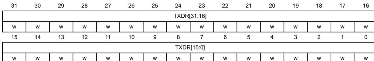
| 31 | 30 | 29 | 28 | 27 | 26 | 25 | 24 | 23 | 22 | 21 | 20 | 19 | 18 | 17 | 16 |
| TXDR[31:16] | |||||||||||||||
| w | w | w | w | w | w | w | w | w | w | w | w | w | w | w | w |
| 15 | 14 | 13 | 12 | 11 | 10 | 9 | 8 | 7 | 6 | 5 | 4 | 3 | 2 | 1 | 0 |
| TXDR[15:0] | |||||||||||||||
| w | w | w | w | w | w | w | w | w | w | w | w | w | w | w | w |
Bits 31:0 TXDR[31:0] : transmit data register
The register serves as an interface with TxFIFO. A write to it accesses TxFIFO.
Note: In SPI mode, data is always right-aligned. Alignment of data at I2S mode depends on DATLEN and DATFMT setting. Unused bits are ignored when writing to the register, and read as zero when the register is read.
Note: DR can be accessed byte-wise (8-bit access): in this case only one data-byte is written by single access.
half-word-wise (16 bit access) in this case 2 data-bytes or 1 half-word-data can be written by single access.
word-wise (32 bit access). In this case 4 data-bytes or 2 half-word-data or word-data can be written by single access.
Write access of this register less than the configured data size is forbidden.
67.11.9 SPI/I2S receive data register (SPI_RXDR)
Address offset: 0x030
Reset value: 0x0000 0000
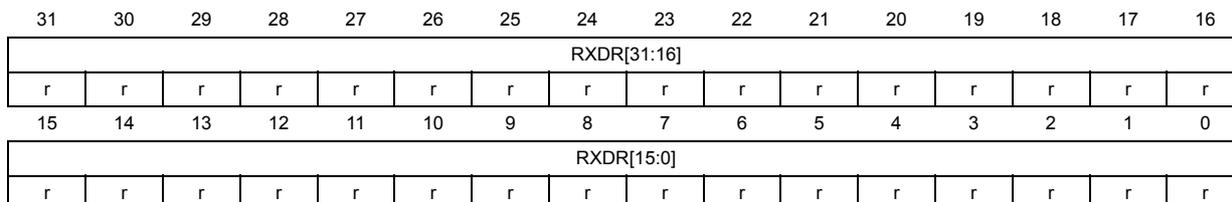
| 31 | 30 | 29 | 28 | 27 | 26 | 25 | 24 | 23 | 22 | 21 | 20 | 19 | 18 | 17 | 16 |
| RXDR[31:16] | |||||||||||||||
| r | r | r | r | r | r | r | r | r | r | r | r | r | r | r | r |
| 15 | 14 | 13 | 12 | 11 | 10 | 9 | 8 | 7 | 6 | 5 | 4 | 3 | 2 | 1 | 0 |
| RXDR[15:0] | |||||||||||||||
| r | r | r | r | r | r | r | r | r | r | r | r | r | r | r | r |
Bits 31:0 RXDR[31:0] : receive data register
The register serves as an interface with RxFIFO. When it is read, RxFIFO is accessed.
Note: In SPI mode, data is always right-aligned. Alignment of data at I2S mode depends on DATLEN and DATFMT setting. Unused bits are read as zero when the register is read. Writing to the register is ignored.
Note: DR can be accessed byte-wise (8-bit access): in this case only one data-byte is read by single access
half-word-wise (16 bit access) in this case 2 data-bytes or 1 half-word data can be read by single access
word-wise (32 bit access). In this case 4 data-bytes or 2 half-word data or word-data can be read by single access.
Read access of this register less than the configured data size is forbidden.
67.11.10 SPI/I2S polynomial register (SPI_CRCPOLY)
Address offset: 0x040
Reset value: 0x0000 0107
The content of this register is write protected when SPI is enabled.
| 31 | 30 | 29 | 28 | 27 | 26 | 25 | 24 | 23 | 22 | 21 | 20 | 19 | 18 | 17 | 16 |
|---|---|---|---|---|---|---|---|---|---|---|---|---|---|---|---|
| CRCPOLY[31:16] | |||||||||||||||
| rw | rw | rw | rw | rw | rw | rw | rw | rw | rw | rw | rw | rw | rw | rw | rw |
| 15 | 14 | 13 | 12 | 11 | 10 | 9 | 8 | 7 | 6 | 5 | 4 | 3 | 2 | 1 | 0 |
| CRCPOLY[15:0] | |||||||||||||||
| rw | rw | rw | rw | rw | rw | rw | rw | rw | rw | rw | rw | rw | rw | rw | rw |
Bits 31:0 CRCPOLY[31:0]: CRC polynomial register
This register contains the polynomial for the CRC calculation.
The default 9-bit polynomial setting 0x107 corresponds to default 8-bit setting of DSIZE. It is compatible with setting 0x07 used in other ST products with fixed length of the polynomial string, where the most significant bit of the string is always kept hidden.
Length of the polynomial is given by the most significant bit of the value stored in this register. It must be set greater than DSIZE. CRC33_17 bit must be set additionally with CRCPOLY register when DSIZE is configured to maximum data size and CRC is enabled (to keep polynomial length greater than data size).
Note: CRCPOLY[31:16] bits are reserved for instances with data size limited to 16 bits. There is no constrain when 32-bit access is applied at these addresses. Reserved bits 31-16 are always read zero while any write to them is ignored.
67.11.11 SPI/I2S transmitter CRC register (SPI_TXCRC)
Address offset: 0x044
Reset value: 0x0000 0000
| 31 | 30 | 29 | 28 | 27 | 26 | 25 | 24 | 23 | 22 | 21 | 20 | 19 | 18 | 17 | 16 |
|---|---|---|---|---|---|---|---|---|---|---|---|---|---|---|---|
| TXCRC[31:16] | |||||||||||||||
| r | r | r | r | r | r | r | r | r | r | r | r | r | r | r | r |
| 15 | 14 | 13 | 12 | 11 | 10 | 9 | 8 | 7 | 6 | 5 | 4 | 3 | 2 | 1 | 0 |
| TXCRC[15:0] | |||||||||||||||
| r | r | r | r | r | r | r | r | r | r | r | r | r | r | r | r |
Bits 31:0 TXCRC[31:0] : CRC register for transmitter
When CRC calculation is enabled, the TXCRC[31:0] bits contain the computed CRC value of the subsequently transmitted bytes. CRC calculation is initialized when the CRCEN bit of the SPI_CR1 register is set or when a data block is transferred completely. The CRC is calculated serially using the polynomial programmed in the SPI_CRCPOLY register.
The number of bits considered at calculation depends on the SPI_CRCPOLY register and CRCSIZE bits settings in the SPI_CFG1 register.
Note: A read to this register when the communication is ongoing may return an incorrect value.
Note: This bitfield is not used in I2S mode.
Note: TXCRC[31-16] bits are reserved for instances with data size limited to 16 bits. There is no constrain when 32-bit access is applied at these addresses. Reserved bits 31-16 are always read zero while any write to them is ignored.
Note: The configuration of the CRCSIZE bitfield is not taken into account when the content of this register is read by software. No masking is applied for unused bits in this case.
67.11.12 SPI/I2S receiver CRC register (SPI_RXCRC)
Address offset: 0x048
Reset value: 0x0000 0000
| 31 | 30 | 29 | 28 | 27 | 26 | 25 | 24 | 23 | 22 | 21 | 20 | 19 | 18 | 17 | 16 |
| RXCRC[31:16] | |||||||||||||||
| r | r | r | r | r | r | r | r | r | r | r | r | r | r | r | r |
| 15 | 14 | 13 | 12 | 11 | 10 | 9 | 8 | 7 | 6 | 5 | 4 | 3 | 2 | 1 | 0 |
| RXCRC[15:0] | |||||||||||||||
| r | r | r | r | r | r | r | r | r | r | r | r | r | r | r | r |
Bits 31:0 RXCRC[31:0] : CRC register for receiver
When CRC calculation is enabled, the RXCRC[31:0] bits contain the computed CRC value of the subsequently received bytes. CRC calculation is initialized when the CRCEN bit of the SPI_CR1 register is set or when a data block is transferred completely. The CRC is calculated serially using the polynomial programmed in the SPI_CRCPOLY register.
The number of bits considered at calculation depends on the SPI_CRCPOLY register and CRCSIZE bits settings in the SPI_CFG1 register.
Note: A read to this register when the communication is ongoing may return an incorrect value.
Note: This bitfield is not used in I2S mode.
Note: RXCRC[31-16] bits are reserved for the peripheral instances with data size limited to 16 bits. There is no constrain when 32-bit access is applied at these addresses. Reserved bits 31-16 are always read zero while any write to them is ignored.
Note: The configuration of CRCSIZE bit field is not taken into account when the content of this register is read by software. No masking is applied for unused bits in this case.
67.11.13 SPI/I2S underrun data register (SPI_UDRDR)
Address offset: 0x04C
Reset value: 0x0000 0000
The content of this register is write protected when SPI is enabled.
| 31 | 30 | 29 | 28 | 27 | 26 | 25 | 24 | 23 | 22 | 21 | 20 | 19 | 18 | 17 | 16 |
|---|---|---|---|---|---|---|---|---|---|---|---|---|---|---|---|
| UDRDR[31:16] | |||||||||||||||
| rw | rw | rw | rw | rw | rw | rw | rw | rw | rw | rw | rw | rw | rw | rw | rw |
| 15 | 14 | 13 | 12 | 11 | 10 | 9 | 8 | 7 | 6 | 5 | 4 | 3 | 2 | 1 | 0 |
| UDRDR[15:0] | |||||||||||||||
| rw | rw | rw | rw | rw | rw | rw | rw | rw | rw | rw | rw | rw | rw | rw | rw |
Bits 31:0 UDRDR[31:0] : data at slave underrun condition
The register is taken into account in slave mode and at underrun condition only. The number of bits considered depends on the DSIZE bit setting in the SPI_CFG1 register. Underrun condition handling depends on the UDRCFG bit setting in the SPI_CFG1 register.
Note: UDRDR[31-16] bits are reserved for the peripheral instances with data size limited to 16 bits. There is no constraint when 32-bit access is applied at these addresses. Reserved bits 31-16 are always read zero while any write to them is ignored.
67.11.14 SPI/I2S configuration register (SPI_I2SCFGR)
Address offset: 0x050
Reset value: 0x0000 0000
This register must be configured when the I2S is disabled (SPE = 0). The content of this register is not taken into account in SPI mode except for the I2SMOD bit, which needs to be kept at 0.
This register is reserved for instances not supporting I2S mode.
| 31 | 30 | 29 | 28 | 27 | 26 | 25 | 24 | 23 | 22 | 21 | 20 | 19 | 18 | 17 | 16 |
|---|---|---|---|---|---|---|---|---|---|---|---|---|---|---|---|
| Res. | Res. | Res. | Res. | Res. | Res. | MCKOE | ODD | I2SDIV[7:0] | |||||||
| rw | rw | rw | rw | rw | rw | rw | rw | rw | rw | ||||||
| 15 | 14 | 13 | 12 | 11 | 10 | 9 | 8 | 7 | 6 | 5 | 4 | 3 | 2 | 1 | 0 |
| Res. | DATFMT | WSINV | FIXCH | CKPOL | CHLEN | DATLEN[1:0] | PCMSYNC | Res. | I2SSTD[1:0] | I2SCFG[2:0] | I2SMOD | ||||
| rw | rw | rw | rw | rw | rw | rw | rw | rw | rw | rw | rw | rw | rw | ||
Bits 31:26 Reserved, must be kept at reset value.
Bit 25 MCKOE : master clock output enable
- 0: Master clock output is disabled
- 1: Master clock output is enabled
Bit 24 ODD : odd factor for the prescaler
Refer to Section 67.9.9: Clock generator for details
- 0: Real divider value is = I2SDIV * 2
- 1: Real divider value is = (I2SDIV * 2) + 1
Bits 23:16 I2SDIV[7:0] : I 2 S linear prescaler
Refer to Section 67.9.9: Clock generator for details
Bit 15 Reserved, must be kept at reset value.
Bit 14 DATFMT : data format
0: The data inside the SPI_RXDR or SPI_TXDR register are right aligned
1: The data inside the SPI_RXDR or SPI_TXDR register are left aligned.
Bit 13 WSINV : word select inversion
This bit is used to invert the default polarity of WS signal.
0: In I2S Philips standard, the left channel transfer starts one CK cycle after the WS falling edge, and the right channel one CK cycle after the WS rising edge.
In MSB- or LSB-justified mode, the left channel is transferred when WS is HIGH, and the right channel when WS is LOW.
In PCM short mode the data transfer starts at the falling edge of WS, while it starts at the rising edge of WS in PCM long mode.
1: In I2S Philips standard, the left channel transfer starts one CK cycle after the WS rising edge, and the right channel one CK cycle after the WS falling edge.
In MSB- or LSB-justified mode, the left channel is transferred when WS is LOW, and right channel when WS is HIGH.
In PCM short mode the data transfer starts at the rising edge of WS, while it starts at the falling edge of WS in PCM long mode.
Bit 12 FIXCH : fixed channel length in slave
0: the channel length in slave mode is different from 16 or 32 bits (CHLEN must be set)
1: the channel length in slave mode is supposed to be 16 or 32 bits (according to CHLEN)
Bit 11 CKPOL : serial audio clock polarity
0: the signals generated by the SPI/I2S (that is SDO and WS) are changed on the falling edge of CK and the signals received by the SPI/I2S (that is SDI and WS) are read of the rising edge of CK.
1: the signals generated by the SPI/I2S (that is SDO and WS) are changed on the rising edge of CK and the signals received by the SPI/I2S (that is SDI and WS) are read of the falling edge of CK.
Bit 10 CHLEN : channel length (number of bits per audio channel)
0: 16-bit wide
1: 32-bit wide
Bits 9:8 DATLEN[1:0] : data length to be transferred.
00: 16-bit data length
01: 24-bit data length
10: 32-bit data length
11: Not allowed
Note: Data width of 24 and 32 bits are not always supported, (DATLEN = 01 or 10), refer to Section 67.3: SPI implementation to check the supported data size.
Bit 7 PCMSYNC : PCM frame synchronization
0: short frame synchronization
1: long frame synchronization
Bit 6 Reserved, must be kept at reset value.
Bits 5:4 I2SSTD[1:0] : I 2 S standard selection
For more details on I 2 S standards, refer to Section 67.9.5: Supported audio protocols
00: I 2 S Philips standard.
01: MSB-justified standard (left justified)
10: LSB-justified standard (right justified)
11: PCM standard
Bits 3:1 I2SCFG[2:0] : I2S configuration mode
000: slave - transmit
001: slave - receive
010: master - transmit
011: master - receive
100: slave - Full Duplex
101: master - Full Duplex
others: not used
Bit 0 I2SMOD : I2S mode selection
0: SPI mode is selected
1: I2S/PCM mode is selected
67.11.15 SPI/I2S register map
Table 667. SPI register map and reset values
| Offset | Register name | 31 | 30 | 29 | 28 | 27 | 26 | 25 | 24 | 23 | 22 | 21 | 20 | 19 | 18 | 17 | 16 | 15 | 14 | 13 | 12 | 11 | 10 | 9 | 8 | 7 | 6 | 5 | 4 | 3 | 2 | 1 | 0 |
|---|---|---|---|---|---|---|---|---|---|---|---|---|---|---|---|---|---|---|---|---|---|---|---|---|---|---|---|---|---|---|---|---|---|
| 0x000 | SPI_CR1 | Res. | Res. | Res. | Res. | Res. | Res. | Res. | Res. | Res. | Res. | Res. | Res. | Res. | Res. | Res. | IOLOCK | TCRCINI | RCRCINI | CRC33_17 | SSI | HDDIR | CSUSP | CSTART | MASRX | Res. | Res. | Res. | Res. | Res. | Res. | Res. | SPE |
| Reset value | 0 | 0 | 0 | 0 | 0 | 0 | 0 | 0 | 0 | 0 | |||||||||||||||||||||||
| 0x004 | SPI_CR2 | Res. | Res. | Res. | Res. | Res. | Res. | Res. | Res. | Res. | Res. | Res. | Res. | Res. | Res. | Res. | Res. | TSIZE[15:0] (1) | |||||||||||||||
| Reset value | 0 | 0 | 0 | 0 | 0 | 0 | 0 | 0 | 0 | 0 | 0 | 0 | 0 | 0 | 0 | 0 | |||||||||||||||||
| 0x008 | SPI_CFG1 | BPASS | MBR[2:0] | Res. | Res. | Res. | Res. | Res. | CRCEN | Res. | CRCSIZE[4:0] (1) | TXDMAEN | RXDMAEN | Res. | Res. | Res. | Res. | UDRCFG | FTHLV[3:0] (1) | DSIZE[4:0] (1) | |||||||||||||
| Reset value | 0 | 0 | 0 | 0 | 0 | 0 | 0 | 1 | 1 | 1 | 0 | 0 | 0 | 0 | 0 | 0 | 0 | 0 | 0 | 0 | 1 | 1 | 1 | ||||||||||
| 0x00C | SPI_CFG2 | AFCNTR | SSOM | SSOE | SSIOP | Res. | SSM | CPOL | CPHA | LSBFRST | MASTER | SP[2:0] | COMM[1:0] | Res. | IOSWP | RDIOP | RDIOM | Res. | Res. | Res. | Res. | MIDI[3:0] | MSSI[3:0] | ||||||||||
| Reset value | 0 | 0 | 0 | 0 | 0 | 0 | 0 | 0 | 0 | 0 | 0 | 0 | 0 | 0 | 0 | 0 | 0 | 0 | 0 | 0 | 0 | 0 | 0 | 0 | 0 | ||||||||
| 0x010 | SPI_IER | Res. | Res. | Res. | Res. | Res. | Res. | Res. | Res. | Res. | Res. | Res. | Res. | Res. | Res. | Res. | Res. | Res. | Res. | Res. | Res. | Res. | MODFIE | TIFREIE | CRCEIE | OVRIE | UDRIE | TXTFIE | EOTIE | DXPIE | TXPIE | RXPIE | |
| Reset value | 0 | 0 | 0 | 0 | 0 | 0 | 0 | 0 | 0 | 0 | |||||||||||||||||||||||
| 0x014 | SPI_SR | CTSIZE[15:0] (1) | RXWNE | RXPVLV[1:0] | TXC | SUSP | Res. | MODF | TIFRE | CRCE | OVR | UDR | TXTF | EOT | DXP | TXP | RXP | ||||||||||||||||
| Reset value | 0 | 0 | 0 | 0 | 0 | 0 | 0 | 0 | 0 | 0 | 0 | 0 | 0 | 0 | 0 | 0 | 0 | 0 | 0 | 1 | 0 | 0 | 0 | 0 | 0 | 0 | 0 | 0 | 1 | 0 | 0 | ||
| 0x018 | SPI_IFCR | Res. | Res. | Res. | Res. | Res. | Res. | Res. | Res. | Res. | Res. | Res. | Res. | Res. | Res. | Res. | Res. | Res. | Res. | Res. | SUSPC | Res. | MODFC | TIFREC | CRCEC | OVRC | UDRC | TXTFC | EOTC | Res. | Res. | Res. | |
| Reset value | 0 | 0 | 0 | 0 | 0 | 0 | 0 | 0 | |||||||||||||||||||||||||
| 0x01C | Reserved | Res. | |||||||||||||||||||||||||||||||
| 0x020 | SPI_TXDR | TXDR[31:16] | TXDR[15:0] | ||||||||||||||||||||||||||||||
| Reset value | 0 | 0 | 0 | 0 | 0 | 0 | 0 | 0 | 0 | 0 | 0 | 0 | 0 | 0 | 0 | 0 | 0 | 0 | 0 | 0 | 0 | 0 | 0 | 0 | 0 | 0 | 0 | 0 | 0 | 0 | 0 | 0 | |
Table 667. SPI register map and reset values (continued)
| Offset | Register name | 31 | 30 | 29 | 28 | 27 | 26 | 25 | 24 | 23 | 22 | 21 | 20 | 19 | 18 | 17 | 16 | 15 | 14 | 13 | 12 | 11 | 10 | 9 | 8 | 7 | 6 | 5 | 4 | 3 | 2 | 1 | 0 |
|---|---|---|---|---|---|---|---|---|---|---|---|---|---|---|---|---|---|---|---|---|---|---|---|---|---|---|---|---|---|---|---|---|---|
| 0x024- 0x02C | Reserved | Res. | |||||||||||||||||||||||||||||||
| 0x030 | SPI_RXDR | RXDR[31:16] | |||||||||||||||||||||||||||||||
| Reset value | 0 | 0 | 0 | 0 | 0 | 0 | 0 | 0 | 0 | 0 | 0 | 0 | 0 | 0 | 0 | 0 | 0 | 0 | 0 | 0 | 0 | 0 | 0 | 0 | 0 | 0 | 0 | 0 | 0 | 0 | 0 | 0 | |
| 0x034 - 0x03C | Reserved | Res. | |||||||||||||||||||||||||||||||
| 0x040 | SPI_CRCPOLY | CRCPOLY[31:16] (2) | |||||||||||||||||||||||||||||||
| Reset value | 0 | 0 | 0 | 0 | 0 | 0 | 0 | 0 | 0 | 0 | 0 | 0 | 0 | 0 | 0 | 0 | 0 | 0 | 0 | 0 | 0 | 0 | 0 | 1 | 0 | 0 | 0 | 0 | 0 | 1 | 1 | 1 | |
| 0x044 | SPI_TXCRC | TXCRC[31:16] (2) | |||||||||||||||||||||||||||||||
| Reset value | 0 | 0 | 0 | 0 | 0 | 0 | 0 | 0 | 0 | 0 | 0 | 0 | 0 | 0 | 0 | 0 | 0 | 0 | 0 | 0 | 0 | 0 | 0 | 0 | 0 | 0 | 0 | 0 | 0 | 0 | 0 | 0 | |
| 0x048 | SPI_RXCRC | RXCRC[31:16] (2) | |||||||||||||||||||||||||||||||
| Reset value | 0 | 0 | 0 | 0 | 0 | 0 | 0 | 0 | 0 | 0 | 0 | 0 | 0 | 0 | 0 | 0 | 0 | 0 | 0 | 0 | 0 | 0 | 0 | 0 | 0 | 0 | 0 | 0 | 0 | 0 | 0 | 0 | |
| 0x04C | SPI_UDRDR | UDRDR[31:16] (2) | |||||||||||||||||||||||||||||||
| Reset value | 0 | 0 | 0 | 0 | 0 | 0 | 0 | 0 | 0 | 0 | 0 | 0 | 0 | 0 | 0 | 0 | 0 | 0 | 0 | 0 | 0 | 0 | 0 | 0 | 0 | 0 | 0 | 0 | 0 | 0 | 0 | 0 | |
| 0x050 | SPI_I2SCFGR | Res. | Res. | Res. | Res. | Res. | Res. | MCKOE | ODD | I2SDIV[7:0] | Res. | Res. | WSINV | FIXCH | CKPOL | CHLEN | DATLEN[1:0] | PCMSYNC | Res. | I2SSTD[1:0] | I2SCFG[2:0] | I2SMOD | |||||||||||
| Reset value | 0 | 0 | 0 | 0 | 0 | 0 | 0 | 0 | 0 | 0 | 0 | 0 | 0 | 0 | 0 | 0 | 0 | 0 | 0 | 0 | 0 | 0 | |||||||||||
1. The configuration of this bitfield depends on the features of the SPI instance. For more details, refer to Section 67.3: SPI implementation .
2. The bits 31-16 are reserved for the peripheral instances with data size limited to 16 bits. There is no constraint when the 32-bit access is applied at these addresses. The bits 31-16, when reserved, are always read to zero while any write to them is ignored.
Refer to Section 2.3: Memory organization for the register boundary addresses.