55. Basic timers (TIM6/TIM7/TIM18)
55.1 TIM6/TIM7/TIM18 introduction
The basic timers TIM6/TIM7/TIM18 consist in a 16-bit autoreload counter driven by a programmable prescaler.
They can be used as generic timers for time-base generation.
The timers are completely independent, and do not share any resources.
55.2 TIM6/TIM7/TIM18 main features
Basic timer (TIM6/TIM7/TIM18) features include:
- • 16-bit autoreload upcounter.
- • 16-bit programmable prescaler used to divide (also “on the fly”) the counter clock frequency by any factor between 1 and 65535.
- • Interrupt/DMA generation on the update event: counter overflow.
- • ADC synchronization for jitter-free sampling points.
55.3 TIM6/TIM7/TIM18 functional description
55.3.1 TIM6/TIM7/TIM18 block diagram
Figure 671. Basic timer block diagram
Notes:
- Reg Preload registers transferred to active registers on U event according to control bit
- Event (indicated by a lightning bolt symbol)
- Interrupt & DMA (indicated by a jagged arrow symbol)
MSV62381V1
55.3.2 TIM6/TIM7/TIM18 internal signals
The table in this section summarizes the TIM inputs and outputs.
Table 520. TIM internal input/output signals
| Internal signal name | Signal type | Description |
|---|---|---|
| tim_pclk | Input | Timer APB clock |
| tim_ker_ck | Input | Timer kernel clock. This clock must be synchronous with tim_pclk (derived from the same source). The clock ratio tim_ker_ck/tim_pclk must be an integer: 1, 2, 3, ..., 16 (maximum value) |
| tim_trgo | Output | Internal trigger output. This trigger can trigger other on-chip peripherals. |
| tim_upd_it | Output | Timer update event interrupt |
| tim_upd_dma | Output | Timer update dma request |
55.3.3 TIM6/TIM7/TIM18 clocks
The timer bus interface is clocked by the tim_pclk APB clock.
The counter clock tim_ker_ck is connected to the tim_pclk input.
The CEN (in the TIMx_CR1 register) and UG bits (in the TIMx_EGR register) are actual control bits and can be changed only by software (except for UG that remains cleared automatically). As soon as the CEN bit is written to 1, the prescaler is clocked by the internal clock tim_ker_ck.
Figure 672 shows the behavior of the control circuit and the upcounter in normal mode, without prescaler.
Figure 672. Control circuit in normal mode, internal clock divided by 1
The timing diagram illustrates the sequence of events for the timer control circuit. At the top, the tim_ker_ck signal is shown as a continuous square wave. Below it, the CEN (Counter Enable) signal is shown as a horizontal line that transitions from low to high at the beginning. The UG (Update Generation) signal follows, transitioning from low to high when CEN goes high. The counter initialization (internal) signal is shown as a pulse that goes high when UG goes high. The tim_cnt_ck, tim_psc_ck signal starts as a low level and transitions to a square wave when the counter initialization pulse goes high. At the bottom, the Counter register values are displayed in a sequence: 31, 32, 33, 34, 35, 36, 00, 01, 02, 03, 04, 05, 06, 07. Vertical dashed lines connect the rising edges of the signals to the corresponding counter values, showing that the counter increments on the rising edge of tim_cnt_ck after initialization.
55.3.4 Time-base unit
The main block of the programmable timer is a 16-bit upcounter with its related autoreload register. The counter clock can be divided by a prescaler.
The counter, the autoreload register and the prescaler register can be written or read by software. This is true even when the counter is running.
The time-base unit includes:
- • Counter register (TIMx_CNT)
- • Prescaler register (TIMx_PSC)
- • Auto-Reload register (TIMx_ARR).
The autoreload register is preloaded. The preload register is accessed each time an attempt is made to write or read the autoreload register. The contents of the preload register are transferred into the shadow register permanently or at each update event UEV, depending on the autoreload preload enable bit (ARPE) in the TIMx_CR1 register. The update event is sent when the counter reaches the overflow value and if the UDIS bit equals 0 in the TIMx_CR1 register. It can also be generated by software. The generation of the update event is described in detail for each configuration.
The counter is clocked by the prescaler output tim_cnt_ck, which is enabled only when the counter enable bit (CEN) in the TIMx_CR1 register is set.
Note that the actual counter enable signal tim_cnt_en is set one clock cycle after CEN bit set.
Prescaler description
The prescaler can divide the counter clock frequency by any factor between 1 and 65536. It is based on a 16-bit counter controlled through a 16-bit register (in the TIMx_PSC register). It can be changed on the fly as the TIMx_PSC control register is buffered. The new prescaler ratio is taken into account at the next update event.
Figure 673 and Figure 674 give some examples of the counter behavior when the prescaler ratio is changed on the fly.
Figure 673. Counter timing diagram with prescaler division change from 1 to 2
This timing diagram illustrates the behavior of a timer when the prescaler division is changed from 1 to 2. The signals shown are:
- tim_psc_ck : A continuous square wave clock signal.
- CEN : Counter Enable signal, which is high to enable the counter.
- tim_cnt_ck : The clock signal for the counter register, derived from tim_psc_ck.
- Counter register : Shows hexadecimal values F7, F8, F9, FA, FB, FC, followed by a rollover to 00, 01, 02, 03.
- Update event (UEV) : A pulse generated when the counter reaches its maximum value (FC) and rolls over.
- Prescaler control register : Initially set to 0 (division 1). It is changed to 1 (division 2) via a write to TIMx_PSC. This change takes effect on the next UEV.
- Prescaler buffer : Latches the new prescaler value (1) from the control register at the UEV.
- Prescaler counter : Counts from 0 to 1 (division 1) and then from 0 to 1 (division 2) after the change. The change in division is visible at the second UEV.
MSv50998V1
Figure 674. Counter timing diagram with prescaler division change from 1 to 4
This timing diagram illustrates the behavior of a timer when the prescaler division is changed from 1 to 4. The signals shown are:
- tim_psc_ck : A continuous square wave clock signal.
- CEN : Counter Enable signal, which is high to enable the counter.
- tim_cnt_ck : The clock signal for the counter register, derived from tim_psc_ck.
- Counter register : Shows hexadecimal values F7, F8, F9, FA, FB, FC, followed by a rollover to 00, 01.
- Update event (UEV) : A pulse generated when the counter reaches its maximum value (FC) and rolls over.
- Prescaler control register : Initially set to 0 (division 1). It is changed to 3 (division 4) via a write to TIMx_PSC. This change takes effect on the next UEV.
- Prescaler buffer : Latches the new prescaler value (3) from the control register at the UEV.
- Prescaler counter : Counts from 0 to 1 (division 1) and then from 0 to 3 (division 4) after the change. The change in division is visible at the second UEV.
MSv50998V1
55.3.5 Counting mode
The counter counts from 0 to the autoreload value (contents of the TIMx_ARR register), then restarts from 0 and generates a counter overflow event.
An update event can be generated at each counter overflow or by setting the UG bit in the TIMx_EGR register (by software or by using the slave mode controller).
The UEV event can be disabled by software by setting the UDIS bit in the TIMx_CR1 register. This avoids updating the shadow registers while writing new values into the preload registers. In this way, no update event occurs until the UDIS bit has been written to 0, however, the counter and the prescaler counter both restart from 0 (but the prescale rate does not change). In addition, if the URS (update request selection) bit in the TIMx_CR1 register is set, setting the UG bit generates an update event UEV, but the UIF flag is not set (so no interrupt or DMA request is sent).
When an update event occurs, all the registers are updated and the update flag (UIF bit in the TIMx_SR register) is set (depending on the URS bit):
- • The buffer of the prescaler is reloaded with the preload value (contents of the TIMx_PSC register).
- • The autoreload shadow register is updated with the preload value (TIMx_ARR).
The following figures show some examples of the counter behavior for different clock frequencies when TIMx_ARR = 0x36.
Figure 675. Counter timing diagram, internal clock divided by 1
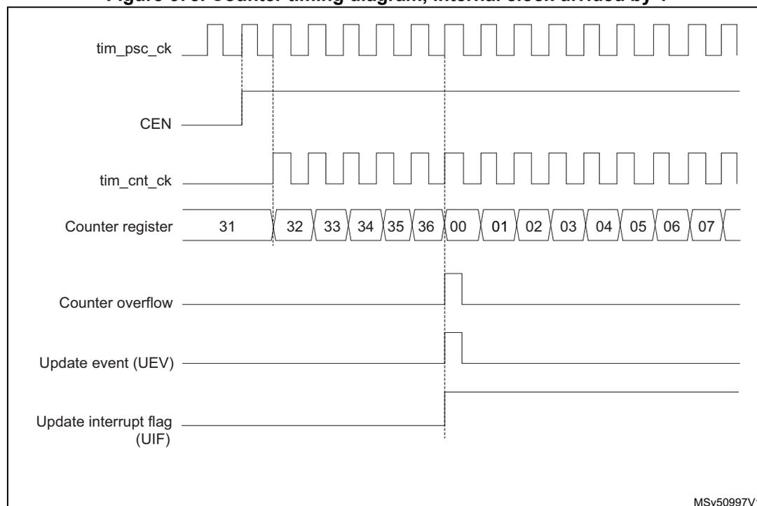
The timing diagram illustrates the operation of a counter. The top signal, tim_psc_ck , is a periodic square wave representing the prescaler clock. Below it, CEN (Counter Enable) is shown as a signal that goes high to enable counting. The tim_cnt_ck signal is a square wave that is active only when CEN is high. The Counter register shows a sequence of values: 31, 32, 33, 34, 35, 36, 00, 01, 02, 03, 04, 05, 06, 07. The Counter overflow signal is a pulse that occurs when the counter reaches the value 36. The Update event (UEV) signal is a pulse that occurs when the counter overflows. The Update interrupt flag (UIF) signal is a pulse that occurs when the counter overflows. Vertical dashed lines indicate the timing relationships between these signals.
MSv50997V1
Figure 676. Counter timing diagram, internal clock divided by 2
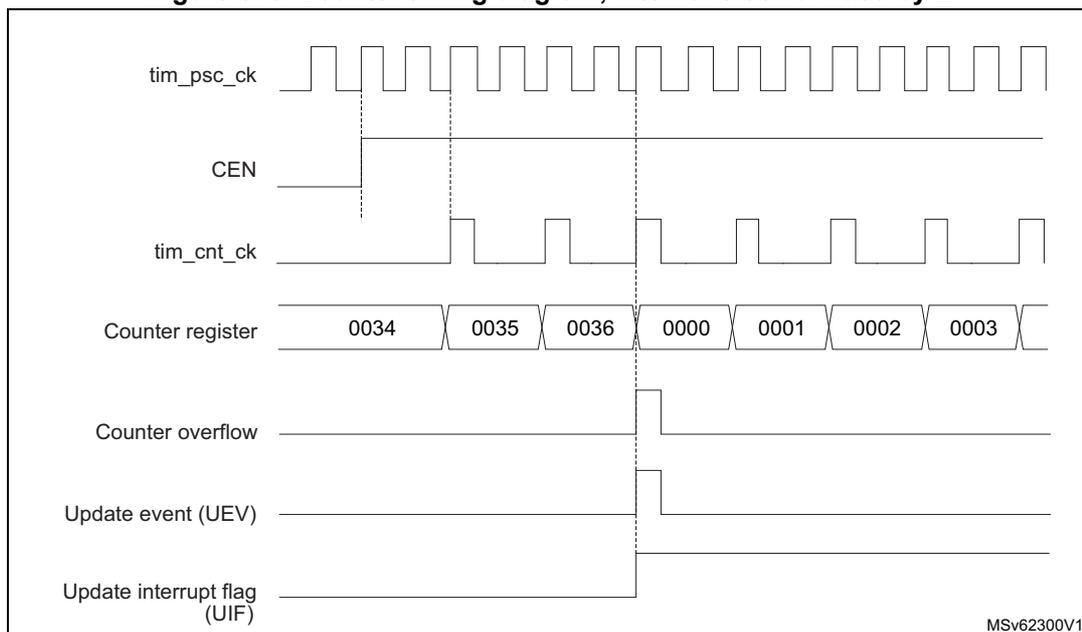
Timing diagram showing the relationship between the prescaler clock (tim_psc_ck), counter enable (CEN), counter clock (tim_cnt_ck), counter register values, counter overflow, update event (UEV), and update interrupt flag (UIF) when the internal clock is divided by 2.
The diagram illustrates the following signals and events:
- tim_psc_ck : Prescaler clock signal (square wave).
- CEN : Counter Enable signal (active high).
- tim_cnt_ck : Counter clock signal (square wave, half the frequency of tim_psc_ck).
- Counter register : Shows the sequence of values: 0034, 0035, 0036, 0000, 0001, 0002, 0003.
- Counter overflow : Pulse generated when the counter reaches 0036 and rolls over to 0000.
- Update event (UEV) : Pulse generated when the counter rolls over.
- Update interrupt flag (UIF) : Pulse generated when the counter rolls over.
MSV62300V1
Figure 677. Counter timing diagram, internal clock divided by 4
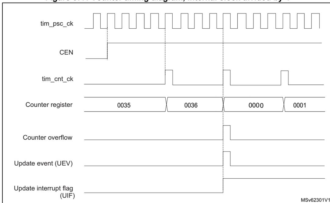
Timing diagram showing the relationship between the prescaler clock (tim_psc_ck), counter enable (CEN), counter clock (tim_cnt_ck), counter register values, counter overflow, update event (UEV), and update interrupt flag (UIF) when the internal clock is divided by 4.
The diagram illustrates the following signals and events:
- tim_psc_ck : Prescaler clock signal (square wave).
- CEN : Counter Enable signal (active high).
- tim_cnt_ck : Counter clock signal (square wave, one-quarter the frequency of tim_psc_ck).
- Counter register : Shows the sequence of values: 0035, 0036, 0000, 0001.
- Counter overflow : Pulse generated when the counter reaches 0036 and rolls over to 0000.
- Update event (UEV) : Pulse generated when the counter rolls over.
- Update interrupt flag (UIF) : Pulse generated when the counter rolls over.
MSV62301V1
Figure 678. Counter timing diagram, internal clock divided by N
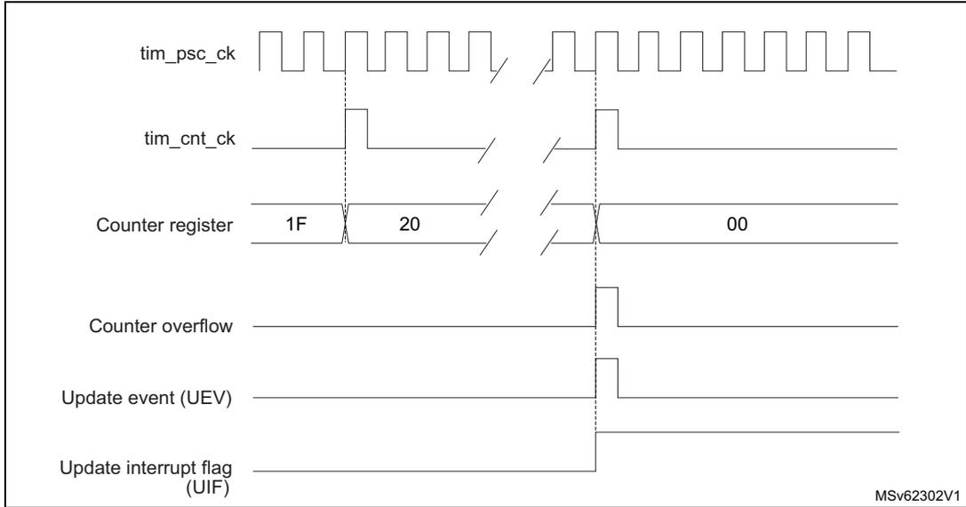
This timing diagram illustrates the operation of a basic timer with an internal clock divided by N. The top signal, tim_psc_ck , is a periodic square wave. Below it, tim_cnt_ck is a lower-frequency square wave derived from the prescaler clock. The Counter register shows a sequence of values: 1F , 20 , and 00 . A transition from 1F to 20 occurs on a rising edge of tim_cnt_ck . When the counter reaches 20 (the auto-reload value), a Counter overflow pulse occurs. This is followed by an Update event (UEV) and a pulse on the Update interrupt flag (UIF) . The counter then reloads with the value 00 . The diagram is labeled MSV62302V1.
Figure 679. Counter timing diagram, update event when ARPE = 0 (TIMx_ARR not preloaded)
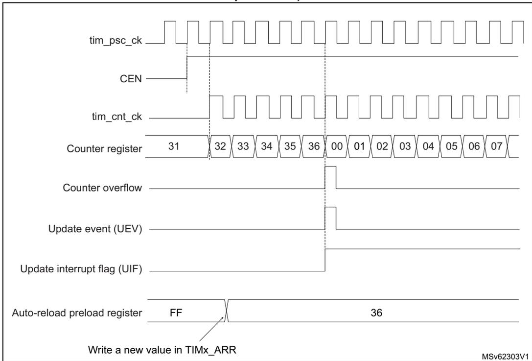
This timing diagram shows the timer's behavior when the ARPE bit is 0 and the auto-reload register is not preloaded. The tim_psc_ck signal is shown at the top. The CEN (Counter Enable) signal is active-low and is shown going low to enable the counter. The tim_cnt_ck signal is the counter clock. The Counter register increments from 31 to 32 , 33 , 34 , 35 , 36 , 00 , 01 , 02 , 03 , 04 , 05 , 06 , and 07 . At the value 36 , a Counter overflow occurs, followed by an Update event (UEV) and a pulse on the Update interrupt flag (UIF) . Simultaneously, the Auto-reload preload register is updated from FF to 36 . An annotation with an arrow pointing to the register says "Write a new value in TIMx_ARR". The diagram is labeled MSV62303V1.
Figure 680. Counter timing diagram, update event when ARPE = 1 (TIMx_ARR preloaded)
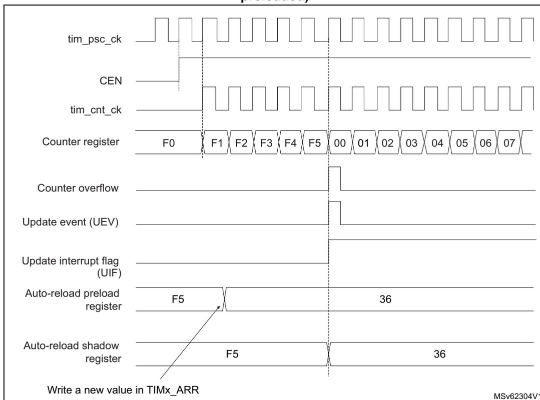
The timing diagram shows the following signals and their states over time:
- tim_psc_ck : A periodic clock signal.
- CEN : Counter Enable, which is high during the counting period.
- tim_cnt_ck : The counter clock, which is a divided version of tim_psc_ck.
- Counter register : Shows the counter values F0, F1, F2, F3, F4, F5, 00, 01, 02, 03, 04, 05, 06, 07. The counter increments from F0 to F5, then overflows to 00.
- Counter overflow : A pulse that goes high when the counter reaches F5 and returns low when it reaches 00.
- Update event (UEV) : A pulse that goes high when the counter reaches F5 and returns low when it reaches 00.
- Update interrupt flag (UIF) : A pulse that goes high when the counter reaches F5 and returns low when it reaches 00.
- Auto-reload preload register : Shows the value F5 being written, then changing to 36. An arrow points to the transition with the text "Write a new value in TIMx_ARR".
- Auto-reload shadow register : Shows the value F5 being updated to 36 at the next update event (when the counter reaches 00).
MSv62304V1
Dithering mode
The time base effective resolution can be increased by enabling the dithering mode, using the DITHEN bit in the TIMx_CR1 register. This affects the way the TIMx_ARR is behaving, and is useful for adjusting the average counter period when the timer is used as a trigger.
The operating principle is to have the actual ARR value slightly changed (adding or not one timer clock period) over 16 consecutive counting periods, with predefined patterns. This allows a 16-fold resolution increase, considering the average counting period.
Figure 681 presents the dithering principle applied to four consecutive counting periods.
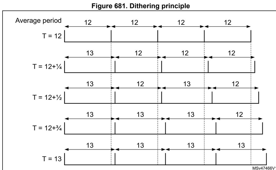
Figure 681. Dithering principle
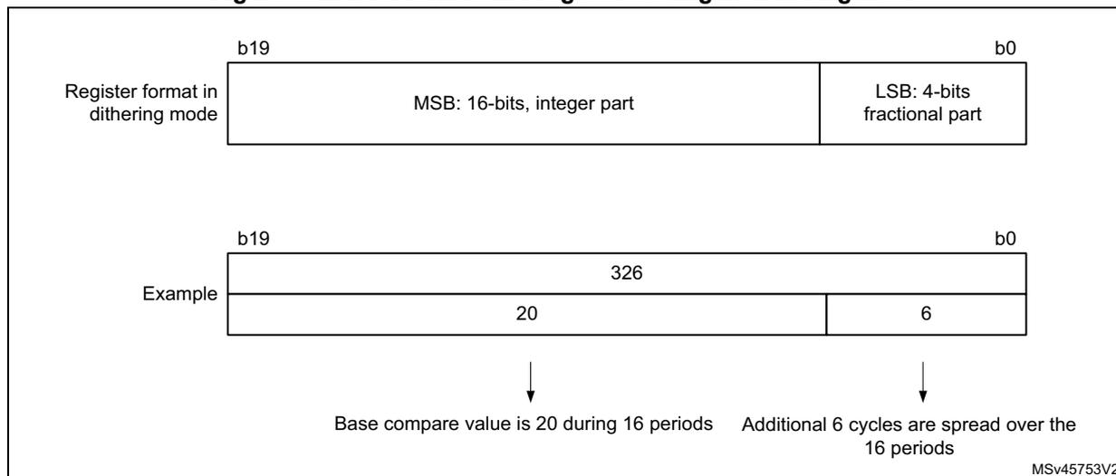
When the dithering mode is enabled, the register coding is changed as follows (see Figure 682 for example):
- • The four LSBs are coding for the enhanced resolution part (fractional part).
- • The MSBs are left-shifted to the bits 19:4 and are coding for the base value.
Note:
The following sequence must be followed when resetting the DITHEN bit:
1. CEN and ARPE bits must be reset
2. The DITHEN bit must be reset
3. The CEN bit can be set (eventually with ARPE = 1).
Figure 682. Data format and register coding in dithering mode
The minimum frequency is given by the following formula:
Note: The maximum TIMx_ARR value is limited to 0xFFFEF in dithering mode (corresponds to 65534 for the integer part and 15 for the dithered part).
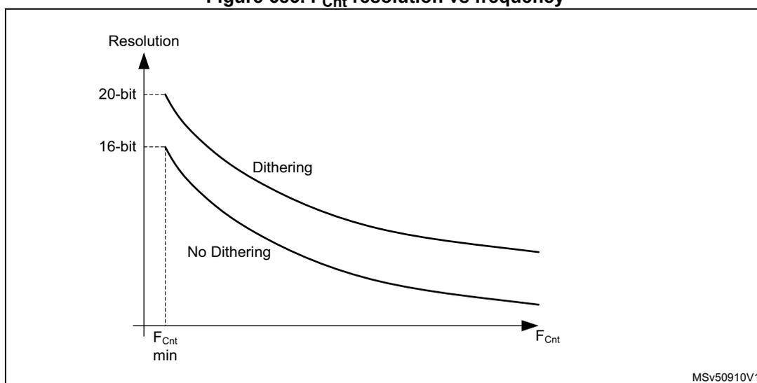
As shown on Figure 683 , the dithering mode is used to increase the PWM resolution whatever the PWM frequency.
Figure 683. \( F_{\text{Cnt}} \) resolution vs frequency
The period changes are spread over 16 consecutive periods, as described in Figure 684 .
Figure 684. PWM dithering pattern
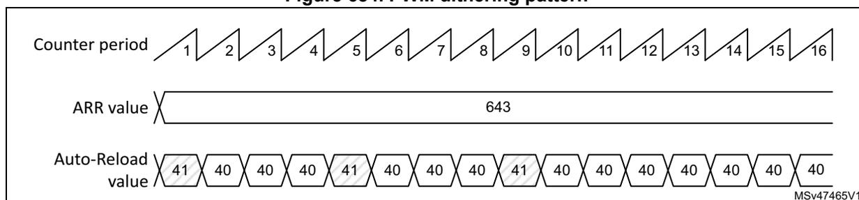
The autoreload and compare values increments are spread following the specific patterns described in Table 521 . The dithering sequence is done to have increments distributed as evenly as possible and minimize the overall ripple.
Table 521. TIMx_ARR register change dithering pattern
| - | PWM period | ||||||||||||||||
|---|---|---|---|---|---|---|---|---|---|---|---|---|---|---|---|---|---|
| LSB value | 1 | 2 | 3 | 4 | 5 | 6 | 7 | 8 | 9 | 10 | 11 | 12 | 13 | 14 | 15 | 16 | |
| 0000 | - | - | - | - | - | - | - | - | - | - | - | - | - | - | - | - | - |
| 0001 | +1 | - | - | - | - | - | - | - | - | - | - | - | - | - | - | - | - |
| 0010 | +1 | - | - | - | - | - | - | - | +1 | - | - | - | - | - | - | - | - |
| 0011 | +1 | - | - | - | +1 | - | - | - | +1 | - | - | - | - | - | - | - | - |
| 0100 | +1 | - | - | - | +1 | - | - | - | +1 | - | - | - | +1 | - | - | - | - |
| 0101 | +1 | - | +1 | - | +1 | - | - | - | +1 | - | - | - | +1 | - | - | - | - |
| 0110 | +1 | - | +1 | - | +1 | - | - | - | +1 | - | +1 | - | +1 | - | - | - | - |
| 0111 | +1 | - | +1 | - | +1 | - | +1 | - | +1 | - | +1 | - | +1 | - | - | - | - |
| 1000 | +1 | - | +1 | - | +1 | - | +1 | - | +1 | - | +1 | - | +1 | - | +1 | - | - |
| 1001 | +1 | +1 | +1 | - | +1 | - | +1 | - | +1 | - | +1 | - | +1 | - | +1 | - | - |
| 1010 | +1 | +1 | +1 | - | +1 | - | +1 | - | +1 | +1 | +1 | - | +1 | - | +1 | - | - |
| 1011 | +1 | +1 | +1 | - | +1 | +1 | +1 | - | +1 | +1 | +1 | - | +1 | - | +1 | - | - |
| 1100 | +1 | +1 | +1 | - | +1 | +1 | +1 | - | +1 | +1 | +1 | - | +1 | +1 | +1 | - | - |
| 1101 | +1 | +1 | +1 | +1 | +1 | +1 | +1 | - | +1 | +1 | +1 | - | +1 | +1 | +1 | - | - |
| 1110 | +1 | +1 | +1 | +1 | +1 | +1 | +1 | - | +1 | +1 | +1 | +1 | +1 | +1 | +1 | +1 | - |
| 1111 | +1 | +1 | +1 | +1 | +1 | +1 | +1 | +1 | +1 | +1 | +1 | +1 | +1 | +1 | +1 | +1 | - |
55.3.6 UIF bit remapping
The IUFREMAP bit in the TIMx_CR1 register forces a continuous copy of the update interrupt flag UIF into the timer counter register's bit 31 (TIMxCNT[31]). This is used to atomically read both the counter value and a potential roll-over condition signaled by the UIFCPY flag. In particular cases, it can ease the calculations by avoiding race conditions caused for instance by a processing shared between a background task (counter reading) and an interrupt (update interrupt).
There is no latency between the assertions of the UIF and UIFCPY flags.
55.3.7 ADC triggers
The timer can generate an ADC triggering event with various internal signals, such as reset, enable or compare events.
Note: The clock of the slave peripherals (such as timer, ADC) receiving the tim_trgo signal must be enabled prior to receiving events from the master timer, and the clock frequency (prescaler) must not be changed on-the-fly while triggers are received from the master timer.
55.3.8 ADC synchronization
The timer operation can be synchronized to the ADC clock to trigger jitter-free ADC sampling. This function is enabled using the ADSYNC bit in the TIMx_CR2 register.
This feature is useful when the timers and the ADCs are operating with semisynchronous clocks (clocks derived from a same source with integer ratio \( tim\_ker\_ck/adc\_ker\_ck \) ), for instance \( adc\_ker\_ck = 75 \) MHz and \( tim\_ker\_ck = 150 \) MHz or 300 MHz.
ADSYNC must also be set when both peripherals are operating at the same frequency from the same clock source, when jitter-free operation is needed.
ADSYNC must not be set and jitter-free operation is not supported in the following cases:
- • When the clock ratio is not an integer (for example \( adc\_ker\_ck = 75 \) MHz and \( tim\_ker\_ck = 100 \) MHz): in this case, the sampling point jitter due to the timer to ADC signal resynchronization is 1 \( adc\_ker\_ck \) period maximum.
- • When the ADC is operating in asynchronous mode ( \( adc\_ker\_ck \) uncorrelated with \( tim\_ker\_ck \) ): in this case, the sampling point jitter due to the timer to ADC signal resynchronization is 1 \( adc\_ker\_ck \) period maximum.
When ADSYNC = 1, the timer operation is slightly changed: the counter enable and counter reset events are aligned to the \( adc\_ker\_ck \) ADC clock, to avoid any phase shift due to clocks enable in the RCC.
Jitter-free operation is guaranteed only when one of the two requirements below is met (depending on the selected trigger source).
- 1. The counter period must be a multiple of the ADC clock period
- 2. The compare value must be a multiple of the ADC clock period
Note: If none of the two above requirements are met, the trigger is still generated, but the latency is not constant and varies with the timer and ADC clocks phase shift.
Programming guidelines
The ADC synchronization feature must not be modified during run-time, once the counter is enabled and once the ADC has been configured for receiving triggers from the timer.
It is mandatory to follow the procedure below to use the ADC synchronization:
- 1. Enable the destination ADC clock
- 2. Configure the timer and set the ADSYNC bit
- 3. Configure the ADC and enable it (using ADSTART and/or JADSTART bits)
- 4. Start the timer (with the CEN counter enable bit)
55.3.9 TIM6/TIM7/TIM18 DMA requests
The TIM6/TIM7/TIM18 can generate a single DMA request, as shown in Table 522 .
Table 522. DMA request
| DMA acronym | DMA request | Enable control bit |
|---|---|---|
| tim_upd_dma | Update | UDE |
55.3.10 Debug mode
When the microcontroller enters debug mode (Cortex ® -M55 core halted), the TIMx counter can either continue to work normally or be stopped.
The behavior in debug mode can be programmed with a dedicated configuration bit per timer in the Debug support (DBG) module.
For more details, refer to section Debug support (DBG).
55.3.11 TIM6/TIM7/TIM18 low-power modes
Table 523. Effect of low-power modes on TIM6/TIM7/TIM18
| Mode | Description |
|---|---|
| Sleep | No effect, peripheral is active. The interrupts can cause the device to exit from Sleep mode. |
| Stop | The timer operation is stopped and the register content is kept. No interrupt can be generated. |
| Standby | The timer is powered-down and must be reinitialized after exiting the Standby mode. |
55.3.12 TIM6/TIM7/TIM18 interrupts
The TIM6/TIM7/TIM18 can generate a single interrupt, as shown in Table 524 .
Table 524. Interrupt request
| Interrupt acronym | Interrupt event | Event flag | Enable control bit | Interrupt clear method | Exit from Sleep mode | Exit from Stop and Standby mode |
|---|---|---|---|---|---|---|
| TIM6 TIM7 | Update | UIF | UIE | write 0 in UIF | Yes | No |
55.4 TIM6/TIM7/TIM18 registers
Refer to Section 1.2 for a list of abbreviations used in register descriptions.
The peripheral registers can be accessed by half-words (16-bit) or words (32-bit).
55.4.1 TIMx control register 1 (TIMx_CR1)(x = 6, 7, 18)
Address offset: 0x00
Reset value: 0x0000
| 15 | 14 | 13 | 12 | 11 | 10 | 9 | 8 | 7 | 6 | 5 | 4 | 3 | 2 | 1 | 0 |
|---|---|---|---|---|---|---|---|---|---|---|---|---|---|---|---|
| Res. | Res. | Res. | DITH EN | UIFRE MAP | Res. | Res. | Res. | ARPE | Res. | Res. | Res. | OPM | URS | UDIS | CEN |
| rw | rw | rw | rw | rw | rw | rw |
Bits 15:13 Reserved, must be kept at reset value.
Bit 12 DITHEN : Dithering enable
0: Dithering disabled
1: Dithering enabled
Note: The DITHEN bit can only be modified when CEN bit is reset.
Bit 11 UIFREMAP : UIF status bit remapping
0: No remapping. UIF status bit is not copied to TIMx_CNT register bit 31.
1: Remapping enabled. UIF status bit is copied to TIMx_CNT register bit 31.
Bits 10:8 Reserved, must be kept at reset value.
Bit 7 ARPE : Auto-reload preload enable
0: TIMx_ARR register is not buffered.
1: TIMx_ARR register is buffered.
Bits 6:4 Reserved, must be kept at reset value.
Bit 3 OPM : One-pulse mode
0: Counter is not stopped at update event
1: Counter stops counting at the next update event (clearing the CEN bit).
Bit 2 URS: Update request sourceThis bit is set and cleared by software to select the UEV event sources.
0: Any of the following events generates an update interrupt or DMA request if enabled.
These events can be:
- - Counter overflow/underflow
- - Setting the UG bit
- - Update generation through the slave mode controller
1: Only counter overflow/underflow generates an update interrupt or DMA request if enabled.
Bit 1 UDIS: Update disableThis bit is set and cleared by software to enable/disable UEV event generation.
0: UEV enabled. The Update (UEV) event is generated by one of the following events:
- - Counter overflow/underflow
- - Setting the UG bit
- - Update generation through the slave mode controller
Buffered registers are then loaded with their preload values.
1: UEV disabled. The Update event is not generated, shadow registers keep their value (ARR, PSC). However the counter and the prescaler are reinitialized if the UG bit is set or if a hardware reset is received from the slave mode controller.
Bit 0 CEN: Counter enable0: Counter disabled
1: Counter enabled
CEN is cleared automatically in one-pulse mode, when an update event occurs.
55.4.2 TIMx control register 2 (TIMx_CR2)(x = 6, 7, 18)
Address offset: 0x04
Reset value: 0x0000 0000
| 31 | 30 | 29 | 28 | 27 | 26 | 25 | 24 | 23 | 22 | 21 | 20 | 19 | 18 | 17 | 16 |
|---|---|---|---|---|---|---|---|---|---|---|---|---|---|---|---|
| Res. | Res. | Res. | AD SYNC | Res. | Res. | Res. | Res. | Res. | Res. | Res. | Res. | Res. | Res. | Res. | Res. |
| rw | |||||||||||||||
| 15 | 14 | 13 | 12 | 11 | 10 | 9 | 8 | 7 | 6 | 5 | 4 | 3 | 2 | 1 | 0 |
| Res. | Res. | Res. | Res. | Res. | Res. | Res. | Res. | Res. | MMS[2:0] | Res. | Res. | Res. | Res. | ||
| rw | rw | rw | |||||||||||||
Bits 31:29 Reserved, must be kept at reset value.
Bit 28 ADSYNC : ADC synchronization
0: The timer operates independently from the ADC
1: The timer operation is synchronized with the ADC clock to provide jitter-free sampling point. This mode can be enabled only with specific ADC / timer clock relationship. Refer to Section 55.3.8 for requirements.
The ADSYNC must not be modified when the counter is enabled (CEN bit is set).
Bits 27:7 Reserved, must be kept at reset value.
Bits 6:4 MMS[2:0] : Master mode selection
These bits are used to select the information to be sent in master mode to slave timers for synchronization (TRGO). The combination is as follows:
000: Reset - the UG bit from the TIMx_EGR register is used as a trigger output (tim_trgo).
001: Enable - the Counter enable signal, tim_cnt_en, is used as a trigger output (tim_trgo). It is useful to start several timers at the same time or to control a window in which a slave timer is enabled. The Counter Enable signal is generated when the CEN control bit is written.
010: Update - The update event is selected as a trigger output (tim_trgo). For instance a master timer can then be used as a prescaler for a slave timer.
Note: The clock of the slave timer or the peripheral receiving the tim_trgo must be enabled prior to receive events from the master timer, and must not be changed on-the-fly while triggers are received from the master timer.
Bits 3:0 Reserved, must be kept at reset value.
55.4.3 TIMx DMA/Interrupt enable register (TIMx_DIER)(x = 6, 7, 18)
Address offset: 0x0C
Reset value: 0x0000
| 15 | 14 | 13 | 12 | 11 | 10 | 9 | 8 | 7 | 6 | 5 | 4 | 3 | 2 | 1 | 0 |
|---|---|---|---|---|---|---|---|---|---|---|---|---|---|---|---|
| Res. | Res. | Res. | Res. | Res. | Res. | Res. | UDE | Res. | Res. | Res. | Res. | Res. | Res. | Res. | UIE |
| rw | rw |
Bits 15:9 Reserved, must be kept at reset value.
Bit 8 UDE : Update DMA request enable
0: Update DMA request disabled.
1: Update DMA request enabled.
Bits 7:1 Reserved, must be kept at reset value.
Bit 0 UIE : Update interrupt enable
0: Update interrupt disabled.
1: Update interrupt enabled.
55.4.4 TIMx status register (TIMx_SR)(x = 6, 7, 18)
Address offset: 0x10
Reset value: 0x0000
| 15 | 14 | 13 | 12 | 11 | 10 | 9 | 8 | 7 | 6 | 5 | 4 | 3 | 2 | 1 | 0 |
|---|---|---|---|---|---|---|---|---|---|---|---|---|---|---|---|
| Res. | Res. | Res. | Res. | Res. | Res. | Res. | Res. | Res. | Res. | Res. | Res. | Res. | Res. | Res. | UIF |
| rc_w0 |
Bits 15:1 Reserved, must be kept at reset value.
Bit 0 UIF : Update interrupt flag
This bit is set by hardware on an update event. It is cleared by software.
0: No update occurred.
1: Update interrupt pending. This bit is set by hardware when the registers are updated:
–On counter overflow if UDIS = 0 in the TIMx_CR1 register.
–When CNT is reinitialized by software using the UG bit in the TIMx_EGR register, if URS = 0 and UDIS = 0 in the TIMx_CR1 register.
55.4.5 TIMx event generation register (TIMx_EGR)(x = 6, 7, 18)
Address offset: 0x14
Reset value: 0x0000
| 15 | 14 | 13 | 12 | 11 | 10 | 9 | 8 | 7 | 6 | 5 | 4 | 3 | 2 | 1 | 0 |
|---|---|---|---|---|---|---|---|---|---|---|---|---|---|---|---|
| Res. | Res. | Res. | Res. | Res. | Res. | Res. | Res. | Res. | Res. | Res. | Res. | Res. | Res. | Res. | UG |
| w |
Bits 15:1 Reserved, must be kept at reset value.
Bit 0 UG : Update generation
This bit can be set by software, it is automatically cleared by hardware.
0: No action.
1: Re-initializes the timer counter and generates an update of the registers. Note that the prescaler counter is cleared too (but the prescaler ratio is not affected).
55.4.6 TIMx counter (TIMx_CNT)(x = 6, 7, 18)
Address offset: 0x24
Reset value: 0x0000 0000
| 31 | 30 | 29 | 28 | 27 | 26 | 25 | 24 | 23 | 22 | 21 | 20 | 19 | 18 | 17 | 16 |
|---|---|---|---|---|---|---|---|---|---|---|---|---|---|---|---|
| UIF CPY | Res. | Res. | Res. | Res. | Res. | Res. | Res. | Res. | Res. | Res. | Res. | Res. | Res. | Res. | Res. |
| r | |||||||||||||||
| 15 | 14 | 13 | 12 | 11 | 10 | 9 | 8 | 7 | 6 | 5 | 4 | 3 | 2 | 1 | 0 |
| CNT[15:0] | |||||||||||||||
| rw | rw | rw | rw | rw | rw | rw | rw | rw | rw | rw | rw | rw | rw | rw | rw |
Bit 31 UIFCPY : UIF copy
This bit is a read-only copy of the UIF bit of the TIMx_ISR register. If the UIFREMAP bit in TIMx_CR1 is reset, bit 31 is reserved and read as 0.
Bits 30:16 Reserved, must be kept at reset value.
Bits 15:0 CNT[15:0] : Counter value
Non-dithering mode (DITHEN = 0)
The register holds the counter value.
Dithering mode (DITHEN = 1)
The register only holds the non-dithered part in CNT[15:0]. The fractional part is not available.
55.4.7 TIMx prescaler (TIMx_PSC)(x = 6, 7, 18)
Address offset: 0x28
Reset value: 0x0000
| 15 | 14 | 13 | 12 | 11 | 10 | 9 | 8 | 7 | 6 | 5 | 4 | 3 | 2 | 1 | 0 |
|---|---|---|---|---|---|---|---|---|---|---|---|---|---|---|---|
| PSC[15:0] | |||||||||||||||
| rw | rw | rw | rw | rw | rw | rw | rw | rw | rw | rw | rw | rw | rw | rw | rw |
Bits 15:0 PSC[15:0] : Prescaler value
The counter clock frequency \( f_{\text{tim\_cnt\_ck}} \) is equal to \( f_{\text{tim\_psc\_ck}} / (\text{PSC}[15:0] + 1) \) .
PSC contains the value to be loaded into the active prescaler register at each update event (including when the counter is cleared through UG bit of TIMx_EGR register).
55.4.8 TIMx autoreload register (TIMx_ARR)(x = 6, 7, 18)
Address offset: 0x2C
Reset value: 0x0000 FFFF
| 31 | 30 | 29 | 28 | 27 | 26 | 25 | 24 | 23 | 22 | 21 | 20 | 19 | 18 | 17 | 16 |
|---|---|---|---|---|---|---|---|---|---|---|---|---|---|---|---|
| Res. | Res. | Res. | Res. | Res. | Res. | Res. | Res. | Res. | Res. | Res. | Res. | ARR[19:16] | |||
| rw | rw | rw | rw | ||||||||||||
| 15 | 14 | 13 | 12 | 11 | 10 | 9 | 8 | 7 | 6 | 5 | 4 | 3 | 2 | 1 | 0 |
| ARR[15:0] | |||||||||||||||
| rw | rw | rw | rw | rw | rw | rw | rw | rw | rw | rw | rw | rw | rw | rw | rw |
Bits 31:20 Reserved, must be kept at reset value.
Bits 19:0 ARR[19:0] : Auto-reload value
ARR is the value to be loaded into the actual auto-reload register.
Refer to Section 55.3.4: Time-base unit for more details about ARR update and behavior.
The counter is blocked while the auto-reload value is null.
Non-dithering mode (DITHEN = 0)
The register holds the auto-reload value in ARR[15:0]. The ARR[19:16] bits are reserved.
Dithering mode (DITHEN = 1)
The register holds the integer part in ARR[19:4]. The ARR[3:0] bitfield contains the dithered part.
55.4.9 TIMx register map
TIMx registers are mapped as 16-bit addressable registers as described in the table below:
Table 525. TIMx register map and reset values
| Offset | Register name | 31 | 30 | 29 | 28 | 27 | 26 | 25 | 24 | 23 | 22 | 21 | 20 | 19 | 18 | 17 | 16 | 15 | 14 | 13 | 12 | 11 | 10 | 9 | 8 | 7 | 6 | 5 | 4 | 3 | 2 | 1 | 0 |
|---|---|---|---|---|---|---|---|---|---|---|---|---|---|---|---|---|---|---|---|---|---|---|---|---|---|---|---|---|---|---|---|---|---|
| 0x00 | TIMx_CR1 | Res. | Res. | Res. | Res. | Res. | Res. | Res. | Res. | Res. | Res. | Res. | Res. | Res. | Res. | Res. | Res. | Res. | Res. | Res. | DITHEN | UIFREMA | Res. | Res. | Res. | ARPE | Res. | Res. | Res. | OPM | URS | UDIS | CEN |
| Reset value | 0 | 0 | 0 | 0 | 0 | 0 | 0 | ||||||||||||||||||||||||||
| 0x04 | TIMx_CR2 | Res. | Res. | Res. | ADSYNC | Res. | Res. | Res. | Res. | Res. | Res. | Res. | Res. | Res. | Res. | Res. | Res. | Res. | Res. | Res. | Res. | Res. | Res. | Res. | Res. | Res. | MMS [2:0] | Res. | Res. | Res. | Res. | ||
| Reset value | 0 | 0 | 0 | 0 | |||||||||||||||||||||||||||||
| 0x08 | Reserved | ||||||||||||||||||||||||||||||||
| 0x0C | TIMx_DIER | Res. | Res. | Res. | Res. | Res. | Res. | Res. | Res. | Res. | Res. | Res. | Res. | Res. | Res. | Res. | Res. | Res. | Res. | Res. | Res. | Res. | Res. | Res. | UDE | Res. | Res. | Res. | Res. | Res. | Res. | Res. | UIE |
| Reset value | 0 | 0 | |||||||||||||||||||||||||||||||
| 0x10 | TIMx_SR | Res. | Res. | Res. | Res. | Res. | Res. | Res. | Res. | Res. | Res. | Res. | Res. | Res. | Res. | Res. | Res. | Res. | Res. | Res. | Res. | Res. | Res. | Res. | Res. | Res. | Res. | Res. | Res. | Res. | Res. | Res. | UIF |
| Reset value | 0 | ||||||||||||||||||||||||||||||||
| 0x14 | TIMx_EGR | Res. | Res. | Res. | Res. | Res. | Res. | Res. | Res. | Res. | Res. | Res. | Res. | Res. | Res. | Res. | Res. | Res. | Res. | Res. | Res. | Res. | Res. | Res. | Res. | Res. | Res. | Res. | Res. | Res. | Res. | Res. | UG |
| Reset value | 0 | ||||||||||||||||||||||||||||||||
| 0x18-0x20 | Reserved | ||||||||||||||||||||||||||||||||
| 0x24 | TIMx_CNT | UIFCPY or Res. | Res. | Res. | Res. | Res. | Res. | Res. | Res. | Res. | Res. | Res. | Res. | Res. | Res. | Res. | Res. | Res. | Res. | Res. | Res. | Res. | Res. | Res. | Res. | Res. | Res. | Res. | Res. | Res. | Res. | Res. | CNT[15:0] |
| Reset value | 0 | 0 0 0 0 0 0 0 0 0 0 0 0 0 0 0 0 | |||||||||||||||||||||||||||||||
| 0x28 | TIMx_PSC | Res. | Res. | Res. | Res. | Res. | Res. | Res. | Res. | Res. | Res. | Res. | Res. | Res. | Res. | Res. | Res. | Res. | Res. | Res. | Res. | Res. | Res. | Res. | Res. | Res. | Res. | Res. | Res. | Res. | Res. | Res. | PSC[15:0] |
| Reset value | 0 0 0 0 0 0 0 0 0 0 0 0 0 0 0 0 | ||||||||||||||||||||||||||||||||
| 0x2C | TIMx_ARR | Res. | Res. | Res. | Res. | Res. | Res. | Res. | Res. | Res. | Res. | Res. | Res. | Res. | Res. | Res. | Res. | Res. | Res. | Res. | Res. | Res. | Res. | Res. | Res. | Res. | Res. | Res. | Res. | Res. | Res. | Res. | ARR[19:0] |
| Reset value | 0 0 0 0 1 1 1 1 1 1 1 1 1 1 1 1 1 1 1 1 | ||||||||||||||||||||||||||||||||
Refer to Section 2.3: Memory organization for the register boundary addresses.