51. Memory cipher engine (MCE)
51.1 MCE introduction
Memory cipher engine (MCE) defines, in a given address space, multiple regions with specific security setup (encryption). All system bus traffic going through an encrypted region is managed on-the-fly by the MCE, automatically decrypting reads and encrypting writes if authorized.
Multiple ciphering option (stream, block, fast block) are available to offer the best security versus performance trade-off.
Note: When MCE is used in conjunction with XSPI it is mandatory to access the flash memory using the memory map mode of the flash memory controller.
51.2 MCE main features
- • System bus in-line encryption (for writes) and decryption (for reads), based on embedded firewall programming
- – Four encryption modes per region (maximum 4 regions available): no encryption (bypass mode), stream cipher, block cipher and fast block cipher modes
- – Start and end of regions defined with 4-Kbytes granularity
- – Default filtering (region 0): any access granted
- – Region 1 to 4 access filtering criteria: none
- • Supported block ciphers: AES-128, AES-256 or Noekeon (12 round version), selected at boot
- • Supported chaining modes: block and stream
- – Block mode with AES cipher is compatible with ECB mode specified in NIST FIPS publication 197 Advanced encryption standard (AES) (normal or fast).
- – Stream mode with AES cipher is compliant with CTR mode specified in NIST SP800-38A Recommendation for Block Cipher Modes of Operation .
- – Includes a leakage resilient mode of operation as defense against side channel attacks (SCA).
- • One set of write-only and lockable 256-bit master key registers per block cipher (normal, fast)
- • Two sets of lockable cipher contexts (128-bit key, IV), usable for stream and block ciphers
- • Optimization for XSPI data pre-fetching mechanism (stream cipher only)
- • Read-write arbitration scheme, for better read performances
- • AHB configuration port
- – Accessible through 32-bit word single accesses only (otherwise an AHB bus error is generated, and write accesses are ignored)
- • AXI system bus master/slave interfaces (64-bit)
- – Support for any AXI-64bit read transactions
- – When encryption is enabled, support for AXI-64bit INCRx (x = 1 to 8) and WRAPx (x = 4) write transactions
51.3 MCE implementation
MCE peripheral generates interrupts to the Cortex® CPU interrupt controller (mce_it).
51.4 MCE functional description
51.4.1 MCE block diagram
Figure 495 shows the memory cipher engine block diagram, associated with one or more memory interface peripheral.
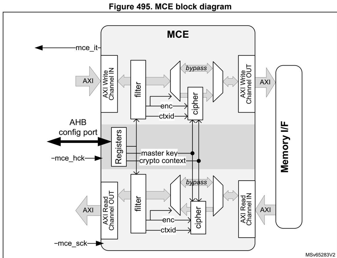
Figure 495. MCE block diagram
The diagram illustrates the internal architecture of the Memory Cipher Engine (MCE). It features two parallel processing paths for write and read operations. The write path consists of an AXI Write Channel IN, a filter, a bypass multiplexer, a cipher block, and an AXI Write Channel OUT. The read path consists of an AXI Read Channel IN, a filter, a bypass multiplexer, a cipher block, and an AXI Read Channel OUT. Both paths are controlled by a central 'Registers' block, which is connected to an AHB config port and receives inputs from -mce_hck and -mce_sck. The registers provide 'master key' and 'crypto context' to the cipher blocks. An interrupt signal 'mce_it' is output from the MCE. The AXI channels are connected to an external 'Memory I/F' block. The diagram is labeled with MSV65283V2.
51.4.2 MCE internal signals
Table 435 describes the user relevant internal signals interfacing the MCE peripheral.
Table 435. MCE internal input/output signals
| Signal name | Signal type (1) | Description |
|---|---|---|
| mce_sck | input | AXI input clock |
| mce_hck | input | AHB input clock for MCE |
| mce_it | output | MCE interrupt request |
1. All digital.
51.4.3 MCE programming
Overview
Through MCE registers application software defines security regions, as shown on Figure 496 .
Figure 496. MCE region programming
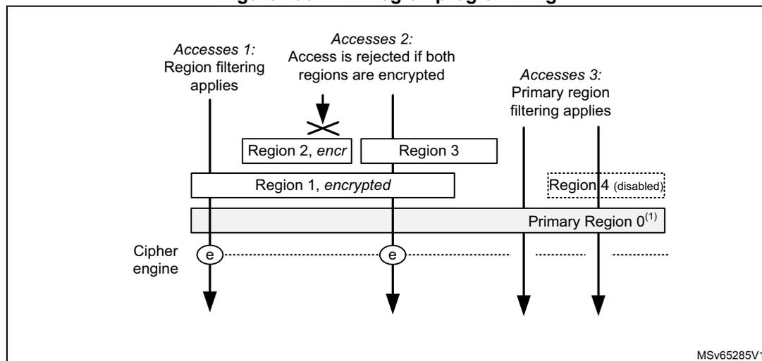
The diagram illustrates the memory cipher engine (MCE) region programming. It shows four access scenarios:
- Accesses 1: Region filtering applies. Access is made to Region 1 (encrypted). The cipher engine is used.
- Accesses 2: Access is rejected if both regions are encrypted. Access is made to the overlapping area of Region 2 (encrypted) and Region 3. The access is rejected.
- Accesses 3: Primary region filtering applies. Access is made to Primary Region 0 (1) . The cipher engine is used.
- Region 4 (disabled): Access is made to a disabled region. The access is rejected.
- 1. Covers all addressable space.
There are three types of accesses filtered by MCE:
- 1. Access to an area located in one enabled region (accesses 1). In this cases region filtering rules applies. If encryption is enabled cipher engine is used accordingly.
- 2. Access to an area overlapping two enabled regions (access 2):
- – If both regions are encrypted, access is automatically rejected with an error
- 3. Access to an area not belonging to any enabled region (accesses 3). In this case primary region 0 filtering apply (any access granted, no encryption).
Configuring regions
When application needs to use any region x following sequence can be used, for example at boot time.
- 1. Application selects, once, the correct cipher using CIPHERSEL in MCE_CR register. By default AES-128 is selected. When CIPHERSEL is changed all keys in MCE are zeroed.
- 2. Application sets a start and end address for each of the required region x, using MCE_SADDRx and MCE_EADDRx registers.
- 3. Application finalizes the programming by configuring MCE_REGCRx setting up security parameters (encryption). Initializing encryption is detailed in Section 51.4.5 and Section 51.4.5 .
- 4. After final check on above configuration application enables each required region z, setting BREN bit in MCE_REGCRz.
MCE configuration can be fixed until next SoC reset when GLOCK is set in MCE_CR register.
Note: When ENCDIS bit is set in MCE_SR , if ENC bit and BREN bits are set in MCE_REGCRx all writes to this region x are ignored and all read requests return zero. See Section 51.4.8 for details.
Runtime modification of region configuration
Note: When BREN is cleared primary region 0 access rules applies instead of base region rules (see Overview).
GLOCK or KEYLOCK/CCLOCK bits must be used to write lock the following registers: MCE_MKEYRx , MCE_FMKEYRx , MCE_CCxCFGR , MCE_CCxNR0/1 and MCE_CCxKEYR , in order to avoid unexpected changes to the cipher keys/context while used by the MCE.
Encrypting with MCE
MCE automatically encrypts on-the-fly any granted write transaction to a region with encryption properly initialized. When stream cipher is selected it is important to activate write protection as soon as the whole region has been encrypted (read-only region).
When MCE is used in conjunction with XSPI it is mandatory to set the Flash memory controller in memory map mode. It is also required to use the DMA to perform writes to the flash memory using 16 bytes bursts.
51.4.4 MCE reset and clocks
MCE configuration port is clocked by the AHB bus clock.
MCE system bus interface is clocked by the AXI clock. AHB interface does not need to be clocked for the system bus to be usable.
When MCE is kept under reset, no traffic can go through the system bus. Out of reset default firewall configuration applies, as described in Section 51.4.3 .
The MCE peripheral clocks are automatically managed by the device, and the peripheral is reset only by a system reset.
51.4.5 MCE block cipher encryption mode
Caution: When MCE is used in conjunction with XSPI it is mandatory to read or write the flash memory using the memory map mode of the flash memory controller.
Figure 497 details the block cipher implementations in the MCE peripheral. Top figure is a standard encryption (for writes), bottom figure is a fast decryption (for reads). Application can select a 256-bit master key using CIPHERSEL bitfield in MCE_CR register (AES-128 selection is shown, multiply by two all key lengths when AES-256 is selected).
Figure 497. MCE implementation of block ciphers
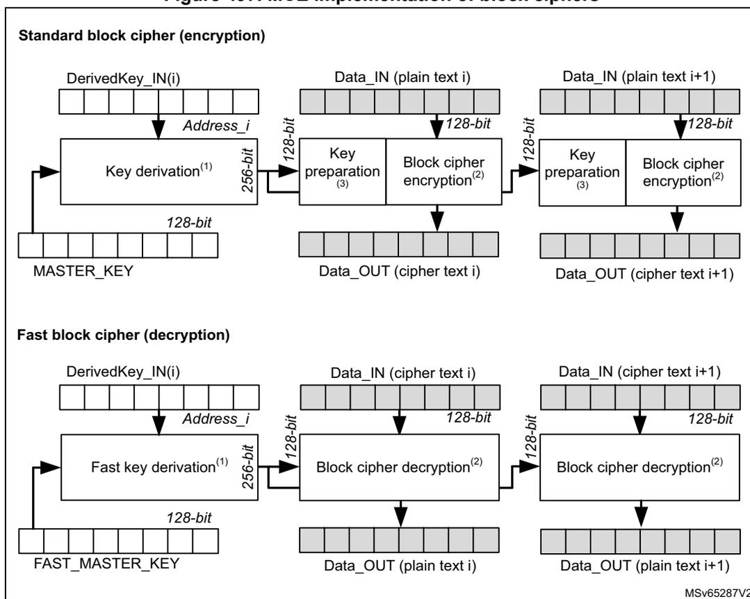
Standard block cipher (encryption)
The diagram shows the flow of data for encryption. It starts with DerivedKey_IN(i) (a 128-bit register) and Address_i (a 128-bit register) as inputs to the Key derivation (1) block. This block outputs a 256-bit key material. A 128-bit portion of this key is passed to the Key preparation (3) block. The Key preparation (3) block also receives Data_IN (plain text i) (a 128-bit register) and outputs a 128-bit key material to the Block cipher encryption (2) block. The Block cipher encryption (2) block outputs Data_OUT (cipher text i) (a 128-bit register). The process repeats for the next block, Data_IN (plain text i+1) (a 128-bit register), which is processed by the Key preparation (3) and Block cipher encryption (2) blocks to produce Data_OUT (cipher text i+1) (a 128-bit register). The MASTER_KEY (a 128-bit register) is also shown as an input to the Key derivation (1) block.
Fast block cipher (decryption)
The diagram shows the flow of data for decryption. It starts with DerivedKey_IN(i) (a 128-bit register) and Address_i (a 128-bit register) as inputs to the Fast key derivation (1) block. This block outputs a 256-bit key material. A 128-bit portion of this key is passed to the Block cipher decryption (2) block. The Block cipher decryption (2) block also receives Data_IN (cipher text i) (a 128-bit register) and outputs Data_OUT (plain text i) (a 128-bit register). The process repeats for the next block, Data_IN (cipher text i+1) (a 128-bit register), which is processed by the Block cipher decryption (2) block to produce Data_OUT (plain text i+1) (a 128-bit register). The FAST_MASTER_KEY (a 128-bit register) is also shown as an input to the Fast key derivation (1) block.
MSV65287V2
- 1. Operation starts from the capture of the address.
- 2. Operation starts from availability of data input.
- 3. Only required for AES cipher.
Address_i is most significant bits of physical address of block (i) + block (i+1). Result of key derivation primitive can be used for two consecutive 16-byte data words. Since the normal key derivation function is leakage resilient the master key information is protected against side channel attacks (SCA).
MASTER_KEY must be stored in write-only MCE_MKEYRx registers. MCE_MKEYR4 to 7 registers must be written only if AES-256 cipher is selected with CIPHERSEL.
FAST_MASTER_KEY must be stored in write-only MCE_FMKEYRx registers.
MCE_FMKEYR4 to 7 registers must be written only if AES-256 cipher is selected with CIPHERSEL. Alternatively, MCE_CCzKEYRx registers can be used if cipher context z is selected in MCE_REGCR (CTXID = z). In this case AES-256 cipher must not be selected with CIPHERSEL.
Each time a key material has been successfully written in MCE, the following flags are set:
- • MKVALID bit in MCE_SR is set when a complete key has been written in MCE_MKEYR registers.
- • FMKVALID bit in MCE_SR is set when a complete key has been written in MCE_FMKEYR registers.
- • KEYCRC[7:0] in MCE_CCzCFGR is loaded with 8-bit checksum when a complete key has been written in MCE_CCzKEYR registers. See KEYCRC bitfield for details.
Bypass mode is selected instead of cipher mode if the selected key is not marked as valid with above flags. See ENC bitfield description for details.
Note: With AES block cipher, writing (encryption) requires extra cycles in order to perform the required key scheduling to obtain the encryption key. See next table for details.
Fast key derivation function may be sensitive against side channel attacks. Hence master key used in normal mode is never used in fast mode.
Relative performances are described on Table 436 .
Table 436. MCE block cipher latencies
| Cipher type | Block mode | ENC bit in MCE_REGCRx | Latency in AXI cycles | Optimization for sequential accesses | |
|---|---|---|---|---|---|
| for 16 bytes data | for 32 bytes data | ||||
| AES-128 (1) | Normal (2) | 10 | 14+11= 25 | 14+11x2= 36 | no |
| Fast | 11 | 3+11= 14 | 3+11x2= 25 | ||
| AES-256 (3) | Normal (2) | 10 | 20+15= 35 | 20+15x2= 50 | no |
| Fast | 11 | 9+15= 24 | 9+15x2= 39 | ||
| Noekeon | Normal | 10 | 14+7= 21 | 14+7x2= 28 | no |
| Fast | 11 | 4+7= 11 | 4+7x2= 18 | ||
- 1. Additional 10 cycles are required when performing encryption/ writes
- 2. Leakage resilient mode of operation as defense against side channel attacks.
- 3. Additional 14 cycles are required when performing encryption/ writes
51.4.6 MCE stream cipher encryption mode
Figure 498 details the stream cipher implementations in the MCE peripheral. It pictures encryptions for AXI writes.
Figure 498. MCE implementation of stream cipher
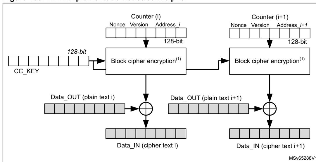
The diagram illustrates the stream cipher encryption process. It consists of two identical stages for processing consecutive data blocks, labeled 'i' and 'i+1'.
- **Stage i**: A 128-bit 'CC_KEY' and a 'Counter (i)' (containing Nonce, Version, and Address i) are inputs to a 'Block cipher encryption' block. The 'Data_OUT (plain text i)' is also an input to this block. The output of the block is XORed with 'Data_OUT (plain text i)' to produce 'Data_IN (cipher text i)'.
- **Stage i+1**: The 'Counter (i)' is incremented to 'Counter (i+1)' (containing Nonce, Version, and Address i+1). This counter, along with the 'CC_KEY', is input to the next 'Block cipher encryption' block. The 'Data_OUT (plain text i+1)' is input to this block. The output is XORed with 'Data_OUT (plain text i+1)' to produce 'Data_IN (cipher text i+1)'.
- The 'Data_IN (cipher text i)' from the first stage is passed as the 'Data_OUT (plain text i+1)' for the second stage.
- Reference code 'MSv65288V1' is shown in the bottom right corner.
- 1. Operation starts from the capture of the address.
Every 128-bit data block (i), a counter (i) information is computed, as defined below:
- Counter[127:0] = MCE_CCzNR1[31:0] || MCE_CCzNR0[31:0] || 0b0000 0000 0000 0000 || MCE_CCzCFGR[31:16] || 0b0000 || Address_i [31:4].
Address_i is the physical address of block (i), modulo 16 bytes.
Version and Nonce are stored by application respectively in MCE_CCzCFGR and MCE_CCzNRx registers, with cipher context z selected in MCE_REGCR (CTXID = z).
The least significant byte of Data_IN and Data_OUT are stored in the first 8 bits of the data blocks.
CC_KEY is stored in write-only MCE_CCzKEYRx registers, with cipher context z selected in MCE_REGCR (CTXID = z). When a complete key have not been written in MCE_CCzKEYR registers bypass mode is selected instead of stream cipher mode.
Note: Stream cipher mode offers no protection against bit-flip attacks, and is sensitive against side channel attacks.
Caution: When MCE is used in conjunction with XSPI it is mandatory to read or write the flash memory using the memory map mode of the flash memory controller.
Relative performances are described on Table 437 .
Table 437. MCE stream cipher latencies
| Cipher type | Stream mode | ENC bit in MCE_REGCRx | Latency for 16 bytes data (in AXI cycles) | Optimization for sequential accesses |
|---|---|---|---|---|
| AES-128 | Normal | 01 | 11 | Yes |
| Noekeon | Normal | 01 | 6 | Yes |
51.4.7 MCE AXI traffic management
MCE includes a special AXI-64 read-write arbitration scheme, designed to speed-up multiple reads. More specifically, when no write is ongoing in MCE the two cipher cores can be allocated to decrypt two reads in parallel. In this case an incoming write request is stalled until the cipher core allocated to writes is free.
Note: Best performances are obtained when transactions are aligned on two 64-bit words for regions where block cipher is selected. See Section 51.4.5 for details.
51.4.8 MCE encryption disable options
When MCE feature is not available in the product encryption/decryption feature of MCE is not usable, for any region. It means that reads (resp. writes) through MCE are not decrypted (resp. encrypted).
When an unexpected event occurs, the ENCDIS bit is set in MCE_SR register and the following effects apply:
- All previously written key materials are erased.
- If ENC bit and BREN bits are set in MCE_REGCRx, all writes to this region x are ignored and all read requests return zero.
In such an event, the application must reset the MCE peripheral to be able to use encrypted regions again.
51.4.9 MCE error management
When an illegal access through the system bus occurs (overlapping encrypted regions, illegal key usage, CIPHERSEL = 0) the corresponding IAEF bit is set in MCE_IASR. Application cleans this flag using IAEF bit in MCE_IACR.
Illegal key usage is triggered when an access to an encrypted region occurs, with the cipher mode in MCE_REGCRx not supported by the selected cipher context key in MCE_CCzCFGGR (see MODE[1:0] bitfield).
Additional debug information on system bus illegal accesses can be read in illegal address register (MCE_IADDR). Illegal read (resp. write) through the system bus returns zero (resp. is ignored).
Reading any MCE key register returns zeros, and read to write-only or write to read-only registers do not trigger an interrupt.
51.5 MCE interrupts
There is one individual maskable interrupt source generated by the MCE, signaling the following error event:
- • Illegal access through the system bus (IAEF), see Section 51.4.9
This interrupt source is connected to the same global interrupt request signal mce_it.
Setting the appropriate mask bit in MCE_IAIER register enables the interrupt. The status of the individual interrupt events can be read from MCE_IASR, and cleared in MCE_IACR register.
Table 438 gives a summary of the available features.
Table 438. MCE interrupt requests
| Interrupt acronym | Interrupt event | Event flag (1) | Enable control bit | Interrupt clear method |
|---|---|---|---|---|
| MCE | Illegal access error | IAEF | IAEIE | Set IAEF bit in MCE_IACR |
1. Read in MCE_IASR register
51.6 MCE registers
51.6.1 MCE configuration register (MCE_CR)
Address offset: 0x000
Reset value: 0x0000 0010
Writes are ignored if GLOCK is set in MCE_CR register.
| 31 | 30 | 29 | 28 | 27 | 26 | 25 | 24 | 23 | 22 | 21 | 20 | 19 | 18 | 17 | 16 |
|---|---|---|---|---|---|---|---|---|---|---|---|---|---|---|---|
| Res. | Res. | Res. | Res. | Res. | Res. | Res. | Res. | Res. | Res. | Res. | Res. | Res. | Res. | Res. | Res. |
| 15 | 14 | 13 | 12 | 11 | 10 | 9 | 8 | 7 | 6 | 5 | 4 | 3 | 2 | 1 | 0 |
| Res. | Res. | Res. | Res. | Res. | Res. | Res. | Res. | Res. | Res. | CIPHERSEL[1:0] | Res. | Res. | MK LOCK | GLOCK | |
| rw | rw | rs | rs |
Bits 31:6 Reserved, must be kept at reset value.
Bits 5:4 CIPHERSEL[1:0] : Cipher selection
01: AES-128 cipher selected for all encrypted regions
10: Noekeon cipher selected for all encrypted regions
11: AES-256 cipher selected for all encrypted regions
00: No cipher is selected. Any read (resp. write) to an encrypted region with BREN = 1 returns zero (resp. is ignored), and illegal access flag IAEF bit is set.
When CIPHERSEL value is changed all keys in MCE are zeroed.
Bits 3:2 Reserved, must be kept at reset value.
Bit 1 MKLOCK : Master keys lock
Lock the master key configurations until next reset. This bit is cleared by default and once set it cannot be reset until MCE reset.
0: Writes to MCE_MKEYRx and MCE_FMKEYRx registers are allowed
1: Writes to MCE_MKEYRx and MCE_FMKEYRx registers are ignored until next MCE reset.
Bit 0 GLOCK : Global lock
Lock the configuration of most MCE registers until next reset. This bit is cleared by default and once set it cannot be reset until MCE reset.
0: MCE registers are writable
1: All writes to MCE registers are ignored, with the exception of MCE_IACR and MCE_IAIER registers.
51.6.2 MCE status register (MCE_SR)
Address offset: 0x004
Reset value: 0x0000 0000
| 31 | 30 | 29 | 28 | 27 | 26 | 25 | 24 | 23 | 22 | 21 | 20 | 19 | 18 | 17 | 16 |
|---|---|---|---|---|---|---|---|---|---|---|---|---|---|---|---|
| Res. | Res. | Res. | Res. | Res. | Res. | Res. | Res. | Res. | Res. | Res. | Res. | Res. | Res. | Res. | Res. |
| 15 | 14 | 13 | 12 | 11 | 10 | 9 | 8 | 7 | 6 | 5 | 4 | 3 | 2 | 1 | 0 |
| Res. | Res. | Res. | Res. | Res. | Res. | Res. | Res. | Res. | Res. | Res. | ENC DIS | Res. | FMK VALID | Res. | MK VALID |
| r | r | r |
Bits 31:5 Reserved, must be kept at reset value.
Bit 4 ENCDIS : encryption disabled
This bit is set by hardware when the encryption feature is not functional.
0: When ENC bit and BREN are set in MCE_REGCRx all allowed write accesses in region x are encrypted, and all allowed read requests are decrypted.
1: When ENC bit and BREN are set in any MCE_REGCRx all write accesses in region x are ignored, and all read requests return zero. All previously written key material are also erased.
When ENCDIS is set application must reset MCE peripheral to be able to use the encryption feature again.
Bit 3 Reserved, must be kept at reset value.
Bit 2 FMKVALID : Fast master key valid
0: A valid key has not been written in MCE_FMKEYRx registers, or a valid unlocked fast master key has been erased by hardware (if bit was set before)
1: A valid key has been written in MCE_FMKEYRx registers (write R0 -> R1 -> R2 -> R3 or the reverse)
When this bit is set, any successful write to MCE_FMKEYRx registers clears FMKVALID bit (for example after a write when GLOCK and MKLOCK are cleared).
Bit 1 Reserved, must be kept at reset value.
Bit 0 MKVALID : Master key valid
0: A valid key has not been written in MCE_MKEYRx registers, or a valid unlocked master key has been erased by hardware (if bit was set before)
1: A valid key has been written in MCE_MKEYRx registers (write R0 -> R1 -> R2 -> R3 or the reverse)
When this bit is set, any successful write to MCE_MKEYRx registers clears MKVALID bit (for example after a write when GLOCK and MKLOCK are cleared).
51.6.3 MCE illegal access status register (MCE_IASR)
Address offset: 0x008
Reset value: 0x0000 0000
| 31 | 30 | 29 | 28 | 27 | 26 | 25 | 24 | 23 | 22 | 21 | 20 | 19 | 18 | 17 | 16 |
|---|---|---|---|---|---|---|---|---|---|---|---|---|---|---|---|
| Res. | Res. | Res. | Res. | Res. | Res. | Res. | Res. | Res. | Res. | Res. | Res. | Res. | Res. | Res. | Res. |
| 15 | 14 | 13 | 12 | 11 | 10 | 9 | 8 | 7 | 6 | 5 | 4 | 3 | 2 | 1 | 0 |
| Res. | Res. | Res. | Res. | Res. | Res. | Res. | Res. | Res. | Res. | Res. | Res. | Res. | Res. | IAEF | Res. |
| r | |||||||||||||||
Bits 31:2 Reserved, must be kept at reset value.
Bit 1 IAEF : Illegal access error flag
This bit is set when an illegal access is detected on the system bus
This bit is cleared by setting corresponding bit in MCE_IACR register.
Bit 0 Reserved, must be kept at reset value.
51.6.4 MCE illegal access clear register (MCE_IACR)
Address offset: 0x00C
Reset value: 0x0000 0000
| 31 | 30 | 29 | 28 | 27 | 26 | 25 | 24 | 23 | 22 | 21 | 20 | 19 | 18 | 17 | 16 |
|---|---|---|---|---|---|---|---|---|---|---|---|---|---|---|---|
| Res. | Res. | Res. | Res. | Res. | Res. | Res. | Res. | Res. | Res. | Res. | Res. | Res. | Res. | Res. | Res. |
| 15 | 14 | 13 | 12 | 11 | 10 | 9 | 8 | 7 | 6 | 5 | 4 | 3 | 2 | 1 | 0 |
| Res. | Res. | Res. | Res. | Res. | Res. | Res. | Res. | Res. | Res. | Res. | Res. | Res. | Res. | IAEF | Res. |
| w | |||||||||||||||
Bits 31:2 Reserved, must be kept at reset value.
Bit 1 IAEF : Illegal access error flag clear
Set this bit to clear IAEF bit in MCE_IASR register.
Bit 0 Reserved, must be kept at reset value.
51.6.5 MCE illegal access interrupt enable register (MCE_IAIER)
Address offset: 0x010
Reset value: 0x0000 0000
| 31 | 30 | 29 | 28 | 27 | 26 | 25 | 24 | 23 | 22 | 21 | 20 | 19 | 18 | 17 | 16 |
|---|---|---|---|---|---|---|---|---|---|---|---|---|---|---|---|
| Res. | Res. | Res. | Res. | Res. | Res. | Res. | Res. | Res. | Res. | Res. | Res. | Res. | Res. | Res. | Res. |
| 15 | 14 | 13 | 12 | 11 | 10 | 9 | 8 | 7 | 6 | 5 | 4 | 3 | 2 | 1 | 0 |
| Res. | Res. | Res. | Res. | Res. | Res. | Res. | Res. | Res. | Res. | Res. | Res. | Res. | Res. | IAEIE | Res. |
| rw | |||||||||||||||
Bits 31:2 Reserved, must be kept at reset value.
Bit 1 IAEIE : Illegal access error interrupt enable
- 0: Interrupt generation on illegal access errors is disabled
- 1: Interrupt generation when an illegal access error occurs (IAEF = 1)
Bit 0 Reserved, must be kept at reset value.
51.6.6 MCE illegal address register (MCE_IADDR)
Address offset: 0x024
Reset value: 0x0000 0000
| 31 | 30 | 29 | 28 | 27 | 26 | 25 | 24 | 23 | 22 | 21 | 20 | 19 | 18 | 17 | 16 |
|---|---|---|---|---|---|---|---|---|---|---|---|---|---|---|---|
| IADD[31:16] | |||||||||||||||
| r | r | r | r | r | r | r | r | r | r | r | r | r | r | r | r |
| 15 | 14 | 13 | 12 | 11 | 10 | 9 | 8 | 7 | 6 | 5 | 4 | 3 | 2 | 1 | 0 |
| IADD[15:0] | |||||||||||||||
| r | r | r | r | r | r | r | r | r | r | r | r | r | r | r | r |
Bits 31:0 IADD[31:0] : Illegal address
When IAEF bit is set in MCE_IASR register, IADD bitfield captures the 32-bit bus address of the erroneous access.
51.6.7 MCE region x configuration register (MCE_REGCRx)
Address offset: \( 0x040 + 0x10 \times (x - 1) \) , (x = 1 to 4)
Reset value: 0x0000 0000
Writes are ignored if GLOCK is set in MCE_CR register.
| 31 | 30 | 29 | 28 | 27 | 26 | 25 | 24 | 23 | 22 | 21 | 20 | 19 | 18 | 17 | 16 |
|---|---|---|---|---|---|---|---|---|---|---|---|---|---|---|---|
| Res. | Res. | Res. | Res. | Res. | Res. | Res. | Res. | Res. | Res. | Res. | Res. | Res. | Res. | Res. | Res. |
| 15 | 14 | 13 | 12 | 11 | 10 | 9 | 8 | 7 | 6 | 5 | 4 | 3 | 2 | 1 | 0 |
| ENC[1] | ENC[0] | Res. | Res. | Res. | CTXID[1] | CTXID[0] | Res. | Res. | Res. | Res. | Res. | Res. | Res. | Res. | BREN |
| rw | rw | rw | rw | rw |
Bits 31:16 Reserved, must be kept at reset value.
Bits 15:14 ENC[1:0] : Encrypted region
Those bits are taken into account only if BREN is set. Write to these bits is ignored if BREN is set.
00: No effect
01: Stream cipher - All allowed read (resp. write) requests are decrypted (resp. encrypted) using the stream cipher, when CCEN bit is set in MCE_CCzCFGR (where CTXID = z).
10: Block cipher - All allowed read (resp. write) requests are decrypted (resp. encrypted) using the SCA resistant block cipher. If CTXID = 0 and MKVALID = 0 bypass mode is selected instead. If CTXID = z and CCEN bit is cleared in MCE_CCzCFGR bypass mode is also selected.
11: Fast block cipher - All allowed read (resp. write) requests are decrypted (resp. encrypted) using the fast block cipher. If CTXID = 0 and FMKVALID = 0 bypass mode is selected instead. If CTXID = z and CCEN bit is cleared in MCE_CCzCFGR bypass mode is also selected.
Bits 13:11 Reserved, must be kept at reset value.
Bits 10:9 CTXID[1:0] : Context ID
This bitfield defines the cryptographic context used by the cipher engine assigned to this region. If ENC = 00 bitfield CTXID is ignored. If BREN is set write to this bitfield is ignored.
00: If ENC = 10 (resp. 11) the key stored in MCE_MKEYR (resp. MCE_FMKEYR) registers is used by the block cipher. If ENC = 01 bypass mode is selected instead of stream cipher.
01: If ENC = 10 or 11 the key stored in MCE_CC1KEYR is used by the block cipher.
If ENC = 01 the key stored in MCE_CC1KEYR is used by the stream cipher. The nonce in MCE_CC1NRx registers and the version in MCE_CC1CR register are also used.
10: If ENC = 10 or 11 the key stored in MCE_CC2KEYR is used by the block cipher.
If ENC = 01 the key stored in MCE_CC2KEYR is used by the stream cipher. The nonce in MCE_CC2NRx registers and the version in MCE_CC2CR register are also used.
11: Reserved
When CTXID = z (z different from zero) the selected key is usable only if ENC[1:0] equals to MODE[1:0] in MCE_CCzCFGR register. When selected key is not usable any read to this region returns zero, any write is ignored until a valid key is selected, and IAEF flag is raised each time there is an access to this region with BREN = 1.
Bits 8:1 Reserved, must be kept at reset value.
Bit 0 BREN : Base region enable
0: Region x is disabled. Access control of primary region (privileged or unprivileged, no encryption) applies to any access between this region start and end addresses.
1: Region x is enable. Access controls and encryption option defined in this region apply to any access between this region start and end addresses.
BREN cannot be set if BADDRSTART > BADDREND.
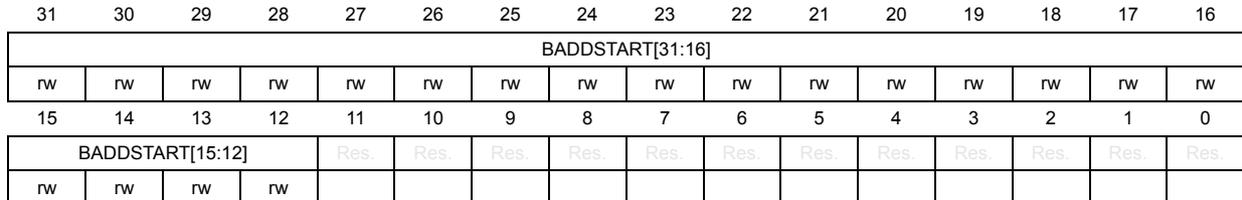
51.6.8 MCE start address for region x register (MCE_SADDRx)
Address offset: \( 0x044 + 0x10 * (x - 1) \) , ( \( x = 1 \) to \( 4 \) )
Reset value: \( 0x0000\ 0000 \)
Writes are ignored if GLOCK is set in MCE_CR register, or if BREN is set in MCE_REGCRx.
| 31 | 30 | 29 | 28 | 27 | 26 | 25 | 24 | 23 | 22 | 21 | 20 | 19 | 18 | 17 | 16 |
| BADDSTART[31:16] | |||||||||||||||
| rw | rw | rw | rw | rw | rw | rw | rw | rw | rw | rw | rw | rw | rw | rw | rw |
| 15 | 14 | 13 | 12 | 11 | 10 | 9 | 8 | 7 | 6 | 5 | 4 | 3 | 2 | 1 | 0 |
| BADDSTART[15:12] | Res | Res | Res | Res | Res | Res | Res | Res | Res | Res | Res | Res | |||
| rw | rw | rw | rw | ||||||||||||
Bits 31:12 BADDSTART[31:12] : Region address start
This bitfield defines the absolute start address of the region x on 4 Kbyte boundary (inclusive).
BREN cannot be set if BADDRSTART > BADDREND.
When MCE determines the region, the first 12 bits (LSB) and the last 4 bits (MSB) in this register are ignored, and when this register is accessed in read the 4 MSB bits and the 12 LSB bits return zeros (reference value in MCE).
Bits 11:0 Reserved, must be kept at reset value.
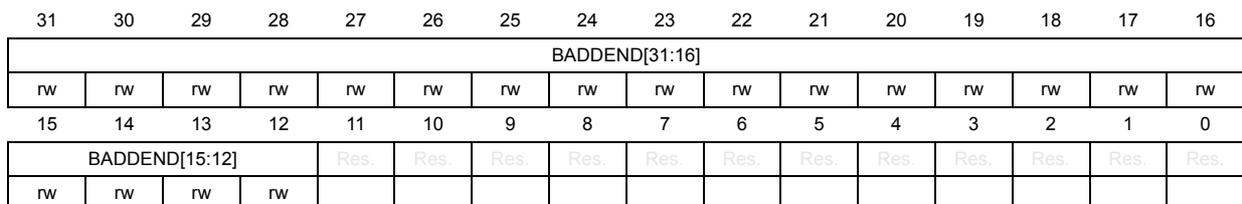
51.6.9 MCE end address for region x register (MCE_EADDRx)
Address offset: \( 0x048 + 0x10 * (x - 1) \) , ( \( x = 1 \) to \( 4 \) )
Reset value: \( 0x0000\ 0FFF \)
Writes are ignored if GLOCK is set in MCE_CR register, or if BREN is set in MCE_REGCRx.
| 31 | 30 | 29 | 28 | 27 | 26 | 25 | 24 | 23 | 22 | 21 | 20 | 19 | 18 | 17 | 16 |
| BADDEND[31:16] | |||||||||||||||
| rw | rw | rw | rw | rw | rw | rw | rw | rw | rw | rw | rw | rw | rw | rw | rw |
| 15 | 14 | 13 | 12 | 11 | 10 | 9 | 8 | 7 | 6 | 5 | 4 | 3 | 2 | 1 | 0 |
| BADDEND[15:12] | Res | Res | Res | Res | Res | Res | Res | Res | Res | Res | Res | Res | |||
| rw | rw | rw | rw | ||||||||||||
Bits 31:12 BADDEND[31:12] : Region address end
This bitfield defines the absolute end address of the region x on 4 Kbyte boundary (inclusive).
BREN cannot be set if BADDRSTART > BADDREND.
When MCE determines the region, the first 12 bits (LSB) and the last 4 bits (MSB) in this register are ignored, and when this register is accessed in read the 4 MSB bits return zeros and the 12 LSB bits return ones (reference value in MCE).
Bits 11:0 Reserved, must be kept at reset value.
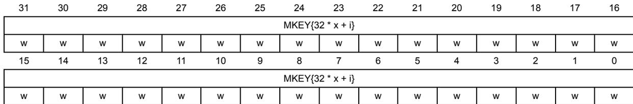
51.6.10 MCE master key x (MCE_MKEYRx)
Address offset: 0x200 + 0x4 * x, (x = 0 to 7)
Reset value: 0x0000 0000
Writes are ignored if MKLOCK or GLOCK bit is set in MCE_CR register.
| 31 | 30 | 29 | 28 | 27 | 26 | 25 | 24 | 23 | 22 | 21 | 20 | 19 | 18 | 17 | 16 |
| MKEY{32 * x + i} | |||||||||||||||
| w | w | w | w | w | w | w | w | w | w | w | w | w | w | w | w |
| 15 | 14 | 13 | 12 | 11 | 10 | 9 | 8 | 7 | 6 | 5 | 4 | 3 | 2 | 1 | 0 |
| MKEY{32 * x + i} | |||||||||||||||
| w | w | w | w | w | w | w | w | w | w | w | w | w | w | w | w |
Bits 31:0 MKEY{32 * x + i} : Master key bit (i = 0 to 31)
This key is used by the MCE block cipher in normal, SCA resistant mode, if CTXID = 0x0 in MCE_REGCR register. Register MCE_MKEYR4 to 7 must be written only if CIPHERSEL = 0x3 in MCE_CR, otherwise MKVALID may become invalid.
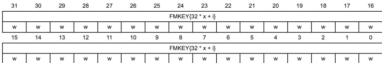
51.6.11 MCE fast master key x (MCE_FMKEYRx)
Address offset: 0x220 + 0x4 * x, (x = 0 to 7)
Reset value: 0x0000 0000
Writes are ignored if MKLOCK or GLOCK bit is set in MCE_CR register.
| 31 | 30 | 29 | 28 | 27 | 26 | 25 | 24 | 23 | 22 | 21 | 20 | 19 | 18 | 17 | 16 |
| FMKEY{32 * x + i} | |||||||||||||||
| w | w | w | w | w | w | w | w | w | w | w | w | w | w | w | w |
| 15 | 14 | 13 | 12 | 11 | 10 | 9 | 8 | 7 | 6 | 5 | 4 | 3 | 2 | 1 | 0 |
| FMKEY{32 * x + i} | |||||||||||||||
| w | w | w | w | w | w | w | w | w | w | w | w | w | w | w | w |
Bits 31:0 FMKEY{32 * x + i} : Fast master key bit (i = 0 to 31)
This key is used by the MCE block cipher in fast mode, if CTXID = 0x0 in MCE_REGCR register. Register MCE_FMKEYR4 to 7 must be written only if CIPHERSEL = 0x3 in MCE_CR, otherwise FMKVALID may become invalid.
51.6.12 MCE cipher context z configuration register (MCE_CCzCFGR)
Address offset: \( 0x240 + 0x30 \times (z - 1) \) ( \( z = 1 \) to \( 2 \) )
Reset value: \( 0x0000\ 0000 \)
Writes are ignored if CCLOCK bit is set in this register. Writes are also ignored if GLOCK is set in MCE_CR register.
| 31 | 30 | 29 | 28 | 27 | 26 | 25 | 24 | 23 | 22 | 21 | 20 | 19 | 18 | 17 | 16 |
|---|---|---|---|---|---|---|---|---|---|---|---|---|---|---|---|
| VERSION[15:0] | |||||||||||||||
| rw | rw | rw | rw | rw | rw | rw | rw | rw | rw | rw | rw | rw | rw | rw | rw |
| 15 | 14 | 13 | 12 | 11 | 10 | 9 | 8 | 7 | 6 | 5 | 4 | 3 | 2 | 1 | 0 |
| KEYCRC[7:0] | Res. | Res. | MODE[1:0] | Res. | KEYLOCK | CCLOCK | CCEN | ||||||||
| r | r | r | r | r | r | r | r | rw | rw | rs | rs | rw | |||
Bits 31:16 VERSION[15:0] : Version
This 16-bit bitfield must be correctly initialized before CCEN bit is set. Bitfield usage is defined in Section 51.4.6: MCE stream cipher encryption mode .
Bits 15:8 KEYCRC[7:0] : Key CRC
When KEYLOCK = 0, KEYCRC information is automatically computed by hardware while loading the key of this region in this exact sequence: KEYR0 then KEYR1 then KEYR2 then finally KEYR3 (all written once). A new KEYCRC computation starts as soon as a new valid sequence is initiated. KEYCRC bitfield reads as zero until a valid sequence is completed (after it return the computed CRC value).
When KEYLOCK or GLOCK = 1, KEYCRC bitfield always returns the computed CRC value until the next reset.
CRC computation is an 8-bit checksum using the standard CRC-8-CCITT algorithm \( X^8 + X^2 + X + 1 \) (according the convention).
CRC information is updated, and the key is usable by MCE, only after the last bit of the key has been written.
Bits 7:6 Reserved, must be kept at reset value.
Bits 5:4 MODE[1:0] : Authorized cipher mode
This bitfield defines the encrypted region type authorized for this cipher context z.
0X: Stream cipher is allowed with this cipher context
10: Block cipher is allowed with this cipher context
11: Fast block cipher is allowed with this cipher context
This cipher mode selection is done in MCE_REGCRx register, by writing ENC[1:0] bitfield, and setting CTXID = z. See CTXID bitfield for details.
When either of the MODE bits are changed, the region key and associated CRC are zeroed.
Bit 3 Reserved, must be kept at reset value.
Bit 2 KEYLOCK : Key lock
0: Writes to MCE_CCzKEYR registers are allowed
1: Writes to MCE_CCzKEYR registers are ignored until next MCE reset. KEYCRC bitfield value does not change.
Note: This bit is set once. If this bit is set, it can only be cleared to 0 if MCE is reset.
Bit 1 CCLOCK : Cipher context lock
0: Writes to MCE_CCzCFGR and MCE_CCzNR registers are allowed
1: Writes to MCE_CCzCFGR and MCE_CCzNR registers are ignored until next MCE reset.
Note: This bit is set once. If this bit is set, it can only be cleared to 0 if MCE is reset. Setting this bit forces KEYLOCK bit to 1.
Bit 0 CCEN : Cipher context enable
0: If an enabled region selects CTXID = z bypass mode is selected by MCE
1: If an enabled region selects CTXID = z with ENC = 01 MCE selects with the stream cipher the information stored in MCE_CCzCFGR, MCE_CCzNR and MCE_CCzKEYR. If the enabled region selects ENC = 10 or 11 instead MCE selects with the block cipher the key information stored in MCE_CCzKEYR. When CCEN is set and MODE[1:0] bits do not allow the configuration written in ENC[1:0] bits (see MODE bitfield) reads return zero and writes are ignored.
51.6.13 MCE cipher context z nonce register 0 (MCE_CCzNR0)
Address offset: 0x244 + 0x30 *(z - 1) (z = 1 to 2)
Reset value: 0x0000 0000
Writes are ignored if CCLOCK is set in MCE_CCzCFGR register, or GLOCK bit is set in MCE_CR register.
| 31 | 30 | 29 | 28 | 27 | 26 | 25 | 24 | 23 | 22 | 21 | 20 | 19 | 18 | 17 | 16 |
|---|---|---|---|---|---|---|---|---|---|---|---|---|---|---|---|
| SCNONCE[31:16] | |||||||||||||||
| rw | rw | rw | rw | rw | rw | rw | rw | rw | rw | rw | rw | rw | rw | rw | rw |
| 15 | 14 | 13 | 12 | 11 | 10 | 9 | 8 | 7 | 6 | 5 | 4 | 3 | 2 | 1 | 0 |
| SCNONCE[15:0] | |||||||||||||||
| rw | rw | rw | rw | rw | rw | rw | rw | rw | rw | rw | rw | rw | rw | rw | rw |
Bits 31:0 SCNONCE[31:0] : Stream cipher nonce, bits [31:0]
This register is used by stream cipher to compute keystream. It must be correctly initialize before CCEN bit is set in MCE_CCzCFGR register. Bitfield usage is defined in Section 51.4.6: MCE stream cipher encryption mode .
51.6.14 MCE cipher context z nonce register 1 (MCE_CCzNR1)
Address offset: 0x248 + 0x30 *(z - 1) (z = 1 to 2)
Reset value: 0x0000 0000
Writes are ignored if CCLOCK is set in MCE_CCzCFGR register, or GLOCK bit is set in MCE_CR register.
| 31 | 30 | 29 | 28 | 27 | 26 | 25 | 24 | 23 | 22 | 21 | 20 | 19 | 18 | 17 | 16 |
| SCNONCE[63:48] | |||||||||||||||
| rw | rw | rw | rw | rw | rw | rw | rw | rw | rw | rw | rw | rw | rw | rw | rw |
| 15 | 14 | 13 | 12 | 11 | 10 | 9 | 8 | 7 | 6 | 5 | 4 | 3 | 2 | 1 | 0 |
| SCNONCE[47:32] | |||||||||||||||
| rw | rw | rw | rw | rw | rw | rw | rw | rw | rw | rw | rw | rw | rw | rw | rw |
Bits 31:0 SCNONCE[63:32] : Stream cipher nonce, bits [63:32]
Refer to the MCE_CCzNR0 register for description of the SCNONCE[63:0] bitfield.
51.6.15 MCE cipher context z key register 0 (MCE_CCzKEYR0)
Address offset: 0x24C + 0x30 *(z - 1) (z = 1 to 2)
Reset value: 0x0000 0000
Writes are ignored if CCLOCK or KEYLOCK are set in MCE_CCzCFGR register, or GLOCK bit is set in MCE_CR register.
| 31 | 30 | 29 | 28 | 27 | 26 | 25 | 24 | 23 | 22 | 21 | 20 | 19 | 18 | 17 | 16 |
| KEY[31:16] | |||||||||||||||
| w | w | w | w | w | w | w | w | w | w | w | w | w | w | w | w |
| 15 | 14 | 13 | 12 | 11 | 10 | 9 | 8 | 7 | 6 | 5 | 4 | 3 | 2 | 1 | 0 |
| KEY[15:0] | |||||||||||||||
| w | w | w | w | w | w | w | w | w | w | w | w | w | w | w | w |
Bits 31:0 KEY[31:0] : cipher key, bits [31:0]
This register is used by the block or stream cipher of MCE when CTXID = z in encrypted region configuration register. KEY[127:0] must be correctly initialize before CCEN bit is set in MCE_CCzCFGR register. When the application selects the block cipher AES-256 must not be selected with CIPHERSEL.
51.6.16 MCE cipher context z key register 1 (MCE_CCzKEYR1)
Address offset: \( 0x250 + 0x30 \cdot (z - 1) \) ( \( z = 1 \) to \( 2 \) )
Reset value: 0x0000 0000
Writes are ignored if CCLOCK or KEYLOCK are set in MCE_CCzCFGR register, or GLOCK bit is set in MCE_CR register.
| 31 | 30 | 29 | 28 | 27 | 26 | 25 | 24 | 23 | 22 | 21 | 20 | 19 | 18 | 17 | 16 |
| KEY[63:48] | |||||||||||||||
| w | w | w | w | w | w | w | w | w | w | w | w | w | w | w | w |
| 15 | 14 | 13 | 12 | 11 | 10 | 9 | 8 | 7 | 6 | 5 | 4 | 3 | 2 | 1 | 0 |
| KEY[47:32] | |||||||||||||||
| w | w | w | w | w | w | w | w | w | w | w | w | w | w | w | w |
Bits 31:0 KEY[63:32] : cipher key, bits [63:32]
Refer to the MCE_CCzKEYR0 register for description of the KEY[127:0] bitfield.
51.6.17 MCE cipher context z key register 2 (MCE_CCzKEYR2)
Address offset: \( 0x254 + 0x30 \cdot (z - 1) \) ( \( z = 1 \) to \( 2 \) )
Reset value: 0x0000 0000
Writes are ignored if CCLOCK or KEYLOCK are set in MCE_CCzCFGR register, or GLOCK bit is set in MCE_CR register.
| 31 | 30 | 29 | 28 | 27 | 26 | 25 | 24 | 23 | 22 | 21 | 20 | 19 | 18 | 17 | 16 |
| KEY[95:80] | |||||||||||||||
| w | w | w | w | w | w | w | w | w | w | w | w | w | w | w | w |
| 15 | 14 | 13 | 12 | 11 | 10 | 9 | 8 | 7 | 6 | 5 | 4 | 3 | 2 | 1 | 0 |
| KEY[79:64] | |||||||||||||||
| w | w | w | w | w | w | w | w | w | w | w | w | w | w | w | w |
Bits 31:0 KEY[95:64] : cipher key, bits [95:64]
Refer to the MCE_CCzKEYR0 register for description of the KEY[127:0] bitfield.
51.6.18 MCE cipher context z key register 3 (MCE_CCzKEYR3)
Address offset: \( 0x258 + 0x30 \cdot (z - 1) \) ( \( z = 1 \) to \( 2 \) )
Reset value: 0x0000 0000
Writes are ignored if CCLOCK or KEYLOCK are set in MCE_CCzCFGR register, or GLOCK bit is set in MCE_CR register.
| 31 | 30 | 29 | 28 | 27 | 26 | 25 | 24 | 23 | 22 | 21 | 20 | 19 | 18 | 17 | 16 |
| KEY[127:112] | |||||||||||||||
| w | w | w | w | w | w | w | w | w | w | w | w | w | w | w | w |
| 15 | 14 | 13 | 12 | 11 | 10 | 9 | 8 | 7 | 6 | 5 | 4 | 3 | 2 | 1 | 0 |
| KEY[111:96] | |||||||||||||||
| w | w | w | w | w | w | w | w | w | w | w | w | w | w | w | w |
Bits 31:0 KEY[127:96] : cipher key, bits [127:96]
Refer to the MCE_CCzKEYR0 register for description of the KEY[127:0] bitfield.
51.6.19 MCE register map
Table 439. MCE register map and reset values
| Offset | Register name reset value | 31 | 30 | 29 | 28 | 27 | 26 | 25 | 24 | 23 | 22 | 21 | 20 | 19 | 18 | 17 | 16 | 15 | 14 | 13 | 12 | 11 | 10 | 9 | 8 | 7 | 6 | 5 | 4 | 3 | 2 | 1 | 0 |
|---|---|---|---|---|---|---|---|---|---|---|---|---|---|---|---|---|---|---|---|---|---|---|---|---|---|---|---|---|---|---|---|---|---|
| 0x000 | MCE_CR | Res. | CIPHER SEL[1:0] | Res. | MKLOCK | GLOCK | |||||||||||||||||||||||||||
| Reset value | 0 | 1 | 0 | 0 | |||||||||||||||||||||||||||||
| 0x004 | MCE_SR | Res. | ENCDIS | Res. | FMKVALID | Res. | MKVALID | ||||||||||||||||||||||||||
| Reset value | 0 | 0 | 0 | ||||||||||||||||||||||||||||||
| 0x008 | MCE_IASR | Res. | IAEF | ||||||||||||||||||||||||||||||
| Reset value | 0 | ||||||||||||||||||||||||||||||||
| 0x00C | MCE_IACR | Res. | IAEF | ||||||||||||||||||||||||||||||
| Reset value | 0 | ||||||||||||||||||||||||||||||||
| 0x010 | MCE_IAIER | Res. | IAEIE | IAEF | |||||||||||||||||||||||||||||
| Reset value | 0 | 0 | |||||||||||||||||||||||||||||||
| 0x020 | Reserved | Res. | |||||||||||||||||||||||||||||||
| 0x024 | MCE_IADDR | IADDR[31:10] | Res. | ||||||||||||||||||||||||||||||
| Reset value | 0 | 0 | 0 | 0 | 0 | 0 | 0 | 0 | 0 | 0 | 0 | 0 | 0 | 0 | 0 | 0 | 0 | 0 | 0 | 0 | 0 | 0 | |||||||||||
| 0x040+ 0x10 * (x-1), (x = 1 to 4) | MCE_REGCRx | Res. | ENC[1] | ENC[0] | Res. | CTXID[1] | CTXID[0] | Res. | BREN | ||||||||||||||||||||||||
| Reset value | 0 | 0 | 0 | 0 | 0 | ||||||||||||||||||||||||||||
| 0x044+ 0x10 * (x-1), (x = 1 to 4) | MCE_SADDRx | BADDSTART[31:16] | BADDSTART [15:12] | Res. | |||||||||||||||||||||||||||||
| Reset value | 0 | 0 | 0 | 0 | 0 | 0 | 0 | 0 | 0 | 0 | 0 | 0 | 0 | 0 | 0 | 0 | 0 | 0 | 0 | 0 | |||||||||||||
| 0x048+ 0x10 * (x-1), (x = 1 to 4) | MCE_EADDRx | BADDEND[31:16] | BADDEND [15:12] | Res. | |||||||||||||||||||||||||||||
| Reset value | 0 | 0 | 0 | 0 | 0 | 0 | 0 | 0 | 0 | 0 | 0 | 0 | 0 | 0 | 0 | 0 | 0 | 0 | 0 | 0 | |||||||||||||
| 0x200+0x 4 * x, (x = 0 to 7) | MCE_MKEYRx | MKEY{32 * x + i} (i = 0 to 31) | |||||||||||||||||||||||||||||||
| Reset value | 0 | 0 | 0 | 0 | 0 | 0 | 0 | 0 | 0 | 0 | 0 | 0 | 0 | 0 | 0 | 0 | 0 | 0 | 0 | 0 | 0 | 0 | 0 | 0 | 0 | 0 | 0 | 0 | 0 | 0 | 0 | 0 | |
| 0x220+0x 4 * x, (x = 0 to 7) | MCE_FMKEYRx | FMKEY{32 * x + i} (i = 0 to 31) | |||||||||||||||||||||||||||||||
| Reset value | 0 | 0 | 0 | 0 | 0 | 0 | 0 | 0 | 0 | 0 | 0 | 0 | 0 | 0 | 0 | 0 | 0 | 0 | 0 | 0 | 0 | 0 | 0 | 0 | 0 | 0 | 0 | 0 | 0 | 0 | 0 | 0 | |
| 0x240 | MCE_CC1CFGR | VERSION[15:0] | KEYCRC[7:0] | Res. | Res. | MODE[1] | MODE[0] | Res. | KEYLOCK | CCLOCK | CCEN | ||||||||||||||||||||||
| Reset value | 0 | 0 | 0 | 0 | 0 | 0 | 0 | 0 | 0 | 0 | 0 | 0 | 0 | 0 | 0 | 0 | 0 | 0 | 0 | 0 | 0 | 0 | 0 | 0 | 0 | 0 | 0 | 0 | 0 | ||||
| 0x244 | MCE_CC1NR0 | SCNONCE[31:0] | |||||||||||||||||||||||||||||||
| Reset value | 0 | 0 | 0 | 0 | 0 | 0 | 0 | 0 | 0 | 0 | 0 | 0 | 0 | 0 | 0 | 0 | 0 | 0 | 0 | 0 | 0 | 0 | 0 | 0 | 0 | 0 | 0 | 0 | 0 | 0 | 0 | 0 | |
| 0x248 | MCE_CC1NR1 | SCNONCE[63:32] | |||||||||||||||||||||||||||||||
| Reset value | 0 | 0 | 0 | 0 | 0 | 0 | 0 | 0 | 0 | 0 | 0 | 0 | 0 | 0 | 0 | 0 | 0 | 0 | 0 | 0 | 0 | 0 | 0 | 0 | 0 | 0 | 0 | 0 | 0 | 0 | 0 | 0 | |
Table 439. MCE register map and reset values (continued)
| Offset | Register name reset value | 31 | 30 | 29 | 28 | 27 | 26 | 25 | 24 | 23 | 22 | 21 | 20 | 19 | 18 | 17 | 16 | 15 | 14 | 13 | 12 | 11 | 10 | 9 | 8 | 7 | 6 | 5 | 4 | 3 | 2 | 1 | 0 |
|---|---|---|---|---|---|---|---|---|---|---|---|---|---|---|---|---|---|---|---|---|---|---|---|---|---|---|---|---|---|---|---|---|---|
| 0x24C | MCE_CC1KEYR0 | KEY[31:0] | |||||||||||||||||||||||||||||||
| Reset value | 0 | 0 | 0 | 0 | 0 | 0 | 0 | 0 | 0 | 0 | 0 | 0 | 0 | 0 | 0 | 0 | 0 | 0 | 0 | 0 | 0 | 0 | 0 | 0 | 0 | 0 | 0 | 0 | 0 | 0 | 0 | 0 | |
| 0x250 | MCE_CC1KEYR1 | KEY[63:32] | |||||||||||||||||||||||||||||||
| Reset value | 0 | 0 | 0 | 0 | 0 | 0 | 0 | 0 | 0 | 0 | 0 | 0 | 0 | 0 | 0 | 0 | 0 | 0 | 0 | 0 | 0 | 0 | 0 | 0 | 0 | 0 | 0 | 0 | 0 | 0 | 0 | 0 | |
| 0x254 | MCE_CC1KEYR2 | KEY[95:64] | |||||||||||||||||||||||||||||||
| Reset value | 0 | 0 | 0 | 0 | 0 | 0 | 0 | 0 | 0 | 0 | 0 | 0 | 0 | 0 | 0 | 0 | 0 | 0 | 0 | 0 | 0 | 0 | 0 | 0 | 0 | 0 | 0 | 0 | 0 | 0 | 0 | 0 | |
| 0x258 | MCE_CC1KEYR3 | KEY[127:96] | |||||||||||||||||||||||||||||||
| Reset value | 0 | 0 | 0 | 0 | 0 | 0 | 0 | 0 | 0 | 0 | 0 | 0 | 0 | 0 | 0 | 0 | 0 | 0 | 0 | 0 | 0 | 0 | 0 | 0 | 0 | 0 | 0 | 0 | 0 | 0 | 0 | 0 | |
| 0x270 | MCE_CC2CFGR | VERSION[15:0] | KEYCRC[7:0] | Res. | Res. | MODE[1] | MODE[0] | Res. | KEYLOCK | CCLOCK | CCEN | ||||||||||||||||||||||
| Reset value | 0 | 0 | 0 | 0 | 0 | 0 | 0 | 0 | 0 | 0 | 0 | 0 | 0 | 0 | 0 | 0 | 0 | 0 | 0 | 0 | 0 | 0 | 0 | 0 | 0 | 0 | 0 | 0 | 0 | 0 | 0 | 0 | |
| 0x274 | MCE_CC2NR0 | SCNONCE[31:0] | |||||||||||||||||||||||||||||||
| Reset value | 0 | 0 | 0 | 0 | 0 | 0 | 0 | 0 | 0 | 0 | 0 | 0 | 0 | 0 | 0 | 0 | 0 | 0 | 0 | 0 | 0 | 0 | 0 | 0 | 0 | 0 | 0 | 0 | 0 | 0 | 0 | 0 | |
| 0x278 | MCE_CC2NR1 | SCNONCE[63:32] | |||||||||||||||||||||||||||||||
| Reset value | 0 | 0 | 0 | 0 | 0 | 0 | 0 | 0 | 0 | 0 | 0 | 0 | 0 | 0 | 0 | 0 | 0 | 0 | 0 | 0 | 0 | 0 | 0 | 0 | 0 | 0 | 0 | 0 | 0 | 0 | 0 | 0 | |
| 0x27C | MCE_CC2KEYR0 | KEY[31:0] | |||||||||||||||||||||||||||||||
| Reset value | 0 | 0 | 0 | 0 | 0 | 0 | 0 | 0 | 0 | 0 | 0 | 0 | 0 | 0 | 0 | 0 | 0 | 0 | 0 | 0 | 0 | 0 | 0 | 0 | 0 | 0 | 0 | 0 | 0 | 0 | 0 | 0 | |
| 0x280 | MCE_CC2KEYR1 | KEY[63:32] | |||||||||||||||||||||||||||||||
| Reset value | 0 | 0 | 0 | 0 | 0 | 0 | 0 | 0 | 0 | 0 | 0 | 0 | 0 | 0 | 0 | 0 | 0 | 0 | 0 | 0 | 0 | 0 | 0 | 0 | 0 | 0 | 0 | 0 | 0 | 0 | 0 | 0 | |
| 0x284 | MCE_CC2KEYR2 | KEY[95:64] | |||||||||||||||||||||||||||||||
| Reset value | 0 | 0 | 0 | 0 | 0 | 0 | 0 | 0 | 0 | 0 | 0 | 0 | 0 | 0 | 0 | 0 | 0 | 0 | 0 | 0 | 0 | 0 | 0 | 0 | 0 | 0 | 0 | 0 | 0 | 0 | 0 | 0 | |
| 0x288 | MCE_CC2KEYR3 | KEY[127:96] | |||||||||||||||||||||||||||||||
| Reset value | 0 | 0 | 0 | 0 | 0 | 0 | 0 | 0 | 0 | 0 | 0 | 0 | 0 | 0 | 0 | 0 | 0 | 0 | 0 | 0 | 0 | 0 | 0 | 0 | 0 | 0 | 0 | 0 | 0 | 0 | 0 | 0 | |
Refer to Section 2.3: Memory organization for the register boundary addresses.