49. Cryptographic processor (CRYP)
49.1 CRYP introduction
The cryptographic processor (CRYP) encrypts or decrypts data in compliance with the advanced encryption standard (AES) defined by NIST.
CRYP supports ECB, CBC, CTR, GCM, GMAC, and CCM chaining modes for key sizes of 128, 192 or 256 bits. CRYP has the possibility to load by hardware the key stored in SAES peripheral, under SAES control.
The peripheral supports both single and fixed DMA burst transfers for incoming and outgoing data (two DMA channels are required). CRYP also includes input and output FIFOs for better performance.
49.2 CRYP main features
- • Compliant with NIST FIPS publication 197 “ Advanced encryption standard (AES) ” (November 2001)
- • Encryption and decryption with multiple chaining modes:
- – Electronic codebook (ECB) mode
- – Cipher block chaining (CBC) mode
- – Counter (CTR) mode
- – Galois counter mode (GCM)
- – Galois message authentication code (GMAC) mode
- – Counter with CBC-MAC (CCM) mode
- • 16-byte data block processing, supporting cipher key lengths of 128, 192 and 256 bits
- – 14 or 18 clock cycle latency in ECB mode for processing one 16-byte block with 128-bit or 256-bit key, respectively
- • Using dedicated key bus, optional key sharing with side-channel resistant SAES peripheral (shared-key mode), controlled by SAES
- • Integrated key scheduler to compute the last round key for ECB/CBC decryption
- • 256-bit of write-only registers for storing the cryptographic keys (eight 32-bit registers)
- • 128-bit of registers for storing initialization vectors (four 32-bit registers)
- • 32-bit input buffer associated with an internal input FIFO of eight 32-bit words, corresponding to two AES blocks
- • 32-bit output buffer associated with an internal output FIFO of eight 32-bit words, corresponding to two AES blocks
- • Automatic data flow control supporting two direct memory access (DMA) channels, one for incoming data, one for processed data. The output FIFO supports both single and burst transfers, while the input FIFO supports only burst transfers.
- • Data swapping logic to support 1-, 8-, 16- or 32-bit data
- • AMBA AHB target peripheral, accessible through 32-bit word single accesses only. Other access types generates an AHB error, and write accesses are ignored.
- • Possibility for software to suspend a message if CRYP needs to process another message with a higher priority, then resume the original message
49.3 CRYP implementation
The devices have one CRYP peripheral, implemented as per the following table. It can use the key generated by the SAES peripheral. For comparison, the SAES peripheral is also included in the table.
Table 415. CRYP versus SAES features
| Modes or features (1) | CRYP | SAES |
|---|---|---|
| ECB, CBC chaining | X | X |
| CTR, CCM, GCM chaining | X | X |
| AES 128-bit ECB encryption in cycles | 14 | 480 |
| DHUK and BHK key selection | - | X |
| Resistance to side-channel attacks | - | X |
| Shared key between SAES and CRYP | X | |
| Key size in bits | 128, 192, 256 | 128, 256 |
1. X = supported.
49.4 CRYP functional description
49.4.1 CRYP block diagram
The figure below shows the block diagram of the cryptographic processor.
Figure 475. CRYP block diagram
The block diagram illustrates the internal architecture of the CRYP processor. On the left, a vertical bus labeled "32-bit AHB2 bus" connects to an "AHB interface". Below this, "cryp_hclk" (clock) enters the main block. The main block contains several groups of registers: "Banked Registers (main)" including CRYP_DIN (data in), CRYP_DOUT (data out), CRYP_SR (status), CRYP_CR (control), CRYP_Kx (key), and CRYP_IVx (iv); "Banked Registers (suspend/restore)" including CRYP_GCMx and CSGCMCMx; and "Banked Registers (IRQ & DMA)" including CRYP_IMSCR, CRYP_RIS, CRYP_MIS, and CRYP_DMACR. To the right of the main registers are two FIFOs: "8x32-bit IN FIFO" and "8x32-bit OUT FIFO", both with "suspend/restore" logic. These FIFOs connect to an "AES Core (AEA)". Below the registers is a "Control Logic" block, which receives inputs from the "DMA interface" (connected to "cryp_in_dma" and "cryp_out_dma") and the "IRQ interface" (connected to "cryp_it"). The Control Logic also connects to the registers and the AES Core. At the bottom, a "Shared key" from an "SAES" block is fed into the Control Logic and the AES Core. The diagram is labeled "MSv66816V1" in the bottom right corner.
49.4.2 CRYP internal signals
Table 416 describes the user relevant internal signals interfacing the CRYP peripheral.
Table 416. CRYP internal input/output signals
| Signal name | Signal type | Description |
|---|---|---|
| crypt_hclk | Digital input | AHB clock |
| crypt_it | Digital output | CRYP interrupt request |
| crypt_in_dma | Digital input/output | CRYP incoming data FIFO DMA request/ acknowledge |
| crypt_out_dma | Digital input/output | CRYP processed data FIFO DMA request/ acknowledge |
49.4.3 CRYP reset and clocks
The CRYP peripheral is clocked by the AHB clock.
The CRYP has a dedicated reset bit in the RCC.
49.4.4 CRYP symmetric cipher implementation
The cryptographic processor (CRYP) is a 32-bit AHB peripheral that encrypts or decrypts 16-byte blocks of data using the advanced encryption standard (AES). It also implements a set of approved AES symmetric key security functions summarized in Table 417 . Those functions can be certified NIST PUB 140-3.
Table 417. CRYP approved AES symmetric key functions
| Operations | Algorithm | Specification | Key size in bits | Chaining modes |
|---|---|---|---|---|
| Encryption, decryption | AES | FIPS PUB 197 NIST SP800-38A | 128, 192, 256 | ECB, CBC, CTR |
| Authenticated encryption or decryption | NIST SP800-38C NIST SP800-38D | GCM, CCM | ||
| Cipher-based message authentication code | NIST SP800-38D | GMAC |
CRYP can be used directly by the CPU, or indirectly using two DMA channels (one for the plaintext, one for the ciphertext).
It is possible to suspend then resume any CRYP processing, following the sequence described in Section 49.4.8 .
49.4.5 CRYP encryption/ decryption typical usage
The following figure shows a typical operation for encryption or decryption.
Figure 476. Encryption/ decryption typical usage
graph TD
    Start([Start]) --> Init([Initialization])
    Init --> ECB_CBC_Dec{ECB or CBC decryption?}
    ECB_CBC_Dec -- Yes --> RoundKey([Round key preparation])
    ECB_CBC_Dec -- No --> DataAppend([Data append])
    RoundKey --> LastBlock{Last block?}
    DataAppend --> LastBlock
    LastBlock -- No --> DataAppend
    LastBlock -- Yes --> AllBytesValid{All bytes valid?}
    AllBytesValid -- Yes --> Finalize([Finalize])
    AllBytesValid -- No --> ECB_CBC_Chaining{ECB or CBC chaining?}
    ECB_CBC_Chaining -- Yes --> DataStealing([Data stealing])
    ECB_CBC_Chaining -- No --> DataPadding([Data padding])
    DataStealing --> Finalize
    DataPadding --> Finalize
    Finalize --> End([End])
Initialization
The CRYP peripheral is initialized according to the chaining mode. Refer to Section 49.4.9: CRYP basic chaining modes (ECB, CBC) and Section 49.4.10: CRYP counter mode (CTR) for details.
Data append
This section describes different ways of appending data for processing. For ECB or CBC chaining modes, refer to Section 49.4.7: CRYP ciphertext stealing and data padding if the size of data to process is not a multiple of 16 bytes. The last block management in these cases is more complex than what is described in this section.
General conditions for data processing
The CRYP is busy and processing data (BUSY flag set) when all the conditions below are met:
- • CRYPTEN is set in CRYP_CR register.
- • There are enough data in the input FIFO (at least four words).
- • There is enough free-space in the output FIFO (at least four word locations).
It is possible to clear the CRYPTEN bit while BUSY bit is set. In this case the ongoing AES processing first completes (that is, the word results are written to the output FIFO) before the BUSY bit is cleared by hardware.
Note: If the application needs to suspend a message to process another one with a higher priority, refer to Section 49.4.8: CRYP suspend and resume operations .
Appending data using the CPU in polling mode
This method uses flag polling to control the data append through the following sequence:
- 1. When KEYVALID is set, enable CRYP by setting the CRYPTEN bit of the CRYP_CR register (if not already done).
- 2. Repeat the following subsequence until the payload is entirely processed:
- a) Write data in the input FIFO (one block or until the FIFO is full).
- b) Repeat until the second last block of data has been processed:
- – Wait until the not-empty flag OFNE is set, then read the output FIFO (one block or until the FIFO is empty).
- – Wait until the not-full flag IFNF is set, then write the input FIFO (one block or until the FIFO is full), except if it is the last block.
- c) The BUSY bit is set automatically by CRYP. At the end of the processing, the BUSY bit is cleared and both FIFOs are empty (input FIFO empty flag IFEM is set, output FIFO not-empty flag OFNE is cleared).
- d) If the next processing block is the last block, pad the data with zeros to obtain a complete block (when applicable), and specify the number of non-valid bytes (using NPBLB[3:0]) in case of GCM payload encryption or CCM payload decryption (otherwise the tag computation is wrong). This operation must be performed after checking that the BUSY bit is cleared.
- 3. As the data block just processed is the last block of the message, optionally discard the data that is not part of the message/payload, then disable the CRYP peripheral by clearing CRYPTEN.
Note: NPBLB[3:0] bitfield is not used in header phase of GCM, GMAC and CCM chaining modes.
Appending data using the CPU in Interrupt mode
The method uses interrupt from the CRYP peripheral to control the data append, through the following sequence:
- 1. Enable interrupts from CRYP, by setting the INIM and OUTIM bits of the CRYP_IMSCR register.
- 2. When KEYVALID is set, enable the CRYP peripheral, by setting CRYPTEN (if not already done).
- 3. Handle the data in the CRYP interrupt service routine that manages the input FIFO. Upon each interrupt:
- a) If the next processing block is the last block of the message, pad (when applicable) the data with zeros to obtain a complete block, and specify the number of non-valid bytes (using NPBLB[3:0] bitfield) in case of GCM payload encryption or CCM payload decryption (otherwise the tag computation is wrong). This operation must be performed after checking that the BUSY bit is cleared. After that load the block into the input FIFO.
- b) If the next processing block is not the last block, load the data into the input FIFO. Application can load only one block (4 words), or load data until the input FIFO is full.
- c) After the last word of data has been written, disable the input FIFO interrupts by clearing the INIM bit (if applicable), then quit the interrupt service routine.
- 4. Handle the data in the CRYP interrupt service routine that manages the output FIFO. Upon each interrupt:
- a) Read data from the output FIFO. Application can read only one block (4 words), or read data until the FIFO is empty.
- b) When the last word of the message has been read, INIM and BUSY bits are cleared and both FIFOs are empty (IFEM is set, OFNE is cleared). Disable the output FIFO interrupt by clearing the OUTIM bit, and disable the peripheral by clearing the CRYPTEN bit.
- c) If the data block just processed is the last block of the message, optionally discard the data that are not part of the message/payload, then quit the interrupt service routine.
Note: The NPBLB[3:0] bitfield is not used in the header phase of GCM, GMAC and CCM chaining modes.
Appending data using the DMA
With this method, all the transfers and processing are managed by DMA and CRYP. Proceed as follows:
- 1. If the last block of the message to process is shorter than 16 bytes, prepare the last four-word data block by padding the remainder of the block with zeros.
- 2. Configure the DMA controller so as to transfer the data to process from the memory to the CRYP peripheral input and the processed data from the CRYP peripheral output to the memory, as described in Section 49.6: CRYP DMA requests . Configure the DMA controller so as to generate an interrupt on transfer completion. For GCM payload encryption or CCM payload decryption, the DMA transfer must not include the last block. The sequence described in Appending data using the CPU in polling mode must be used instead for this last block, because the NPBLB[3:0] bitfield must be set up before processing the block, for CRYP to compute a correct tag.
- 3. When KEYVALID is set, enable the CRYP peripheral, by setting CRYPTEN (if not already done).
- 4. Enable DMA requests, by setting DIEN and DOEN of the CRYP_DMACR register.
- 5. Upon DMA interrupt indicating the transfer completion, get the CRYP-processed data from the memory. Both FIFOs are normally empty and BUSY flag is cleared.
Note: The NPBLB[3:0] bitfield is not used in the header phase of GCM, GMAC and CCM chaining modes.
Caution: It is important for the DMA controller to empty the CRYP output FIFO buffer before filling the CRYP input FIFO buffer. To ensure this, configure the DMA controller to prioritize transfers from CRYP to memory over those from memory to CRYP.
49.4.6 CRYP authenticated encryption, decryption, and cipher-based message authentication
The following figure shows a typical operation for authenticated encryption or decryption, and for cipher-based message authentication.
Figure 477. Typical operation with authentication
graph TD
    Start([Start]) --> Init([Initialization])
    Init --> HeaderInit([Header phase init])
    HeaderInit --> HeaderDataAppend([Header data append])
    HeaderDataAppend --> LastBlockHeader{Last block?}
    LastBlockHeader -- No --> HeaderDataAppend
    LastBlockHeader -- Yes --> AllBytesValidHeader{All bytes valid?}
    AllBytesValidHeader -- No --> DataPaddingHeader([Data padding])
    AllBytesValidHeader -- Yes --> CipherAuth{cipher-based* authentication?}
    CipherAuth -- No --> PayloadInit([Payload phase init])
    CipherAuth -- Yes --> Finalization([Finalization])
    PayloadInit --> PayloadDataAppend([Payload data append])
    PayloadDataAppend --> LastBlockPayload{Last block?}
    LastBlockPayload -- No --> PayloadDataAppend
    LastBlockPayload -- Yes --> AllBytesValidPayload{All bytes valid?}
    AllBytesValidPayload -- No --> DataPaddingPayload([Data padding])
    AllBytesValidPayload -- Yes --> Finalization
    DataPaddingHeader --> Finalization
    DataPaddingPayload --> Finalization
    Finalization --> End([End])
MSV66121V1
Section 49.4.11: CRYP AES Galois/counter mode (GCM) and Section 49.4.13: CRYP AES Counter with CBC-MAC (CCM) describe detailed sequences supported by CRYP.
Cipher-based message authentication flow omits the payload phase, as shown in the figure. Detailed sequence supported by CRYP is described in Section 49.4.12: CRYP AES Galois message authentication code (GMAC) .
49.4.7 CRYP ciphertext stealing and data padding
When using ECB or CBC modes to manage messages the size of which is not a multiple of the block size (16 bytes), the application must use ciphertext stealing techniques such as those described in NIST Special Publication 800-38A, Recommendation for Block Cipher Modes of Operation: Three Variants of Ciphertext Stealing for CBC Mode . Since CRYP does not implement such techniques, the application must complete the last block of input data using data from the second last block.
Note: Ciphertext stealing techniques are not documented in this reference manual.
Similarly, in other modes than ECB or CBC, an incomplete input data block (that is, a block with input data shorter than 16 bytes) must be padded with zeros prior to encryption. That is, extra bits must be appended to the trailing end of the data string. After decryption, the extra bits must be discarded. Since CRYP does not implement automatic data padding operation to the last block, the application must follow the recommendation given in this document to manage messages the size of which is not a multiple of 16 bytes.
49.4.8 CRYP suspend and resume operations
A message can be suspended to process another message with a higher priority. When the higher-priority message is sent, the suspended message can resume. This applies to both encryption and decryption mode.
Suspend and resume operations do not break the chaining operation. The message processing can resume as soon as CRYP is enabled again, to receive a next data block.
Figure 478 gives an example of suspend and resume operation: message 1 is suspended in order to send a shorter and higher-priority message 2.
Figure 478. Example of suspend mode management
The diagram illustrates the flow of data blocks for two messages, Message 1 and Message 2, through a cryptographic processor. Message 1 consists of six 128-bit blocks. The first three blocks are processed, then a 'CRYP suspend sequence' is triggered by a 'New higher priority message 2 to be processed'. Message 2, consisting of two 128-bit blocks, is then processed. After Message 2, a 'CRYP resume sequence' is triggered, and Message 1's processing resumes with the fourth block, continuing through the sixth block and beyond (indicated by '...').
Detailed descriptions of suspend and resume operations are provided in the sections dedicated to each chaining mode.
49.4.9 CRYP basic chaining modes (ECB, CBC)
ECB is the simplest mode of operation. There are no chaining operations, and no special initialization stage. The message is divided into blocks and each block is encrypted or decrypted separately. When decrypting in ECB mode, a special key scheduling is required before processing the first block.
Figure 479 and Figure 480 describe the electronic codebook (ECB) chaining implementation in encryption and decryption, respectively. To select this chaining mode, write ALGOMODE[3:0] with 0x4.
Figure 479. ECB encryption
![Diagram of ECB encryption showing two blocks, Block 1 and Block 2. Each block consists of a Swap management unit, an Encrypt unit, and another Swap management unit. Inputs are DIN (plaintext P1, P2), KEY, and DATATYPE[1:0]. Intermediate signals are I1, I2, O1, O2. Outputs are DOUT (ciphertext C1, C2). A legend indicates input is white and output is grey.](/RM0486-STM32N6x5-x7/7f951a028b72c9c117f66e31f51785a8_img.jpg)
The diagram illustrates the ECB encryption process for two blocks, Block 1 and Block 2. Each block follows a similar internal structure:
- Block 1: DIN (plaintext P1) is input to a 'Swap management' block. The output of this block is I1, which is then input to an 'Encrypt' block. The 'Encrypt' block also takes a 'KEY' as input. The output of the 'Encrypt' block is O1, which is then input to another 'Swap management' block. The final output is DOUT (ciphertext C1). DATATYPE[1:0] is an input to both 'Swap management' blocks.
- Block 2: Similar to Block 1, but with DIN (plaintext P2), I2, O2, and DOUT (ciphertext C2).
MSV69563V1
Figure 480. ECB decryption
![Diagram of ECB decryption showing two blocks, Block 1 and Block 2. Each block consists of a Swap management unit, a Decrypt unit, and another Swap management unit. Inputs are DIN (ciphertext C1, C2), KEY, and DATATYPE[1:0]. Intermediate signals are I1, I2, O1, O2. Outputs are DOUT (plaintext P1, P2). A legend indicates input is white and output is grey.](/RM0486-STM32N6x5-x7/f00bfa25f4b557867574b812be6159b0_img.jpg)
The diagram illustrates the ECB decryption process for two blocks, Block 1 and Block 2. Each block follows a similar internal structure:
- Block 1: DIN (ciphertext C1) is input to a 'Swap management' block. The output of this block is I1, which is then input to a 'Decrypt' block. The 'Decrypt' block also takes a 'KEY' as input. The output of the 'Decrypt' block is O1, which is then input to another 'Swap management' block. The final output is DOUT (plaintext P1). DATATYPE[1:0] is an input to both 'Swap management' blocks.
- Block 2: Similar to Block 1, but with DIN (ciphertext C2), I2, O2, and DOUT (plaintext P2).
MSV69564V1
In CBC encryption mode the output of each block chains with the input of the following block. To make each message unique, an initialization vector is used during the first block processing. When decrypting in CBC mode, a special key scheduling is required before processing the first block.
Figure 481 and Figure 482 describe the cipher block chaining (CBC) implementation in encryption and decryption, respectively. To select this chaining mode, write ALGOMODE[3:0] with 0x5.
Figure 481. CBC encryption
Figure 481. CBC encryption
The diagram illustrates the CBC encryption process for two blocks, Block 1 and Block 2.
- Block 1:
- DIN (plaintext P1) is input to a Swap management block.
- The Swap management block outputs P1'.
- P1' is XORed with IVI to produce I1.
- I1 is input to the Block cipher encryption block, which also takes KEY as input.
- The Block cipher encryption block outputs O1.
- O1 is input to another Swap management block.
- The Swap management block outputs DOUT (ciphertext C1).
- Block 2:
- DIN (plaintext P2) is input to a Swap management block.
- The Swap management block outputs P2'.
- P2' is XORed with the ciphertext C1 from Block 1 to produce I2.
- I2 is input to the Block cipher encryption block, which also takes KEY as input.
- The Block cipher encryption block outputs O2.
- O2 is input to another Swap management block.
- The Swap management block outputs DOUT (ciphertext C2).
Legend
- input (light gray box)
- output (dark gray box)
- XOR (circle with a cross)
Figure 482. CBC decryption
Figure 482. CBC decryption
The diagram illustrates the CBC decryption process for two blocks, Block 1 and Block 2.
- Block 1:
- DIN (ciphertext C1) is input to a Swap management block.
- The Swap management block outputs I1.
- I1 is input to the Decrypt block, which also takes KEY as input.
- The Decrypt block outputs O1.
- O1 is XORed with IVI to produce P1'.
- P1' is input to another Swap management block.
- The Swap management block outputs DOUT (plaintext P1).
- Block 2:
- DIN (ciphertext C2) is input to a Swap management block.
- The Swap management block outputs I2.
- I2 is input to the Decrypt block, which also takes KEY as input.
- The Decrypt block outputs O2.
- O2 is XORed with the plaintext P1 from Block 1 to produce P2'.
- P2' is input to another Swap management block.
- The Swap management block outputs DOUT (plaintext P2).
Legend
- input (light gray box)
- output (dark gray box)
- XOR (circle with a cross)
For more details, refer to NIST Special Publication 800-38A, Recommendation for Block Cipher Modes of Operation .
ECB/CBC encryption process
This process is described in Section 49.4.5 , with the following sequence of events:
- 1. Disable the CRYP peripheral by clearing CRYPTEN.
- 2. Flush the FIFOs by setting FFLUSH.
- 3. Initialize the CRYP_CR register as follows:
- a) Select ECB or CBC chaining mode (write ALGOMODE[3:0] with 0x4 or 0x5) in encryption mode (ALGODIR = 0).
- b) Configure the data type through DATATYPE[1:0].
- c) Configure the key size through KEYSIZE.
- d) Select the key mode using KMOD[1:0]: if the key is coming from SAES peripheral, set KMOD[1:0] to 0x2, else keep it at 0x0.
- 4. Write the initialization vector into the CRYP_IVxL/R registers if CBC mode is selected in the previous step.
- 5. Write the key into the CRYP_KxL/R registers if KMOD[1:0] is 0x0. If KMOD[1:0] = 0x2, the key is being transferred from the SAES peripheral (see Section 49.4.14 ).
- 6. Wait until KEYVALID is set (the key loading completed).
- 7. Enable CRYP by setting CRYPTEN.
- 8. Append cleartext data:
- a) If it is the second-last or the last block and the plaintext size of the message is not a multiple of 16 bytes, follow the guidance in Section 49.4.7 .
- b) Append the cleartext block into CRYP as described in Section 49.4.5 , then read the CRYP_DOUTR register to save the ciphertext block(s), MSB first.
- c) Repeat the step b) until the third-last plaintext block is encrypted. For the last two blocks, follow the steps a) and b) .
- 9. Finalize the sequence: disable the CRYP peripheral, by clearing CRYPTEN.
Note: KEYSIZE and ALGOMODE[3:0] must be written before the key, as explained above.
KMOD[1:0] = 0x2 (shared key) must be written after ALGOMODE[3:0] or at the same time.
ECB/CBC decryption process
This process is described in Section 49.4.5 , with the following sequence of events:
- 1. Disable the CRYP peripheral, by clearing CRYPTEN.
- 2. Flush the FIFOs by setting FFLUSH.
- 3. Initialize the CRYP_CR register as follows:
- a) Select the key derivation mode (write ALGOMODE[3:0] with 0x7) in encryption mode (ALGODIR= 0).
- b) Configure the data type through DATATYPE[1:0].
- c) Configure the key size through KEYSIZE.
- d) Select the key mode, using KMOD[1:0]: if the key is coming from SAES peripheral set KMOD[1:0] to 0x2, else keep it at 0x0.
- 4. Write the key into the CRYP_KxL/R registers if KMOD[1:0] is 0x0. If KMOD[1:0]= 0x2, the key is being transferred from the SAES peripheral (see Section 49.4.14 ).
- 5. Wait until KEYVALID is set (the key loading completed).
- 6. Enable the CRYP peripheral by setting CRYPTEN. The peripheral immediately starts an AES round for key preparation, setting the BUSY bit.
- 7. Wait until the BUSY bit is cleared, then select ECB or CBC chaining mode (write ALGOMODE[3:0] with 0x4 or 0x5) in decryption mode (ALGODIR = 1). Do not change other parameters.
- 8. Write the initialization vector into the CRYP_IVxL/R registers if CBC mode is selected in the previous step.
- 9. Enable CRYP by setting CRYPTEN.
- 10. Append encrypted data:
- a) If it is the second-last or the last block and the ciphertext size of the message is not a multiple of 16 bytes, follow the guidance in Section 49.4.7 .
- b) Append the ciphertext block into CRYP as described in Section 49.4.5 , then read the CRYP_DOUTR register to save the plaintext block(s), MSB first.
- c) Repeat the step b) until the third-last ciphertext block is decrypted. For the last two blocks, follow the steps a) and b) .
- 11. Finalize the sequence: disable the CRYP peripheral, by clearing CRYPTEN.
Note: KEYSIZE and ALGOMODE[3:0] must be written before the key, as explained above.
KMOD[1:0] = 0x2 (shared key) must be written after ALGOMODE[3:0] or at the same time.
Suspend and resume operations in ECB/CBC modes
To suspend the processing of a message, proceed as follows:
- 1. If DMA is used, stop the CRYP DMA transfers to the input FIFO by clearing the DIEN bit of the CRYP_DMACR register.
- 2. Wait until both FIFOs are empty (IFEM = 1 and OFNE = 0 in CRYP_SR) and the BUSY bit is cleared.
- 3. If DMA is used, stop the CRYP DMA transfers from the output FIFO, by clearing the DOEN bit of the CRYP_DMACR register.
- 4. Disable the CRYP peripheral, by clearing CRYPTEN.
- 5. Save the CRYP_CR register and clear the key registers if they are not needed, to process the higher-priority message.
- 6. Save initialization vector registers (only required in CBC mode as the CRYP_IVxL/R registers are altered during the data processing).
- 7. If DMA is used, save the DMA controller status (pointers for CRYP input and output data transfers, number of remaining bytes, and so on).
To resume the processing of a message, proceed as follows:
- 1. If DMA is used, configure the DMA controller so as to complete the remaining input FIFO and output FIFO transfers.
- 2. Disable the CRYP peripheral, by clearing CRYPTEN.
- 3. Restore the CRYP_CR register (with correct KEYSIZE), then restore the CRYP_KxL/R registers. If KMOD[1:0] = 0x2 the key needs to be transferred again from the SAES peripheral (see Section 49.4.14 ).
- 4. Prepare the decryption key as described in ECB/CBC decryption process (only required for ECB or CBC decryption).
- 5. Restore the CRYP_IVxL/R registers, using the saved configuration (only required in CBC mode).
- 6. Enable the CRYP peripheral by setting CRYPTEN.
- 7. If DMA is used, enable CRYP DMA transfers, by setting DIEN and DOEN.
Note: Key registers do not need to be saved as the original key value is known by the application.
49.4.10 CRYP counter mode (CTR)
The CTR mode uses the AES core to generate a key stream. The keys are then XOR-ed with the plaintext to obtain the ciphertext. Unlike with ECB and CBC modes, no key scheduling is required for the CTR decryption since the AES core is always used in encryption mode.
A typical message construction in CTR mode is given in Figure 483 .
Figure 483. Message construction in CTR mode
The diagram illustrates a message construction in CTR mode. It shows a large rectangular area representing the message. On the right side, a vertical line marks a '16-byte bound'. To the left of this bound is a block labeled 'ICB' (Initial Counter Block). A diagonal line extends from the bottom-left corner of the main message area towards the ICB block. To the right of the ICB block, there is another rectangular area, partially cut off by the right edge of the diagram.
The structure of this message is:
- • A 16-byte initial counter block (ICB), composed of two distinct fields:
- – Initialization vector (IVI) : a 96-bit value that must be unique for each encryption cycle with a given key.
- – Counter : a 32-bit big-endian integer that is incremented each time a block processing is complete. The initial value of the counter must be set.
- • The plaintext P is encrypted as ciphertext C, with a known length. This length can be non-multiple of 16 bytes, in which case a plaintext padding is required.
For more details, refer to NIST Special Publication 800-38A, Recommendation for Block Cipher Modes of Operation .
CTR encryption and decryption
Figure 484 describes the counter (CTR) chaining implementation in the CRYP peripheral (encryption). To select this chaining mode, write ALGOMODE[3:0] with 0x6.
Figure 484. CTR encryption
The diagram illustrates the CTR encryption process for two blocks, Block 1 and Block 2. In Block 1, the IVI (Nonce + 32-bit counter) is input to an Encrypt block along with a KEY. The Encrypt block produces an output O1. This output O1 is XORed with the plaintext P1 (DIN) after it has been processed by a Swap management block (controlled by DATATYPE[1:0]) to produce the ciphertext C1 (DOUT). The counter in the IVI is incremented by 1 for Block 2. In Block 2, the process is identical: the incremented IVI is encrypted with the KEY to produce O2, which is XORed with the plaintext P2 (DIN) via another Swap management block to produce the ciphertext C2 (DOUT). A legend at the bottom left defines the symbols: white box for input, grey box for output, and a circle with a cross for XOR.
Initialization vectors in CRYP must be initialized as shown in Table 418 .
Table 418. Counter mode initialization vector definition
| CRYP_IV0LR[31:0] | CRYP_IV0RR[31:0] | CRYP_IV1LR[31:0] | CRYP_IV1RR[31:0] |
|---|---|---|---|
| IVI[127:96] | IVI[95:64] | IVI[63:32] | IVI[31:0] 32-bit counter = 0x1 |
CTR encryption and decryption process
This process is described in Section 49.4.5 , with the following sequence of events:
- 1. Disable the CRYP peripheral, by clearing CRYPTEN.
- 2. Flush the FIFOs by setting FFLUSH.
- 3. Initialize the CRYP_CR register as follows:
- a) Select CTR chaining mode (write ALGOMODE[3:0] with 0x6) in encryption or decryption mode (write ALGODIR with 0 or 1).
- b) Configure the data type through DATATYPE[1:0].
- c) Configure the key size through KEYSIZE.
- d) Select the key mode, using KMOD[1:0]: if the key is coming from SAES peripheral set KMOD[1:0] to 0x2 else keep it at 0x0.
- 4. Write the initialization vector into the CRYP_IVxL/R registers according to Table 418 .
- 5. Write the key into the CRYP_KxL/R registers if KMOD[1:0] is 0x0. If KMOD[1:0]= 0x2 the key is being transferred from the SAES peripheral (see Section 49.4.14 ).
- 6. Wait until KEYVALID is set (the key loading completed).
- 7. Enable CRYP by setting CRYPTEN.
- 8. Append data:
- a) If it is the last block and the plaintext (encryption) or ciphertext (decryption) size in the block is less than 16 bytes, pad the remainder of the block with zeros.
- b) Append the data block into CRYP as described in Section 49.4.5 , then read the CRYP_DOUTR register to save the resulting block(s), MSB first.
- c) Repeat the step b) until the second-last block is processed. For the last block of plaintext (encryption only), follow the steps a) and b) . For the last block, discard the bits that are not part of the message when the last block is smaller than 16 bytes.
- 9. Finalize the sequence: disable the CRYP peripheral, by clearing CRYPTEN.
Note: KEYSIZE and ALGOMODE[3:0] must be written before the key, as explained above.
KMOD[1:0] = 0x2 (shared key) must be written after ALGOMODE[3:0] or at the same time.
Suspend and resume operations in CTR mode
Like for the CBC mode, it is possible to interrupt a message to send a higher priority message, then resume the interrupted message. Detailed CBC suspend and resume sequence is described in Section 49.4.9: CRYP basic chaining modes (ECB, CBC) .
Note: Like for CBC mode, IVI registers must be reloaded during the resume operation.
49.4.11 CRYP AES Galois/counter mode (GCM)
The AES Galois/counter mode (GCM) enables encrypting and authenticating a plaintext message into the corresponding ciphertext and tag (also known as message authentication code).
GCM mode is based on AES in counter mode for confidentiality. It uses a multiplier over a fixed finite field for computing the message authentication code. The following figure shows a typical message construction in GCM mode.
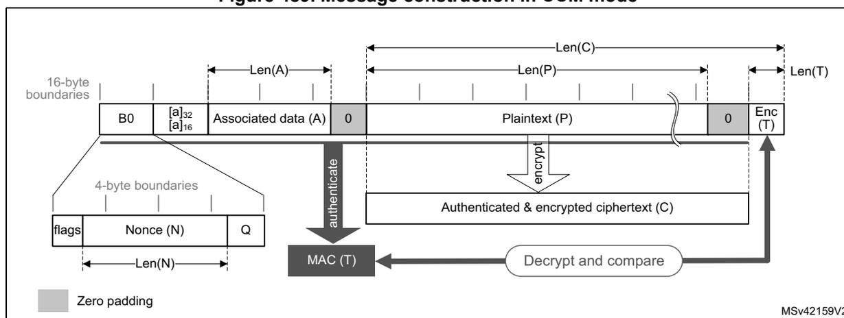
Figure 485. Message construction in GCM
The diagram shows the construction of a GCM message. It starts with a 16-byte Initial Counter Block (ICB) consisting of a 96-bit Initialization Vector (IV) and a 32-bit Counter. This is followed by Additional Authenticated Data (AAD) of length \( Len(A) \) , which is padded with zeros to a 16-byte boundary. Next is the Plaintext (P) of length \( Len(P) \) , also padded with zeros. The Plaintext is encrypted to form the Authenticated & encrypted ciphertext (C), where \( Len(P) = Len(C) \) . The final part is the Last block, which contains the 64-bit lengths \( [Len(A)]_{64} \) and \( [Len(C)]_{64} \) . Arrows labeled 'authenticate' and 'encrypt' show the processing flow: AAD, Ciphertext, and the Last block are all processed to generate the Authentication tag (T).
The structure of this message is defined as below:
- •
16-byte Initial Counter Block (ICB)
, composed of two distinct fields:
- – Initialization vector (IVI) : a 96-bit value that must be unique for each encryption cycle with a given key. The GCM standard supports IVIs with less than 96 bits, but in this case strict rules apply.
- – Counter : a 32-bit big-endian integer that is incremented each time a block processing is complete. According to NIST specification, the counter value is 0x2 when processing the first block of payload.
- • Authenticated header AAD (also known as additional authentication data) has a known length \( Len(A) \) that may be a non-multiple of 16 bytes, and must not exceed \( 2^{64} - 1 \) bits. This part of the message is only authenticated, not encrypted.
- • Plaintext message P is both authenticated and encrypted as ciphertext C, with a known length \( Len(P) \) that may be non-multiple of 16 bytes, and cannot exceed \( 2^{32} - 2 \) 16-bytes blocks.
- • Last block contains the AAD header length (bits \( [32:63] \) ) and the payload length (bits \( [96:127] \) ) information, as shown in Table 420 .
The GCM standard specifies that ciphertext C has the same bit length as the plaintext P.
A special padding scheme is required when a part of the message (AAD or P) has a length that is a non-multiple of 16-bytes.
For more details, refer to NIST Special Publication 800-38D, Recommendation for Block Cipher Modes of Operation - Galois/Counter Mode (GCM) and GMAC .
Figure 486 describes the GCM chaining implementation in the CRYP peripheral (encryption). To select this chaining mode, write ALGOMODE[3:0] with 0x6.
Figure 486. GCM authenticated encryption
The first counter block (CB1) is derived from the initial counter block ICB by the application software, as defined in Table 419 .
Table 419. GCM mode IVI registers initialization
| Register | CRYP_IV0LR[31:0] | CRYP_IV0RR[31:0] | CRYP_IV1LR[31:0] | CRYP_IV1RR[31:0] |
|---|---|---|---|---|
| Input data | ICB[127:96] | ICB[95:64] | ICB[63:32] | ICB[31:0] 32-bit counter = 0x2 |
The last block of a GCM message contains the AAD header length and the payload length information, as shown in Table 420 .
Table 420. GCM last block definition
| Word order to CRYP_DINR | First word | Second word | Third word | Fourth word |
|---|---|---|---|---|
| Input data | AAD length[63:32] | AAD length[31:0] | Payload length[63:32] | Payload length[31:0] |
GCM encryption and decryption process
This process is described in Section 49.4.6 , with the following sequence of events:
GCM initialize
- 1. Disable the CRYP peripheral, by clearing CRYPTEN.
- 2. Flush the FIFOs by setting FFLUSH.
- 3. Initialize the CRYP_CR register:
- a) Select GCM chaining mode (write ALGOMODE[3:0] with 0x8) in encryption or decryption mode (write ALGODIR with 0 or 1).
- b) Configure the data type through DATATYPE[1:0]
- c) Configure the key size through KEYSIZE.
- d) Select the key mode, using KMOD[1:0]: if the key is coming from SAES peripheral set KMOD[1:0] to 0x2 else keep it at 0x0.
- e) Select the GCM initialization phase, by writing 0x0 to GCM_CCMPH[1:0]
- 4. Write the initialization vector in CRYP_IVxL/R registers according to Table 419 .
- 5. Write the key in CRYP_KxL/R registers if KMOD[1:0] is 0x0. If KMOD[1:0]= 0x2, the key is being transferred from the SAES peripheral (see Section 49.4.14 ).
- 6. Wait until KEYVALID is set (the key loading completed).
- 7. Set CRYPTEN to start the calculation of the hash key. CRYPTEN is automatically cleared when the calculation is complete.
- 8. Wait for the CRYPTEN bit to be cleared, indicating that the GCM hash subkey (H) computation is complete.
GCM header phase
- 9. Initialize header phase:
- a) Select the GCM header phase, by writing 0x1 to GCM_CCMPH[1:0]. Do not change the other configurations written during GCM initialization.
- b) Set CRYPTEN to start accepting data.
- 10. Append header data:
- a) If it is the last block and the AAD in the block is smaller than 16 bytes, pad the remainder of the block with zeros.
- b) Append the data into CRYP as described in Section 49.4.5 .
- c) Repeat the step b) until the second-last AAD data block is processed. For the last block follow the steps a) and b) .
- 11. Wait until the BUSY flag is cleared.
Note: This phase can be skipped if there is no AAD, that is, Len(A) = 0.
No data are read during header phase.
GCM payload phase- 12. Initialize payload phase:
- a) Disable the CRYP peripheral, by clearing CRYPTEN.
- b) Select the GCM payload phase, by writing GCM_CCMPH[1:0] with 0x2. Do not change the other configurations written during GCM initialization.
- c) Enable the CRYP peripheral by setting CRYPTEN, to start accepting data.
- 13. Append payload data:
- a) If it is the last block and the message in the block is smaller than 16 bytes, pad the remainder of the block with zeros.
- b) Append the data into CRYP as described in Section 49.4.5 , then read the CRYP_DOUTR register to save the resulting block(s).
- c) Repeat the step b) until the second-last plaintext block is encrypted or until the last block of ciphertext is decrypted. For the last block of plaintext (encryption only), follow the steps a) and b) . For the last block, discard the bits that are not part of the payload when the last block is smaller than 16 bytes.
- 14. Wait until the BUSY flag is cleared.
Note: This phase can be skipped if there is no payload, that is, Len(C) = 0 (see GMAC mode).
GCM finalization- 15. Select the GCM final phase, by writing GCM_CCMPH[1:0] with 0x3, and clear the ALGODIR bit (encryption). Do not change the other configurations written during GCM initialization.
- 16. Write the final GCM block into the CRYP_DINR register. It is the concatenated AAD bit and payload bit lengths, as shown in Table 420 .
- 17. Wait until the OFNE flag in the CRYP_SR register is set.
- 18. Get the GCM authentication tag, by reading the CRYP_DOUTR register four times.
- 19. Disable the CRYP peripheral, by clearing CRYPTEN. If it is an authenticated decryption, compare the generated tag with the expected tag passed with the message.
Note: In the final phase, data are written to CRYP_DINR normally (no swapping).
Suspend and resume operations in GCM mode
To suspend the processing of a message , proceed as follows:
- 1. If DMA is used, stop the CRYP DMA transfers to the input FIFO, by clearing DIEN bit of the CRYP_DMACR register.
- 2. Wait until both FIFOs are empty (IFEM = 1 and OFNE = 0 in CRYP_SR) and the BUSY bit is cleared.
- 3. In the payload phase, if DMA is used, stop the CRYP DMA transfers from the output FIFO, by clearing the DOEN bit of the CRYP_DMACR register.
- 4. Disable the CRYP by clearing CRYPTEN.
- 5. Save the current CRYP_CR configuration in the memory. Key registers do not need to be saved as the original key value is known by the application.
- 6. In the payload phase, save the CRYP_IVxL/R registers as, during the data processing, they changed from their initial values. In the header phase, this step is not required.
- 7. Save the CRYP_CSGCMCCMRx and CRYP_CSGCMRx registers in memory.
- 8. If DMA is used, save the DMA controller status (pointer for CRYP input data transfers, number of remaining bytes, and so on). In the payload phase, also save pointer for CRYP output data transfers.
To resume the processing of a message , proceed as follows:
- 1. If DMA is used, configure the DMA controller in order to complete the remaining input FIFO transfers. In the payload phase, also configure the DMA controller for the remaining output FIFO transfers.
- 2. Disable the CRYP peripheral, by clearing CRYPTEN.
- 3. Restore the initial setting values in the CRYP_CR and CRYP_KxL/R registers. If KMOD[1:0]= 0x2 the key needs to be transferred again from the SAES peripheral (see Section 49.4.14 ).
- 4. Write the suspend register values, previously saved in the memory, back into their corresponding CRYP_CSGCMCCMRx and CRYP_CSGCMRx registers.
- 5. In the payload phase, write the initialization vector register values, previously saved in the memory, back into their corresponding CRYP_IVxL/R registers. In the header phase, write initial setting values back into the CRYP_IVxL/R registers.
- 6. Enable the CRYP peripheral by setting CRYPTEN.
- 7. If DMA is used, enable CRYP DMA requests, by setting DIEN (and DOEN if in payload phase).
49.4.12 CRYP AES Galois message authentication code (GMAC)
The Galois message authentication code (GMAC) enables the authentication of a plaintext, generating the corresponding tag information (also known as message authentication code).
GMAC is similar to GCM, except that it is applied on a message composed only by plaintext authenticated data (that is, only header, no payload). The following figure shows typical message construction for GMAC.
Figure 487. Message construction in GMAC mode
The diagram illustrates the message construction for GMAC. It shows a sequence of blocks starting with an Initialization Vector (IV) and Counter (ICB), followed by 'Authenticated data' of length 'Len(A)'. The 'Authenticated data' is split into 16-byte boundaries. Above the 'Authenticated data' block, there are two additional fields: '[Len(A)] 64 ' and '[0] 64 '. Below the 'Authenticated data' block, there is a 'Last block' which is zero-padded. An arrow labeled 'auth.' points from the 'Authenticated data' block to an 'Authentication tag (T)'. Below the ICB, there are two boxes: 'Initialization vector (IV)' and 'Counter', which are 4-byte boundaries. A legend indicates that grey boxes represent 'Zero padding'. The diagram is labeled 'MSV42158V2'.
For more details, refer to NIST Special Publication 800-38D, Recommendation for Block Cipher Modes of Operation - Galois/Counter Mode (GCM) and GMAC .
Figure 488 describes the GMAC chaining implementation in the CRYP peripheral. To select this chaining mode, write ALGOMODE[3:0] with 0x6.
Figure 488. GMAC authentication mode
The diagram illustrates the GMAC authentication mode chaining implementation. It is divided into three main stages: (1) Init, (2) Header, and (4) Final.
(1) Init: A KEY is input to an 'Encrypt' block along with '[0]
128
'. The output is 'H'.
(2) Header: This stage processes message blocks 'DIN (message block 1)' through 'DINR (message block n)'. Each block passes through a 'Swap management' block, which is controlled by 'DATATYPE [1:0]'. The output of the 'Swap management' block is then input to a 'GF2mul' block along with 'H'. The output of the 'GF2mul' block is XORed with the previous block's output (or the initial 'H' for the first block).
(4) Final: This stage takes the KEY and 'IVI + 32-bit counter (= 0x0)' as input to an 'Encrypt' block, producing 'S'. It also takes 'DIN len(A)
64
|| [0]
64
' as input to a 'GF2mul' block along with 'H'. The output of the 'GF2mul' block is XORed with 'S' to produce the final 'DOUT (authentication tag T)'.
A legend indicates that white boxes are 'input', grey boxes are 'output', and a circle with a cross is 'XOR'. The diagram is labeled 'MSV69569V1'.
The GMAC algorithm corresponds to the GCM algorithm applied on a message only containing a header. As a consequence, all steps and settings are the same as for the GCM, except that the payload phase is omitted.
Suspend and resume operations in GMAC
In GMAC mode, the sequence described for the GCM applies except that only the header phase can be interrupted.
49.4.13 CRYP AES Counter with CBC-MAC (CCM)
The AES counter with cipher block chaining-message authentication code (CCM) algorithm enables encryption and authentication of plaintext, generating the corresponding ciphertext and tag (also known as message authentication code). To ensure confidentiality, the CCM algorithm is based on AES in counter mode. It uses cipher block chaining technique to generate the message authentication code. This is commonly called CBC-MAC.
Note: NIST does not approve CBC-MAC as an authentication mode outside the context of the CCM specification.
The following figure shows typical message construction for CCM.
Figure 489. Message construction in CCM mode
The structure of the message is:
- •
16-byte first authentication block (B0)
, composed of three distinct fields:
- – Q : a bit string representation of the octet length of P (Len(P))
- – Nonce (N) : a single-use value (that is, a new nonce must be assigned to each new communication) of Len(N) size. The sum Len(N) + Len(P) must be equal to 15 bytes.
- – Flags : most significant octet containing four flags for control information, as specified by the standard. It contains two 3-bit strings to encode the values t (MAC length expressed in bytes) and Q (plaintext length such that \( \text{Len}(P) < 2^{8Q} \) bytes). The counter blocks range associated to Q is equal to \( 2^{8Q-4} \) , that is, if the maximum value of Q is 8, the counter blocks used in cipher must be on 60 bits.
- • 16-bytes blocks (B) associated to the Associated Data (A).
This part of the message is only authenticated, not encrypted. This section has a known length \( \text{Len}(A) \) that can be a non-multiple of 16 bytes (see Figure 489 ). The standard also states that, on the MSB bits of the first message block ( \( B_1 \) ), the associated data length expressed in bytes ( \( a \) ) must be encoded as follows:
- – If \( 0 < a < 2^{16} - 2^8 \) , then it is encoded as \( [a]_{16} \) , that is, on two bytes.
- – If \( 2^{16} - 2^8 < a < 2^{32} \) , then it is encoded as \( 0xFF \parallel 0xFE \parallel [a]_{32} \) , that is, on six bytes.
- – If \( 2^{32} < a < 2^{64} \) , then it is encoded as \( 0xFF \parallel 0xFF \parallel [a]_{64} \) , that is, on ten bytes.
- • 16-byte blocks (B) associated to the plaintext message \( P \) , which is both authenticated and encrypted as ciphertext \( C \) , with a known length \( \text{Len}(P) \) . This length can be a non-multiple of 16 bytes (see Figure 489 ).
- • Encrypted MAC (T) of length \( \text{Len}(T) \) appended to the ciphertext \( C \) of overall length \( \text{Len}(C) \) .
When a part of the message ( \( A \) or \( P \) ) has a length that is a non-multiple of 16-bytes, a special padding scheme is required.
Note: CCM chaining mode can also be used with associated data only (that is, no payload).
As an example, the C.1 section in NIST Special Publication 800-38C gives the following values (hexadecimal numbers):
N:
10111213 141516
(
\(
\text{Len}(N) = 56
\)
bits or 0x7 bytes)
A:
00010203 04050607
(
\(
\text{Len}(A) = 64
\)
bits or 0x8 bytes)
P:
20212223
(
\(
\text{Len}(P) = 32
\)
bits i.e.
\(
Q = 0x4
\)
bytes)
T:
6084341b
(
\(
\text{Len}(T) = 32
\)
bits or
\(
t = 4
\)
)
\(
B_0
\)
:
4f101112 13141516 00000000 00000004
\(
B_1
\)
:
00080001 02030405 06070000 00000000
\(
B_2
\)
:
20212223 00000000 00000000 00000000
CTR0:
0710111213 141516 00000000 00000000
CTR1:
0710111213 141516 00000000 00000001
For more details, refer to NIST Special Publication 800-38C, Recommendation for Block Cipher Modes of Operation - The CCM Mode for Authentication and Confidentiality .
Figure 490 describes the CCM chaining implementation in the CRYP peripheral (encryption). To select this chaining mode, write ALGOMODE[3:0] with 0x9.
Figure 490. CCM mode authenticated encryption
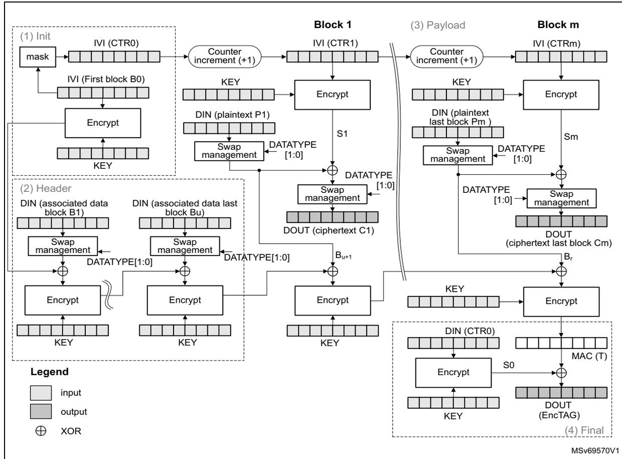
The diagram illustrates the CCM chaining implementation for encryption, divided into four main stages:
- (1) Init: The process starts with a 'mask' and 'IVI (First block B0)' being input to an 'Encrypt' block along with a 'KEY'. The output is 'IVI (CTR0)'. A 'Counter increment (+1)' block takes 'IVI (CTR0)' and produces 'IVI (CTR1)'.
- (2) Header: This stage processes associated data blocks. 'DIN (associated data block B1)' and 'DIN (associated data last block Bu)' are input to 'Swap management' blocks. The outputs are XORed with 'DATATYPE[1:0]' and then passed to 'Encrypt' blocks. The 'Encrypt' blocks also take a 'KEY' as input. The output of the last 'Encrypt' block in this stage is 'Bu+1'.
- (3) Payload: This stage processes the plaintext blocks. 'Counter increment (+1)' blocks take 'IVI (CTR1)' and 'IVI (CTRm)' to produce the next counter value. 'DIN (plaintext P1)' and 'DIN (plaintext last block Pm)' are input to 'Swap management' blocks. The outputs are XORed with 'DATATYPE[1:0]' and then passed to 'Encrypt' blocks. The 'Encrypt' blocks also take a 'KEY' as input. The output of the last 'Encrypt' block in this stage is 'Sm'.
- (4) Final: This stage generates the MAC (T). 'DIN (CTR0)' is input to an 'Encrypt' block along with a 'KEY'. The output is 'S0'. 'S0' is XORed with 'MAC (T)' to produce the final output 'DOUT (EncTAG)'.
A 'Legend' indicates that light gray boxes represent 'input', dark gray boxes represent 'output', and a circle with a cross represents 'XOR'.
The first block of a CCM message (B0) must be prepared by the application as defined in Table 421.
Table 421. CCM mode IVI registers initialization
| Register | CRYP_IV0LR[31:0] | CRYP_IV0RR[31:0] | CRYP_IV1LR[31:0] | CRYP_IV1RR[31:0] |
|---|---|---|---|---|
| Input data | B0[127:96] (1) | B0[95:64] | B0[63:32] | B0[31:0] (2) |
- 1. The 5 most significant bits are cleared (flag bits).
- 2. Q length bits are cleared, except for bit 0 that is set.
CRYP supports counters up to 64 bits, as specified by NIST.
CCM encryption and decryption process
This process is described in Section 49.4.6 , with the following sequence of events:
CCM initialize
- 1. Disable the CRYP peripheral, by clearing CRYPTEN.
- 2. Flush the FIFOs by setting FFLUSH.
- 3. Initialize the CRYP_CR register:
- a) Select CCM chaining mode (write ALGOMODE[3:0] with 0x9) in encryption or decryption mode (write ALGODIR with 0 or 1).
- b) Configure the data type through DATATYPE[1:0]
- c) Configure the key size through KEYSIZE.
- d) Select the key mode, using KMOD[1:0]: if the key is coming from SAES peripheral set KMOD[1:0] to 0x2 else keep it at 0x0.
- e) Select the CCM initialization phase, by writing 0x0 to GCM_CCMPH[1:0]
- 4. Write the initialization vector into the CRYP_IVxL/R registers with CTR1 information, as defined in Table 421
- 5. Write the key in CRYP_KxL/R registers if KMOD[1:0] is 0x0. If KMOD[1:0]= 0x2 the key is being transferred from the SAES peripheral (see Section 49.4.14 ).
- 6. Wait until KEYVALID is set (the key loading completed).
- 7. Enable the CRYP peripheral by setting CRYPTEN.
- 8. Write the B0 data in CRYP_DINR registers according to Table 421 , then wait for the CRYPTEN bit to be cleared.
Note: In this initialization phase, data have to be inserted normally (no swapping).
CCM header phase
- 9. Initialize header phase:
- a) Prepare the first block of the (B1) data associated with the message, in accordance with CCM chaining rules.
- b) Select the GCM header phase, by writing GCM_CCMPH[1:0] with 0x1. Do not change the other configurations written during the GCM initialization.
- c) Set CRYPTEN to start accepting data.
- 10. Append header data:
- a) If it is the last block and the associated data in the block is smaller than 16 bytes, pad the remainder of the block with zeros.
- b) Append the data into CRYP as described in Section 49.4.5 .
- c) Repeat the step b) until the second-last associated data block is processed. For the last block follow the steps a) and b) .
- 11. Wait until the BUSY flag is cleared.
Note: This phase can be skipped if there is no associated data, that is, Len(A) = 0
No data are read during the header phase.
- 12. Initialize payload phase:
- a) Disable the CRYP peripheral, by clearing CRYPTEN.
- b) Select the GCM payload phase, by writing GCM_CCMPH[1:0] with 0x2. Do not change the other configurations written during GCM initialization.
- c) Enable the CRYP peripheral by setting CRYPTEN, to start accepting data.
- 13. Append payload data:
- a) In encryption only, if it is the last block and the plaintext in the block is smaller than 16 bytes, pad the remainder of the block with zeros.
- b) Append the data into CRYP as described in Section 49.4.5 , then read the CRYP_DOUTR register to save the resulting block(s).
- c) Repeat the step b) until the second-last plaintext block is encrypted or until the last block of ciphertext is decrypted. For the last block of plaintext (encryption only), follow the steps a) and b) . For the last block, discard the bits that are not part of the payload when the last block is smaller than 16 bytes.
- 14. Wait until the BUSY flag is cleared.
Note: This phase can be skipped if there is no payload, that is, \( Len(P) = 0 \) or \( Len(C) = Len(T) \) . Remove \( LSB_{Len(T)}(C) \) encrypted tag information when decrypting ciphertext C.
CCM finalization- 15. Select the GCM final phase, by writing GCM_CCMPH[1:0] with 0x3, and clear the ALGODIR bit (encryption). Do not change the other configurations written during GCM initialization.
- 16. Write the CTR0 information into the CRYP_DINR register. CTR0 information is described in Table 421 , with the bit[0] cleared.
- 17. Wait until the OFNE flag in the CRYP_SR register is set.
- 18. Get the CCM authentication tag, by reading the CRYP_DOUTR register four times.
- 19. Disable the CRYP peripheral by clearing CRYPTEN. If it is an authenticated decryption, compare the generated tag with the expected tag passed with the message. Mask the authentication tag output with tag length to obtain a valid tag.
Note: In this final phase, data have to be inserted normally (no swapping).
Suspend and resume operations in CCM mode
To suspend the processing of a message in header or payload phase, proceed as follows:
- 1. If DMA is used, stop the CRYP DMA transfers to the input FIFO, by clearing DIEN bit of the CRYP_DMACR register.
- 2. Wait until both FIFOs are empty (IFEM = 1 and OFNE = 0 in CRYP_SR) and the BUSY bit is cleared.
- 3. In the payload phase, if DMA is used, stop the CRYP DMA transfers from the output FIFO, by clearing the DOEN bit of the CRYP_DMACR register.
- 4. Disable the CRYP by clearing CRYPTEN.
- 5. Save the current CRYP_CR configuration in the memory. Key registers do not need to be saved as the original key value is known by the application.
- 6. In the payload phase, save the CRYP_IVxL/R registers as, during the data processing, they changed from their initial values. In the header phase, this step is not required.
- 7. Save the CRYP_CSGCMCCMRx registers in the memory.
- 8. If DMA is used, save the DMA controller status (pointer for CRYP input data transfers, number of remaining bytes, and so on). In the payload phase, also save pointer for CRYP output data transfers.
To resume the processing of a message, proceed as follows:
- 1. If DMA is used, configure the DMA controller in order to complete the remaining input FIFO transfers. In the payload phase, also configure the DMA controller for the remaining output FIFO transfers.
- 2. Disable the CRYP peripheral, by clearing CRYPTEN.
- 3. Restore the initial setting values in the CRYP_CR and CRYP_KxL/R registers. If KMOD[1:0]= 0x2 the key needs to be transferred again from the SAES peripheral (see Section 49.4.14 ).
- 4. Write the suspend register values, previously saved in the memory, back into their corresponding CRYP_CSGCMCCMRx registers.
- 5. In the payload phase, write the initialization vector register values, previously saved in the memory, back into their corresponding CRYP_IVxL/R registers. In the header phase, write initial setting values back into the CRYP_IVxL/R registers.
- 6. Enable the CRYP peripheral by setting CRYPTEN.
- 7. If DMA is used, enable CRYP DMA requests, by setting DIEN (and DOEN if in payload phase).
49.4.14 AES key sharing with secure AES co-processor
The CRYP peripheral can use the SAES peripheral as security co-processor. The secure application prepares the key in the robust SAES peripheral. When it is ready, the CRYP application can load this prepared key through a dedicated hardware key bus.
The recommended sequence is described hereafter and in section SAES operations with shared keys in section Secure AES coprocessor (SAES) of this document.
- 1. In SAES peripheral, the application encrypts the key to share in shared-key mode (KMOD[1:0] at 0x2). When applicable, the proper CRYP instance must be selected through KSHAREID[1:0].
- 2. Each time the shared key is required in the CRYP peripheral, the application decrypts it in the SAES peripheral in shared-key mode (KMOD[1:0] at 0x2). When applicable, the proper CRYP instance must be selected through KSHAREID[1:0].
- 3. Once the shared key is decrypted and loaded in SAES_KEYRx registers it can be shared with CRYP. To load the shared key in CRYP, the application sets KEYSIZE as appropriate and writes KMOD[1:0] with 0x2. When KEYVALID is cleared, the key is automatically transferred by hardware into the CRYP_KxL/R registers and the BUSY flag in the CRYP_SR register set.
- 4. Once the key transfer is complete, the BUSY flag is cleared and the KEYVALID flag set in the CRYP_SR register. If KEYVALID is not set when BUSY bit is cleared, or if the KERF flag is set in the CRYP_SR register, it means that the KEYSIZE value is incorrect or an unexpected event occurred during the transfer (such as DPA error, tamper event or KEYVALID in SAES_SR cleared before the end of the transfer). When such errors occur, reset both peripherals through their IPRST bits and restart the whole key sharing process.
When the key sharing sequence is complete, the CRYP is initialized with a valid, shared key. The application can then process data in normal key mode, by writing KMOD[1:0] with 0x0.
Note: This sequence in CRYP peripheral can be run multiple times (for example, to manage a suspend/resume situation), as long as SAES peripheral is unused and duly remains in key sharing state.
When sharing keys KEYSIZE in CRYP must be identical to SAES value (128 or 256 bits).
49.4.15 CRYP data registers and data swapping
Data input and output
A 16-byte data block enters the CRYP peripheral with four successive 32-bit word writes into the CRYP_DINR register (bitfield DIN[31:0]), the most significant word (bits [127:96]) first, the least significant word (bits [31:0]) last.
A 16-byte data block is retrieved from the CRYP peripheral with four successive 32-bit word reads of the CRYP_DOUTR register (bitfield DOUT[31:0]), the most significant word (bits [127:96]) first, the least significant word (bits [31:0]) last.
The four 32-bit words of a 16-byte data block must be stored in the memory consecutively and in big-endian order, that is, with the most significant word on the lowest address. See Table 422 “no swapping” option for details.
Data swapping
The CRYP peripheral can be configured to perform a bit-, a byte-, a half-word-, or no swapping on the input data word in the CRYP input FIFO, before loading it to the AES processing core, and on the data output from the AES processing core, before sending it to the CRYP output FIFO. The choice depends on the type of data. For example, a byte swapping is used for an ASCII text stream.
The data swap type is selected through the DATATYPE[1:0]. The selection applies both to the input and the output of the CRYP, except in GCM/CCM final phase (data must be inserted normally).
Note: The data in CRYP key registers (CRYP_KxL/R) and initialization vector registers (CRYP_IVxL/R) are not sensitive to the swap mode selection.
The CRYP data swapping feature is summarized in Table 422 and Figure 491 .
Table 422. AES data swapping example
| DATATYPE[1:0] | Swapping performed | Data block |
|---|---|---|
| System memory data (big-endian) | ||
| 0x0 | No swapping | Block[127..64]: 0x04EEF672 2E04CE96 Block[63..0]: 0x4E6F7720 69732074 |
| Address @, word[127..96]: 0x04EE F672 Address @ + 0x4, word[95..64]: 0x2E04 CE96 Address @ + 0x8, word[63..32]: 0x4E6F 7720 Address @ + 0xC, word[31..0]: 0x6973 2074 | ||
| 0x1 | Half-word (16-bit) swapping | Block[63..0]: 0x 4E6F 7720 6973 2074 |
| Address @, word[63..32]: 0x7720
4E6F Address @ + 0x4, word[31..0]: 0x2074 6973 | ||
| 0x2 | Byte (8-bit) swapping | Block[63..0]: 0x 4E 6F 77 20 69 73 20 74 |
| Address @, word[63..32]: 0x2077
6F4E Address @ + 0x4, word[31..0]: 0x74 20 73 69 | ||
| 0x3 | Bit swapping | Block[63..32]: 0x4E6F 7720 0100 1110 0110 1111 0111 0111 0010 0000 Block[31..0]: 0x6973 2074 0110 1001 0111 0011 0010 0000 0111 0100 |
| Address @, word[63..32]: 0x04EE F672 0000 0100 1110 1110 1111 0110 0111 0010 Address @ + 0x4, word[31..0]: 0x2E04 CE96 0010 1110 0000 0100 1100 1110 1001 0110 |
Figure 491. 128-bit block construction according to the data type
![Figure 491: 128-bit block construction according to the data type. The diagram shows four examples of data block construction based on DATATYPE[1:0] settings: 00 (no swapping), 01 (16-bit half-word swapping), 10 (8-bit byte swapping), and 11 (bit swapping). Each example shows four words (Word 0 to Word 3) and the mapping of their bits into a 128-bit block. Arrows indicate the order of write to CRYP_DINR / read from CRYP_DOUTR (1 to 4). A legend explains the symbols: Dx for input/output data bit 'x', double-headed arrows for data swap, circled numbers 1-4 for write/read order, grey boxes for zero padding, and dashed boxes for AES core input/output data.](/RM0486-STM32N6x5-x7/9e036618fedede585490434716c06693_img.jpg)
DATATYPE[1:0] = 00: no swapping
Word 3: D127...D96, Word 2: D95...D64, Word 1: D63...D32, Word 0: D31...D0. The mapping is direct: Word 3 maps to D127...D96, Word 2 to D95...D64, Word 1 to D63...D32, and Word 0 to D31...D0.
DATATYPE[1:0] = 01: 16-bit (half-word) swapping
Word 3: D127...D112, D111...D96; Word 2: D95...D80, D79...D64; Word 1: D63...D48, D47...D32; Word 0: D31...D16, D15...D0. Swapping occurs within each word: D127...D112 swaps with D111...D96, etc.
DATATYPE[1:0] = 10: 8-bit (byte) swapping
Word 3: D127...D120, D119...D112, D111...D104, D103...D96; Word 2: D95...D88, D87...D80, D79...D72, D71...D64; Word 1: D63...D56, D55...D48, D47...D40, D39...D32; Word 0: D31...D24, D23...D16, D15...D8, D7...D0. Swapping occurs within each word: D127...D120 swaps with D111...D104, and D119...D112 swaps with D103...D96, etc.
DATATYPE[1:0] = 11: bit swapping
Word 3: D127; D126; D125; D98; D97; D96; Word 2: D95; D94; D93; D66; D65; D64; Word 1: D63; D62; D61; D34; D33; D32; Word 0: D31; D30; D29; D2; D1; D0. Bit-level swapping occurs within each word: D127 swaps with D96, D126 with D97, and D125 with D98, etc.
Legend:
- Dx input/output data bit 'x'
- ↔ Data swap
- ①...④ Order of write to CRYP_DINR / read from CRYP_DOUTR
- ▒ Zero padding (example)
- [ - - - ] AES core input/output data
MSv43721V3
Data padding
Figure 491 also gives an example of memory data block padding with zeros such that the zeroed bits after the data swap form a contiguous zone at the MSB end of the AES core input buffer. The example shows the padding of an input data block containing:
- • 84 message bits, with DATATYPE[1:0] = 0x0
- • 48 message bits, with DATATYPE[1:0] = 0x1
- • 56 message bits, with DATATYPE[1:0] = 0x2
- • 34 message bits, with DATATYPE[1:0] = 0x3
49.4.16 CRYP key registers
The eight CRYP_KxR/LR write-only registers store the encryption or decryption key information, as shown in Table 423 . Reads are not allowed for security reason.
Note: In memory and in CRYP key registers, keys are stored in big-endian format, with most significant byte on the lowest address.
Table 423. Key endianness in CRYP_KxR/LR registers (128/192/256-bit keys)
| K0LR[31:0] | K0RR[31:0] | K1LR[31:0] | K1RR[31:0] | K2LR[31:0] | K2RR[31:0] | K3LR[31:0] | K3RR[31:0] |
|---|---|---|---|---|---|---|---|
| - | - | - | - | k[127:96] | k[95:64] | k[63:32] | k[31:0] |
| K0LR[31:0] | K0RR[31:0] | K1LR[31:0] | K1RR[31:0] | K2LR[31:0] | K2RR[31:0] | K3LR[31:0] | K3RR[31:0] |
| - | - | k[191:160] | k[159:128] | k[127:96] | k[95:64] | k[63:32] | k[31:0] |
| K0LR[31:0] | K0RR[31:0] | K1LR[31:0] | K1RR[31:0] | K2LR[31:0] | K2RR[31:0] | K3LR[31:0] | K3RR[31:0] |
| k[255:224] | k[223:192] | k[191:160] | k[159:128] | k[127:96] | k[95:64] | k[63:32] | k[31:0] |
The key registers are not affected by the data swapping feature controlled by the DATATYPE[1:0] bitfield.
Write operations to the CRYP_KxL/R registers are ignored when BUSY bit is set. The application must check this before modifying key registers.
The entire key must be written before starting an AES computation. In normal key mode (KMOD[1:0] at 0x0), the key registers must always be written in either ascending or descending order. The write sequence becomes (in ascending order):
- • K2LR, K2RR, K3LR, then K3RR registers for KEYSIZE = 0x0
- • K1LR, K1RR, K2LR, K2RR, K3LR, then K3RR register for KEYSIZE = 0x1
- • K0LR, K0RR, K1LR, K1RR, K2LR, K2RR, K3LR, then K3RR register for KEYSIZE = 0x2
Note: KEYSIZE must be written before the key.
As soon as the first key register is written, the KEYVALID bit is cleared. Once the key registers writing sequence is complete, KEYVALID is set and CRYPTEN bit becomes writable. If an error occurs, KEYVALID is cleared and KERF set (see Section 49.4.18 ).
49.4.17 CRYP initialization vector registers
The four CRYP_IVxR/LR registers store the initialization vector (IVI) information, as shown in Table 424 . They can only be written if BUSY bit is cleared.
Note: In memory and in CRYP IVI registers, initialization vectors are stored in big-endian format, with most significant byte on the lowest address.
Table 424. Initialization vector endianness in CRYP_IVxR registers (AES)
| CRYP_IV0L[31:0] | CRYP_IV0R[31:0] | CRYP_IV1L[31:0] | CRYP_IV1R[31:0] |
|---|---|---|---|
| IVI[127:96] | IVI[95:64] | IVI[63:32] | IVI[31:0] |
Initialization vector information depend on the chaining mode selected. When used, CRYP_IVxR/LR registers are updated upon each AES computation cycle (useful for
managing suspend mode).
The initialization vector registers are not affected by the data swapping feature controlled by DATATYPE[1:0].
49.4.18 CRYP error management
The CRYP peripheral manages the errors described in this section.
Key error flag (KERF)
There are multiple sources of errors that set the KERF flag and clear the KEYVALID bit of the CRYP_SR register:
- • Key writing sequence error: triggered upon detecting an incorrect sequence of writing key registers. See Section 49.4.16: CRYP key registers for details.
- • Key sharing size mismatch error: triggered when KMOD[1:0] is at 0x2 and KEYSIZE in CRYP does not match KEYSIZE in SAES peripheral, or KEYSIZE is at 0x1 in CRYP_CR (192-bit key).
- • Key sharing error: triggered upon failing transfer of SAES shared key to CRYP. See Section 49.4.14: AES key sharing with secure AES co-processor for details.
Upon a key writing sequence error, KERF flag is cleared when a correct key writing sequence starts.
Upon a key sharing error, reset both CRYP and SAES peripherals through the IPRST bit of their corresponding control register, then restart the key sharing sequence.
Note: For any key error, clear KERF flag prior to setting CRYPTEN.
49.5 CRYP interrupts
There are two individual maskable interrupt sources generated by the CRYP peripheral to signal the following events:
- • Input FIFO empty (IFEM) or not full (IFNF)
- • Output FIFO full (OFFU) or not empty (OFNE)
These sources are combined into a common interrupt signal from the CRYP peripheral that connects to the Arm ® Cortex ® interrupt controller. The application can enable or disable CRYP interrupt sources individually by setting/clearing the corresponding mask bit of the CRYP_IMSCR register. The status of the individual source of event flags can be read from the CRYP_SR register.
The global status of the two source of interrupts can be read either from the CRYP_RISR register (raw, that is unmasked), or from the CRYP_MISR register (masked).
Table 425 gives a summary of the available features.
Table 425. CRYP interrupt requests
| Interrupt acronym | Interrupt event | Event flag | Enable bit | Interrupt clear method | |
|---|---|---|---|---|---|
| in CRYP_xISR (1) | in CRYP_SR | ||||
| CRYP | Output FIFO full | OUTRIS (not masked) OUTMIS (masked) | OFFU | OUTIM
(2)
and CRYPEN | Read one data from output FIFO |
| Output FIFO not empty | OFNE | Read all data from output FIFO | |||
| Input FIFO not full | INRIS (not masked) INMIS (masked) | IFNF | INIM
(2)
and CRYPEN | Write data until input FIFO is full | |
| Input FIFO empty | IFEM | Write at least one word in input FIFO | |||
1. Flag of the CRYP_RISR register (unmasked or raw), or CRYP_MISR register (masked).
2. Bit of the CRYP_IMSCR register.
Output FIFO service interrupt (OUTMIS)
The output FIFO service interrupt is asserted when there is one or more (32-bit word) data items in the output FIFO. This interrupt is cleared by reading data from the output FIFO until there is no valid (32-bit) word left (that is, when the interrupt follows the state of the output FIFO not empty flag OFNE).
The output FIFO service interrupt OUTMIS is active also when CRYP is disabled.
Consequently, when CRYPEN bit is cleared, the OUTMIS bit is not cleared when the output FIFO is not empty.
Input FIFO service interrupt (INMIS)
The input FIFO service interrupt is asserted when there are less than four words in the input FIFO. It is cleared by performing write operations to the input FIFO until it holds four or more words.
The input FIFO service interrupt INMIS is active only when CRYP is enabled. Consequently, when CRYPEN bit is cleared, the INMIS bit stay low even if the input FIFO is empty.
49.6 CRYP DMA requests
The CRYP peripheral provides an interface to connect to the DMA (direct memory access) controller. The DMA operation is controlled through the DIEN and DOEN bits of the CRYP_DMAGR register.
Detailed usage of DMA with CRYP can be found in Appending data using the DMA subsection of Section 49.4.5: CRYP encryption/ decryption typical usage .
Data input using DMA
Setting DIEN enables DMA writing into CRYP. The CRYP then initiates, during the input phase, a DMA request for each 16-byte data block to write to the CRYP_DINR register (quadruple 32-bit word, MSB first).
The CRYP supports both single and burst DMA transfers. Recommended configuration is fixed burst size of four words.
CRYP issues a DMA transfer request to its input FIFO every time a 16-bytes block has been read from the FIFO.
Note: According to the algorithm and the mode selected, special padding / ciphertext stealing might be required (see Section 49.4.7 ).
Data output using DMA
Setting DOEN enables DMA reading from CRYP. The CRYP then initiates, during the output phase, a DMA request for each 16-byte data block to read from the CRYP_DOUTR register (quadruple 32-bit word, MSB first).
The CRYP supports both single and burst DMA transfers. Recommended configuration is fixed burst size of four words.
CRYP issues a DMA transfer request from output FIFO every time one 16-byte block has been written into the FIFO.
Note: According to the message size, extra bytes might need to be discarded by application in the last block.
Stopping DMA transfers
All DMA request signals are de-asserted when CRYP is disabled (CRYPEN cleared) or the DMA enable bit (DIEN for input data, DOEN for output data) is cleared.
49.7 CRYP processing time
The following tables provide the 16-byte data block processing latency per operating mode.
Table 426. Processing latency for ECB, CBC and CTR
| Key size | Mode of operation | Chaining algorithm | Clock cycles |
|---|---|---|---|
| 128 bits | encryption or decryption (1) | ECD, CBC, CTR | 14 |
| key preparation | - | 12 | |
| 192 bits | encryption or decryption (1) | ECD, CBC, CTR | 16 |
| key preparation | - | 14 | |
| 256 bits | encryption or decryption (1) | ECD, CBC, CTR | 18 |
| key preparation | - | 16 |
1. Excluding key preparation time (ECB and CBC only).
Table 427. Processing latency for GCM and CCM (in clock cycles)
| Key size | Mode of operation | Chaining algorithm | Initialization phase | Header phase | Payload phase | Final phase |
|---|---|---|---|---|---|---|
| 128 bits | encryption or decryption | GCM | 24 | 10 | 14 | 14 |
| CCM | 12 | 14 | 25 | 14 | ||
| 192 bits | GCM | 28 | 10 | 16 | 16 | |
| CCM | 14 | 16 | 29 | 16 | ||
| 256 bits | GCM | 32 | 10 | 18 | 18 | |
| CCM | 16 | 18 | 33 | 18 | ||
49.8 CRYP registers
These registers are accessible through 32-bit word single accesses only (otherwise an AHB error is generated, and write accesses are ignored).
49.8.1 CRYP control register (CRYP_CR)
Address offset: 0x00
Reset value: 0x0000 0000
| 31 | 30 | 29 | 28 | 27 | 26 | 25 | 24 | 23 | 22 | 21 | 20 | 19 | 18 | 17 | 16 |
|---|---|---|---|---|---|---|---|---|---|---|---|---|---|---|---|
| IPRST | Res. | Res. | Res. | Res. | Res. | KMOD[1:0] | NPBLB[3:0] | ALGOMODE[3] | Res. | GCM_CCMPH[1:0] | |||||
| rw | rw | rw | rw | rw | rw | rw | rw | rw | rw | ||||||
| 15 | 14 | 13 | 12 | 11 | 10 | 9 | 8 | 7 | 6 | 5 | 4 | 3 | 2 | 1 | 0 |
|---|---|---|---|---|---|---|---|---|---|---|---|---|---|---|---|
| CRYPEN | FFLUSH | Res. | Res. | Res. | Res. | KEYSIZE[1:0] | DATATYPE[1:0] | ALGOMODE[2:0] | ALGODIR | Res. | Res. | ||||
| rw | rw | rw | rw | rw | rw | rw | rw | rw | rw | ||||||
Bit 31 IPRST : CRYP peripheral software reset
Setting the bit resets the CRYP peripheral, putting all registers to their default values, except the IPRST bit itself.
This bit must be kept cleared while writing any configuration registers.
Bits 30:26 Reserved, must be kept at reset value.
Bits 25:24 KMOD[1:0] : Key mode selection
This bitfield defines how the CRYP key can be used by the application. KEYSIZE must be correctly initialized when setting KMOD[1:0] different from zero.
0x0: Normal-key mode. Key registers are freely usable.
0x2: Shared-key mode. If shared-key mode is properly initialized in SAES peripheral, the CRYP peripheral automatically loads its key registers with the data stored in the SAES key registers. The key value is available in CRYP key registers when BUSY bit is cleared and KEYVALID is set in the CRYP_SR register. Key error flag KERF is set otherwise in the CRYP_SR register.
Others: Reserved
Attempts to write the bitfield are ignored when BUSY is set.
Bits 23:20 NPBLB[3:0] : Number of padding bytes in last block
This padding information must be filled by software before processing the last block of GCM payload encryption or CCM payload decryption, otherwise authentication tag computation is incorrect.
0x0: All bytes are valid (no padding)
0x1: Padding for the last LSB byte
...
0xF: Padding for the 15 LSB bytes of last block.
Attempts to write the bitfield are ignored when BUSY is set.
Bit 18 Reserved, must be kept at reset value.
Bits 17:16 GCM_CCMPH[1:0] : GCM or CCM phase selection
This bitfield selects the phase, applicable only with GCM, GMAC or CCM chaining modes.
0x0: Initialization phase
0x1: Header phase
0x2: Payload phase
0x3: Final phase
Attempts to write the bitfield are ignored when BUSY is set.
Bit 15 CRYPEN : CRYP enable
This bit enables/disables the CRYP peripheral.
0: CRYP disabled
1: CRYP enabled
This bit is automatically cleared by hardware upon the completion of the key preparation (ALGOMODE[3:0] at 0x7) and upon the completion of GCM/GMAC/CCM initialization phase.
The bit cannot be set as long as KEYVALID is cleared.
Bit 14 FFLUSH : FIFO flush
This bit enables/disables the flushing of CRYP input and output FIFOs. Reading this bit always returns 0.
0: No effect
1: FIFO flush enabled
When CRYPEN is cleared, writing this bit to 1 flushes both input and output FIFOs (that is read and write pointers of the FIFOs are reset).
FFLUSH bit must be set when BUSY is cleared, otherwise the FIFO is flushed, but the block being processed may be pushed into the output FIFO just after the flush operation, resulting in a non-empty FIFO condition.
Attempts to write FFLUSH are ignored when CRYPEN is set.
Bits 13:10 Reserved, must be kept at reset value.
Bits 9:8 KEYSIZE[1:0] : Key size selection
This bitfield defines the key length in bits of the key used by CRYP.
0x0: 128-bits
0x1: 192 bits
0x2: 256 bits
0x3: Reserved
When KEYSIZE is changed, KEYVALID bit is cleared.
Attempts to write the bitfield are ignored when BUSY is set.
Bits 7:6 DATATYPE[1:0] : Data type
This bitfield defines the format of data written in the CRYP_DINR register or read from the CRYP_DOUTR register, through selecting the mode of data swapping. This swapping is defined in Section 49.4.15: CRYP data registers and data swapping .
0x0: No swapping (32-bit data).
0x1: Half-word swapping (16-bit data).
0x2: Byte swapping (8-bit data).
0x3: Bit-level swapping.
Attempts to write the bitfield are ignored when BUSY is set.
Bits 19, 5:3 ALGOMODE[3:0] : Algorithm mode
This bitfield selects the AES algorithm/chaining mode.
0x4: Electronic codebook (ECB)
0x5: Cipher Block Chaining (CBC)
0x6: Counter mode (CTR)
0x7: AES key preparation for ECB or CBC decryption
0x8: Galois counter mode (GCM) and Galois message authentication code (GMAC)
0x9: Counter with CBC-MAC (CCM)
Others: Reserved
Attempts to write the bitfield are ignored when BUSY is set.
Bit 2 ALGODIR : Algorithm direction
This bit selects the algorithm direction.
0: Encryption
1: Decryption
Attempts to write the bitfield are ignored when BUSY is set.
Bits 1:0 Reserved, must be kept at reset value.
49.8.2 CRYP status register (CRYP_SR)
Address offset: 0x04
Reset value: 0x0000 0003
| 31 | 30 | 29 | 28 | 27 | 26 | 25 | 24 | 23 | 22 | 21 | 20 | 19 | 18 | 17 | 16 |
|---|---|---|---|---|---|---|---|---|---|---|---|---|---|---|---|
| Res. | Res. | Res. | Res. | Res. | Res. | Res. | Res. | Res. | Res. | Res. | Res. | Res. | Res. | Res. | Res. |
| 15 | 14 | 13 | 12 | 11 | 10 | 9 | 8 | 7 | 6 | 5 | 4 | 3 | 2 | 1 | 0 |
| Res. | Res. | Res. | Res. | Res. | Res. | Res. | Res. | KEY VALID | KERF | Res. | BUSY | OFFU | OFNE | IFNF | IFEM |
| r | r | r | r | r | r | r |
Bits 31:8 Reserved, must be kept at reset value.
Bit 7 KEYVALID : Key valid flag
This read-only bit is set by hardware when the key of size defined by KEYSIZE is loaded in CRYP_KxR/LR key registers.
0: Key not valid
1: Key valid
The CRYPTEN bit can only be set when KEYVALID is set.
In normal mode when KMOD[1:0] is at zero, the key must be written in the key registers in the correct sequence, otherwise the KERF flag is set and KEYVALID remains cleared.
When KMOD[1:0] is different from zero, the BUSY flag is automatically set by CRYP. When the key is loaded successfully, BUSY is cleared and KEYVALID set. Upon an error, KERF is set, BUSY cleared and KEYVALID remains cleared.
If set, KERF must be cleared, otherwise KEYVALID cannot be set. For further information on key loading, refer to Section 49.4.16: CRYP key registers .
Bit 6 KERF : Key error flag
This read-only bit is set by hardware when key information failed to load into key registers.
0: No key error detected
1: Key information failed to load into key registers
KERF is triggered upon any of the following errors:
- – CRYP_KxR/LR register write does not respect the correct order (refer to Section 49.4.16: CRYP key registers for details).
- – CRYP fails to load the key shared by SAES peripheral (KMOD = 0x2).
KERF must be cleared by the application software, otherwise KEYVALID cannot be set. It can be done through IPRST bit of CRYP_CR, or when a correct key writing sequence starts.
Bit 5 Reserved, must be kept at reset value.
Bit 4 BUSY : Busy bit
This flag indicates whether CRYP is idle or busy.
0: Idle
1: Busy
CRYP is flagged as idle when disabled (CRYPTEN = 0) or when the AES core is not processing any data. It happens when the last processing has completed, or CRYP is waiting for enough data in the input FIFO or enough free space in the output FIFO (that is in each case at least 4 words).
CRYP is flagged as busy when processing a block data, preparing a key (ECB or CBC decryption only), or transferring a shared key from SAES peripheral.
Bit 3 OFFU : Output FIFO full flag
0: Output FIFO is not full
1: Output FIFO is full
Bit 2 OFNE : Output FIFO not empty flag
0: Output FIFO is empty
1: Output FIFO is not empty
Bit 1 IFNF : Input FIFO not full flag
0: Input FIFO is full
1: Input FIFO is not full
Bit 0 IFEM : Input FIFO empty flag
0: Input FIFO is not empty
1: Input FIFO is empty
49.8.3 CRYP data input register (CRYP_DINR)
Address offset: 0x08
Reset value: 0x0000 0000
| 31 | 30 | 29 | 28 | 27 | 26 | 25 | 24 | 23 | 22 | 21 | 20 | 19 | 18 | 17 | 16 |
|---|---|---|---|---|---|---|---|---|---|---|---|---|---|---|---|
| DIN[31:16] | |||||||||||||||
| rw | rw | rw | rw | rw | rw | rw | rw | rw | rw | rw | rw | rw | rw | rw | rw |
| 15 | 14 | 13 | 12 | 11 | 10 | 9 | 8 | 7 | 6 | 5 | 4 | 3 | 2 | 1 | 0 |
| DIN[15:0] | |||||||||||||||
| rw | rw | rw | rw | rw | rw | rw | rw | rw | rw | rw | rw | rw | rw | rw | rw |
Bits 31:0 DIN[31:0] : Data input
A four-fold sequential write to this bitfield during the Input phase results in pushing a complete 16-byte block into the CRYP input FIFO. From the first to the fourth write, the corresponding data weights are [127:96], [95:64], [63:32], and [31:0].
Input FIFO can receive up to two 16-byte blocks of plaintext (when encrypting) or ciphertext (when decrypting).
If EN bit is set in CRYP_CR register, when at least four 32-bit words have been pushed into the input FIFO, and when at least four 32-bit words are free in the output FIFO, the CRYP automatically starts an encryption or decryption process, setting the BUSY bit.
Reading this register pops data off the input FIFO (oldest value is returned). The data present in the input FIFO are returned only if CRYPTEN is cleared (undefined value is returned otherwise). Following one or more reads the FIFO must be flushed (setting the FFLUSH bit) prior to processing new data.
49.8.4 CRYP data output register (CRYP_DOUTR)
Address offset: 0x0C
Reset value: 0x0000 0000
| 31 | 30 | 29 | 28 | 27 | 26 | 25 | 24 | 23 | 22 | 21 | 20 | 19 | 18 | 17 | 16 |
|---|---|---|---|---|---|---|---|---|---|---|---|---|---|---|---|
| DOUT[31:16] | |||||||||||||||
| r | r | r | r | r | r | r | r | r | r | r | r | r | r | r | r |
| 15 | 14 | 13 | 12 | 11 | 10 | 9 | 8 | 7 | 6 | 5 | 4 | 3 | 2 | 1 | 0 |
| DOUT[15:0] | |||||||||||||||
| r | r | r | r | r | r | r | r | r | r | r | r | r | r | r | r |
Bits 31:0 DOUT[31:0] : Data output
A four-fold sequential read to this bitfield during the output phase results in retrieving a complete 16-byte block from the CRYP output FIFO. From the first to the fourth read, the corresponding data weights are [127:96], [95:64], [63:32], and [31:0].
Output FIFO can store up to two 16-byte blocks of plaintext (when decrypting) or ciphertext (when encrypting).
When the output FIFO is empty a read returns an undefined value. Writes are ignored.
49.8.5 CRYP DMA control register (CRYP_DMACR)
Address offset: 0x10
Reset value: 0x0000 0000
| 31 | 30 | 29 | 28 | 27 | 26 | 25 | 24 | 23 | 22 | 21 | 20 | 19 | 18 | 17 | 16 |
|---|---|---|---|---|---|---|---|---|---|---|---|---|---|---|---|
| Res. | Res. | Res. | Res. | Res. | Res. | Res. | Res. | Res. | Res. | Res. | Res. | Res. | Res. | Res. | Res. |
| 15 | 14 | 13 | 12 | 11 | 10 | 9 | 8 | 7 | 6 | 5 | 4 | 3 | 2 | 1 | 0 |
| Res. | Res. | Res. | Res. | Res. | Res. | Res. | Res. | Res. | Res. | Res. | Res. | Res. | Res. | DOEN | DIEN |
| rw | rw |
Bits 31:2 Reserved, must be kept at reset value.
Bit 1 DOEN : DMA output enable
When this bit is set, DMA requests are automatically generated by the peripheral during the output data phase.
0: Outgoing data transfer from CRYP via DMA is disabled
1: Outgoing data transfer from CRYP via DMA is enabled
Bit 0 DIEN : DMA input enable
When this bit is set, DMA requests are automatically generated by the peripheral during the input data phase.
0: Incoming data transfer to CRYP via DMA is disabled
1: Incoming data transfer to CRYP via DMA is enabled
49.8.6 CRYP interrupt mask set/clear register (CRYP_IMSCR)
Address offset: 0x14
Reset value: 0x0000 0000
| 31 | 30 | 29 | 28 | 27 | 26 | 25 | 24 | 23 | 22 | 21 | 20 | 19 | 18 | 17 | 16 |
|---|---|---|---|---|---|---|---|---|---|---|---|---|---|---|---|
| Res. | Res. | Res. | Res. | Res. | Res. | Res. | Res. | Res. | Res. | Res. | Res. | Res. | Res. | Res. | Res. |
| 15 | 14 | 13 | 12 | 11 | 10 | 9 | 8 | 7 | 6 | 5 | 4 | 3 | 2 | 1 | 0 |
| Res. | Res. | Res. | Res. | Res. | Res. | Res. | Res. | Res. | Res. | Res. | Res. | Res. | Res. | OUTIM | INIM |
| rw | rw |
Bits 31:2 Reserved, must be kept at reset value.
Bit 1 OUTIM : Output FIFO service interrupt mask
This bit enables or disables (masks) the CRYP output FIFO service interrupt generation when OUTRIS is set.
0: Output FIFO interrupt is disabled (masked), masked interrupt status (OUTMIS) stays cleared
1: Output FIFO interrupt is enabled (not masked)
Bit 0 INIM : Input FIFO service interrupt mask
This bit enables or disables (masks) the CRYP input FIFO service interrupt generation when INRIS is set.
0: Input FIFO interrupt is disabled (masked), masked interrupt status (INMIS) stays cleared
1: Input FIFO interrupt is enabled (not masked)
49.8.7 CRYP raw interrupt status register (CRYP_RISR)
Address offset: 0x18
Reset value: 0x0000 0001
| 31 | 30 | 29 | 28 | 27 | 26 | 25 | 24 | 23 | 22 | 21 | 20 | 19 | 18 | 17 | 16 |
|---|---|---|---|---|---|---|---|---|---|---|---|---|---|---|---|
| Res. | Res. | Res. | Res. | Res. | Res. | Res. | Res. | Res. | Res. | Res. | Res. | Res. | Res. | Res. | Res. |
| 15 | 14 | 13 | 12 | 11 | 10 | 9 | 8 | 7 | 6 | 5 | 4 | 3 | 2 | 1 | 0 |
| Res. | Res. | Res. | Res. | Res. | Res. | Res. | Res. | Res. | Res. | Res. | Res. | Res. | Res. | OUTRIS | INRIS |
| r | r |
Bits 31:2 Reserved, must be kept at reset value.
Bit 1 OUTRIS : Output FIFO service raw interrupt status
This read-only bit is set by hardware when an output FIFO flag (OFFU or OFNE) is set in CRYP_SR register, regardless of the OUTIM mask bit value in CRYP_IMSCR register.
0: No output FIFO event detected
1: Output FIFO full or not empty detected; an interrupt is generated if OUTIM bit is set in CRYP_IMSCR register
Bit 0 INRIS : Input FIFO service raw interrupt status
This read-only bit is set by hardware when an input FIFO flag (IFNF or IFEM) is set in CRYP_SR register, regardless of the INIM mask bit value in CRYP_IMSCR register.
0: No input FIFO event detected
1: Input FIFO empty or not full detected; an interrupt is generated if CRYPTEN is set and if INIM bit is set in CRYP_IMSCR register
49.8.8 CRYP masked interrupt status register (CRYP_MISR)
Address offset: 0x1C
Reset value: 0x0000 0000
| 31 | 30 | 29 | 28 | 27 | 26 | 25 | 24 | 23 | 22 | 21 | 20 | 19 | 18 | 17 | 16 |
|---|---|---|---|---|---|---|---|---|---|---|---|---|---|---|---|
| Res. | Res. | Res. | Res. | Res. | Res. | Res. | Res. | Res. | Res. | Res. | Res. | Res. | Res. | Res. | Res. |
| 15 | 14 | 13 | 12 | 11 | 10 | 9 | 8 | 7 | 6 | 5 | 4 | 3 | 2 | 1 | 0 |
| Res. | Res. | Res. | Res. | Res. | Res. | Res. | Res. | Res. | Res. | Res. | Res. | Res. | Res. | OUTMIS | INMIS |
| r | r |
Bits 31:2 Reserved, must be kept at reset value.
Bit 1 OUTMIS : Output FIFO service masked interrupt status
This read-only bit is set by hardware when an output FIFO flag (OFFU or OFNE) is set in CRYP_SR register. If the OUTIM mask bit is cleared in CRYP_IMSCR register, the OUTMIS bit stays cleared (masked).
0: No output FIFO event detected or OUTIM mask cleared in CRYP_IMSCR
1: Output FIFO full or not empty detected, with an interrupt pending
The OUTMIS bit is cleared by reading data from the output FIFO until OFNE flag is cleared (output FIFO empty). It is not cleared by disabling CRYP with CRYPTEN bit.
Bit 0 INMIS : Input FIFO service masked interrupt status
This read-only bit is set by hardware when an input FIFO flag (IFNF or IFEM) is set in CRYP_SR register. If the INIM mask bit is cleared in CRYP_IMSCR register, the INMIS bit stays cleared (masked).
0: No input FIFO event detected or INIM mask cleared in CRYP_IMSCR or CRYPTEN bit cleared.
1: Input FIFO empty or not full detected, with an interrupt pending
The INMIS bit is cleared by writing data to the input FIFO until IFEM flag is cleared (there is at least one word in input FIFO), or by clearing CRYPTEN,
When CRYP is disabled, INMIS bit stays low even if the input FIFO is empty.
49.8.9 CRYP key register 0L (CRYP_K0LR)
Address offset: 0x20
Reset value: 0x0000 0000
| 31 | 30 | 29 | 28 | 27 | 26 | 25 | 24 | 23 | 22 | 21 | 20 | 19 | 18 | 17 | 16 |
|---|---|---|---|---|---|---|---|---|---|---|---|---|---|---|---|
| K[255:240] | |||||||||||||||
| w | w | w | w | w | w | w | w | w | w | w | w | w | w | w | w |
| 15 | 14 | 13 | 12 | 11 | 10 | 9 | 8 | 7 | 6 | 5 | 4 | 3 | 2 | 1 | 0 |
| K[239:224] | |||||||||||||||
| w | w | w | w | w | w | w | w | w | w | w | w | w | w | w | w |
Bits 31:0 K[255:224] : Key bit x (x = 255 to 224)
This write-only bitfield contains the bits [255:224] of the AES encryption or decryption key, depending on the operating mode.
Write to CRYP_KxR/LR registers is ignored when CRYP is busy (BUSY bit set). When key is coming from the SAES peripheral (KMOD[1:0] = 0x2), write is also ignored. With KMOD[1:0] at 0x0, a special writing sequence is required. In this sequence, any valid write to CRYP_KxR/LR register clears the KEYVALID flag except for the sequence-completing write that sets it. Also refer to the description of the KEYVALID flag in the CRYP_SR register.
49.8.10 CRYP key register 0R (CRYP_K0RR)
Address offset: 0x24
Reset value: 0x0000 0000
| 31 | 30 | 29 | 28 | 27 | 26 | 25 | 24 | 23 | 22 | 21 | 20 | 19 | 18 | 17 | 16 |
| K[223:208] | |||||||||||||||
| w | w | w | w | w | w | w | w | w | w | w | w | w | w | w | w |
| 15 | 14 | 13 | 12 | 11 | 10 | 9 | 8 | 7 | 6 | 5 | 4 | 3 | 2 | 1 | 0 |
| K[207:192] | |||||||||||||||
| w | w | w | w | w | w | w | w | w | w | w | w | w | w | w | w |
Bits 31:0 K[223:192] : Key bit x (x = 223 to 192)
This write-only bitfield contains the bits [223:192] of the AES encryption or decryption key, depending on the operating mode.
Refer to the CRYP_K0LR register for information relative to writing CRYP_KxR/LR registers.
49.8.11 CRYP key register 1L (CRYP_K1LR)
Address offset: 0x28
Reset value: 0x0000 0000
| 31 | 30 | 29 | 28 | 27 | 26 | 25 | 24 | 23 | 22 | 21 | 20 | 19 | 18 | 17 | 16 |
| K[191:176] | |||||||||||||||
| w | w | w | w | w | w | w | w | w | w | w | w | w | w | w | w |
| 15 | 14 | 13 | 12 | 11 | 10 | 9 | 8 | 7 | 6 | 5 | 4 | 3 | 2 | 1 | 0 |
| K[175:160] | |||||||||||||||
| w | w | w | w | w | w | w | w | w | w | w | w | w | w | w | w |
Bits 31:0 K[191:160] : Key bit x (x = 191 to 160)
This write-only bitfield contains the bits [191:160] of the AES encryption or decryption key, depending on the operating mode.
Refer to the CRYP_K0LR register for information relative to writing CRYP_KxR/LR registers.
49.8.12 CRYP key register 1R (CRYP_K1RR)
Address offset: 0x2C
Reset value: 0x0000 0000
| 31 | 30 | 29 | 28 | 27 | 26 | 25 | 24 | 23 | 22 | 21 | 20 | 19 | 18 | 17 | 16 |
| K[159:144] | |||||||||||||||
| w | w | w | w | w | w | w | w | w | w | w | w | w | w | w | w |
| 15 | 14 | 13 | 12 | 11 | 10 | 9 | 8 | 7 | 6 | 5 | 4 | 3 | 2 | 1 | 0 |
| K[143:128] | |||||||||||||||
| w | w | w | w | w | w | w | w | w | w | w | w | w | w | w | w |
Bits 31:0 K[159:128] : Key bit x (x = 159 to 128)
This write-only bitfield contains the bits [159:128] of the AES encryption or decryption key, depending on the operating mode.
Refer to the CRYP_K0LR register for information relative to writing CRYP_KxR/LR registers.
49.8.13 CRYP key register 2L (CRYP_K2LR)
Address offset: 0x30
Reset value: 0x0000 0000
| 31 | 30 | 29 | 28 | 27 | 26 | 25 | 24 | 23 | 22 | 21 | 20 | 19 | 18 | 17 | 16 |
| K[127:112] | |||||||||||||||
| w | w | w | w | w | w | w | w | w | w | w | w | w | w | w | w |
| 15 | 14 | 13 | 12 | 11 | 10 | 9 | 8 | 7 | 6 | 5 | 4 | 3 | 2 | 1 | 0 |
| K[111:96] | |||||||||||||||
| w | w | w | w | w | w | w | w | w | w | w | w | w | w | w | w |
Bits 31:0 K[127:96] : Key bit x (x = 127 to 96)
This write-only bitfield contains the bits [127:96] of the AES encryption or decryption key, depending on the operating mode.
Refer to the CRYP_K0LR register for information relative to writing CRYP_KxR/LR registers.
49.8.14 CRYP key register 2R (CRYP_K2RR)
Address offset: 0x34
Reset value: 0x0000 0000
| 31 | 30 | 29 | 28 | 27 | 26 | 25 | 24 | 23 | 22 | 21 | 20 | 19 | 18 | 17 | 16 |
| K[95:80] | |||||||||||||||
| w | w | w | w | w | w | w | w | w | w | w | w | w | w | w | w |
| 15 | 14 | 13 | 12 | 11 | 10 | 9 | 8 | 7 | 6 | 5 | 4 | 3 | 2 | 1 | 0 |
| K[79:64] | |||||||||||||||
| w | w | w | w | w | w | w | w | w | w | w | w | w | w | w | w |
Bits 31:0 K[95:64] : Key bit x (x = 95 to 64)
This write-only bitfield contains the bits [95:64] of the AES encryption or decryption key, depending on the operating mode.
Refer to the CRYP_K0LR register for information relative to writing CRYP_KxR/LR registers.
49.8.15 CRYP key register 3L (CRYP_K3LR)
Address offset: 0x38
Reset value: 0x0000 0000
| 31 | 30 | 29 | 28 | 27 | 26 | 25 | 24 | 23 | 22 | 21 | 20 | 19 | 18 | 17 | 16 |
| K[63:48] | |||||||||||||||
| w | w | w | w | w | w | w | w | w | w | w | w | w | w | w | w |
| 15 | 14 | 13 | 12 | 11 | 10 | 9 | 8 | 7 | 6 | 5 | 4 | 3 | 2 | 1 | 0 |
| K[47:32] | |||||||||||||||
| w | w | w | w | w | w | w | w | w | w | w | w | w | w | w | w |
Bits 31:0 K[63:32] : Key bit x (x = 63 to 32)
This write-only bitfield contains the bits [63:32] of the AES encryption or decryption key, depending on the operating mode.
Refer to the CRYP_K0LR register for information relative to writing CRYP_KxR/LR registers.
49.8.16 CRYP key register 3R (CRYP_K3RR)
Address offset: 0x3C
Reset value: 0x0000 0000
| 31 | 30 | 29 | 28 | 27 | 26 | 25 | 24 | 23 | 22 | 21 | 20 | 19 | 18 | 17 | 16 |
| K[31:16] | |||||||||||||||
| w | w | w | w | w | w | w | w | w | w | w | w | w | w | w | w |
| 15 | 14 | 13 | 12 | 11 | 10 | 9 | 8 | 7 | 6 | 5 | 4 | 3 | 2 | 1 | 0 |
| K[15:0] | |||||||||||||||
| w | w | w | w | w | w | w | w | w | w | w | w | w | w | w | w |
Bits 31:0 K[31:0] : Key bit x (x = 31 to 0)
This write-only bitfield contains the bits [31:0] of the AES encryption or decryption key, depending on the operating mode.
Refer to the CRYP_K0LR register for information relative to writing CRYP_KxR/LR registers.
49.8.17 CRYP initialization vector register 0L (CRYP_IV0LR)
Address offset: 0x40
Reset value: 0x0000 0000
| 31 | 30 | 29 | 28 | 27 | 26 | 25 | 24 | 23 | 22 | 21 | 20 | 19 | 18 | 17 | 16 |
| IVI[127:112] | |||||||||||||||
| rw | rw | rw | rw | rw | rw | rw | rw | rw | rw | rw | rw | rw | rw | rw | rw |
| 15 | 14 | 13 | 12 | 11 | 10 | 9 | 8 | 7 | 6 | 5 | 4 | 3 | 2 | 1 | 0 |
| IVI[111:96] | |||||||||||||||
| rw | rw | rw | rw | rw | rw | rw | rw | rw | rw | rw | rw | rw | rw | rw | rw |
Bits 31:0 IVI[127:96] : Initialization vector bit x (x = 127 to 96)
This bitfield stores the initialization vector bits [127:96] for AES chaining modes other than ECB.
The value stored in CRYP_IVxR/LR registers is updated by hardware after each computation round (when applicable).
Write to this register is ignored when CRYP is busy (BUSY bit set).
49.8.18 CRYP initialization vector register 0R (CRYP_IV0RR)
Address offset: 0x44
Reset value: 0x0000 0000
| 31 | 30 | 29 | 28 | 27 | 26 | 25 | 24 | 23 | 22 | 21 | 20 | 19 | 18 | 17 | 16 |
| IVI[95:80] | |||||||||||||||
| rw | rw | rw | rw | rw | rw | rw | rw | rw | rw | rw | rw | rw | rw | rw | rw |
| 15 | 14 | 13 | 12 | 11 | 10 | 9 | 8 | 7 | 6 | 5 | 4 | 3 | 2 | 1 | 0 |
| IVI[79:64] | |||||||||||||||
| rw | rw | rw | rw | rw | rw | rw | rw | rw | rw | rw | rw | rw | rw | rw | rw |
Bits 31:0 IVI[95:64] : Initialization vector bit x (x = 95 to 64)
This bitfield stores the initialization vector bits [95:64] for AES chaining modes other than ECB.
The value stored in CRYP_IVxR/LR registers is updated by hardware after each computation round (when applicable).
Write to this register is ignored when CRYP is busy (BUSY bit set).
49.8.19 CRYP initialization vector register 1L (CRYP_IV1LR)
Address offset: 0x48
Reset value: 0x0000 0000
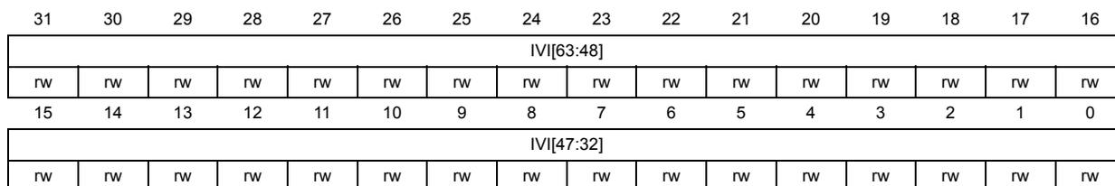
| 31 | 30 | 29 | 28 | 27 | 26 | 25 | 24 | 23 | 22 | 21 | 20 | 19 | 18 | 17 | 16 |
| IVI[63:48] | |||||||||||||||
| rw | rw | rw | rw | rw | rw | rw | rw | rw | rw | rw | rw | rw | rw | rw | rw |
| 15 | 14 | 13 | 12 | 11 | 10 | 9 | 8 | 7 | 6 | 5 | 4 | 3 | 2 | 1 | 0 |
| IVI[47:32] | |||||||||||||||
| rw | rw | rw | rw | rw | rw | rw | rw | rw | rw | rw | rw | rw | rw | rw | rw |
Bits 31:0 IVI[63:32] : Initialization vector bit x (x = 63 to 32)
This bitfield stores the initialization vector bits [63:32] for AES chaining modes other than ECB.
The value stored in CRYP_IVxR/LR registers is updated by hardware after each computation round (when applicable).
Write to this register is ignored when CRYP is busy (BUSY bit set).
49.8.20 CRYP initialization vector register 1R (CRYP_IV1RR)
Address offset: 0x4C
Reset value: 0x0000 0000
| 31 | 30 | 29 | 28 | 27 | 26 | 25 | 24 | 23 | 22 | 21 | 20 | 19 | 18 | 17 | 16 |
| IVI[31:16] | |||||||||||||||
| rw | rw | rw | rw | rw | rw | rw | rw | rw | rw | rw | rw | rw | rw | rw | rw |
| 15 | 14 | 13 | 12 | 11 | 10 | 9 | 8 | 7 | 6 | 5 | 4 | 3 | 2 | 1 | 0 |
| IVI[15:0] | |||||||||||||||
| rw | rw | rw | rw | rw | rw | rw | rw | rw | rw | rw | rw | rw | rw | rw | rw |
Bits 31:0 IVI[31:0] : Initialization vector bit x (x = 31 to 0)
This bitfield stores the initialization vector bits [31:0] for AES chaining modes other than ECB.
The value stored in CRYP_IVxR/LR registers is updated by hardware after each computation round (when applicable).
Write to this register is ignored when CRYP is busy (BUSY bit set).
49.8.21 CRYP context swap GCM-CCM registers (CRYP_CSGCMCCMxR)
Address offset: 0x50 + 0x4 * x, (x = 0 to 7)
Reset value: 0x0000 0000
| 31 | 30 | 29 | 28 | 27 | 26 | 25 | 24 | 23 | 22 | 21 | 20 | 19 | 18 | 17 | 16 |
| CSGCMCCM[31:16] | |||||||||||||||
| rw | rw | rw | rw | rw | rw | rw | rw | rw | rw | rw | rw | rw | rw | rw | rw |
| 15 | 14 | 13 | 12 | 11 | 10 | 9 | 8 | 7 | 6 | 5 | 4 | 3 | 2 | 1 | 0 |
| CSGCMCCM[15:0] | |||||||||||||||
| rw | rw | rw | rw | rw | rw | rw | rw | rw | rw | rw | rw | rw | rw | rw | rw |
Bits 31:0 CSGCMCCM[31:0] : Context swap for GCM/GMAC and CCM modes
CRYP_CSGCMCCMxR registers contain the complete internal register states of the CRYP when the GCM, GMAC or CCM processing of the current task is suspended to process a higher-priority task. Refer to Section 49.4.8: CRYP suspend and resume operations for more details.
CRYP_CSGCMCCMxR registers are not used in other chaining modes than GCM, GMAC or CCM.
49.8.22 CRYP context swap GCM registers (CRYP_CSGCMxR)
Address offset: 0x70 + 0x4 * x, (x = 0 to 7)
Reset value: 0x0000 0000
| 31 | 30 | 29 | 28 | 27 | 26 | 25 | 24 | 23 | 22 | 21 | 20 | 19 | 18 | 17 | 16 |
|---|---|---|---|---|---|---|---|---|---|---|---|---|---|---|---|
| CSGCM[31:16] | |||||||||||||||
| rw | rw | rw | rw | rw | rw | rw | rw | rw | rw | rw | rw | rw | rw | rw | rw |
| 15 | 14 | 13 | 12 | 11 | 10 | 9 | 8 | 7 | 6 | 5 | 4 | 3 | 2 | 1 | 0 |
| CSGCM[15:0] | |||||||||||||||
| rw | rw | rw | rw | rw | rw | rw | rw | rw | rw | rw | rw | rw | rw | rw | rw |
Bits 31:0 CSGCM[31:0] : Context swap for GCM/GMAC modes
CRYP_CSGCMxR registers contain the complete internal register states of the CRYP when the GCM or GMAC processing of the current task is suspended to process a higher-priority task. Refer to Section 49.4.8: CRYP suspend and resume operations for more details.
CRYP_CSGCMxR registers are not used in other chaining modes than GCM or GMAC.
49.8.23 CRYP register map
Table 428. CRYP register map and reset values
| Offset | Register name | 31 | 30 | 29 | 28 | 27 | 26 | 25 | 24 | 23 | 22 | 21 | 20 | 19 | 18 | 17 | 16 | 15 | 14 | 13 | 12 | 11 | 10 | 9 | 8 | 7 | 6 | 5 | 4 | 3 | 2 | 1 | 0 | ||||||||
|---|---|---|---|---|---|---|---|---|---|---|---|---|---|---|---|---|---|---|---|---|---|---|---|---|---|---|---|---|---|---|---|---|---|---|---|---|---|---|---|---|---|
| 0x00 | CRYP_CR | IPRST | Res. | Res. | Res. | Res. | Res. | KMOD[1:0] | Res. | Res. | NPBLB[3:0] | Res. | Res. | ALGOMODE[3] | Res. | GCM_CCMPH[1:0] | Res. | CRYPEN | FFLUSH | Res. | Res. | Res. | Res. | KEYSIZE[1:0] | Res. | DATATYPE[1:0] | Res. | ALGOMODE[2:0] | Res. | ALGODIR | Res. | Res. | |||||||||
| 0 | 0 | 0 | 0 | 0 | 0 | 0 | 0 | 0 | 0 | 0 | 0 | 0 | 0 | 0 | 0 | 0 | 0 | 0 | 0 | ||||||||||||||||||||||
| 0x04 | CRYP_SR | Res. | Res. | Res. | Res. | Res. | Res. | Res. | Res. | Res. | Res. | Res. | Res. | Res. | Res. | Res. | Res. | Res. | Res. | Res. | Res. | Res. | Res. | Res. | Res. | KEYVALID | KERF | Res. | BUSY | OFFU | OFNE | IFNF | IFEM | ||||||||
| 0 | 0 | 0 | 0 | 0 | 1 | 1 | |||||||||||||||||||||||||||||||||||
| 0x08 | CRYP_DINR | DIN[31:0] | |||||||||||||||||||||||||||||||||||||||
| 0 | 0 | 0 | 0 | 0 | 0 | 0 | 0 | 0 | 0 | 0 | 0 | 0 | 0 | 0 | 0 | 0 | 0 | 0 | 0 | 0 | 0 | 0 | 0 | 0 | 0 | 0 | 0 | 0 | 0 | 0 | 0 | ||||||||||
| 0x0C | CRYP_DOUTR | DOUT[31:0] | |||||||||||||||||||||||||||||||||||||||
| 0 | 0 | 0 | 0 | 0 | 0 | 0 | 0 | 0 | 0 | 0 | 0 | 0 | 0 | 0 | 0 | 0 | 0 | 0 | 0 | 0 | 0 | 0 | 0 | 0 | 0 | 0 | 0 | 0 | 0 | 0 | 0 | ||||||||||
| 0x10 | CRYP_DMACR | Res. | Res. | Res. | Res. | Res. | Res. | Res. | Res. | Res. | Res. | Res. | Res. | Res. | Res. | Res. | Res. | Res. | Res. | Res. | Res. | Res. | Res. | Res. | Res. | Res. | Res. | Res. | Res. | Res. | Res. | DOEN | DIEN | ||||||||
| 0 | 0 | ||||||||||||||||||||||||||||||||||||||||
| 0x14 | CRYP_IMSCR | Res. | Res. | Res. | Res. | Res. | Res. | Res. | Res. | Res. | Res. | Res. | Res. | Res. | Res. | Res. | Res. | Res. | Res. | Res. | Res. | Res. | Res. | Res. | Res. | Res. | Res. | Res. | Res. | Res. | Res. | OUTIM | INIM | ||||||||
| 0 | 0 | ||||||||||||||||||||||||||||||||||||||||
Table 428. CRYP register map and reset values (continued)
| Offset | Register name | 31 | 30 | 29 | 28 | 27 | 26 | 25 | 24 | 23 | 22 | 21 | 20 | 19 | 18 | 17 | 16 | 15 | 14 | 13 | 12 | 11 | 10 | 9 | 8 | 7 | 6 | 5 | 4 | 3 | 2 | 1 | 0 |
|---|---|---|---|---|---|---|---|---|---|---|---|---|---|---|---|---|---|---|---|---|---|---|---|---|---|---|---|---|---|---|---|---|---|
| 0x18 | CRYP_RISR | Res. | Res. | Res. | Res. | Res. | Res. | Res. | Res. | Res. | Res. | Res. | Res. | Res. | Res. | Res. | Res. | Res. | Res. | Res. | Res. | Res. | Res. | Res. | Res. | Res. | Res. | Res. | Res. | Res. | Res. | OUTRIS | INRIS |
| Reset value | 0 | 1 | |||||||||||||||||||||||||||||||
| 0x1C | CRYP_MISR | Res. | Res. | Res. | Res. | Res. | Res. | Res. | Res. | Res. | Res. | Res. | Res. | Res. | Res. | Res. | Res. | Res. | Res. | Res. | Res. | Res. | Res. | Res. | Res. | Res. | Res. | Res. | Res. | Res. | Res. | OUTMIS | INMIS |
| Reset value | 0 | 0 | |||||||||||||||||||||||||||||||
| 0x20 | CRYP_K0LR | K[255:224] | |||||||||||||||||||||||||||||||
| Reset value | 0 | 0 | 0 | 0 | 0 | 0 | 0 | 0 | 0 | 0 | 0 | 0 | 0 | 0 | 0 | 0 | 0 | 0 | 0 | 0 | 0 | 0 | 0 | 0 | 0 | 0 | 0 | 0 | 0 | 0 | 0 | 0 | |
| 0x24 | CRYP_K0RR | K[223:192] | |||||||||||||||||||||||||||||||
| Reset value | 0 | 0 | 0 | 0 | 0 | 0 | 0 | 0 | 0 | 0 | 0 | 0 | 0 | 0 | 0 | 0 | 0 | 0 | 0 | 0 | 0 | 0 | 0 | 0 | 0 | 0 | 0 | 0 | 0 | 0 | 0 | 0 | |
| ⋮ | |||||||||||||||||||||||||||||||||
| 0x38 | CRYP_K3LR | K[63:32] | |||||||||||||||||||||||||||||||
| Reset value | 0 | 0 | 0 | 0 | 0 | 0 | 0 | 0 | 0 | 0 | 0 | 0 | 0 | 0 | 0 | 0 | 0 | 0 | 0 | 0 | 0 | 0 | 0 | 0 | 0 | 0 | 0 | 0 | 0 | 0 | 0 | 0 | |
| 0x3C | CRYP_K3RR | K[31:0] | |||||||||||||||||||||||||||||||
| Reset value | 0 | 0 | 0 | 0 | 0 | 0 | 0 | 0 | 0 | 0 | 0 | 0 | 0 | 0 | 0 | 0 | 0 | 0 | 0 | 0 | 0 | 0 | 0 | 0 | 0 | 0 | 0 | 0 | 0 | 0 | 0 | 0 | |
| 0x40 | CRYP_IV0LR | IVI[127:96] | |||||||||||||||||||||||||||||||
| Reset value | 0 | 0 | 0 | 0 | 0 | 0 | 0 | 0 | 0 | 0 | 0 | 0 | 0 | 0 | 0 | 0 | 0 | 0 | 0 | 0 | 0 | 0 | 0 | 0 | 0 | 0 | 0 | 0 | 0 | 0 | 0 | 0 | |
| 0x44 | CRYP_IV0RR | IVI[95:64] | |||||||||||||||||||||||||||||||
| Reset value | 0 | 0 | 0 | 0 | 0 | 0 | 0 | 0 | 0 | 0 | 0 | 0 | 0 | 0 | 0 | 0 | 0 | 0 | 0 | 0 | 0 | 0 | 0 | 0 | 0 | 0 | 0 | 0 | 0 | 0 | 0 | 0 | |
| 0x48 | CRYP_IV1LR | IVI[63:32] | |||||||||||||||||||||||||||||||
| Reset value | 0 | 0 | 0 | 0 | 0 | 0 | 0 | 0 | 0 | 0 | 0 | 0 | 0 | 0 | 0 | 0 | 0 | 0 | 0 | 0 | 0 | 0 | 0 | 0 | 0 | 0 | 0 | 0 | 0 | 0 | 0 | 0 | |
| 0x4C | CRYP_IV1RR | IVI[31:0] | |||||||||||||||||||||||||||||||
| Reset value | 0 | 0 | 0 | 0 | 0 | 0 | 0 | 0 | 0 | 0 | 0 | 0 | 0 | 0 | 0 | 0 | 0 | 0 | 0 | 0 | 0 | 0 | 0 | 0 | 0 | 0 | 0 | 0 | 0 | 0 | 0 | 0 | |
| 0x50 + x*0x4, (x = 0 to 7), last address 0x6C | CRYP_CSGCMCCMxR | CSGCMCCMx[31:0] | |||||||||||||||||||||||||||||||
| Reset value | 0 | 0 | 0 | 0 | 0 | 0 | 0 | 0 | 0 | 0 | 0 | 0 | 0 | 0 | 0 | 0 | 0 | 0 | 0 | 0 | 0 | 0 | 0 | 0 | 0 | 0 | 0 | 0 | 0 | 0 | 0 | 0 | |
| 0x70 + x*0x4, (x = 0 to 7), last address 0x8C | CRYP_CSGCMxR | CSGCMx[31:0] | |||||||||||||||||||||||||||||||
| Reset value | 0 | 0 | 0 | 0 | 0 | 0 | 0 | 0 | 0 | 0 | 0 | 0 | 0 | 0 | 0 | 0 | 0 | 0 | 0 | 0 | 0 | 0 | 0 | 0 | 0 | 0 | 0 | 0 | 0 | 0 | 0 | 0 | |
Refer to Section 2.3: Memory organization for the register boundary addresses.