43. LCD-TFT display controller (LTDC)
43.1 LTDC introduction
The LTDC (liquid crystal display - thin film transistor) display controller provides a parallel digital RGB (Red, Green, Blue) and signals for horizontal, vertical synchronization, pixel clock and data enable as output to interface directly to a variety of LCD-TFT panels.
43.2 LTDC main features
- • 2 input layers blended together to compose the display
- • Cropping of layers from any input size and location
- • Multiple input pixel formats:
- – Predefined ARGB formats: ARGB8888, ABGR8888, RGBA8888, BGRA8888, RGB565, BGR565, and RGB888packed
- – Flexible ARGB, allowing any width and location for A,R,G, and B components
- – Predefined YUV formats: YUV422-1L (FourCC: YUYV, Interleaved), YUV420-2L (FourCC: NV12, semi planar), YUV420-3L (FourCC: Yxx I420, full planar) with some flexibility on the component sequence
- • Color look-up table (CLUT) up to 256 colors (256 x 24 bits) per layer
- • Color transparency keying
- • Composition with flexible window position and size versus output display
- • Blending with flexible layer order and alpha value (per pixel or constant)
- • Background underlying color
- • Gamma with non-linear configurable table
- • Dithering for output with less bits per component (pseudo-random on 2 bits)
- • Polarity inversion for HSync, VSync, and DataEnable outputs
- • Output as RGB888 24 bpp or YUV422 16 bpp
- • Secure layer (using layer2) capability, with grouped regs and additional interrupt set
- • Interrupts based on 7 different events
- • AXI master interface with long efficient bursts (64 or 128 bytes)
Note: The above mentioned FourCC pixel formats are described at www.fourcc.org .
43.3 LTDC functional description
43.3.1 LTDC block diagram
Figure 444. LTDC block diagram
![Figure 444. LTDC block diagram. The diagram shows the internal architecture of the LTDC. On the left, a 64-bit AXI bus connects to two AXI read blocks, which are followed by FIFOs. These lead into two parallel pixel pipes, 'Pixel pipe layer 1' and 'Pixel pipe layer 2'. Each pipe consists of 'Input and crop', 'Pixel format', 'YUV planar', 'YUV to RGB', 'CLUT', and 'Trans. keying' blocks. The outputs of these pipes are combined in a 'Window crop and Fore and alpha blend' block, which also receives a 'Background color'. The combined signal then passes through 'Gam-ma', 'RGB to YUV 422', 'Dither', and 'OUT SYNC and POL' blocks. The 'OUT SYNC and POL' block generates LCD signals: LCD_R[7:0], LCD_G[7:0], and LCD_B[7:0]. Below the pixel pipes is a 'Config and status registers APB slave' block connected to a 32-bit APB bus. This block is controlled by signals like ltde_pclk, ltde_lo_it, ltde_lo_err_it, ltde_up_it, ltde_up_err_it, ltde_lo_li, and ltde_up_li. To the right of the output pipe is a 'CRC HASH' block and an 'Output timing generator' which produces LCD_CLK, LCD_VSYNC, LCD_HSYNC, and LCD_DE signals. The diagram is labeled MSV71164V2 at the bottom right.](/RM0486-STM32N6x5-x7/e9660cb42bf9e65f69228142eea04d4b_img.jpg)
43.3.2 LTDC pins and internal signals
Table 380. LTDC pins
| Pin name | Pin type | Description |
|---|---|---|
| LCD_CLK | Output | Clock output |
| LCD_HSYNC | Horizontal synchronization | |
| LCD_VSYNC | Vertical synchronization | |
| LCD_DE | Not data enable | |
| LCD_R[7:0] | 8-bit Red data (or U/V component, if output is YUV422) | |
| LCD_G[7:0] | 8-bit Green data (or Y component if output is YUV422) | |
| LCD_B[7:0] | 8-bit Blue data |
The LTDC pins must be configured by the user application. The unused pins can be used for other purposes.
Using less pins than the default 24 bpp
The LTDC outputs the pixels on 24 pins by default (RGB888). The user can however connect the display panel using less wires, for instance 16 wires (if RGB565) or 18 wires (RGB666). If so, R (resp. G, B) wires must be connected to the MSB of the LTDC R (resp. G, B) output pins (see Section 43.3.2 ).
Example: LTDC interfacing with a RGB565 16-bit display panel. Display panel R[4:0], G[5:0] and B[4:0] wires and input pins must be connected to LTDC_R[7:3], LCD_G[7:2], and LCD_B[7:3] output pins.
The following table shows how the LTDC is connected.
Table 381. LTDC trigger interconnections
| Trigger name | Direction | Trigger source/destination |
|---|---|---|
| ltdc_lo_li | Output | hpdma1_trigsel[20] gpdma1_trigsel[20] |
| ltdc_up_li | Output | hpdma1_trigsel[110] gpdma1_trigsel[110] |
43.3.3 LTDC reset and clocks
The LTDC uses the following clock domains:
- •
AXI clock domain
This domain contains the LTDC AXI master interface for data transfer from the memories to the layer FIFO and the frame buffer configuration register. - •
APB clock domain
This domain contains the global configuration registers and the interrupt register. - •
Pixel clock domain
This domain contains the pixel data generation, the layer configuration register as well as the LTDC interface signal generator. The LCD_CLK output must be configured following the panel requirements.
Note: For normal operation, all clocks must be provided to allow clock domain crossing for read and write operations.
The following table lists the clock domains used to store the register values.
Table 382. Clock domain for each register
| LTDC register | Clock domain |
|---|---|
| LTDC_SSCR | Pixel clock |
| LTDC_BPCR | AXI + pixel clock |
| LTDC_AWCR | |
| LTDC_TWCR | |
| LTDC_GCR | APB clock |
| LTDC_SRCR | Pixel clock |
| LTDC_GCCR | |
| LTDC_BCCR | APB clock |
| LTDC_IER | |
| LTDC_ISR | |
| LTDC_ICR |
Table 382. Clock domain for each register (continued)
| LTDC register | Clock domain |
|---|---|
| LTDC_LIPCR | Pixel clock |
| LTDC_CPSR | |
| LTDC_CDSR | |
| LTDC_EDCR | |
| LTDC_IER2 | APB clock |
| LTDC_ISR2 | |
| LTDC_ICR2 | |
| LTDC_LIPCR2 | Pixel clock |
| LTDC_ECRCR | |
| LTDC_CRCR | |
| LTDC_FUTR | Pixel clock |
| LTDC_LxC0R | APB clock |
| LTDC_LxC1R | |
| LTDC_LxRCR | |
| LTDC_LxC R | AXI + pixel clock |
| LTDC_LxWHP CR | Pixel clock |
| LTDC_LxWVPC R | |
| LTDC_LxC KCR | |
| LTDC_LxPFC R | |
| LTDC_LxCAC R | |
| LTDC_LxDCCR | |
| LTDC_LxBFC R | |
| LTDC_LxBLC R | AXI clock |
| LTDC_LxPC R | AXI + pixel clock |
| LTDC_LxC FBAR | |
| LTDC_LxC FBLR | |
| LTDC_LxC FBLNR | |
| LTDC_L1AFBA0R | |
| LTDC_L1AFBA1R | |
| LTDC_L1AFBLR | |
| LTDC_L1AFBLNR |
Table 382. Clock domain for each register (continued)
| LTDC register | Clock domain |
|---|---|
| LTDC_LxCLUTWR | Pixel clock |
| LTDC_LxCYR0R | |
| LTDC_LxCYR1R | |
| LTDC_LxFPF0R | |
| LTDC_LxFPR1R |
While accessing LTDC registers, the APB bus is stalled during the access for a given time period detailed in the following table.
Table 383. LTDC register access and updated durations
| Access type | AXI register clock domain | APB register clock domain | Pixel register clock domain |
|---|---|---|---|
| Read | 7 x ltdc_pclk + 5 x ltdc_aclk | 7 x ltdc_pclk | 7 x ltdc_pclk + 5 x ltdc_ker_clk |
| Write | 6 x ltdc_pclk + 5 x ltdc_aclk | 6 x ltdc_pclk | 6 x ltdc_pclk + 5 x ltdc_ker_clk |
The LTDC can be reset by setting the corresponding bit in the RCC, that resets the three clock domains.
43.4 LTDC configuration parameters
The LTDC configuration parameters are sequenced following the pixel flow as shown in Figure 444 , starting at the input (AXI master that reads pixels) and ending at the pixel output.
Common controls (such as interrupts) are listed at the end.
43.4.1 AXI master
The AXI master busses perform the accesses to the memory and are driven by the internal logic. The LTDC internal per-layer FIFOs are fairly large to cope with reasonably long external memory latencies.
The LTDC generates long burst (128-byte) for higher external memory efficiency. For more granularity, it is possible to decrease the max burst size to 64 bytes, but it is not recommended.
Parameter in LTDC_LxBLCR
BL: burst length, in 64-bit words, with a default 0 for max size
Default configuration
The default AXI burst length is set at its maximum value after reset, with BL = 0.
43.4.2 Input layer definition and cropping
The LTDC supports two layers. Each layer is defined by:
- • Its base-address in the memory
If the buffer is YUV semi-planar or full-planar, there are respectively two and three base-addresses. The first buffer is called main and stores the luminance data, while the other buffers are called auxiliary and store the chrominance data. - • A dimension in the memory
- – Width defined as its pitch (or address jump or stride): amount of bytes between the start of one line and the start of the next line
- – Height that does not need to be defined
- • A dimension of the pixel rectangle that is cropped and read from the memory
- – Top-left start position: set by the base-address at exactly the byte where the top-left pixel is located
- – Width, number of bytes per line to read
- - If too few bytes versus required, a FIFO underrun interrupt is generated(FUWIF).
- - If too many bytes versus required, the useless data are discarded.
- – Height, number of lines per frame to read
Note: The pitch and number of bytes per line can be different if a sub-part of a frame is cropped to be displayed. If the full frame is displayed, the pitch and number of lines are the same.
Parameters
- • LEN in LTDC_LxCR: activates this layer.
- • CFBADD in LTDC_LxCFBAR: main base address, for ARGB or Y buffer
- • CFBL in LTDC_LxCFBLR: main number of bytes per line
- • CFBP in LTDC_LxCFBLR: pitch between two consecutive lines of the main buffer
- • CFBLNBR in LTDC_LxCFBLNR: main number of lines per frame
Specifically for multi-planar layers, the following additional registers have to be configured (only required for YUV420 semi-planar and full-planar pixel formats):
- • AFBADD0 in LTDC_L1AFBA0R: auxiliary address 0, for UV if semi-planar or for V if full-planar
- • AFBADD1 in LTDC_L1AFBA1R: auxiliary address 1, for U if full-planar
- • AFBL in LTDC_L1AFBLR: auxiliary 0 and 1, number of bytes per line
- • AFBP in LTDC_L1AFBLR: pitch for the auxiliary 0 and 1 buffers
- • AFBLNBR in LTDC_L1AFBLNR: auxiliary 0 and 1 number of lines per frame
Configuration examples
- • A frame buffer having the format RGB565 (2 bytes per pixel) and a width of 256 pixels (total number of bytes per line is \( 256 * 2 = 512 \) ), where pitch = line length requires a value of 0x02000207 to be written into this register.
- • A frame buffer having the format RGB888 (3 bytes per pixel) and a width of 320 pixels (total number of bytes per line is \( 320 * 3 = 960 \) ), where pitch = line length requires a value of 0x03C003C7 to be written into this register.
- • A frame buffer having the format CbCr (2 bytes per pixel) and a width of 256 pixels (total number of bytes per line is \( 256 * 2 = 512 \) ), where pitch = line length requires a value of 0x02000207 to be written into this register.
- • A frame buffer having the format Cb (1 byte per pixel) and a width of 320 pixels (total number of bytes per line is \( 320 * 1 = 320 \) ), where pitch = line length requires a value of 0x01400147 to be written into this register.
43.4.3 Input pixel format
The LTDC reads the pixel data from memory buffers and maps it onto the internal LTDC format that is based on the definition of the input pixel format, defined per layer.
The pixel formats are grouped as follows:
- •
Predefined ARGB formats:
ARGB8888, ABGR8888, RGBA8888, BGRA8888, RGB565, BGR565, and RGB888pack - •
Flexible ARGB format:
Allows a configurable width and location of each A,R,G, and B component and is used to extend the above list to any multi-component pixel format except to coplanar ARGB. - •
YUV formats:
Used to read YUV with a 422 coplanar, 420 semi-planar, or 420 full-planar format, and to convert the YUV color into RGB.
While the layer 1 supports all YUV formats, the layer 2 only supports the 422 coplanar format.
Note: The LTDC hardware pipeline uses 8 bits per component: when reading and mapping a pixel format, with less than 8 bits per component. That component is extended to 8 bits by stuffing the LSB, that are recopied from its MSB. This applies mostly on RGB565.
For instance, a component on 5 bits (named: 43210) results in the following 8 bits mapped into the pipe: 43210432. A 3-bit input (named 210) results in 21021021.
Parameter when using the predefined ARGB formats
- • PF in LTDC_LxPFCR: 0 to 6 to select one of the seven predefined pixel formats
Parameters when using the flexible ARGB formats
- • PR in LTDC_LxPFCR: seven to activate the flexible pixel format type
- • PSIZE in LTDC_LxFPF1R: defines the amount of bytes per pixel (typically 1,2,3, or 4)
- • APOS/RPOS in LTDC_LxFPF0R: defines the Alpha/Red location inside a 32-bit word
- • BPOS/GPOS in LTDC_LxFPF1R: defines the Blue/Green location inside a 32-bit word
- • ALEN/RLEN in LTDC_LxFPF0R: defines the amount of bits for Alpha/Red components
- • BLEN/GLEN in LTDC_LxFPF1R: defines the amount of bits for Blue/Green components
An RGB565 pixel format is defined as follows:
- – Alpha: APOS = 0, ALEN = 0
- – Red: RPOS= 11, RLEN = 5
- – Green: GPOS = 5, GLEN = 6
- – Blue: BPOS = 0, BLEN = 5
The BGRA8888 32 bpp pixel format is set as follows (default reset values of LTDC_LxFPF0R and LTDC_LxFPF1R):
- – Alpha: APOS = 0, ALEN = 8
- – Red: RPOS= 8, RLEN = 8
- – Green: GPOS = 16, GLEN = 8
- – Blue: BPOS = 24, BLEN = 8
Parameters when using the YUV formats
The YUV pixel format is defined and detailed in Section 43.4.4: YUV planar and supersedes any setting here.
The following table describes the memory mapping of the predefined ARGB pixel format.
Table 384. Pixel data mapping versus color format
| ARGB8888 (PF = 000) | |||
|---|---|---|---|
| @+3 A x [7:0] | @+2 R x [7:0] | @+1 G x [7:0] | @ B x [7:0] |
| @+7 A x+1 [7:0] | @+6 R x+1 [7:0] | @+5 G x+1 [7:0] | @+4 B x+1 [7:0] |
| ABGR8888 (PF = 001) | |||
| @+3 A x [7:0] | @+2 B x [7:0] | @+1 G x [7:0] | @ R x [7:0] |
| @+7 A x+1 [7:0] | @+6 B x+1 [7:0] | @+5 G x+1 [7:0] | @+4 R x+1 [7:0] |
| RGBA8888 (PF = 010) | |||
| @+3 R x [7:0] | @+2 G x [7:0] | @+1 B x [7:0] | @ A x [7:0] |
| @+7 R x+1 [7:0] | @+6 G x+1 [7:0] | @+5 B x+1 [7:0] | @+4 A x+1 [7:0] |
| BGRA8888 (PF = 011) | |||
| @+3 B x [7:0] | @+2 G x [7:0] | @+1 R x [7:0] | @ A x [7:0] |
| @+7 B x+1 [7:0] | @+6 G x+1 [7:0] | @+5 R x+1 [7:0] | @+4 A x+1 [7:0] |
| RGB565 (PF = 100) | |||
| @+3 R x+1 [4:0] G x+1 [5:3] | @+2 G x+1 [2:0] B x+1 [4:0] | @+1 R x [4:0] G x [5:3] | @ G x [2:0] B x [4:0] |
| @+7 R x+3 [4:0] G x+3 [5:3] | @+6 G x+3 [2:0] B x+3 [4:0] | @+5 R x+2 [4:0] G x+2 [5:3] | @+4 G x+2 [2:0] B x+2 [4:0] |
| BGR565 (PF = 101) | |||
| @+3 B x+1 [4:0] G x+1 [5:3] | @+2 G x+1 [2:0] R x+1 [4:0] | @+1 B x [4:0] G x [5:3] | @ G x [2:0] R x [4:0] |
| @+7 B x+3 [4:0] G x+3 [5:3] | @+6 G x+3 [2:0] R x+3 [4:0] | @+5 B x+2 [4:0] G x+2 [5:3] | @+4 G x+2 [2:0] R x+2 [4:0] |
| RGB888 (PF = 110) | |||
| @+3 B x+1 [7:0] | @+2 R x [7:0] | @+1 G x [7:0] | @ B x [7:0] |
| @+7 G x+2 [7:0] | @+6 B x+2 [7:0] | @+5 R x+1 [7:0] | @+4 G x+1 [7:0] |
| The flexible format (PF = 111), not represented here, allows any above mapping. | |||
43.4.4 YUV planar
This operator handles the YUV planar formats, reading data from potentially several distinct buffers (Y versus Cb versus Cr) into a single pixel information. The feature is available for layer 1 and layer 2 (coplanar only for the layer 2).
The LTDC supports the following planar formats:
- • YUV422 coplanar (one buffer)
- • YUV420 semi-planar (two buffers)
- • YUV420 full-planar (three buffers)
Following its configuration, the LTDC reads the relevant luminance and chrominance buffers, upscaling the chrominance components required to reach YUV444 pixels, and converts the color from YUV to RGB as described in Section 43.4.5 .
The LTDC allows swapping the memory locations of the Y and Cb/Cr data and of the Cb and Cr data. It also allows inverting the endianness of the Y data. This extends the amount of supported pixel format variants.
Parameters
Pixel format parameters are stored in LTDC_LxPCR:
- • YCEN: activates the YUV mode (both the planar extraction and color conversion).
- • YCM: selects the input scheme (422 for coplanar, 420 for semi-planar, 420 for full-planar).
- • YF: defines if either Y or Cb/Cr is provided first (from LSB).
- • CBF: defines if either Cb or Cr is provided first (from LSB).
- • OF: defines if either odd or even Y is provided first (from LSB).
When using a semi-planar or full-planar buffer, some additional base-address must be configured for auxiliary (chrominance) buffers, as well as the pitch of these buffers (see Section 43.4.2 ).
Configuration examples
Settings of OF, CBF, YF bits for a YCbCr 422 pixel format:
- • OF = 0, CBF = 0, YF = 0 define the buffer word to contain Word[31:0] = Y1-Cb-Y0-Cr.
- • OF = 1, CBF = 0, YF = 0 define the buffer word to contain Word[31:0] = Y0-Cb-Y1-Cr.
- • OF = 0, CBF = 1, YF = 0 define the buffer word to contain Word[31:0] = Y0-Cr-Y1-Cb.
- • OF = 0, CBF = 0, YF = 1 define the buffer word to contain Word[31:0] = Cb-Y1-Cr-Y0.
- • OF = 1, CBF = 1, YF = 1 define the buffer word to contain Word[31:0] = Cr-Y0-Cb-Y1.
- These settings are also valid for YCbCr 420 pixel formats.
43.4.5 YUV-to-RGB color conversion
This operator handles the YUV-to-RGB color conversion of the YUV planar pixels. The color conversion is activated automatically, simultaneously with the YUV planar handling.
The color conversion is based on a semi-flexible 3x3 matrix multiplication:
- • It is restricted to YUV-to-RGB conversion due to some frozen coefficients (see next).
- • It handles the most used YUV references (ITU-R BT.601 and ITU-R BT.709) thanks to some configurable coefficients.
- • It supports the full versus reduced dynamic of the input pixel (luminance defined either in 0 to 255, or in 16 to 235), by extending a potential reduced-range input to a full range.
Parameters
- • YCEN in LTDC_LxPCR: activates the color conversion, same bit as for planar.
- • YREN in LTDC_LxPCR: if active, extends a reduced range to a full range.
- • CR2R in LTDC_LxCYR0R: matrix coefficient from Cr to Red
- • CB2B in LTDC_LxCYR0R: matrix coefficient from Cb to Blue
- • CR2G in LTDC_LxCYR0R: matrix coefficient from Cr to Green
- • CB2G in LTDC_LxCYR0R: matrix coefficient from Cb to Green
The full matrix computation, to convert from YCbCr to RGB, is defined as the following:
The CR2R, CB2B, CR2G, and CB2G coefficients are defined on 10 bits unsigned: as the operator works with 8-bit components, the coefficients are thus equivalent, in fixed-point, to 2-bit integer and 8-bit decimals.
The CR2G and CB2G coefficients are configured as unsigned positive, but are set negative in the hardware computation, as shown in the above matrix where a “-” is mentioned.
When the luminance scaling is active (YREN = 1, thus where the YCbCr input is assumed in the range of 16 to 235/240, and RGB in 0 to 255), then the Y input value is first scaled in hardware to \( Y' = 255/219 * (Y - 16) \) . That first result is then inserted as input to the above matrix multiplication.
Configuration examples
To read an ITU-R BT.601 layer and to convert its YCbCr (assuming a default reduced dynamic in 16 to 235/240) to RGB (with full dynamic in 0 to 255), the recommended coefficients are:
- • YCEN = 1: to activate the conversion
- • YREN = 1: to select the reduced dynamic range
- • CR2R = 409: specific coefficient set for ITU-R BT.601
- • CR2G = 208
- • CB2G = 100
- • CB2B = 516
To read an ITU-R BT.709 layer and to convert its YCbCr (assuming a default reduced dynamic in 16 to 235/240) to RGB (with full dynamic in 0 to 255), the recommended values to configure coefficients are:
- • YCEN = 1: to activate the conversion
- • YREN = 1: to select the reduced dynamic range
- • CR2R = 459: specific following coefficient set is for ITU-R BT.709
- • CR2G = 136
- • CB2G = 55
- • CB2B = 541
43.4.6 Horizontal or vertical mirroring
The LTDC can mirror horizontally or vertically its input layers, thus to read them from right to left, and/or from bottom to top.
It applies on both coplanar (ARGB, YUV422) and multi-planar (YUV420) pixel formats.
Parameters for horizontal mirroring
To mirror a layer horizontally, the LTDC must be configured to extract the pixels from right to left (backward), and to set the layer base-address at the right-end of the line.
The configuration bitfields are the following:
- • HMEN in LTDC_LxCR: activates the horizontal mirroring.
- • CFBADD in LTDC_LxCFBAR: base + (width - 1) (increase for horizontal mirror)
- • AFBADD0 in LTDC_L1AFBA0R: base + (width - 1)
- • AFBADD1 in LTDC_L1AFBA1R: base + (width - 1)
Parameters for vertical mirroring
To mirror a layer vertically, the LTDC must be configured to start reading this layer from the bottom, and line per line, to come upward. The layer base-address must be set to the start of the bottom line, and a negative line-per-line pitch must be provided.
The configuration bitfields for the base-address are (all to be set at bottom line start):
- • CFBADD in LTDC_LxCFBAR: main base-address
- • AFBADD0 in LTDC_L1AFBA0R: auxiliary address 0
- • AFBADD1 in LTDC_L1AFBA1R: auxiliary address 1
- • CFBADD in LTDC_LxCFBAR: base + (lines - 1) * pitch (increase for vertical mirror)
- • AFBADD0 in LTDC_L1AFBA0R: base + (lines - 1) * pitch
- • AFBADD1 in LTDC_L1AFBA1R: base + (lines - 1) * pitch
The configuration bitfields for the pitch are (all to be set with a negative pitch):
- • CFBP in LTDC_LxCFBLR: -pitch (negative line pitch for vertical mirror)
- • AFBP in LTDC_L1AFBLR: -pitch
43.4.7 Default layer color
Every layer has a default color in the format ARGB8888, that is used outside the defined layer window or when a layer is disabled. This default color can be configured as active or absent.
Parameters
The default layer color parameters are:
- • DCBEN in LTDC_LxCR: default color activation
- • DCALPHA in LTDC_LxDCCR: default Alpha transparency setting
- • DCRED in LTDC_LxDCCR: default Red component
- • DCGREEN in LTDC_LxDCCR: default Green component
- • DCBLUE in LTDC_LxDCCR: default Blue component
Default configuration
By default, and after reset, the default layer color is inactive (DCBEN = 0 and DCALPHA = 0).
Note: The blending of a layer is always performed even when a layer is disabled. To avoid displaying the default color when a layer is disabled, the default Alpha must be set to null (DCALPHA = 0), or the whole default color must be disabled (with DCBEN).
43.4.8 Color look-up table (CLUT)
The LTDC supports frame buffers with each pixel defined as an index to a color table, allowing a display with a set of 256 colors, but stored in memory with only 8 bpp.
The CLUT defines 256 colors and must be indexed with a maximum 8-bit pixel format (typically L8 or AL44). Such format can be extracted using the flexible RGB approach described in Section 43.4.3 .
The CLUT table is differentiated for each layer. It must be initialized with one RGB888 value per color index, with the color index corresponding to the CLUT address:
- • For L8, the CLUT must be loaded with 256 colors.
- • For AL44, the CLUT must be only loaded with 16 colors. Each color address is defined by replicating the 4-bit L channel to 8 bits as follows:
- – Color L4 = 0: looks out its RGB888 from index = 0x00.
- – Color L4 = 1: looks out its RGB888 from index = 0x11.
- – Color L4 = 2: looks out its RGB888 from index = 0x22.
- – ...
- – Color L4 = 15: looks out its RGB888 from index = 0xFF.
- • For ARGB, the Blue component is used as the CLUT index.
Parameters
The RGB888 values and color indices are configured through the following bitfields in LTDC_LxCLUTWR:
- • CLUTADD defines the color index to update.
- • RED defines the 8-bit Red component of that color index.
- • GREEN defines the 8-bit Green component of that color index.
- • BLUE defines the 8-bit Blue component of that color index.
43.4.9 Transparency color keying
Pixels can be defined as transparent using a color key. If the pixel RGB components equals the defined RGB color key, that pixel is considered transparent and its Alpha channel is forced null.
A pixel forced to transparent is transparent when proceeding to the later blending phase, and shows the pixel of the underlying layer.
The color key is defined as an RGB888 value, that is compared with the flowing pixel after some processing in the input format operator (where LSBs are stuffed by replication) and CLUT processing. The constant color keying parameters must take these previous processing into account.
Parameters
The color keying parameters are the following:
- • CKEN in LTDC_LxCR enables the color keying.
- • CKRED in LTDC_LxCKCR defines the 8-bit Red color key.
- • CKGREEN in LTDC_LxCKCR defines the 8-bit Green color key.
- • CKBLUE in LTDC_LxCKCR defines the 8-bit Blue color key.
Configuration example
A mid-yellow color (50 % Red + 50 % Green) is used as the transparent color key. The color keying parameters take it into account as follows:
- • ARGB8888 input: The mid-yellow input is 0x808000. Set LTDC_LxCKCR = 0x808000.
- • RGB565 input: The mid-yellow input is 0x8400. Set LTDC_LxCKCR = 0x848200 (due to the replication of input MSB onto the missing LSB).
- • CLUT input for L8, AL88 or AL44: Set one of the palette entry to the mid-yellow color 0x808000 and set LTDC_LxCKCR = 0x808000.
43.4.10 Display composition - windowing
When performing the display composition, every layer can be cropped and positioned into the active display area. The window position and size are configured by defining its top-left and bottom-right corners.
Note: The locations are defined versus the internal timing generator that must take into account the potential synchronization header, the back porch size and the chosen active pixel area (as shown in Figure 445).
The mapping between the input layer and the visible window is performed as follows:
- • The most top-left pixels of the input layer are mapped to the top-left of the visible window of this layer.
- • If the visible window is smaller (less wide, less high) than the input layer, then the exceeding input pixels are automatically discarded from the pipe.
Parameters:
The following parameters are defined versus the top-left of the synchronization:
- • WHSTPOS in LTDC_LxWHPER: first (left) visible pixel of the layer
- • WHSPPPOS in LTDC_LxWHPER: last (right) visible pixel of the layer
- • WVSTPOS in LTDC_LxWVPER: first (top) visible line of the layer
- • WVSPPOS in LTDC_LxWVPER: last (bottom) visible line of the layer
Figure 445. Layer window programmable parameters
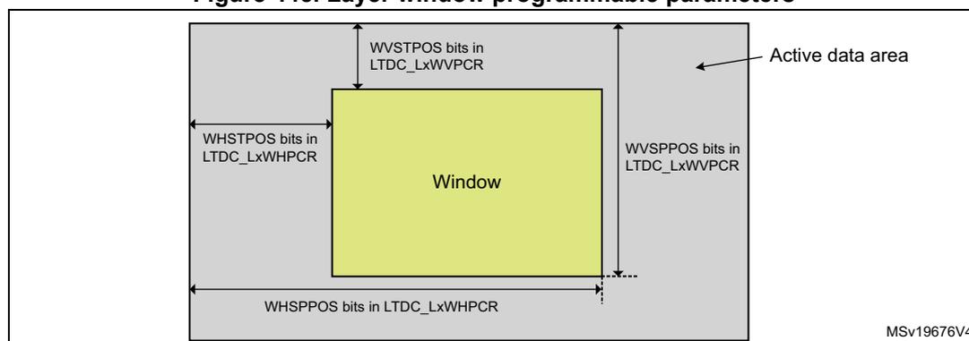
Configuration examples
- • LTDC_BPCR is configured to 0x000E0005 (AHBP[11:0] is 0xE), and LTDC_AWCR is configured to 0x028E01E5 (AAW[11:0] is 0x28E). To configure the horizontal position of a window size of 630x460, with horizontal start offset of 5 pixels in the active data area:
- – Layer window first pixel: WHSTPOS[11:0] must be programmed to 0x14 (0xE + 1 + 0x5).
- – Layer window last pixel: WHSPPPOS[11:0] must be programmed to 0x28A.
- • LTDC_BPCR is configured to 0x000E0005 (AVBP[11:0] is 0x5) and LTDC_AWCR is configured to 0x028E01E5 (AAH[11:0] is 0x1E5). To configure the vertical position of a window size of 630x460, with vertical start offset of eight lines in the active data area:
- – Layer window, first line: WVSTPOS[11:0] must be programmed to 0xE (0x5 + 1 + 0x8).
- – Layer window last line: WVSPPOS[11:0] must be programmed to 0x1DA.
43.4.11 Display composition - blending
The Alpha blending stage is used to blend together the 2 input layers, on top of a background color.
It is possible to select the sequence of the layers (foreground, middle, and background), to apply a global multiplicative Alpha per-layer, and to define an underlying background color.
The blending computation is performed from back to front, sequentially, as shown the following figure.
Figure 446. Blending two layers
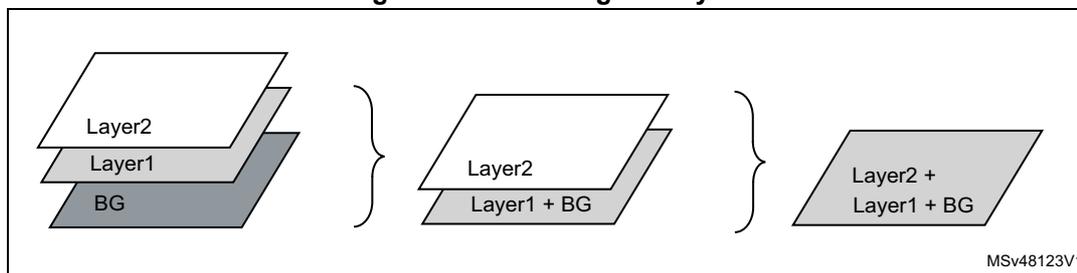
The general formula for a 2-to-1 blending is \( CR = (BF1 \times C1) + (BF2 \times C2) \) where:
- • CR: resulting blended color
- • BF1: blending-factor of current layer
- • C1: layer-color of the current layer
- • BF2: blend-factor of underlying pixels
- • C2: layer-color of the underlying pixels
Both blending factor, BF1 and BF2, can be defined as one of the following:
- • Pure per-pixel Alpha value
- • Mix of per-pixel Alpha and a global per-layer Alpha (the mix is multiplicative)
Parameters
- • CONSTA in LTDC_LxCACR: global multiplicative Alpha value of the current layer
- • BOR in LTDC_LxBFCR: blending order of the current layer
- • BF1 in LTDC_LxBFCR: blending factor for the current layer
- • BF2 in LTDC_LxBFCR: blending factor for the underlying layer
The background color is defined by the following bitfields in LTDC_BCCR:
- • BCRED: background Red component
- • BCGREEN: background Green component
- • BCBLUE: background Blue component
Note: For secure purposes, in case of an inconsistent configuration, the blending order falls back to a fixed order, with the layer 2 on the foreground, and layer 1 in background, followed by the underlying background color.
The inconsistent fallback is setup to protect a potential secure layer. If a secure software configures the secure layer2 to be on the foreground, and a malware tries to place that another layer on the foreground, the inconsistency is detected, and the secure layer is automatically forced on the foreground, guaranteeing that it is visible.
Configuration example
Only layer 1 is enabled, BF1 configured to constant alpha. BF2 configured to 1 - constant alpha. The constant alpha programmed in LTDC_LxCACR is 240 (0xF0). Thus, the constant alpha value is \( 240 / 255 = 0.94 \) . C: current layer color is 128. Cs: background color is 48. Layer 1 is blended with the background color.
\( BC = \text{constant alpha} \times C + (1 - \text{constant alpha}) \times Cs = 0.94 \times 128 + (1 - 0.94) \times 48 = 123 \) .
Default configuration
All active layers can be made visible and blended by keeping the following configuration values after reset:
- • CONSTA: keep as reset CONSTA = 255.
- • BOR: keep as reset BOR (layer) = LayerID-1.
- • BF1: keep as reset BF1 = 6 for default mixed Alpha.
- • BF12: keep as reset BF2 = 7 for default mixed 1-Alpha.
- • Background color: keep as reset (black), although any color is ok.
43.4.12 Gamma correction
The gamma correction is a non-linear operator that adapts the pixel to the non-linear display, using a compensating pre-distortion. The R, G, B components can be independently adapted, using a configurable non-linear transformation.
The non-linear transformation is implemented in the LTDC as eight independent linearly-interpolated segments: the desired non-linear transformation must thus be mapped onto the eight segments, and the shape of the eight segments configured in LTDC registers.
Parameters
- • GAMEN in LTDC_GCR: activation of the gamma operator
- • ADDR in LTDC_GCCR: table configuration, index (among 256) to write-in
- • COMP in LTDC_GCCR: table configuration, 8-bit component to write-in
- • REN in LTDC_GCCR: table configuration, active to write into the Red table
- • GEN in LTDC_GCCR: table configuration, active to write into the Green table
- • BEN in LTDC_GCCR: table configuration, active to write into the Blue table
Note: As the gamma correction works with eight interpolated segments. The only table indices to write-in are located at index: 0, 32, 64, 96, ..., 224, 255. The value to provide for index 255 contains the value for the pseudo-index 256.
Example configuration
The gamma correction is recommended to be set to pre-compensate the pixels with a gamma exponent of 2.2: Red, Green, and Blue components are compensated the same way by the Gamma. The configuration of Red, Green, and Blue tables is then usually the same.
Default configuration
The gamma correction is disabled with the default configuration after reset, with GAMEN = 0.
43.4.13 YUV output conversion
The default RGB888 24 bpp output can be converted to a YUV422 16 bpp output (coplanar), in order to reduce the bitrate or the interface width, if necessary.
The operator can convert the RGB to YUV with either ITU-R BT.601 versus BT.709 reference, and filter down the chrominance, to output the pixels as a YUV422 interface.
When the conversion is enabled, the Y is output on the LCD_G (green bits) and the Cb/Cr are output on the LCD_R (red bits).
Parameters in LTDC_EDCR
- • OCYEN: activates the output conversion to YUV422.
- • OCSEL: selects between a color conversion to ITU-R BT.601 versus to BT.709.
- • OCYCO: defines whether Cb or Cr is output first.
The configuration must follow what is expected by the external display panel.
Default configuration
The YUV output conversion is disabled with the default configuration after reset, with OCYEN = 0, allowing a default RGB888 to be output.
43.4.14 Dithering
The dithering operator allows a clean conversion of the RGB888 output into a reduced pixel format, like RGB565 or RGB666, and so avoiding the usual artifact of flat area that occurs when no dithering is available.
The dithering is based on a LFSR (polynomial generating random) and adds pseudo-random noise on the LSB of each of the displayed component (bit 2 in case of an RGB666), and makes that the average of the local pixels represents the information content of the full 8-component value.
Once the LTDC is enabled, the LFSR starts running with the first active pixel and it is kept running even during blanking periods and when dithering is switched off. If the LTDC is disabled, the LFSR is reset.
Parameters in LTDC_GCR
- • DEN: dithering enable
- • DRW: bit-id of LSB of the displayed Red component (among 8 bits)
- • DGW: bit-id of LSB of the displayed Green component (among 8 bits)
- • DBW: bit-id of LSB of the displayed Blue component (among 8 bits)
Example
To dither from RGB888 to RGB565 (assuming a RGB565 display panel):
- • The LTDC outputs the Red component on pins LCD_R[7:0].
- • The display panel probes the five MSB bits LCD_R[7:3].
- • The red bit to dither, using its two following LSB as decimals, is the bit 3.
- • DRW must be configured to 3.
- • DGW = 2 and DBW = 3.
Similarly, a dithering to RGB666 requires DRW = DGW = DBW = 2.
Default configuration
The dithering is disabled with the default configuration after reset, with DEN = 0, allowing a default RGB888 to be output.
43.4.15 CRC hashing
The CRC operator allows a 16-bit signature to be extracted for each frame, by hashing the R,G,B components of all the frame pixels.
The computed CRC can be read in LTDC_CRCR.
An expected CRC value can be configured: if the computed CRC does not match the expected CRC, the CRC interrupt is triggered. It allows a system test, letting the LTDC run for hours, and be warned only if a failed frame occurs.
Parameters
- • CRCEN in LTDC_GCR: activates the CRC computation
- • ECRC in LTDC_ECRCR: expected 16-bit CRC value
- • CCRC in LTDC_CRCR: computed 16-bit CRC value
Default configuration
The CRC hashing is disabled with the default configuration after reset, with CRCEN = 0.
43.4.16 Display timing
This section describes the configuration of the display timings, so that the LTDC matches what is expected by the external display panel.
The configuration defines the horizontal and vertical duration of each of the following items:
- • Synchronization period (HSYNC and VSYNC)
- • Back porch (HBP, VBP)
- • Active display (pixels that are visible on the screen)
- • Front porch (HFP, VFP)
These timings are described in the following figure.
Figure 447. LTDC synchronous timings
The diagram illustrates the timing parameters for an LCD-TFT display controller (LTDC). It shows a rectangular frame representing the total display area. The horizontal dimensions are labeled as 'Total width' (the full width of the frame) and 'Active width' (the width of the active display area). The vertical dimensions are labeled as 'Total height' (the full height of the frame) and 'Active height' (the height of the active display area). The active display area is shown as a shaded rectangle within the frame, containing 'Data1, Line1' at the top-left and 'Data(n), Line(n)' at the bottom-right. The horizontal synchronization parameters are: 'HSYNC width' (the duration of the horizontal sync signal), 'HBP' (horizontal back porch, the time from the start of HSYNC to the start of active data), and 'HFP' (horizontal front porch, the time from the end of active data to the start of the next HSYNC). The vertical synchronization parameters are: 'VSYNC width' (the duration of the vertical sync signal), 'VBP' (vertical back porch, the time from the start of VSYNC to the start of active data), and 'VFP' (vertical front porch, the time from the end of active data to the start of the next VSYNC). A note at the bottom states: 'Note: HBP and HFP are respectively the horizontal back porch and front porch period. VBP and VFP are respectively the vertical back porch and front porch period.' The diagram is labeled 'MSv19674V2' in the bottom right corner.
As a result of these timings, the LTDC samples in pixels during the active display duration, and generates the output synchronization signals (HSYNC, VSYNC), the pixel data, and the data-enable signal.
Parameters
All the timings configured next are absolute timings, computed from the display start position, and not the relative increment (or width or height) of each area.
All these bitfields indicate the last pixel of each area, and hence are subtracted 1.
- •
HSYNC and VSYNC width
(horizontal and vertical synchronization width) in LTDC_SSCR:
- – \( HSW = HSYNC\ width - 1 \)
- – \( VSW = VSYNC\ width - 1 \)
- •
HBP and VBP
(last pixel/line of the horizontal and vertical synchronization back porch) in LTDC_BPCR:
- – \( AHBP = HSYNC\ width + HBP - 1 \)
- – \( AVBP = VSYNC\ width + VBP - 1 \)
- •
Active width and active height
(last pixel/line of the active display area) in LTDC_AWCR:
- – \( AAW = HSYNC\ width + HBP + active\ width - 1 \)
- – \( AAH = VSYNC\ width + VBP + active\ height - 1 \)
- •
Total display width
(last pixel/line of the total display timings) in LTDC_TWCR:
- – TOTALW = HSYNC width + HBP + active width + HFP - 1
- – TOTALH = VSYNC height + VBP + active height + VFP - 1
Note: When the LTDC is enabled, timings generated start at the position (X, Y) = (0, 0), and generate immediately the first horizontal synchronization pixel in the vertical synchronization, followed by the back porch, then the active display area, and finally the front porch.
When the LTDC is disabled, the timing generator block is reset to X = total width - 1, Y = total height - 1. It holds the last pixel before the vertical synchronization phase and the FIFO are flushed. Therefore, only blanking data is output continuously.
Example of synchronous timing configuration
Assume the following display panel timings (to be extracted from panel datasheet):
- • Horizontal and vertical synchronization width: 0xA pixels, 0x2 lines
- • Horizontal and vertical back porch: 0x14 pixels, 0x2 lines
- • Active width and active height (320x240): 0x140 pixels, 0x0F0 lines
- • Horizontal and vertical front porch: 0xA pixels 0x4 lines
Bitfield values to configure become:
- • HSW[11:0] = 0x9 (horizontal synchro -1) in LTDC_SSCR.
- • VSH[11:0] = 0x1 (vertical synchro -1) in LTDC_SSCR.
- • AHBP[11:0] = 0x1D (horizontal synchro + back porch -1) in LTDC_BPCR.
- • AVBP[11:0] = 0x3 (vertical synchro + back porch -1) in LTDC_BPCR.
- • AAW[11:0] = 0x15D (horizontal synchro + back porch + width -1) in LTDC_AWCR.
- • AAH[11:0] = 0xF3 (vertical synchro + back porch + height -1) in LTDC_AWCR.
- • TOTALW[11:0] = 0x167 (horizontal synchro + back porch + width + front porch -1) in LTDC_TWCR.
- • TOTALH[11:0] = 0xF7 (vertical synchro + back porch + width + front porch -1) in LTDC_TWCR.
Default configuration
There is no default configuration to propose. As display timings depend on the specific display panel and its own required timings, all these parameters must be extracted from the display panel specification.
Note: The configuration of all the above is mandatory to have the LTDC driving correctly the external display panel.
43.4.17 Output interface polarity
The polarity of the control signals of the output interface includes the clock polarity, the vertical/horizontal synchronization, and the data-enable signal.
Parameters in LTDC_GCR
- • PCPOL: polarity of the output clock
- • VSPOL: polarity of the vertical synchronization
- • HSPOL: polarity of the vertical synchronization
- • DEPOL: polarity of the data enable
Default configuration
There is not default configuration, as the configuration of the polarity depends on the display panel specifications.
The following configuration can be used to have all items working with a positive polarity:
- • PCPOL = 1 (rising-edge)
- • VSPOL = 1 (active high)
- • HSPOL = 1 (active high)
- • DEPOL = 1 (active high)
43.4.18 Shadow registers
When activated, the LTDC is expected to display continuously data, frame after frame.
The user may want to modify some settings: for example, add a new layer, modify the layer window location, or update the displayed content by updating the pointer to the buffer that is displayed.
The LTDC provides shadow registers for most of its configuration registers to allow transitions to occur cleanly synchronized during the short vertical synchronization, when nothing is displayed: while the LTDC is busy working with a copy of its configuration registers to control the ongoing display (the active set), a new version of the registers can be progressively updated by software (the shadow set). When ready, and at the exact VSync event, the shadow set is copied into the active set, ready for the next frame.
Once the shadow set is fully updated, there are two ways to transfer it in the active set:
- • Immediate copy: the copy occurs immediately.
- • Delayed to next VSync: the copy occurs at the next VSync.
Note: In case of delayed copy, shadow registers must not be modified again before the reload has been done.
Reading from shadow registers returns the current active value. The new written value can only be read after the reload has taken place.
The impossibility to read a temporary value in a shadow register makes impossible to perform a read-modify-write to set/reset a single bit inside a shadow register.
A register reload interrupt can be generated if enabled in LTDC_IER or LTDC_IER2.
Shadowed registers
Non-layer registers
The non-layer registers (not prefixed with LTDC_Lx) are all non-shadowed. They contain static configurations dependent mostly on the attached display panel. They do not require update during an ongoing display.
Layer registers
The layer registers are prefixed with LTDC_Lx. Most are shadowed to support a clean frame-to-frame update. The following are not shadowed, either because their shadowing
must be too costly or because they are not expected to require frequent or synchronized updates:
- • LTDC_LxRCR reload control
- • LTDC_LxCKCR color key (assumed static)
- • LTDC_LxCLUTWR CLUT (indirect access, too costly to shadow)
- • LTDC_LxCYR0R/R1R YUV-to-RGB color conversion (assumed static)
- • LTDC_LxFPF0R/LTDC_LxFPF1R flexible pixel format (assumed static)
Parameters
The centralized reload of the shadow register is controlled with bitfields in LTDC_SRCR:
- • IMR: writing 1 triggers an immediate copy.
- • VBR: writing 1 triggers a copy delayed at the next blanking.
A per-layer reload control is available with bitfields in LTDC_LxRCR:
- • GRMSK delegates the per-layer reload to the central reload (above).
- • IMR: writing 1 triggers an immediate copy for this layer.
- • VBR: writing 1 triggers a copy delayed at the next blanking.
Default configuration
For the initial LTDC configuration, when the display is inactive, the IMR mode must be used to copy the initial configuration to the active set.
When the display is active, it is recommended to use VBR to update any parameters: the parameter transition occurs then from frame-to-frame, and not inside an ongoing frame. Applying an immediate change of the LTDC configuration within a frame results in an unpredictable behavior.
43.4.19 General control
The final and mandatory step, after all the above configurations, is to trigger the display. The LTDC has two working mode:
- • Continuous mode: the LTDC continuously sends frames to the display.
- • Single-frame mode: the LTDC sends a single frame after a software-based trigger (generated by a software access to a register)
Parameters in LTDC_GCR
- • LTDCEN: general LTDC activation
- • SFEN: moves from the continuous to the single-frame mode.
- • SFSWTR: software trigger, when in single-frame mode
43.4.20 Hardware trigger generation
The LTDC can generate an hardware trigger on a line event to synchronize with other peripherals.
As these hardware events reuse the interrupt circuitry, the enable bit must be set in order to properly generate the hardware event. The interrupt masking must thus be done at NVIC level.
Table 385. LTDC hardware triggers
| Event line | Event | Event flag | Enable control bit | Event clear method |
|---|---|---|---|---|
| ltdc_lo_li | Lower-layer line interrupt | LIF (LTDC_ISR) | LIE (LTDC_IER) | write 1 in CLIF (LTDC_ICR) |
| ltdc_up_li | Upper-layer line interrupt | LIF (LTDC_ISR2) | LIE (LTDC_IER2) | write 1 in CLIF (LTDC_ICR2) |
43.4.21 Provision for a secure layer
The LTDC allows a secure layer support, with the addition of a wrapper around the LTDC that secures the access to its registers (register-per-register), and secures the access of its AXI master to the layer framebuffers.
The layer 2 can be secured thanks to the measures described in the following sub-sections.
Configuration registers
The granularity between secure versus nonsecure items is at register level:
- • A secure register contains only to-be-secured bitfields.
- • Nonsecure bitfields are all in open-access registers.
There is no merge of secure and nonsecure bitfields in a same register. It allows all registers to be segregated between secure ones (with an access only by secure software) and open ones (with an access by any nonsecure software).
Interrupts
The interruption logic has been duplicated, with one secure interrupt logic (register and pin) reserved for secure software, and another open interrupt logic (second register set and second output pin) for nonsecure software.
Blending
The blending order (foreground to background) is defined in per-layer register, so that the blending order of the secure layer2 can be securely defined as foreground. If some nonsecure software defines layer 1 in foreground, the integrated hardware consistency check reverses the blending order to a fixed one, forcing the secure layer to be in the foreground.
CRC
The CRC configuration registers stated next can also be defined as secure, to secure the extracted signature of the displayed frame. The CRC that computes a signature of the displayed frame has its configuration located in specific registers that can be defined as secure, too.
- • LTDC_ECRCR
- • LTDC_CRCR
43.5 LTDC interrupts
The LTDC provides various maskable interrupts, that are grouped into two global interrupt pins: one working interrupt pin, and one error interrupt pin.
These maskable interrupts and two global output pins are duplicated for the secure software usage, resulting in a duplicated set of registers (for masking) and a duplicated set of output pin. Hence a total of four interrupt output pins: global working, global error, secure global, secure global error.
The following working interrupts on which to synchronize software are ORed together as a global working interrupt:
- • Line interrupt: generated when a configured line number is reached. Its position is Configured in LTDC_LIPCR.
- • Register reload interrupt: generated when a shadow-register reload is performed during the vertical blanking period.
The following error interrupts warn about some internal processing errors, and are ORed together as a global error interrupt:
- • FIFO underrun warning interrupt: generated when a pixel is requested from an empty layer FIFO.
- • FIFO underrun error interrupt: generated when more pixels are requested from an empty layer FIFO.
- • Transfer-error interrupt: generated when an AXI bus error occurs during data transfer.
- • CRC-error interrupt: generated when the CRC computed and expected are different.
The LTDC also provides an observation mean, to retrieve X and Y positions of the currently displayed pixel.
Parameters
The following nonsecure registers are used to handle the interrupts:
- • LTDC_LIPCR: defines the line-number on which the line-number interrupt occurs.
- • LTDC_IER demasking bit: setting each bit enables the corresponding interrupt.
- • LTDC_ISR: event bit where to read if an event has occurred
- • LTDC_ICR: clear bit where to write to clean an interrupt.
- • LTDC_CPSR: location with X and Y of the current displayed pixel
- • LTDC_FUTR: trigger from which a FIFO underrun warning becomes a FIFO underrun error, and is the amount of missed words of 64 bits
The duplicated secure registers are used to handle the interrupts (with same respective content as the nonsecure ones): LTDC_LIPCR2, LTDC_IER2, LTDC_ISR2, LTDC_ICR2.
The following table lists the bitfields of the available interrupts, and shows the four pins on which these bitfields are directed:
- • Nonsecure registers drive ltdc_lo_xx interrupts. Secure registers drive ltdc_up_xx interrupts.
- • Interrupts triggered by an error are suffixed with a xx_err_it. Interrupts triggered during a normal LTDC handling are suffixed with an _it only.
Table 386. LTDC interrupt requests
| Registers | Interrupt event | Event bit | Enable control bit | Interrupt signal |
|---|---|---|---|---|
| Nonsecure registers (IER, ISR, ICR) | Line number | LIF | LIE | ltdc_lo_li |
| Register reload | RRIF | RIE | ltdc_lo_li | |
| FIFO underrun warning | FUWIF | FUWIE | ltdc_lo_li | |
| FIFO underrun error | FUIF | FUIE | ltdc_lo_err_it | |
| Bus transfer error | TERRIF | TERRIE | ltdc_lo_err_it | |
| CRC error | CRCIF | CRCIE | ltdc_lo_err_it | |
| Secure registers (IER2, ISR2, ICR2) | Line number | LIF | LIE | ltdc_up_li |
| Register reload | RRIF | RIE | ltdc_up_li | |
| FIFO underrun warning | FUWIF | FUWIE | ltdc_up_li | |
| FIFO underrun error | FUIF | FUIE | ltdc_up_err_it | |
| Bus transfer error | TERRIF | TERRIE | ltdc_up_err_it | |
| CRC error | CRCIF | CRCIE | ltdc_up_err_it |
43.6 LTDC programming procedure
The LTDC programming procedure consists to activate the clocks, to follow all the operator sequence (as listed in Section 43.4 ) from the beginning (AXI master) to the end (output interface polarity), and to configure the needed operators as described.
The minimum configuration that must be performed is the following:
- 1. Enable the LTDC clock in the RCC register:
- – APB slave
- – AXI master
- – Pixel clock that fits display panel requirements (resolution, blanking, frame rate)
- 2. Define the buffer of at least one input layer (see Section 43.4.2 , with for example, layer base-address, size, or buffer pitch).
- 3. Define this layer pixel format (see Section 43.4.3 ). ARGB8888 can simply be used, depending on the stored buffer.
- 4. Define where this layer is inserted in the final display (see Section 43.4.10 ): typically the top-left and bottom-right corners of the display.
- 5. Define how this layer is blended in the final display (see Section 43.4.11 ).
- 6. Define timings of the display panel to drive (see Section 43.4.16 ).
- 7. Define polarity of the output signals (see Section 43.4.17 ).
- 8. Copy all above settings, once, using the immediate global reload (see Section 43.4.18 ).
- 9. Start the display by activating the main enable (see Section 43.4.18 ).
Note: Most layer registers are shadowed. Once a register is written, it must not be modified again before the reload has been done. A new write to the same register overrides the previous configuration if not yet reloaded. It is also not possible to read the temporary value of a shadowed register, which makes impossible to perform read-modify-write to set/reset a single bit inside a register.
43.7 LTDC registers
43.7.1 LTDC synchronization size configuration register (LTDC_SSCR)
Address offset: 0x008
Reset value: 0x0000 0000
This register defines the number of horizontal synchronization pixels minus 1, and the number of vertical synchronization lines minus 1. Refer to Figure 447 and Section 43.4 for a configuration example.
| 31 | 30 | 29 | 28 | 27 | 26 | 25 | 24 | 23 | 22 | 21 | 20 | 19 | 18 | 17 | 16 |
|---|---|---|---|---|---|---|---|---|---|---|---|---|---|---|---|
| Res. | Res. | Res. | Res. | HSW[11:0] | |||||||||||
| rw | rw | rw | rw | rw | rw | rw | rw | rw | rw | rw | rw | ||||
| 15 | 14 | 13 | 12 | 11 | 10 | 9 | 8 | 7 | 6 | 5 | 4 | 3 | 2 | 1 | 0 |
| Res. | Res. | Res. | Res. | VSH[11:0] | |||||||||||
| rw | rw | rw | rw | rw | rw | rw | rw | rw | rw | rw | rw | ||||
Bits 31:28 Reserved, must be kept at reset value.
Bits 27:16 HSW[11:0] : Horizontal synchronization width (in units of pixel clock period)
This bitfield defines the number of horizontal synchronization pixel minus 1.
Bits 15:12 Reserved, must be kept at reset value.
Bits 11:0 VSH[11:0] : Vertical synchronization height (in units of horizontal scan line)
This bitfield defines the vertical synchronization height minus 1. It represents the number of horizontal synchronization lines.
43.7.2 LTDC back porch configuration register (LTDC_BPCR)
Address offset: 0x00C
Reset value: 0x0000 0000
This register defines the accumulated number of horizontal synchronization and back porch pixels minus 1 (HSYNC width + HBP - 1), and the accumulated number of vertical
synchronization and back porch lines minus 1 (VSYNC height + VBP - 1).
Refer to
Figure 447
and
Section 43.4
for a configuration example.
| 31 | 30 | 29 | 28 | 27 | 26 | 25 | 24 | 23 | 22 | 21 | 20 | 19 | 18 | 17 | 16 |
|---|---|---|---|---|---|---|---|---|---|---|---|---|---|---|---|
| Res. | Res. | Res. | Res. | AHBP[11:0] | |||||||||||
| rw | rw | rw | rw | rw | rw | rw | rw | rw | rw | rw | rw | ||||
| 15 | 14 | 13 | 12 | 11 | 10 | 9 | 8 | 7 | 6 | 5 | 4 | 3 | 2 | 1 | 0 |
| Res. | Res. | Res. | Res. | AVBP[11:0] | |||||||||||
| rw | rw | rw | rw | rw | rw | rw | rw | rw | rw | rw | rw | ||||
Bits 31:28 Reserved, must be kept at reset value.
Bits 27:16 AHBP[11:0] : Accumulated horizontal back porch (in units of pixel clock period)
This bitfield defines the accumulated horizontal back porch width that includes the horizontal synchronization and horizontal back porch pixels minus 1.
The horizontal back porch is the period between horizontal synchronization going inactive, and the start of the active display part of the next scan line.
Bits 15:12 Reserved, must be kept at reset value.
Bits 11:0 AVBP[11:0] : Accumulated Vertical back porch (in units of horizontal scan line)
This bitfield defines the accumulated vertical back porch width that includes the vertical synchronization and vertical back porch lines minus 1.
The vertical back porch is the number of horizontal scan lines at a start of frame to the start of the first active scan line of the next frame.
43.7.3 LTDC active width configuration register (LTDC_AWCR)
Address offset: 0x010
Reset value: 0x0000 0000
This register defines the accumulated number of horizontal synchronization, back porch and active pixels minus 1 (HSYNC width + HBP + active width - 1), and the accumulated number of vertical synchronization, back porch lines and active lines minus 1 (VSYNC height + BVBP + active height - 1). Refer to Figure 447 and Section 43.4 for a configuration example.
| 31 | 30 | 29 | 28 | 27 | 26 | 25 | 24 | 23 | 22 | 21 | 20 | 19 | 18 | 17 | 16 |
|---|---|---|---|---|---|---|---|---|---|---|---|---|---|---|---|
| Res. | Res. | Res. | Res. | AAW[11:0] | |||||||||||
| rw | rw | rw | rw | rw | rw | rw | rw | rw | rw | rw | rw | ||||
| 15 | 14 | 13 | 12 | 11 | 10 | 9 | 8 | 7 | 6 | 5 | 4 | 3 | 2 | 1 | 0 |
| Res. | Res. | Res. | Res. | AAH[11:0] | |||||||||||
| rw | rw | rw | rw | rw | rw | rw | rw | rw | rw | rw | rw | ||||
Bits 31:28 Reserved, must be kept at reset value.
Bits 27:16 AAW[11:0] : Accumulated active width (in units of pixel clock period)
This bitfield defines the accumulated active width that includes the horizontal synchronization, horizontal back porch and active pixels minus 1. The active width is the number of pixels in active display area of the panel scan line.
Refer to device datasheet for the maximum active width supported following the maximum pixel clock.
Bits 15:12 Reserved, must be kept at reset value.
Bits 11:0 AAH[11:0] : Accumulated active height (in units of horizontal scan line)
This bitfield defines the accumulated height that includes the vertical synchronization, vertical back porch and the active height lines minus 1. The active height is the number of active lines in the panel.
Refer to device datasheet for the maximum active height supported following the maximum pixel clock.
43.7.4 LTDC total width configuration register (LTDC_TWCR)
Address offset: 0x014
Reset value: 0x0000 0000
This register defines the accumulated number of horizontal synchronization, back porch, active and front porch pixels minus 1 (HSYNC width + HBP + active width + HFP - 1), and the accumulated number of vertical synchronization, back porch lines, active and front lines minus 1 (VSYNC height + VBP + active height + VFP - 1). Refer to Figure 447 and Section 43.4 for a configuration example.
| 31 | 30 | 29 | 28 | 27 | 26 | 25 | 24 | 23 | 22 | 21 | 20 | 19 | 18 | 17 | 16 |
|---|---|---|---|---|---|---|---|---|---|---|---|---|---|---|---|
| Res. | Res. | Res. | Res. | TOTALW[11:0] | |||||||||||
| rw | rw | rw | rw | rw | rw | rw | rw | rw | rw | rw | rw | ||||
| 15 | 14 | 13 | 12 | 11 | 10 | 9 | 8 | 7 | 6 | 5 | 4 | 3 | 2 | 1 | 0 |
| Res. | Res. | Res. | Res. | TOTALH[11:0] | |||||||||||
| rw | rw | rw | rw | rw | rw | rw | rw | rw | rw | rw | rw | ||||
Bits 31:28 Reserved, must be kept at reset value.
Bits 27:16 TOTALW[11:0] : Total width (in units of pixel clock period)
This bitfield defines the accumulated total width that includes the horizontal synchronization, horizontal back porch, active width and horizontal front porch pixels minus 1.
Bits 15:12 Reserved, must be kept at reset value.
Bits 11:0 TOTALH[11:0] : Total height (in units of horizontal scan line)
This bitfield defines the accumulated height that includes the vertical synchronization, vertical back porch, the active height and vertical front porch height lines minus 1.
43.7.5 LTDC global control register (LTDC_GCR)
Address offset: 0x018
Reset value: 0x0000 2220
This register defines the LTDC global configuration.
| 31 | 30 | 29 | 28 | 27 | 26 | 25 | 24 | 23 | 22 | 21 | 20 | 19 | 18 | 17 | 16 |
|---|---|---|---|---|---|---|---|---|---|---|---|---|---|---|---|
| HSPOL | VSPOL | DEPOL | PCPOL | Res. | Res. | SFSWTR | SFEN | Res. | Res. | Res. | Res. | CRCE N | Res. | Res. | DEN |
| rw | rw | rw | rw | w | rw | rw | rw | ||||||||
| 15 | 14 | 13 | 12 | 11 | 10 | 9 | 8 | 7 | 6 | 5 | 4 | 3 | 2 | 1 | 0 |
| Res. | DRW[2:0] | Res. | DGW[2:0] | Res. | DBW[2:0] | Res. | Res. | GAME N | LTDCE N | ||||||
| r | r | r | r | r | r | r | r | r | rw | rw | |||||
Bit 31 HSPOL : Horizontal synchronization polarity
This bit is set and cleared by software.
0: Horizontal synchronization polarity is active low.
1: Horizontal synchronization polarity is active high.
Bit 30 VSPOL : Vertical synchronization polarity
This bit is set and cleared by software.
0: Vertical synchronization is active low.
1: Vertical synchronization is active high.
Bit 29 DEPOL : Blanking (no data/pixel) polarity
This bit is set and cleared by software.
0: Blanking (no data/pixel) polarity is active low.
1: Blanking (no data/pixel) polarity is active high.
Bit 28 PCPOL : Pixel clock polarity
This bit is set and cleared by software.
0: The pixel and sync data are generated at the rising-edge of the output LCD_CLK clock.
1: The pixel and sync data are generated at the falling-edge of the output LCD_CLK clock.
Bits 27:26 Reserved, must be kept at reset value.
Bit 25 SFSWTR : Single-frame mode software trigger
This bit is set by software and cleared by hardware.
0: No action
1: Triggers one frame
Bit 24 SFEN : Single-frame mode enable
This bit is set and cleared by software.
0: Single-frame disabled: a trigger (on SFSWTR) generates a continuous flow.
1: Single-frame enabled: a trigger (on SFSWTR) generates a single frame.
Bits 23:20 Reserved, must be kept at reset value.
Bit 19 CRCEN : CRC enable
This bit is set and cleared by software.
0: CRC disabled
1: CRC enabled
Bits 18:17 Reserved, must be kept at reset value.
Bit 16 DEN : Dither enable
This bit is set and cleared by software.
0: Dither disabled
1: Dither enabled
Bit 15 Reserved, must be kept at reset value.
Bits 14:12 DRW[2:0] : Dither red width
This bitfield returns the dither red bits.
Bit 11 Reserved, must be kept at reset value.
Bits 10:8 DGW[2:0] : Dither green width
This bitfield returns the dither green bits.
Bit 7 Reserved, must be kept at reset value.
Bits 6:4 DBW[2:0] : Dither blue width
This bitfield returns the dither Blue bits.
Bits 3:2 Reserved, must be kept at reset value.
Bit 1 GAMEN : Gamma correction enable
This bit is set and cleared by software.
0: Gamma correction disabled (pixels bypass the gamma operator)
1: Gamma correction enabled
Bit 0 LTDCEN : LTDC global enable
This bit is set and cleared by software.
0: LTDC disabled
1: LTDC enabled
43.7.6 LTDC shadow reload configuration register (LTDC_SRCR)
Address offset: 0x024
Reset value: 0x0000 0000
This register allows the reload, either immediately or during the vertical blanking period, of shadow register values to the active registers. Shadow registers are all layer x ones, except LTDC_L1CLUTWR and LTDC_L2CLUTWR.
| 31 | 30 | 29 | 28 | 27 | 26 | 25 | 24 | 23 | 22 | 21 | 20 | 19 | 18 | 17 | 16 |
|---|---|---|---|---|---|---|---|---|---|---|---|---|---|---|---|
| Res. | Res. | Res. | Res. | Res. | Res. | Res. | Res. | Res. | Res. | Res. | Res. | Res. | Res. | Res. | Res. |
| 15 | 14 | 13 | 12 | 11 | 10 | 9 | 8 | 7 | 6 | 5 | 4 | 3 | 2 | 1 | 0 |
| Res. | Res. | Res. | Res. | Res. | Res. | Res. | Res. | Res. | Res. | Res. | Res. | Res. | Res. | VBR rw | IMR rw |
Bits 31:2 Reserved, must be kept at reset value.
Bit 1 VBR : Vertical blanking reload request
This bit is set by software and cleared only by hardware after reload (it cannot be cleared through register write once it is set).
0: No effect
1: The shadow registers are reloaded during the vertical blanking period (at the beginning of the first line after the active display area).
Bit 0 IMR : Immediate reload trigger
This bit is set by software and cleared only by hardware after reload.
0: No effect
1: The shadow registers are reloaded immediately.
43.7.7 LTDC gamma correction configuration register (LTDC_GCCR)
Address offset: 0x028
Reset value: 0x0000 0000
This register performs indirect access to the gamma correction R,G,B tables.
| 31 | 30 | 29 | 28 | 27 | 26 | 25 | 24 | 23 | 22 | 21 | 20 | 19 | 18 | 17 | 16 |
|---|---|---|---|---|---|---|---|---|---|---|---|---|---|---|---|
| Res | Res | Res | Res | Res | Res | Res | Res | Res | Res | Res | Res | Res | REN | GEN | BEN |
| w | w | w | |||||||||||||
| 15 | 14 | 13 | 12 | 11 | 10 | 9 | 8 | 7 | 6 | 5 | 4 | 3 | 2 | 1 | 0 |
| COMP[7:0] | ADDR[7:0] | ||||||||||||||
| w | w | w | w | w | w | w | w | w | w | w | w | w | w | w | w |
Bits 31:19 Reserved, must be kept at reset value.
Bit 18 REN : Write trigger to the red table
0: No action
1: COMP is written at ADDR in the red table.
Bit 17 GEN : Write trigger to the green table
0: No action
1: COMP is written at ADDR in the green table.
Bit 16 BEN : Write trigger to the blue table
0: No action
1: COMP is written at ADDR in the blue table.
Bits 15:8 COMP[7:0] : Color component to be written, in either (or all) the R,G,B tables
Bits 7:0 ADDR[7:0] : Address of the R,G,B table where the COMP component is written
When LTDC_GC1R.GCT=2, the gamma is implemented with eight interpolated segment. In that case, the valid ADDR addresses are: 0, 32, 64, 96, 128, 160, 192, 224, 255.
Note: For ADDR = 255, the gamma interpolation hardware considers that the address is 256.
43.7.8 LTDC background color configuration register (LTDC_BCCR)
Address offset: 0x02C
Reset value: 0x0000 0000
This register defines the background color (RGB888).
| 31 | 30 | 29 | 28 | 27 | 26 | 25 | 24 | 23 | 22 | 21 | 20 | 19 | 18 | 17 | 16 |
|---|---|---|---|---|---|---|---|---|---|---|---|---|---|---|---|
| Res. | Res. | Res. | Res. | Res. | Res. | Res. | Res. | BCRED[7:0] | |||||||
| rw | rw | rw | rw | rw | rw | rw | rw | ||||||||
| 15 | 14 | 13 | 12 | 11 | 10 | 9 | 8 | 7 | 6 | 5 | 4 | 3 | 2 | 1 | 0 |
| BCGREEN[7:0] | BCBLUE[7:0] | ||||||||||||||
| rw | rw | rw | rw | rw | rw | rw | rw | rw | rw | rw | rw | rw | rw | rw | rw |
Bits 31:24 Reserved, must be kept at reset value.
Bits 23:16 BCRED[7:0] : Background color red value
This bitfield configures the background red value.
Bits 15:8 BCGREEN[7:0] : Background color green value
This bitfield configures the background green value.
Bits 7:0 BCBLUE[7:0] : Background color blue value
This bitfield configures the background blue value.
43.7.9 LTDC interrupt enable register (LTDC_IER)
Address offset: 0x034
Reset value: 0x0000 0000
This register determines which status flags generate an interrupt request, by setting the corresponding bit to 1.
| 31 | 30 | 29 | 28 | 27 | 26 | 25 | 24 | 23 | 22 | 21 | 20 | 19 | 18 | 17 | 16 |
|---|---|---|---|---|---|---|---|---|---|---|---|---|---|---|---|
| Res. | Res. | Res. | Res. | Res. | Res. | Res. | Res. | Res. | Res. | Res. | Res. | Res. | Res. | Res. | Res. |
| 15 | 14 | 13 | 12 | 11 | 10 | 9 | 8 | 7 | 6 | 5 | 4 | 3 | 2 | 1 | 0 |
| Res. | Res. | Res. | Res. | Res. | Res. | Res. | Res. | CRCIE | FUIE | Res. | Res. | RRIE | TERRIE | FUWIE | LIE |
| rw | rw | rw | rw | rw | rw |
Bits 31:8 Reserved, must be kept at reset value.
Bit 7 CRCIE : CRC error interrupt enable
This bit is set and cleared by software.
0: CRC error disabled
1: CRC error interrupt enabled
Bit 6 FUIE : FIFO underrun interrupt enable
This bit is set and cleared by software.
0: FIFO underrun interrupt disabled
1: FIFO underrun Interrupt enabled
Bits 5:4 Reserved, must be kept at reset value.
Bit 3 RRIE : Register reload interrupt enable
This bit is set and cleared by software.
0: Register reload interrupt disabled
1: Register reload interrupt enabled
Bit 2 TERRIE : Transfer error interrupt enable
This bit is set and cleared by software.
0: Transfer error interrupt disabled
1: Transfer error interrupt enabled
Bit 1 FUWIE : FIFO underrun warning interrupt enable
This bit is set and cleared by software.
0: FIFO underrun interrupt disabled
1: FIFO underrun Interrupt enabled
Bit 0 LIE : Line interrupt enable
This bit is set and cleared by software.
0: line interrupt disabled
1: line interrupt enabled
43.7.10 LTDC interrupt status register (LTDC_ISR)
Address offset: 0x038
Reset value: 0x0000 0000
This register returns the interrupt status flag.
| 31 | 30 | 29 | 28 | 27 | 26 | 25 | 24 | 23 | 22 | 21 | 20 | 19 | 18 | 17 | 16 |
|---|---|---|---|---|---|---|---|---|---|---|---|---|---|---|---|
| Res. | Res. | Res. | Res. | Res. | Res. | Res. | Res. | Res. | Res. | Res. | Res. | Res. | Res. | Res. | Res. |
| 15 | 14 | 13 | 12 | 11 | 10 | 9 | 8 | 7 | 6 | 5 | 4 | 3 | 2 | 1 | 0 |
| Res. | Res. | Res. | Res. | Res. | Res. | Res. | Res. | CRCIF | FUIF | Res. | Res. | RRIF | TERRIF | FUWIF | LIF |
| r | r | r | r | r | r |
Bits 31:8 Reserved, must be kept at reset value.
Bit 7 CRCIF : CRC error interrupt flag
0: No CRC error interrupt generated
1: CRC error interrupt generated when a bus error occurs
Bit 6 FUIF : FIFO underrun interrupt flag
0: No FIFO underrun interrupt generated
1: FIFO underrun interrupt generated, if one of the layer FIFOs is empty and many pixel data are read from the FIFO
Bits 5:4 Reserved, must be kept at reset value.
Bit 3 RRIF : Register reload interrupt flag
0: No register reload interrupt generated
1: Register reload interrupt generated when a vertical blanking reload occurs (and the first line after the active area is reached)
Bit 2 TERRIF : Transfer error interrupt flag
0: No transfer error interrupt generated
1: Transfer error interrupt generated when a bus error occurs
Bit 1 FUWIF : FIFO underrun warning interrupt flag
0: No FIFO underrun warning interrupt generated
1: FIFO underrun warning interrupt generated, if one of the layer FIFO is empty and pixel data is read from the FIFO
Bit 0 LIF : Line interrupt flag
0: No line interrupt generated
1: Line interrupt generated when a programmed line is reached
43.7.11 LTDC interrupt clear register (LTDC_ICR)
Address offset: 0x03C
Reset value: 0x0000 0000
| 31 | 30 | 29 | 28 | 27 | 26 | 25 | 24 | 23 | 22 | 21 | 20 | 19 | 18 | 17 | 16 |
|---|---|---|---|---|---|---|---|---|---|---|---|---|---|---|---|
| Res. | Res. | Res. | Res. | Res. | Res. | Res. | Res. | Res. | Res. | Res. | Res. | Res. | Res. | Res. | Res. |
| 15 | 14 | 13 | 12 | 11 | 10 | 9 | 8 | 7 | 6 | 5 | 4 | 3 | 2 | 1 | 0 |
| Res. | Res. | Res. | Res. | Res. | Res. | Res. | Res. | CCRCIF | CFUIF | Res. | Res. | CRRIF | CTERRIF | CFUWIF | CLIF |
| w | w | w | w | w | w |
Bits 31:8 Reserved, must be kept at reset value.
Bit 7 CCRCIF : CRC error interrupt flag clear
0: No effect
1: Clear CRCIF flag in LTDC_ISR.
Bit 6 CFUIF : FIFO underrun interrupt flag clear
0: No effect
1: Clear FUIF flag in LTDC_ISR.
Bits 5:4 Reserved, must be kept at reset value.
Bit 3 CRRIF : Register reload interrupt flag clear
0: No effect
1: Clear RRIF flag in LTDC_ISR.
Bit 2 CTERRIF : Transfer error interrupt flag clear
0: No effect
1: Clear TERRIF flag in LTDC_ISR.
Bit 1 CFUWIF : FIFO underrun warning interrupt flag clear
0: No effect
1: Clear FUWIF flag in LTDC_ISR.
Bit 0 CLIF : Line-interrupt flag clear
0: No effect
1: Clear LIF flag in LTDC_ISR.
43.7.12 LTDC line interrupt position configuration register (LTDC_LIPCR)
Address offset: 0x040
Reset value: 0x0000 0000
This register defines the line interrupt position. The line value to be programmed depends on timing parameters (see Figure 447 ).
| 31 | 30 | 29 | 28 | 27 | 26 | 25 | 24 | 23 | 22 | 21 | 20 | 19 | 18 | 17 | 16 |
|---|---|---|---|---|---|---|---|---|---|---|---|---|---|---|---|
| Res. | Res. | Res. | Res. | Res. | Res. | Res. | Res. | Res. | Res. | Res. | Res. | Res. | Res. | Res. | Res. |
| 15 | 14 | 13 | 12 | 11 | 10 | 9 | 8 | 7 | 6 | 5 | 4 | 3 | 2 | 1 | 0 |
| Res. | Res. | Res. | Res. | LIPOS[11:0] | |||||||||||
| rw | rw | rw | rw | rw | rw | rw | rw | rw | rw | rw | rw | ||||
Bits 31:12 Reserved, must be kept at reset value.
Bits 11:0 LIPOS[11:0] : Line interrupt position
This bitfield configures the line interrupt position.
43.7.13 LTDC current position status register (LTDC_CPSR)
Address offset: 0x044
Reset value: 0x0000 0000
This register returns the X,Y position of the currently displayed pixel.
| 31 | 30 | 29 | 28 | 27 | 26 | 25 | 24 | 23 | 22 | 21 | 20 | 19 | 18 | 17 | 16 |
|---|---|---|---|---|---|---|---|---|---|---|---|---|---|---|---|
| Res. | Res. | Res. | Res. | CXPOS[11:0] | |||||||||||
| r | r | r | r | r | r | r | r | r | r | r | r | ||||
| 15 | 14 | 13 | 12 | 11 | 10 | 9 | 8 | 7 | 6 | 5 | 4 | 3 | 2 | 1 | 0 |
| Res. | Res. | Res. | Res. | CYPOS[11:0] | |||||||||||
| r | r | r | r | r | r | r | r | r | r | r | r | ||||
Bits 31:28 Reserved, must be kept at reset value.
Bits 27:16 CXPOS[11:0] : Current X position
Bits 15:12 Reserved, must be kept at reset value.
Bits 11:0 CYPOS[11:0] : Current Y position
43.7.14 LTDC current display status register (LTDC_CDSR)
Address offset: 0x048
Reset value: 0x0000 0003
This register returns the status of the current display phase that is controlled by HSYNC, VSYNC, and horizontal/vertical data-enable signals.
Example: if the current display phase is the vertical synchronization, VSYNC is active high. If the current display phase is the horizontal synchronization, HSYNC is active high.
The returned status does not depend on the configured polarity in LTDC_GCR: it returns the current active display phase.
| 31 | 30 | 29 | 28 | 27 | 26 | 25 | 24 | 23 | 22 | 21 | 20 | 19 | 18 | 17 | 16 |
|---|---|---|---|---|---|---|---|---|---|---|---|---|---|---|---|
| Res. | Res. | Res. | Res. | Res. | Res. | Res. | Res. | Res. | Res. | Res. | Res. | Res. | Res. | Res. | Res. |
| 15 | 14 | 13 | 12 | 11 | 10 | 9 | 8 | 7 | 6 | 5 | 4 | 3 | 2 | 1 | 0 |
| Res. | Res. | Res. | Res. | Res. | Res. | Res. | Res. | Res. | Res. | Res. | Res. | HSYNC S | VSYNC S | HDES | VDES |
| r | r | r | r |
Bits 31:4 Reserved, must be kept at reset value.
Bit 3 HSYNC : Horizontal synchronization display status
0: Active low
1: Active high
Bit 2 VSYNC : Vertical synchronization display status
0: Active low
1: Active high
Bit 1 HDES : Horizontal data enable display status
0: Active low
1: Active high
Bit 0 VDES : Vertical data enable display status
0: Active low
1: Active high
43.7.15 LTDC external display control register (LTDC_EDCR)
Address offset: 0x060
Reset value: 0x0000 0000
This register controls the external display interface.
| 31 | 30 | 29 | 28 | 27 | 26 | 25 | 24 | 23 | 22 | 21 | 20 | 19 | 18 | 17 | 16 |
|---|---|---|---|---|---|---|---|---|---|---|---|---|---|---|---|
| Res. | Res. | Res. | Res. | OCYCO | OCYSEL | OCYEN | Res. | Res. | Res. | Res. | Res. | Res. | Res. | Res. | Res. |
| rw | rw | rw | |||||||||||||
| 15 | 14 | 13 | 12 | 11 | 10 | 9 | 8 | 7 | 6 | 5 | 4 | 3 | 2 | 1 | 0 |
| Res. | Res. | Res. | Res. | Res. | Res. | Res. | Res. | Res. | Res. | Res. | Res. | Res. | Res. | Res. | Res. |
Bits 31:28 Reserved, must be kept at reset value.
Bit 27 OCYCO : Output conversion to YCbCr 422
This bit defines the chrominance order (whether Cb or Cr is output first).
0: Cb is output first (Y0Cb, then Y1Cr, Y2Cb and so on).
1: Cr is output first (Y0Cr, then Y1Cb, Y2Cr and so on).
Bit 26 OCYSEL : Output conversion to YCbCr 422
This bit selects the set of CCIR hard-wired coefficients (ITU-R BT.601 or 709).
0: Use ITU-R BT.601 set (for typically SDTV analog-like displays).
1: Use ITU-R BT.709 set (for typically HDTV digital-like displays).
Bit 25 OCYEN : Output conversion to YCbCr 422 enable
0: Conversion disabled
1: Conversion enabled
Bits 24:0 Reserved, must be kept at reset value.
43.7.16 LTDC interrupt enable register 2 (LTDC_IER2)
Address offset: 0x064
Reset value: 0x0000 0000
This register determines which status flags generate an interrupt request, by setting the corresponding bit to 1.
| 31 | 30 | 29 | 28 | 27 | 26 | 25 | 24 | 23 | 22 | 21 | 20 | 19 | 18 | 17 | 16 |
|---|---|---|---|---|---|---|---|---|---|---|---|---|---|---|---|
| Res. | Res. | Res. | Res. | Res. | Res. | Res. | Res. | Res. | Res. | Res. | Res. | Res. | Res. | Res. | Res. |
| 15 | 14 | 13 | 12 | 11 | 10 | 9 | 8 | 7 | 6 | 5 | 4 | 3 | 2 | 1 | 0 |
| Res. | Res. | Res. | Res. | Res. | Res. | Res. | Res. | CRCIE | FUIE | Res. | Res. | RRIE | TERRIE | FUWIE | LIE |
| rw | rw | rw | rw | rw | rw |
Bits 31:8 Reserved, must be kept at reset value.
Bit 7
CRCIE
: CRC error interrupt enable
This bit is set and cleared by software.
0: CRC error disabled
1: CRC error interrupt enabled
Bit 6
FUIE
: FIFO underrun interrupt enable
This bit is set and cleared by software.
0: FIFO underrun interrupt disabled
1: FIFO underrun Interrupt enabled
Bits 5:4 Reserved, must be kept at reset value.
Bit 3
RRIE
: Register reload interrupt enable
This bit is set and cleared by software.
0: Register reload interrupt disabled
1: Register reload interrupt enabled
Bit 2
TERRIE
: Transfer error interrupt enable
This bit is set and cleared by software.
0: Transfer error interrupt disabled
1: Transfer error interrupt enabled
Bit 1
FUWIE
: FIFO underrun warning interrupt enable
This bit is set and cleared by software.
0: FIFO underrun interrupt disabled
1: FIFO underrun Interrupt enabled
Bit 0
LIE
: Line interrupt enable
This bit is set and cleared by software.
0: Line interrupt disabled
1: Line interrupt enabled
43.7.17 LTDC interrupt status register 2 (LTDC_ISR2)
Address offset: 0x068
Reset value: 0x0000 0000
This register returns the interrupt status flag.
| 31 | 30 | 29 | 28 | 27 | 26 | 25 | 24 | 23 | 22 | 21 | 20 | 19 | 18 | 17 | 16 |
|---|---|---|---|---|---|---|---|---|---|---|---|---|---|---|---|
| Res. | Res. | Res. | Res. | Res. | Res. | Res. | Res. | Res. | Res. | Res. | Res. | Res. | Res. | Res. | Res. |
| 15 | 14 | 13 | 12 | 11 | 10 | 9 | 8 | 7 | 6 | 5 | 4 | 3 | 2 | 1 | 0 |
| Res. | Res. | Res. | Res. | Res. | Res. | Res. | Res. | CRCIF | FUIF | Res. | Res. | RRIF | TERRIF | FUWIF | LIF |
| r | r | r | r | r | r |
Bits 31:8 Reserved, must be kept at reset value.
Bit 7 CRCIF : CRC Error interrupt flag
0: No CRC error interrupt generated
1: CRC error interrupt generated when a bus error occurs
Bit 6 FUIF : FIFO underrun interrupt flag
0: No FIFO underrun interrupt generated.
1: FIFO underrun interrupt generated, if one of the layer FIFO is empty and many pixel data are read from the FIFO
Bits 5:4 Reserved, must be kept at reset value.
Bit 3 RRIF : Register reload interrupt flag
0: No register reload interrupt generated
1: Register reload interrupt generated when a vertical blanking reload occurs (and the first line after the active area is reached)
Bit 2 TERRIF : Transfer error interrupt flag
0: No transfer error interrupt generated
1: Transfer error interrupt generated when a bus error occurs
Bit 1 FUWIF : FIFO underrun warning interrupt flag
0: No FIFO underrun warning interrupt generated.
1: FIFO underrun warning interrupt generated, if one of the layer FIFO is empty and pixel data is read from the FIFO
Bit 0 LIF : Line interrupt flag
0: No line interrupt generated
1: Line interrupt generated when a programmed line is reached
43.7.18 LTDC interrupt clear register 2 (LTDC_ICR2)
Address offset: 0x06C
Reset value: 0x0000 0000
| 31 | 30 | 29 | 28 | 27 | 26 | 25 | 24 | 23 | 22 | 21 | 20 | 19 | 18 | 17 | 16 |
|---|---|---|---|---|---|---|---|---|---|---|---|---|---|---|---|
| Res. | Res. | Res. | Res. | Res. | Res. | Res. | Res. | Res. | Res. | Res. | Res. | Res. | Res. | Res. | Res. |
| 15 | 14 | 13 | 12 | 11 | 10 | 9 | 8 | 7 | 6 | 5 | 4 | 3 | 2 | 1 | 0 |
| Res. | Res. | Res. | Res. | Res. | Res. | Res. | Res. | CCRCIF | CFUIF | Res. | Res. | CRRIF | CTERRIF | CFUWIF | CLIF |
| w | w | w | w | w | w |
Bits 31:8 Reserved, must be kept at reset value.
- Bit 7
CCRCIF
: Clear the CRC error interrupt flag
- 0: No effect
- 1: Clear the CRCIF flag in LTDC_ISR2.
- Bit 6
CFUIF
: Clear the FIFO underrun interrupt flag
- 0: No effect
- 1: Clear the FUIF flag in LTDC_ISR2.
- Bits 5:4 Reserved, must be kept at reset value.
- Bit 3
CRRIF
: Clear register reload interrupt flag
- 0: No effect
- 1: Clear the RRIF flag in LTDC_ISR2.
- Bit 2
CTERRIF
: Clear the transfer error interrupt flag
- 0: No effect
- 1: Clear the TERRIF flag in LTDC_ISR2.
- Bit 1
CFUWIF
: Clear the FIFO underrun warning interrupt flag
- 0: No effect
- 1: Clear the FUWIF flag in LTDC_ISR2.
- Bit 0
CLIF
: Clear the line interrupt flag
- 0: No effect
- 1: Clear the LIF flag in LTDC_ISR2.
43.7.19 LTDC line interrupt position configuration register 2 (LTDC_LIPCR2)
Address offset: 0x070
Reset value: 0x0000 0000
This register defines the line interrupt position. The line value to be programmed depends on timing parameters (see Figure 447 ).
| 31 | 30 | 29 | 28 | 27 | 26 | 25 | 24 | 23 | 22 | 21 | 20 | 19 | 18 | 17 | 16 |
|---|---|---|---|---|---|---|---|---|---|---|---|---|---|---|---|
| Res. | Res. | Res. | Res. | Res. | Res. | Res. | Res. | Res. | Res. | Res. | Res. | Res. | Res. | Res. | Res. |
| 15 | 14 | 13 | 12 | 11 | 10 | 9 | 8 | 7 | 6 | 5 | 4 | 3 | 2 | 1 | 0 |
| Res. | Res. | Res. | Res. | rw | rw | rw | rw | rw | rw | rw | rw | rw | rw | rw | rw |
| LIPOS[11:0] | |||||||||||||||
Bits 31:12 Reserved, must be kept at reset value.
Bits 11:0 LIPOS[11:0] : Line interrupt position
43.7.20 LTDC expected CRC register (LTDC_ECRCR)
Address offset: 0x078
Reset value: 0x0000 0000
| 31 | 30 | 29 | 28 | 27 | 26 | 25 | 24 | 23 | 22 | 21 | 20 | 19 | 18 | 17 | 16 |
|---|---|---|---|---|---|---|---|---|---|---|---|---|---|---|---|
| Res. | Res. | Res. | Res. | Res. | Res. | Res. | Res. | Res. | Res. | Res. | Res. | Res. | Res. | Res. | Res. |
| 15 | 14 | 13 | 12 | 11 | 10 | 9 | 8 | 7 | 6 | 5 | 4 | 3 | 2 | 1 | 0 |
| rw | rw | rw | rw | rw | rw | rw | rw | rw | rw | rw | rw | rw | rw | rw | rw |
| ECRC[15:0] | |||||||||||||||
Bits 31:16 Reserved, must be kept at reset value.
Bits 15:0 ECRC[15:0] : Expected CRC of frame
43.7.21 LTDC computed CRC register (LTDC_CCRCR)
Address offset: 0x07C
Reset value: 0x0000 0000
| 31 | 30 | 29 | 28 | 27 | 26 | 25 | 24 | 23 | 22 | 21 | 20 | 19 | 18 | 17 | 16 |
|---|---|---|---|---|---|---|---|---|---|---|---|---|---|---|---|
| Res. | Res. | Res. | Res. | Res. | Res. | Res. | Res. | Res. | Res. | Res. | Res. | Res. | Res. | Res. | Res. |
| 15 | 14 | 13 | 12 | 11 | 10 | 9 | 8 | 7 | 6 | 5 | 4 | 3 | 2 | 1 | 0 |
| r | r | r | r | r | r | r | r | r | r | r | r | r | r | r | r |
| CCRC[15:0] | |||||||||||||||
Bits 31:16 Reserved, must be kept at reset value.
Bits 15:0 CCRC[15:0] : Computed CRC of frame
43.7.22 LTDC FIFO underrun threshold register (LTDC_FUTR)
Address offset: 0x090
Reset value: 0x0000 0010
A default value for THRE[15:0] is 0x80, that represents 128 words of 64 bits, thus 256 pixels 32bpp or 1024 luminance of a YUV420 pixel.
| 31 | 30 | 29 | 28 | 27 | 26 | 25 | 24 | 23 | 22 | 21 | 20 | 19 | 18 | 17 | 16 |
|---|---|---|---|---|---|---|---|---|---|---|---|---|---|---|---|
| Res. | Res. | Res. | Res. | Res. | Res. | Res. | Res. | Res. | Res. | Res. | Res. | Res. | Res. | Res. | Res. |
| 15 | 14 | 13 | 12 | 11 | 10 | 9 | 8 | 7 | 6 | 5 | 4 | 3 | 2 | 1 | 0 |
| rw | rw | rw | rw | rw | rw | rw | rw | rw | rw | rw | rw | rw | rw | rw | rw |
| THRE[15:0] | |||||||||||||||
Bits 31:16 Reserved, must be kept at reset value.
Bits 15:0
THRE[15:0]
: Threshold to trigger a FIFO underrun interrupt (per FIFO word, 64 bits)
Threshold above which a FIFO underrun warning becomes a FIFO underrun error.
43.7.23 LTDC layer x configuration 0 register (LTDC_LxC0R)
Address offset: \( 0x100 + 0x100 * (x - 1) \) , ( \( x = 1 \) to \( 2 \) )
Reset value: 0xFF50 A075
| 31 | 30 | 29 | 28 | 27 | 26 | 25 | 24 | 23 | 22 | 21 | 20 | 19 | 18 | 17 | 16 |
|---|---|---|---|---|---|---|---|---|---|---|---|---|---|---|---|
| ARGB888 | ABGR888 | RGBA888 | BGRA888 | RGB565 | BGR565 | RGB888 | FF | F11PC | F1PC | F11C | F1C | F11P | F1P | F10 | F11 |
| r | r | r | r | r | r | r | r | r | r | r | r | r | r | r | r |
| 15 | 14 | 13 | 12 | 11 | 10 | 9 | 8 | 7 | 6 | 5 | 4 | 3 | 2 | 1 | 0 |
| F21PC | F2PC | F21C | F2C | F21P | F2P | F20 | F21 | CKRA | CLUTA | WINA | DCP | APA | CFBPA | CFBDA | CKTA |
| r | r | r | r | r | r | r | r | r | r | r | r | r | r | r | r |
Bit 31 ARGB888 : Pixel format, ability for argb8888
Bit 30 ABGR8888 : Pixel format, ability for abgr8888
Bit 29 RGBA8888 : Pixel format, ability for rgba8888
Bit 28 BGRA8888 : Pixel format, ability for bgra8888
Bit 27 RGB565 : Pixel format, ability for rgb565
Bit 26 BGR565 : Pixel format, ability for bgr565
Bit 25 RGB888 : Pixel format, ability for rgb888
Bit 24 FF : Flexible pixel format, ability
Bit 23 F11PC : Blending factor 1, ability for \( 1.0 - (\text{pixel\_alpha} * \text{constant\_alpha}) \)
Bit 22 F1PC : Blending factor 1, ability for \( \text{pixel\_alpha} * \text{constant\_alpha} \)
Bit 21 F11C : Blending factor 1, ability for \( 1.0 - \text{constant\_alpha} \)
Bit 20 F1C : Blending factor 1, ability for \( \text{constant\_alpha} \)
Bit 19 F11P : Blending factor 1, ability for \( 1.0 - \text{pixel\_alpha} \)
Bit 18 F1P : Blending factor 1, ability for \( \text{pixel\_alpha} \)
Bit 17 F10 : Blending factor 1, ability for 0.0
Bit 16 F11 : Blending factor 1, ability for 1.0
Bit 15 F21PC : Blending factor 2, ability for \( 1.0 - (\text{pixel\_alpha} * \text{constant\_alpha}) \)
Bit 14 F2PC : Blending factor 2, ability for \( \text{pixel\_alpha} * \text{constant\_alpha} \)
Bit 13 F21C : Blending factor 2, ability for \( 1.0 - \text{constant\_alpha} \)
Bit 12 F2C : Blending factor 2, ability for \( \text{constant\_alpha} \)
Bit 11 F21P : Blending factor 2, ability for \( 1.0 - \text{pixel\_alpha} \)
Bit 10 F2P : Blending factor 2, ability for \( \text{pixel\_alpha} \)
Bit 9 F20 : Blending factor 2, ability for 0.0
Bit 8 F21 : Blending factor 2, ability for 1.0
Bit 7 CKRA : Color key replace ability
Bit 6 CLUTA : CLUT ability
Bit 5 WINA : Windowing ability
- Bit 4
DCP
: Default color programmability
Bit 3 APA : Alpha plane ability
Bit 2 CFBPA : Color frame buffer pitch ability
Bit 1 CFBDA : Color frame buffer duplication ability
Bit 0 CKTA : Color key transparency ability
43.7.24 LTDC layer x configuration 1 register (LTDC_LxC1R)
Address offset: 0x104 + 0x100 * (x - 1), (x = 1 to 2)
Reset value: 0x0000 0007, 0x0000 0001
| 31 | 30 | 29 | 28 | 27 | 26 | 25 | 24 | 23 | 22 | 21 | 20 | 19 | 18 | 17 | 16 |
|---|---|---|---|---|---|---|---|---|---|---|---|---|---|---|---|
| SCA | Res. | Res. | Res. | Res. | Res. | Res. | Res. | Res. | Res. | Res. | Res. | Res. | Res. | Res. | Res. |
| r | |||||||||||||||
| 15 | 14 | 13 | 12 | 11 | 10 | 9 | 8 | 7 | 6 | 5 | 4 | 3 | 2 | 1 | 0 |
| Res. | Res. | Res. | Res. | Res. | Res. | Res. | Res. | Res. | Res. | Res. | Res. | Res. | YFPA | YSPA | YIA |
| r | r | r |
- Bit 31
SCA
: Scaling ability for this layer
0: Scaling not available
1: Scaling available
Bits 30:3 Reserved, must be kept at reset value.
Bit 2 YFPA : YCbCr 420 full-planar ability for this layer
0: Full planar not available
1: Full planar available
Bit 1 YSPA : YCbCr 420 semi-planar ability for this layer
0: Semi-planar not available
1: Semi-planar available
Bit 0 YIA : YCbCr 422 interleaved ability for this layer
0: Interleaved not available
1: Interleaved available
43.7.25 LTDC layer x reload control register (LTDC_LxRCR)
Address offset: 0x108 + 0x100 * (x - 1), (x = 1 to 2)
Reset value: 0x0000 0004
| 31 | 30 | 29 | 28 | 27 | 26 | 25 | 24 | 23 | 22 | 21 | 20 | 19 | 18 | 17 | 16 |
|---|---|---|---|---|---|---|---|---|---|---|---|---|---|---|---|
| Res. | Res. | Res. | Res. | Res. | Res. | Res. | Res. | Res. | Res. | Res. | Res. | Res. | Res. | Res. | Res. |
| 15 | 14 | 13 | 12 | 11 | 10 | 9 | 8 | 7 | 6 | 5 | 4 | 3 | 2 | 1 | 0 |
| Res. | Res. | Res. | Res. | Res. | Res. | Res. | Res. | Res. | Res. | Res. | Res. | Res. | GRMS K | VBR | IMR |
| rw | rw | w |
Bits 31:3 Reserved, must be kept at reset value.
Bit 2 GRMSK : Shadow reload control, global (centralized) reload masked
This bit is set and cleared by software.
0: Global reload masked for this layer (control from LTDC_SRCR disabled)
1: Global reload active for this layer (control from LTDC_SRCR enabled)
Bit 1 VBR : Vertical blanking reload request
This bit is set by software and cleared only by hardware after reload (it cannot be cleared through register write once it is set).
0: No effect
1: Shadow registers are reloaded during the vertical blanking period (at the beginning of the first line after the active display area).
Bit 0 IMR : Immediate reload trigger
This bit is set by software and cleared only by hardware after reload.
0: No effect
1: Shadow registers are reloaded immediately.
43.7.26 LTDC layer x control register (LTDC_LxCR)
Address offset: 0x10C + 0x100 * (x - 1), (x = 1 to 2)
Reset value: 0x0000 0000
| 31 | 30 | 29 | 28 | 27 | 26 | 25 | 24 | 23 | 22 | 21 | 20 | 19 | 18 | 17 | 16 |
|---|---|---|---|---|---|---|---|---|---|---|---|---|---|---|---|
| Res. | Res. | Res. | Res. | Res. | Res. | Res. | Res. | Res. | Res. | Res. | Res. | Res. | Res. | Res. | Res. |
| 15 | 14 | 13 | 12 | 11 | 10 | 9 | 8 | 7 | 6 | 5 | 4 | 3 | 2 | 1 | 0 |
| Res. | Res. | Res. | Res. | Res. | Res. | DCBEN | HMEN | Res. | Res. | Res. | CLUTEN | Res. | Res. | CKEN | LEN |
| rw | rw | rw | rw | rw |
Bits 31:10 Reserved, must be kept at reset value.
Bit 9 DCBEN : Default color blending enable
This bit is set and cleared by software.
0: Blending disabled
1: Blending enabled
Bit 8 HMEN : Horizontal mirroring enable
This bit is set and cleared by software.
0: Mirror disabled
1: Mirror enabled (if so, the color frame buffer start address has to be set to the last byte of the first line, so for instance: if line is 100 pixels, 24 bpp, then address is set to 299)
Bits 7:5 Reserved, must be kept at reset value.
Bit 4 CLUTEN : Color look-up table enable
This bit is set and cleared by software.
0: Color look-up table disabled
1: Color look-up table enabled
The CLUT is only meaningful for L8, AL44 and AL88 pixel format.
Bits 3:2 Reserved, must be kept at reset value.
Bit 1 CKEN : Color keying enable
This bit is set and cleared by software.
- 0: Color keying disabled
- 1: Color keying enabled: if RGB matches, then the ARGB are set to 0.
Bit 0 LEN : Layer enable
This bit is used to enable/disable the presence of this whole layer. It is set and cleared by software.
- 0: Layer disabled
- 1: Layer enabled
43.7.27 LTDC layer x window horizontal position configuration register (LTDC_LxWHPCR)
Address offset: 0x110 + 0x100 * (x - 1), (x = 1 to 2)
Reset value: 0x0000 0000
This register defines the horizontal position (first and last pixel) of the window of layer 1/2.
The first visible pixel of a line is the programmed value of AHBP[11:0] + 1 in LTDC_BPCR.
The last visible pixel of a line is the programmed value of AAW[11:0] in LTDC_AWCR.
| 31 | 30 | 29 | 28 | 27 | 26 | 25 | 24 | 23 | 22 | 21 | 20 | 19 | 18 | 17 | 16 |
|---|---|---|---|---|---|---|---|---|---|---|---|---|---|---|---|
| Res. | Res. | Res. | Res. | WHSPPOS[11:0] | |||||||||||
| rw | rw | rw | rw | rw | rw | rw | rw | rw | rw | rw | rw | ||||
| 15 | 14 | 13 | 12 | 11 | 10 | 9 | 8 | 7 | 6 | 5 | 4 | 3 | 2 | 1 | 0 |
| Res. | Res. | Res. | Res. | WHSTPOS[11:0] | |||||||||||
| rw | rw | rw | rw | rw | rw | rw | rw | rw | rw | rw | rw | ||||
Bits 31:28 Reserved, must be kept at reset value.
Bits 27:16 WHSPPOS[11:0] : Window horizontal stop position
This bitfield configures the last visible pixel of a line of the layer window.
WHSPPOS[11:0] must be \( \geq \) AHBP[11:0] bits + 1 (programmed in LTDC_BPCR).
Bits 15:12 Reserved, must be kept at reset value.
Bits 11:0 WHSTPOS[11:0] : Window horizontal start position
This bitfield configures the first visible pixel of a line of the layer window.
WHSTPOS[11:0] must be \( \leq \) AAW[11:0] bits (programmed in LTDC_AWCR).
43.7.28 LTDC layer x window vertical position configuration register (LTDC_LxWVPCR)
Address offset: \( 0x114 + 0x100 * (x - 1) \) , ( \( x = 1 \) to \( 2 \) )
Reset value: \( 0x0000\ 0000 \)
This register defines the vertical position (first and last line) of the layer 1 or 2 window.
The first visible line of a frame is the programmed value of AVBP[11:0] + 1 in LTDC_BPCR.
The last visible line of a frame is the programmed value of AAH[11:0] in LTDC_AWCR.
| 31 | 30 | 29 | 28 | 27 | 26 | 25 | 24 | 23 | 22 | 21 | 20 | 19 | 18 | 17 | 16 |
|---|---|---|---|---|---|---|---|---|---|---|---|---|---|---|---|
| Res. | Res. | Res. | Res. | WVSPPOS[11:0] | |||||||||||
| rw | rw | rw | rw | rw | rw | rw | rw | rw | rw | rw | rw | ||||
| 15 | 14 | 13 | 12 | 11 | 10 | 9 | 8 | 7 | 6 | 5 | 4 | 3 | 2 | 1 | 0 |
| Res. | Res. | Res. | Res. | WVSTPOS[11:0] | |||||||||||
| rw | rw | rw | rw | rw | rw | rw | rw | rw | rw | rw | rw | ||||
Bits 31:28 Reserved, must be kept at reset value.
Bits 27:16 WVSPPOS[11:0] : Window vertical stop position
This bitfield configures the last visible line of the layer window.
WVSPPOS[11:0] must be \( \geq \) AVBP[11:0] + 1 (programmed in LTDC_BPCR).
Bits 15:12 Reserved, must be kept at reset value.
Bits 11:0 WVSTPOS[11:0] : Window vertical start position
This bitfield configures the first visible line of the layer window.
WVSTPOS[11:0] must be \( \leq \) AAH[11:0] (programmed in LTDC_AWCR).
43.7.29 LTDC layer x color keying configuration register (LTDC_LxCKCR)
Address offset: \( 0x118 + 0x100 * (x - 1) \) , ( \( x = 1 \) to \( 2 \) )
Reset value: \( 0x0000\ 0000 \)
This register defines the color key value (RGB), that is used by the color keying.
| 31 | 30 | 29 | 28 | 27 | 26 | 25 | 24 | 23 | 22 | 21 | 20 | 19 | 18 | 17 | 16 |
|---|---|---|---|---|---|---|---|---|---|---|---|---|---|---|---|
| Res. | Res. | Res. | Res. | Res. | Res. | Res. | Res. | CKRED[7:0] | |||||||
| rw | rw | rw | rw | rw | rw | rw | rw | ||||||||
| 15 | 14 | 13 | 12 | 11 | 10 | 9 | 8 | 7 | 6 | 5 | 4 | 3 | 2 | 1 | 0 |
| CKGREEN[7:0] | CKBLUE[7:0] | ||||||||||||||
| rw | rw | rw | rw | rw | rw | rw | rw | rw | rw | rw | rw | rw | rw | rw | rw |
Bits 31:24 Reserved, must be kept at reset value.
Bits 23:16 CKRED[7:0] : Color key red value
Bits 15:8 CKGREEN[7:0] : Color key green value
Bits 7:0 CKBLUE[7:0] : Color key blue value
43.7.30 LTDC layer x pixel format configuration register (LTDC_LxPFCR)
Address offset: \( 0x11C + 0x100 \times (x - 1) \) , ( \( x = 1 \) to \( 2 \) )
Reset value: 0x0000 0000
This register defines the pixel format that is used for the stored data in the frame buffer of a layer. The pixel data is read from the frame buffer and then transformed to the internal format 8888 (ARGB). When components are provided with less than 8 bits per component, they get expanded to 8 bits by replication of their MSB onto their LSB.
When the Alpha value is not defined in the input pixel format, Alpha is assumed for farther needs to be equal to 255 (opaque layer).
| 31 | 30 | 29 | 28 | 27 | 26 | 25 | 24 | 23 | 22 | 21 | 20 | 19 | 18 | 17 | 16 |
|---|---|---|---|---|---|---|---|---|---|---|---|---|---|---|---|
| Res. | Res. | Res. | Res. | Res. | Res. | Res. | Res. | Res. | Res. | Res. | Res. | Res. | Res. | Res. | Res. |
| 15 | 14 | 13 | 12 | 11 | 10 | 9 | 8 | 7 | 6 | 5 | 4 | 3 | 2 | 1 | 0 |
| Res. | Res. | Res. | Res. | Res. | Res. | Res. | Res. | Res. | Res. | Res. | Res. | Res. | PF[2:0] | ||
| rw | rw | rw | |||||||||||||
Bits 31:3 Reserved, must be kept at reset value.
Bits 2:0 PF[2:0] : Pixel format
This bitfield configures the pixel format.
- 000: ARGB8888 (32 bpp)
- 001: ABGR8888 (32 bpp)
- 010: RGBA8888 (32 bpp)
- 011: BGRA8888 (32 bpp)
- 100: RGB565 (16 bpp, A = 255)
- 101: BGR565 (16 bpp, A = 255)
- 110: RGB888 (24 bpp packed, A = 255)
- 111: Flexible pixel format selected (see Section 43.7.46 and Section 43.7.47 )
43.7.31 LTDC layer x constant alpha configuration register (LTDC_LxCACR)
Address offset: \( 0x120 + 0x100 \times (x - 1) \) , ( \( x = 1 \) to \( 2 \) )
Reset value: 0x0000 00FF
This register defines the constant alpha value (divided by 255 by hardware), that is used in the alpha blending (see LTDC_LxBFCR).
| 31 | 30 | 29 | 28 | 27 | 26 | 25 | 24 | 23 | 22 | 21 | 20 | 19 | 18 | 17 | 16 |
|---|---|---|---|---|---|---|---|---|---|---|---|---|---|---|---|
| Res. | Res. | Res. | Res. | Res. | Res. | Res. | Res. | Res. | Res. | Res. | Res. | Res. | Res. | Res. | Res. |
| 15 | 14 | 13 | 12 | 11 | 10 | 9 | 8 | 7 | 6 | 5 | 4 | 3 | 2 | 1 | 0 |
| Res. | Res. | Res. | Res. | Res. | Res. | Res. | Res. | CONSTA[7:0] | |||||||
| rw | rw | rw | rw | rw | rw | rw | rw | ||||||||
Bits 31:8 Reserved, must be kept at reset value.
Bits 7:0 CONSTA[7:0] : Constant alpha
This bitfield configures the constant alpha used for blending. The constant alpha is divided by 255 by hardware.
Example: if the programmed constant alpha is 0xFF, the floating alpha value is \( 255 / 255 = 1 \) .
43.7.32 LTDC layer x default color configuration register (LTDC_LxDCCR)
Address offset: \( 0x124 + 0x100 * (x - 1) \) , ( \( x = 1 \) to \( 2 \) )
Reset value: 0x0000 0000
This register defines the default color of a layer in the format ARGB. The default color is used outside the defined layer window or when a layer is disabled. The reset value of 0x00000000 defines a transparent black color.
| 31 | 30 | 29 | 28 | 27 | 26 | 25 | 24 | 23 | 22 | 21 | 20 | 19 | 18 | 17 | 16 |
|---|---|---|---|---|---|---|---|---|---|---|---|---|---|---|---|
| DCALPHA[7:0] | DCRED[7:0] | ||||||||||||||
| rw | rw | rw | rw | rw | rw | rw | rw | rw | rw | rw | rw | rw | rw | rw | rw |
| 15 | 14 | 13 | 12 | 11 | 10 | 9 | 8 | 7 | 6 | 5 | 4 | 3 | 2 | 1 | 0 |
| DCGREEN[7:0] | DCBLUE[7:0] | ||||||||||||||
| rw | rw | rw | rw | rw | rw | rw | rw | rw | rw | rw | rw | rw | rw | rw | rw |
Bits 31:24 DCALPHA[7:0] : Default color alpha
This bitfield configures the default alpha value.
Bits 23:16 DCRED[7:0] : Default color red
This bitfield configures the default red value.
Bits 15:8 DCGREEN[7:0] : Default color green
This bitfield configures the default green value.
Bits 7:0 DCBLUE[7:0] : Default color blue
This bitfield configures the default blue value.
43.7.33 LTDC layer x blending factors configuration register (LTDC_LxBFCR)
Address offset: \( 0x128 + 0x100 * (x - 1) \) , ( \( x = 1 \) to \( 2 \) )
Reset value: 0x0000 0607, 0x0001 0607,
This register defines the blending order, and the factors BF1 and BF2. The constant alpha value is the programmed value in LTDC_LxCACR, divided by 255 by hardware.
| 31 | 30 | 29 | 28 | 27 | 26 | 25 | 24 | 23 | 22 | 21 | 20 | 19 | 18 | 17 | 16 |
|---|---|---|---|---|---|---|---|---|---|---|---|---|---|---|---|
| Res. | Res. | Res. | Res. | Res. | Res. | Res. | Res. | Res. | Res. | Res. | Res. | Res. | Res. | Res. | BOR |
| rw | |||||||||||||||
| 15 | 14 | 13 | 12 | 11 | 10 | 9 | 8 | 7 | 6 | 5 | 4 | 3 | 2 | 1 | 0 |
| Res. | Res. | Res. | Res. | Res. | BF1[2:0] | Res. | Res. | Res. | Res. | Res. | BF2[2:0] | ||||
| rw | rw | rw | rw | rw | rw | ||||||||||
Bits 31:17 Reserved, must be kept at reset value.
Bit 16 BOR : Default order
This bit defines the blending order of the layer. If two layers have the same BOR value, the layer with the highest index is on the foreground.
0: layer set in background
1: layer set in foreground
Bits 15:11 Reserved, must be kept at reset value.
Bits 10:8 BF1[2:0] : Default factor 1
This bitfield selects the blending factor F1.
100: Constant alpha
110: Pixel alpha x constant alpha
Others: Reserved
Bits 7:3 Reserved, must be kept at reset value.
Bits 2:0 BF2[2:0] : Blending factor 2
This bitfield selects the blending factor F2.
101: 1 - constant alpha
111: 1 - (pixel alpha x constant alpha)
Others: Reserved
43.7.34 LTDC layer x burst length configuration register (LTDC_LxBLCR)
Address offset: \( 0x12C + 0x100 * (x - 1) \) , ( \( x = 1 \) to 2)
Reset value: 0x0000 0000
This register defines the length of the bursts requested by layer x.
| 31 | 30 | 29 | 28 | 27 | 26 | 25 | 24 | 23 | 22 | 21 | 20 | 19 | 18 | 17 | 16 |
|---|---|---|---|---|---|---|---|---|---|---|---|---|---|---|---|
| Res. | Res. | Res. | Res. | Res. | Res. | Res. | Res. | Res. | Res. | Res. | Res. | Res. | Res. | Res. | Res. |
| 15 | 14 | 13 | 12 | 11 | 10 | 9 | 8 | 7 | 6 | 5 | 4 | 3 | 2 | 1 | 0 |
| Res. | Res. | Res. | Res. | Res. | Res. | Res. | Res. | Res. | Res. | Res. | BL[4:0] | ||||
| rw | rw | rw | rw | rw | |||||||||||
Bits 31:5 Reserved, must be kept at reset value.
Bits 4:0 BL[4:0] : Burst length
0x00: maximum burst length (16 words 64 bits, thus 128 Bytes)
0x01: 1 word (of 64 bits) per burst
0x10: 16 words (of 64 bits) per burst
Others: Reserved
43.7.35 LTDC layer x planar configuration register (LTDC_LxPCR)
Address offset: \( 0x130 + 0x100 * (x - 1) \) , ( \( x = 1 \) to \( 2 \) )
Reset value: 0x0000 0000
This register defines, for layer x, the configuration when accessing planar or semi-planar buffers.
| 31 | 30 | 29 | 28 | 27 | 26 | 25 | 24 | 23 | 22 | 21 | 20 | 19 | 18 | 17 | 16 |
| Res. | Res. | Res. | Res. | Res. | Res. | Res. | Res. | Res. | Res. | Res. | Res. | Res. | Res. | Res. | Res. |
| 15 | 14 | 13 | 12 | 11 | 10 | 9 | 8 | 7 | 6 | 5 4 | 3 | 2 | 1 | 0 | |
| Res. | Res. | Res. | Res. | Res. | Res. | YREN | OF | CBF | YF | YCM[1:0] | YCEN | Res. | Res. | Res. | |
| rw | rw | rw | rw | rw | rw | ||||||||||
Bits 31:10 Reserved , must be kept at reset value.
Bit 9 YREN : Y rescale enable for the color dynamic range
When enabled, incoming Y values in range 16 to 235, are re-scaled to range 0 to 255.
0: Rescaling disabled (input component thus assumed provided in 0 to 255)
1: Rescaling enabled (input component thus assumed provided in 16 to 235).
Bit 8 OF : Odd pixel first
This bit defines if the byte 0 of a word (in LSB) contains the odd pixel.
0: Odd pixel disabled (thus even pixel on byte 0)
1: Odd pixel enabled (thus odd pixel on byte 0)
Bit 7 CBF : Cb component first
This bit defines if the byte 0 and 1 of a word (in LSB) contains the Cb component. The setting impacts only for interleaved and semi-planar modes, as it has no meaning in full-planar mode.
0: Cb disabled (thus Cr component is on byte 0 and 1)
1: Cb enabled (thus Cb component is on byte 0 and 1)
Bit 6 YF : Y component first
This bit defines if the byte 0 of a word (in LSB) contains the Y component.
0: Y component disabled (thus Cr or Cb component is on byte 0)
1: Y component enabled (thus Y component is on byte 0)
Bits 5:4 YCM[1:0] : YCbCr conversion mode
This bitfield defines the type of input that is considered and converted to a YCbCr 444.
00: Interleaved 422 (Cb and Cr component are replicated horizontally for pixels P and P+1)
01: Semi-Planar 420: (Cb and Cr component are replicated horizontally and vertically. The layer main configuration defines the access to the Y buffer, and auxiliary registers define the access to the Cb and Cr buffers).
10: Full-Planar 420: (Cb and Cr component are replicated horizontally and vertically. The layer main configuration defines the access to the Y buffer, and auxiliary registers define the access to the Cb and Cr buffers).
11: Reserved
Bit 3 YCEN : YCbCr-to-RGB conversion enable
0: Conversion disabled
1: YCbCr conversion enabled, using the YCM setting above
Bits 2:0 Reserved, must be kept at reset value.
43.7.36 LTDC layer x color frame buffer address register (LTDC_LxCFBAR)
Address offset: \( 0x134 + 0x100 * (x - 1) \) , ( \( x = 1 \) to \( 2 \) )
Reset value: 0x0000 0000
This register defines the color frame buffer start address, which has to point to the address where the pixel data of the top-left pixel of a layer is stored in the frame buffer.
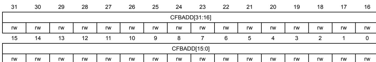
| 31 | 30 | 29 | 28 | 27 | 26 | 25 | 24 | 23 | 22 | 21 | 20 | 19 | 18 | 17 | 16 |
| CFBADD[31:16] | |||||||||||||||
| rw | rw | rw | rw | rw | rw | rw | rw | rw | rw | rw | rw | rw | rw | rw | rw |
| 15 | 14 | 13 | 12 | 11 | 10 | 9 | 8 | 7 | 6 | 5 | 4 | 3 | 2 | 1 | 0 |
| CFBADD[15:0] | |||||||||||||||
| rw | rw | rw | rw | rw | rw | rw | rw | rw | rw | rw | rw | rw | rw | rw | rw |
Bits 31:0 CFBADD[31:0] : Color frame buffer start address
This bitfield defines the color frame buffer start address.
43.7.37 LTDC layer x color frame buffer length register (LTDC_LxCFBLR)
Address offset: \( 0x138 + 0x100 * (x - 1) \) , ( \( x = 1 \) to \( 2 \) )
Reset value: 0x0000 0000
This register defines the color frame buffer line length and pitch.
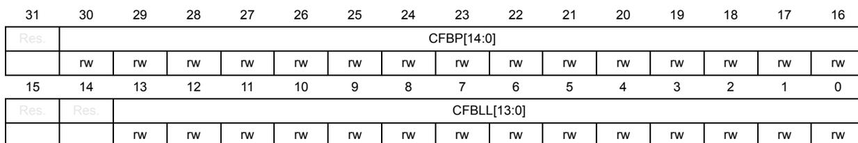
| 31 | 30 | 29 | 28 | 27 | 26 | 25 | 24 | 23 | 22 | 21 | 20 | 19 | 18 | 17 | 16 |
| Res. | CFBP[14:0] | ||||||||||||||
| rw | rw | rw | rw | rw | rw | rw | rw | rw | rw | rw | rw | rw | rw | rw | |
| 15 | 14 | 13 | 12 | 11 | 10 | 9 | 8 | 7 | 6 | 5 | 4 | 3 | 2 | 1 | 0 |
| Res. | Res. | CFBLL[13:0] | |||||||||||||
| rw | rw | rw | rw | rw | rw | rw | rw | rw | rw | rw | rw | rw | rw | ||
Bit 31 Reserved, must be kept at reset value. Upon reading, this bit returns the value of the bit 30.
Bits 30:16 CFBP[14:0] : Color frame buffer pitch in bytes
This bitfield defines the pitch that is the increment from the start of one line of pixels to the start of the next line in bytes.
Negative values (with MSB bit = 1) are allowed, to read the buffer from bottom to top, and thus to flip it vertically. When vertically flipped, as the address register must provide the address of the first line to be read, the address register must point to the start of the bottom line of the buffer.
Bits 15:14 Reserved, must be kept at reset value.
Bits 13:0 CFBLL[13:0] : Color frame buffer line length
This bitfield defines the length of one line of pixels in bytes + 7.
The line length is computed as follows: active high width * number of bytes per pixel + 7.
43.7.38 LTDC layer x color frame buffer line number register (LTDC_LxCFBLNR)
Address offset: \( 0x13C + 0x100 * (x - 1) \) , ( \( x = 1 \) to \( 2 \) )
Reset value: 0x0000 0000
This register defines the number of lines in the color frame buffer. The number of lines and line-length settings define how much data are fetched per frame for every layer. If it is configured to less bytes than required, a FIFO underrun interrupt is generated if enabled. The start address and pitch settings define the correct start of every line in memory.
| 31 | 30 | 29 | 28 | 27 | 26 | 25 | 24 | 23 | 22 | 21 | 20 | 19 | 18 | 17 | 16 |
|---|---|---|---|---|---|---|---|---|---|---|---|---|---|---|---|
| Res. | Res. | Res. | Res. | Res. | Res. | Res. | Res. | Res. | Res. | Res. | Res. | Res. | Res. | Res. | Res. |
| 15 | 14 | 13 | 12 | 11 | 10 | 9 | 8 | 7 | 6 | 5 | 4 | 3 | 2 | 1 | 0 |
| Res. | Res. | Res. | Res. | CFBLNBR[11:0] | |||||||||||
| rw | rw | rw | rw | rw | rw | rw | rw | rw | rw | rw | rw | ||||
Bits 31:12 Reserved, must be kept at reset value.
Bits 11:0 CFBLNBR[11:0] : Frame buffer line number
This bitfield defines the number of lines in the frame buffer that corresponds to the active high width.
43.7.39 LTDC layer 1 auxiliary frame buffer address 0 register (LTDC_L1AFBA0R)
Address offset: 0x140
Reset value: 0x0000 0000
This register defines the start address for the auxiliary 0 frame buffer. It has to point to the address where the pixel data of the top left pixel of a layer is stored in the frame buffer. The auxiliary 0 and 1 frame buffers are for YCbCr semi-planar or full-planar pixel formats: the color frame buffer is used to store the Y components, while the auxiliary buffers 0 and 1 are used to store the other one (for semi-planar) or two (for full-planar) planes of components.
| 31 | 30 | 29 | 28 | 27 | 26 | 25 | 24 | 23 | 22 | 21 | 20 | 19 | 18 | 17 | 16 |
|---|---|---|---|---|---|---|---|---|---|---|---|---|---|---|---|
| AFBADD0[31:16] | |||||||||||||||
| rw | rw | rw | rw | rw | rw | rw | rw | rw | rw | rw | rw | rw | rw | rw | rw |
| 15 | 14 | 13 | 12 | 11 | 10 | 9 | 8 | 7 | 6 | 5 | 4 | 3 | 2 | 1 | 0 |
| AFBADD0[15:0] | |||||||||||||||
| rw | rw | rw | rw | rw | rw | rw | rw | rw | rw | rw | rw | rw | rw | rw | rw |
Bits 31:0 AFBADD0[31:0] : Frame buffer start address
This bitfield defines the color frame buffer start address.
43.7.40 LTDC layer 1 auxiliary frame buffer address 1 register (LTDC_L1AFBA1R)
Address offset: 0x144
Reset value: 0x0000 0000
This register defines the start address for the auxiliary 1 frame buffer. It has to point to the address where the pixel data of the top left pixel of a layer is stored in the frame buffer (the auxiliary 0 and 1 frame buffers are for YCbCr semi-planar or full-planar pixel formats).
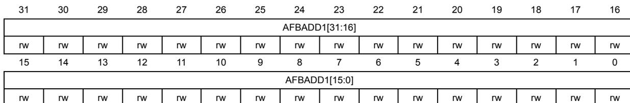
| 31 | 30 | 29 | 28 | 27 | 26 | 25 | 24 | 23 | 22 | 21 | 20 | 19 | 18 | 17 | 16 |
| AFBADD1[31:16] | |||||||||||||||
| rw | rw | rw | rw | rw | rw | rw | rw | rw | rw | rw | rw | rw | rw | rw | rw |
| 15 | 14 | 13 | 12 | 11 | 10 | 9 | 8 | 7 | 6 | 5 | 4 | 3 | 2 | 1 | 0 |
| AFBADD1[15:0] | |||||||||||||||
| rw | rw | rw | rw | rw | rw | rw | rw | rw | rw | rw | rw | rw | rw | rw | rw |
Bits 31:0
AFBADD1[31:0]
: Auxiliary frame buffer start address
This bitfield defines the color frame buffer start address.
43.7.41 LTDC layer 1 auxiliary frame buffer length register (LTDC_L1AFBLR)
Address offset: 0x148
Reset value: 0x0000 0000
This register defines the auxiliary 0 and 1 frame buffer line length and pitch (the auxiliary 0 and 1 frame buffers are for YCbCr semi-planar or full-planar pixel formats).
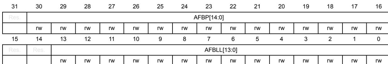
| 31 | 30 | 29 | 28 | 27 | 26 | 25 | 24 | 23 | 22 | 21 | 20 | 19 | 18 | 17 | 16 |
| Res. | AFBP[14:0] | ||||||||||||||
| rw | rw | rw | rw | rw | rw | rw | rw | rw | rw | rw | rw | rw | rw | rw | |
| 15 | 14 | 13 | 12 | 11 | 10 | 9 | 8 | 7 | 6 | 5 | 4 | 3 | 2 | 1 | 0 |
| Res. | Res. | AFBLL[13:0] | |||||||||||||
| rw | rw | rw | rw | rw | rw | rw | rw | rw | rw | rw | rw | rw | rw | ||
Bit 31 Reserved, must be kept at reset value. Upon reading, this bit returns the value of the bit 30.
Bits 30:16 AFBP[14:0] : Auxiliary frame buffer pitch in bytes
This bitfield defines the pitch that is the increment from the start of one line of pixels to the start of the next line in bytes.
Negative values (with MSB bit = 1) are allowed, to read the buffer from bottom to top, and thus to flip it vertically. When vertically flipped, as the address register must provide the address of the first line to be read, the address register must point to the start of the bottom line of the buffer.
Bits 15:14 Reserved, must be kept at reset value.
Bits 13:0 AFBLL[13:0] : Auxiliary frame buffer line length
This bitfield defines the length of one line of pixels in bytes + 7.
The line length is computed as follows:
active high width * number of bytes per pixel + 7.
43.7.42 LTDC layer 1 auxiliary frame buffer line number register (LTDC_L1AFBLNR)
Address offset: 0x14C
Reset value: 0x0000 0000
This register defines the number of lines in the auxiliary 0 and 1 frame buffers (the auxiliary 0 and 1 frame buffers are for YCbCr semi-planar or full-planar pixel formats). The number of lines and line length settings define how much data is fetched per frame for every layer. If it is configured to less bytes than required, a FIFO underrun interrupt is generated if enabled. The start address and pitch settings define the correct start of every line in memory.
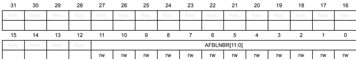
| 31 | 30 | 29 | 28 | 27 | 26 | 25 | 24 | 23 | 22 | 21 | 20 | 19 | 18 | 17 | 16 |
| Res. | Res. | Res. | Res. | Res. | Res. | Res. | Res. | Res. | Res. | Res. | Res. | Res. | Res. | Res. | Res. |
| 15 | 14 | 13 | 12 | 11 | 10 | 9 | 8 | 7 | 6 | 5 | 4 | 3 | 2 | 1 | 0 |
| Res. | Res. | Res. | Res. | AFBLNBR[11:0] | |||||||||||
| rw | rw | rw | rw | rw | rw | rw | rw | rw | rw | rw | rw | ||||
Bits 31:12 Reserved, must be kept at reset value.
Bits 11:0 AFBLNBR[11:0] : Auxiliary frame buffer line number
This bitfield defines the number of lines in the auxiliary frame buffer that corresponds to the active high width.
43.7.43 LTDC layer x CLUT write register (LTDC_LxCLUTWR)
Address offset: 0x150 + 0x100 * (x - 1), (x = 1 to 2)
Reset value: 0x0000 0000
This register defines the CLUT address and the RGB value. The CLUT write register must only be configured during blanking period or if the layer is disabled. The CLUT can be enabled or disabled in LTDC_LxCR. The CLUT is only meaningful for L8, AL44, and AL88 pixel format.
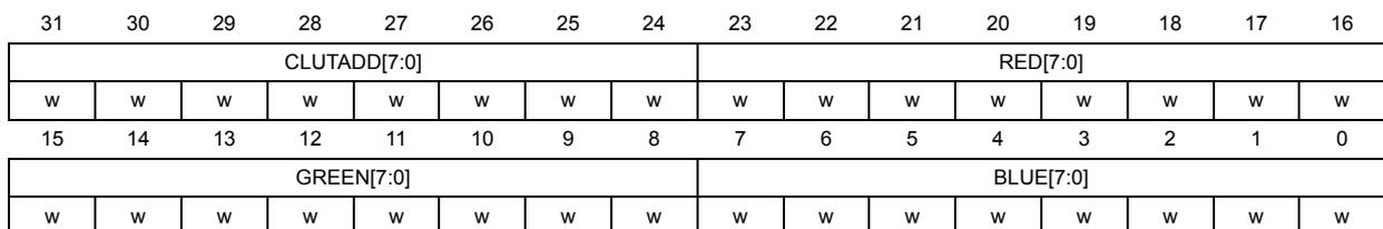
| 31 | 30 | 29 | 28 | 27 | 26 | 25 | 24 | 23 | 22 | 21 | 20 | 19 | 18 | 17 | 16 |
| CLUTADD[7:0] | RED[7:0] | ||||||||||||||
| w | w | w | w | w | w | w | w | w | w | w | w | w | w | w | w |
| 15 | 14 | 13 | 12 | 11 | 10 | 9 | 8 | 7 | 6 | 5 | 4 | 3 | 2 | 1 | 0 |
| GREEN[7:0] | BLUE[7:0] | ||||||||||||||
| w | w | w | w | w | w | w | w | w | w | w | w | w | w | w | w |
Bits 31:24 CLUTADD[7:0] : CLUT address
This bitfield configures the CLUT address (color position within the CLUT) of each RGB value.
Bits 23:16 RED[7:0] : Red value
This bitfield configures the red value.
Bits 15:8 GREEN[7:0] : Green value
This bitfield configures the green value.
Bits 7:0 BLUE[7:0] : Blue value
This bitfield configures the blue value.
43.7.44 LTDC layer x conversion YCbCr RGB 0 register (LTDC_LxCYR0R)
Address offset: \( 0x16C + 0x100 * (x - 1) \) , ( \( x = 1 \) to \( 2 \) )
Reset value: 0x0000 0000
This register defines the coefficients to convert from YCbCr to RGB.
| 31 | 30 | 29 | 28 | 27 | 26 | 25 | 24 | 23 | 22 | 21 | 20 | 19 | 18 | 17 | 16 |
|---|---|---|---|---|---|---|---|---|---|---|---|---|---|---|---|
| Res. | Res. | Res. | Res. | Res. | Res. | CB2B[9:0] | |||||||||
| rw | rw | rw | rw | rw | rw | rw | rw | rw | rw | ||||||
| 15 | 14 | 13 | 12 | 11 | 10 | 9 | 8 | 7 | 6 | 5 | 4 | 3 | 2 | 1 | 0 |
| Res. | Res. | Res. | Res. | Res. | Res. | CR2R[9:0] | |||||||||
| rw | rw | rw | rw | rw | rw | rw | rw | rw | rw | ||||||
Bits 31:26 Reserved, must be kept at reset value.
Bits 25:16 CB2B[9:0] : Cb-to-Blue coefficient, with bits 9:8 as positive integer and 7:0 as decimals.
Bits 15:10 Reserved, must be kept at reset value.
Bits 9:0 CR2R[9:0] : Cr-to-Red coefficient, with bits 9:8 as positive integer and 7:0 as decimals.
43.7.45 LTDC layer x conversion YCbCr RGB 1 register (LTDC_LxCYR1R)
Address offset: \( 0x170 + 0x100 * (x - 1) \) , ( \( x = 1 \) to \( 2 \) )
Reset value: 0x0000 0000
This register defines the coefficients to convert from YCbCr to RGB.
| 31 | 30 | 29 | 28 | 27 | 26 | 25 | 24 | 23 | 22 | 21 | 20 | 19 | 18 | 17 | 16 |
|---|---|---|---|---|---|---|---|---|---|---|---|---|---|---|---|
| Res. | Res. | Res. | Res. | Res. | Res. | CB2G[9:0] | |||||||||
| rw | rw | rw | rw | rw | rw | rw | rw | rw | rw | ||||||
| 15 | 14 | 13 | 12 | 11 | 10 | 9 | 8 | 7 | 6 | 5 | 4 | 3 | 2 | 1 | 0 |
| Res. | Res. | Res. | Res. | Res. | Res. | CR2G[9:0] | |||||||||
| rw | rw | rw | rw | rw | rw | rw | rw | rw | rw | ||||||
Bits 31:26 Reserved, must be kept at reset value.
Bits 25:16 CB2G[9:0] : Cb-to-Green coefficient, with bits 9:8 as positive integer and 7:0 as decimals.
Bits 15:10 Reserved, must be kept at reset value.
Bits 9:0 CR2G[9:0] : Cr-to-Green coefficient, with bits 9:8 as positive integer and 7:0 as decimals.
43.7.46 LTDC layer x flexible pixel format 0 register (LTDC_LxFPF0R)
Address offset: \( 0x174 + 0x100 * (x - 1) \) , ( \( x = 1 \) to \( 2 \) )
Reset value: \( 0x0002\ 1100 \)
This register is one of the registers that define the flexible color format, by specifying the location and width of all A, R, G, B components in a memory word. Components A and R are defined in this specific register.
| 31 | 30 | 29 | 28 | 27 | 26 | 25 | 24 | 23 | 22 | 21 | 20 | 19 | 18 | 17 | 16 |
|---|---|---|---|---|---|---|---|---|---|---|---|---|---|---|---|
| Res. | Res. | Res. | Res. | Res. | Res. | Res. | Res. | Res. | Res. | Res. | Res. | Res. | Res. | RLEN[3:2] | |
| 15 | 14 | 13 | 12 | 11 | 10 | 9 | 8 | 7 | 6 | 5 | 4 | 3 | 2 | 1 | 0 |
| RLEN[1:0] | RPOS[4:0] | ALEN[3:0] | APOS[4:0] | ||||||||||||
| rw | rw | rw | rw | rw | rw | rw | rw | rw | rw | rw | rw | rw | rw | rw | rw |
Bits 31:18 Reserved, must be kept at reset value.
Bits 17:14 RLEN[3:0] : Width of the red component (in bits)
Bits 13:9 RPOS[4:0] : Location of the red component inside the pixel memory word (in bits)
Bits 8:5 ALEN[3:0] : Width of the alpha component (in bits)
Bits 4:0 APOS[4:0] : Location of the alpha component inside the pixel memory word (in bits)
43.7.47 LTDC layer x flexible pixel format 1 register (LTDC_LxFPF1R)
Address offset: \( 0x178 + 0x100 * (x - 1) \) , ( \( x = 1 \) to \( 2 \) )
Reset value: \( 0x0012\ 3110 \)
This register is one of the registers that define the flexible color format, by specifying the location and width of all A, R, G, B components in a memory word. Components G and B are defined in this specific register.
| 31 | 30 | 29 | 28 | 27 | 26 | 25 | 24 | 23 | 22 | 21 | 20 | 19 | 18 | 17 | 16 |
|---|---|---|---|---|---|---|---|---|---|---|---|---|---|---|---|
| Res. | Res. | Res. | Res. | Res. | Res. | Res. | Res. | Res. | Res. | Res. | PSIZE[2:0] | BLEN[3:2] | |||
| 15 | 14 | 13 | 12 | 11 | 10 | 9 | 8 | 7 | 6 | 5 | 4 | 3 | 2 | 1 | 0 |
| BLEN[1:0] | BPOS[4:0] | GLEN[3:0] | GPOS[4:0] | ||||||||||||
| rw | rw | rw | rw | rw | rw | rw | rw | rw | rw | rw | rw | rw | rw | rw | rw |
Bits 31:21 Reserved, must be kept at reset value.
Bits 20:18 PSIZE[2:0] : Pixel size (in bytes)
Bits 17:14 BLEN[3:0] : Width of the blue component (in bits)
Bits 13:9 BPOS[4:0] : Location of the blue component inside the pixel memory word (in bits)
Bits 8:5 GLEN[3:0] : Width of the green component (in bits)
Bits 4:0 GPOS[4:0] : Location of the green component inside the pixel memory word (in bits)
43.7.48 LTDC register map
Table 387. LTDC register map and reset values
| Offset | Register name | 31 | 30 | 29 | 28 | 27 | 26 | 25 | 24 | 23 | 22 | 21 | 20 | 19 | 18 | 17 | 16 | 15 | 14 | 13 | 12 | 11 | 10 | 9 | 8 | 7 | 6 | 5 | 4 | 3 | 2 | 1 | 0 |
|---|---|---|---|---|---|---|---|---|---|---|---|---|---|---|---|---|---|---|---|---|---|---|---|---|---|---|---|---|---|---|---|---|---|
| 0x008 | LTDC_SSCR | Res | Res | Res | Res | Res | HSW[11:0] | Res | Res | Res | Res | VSH[11:0] | |||||||||||||||||||||
| Reset value | 0 | 0 | 0 | 0 | 0 | 0 | 0 | 0 | 0 | 0 | 0 | 0 | 0 | 0 | 0 | 0 | 0 | 0 | 0 | 0 | 0 | 0 | 0 | ||||||||||
| 0x00C | LTDC_BPCR | Res | Res | Res | Res | Res | AHBP[11:0] | Res | Res | Res | Res | AVBP[11:0] | |||||||||||||||||||||
| Reset value | 0 | 0 | 0 | 0 | 0 | 0 | 0 | 0 | 0 | 0 | 0 | 0 | 0 | 0 | 0 | 0 | 0 | 0 | 0 | 0 | 0 | 0 | 0 | ||||||||||
| 0x010 | LTDC_AWCR | Res | Res | Res | Res | Res | AAW[11:0] | Res | Res | Res | Res | AAH[11:0] | |||||||||||||||||||||
| Reset value | 0 | 0 | 0 | 0 | 0 | 0 | 0 | 0 | 0 | 0 | 0 | 0 | 0 | 0 | 0 | 0 | 0 | 0 | 0 | 0 | 0 | 0 | 0 | ||||||||||
| 0x014 | LTDC_TWCR | Res | Res | Res | Res | Res | TOTALW[11:0] | Res | Res | Res | Res | TOTALH[11:0] | |||||||||||||||||||||
| Reset value | 0 | 0 | 0 | 0 | 0 | 0 | 0 | 0 | 0 | 0 | 0 | 0 | 0 | 0 | 0 | 0 | 0 | 0 | 0 | 0 | 0 | 0 | 0 | ||||||||||
| 0x018 | LTDC_GCR | HSPOL | VSPOL | DEPOL | PCPOL | Res | Res | SFSWTR | SFEN | Res | Res | Res | Res | CRCEN | Res | Res | DEN | Res | DRW[2:0] | Res | DGW[2:0] | Res | DBW[2:0] | Res | Res | Res | Res | GAMEN | LTDEN | ||||
| Reset value | 0 | 0 | 0 | 0 | 0 | 0 | 0 | 0 | 0 | 1 | 0 | 0 | 1 | 0 | 0 | 1 | 0 | 0 | 0 | ||||||||||||||
| 0x024 | LTDC_SRCR | Res | Res | Res | Res | Res | Res | Res | Res | Res | Res | Res | Res | Res | Res | Res | Res | Res | Res | Res | Res | Res | Res | Res | Res | Res | Res | Res | Res | Res | Res | VBR | IMR |
| Reset value | 0 | 0 | |||||||||||||||||||||||||||||||
| 0x028 | LTDC_GCCR | Res | Res | Res | Res | Res | Res | Res | Res | Res | Res | Res | Res | REN | GEN | BEN | COMP[7:0] | ADDR[7:0] | |||||||||||||||
| Reset value | 0 | 0 | 0 | 0 | 0 | 0 | 0 | 0 | 0 | 0 | 0 | 0 | 0 | 0 | 0 | 0 | 0 | 0 | 0 | ||||||||||||||
| 0x02C | LTDC_BCCR | Res | Res | Res | Res | Res | Res | Res | Res | Res | Res | Res | Res | BCRED[7:0] | BCGREEN[7:0] | BCBLUE[7:0] | |||||||||||||||||
| Reset value | 0 | 0 | 0 | 0 | 0 | 0 | 0 | 0 | 0 | 0 | 0 | 0 | 0 | 0 | 0 | 0 | 0 | 0 | 0 | ||||||||||||||
| 0x030 | Reserved | Reserved | |||||||||||||||||||||||||||||||
| 0x034 | LTDC_IER | Res | Res | Res | Res | Res | Res | Res | Res | Res | Res | Res | Res | Res | Res | Res | Res | Res | Res | Res | Res | Res | Res | Res | Res | Res | Res | Res | Res | Res | Res | Res | Res |
| Reset value | 0 | 0 | |||||||||||||||||||||||||||||||
| 0x038 | LTDC_ISR | Res | Res | Res | Res | Res | Res | Res | Res | Res | Res | Res | Res | Res | Res | Res | Res | Res | Res | Res | Res | Res | Res | Res | Res | Res | Res | Res | Res | Res | Res | Res | Res |
| Reset value | 0 | 0 | |||||||||||||||||||||||||||||||
| 0x03C | LTDC_ICR | Res | Res | Res | Res | Res | Res | Res | Res | Res | Res | Res | Res | Res | Res | Res | Res | Res | Res | Res | Res | Res | Res | Res | Res | Res | Res | Res | Res | Res | Res | Res | Res |
| Reset value | 0 | 0 | |||||||||||||||||||||||||||||||
| 0x040 | LTDC_LIPCR | Res | Res | Res | Res | Res | Res | Res | Res | Res | Res | Res | Res | Res | Res | Res | Res | Res | Res | Res | Res | LIPOS[11:0] | |||||||||||
| Reset value | 0 | 0 | 0 | 0 | 0 | 0 | 0 | 0 | 0 | 0 | 0 | 0 | |||||||||||||||||||||
| 0x044 | LTDC_CPSR | Res | Res | Res | Res | Res | Res | Res | Res | Res | Res | Res | Res | Res | Res | Res | Res | Res | Res | Res | Res | CXPOS[11:0] | |||||||||||
| Reset value | 0 | 0 | 0 | 0 | 0 | 0 | 0 | 0 | 0 | 0 | 0 | 0 | |||||||||||||||||||||
| 0x048 | LTDC_CDSR | Res | Res | Res | Res | Res | Res | Res | Res | Res | Res | Res | Res | Res | Res | Res | Res | Res | Res | Res | Res | Res | Res | Res | Res | Res | Res | Res | Res | Res | Res | Res | Res |
| Reset value | 0 | 0 | |||||||||||||||||||||||||||||||
| 0x04C-0x05C | Reserved | Reserved | |||||||||||||||||||||||||||||||
Table 387. LTDC register map and reset values (continued)
| Offset | Register name | 31 | 30 | 29 | 28 | 27 | 26 | 25 | 24 | 23 | 22 | 21 | 20 | 19 | 18 | 17 | 16 | 15 | 14 | 13 | 12 | 11 | 10 | 9 | 8 | 7 | 6 | 5 | 4 | 3 | 2 | 1 | 0 |
|---|---|---|---|---|---|---|---|---|---|---|---|---|---|---|---|---|---|---|---|---|---|---|---|---|---|---|---|---|---|---|---|---|---|
| 0x060 | LTDC_EDCR | Res. | Res. | Res. | Res. | OCYCO | OCYSEL | OCYEN | Res. | Res. | Res. | Res. | Res. | Res. | Res. | Res. | Res. | Res. | Res. | Res. | Res. | Res. | Res. | Res. | Res. | Res. | Res. | Res. | Res. | Res. | Res. | Res. | Res. |
| Reset value | 0 | 0 | 0 | ||||||||||||||||||||||||||||||
| 0x064 | LTDC_IE2R | Res. | Res. | Res. | Res. | Res. | Res. | Res. | Res. | Res. | Res. | Res. | Res. | Res. | Res. | Res. | Res. | Res. | Res. | Res. | Res. | Res. | Res. | Res. | Res. | CRCIE | FUIE | Res. | Res. | RRIE | TERRIE | FUWIE | LIE |
| Reset value | 0 | 0 | 0 | 0 | 0 | 0 | |||||||||||||||||||||||||||
| 0x068 | LTDC_ISR2 | Res. | Res. | Res. | Res. | Res. | Res. | Res. | Res. | Res. | Res. | Res. | Res. | Res. | Res. | Res. | Res. | Res. | Res. | Res. | Res. | Res. | Res. | Res. | Res. | CRCIF | FUIF | Res. | Res. | RRIF | TERRIF | FUWIF | LIF |
| Reset value | 0 | 0 | 0 | 0 | 0 | 0 | |||||||||||||||||||||||||||
| 0x06C | LTDC_ICR2 | Res. | Res. | Res. | Res. | Res. | Res. | Res. | Res. | Res. | Res. | Res. | Res. | Res. | Res. | Res. | Res. | Res. | Res. | Res. | Res. | Res. | Res. | Res. | Res. | CCRCIF | CFUIF | Res. | Res. | CRRIF | CTERRIF | CFUWIF | CLIF |
| Reset value | 0 | 0 | 0 | 0 | 0 | 0 | |||||||||||||||||||||||||||
| 0x070 | LTDC_LIPCR2 | Res. | Res. | Res. | Res. | Res. | Res. | Res. | Res. | Res. | Res. | Res. | Res. | Res. | Res. | Res. | Res. | Res. | Res. | Res. | Res. | LIPOS[11:0] | |||||||||||
| Reset value | 0 | 0 | 0 | 0 | 0 | 0 | 0 | 0 | 0 | 0 | 0 | 0 | |||||||||||||||||||||
| 0x074 | Reserved | Reserved | |||||||||||||||||||||||||||||||
| 0x078 | LTDC_ECRCR | Res. | Res. | Res. | Res. | Res. | Res. | Res. | Res. | Res. | Res. | Res. | Res. | Res. | Res. | Res. | Res. | ECRC[15:0] | |||||||||||||||
| Reset value | 0 | 0 | 0 | 0 | 0 | 0 | 0 | 0 | 0 | 0 | 0 | 0 | 0 | 0 | 0 | 0 | |||||||||||||||||
| 0x07C | LTDC_CCRCR | Res. | Res. | Res. | Res. | Res. | Res. | Res. | Res. | Res. | Res. | Res. | Res. | Res. | Res. | Res. | Res. | CCRC[15:0] | |||||||||||||||
| Reset value | 0 | 0 | 0 | 0 | 0 | 0 | 0 | 0 | 0 | 0 | 0 | 0 | 0 | 0 | 0 | 0 | |||||||||||||||||
| 0x080-0x08C | Reserved | Reserved | |||||||||||||||||||||||||||||||
| 0x090 | LTDC_FUTR | Res. | Res. | Res. | Res. | Res. | Res. | Res. | Res. | Res. | Res. | Res. | Res. | Res. | Res. | Res. | Res. | THRE[15:0] | |||||||||||||||
| Reset value | 0 | 0 | 0 | 0 | 0 | 0 | 0 | 0 | 0 | 0 | 0 | 0 | 0 | 0 | 0 | 0 | |||||||||||||||||
| 0x094-0x0FC | Reserved | Reserved | |||||||||||||||||||||||||||||||
| 0x100 | LTDC_L1C0R | ARGB8888 | ABGR8888 | RGBA8888 | BGRA8888 | RGB565 | BGR565 | RGB888 | FF | F11PC | F1PC | F11C | F1C | F11P | F1P | F10 | F11 | F21PC | F2PC | F21C | F2C | F21P | F2P | F20 | F21 | CKRA | CLUTA | WINA | DCP | APA | CFBPA | CFBDA | CKTA |
| Reset value | 1 | 1 | 1 | 1 | 1 | 1 | 1 | 1 | 0 | 1 | 0 | 1 | 0 | 0 | 0 | 0 | 1 | 0 | 1 | 0 | 0 | 0 | 0 | 0 | 0 | 1 | 1 | 1 | 0 | 1 | 0 | 1 | |
| 0x104 | LTDC_L1C1R | SCA | Res. | Res. | Res. | Res. | Res. | Res. | Res. | Res. | Res. | Res. | Res. | Res. | Res. | Res. | Res. | Res. | Res. | Res. | Res. | Res. | Res. | Res. | Res. | Res. | Res. | Res. | Res. | Res. | YFPA | YSP | YIA |
| Reset value | 0 | 1 | 1 | 1 | |||||||||||||||||||||||||||||
| 0x108 | LTDC_L1RCR | Res. | Res. | Res. | Res. | Res. | Res. | Res. | Res. | Res. | Res. | Res. | Res. | Res. | Res. | Res. | Res. | Res. | Res. | Res. | Res. | Res. | Res. | Res. | Res. | Res. | Res. | Res. | Res. | Res. | GRMSK | VBR | IMR |
| Reset value | 1 | 0 | 0 | ||||||||||||||||||||||||||||||
| 0x10C | LTDC_L1CR | Res. | Res. | Res. | Res. | Res. | Res. | Res. | Res. | Res. | Res. | Res. | Res. | Res. | Res. | Res. | Res. | Res. | Res. | Res. | Res. | Res. | Res. | DCBEN | HMEN | Res. | Res. | Res. | CLUTEN | HPDEN | VPDEN | CKEN | LEN |
| Reset value | 0 | 0 | 0 | 0 | 0 | 0 | 0 | ||||||||||||||||||||||||||
| 0x110 | LTDC_L1WHPCR | Res. | Res. | Res. | Res. | WHSPPOS[11:0] | Res. | Res. | Res. | Res. | WHSTPOS[11:0] | ||||||||||||||||||||||
| Reset value | 0 | 0 | 0 | 0 | 0 | 0 | 0 | 0 | 0 | 0 | 0 | 0 | 0 | 0 | 0 | 0 | 0 | 0 | 0 | 0 | 0 | 0 | 0 | 0 | |||||||||
| 0x114 | LTDC_L1WVPCR | Res. | Res. | Res. | Res. | WVSPPOS[11:0] | Res. | Res. | Res. | Res. | WVSTPOS[11:0] | ||||||||||||||||||||||
| Reset value | 0 | 0 | 0 | 0 | 0 | 0 | 0 | 0 | 0 | 0 | 0 | 0 | 0 | 0 | 0 | 0 | 0 | 0 | 0 | 0 | 0 | 0 | 0 | 0 | |||||||||
| Offset | Register name | 31 | 30 | 29 | 28 | 27 | 26 | 25 | 24 | 23 | 22 | 21 | 20 | 19 | 18 | 17 | 16 | 15 | 14 | 13 | 12 | 11 | 10 | 9 | 8 | 7 | 6 | 5 | 4 | 3 | 2 | 1 | 0 | ||
|---|---|---|---|---|---|---|---|---|---|---|---|---|---|---|---|---|---|---|---|---|---|---|---|---|---|---|---|---|---|---|---|---|---|---|---|
| 0x118 | LTDC_L1CKCR | Res. | Res. | Res. | Res. | Res. | Res. | Res. | Res. | CKRED[7:0] | CKGREEN[7:0] | CKBLUE[7:0] | |||||||||||||||||||||||
| Reset value | 0 | 0 | 0 | 0 | 0 | 0 | 0 | 0 | 0 | 0 | 0 | 0 | 0 | 0 | 0 | 0 | 0 | 0 | 0 | 0 | 0 | 0 | 0 | 0 | |||||||||||
| 0x11C | LTDC_L1PFCR | Res. | Res. | Res. | Res. | Res. | Res. | Res. | Res. | Res. | Res. | Res. | Res. | Res. | Res. | Res. | Res. | Res. | Res. | Res. | Res. | Res. | Res. | Res. | Res. | Res. | Res. | Res. | Res. | Res. | PF[2:0] | ||||
| Reset value | 0 | 0 | 0 | ||||||||||||||||||||||||||||||||
| 0x120 | LTDC_L1CACR | Res. | Res. | Res. | Res. | Res. | Res. | Res. | Res. | Res. | Res. | Res. | Res. | Res. | Res. | Res. | Res. | Res. | Res. | Res. | Res. | Res. | Res. | Res. | Res. | CONSTA[7:0] | |||||||||
| Reset value | 1 | 1 | 1 | 1 | 1 | 1 | 1 | 1 | |||||||||||||||||||||||||||
| 0x124 | LTDC_L1DCCR | DCALPHA[7:0] | DCRED[7:0] | DCGREEN[7:0] | DCBLUE[7:0] | ||||||||||||||||||||||||||||||
| Reset value | 0 | 0 | 0 | 0 | 0 | 0 | 0 | 0 | 0 | 0 | 0 | 0 | 0 | 0 | 0 | 0 | 0 | 0 | 0 | 0 | 0 | 0 | 0 | 0 | 0 | 0 | 0 | 0 | 0 | 0 | 0 | 0 | |||
| 0x128 | LTDC_L1BFCR | Res. | Res. | Res. | Res. | Res. | Res. | Res. | Res. | Res. | Res. | Res. | Res. | Res. | Res. | Res. | BOR | Res. | Res. | Res. | Res. | Res. | BF1[2:0] | Res. | Res. | Res. | Res. | Res. | BF2[2:0] | ||||||
| Reset value | 0 | 1 | 1 | 0 | 1 | 1 | 1 | ||||||||||||||||||||||||||||
| 0x12C | LTDC_L1BLCR | Res. | Res. | Res. | Res. | Res. | Res. | Res. | Res. | Res. | Res. | Res. | Res. | Res. | Res. | Res. | Res. | Res. | Res. | Res. | Res. | Res. | Res. | Res. | Res. | Res. | Res. | Res. | BL[4:0] | ||||||
| Reset value | 0 | 0 | 0 | 0 | 0 | ||||||||||||||||||||||||||||||
| 0x130 | LTDC_L1PCR | Res. | Res. | Res. | Res. | Res. | Res. | Res. | Res. | Res. | Res. | Res. | Res. | Res. | Res. | Res. | Res. | Res. | Res. | Res. | Res. | Res. | Res. | YREN | OF | CBF | YF | YCM [1:0] | YCEN | Res. | Res. | Res. | |||
| Reset value | 0 | 0 | 0 | 0 | 0 | 0 | 0 | ||||||||||||||||||||||||||||
| 0x134 | LTDC_L1CFBAR | CFBADD[31:0] | |||||||||||||||||||||||||||||||||
| Reset value | 0 | 0 | 0 | 0 | 0 | 0 | 0 | 0 | 0 | 0 | 0 | 0 | 0 | 0 | 0 | 0 | 0 | 0 | 0 | 0 | 0 | 0 | 0 | 0 | 0 | 0 | 0 | 0 | 0 | 0 | 0 | 0 | |||
| 0x138 | LTDC_L1CFBLR | Res. | CFBP[14:0] | Res. | Res. | CFBLL[13:0] | |||||||||||||||||||||||||||||
| Reset value | 0 | 0 | 0 | 0 | 0 | 0 | 0 | 0 | 0 | 0 | 0 | 0 | 0 | 0 | 0 | 0 | 0 | 0 | 0 | 0 | 0 | 0 | 0 | 0 | 0 | 0 | 0 | 0 | 0 | ||||||
| 0x13C | LTDC_L1CFBLNR | Res. | Res. | Res. | Res. | Res. | Res. | Res. | Res. | Res. | Res. | Res. | Res. | Res. | Res. | Res. | Res. | Res. | Res. | Res. | Res. | CFBLNBR[11:0] | |||||||||||||
| Reset value | 0 | 0 | 0 | 0 | 0 | 0 | 0 | 0 | 0 | 0 | 0 | 0 | |||||||||||||||||||||||
| 0x140 | LTDC_L1AFBA0R | AFBADD0[31:0] | |||||||||||||||||||||||||||||||||
| Reset value | 0 | 0 | 0 | 0 | 0 | 0 | 0 | 0 | 0 | 0 | 0 | 0 | 0 | 0 | 0 | 0 | 0 | 0 | 0 | 0 | 0 | 0 | 0 | 0 | 0 | 0 | 0 | 0 | 0 | 0 | 0 | 0 | |||
| 0x144 | LTDC_L1AFBA1R | AFBADD1[31:0] | |||||||||||||||||||||||||||||||||
| Reset value | 0 | 0 | 0 | 0 | 0 | 0 | 0 | 0 | 0 | 0 | 0 | 0 | 0 | 0 | 0 | 0 | 0 | 0 | 0 | 0 | 0 | 0 | 0 | 0 | 0 | 0 | 0 | 0 | 0 | 0 | 0 | 0 | |||
| 0x148 | LTDC_L1AFBLR | Res. | AFBP[14:0] | Res. | Res. | AFBLL[13:0] | |||||||||||||||||||||||||||||
| Reset value | 0 | 0 | 0 | 0 | 0 | 0 | 0 | 0 | 0 | 0 | 0 | 0 | 0 | 0 | 0 | 0 | 0 | 0 | 0 | 0 | 0 | 0 | 0 | 0 | 0 | 0 | 0 | 0 | 0 | ||||||
| 0x14C | LTDC_L1AFBLNR | Res. | Res. | Res. | Res. | Res. | Res. | Res. | Res. | Res. | Res. | Res. | Res. | Res. | Res. | Res. | Res. | Res. | Res. | Res. | Res. | AFBLNBR[11:0] | |||||||||||||
| Reset value | 0 | 0 | 0 | 0 | 0 | 0 | 0 | 0 | 0 | 0 | 0 | 0 | |||||||||||||||||||||||
| 0x150 | LTDC_L1CLUTWR | CLUTADD[7:0] | RED[7:0] | GREEN[7:0] | BLUE[7:0] | ||||||||||||||||||||||||||||||
| Reset value | 0 | 0 | 0 | 0 | 0 | 0 | 0 | 0 | 0 | 0 | 0 | 0 | 0 | 0 | 0 | 0 | 0 | 0 | 0 | 0 | 0 | 0 | 0 | 0 | 0 | 0 | 0 | 0 | 0 | 0 | 0 | 0 | |||
| 0x154-0x168 | Reserved | Reserved | |||||||||||||||||||||||||||||||||
| 0x16C | LTDC_L1CYR0R | Res. | Res. | Res. | Res. | Res. | Res. | CB2B[9:0] | Res. | Res. | Res. | Res. | Res. | Res. | Res. | Res. | CR2R[9:0] | ||||||||||||||||||
| Reset value | 0 | 0 | 0 | 0 | 0 | 0 | 0 | 0 | 0 | 0 | 0 | 0 | 0 | 0 | 0 | 0 | 0 | 0 | 0 | 0 | |||||||||||||||
| 0x170 | LTDC_L1CYR1R | Res. | Res. | Res. | Res. | Res. | Res. | CB2G[9:0] | Res. | Res. | Res. | Res. | Res. | Res. | Res. | Res. | CR2G[9:0] | ||||||||||||||||||
| Reset value | 0 | 0 | 0 | 0 | 0 | 0 | 0 | 0 | 0 | 0 | 0 | 0 | 0 | 0 | 0 | 0 | 0 | 0 | 0 | 0 | |||||||||||||||
| 0x174 | LTDC_L1FPF0R | Res. | Res. | Res. | Res. | Res. | Res. | Res. | Res. | Res. | Res. | Res. | Res. | Res. | Res. | Res. | RLEN[3:0] | RPOS[4:0] | ALEN[3:0] | APOS[4:0] | |||||||||||||||
| Reset value | 1 | 0 | 0 | 0 | 0 | 1 | 0 | 0 | 0 | 1 | 0 | 0 | 0 | 0 | 0 | 0 | 0 | ||||||||||||||||||
| 0x178 | LTDC_L1FPF1R | Res. | Res. | Res. | Res. | Res. | Res. | Res. | Res. | Res. | Res. | Res. | Res. | PSIZE [2:0] | BLEN[3:0] | BPOS[4:0] | GLEN[3:0] | GPOS[4:0] | |||||||||||||||||
| Reset value | 1 | 0 | 0 | 1 | 0 | 0 | 0 | 1 | 1 | 0 | 0 | 0 | 1 | 0 | 0 | 0 | 1 | 0 | 0 | 0 | |||||||||||||||
Table 387. LTDC register map and reset values (continued)
| Offset | Register name | 31 | 30 | 29 | 28 | 27 | 26 | 25 | 24 | 23 | 22 | 21 | 20 | 19 | 18 | 17 | 16 | 15 | 14 | 13 | 12 | 11 | 10 | 9 | 8 | 7 | 6 | 5 | 4 | 3 | 2 | 1 | 0 | |
|---|---|---|---|---|---|---|---|---|---|---|---|---|---|---|---|---|---|---|---|---|---|---|---|---|---|---|---|---|---|---|---|---|---|---|
| 0x17C- 0x1FC | Reserved | Reserved | ||||||||||||||||||||||||||||||||
| 0x200 | LTDC_L2C0R | ARG8888 | ABGR8888 | RGB8888 | BGR8888 | RGB565 | BGR565 | RGB888 | FF | F11PC | F1PC | F11C | F1C | F11P | F1P | F10 | F11 | F21PC | F2PC | F21C | F2C | F21P | F2P | F20 | F21 | CKRA | GLUTA | WINA | DCP | APA | CFBPA | CFBDA | CKTA | |
| Reset value | 1 | 1 | 1 | 1 | 1 | 1 | 1 | 1 | 0 | 1 | 0 | 1 | 0 | 0 | 0 | 0 | 1 | 0 | 1 | 0 | 0 | 0 | 0 | 0 | 0 | 1 | 1 | 1 | 0 | 1 | 0 | 1 | ||
| 0x204 | LTDC_L2C1R | SCA | Res. | Res. | Res. | Res. | Res. | Res. | Res. | Res. | Res. | Res. | Res. | Res. | Res. | Res. | Res. | Res. | Res. | Res. | Res. | Res. | Res. | Res. | Res. | Res. | Res. | Res. | Res. | Res. | YFPA | YSP | YIA | |
| Reset value | 0 | 0 | 0 | 1 | ||||||||||||||||||||||||||||||
| 0x208 | LTDC_L2RCR | Res. | Res. | Res. | Res. | Res. | Res. | Res. | Res. | Res. | Res. | Res. | Res. | Res. | Res. | Res. | Res. | Res. | Res. | Res. | Res. | Res. | Res. | Res. | Res. | Res. | Res. | Res. | Res. | Res. | GRMSK | VBR | IMR | |
| Reset value | -1 | 0 | 0 | |||||||||||||||||||||||||||||||
| 0x20C | LTDC_L2CR | Res. | Res. | Res. | Res. | Res. | Res. | Res. | Res. | Res. | Res. | Res. | Res. | Res. | Res. | Res. | Res. | Res. | Res. | Res. | Res. | Res. | Res. | DCBEN | HMEN | Res. | Res. | Res. | Res. | CLUTEN | HPDEN | VPDEN | CKEN | LEN |
| Reset value | 0 | 0 | 0 | 0 | 0 | 0 | 0 | |||||||||||||||||||||||||||
| 0x210 | LTDC_L2WHPER | Res. | Res. | Res. | Res. | WHSPPOS[11:0] | Res. | Res. | Res. | Res. | Res. | WHSTPOS[11:0] | ||||||||||||||||||||||
| Reset value | 0 | 0 | 0 | 0 | 0 | 0 | 0 | 0 | 0 | 0 | 0 | 0 | 0 | 0 | 0 | 0 | 0 | 0 | 0 | 0 | 0 | 0 | 0 | |||||||||||
| 0x214 | LTDC_L2WVPER | Res. | Res. | Res. | Res. | WVSPPOS[11:0] | Res. | Res. | Res. | Res. | Res. | WVSTPOS[11:0] | ||||||||||||||||||||||
| Reset value | 0 | 0 | 0 | 0 | 0 | 0 | 0 | 0 | 0 | 0 | 0 | 0 | 0 | 0 | 0 | 0 | 0 | 0 | 0 | 0 | 0 | 0 | 0 | |||||||||||
| 0x218 | LTDC_L2CKCR | Res. | Res. | Res. | Res. | Res. | Res. | Res. | Res. | CKRED[7:0] | CKGREEN[7:0] | CKBLUE[7:0] | ||||||||||||||||||||||
| Reset value | 0 | 0 | 0 | 0 | 0 | 0 | 0 | 0 | 0 | 0 | 0 | 0 | 0 | 0 | 0 | 0 | 0 | 0 | 0 | 0 | 0 | 0 | 0 | |||||||||||
| 0x21C | LTDC_L2PFCR | Res. | Res. | Res. | Res. | Res. | Res. | Res. | Res. | Res. | Res. | Res. | Res. | Res. | Res. | Res. | Res. | Res. | Res. | Res. | Res. | Res. | Res. | Res. | Res. | Res. | Res. | Res. | Res. | Res. | Res. | PF[2:0] | ||
| Reset value | 0 | 0 | 0 | |||||||||||||||||||||||||||||||
| 0x220 | LTDC_L2CACR | Res. | Res. | Res. | Res. | Res. | Res. | Res. | Res. | Res. | Res. | Res. | Res. | Res. | Res. | Res. | Res. | Res. | Res. | Res. | Res. | Res. | Res. | Res. | Res. | Res. | Res. | Res. | Res. | Res. | Res. | CONSTA[7:0] | ||
| Reset value | 1 | 1 | 1 | |||||||||||||||||||||||||||||||
| 0x224 | LTDC_L2DCCR | DCALPHA[7:0] | DCRED[7:0] | DCGREEN[7:0] | DCBLUE[7:0] | |||||||||||||||||||||||||||||
| Reset value | 0 | 0 | 0 | 0 | 0 | 0 | 0 | 0 | 0 | 0 | 0 | 0 | 0 | 0 | 0 | 0 | 0 | 0 | 0 | 0 | 0 | 0 | 0 | 0 | 0 | 0 | 0 | 0 | 0 | 0 | 0 | 0 | ||
| 0x228 | LTDC_L2BFCR | Res. | Res. | Res. | Res. | Res. | Res. | Res. | Res. | Res. | Res. | Res. | Res. | Res. | Res. | Res. | BOR | Res. | Res. | Res. | Res. | Res. | Res. | BF1[2:0] | Res. | Res. | Res. | Res. | Res. | Res. | Res. | Res. | BF2[2:0] | |
| Reset value | 0 | 1 | 1 | 0 | 1 | 1 | 1 | |||||||||||||||||||||||||||
| 0x22C | LTDC_L2BLCR | Res. | Res. | Res. | Res. | Res. | Res. | Res. | Res. | Res. | Res. | Res. | Res. | Res. | Res. | Res. | Res. | Res. | Res. | Res. | Res. | Res. | Res. | Res. | Res. | Res. | Res. | Res. | Res. | Res. | Res. | Res. | BL[4:0] | |
| Reset value | 0 | 0 | 0 | |||||||||||||||||||||||||||||||
| 0x230 | LTDC_L2PCR | Res. | Res. | Res. | Res. | Res. | Res. | Res. | Res. | Res. | Res. | Res. | Res. | Res. | Res. | Res. | Res. | Res. | Res. | Res. | Res. | Res. | Res. | YREN | OF | CBF | YF | YCM[1:0] | YCEN | Res. | Res. | Res. | Res. | |
| Reset value | 0 | 0 | 0 | 0 | 0 | 0 | 0 | 0 | 0 | 0 | ||||||||||||||||||||||||
| 0x234 | LTDC_L2CFBAR | CFBADD[31:0] | ||||||||||||||||||||||||||||||||
| Reset value | 0 | 0 | 0 | 0 | 0 | 0 | 0 | 0 | 0 | 0 | 0 | 0 | 0 | 0 | 0 | 0 | 0 | 0 | 0 | 0 | 0 | 0 | 0 | 0 | 0 | 0 | 0 | 0 | 0 | 0 | 0 | 0 | ||
| 0x238 | LTDC_L2CFBLR | Res. | CFBP[14:0] | Res. | Res. | CFBLL[13:0] | ||||||||||||||||||||||||||||
| Reset value | 0 | 0 | 0 | 0 | 0 | 0 | 0 | 0 | 0 | 0 | 0 | 0 | 0 | 0 | 0 | 0 | 0 | 0 | 0 | 0 | 0 | 0 | 0 | 0 | 0 | 0 | 0 | 0 | 0 | |||||
| 0x23C | LTDC_L2CFBLNR | Res. | Res. | Res. | Res. | Res. | Res. | Res. | Res. | Res. | Res. | Res. | Res. | Res. | Res. | Res. | Res. | Res. | Res. | Res. | Res. | Res. | Res. | Res. | Res. | Res. | Res. | Res. | Res. | Res. | Res. | Res. | CFBLNBR[11:0] | |
| Reset value | 0 | 0 | 0 | |||||||||||||||||||||||||||||||
| 0x240- 0x24C | Reserved | Reserved | ||||||||||||||||||||||||||||||||
Table 387. LTDC register map and reset values (continued)
| Offset | Register name | 31 | 30 | 29 | 28 | 27 | 26 | 25 | 24 | 23 | 22 | 21 | 20 | 19 | 18 | 17 | 16 | 15 | 14 | 13 | 12 | 11 | 10 | 9 | 8 | 7 | 6 | 5 | 4 | 3 | 2 | 1 | 0 |
|---|---|---|---|---|---|---|---|---|---|---|---|---|---|---|---|---|---|---|---|---|---|---|---|---|---|---|---|---|---|---|---|---|---|
| 0x250 | LTDC_L2CLUTWR | CLUTADD[7:0] | RED[7:0] | GREEN[7:0] | BLUE[7:0] | ||||||||||||||||||||||||||||
| Reset value | 0 | 0 | 0 | 0 | 0 | 0 | 0 | 0 | 0 | 0 | 0 | 0 | 0 | 0 | 0 | 0 | 0 | 0 | 0 | 0 | 0 | 0 | 0 | 0 | 0 | 0 | 0 | 0 | 0 | 0 | 0 | 0 | |
| 0x254-0x268 | Reserved | Reserved | |||||||||||||||||||||||||||||||
| 0x26C | LTDC_L2CYR0R | Res | Res | Res | Res | Res | Res | CB2B[9:0] | Res | Res | Res | Res | Res | Res | CR2R[9:0] | ||||||||||||||||||
| Reset value | 0 | 0 | 0 | 0 | 0 | 0 | 0 | 0 | 0 | 0 | 0 | 0 | 0 | 0 | 0 | 0 | 0 | 0 | 0 | 0 | |||||||||||||
| 0x270 | LTDC_L2CYR1R | Res | Res | Res | Res | Res | Res | CB2G[9:0] | Res | Res | Res | Res | Res | Res | CR2G[9:0] | ||||||||||||||||||
| Reset value | 0 | 0 | 0 | 0 | 0 | 0 | 0 | 0 | 0 | 0 | 0 | 0 | 0 | 0 | 0 | 0 | 0 | 0 | 0 | 0 | |||||||||||||
| 0x274 | LTDC_L2FPF0R | Res | Res | Res | Res | Res | Res | Res | Res | Res | Res | Res | Res | Res | Res | RLEN[3:0] | RPOS[4:0] | ALEN[3:0] | APOS[4:0] | ||||||||||||||
| Reset value | 1 | 0 | 0 | 0 | 0 | 1 | 0 | 0 | 0 | 1 | 0 | 0 | 0 | 0 | 0 | 0 | 0 | 0 | |||||||||||||||
| 0x278 | LTDC_L2FPF1R | Res | Res | Res | Res | Res | Res | Res | Res | Res | Res | Res | Res | PSIZE[2:0] | BLEN[3:0] | BPOS[4:0] | GLEN[3:0] | GPOS[4:0] | |||||||||||||||
| Reset value | 1 | 0 | 0 | 1 | 0 | 0 | 0 | 1 | 1 | 0 | 0 | 0 | 1 | 0 | 0 | 0 | 1 | 0 | 0 | 0 | |||||||||||||
Refer to Section 2.3: Memory organization for the register boundary addresses.