42. Display subsystem
42.1 Introduction
The display subsystem is targeted to drive up to 1080p60 display panels, through a parallel interface. It supports some on-the-fly compositions to offload the GPU and optimize the use of the system bandwidth: up to two layers, color conversion, blend, mirror, and a final YUV conversion.
The display subsystem can display a secure layer with data that cannot be read by nonsecure application, and with the display guaranteed stable.
42.2 Display subsystem main features
The display subsystem is built around LTDC:
- • LTDC: handles display composition
- – Composition: two layers
- – Input pixel format: flexible format, including YUV420 full-planar on layer L1
- – Secure layer: protected access to buffer and configuration registers.
- – Mirror: horizontal and vertical
- – Miscellaneous: color lookup-table, color keying, Gamma
- – 1080p60 max performance
- • LTDC parallel interface (integrated inside the LTDC):
- – Standard: 24 bpp + Hs, Vs, De (DataEnable) synchronization signals with ReTime
- – Output rate: 150 Mpixel/s
- – Resolution: 1920x1080 at 60 fps max, with HDMI blankings
- – Pixel formats: RGB888, 666, 565, YUV422-16 bits/BT601/709
42.3 Display subsystem implementation
The implementation is described in Section 43: LCD-TFT display controller (LTDC) .
42.4 Display subsystem functional description
42.4.1 Display subsystem block diagram
Figure 442 shows the functional blocks in the display subsystem, with their instance/design names:
- • LTDC: composition engine, includes a parallel interface
- • Parallel GPIO: Parallel I/O-ring of the device with up to 24 bpp + H/V synchronization
- • RIMU/RISAD: RIF security logic, configured for the specific display needs
Figure 442. Display subsystem block diagram
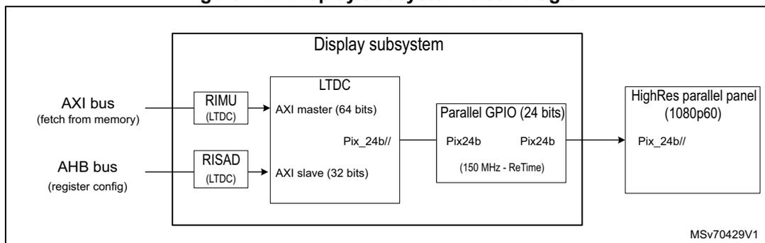
The diagram shows the internal architecture of the display subsystem. On the left, an AXI bus (fetch from memory) connects to a RIMU (LTDC) block, which in turn connects to an AXI master (64 bits) within the LTDC block. An AHB bus (register config) connects to a RISAD (LTDC) block, which connects to an AXI slave (32 bits) within the LTDC block. The LTDC block also contains a Pix_24b// output. This output connects to a Parallel GPIO (24 bits) block, which contains two Pix24b blocks operating at 150 MHz - ReTime. The Parallel GPIO block connects to a HighRes parallel panel (1080p60), which also contains a Pix_24b// output. The entire subsystem is labeled MSv70429V1.
42.4.2 Display subsystem pins and external signal interface
The details of the pins and external signal interface of the display subsystem can be found in the respective functional block sections in this reference manual.
42.4.3 Display subsystem clocks
Figure 443. Display subsystem clock diagram
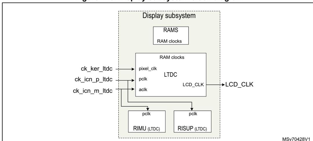
The diagram illustrates the clocking scheme for the display subsystem. External clock inputs are ck_ker_ltdc, ck_icn_p_ltdc, and ck_icn_m_ltdc. The LTDC block receives pixel_clk, pclk, and aclk. RAMS and RAM clocks are shown. The LTDC block also outputs LCD_CLK. The RIMU (LTDC) and RISUP (LTDC) blocks receive pclk. The entire subsystem is labeled MSv70428V1.
The display subsystem is implemented with the following clock max frequencies:
- • LTDC pixel clock (pixel_clk): 150 MHz
- • LTDC parallel interface (lcd_clk): 150 MHz (I/O ReTime mandatory)
- • Register clocks (ck_icn_p_*): 200 MHz (all APB/AHB register files)
- • AXI-Master clock (ck_icn_m_ltdc): 400 MHz
42.4.4 Display subsystem security
This section is an application of RIF security architecture (see Section 3.5.3: RIF infrastructure ). The security of the display subsystem is based on the protection of its register map and its master access to the system interconnect, based on default RISUP and RIMU respectively.
The RISUP differentiates the access right of accesses performed toward the following RIF protected peripheral ID (see Table 20: RISUP indexes ):
- • LTDC common: LTDC common registers, about panel info, synchronization, interface
- • LTDC_L1 (layer 1): for the window of a default application
- • LTDC_L2 (layer 2): LTDC layer 2, for the window of a potentially secure application
The RIMU (RIMU_AXI_LTDC) differentiates the bus transactions emitted by the following AXI masters:
- • RIMU_L1: read access only for layer 1, always non-protected
- • RIMU_L2: read access only for layer 2, potentially protected
Security configuration of devices with never-secure display content
The security setup of devices that are never required to display any secure content is detailed below (the display subsystem works by default in a non-protected mode):
- • The display subsystem configuration space is set as non-protected.
The default operating system (OS) software has a full access and can configure/handle all peripherals of the display subsystem. - • The layer 2 (which has a hardware secure capability) can be reused as a default layer, like layer 1, and can display the content of any application.
Note: Layer 2 is not fully featured, and lacks the resize and multi-planar capabilities of layer 1.
- • The LTDC AXI-master emits by default non-protected accesses.
The AXI CID = DISP S and P can be associated to the two AXI clients, via the RIMU, to tag that the AXI transaction contains pixels.
Security configuration of devices with a temporary secure content
For devices that temporarily display a secure content, it is expected that the secure content is displayed during short periods.
The working principle of the display subsystem is to segregate configuration spaces:
- • The secure layer 2 is always protected.
- • Never-secure layer 1 is always non-protected.
- • The intermediate common features (such as panel data, synchronization) are usually non-protected and handled by the OS (when no secure content is displayed), but temporarily protected (with no OS access) during the short period when a secure content is displayed via layer 2. Removing the access of the non-protected OS guarantees that a malware does not impact the stability of the displayed protected content.
- • A few minor items get specifically protected or open, as detailed below.
The configuration of the display subsystem for a secure content is the following:
- • Layer 2 is set permanently protected:
- – RIF LTDC_L2 RISUP peripheral ID must be set as protected (S and/or P flags).
- – RIF LTDC_L2 RIMU AXI-Master emits protected transactions (tagged as S a/o P), which allow it to retrieve the protected layer 2 pixels from their protected memory
buffer. The RIMU must be updated by a trusted domain application using RIFSC_RIMC_ATTR11.
The recommendation is to use a secure, privileged (optional), and CID = 0x4 setup. With this secure setup, the application must make sure that CID4 has access to the secure pixels area.
- – Only a secure software is able to configure the layer 2 parameters (such as width, height, buffer address), so that the characteristics of the layer 2 are guaranteed.
- – The interrupt bank B is associated automatically with the layer 2, and gets permanently protected and devoted to the secure software handling layer 2. The secure software must thus handle and be driven by that interrupt bank B.
- – The LTDC features that must allow data-evasion get also protected (automatically, as associated with the layer 2 rights), with an access allowed only to the secure software. These features are the CRC (which allows the displayed frames to be signed mainly for test purposes), the blend-order (which is used to hide the protected content below some malware layer faking the protected content).
- • Layer 1 is set permanently as non-protected:
- – RIF LTDC_L1 RISUP peripheral ID is set as not protected.
- – RIF LTDC_L1 RIMU AXI-master keeps its initial setup in RIFSC_RIMC_ATTR10, and emits only non-protected transactions which is enough to retrieve pixels from any application buffer.
- – The default OS drivers handle the layer 1 parameters (such as width, height, buffer address).
- – The interrupt bank A is associated automatically with layer 1, and keeps an non-protected open access. The OS must then handle and be driven by that Interrupt bank A to globally drive the display.
- • Common registers must be set at boot as non-protected, temporarily:
- – RIF LTDC common non-layer peripheral indexes is concerned.
- – This allows the default OS to boot the display subsystem, and to handle it.
- • Common registers must be set as protected when displaying a protected content:
- – The RIF LTDC common must be set protected before starting to display a protected content, and be unprotected after the protected content has finished to be updated. The LTDC common configuration spaces keep a permanent read access for nonsecure or unprivileged software.
- – The protection restricts the write accesses only: it removes the access of the non-protected OS, and so guarantees that a malware does not impact the stability of the displayed protected content. The LTDC common configuration spaces keep a permanent read-access for nonsecure or unprivileged software.
- – The protection does not restrict the read accesses: the OS is usually unaware of the status of the protected layer 2 that is handled by a different, secure, software. The read access capability for the OS allow the display drivers to remain. somehow stable, although the write access of the display drivers is not performed.
Table 379 lists vertically all the functional blocks of the display subsystem, and horizontally lists the associated RIF peripheral ID.
Note: Table color legend for recommended settings:
- - green for a permanently non-protected setting
- - blue for a temporarily protected versus non-protected
- - purple for a permanently protected state
Table 379. Display subsystem RIF peripheral ID
| All in display subsystem | RISUP-slave | ||||||
|---|---|---|---|---|---|---|---|
| 102 | 103 | 104 | |||||
| Blocks | Address range | (LTDC) address x1 | Start address x4 | End address x4 | LTDC common | LTDC_L1 | LTDC_L2 |
| LTDC | Common CFG0 | 0x0 | 0x0 | 0x30 | Y | - | - |
| Interrupt-A | 0xD | 0x34 | 0x3C | - | Y | - | |
| Common CFG1 | 0x10 | 0x40 | 0x60 | Y | - | - | |
| Interrupt-B | 0x19 | 0x64 | 0x70 | - | - | Y | |
| (empty) | 0x1D | 0x74 | 0x74 | Y | - | - | |
| CRC | 0x1E | 0x78 | 0x7C | - | - | Y | |
| Common CFG2 | 0x23 | 0x8C | 0xFC | Y | - | - | |
| L1-CFG0 (typ: video) | 0x40 | 0x100 | 0x100 | - | Y | - | |
| L1-CTRL | 0x41 | 0x104 | 0x104 | - | Y | - | |
| L1-CFG1 | 0x42 | 0x108 | 0x1FC | - | Y | - | |
| L2-CFG0 (typ: UI) | 0x80 | 0x200 | 0x200 | - | - | Y | |
| L2-CTRL | 0x81 | 0x204 | 0x204 | - | - | Y | |
| L2-CFG1 | 0x82 | 0x208 | 0x2FC | - | - | Y | |
42.5 Display subsystem programmable parameters
Steps to configure the various main use cases supported by the display subsystem are detailed below. They provide the global picture and settings of the display subsystem (not repeating information available in the local sections).
The display subsystem drives a display panel or bridge through the parallel interface. It allows panels to be driven up to 1080p60 (150 Mpixel/s), with either RGB888 or YUV422.
The RCC provides a pixel clock that drives both the LTDC and its synchronous parallel interface. Aside, the LTDC needs an AXI-Master clock to fetch pixels, and an APB-Slave clock to get configured.
The steps to follow are detailed below:
- 1. Setup security settings, with or without a secure layer depending on application needs, as described in Figure 442 .
- 2. Clock and reset:
- – ck_ker_ltdc clock, provided by the RCC, as output pixel clock.
One PLL of the RCC needs to be allocated to the display subsystem to provide the clock that is exactly at the wanted pixel rate for the output display. For instance, a standard 1080p60 requires a 148,50 MHz clock. - – LTDC_CLK is driven automatically by the LTDC (after some gating) from its above provided pixel_clock (ck_ker_ltdc from the RCC).
- – ck_icn_p_ltdc is provided by the RCC to allow the LTDC configuration (default 200 MHz).
- – ck_icn_m_ltdc is provided by the RCC to allow the LTDC AXI to work (default 400 MHz).
- – ck_ker_ltdc clock, provided by the RCC, as output pixel clock.
- 3. LTDC configuration:
- – Setup the LTDC (such as input layers, display information, parallel interface, AXI settings) as described in the LTDC section.
- 4. Signal polarity:
The polarities of the signals are impacted by the fact that the LTDC parallel interface signals are reclocked in the IO-ReTime logic, downstream of the LTDC. It results the following when configuring the polarities to match the panel on the parallel interface:- – The clock polarity (rising-vs-falling edge) must be configured in the IO-ReTime only (see Section 15: General-purpose I/Os (GPIO) ), and not in the LTDC output logic. The clock polarity logic in the LTDC must remain in its default post-reset state.
- – The polarity of the Vs, Hs, and De synchronization signals, unlike for the clock polarity, can be configured directly in the LTDC output stage (see Section 43: LCD-TFT display controller (LTDC) ).
- 5. I/O configuration:
Allocate an alternate GPIO bank to the display subsystem, with usually 28 pins needed: 24 pins for RGB888 and four others for the ancillary: Hs, Vs, De, and clock.
42.6 Display subsystem interrupts
The interrupts are described in sections of peripherals in this reference manual.
42.7 Display subsystem registers
All registers are described in Section 43: LCD-TFT display controller (LTDC) .