40. CSI-2 Host (CSI)
40.1 CSI introduction
The camera serial interface 2 (CSI-2) is a part of a group of communication protocols defined by the MIPI® Alliance. The MIPI® CSI-2 Host controller is a digital core that implements all protocol functions defined in the MIPI® CSI-2 specification.
It provides an interface between the system and the MIPI® D-PHY, allowing communication with a CSI-2 compliant camera.
40.2 Standard and references
- • MIPI Alliance Specification for Camera Serial Interface 2 (CSI-2) v1.3 - 29 May 2014
- • MIPI Alliance Specification for D-PHY v1.2 - 01 August 2014
40.3 Glossary
Table 368. Glossary of terms
| Term | Definition |
|---|---|
| D-PHY_RX | D-PHY physical layer receiver |
| EOF | End of frame |
| EOT | End of transmission |
| ESC | Escape mode for the D-PHY_RX |
| HS | High speed |
| ISB | Imaging system bus |
| LLP | Low-level protocol |
| LP | Low power |
| PHY | Physical layer |
| PPI | Phy protocol interface |
| RX | Receiver |
| SOF | Start of frame |
| SOT | Start of transmission |
40.4 CSI-2 Host main features
- • Compliant with MIPI Alliance standard (see Section 40.2 )
- • Interface with MIPI D-PHY (see Section 40.2 )
- • Up to two D-PHY data lanes supported (up to 2.5 Gbit/s per lane in high-speed (HS) mode and 10 Mbit/s in low-power (LP) mode)
- • Data transmission in HS and LP modes supported by the D-PHY
- • Escape mode (ESC) and ultra-low-power state mode (ULPS) supported
- • CSI-2 lane management layer connected to the D-PHY_RX to merge 1 or 2 data lanes in a single 32-bit ISB-Byte bus
- • ECC and error correction capabilities
- • CRC check capability
- • CSI-2 virtual channel and data type filtering supporting interleaved data
- – Up to 4 virtual channels
- – Support the data formats specified into the MIPI Alliance standard for CSI-2 v1.3 (18 data formats, plus the user defined ones)
- • Up to 7 independent data types
- • Programmable interrupts:
- – 4 timer interrupts mapped on a selected virtual channel with starting point from SOF (start of frame) or EOF (end of frame)
- – 4 line/byte counter interrupts mapped on a selected virtual channel to trigger an event
- • ISB-Byte header generation for internal connection with the DCMIPP peripheral
40.5 CSI-2 Host functional description
40.5.1 General description
The MIPI CSI-2 Host controller offers a means to connect cameras to capture and dispatch a robust header with ECC correction and data payload with checksum.
A D-PHY_RX receiver fills out the role of interfacing the external serial camera devices with the embedded CSI-2 Host controller:
- • D-PHY receiver:
This is a D-PHY_RX receiver composed of two unidirectional data lanes, and one clock lane. It operates in slave mode with HS and LP mode capabilities. The D-PHY drives a PPI interface to communicate with the CSI-2 Host. - • CSI-2 lane merger:
Up to two data lane inputs to increase data rate while avoiding high clock rates
The lane manager function collects incoming bytes from N (N = 1 to 2) lanes. It consolidates them by merging operations into a complete packet provided to the CSI-2 low-level protocol decoder (LLP), to decompose the meaning of each data packet thanks to the CSI-2 protocol specification. - • CSI-2 clock changer:
The clock changer moves the data transfer from an input clock domain from D-PHY_RX to a clock_proc domain before being processed by the LLP.
- CSI-2 low-level protocol decoder (LLP)
The low-level protocol is a byte-orientated packet-based protocol that supports the transport of arbitrary data using short and long packet formats.
It generates an ISB-byte header data for further processing, with data integrity check or miscellaneous integrity checks.
It supports data interleaving through the support of up to four virtual channels and many data type formats.
The LLP offers interrupt generation capability, depending on specific events such as line/byte detection within a frame, or a time-base event selected from a SOF or an EOF.
The CSI-2 Host-controller register bank is configured and accessed by the APB bus interface.
A block diagram of the CSI-2 Host is shown in the figure below.
Figure 416. CSI-2 Host block diagram
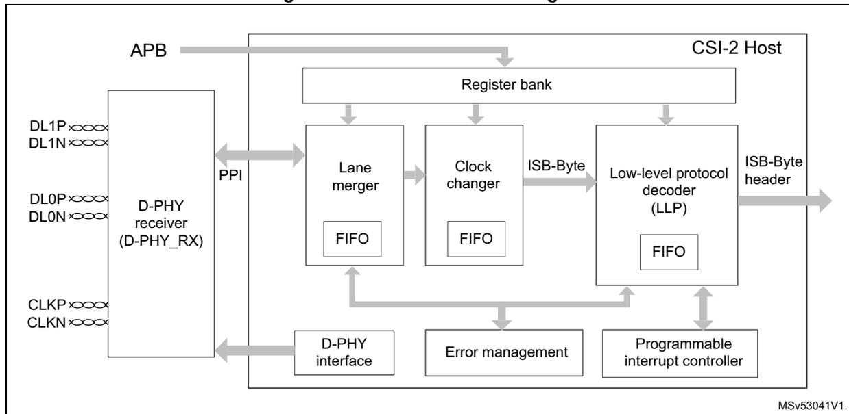
The block diagram illustrates the internal architecture of the CSI-2 Host. On the left, external pins are labeled DL1P, DL1N, DL0P, DL0N, CLKP, and CLKN, which connect to a D-PHY receiver (D-PHY_RX). This receiver is connected to the internal 'Lane merger' block via a PPI (Parallel Interface). The 'Lane merger' block contains a FIFO and is connected to the 'Clock changer' block, which also contains a FIFO. The 'Clock changer' outputs 'ISB-Byte' data to the 'Low-level protocol decoder (LLP)', which contains its own FIFO. The LLP outputs an 'ISB-Byte header'. Below these main blocks are the 'D-PHY interface', 'Error management', and 'Programmable interrupt controller', which are interconnected and connected to the 'Register bank'. The 'Register bank' is connected to the 'APB' (Advanced Peripheral Bus) at the top. The entire internal structure is labeled 'CSI-2 Host'.
40.5.2 System level architecture
The figure below shows the CSI-2 Host architecture.
Figure 417. CSI-2 Host architecture
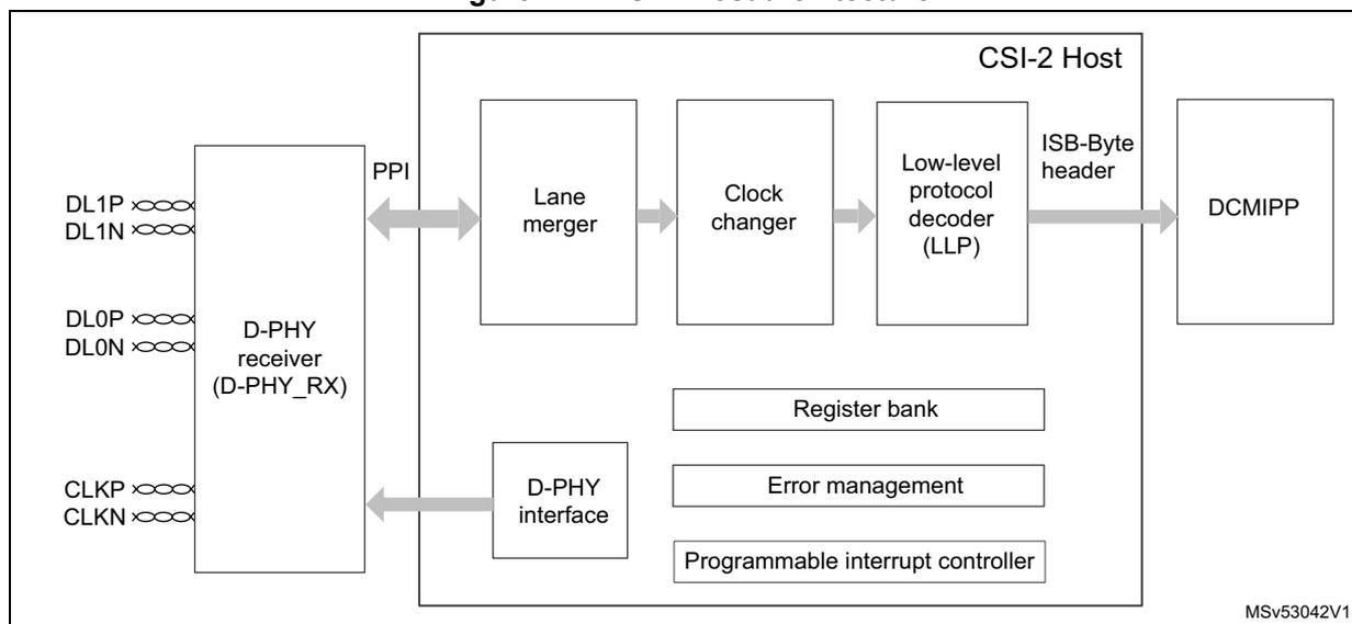
The diagram illustrates the CSI-2 Host architecture. On the left, external connections are shown: DL1P and DL1N (data lanes), DL0P and DL0N (data lanes), and CLKP and CLKN (clock lanes). These connect to a block labeled 'D-PHY receiver (D-PHY_RX)'. This block is connected via a 'PPI' (Parallel Interface) to a 'Lane merger' block. The 'Lane merger' is part of a larger 'CSI-2 Host' block. Inside the 'CSI-2 Host' block, the data flow proceeds from the 'Lane merger' to a 'Clock changer', then to a 'Low-level protocol decoder (LLP)'. The 'LLP' outputs an 'ISB-Byte header' to a 'DCMIPP' block. Below the main data path, a 'D-PHY interface' block is connected to the 'D-PHY_RX' and to a 'Register bank'. The 'Register bank' is connected to an 'Error management' block, which is in turn connected to a 'Programmable interrupt controller'.
The blocks shown have the following functions:
- • D-PHY_RX is a slave receiver device that connects external serial cameras to the CSI-2 Host controller. It is based on unidirectional slave data lanes and clock lanes to handle data transmission from the CSI-2 protocol-based camera devices to subsystems for data processing (handled by the DCMIPP).
- • The D-PHY interface manages D-PHY_RX register accesses. It also allows the block to be configured to raise interrupts on the detection of some errors during reception. It highlights the status of the physical lines up to the software layers.
- • The lane merger module packs the data coming from the two D-PHY_RX data lanes, if required to do so for increased data rates. It generates a data flow based on an ISB-Byte protocol, which is not linked to any protocol at this point. The data is only identified as a control or a data packet for the clock changer module.
- • The clock changer module manages data crossing from the D-PHY_RX clock domain to the clk_proc clock domain.
- • The LLP handles data filtering to serve the data-interleaving capability of the DCMIPP. It can filter data from external devices depending on virtual channel identifiers, or on data-type format selection. It also executes, depending on the input pixel format, data reordering in order to optimize the data storage, for instance in memories.
- • The CSI-2 Host manages also various errors coming (not exclusively) from the D-PHY_RX physical layer. It can detect error conditions in the received header or a short packet in a frame. ECC is implemented to correct one bit error in the header. A CRC checksum is also implemented to detect any data corruption during the data payload reception. The 16-bit CRC value is located into the packet footer. The CSI-2 Host also ensures that specific timings within the data reception are properly in line with the CSI-2 specification. All error conditions and associated interrupts are detailed in Section 40.8 .
- • A specific module generates interrupts following the detection of selected events in a frame. For a given virtual channel, these events may be triggers based on line- and byte-number detection within the frame, or counters from dedicated timers reaching a number of cycles (clk_proc) from an SOF or an EOF.
- • Data is filtered out by the LLP, and sent to the DCMIPP in a format that is quite similar to the CSI-2 protocol, but without CRC (packet footer) and ECC information inside the packet header. The data type and the virtual channel are also sent to the DCMIPP to handle the interleaved transmission of different image data formats within the same video data stream.
40.5.3 CSI-2 Host reset and clocks
There are two reset sources:
- • hardware asynchronous reset which is resynchronized on clk_byte and clk_proc clock domain (processing clock) to reset the flops connected to these clock domains
- • APB reset from the reset and clock controller unit to reset mainly all the registers
There are three clocks to serve the CSI-2 Host controller (see Figure 418 ):
- • clk_byte: derived from the D-PHY_RX clock lane, and used by the lane merger module and the clock changer module
- • clk_proc: used by the kernel of the LLP
Resynchronization between the clk_byte domain and the clk_proc domain is handled by the clock changer module. - • PCLK clock: APB clock used to access to the register bank
Figure 418. CSI-2 Host clock domain
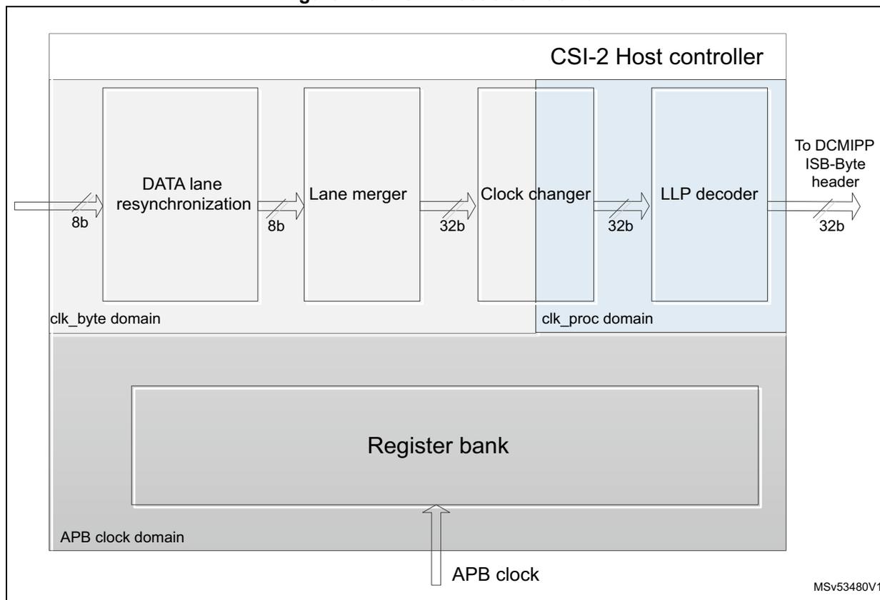
The diagram illustrates the CSI-2 Host clock domain. It is divided into three main clock domains: clk_byte domain , clk_proc domain , and APB clock domain .
- clk_byte domain : Contains the DATA lane resynchronization block. It receives an 8b input and outputs an 8b signal to the Lane merger block.
- clk_proc domain : Contains the Lane merger , Clock changer , and LLP decoder blocks. The Lane merger outputs a 32b signal to the Clock changer , which in turn outputs a 32b signal to the LLP decoder . The LLP decoder outputs a 32b signal labeled To DCMIPP ISB-Byte header .
- APB clock domain : Contains the Register bank block. It is connected to the APB clock input.
The CSI-2 Host controller is shown as a large box containing the clk_byte domain and clk_proc domain blocks. The Register bank is shown as a separate block below the controller, connected to the APB clock .
The D-PHY_RX supports up to 2.5 Gbit/s per data lane: the maximum frequency on the D-PHY_RX clock is \( 2.5 \text{ Gbits} / 8 \) to output a byte = 312 MHz.
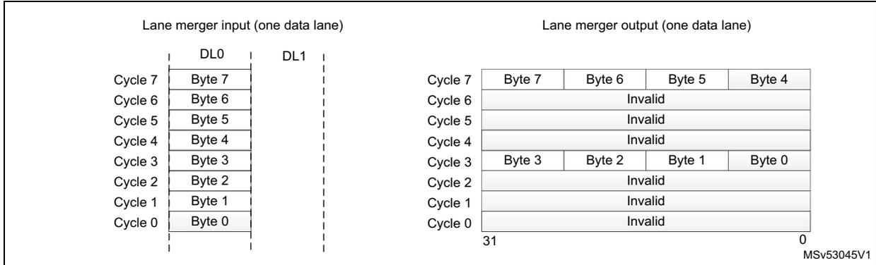
40.5.4 Lane merger
Applications requiring more bandwidth than the one provided by a single data lane may expand the data path to more lanes in order to increase the attainable data rate. The lane merger supports then up to two data lanes.
The lane merger module converts the D-PHY_RX PPI protocol into a byte-oriented bus to be sent to the LLP.
The lane merger parallelizes the bytes to 32 bits in parallel to build a 32-bit output as shown in the figures below. The cycle number does not account for module internal latency.
Figure 419. Lane merger input and output (one data lane)
| Lane merger input (one data lane) | Lane merger output (one data lane) | |||||
|---|---|---|---|---|---|---|
| Cycle | DL0 | DL1 | Byte 7 | Byte 6 | Byte 5 | Byte 4 |
| 7 | Byte 7 | Byte 7 | Byte 6 | Byte 5 | Byte 4 | |
| 6 | Byte 6 | Invalid | ||||
| 5 | Byte 5 | Invalid | ||||
| 4 | Byte 4 | Invalid | ||||
| 3 | Byte 3 | Byte 3 | Byte 2 | Byte 1 | Byte 0 | |
| 2 | Byte 2 | Invalid | ||||
| 1 | Byte 1 | Invalid | ||||
| 0 | Byte 0 | Invalid | ||||
MSv53045V1
Figure 420. Lane merger input and output (two data lanes)
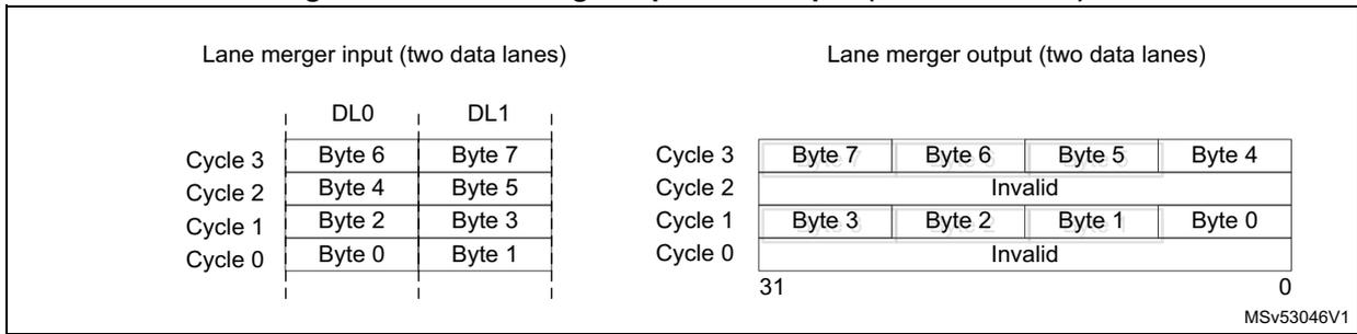
| Lane merger input (two data lanes) | Lane merger output (two data lanes) | |||||
|---|---|---|---|---|---|---|
| Cycle | DL0 | DL1 | Byte 7 | Byte 6 | Byte 5 | Byte 4 |
| 3 | Byte 6 | Byte 7 | Byte 7 | Byte 6 | Byte 5 | Byte 4 |
| 2 | Byte 4 | Byte 5 | Invalid | |||
| 1 | Byte 2 | Byte 3 | Byte 3 | Byte 2 | Byte 1 | Byte 0 |
| 0 | Byte 0 | Byte 1 | Invalid | |||
MSv53046V1
LANENB[2:0] in CSI_LMCFGGR configures the number of data lanes used in the application. The software needs to map the physical data lanes input to the lane merger logical data lanes, using DL0MAP[2:0] and DL1MAP[2:0] as shown in the figure below.
Figure 421. Data lane mapping
![Block diagram showing physical data lanes 0 and 1 being mapped via multiplexers controlled by DL0MAP[2:0] and DL1MAP[2:0] to logical data lanes 0 and 1, which then enter the Lane merger block.](/RM0486-STM32N6x5-x7/f6691a6b2253a325f495bbfca5df585c_img.jpg)
MSv53047V1
40.5.5 Clock changer
The clock changer module changes the clock frequency from the input clock domain linked to the D-PHY_RX PPI protocol, to the output clock domain based on clk_proc clock domain (reference clock for the LLP).
An integrated FIFO receives data from the input clock domain and realigns it to the output clock domain.
40.5.6 Low-level protocol (LLP)
The LPP module retrieves the raw data from the lane merger, and decodes the data flow respect to the CSI-2 low-level protocol. The software selects which data in the data interleaving flow need to be sent to the DCMIPP without being filtered out. The LLP is compliant with the MIPI CSI-2 specification as described in Section 40.2 .
A data integrity check is done thanks to an ECC code for packet header error correction, and a 16-bit CRC checksum code for payload error detection. All these errors are flagged into specific registers, and may trig interruption for specific software action needs (see Section 40.8 for more details).
Figure 422. Low-level protocol overview
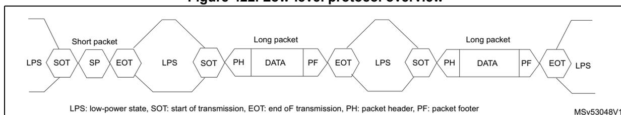
LPS: low-power state, SOT: start of transmission, EOT: end of transmission, PH: packet header, PF: packet footer
MSv53048V1
The CSI-2 low-level protocol is mainly composed by short and long packets, each of them having a well identified role.
Long packet
The long packet format is presented in Figure 423 . It contains a data ID that is composed of a virtual channel number for which the data packets are attached, and the corresponding data type. The LLP module filters data out by configuring CSI_VCxCFGRy registers ( \( x = 0 \) to \( 3 \) , \( y = 1 \) to \( 4 \) ), and VCxSTART/VCxSTOP bits in CSI_CR register.
The word-count field allows the LLP to determine the data-payload width before detecting the packet footer and the EOT. This information is used to detect shorter-than-expected packets, and to trigger a corresponding error (refer to Section 40.8 ).
The ECC corrects a single erroneous bit in the packet header in the case of data corruption. An error is raised if there are two errors in total (the LLP decoder immediately stops the current frame), because only one bit can be corrected.
The packet data corresponds to the data payload for a given virtual channel and for an identified data type.
To complete the long-packet reception block, a packet footer that contains a 16-bit CRC checksum is received and compared to that which is internally calculated by the LLP, to check the data integrity of the received data payload.
Figure 423. CSI2- long-packet structure for a D-PHY physical layer
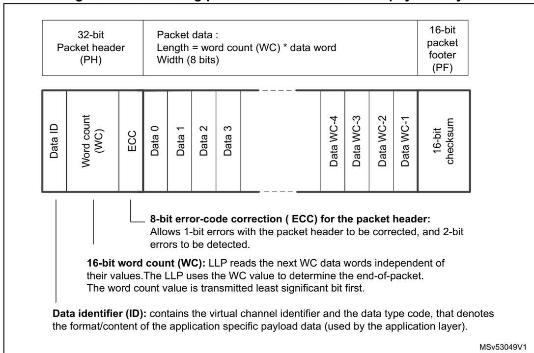
32-bit Packet header (PH)
Packet data :
Length = word count (WC) * data word
Width (8 bits)
16-bit packet footer (PF)
Data ID
Word count (WC)
ECC
Data 0
Data 1
Data 2
Data 3
...
Data WC-4
Data WC-3
Data WC-2
Data WC-1
16-bit checksum
8-bit error-code correction (ECC) for the packet header:
Allows 1-bit errors with the packet header to be corrected, and 2-bit errors to be detected.
16-bit word count (WC): LLP reads the next WC data words independent of their values. The LLP uses the WC value to determine the end-of-packet. The word count value is transmitted least significant bit first.
Data identifier (ID): contains the virtual channel identifier and the data type code, that denotes the format/content of the application specific payload data (used by the application layer).
MSV53049V1
Short packet
The CSI-2 short-packet format for a D-PHY physical layer is shown in Figure 424 .
It is similar to the long packet header, except that the word count field is replaced by a 16-bit data field. The ECC 8-bit code is present to secure headers having potential bit corruption.
Figure 424. Short-packet structure based on D-PHY physical layer
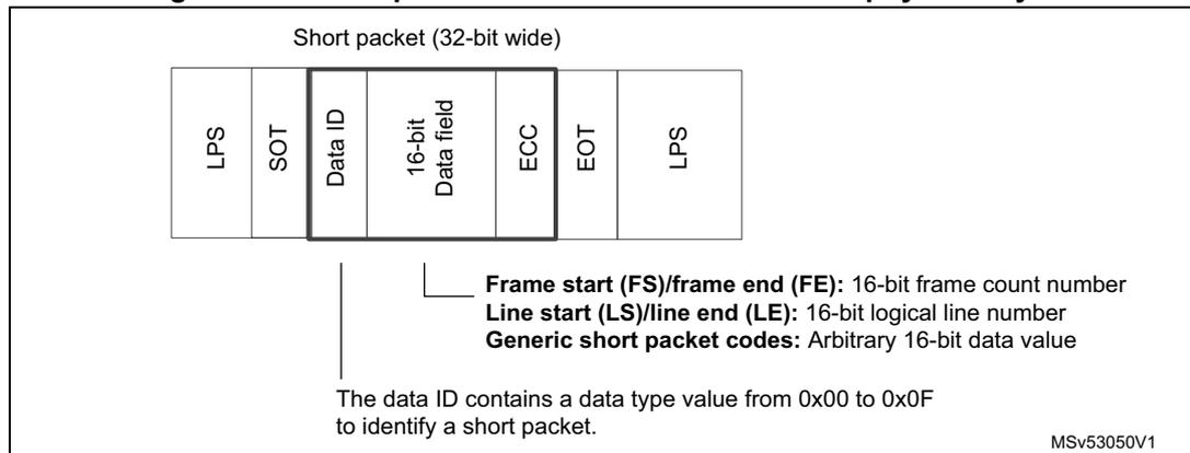
Short packet (32-bit wide)
LPS
SOT
Data ID
16-bit Data field
ECC
EOT
LPS
Frame start (FS)/frame end (FE):
16-bit frame count number
Line start (LS)/line end (LE):
16-bit logical line number
Generic short packet codes:
Arbitrary 16-bit data value
The data ID contains a data type value from 0x00 to 0x0F to identify a short packet.
MSV53050V1
Data ID field
The 8-bit data ID field comprises 2 bits for the virtual channel number coding, and 6 bits to identify the packet data type (short or long packet), and the payload data packet format in the case of long packet reception.
The LLP filters subsequent packets depending on the user configuration indicated in the previously received data ID field (see Figure 425 ).
Figure 425. DATA ID structure in short or long packet format
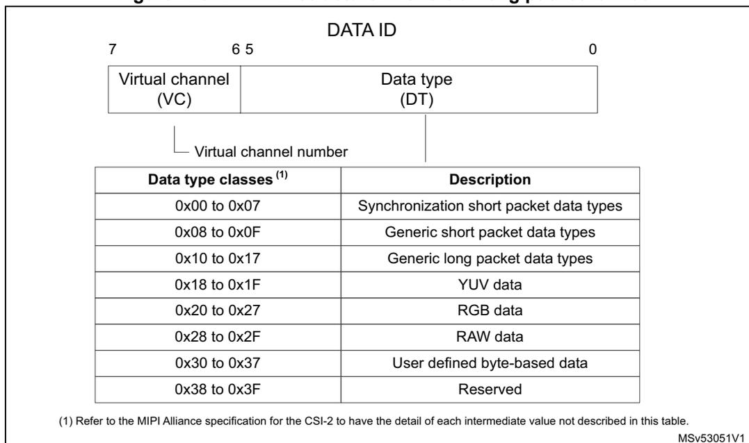
DATA ID
7 6 5 0
| Virtual channel (VC) | Data type (DT) |
└ Virtual channel number
| Data type classes (1) | Description |
|---|---|
| 0x00 to 0x07 | Synchronization short packet data types |
| 0x08 to 0x0F | Generic short packet data types |
| 0x10 to 0x17 | Generic long packet data types |
| 0x18 to 0x1F | YUV data |
| 0x20 to 0x27 | RGB data |
| 0x28 to 0x2F | RAW data |
| 0x30 to 0x37 | User defined byte-based data |
| 0x38 to 0x3F | Reserved |
(1) Refer to the MIPI Alliance specification for the CSI-2 to have the detail of each intermediate value not described in this table.
MSV53051V1
Data type field
The data type (DT) fields are configured by the application code to determine which data types are processed by the LLP for a given virtual channel. CSI_VCxCFG Ry registers are used to configure the data types to be considered by the LLP.
Each virtual channel is managed independently, and up to seven different virtual-channel data types can be declared in parallel. All data type input to the LLP that are not defined for a given virtual channel are filtered out by the LLP module and discarded.
Data types in the video data flow are located:
- • in the data ID packet for a short packet
- • in the packet header (PH) for a long packet format
Data interleaving: data-type based
In the video data flow, the transmitter can merge, on the same physical node, multi-device data transmissions having different data types. The LLP filters out these multi-device flows depending on the application configuration. A typical video data flow interleaving multiple data types is shown in Figure 426 .
The application software must configure CSI_VCxCFG Ry registers to enable data types for a virtual channel, and to set data-type formats to be processed. The LLP reorders the input data in a format that optimizes memory usage (see Figure 426 to Figure 434 ).
Figure 426. Data interleaving using data type
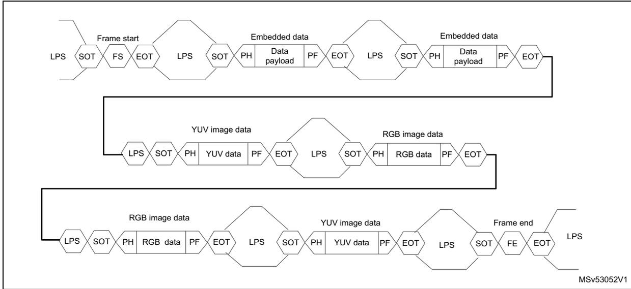
The diagram illustrates data interleaving using data type. It shows three horizontal data streams being interleaved into a single output stream. The top stream contains 'Frame start' (LPS, SOT, FS, EOT) followed by two 'Embedded data' packets (LPS, SOT, PH, Data payload, PF, EOT). The middle stream contains 'YUV image data' (LPS, SOT, PH, YUV data, PF, EOT) and 'RGB image data' (LPS, SOT, PH, RGB data, PF, EOT). The bottom stream contains 'RGB image data' (LPS, SOT, PH, RGB data, PF, EOT), 'YUV image data' (LPS, SOT, PH, YUV data, PF, EOT), and 'Frame end' (LPS, SOT, FE, EOT). Arrows indicate the interleaving of data from different sources into a single output stream. The diagram is labeled MSv53052V1 in the bottom right corner.
Data interleaving: virtual channels
The data interleaving in the video data flow can also be managed by the virtual channel ID. Each external device can have a specific virtual channel identifier in order for the software layer or the DCMIPP to properly handle data packets belonging to a device.
The application code defines which of the virtual channels have to be considered by the LPP without any filtering operation. The CSI_CR register must be configured accordingly by activating the virtual channel (via VCxSTART), or by setting VCxSTOP to deactivate the virtual channel.
The virtual channel number is encapsulated in the data ID packet in short or long packet.
A typical data interleaving case is illustrated in Figure 427 .
Figure 427. Data interleaving using virtual channels
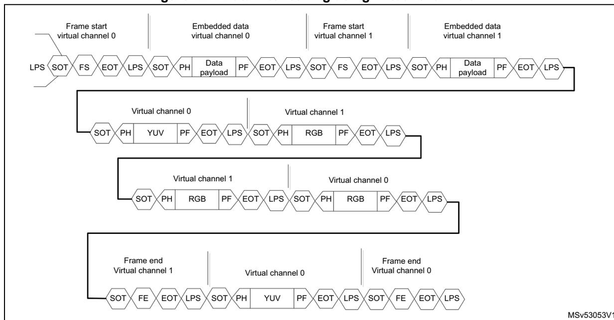
The diagram illustrates the data interleaving process using virtual channels in a CSI-2 Host. It shows a sequence of packets (SOT, FS, EOT, LPS, PH, Data payload, PF) being interleaved between two virtual channels (0 and 1).
The sequence starts with a frame start for virtual channel 0, followed by embedded data for virtual channel 0, then a frame start for virtual channel 1, and finally embedded data for virtual channel 1. The sequence ends with a frame end for virtual channel 1, followed by embedded data for virtual channel 0, and then a frame end for virtual channel 0.
The diagram is divided into three horizontal sections, each showing a different interleaving scenario. The first section shows a single frame start and end. The second section shows two frame starts and ends. The third section shows a frame end, a frame start, and another frame end.
The diagram is labeled with 'MSv53053V1' in the bottom right corner.
Data formats
The LLP, in addition to a data-flow filter role, handles data reordering for memory optimization, storage, or post-processing purposes.
The CSI-2 Host controller is compliant with the MIPI Alliance CSI-2 specification. It mainly supports the following data formats:
- • BPP6 (for example RAW6, RGB666)
- • BPP7 (for example RAW7)
- • BPP8 (for example RAW8, YUV 8-bits, RGB444, RGB555, RGB565, RGB888, JPEG)
- • BPP10 (for example RAW10, YUV 10-bits)
- • BPP12 (for example RAW12)
- • BPP14 (for example RAW14)
- • BPP16 (for example RAW16)
Figure 428. RAW6 (BPP6) input and output format
![Diagram showing RAW6 (BPP6) input and output format for three cycles. Each cycle has four columns labeled n+3, n+2, n+1, n+0. Cycle 1 contains P5[1:0], P4[5:0], P3[5:0], P2[5:0], P1[5:0], P0[5:0]. Cycle 2 contains P10[3:0], P9[5:0], P8[5:0], P7[5:0], P6[5:0], P5[5:2]. Cycle 3 contains P15[5:0], P14[5:0], P13[5:0], P12[5:0], P11[5:0], P10[5:4]. Bit positions 31 and 0 are indicated at the bottom of each cycle's data row.](/RM0486-STM32N6x5-x7/3803569665fc628700e4705dbd492006_img.jpg)
The diagram illustrates the RAW6 (BPP6) input and output format across three cycles. Each cycle is divided into four columns labeled n+3, n+2, n+1, and n+0. The data is presented in a 6-bit wide format, with bit positions 31 and 0 indicated at the bottom of each cycle's data row.
Cycle 1:
| n+3 | n+2 | n+1 | n+0 | ||||||||
| P5[1:0] | P4[5:0] | P3[5:0] | P2[5:0] | P1[5:0] | P0[5:0] | ||||||
| 31 | 0 | ||||||||||
Cycle 2:
| n+3 | n+2 | n+1 | n+0 | ||||||||
| P10[3:0] | P9[5:0] | P8[5:0] | P7[5:0] | P6[5:0] | P5[5:2] | ||||||
| 31 | 0 | ||||||||||
Cycle 3:
| n+3 | n+2 | n+1 | n+0 | ||||||||
| P15[5:0] | P14[5:0] | P13[5:0] | P12[5:0] | P11[5:0] | P10[5:4] | ||||||
| 31 | 0 | ||||||||||
MSv53054V1
Figure 429. Raw7 (BPP7) input and output format
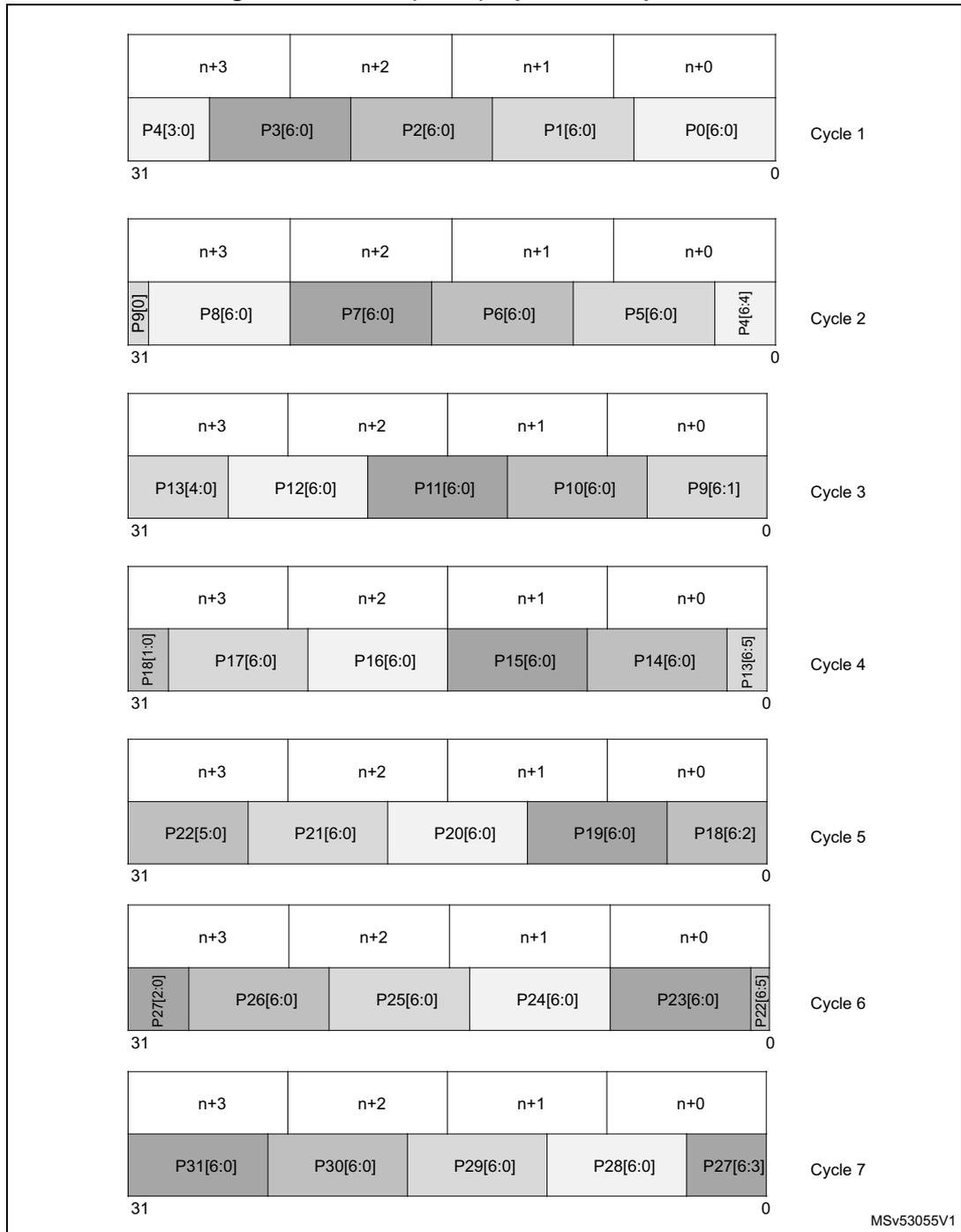
The diagram illustrates the Raw7 (BPP7) input and output format across seven cycles. Each cycle consists of four words (n+3, n+2, n+1, n+0) and a corresponding data payload (P0 to P31) with specific bit widths. The diagram includes bit positions 31 and 0 for each cycle.
| Cycle | n+3 | n+2 | n+1 | n+0 | Bit Widths |
|---|---|---|---|---|---|
| Cycle 1 | P4[3:0] | P3[6:0] | P2[6:0] | P1[6:0] | P0[6:0] |
| Cycle 2 | P9[0] | P8[6:0] | P7[6:0] | P6[6:0] | P5[6:0], P4[6:4] |
| Cycle 3 | P13[4:0] | P12[6:0] | P11[6:0] | P10[6:0] | P9[6:1] |
| Cycle 4 | P18[1:0] | P17[6:0] | P16[6:0] | P15[6:0] | P14[6:0], P13[6:5] |
| Cycle 5 | P22[5:0] | P21[6:0] | P20[6:0] | P19[6:0] | P18[6:2] |
| Cycle 6 | P27[2:0] | P26[6:0] | P25[6:0] | P24[6:0] | P23[6:0], P22[6:5] |
| Cycle 7 | P31[6:0] | P30[6:0] | P29[6:0] | P28[6:0] | P27[6:3] |
MSV53055V1
Figure 430. Raw8 (BPP8) input and output format
![Diagram of Raw8 (BPP8) input and output format for Cycle 1. It shows a 32-bit word structure with four 8-bit pixel data segments: P3[7:0], P2[7:0], P1[7:0], and P0[7:0]. The word is divided into four 16-bit nibbles labeled n+3, n+2, n+1, and n+0. Bit 31 is the start of the first pixel and bit 0 is the end of the last pixel.](/RM0486-STM32N6x5-x7/4f3ef4c523f681c469a4b5c839a32812_img.jpg)
Diagram illustrating the Raw8 (BPP8) input and output format for Cycle 1. The 32-bit word is divided into four 8-bit pixel data segments: P3[7:0], P2[7:0], P1[7:0], and P0[7:0]. The word is divided into four 16-bit nibbles labeled n+3, n+2, n+1, and n+0. Bit 31 is the start of the first pixel and bit 0 is the end of the last pixel.
Figure 431. Raw 10 (BPP10) input and output format
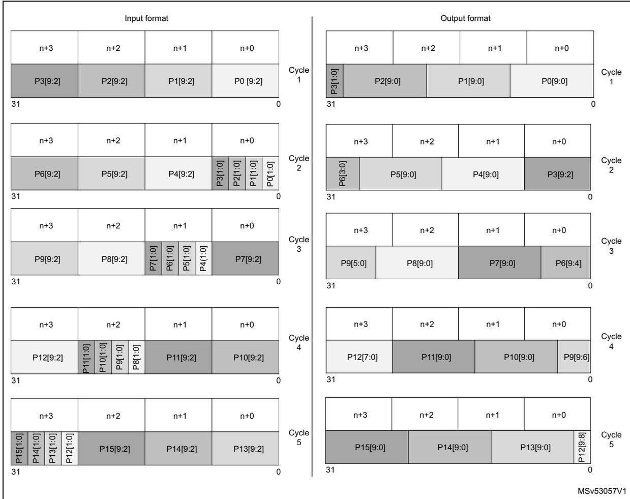
Diagram illustrating the Raw 10 (BPP10) input and output format across five cycles. The input format shows pixels P0 through P15 being packed into five cycles. The output format shows the same pixels being unpacked. Each cycle has four nibbles: n+3, n+2, n+1, n+0. Bit 31 is the start and bit 0 is the end of each 32-bit word.
Figure 432. Raw12 (BPP12) input/output format
![Diagram showing Raw12 (BPP12) input/output format across three cycles. It details the mapping of pixel data (P0-P7) from input format to output format for cycles 1, 2, and 3, with bit positions (n+0 to n+3) and bit ranges (e.g., [11:4], [3:0]) indicated.](/RM0486-STM32N6x5-x7/7f2c91e3cefd29399a9a98f2f46f5ed4_img.jpg)
The diagram illustrates the Raw12 (BPP12) input/output format across three cycles. It is divided into two main columns: 'Input format' and 'Output format'.
Input format:
- Cycle 1: A 32-bit word structure with 4 nibbles (n+3, n+2, n+1, n+0). The data is: P2[11:4] in n+3, P1[3:0] and P0[3:0] in n+2, P1[11:4] in n+1, and P0[11:4] in n+0.
- Cycle 2: A 32-bit word structure with 4 nibbles. The data is: P5[11:4] in n+3, P4[11:4] in n+2, P3[3:0] and P2[3:0] in n+1, and P3[11:4] in n+0.
- Cycle 3: A 32-bit word structure with 4 nibbles. The data is: P7[3:0] and P6[3:0] in n+3, P7[11:4] in n+2, P6[11:4] in n+1, and P5[3:0] and P4[3:0] in n+0.
Output format:
- Cycle 1: A 32-bit word structure with 4 nibbles. The data is: P2[7:0] in n+3, P1[11:0] in n+2, and P0[11:0] in n+1. The n+0 nibble is empty.
- Cycle 2: A 32-bit word structure with 4 nibbles. The data is: P5[3:0] in n+3, P4[11:0] in n+2, P3[11:0] in n+1, and P2[11:8] in n+0.
- Cycle 3: A 32-bit word structure with 4 nibbles. The data is: P7[11:0] in n+3, P6[11:0] in n+2, and P5[11:4] in n+1. The n+0 nibble is empty.
Bit positions 31 and 0 are indicated at the bottom of each cycle's data structure. The identifier MSV53058V1 is present at the bottom right.
Figure 433. Raw14 (BPP14) input format
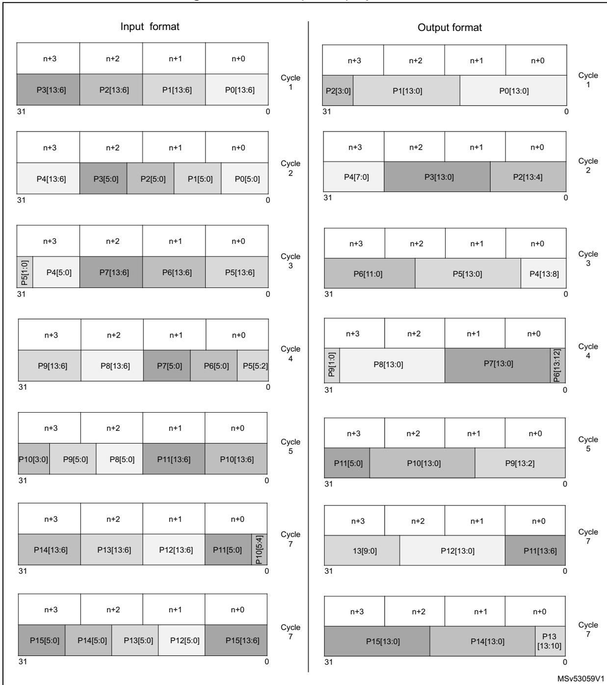
Input format
Cycle 1
n+3: P3[13:6], n+2: P2[13:6], n+1: P1[13:6], n+0: P0[13:6]
31 0
Cycle 2
n+3: P4[13:6], n+2: P3[5:0], n+1: P2[5:0], n+0: P1[5:0], P0[5:0]
31 0
Cycle 3
n+3: P5[1:0], P4[5:0], n+2: P7[13:6], n+1: P6[13:6], n+0: P5[13:6]
31 0
Cycle 4
n+3: P9[13:6], n+2: P8[13:6], n+1: P7[5:0], P6[5:0], n+0: P5[5:2]
31 0
Cycle 5
n+3: P10[3:0], P9[5:0], P8[5:0], n+2: P11[13:6], n+1: P10[13:6], n+0:
31 0
Cycle 7
n+3: P14[13:6], n+2: P13[13:6], n+1: P12[13:6], n+0: P11[5:0], P10[5:4]
31 0
Cycle 7
n+3: P15[5:0], n+2: P14[5:0], n+1: P13[5:0], n+0: P12[5:0], P15[13:6]
31 0
Output format
Cycle 1
n+3: P2[3:0], n+2: P1[13:0], n+1: P0[13:0], n+0:
31 0
Cycle 2
n+3: P4[7:0], n+2: P3[13:0], n+1: P2[13:4], n+0:
31 0
Cycle 3
n+3: P6[11:0], n+2: P5[13:0], n+1: P4[13:8], n+0:
31 0
Cycle 4
n+3: P9[1:0], n+2: P8[13:0], n+1: P7[13:0], n+0: P6[13:12]
31 0
Cycle 5
n+3: P11[5:0], n+2: P10[13:0], n+1: P9[13:2], n+0:
31 0
Cycle 7
n+3: P13[9:0], n+2: P12[13:0], n+1: P11[13:6], n+0:
31 0
Cycle 7
n+3: P15[13:0], n+2: P14[13:0], n+1: P13[13:10], n+0:
31 0
MSV53059V1
Figure 434. Raw16 (BPP16) input/output format
![Figure 434. Raw16 (BPP16) input/output format. The diagram shows two tables representing input and output data formats for Cycle 1. The input format table has four columns labeled n+3, n+2, n+1, n+0. The first row contains these labels, and the second row contains P1[7:0], P1[15:8], P0[7:0], P0[15:8]. Bit positions 31 and 0 are indicated at the bottom. The output format table also has four columns labeled n+3, n+2, n+1, n+0. The first row contains these labels, and the second row contains P1[15:0] and P0[15:0] (each spanning two columns). Bit positions 31 and 0 are indicated at the bottom. The text 'MSv53080V2' is in the bottom right corner.](/RM0486-STM32N6x5-x7/8d8b4353adec6f70dca9c1cf848fc69c_img.jpg)
40.5.7 CSI-2 Host protocol output
The CSI-2 Host controller generates ISB-Byte header data according to CSI_VCxCFGRy. The ISB-Byte header generation respects the following rules:
- • ISB-Byte header channel number is identical to the CSI-2 virtual channel and data type (LSB aligned).
- • ISB-Byte header data type is identical to CSI-2 data type (LSB aligned).
- • ISB-Byte header frame number is identical to the CSI-2 frame number.
- • ISB-Byte header count is identical to CSI-2 word count.
- • The format is updated according to CSI_VCxCFGRy configuration.
The only differences between the ISB-Byte data flow in input to the LLP and the ISB-Byte header bus at the output are listed below:
- • There is no ECC information in the data corresponding to the short packet information.
- • The packet footer (containing the CRC-16 value) is not transmitted, or forwarded on the output since the decoder already checked it from the input, and raised an error if the data payload is corrupted.
- • The data payload output format is reordered and compared to the input data format of the LLP in order to ease pixels storage in memory for further hardware/software post-processing.
- • Only identified virtual channels and their selected data types are generated on the output.
The ISB-Byte header is used by the DCMIPP peripheral to handle post-processing data from the external devices.
40.6 CSI-2 Host programming guide
40.6.1 CSI-2 PHY setup
The following actions are required to setup the CSI-2 PHY:
- 1. Quit the hardware reset state with PEN = 0x01 in CSI_PRCR.
- 2. Configure frequency settings with:
- – DLD = 0x00 in CSI_PFCR (to remain in Rx)
- – HSFR in CSI_PFCR that depends on the bit-rate expected on the data lanes
- – CCFR = RoundUp((F - 17) × 4) in CSI_PFCR (F = configuration clock frequency)
- 3. Configure internal registers via the test interface, with TRSEN = TCKEN = 0x0 in CSI_PTCR0.
40.6.2 CSI-2 Host controller setup and data reception start
The D-PHY RX software initialization is required to set up the CSI-2 Host controller.
Lane-merger configuration (static configuration)
The lane merger must be configured while CSIEN = 0 in CSI_CR, and when the D-PHY_RX is not streaming (when it is not providing a clock).
To map the physical data lane to the logical data lane, the lane merger needs to be configured through DL0MAP and DL1MAP in CSI_LMCFGGR. In addition, the number of valid data lanes must be configured through LANENB in the same register.
LLP configuration
- 1. Configure the watchdog value in CSI_WDR. This corresponds to the maximum number of clock cycles between two packets before an input frame is considered erroneous and the transmission failed. It can be left at 0x0 to disable the watchdog feature.
- 2. Enable the CSI-2 Host controller with CSIEN = 1 in CSI_CR.
- 3. Configure the selected virtual channels in CSI_VCxCFG Ry.
If all data types must be captured with the same format, in CSI_VCxCFG R1:- – Set ALLDT = 0x011.
- – Select the format with CDTFT[4:0].
- – Set ALLDT = 0x0 in CSI_VCxCFG R1.
- – Set DTyEN = 0x1 (y = 0 to 6) in CSI_VCxCFG R1 for the data types used.
- – Set DTy[5:0] in CSI_VCxCFG Ry to the selected data type.
- – Set DTyFT[4:0] in CSI_VCxCFG Ry to the selected format.
- 4. Depending on application requirements, specific software actions may detect particular events in a frame, and trigger a corresponding interrupt, with the following:
- – Set LINECNT[15:0] and BYTECNT[15:0] in CSI_LBxCFG R to trigger an event when the data corresponding to a specific byte within a specific line is detected by the LLP. Up to four independent triggers can be programmed and linked to a selected virtual channel through LBxVC[1:0] in CSI_PRGITR. The selected trigger can be enabled by setting LBxEN in the same register.
- – Set COUNT[24:0] in CSI_TIMxCFG R to trigger an event after a specified number of clock cycles (clk_proc) from an SOF or an EO, depending on TIMxEOF and TIMxEN in CSI_PRGITR. Up to four independent timer triggers can be programmed and linked to a selected virtual channel through TIMxVC[1:0] in CSI_PRGITR.
- 5. Enable interrupt sources for which the code needs to make specific actions, by configuring CSI_IER0 and CSI_IER1 registers.
- 6. D-PHY_RX lanes can be enabled by setting DL0EN and/or DL1EN, and CLEN in CSI_PCR.
- 7. Start the virtual channel by setting VCxSTART = 0x1 in CSI_CR.
40.6.3 Data reception stop
To stop data reception, set VCxSTOP = 1 in CSI_CR. The data reception stops at the end of the current frame. The virtual channel status can be retrieved from VCxSTATEF in CSI_SR0.
Note: A virtual channel cannot start before it has been completely stopped (VCxSTATEF = 0 in CSI_SR0).
40.7 CSI-2 Host low-power modes
Table 369. Effect of low-power modes on CSI-2 Host controller
| Mode | Description |
|---|---|
| Sleep | No effect. The CSI-2 host interrupts cause the device to exit the Sleep mode. |
| Stop | The CSI-2 host is in power-down, and must be reinitialized after exiting Stop mode. |
| Standby | The CSI-2 host is in power-down, and must be reinitialized after exiting Standby mode. |
40.8 CSI-2 Host interrupts and errors
Few events can generate an error flag or an interrupt from the CSI-2 Host controller interrupt handler.
The table below defines the error sources flagged by the CSI-2 HOST controller. The content of CSI_ERR1 and CSI_ERR2 registers can be used to know exactly from which virtual number and data types a particular error appeared and has been detected. It can be used as debug purpose too.
Table 370. List of errors detected by the CSI-2 Host controller
| Error description | Bit name | Register |
|---|---|---|
| Virtual channel number on which a data ID information error is detected | IDVCERR[1:0] | CSI_ERR1 |
| Data type for which a data ID information error is detected | IDD TERR[5:0] | |
| Virtual channel number for which the ECC has corrected one bit in error | CECCVCERR[1:0] | |
| Data type for which the ECC has corrected one bit in error | CECCDTERR[5:0] | |
| Virtual channel number for which a CRC error is detected | CRCVCERR[1:0] | |
| Data type for which a CRC error is detected | CRCD TERR[5:0] | |
| Virtual channel number on which the invalid synchronization has been detected | SYNCVCERR[1:0] | CSI_ERR2 |
| Virtual channel number on which a watchdog error has been detected | WDVCERR[1:0] | |
| Virtual channel number on which a shorter packet than expected has been detected | SPKTV CERR[1:0] | |
| Data type for which the shorter packet than expected error has been detected | SPKTD TERR[5:0] |
The table below shows the interrupt sources that are triggered by the CSI-2 Host controller if the corresponding bit is enabled.
Table 371. List of events that trigger an interrupt
| Interrupt flag | Register | Interrupt sources |
|---|---|---|
| SYNCERRF | CSI_SR0 | Synchronization error. The interrupt is enabled if SYNCERRIE is set in CSI_IER0 (1) . |
| WDERRF | Watchdog error. The interrupt is enabled if WDERRIE is set in CSI_IER0 (1) . | |
| SPKTERRF | Shorter packet than expected error. The interrupt is enabled if SPKTERRIE is set in CSI_IER0 register (1) . | |
| IDERRF | Data ID information error. The interrupt is enabled if IDERRIE is set in CSI_IER0 (1) . | |
| CECCERRF | Corrected ECC error. The interrupt is enabled if CECCERRIE is set in CSI_IER0 (1) . | |
| ECCERRF | ECC error. The interrupt is enabled if ECCERRIE is set in CSI_IER0 (1) . | |
| CRCERRF | CRC error. The interrupt is enabled if CRCERRIE is set in CSI_IER0 (1) . | |
| CCFIFOFF | Clock changer FIFO full event. The interrupt is enabled if CCFIFOFFIE is set in CSI_IER0 (2) . | |
| SPKTF | Short packet detection. The interrupt is enabled if SPKTIE is set in CSI_IER0 (2) . | |
| EOF3F | EOF on virtual channel 3. The interrupt is enabled if EOF3IE is set in CSI_IER0 (2) . | |
| EOF2F | EOF on virtual channel 2. The interrupt is enabled if EOF2IE is set in CSI_IER0 (2) . | |
| EOF1F | EOF on virtual channel 1. The interrupt is enabled if EOF1IE is set in CSI_IER0 (2) . | |
| EOF0F | EOF on virtual channel 0. The interrupt is enabled if EOF0IE is set in CSI_IER0 (2) . | |
| SOF3F | SOF on virtual channel 3. The interrupt is enabled if SOF3IE is set in CSI_IER0 (2) . | |
| SOF2F | SOF on virtual channel 2. The interrupt is enabled if SOF2IE is set in CSI_IER0 (2) . | |
| SOF1F | SOF on virtual channel 1. The interrupt is enabled if SOF1IE is set in CSI_IER0 (2) . | |
| SOF0F | SOF on virtual channel 0. The interrupt is enabled if SOF0IE is set in CSI_IER0 (2) . | |
| TIM3F | Timer 3 counter value reached. The interrupt is enabled if TIM3IE is set in CSI_IER0 (2) . | |
| TIM2F | Timer 2 counter value reached. The interrupt is enabled if TIM2IE is set in CSI_IER0 (2) . | |
| TIM1F | Timer 1 counter value reached. The interrupt is enabled if TIM1IE is set in CSI_IER0 (2) . | |
| TIM0F | Timer 0 counter value reached. The interrupt is enabled if TIM0IE is set in CSI_IER0 (2) . | |
| LB3F | Line/byte event 3 reached. The interrupt is enabled if LB3IE is set in CSI_IER0 (2) . | |
| LB2F | Line/byte event 2 reached. The interrupt is enabled if LB2IE is set in CSI_IER0 (2) . | |
| LB1F | Line/byte event 1 reached. The interrupt is enabled if LB1IE is set in CSI_IER0 (2) . | |
| LB0F | Line/byte event 0 reached. The interrupt is enabled if LB0IE is set in CSI_IER0 (2) . |
Table 371. List of events that trigger an interrupt (continued)
| Interrupt flag | Register | Interrupt sources |
|---|---|---|
| ECTRLDL1F | CSI_IER1 | Error control on data line 1. The interrupt is enabled if ECTRLDL1IE is set in CSI_IER1. |
| ESYNCESCDL1F | Low-power data transmission synchronization error on data line 1. The interrupt is enabled if ESYNCESCDL1IE is set in CSI_IER1. | |
| EESCDL1F | Escape entry error on data line 1. The interrupt is enabled if EESCDL1IE is set in CSI_IER1. | |
| ESOTSYNCDL1F | SOT synchronization error on data line 1. The interrupt is enabled if ESOTSYNCDL1IE is set in CSI_IER1. | |
| ESOTDL1F | SOT error on data line 1. The interrupt is enabled if the bit ESOTDL1IE is set into CSI_IER1. | |
| ECTRLDL0F | Error control on data line 0. The interrupt is enabled if the bit ECTRLDL0IE is set into CSI_IER1. | |
| ESYNCESCDL0F | Low-power data transmission synchronization error on data line 0. The interrupt is enabled if the bit ESYNCESCDL0IE is set into CSI_IER1. | |
| EESCDL0F | Escape entry error on data line 0. The interrupt is enabled if EESCDL0IE is set in CSI_IER1. | |
| ESOTSYNCDL0F | SOT synchronization error on data line 0. The interrupt is enabled if ESOTSYNCDL0IE is set in CSI_IER1. | |
| ESOTDL0F | SOT error on data line 0. The interrupt is enabled if ESOTDL0IE is set in CSI_IER1. |
1. Refer to Section 40.8.1: Error handling .
2. Refer to Section 40.8.2: Interrupt handling .
40.8.1 Error handling
Details of the errors are given in CSI_ERR1 and CSI_ERR2.
Note: Except for data ID information, all other errors can occur during the product life, and must be handled by the software.
Corrected ECC error
When this error is detected, the CECCERR interrupt is triggered if CECCERRIE = 1 in CSI_IER0. This is an information event rather than a real error, as the CSI-2 Host controller successfully recovered the ECC error, so the frame is processed properly. Some details of the error are located in CECCVCERR and CECCDTERR in CSI_ERR1:
ECC error
When a multi-bit ECC error is detected, the ECCERR interrupt is triggered if ECCERRIE = 1 in CSI_IER0. As all virtual channels are potentially corrupted, the LPP immediately stops the current frames.
The CSI-2 Host controller restarts each enabled virtual channel on the next SOF packet of each channel. The software must perform the necessary error management (such as resetting some peripherals after this error detection). No details are available for the error as the relevant information is corrupted.
CRC error
When a CRC error is detected, the CRCERR interrupt is triggered if CRCERRIE = 1 in CSI_IER0. As the frame envelope is not corrupted, the CSI-2 Host controller does not stop the frame processing. The software must perform the necessary error management (such as resetting some peripherals, possibly including the CSI-2 Host controller). Details are available for this error in CRCVCERR and CRCDTERR in CSI_ERR1.
Data ID information
When a reserved data type is detected, the IDERR interrupt is triggered if IDERRIE = 1 in CSI_IER0. This is an information event rather than a real error, as the hardware processes this packet as for any non-erroneous packet. Details for the error are available in IDVCERR and IDDTERR in CSI_ERR1.
Invalid synchronization
When an invalid synchronization is detected, the SYNCERR interrupt is triggered if SYNCERRIE = 1 in CSI_IER0. An invalid synchronization is either an SOF short packet during a frame, or an EOF short packet during an inter-frame. It is an information event rather than a real error, as the hardware is able to handle such an error:
- • An SOF short packet during a frame is interpreted as back-to-back EOF and SOF. It behaves accordingly (ISB-Byte header EOF, ISB-Byte header SOF, and so on). The SOFx interrupt is generated in addition to the SYNCERR one if SOFxIE = 1 in CSI_IER0.
- • An EOF short packet during an inter-frame is ignored (no EOFx interrupt is generated whatever the state of EOFx in CSI_IER0). Details for the error are available in SYNCVCERR in CSI_ERR2.
Shorter than expected packet
When a shorter-than-expected packet is received, the SPKTERR interrupt is triggered if SPKTERRIE = 1 in CSI_IER0. The packet is padded up to its theoretical size, and the frame is processed as if no error occurred. The software must perform the necessary error management (such as resetting some peripherals, possibly including the CSI decoder). Details for the error are available in SPKTVCERR and SPKTDTERR in CSI_ERR2.
Watchdog
When the time between two packets of a given virtual channel is longer than the programmed watchdog (CNT[31:0] in CSI_WDR), the WDERR interrupt is triggered if WDERRIE = 1 in CSI_WDR. As the corresponding virtual channel stream is corrupted, the CSI2 Host controller immediately stops processing this virtual channel. The software must perform the necessary error management (such as resetting some peripherals after this error detection), before restarting the CSI-2 Host. Details for the error are available in WDVVCERR in CSI_ERR2.
40.8.2 Interrupt handling
The CSI-2 Host controller offers many interrupt sources that can be activated if the associated enable bit is set. Some interrupt sources are linked to an error detection from the D-PHY physical layer or the CSI-2 Host controller (refer to Section 40.8.1 ).
Short packet interrupt
This interrupt notifies the software that a generic short packet has been received. The software can retrieve the associated data in CSI_SPDFR. This register value is overwritten with each new generic short packet.
SOF and EOF interrupts
The CSI-2 Host controller generates an SOF interrupt for each SOF short packet received. It also generates an EOF interrupt for each EOF short packet, independently for all four virtual channels. These interrupts are generated even if the virtual channel is disabled. The software must mask or ignore these interrupts if they are not needed.
Line/byte programmable interrupts
The CSI-2 Host controller provides four interrupts that can be programmed to be triggered at any point during the active data of a frame. In order to set a programmable line/byte interrupt, the software must follow these steps:
- 1. Select a virtual channel by setting LBxVC[1:0] in CSI_PRGITR.
- 2. Select the frame location at which the interrupt is triggered by setting LINECNT and BYTECNT in CSI_LBxCFGRy.
- 3. Enable the line/byte counting by setting LBxEN in the CSI_PRGITR register. This bit must be set only when the CSI-2 is enabled.
- 4. Enable the interrupt by setting LBxIE in CSI_IER0.
- 5. The interrupt is generated starting from the next frame on the selected virtual channel.
In order to stop a programmable interrupt, the software must reset the LBxIE bit in the CSI_IER0 register. It immediately stops the interrupt.
Note: All four line/byte programmable interrupts are independent.
Timer-based programmable interrupts
The CSI-2 Host controller provides four interrupts that can be programmed to be triggered based on a timer. In order to set a programmable timer based interrupt, the software must select a virtual channel by setting TIMxVC[1:0] in CSI_PRGITR. The following steps must be followed, while the CSI-2 is disabled:
- 1. Select the starting event of the timer with TIMxEOF in CSI_PRGITR.
- 2. Select the timer duration by setting COUNT[24:0] in CSI_TIMxCFGR.
- 3. Select and enable counting by setting TIMxEN in CSI_PRGITR.
- 4. Enable the interrupt by setting TIMxIE in CSI_IER0.
- 5. The interrupt is generated starting from the next frame on the selected virtual channel.
In order to stop a programmable interrupt, the software must reset the TIMxIE bit in the CSI_IER0 register. It immediately stops the interrupt.
Note: All four timer-based programmable interrupts are independent.
If the timer is set to a value longer than the frame period, the interrupt may not be generated for all frames.
Clock-changer FIFO full interrupt
The clock changer is also built around a FIFO which is never full in normal conditions. If the overall system works very slowly (for example due to the CSI-2 and DCMIPP processing clock frequency being set to an inadequate frequency, system-bus bandwidth availability, and so on), the clock-changer FIFO may become full. In this case, an interrupt is set if CCFIFOIE = 1 in CSI_IER0.
40.9 CSI-2 Host registers
40.9.1 CSI-2 Host control register (CSI_CR)
Address offset: 0x00
Reset value: 0x0000 0000
| 31 | 30 | 29 | 28 | 27 | 26 | 25 | 24 | 23 | 22 | 21 | 20 | 19 | 18 | 17 | 16 |
|---|---|---|---|---|---|---|---|---|---|---|---|---|---|---|---|
| Res. | Res. | Res. | Res. | Res. | Res. | Res. | Res. | Res. | Res. | Res. | Res. | Res. | Res. | Res. | Res. |
| 15 | 14 | 13 | 12 | 11 | 10 | 9 | 8 | 7 | 6 | 5 | 4 | 3 | 2 | 1 | 0 |
| VC3 STOP | VC3 START | Res. | Res. | VC2 STOP | VC2 START | Res. | Res. | VC1 STOP | VC1 START | Res. | Res. | VC0 STOP | VC0 START | Res. | CSIEN |
| w | w | w | w | w | w | w | w | rw |
Bits 31:16 Reserved, must be kept at reset value.
Bit 15 VC3STOP : Virtual channel 3 stop
The CSI-2 decoder stops the virtual channel 3.
0: No effect
1: Pulse generation to stop the virtual channel 3 processing
Note: The CSI-2 decoder stops processing the virtual channel 3 after the next EOF event (or immediately if the Stop command is issued during frame blanking).
A write operation into this bit must not be simultaneous with a write into VC3START.
Reading this bit returns 0.
Bit 14 VC3START : Virtual channel 3 start
The CSI-2 decoder processes the virtual channel 3 according to CSI_VC3CFG x (x = 0..3).
0: No effect
1: Pulse generation to start the virtual channel 3 processing
Note: The CSI-2 decoder starts processing the virtual channel 3 after the next SOF event.
A write operation into this bit must not be simultaneous with a write into VC3STOP.
Reading this bit returns 0.
Bits 13:12 Reserved, must be kept at reset value.
Bit 11 VC2STOP : Virtual channel 2 stopThe CSI-2 decoder stops the virtual channel 2.
0: No effect
1: Pulse generation to stop the virtual channel 2 processing
Note: The CSI-2 decoder stops processing the virtual channel 2 after the next EOF event (or immediately if the Stop command is issued during frame blanking).
A write operation into this bit must not be simultaneous with a write into VC2START.
Reading this bit returns 0.
Bit 10 VC2START : Virtual channel 2 startThe CSI-2 decoder processes the virtual channel 2 according to CSI_VC2CFGRx (x = 0..3).
0: No effect
1: Pulse generation to start the virtual channel 2 processing
Note: The CSI-2 decoder starts processing the virtual channel 2 after the next SOF event.
A write operation into this bit must not be simultaneous with a write into VC2STOP.
Reading this bit returns 0.
Bits 9:8 Reserved, must be kept at reset value.
Bit 7 VC1STOP : Virtual channel 1 stopThe CSI-2 decoder stops the virtual channel 1.
0: No effect
1: Pulse generation to stop the virtual channel 1 processing
Note: The CSI-2 decoder stops processing the virtual channel 1 after the next EOF event (or immediately if the Stop command is issued during frame blanking).
A write operation into this bit must not be simultaneous with a write into VC1START.
Reading this bit returns 0.
Bit 6 VC1START : Virtual channel 1 startThe CSI-2 decoder processes the virtual channel 1 according to CSI_VC1CFGRx (x = 0..3).
0: No effect
1: Pulse generation to start the virtual channel 1 processing
Note: The CSI-2 decoder starts processing the virtual channel 1 after the next SOF event.
A write operation into this bit must not be simultaneous with a write into VC1STOP.
Reading this bit returns 0.
Bits 5:4 Reserved, must be kept at reset value.
Bit 3 VC0STOP : Virtual channel 0 stopThe CSI-2 decoder stops the virtual channel 0.
0: No effect
1: Pulse generation to stop the virtual channel 0 processing
Note: The CSI-2 decoder stops processing the virtual channel 0 after the next EOF event (or immediately if the Stop command is issued during frame blanking).
A write operation into this bit must not be simultaneous with a write into VC0START.
Reading this bit returns 0.
Bit 2 VC0START : Virtual channel 0 startThe CSI-2 decoder processes the virtual channel 0 according to CSI_VC0CFGRx (x = 0..3).
0: No effect
1: Pulse generation to start the virtual channel 0 processing
Note: The CSI-2 decoder starts processing the virtual channel 0 after the next SOF event.
A write operation into this bit must not be simultaneous with a write into VC0STOP.
Reading this bit returns 0.
Bit 1 Reserved, must be kept at reset value.
Bit 0 CSIEN : CSI-2 enable
This bit enables the CSI-2 peripheral for processing the data flow coming from the camera through the D-PHY_RX.
0: CSI-2 disabled
1: CSI-2 enabled
40.9.2 CSI-2 Host DPHY_RX control register (CSI_PCR)
Address offset: 0x04
Reset value: 0x0000 0000
| 31 | 30 | 29 | 28 | 27 | 26 | 25 | 24 | 23 | 22 | 21 | 20 | 19 | 18 | 17 | 16 |
|---|---|---|---|---|---|---|---|---|---|---|---|---|---|---|---|
| Res. | Res. | Res. | Res. | Res. | Res. | Res. | Res. | Res. | Res. | Res. | Res. | Res. | Res. | Res. | Res. |
| 15 | 14 | 13 | 12 | 11 | 10 | 9 | 8 | 7 | 6 | 5 | 4 | 3 | 2 | 1 | 0 |
| Res. | Res. | Res. | Res. | Res. | Res. | Res. | Res. | Res. | Res. | Res. | Res. | DL1EN | DL0EN | CLEN | PWR DOWN |
| rw | rw | rw | rw |
Bits 31:4 Reserved, must be kept at reset value.
Bit 3 DL1EN : D-PHY_RX data lane 1 enable
This bit enables the data lane 1 for the D-PHY_RX.
0: Data lane 1 module is in shutdown mode.
1: Enable the data lane 1 module.
Bit 2 DL0EN : D-PHY_RX data lane 0 enable
This bit enables the data lane 0 for the D-PHY_RX.
0: Data lane 0 module is in shutdown mode.
1: Enable the data lane 0 module.
Bit 1 CLEN : Clock lane enable
This bit enables the clock lane module of the D-PHY_RX.
0: Clock lanes disabled
1: Clock lanes enabled
Bit 0 PWRDOWN : Power down
This bit keeps the D-PHY_RX in power-down state.
0: Active state
1: Power down the D-PHY_RX
40.9.3 CSI-2 Host virtual channel x configuration register 1
(CSI_VCxCFGGR1)
Address offset: 0x10 + 0x10 * x, (x = 0 to 3)
Reset value: 0x0000 0000
Any change in this register while the virtual channel x is running is ignored.
| 31 | 30 | 29 | 28 | 27 | 26 | 25 | 24 | 23 | 22 | 21 | 20 | 19 | 18 | 17 | 16 |
|---|---|---|---|---|---|---|---|---|---|---|---|---|---|---|---|
| Res. | Res. | Res. | DT0FT[4:0] | Res. | Res. | DT0[5:0] | |||||||||
| rw | rw | rw | rw | rw | rw | rw | rw | rw | rw | rw | |||||
| 15 | 14 | 13 | 12 | 11 | 10 | 9 | 8 | 7 | 6 | 5 | 4 | 3 | 2 | 1 | 0 |
| Res. | Res. | Res. | CDTFT[4:0] | DT6EN | DT5EN | DT4EN | DT3EN | DT2EN | DT1EN | DT0EN | ALLDT | ||||
| rw | rw | rw | rw | rw | rw | rw | rw | rw | rw | rw | rw | rw | |||
Bits 31:29 Reserved, must be kept at reset value.
Bits 28:24 DT0FT[4:0] : Data type 0 format
These bits configure the input pixel format for the virtual channel x on data type 0.
00000: (BPP6) 6-bit words (for example RAW6, RGB666)
00001: (BPP7) 7-bit words (for example RAW7)
00010: (BPP8) 8-bit words (for example RAW8, YUV 8 bits, RGB888, RGB444, RGB555, RGB565, JPEG)
00011: (BPP10) 10-bit words (for example RAW10, YUV 10 bits)
00100: (BPP12) 12-bit words (for example RAW12)
00101: (BPP14) 14-bit words (for example RAW14)
00110: (BPP16) 16-bit words (for example RAW16)
Others: reserved and must not be used
Note: The format selection is valid only if ALLDT = 0 and DT0EN = 1. These bits have no effect if ALLDT = 1.
Bits 23:22 Reserved, must be kept at reset value.
Bits 21:16 DT0[5:0] : Data type 0 class selection for virtual channel x
These bits select the data type 0 class and subclass for the virtual channel x according to the MIPI specification for CSI-2.
Bits 15:13 Reserved, must be kept at reset value.
Bits 12:8 CDTFT[4:0] : Common format for all data types
These bits are configured to select which input pixel format is applied for all the seven data type on virtual channel x.
00000: (BPP6) 6-bit words (for example RAW6, RGB666)
00001: (BPP7) 7-bit words (for example RAW7)
00010: (BPP8) 8-bit words (for example RAW8, YUV 8 bits, RGB888, RGB444, RGB555, RGB565, JPEG)
00011: (BPP10) 10-bit words (for example RAW10, YUV 10 bits)
00100: (BPP12) 12-bit words (for example RAW12)
00101: (BPP14) 14-bit words (for example RAW14)
00110: (BPP16) 16-bit words (for example RAW16)
Others: Reserved
Note: The format selection is valid only if ALLDT = 1. These bits have no effect if ALLDT = 0.
Bit 7 DT6EN: Data type 6 enableThis bit enables the data type 6 for the virtual channel x. The data type format is applied with respect to the configuration of DT6[5:0] and DT6FT[4:0] in CSI_VCxCFGR4.
0: Data type 6 for virtual channel x is disabled.
1: Data type 6 for virtual channel x is enabled.
Note: This bit has no effect if ALLDT = 1.
Bit 6 DT5EN: Data type 5 enableThis bit enables the data type 5 for the virtual channel x. The data type format is applied with respect to the configuration of DT5[5:0] and DT5FT[4:0] in CSI_VCxCFGR4.
0: Data type 5 for virtual channel x is disabled.
1: Data type 5 for virtual channel x is enabled.
Note: This bit has no effect if ALLDT = 1.
Bit 5 DT4EN: Data type 4 enableThis bit enables the data type 4 for the virtual channel x. The data type format is applied with respect to the configuration of DT4[5:0] and DT4FT[4:0] in CSI_VCxCFGR3.
0: Data type 4 for virtual channel x is disabled.
1: Data type 4 for virtual channel x is enabled.
Note: This bit has no effect if ALLDT = 1.
Bit 4 DT3EN: Data type 3 enableThis bit enables the data type 3 for the virtual channel x. The data type format is applied with respect to the configuration of DT3[5:0] and DT3FT[4:0] in CSI_VCxCFGR3.
0: Data type 3 for virtual channel x is disabled.
1: Data type 3 for virtual channel x is enabled.
Note: This bit has no effect if ALLDT = 1.
Bit 3 DT2EN: Data type 2 enableThis bit enables the data type 2 for the virtual channel x. The data type format is applied with respect to the configuration of DT2[5:0] and DT2FT[4:0] in CSI_VCxCFGR2.
0: Data type 2 for virtual channel x is disabled.
1: Data type 2 for virtual channel x is enabled.
Note: This bit has no effect if ALLDT = 1.
Bit 2 DT1EN: Data type 1 enableThis bit enables the data type 1 for the virtual channel x. The data type format is applied with respect to the configuration of DT1[5:0] and DT1FT[4:0] in CSI_VCxCFGR2.
0: Data type 1 for virtual channel x is disabled.
1: Data type 1 for virtual channel x is enabled.
Note: This bit has no effect if ALLDT = 1.
Bit 1 DT0EN: Data type 0 enableThis bit enables the data type 0 for the virtual channel x. The data type format is applied with respect to the configuration of DT0[5:0] and DT0FT[4:0] in CSI_VCxCFGR1.
0: Data type 0 for virtual channel x is disabled.
1: Data type 0 for virtual channel x is enabled.
Note: This bit has no effect if ALLDT = 1.
Bit 0 ALLDT: All data types enable for the virtual channel xThis bit allows to capture all data types according to CDTFT[4:0] for the virtual channel x.
0: Data type capture managed individually
1: All data types captured for virtual channel x
40.9.4 CSI-2 Host virtual channel x configuration register 2 (CSI_VCxCFGR2)
Address offset: 0x14 + 0x10 * x, (x = 0 to 3)
Reset value: 0x0000 0000
Any change in this register while the virtual channel x is running is ignored.
| 31 | 30 | 29 | 28 | 27 | 26 | 25 | 24 | 23 | 22 | 21 | 20 | 19 | 18 | 17 | 16 |
|---|---|---|---|---|---|---|---|---|---|---|---|---|---|---|---|
| Res. | Res. | Res. | DT2FT[4:0] | Res. | Res. | DT2[5:0] | |||||||||
| rw | rw | rw | rw | rw | rw | rw | rw | rw | rw | rw | |||||
| 15 | 14 | 13 | 12 | 11 | 10 | 9 | 8 | 7 | 6 | 5 | 4 | 3 | 2 | 1 | 0 |
| 15 | 14 | 13 | 12 | 11 | 10 | 9 | 8 | 7 | 6 | 5 | 4 | 3 | 2 | 1 | 0 |
|---|---|---|---|---|---|---|---|---|---|---|---|---|---|---|---|
| Res. | Res. | Res. | DT1FT[4:0] | Res. | Res. | DT1[5:0] | |||||||||
| rw | rw | rw | rw | rw | rw | rw | rw | rw | rw | rw | |||||
Bits 31:29 Reserved, must be kept at reset value.
Bits 28:24 DT2FT[4:0] : Data type 2 format
These bits configure the input pixel format for the virtual channel x on data type 2.
00000: (BPP6) 6-bit words (for example RAW6, RGB666)
00001: (BPP7) 7-bit words (for example RAW7)
00010: (BPP8) 8-bit words (for example RAW8, YUV 8 bits, RGB888, RGB444, RGB555, RGB565, JPEG)
00011: (BPP10) 10-bit words (for example RAW10, YUV 10 bits)
00100: (BPP12) 12-bit words (for example RAW12)
00101: (BPP14) 14-bit words (for example RAW14)
00110: (BPP16) 16-bit words (for example RAW16)
Others: Reserved and must not be used.
Note: The format selection is valid only if ALLDT = 0 and DT2EN = 1. These bits have no effect if ALLDT = 1.
Bits 23:22 Reserved, must be kept at reset value.
Bits 21:16 DT2[5:0] : Data type 2 class selection for virtual channel x
These bits select the data type 2 class and subclass for the virtual channel x according to the MIPI specification for CSI- 2.
Bits 15:13 Reserved, must be kept at reset value.
Bits 12:8 DT1FT[4:0] : Data type 1 format
These bits configure the input pixel format for the virtual channel x on data type 1.
00000: (BPP6) 6-bit words (for example RAW6, RGB666)
00001: (BPP7) 7-bit words (for example RAW7)
00010: (BPP8) 8-bit words (for example RAW8, YUV 8 bits, RGB888, RGB444, RGB555, RGB565, JPEG)
00011: (BPP10) 10-bit words (for example RAW10, YUV 10 bits)
00100: (BPP12) 12-bit words (for example RAW12)
00101: (BPP14) 14-bit words (for example RAW14)
00110: (BPP16) 16-bit words (for example RAW16)
Others: Reserved and must not be used.
Note: The format selection is valid only if ALLDT = 0 and DT1EN = 1. These bits have no effect if ALLDT = 1.
Bits 7:6 Reserved, must be kept at reset value.
Bits 5:0 DT1[5:0] : Data type 1 class selection for virtual channel x
These bits select the data type 1 class and subclass for the virtual channel x according to the MIPI specification for CSI- 2.
40.9.5 CSI-2 Host virtual channel x configuration register 3 (CSI_VCxCFGR3)
Address offset: 0x18 + 0x10 * x, (x = 0 to 3)
Reset value: 0x0000 0000
Any change in this register while the virtual channel x is running is ignored.
| 31 | 30 | 29 | 28 | 27 | 26 | 25 | 24 | 23 | 22 | 21 | 20 | 19 | 18 | 17 | 16 |
|---|---|---|---|---|---|---|---|---|---|---|---|---|---|---|---|
| Res. | Res. | Res. | DT4FT[4:0] | Res. | Res. | DT4[5:0] | |||||||||
| rw | rw | rw | rw | rw | rw | rw | rw | rw | rw | rw | |||||
| 15 | 14 | 13 | 12 | 11 | 10 | 9 | 8 | 7 | 6 | 5 | 4 | 3 | 2 | 1 | 0 |
| Res. | Res. | Res. | DT3FT[4:0] | Res. | Res. | DT3[5:0] | |||||||||
| rw | rw | rw | rw | rw | rw | rw | rw | rw | rw | rw | |||||
Bits 31:29 Reserved, must be kept at reset value.
Bits 28:24 DT4FT[4:0] : Data type 4 format
These bits configure the input pixel format for the virtual channel x on data type 4.
00000: (BPP6) 6-bit words (for example RAW6, RGB666)
00001: (BPP7) 7-bit words (for example RAW7)
00010: (BPP8) 8-bit words (for example RAW8, YUV 8 bits, RGB888, RGB444, RGB555, RGB565, JPEG)
00011: (BPP10) 10-bit words (for example RAW10, YUV 10 bits)
00100: (BPP12) 12-bit words (for example RAW12)
00101: (BPP14) 14-bit words (for example RAW14)
00110: (BPP16) 16-bit words (for example RAW16)
Others: Reserved and must not be used.
Note: The format selection is valid only if ALLDT = 0 and DT4EN = 1. These bits have no effect if ALLDT = 1.
Bits 23:22 Reserved, must be kept at reset value.
Bits 21:16 DT4[5:0] : Data type 4 class selection for virtual channel x
These bits select the data type 4 class and subclass for the virtual channel x according to the MIPI specification for CSI-2.
Bits 15:13 Reserved, must be kept at reset value.
Bits 12:8 DT3FT[4:0] : Data type 3 format
These bits configure the input pixel format for the virtual channel x on data type 3.
00000: (BPP6) 6-bit words (for example RAW6, RGB666)
00001: (BPP7) 7-bit words (for example RAW7)
00010: (BPP8) 8-bit words (for example RAW8, YUV 8 bits, RGB888, RGB444, RGB555, RGB565, JPEG)
00011: (BPP10) 10-bit words (for example RAW10, YUV 10 bits)
00100: (BPP12) 12-bit words (for example RAW12)
00101: (BPP14) 14-bit words (for example RAW14)
00110: (BPP16) 16-bit words (for example RAW16)
Others: Reserved and must not be used.
Note: The format selection is valid only if ALLDT = 0 and DT3EN = 1. These bits have no effect if ALLDT = 1.
Bits 7:6 Reserved, must be kept at reset value.
Bits 5:0 DT3[5:0] : Data type 3 class selection for virtual channel x
These bits select the data type 3 class and subclass for the virtual channel x according to the MIPI specification for CSI-2.
40.9.6 CSI-2 Host virtual channel x configuration register 4 (CSI_VCxCFGR4)
Address offset: 0x1C + 0x10 * x, (x = 0 to 3)
Reset value: 0x0000 0000
Any change in this register while the virtual channel x is running is ignored.
| 31 | 30 | 29 | 28 | 27 | 26 | 25 | 24 | 23 | 22 | 21 | 20 | 19 | 18 | 17 | 16 |
|---|---|---|---|---|---|---|---|---|---|---|---|---|---|---|---|
| Res. | Res. | Res. | DT6FT[4:0] | Res. | Res. | DT6[5:0] | |||||||||
| rw | rw | rw | rw | rw | rw | rw | rw | rw | rw | rw | |||||
| 15 | 14 | 13 | 12 | 11 | 10 | 9 | 8 | 7 | 6 | 5 | 4 | 3 | 2 | 1 | 0 |
| Res. | Res. | Res. | DT5FT[4:0] | Res. | Res. | DT5[5:0] | |||||||||
| rw | rw | rw | rw | rw | rw | rw | rw | rw | rw | rw | |||||
Bits 31:29 Reserved, must be kept at reset value.
Bits 28:24 DT6FT[4:0] : Data type 6 format
These bits configure the input pixel format for the virtual channel x on data type 6.
00000: (BPP6) 6-bit words (for example RAW6, RGB666)
00001: (BPP7) 7-bit words (for example RAW7)
00010: (BPP8) 8-bit words (for example RAW8, YUV 8 bits, RGB888, RGB444, RGB555, RGB565, JPEG)
00011: (BPP10) 10-bit words (for example RAW10, YUV 10 bits)
00100: (BPP12) 12-bit words (for example RAW12)
00101: (BPP14) 14-bit words (for example RAW14)
00110: (BPP16) 16-bit words (for example RAW16)
Others: Reserved and must not be used.
Note: The format selection is valid only if ALLDT = 0 and DT6EN = 1. These bits have no effect if ALLDT = 1.
Bits 23:22 Reserved, must be kept at reset value.
Bits 21:16 DT6[5:0] : Data type 6 class selection for virtual channel x
These bits select the data type 6 class and subclass for the virtual channel x according to the MIPI specification for CSI-2.
Bits 15:13 Reserved, must be kept at reset value.
Bits 12:8 DT5FT[4:0] : Data type 5 format
These bits configure the input pixel format for the virtual channel x on data type 5.
00000: (BPP6) 6-bit words (for example RAW6, RGB666)
00001: (BPP7) 7-bit words (for example RAW7)
00010: (BPP8) 8-bit words (for example RAW8, YUV 8 bits, RGB888, RGB444, RGB555, RGB565, JPEG)
00011: (BPP10) 10-bit words (for example RAW10, YUV 10 bits)
00100: (BPP12) 12-bit words (for example RAW12)
00101: (BPP14) 14-bit words (for example RAW14)
00110: (BPP16) 16-bit words (for example RAW16)
Others: Reserved.
Note: The format selection is valid only if ALLDT = 0 and DT5EN = 1. These bits have no effect if ALLDT = 1.
Bits 7:6 Reserved, must be kept at reset value.
Bits 5:0 DT5[5:0] : Data type 5 class selection for virtual channel x
These bits select the data type 5 class and subclass for the virtual channel x according to the MIPI specification for Camera Serial Interface 2.
40.9.7 CSI-2 Host line byte x configuration register (CSI_LBxCFGR)
Address offset: 0x50 + 0x04 * x, (x = 0 to 3)
Reset value: 0x0000 0000
Any change in this register while LBxEN bit is set into the CSI_PRGITR is ignored.
| 31 | 30 | 29 | 28 | 27 | 26 | 25 | 24 | 23 | 22 | 21 | 20 | 19 | 18 | 17 | 16 |
|---|---|---|---|---|---|---|---|---|---|---|---|---|---|---|---|
| LINECNT[15:0] | |||||||||||||||
| rw | rw | rw | rw | rw | rw | rw | rw | rw | rw | rw | rw | rw | rw | rw | rw |
| 15 | 14 | 13 | 12 | 11 | 10 | 9 | 8 | 7 | 6 | 5 | 4 | 3 | 2 | 1 | 0 |
| BYTECNT[15:0] | |||||||||||||||
| rw | rw | rw | rw | rw | rw | rw | rw | rw | rw | rw | rw | rw | rw | rw | rw |
Bits 31:16 LINECNT[15:0] : Line counter
These bits select the line number, associated to LINECNT[15:0], to trigger, if enabled, the corresponding line/byte interruption flag based on the selected virtual channel identified in CSI_PRGITR.
Bits 15:0 BYTECNT[15:0] : Byte counter
These bits select the byte number, associated to BYTECNT[15:0], to trigger, if enabled, the corresponding line/byte interruption flag based on the selected virtual channel identified in CSI_PRGITR.
40.9.8 CSI-2 Host timer x configuration register (CSI_TIMxCFGR)
Address offset: 0x60 + 0x04 * x, (x = 0 to 3)
Reset value: 0x0000 0000
| 31 | 30 | 29 | 28 | 27 | 26 | 25 | 24 | 23 | 22 | 21 | 20 | 19 | 18 | 17 | 16 |
|---|---|---|---|---|---|---|---|---|---|---|---|---|---|---|---|
| Res. | Res. | Res. | Res. | Res. | Res. | Res. | COUNT[24:16] | ||||||||
| rw | rw | rw | rw | rw | rw | rw | rw | rw | |||||||
| 15 | 14 | 13 | 12 | 11 | 10 | 9 | 8 | 7 | 6 | 5 | 4 | 3 | 2 | 1 | 0 |
| COUNT[15:0] | |||||||||||||||
| rw | rw | rw | rw | rw | rw | rw | rw | rw | rw | rw | rw | rw | rw | rw | rw |
Bits 31:25 Reserved, must be kept at reset value.
Bits 24:0 COUNT[24:0] : Clock cycle counter
This register is used to specify how many clock cycles (clk_proc) the timer needs to count from a SOF on the considered virtual channel, before triggering the associated interrupt flag if enabled in CSI_PIRGTR. The interruption is generated if TIMxIE is set in CSI_IER0.
40.9.9 CSI-2 Host lane merger configuration register (CSI_LMCFGR)
Address offset: 0x70
Reset value: 0x4321 0200
This register must not be modified while the CSI-2 is enabled.
| 31 | 30 | 29 | 28 | 27 | 26 | 25 | 24 | 23 | 22 | 21 | 20 | 19 | 18 | 17 | 16 |
|---|---|---|---|---|---|---|---|---|---|---|---|---|---|---|---|
| Res. | Res. | Res. | Res. | Res. | Res. | Res. | Res. | Res. | DL1MAP[2:0] | Res. | DL0MAP[2:0] | ||||
| rw | rw | rw | rw | rw | rw | ||||||||||
| 15 | 14 | 13 | 12 | 11 | 10 | 9 | 8 | 7 | 6 | 5 | 4 | 3 | 2 | 1 | 0 |
| Res. | Res. | Res. | Res. | Res. | LANENB[2:0] | Res. | Res. | Res. | Res. | Res. | Res. | Res. | Res. | ||
| rw | rw | rw | |||||||||||||
Bits 31:23 Reserved, must be kept at reset value.
Bits 22:20 DL1MAP[2:0] : Physical mapping of logical data lane 1
These bits are used to map the physical data lane 1 on the logical data lane.
001: Physical data lane 1 connected to logical data lane 0
010: Physical data lane 1 connected to logical data lane 1
Others: Reserved
Note: This field value must be different from DL0MAP[2:0].
Bit 19 Reserved, must be kept at reset value.
Bits 18:16 DL0MAP[2:0] : Physical mapping of logical data lane 0
These bits are used to map the physical data lane 0 on the logical data lane.
001: Physical data lane 0 connected to logical data lane 0
010: Physical data lane 0 connected to logical data lane 1
Others: Reserved
Note: This field value must be different from DL1MAP[2:0].
Bits 15:11 Reserved, must be kept at reset value.
Bits 10:8 LANENB[2:0] : Number of lanes
These bits are used to specify the number of lanes used for the data reception.
001: 1 lane for the reception
010: 2 lanes for the reception
Others: Reserved
Bits 7:0 Reserved, must be kept at reset value.
40.9.10 CSI-2 Host program interrupt register (CSI_PRGITR)
Address offset: 0x74
Reset value: 0x0000 0000
| 31 | 30 | 29 | 28 | 27 | 26 | 25 | 24 | 23 | 22 | 21 | 20 | 19 | 18 | 17 | 16 |
|---|---|---|---|---|---|---|---|---|---|---|---|---|---|---|---|
| TIM3 EN | TIM3 EOF | TIM3VC[1:0] | TIM2 EN | TIM2 EOF | TIM2VC[1:0] | TIM1 EN | TIM1 EOF | TIM1VC[1:0] | TIM0 EN | TIM0 EOF | TIM0VC[1:0] | ||||
| rw | rw | rw | rw | rw | rw | rw | rw | rw | rw | rw | rw | rw | rw | rw | rw |
| 15 | 14 | 13 | 12 | 11 | 10 | 9 | 8 | 7 | 6 | 5 | 4 | 3 | 2 | 1 | 0 |
| LB3 EN | Res. | LB3VC[1:0] | LB2 EN | Res. | LB2VC[1:0] | LB1 EN | Res. | LB1VC[1:0] | LB0 EN | Res. | LB0VC[1:0] | ||||
| rw | rw | rw | rw | rw | rw | rw | rw | rw | rw | rw | rw | ||||
Bit 31 TIM3EN : TIM3 base time enable
This bit is used to enable the mechanism of event generation starting from SOF or EOF depending on TIM3EOF. An interrupt is generated if TIM3IE is set in CSI_IER0.
0: Timer 3 clock cycle counter not active
1: Timer 3 clock cycle counter active
Note: Enabling this bit locks TIM3EOF and TIM3VC[1:0] values.
The counting starts from the next frame after setting this bit.
This bit must be written only when the CSI-2 is disabled.
Bit 30 TIM3EOF : TIM3 base time starting from the EOF
This bit is used to select the starting point of the counter on the selected virtual channel.
0: SOF selected as starting point for the counter
1: EOF selected as starting point for the counter
Note: The write access to this bit is ignored if TIM3EN = 1 in CSI_PRGITR.
This bit must be written only when the CSI-2 is disabled.
Bits 29:28 TIM3VC[1:0] : TIM3 base time linked to a virtual channel
These bits are used to select from which of the virtual channels the TIM3 counter is linked.
00: Virtual channel 0 used to generate the TIM3 event
01: Virtual channel 1 used to generate the TIM3 event
10: Virtual channel 2 used to generate the TIM3 event
11: Virtual channel 3 used to generate the TIM3 event
Note: The write access to these bits is ignored if TIM3EN = 1 in CSI_PRGITR.
These bits must be written only when the CSI-2 is disabled.
Bit 27 TIM2EN: TIM2 base time enableThis bit is used to enable the mechanism of event generation starting from SOF or EOF depending on TIM2EOF. An interrupt is generated if TIM2IE is set in CSI_IER0.
0: Timer 2 clock cycle counter not active.
1: Timer 2 clock cycle counter active
Note: Enabling this bit locks TIM2EOF and TIM2VC[1:0] values.
The counting starts from the next frame after setting this bit.
This bit must be written only when the CSI-2 is disabled.
Bit 26 TIM2EOF: TIM2 base time starting from the EOFThis bit is used to select the starting point of the counter on the selected virtual channel.
0: SOF selected as starting point for the counter
1: EOF selected as starting point for the counter
Note: The write access to this bit is ignored if TIM2EN = 1 in CSI_PRGITR.
This bit must be written only when the CSI-2 is disabled.
Bits 25:24 TIM2VC[1:0]: TIM2 base time linked to a virtual channelThese bits are used to select from which of the virtual channels the TIM2 counter is linked.
00: Virtual channel 0 used to generate the TIM2 event
01: Virtual channel 1 used to generate the TIM2 event
10: Virtual channel 2 used to generate the TIM2 event
11: Virtual channel 3 used to generate the TIM2 event
Note: The write access to these bits is ignored if TIM2EN = 1 in CSI_PRGITR.
These bits must be written only when the CSI-2 is disabled.
Bit 23 TIM1EN: TIM1 base time enableThis bit is used to enable the mechanism of event generation starting from SOF or EOF depending on TIM1EOF. An interrupt is generated if TIM1IE is set in CSI_IER0.
0: Timer 1 clock cycle counter not active.
1: Timer 1 clock cycle counter active
Note: Enabling this bit locks TIM1EOF and TIM1VC[1:0] values.
The counting starts from the next frame after setting this bit.
This bit must be written only when the CSI-2 is disabled.
Bit 22 TIM1EOF: TIM1 base time starting from the EOFThis bit is used to select the starting point of the counter on the selected virtual channel.
0: SOF selected as starting point for the counter
1: EOF selected as starting point for the counter
Note: The write access to this bit is ignored if TIM1EN = 1 in CSI_PRGITR.
This bit must be written only when the CSI-2 is disabled.
Bits 21:20 TIM1VC[1:0]: TIM1 base time linked to a virtual channelThese bits are used to select from which of the virtual channels the TIM1 counter is linked.
00: Virtual channel 0 used to generate the TIM1 event
01: Virtual channel 1 used to generate the TIM1 event
10: Virtual channel 2 used to generate the TIM1 event
11: Virtual channel 3 used to generate the TIM1 event
Note: The write access to these bits is ignored if TIM1EN = 1 in CSI_PRGITR.
These bits must be written only when the CSI-2 is disabled.
Bit 19 TIM0EN : TIM0 base time enableThis bit is used to enable the mechanism of event generation starting from SOF or EOF depending on TIM0EOF. An interrupt is generated if TIM0IE is set in CSI_IER0.
0: Timer 0 clock cycle counter not active
1: Timer 0 clock cycle counter active
Note: Enabling this bit locks TIM0EOF and TIM0VC[1:0] values.
The counting starts from the next frame after setting this bit.
This bit must be written only when the CSI-2 is disabled.
Bit 18 TIM0EOF : TIM0 base time starting from the EOFThis bit is used to select the starting point of the counter on the selected virtual channel.
0: SOF selected as starting point for the counter
1: EOF selected as starting point for the counter
Note: The write access to this bit is ignored if TIM0EN = 1 in CSI_PRGITR.
This bit must be written only when the CSI-2 is disabled.
Bits 17:16 TIM0VC[1:0] : TIM0 base time linked to a virtual channelThese bits are used to select from which of the virtual channels the TIM0 counter is linked.
00: Virtual channel 0 used to generate the TIM0 event
01: Virtual channel 1 used to generate the TIM0 event
10: Virtual channel 2 used to generate the TIM0 event
11: Virtual channel 3 used to generate the TIM0 event
Note: The write access to these bits is ignored if TIM0EN = 1 in CSI_PRGITR.
These bits must be written only when the CSI-2 is disabled.
Bit 15 LB3EN : Line/byte 3 counter enableThis bit is used to enable the mechanism of event generation at any location in the frame corresponding to the value set in CSI_LB3CFGR. An interrupt is generated if LB3IE is set in CSI_IER0.
0: Line/byte 3 counter stopped
1: Line/byte 3 counter active
Note: Enabling this bit locks LB3VC[1:0] value.
The counter starts from the next frame after setting this bit.
This bit must be set only when the CSI-2 is enabled.
Bit 14 Reserved, must be kept at reset value.
Bits 13:12 LB3VC[1:0] : Line/byte counter 3 linked to a virtual channelThese bits are used to select from which of the virtual channels the line/byte counter 3 is linked.
00: Virtual channel 0 used to generate the line/byte counter 3 event
01: Virtual channel 1 used to generate the line/byte counter 3 event
10: Virtual channel 2 used to generate the line/byte counter 3 event
11: Virtual channel 3 used to generate the line/byte counter 3 event
Note: The write access to these bits is ignored if LB3EN = 1 in CSI_PRGITR.
Bit 11 LB2EN : Line/byte 2 counter enableThis bit is used to enable the mechanism of event generation at any location in the frame corresponding to the value set in CSI_LB2CFGGR. An interrupt is generated if LB2IE is set in CSI_IER0.
0: Line/byte 2 counter stopped
1: Line/byte 2 counter active
Note: Enabling this bit locks LB2VC[1:0] value.
The counter starts from the next frame after setting this bit.
This bit must be set only when the CSI-2 is enabled.
Bit 10 Reserved, must be kept at reset value.
Bits 9:8 LB2VC[1:0] : Line/byte counter 2 linked to a virtual channelThese bits are used to select from which of the virtual channels the line/byte counter 2 is linked.
00: Virtual channel 0 used to generate the line/byte counter 2 event
01: Virtual channel 1 used to generate the line/byte counter 2 event
10: Virtual channel 2 used to generate the line/byte counter 2 event
11: Virtual channel 3 used to generate the line/byte counter 2 event
Note: The write access to these bits is ignored if LB2EN = 1 in CSI_PRGITR.
Bit 7 LB1EN : Line/byte 1 counter enableThis bit is used to enable the mechanism of event generation at any location in the frame corresponding to the value set in CSI_LB1CFGGR. An interrupt is generated if LB1IE is set in CSI_IER0.
0: Line/byte 1 counter stopped
1: Line/byte 1 counter active
Note: Enabling this bit locks LB1VC[1:0] value.
The counter starts from the next frame after setting this bit.
This bit must be set only when the CSI-2 is enabled.
Bit 6 Reserved, must be kept at reset value.
Bits 5:4 LB1VC[1:0] : Line/byte counter 1 linked to a virtual channelThese bits are used to select from which of the virtual channels the line/byte counter 1 is linked.
00: Virtual channel 0 used to generate the line/byte counter 1 event
01: Virtual channel 1 used to generate the line/byte counter 1 event
10: Virtual channel 2 used to generate the line/byte counter 1 event
11: Virtual channel 3 used to generate the line/byte counter 1 event
Note: The write access to these bits is ignored if LB1EN = 1 in CSI_PRGITR.
Bit 3 LB0EN : Line/byte 0 counter enableThis bit is used to enable the mechanism of event generation at any location in the frame corresponding to the value set in CSI_LB0CFGGR. An interrupt is generated if LB0IE is set in CSI_IER0.
0: Line/byte 0 counter stopped
1: Line/byte 0 counter active
Note: Enabling this bit locks LB0VC[1:0] value.
The counter starts from the next frame after setting this bit.
This bit must be set only when the CSI-2 is enabled.
Bit 2 Reserved, must be kept at reset value.
Bits 1:0 LB0VC[1:0] : Line/byte counter 0 linked to a virtual channel
These bits are used to select from which of the virtual channels the line/byte counter 0 is linked.
00: Virtual channel 0 used to generate the line/byte counter 0 event
01: Virtual channel 1 used to generate the line/byte counter 0 event
10: Virtual channel 2 used to generate the line/byte counter 0 event
11: Virtual channel 3 used to generate the line/byte counter 0 event
Note: The write access to these bits is ignored if LB0EN = 1 in CSI_PRGITR.
40.9.11 CSI-2 Host watchdog register (CSI_WDR)
Address offset: 0x78
Reset value: 0x0000 0000
| 31 | 30 | 29 | 28 | 27 | 26 | 25 | 24 | 23 | 22 | 21 | 20 | 19 | 18 | 17 | 16 |
|---|---|---|---|---|---|---|---|---|---|---|---|---|---|---|---|
| CNT[31:16] | |||||||||||||||
| rw | rw | rw | rw | rw | rw | rw | rw | rw | rw | rw | rw | rw | rw | rw | rw |
| 15 | 14 | 13 | 12 | 11 | 10 | 9 | 8 | 7 | 6 | 5 | 4 | 3 | 2 | 1 | 0 |
| CNT[15:0] | |||||||||||||||
| rw | rw | rw | rw | rw | rw | rw | rw | rw | rw | rw | rw | rw | rw | rw | rw |
Bits 31:0 CNT[31:0] : Watchdog counter
These bits contains the maximum number of clock cycles (clk_proc) between an EOF and a SOF for a given channel before triggering an interrupt if WDERRIE = 1 in CSI_IER0.
The value 0x0000000 disables the watchdog counter.
40.9.12 CSI-2 Host interrupt enable register 0 (CSI_IER0)
Address offset: 0x80
Reset value: 0x0000 0000
| 31 | 30 | 29 | 28 | 27 | 26 | 25 | 24 | 23 | 22 | 21 | 20 | 19 | 18 | 17 | 16 |
|---|---|---|---|---|---|---|---|---|---|---|---|---|---|---|---|
| Res. | SYNC ERRIE | WD ERRIE | SPKT ERRIE | ID ERRIE | CECC ERRIE | ECC ERRIE | CRC ERRIE | Res. | Res. | CCFIF OFIE | Res. | Res. | Res. | Res. | SPKTIE |
| rw | rw | rw | rw | rw | rw | rw | rw | rw | |||||||
| 15 | 14 | 13 | 12 | 11 | 10 | 9 | 8 | 7 | 6 | 5 | 4 | 3 | 2 | 1 | 0 |
| EOF3 IE | EOF2 IE | EOF1 IE | EOF0 IE | SOF3 IE | SOF2 IE | SOF1 IE | SOF0 IE | TIM3 IE | TIM2 IE | TIM1 IE | TIM0 IE | LB3 IE | LB2 IE | LB1 IE | LB0 IE |
| rw | rw | rw | rw | rw | rw | rw | rw | rw | rw | rw | rw | rw | rw | rw | rw |
Bit 31 Reserved, must be kept at reset value.
Bit 30 SYNCERRIE : Invalid synchronization error interrupt enable
This bit enables the interrupt generation when an invalid synchronization is detected.
It can be a SOF short packet during a frame, or and EOF short packet during an inter-frame.
0: Interrupt on invalid synchronization error disabled
1: Interrupt on invalid synchronization error enabled
Bit 29 WDERRIE : Watchdog error interrupt enable
This bit enables the interrupt generation when the time between two packets for a virtual channel is longer than the programmed watchdog.
0: Interrupt on watchdog error disabled
1: Interrupt on watchdog error enabled
Bit 28 SPKTERRIE : Short packet error interrupt enable
This bit enables the interrupt generation based on a reception of a shorter packet than expected.
0: Interrupt on short packet error disabled
1: Interrupt on short packet error enabled
Bit 27 IDERRIE : Data type ID error interrupt enable
This bit enables the interrupt generation based on a detection of a reserved data type.
0: Interrupt on reception of reserved data type disabled
1: Interrupt on reception of reserved data type enabled
Bit 26 CECCERRIE : Corrected ECC error interrupt enable
This bit enables the interrupt generation based on a corrected ECC error detection.
0: Interrupt on corrected ECC error detection disabled
1: Interrupt on corrected ECC error detection enabled
Bit 25 ECCERRIE : ECC error interrupt enable
This bit enables the interrupt generation based on an ECC error detection.
0: Interrupt on ECC error detection disabled
1: Interrupt on ECC error detection enabled
Bit 24 CRCERRIE : CRC error interrupt enable
This bit enables the interrupt generation based on CRC error detection on a long packet reception.
0: Interrupt on CRC error detection disabled
1: Interrupt on CRC error detection enabled
Bits 23:22 Reserved, must be kept at reset value.
Bit 21 CCFIFOIE : Clock changer FIFO full interrupt enable
This bit enables the interrupt generation based on clock changer FIFO full detection.
0: Interrupt on clock changer FIFO full detection disabled
1: Interrupt on clock changer FIFO full detection enabled
Bits 20:17 Reserved, must be kept at reset value.
Bit 16 SPKTIE : Short packet interrupt enable
This bit generates an interrupt which notifies that a generic short packet has been received by the CSI-2 Host.
0: Short packet detection interrupt disabled
1: Short packet detection interrupt enabled
Bit 15 EOF3IE : EOF for virtual channel 3 interrupt enable
This bit enables the interrupt generation when the CSI-2 Host is decoding an EOF on the virtual channel 3.
0: EOF on virtual channel 3 interrupt disabled
1: EOF on virtual channel 3 interrupt enabled
Bit 14 EOF2IE: EOF for virtual channel 2 interrupt enableThis bit enables the interrupt generation when the CSI-2 Host is decoding an EOF on the virtual channel 2.
0: EOF on virtual channel 2 interrupt disabled
1: EOF on virtual channel 2 interrupt enabled
Bit 13 EOF1IE: EOF for virtual channel 1 interrupt enableThis bit enables the interrupt generation when the CSI-2 Host is decoding an EOF on the virtual channel 1.
0: EOF on virtual channel 1 interrupt disabled
1: EOF on virtual channel 1 interrupt enabled
Bit 12 EOF0IE: EOF for virtual channel 0 interrupt enableThis bit enables the interrupt generation when the CSI-2 Host is decoding an EOF on the virtual channel 0.
0: EOF on virtual channel 0 interrupt disabled
1: EOF on virtual channel 0 interrupt enabled
Bit 11 SOF3IE: SOF for virtual channel 3 interrupt enableThis bit enables the interrupt generation when the CSI-2 Host is decoding a SOF on the virtual channel 3.
0: SOF on virtual channel 3 interrupt disabled
1: SOF on virtual channel 3 interrupt enabled
Bit 10 SOF2IE: SOF for virtual channel 2 interrupt enableThis bit enables the interrupt generation when the CSI-2 Host is decoding a SOF on the virtual channel 2.
0: SOF on virtual channel 2 interrupt disabled
1: SOF on virtual channel 2 interrupt enabled
Bit 9 SOF1IE: SOF for virtual channel 1 interrupt enableThis bit enables the interrupt generation when the CSI-2 Host is decoding a SOF on the virtual channel 1.
0: SOF on virtual channel 1 interrupt disabled.
1: SOF on virtual channel 1 interrupt enabled.
Bit 8 SOF0IE: SOF for virtual channel 0 interrupt enableThis bit enables the interrupt generation when the CSI-2 Host is decoding a SOF on the virtual channel 0.
0: SOF on virtual channel 0 interrupt disabled
1: SOF on virtual channel 0 interrupt enabled
Bit 7 TIM3IE: Timer 3 interrupt enableThis bit enables the interrupt generation from the timer 3 linked to the virtual channel number configured by TIM3VC in CSI_PRGITR. The interrupt raises when the timer 3 value reaches the value configured in CSI_TIM3CFGR.
0: Timer 3 interrupt disabled
1: Timer 3 interrupt enabled
Bit 6 TIM2IE: Timer 2 interrupt enableThis bit enables the interrupt generation from the timer 2 linked to the virtual channel number configured by TIM2VC in CSI_PRGITR. The interrupt raises when the timer 2 value reaches the value configured in CSI_TIM2CFGR.
0: Timer 2 interrupt disabled
1: Timer 2 interrupt enabled
Bit 5 TIM1IE : Timer 1 interrupt enableThis bit enables the interrupt generation from the timer 1 linked to the virtual channel number configured by TIM1VC in CSI_PRGITR. The interrupt raises when the timer 1 value reaches the value configured in CSI_TIM1CFGR.
0: Timer 1 interrupt disabled
1: Timer 1 interrupt enabled
Bit 4 TIM0IE : Timer 0 interrupt enableThis bit enables the interrupt generation from the timer 0 linked to the virtual channel number configured by TIM0VC in CSI_PRGITR. The interrupt raises when the timer 0 value reaches the value configured in CSI_TIM0CFGR.
0: Timer 0 interrupt disabled
1: Timer 0 interrupt enabled
Bit 3 LB3IE : Line/byte counter 3 interrupt enableThis bit enables the interrupt generation when the active frame of the virtual channel configured by LB3VC in CSI_PRGITR reaches the line/byte number programmed in CSI_LB3CFGR.
Bit 2 LB2IE : Line/byte counter 2 interrupt enableThis bit enables the interrupt generation when the active frame of the virtual channel configured by LB2VC in CSI_PRGITR reaches the line/byte number programmed in CSI_LB2CFGR.
Bit 1 LB1IE : Line/byte counter 1 interrupt enableThis bit enables the interrupt generation when the active frame of the virtual channel configured by LB1VC in CSI_PRGITR reaches the line/byte number programmed in CSI_LB1CFGR.
Bit 0 LB0IE : Line/byte counter 0 interrupt enableThis bit enables the interrupt generation when the active frame of the virtual channel configured by LB0VC in CSI_PRGITR reaches the line/byte number programmed in CSI_LB0CFGR.
40.9.13 CSI-2 Host interrupt enable register 1 (CSI_IER1)
Address offset: 0x84
Reset value: 0x0000 0000
| 31 | 30 | 29 | 28 | 27 | 26 | 25 | 24 | 23 | 22 | 21 | 20 | 19 | 18 | 17 | 16 |
|---|---|---|---|---|---|---|---|---|---|---|---|---|---|---|---|
| Res. | Res. | Res. | Res. | Res. | Res. | Res. | Res. | Res. | Res. | Res. | Res. | Res. | Res. | Res. | Res. |
| 15 | 14 | 13 | 12 | 11 | 10 | 9 | 8 | 7 | 6 | 5 | 4 | 3 | 2 | 1 | 0 |
| Res. | Res. | Res. | ECTRL DL1IE | ESYNC C ESC DL1IE | EESC DL1IE | ESOT SYNC DL1IE | ESOT DL1IE | Res. | Res. | Res. | ECTRL DL0IE | ESYNC ESC DL0IE | EESC DL0IE | ESOT SYNC DL0IE | ESOT DL0IE |
| rw | rw | rw | rw | rw | rw | rw | rw | rw | rw |
Bits 31:13 Reserved, must be kept at reset value.
- Bit 12
ECTRLDL1IE
: D-PHY_RX lane 1 control error interrupt enable
This bit enables the D-PHY_RX control error interrupt detected on lane 1 consecutive to an incorrect line state sequence.
0: Lane 1 control error interrupt disabled
1: Lane 1 control error interrupt enabled - Bit 11
ESYNCECDL1IE
: D-PHY_RX lane 1 low-power data transmission synchronization error interrupt enable
This bit enables the interrupt generation when the number of bits received during a low-power data transmission is not a multiple of eight when the transmission ends on lane 1.
0: Lane 1 low-power data transmission interrupt error disabled
1: Lane 1 low-power data transmission Interrupt error enabled - Bit 10
EESCDL1IE
: D-PHY_RX lane 1 escape entry error interrupt enable
This bit enables the interrupt generation when an unrecognized escape entry command is received on lane 1.
0: Lane 1 unrecognized escape entry command interrupt error disabled
1: Lane 1 unrecognized escape entry command interrupt error enabled - Bit 9
ESOTSYNCDL1IE
: SOT synchronization interrupt error enable on lane 1
This bit enables the interrupt generation when the high-speed SOT leader sequence is corrupted in a such way that the proper synchronization cannot be expected.
0: Lane 1 SOT synchronization interrupt error disabled
1: Lane 1 SOT synchronization interrupt error enabled - Bit 8
ESOTDL1IE
: SOT error interrupt enable on lane 1
This bit enables the interrupt generation when the high-speed SOT leader sequence is corrupted in a such way that the proper synchronization can still be achieved.
0: Lane 1 SOT interrupt error disabled
1: Lane 1 SOT interrupt error enabled - Bits 7:5 Reserved, must be kept at reset value.
- Bit 4
ECTRLDL0IE
: D-PHY_RX lane 0 control error interrupt enable
This bit enables the D-PHY_RX control error interrupt detected on lane 0 consecutive to an incorrect line state sequence.
0: Lane 0 control error interrupt disabled
1: Lane 0 control error interrupt enabled - Bit 3
ESYNCECDL0IE
: D-PHY_RX lane 0 low power data transmission synchronization error interrupt enable
This bit enables the interrupt generation when the number of bits received during a low-power data transmission is not a multiple of eight when the transmission ends on lane 1.
0: Lane 0 low-power data transmission interrupt error disabled
1: Lane 0 low-power data transmission Interrupt error enabled - Bit 2
EESCDL0IE
: D-PHY_RX lane 0 escape entry error interrupt enable
This bit enables the interrupt generation when an unrecognized escape entry command is received on lane 0.
0: Lane 0 unrecognized escape entry command interrupt error disabled
1: Lane 0 unrecognized escape entry command interrupt error enabled - Bit 1
ESOTSYNCDL0IE
: SOT synchronization interrupt error enable on lane 0
This bit enables the interrupt generation when the high-speed SOT leader sequence is corrupted in a such way that the proper synchronization cannot be expected.
0: Lane 0 SOT synchronization interrupt error disabled
1: Lane 0 SOT synchronization interrupt error enabled
Bit 0 ESOTDL0IE : SOT error interrupt enable on lane 0
This bit enables the interrupt generation when the high-speed SOT leader sequence is corrupted in a such way that the proper synchronization can still be achieved.
0: Lane 0 SOT interrupt error disabled
1: Lane 0 SOT interrupt error enabled
40.9.14 CSI-2 Host status register 0 (CSI_SR0)
Address offset: 0x90
Reset value: 0x0000 0000
| 31 | 30 | 29 | 28 | 27 | 26 | 25 | 24 | 23 | 22 | 21 | 20 | 19 | 18 | 17 | 16 |
|---|---|---|---|---|---|---|---|---|---|---|---|---|---|---|---|
| Res. | SYNC ERRF | WD ERRF | SPKT ERRF | ID ERRF | CECC ERRF | ECC ERRF | CRC ERRF | Res. | Res. | CCFIF OFF | VC3 STATE F | VC2 STATE F | VC1 STATE F | VC0 STATE F | SPKTF |
| r | r | r | r | r | r | r | r | r | r | r | r | r | |||
| 15 | 14 | 13 | 12 | 11 | 10 | 9 | 8 | 7 | 6 | 5 | 4 | 3 | 2 | 1 | 0 |
| EOF3 F | EOF2 F | EOF1 F | EOF0 F | SOF3 F | SOF2 F | SOF1 F | SOF0 F | TIM3 F | TIM2 F | TIM1 F | TIM0 F | LB3 F | LB2 F | LB1 F | LB0 F |
| r | r | r | r | r | r | r | r | r | r | r | r | r | r | r | r |
Bit 31 Reserved, must be kept at reset value.
Bit 30 SYNCERRF : Invalid synchronization error flag
This bit indicates an invalid synchronization is detected. It can be a SOF short packet during a frame, or and EOF short packet during an inter-frame.
Bit 29 WDERRF : Watchdog error flag
This bit indicates that the time between two packets for a virtual channel is longer than the programmed watchdog.
Bit 28 SPKTERRF : Short packet error flag
This bit indicates a reception of a shorter packet than expected.
Bit 27 IDERRF : Data type ID error flag
This bit indicates a detection of a reserved data type.
Bit 26 CECCERRF : Corrected ECC error flag
This bit indicates a corrected ECC error detection took place in the frame.
Bit 25 ECCERRF : ECC error flag
This bit indicates that an ECC error has been detected.
Bit 24 CRCCERRF : CRC error flag
This bit indicates a CRC error detection on a long packet reception.
Bits 23:22 Reserved, must be kept at reset value.
Bit 21 CCFIFOFF : Clock changer FIFO full flag
This bit indicates a FIFO full detection in the clock changer.
Bit 20 VC3STATEF : Virtual channel 3 state flag
This bit indicates the state of the virtual channel 3.
0: Virtual channel inactive
1: Virtual channel active
- Bit 19
VC2STATEF
: Virtual channel 2 state flag
This bit indicates the state of the virtual channel 2.
0: Virtual channel inactive
1: Virtual channel active - Bit 18
VC1STATEF
: Virtual channel 1 state flag
This bit indicates the state of the virtual channel 1.
0: Virtual channel inactive
1: Virtual channel active - Bit 17
VC0STATEF
: Virtual channel 0 state flag
This bit indicates the state of the virtual channel 0.
0: Virtual channel inactive
1: Virtual channel active - Bit 16
SPKTF
: Short packet flag
This bit notifies that a generic short packet has been received by the CSI-2 Host. - Bit 15
EOF3F
: EOF flag for virtual channel 3
This bit notifies that the CSI-2 Host decodes an EOF on the virtual channel 3. - Bit 14
EOF2F
: EOF flag for virtual channel 2
This bit notifies that the CSI-2 Host is decoding an EOF on the virtual channel 2. - Bit 13
EOF1F
: EOF flag for virtual channel 1
This bit notifies that the CSI-2 Host is decoding an EOF on the virtual channel 1. - Bit 12
EOF0F
: EOF flag for virtual channel 0
This bit notifies that the CSI-2 Host is decoding an EOF on the virtual channel 0. - Bit 11
SOF3F
: SOF flag for virtual channel 3
This bit notifies that the CSI-2 Host is decoding a SOF on the virtual channel 3. - Bit 10
SOF2F
: SOF flag for virtual channel 2
This bit notifies that the CSI-2 Host is decoding a SOF on the virtual channel 2. - Bit 9
SOF1F
: SOF flag for virtual channel 1
This bit notifies that the CSI-2 Host is decoding a sSOF on the virtual channel 1. - Bit 8
SOF0F
: SOF flag for virtual channel 0
This bit notifies that the CSI-2 Host is decoding a SOF on the virtual channel 0. - Bit 7
TIM3F
: Timer 3 flag
This bit indicates that the timer 3 linked to the virtual channel configured by TIM3VC in CSI_PRGITR reaches the value programmed in CSI_TIM3CFGR. - Bit 6
TIM2F
: Timer 2 flag
This bit indicates that the timer 2 linked to the virtual channel configured by TIM2VC in CSI_PRGITR reaches the value programmed in CSI_TIM2CFGR. - Bit 5
TIM1F
: Timer 1 flag
This bit indicates that the timer 1 linked to the virtual channel configured by TIM1VC in CSI_PRGITR reaches the value programmed in CSI_TIM1CFGR. - Bit 4
TIM0F
: Timer 0 flag
This bit indicates that the timer 0 linked to the virtual channel configured by TIM0VC in CSI_PRGITR reaches the value programmed in CSI_TIM0CFGR.
Bit 3 LB3F : Line/byte counter 3 flag
This bit notifies that the active frame of the virtual channel configured by LB3VC in CSI_PIRGTR has reached the line/byte number programmed in the CSI_LB3CFGR.
Bit 2 LB2F : Line/byte counter 2 flag
This bit notifies that the active frame of the virtual channel configured by LB2VC in CSI_PIRGTR has reached the line/byte number programmed in CSI_LB2CFGR.
Bit 1 LB1F : Line/byte counter 1 flag
This bit notifies that the active frame of the virtual channel configured by LB1VC in CSI_PIRGTR has reached the line/byte number programmed in CSI_LB1CFGR.
Bit 0 LB0F : Line/byte counter 0 flag
This bit notifies that the active frame of the virtual channel configured by LB0VC in CSI_PIRGTR has reached the line/byte number programmed in CSI_LB0CFGR.
40.9.15 CSI-2 Host status register 1 (CSI_SR1)
Address offset: 0x94
Reset value: 0x0000 0000
| 31 | 30 | 29 | 28 | 27 | 26 | 25 | 24 | 23 | 22 | 21 | 20 | 19 | 18 | 17 | 16 |
|---|---|---|---|---|---|---|---|---|---|---|---|---|---|---|---|
| ACT CLF | ULPN CLF | ULPN ACTF | STOP CLF | Res. | ULPN DL1F | STOP DL1F | SKCAL DL1F | SYNC DL1F | ACT DL1F | Res. | ULPN DL0F | STOP DL0F | SKCAL DL0F | SYNC DL0F | ACT DL0F |
| r | r | r | r | r | r | r | r | r | r | r | r | r | r |
| 15 | 14 | 13 | 12 | 11 | 10 | 9 | 8 | 7 | 6 | 5 | 4 | 3 | 2 | 1 | 0 |
|---|---|---|---|---|---|---|---|---|---|---|---|---|---|---|---|
| Res. | Res. | Res. | ECTRL DL1F | ESYNC C ESC DL1F | EESC DL1F | ESOT SYNC DL1F | ESOT DL1F | Res. | Res. | Res. | ECTRL DL0F | ESYNC ESC DL0F | EESC DL0F | ESOT SYNC DL0F | ESOT DL0F |
| r | r | r | r | r | r | r | r | r | r |
Bit 31 ACTCLF : D-PHY_RX receiver clock active flag
This bit indicates the status of RxClkActiveHs D-PHY_RX signal.
Bit 30 ULPNCLF : D-PHY_RX receiver Ultra-Low power state (not) on clock lane.
This bit indicates the status of RxUlpsClkNot D-PHY_RX signal.
Bit 29 ULPNACTF : D-PHY_RX receiver ULP state (not) active
This bit indicates the status of UlpsActiveNotC D-PHY_RX signal.
Bit 28 STOPCLF : D-PHY_RX receiver in stop state for the clock lane
This bit indicates the status of StopStateC D-PHY_RX signal.
Bit 27 Reserved, must be kept at reset value.
Bit 26 ULPNDL1F : D-PHY_RX receiver ultra-low-power state (not) active on data lane 1
This bit indicates the status of UlpsActiveNot_D_lane1 D-PHY_RX signal.
Bit 25 STOPDL1F : D-PHY_RX receiver data lane 1 in stop state
This bit indicates the status of StopState_D_lane1 D-PHY_RX signal.
Bit 24 SKCALDL1F : D-PHY_RX lane 1 high-speed skew calibration
This bit indicates the status of RxSkewCalHS_lane1 D-PHY_RX signal.
Bit 23 SYNCDL1F : D-PHY_RX lane 1 receiver synchronization observed
This bit indicates the status of RXSyncHS_lane1 D-PHY_RX signal.
- Bit 22
ACTDL1F
: D-PHY_RX lane 1 high-speed reception active
This bit indicates the status of RxActiveHS_lane1 D-PHY_RX signal. - Bit 21 Reserved, must be kept at reset value.
- Bit 20
ULPNDL0F
: D-PHY_RX receiver ultra-low-power state (not) active on data lane 0
This bit indicates the status of UlpsActiveNot_D_lane0 D-PHY_RX signal. - Bit 19
STOPDL0F
: D-PHY_RX receiver data lane 0 in stop state
This bit indicates the status of StopState_D_lane0 D-PHY_RX signal. - Bit 18
SKCALDL0F
: D-PHY_RX lane 0 high-speed skew calibration
This bit indicates the status of RxSkewCalHS_lane0 D-PHY_RX signal. - Bit 17
SYNCDL0F
: D-PHY_RX lane 0 receiver synchronization observed
This bit indicates the status of RXSyncHS_lane0 D-PHY_RX signal. - Bit 16
ACTDL0F
: D-PHY_RX lane 0 high-speed reception active
This bit indicates the status of RxActiveHS_lane0 D-PHY_RX signal. - Bits 15:13 Reserved, must be kept at reset value.
- Bit 12
ECTRLDL1F
: D-PHY_RX lane 1 control error flag
This bit indicates that the D-PHY_RX detected on lane 1 an incorrect line state sequence. - Bit 11
ESYNCESCDL1F
: D-PHY_RX lane 1 low-power data transmission synchronization error flag
This bit notifies a synchronization error when the number of bits received during a low-power data transmission is not a multiple of eight when the transmission ends on lane 1. - Bit 10
EESCDL1F
: D-PHY_RX lane 1 escape entry error flag
This bit notifies an escape entry error when an unrecognized escape entry command is received on lane 1. - Bit 9
ESOTSYNCDL1F
: SOT synchronization error flag on lane 1
This bit indicates a SOT synchronization error when the high-speed SOT leader sequence is corrupted in a such way that the proper synchronization cannot be expected. - Bit 8
ESOTDL1F
: SOT error flag on lane 1
This bit notifies a SOT error when the high-speed SOT leader sequence is corrupted in a such way that the proper synchronization can still be achieved. - Bits 7:5 Reserved, must be kept at reset value.
- Bit 4
ECTRLDL0F
: D-PHY_RX lane 0 control error flag
This bit indicates that the D-PHY_RX detected on lane 0 an incorrect line state sequence. - Bit 3
ESYNCESCDL0F
: D-PHY_RX lane 0 low-power data transmission synchronization error flag
This bit notifies a synchronization error when the number of bits received during a low-power data transmission is not a multiple of eight when the transmission ends on lane 0. - Bit 2
EESCDL0F
: D-PHY_RX lane 0 escape entry error flag
This bit notifies an escape entry error when an unrecognized escape entry command is received on lane 0. - Bit 1
ESOTSYNCDL0F
: SOT synchronization error flag on lane 0
This bit indicates a SOT synchronization error when the high-speed SOT leader sequence is corrupted in a such way that the proper synchronization cannot be expected. - Bit 0
ESOTDL0F
: SOT error flag on lane 0
This bit notifies a SOT error when the high-speed SOT leader sequence is corrupted in a such way that the proper synchronization can still be achieved.
40.9.16 CSI-2 Host flag clear register 0 (CSI_FCR0)
Address offset: 0x100
Reset value: 0x0000 0000
| 31 | 30 | 29 | 28 | 27 | 26 | 25 | 24 | 23 | 22 | 21 | 20 | 19 | 18 | 17 | 16 |
|---|---|---|---|---|---|---|---|---|---|---|---|---|---|---|---|
| Res. | CSYNCERRF | CWDERRF | CSPKTERRF | CIDERRF | CCECCERRF | CECCERRF | CCRCERRF | Res. | Res. | CCCFIFOFF | Res. | Res. | Res. | Res. | CSPKTF |
| W | W | W | W | W | W | W | W | W | |||||||
| 15 | 14 | 13 | 12 | 11 | 10 | 9 | 8 | 7 | 6 | 5 | 4 | 3 | 2 | 1 | 0 |
| CEOF3F | CEOF2F | CEOF1F | CEOF0F | CSOF3F | CSOF2F | CSOF1F | CSOF0F | CTIM3F | CTIM2F | CTIM1F | CTIM0F | CLB3F | CLB2F | CLB1F | CLB0F |
| W | W | W | W | W | W | W | W | W | W | W | W | W | W | W | W |
Bit 31 Reserved, must be kept at reset value.
Bit 30 CSYNCERRF : Clear invalid synchronization error flag
Write 1 clears SYNCERRF flag in CSI_SR0.
Bit 29 CWDERRF : Clear watchdog error flag
Write 1 clears WDERRF flag in CSI_SR0.
Bit 28 CSPKTERRF : Clear short packet error flag
Write 1 clears SPKTERRF flag in CSI_SR0.
Bit 27 CIDERRF : Clear data type ID error flag
Write 1 clears CIDERRF flag in CSI_SR0.
Bit 26 CCECCERRF : Clear corrected ECC error flag
Write 1 clears CCECCERRF flag in CSI_SR0.
Bit 25 CECCERRF : Clear ECC error flag
Write 1 clears CECCERRF flag in CSI_SR0.
Bit 24 CCRCERRF : Clear CRC error flag
Write 1 clears CRCERRF flag in CSI_SR0.
Bits 23:22 Reserved, must be kept at reset value.
Bit 21 CCCFIFOFF : Clear clock changer FIFO full flag
Write 1 clears CCFIFOFF flag in CSI_SR0.
Bits 20:17 Reserved, must be kept at reset value.
Bit 16 CSPKTF : Clear short packet flag
Write 1 clears SPKTF flag in CSI_SR0.
Bit 15 CEOF3F : Clear EOF flag for virtual channel 3
Write 1 clears EOF3F flag in CSI_SR0.
Bit 14 CEOF2F : Clear EOF flag for virtual channel 2
Write 1 clears EOF2F flag in CSI_SR0.
Bit 13 CEOF1F : Clear EOF flag for virtual channel 1
Write 1 clears EOF1F flag in CSI_SR0.
Bit 12 CEOF0F : Clear EOF flag for virtual channel 0
Write 1 clears EOF0F flag in CSI_SR0.
- Bit 11
CSOF3F
: Clear SOF flag for virtual channel 3
Write 1 clears SOF3F flag in CSI_SR0. - Bit 10
CSOF2F
: Clear SOF flag for virtual channel 2
Write 1 clears SOF2F flag in CSI_SR0. - Bit 9
CSOF1F
: Clear SOF flag for virtual channel 1
Write 1 clears SOF1F flag in CSI_SR0. - Bit 8
CSOF0F
: Clear SOF flag for virtual channel 0
Write 1 clears SOF0F flag in CSI_SR0. - Bit 7
CTIM3F
: Clear timer 3 flag
Write 1 clears TIM3F flag in CSI_SR0. - Bit 6
CTIM2F
: Clear timer 2 flag
Write 1 clears TIM2F flag in CSI_SR0. - Bit 5
CTIM1F
: Clear timer 1 flag
Write 1 clears TIM1F flag in CSI_SR0. - Bit 4
CTIM0F
: Clear timer 0 flag
Write 1 clears TIM0F flag in CSI_SR0. - Bit 3
CLB3F
: Clear line/byte counter 3 flag
Write 1 clears LB3F flag in CSI_SR0. - Bit 2
CLB2F
: Clear line/byte counter 2 flag
Write 1 clears LB2F flag in CSI_SR0. - Bit 1
CLB1F
: Clear line/byte counter 1 flag
Write 1 clears LB1F flag in CSI_SR0. - Bit 0
CLB0F
: Clear line/byte counter 0 flag
Write 1 clears LB0F flag in CSI_SR0.
40.9.17 CSI-2 Host flag clear register 1 (CSI_FCR1)
Address offset: 0x104
Reset value: 0x0000 0000
| 31 | 30 | 29 | 28 | 27 | 26 | 25 | 24 | 23 | 22 | 21 | 20 | 19 | 18 | 17 | 16 |
|---|---|---|---|---|---|---|---|---|---|---|---|---|---|---|---|
| Res. | Res. | Res. | Res. | Res. | Res. | Res. | Res. | Res. | Res. | Res. | Res. | Res. | Res. | Res. | Res. |
| 15 | 14 | 13 | 12 | 11 | 10 | 9 | 8 | 7 | 6 | 5 | 4 | 3 | 2 | 1 | 0 |
| Res. | Res. | Res. | CECTR RLDL1 F | CESY NC ESC DL1F | CEES C DL1F | CESOT SYNC DL1F | CESOT DL1F | Res. | Res. | Res. | CECTR LDLOF | CESYN CESC DL0F | CEESC DL0F | CESOT SYNC DL0F | CESOT DL0F |
| w | w | w | w | w | w | w | w | w | w |
Bits 31:13 Reserved, must be kept at reset value.
- Bit 12
CECTRRLDL1F
: Clear D-PHY_RX lane 1 control error flag
Write 1 clears ECTRLDL1F flag in CSI_SR1.
- Bit 11
CESYNCESCDL1F
: Clear D-PHY_RX lane 1 low-power data transmission synchronization error flag
Write 1 clears ESYNCESCDL1F flag in CSI_SR1. - Bit 10
CEESCDL1F
: Clear D-PHY_RX lane 1 escape entry error flag
Write 1 clears the EESCDL1F flag in the CSI_SR1 register - Bit 9
CESOTSYNCDL1F
: Clear SOT synchronization error flag on lane 1
Write 1 clears ESOTSYNCDL1F flag in CSI_SR1. - Bit 8
CESOTDL1F
: Clear SOT error flag on lane 1
Write 1 clears ESOTDL1F flag in CSI_SR1. - Bits 7:5 Reserved, must be kept at reset value.
- Bit 4
CECTRLDL0F
: Clear D-PHY_RX lane 0 control error flag
Write 1 clears ECTRLDL0F in CSI_SR1. - Bit 3
CESYNCESCDL0F
: Clear D-PHY_RX lane 0 low-power data transmission synchronization error flag
Write 1 clears ESYNCESCDL0F flag in CSI_SR1. - Bit 2
CEESCDL0F
: Clear D-PHY_RX lane 0 escape entry error flag
Write 1 clears EESCDL0F flag in CSI_SR1. - Bit 1
CESOTSYNCDL0F
: Clear SOT synchronization error flag on lane 0
Write 1 clears ESOTSYNCDL0F flag in CSI_SR1. - Bit 0
CESOTDL0F
: Clear SOT error flag on lane 0
Write 1 clears ESOTDL0F flag in CSI_SR1.
40.9.18 CSI-2 Host short packet data field register (CSI_SPDFR)
Address offset: 0x110
Reset value: 0x0000 0000
| 31 | 30 | 29 | 28 | 27 | 26 | 25 | 24 | 23 | 22 | 21 | 20 | 19 | 18 | 17 | 16 |
|---|---|---|---|---|---|---|---|---|---|---|---|---|---|---|---|
| Res. | Res. | Res. | Res. | Res. | Res. | Res. | Res. | VCHANNEL[1:0] | DATATYPE[5:0] | ||||||
| r | r | r | r | r | r | r | r | ||||||||
| 15 | 14 | 13 | 12 | 11 | 10 | 9 | 8 | 7 | 6 | 5 | 4 | 3 | 2 | 1 | 0 |
| DATAFIELD[15:0] | |||||||||||||||
| r | r | r | r | r | r | r | r | r | r | r | r | r | r | r | r |
Bits 31:24 Reserved, must be kept at reset value.
Bits 23:22 VCHANNEL[1:0] : Virtual channel
This bit indicates which is the virtual channel number decoded in the last generic short packet data field reception. Write to this bit has no effect.
Bits 21:16 DATATYPE[5:0] : Data type class
This bit indicates which is the data type class and subclass (according to the MIPI specification for CSI-2) decoded in the last generic short packet data field reception. Write to this bit has no effect.
Bits 15:0 DATAFIELD[15:0] : Data field
This bit indicates which is the current data field decoded in the last generic short packet data field reception. Write to this bit has no effect.
40.9.19 CSI-2 Host error register 1 (CSI_ERR1)
Address offset: 0x114
Reset value: 0x0000 0000
| 31 | 30 | 29 | 28 | 27 | 26 | 25 | 24 | 23 | 22 | 21 | 20 | 19 | 18 | 17 | 16 |
|---|---|---|---|---|---|---|---|---|---|---|---|---|---|---|---|
| Res. | Res. | Res. | Res. | Res. | Res. | Res. | Res. | IDVCERR[1:0] | IDDTERR[5:0] | ||||||
| r | r | r | r | r | r | r | r | r | r | r | r | r | r | r | r |
| 15 | 14 | 13 | 12 | 11 | 10 | 9 | 8 | 7 | 6 | 5 | 4 | 3 | 2 | 1 | 0 |
|---|---|---|---|---|---|---|---|---|---|---|---|---|---|---|---|
| CECCVCERR [1:0] | CECCDTERR[5:0] | CRCVCERR [1:0] | CRCDTERR [5:0] | ||||||||||||
| r | r | r | r | r | r | r | r | r | r | r | r | r | r | r | r |
Bits 31:24 Reserved, must be kept at reset value.
Bits 23:22 IDVCERR[1:0] : Virtual channel having ID error
This bit indicates for which virtual channel an ID error has been detected.
IDERRF is set in CSI_SR0 to highlight the error.
Bits 21:16 IDDTERR[5:0] : Data type in error
This bit indicates for which data type an ID error has been detected.
IDERRF is set in CSI_SR0 to highlight the error.
Bits 15:14 CECCVCERR[1:0] : Virtual channel having a corrected ECC error
This bit indicates for which virtual channel a corrected ECC error has been detected.
CECCERRF is set in CSI_SR0 to highlight the error.
Bits 13:8 CECCDTERR[5:0] : Data type having a corrected ECC error
This bit indicates for which data type a corrected ECC error has been detected.
CECCERRF is set in CSI_SR0 to highlight the error.
Bits 7:6 CRCVCERR[1:0] : Virtual channel having a CRC error
This bit indicates for which virtual channel a CRC error has been detected.
CRCERRF is set in CSI_SR0 to highlight the error.
Bits 5:0 CRCDTERR[5:0] : Data type having a CRC error
This bit indicates for which data type a CRC error has been detected.
CRCERRF is set in CSI_SR0 to highlight the error.
40.9.20 CSI-2 Host error register 2 (CSI_ERR2)
Address offset: 0x118
Reset value: 0x0000 0000
| 31 | 30 | 29 | 28 | 27 | 26 | 25 | 24 | 23 | 22 | 21 | 20 | 19 | 18 | 17 | 16 |
|---|---|---|---|---|---|---|---|---|---|---|---|---|---|---|---|
| Res. | Res. | Res. | Res. | Res. | Res. | Res. | Res. | Res. | Res. | Res. | Res. | SYNCVCERR [1:0] | WDVCERR [1:0] | ||
| r | r | r | r | ||||||||||||
| 15 | 14 | 13 | 12 | 11 | 10 | 9 | 8 | 7 | 6 | 5 | 4 | 3 | 2 | 1 | 0 |
| Res. | Res. | Res. | Res. | Res. | Res. | Res. | Res. | SPKTVERR [1:0] | SPKDTERR [5:0] | ||||||
| r | r | r | r | r | r | r | r | ||||||||
Bits 31:20 Reserved, must be kept at reset value.
Bits 19:18 SYNCVCERR[1:0] : Virtual channel having synchronization error
This bit indicates for which virtual channel a synchronization error has been detected.
SYNCERRF is set in CSI_SR0 to highlight the error.
Bits 17:16 WDVCERR[1:0] : Virtual channel having a watchdog error
This bit indicates for which virtual channel a watchdog error has been detected.
WDERRF is set in CSI_SR0 to highlight the error.
Bits 15:8 Reserved, must be kept at reset value.
Bits 7:6 SPKTVERR[1:0] : Virtual channel having a short packet error
This bit indicates for which virtual channel a short packet error has been detected.
SPKTERRF is set in CSI_SR0 to highlight the error.
Bits 5:0 SPKDTERR[5:0] : Data type having a short packet error
This bit indicates for which data type a shorter packet than expected error has been detected.
SPKTERRF is set in CSI_SR0 to highlight the error.
40.10 CSI PHY registers
40.10.1 CSI PHY reset control register (CSI_PRCR)
Address offset: 0x1000
Reset value: 0x0000 0000
| 31 | 30 | 29 | 28 | 27 | 26 | 25 | 24 | 23 | 22 | 21 | 20 | 19 | 18 | 17 | 16 |
|---|---|---|---|---|---|---|---|---|---|---|---|---|---|---|---|
| Res. | Res. | Res. | Res. | Res. | Res. | Res. | Res. | Res. | Res. | Res. | Res. | Res. | Res. | Res. | Res. |
| 15 | 14 | 13 | 12 | 11 | 10 | 9 | 8 | 7 | 6 | 5 | 4 | 3 | 2 | 1 | 0 |
| Res. | Res. | Res. | Res. | Res. | Res. | Res. | Res. | Res. | Res. | Res. | Res. | Res. | Res. | PEN | Res. |
| rw |
Bits 31:2 Reserved, must be kept at reset value.
Bit 1 PEN :When set to 0, this bit places the digital section of the D-PHY in the reset state.
0: PHY is disabled (in reset state).
1: PHY is enabled (out of reset state).
Bit 0 Reserved, must be kept at reset value.
40.10.2 CSI PHY mode control register (CSI_PMCR)
Address offset: 0x1004
Reset value: 0x0001 1003
| 31 | 30 | 29 | 28 | 27 | 26 | 25 | 24 | 23 | 22 | 21 | 20 | 19 | 18 | 17 | 16 |
|---|---|---|---|---|---|---|---|---|---|---|---|---|---|---|---|
| Res. | Res. | Res. | Res. | Res. | Res. | Res. | Res. | Res. | Res. | Res. | Res. | Res. | Res. | Res. | TUEX DL0 |
| rw | |||||||||||||||
| 15 | 14 | 13 | 12 | 11 | 10 | 9 | 8 | 7 | 6 | 5 | 4 | 3 | 2 | 1 | 0 |
| Res. | Res. | Res. | TUES DL0 | Res. | Res. | Res. | RTDL0 | Res. | Res. | Res. | DTDL | Res. | FTXSM DL0 | FRXM DL1 | FRXM DL0 |
| rw | rw | rw | rw | rw | rw |
Bits 31:17 Reserved, must be kept at reset value.
Bit 16 TUEXDL0 : Tx ULP exit sequence data lane 0
This bit initiates the transmission of the ULP exit sequence.
Bits 15:13 Reserved, must be kept at reset value.
Bit 12 TUESDL0 : Tx ULP escape-mode data lane 0
Bits 11:9 Reserved, must be kept at reset value.
Bit 8 RTDL0 : Turn-around request data lane 0
This bit is used to indicate that the protocol layer needs to turn the lane around, allowing from the other side to start transmitting the data.
0: No request
1: Request for turn-around for DL0
Bits 7:5 Reserved, must be kept at reset value.
Bit 4 DTDL : Disable turn-around data lane 0
This bit is used to prevent the bi-directional lane from processing a turn-around request in the lane interconnect
0: Disabled
1: Enabled
Bit 3 Reserved, must be kept at reset value.
Bit 2 FTXSM DL0 : Force to Tx Stop mode the data lane 0
0: Disabled
1: Enabled
Bit 1 FRXMDL1 : Force to Rx mode the data lane 1
Module 0 into receive mode/wait for stop state.
0: Disabled
1: Enabled
Bit 0
FRXMDL0
: Force to Rx mode the data lane 0
Module 0 into receive mode/wait for stop state.
0: Disabled
1: Enabled
40.10.3 CSI PHY frequency control register (CSI_PFCR)
Address offset: 0x1008
Reset value: 0x0000 0017
| 31 | 30 | 29 | 28 | 27 | 26 | 25 | 24 | 23 | 22 | 21 | 20 | 19 | 18 | 17 | 16 |
|---|---|---|---|---|---|---|---|---|---|---|---|---|---|---|---|
| Res. | Res. | Res. | Res. | Res. | Res. | Res. | Res. | Res. | Res. | Res. | Res. | Res. | Res. | Res. | DLD |
| 15 | 14 | 13 | 12 | 11 | 10 | 9 | 8 | 7 | 6 | 5 | 4 | 3 | 2 | 1 | 0 |
| Res. | HSFR[6:0] | Res. | Res. | CCFR[5:0] | |||||||||||
| rw | rw | rw | rw | rw | rw | rw | rw | rw | rw | rw | rw | rw | |||
Bits 31:17 Reserved, must be kept at reset value.
Bit 16 DLD : Data lane direction of lane 0
0: Rx
1: Tx
Bit 15 Reserved, must be kept at reset value.
Bits 14:8 HSFR[6:0] : PHY high-speed frequency range selection
Must be set when the CSI PHY is in power-down, and must not change during operation.
Bits 7:6 Reserved, must be kept at reset value.
Bits 5:0 CCFR[5:0] : Configuration clock frequency range selection
Must be set at value = round (Fcfg_clk(MHz) - 17) * 4.
40.10.4 CSI PHY test control register 0 (CSI_PTCR0)
Address offset: 0x1010
Reset value: 0x0000 0001
| 31 | 30 | 29 | 28 | 27 | 26 | 25 | 24 | 23 | 22 | 21 | 20 | 19 | 18 | 17 | 16 |
|---|---|---|---|---|---|---|---|---|---|---|---|---|---|---|---|
| Res. | Res. | Res. | Res. | Res. | Res. | Res. | Res. | Res. | Res. | Res. | Res. | Res. | Res. | Res. | Res. |
| 15 | 14 | 13 | 12 | 11 | 10 | 9 | 8 | 7 | 6 | 5 | 4 | 3 | 2 | 1 | 0 |
| Res. | Res. | Res. | Res. | Res. | Res. | Res. | Res. | Res. | Res. | Res. | Res. | Res. | Res. | TRSEN | TCKEN |
| rw | rw |
Bits 31:2 Reserved, must be kept at reset value.
Bit 1 TRSEN : Test-interface reset enable for the TDI bus into the PHY
Bit 0 TCKEN : Test-interface clock enable for the TDI bus into the PHY
40.10.5 CSI PHY test control register 1 (CSI_PTCR1)
Address offset: 0x1014
Reset value: 0x0000 0000
| 31 | 30 | 29 | 28 | 27 | 26 | 25 | 24 | 23 | 22 | 21 | 20 | 19 | 18 | 17 | 16 |
|---|---|---|---|---|---|---|---|---|---|---|---|---|---|---|---|
| Res. | Res. | Res. | Res. | Res. | Res. | Res. | Res. | Res. | Res. | Res. | Res. | Res. | Res. | Res. | TWM |
| rw | |||||||||||||||
| 15 | 14 | 13 | 12 | 11 | 10 | 9 | 8 | 7 | 6 | 5 | 4 | 3 | 2 | 1 | 0 |
| Res. | Res. | Res. | Res. | Res. | Res. | Res. | Res. | TDI[7:0] | |||||||
| rw | rw | rw | rw | rw | rw | rw | rw | ||||||||
Bits 31:17 Reserved, must be kept at reset value.
Bit 16 TWM : Test-interface write mode selector
0: Data write operation is set on the rising edge of the testclk signal.
1: Address write operation is set on the falling edge of the testclk signal.
Bits 15:8 Reserved, must be kept at reset value.
Bits 7:0 TDI[7:0] : Test-interface data in
40.10.6 CSI PHY test status register (CSI_PTSR)
Address offset: 0x1018
Reset value: 0x0000 0000
| 31 | 30 | 29 | 28 | 27 | 26 | 25 | 24 | 23 | 22 | 21 | 20 | 19 | 18 | 17 | 16 |
|---|---|---|---|---|---|---|---|---|---|---|---|---|---|---|---|
| Res. | Res. | Res. | Res. | Res. | Res. | Res. | Res. | Res. | Res. | Res. | Res. | Res. | Res. | Res. | Res. |
| 15 | 14 | 13 | 12 | 11 | 10 | 9 | 8 | 7 | 6 | 5 | 4 | 3 | 2 | 1 | 0 |
| Res. | Res. | Res. | Res. | Res. | Res. | Res. | Res. | TDO[7:0] | |||||||
| r | r | r | r | r | r | r | r | ||||||||
Bits 31:8 Reserved, must be kept at reset value.
Bits 7:0 TDO[7:0] : CSI PHY test interface data output bus for read-back and internal probing functionalities
40.10.7 CSI-2 Host and PHY register map
Table 372. CSI-2 Host and PHY register map and reset values
| Offset | Register name | 31 | 30 | 29 | 28 | 27 | 26 | 25 | 24 | 23 | 22 | 21 | 20 | 19 | 18 | 17 | 16 | 15 | 14 | 13 | 12 | 11 | 10 | 9 | 8 | 7 | 6 | 5 | 4 | 3 | 2 | 1 | 0 |
|---|---|---|---|---|---|---|---|---|---|---|---|---|---|---|---|---|---|---|---|---|---|---|---|---|---|---|---|---|---|---|---|---|---|
| Res. | Res. | Res. | Res. | Res. | Res. | Res. | Res. | Res. | Res. | Res. | Res. | Res. | Res. | Res. | Res. | VC3STOP | VC3START | Res. | Res. | VC2STOP | VC2START | Res. | Res. | VC1STOP | VC1START | Res. | Res. | VC0STOP | VC0START | Res. | CSIEN | ||
| 0x00 | CSI_CR | 0 | 0 | 0 | 0 | 0 | 0 | 0 | 0 | 0 | |||||||||||||||||||||||
| Reset value | 0 | 0 | 0 | 0 | 0 | 0 | 0 | 0 | 0 |
| Offset | Register name | 31 | 30 | 29 | 28 | 27 | 26 | 25 | 24 | 23 | 22 | 21 | 20 | 19 | 18 | 17 | 16 | 15 | 14 | 13 | 12 | 11 | 10 | 9 | 8 | 7 | 6 | 5 | 4 | 3 | 2 | 1 | 0 |
|---|---|---|---|---|---|---|---|---|---|---|---|---|---|---|---|---|---|---|---|---|---|---|---|---|---|---|---|---|---|---|---|---|---|
| 0x04 | CSI_PCR | Res. | Res. | Res. | Res. | Res. | Res. | Res. | Res. | Res. | Res. | Res. | Res. | Res. | Res. | Res. | Res. | Res. | Res. | Res. | Res. | Res. | Res. | Res. | Res. | Res. | Res. | Res. | Res. | DL1EN | DL0EN | CLEN | PWRDOWN |
| Reset value | 0 | 0 | 0 | 0 | |||||||||||||||||||||||||||||
| 0x08-0x0C | Reserved | Reserved | |||||||||||||||||||||||||||||||
| 0x10 + 0x10*x (x=0 to 3) | CSI_VCxCFGR1 | Res. | Res. | Res. | DT0FT[4:0] | Res. | Res. | DT0[5:0] | Res. | Res. | Res. | CDTFT[4:0] | DT6EN | DT5EN | DT4EN | DT3EN | DT2EN | DT1EN | DT0EN | ALLDT | |||||||||||||
| Reset value | 0 | 0 | 0 | 0 | 0 | 0 | 0 | 0 | 0 | 0 | 0 | 0 | 0 | 0 | 0 | 0 | 0 | 0 | 0 | 0 | 0 | 0 | 0 | 0 | |||||||||
| 0x14 + 0x10*x (x=0 to 3) | CSI_VCxCFGR2 | Res. | Res. | Res. | DT2FT[4:0] | Res. | Res. | DT2[5:0] | Res. | Res. | Res. | DT1FT[4:0] | Res. | Res. | DT1[5:0] | ||||||||||||||||||
| Reset value | 0 | 0 | 0 | 0 | 0 | 0 | 0 | 0 | 0 | 0 | 0 | 0 | 0 | 0 | 0 | 0 | 0 | 0 | 0 | 0 | 0 | 0 | |||||||||||
| 0x18 + 0x10*x (x=0 to 3) | CSI_VCxCFGR3 | Res. | Res. | Res. | DT4FT[4:0] | Res. | Res. | DT4[5:0] | Res. | Res. | Res. | DT3FT[4:0] | Res. | Res. | DT3[5:0] | ||||||||||||||||||
| Reset value | 0 | 0 | 0 | 0 | 0 | 0 | 0 | 0 | 0 | 0 | 0 | 0 | 0 | 0 | 0 | 0 | 0 | 0 | 0 | 0 | 0 | 0 | |||||||||||
| 0x1C + 0x10*x (x=0 to 3) | CSI_VCxCFGR4 | Res. | Res. | Res. | DT6FT[4:0] | Res. | Res. | DT6[5:0] | Res. | Res. | Res. | DT5FT[4:0] | Res. | Res. | DT5[5:0] | ||||||||||||||||||
| Reset value | 0 | 0 | 0 | 0 | 0 | 0 | 0 | 0 | 0 | 0 | 0 | 0 | 0 | 0 | 0 | 0 | 0 | 0 | 0 | 0 | 0 | 0 | |||||||||||
| 0x50 + 0x04*x (x=0 to 3) | CSI_LBxCFGR | LINECNT[15:0] | BYTECNT[15:0] | ||||||||||||||||||||||||||||||
| Reset value | 0 | 0 | 0 | 0 | 0 | 0 | 0 | 0 | 0 | 0 | 0 | 0 | 0 | 0 | 0 | 0 | 0 | 0 | 0 | 0 | 0 | 0 | 0 | 0 | 0 | 0 | 0 | 0 | 0 | 0 | 0 | 0 | |
| 0x60 + 0x04*x (x=0 to 3) | CSI_TIMxCFGR | Res. | Res. | Res. | Res. | Res. | Res. | Res. | COUNT[24:0] | ||||||||||||||||||||||||
| Reset value | 0 | 0 | 0 | 0 | 0 | 0 | 0 | 0 | 0 | 0 | 0 | 0 | 0 | 0 | 0 | 0 | 0 | 0 | 0 | 0 | 0 | 0 | 0 | 0 | 0 | ||||||||
| 0x70 | CSI_LMCFGR | Res. | Res. | Res. | Res. | Res. | Res. | Res. | Res. | DL1MAP[2:0] | Res. | DL0MAP[2:0] | Res. | Res. | Res. | Res. | LANENB[2:0] | Res. | Res. | Res. | Res. | Res. | Res. | Res. | Res. | ||||||||
| Reset value | 0 | 1 | 0 | 0 | 0 | 1 | 0 | 0 | 1 | 0 | |||||||||||||||||||||||
| 0x74 | CSI_PRGITR | TIM3EN | TIM3EOF | TIM3VC[1:0] | TIM2EN | TIM2EOF | TIM2VC[1:0] | TIM1EN | TIM1EOF | TIM1VC[1:0] | TIM0EN | TIM0EOF | TIM0VC[1:0] | LB3EN | Res. | LB3VC[1:0] | LB2EN | Res. | LB2VC[1:0] | LB1EN | Res. | LB1VC[1:0] | LB0EN | Res. | LB0VC[1:0] | ||||||||
| Reset value | 0 | 0 | 0 | 0 | 0 | 0 | 0 | 0 | 0 | 0 | 0 | 0 | 0 | 0 | 0 | 0 | 0 | 0 | 0 | 0 | 0 | 0 | 0 | 0 | 0 | 0 | 0 | 0 | |||||
| 0x78 | CSI_WDR | CNT[31:0] | |||||||||||||||||||||||||||||||
| Reset value | 0 | 0 | 0 | 0 | 0 | 0 | 0 | 0 | 0 | 0 | 0 | 0 | 0 | 0 | 0 | 0 | 0 | 0 | 0 | 0 | 0 | 0 | 0 | 0 | 0 | 0 | 0 | 0 | 0 | 0 | 0 | 0 | |
| 0x7C | Reserved | Reserved | |||||||||||||||||||||||||||||||
| 0x80 | CSI_IER0 | Res. | SYNCERRIE | WDERRIE | SPKTERRIE | IDERRIE | CECCERRIE | ECCERRIE | CRCERRIE | Res. | Res. | CCFIFOFIE | Res. | Res. | Res. | SPKTIE | EOF4IE | EOF3IE | EOF2IE | EOF1IE | SOF3IE | SOF2IE | SOF1IE | SOF0IE | TIM3IE | TIM2IE | TIM1IE | TIM0IE | LB3IE | LB2IE | LB1IE | LB0IE | |
| Reset value | 0 | 0 | 0 | 0 | 0 | 0 | 0 | 0 | 0 | 0 | 0 | 0 | 0 | 0 | 0 | 0 | 0 | 0 | 0 | 0 | 0 | 0 | 0 | 0 | 0 | ||||||||
Table 372. CSI-2 Host and PHY register map and reset values (continued)
| Offset | Register name | 31 | 30 | 29 | 28 | 27 | 26 | 25 | 24 | 23 | 22 | 21 | 20 | 19 | 18 | 17 | 16 | 15 | 14 | 13 | 12 | 11 | 10 | 9 | 8 | 7 | 6 | 5 | 4 | 3 | 2 | 1 | 0 |
|---|---|---|---|---|---|---|---|---|---|---|---|---|---|---|---|---|---|---|---|---|---|---|---|---|---|---|---|---|---|---|---|---|---|
| 0x84 | CSI_IER1 | Res | Res | Res | Res | Res | Res | Res | Res | Res | Res | Res | Res | Res | Res | Res | Res | Res | Res | Res | ECTRLDL1IE | ESYNCELCDL1IE | EESCDL1IE | ESOTSYNCDL1IE | ESOTDL1IE | Res | Res | Res | ECTRLDL0IE | ESYNCELCDL0IE | EESCDL0IE | ESOTSYNCDL0IE | ESOTDL0IE |
| Reset value | 0 | 0 | 0 | 0 | 0 | 0 | 0 | 0 | 0 | 0 | |||||||||||||||||||||||
| 0x88-0x8C | Reserved | Reserved | |||||||||||||||||||||||||||||||
| 0x90 | CSI_SR0 | Res | SYNCERRF | WDERRF | SPKTERRF | IDERRF | CECCERRF | ECCERRF | CRERRF | Res | Res | CCFIFOFF | VC3STATEF | VC2STATEF | VC1STATEF | VC0STATEF | SPKTF | EOF3F | EOF2F | EOF1F | EOF0F | SOF3F | SOF2F | SOF1F | SOF0F | TIM3F | TIM2F | TIM1F | TIM0F | LB3F | LB2F | LB1F | LB0F |
| Reset value | 0 | 0 | 0 | 0 | 0 | 0 | 0 | 0 | 0 | 0 | 0 | 0 | 0 | 0 | 0 | 0 | 0 | 0 | 0 | 0 | 0 | 0 | 0 | 0 | 0 | 0 | 0 | 0 | 0 | ||||
| 0x94 | CSI_SR1 | ACTCLF | ULPNCLF | ULPNACTF | STOPCLF | Res | ULPNDL1F | STOPDL1F | SKCALDL1F | SYNCDL1F | ACTDL1F | Res | ULPNDL0F | STOPDL0F | SKCALDL0F | SYNCDL0F | ACTDL0F | Res | Res | Res | ECTRLDL1F | ESYNCELCDL1F | EESCDL1F | ESOTSYNCDL1F | ESOTDL1F | Res | Res | Res | ECTRLDL0F | ESYNCELCDL0F | EESCDL0F | ESOTSYNCDL0F | ESOTDL0F |
| Reset value | 0 | 0 | 0 | 0 | 0 | 0 | 0 | 0 | 0 | 0 | 0 | 0 | 0 | 0 | 0 | 0 | 0 | 0 | 0 | 0 | 0 | 0 | 0 | 0 | |||||||||
| 0x98-0x9C | Reserved | Reserved | |||||||||||||||||||||||||||||||
| 0x100 | CSI_FCR0 | Res | CSYNCERRF | CWDERRF | CSPKTERRF | CIDERRF | CECCERRF | CECCERRF | CCRERRF | Res | Res | CCFIFOFF | Res | Res | Res | Res | CSPKTF | CEOF3F | CEOF2F | CEOF1F | CEOF0F | CSOF3F | CSOF2F | CSOF1F | CSOF0F | CTIM3F | CTIM2F | CTIM1F | CTIM0F | CLB3F | CLB2F | CLB1F | CLB0F |
| Reset value | 0 | 0 | 0 | 0 | 0 | 0 | 0 | 0 | 0 | 0 | 0 | 0 | 0 | 0 | 0 | 0 | 0 | 0 | 0 | 0 | 0 | 0 | 0 | 0 | 0 | ||||||||
| 0x104 | CSI_FCR1 | Res | Res | Res | Res | Res | Res | Res | Res | Res | Res | Res | Res | Res | Res | Res | Res | Res | Res | Res | ECTRLDL1F | ESYNCELCDL1F | EESCDL1F | ESOTSYNCDL1F | ESOTDL1F | Res | Res | Res | ECTRLDL0F | ESYNCELCDL0F | EESCDL0F | ESOTSYNCDL0F | ESOTDL0F |
| Reset value | 0 | 0 | 0 | 0 | 0 | 0 | 0 | 0 | 0 | 0 | |||||||||||||||||||||||
| 0x108-0x10C | Reserved | Reserved | |||||||||||||||||||||||||||||||
| 0x110 | CSI_SPDFR | Res | Res | Res | Res | Res | Res | VCHANNEL[1:0] | DATATYPE[5:0] | DATAFIELD[15:0] | |||||||||||||||||||||||
| Reset value | 0 | 0 | 0 | 0 | 0 | 0 | 0 | 0 | 0 | 0 | 0 | 0 | 0 | 0 | 0 | 0 | 0 | 0 | 0 | 0 | 0 | 0 | 0 | 0 | 0 | 0 | |||||||
| 0x114 | CSI_ERR1 | Res | Res | Res | Res | Res | Res | IDVCERR[1:0] | IDDTERR[5:0] | CECCVCERR[1:0] | CECCDTERR[5:0] | CRCVCERR[1:0] | CRCDTERR[5:0] | Res | Res | ||||||||||||||||||
| Reset value | 0 | 0 | 0 | 0 | 0 | 0 | 0 | 0 | 0 | 0 | 0 | 0 | 0 | 0 | 0 | 0 | 0 | 0 | 0 | 0 | 0 | 0 | 0 | 0 | |||||||||
Table 372. CSI-2 Host and PHY register map and reset values (continued)
| Offset | Register name | 31 | 30 | 29 | 28 | 27 | 26 | 25 | 24 | 23 | 22 | 21 | 20 | 19 | 18 | 17 | 16 | 15 | 14 | 13 | 12 | 11 | 10 | 9 | 8 | 7 | 6 | 5 | 4 | 3 | 2 | 1 | 0 |
|---|---|---|---|---|---|---|---|---|---|---|---|---|---|---|---|---|---|---|---|---|---|---|---|---|---|---|---|---|---|---|---|---|---|
| 0x118 | CSI_ERR2 | Res | Res | Res | Res | Res | Res | Res | Res | Res | Res | Res | Res | SYNCVCERR[1:0] | WDVCERR[1:0] | Res | Res | Res | Res | Res | Res | Res | Res | SPKTVERR[1:0] | SPKTDERR[5:0] | ||||||||
| Reset value | 0 | 0 | 0 | 0 | 0 | 0 | 0 | 0 | 0 | 0 | 0 | 0 | |||||||||||||||||||||
| 0x11C-0xFFC | Reserved | Reserved | |||||||||||||||||||||||||||||||
| 0x1000 | CSI_PRCR | Res | Res | Res | Res | Res | Res | Res | Res | Res | Res | Res | Res | Res | Res | Res | Res | Res | Res | Res | Res | Res | Res | Res | Res | Res | Res | Res | Res | Res | Res | Res | PEN |
| Reset value | 0 | ||||||||||||||||||||||||||||||||
| 0x1004 | CSI_PMCR | Res | Res | Res | Res | Res | Res | Res | Res | Res | Res | Res | Res | Res | Res | TUEXDL0 | Res | Res | Res | TUESDL0 | Res | Res | Res | RTDL0 | Res | Res | Res | DTDL | Res | FTXSMDL0 | FRXMDL1 | FRXMDL0 | |
| Reset value | 1 | 1 | 0 | 0 | 0 | 1 | 1 | ||||||||||||||||||||||||||
| 0x1008 | CSI_PFCR | Res | Res | Res | Res | Res | Res | Res | Res | Res | Res | Res | Res | Res | Res | DLD | Res | HSFR[6:0] | Res | Res | CCFR[5:0] | ||||||||||||
| Reset value | 0 | 0 | 0 | 0 | 0 | 0 | 0 | 0 | 0 | 0 | 0 | 0 | 1 | 0 | 1 | 1 | 1 | ||||||||||||||||
| 0x100C | Reserved | Reserved | |||||||||||||||||||||||||||||||
| 0x1010 | CSI_PTCR0 | Res | Res | Res | Res | Res | Res | Res | Res | Res | Res | Res | Res | Res | Res | Res | Res | Res | Res | Res | Res | Res | Res | Res | Res | Res | Res | Res | Res | Res | Res | TRSEN | TOKEN |
| Reset value | 0 | 1 | |||||||||||||||||||||||||||||||
| 0x1014 | CSI_PTCR1 | Res | Res | Res | Res | Res | Res | Res | Res | Res | Res | Res | Res | Res | Res | TWM | Res | Res | Res | Res | Res | Res | Res | Res | Res | TDI[7:0] | |||||||
| Reset value | 0 | 0 | 0 | 0 | 0 | 0 | 0 | 0 | 0 | ||||||||||||||||||||||||
| 0x1018 | CSI_PTSR | Res | Res | Res | Res | Res | Res | Res | Res | Res | Res | Res | Res | Res | Res | Res | Res | Res | Res | Res | Res | Res | Res | Res | Res | TDO[7:0] | |||||||
| Reset value | 0 | 0 | 0 | 0 | 0 | 0 | 0 | 0 | |||||||||||||||||||||||||