39. Digital camera interface pixel pipeline (DCMIPP)
39.1 DCMIPP introduction
The DCMIPP is the pixel pipeline section of a high-resolution camera subsystem: it gets pixels from a parallel or a CSI interface, and after some processing (such as decimation, cropping, downsize, color conversion, gamma correction, auto-exposure) dumps them to the memory.
DCMIPP supports multiple types of external sensors, among others:
- • dumb sensors (without internal ISP), which output raw Bayer pixels
- • smart sensors (with an internal ISP), which usually output RGB or YUV pixels
- • smart sensors with internal compression, which output a bit-stream (such as JPEG, or H264)
- • sensors with interlaced video, which output their odd and even fields sequentially
The DCMIPP input interface integrates a parallel interface (up to 16 bits at 120 MHz, with internal/external synchronization), and makes it possible to abut an external CSI-2 host (one to two data lanes, up to 2.5 Gbps/lane).
A first common part of the DCMIPP selects the input exclusively from the parallel or the CSI interfaces. Data go to dedicated pipeline(s) before they are sent to memory for further processing or display purposes.
Table 328. Available pipelines
| ID | Function | Description |
|---|---|---|
| Pipe0 | Dump pipe | Used to dump the received data as-is, without any processing (for example, without pixel extraction, no formatting), with an exception: it formats the CSI 10/12/14-bit raw Bayer components mapped unpacked into 16-bit memory words, to ease the job of a downstream application. 2D crop operation and basic decimation can be performed within this pipe. |
| Pipe1 | Main pipe | Typically used for the main needs (such as video encode, software analysis, neural network), it allows to downsize the input, convert its color and dump to multiple pixel formats, including multi-planar ones. It can adapt the luminosity (gamma conversion) as well as auto-exposure and black level calibration based on its own embedded image processing functions, handling camera sensor without internal ISP. It can convert the raw Bayer to RGB (demosaicng). Pipe1 shares all the image processing functions with Pipe2. |
| Pipe2 | Ancillary pipe | Typically used for ancillary needs (such as a permanent display), also allows to downsize the input and dump to several pixel formats, however restricted to coplanar ones (as specialized for display-like usage). |
Figure 396 shows the DCMIPP main functions, namely the integrated parallel interface, the abutted CSI-2 host, the ISP functions in Pipe1 and shareable with Pipe2, the differentiated applicative post-processing pipelines with their crop, downsize, and pixel formatting.
Figure 396. DCMIPP overview
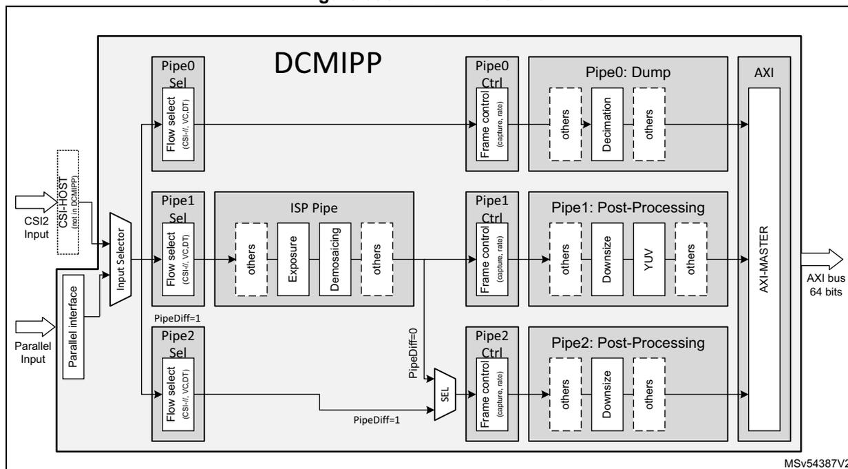
The diagram illustrates the DCMIPP architecture. On the left, two input sources are shown: 'CSI2 HOST' (with a note 'config in DCMIPP') and 'Parallel Input'. Both connect to an 'Input Selector'. The 'Input Selector' outputs to three processing pipes: 'Pipe0', 'Pipe1', and 'Pipe2'. Each pipe has a 'Flow select (CSI2/ VC, DT)' block. Pipe0's output goes to 'Pipe0 Ctrl (capture, rate)' and 'Pipe0: Dump', which contains 'others', 'Decimation', and 'others' blocks. Pipe1's output goes to 'Pipe1 Ctrl (capture, rate)' and 'Pipe1: Post-Processing', which contains 'others', 'Exposure', 'Demosaicing', and 'others' blocks. Pipe2's output goes to 'Pipe2 Ctrl (capture, rate)' and 'Pipe2: Post-Processing', which contains 'others', 'Downsize', and 'others' blocks. All three pipes' outputs converge to an 'AXI' block, specifically an 'AXI-MASTER', which is connected to an 'AXI bus 64 bits'. There are also control signals 'PipeDiff=1' and 'PipeDiff=0' between the pipes and a 'SEL' block.
In the ISP processing, and therefore before the post-processing pipes (Pipe1 and Pipe2), the component dynamic is reduced to 8 bits per component. If the software intends to benefit of the wider dynamic, the input data must be dumped via Pipe0, which keeps the input pixel format (10/12/14 bpp) when storing them in memory.
Table 329. Glossary
| Item | Definition |
|---|---|
| A | Alpha component, used to define transparency, opaque = 0xFF, for example ARGB. |
| 3A (or AAA) | In ISP domain: acronym for AE-AF-AWB, algorithms automatically correcting pictures: – AE: automatic exposure control (adapts exposure or sensibility of sensor) – AF: automatic focus control (adapts the focus) – AWB: automatic white balance (adapts the color tones to have a white balance). |
| BPC | Bits per component (for example, RGB565 has five bits for the red component, hence 5 bpc) |
| BPP | Bits per pixel (for example, RGB565 has 16 bits per pixel, hence 16 bpp) |
| CSI | Camera serial interface, and its latest standard by MIPI ® , the CSI-2 v1.3 (and v2.0) |
| DCMIPP_ | Digital camera interface - Pixel pipeline |
| DT | Data type, used in the CSI-2 standard. The data type is a concept similar to the pixel format, but adds support for other data like the byte format. |
| Interlaced | Interlaced video: the field with odd lines is transmitted first, followed, after the last odd line, by the field with even lines. The two fields are thus consecutive but exclusive. |
| Interleaved | Interleaved packets, applies to CSI-2: two groups of packets transmitted by the sensor can be emitted mixed, as a packet granularity. |
| Item | Definition |
|---|---|
| ISP | Image signal processing: algorithms that retune the sensor output (through correction of pixels, demosaicing, lens-correction, light/contrast correction) to build a good quality picture. |
| NPU | Neural network processing engine (also known as NN, neural network). |
| Planar | Defines in how many sub-buffers a pixel buffer is split into: 1 (coplanar), 2 (semi-planar), 3 (full planar). |
| ROI | Region of interest (pixel box surrounding the region of interest) |
| VC | Virtual channel, used in the CSI-2 standard, makes it possible to simultaneously transmit up to four parallel flows (in CSI-2 v1.3) or more (in CSI-2 v2.0). |
| YUV444 | Pixel format, YUV color reference, all three components (Y, U, V) given per pixel. |
| YUV422 | Pixel format, YUV color reference, chroma component (U, V) sub-sampled 1/2 in X |
39.2 DCMIPP main features
- • Parallel input interface:
- – Pixel rate: up to 16 bits in parallel, 100 Mpixel/s (typically 1080p30, maximum 2048x2048 on processing pipelines after decimation).
- – Pixel format: RGB565, RGB888, YUV422, raw Bayer/Mono 8/10/12/14, and ByteStream (JPEG)
- • CSI-2 host input interface:
- – Pixel rate: 32 bits in parallel at 200 Mpixel/s (typically 5 MPixel x30), supports MIPI® CSI-2 v1.3
- – Pixel format: all MIPI CSI-2 v1.3, among others RGB565, RGB888, YUV422, raw Bayer (see Table 335 )
- – Abutted CSI-2 host IP: 1-to-2 DL at up to 2.5 Gbps/lane
- – Features: Interleaved packets, four virtual channels
- • Pipeline maximum resolution:
- – Dimensioned for 5 Mpixel (typically 2560 x 2048 or 2688 x 1944) before decimation
- – Maximum pipe resolution: 4094 x 4094
- – Maximum demosaicing or downsize or YUV420 width: 2688 pixels
- • Pipe pixel rate: 200 Mpixel/s peak (150 Mpixel/s average + blanking)
- • Maximum frame per second (fps): typical examples are defined with 30 fps, it is possible to reach higher rates (for example 120 fps) by decreasing image resolution to guarantee the maximum pixel rate constraints.
- • Flow selection and frame control:
- – CSI-2 interleaved packets supported (with some restrictions)
- – Capture mode in Continuous vs. Snapshot mode
- • Byte-to-pixel conversion:
- – Enables the above flexible input pixel formats to be extracted and fed to pipes
- – Non-extracted pixel formats can still be dumped via Pipe0, to allow an ad-hoc software extraction
- • Statistic removal:
- – To remove unused metadata (like statistics) from received pictures
- • Bad pixel removal (automatic detection and correction of bad pixels from sensor array)
- • Decimation of one pixel every 1/2/4/8:
- – Decimation to fit the demosaicing (maximum 2688 pixel width)
- – Raw Bayer format support, via a decimation of components (2 by 2)
- • Integrated image processing block, which makes possible to connect very low cost camera modules without any embedded ISP
- – Black level calibration
- – Statistics extraction
- > To extract average R, G, B, L values (for auto exposure and white balance)
- > To sort any R, G, B, L value into 12 dynamic bins (for contrast enhancement)
- – Exposure control (amplifies the exposure up to 256x)
- > To smoothly adapt to dark exposures
- – Raw Bayer to RGB conversion (demosaicing)
- > Mid quality conversion for display and software analysis purposes (high quality conversion can be done in software upon trigger, for still-image only)
- > Algorithm with a 4 x 3 heuristic analysis matrix
- – Color conversion to adapt to the sensor and tune the illumination
- > Configurable coefficients, to map any linear tuning
- – Contrast enhancement
- > Non-linear luminance tuning, linearized across eight luminance segments.
- • Decimation on Pipe0 (dump pipe)
- – Pure sub-sampling, ratio 1 vs. 1, 2, 4 in X and ratio 1 vs. 1, 2 in Y (no X if CSI source)
- • Parallel pipelines for parallel applications:
- – Pipe0 (for data dump) for a direct dump without processing
- – Pipe1 (for main usage) with downsize, ColorConv, decimation, multi-planar
- – Pipe2 (for ancillary usage) with downsize, decimation, coplanar
- • Downsize
- – Decimation, optional pre-processing, sub-sampling ratio 1 vs. 1, 2, 4, 8 in X and Y
- – Box-filtering, with any decimal ratio up to 8x8, on Pipe1 and Pipe2
- • Up to eight regions of interest (ROI) can be defined for displaying purpose (only supporting RGB data format)
- – Up to 64 line colors can be selected by the software, per ROI
- – Up to four line widths can be configurable (1, 2, 4, 8 pixels, common to all ROIs)
- – Pipe0 does not support ROI
- • Gamma conversion for display:
- – Non-linear transform, with seven interpolated segments, with static coefficient for \( G = 2.2 \)
- • Color conversion 2 for RGB to YUV conversion:
- – to/from YUV: 12 coefficients (BT.601, 709, any), with optional range ext/clamp
- • Output pixel format:
- – Pipe0: any data as-is, Y/Rb: 8/10/12/14 statistics, bit streams
- – Pipe2: 888, 565, 422-1, Y8, ARGB and RGBA (coplanar only)
- – Pipe1: adds 422-2, 420-2, 420-3 (multi-planar possible) to Pipe2 formats
- • AXI master:
- – Output FIFOs to drain pixel/data to the memory (linked to the memory latency) from the pipe(s)
- – The unique AXI-Master interface implements one client per pipe, with semi- or multi-planar pipes using, respectively, two or three clients
- – Double buffer mode capability per pipe
- – Address wrapping to write into a ping-pong buffer
- • Overrun detection:
- – Notification in case of frame impacted by pixel congestion (no impact on the following frame if the congestion cause is solved)
39.3 DCMIPP functional description
39.3.1 DCMIPP block diagram
The block diagram of the DCMIPP is shown in Figure 397 .
Figure 397. DCMIPP block diagram
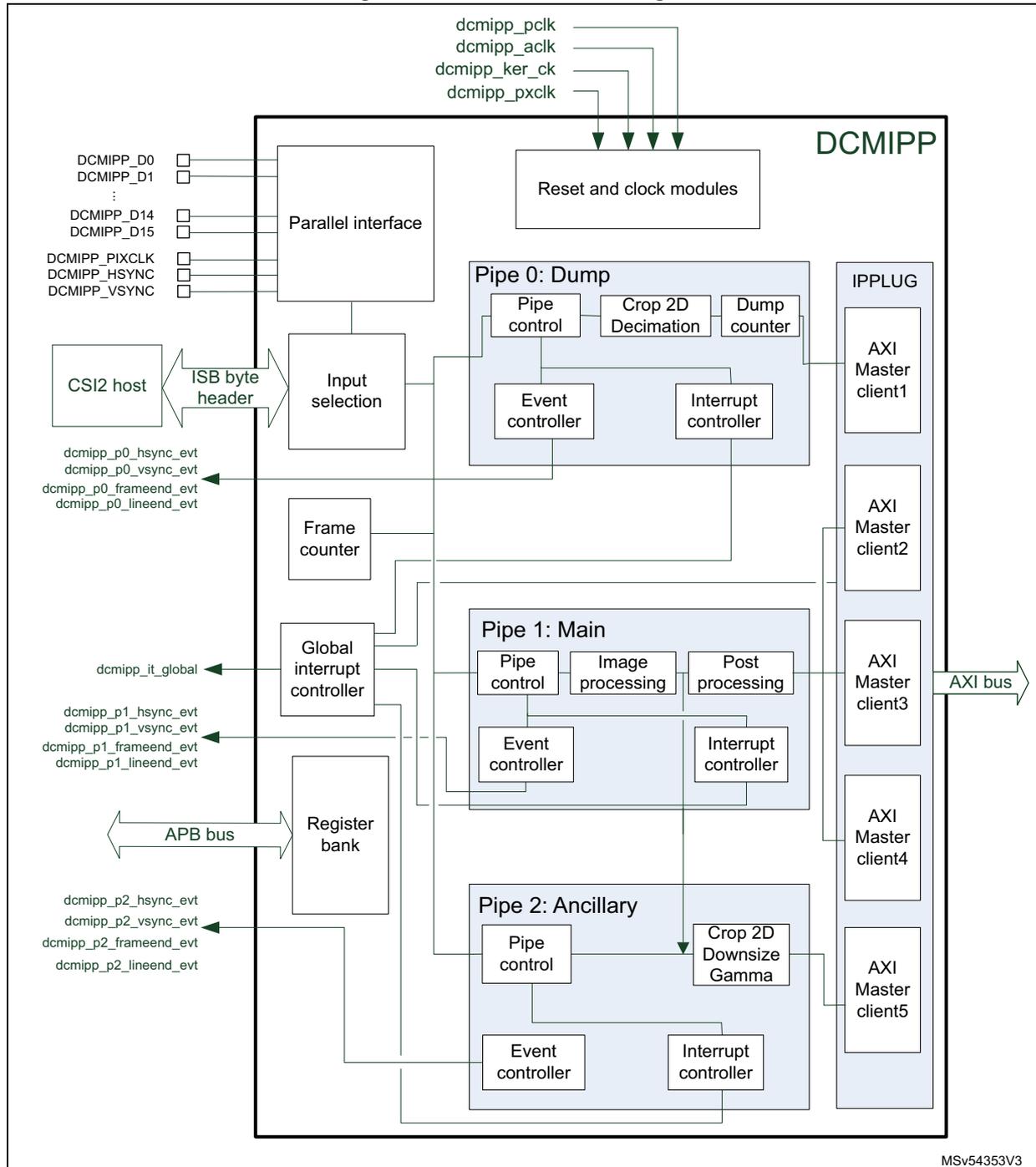
The block diagram illustrates the internal architecture of the DCMIPP. At the top, four clock signals (dcmipp_pclk, dcmipp_aclk, dcmipp_ker_ck, dcmipp_pxclk) are input to the 'Reset and clock modules'. On the left, a 'Parallel interface' connects to external pins: DCMIPP_D0 through DCMIPP_D15, DCMIPP_PIXCLK, DCMIPP_HSYNC, and DCMIPP_VSYNC. Below this, a 'CSI2 host' connects via an 'ISB byte header' to an 'Input selection' block. The 'Input selection' feeds into three parallel processing pipes: 'Pipe 0: Dump', 'Pipe 1: Main', and 'Pipe 2: Ancillary'. Each pipe contains a 'Pipe control', an 'Event controller', and an 'Interrupt controller'. 'Pipe 0' also includes 'Crop 2D Decimation' and a 'Dump counter'. 'Pipe 1' includes 'Image processing' and 'Post processing'. 'Pipe 2' includes 'Crop 2D Downsize Gamma'. A 'Frame counter' and a 'Global interrupt controller' are also present. The 'Global interrupt controller' outputs signals: dcmipp_it_global, dcmipp_p0_hsync_evt, dcmipp_p0_vsync_evt, dcmipp_p0_frameend_evt, dcmipp_p0_lineend_evt, dcmipp_p1_hsync_evt, dcmipp_p1_vsync_evt, dcmipp_p1_frameend_evt, dcmipp_p1_lineend_evt, dcmipp_p2_hsync_evt, dcmipp_p2_vsync_evt, dcmipp_p2_frameend_evt, and dcmipp_p2_lineend_evt. A 'Register bank' is connected to an 'APB bus'. On the right, an 'IPPLUG' block contains five 'AXI Master client' units (client1 through client5), which are connected to an external 'AXI bus'. The diagram is labeled 'DCMIPP' in the top right and 'MSV54353V3' in the bottom right.
39.3.2 DCMIPP pads and internal signals
Table 330. DCMIPP input/output pads
| Pin name | Signal type | Description |
|---|---|---|
| DCMIPP_Dn (n = 0 to 15) | Input | Bit n of the parallel data bus coming from the camera sensor |
| DCMIPP_PIXCLK | Input | Pixel clock sent by the master (parallel camera sensor module) |
| DCMIPP_VSYNC | Input | VSYNC signal (vertical synchronization) coming from the camera sensor |
| DCMIPP_HSYNC | Input | HSYNC signal (horizontal synchronization) coming from the camera sensor |
Table 331. DCMIPP input/output pins
| Internal signal name | Signal type | Description |
|---|---|---|
| dcmipp_pclk | Input | DCMIPP APB clock (APB bus) |
| dcmipp_aclk | Input | DCMIPP AXI clock (AXI bus) |
| dcmipp_ker_ck | Input | Interface from the CSI2 host |
| dcmipp_it_global | Output | DCMIPP interrupts (refer to Table 364 for the full list of interrupt sources) |
| dcmipp_p0_hsync_evt | Output | Pipe0 Hsync event |
| dcmipp_p0_vsync_evt | Pipe0 Vsync event | |
| dcmipp_p0_frameend_evt | Pipe0 frame end event | |
| dcmipp_p0_lineend_evt | Pipe0 line event | |
| dcmipp_p1_hsync_evt | Output | Pipe1 Hsync event |
| dcmipp_p1_vsync_evt | Pipe1 Vsync event | |
| dcmipp_p1_frameend_evt | Pipe1 frame end event | |
| dcmipp_p1_lineend_evt | Pipe1 line event | |
| dcmipp_p2_hsync_evt | Output | Pipe2 Hsync event |
| dcmipp_p2_vsync_evt | Pipe2 Vsync event | |
| dcmipp_p2_frameend_evt | Pipe2 frame end event | |
| dcmipp_p2_lineend_evt | Pipe2 line event |
39.3.3 DCMIPP reset and clocks
Table 332. DCMIPP clocks
| Domain | Clock | Maximum frequency | Comments |
|---|---|---|---|
| Parallel | dcmipp_pxclk | 120 MHz | Up to 2x 120 MB/s in 16-bit mode |
| Pipeline | dcmipp_ker_ck | 333 MHz | Up to 333 Mpixels/s (minus the blanking) |
| AXI bus | dcmipp_aclk | 400 MHz | SoC AXI frequency |
| APB bus | dcmipp_pclk | 200 MHz | SoC APB frequency |
| Domain | Reset type | Comments |
|---|---|---|
| Parallel + Pipeline | Asynchronous | Resynchronized internally on dcmipp_pxclk/dcmipp_ker_ck |
| AXI bus | Synchronous | Resets directly the dcmipp_aclk domain |
| APB bus | Synchronous | Resets directly the dcmipp_pclk domain |
Clocks and pixel rate limitations
This paragraph lists the DCMIPP limitations and bottlenecks:
- • The target is to sustain an average pixel rate (PixRateAvg):
- – A 5 Mpixel sensor at 30 fps requires 150 Mpixel/s (CSI-2 interface)
- – Higher resolution sensors can be supported, but with lower FPS (for example 10 Mpixels at 15 fps)
- • Vertical and horizontal blanking:
- – The full system (sensor, interface, pipe, AXI) embeds limited capacity FIFOs. The idle times that the sensor inserts during its blanking periods impact all the downstream elements, including interface, pipe, and AXI. A pixel rate (PixRatePeak) higher than average must be used. The idle time due to the blanking can reach 33% of the frame duration, sometimes more (check sensor specification).
- – \( PixRatePeak = 1.33 * PixRateAvg = 200 \text{ Mpixel/s} \) in our example.
- • Parallel interface clock (dcmipp_pxclk):
- – On the parallel interface, pixels are received sequentially, in one, two or three cycles. The maximum implemented clock (120 MHz) constrains the peak pixel rate, depending on the ratio of cycles per pixel.
- – \( PixRatePeak \leq dcmipp\_pxclk / (1, 2 \text{ or } 3) = 120 / (1, 2 \text{ or } 3) \)
- – Clock frequency:
- > \( dcmipp\_pxclk \leq dcmipp\_ker\_ck \) (due to resync interface between them)
- > \( dcmipp\_pxclk \leq dcmipp\_aclk \)
- – Consequences: see Table 334 .
Table 334. Parallel interface maximum resolution (80 MHz)
| Pixel | Transmission on the interface | Resolution (30 fps), including blanking | ||||
|---|---|---|---|---|---|---|
| Format | Width (bpp) | Width | Cycles/pixel | Pixel rate | Mpixel/frame | Example |
| Mono/raw | 8 | 8 | 1 | 80 | 2.15 | 1080 p |
| 14 | 14 | 1 | 80 | 2.15 | 1080 p | |
| RGB565 | 16 | 8 | 2 | 40 | 1.08 | 720 p |
| 16 | 1 | 80 | 2.15 | 1080 p | ||
| RGB888 | 24 | 8 | 3 | 27 | 0.72 | qHD |
| 12 | 2 | 40 | 1.08 | 720 p | ||
| YUV422 | 16 | 16 | 1 | 80 | 2.15 | 1080 p |
| 16 | 2 | 40 | 1.08 | 720 p | ||
| YUV444 | 24 | 12 | 2 | 40 | 1.08 | 720 p |
| 16 | 2 | 40 | 1.08 | 720 p | ||
- – Clock setting: \( dcmipp\_pxclk \geq PixRatePeak * Ratio(1,2,3) \)
- • Pipe clock
dcmipp_ker_ck(when using the CSI-2 host interface)- – CSI-2 PHY provides data bit at the
clk_bitrate, on DL parallel data lanes. - – Rationale: internally, the CSI-2 host interface packs the serial stream on 32-bit words, resynchronized on the pipe clock (
dcmipp_ker_ck). - – Clock setting: \( dcmipp\_ker\_ck \geq clk\_bit * DL / 32 \text{ bpp} = 156.25 \text{ MHz} \) .
- – Rationale 2: The pixel pipe processes 1 pixel/clk, so that
dcmipp_ker_ckmust be higher than the wantedPixRatePeak. - – Clock setting: \( dcmipp\_ker\_ck \geq PixRatePeak \) .
- – For small footprint pixels (like Raw8), the DCMIPP is limited by its maximum
dcmipp_ker_clk, and can be unable to handle the maximum CSI pixel rate ( \( clk\_bit * DL / 8 \text{ bpp} \) for Raw8).
- – CSI-2 PHY provides data bit at the
- • Downsize:
- – The line buffer of the vertical downsize operator is limited to a width of 2688 pixels after the horizontal downsize operation, limiting the resolution, when the downsizing is active, to 2688 x 1944 (1944 is the usual maximum height with a width of 2688), thus 5.1 Mpixel.
- – If a camera resolution higher than 5 Mpixel is targeted, a basic decimation has to be performed to decrease the resolution to a maximum of 5 Mpixel before processing the downsizing operation.
- • AXI clock:
- – The pixels must be reclocked from the processing to the AXI domain, resulting in
- > \( dcmipp\_ker\_ck \leq dcmipp\_ackl \)
- – The AXI bus must drain the running pipelines. The maximum footprint of pixel (or data) pipes is 32 bpp (Pipe1 and Pipe2) and 16 bpp (Pipe0). AXI is on 64 bits, with an efficiency of 8 / 9 for the typical 64-byte burst.
- – \( dcmipp\_ackl \geq dcmipp\_ker\_ck * (32 \text{ bpp} + 32 \text{ bpp} + 16 \text{ bpp}) / (64 \text{ bit} / \text{ bus}) * 9 / 8 \text{ (efficiency)} = dcmipp\_ker\_ck * 1.4 \) .
- – The pixels must be reclocked from the processing to the AXI domain, resulting in
39.3.4 DCMIPP maximum resolution
The limitations related to the maximum resolution supported by the DCMIPP are:
- • Maximum width and height across pipes: 4094 x 4094 pixels
- – Registers and counters are limited to 12 bits
- • Maximum performance: 333 Mpixel/s on each pipe
- – Larger pixel rate can be used, but with less pipe active or lower memory latency
- – Maximum pixel rate on each pipe must remain below the pixel clock
- • Maximum width on demosaicing: 2688 components wide
- – limitation related to the Line-buffer size
- • Maximum width after downsize: 2688 pixels
- – limitation related to the Line-buffer size
- • Maximum width for conversion to YUV420: 2688 pixels
- – limitation related to the Line-buffer size
- • Max line stride: 32767 bytes
- – Registers and counters, to handle 4094 pixels x 32 bits x 2 (provision for interleaving)
39.3.5 DCMIPP minimum requirements for frame structure
DCMIPP imposes the following minimum requirements for the frame architecture:
Blanking phase
- • Dump pipe
- – The minimal duration of the blanking between two frames must be an equivalent of 666 datawords of 32 bits
- • Pixel pipe
- – Vertical blanking: minimum is 5 lines. If the line is less than 12 pixels, a minimum of 24 pixels equivalent for the vertical blanking parameter is requested
- – Horizontal blanking: a minimum duration of 12 pixels is required between two lines
Data image area
- • Vertical image area: minimum one line (two lines if raw Bayer conversion is active)
- • Horizontal image area: minimum two pixels
- • The minimum total frame size is fixed to 36 pixels
39.3.6 Description of DCMIPP pixel format support
Table 335 lists the supported pixel formats in the input interfaces (parallel, CSI), as input to the pixel Pipe1 and Pipe2, and in the three output pipes.
Table 335. Supported pixel formats
| Index (1) | Pixel format | BPP | Parallel input (clk/pix) (2) | CSI input | Pipe0 output (dump) | Pipe1 and Pipe2 input | Pipe1 output (main) | Pipe2 output (ancillary) |
|---|---|---|---|---|---|---|---|---|
| - | Bytes (CSI: long packets and user) | 8 | - | Y | Y | - | - | - |
| 13 (3) | Byte stream (JPEG, compressed video) | 8 | Y, 1 | - | Y | - | - | - |
| 14 (4) | Other data | 8 to 16 (4) | Y, 1 | - | Y | - | - | - |
| 5 | Raw6 | 6 | (5) | Y (6) | Y (6) | - | - | - |
| 5 | Raw7 | 7 | (5) | Y (6) | Y (6) | - | - | - |
| 5 | Raw8 | 8 | Y, 1 | Y | Y | Y | Y | Y |
| 6 | Raw10 | 10 | Y, 1 | Y | To 16 bpc | To 8 bpc | - | - |
| 7 | Raw12 | 12 | Y, 1 | Y | To 16 bpc | To 8 bpc | - | - |
| 8 | Raw14 | 14 | Y, 1 | Y | To 16 bpc | To 8 bpc | - | - |
| 9 | Mono8 | 8 | Y, 1 | - | Y | Y | Y | Y |
| 10 | Mono10 | 10 | Y, 1 | - | To 16 bpc | To 8 bpc | - | - |
| 11 | Mono12 | 12 | Y, 1 | - | To 16 bpc | To 8 bpc | - | - |
| 12 | Mono14 | 14 | Y, 1 | - | To 16 bpc | To 8 bpc | - | - |
| 2 | RGB444 | 12 | (5) | Y | (5) | To 8 bpc | - | - |
| 2 | RGB555 | 15 | (5) | Y | (5) | To 8 bpc | - | - |
Table 335. Supported pixel formats (continued)
| Index (1) | Pixel format | BPP | Parallel input (clk/pix) (2) | CSI input | Pipe0 output (dump) | Pipe1 and Pipe2 input | Pipe1 output (main) | Pipe2 output (ancillary) |
|---|---|---|---|---|---|---|---|---|
| 2 | RGB565 | 16 | Y, 1, 2 | Y | Y | To 8 bpc | Y | Y |
| 3 | RGB666 | 18 | (5) | Y | (5) | To 8 bpc | - | - |
| 4 | RGB888 / YUV444 (6) | 24 | Y, 2, 3 | Y | Y | Y | Y | Y |
| - | xRGB888 / xYUV444 (6) | 32 | - | - | Y | - | Y | Y |
| - | RGBx888 / YUVx444 (6) | 32 | - | - | Y | - | Y | Y |
| 1 | YUV422-1 (YUYV) | 16 | Y, 1, 2 | Y | Y | Y | Y | Y |
| - | YUV422-2 | 16 | - | Y (6) | Y (6) | - | Y | - |
| - | YUV420-2 (NV21/NV12) | 12 | - | Y (6) | Y (6) | - | Y | - |
| - | YUV420-3 (YV12) | 12 | - | Y (6) | Y (6) | - | Y | - |
| - | YUV422 10 bpc | 20 | - | Y (6) | Y (6) | - | - | - |
| - | YUV420 10 bpc | 15 | - | Y (6) | Y (6) | - | - | - |
| - | Any other CSI-2 | Any | - | Y (6) | Y (6) | - | - | - |
- Index is used to link the input pixel format to the DCMIPP_PRCR register. The index has a meaning only for camera connected with the parallel interface
- Pixel formats on 16 bpp (like RGB565 or YUV422-1) can be received either on an 8-bit interface (using 2 cycles), or on a 16-bit input interface (using one cycle). Pixel formats on 24 bpp (like RGB888) can be received either on an 8-bit interface (using three cycles), or on a 12-bit input interface (using two cycles).
- In Byte stream mode, the bytes are dumped consecutively with only a 32-bit padding (if needed) at the end of the frame (or JPEG stream). There is no 32-bit padding operation inside the stream until the VSYNC deassertion (end of frame, or end of JPEG stream).
- If the data format is different from those in this table, user can choose "others" configuration into bit field FORMAT in the DCMIPP_PRCR register, using bit-field EDM to select how many data bits must be captured in one pixel clock. It is possible to capture two 8-bit data mapped on 16-bit parallel input data in a single cycle (for instance FORMAT = Others, EDM = 100, i.e. 16-bit capture on each pixel clock). Data are 32-bit padded at the end of a line to have a complete line aligned on 32-bit width.
- On the parallel interface input, some sensor pixel formats are supported by the DCMIPP, by selecting a wider pixel format in DCMIPP, by mapping the sensor wires onto the MSB of the DCMIPP interface. On the input missing pins, it is recommended to replicate the sensor MSB pins onto the missing input LSB pins. This helps achieving full dynamic on the extended pixel format. The work-around can be applied on the following formats (sensor output on left, mapping on DCMIPP format on right):
- - Raw6: Raw8 with 1-cycle input, processed as a 8 bpp
- - Raw7: Raw8 with 1-cycle input, processed as a 8 bpp
- - RGB444: RGB565 with 1-cycle input, processed as a 16 bpp
- - RGB555: RGB565 with 1-cycle input, processed as a 16 bpp
- - RGB666: RGB888 with 3-cycle input, processed as a 24 bpp
- The same bit mapping is used for the input RGB888 and YUV444, the input xRGB and xYUV, and similarly for the outputs. The difference between RGB and YUV is the color reference, set in the color conversion that occurs after the input or before the output.
39.4 DCMIPP input and flow control
This section describes the functional elements of the DCMIPP. For each, it details the features, the software configuration, and provides a software configuration example (when needed).
39.4.1 DCMIPP common configuration
The DCMIPP common configuration register (DCMIPP_CMCR) enables the selection of the input interface—either parallel DCMI or serial CSI-2—from which to fetch the input pixels. It also allows swapping the R/B color components of the incoming pixels and selecting the pipe used by the frame counter.
Table 336. DCMIPP_CMCR bit function
| Bit ID | Function | Comments |
|---|---|---|
| INSEL | Input selection | Select the input interface to fetch pixels from. The selection is common to all pipes and must not be changed while they are active. – 0: DCMI – 1: CSI-2 |
| PSFC | Pipe selection for the frame counter | Select which pipe the frame counter maps to. |
| CFC | Clear frame counter | Clear the frame counter when set. |
| SWAPRB | Swaps R-versus-B components (and U-versus-V) of the input pixels | Operate only on pixel pipes, not on dump pipe. |
39.4.2 Parallel input interface
The parallel interface is a flexible pixel interface that clocks in a bus of 8- to 16-bit in parallel, with an externally provided clock, and adds vertical and horizontal synchronization, provided either with specific pins (external sync) or flagged via specific data (as in CCIR601).
Interface (all inputs)
- • Clk: clock up to 120 MHz, internally named dcmipp_pxclk
- • Data: 16 IO pins, up to 120 Mbps/pin, 8- to 16-bit, pixels potentially serialized
- • HSync, VSync, but no enable (EN)
Features
- • Horizontal and vertical synchronization:
- – External, via the HSync and VSync pins.
- – Internal, via the CCIR601 flagging.
Data provided during the horizontal or vertical blanking cannot be captured.
- • Input pixel format (see
Section 39.3.6
)
- – Binary stream like JPG
- – Single cycle data:
- > Raw Bayer and monochrome: 8/10/12/14 bits in parallel
- > YUV422, RGB565:16 bpp on 16 bits in parallel
- – Double-cycle data:
- > YUV422, RGB565:16 bpp on 8 bits in parallel
- > RGB888/YUV444: 24 bpp on 12 bits in parallel
- – Triple-cycle data:
- > RGB888/YUV444: 24 bpp on 8 bits in parallel
- • Flexible input:
- – MSB-vs-LSB bits can be swapped to ease PCB placement
- – Cycle0-vs-Cycle1 can be swapped (for 2-cycle long pixels).
- – Red-vs-blue components can be swapped (for RGB, or U-vs-V for YUV), this last swap operates only on the pixel pipes and not the dump pipe.
Hardware synchronization mode
In this mode two synchronization signals (DCMIPP_HSYNC and DCMIPP_VSYNC) are used.
Depending on the camera module/mode, data can be transmitted during horizontal/vertical synchronization periods. DCMIPP_HSYNC/DCMIPP_VSYNC act as blanking signals, as all data received during DCMIPP_HSYNC/DCMIPP_VSYNC active periods are ignored.
To correctly transfer images in the RAM buffer, data transfer is synchronized with the DCMIPP_HSYNC/DCMIPP_VSYNC signals. When the hardware synchronization mode is selected, and capture is enabled (CPTREQ bit set in DCMIPP_PxFCTCR), data transfer is synchronized with the deassertion of the DCMIPP_VSYNC signal (next start of frame).
Transfer can then be continuous, with successive frames transferred by the IP-Plug to successive buffers or the same/circular buffer.
Embedded data synchronization mode
In this synchronization mode, the data flow is synchronized using embedded 32-bit codes, using the 0x00/0xFF values not used in data anymore. There are four types of codes, all with 0xFF00 00XY format. The embedded synchronization codes are supported only in 8-bit parallel data capture (in the DCMIPP_PRCR register, the EDM[2:0] bits must be programmed to “000”). For other data widths, this mode generates unpredictable results.
Note: Camera modules generate up to eight synchronization codes when in interleaved mode, while the DCMIPP reacts to one single code. As a consequence, an interleaved flow with an embedded synchronization has one every other frame discarded as not detected.
Mode 2
Four embedded codes signal the following events:
- • Frame start (FS)
- • Frame end (FE)
- • Line start (LS)
- • Line end (LE)
The XY values in the 0xFF00 00XY format of these codes are programmable (see Section 39.14.9 ).
A 0xFF value programmed as a frame end means that all the unused codes are interpreted as valid frame end codes.
In this mode, once the camera interface has been enabled, the frame capture starts after the first occurrence of the frame end (FE) code followed by a frame start (FS) code.
Mode 1
An alternative coding is the camera mode 1. This mode is ITU656 compatible.
The codes signal another set of events:
- • SAV (active line) - Line start
- • EAV (active line) - Line end
- • SAV (blanking) - Start of line during interframe blanking period
- • EAV (blanking) - End of line during interframe blanking period
This mode can be supported by programming the following codes:
- • \( FS \leq 0xFF \)
- • \( FE \leq 0xFF \)
- • \( LS \leq SAV \) (active)
- • \( LE \leq EAV \) (active)
An embedded unmask code is also implemented for frame/line start and frame/line end codes. Using it, it is possible to compare only the selected unmasked bits with the programmed code. User can therefore select a bit to compare in the embedded code and detect a frame/line start or frame/line end. This means that there can be different codes for the frame/line start and frame/line end with the unmasked bit position remaining the same.
Example:
- • \( FS = 0xA5 \)
- • Unmask code for \( FS = 0x10 \)
In this case the frame start code is embedded in bit 4 of the frame start code.
Note: FEC sequence must be sent before the transfer of the first frame, otherwise other codes are not decoded and the first frame can be lost after the DCMIPP has been enabled. After the first FE sequence, the following frame is captured based on FS sequence.
Error conditions
Error conditions can be detected when using the embedding synchronization data modes. Flags PRERRF in DCMIPP_CMSR2 and ERRF in DCMIPP_PSR are used for this function. An interruption can be triggered based on error detection if bit PRERRIE in
DCMIPP_CMIER is set for the global interrupt (or bit ERRRIE in DCMIPP_PRIER for a local interrupt line).
For instance, such kind of wrong sequences or values generate an error:
- – FF 00 00 XY sequence detected with XY value different from the one set for FS/LS/FE/LE
- – LS = 0xFF or LE = 0xFF
- – If an LS or FS sequence follows an LS sequence
Software configuration
Table 337. DCMIPP_PRCR bit function
| Bit ID | Function | Comments |
|---|---|---|
| ENABLE | Enables the parallel interface | Low-power mode when disabled. |
| PCKPOL | Defines clock polarity |
|
| ESS | Defines if VSync and HSync synchronizations are provided by sideband (specific hardware IO) or by in-band (specific embedded codes) signals |
|
| VSPOL, HSPOL | Defines the polarity of the IO DCMIPP_VSYNC and DCMIPP_HSYNC used for, respectively, the vertical and horizontal synchronization |
|
| FORMAT | Defines the pixel format used on the IO DCMIPP_Dx | From 0 to 15 |
| EDM | Defines the amount of valid bits received per cycle The duration of a pixel is extracted by the bit-per-pixel (given by FORMAT) and bit-per-cycle (given by EDM) ratios | 8/10/12/14/16 bits 1, 2 or 3 cycles |
| SWAPBITS | Swaps the 16 bits of the parallel interface | 15:0 becomes 0:15 |
| SWAPCYCLES | Swaps, when a pixel is received in two cycles, the data from the first cycle with the data from the second cycle | Software must not activate it when a pixel is received in one or three cycles. |
The embedded synchronization codes are configured by means of DCMIPP_PRESR and DCMIPP_PRESUR registers (see Table 338 ).
Table 338. DCMIPP_PRESR and DCMIPP_PRESUR bit function
| Bit ID | Function |
|---|---|
| FSC, FEC | Frame-start and frame-end synchronization, when embedded synchronization ESS = 1 |
| FSU, FEU | Masks for FSC and FEC codes |
Table 338. DCMIPP_PRESER and DCMIPP_PRESUR bit function (continued)
| Bit ID | Function |
|---|---|
| LSC, LEC | Line-start and line-end synchronization, when embedded synchronization ESS = 1 |
| LSU, LEU | Masks for LSC and LEC codes |
39.4.3 Interface from CSI-2 host
The CSI-2 host and DPHY_RX (both external to the DCMIPP) provide the data from the CSI-2 camera sensor, forward them into the DCMIPP using the ISB byte header interface.
The ISB byte header features are:
- • CSI-2 clock interface aligned with the DCMIPP processing clock (333 MHz)
- • Data width: 32 bit (data and CSI headers are interleaved)
- – Frame synchronization short packet
- – Frame number, Data ID, and packet type are provided (see Section 39.7.9 ).
- • Line Sync short packets are not received.
- • Headers of data long packet:
- – Packet length, Data ID, and packet type are provided (see Section 39.7.9 ).
- • Payloads of data long packet:
- – Data as 32-bit words, as collected by the CSI-2 host.
- • Packet CRC is not received.
39.4.4 Input selection
Input selection block is ahead of any pipe to select the camera sensor module interface connected to the DCMIPP. Two interfaces are supported:
- • Parallel interface: up to 16-bit parallel interface with physical synchronization signals (DCMIPP_VSYNC/DCMIPP_HSYNC) or software embedded ones (as in CCIR601).
- • MIPI CSI-2 interface: Host ISB byte header internal connection from the CSI2 host controller placed in front of the DCMIPP.
Both interfaces are exclusive. The selected one is applied to all the input pipes.
The camera sensor interface is selected by means of bit INSEL of the DCMIPP_CMCR register.
39.4.5 Flow selection
The module, present in each pipe, handles the flow control around the CSI2 camera sensor interface. For each pipe, the software needs to configure which virtual channel (VC) and which Datatypes (DT) are processed by the pipe.
For Pipe0 and Pipe1, multiple Datatypes can be selected whereas only one virtual channel can be defined for a frame. Configuration can be changed frame by frame if the application requires it, offering some flexibility.
For Pipe2, when the pipe is independent with PIPEDIFF = 1, only one virtual channel and only one data type by frame can be selected.
The software has to reconfigure the flow selection module to handle interleaved frames from a sensor if it uses virtual channels as a mean to make the differentiation, accepting to lose frames since there can be only one virtual channel active for a given frame (it decreases the FPS).
Multiple cameras data flow can be received simultaneously through the CSI2 ISB header bus. For instance, for a system having two different camera data flows, it is possible to redirect one virtual channel on a pipe and the other one on the other pipe. It can be interesting to dump them on Pipe0, but only one frame over two since the flow selection block has to be reconfigured to switch from one VC to another one.
The flow selection module is used also to share some image processing features (demosaicing, color conversion, statistics, contrast enhancement, auto exposure, statistics removal and basic decimation) between Pipe1 and Pipe2, whatever the camera sensor interface solution (parallel interface or CSI2 interface): when bit PIPEDIFF in the DCMIPP_P1FSCR register is 0, or the input is on the parallel interface that provides unique flow, the Pipe2 samples pixels from the output of the ISP of Pipe1 (see Figure 396 ). PIPEDIFF must be reconfigured when Pipe1 and Pipe2 are disabled.
Software configuration
The following configurations must be set first, because static in the DCMIPP_PxFSCR registers:
Pipe0
- • DTMODE[1:0]: Mode for CSI flow selection into that pipe
- – 0: only flow VC/DTIDA is forwarded in the pipe
- – 1: flows VC/DTIDA and/or VC/DTIDB are forwarded in the pipe
- – 2: all Datatypes of the selected virtual channel, except the VC/DTIDA or VC/DTIDB, are forwarded in the pipe
- – 3: all Datatypes of the selected virtual channel are forwarded in the pipe
- • VC[1:0]: Virtual channel ID of the CSI flow to select for further processing on the pipe
- • DTIDA[5:0]: Data type ID A to select in the CSI flow for further processing in the pipe
- • DTIDB[5:0]: Data type ID B to select in the CSI flow for further processing in the pipe
- • PIPEN: activation of the Pipes, to be set after the above configurations.
Pipe1
- • DTMODE[1:0]: mode for CSI flow selection into that pipe
- – 0: only flow VC/DTIDA is forwarded in the pipe
- – 1: flows VC/DTIDA and VC/DTIDB are forwarded in the pipe
- • VC[1:0]: virtual channel ID of the CSI flow to select for further processing on the pipe
- • DTIDA[5:0]: data type ID A to select in the CSI flow for further processing in the pipe
- • DTIDB[5:0]: data type ID B to select in the CSI flow for further processing in the pipe
- • FDTFEN: when the DTIDX is detected depending on DTMODE, the software forces the data type format to the value set into FDTF[5:0] for the pixel pipe processing. It can be used, for instance, to address sensor 3D camera through specific bridge using CSI2
“user data type” to make distinction between left and right camera sensor (each camera has its own user data type value, but sharing the same pixel format).
- • FDTF[5:0]: data type value to be forced
- • PIPEDIFF: Pipe2 to take same input as Pipe1 or differentiated:
- – 0: Pipe1 and Pipe2 take the flow selection configuration of Pipe1. Pipe1 shares the image processing functions with Pipe2.
- – 1: Pipe1 and Pipe2 are considered as two independent pipes, without any shared configuration.
- • PIPEN: activation of the pipes, to be set after the above configurations.
Pipe2
- • VC[1:0]: Virtual channel ID of the CSI flow to select for further processing on the pipe.
- • DTIDA[5:0]: Data type ID A to select in the CSI flow for further processing in the pipe
- • FDTFEN: When the DTIDX is detected depending on DTMODE, the software forces the data type format to the value set into FDTF[5:0] for the pixel pipe processing. It can be used to address sensor 3D camera through specific bridge using CSI2 “user data type” to make distinction between left and right camera sensor for instance (each camera having its own user data type value, but sharing the same pixel format).
- • FDTF[5:0]: Data type value to be forced
- • PIPEN: activation of the pipes, to be set after the above configurations.
If PIPEDIFF = 0 in DCMIPP_P1FSCR, the configuration bits are directly those set in the DCMIPP_P1FSCR register.
The above bit fields are meaningful when PIPEDIFF = 1.
39.4.6 Frame counter
A frame counter is available for a tag purpose and counts all the frame received on the selected pipe.
The counter is 32-bit, read-only. It is active at least when bit PIPEN of the pipe to whom it is connected is enabled (PIPEN = 1).
It provides an (almost) unique frame number, with a loop time of 4.5 years (if 30 fps).
The counter can be incremented, depending on the PSFC in DCMIPP_CMCR, at the FrameStart event of the selected virtual channel, when a CSI-2 camera sensor is connected, or at the FrameStart event of the pipe when the camera sensor module is connected with parallel interface.
The frame counter is cleared by setting CFC in the DCMIPP_CMCR register.
Software configuration
The frame counter must be configured before it is used for the pipe. Software action(s) must be performed in the DCMIPP_CMCR register:
- – Select on which pipe the frame counter is connected by configuring bit PSFC[1:0]
- – Frame counter runs as soon as the selected pipe is active (PIPEN = 1)
Note: It is possible to have the Frame counter run on a pipe, while having the pipe not flowing any pixel: this is achieved with pipe enable active (PIPEN = 1) to have the frame counter run, but with CPTREQ = 0 to avoid any pixel flow.
39.4.7 Frame control
The module is replicated for each dump and pixel pipe. It handles the frame control and the capture of each pipe, grouping data into frames, and capturing them when requested.
Definitions
There are two notions of frame events
- • Event used inside the hardware (provided by the input interfaces):
- – FrameStart: when a frame starts at the input of the pipes (at frame control)
- > Parallel interface with VSync fall
- > CSI-2 interface: SoF (Start-of-Frame) packet
- – FrameEnd: when a frame finishes at the input of pipes (at frame control)
- > Parallel interface: VSync rise (End-of-Frame)
- > CSI-2 interface: EoF (End-of-Frame) packet
- – FrameStart: when a frame starts at the input of the pipes (at frame control)
- • Events exposed to software via DCMIPP events and interrupts:
- – VSYNC
- > When a frame starts, observed at the input of the pipes (at frame control)
- > It indicates that the current frame has started and has sampled its shadow registers, and that the software can start to configure the next frame
- > It is recommended to use that interrupt to trigger the software that reconfigures the DCMIPP.
- – FRAME END
- > When a frame finishes, observed at the output of pipes (when the last pixel has been written on the AXI)
- > It indicates that the current frame has finished writing all its data to memory, and that the application can immediately start using them
- > It is recommended to use that interrupt to trigger the software that forwards the memory buffer to other applications
- – VSYNC
Features
- • Frame delineation: allows to dump data with the required frame granularity.
- – Extracts, per pipe, the FrameStart and FrameEnd event, based on the input Start-of-Frame and End-of-Frame.
- > The FrameStart immediately generates a VSYNC event.
- > The FrameEnd ripples till the end of the pipe, at the pixel packer level, where it generates the FRAME event.
- – Based on the algorithm detailed in Extraction algorithm for FrameStart and FrameEnd .
- – Extracts, per pipe, the FrameStart and FrameEnd event, based on the input Start-of-Frame and End-of-Frame.
- • Capture mode: can capture a frame snapshot, or capture continuously.
- • Capture rate: can capture all frames, or one out of 2, 4, 8. It is only active when the Capture mode is in Continuous mode.
- • Frame status: stores infos about the last captured frame (PxLSTFRM, PxLSTLINE), re-sampled at the FrameEnd event.
Extraction algorithm for FrameStart and FrameEnd
The extraction of the FrameStart and FrameEnd is straightforward.
In CSI-2 mode, each pipe is handling a unique virtual channel ID by frame. In case of interleaved flow in input of the DCMIPP, the software can decide to:
- • Dedicate each virtual channel on a single pipe in case of multiple pipes, each of them having its own virtual channel number selected
- • Decide to decrease the FPS ratio by changing the pipe configuration swapping with the other virtual channel ID (mainly in case of single pipe)
The interlaced mode can be handled by the software in CSI-2 mode by changing the pipe configuration frame by frame.
The following usecases are supported and detailed in the figures below:
- • Default single VC: straightforward behavior, support in both pixel and dump pipes ( Figure 398 )
- • Overlapping VC (supported on a single pipe via the loss of one frame when switching)
- – It can be supported by affecting each VC on a dedicated pipe ( Figure 400 )
- • Exclusive VC (supported in both pixel and dump pipes), see Figure 399 :
The use cases with two exclusive VCs can be handled either using one single pipe, by reconfiguring it from frame to frame, or by splitting the flow on more than one pipe, each of them handling its own VC:
- • each flow arrives exclusively in one pipe and is processed as an independent frame, with its Start-of-Frame and End-of-Frame
- • FrameStart and FrameEnd are generated per VC flow.
Figure 398. VC flow processed by one pipe
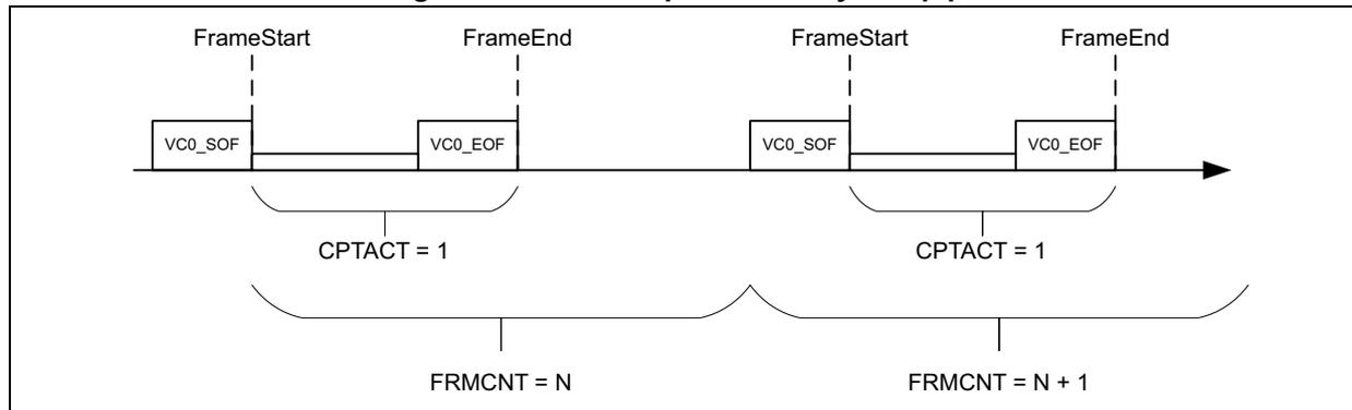
The diagram illustrates the processing of a virtual channel (VC) flow through a single pipe. It shows two consecutive frames. Each frame is bounded by a 'FrameStart' (dashed vertical line) and a 'FrameEnd' (dashed vertical line). Within each frame, there are two markers: 'VC0_SOF' (Start of Frame) and 'VC0_EOF' (End of Frame). Below the first frame, a bracket labeled 'CPTACT = 1' spans the distance between the SOF and EOF markers. Below the second frame, a similar bracket labeled 'CPTACT = 1' spans the distance between its SOF and EOF markers. At the bottom, two larger brackets indicate frame counts: 'FRMCNT = N' for the first frame and 'FRMCNT = N + 1' for the second frame, showing that each frame increments the frame counter.
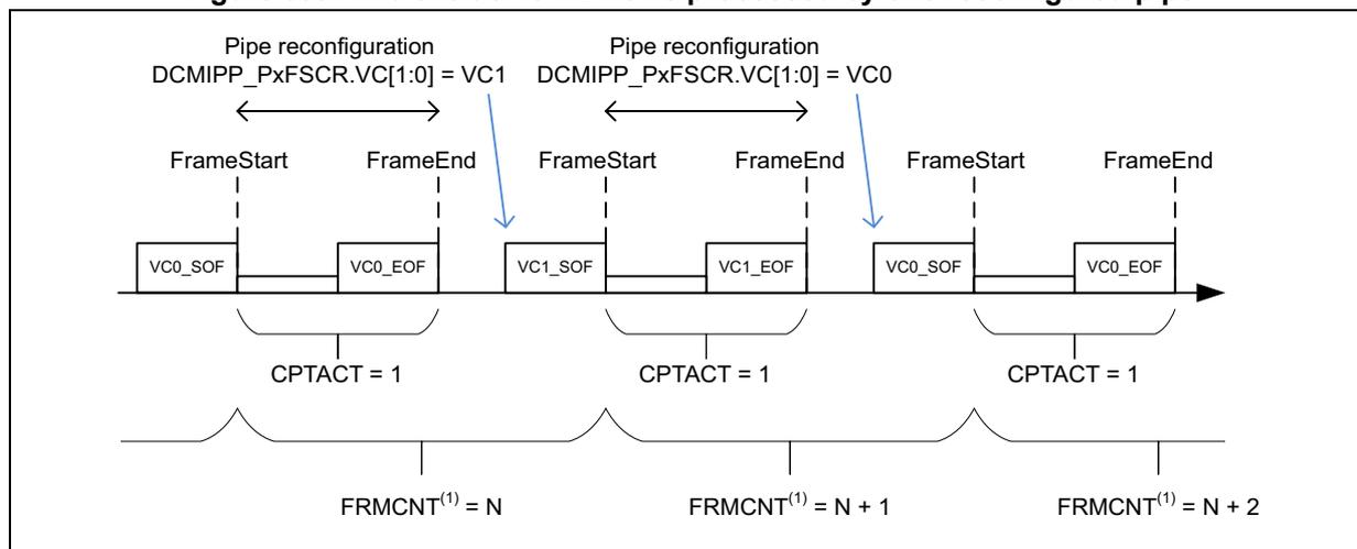
The diagram illustrates the processing of two exclusive VC flows (VC0 and VC1) by a single reconfigured pipe. The timeline shows frame start (SOF) and end (EOF) events. The pipe is reconfigured from VC1 to VC0. The first frame is VC0 (CPTACT = 1, FRMCNT (1) = N). The second frame is VC1 (CPTACT = 1, FRMCNT (1) = N + 1). The third frame is VC0 (CPTACT = 1, FRMCNT (1) = N + 2). The reconfiguration is indicated by the labels 'Pipe reconfiguration DCMIPP_PxFSCR.VC[1:0] = VC1' and 'Pipe reconfiguration DCMIPP_PxFSCR.VC[1:0] = VC0' above the respective frame segments.
- 1. If frame counter is attached to the pipe and if reset is not requested when changing VC.
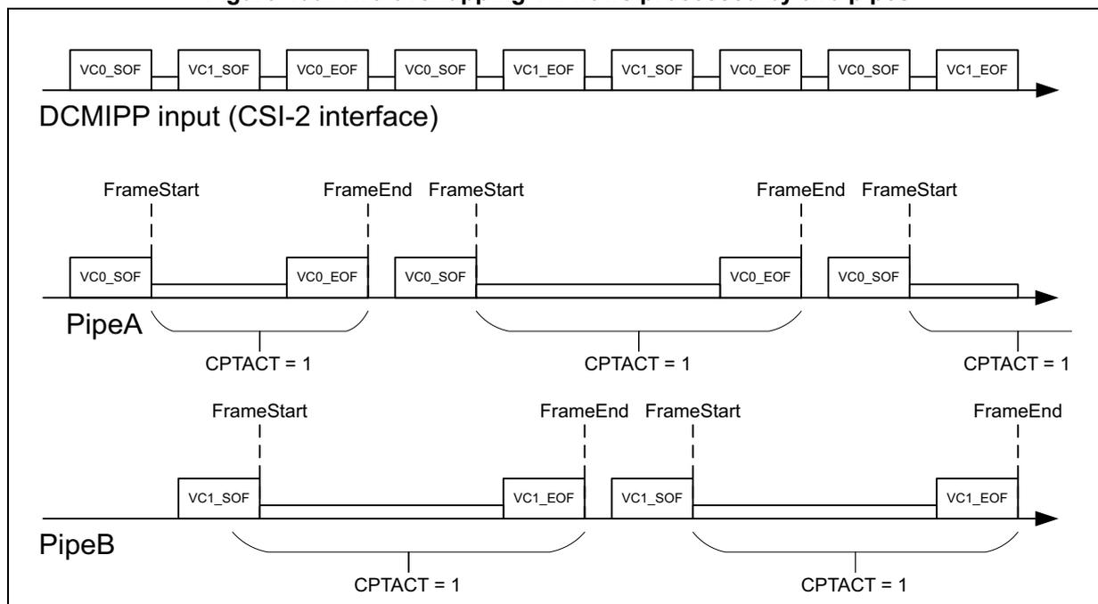
The diagram illustrates the processing of two overlapping VC flows (VC0 and VC1) by two separate pipes (PipeA and PipeB). The top timeline shows the DCMIPP input (CSI-2 interface) with a sequence of VC0 and VC1 frames. Below, PipeA and PipeB are shown processing these frames. PipeA processes VC0 frames (CPTACT = 1) and PipeB processes VC1 frames (CPTACT = 1). The diagram shows the flow of frames through the pipes, with FrameStart and FrameEnd markers indicating the start and end of each frame.
Use cases
The Continuous mode is typically used to send to display or to software-analysis a continuous stream of frames.
The Snapshot mode is typically used to dump a high-resolution frame.
The Frame rate mode is typically used for a low-power continuous analysis, where only one frame every eight is dumped and analyzed.
The frame informations are typically used for interlaced video use cases, where the sensors transmit alternatively odd and even fields (top vs. bottom), and where software must be able to retrieve the type of field. Depending on the sensor, it can be retrieved from:
- • the VC-ID, if the sensor uses one VC for one field and another for the other
- • the LSB of the counted number of lines in that frame (indicates if the number is odd or even)
- • the LSB of the frame counter extracted from the CSI information (if counting this pipe), which can be odd or even.
Software configuration
The frame control supports two different capture modes:
- • Snapshot mode: the software captures single frames
- • Continuous mode: the software captures a continuous sequence.
The timing diagram of these two modes is shown in Figure 401 .
Figure 401. Snapshot (CPTMODE = 1) and Continuous (CPTMODE = 0) capture modes
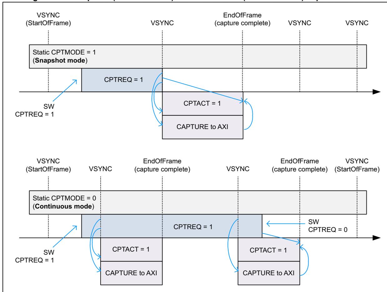
The diagram illustrates two capture modes over time, represented by a horizontal timeline with vertical dashed lines indicating key events.
Top Section: Snapshot Mode (Static CPTMODE = 1)
- The timeline starts with a VSYNC (StartOfFrame) signal.
- Following this, a software write SW CPTREQ = 1 is made.
- The next significant event is another VSYNC signal.
- At this VSYNC, the capture logic activates, setting CPTACT = 1 and initiating CAPTURE to AXI .
- The capture continues until an EndOfFrame (capture complete) signal is received.
- After the end of the frame, the CPTACT signal returns to 0.
- The sequence concludes with a subsequent VSYNC signal.
Bottom Section: Continuous Mode (Static CPTMODE = 0)
- The timeline starts with a VSYNC (StartOfFrame) signal.
- A software write SW CPTREQ = 1 is made.
- The capture logic activates at the next VSYNC signal, setting CPTACT = 1 and initiating CAPTURE to AXI .
- The capture continues until an EndOfFrame (capture complete) signal is received.
- At this point, a software write SW CPTREQ = 0 is made.
- The capture logic deactivates ( CPTACT = 0 ) until the next VSYNC signal.
- At the next VSYNC , the capture logic activates again ( CPTACT = 1 ) and initiates CAPTURE to AXI once more.
- This cycle repeats until another EndOfFrame (capture complete) signal is received.
- The sequence concludes with a final VSYNC (StartOfFrame) signal.
Table 339. DCMIPP_PxFCTCR bit function
| Bit ID | Function | Values |
|---|---|---|
| CPTMODE | Capture mode | – 0: Continuous – 1: Snapshot |
| CPTREQ | Capture request | – 1: Capture requested |
| FRATE | Frame rate | – 0: Full rate capture – 1: 1/2-rate capture – 2: 1/4-rate capture – 3: 1/8-rate capture |
| CPTACT (1) | Capture status | – 1: Capture currently active |
- 1. Bit read from the DCMIPP_PxSR register.
Configuration example
The software operations when using the Snapshot mode are the following:
- 1. Software sets CPTMODE = 1, to use the Snapshot mode.
- 2. Software sets PIPEN = 1, to let the flow selection send data to PipeN.
- 3. Software sets CPTREQ = 1, to request the capture of one frame.
- 4. At the first following VSync, the HW samples CPTREQ at 1, with the following impact:
- a) The capture effectively starts: pixels flow into the pipe and are dumped in memory.
- b) CPTACT is set to 1, to mention that a capture is currently ongoing, and that it is best to not modify the configuration of the pipe operators, unless shadowed.
- c) CPTREQ is reset to 0, so that only a single frame is dumped.
- 5. At the following capture complete interrupt
- a) CPTACT is reset to 0, to signal that the capture is over.
- b) The capture is complete, no more pixels are flowing, hence software can restart to update the configuration of non-shadowed registers without any issue, and use the captured pixels in memory. Depending upon the sensor blanking, this period can be short.
- 6. At the next VSync, CPTREQ usually is sampled at 0, so that no more frames are captured
- – As soon as CPTREQ is reset to 0 the software can set it again to 1, to request a capture at the following frame. It means that a continuous sequence of frame can be captured by setting again CPTREQ to 1, continuously frame after frame.
The software operations when using the Continuous mode are the following:
- 1. Software sets CPTMODE = 0, to use the Continuous mode.
- 2. Software sets PIPEN = 1, to let the flow selection send data to PipeN.
- 3. Software sets CPTREQ = 1, to request the continuous capture of frames.
- 4. At the first following VSync, CPTREQ is sampled at 1, with the following impact:
- – As in Snapshot mode, the capture starts, and CPTACT is set at 1.
- – Unlike the Snapshot mode, CPTREQ is not modified and remains at 1.
- 5. At the following capture complete interrupt:
- – As in Snapshot mode, CPTACT is reset to 0, capture stops, software can shortly reconfigure the pipes, and software can use the captured pixels.
- 6. At the next VSync, and as long as CPTREQ remains at 1, the capture restarts, similarly as described above.
- 7. To stop capturing later frames, software resets CPTREQ to 0.
- – An ongoing capture continues until completion.
- 8. At the next VSync, CPTREQ is sampled at 0, and the next capture does not restart.
39.4.8 Pipe deactivation
It is possible to abort a pipe to stop any frame acquisition and to potentially offer a mean to reprogram it completely (including non-shadowed registers), or to let it fully disabled for some time. The following operating mode has to be considered to correctly stop the pipe:
- 1. Disable the CPTREQ bit of the DCMIPP_PxFCTCR register of the corresponding pipe
- 2. Poll CPTACT = 0 status bit in the DCMIPP_CMSR1 register to check if the pipe is no longer active (idle state)
- 3. Disable PIPEN in the DCMIPP_PxFCTCR register.
When disabling the pipe, the last frame is processed completely by respecting the above operating mode.
Note: To disable the parallel interface (PREN = 0 in the DCMIPP_PxFSCR), it is recommended to first disable the pipes considering the above operation mode, before switching off the parallel interface.
39.5 Pipe0 (dump pipe)
39.5.1 Overview
Pipe0 works as a dump pipe: it extracts data from the camera sensor module and dumps them (as-is) to the targeted memory, with some basic decimation and cropping 2D operations in between.
Figure 402. Pipe0 (dump) architecture overview
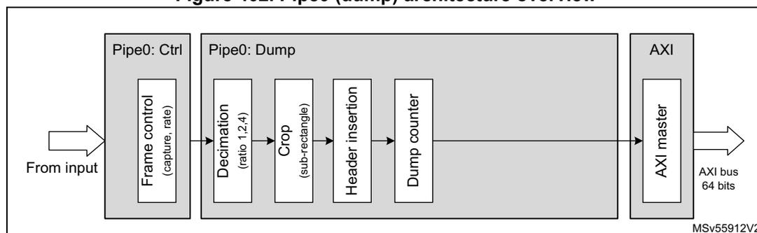
The diagram illustrates the architecture of Pipe0 (dump). It starts with an input arrow labeled 'From input' pointing into a box labeled 'Pipe0: Ctrl'. Inside this box is a sub-box labeled 'Frame control (capture, rate)'. An arrow points from 'Pipe0: Ctrl' to a larger box labeled 'Pipe0: Dump'. Inside 'Pipe0: Dump' are four sub-boxes in sequence: 'Decimation (ratio 1:2,4)', 'Crop (sub-rectangle)', 'Header insertion', and 'Dump counter'. An arrow points from 'Dump counter' to a box labeled 'AXI'. Inside 'AXI' is a sub-box labeled 'AXI master'. An arrow points from 'AXI master' to the right, labeled 'AXI bus 64 bits'. The diagram is labeled 'MSV55912V2' in the bottom right corner.
Pipe0 retrieves data from the camera sensor module connected to the DCMIPP through the 16-bit parallel interface or the CSI-2 interface, by means of the CSI-2 host controller peripheral. The selection between interfaces is managed by means of bit INSEL in the DCMIPP_CMCR register.
The flow selection chooses the virtual channels and data types to be processed by the pipe from the CSI2 host controller, see Section 39.4.5 for more details.
The frame controller handles mainly the camera acquisition mode (continuous or snapshot, frame rate), see Section 39.4.7 for more details.
When the input data from the camera is valid and supposed to be processed by Pipe0, 2D-cropping and decimation operations can be configured by the software. A dump counter combining with a limit amount of data to be set is offered to handle unknown length of data or to avoid the amount of data to be too wide within a frame.
Pipe0 can be reconfigured from time to time. Some events can be used to trigger the software reconfiguration routines (refer to Section 39.13.2: Interrupts ).
It is also possible to write into the shadow registers within the processing of a frame. The values are loaded into the physical register based on the start of frame event.
39.5.2 Decimation
The decimation allows to cheaply downsize a frame.
Based on parallel interface camera module:
- – Factor 1x, 2x, 4x at data/byte level depending on the configuration of bit field BSM[1:0] of the DCMIPP_P0PPCR register. The decimation is not working directly at pixel level, but it is based on either byte or 16-bit word granularity (for padded raw 10, for instance) to make equivalent decimation to one pixel out of two. Bit OEBS is used to start from the odd or even byte (or data) to capture first.
- – The decimation can also be based on entire line, by capturing all the lines, or one line out of two thanks to bit LSM. Here, again, choice is given to the software to reject odd or even lines within the frame by configuring bit OELS.
When the camera sensor module is designed on CSI-2 interface, the decimation can be based filter out potentially, one line out of two. Indeed, each packet is by protocol composed for an entire line.
Note: Care must be taken when the CSI-2 header is dumped, as it is 32-bit wide, and it increases by one unit the data counter, taking part of the decimation. It is advised not to use the CSI header option when decimation takes place.
Table 340. DCMIPP_P0PPCR bit function
| Bit ID | Function |
|---|---|
| BSM[1:0] | To select how much byte/data have to be captured within a line. This feature is available only for a parallel interface camera module. |
| OEBS | Allows the user to chose if the filtering starts from the odd or the even byte. |
| LSM | Possibility to filter out one line out of two. |
| OELS | The software can select if the filtering rejects the odd or even lines. |
39.5.3 Crop/statistics selection/suppression
The dump pipe (Pipe0) has the capability to handle 2-D crop processing. The vertical cropping is based on line, thanks to HSYNC event (from the physical IOs or the embedded code detection if selected). It can be extracted from the CSI-2 packet information (each packet is one line wide by protocol).
The horizontal area on which the crop is applied is based on data (32-bit wide), and not on pixels since this pipe is not directly considering the pixels. It handles the data flow with 32-bit granularity. The CROP functionality is not supported when the pipe is conveying JPEG format. The ENABLE bit must be kept cleared into DCMIPP_P0SCSZR to avoid any unpredictable behavior.
The area to be captured within the frame has to be specified configuring the registers DCMIPP_P0SCSTR and DCMIPP_P0SCSZR. The starting point on the two axis are set accordingly as well as the width in both directions. It is possible to take the data inside or outside this area by means of bit POSNEG in the DCMIPP_P0SCSZR register. Some sensors can send sensor configuration data and statistics (histogram) on the very first and last lines of a frame. By specifying active the area outside of this window selection (POSNEG = 1), only statistic data are extracted by the way, and the software can decide to apply some processing on the data to correct, such as contrast or exposure.
Features
- • 2D-Crop operation with granularity:
- – Lines in the vertical axis
- – 32-bit data in the horizontal axis
- • Possibility to capture data inside or outside the defined window (valid image data or statistic data)
- • Cropping with 0 value for HSIZE[11:0] or VSIZE[11:0] has no crop effect to the dimension for which the 0 value has been applied (vertical or horizontal axis).
Software configuration
Registers DCMIPP_P0SCSTR and DCMIPP_P0SCSZR have to be configured to set the crop feature into the dump pipe:
- 1. Configure the cropped horizontal starting point with HSTART[11:0] and the width with HSIZE[11:0] (both with a 32-bit data granularity).
- 2. Configure the cropped lines, starting at line VSTART[11:0] and with a height of VSIZE[11:0] (both with a line granularity)
- 3. If any value HSIZE or VSIZE is set to 0, the hardware does not consider crop operation in the vertical or horizontal dimension for which the 0 value has been applied, so that all the pixels in that dimension are sampled.
- 4. Select the inner or the outer part of the window for the data capture by configuring POSNEG bit.
- 5. Enable the crop feature setting ENABLE bit. This bit must be cleared when JPEG is selected as the input format for Pipe0.
Note: Cropping out the picture size (with too large HSTART or VSTART) leads to a not guaranteed processed frame.
39.5.4 Header insertion
The module works on the dump pipe(s) and it optionally inserts an header before the data of a former CSI packet.
Features
- • Optionally inserts non-data information to help software interpreting the following data payload. The non-data info is Frame sync short packets and Header of data long packets (both non-data info into a 32-bit word), mapped as follows:
- – Frame sync short packet: defined by Frame type = SOF or EOF
- > bits 31:16: Frame number
- > bits 15:8: Reserved (forced to 0)
- > bits 7:4: Virtual channel ID in CSI-2_v1.3, bits 7:6 = 00
- > bits 3:0: Frame type (SOF = 0x1 or EOF = 0x2)
- – Header of data long packet (defined by below Frame type = DATA)
- > bits 31:16: Amount of bytes in the payload
- > bits 15:8: Data type ID in CSI-2_v1.3, bits 15:14 = 00
- > bits 7:4: Virtual channel ID in CSI-2_v1.3, bits 7:6 = 00
- > bits 3:0: Frame type (DATA = 0x0)
- – Frame sync short packet: defined by Frame type = SOF or EOF
To keep consistency between the amount of bytes provided by the header versus those effectively dumped, it is recommended to not activate the header insertion simultaneously with the crop or decimation, as these functions modify the amount of dumped data.
When header insertion is active, the FrameEnd packet is dumped as a header, and is considered as the unique part of an additional line, inducing an event.
Software configuration
It is configured with the DCMIPP_P0PPCR register:
- • HEADEREN:
- – 0: No header insertion
- – 1: Insertion of the headers, aligned on 32 bits.
39.5.5 Dump counter
The dump counter is present on dump pipe. It is used to count the amount of data that are dumped in that frame, and to potentially limit the amount dumped if too large. It allows the software to know the size of dumped buffer, and to make sure that no dump is made out of a preallocated buffer.
It is specifically useful when dumping a content whose length is unknown prior to reception, like an encoded JPG stream. When dumping a pixel frame, the size is known thanks to the configured width and height of the frame.
The counter is counting 32-bit data for almost all the input formats, even if the value is expressed in number of bytes. The counter increment is 4-bytes granularity for all formats except the JPEG byte stream input mode, for which the counter granularity is 8-bit because the application does not know the amount of dumped data.
Features
- • Dump counter, counting the amount of bytes dumped. It counts the amount of dumped 32-bit words (the increment is 4), except when connected to a parallel interface camera and dumping a 8-bit data in byte stream mode (see FORMAT bit field in the DCMIPP_PRCR register), where it counts per byte (the increment is 1).
- – The counter saturates at 0x03FF_FFFF.
- – At FrameEnd, the counter value is recopied in a readable shadow register and the counter itself is reset to start the count of the next frame.
- • Dump limit, that clamps the dumped words below a maximum limit:
- – If the counter reaches the limit, all following bytes are deleted until the next VSync.
- – The counter continues to count over the limit, to indicate how many bytes have been received and must have been dumped if not deleted.
- • Interrupt limit is triggered when some bytes are deleted due to dump limit crossed.
- • CSI headers, when dumped (HEADEREN = 1), participate to the counted and limited data volumes.
- • Monochrome or raw Bayer padding (alignment of 10/12/14 bpp to 16 bpp) is also taken into account in data volumes.
Software configuration
Table 341. DCMIPP_P0DCCNTR and DCMIPP_P0DCLMTR bit function
| Bit ID | Function |
|---|---|
| ENABLE | 1: Enables the limit check. |
| CNT | Read-only, counts the amount of data with a 4-byte granularity for most of the input formats or with an 8-bit data granularity in JPEG byte stream mode selected into DCMIPP_PRCR.FORMAT). The counter increment is based on dumped data at the pipe output standpoint. The value is expressed in bytes, whatever the input format. |
| LIMIT | Gives the maximum amount of 32-bit data that can be dumped. Limit value 0 is inconsistent and the processed frame is not guaranteed if ENABLE bit is set. |
| LIMITIE | DCMIPP_PxIER.LIMITIE bit enables the interrupt. |
Note: The dump counter sees the CSI-2 packet headers as normal 32-bit words. Raw Bayer and monochrome pixels on 10/12/14 bpc are padded onto 16 bits, and are thus slightly larger than their 10/12/14 bit size.
39.5.6 Double buffer mode
The dump pipe uses an AXI master interface to dump the data from the internal FIFO to the external memory. In the application, it is possible to handle frame data swapping memory area frame by frame. The double buffer mode fills up this function. There are two memory address registers set to initialize the base addresses of these memories areas. Each start of captured frame event swaps the memory base address to handle double buffering mode.
The double buffer mode can be used to allow post-processing on a buffer (frame buffer) while the other buffer is read to be displayed (display buffer).
Software configuration
Double buffering mode requires an activation, as well as addresses configuration, to define the two memory areas in which data are consecutively stored frame by frame at the output of the pipeline:
- • DCMIPP_PxPPM0AR1 and DCMIPP_PxPPM0AR2 must be filled with the memory addresses associated to the double buffer memory locations.
- • Bit DBM in the DCMIPP_PxPPCR register(s) is set to enable the double buffer mode.
39.6 Pipe1 (ISP part)
39.6.1 Overview
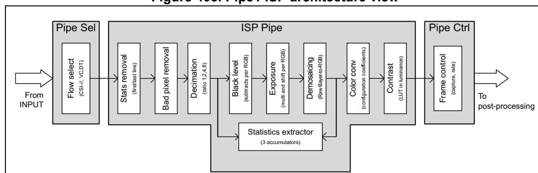
Pipe1 is a pixel pipeline in which some image processing (ISP) and post-processing functions are integrated, to relieve the software from very specific (time and memory consuming) operations. The ISP part implements functions like:
- • Statistics removal within the dataflow
- • Bad pixel detection to automatically remove noisy pixels
- • Basic decimation to reduce high resolution camera sensor to fit with the image processing maximum resolution tolerance
- • Auto exposure and statistics extraction based on pixel analysis
- • Demosaicing algorithm to convert raw Bayer input pixels to RGB ones
- • Color conversion and contrast enhancement functions
Pipe1 ISP block diagram is shown in Figure 403 .
Figure 403. Pipe1 ISP architecture view
    graph LR
    IN[From INPUT] --> PS[Pipe Sel]
    subgraph PS [Pipe Sel]
    FS[Flow select
(CSI-2, VC, DT)]
    end
    PS --> IP
    subgraph IP [ISP Pipe]
    SR[Stats removal
(first/last line)] --> BPR[Bad pixel removal]
    BPR --> D[Decimation
(ratio 1,2,4,8)]
    D --> BL[Black level
(subtracts per RGB)]
    BL --> E[Exposure
(multi and shift per RGB)]
    E --> DEM[Demosaicing
(Raw Bayer-to-RGB)]
    DEM --> CC[Color conv
(configuration coefficients)]
    CC --> C[Contrast
(LUT in luminance)]
    SE[Statistics extractor
(3 accumulators)]
    BL --> SE
    E --> SE
    DEM --> SE
    end
    IP --> PC
    subgraph PC [Pipe Ctrl]
    FC[Frame control
(capture, rate)]
    end
    PC --> OUT[To post-processing]
Pipe1 is the most featured pixel pipeline, even if the image processing functions can be shared with Pipe2 (refer to Section 39.8.2 ).
Pipe1 retrieves data from the camera sensor module connected to the DCMIPP with the 16-bit parallel interface or with the CSI-2 interface, thanks to the external CSI-2 host controller peripheral. The selection between interfaces is managed by means of bit INSEL in the DCMIPP_CMCR register.
The flow selection chooses the virtual channels and data types to be processed by the pipe from the CSI2 host controller. Refer to Section 39.4.5: Flow selection for more details.
The frame controller handles mainly the camera acquisition mode (continuous or snapshot, the frame rate). Refer to Section 39.4.7: Frame control .
Pipe1 can be reconfigured from time to time. Some events can be used to trigger the software reconfiguration routines (refer to Section 39.13.2: Interrupts ).
It is also possible to write into the shadow registers during the processing of a frame. The values are loaded into the physical register based on the following start of frame event.
39.6.2 Byte-to-pixel conversion
The module works on the pixel pipes: it gets 32-bit words from the input (parallel or CSI) interfaces, extracts the pixels depending on the provided pixel format, and maps them onto
the triple-component pixel pipeline, that is 14 bpc at this stage (and 8 bpc later downstream).
Functionality
- • Extracts various input pixel formats to a triple R, G, B lane
- – All CSI-2 formats of versions CSI v1.3 and v2.0 are supported, except Raw 6/7 bpc, YUV422-10 bpc, YUV420 (see Table 335 )
- • YUV420-to-YUV444 conversion is not supported
- – Pipe1 and Pipe2 cannot extract and process YUV420 pixels received from the CSI interface
- • YUV422-to-YUV444 conversion:
- – Done by replication of the U and V components. It thus assumes that the location of the common chroma is defined at mid-distance between the two pixels.
- • Extension of short triple component (RGB/YUV) to the output triple 8 bpc:
- – The extension is done by replicating the input MSB onto the missing output LSB. The replication onto the LSB allows to map any input dynamic on the full downstream dynamic.
- – Examples of 5 and 6 bpc extended to the output 8 bpc:
- > Input Di[4:0]: Output Do = Di[4:0] and Di[4:2]
- > Input Di[5:0]: Output Do = Di[5:0] and Di[5:4]
- • Keeps as-is the single-components, usually wide:
- – The monochrome and raw Bayer 10/12/14 bpc are fed into the pipes as-is (the monochrome assumes a Y, with U = V = 128).
Software configuration
The used pixel format depends upon the source of the pixels:
- • CSI-2 interface: the pixel format is embedded in the received CSI-2 packets, and defined in the data type field of the packet header.
- – When FDTFEN = 0, the byte-to-pixel conversion uses the data type provided by the CSI-2 packet, and works automatically, without need for any configuration.
- – When FDTFEN = 1, the data type is configured by software in the FDTF field.
- • Parallel interface: the pixel format is determined by the source of the pixels, i.e. the camera sensor. The byte-to-pixel extracts the pixels based on the pixel format provided by the software in the parallel interface configuration, in the field of the DCMIPP_PRCR register.
39.6.3 Statistics removal
The module is used to removing potential statistic data inserted by a sensor, prior to starting the demosaicing conversion that is multi-pixel and would be impacted by remaining statistics. It is typically used by sensors with a parallel interface, which does not have any way to distinguish between statistics and pixel data. CSI-2 sensors typically split these flows using different virtual channel IDs.
Features
- • Suppression of some of the first lines of the frame.
- • Suppression of the last lines of the frame, after a configured line N.
Software configuration
Table 342. DCMIPP_P1SRCR bit function
| Bit ID | Values | Comments |
|---|---|---|
| CROPEN | 1: Active | If CROPEN = 0 all pixels are fed through. |
| FIRSTLINEDEL | 0 to 7 | Amount of first lines to delete when CROPEN = 1 |
| LASTLINE | 0 to 4094 | Amount of lines to keep after the removed first lines. If LASTLINE is null, all remaining lines after FIRSTLINEDEL are fed through. |
Configuration example
If the received frame contains four lines of statistics, followed by 100 lines of pixels and eight lines of ancillary data, the configuration to extract the 100 lines of pixels is the following:
- • CROPEN = 1, to have the removal active
- • FIRSTLINEDEL = 4, to remove the first four lines
- • LASTLINE = 100, to keep the next 100 lines
39.6.4 Bad pixel removal
This module aims at detecting and correcting artifacts generated by a bad pixel on the sensor array. It is based on a correlation extraction, and not on fixed locations.
Functionality
- • Works for raw Bayer flows only, as RGB flows are assumed as already processed.
- • Scans all the arriving components, and extracts the horizontal continuity correlation versus the two left and two right neighbors, on both the local component and on the adjacent raw Bayer component:
- – if a component is seen as too light, it is declared as bad
- – too dark components are not extracted, to avoid false positives
- • A component assumed bad is replaced by the horizontal average of its two neighbors (with the same component).
Software configuration
Table 343. DCMIPP_P1BPRCR and DCMIPP_P1BPRSR bit function
| Bit ID | Function |
|---|---|
| ENABLE |
|
| STRENGTH | 3 bits, 0 (high tolerance) to 7 (aggressive detection) |
| BADCNT | 12-bit counter, reporting the amount of bad components corrected. The counter saturates at its maximum value (4095). At FrameEnd, the counter is re-clocked (the read value remains stable one full frame), even if the frame is skipped (not captured), and reset to restart accumulation at the next frame. |
Configuration example
A too aggressive bad pixel detection might detect false bad pixels and erroneously correct them (it can occur for very thin light vertical lines that cannot be distinguished from bad pixels in the implemented horizontal filter). To avoid such artifacts, it is advised to setup a software loop-back that tunes the filter strength so that the detected bad pixels remain within a predefined valid range.
Start configuration (or without software feedback loop):
- • ENABLE = 1 (enabled)
- • STRENGTH = 0 (high tolerance)
Software feedback loop:
Assumes a maximum amount of 100 bad pixels on the array (any other value can be used).
- • BADCNT read: gets the amount of corrected bad pixels of the last frame
- • Low-pass filter on the BADCNT, and/or hysteresis
- – BADCNT > 100: too aggressive, decrease STRENGTH
- – BADCNT < 30: too tolerant, increase STRENGTH (assuming there are bad pixel on the array)
Note: The expected amount of bad pixels (100 in the above example) can be set to other values, or made dependent upon the equivalent gain of the sensor (analog gain, exposure duration). A high-gain picture has more noisy pixels and can accept a more aggressive filter to smooth the noise, while a low-gain picture has mostly correct pixels, only very uncorrelated pixels need to be corrected.
39.6.5 Input decimation
The decimation makes it possible to cheaply downsize a frame, by a factor 2, 4, or 8, in both horizontal and vertical directions. It supports a special mode adapted to a raw Bayer format in input.
The decimation is redundant with the downsize, that brings a higher quality (the decimation discards the data of the dropped pixels, while the downsize averages all pixels and does not lose information).
The decimation has two main usages:
- • Reduces the width of very high resolution sensors to one accepted by the raw Bayer-to-RGB conversion. Indeed, the raw Bayer-to-RGB embeds a line buffer that limits its processed images to a maximum width of 2688 pixels. The decimation makes possible, for instance, to plug a 12 Mpixel sensor (4000 x 3000), decimate its width by a factor 2x to 2000 pixels wide, and have it converted to RGB.
- • Complements the downsize (limited to ratio of 8 x 8), to have a combined downsizing ratio of 64 x 64. It is recommended to have the largest ratio implemented in the downsize, and the decimation complement to that. For instance, for a ratio 30x, is it recommended to have a ratio 4x in decimation, and a ratio \( 30 / 4 = 7.5 \) in the downsize.
Features
- • Forwards one item every 1, 2, 4, 8 pixels, independently, vertical and horizontal.
- • Supports raw Bayer formats, where RG-GB components must remain grouped. In that mode the above forwarded items are not pixels, but a double component (for example R and G or G and B for a RGGB format), in both vertical and horizontal directions. For
instance, with a decimation of 2x, the input sequence R0, G0, R1, G1, R2, G2, R3, G3 gets forwarded as R0, G0, R2, G2 and not R0, R1, R2. The same applies vertically.
Software configuration
Table 344. DCMIPP_P1DECR bit function
| Bit ID | Function | Value | Comments |
|---|---|---|---|
| HDEC[1:0] | Ratio (2 bits) | 0 | No decimation |
| 1 | Ratio 1/2 | ||
| 2 | Ratio 1/4 | ||
| 3 | Ratio 1/8 | ||
| VDEC[1:0] | 0 | No decimation | |
| 1 | Ratio 1/2 | ||
| 2 | Ratio 1/4 | ||
| 3 | Ratio 1/8 | ||
The raw Bayer mode in decimation is indirectly activated when the Datatype is defined as raw Bayer.
39.6.6 Black level calibration
This module suppresses a potential positive black level offset, which happens when the sensor sends non-null pixels when capturing a black picture.
Functionality
- • Subtracts an offset from the R, G, B components.
- • A different constant is used for R vs. G vs. B, including within raw Bayer pixels.
Software configuration
Table 345. DCMIPP_P1BLCCR bit function
| Bit ID | Value | Comments |
|---|---|---|
| ENABLE | – 1: Active – 0: Bypasses R, G, B components | - |
| BLCR | - | 8-bit offset, for red |
| BLCG | - | 8-bit offset, for green |
| BLCB | - | 8-bit offset, for blue |
The offset subtracted is aligned components MSB: for instance, if components are defined on 12 bits, the 8-bit offset subtracted for red is BLCR « 4.
Configuration example
It is possible to use the statistics extraction, to extract the long-term most-dark R, G, B components, and assign their darkness as black. Their RGB values become the black level offset for each RGB.
For a raw Bayer sensor with 12-bit components, if the measured black level offset for red is 64 (out of a maximum of 4095), configure BLCR as 16.
39.6.7 Exposure compensation and white-balance calibration
This module aims at compensating bad exposure (too short/dark or too long/light), and at compensating a bad color balance to recenter the colors to more white ones.
The exposure and white balance operations are purely linear, and do not distort colors if performed correctly.
Functionality
- • Multiplies R, G, B by a configured floating-point constant.
- • A different constant is used for R vs. G vs. B, including within raw Bayer pixels.
Software configuration
Table 346. DCMIPP_P1EXCR1 and DCMIPP_P1EXCR2 bit function
| Bit ID | Value | Comments |
|---|---|---|
| ENABLE | – 1: Active – 0: Bypasses R, G, B components | - |
| MULTR, SHFR | - | 8-bit multiplier (mantissa), and up-shift value (0, 1, 2, 3, 4, 5, 6, 7) for red components. |
| MULTG, SHTG | - | 8-bit multiplier and exponent, for green components. |
| MULTB, SHTB | - | 8-bit multiplier and exponent, for blue components. |
The idle setting (that sends out a similar value as input) is:
- • MULTR = MULTG = MULTB = 128
- • SHFR = SHFG = SHFB = 0
Similar idle couples are MULTx = 64 and SHFx = 1, or 32 and 2, or 16 and 3.
Configuration example for exposure alone
It is recommended to use the exposure control in conjunction with the contrast enhancement below in the pipe: the idea is to deliberately keep an exposure lower than ideal, to avoid burning the whites: the contrast enhancement, thanks to non-linear operator on luminance, lightens the dark pixels, and reduces the dynamic of the light pixels without burning them.
It is recommended to use the statistics to extract the average luminance across the whole frame (done best by extracting the R, G, B averages, and computing the luminance from the RGB).
The idea is to push the average output luminance to 128, or if working with the contrast enhancement too, to push it to a lower value, for instance 64.
When measuring an average luminance of 26 (target is 64), the exposure factor to apply is \( 64 / 26 = 2.5x = 1.25x * 2 \) , hence the following configuration must be set:
- • \( MULTR = MULTG = MULTB = 128 * 1.25 = 160 \)
- • \( SHFR = SHFG = SHFB = 1 \)
Configuration example for an additional white balance
An example of easy way to recenter the colors is using the Gray-world algorithm.
This algorithm assumes that a default scene has an inherent balance of its red, green, and blue pixels, so that the average values of the red, green, and blue components across the ideal picture are the same. If the measured averages are not the same, it means that there has been a distortion of the white balance, that must be corrected by amplifying or reducing the red, green, and blue strengths in the exposure module, thanks to the differentiated red vs. green vs. blue multipliers and exponents.
In practice this is the same approach used for the exposure compensation, but, instead of forcing the output luminance to a default target (64 in the example), user must force the red, green, and blue averages towards the same exposure target.
As an example:
- • Exposure target is defined as 64.
- • Measured red is 26: red factor is \( 64 / 26 = 2.5x \) , hence \( MULTR = 160 \) , \( SHFR = 1 \) .
- • Measured green is 32: green factor is \( 64 / 32 = 2.0x \) , hence \( MULTG = 128 \) , \( SHFG = 1 \) .
- • Measured blue is 10: blue factor is \( 64 / 10 = 6.4x \) , hence \( MULTB = 205 \) , \( SHFB = 2 \) .
39.6.8 Demosaicing
The module works on the pixel pipes, and implements a mid-quality conversion from raw Bayer 8 bpp to an RGB 24 bpp, with no implicit half-sizing: the output RGB pixel rate is the same as the input component rate.
The conversion targets real-time but medium quality purposes, like display or low-resolution software analysis. For higher quality conversions, it is recommended to convert the raw Bayer in software, with higher quality algorithms but limited to non-real-time, thus still-picture applications.
The algorithm takes the surrounding \( 3 \times 3 \) components in input, applies linear heuristics to determine the most likely missing components, and generates an output RGB888 pixel.
To provide the \( 3 \times 3 \) input matrix to the algorithm, the demosaicing module embeds a double line-buffer, \( 2 \times 2688 \) components wide. As such, it limits the maximum width of a converted demosaicing buffer to 2688 components/pixels wide. Wider camera sensor resolution can be connected and goes through the first decimation stage in front of the demosaicing operation.
Note: This demosaicing conversion algorithm can create some artifacts, like Zipper. Such artifacts are much reduced by a later downsizing or even suppressed for a \( 2 \times 2 \) downsizing.
Applications like display, video encode, or software analysis usually require such a downsize, so the artifacts become invisible.
The underlying heuristic filters try to extract and adapt to edges, horizontal and vertical lines, and lone pixels.
Functionality
- • Input pixel format: from 1 (raw Bayer) to three (RGB/YUV) components on 8 bits
- • Max input width of 2688 components
- • Demosaicing conversion:
- – 2-line buffer
- – provides a 3 x 3 matrix to the algorithm + one trailing component (2 left)
- – Extraction and optimization for specific shapes:
- > Edges (on left, right, top, bottom)
- > Lines (horizontal and vertical)
- > Peaking (lone pixels detection)
- • Output pixel format: three RGB components on 8 bits.
Software configuration
Table 347. DCMIPP_P1DMCR bit function
| Bit ID | Values | Comments |
|---|---|---|
| ENABLE |
| If the camera sensor transmits an RGB or YUV frame and not raw Bayer, the demosaicing conversion must be disabled, by setting Enable = 0. All other parameters are ignored. |
| TYPE |
| Default raw Bayer with three components (R, G, B) |
| EDGE |
| - |
| LINEH |
| - |
| LINEV |
| - |
| PEAK |
| - |
The four filters, EDGE, LINEH, LINEV, PEAK, improve the zoomed accuracy of the filtered picture (thus mostly luminance correctness, like no Zipper artifact), however at the expense of some chrominance blurring or distortion. Some scenes can require specific settings:
- • Scenes where chrominance distortion is very visible (like a mostly black and white scene viewed by an RGB sensor) can require lower strength of the filters.
- • On the opposite, scenes heavily loaded with geometric shapes (and thus source of artifacts) can require strengthening the filters.
Globally, 6/4/4/2 is a good compromise for the filter strength.
Configuration example
If the camera sensor is raw Bayer, with a grid with a red top-left pixel, the next configuration can be used:
- • ENABLE = 1 to have the demosaicing active
- • TYPE = 0 to have a top-red pixel, thus a RGGB grid
- • EDGE, LINEH, LINEV, PEAK = (4, 4, 4, 4) as typical setting (so an internal strength of 8 for each parameter).
39.6.9 Color conversion
This module implements a color conversion with flexible (fully programmable coefficients), which can be used to map the following features:
- • YUV-to-RGB: when the pixels of a YUV-sensor are used as RGB (display, GPU)
- • RGB-to-YUV: when the pixels of a RGB-sensor are used by software (for example video encode)
- • Tone change: to map special color references (sepia), emphasize some tone/colors
- • Monochrome: to compute a monochrome from RGB/YUV with a specific linear mix
- • Expansion: to handle a YUV (or RGB) expansion or compression
- • Gamma: to emulate a gamma correction via a linear scale
Features
- • Linear rotation of color space: 3 x 3 matrix + 3 x 1 column.
- • Clamping optional on either [16 to 235] for Y, R, G, B and [16 to 240] for U, V.
Software configuration
Table 348. DCMIPP_PxCCyy (yy = R0, R1, G0, G1, B0, B1) bit function
| Bit ID | Value | Comments |
|---|---|---|
| ENABLE | – 1: Activates the color conversion | - |
| CLAMP | – 1: Clamps the output pixel, when using a reduced dynamic | - |
| TYPE | – 1: Clamps as RGB – 0: Clamps as YUV | - |
| Bit ID | Value | Comments |
|---|---|---|
| Matrix3x3_Coeff | - | 11 bits (sign, 2 int, 8 dec, with sign as complement to 2) |
| Added3x1_Coeff | - | 10 bits (sign, 9 int, with sign as complement to 2) |
Configuration example
Table 349 provides examples of the most used conversions:
- • To / from RGB from/to YUV (as SDTV ITU-R BT.601 or HDTV BT.709).
- • With a full (0 to 255) or a reduced (16 to 235) dynamic for Y and RGB, 16 to 240 for CbCr.
- • Matrix fields are defined as XY bit fields in the color conversion coefficient registers, with X being the input R or G or B, and Y being the output R or G or B. For conversions to/from YUV, the R must be assumed as Cr (= V), G must be assumed as Y, and B must be assumed as Cb (= U).
- • Coefficients are defined signed, and multiplied by 256 when there are decimals (the matrix coefficients). Negative values are on 11 bits: \( N11(\text{val}) = \text{XOR}(\text{val}, 0x7FF) + 1 \) , on 10 bits for Added_Coeff: \( N10(\text{val}) = \text{XOR}(\text{val}, 0x3FF) + 1 \) .
| Conversion | Output components | Input components | ||||
|---|---|---|---|---|---|---|
| R | G | B | Added | Clamping | ||
| RGB-255 to YUV601-255 | - | |||||
| Cr | 131 | -110 | -21 | 128 | [0 to 255] | |
| Y | 77 | 150 | 29 | 0 | [0 to 255] | |
| Cb | -44 | -87 | 131 | 128 | [0 to 255] | |
| YUV601-255 to RGB255 | - | Cr | Y | Cb | Added | Clamping |
| R | 351 | 256 | 0 | -175 | [0 to 255] | |
| G | -179 | 256 | -86 | 132 | [0 to 255] | |
| B | 0 | 256 | 443 | -222 | [0 to 255] | |
| RGB-255 to YUV709-255 | - | R | G | B | Added | Clamping |
| Cr | 131 | -119 | -12 | 128 | [0 to 255] | |
| Y | 55 | 183 | 18 | 0 | [0 to 255] | |
| Cb | -30 | -101 | 131 | 128 | [0 to 255] | |
| YUV709-255 to RGB255 | - | Cr | Y | Cb | Added | Clamping |
| R | 394 | 256 | 0 | -197 | [0 to 255] | |
| G | -118 | 256 | -47 | 82 | [0 to 255] | |
| B | 0 | 256 | 456 | -232 | [0 to 255] | |
Table 349. Color conversion: examples of coefficients (continued)
| Conversion | Output components | Input components | ||||
|---|---|---|---|---|---|---|
| RGB-255 to YUV601-240 | - | R | G | B | Added | Clamping |
| Cr | 112 | -94 | -18 | 128 | [16 to 240] | |
| Y | 66 | 129 | 25 | 16 | [16 to 235] | |
| Cb | -38 | -74 | 112 | 128 | [16 to 240] | |
| YUV601-240 to RGB255 | - | Cr | Y | Cb | Added | Clamping |
| R | 409 | 298 | 0 | -223 | [0 to 255] | |
| G | -208 | 298 | -100 | 135 | [0 to 255] | |
| B | 0 | 298 | 517 | -277 | [0 to 255] | |
| RGB-255 to YUV709-240 | - | R | G | B | Added | Clamping |
| Cr | 112 | -102 | -10 | 128 | [16 to 240] | |
| Y | 47 | 157 | 16 | 16 | [16 to 235] | |
| Cb | -26 | -87 | 112 | 128 | [16 to 240] | |
| YUV709-240 to RGB255 | - | Cr | Y | Cb | Added | Clamping |
| R | 459 | 298 | 0 | -248 | [0 to 255] | |
| G | -137 | 298 | -55 | 77 | [0 to 255] | |
| B | 0 | 298 | 541 | -289 | [0 to 255] | |
| RGB-240 to YUV601-240 | - | R | G | B | Added | Clamping |
| Cr | 131 | -110 | -21 | 128 | [16 to 240] | |
| Y | 77 | 150 | 29 | 0 | [16 to 235] | |
| Cb | -44 | -87 | 131 | 128 | [16 to 240] | |
| YUV601-240 to RGB240 | - | Cr | Y | Cb | Added | Clamping |
| R | 351 | 256 | 0 | -175 | [16 to 235] | |
| G | -179 | 256 | -86 | 132 | [16 to 235] | |
| B | 0 | 256 | 443 | -222 | [16 to 235] | |
| RGB-240 to YUV709-240 | - | R | G | B | Added | Clamping |
| Cr | 131 | -119 | -12 | 128 | [16 to 240] | |
| Y | 55 | 183 | 18 | 0 | [16 to 235] | |
| Cb | -30 | -101 | 131 | 128 | [16 to 240] | |
| YUV709-240 to RGB240 | - | Cr | Y | Cb | Added | Clamping |
| R | 394 | 256 | 0 | -197 | [16 to 235] | |
| G | -118 | 256 | -47 | 82 | [16 to 235] | |
| B | 0 | 256 | 465 | -232 | [16 to 235] | |
39.6.10 Contrast enhancement
This module ends the image processing pipe. It makes possible to enhance the contrast of the frame, by non-linear emphasis of the luminance of the pixels, and to provide more luminance quantification steps at highly used luminances (usually central grays), by reducing the amount of quantification steps less used by the picture (usually the few very dark and very light pixels).
Functionality
- • Inputs RGB from the pipe
- • Computes the luminance of the local pixel
- • Extracts the desired luminance increase/decrease factor, in function of the input luminance, non-linearly (using a look-up table)
- • Multiplies the input RGB with the amplification factor
- • Outputs the clamped RGB components on 8 bits
Software configuration
Table 350. DCMIPP_P1CTCR1,2,3 bit function
| Bit ID | Values | Comments |
|---|---|---|
| ENABLE |
| - |
| LUMx (x = 0 to 8, respectively inputs at 0, 32, 64, 96, 128, 160, 192, 224, 256) | 0 to 63 | Amplification factor:
|
Configuration example
There are multiple approaches to handle contrasts.
It is possible to flatten the spectrum of luminance density (that is, to try have a similar amount of pixel per each segment of luminance), which is to fill each of the eight segments of luminance with 12.5% of the pixels of the frame.
An intermediate approach is to proceed with only the upper and lower half pixels: half of pixels must have a luminance below and another half above the mid-dynamic (128 for 8-bit components).
It is advised to use the statistics extraction module, sample the luminance after the exposure control (to avoid an impact on the exposure compensation), and sort it in the 12 available bins (refer to Section 39.6.11 ). From the extracted bins the user must linearly extrapolate the luminance of the median of the amount of pixels. The luminance of median pixel must be increased/decreased to be moved to the targeted output median luminance, which is recommended to be the median dynamic (128).
For instance, a 400 kpixels VGA picture can have 200 kpixels below a luminance of 64, and the other 200 kpixels above that value. The ideal luminance amplification factor can be set to \( 128 / 64 = 2x \) :
- • pixels darker than 64 are lightened by a factor 2x
- • pixels lighter than 64 are lightened a bit less, decreasingly
- • pixel of luminance of 255 get an idle, 1x, factor.
The above assertions can be used to compute the LUMx values to configure:
- • Ratio 2x from lum = 0 to 64:
- – LUM0 = LUM1 = LUM2 = 32.
- • Decreasing ratio from 32 to 256, best exponentially decreasing:
- – LUM3 = 27
- – LUM4 = 23
- – LUM5 = 20
- – LUM6 = 18
- – LUM7 = 17
- – LUM8 = 16 (the maximum luminance, 256, must remain idle).
39.6.11 Statistics extraction
This module extracts several statistics across the frame, to provide inputs to the software image compensation algorithms, that configure feedbacks to the following implemented hardware modules: black level calibration, exposure compensation, white balance, and contrast enhancement.
The statistics are accumulated during a full frame, and sampled at the end of the frame, thus allows the software to have the full next frame to read the accumulated statistics, process them, define the adapted configuration for the hardware feedback modules, and to configure these modules.
Thanks the shadowing mechanism, the newly configuration parameters are active at the following frame, thus active at an average two frames after the statistics are accumulated. The statistics extraction block is considering all frames selected by means of the DCMIPP_P1FSCR configuration registers. Statistics block is running even when the frame is not supposed to be captured, respect to the DCMIPP_FCTCR configuration register.
The latency is not an issue, as the captured scene is expected to be almost static, and typical software compensation algorithms filter the statistic variations to avoid oscillations and visual artifacts (the low-pass filter typically has a one-second period).
Functionality
- • Three statistics accumulators available, allowing three statistics extractions per frame.
- – Different types of statistics can be extracted frame over frame
- • 32-bit accumulators, allowing to accumulate 8-bit samples over 16 Mpixels.
- • Average mode, that extracts averages (accumulates component values)
- – Capability to discard extreme values (if value is <16 or >240, same for 32 or 64).
- • Binning mode, which extracts presences (accumulates 256 per fit)
- – 12 available bins (values: <4, <8, <16, <32, <64, <128, and reverse to 256).
- • Capability to define a sub-rectangle within the frame where statistics are extracted
- – Allows to focus the statistics on a specific region of interest.
- • Raw Bayer supported, with the statistics using the specific locally available R, G, B components of the raw Bayer
- • Statistics can be performed on either the input data (before any pixel modification) or after demosaicing, to benefit of a full RGB and thus luminance presence per pixel.
Software configuration
Table 351. DCMIPP_P1STyCR (y = 1, 2, 3), DCMIPP_P1STySR (y = 1, 2, 3), DCMIPP_P1STSTR and DCMIPP_P1STSZR bit function
| Bit ID | Value | Comments |
|---|---|---|
| ENABLE | – 1: Active – 0: Bypasses R, G, B components | - |
| MODE | – 0: Average mode | Values of pixels are accumulated as-is. |
| – 1: Bin mode | Values of pixels are used to see if the pixel fits one of the 12 bins | |
| SRC (3 bits) | – (R, G, B, L)_up | – Up: refers to sampling after decimation. – L: luma (Y') computed as \( R / 4 + G / 2 + B / 4 \) when receiving RGB pixels, (R or G or B) when in raw Bayer mode. |
| – (R, G, B, L)_down | – Down: refers to sampling after demosaicing (raw Bayer to RGB conversion), thus after both the exposure and white balance compensation, and when true RGB components (and thus luminance components) are available. |
Table 351. DCMIPP_P1STyCR (y = 1, 2, 3), DCMIPP_P1STySR (y = 1, 2, 3), DCMIPP_P1STSTR and DCMIPP_P1STSZR bit function (continued)
| Bit ID | Value | Comments | |
|---|---|---|---|
| BINS (2 bits) | MODE = Average |
| Enables to reject extreme data, not accumulated for statistics. Additional statistics (with MODE = Bin) are needed to count the amount of selected pixels. BINS = 0 is likely to be the most used setting. |
| MODE = Bin |
| Counts the amount of components V. | |
| CROPEN (1 bit) |
| - | |
| VSTART (12 bits) | - | Upper position of rectangle, from which statistics are extracted. | |
| HSTART (12 bits) | - | Left position of the rectangle, from which statistics are extracted. | |
| VSIZE (12 bits) | - | Height of the sub-rectangle, from which statistics are extracted. | |
| HSIZE (12 bits) | - | Width of the sub-rectangle, from which statistics are extracted. | |
| ACCU (24 bits) | - | Result of the 32-bit accumulation, re-sampled at frame boundary, and divided by 256 to fit the ACCU width of 24 bits. | |
Note: If HSIZE or VSIZE = 0 when the CROPEN bit is set, the block internally forces the “0” value at the maximum for the corresponding bit field (i.e. 0xFFE).
Table 352. Statistics extraction: collected data vs. modes
| Mode | Average | Bin | |||
|---|---|---|---|---|---|
| SRC | RGB | Raw | RGB | Raw | |
| R, G, B up | 012 = R / G / B | 012 = RGB / 0 / 0 | 012 = R / G / B | 012 = RGB / 0 / 0 | |
| L up | 012 = R / 4 + G / 2 + B / 4 | 012 = RGB + 0 + 0 | 012 = R / 4 + G / 2 + B / 4 | 012 = RGB + 0 + 0 | |
| R, G, B down | 012 = R / G / B | - | 012 = R / G / B | - | |
| L down | 012 = R / 4 + G / 2 + B / 4 | - | 012 = R / 4 + G / 2 + B / 4 | - | |
Configuration example for exposure control
For exposure control and white balance calibration, user would typically extract the average values of the luminance, and of the R, G, B. It can be done in a single frame capture campaign, with the following settings:
- • ENABLE = 1 (enabled)
- • MODE = 0 (average mode)
- • SRC = 0 for red, 1 for G, 2 for B (upper values, before processing)
- • BINS = 0 (all pixel values)
- • CROPEN = 1 (1 below: to select a 300 x 220 close to top-left corner: 10,10)
- • VSTART = 10
- • HSTART = 10
- • VSIZE= 220
- • HSIZE= 300
After one frame (after a VSync), the Accu0, Accu1, Accu2 counters contain, respectively, the average red, green, blue accumulated across the 300 x 220 rectangle.
The value to expect from the Accu0, Accu1, Accu2 can be computed according to the following hypotheses:
- • Amount of pixels: 300 x 220 (or full frame if statistics has CROPEN = 0)
- • Amount of components:
- – Raw Bayer-red: 1/4, as one pixel every four in raw Bayer has a red component.
- – Raw Bayer-green: 1/2, as one pixel every two in raw Bayer has a green component.
- – Raw Bayer-blue: 1/4, as one pixel every four in raw Bayer has a blue component.
- – RGB: 1, as all pixels contain R, G, B components.
- • Average value on 8 bits: 128 typically for a mid-gray picture (RGB: 128, 128, 128).
- • Re-sampling: 1/256 (re-sampling accumulator to ACCU at end of frame).
The expected values in the accumulators are:
- • Accu0 (red): \( 300 \times 220 / 4 \times 128 / 256 = 8250 \)
- • Accu1 (green): \( 300 \times 220 / 2 \times 128 / 256 = 16500 \)
- • Accu2 (blue): \( 300 \times 220 / 4 \times 128 / 256 = 8250 \)
Configuration example for contrast enhancement
For contrast enhancement, the amount of pixels with a luminance inside a bin is typically extracted. As statistics are extracted 3 by 3, and as 12 bins can be accumulated, data are extracted during four consecutive frames, with three different bins for each frame.
The typical configuration is the following:
- • ENABLE = 1 (enabled)
- • MODE = 1 (bin mode)
- • SRC = 3 (upper value, luminance selected)
- • BINS = 0 (then, at next frame 1, then 2, then 3)
- • CROPEN = 0 (no stat sub-rectangle)
After one frame (after a VSync), Accu0, Accu1, Accu2 counters contain the amount of pixels fitting bins <4, <8, <16, respectively.
The value to expect from the Accu0, Accu1, Accu2 can be computed by multiplying the following:
- • Amount of pixels: \( 640 \times 480 \) (assuming a full frame resolution of VGA).
- • Amount of components: 1 (all pixels contribute to the luminance, even in raw Bayer).
- • All pixels contribute to the statistics, both in raw Bayer and in RGB. In raw Bayer, a fake statistics is extracted, assuming a RGB-balanced pixel (Gray-world algorithm).
- • Average value for bins: 256 (as in Bin mode, 256 is added for each fitting presence).
- • Re-sampling: 1/256 (at end of frame)
The resulting value in accumulators are:
- • Accu0 (bin < 4): \( 640 \times 480 \times 1 \times 256 / 256 \times 1\% = 3072 \) (assuming 1% of pixels have lum < 4)
- • Accu1 (bin < 8): \( 640 \times 480 \times 1 \times 256 / 256 \times 3\% = 9000 \) (assuming 3% of pixels have lum < 8)
- • Accu2 (bin < 16): \( 640 \times 480 \times 1 \times 256 / 256 \times 8\% = 24000 \) (assuming 8% of pixels have lum < 16)
At the following frame, with BINS = 1 , the statistics for luminance <32, <64, <128 are extracted, providing figures like 72k (25%), 144k (50%), and 210k (75%).
Such values indicate a median luminance \( \sim 64 \) , as 50% of the pixels have a luminance \( < 64 \) .
39.7 Pipe1 (post-processing part)
39.7.1 Overview
The post-processing Pipe1 (whose diagram is shown in Figure 404 ) is a pixel pipeline in which post-processing functions are integrated to relieve the software from very specific operations (time and memory consuming), like:
- • Crop, to keep only the part of the picture required by the targeted application
- • Decimation, as a cheap preprocessing before the downsize
- • Downsize, to reduce the picture resolution (size reduction)
- • ROI signaling
- • Gamma correction before sending the data to the memory for further displaying operations
- • YUV conversion with possible down-sampling option, to optimize the memory size needed to store the corresponding image or to match a YUV420 video encoder.
Figure 404. Block diagram
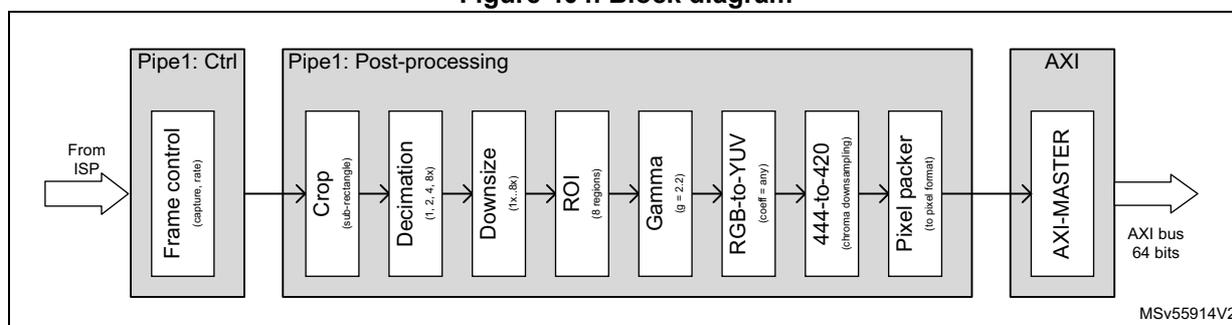
graph LR
    subgraph Pipe1_Ctrl [Pipe1: Ctrl]
        FC[Frame control
capture, rate]
    end
    subgraph Pipe1_Post [Pipe1: Post-processing]
        C[Crop
sub-rectangle]
        D[Decimation
1, 2, 4, 8x]
        DS[Downsize
h, 8x]
        R[ROI
8 regions]
        G[Gamma
g = 2.2]
        RY[RGB-to-YUV
cscf = any]
        D420[444-to-420
chroma downsampling]
        PP[Pixel packer
to pixel format]
    end
    subgraph AXI [AXI]
        AM[AXI-MASTER]
    end
    FromISP[From ISP] --> FC
    FC --> C
    C --> D
    D --> DS
    DS --> R
    R --> G
    G --> RY
    RY --> D420
    D420 --> PP
    PP --> AM
    AM --> AXIBus[AXI bus 64 bits]
The applicative Pipe1 is the most featured pixel pipeline, even if the image processing functions can be shared with Pipe2 (refer to Section 39.8.2 ).
Pipe1 can be reconfigured from time to time. Some events can be used to trigger the software reconfiguration routines (refer to Section 39.13.2 ).
It is also possible to write into the shadow registers during the processing of a frame. The values are loaded into the physical register based on the following start of frame event.
39.7.2 Pixel 2D cropping
The pixel 2D cropping aims at extracting and forwarding a rectangle of pixels.
The cropping assigns an X and Y location to its input pixels, and selects a configured rectangle among the pixels, and forward the pixels of this rectangle farther in the pixel pipe. The pixels around the selected rectangle are discarded.
Functionality
- • Counts lines thanks to HSync (if from parallel interface) or packets (if from CSI-2)
- • Counts pixels inside a line
- • Positive cropping (forwards a selected rectangle of pixels in the pipe)
- • Cropping with 0 value for HSIZE[11:0] or VSIZE[11:0] forces the internal crop to get the maximum value on the parameter where the software sets to the 0 value
Software configuration
Table 353. DCMIPP_PxCWSTR and DCMIPP_PxCRSZR bit function
| Bit ID | Values | Comments |
|---|---|---|
| ENABLE | – 1: Cropping active – 0: All data transmitted | - |
| HSTART, VSTART | 0 to 4094 | Top-left corner of the cropped rectangle. |
| HSIZE, VSIZE | 0 to 4094 | Width and height of the cropped rectangle. Can be larger than the received picture to grab everything. |
If the cropped window is larger than the received window, only the received pixels are forwarded (no pixels are inserted to match the window size).
If the software sets 0 in one or both horizontal/vertical size bit fields (HSIZE, VSIZE), the crop forces internally the value to be at the maximum on the corresponding bit field.
Configuration example
To select a small rectangle (size 100 x 50), whose upper pixel is located at position (30, 10), provide the following setting:
- • ENABLE = 1 to crop a sub-rectangle
- • HSTART, VSTART = (30, 10) to start cropping at x = 30, y = 10 of the received picture
- • HSIZE, VSIZE = (100, 50)
The most bottom-right selected pixels have a position (129, 59) from the received picture.
The frame forwarded is handled downstream in the pipe as a 100 x 50 frame.
39.7.3 Decimation pre-downsize
The decimation (prior to downsize) makes it possible to cheaply downsize a frame by a factor 2, 4, or 8x, in both horizontal and vertical directions.
The decimation is partially redundant with the downsize, that brings a higher quality (the decimation discards the data of the dropped pixels, while the downsize averages all pixels and does not lose information).
The decimation complements the downsize (limited to ratio of 8 x 8), to have a combined downsizing ratio of 64 x 64. It is recommended to have the largest ratio implemented in the higher quality downsize, and have needed the decimation complement to that. For instance, for a ratio 30x, is it recommended to have a ratio 4x in decimation, and a ratio \( 30 / 4 = 7.5 \) in the downsize.
Features
- • Forwards one item (typically pixel) every 1, 2, 4, 8 pixels, independently vertical and horizontal.
Software configuration
Table 354. DCMIPP_PxDCCR bit function
| Bit ID | Function | Value | Comments |
|---|---|---|---|
| HDEC[1:0] | Ratio (2 bits) | 0 | No decimation |
| 1 | Ratio 1/2 | ||
| 2 | Ratio 1/4 | ||
| 3 | Ratio 1/8 | ||
| VDEC[1:0] | 0 | No decimation | |
| 1 | Ratio 1/2 | ||
| 2 | Ratio 1/4 | ||
| 3 | Ratio 1/8 | ||
39.7.4 Downsize
This module implements a downsize based on box filtering, which allows ratios from 1x to 8x, independently, in both X and Y directions.
The box filter has properties close to a bilinear filter for small ratios (from 1x to 2x), but provides the advantage of avoiding some Moiré effect for higher ratios (from 2x to 8x) thanks to using all the samples.
Functionality
- • Features:
- – Integer + decimal ratio, different vertically and horizontally.
- – Ratio: 1.0x to 8x
- – Limited to a maximum output buffer width of 2688 pixels due to the needed linebuffer.
- • Operations:
- – Increments defined with 3.13 precision (<1 pixel error after maximum width of 4094)
- – Internal computations for filter defined with 3.3 precision
- – Accumulates skipped pixels to allow ratio up to 8x with saturation on 11 bits
- – Weighting of shared pixels, to allow good quality at ratio close to 1
- – Independent H filter, then V filter
- – Init phase: left of left-most pixel is aligned on input pixel (see below Pi0, Po0)
Software configuration
Table 355. DCMIPP_PxDSCR, DCMIPP_PxDSRTIOR, DCMIPP_PxDSSZR
| Bit ID | Function | Values | Comments |
|---|---|---|---|
| ENABLE | - | – 1: Downsize active – 0: Transmission without downsize | - |
| HRATIO, VRATIO | Downsize ratio (respectively horizontally and vertically) | 16-bit fields, used as unsigned 3 integer 13 decimal. Valid values are 8192 (= 1x) to 65535 (= 7.999x). | Key parameters that create output pixels. The optimal is computed as \( xRATIO = Floor(8192 \times xRatioFloatingPoint) \) , maximum value 65535 ( \( x = H \) or \( V \) ). |
| HDIV, VDIV | Inverted ratio, must be consistent with Ratio | 10-bit fields, used as unsigned 10 decimal. Valid values are 128 (= inv8x) to 1023 (= inv1x). | A side parameter, impacts only the luminance of the output pixels. The optimal in function of xRATIO is \( xDIV = Floor((1024 \times 8192 - 1) / xRATIO) \) ( \( x = H \) or \( V \) ). |
| HSIZE, VSIZE | Final size after the downsize | - | The downsize filter clips pixels if the post-downsize size is not correct. The HSIZE and VSIZE are partially redundant vs. the cropping size divided by the downsize ratio. If VSIZE = 0 or HSIZE = 0, the filter is disabled in that dimension. |
Figure 405 shows the principle of the computations:
- • \( Po0 = (1.00 \times Pi0 + 1.00 \times Pi1 + 0.25 \times Pi2) / 2.25 \)
- • \( Po1 = (0.75 \times Pi2 + 1.00 \times Pi3 + 0.50 \times Pi4) / 2.25 \)
- • \( Po2 = (0.50 \times Pi4 + 1.00 \times Pi5 + 0.75 \times Pi6) / 2.25 \)
Figure 405. Downsize with coverage filtering
| Pi0 | Pi1 | Pi2 | Pi3 | Pi4 | Pi5 | Pi6 | Pi7 | Pi8 | Pi9 | ... | |
| 0.0 | 1.0 | 2.0 | 3.0 | 4.0 | 5.0 | 6.0 | 7.0 | ||||
| 100% | 100% | 25% | 75% | 100% | 50% | 50% | 100% | 75% | 25% | 100% | ... | |||
| Po0 | Po1 | Po2 | Po3 | ||||||||
Configuration example
- • ENABLE = 1 to activate the downsize
- • Downsize ratio 1x: HRATIO = VRATIO = 8192, HDIV = VDIV = 1023
- • Downsize ratio 2x: HRATIO = VRATIO = 16384, HDIV = VDIV = 512
- • Downsize ratio 3x: HRATIO = VRATIO = 24576, HDIV = VDIV = 341
- • Downsize ratio 8x: HRATIO = VRATIO = 65535, HDIV = VDIV = 128
39.7.5 Regions of interest (ROIs)
Pixel pipes can defined up to eight different ROIs to highlight areas on a picture. The purpose of this feature is to draw one rectangle with user size defined for each enabled ROI.
There is no hardware processing within the defined area applied on the image. As the aim is to draw rectangles on a display, the ROI is supposed to be used when the data flow is RGB at the output of the image processing blocks.
The line width is configurable commonly for each ROI thanks to bit-field ROILSZ[1:0] of the DCMIPP_PxCMRICR register. The color line is configurable per ROI to make easy visual distinction between each region of interest.
Each configuration is valid for a frame and it may be changed frame by frame by reprogramming the registers by software.
Each ROI can be enabled independently for displaying purpose.
Figure 406 shows a basic example of two ROIs displayed within a frame to isolate two flights (it is only visual information). The application can decide to crop the area to work on these two ROIs, by reprogramming the crop area for the next frames to make appropriate analysis linked to the application target.
Figure 406. Example with two ROIs
Software configuration
The first action is the configuration of DCMIPP_PxCMRICR, the common register to activate the ROI and to select the line width applied to all the active ROIs within a frame:
- • ROIEYEN (y = 1 to 8): each ROI can be enabled during the frame.
- • ROILSZ: select the line width in pixel (1, 2, 4 or 8 pixels wide).
The second step is the configuration of each ROI, independently, through registers DCMIPP_PxRIyCR1 and DCMIPP_PxRIyCR2. The color line, among others, is set during this step.
- • VSTART and HSTART bit fields allow to set the origin point of the rectangle for a given ROI. The origin is located on the top-left pixel, within the colored lines.
- • VSIZE and HSIZE bit fields are used to set up the vertical and horizontal size in pixel for the area to draw. The size of the rectangle is measured the colored lines.
- • CLR, CLG, CLB are used to select the color among 64. Each component has its two bits duplicated to 8-bit, to get an RGB888 at the output of the ROI block
39.7.6 Gamma conversion
This feature implements a gamma compression on each R, G, B component, using a static gamma exponent 2.2, to store gamma-compressed pictures, as defined in the sRGB standard.
Features
- • The gamma is implemented as a 7-segment linear curve.
- • It crosses the following way-points, in logarithm spacing:
- – (0,0)
- – (4,39)
- – (8,53)
- – (16,72)
- – (32,99)
- – (64,136)
- – (128,186)
- – (256,256)
Software configuration
ENABLE = 1 in the DCMIPP_PxGMCR registers activate the color conversion.
39.7.7 YUV conversion
This block is a replication of the one described in Section 39.6.9 , used to convert RGB in YUV color format (basically, since the conversion YUV to RGB is assumed to be performed by the color conversion block into the image processing main function). Bit fields are the same of the color conversion module, only the register name and the memory mapping are different. The register functions are the same, the register names are DCMIPP_P1YUVxxx instead of DCMIPP_P1CCxx.
39.7.8 Chroma down-sampling
The Chroma down-sampling module reduces the chroma resolution from its arriving YUV444 format to the potential YUV420 output, and sends them to a different channel.
Features
- • Downsizes in H first, if YUV420, with (0.5 + 0.5) filter
- • Downsizes in V then, if YUV420, with (0.5 + 0.5) filter
- • Memory: embeds one half-line buffer for each U and V
Software configuration
Configuration is indirectly taken from the pixel packing output format, located in the DCMIPP_PxPPCR register.
- • The Chroma down-sampling is active when the output pixel format is YUV422-1, YUV422-2, YUV420-2, YUV420-3.
Output
- • One to three channels: RGB/Y, UV (or U) and V.
39.7.9 Pixel packing
This module works on the dump pipe (Pipe0) and pixel pipes (Pipe1 .. N), setting the arriving pixels in memory words.
Features
- • DBM addresses: double buffer mode with their associated address locations if the application need to swap memory address for one frame to the next one.
- • Flexible pitch (line stride): width up to 4094 pixels, 32 bpp, potentially interleaved.
- • Pixel format: all usual formats, as indicated in Section 39.3.6 (Pipe1 allows semi-planar and full planar buffer, Pipe2 coplanar buffer only).
- • Swap R-vs-B: swap the red vs. the blue components of the output pixel.
- • Padding: MSB vs. LSB padding of 10/12/14 bit onto 16 bit. (such formats are supported only on the dump pipe).
- • Header enable: allows to dump (or not) the CSI packet headers, to allow software an easier extraction of data in case of Interleaved CSI packets in the captured buffer.
- • Multi-line event: event generated (for DMA and INT) at each multiple of sent lines.
- • Multi-line address wrapping: allows to write the full frame across a ping-pong buffer, thanks to wrapping back to the BaseAddress after a power-of-2 amount of lines.
Note: Some features (for example padding) are available only on the dump pipe, while others (like swap R-vs-B) are available only on the pixel pipes.
Table 356. DCMIPP_PxPPCR bit function
| Bit ID | Function | Value | Comments |
|---|---|---|---|
| M0A, M1A, M2A | Base address of pixel buffer in memory, 32-bit wide, aligned on 16 bytes | - | The line alignment of the pixel buffers in memory is assumed on 16 bytes. Therefore the buffer base address (i.e. M0A, M1A, M2A) must be a multiple of 16 bytes, and similarly for line PITCH. |
| PITCH | Address jump from line to line, up to 32 Kbyte - 1. | - | Aligned on 16 bytes. |
Table 356. DCMIPP_PxPPCR bit function (continued)
| Bit ID | Function | Value | Comments |
|---|---|---|---|
| SWAPRB | Swaps R-vs-B components (and U-vs-V, same operation if Y mapped on G) available on pixel pipe and not on dump pipe. | - | - |
| HEADEREN | - | - 1: Dumps headers | Feature present only in dump pipe. |
| PAD | MSB vs. LSB padding of the raw Bayer and monochrome to 16 bpp. | - 0 (align on LSB): backward compatibility with the former DCMI IP - 1 (align on MSB): easier use by software or GPU | Applies only on the dump pipe and for the 10/12/14 (not 8)-bit pixels (the pixel pipe convert pixels into 8 bpc, and padding is therefore not relevant). |
| FORMAT | Output pixel format | - |
|
| LINEMULT | Periodicity of the line (HSync) interrupt and event, as power of 2 of LINEMULT configuration (i.e. every 1, 2, ...,128 lines). | - | - |
| LMAWE | Enable line multi address wrapping (see LMAWM ) | - | - |
| LMAWM | Periodicity of the address wrapping to BaseAddress, period given as power of 2 of LMAWM configuration (i.e. every 1, 2, ...,128 lines). | - | - |
Double buffer mode
The dump pipe uses an AXI master interface to dump the data from the internal FIFO to the external memory. In the application, it is possible to handle frame data swapping memory area frame by frame. The double buffer mode fills up this function. There are two memory address registers set to initialize the base addresses of these memories areas. Each start of captured frame event swaps the memory base address to handle double buffering mode. The double buffer mode can be used to allow post-processing on a buffer (frame buffer), while the other buffer is read to be displayed (display buffer).
Software configuration
Double buffering mode requires an activation and addresses configuration to define the two memory areas in which data are consecutively stored frame by frame at the output of the pipeline:
- • DCMIPP_PxPPM0AR1 and DCMIPP_PxPPM0AR2 must be filled with the memory addresses associated to the double buffer memory locations.
- • Bit DBM in the DCMIPP_PxPPCR registers is set to enable the double buffer mode.
Streaming across a ping-pong buffer
The DCMIPP has the capability (pixel pipes only) to stream pixels to a slave IP (like VENC or any) without storing the full frame in the main memory, by writing to a short intermediate multi-line buffer. It can do so by configuring the LINEMULT, LMAWE and LMAWM fields.
As an example, the slave IP is a JPG encoder that expects to be provided lines of macroblocks (16x16 pixels). The DCMIPP writes into a double (ping-pong) buffer, with each 16 lines high.
The streaming flow is as follows:
- 1. At a start of frame, the DCMIPP writes its pixels at an incremented address starting at the buffer BaseAddress (M1A/M2A).
- 2. After having written 16 lines, it emits a hardware Line event (dcmpp1_pXline_evt). At the reception of this hardware trigger, the slaved IP (JPG encoder here) starts to read the first 16-line buffer at the BaseAddress, and to encode its pixels.
- 3. The DCMIPP continues to write at the following addresses, thus after line 16.
- 4. After having written another 16 lines, the DCMIPP emits another Line event, to that the slaved IP can read and process the following 16 lines (at BaseAddress + Line16).
- 5. The DCMIPP wraps back to the BaseAddress, writes the following lines (32 to 47) starting at this BaseAddress, and then sends a trigger to the slave IP to process these new 16 lines.
The needed configuration is the following one:
- • LINEMULT = 0x4, to send an event after having written each 16 lines
- • LMAWM = 0x5, to wrap the address after having written each 32 lines
- • LMAWE = 1, to enable the address wrapping of the address.
39.7.10 Overrun detection
This logic handles flow-control hazards: the DCMIPP is provided a continuous flow of data (via parallel or CSI2 interfaces) without any wait/hold capability, while downstream of DCMIPP, the access to memory can be temporarily stuck.
In some cases the internal FIFOs of the DCMIPP get full and pixels may be deleted. The overrun detection logic handles such hazard at best.
Features
- • Software gets warned in case of an hazard:
- – Interrupt OVR is triggered at the first deletion of a pixel, repeated at every frame, as long as the overrun hazard is present.
- – It is recommended to skip / trash the impacted frame:
- > Overflowing pixels are deleted, so that when the access to memory resumes, the remaining of the line is discarded (not written out). The normal processing resumes at the start of the next line. Potentially, several full lines can get discarded.
- • No Frame-to-Frame impact in case of an hazard:
- – VSync resets what is needed in the DCMIPP, so that any hazard on a previous frame has no impact at all on the pixels dumped in next frames.
Software configuration
- • Interrupt DCMIPP_PxSR.OVRF is warned in case of hazard.
39.8 Pipe2 (post-processing)
39.8.1 Overview
Pipe2, compared to Pipe1, is a lighter pixel pipeline offering no embedded image processing blocks. This pipe can work in standalone mode, or share the image processing functions with Pipe1 (refer to Section 39.8.2 ).
Figure 407. Pipe2 architecture overview
graph LR
    subgraph Inputs
        ISP[From ISP] --> SEL[SEL]
        Input[From input] --> SEL
    end
    SEL --> Pipe2_Ctrl[Pipe2: Ctrl]
    subgraph Pipe2_Ctrl
        FC[Frame control capture, rate]
    end
    Pipe2_Ctrl --> Pipe2_Post[Pipe2: Post-processing]
    subgraph Pipe2_Post
        direction LR
        Crop[Crop sub-rectangle] --> Decimation[Decimation 1, 2, 4, 8x]
        Decimation --> Downsize[Downsize 1x, 8x]
        Downsize --> ROI[ROI 8 regions]
        ROI --> Gamma[Gamma g = 2.2]
        Gamma --> PixelPacker[Pixel packer to pixel format]
    end
    PixelPacker --> AXI_MASTER[AXI MASTER]
    AXI_MASTER --> AXI_Bus[AXI bus 64 bits]
The main blocks (controller and post-processing general functions) of Pipe2 are almost the same as those of Pipe1. The flow selection and frame controller allow to configure Pipe2 behavior when it is used in standalone, meaning without image processing heritage from Pipe1. Refer to Section 39.4.5 and Section 39.4.6 for more details about the use cases and the configuration of the pipe.
The set of post-processing blocks is reduced compared to Pipe1, as neither the YUV conversion nor the down-sampling YUV444 to YUV420 are integrated in Pipe2. This pipe can have its own image crop area, its dedicated downsizing, and take benefit of the gamma correction, like Pipe1. Refer to Section 39.7 and to its subsections for more details on how to use and configure by software these post-processing functions.
Software configuration
To use Pipe2 as a standalone pixel pipe, without any image processing functions shared with Pipe1, bit PIPEDIFF must be set in the DCMIPP_P1FSCR register. This bit has a meaning only when the flows can be differentiated, that is, when the camera connected and processed by the DCMIPP is a CSI2 camera interface.
In this non-shared mode, it is required that different flows are sent to Pipe1 and Pipe2, or a non-supported behavior can occur.
The flow to Pipe1 and the flow to Pipe2 may potentially be interleaved at packet level.
Pipe2 may be reconfigured time to time. Some events may be used to trigger the software reconfiguration routines (refer to Section 39.13.2: Interrupts ).
It is possible also to write into the shadow registers within the processing of a frame. The values are loaded into the physical register based on the start of frame event.
39.8.2 Pipe1 and Pipe2 sharing image processing functions
Following the application, it may be interesting to share the image processing functions belonging to Pipe1 with Pipe2 when the dataflow is shared for both. One pipe may be used for display operation, and the other one used for statistics or software analysis. In this case PIPEDIFF bit of DCMIPP_P1FSCR register must be cleared.
If the CSI-2 module is connected to the DCMIPP, the VC DT and DTMODE of Pipe2 are the same as those configured into DCMIPP_P1FSCR register, making non relevant the values for these fields into the DCMIPP_P2FSCR register. However, bits CPTREQ and CPTMODE remain active into the DCMIPP_P2FSCR register to control the flow inside Pipe2.
39.9 Application use cases
There are several application use cases that can fit the DCMIPP architecture, a few of them are described in this section.
39.9.1 Parallel interface camera sensor module
A parallel interface camera sensor can transfer images as well as statistics. It is easier to manage the software processing by splitting the statistics and the image data on different memory storages. Two pipes are used in such case, with Pipe0 extracting the statistics and Pipe1 dealing with the image data (whatever the data format supported by the DCMIPP). Both work in parallel on the same frame, frame by frame. Each output FIFO attached to the pipe conveys the data on the targeted memory for further processing.
The camera sensor module may use some lines of the frame to transfer statistics or sensor configuration data. These lines can be placed at the beginning and at the end of the frame (see Figure 408 ), even if there is no real standard.
Figure 408. Use case: Pipe0 (statistics), Pipe1 (pixels)
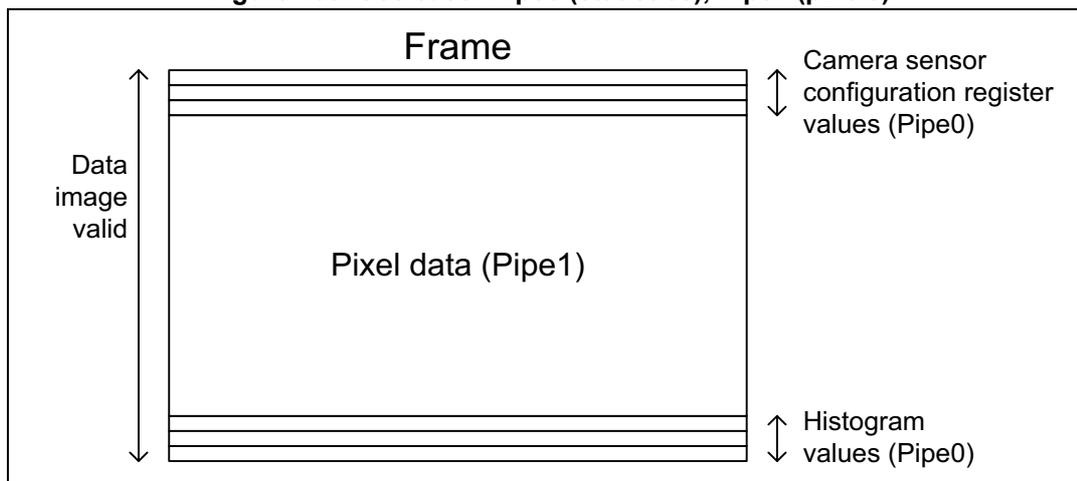
The diagram illustrates a 'Frame' represented by a large rectangle. Inside this rectangle, there are several horizontal bands. At the top, there are three thin bands. Below them is a large band labeled 'Pixel data (Pipe1)'. At the bottom, there are three more thin bands. To the left of the frame, a vertical double-headed arrow spans the height of the main pixel data area and is labeled 'Data image valid'. To the right of the frame, two vertical double-headed arrows are shown. The top one spans the height of the three thin top bands and is labeled 'Camera sensor configuration register values (Pipe0)'. The bottom one spans the height of the three thin bottom bands and is labeled 'Histogram values (Pipe0)'.
Software configuration
- • Pipe0: select the crop area to extract statistics only
- – Configure HSTART[11:0] = 0 and VSTART[11:0] bits in the DCMIPP_P0SCSTR register from the line number corresponding to the first pixel data line (after first statistics line).
- – Configure HSIZE [11:0] (horizontal screen resolution in number of data 32-bit equivalent to the horizontal resolution of the screen in pixels) and VSIZE [11:0] to the value corresponding to the offset line number from the first pixel data area. These bits are in the DCMIPP_P0SCSZR register.
- – Set bit POSNEG of the DCMIPP_P0SCSZR register to reject data belonging to the rectangle defined, to keep the outside area of the rectangle, where the statistics are taken in this use case.
- • Pipe1: Select the area to extract the statistics into DCMIPP_P1SRCR register, by configuring bit FIRSTLINEDEL[2:0] and LASTLINE[11:0] (it avoids to start the image processing on statistics data). Only the pixel data are forwarded, if needed, to the image processing blocks (for example demosaicing, auto exposure, contrast enhancement) for further processing.
39.9.2 CSI2 camera sensor module
The CSI2 protocol allows, thanks to Datatypes, to make distinction between different data categories. The application may request to handle interlaced video as well as interleaved data flow like described below.
Single virtual channel involving two pipes (for example Pipe0 and Pipe1)
- • Use case: the CSI provides two data flows in parallel, typically RGB (or raw Bayer) with its sideband statistics.
- • Handling: the statistics are dumped by the dump pipe, while the pixels are sent to the pixel pipes.
Figure 409. Statistics and RGB data for single virtual channel data flow
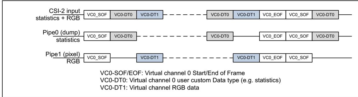
The diagram illustrates the data flow for three components over time, represented by horizontal timelines. The components are:
- CSI-2 input statistics + RGB: Shows a sequence of packets: VC0_SOF, VC0-DT0, VC0-DT1, followed by a dashed line gap, then VC0-DT0, VC0-DT1, VC0_EOF, VC0_SOF, VC0-DT0.
- Pipe0 (dump) statistics: Shows packets: VC0_SOF, VC0-DT0, followed by a dashed line gap, then VC0-DT0, VC0_EOF, VC0_SOF, VC0-DT0.
- Pipe1 (pixel) RGB: Shows packets: VC0_SOF, followed by a dashed line gap, then VC0-DT1, followed by a dashed line gap, then VC0-DT1, VC0_EOF, VC0_SOF.
Legend:
- VC0-SOF/EOF: Virtual channel 0 Start/End of Frame
- VC0-DT0: Virtual channel 0 user custom Data type (e.g. statistics)
- VC0-DT1: Virtual channel 0 RGB data
Single virtual channel involving three pipes (for example Pipe0, Pipe1 and Pipe2)
Another use case ( Figure 410 ) employs different Datatypes in addition to the statistics within the CSI-2 flow based on a single virtual channel.
Figure 410. Three pipes within a single virtual channel in CSI2 mode
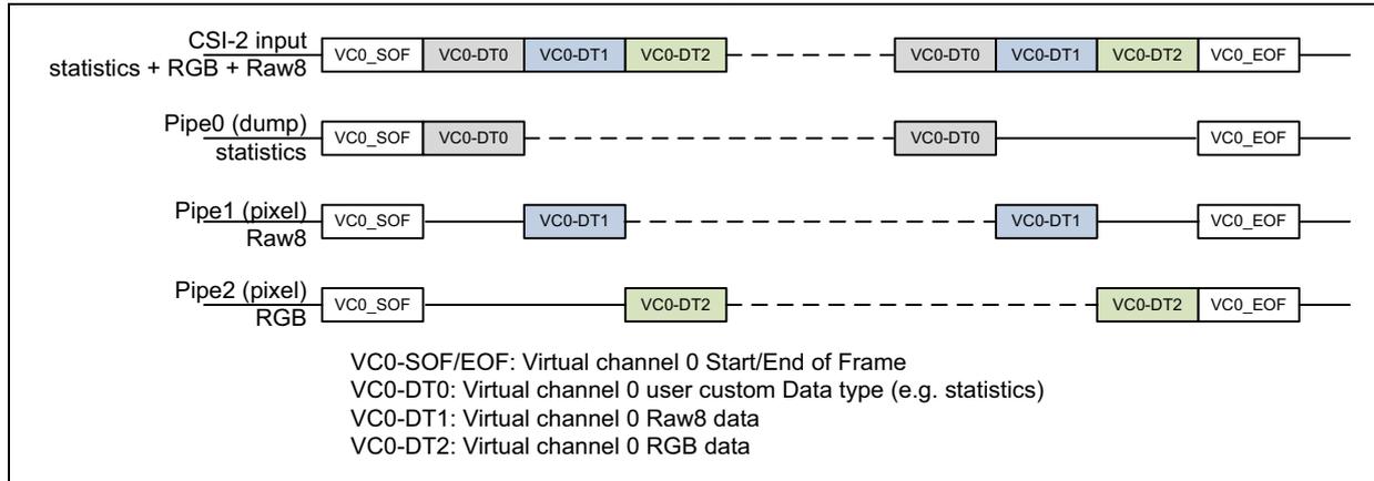
The diagram illustrates the data flow for four components over time, represented by horizontal timelines. The components are:
- CSI-2 input statistics + RGB + Raw8: Shows a sequence of packets: VC0_SOF, VC0-DT0, VC0-DT1, VC0-DT2, followed by a dashed line gap, then VC0-DT0, VC0-DT1, VC0-DT2, VC0_EOF.
- Pipe0 (dump) statistics: Shows packets: VC0_SOF, VC0-DT0, followed by a dashed line gap, then VC0-DT0, followed by a dashed line gap, then VC0_EOF.
- Pipe1 (pixel) Raw8: Shows packets: VC0_SOF, followed by a dashed line gap, then VC0-DT1, followed by a dashed line gap, then VC0-DT1, followed by a dashed line gap, then VC0_EOF.
- Pipe2 (pixel) RGB: Shows packets: VC0_SOF, followed by a dashed line gap, then VC0-DT2, followed by a dashed line gap, then VC0-DT2, followed by a dashed line gap, then VC0_EOF.
Legend:
- VC0-SOF/EOF: Virtual channel 0 Start/End of Frame
- VC0-DT0: Virtual channel 0 user custom Data type (e.g. statistics)
- VC0-DT1: Virtual channel 0 Raw8 data
- VC0-DT2: Virtual channel 0 RGB data
Interleaved packets (based on multiple virtual channels)
- • Use case: the CSI provides two pixel flows in parallel, typically a JPG-compressed flow and an RGB888 or raw Bayer flow.
- • Handling: the JPG is dumped by the dump pipe, while the pixels are sent to the pixel pipes.
Both Pipe1 and Pipe2 can process these pixels. The shared demosaicing mode can be used, hence both Pipe1 and Pipe2 benefit of the potential demosaicing conversion.
Figure 411. Handling interleaved packet
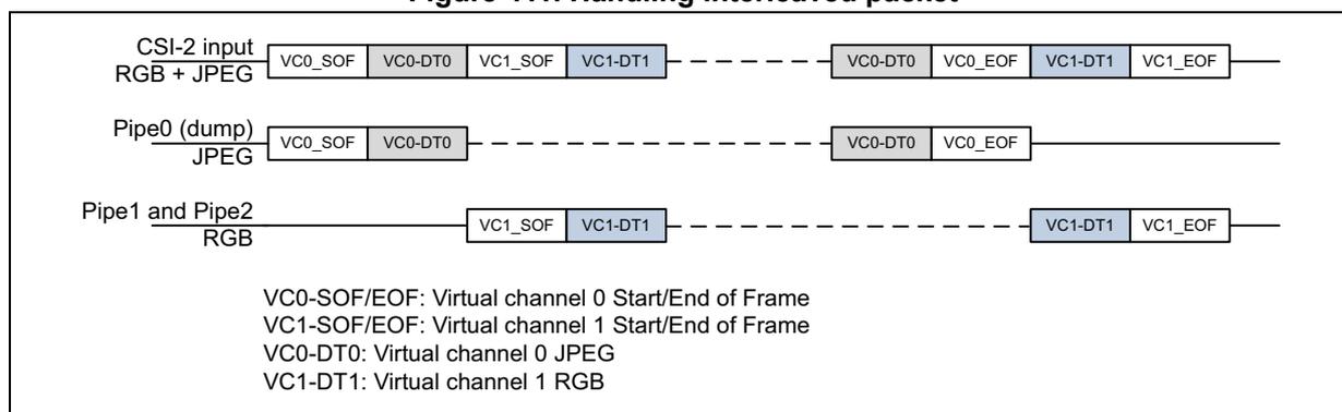
The diagram illustrates the handling of interleaved packets. The CSI-2 input (RGB + JPEG) is shown as a sequence of packets: VC0_SOF, VC0-DT0, VC1_SOF, VC1-DT1, followed by a dashed line, then VC0-DT0, VC0_EOF, VC1-DT1, VC1_EOF. Pipe0 (dump) for JPEG shows VC0_SOF, VC0-DT0, followed by a dashed line, then VC0-DT0, VC0_EOF. Pipe1 and Pipe2 for RGB show VC1_SOF, VC1-DT1, followed by a dashed line, then VC1-DT1, VC1_EOF.
VC0-SOF/EOF: Virtual channel 0 Start/End of Frame
VC1-SOF/EOF: Virtual channel 1 Start/End of Frame
VC0-DT0: Virtual channel 0 JPEG
VC1-DT1: Virtual channel 1 RGB
Figure 412. Handling interleaved packets across two pixel pipes
The diagram illustrates the handling of interleaved packets across two pixel pipes. The CSI-2 input (RGB + YUV) is shown as a sequence of packets: VC0_SOF, VC0-DT0, VC1_SOF, VC1-DT1, followed by a dashed line, then VC0-DT0, VC0_EOF, VC1-DT1, VC1_EOF. Pipe1 for YUV shows VC0_SOF, VC0-DT0, followed by a dashed line, then VC0-DT0, VC0_EOF. Pipe2 for RGB shows VC1_SOF, VC1-DT1, followed by a dashed line, then VC1-DT1, VC1_EOF.
VC0-SOF/EOF: Virtual channel 0 Start/End of Frame
VC1-SOF/EOF: Virtual channel 1 Start/End of Frame
VC0-DT0: Virtual channel 0 YUV
VC1-DT1: Virtual channel 1 RGB
Interlaced video
- • Use case: the CSI provides the odd and even frames of an interlaced video onto two different virtual channels (usually with a same data type).
- • Handling: the flows of both the virtual channel of the odd field and the virtual channel of the even field are sent to the pixel pipes.
- • Single pixel pipe may be configured if the image processing function is required by the application to handle both interlaced frame (refer to Figure 413 ). In such case, a pipe reconfiguration is needed frame by frame to change the virtual channel number and the address memory for the output buffer if the software distinctly keeps the odd and even frame buffers in their respective memory locations.
- • Pipe1 and Pipe2 may be used if the application software does not need image processing functions (refer to Figure 414 ). Each pipe is configured with its own virtual channel and its own output buffer address in memory. The split of the odd and even frames is explicitly defined in a static way, avoiding any pipe reconfiguration between two frames.
- • Interlaced video can be managed with a single virtual channel identifier, using a different data type to identify odd and even frames. In such case, the CSI2 bridge uses user Datatypes to distinguish between them.
- • Limitation: the frames of the two virtual channels must be time-exclusive, by default the case for usual interlaced video sensors.
Figure 413. Interlaced video (based on single pixel pipe)
Pipe1 reconfiguration (VC change in DCMIPP_P1FSCR register memory address to easily isolate odd from even frame)
VC0-SOF/EOF: Virtual channel 0 Start/End of Frame
VC1-SOF/EOF: Virtual channel 1 Start/End of Frame
VC0-DT1: Virtual channel 0 RGB odd field
VC1-DT1: Virtual channel 1 RGB even field
Figure 414. Interlaced video (based on two pixel pipes)
VC0-SOF/EOF: Virtual channel 0 Start/End of Frame
VC1-SOF/EOF: Virtual channel 1 Start/End of Frame
VC0-DT1: Virtual channel 0 RGB odd field
VC1-DT1: Virtual channel 1 RGB even field
Software configuration
The following configuration must be set first into the static DCMIPP_PxFSCR and DCMIPP_CMCR registers:
- • INSEL: Selects the input flow (parallel vs. CSI) in the DCMIPP_CMCR register
- • DTMODE[1:0]: mode for CSI flow selection into that pipe:
- – 0: only flow VC/DTIDA is forwarded in the corresponding pipe.
- – 1: flows VC/DTIDA and/or VC/DTIDB are forwarded for Pipe0, and VC/DTIDA and VC/DTIDB for Pipe1.
- – 2: all flows, except the VCDTIDA or VCDTIDB, are forwarded in the pipe (this last setting, 3, is available only for Pipe0).
- – 3: all Datatypes from the selected virtual channel are forwarded in Pipe0. It is valid only for Pipe0 (the pixel formats that are not supported by Pixel pipes are suppressed).
This bit field is not valid for Pipe2.
- • DTIDA/DTIDB: Data type selection ID-A and ID-B for Pipe0 and Pipe1.
- • DTIDA: Data type selection for the pixel Pipe2 when PIPEDIFF = 1.
- • FDTFEN: Forces the value of the data type (value defined in FDTF[5:0]) to be processed by the pixel Pipe1 and Pipe2, based on the DTIDA/DTIDB detection in the flow selection block of the pipe. Not available for Pipe0.
- • FDTF[5:0]: Data type value overwritten the one received by the CSI-2 physical node when equal to DTIDA/DTIDB. Not available for Pipe0.
- • PIPEDIFF: Pipe2 to take same input as Pipe1 or differentiated:
- – 0: Pipe2 takes the same VC/DTIDx as well as the same FDTFEN and FDTF[5:0] configured into the DCMIPP_P1FSCR register.
- – 1: Pipe1 and Pipe2 take their own VC/DTID, FDTFEN and FDTF[5:0] values in the data flow.
After all the pipes have been configured, the processing can be activated:
- • PIPEN: Set to 1 to start the frame control logic of the pipe. When reset at 0, it immediately resets the frame control logic, which results in immediately stopping an ongoing dump (CPTREQ = 0, CPTACT = 0), see Figure 398 , Figure 399 , Figure 400 .
- • CPTREQ: Set to 1 to activate the capture at the next start-of-frame in the DCMIPP_PxFSCR register.
Note: To be cleanly sampled for the next frame, the VCIDA, VCIDB, DTIDA, and DTIDB fields must be updated after a VSync and after the first HSync.
Configuration example
The following list details five possible use cases, among others interlaced video and interleaved frames, and a 3D sensor (left + right eye):
- • Default, with a parallel dump of statistics and processing of an image on both Pipe1 and Pipe2:
- – Image forwarded to the pixel Pipe1 and Pipe2, and processed, with the following settings:
- > Pipe1 / DTMODE = 0, to extract a single flow.
- > Pipe1 / VC / DTIDA = vv_dddddd, with VC and DTIDA matching the image flow
- > Pipe1 / PIPEDIFF = 0, to send the flow to both Pipe1 and Pipe2
- – Statistics are extracted and dumped on Pipe0 with the following config:
- > Pipe0 / DTMODE = 0, to extract a single flow.
- > Pipe0 / VC / DTIDA = vv_dddddd, with VC and DTIDA matching the statistics flow.
- – Image forwarded to the pixel Pipe1 and Pipe2, and processed, with the following settings:
- • Interlaced video, with the consecutive but exclusive odd and even (requiring the use of the image processing functions):
- – Interlaced video, if having differentiated VC and DT, is forwarded to the pixel Pipe1 and Pipe2, and processed, with the following settings:
- > Pipe1 / DTMODE = 0, to extract the VC /DTIDA flow
- > Pipe1 / VC/DTIDA = vv_dddddd, with VC and DTIDA matching the odd or the even field by reprogramming between two frames
- > Pipe1 / PIPEDIFF = 0, to send the flow to both Pipe1 and Pipe2
- > Pipe1 / Pipe2 / CPTMODE = 1, Snapshot mode
- > Pipe1 / Pipe2 / CPTREQ = 1 alternatively for Pipe1 and Pipe2, frame by frame
- – Any other (different) data can be potentially dumped with the following settings:
- > Pipe0 / DTMODE = 2, to extract all but flows A and B
- > Pipe0 / VCDTIDA = Pipe1 / VC / DTIDA corresponding to the odd field
- > Pipe0 / VCDTIDB = Pipe1 / VC / DTIDB corresponding to the even field
- – Interlaced video, if having differentiated VC and DT, is forwarded to the pixel Pipe1 and Pipe2, and processed, with the following settings:
The software needs to reprogram frame to frame the DTIDx fields of the DCMIPP_P1FSCR register to select the data to process into Pipe1 or Pipe2. The software sets CPTMODE bit to work in Snapshot mode for Pipe1 and Pipe2 in the DCMIPP_P1FCTCR and DCMIPP_P2FCTCR registers. Alternatively, bit CPTREQ is set frame by frame in one pipe then in the other one to allow the acquisition of data on the allocated pipe. The data type identifying the odd or even fields needs to be updated into the DCMIPP_P1FSCR register only, as Pipe2 shares the image processing block of Pipe1.
- • Interlaced video, with consecutive but exclusive odd and even (bypassing the image processing functions):
- – Interlaced video, if having differentiated VC and/or DT, is forwarded to pixel Pipe1 and Pipe2, and processed, with the following settings:
- > Pipe1 / DTMODE = 0, to extract the VC /DTIDA flow
- > Pipe1 / VC / DTIDA = vv_dddddd, with VC and DTIDA matching (for instance) the odd field data type
- > Pipe2 / DTMODE = 0, to extract the VC /DTIDA flow
- – Interlaced video, if having differentiated VC and/or DT, is forwarded to pixel Pipe1 and Pipe2, and processed, with the following settings:
- > Pipe2 / VC / DTIDA = vv_dddddd, with VC and DTIDA matching (for instance) the even field data type
- > Pipe1 / PIPEDIFF = 1, to consider Pipe1 and Pipe2 as totally independent
- > Pipe1 / Pipe2 / CPTMODE = 0, Continuous grab mode
- > Pipe1 / Pipe2 / CPTREQ = 1 to capture data corresponding to the VCDTIDA attached to the corresponding pipe
- – Any other different data can be potentially dumped with the following settings:
- > Pipe0 / DTMODE = 2, to extract all but flows A and B
- > Pipe0 / VCDTIDA = Pipe0 / VC / DTIDA corresponding to the odd field
- > Pipe0 / VCDTIDB = Pipe0 / VC / DTIDB corresponding to the even field
In this case the interlaced video must be differentiated with the data type and not with the virtual channel (since there is a single VC by pipe), if the application wants to dump data other than the odd and even frames on Pipe0.
- • Interleaved flows, with a parallel dump of an RGB picture and a JPEG-encoded flow:
- – The RGB picture is extracted and forwarded to pixel Pipe1 to be processed, with the following settings:
- > Pipe1 / DTMODE = 0, to extract one flow, the RGB picture
- > Pipe1 / VC / DTIDA = vv_dddddd, with VC and DTIDA matching the RGB picture data type
- > Pipe1 / PIPEDIFF = 1, to send the RGB on Pipe1 and use Pipe2 for other purposes
- – The JPEG-encoded stream is transmitted under the CSI user-defined format, is extracted and sent to the pipe to be dumped, thanks to the following:
- > Pipe0 / DTMODE = 0, to extract one flow, the JPEG-encoded flow
- > Pipe0 / VCDTIDA = vv_dddddd, with VC and DTIDA matching the JPEG stream data type
- > Pipe0 / VCDTIDB = not used
- – Another pixel picture, like YUV, can be dumped using Pipe2, by overwriting fields:
- > Pipe2 / DTMODE = 0, to extract a second flow for the YUV picture
- > Pipe2 / VCDTIDA = vv_dddddd, with VC and DTIDA matching the YUV picture data type
- – The RGB picture is extracted and forwarded to pixel Pipe1 to be processed, with the following settings:
- • 3D sensor, with a parallel transmission of two RGB or YUV pictures: one with data type DT1 for the left eye, and one with data type DT2 for the right eye: the DCMIPP can process each eye on a different pipe (for example left eye on Pipe1 and right eye on Pipe2). Note that, as Pipe1 and Pipe2 are differentiated, the demosaicing is assigned to Pipe1 only and is not available for Pipe2. The left and right eye flows are similar (raw Bayer or RGB), hence they both need to be RGB and not raw Bayer:
- – The left eye RGB picture is extracted and forwarded to the pixel Pipe1:
- > Pipe1 / DTMODE = 0, to extract one flow, the RGB picture
- > Pipe1 / VC / DTIDA = vv_dddddd, with VC and DTIDA matching the left eye data type (DT1)
- > Pipe1 / PIPEDIFF = 1, to split and differentiate the flow between Pipe1 and Pipe2
- – The right eye RGB picture is extracted and forwarded to the pixel Pipe2:
- > Pipe2 / VC / DTIDA = vv_dddddd, with VC and DTIDA matching the right eye
- – The left eye RGB picture is extracted and forwarded to the pixel Pipe1:
- data type (DT2)
- – Another flow can be dumped onto the dump pipe:
- > Pipe0 / DTMODE = 0, to extract one flow
- > Pipe0 / VCDTIDA = vv_ddddd, with VC and DTIDA matching the flow to dump for instance
- • Sensors in 3D, with left and right image inside a unique global image:
- – If the left and right images are differentiated with a left and right part of a single image, that double image can be extracted and duplicated to both the pixel pipes, and there, cropped differently at input of Pipe1 and Pipe2 respectively
- • Sensors with multiple DT:
- – The sensor is supported by sending all (or most) of the flows to the dump pipe, and dumped consecutively, inserting ahead of each dumped packet an header containing the VC, DT, and packet length. See Section 39.7.9 for more details on the header format. One or two pixel flows can still be extracted and processed by Pipe1 and Pipe2, and potentially suppressed from the extraction of the data dump, thanks to DCMIPP_PxFSCR.DTMODE.
- – Another flow can be dumped onto the dump pipe:
39.9.3 Force data type format from CSI-2 data flow (pixel pipes only)
Application may require to use a user data type in the CSI-2 data flow without specifying the format used for the pixel transfer from a camera bridge to the DCMIPP, thanks to CSI-2 interface physical link.
However, the pixel pipes need to know the data format to process them in a proper way along the pipeline. It is possible to force a data type by software thanks to bits FDTF[5:0] and FDTFEN[5:0]. Only the pixel pipes (Pipe1 and Pipe2) can benefit of this capability. Indeed, Pipe0 manages the data and not the pixel itself.
If FDTFEN bit is set in the DCMIPP_PxFSCR register, the data type set into DTIDA/DTIDB (coupled with DTMODE) is used to detect the data type to be overwritten by FDTF[5:0] value. The value used to force the data type must follow CSI-2 data type format specification to identify the CSI-2 normalized data format.
Note: The forced data type value is unique. This means that, if two data types have been selected to be propagated into Pipe1 (DTMODE = 1), both DTIDA and DTIDB detected in input of the pipe are considered by Pipe1 with the forced value FDTF[5:0] if bit FDTFEN is set.
If the virtual channel and data type values are identical between Pipe1 and Pipe2, the force value FDTF[5:0] needs to be aligned within these two pipes if the respective FDTFEN bits are set, otherwise the behavior is not guaranteed.
If PIPEDIFF = 1, any data type format linked to a raw format can be forced on Pipe2 since it is not sharing the demosaicing block of Pipe1.
Typical application example: 3D sensors camera (top-bottom)
Some CSI-2 bridges concatenate data from left and right camera in a top-bottom approach. It means that within a frame, first half of the lines are the ones generated by the left camera, whereas the half last lines of a frame are attached to the right camera sensor. The bridge may typically make a distinction between lines coming from left camera and right camera by identifying the data type with a user data type value linked to a camera.
The user data type does not identify a pixel format, but rather a data linked to a camera. To help the pipeline process in a correct way the pixel, the software must inform the pipeline about the pixel format in input attached to the user Datatypes.
Let us imagine that the application has to separate pixels from the left camera from those of the right camera. Two pixel pipes can be configured for that, with, for instance, Pipe1 for left camera and Pipe2 dedicated to extract pixels from the right camera, as shown in Figure 415 .
Figure 415. 3D sensors (top-bottom) processed by two pixel pipes
The diagram shows the data flow for a 3D sensor input split into two pixel pipes. The input is labeled 'CSI-2 input pixel format Raw10'. The data is divided into two ranges: 'Top – Left camera sensor range' and 'Bottom – Right camera sensor range'. Pipe1 processes the first half-frame from the left sensor, and Pipe2 processes the second half-frame from the right sensor. The data blocks are labeled with VC0_SOF, VC0-DT0, VC0-DT1, and VC0_EOF.
Legend:
- VC0-SOF/EOF: Virtual channel 0 Start/End of Frame
- VC1-SOF/EOF: Virtual channel 1 Start/End of Frame
- VC0-DT0: Datatype 0 with a User datatype (e.g. 0x32) – Left sensor
- VC1-DT1: Datatype 1 with a User datatype (e.g. 0x33) – Right sensor
DCMIPP_P1FSCR configuration
- – PIPEDIFF = 0, Pipe1 shares the demosaicing block with Pipe2 to transform, for instance, Raw10 in RGB888 for the output pixel format.
- – VC = Virtual channel number
- – DTMODE = 1, both Datatypes (0x32 and 0x33) selected to be propagated into Pipe1 through the demosaicing, shared with Pipe2.
- – DTIDA = 0x32, to let pixel data from the left camera sensor (identified by the user data type 0x32) to be processed by the demosaicing block, and further Pipe1 post processing stages (crop, downsize).
- – DTIDB = 0x33, to let pixel data from the right camera sensor (identified by the user data type 0x33) to be processed by the demosaicing block, and further Pipe2 post processing stages (crop, downsize).
- – FDTF[5:0] = 0x2B, to inform about the Raw10 data type normalized value in CSI-2 specification as input pixel format of the pipes.
- – FDTFEN = 1, to force the user Datatypes DTIDA and DTIDB to be decoded as FDTF[5:0] input pixel format value.
- – PIPEN = 1, to activate Pipe1.
Pipe1 crop registers (DCMIPP_P1CRSTR and DCMIPP_P1CRSZR) must be configured to crop only the first half lines of the frame corresponding to the pixels coming from the left camera sensor.
DCMIPP_P2FSCR configuration:
- – VC / DTIDA / DTIDB / FDTF[5:0] / FDTFEN = don't care since it is the same as the one defined in DCMIPP_P1FSCR (as PIPEDIFF = 0).
- – PIPEN = 1 to activate Pipe2.
Pipe2 crop registers (DCMIPP_P2CRSTR and DCMIPP_P2CRSZR registers) must be configured to crop only the second half lines of the frame corresponding to the pixels coming from the right camera sensor.
39.10 Pixel format description
This section describes the pixel formats used in the parallel interface and in the pixel pipes and dump pipe. The CSI-2 pixel format is described in the CSI-2 v1.3 Standard.
The support for the pixel formats, per interface (parallel, CSI-2, pixel output, dump output) are summarized in Table 357 , Table 335 .
Note: In the following tables the components are represented with their symbolic color: red and Cr (= V) in red, blue and Cb (= U) in blue, green in green, and Y, monochrome, and all raw Bayer components in gray.
39.10.1 Parallel interface formats
This paragraph describes the input pixel format as supported by the parallel interface of the DCMIPP and the possible swap combinations.
Note: The parallel interface does not input specifically RGB444/RGB555 (and RGB666). However, a sensor with these output can connect them onto the DCMIPP, by selecting RGB565 (and RGB888), and by either connecting the missing bits with the MSB of the sensor output or by strapping them.
Table 357. Parallel interface input pixel formats
| Index | IO pin | 15 | 14 | 13 | 12 | 11 | 10 | 9 | 8 | 7 | 6 | 5 | 4 | 3 | 2 | 1 | 0 | |
|---|---|---|---|---|---|---|---|---|---|---|---|---|---|---|---|---|---|---|
| 13 | Byte | Cycle 1/1 | - | - | - | - | - | - | - | - | 7 | 6 | 5 | 4 | 3 | 2 | 1 | 0 |
| 5 | Raw Bayer 8 | Cycle 1/1 | - | - | - | - | - | - | - | - | 7 | 6 | 5 | 4 | 3 | 2 | 1 | 0 |
| 6 | Raw Bayer 10 | Cycle 1/1 | - | - | - | - | - | - | 9 | 8 | 7 | 6 | 5 | 4 | 3 | 2 | 1 | 0 |
| 7 | Raw Bayer 12 | Cycle 1/1 | - | - | - | - | 11 | 10 | 9 | 8 | 7 | 6 | 5 | 4 | 3 | 2 | 1 | 0 |
| 8 | Raw Bayer 14 | Cycle 1/1 | - | - | 13 | 12 | 11 | 10 | 9 | 8 | 7 | 6 | 5 | 4 | 3 | 2 | 1 | 0 |
| 9 | Monochrome 8 | Cycle 1/1 | - | - | - | - | - | - | - | - | 7 | 6 | 5 | 4 | 3 | 2 | 1 | 0 |
| 10 | Monochrome 10 | Cycle 1/1 | - | - | - | - | - | - | 9 | 8 | 7 | 6 | 5 | 4 | 3 | 2 | 1 | 0 |
| 11 | Monochrome 12 | Cycle 1/1 | - | - | - | - | 11 | 10 | 9 | 8 | 7 | 6 | 5 | 4 | 3 | 2 | 1 | 0 |
| 12 | Monochrome 14 | Cycle 1/1 | - | - | 13 | 12 | 11 | 10 | 9 | 8 | 7 | 6 | 5 | 4 | 3 | 2 | 1 | 0 |
| 2-1 | RGB565 - 8 bits | Cycle 1/2 | - | - | - | - | - | - | - | - | R4 | R3 | R2 | R1 | R0 | G5 | G4 | G3 |
| Cycle 2/2 | - | - | - | - | - | - | - | - | G2 | G1 | G0 | B4 | B3 | B2 | B1 | B0 | ||
| 2-2 | RGB565 - 16 bits | Cycle 1/1 | R4 | R3 | R2 | R1 | R0 | G5 | G4 | G3 | G2 | G1 | G0 | B4 | B3 | B2 | B1 | B0 |
| 2-2 | PCB: Sensor444 to DCMIPP-RGB565 | Cycle 1/1 | R3 | R2 | R1 | R0 | R3 | G3 | G2 | G1 | G0 | G3 | G2 | B3 | B2 | B1 | B0 | B3 |
| 2-2 | PCB: Sensor555 to DCMIPP-RGB565 | Cycle 1/1 | R4 | R3 | R2 | R1 | R0 | G4 | G3 | G2 | G1 | G0 | G4 | B4 | B3 | B2 | B1 | B0 |
| 4-1 | RGB888 - 12 bits | Cycle 1/2 | - | - | - | - | R7 | R6 | R5 | R4 | R3 | R2 | R1 | R0 | G7 | G6 | G5 | G4 |
| Cycle 2/2 | - | - | - | - | G3 | G2 | G1 | G0 | B7 | B6 | B5 | B4 | B3 | B2 | B1 | B0 | ||
| YUV444 - 12 bits | Cycle 1/2 | - | - | - | - | V7 | V6 | V5 | V4 | V3 | V2 | V1 | V0 | Y7 | Y6 | Y5 | Y4 | |
| Cycle 2/2 | - | - | - | - | Y3 | Y2 | Y1 | Y0 | U7 | U6 | U5 | U4 | U3 | U2 | U1 | U0 |
Table 357. Parallel interface input pixel formats (continued)
| Index | IO pin | 15 | 14 | 13 | 12 | 11 | 10 | 9 | 8 | 7 | 6 | 5 | 4 | 3 | 2 | 1 | 0 | |
|---|---|---|---|---|---|---|---|---|---|---|---|---|---|---|---|---|---|---|
| 4-2 | RGB888 - 8 bits | Cycle 1/3 | - | - | - | - | - | - | - | - | R7 | R6 | R5 | R4 | R3 | R2 | R1 | R0 |
| Cycle 2/3 | - | - | - | - | - | - | - | - | G7 | G6 | G5 | G4 | G3 | G2 | G1 | G0 | ||
| Cycle 3/3 | - | - | - | - | - | - | - | - | B7 | B6 | B5 | B4 | B3 | B2 | B1 | B0 | ||
| YUV444 - 8 bits | Cycle 1/3 | - | - | - | - | - | - | - | - | V7 | V6 | V5 | V4 | V3 | V2 | V1 | V0 | |
| Cycle 2/3 | - | - | - | - | - | - | - | - | Y7 | Y6 | Y5 | Y4 | Y3 | Y2 | Y1 | Y0 | ||
| Cycle 3/3 | - | - | - | - | - | - | - | - | U7 | U6 | U5 | U4 | U3 | U2 | U1 | U0 | ||
| 3 | PCB: Sensor 666 to RGB888 | Cycle 1/3 | - | - | - | - | - | - | - | - | R5 | R4 | R3 | R2 | R1 | R0 | R5 | R4 |
| Cycle 2/3 | - | - | - | - | - | - | - | - | G5 | G4 | G3 | G2 | G1 | G0 | G5 | G4 | ||
| Cycle 3/3 | - | - | - | - | - | - | - | - | B5 | B4 | B3 | B2 | B1 | B0 | B5 | B4 | ||
| 1-1 | YUV422 - 8 bits (YUY'V) | Cycle 1/4 | - | - | - | - | - | - | - | - | Y7 | Y6 | Y5 | Y4 | Y3 | Y2 | Y1 | Y0 |
| Cycle 2/4 | - | - | - | - | - | - | - | - | U7 | U6 | U5 | U4 | U3 | U2 | U1 | U0 | ||
| Cycle 3/4 | - | - | - | - | - | - | - | - | Y7' | Y6' | Y5' | Y4' | Y3' | Y2' | Y1' | Y0' | ||
| Cycle 4/4 | - | - | - | - | - | - | - | - | V7 | V6 | V5 | V4 | V3 | V2 | V1 | V0 | ||
| 1-2 | YUV422 - 16 bits (YUY'V) | Cycle 1/2 | Y7 | Y6 | Y5 | Y4 | Y3 | Y2 | Y1 | Y0 | U7 | U6 | U5 | U4 | U3 | U2 | U1 | U0 |
| Cycle 2/2 | Y7' | Y6' | Y5' | Y4' | Y3' | Y2' | Y1' | Y0' | V7 | V6 | V5 | V4 | V3 | V2 | V1 | V0 |
Table 358. Correspondence between index and DCMIPP_PRCR register values
| Index | FORMAT[7:0] | EDM[2:0] |
|---|---|---|
| 1-1 | 0x1E | 0x00 |
| 1-2 | 0x1E | 0x04 |
| 2 | 0x22 | 0x04 |
| 3 | 0x23 | 0x00 |
| 4-1 | 0x24 | 0x02 |
| 4-2 | 0x24 | 0x00 |
| 5 | 0x2A | 0x00 |
| 6 | 0x2B | 0x01 |
| 7 | 0x2C | 0x02 |
| 8 | 0x2D | 0x03 |
| 9 | 0x4A | 0x00 |
| 10 | 0x4B | 0x01 |
| 11 | 0x4C | 0x02 |
| 12 | 0x4D | 0x03 |
| 13 | Other values | 0x00 |
To adapt to non-standard sensors, the parallel interface is flexible and allows to swap bits, cycles, components, namely:
- • Bits: LSB-vs.-MSB bits are swapped, across the whole 16-bit IO pins.
- • Cycles: cycle 1/2 and cycle 2/2 are swapped. No impact for 1 or 3 cycles.
- • Components: R-vs-B components are swapped (or V-vs-U if YUV).
Table 359 shows these permutations, based on the RGB565 format. It lists the sampled bits of cycles 1 and 2, on pins 0 to 7, and for each of them returns the assignation of the RGB output components.
Table 359. Parallel interface input pixel formats
| IO pin | 15 | 14 | 13 | 12 | 11 | 10 | 9 | 8 | 7 | 6 | 5 | 4 | 3 | 2 | 1 | 0 | |
|---|---|---|---|---|---|---|---|---|---|---|---|---|---|---|---|---|---|
| NATIVE RGB565 8 bits | Cycle 1/2 | - | - | - | - | - | - | - | - | R4 | R3 | R2 | R1 | R0 | G5 | G4 | G3 |
| Cycle 2/2 | - | - | - | - | - | - | - | - | G2 | G1 | G0 | B4 | B3 | B2 | B1 | B0 | |
| SWAP LSB-MSB RGB565 - 8 bits | Cycle 1/2 | G3 | G4 | G5 | R0 | R1 | R2 | R3 | R4 | - | - | - | - | - | - | - | - |
| Cycle 2/2 | B0 | B1 | B2 | B3 | B4 | G0 | G1 | G2 | - | - | - | - | - | - | - | - | |
| SWAP cycles RGB565 8 bits | Cycle 1/2 | - | - | - | - | - | - | - | - | G2 | G1 | G0 | B4 | B3 | B2 | B1 | B0 |
| Cycle 2/2 | - | - | - | - | - | - | - | - | R4 | R3 | R2 | R1 | R0 | G5 | G4 | G3 | |
| SWAP R-vs-B RGB565 8 bits (not available on dump pipe) | Cycle 1/2 | - | - | - | - | - | - | - | - | B4 | B3 | B2 | B1 | B0 | G5 | G4 | G3 |
| Cycle 2/2 | - | - | - | - | - | - | - | - | G2 | G1 | G0 | R4 | R3 | R2 | R1 | R0 | |
39.10.2 Pixel pipe formats
Table 360. Pixel pipe output pixel format (1)
| Format | Memory bits | 31 | 30 | 29 | 28 | 27 | 26 | 25 | 24 | 23 | 22 | 21 | 20 | 19 | 18 | 17 | 16 | 15 | 14 | 13 | 12 | 11 | 10 | 9 | 8 | 7 | 6 | 5 | 4 | 3 | 2 | 1 | 0 | |
|---|---|---|---|---|---|---|---|---|---|---|---|---|---|---|---|---|---|---|---|---|---|---|---|---|---|---|---|---|---|---|---|---|---|---|
| 0 | RGB888 (packed) | B7 | B6 | B5 | B4 | B3 | B2 | B1 | B0 | R7 | R6 | R5 | R4 | R3 | R2 | R1 | R0 | G7 | G6 | G5 | G4 | G3 | G2 | G1 | G0 | B7 | B6 | B5 | B4 | B3 | B2 | B1 | B0 | |
| Pixel N + 1 | Pixel N + 0 | |||||||||||||||||||||||||||||||||
| G7 | G6 | G5 | G4 | G3 | G2 | G1 | G0 | B7 | B6 | B5 | B4 | B3 | B2 | B1 | B0 | R7 | R6 | R5 | R4 | R3 | R2 | R1 | R0 | G7 | G6 | G5 | G4 | G3 | G2 | G1 | G0 | |||
| Pixel N + 2 | ||||||||||||||||||||||||||||||||||
| R7 | R6 | R5 | R4 | R3 | R2 | R1 | R0 | G7 | G6 | G5 | G4 | G3 | G2 | G1 | G0 | B7 | B6 | B5 | B4 | B3 | B2 | B1 | B0 | R7 | R6 | R5 | R4 | R3 | R2 | R1 | R0 | |||
| 1 | RGB565 | R4 | R3 | R2 | R1 | R0 | G5 | G4 | G3 | G2 | G1 | G0 | B4 | B3 | B2 | B1 | B0 | R4 | R3 | R2 | R1 | R0 | G5 | G4 | G3 | G2 | G1 | G0 | B4 | B3 | B2 | B1 | B0 | |
| 2 | xRGB888 (32 bpp) | x (Filling = 0xFF) | R7 | R6 | R5 | R4 | R3 | R2 | R1 | R0 | G7 | G6 | G5 | G4 | G3 | G2 | G1 | G0 | B7 | B6 | B5 | B4 | B3 | B2 | B1 | B0 | ||||||||
| 3 | RGBx888 (32 bpp) | R7 | R6 | R5 | R4 | R3 | R2 | R1 | R0 | G7 | G6 | G5 | G4 | G3 | G2 | G1 | G0 | B7 | B6 | B5 | B4 | B3 | B2 | B1 | B0 | x (filling = 0xFF) | ||||||||
Table 360. Pixel pipe output pixel format (1) (continued)
| Format | Memory bits | 31 | 30 | 29 | 28 | 27 | 26 | 25 | 24 | 23 | 22 | 21 | 20 | 19 | 18 | 17 | 16 | 15 | 14 | 13 | 12 | 11 | 10 | 9 | 8 | 7 | 6 | 5 | 4 | 3 | 2 | 1 | 0 |
|---|---|---|---|---|---|---|---|---|---|---|---|---|---|---|---|---|---|---|---|---|---|---|---|---|---|---|---|---|---|---|---|---|---|
| 4 | Mono or raw Bayer (8 bpp) | 7 | 6 | 5 | 4 | 3 | 2 | 1 | 0 | 7 | 6 | 5 | 4 | 3 | 2 | 1 | 0 | 7 | 6 | 5 | 4 | 3 | 2 | 1 | 0 | 7 | 6 | 5 | 4 | 3 | 2 | 1 | 0 |
| Pixel N + 3 | Pixel N + 2 | Pixel N + 1 | Pixel N + 0 | ||||||||||||||||||||||||||||||
| 5 | AYUV888 (32 bpp, AYUV) | A (Filling = 0xFF) | Y7 | Y6 | Y5 | Y4 | Y3 | Y2 | Y1 | Y0 | U7 | U6 | U5 | U4 | U3 | U2 | U1 | U0 | V7 | V6 | V5 | V4 | V3 | V2 | V1 | V0 | |||||||
| Pixel N | |||||||||||||||||||||||||||||||||
| 6 | YUV422-1 buffer (YUYV) | Y7 | Y6 | Y5 | Y4 | Y3 | Y2 | Y1 | Y0 | V7 | V6 | V5 | V4 | V3 | V2 | V1 | V0 | Y7 | Y6 | Y5 | Y4 | Y3 | Y2 | Y1 | Y0 | U7 | U6 | U5 | U4 | U3 | U2 | U1 | U0 |
| Pixel N + 1 | Pixel N + 0 | ||||||||||||||||||||||||||||||||
| 7 | YUV422-2 buffers (-) | Y7 | Y6 | Y5 | Y4 | Y3 | Y2 | Y1 | Y0 | Y7 | Y6 | Y5 | Y4 | Y3 | Y2 | Y1 | Y0 | Y7 | Y6 | Y5 | Y4 | Y3 | Y2 | Y1 | Y0 | Y7 | Y6 | Y5 | Y4 | Y3 | Y2 | Y1 | Y0 |
| Buffer0: Pixel N + 3 | Pixel N + 2 | Pixel N + 1 | Pixel N + 0 | ||||||||||||||||||||||||||||||
| V7 | V6 | V5 | V4 | V3 | V2 | V1 | V0 | U7 | U6 | U5 | U4 | U3 | U2 | U1 | U0 | V7 | V6 | V5 | V4 | V3 | V2 | V1 | V0 | U7 | U6 | U5 | U4 | U3 | U2 | U1 | U0 | ||
| Buffer1: Pixel N + 2 and 3 | Pixel N + 0 and 1 | ||||||||||||||||||||||||||||||||
| 8 | YUV420-2 buffers (NV21, NV12 if SwapRB) | Y7 | Y6 | Y5 | Y4 | Y3 | Y2 | Y1 | Y0 | Y7 | Y6 | Y5 | Y4 | Y3 | Y2 | Y1 | Y0 | Y7 | Y6 | Y5 | Y4 | Y3 | Y2 | Y1 | Y0 | Y7 | Y6 | Y5 | Y4 | Y3 | Y2 | Y1 | Y0 |
| Buffer0: Pixel N + 3 | Pixel N + 2 | Pixel N + 1 | Pixel N + 0 | ||||||||||||||||||||||||||||||
| V7 | V6 | V5 | V4 | V3 | V2 | V1 | V0 | U7 | U6 | U5 | U4 | U3 | U2 | U1 | U0 | V7 | V6 | V5 | V4 | V3 | V2 | V1 | V0 | U7 | U6 | U5 | U4 | U3 | U2 | U1 | U0 | ||
| Buffer1: Pixel N + 2 and 3 | Pixel N + 0 and 1 | ||||||||||||||||||||||||||||||||
| 9 | YUV420-3 buffers (YV12) | Y7 | Y6 | Y5 | Y4 | Y3 | Y2 | Y1 | Y0 | Y7 | Y6 | Y5 | Y4 | Y3 | Y2 | Y1 | Y0 | Y7 | Y6 | Y5 | Y4 | Y3 | Y2 | Y1 | Y0 | Y7 | Y6 | Y5 | Y4 | Y3 | Y2 | Y1 | Y0 |
| Buffer0: Pixel N + 3 | Pixel N + 2 | Pixel N + 1 | Pixel N + 0 | ||||||||||||||||||||||||||||||
| U7 | U6 | U5 | U4 | U3 | U2 | U1 | U0 | U7 | U6 | U5 | U4 | U3 | U2 | U1 | U0 | U7 | U6 | U5 | U4 | U3 | U2 | U1 | U0 | U7 | U6 | U5 | U4 | U3 | U2 | U1 | U0 | ||
| Buffer1: Pixel N + 6 and 7 | Pixel N + 4 and 5 | Pixel N + 2 and 3 | Pixel N + 0 and 1 | ||||||||||||||||||||||||||||||
| V7 | V6 | V5 | V4 | V3 | V2 | V1 | V0 | V7 | V6 | V5 | V4 | V3 | V2 | V1 | V0 | V7 | V6 | V5 | V4 | V3 | V2 | V1 | V0 | V7 | V6 | V5 | V4 | V3 | V2 | V1 | V0 | ||
| Buffer2: Pixel N + 6 and 7 | Pixel N + 4 and 5 | Pixel N + 2 and 3 | Pixel N + 0 and 1 | ||||||||||||||||||||||||||||||
| 10 | YUV422-1 buffer (UYVY) | Y7 | Y6 | Y5 | Y4 | Y3 | Y2 | Y1 | Y0 | U7 | U6 | U5 | U4 | U3 | U2 | U1 | U0 | Y7 | Y6 | Y5 | Y4 | Y3 | Y2 | Y1 | Y0 | V7 | V6 | V5 | V4 | V3 | V2 | V1 | V0 |
| Pixel N + 1 | Pixel N + 0 | ||||||||||||||||||||||||||||||||
1. Format identifies the value set in bitfield FORMAT[3:0] of DCMIPP_PxPPCR registers (x = 1 to 2).
39.10.3 Dump pipe formats
The dump pipe, thanks to its capability to dump, supports more formats than the pixel pipe, namely:
- • CSI-2 packet headers and data
- • CSI-2 raw Bayer pixels on 6/7bits (that can be dumped as-is but are not supported by the pixel pipe and hence cannot be processed as pixels).
- • Monochrome and raw Bayer pixels on 10/12/14 bits, padded on 16 bpp.
Table 361 details the support for these additional pixel formats. Other formats are assumed to be pixels with the same width. The other pixel formats used by the dump pipe are similar to the pixel formats used by the pixel pipe.
Table 361. Dump pipe OUTPUT pixel formats (1)
| Bits | 31 | 30 | 29 | 28 | 27 | 26 | 25 | 24 | 23 | 22 | 21 | 20 | 19 | 18 | 17 | 16 | 15 | 14 | 13 | 12 | 11 | 10 | 9 | 8 | 7 | 6 | 5 | 4 | 3 | 2 | 1 | 0 |
|---|---|---|---|---|---|---|---|---|---|---|---|---|---|---|---|---|---|---|---|---|---|---|---|---|---|---|---|---|---|---|---|---|
| CSI-2 header | Packet data (FrameNumber or ByteCount) | DataType-ID | VC-ID | FrameType | ||||||||||||||||||||||||||||
| Header 32 bits | ||||||||||||||||||||||||||||||||
| CSI-2 data | 31 30 29 28 27 26 25 24 23 22 | 21 20 19 18 17 16 15 14 13 12 | 11 10 9 8 7 6 5 4 3 2 | 1 0 | ||||||||||||||||||||||||||||
| Data 32 bits | ||||||||||||||||||||||||||||||||
| CSI-2 raw Bayer 6 bpp (words 0 to 2) | 1 | 0 | 5 | 4 | 3 | 2 | 1 | 0 | 5 | 4 | 3 | 2 | 1 | 0 | 5 | 4 | 3 | 2 | 1 | 0 | 5 | 4 | 3 | 2 | 1 | 0 | 5 | 4 | 3 | 2 | 1 | 0 |
| PN + 5 | PN + 4 | PN + 3 | PN + 2 | PN + 1 | PN + 0 | |||||||||||||||||||||||||||
| 3 | 2 | 1 | 0 | 5 | 4 | 3 | 2 | 1 | 0 | 5 | 4 | 3 | 2 | 1 | 0 | 5 | 4 | 3 | 2 | 1 | 0 | 5 | 4 | 3 | 2 | 1 | 0 | 5 | 4 | 3 | 2 | |
| PN + 11 | PN + 10 | PN + 9 | PN + 8 | PN + 6 | ||||||||||||||||||||||||||||
| 5 | 4 | 3 | 2 | 1 | 0 | 5 | 4 | 3 | 2 | 1 | 0 | 5 | 4 | 3 | 2 | 1 | 0 | 5 | 4 | 3 | 2 | 1 | 0 | 5 | 4 | 3 | 2 | 1 | 0 | 5 | 4 | |
| CSI-2 raw Bayer 7 bpp (words 0 to 7) | PN + 16 | PN + 15 | PN + 14 | PN + 13 | PN + 11 | |||||||||||||||||||||||||||
| 3 | 2 | 1 | 0 | 6 | 5 | 4 | 3 | 2 | 1 | 0 | 6 | 5 | 4 | 3 | 2 | 1 | 0 | 6 | 5 | 4 | 3 | 2 | 1 | 0 | 6 | 5 | 4 | 3 | 2 | 1 | 0 | |
| PN + 4 | PN + 3 | PN + 2 | PN + 1 | PN + 0 | ||||||||||||||||||||||||||||
| 31 | 6 | 5 | 4 | 3 | 2 | 1 | 0 | 6 | 5 | 4 | 3 | 2 | 1 | 0 | 6 | 5 | 4 | 3 | 2 | 1 | 0 | 6 | 5 | 4 | 3 | 2 | 1 | 0 | 6 | 5 | 4 | |
| PN + 9 | PN + 8 | PN + 7 | PN + 6 | PN + 4 | ||||||||||||||||||||||||||||
| 4 | 3 | 2 | 1 | 0 | 6 | 5 | 4 | 3 | 2 | 1 | 0 | 6 | 5 | 4 | 3 | 2 | 1 | 0 | 6 | 5 | 4 | 3 | 2 | 1 | 0 | 6 | 5 | 4 | 3 | 2 | 1 | |
| PN + 13 | PN + 12 | PN + 11 | PN + 10 | PN + 9 | ||||||||||||||||||||||||||||
| 1 | 0 | 6 | 5 | 4 | 3 | 2 | 1 | 0 | 6 | 5 | 4 | 3 | 2 | 1 | 0 | 6 | 5 | 4 | 3 | 2 | 1 | 0 | 6 | 5 | 4 | 3 | 2 | 1 | 0 | 6 | 5 | |
| PN + 18 | PN + 17 | PN + 16 | PN + 15 | PN + 13 | ||||||||||||||||||||||||||||
| 5 | 4 | 3 | 2 | 1 | 0 | 6 | 5 | 4 | 3 | 2 | 1 | 0 | 6 | 5 | 4 | 3 | 2 | 1 | 0 | 6 | 5 | 4 | 3 | 2 | 1 | 0 | 6 | 5 | 4 | 3 | 2 | |
| PN + 22 | PN + 21 | PN + 20 | PN + 19 | PN + 18 | ||||||||||||||||||||||||||||
| 2 | 1 | 0 | 6 | 5 | 4 | 3 | 2 | 1 | 0 | 6 | 5 | 4 | 3 | 2 | 1 | 0 | 6 | 5 | 4 | 3 | 2 | 1 | 0 | 6 | 5 | 4 | 3 | 2 | 1 | 0 | 0 | |
| PN + 27 | PN + 26 | PN + 25 | PN + 24 | PN + 23 | ||||||||||||||||||||||||||||
| 6 | 5 | 4 | 3 | 2 | 1 | 0 | 6 | 5 | 4 | 3 | 2 | 1 | 0 | 6 | 5 | 4 | 3 | 2 | 1 | 0 | 6 | 5 | 4 | 3 | 2 | 1 | 0 | 6 | 5 | 4 | 3 | |
| PN + 31 | PN + 30 | PN + 29 | PN + 28 | PN + 27 | ||||||||||||||||||||||||||||
| Byte/mono/raw 8 bpp | 7 | 6 | 5 | 4 | 3 | 2 | 1 | 0 | 7 | 6 | 5 | 4 | 3 | 2 | 1 | 0 | 7 | 6 | 5 | 4 | 3 | 2 | 1 | 0 | 7 | 6 | 5 | 4 | 3 | 2 | 1 | 0 |
| PN + 3 | PN + 2 | PN + 1 | PN + 0 | |||||||||||||||||||||||||||||
| Bits | 31 | 30 | 29 | 28 | 27 | 26 | 25 | 24 | 23 | 22 | 21 | 20 | 19 | 18 | 17 | 16 | 15 | 14 | 13 | 12 | 11 | 10 | 9 | 8 | 7 | 6 | 5 | 4 | 3 | 2 | 1 | 0 | |
|---|---|---|---|---|---|---|---|---|---|---|---|---|---|---|---|---|---|---|---|---|---|---|---|---|---|---|---|---|---|---|---|---|---|
| PAD = 0 Mono/raw 10 bpp | 0 | 9 | 8 | 7 | 6 | 5 | 4 | 3 | 2 | 1 | 0 | 0 | 9 | 8 | 7 | 6 | 5 | 4 | 3 | 2 | 1 | 0 | |||||||||||
| PN + 1 | PN + 0 | ||||||||||||||||||||||||||||||||
| PAD = 0 Mono/raw 12 bpp | 0 | 11 | 10 | 9 | 8 | 7 | 6 | 5 | 4 | 3 | 2 | 1 | 0 | 0 | 11 | 10 | 9 | 8 | 7 | 6 | 5 | 4 | 3 | 2 | 1 | 0 | |||||||
| PN + 1 | PN + 0 | ||||||||||||||||||||||||||||||||
| PAD = 0 Mono/raw 14 bpp | 0 | 13 | 12 | 11 | 10 | 9 | 8 | 7 | 6 | 5 | 4 | 3 | 2 | 1 | 0 | 0 | 13 | 12 | 11 | 10 | 9 | 8 | 7 | 6 | 5 | 4 | 3 | 2 | 1 | 0 | |||
| PN + 1 | PN + 0 | ||||||||||||||||||||||||||||||||
| PAD = 1 Mono/raw 10 bpp | 9 | 8 | 7 | 6 | 5 | 4 | 3 | 2 | 1 | 0 | 0 | 0 | 0 | 0 | 0 | 0 | 9 | 8 | 7 | 6 | 5 | 4 | 3 | 2 | 1 | 0 | 0 | 0 | 0 | 0 | 0 | 0 | |
| PN + 1 | PN + 0 | ||||||||||||||||||||||||||||||||
| PAD = 1 Mono/raw 12 bpp | 11 | 10 | 9 | 8 | 7 | 6 | 5 | 4 | 3 | 2 | 1 | 0 | 0 | 0 | 0 | 0 | 11 | 10 | 9 | 8 | 7 | 6 | 5 | 4 | 3 | 2 | 1 | 0 | 0 | 0 | 0 | 0 | |
| PN + 1 | PN + 0 | ||||||||||||||||||||||||||||||||
| PAD = 1 Mono/raw 14 bpp | 13 | 12 | 11 | 10 | 9 | 8 | 7 | 6 | 5 | 4 | 3 | 2 | 1 | 0 | 0 | 0 | 13 | 12 | 11 | 10 | 9 | 8 | 7 | 6 | 5 | 4 | 3 | 2 | 1 | 0 | 0 | 0 | |
| PN + 1 | PN + 0 | ||||||||||||||||||||||||||||||||
| RGB 16 bpp | 15 | 14 | 13 | 12 | 11 | 10 | 9 | 8 | 7 | 6 | 5 | 4 | 3 | 2 | 1 | 0 | 15 | 14 | 13 | 12 | 11 | 10 | 9 | 8 | 7 | 6 | 5 | 4 | 3 | 2 | 1 | 0 | |
| PN + 1 | PN + 0 | ||||||||||||||||||||||||||||||||
| R4 | R3 | R2 | R1 | R0 | G5 | G4 | G3 | G2 | G1 | G0 | B4 | B3 | B2 | B1 | B0 | R4 | R3 | R2 | R1 | R0 | G5 | G4 | G3 | G2 | G1 | G0 | B4 | B3 | B2 | B1 | B0 | ||
| RGB 24 bpp (words 0 to 2) | 7 | 6 | 5 | 4 | 3 | 2 | 1 | 0 | 23 | 22 | 21 | 20 | 19 | 18 | 17 | 16 | 15 | 14 | 13 | 12 | 11 | 10 | 9 | 8 | 7 | 6 | 5 | 4 | 3 | 2 | 1 | 0 | |
| PN + 1 | PN + 0 | ||||||||||||||||||||||||||||||||
| B7 | B6 | B5 | B4 | B3 | B2 | B1 | B0 | R7 | R6 | R5 | R4 | R3 | R2 | R1 | R0 | G7 | G6 | G5 | G4 | G3 | G2 | G1 | G0 | B7 | B6 | B5 | B4 | B3 | B2 | B1 | B0 | ||
| 15 | 14 | 13 | 12 | 11 | 10 | 9 | 8 | 7 | 6 | 5 | 4 | 3 | 2 | 1 | 0 | 23 | 22 | 21 | 20 | 19 | 18 | 17 | 16 | 15 | 14 | 13 | 12 | 11 | 10 | 9 | 8 | ||
| PN + 2 | PN + 1 | ||||||||||||||||||||||||||||||||
| G7 | G6 | G5 | G4 | G3 | G2 | G1 | G0 | B7 | B6 | B5 | B4 | B3 | B2 | B1 | B0 | R7 | R6 | R5 | R4 | R3 | R2 | R1 | R0 | G7 | G6 | G5 | G4 | G3 | G2 | G1 | G0 | ||
| 23 | 22 | 21 | 20 | 19 | 18 | 17 | 16 | 15 | 14 | 13 | 12 | 11 | 10 | 9 | 8 | 7 | 6 | 5 | 4 | 3 | 2 | 1 | 0 | 23 | 22 | 21 | 20 | 19 | 18 | 17 | 16 | ||
| PN + 3 | PN + 2 | ||||||||||||||||||||||||||||||||
| R7 | R6 | R5 | R4 | R3 | R2 | R1 | R0 | G7 | G6 | G5 | G4 | G3 | G2 | G1 | G0 | B7 | B6 | B5 | B4 | B3 | B2 | B1 | B0 | R7 | R6 | R5 | R4 | R3 | R2 | R1 | R0 | ||
| YUV422-1 (1 word) | 31 | 30 | 29 | 28 | 27 | 26 | 25 | 24 | 23 | 22 | 21 | 20 | 19 | 18 | 17 | 16 | 15 | 14 | 13 | 12 | 11 | 10 | 9 | 8 | 7 | 6 | 5 | 4 | 3 | 2 | 1 | 0 | |
| PN + 1 | PN + 0 | ||||||||||||||||||||||||||||||||
| Y7 | Y6 | Y5 | Y4 | Y3 | Y2 | Y1 | Y0 | V7 | V6 | V5 | V4 | V3 | V2 | V1 | V0 | Y7 | Y6 | Y5 | Y4 | Y3 | Y2 | Y1 | Y0 | U7 | U6 | U5 | U4 | U3 | U2 | U1 | U0 | ||
1. PN indicates Pixel N.
39.10.4 AXI IP-Plug
The AXI IP-Plug dumps the data of the pipes (via the AXI) to the memory. It is unique, shared by all the pipes.
Features
- • Pipe ID: AXI IP-Plug differentiates, via its ID, the source of the pipe. It allows to differentiate the QoS depending upon the clients.
- • FIFOs: sized to handle up to 2 µs latencies (1 µs average round-trip + 1 µs memory slowdown), with, by default, at reset:
- a) Pipe0: 5 Gbps, thus up to 1.25 Kbytes
- b) Pipe1-Y/RGB: 200 Mpixel/s peak x 8bpp / 32bpp, thus up to 1.6 Kbytes (if ARGB)
- c) Pipe1-U: 200 Mpixel/s peak x 8 bpp, thus up to 400 bytes
- d) Pipe1-V: 200 Mpixel/s peak x 4 bpp, thus up to 200 bytes
- e) Pipe2: 200 Mpixel/s peak x 32 bpp, thus up to 1.6 Kbytes
- • Burst length: 64 and 128 bytes for all the pipes.
- • Outstanding capability: 16 outstanding, to cope with 2 GB/s maximum bandwidth on 128 bytes bursts.
- • Bandwidth limiter (via an outstanding limitation per pipe): avoids a last-line dump that would uselessly overload the memory bandwidth.
- • Unique AXI-QOS: unique QOS for the DCMIPP (without differentiation between pipes that must all work correctly with their real-time constraint).
- • The total FIFO size is 5120 bytes.
Common software configuration
The AXI IP-Plug has a common configuration in the DCMIPP_IPGR1/2/3/8 registers.
The common registers are writable only when the IP-Plug is in Idle mode (see PSTART below to lock it, or below for an example).
- • MEMORYPAGE: for efficient handling of DRAM: bursts do not cross this module.
- • PSTART: request to freeze the plug, to reconfigure it safely.
- • IDLE: status to mention the plug is frozen, to reconfigure it safely.
- • IPPID[7:0], ARCHIID[4:0], REVID[4:0], DID[5:0]: version IDs of the IP-Plug.
Per-client software configuration
The AXI IP-Plug has a per-client configuration in the registers DCMIPP_IPCxR1/2/3.
The client registers are writable only when the IP-Plug is in Idle mode (see PSTART in common registers above to lock it, or below for an example).
The clients (1..n) are numbered following the sequence Pipe0..m. Inside each pipe, there are several potential clients when the planar feature is needed.
For instance, the DCMIPP with its three pipes (Pipe0, Pipe1, Pipe2) and with Pipe1 allowing a full planar capability (three buffers: Y, U, V), has the IP-Plug clients, numbered as follows:
- • Client1 = Pipe0
- • Client2 = Pipe1Y/RGB
- • Client3 = Pipe1U
- • Client4 = Pipe1V
- • Client5 = Pipe2
The configurable per-client features are the following:
- • OTR: outstanding transactions per client (Outstanding = OTR + 1)
- • TRAFFIC[2:0]: burst size: best select 128 bytes, thus TRAFFIC = 4
- • WLRU[3:0]: proportion of total bandwidth: \( WLRU = BW_i / \sum (\text{all BW}) \)
- • SVC: system virtual channel, keep SVC = 0
- • DPREGSTART: local base-address of start of FIFO for this client
- • DPREGEND: local base-address of end of FIFO (included word) for this client
Configuration computations
IP-Plug common configuration:
- • PSTART: set to 1, to put IP-Plug idle and configure its registers G1/3, R1/3
- • IDLE: read and wait till 1, to get it idle
- • MEMORYPAGE: 4, to optimize for memory pages of 256 bytes
IP-Plug per-client configuration:
- • OTR (client): outstanding requests per client, among a total of 16 requests.
- – The provided value (OTR), is the outstanding amount minus 1.
- • DPREG size (client): RAM shared among client, among a total of 640 x 64-bit words
- – DPREGSTART = 0 (or after another client location).
- – DPREGEND = 127 for \( ((127 - 0) + 1) \times 8 \text{ B} = 1 \text{ KB} \) , as example if 1 KB is assigned to this client. The value to program is 127, as the word is included. DPREGEND is defined to include the last given word of memory, so that a FIFO of 128 words (starting at 0) has DPREGEND = 127.
- • WLRU (client): Weighted Least Recently Used arbitration ratio, represents the bandwidth ratio for each client. The maximum ratio WLRU value is 16, meaning that the most demanding client will have 16 times the bandwidth of the least demanding client. The value to configure in DCMIPP_IPCxR2 is the WLRU ratio minus 1.
Each client is provided a proportion of the total FIFO size and of the total outstanding available transactions, in function of the local peak bandwidth. Indeed, the DCMIPP implements buffers to smooth the bandwidth, but they are not large enough to buffer full lines. The proportion of the peak bandwidth of each pipe is estimated as:
- • \( \text{PeakBandwidthProportion (PBP)} = \text{OutputWidth (OW)} \times \text{PixelFormatSize (PFS)} \)
- • \( \text{OTR(client)} = \text{Total\_OTR} \times \text{PBP(client)} / \sum \text{All(PBP)} - 1 \)
- • \( \text{DPREG\_Size(client)} = \text{Total\_DPREG\_Size} \times \text{PBP(client)} / \sum \text{All(PBP)} \)
As an example, an xRGB 720p display output, a VGA 422 video output (for software), and no statistics, results in:
- • \( \text{PBP(Display)} = 1280 \times 4 = 5120 \)
- • \( \text{PBP(Video)} = 640 \times 2 = 1280 \)
- • \( \text{OTR(Display)} = 16 \times 5120 / (5120 + 1280) - 1 = 12 \)
- • \( \text{OTR(Video)} = 16 \times 1280 / (5120 + 1280) - 1 = 3 \)
- • \( \text{DPREG\_Size(Display)} = 640 \times 5120 / (5120 + 1280) = 512 \)
- • \( \text{DPREG\_Size(Video)} = 640 \times 1280 / (5120 + 1280) = 128 \)
Video is assigned to Pipe1 (= Client2) and display to Pipe2 (Client5):
- • IP-Plug common registers:
- – DCMIPP_IPGR1.MEMORYPAGE = 2 (default, 256 bytes)
- – DCMIPP_IPGR2.PSTART = 1 (locks IP-Plug for reconfiguration)
- – DCMIPP_IPGR3.IDLE to wait until = 1 (to wait before continuing)
- • Video as Pipe1, statically mapped onto IP-Plug Client2:
- – DCMIPP_IPC2R1.OTR = 3
- – DCMIPP_IPC2R1.TRAFFIC = 4 (default)
- – DCMIPP_IPC2R3.DPREGSTART = 512
- – DCMIPP_IPC2R3.DPREGEND = 639
- • Display as Pipe2, statically mapped onto IP-Plug Client5:
- – DCMIPP_IPC5R1.OTR = 11
- – DCMIPP_IPC5R1.TRAFFIC = 4 (default)
- – DCMIPP_IPC5R3.DPREGSTART = 0
- – DCMIPP_IPC5R3.DPREGEND = 511
- • IP-Plug common registers:
- – DCMIPP_IPGR2.PSTART = 0 (unlocks IP-Plug after configuration)
Configuration example 1: Single RGB dump
It is the simplest but most usual configuration, with the DCMIPP dumping to a single xRGB buffer. It has thus a single pipe active, the dump is coplanar (no side U or V planes), and to emphasize, it does not dump separate statistics (with Pipe0), nor does use the second pixel pipe (Pipe2).
All the AXI capabilities are focused on the single active pipe, which gets all the FIFO space and outstanding capability of the DCMIPP. With this setting, a camera dump of 200 Mpixel/s peak on 32 bpp (800 MB/s bandwidth) benefits of:
- • 5 Kbytes FIFO, allowing a memory peak slowdown 6 µs (a very high value).
- • 16 outstanding of 128 bytes, allowing thus an average memory latency of 2.5 µs (a high value).
- • IP-Plug common registers:
- – DCMIPP_IPGR1.MEMORYPAGE = 2 (default, 256 bytes)
- – DCMIPP_IPGR2.PSTART = 1 (locks IP-Plug for reconfig)
- – DCMIPP_IPGR3.IDLE to wait until = 1 (to wait before continuing)
- • Single dump on Pipe1 (main pipe), statically mapped onto IP-Plug Client2:
- – DCMIPP_IPC2R1.OTR = 15 (maximum assigned here)
- – DCMIPP_IPC2R1.TRAFFIC = 4 (default, 128 bytes/burst)
- – DCMIPP_IPC2R2.WLRU = 0 (not used as single client)
- – DCMIPP_IPC2R2.SVCMAPPING = 0 (non-user)
- – DCMIPP_IPC2R3.DPREGSTART = 0 (single FIFO, start at lowest)
- – DCMIPP_IPC2R3.DPREGEND = 639 (single FIFO, end at highest)
- • IP-Plug common registers:
- – DCMIPP_IPGR2.PSTART = 0 (unlocks IP-Plug after configuration)
Configuration example 2: All pipes active
This is the most flexible configuration of the DCMIPP: the five clients of the IP-Plug are configured to dump the maximum bandwidth they can receive).
Note that, as the bus capabilities are shared among the clients, that configuration is less resistant to memory latencies than the above configuration with only a single RGB dump.
The capabilities of the DCMIPP are shared among the clients with the following assumptions:
- • Client1 for Pipe0: dump of raw Bayer pixels, padded to 16 bpp, BW = 2 / 12
- • Client2 for Pipe1-Y: dump of ARGB pixels, on 32 bpp, BW = 4 / 12
- • Client3 for Pipe1-UV: dump of UV components, on 8 bpp, BW = 1 / 12
- • Client4 for Pipe1-V: dump of V component, on 4 bpp, BW = 1 / 12
- • Client5 for Pipe2: dump of ARGB pixels, on 32 bpp, BW = 4 / 12
The total bandwidth proportion, when all pipes are used, is 12. As some configurations (like the outstanding capability) are divided in other granularities, Pipe1-Y/RGB has some advantages, sometimes is used alone (as in the above simpler use case).
With these settings, a camera dump of 200 Mpixel/s peak on 32 bpp (800 MB/s bandwidth) benefits, for an average pipe like Pipe2, of:
- • 1.5 Kbytes FIFO, allowing a memory peak slowdown of ~2 µs
- • Four outstanding of 128 bytes, allowing thus an average memory latency of 0.65 µs, (acceptable but not so large): the DCMIPP must get priority to access the memory.
It results in the following register configuration:
- • IP-Plug common registers:
- – DCMIPP_IPGR1.MEMORYPAGE = 2 (default, 256 bytes)
- – DCMIPP_IPGR2.PSTART = 1 (locks IP-Plug for reconfiguration)
- – DCMIPP_IPGR3.IDLE to wait until = 1 (to wait before continuing)
- • Client1 for Pipe0: (raw Bayer, 16 bpp) with 2 / 12 of the BW:
- – DCMIPP_IPC1R1.OTR = 1 (2 outstanding, among 16)
- – DCMIPP_IPC1R1.TRAFFIC = 4 (default, 128 bytes/burst)
- – DCMIPP_IPC1R2.WLRU = 1 (2 parts of BW, among 12)
- – DCMIPP_IPC1R2.SVCMAPPING = 0 (non-user)
- – DCMIPP_IPC1R3.DPREGSTART = 0 (96 parts of FIFO, among 640)
- – DCMIPP_IPC1R3.DPREGEND = 95 (96 parts of FIFO, among 640)
- • Client2 for Pipe1-Y/RGB: (ARGB, 32 bpp) with 4 / 12 of the BW:
- – DCMIPP_IPC2R1.OTR = 5 (6 outstanding, among 16)
- – DCMIPP_IPC2R1.TRAFFIC = 4 (default, 128 bytes/burst)
- – DCMIPP_IPC2R2.WLRU = 3 (4 parts of BW, among 12)
- – DCMIPP_IPC2R2.SVCMAPPING = 0 (non-user)
- – DCMIPP_IPC2R3.DPREGSTART = 96 (224 parts of FIFO, among 640)
- – DCMIPP_IPC2R3.DPREGEND = 319 (224 parts of FIFO, among 640)
- • Client3 for Pipe1-UV: (UV, 16 bpp) with 2 / 12 of the BW:
- – DCMIPP_IPC3R1.OTR = 1 (2 outstanding, among 16)
- – DCMIPP_IPC3R1.TRAFFIC = 4 (default, 128 bytes/burst)
- – DCMIPP_IPC3R2.WLRU = 0 (1 part of BW, among 12)
- – DCMIPP_IPC3R2.SVCMAPPING = 0 (non-user)
- – DCMIPP_IPC3R3.DPREGSTART = 320 (64 parts of FIFO, among 640)
- – DCMIPP_IPC3R3.DPREGEND = 383 (64 parts of FIFO, among 640)
- • Client4 for Pipe1-V: (V, 8 bpp) with 1 / 12 of the BW:
- – DCMIPP_IPC4R1.OTR = 1 (2 outstanding, among 16)
- – DCMIPP_IPC4R1.TRAFFIC = 4 (default, 128 bytes/burst)
- – DCMIPP_IPC4R2.WLRU = 0 (1 part of BW, among 12)
- – DCMIPP_IPC4R2.SVCMAPPING = 0 (non-user)
- – DCMIPP_IPC4R3.DPREGSTART = 384 (32 parts of FIFO, among 640)
- – DCMIPP_IPC4R3.DPREGEND = 415 (32 parts of FIFO, among 640)
- • Client5 for Pipe2: (ARGB, 32 bpp) with 4 / 12 of the BW:
- – DCMIPP_IPC5R1.OTR = 3 (4 outstanding, among 16)
- – DCMIPP_IPC5R1.TRAFFIC = 4 (default, 128 bytes/burst)
- – DCMIPP_IPC5R2.WLRU = 3 (4 parts of BW, among 12)
- – DCMIPP_IPC5R2.SVCMAPPING = 0 (non-user)
- – DCMIPP_IPC5R3.DPREGSTART = 416 (224 parts of FIFO, among 640)
- – DCMIPP_IPC5R3.DPREGEND = 639 (224 parts of FIFO, among 640)
- • IP-Plug common registers:
- – DCMIPP_IPGR2.PSTART = 0 (unlocks IP-Plug after configuration)
39.11 Shadow registers
A dump and/or pixel pipe must have the capability to be reconfigured without stopping it. Some registers can be written in the middle of a frame without impacting the actual frame acquisition. The values are stored into some shadow registers before being written in their corresponding physical registers, based on a trigger event like described in Table 362 .
Each physical register in the register map has its address increased by 0x200 respect to its own shadow register address.
Table 362. Shadow and physical registers
| Shadow register | Physical register | Trigger event |
|---|---|---|
| DCMIPP_P0FSCR (1) | DCMIPP_P0CFSCR | Vsync boundaries |
| DCMIPP_P0FCTCR | DCMIPP_P0CFCTCR | Vsync boundaries |
| DCMIPP_P0SCSTR | DCMIPP_P0CSCSTR | Vsync boundaries |
| DCMIPP_P0SCSZR | DCMIPP_P0CSCSZR | Vsync boundaries |
| DCMIPP_P0PPCR | DCMIPP_P0CPPCR | Vsync boundaries |
| DCMIPP_P0PPM0AR1 | DCMIPP_P0CPPM0AR1 | Vsync boundaries |
| DCMIPP_P0PPM0AR2 | DCMIPP_P0CPPM0AR2 | Vsync boundaries |
| DCMIPP_P1FSCR (1) | DCMIPP_P1CFSCR | Vsync boundaries |
| DCMIPP_P1FCTCR | DCMIPP_P1CFCTCR | Vsync boundaries |
| DCMIPP_P1BPRCR | DCMIPP_P1CBPRCR | Vsync boundaries |
| DCMIPP_P1BLCCR | DCMIPP_P1CBLCCR | Vsync boundaries |
| DCMIPP_P1EXCR1 | DCMIPP_P1CEXCR1 | Vsync boundaries |
| DCMIPP_P1EXCR2 | DCMIPP_P1CEXCR2 | Vsync boundaries |
| DCMIPP_P1STxCR (x = 1 to 3) | DCMIPP_P1CSTxCR (x = 1 to 3) | Vsync boundaries |
| DCMIPP_P1STSTR | DCMIPP_P1CSTSTR | Vsync boundaries |
| DCMIPP_P1STSZR | DCMIPP_P1CSTSZR | Vsync boundaries |
| DCMIPP_P1CTCRx (x = 1 to 3) | DCMIPP_P1CCTCRx (x = 1 to 3) | Vsync boundaries |
| DCMIPP_P1CC1CR | DCMIPP_P1CCC1CR | Vsync boundaries |
| DCMIPP_P1CC1RRx (x = 1 to 2) | DCMIPP_P1CCC1RRx (x = 1 to 2) | Vsync boundaries |
| DCMIPP_P1CC1GRx (x = 1 to 2) | DCMIPP_P1CCC1GRx (x = 1 to 2) | Vsync boundaries |
| DCMIPP_P1CC1BRx (x = 1 to 2) | DCMIPP_P1CCC1BRx (x = 1 to 2) | Vsync boundaries |
| DCMIPP_P1CRSTR | DCMIPP_P1CCRSTR | Vsync boundaries |
Table 362. Shadow and physical registers (continued)
| Shadow register | Physical register | Trigger event |
|---|---|---|
| DCMIPP_P1CRSZR | DCMIPP_P1CCRSZR | Vsync boundaries |
| DCMIPP_P1DCCR | DCMIPP_P1CDCCR | Vsync boundaries |
| DCMIPP_P1DSCR | DCMIPP_P1CDSCR | Vsync boundaries |
| DCMIPP_P1DSRTIOR | DCMIPP_P1CDSRTIOR | Vsync boundaries |
| DCMIPP_P1DSSZR | DCMIPP_P1CDSSZR | Vsync boundaries |
| DCMIPP_P1PPCR | DCMIPP_P1CPPCR | Vsync boundaries |
| DCMIPP_P1CMRICR | DCMIPP_P1CCMRICR | Vsync boundaries |
| DCMIPP_P1RIxCR1 (x = 1 to 8) | DCMIPP_P1CRIxCR1 (x = 1 to 8) | Vsync boundaries |
| DCMIPP_P1RIxCR2 (x = 1 to 8) | DCMIPP_P1CRIxCR2 (x = 1 to 8) | Vsync boundaries |
| DCMIPP_P1PPM0AR1 | DCMIPP_P1CPPM0AR1 | Vsync boundaries |
| DCMIPP_P1PPM0AR2 | DCMIPP_P1CPPM0AR2 | Vsync boundaries |
| DCMIPP_P1PPM0PR | DCMIPP_P1CPPM0PR | Vsync boundaries |
| DCMIPP_P1PPM1AR1 | DCMIPP_P1CPPM1AR1 | Vsync boundaries |
| DCMIPP_P1PPM1AR2 | DCMIPP_P1CPPM1AR2 | Vsync boundaries |
| DCMIPP_P1PPM1PR | DCMIPP_P1CPPM1PR | Vsync boundaries |
| DCMIPP_P1PPM2AR1 | DCMIPP_P1CPPM2AR1 | Vsync boundaries |
| DCMIPP_P1PPM2AR2 | DCMIPP_P1CPPM2AR2 | Vsync boundaries |
| DCMIPP_P2FSCR (1) | DCMIPP_P2CFSCR | Vsync boundaries |
| DCMIPP_P2FCTCR | DCMIPP_P2CFCTCR | Vsync boundaries |
| DCMIPP_P2CRSTR | DCMIPP_P2CCRSTR | Vsync boundaries |
| DCMIPP_P2CRSZR | DCMIPP_P2CCRSZR | Vsync boundaries |
| DCMIPP_P2DSCR | DCMIPP_P2CDSCR | Vsync boundaries |
| DCMIPP_P2DCCR | DCMIPP_P2CDCCR | Vsync boundaries |
| DCMIPP_P2DSRTIOR | DCMIPP_P2CDSRTIOR | Vsync boundaries |
| DCMIPP_P2DSSZR | DCMIPP_P2CDSSZR | Vsync boundaries |
| DCMIPP_P2PPCR | DCMIPP_P2CPPCR | Vsync boundaries |
| DCMIPP_P2CMRICR | DCMIPP_P2CCMRICR | Vsync boundaries |
| DCMIPP_P2RIxCR1 (x= 1 to 8) | DCMIPP_P2CRIxCR1 (x= 1 to 8) | Vsync boundaries |
| DCMIPP_P2RIxCR2 (x = 1 to 8) | DCMIPP_P2CRIxCR2 (x = 1 to 8) | Vsync boundaries |
| DCMIPP_P2PPM0AR1 | DCMIPP_P2CPPM0AR1 | Vsync boundaries |
| DCMIPP_P2PPM0AR2 | DCMIPP_P2CPPM0AR2 | Vsync boundaries |
| DCMIPP_P2PPM0PR | DCMIPP_P2CPPM0PR | Vsync boundaries |
1. Bit PIPEN of this register is not shadowed.
It is mandatory to refresh the shadow registers within a frame to prepare the context to be ready for the next start of frame, to avoid any unpredictable behavior during the acquisition. The software must then react to the following interrupt sources to launch the shadow registers accesses:
- • At VSYNC interrupt (FrameStart at start of pipe) an interrupt is generated, and the software can update the shadow registers loaded into the physical registers at the end of the current frame (so active for the next frame). The software has an entire frame period to complete the update.
- • At LINE interrupt line selection can be used also to trigger the software to update the physical registers with the new frame context to consider. The application code must ensure that the update takes place before the end of frame event (current frame). If not, the context can be partially considered from the next frame, dealing with inconsistent settings.
In any case, the software must ensure that the shadow registers are updated before the end of the current frame, to be active from the next frame. Updates started and not completed before the end of current frame result in inconsistent frame acquisition for the next frame (mixing old and new configurations).
It is recommended to change non-shadowed registers when the corresponding pipe is disabled and in an idle state (refer to Section 39.4.8: Pipe deactivation ).
39.12 DCMIPP low power modes
This section describes the behavior of the DCMIPP versus the modes listed in Table 363 .
Table 363. DCMIPP low power modes
| Mode | Description |
|---|---|
| Stop | Peripheral content is kept. It is recommended to follow the pipe(s) disabling procedure before entering it. |
| Standby | Powered-down. The peripherals must be reinitialized after exiting this mode. |
| Sleep | No effect. DCMIPP is still working in this mode, peripheral interrupts cause the device to exit it. |
39.13 DCMIPP interrupts
This section describes the DCMIPP interrupts, and more globally, the features that are related to real-time, namely:
- • Free-running: DCMIPP can run without CPU involvement
- • Shadow registers: relieve timing constraints from the software
- • Interrupts: source of interrupt
- • Event pins: to drive external IPs, like a DMA
39.13.1 Free-running DCMIPP
After a camera flow has been configured and established, it is able to run permanently, without any software involvement. The following features are available:
- • Permanent pipe activation, for Pipe0, 1, 2: when set, the respective pipe dumps frame data, for an unlimited amount of frames.
- – DCMIPP_PxFCTCR.CPTMODE = 0
- – DCMIPP_PxSR.CPTACT = 1
- – DCMIPP_PxFCTCR.FRATE = xx (depending on desired frame subsampling rate)
- • Double buffered frames: the DCMIPP can be defined with two BaseAddress pointers for the output buffers:
- – Software can set up the two BaseAddress pointers to let the hardware reacting to the VSYNC event to change from one buffer BaseAddress to the other one, and this alternatively.
39.13.2 Interrupts
The DCMIPP handles five interrupt pins, the fifth being the OR of the first four.
A register set is associated to each interrupt to provide the following functionality:
- • Unmasked events: reports an event that occurred and has not yet been cleared
- • Masks: to mask unwanted events
- • Masked events: not readable, any active unmasked bit triggers the interrupt pin
- • Clear register: write to clear any active event
The interrupt pins are active when high: they go high when triggered by an unmasked event, and remain high until all the masked events of that interrupt are cleared.
The interrupts lines and registers are:
- 1. Parallel interface, with the next interrupt events handled:
- – ERR: bad embedded synchronization detected.
- > Unexpected behavior in the parallel interface, usually not triggered if no issues.
- > It is due to an unexpected sensor behavior, or to a transmission error.
- – ERR: bad embedded synchronization detected.
- 2. Pipe0 (dump), with the next interrupt events handled:
- – OVR: data overflow: the memory was too slow vs. received pixels.
- > Unexpected behavior in Pipe0, usually not triggered if no issues.
- > Same recommendation as for above OVR: skip the impacted frame.
- – LIMIT: received volume is larger than the maximum allowed dump volume.
- > Unexpected behavior in Pipe0, usually not triggered if no issues.
- > The transmitted flow is too long. More space must be allocated in memory to store the transmission of a next frame.
- – VSYNC: main interrupt, where most software can sit.
- > Trigger: at VSync (mid blanking), permanent (even if no dump active).
- > Typically to reconfigure slowly the pipes (at least shadow registers) for next frame
- > Typically to trigger usage of the previously captured frame.
- – FRAME: secondary interrupt, as backup for fast-software
- > Trigger: after last data dump of this pipe, inactive if no capture has occurred.
- > Typically to quickly reconfigure non-shadow registers (during only vertical blanking)
- > Typically to trigger usage of the previously captured frame.
- – LINE: interruption for stripe-based operators trigger: after every 1/2/4/8/16/32/64/128 dumped lines and last line. It is measured and extracted at end of pipe, close to output to memory.
- > Typically to trigger fast/reactive software or hardware stripe-based operators.
- – OVR: data overflow: the memory was too slow vs. received pixels.
Note: The LINE flag (LINEF bit) is set at the end of frame, to trigger out software event when the frame height is not a multiple of the selected number of lines for which the LINEF event is triggered. The last part of the frame can, in such case, have a lower number of lines than the selection. The event/interrupt is generated even if the number of lines is incomplete. The software must consider that this last event has a lower than expected number of lines when reaching the end of frame (FRAME event).
- 3. Pipe1 (main pipe)
- – Same events handled as Pipe0: OVR, VSYNC, FRAME, LINE, but no LIMIT as only pixels are captured after a potential crop.
- 4. Pipe2 (ancillary pipe)
- – Same events handled as Pipe1: OVR, VSYNC, FRAME, LINE.
- 5. Common interrupt: groups the events of the above interrupts in a single register set and drives its own interrupt line.
- – The fifth interrupt is designed for systems where a single driver handles the whole DCMIPP: a single access to this interrupt status allows to retrieve the status of the whole DCMIPP.
- – The first four interrupts are designed for systems where a driver handles a pipe
and (potentially) another one drives the parallel interface. In that case, each driver handles its own individual interrupt register set, without need for semaphores to arbitrate conflicting accesses.
There is also a common interrupt that can be generated if enabled, when a transfer error is detected during an AXI transfer from the IP-Plug to memories. Error flag ATXERR in the DCMIPP_CMSR2 register is set and an interrupt can be generated to inform the software about this error status. There is no specific hardware action linked to this error, it is up to software to handle the transfer error situation.
On multiple-pipe architecture, the error informs that at least one AXI client has a transfer error, but does not identify from which client.
The DCMIPP interrupts are summarized in Table 364 . An event that generates an interrupt does it at two locations:
- – once in the common interrupt register set (when driven by a single CPU)
- – once in the local interrupt register set (when driven by multiple CPUs).
Table 364 provides the local (register and bit) and global (bit only, as all bits are in the same DCMIPP_CMSR2 register) locations.
Table 364. DCMIPP interrupts
| Interrupt event | Local register | Local bit | Common bit in DCMIPP_CMSR2 | Event flag/interrupt clearing method | Interrupt enable control bit local/common register |
|---|---|---|---|---|---|
| Synchronization error in parallel interface | DCMIPP_PSR | ERRF | PRERRF | Write CERRF = 1 / CPRERRF = 1 | ERRIE/PRERRFIE |
| AXI transfer error | - | - | ATXERR | Write CATXERRF = 1 | ATXERRIE |
| Overflow in Pipe0 | DCMIPP_P0SR | OVRF | P0OVRF | Write COVRF = 1 / CP0OVRF = 1 | OVRIE/P0OVRIE |
| Limit violation in Pipe0 | LIMITF | P0LIMITF | Write CLIMITF = 1 / CP0LIMITF = 1 | LIMITIE/P0LIMITIE | |
| Frame start (VSYNC) in Pipe0 | VSYNC | P0VSYNC | Write CVSYNCF = 1 / CP0VCSYNCF = 1 | VSYNCIE/P0VSYNCIE | |
| Frame end (FRAME) in Pipe0 | FRAMEF | P0FRAMEF | Write CFRAMEF = 1 / CP0FRAMEF = 1 | FRAMEIE/P0FRAMIE | |
| Multi-line (LINE) in Pipe0 | LINEF | P0LINEF | Write CLINEF = 1 / CP0LINEF = 1 | LINEFIE/P0LINEFIE | |
| Overflow in Pipe1 | DCMIPP_P1SR | OVRF | P1OVRF | Write COVRF = 1 / CP1OVRF = 1 | OVRIE/P1OVRIE |
| Frame start (VSYNC) in Pipe1 | VSYNC | P1VSYNC | Write CLIMITF = 1 / CP1LIMITF = 1 | LIMITIE/P1LIMITIE | |
| Frame end (FRAME) in Pipe1 | FRAMEF | P1FRAMEF | Write CVSYNCF = 1 / CP1VCSYNCF = 1 | VSYNCIE/P1VSYNCIE | |
| Multi-line (LINE) in Pipe1 | LINEF | P1LINEF | Write CFRAMEF = 1 / CP1FRAMEF = 1 | FRAMEIE/P1FRAMIE |
Table 364. DCMIPP interrupts (continued)
| Interrupt event | Local register | Local bit | Common bit in DCMIPP_CMSR2 | Event flag/interrupt clearing method | Interrupt enable control bit local/common register |
|---|---|---|---|---|---|
| Overflow in Pipe2 | DCMIPP_P2SR | OVRF | P2OVRF | Write COVRF = 1 / CP2OVRF = 1 | OVRIE/P2OVRIE |
| Frame start (VSYNC) in Pipe2 | VSYNC | P2VSYNC | Write CLIMITF = 1 / CP2LIMITF = 1 | LIMITIE/P2LIMITIE | |
| Frame end (FRAME) in Pipe2 | FRAMEF | P2FRAMEF | Write CVSYNCF = 1 / CP2VCSYCNF = 1 | VSYNCIE/P2VSYNCIE | |
| Multi-line (LINE) in Pipe2 | LINEF | P2LINEF | Write CFRAMEF = 1 / CP2FRAMEF = 1 | FRAMEIE/P2FRAMIE |
39.13.3 Event pins
Event pins are exposed to let an ancillary HW IP, like a central DMA, to synchronize with them. The event pins are the unmasked synchronization events (VSYNC, FRAME, LINE, HSYNC) of the pipes.
An internal events generates a pulse (15 APB cycles long) on its pin.
Table 365. Event connection
| Pipe | Event name | Internal signal |
|---|---|---|
| Pipe0 | HSYNC | dcmipp_p0_hsync_evt |
| VSYNC | dcmipp_p0_vsync_evt | |
| Frame | dcmipp_p0_frameend_evt | |
| Line | dcmipp_p0_lineend_evt | |
| Pipe1 | HSYNC | dcmipp_p1_hsync_evt |
| VSYNC | dcmipp_p1_vsync_evt | |
| Frame | dcmipp_p1_frameend_evt | |
| Line | dcmipp_p1_lineend_evt | |
| Pipe2 | HSYNC | dcmipp_p2_hsync_evt |
| VSYNC | dcmipp_p2_vsync_evt | |
| Frame | dcmipp_p2_frameend_evt | |
| Line | dcmipp_p2_lineend_evt |
39.14 DCMIPP registers
The registers are split into groups with a same prefix, as shown in Table 366 .
Table 366. DCMIPP registers organization
| Register name | Offset | Function |
|---|---|---|
| DCMIPP_IP | 0x000 | IP-Plug registers |
| DCMIPP_PR | 0x100 | Parallel interface |
| DCMIPP_CM | 0x200 | Common registers |
| DCMIPP_P0 | 0x500 | Pipe0 (dump pipe) with shadow registers |
| 0x700 | Pipe0 (dump pipe) with physical registers | |
| DCMIPP_P1 | 0x800 | Pipe1 image processing with shadow registers |
| 0x900 | Pipe1 post-processing with shadow registers | |
| 0xA00 | Pipe1 image processing with physical registers | |
| 0xB00 | Pipe1 post-processing with physical registers | |
| DCMIPP_P2 | 0xC00 | Pipe2 image processing with shadow registers |
| 0xD00 | Pipe2 post-processing with shadow registers | |
| 0xE00 | Pipe2 image processing with physical registers | |
| 0xF00 | Pipe2 post-processing with physical registers | |
| DCMIPP_ | 0xFF0 | IP version and configuration (without prefix) |
39.14.1 DCMIPP IP-Plug global register 1 (DCMIPP_IPGR1)
Address offset: 0x000
Reset value: 0x0000 0002
| 31 | 30 | 29 | 28 | 27 | 26 | 25 | 24 | 23 | 22 | 21 | 20 | 19 | 18 | 17 | 16 |
|---|---|---|---|---|---|---|---|---|---|---|---|---|---|---|---|
| Res. | Res. | Res. | Res. | Res. | Res. | Res. | QOS_MODE | Res. | Res. | Res. | Res. | Res. | Res. | Res. | Res. |
| rw | |||||||||||||||
| 15 | 14 | 13 | 12 | 11 | 10 | 9 | 8 | 7 | 6 | 5 | 4 | 3 | 2 | 1 | 0 |
| Res. | Res. | Res. | Res. | Res. | Res. | Res. | Res. | Res. | Res. | Res. | Res. | Res. | MEMORYPAGE[2:0] | ||
| rw | rw | rw |
Bits 31:25 Reserved, must be kept at reset value.
Bit 24 QOS_MODE : Quality of service
Set of functions enabling to build and configure an architecture meeting bandwidth and latency requirements.
Bits 23:3 Reserved, must be kept at reset value.
Bits 2:0 MEMORYPAGE[2:0] : Memory page size, as power of 2 of 64-byte units:
0x0: 64 bytes
0x1: 128 bytes
0x2: 256 bytes
0x3: 512 bytes
0x4: 1K bytes
0x5: 2K bytes
0x6: 4K bytes
0x7: 8K bytes
39.14.2 DCMIPP IP-Plug global register 2 (DCMIPP_IPGR2)
Address offset: 0x004
Reset value: 0x0000 0000
| 31 | 30 | 29 | 28 | 27 | 26 | 25 | 24 | 23 | 22 | 21 | 20 | 19 | 18 | 17 | 16 |
|---|---|---|---|---|---|---|---|---|---|---|---|---|---|---|---|
| Res. | Res. | Res. | Res. | Res. | Res. | Res. | Res. | Res. | Res. | Res. | Res. | Res. | Res. | Res. | Res. |
| 15 | 14 | 13 | 12 | 11 | 10 | 9 | 8 | 7 | 6 | 5 | 4 | 3 | 2 | 1 | 0 |
| Res. | Res. | Res. | Res. | Res. | Res. | Res. | Res. | Res. | Res. | Res. | Res. | Res. | Res. | Res. | PSTART |
| rw |
Bits 31:1 Reserved, must be kept at reset value.
Bit 0 PSTART : Request to lock the IP-Plug, to allow reconfiguration.
0: No lock requested, IP-Plug runs on demand by background HW.
1: Lock requested: IP-Plug freezes shortly (see IDLE bit when lock is active).
PSTART must be reset to 0 after configuration is completed, to restart the IP-Plug.
39.14.3 DCMIPP IP-Plug global register 3 (DCMIPP_IPGR3)
Address offset: 0x008
Reset value: 0x0000 0001
| 31 | 30 | 29 | 28 | 27 | 26 | 25 | 24 | 23 | 22 | 21 | 20 | 19 | 18 | 17 | 16 |
|---|---|---|---|---|---|---|---|---|---|---|---|---|---|---|---|
| Res. | Res. | Res. | Res. | Res. | Res. | Res. | Res. | Res. | Res. | Res. | Res. | Res. | Res. | Res. | Res. |
| 15 | 14 | 13 | 12 | 11 | 10 | 9 | 8 | 7 | 6 | 5 | 4 | 3 | 2 | 1 | 0 |
| Res. | Res. | Res. | Res. | Res. | Res. | Res. | Res. | Res. | Res. | Res. | Res. | Res. | Res. | Res. | IDLE |
| r |
Bits 31:1 Reserved, must be kept at reset value.
Bit 0 IDLE : Status of IP-Plug
0: IP-Plug is running (on demand by background HW)
1: IP-Plug is currently locked and can be reconfigured
IDLE is set after a request by setting PSTART at 1, and reset by resetting PSTART at 0.
39.14.4 DCMIPP IP-Plug identification register (DCMIPP_IPGR8)
Address offset: 0x01C
Reset value: 0xAA04 0314
| 31 | 30 | 29 | 28 | 27 | 26 | 25 | 24 | 23 | 22 | 21 | 20 | 19 | 18 | 17 | 16 |
|---|---|---|---|---|---|---|---|---|---|---|---|---|---|---|---|
| IPPID[7:0] | Res. | Res. | Res. | ARCHIID[4:0] | |||||||||||
| r | r | r | r | r | r | r | r | r | r | r | r | r | |||
| 15 | 14 | 13 | 12 | 11 | 10 | 9 | 8 | 7 | 6 | 5 | 4 | 3 | 2 | 1 | 0 |
| Res. | Res. | Res. | REVID[4:0] | Res. | Res. | DID[5:0] | |||||||||
| r | r | r | r | r | r | r | r | r | r | r | |||||
Bits 31:24 IPPID[7:0] : IP identifier (0xAA)
Bits 23:21 Reserved, must be kept at reset value.
Bits 20:16 ARCHIID[4:0] : Architecture identifier (0x04)
Bits 15:13 Reserved, must be kept at reset value.
Bits 12:8 REVID[4:0] : Revision identifier (0x03)
Bits 7:6 Reserved, must be kept at reset value.
Bits 5:0 DID[5:0] : Division identifier (0x14)
39.14.5 DCMIPP IP-Plug Clientx register 1 (DCMIPP_IPCxR1)
Address offset: 0x020 + 0x10 * (x - 1), (x = 1 to 5)
Reset value: 0x0000 0004
| 31 | 30 | 29 | 28 | 27 | 26 | 25 | 24 | 23 | 22 | 21 | 20 | 19 | 18 | 17 | 16 |
|---|---|---|---|---|---|---|---|---|---|---|---|---|---|---|---|
| Res. | Res. | Res. | Res. | Res. | Res. | Res. | Res. | Res. | Res. | Res. | Res. | Res. | Res. | Res. | Res. |
| 15 | 14 | 13 | 12 | 11 | 10 | 9 | 8 | 7 | 6 | 5 | 4 | 3 | 2 | 1 | 0 |
| Res. | Res. | Res. | Res. | OTR[3:0] | Res. | Res. | Res. | Res. | Res. | TRAFFIC[2:0] | |||||
| rw | rw | rw | rw | rw | rw | rw | |||||||||
Bits 31:12 Reserved, must be kept at reset value.
Bits 11:8 OTR[3:0] : Maximum outstanding transactions
0: Disabled. No outstanding transaction limitation (except via FIFO size)
1: Maximum two outstanding transactions ongoing.
...
15: Maximum 16 outstanding transactions ongoing.
Bits 7:3 Reserved, must be kept at reset value.
Bits 2:0 TRAFFIC[2:0] : Burst size as power of 2 of 8-byte units
0x0: 8 bytes
0x1: 16 bytes
0x2: 32 bytes
0x3: 64 bytes
0x4: 128 bytes
Other values: Reserved
39.14.6 DCMIPP IP-Plug Clientx register 2 (DCMIPP_IPCxR2)
Address offset: 0x024 + 0x10 * (x - 1), (x = 1 to 5)
Reset value: 0x0001 0000
| 31 | 30 | 29 | 28 | 27 | 26 | 25 | 24 | 23 | 22 | 21 | 20 | 19 | 18 | 17 | 16 |
|---|---|---|---|---|---|---|---|---|---|---|---|---|---|---|---|
| Res. | Res. | Res. | Res. | Res. | Res. | Res. | Res. | Res. | Res. | Res. | Res. | WLRU[3:0] | |||
| rw | rw | rw | rw | ||||||||||||
| 15 | 14 | 13 | 12 | 11 | 10 | 9 | 8 | 7 | 6 | 5 | 4 | 3 | 2 | 1 | 0 |
| Res. | Res. | Res. | Res. | Res. | Res. | Res. | Res. | Res. | Res. | Res. | Res. | Res. | Res. | Res. | Res. |
Bits 31:20 Reserved, must be kept at reset value.
Bits 19:16 WLRU[3:0] : Ratio for WLRU[3:0] arbitration
A client gets a portion of the total bandwidth = Ratio(client) / Sum(all ratios)
0x0: Ratio part = 1
0x1: Ratio part = 2
...
0xF: Ratio part = 16
Bits 15:0 Reserved, must be kept at reset value.
39.14.7 DCMIPP IP-Plug Clientx register 3 (DCMIPP_IPCxR3)
Address offset: 0x028 + 0x10 * (x - 1), (x = 1 to 5)
Reset value: 0x007F 0000, 0x013F 0080, 0x018F 0140, 0x01BF 0190, 0x027F 01C0
| 31 | 30 | 29 | 28 | 27 | 26 | 25 | 24 | 23 | 22 | 21 | 20 | 19 | 18 | 17 | 16 |
|---|---|---|---|---|---|---|---|---|---|---|---|---|---|---|---|
| Res. | Res. | Res. | Res. | Res. | Res. | DPREGEND[9:0] | |||||||||
| rw | rw | rw | rw | rw | rw | rw | rw | rw | rw | ||||||
| 15 | 14 | 13 | 12 | 11 | 10 | 9 | 8 | 7 | 6 | 5 | 4 | 3 | 2 | 1 | 0 |
| Res. | Res. | Res. | Res. | Res. | Res. | DPREGSTART[9:0] | |||||||||
| rw | rw | rw | rw | rw | rw | rw | rw | rw | rw | ||||||
Bits 31:26 Reserved, must be kept at reset value.
Bits 25:16 DPREGEND[9:0] : End word (AXI width = 64 bits) of the FIFO of Clientx.
The addressed word is included in the FIFO, so that next DPREGSTART is DPREGEND + 1.
Bits 15:10 Reserved, must be kept at reset value.
Bits 9:0 DPREGSTART[9:0] : Start word (AXI width = 64 bits) of the FIFO of Clientx.
39.14.8 DCMIPP parallel interface control register (DCMIPP_PRCR)
Address offset: 0x104
Reset value: 0x0000 0000
| 31 | 30 | 29 | 28 | 27 | 26 | 25 | 24 | 23 | 22 | 21 | 20 | 19 | 18 | 17 | 16 |
|---|---|---|---|---|---|---|---|---|---|---|---|---|---|---|---|
| Res. | Res. | Res. | Res. | Res. | SWAP BITS | SWAP CYCLES | Res. | FORMAT[7:0] | |||||||
| rw | rw | rw | rw | rw | rw | rw | rw | rw | rw | ||||||
| 15 | 14 | 13 | 12 | 11 | 10 | 9 | 8 | 7 | 6 | 5 | 4 | 3 | 2 | 1 | 0 |
| Res. | ENABLE | Res. | EDM[2:0] | Res. | Res. | VSPOL | HSPOL | PCKPOL | ESS | Res. | Res. | Res. | Res. | ||
| rw | rw | rw | rw | rw | rw | rw | rw | ||||||||
Bits 31:27 Reserved, must be kept at reset value.
Bit 26 SWAPBITS : Swap LSB vs. MSB within each received component
0: As received
1: Swapped MSB vs. LSB
Bit 25 SWAPCYCLES : Swap data (cycle 0 vs. cycle 1) for pixels received on two cycles
0: Default
1: Swap active: the data of cycle 1 is used before the data of cycle 0.
The swap must not be activated by software for pixels received in one or three cycles.
Bit 24 Reserved, must be kept at reset value.
Bits 23:16 FORMAT[7:0] :
0x1E: YUV422
0x22: RGB565
0x24: RGB888 (= YUV444)
0x2A: RAW8
0x2B: RAW10
0x2C: RAW12
0x2D: RAW14
0x4A: monochrome 8-bit
0x4B: monochrome 10-bit
0x4C: monochrome 12-bit
0x4D: monochrome 14-bit
0x5A: byte stream (JPEG, compressed video)
Other values: data are captured and output as-is only through the data/dump pipeline (for example JPEG or byte input format).
The monochrome Y input is inserted in the pipe as YUV pixels, with the U and V components set to neutral, to represent a gray color.
Bit 15 Reserved, must be kept at reset value.
Bit 14 ENABLE : Parallel interface enable
0: Parallel interface disabled to lower power consumption
1: Parallel interface enabled
The parallel interface configuration registers must be correctly programmed before enabling this bit.
Bit 13 Reserved, must be kept at reset value.
Bits 12:10 EDM[2:0] : Extended data mode
0x0: Interface captures 8-bit data on every pixel clock
0x1: Interface captures 10-bit data on every pixel clock
0x2: Interface captures 12-bit data on every pixel clock
0x3: Interface captures 14-bit data on every pixel clock
0x4: Interface captures 16-bit data on every pixel clock
Other values: Reserved
Bits 9:8 Reserved, must be kept at reset value.
Bit 7 VSPOL : Vertical synchronization polarity
This bit indicates the level on the VSYNC pin when the data are not valid on the parallel interface.
0: VSYNC active low
1: VSYNC active high
Bit 6 HSPOL : Horizontal synchronization polarity
This bit indicates the level on the HSYNC pin when the data are not valid on the parallel interface.
0: HSYNC active low
1: HSYNC active high
Bit 5 PCKPOL : Pixel clock polarity
This bit configures the capture edge of the pixel clock
0: Falling edge active
1: Rising edge active
Bit 4 ESS : Embedded synchronization select
0: Hardware synchronization data capture (frame/line start/stop) is synchronized with the HSYNC/VSYNC signals.
1: Embedded synchronization data capture is synchronized with synchronization codes embedded in the data flow.
Valid only for 8-bit parallel data. HSPOL/VSPOL are ignored when this bit is set.
Bits 3:0 Reserved, must be kept at reset value.
39.14.9 DCMIPP parallel interface embedded synchronization code register (DCMIPP_PRESCR)
Address offset: 0x108
Reset value: 0x0000 0000
| 31 | 30 | 29 | 28 | 27 | 26 | 25 | 24 | 23 | 22 | 21 | 20 | 19 | 18 | 17 | 16 |
|---|---|---|---|---|---|---|---|---|---|---|---|---|---|---|---|
| FEC[7:0] | LEC[7:0] | ||||||||||||||
| rw | rw | rw | rw | rw | rw | rw | rw | rw | rw | rw | rw | rw | rw | rw | rw |
| 15 | 14 | 13 | 12 | 11 | 10 | 9 | 8 | 7 | 6 | 5 | 4 | 3 | 2 | 1 | 0 |
| LSC[7:0] | FSC[7:0] | ||||||||||||||
| rw | rw | rw | rw | rw | rw | rw | rw | rw | rw | rw | rw | rw | rw | rw | rw |
Bits 31:24 FEC[7:0] : Frame end delimiter code
This byte specifies the code of the frame end delimiter. The code consists of four bytes in the form of 0xFF, 0x00, 0x00, FEC.
If FEC is programmed to 0xFF, all the unused codes (0xFF00 00XY) are interpreted as frame end delimiters.
Bits 23:16 LEC[7:0] : Line end delimiter code
This byte specifies the code of the line end delimiter. The code consists of four bytes in the form of 0xFF, 0x00, 0x00, LEC.
Bits 15:8 LSC[7:0] : Line start delimiter code
This byte specifies the code of the line start delimiter. The code consists of four bytes in the form of 0xFF, 0x00, 0x00, LSC.
Bits 7:0 FSC[7:0] : Frame start delimiter code
This byte specifies the code of the frame start delimiter. The code consists of four bytes in the form of 0xFF, 0x00, 0x00, FSC.
If FSC is programmed to 0xFF, no frame start delimiter is detected, but the first occurrence of LSC after an FEC code is interpreted as the start of frame delimiter.
39.14.10 DCMIPP parallel interface embedded synchronization unmask register (DCMIPP_PRESUR)
Address offset: 0x10C
Reset value: 0x0000 0000
| 31 | 30 | 29 | 28 | 27 | 26 | 25 | 24 | 23 | 22 | 21 | 20 | 19 | 18 | 17 | 16 |
|---|---|---|---|---|---|---|---|---|---|---|---|---|---|---|---|
| FEU[7:0] | LEU[7:0] | ||||||||||||||
| rw | rw | rw | rw | rw | rw | rw | rw | rw | rw | rw | rw | rw | rw | rw | rw |
| 15 | 14 | 13 | 12 | 11 | 10 | 9 | 8 | 7 | 6 | 5 | 4 | 3 | 2 | 1 | 0 |
| LSU[7:0] | FSU[7:0] | ||||||||||||||
| rw | rw | rw | rw | rw | rw | rw | rw | rw | rw | rw | rw | rw | rw | rw | rw |
Bits 31:24 FEU[7:0] : Frame end delimiter unmask
This byte specifies the mask to be applied to the code of the frame end delimiter.
0: The corresponding bit in the FEC byte in DCMIPP_ESCR is masked while comparing the frame end delimiter with the received data.
1: The corresponding bit in the FEC byte in DCMIPP_ESCR is compared while comparing the frame end delimiter with the received data
Bits 23:16 LEU[7:0] : Line end delimiter unmask
This byte specifies the mask to be applied to the code of the line end delimiter.
0: The corresponding bit in the LEC byte in DCMIPP_ESCR is masked while comparing the line end delimiter with the received data
1: The corresponding bit in the LEC byte in DCMIPP_ESCR is compared while comparing the line end delimiter with the received data
Bits 15:8 LSU[7:0] : Line start delimiter unmask
This byte specifies the mask to be applied to the code of the line start delimiter.
0: The corresponding bit in the LSC byte in DCMIPP_ESCR is masked while comparing the line start delimiter with the received data
1: The corresponding bit in the LSC byte in DCMIPP_ESCR is compared while comparing the line start delimiter with the received data
Bits 7:0 FSU[7:0] : Frame start delimiter unmask
This byte specifies the mask to be applied to the code of the frame start delimiter.
0: The corresponding bit in the FSC byte in DCMIPP_ESCR is masked while comparing the frame start delimiter with the received data
1: The corresponding bit in the FSC byte in DCMIPP_ESCR is compared while comparing the frame start delimiter with the received data
39.14.11 DCMIPP parallel interface interrupt enable register (DCMIPP_PRIER)
Address offset: 0x1F4
Reset value: 0x0000 0000
| 31 | 30 | 29 | 28 | 27 | 26 | 25 | 24 | 23 | 22 | 21 | 20 | 19 | 18 | 17 | 16 |
|---|---|---|---|---|---|---|---|---|---|---|---|---|---|---|---|
| Res. | Res. | Res. | Res. | Res. | Res. | Res. | Res. | Res. | Res. | Res. | Res. | Res. | Res. | Res. | Res. |
| 15 | 14 | 13 | 12 | 11 | 10 | 9 | 8 | 7 | 6 | 5 | 4 | 3 | 2 | 1 | 0 |
| Res. | Res. | Res. | Res. | Res. | Res. | Res. | Res. | Res. | ERRIE | Res. | Res. | Res. | Res. | Res. | Res. |
| rw |
Bits 31:7 Reserved, must be kept at reset value.
Bit 6 ERRIE : Synchronization error interrupt enable
0: No interrupt generation
1: An interrupt is generated if the embedded synchronization codes are not received in the correct order.
This bit is available only in embedded synchronization mode.
Bits 5:0 Reserved, must be kept at reset value.
39.14.12 DCMIPP parallel interface status register (DCMIPP_PSR)
Address offset: 0x1F8
Reset value: 0x0003 0000
| 31 | 30 | 29 | 28 | 27 | 26 | 25 | 24 | 23 | 22 | 21 | 20 | 19 | 18 | 17 | 16 |
|---|---|---|---|---|---|---|---|---|---|---|---|---|---|---|---|
| Res. | Res. | Res. | Res. | Res. | Res. | Res. | Res. | Res. | Res. | Res. | Res. | Res. | Res. | VSYNC | HSYNC |
| r | r | ||||||||||||||
| 15 | 14 | 13 | 12 | 11 | 10 | 9 | 8 | 7 | 6 | 5 | 4 | 3 | 2 | 1 | 0 |
| Res. | Res. | Res. | Res. | Res. | Res. | Res. | Res. | Res. | ERRF | Res. | Res. | Res. | Res. | Res. | Res. |
| r |
Bits 31:18 Reserved, must be kept at reset value.
Bit 17 VSYNC:
This bit gives the state of the VSYNC pin with the correct programmed polarity if ENABLE bit is set into the DCMIPP_PRCR register and if the pixel clock is received. It is set during the blanking period whatever the polarity selected in VPOL bit, and cleared otherwise.
When embedded synchronization codes are used:
0: Active frame
1: Synchronization between frames
In case of embedded synchronization, this bit is meaningful only if the CAPTURE bit in DCMIPP_CR is set.
Bit 16 HSYNC:
This bit gives the state of the HSYNC pin with the correct programmed polarity if ENABLE bit is set into the DCMIPP_PRCR register and if the pixel clock is received. It is set during the blanking period whatever the polarity selected in HPOL bit, and cleared otherwise.
When embedded synchronization codes are used:
0: Active line
1: Synchronization between lines
In case of embedded synchronization, this bit is meaningful only if the CAPTURE bit in DCMIPP_CR is set.
Bits 15:7 Reserved, must be kept at reset value.
Bit 6 ERRF: Synchronization error raw interrupt status
0: No synchronization error detected
1: Embedded synchronization characters are not received in the correct order.
This bit is valid only in the embedded synchronization mode. It is cleared by writing 1 to the CERRF bit in DCMIPP_PRFCR.
This bit is available only in embedded synchronization mode.
Bits 5:0 Reserved, must be kept at reset value.
39.14.13 DCMIPP parallel interface interrupt clear register (DCMIPP_PRFCR)
Address offset: 0x1FC
Reset value: 0x0000 0000
| 31 | 30 | 29 | 28 | 27 | 26 | 25 | 24 | 23 | 22 | 21 | 20 | 19 | 18 | 17 | 16 |
|---|---|---|---|---|---|---|---|---|---|---|---|---|---|---|---|
| Res. | Res. | Res. | Res. | Res. | Res. | Res. | Res. | Res. | Res. | Res. | Res. | Res. | Res. | Res. | Res. |
| 15 | 14 | 13 | 12 | 11 | 10 | 9 | 8 | 7 | 6 | 5 | 4 | 3 | 2 | 1 | 0 |
| Res. | Res. | Res. | Res. | Res. | Res. | Res. | Res. | Res. | CERRF | Res. | Res. | Res. | Res. | Res. | Res. |
| w |
Bits 31:7 Reserved, must be kept at reset value.
Bit 6 CERRF: Synchronization error interrupt status clear
Writing a 1 into this bit clears the ERRF bit in DCMIPP_PSR.
This bit is available only in embedded synchronization mode.
Bits 5:0 Reserved, must be kept at reset value.
39.14.14 DCMIPP common configuration register (DCMIPP_CMCR)
Address offset: 0x204
Reset value: 0x0000 0000
| 31 | 30 | 29 | 28 | 27 | 26 | 25 | 24 | 23 | 22 | 21 | 20 | 19 | 18 | 17 | 16 |
|---|---|---|---|---|---|---|---|---|---|---|---|---|---|---|---|
| Res. | Res. | Res. | Res. | Res. | Res. | Res. | Res. | Res. | Res. | Res. | Res. | Res. | Res. | Res. | Res. |
| 15 | 14 | 13 | 12 | 11 | 10 | 9 | 8 | 7 | 6 | 5 | 4 | 3 | 2 | 1 | 0 |
| Res. | Res. | Res. | Res. | Res. | Res. | Res. | Res. | SWAP RB | Res. | Res. | CFC | Res. | PSFC[1:0] | INSEL | |
| rw | w | rw | rw | rw |
Bits 31:8 Reserved, must be kept at reset value.
Bit 7 SWAPRB : Swap R/U and B/V
0: RGB/VYU
1: BGR/UYV
This bit is not applicable for Pipe0.
Bits 6:5 Reserved, must be kept at reset value.
Bit 4 CFC : Clear frame counter
When this bit is set, the frame counter associated to a pipe is cleared. It resets DCMIPP_CMFRCR register. This bit is always read at 0.
Bit 3 Reserved, must be kept at reset value.
Bits 2:1 PSFC[1:0] : Pipe selection for the frame counter
These bits (set and cleared by software) select on which pipe the frame counter is mapped.
00: Frame counter mapped to Pipe0
01: Frame counter mapped to Pipe1
10: Frame counter mapped to Pipe2
Other values: Reserved
Bit 0 INSEL : input selection
0: DCMI
1: CSI-2
This selection is common for all the pipes, meaning that the input source (DCMI or CSI) is exclusive. This bit must not be changed if one or more pipes are enabled or still in processing state after a disabling operation (corresponding CPTACT bit set into the DCMIPP_CMSR1 register).
39.14.15 DCMIPP common frame counter register (DCMIPP_CMFCR)
Address offset: 0x208
Reset value: 0x0000 0000
| 31 | 30 | 29 | 28 | 27 | 26 | 25 | 24 | 23 | 22 | 21 | 20 | 19 | 18 | 17 | 16 |
|---|---|---|---|---|---|---|---|---|---|---|---|---|---|---|---|
| FRMCNT[31:16] | |||||||||||||||
| r | r | r | r | r | r | r | r | r | r | r | r | r | r | r | r |
| 15 | 14 | 13 | 12 | 11 | 10 | 9 | 8 | 7 | 6 | 5 | 4 | 3 | 2 | 1 | 0 |
| FRMCNT[15:0] | |||||||||||||||
| r | r | r | r | r | r | r | r | r | r | r | r | r | r | r | r |
Bits 31:0 FRMCNT[31:0] : Frame counter, read-only, loops around.
Incremented following VSYNC detection mapped to the pipe configured into bits PSFC[1:0] of the DCMIPP_CMCR register. The counter is cleared using clear frame counter (CFC) bit of DCMIPP_CMCR register.
39.14.16 DCMIPP common interrupt enable register (DCMIPP_CMIER)
Address offset: 0x3F0
Reset value: 0x0000 0000
| 31 | 30 | 29 | 28 | 27 | 26 | 25 | 24 | 23 | 22 | 21 | 20 | 19 | 18 | 17 | 16 |
|---|---|---|---|---|---|---|---|---|---|---|---|---|---|---|---|
| P2 OVR IE | Res. | Res. | Res. | Res. | P2 VSYNC IE | P2 FRAME IE | P2 LINE IE | P1 OVR IE | Res. | Res. | Res. | Res. | P1 VSYNC IE | P1 FRAME IE | P1 LINE IE |
| rw | rw | rw | rw | rw | rw | rw | rw | ||||||||
| 15 | 14 | 13 | 12 | 11 | 10 | 9 | 8 | 7 | 6 | 5 | 4 | 3 | 2 | 1 | 0 |
| P0 OVR IE | P0 LIMIT IE | Res. | Res. | Res. | P0 VSYNC IE | P0 FRAME IE | P0 LINE IE | Res. | PR ERR IE | ATX ERR IE | Res. | Res. | Res. | Res. | Res. |
| rw | rw | rw | rw | rw | rw | rw |
Bit 31 P2OVRIE : Overrun interrupt status enable for Pipe2
0: No interrupt generation
1: An interrupt is generated
Bits 30:28 Reserved, must be kept at reset value.
Bit 27 Reserved, must be kept at reset value.
Bit 26 P2VSYNCIE : Vertical sync interrupt enable for Pipe2
0: No interrupt generation
1: An interrupt is generated
Bit 25 P2FRAMEIE : Frame capture complete interrupt enable for Pipe2
0: No interrupt generation
1: An interrupt is generated
Bit 24 P2LINEIE : Multi-line capture complete interrupt enable for Pipe2
0: No interrupt generation
1: An interrupt is generated
Bit 23 P1OVRIE : Overrun interrupt enable for Pipe1
- Bits 22:20 Reserved, must be kept at reset value.
- Bit 19 Reserved, must be kept at reset value.
- Bit 18
P1VSYNCIE
: Vertical sync interrupt enable for Pipe1
0: No interrupt generation
1: An interrupt is generated - Bit 17
P1FRAMEIE
: Frame capture complete interrupt enable for Pipe1
0: No interrupt generation
1: An interrupt is generated - Bit 16
P1LINEIE
: Multi-line capture complete interrupt status clear for Pipe1
0: No interrupt generation
1: An interrupt is generated - Bit 15
P0OVRIE
: Overrun interrupt enable for Pipe0
0: No interrupt generation
1: An interrupt is generated - Bit 14
P0LIMITIE
: Limit interrupt enable for Pipe0
0: No interrupt generation
1: An interrupt is generated - Bits 13:11 Reserved, must be kept at reset value.
- Bit 10
P0VSYNCIE
: Vertical sync interrupt enable for Pipe0
0: No interrupt generation
1: An interrupt is generated - Bit 9
P0FRAMEIE
: Frame capture complete interrupt enable for Pipe0
0: No interrupt generation
1: An interrupt is generated - Bit 8
P0LINEIE
: Multi-line capture complete interrupt enable for Pipe0
0: No interrupt generation
1: An interrupt is generated - Bit 7 Reserved, must be kept at reset value.
- Bit 6
PRERRIE
: Limit interrupt enable for the parallel Interface
0: No interrupt generation
1: An interrupt is generated - Bit 5
ATXERRIE
: AXI transfer error interrupt enable for IP-Plug
0: No interrupt generation
1: An interrupt is generated - Bits 4:0 Reserved, must be kept at reset value.
39.14.17 DCMIPP common status register 1 (DCMIPP_CMSR1)
Address offset: 0x3F4
Reset value: 0x0000 0003
| 31 | 30 | 29 | 28 | 27 | 26 | 25 | 24 | 23 | 22 | 21 | 20 | 19 | 18 | 17 | 16 |
|---|---|---|---|---|---|---|---|---|---|---|---|---|---|---|---|
| P2CPT ACT | Res. | Res. | Res. | Res. | Res. | P2LST FRM | P2LST LINE | P1CPT ACT | Res. | Res. | Res. | Res. | Res. | P1LST FRM | P1LST LINE |
| r | r | r | r | r | r |
| 15 | 14 | 13 | 12 | 11 | 10 | 9 | 8 | 7 | 6 | 5 | 4 | 3 | 2 | 1 | 0 |
|---|---|---|---|---|---|---|---|---|---|---|---|---|---|---|---|
| P0CPT ACT | Res. | Res. | Res. | Res. | Res. | P0LST FRM | P0LST LINE | Res. | Res. | Res. | Res. | Res. | Res. | PRV SYNC | PRH SYNC |
| r | r | r | r | r |
Bit 31 P2CPTACT : Active frame capture (active from start-of-frame to frame complete) for Pipe2
0: No capture currently active
1: Capture currently active
Bits 30:28 Reserved, must be kept at reset value.
Bits 27:26 Reserved, must be kept at reset value.
Bit 25 P2LSTFRM : Last frame LSB bit, sampled at frame capture complete event for Pipe2
The information is extracted from the frame data number that can be delivered by the camera through the CSI2 interface.
Bit 24 P2LSTLINE : Last line LSB bit, sampled at frame capture complete event for Pipe2
The first line of a frame is counted as 0.
Bit 23 P1CPTACT : Active frame capture (active from start-of-frame to frame complete) for Pipe1
0: No capture currently active
1: Capture currently active
Bits 22:20 Reserved, must be kept at reset value.
Bits 19:18 Reserved, must be kept at reset value.
Bit 17 P1LSTFRM : Last frame LSB bit, sampled at frame capture complete event for Pipe1
The information is extracted from the frame data number, which can be delivered by the camera through the CSI2 interface.
Bit 16 P1LSTLINE : Last line LSB bit, sampled at Frame capture complete event for Pipe1
Bit 15 P0CPTACT : Active frame capture (active from start-of-frame to frame complete) for Pipe0
0: No capture currently active
1: Capture currently active
Bits 14:12 Reserved, must be kept at reset value.
Bits 11:10 Reserved, must be kept at reset value.
Bit 9 P0LSTFRM : Last frame LSB bit, sampled at Frame capture complete event for Pipe0
The information is extracted from the frame data number that can be delivered by the camera through the CSI2 interface.
Bit 8 P0LSTLINE : Last line LSB bit, sampled at Frame capture complete event for Pipe0
Bits 7:2 Reserved, must be kept at reset value.
Bit 1 PRVSYNC:This bit gives the state of the VSYNC pin with the correct programmed polarity on the parallel interface if ENABLE bit is set into the DCMIPP_PRCR register and if the pixel clock is received. It is set during the blanking period whatever the polarity selected in VPOL bit of the DCMIPP_PRCR register, and cleared otherwise.
When embedded synchronization codes are used, the meaning of this bit is the following:
0: Active frame
1: Synchronization between frames
In case of embedded synchronization, this bit is meaningful only if the CAPTURE bit in the DCMIPP_PRCR register is set.
Bit 0 PRHSYNC:This bit gives the state of the HSYNC pin with the correct programmed polarity on the parallel interface if ENABLE bit is set into the DCMIPP_PRCR register and if the pixel clock is received. It is set during the blanking period whatever the polarity selected in HPOL bit of the DCMIPP_PRCR register, and cleared otherwise.
When embedded synchronization codes are used the meaning of this bit is the following:
0: Active line
1: Synchronization between lines
In case of embedded synchronization, this bit is meaningful only if the CAPTURE bit in the DCMIPP_PRCR register is set.
39.14.18 DCMIPP common status register 2 (DCMIPP_CMSR2)
Address offset: 0x3F8
Reset value: 0x0000 0000
| 31 | 30 | 29 | 28 | 27 | 26 | 25 | 24 | 23 | 22 | 21 | 20 | 19 | 18 | 17 | 16 |
|---|---|---|---|---|---|---|---|---|---|---|---|---|---|---|---|
| P2 OVRF | Res. | Res. | Res. | Res. | P2 VSYNC F | P2 FRAME F | P2 LINEF | P1 OVRF | Res. | Res. | Res. | Res. | P1 VSYNC F | P1 FRAME F | P1LINE F |
| r | r | r | r | r | r | r | r |
| 15 | 14 | 13 | 12 | 11 | 10 | 9 | 8 | 7 | 6 | 5 | 4 | 3 | 2 | 1 | 0 |
|---|---|---|---|---|---|---|---|---|---|---|---|---|---|---|---|
| P0 OVRF | P0 LIMITF | Res. | Res. | Res. | P0 VSYNC F | P0 FRAME F | P0 LINEF | Res. | PR ERRF | ATX ERRF | Res. | Res. | Res. | Res. | Res. |
| r | r | r | r | r | r | r |
0: No data buffer overrun occurred
1: A data buffer overrun occurred, and this frame data are corrupted
This bit is cleared by writing 1 to the CP2OVRF bit in DCMIPP_CMFCR.
Bits 30:28 Reserved, must be kept at reset value.
Bit 27 Reserved, must be kept at reset value.
Bit 26 P2VSYNCF: VSYNC raw interrupt status for Pipe2This bit is set when the VSYNC signal changes from the inactive state to the active state.
In the case of embedded synchronization, this bit is set only if the CAPTURE bit is set in the DCMIPP_CR register. It is cleared by writing 1 to the CP2VSYNCF bit in the DCMIPP_CMFCR register.
- Bit 25
P2FRAMEF
: Frame capture completed raw interrupt status for Pipe2
0: No capture or ongoing capture
1: All data of a frame have been captured
This bit is set when all data of a frame or window have been captured.
In case of a cropped window, this bit is set at the end of line of the last line in the crop. It is set even if the captured frame is empty (for example window cropped outside the frame).
This bit is cleared by writing 1 to the CP2FRAMEF bit in the DCMIPP_CMFCR. - Bit 24
P2LINEF
: Multi-line capture completed raw interrupt status for Pipe2
This bit is set when at least a line has been completed, and cleared by writing 1 to the CP2LINEF bit in the DCMIPP_CMFCR register.
The periodicity of LINEF event is configured by LINEMULT bits of the DCMIPP_P2PPCR register. When reaching end of frame, this event is triggered out to allow software action even if the LINEMULT value set is not a multiple of the total lines frame. For embedded synchronization, this bit is set only if the CAPTURE bit in the DCMIPP_CR register is set. - Bit 23
P1OVRFF
: Overrun raw interrupt status for Pipe1
0: No data buffer overrun occurred
1: A data buffer overrun occurred and this frame data are corrupted
This bit is cleared by writing 1 to the CP1OVRFF bit in the DCMIPP_CMFCR register. - Bits 22:20 Reserved, must be kept at reset value.
- Bit 19 Reserved, must be kept at reset value.
- Bit 18
P1VSYNCF
: VSYNC raw interrupt status for Pipe1
This bit is set when the VSYNC signal changes from inactive to active state. In the case of embedded synchronization, this bit is set only if the CAPTURE bit is set in the DCMIPP_CR register. It is cleared by writing 1 to the CP1VSYNCF bit in the DCMIPP_CMFCR register. - Bit 17
P1FRAMEF
: Frame capture completed raw interrupt status for Pipe1
0: No capture or ongoing capture
1: All data of a frame have been captured
This bit is set when all data of a frame or window have been captured. In case of a cropped window, this bit is set at the end of line of the last line in the crop. It is set even if the captured frame is empty (for example window cropped outside the frame). This bit is cleared by writing 1 to the CP1FRAMEF bit in the DCMIPP_CMFCR register. - Bit 16
P1LINEF
: Multi-line capture completed raw interrupt status for Pipe1
This bit is set when one/more lines have been completed. The periodicity of LINEF event is configured by LINEMULT bits into DCMIPP_P1PPCR register. When reaching end of frame, this event is triggered out to allow software action even if the LINEMULT value set is not a multiple of the total lines frame. In the case of embedded synchronization, this bit is set only if the CAPTURE bit in DCMIPP_CR is set. It is cleared by writing 1 to the CP1LINEF bit in the DCMIPP_CMFCR register. - Bit 15
P0OVRFF
: Overrun raw interrupt status for Pipe0
0: No data buffer overrun occurred
1: A data buffer overrun occurred and this frame data are corrupted
This bit is cleared by writing 1 to the CP0OVRFF bit in the DCMIPP_CMFCR register. - Bit 14
P0LIMITF
: Limit raw interrupt status for Pipe0
This bit is set when the data counter DCMIPP_P0DCCNT reaches its maximum value DCMIPP_P0DCLIMIT. It is cleared by writing 1 to the CP0LIMITF bit in the DCMIPP_CMFCR register. - Bits 13:11 Reserved, must be kept at reset value.
Bit 10 P0VSYNCF : VSYNC raw interrupt status for Pipe0
This bit is set when the VSYNC signal changes from the inactive state to the active state. In the case of embedded synchronization, this bit is set only if the CAPTURE bit is set in DCMIPP_CR. It is cleared by writing 1 to the CP0VSYNCF bit in the DCMIPP_CMFCR register.
Bit 9 P0FRAMEF : Frame capture completed raw interrupt status for Pipe0
0: No capture or ongoing capture
1: All data of a frame have been captured
This bit is set when all data of a frame or window have been captured.
In case of a cropped window, this bit is set at the end of line of the last line in the crop, even if the captured frame is empty (for example window cropped outside the frame).
This bit is cleared by writing 1 to the CP0FRAMEF bit in the DCMIPP_CMFCR register.
Bit 8 P0LINEF : Multi-line capture completed raw interrupt status for Pipe0
This bit is set when one/more lines have been completed. The periodicity of LINEF event is configured by LINEMULT bits into DCMIPP_P0PPCR register. When reaching end of frame, this event is triggered out to allow software action even if the LINEMULT value set is not a multiple of the total lines frame.
In the case of embedded synchronization, this bit is set only if the CAPTURE bit in the DCMIPP_CR register is set. It is cleared by writing 1 to the CP0LINEF bit in the DCMIPP_CMFCR register.
Bit 7 Reserved, must be kept at reset value.
Bit 6 PRERERRF : Synchronization error raw interrupt status for the parallel interface.
0: No synchronization error detected
1: Embedded synchronization characters are not received in the correct order.
This bit is valid only in the embedded synchronization mode. It is cleared by writing 1 to the CPRERERRF bit in the DCMIPP_CMFCR register.
This bit is available only in embedded synchronization mode.
Bit 5 ATXERRF : AXI transfer error interrupt status flag for the IP-Plug.
0: No AXI transfer error detected
1: AXI transfer error occurred on an AXI client. This bit signals an error on a client without any specific hardware action, the software must handle the situation (normally used when debugging software application code).
This bit is cleared by writing 1 to CATXERRF bit in the DCMIPP_CMFCR register.
Bits 4:0 Reserved, must be kept at reset value.
39.14.19 DCMIPP common interrupt clear register (DCMIPP_CMFCR)
Address offset: 0x3FC
Reset value: 0x0000 0000
| 31 | 30 | 29 | 28 | 27 | 26 | 25 | 24 | 23 | 22 | 21 | 20 | 19 | 18 | 17 | 16 |
|---|---|---|---|---|---|---|---|---|---|---|---|---|---|---|---|
| CP2 OVR F | Res. | Res. | Res. | Res. | CP2 VSYNC F | CP2 FRAME F | CP2 LINE F | CP1 OVR F | Res. | Res. | Res. | Res. | CP1 VSYNC F | CP1 FRAME F | CP1 LINE F |
| w | w | w | w | w | w | w | w |
| 15 | 14 | 13 | 12 | 11 | 10 | 9 | 8 | 7 | 6 | 5 | 4 | 3 | 2 | 1 | 0 |
|---|---|---|---|---|---|---|---|---|---|---|---|---|---|---|---|
| CP0 OVR F | CP0 LIMIT F | Res. | Res. | Res. | CP0 VSYNC F | CP0 FRAME F | CP0 LINE F | Res. | CPR ERR F | CATX ERR F | Res. | Res. | Res. | Res. | Res. |
| w | w | w | w | w | w | w |
- Bit 31
CP2OVRF
: Overrun interrupt status clear
Writing 1 into this bit clears the P2OVRF bit in the DCMIPP_CMSR2 register - Bits 30:28 Reserved, must be kept at reset value.
- Bit 27 Reserved, must be kept at reset value.
- Bit 26
CP2VSYNCF
: Vertical synchronization interrupt status clear
Writing 1 into this bit clears the P2VSYNCF bit in the DCMIPP_CMSR2 register - Bit 25
CP2FRAMEF
: Frame capture complete interrupt status clear
Writing 1 into this bit clears the P2FRAMEF bit in the DCMIPP_CMSR2 register - Bit 24
CP2LINEF
: Multi-line capture complete interrupt status clear
Writing 1 into this bit clears P2LINEF in the DCMIPP_CMSR2 register - Bit 23
CP1OVRF
: Overrun interrupt status clear
Writing 1 into this bit clears the P1OVRF bit in the DCMIPP_CMSR2 register - Bits 22:20 Reserved, must be kept at reset value.
- Bit 19 Reserved, must be kept at reset value.
- Bit 18
CP1VSYNCF
: Vertical synchronization interrupt status clear
Writing 1 into this bit clears the P1VSYNCF bit in the DCMIPP_CMSR2 register - Bit 17
CP1FRAMEF
: Frame capture complete interrupt status clear
Writing 1 into this bit clears the P1FRAMEF bit in the DCMIPP_CMSR2 register - Bit 16
CP1LINEF
: Multi-line capture complete interrupt status clear
Writing 1 into this bit clears P1LINEF in the DCMIPP_CMSR2 register - Bit 15
CP0OVRF
: Overrun interrupt status clear
Writing 1 into this bit clears the P0OVRF bit in the DCMIPP_CMSR2 register - Bit 14
CP0LIMITF
: limit interrupt status clear
Writing 1 into this bit clears P0LIMITF in the DCMIPP_CMSR2 register - Bits 13:11 Reserved, must be kept at reset value.
- Bit 10
CP0VSYNCF
: Vertical synchronization interrupt status clear
Writing 1 into this bit clears the P0VSYNCF bit in the DCMIPP_CMSR2 register. - Bit 9
CP0FRAMEF
: Frame capture complete interrupt status clear
Writing 1 into this bit clears the P0FRAMEF bit in the DCMIPP_CMSR2 register. - Bit 8
CP0LINEF
: Multi-line capture complete interrupt status clear
Writing 1 into this bit clears P0LINEF in the DCMIPP_CMSR2 register - Bit 7 Reserved, must be kept at reset value.
- Bit 6
CPRERRF
: Synchronization error interrupt status clear
Writing 1 into this bit clears the PRERRF bit in the DCMIPP_CMSR2 register.
This bit is available only in embedded synchronization mode. - Bit 5
CATXERRF
: AXI transfer error interrupt status clear
Writing 1 into this bit clears the ATXERRF bit in the DCMIPP_CMSR2 register. - Bits 4:0 Reserved, must be kept at reset value.
39.14.20 DCMIPP Pipe0 flow selection configuration register (DCMIPP_P0FSCR)
Address offset: 0x404
Reset value: 0x0000 0000
| 31 | 30 | 29 | 28 | 27 | 26 | 25 | 24 | 23 | 22 | 21 | 20 | 19 | 18 | 17 | 16 |
|---|---|---|---|---|---|---|---|---|---|---|---|---|---|---|---|
| PIPEN | Res. | Res. | Res. | Res. | Res. | Res. | Res. | Res. | Res. | Res. | VC[1:0] | Res. | DTMODE[1:0] | ||
| rw | rw | rw | rw | rw | |||||||||||
| 15 | 14 | 13 | 12 | 11 | 10 | 9 | 8 | 7 | 6 | 5 | 4 | 3 | 2 | 1 | 0 |
| Res. | Res. | DTIDB[5:0] | Res. | Res. | DTIDA[5:0] | ||||||||||
| rw | rw | rw | rw | rw | rw | rw | rw | rw | rw | rw | rw | ||||
Bit 31 PIPEN : Activation of PipeN
0: Pipe disabled
1: Pipe enabled, can start capturing with CPTMODE, CPTREQ, CPTACK
Note: This bit is not shadowed, differently from all other bits in this register.
Bits 30:21 Reserved, must be kept at reset value.
Bits 20:19 VC[1:0] : Flow selection mode
Virtual channel ID of the CSI flow to select for further processing on the pipe.
Bit 18 Reserved, must be kept at reset value.
Bits 17:16 DTMODE[1:0] : Flow selection mode
00: Only flow DTIDA from the selected virtual channel is forwarded in the pipe
01: Flows DTIDA and/or DTIDB from the selected virtual channel are forwarded in the pipe
10: All data types from the selected virtual channel (except the DTIDA or DTIDB) are forwarded in the pipe
11: All data types of the selected virtual channel VC are forwarded in the pipe
Bits 15:14 Reserved, must be kept at reset value.
Bits 13:8 DTIDB[5:0] : Data type selection ID B
Data type ID of the CSI flow to select.
Bits 7:6 Reserved, must be kept at reset value.
Bits 5:0 DTIDA[5:0] : Data type selection ID A
Data type ID of the CSI flow to select.
39.14.21 DCMIPP Pipe0 flow control configuration register (DCMIPP_P0FCTCR)
Address offset: 0x500
Reset value: 0x0000 0000
| 31 | 30 | 29 | 28 | 27 | 26 | 25 | 24 | 23 | 22 | 21 | 20 | 19 | 18 | 17 | 16 |
|---|---|---|---|---|---|---|---|---|---|---|---|---|---|---|---|
| Res. | Res. | Res. | Res. | Res. | Res. | Res. | Res. | Res. | Res. | Res. | Res. | Res. | Res. | Res. | Res. |
| 15 | 14 | 13 | 12 | 11 | 10 | 9 | 8 | 7 | 6 | 5 | 4 | 3 | 2 | 1 | 0 |
| Res. | Res. | Res. | Res. | Res. | Res. | Res. | Res. | Res. | Res. | Res. | Res. | CPT REQ | CPT MODE | FRATE[1:0] | |
| rw | rw | rw | rw | ||||||||||||
Bits 31:4 Reserved, must be kept at reset value.
Bit 3 CPTREQ : Capture requested
0: Capture not requested for next frame
1: Capture requested for next frame
When PIPEN = 1 and CPTREQ = 1, the pipe waits for the first VSync, automatically starts a capture, and sets CPTACT = 1 to mention it.
In Snapshot mode the CPTREQ bit is cleared at the start of the first received frame.
In Continuous grab mode, the capture remains active and CPTREQ = 1 until the software clears CPTREQ: the capture stops and CPTACT is reset at the end of the ongoing frame.
The DCMI and pipe configuration registers must be correctly programmed before enabling this bit.
Bit 2 CPTMODE : Capture mode
0: Continuous grab mode - The received data are transferred into the destination memory through the AXI master.
1: Snapshot mode (single frame) - Once activated, the interface waits for the start of frame, and then transfers a single frame through the AXI master. At the end of the frame, the CPTACT bit is automatically reset.
Bits 1:0 FRATE[1:0] : Frame capture rate control
These bits define the frequency of frame capture. They are meaningful only in Continuous grab mode, ignored in Snapshot mode.
00: All frames are captured
01: one out of two frames captured (50% bandwidth reduction)
10: one out of four frames captured (75% bandwidth reduction)
11: one out of eight frames captured (87% bandwidth reduction)
39.14.22 DCMIPP Pipe0 statistic/crop start register (DCMIPP_P0SCSTR)
Address offset: 0x504
Reset value: 0x0000 0000
| 31 | 30 | 29 | 28 | 27 | 26 | 25 | 24 | 23 | 22 | 21 | 20 | 19 | 18 | 17 | 16 |
|---|---|---|---|---|---|---|---|---|---|---|---|---|---|---|---|
| Res. | Res. | Res. | Res. | VSTART[11:0] | |||||||||||
| rw | rw | rw | rw | rw | rw | rw | rw | rw | rw | rw | rw | ||||
| 15 | 14 | 13 | 12 | 11 | 10 | 9 | 8 | 7 | 6 | 5 | 4 | 3 | 2 | 1 | 0 |
| Res. | Res. | Res. | Res. | HSTART[11:0] | |||||||||||
| rw | rw | rw | rw | rw | rw | rw | rw | rw | rw | rw | rw | ||||
Bits 31:28 Reserved, must be kept at reset value.
Bits 27:16 VSTART[11:0] : Vertical start, from 0 to 4094 pixels high
Bits 15:12 Reserved, must be kept at reset value.
Bits 11:0 HSTART[11:0] : Horizontal start, from 0 to 4094 words wide
39.14.23 DCMIPP Pipe0 statistic/crop size register (DCMIPP_P0SCSZR)
Address offset: 0x508
Reset value: 0x0000 0000
| 31 | 30 | 29 | 28 | 27 | 26 | 25 | 24 | 23 | 22 | 21 | 20 | 19 | 18 | 17 | 16 |
|---|---|---|---|---|---|---|---|---|---|---|---|---|---|---|---|
| ENABLE | POSNEG | Res. | Res. | VSIZE[11:0] | |||||||||||
| rw | rw | rw | rw | rw | rw | rw | rw | rw | rw | rw | rw | rw | rw | ||
| 15 | 14 | 13 | 12 | 11 | 10 | 9 | 8 | 7 | 6 | 5 | 4 | 3 | 2 | 1 | 0 |
| Res. | Res. | Res. | Res. | HSIZE[11:0] | |||||||||||
| rw | rw | rw | rw | rw | rw | rw | rw | rw | rw | rw | rw | ||||
Bit 31 ENABLE :
This bit is set and cleared by software.
0: Bypass. All the data are computed, if the statistic data are sent within the frame, they are sent to the processing pipe as pixels data.
1: Enable. Depending on bit POSNEG value, the rectangle defined by VSIZE, HSIZE, VSTART and HSTART can be used to extract or to remove some data (statistical extraction or removal, or basic 2D crop features).
if POSNEG = 0, the data inside the rectangle area are transmitted (it can correspond to a statistical data removal, or as a crop feature in a data valid image area).
if POSNEG = 1, the data outside of the rectangle area are transmitted (it can correspond to a statistical data extraction, rejecting all data inside the window).
This bit must be kept cleared if the input format is JPEG, to avoid unpredictable behavior of the pipe.
Bit 30 POSNEG :
This bit is set and cleared by software. It has a meaning only if ENABLE bit is set.
0: Positive area, the rectangle defined by VSIZE, HSIZE, and VSTART, HSTART
1: Negative area, the area excluding the rectangle defined by VSIZE, HSIZE, and VSTART, HSTART
Bits 29:28 Reserved, must be kept at reset value.
Bits 27:16 VSIZE[11:0] : Vertical size, from 0 to 4094 pixels high
If the value is maintained at 0 when enabling the crop by means of ENABLE bit, the crop operation is not performed on vertical direction.
Bits 15:12 Reserved, must be kept at reset value.
Bits 11:0 HSIZE[11:0] : Horizontal size, from 0 to 4094 word wide (data 32-bit)
If the value is maintained at 0 when enabling the crop by means of ENABLE bit, the crop operation is not performed on horizontal direction.
39.14.24 DCMIPP Pipe0 dump counter register (DCMIPP_P0DCCNTR)
Address offset: 0x5B0
Reset value: 0x0000 0000
| 31 | 30 | 29 | 28 | 27 | 26 | 25 | 24 | 23 | 22 | 21 | 20 | 19 | 18 | 17 | 16 |
|---|---|---|---|---|---|---|---|---|---|---|---|---|---|---|---|
| Res. | Res. | Res. | Res. | Res. | Res. | CNT[25:16] | |||||||||
| r | r | r | r | r | r | r | r | r | r | ||||||
| 15 | 14 | 13 | 12 | 11 | 10 | 9 | 8 | 7 | 6 | 5 | 4 | 3 | 2 | 1 | 0 |
| CNT[15:0] | |||||||||||||||
| r | r | r | r | r | r | r | r | r | r | r | r | r | r | r | r |
Bits 31:26 Reserved, must be kept at reset value.
Bits 25:0 CNT[25:0] : Number of data dumped during the frame.
The size of the data is expressed in bytes. It counts only the data selected by means of the CROP 2D function. The counter saturates at 0x3FFFFFF. Granularity is 32-bit for all the formats except for the byte stream formats (for example JPEG) having byte granularity.
39.14.25 DCMIPP Pipe0 dump limit register (DCMIPP_P0DCLMTR)
Address offset: 0x5B4
Reset value: 0x00FF FFFF
| 31 | 30 | 29 | 28 | 27 | 26 | 25 | 24 | 23 | 22 | 21 | 20 | 19 | 18 | 17 | 16 |
|---|---|---|---|---|---|---|---|---|---|---|---|---|---|---|---|
| ENABLE | Res. | Res. | Res. | Res. | Res. | Res. | Res. | LIMIT[23:16] | |||||||
| rw | rw | rw | rw | rw | rw | rw | rw | rw | |||||||
| 15 | 14 | 13 | 12 | 11 | 10 | 9 | 8 | 7 | 6 | 5 | 4 | 3 | 2 | 1 | 0 |
| LIMIT[15:0] | |||||||||||||||
| rw | rw | rw | rw | rw | rw | rw | rw | rw | rw | rw | rw | rw | rw | rw | rw |
Bit 31 ENABLE :
0: Disabled, no check on the amount of 32-bit words transmitted
1: Enabled, check done versus limit
Bits 30:24 Reserved, must be kept at reset value.
Bits 23:0 LIMIT[23:0] : Maximum number of 32-bit data that can be dumped during a frame, after the crop 2D operation.
39.14.26 DCMIPP Pipe0 pixel packer configuration register (DCMIPP_P0PPCR)
Address offset: 0x5C0
Reset value: 0x0000 0000
| 31 | 30 | 29 | 28 | 27 | 26 | 25 | 24 | 23 | 22 | 21 | 20 | 19 | 18 | 17 | 16 |
|---|---|---|---|---|---|---|---|---|---|---|---|---|---|---|---|
| Res. | Res. | Res. | Res. | Res. | Res. | Res. | Res. | Res. | Res. | Res. | Res. | Res. | Res. | Res. | DBM |
| rw | |||||||||||||||
| 15 | 14 | 13 | 12 | 11 | 10 | 9 | 8 | 7 | 6 | 5 | 4 | 3 | 2 | 1 | 0 |
| LINEMULT[2:0] | Res. | OELS | LSM | OEBS | BSM[1:0] | HEADER EN | PAD | Res. | Res. | Res. | Res. | SWAP YUV | |||
| rw | rw | rw | rw | rw | rw | rw | rw | rw | rw | rw | |||||
Bits 31:17 Reserved, must be kept at reset value.
Bit 16 DBM : Double buffer mode
This bit is set and cleared by software.
0: No double buffer mode activated. Pipe0 always dumps to memory address set by DCMIPP_P0PPM0AR1.
1: Double buffer mode activated. Dump address location switches from DCMIPP_P0PPM0AR1 to DCMIPP_P0PPM0AR2 alternatively on each frame.
Bits 15:13 LINEMULT[2:0] : Amount of capture completed lines for LINE event and interrupt
0x0: Event after one line
0x1: Event after two lines
0x2: Event after four lines
0x3: Event after eight lines
0x4: Event after sixteen lines
0x5: Event after 32 lines
0x6: Event after 64 lines
0x7: Event after 128 lines
Bit 12 Reserved, must be kept at reset value.
Bit 11 OELS : Odd/even line select (line select start)
This bit works in conjunction with LSM field (LSM = 1).
0: Interface captures first line after the frame start, second one is dropped
1: Interface captures second line from the frame start, first one is dropped
Bit 10 LSM : Line select mode
0: Interface captures all received lines
1: Interface captures one line out of two
Bit 9 OEBS : Odd/even byte select (byte select start)
This bit works in conjunction with BSM field (BSM ≠ 00)
0: Interface captures the first data (byte or double byte) from the frame/line start, the second one is dropped
1: Interface captures the second data (byte or double byte) from the frame/line start, the first one is dropped
This bit has a meaning only if INSEL = 0 into the DCMIPP_CMCR register.
Bits 8:7 BSM[1:0] : Byte select mode
00: Interface captures all received data
01: Interface captures 1 data out of 2
10: Interface captures one byte out of four
11: Interface captures two bytes out of four
Modes 10 and 11 work only with EDM [2:0] = 000 into the DCMIPP_PRCR register.
This bit has a meaning only if INSEL = 0 into the DCMIPP_CMCR register
Bit 6 HEADEREN : CSI header dump enable
0: CSI-2 headers are not dumped
1: CSI-2 headers are dumped as a 32-bit word.
This setting is ignored for parallel interface mode, as there are no headers.
Bit 5 PAD : Pad mode for monochrome and raw Bayer 10/12/14 bpp (MSB vs. LSB alignment)
0: Aligns on LSB (and pads null bits on MSB), for backward compatibility with former DCMI.
1: Aligns on MSB (and pads null bits on LSB), for better ease of software or GPU.
Bits 4:1 Reserved, must be kept at reset value.
Bit 0 SWAPYUV : Swaps, within a 32-bit word, byte 0-vs-1 and byte 2-vs-3. It corresponds, for YUV422 pixels formats, to swap between UYVY and YUYV.
0: Outputs the provided words, as described in Section 39.10: Pixel format description .
1: Swaps the bytes from provided words, byte 0-vs.-1 and 2-vs.-3
39.14.27 DCMIPP Pipe0 pixel packer Memory0 address register 1 (DCMIPP_P0PPM0AR1)
Address offset: 0x5C4
Reset value: 0x0000 0000
| 31 | 30 | 29 | 28 | 27 | 26 | 25 | 24 | 23 | 22 | 21 | 20 | 19 | 18 | 17 | 16 |
| MOA[31:16] | |||||||||||||||
| rw | rw | rw | rw | rw | rw | rw | rw | rw | rw | rw | rw | rw | rw | rw | rw |
| 15 | 14 | 13 | 12 | 11 | 10 | 9 | 8 | 7 | 6 | 5 | 4 | 3 | 2 | 1 | 0 |
| MOA[15:0] | |||||||||||||||
| rw | rw | rw | rw | rw | rw | rw | rw | rw | rw | rw | rw | r | r | r | r |
Bits 31:0 MOA[31:0] : Memory0 address
Base address of memory area 0, to whom data are written. It is assumed to be a multiple of 16, hence its bits 3:0 are always at 0x0.
39.14.28 DCMIPP Pipe0 pixel packer Memory0 address register 2 (DCMIPP_P0PPM0AR2)
Address offset: 0x5C8
Reset value: 0x0000 0000
| 31 | 30 | 29 | 28 | 27 | 26 | 25 | 24 | 23 | 22 | 21 | 20 | 19 | 18 | 17 | 16 |
| MOA[31:16] | |||||||||||||||
| rw | rw | rw | rw | rw | rw | rw | rw | rw | rw | rw | rw | rw | rw | rw | rw |
| 15 | 14 | 13 | 12 | 11 | 10 | 9 | 8 | 7 | 6 | 5 | 4 | 3 | 2 | 1 | 0 |
| MOA[15:0] | |||||||||||||||
| rw | rw | rw | rw | rw | rw | rw | rw | rw | rw | rw | rw | r | r | r | r |
Bits 31:0 MOA[31:0] : Memory0 address
Base address of memory area 0, to whom data are written. It is assumed to be a multiple of 16, hence its bits 3:0 are always at 0x0.
39.14.29 DCMIPP Pipe0 status Memory0 address register (DCMIPP_P0STM0AR)
Address offset: 0x5D0
Reset value: 0x0000 0000

| 31 | 30 | 29 | 28 | 27 | 26 | 25 | 24 | 23 | 22 | 21 | 20 | 19 | 18 | 17 | 16 |
| M0A[31:16] | |||||||||||||||
| r | r | r | r | r | r | r | r | r | r | r | r | r | r | r | r |
| 15 | 14 | 13 | 12 | 11 | 10 | 9 | 8 | 7 | 6 | 5 | 4 | 3 | 2 | 1 | 0 |
| M0A[15:0] | |||||||||||||||
| r | r | r | r | r | r | r | r | r | r | r | r | r | r | r | r |
Bits 31:0 M0A[31:0] : Memory0 address
Base address of memory area 0, to whom data are written. It is assumed to be a multiple of 16, hence its bits 3:0 are always at 0x0.
The register returns the status of the last captured frame.
39.14.30 DCMIPP Pipe0 interrupt enable register (DCMIPP_P0IER)
Address offset: 0x5F4
Reset value: 0x0000 0000
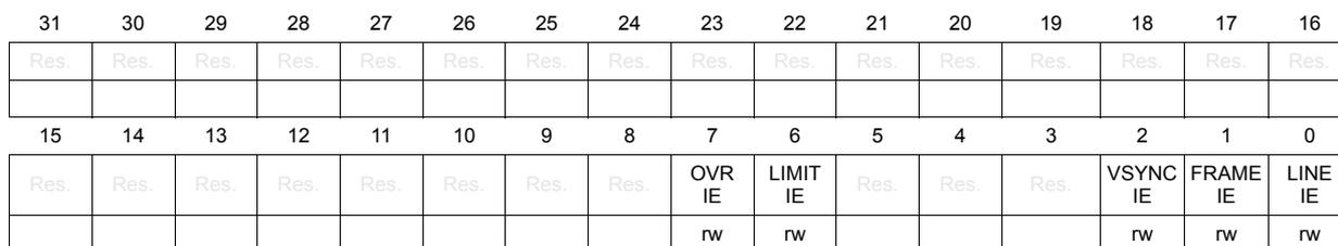
| 31 | 30 | 29 | 28 | 27 | 26 | 25 | 24 | 23 | 22 | 21 | 20 | 19 | 18 | 17 | 16 |
| Res. | Res. | Res. | Res. | Res. | Res. | Res. | Res. | Res. | Res. | Res. | Res. | Res. | Res. | Res. | Res. |
| 15 | 14 | 13 | 12 | 11 | 10 | 9 | 8 | 7 | 6 | 5 | 4 | 3 | 2 | 1 | 0 |
| Res. | Res. | Res. | Res. | Res. | Res. | Res. | Res. | OVR IE | LIMIT IE | Res. | Res. | Res. | VSYNC IE | FRAME IE | LINE IE |
| rw | rw | rw | rw | rw |
Bits 31:8 Reserved, must be kept at reset value.
Bit 7 OVR IE : Overrun interrupt enable
0: No interrupt generation
1: An interrupt is generated if the AXI master is unable to transfer the last data before new data (32-bit) are received.
Bit 6 LIMIT IE : Limit interrupt enable
0: No interrupt generation when the limit is reached
1: An interrupt is generated when the limit is reached
Bits 5:3 Reserved, must be kept at reset value.
Bit 2 VSYNC IE : VSYNC interrupt enable
0: No interrupt generation
1: An interrupt is generated on each VSYNC (captured or not)
Bit 1 FRAME IE : Frame capture completed interrupt enable
0: No interrupt generation
1: An interrupt is generated after the full capture of a cropped frame
Bit 0 LINE IE : Multi-line capture completed interrupt enable
0: No interrupt generation when the line is received
1: An interrupt is generated after the full capture of a group of lines (or last line reached)
39.14.31 DCMIPP Pipe0 status register (DCMIPP_P0SR)
Address offset: 0x5F8
Reset value: 0x0000 0000
| 31 | 30 | 29 | 28 | 27 | 26 | 25 | 24 | 23 | 22 | 21 | 20 | 19 | 18 | 17 | 16 |
|---|---|---|---|---|---|---|---|---|---|---|---|---|---|---|---|
| Res. | Res. | Res. | Res. | Res. | Res. | Res. | Res. | CPTACT | Res. | Res. | Res. | Res. | Res. | LST FRM | LST LINE |
| r | r | r | |||||||||||||
| 15 | 14 | 13 | 12 | 11 | 10 | 9 | 8 | 7 | 6 | 5 | 4 | 3 | 2 | 1 | 0 |
| Res. | Res. | Res. | Res. | Res. | Res. | Res. | Res. | OVR F | LIMIT F | Res. | Res. | Res. | VSYNC F | FRAME F | LINE F |
| r | r | r | r | r |
Bits 31:24 Reserved, must be kept at reset value.
Bit 23 CPTACT : Capture immediate status
0: Capture currently inactive
1: Capture currently active
This bit is automatically reset at the end of frame capture complete event (after all the data of that frame have been captured and the IP-Plug has started to emit the last burst on the AXI, usually before the next VSync).
Bits 22:20 Reserved, must be kept at reset value.
Bits 19:18 Reserved, must be kept at reset value.
Bit 17 LSTFRM : Last frame LSB bit, sampled at frame capture complete event.
The information is extracted from the frame data number that can be delivered by the camera through the CSI2 interface.
Bit 16 LSTLINE : Last line LSB bit, sampled at frame capture complete event.
Bits 15:8 Reserved, must be kept at reset value.
Bit 7 OVRF : Overrun raw interrupt status
0: No data buffer overrun occurred
1: A data buffer overrun occurred and this frame data are corrupted
This bit is cleared by writing 1 to the COVRF bit in the DCMIPP_P0FCR register.
Bit 6 LIMITF : Limit raw interrupt status
This bit is set when the data counter DCMIPP_PxDCCNTR reaches its maximum value DCMIPP_PxDCLIMITR.
It is cleared by writing 1 to the CLIMITF bit in the DCMIPP_P0FCR register.
Bits 5:3 Reserved, must be kept at reset value.
Bit 2 VSYNCF : VSYNC raw interrupt status
This bit is set when the VSYNC signal changes from the inactive state to the active state. In case of embedded synchronization, this bit is set only if the CAPTURE bit is set in DCMIPP_CR.
It is cleared by writing 1 to the CVSYNCF bit in the DCMIPP_P0FCR register.
Bit 1 FRAMEF : Frame capture completed raw interrupt status
0: No capture or ongoing capture
1: All data of a frame have been captured
This bit is set when all data of a frame or window have been captured. In case of a cropped window, this bit is set at the end of line of the last line in the crop. It is set even if the captured frame is empty (for example window cropped outside the frame).
This bit is cleared by writing 1 to the CFRAMEF bit in DCMIPP_P0FCR.
Bit 0 LINEF : Multi-line capture completed raw interrupt status
This bit is set when one/more lines have been completed. For the JPEG mode, this bit is raised at the end of the frame.
The periodicity of LINEF event is configured by LINEMULT bits into DCMIPP_P0PPCR register. When reaching end of frame, this event is triggered out to allow software action even if the LINEMULT value set is not a multiple of the total lines frame.
In case of embedded synchronization, this bit is set only if the CAPTURE bit in the DCMIPP_CR register is set. It is cleared by writing 1 to the CLINEF bit in the DCMIPP_P0FCR register.
39.14.32 DCMIPP Pipe0 interrupt clear register (DCMIPP_P0FCR)
Address offset: 0x5FC
Reset value: 0x0000 0000
| 31 | 30 | 29 | 28 | 27 | 26 | 25 | 24 | 23 | 22 | 21 | 20 | 19 | 18 | 17 | 16 |
|---|---|---|---|---|---|---|---|---|---|---|---|---|---|---|---|
| Res. | Res. | Res. | Res. | Res. | Res. | Res. | Res. | Res. | Res. | Res. | Res. | Res. | Res. | Res. | Res. |
| 15 | 14 | 13 | 12 | 11 | 10 | 9 | 8 | 7 | 6 | 5 | 4 | 3 | 2 | 1 | 0 |
| Res. | Res. | Res. | Res. | Res. | Res. | Res. | Res. | COVR F | CLIMIT F | Res. | Res. | Res. | CVSYNC F | CFRAME F | CLINE F |
| w | w | w | w | w |
Bits 31:8 Reserved, must be kept at reset value.
Bit 7 COVRF : Overrun interrupt status clear
Writing 1 into this bit clears the OVRF bit in the DCMIPP_P0SR register.
Bit 6 CLIMITF : limit interrupt status clear
Writing 1 into this bit clears LIMITF in the DCMIPP_P0SR register.
Bits 5:3 Reserved, must be kept at reset value.
Bit 2 CVSYNCF : Vertical synchronization interrupt status clear
Writing 1 into this bit clears the VSYNCF bit in the DCMIPP_P0SR register.
Bit 1 CFRAMEF : Frame capture complete interrupt status clear
Writing 1 into this bit clears the FRAMEF bit in the DCMIPP_P0SR register.
Bit 0 CLINEF : Multi-line capture complete interrupt status clear
Writing 1 into this bit clears LINEF in the DCMIPP_P0SR register.
39.14.33 DCMIPP Pipe0 current flow selection configuration register (DCMIPP_P0CFSCR)
Address offset: 0x604
Reset value: 0x0000 0000
| 31 | 30 | 29 | 28 | 27 | 26 | 25 | 24 | 23 | 22 | 21 | 20 | 19 | 18 | 17 | 16 |
|---|---|---|---|---|---|---|---|---|---|---|---|---|---|---|---|
| PIPEN | Res. | Res. | Res. | Res. | Res. | Res. | Res. | Res. | Res. | Res. | VC[1:0] | Res. | DTMODE[1:0] | ||
| r | r | r | r | r | |||||||||||
| 15 | 14 | 13 | 12 | 11 | 10 | 9 | 8 | 7 | 6 | 5 | 4 | 3 | 2 | 1 | 0 |
| Res. | Res. | DTIDB[5:0] | Res. | Res. | DTIDA[5:0] | ||||||||||
| r | r | r | r | r | r | r | r | r | r | r | r | ||||
Bit 31 PIPEN : Current activation of PipeN
0: Pipe disabled
1: Pipe enabled, can start capturing with CPTMODE, CPTREQ, CPTACK.
Bits 30:21 Reserved, must be kept at reset value.
Bits 20:19 VC[1:0] : Current flow selection mode
Virtual channel ID of the CSI flow to select for further processing on the pipe.
Bit 18 Reserved, must be kept at reset value.
Bits 17:16 DTMODE[1:0] : Flow selection mode
00: Only flow DTIDA from the selected virtual channel is forwarded in the pipe.
01: Flows DTIDA and/or DTIDB from the selected virtual channel are forwarded in the pipe.
10: All Datatypes from the selected virtual channel, except the DTIDA or DTIDB are forwarded into the pipe.
11: All Datatypes of the selected virtual channel VC are forwarded in the pipe.
Bits 15:14 Reserved, must be kept at reset value.
Bits 13:8 DTIDB[5:0] : Current data type selection ID B
Data type ID of the CSI flow to select.
Bits 7:6 Reserved, must be kept at reset value.
Bits 5:0 DTIDA[5:0] : Current data type selection ID A
Data type ID of the CSI flow to select.
39.14.34 DCMIPP Pipe0 current flow control configuration register (DCMIPP_P0CFCTCR)
Address offset: 0x700
Reset value: 0x0000 0000
| 31 | 30 | 29 | 28 | 27 | 26 | 25 | 24 | 23 | 22 | 21 | 20 | 19 | 18 | 17 | 16 |
|---|---|---|---|---|---|---|---|---|---|---|---|---|---|---|---|
| Res. | Res. | Res. | Res. | Res. | Res. | Res. | Res. | Res. | Res. | Res. | Res. | Res. | Res. | Res. | Res. |
| 15 | 14 | 13 | 12 | 11 | 10 | 9 | 8 | 7 | 6 | 5 | 4 | 3 | 2 | 1 | 0 |
| Res. | Res. | Res. | Res. | Res. | Res. | Res. | Res. | Res. | Res. | Res. | Res. | CPT REQ | CPT MODE | FRATE[1:0] | |
| r | r | r | r | ||||||||||||
Bits 31:4 Reserved, must be kept at reset value.
Bit 3 CPTREQ : Capture requested
0: Capture not requested for next frame.
1: Capture requested for next frame.
When PIPEN = 1, and when the CPTREQ is set to 1 the pipe waits for the first VSync, and automatically starts a capture and sets CPTACT = 1 to mention it.
In Snapshot mode the CPTREQ bit is automatically cleared at the start of the first frame received.
In continuous grab mode the capture remains active and CPTREQ = 1, until the software clears CPTREQ: the capture stops and CPTACT is reset at the end of the ongoing frame. The DCMI and pipe configuration registers must be correctly programmed before enabling this bit.
Bit 2 CPTMODE : Capture mode
0: Continuous grab mode - The received data are transferred into the destination memory through the AXI master.
1: Snapshot mode (single frame) - Once activated, the interface waits for the start of frame, and then transfers a single frame through the AXI master. At the end of the frame the CPTACT bit is automatically reset.
Bits 1:0 FRATE[1:0] : Frame capture rate control
These bits define the frequency of frame capture. They are meaningful only in Continuous grab mode, ignored in Snapshot mode.
00: all frames are captured
01: one out of two frames captured (50% bandwidth reduction)
10: one out of four frames captured (75% bandwidth reduction)
11: one out of eight frames captured (87% bandwidth reduction)
39.14.35 DCMIPP Pipe0 current statistic/crop start register (DCMIPP_P0CSCSTR)
Address offset: 0x704
Reset value: 0x0000 0000
| 31 | 30 | 29 | 28 | 27 | 26 | 25 | 24 | 23 | 22 | 21 | 20 | 19 | 18 | 17 | 16 |
|---|---|---|---|---|---|---|---|---|---|---|---|---|---|---|---|
| Res. | Res. | Res. | Res. | VSTART[11:0] | |||||||||||
| r | r | r | r | r | r | r | r | r | r | r | r | ||||
| 15 | 14 | 13 | 12 | 11 | 10 | 9 | 8 | 7 | 6 | 5 | 4 | 3 | 2 | 1 | 0 |
| Res. | Res. | Res. | Res. | HSTART[11:0] | |||||||||||
| r | r | r | r | r | r | r | r | r | r | r | r | ||||
Bits 31:28 Reserved, must be kept at reset value.
Bits 27:16 VSTART[11:0] : Current vertical start, from 0 to 4094 pixels high
Bits 15:12 Reserved, must be kept at reset value.
Bits 11:0 HSTART[11:0] : Current horizontal start, from 0 to 4094 words wide
39.14.36 DCMIPP Pipe0 current statistic/crop size register (DCMIPP_P0CSCSZR)
Address offset: 0x708
Reset value: 0x0000 0000
| 31 | 30 | 29 | 28 | 27 | 26 | 25 | 24 | 23 | 22 | 21 | 20 | 19 | 18 | 17 | 16 |
|---|---|---|---|---|---|---|---|---|---|---|---|---|---|---|---|
| ENABLE | POSNEG | Res. | Res. | VSIZE[11:0] | |||||||||||
| r | r | r | r | r | r | r | r | r | r | r | r | r | r | ||
| 15 | 14 | 13 | 12 | 11 | 10 | 9 | 8 | 7 | 6 | 5 | 4 | 3 | 2 | 1 | 0 |
| Res. | Res. | Res. | Res. | HSIZE[11:0] | |||||||||||
| r | r | r | r | r | r | r | r | r | r | r | r | ||||
Bit 31 ENABLE : Current value of the ENABLE bit
0: Bypass. All data are computed, if the statistics data are sent within the frame, they are sent to the processing pipe as pixels data.
1: Enable: Depending on bit POSNEG value, the rectangle defined by the VSIZE, HSIZE, VSTART, HSTART can be used to extract or to remove certain amount of data (statistical extraction or removal, or basic 2D crop features)
if POSNEG = 0, the data inside the rectangle area are transmitted (can correspond to a statistical data removal, or as a crop feature in a data valid image area).
if POSNEG = 1, the data outside of the rectangle area are transmitted (can correspond to a statistical data extraction, rejecting all data inside the window)
Bit 30 POSNEG : Current value of the POSNEG bit
This bit has a meaning only if ENABLE bit is set.
0: Positive area. The rectangle defined by VSIZE, HSIZE, and VSTART, HSTART is the active area.
1: Negative area. The active area is the area excluding the rectangle defined by VSIZE, HSIZE, and VSTART, HSTART.
Bits 29:28 Reserved, must be kept at reset value.
Bits 27:16 VSIZE[11:0] : Current vertical size, from 0 to 4094 pixels high.
If the value is maintained at 0 when enabling the crop by means of the ENABLE bit, the value is forced internally at 0xFFE which is the maximum value.
Bits 15:12 Reserved, must be kept at reset value.
Bits 11:0 HSIZE[11:0] : Current horizontal size, from 0 to 4094 word wide (data 32-bit).
If the value is maintained at 0 when enabling the crop by means of the ENABLE bit, the value is forced internally at 0xFFE, which is the maximum value.
39.14.37 DCMIPP Pipe0 current pixel packer configuration register (DCMIPP_P0CPPCR)
Address offset: 0x7C0
Reset value: 0x0000 0000
| 31 | 30 | 29 | 28 | 27 | 26 | 25 | 24 | 23 | 22 | 21 | 20 | 19 | 18 | 17 | 16 |
|---|---|---|---|---|---|---|---|---|---|---|---|---|---|---|---|
| Res. | Res. | Res. | Res. | Res. | Res. | Res. | Res. | Res. | Res. | Res. | LMAWE | LMAWM[2:0] | DBM | ||
| r | r | r | r | r | |||||||||||
| 15 | 14 | 13 | 12 | 11 | 10 | 9 | 8 | 7 | 6 | 5 | 4 | 3 | 2 | 1 | 0 |
| LINEMULT[2:0] | Res. | OELS | LSM | OEBS | BSM[1:0] | HEADER EN | PAD | Res. | Res. | Res. | Res. | SWAP YUV | |||
| r | r | r | r | r | r | r | r | r | r | r | |||||
Bits 31:21 Reserved, must be kept at reset value.
Bit 20 LMAWE : Line multi address wrapping enable bit
Enables the wrapping of the address every power-of-2 of written lines.
0: Line multi address wrapping disabled.
1: Line multi address wrapping enabled.
Bits 19:17 LMAWM[2:0] : Line multi address wrapping modulo
Amount of captured lines after which the write address is wrapped back to the BaseAddress. It is used to write a full frame onto a circular (ping-pong) buffer.
000: Wraps address after every line
001: Wraps address after two lines
010: Wraps address after four lines
011: Wraps address after eight lines
100: Wraps address after sixteen lines
101: Wraps address after 32 lines
110: Wraps address after 64 lines
111: Wraps address after 128 lines
Bit 16 DBM : Double buffer mode
0: No double buffer mode activated. Pipe0 is always dump to memory address set by DCMIPP_P0PPM0AR1 register
1: Double buffer mode activated. Dump address location switches from DCMIPP_P0PPM0AR1 register to DCMIPP_P0PPM0AR2 register alternatively on each frame.
Bits 15:13 LINEMULT[2:0] : Current amount of capture completed lines for LINE event and interrupt
0x0: Event after every line
0x1: Event after two lines
0x2: Event after four lines
0x3: Event after eight lines
0x4: Event after sixteen lines
0x5: Event after 32 lines
0x6: Event after 64 lines
0x7: Event after 128 lines
Bit 12 Reserved, must be kept at reset value.
Bit 11 OELS : Current odd/even line select (line select start)
This bit works in conjunction with LSM field (LSM = 1)
0: Interface captures the first line after the frame start, the second one is dropped
1: Interface captures the second line from the frame start, the first one is dropped
This bit has a meaning only if INSEL = 0 in the DCMIPP_CMCR register.
Bit 10 LSM : Current Line select mode
0: Interface captures all received lines
1: Interface captures one line out of two
This bit has a meaning only if INSEL = 0 in the DCMIPP_CMCR register.
Bit 9 OELS : Current odd/even byte select (byte select start)
This bit works in conjunction with BSM field (BSM ≠ 00)
0: Interface captures the first data (byte or double byte) from the frame/line start, the second one is dropped
1: Interface captures the second data (byte or double byte) from the frame/line start, the first one is dropped
This bit has a meaning only if INSEL = 0 in the DCMIPP_CMCR register.
Bits 8:7 BSM[1:0] : Current Byte select mode
00: Interface captures all received data
01: Interface captures one data out of two
10: Interface captures one byte out of four
11: Interface captures two bytes out of four
Modes 10 and 11 work only with EDM [2:0] = 000 into the DCMIPP_PRCR register.
This bit has a meaning only if INSEL = 0 into the DCMIPP_CMCR register
Bit 6 HEADEREN : Current CSI header dump enable
0: CSI-2 headers are not dumped.
1: CSI-2 headers are dumped as 32-bit words.
This setting is ignored for Parallel interface mode, as there are no headers.
Bit 5 PAD : Current Pad mode for monochrome and raw Bayer 10/12/14 bpp (MSB vs. LSB alignment)
0: Aligns on LSB (and pads null bits on MSB), for backward compatibility with former DCMI
1: Aligns on MSB (and pads null bits on LSB), for better ease of software or GPU
Bits 4:1 Reserved, must be kept at reset value.
Bit 0 SWAPYUV : Swaps, within a 32-bit word, byte 0 vs. 1 and byte 2 vs. 3. It corresponds, for YUV422 pixels formats, to swap between UYVY and YUYV.
0: Outputs the provided words, as described in Section 39.10: Pixel format description .
1: Swaps the bytes from provided words, byte 0 vs. 1 and 2 vs. 3.
39.14.38 DCMIPP Pipe0 current pixel packer Memory0 address register 1 (DCMIPP_P0CPPM0AR1)
Address offset: 0x7C4
Reset value: 0x0000 0000
| 31 | 30 | 29 | 28 | 27 | 26 | 25 | 24 | 23 | 22 | 21 | 20 | 19 | 18 | 17 | 16 |
|---|---|---|---|---|---|---|---|---|---|---|---|---|---|---|---|
| M0A[31:16] | |||||||||||||||
| r | r | r | r | r | r | r | r | r | r | r | r | r | r | r | r |
| 15 | 14 | 13 | 12 | 11 | 10 | 9 | 8 | 7 | 6 | 5 | 4 | 3 | 2 | 1 | 0 |
| M0A[15:0] | |||||||||||||||
| r | r | r | r | r | r | r | r | r | r | r | r | r | r | r | r |
Bits 31:0 M0A[31:0] : Memory0 address
Base address of the current memory area 0, to whom data are written. It is assumed to be a multiple of 16, hence its bits 3:0 are always at 0x0.
39.14.39 DCMIPP Pipe0 current pixel packer Memory0 address register 2 (DCMIPP_P0CPPM0AR2)
Address offset: 0x7C8
Reset value: 0x0000 0000
| 31 | 30 | 29 | 28 | 27 | 26 | 25 | 24 | 23 | 22 | 21 | 20 | 19 | 18 | 17 | 16 |
| M0A[31:16] | |||||||||||||||
| r | r | r | r | r | r | r | r | r | r | r | r | r | r | r | r |
| 15 | 14 | 13 | 12 | 11 | 10 | 9 | 8 | 7 | 6 | 5 | 4 | 3 | 2 | 1 | 0 |
| M0A[15:0] | |||||||||||||||
| r | r | r | r | r | r | r | r | r | r | r | r | r | r | r | r |
Bits 31:0 M0A[31:0] : Memory0 address
Base address of the current memory area 0, to whom data are written. It is assumed to be a multiple of 16, hence its bits 3:0 are always at 0x0.
39.14.40 DCMIPP Pipe1 flow selection configuration register (DCMIPP_P1FSCR)
Address offset: 0x804
Reset value: 0x0000 0000
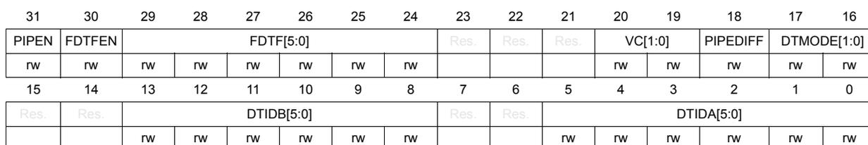
| 31 | 30 | 29 | 28 | 27 | 26 | 25 | 24 | 23 | 22 | 21 | 20 | 19 | 18 | 17 | 16 |
| PIPEN | FDTFEN | FDTF[5:0] | Res. | Res. | Res. | VC[1:0] | PIPEDIFF | DTMODE[1:0] | |||||||
| r/w | r/w | r/w | r/w | r/w | r/w | r/w | r/w | r/w | r/w | r/w | r/w | r/w | |||
| 15 | 14 | 13 | 12 | 11 | 10 | 9 | 8 | 7 | 6 | 5 | 4 | 3 | 2 | 1 | 0 |
| Res. | Res. | DTIDB[5:0] | Res. | Res. | DTIDA[5:0] | ||||||||||
| r/w | r/w | r/w | r/w | r/w | r/w | r/w | r/w | r/w | r/w | r/w | r/w | ||||
Bit 31 PIPEN : Activation of PipeN
0: Pipe disabled
1: Pipe enabled, can start capturing with CPTMODE, CPTREQ, CPTACK
Bit 30 FDTFEN : Force Datatype format enable
0: Disable force Datatype format. The Datatype format used by the pipe is the one defined into DTIDX1: Enable force Datatype format. When the Datatype DTIDX is detected by the pipe, the real pixel format considered by the pipe is the one set into the FDTF[5:0] bit field instead of the physical one received by the CSI2 Host. It allows to handle, for instance, 3D sensors camera using user data type in bottom-up approach, and to explicitly define the pixel format to be handled by the pipe. Note that the flow is first selected using the DTMODE and DTIDA/B, and then, if selected, its data type may be forced with the to FDTF using FDTFEN = 1.
Bits 29:24 FDTF[5:0] : Force Datatype format
Forcing the Datatype format. This Datatype overwrites the one received by the CSI2-HOST by specifying the pixel format to consider. The value must follow the CSI2 Datatype format definition in the CSI2 standard. This bit field has no meaning if the FDTFEN bit is cleared.
Bits 23:21 Reserved, must be kept at reset value.
Bits 20:19 VC[1:0] : Flow selection mode
Virtual channel ID of the CSI flow to select for further processing on the pipe.
Bit 18 PIPEDIFF : Differentiates Pipe2 from Pipe1
0: Pipe2 receives the same data as Pipe1 (data filtered by Pipe1 configuration for VC and DTIDA/DTIDB and DTMODE mode, as well as FDTF and FDTFEN bit).
1: Pipe1 gets pixels only from VC and DT configured in Pipe1, processed by all blocks belonging to the image processing functional block (demosaicing, auto exposure, statistics, contrast enhancement). Pipe2 gets pixels only from VC/DTID and FDTFEN/FDTF bits configured in Pipe2, processed from Crop. There are no shared functions with Pipe1, fully independent.
This bit must be kept cleared when INSEL = 0 into the DCMIPP_CMCR register.
Bits 17:16 DTMODE[1:0] : Flow selection mode
00: Only flow DTIDA from the selected virtual channel is forwarded in the pipe
01: Flows DTIDA and/or DTIDB from the selected virtual channel are forwarded in the pipe
Other values: Reserved.
Bits 15:14 Reserved, must be kept at reset value.
Bits 13:8 DTIDB[5:0] : Data type selection ID B
Data type ID of the CSI flow to select.
Bits 7:6 Reserved, must be kept at reset value.
Bits 5:0 DTIDA[5:0] : Data type selection ID A
Data type ID of the CSI flow to select.
39.14.41 DCMIPP Pipe1 stat removal configuration register (DCMIPP_P1SRCR)
Address offset: 0x820
Reset value: 0x0000 0000
| 31 | 30 | 29 | 28 | 27 | 26 | 25 | 24 | 23 | 22 | 21 | 20 | 19 | 18 | 17 | 16 |
|---|---|---|---|---|---|---|---|---|---|---|---|---|---|---|---|
| Res. | Res. | Res. | Res. | Res. | Res. | Res. | Res. | Res. | Res. | Res. | Res. | Res. | Res. | Res. | Res. |
| 15 | 14 | 13 | 12 | 11 | 10 | 9 | 8 | 7 | 6 | 5 | 4 | 3 | 2 | 1 | 0 |
| CROP EN | FIRSTLINEDEL[2:0] | LASTLINE[11:0] | |||||||||||||
| rw | rw | rw | rw | rw | rw | rw | rw | rw | rw | rw | rw | rw | rw | rw | rw |
Bits 31:16 Reserved, must be kept at reset value.
Bit 15 CROPEN : Crop line enable
0: No crop (all pixels are fed through)
1: Crop
Bits 14:12 FIRSTLINEDEL[2:0] : Amount of first lines to delete when CROPEN = 1
Bits 11:0 LASTLINE[11:0] : Amount of following lines to keep when CROPEN = 1.
If LASTLINE = 0 all pixels after FIRSTLINEDEL are fed through.
39.14.42 DCMIPP Pipe1 bad pixel removal control register (DCMIPP_P1BPRCR)
Address offset: 0x824
Reset value: 0x0000 0000
| 31 | 30 | 29 | 28 | 27 | 26 | 25 | 24 | 23 | 22 | 21 | 20 | 19 | 18 | 17 | 16 |
|---|---|---|---|---|---|---|---|---|---|---|---|---|---|---|---|
| Res. | Res. | Res. | Res. | Res. | Res. | Res. | Res. | Res. | Res. | Res. | Res. | Res. | Res. | Res. | Res. |
| 15 | 14 | 13 | 12 | 11 | 10 | 9 | 8 | 7 | 6 | 5 | 4 | 3 | 2 | 1 | 0 |
| Res. | Res. | Res. | Res. | Res. | Res. | Res. | Res. | Res. | Res. | Res. | Res. | STRENGTH[2:0] | ENABLE | ||
| rw | rw | rw | rw | ||||||||||||
Bits 31:4 Reserved, must be kept at reset value.
Bits 3:1 STRENGTH[2:0] : Strength (aggressiveness) of the bad pixel detection
0x0: The filter is fairly tolerant: only a few pixels are declared bad, due to their high noise
...
0x7: The filter is very aggressive: many pixels are declared bad, even if only slightly noisy.
Bit 0 ENABLE :
0: Bypass: bad pixel removal is not active, all pixels are transmitted through
1: Enable: if bad pixel are detected, they are replaced by corrected pixels
Bad pixel detection must be enabled only for raw Bayer flows, as it corrupts RGB flows.
39.14.43 DCMIPP Pipe1 bad pixel removal status register (DCMIPP_P1BPRSR)
Address offset: 0x828
Reset value: 0x0000 0000
| 31 | 30 | 29 | 28 | 27 | 26 | 25 | 24 | 23 | 22 | 21 | 20 | 19 | 18 | 17 | 16 |
|---|---|---|---|---|---|---|---|---|---|---|---|---|---|---|---|
| Res. | Res. | Res. | Res. | Res. | Res. | Res. | Res. | Res. | Res. | Res. | Res. | Res. | Res. | Res. | Res. |
| 15 | 14 | 13 | 12 | 11 | 10 | 9 | 8 | 7 | 6 | 5 | 4 | 3 | 2 | 1 | 0 |
| Res. | Res. | Res. | Res. | BADCNT[11:0] | |||||||||||
| r | r | r | r | r | r | r | r | r | r | r | r | ||||
Bits 31:12 Reserved, must be kept at reset value.
Bits 11:0 BADCNT[11:0] : Amount of detected bad pixels
Counts the amount of bad pixels detected in each frame, and if too many, saturates at its maximum value (4095). It is reclocked at the frame end, to remain stable for reading during the next frame.
39.14.44 DCMIPP Pipe1 decimation register (DCMIPP_P1DECR)
This register controls the input decimation.
Address offset: 0x830
Reset value: 0x0000 0000
| 31 | 30 | 29 | 28 | 27 | 26 | 25 | 24 | 23 | 22 | 21 | 20 | 19 | 18 | 17 | 16 |
|---|---|---|---|---|---|---|---|---|---|---|---|---|---|---|---|
| Res. | Res. | Res. | Res. | Res. | Res. | Res. | Res. | Res. | Res. | Res. | Res. | Res. | Res. | Res. | Res. |
| 15 | 14 | 13 | 12 | 11 | 10 | 9 | 8 | 7 | 6 | 5 | 4 | 3 | 2 | 1 | 0 |
| Res. | Res. | Res. | Res. | Res. | Res. | Res. | Res. | Res. | Res. | Res. | VDEC[1:0] | HDEC[1:0] | ENABLE | ||
| rw | rw | rw | rw | rw |
Bits 31:5 Reserved, must be kept at reset value.
Bits 4:3 VDEC[1:0] : Vertical decimation ratio
0x0: All pixels are transmitted, no vertical decimation
0x1: one line out of two transmitted (for raw Bayer data, two lines of components every four)
0x2: one line out of four transmitted (for raw Bayer data, two lines of components every eight)
0x3: one line out of eight transmitted (for raw Bayer data, two lines of components every 16)
Bits 2:1 HDEC[1:0] : Horizontal decimation ratio
0x0: All pixels are transmitted, no horizontal decimation
0x1: one line out of two transmitted (for raw Bayer data, two lines of components every four)
0x2: one line out of four transmitted (for raw Bayer data, two lines of components every eight)
0x3: one line out of eight transmitted (for raw Bayer data, two lines of components every 16)
Bit 0 ENABLE :
0: Bypass: decimation is not active, all pixels are transmitted
1: Enable: one pixel every 1, 2, 4, or 8, in H and V is transmitted, following HDEC and VDEC
39.14.45 DCMIPP Pipe1 black level calibration control register (DCMIPP_P1BLCCR)
Address offset: 0x840
Reset value: 0x0000 0000
| 31 | 30 | 29 | 28 | 27 | 26 | 25 | 24 | 23 | 22 | 21 | 20 | 19 | 18 | 17 | 16 |
|---|---|---|---|---|---|---|---|---|---|---|---|---|---|---|---|
| rw | rw | rw | rw | rw | rw | rw | rw | rw | rw | rw | rw | rw | rw | rw | rw |
| BLCR[7:0] | BLCG[7:0] | ||||||||||||||
| 15 | 14 | 13 | 12 | 11 | 10 | 9 | 8 | 7 | 6 | 5 | 4 | 3 | 2 | 1 | 0 |
| BLCB[7:0] | Res. | Res. | Res. | Res. | Res. | Res. | Res. | ENABLE | |||||||
| rw | rw | rw | rw | rw | rw | rw | rw | rw | |||||||
Bits 31:24 BLCR[7:0] : Black level calibration - Red
Value subtracted from the red input MSB component, whether it is on 8, 10, 12, 14 bits.
Bits 23:16 BLCG[7:0] : Black level calibration - Green
Value subtracted from the green input MSB component, whether it is on 8, 10, 12, 14 bits.
Bits 15:8 BLCB[7:0] : Black level calibration - Blue
Value subtracted from the blue input MSB component, whether it is on 8, 10, 12, 14 bits.
Bits 7:1 Reserved, must be kept at reset value.
Bit 0 ENABLE : Black level calibration
0: Bypass: black level calibration is not active, all pixels are transmitted non-modified.
1: Enable: the BLC R, G, B are subtracted.
39.14.46 DCMIPP Pipe1 exposure control register 1 (DCMIPP_P1EXCR1)
Address offset: 0x844
Reset value: 0x0000 0000
| 31 | 30 | 29 | 28 | 27 | 26 | 25 | 24 | 23 | 22 | 21 | 20 | 19 | 18 | 17 | 16 |
|---|---|---|---|---|---|---|---|---|---|---|---|---|---|---|---|
| Res. | SHFR[2:0] | MULTR[7:0] | Res. | Res. | Res. | Res. | |||||||||
| rw | rw | rw | rw | rw | rw | rw | rw | rw | rw | rw | |||||
| 15 | 14 | 13 | 12 | 11 | 10 | 9 | 8 | 7 | 6 | 5 | 4 | 3 | 2 | 1 | 0 |
| Res. | Res. | Res. | Res. | Res. | Res. | Res. | Res. | Res. | Res. | Res. | Res. | Res. | Res. | Res. | ENABLE |
| rw | |||||||||||||||
Bit 31 Reserved, must be kept at reset value.
Bits 30:28 SHFR[2:0] : Exposure shift - Red
0x0, 0x1, 0x2, 0x3, 0x4, 0x5, 0x6, 0x7: exposure of reds is increased, respectively, by a factor 1x, 2x, 4x, 8x, 16x, 32x, 64x, 128x.
Bits 27:20 MULTR[7:0] : Exposure multiplier - Red
Value that is multiplied for the red input components, whether it is on 8, 10, 12, 14 bits.
Multiplying by 64 reduces the exposure (darkens the reds) by a factor 2x.
Multiplying by 128 does not modify the exposure (keeps the reds as-is).
Multiplying by 255 increase the exposure (lightens the reds) by a factor ~2x.
Bits 19:1 Reserved, must be kept at reset value.
Bit 0 ENABLE : Exposure control (multiplication and shift) of all red, green and blue
0: Bypass: exposure multiplier and shift are not applied
1: Enable: the exposure multiplication and shift is applied
39.14.47 DCMIPP Pipe1 exposure control register 2 (DCMIPP_P1EXCR2)
Address offset: 0x848
Reset value: 0x0000 0000
| 31 | 30 | 29 | 28 | 27 | 26 | 25 | 24 | 23 | 22 | 21 | 20 | 19 | 18 | 17 | 16 |
|---|---|---|---|---|---|---|---|---|---|---|---|---|---|---|---|
| Res. | SHFG[2:0] | MULTG[7:0] | Res. | Res. | Res. | Res. | |||||||||
| rw | rw | rw | rw | rw | rw | rw | rw | rw | rw | rw | |||||
| 15 | 14 | 13 | 12 | 11 | 10 | 9 | 8 | 7 | 6 | 5 | 4 | 3 | 2 | 1 | 0 |
| Res. | SHFB[2:0] | MULTB[7:0] | Res. | Res. | Res. | Res. | |||||||||
| rw | rw | rw | rw | rw | rw | rw | rw | rw | rw | rw | |||||
Bit 31 Reserved, must be kept at reset value.
Bits 30:28 SHFG[2:0] : Exposure shift - Green
0x0, 0x1, 0x2, 0x3, 0x4, 0x5, 0x6, 0x7: Exposure of greens is increased, respectively, by a factor 1x, 2x, 4x, 8x, 16x, 32x, 64x, 128x.
Bits 27:20 MULTG[7:0] : Exposure multiplier - Green
Value that is multiplied for the green input components, whether it is on 8, 10, 12, 14 bits.
Multiplying by 64 reduces the exposure (darkens the greens) by a factor 2x.
Multiplying by 128 does not modify the exposure (keeps the greens as-is).
Multiplying by 255 increases the exposure (lightens the greens) by a factor ~2x.
Bits 19:15 Reserved, must be kept at reset value.
Bits 14:12 SHFB[2:0] : Exposure shift - Blue
0x0, 0x1, 0x2, 0x3, 0x4, 0x5, 0x6, 0x7: exposure of blues is increased, respectively, by a factor 1x, 2x, 4x, 8x, 16x, 32x, 64x, 128x.
Bits 11:4 MULTB[7:0] : Exposure multiplier - Blue
Value that is multiplied for the blue input components, whether it is on 8, 10, 12, 14 bits.
Multiplying by 64 reduces the exposure (darkens the blues) by a factor 2x.
Multiplying by 128 does not modify the exposure (keeps the blues as-is).
Multiplying by 255 increases the exposure (lightens the blues) by a factor ~2x.
Bits 3:0 Reserved, must be kept at reset value.
39.14.48 DCMIPP Pipe1 statistics1 control register (DCMIPP_P1ST1CR)
Address offset: 0x850
Reset value: 0x0000 0000
| 31 | 30 | 29 | 28 | 27 | 26 | 25 | 24 | 23 | 22 | 21 | 20 | 19 | 18 | 17 | 16 |
|---|---|---|---|---|---|---|---|---|---|---|---|---|---|---|---|
| Res. | Res. | Res. | Res. | Res. | Res. | Res. | Res. | Res. | Res. | Res. | Res. | Res. | Res. | Res. | Res. |
| 15 | 14 | 13 | 12 | 11 | 10 | 9 | 8 | 7 | 6 | 5 | 4 | 3 | 2 | 1 | 0 |
| Res. | Res. | Res. | Res. | Res. | Res. | Res. | Res. | MODE | SRC[2:0] | BINS[1:0] | Res. | ENABLE | |||
| rw | rw | rw | rw | rw | rw | rw | |||||||||
Bits 31:8 Reserved, must be kept at reset value.
Bit 7 MODE : Statistics mode
0: Average: accumulates the 8-bit component value of the considered pixel components.
Typically used to extract the average value of R, G, B, or luminance across the picture, and to drive the exposure control and the white balance.
1: Bins: accumulates 256 for each considered pixel component fitting a bin dynamic.
Typically used to extract how many pixel components fall into the various dynamic bins, and to drive the contrast enhancement.
Bits 6:4 SRC[2:0] : Statistics source
0x0, 0x1, 0x2, 0x3: components are sampled after decimation, and sample, respectively, red, green, blue, and luminance. For raw Bayer formats, only one component is available by pixel.
0x4, 0x5, 0x6, 0x7: components are sampled after demosaicing, and sample, respectively, red, green, blue, and luminance.
Bits 3:2 BINS[1:0] : Current bin definition
Condition: MODE = Bins
0x0: LowerBins: Accu0 (1, 2) is incremented of 256 if Component <4 (<8, <16)
0x1: LowMid Bins: Accu0 (1, 2) is incremented of 256 if Component <32 (<64, <128)
0x2: UpMid Bins: Accu0 (1, 2) is incremented of 256 if Component >127 (>191, >224)
0x3: UpBins: Accu0 (1, 2) is incremented of 256 if Component >239 (>247, >251)
Condition: MODE = Average
0x0: All Pixels: Accu is incremented of Component, if \( 0 \leq \text{Component} < 256 \) .
0x1: NoExt16: Accu is incremented of Component, if \( 16 \leq \text{Component} < 240 \)
0x2: NoExt32: Accu is incremented of Component, if \( 32 \leq \text{Component} < 224 \)
0x3: NoExt64: Accu is incremented of Component, if \( 64 \leq \text{Component} < 192 \)
Bit 1 Reserved, must be kept at reset value.
Bit 0 ENABLE :
0: Disabled: statistics are not accumulated
1: Enable: statistics are accumulated
39.14.49 DCMIPP Pipe1 statistics 2 control register (DCMIPP_P1ST2CR)
Address offset: 0x854
Reset value: 0x0000 0000
| 31 | 30 | 29 | 28 | 27 | 26 | 25 | 24 | 23 | 22 | 21 | 20 | 19 | 18 | 17 | 16 |
|---|---|---|---|---|---|---|---|---|---|---|---|---|---|---|---|
| Res. | Res. | Res. | Res. | Res. | Res. | Res. | Res. | Res. | Res. | Res. | Res. | Res. | Res. | Res. | Res. |
| 15 | 14 | 13 | 12 | 11 | 10 | 9 | 8 | 7 | 6 | 5 | 4 | 3 | 2 | 1 | 0 |
| Res. | Res. | Res. | Res. | Res. | Res. | Res. | Res. | MODE | SRC[2:0] | BINS[1:0] | Res. | ENABLE | |||
| rw | rw | rw | rw | rw | rw | rw | |||||||||
Bits 31:8 Reserved, must be kept at reset value.
Bit 7 MODE : Statistics mode
0: Average: accumulates the 8-bit component value of the considered pixel components.
It is typically used to extract the average value of R, G, B, or luminance across the picture, and to drive the exposure control and the white balance.
1: Bins: accumulates 256 for each considered pixel component fitting a bin dynamic.
It is typically used to extract how many pixel components fall into the various dynamic bins.
It is usually used to drive the contrast enhancement.
Bits 6:4 SRC[2:0] : Statistics source
0x0, 0x1, 0x2, 0x3: components are sampled after decimation, and sample, respectively, the red, green, blue components, and luminance.
0x4, 0x5, 0x6, 0x7: components are sampled after the black level calibration and exposure, and sample, respectively, red, green, blue and luminance.
Bits 3:2 BINS[1:0] : Bin definition
Condition: MODE = Bins
0x0: LowerBins: Accu0 (1, 2) is incremented of 256 if Component < 4 (< 8, < 16)
0x1: LowMid Bins: Accu0 (1, 2) is incremented of 256 if Component < 32 (< 64, < 128)
0x2: UpMid Bins: Accu0 (1, 2) is incremented of 256 if Component > 127 (> 191, > 224)
0x3: UpBins: Accu0 (1, 2) is incremented of 256 if Component > 239 (> 247, > 251)
Condition: MODE = Average
0x0: AllPixels: Accu is incremented of Component, if 0 ≤ Component < 256.
0x1: NoExt16: Accu is incremented of Component, if 16 ≤ Component < 240.
0x2: NoExt32: Accu is incremented of Component, if 32 ≤ Component < 224.
0x3: NoExt64: Accu is incremented of Component, if 64 ≤ Component < 192.
Bit 1 Reserved, must be kept at reset value.
Bit 0 ENABLE :
0: Disabled: statistics are not accumulated
1: Enabled: statistics are accumulated
39.14.50 DCMIPP Pipe1 statistics 3 control register (DCMIPP_P1ST3CR)
Address offset: 0x858
Reset value: 0x0000 0000
| 31 | 30 | 29 | 28 | 27 | 26 | 25 | 24 | 23 | 22 | 21 | 20 | 19 | 18 | 17 | 16 |
|---|---|---|---|---|---|---|---|---|---|---|---|---|---|---|---|
| Res. | Res. | Res. | Res. | Res. | Res. | Res. | Res. | Res. | Res. | Res. | Res. | Res. | Res. | Res. | Res. |
| 15 | 14 | 13 | 12 | 11 | 10 | 9 | 8 | 7 | 6 | 5 | 4 | 3 | 2 | 1 | 0 |
| Res. | Res. | Res. | Res. | Res. | Res. | Res. | Res. | MODE | SRC[2:0] | BINS[1:0] | Res. | ENABLE | |||
| rw | rw | rw | rw | rw | rw | rw | |||||||||
Bits 31:8 Reserved, must be kept at reset value.
Bit 7 MODE : Statistics mode
0: Average: accumulates the 8-bit component value of the considered pixel components.
It is typically used to extract the average value of R, G, B, or luminance across the picture, and to drive the exposure control and the white balance.
1: Bins: accumulates 256 for each considered pixel component fitting a bin dynamic.
It is typically used to extract how many pixel components fall into the various dynamic bins.
It is usually used to drive the contrast enhancement.
Bits 6:4 SRC[2:0] : Statistics source
0x0, 0x1, 0x2, 0x3: components are sampled after decimation, and sample, respectively, the red, green, blue components, and luminance.
0x4, 0x5, 0x6, 0x7: components are sampled after the black level calibration and exposure, and sample, respectively, the red, green, blue and luminance.
Bits 3:2 BINS[1:0] : Bin definition
Condition: MODE = Bins
0x0: LowerBins: Accu0 (1, 2) is incremented of 256 if Component <4 (<8, <16)
0x1: LowMid Bins: Accu0 (1, 2) is incremented of 256 if Component <32 (<64, <128)
0x2: UpMid Bins: Accu0 (1, 2) is incremented of 256 if Component >127 (>191, >224)
0x3: UpBins: Accu0 (1, 2) is incremented of 256 if Component >239 (>247, >251)
Condition: MODE = Average
0x0: AllPixels: Accu is incremented of Component, if 0 ≤ Component < 256.
0x1: NoExt16: Accu is incremented of Component, if 16 ≤ Component < 240.
0x2: NoExt32: Accu is incremented of Component, if 32 ≤ Component < 224.
0x3: NoExt64: Accu is incremented of Component, if 64 ≤ Component < 192.
Bit 1 Reserved, must be kept at reset value.
Bit 0 ENABLE :
0: Disabled: statistics are not accumulated
1: Enabled: statistics are accumulated
39.14.51 DCMIPP Pipe1 statistics window start register (DCMIPP_P1STSTR)
Address offset: 0x85C
Reset value: 0x0000 0000
| 31 | 30 | 29 | 28 | 27 | 26 | 25 | 24 | 23 | 22 | 21 | 20 | 19 | 18 | 17 | 16 |
|---|---|---|---|---|---|---|---|---|---|---|---|---|---|---|---|
| Res. | Res. | Res. | Res. | VSTART[11:0] | |||||||||||
| rw | rw | rw | rw | rw | rw | rw | rw | rw | rw | rw | rw | ||||
| 15 | 14 | 13 | 12 | 11 | 10 | 9 | 8 | 7 | 6 | 5 | 4 | 3 | 2 | 1 | 0 |
| Res. | Res. | Res. | Res. | HSTART[11:0] | |||||||||||
| rw | rw | rw | rw | rw | rw | rw | rw | rw | rw | rw | rw | ||||
Bits 31:28 Reserved, must be kept at reset value.
Bits 27:16 VSTART[11:0] : Vertical start, from 0 to 4094 pixels high
Bits 15:12 Reserved, must be kept at reset value.
Bits 11:0 HSTART[11:0] : Horizontal start, from 0 to 4094 pixels wide
39.14.52 DCMIPP Pipe1 statistics window size register (DCMIPP_P1STSZR)
Address offset: 0x860
Reset value: 0x0000 0000
| 31 | 30 | 29 | 28 | 27 | 26 | 25 | 24 | 23 | 22 | 21 | 20 | 19 | 18 | 17 | 16 |
|---|---|---|---|---|---|---|---|---|---|---|---|---|---|---|---|
| CROP EN | Res. | Res. | Res. | VSIZE[11:0] | |||||||||||
| rw | rw | rw | rw | rw | rw | rw | rw | rw | rw | rw | rw | rw | |||
| 15 | 14 | 13 | 12 | 11 | 10 | 9 | 8 | 7 | 6 | 5 | 4 | 3 | 2 | 1 | 0 |
| Res. | Res. | Res. | Res. | HSIZE[11:0] | |||||||||||
| rw | rw | rw | rw | rw | rw | rw | rw | rw | rw | rw | rw | ||||
Bit 31 CROPEN :
0: Bypass, all pixels are used to compute the statistics
1: Enable, only the rectangle defined by VSTART, HSTART, VSIZE, HSIZE is used for statistics.
Bits 30:28 Reserved, must be kept at reset value.
Bits 27:16 VSIZE[11:0] : Vertical size, from 0 to 4094 pixels high
If the value is kept at 0 when enabling the crop with the CROPEN bit, the value is forced internally at the maximum value 0xFFE.
Bits 15:12 Reserved, must be kept at reset value.
Bits 11:0 HSIZE[11:0] : Horizontal size, from 0 to 4094 pixels wide
If the value is kept at 0 when enabling the crop with the CROPEN bit, the value is forced internally at the maximum value 0xFFE.
39.14.53 DCMIPP Pipe1 statistics 1 status register (DCMIPP_P1ST1SR)
Address offset: 0x864
Reset value: 0x0000 0000
| 31 | 30 | 29 | 28 | 27 | 26 | 25 | 24 | 23 | 22 | 21 | 20 | 19 | 18 | 17 | 16 |
|---|---|---|---|---|---|---|---|---|---|---|---|---|---|---|---|
| Res. | Res. | Res. | Res. | Res. | Res. | Res. | Res. | ACCU[23:16] | |||||||
| r | r | r | r | r | r | r | r | ||||||||
| 15 | 14 | 13 | 12 | 11 | 10 | 9 | 8 | 7 | 6 | 5 | 4 | 3 | 2 | 1 | 0 |
| ACCU[15:0] | |||||||||||||||
| r | r | r | r | r | r | r | r | r | r | r | r | r | r | r | r |
Bits 31:24 Reserved, must be kept at reset value.
Bits 23:0 ACCU[23:0] : Accumulation result, divided by 256.
39.14.54 DCMIPP Pipe1 statistics 2 status register (DCMIPP_P1ST2SR)
Address offset: 0x868
Reset value: 0x0000 0000
| 31 | 30 | 29 | 28 | 27 | 26 | 25 | 24 | 23 | 22 | 21 | 20 | 19 | 18 | 17 | 16 |
|---|---|---|---|---|---|---|---|---|---|---|---|---|---|---|---|
| Res. | Res. | Res. | Res. | Res. | Res. | Res. | Res. | ACCU[23:16] | |||||||
| r | r | r | r | r | r | r | r | ||||||||
| 15 | 14 | 13 | 12 | 11 | 10 | 9 | 8 | 7 | 6 | 5 | 4 | 3 | 2 | 1 | 0 |
| ACCU[15:0] | |||||||||||||||
| r | r | r | r | r | r | r | r | r | r | r | r | r | r | r | r |
Bits 31:24 Reserved, must be kept at reset value.
Bits 23:0 ACCU[23:0] : accumulation result, divided by 256.
39.14.55 DCMIPP Pipe1 statistics 3 status register (DCMIPP_P1ST3SR)
Address offset: 0x86C
Reset value: 0x0000 0000
| 31 | 30 | 29 | 28 | 27 | 26 | 25 | 24 | 23 | 22 | 21 | 20 | 19 | 18 | 17 | 16 |
|---|---|---|---|---|---|---|---|---|---|---|---|---|---|---|---|
| Res. | Res. | Res. | Res. | Res. | Res. | Res. | Res. | ACCU[23:16] | |||||||
| r | r | r | r | r | r | r | r | ||||||||
| 15 | 14 | 13 | 12 | 11 | 10 | 9 | 8 | 7 | 6 | 5 | 4 | 3 | 2 | 1 | 0 |
| ACCU[15:0] | |||||||||||||||
| r | r | r | r | r | r | r | r | r | r | r | r | r | r | r | r |
Bits 31:24 Reserved, must be kept at reset value.
Bits 23:0 ACCU[23:0] : accumulation result, divided by 256.
39.14.56 DCMIPP Pipe1 demosaicing configuration register (DCMIPP_P1DMCR)
Address offset: 0x870
Reset value: 0x0000 0000
| 31 | 30 | 29 | 28 | 27 | 26 | 25 | 24 | 23 | 22 | 21 | 20 | 19 | 18 | 17 | 16 |
|---|---|---|---|---|---|---|---|---|---|---|---|---|---|---|---|
| Res. | EDGE[2:0] | Res. | LINEH[2:0] | Res. | LINEV[2:0] | Res. | PEAK[2:0] | ||||||||
| rw | rw | rw | rw | rw | rw | rw | rw | rw | rw | rw | rw | ||||
| 15 | 14 | 13 | 12 | 11 | 10 | 9 | 8 | 7 | 6 | 5 | 4 | 3 | 2 | 1 | 0 |
| Res. | Res. | Res. | Res. | Res. | Res. | Res. | Res. | Res. | Res. | Res. | Res. | Res. | TYPE[1:0] | ENABLE | |
| rw | rw | rw | |||||||||||||
Bit 31 Reserved, must be kept at reset value.
- Bits 30:28
EDGE[2:0]
: Strength of the edge detection
- 0x0: No edge detection, pure linear interpolation
- 0x1 to 0x7: Algorithm strength, respectively 3, 4, 6, 8, 12, 16, 24
- Bit 27 Reserved, must be kept at reset value.
- Bits 26:24
LINEH[2:0]
: Strength of the horizontal line detection
- 0x0: No horizontal line detection, pure linear interpolation
- 0x1 to 0x7: Algorithm strength, respectively 3, 4, 6, 8, 12, 16, 24
- Bit 23 Reserved, must be kept at reset value.
- Bits 22:20
LINEV[2:0]
: Strength of the vertical line detection
- 0x0: No vertical line detection, pure linear interpolation
- 0x1 to 0x7: Algorithm strength, respectively 3, 4, 6, 8, 12, 16, 24
- Bit 19 Reserved, must be kept at reset value.
- Bits 18:16
PEAK[2:0]
: Strength of the peak detection
- 0x0: No peak detection, pure linear interpolation
- 0x1 to 0x7: Algorithm strength, respectively 3, 4, 6, 8, 12, 16, 24
- Bits 15:3 Reserved, must be kept at reset value.
- Bits 2:1
TYPE[1:0]
: Raw Bayer type
- 0x0: RGGB
- 0x1: GRBG
- 0x2: GBRG
- 0x3: BGGR
- Bit 0
ENABLE
:
- 0: Bypass
- 1: Enable demosaicing
39.14.57 DCMIPP Pipe1 ColorConv configuration register (DCMIPP_P1CCCR)
Address offset: 0x880
Reset value: 0x0000 0000
| 31 | 30 | 29 | 28 | 27 | 26 | 25 | 24 | 23 | 22 | 21 | 20 | 19 | 18 | 17 | 16 |
|---|---|---|---|---|---|---|---|---|---|---|---|---|---|---|---|
| Res. | Res. | Res. | Res. | Res. | Res. | Res. | Res. | Res. | Res. | Res. | Res. | Res. | Res. | Res. | Res. |
| 15 | 14 | 13 | 12 | 11 | 10 | 9 | 8 | 7 | 6 | 5 | 4 | 3 | 2 | 1 | 0 |
| Res. | Res. | Res. | Res. | Res. | Res. | Res. | Res. | Res. | Res. | Res. | Res. | Res. | CLAMP | TYPE | ENABLE |
| rw | rw | rw |
- Bits 31:3 Reserved, must be kept at reset value.
- Bit 2
CLAMP
: Clamp the output samples
- 0: Not activated (clamped to [0;255] by default)
- 1: Activated, depending on TYPE
- Bit 1
TYPE
: output samples type used while CLAMP is activated
- 0: Clamped to [16;235] for Y and to [16;240] for U and V
- 1: Clamped to [16;235] for R, G and B
0: ColorConv is bypassed
1: ColorConv is enabled
39.14.58 DCMIPP Pipe1 ColorConv red coefficient register 1 (DCMIPP_P1CRR1)Address offset: 0x884
Reset value: 0x0000 0000
Coefficients of the ColorConv, in signed 2.8 format (1.0 is coded by 0x100). The sign is indicated as complement to 2.
| 31 | 30 | 29 | 28 | 27 | 26 | 25 | 24 | 23 | 22 | 21 | 20 | 19 | 18 | 17 | 16 |
|---|---|---|---|---|---|---|---|---|---|---|---|---|---|---|---|
| Res. | Res. | Res. | Res. | Res. | RG[10:0] | ||||||||||
| rw | rw | rw | rw | rw | rw | rw | rw | rw | rw | rw | |||||
| 15 | 14 | 13 | 12 | 11 | 10 | 9 | 8 | 7 | 6 | 5 | 4 | 3 | 2 | 1 | 0 |
| Res. | Res. | Res. | Res. | Res. | RR[10:0] | ||||||||||
| rw | rw | rw | rw | rw | rw | rw | rw | rw | rw | rw | |||||
Bits 31:27 Reserved, must be kept at reset value.
Bits 26:16 RG[10:0] : Coefficient row 1 column 2 of the matrixBits 15:11 Reserved, must be kept at reset value.
Bits 10:0 RR[10:0] : Coefficient row 1 column 1 of the matrix 39.14.59 DCMIPP Pipe1 ColorConv red coefficient register 2 (DCMIPP_P1CRR2)Address offset: 0x888
Reset value: 0x0000 0000
The coefficients RA[9:0] of the added column, for the ColorConv, are defined as signed 10-bit integer with the sign as complement to 2 (-256 is coded by 0x200).
| 31 | 30 | 29 | 28 | 27 | 26 | 25 | 24 | 23 | 22 | 21 | 20 | 19 | 18 | 17 | 16 |
|---|---|---|---|---|---|---|---|---|---|---|---|---|---|---|---|
| Res. | Res. | Res. | Res. | Res. | Res. | RA[9:0] | |||||||||
| rw | rw | rw | rw | rw | rw | rw | rw | rw | rw | ||||||
| 15 | 14 | 13 | 12 | 11 | 10 | 9 | 8 | 7 | 6 | 5 | 4 | 3 | 2 | 1 | 0 |
| Res. | Res. | Res. | Res. | Res. | RB[10:0] | ||||||||||
| rw | rw | rw | rw | rw | rw | rw | rw | rw | rw | rw | |||||
Bits 31:26 Reserved, must be kept at reset value.
Bits 25:16 RA[9:0] : Coefficient row 1 of the added column (signed integer value)Bits 15:11 Reserved, must be kept at reset value.
Bits 10:0 RB[10:0] : Coefficient row 1 column 3 of the matrix39.14.60 DCMIPP Pipe1 ColorConv green coefficient register 1 (DCMIPP_P1CCGR1)
Address offset: 0x88C
Reset value: 0x0000 0000
| 31 | 30 | 29 | 28 | 27 | 26 | 25 | 24 | 23 | 22 | 21 | 20 | 19 | 18 | 17 | 16 |
|---|---|---|---|---|---|---|---|---|---|---|---|---|---|---|---|
| Res. | Res. | Res. | Res. | Res. | GG[10:0] | ||||||||||
| rw | rw | rw | rw | rw | rw | rw | rw | rw | rw | rw | |||||
| 15 | 14 | 13 | 12 | 11 | 10 | 9 | 8 | 7 | 6 | 5 | 4 | 3 | 2 | 1 | 0 |
| Res. | Res. | Res. | Res. | Res. | GR[10:0] | ||||||||||
| rw | rw | rw | rw | rw | rw | rw | rw | rw | rw | rw | |||||
Bits 31:27 Reserved, must be kept at reset value.
Bits 26:16 GG[10:0] : Coefficient row 2 column 2 of the matrixBits 15:11 Reserved, must be kept at reset value.
Bits 10:0 GR[10:0] : Coefficient row 2 column 1 of the matrix39.14.61 DCMIPP Pipe1 ColorConv green coefficient register 2 (DCMIPP_P1CCGR2)
Address offset: 0x890
Reset value: 0x0000 0000
| 31 | 30 | 29 | 28 | 27 | 26 | 25 | 24 | 23 | 22 | 21 | 20 | 19 | 18 | 17 | 16 |
|---|---|---|---|---|---|---|---|---|---|---|---|---|---|---|---|
| Res. | Res. | Res. | Res. | Res. | Res. | GA[9:0] | |||||||||
| rw | rw | rw | rw | rw | rw | rw | rw | rw | rw | ||||||
| 15 | 14 | 13 | 12 | 11 | 10 | 9 | 8 | 7 | 6 | 5 | 4 | 3 | 2 | 1 | 0 |
| Res. | Res. | Res. | Res. | Res. | GB[10:0] | ||||||||||
| rw | rw | rw | rw | rw | rw | rw | rw | rw | rw | rw | |||||
Bits 31:26 Reserved, must be kept at reset value.
Bits 25:16 GA[9:0] : Coefficient row 2 of the added column (signed integer value)Bits 15:11 Reserved, must be kept at reset value.
Bits 10:0 GB[10:0] : Coefficient row 2 column 3 of the matrix39.14.62 DCMIPP Pipex ColorConv blue coefficient register 1 (DCMIPP_P1CCBR1)
Address offset: 0x894
Reset value: 0x0000 0000
| 31 | 30 | 29 | 28 | 27 | 26 | 25 | 24 | 23 | 22 | 21 | 20 | 19 | 18 | 17 | 16 |
|---|---|---|---|---|---|---|---|---|---|---|---|---|---|---|---|
| Res. | Res. | Res. | Res. | Res. | BG[10:0] | ||||||||||
| rw | rw | rw | rw | rw | rw | rw | rw | rw | rw | rw | |||||
| 15 | 14 | 13 | 12 | 11 | 10 | 9 | 8 | 7 | 6 | 5 | 4 | 3 | 2 | 1 | 0 |
| Res. | Res. | Res. | Res. | Res. | BR[10:0] | ||||||||||
| rw | rw | rw | rw | rw | rw | rw | rw | rw | rw | rw | |||||
Bits 31:27 Reserved, must be kept at reset value.
Bits 26:16 BG[10:0] : Coefficient row 3 column 2 of the matrix
Bits 15:11 Reserved, must be kept at reset value.
Bits 10:0 BR[10:0] : Coefficient row 3 column 1 of the matrix
39.14.63 DCMIPP Pipe1 ColorConv blue coefficient register 2 (DCMIPP_P1CCBR2)
Address offset: 0x898
Reset value: 0x0000 0000
| 31 | 30 | 29 | 28 | 27 | 26 | 25 | 24 | 23 | 22 | 21 | 20 | 19 | 18 | 17 | 16 |
|---|---|---|---|---|---|---|---|---|---|---|---|---|---|---|---|
| Res. | Res. | Res. | Res. | Res. | Res. | BA[9:0] | |||||||||
| rw | rw | rw | rw | rw | rw | rw | rw | rw | rw | ||||||
| 15 | 14 | 13 | 12 | 11 | 10 | 9 | 8 | 7 | 6 | 5 | 4 | 3 | 2 | 1 | 0 |
| Res. | Res. | Res. | Res. | Res. | BB[10:0] | ||||||||||
| rw | rw | rw | rw | rw | rw | rw | rw | rw | rw | rw | |||||
Bits 31:26 Reserved, must be kept at reset value.
Bits 25:16 BA[9:0] : Coefficient row 3 of the added column (signed integer value)
Bits 15:11 Reserved, must be kept at reset value.
Bits 10:0 BB[10:0] : Coefficient row 3 column 3 of the matrix
39.14.64 DCMIPP Pipe1 contrast control register 1 (DCMIPP_P1CTCR1)
Address offset: 0x8A0
Reset value: 0x0000 2000
| 31 | 30 | 29 | 28 | 27 | 26 | 25 | 24 | 23 | 22 | 21 | 20 | 19 | 18 | 17 | 16 |
|---|---|---|---|---|---|---|---|---|---|---|---|---|---|---|---|
| Res. | Res. | Res. | Res. | Res. | Res. | Res. | Res. | Res. | Res. | Res. | Res. | Res. | Res. | Res. | Res. |
| 15 | 14 | 13 | 12 | 11 | 10 | 9 | 8 | 7 | 6 | 5 | 4 | 3 | 2 | 1 | 0 |
| Res. | LUM0[5:0] | Res. | Res. | Res. | Res. | Res. | Res. | Res. | Res. | ENABLE | |||||
| rw | rw | rw | rw | rw | rw | rw | |||||||||
Bits 31:15 Reserved, must be kept at reset value.
Bits 14:9 LUM0[5:0] : Luminance increase for input luminance of 0 (increase is idle with LUMx = 16)
Bits 8:1 Reserved, must be kept at reset value.
Bit 0 ENABLE :
0: Bypass, pixels are forwarded idle.
1: Enable, contrast enhancement is applied on pixels.
39.14.65 DCMIPP Pipe1 contrast control register 2 (DCMIPP_P1CTCR2)
Address offset: 0x8A4
Reset value: 0x2020 2020
| 31 | 30 | 29 | 28 | 27 | 26 | 25 | 24 | 23 | 22 | 21 | 20 | 19 | 18 | 17 | 16 |
|---|---|---|---|---|---|---|---|---|---|---|---|---|---|---|---|
| Res. | LUM1[5:0] | Res. | Res. | LUM2[5:0] | Res. | ||||||||||
| rw | rw | rw | rw | rw | rw | rw | rw | rw | rw | rw | rw | ||||
| 15 | 14 | 13 | 12 | 11 | 10 | 9 | 8 | 7 | 6 | 5 | 4 | 3 | 2 | 1 | 0 |
| Res. | LUM3[5:0] | Res. | Res. | LUM4[5:0] | Res. | ||||||||||
| rw | rw | rw | rw | rw | rw | rw | rw | rw | rw | rw | rw | ||||
Bit 31 Reserved, must be kept at reset value.
Bits 30:25 LUM1[5:0] : Luminance increase for input luminance of 32 (increase is idle with LUMx = 16)
Bits 24:23 Reserved, must be kept at reset value.
Bits 22:17 LUM2[5:0] : Luminance increase for input luminance of 64 (increase is idle with LUMx = 16)
Bits 16:15 Reserved, must be kept at reset value.
Bits 14:9 LUM3[5:0] : Luminance increase for input luminance of 96 (increase is idle with LUMx = 16)
Bits 8:7 Reserved, must be kept at reset value.
Bits 6:1 LUM4[5:0] : Luminance increase for input luminance of 128 (increase is idle with LUMx = 16)
Bit 0 Reserved, must be kept at reset value.
39.14.66 DCMIPP Pipe1 contrast control register 3 (DCMIPP_P1CTCR3)
Address offset: 0x8A8
Reset value: 0x2020 2020
| 31 | 30 | 29 | 28 | 27 | 26 | 25 | 24 | 23 | 22 | 21 | 20 | 19 | 18 | 17 | 16 |
|---|---|---|---|---|---|---|---|---|---|---|---|---|---|---|---|
| Res. | LUM5[5:0] | Res. | Res. | LUM6[5:0] | Res. | ||||||||||
| rw | rw | rw | rw | rw | rw | rw | rw | rw | rw | rw | rw | ||||
| 15 | 14 | 13 | 12 | 11 | 10 | 9 | 8 | 7 | 6 | 5 | 4 | 3 | 2 | 1 | 0 |
| Res. | LUM7[5:0] | Res. | Res. | LUM8[5:0] | Res. | ||||||||||
| rw | rw | rw | rw | rw | rw | rw | rw | rw | rw | rw | rw | ||||
Bit 31 Reserved, must be kept at reset value.
Bits 30:25 LUM5[5:0] : Luminance increase for input luminance of 160 (increase is idle with LUMx = 16)
Bits 24:23 Reserved, must be kept at reset value.
Bits 22:17 LUM6[5:0] : Luminance increase for input luminance of 192 (increase is idle with LUMx = 16)
Bits 16:15 Reserved, must be kept at reset value.
Bits 14:9 LUM7[5:0] : Luminance increase for input luminance of 224 (increase is idle with LUMx = 16)
Bits 8:7 Reserved, must be kept at reset value.
Bits 6:1 LUM8[5:0] : Luminance increase for input luminance of 256 (increase is idle with LUMx = 16)
Bit 0 Reserved, must be kept at reset value.
39.14.67 DCMIPP Pipex flow control configuration register (DCMIPP_PxFCTCR)
Address offset: 0x900 + 0x400 * (x - 1), (x = 1 to 2)
Reset value: 0x0000 0000
| 31 | 30 | 29 | 28 | 27 | 26 | 25 | 24 | 23 | 22 | 21 | 20 | 19 | 18 | 17 | 16 |
|---|---|---|---|---|---|---|---|---|---|---|---|---|---|---|---|
| Res. | Res. | Res. | Res. | Res. | Res. | Res. | Res. | Res. | Res. | Res. | Res. | Res. | Res. | Res. | Res. |
| 15 | 14 | 13 | 12 | 11 | 10 | 9 | 8 | 7 | 6 | 5 | 4 | 3 | 2 | 1 | 0 |
| Res. | Res. | Res. | Res. | Res. | Res. | Res. | Res. | Res. | Res. | Res. | Res. | CPT REQ | CPT MODE | FRATE[1:0] | |
| rw | rw | rw | rw | ||||||||||||
Bits 31:4 Reserved, must be kept at reset value.
Bit 3 CPTREQ : Capture requested
0: Capture not requested for next frame
1: Capture requested for next frame
When PIPEN = 1, and when the CPTREQ is set to 1, the pipe waits for the first VSync, then automatically starts a capture and sets CPTACT = 1 to mention it.
In Snapshot mode, the CPTREQ bit is automatically cleared at the start of the first frame received.
In continuous grab mode, the capture remains active and CPTREQ = 1, until the software clears CPTREQ: the capture stops and CPTACT is reset at the end of the ongoing frame.
The DCMI and pipe configuration registers must be correctly programmed before enabling this bit.
Bit 2 CPTMODE : Capture mode
0: Continuous grab mode. The received data are transferred into the destination memory through the AXI master.
1: Snapshot mode (single frame). Once activated, the interface waits for the start of frame, and then transfers a single frame through the AXI master. At the end of the frame, the CPTACT bit is automatically reset.
Bits 1:0 FRATE[1:0] : Frame capture rate control
These bits define the frequency of frame capture. They are meaningful only in Continuous grab mode, ignored in Snapshot mode.
00: All frames are captured
01: one out of two frames captured (50% bandwidth reduction)
10: one out of four frames captured (75% bandwidth reduction)
11: one out of eight frames captured (87% bandwidth reduction)
39.14.68 DCMIPP Pipex crop window start register (DCMIPP_PxCWSTR)
Address offset: 0x904 + 0x400 * (x - 1), (x = 1 to 2)
Reset value: 0x0000 0000
| 31 | 30 | 29 | 28 | 27 | 26 | 25 | 24 | 23 | 22 | 21 | 20 | 19 | 18 | 17 | 16 |
|---|---|---|---|---|---|---|---|---|---|---|---|---|---|---|---|
| Res. | Res. | Res. | Res. | VSTART[11:0] | |||||||||||
| rw | rw | rw | rw | rw | rw | rw | rw | rw | rw | rw | rw | ||||
| 15 | 14 | 13 | 12 | 11 | 10 | 9 | 8 | 7 | 6 | 5 | 4 | 3 | 2 | 1 | 0 |
| Res. | Res. | Res. | Res. | HSTART[11:0] | |||||||||||
| rw | rw | rw | rw | rw | rw | rw | rw | rw | rw | rw | rw | ||||
Bits 31:28 Reserved, must be kept at reset value.
Bits 27:16 VSTART[11:0] : Vertical start, from 0 to 4094 pixels high
Bits 15:12 Reserved, must be kept at reset value.
Bits 11:0 HSTART[11:0] : Horizontal start, from 0 to 4094 pixels wide
39.14.69 DCMIPP Pipex crop window size register (DCMIPP_PxCRSZR)
Address offset: \( 0x908 + 0x400 * (x - 1) \) , ( \( x = 1 \) to \( 2 \) )
Reset value: 0x0000 0000
| 31 | 30 | 29 | 28 | 27 | 26 | 25 | 24 | 23 | 22 | 21 | 20 | 19 | 18 | 17 | 16 |
|---|---|---|---|---|---|---|---|---|---|---|---|---|---|---|---|
| ENABLE | Res. | Res. | Res. | VSIZE[11:0] | |||||||||||
| r/w | r/w | r/w | r/w | r/w | r/w | r/w | r/w | r/w | r/w | r/w | r/w | r/w | |||
| 15 | 14 | 13 | 12 | 11 | 10 | 9 | 8 | 7 | 6 | 5 | 4 | 3 | 2 | 1 | 0 |
| Res. | Res. | Res. | Res. | HSIZE[11:0] | |||||||||||
| r/w | r/w | r/w | r/w | r/w | r/w | r/w | r/w | r/w | r/w | r/w | r/w | ||||
Bit 31 ENABLE:
0: Bypass, all pixels are transmitted through (no need to set any start and size values)
1: Enable, only the rectangle defined by VSIZE, HSIZE, VSTART, HSTART is transmitted.
Bits 30:28 Reserved, must be kept at reset value.
Bits 27:16 VSIZE[11:0] : Vertical size, from 0 to 4094 pixels high. If the value is maintained at 0 when enabling the crop thanks to the ENABLE bit, the value is forced internally at 0xFFE, which is the maximum value.
Bits 15:12 Reserved, must be kept at reset value.
Bits 11:0 HSIZE[11:0] : Horizontal size, from 0 to 4094 pixels wide. If the value is maintained at 0 when enabling the crop by means of the ENABLE bit, the value is forced internally at 0xFFE, which is the maximum value.
39.14.70 DCMIPP Pipex decimation register (DCMIPP_PxDCCR)
This register controls decimation, prior to downsize (to complement it).
Address offset: \( 0x90C + 0x400 * (x - 1) \) , ( \( x = 1 \) to \( 2 \) )
Reset value: 0x0000 0000
| 31 | 30 | 29 | 28 | 27 | 26 | 25 | 24 | 23 | 22 | 21 | 20 | 19 | 18 | 17 | 16 |
|---|---|---|---|---|---|---|---|---|---|---|---|---|---|---|---|
| Res. | Res. | Res. | Res. | Res. | Res. | Res. | Res. | Res. | Res. | Res. | Res. | Res. | Res. | Res. | Res. |
| 15 | 14 | 13 | 12 | 11 | 10 | 9 | 8 | 7 | 6 | 5 | 4 | 3 | 2 | 1 | 0 |
| Res. | Res. | Res. | Res. | Res. | Res. | Res. | Res. | Res. | Res. | Res. | VDEC[1:0] | HDEC[1:0] | ENABLE | ||
| r/w | r/w | r/w | r/w | r/w |
Bits 31:5 Reserved, must be kept at reset value.
Bits 4:3 VDEC[1:0]: Vertical decimation ratio
0x0: all pixels are transmitted, no vertical decimation
0x1: one line out of two transmitted
0x2: one line out of four transmitted
0x3: one line out of eight transmitted
Bits 2:1 HDEC[1:0] : Horizontal decimation ratio
0x0: all pixels are transmitted, no horizontal decimation
0x1: one line out of two transmitted
0x2: one line out of four transmitted
0x3: one line out of eight transmitted
Bit 0 ENABLE :
0: Bypass: decimation is not active, all pixels are transmitted
1: Enable: one pixel every 1, 2, 4 or 8, in H and V is transmitted, following HDEC and VDEC
39.14.71 DCMIPP Pipex downsize configuration register (DCMIPP_PxDSCR)
Address offset: 0x910 + 0x400 * (x - 1) (x = 1 to 2)
Reset value: 0x0000 0000
The division factor is an unsigned integer based on the source/destination ratio:
| 31 | 30 | 29 | 28 | 27 | 26 | 25 | 24 | 23 | 22 | 21 | 20 | 19 | 18 | 17 | 16 |
|---|---|---|---|---|---|---|---|---|---|---|---|---|---|---|---|
| ENABLE | Res. | Res. | Res. | Res. | Res. | VDIV[9:0] | |||||||||
| rw | rw | rw | rw | rw | rw | rw | rw | rw | rw | rw | |||||
| 15 | 14 | 13 | 12 | 11 | 10 | 9 | 8 | 7 | 6 | 5 | 4 | 3 | 2 | 1 | 0 |
|---|---|---|---|---|---|---|---|---|---|---|---|---|---|---|---|
| Res. | Res. | Res. | Res. | Res. | Res. | HDIV[9:0] | |||||||||
| rw | rw | rw | rw | rw | rw | rw | rw | rw | rw | ||||||
Bit 31 ENABLE :
0: Down scaler is bypassed
1: Down scaler is enabled
Bits 30:26 Reserved, must be kept at reset value.
Bits 25:16 VDIV[9:0] : Vertical division factor, from 128 (8x) to 1023 (1x)
Bits 15:10 Reserved, must be kept at reset value.
Bits 9:0 HDIV[9:0] : Horizontal division factor, from 128 (8x) to 1023 (1x)
39.14.72 DCMIPP Pipex downsize ratio register (DCMIPP_PxDSRTIOR)
Address offset: 0x914 + 0x400 * (x - 1), (x = 1 to 2)
Reset value: 0x0000 0000
The down scale ratio is expressed in unsigned 3.13 format:
| 31 | 30 | 29 | 28 | 27 | 26 | 25 | 24 | 23 | 22 | 21 | 20 | 19 | 18 | 17 | 16 |
|---|---|---|---|---|---|---|---|---|---|---|---|---|---|---|---|
| VRATIO[15:0] | |||||||||||||||
| rw | rw | rw | rw | rw | rw | rw | rw | rw | rw | rw | rw | rw | rw | rw | rw |
| 15 | 14 | 13 | 12 | 11 | 10 | 9 | 8 | 7 | 6 | 5 | 4 | 3 | 2 | 1 | 0 |
| HRATIO[15:0] | |||||||||||||||
| rw | rw | rw | rw | rw | rw | rw | rw | rw | rw | rw | rw | rw | rw | rw | rw |
Bits 31:16 VRATIO[15:0] : Vertical ratio, from 8192 (1x) to 65535 (8x)
Bits 15:0 HRATIO[15:0] : Horizontal ratio, from 8192 (1x) to 65535 (8x)
39.14.73 DCMIPP Pipex downsize destination size register (DCMIPP_PxDSSZR)
Address offset: 0x918 + 0x400 * (x - 1), (x = 1 to 2)
Reset value: 0x0000 0000
| 31 | 30 | 29 | 28 | 27 | 26 | 25 | 24 | 23 | 22 | 21 | 20 | 19 | 18 | 17 | 16 |
|---|---|---|---|---|---|---|---|---|---|---|---|---|---|---|---|
| Res. | Res. | Res. | Res. | VSIZE[11:0] | |||||||||||
| rw | rw | rw | rw | rw | rw | rw | rw | rw | rw | rw | rw | ||||
| 15 | 14 | 13 | 12 | 11 | 10 | 9 | 8 | 7 | 6 | 5 | 4 | 3 | 2 | 1 | 0 |
| Res. | Res. | Res. | Res. | HSIZE[11:0] | |||||||||||
| rw | rw | rw | rw | rw | rw | rw | rw | rw | rw | rw | rw | ||||
Bits 31:28 Reserved, must be kept at reset value.
Bits 27:16 VSIZE[11:0] : Vertical size, from 0 to 4094 pixels high
Bits 15:12 Reserved, must be kept at reset value.
Bits 11:0 HSIZE[11:0] : Horizontal size, from 0 to 4094 pixels wide
39.14.74 DCMIPP Pipex common ROI configuration register (DCMIPP_PxCMRICR)
Address offset: 0x920 + 0x400 * (x - 1), (x = 1 to 2)
Reset value: 0x0000 0000
| 31 | 30 | 29 | 28 | 27 | 26 | 25 | 24 | 23 | 22 | 21 | 20 | 19 | 18 | 17 | 16 |
|---|---|---|---|---|---|---|---|---|---|---|---|---|---|---|---|
| Res. | Res. | Res. | Res. | Res. | Res. | Res. | Res. | ROI8 EN | ROI7 EN | ROI6 EN | ROI5 EN | ROI4 EN | ROI3 EN | ROI2 EN | ROI1 EN |
| rw | rw | rw | rw | rw | rw | rw | rw | ||||||||
| 15 | 14 | 13 | 12 | 11 | 10 | 9 | 8 | 7 | 6 | 5 | 4 | 3 | 2 | 1 | 0 |
| Res. | Res. | Res. | Res. | Res. | Res. | Res. | Res. | Res. | Res. | Res. | Res. | Res. | Res. | ROILSZ[1:0] | |
| rw | rw | ||||||||||||||
Bits 31:24 Reserved, must be kept at reset value.
Bit 23 ROI8EN : Region of interest 8 enable
This bit is written by software or hardware to enable the ROI8 area to be displayed.
0: Disable ROI
1: Enable ROI
Bit 22 ROI7EN : Region of interest 7 enable
This bit is written by software or hardware to enable the ROI7 area to be displayed.
0: Disable ROI
1: Enable ROI
Bit 21 ROI6EN : Region of interest 6 enable
This bit is written by software or hardware to enable the ROI6 area to be displayed.
0: Disable ROI
1: Enable ROI
Bit 20 ROI5EN : Region of interest 5 enable
This bit is written by software or hardware to enable the ROI5 area to be displayed.
0: Disable ROI
1: Enable ROI
Bit 19 ROI4EN : Region of interest 4 enable
This bit is written by software or hardware to enable the ROI4 area to be displayed.
0: Disable ROI
1: Enable ROI
Bit 18 ROI3EN : Region of interest 3 enable
This bit is written by software or hardware to enable the ROI3 area to be displayed.
0: Disable ROI
1: Enable ROI
Bit 17 ROI2EN : Region of interest 2 enable
This bit is written by software or hardware to enable the ROI2 area to be displayed.
0: Disable ROI
1: Enable ROI
Bit 16 ROI1EN : Region of interest 1 enable
This bit is written by software or hardware to enable the ROI1 area to be displayed.
0: Disable ROI
1: Enable ROI
Bits 15:2 Reserved, must be kept at reset value.
Bits 1:0 ROI1SZ[1:0] : Region of interest line size width
00: Line width 1 pixel
01: Line width 2 pixels
10: Line width 4 pixels
11: Line width 8 pixels
39.14.75 DCMIPP Pipe1 ROIx configuration register 1 (DCMIPP_P1RIxCR1)
Address offset: \( 0x924 + 0x8 * (x - 1) \) , ( \( x = 1 \) to \( 8 \) )
Reset value: 0x0000 0000
| 31 | 30 | 29 | 28 | 27 | 26 | 25 | 24 | 23 | 22 | 21 | 20 | 19 | 18 | 17 | 16 |
|---|---|---|---|---|---|---|---|---|---|---|---|---|---|---|---|
| Res. | Res. | CLR[1:0] | VSTART[11:0] | ||||||||||||
| rw | rw | rw | rw | rw | rw | rw | rw | rw | rw | rw | rw | rw | rw | ||
| 15 | 14 | 13 | 12 | 11 | 10 | 9 | 8 | 7 | 6 | 5 | 4 | 3 | 2 | 1 | 0 |
| CLG[1:0] | CLB[1:0] | HSTART[11:0] | |||||||||||||
| rw | rw | rw | rw | rw | rw | rw | rw | rw | rw | rw | rw | rw | rw | rw | rw |
Bits 31:30 Reserved, must be kept at reset value.
Bits 29:28 CLR[1:0] : Color line red
These bits are written and cleared by software or hardware.
The two bits coding the red value are duplicated over 8 bits as 0bCLR1 CLR0 CLR1 CLR0 CLR1 CLR0 CLR1 CLR0.
Bits 27:16 VSTART[11:0] : Vertical start, from 0 to 4094 pixels high
Bits 15:14 CLG[1:0] : Color line green
These bits are written and cleared by software or hardware.
The two bits coding the green value are duplicated over 8 bits as 0bCLG1 CLG0 CLG1 CLG0 CLG1 CLG0 CLG1 CLG0.
Bits 13:12 CLB[1:0] : Color line blue
These bits are written and cleared by software or hardware.
The two bits coding the red value are duplicated over 8 bits as 0bCLB1 CLB0 CLB1 CLB0 CLB1 CLB0 CLB1 CLB0.
Bits 11:0 HSTART[11:0] : Horizontal start, from 0 to 4094 pixels wide
39.14.76 DCMIPP Pipe1 ROIx configuration register 2 (DCMIPP_P1RIxCR2)
Address offset: \( 0x928 + 0x8 * (x - 1) \) , ( \( x = 1 \) to \( 8 \) )
Reset value: 0x0000 0000
| 31 | 30 | 29 | 28 | 27 | 26 | 25 | 24 | 23 | 22 | 21 | 20 | 19 | 18 | 17 | 16 |
|---|---|---|---|---|---|---|---|---|---|---|---|---|---|---|---|
| Res. | Res. | Res. | Res. | VSIZE[11:0] | |||||||||||
| rw | rw | rw | rw | rw | rw | rw | rw | rw | rw | rw | rw | ||||
| 15 | 14 | 13 | 12 | 11 | 10 | 9 | 8 | 7 | 6 | 5 | 4 | 3 | 2 | 1 | 0 |
| Res. | Res. | Res. | Res. | HSIZE[11:0] | |||||||||||
| rw | rw | rw | rw | rw | rw | rw | rw | rw | rw | rw | rw | ||||
Bits 31:28 Reserved, must be kept at reset value.
Bits 27:16 VSIZE[11:0] : Vertical size, from 0 to 4094 pixels high
Bits 15:12 Reserved, must be kept at reset value.
Bits 11:0 HSIZE[11:0] : Horizontal size, from 0 to 4094 pixels wide
39.14.77 DCMIPP Pipex gamma configuration register (DCMIPP_PxGMCR)
Address offset: \( 0x970 + 0x400 * (x - 1) \) , ( \( x = 1 \) to \( 2 \) )
Reset value: 0x0000 0000
| 31 | 30 | 29 | 28 | 27 | 26 | 25 | 24 | 23 | 22 | 21 | 20 | 19 | 18 | 17 | 16 |
|---|---|---|---|---|---|---|---|---|---|---|---|---|---|---|---|
| Res. | Res. | Res. | Res. | Res. | Res. | Res. | Res. | Res. | Res. | Res. | Res. | Res. | Res. | Res. | Res. |
| 15 | 14 | 13 | 12 | 11 | 10 | 9 | 8 | 7 | 6 | 5 | 4 | 3 | 2 | 1 | 0 |
| Res. | Res. | Res. | Res. | Res. | Res. | Res. | Res. | Res. | Res. | Res. | Res. | Res. | Res. | Res. | ENABLE |
| rw |
Bits 31:1 Reserved, must be kept at reset value.
Bit 0 ENABLE :
0: Gamma is bypassed
1: Gamma is enabled
39.14.78 DCMIPP Pipe1 YUVConv configuration register (DCMIPP_P1YUVCR)
Address offset: 0x980
Reset value: 0x0000 0000
| 31 | 30 | 29 | 28 | 27 | 26 | 25 | 24 | 23 | 22 | 21 | 20 | 19 | 18 | 17 | 16 |
|---|---|---|---|---|---|---|---|---|---|---|---|---|---|---|---|
| Res. | Res. | Res. | Res. | Res. | Res. | Res. | Res. | Res. | Res. | Res. | Res. | Res. | Res. | Res. | Res. |
| 15 | 14 | 13 | 12 | 11 | 10 | 9 | 8 | 7 | 6 | 5 | 4 | 3 | 2 | 1 | 0 |
| Res. | Res. | Res. | Res. | Res. | Res. | Res. | Res. | Res. | Res. | Res. | Res. | Res. | CLAMP | TYPE | ENABLE |
| rw | rw | rw |
Bits 31:3 Reserved, must be kept at reset value.
Bit 2 CLAMP : Clamp the output samples
0: Not activated (clamped to [0;255] by default)
1: Activated, depending on TYPE
Bit 1 TYPE : Output samples type used while CLAMP is activated
0: Clamped to [16;235] for Y and to [16;240] for U and V
1: Clamped to [16;235] for R, G and B
Bit 0 ENABLE :
0: ColorConv is bypassed
1: ColorConv is enabled
39.14.79 DCMIPP Pipe1 YUVConv red coefficient register 1 (DCMIPP_P1YUVRR1)
Address offset: 0x984
Reset value: 0x0000 0000
Coefficients of the ColorConv, in signed 2.8 format (1.0 is coded by 0x100):
| 31 | 30 | 29 | 28 | 27 | 26 | 25 | 24 | 23 | 22 | 21 | 20 | 19 | 18 | 17 | 16 |
|---|---|---|---|---|---|---|---|---|---|---|---|---|---|---|---|
| Res. | Res. | Res. | Res. | Res. | RG[10:0] | ||||||||||
| rw | rw | rw | rw | rw | rw | rw | rw | rw | rw | rw | |||||
| 15 | 14 | 13 | 12 | 11 | 10 | 9 | 8 | 7 | 6 | 5 | 4 | 3 | 2 | 1 | 0 |
| Res. | Res. | Res. | Res. | Res. | RR[10:0] | ||||||||||
| rw | rw | rw | rw | rw | rw | rw | rw | rw | rw | rw | |||||
Bits 31:27 Reserved, must be kept at reset value.
Bits 26:16 RG[10:0] : Coefficient row 1 column 2 of the matrix
Bits 15:11 Reserved, must be kept at reset value.
Bits 10:0 RR[10:0] : Coefficient row 1 column 1 of the matrix
39.14.80 DCMIPP Pipe1 YUVConv red coefficient register 2 (DCMIPP_P1YUVR2)
Address offset: 0x988
Reset value: 0x0000 0000
| 31 | 30 | 29 | 28 | 27 | 26 | 25 | 24 | 23 | 22 | 21 | 20 | 19 | 18 | 17 | 16 |
|---|---|---|---|---|---|---|---|---|---|---|---|---|---|---|---|
| Res. | Res. | Res. | Res. | Res. | Res. | RA[9:0] | |||||||||
| rw | rw | rw | rw | rw | rw | rw | rw | rw | rw | ||||||
| 15 | 14 | 13 | 12 | 11 | 10 | 9 | 8 | 7 | 6 | 5 | 4 | 3 | 2 | 1 | 0 |
| Res. | Res. | Res. | Res. | Res. | RB[10:0] | ||||||||||
| rw | rw | rw | rw | rw | rw | rw | rw | rw | rw | rw | |||||
Bits 31:26 Reserved, must be kept at reset value.
Bits 25:16 RA[9:0] : Coefficient row 1 of the added column (signed integer value)
Bits 15:11 Reserved, must be kept at reset value.
Bits 10:0 RB[10:0] : Coefficient row 1 column 3 of the matrix
39.14.81 DCMIPP Pipe1 YUVConv green coefficient register 1 (DCMIPP_P1YUVGR1)
Address offset: 0x98C
Reset value: 0x0000 0000
| 31 | 30 | 29 | 28 | 27 | 26 | 25 | 24 | 23 | 22 | 21 | 20 | 19 | 18 | 17 | 16 |
|---|---|---|---|---|---|---|---|---|---|---|---|---|---|---|---|
| Res. | Res. | Res. | Res. | Res. | GG[10:0] | ||||||||||
| rw | rw | rw | rw | rw | rw | rw | rw | rw | rw | rw | |||||
| 15 | 14 | 13 | 12 | 11 | 10 | 9 | 8 | 7 | 6 | 5 | 4 | 3 | 2 | 1 | 0 |
| Res. | Res. | Res. | Res. | Res. | GR[10:0] | ||||||||||
| rw | rw | rw | rw | rw | rw | rw | rw | rw | rw | rw | |||||
- Bits 31:27 Reserved, must be kept at reset value.
- Bits 26:16 GG[10:0] : Coefficient row 2 column 2 of the matrix
- Bits 15:11 Reserved, must be kept at reset value.
- Bits 10:0 GR[10:0] : Coefficient row 2 column 1 of the matrix
39.14.82 DCMIPP Pipe1 YUVConv green coefficient register 2 (DCMIPP_P1YUVGR2)
Address offset: 0x990
Reset value: 0x0000 0000
| 31 | 30 | 29 | 28 | 27 | 26 | 25 | 24 | 23 | 22 | 21 | 20 | 19 | 18 | 17 | 16 |
|---|---|---|---|---|---|---|---|---|---|---|---|---|---|---|---|
| Res. | Res. | Res. | Res. | Res. | Res. | GA[9:0] | |||||||||
| rw | rw | rw | rw | rw | rw | rw | rw | rw | rw | ||||||
| 15 | 14 | 13 | 12 | 11 | 10 | 9 | 8 | 7 | 6 | 5 | 4 | 3 | 2 | 1 | 0 |
| Res. | Res. | Res. | Res. | Res. | GB[10:0] | ||||||||||
| rw | rw | rw | rw | rw | rw | rw | rw | rw | rw | rw | |||||
- Bits 31:26 Reserved, must be kept at reset value.
- Bits 25:16 GA[9:0] : Coefficient row 2 of the added column (signed integer value)
- Bits 15:11 Reserved, must be kept at reset value.
- Bits 10:0 GB[10:0] : Coefficient row 2 column 3 of the matrix
39.14.83 DCMIPP Pipe1 YUVConv blue coefficient register 1 (DCMIPP_P1YUVBR1)
Address offset: 0x994
Reset value: 0x0000 0000
| 31 | 30 | 29 | 28 | 27 | 26 | 25 | 24 | 23 | 22 | 21 | 20 | 19 | 18 | 17 | 16 |
|---|---|---|---|---|---|---|---|---|---|---|---|---|---|---|---|
| Res. | Res. | Res. | Res. | Res. | BG[10:0] | ||||||||||
| rw | rw | rw | rw | rw | rw | rw | rw | rw | rw | rw | |||||
| 15 | 14 | 13 | 12 | 11 | 10 | 9 | 8 | 7 | 6 | 5 | 4 | 3 | 2 | 1 | 0 |
| Res. | Res. | Res. | Res. | Res. | BR[10:0] | ||||||||||
| rw | rw | rw | rw | rw | rw | rw | rw | rw | rw | rw | |||||
- Bits 31:27 Reserved, must be kept at reset value.
- Bits 26:16 BG[10:0] : Coefficient row 3 column 2 of the matrix
- Bits 15:11 Reserved, must be kept at reset value.
- Bits 10:0 BR[10:0] : Coefficient row 3 column 1 of the matrix
39.14.84 DCMIPP Pipe1 YUV blue coefficient register 2 (DCMIPP_P1YUVBR2)
Address offset: 0x998
Reset value: 0x0000 0000
| 31 | 30 | 29 | 28 | 27 | 26 | 25 | 24 | 23 | 22 | 21 | 20 | 19 | 18 | 17 | 16 |
|---|---|---|---|---|---|---|---|---|---|---|---|---|---|---|---|
| Res. | Res. | Res. | Res. | Res. | Res. | BA[9:0] | |||||||||
| rw | rw | rw | rw | rw | rw | rw | rw | rw | rw | ||||||
| 15 | 14 | 13 | 12 | 11 | 10 | 9 | 8 | 7 | 6 | 5 | 4 | 3 | 2 | 1 | 0 |
| Res. | Res. | Res. | Res. | Res. | BB[10:0] | ||||||||||
| rw | rw | rw | rw | rw | rw | rw | rw | rw | rw | rw | |||||
Bits 31:26 Reserved, must be kept at reset value.
Bits 25:16 BA[9:0] : Coefficient row 3 of the added column (signed integer value)Bits 15:11 Reserved, must be kept at reset value.
Bits 10:0 BB[10:0] : Coefficient row 3 column 3 of the matrix39.14.85 DCMIPP Pipe1 pixel packer configuration register (DCMIPP_P1PPCR)
Address offset: 0x9C0
Reset value: 0x0000 0000
| 31 | 30 | 29 | 28 | 27 | 26 | 25 | 24 | 23 | 22 | 21 | 20 | 19 | 18 | 17 | 16 |
|---|---|---|---|---|---|---|---|---|---|---|---|---|---|---|---|
| Res. | Res. | Res. | Res. | Res. | Res. | Res. | Res. | Res. | Res. | Res. | LMAWE | LMAWM[2:0] | DBM | ||
| rw | rw | rw | rw | rw | |||||||||||
| 15 | 14 | 13 | 12 | 11 | 10 | 9 | 8 | 7 | 6 | 5 | 4 | 3 | 2 | 1 | 0 |
| LINEMULT[2:0] | Res. | Res. | Res. | Res. | Res. | Res. | Res. | Res. | SWAP RB | FORMAT[3:0] | |||||
| rw | rw | rw | rw | rw | rw | rw | rw | ||||||||
Bits 31:21 Reserved, must be kept at reset value.
Bit 20 LMAWE : Line multi address wrapping enable bit.Enables the wrapping of the address every power-of-2 of written lines.
0: Line multi address wrapping disabled.
1: Line multi address wrapping enabled.
Bits 19:17 LMAWM[2:0] : Line multi address wrapping modulo.Amount of captured lines after which write address is wrapped back to the BaseAddress. It is used to write a full frame onto a circular (ping-pong) buffer.
000: Wraps address after every line
001: Wraps address after two lines
010: Wraps address after four lines
011: Wraps address after eight lines
100: Wraps address after sixteen lines
101: Wraps address after 32 lines
110: Wraps address after 64 lines
111: Wraps address after 128 lines
Bit 16 DBM : Double buffer mode
This bit is set and cleared by software.
0: No double buffer mode activated. Pipe1 always drains out the pixels to memory address set by DCMIPP_P1PPM0AR1, and DCMIPP_P1PPM1AR1 as well as DCMIPP_P1PPM2AR1 in case of semi-planar or multi-planar buffer configuration
1: Double buffer mode activated. Output pixels address location switches from DCMIPP_P1PPM0AR1 to DCMIPP_P1PPM0AR2 alternatively on each frame. For the semi- and multi-planar operations, the output pixels switches from/to DCMIPP_P1PPM1AR1 to/from DCMIPP_P1PPM1AR2. Memory buffer switches from/to DCMIPP_P1PPM2AR1 to/from DCMIPP_P1PPM2AR2 for multi-planar operations.
Bits 15:13 LINEMULT[2:0] : Amount of capture completed lines for LINE Event and Interrupt
0x0: Event after one line
0x1: Event after two lines
0x2: Event after four lines
0x3: Event after eight lines
0x4: Event after sixteen lines
0x5: Event after 32 lines
0x6: Event after 64 lines
0x7: Event after 128 lines
Bits 12:5 Reserved, must be kept at reset value.
Bit 4 SWAPRB : Swaps R-vs-B components if RGB, and U-vs-V components if YUV
0: No swap of R-vs-B (U-vs-V)
1: Swap active
Bits 3:0 FORMAT[3:0] : Memory format
0x0: RGB888 or YUV444 1-buffer
0x1: RGB565 1-buffer
0x2: ARGB8888 (with A = 0xFF)
0x3: RGBA8888 (with A = 0xFF)
0x4: monochrome Y8 or G8 1-buffer
0x5: YUV444 1-buffer (32 bpp, FOURCC = AYUV, with A = 0xFF)
0x6: YUV422 1-buffer (16 bpp, FOURCC = YUYV)
0x7: YUV422 2-buffer (16 bpp, FOURCC = none)
0x8: YUV420 2-buffer (12 bpp, FOURCC = NV21), NV12 available with SWAPRB = 1
0x9: YUV420 3-buffer (12 bpp, FOURCC = YV12)
0xA: YUV422 1-buffer (16 bpp, FOURCC = UYVY)
Other formats are reserved and not supported.
39.14.86 DCMIPP Pipe1 pixel packer Memory0 address register 1 (DCMIPP_P1PPM0AR1)
Address offset: 0x9C4
Reset value: 0x0000 0000
| 31 | 30 | 29 | 28 | 27 | 26 | 25 | 24 | 23 | 22 | 21 | 20 | 19 | 18 | 17 | 16 |
|---|---|---|---|---|---|---|---|---|---|---|---|---|---|---|---|
| M0A[31:16] | |||||||||||||||
| rw | rw | rw | rw | rw | rw | rw | rw | rw | rw | rw | rw | rw | rw | rw | rw |
| 15 | 14 | 13 | 12 | 11 | 10 | 9 | 8 | 7 | 6 | 5 | 4 | 3 | 2 | 1 | 0 |
| M0A[15:0] | |||||||||||||||
| rw | rw | rw | rw | rw | rw | rw | rw | rw | rw | rw | rw | r | r | r | r |
Bits 31:0 M0A[31:0] : Memory0 address
Base address of memory area 0, to whom data are written. It is assumed to be a multiple of 16, hence its bits 3:0 are always at 0x0.
39.14.87 DCMIPP Pipe1 pixel packer Memory0 address register 2 (DCMIPP_P1PPM0AR2)
Address offset: 0x9C8
Reset value: 0x0000 0000
| 31 | 30 | 29 | 28 | 27 | 26 | 25 | 24 | 23 | 22 | 21 | 20 | 19 | 18 | 17 | 16 |
|---|---|---|---|---|---|---|---|---|---|---|---|---|---|---|---|
| M0A[31:16] | |||||||||||||||
| rw | rw | rw | rw | rw | rw | rw | rw | rw | rw | rw | rw | rw | rw | rw | rw |
| 15 | 14 | 13 | 12 | 11 | 10 | 9 | 8 | 7 | 6 | 5 | 4 | 3 | 2 | 1 | 0 |
| M0A[15:0] | |||||||||||||||
| rw | rw | rw | rw | rw | rw | rw | rw | rw | rw | rw | rw | r | r | r | r |
Bits 31:0 M0A[31:0] : Memory0 address
Base address of memory area 0, to whom data are written. It is assumed to be a multiple of 16, hence its bits 3:0 are always at 0x0.
39.14.88 DCMIPP Pipex pixel packer Memory0 pitch register (DCMIPP_PxPPM0PR)
Address offset: 0x9CC + 0x400 * (x - 1), (x = 1 to 2)
Reset value: 0x0000 0000
| 31 | 30 | 29 | 28 | 27 | 26 | 25 | 24 | 23 | 22 | 21 | 20 | 19 | 18 | 17 | 16 |
|---|---|---|---|---|---|---|---|---|---|---|---|---|---|---|---|
| Res. | Res. | Res. | Res. | Res. | Res. | Res. | Res. | Res. | Res. | Res. | Res. | Res. | Res. | Res. | Res. |
| 15 | 14 | 13 | 12 | 11 | 10 | 9 | 8 | 7 | 6 | 5 | 4 | 3 | 2 | 1 | 0 |
| Res. | PITCH[14:0] | ||||||||||||||
| rw | rw | rw | rw | rw | rw | rw | rw | rw | rw | rw | r | r | r | r | |
Bits 31:15 Reserved, must be kept at reset value.
Bits 14:0 PITCH[14:0] : Number of bytes between the address of two consecutive lines.
It is assumed to be a multiple of 16, hence its bits 3:0 are always at 0x0. It ranges to 32 Kbytes, to allow a double-width buffer, containing a 4-kpixel wide 32 bpp picture.
39.14.89 DCMIPP Pipex status Memory0 address register (DCMIPP_PxSTM0AR)
Address offset: \( 0x9D0 + 0x400 \times (x - 1) \) , ( \( x = 1 \) to \( 2 \) )
Reset value: 0x0000 0000

| 31 | 30 | 29 | 28 | 27 | 26 | 25 | 24 | 23 | 22 | 21 | 20 | 19 | 18 | 17 | 16 |
| M0A[31:16] | |||||||||||||||
| r | r | r | r | r | r | r | r | r | r | r | r | r | r | r | r |
| 15 | 14 | 13 | 12 | 11 | 10 | 9 | 8 | 7 | 6 | 5 | 4 | 3 | 2 | 1 | 0 |
| M0A[15:0] | |||||||||||||||
| r | r | r | r | r | r | r | r | r | r | r | r | r | r | r | r |
Bits 31:0 M0A[31:0] : Memory0 address
Base address of memory area 0, to whom data are written. It is assumed to be a multiple of 16, hence its bits 3:0 are always at 0x0. The register returns the status of the last captured frame.
39.14.90 DCMIPP Pipex pixel packer Memory1 address register 1 (DCMIPP_PxPPM1AR1)
Address offset: \( 0x9D4 + 0x200 \times (x - 1) \) , ( \( x = 1 \) to \( 1 \) )
Reset value: 0x0000 0000
| 31 | 30 | 29 | 28 | 27 | 26 | 25 | 24 | 23 | 22 | 21 | 20 | 19 | 18 | 17 | 16 |
| M1A[31:16] | |||||||||||||||
| rw | rw | rw | rw | rw | rw | rw | rw | rw | rw | rw | rw | rw | rw | rw | rw |
| 15 | 14 | 13 | 12 | 11 | 10 | 9 | 8 | 7 | 6 | 5 | 4 | 3 | 2 | 1 | 0 |
| M1A[15:0] | |||||||||||||||
| rw | rw | rw | rw | rw | rw | rw | rw | rw | rw | rw | rw | r | r | r | r |
Bits 31:0 M1A[31:0] : Memory1 address
Base address of memory area 1, to whom data are written. It is assumed to be a multiple of 16, hence its bits 3:0 are always at 0x0.
39.14.91 DCMIPP Pipex pixel packer Memory1 address register 2 (DCMIPP_PxPPM1AR2)
Address offset: \( 0x9D8 + 0x400 \times (x - 1) \) , ( \( x = 1 \) to \( 1 \) )
Reset value: 0x0000 0000
| 31 | 30 | 29 | 28 | 27 | 26 | 25 | 24 | 23 | 22 | 21 | 20 | 19 | 18 | 17 | 16 |
| M1A[31:16] | |||||||||||||||
| rw | rw | rw | rw | rw | rw | rw | rw | rw | rw | rw | rw | rw | rw | rw | rw |
| 15 | 14 | 13 | 12 | 11 | 10 | 9 | 8 | 7 | 6 | 5 | 4 | 3 | 2 | 1 | 0 |
| M1A[15:0] | |||||||||||||||
| rw | rw | rw | rw | rw | rw | rw | rw | rw | rw | rw | rw | r | r | r | r |
Bits 31:0 M1A[31:0] : Memory1 address
Base address of memory area 1, to whom data are written. It is assumed to be a multiple of 16, hence its bits 3:0 are always at 0x0.
39.14.92 DCMIPP Pipex pixel packer Memory1 pitch register (DCMIPP_PxPPM1PR)
Address offset: \( 0x9DC + 0x400 \times (x - 1) \) , ( \( x = 1 \) to \( 1 \) )
Reset value: 0x0000 0000
| 31 | 30 | 29 | 28 | 27 | 26 | 25 | 24 | 23 | 22 | 21 | 20 | 19 | 18 | 17 | 16 |
|---|---|---|---|---|---|---|---|---|---|---|---|---|---|---|---|
| Res. | Res. | Res. | Res. | Res. | Res. | Res. | Res. | Res. | Res. | Res. | Res. | Res. | Res. | Res. | Res. |
| 15 | 14 | 13 | 12 | 11 | 10 | 9 | 8 | 7 | 6 | 5 | 4 | 3 | 2 | 1 | 0 |
| Res. | PITCH[14:0] | ||||||||||||||
| rw | rw | rw | rw | rw | rw | rw | rw | rw | rw | rw | r | r | r | r | |
Bits 31:15 Reserved, must be kept at reset value.
Bits 14:0 PITCH[14:0] : Number of bytes between the address of two consecutive lines.
It is assumed to be a multiple of 16, hence its bits 3:0 are always at 0x0. It ranges to 32 Kbytes, to allow a double-width buffer, containing a 4-kpixel wide 32 bpp picture. PITCH is used also for Memory2 (there is no need to differentiate the pitch of Memory1/Memory2).
39.14.93 DCMIPP Pipex status Memory1 address register (DCMIPP_PxSTM1AR)
Address offset: \( 0x9E0 + 0x400 \times (x - 1) \) , ( \( x = 1 \) to \( 1 \) )
Reset value: 0x0000 0000
| 31 | 30 | 29 | 28 | 27 | 26 | 25 | 24 | 23 | 22 | 21 | 20 | 19 | 18 | 17 | 16 |
|---|---|---|---|---|---|---|---|---|---|---|---|---|---|---|---|
| M1A[31:16] | |||||||||||||||
| r | r | r | r | r | r | r | r | r | r | r | r | r | r | r | r |
| 15 | 14 | 13 | 12 | 11 | 10 | 9 | 8 | 7 | 6 | 5 | 4 | 3 | 2 | 1 | 0 |
| M1A[15:0] | |||||||||||||||
| r | r | r | r | r | r | r | r | r | r | r | r | r | r | r | r |
Bits 31:0 M1A[31:0] : Memory1 address
Base address of memory area 1, to whom data are written. It is assumed to be a multiple of 16, hence its bits 3:0 are always at 0x0. The register returns the status of the last captured frame.
39.14.94 DCMIPP Pipex pixel packer memory2 address register 1 (DCMIPP_PxPPM2AR1)
Address offset: \( 0x9E4 + 0x400 * (x - 1) \) , ( \( x = 1 \) to \( 1 \) )
Reset value: 0x0000 0000
| 31 | 30 | 29 | 28 | 27 | 26 | 25 | 24 | 23 | 22 | 21 | 20 | 19 | 18 | 17 | 16 |
| M2A[31:16] | |||||||||||||||
| rw | rw | rw | rw | rw | rw | rw | rw | rw | rw | rw | rw | rw | rw | rw | rw |
| 15 | 14 | 13 | 12 | 11 | 10 | 9 | 8 | 7 | 6 | 5 | 4 | 3 | 2 | 1 | 0 |
| M2A[15:0] | |||||||||||||||
| rw | rw | rw | rw | rw | rw | rw | rw | rw | rw | rw | rw | r | r | r | r |
Bits 31:0 M2A[31:0] : Memory 2 address
Base address of memory area 2 to whom data are written. It is assumed to be a multiple of 16, hence its bits 3:0 are always at 0x0.
39.14.95 DCMIPP Pipex pixel packer memory2 address register 2 (DCMIPP_PxPPM2AR2)
Address offset: \( 0x9E8 + 0x400 * (x - 1) \) , ( \( x = 1 \) to \( 1 \) )
Reset value: 0x0000 0000
| 31 | 30 | 29 | 28 | 27 | 26 | 25 | 24 | 23 | 22 | 21 | 20 | 19 | 18 | 17 | 16 |
| M2A[31:16] | |||||||||||||||
| rw | rw | rw | rw | rw | rw | rw | rw | rw | rw | rw | rw | rw | rw | rw | rw |
| 15 | 14 | 13 | 12 | 11 | 10 | 9 | 8 | 7 | 6 | 5 | 4 | 3 | 2 | 1 | 0 |
| M2A[15:0] | |||||||||||||||
| rw | rw | rw | rw | rw | rw | rw | rw | rw | rw | rw | rw | r | r | r | r |
Bits 31:0 M2A[31:0] : Memory 2 address
Base address of memory area 2, to whom data are written. It is assumed to be a multiple of 16, hence its bits 3:0 are always at 0x0.
39.14.96 DCMIPP Pipex status Memory2 address register (DCMIPP_PxSTM2AR)
Address offset: \( 0x9F0 + 0x400 * (x - 1) \) , ( \( x = 1 \) to \( 1 \) )
Reset value: 0x0000 0000
| 31 | 30 | 29 | 28 | 27 | 26 | 25 | 24 | 23 | 22 | 21 | 20 | 19 | 18 | 17 | 16 |
| M2A[31:16] | |||||||||||||||
| r | r | r | r | r | r | r | r | r | r | r | r | r | r | r | r |
| 15 | 14 | 13 | 12 | 11 | 10 | 9 | 8 | 7 | 6 | 5 | 4 | 3 | 2 | 1 | 0 |
| M2A[15:0] | |||||||||||||||
| r | r | r | r | r | r | r | r | r | r | r | r | r | r | r | r |
Bits 31:0 M2A[31:0] : Memory2 address
Base address of memory area 0, to whom data are written. It is assumed to be a multiple of 16, hence its bits 3:0 are always at 0x0. The register returns the status of the last captured frame.
39.14.97 DCMIPP Pipe1 interrupt enable register (DCMIPP_P1IER)
Address offset: 0x9F4
Reset value: 0x0000 0000
| 31 | 30 | 29 | 28 | 27 | 26 | 25 | 24 | 23 | 22 | 21 | 20 | 19 | 18 | 17 | 16 |
|---|---|---|---|---|---|---|---|---|---|---|---|---|---|---|---|
| Res. | Res. | Res. | Res. | Res. | Res. | Res. | Res. | Res. | Res. | Res. | Res. | Res. | Res. | Res. | Res. |
| 15 | 14 | 13 | 12 | 11 | 10 | 9 | 8 | 7 | 6 | 5 | 4 | 3 | 2 | 1 | 0 |
| Res. | Res. | Res. | Res. | Res. | Res. | Res. | Res. | OVR IE | Res. | Res. | Res. | Res. | VSYNC IE | FRAME IE | LINE IE |
| rw | rw | rw | rw |
Bits 31:8 Reserved, must be kept at reset value.
Bit 7 OVRIE : Overrun interrupt enable
0: No interrupt generation
1: An interrupt is generated if the AXI master is unable to transfer the last data before new data (32-bit) are received.
Bits 6:4 Reserved, must be kept at reset value.
Bit 3 Reserved, must be kept at reset value.
Bit 2 VSYNCIE : VSYNC interrupt enable
0: No interrupt generation
1: An interrupt is generated on each VSYNC (captured or not)
Bit 1 FRAMEIE : Frame capture completed interrupt enable
0: No interrupt generation
1: An interrupt is generated after the full capture of a cropped frame
Bit 0 LINEIE : Multi-line capture completed interrupt enable
0: No interrupt generation when the line is received
1: An interrupt is generated after the full capture of a group of lines (or last line reached)
39.14.98 DCMIPP Pipe1 status register (DCMIPP_P1SR)
Address offset: 0x9F8
Reset value: 0x0000 0000
| 31 | 30 | 29 | 28 | 27 | 26 | 25 | 24 | 23 | 22 | 21 | 20 | 19 | 18 | 17 | 16 |
|---|---|---|---|---|---|---|---|---|---|---|---|---|---|---|---|
| Res. | Res. | Res. | Res. | Res. | Res. | Res. | Res. | CPT ACT | Res. | Res. | Res. | Res. | Res. | LST FRM | LST LINE |
| r | r | r | |||||||||||||
| 15 | 14 | 13 | 12 | 11 | 10 | 9 | 8 | 7 | 6 | 5 | 4 | 3 | 2 | 1 | 0 |
| Res. | Res. | Res. | Res. | Res. | Res. | Res. | Res. | OVR F | Res. | Res. | Res. | Res. | VSYNC F | FRAME F | LINE F |
| r | r | r | r |
Bits 31:24 Reserved, must be kept at reset value.
Bit 23 CPTACT : Capture immediate status0: Capture currently inactive
1: Capture currently active
This bit is automatically reset at the end of Frame capture complete event (after all the data of that frame have been captured, usually before the next VSync).
Bits 22:20 Reserved, must be kept at reset value.
Bits 19:18 Reserved, must be kept at reset value.
Bit 17 LSTFRM : Last frame LSB bit, sampled at frame capture complete event. The information is extracted from the frame data number, which can be delivered by the camera through the CSI2 interface.Bit 16 LSTLINE : Last line LSB bit, sampled at frame capture complete event.Bits 15:8 Reserved, must be kept at reset value.
Bit 7 OVRF : Overrun raw interrupt status0: No data buffer overrun occurred
1: A data buffer overrun occurred and this frame data are corrupted.
This bit is cleared by writing 1 to the COVRF bit in DCMIPP_P1FCR.
Bits 6:4 Reserved, must be kept at reset value.
Bit 3 Reserved, must be kept at reset value.
Bit 2 VSYNCF : VSYNC raw interrupt statusThis bit is set when the VSYNC signal changes from the inactive state to the active state.
In the case of embedded synchronization, this bit is set only if the CAPTURE bit is set in DCMIPP_CR.
It is cleared by writing 1 to the CVSYNCF bit in DCMIPP_P1FCR.
Bit 1 FRAMEF : Frame capture completed raw interrupt status0: no capture or ongoing capture
1: all data of a frame have been captured
This bit is set when all data of a frame or window have been captured.
In case of a cropped window, this bit is set at the end of line of the last line in the crop, even if the captured frame is empty (for example window cropped outside the frame).
This bit is cleared by writing 1 to the CFRAMEF bit in DCMIPP_P1FCR.
Bit 0 LINEF : Multi-line capture completed raw interrupt status
This bit is set when one/more lines have been completed. The periodicity of LINEF event is configured by LINEMULT bits into DCMIPP_P1PPCR. When reaching end of frame, this event is triggered out to allow software action even if the LINEMULT value set is not a multiple of the total lines frame.
In the case of embedded synchronization, this bit is set only if the CAPTURE bit in DCMIPP_CR is set. It is cleared by writing 1 to the CLINEF bit in DCMIPP_P1FCR.
39.14.99 DCMIPP Pipe1 interrupt clear register (DCMIPP_P1FCR)
Address offset: 0x9FC
Reset value: 0x0000 0000
| 31 | 30 | 29 | 28 | 27 | 26 | 25 | 24 | 23 | 22 | 21 | 20 | 19 | 18 | 17 | 16 |
|---|---|---|---|---|---|---|---|---|---|---|---|---|---|---|---|
| Res. | Res. | Res. | Res. | Res. | Res. | Res. | Res. | Res. | Res. | Res. | Res. | Res. | Res. | Res. | Res. |
| 15 | 14 | 13 | 12 | 11 | 10 | 9 | 8 | 7 | 6 | 5 | 4 | 3 | 2 | 1 | 0 |
| Res. | Res. | Res. | Res. | Res. | Res. | Res. | Res. | COVRF | Res. | Res. | Res. | Res. | CVSYNCF | CFRAMEF | CLINEF |
| w | w | w | w |
Bits 31:8 Reserved, must be kept at reset value.
Bit 7 COVRF : Overrun interrupt status clear
Writing 1 into this bit clears the OVRF bit in the DCMIPP_P1SR register.
Bits 6:4 Reserved, must be kept at reset value.
Bit 3 Reserved, must be kept at reset value.
Bit 2 CVSYNCF : Vertical synchronization interrupt status clear
Writing 1 into this bit clears the VSYNCF bit in the DCMIPP_P1SR register.
Bit 1 CFRAMEF : Frame capture complete interrupt status clear
Writing 1 into this bit clears the FRAMEF bit in the DCMIPP_P1SR register.
Bit 0 CLINEF : Multi-line capture complete interrupt status clear
Writing 1 into this bit clears LINEF in the DCMIPP_P1SR register.
39.14.100 DCMIPP Pipe1 current flow selection configuration register (DCMIPP_P1CFSCR)
Address offset: 0xA04
Reset value: 0x0000 0000
| 31 | 30 | 29 | 28 | 27 | 26 | 25 | 24 | 23 | 22 | 21 | 20 | 19 | 18 | 17 | 16 |
|---|---|---|---|---|---|---|---|---|---|---|---|---|---|---|---|
| PIPEN | FDTFEN | FDTF[5:0] | Res. | Res. | Res. | VC[1:0] | PIPE DIFF | DTMODE[1:0] | |||||||
| r | r | r | r | r | r | r | r | r | r | r | r | r | |||
| 15 | 14 | 13 | 12 | 11 | 10 | 9 | 8 | 7 | 6 | 5 | 4 | 3 | 2 | 1 | 0 |
| Res. | Res. | DTIDB[5:0] | Res. | Res. | DTIDA[5:0] | ||||||||||
| r | r | r | r | r | r | r | r | r | r | r | r | ||||
- Bit 31
PIPEN
: Current activation of PipeN
0: Pipe disabled
1: Pipe enabled, can start capturing with CPTMODE, CPTREQ, CPTACK. - Bit 30
FDTFEN
: Current force data type format enable
0: Disable force data type format. The data type format used by the pipe is the one defined into DTIDX
1: Enable force data type format. When the data type DTIDX is detected by the pipe, the real pixel format considering by the pipe is the one set into the FDTF[5:0] bit field instead of the physical one received by the CSI2 host. It allows to handle, for instance, 3D sensors camera with user data type in bottom-up approach, and to explicitly define the pixel format to be handled by the pipe. - Bits 29:24
FDTF[5:0]
: Current force data type format
Forcing the data type format. This data type overwrites the one received by the CSI2-HOST by specifying the pixel format to consider. The value must follow the CSI2 data type format definition in the CSI2 standard. This bit field has no meaning if the FDTFEN bit is cleared. - Bits 23:21 Reserved, must be kept at reset value.
- Bits 20:19
VC[1:0]
: Current flow selection mode
Virtual channel ID of the CSI flow to select for further processing on the pipe. - Bit 18
PIPEDIFF
: Current differentiates Pipe2 vs. Pipe1
0: Pipe2 gets Pipe1 pixels after their processing in shared Gamma, StatRemoval, Demosaicing. Pipe2 shares the same VC DTID of Pipe1 when a CSI2 camera sensor is plugged.
1: Pipe1 gets pixels from only VC/DTID configured in Pipe1, processed by all including Gamma, StatRemoval, Demosaicing. Pipe2 gets pixels from only VC/DTID configured in Pipe2, processed from Crop only (Gamma common with Pipe1, no StatRem, no demosaicing) - Bits 17:16
DTMODE[1:0]
: Flow selection mode
00: Only flow DTID A from the selected virtual channel is forwarded in the pipe.
01: Flows DTIDA and DTIDB from the selected virtual channel are forwarded in the pipe. This combination is valid only if the FDTFEN bit is set.
Other values: Reserved. - Bits 15:14 Reserved, must be kept at reset value.
- Bits 13:8
DTIDB[5:0]
: Current data type ID B
Data type ID of the CSI flow to select. - Bits 7:6 Reserved, must be kept at reset value.
- Bits 5:0
DTIDA[5:0]
: Current data type ID A
Data type ID of the CSI flow to select.
39.14.101 DCMIPP Pipe1 current bad pixel removal register (DCMIPP_P1CBPRCR)
Address offset: 0xA24
Reset value: 0x0000 0000
| 31 | 30 | 29 | 28 | 27 | 26 | 25 | 24 | 23 | 22 | 21 | 20 | 19 | 18 | 17 | 16 |
|---|---|---|---|---|---|---|---|---|---|---|---|---|---|---|---|
| Res. | Res. | Res. | Res. | Res. | Res. | Res. | Res. | Res. | Res. | Res. | Res. | Res. | Res. | Res. | Res. |
| 15 | 14 | 13 | 12 | 11 | 10 | 9 | 8 | 7 | 6 | 5 | 4 | 3 | 2 | 1 | 0 |
| Res. | Res. | Res. | Res. | Res. | Res. | Res. | Res. | Res. | Res. | Res. | Res. | STRENGTH[2:0] | ENABLE | ||
| r | r | r | r | ||||||||||||
Bits 31:4 Reserved, must be kept at reset value.
Bits 3:1 STRENGTH[2:0] : Current strength (aggressiveness) of the bad pixel detection:
0x0: the filter is fairly tolerant: only a few pixels are declared bad, due to their high noise.
0x7: the filter is very aggressive: many pixels are declared bad, even if only slightly noisy.
Bit 0 ENABLE : Current status of enable bit
0: Bypass: bad pixel removal is not active, all pixels are transmitted through
1: Enable: if bad pixel are detected, they are replaced by corrected pixels.
(bad pixel detection must be enabled only for raw Bayer flows, as it would corrupt RGB flows)
39.14.102 DCMIPP Pipe1 current black level calibration control register (DCMIPP_P1CBLCCR)
Address offset: 0xA40
Reset value: 0x0000 0000
| 31 | 30 | 29 | 28 | 27 | 26 | 25 | 24 | 23 | 22 | 21 | 20 | 19 | 18 | 17 | 16 |
|---|---|---|---|---|---|---|---|---|---|---|---|---|---|---|---|
| BLCR[7:0] | BLCG[7:0] | ||||||||||||||
| r | r | r | r | r | r | r | r | r | r | r | r | r | r | r | r |
| 15 | 14 | 13 | 12 | 11 | 10 | 9 | 8 | 7 | 6 | 5 | 4 | 3 | 2 | 1 | 0 |
| BLCB[7:0] | Res. | Res. | Res. | Res. | Res. | Res. | Res. | ENABLE | |||||||
| r | r | r | r | r | r | r | r | r | |||||||
Bits 31:24 BLCR[7:0] : Current black level calibration - Red
Value that is subtracted from the red input components, whether it is on 8,10,12,14 bits.
Bits 23:16 BLCG[7:0] : Current black level calibration - Green
Value that is subtracted from the green input components, whether it is on 8,10,12,14 bits.
Bits 15:8 BLCB[7:0] : Current black level calibration - Blue
Value that is subtracted from the blue input components, whether it is on 8,10,12,14 bits.
Bits 7:1 Reserved, must be kept at reset value.
Bit 0 ENABLE : For current black level calibration
0: Bypass: black level calibration is not active, all pixels are transmitted non-modified.
1: Enable: the BLCR, G, B are subtracted.
39.14.103 DCMIPP Pipe1 current exposure control register 1 (DCMIPP_P1CEXCR1)
Address offset: 0xA44
Reset value: 0x0000 0000
| 31 | 30 | 29 | 28 | 27 | 26 | 25 | 24 | 23 | 22 | 21 | 20 | 19 | 18 | 17 | 16 |
|---|---|---|---|---|---|---|---|---|---|---|---|---|---|---|---|
| Res. | SHFR[2:0] | MULTR[7:0] | Res. | Res. | Res. | Res. | |||||||||
| r | r | r | r | r | r | r | r | r | r | r | |||||
| 15 | 14 | 13 | 12 | 11 | 10 | 9 | 8 | 7 | 6 | 5 | 4 | 3 | 2 | 1 | 0 |
| Res. | Res. | Res. | Res. | Res. | Res. | Res. | Res. | Res. | Res. | Res. | Res. | Res. | Res. | Res. | ENABLE |
| r | |||||||||||||||
Bit 31 Reserved, must be kept at reset value.
Bits 30:28 SHFR[2:0] : Current exposure shift - Red
0x0, 0x1, 0x2, 0x3, 0x4, 0x5, 0x6, 0x7: exposure of reds is increased, respectively, by a factor 1x, 2x, 4x, 8x, 16x, 32x, 64x, 128x.
Bits 27:20 MULTR[7:0] : Current exposure multiplier - Red
Value that is multiplied for the red input components, whether it is on 8,10,12,14 bits.
Multiplying by 64 reduces the exposure (darkens the reds) by a factor 2x.
Multiplying by 128 does not modify the exposure (keeps the reds as-is).
Multiplying by 255 increases the exposure (lightens the reds) by a factor ~2x.
Bits 19:1 Reserved, must be kept at reset value.
Bit 0 ENABLE : for exposure control (multiplication and shift)
0: Bypass: exposure multiplier and shift are not applied.
1: Enable: the exposure multiplication and shift is applied.
39.14.104 DCMIPP Pipe1 current exposure control register 2 (DCMIPP_P1CEXCR2)
Address offset: 0xA48
Reset value: 0x0000 0000
| 31 | 30 | 29 | 28 | 27 | 26 | 25 | 24 | 23 | 22 | 21 | 20 | 19 | 18 | 17 | 16 |
|---|---|---|---|---|---|---|---|---|---|---|---|---|---|---|---|
| Res. | SHFG[2:0] | MULTG[7:0] | Res. | Res. | Res. | Res. | |||||||||
| r | r | r | r | r | r | r | r | r | r | r | |||||
| 15 | 14 | 13 | 12 | 11 | 10 | 9 | 8 | 7 | 6 | 5 | 4 | 3 | 2 | 1 | 0 |
| Res. | SHFB[2:0] | MULTB[7:0] | Res. | Res. | Res. | Res. | |||||||||
| r | r | r | r | r | r | r | r | r | r | r | |||||
Bit 31 Reserved, must be kept at reset value.
Bits 30:28 SHFG[2:0] : Current exposure shift - Green
0x0, 0x1, 0x2, 0x3, 0x4, 0x5, 0x6, 0x7: exposure of greens is increased, respectively, by a factor 1x, 2x, 4x, 8x, 16x, 32x, 64x, 128x.
Bits 27:20 MULTG[7:0] : Current exposure multiplier - Green
Value that is multiplied for the green input components, whether it is on 8,10,12,14 bits.
Multiplying by 64 reduces the exposure (darkens the greens) by a factor 2x.
Multiplying by 128 does not modify the exposure (keeps the greens as-is).
Multiplying by 255 increases the exposure (lightens the greens) by a factor ~2x.
Bits 19:15 Reserved, must be kept at reset value.
Bits 14:12 SHFB[2:0] : Current exposure shift - Blue
0x0, 0x1, 0x2, 0x3, 0x4, 0x5, 0x6, 0x7: exposure of blues is increased, respectively , by a factor 1x, 2x, 4x, 8x, 16x, 32x, 64x, 128x.
Bits 11:4 MULTB[7:0] : Current exposure multiplier - Blue
Value that is multiplied for the blue input components, whether it is on 8,10,12,14 bits.
Multiplying by 64 reduces the exposure (darkens the blues) by a factor 2x.
Multiplying by 128 does not modify the exposure (keeps the blues as-is).
Multiplying by 255 increases the exposure (lightens the blues) by a factor ~2x.
Bits 3:0 Reserved, must be kept at reset value.
39.14.105 DCMIPP Pipe1 current statistics 1 control register (DCMIPP_P1CST1CR)
Address offset: 0xA50
Reset value: 0x0000 0000
| 31 | 30 | 29 | 28 | 27 | 26 | 25 | 24 | 23 | 22 | 21 | 20 | 19 | 18 | 17 | 16 |
|---|---|---|---|---|---|---|---|---|---|---|---|---|---|---|---|
| ACCU[23:8] | |||||||||||||||
| r | r | r | r | r | r | r | r | r | r | r | r | r | r | r | r |
| 15 | 14 | 13 | 12 | 11 | 10 | 9 | 8 | 7 | 6 | 5 | 4 | 3 | 2 | 1 | 0 |
| ACCU[7:0] | MODE | SRC[2:0] | BINS[1:0] | Res. | ENABLE | ||||||||||
| r | r | r | r | r | r | r | r | r | r | r | r | r | r | r | |
Bits 31:8 ACCU[23:0] : Current accumulation result, divided by 256.
Bit 7 MODE : Current statistics mode
0: Average: accumulates the 8-bit component value of the considered pixel components.
It is typically used to extract the average value of R, G, B, or luminance across the picture, and to drive the exposure control and the white balance.
1: Bins: accumulates 256 for each considered pixel component fitting a bin dynamic.
It is typically used to extract how many pixel components fall into the various dynamic bins.
It is usually used to drive the contrast enhancement.
Bits 6:4 SRC[2:0] : Current source of statistics
0x0, 0x1, 0x2, 0x3: components are sampled before the black level calibration and exposure, and sample, respectively , the red, green, blue components, and luminance (computed as \( R/4 + G/2 + B/4 \) ).
0x4, 0x5, 0x6, 0x7: components are sampled after the black level calibration and exposure, and sample, respectively , red, green, blue and luminance.
Bits 3:2 BINS[1:0] : Current bin definition
Condition: MODE = Bins
0x0: LowerBins: Accu0 (1, 2) is incremented of 256 if Component <4 (<8, <16)
0x1: LowMid Bins: Accu0 (1, 2) is incremented of 256 if Component <32 (<64, <128)
0x2: UpMid Bins: Accu0 (1, 2) is incremented of 256 if Component >127 (>191, >224)
0x3: UpBins: Accu0 (1, 2) is incremented of 256 if Component >239 (>247, >251)
Condition: MODE = Average
0x0: AllPixels: Accu is incremented of Component, if \( 0 \leq \text{Component} < 256 \)
0x1: NoExt16: Accu is incremented of Component, if \( 16 \leq \text{Component} < 240 \)
0x2: NoExt32: Accu is incremented of Component, if \( 32 \leq \text{Component} < 224 \)
0x3: NoExt64: Accu is incremented of Component, if \( 64 \leq \text{Component} < 192 \)
Bit 1 Reserved, must be kept at reset value.
Bit 0 ENABLE : Current enable bit value
- 0: Disabled: statistics are not accumulated
- 1: Enable: statistics are accumulated
39.14.106 DCMIPP Pipe1 current statistics 2 control register (DCMIPP_P1CST2CR)
Address offset: 0xA54
Reset value: 0x0000 0000
| 31 | 30 | 29 | 28 | 27 | 26 | 25 | 24 | 23 | 22 | 21 | 20 | 19 | 18 | 17 | 16 |
|---|---|---|---|---|---|---|---|---|---|---|---|---|---|---|---|
| ACCU[23:8] | |||||||||||||||
| r | r | r | r | r | r | r | r | r | r | r | r | r | r | r | r |
| 15 | 14 | 13 | 12 | 11 | 10 | 9 | 8 | 7 | 6 | 5 | 4 | 3 | 2 | 1 | 0 |
| ACCU[7:0] | MODE | SRC[2:0] | BINS[1:0] | Res. | ENABLE | ||||||||||
| r | r | r | r | r | r | r | r | r | r | r | r | r | r | r | |
Bits 31:8 ACCU[23:0] : Accumulation result, divided by 256.
Bit 7 MODE : Statistics mode
- 0: Average: accumulates the 8-bit component value of the considered pixel components.
It is typically used to extract the average value of R, G, B, or luminance across the picture, and to drive the exposure control and the white balance. - 1: Bins: accumulates 256 for each considered pixel component fitting a bin dynamic.
It is typically used to extract how many pixel components fall into the various dynamic bins. It is usually used to drive the contrast enhancement.
Bits 6:4 SRC[2:0] : Statistics source
- 0x0, 0x1, 0x2, 0x3: components are sampled before the black level calibration and exposure, and sample, respectively, the red, green, blue components, and luminance (computed as \( R / 4 + G / 2 + B / 4 \) ).
- 0x4, 0x5, 0x6, 0x7: components are sampled after the black level calibration and exposure, and sample, respectively, the red, green, blue and luminance.
Bits 3:2 BINS[1:0] : Bin definition
Condition: MODE = Bins
- 0x0: LowerBins: Accu0 (1, 2) is incremented of 256 if Component <4 (<8, <16)
- 0x1: LowMid Bins: Accu0 (1, 2) is incremented of 256 if Component <32 (<64, <128)
- 0x2: UpMid Bins: Accu0 (1, 2) is incremented of 256 if Component >127 (>191, >224)
- 0x3: UpBins: Accu0 (1, 2) is incremented of 256 if Component >239 (>247, >251)
Condition: MODE = Average
- 0x0: AllPixels: Accu is incremented of Component, if \( 0 \leq \text{Component} < 256 \)
- 0x1: NoExt16: Accu is incremented of Component, if \( 16 \leq \text{Component} < 240 \)
- 0x2: NoExt32: Accu is incremented of Component, if \( 32 \leq \text{Component} < 224 \)
- 0x3: NoExt64: Accu is incremented of Component, if \( 64 \leq \text{Component} < 192 \)
Bit 1 Reserved, must be kept at reset value.
Bit 0 ENABLE :
- 0: Disabled: statistics are not accumulated
- 1: Enable: statistics are accumulated
39.14.107 DCMIPP Pipe1 current statistics 3 control register (DCMIPP_P1CST3CR)
Address offset: 0xA58
Reset value: 0x0000 0000
| 31 | 30 | 29 | 28 | 27 | 26 | 25 | 24 | 23 | 22 | 21 | 20 | 19 | 18 | 17 | 16 |
|---|---|---|---|---|---|---|---|---|---|---|---|---|---|---|---|
| ACCU[23:8] | |||||||||||||||
| r | r | r | r | r | r | r | r | r | r | r | r | r | r | r | r |
| 15 | 14 | 13 | 12 | 11 | 10 | 9 | 8 | 7 | 6 | 5 | 4 | 3 | 2 | 1 | 0 |
| ACCU[7:0] | MODE | SRC[2:0] | BINS[1:0] | Res. | ENABLE | ||||||||||
| r | r | r | r | r | r | r | r | r | r | r | r | r | r | r | |
Bits 31:8 ACCU[23:0] : Accumulation result, divided by 256.
Bit 7 MODE : Statistics mode
0: Average: accumulates the 8-bit component value of the considered pixel components.
It is typically used to extract the average value of R, G, B, or luminance across the picture, and to drive the exposure control and the white balance.
1: Bins: accumulates 256 for each considered pixel component fitting a bin dynamic.
It is typically used to extract how many pixel components fall into the various dynamic bins. It is usually used to drive the contrast enhancement.
Bits 6:4 SRC[2:0] : Statistics source
0x0, 0x1, 0x2, 0x3: components are sampled before the black level calibration and exposure, and sample, respectively, the red, green, blue components, and luminance (computed as \( R / 4 + G / 2 + B / 4 \) ).
0x4, 0x5, 0x6, 0x7: components are sampled after the black level calibration and exposure, and sample, respectively, red, green, blue and luminance.
Bits 3:2 BINS[1:0] : Current bin definition
Condition: MODE = Bins
0x0: LowerBins: Accu0 (1, 2) is incremented of 256 if Component <4 (<8, <16)
0x1: LowMid Bins: Accu0 (1, 2) is incremented of 256 if Component <32 (<64, <128)
0x2: UpMid Bins: Accu0 (1, 2) is incremented of 256 if Component >127 (>191, >224)
0x3: UpBins: Accu0 (1, 2) is incremented of 256 if Component >239 (>247, >251)
Condition: MODE = Average
0x0: AllPixels: Accu is incremented of Component, if \( 0 \leq \text{Component} < 256 \)
0x1: NoExt16: Accu is incremented of Component, if \( 16 \leq \text{Component} < 240 \)
0x2: NoExt32: Accu is incremented of Component, if \( 32 \leq \text{Component} < 224 \)
0x3: NoExt64: Accu is incremented of Component, if \( 64 \leq \text{Component} < 192 \)
Bit 1 Reserved, must be kept at reset value.
Bit 0 ENABLE :
0: Disabled: statistics are not accumulated
1: Enable: statistics are accumulated
39.14.108 DCMIPP Pipe1 current statistics window start register (DCMIPP_P1CSTSTR)
Address offset: 0xA5C
Reset value: 0x0000 0000
| 31 | 30 | 29 | 28 | 27 | 26 | 25 | 24 | 23 | 22 | 21 | 20 | 19 | 18 | 17 | 16 |
|---|---|---|---|---|---|---|---|---|---|---|---|---|---|---|---|
| Res. | Res. | Res. | Res. | VSTART[11:0] | |||||||||||
| r | r | r | r | r | r | r | r | r | r | r | r | ||||
| 15 | 14 | 13 | 12 | 11 | 10 | 9 | 8 | 7 | 6 | 5 | 4 | 3 | 2 | 1 | 0 |
| Res. | Res. | Res. | Res. | HSTART[11:0] | |||||||||||
| r | r | r | r | r | r | r | r | r | r | r | r | ||||
Bits 31:28 Reserved, must be kept at reset value.
Bits 27:16 VSTART[11:0] : Current vertical start, from 0 to 4094 pixels high
Bits 15:12 Reserved, must be kept at reset value.
Bits 11:0 HSTART[11:0] : Current horizontal start, from 0 to 4094 pixels wide
39.14.109 DCMIPP Pipe1 current statistics window size register (DCMIPP_P1CSTSZR)
Address offset: 0xA60
Reset value: 0x0000 0000
| 31 | 30 | 29 | 28 | 27 | 26 | 25 | 24 | 23 | 22 | 21 | 20 | 19 | 18 | 17 | 16 |
|---|---|---|---|---|---|---|---|---|---|---|---|---|---|---|---|
| CROP EN | Res. | Res. | Res. | VSIZE[11:0] | |||||||||||
| r | r | r | r | r | r | r | r | r | r | r | r | r | |||
| 15 | 14 | 13 | 12 | 11 | 10 | 9 | 8 | 7 | 6 | 5 | 4 | 3 | 2 | 1 | 0 |
| Res. | Res. | Res. | Res. | HSIZE[11:0] | |||||||||||
| r | r | r | r | r | r | r | r | r | r | r | r | ||||
Bit 31 CROPEN : Current CROPEN bit value
0: Bypass, all pixels are used to compute the statistics.
1: Enable, only the rectangle defined by VSTART, HSTART, VSIZE, HSIZE, are used for statistics.
Bits 30:28 Reserved, must be kept at reset value.
Bits 27:16 VSIZE[11:0] : Current vertical size, from 0 to 4094 pixels high
If the value is maintained at 0 when enabling the crop by means of the CROPEN bit, the value is forced internally at 0xFFE, which is the maximum value.
Bits 15:12 Reserved, must be kept at reset value.
Bits 11:0 HSIZE[11:0] : Current horizontal size, from 0 to 4094 pixels wide
If the value is maintained at 0 when enabling the crop by means of the CROPEN bit, the value is forced internally at 0xFFE, which is the maximum value.
39.14.110 DCMIPP Pipe1 current ColorConv configuration register (DCMIPP_P1CCCCR)
Address offset: 0xA80
Reset value: 0x0000 0000
| 31 | 30 | 29 | 28 | 27 | 26 | 25 | 24 | 23 | 22 | 21 | 20 | 19 | 18 | 17 | 16 |
|---|---|---|---|---|---|---|---|---|---|---|---|---|---|---|---|
| Res. | Res. | Res. | Res. | Res. | Res. | Res. | Res. | Res. | Res. | Res. | Res. | Res. | Res. | Res. | Res. |
| 15 | 14 | 13 | 12 | 11 | 10 | 9 | 8 | 7 | 6 | 5 | 4 | 3 | 2 | 1 | 0 |
| Res. | Res. | Res. | Res. | Res. | Res. | Res. | Res. | Res. | Res. | Res. | Res. | Res. | CLAMP | TYPE | ENABLE |
| r | r | r |
Bits 31:3 Reserved, must be kept at reset value.
Bit 2 CLAMP : Clamp the output samples
This bit indicates the current value applied.
0: Not activated (clamped to [0;255] by default)
1: Activated, depending on TYPE
Bit 1 TYPE : Output samples type used while CLAMP is activated
This bit indicates the current value applied
0: clamped to [16;235] for Y and to [16;240] for U and V
1: clamped to [16;235] for R, G and B
Bit 0 ENABLE : Current value applied
0: ColorConv is bypassed
1: ColorConv is enabled
39.14.111 DCMIPP Pipe1 current ColorConv red coefficient register 1 (DCMIPP_P1CCRR1)
Address offset: 0xA84
Reset value: 0x0000 0000
Coefficients of the ColorConv, in signed 2.8 format (1.0 is coded by 0x100):
| 31 | 30 | 29 | 28 | 27 | 26 | 25 | 24 | 23 | 22 | 21 | 20 | 19 | 18 | 17 | 16 |
|---|---|---|---|---|---|---|---|---|---|---|---|---|---|---|---|
| Res. | Res. | Res. | Res. | Res. | RG[10:0] | ||||||||||
| r | r | r | r | r | r | r | r | r | r | r | |||||
| 15 | 14 | 13 | 12 | 11 | 10 | 9 | 8 | 7 | 6 | 5 | 4 | 3 | 2 | 1 | 0 |
| Res. | Res. | Res. | Res. | Res. | RR[10:0] | ||||||||||
| r | r | r | r | r | r | r | r | r | r | r | |||||
Bits 31:27 Reserved, must be kept at reset value.
Bits 26:16 RG[10:0] : Current coefficient row 1 column 2 of the matrix
Bits 15:11 Reserved, must be kept at reset value.
Bits 10:0 RR[10:0] : Current coefficient row 1 column 1 of the matrix
39.14.112 DCMIPP Pipe1 current ColorConv red coefficient register 2 (DCMIPP_P1CCRR2)
Address offset: 0xA88
Reset value: 0x0000 0000
| 31 | 30 | 29 | 28 | 27 | 26 | 25 | 24 | 23 | 22 | 21 | 20 | 19 | 18 | 17 | 16 |
|---|---|---|---|---|---|---|---|---|---|---|---|---|---|---|---|
| Res. | Res. | Res. | Res. | Res. | Res. | RA[9:0] | |||||||||
| r | r | r | r | r | r | r | r | r | r | ||||||
| 15 | 14 | 13 | 12 | 11 | 10 | 9 | 8 | 7 | 6 | 5 | 4 | 3 | 2 | 1 | 0 |
| Res. | Res. | Res. | Res. | Res. | RB[10:0] | ||||||||||
| r | r | r | r | r | r | r | r | r | r | ||||||
Bits 31:26 Reserved, must be kept at reset value.
Bits 25:16 RA[9:0] : Current coefficient row 1 of the added column (signed integer value)
Bits 15:11 Reserved, must be kept at reset value.
Bits 10:0 RB[10:0] : Current coefficient row 1 column 3 of the matrix
39.14.113 DCMIPP Pipe1 current ColorConv green coefficient register 1 (DCMIPP_P1CCGR1)
Address offset: 0xA8C
Reset value: 0x0000 0000
| 31 | 30 | 29 | 28 | 27 | 26 | 25 | 24 | 23 | 22 | 21 | 20 | 19 | 18 | 17 | 16 |
|---|---|---|---|---|---|---|---|---|---|---|---|---|---|---|---|
| Res. | Res. | Res. | Res. | Res. | GG[10:0] | ||||||||||
| r | r | r | r | r | r | r | r | r | r | ||||||
| 15 | 14 | 13 | 12 | 11 | 10 | 9 | 8 | 7 | 6 | 5 | 4 | 3 | 2 | 1 | 0 |
| Res. | Res. | Res. | Res. | Res. | GR[10:0] | ||||||||||
| r | r | r | r | r | r | r | r | r | r | ||||||
Bits 31:27 Reserved, must be kept at reset value.
Bits 26:16 GG[10:0] : Current coefficient row 2 column 2 of the matrix
Bits 15:11 Reserved, must be kept at reset value.
Bits 10:0 GR[10:0] : Current coefficient row 2 column 1 of the matrix
39.14.114 DCMIPP Pipe1 current ColorConv green coefficient register 2 (DCMIPP_P1CCCGR2)
Address offset: 0xA90
Reset value: 0x0000 0000
| 31 | 30 | 29 | 28 | 27 | 26 | 25 | 24 | 23 | 22 | 21 | 20 | 19 | 18 | 17 | 16 |
|---|---|---|---|---|---|---|---|---|---|---|---|---|---|---|---|
| Res. | Res. | Res. | Res. | Res. | Res. | GA[9:0] | |||||||||
| r | r | r | r | r | r | r | r | r | r | ||||||
| 15 | 14 | 13 | 12 | 11 | 10 | 9 | 8 | 7 | 6 | 5 | 4 | 3 | 2 | 1 | 0 |
|---|---|---|---|---|---|---|---|---|---|---|---|---|---|---|---|
| Res. | Res. | Res. | Res. | Res. | GB[10:0] | ||||||||||
| r | r | r | r | r | r | r | r | r | r | ||||||
Bits 31:26 Reserved, must be kept at reset value.
Bits 25:16 GA[9:0] : Current coefficient row 2 of the added column (signed integer value)
Bits 15:11 Reserved, must be kept at reset value.
Bits 10:0 GB[10:0] : Current coefficient row 2 column 3 of the matrix
39.14.115 DCMIPP Pipex current ColorConv blue coefficient register 1 (DCMIPP_P1CCCBR1)
Address offset: 0xA94
Reset value: 0x0000 0000
| 31 | 30 | 29 | 28 | 27 | 26 | 25 | 24 | 23 | 22 | 21 | 20 | 19 | 18 | 17 | 16 |
|---|---|---|---|---|---|---|---|---|---|---|---|---|---|---|---|
| Res. | Res. | Res. | Res. | Res. | BG[10:0] | ||||||||||
| r | r | r | r | r | r | r | r | r | r | ||||||
| 15 | 14 | 13 | 12 | 11 | 10 | 9 | 8 | 7 | 6 | 5 | 4 | 3 | 2 | 1 | 0 |
|---|---|---|---|---|---|---|---|---|---|---|---|---|---|---|---|
| Res. | Res. | Res. | Res. | Res. | BR[10:0] | ||||||||||
| r | r | r | r | r | r | r | r | r | r | ||||||
Bits 31:27 Reserved, must be kept at reset value.
Bits 26:16 BG[10:0] : Current coefficient row 3 column 2 of the matrix
Bits 15:11 Reserved, must be kept at reset value.
Bits 10:0 BR[10:0] : Current coefficient row 3 column 1 of the matrix
39.14.116 DCMIPP Pipe1 current ColorConv blue coefficient register 2 (DCMIPP_P1CCBR2)
Address offset: 0xA98
Reset value: 0x0000 0000
| 31 | 30 | 29 | 28 | 27 | 26 | 25 | 24 | 23 | 22 | 21 | 20 | 19 | 18 | 17 | 16 |
|---|---|---|---|---|---|---|---|---|---|---|---|---|---|---|---|
| Res. | Res. | Res. | Res. | Res. | Res. | BA[9:0] | |||||||||
| r | r | r | r | r | r | r | r | r | r | ||||||
| 15 | 14 | 13 | 12 | 11 | 10 | 9 | 8 | 7 | 6 | 5 | 4 | 3 | 2 | 1 | 0 |
| Res. | Res. | Res. | Res. | Res. | BB[10:0] | ||||||||||
| r | r | r | r | r | r | r | r | r | r | ||||||
Bits 31:26 Reserved, must be kept at reset value.
Bits 25:16 BA[9:0] : Current coefficient row 3 of the added column (signed integer value)
Bits 15:11 Reserved, must be kept at reset value.
Bits 10:0 BB[10:0] : Current coefficient row 3 column 3 of the matrix
39.14.117 DCMIPP Pipe1 current contrast control register 1 (DCMIPP_P1CCTCR1)
Address offset: 0xAA0
Reset value: 0x0000 2000
| 31 | 30 | 29 | 28 | 27 | 26 | 25 | 24 | 23 | 22 | 21 | 20 | 19 | 18 | 17 | 16 |
|---|---|---|---|---|---|---|---|---|---|---|---|---|---|---|---|
| Res. | Res. | Res. | Res. | Res. | Res. | Res. | Res. | Res. | Res. | Res. | Res. | Res. | Res. | Res. | Res. |
| 15 | 14 | 13 | 12 | 11 | 10 | 9 | 8 | 7 | 6 | 5 | 4 | 3 | 2 | 1 | 0 |
| Res. | LUM0[5:0] | Res. | Res. | Res. | Res. | Res. | Res. | Res. | Res. | ENABLE | |||||
| r | r | r | r | r | r | r | |||||||||
Bits 31:15 Reserved, must be kept at reset value.
Bits 14:9 LUM0[5:0] : Current luminance increase for input luminance of 0 (increase is idle with LUMx = 16)
Bits 8:1 Reserved, must be kept at reset value.
Bit 0 ENABLE : Current ENABLE bit value
0: Bypass, pixels are forwarded idle.
1: Enable, contrast enhancement is applied on pixels.
39.14.118 DCMIPP Pipe1 current contrast control register 2 (DCMIPP_P1CCTCR2)
Address offset: 0xAA4
Reset value: 0x2020 2020
| 31 | 30 | 29 | 28 | 27 | 26 | 25 | 24 | 23 | 22 | 21 | 20 | 19 | 18 | 17 | 16 |
|---|---|---|---|---|---|---|---|---|---|---|---|---|---|---|---|
| Res. | LUM1[5:0] | Res. | Res. | LUM2[5:0] | Res. | ||||||||||
| r | r | r | r | r | r | r | r | r | r | r | r | ||||
| 15 | 14 | 13 | 12 | 11 | 10 | 9 | 8 | 7 | 6 | 5 | 4 | 3 | 2 | 1 | 0 |
|---|---|---|---|---|---|---|---|---|---|---|---|---|---|---|---|
| Res. | LUM3[5:0] | Res. | Res. | LUM4[5:0] | Res. | ||||||||||
| r | r | r | r | r | r | r | r | r | r | r | r | ||||
Bit 31 Reserved, must be kept at reset value.
Bits 30:25 LUM1[5:0] : Current luminance increase for input luminance of 32 (increase is idle with LUMx = 16)
Bits 24:23 Reserved, must be kept at reset value.
Bits 22:17 LUM2[5:0] : Current luminance increase for input luminance of 64 (increase is idle with LUMx = 16)
Bits 16:15 Reserved, must be kept at reset value.
Bits 14:9 LUM3[5:0] : Current luminance increase for input luminance of 96 (increase is idle with LUMx = 16)
Bits 8:7 Reserved, must be kept at reset value.
Bits 6:1 LUM4[5:0] : Current luminance increase for input luminance of 128 (increase is idle with LUMx = 16)
Bit 0 Reserved, must be kept at reset value.
39.14.119 DCMIPP Pipe1 current contrast control register 3 (DCMIPP_P1CCTCR3)
Address offset: 0xAA8
Reset value: 0x2020 2020
| 31 | 30 | 29 | 28 | 27 | 26 | 25 | 24 | 23 | 22 | 21 | 20 | 19 | 18 | 17 | 16 |
|---|---|---|---|---|---|---|---|---|---|---|---|---|---|---|---|
| Res. | LUM5[5:0] | Res. | Res. | LUM6[5:0] | Res. | ||||||||||
| r | r | r | r | r | r | r | r | r | r | r | r | ||||
| 15 | 14 | 13 | 12 | 11 | 10 | 9 | 8 | 7 | 6 | 5 | 4 | 3 | 2 | 1 | 0 |
|---|---|---|---|---|---|---|---|---|---|---|---|---|---|---|---|
| Res. | LUM7[5:0] | Res. | Res. | LUM8[5:0] | Res. | ||||||||||
| r | r | r | r | r | r | r | r | r | r | r | r | ||||
Bit 31 Reserved, must be kept at reset value.
Bits 30:25 LUM5[5:0] : Luminance increase for input luminance of 160 (increase is idle with LUMx = 16)
Bits 24:23 Reserved, must be kept at reset value.
Bits 22:17 LUM6[5:0] : Luminance increase for input luminance of 192 (increase is idle with LUMx = 16)
Bits 16:15 Reserved, must be kept at reset value.
Bits 14:9 LUM7[5:0] : Luminance increase for input luminance of 224 (increase is idle with LUMx = 16)
Bits 8:7 Reserved, must be kept at reset value.
Bits 6:1 LUM8[5:0] : Luminance increase for input luminance of 256 (increase is idle with LUMx = 16)
Bit 0 Reserved, must be kept at reset value.
39.14.120 DCMIPP Pipex current flow control configuration register (DCMIPP_PxCFCTCR)
Address offset: 0xB00 + 0x400 * (x - 1), (x = 1 to 2)
Reset value: 0x0000 0000
| 31 | 30 | 29 | 28 | 27 | 26 | 25 | 24 | 23 | 22 | 21 | 20 | 19 | 18 | 17 | 16 |
|---|---|---|---|---|---|---|---|---|---|---|---|---|---|---|---|
| Res. | Res. | Res. | Res. | Res. | Res. | Res. | Res. | Res. | Res. | Res. | Res. | Res. | Res. | Res. | Res. |
| 15 | 14 | 13 | 12 | 11 | 10 | 9 | 8 | 7 | 6 | 5 | 4 | 3 | 2 | 1 | 0 |
| Res. | Res. | Res. | Res. | Res. | Res. | Res. | Res. | Res. | Res. | Res. | Res. | CPT REQ | CPT MODE | FRATE[1:0] | |
| r | r | r | r | ||||||||||||
Bits 31:4 Reserved, must be kept at reset value.
Bit 3 CPTREQ : Capture requested
0: Capture not requested for next frame.
1: Capture requested for next frame.
When PIPEN = 1, and when the CPTREQ is set to 1 the pipe waits for the first VSync, and automatically starts a capture and sets CPTACT= 1 to mention it.
In Snapshot mode, the CPTREQ bit is automatically cleared at the start of the first frame received.
In continuous grab mode, the capture remains active and CPTREQ = 1, until the software clears CPTREQ: the capture stops and CPTACT is reset at the end of the ongoing frame.
The DCMIPP and pipe configuration registers must be correctly programmed before enabling this bit.
Bit 2 CPTMODE : Capture mode
0: Continuous grab mode - Received data are transferred into the destination memory through the AXI master.
1: Snapshot mode (single frame) - Once activated, the interface waits for the start of frame and then transfers a single frame through the AXI master. At the end of the frame, the CPTACT bit is automatically reset.
Bits 1:0 FRATE[1:0] : Frame capture rate control
These bits define the frequency of frame capture. They are meaningful only in Continuous grab mode, ignored in Snapshot mode.
00: all frames are captured
01: one out of two frames captured (50% bandwidth reduction)
10: one out of four frames captured (75% bandwidth reduction)
11: one out of eight frames captured (87% bandwidth reduction)
39.14.121 DCMIPP Pipex current crop window start register (DCMIPP_PxCCTRSTR)
Address offset: \( 0xB04 + 0x400 * (x - 1) \) , ( \( x = 1 \) to \( 2 \) )
Reset value: 0x0000 0000
| 31 | 30 | 29 | 28 | 27 | 26 | 25 | 24 | 23 | 22 | 21 | 20 | 19 | 18 | 17 | 16 |
|---|---|---|---|---|---|---|---|---|---|---|---|---|---|---|---|
| Res. | Res. | Res. | Res. | VSTART[11:0] | |||||||||||
| r | r | r | r | r | r | r | r | r | r | r | r | ||||
| 15 | 14 | 13 | 12 | 11 | 10 | 9 | 8 | 7 | 6 | 5 | 4 | 3 | 2 | 1 | 0 |
| Res. | Res. | Res. | Res. | HSTART[11:0] | |||||||||||
| r | r | r | r | r | r | r | r | r | r | r | r | ||||
Bits 31:28 Reserved, must be kept at reset value.
Bits 27:16 VSTART[11:0] : Current vertical start, from 0 to 4094 pixels high
Bits 15:12 Reserved, must be kept at reset value.
Bits 11:0 HSTART[11:0] : Current horizontal start, from 0 to 4094 pixels wide
39.14.122 DCMIPP Pipex current crop window size register (DCMIPP_PxC CRSZR)
Address offset: \( 0xB08 + 0x400 * (x - 1) \) , ( \( x = 1 \) to \( 2 \) )
Reset value: 0x0000 0000
| 31 | 30 | 29 | 28 | 27 | 26 | 25 | 24 | 23 | 22 | 21 | 20 | 19 | 18 | 17 | 16 |
|---|---|---|---|---|---|---|---|---|---|---|---|---|---|---|---|
| ENABLE | Res. | Res. | Res. | VSIZE[11:0] | |||||||||||
| r | r | r | r | r | r | r | r | r | r | r | r | r | |||
| 15 | 14 | 13 | 12 | 11 | 10 | 9 | 8 | 7 | 6 | 5 | 4 | 3 | 2 | 1 | 0 |
| Res. | Res. | Res. | Res. | HSIZE[11:0] | |||||||||||
| r | r | r | r | r | r | r | r | r | r | r | r | ||||
Bit 31 ENABLE : Current ENABLE bit value.
0: Bypass, all pixels are transmitted through (no need to set any start and size values)
1: Enable, only the rectangle defined by VSIZE, HSIZE, VSTART, HSTART is transmitted.
Bits 30:28 Reserved, must be kept at reset value.
Bits 27:16 VSIZE[11:0] : Current vertical size, from 0 to 4094 pixels high
Bits 15:12 Reserved, must be kept at reset value.
Bits 11:0 HSIZE[11:0] : Current horizontal size, from 0 to 4094 pixels wide
39.14.123 DCMIPP Pipex current decimation register (DCMIPP_PxCDCR)
This register controls decimation, prior to downsize (to complement it).
Address offset: 0xB0C + 0x400 * (x - 1), (x = 1 to 2)
Reset value: 0x0000 0000
| 31 | 30 | 29 | 28 | 27 | 26 | 25 | 24 | 23 | 22 | 21 | 20 | 19 | 18 | 17 | 16 |
|---|---|---|---|---|---|---|---|---|---|---|---|---|---|---|---|
| Res. | Res. | Res. | Res. | Res. | Res. | Res. | Res. | Res. | Res. | Res. | Res. | Res. | Res. | Res. | Res. |
| 15 | 14 | 13 | 12 | 11 | 10 | 9 | 8 | 7 | 6 | 5 | 4 | 3 | 2 | 1 | 0 |
| Res. | Res. | Res. | Res. | Res. | Res. | Res. | Res. | Res. | Res. | Res. | VDEC[1:0] | HDEC[1:0] | ENABLE | ||
| r | r | r | r | r |
Bits 31:5 Reserved, must be kept at reset value.
Bits 4:3 VDEC[1:0] : Vertical decimation ratio
- 0x0: All pixels are transmitted, no vertical decimation
- 0x1: one line out of two transmitted
- 0x2: one line out of four transmitted
- 0x3: one line out of eight transmitted
Bits 2:1 HDEC[1:0] : Horizontal decimation ratio
- 0x0: All pixels are transmitted, no horizontal decimation
- 0x1: one line out of two transmitted
- 0x2: one line out of four transmitted
- 0x3: one line out of eight transmitted
Bit 0 ENABLE :
- 0: Bypass: decimation is not active, all pixels are transmitted
- 1: Enable: one pixel every 1, 2, 4 or 8, in H and V is transmitted, following HDEC and VDEC
39.14.124 DCMIPP Pipex current downsize configuration register (DCMIPP_PxCDSR)
Address offset: 0xB10 + 0x400 * (x - 1), (x = 1 to 2)
Reset value: 0x0000 0000
The division factor is an unsigned integer based on the source/destination ratio:
| 31 | 30 | 29 | 28 | 27 | 26 | 25 | 24 | 23 | 22 | 21 | 20 | 19 | 18 | 17 | 16 |
|---|---|---|---|---|---|---|---|---|---|---|---|---|---|---|---|
| ENABLE | Res. | Res. | Res. | Res. | Res. | VDIV[9:0] | |||||||||
| r | r | r | r | r | r | r | r | r | r | r | |||||
| 15 | 14 | 13 | 12 | 11 | 10 | 9 | 8 | 7 | 6 | 5 | 4 | 3 | 2 | 1 | 0 |
| Res. | Res. | Res. | Res. | Res. | Res. | HDIV[9:0] | |||||||||
| r | r | r | r | r | r | r | r | r | r | ||||||
Bit 31 ENABLE : Current value of bit ENABLE
- 0: Down scaler is bypassed
- 1: Down scaler is enabled
Bits 30:26 Reserved, must be kept at reset value.
Bits 25:16 VDIV[9:0] : Current vertical division factor, from 128 (8x) to 1023 (1x)
Bits 15:10 Reserved, must be kept at reset value.
Bits 9:0 HDIV[9:0] : Current horizontal division factor, from 128 (8x) to 1023 (1x)
39.14.125 DCMIPP Pipex current downsize ratio register (DCMIPP_PxCDSRTIOR)
Address offset: 0xB14 + 0x400 * (x - 1), (x = 1 to 2)
Reset value: 0x0000 0000
The down scale ratio is expressed in unsigned 3.13 format:
| 31 | 30 | 29 | 28 | 27 | 26 | 25 | 24 | 23 | 22 | 21 | 20 | 19 | 18 | 17 | 16 |
|---|---|---|---|---|---|---|---|---|---|---|---|---|---|---|---|
| VRATIO[15:0] | |||||||||||||||
| r | r | r | r | r | r | r | r | r | r | r | r | r | r | r | r |
| 15 | 14 | 13 | 12 | 11 | 10 | 9 | 8 | 7 | 6 | 5 | 4 | 3 | 2 | 1 | 0 |
| HRATIO[15:0] | |||||||||||||||
| r | r | r | r | r | r | r | r | r | r | r | r | r | r | r | r |
Bits 31:16 VRATIO[15:0] : Current vertical ratio, from 8192 (1x) to 65535 (8x)
Bits 15:0 HRATIO[15:0] : Current horizontal ratio, from 8192 (1x) to 65535 (8x)
39.14.126 DCMIPP Pipex current downsize destination size register (DCMIPP_PxCDSZR)
Address offset: 0xB18 + 0x400 * (x - 1), (x = 1 to 2)
Reset value: 0x0000 0000
| 31 | 30 | 29 | 28 | 27 | 26 | 25 | 24 | 23 | 22 | 21 | 20 | 19 | 18 | 17 | 16 |
|---|---|---|---|---|---|---|---|---|---|---|---|---|---|---|---|
| Res. | Res. | Res. | Res. | VSIZE[11:0] | |||||||||||
| r | r | r | r | r | r | r | r | r | r | r | r | ||||
| 15 | 14 | 13 | 12 | 11 | 10 | 9 | 8 | 7 | 6 | 5 | 4 | 3 | 2 | 1 | 0 |
| Res. | Res. | Res. | Res. | HSIZE[11:0] | |||||||||||
| r | r | r | r | r | r | r | r | r | r | r | r | ||||
Bits 31:28 Reserved, must be kept at reset value.
Bits 27:16 VSIZE[11:0] : Current vertical size, from 0 to 4094 pixels high
Bits 15:12 Reserved, must be kept at reset value.
Bits 11:0 HSIZE[11:0] : Current horizontal size, from 0 to 4094 pixels wide
39.14.127 DCMIPP Pipex current common ROI configuration register (DCMIPP_PxC CMRICR)
Address offset: \( 0xB20 + 0x400 * (x - 1) \) , ( \( x = 1 \) to \( 2 \) )
Reset value: 0x0000 0000
| 31 | 30 | 29 | 28 | 27 | 26 | 25 | 24 | 23 | 22 | 21 | 20 | 19 | 18 | 17 | 16 |
|---|---|---|---|---|---|---|---|---|---|---|---|---|---|---|---|
| Res. | Res. | Res. | Res. | Res. | Res. | Res. | Res. | ROI8 EN | ROI7 EN | ROI6 EN | ROI5 EN | ROI4 EN | ROI3 EN | ROI2 EN | ROI1 EN |
| r | r | r | r | r | r | r | r | ||||||||
| 15 | 14 | 13 | 12 | 11 | 10 | 9 | 8 | 7 | 6 | 5 | 4 | 3 | 2 | 1 | 0 |
| Res. | Res. | Res. | Res. | Res. | Res. | Res. | Res. | Res. | Res. | Res. | Res. | Res. | Res. | ROILSZ[1:0] | |
| r | r |
Bits 31:24 Reserved, must be kept at reset value.
Bit 23 ROI8EN : Current region of interest 8 enable
This bit enables the ROI8 area to be displayed.
0: Disable ROI
1: Enable ROI
Bit 22 ROI7EN : Current region of interest 7 enable
This bit enables the ROI7 area to be displayed.
0: Disable ROI
1: Enable ROI
Bit 21 ROI6EN : Current region of interest 6 enable
This bit enables the ROI6 area to be displayed.
0: Disable ROI
1: Enable ROI
Bit 20 ROI5EN : Current region of interest 5 enable
This bit enables the ROI5 area to be displayed.
0: Disable ROI
1: Enable ROI
Bit 19 ROI4EN : Current region of interest 4 enable
This bit enables the ROI4 area to be displayed.
0: Disable ROI
1: Enable ROI
Bit 18 ROI3EN : Current region of interest 3 enable
This bit enables the ROI3 area to be displayed.
0: Disable ROI
1: Enable ROI
Bit 17 ROI2EN : Current region of interest 2 enable
This bit enables the ROI2 area to be displayed.
0: Disable ROI
1: Enable ROI
Bit 16 ROI1EN : Current region of interest 1 enable
This bit enables the ROI1 area to be displayed.
0: Disable ROI
1: Enable ROI
Bits 15:2 Reserved, must be kept at reset value.
Bits 1:0 ROILSZ[1:0] : Current region of interest line size width
00: Line width 1 pixel
01: Line width 2 pixels
10: Line width 4 pixels
11: Line width 8 pixels
39.14.128 DCMIPP Pipe1 current ROIx configuration register 1 (DCMIPP_P1CR1xCR1)
Address offset: 0xB24 + 0x8 * (x - 1), (x = 1 to 8)
Reset value: 0x0000 0000
| 31 | 30 | 29 | 28 | 27 | 26 | 25 | 24 | 23 | 22 | 21 | 20 | 19 | 18 | 17 | 16 |
|---|---|---|---|---|---|---|---|---|---|---|---|---|---|---|---|
| Res. | Res. | CLR[1:0] | VSTART[11:0] | ||||||||||||
| r | r | r | r | r | r | r | r | r | r | r | r | r | r | ||
| 15 | 14 | 13 | 12 | 11 | 10 | 9 | 8 | 7 | 6 | 5 | 4 | 3 | 2 | 1 | 0 |
| CLG[1:0] | CLB[1:0] | HSTART[11:0] | |||||||||||||
| r | r | r | r | r | r | r | r | r | r | r | r | r | r | r | r |
Bits 31:30 Reserved, must be kept at reset value.
Bits 29:28 CLR[1:0] : Current color line red
The two bits coding the red value are duplicated over 8 bits as 0bCLR1 CLR0 CLR1 CLR0 CLR1 CLR0 CLR1 CLR0.
Bits 27:16 VSTART[11:0] : Current vertical start, from 0 to 4094 pixels high
Bits 15:14 CLG[1:0] : Current color line green
The two bits coding the red value are duplicated over 8 bits as 0bCLG1 CLG0 CLG1 CLG0 CLG1 CLG0 CLG1 CLG0.
Bits 13:12 CLB[1:0] : Current color line blue
The two bits coding the red value are duplicated over 8 bits as 0bCLB1 CLB0 CLB1 CLB0 CLB1 CLB0 CLB1 CLB0.
Bits 11:0 HSTART[11:0] : Current horizontal start, from 0 to 4094 pixels wide
39.14.129 DCMIPP Pipe1 current ROIx configuration register 2 (DCMIPP_P1CR1xCR2)
Address offset: 0xB28 + 0x8 * (x - 1), (x = 1 to 8)
Reset value: 0x0000 0000
| 31 | 30 | 29 | 28 | 27 | 26 | 25 | 24 | 23 | 22 | 21 | 20 | 19 | 18 | 17 | 16 |
|---|---|---|---|---|---|---|---|---|---|---|---|---|---|---|---|
| Res. | Res. | Res. | Res. | VSIZE[11:0] | |||||||||||
| r | r | r | r | r | r | r | r | r | r | r | r | ||||
| 15 | 14 | 13 | 12 | 11 | 10 | 9 | 8 | 7 | 6 | 5 | 4 | 3 | 2 | 1 | 0 |
| Res. | Res. | Res. | Res. | HSIZE[11:0] | |||||||||||
| r | r | r | r | r | r | r | r | r | r | r | r | ||||
Bits 31:28 Reserved, must be kept at reset value.
Bits 27:16 VSIZE[11:0] : Current vertical size, from 0 to 4094 pixels high
Bits 15:12 Reserved, must be kept at reset value.
Bits 11:0 HSIZE[11:0] : Current horizontal size, from 0 to 4094 pixels wide
39.14.130 DCMIPP Pipe1 current pixel packer configuration register (DCMIPP_P1CPPCR)
Address offset: 0xBC0
Reset value: 0x0000 0000
| 31 | 30 | 29 | 28 | 27 | 26 | 25 | 24 | 23 | 22 | 21 | 20 | 19 | 18 | 17 | 16 |
|---|---|---|---|---|---|---|---|---|---|---|---|---|---|---|---|
| Res. | Res. | Res. | Res. | Res. | Res. | Res. | Res. | Res. | Res. | Res. | LMAWE | LMAWM[2:0] | DBM | ||
| r | r | r | r | r | |||||||||||
| 15 | 14 | 13 | 12 | 11 | 10 | 9 | 8 | 7 | 6 | 5 | 4 | 3 | 2 | 1 | 0 |
|---|---|---|---|---|---|---|---|---|---|---|---|---|---|---|---|
| LINEMULT[2:0] | Res. | Res. | Res. | Res. | Res. | Res. | Res. | Res. | SWAP RB | FORMAT[3:0] | |||||
| r | r | r | r | r | r | r | r | ||||||||
Bits 31:21 Reserved, must be kept at reset value.
Bit 20 LMAWE : Line multi address wrapping enable bit
Enables the wrapping of the address every power-of-2 of written lines.
0: Line multi address wrapping disabled.
1: Line multi address wrapping enabled.
Bits 19:17 LMAWM[2:0] : Line multi address wrapping modulo
Amount of captured lines after which the write address is wrapped back to the BaseAddress. It is used to write a full frame onto a circular (ping-pong) buffer.
000: Wraps address after every line
001: Wraps address after two lines
010: Wraps address after four lines
011: Wraps address after eight lines
100: Wraps address after sixteen lines
101: Wraps address after 32 lines
110: Wraps address after 64 lines
111: Wraps address after 128 lines
Bit 16 DBM : Double buffer mode
This bit is set and cleared by software.
0: No double buffer mode activated. Pipe1 always drains out the pixels to memory address set by DCMIPP_P1PPM0AR1, and DCMIPP_P1PPM1AR1 as well as DCMIPP_P1PPM2AR1 in case of semi-planar or multi-planar buffer configuration
1: Double buffer mode activated. Output pixels address location switches from DCMIPP_P1PPM0AR1 to DCMIPP_P1PPM0AR2 alternatively on each frame. For the semi- and multi-planar operations, the output pixels switches from/to DCMIPP_P1PPM1AR1 to/from DCMIPP_P1PPM1AR2. Memory buffer switches from/to DCMIPP_P1PPM2AR1 to/from DCMIPP_P1PPM2AR2 for multi-planar operations.
Bits 15:13 LINEMULT[2:0] : Amount of capture completed lines for LINE Event and Interrupt
0x0: Event after one line
0x1: Event after two lines
0x2: Event after four lines
0x3: Event after eight lines
0x4: Event after sixteen lines
0x5: Event after 32 lines
0x6: Event after 64 lines
0x7: Event after 128 lines
Bits 12:5 Reserved, must be kept at reset value.
Bit 4 SWAPRB : Swaps R-vs-B components if RGB, and U-vs-V components if YUV
0: No swap of R-vs-B (U-vs-V)
1: Swap active
Bits 3:0 FORMAT[3:0] : Memory format
0x0: RGB888 or YUV444 1-buffer
0x1: RGB565 1-buffer
0x2: ARGB8888 (with A = 0xFF)
0x3: RGBA8888 (with A = 0xFF)
0x4: monochrome Y8 or G8 1-buffer
0x5: YUV444 1-buffer (32 bpp, FOURCC = AYUV, with A = 0xFF)
0x6: YUV422 1-buffer (16 bpp, FOURCC = YUYV)
0x7: YUV422 2-buffer (16 bpp, FOURCC = none)
0x8: YUV420 2-buffer (12 bpp, FOURCC = NV21), NV12 available with SWAPRB = 1
0x9: YUV420 3-buffer (12 bpp, FOURCC = YV12)
0xA: YUV422 1-buffer (16 bpp, FOURCC = UYVY)
Other formats are reserved and not supported.
39.14.131 DCMIPP Pipe1 current pixel packer Memory0 address register 1 (DCMIPP_P1CPPM0AR1)
Address offset: 0xBC4
Reset value: 0x0000 0000
| 31 | 30 | 29 | 28 | 27 | 26 | 25 | 24 | 23 | 22 | 21 | 20 | 19 | 18 | 17 | 16 |
|---|---|---|---|---|---|---|---|---|---|---|---|---|---|---|---|
| M0A[31:16] | |||||||||||||||
| r | r | r | r | r | r | r | r | r | r | r | r | r | r | r | r |
| 15 | 14 | 13 | 12 | 11 | 10 | 9 | 8 | 7 | 6 | 5 | 4 | 3 | 2 | 1 | 0 |
| M0A[15:0] | |||||||||||||||
| r | r | r | r | r | r | r | r | r | r | r | r | r | r | r | r |
Bits 31:0 M0A[31:0] : Memory0 address
Base address of current memory area 0, to whom data are written.
It is assumed to be a multiple of 16, hence its bits 3:0 are always at 0x0.
39.14.132 DCMIPP Pipe1 current pixel packer Memory0 address register 2 (DCMIPP_P1CPPM0AR2)
Address offset: 0xBC8
Reset value: 0x0000 0000
| 31 | 30 | 29 | 28 | 27 | 26 | 25 | 24 | 23 | 22 | 21 | 20 | 19 | 18 | 17 | 16 |
| M0A[31:16] | |||||||||||||||
| r | r | r | r | r | r | r | r | r | r | r | r | r | r | r | r |
| 15 | 14 | 13 | 12 | 11 | 10 | 9 | 8 | 7 | 6 | 5 | 4 | 3 | 2 | 1 | 0 |
| M0A[15:0] | |||||||||||||||
| r | r | r | r | r | r | r | r | r | r | r | r | r | r | r | r |
Bits 31:0 M0A[31:0] : Memory0 address
Base address of current memory area 0, to whom data are written.
It is assumed to be a multiple of 16, hence its bits 3:0 are always at 0x0.
39.14.133 DCMIPP Pipex current pixel packer Memory0 pitch register (DCMIPP_PxCPPM0PR)
Address offset: 0xBCC + 0x400 * (x - 1), (x = 1 to 2)
Reset value: 0x0000 0000
| 31 | 30 | 29 | 28 | 27 | 26 | 25 | 24 | 23 | 22 | 21 | 20 | 19 | 18 | 17 | 16 |
| Res. | Res. | Res. | Res. | Res. | Res. | Res. | Res. | Res. | Res. | Res. | Res. | Res. | Res. | Res. | Res. |
| 15 | 14 | 13 | 12 | 11 | 10 | 9 | 8 | 7 | 6 | 5 | 4 | 3 | 2 | 1 | 0 |
| Res. | PITCH[14:0] | ||||||||||||||
| r | r | r | r | r | r | r | r | r | r | r | r | r | r | r | |
Bits 31:15 Reserved, must be kept at reset value.
Bits 14:0 PITCH[14:0] : Current number of bytes between the address of two consecutive lines.
It is assumed to be a multiple of 16, hence its bits 3:0 are always at 0x0. It ranges to 32 Kbytes, to allow a double-width buffer, containing a 4-kpixel wide 32 bpp picture.
39.14.134 DCMIPP Pipex current pixel packer Memory1 address register 1 (DCMIPP_PxCPPM1AR1)
Address offset: 0xBD4 + 0x400 * (x - 1), (x = 1 to 1)
Reset value: 0x0000 0000
| 31 | 30 | 29 | 28 | 27 | 26 | 25 | 24 | 23 | 22 | 21 | 20 | 19 | 18 | 17 | 16 |
| M1A[31:16] | |||||||||||||||
| r | r | r | r | r | r | r | r | r | r | r | r | r | r | r | r |
| 15 | 14 | 13 | 12 | 11 | 10 | 9 | 8 | 7 | 6 | 5 | 4 | 3 | 2 | 1 | 0 |
| M1A[15:0] | |||||||||||||||
| r | r | r | r | r | r | r | r | r | r | r | r | r | r | r | r |
Bits 31:0 M1A[31:0] : Memory1 address
Base address of current memory area 1, to whom data are written. It is assumed to be a multiple of 16, hence its bits 3:0 are always at 0x0.
39.14.135 DCMIPP Pipex current pixel packer Memory1 address register 2 (DCMIPP_PxCPPM1AR2)
Address offset: 0xBD8 + 0x400 * (x - 1), (x = 1 to 1)
Reset value: 0x0000 0000
| 31 | 30 | 29 | 28 | 27 | 26 | 25 | 24 | 23 | 22 | 21 | 20 | 19 | 18 | 17 | 16 |
| M1A[31:16] | |||||||||||||||
| r | r | r | r | r | r | r | r | r | r | r | r | r | r | r | r |
| 15 | 14 | 13 | 12 | 11 | 10 | 9 | 8 | 7 | 6 | 5 | 4 | 3 | 2 | 1 | 0 |
| M1A[15:0] | |||||||||||||||
| r | r | r | r | r | r | r | r | r | r | r | r | r | r | r | r |
Bits 31:0 M1A[31:0] : Memory1 address
Base address of memory area 1, to whom data are written. It is assumed to be a multiple of 16, hence its bits 3:0 are always at 0x0.
39.14.136 DCMIPP Pipex current pixel packer Memory1 pitch register (DCMIPP_PxCPPM1PR)
Address offset: 0xBDC + 0x400 * (x - 1), (x = 1 to 1)
Reset value: 0x0000 0000
| 31 | 30 | 29 | 28 | 27 | 26 | 25 | 24 | 23 | 22 | 21 | 20 | 19 | 18 | 17 | 16 |
| Res. | Res. | Res. | Res. | Res. | Res. | Res. | Res. | Res. | Res. | Res. | Res. | Res. | Res. | Res. | Res. |
| 15 | 14 | 13 | 12 | 11 | 10 | 9 | 8 | 7 | 6 | 5 | 4 | 3 | 2 | 1 | 0 |
| Res. | PITCH[14:0] | ||||||||||||||
| r | r | r | r | r | r | r | r | r | r | r | r | r | r | r | |
Bits 31:15 Reserved, must be kept at reset value.
Bits 14:0 PITCH[14:0] : Current number of bytes between the address of two consecutive lines
It is assumed to be a multiple of 16, hence its bits [3:0] are always at 0x0. It ranges to 32 Kbytes, to allow a double-width buffer, containing a 4-kpixel wide 32 bpp picture.
39.14.137 DCMIPP Pipex current pixel packer Memory2 address register 1 (DCMIPP_PxCPPM2AR1)
Address offset: 0xBE4 + 0x400 * (x - 1), (x = 1 to 1)
Reset value: 0x0000 0000
| 31 | 30 | 29 | 28 | 27 | 26 | 25 | 24 | 23 | 22 | 21 | 20 | 19 | 18 | 17 | 16 |
|---|---|---|---|---|---|---|---|---|---|---|---|---|---|---|---|
| M2A[31:16] | |||||||||||||||
| r | r | r | r | r | r | r | r | r | r | r | r | r | r | r | r |
| 15 | 14 | 13 | 12 | 11 | 10 | 9 | 8 | 7 | 6 | 5 | 4 | 3 | 2 | 1 | 0 |
| M2A[15:0] | |||||||||||||||
| r | r | r | r | r | r | r | r | r | r | r | r | r | r | r | r |
Bits 31:0 M2A[31:0] : Memory 2 address
Base address of current memory area 2 where data are written. It is assumed to be a multiple of 16, hence its bits [3:0] are always at 0x0.
39.14.138 DCMIPP Pipex current pixel packer Memory2 address register 2 (DCMIPP_PxCPPM2AR2)
Address offset: 0xBE8 + 0x400 * (x - 1), (x = 1 to 1)
Reset value: 0x0000 0000
| 31 | 30 | 29 | 28 | 27 | 26 | 25 | 24 | 23 | 22 | 21 | 20 | 19 | 18 | 17 | 16 |
|---|---|---|---|---|---|---|---|---|---|---|---|---|---|---|---|
| M2A[31:16] | |||||||||||||||
| r | r | r | r | r | r | r | r | r | r | r | r | r | r | r | r |
| 15 | 14 | 13 | 12 | 11 | 10 | 9 | 8 | 7 | 6 | 5 | 4 | 3 | 2 | 1 | 0 |
| M2A[15:0] | |||||||||||||||
| r | r | r | r | r | r | r | r | r | r | r | r | r | r | r | r |
Bits 31:0 M2A[31:0] : Memory 2 address
Base address of current memory area 2 where data are written. It is assumed to be a multiple of 16, hence its bits [3:0] are always at 0x0.
39.14.139 DCMIPP Pipe2 flow selection configuration register (DCMIPP_P2FSCR)
Address offset: 0xC04
Reset value: 0x0000 0000
| 31 | 30 | 29 | 28 | 27 | 26 | 25 | 24 | 23 | 22 | 21 | 20 | 19 | 18 | 17 | 16 |
|---|---|---|---|---|---|---|---|---|---|---|---|---|---|---|---|
| PIPEN | FDTFEN | FDTF[5:0] | Res. | Res. | Res. | VC[1:0] | Res. | Res. | Res. | ||||||
| rw | rw | rw | rw | rw | rw | rw | rw | rw | rw | ||||||
| 15 | 14 | 13 | 12 | 11 | 10 | 9 | 8 | 7 | 6 | 5 | 4 | 3 | 2 | 1 | 0 |
| Res. | Res. | Res. | Res. | Res. | Res. | Res. | Res. | Res. | Res. | DTIDA[5:0] | |||||
| rw | rw | rw | rw | rw | rw | ||||||||||
Bit 31 PIPEN : Activation of PipeN
0: PipeN disabled
1: PipeN enabled, can start capturing with CPTMODE, CPTREQ, CPTACK
Bit 30 FDTFEN : Force data type format enable
0: Disable force data type format. The data type format used by the pipe is the one defined into DTIDX
1: Enable force data type format. When the data type DTIDA is detected by the pipe, the real pixel format considered by the pipe is the one set into the FDTF[5:0] bit field instead of the physical one received by the CSI2 host.
This bit has no meaning if PIPEDIFF = 0 in the DCMIPP_P1FSCR register.
Bits 29:24 FDTF[5:0] : Force data type format
This data type overwrites the one received by the CSI2 Host by specifying the pixel format to consider. The value must follow the CSI2 data type format definition in the CSI2 standard. This bit field has no meaning if the FDTFEN bit is cleared.
These bits have no meaning if PIPEDIFF = 0 in the DCMIPP_P1FSCR register.
Bits 23:21 Reserved, must be kept at reset value.
Bits 20:19 VC[1:0] : Flow selection mode
Virtual channel ID of the CSI flow to select for further processing on the pipe.
These bits have no meaning if PIPEDIFF = 0 into DCMIPP_P1FSCR, hence the pipe takes the value VC[1:0] configured into the DMCIPP_P1FSCR register.
Bits 18:6 Reserved, must be kept at reset value.
Bits 5:0 DTIDA[5:0] : Data type ID
Data type ID of the CSI flow to select.
These bits have no meaning if PIPEDIFF = 0 into DCMIPP_P1FSCR, hence the pipe takes the value of VC and DTIDA[5:0] / DTIDB[5:0] configured into the DMCIPP_P1FSCR register.
39.14.140 DCMIPP Pipe2 ROx configuration register 1 (DCMIPP_P2R1CR1)
Address offset: 0xD24 + 0x8 * (x - 1), (x = 1 to 8)
Reset value: 0x0000 0000
| 31 | 30 | 29 | 28 | 27 | 26 | 25 | 24 | 23 | 22 | 21 | 20 | 19 | 18 | 17 | 16 |
|---|---|---|---|---|---|---|---|---|---|---|---|---|---|---|---|
| Res. | Res. | CLR[1:0] | VSTART[11:0] | ||||||||||||
| rw | rw | rw | rw | rw | rw | rw | rw | rw | rw | rw | rw | rw | rw | ||
| 15 | 14 | 13 | 12 | 11 | 10 | 9 | 8 | 7 | 6 | 5 | 4 | 3 | 2 | 1 | 0 |
| CLG[1:0] | CLB[1:0] | HSTART[11:0] | |||||||||||||
| rw | rw | rw | rw | rw | rw | rw | rw | rw | rw | rw | rw | rw | rw | rw | rw |
Bits 31:30 Reserved, must be kept at reset value.
Bits 29:28 CLR[1:0] : Color line red
These bits are written and cleared by software or hardware. The two bits coding the red value are duplicated over 8 bits as 0bCLR1 CLR0 CLR1 CLR0 CLR1 CLR0 CLR1 CLR0.
Bits 27:16 VSTART[11:0] : Vertical start, from 0 to 4094 pixels high
Bits 15:14 CLG[1:0] : Color line green
These bits are written and cleared by software or hardware. The two bits coding the green value are duplicated over 8 bits as 0bCLG1 CLG0 CLG1 CLG0 CLG1 CLG0 CLG1 CLG0.
Bits 13:12 CLB[1:0] : Color line blue
These bits are written and cleared by software or hardware. The two bits coding the red value are duplicated over 8 bits as 0bCLB1 CLB0 CLB1 CLB0 CLB1 CLB0 CLB1 CLB0.
Bits 11:0 HSTART[11:0] : Horizontal start, from 0 to 4094 pixels wide
39.14.141 DCMIPP Pipe2 ROlx configuration register 2 (DCMIPP_P2RlxCR2)
Address offset: \( 0xD28 + 0x8 * (x - 1) \) , ( \( x = 1 \) to 8)
Reset value: 0x0000 0000
| 31 | 30 | 29 | 28 | 27 | 26 | 25 | 24 | 23 | 22 | 21 | 20 | 19 | 18 | 17 | 16 |
|---|---|---|---|---|---|---|---|---|---|---|---|---|---|---|---|
| Res. | Res. | Res. | Res. | VSIZE[11:0] | |||||||||||
| rw | rw | rw | rw | rw | rw | rw | rw | rw | rw | rw | rw | ||||
| 15 | 14 | 13 | 12 | 11 | 10 | 9 | 8 | 7 | 6 | 5 | 4 | 3 | 2 | 1 | 0 |
| Res. | Res. | Res. | Res. | HSIZE[11:0] | |||||||||||
| rw | rw | rw | rw | rw | rw | rw | rw | rw | rw | rw | rw | ||||
Bits 31:28 Reserved, must be kept at reset value.
Bits 27:16 VSIZE[11:0] : Vertical size, from 0 to 4094 pixels high
Bits 15:12 Reserved, must be kept at reset value.
Bits 11:0 HSIZE[11:0] : Horizontal size, from 0 to 4094 pixels wide
39.14.142 DCMIPP Pipe2 pixel packer configuration register (DCMIPP_P2PPCR)
Address offset: 0xDC0
Reset value: 0x0000 0000
| 31 | 30 | 29 | 28 | 27 | 26 | 25 | 24 | 23 | 22 | 21 | 20 | 19 | 18 | 17 | 16 |
|---|---|---|---|---|---|---|---|---|---|---|---|---|---|---|---|
| Res. | Res. | Res. | Res. | Res. | Res. | Res. | Res. | Res. | Res. | Res. | LMAWE | LMAWM[2:0] | DBM | ||
| rw | rw | rw | rw | rw | |||||||||||
| 15 | 14 | 13 | 12 | 11 | 10 | 9 | 8 | 7 | 6 | 5 | 4 | 3 | 2 | 1 | 0 |
| LINEMULT[2:0] | Res. | Res. | Res. | Res. | Res. | Res. | Res. | Res. | SWAP RB | FORMAT[3:0] | |||||
| rw | rw | rw | rw | rw | rw | rw | rw | ||||||||
Bits 31:21 Reserved, must be kept at reset value.
Bit 20 LMAWE : Line multi address wrapping enable bit
Enables the wrapping of the address every power-of-2 of written lines.
0: Line multi address wrapping disabled.
1: Line multi address wrapping enabled.
- Bits 19:17
LMAWM[2:0]
: Line multi address wrapping modulo
Amount of captured lines after which the write address is wrapped back to the BaseAddress. It is used to write a full frame onto a circular (ping-pong) buffer.
000: Wraps address after every line
001: Wraps address after two lines
010: Wraps address after four lines
011: Wraps address after eight lines
100: Wraps address after sixteen lines
101: Wraps address after 32 lines
110: Wraps address after 64 lines
111: Wraps address after 128 lines - Bit 16
DBM
: Double buffer mode
This bit is set and cleared by software.
0: No double buffer mode activated. Pipe2 is always dump to memory address set by DCMIPP_P2PPM0AR1
1: Double buffer mode activated. Dump address location switches from DCMIPP_P2PPM0AR1 register to DCMIPP_P2PPM0AR2 register alternatively on each frame - Bits 15:13
LINEMULT[2:0]
: Amount of capture completed lines for LINE event and interrupt
0x0: Event after every line
0x1: Event after two lines
0x2: Event after four lines
0x3: Event after eight lines
0x4: Event after sixteen lines
0x5: Event after 32 lines
0x6: Event after 64 lines
0x7: Event after 128 lines - Bits 12:5 Reserved, must be kept at reset value.
- Bit 4
SWAPRB
: Swaps R-vs-B components if RGB, and if YUV, swaps U-vs-V components
0: No swap of R-vs-B (U-vs-V)
1: Swap active. - Bits 3:0
FORMAT[3:0]
: Memory format (only coplanar formats are supported in Pipe2)
0x0: RG/B888 or YUV444 1-buffer
0x1: RGB565 1-buffer
0x2: ARGB8888
0x3: RGBA8888
0x4: monochrome Y8 or G8 1-buffer
0x5: YUV444 1-buffer (FOURCC = AYUV)
0x6: YUV422 1-buffer (FOURCC = YUYV)
Other formats are reserved and not supported.
39.14.143 DCMIPP Pipe2 pixel packer Memory0 address register 1 (DCMIPP_P2PPM0AR1)
Address offset: 0xDC4
Reset value: 0x0000 0000
| 31 | 30 | 29 | 28 | 27 | 26 | 25 | 24 | 23 | 22 | 21 | 20 | 19 | 18 | 17 | 16 |
| M0A[31:16] | |||||||||||||||
| rw | rw | rw | rw | rw | rw | rw | rw | rw | rw | rw | rw | rw | rw | rw | rw |
| 15 | 14 | 13 | 12 | 11 | 10 | 9 | 8 | 7 | 6 | 5 | 4 | 3 | 2 | 1 | 0 |
| M0A[15:0] | |||||||||||||||
| rw | rw | rw | rw | rw | rw | rw | rw | rw | rw | rw | rw | r | r | r | r |
Bits 31:0 M0A[31:0] : Memory0 address
Base address of memory area 0, to whom data are written. It is assumed to be a multiple of 16, hence its bits 3:0 are always at 0x0.
39.14.144 DCMIPP Pipe2 pixel packer Memory0 address register 2 (DCMIPP_P2PPM0AR2)
Address offset: 0xDC8
Reset value: 0x0000 0000
| 31 | 30 | 29 | 28 | 27 | 26 | 25 | 24 | 23 | 22 | 21 | 20 | 19 | 18 | 17 | 16 |
| M0A[31:16] | |||||||||||||||
| rw | rw | rw | rw | rw | rw | rw | rw | rw | rw | rw | rw | rw | rw | rw | rw |
| 15 | 14 | 13 | 12 | 11 | 10 | 9 | 8 | 7 | 6 | 5 | 4 | 3 | 2 | 1 | 0 |
| M0A[15:0] | |||||||||||||||
| rw | rw | rw | rw | rw | rw | rw | rw | rw | rw | rw | rw | r | r | r | r |
Bits 31:0 M0A[31:0] : Memory0 address
Base address of memory area 0, to whom data are written. It is assumed to be a multiple of 16, hence its bits 3:0 are always at 0x0.
39.14.145 DCMIPP Pipe2 interrupt enable register (DCMIPP_P2IER)
Address offset: 0xDF4
Reset value: 0x0000 0000
| 31 | 30 | 29 | 28 | 27 | 26 | 25 | 24 | 23 | 22 | 21 | 20 | 19 | 18 | 17 | 16 |
| Res. | Res. | Res. | Res. | Res. | Res. | Res. | Res. | Res. | Res. | Res. | Res. | Res. | Res. | Res. | Res. |
| 15 | 14 | 13 | 12 | 11 | 10 | 9 | 8 | 7 | 6 | 5 | 4 | 3 | 2 | 1 | 0 |
| Res. | Res. | Res. | Res. | Res. | Res. | Res. | Res. | OVR IE | Res. | Res. | Res. | Res. | VSYNC IE | FRAME IE | LINE IE |
| rw | rw | rw | rw |
Bits 31:8 Reserved, must be kept at reset value.
Bit 7 OVRRIE : Overrun interrupt enable
0: No interrupt generation
1: An interrupt is generated if the AXI master is unable to transfer the last data before new data (32-bit) are received
Bits 6:3 Reserved, must be kept at reset value.
Bit 2 VSYNCIE : VSYNC interrupt enable
0: No interrupt generation
1: An interrupt is generated on each VSYNC (captured or not)
Bit 1 FRAMEIE : Frame capture completed interrupt enable
0: No interrupt generation
1: An interrupt is generated after the full capture of a cropped frame
Bit 0 LINEIE : Multi-line capture completed interrupt enable
0: No interrupt generation when the line is received
1: An interrupt is generated after the full capture of a group of lines (or last line reached)
39.14.146 DCMIPP Pipe2 status register (DCMIPP_P2SR)
Address offset: 0xDF8
Reset value: 0x0000 0000
| 31 | 30 | 29 | 28 | 27 | 26 | 25 | 24 | 23 | 22 | 21 | 20 | 19 | 18 | 17 | 16 |
|---|---|---|---|---|---|---|---|---|---|---|---|---|---|---|---|
| Res. | Res. | Res. | Res. | Res. | Res. | Res. | Res. | CPT ACT | Res. | Res. | Res. | Res. | Res. | LST FRM | LST LINE |
| r | r | r | |||||||||||||
| 15 | 14 | 13 | 12 | 11 | 10 | 9 | 8 | 7 | 6 | 5 | 4 | 3 | 2 | 1 | 0 |
| Res. | Res. | Res. | Res. | Res. | Res. | Res. | Res. | OVR F | Res. | Res. | Res. | Res. | VSYNC F | FRAME F | LINE F |
| r | r | r | r |
Bits 31:24 Reserved, must be kept at reset value.
Bit 23 CPTACT : Capture immediate status
0: Capture currently inactive
1: Capture currently active
This bit is automatically reset at the end of frame capture complete event (after all the data of that frame have been captured, usually before the next VSync).
Bits 22:20 Reserved, must be kept at reset value.
Bits 19:18 Reserved, must be kept at reset value.
Bit 17 LSTFRM : Last frame LSB bit, sampled at frame capture complete event.
The information is extracted from the frame data number which can be delivered by the camera through the CSI2 interface.
Bit 16 LSTLINE : Last line LSB bit, sampled at frame capture complete event.
Bits 15:8 Reserved, must be kept at reset value.
- Bit 7
OVRF
: Overrun raw interrupt status
0: No data buffer overrun occurred
1: A data buffer overrun occurred and data of this frame are corrupted
This bit is cleared by writing 1 to the COVRF bit in the DCMIPP_P2FCR register. - Bits 6:3 Reserved, must be kept at reset value.
- Bit 2
VSYNCF
: VSYNC raw interrupt status
This bit is set when the VSYNC signal changes from the inactive state to the active state. In the case of embedded synchronization, this bit is set only if the CAPTURE bit is set in the DCMIPP_CR register. It is cleared by writing 1 to the CVSYNCF bit in the DCMIPP_P2FCR register. - Bit 1
FRAMEF
: Frame capture completed raw interrupt status
0: No capture or ongoing capture
1: All data of a frame have been captured
This bit is set when all data of a frame or window have been captured.
In case of a cropped window, this bit is set at the end of line of the last line in the crop. It is set even if the captured frame is empty (for example window cropped outside the frame).
This bit is cleared by writing 1 to the CFRAMEF bit in DCMIPP_P2FCR. - Bit 0
LINEF
: Multi-line capture completed raw interrupt status
This bit is set when one/more lines have been completed.
The periodicity of LINEF event is configured by LINEMULT bits into DCMIPP_P1PPCR register. When reaching end of frame, this event is triggered out to allow software action even if the LINEMULT value set is not a multiple of the total lines frame.
In the case of embedded synchronization, this bit is set only if the CAPTURE bit in the DCMIPP_CR register is set.
It is cleared by writing 1 to the CLINEF bit in the DCMIPP_P2FCR register.
39.14.147 DCMIPP Pipe2 interrupt clear register (DCMIPP_P2FCR)
Address offset: 0xDFC
Reset value: 0x0000 0000
| 31 | 30 | 29 | 28 | 27 | 26 | 25 | 24 | 23 | 22 | 21 | 20 | 19 | 18 | 17 | 16 |
|---|---|---|---|---|---|---|---|---|---|---|---|---|---|---|---|
| Res. | Res. | Res. | Res. | Res. | Res. | Res. | Res. | Res. | Res. | Res. | Res. | Res. | Res. | Res. | Res. |
| 15 | 14 | 13 | 12 | 11 | 10 | 9 | 8 | 7 | 6 | 5 | 4 | 3 | 2 | 1 | 0 |
| Res. | Res. | Res. | Res. | Res. | Res. | Res. | Res. | C OVRF | Res. | Res. | Res. | Res. | C VSYNC F | C FRAME F | C LINEF |
| w | w | w | w |
Bits 31:8 Reserved, must be kept at reset value.
Bit 7
COVRF
: Overrun interrupt status clear
Writing 1 into this bit clears the OVRF bit in the DCMIPP_P2SR register.
Bits 6:3 Reserved, must be kept at reset value.
Bit 2
CVSYNCF
: Vertical synchronization interrupt status clear
Writing 1 into this bit clears the VSYNCF bit in the DCMIPP_P2SR register.
Bit 1 CFRAMEF : Frame capture complete interrupt status clear
Writing 1 into this bit clears the FRAMEF bit in the DCMIPP_P2SR register.
Bit 0 CLINEF : Multi-line capture complete interrupt status clear
Writing 1 into this bit clears LINEF in the DCMIPP_P2SR register.
39.14.148 DCMIPP Pipe2 current flow selection configuration register (DCMIPP_P2CFSCR)
Address offset: 0xE04
Reset value: 0x0000 0000
| 31 | 30 | 29 | 28 | 27 | 26 | 25 | 24 | 23 | 22 | 21 | 20 | 19 | 18 | 17 | 16 |
|---|---|---|---|---|---|---|---|---|---|---|---|---|---|---|---|
| PIPEN | FDTFEN | FDTF[5:0] | Res. | Res. | Res. | VC[1:0] | Res. | Res. | Res. | ||||||
| r | r | r | r | r | r | r | r | r | r | ||||||
| 15 | 14 | 13 | 12 | 11 | 10 | 9 | 8 | 7 | 6 | 5 | 4 | 3 | 2 | 1 | 0 |
| Res. | Res. | Res. | Res. | Res. | Res. | Res. | Res. | Res. | Res. | DTIDA[5:0] | |||||
| r | r | r | r | r | r | ||||||||||
Bit 31 PIPEN : Current activation of PipeN
0: Pipe disabled
1: Pipe enabled, can start capturing with CPTMODE, CPTREQ, CPTACK.
Bit 30 FDTFEN : Current force data type format enable
0: Disable force data type format. The data type format used by the pipe is the one defined into DTIDX
1: Enable force data type format. When data type DTIDA is detected by the pipe, the real pixel format considering by the pipe is the one set into the FDTF[5:0] bit field instead of the physical one received by the CSI2 host.
This bit has no meaning if PIPEDIFF = 0 in the DCMIPP_P1FSCR register.
Bits 29:24 FDTF[5:0] : Current force data type format
Forcing the data type format. This data type overwrites the one received by the CSI2-HOST by specifying the pixel format to consider. The value must follow the CSI2 data type format definition in the CSI2 standard. This bit field has no meaning if the FDTFEN bit is cleared, or if PIPEDIFF = 0 in the DCMIPP_P1FSCR register.
Bits 23:21 Reserved, must be kept at reset value.
Bits 20:19 VC[1:0] : Current flow selection mode
Virtual channel ID of the CSI flow to select for further processing on the pipe. These bits have no meaning if PIPEDIFF = 0 into DCMIPP_P1FSCR. For this configuration the pipe takes the value VC[1:0] configured in the DCMIPP_P1FSCR register.
Bits 18:6 Reserved, must be kept at reset value.
Bits 5:0 DTIDA[5:0] : Current data type ID
Data type ID of the CSI flow to select. For this configuration the pipe takes the value DTIDA[5:0] configured in the DCMIPP_P1FSCR register.
39.14.149 DCMIPP Pipe2 current ROlx configuration register 1 (DCMIPP_P2CRlxCR1)
Address offset: 0xF24 + 0x8 * (x - 1), (x = 1 to 8)
Reset value: 0x0000 0000
| 31 | 30 | 29 | 28 | 27 | 26 | 25 | 24 | 23 | 22 | 21 | 20 | 19 | 18 | 17 | 16 |
|---|---|---|---|---|---|---|---|---|---|---|---|---|---|---|---|
| Res. | Res. | CLR[1:0] | VSTART[11:0] | ||||||||||||
| r | r | r | r | r | r | r | r | r | r | r | r | r | r | ||
| 15 | 14 | 13 | 12 | 11 | 10 | 9 | 8 | 7 | 6 | 5 | 4 | 3 | 2 | 1 | 0 |
| CLG[1:0] | CLB[1:0] | HSTART[11:0] | |||||||||||||
| r | r | r | r | r | r | r | r | r | r | r | r | r | r | r | r |
Bits 31:30 Reserved, must be kept at reset value.
Bits 29:28 CLR[1:0] : Current color line red
The two bits coding the red value are duplicated over 8 bits as 0bCLR1 CLR0 CLR1 CLR0 CLR1 CLR0 CLR1 CLR0.
Bits 27:16 VSTART[11:0] : Current vertical start, from 0 to 4094 pixels high
Bits 15:14 CLG[1:0] : Current color line green
The two bits coding the red value are duplicated over 8 bits as 0bCLG1 CLG0 CLG1 CLG0 CLG1 CLG0 CLG1 CLG0.
Bits 13:12 CLB[1:0] : Current color line blue
The two bits coding the red value are duplicated over 8 bits as 0bCLB1 CLB0 CLB1 CLB0 CLB1 CLB0 CLB1 CLB0.
Bits 11:0 HSTART[11:0] : Current horizontal start, from 0 to 4094 pixels wide
39.14.150 DCMIPP Pipe2 current ROlx configuration register 2 (DCMIPP_P2CRlxCR2)
Address offset: 0xF28 + 0x8 * (x - 1), (x = 1 to 8)
Reset value: 0x0000 0000
| 31 | 30 | 29 | 28 | 27 | 26 | 25 | 24 | 23 | 22 | 21 | 20 | 19 | 18 | 17 | 16 |
|---|---|---|---|---|---|---|---|---|---|---|---|---|---|---|---|
| Res. | Res. | Res. | Res. | VSIZE[11:0] | |||||||||||
| r | r | r | r | r | r | r | r | r | r | r | r | ||||
| 15 | 14 | 13 | 12 | 11 | 10 | 9 | 8 | 7 | 6 | 5 | 4 | 3 | 2 | 1 | 0 |
| Res. | Res. | Res. | Res. | HSIZE[11:0] | |||||||||||
| r | r | r | r | r | r | r | r | r | r | r | r | ||||
Bits 31:28 Reserved, must be kept at reset value.
Bits 27:16 VSIZE[11:0] : Current vertical size, from 0 to 4094 pixels high
Bits 15:12 Reserved, must be kept at reset value.
Bits 11:0 HSIZE[11:0] : Current horizontal size, from 0 to 4094 pixels wide
39.14.151 DCMIPP Pipe2 current pixel packer configuration register (DCMIPP_P2CPPCR)
Address offset: 0xFC0
Reset value: 0x0000 0000
| 31 | 30 | 29 | 28 | 27 | 26 | 25 | 24 | 23 | 22 | 21 | 20 | 19 | 18 | 17 | 16 |
|---|---|---|---|---|---|---|---|---|---|---|---|---|---|---|---|
| Res. | Res. | Res. | Res. | Res. | Res. | Res. | Res. | Res. | Res. | Res. | LMAWE | LMAWM[2:0] | DBM | ||
| r | r | r | r | r | |||||||||||
| 15 | 14 | 13 | 12 | 11 | 10 | 9 | 8 | 7 | 6 | 5 | 4 | 3 | 2 | 1 | 0 |
|---|---|---|---|---|---|---|---|---|---|---|---|---|---|---|---|
| LINEMULT[2:0] | Res. | Res. | Res. | Res. | Res. | Res. | Res. | Res. | SWAP RB | FORMAT[3:0] | |||||
| r | r | r | r | r | r | r | r | ||||||||
Bits 31:21 Reserved, must be kept at reset value.
Bit 20 LMAWE : Line multi address wrapping enable bit
Enables the wrapping of the address every power-of-2 of written lines.
0: Line multi address wrapping disabled.
1: Line multi address wrapping enabled.
Bits 19:17 LMAWM[2:0] : Line multi address wrapping modulo
Amount of captured lines after which the write address is wrapped back to the BaseAddress. It is used to write a full frame onto a circular (ping-pong) buffer.
000: Wraps address after every line
001: Wraps address after two lines
010: Wraps address after four lines
011: Wraps address after eight lines
100: Wraps address after sixteen lines
101: Wraps address after 32 lines
110: Wraps address after 64 lines
111: Wraps address after 128 lines
Bit 16 DBM : Double buffer mode
This bit is set and cleared by software.
0: No double buffer mode activated. Pipe2 is always dump to memory address set by DCMIPP_P2PPM0AR1
1: Double buffer mode activated. Dump address location switches from DCMIPP_P2PPM0AR1 register to DCMIPP_P2PPM0AR2 register alternatively on each frame
Bits 15:13 LINEMULT[2:0] : Amount of capture completed lines for LINE event and interrupt
0x0: Event after every line
0x1: Event after two lines
0x2: Event after four lines
0x3: Event after eight lines
0x4: Event after sixteen lines
0x5: Event after 32 lines
0x6: Event after 64 lines
0x7: Event after 128 lines
Bits 12:5 Reserved, must be kept at reset value.
Bit 4 SWAPRB : Swaps R-vs-B components if RGB, and if YUV, swaps U-vs-V components
0: No swap of R-vs-B (U-vs-V)
1: Swap active.
Bits 3:0 FORMAT[3:0] : Memory format (only coplanar formats are supported in Pipe2)
0x0: RG/B888 or YUV444 1-buffer
0x1: RGB565 1-buffer
0x2: ARGB8888
0x3: RGBA8888
0x4: monochrome Y8 or G8 1-buffer
0x5: YUV444 1-buffer (FOURCC = AYUV)
0x6: YUV422 1-buffer (FOURCC = YUYV)
Other formats are reserved and not supported.
39.14.152 DCMIPP Pipe2 current pixel packer Memory0 address register 1 (DCMIPP_P2CPPM0AR1)
Address offset: 0xFC4
Reset value: 0x0000 0000
| 31 | 30 | 29 | 28 | 27 | 26 | 25 | 24 | 23 | 22 | 21 | 20 | 19 | 18 | 17 | 16 |
|---|---|---|---|---|---|---|---|---|---|---|---|---|---|---|---|
| M0A[31:16] | |||||||||||||||
| r | r | r | r | r | r | r | r | r | r | r | r | r | r | r | r |
| 15 | 14 | 13 | 12 | 11 | 10 | 9 | 8 | 7 | 6 | 5 | 4 | 3 | 2 | 1 | 0 |
| M0A[15:0] | |||||||||||||||
| r | r | r | r | r | r | r | r | r | r | r | r | r | r | r | r |
Bits 31:0 M0A[31:0] : Memory0 address
Base address of current memory area 0, to whom data are written. It is assumed to be a multiple of 16, hence its bits 3:0 are always at 0x0.
39.14.153 DCMIPP Pipe2 current pixel packer Memory0 address register 2 (DCMIPP_P2CPPM0AR2)
Address offset: 0xFC8
Reset value: 0x0000 0000
| 31 | 30 | 29 | 28 | 27 | 26 | 25 | 24 | 23 | 22 | 21 | 20 | 19 | 18 | 17 | 16 |
|---|---|---|---|---|---|---|---|---|---|---|---|---|---|---|---|
| M0A[31:16] | |||||||||||||||
| r | r | r | r | r | r | r | r | r | r | r | r | r | r | r | r |
| 15 | 14 | 13 | 12 | 11 | 10 | 9 | 8 | 7 | 6 | 5 | 4 | 3 | 2 | 1 | 0 |
| M0A[15:0] | |||||||||||||||
| r | r | r | r | r | r | r | r | r | r | r | r | r | r | r | r |
Bits 31:0 M0A[31:0] : Memory0 address
Base address of current memory area 0, to whom data are written. It is assumed to be a multiple of 16, hence its bits 3:0 are always at 0x0.
39.15 DCMIPP register map
Table 367. DCMIPP register map and reset values
| Offset | Register name | 31 | 30 | 29 | 28 | 27 | 26 | 25 | 24 | 23 | 22 | 21 | 20 | 19 | 18 | 17 | 16 | 15 | 14 | 13 | 12 | 11 | 10 | 9 | 8 | 7 | 6 | 5 | 4 | 3 | 2 | 1 | 0 |
|---|---|---|---|---|---|---|---|---|---|---|---|---|---|---|---|---|---|---|---|---|---|---|---|---|---|---|---|---|---|---|---|---|---|
| 0x000 | DCMIPP_IPGR1 | Res. | Res. | Res. | Res. | Res. | Res. | Res. | QOS_MODE | Res. | Res. | Res. | Res. | Res. | Res. | Res. | Res. | Res. | Res. | Res. | Res. | Res. | Res. | Res. | Res. | Res. | Res. | Res. | Res. | Res. | Res. | MEMORYPAGE [2:0] | |
| Reset value | 0 | 0 1 0 | |||||||||||||||||||||||||||||||
| 0x004 | DCMIPP_IPGR2 | Res. | Res. | Res. | Res. | Res. | Res. | Res. | Res. | Res. | Res. | Res. | Res. | Res. | Res. | Res. | Res. | Res. | Res. | Res. | Res. | Res. | Res. | Res. | Res. | Res. | Res. | Res. | Res. | Res. | Res. | Res. | PSTART |
| Reset value | 0 | ||||||||||||||||||||||||||||||||
| 0x008 | DCMIPP_IPGR3 | Res. | Res. | Res. | Res. | Res. | Res. | Res. | Res. | Res. | Res. | Res. | Res. | Res. | Res. | Res. | Res. | Res. | Res. | Res. | Res. | Res. | Res. | Res. | Res. | Res. | Res. | Res. | Res. | Res. | Res. | Res. | IDLE |
| Reset value | -1 | ||||||||||||||||||||||||||||||||
| 0x00C-0x018 | Reserved | Reserved | |||||||||||||||||||||||||||||||
| 0x01C | DCMIPP_IPGR8 | IPPID[7:0] | Res. | Res. | Res. | ARCHIID[4:0] | Res. | Res. | Res. | Res. | REVID[4:0] | Res. | Res. | DID[5:0] | |||||||||||||||||||
| Reset value | 1 | 0 | 1 | 0 | 1 | 0 | 1 | 0 | 0 | 0 | 1 | 0 | 0 | 0 | 0 | 0 | 1 | 1 | 0 | 1 | 0 | 1 | 0 | 0 | |||||||||
| 0x020 | DCMIPP_IPC1R1 | Res. | Res. | Res. | Res. | Res. | Res. | Res. | Res. | Res. | Res. | Res. | Res. | Res. | Res. | Res. | Res. | Res. | Res. | Res. | Res. | OTR[3:0] | Res. | Res. | Res. | Res. | Res. | Res. | TRAFFIC [2:0] | ||||
| Reset value | 0 | 0 | 0 | 0 | 1 | 0 | |||||||||||||||||||||||||||
| 0x028 | DCMIPP_IPC1R3 | Res. | Res. | Res. | Res. | Res. | Res. | DPREGEND[9:0] | DPREGSTART[9:0] | ||||||||||||||||||||||||
| Reset value | 0 | 0 | 0 | 1 | 1 | 1 | 1 | 1 | 1 | 1 | 1 | 1 | 0 | 0 | 0 | 0 | 0 | 0 | 0 | 0 | |||||||||||||
| 0x02C | Reserved | Reserved | |||||||||||||||||||||||||||||||
| 0x030 | DCMIPP_IPC2R1 | Res. | Res. | Res. | Res. | Res. | Res. | Res. | Res. | Res. | Res. | Res. | Res. | Res. | Res. | Res. | Res. | Res. | Res. | Res. | Res. | OTR[3:0] | Res. | Res. | Res. | Res. | Res. | Res. | TRAFFIC [2:0] | ||||
| Reset value | 0 | 0 | 0 | 0 | 1 | 0 | |||||||||||||||||||||||||||
| 0x034 | DCMIPP_IPC2R2 | Res. | Res. | Res. | Res. | Res. | Res. | Res. | Res. | Res. | Res. | Res. | Res. | WLRU[3:0] | Res. | Res. | Res. | Res. | SVC MAPPING [3:0] | Res. | Res. | Res. | Res. | Res. | Res. | Res. | Res. | ||||||
| Reset value | 0 | 0 | 0 | 1 | 0 | 0 | 0 | 0 | |||||||||||||||||||||||||
| 0x038 | DCMIPP_IPC2R3 | Res. | Res. | Res. | Res. | Res. | Res. | DPREGEND[9:0] | DPREGSTART[9:0] | ||||||||||||||||||||||||
| Reset value | 0 | 1 | 0 | 0 | 1 | 1 | 1 | 1 | 1 | 1 | 1 | 1 | 0 | 0 | 1 | 0 | 0 | 0 | 0 | 0 | |||||||||||||
| 0x03C | Reserved | Reserved | |||||||||||||||||||||||||||||||
| 0x040 | DCMIPP_IPC3R1 | Res. | Res. | Res. | Res. | Res. | Res. | Res. | Res. | Res. | Res. | Res. | Res. | Res. | Res. | Res. | Res. | Res. | Res. | Res. | Res. | OTR[3:0] | Res. | Res. | Res. | Res. | Res. | Res. | TRAFFIC [2:0] | ||||
| Reset value | 0 | 0 | 0 | 0 | 1 | 0 | |||||||||||||||||||||||||||
| 0x044 | DCMIPP_IPC3R2 | Res. | Res. | Res. | Res. | Res. | Res. | Res. | Res. | Res. | Res. | Res. | Res. | WLRU[3:0] | Res. | Res. | Res. | Res. | SVC MAPPING [3:0] | Res. | Res. | Res. | Res. | Res. | Res. | Res. | Res. | ||||||
| Reset value | 0 | 0 | 0 | 1 | 0 | 0 | 0 | 0 | |||||||||||||||||||||||||
| 0x048 | DCMIPP_IPC3R3 | Res. | Res. | Res. | Res. | Res. | Res. | DPREGEND[9:0] | DPREGSTART[9:0] | ||||||||||||||||||||||||
| Reset value | 0 | 1 | 1 | 0 | 0 | 0 | 1 | 1 | 1 | 1 | 1 | 1 | 0 | 1 | 0 | 1 | 0 | 0 | 0 | 0 | |||||||||||||
| 0x04C | Reserved | Reserved | |||||||||||||||||||||||||||||||
| 0x050 | DCMIPP_IPC4R1 | Res. | Res. | Res. | Res. | Res. | Res. | Res. | Res. | Res. | Res. | Res. | Res. | Res. | Res. | Res. | Res. | Res. | Res. | Res. | Res. | OTR[3:0] | Res. | Res. | Res. | Res. | Res. | Res. | TRAFFIC [2:0] | ||||
| Reset value | 0 | 0 | 0 | 0 | 1 | 0 | |||||||||||||||||||||||||||
Table 367. DCMIPP register map and reset values (continued)
| Offset | Register name | 31 | 30 | 29 | 28 | 27 | 26 | 25 | 24 | 23 | 22 | 21 | 20 | 19 | 18 | 17 | 16 | 15 | 14 | 13 | 12 | 11 | 10 | 9 | 8 | 7 | 6 | 5 | 4 | 3 | 2 | 1 | 0 | |
|---|---|---|---|---|---|---|---|---|---|---|---|---|---|---|---|---|---|---|---|---|---|---|---|---|---|---|---|---|---|---|---|---|---|---|
| 0x054 | DCMIPP_IPC4R2 | Res | Res | Res | Res | Res | Res | Res | Res | Res | Res | Res | Res | WLRU[3:0] | Res | Res | Res | Res | SVC MAPPING [3:0] | Res | Res | Res | Res | Res | Res | Res | Res | |||||||
| Reset value | 0 | 0 | 0 | 1 | 0 | 0 | 0 | 0 | ||||||||||||||||||||||||||
| 0x058 | DCMIPP_IPC4R3 | Res | Res | Res | Res | Res | Res | DPREGEND[9:0] | Res | Res | Res | Res | DPREGSTART[9:0] | |||||||||||||||||||||
| Reset value | 0 | 1 | 1 | 0 | 1 | 1 | 1 | 1 | 1 | 1 | 0 | 1 | 1 | 0 | 0 | 1 | 0 | 0 | 0 | 0 | ||||||||||||||
| 0x05C | Reserved | Reserved | ||||||||||||||||||||||||||||||||
| 0x060 | DCMIPP_IPC5R1 | Res | Res | Res | Res | Res | Res | Res | Res | Res | Res | Res | Res | Res | Res | Res | Res | Res | Res | Res | Res | OTR[3:0] | Res | Res | Res | Res | Res | Res | TRAFFIC [2:0] | |||||
| Reset value | 0 | 0 | 0 | 0 | 1 | 0 | ||||||||||||||||||||||||||||
| 0x064 | DCMIPP_IPC5R2 | Res | Res | Res | Res | Res | Res | Res | Res | Res | Res | Res | Res | WLRU[3:0] | Res | Res | Res | Res | SVC MAPPING [3:0] | Res | Res | Res | Res | Res | Res | Res | Res | |||||||
| Reset value | 0 | 0 | 0 | 1 | 0 | 0 | 0 | 0 | ||||||||||||||||||||||||||
| 0x068 | DCMIPP_IPC5R3 | Res | Res | Res | Res | Res | Res | DPREGEND[9:0] | Res | Res | Res | Res | DPREGSTART[9:0] | |||||||||||||||||||||
| Reset value | 1 | 0 | 0 | 1 | 1 | 1 | 1 | 1 | 1 | 1 | 0 | 1 | 1 | 1 | 0 | 0 | 0 | 0 | 0 | 0 | ||||||||||||||
| 0x06C to 0x100 | Reserved | Reserved | ||||||||||||||||||||||||||||||||
| 0x100 | DCMIPP_PRHWCGR | PRHWCGR[31:0] | ||||||||||||||||||||||||||||||||
| Reset value | 0 | 0 | 0 | 0 | 0 | 0 | 0 | 0 | 0 | 0 | 0 | 0 | 0 | 0 | 0 | 0 | 0 | 0 | 0 | 0 | 0 | 0 | 0 | 0 | 0 | 0 | 0 | 0 | 0 | 0 | 0 | 0 | ||
| 0x104 | DCMIPP_PRCR | Res | Res | Res | Res | Res | SWAPBITS | SWAPCYCLES | Res | FORMAT[7:0] | ENABLE | Res | EDM [2:0] | Res | Res | VSPOL | HSPOL | PCKPOL | ESS | Res | Res | Res | Res | |||||||||||
| Reset value | 0 | 0 | 0 | 0 | 0 | 0 | 0 | 0 | 0 | 0 | 0 | 0 | 0 | 0 | 0 | 0 | 0 | 0 | 0 | |||||||||||||||
| 0x108 | DCMIPP_PRESR | FEC[7:0] | LEC[7:0] | LSC[7:0] | FSC[7:0] | |||||||||||||||||||||||||||||
| Reset value | 0 | 0 | 0 | 0 | 0 | 0 | 0 | 0 | 0 | 0 | 0 | 0 | 0 | 0 | 0 | 0 | 0 | 0 | 0 | 0 | 0 | 0 | 0 | 0 | 0 | 0 | 0 | 0 | 0 | 0 | 0 | 0 | ||
| 0x10C | DCMIPP_PRESUR | FEU[7:0] | LEU[7:0] | LSU[7:0] | FSU[7:0] | |||||||||||||||||||||||||||||
| Reset value | 0 | 0 | 0 | 0 | 0 | 0 | 0 | 0 | 0 | 0 | 0 | 0 | 0 | 0 | 0 | 0 | 0 | 0 | 0 | 0 | 0 | 0 | 0 | 0 | 0 | 0 | 0 | 0 | 0 | 0 | 0 | 0 | ||
| 0x110 to 0x1F0 | Reserved | Reserved | ||||||||||||||||||||||||||||||||
| 0x1F4 | DCMIPP_PRIER | Res | Res | Res | Res | Res | Res | Res | Res | Res | Res | Res | Res | Res | Res | Res | Res | Res | Res | Res | Res | Res | Res | Res | Res | Res | Res | ERRIE | Res | Res | Res | Res | Res | |
| Reset value | 0 | |||||||||||||||||||||||||||||||||
| 0x1F8 | DCMIPP_PRSR | Res | Res | Res | Res | Res | Res | Res | Res | Res | Res | Res | Res | VSYNC | HSYNC | Res | Res | Res | Res | Res | Res | Res | Res | Res | Res | Res | Res | ERRF | Res | Res | Res | Res | Res | |
| Reset value | 1 | 1 | 0 | |||||||||||||||||||||||||||||||
| 0x1FC | DCMIPP_PRFCR | Res | Res | Res | Res | Res | Res | Res | Res | Res | Res | Res | Res | Res | Res | Res | Res | Res | Res | Res | Res | Res | Res | Res | Res | Res | Res | CERRF | Res | Res | Res | Res | Res | |
| Reset value | 0 | |||||||||||||||||||||||||||||||||
| 0x200 | Reserved | Reserved | ||||||||||||||||||||||||||||||||
| 0x204 | DCMIPP_CMCR | Res | Res | Res | Res | Res | Res | Res | Res | Res | Res | Res | Res | Res | Res | Res | Res | Res | Res | Res | Res | Res | Res | Res | Res | SWAPRB | Res | Res | CFC | Res | PSFC [1:0] | INSEL | ||
| Reset value | 0 | 0 | 0 | 0 | 0 | |||||||||||||||||||||||||||||
| 0x208 | DCMIPP_CMFCR | FRMCNT[31:0] | ||||||||||||||||||||||||||||||||
| Reset value | 0 | 0 | 0 | 0 | 0 | 0 | 0 | 0 | 0 | 0 | 0 | 0 | 0 | 0 | 0 | 0 | 0 | 0 | 0 | 0 | 0 | 0 | 0 | 0 | 0 | 0 | 0 | 0 | 0 | 0 | 0 | 0 | ||
| 0x20C-0x3EC | Reserved | Reserved | ||||||||||||||||||||||||||||||||
Table 367. DCMIPP register map and reset values (continued)
| Offset | Register name | 31 | 30 | 29 | 28 | 27 | 26 | 25 | 24 | 23 | 22 | 21 | 20 | 19 | 18 | 17 | 16 | 15 | 14 | 13 | 12 | 11 | 10 | 9 | 8 | 7 | 6 | 5 | 4 | 3 | 2 | 1 | 0 | |
|---|---|---|---|---|---|---|---|---|---|---|---|---|---|---|---|---|---|---|---|---|---|---|---|---|---|---|---|---|---|---|---|---|---|---|
| 0x3F0 | DCMIPP_CMIER | P2OVRIE | Res. | Res. | Res. | Res. | P2VSYNCIE | P2FRAMEIE | P2LINEIE | P1OVRIE | Res. | Res. | Res. | Res. | P1VSYNCIE | P1FRAMEIE | P1LINEIE | P0OVRIE | POLIMITIE | Res. | Res. | Res. | P0VSYNCIE | P0FRAMEIE | P0LINEIE | Res. | PRERIE | ATXERRIE | Res. | Res. | Res. | Res. | Res. | |
| Reset value | 0 | 0 | 0 | 0 | 0 | 0 | 0 | 0 | 0 | 0 | 0 | 0 | 0 | 0 | 0 | |||||||||||||||||||
| 0x3F4 | DCMIPP_CMSR1 | P2CPACT | Res. | Res. | Res. | Res. | Res. | P2LSTFRM | P2LSTLINE | P1CPACT | Res. | Res. | Res. | Res. | Res. | P1LSTFRM | P1LSTLINE | P0CPACT | Res. | Res. | Res. | Res. | Res. | P0LSTFRM | P0LSTLINE | Res. | Res. | Res. | Res. | Res. | Res. | PRVSYNC | PRHSYNC | |
| Reset value | 0 | 0 | 0 | 0 | 0 | 0 | 0 | 0 | 0 | 1 | 1 | |||||||||||||||||||||||
| 0x3F8 | DCMIPP_CMSR2 | P2OVRF | Res. | Res. | Res. | Res. | P2VSYNCNF | P2FRAMEF | P2LINEF | P1OVRF | Res. | Res. | Res. | Res. | P1VSYNCNF | P1FRAMEF | P1LINEF | P0OVRF | POLIMITF | Res. | Res. | Res. | P0VSYNCNF | P0FRAMEF | P0LINEF | Res. | PRERRF | ATXERRF | Res. | Res. | Res. | Res. | Res. | |
| Reset value | 0 | 0 | 0 | 0 | 0 | 0 | 0 | 0 | 0 | 0 | 0 | 0 | 0 | 0 | 0 | |||||||||||||||||||
| 0x3FC | DCMIPP_CMFRC | CP2OVRF | Res. | Res. | Res. | Res. | CP2VSYNCNF | CP2FRAMEF | CP2LINEF | CP1OVRF | Res. | Res. | Res. | Res. | CP1VSYNCNF | CP1FRAMEF | CP1LINEF | CP0OVRF | CPOLIMITF | Res. | Res. | Res. | CP0VSYNCNF | CP0FRAMEF | CP0LINEF | Res. | CPPRERRF | CATXERRF | Res. | Res. | Res. | Res. | Res. | |
| Reset value | 0 | 0 | 0 | 0 | 0 | 0 | 0 | 0 | 0 | 0 | 0 | 0 | 0 | 0 | 0 | |||||||||||||||||||
| 0x400 | Reserved | Reserved | ||||||||||||||||||||||||||||||||
| 0x404 | DCMIPP_P0FSCR | PIPEN | Res. | Res. | Res. | Res. | Res. | Res. | Res. | Res. | Res. | Res. | VC [1:0] | Res. | Res. | DTMODE [1:0] | Res. | Res. | DTIDB[5:0] | Res. | Res. | DTIDA[5:0] | ||||||||||||
| Reset value | 0 | 0 | 0 | 0 | 0 | 0 | 0 | 0 | 0 | 0 | 0 | 0 | 0 | 0 | 0 | 0 | 0 | |||||||||||||||||
| 0x408-0x4FC | Reserved | Reserved | ||||||||||||||||||||||||||||||||
| 0x500 | DCMIPP_P0FCTR | Res. | Res. | Res. | Res. | Res. | Res. | Res. | Res. | Res. | Res. | Res. | Res. | Res. | Res. | Res. | Res. | Res. | Res. | Res. | Res. | Res. | Res. | Res. | Res. | Res. | Res. | Res. | CPTREQ | CPTMODE | FRATE [1:0] | |||
| Reset value | 0 | 0 | 0 | 0 | ||||||||||||||||||||||||||||||
| 0x504 | DCMIPP_P0SCSTR | Res. | Res. | Res. | Res. | VSTART[11:0] | Res. | Res. | Res. | Res. | HSTART[11:0] | |||||||||||||||||||||||
| Reset value | 0 | 0 | 0 | 0 | 0 | 0 | 0 | 0 | 0 | 0 | 0 | 0 | 0 | 0 | 0 | 0 | 0 | 0 | 0 | 0 | 0 | 0 | 0 | 0 | ||||||||||
| 0x508 | DCMIPP_P0SCSZR | ENABLE | POSNEG | Res. | Res. | VSIZE[11:0] | Res. | Res. | Res. | Res. | HSIZE[11:0] | |||||||||||||||||||||||
| Reset value | 0 | 0 | 0 | 0 | 0 | 0 | 0 | 0 | 0 | 0 | 0 | 0 | 0 | 0 | 0 | 0 | 0 | 0 | 0 | 0 | 0 | 0 | 0 | 0 | 0 | 0 | ||||||||
| 0x50C-0x5AC | Reserved | Reserved | ||||||||||||||||||||||||||||||||
| 0x5B0 | DCMIPP_P0DCCTR | Res. | Res. | Res. | Res. | Res. | Res. | CNT[25:0] | ||||||||||||||||||||||||||
| Reset value | 0 | 0 | 0 | 0 | 0 | 0 | 0 | 0 | 0 | 0 | 0 | 0 | 0 | 0 | 0 | 0 | 0 | 0 | 0 | 0 | 0 | 0 | 0 | 0 | 0 | 0 | ||||||||
| 0x5B4 | DCMIPP_P0DCLMTR | ENABLE | Res. | Res. | Res. | Res. | Res. | Res. | Res. | LIMIT[23:0] | ||||||||||||||||||||||||
| Reset value | 0 | 1 | 1 | 1 | 1 | 1 | 1 | 1 | 1 | 1 | 1 | 1 | 1 | 1 | 1 | 1 | 1 | 1 | 1 | 1 | 1 | 1 | 1 | 1 | 1 | |||||||||
| 0x5B8-0x5BC | Reserved | Reserved | ||||||||||||||||||||||||||||||||
| 0x5C0 | DCMIPP_P0PPCR | Res. | Res. | Res. | Res. | Res. | Res. | Res. | Res. | Res. | Res. | Res. | LMAWE | LMAWM[2:0] | Res. | DBM | LINEMULT [2:0] | Res. | OELS | LSM | OEBS | BSM[1:0] | HEADEREN | PAD | Res. | Res. | Res. | SWAPYUV | ||||||
| Reset value | 0 | 0 | 0 | 0 | 0 | 0 | 0 | 0 | 0 | 0 | 0 | 0 | 0 | 0 | 0 | 0 | ||||||||||||||||||
Table 367. DCMIPP register map and reset values (continued)
| Offset | Register name | 31 | 30 | 29 | 28 | 27 | 26 | 25 | 24 | 23 | 22 | 21 | 20 | 19 | 18 | 17 | 16 | 15 | 14 | 13 | 12 | 11 | 10 | 9 | 8 | 7 | 6 | 5 | 4 | 3 | 2 | 1 | 0 | |
|---|---|---|---|---|---|---|---|---|---|---|---|---|---|---|---|---|---|---|---|---|---|---|---|---|---|---|---|---|---|---|---|---|---|---|
| 0x5C4 | DCMIPP_P0PPM0AR1 | M0A[31:0] | ||||||||||||||||||||||||||||||||
| Reset value | 0 | 0 | 0 | 0 | 0 | 0 | 0 | 0 | 0 | 0 | 0 | 0 | 0 | 0 | 0 | 0 | 0 | 0 | 0 | 0 | 0 | 0 | 0 | 0 | 0 | 0 | 0 | 0 | 0 | 0 | 0 | 0 | ||
| 0x5C8 | DCMIPP_P0PPM0AR2 | M0A[31:0] | ||||||||||||||||||||||||||||||||
| Reset value | 0 | 0 | 0 | 0 | 0 | 0 | 0 | 0 | 0 | 0 | 0 | 0 | 0 | 0 | 0 | 0 | 0 | 0 | 0 | 0 | 0 | 0 | 0 | 0 | 0 | 0 | 0 | 0 | 0 | 0 | 0 | 0 | ||
| 0x5D0 | DCMIPP_P0STM0AR | M0A[31:0] | ||||||||||||||||||||||||||||||||
| Reset value | 0 | 0 | 0 | 0 | 0 | 0 | 0 | 0 | 0 | 0 | 0 | 0 | 0 | 0 | 0 | 0 | 0 | 0 | 0 | 0 | 0 | 0 | 0 | 0 | 0 | 0 | 0 | 0 | 0 | 0 | 0 | 0 | ||
| 0x5D4-0x5F0 | Reserved | Reserved | ||||||||||||||||||||||||||||||||
| 0x5F4 | DCMIPP_P0IER | Res. | Res. | Res. | Res. | Res. | Res. | Res. | Res. | Res. | Res. | Res. | Res. | Res. | Res. | Res. | Res. | Res. | Res. | Res. | Res. | Res. | Res. | Res. | Res. | OVRIE | LIMITIE | Res. | Res. | Res. | Res. | VSYNCIE | FRAMEIE | LINEIE |
| Reset value | 0 | 0 | 0 | 0 | 0 | |||||||||||||||||||||||||||||
| 0x5F8 | DCMIPP_P0SR | Res. | Res. | Res. | Res. | Res. | Res. | Res. | Res. | Res. | Res. | Res. | Res. | Res. | Res. | Res. | Res. | Res. | Res. | Res. | Res. | Res. | Res. | Res. | Res. | OVRF | LIMITF | Res. | Res. | Res. | Res. | VSYNCF | FRAMEF | LINEF |
| Reset value | 0 | 0 | 0 | 0 | 0 | |||||||||||||||||||||||||||||
| 0x5FC | DCMIPP_P0FCR | Res. | Res. | Res. | Res. | Res. | Res. | Res. | Res. | Res. | Res. | Res. | Res. | Res. | Res. | Res. | Res. | Res. | Res. | Res. | Res. | Res. | Res. | Res. | Res. | COVRF | CLIMITF | Res. | Res. | Res. | Res. | CVSYNCF | CFRAMEF | CLINEF |
| Reset value | 0 | 0 | 0 | 0 | 0 | |||||||||||||||||||||||||||||
| 0x600 | Reserved | Reserved | ||||||||||||||||||||||||||||||||
| 0x604 | DCMIPP_P0CFSCR | PIPEN | Res. | Res. | Res. | Res. | Res. | Res. | Res. | Res. | Res. | Res. | VC [1:0] | Res. | DTMODE [1:0] | Res. | Res. | Res. | Res. | Res. | DTIDB[5:0] | Res. | Res. | Res. | Res. | Res. | Res. | Res. | Res. | Res. | DTIDA[5:0] | Res. | Res. | |
| Reset value | 0 | 0 | 0 | 0 | 0 | 0 | 0 | 0 | 0 | 0 | 0 | 0 | 0 | 0 | ||||||||||||||||||||
| 0x608-0x6FC | Reserved | Reserved | ||||||||||||||||||||||||||||||||
| 0x700 | DCMIPP_P0CFCTR | Res. | Res. | Res. | Res. | Res. | Res. | Res. | Res. | Res. | Res. | Res. | Res. | Res. | Res. | Res. | Res. | Res. | Res. | Res. | Res. | Res. | Res. | Res. | Res. | Res. | Res. | Res. | Res. | Res. | Res. | CPTREQ | CPTMODE | FRATE [1:0] |
| Reset value | 0 | 0 | 0 | |||||||||||||||||||||||||||||||
| 0x704 | DCMIPP_P0CSCSTR | Res. | Res. | Res. | Res. | Res. | Res. | Res. | Res. | Res. | Res. | Res. | Res. | Res. | Res. | Res. | Res. | Res. | Res. | Res. | Res. | Res. | Res. | Res. | Res. | Res. | Res. | Res. | Res. | Res. | Res. | Res. | Res. | Res. |
| Reset value | ||||||||||||||||||||||||||||||||||
| 0x708 | DCMIPP_P0CSCSZR | ENABLE | POSNEG | Res. | Res. | Res. | Res. | Res. | Res. | Res. | Res. | Res. | Res. | Res. | Res. | Res. | Res. | Res. | Res. | Res. | Res. | Res. | Res. | Res. | Res. | Res. | Res. | Res. | Res. | Res. | Res. | Res. | Res. | Res. |
| Reset value | 0 | 0 | ||||||||||||||||||||||||||||||||
| 0x70C-0x7BC | Reserved | Reserved | ||||||||||||||||||||||||||||||||
| 0x7C0 | DCMIPP_P0CPPCR | Res. | Res. | Res. | Res. | Res. | Res. | Res. | Res. | Res. | Res. | Res. | Res. | Res. | Res. | Res. | Res. | Res. | Res. | Res. | Res. | Res. | Res. | Res. | Res. | Res. | Res. | Res. | Res. | Res. | Res. | Res. | Res. | Res. |
| Reset value | ||||||||||||||||||||||||||||||||||
| 0x7C4 | DCMIPP_P0CPPM0AR1 | M0A[31:0] | ||||||||||||||||||||||||||||||||
| Reset value | 0 | 0 | 0 | 0 | 0 | 0 | 0 | 0 | 0 | 0 | 0 | 0 | 0 | 0 | 0 | 0 | 0 | 0 | 0 | 0 | 0 | 0 | 0 | 0 | 0 | 0 | 0 | 0 | 0 | 0 | 0 | 0 | ||
| 0x7C8 | DCMIPP_P0CPPM0AR2 | M0A[31:0] | ||||||||||||||||||||||||||||||||
| Reset value | 0 | 0 | 0 | 0 | 0 | 0 | 0 | 0 | 0 | 0 | 0 | 0 | 0 | 0 | 0 | 0 | 0 | 0 | 0 | 0 | 0 | 0 | 0 | 0 | 0 | 0 | 0 | 0 | 0 | 0 | 0 | 0 | ||
| 0x7CC-0x800 | Reserved | Reserved | ||||||||||||||||||||||||||||||||
Table 367. DCMIPP register map and reset values (continued)
| Offset | Register name | 31 | 30 | 29 | 28 | 27 | 26 | 25 | 24 | 23 | 22 | 21 | 20 | 19 | 18 | 17 | 16 | 15 | 14 | 13 | 12 | 11 | 10 | 9 | 8 | 7 | 6 | 5 | 4 | 3 | 2 | 1 | 0 | |
|---|---|---|---|---|---|---|---|---|---|---|---|---|---|---|---|---|---|---|---|---|---|---|---|---|---|---|---|---|---|---|---|---|---|---|
| 0x804 | DCMIPP_P1FSCR | PIPEN | FDTFEN | FDTF[5:0] | Res. | Res. | Res. | VC [1:0] | PIPEDIFF | DTMODE [1:0] | Res. | Res. | DTIDB[5:0] | Res. | Res. | DTIDA[5:0] | ||||||||||||||||||
| 0 | 0 | 0 | 0 | 0 | 0 | 0 | 0 | 0 | 0 | 0 | 0 | 0 | 0 | 0 | 0 | 0 | 0 | 0 | 0 | 0 | 0 | 0 | 0 | 0 | ||||||||||
| 0x808-0x81C | Reserved | Reserved | ||||||||||||||||||||||||||||||||
| 0x820 | DCMIPP_P1SRCR | Res. | Res. | Res. | Res. | Res. | Res. | Res. | Res. | Res. | Res. | Res. | Res. | Res. | Res. | Res. | CROPEN | FIRSTLINE DEL[2:0] | LASTLINE[11:0] | |||||||||||||||
| 0 | 0 | 0 | 0 | 0 | 0 | 0 | 0 | 0 | 0 | 0 | 0 | 0 | 0 | 0 | 0 | 0 | ||||||||||||||||||
| 0x824 | DCMIPP_P1BPRCR | Res. | Res. | Res. | Res. | Res. | Res. | Res. | Res. | Res. | Res. | Res. | Res. | Res. | Res. | Res. | Res. | Res. | Res. | Res. | Res. | Res. | Res. | Res. | Res. | Res. | Res. | Res. | Res. | STRENGTH [2:0] | ENABLE | |||
| 0 | 0 | 0 | 0 | |||||||||||||||||||||||||||||||
| 0x828 | DCMIPP_P1BPRSR | Res. | Res. | Res. | Res. | Res. | Res. | Res. | Res. | Res. | Res. | Res. | Res. | Res. | Res. | Res. | Res. | Res. | Res. | Res. | Res. | BADCNT[11:0] | ||||||||||||
| 0 | 0 | 0 | 0 | 0 | 0 | 0 | 0 | 0 | 0 | 0 | 0 | |||||||||||||||||||||||
| 0x82C | Reserved | Reserved | ||||||||||||||||||||||||||||||||
| 0x830 | DCMIPP_P1DECR | Res. | Res. | Res. | Res. | Res. | Res. | Res. | Res. | Res. | Res. | Res. | Res. | Res. | Res. | Res. | Res. | Res. | Res. | Res. | Res. | Res. | Res. | Res. | Res. | Res. | Res. | Res. | VDEC [1:0] | HDEC [1:0] | ENABLE | |||
| 0 | 0 | 0 | 0 | 0 | ||||||||||||||||||||||||||||||
| 0x834-0x83C | Reserved | Reserved | ||||||||||||||||||||||||||||||||
| 0x840 | DCMIPP_P1BLCCR | BLCR[7:0] | BLCG[7:0] | BLCB[7:0] | Res. | Res. | Res. | Res. | Res. | Res. | Res. | ENABLE | ||||||||||||||||||||||
| 0 | 0 | 0 | 0 | 0 | 0 | 0 | 0 | 0 | 0 | 0 | 0 | 0 | 0 | 0 | 0 | 0 | 0 | 0 | 0 | 0 | 0 | 0 | 0 | 0 | ||||||||||
| 0x844 | DCMIPP_P1EXCR1 | Res. | SHFR [2:0] | MULTR[7:0] | Res. | Res. | Res. | Res. | Res. | Res. | Res. | Res. | Res. | Res. | Res. | Res. | Res. | Res. | Res. | Res. | Res. | Res. | Res. | ENABLE | ||||||||||
| 0 | 0 | 0 | 0 | 0 | 0 | 0 | 0 | 0 | 0 | 0 | 0 | |||||||||||||||||||||||
| 0x848 | DCMIPP_P1EXCR2 | Res. | SHFG [2:0] | MULTG[7:0] | Res. | Res. | Res. | Res. | Res. | Res. | Res. | SHFB [2:0] | MULTB[7:0] | Res. | Res. | Res. | ||||||||||||||||||
| 0 | 0 | 0 | 0 | 0 | 0 | 0 | 0 | 0 | 0 | 0 | 0 | 0 | 0 | 0 | 0 | 0 | 0 | 0 | 0 | 0 | ||||||||||||||
| 0x84C | Reserved | Reserved | ||||||||||||||||||||||||||||||||
| 0x850 | DCMIPP_P1ST1CR | Res. | Res. | Res. | Res. | Res. | Res. | Res. | Res. | Res. | Res. | Res. | Res. | Res. | Res. | Res. | Res. | Res. | Res. | Res. | Res. | Res. | Res. | Res. | Res. | MODE | SRC [2:0] | BINS [1:0] | Res. | ENABLE | ||||
| 0 | 0 | 0 | 0 | 0 | 0 | 0 | ||||||||||||||||||||||||||||
| 0x854 | DCMIPP_P1ST2CR | Res. | Res. | Res. | Res. | Res. | Res. | Res. | Res. | Res. | Res. | Res. | Res. | Res. | Res. | Res. | Res. | Res. | Res. | Res. | Res. | Res. | Res. | Res. | Res. | MODE | SRC [2:0] | BINS [1:0] | Res. | ENABLE | ||||
| 0 | 0 | 0 | 0 | 0 | 0 | 0 | ||||||||||||||||||||||||||||
| 0x858 | DCMIPP_P1ST3CR | Res. | Res. | Res. | Res. | Res. | Res. | Res. | Res. | Res. | Res. | Res. | Res. | Res. | Res. | Res. | Res. | Res. | Res. | Res. | Res. | Res. | Res. | Res. | Res. | MODE | SRC [2:0] | BINS [1:0] | Res. | ENABLE | ||||
| 0 | 0 | 0 | 0 | 0 | 0 | 0 | ||||||||||||||||||||||||||||
| 0x85C | DCMIPP_P1STSTR | Res. | Res. | Res. | Res. | VSTART[11:0] | Res. | Res. | Res. | Res. | HSTART[11:0] | |||||||||||||||||||||||
| 0 | 0 | 0 | 0 | 0 | 0 | 0 | 0 | 0 | 0 | 0 | 0 | 0 | 0 | 0 | 0 | 0 | 0 | 0 | 0 | 0 | 0 | 0 | 0 | |||||||||||
| 0x860 | DCMIPP_P1STSZR | CROPEN | Res. | Res. | Res. | VSIZE[11:0] | Res. | Res. | Res. | Res. | HSIZE[11:0] | |||||||||||||||||||||||
| 0 | 0 | 0 | 0 | 0 | 0 | 0 | 0 | 0 | 0 | 0 | 0 | 0 | 0 | 0 | 0 | 0 | 0 | 0 | 0 | 0 | 0 | 0 | 0 | 0 | ||||||||||
Table 367. DCMIPP register map and reset values (continued)
| Offset | Register name | 31 | 30 | 29 | 28 | 27 | 26 | 25 | 24 | 23 | 22 | 21 | 20 | 19 | 18 | 17 | 16 | 15 | 14 | 13 | 12 | 11 | 10 | 9 | 8 | 7 | 6 | 5 | 4 | 3 | 2 | 1 | 0 |
|---|---|---|---|---|---|---|---|---|---|---|---|---|---|---|---|---|---|---|---|---|---|---|---|---|---|---|---|---|---|---|---|---|---|
| 0x864 | DCMIPP_P1ST1SR | Res. | Res. | Res. | Res. | Res. | Res. | Res. | Res. | ACCU[23:0] | |||||||||||||||||||||||
| Reset value | 0 | 0 | 0 | 0 | 0 | 0 | 0 | 0 | 0 | 0 | 0 | 0 | 0 | 0 | 0 | 0 | 0 | 0 | 0 | 0 | 0 | 0 | 0 | 0 | |||||||||
| 0x868 | DCMIPP_P1ST2SR | Res. | Res. | Res. | Res. | Res. | Res. | Res. | Res. | ACCU[23:0] | |||||||||||||||||||||||
| Reset value | 0 | 0 | 0 | 0 | 0 | 0 | 0 | 0 | 0 | 0 | 0 | 0 | 0 | 0 | 0 | 0 | 0 | 0 | 0 | 0 | 0 | 0 | 0 | 0 | |||||||||
| 0x86C | DCMIPP_P1ST3SR | Res. | Res. | Res. | Res. | Res. | Res. | Res. | Res. | ACCU[23:0] | |||||||||||||||||||||||
| Reset value | 0 | 0 | 0 | 0 | 0 | 0 | 0 | 0 | 0 | 0 | 0 | 0 | 0 | 0 | 0 | 0 | 0 | 0 | 0 | 0 | 0 | 0 | 0 | 0 | |||||||||
| 0x870 | DCMIPP_P1DMCR | Res. | EDGE [2:0] | Res. | LINEH [2:0] | Res. | LINEV [2:0] | Res. | PEAK [2:0] | Res. | Res. | Res. | Res. | Res. | Res. | Res. | Res. | Res. | Res. | Res. | Res. | Res. | TYPE [1:0] | ENABLE | |||||||||
| Reset value | 0 | 0 | 0 | 0 | 0 | 0 | 0 | 0 | 0 | 0 | 0 | 0 | 0 | 0 | 0 | ||||||||||||||||||
| 0x874-0x87C | Reserved | Reserved | |||||||||||||||||||||||||||||||
| 0x880 | DCMIPP_P1CCCR | Res. | Res. | Res. | Res. | Res. | Res. | Res. | Res. | Res. | Res. | Res. | Res. | Res. | Res. | Res. | Res. | Res. | Res. | Res. | Res. | Res. | Res. | Res. | Res. | Res. | Res. | Res. | Res. | Res. | CLAMP | TYPE | ENABLE |
| Reset value | 0 | 0 | 0 | ||||||||||||||||||||||||||||||
| 0x884 | DCMIPP_P1CCRR1 | Res. | Res. | Res. | Res. | Res. | RG[10:0] | Res. | Res. | Res. | Res. | Res. | RR[10:0] | ||||||||||||||||||||
| Reset value | 0 | 0 | 0 | 0 | 0 | 0 | 0 | 0 | 0 | 0 | 0 | 0 | 0 | 0 | 0 | 0 | 0 | 0 | 0 | 0 | 0 | 0 | |||||||||||
| 0x888 | DCMIPP_P1CCRR2 | Res. | Res. | Res. | Res. | Res. | Res. | RA[9:0] | Res. | Res. | Res. | Res. | Res. | RB[10:0] | |||||||||||||||||||
| Reset value | 0 | 0 | 0 | 0 | 0 | 0 | 0 | 0 | 0 | 0 | 0 | 0 | 0 | 0 | 0 | 0 | 0 | 0 | 0 | 0 | 0 | ||||||||||||
| 0x88C | DCMIPP_P1CCGR1 | Res. | Res. | Res. | Res. | Res. | GG[10:0] | Res. | Res. | Res. | Res. | Res. | GR[10:0] | ||||||||||||||||||||
| Reset value | 0 | 0 | 0 | 0 | 0 | 0 | 0 | 0 | 0 | 0 | 0 | 0 | 0 | 0 | 0 | 0 | 0 | 0 | 0 | 0 | 0 | 0 | |||||||||||
| 0x890 | DCMIPP_P1CCGR2 | Res. | Res. | Res. | Res. | Res. | Res. | GA[9:0] | Res. | Res. | Res. | Res. | Res. | GB[10:0] | |||||||||||||||||||
| Reset value | 0 | 0 | 0 | 0 | 0 | 0 | 0 | 0 | 0 | 0 | 0 | 0 | 0 | 0 | 0 | 0 | 0 | 0 | 0 | 0 | 0 | ||||||||||||
| 0x894 | DCMIPP_P1CCBR1 | Res. | Res. | Res. | Res. | Res. | BG[10:0] | Res. | Res. | Res. | Res. | Res. | BR[10:0] | ||||||||||||||||||||
| Reset value | 0 | 0 | 0 | 0 | 0 | 0 | 0 | 0 | 0 | 0 | 0 | 0 | 0 | 0 | 0 | 0 | 0 | 0 | 0 | 0 | 0 | 0 | |||||||||||
| 0x898 | DCMIPP_P1CCBR2 | Res. | Res. | Res. | Res. | Res. | Res. | BA[9:0] | Res. | Res. | Res. | Res. | Res. | BB[10:0] | |||||||||||||||||||
| Reset value | 0 | 0 | 0 | 0 | 0 | 0 | 0 | 0 | 0 | 0 | 0 | 0 | 0 | 0 | 0 | 0 | 0 | 0 | 0 | 0 | 0 | ||||||||||||
| 0x89C | Reserved | Reserved | |||||||||||||||||||||||||||||||
| 0x8A0 | DCMIPP_P1CTCR1 | Res. | Res. | Res. | Res. | Res. | Res. | Res. | Res. | Res. | Res. | Res. | Res. | Res. | Res. | Res. | Res. | Res. | Res. | LUM0[5:0] | Res. | Res. | Res. | Res. | Res. | Res. | Res. | ENABLE | |||||
| Reset value | 0 | 1 | 0 | 0 | 0 | 0 | 0 | ||||||||||||||||||||||||||
| 0x8A4 | DCMIPP_P1CTCR2 | Res. | Res. | LUM1[5:0] | Res. | Res. | LUM2[5:0] | Res. | Res. | LUM3[5:0] | Res. | Res. | LUM4[5:0] | ||||||||||||||||||||
| Reset value | 0 | 1 | 0 | 0 | 0 | 0 | 0 | 1 | 0 | 0 | 0 | 0 | 0 | 1 | 0 | 0 | 0 | 0 | 0 | 1 | 0 | 0 | 0 | 0 | |||||||||
| 0x8A8 | DCMIPP_P1CTCR3 | Res. | Res. | LUM5[5:0] | Res. | Res. | LUM6[5:0] | Res. | Res. | LUM7[5:0] | Res. | Res. | LUM8[5:0] | ||||||||||||||||||||
| Reset value | 0 | 1 | 0 | 0 | 0 | 0 | 0 | 1 | 0 | 0 | 0 | 0 | 0 | 1 | 0 | 0 | 0 | 0 | 0 | 1 | 0 | 0 | 0 | 0 | |||||||||
| 0x8AC-0x8FC | Reserved | Reserved | |||||||||||||||||||||||||||||||
| 0x900 | DCMIPP_P1FCTCR | Res. | Res. | Res. | Res. | Res. | Res. | Res. | Res. | Res. | Res. | Res. | Res. | Res. | Res. | Res. | Res. | Res. | Res. | Res. | Res. | Res. | Res. | Res. | Res. | Res. | Res. | Res. | Res. | CPTREQ | CPTMODE | FRATE [1:0] | |
| Reset value | 0 | 0 | 0 | 0 | |||||||||||||||||||||||||||||
| 0x904 | DCMIPP_P1CRSTR | Res. | Res. | Res. | Res. | VSTART[11:0] | Res. | Res. | Res. | Res. | HSTART[11:0] | ||||||||||||||||||||||
| Reset value | 0 | 0 | 0 | 0 | 0 | 0 | 0 | 0 | 0 | 0 | 0 | 0 | 0 | 0 | 0 | 0 | 0 | 0 | 0 | 0 | 0 | 0 | 0 | 0 | |||||||||
Table 367. DCMIPP register map and reset values (continued)
| Offset | Register name | 31 | 30 | 29 | 28 | 27 | 26 | 25 | 24 | 23 | 22 | 21 | 20 | 19 | 18 | 17 | 16 | 15 | 14 | 13 | 12 | 11 | 10 | 9 | 8 | 7 | 6 | 5 | 4 | 3 | 2 | 1 | 0 |
|---|---|---|---|---|---|---|---|---|---|---|---|---|---|---|---|---|---|---|---|---|---|---|---|---|---|---|---|---|---|---|---|---|---|
| 0x908 | DCMIPP_P1CRSZR | ENABLE | Res. | Res. | Res. | VSIZE[11:0] | Res. | Res. | Res. | Res. | HSIZE[11:0] | ||||||||||||||||||||||
| Reset value | 0 | 0 | 0 | 0 | 0 | 0 | 0 | 0 | 0 | 0 | 0 | 0 | 0 | 0 | 0 | 0 | 0 | 0 | 0 | 0 | 0 | 0 | 0 | 0 | 0 | 0 | |||||||
| 0x90C | DCMIPP_P1DCCR | Res. | Res. | Res. | Res. | Res. | Res. | Res. | Res. | Res. | Res. | Res. | Res. | Res. | Res. | Res. | Res. | Res. | Res. | Res. | Res. | Res. | Res. | Res. | Res. | Res. | Res. | Res. | Res. | VDEC [1:0] | HDEC [1:0] | ENABLE | |
| Reset value | 0 | 0 | 0 | 0 | |||||||||||||||||||||||||||||
| 0x910 | DCMIPP_P1DSCR | ENABLE | Res. | Res. | Res. | Res. | Res. | VDIV[9:0] | Res. | Res. | Res. | Res. | HDIV[9:0] | ||||||||||||||||||||
| Reset value | 0 | 0 | 0 | 0 | 0 | 0 | 0 | 0 | 0 | 0 | 0 | 0 | 0 | 0 | 0 | 0 | 0 | 0 | 0 | 0 | 0 | 0 | 0 | ||||||||||
| 0x914 | DCMIPP_P1DSRTIOR | VRATIO[15:0] | |||||||||||||||||||||||||||||||
| Reset value | 0 | 0 | 0 | 0 | 0 | 0 | 0 | 0 | 0 | 0 | 0 | 0 | 0 | 0 | 0 | 0 | 0 | 0 | 0 | 0 | 0 | 0 | 0 | 0 | 0 | 0 | 0 | 0 | 0 | 0 | 0 | ||
| 0x918 | DCMIPP_P1DSSZR | Res. | Res. | Res. | Res. | VSIZE[11:0] | Res. | Res. | Res. | Res. | HSIZE[11:0] | ||||||||||||||||||||||
| Reset value | 0 | 0 | 0 | 0 | 0 | 0 | 0 | 0 | 0 | 0 | 0 | 0 | 0 | 0 | 0 | 0 | 0 | 0 | 0 | 0 | 0 | 0 | 0 | 0 | |||||||||
| 0x920 | DCMIPP_P1CMRICR | Res. | Res. | Res. | Res. | Res. | Res. | Res. | Res. | ROIEN | ROIEN | ROIEN | ROIEN | ROIEN | ROIEN | ROIEN | Res. | Res. | Res. | Res. | Res. | Res. | Res. | Res. | Res. | Res. | Res. | Res. | Res. | Res. | Res. | Res. | ROLLSZ [1:0] |
| Reset value | 0 | 0 | 0 | 0 | 0 | 0 | 0 | 0 | |||||||||||||||||||||||||
| 0x924 | DCMIPP_P1R1XCR1 | Res. | Res. | CLR [1:0] | VSTART[11:0] | CLG [1:0] | CLB [1:0] | HSTART[11:0] | |||||||||||||||||||||||||
| Reset value | 0 | 0 | 0 | 0 | 0 | 0 | 0 | 0 | 0 | 0 | 0 | 0 | 0 | 0 | 0 | 0 | 0 | 0 | 0 | 0 | 0 | 0 | 0 | 0 | 0 | 0 | 0 | 0 | 0 | ||||
| 0x928 | DCMIPP_P1R1XCR2 | Res. | Res. | Res. | Res. | VSIZE[11:0] | Res. | Res. | Res. | Res. | HSIZE[11:0] | ||||||||||||||||||||||
| Reset value | 0 | 0 | 0 | 0 | 0 | 0 | 0 | 0 | 0 | 0 | 0 | 0 | 0 | 0 | 0 | 0 | 0 | 0 | 0 | 0 | 0 | 0 | 0 | 0 | |||||||||
| 0x92C-0x96C | Reserved | Reserved | |||||||||||||||||||||||||||||||
| 0x970 | DCMIPP_P1GMCGR | Res. | Res. | Res. | Res. | Res. | Res. | Res. | Res. | Res. | Res. | Res. | Res. | Res. | Res. | Res. | Res. | Res. | Res. | Res. | Res. | Res. | Res. | Res. | Res. | Res. | Res. | Res. | Res. | Res. | Res. | Res. | ENABLE |
| Reset value | 0 | ||||||||||||||||||||||||||||||||
| 0x974-0x97C | Reserved | Reserved | |||||||||||||||||||||||||||||||
| 0x980 | DCMIPP_P1YUVCGR | Res. | Res. | Res. | Res. | Res. | Res. | Res. | Res. | Res. | Res. | Res. | Res. | Res. | Res. | Res. | Res. | Res. | Res. | Res. | Res. | Res. | Res. | Res. | Res. | Res. | Res. | Res. | Res. | CLAMP TYPE | ENABLE | ||
| Reset value | 0 | 0 | 0 | 0 | |||||||||||||||||||||||||||||
| 0x984 | DCMIPP_P1YUVR1 | Res. | Res. | Res. | Res. | RG[10:0] | Res. | Res. | Res. | Res. | RR[10:0] | ||||||||||||||||||||||
| Reset value | 0 | 0 | 0 | 0 | 0 | 0 | 0 | 0 | 0 | 0 | 0 | 0 | 0 | 0 | 0 | 0 | 0 | 0 | 0 | 0 | 0 | 0 | 0 | 0 | |||||||||
| 0x988 | DCMIPP_P1YUVR2 | Res. | Res. | Res. | Res. | RA[9:0] | Res. | Res. | Res. | Res. | RB[10:0] | ||||||||||||||||||||||
| Reset value | 0 | 0 | 0 | 0 | 0 | 0 | 0 | 0 | 0 | 0 | 0 | 0 | 0 | 0 | 0 | 0 | 0 | 0 | 0 | 0 | 0 | 0 | 0 | 0 | |||||||||
| 0x98C | DCMIPP_P1YUVGR1 | Res. | Res. | Res. | Res. | GG[10:0] | Res. | Res. | Res. | Res. | GR[10:0] | ||||||||||||||||||||||
| Reset value | 0 | 0 | 0 | 0 | 0 | 0 | 0 | 0 | 0 | 0 | 0 | 0 | 0 | 0 | 0 | 0 | 0 | 0 | 0 | 0 | 0 | 0 | 0 | 0 | |||||||||
| 0x990 | DCMIPP_P1YUVGR2 | Res. | Res. | Res. | Res. | GA[9:0] | Res. | Res. | Res. | Res. | GB[10:0] | ||||||||||||||||||||||
| Reset value | 0 | 0 | 0 | 0 | 0 | 0 | 0 | 0 | 0 | 0 | 0 | 0 | 0 | 0 | 0 | 0 | 0 | 0 | 0 | 0 | 0 | 0 | 0 | 0 | |||||||||
| 0x994 | DCMIPP_P1YUVBR1 | Res. | Res. | Res. | Res. | BG[10:0] | Res. | Res. | Res. | Res. | BR[10:0] | ||||||||||||||||||||||
| Reset value | 0 | 0 | 0 | 0 | 0 | 0 | 0 | 0 | 0 | 0 | 0 | 0 | 0 | 0 | 0 | 0 | 0 | 0 | 0 | 0 | 0 | 0 | 0 | 0 | |||||||||
| 0x998 | DCMIPP_P1YUVBR2 | Res. | Res. | Res. | Res. | BA[9:0] | Res. | Res. | Res. | Res. | BB[10:0] | ||||||||||||||||||||||
| Reset value | 0 | 0 | 0 | 0 | 0 | 0 | 0 | 0 | 0 | 0 | 0 | 0 | 0 | 0 | 0 | 0 | 0 | 0 | 0 | 0 | 0 | 0 | 0 | 0 | |||||||||
| 0x99C-0x9BC | Reserved | Reserved | |||||||||||||||||||||||||||||||
Table 367. DCMIPP register map and reset values (continued)
| Offset | Register name | 31 | 30 | 29 | 28 | 27 | 26 | 25 | 24 | 23 | 22 | 21 | 20 | 19 | 18 | 17 | 16 | 15 | 14 | 13 | 12 | 11 | 10 | 9 | 8 | 7 | 6 | 5 | 4 | 3 | 2 | 1 | 0 | |
|---|---|---|---|---|---|---|---|---|---|---|---|---|---|---|---|---|---|---|---|---|---|---|---|---|---|---|---|---|---|---|---|---|---|---|
| 0x9C0 | DCMIPP_P1PPCR | Res. | Res. | Res. | Res. | Res. | Res. | Res. | Res. | Res. | Res. | Res. | LMAWE | LMAWM[2:0] | DBM | LINEMULT[2:0] | Res. | Res. | Res. | Res. | Res. | Res. | Res. | Res. | Res. | Res. | Res. | SWAPRB | FORMAT[3:0] | |||||
| Reset value | 0 | 0 | 0 | 0 | 0 | 0 | 0 | 0 | 0 | 0 | 0 | 0 | 0 | |||||||||||||||||||||
| 0x9C4 | DCMIPP_P1PPM0AR1 | M0A[31:0] | ||||||||||||||||||||||||||||||||
| Reset value | 0 | 0 | 0 | 0 | 0 | 0 | 0 | 0 | 0 | 0 | 0 | 0 | 0 | 0 | 0 | 0 | 0 | 0 | 0 | 0 | 0 | 0 | 0 | 0 | 0 | 0 | 0 | 0 | 0 | 0 | 0 | 0 | ||
| 0x9C8 | DCMIPP_P1PPM0AR2 | M0A[31:0] | ||||||||||||||||||||||||||||||||
| Reset value | 0 | 0 | 0 | 0 | 0 | 0 | 0 | 0 | 0 | 0 | 0 | 0 | 0 | 0 | 0 | 0 | 0 | 0 | 0 | 0 | 0 | 0 | 0 | 0 | 0 | 0 | 0 | 0 | 0 | 0 | 0 | 0 | ||
| 0x9CC | DCMIPP_P1PPM0PR | Res. | Res. | Res. | Res. | Res. | Res. | Res. | Res. | Res. | Res. | Res. | Res. | Res. | Res. | Res. | Res. | Res. | PITCH[14:0] | |||||||||||||||
| Reset value | 0 | 0 | 0 | 0 | 0 | 0 | 0 | 0 | 0 | 0 | 0 | 0 | 0 | 0 | 0 | |||||||||||||||||||
| 0x9D0 | DCMIPP_P1STM0A | M0A[31:0] | ||||||||||||||||||||||||||||||||
| Reset value | 0 | 0 | 0 | 0 | 0 | 0 | 0 | 0 | 0 | 0 | 0 | 0 | 0 | 0 | 0 | 0 | 0 | 0 | 0 | 0 | 0 | 0 | 0 | 0 | 0 | 0 | 0 | 0 | 0 | 0 | 0 | 0 | ||
| 0x9D4 | DCMIPP_P1PPM1AR1 | M1A[31:0] | ||||||||||||||||||||||||||||||||
| Reset value | 0 | 0 | 0 | 0 | 0 | 0 | 0 | 0 | 0 | 0 | 0 | 0 | 0 | 0 | 0 | 0 | 0 | 0 | 0 | 0 | 0 | 0 | 0 | 0 | 0 | 0 | 0 | 0 | 0 | 0 | 0 | 0 | ||
| 0x9D8 | DCMIPP_P1PPM1AR2 | M1A[31:0] | ||||||||||||||||||||||||||||||||
| Reset value | 0 | 0 | 0 | 0 | 0 | 0 | 0 | 0 | 0 | 0 | 0 | 0 | 0 | 0 | 0 | 0 | 0 | 0 | 0 | 0 | 0 | 0 | 0 | 0 | 0 | 0 | 0 | 0 | 0 | 0 | 0 | 0 | ||
| 0x9DC | DCMIPP_P1PPM1PR | Res. | Res. | Res. | Res. | Res. | Res. | Res. | Res. | Res. | Res. | Res. | Res. | Res. | Res. | Res. | Res. | Res. | PITCH[14:0] | |||||||||||||||
| Reset value | 0 | 0 | 0 | 0 | 0 | 0 | 0 | 0 | 0 | 0 | 0 | 0 | 0 | 0 | 0 | |||||||||||||||||||
| 0x9E0 | DCMIPP_P1STM1AR | M1A[31:0] | ||||||||||||||||||||||||||||||||
| Reset value | 0 | 0 | 0 | 0 | 0 | 0 | 0 | 0 | 0 | 0 | 0 | 0 | 0 | 0 | 0 | 0 | 0 | 0 | 0 | 0 | 0 | 0 | 0 | 0 | 0 | 0 | 0 | 0 | 0 | 0 | 0 | 0 | ||
| 0x9E4 | DCMIPP_P1PPM2AR1 | M2A[31:0] | ||||||||||||||||||||||||||||||||
| Reset value | 0 | 0 | 0 | 0 | 0 | 0 | 0 | 0 | 0 | 0 | 0 | 0 | 0 | 0 | 0 | 0 | 0 | 0 | 0 | 0 | 0 | 0 | 0 | 0 | 0 | 0 | 0 | 0 | 0 | 0 | 0 | 0 | ||
| 0x9E8 | DCMIPP_P1PPM2AR2 | M2A[31:0] | ||||||||||||||||||||||||||||||||
| Reset value | 0 | 0 | 0 | 0 | 0 | 0 | 0 | 0 | 0 | 0 | 0 | 0 | 0 | 0 | 0 | 0 | 0 | 0 | 0 | 0 | 0 | 0 | 0 | 0 | 0 | 0 | 0 | 0 | 0 | 0 | 0 | 0 | ||
| 0x9EC | Reserved | Reserved | ||||||||||||||||||||||||||||||||
| Reset value | ||||||||||||||||||||||||||||||||||
| 0x9F0 | DCMIPP_P1STM2AR | M2A[31:0] | ||||||||||||||||||||||||||||||||
| Reset value | 0 | 0 | 0 | 0 | 0 | 0 | 0 | 0 | 0 | 0 | 0 | 0 | 0 | 0 | 0 | 0 | 0 | 0 | 0 | 0 | 0 | 0 | 0 | 0 | 0 | 0 | 0 | 0 | 0 | 0 | 0 | 0 | ||
| 0x9F4 | DCMIPP_P1IER | Res. | Res. | Res. | Res. | Res. | Res. | Res. | Res. | Res. | Res. | Res. | Res. | Res. | Res. | Res. | Res. | Res. | Res. | Res. | Res. | Res. | Res. | Res. | Res. | OVRIE | Res. | Res. | Res. | Res. | Res. | Res. | Res. | Res. |
| Reset value | 0 | |||||||||||||||||||||||||||||||||
| 0x9F8 | DCMIPP_P1SR | Res. | Res. | Res. | Res. | Res. | Res. | Res. | Res. | Res. | Res. | Res. | Res. | Res. | Res. | Res. | Res. | Res. | Res. | Res. | Res. | Res. | Res. | Res. | Res. | OVRF | Res. | Res. | Res. | Res. | Res. | Res. | Res. | Res. |
| Reset value | 0 | |||||||||||||||||||||||||||||||||
| 0x9FC | DCMIPP_P1FCR | Res. | Res. | Res. | Res. | Res. | Res. | Res. | Res. | Res. | Res. | Res. | Res. | Res. | Res. | Res. | Res. | Res. | Res. | Res. | Res. | Res. | Res. | Res. | Res. | COVRF | Res. | Res. | Res. | Res. | Res. | Res. | Res. | Res. |
| Reset value | 0 | |||||||||||||||||||||||||||||||||
| 0xA00 | Reserved | Reserved | ||||||||||||||||||||||||||||||||
| 0xA04 | DCMIPP_P1CFSCR | PIPEN | FDTFEN | FDTF[5:0] | Res. | Res. | Res. | VC[1:0] | PIPEDIFF | DTMODE[1:0] | Res. | Res. | DTIDB[5:0] | Res. | Res. | DTIDA[5:0] | ||||||||||||||||||
| Reset value | 0 | 0 | 0 | 0 | 0 | 0 | 0 | 0 | 0 | 0 | 0 | 0 | 0 | 0 | 0 | 0 | 0 | 0 | 0 | 0 | 0 | 0 | 0 | 0 | 0 | |||||||||
| 0xA08-0xA20 | Reserved | Reserved | ||||||||||||||||||||||||||||||||
Table 367. DCMIPP register map and reset values (continued)
| Offset | Register name | 31 | 30 | 29 | 28 | 27 | 26 | 25 | 24 | 23 | 22 | 21 | 20 | 19 | 18 | 17 | 16 | 15 | 14 | 13 | 12 | 11 | 10 | 9 | 8 | 7 | 6 | 5 | 4 | 3 | 2 | 1 | 0 | |
|---|---|---|---|---|---|---|---|---|---|---|---|---|---|---|---|---|---|---|---|---|---|---|---|---|---|---|---|---|---|---|---|---|---|---|
| 0xA24 | DCMIPP_P1CBPRCR | Res. | Res. | Res. | Res. | Res. | Res. | Res. | Res. | Res. | Res. | Res. | Res. | Res. | Res. | Res. | Res. | Res. | Res. | Res. | Res. | Res. | Res. | Res. | Res. | Res. | Res. | Res. | Res. | STRENGTH [2:0] | ENABLE | |||
| Reset value | 0 | 0 | 0 | 0 | ||||||||||||||||||||||||||||||
| 0xA28-0xA3C | Reserved | Reserved | ||||||||||||||||||||||||||||||||
| 0xA40 | DCMIPP_P1CBLCCR | BLCR[7:0] | BLCG[7:0] | BLCB[7:0] | Res. | Res. | Res. | Res. | Res. | Res. | Res. | ENABLE | ||||||||||||||||||||||
| Reset value | 0 | 0 | 0 | 0 | 0 | 0 | 0 | 0 | 0 | 0 | 0 | 0 | 0 | 0 | 0 | 0 | 0 | 0 | 0 | 0 | 0 | 0 | 0 | 0 | 0 | 0 | 0 | 0 | 0 | 0 | 0 | 0 | ||
| 0xA44 | DCMIPP_P1CEXCR1 | Res. | SHFR [2:0] | MULTR[7:0] | Res. | Res. | Res. | Res. | Res. | Res. | Res. | Res. | Res. | Res. | Res. | Res. | Res. | Res. | Res. | Res. | Res. | Res. | Res. | Res. | ENABLE | |||||||||
| Reset value | 0 | 0 | 0 | 0 | 0 | 0 | 0 | 0 | 0 | 0 | 0 | |||||||||||||||||||||||
| 0xA48 | DCMIPP_P1CEXCR2 | Res. | SHFG [2:0] | MULTG[7:0] | Res. | Res. | Res. | Res. | Res. | Res. | Res. | SHFB [2:0] | MULTB[7:0] | Res. | Res. | ENABLE | ||||||||||||||||||
| Reset value | 0 | 0 | 0 | 0 | 0 | 0 | 0 | 0 | 0 | 0 | 0 | 0 | 0 | 0 | 0 | 0 | 0 | 0 | 0 | 0 | 0 | 0 | 0 | |||||||||||
| 0xA4C | Reserved | Reserved | ||||||||||||||||||||||||||||||||
| 0xA50 | DCMIPP_P1CST1CR | ACCU[23:0] | MODE | SRC [2:0] | BINS [1:0] | Res. | ENABLE | |||||||||||||||||||||||||||
| Reset value | 0 | 0 | 0 | 0 | 0 | 0 | 0 | 0 | 0 | 0 | 0 | 0 | 0 | 0 | 0 | 0 | 0 | 0 | 0 | 0 | 0 | 0 | 0 | 0 | 0 | 0 | 0 | 0 | 0 | 0 | 0 | 0 | ||
| 0xA54 | DCMIPP_P1CST2CR | ACCU[23:0] | MODE | SRC [2:0] | BINS [1:0] | Res. | ENABLE | |||||||||||||||||||||||||||
| Reset value | 0 | 0 | 0 | 0 | 0 | 0 | 0 | 0 | 0 | 0 | 0 | 0 | 0 | 0 | 0 | 0 | 0 | 0 | 0 | 0 | 0 | 0 | 0 | 0 | 0 | 0 | 0 | 0 | 0 | 0 | 0 | 0 | ||
| 0xA58 | DCMIPP_P1CST3CR | ACCU[23:0] | MODE | SRC [2:0] | BINS [1:0] | Res. | ENABLE | |||||||||||||||||||||||||||
| Reset value | 0 | 0 | 0 | 0 | 0 | 0 | 0 | 0 | 0 | 0 | 0 | 0 | 0 | 0 | 0 | 0 | 0 | 0 | 0 | 0 | 0 | 0 | 0 | 0 | 0 | 0 | 0 | 0 | 0 | 0 | 0 | 0 | ||
| 0xA5C | DCMIPP_P1CSTSTR | Res. | Res. | Res. | Res. | VSTART[11:0] | Res. | Res. | Res. | Res. | HSTART[11:0] | |||||||||||||||||||||||
| Reset value | 0 | 0 | 0 | 0 | 0 | 0 | 0 | 0 | 0 | 0 | 0 | 0 | 0 | 0 | 0 | 0 | 0 | 0 | 0 | 0 | 0 | 0 | 0 | 0 | ||||||||||
| 0xA60 | DCMIPP_P1CSTSZR | CROPEN | Res. | Res. | Res. | VSIZE[11:0] | Res. | Res. | Res. | Res. | HSIZE[11:0] | |||||||||||||||||||||||
| Reset value | 0 | 0 | 0 | 0 | 0 | 0 | 0 | 0 | 0 | 0 | 0 | 0 | 0 | 0 | 0 | 0 | 0 | 0 | 0 | 0 | 0 | 0 | 0 | 0 | 0 | |||||||||
| 0xA64-0xA7C | Reserved | Reserved | ||||||||||||||||||||||||||||||||
| 0xA80 | DCMIPP_P1CCCCR | Res. | Res. | Res. | Res. | Res. | Res. | Res. | Res. | Res. | Res. | Res. | Res. | Res. | Res. | Res. | Res. | Res. | Res. | Res. | Res. | Res. | Res. | Res. | Res. | Res. | Res. | Res. | Res. | Res. | CLAMP | TYPE | ENABLE | |
| Reset value | 0 | 0 | 0 | |||||||||||||||||||||||||||||||
| 0xA84 | DCMIPP_P1CCRR1 | Res. | Res. | Res. | Res. | Res. | RG[10:0] | Res. | Res. | Res. | Res. | Res. | RR[10:0] | |||||||||||||||||||||
| Reset value | 0 | 0 | 0 | 0 | 0 | 0 | 0 | 0 | 0 | 0 | 0 | 0 | 0 | 0 | 0 | 0 | 0 | 0 | 0 | 0 | 0 | 0 | ||||||||||||
| 0xA88 | DCMIPP_P1CCRR2 | Res. | Res. | Res. | Res. | Res. | Res. | RA[9:0] | Res. | Res. | Res. | Res. | Res. | Res. | RB[9:0] | |||||||||||||||||||
| Reset value | 0 | 0 | 0 | 0 | 0 | 0 | 0 | 0 | 0 | 0 | 0 | 0 | 0 | 0 | 0 | 0 | 0 | 0 | 0 | 0 | ||||||||||||||
| 0xA8C | DCMIPP_P1CCGR1 | Res. | Res. | Res. | Res. | Res. | GG[10:0] | Res. | Res. | Res. | Res. | Res. | GR[10:0] | |||||||||||||||||||||
| Reset value | 0 | 0 | 0 | 0 | 0 | 0 | 0 | 0 | 0 | 0 | 0 | 0 | 0 | 0 | 0 | 0 | 0 | 0 | 0 | 0 | 0 | 0 | ||||||||||||
| 0xA90 | DCMIPP_P1CCGR2 | Res. | Res. | Res. | Res. | Res. | Res. | GA[9:0] | Res. | Res. | Res. | Res. | Res. | Res. | GB[9:0] | |||||||||||||||||||
| Reset value | 0 | 0 | 0 | 0 | 0 | 0 | 0 | 0 | 0 | 0 | 0 | 0 | 0 | 0 | 0 | 0 | 0 | 0 | 0 | 0 | ||||||||||||||
Table 367. DCMIPP register map and reset values (continued)
| Offset | Register name | 31 | 30 | 29 | 28 | 27 | 26 | 25 | 24 | 23 | 22 | 21 | 20 | 19 | 18 | 17 | 16 | 15 | 14 | 13 | 12 | 11 | 10 | 9 | 8 | 7 | 6 | 5 | 4 | 3 | 2 | 1 | 0 | |
|---|---|---|---|---|---|---|---|---|---|---|---|---|---|---|---|---|---|---|---|---|---|---|---|---|---|---|---|---|---|---|---|---|---|---|
| 0xA94 | DCMIPP_P1CCCBR1 | Res | Res | Res | Res | Res | BG[10:0] | BR[10:0] | ||||||||||||||||||||||||||
| Reset value | 0 | 0 | 0 | 0 | 0 | 0 | 0 | 0 | 0 | 0 | 0 | 0 | 0 | 0 | 0 | 0 | 0 | 0 | 0 | 0 | 0 | 0 | 0 | 0 | 0 | 0 | 0 | |||||||
| 0xA98 | DCMIPP_P1CCCBR2 | Res | Res | Res | Res | Res | BA[9:0] | BB[10:0] | ||||||||||||||||||||||||||
| Reset value | 0 | 0 | 0 | 0 | 0 | 0 | 0 | 0 | 0 | 0 | 0 | 0 | 0 | 0 | 0 | 0 | 0 | 0 | 0 | 0 | 0 | 0 | 0 | 0 | 0 | 0 | 0 | |||||||
| 0xA9C | Reserved | Reserved | ||||||||||||||||||||||||||||||||
| 0xAA0 | DCMIPP_P1CCTCR1 | Res | Res | Res | Res | Res | Res | Res | Res | Res | Res | Res | Res | Res | Res | Res | Res | LUM0[5:0] | Res | Res | Res | Res | Res | Res | Res | Res | Res | ENABLE | ||||||
| Reset value | 0 | 1 | 0 | 0 | 0 | 0 | 0 | |||||||||||||||||||||||||||
| 0xAA4 | DCMIPP_P1CCTCR2 | Res | LUM1[5:0] | Res | Res | LUM2[5:0] | Res | LUM3[5:0] | Res | Res | LUM4[5:0] | Res | ||||||||||||||||||||||
| Reset value | 0 | 1 | 0 | 0 | 0 | 0 | 0 | 1 | 0 | 0 | 0 | 0 | 0 | 1 | 0 | 0 | 0 | 0 | 0 | 1 | 0 | 0 | 0 | 0 | 0 | |||||||||
| 0xAA8 | DCMIPP_P1CCTCR3 | Res | LUM5[5:0] | Res | Res | LUM6[5:0] | Res | LUM7[5:0] | Res | Res | LUM8[5:0] | Res | ||||||||||||||||||||||
| Reset value | 0 | 1 | 0 | 0 | 0 | 0 | 0 | 1 | 0 | 0 | 0 | 0 | 0 | 1 | 0 | 0 | 0 | 0 | 0 | 1 | 0 | 0 | 0 | 0 | 0 | |||||||||
| 0xAAC-0xAFC | Reserved | Reserved | ||||||||||||||||||||||||||||||||
| 0xB00 | DCMIPP_P1CFCTR | Res | Res | Res | Res | Res | Res | Res | Res | Res | Res | Res | Res | Res | Res | Res | Res | Res | Res | Res | Res | Res | Res | Res | Res | Res | Res | Res | Res | Res | Res | CPTREQ CPTMODE FRATE [1:0] | ||
| Reset value | 0 | |||||||||||||||||||||||||||||||||
| 0xB04 | DCMIPP_P1CCRSTR | Res | Res | Res | Res | VSTART[11:0] | HSTART[11:0] | |||||||||||||||||||||||||||
| Reset value | 0 | 0 | 0 | 0 | 0 | 0 | 0 | 0 | 0 | 0 | 0 | 0 | 0 | 0 | 0 | 0 | 0 | 0 | 0 | 0 | 0 | 0 | 0 | 0 | 0 | 0 | 0 | |||||||
| 0xB08 | DCMIPP_P1CCRSZR | ENABLE | Res | Res | Res | VSIZE[11:0] | HSIZE[11:0] | |||||||||||||||||||||||||||
| Reset value | 0 | 0 | 0 | 0 | 0 | 0 | 0 | 0 | 0 | 0 | 0 | 0 | 0 | 0 | 0 | 0 | 0 | 0 | 0 | 0 | 0 | 0 | 0 | 0 | 0 | 0 | 0 | 0 | ||||||
| 0xB0C | DCMIPP_P1CDCR | Res | Res | Res | Res | Res | Res | Res | Res | Res | Res | Res | Res | Res | Res | Res | Res | Res | Res | Res | Res | Res | Res | Res | Res | Res | Res | Res | Res | Res | Res | VDEC [1:0] HDEC [1:0] ENABLE | ||
| Reset value | 0 | |||||||||||||||||||||||||||||||||
| 0xB10 | DCMIPP_P1CDSCR | ENABLE | Res | Res | Res | Res | VDIV[9:0] | HDIV[9:0] | ||||||||||||||||||||||||||
| Reset value | 0 | 0 | 0 | 0 | 0 | 0 | 0 | 0 | 0 | 0 | 0 | 0 | 0 | 0 | 0 | 0 | 0 | 0 | 0 | 0 | 0 | 0 | 0 | 0 | 0 | 0 | 0 | |||||||
| 0xB14 | DCMIPP_P1CDSRTIOR | VRATIO[15:0] | HRATIO[15:0] | |||||||||||||||||||||||||||||||
| Reset value | 0 | 0 | 0 | 0 | 0 | 0 | 0 | 0 | 0 | 0 | 0 | 0 | 0 | 0 | 0 | 0 | 0 | 0 | 0 | 0 | 0 | 0 | 0 | 0 | 0 | 0 | 0 | 0 | 0 | 0 | 0 | |||
| 0xB18 | DCMIPP_P1CDSSZR | Res | Res | Res | Res | VSIZE[11:0] | HSIZE[11:0] | |||||||||||||||||||||||||||
| Reset value | 0 | 0 | 0 | 0 | 0 | 0 | 0 | 0 | 0 | 0 | 0 | 0 | 0 | 0 | 0 | 0 | 0 | 0 | 0 | 0 | 0 | 0 | 0 | 0 | 0 | 0 | 0 | |||||||
| 0xB20 | DCMIPP_P1CCMRICR | Res | Res | Res | Res | Res | Res | Res | Res | Res | Res | Res | Res | Res | Res | Res | Res | Res | Res | Res | Res | Res | Res | Res | Res | Res | Res | Res | Res | Res | Res | ROI5N ROI4N ROI3N ROI2N ROI1N ROILSZ [1:0] | ||
| Reset value | 0 | |||||||||||||||||||||||||||||||||
| 0xB24 | DCMIPP_P1CRICR1 | Res | Res | CLR [1:0] | VSTART[11:0] | CLG [1:0] | CLB [1:0] | HSTART[11:0] | ||||||||||||||||||||||||||
| Reset value | 0 | 0 | 0 | 0 | 0 | 0 | 0 | 0 | 0 | 0 | 0 | 0 | 0 | 0 | 0 | 0 | 0 | 0 | 0 | 0 | 0 | 0 | 0 | 0 | 0 | 0 | 0 | 0 | 0 | |||||
| 0xB28 | DCMIPP_P1CR1CR2 | Res | Res | Res | Res | VSIZE[11:0] | HSIZE[11:0] | |||||||||||||||||||||||||||
| Reset value | 0 | 0 | 0 | 0 | 0 | 0 | 0 | 0 | 0 | 0 | 0 | 0 | 0 | 0 | 0 | 0 | 0 | 0 | 0 | 0 | 0 | 0 | 0 | 0 | 0 | 0 | 0 | |||||||
| 0xB2-CxBBC | Reserved | Reserved | ||||||||||||||||||||||||||||||||
Table 367. DCMIPP register map and reset values (continued)
| Offset | Register name | 31 | 30 | 29 | 28 | 27 | 26 | 25 | 24 | 23 | 22 | 21 | 20 | 19 | 18 | 17 | 16 | 15 | 14 | 13 | 12 | 11 | 10 | 9 | 8 | 7 | 6 | 5 | 4 | 3 | 2 | 1 | 0 | |||
|---|---|---|---|---|---|---|---|---|---|---|---|---|---|---|---|---|---|---|---|---|---|---|---|---|---|---|---|---|---|---|---|---|---|---|---|---|
| 0xBC0 | DCMIPP_P1CPPCR | Res. | Res. | Res. | Res. | Res. | Res. | Res. | Res. | Res. | Res. | Res. | LMAWE | LMAWM[2:0] | DBM | LINEMULT[2:0] | Res. | Res. | Res. | Res. | Res. | Res. | Res. | Res. | Res. | Res. | Res. | SWAPRB | FORMAT [3:0] | |||||||
| Reset value | 0 | 0 | 0 | 0 | 0 | 0 | 0 | 0 | 0 | 0 | 0 | 0 | 0 | |||||||||||||||||||||||
| 0xBC4 | DCMIPP_P1CPPM0AR1 | M0A[31:0] | ||||||||||||||||||||||||||||||||||
| Reset value | 0 | 0 | 0 | 0 | 0 | 0 | 0 | 0 | 0 | 0 | 0 | 0 | 0 | 0 | 0 | 0 | 0 | 0 | 0 | 0 | 0 | 0 | 0 | 0 | 0 | 0 | 0 | 0 | 0 | 0 | 0 | 0 | ||||
| 0xBC8 | DCMIPP_P1CPPM0AR2 | M0A[31:0] | ||||||||||||||||||||||||||||||||||
| Reset value | 0 | 0 | 0 | 0 | 0 | 0 | 0 | 0 | 0 | 0 | 0 | 0 | 0 | 0 | 0 | 0 | 0 | 0 | 0 | 0 | 0 | 0 | 0 | 0 | 0 | 0 | 0 | 0 | 0 | 0 | 0 | 0 | ||||
| 0xBCC | DCMIPP_P1CPPM0PR | Res. | Res. | Res. | Res. | Res. | Res. | Res. | Res. | Res. | Res. | Res. | Res. | Res. | Res. | Res. | Res. | Res. | PITCH[14:0] | |||||||||||||||||
| Reset value | 0 | 0 | 0 | 0 | 0 | 0 | 0 | 0 | 0 | 0 | 0 | 0 | 0 | 0 | 0 | |||||||||||||||||||||
| 0xBD0 | Reserved | |||||||||||||||||||||||||||||||||||
| 0xBD4 | DCMIPP_P1CPPM1AR1 | M1A[31:0] | ||||||||||||||||||||||||||||||||||
| Reset value | 0 | 0 | 0 | 0 | 0 | 0 | 0 | 0 | 0 | 0 | 0 | 0 | 0 | 0 | 0 | 0 | 0 | 0 | 0 | 0 | 0 | 0 | 0 | 0 | 0 | 0 | 0 | 0 | 0 | 0 | 0 | 0 | ||||
| 0xBD8 | DCMIPP_P1CPPM1AR2 | M1A[31:0] | ||||||||||||||||||||||||||||||||||
| Reset value | 0 | 0 | 0 | 0 | 0 | 0 | 0 | 0 | 0 | 0 | 0 | 0 | 0 | 0 | 0 | 0 | 0 | 0 | 0 | 0 | 0 | 0 | 0 | 0 | 0 | 0 | 0 | 0 | 0 | 0 | 0 | 0 | ||||
| 0xBDC | DCMIPP_P1CPPM1PR | Res. | Res. | Res. | Res. | Res. | Res. | Res. | Res. | Res. | Res. | Res. | Res. | Res. | Res. | Res. | Res. | Res. | PITCH[14:0] | |||||||||||||||||
| Reset value | 0 | 0 | 0 | 0 | 0 | 0 | 0 | 0 | 0 | 0 | 0 | 0 | 0 | 0 | 0 | |||||||||||||||||||||
| 0xBE0 | Reserved | |||||||||||||||||||||||||||||||||||
| 0xBE4 | DCMIPP_P1CPPM2AR1 | M2A[31:0] | ||||||||||||||||||||||||||||||||||
| Reset value | 0 | 0 | 0 | 0 | 0 | 0 | 0 | 0 | 0 | 0 | 0 | 0 | 0 | 0 | 0 | 0 | 0 | 0 | 0 | 0 | 0 | 0 | 0 | 0 | 0 | 0 | 0 | 0 | 0 | 0 | 0 | 0 | ||||
| 0xBE8 | DCMIPP_P1CPPM2AR2 | M2A[31:0] | ||||||||||||||||||||||||||||||||||
| Reset value | 0 | 0 | 0 | 0 | 0 | 0 | 0 | 0 | 0 | 0 | 0 | 0 | 0 | 0 | 0 | 0 | 0 | 0 | 0 | 0 | 0 | 0 | 0 | 0 | 0 | 0 | 0 | 0 | 0 | 0 | 0 | 0 | ||||
| 0xBEC - 0xC00 | Reserved | Reserved | ||||||||||||||||||||||||||||||||||
| 0xC04 | DCMIPP_P2FSCR | PIPEN | FDTFEN | FDTF[5:0] | Res. | Res. | Res. | VC [1:0] | Res. | Res. | Res. | Res. | Res. | Res. | Res. | Res. | Res. | Res. | Res. | Res. | Res. | Res. | DTIDA[5:0] | |||||||||||||
| Reset value | 0 | 0 | 0 | 0 | 0 | 0 | 0 | 0 | 0 | 0 | 0 | 0 | 0 | 0 | 0 | 0 | ||||||||||||||||||||
| 0xC08 - 0xCFC | Reserved | Reserved | ||||||||||||||||||||||||||||||||||
| 0xD00 | DCMIPP_P2FCTCR | Res. | Res. | Res. | Res. | Res. | Res. | Res. | Res. | Res. | Res. | Res. | Res. | Res. | Res. | Res. | Res. | Res. | Res. | Res. | Res. | Res. | Res. | Res. | Res. | Res. | Res. | Res. | CPTREQ | CPTMODE | FRATE [1:0] | |||||
| Reset value | 0 | 0 | 0 | 0 | ||||||||||||||||||||||||||||||||
| 0xD04 | DCMIPP_P2CRSTR | Res. | Res. | Res. | VSTART[11:0] | Res. | Res. | Res. | Res. | HSTART[11:0] | ||||||||||||||||||||||||||
| Reset value | 0 | 0 | 0 | 0 | 0 | 0 | 0 | 0 | 0 | 0 | 0 | 0 | 0 | 0 | 0 | 0 | 0 | 0 | 0 | 0 | 0 | 0 | 0 | 0 | ||||||||||||
| 0xD08 | DCMIPP_P2CRSZR | ENABLE | Res. | Res. | VSIZE[11:0] | Res. | Res. | Res. | Res. | HSIZE[11:0] | ||||||||||||||||||||||||||
| Reset value | 0 | 0 | 0 | 0 | 0 | 0 | 0 | 0 | 0 | 0 | 0 | 0 | 0 | 0 | 0 | 0 | 0 | 0 | 0 | 0 | 0 | 0 | 0 | 0 | 0 | |||||||||||
| 0xD0C | DCMIPP_P2DCCR | Res. | Res. | Res. | Res. | Res. | Res. | Res. | Res. | Res. | Res. | Res. | Res. | Res. | Res. | Res. | Res. | Res. | Res. | Res. | Res. | Res. | Res. | Res. | Res. | Res. | Res. | Res. | VDEC [1:0] | HDEC [1:0] | ENABLE | |||||
| Reset value | 0 | 0 | 0 | 0 | 0 | |||||||||||||||||||||||||||||||
Table 367. DCMIPP register map and reset values (continued)
| Offset | Register name | 31 | 30 | 29 | 28 | 27 | 26 | 25 | 24 | 23 | 22 | 21 | 20 | 19 | 18 | 17 | 16 | 15 | 14 | 13 | 12 | 11 | 10 | 9 | 8 | 7 | 6 | 5 | 4 | 3 | 2 | 1 | 0 |
|---|---|---|---|---|---|---|---|---|---|---|---|---|---|---|---|---|---|---|---|---|---|---|---|---|---|---|---|---|---|---|---|---|---|
| 0xD10 | DCMIPP_P2DSCR | ENABLE | Res. | Res. | Res. | Res. | Res. | VDIV[9:0] | Res. | Res. | Res. | Res. | Res. | Res. | HDIV[9:0] | ||||||||||||||||||
| Reset value | 0 | 0 | 0 | 0 | 0 | 0 | 0 | 0 | 0 | 0 | 0 | 0 | 0 | 0 | 0 | 0 | 0 | 0 | 0 | 0 | 0 | ||||||||||||
| 0xD14 | DCMIPP_P2DSRTIOR | VRATIO[15:0] | HRATIO[15:0] | ||||||||||||||||||||||||||||||
| Reset value | 0 | 0 | 0 | 0 | 0 | 0 | 0 | 0 | 0 | 0 | 0 | 0 | 0 | 0 | 0 | 0 | 0 | 0 | 0 | 0 | 0 | 0 | 0 | 0 | 0 | 0 | 0 | 0 | 0 | 0 | 0 | 0 | |
| 0xD18 | DCMIPP_P2DSSZR | Res. | Res. | Res. | Res. | VSIZE[11:0] | Res. | Res. | Res. | Res. | HSIZE[11:0] | ||||||||||||||||||||||
| Reset value | 0 | 0 | 0 | 0 | 0 | 0 | 0 | 0 | 0 | 0 | 0 | 0 | 0 | 0 | 0 | 0 | 0 | 0 | 0 | 0 | 0 | 0 | 0 | 0 | |||||||||
| 0xD20 | DCMIPP_P1CCMRICR | Res. | Res. | Res. | Res. | Res. | Res. | Res. | Res. | ROI8EN | ROI7EN | ROI6EN | ROI5EN | ROI4EN | ROI3EN | ROI2EN | ROI1EN | Res. | Res. | Res. | Res. | Res. | Res. | Res. | Res. | Res. | Res. | Res. | Res. | Res. | Res. | ROILSZ [1:0] | |
| Reset value | 0 | 0 | 0 | 0 | 0 | 0 | 0 | 0 | 0 | 0 | |||||||||||||||||||||||
| 0xD24 | DCMIPP_P2RI1CR1 | Res. | Res. | CLR [1:0] | VSTART[11:0] | CLG [1:0] | CLB [1:0] | HSTART[11:0] | |||||||||||||||||||||||||
| Reset value | 0 | 0 | 0 | 0 | 0 | 0 | 0 | 0 | 0 | 0 | 0 | 0 | 0 | 0 | 0 | 0 | 0 | 0 | 0 | 0 | 0 | 0 | 0 | 0 | 0 | 0 | 0 | 0 | 0 | 0 | |||
| 0xD28 | DCMIPP_P2RI1CR2 | Res. | Res. | Res. | Res. | VSIZE[11:0] | Res. | Res. | Res. | Res. | HSIZE[11:0] | ||||||||||||||||||||||
| Reset value | 0 | 0 | 0 | 0 | 0 | 0 | 0 | 0 | 0 | 0 | 0 | 0 | 0 | 0 | 0 | 0 | 0 | 0 | 0 | 0 | 0 | 0 | 0 | 0 | |||||||||
| 0xD2C | DCMIPP_P2RI2CR1 | Res. | Res. | CLR [1:0] | VSTART[11:0] | CLG [1:0] | CLB [1:0] | HSTART[11:0] | |||||||||||||||||||||||||
| Reset value | 0 | 0 | 0 | 0 | 0 | 0 | 0 | 0 | 0 | 0 | 0 | 0 | 0 | 0 | 0 | 0 | 0 | 0 | 0 | 0 | 0 | 0 | 0 | 0 | 0 | 0 | 0 | 0 | 0 | 0 | |||
| 0xD30 | DCMIPP_P2RI2CR2 | Res. | Res. | Res. | Res. | VSIZE[11:0] | Res. | Res. | Res. | Res. | HSIZE[11:0] | ||||||||||||||||||||||
| Reset value | 0 | 0 | 0 | 0 | 0 | 0 | 0 | 0 | 0 | 0 | 0 | 0 | 0 | 0 | 0 | 0 | 0 | 0 | 0 | 0 | 0 | 0 | 0 | 0 | |||||||||
| 0xD34 | DCMIPP_P2RI3CR1 | Res. | Res. | CLR [1:0] | VSTART[11:0] | CLG [1:0] | CLB [1:0] | HSTART[11:0] | |||||||||||||||||||||||||
| Reset value | 0 | 0 | 0 | 0 | 0 | 0 | 0 | 0 | 0 | 0 | 0 | 0 | 0 | 0 | 0 | 0 | 0 | 0 | 0 | 0 | 0 | 0 | 0 | 0 | 0 | 0 | 0 | 0 | 0 | 0 | |||
| 0xD38 | DCMIPP_P2RI3CR2 | Res. | Res. | Res. | Res. | VSIZE[11:0] | Res. | Res. | Res. | Res. | HSIZE[11:0] | ||||||||||||||||||||||
| Reset value | 0 | 0 | 0 | 0 | 0 | 0 | 0 | 0 | 0 | 0 | 0 | 0 | 0 | 0 | 0 | 0 | 0 | 0 | 0 | 0 | 0 | 0 | 0 | 0 | |||||||||
| 0xD3C | DCMIPP_P2RI4CR1 | Res. | Res. | CLR [1:0] | VSTART[11:0] | CLG [1:0] | CLB [1:0] | HSTART[11:0] | |||||||||||||||||||||||||
| Reset value | 0 | 0 | 0 | 0 | 0 | 0 | 0 | 0 | 0 | 0 | 0 | 0 | 0 | 0 | 0 | 0 | 0 | 0 | 0 | 0 | 0 | 0 | 0 | 0 | 0 | 0 | 0 | 0 | 0 | 0 | |||
| 0xD40 | DCMIPP_P2RI4CR2 | Res. | Res. | Res. | Res. | VSIZE[11:0] | Res. | Res. | Res. | Res. | HSIZE[11:0] | ||||||||||||||||||||||
| Reset value | 0 | 0 | 0 | 0 | 0 | 0 | 0 | 0 | 0 | 0 | 0 | 0 | 0 | 0 | 0 | 0 | 0 | 0 | 0 | 0 | 0 | 0 | 0 | 0 | |||||||||
| 0xD44 | DCMIPP_P2RI5CR1 | Res. | Res. | CLR [1:0] | VSTART[11:0] | CLG [1:0] | CLB [1:0] | HSTART[11:0] | |||||||||||||||||||||||||
| Reset value | 0 | 0 | 0 | 0 | 0 | 0 | 0 | 0 | 0 | 0 | 0 | 0 | 0 | 0 | 0 | 0 | 0 | 0 | 0 | 0 | 0 | 0 | 0 | 0 | 0 | 0 | 0 | 0 | 0 | 0 | |||
| 0xD48 | DCMIPP_P2RI5CR2 | Res. | Res. | Res. | Res. | VSIZE[11:0] | Res. | Res. | Res. | Res. | HSIZE[11:0] | ||||||||||||||||||||||
| Reset value | 0 | 0 | 0 | 0 | 0 | 0 | 0 | 0 | 0 | 0 | 0 | 0 | 0 | 0 | 0 | 0 | 0 | 0 | 0 | 0 | 0 | 0 | 0 | 0 | |||||||||
| 0xD4C | DCMIPP_P2RI6CR1 | Res. | Res. | CLR [1:0] | VSTART[11:0] | CLG [1:0] | CLB [1:0] | HSTART[11:0] | |||||||||||||||||||||||||
| Reset value | 0 | 0 | 0 | 0 | 0 | 0 | 0 | 0 | 0 | 0 | 0 | 0 | 0 | 0 | 0 | 0 | 0 | 0 | 0 | 0 | 0 | 0 | 0 | 0 | 0 | 0 | 0 | 0 | 0 | 0 | |||
| 0xD50 | DCMIPP_P2RI6CR2 | Res. | Res. | Res. | Res. | VSIZE[11:0] | Res. | Res. | Res. | Res. | HSIZE[11:0] | ||||||||||||||||||||||
| Reset value | 0 | 0 | 0 | 0 | 0 | 0 | 0 | 0 | 0 | 0 | 0 | 0 | 0 | 0 | 0 | 0 | 0 | 0 | 0 | 0 | 0 | 0 | 0 | 0 | |||||||||
| 0xD54 | DCMIPP_P2RI7CR1 | Res. | Res. | CLR [1:0] | VSTART[11:0] | CLG [1:0] | CLB [1:0] | HSTART[11:0] | |||||||||||||||||||||||||
| Reset value | 0 | 0 | 0 | 0 | 0 | 0 | 0 | 0 | 0 | 0 | 0 | 0 | 0 | 0 | 0 | 0 | 0 | 0 | 0 | 0 | 0 | 0 | 0 | 0 | 0 | 0 | 0 | 0 | 0 | 0 | |||
| 0xD58 | DCMIPP_P2RI7CR2 | Res. | Res. | Res. | Res. | VSIZE[11:0] | Res. | Res. | Res. | Res. | HSIZE[11:0] | ||||||||||||||||||||||
| Reset value | 0 | 0 | 0 | 0 | 0 | 0 | 0 | 0 | 0 | 0 | 0 | 0 | 0 | 0 | 0 | 0 | 0 | 0 | 0 | 0 | 0 | 0 | 0 | 0 | |||||||||
Table 367. DCMIPP register map and reset values (continued)
| Offset | Register name | 31 | 30 | 29 | 28 | 27 | 26 | 25 | 24 | 23 | 22 | 21 | 20 | 19 | 18 | 17 | 16 | 15 | 14 | 13 | 12 | 11 | 10 | 9 | 8 | 7 | 6 | 5 | 4 | 3 | 2 | 1 | 0 |
|---|---|---|---|---|---|---|---|---|---|---|---|---|---|---|---|---|---|---|---|---|---|---|---|---|---|---|---|---|---|---|---|---|---|
| 0xD5C | DCMIPP_P2RI8CR1 | Res. | Res. | CLR [1:0] | VSTART[11:0] | CLG [1:0] | CLB [1:0] | HSTART[11:0] | |||||||||||||||||||||||||
| Reset value | 0 0 | 0 0 | 0 0 | 0 0 | 0 0 | 0 0 | 0 0 | 0 0 | 0 0 | 0 0 | 0 0 | 0 0 | 0 0 | 0 0 | 0 0 | 0 0 | 0 0 | 0 0 | 0 0 | 0 0 | 0 0 | 0 0 | 0 0 | 0 0 | 0 0 | 0 0 | 0 0 | 0 0 | 0 0 | 0 0 | |||
| 0xD60 | DCMIPP_P2RI8CR2 | Res. | Res. | Res. | VSIZE[11:0] | Res. | Res. | Res. | Res. | HSIZE[11:0] | |||||||||||||||||||||||
| Reset value | 0 0 | 0 0 | 0 0 | 0 0 | 0 0 | 0 0 | 0 0 | 0 0 | 0 0 | 0 0 | 0 0 | 0 0 | 0 0 | 0 0 | 0 0 | 0 0 | 0 0 | 0 0 | 0 0 | 0 0 | 0 0 | 0 0 | 0 0 | 0 0 | |||||||||
| 0xD64-0xD6C | Reserved | Reserved | |||||||||||||||||||||||||||||||
| 0xD70 | DCMIPP_P2GMCR | Res. | Res. | Res. | Res. | Res. | Res. | Res. | Res. | Res. | Res. | Res. | Res. | Res. | Res. | Res. | Res. | Res. | Res. | Res. | Res. | Res. | Res. | Res. | Res. | Res. | Res. | Res. | Res. | Res. | Res. | Res. | ENABLE |
| Reset value | 0 | ||||||||||||||||||||||||||||||||
| 0xD64-0xDBC | Reserved | Reserved | |||||||||||||||||||||||||||||||
| 0xDC0 | DCMIPP_P2PPCR | Res. | Res. | Res. | Res. | Res. | Res. | Res. | Res. | Res. | Res. | Res. | Res. | Res. | Res. | Res. | Res. | Res. | Res. | Res. | Res. | Res. | Res. | Res. | Res. | Res. | Res. | Res. | Res. | Res. | Res. | Res. | FORMAT [3:0] |
| Reset value | 0 0 0 0 | ||||||||||||||||||||||||||||||||
| 0xDC4 | DCMIPP_P2PPM0AR1 | M0A[31:0] | |||||||||||||||||||||||||||||||
| Reset value | 0 | 0 | 0 | 0 | 0 | 0 | 0 | 0 | 0 | 0 | 0 | 0 | 0 | 0 | 0 | 0 | 0 | 0 | 0 | 0 | 0 | 0 | 0 | 0 | 0 | 0 | 0 | 0 | 0 | 0 | 0 | ||
| 0xDC8 | DCMIPP_P2PPM0AR2 | M0A[31:0] | |||||||||||||||||||||||||||||||
| Reset value | 0 | 0 | 0 | 0 | 0 | 0 | 0 | 0 | 0 | 0 | 0 | 0 | 0 | 0 | 0 | 0 | 0 | 0 | 0 | 0 | 0 | 0 | 0 | 0 | 0 | 0 | 0 | 0 | 0 | 0 | 0 | ||
| 0xDCC | DCMIPP_P2PPM0PR | Res. | Res. | Res. | Res. | Res. | Res. | Res. | Res. | Res. | Res. | Res. | Res. | Res. | Res. | Res. | Res. | Res. | Res. | Res. | PITCH[14:0] | ||||||||||||
| Reset value | 0 | 0 | 0 | 0 | 0 | 0 | 0 | 0 | 0 | 0 | 0 | 0 | |||||||||||||||||||||
| 0xDD0 | DCMIPP_P2STM0AR | M0A[31:0] | |||||||||||||||||||||||||||||||
| Reset value | 0 | 0 | 0 | 0 | 0 | 0 | 0 | 0 | 0 | 0 | 0 | 0 | 0 | 0 | 0 | 0 | 0 | 0 | 0 | 0 | 0 | 0 | 0 | 0 | 0 | 0 | 0 | 0 | 0 | 0 | 0 | ||
| 0xDD4-0xDF0 | Reserved | Reserved | |||||||||||||||||||||||||||||||
| 0xDF4 | DCMIPP_P2IER | Res. | Res. | Res. | Res. | Res. | Res. | Res. | Res. | Res. | Res. | Res. | Res. | Res. | Res. | Res. | Res. | Res. | Res. | Res. | Res. | Res. | Res. | Res. | Res. | Res. | Res. | Res. | Res. | Res. | Res. | Res. | OVRIE |
| Reset value | 0 | ||||||||||||||||||||||||||||||||
| 0xDF8 | DCMIPP_P2SR | Res. | Res. | Res. | Res. | Res. | Res. | Res. | Res. | Res. | Res. | Res. | Res. | Res. | Res. | Res. | Res. | Res. | Res. | Res. | Res. | Res. | Res. | Res. | Res. | Res. | Res. | Res. | Res. | Res. | Res. | Res. | OVRF |
| Reset value | 0 | ||||||||||||||||||||||||||||||||
| 0xDFC | DCMIPP_P2FCR | Res. | Res. | Res. | Res. | Res. | Res. | Res. | Res. | Res. | Res. | Res. | Res. | Res. | Res. | Res. | Res. | Res. | Res. | Res. | Res. | Res. | Res. | Res. | Res. | Res. | Res. | Res. | Res. | Res. | Res. | Res. | COVRF |
| Reset value | 0 | ||||||||||||||||||||||||||||||||
| 0xE00 | Reserved | Reserved | |||||||||||||||||||||||||||||||
| 0xE04 | DCMIPP_P2CFSCR | PIPEN | FDTFEN | FDTF[5:0] | Res. | Res. | Res. | VC [1:0] | Res. | Res. | Res. | Res. | Res. | Res. | Res. | Res. | Res. | Res. | Res. | Res. | Res. | Res. | Res. | Res. | Res. | Res. | DTIDA[5:0] | ||||||
| Reset value | 0 | 0 | 0 | 0 | 0 | 0 | 0 | 0 0 | 0 0 0 0 0 0 | ||||||||||||||||||||||||
| 0xE08-0xF20 | Reserved | Reserved | |||||||||||||||||||||||||||||||
Table 367. DCMIPP register map and reset values (continued)
| Offset | Register name | 31 | 30 | 29 | 28 | 27 | 26 | 25 | 24 | 23 | 22 | 21 | 20 | 19 | 18 | 17 | 16 | 15 | 14 | 13 | 12 | 11 | 10 | 9 | 8 | 7 | 6 | 5 | 4 | 3 | 2 | 1 | 0 | |
|---|---|---|---|---|---|---|---|---|---|---|---|---|---|---|---|---|---|---|---|---|---|---|---|---|---|---|---|---|---|---|---|---|---|---|
| 0xF00 | DCMIPP_P2CFCTCR | Res. | Res. | Res. | Res. | Res. | Res. | Res. | Res. | Res. | Res. | Res. | Res. | Res. | Res. | Res. | Res. | Res. | Res. | Res. | Res. | Res. | Res. | Res. | Res. | Res. | Res. | Res. | Res. | Res. | CPTREQ | CPTMODE | FRATE [1:0] | |
| Reset value | 0 | 0 | 0 | 0 | ||||||||||||||||||||||||||||||
| 0xF04 | DCMIPP_P2CCRSTR | Res. | Res. | Res. | Res. | VSTART[11:0] | Res. | Res. | Res. | Res. | HSTART[11:0] | |||||||||||||||||||||||
| Reset value | 0 | 0 | 0 | 0 | 0 | 0 | 0 | 0 | 0 | 0 | 0 | 0 | 0 | 0 | 0 | 0 | 0 | 0 | 0 | 0 | 0 | 0 | 0 | 0 | ||||||||||
| 0xF08 | DCMIPP_P2CCRSZR | ENABLE | Res. | Res. | Res. | VSIZE[11:0] | Res. | Res. | Res. | Res. | HSIZE[11:0] | |||||||||||||||||||||||
| Reset value | 0 | 0 | 0 | 0 | 0 | 0 | 0 | 0 | 0 | 0 | 0 | 0 | 0 | 0 | 0 | 0 | 0 | 0 | 0 | 0 | 0 | 0 | 0 | 0 | 0 | |||||||||
| 0xF0C | DCMIPP_P2DCCR | Res. | Res. | Res. | Res. | Res. | Res. | Res. | Res. | Res. | Res. | Res. | Res. | Res. | Res. | Res. | Res. | Res. | Res. | Res. | Res. | Res. | Res. | Res. | Res. | Res. | Res. | Res. | Res. | VDEC [1:0] | HDEC [1:0] | ENABLE | ||
| Reset value | 0 | 0 | 0 | 0 | 0 | |||||||||||||||||||||||||||||
| 0xF10 | DCMIPP_P2CDSCR | ENABLE | Res. | Res. | Res. | Res. | VDIV[9:0] | Res. | Res. | Res. | Res. | Res. | HDIV[9:0] | |||||||||||||||||||||
| Reset value | 0 | 0 | 0 | 0 | 0 | 0 | 0 | 0 | 0 | 0 | 0 | 0 | 0 | 0 | 0 | 0 | 0 | 0 | 0 | 0 | 0 | |||||||||||||
| 0xF14 | DCMIPP_P2CDSRTIOR | VRATIO[15:0] | HRATIO[15:0] | |||||||||||||||||||||||||||||||
| Reset value | 0 | 0 | 0 | 0 | 0 | 0 | 0 | 0 | 0 | 0 | 0 | 0 | 0 | 0 | 0 | 0 | 0 | 0 | 0 | 0 | 0 | 0 | 0 | 0 | 0 | 0 | 0 | 0 | 0 | 0 | 0 | 0 | ||
| 0xF18 | DCMIPP_P2CDSSZR | Res. | Res. | Res. | Res. | VSIZE[11:0] | Res. | Res. | Res. | Res. | HSIZE[11:0] | |||||||||||||||||||||||
| Reset value | 0 | 0 | 0 | 0 | 0 | 0 | 0 | 0 | 0 | 0 | 0 | 0 | 0 | 0 | 0 | 0 | 0 | 0 | 0 | 0 | 0 | 0 | 0 | 0 | ||||||||||
| 0xF1C-0xF20 | Reserved | Reserved | ||||||||||||||||||||||||||||||||
| 0xF24 | DCMIPP_P2CRI1CR1 | Res. | Res. | CLR [1:0] | VSTART[11:0] | CLG[1:0] | CLB[1:0] | HSTART[11:0] | ||||||||||||||||||||||||||
| Reset value | 0 | 0 | 0 | 0 | 0 | 0 | 0 | 0 | 0 | 0 | 0 | 0 | 0 | 0 | 0 | 0 | 0 | 0 | 0 | 0 | 0 | 0 | 0 | 0 | 0 | 0 | 0 | 0 | 0 | 0 | ||||
| 0xF28 | DCMIPP_P2CRI1CR2 | Res. | Res. | Res. | Res. | VSTART[11:0] | Res. | Res. | Res. | Res. | HSTART[11:0] | |||||||||||||||||||||||
| Reset value | 0 | 0 | 0 | 0 | 0 | 0 | 0 | 0 | 0 | 0 | 0 | 0 | 0 | 0 | 0 | 0 | 0 | 0 | 0 | 0 | 0 | 0 | 0 | 0 | ||||||||||
| 0xF2C | DCMIPP_P2CRI2CR1 | Res. | Res. | CLR [1:0] | VSTART[11:0] | CLG[1:0] | CLB[1:0] | HSTART[11:0] | ||||||||||||||||||||||||||
| Reset value | 0 | 0 | 0 | 0 | 0 | 0 | 0 | 0 | 0 | 0 | 0 | 0 | 0 | 0 | 0 | 0 | 0 | 0 | 0 | 0 | 0 | 0 | 0 | 0 | 0 | 0 | 0 | 0 | 0 | 0 | ||||
| 0xF28 | DCMIPP_P2CRI2CR2 | Res. | Res. | Res. | Res. | VSTART[11:0] | Res. | Res. | Res. | Res. | HSTART[11:0] | |||||||||||||||||||||||
| Reset value | 0 | 0 | 0 | 0 | 0 | 0 | 0 | 0 | 0 | 0 | 0 | 0 | 0 | 0 | 0 | 0 | 0 | 0 | 0 | 0 | 0 | 0 | 0 | 0 | ||||||||||
| 0xF34 | DCMIPP_P2CRI3CR1 | Res. | Res. | CLR [1:0] | VSTART[11:0] | CLG[1:0] | CLB[1:0] | HSTART[11:0] | ||||||||||||||||||||||||||
| Reset value | 0 | 0 | 0 | 0 | 0 | 0 | 0 | 0 | 0 | 0 | 0 | 0 | 0 | 0 | 0 | 0 | 0 | 0 | 0 | 0 | 0 | 0 | 0 | 0 | 0 | 0 | 0 | 0 | 0 | 0 | ||||
| 0xF38 | DCMIPP_P2CRI3CR2 | Res. | Res. | Res. | Res. | VSTART[11:0] | Res. | Res. | Res. | Res. | HSTART[11:0] | |||||||||||||||||||||||
| Reset value | 0 | 0 | 0 | 0 | 0 | 0 | 0 | 0 | 0 | 0 | 0 | 0 | 0 | 0 | 0 | 0 | 0 | 0 | 0 | 0 | 0 | 0 | 0 | 0 | ||||||||||
| 0xF3C | DCMIPP_P2CRI4CR1 | Res. | Res. | CLR [1:0] | VSTART[11:0] | CLG[1:0] | CLB[1:0] | HSTART[11:0] | ||||||||||||||||||||||||||
| Reset value | 0 | 0 | 0 | 0 | 0 | 0 | 0 | 0 | 0 | 0 | 0 | 0 | 0 | 0 | 0 | 0 | 0 | 0 | 0 | 0 | 0 | 0 | 0 | 0 | 0 | 0 | 0 | 0 | 0 | 0 | ||||
| 0xF40 | DCMIPP_P2CRI4CR2 | Res. | Res. | Res. | Res. | VSTART[11:0] | Res. | Res. | Res. | Res. | HSTART[11:0] | |||||||||||||||||||||||
| Reset value | 0 | 0 | 0 | 0 | 0 | 0 | 0 | 0 | 0 | 0 | 0 | 0 | 0 | 0 | 0 | 0 | 0 | 0 | 0 | 0 | 0 | 0 | 0 | 0 | ||||||||||
| 0xF44 | DCMIPP_P2CRI5CR1 | Res. | Res. | CLR [1:0] | VSTART[11:0] | CLG[1:0] | CLB[1:0] | HSTART[11:0] | ||||||||||||||||||||||||||
| Reset value | 0 | 0 | 0 | 0 | 0 | 0 | 0 | 0 | 0 | 0 | 0 | 0 | 0 | 0 | 0 | 0 | 0 | 0 | 0 | 0 | 0 | 0 | 0 | 0 | 0 | 0 | 0 | 0 | 0 | 0 | ||||
Table 367. DCMIPP register map and reset values (continued)
| Offset | Register name | 31 | 30 | 29 | 28 | 27 | 26 | 25 | 24 | 23 | 22 | 21 | 20 | 19 | 18 | 17 | 16 | 15 | 14 | 13 | 12 | 11 | 10 | 9 | 8 | 7 | 6 | 5 | 4 | 3 | 2 | 1 | 0 |
|---|---|---|---|---|---|---|---|---|---|---|---|---|---|---|---|---|---|---|---|---|---|---|---|---|---|---|---|---|---|---|---|---|---|
| 0xF48 | DCMIPP_P2CRI5CR2 | Res | Res | Res | Res | VSTART[11:0] | Res | Res | Res | Res | HSTART[11:0] | ||||||||||||||||||||||
| Reset value | 0 | 0 | 0 | 0 | 0 | 0 | 0 | 0 | 0 | 0 | 0 | 0 | 0 | 0 | 0 | 0 | 0 | 0 | 0 | 0 | 0 | 0 | 0 | 0 | 0 | ||||||||
| 0xF4C | DCMIPP_P2CRI6CR1 | CLR [1:0] | VSTART[11:0] | CLG[ 1:0] | CLB [1:0] | HSTART[11:0] | |||||||||||||||||||||||||||
| Reset value | 0 | 0 | 0 | 0 | 0 | 0 | 0 | 0 | 0 | 0 | 0 | 0 | 0 | 0 | 0 | 0 | 0 | 0 | 0 | 0 | 0 | 0 | 0 | 0 | 0 | 0 | 0 | 0 | 0 | 0 | 0 | 0 | |
| 0xF50 | DCMIPP_P2CRI6CR2 | Res | Res | Res | Res | VSTART[11:0] | Res | Res | Res | Res | HSTART[11:0] | ||||||||||||||||||||||
| Reset value | 0 | 0 | 0 | 0 | 0 | 0 | 0 | 0 | 0 | 0 | 0 | 0 | 0 | 0 | 0 | 0 | 0 | 0 | 0 | 0 | 0 | 0 | 0 | 0 | |||||||||
| 0xF54 | DCMIPP_P2CRI7CR1 | CLR [1:0] | VSTART[11:0] | CLG[ 1:0] | CLB [1:0] | HSTART[11:0] | |||||||||||||||||||||||||||
| Reset value | 0 | 0 | 0 | 0 | 0 | 0 | 0 | 0 | 0 | 0 | 0 | 0 | 0 | 0 | 0 | 0 | 0 | 0 | 0 | 0 | 0 | 0 | 0 | 0 | 0 | 0 | 0 | 0 | 0 | 0 | 0 | 0 | |
| 0xF58 | DCMIPP_P2CRI7CR2 | Res | Res | Res | Res | VSTART[11:0] | Res | Res | Res | Res | HSTART[11:0] | ||||||||||||||||||||||
| Reset value | 0 | 0 | 0 | 0 | 0 | 0 | 0 | 0 | 0 | 0 | 0 | 0 | 0 | 0 | 0 | 0 | 0 | 0 | 0 | 0 | 0 | 0 | 0 | 0 | |||||||||
| 0xF5C | DCMIPP_P2CRI8CR1 | CLR [1:0] | VSTART[11:0] | CLG[ 1:0] | CLB [1:0] | HSTART[11:0] | |||||||||||||||||||||||||||
| Reset value | 0 | 0 | 0 | 0 | 0 | 0 | 0 | 0 | 0 | 0 | 0 | 0 | 0 | 0 | 0 | 0 | 0 | 0 | 0 | 0 | 0 | 0 | 0 | 0 | 0 | 0 | 0 | 0 | 0 | 0 | 0 | 0 | |
| 0xF60 | DCMIPP_P2CRI8CR2 | Res | Res | Res | Res | VSTART[11:0] | Res | Res | Res | Res | HSTART[11:0] | ||||||||||||||||||||||
| Reset value | 0 | 0 | 0 | 0 | 0 | 0 | 0 | 0 | 0 | 0 | 0 | 0 | 0 | 0 | 0 | 0 | 0 | 0 | 0 | 0 | 0 | 0 | 0 | 0 | |||||||||
| 0xF64- 0xFBC | Reserved | Reserved | |||||||||||||||||||||||||||||||
| 0xFC0 | DCMIPP_P2CPPCR | Res | Res | Res | Res | Res | Res | Res | Res | Res | Res | Res | LM AWE | LM
AWM
[ 2:0] | DBM | LINE
MULT [2:0] | Res | Res | Res | Res | Res | Res | Res | Res | Res | Res | Res | SWAPRB | FORMAT [3:0] | ||||
| Reset value | 0 | 0 | 0 | 0 | 0 | 0 | 0 | 0 | 0 | 0 | 0 | 0 | 0 | 0 | |||||||||||||||||||
| 0xFC4 | DCMIPP_P2CPPM0AR1 | MOA[31:0] | |||||||||||||||||||||||||||||||
| Reset value | 0 | 0 | 0 | 0 | 0 | 0 | 0 | 0 | 0 | 0 | 0 | 0 | 0 | 0 | 0 | 0 | 0 | 0 | 0 | 0 | 0 | 0 | 0 | 0 | 0 | 0 | 0 | 0 | 0 | 0 | 0 | 0 | |
| 0xFC8 | DCMIPP_P2CPPM0AR2 | MOA[31:0] | |||||||||||||||||||||||||||||||
| Reset value | 0 | 0 | 0 | 0 | 0 | 0 | 0 | 0 | 0 | 0 | 0 | 0 | 0 | 0 | 0 | 0 | 0 | 0 | 0 | 0 | 0 | 0 | 0 | 0 | 0 | 0 | 0 | 0 | 0 | 0 | 0 | 0 | |