36. Audio digital filter (ADF)
36.1 ADF introduction
The audio digital filter (ADF) is a high-performance module dedicated to the connection of external sigma-delta ( \( \Sigma\Delta \) ) modulators. It is mainly targeted for the following applications:
- • audio capture signals
- • metering
The ADF features one digital serial interface (SITF0) and one digital filter (DFLT0) with flexible digital processing options in order to offer up to 24-bit final resolution.
The ADF serial interface supports several standards allowing the connection of various \( \Sigma\Delta \) modulator sensors:
- • SPI interface
- • Manchester coded 1-wire interface
- • PDM interface
The ADF converts an input data stream into clean decimated digital data words. This conversion is done thanks to low-pass digital filters and decimation blocks. In addition, it is possible to insert a high-pass filter.
The conversion speed and resolution are adjustable according to configurable parameters for digital processing: filter bypass, filter order, decimation ratio. The maximum output data resolution is up to 24 bits. There are two conversion modes: single conversion and continuous modes. The data can be automatically stored in a system RAM buffer through DMA, thus reducing the software overhead.
A sound activity detector (SAD) is available for the detection of sounds or voice signals. The SAD is connected at the output of the DFLT0. Several parameters can be programmed in order to adjust properly the SAD to the sound environment. The SAD strongly reduces the power consumption by preventing the storage of samples into the system memory, as long as the observed signal does not match the programmed criteria.
The digital processing is performed using only the kernel clock. The ADF requests the bus interface clock (AHB clock) only when data must be transferred or when a specific event requests the attention of the system processor.
36.2 ADF main features
- • AHB Interface
- • 1 serial digital input:
- – configurable SPI interface to connect various digital sensors
- – configurable Manchester coded interface support
- – compatible with PDM interface to support digital microphones
- • 2 common clocks input/output for \( \Sigma\Delta \) modulators
- • 1 flexible digital filter path including:
- – A MCIC filter configurable in Sinc 4 or Sinc 5 filter with an adjustable decimation ratio
- – A reshape filter to improve the out-of band rejection and in-band ripple
- – A high-pass filter to cancel the DC offset
- – Gain control
- – Saturation blocks
- • Clock absence detector
- • Sound activity detector
- • 24-bit signed output data resolution
- • Continuous or single conversion
- • Possibility to delay the selected bitstream
- • One trigger input
- • Autonomous functionality in Stop mode(s)
- • DMA can be used to read the conversion data
- • Interrupts services
36.3 ADF implementation
The devices embed one MDF instance and one ADF instance, both being digital filters with common features.
Table 294. ADF features (1)
| ADF modes/features | ADF |
|---|---|
| Number of filters (DFLT) and serial interfaces (SITF) | 1 |
| ADF_CK[x] connected to pins | - |
| Sound activity detection (SAD) | X |
| RXFIFO depth (number of 24-bit words) | 4 |
| Number of trigger inputs | 1 |
| ADC connected to ADCITF1 | - |
| ADC connected to ADCITF2 | - |
| Motor dedicated features (SCD, OLD, OEC, INT, snapshot, break) | - |
| Main path with CIC4, CIC5 | X |
| Main path with CIC1,2, 3 or FastSinc | - |
| RSFLT, HPF, SAT, SCALE, DLY, Discard functions | X |
| Global interrupts ADF_FLT[0:0] (adf_flt_it[0:0]) | X |
| Receive interrupts ADF_RX[0:0] (adf_rx_it[0:0]) | - |
| Event interrupts ADF_EVT[0:0] (adf_evt_it[0:0]) | - |
| Autonomous in Stop mode | X (2) |
| Only DMA of filter 0 connected | - |
| All DMA channels connected | X |
1. 'X' = supported, '-' = not supported.
2. Only in Stop SVOS high mode.
36.4 ADF functional description
36.4.1 ADF block diagram
Figure 355. ADF block diagram
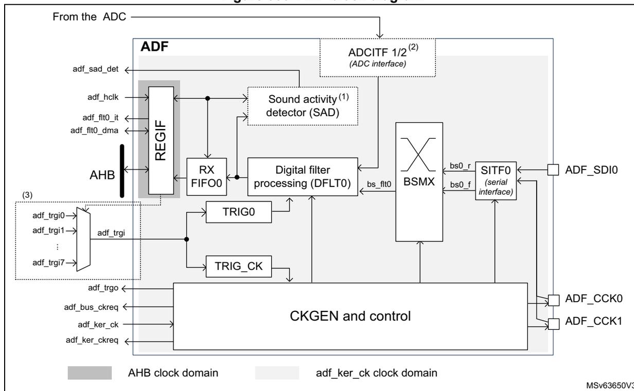
- 1. Refer to Section 36.3: ADF implementation to check if the SAD is available.
- 2. Refer to Section 36.3: ADF implementation to check if the ADCITF is available, and which ADCs are connected.
- 3. The number of trigger inputs depends on the product. Refer to Table 297 for details.
36.4.2 ADF pins and internal signals
Table 295. ADF external pins
| Pin name | Pin type | Remarks |
|---|---|---|
| ADF_SDIO | Input | Data signal from external sensors |
| ADF_CCKy (y = 0,1) | Input/output | Clock outputs for external sensor, or common clock input from external sensors |
Table 296. ADF internal signals
| Signal name | Signal type | Remarks |
|---|---|---|
| adf_trgi | Input | Trigger inputs to control the acquisition (see Table 297: ADF trigger connections for details) |
| adf_trgo | Output | Trigger output for synchronizing with other MDF instances |
| adf_flt0_dma | Input/output | DMA request/acknowledge signals for the ADF processing chain |
| adf_flt0_it | Output | Global interrupt signals |
| adf_bus_ckreq | Output | Bus interface clock request output |
| adf_ker_ckreq | Output | Kernel clock request output |
| adf_ker_ck | Input | Kernel clock input |
| adf_hclk | Input | AHB bus interface clock input |
| adf_sad_det | Output | SAD sound detection: 1 means that detecting sound |
| adf_adcitf1_dat[15:0] | Input | ADCITF1 data input |
| adf_adcitf2_dat[15:0] | Input | ADCITF2 data input |
Table 297. ADF trigger connections
| Trigger name | Direction | Trigger source/destination |
|---|---|---|
| adf_trgi | Input | From exti15 |
| adf_trgo | Output | mdf_trgi13 |
| adf_sad_det | Output | mdf_trgi12 |
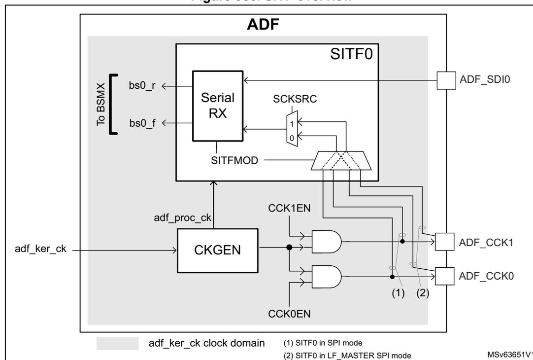
36.4.3 Serial input interface (SITF)
The SITF0 input interface allows the connection of the external sensor to the digital filter via the bitstream matrix (BSMX). The SITF0 can be configured in the following modes:
- • LF_MASTER SPI mode (low-frequency)
- • normal SPI mode
- • Manchester mode
The data from the serial interface is routed to the filter in order to perform the PDM to PCM conversion and the sound activity detection.
The serial interface is enabled by setting the SITFEN bit to 1. Once the interface is enabled, it receives serial data from the external \( \Sigma\Delta \) modulator.
Note: Before enabling the serial interface, the user must insure that the adf_proc_ck is already enabled (see Section 36.4.5: Clock generator (CKGEN) for details).
The SITF0 is controlled via the ADF serial interface control register 0 (ADF_SITF0CR) .
As shown in the Figure 356 , ADF_CCK0 or ADF_CCK1 can be selected as clock source, in order to sample the incoming bitstream:
- • If the serial interface is programmed in SPI mode, the selected clock source is a copy of the clock present on the ADF_CCK0 or ADF_CCK1 pin.
- • If the serial interface is programmed in LF_MASTER SPI mode, the selected clock source is the clock directly provided by the CCKDIV to the ADF_CCK0 or ADF_CCK1 pin.
See Table 298 for additional information.
Figure 356. SITF overview
LF_MASTER and normal SPI modes
The LF_MASTER SPI mode is a special mode allowing the use of an adf_proc_ck clock frequency, only two times bigger than the sensor clock. This mode is dedicated to low-power use-cases, using low-speed sensors.
In LF_MASTER SPI mode, the ADF must provide the bitstream clock to the external sensors via ADF_CCK0 and ADF_CCK1 pins. The ADF receives the bitstream data via the serial data input ADF_SDI0.
For the SITF0, the application must select the same clock than the one provided to the external sensor (ADF_CCK0 or ADF_CCK1), in order to guarantee optimal timing performances. This selection is done via SCKSRC[1:0].
The normal SPI interface is a more flexible interface than the LF_MASTER SPI, but the adf_proc_ck frequency must be at least four times higher than the sensor clock.
The application can select ADF_CCK0 or ADF_CCK1 clock for the capture of the data received via the ADF_SDI0 pin.
The ADF can generate a clock to the sensors via ADF_CCK0 or ADF_CCK1 if needed.
For all SPI modes, the serial data is captured using the rising and the falling edge of the selected clock. The SITF0 always provides the following bitstreams:
- • bitstream received using the bitstream clock falling edge (bs0_f)
- • bitstream received using the bitstream clock rising edge (bs0_r)
According to the sensors connected, one of the two bitstreams may not be available.
The application can select the wanted stream via the BSMX matrix.
Figure 357. SPI timing example
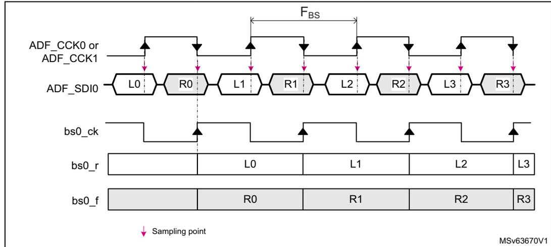
The diagram illustrates the SPI timing for data reception. The top signal is the clock (ADF_CCK0 or ADF_CCK1). Below it, the ADF_SDI0 line shows a sequence of segments: L0, R0, L1, R1, L2, R2, L3, R3. The third signal is bs0_ck, which is a square wave. The fourth signal is bs0_r, showing segments L0, L1, L2, L3. The fifth signal is bs0_f, showing segments R0, R1, R2, R3. Pink arrows indicate sampling points on the bs0_ck signal. A horizontal double-headed arrow labeled F BS indicates the bitstream period. A legend at the bottom left shows a pink arrow pointing down to a sampling point. The code MSv63670V1 is in the bottom right corner.
To properly synchronize/receive the data stream, the adf_proc_ck frequency must be adjusted according to the constraints listed in Table 299 .
Clock absence detection
A no-clock-transition period may be detected when the serial interface works in normal SPI mode. This feature can be used to detect a clock failure in the SPI link.
The application can program a timeout value via the STH[4:0] bitfield of the SITF0. If the ADF does not detect clock transitions for a duration of \( STH[4:0] \times T_{adf\_proc\_ck} \) , then the CKABF flag is set.
An interrupt can be generated if CKABIE is set to 1. The STH[4:0] bitfield is in the ADF serial interface control register 0 (ADF_SITF0CR) .
When the serial interface is enabled, the CKABF flag remains to 1 until a first clock transition is detected.
To avoid spurious clock absence detection, the following sequence must be respected:
- 1. Configure the serial interface in normal SPI mode and enable it.
- 2. Clear the CKABF flag by writing CKABF bit to 1.
If no clock transition is detected on the serial interface, the hardware immediately sets the CKABF flag to 1.
- 3. Read the CKABF flag:
- – If CKABF = 1, go back to step 2.
- – If CKABF = 0, a clock has been detected. The CKABIE bit can be set to 1 if the application wants an interrupt on detection of a clock absence.
Note: The clock absence detection feature is not available in the LF_MASTER SPI mode.
Manchester mode
In Manchester coded format, the ADF receives data stream from the external sensor via the ADF_SDI0 pin only.
The ADF_CCK0 and ADF_CCK1 pins are not needed in this mode.
Decoded data and clock signals are recovered from serial stream after Manchester decoding. They are available on bs0_r . There are two possible settings of Manchester codings:
- • signal rising edge decoded as 0 and signal falling edge decoded as 1
- • signal rising edge decoded as 1 and signal falling edge decoded as 0
Figure 358. Manchester timing example (SITFMOD = 11)
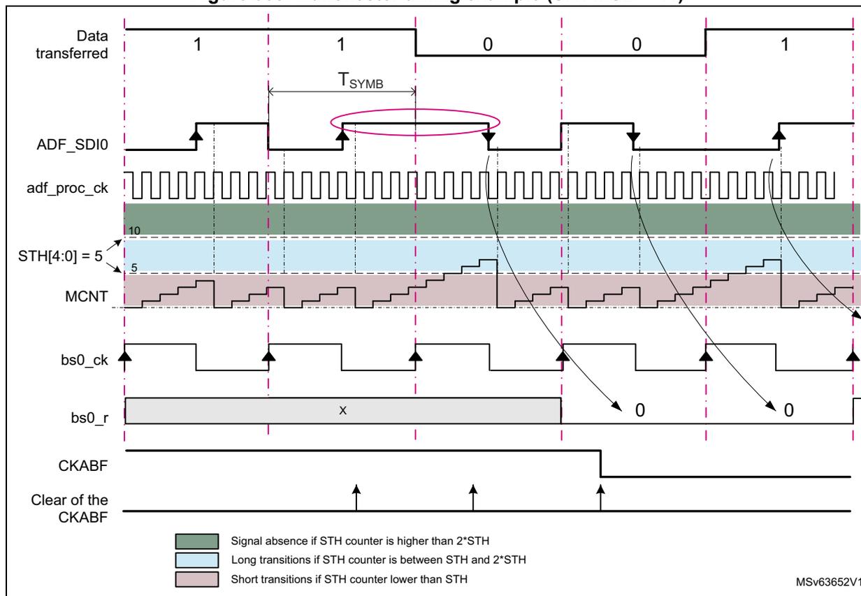
The diagram illustrates the timing for Manchester decoding. The top signal, 'Data transferred', shows bits 1, 1, 0, 0, 1. Below it, the 'ADF_SDI0' signal shows the corresponding Manchester-coded waveform. A pink oval highlights a long transition between the second and third bits. The 'adf_proc_ck' signal is a high-frequency clock. The 'STH[4:0] = 5' signal shows the threshold counter value. The 'MCNT' signal shows the internal counter value, which is restarted on transitions. The 'bs0_ck' signal is the recovered clock. The 'bs0_r' signal shows the decoded data, with 'X' for the first two bits and '0' for the last two. The 'CKABF' flag is shown as a high signal, indicating clock absence. The 'Clear of the CKABF' signal shows the flag being cleared by a transition. A legend at the bottom explains the background colors: green for signal absence (STH counter higher than 2*STH), light blue for long transitions (STH counter between STH and 2*STH), and pink for short transitions (STH counter lower than STH). The diagram is labeled MSv63652V1.
To decode the incoming Manchester stream, the user must program STH[4:0] in the ADF serial interface control register 0 (ADF_SITF0CR) . The STH[4:0] bitfield is used by the SITF0 to estimate the Manchester symbol length and to detect a clock absence. An internal counter (MCNT) is restarted every time a transition is detected in the ADF_SDI0 input. It is used to detect short transitions, long transitions or clock absence. A long transition indicates
that the data value changed. Figure 358 shows a case where the OVR is around height and \( STH[4:0] = 5 \) .
The estimated Manchester symbol rate ( \( T_{SYMB} \) ) must respect the following formula:
It is recommended to compute STH as follows:
where OVR represents the ratio between the \( adf\_proc\_ck \) frequency and the expected Manchester symbol frequency. OVR must be higher than five, and the \( adf\_proc\_ck \) clock must be adjusted according to the constraints listed in Table 299 .
The clock absence flag CKABF is set to 1 when no transition is detected during more than \( 2 \times STH[4:0] \times T_{adf\_proc\_ck} \) , or when the SITF0 is not yet synchronized to the incoming Manchester stream. In addition, an interrupt can be generated if the bit CKABIE is set to 1.
When the serial interface is enabled, the ADF must first be synchronized to the incoming Manchester stream. The synchronization ends when a data transition from 0 to 1 or from 1 to 0 (pink circle in the Figure 358 ) is detected.
The end of the synchronization phase can be checked by following the software sequence:
- 1. Clear the CKABF flag in the ADF DFLT0 interrupt status register 0 (ADF_DFLT0ISR) by writing CKABF bit to 1. If the serial interface is not yet synchronized the hardware immediately set the CKABF flag to 1.
- 2. Read the CKABF flag:
- – If CKABF= 1, go back to step 1.
- – If CKABF = 0, the Manchester interface is synchronized and provides valid data.
Programming example
In the following example, the ADF kernel clock frequency ( \( F_{adf\_ker\_ck} \) ) is 100 MHz and the received Manchester stream is at about 6 MHz ( \( F_{SYMB} \) ):
- 1. Provide a valid \( adf\_proc\_ck \) to the SITF0.
The \( adf\_proc\_ck \) frequency must be at least six times higher than the Manchester symbol frequency (means at least 36 MHz).
PROCDIV is programmed to 1 to perform a division by two of the kernel clock. In that case, \( F_{adf\_proc\_ck} = 50 \) MHz (8.33 times higher than the Manchester symbol frequency).
- 2. Compute STH.
OVR is given by: \( OVR = F_{adf\_proc\_ck} / F_{SYMB} = 50 \) MHz / 6 MHz = 8.33.
The minimum allowed frequency for the Manchester stream is then:
The maximum allowed frequency for the Manchester stream is then:
36.4.4 ADC slave interface (ADCITF)
The ADCs are not always connected to the ADF. Refer to Section 36.3 to check the situation for this product.
The ADF allows the connection of up to two ADCs to the filter path. For the filter, the DATSRC[1:0] bitfield in the ADF digital filter configuration register 0 (ADF_DFLT0CICR) allows the application to select data from the ADCs.
Warning: The ADF does not support receiving interleaved data from one of the ADCITF input.
36.4.5 Clock generator (CKGEN)
The RCC (reset and clock controller) provides the following clocks to the ADF:
- • AHB clock (adf_hclk) used for the register interface
- • kernel clock (adf_ker_ck) mainly used by all other parts of the circuit via the CKGEN
These clocks are not supposed to be phase locked, so all signals crossing those clock domains are resynchronized.
The clock generator (CKGEN) is responsible of the generation of the processing clock, and the clock provided to the ADF_CCK0 and ADF_CCK1 pins. All those clocks are generated from the adf_ker_ck.
The processing clock (adf_proc_ck) is used to run all the signal processing and to re-sample the incoming serial or parallel stream.
To adapt the kernel clock frequency provided by the RCC, the following dividers are available:
- • PROCODIV[6:0] used to adapt the kernel clock frequency to the constraints of the parallel and serial interfaces, and to the processing blocks
- • CCKDIV[3:0] used to adapt the frequency of the ADF_CCK0 and ADF_CCK1 clocks
PROCODIV[6:0] and CCKDIV[3:0] must be programmed when no clock is provided to the dividers (CKGDEN = 0).
The adf_proc_ck generation is controlled by CKGDEN.
In addition, the CKGMOD bit allows the application to define the way to trigger the CCKDIV divider:
- • When CKGMOD = 0, the CCKDIV divider is started as soon as CKGDEN is set to 1.
- • When CKGMOD = 1, the CCKDIV divider is started when CKGDEN is set to 1 and the programmed trigger condition occurred.
All the bits and fields controlling the CKGEN are in the ADF clock generator control register (ADF_CKGCR) .
Figure 359. CKGEN overview
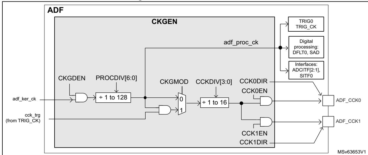
The diagram illustrates the internal architecture of the CKGEN block within the ADF. It shows the following components and signals:
- Inputs:
adf_ker_ck(internal clock) andcck_trg(fromTRIG_CK). - Logic:
CKGDENis ANDed withadf_ker_ck. The result passes through a divider labeled+ 1 to 128(controlled byPROCODIV[6:0]). This signal is then ANDed withcck_trg. - Multiplexer:
The output of the second AND gate goes to a multiplexer controlled by
CKGMOD. The multiplexer has two inputs: '0' (passing the previous signal) and '1' (passingadf_ker_ckdirectly). - Second Divider:
The output of the multiplexer passes through another divider labeled
+ 1 to 16(controlled byCCKDIV[3:0]). - Outputs:
- The output of the second divider is connected to
ADF_CCK0through an AND gate controlled byCCK0ENandCCK0DIR. - It is also connected to
ADF_CCK1through an AND gate controlled byCCK1ENandCCK1DIR.
- The output of the second divider is connected to
- Other Connections:
The signal
adf_proc_ckis derived from the output of the first divider and is connected toTRIG0,TRIG_CK,Digital processing: DFLT0, SAD, andInterfaces: ADCITF[2:1], SITF0.
The trigger logic for CKGEN is handled by the block TRG_CK. As shown in Figure 364, the CCKDIV divider can be triggered on the rising or falling edge of an external trigger source. When the proper trigger condition occurs, the
cck_trg
signal goes to high, allowing the CCKDIV divider to start. The TRG_CK logic is reset when
CKGDEN
is set to 0.
This feature can be helpful to synchronize the
ADF_CCKy
(
\(
y = 0, 1
\)
) clock of several ADF instances, or to synchronize the clock generation to a timer event.
The application can control the activation of the
ADF_CCK0
or
ADF_CCK1
pin thanks to
CCK0EN/CCK1EN
and
CCK0DIR/CCK1DIR
bits:
- •
CCKyENis used to enable the CCKDIV, and thus generates a clock for the external sensors. - •
CCKyDIRis used to control the direction of theADF_CCKypin (input or output)
Table 298. Control of the common clock generation (1)
| CCKyEN | CCKyDIR | Description |
|---|---|---|
| 0 | 0 | The
ADF_CCKy
pin is in input. An external clock can be connected to the
ADF_CCKy
pin and used by the
SITF0
in order to decode the serial stream |
| 0 | 1 | The
ADF_CCKy
pin is in output. No clock is generated. The
ADF_CCKy
pin is driven low. |
| 1 | 1 | The
ADF_CCKy
pin is in output. A clock is generated on the
ADF_CCKy
pin. The
SITF0
can use this pin as clock source in order to decode the serial stream |
1. The configuration with
CCKyEN = 1
and
CCKyDIR = 0
is not shown must be avoided (no interest).
Note:
The
adf_proc_ck
must be enabled (by
CKGDEN = 1
) before enabling other blocks (such as
SITF0
or
DFLT0
).
CKGEN activation sequence example
- 1. Set CKGDEN to 0.
- 2. Wait for CKGACTIVE = 0. If CKGDEN was previously enabled, this phase can take two periods of adf_hclk, and two periods of adf_proc_ck.
- 3. Program PROCDIV[6:0], CKGMOD, CCKDIV[3:0], TRGSRC[3:0], TRGSENS, CCK1EN and CCK0EN.
- 4. Set CKGDEN to 1.
When needed, at any moment, CCK[1:0]EN bitfield value can be changed without disabling the clock generator.
Clock frequency constraints
Table 299 shows the frequency constraints to receive and process properly the samples.
Note: The reshape filter (RSFLT) needs up to 24 cycles of adf_proc_ck clock to process one sample.
Table 299. Clock constraints with respect to the incoming stream (1)
| SITF0 mode | ADF clock constraints | |
|---|---|---|
| With RSFLT disabled | With RSFLT enabled | |
| LF_MASTER SPI | \( F_{ADF\_CCKy} \) max frequency limited to 5 MHz | |
| \(
F_{adf\_proc\_ck} > 2 \times F_{ADF\_CCKy}
\) and \( F_{adf\_hclk} \geq F_{adf\_proc\_ck} \) | \(
F_{adf\_proc\_ck} > 24 \times F_{ADF\_CCKy} / (MCICD+1)
\) and \( F_{adf\_proc\_ck} > 2 \times F_{ADF\_CCKy} \) and \( F_{adf\_hclk} \geq F_{adf\_proc\_ck} \) | |
| MASTER SPI SLAVE SPI | \( F_{ADF\_CKx} \) max frequency limited to 25 MHz | |
| \(
F_{adf\_proc\_ck} > 4 \times F_{ADF\_CCKy}
\) and \( F_{adf\_hclk} \geq F_{adf\_proc\_ck} \) | \(
F_{adf\_proc\_ck} > 24 \times F_{ADF\_CCKy} / (MCICD+1)
\) and \( F_{adf\_proc\_ck} > 4 \times F_{ADF\_CCKy} \) and \( F_{adf\_hclk} \geq F_{adf\_proc\_ck} \) | |
| Manchester | \( F_{SYMB} \) max frequency limited to 20 MHz | |
| \(
F_{adf\_proc\_ck} > 6 \times F_{SYMB}
\) and \( F_{adf\_hclk} \geq F_{adf\_proc\_ck} \) | \(
F_{adf\_proc\_ck} > 24 \times F_{ADF\_CCKy} / (MCICD+1)
\) and \( F_{adf\_proc\_ck} > 6 \times F_{SYMB} \) and \( F_{adf\_hclk} \geq F_{adf\_proc\_ck} \) | |
1. \( F_{ADF\_CCKy} \) represents the frequency of clock received via ADF_CCKy, or generated via ADF_CCKy. \( F_{SYMB} \) represents the frequency of the received symbol rate for Manchester mode.
36.4.6 Bitstream matrix (BSMX)
The BSMX receives the bitstreams from the serial interface SITF0 and provides the selected stream to the digital filter DFLT0.
As shown in Figure 355, the SITF0 provides two bitstreams (bs0_r and bs0_f) to the BSMX.
The application to select the wanted stream via the ADF bitstream matrix control register 0 (ADF_BSMX0CR) . This selection is intended to be static.
Figure 360. BSMX overview
![Figure 360. BSMX overview diagram showing the internal structure of the Audio Digital Filter (ADF). The diagram includes blocks for ADF, ADCITF[2,1], DFLT0, BSMX (with a switch symbol), and SITF0. Signals shown include bs_fit0, BSSEL, bs0_r, and bs0_f. A reference code MSV63654V1 is present in the bottom right corner of the diagram area.](/RM0486-STM32N6x5-x7/c7a15b84644477135d224e8572d4fe29_img.jpg)
BSMX programming sequence example
The BSSEL[4:0] bitfield cannot be changed if the DFLT0 is enabled. The following steps are needed to change the value of BSMX:
- 1. Set DFLTEN of DFLT0 to 0.
- 2. Wait for BSMXACTIVE = 0.
- 3. Program BSSEL[4:0].
- 4. Set DFLTEN of DFLT0 to 1.
36.4.7 Digital filter processing (DFLT)
The digital filter processing includes the following sub-blocks:
- • symbol remap (SBR)
- • clock skipper delay (DLY)
- • MCIC decimation filter that can be configured in Sinc 4 or Sinc 5
- • gain control (SCALE)
- • signal saturation (SAT)
- • reshape filter (RSFLT)
- • high-pass filter (HPF)
- • receive RXFIFO
Figure 361 shows the filter path configuration according to CICMOD[2:0]. Several configuration bits are available to configure the digital filter to the application needs.
Figure 361. DFLT overview
![Figure 361. DFLT overview. This block diagram illustrates the internal architecture of the Digital Filter (DFLT) within the Audio Digital Filter (ADF). The diagram is divided into three main frequency domains: F_PCM (PCM frequency domain), F_RS (Resampling frequency domain), and F_BS (Bitstream frequency domain). The F_PCM domain includes an RX FIFO, PCM[23:0] input, HPFC (High Pass Filter Control), HPFBYP (High Pass Filter Bypass), SAT (Saturation), HPF (High Pass Filter), and Discard logic. The F_RS domain includes RSFLTD (Resampling Filter Delay), RSFLTBY (Resampling Filter Bypass), SAT, SCALE (Scaling), and CICMOD (CIC Mode). The F_BS domain includes DFLTO (Digital Filter), D1 (Delay), MCIC4 (Micro-CIC 4), D1, MCIC5 (Micro-CIC 5), DLY (Delay), DATSRC (Data Source), 11, 10, 0x, SBR (Symbol Remap), 1 - 1, -1 - 0, and From BSMX. The diagram also shows the flow of data from the RX FIFO through the HPF, then through the RSFLT, then through the SCALE, then through the DFLTO, and finally through the DLY to the DATSRC. The clock domain is labeled adf_proc_ck clock domain. The diagram is labeled MSv63655V1.](/RM0486-STM32N6x5-x7/9f39eaaad750a3db222898c4991d52ae_img.jpg)
Symbol remap and source selection
The symbol remap (SBR) converts the bitstream selected by the BSMX into data usable by the filter path. More especially:
- • The high levels are converted into a 16-bit signed number + 1.
- • The low levels are converted into a 16-bit signed number - 1.
The signal source of the digital filter can be selected via DATSRC[1:0] between the two following:
- • data coming from the BSMX
- • data coming from one of the ADC interfaces (ADCITF2 or 1)
Programmable micro-delay control (DLY)
The digital filter has a delay line that allows the timing adjustment of each stream with the resolution of the bitstream clock.
This feature is particularly helpful in the case of microphone beam forming applications where delays smaller than the final sampling rate must be applied to the incoming stream. This feature can be used when the ADF is synchronized with another MDF instance (if present in the product) for a beam forming application for example.
The delay is performed by discarding a given number of samples from the selected input stream, before samples enter into the CIC filter. This data discarding is done by skipping a given number of data strobe, preventing the CIC filter to take into account those data.
When the wanted amount of data strobe has been skipped, the next incoming samples are strobed normally.
Table 362 shows an example on how to apply dynamically small delay to an incoming stream. For simplification, the CIC filter performs a decimation by height in this example. CIC1 represents the CIC included in the ADF and CIC0 represents a filter from another MDF instance (if present in the product).
Figure 362. Programmable delay
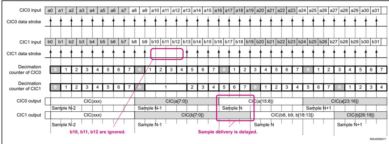
The diagram illustrates the timing of an audio digital filter (ADF) with a programmable delay. It shows the following signals and counters over time:
- CIC0 input: A sequence of samples a0 through a31.
- CIC0 data strobe: A series of pulses indicating valid input samples for CIC0.
- CIC1 input: A sequence of samples b0 through b31.
- CIC1 data strobe: A series of pulses indicating valid input samples for CIC1. A pink box highlights that the strobes for b10, b11, and b12 are missing, indicating they are ignored.
- Decimation counter of CIC0: A counter that cycles from 0 to 7. It is shown that the counter continues to increment even when CIC1 data strobes are skipped.
- Decimation counter of CIC1: A counter that cycles from 0 to 7. It is shown that the counter is frozen (stays at 0) when data strobes are skipped.
- CIC0 output: Output samples are generated every 8 input samples. The output for Sample N is CIC(a[15:8]).
- CIC1 output: Output samples are generated every 8 input samples. Due to the skipped strobes, the output for Sample N is delayed and becomes CIC(b[26:19]).
Annotations in the diagram:
- b10, b11, b12 are ignored. (indicated by a pink line from the CIC1 input section)
- Sample delivery is delayed. (indicated by a pink box around the CIC1 output section)
The CIC of the ADF (CIC1) receives a command in order to skip three incoming samples. So the input samples named b10, b11 and b12 are not processed by CIC1. As a consequence, the output sample N+1 generated by CIC0 is built from input samples a[23:16] while the sample N+1 of CIC1 is built from input samples b[26:19].
Finally, the non-skipped data stream looks delayed by three bitstream periods.
Note: When the input data strobes are skipped, the decimation counter remains frozen. As a consequence, the samples delivered by the CIC1 are a bit delayed.
The following steps are needed to program the amount of bitstream clock periods to be skipped:
- 1. Wait for SKPBF equal to 0.
- 2. Write SKPDLY[6:0] to the wanted number of bitstream clock periods to be skipped. The SKPBF flag goes immediately to 1, indicating that the delay value entered into SKPDLY[6:0] is under process.
- – If the DFLT0 is not yet enabled (DFLTEN = 0), then the DLY logic waits for DFLTEN = 1. When the application sets DFLTEN to 1, the DLY logic starts to skip the amount of wanted data strobes.
- – If the DFLT0 is already enabled (DFLTEN = 1), then the DLY logic immediately starts to skip the amount of wanted data strobes.
When the ADF skipped the amount of wanted data strobes, then SKPBF goes back to 0.
- 3. If the application needs to skip more data strobes, then the operation must be restarted from step 1.
The effect of the delay performed with this mechanism is cumulative as long as the ADF is enabled. If the application performs a D1 delay followed by a D2 delay, then all other active filters are delayed by D1 + D2.
Note: If SKPDLY[6:0] is written when SKPBF = 1, the write operation is ignored.
Cascaded-integrator-comb (CIC) filter
The CIC digital filters are an efficient implementation of low-pass filters, often used for decimation and interpolation. The CIC frequency response is equal to a Sinc N function, this is why they are often called Sinc filters.
The Sinc N digital filter embedded into the ADF can be configurable in Sinc 4 or Sinc 5 , according to CICMOD:
- • If CICMOD[2:0] = 4, Sinc 4 is selected.
- • If CICMOD[2:0] = 5, Sinc 5 is selected.
The filters have the following transfer function:
where N can be 4 or 5, and D is the decimation ratio. D is equal to MCICD+1.
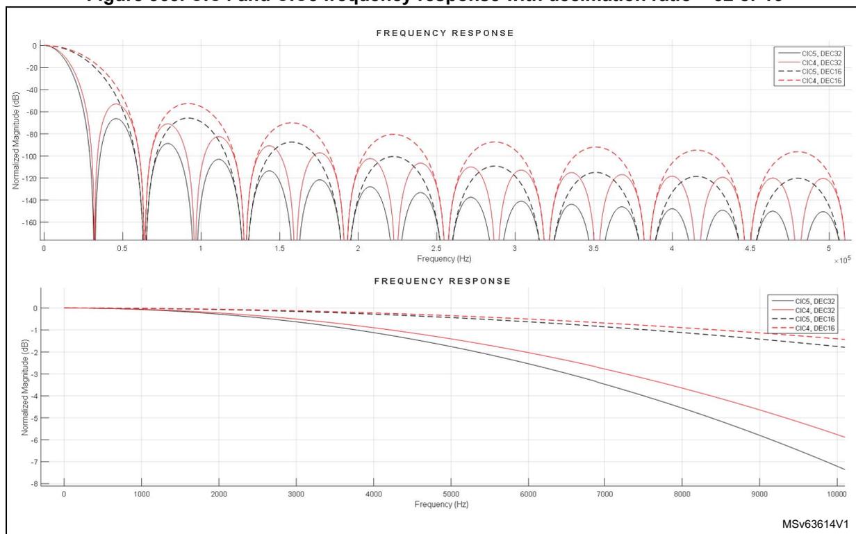
Figure 363. CIC4 and CIC5 frequency response with decimation ratio = 32 or 16
CIC output data size
The size of samples delivered by the CIC (DS CIC ), depends on the following parameters:
- • CIC order (N)
- • CIC decimation ratio (D)
- • data size of the input stream (DSIN)
The CIC order and decimation ratio must be programmed in order to insure that the data size does not exceed the 26-bit CIC capability.
The following formula gives the output data size (DS CIC ) according to the parameters above.
and the CIC gain is given by this formula:
The decimation ratio can be adjusted from 2 to 512 for the CIC filter.
Table 300 gives some data output size in bits for some decimation values, when the data source is a full-scale signal coming from the serial interface or from a 12-bit ADC.
Note: \( DS_{IN} = 1 \) bit for a serial bitstream, but can be up to 16 bits when coming from the ADCITF.
Table 300. Data size according to CIC order and CIC decimation values
| Decimation | Data size (bits) when
\(
DS_{IN} = 1
\)
bit (data from SITF0) | Data size (bits) when
\(
DS_{IN} = 12
\)
bits (data from ADCITF) | ||
|---|---|---|---|---|
| Sinc 4 | Sinc 5 | Sinc 4 | Sinc 5 | |
| 4 | 9 | 11 | 20 | 22 |
| 8 | 13 | 16 | 24 | - |
| 10 | 15 | 18 | 26 | - |
| 12 | 16 | 19 | - | - |
| 16 | 17 | 21 | - | - |
| 20 | 19 | 23 | - | - |
| 24 | 20 | 24 | - | - |
| 32 | 21 | 26 | - | - |
| 48 | 24 | - | - | - |
| 64 | 25 | - | - | - |
| 76 | 26 | - | - | - |
Note: For a full-scale input signal, the decimation ratio must not exceed 76 for a Sinc 4 and 32 for a Sinc 5 .
The LSB parts of the data provided by the CIC is not necessarily significant: it depends on the sensor performances and the ability of the CIC to reject the out-of band noise.
The sample size at CIC output can be adjusted thanks to the SCALE block.
Scaling (SCALE) and saturation (SAT)
The SCALE block allows the application to adjust the amplitude of the signal provided by the CIC, by steps of 3 dB ( \( \pm 0.5 \) dB).
The signal amplitude can be decreased by up to 8 bits (- 48.2 dB), and can be increased by up to 12 bits (+ 72.2 dB).
The gain is adjusted by the SCALE[5:0] bitfield in the ADF digital filter configuration register 0 (ADF_DFLT0CR) .
SCALE[5:0] can be changed even if the DFLT0 is enabled. During the gain transition, the signal provided by the filter is disturbed.
Due to internal resynchronization, there is a delay of some cycles of adf_proc_ck clock between the moment where the application writes the new gain, and the moment where the gain is effectively applied to the samples. If the application attempts to write a new gain value while the previous one is not yet applied, this new gain value is ignored. Reading back SCALE[5:0] informs the application on the current gain value.
Table 301 shows the possible gain values.
Table 301. Possible gain values
| SCALE[5:0] | Gain (dB) | SCALE[5:0] | Gain (dB) | SCALE[5:0] | Gain (dB) | SCALE[5:0] | Gain (dB) |
|---|---|---|---|---|---|---|---|
| 0x20 | - 48.2 | 0x2B | - 14.5 | 0x06 | + 18.1 | 0x11 | + 51.7 |
| 0x21 | - 44.6 | 0x2C | - 12.0 | 0x07 | + 21.6 | 0x12 | + 54.2 |
| 0x22 | - 42.1 | 0x2D | - 8.5 | 0x08 | + 24.1 | 0x13 | + 57.7 |
| 0x23 | - 38.6 | 0x2E | - 6.0 | 0x09 | + 27.6 | 0x14 | + 60.2 |
| 0x24 | - 36.1 | 0x2F | - 2.5 | 0x0A | + 30.1 | 0x15 | + 63.7 |
| 0x25 | - 32.6 | 0x00 | 0.0 | 0x0B | + 33.6 | 0x16 | + 66.2 |
| 0x26 | - 30.1 | 0x01 | + 3.5 | 0x0C | + 36.1 | 0x17 | + 69.7 |
| 0x27 | - 26.6 | 0x02 | + 6.0 | 0x0D | + 39.6 | 0x18 | + 72.2 |
| 0x28 | - 24.1 | 0x03 | + 9.5 | 0x0E | + 42.1 | - | - |
| 0x29 | - 20.6 | 0x04 | + 12.0 | 0x0F | + 45.7 | - | - |
| 0x2A | - 18.1 | 0x05 | + 15.6 | 0x10 | + 48.2 | - | - |
The SAT blocks avoid having a wrap-around of the binary code when the code exceeds its maximal or minimal value.
The ADF performs saturation operations at the following levels:
- • after the SCALE block (performed by the SAT block): The signal is saturated at 24 bits.
- • inside the RSFLT, to insure a good filter behavior
- • at the output of the HPF, to insure that the output signal does not exceed 24 bits
The SATF bit informs the application that a saturation occurred either after the SCALE, inside the RSFLT or after the HPF. In addition, an interrupt can be generated if SATIE is set to 1. As soon as a saturation is detected, the SATF flag is set to 1. It is up to the application to clear this flag in order to be able to detect a new saturation.
Those bits are in the ADF DFLT0 interrupt enable register (ADF_DFLT0IER) and ADF DFLT0 interrupt status register 0 (ADF_DFLT0ISR) .
Gain adjustment policy
To get the best ADF performances, it is important to properly adjust the gain value via SCALE[5:0].
A usual way to adjust the gain is to select the SCALE[5:0] value that gives a final signal amplitude as close as possible to the 24-bit full-scale, for the maximum input signal.
A way to select the optimal gain is detailed below:
- 1. Check that, for the expected input signal, the data size into the CIC filter does not exceed 26 bits. This can be checked using this formula:
where N represents the CIC order, D the decimation ratio and \( \text{SIN}_{\text{pp}} \) the maximum peak-to-peak amplitude of the input signal.
\( \text{SIN}_{\text{pp}} \) can take:
- – a maximum peak-to-peak amplitude of 2 ( \( \pm 1 \) ), for samples coming from SITF0
- – A maximum peak-to-peak amplitude of 4095 (+ 2047, - 2048), for samples coming from a 12-bit ADC
Example: a \( \text{Sinc}^4 \) can be used with a decimation ratio of 96, if the maximum input signal does not exceed \( \pm 0.35 \) . Indeed:
- 2. Adjust the SCALE value.
To select the most appropriate SCALE value, the user must check if the RSFLT is used or not. If the RSFLT is used, the data size at SCALE output must not exceed 22 bits, otherwise the data size can be up to 24 bits.
The SCALE value in dB must be selected using this formula:
where NB is equal to 22 if RSFLT is enabled, or 24 if RSFLT is bypassed. \( \text{SCALE}_{\text{dB}} \) represents the gain value selected by SCALE[5:0].
Example: For a Sinc 4 with a decimation ratio of 96 and a \( \text{SIN}_{\text{pp}} \) of 0.7.
- – If the RSFLT is bypassed:
\( \text{SCALE}_{\text{dB}} \) value must be lower than - 11 dB, the closest lower value is - 12dB (SCALE[5:0] = 0x2C).
- – If the RSFLT is enabled:
\( \text{SCALE}_{\text{dB}} \) value must be lower than - 23 dB, the closest lower value is - 24.1 dB (SCALE[5:0] = 0x28).
If SCALE[5:0] is set to a higher value, then a saturation may occur. An event flag informs the user if a saturation occurred.
Table 302 proposes gain values for different filter configurations, when the data comes from the SITF0, according to the MCIC order, and the MCIC decimation ratio. This table is not exhaustive and considers a full-scale input signal (see Section 36.7.5: Total ADF gain for details).
Table 302. Recommended maximum gain values versus CIC decimation ratios
| CIC decimation ratio | Gain settings (dB) for configuration SITF + CICx + RSFLT (+ HPF) | Gain settings (dB) for configuration SITF + CICx (+ HPF) | ||
|---|---|---|---|---|
| CIC5 | CIC4 | CIC5 | CIC4 | |
| 8 | 33.6 | 51.7 | 45.7 | 63.7 |
| 12 | 18.1 | 39.6 | 30.1 | 51.7 |
| 16 | 3.5 | 27.6 | 15.6 | 39.6 |
| 20 | - 6.0 | 21.6 | 6.0 | 33.6 |
| 24 | - 12.0 | 15.6 | 0 | 27.6 |
| 28 | - 20.6 | 9.5 | - 8.5 | 21.6 |
Table 302. Recommended maximum gain values versus CIC decimation ratios (continued)
| CIC decimation ratio | Gain settings (dB) for configuration SITF + CICx + RSFLT (+ HPF) | Gain settings (dB) for configuration SITF + CICx (+ HPF) | ||
|---|---|---|---|---|
| CIC5 | CIC4 | CIC5 | CIC4 | |
| 32 | - 26.6 | 3.5 | - 4.5 | 15.6 |
| 48 | - | - 8.5 | - | 3.5 |
| 64 | - | - 20.6 | - | - 8.5 |
Reshaping filter (RSFLT)
In addition to the CIC, the ADF offers a reshaping IIR filter mainly dedicated to the audio application, but also usable in other applications.
When the RSFLT is used, the sample size at its input must not exceed 22 bits.
The samples at the RSFLT output can be decimated by four or not according to the RSFLTD bit in the ADF reshape filter configuration register 0 (ADF_DFLT0RSFR) .
The RSFLT can be bypassed by setting RSFBYP to 1 in the ADF reshape filter configuration register 0 (ADF_DFLT0RSFR) .
Table 303 shows which sampling rate must be provided to the RSFLT in order to process the most common audio streams.
The RSFLT cutoff frequency ( \( F_C \) ) depends on the sample rates at its input ( \( F_{RS} \) ), and is given by the following formula:
Table 303. Most common microphone settings
| Sample rate (kHz) at RSFLT ( \( F_{RS} \) ) | Pass band (kHz) | D2 | PCM sampling rate (kHz) |
|---|---|---|---|
| 32 | 3.55 | 4 | 8 |
| 64 | 7.1 | 4 | 16 |
| 128 | 14.2 | 4 | 32 |
| 192 | 21.3 | 4 | 48 |
Table 364 shows the frequency response of the reshape filter.
Figure 364. Reshape filter frequency response normalized ( \( F_{RS} / 2 = 1 \) )
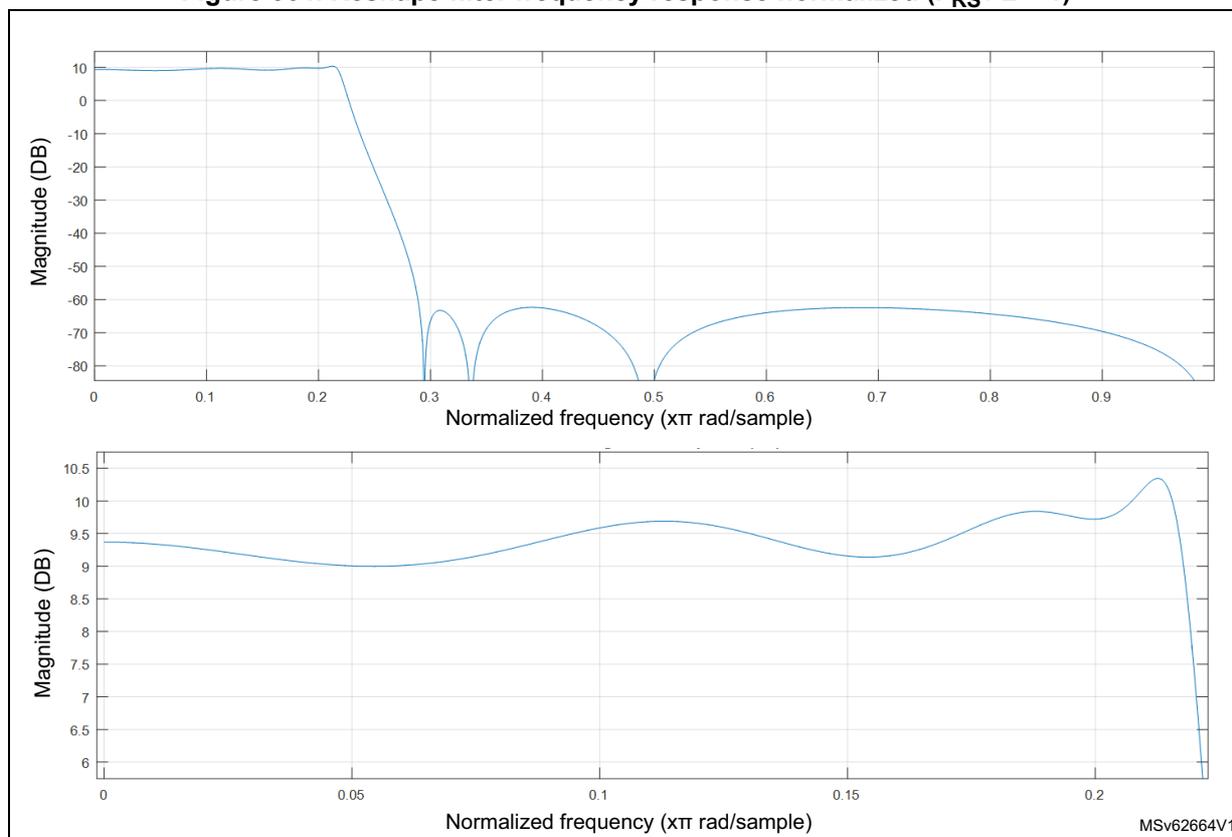
The RSFLT gain is close to 9.3 dB, so the output data size is a little bit lower than 24 bits for a 22-bit wide input signal.
The RSFLT takes 24 clock cycles of
adf_proc_ck
clock to process one sample at
\(
F_{RS}
\)
. When the RSFLT is enabled, the application must insure that the
adf_proc_ck
is at least 24 times faster
\(
F_{RS}
\)
.
The RSFLT generates an event (
rfov_evt
) and sets the RFOVRF flag, if the RSFLT receives a new samples while the previous one is still under processing.
When RFOVRF is set, the samples provided by the RSFLT are invalid. The application must then stop the data acquisition and provides a faster
adf_proc_ck
clock to the RSFLT.
High-pass filter (HPF)
The high-pass filter suppresses the low-frequency content from the final output data stream in case of continuous conversion mode. The high-pass filter can be enabled or disabled via HPFBYP in the ADF reshape filter configuration register 0 (ADF_DFLT0RSFR) .
The HPF is useful when there is parasitic low-frequency noise (or DC signal) in the input data source that must be removed from the final data.
The HPF is a first order IIR filter and the cut-off frequency can be selected via HPFC[1:0] in the ADF reshape filter configuration register 0 (ADF_DFLT0RSFR) , among the following values:
- • \( 0.000625 \times F_{PCM} \)
- • \( 0.00125 \times F_{PCM} \)
- • \( 0.00250 \times F_{PCM} \)
- • \( 0.00950 \times F_{PCM} \)
Table 304. HPF 3 dB cut-off frequency examples
| HPFC | 3 dB cut-off frequency for common \( F_{PCM} \) frequencies (Hz) | ||
|---|---|---|---|
| \( F_{PCM} = 8 \text{ kHz} \) | \( F_{PCM} = 16 \text{ kHz} \) | \( F_{PCM} = 48 \text{ kHz} \) | |
| 0 | 5 | 10 | 30 |
| 1 | 10 | 20 | 60 |
| 2 | 20 | 40 | 120 |
| 3 | 76 | 152 | 456 |
The HPF output is saturated at 24 bits. The SATF flag is set if a sample is saturated.
36.4.8 Digital filter acquisition modes
The ADF offers the following modes to perform a data capture:
- • asynchronous continuous acquisition mode
- • asynchronous single-shot acquisition mode
- • synchronous continuous acquisition mode
- • synchronous single-shot acquisition mode
- • window continuous acquisition mode
Note: To perform a data capture, the filter, the interface providing the data (SITF0 or ADCITF) and the CKGEN must be enabled. If needed, the ADF_CCK0 or ADF_CCK1 must be enabled as well.
The filter can be stopped immediately when DFLTEN is set to 0. This action resets the filter and flushes the RXFIFO. The DFLTACTIVE flag also goes back to 0 when the RXFIFO and the filter is reset.
Table 365 shows a simplified view of the trigger logic available for each filter and for the clock generator.
Figure 365. Trigger logic for DFLT and CKGEN
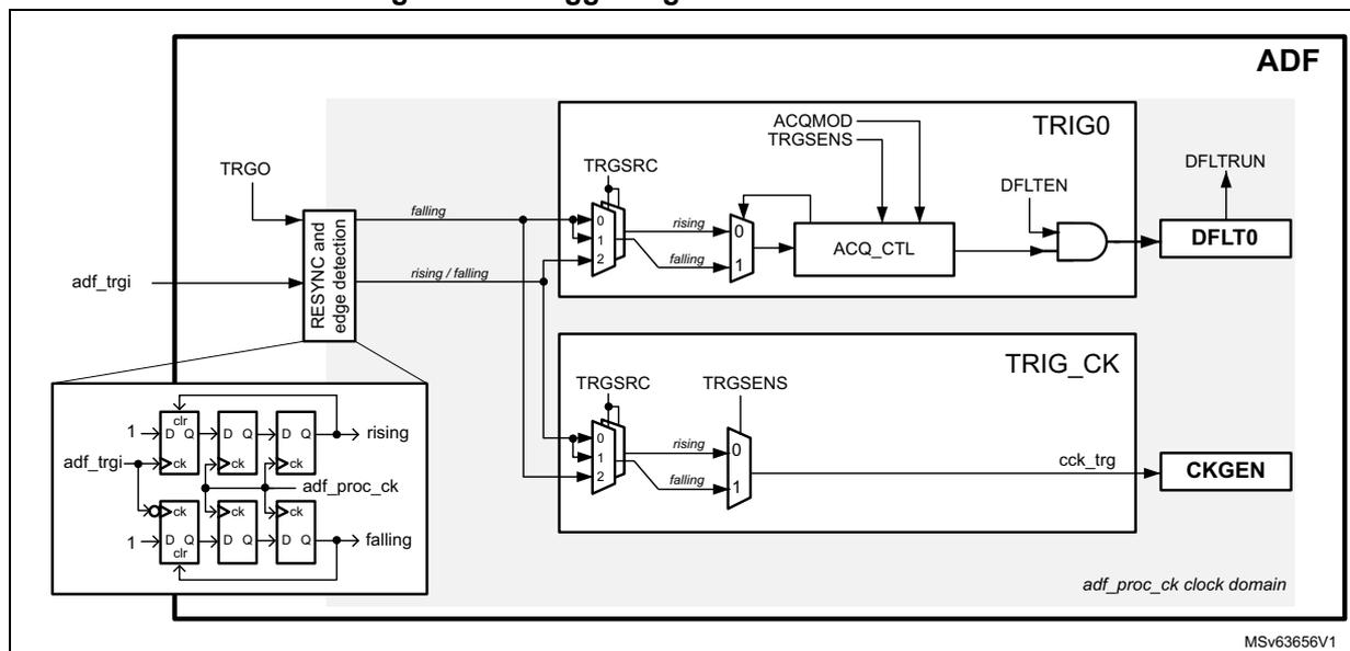
A block common to all TRIG blocks performs the rising and falling edges detection and the resynchronization of the input trigger to the adf_ker_ck clock domain. This implementation allows the application to use triggers with pulse width smaller than the adf_ker_ck period.
In synchronous modes, the TRIG block offers the possibility to select adf_trgi or TRGO bit as trigger sources. The TRGO bit is in the ADF global control register (ADF_GCR) .
The edge sensitivity can also be selected.
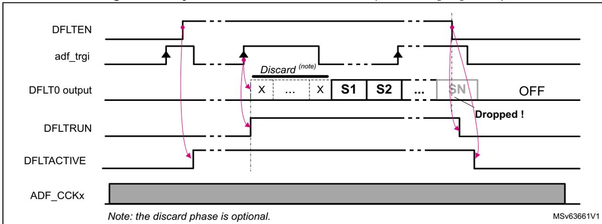
Asynchronous continuous acquisition mode
This mode allows the application to start a continuous acquisition by simply writing the DFLTEN bit to 1.
The asynchronous continuous acquisition mode is selected when ACQMOD[2:0] = 0.
The sequence below shows the most important programming steps (assuming that DFLTEN is set to 0):
- 1. Configure and enable the clock generator (CKGEN) so that the adf_proc_ck frequency is compatible with the targeted application (see examples in Table 308 ).
- 2. Enable the CKGEN (CKGDEN = 1) and, if needed, enable the ADF_CCK0 and ADF_CCK1 clocks.
- 3. Program the filter configuration and set the ACQMOD[2:0] to 0.
- 4. Set to 1 the SITFEN bit of the serial data interface.
- 5. Before setting DFLTEN to 1, wait for DFLTACTIVE = 0: it insures that the previous filter deactivation sequence terminated properly.
- 6. When DFLTEN is set to 1, the acquisition sequence starts immediately.
Figure 366 shows a simplified example of the samples generated by the DFLT0.
Figure 366. Asynchronous continuous mode (ACQMOD[2:0] = 0)
![Timing diagram for Asynchronous continuous mode (ACQMOD[2:0] = 0). The diagram shows five signals over time: DFLTEN, DFLT0 output, DFLTRUN, ADFLTACTIVE, and ADF_CCKy. DFLTEN is a control signal that goes high to start acquisition and low to stop it. DFLT0 output shows samples: X, ..., X, S1, S2, ..., SN, followed by OFF. A 'Discard (note)' phase is indicated for the initial X samples. DFLTRUN goes high when DFLTEN goes high and low when DFLTEN goes low. ADFLTACTIVE goes high when DFLTEN goes high and low when DFLTEN goes low. ADF_CCKy is a constant clock signal. A 'Dropped !' label with an arrow points to the SN sample when DFLTEN goes low before it is read.](/RM0486-STM32N6x5-x7/e6b532e60f69398719955cd76ab31aa7_img.jpg)
Note: the discard phase is optional. MSV63657V1
Note: The acquisition can be stopped by setting DFLTEN back to 0. This resets the filter and flushes the RXFIFO, so the samples located into the RXFIFO are lost. The ongoing DMA transfer is properly terminated. DFLTACTIVE goes back to 0 when the filter chain is reset and the RXFIFO flushed.
Asynchronous single-shot acquisition mode
This mode allows the application to start the acquisition of one sample by simply writing the DFLTEN bit to 1.
The asynchronous single-shot acquisition mode is selected when ACQMOD[2:0] = 001.
The sequence below shows the most important programming steps (assuming that DFLTEN is set to 0):
- 1. Configure and enable the clock generator (CKGEN), so that the adf_proc_ck frequency is compatible with the targeted application (see examples in Table 308 ).
- 2. Enable the CKGEN (CKGDEN = 1) and, if needed, enable the ADF_CCK0 and ADF_CCK1 clocks.
- 3. Program the filter configuration, and set the ACQMOD[2:0] to 001.
- 4. Set to 1 the SITFEN bit.
- 5. Before setting DFLTEN to 1, wait for DFLTACTIVE = 0: it insures that the previous filter deactivation sequence terminated properly.
- 6. When DFLTEN is set to 1, the filter provides one data to the RXFIFO and stops the acquisition.
To trigger a new acquisition, the application must:
- 1. Check that the previous acquisition is completed, by waiting that DFLTRUN = 0.
- 2. Set again DFLTEN to 1.
This sequence can be repeated every time a new data must be converted.
As shown in Figure 366 , every time DFLTEN is set to 1, an acquisition sequence is triggered. The first samples provided by the filter can be discarded if needed. At the end of each conversion, the decimation counters and filter taps are reset, and the filter is ready to start a new conversion.
If DFLTEN is set to 0 while an acquisition is ongoing, the ongoing conversion is stopped (in the example, S3 is lost). This situation can be avoided with the following steps:
- 1. Wait for DFLTRUN = 0.
- 2. Read the sample from the RXFIFO.
- 3. Set DFLTEN to 0.
Figure 367. Asynchronous single-shot mode (ACQMOD[2:0] = 001)
![Timing diagram for asynchronous single-shot mode (ACQMOD[2:0] = 001). The diagram shows five signals over time: DFLTEN, Writing to DFLTEN, DFLT0 output, DFLTRUN, and ADF_CCK. DFLTEN is shown as a series of pulses. Writing to DFLTEN is shown as a series of pulses. DFLT0 output shows a sequence of samples: X, ..., X, S1, X, ..., X, S2, X, ..., X, S3. The samples S1 and S2 are valid, but S3 is dropped because DFLTEN is set to 0 before it is read. DFLTRUN is shown as a series of pulses. ADF_CCK is shown as a continuous clock signal. A note indicates that the discard phase is optional.](/RM0486-STM32N6x5-x7/f09666e9ad488f4095ef866818882145_img.jpg)
The diagram illustrates the timing for asynchronous single-shot mode. The DFLTEN signal is initially high, then goes low, and then high again. The Writing to DFLTEN signal is shown as a series of pulses. The DFLT0 output shows a sequence of samples: X, ..., X, S1, X, ..., X, S2, X, ..., X, S3. The samples S1 and S2 are valid, but S3 is dropped because DFLTEN is set to 0 before it is read. The DFLTRUN signal is shown as a series of pulses. The ADF_CCK signal is shown as a continuous clock signal. A note indicates that the discard phase is optional.
Note: the discard phase is optional. MSV63660V1
Note: The acquisition can be stopped by setting DFLTEN back to 0. This resets the filter and flushes the RXFIFO, so the samples located into the RXFIFO are lost. The ongoing DMA transfer is properly terminated. DFLTACTIVE goes back to 0 when the filter chain is reset and the RXFIFO flushed.
Synchronous continuous acquisition mode
This mode allows the application to start a continuous acquisition by using one of the following trigger sources:
- • adf_trgi signal
- • TRGO bit
The Synchronous continuous acquisition mode is selected when ACQMOD[2:0] = 010.
The sequence below shows the most important programming steps (assuming that DFLTEN is set to 0):
- 1. Configure and enable the clock generator (CKGEN), so that the frequency of adf_proc_ck clock is compatible with the targeted application (see examples in Table 308 ).
- 2. Enable the CKGEN (CKGDEN = 1) and, if needed, enable the ADF_CCK0 and ADF_CCK1 clocks.
- 3. Program the filter configuration and set the ACQMOD[2:0] to 010.
- 4. Set to 1 the bit SITFEN.
- 5. Select the proper trigger source and sensitivity.
- 6. Before setting DFLTEN to 1, wait for DFLTACTIVE = 0: it insures that the previous filter deactivation sequence terminated properly.
- 7. Set DFLTEN to 1.
- 8. When the trigger condition is met, the filter starts the acquisition.
The TRGSENS bit allows the selection of the trigger edge (rising or falling). The trigger is ignored if an acquisition is ongoing or if DFLTEN is set to 0.
Figure 368 shows a simplified example where the trigger logic is sensitive to a rising edge trigger (TRGSENS = 0). The first rising edge of the trigger signal is ignored because DFLTEN = 0. Then the next rising edge is taken into account and starts the acquisition. All other rising edges are ignored. The trigger logic is re-initialized when DFLTRUN goes back to 0.
Figure 368. Synchronous continuous mode (ACQMOD[2:0] = 010)
The timing diagram shows the following signals and their interactions:
- DFLTEN: Control signal. It is initially high, then goes low, and then high again. The first rising edge after it goes low is ignored.
- adf_trgi: Trigger signal. It has rising edges. The first rising edge after DFLTEN goes high is ignored. The second rising edge starts the acquisition.
- DFLT0 output: Output signal. It shows a 'Discard (note)' phase with samples 'X ... X', followed by valid samples 'S1 S2 ... SN', and then 'OFF'. A label 'Dropped !' points to a sample that is not captured.
- DFLTRUN: Run signal. It goes high when the acquisition starts and low when it stops.
- DFLTACTIVE: Active signal. It goes high when the acquisition starts and low when it stops.
- ADF_CCKx: Clock signal, shown as a constant high-frequency signal.
Note: the discard phase is optional. MSv63661V1
Note: The acquisition can be stopped by setting DFLTEN back to 0. This resets the filter and flushes the RXFIFO, so the samples located into the RXFIFO are lost. The ongoing DMA transfer is properly terminated. DFLTACTIVE goes back to 0 when the filter chain is reset and the RXFIFO flushed.
Synchronous single-shot acquisition mode
This mode allows the application to start a single acquisition by using one of the following trigger sources:
- • adf_trgi signal
- • TRGO bit
The Synchronous single-shot acquisition mode is selected when ACQMOD[2:0] = 011.
The sequence below shows the most important programming steps (assuming that DFLTEN is set to 0):
- 1. Configure and enable the clock generator (CKGEN), so that the frequency of adf_proc_ck clock is compatible with the targeted application (see examples in Table 308 ).
- 2. Enable the CKGEN and, if needed, enable the ADF_CCK0 and ADF_CCK1 clocks.
- 3. Program the filter configuration, and set the ACQMOD[2:0] to 011.
- 4. Set to 1 the SITFEN bit.
- 5. Select the proper trigger source and sensitivity.
- 6. Before setting DFLTEN to 1, wait for DFLTACTIVE = 0: it insures that the previous filter deactivation sequence terminated properly.
- 7. Set DFLTEN to 1.
- 8. When the trigger condition is met, the filter starts the acquisition and provides one data to the RXFIFO, then the filter is ready to accept a new trigger.
TRGSENS allows the selection of the trigger edge (rising or falling). The trigger is ignored if an acquisition is ongoing, or if DFLTEN is set to 0.
Figure 369 shows a simplified example where the trigger logic is sensitive to a rising edge trigger (TRGSENS = 0). Every-time a trigger rising edge is detected with DFLTEN = 1, an acquisition sequence is triggered. The first samples provided by the filter can be discarded if needed. At the end of each conversion, the decimation counters and filter taps are reset. DFLTRUN is set to 0 and the filter is ready to start a new conversion.
Figure 369. Synchronous single-shot mode (ACQMOD[2:0] = 011)
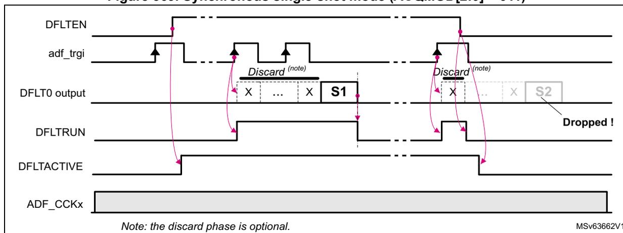
Note: The acquisition can be stopped by setting DFLTEN back to 0. This resets the filter and flushes the RXFIFO, so the samples located into the RXFIFO are lost. The ongoing DMA transfer is properly terminated. DFLTACTIVE goes back to 0 when the filter chain is reset and the RXFIFO flushed.
Figure 368 shows a case where the DFLTEN is set to 0 while an acquisition is ongoing (the sample S2 is lost). This situation can be avoided with the following steps:
- 1. Wait for DFLTRUN = 0.
- 2. Read the sample from the RXFIFO.
- 3. Clear DFLTEN to 0.
Window continuous acquisition mode
This mode allows the application to start or stop a continuous acquisition controlled by consecutive edges of one of the following trigger sources:
- • adf_trgi signal
- • TRGO bit
The window continuous acquisition mode is selected when ACQMOD[2:0] = 100.
The sequence below shows the most important programming steps (assuming that DFLTEN is set to 0):
- 1. Configure and enable the clock generator (CKGEN), so that the frequency of adf_proc_ck clock is compatible with the targeted application (see examples in Table 308 ).
- 2. Enable the CKGEN and, if needed, enable the ADF_CCK0 and ADF_CCK1 clocks.
- 3. Program the filter settings and set the ACQMOD[2:0] to 100.
- 4. Set to 1 the SITFEN bit.
- 5. Select the proper trigger source and sensitivity.
- 6. Before setting DFLTEN to 1, wait for DFLTACTIVE = 0: it insures that the previous filter deactivation sequence terminated properly.
- 7. Set DFLTEN to 1.
- 8. If TRGSENS = 0, the acquisition starts on trigger rising edge and stops on trigger falling edge. If TRGSENS = 1, the acquisition starts on trigger falling edge and stops on trigger rising edge.
Note: The acquisition may restart if the trigger condition becomes again active.
Figure 370 shows a simplified example of window continuous acquisition mode, with TRGSENS = 1. Once DFLTEN is set to 1, the ADF waits for a falling edge on the selected trigger input. When the trigger condition is met, DFLTRUN goes to 1 and the acquisition starts. The acquisition stops if the ADF detects a rising edge on the selected trigger input. If DFLTEN is still set to 1, the ADF waits again for a falling edge on the selected trigger input.
Figure 370. Window continuous mode (ACQMOD[2:0] = 100)
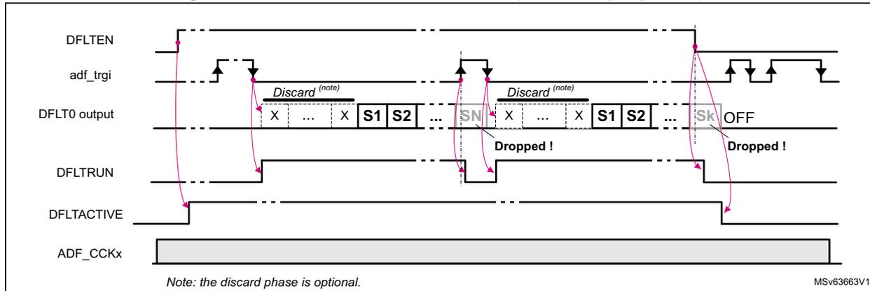
The diagram illustrates the timing for window continuous mode. The DFLTEN signal is set to 1. The adf_trgi signal shows a falling edge that triggers the start of acquisition and a rising edge that triggers the stop. The DFLT0 output shows a sequence of samples: X (discard), ..., X (discard), S1, S2, ..., SN (stored), X (discard), ..., X (discard), S1, S2, ..., Sk (stored), and then OFF. The DFLTRUN signal is high during the active acquisition periods. The DFLTACTIVE signal is high during the active acquisition periods. A 'Discard (note)' phase is indicated at the start of each acquisition. A 'Dropped !' label indicates samples lost when the trigger condition is not met. A note at the bottom states: 'Note: the discard phase is optional.' The diagram is labeled MSV63663V1.
Note: The acquisition can be stopped by setting DFLTEN back to 0. This resets the filter and flushes the RXFIFO, so the samples located into the RXFIFO are lost. The ongoing DMA transfer is properly terminated. DFLTACTIVE goes back to 0 when the filter chain is reset and the RXFIFO flushed.
Starting several filters synchronously
If the ADF is used with MDF instances (if present in the product), it is possible to start simultaneously the acquisition of all the filters. This synchronization capability depends on the way the triggers are connected in the product. Generally, an ADF is able to trigger MDF instances, if its
adf_trgo
signal is connected as trigger input to those blocks (see
Section 36.4.2: ADF pins and internal signals
to check trigger capabilities).
In the following programming example, one ADF has its
adf_trgo
signal connected to some MDFs. To start the acquisition of several filters synchronously, the following sequence must be performed (assuming that DFLTEN bits of the filters are set to 0):
On MDFs receiving the
adf_trgo
trigger:
- 1. Enable the CKGEN (CKGDEN = 1) and, if needed, enable the ADF_CCK0 and ADF_CCK1 clocks.
- 2. Set to 1 the SITFEN bit of the requested data interfaces.
- 3. For each filter, set the acquisition mode to synchronous (ACQMOD[2:0] = 01x).
- 4. For each filter, set TRGSRC[3:0] in order to select the
adf_trgotrigger input. - 5. For each filter, set TRGSENS to 0 (rising edge).
- 6. For each filter, set DFLTEN to 1.
On the ADF generating the
adf_trgo
trigger:
- 1. Enable the CKGEN (CKGDEN = 1) and, if needed, enable the ADF_CCK[1:0] clocks.
- 2. Set to 1 the SITFEN bit of the requested data interfaces.
- 3. Set the acquisition mode to synchronous (ACQMOD[2:0] = 01x).
- 4. Set TRGSRC[3:0] to 0 (TRGO selected).
- 5. Set TRGSENS to 0 (rising edge).
- 6. Set DFLTEN to 1.
- 7. Read TRGO bit until it is read to 0.
- 8. Set TRGO to 1. Then the acquisition sequence for all selected filters starts immediately.
To trigger a new acquisition (in case of single-shot) the application must do the following:
- 1. Check that the previous acquisition is completed, by waiting DFLTRUN = 0.
- 2. Read TRGO until it is read to 0.
- 3. Set again the bit TRGO to 1.
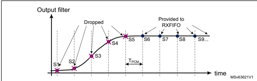
Discarded samples
The ADF offers the possibility to program the amount of samples to be discarded after each restart:
- • to avoid capturing samples affected by the impulse response of the filter
- • to delay the acquisition of filters by a specific amount of samples
The discard function is controlled via NBDIS[7:0] as follows:
- • When NBDIS[7:0] = 0, the discard function is disabled.
- • When NBDIS[7:0] ≠ 0, the discard function is activated in one of the following condition:
- – when the DFLTEN bit goes to 1
- – every time an acquisition is started in (A)synchronous single-shot modes
Refer to Figure 365 to Figure 369 , and Figure 371 .
In the example shown in Figure 371, the discard function is used to drop the first five samples provided by the digital filter (S1 to S5). The first sample transferred to the RXFIFO is S6.
Figure 371. Discard function example
36.4.9 Start-up sequence examples
Figure 372 details a start of acquisition sequence of a digital filter triggered by DFLTEN (ACQMOD[2:0] = 0), with NBDIS[7:0] = 3 (three samples to discard before acquisition).
The DFLT0 is configured for audio application: MCIC, RSFLT and HPF activated. The data interface (SITF0 or ADCITF) is assumed to be already activated.
Note: NBDIS[7:0] is set on purpose to a small value to simplify the drawing.
Figure 372. Start sequence with DFLTEN, in continuous mode, audio configuration
![Figure 372: Start sequence with DFLTEN, in continuous mode, audio configuration timing diagram. It shows the relationship between various signals over time. A 'Re-sync of DFLTEN with adf_proc_ck' is shown at the top. The diagram includes: ADCITF/SITF status (Enabled), ACQMOD (000), DFLTEN (high pulse), adf_proc_ck (processing clock), bs0_[r]f[_ck] (bitstream clock), MCIC dec. counter (counting 0, 1, 2, ..., N), MCIC_OUT (samples MCIC_S0, MCIC_S3, MCIC_S7, MCIC_S11, MCIC_S15, MCIC_S19, MCIC_S23), RSFLT dec. counter (counting 0, 1, ..., 4), RSFLT_OUT (samples RSFLT_S0 to RSFLT_S5), HPF_OUT (samples HPF_S0 to HPF_S5), NBDIS_CNTR (counting down from 3 to 0), and Sample stored in RXFIFO (samples HPF_S3, HPF_S4, HPF_S5). Points P1 and P2 are marked on the RSFLT_OUT signal. MSV63664V1 is noted in the bottom right.](/RM0486-STM32N6x5-x7/89dd6ad9354f26bc60af77d3c772a714_img.jpg)
The DFLTEN bit is re-sampled into the ADF processing clock domain. When DFLTEN is detected high, the filter chain is enabled, and the decimation counter of the MCIC filter is incremented at the rate of the bitstream clock.
When the MCIC decimation counter reached its programmed value N, a sample is available for the RSFLT.
The RSFLT processes all the samples provided by the MCIC, and delivers a sample to the HPF every-time it processes four samples (decimation by 4). The RSFLT needs up to 24 cycles of adf_proc_ck clock before delivering a sample (P1).
The HPF processes all the samples provided by the RSFLT, but the NBDIS function prevents the data writing in the RXFIFO as long as NBDIS_CNTR does not reach 0.
When NBDIS_CNTR reaches 0, the samples provided by the HPF are stored into the RXFIFO.
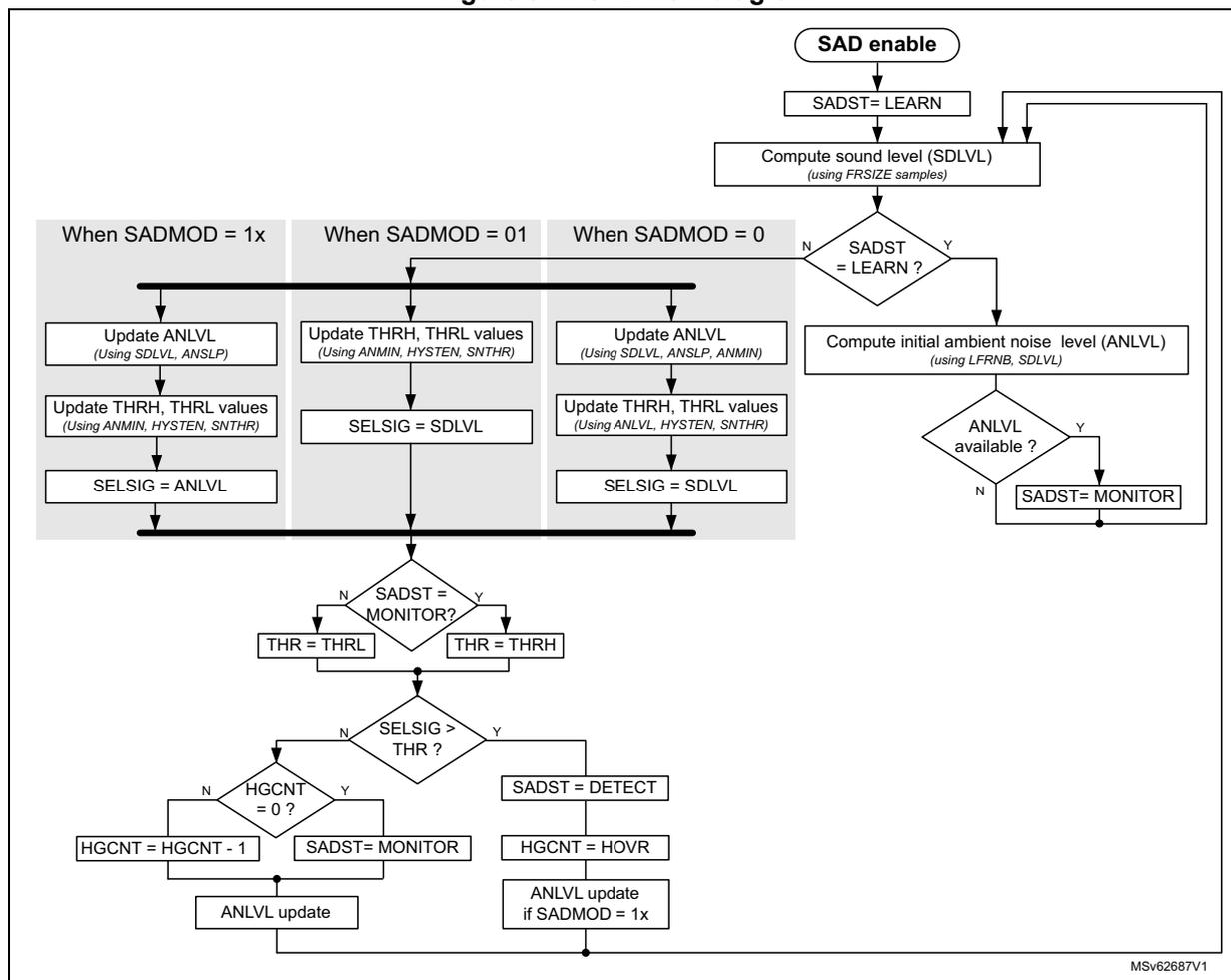
36.4.10 Sound activity detection (SAD)
The SAD is based on the computation of the ambient noise level (ANLVL) and of the short-term sound level (SDLVL). The SAD offers the following ways to detect a sound:
- • when the SDLVL reaches a threshold referenced to the ambient noise level
- • when the SDLVL reaches a fixed threshold
- • when the ANLVL reaches a fixed threshold
As shown in Figure 373, the SAD takes the 16 MSB samples from the DFLT0 output.
Figure 373. SAD block diagram
![Figure 373. SAD block diagram. The diagram shows the internal architecture of the Sound Activity Detection (SAD) block. At the top, a 'Logic' block receives configuration inputs: ADF_SADCR.SADEN, ADF_SADCR.DATCAP[1:0], and ADF_SADCR.SADST[1:0]. Below it, the 'SDLVL computation' block takes PCM[23:8] data, applies an absolute value (|xn|), and computes the short-term sound level (SDLVL). This is followed by a 'Detection' block containing 'ANLVL update Thresholds update' and 'Learning phase ANLVL computation' which output sddet_evt and sdlvl_evt signals. At the bottom, a 'DFLT0' block outputs PCM[23:0] data, which is split: one path goes to an 'RXFIFO0' via a switch, and the other path goes to the 'SDLVL computation' block. The diagram is labeled MSv63623V1.](/RM0486-STM32N6x5-x7/7caa2ee0c9964883c3d6be5623818a8c_img.jpg)
The SAD is highly configurable, and the application can adjust several parameters:
- • SAD detection behavior (SADMOD)
- • number of samples used to compute the sound level (FRSIZE)
- • number of frames used to compute the ambient noise level during the learning phase (LFRNB)
- • slope of the ambient noise estimator (ANSLP)
- • minimum expected ambient noise level (ANMIN)
- • threshold level (SNTHR)
- • threshold hysteresis (HYSTEN)
- • hangover window in order to filter spurious transitions between DETECT and MONITOR states (HGOVR)
- • data capture mode (DATCAP)
SAD detection behavior
The SAD can use the following ways to detect a sound, selected by SADMOD[1:0]:
- • When SADMOD[1:0] = 0, the SAD works like a voice-activity detection. In this mode, the SAD estimates the ambient noise level according to the computed sound level values. The threshold of the trigger is elaborated from the estimated ambient noise. Finally the current sound level is compared to this threshold. In a first approximation, the SAD triggers if the peak-to-average value of the input signal reaches a level defined by SNTHR[3:0].
- • When SADMOD[1:0] = 01, the SAD compares the current sound level (SDLVL) to a fixed trigger value defined by the application via SNTHR[3:0] and ANMIN[12:0]. This mode allows a fast SAD reaction as the amount of samples used to compute the sound level can be configured via FRSIZE[2:0].
- • When SADMOD[1:0] = 1x, the SAD compares the estimated ambient noise level (ANLVL) to a fixed trigger value defined by the application via SNTHR[3:0] and ANMIN[12:0]. This mode avoids unwanted triggers, due to peak levels, but the SAD reacts more slowly to an input signal variation. It is nevertheless possible to adjust the reaction time via FRSIZE[2:0] and ANSLP[2:0].
SAD states
As shown in Figure 373 , the SAD works as follows:
- 1. When enabled (SADEN = 1), the SAD is first in LEARN state to perform a first estimation of the ambient noise level.
- 2. The SAD continuously computes the short-term sound level (SDLVL) using the samples provided by the DFLT0. The amount of samples used to compute the sound level is given by FRSIZE[2:0]. The samples processed by the DFLT0 can be transferred into the memory or not depending on DATCAP[1:0] value.
- 3. The initial ambient noise level (ANLVL) is computed using the consecutive sound level values. The application can define how much sound level values are used to perform the computation of this initial ambient noise estimation (LFRNB).
- 4. When the initial ambient noise level (ANLVL) is computed, the SAD switches to the MONITOR state.
- 5. Every time a new short-term sound level value is available, the SAD updates the ambient noise level and the thresholds according to the selected detection mode.
- 6. If the SAD triggers, then the following happens:
- – The SAD switches to DETECT state.
- – The sddet_evt event is asserted.
- – The adf_sad_det signal is set to high.
- 7. The hangover function insures that the DETECT state is maintained even if the sound level goes below the threshold level for a time given by HGOVR.
Figure 374. SAD flow diagram
    graph TD
      Start([SAD enable]) --> Learn[SADST = LEARN]
      Learn --> ComputeSDLVL[Compute sound level (SDLVL)
using FRSIZE samples]
      ComputeSDLVL --> SADSTLearn{SADST = LEARN ?}
      SADSTLearn -- N --> SADMOD_Branch{SADMOD}
      SADMOD_Branch -- 1x --> SADMOD1x[Update ANLVL
Using SDLVL, ANSLP
---
Update THRH, THRL values
Using ANMIN, HYSTEN, SNTHR
---
SELSIG = ANLVL]
      SADMOD_Branch -- 01 --> SADMOD01[Update THRH, THRL values
Using ANMIN, HYSTEN, SNTHR
---
SELSIG = SDLVL]
      SADMOD_Branch -- 0 --> SADMOD0[Update ANLVL
Using SDLVL, ANSLP, ANMIN
---
Update THRH, THRL values
Using ANLVL, HYSTEN, SNTHR
---
SELSIG = SDLVL]
      SADSTLearn -- Y --> ComputeANLVL[Compute initial ambient noise level (ANLVL)
using LFRNB, SDLVL]
      ComputeANLVL --> ANLVLAvailable{ANLVL available ?}
      ANLVLAvailable -- Y --> Monitor[SADST = MONITOR]
      ANLVLAvailable -- N --> Learn
      SADMOD1x --> MonitorCheck{SADST = MONITOR?}
      SADMOD01 --> MonitorCheck
      SADMOD0 --> MonitorCheck
      Monitor --> MonitorCheck
      MonitorCheck -- N --> THR_L[THR = THRL]
      MonitorCheck -- Y --> THR_H[THR = THRH]
      THR_L --> SELSIGGT{SELSIG > THR ?}
      THR_H --> SELSIGGT
      SELSIGGT -- Y --> Detect[SADST = DETECT]
      Detect --> HOVR[HGCNT = HOVR]
      HOVR --> ANLVLUpdate1x[ANLVL update
if SADMOD = 1x]
      ANLVLUpdate1x --> ComputeSDLVL
      SELSIGGT -- N --> HGCNT0{HGCNT = 0 ?}
      HGCNT0 -- Y --> MonitorSet[SADST = MONITOR]
      MonitorSet --> ANLVLUpdate[ANLVL update]
      HGCNT0 -- N --> HGCNTDec[HGCNT = HGCNT - 1]
      HGCNTDec --> ANLVLUpdate
      ANLVLUpdate --> ComputeSDLVL
MSV62687V1
Sound level computation (SDLVL)
Once enabled, the SAD computes continuously the sound level value. The sound level represents the average of the absolute value of an amount of PCM samples given by FRSIZE[2:0].
where \( N_{FRSIZE} \) is the amount of PCM samples given by FRSIZE[2:0].
Ambient noise estimation (ANLVL)
The ambient noise level (ANLVL) is computed when SADMOD[1:0] is 00 or 10.
The ambient noise level is computed differently according to the state of the SAD as detailed below:
- • ANLVL computation during the LEARN state
Every time the SAD is enabled, a learning phase is initiated in order to estimate a first value of the ambient noise level. During this phase, the SAD cannot trigger.
During the LEARN phase, the ambient noise level is computed as follows:
where \( N_{\text{LFRNB}} \) is the amount of frames given by LFRNB[2:0] bitfield.
- • ANLVL computation during the MONITOR or DETECT state
When the learning phase is completed, the SAD updates the ambient noise level in the following way:
- – The SAD computes the new possible values for the ambient noise level:
- – The ANLVL takes the ANLVL_DN value if the current sound level is lower than ANLVL_DN, otherwise ANLVL takes the value of ANLVL_UP.
The ANLVL is not updated if the current sound level is higher than the threshold level, except if SADMOD[1:0] = 10.
- – When SADMOD[1:0] = 0, if the new ANLVL value is lower than ANMIN[12:0], ANLVL is replaced by ANMIN.
The slope of the noise estimator can be adjusted to optimize the detection of the wanted signal. This slope is adjusted via ANSLP[2:0] in the ADF SAD configuration register (ADF_SADCFGGR) .
Table 305 shows the allowed values according to the frame size and the sampling rate of the data observed by the SAD. The recommended values when the SADMOD[1:0] = 0 are the ones into the gray shaded cells.
Table 305. ANSLP values versus FRSIZE and sampling rates
| FRSIZE | ANSLP values for Fs = 8 kHz | ANSLP values for Fs = 16 kHz | ||||
|---|---|---|---|---|---|---|
| Slow (1) | typical (2) | Fast (3) | Slow (1) | typical (2) | Fast (3) | |
| 0 (8 samples) | 0 | 1 | 2 | - | 0 | 1 |
| 1 (16 samples) | 1 | 2 | 3 | 0 | 1 | 2 |
| 2 (32 samples) | 2 | 3 | 4 | 1 | 2 | 3 |
| 3 (64 samples) | 3 | 4 | 5 | 2 | 3 | 4 |
| 4 (128 samples) | 4 | 5 | 6 | 3 | 4 | 5 |
| 5 (256 samples) | 5 | 6 | 7 | 4 | 5 | 6 |
| 6 (512 samples) | 6 | 7 | - | 5 | 6 | 7 |
- 1. The slow slope is equal to - 8.5 dB/s for the negative slope and + 2.1 dB/s for the positive slope.
- 2. The typical slope is equal to - 17.1 dB/s for the negative slope and + 4.2 dB/s for the positive slope.
- 3. The fast slope is equal to - 34.2 dB/s for the negative slope and + 8.5 dB/s for the positive slope.
The slopes can also be computed using the following formulas:
where \( F_s \) is the sampling rate of the stream observed by the SAD and \( F_{SIZE} \) is the frame size defined by FRSIZE[2:0].
Threshold computation
The way the threshold value is computed depends on SADMOD[1:0]:
- • If SADMOD[1:0] = 0, THRH is obtained by multiplying the current ANLVL value with the gain defined in SNTHR[3:0].
This threshold value is then compared to the current sound level (SDLVL).
- • If SADMOD[1:0] = 01, THRH is obtained by multiplying the current ANMIN[12:0] with the gain defined by SNTHR[3:0].
This threshold value is then compared to the current sound level (SDLVL).
- • If SADMOD[1:0] = 1x, THRH is obtained by multiplying the current ANMIN[12:0] by 4.
This threshold value is then compared to:
The hysteresis mode can be enabled to reduce the spurious transitions between MONITOR and DETECT states. In hysteresis mode (HYSTEN = 1), the following threshold values are used:
- • THRH when the SAD is in MONITOR state.
- • THRL when the SAD is in DETECT state.
Table 306 shows the thresholds values according to SNTHR.
Table 306. Threshold values according SNTHR (1)
| SNTHR[3:0] | THRH | THRL | Comments | ||
|---|---|---|---|---|---|
| 0 | LVL + 3.5 dB | LVL x 1.5 | LVL + 3.5 dB | LVL x 1.5 | No hysteresis |
| 1 | LVL + 6.0 dB | LVL x 2 | LVL + 3.5 dB | LVL x 1.5 | Hysteresis of 2.5 dB |
| 2 | LVL + 9.5 dB | LVL x 3 | LVL + 6.0 dB | LVL x 2 | Hysteresis of 3.5 dB |
| 3 | LVL + 12.0 dB | LVL x 4 | LVL + 9.5 dB | LVL x 3 | Hysteresis of 2.5 dB |
| 4 | LVL + 15.6 dB | LVL x 6 | LVL + 12.0 dB | LVL x 4 | Hysteresis of 3.5 dB |
| 5 | LVL + 18.1 dB | LVL x 8 | LVL + 15.6 dB | LVL x 6 | Hysteresis of 2.5 dB |
| 6 | LVL + 21.6 dB | LVL x 12 | LVL + 18.1 dB | LVL x 8 | Hysteresis of 3.5 dB |
| 7 | LVL + 24.1 dB | LVL x 16 | LVL + 21.6 dB | LVL x 12 | Hysteresis of 2.5 dB |
| 8 | LVL + 27.6 dB | LVL x 24 | LVL + 24.1dB | LVL x 16 | Hysteresis of 3.5 dB |
| 9 | LVL + 30.1 dB | LVL x 32 | LVL + 27.6dB | LVL x 24 | Hysteresis of 2.5 dB |
1. LVL must be replaced by ANLVL when SADMOD[1:0] = 0 and by ANMIN for other SADMOD[1:0] values.
When the hysteresis function is disabled, the SAD always use THRH.
Note: The hysteresis mode must not be used when SADMOD[1:0] = 1x.
Trigger logic
The signal compared to this threshold depends also on SADMOD[1:0].
The trigger condition is reached when the selected signal (SELSIG) is bigger than the threshold level.
If the trigger condition is met, the following happens:
- • The SAD switches to DETECT state.
- • The SAD refreshes the hangover counter with HGOVR.
- • The sddet_evt event is asserted if the SAD transits from MONITOR to DETECT.
- • The adf_sad_det signal is set to high.
The SAD remains in DETECT state as long as the trigger condition is met or the hangover down-counter is different from 0.
The sddet_evt event indicates when the SAD enters and/or exits the DETECT state. This event is used to generate an interrupt when a sound is detected or when a sound is no longer detected:
- • When DETCFG = 0, the application receives an event only when the SAD enters the DETECT state.
- • When DETCFG = 1, the application receives an event when the SAD enters or exits the DETECT state.
The adf_sad_det signal remains high as long as the SAD is in DETECT state.
The SAD also provides a flag indicating that a new sound level value is available (SDLVLF). The last computed sound level (SDLVL[14:0]) is available in the ADF SAD sound level register (ADF_SADSDLVR) , and the last computed ambient noise level (ANLVL[14:0]), in the ADF SAD ambient noise level register (ADF_SADANLVR) .
Note: The SAD can work even when the AHB clock is not present. In that case, the SAD does not update SDLVL[14:0] and ANLVL[14:0].
To get the latest valid SDLVL[14:0] and ANLVL[14:0] values, the application must read the ADF_SADSDLVR, and ADF_SADANLVR registers, when the SDLVLF flag goes high. This can be done in the following ways:
- • by polling the SDLVLF flag:
- a) Clear the SDLVLF flag by writing SDLVLF to 1.
- b) Wait for SDLVLF = 1, by reading ADF_DFLTxISR.
- c) Read ADF_SADSDLVR and ADF_SADANLVR.
- d) Clear SDLVLF by writing it to 1.
- e) Go to step 2 if other values must to be read.
- • by generating an interrupt:
- a) Read ADF_DFLTxISR.
- b) If SDLVLF = 1, read ADF_SADSDLVR and ADF_SADANLVR, and clear SDLVLF by writing it to 1.
- c) Handle other status flags and exit from ISR.
Sample transfer to memory
The SAD offers the following options to control the samples transfer from DFLT0 to the system memory:
- • If DATCAP[1:0] = 1x, the samples are transferred into the system memory as soon as DFLT0 and SAD are enabled. The transfer does not depend on the SAD state.
- • If DATCAP[1:0] = 01, the samples are transferred into the system memory when the SAD detects a sound (when the SAD is in DETECT state), assuming that DFLT0 and SAD are enabled.
- • If DATCAP[1:0] = 0, the samples are not transferred into the memory. This mode can be used if the application only wants to observe but does not need samples for other processing.
Note: DATCAP[1:0] is taken into account only when the SADEN = 1. For example, if the SAD configuration is DATCAP[1:0] = 0, SADEN = DFLTEN = 1, and if the application sets now SADEN to 0, the samples provided by the DFLT0 are transferred to the RXFIFO.
Programming recommendations
To make the SAD function working properly, the ADF must be programmed as follows:
- 1. Provide the proper kernel clock (adf_ker_ck) to the ADF.
- 2. Configure the CKGEN and enable it.
- 3. Configure the SITF and enable it (note that microphones have a settling time of several milliseconds).
- 4. Configure the DFLT0. A typical setting is the following:
- – CIC5 with a decimation ratio of 12, 16 or 24
- – RSFLT with a decimation ratio of 4
- – HPF with HPFC = 2 or 3
- 5. Set SADEN to 0.
- 6. Wait for SADACTION = 0. If SADEN was previously enabled, this phase can take two periods of adf_hclk, and two periods of adf_proc_ck.
- 7. Configure the SAD as follows:
- – Set DATCAP[1:0] to 0, if the application does not want to store the samples into the system memory.
- – Set DATCAP[1:0] to 01, if the application wants to store the samples into the system memory only when the SAD detects a sound.
- – Set DATCAP[1:0] to 11, if the application wants to store the samples into the system memory continuously.
- 8. Configure the DMA (optional).
- 9. Enable the SAD.
- 10. Enable the DFLT0.
Figure 374 shows a simplified timing diagram when the SAD works with DATCAP[1:0] = 01.
Thanks to the kernel clock (adf_ker_ck), the SAD continuously monitors the audio signal provided by the DFLT0. The threshold is also continuously updated according to the ambient noise level estimation.
- • When the SAD detects a sound higher than the programmed threshold (1), the ADF requests the bus clock (adf_bus_ckreq asserted).
- • When the bus clock is available (see 2 in
Figure 374
) then:
- – The data transfer to the memory is triggered.
- – The event interrupt (adf_evt_it) can be generated.
- • In this example, the event interrupt (adf_evt_it) is used to wake up the application. The interrupt line is released by clearing SDDETF by writing 1 to it.
- • As long as the SAD remains in DETECT state, the application waits to get enough samples and calls, for example the keyword recognition algorithm (see 3 in Figure 374 ).
- • In the case shown in Figure 375 , the SAD state (SADST) goes back to MONITOR before the keyword is recognized. If DETCFG is set to 1, an event signals when the SAD goes back to MONITOR state. The SAD stops the transfer of samples into the memory and the application can clean up the receive buffer for the next detection (see 4 in Figure 374 ).
Figure 375. SAD timing diagram example
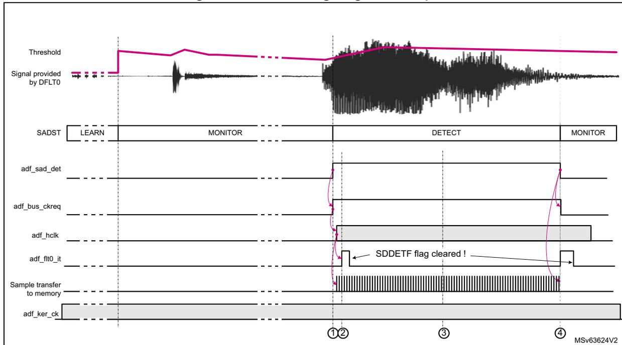
36.4.11 Data transfer to memory
Data format
The samples processed by DFLT0 are stored into a RXFIFO. The application can read the samples stored into these FIFOs via the ADF digital filter data register 0 (ADF_DFLT0DR) . The samples inside this register are signed and left aligned. The bit 31 always represents the sign.
The ADF provides 24-bit left-aligned data. Performing a 16-bit access to ADF_DFLT0DR allows the application to get the 16 most significant bits. Performing a 32-bit access to ADF_DFLT0DR allows the application to get a 24-bit data size.
Figure 376. ADF_DFLTxDR data format
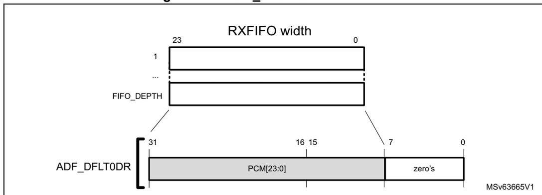
Data resynchronization
The samples stored into the RXFIFO can be transferred into the memory by using either DMA requests or interrupt signaling.
Note: The RXFIFO is located into the adf_ker_ck clock domain, while ADF_DFLT0DR is located into the adf_hclk (AHB) clock domain.
When the AHB clock is available, if ADF_DFLT0DR is empty and if a sample is available into the RXFIFO, this sample is transferred into ADF_DFLT0DR.
The sample transfer from the RXFIFO to ADF_DFLT0DR takes two periods of the AHB clock (adf_hclk) and two periods of the adf_ker_ck clock. The ADF inserts automatically wait-states if the application performs a read operation of ADF_DFLT0DR while the transfer of the new sample from the RXFIFO to ADF_DFLT0DR is not yet completed.
Figure 377. Data resynchronization
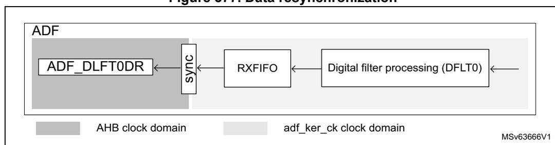
Data transfer
The content of the RXFIFO can be transferred to the memory either by using a DMA channel or interrupt services.
Both single and burst, DMA transfers are supported by the ADF, but the application has to care about the following points:
- • The RXFIFO must contain at least the same amount of samples than the burst size.
- • The burst mode efficiency may be reduced due to the data resynchronization explained in the previous section.
Note: The burst mode is not available in all products (see the DMA section to check if the product supports it).
In addition, the application can select the RXFIFO threshold (FTH bit) in order to trigger the data transfer: a data transfer can be triggered as soon as the RXFIFO is not empty, or when the RXFIFO is half-full (containing depth/2 samples).
For the DMA transfer, as soon as one of the RXFIFO reaches the threshold level, the DMA request is asserted in order to ask for data transfer. Successive DMA requests are performed as long as the RXFIFO is not empty.
The DMA mode of the RXFIFO is enabled via the DMAEN bit in ADF_DFLT0DR.
For the interrupt signaling, the following cases must be considered:
- • If FTH = 0, as soon as a data is available in ADF_DFLT0DR, the FTHF is set, allowing the generation of an interrupt. FTHF is released as soon as ADF_DFLT0DR is read.
- • If FTH = 1, as soon as the RXFIFO reaches the threshold level and a data is available in ADF_DFLT0DR, the FTHF is set, allowing the generation of an interrupt. FTHF is released as soon as one data is read. FTHF is set again if the threshold condition is
met again. In this mode, every time an interrupt occurs, the application is supposed to read \( FIFO\_SIZE/2 \) data.
RXFIFO overrun
A RXFIFO overrun condition is detected when the RXFIFO is full, and a new sample from the DFLT0 must be written.
In this case, DOVRF is set and the new sample is dropped. When the RXFIFO has at least one location available, the new incoming sample is written into the RXFIFO.
Figure 378 shows an example based on a RXFIFO depth of four words and FTH set to 1, so that FTHF goes to 1 when the RXFIFO is half-full.
The S7 sample is lost due to an overrun: the RXFIFO is full while S7 must be written into the RXFIFO. The S7 write operation is not performed. DOVRF is set to 1 at the moment where the write operation was expected. The overflow event remains to 1 as long as it is not cleared by the application.
In this example, DOVRIE is set to 1 to have an interrupt if an overrun condition is detected.
After the S7 sample, the application manages to read data from the RXFIFO, and the ADF can write the S8 sample and consecutive. Later, the application clears DOVR, allowing the detection of a new overrun situation.
In the \( adf\_hclk \) line, the gray boxes indicate that the ADF requested the AHB clock.
Figure 378 shows the AHB clock available only when the ADF requests it. In real applications, the AHB clock may also be present if the ADF does not request it.
Figure 378. Example of overflow and transfer to memory
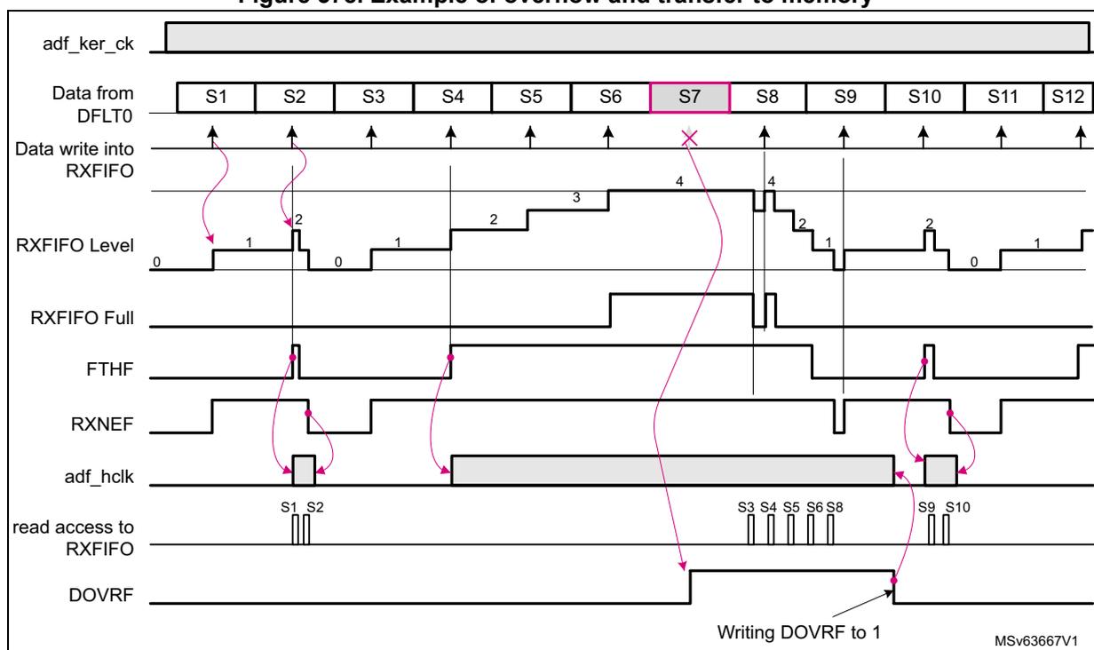
The timing diagram illustrates the following sequence of events:
- adf_ker_ck : A continuous clock signal.
- Data from DFLT0 : A sequence of samples S1 through S12. Sample S7 is highlighted in pink.
- Data write into RXFIFO : Arrows indicate write attempts for each sample. The write for S7 is marked with a red 'X' because the RXFIFO is full.
- RXFIFO Level : A step-like graph showing the number of samples in the FIFO. It reaches a maximum level of 4. Labels 0, 1, 2, 3, 4 are present.
- RXFIFO Full : A signal that goes high when the FIFO level reaches 4 and returns low when it drops below 4.
- FTHF : A signal that goes high when the FIFO level reaches the threshold (2, which is FIFO_SIZE/2).
- RXNEF : A signal that goes high when the FIFO is not empty and returns low when it is empty.
- adf_hclk : The AHB clock, shown as gray blocks indicating periods when the ADF requested it.
- read access to RXFIFO : Vertical pulses indicating when the application reads samples. Samples S1, S2, S3, S4, S5, S6, S8, S9, and S10 are shown being read.
- DOVRF : An overflow flag that goes high at the time of the overrun (S7) and remains high until it is manually cleared (labeled 'Writing DOVRF to 1').
MSv63667V1
36.4.12 Autonomous mode
The ADF can work even if the AHB bus clock is not available (Stop modes). The ADF uses the AHB clock only for the register interface. All the processing part is clocked with the kernel clock.
In Stop mode, the ADF receives a kernel clock if the following conditions are met:
- • The ADF autonomous mode is enabled in the RCC.
- • The selected kernel clock source is taken from an oscillator available in Stop mode.
In Stop mode, the ADF receives the AHB clock if the following conditions are met:
- • The ADF autonomous mode is enabled in the RCC.
- • The ADF requests the AHB clock in the following situations:
- – when the ADF must transfer data into memory via the DMA
The data is directly transferred to the SRAM thanks to the DMA while the product remains in Stop mode. The AHB clock request is maintained until the DMA transfer is completed. - – when the ADF needs to generate an interrupt
An interrupt generally wakes up the device from Stop mode, as an action from the application is needed. Once the AHB clock is available, the interrupt is generated. The AHB clock request is maintained as long as an enabled interrupt flag is still active.
- – when the ADF must transfer data into memory via the DMA
36.4.13 Register protection
The ADF embeds some hardware protection to prevent invalid situations.
Table 307 shows the list of write-protected and unprotected fields.
Table 307. Register protection summary
| Registers | Unprotected fields | Write-protected fields | Write-protection condition |
|---|---|---|---|
| ADF global control register (ADF_GCR) | TRGO | - | DFLTACTIVE0 = 1 |
| ADF clock generator control register (ADF_CKGCR) | CKGDEN CCK0EN CCK1EN | PROCDIV[6:0], CCKDIV[3:0], CKGMOD, TRG SRC[3:0], TRG SENS, CCK[1:0]DIR | CKGACTIVE = 1 |
| ADF serial interface control register 0 (ADF_SITF0CR) | SITFEN | STH[4:0], SITF MOD[1:0], SCK SRC[1:0] | SITFACTIVEEx = 1 |
| ADF bitstream matrix control register 0 (ADF_BSMX0CR) | - | BSSEL[4:0] | DFLTACTIVEEx = 1 |
| ADF digital filter control register 0 (ADF_DFLT0CR) | DFLTEN | NBDIS[7:0], TRG SRC[3:0], TRG SENS, FTH, DMAEN, SNPSFMT, ACQ MOD[2:0] | DFLTACTIVEEx = 1 |
| ADF digital filter configuration register 0 (ADF_DFLT0ICR) | SCALE[5:0] | MCICD[8:0], CIC MOD[2:0], DAT SRC[1:0] | |
| ADF reshape filter configuration register 0 (ADF_DFLT0RSFR) | - | All fields | |
| ADF delay control register 0 (ADF_DLY0CR) | - | SKPDLY[6:0] | SKPBF = 1 |
Table 307. Register protection summary (continued)
| Registers | Unprotected fields | Write-protected fields | Write-protection condition |
|---|---|---|---|
| ADF DFLT0 interrupt enable register (ADF_DFLT0IER) | All fields | - | - |
| ADF DFLT0 interrupt status register 0 (ADF_DFLT0ISR) | All fields | - | - |
| ADF SAD control register (ADF_SADCR) | SADEN | FRSIZE[2:0], DETCFG, SADMOD[1:0], HYSTEN, DATCAP[1:0] | SADACTIVE = 1 |
| ADF SAD configuration register (ADF_SADCFG) | - | ANMIN[12:0], SNTHR[3:0], HGOVR[3:0], LFRNB[2:0], ANSLP[2:0] | SADACTIVE = 1 |
All the ADF processing is performed in the adf_proc_ck clock domain. For that reason, enabling or disabling an ADF sub-block may take some time due to the resynchronization between the AHB clock domain and the adf_proc_ck clock domain. XXXACTIVE flags are available to allow the application to check that the synchronization between the two clock domains is completed.
To change a write-protected bitfield, the application must follow this sequence:
- 1. Set the enable bit of the sub-block to 0.
- 2. Wait for corresponding flag XXXACTIVE = 0.
- 3. Modify the wanted fields.
- 4. Set the enable bit of the sub-block to 1.
Refer to the description of each sub-block for details.
36.5 ADF low-power modes
Table 308. Effect of low-power modes on ADF
| Mode | Description |
|---|---|
| Sleep | No effect. ADF interrupts cause the device to exit the Sleep mode. |
| Stop (1) | The ADF registers content is kept. Thanks to the kernel clock request feature, if the ADF is clocked by an internal oscillator available in Stop mode, the ADF remains active. The interrupts cause the device to exit Stop mode. |
| Standby | The ADF is powered down and must be reinitialized after exiting Standby mode. |
- 1. Refer to Section 36.3: ADF implementation for details about Stop modes supported by the ADF.
36.6 ADF interrupts
To increase the CPU performance, the ADF offers an interrupt line (adf_flt0_it), sensitive to several events.
Note: The status flags are available even if the corresponding interrupt enable flag is not enabled.
The interrupt interface is controlled via the ADF_DFLT0 interrupt enable register (ADF_DFLT0IER) and the ADF_DFLT0 interrupt status register 0 (ADF_DFLT0ISR) .
Figure 379. ADF interrupt interface
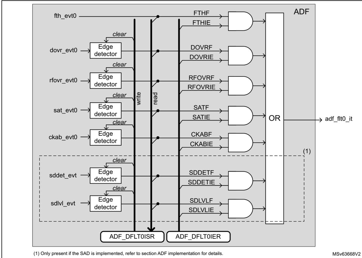
(1) Only present if the SAD is implemented, refer to section ADF implementation for details.
MSV63668V2
Table 309 shows which interrupt line is affected by which event, and how to clear and activate each interrupt/event.
Table 309. ADF interrupt requests
| Interrupt vector | Interrupt event | Event flag | Event/interrupt clearing method | Exit Sleep mode | Exit Stop modes (1) | Exit Standby mode |
|---|---|---|---|---|---|---|
| ADF_FLT0 (2) | RXFIFO threshold reached | FTHF | Read ADF_DFLT0DR until RXFIFO level is lower than the threshold. | Yes | Yes | No |
| RXFIFO overrun | DOVRF | Write DOVRF to 1. | ||||
| RSFLT overrun | RFOVRF | Write RFOVRF to 1. | ||||
| Saturation detection | SATF | Write SATF to 1. | ||||
| Channel clock absence detection | CKABF | Write CKABF to 1. | ||||
| SAD: sound detected | SDDETF | Write SDDETF to 1. | ||||
| SAD: sound level value available | SDLVLF | Write SDLVLF to 1. |
- 1. Refer to Section 36.3: ADF implementation for details.
- 2. ADF_FLT0 vector corresponds to the assertion of adf_flt0_it signal.
36.7 ADF application information
36.7.1 ADF configuration examples for audio capture
Table 310 gives some examples of the ADF settings for the digital microphones, focusing on 16 and 48 kHz output data rate.
Configurations #1 and #2 are for very low-power use-cases and have a reduced signal-to-noise ratio. The user must also insure that the selected digital microphone can work properly at 512 kHz. These configurations can be used for sound detection. The RSFLT is not used to reduce as much as possible the frequency of the kernel clock (adf_ker_ck).
Configurations #3, #4, #9, #10, #11 give signal-to-noise ratios around 115 dB, with an ideal microphone model, with a sinus signal of 997 Hz. Using the RSFLT allows a good control on the in-band ripple, and a good image rejection.
Configurations #7, #8, #10 give signal-to-noise ratio around 120 dB, with an ideal microphone model, using a sinus signal of 997 Hz.
Table 310. Examples of ADF settings for microphone capture
| Configuration | adf_ker_ck (MHz) | PROC DIV + 1 | CCK DIV + 1 | CIC order (1) | MCICD + 1 | SCALE | RSFLT BYP | RSFLT D | HPF BYP | - | adf_proc_ck (MHz) | Total dec. ratio | F RS (kHz) | F ADF_CCKx (MHz) | F PCM (kHz) |
|---|---|---|---|---|---|---|---|---|---|---|---|---|---|---|---|
| #1 | 1.024 | 1 | 2 | 4 | 64 | 0x2D (- 8.5 dB) | 1 | x | x | => | 1.024 | 64 | - | 0.512 | 8 |
| #2 | 1 | 2 | 5 | 32 | 0x2B (- 14.5 dB) | 32 | - | 16 | |||||||
| #3 | 1 | 2 | 5 | 16 | 0x01 (+ 3.5 dB) | 64 | 32 | 8 | |||||||
| #4 | 2.048 | 1 | 2 | 5 | 16 | 0x01 (+ 3.5 dB) | 0 | 0 | 2.048 | 64 | 64 | 1.024 | 16 | ||
| #5 | 3.072 | 1 | 6 | 5 | 8 | 0x0B (+ 33.6 dB) | 0 | 0 | 3.072 | 32 | 32 | 0.512 | 8 | ||
| #6 | 2 | 2 | 5 | 12 | 0x06 (+ 18.1 dB) | 48 | 64 | 0.768 | 16 | ||||||
| #7 | 1 | 2 | 5 | 24 | 0x2C (- 12 dB) | 96 | 1.536 | ||||||||
| #8 | 4.096 | 1 | 2 | 5 | 32 | 0x27 (- 26.6 dB) | 0 | 0 | 4.096 | 128 | 64 | 2.048 | 16 | ||
| #9 | 6.144 | 3 | 2 | 5 | 16 | 0x02 (+ 6.0 dB) | 0 | 0 | 3.072 | 64 | 64 | 1.024 | 16 | ||
| #10 | 2 | 2 | 5 | 24 | 0x2C (- 12 dB) | 96 | 1.536 | ||||||||
| #11 | 1 | 2 | 5 | 16 | 0x01 (+ 3.5 dB) | 64 | 192 | 3.072 | 48 | ||||||
| #12 | 7.680 | 1 | 2 | 5 | 20 | 0x2E (- 6.0 dB) | 0 | 0 | 7.680 | 80 | 192 | 3.840 | 48 | ||
- 1. CICMOD = 100 for CIC order equal to 4. CICMOD = 101 for CIC order equal to 5.
36.7.2 Programming examples
Example 1
This example describes the programming of ADF for the capture of a signal coming from a digital microphone, using only the CIC4, with a decimation of 48, assuming that the kernel clock is 1.536 MHz. Typically, this configuration can be used to detect sound using the SAD.
Table 311. Programming sequence (CIC4)
| Operations | Comments |
|---|---|
| Adjust the proper kernel clock frequency via the RCC | Assuming that the RCC is programmed to provide a kernel clock (adf_ker_ck) of 1.536 MHz coming from a RC oscillator. |
| Select the proper ADF kernel clock source via the RCC | Refer to the RCC of the product. |
| Enable the ADF clocks via the RCC | Refer to the RCC of the product. |
| Reset the ADF via the RCC | Refer to the RCC of the product. |
| AFMUX programming | Program the AFMUX to select ADF_SD0 and ADF_CCK0 functions. |
| Enable ADF processing clock: ADF_CKGCR = 0x0001 0023 | PROC DIV = 0 (bypass): adf_proc_ck frequency is 1.536 MHz. CCK DIV = 1 (division by 2): ADF_CCK0 clock frequency is 768 kHz. The ADF_CCK0 pin is set in output and generates a clock so that the microphone can exit from low-power mode. |
| Serial interfaces configuration: ADF_SITF0CR = 0x0000 1F01 | SCKSRC = 0 to select ADF_CCK0 as serial clock. SIFTMOD = 0 to select LF_MASTER SPI mode. Clock absence feature is not working in this mode. The serial interface is enabled. |
| Bitstream matrix configuration: ADF_BSMX0CR = 0x0000 0000 | DFLT0 filter takes the bitstream of SITF0, sampled on rising edge |
| Filters configuration (CIC): ADF_DFLT0CICR = 0x0040 2F40 | SCALE = 0x04 (12 dB): RSFLT is not enabled. Note that the gain is 8.5 dB, higher than recommended in order to improve signal accuracy for the SAD. Saturation is not an issue in this case, as only the detection of a signal much lower than the full scale is needed. MCICD = 0x2F (decimation by 48) CICMOD = 4 to select a Sinc 4 DATSCR = 0 to select data coming from BSMX |
| Filters configuration (RSFLT and HPF): ADF_DFLT0RSFR = 0x0000 0301 | HPFC = 3: cut-off frequency of 16kHz * 0.0095 = 152 Hz HPFBYP = 0: HPF not bypassed RSFLTBY = 1: RSFLT bypassed |
| Micro delay adjust: ADF_DLY0CR = 0x0000 0000 | Not used in this example |
| Enable interrupt events: ADF_DFLT0IER = 0x0000 1000 | Enable the interrupt events the application wants to handle. In this example, SDDETIE is set to 1 to have an interrupt if a sound is detected. |
Table 311. Programming sequence (CIC4) (continued)
| Operations | Comments |
|---|---|
| SAD setting: ADF_SADCR = 0x0000 1400 | SADMOD = 1: Trigger based on sound level values FRSIZE = 4: Sound level computed on 128 samples HYSTEN = 0: No hysteresis DETCFG = 0: interrupt generated when the SAD enters in DETECT state DATCAP = 0: samples not transferred to memory SADEN = 0: SAD not yet enabled |
| SAD setting: ADF_SADCFGR = 0x0025 0001 | ANMIN = 0x25: Sound threshold of
\(
37 \cdot 10^{\text{SNTHR}/20} = 74 \text{ LSB}^{(1)}
\) HGOVR = 0: four frames ( \( 4 \times 128 = 512 \) samples) LFRNB = 0: Learning phase set to two frames. Not useful in this mode. ANSLP = 0: Not used in this mode SNTHR = 1: Threshold set to 6 dB (see ANMIN) |
| Clear status flags: ADF_DFLT0ISR = 0x0000 0FFF | Clear all the status flags before running the ADF |
| Enable the SAD: ADF_SADCR = 0x0000 1401 Wait for SADACTIVE flag = 1 | Enable first the SAD, in order to be sure that data transfer to memory are blocked by the SAD. |
| Enable the filter: ADF_DFLT0CR = 0x0000 0001 | NBDIS = 0: no samples discarded ACQMOD = 0: Asynchronous continuous acquisition mode DMAEN = 0: DMA interface not used DFLTEN = 1: Filter enabled |
1. SNTHR and ANMIN values are computed using the same approach than in Threshold programming with SADMOD = 01 (detection of a sound higher than 63 dBSPL).
Example 2
This example describes the programming of ADF for the capture of a signal coming from a digital microphone, using the CIC5, and the RSFLT, with a total decimation of 64.
Table 312. Programming sequence (CIC5)
| Operations | Comments |
|---|---|
| Adjust the proper kernel clock frequency via the RCC | Assuming that the RCC is programmed to provide a kernel clock (adf_ker_ck) of 6.144 MHz |
| Select the proper ADF kernel clock source via the RCC | Refer to the RCC of the product. |
| Enable the ADF clocks via the RCC | Refer to the RCC of the product. |
| Reset the ADF via the RCC | Refer to the RCC of the product. |
| AFMUX programming | Program the AFMUX to select ADF_SD0 and ADF_CCK0 functions. |
| Enable ADF processing clock: ADF_CKGCR = 0x0201 0023 | PROCDIV = 2 (division by 3): adf_proc_ck frequency is 6.144 MHz. CCKDIV = 1 (division by 2): ADF_CCK0 clock frequency is 1.024 MHz. The ADF_CCK0 pin is set in output and generates a clock so that the microphone can exit from low-power mode. |
| Operations | Comments |
|---|---|
| Serial interfaces configuration: ADF_SITF0CR = 0x0000 1F01 | SCKSRC = 0 to select ADF_CCK0 as serial clock. SIFTMOD = 0 to select LF_MASTER SIPI mode. Clock absence feature is not working in this mode. The serial interface is enabled. |
| Bitstream matrix configuration: ADF_BSMX0CR = 0x0000 0000 | DFLT0 filter takes the bitstream of SITF0, sampled on rising edge |
| Digital filter control: ADF_DFLT0CR = 0x0000 0006 | NBDIS = 0: no samples discarded ACQMOD = 0: Asynchronous continuous acquisition mode DMAEN = 1: DMA interface not used DFLTEN = 0: Filter disabled FTH = 1: RXFIFO half-full |
| Filters configuration (CIC): ADF_DFLT0CICR = 0x0010 0F50 | SCALE = 0x01(+3.5 dB): Output limited to 22 bits due to RSFLT. MCICD = 0xF (decimation by 16) CICMOD = 5 to select a Sinc 5 DATSCR = 0 to select data coming from BSMX |
| Filters configuration (RSFLT and HPF): ADF_DFLT0RSFR = 0x0000 0200 | HPFC = 2: cut-off frequency of 16 kHz * 0.0025 = 40 Hz HPFBYP = 0: HPF not bypassed RSFLTBY = 0: RSFLT not bypassed RSFLTD = 0: Decimation by 4 |
| Micro delay adjust: ADF_DLY0CR = 0x0000 0000 | Not used in this example |
| Enable interrupt events: ADF_DFLT0IER = x | Enable the interrupt events the application wants to handle. |
| Clear status flags: ADF_DFLT0ISR = 0x0000 0FFF | Clear all the status flags before running the ADF |
| Program the DMA Enable the DMA | The DMA must be programmed in order to read the data inside the ADF_DLT0DR register every time a DMA request is generated. |
| Start acquisition: ADF_DFLT0CR = 0x0000 0007 | The ADF starts to filter data. |
36.7.3 Connection examples
Figure 379 shows simple connection examples of the ADF to external sensors.
- • Picture on the left: two digital microphones connected to the ADF
In this connection, the amount of connections is optimized; DMIC1 and DMIC2 are sharing the same data line, and the same clock line. BSMX allows the application to connect the digital filter either to DMIC1 or to DMIC2. In this configuration when one of the microphone is used, the other is activated as well, as they share the same clock. - • Picture in the center: two digital microphones connected to the ADF
In this connection, DMIC1 and DMIC2 are sharing the same data line, but have a dedicated clock line. BSMX allows the application to connect the filter either to DMIC1 or to DMIC2. When the application wants to use a microphone, it is possible to keep the other in low-power mode by forcing its clock line to 0 (CCKyEN = 0, CCKyDIR = 1).
- • Picture on the right: single sensor connected to the ADF
It is also possible to configure the CCK0 and CCK1 pins to input in order to connect sensors providing the clock.
Figure 380. Sensor connection examples
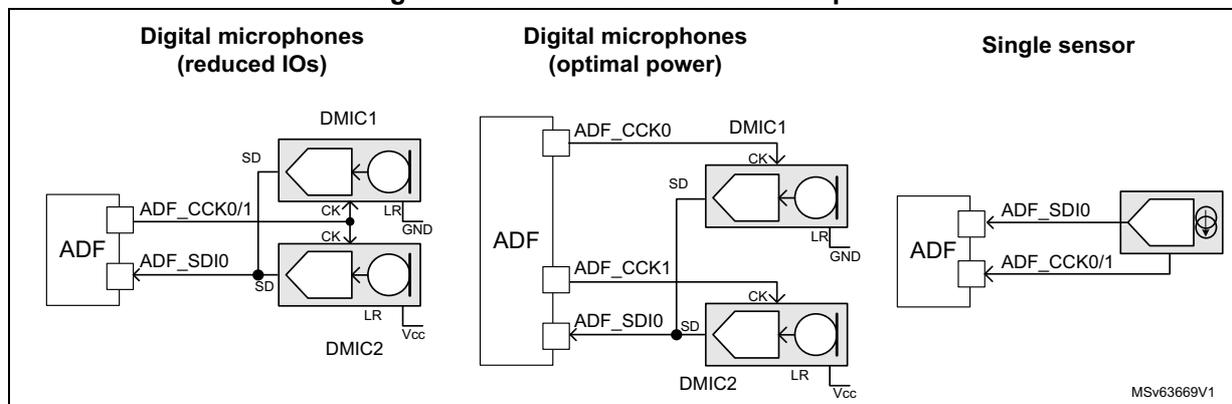
36.7.4 Global frequency response
Figure 380 shows the global frequency response for a 16 kHz audio signal with a digital microphone working at 1.024 MHz. The filter configuration is the following:
- • CIC order 4 or 5, with a decimation ratio of 16
- • RSFLT enabled, with a decimation ratio of 4
- • HPF enabled with a cut-off frequency of 40 Hz
Figure 381 shows the theoretical frequency response using a CIC4 and a CIC5.
Figure 381. Global frequency response
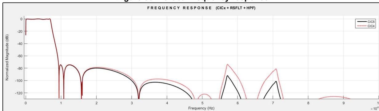
Figure 382 shows the in-band ripple for a 16 kHz audio signal with a digital microphone working at 1.024 MHz. The filter configuration is the following:
- • CIC order 4 or 5, with a decimation ratio of 16
- • RSFLT enabled, with a decimation ratio of 4
- • HPF enabled with a cut-off frequency of 20 Hz
The resulting in-band ripple is \( \pm 0.41 \) dB for CIC5, and \( \pm 0.45 \) dB for CIC4.
The - 3 dB cut-off frequency is 7061 Hz.
Figure 382. Detailed frequency response
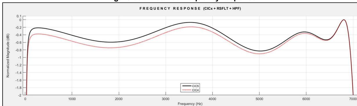
36.7.5 Total ADF gain
This section details how to compute the signal level provided by the ADF according to the filter settings.
A signal level may be expressed in dBFS (decibel full scale). A 0 dBFS level is assigned to the maximum possible digital level. For example, a signal that reaches 50 % of the maximum level, has a – 6 dBFS level (6 dB below full scale).
For example, for the ADF offering a final data width of 24 bits, a signal having an amplitude of \( 2 \cdot 10^6 \) LSB has a level of:
In addition, the data size of a signal having an amplitude (Amp) expressed in LSB is given by:
One bit need to be added for negative values.
So a signal having an amplitude of \( 2 \cdot 10^6 \) LSB, has a data size of 21.9 bits.
CIC gain
The CIC gain ( \( G_{\text{CIC}} \) and \( G_{\text{dBCIC}} \) ) can be deduced from the following formula giving data size in bits ( \( DS_{\text{CIC}} \) ).
where N represents the CIC order (selected by CICMOD[2:0]), and D1 is the decimation ratio (given by MCICD[8:0]).
\( DS_{\text{in}} \) represents the data size (in bits) of the signal at CIC input.
Warning: \( DS_{\text{CIC}} \) is very important for CIC filter. In order to work fine, \( DS_{\text{CIC}} \) must not exceed 26 bits.
The CIC gain \( G_{\text{CIC}} \) is given by:
which gives in decibels:
Data size at SCALE output
The data size at SCALE output (including the CIC gain), is a key information as the RSFLT starts to have some saturations, if the peak-to-peak signal amplitude at SCALE output is higher than 22 bits.
If the RSFLT is bypassed, then a peak-to-peak signal amplitude of 24 bits is accepted.
The signal amplitude at SCALE output is:
\( G_{\text{dBSCALE}} \) represents the gain selected by SCALE[5:0], in dB.
\( Asout_{\text{SCALE}} \) is the signal amplitude at SCALE output (in LSB), and \( Asin_{\text{DFLT}} \) is the signal amplitude at CIC input (LSB).
The data size at SCALE output ( \( DS_{\text{SCALE}} \) ) is expressed in bits.
RSFLT gain
The RSFLT gain in the useful bandwidth is typically 9.5 dB, but due to ripple a margin of about \( \pm 0.41 \) dB must be considered.
Note: The HPF filter has a gain of 0 dB.
SAD gain
The SAD is using only the 16 MSB on the signal, as a consequence, from the SAD point of view, the truncation from 24 to 16 bits can be seen as an attenuation.
and
The Figure 383 shows a simplified view of the filter path and gives, for each significant component, the expression of the bit growth and the gain.
Figure 383. Simplified DFLT view with gain information
![Simplified DFLT view with gain information diagram showing signal flow from PCM[23:0] through various filter stages (SAD, HPF, RSFLT, SAT, SCALE, CIC) with associated gain and bit growth information.](/RM0486-STM32N6x5-x7/5f84f6a39d40a9f9277bd245b057470d_img.jpg)
The diagram illustrates the signal path and gain components of the Audio Digital Filter (ADF). The input signal PCM[23:0] is processed through a series of stages: SAD, HPF, RSFLT, SAT, SCALE, and CIC. The gain for each stage is provided in both linear and dB formats. The SAD stage is optional, as indicated by the note (1). The gain for the SCALE stage is calculated as \( G_{SCALE} = 10^{\frac{GdB_{SCALE}}{20}} \) . The gain for the CIC stage is \( G_{CIC} = D1^N \) . The gain in dB for the CIC stage is \( GdB_{CIC} = 20 \times \log_{10}(D1^N) \) . The gain for the RSFLT stage is \( G_{RSFLT} = 2.98 \) and \( GdB_{RSFLT} = 9.5 \) dB. The gain for the HPF stage is \( G_{HPF} = 1 \) and \( GdB_{HPF} = 0 \) dB. The gain for the SAD stage is \( G_{SAD} = 0.00391 \) and \( GdB_{SAD} = -48.1 \) dB. The gain for the SAT stage is not explicitly given but is part of the filter chain. The gain for the SCALE stage is \( G_{SCALE} = 10^{\frac{GdB_{SCALE}}{20}} \) and \( GdB_{SCALE} \) is not explicitly given. The gain for the CIC stage is \( G_{CIC} = D1^N \) and \( GdB_{CIC} = 20 \times \log_{10}(D1^N) \) . The gain for the RSFLT stage is \( G_{RSFLT} = 2.98 \) and \( GdB_{RSFLT} = 9.5 \) dB. The gain for the HPF stage is \( G_{HPF} = 1 \) and \( GdB_{HPF} = 0 \) dB. The gain for the SAD stage is \( G_{SAD} = 0.00391 \) and \( GdB_{SAD} = -48.1 \) dB. The gain for the SAT stage is not explicitly given but is part of the filter chain. The gain for the SCALE stage is \( G_{SCALE} = 10^{\frac{GdB_{SCALE}}{20}} \) and \( GdB_{SCALE} \) is not explicitly given. The gain for the CIC stage is \( G_{CIC} = D1^N \) and \( GdB_{CIC} = 20 \times \log_{10}(D1^N) \) .
(1) The SAD is not always implemented (see the ADF implementation section for details).
MSv62698V1
Table 313 summarizes of the final data size for different filter configurations.
Table 313. Output signal levels
| Filter configurations | Final signal amplitude (LSB) |
|---|---|
| CIC + RSFLT + HPF + SAD | Samples provided to the RXFIFO: \[
Asout_{RXFIFO} = D1^N \times 10^{\frac{GdB_{SCALE}}{20}} \times 10^{\frac{9.5}{20}} \times Asin_{DFLT}
\] Samples provided to the SAD: \[
Asout_{SAD} = D1^N \times 10^{\frac{GdB_{SCALE}}{20}} \times 10^{\frac{9.5}{20}} \times 0.003906 \times Asin_{DFLT}
\] DS SCALE must be lower than 22 bits. |
| CIC + RSFLT (+ HPF) | \[
Asout_{HPF} = D1^N \times 10^{\frac{GdB_{SCALE}}{20}} \times 10^{\frac{9.5}{20}} \times Asin_{DFLT}
\] DS SCALE must be lower than 22 bits. |
| CIC (+ HPF) | \[
Asout_{HPF} = D1^N \times 10^{\frac{GdB_{SCALE}}{20}} \times Asin_{DFLT}
\] DS SCALE must be lower than 24 bits. |
Example using the main filter chain
If the ADF filter is programmed as follows:
- • The input signal is coming from a serial interface (Dsin RSFLT = 1 bit).
- • CIC order = 5 (N), with a decimation value of 24 (D1).
- • SCALE[5:0] is set to - 12 dB.
- • RSFLT enabled, and the decimation by four is enabled.
- • HPF is enabled.
Check first the data size at CIC output:
The size is lower than 26 bits, so the CIC works in good conditions.
The data size at CIC output is very close to 24 bits, so the SCALE must be adjusted in order to provide a 22-bit max signal to the RSFLT. An attenuation of 12 dB is needed.
Then the signal level provided to the RSFLT is:
If a higher gain is used, the RSFLT may saturate the output signal for strong input signals.
At the end, the final signal amplitude is:
or:
36.7.6 How to compute SAD thresholds
The SAD does not compute the RMS value of the converted signal, but the average of the absolute values. As a consequence, the estimated level differs from the RMS value of the signal:
- • For a sine signal having an RMS value of 1, the SAD computes a level of 0.9.
- • For a white or pink noise signal having an RMS value of 1, the SAD computes a level of about 0.8.
Note: FRSIZE[2:0] has a big influence on the accuracy of the level estimation: big FRSIZE[2:0] values give better results.
Threshold programming with SADMOD = 01
Consider the case of a sound capture where the application wants to wake up the system when the captured sound is bigger than 63 dB SPL.
The sound capture can be performed with a digital microphone such as the MP45DT02.
The sensitivity of this microphone is typically -26 dBFS for an input signal of 94 dB SPL.
An acoustic signal at 63 dB SPL produces a digital signal of about:
\(
-26 \text{ dBFS} - (94 - 63) = -57 \text{ dBFS}
\)
.
- • SCALE value adjustment
For this example, the filter configuration is the following:
- – CIC5 with a decimation by 16
- – RSFLT enabled with a decimation by 4
- – HPF enabled
A SCALE value of 3.5 dB is recommended for this configuration. As DFTL0 provides samples only used for a sound detection (samples not provided to the application), a bigger gain value can be applied: it increases the SAD accuracy and a saturation does not affect the SAD behavior (for example, a SCALE value of 15.6 dB).
- • Input signal amplitude
The input signal is
\(
-57 \text{ dBFS}
\)
, corresponding to an amplitude
\(
A_{\text{sin}} = 10^{(-57/20)} = 0.00141 \text{ LSB}
\)
.
- • Signal level at SAD input
The total filter gain for the SAD is:
The signal amplitude received by the SAD is:
The gain can be increased if the expected amplitude is too small. For the targeted application, 104 LSB is fine.
If the input signal is expected to be a sine, the sound level for a signal amplitude of 104 LSB is:
where 0.9 is the correction factor to apply with respect to the RMS value.
- • Program the trigger value
ANMIN and SNTHR must be programmed to trigger the SAD when the input signal level reaches 66 LSB.
For \( \text{SADMOD}[1:0] = 01 \) , the threshold value is given by:
where \( \text{GdB}_{\text{SNTHR}} \) represents the decibel value selected by \( \text{SNTHR}[3:0] \) .
When \( \text{SNTHR}[3:0] = 6 \text{ dB} \) for example, this formula becomes:
So \( \text{ANMIN} = \text{THRH}/2 = 66 / 2 = 33 \text{ LSB} \) .
In Figure 383 , the trigger value (THRH in red) is fixed to 66 LSB. The input signal is at \( -65 \text{ dBFS} \) during 256 samples, then its value goes to \( -55 \text{ dB} \) for 256 samples, and finally it is reduced to \( -60 \text{ dBFS} \) .
The blue curve is showing the sound level estimation (SDLVL) versus time. Fluctuation on the estimated value can be observed due to windowing effect of FRSIZE samples.
The SAD DETECT state (when green signal is high) is maintained during four additional frames due to hangover function value.
In this example ANSLP = FRSIZE = 3 (64 samples), LFRNB = 0 (2 frames), HGOVR = 0 (4 frames), SNTHR = 1 (6 dB) and ANMIN = 33.
Figure 384. SAD example working with SADMOD = 01
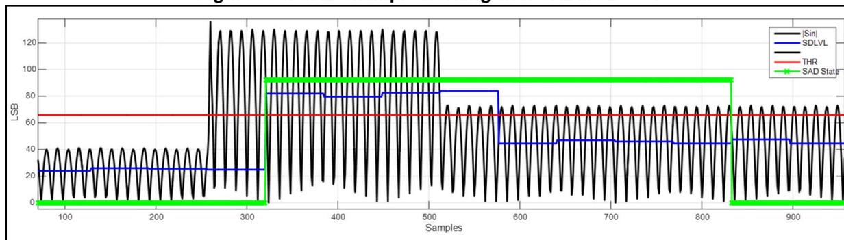
Threshold programming with SADMOD = 1x
Consider the case of a sound capture where the application wants to wake up the system when the captured sound is bigger than 57 dB SPL.
The sound capture can be performed with a digital microphone such as the MP45DT02. The sensitivity of this microphone is typically - 26 dBFS for an input signal of 94 dB SPL.
An acoustic signal at 57 dB SPL produces a digital signal of about:
- • Adjust SCALE value
For this example, the filter configuration is the following:
- – CIC4 with a decimation by 48
- – RSFLT bypassed
- – HPF enabled
A SCALE value of 3.5 dB is recommended for this configuration. The samples provided by DFTL0 are only used for a sound detection, without providing the samples to the application, a bigger gain value can be provided: it increases the SAD accuracy and a saturation does not affect the SAD behavior (for example, a SCALE value of 24 dB).
- • Input signal amplitude
The input signal is - 63 dBFS, corresponding to an amplitude:
- • Signal level at SAD input
The total filter gain for the SAD is:
The signal amplitude received by the SAD is:
The gain can be increased if the expected amplitude is too small.
If the input signal is expected to be a sine, the sound level for a signal amplitude of 232 LSB is:
where 0.9 is the correction factor to apply with respect to the RMS value.
Note: ANLVL converges to average of SDLVL values, with a long constant time.
So
\(
\text{SDLVL} \sim \text{ANLVL} = 148 \text{ LSB}
\)
for a constant input signal at 57 dB SPL.
- • Programming trigger value
For \( \text{SADMOD} = 1' \) , the SAD compares the estimated ambient noise multiplied by the gain selected by \( \text{SNTHR}[3:0] \) to \( \text{ANMIN}[12:0] * 4 \) .
For simplification, \( \text{SNTHR}[3:0] \) is set to 1 (6 dB), meaning that ANLVL is multiplied by two.
The SAD triggers if \( 2 * \text{ANLVL} > \text{THRH} \) .
In this mode:
So the SAD triggers if:
So \( \text{ANMIN} = 148 / 2 = 74 \text{ LSB} \)
In Figure 384 , the trigger value (THRH in red) is fixed to 148 LSB. The input signal is at - 75 dBFS during 512 samples, then its value goes to - 62 dB for 11000 samples, and finally it is reduced to - 70 dBFS.
The blue curve shows the sound level estimation (SDLVL) versus time. The black curve shows the ambient noise estimation versus time, increasing or decreasing logarithmically. During the learning phase, it reaches the SDLVL value.
In this example \( \text{ANS LP} = 6 \) , \( \text{FRSIZE} = 3 \) (64 samples), \( \text{LFRNB} = 0 \) (2 frames), \( \text{HGOVR} = 0 \) (4 frames), \( \text{SNTHR} = 1 \) (6 dB) and \( \text{ANMIN} = 74 \) .
Figure 385. SAD example working with \( \text{SADMOD} = 1x \)
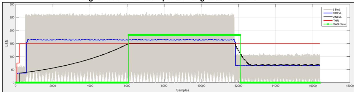
36.8 ADF registers
All the ADF registers must be accessed either in word (32-bit) or half-word (16-bit) formats.
36.8.1 ADF global control register (ADF_GCR)
Address offset: 0x000
Reset value: 0x0000 0000
| 31 | 30 | 29 | 28 | 27 | 26 | 25 | 24 | 23 | 22 | 21 | 20 | 19 | 18 | 17 | 16 |
|---|---|---|---|---|---|---|---|---|---|---|---|---|---|---|---|
| Res. | Res. | Res. | Res. | Res. | Res. | Res. | Res. | Res. | Res. | Res. | Res. | Res. | Res. | Res. | Res. |
| 15 | 14 | 13 | 12 | 11 | 10 | 9 | 8 | 7 | 6 | 5 | 4 | 3 | 2 | 1 | 0 |
| Res. | Res. | Res. | Res. | Res. | Res. | Res. | Res. | Res. | Res. | Res. | Res. | Res. | Res. | Res. | TRGO |
| r/w |
Bits 31:1 Reserved, must be kept at reset value.
Bit 0 TRGO : Trigger output control
This bit is set by software and reset by hardware. It is used to start the acquisition of several filters synchronously. It is also used to synchronize several ADF together by controlling the adf_trgo signal.
0: Write 0 has no effect. Read 0 means that the trigger can be set again to 1.
1: Write 1 generates a positive pulse on the adf_trgo signal and triggers the acquisition on enabled filter having their ACQMOD[2:0] = 01x and selecting TRGO as trigger. Read 1 means that the trigger pulse is still active.
36.8.2 ADF clock generator control register (ADF_CKGCR)
Address offset: 0x004
Reset value: 0x0000 0000
This register is used to control the clock generator. The clock adf_proc_ck must be enabled before enabling other ADF parts.
| 31 | 30 | 29 | 28 | 27 | 26 | 25 | 24 | 23 | 22 | 21 | 20 | 19 | 18 | 17 | 16 |
|---|---|---|---|---|---|---|---|---|---|---|---|---|---|---|---|
| CKGA CTIVE | PROCDIV[6:0] | Res. | Res. | Res. | Res. | CCKDIV[3:0] | |||||||||
| r | rw | rw | rw | rw | rw | rw | rw | rw | rw | rw | rw | ||||
| 15 | 14 | 13 | 12 | 11 | 10 | 9 | 8 | 7 | 6 | 5 | 4 | 3 | 2 | 1 | 0 |
| TRGSRC[3:0] | Res. | Res. | Res. | TRGSE NS | Res. | CCK1D IR | CCK0D IR | CKGM OD | Res. | CCK1E N | CCK0E N | CKGD EN | |||
| rw | rw | rw | rw | rw | rw | rw | rw | rw | rw | rw | |||||
Bit 31 CKGACTIVE : Clock generator active flag
This bit is set and cleared by hardware. It is used by the application to check if the clock generator is effectively enabled (active) or not. The protected fields of this function can only be updated when CKGACTIVE = 0 (see Section 36.4.13: Register protection for details).
The delay between a transition on CKGDEN and a transition on CKGACTIVE is two periods of AHB clock and two 2 periods of adf_proc_ck.
0: The clock generator is not active and can be configured if needed.
1: The clock generator is active and protected fields cannot be configured.
Bits 30:24 PROCDIV[6:0] : Divider to control the serial interface clock
This bitfield is set and reset by software. It is used to adjust the frequency of the clock provided to the SITF.
This bitfield must not be changed if the filter is enabled (DFTEN = 1).
0: adf_ker_ck provided to the SITF
1: adf_ker_ck / 2 provided to the SITF
2: adf_ker_ck / 3 provided to the SITF
...
127: adf_ker_ck / 128 provided to the SITF
Note: This bitfield can be write-protected (see Section 36.4.13: Register protection for details).
Bits 23:20 Reserved, must be kept at reset value.
Bits 19:16 CCKDIV[3:0] : Divider to control the ADF_CCK clock
This bitfield is set and reset by software. It is used to adjust the frequency of the ADF_CCK clock. The input clock of this divider is the clock provided to the SITF. More globally, the frequency of the ADF_CCK is given by the following formula:
This bitfield must not be changed if the filter is enabled (DFTEN = 1).
0000: The ADF_CCK clock is adf_proc_ck.
0001: The ADF_CCK clock is adf_proc_ck / 2.
0010: The ADF_CCK clock is adf_proc_ck / 3.
...
1111: The ADF_CCK clock is adf_proc_ck / 16.
Note: This bitfield can be write-protected (see Section 36.4.13: Register protection for details).
Bits 15:12 TRGSRC[3:0] : Digital filter trigger signal selection
This bitfield is set and cleared by software. It is used to select which external signals trigger the corresponding filter. This bitfield is not significant if the CKGMOD = 0.
000x: TRGO selected
0010: adf_trg1 selected
Others: Reserved
Note: This bitfield can be write-protected (see Section 36.4.13: Register protection for details).
Bits 11:9 Reserved, must be kept at reset value.
Bit 8 TRGSENS : CKGEN trigger sensitivity selection
This bit is set and cleared by software. It is used to select the trigger sensitivity of the trigger signals. This bit is not significant if the CKGMOD = 0.
0: A rising edge event triggers the activation of CKGEN dividers.
1: A falling edge even triggers the activation of CKGEN dividers.
Note: When the trigger source is TRGO, the sensitivity is forced to falling edge, thus TRGSENS value is not taken into account. This bit can be write-protected (see Section 36.4.13: Register protection for details).
Bit 7 Reserved, must be kept at reset value.
Bit 6 CCK1DIR : ADF_CCK1 directionThis bit is set and reset by software. It is used to control the direction of the ADF_CCK1 pin.
0: The ADF_CCK1 pin direction is in input.
1: The ADF_CCK1 pin direction is in output.
Note: This bit can be write-protected (see Section 36.4.13: Register protection for details).
Bit 5 CCK0DIR : ADF_CCK0 directionThis bit is set and reset by software. It is used to control the direction of the ADF_CCK0 pin.
0: The ADF_CCK0 pin direction is in input.
1: The ADF_CCK0 pin direction is in output.
Note: This bit can be write-protected (see Section 36.4.13: Register protection for details).
Bit 4 CKGMOD : Clock generator modeThis bit is set and reset by software. It is used to define the way the clock generator is enabled. This bit must not be changed if the filter is enabled (DFTEN = 1).
0: The kernel clock is provided to the dividers as soon as CKGDEN is set to 1.
1: The kernel clock is provided to the dividers when CKGDEN is set to 1 and the trigger condition met.
Note: This bit can be write-protected (see Section 36.4.13: Register protection for details).
Bit 3 Reserved, must be kept at reset value.
Bit 2 CCK1EN : ADF_CCK1 clock enableThis bit is set and reset by software. It is used to control the generation of the bitstream clock on the ADF_CCK1 pin.
0: Bitstream clock not generated
1: Bitstream clock generated on the ADF_CCK1 pin.
Bit 1 CCK0EN : ADF_CCK0 clock enableThis bit is set and reset by software. It is used to control the generation of the bitstream clock on the ADF_CCK0 pin.
0: Bitstream clock not generated
1: Bitstream clock generated on the ADF_CCK0 pin
Bit 0 CKGDEN : CKGEN dividers enableThis bit is set and reset by software. It is used to enable/disable the clock dividers of the CKGEN: PROCDIV and CCKDIV.
0: CKGEN dividers disabled
1: CKGEN dividers enabled
36.8.3 ADF serial interface control register 0 (ADF_SITF0CR)
Address offset: 0x080
Reset value: 0x0000 1F00
This register is used to control the serial interface SITF0.
| 31 | 30 | 29 | 28 | 27 | 26 | 25 | 24 | 23 | 22 | 21 | 20 | 19 | 18 | 17 | 16 |
|---|---|---|---|---|---|---|---|---|---|---|---|---|---|---|---|
| SITFAC TIVE | Res. | Res. | Res. | Res. | Res. | Res. | Res. | Res. | Res. | Res. | Res. | Res. | Res. | Res. | Res. |
| r | |||||||||||||||
| 15 | 14 | 13 | 12 | 11 | 10 | 9 | 8 | 7 | 6 | 5 | 4 | 3 | 2 | 1 | 0 |
| Res. | Res. | Res. | STH[4:0] | Res. | Res. | SITFMOD[1:0] | Res. | SCKSRC[1:0] | SITFE N | ||||||
| rw | rw | rw | rw | rw | rw | rw | rw | rw | rw | ||||||
Bit 31 SITFAACTIVE : Serial interface active flag
This bit is set and cleared by hardware. It is used by the application to check if the serial interface is effectively enabled (active) or not. The protected fields of this function can only be updated when SITFAACTIVE is set to 0 (see Section 36.4.13: Register protection for details). The delay between a transition on SITFEN and a transition on SITFAACTIVE is two periods of AHB clock and two periods of adf_proc_ck.
0: The serial interface is not active, and can be configured if needed.
1: The serial interface is active and protected fields cannot be configured.
Bits 30:13 Reserved, must be kept at reset value.
Bits 12:8 STH[4:0] : Manchester symbol threshold/SPI threshold
This bitfield is set and cleared by software. It is used for Manchester mode to define the expected symbol threshold levels (see Manchester mode for details on computation).
In addition this bitfield is used to define the timeout value for the clock absence detection in Normal SPI mode. STH[4:0] values lower than four are invalid.
Note: This bitfield can be write-protected (see Section 36.4.13: Register protection for details).
Bits 7:6 Reserved, must be kept at reset value.
Bits 5:4 SITFMOD[1:0] : Serial interface type
This bitfield is set and cleared by software. It is used to define the serial interface type.
00: LF_MASTER SPI mode
01: Normal SPI mode
10: Manchester mode: rising edge = logic 0, falling edge = logic 1
11: Manchester mode: rising edge = logic 1, falling edge = logic 0
Note: This bitfield can be write-protected (see Section 36.4.13: Register protection for details).
Bit 3 Reserved, must be kept at reset value.
Bits 2:1 SCKSRC[1:0] : Serial clock source
This bitfield is set and cleared by software. It is used to select the clock source of the serial interface.
00: Serial clock source is ADF_CCK0.
01: Serial clock source is ADF_CCK1.
others: reserved
Note: This bitfield can be write-protected (see Section 36.4.13: Register protection for details).
Bit 0 SITFEN : Serial interface enable
This bit is set and cleared by software. It is used to enable/disable the serial interface.
0: Serial interface disabled
1: Serial interface enabled
36.8.4 ADF bitstream matrix control register 0 (ADF_BSMX0CR)
Address offset: 0x084
Reset value: 0x0000 0000
This register is used to select the bitstream to be provided to DFLT0.
| 31 | 30 | 29 | 28 | 27 | 26 | 25 | 24 | 23 | 22 | 21 | 20 | 19 | 18 | 17 | 16 |
|---|---|---|---|---|---|---|---|---|---|---|---|---|---|---|---|
| BSMXA CTIVE | Res. | Res. | Res. | Res. | Res. | Res. | Res. | Res. | Res. | Res. | Res. | Res. | Res. | Res. | Res. |
| r | |||||||||||||||
| 15 | 14 | 13 | 12 | 11 | 10 | 9 | 8 | 7 | 6 | 5 | 4 | 3 | 2 | 1 | 0 |
| Res. | Res. | Res. | Res. | Res. | Res. | Res. | Res. | Res. | Res. | Res. | BSSEL[4:0] | ||||
| rw | rw | rw | rw | rw | |||||||||||
Bit 31 BSMXACTIVE : BSMX active flag
This bit is set and cleared by hardware. It is used by the application to check if the BSMX is effectively enabled (active) or not. BSSEL[4:0] can only be updated when BSMXACTIVE is set to 0. This BSMXACTIVE flag cannot go to 0 if DFLT0 is enabled.
0: BSMX is not active and can be configured if needed.
1: BSMX is active and protected fields cannot be configured.
Bits 30:5 Reserved, must be kept at reset value.
Bits 4:0 BSSEL[4:0] : Bitstream selection
This bitfield is set and cleared by software. It is used to select the bitstream to be processed for DFLT0.
00000: bs0_r provided to DFLT0
00001: bs0_f provided to DFLT0
others: reserved
Note: This bitfield can be write-protected (see Section 36.4.13: Register protection for details).
36.8.5 ADF digital filter control register 0 (ADF_DFLT0CR)
Address offset: 0x088
Reset value: 0x0000 0000
| 31 | 30 | 29 | 28 | 27 | 26 | 25 | 24 | 23 | 22 | 21 | 20 | 19 | 18 | 17 | 16 |
|---|---|---|---|---|---|---|---|---|---|---|---|---|---|---|---|
| DFLT0A CTIVE | DFLT0R UN | Res. | Res. | NBDIS[7:0] | Res. | Res. | Res. | Res. | |||||||
| r | r | rw | rw | rw | rw | rw | rw | rw | rw | ||||||
| 15 | 14 | 13 | 12 | 11 | 10 | 9 | 8 | 7 | 6 | 5 | 4 | 3 | 2 | 1 | 0 |
| TRGSRC[3:0] | Res. | Res. | Res. | TRGSE NS | Res. | ACQMOD[2:0] | Res. | FTH | DMAE N | DFLTE N | |||||
| rw | rw | rw | rw | rw | rw | rw | rw | rw | rw | w | |||||
Bit 31 DFLT0ACTIVE : DFLT0 active flag
This bit is set and cleared by hardware. It indicates if DFLT0 is active: can be running or waiting for events.
0: DFLT0 not active (can be re-enabled again, via DFLTEN bit, if needed)
1: DFLT0 active
Bit 30 DFLTRUN : DFLT0 run status flag
This bit is set and cleared by hardware. It indicates if DFLT0 is running or not.
0: DFLT0 not running and ready to accept a new trigger event
1: DFLT0 running
Bits 29:28 Reserved, must be kept at reset value.
Bits 27:20 NBDIS[7:0] : Number of samples to be discarded
This bitfield is set and cleared by software. It is used to define the number of samples to be discarded every time DFLT0 is re-started.
0: No sample discarded
1: 1 sample discarded
2: 2 samples discarded
...
255: 255 samples discarded
Note: This bitfield can be write-protected (see Section 36.4.13: Register protection for details).
Bits 19:16 Reserved, must be kept at reset value.
Bits 15:12 TRGSRC[3:0] : DFLT0 trigger signal selection
This bitfield is set and cleared by software. It is used to select which external signals trigger DFLT0.
0000: TRGO selected
0010: adf_trgi selected
Others: Reserved
Note: This bitfield can be write-protected (see Section 36.4.13: Register protection for details).
Bits 11:9 Reserved, must be kept at reset value.
Bit 8 TRGSENS : DFLT0 trigger sensitivity selection
This bitfield is set and cleared by software. It is used to select the trigger sensitivity of the external signals
0: A rising edge event triggers the acquisition.
1: A falling edge even triggers the acquisition.
Note: When the trigger source is TRGO, TRGSENS value is not taken into account. When TRGO is selected, the sensitivity is forced to falling edge.
This bit can be write-protected (see Section 36.4.13: Register protection for details).
Bit 7 Reserved, must be kept at reset value.
Bits 6:4 ACQMOD[2:0] : DFLT0 trigger mode
This bitfield is set and cleared by software. It is used to select the filter trigger mode.
000: Asynchronous continuous acquisition mode
001: Asynchronous single-shot acquisition mode
010: Synchronous continuous acquisition mode
011: Synchronous single-shot acquisition mode
100: Window continuous acquisition mode
Others: Same as 000
Note: This bitfield can be write-protected (see Section 36.4.13: Register protection for details).
Bit 3 Reserved, must be kept at reset value.
Bit 2 FTH : RXFIFO threshold selection
This bit is set and cleared by software. It is used to select the RXFIFO threshold.
0: RXFIFO threshold event generated when the RXFIFO is not empty
1: RXFIFO threshold event generated when the RXFIFO is half-full
Note: This bit can be write-protected (see Section 36.4.13: Register protection for details).
Bit 1 DMAEN : DMA requests enable
This bit is set and cleared by software. It is used to control the generation of DMA request to transfer the processed samples into the memory.
0: DMA interface for the corresponding digital filter disabled
1: DMA interface for the corresponding digital filter enabled
Note: This bit can be write-protected (see Section 36.4.13: Register protection for details).
Bit 0 DFLTEN : DFLT0 enable
This bit is set and cleared by software. It is used to control the start of acquisition of the DFLT0 path. This bit behavior depends on ACQMOD[2:0] and external events. The serial or parallel interface delivering the samples must be enabled as well.
0: Acquisition immediately stopped
1: Acquisition immediately started if ACQMOD[2:0] = 00x or 101, or acquisition started when the proper trigger event occurs if ACQMOD[2:0] = 01x.
36.8.6 ADF digital filter configuration register 0 (ADF_DFLT0CICR)
Address offset: 0x08C
Reset value: 0x0000 0000
This register is used to control the main CIC filter.
| 31 | 30 | 29 | 28 | 27 | 26 | 25 | 24 | 23 | 22 | 21 | 20 | 19 | 18 | 17 | 16 |
|---|---|---|---|---|---|---|---|---|---|---|---|---|---|---|---|
| Res. | Res. | Res. | Res. | Res. | Res. | SCALE[5:0] | Res. | Res. | Res. | MCICD 8 | |||||
| rw | rw | rw | rw | rw | rw | rw | |||||||||
| 15 | 14 | 13 | 12 | 11 | 10 | 9 | 8 | 7 | 6 | 5 | 4 | 3 | 2 | 1 | 0 |
| MCICD[7:0] | Res. | CICMOD[2:0] | Res. | Res. | DATSRC[1:0] | ||||||||||
| rw | rw | rw | rw | rw | rw | rw | rw | rw | rw | rw | rw | rw | |||
Bits 31:26 Reserved, must be kept at reset value.
Bits 25:20 SCALE[5:0] : Scaling factor selection
This bitfield is set and cleared by software. It is used to select the gain to be applied at CIC output (see Table 301 for details). If the application attempts to write a new gain value while the previous one is not yet applied, this new gain value is ignored. Reading back this bitfield informs the application on the current gain value.
000000: 0 dB
000001: + 3.5 dB
000010: + 6 dB or shift left by 1 bit
...
011000: + 72 dB or shift left by 12 bits
100000: - 48.2 dB or shift right by 8 bits (default value)
100001: - 44.6 dB
100010: - 42.1 dB or shift right by 7 bits
100011: - 38.6 dB
...
101110: -6 dB or shift right by 1 bit
101111: -2.5 dB
Others: Reserved
Bits 19:17 Reserved, must be kept at reset value.
Bits 16:8 MCICD[8:0] : CIC decimation ratio selection
This bitfield is set and cleared by software. It is used to select the CIC decimation ratio. A decimation ratio smaller than two is not allowed. The decimation ratio is given by (CICDEC+1).
0: Decimation ratio is 2.
1: Decimation ratio is 2.
2: Decimation ratio is 3.
3: Decimation ratio is 4.
...
511: Decimation ratio is 512.
Note: This bitfield can be write-protected (see Section 36.4.13: Register protection for details).
Bit 7 Reserved, must be kept at reset value.
Bits 6:4 CICMOD[2:0] : Select the CIC order
This bitfield is set and cleared by software. It is used to select the order of the MCIC.
100: MCIC configured in single Sinc 4 filter
101: MCIC configured in single Sinc 5 filter
Others: Reserved
Note: This bitfield can be write-protected (see Section 36.4.13: Register protection for details).
Bits 3:2 Reserved, must be kept at reset value.
Bits 1:0 DATSRC[1:0] : Source data for the digital filter
This bitfield is set and cleared by software.
0x: Stream coming from the BSMX selected
10: Stream coming from the ADCITF1 selected
11: Stream coming from the ADCITF2 selected
Note: This bitfield can be write-protected (see Section 36.4.13: Register protection for details).
36.8.7 ADF reshape filter configuration register 0 (ADF_DFLT0RSFR)
Address offset: 0x090
Reset value: 0x0000 0000
This register is used to control the reshape and HPF filter.
| 31 | 30 | 29 | 28 | 27 | 26 | 25 | 24 | 23 | 22 | 21 | 20 | 19 | 18 | 17 | 16 |
|---|---|---|---|---|---|---|---|---|---|---|---|---|---|---|---|
| Res. | Res. | Res. | Res. | Res. | Res. | Res. | Res. | Res. | Res. | Res. | Res. | Res. | Res. | Res. | Res. |
| 15 | 14 | 13 | 12 | 11 | 10 | 9 | 8 | 7 | 6 | 5 | 4 | 3 | 2 | 1 | 0 |
| Res. | Res. | Res. | Res. | Res. | Res. | HPFC[1:0] | HPFBYP | Res. | Res. | RSFLT | Res. | Res. | Res. | RSFLT | |
| rw | rw | rw | rw | rw | |||||||||||
Bits 31:10 Reserved, must be kept at reset value.
Bits 9:8 HPFC[1:0] : High-pass filter cut-off frequency
This bitfield is set and cleared by software. it is used to select the cut-off frequency of the high-pass filter. \( F_{PCM} \) represents the sampling frequency at HPF input.
00: Cut-off frequency = \( 0.000625 \times F_{PCM} \)
01: Cut-off frequency = \( 0.00125 \times F_{PCM} \)
10: Cut-off frequency = \( 0.00250 \times F_{PCM} \)
11: Cut-off frequency = \( 0.00950 \times F_{PCM} \)
Note: This bitfield can be write-protected (see Section 36.4.13: Register protection for details).
Bit 7 HPFBYP : High-pass filter bypass
This bit is set and cleared by software. It is used to bypass the high-pass filter.
0: HPF not bypassed (default value)
1: HPF bypassed
Note: This bit can be write-protected (see Section 36.4.13: Register protection for details).
Bits 6:5 Reserved, must be kept at reset value.
Bit 4 RSFLTD : Reshaper filter decimation ratio
This bit is set and cleared by software. It is used to select the decimation ratio for the reshape filter
0: Decimation ratio is 4 (default value).
1: Decimation ratio is 1.
Note: This bit can be write-protected (see Section 36.4.13: Register protection for details).
Bits 3:1 Reserved, must be kept at reset value.
Bit 0 RSFLTBYP : Reshaper filter bypass
This bit is set and cleared by software. It is used to bypass the reshape filter and its decimation block.
0: Reshape filter not bypassed (default value)
1: Reshape filter bypassed
Note: This bit can be write-protected (see Section 36.4.13: Register protection for details).
36.8.8 ADF delay control register 0 (ADF_DLY0CR)
Address offset: 0x0A4
Reset value: 0x0000 0000
This register is used for the adjustment stream delays.
| 31 | 30 | 29 | 28 | 27 | 26 | 25 | 24 | 23 | 22 | 21 | 20 | 19 | 18 | 17 | 16 |
|---|---|---|---|---|---|---|---|---|---|---|---|---|---|---|---|
| SKPBF | Res. | Res. | Res. | Res. | Res. | Res. | Res. | Res. | Res. | Res. | Res. | Res. | Res. | Res. | Res. |
| r | |||||||||||||||
| 15 | 14 | 13 | 12 | 11 | 10 | 9 | 8 | 7 | 6 | 5 | 4 | 3 | 2 | 1 | 0 |
| Res. | Res. | Res. | Res. | Res. | Res. | Res. | Res. | Res. | SKPDLY[6:0] | ||||||
| rw | rw | rw | rw | rw | rw | rw | |||||||||
Bit 31 SKPBF : Skip busy flag
This bit is set and cleared by hardware. It is used to control if the delay sequence is completed.
0: ADF ready to accept a new value into SKPDLY[6:0]
1: Last valid SKPDLY[6:0] still under processing
Bits 30:7 Reserved, must be kept at reset value.
Bits 6:0 SKPDLY[6:0] : Delay to apply to a bitstream
This bitfield is set and cleared by software. It defines the number of input samples that are skipped. Skipping is applied immediately after writing to this bitfield, if SKPBF = 0 and DFLTEN = 1. If SKPBF = 1, the value written into the register is ignored by the delay state machine.
0: No input sample skipped
1: 1 input sample skipped
...
127: 127 input samples skipped
36.8.9 ADF DFLT0 interrupt enable register (ADF_DFLT0IER)
Address offset: 0x0AC
Reset value: 0x0000 0000
This register is used for allowing or not the events to generate an interrupt.
| 31 | 30 | 29 | 28 | 27 | 26 | 25 | 24 | 23 | 22 | 21 | 20 | 19 | 18 | 17 | 16 |
|---|---|---|---|---|---|---|---|---|---|---|---|---|---|---|---|
| Res. | Res. | Res. | Res. | Res. | Res. | Res. | Res. | Res. | Res. | Res. | Res. | Res. | Res. | Res. | Res. |
| 15 | 14 | 13 | 12 | 11 | 10 | 9 | 8 | 7 | 6 | 5 | 4 | 3 | 2 | 1 | 0 |
| Res. | Res. | SDLVLIE | SDDETIE | RFOVRIE | CKABIE | SATIE | Res. | Res. | Res. | Res. | Res. | Res. | Res. | DOVRIE | FTHIE |
| rW | rW | rW | rW | rW | rW | rW |
Bits 31:14 Reserved, must be kept at reset value.
Bit 13 SDLVLIE : SAD sound-level value ready enable
This bit is set and cleared by software.
0: Sound-level-ready interrupt disabled
1: Sound-level-ready interrupt enabled
Bit 12 SDDETIE : Sound activity detection interrupt enable
This bit is set and cleared by software.
0: Sound-trigger interrupt disabled
1: Sound-trigger interrupt enabled
Bit 11 RFOVRIE : Reshape filter overrun interrupt enable
This bit is set and cleared by software.
0: Reshape filter overrun interrupt disabled
1: Reshape filter overrun interrupt enabled
Bit 10 CKABIE : Clock absence detection interrupt enable
This bit is set and cleared by software.
0: Clock absence interrupt disabled
1: Clock absence interrupt enabled
Bit 9 SATIE : Saturation detection interrupt enable
This bit is set and cleared by software.
0: Saturation interrupt disabled
1: Saturation interrupt enabled
Bits 8:2 Reserved, must be kept at reset value.
Bit 1 DOVRIE : Data overflow interrupt enable
This bit is set and cleared by software.
0: Data overflow interrupt disabled
1: Data overflow interrupt enabled
Bit 0 FTHIE : RXFIFO threshold interrupt enable
This bit is set and cleared by software.
0: RXFIFO threshold interrupt disabled
1: RXFIFO threshold interrupt enabled
36.8.10 ADF DFLT0 interrupt status register 0 (ADF_DFLT0ISR)
Address offset: 0x0B0
Reset value: 0x0000 0000
This register contains the status flags for the digital filter path.
| 31 | 30 | 29 | 28 | 27 | 26 | 25 | 24 | 23 | 22 | 21 | 20 | 19 | 18 | 17 | 16 |
|---|---|---|---|---|---|---|---|---|---|---|---|---|---|---|---|
| Res. | Res. | Res. | Res. | Res. | Res. | Res. | Res. | Res. | Res. | Res. | Res. | Res. | Res. | Res. | Res. |
| 15 | 14 | 13 | 12 | 11 | 10 | 9 | 8 | 7 | 6 | 5 | 4 | 3 | 2 | 1 | 0 |
| Res. | Res. | SDLVLF | SDDETF | RFOVRF | CKABF | SATF | Res. | Res. | Res. | Res. | Res. | RXNEF | Res. | DOVRF | FTHF |
| rc_w1 | rc_w1 | rc_w1 | rc_w1 | rc_w1 | r | rc_w1 | r |
Bits 31:14 Reserved, must be kept at reset value.
Bit 13 SDLVLF : Sound level value ready flag
This bit is set by hardware and cleared by software by writing this bit to 1.
0: Read 0 means that new sound level value is not ready. Write 0 has no effect.
1: Read 1 means that new sound level value is ready. Write 1 clears this flag.
Bit 12 SDDETF : Sound activity detection flag
This bit is set by hardware and cleared by software by writing this bit to 1.
0: Read 0 means that no sound activity is detected. Write 0 has no effect.
1: Read 1 means that sound activity is detected. Write 1 clears this flag.
Bit 11 RFOVRF : Reshape filter overrun detection flag
This bit is set by hardware and cleared by software by writing this bit to 1.
0: Read 0 means that no reshape filter overrun is detected. Write 0 has no effect.
1: Read 1 means that reshape filter overrun is detected. Write 1 clears this flag.
Bit 10 CKABF : Clock absence detection flag
This bit is set by hardware and cleared by software by writing this bit to 1.
0: Read 0 means that no clock absence is detected. Write 0 has no effect.
1: Read 1 means that a clock absence is detected. Write 1 clears this flag.
Bit 9 SATF : Saturation detection flag
This bit is set by hardware and cleared by software by writing this bit to 1.
0: Read 0 means that no saturation is detected. Write 0 has no effect.
1: Read 1 means that a saturation is detected. Write 1 clears this flag.
Bits 8:4 Reserved, must be kept at reset value.
Bit 3 RXNEF : RXFIFO not empty flag
This bit is set and cleared by hardware according to the RXFIFO level.
0: RXFIFO empty
1: RXFIFO not empty
Bit 2 Reserved, must be kept at reset value.
Bit 1 DOVRF : Data overflow flag
This bit is set by hardware and cleared by software by writing this bit to 1.
0: Read 0 means that no overflow is detected. Write 0 has no effect.
1: Read 1 means that an overflow is detected; Write 1 clears this flag.
Bit 0 FTHF : RXFIFO threshold flag
This bit is set by hardware, and cleared by the hardware when the RXFIFO level is lower than the threshold.
0: RXFIFO threshold not reached
1: RXFIFO threshold reached
36.8.11 ADF SAD control register (ADF_SADCR)
Address offset: 0x0B8
Reset value: 0x0000 0000
This register is used for the configuration and the control of the sound activity detection.
| 31 | 30 | 29 | 28 | 27 | 26 | 25 | 24 | 23 | 22 | 21 | 20 | 19 | 18 | 17 | 16 |
|---|---|---|---|---|---|---|---|---|---|---|---|---|---|---|---|
| SADACTIVE | Res. | Res. | Res. | Res. | Res. | Res. | Res. | Res. | Res. | Res. | Res. | Res. | Res. | Res. | Res. |
| r | |||||||||||||||
| 15 | 14 | 13 | 12 | 11 | 10 | 9 | 8 | 7 | 6 | 5 | 4 | 3 | 2 | 1 | 0 |
| Res. | Res. | SADMOD[1:0] | Res. | FRSIZE[2:0] | HYSTEN | Res. | SADST[1:0] | DETCFG | DATCAP[1:0] | SADEN | |||||
| rw | rw | rw | rw | rw | rw | r | r | rw | rw | rw | rw | ||||
Bit 31 SADACTIVE : SAD Active flag
This bit is set and cleared by hardware. It is used to check if the SAD is effectively enabled (active) or not. The protected fields and registers of this function can only be updated when the SADACTIVE is set to 0 (see Section 36.4.13: Register protection for details).
The delay between a transition on SADEN and a transition on SADACTIVE is two periods of AHB clock and two periods of adf_proc_ck.
0: SAD not active and can be configured if needed
1: SAD active and protected fields cannot be configured.
Bits 30:14 Reserved, must be kept at reset value.
Bits 13:12 SADMOD[1:0] : SAD working modeThis bitfield is set and cleared by software. It is used to define the way the SAD works.
00: Threshold value computed according to the estimated ambient noise
The SAD triggers when the sound level (SDLVL) is bigger than the defined threshold. In this mode, the SAD works like a voice activity detector.
01: Threshold value equal to ANMIN[12:0], multiplied by the gain selected by SNTHR[3:0]
The SAD triggers when the sound level (SDLVL) is bigger than the defined threshold. In this mode, the SAD works like a sound detector.
1x: Threshold value given by 4 x ANMIN[12:0]
The SAD triggers when the estimated ambient noise (ANLVL), multiplied by the gain selected by SNTHR[3:0] is bigger than the defined threshold. In this mode, the SAD is working like an ambient noise estimator. Hysteresis function cannot be used in this mode.
Note: This bitfield can be write-protected (see Section 36.4.13: Register protection for details).
Bit 11 Reserved, must be kept at reset value.
Bits 10:8 FRSIZE[2:0] : Frame sizeThis bitfield is set and cleared by software. it is used to define the size of one frame and also to define how many samples are taken into account to compute the short-term signal level.
000: 8 PCM samples used to compute the short-term signal level
001: 16 PCM samples used to compute the short-term signal level
010: 32 PCM samples used to compute the short-term signal level
011: 64 PCM samples used to compute the short-term signal level
100: 128 PCM samples used to compute the short-term signal level
101: 256 PCM samples used to compute the short-term signal level
11x: 512 PCM samples used to compute the short-term signal level
Note: This bitfield can be write-protected (see Section 36.4.13: Register protection for details).
Bit 7 HYSTEN : Hysteresis enableThis bit is set and cleared by software. It is used to enable/disable the hysteresis function (see Table 301 for details). This bit must be kept to 0 when SADMOD[1:0] = 1x.
0: Hysteresis function disabled. THR H is always used.
1: Hysteresis function enabled. THR H is used for MONITOR to DETECT transition and THR L is used for DETECT to MONITOR transition.
Note: This bit can be write-protected (see Section 36.4.13: Register protection for details).
Bit 6 Reserved, must be kept at reset value.
Bits 5:4 SADST[1:0] : SAD stateThis bitfield is set and cleared by hardware. It indicates the SAD state and is meaningful only when SADEN = 1. The SAD state can be:
- - LEARN when the SAD is in learning phase or in SDLVL computation mode
- - MONITOR when the SAD is in monitoring phase
- - DETECT when the SAD detects a sound
00: SAD in LEARN state
01: SAD in MONITOR state
11: SAD in DETECT state
Bit 3 DETCFG : Sound trigger event configurationThis bit is set and cleared by software. It is used to define if the sddet_evt event is generated only when the SAD enters to MONITOR state or when the SAD enters or exits the DETECT state.
0: sddet_evt generated when SAD enters the MONITOR state
1: sddet_evt generated when SAD enters or exits the DETECT state
Note: This bit can be write-protected (see Section 36.4.13: Register protection for details).
Bits 2:1 DATCAP[1:0] : Data capture mode
This bitfield is set and cleared by software. It is used to define in which conditions, the samples provided by DFLT0 are stored into the memory.
00: Samples from DFLT0 not transfered into the memory
01: Samples from DFLT0 transfered into the memory when SAD is in DETECT state
1x: Samples from DFLT0 transfered into memory when SAD and DFLT0 are enabled
Note: This bitfield can be write-protected (see Section 36.4.13: Register protection for details).
Bit 0 SADEN : Sound activity detector enable
This bit is set and cleared by software. It is used to enable/disable the SAD.
0: SAD disabled and SAD state reset
1: SAD enabled
36.8.12 ADF SAD configuration register (ADF_SADCFGR)
Address offset: 0x0BC
Reset value: 0x0000 0000
This register is used for the configuration of the sound activity detection.
| 31 | 30 | 29 | 28 | 27 | 26 | 25 | 24 | 23 | 22 | 21 | 20 | 19 | 18 | 17 | 16 |
|---|---|---|---|---|---|---|---|---|---|---|---|---|---|---|---|
| Res. | Res. | Res. | ANMIN[12:0] | ||||||||||||
| rw | rw | rw | rw | rw | rw | rw | rw | rw | rw | rw | rw | rw | |||
| 15 | 14 | 13 | 12 | 11 | 10 | 9 | 8 | 7 | 6 | 5 | 4 | 3 | 2 | 1 | 0 |
| Res. | HGOVR[2:0] | Res. | LFRNB[2:0] | Res. | ANSLP[2:0] | SNTHR[3:0] | |||||||||
| rw | rw | rw | rw | rw | rw | rw | rw | rw | rw | rw | rw | rw | |||
Bits 31:29 Reserved, must be kept at reset value.
Bits 28:16 ANMIN[12:0] : Minimum noise level
This bitfield is set and cleared by software. It is used to define the minimum noise level and then the sensitivity. It represents a positive number.
Note: This bitfield can be write-protected (see Section 36.4.13: Register protection for details).
Bit 15 Reserved, must be kept at reset value.
Bits 14:12 HGOVR[2:0] : Hangover time window
This bitfield is set and cleared by software. Once the SAD state is DETECT, this parameter is used to define the amount of time the sound is allowed to remain below the threshold, before switching the SAD to MONITOR state (see FRSIZE bitfield for the description of a frame).
000: SAD back to MONITOR state if sound is below threshold for 4 frames
001: SAD back to MONITOR state if sound is below threshold for 8 frames
010: SAD back to MONITOR state if sound is below threshold for 16 frames
011: SAD back to MONITOR state if sound is below threshold for 32 frames
100: SAD back to MONITOR state if sound is below threshold for 64 frames
101: SAD back to MONITOR state if sound is below threshold for 128 frames
110: SAD back to MONITOR state if sound is below threshold for 256 frames
111: SAD back to MONITOR state if sound is below threshold for 512 frames
Note: This bitfield can be write-protected (see Section 36.4.13: Register protection for details).
Bit 11 Reserved, must be kept at reset value.
Bits 10:8 LFRNB[2:0] : Number of learning frames
This bitfield is set and cleared by software. It is used to define the number of learning frames to perform the first estimate of the noise level.
000: 2 frames used to compute the initial noise level
001: 4 frames used to compute the initial noise level
010: 8 frames used to compute the initial noise level
011: 16 frames used to compute the initial noise level
1xx: 32 frames used to compute the initial noise level
Note: This bitfield can be write-protected (see Section 36.4.13: Register protection for details).
Bit 7 Reserved, must be kept at reset value.
Bits 6:4 ANSLP[2:0] : Ambient noise slope control
This bitfield is set and cleared by software. It is used to define the positive and negative slope of the noise estimator, in charge of updating the ANLVL (see Ambient noise estimation (ANLVL) for information about programming this bitfield).
Note: This bitfield can be write-protected (see Section 36.4.13: Register protection for details).
Bits 3:0 SNTHR[3:0] : Signal to noise threshold
This bitfield is set and cleared by software. It is used to define \( THR_H \) (and \( THR_L \) if hysteresis is enabled). See Table 301 for details.
0000: \( THR_H \) is 3.5 dB higher than ANLVL
0001: \( THR_H \) is 6.0 dB higher than ANLVL
0010: \( THR_H \) is 9.5 dB higher than ANLVL
0011: \( THR_H \) is 12 dB higher than ANLVL
0100: \( THR_H \) is 15.6 dB higher than ANLVL
0101: \( THR_H \) is 18 dB higher than ANLVL
0110: \( THR_H \) is 21.6 dB higher than ANLVL
0111: \( THR_H \) is 24.1 dB higher than ANLVL
1000: \( THR_H \) is 27.6 dB higher than ANLVL
1001: \( THR_H \) is 30.1 dB higher than ANLVL
others: Reserved
Note: This bitfield can be write-protected (see Section 36.4.13: Register protection for details).
36.8.13 ADF SAD sound level register (ADF_SADSDLVR)
Address offset: 0x0C0
Reset value: 0x0000 0000
This register contains the short-term sound-level computed by the SAD.
| 31 | 30 | 29 | 28 | 27 | 26 | 25 | 24 | 23 | 22 | 21 | 20 | 19 | 18 | 17 | 16 |
|---|---|---|---|---|---|---|---|---|---|---|---|---|---|---|---|
| Res | Res | Res | Res | Res | Res | Res | Res | Res | Res | Res | Res | Res | Res | Res | Res |
| 15 | 14 | 13 | 12 | 11 | 10 | 9 | 8 | 7 | 6 | 5 | 4 | 3 | 2 | 1 | 0 |
| Res. | SDLVL[14:0] | ||||||||||||||
| r | r | r | r | r | r | r | r | r | r | r | r | r | r | r | |
Bits 31:15 Reserved, must be kept at reset value.
Bits 14:0 SDLVL[14:0] : Short term sound level
This bitfield is set by hardware. It contains the latest sound level computed by the SAD. To refresh this value, SDLVLF must be cleared.
36.8.14 ADF SAD ambient noise level register (ADF_SADANLVR)
Address offset: 0x0C4
Reset value: 0x0000 0000
This register contains the ambient noise level computed by the SAD.
| 31 | 30 | 29 | 28 | 27 | 26 | 25 | 24 | 23 | 22 | 21 | 20 | 19 | 18 | 17 | 16 |
|---|---|---|---|---|---|---|---|---|---|---|---|---|---|---|---|
| Res. | Res. | Res. | Res. | Res. | Res. | Res. | Res. | Res. | Res. | Res. | Res. | Res. | Res. | Res. | Res. |
| 15 | 14 | 13 | 12 | 11 | 10 | 9 | 8 | 7 | 6 | 5 | 4 | 3 | 2 | 1 | 0 |
| Res. | ANLVL[14:0] | ||||||||||||||
| r | r | r | r | r | r | r | r | r | r | r | r | r | r | r | |
Bits 31:15 Reserved, must be kept at reset value.
Bits 14:0 ANLVL[14:0] : Ambient noise level estimation
This bitfield is set by hardware. It contains the latest ambient noise level computed by the SAD. To refresh this bitfield, the SDLVLF flag must be cleared.
36.8.15 ADF digital filter data register 0 (ADF_DFLT0DR)
Address offset: 0x0F0
Reset value: 0x0000 0000
This register is used to read the data processed by the digital filter.
| 31 | 30 | 29 | 28 | 27 | 26 | 25 | 24 | 23 | 22 | 21 | 20 | 19 | 18 | 17 | 16 |
|---|---|---|---|---|---|---|---|---|---|---|---|---|---|---|---|
| DR[23:8] | |||||||||||||||
| r | r | r | r | r | r | r | r | r | r | r | r | r | r | r | r |
| 15 | 14 | 13 | 12 | 11 | 10 | 9 | 8 | 7 | 6 | 5 | 4 | 3 | 2 | 1 | 0 |
| DR[7:0] | Res. | Res. | Res. | Res. | Res. | Res. | Res. | Res. | |||||||
| r | r | r | r | r | r | r | r | ||||||||
Bits 31:8 DR[23:0] : Data processed by DFT0
Bits 7:0 Reserved, must be kept at reset value.
36.8.16 ADF register map
Table 314. ADF register map and reset values
| Offset | Register name | 31 | 30 | 29 | 28 | 27 | 26 | 25 | 24 | 23 | 22 | 21 | 20 | 19 | 18 | 17 | 16 | 15 | 14 | 13 | 12 | 11 | 10 | 9 | 8 | 7 | 6 | 5 | 4 | 3 | 2 | 1 | 0 |
|---|---|---|---|---|---|---|---|---|---|---|---|---|---|---|---|---|---|---|---|---|---|---|---|---|---|---|---|---|---|---|---|---|---|
| 0x000 | ADF_GCR | Res. | Res. | Res. | Res. | Res. | Res. | Res. | Res. | Res. | Res. | Res. | Res. | Res. | Res. | Res. | Res. | Res. | Res. | Res. | Res. | Res. | Res. | Res. | Res. | Res. | Res. | Res. | Res. | Res. | Res. | Res. | TRGO |
| Reset value | 0 | ||||||||||||||||||||||||||||||||
| 0x004 | ADF_CKGCR | CKGACTVIE | PROCIDIV[6:0] | Res. | Res. | Res. | Res. | CCKDIV [3:0] | TRGSRC [3:0] | Res. | Res. | Res. | Res. | TRGSENS | Res. | CCK1DIR | CCK0DIR | CKGMOD | Res. | CCK1EN | CCK0EN | CKGDEN | |||||||||||
| Reset value | 0 | 0 | 0 | 0 | 0 | 0 | 0 | 0 | 0 | 0 | 0 | 0 | 0 | 0 | 0 | 0 | 0 | 0 | 0 | 0 | 0 | 0 | |||||||||||
| Offset | Register name | 31 | 30 | 29 | 28 | 27 | 26 | 25 | 24 | 23 | 22 | 21 | 20 | 19 | 18 | 17 | 16 | 15 | 14 | 13 | 12 | 11 | 10 | 9 | 8 | 7 | 6 | 5 | 4 | 3 | 2 | 1 | 0 |
|---|---|---|---|---|---|---|---|---|---|---|---|---|---|---|---|---|---|---|---|---|---|---|---|---|---|---|---|---|---|---|---|---|---|
| 0x008 - 0x07C | Reserved | ||||||||||||||||||||||||||||||||
| 0x080 | ADF_SITF0CR | SITFACTIVE | Res. | Res. | Res. | Res. | Res. | Res. | Res. | Res. | Res. | Res. | Res. | Res. | Res. | Res. | Res. | Res. | STH[4:0] | Res. | Res. | SITFMOD [1:0] | Res. | SCKSRC [1:0] | SITFEN | ||||||||
| Reset value | 0 | 1 | 1 | 1 | 1 | 1 | 0 | 0 | 0 | 0 | 0 | ||||||||||||||||||||||
| 0x084 | ADF_BSMX0CR | BSMXACTIVE | Res. | Res. | Res. | Res. | Res. | Res. | Res. | Res. | Res. | Res. | Res. | Res. | Res. | Res. | Res. | Res. | Res. | Res. | Res. | Res. | Res. | Res. | Res. | Res. | BSSEL[4:0] | ||||||
| Reset value | 0 | 0 | 0 | 0 | 0 | 0 | |||||||||||||||||||||||||||
| 0x088 | ADF_DFLT0CR | DFLFACTIVE | DFLTRUN | Res. | Res. | NBDIS[7:0] | Res. | Res. | Res. | TRGSRC [3:0] | Res. | Res. | Res. | TRGSENS | Res. | ACQMOD [2:0] | Res. | FTH | DMAEN | DFLTEN | |||||||||||||
| Reset value | 0 | 0 | 0 | 0 | 0 | 0 | 0 | 0 | 0 | 0 | 0 | 0 | 0 | 0 | 0 | 0 | 0 | 0 | 0 | 0 | 0 | ||||||||||||
| 0x08C | ADF_DFLT0CICR | Res. | Res. | Res. | Res. | Res. | Res. | SCALE[5:0] | Res. | Res. | Res. | MCICD[8:0] | Res. | CICMOD[2:0] | Res. | Res. | DATSRC[1:0] | ||||||||||||||||
| Reset value | 0 | 0 | 0 | 0 | 0 | 0 | 0 | 0 | 0 | 0 | 0 | 0 | 0 | 0 | 0 | 0 | 0 | 0 | 0 | 0 | |||||||||||||
| 0x090 | ADF_DFLT0RSFR | Res. | Res. | Res. | Res. | Res. | Res. | Res. | Res. | Res. | Res. | Res. | Res. | Res. | Res. | Res. | Res. | Res. | Res. | Res. | HPFC[1:0] | HPFBYP | Res. | Res. | RSFLTD | Res. | Res. | Res. | RSFLTBYP | ||||
| Reset value | 0 | 0 | 0 | 0 | 0 | 0 | |||||||||||||||||||||||||||
| 0x094 - 0x0A0 | Reserved | ||||||||||||||||||||||||||||||||
| 0x0A4 | ADF_DLY0CR | SKPBF | Res. | Res. | Res. | Res. | Res. | Res. | Res. | Res. | Res. | Res. | Res. | Res. | Res. | Res. | Res. | Res. | Res. | Res. | Res. | Res. | Res. | Res. | Res. | Res. | SKPDLY[6:0] | ||||||
| Reset value | 0 | 0 | 0 | 0 | 0 | 0 | 0 | 0 | |||||||||||||||||||||||||
| 0x0A8 | Reserved | ||||||||||||||||||||||||||||||||
| 0x0AC | ADF_DFLT0IER | Res. | Res. | Res. | Res. | Res. | Res. | Res. | Res. | Res. | Res. | Res. | Res. | Res. | Res. | Res. | Res. | Res. | Res. | SDLVLIE | SDDETIE | RFOVRIE | CKABIE | SATIE | Res. | Res. | Res. | Res. | Res. | Res. | Res. | DOVRIE | FTHIE |
| Reset value | 0 | 0 | 0 | 0 | 0 | 0 | 0 | 0 | |||||||||||||||||||||||||
| 0x0B0 | ADF_DFLT0ISR | Res. | Res. | Res. | Res. | Res. | Res. | Res. | Res. | Res. | Res. | Res. | Res. | Res. | Res. | Res. | Res. | Res. | Res. | SDLVLF | SDDETF | RFOVRF | CKABF | SATF | Res. | Res. | Res. | Res. | Res. | RXNEF | Res. | DOVRF | FTHF |
| Reset value | 0 | 0 | 0 | 0 | 0 | 0 | 0 | 0 | |||||||||||||||||||||||||
| 0x0B4 | Reserved | ||||||||||||||||||||||||||||||||
Table 314. ADF register map and reset values (continued)
| Offset | Register name | 31 | 30 | 29 | 28 | 27 | 26 | 25 | 24 | 23 | 22 | 21 | 20 | 19 | 18 | 17 | 16 | 15 | 14 | 13 | 12 | 11 | 10 | 9 | 8 | 7 | 6 | 5 | 4 | 3 | 2 | 1 | 0 | |
|---|---|---|---|---|---|---|---|---|---|---|---|---|---|---|---|---|---|---|---|---|---|---|---|---|---|---|---|---|---|---|---|---|---|---|
| 0x0B8 | ADF_SADCR | SADACTVE Res. | Res. | Res. | Res. | Res. | Res. | Res. | Res. | Res. | Res. | Res. | Res. | Res. | Res. | Res. | Res. | Res. | Res. | SADMOD[1:0] | Res. | Res. | FRFSIZE[2:0] | Res. | HYSTEN | Res. | SADST[1:0] | DETCFG | DATCAP[1:0] | Res. | SADEN | |||
| Reset value | 0 | 0 0 | 0 0 0 | 0 | 0 0 | 0 | 0 | 0 | 0 | 0 | ||||||||||||||||||||||||
| 0x0BC | ADF_SADCFG | Res. | Res. | Res. | ANMIN[12:0] | |||||||||||||||||||||||||||||
| Reset value | 0 | 0 | 0 | 0 | 0 | 0 | 0 | 0 | 0 | 0 | 0 | 0 | 0 | 0 | 0 | 0 | 0 | 0 | 0 | 0 | 0 | 0 | 0 | 0 | 0 | 0 | 0 | 0 | 0 | |||||
| 0x0C0 | ADF_SADSDLVR | Res. | Res. | Res. | Res. | Res. | Res. | Res. | Res. | Res. | Res. | Res. | Res. | Res. | Res. | Res. | Res. | Res. | Res. | SDLVL[14:0] | ||||||||||||||
| Reset value | 0 | 0 | 0 | 0 | 0 | 0 | 0 | 0 | 0 | 0 | 0 | 0 | 0 | 0 | ||||||||||||||||||||
| 0x0C4 | ADF_SADANLVR | Res. | Res. | Res. | Res. | Res. | Res. | Res. | Res. | Res. | Res. | Res. | Res. | Res. | Res. | Res. | Res. | Res. | Res. | ANLVL[14:0] | ||||||||||||||
| Reset value | 0 | 0 | 0 | 0 | 0 | 0 | 0 | 0 | 0 | 0 | 0 | 0 | 0 | 0 | ||||||||||||||||||||
| 0x0C8 - 0x0EC | Reserved | |||||||||||||||||||||||||||||||||
| 0x0F0 | ADF_DFLT0DR | DR[23:0] | ||||||||||||||||||||||||||||||||
| Reset value | 0 | 0 | 0 | 0 | 0 | 0 | 0 | 0 | 0 | 0 | 0 | 0 | 0 | 0 | 0 | 0 | 0 | 0 | 0 | 0 | 0 | 0 | 0 | 0 | 0 | 0 | 0 | 0 | 0 | 0 | 0 | 0 | ||
Refer to Section 2.3: Memory organization for the register boundary addresses.