35. Multi-function digital filter (MDF)
35.1 MDF introduction
The multi-function digital filter (MDF) is a high-performance module dedicated to the connection of external sigma-delta ( \( \Sigma\Delta \) ) modulators. It is mainly targeted for the following applications:
- • audio capture signals
- • motor control
- • metering
The MDF features 6 digital serial interfaces (SITFx) and digital filters (DFLTx) with flexible digital processing options to offer up to 24-bit final resolution.
The DFLTx of the MDF also include the filters of the audio digital filter (ADF).
The MDF can receive, via its serial interfaces, streams coming from various digital sensors.
The MDF supports the following standards allowing the connection of various \( \Sigma\Delta \) modulator sensors:
- • SPI interface
- • Manchester coded 1-wire interface
- • PDM interface
A flexible bitstream matrix (BSMX) allows the connection of any incoming bitstream to any filter.
The MDF converts an input data stream into clean decimated digital data words. This conversion is done thanks to low-pass digital filters and decimation blocks. In addition it is possible to insert a high-pass filter or a DC offset correction block.
The conversion speed and resolution are adjustable according to configurable parameters for digital processing: filter type, filter order, decimation ratio, integrator length. The maximum output data resolution is up to 24 bits. There are two conversion modes: single conversion and continuous modes. The data can be automatically stored in a system RAM buffer through DMA, thus reducing the software overhead.
A flexible trigger interface can be used to control the conversion start. This timing control can trigger simultaneous conversions or insert a programmable delay between conversions.
The MDF features an out-of-limit detectors (OLD) function. There is one OLD for each digital filter chain. Independent programmable thresholds are available for each OLD, making it very suitable for over-current detection.
A short circuit detector (SCD) is also available for every selected bitstream. The SCD is able to detect a short-circuit condition with a very short latency. Independent programmable thresholds are offered in order to define the short circuit condition.
The digital processing is performed using only the kernel clock. The MDF requests the bus interface clock (AHB clock) only when data must be transferred or when a specific event requests the attention of the system processor.
35.2 MDF main features
- • AHB interface
- • 6 serial digital inputs:
- – configurable SPI interface to connect various digital sensors
- – configurable Manchester coded interface support
- – compatible with PDM interface to support digital microphones
- • 2 common clocks input/output for \( \Sigma\Delta \) modulators
- • Flexible matrix (BSMX) for connection between filters and digital inputs
- • 2 inputs to connect the internal ADCs
- • 6 flexible digital filter paths, including:
- – A configurable CIC filter:
- - Can be split into 2 CIC filters: high-resolution filter and out-off limit detector
- - Can be configured in Sinc 4 filter
- - Can be configured in Sinc 5 filter
- - Adjustable decimation ratio
- – A reshape filter to improve the out-off band rejection and in-band ripple
- – A high-pass filter to cancel the DC offset
- – An offset error cancellation
- – Gain control
- – Saturation blocks
- – An out-off limit detector
- – A configurable CIC filter:
- • Short-circuit detector
- • Clock absence detector
- • 16- or 24-bit signed output data resolution
- • Continuous or single conversion
- • Possibility to delay independently each bitstream
- • Various trigger possibilities
- • Break generation on out-of limit or short-circuit detector events
- • Autonomous functionality in Stop mode(s)
- • DMA can be used to read the conversion data
- • Interrupts services
35.3 MDF implementation
The devices embed one MDF instance and one ADF instance, both being digital filters with common features.
Table 274. MDF features (1)
| Modes or features | MDF1 |
|---|---|
| Number of filters (DFLT) and serial interfaces (SITF) | 6 |
| MDF_CKI[x] connected to pads | X |
| Modes or features | MDF1 |
|---|---|
| Sound Activity Detection (SAD) | - |
| RXFIFO depth (number of 24-bit words) | 4 |
| Number of trigger inputs | 14 |
| ADC connected to ADCITF1 | ADC1 |
| ADC connected to ADCITF2 | ADC2 |
| Motor dedicated features (SCD, OLD, OEC, INT, snapshot, break) | X |
| Main path with CIC4, CIC5 | X |
| Main path with CIC1,2, 3 or FastSinc | X |
| RSFLT, HPF, SAT, SCALE, DLY, Discard functions | X |
| Global Interrupts MDF_FLT[0:0] (mdf_it[0:0]) | X |
| Receive interrupts MDF_RX[0:0] (mdf_rx_it[0:0]) | - |
| Event interrupts MDF_EVT[0:0] (mdf_evt_it[0:0]) | - |
| Autonomous in Stop mode | X (2) |
| Only DMA of filter 0 connected | - |
| All DMA channels connected | X |
1. 'X' = supported, '-' = not supported.
2. Only in Stop SVOS high mode.
35.4 MDF functional description
35.4.1 MDF block diagram
Figure 321. MDF block diagram
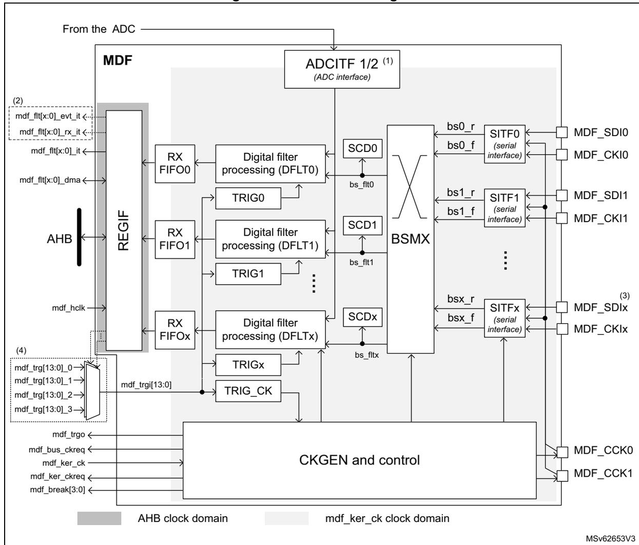
From the ADC
MDF
ADCITF 1/2
(1)
(ADC interface)
(2)
mdf_flt[x:0]_evt_it ←
mdf_flt[x:0]_rx_it ←
mdf_flt[x:0]_it ←
mdf_flt[x:0]_dma ←
AHB
REGIF
RX FIFO0
Digital filter processing (DFLT0)
SCD0
bs_flt0
TRIG0
RX FIFO1
Digital filter processing (DFLT1)
SCD1
bs_flt1
TRIG1
⋮
RX FIFOx
Digital filter processing (DFLTx)
SCDx
bs_fltx
TRIGx
TRIG_CK
BSMX
bs0_r
bs0_f
SITF0
(serial interface)
MDF_SDI0
MDF_CKI0
bs1_r
bs1_f
SITF1
(serial interface)
MDF_SDI1
MDF_CKI1
⋮
bsx_r
bsx_f
SITFx
(serial interface)
(3)
MDF_SDIx
MDF_CKIx
(4)
mdf_trg[13:0]_0 →
mdf_trg[13:0]_1 →
mdf_trg[13:0]_2 →
mdf_trg[13:0]_3 →
mdf_trgi[13:0]
mdf_hclk →
mdf_trgo ←
mdf_bus_ckreq ←
mdf_ker_ck →
mdf_ker_ckreq ←
mdf_break[3:0] ←
CKGEN and control
MDF_CCK0
MDF_CCK1
AHB clock domain
mdf_ker_ck clock domain
MSv62653V3
- 1. Refer to Section 35.3: MDF implementation to check if the ADCITF is available, and which ADCs are connected.
- 2. Not always implemented, refer to the vector table of the product for details.
- 3. Refer to Section 35.3: MDF implementation to check the number of filter instances available.
- 4. The number of trigger inputs depends on the product. Refer to Section 35.3: MDF implementation for details.
35.4.2 MDF pins and internal signals
Table 275. MDF external pins
| Name | Signal type | Comment |
|---|---|---|
| MDF_CKly (y = 0 to 5) (1) | Input | Dedicated clock signals from external sensors |
| MDF_SDIy (y = 0 to 5) (1) | Input | Data signal from external sensors |
| MDF_CCKy (y = 0, 1) | Input/output | Clock outputs for external sensor, or common clock input from external sensors |
1. The number of inputs available depends on the number of filters. Refer to Section 35.3 for details.
Table 276. MDF internal signals
| Name | Signal type | Comment |
|---|---|---|
| mdf_trgi[13:0] | Input | Trigger inputs in order to control the acquisition (see Table 277: MDF trigger connections for details) |
| mdf_trgo | Output | Trigger output for synchronizing several MDFs |
| mdf_break[3:0] | Output | Break signals event generation from over-current detector or short-circuit detector (see the next table for details) |
| mdf_fit[5:0]_dma (1) | Input/output | DMA request/acknowledge signals for each filter processing chain |
| mdf_fit[5:0]_it (1) | Output | Global interrupt signals, for each MDF filter |
| mdf_fit[5:0]_rx_it (1)(2) | Output | Receive interrupt signals, for each MDF filter. |
| mdf_fit[5:0]_evt_it (1)(2) | Output | Event interrupt signals, for each MDF filter. |
| mdf_bus_ckreq | Output | Bus interface clock request output |
| mdf_ker_ckreq | Output | Kernel clock request output |
| mdf_ker_ck | Input | Kernel clock input |
| mdf_hclk | Input | AHB bus interface clock input |
| mdf_adcitf1_dat[15:0] | Input | ADCITF1 data input |
| mdf_adcitf2_dat[15:0] | Input | ADCITF2 data input |
1. The number of signals available depends on the number of filters. Refer to Section 35.3 for details.
2. Not always connected. See the interrupt vector table for details.
The table below shows the way the trigger inputs of the MDF are connected.
Table 277. MDF trigger connections
| Trigger name | Trigger source |
|---|---|
| mdf_trgi0 | EXTI15 |
| mdf_trgi1 | EXTI11 |
| mdf_trgi2 | tim1_trgo |
| mdf_trgi3 | tim1_trgo2 |
| mdf_trgi4 | tim3_trgo |
| Trigger name | Trigger source |
|---|---|
| mdf_trgi5 | tim4_trgo |
| mdf_trgi6 | tim6_trgo |
| mdf_trgi7 | tim7_trgo |
| mdf_trgi8 | tim8_trgo |
| mdf_trgi9 | tim8_trgo2 |
| mdf_trgi10 | tim15_trgo |
| mdf_trgi11 | lptim1_ch1 |
| mdf_trgi12 | adf_sad_det signal (from ADF) |
| mdf_trgi13 | adf_trgo signal (from ADF) |
| mdf_trgo | - |
The table below shows the way the break outputs of the MDF are connected.
Table 278. MDF break connections| Trigger name | Trigger source |
|---|---|
| mdf_break0 | tim1_brk_cmp[8] |
| mdf_break1 | tim1_brk2_cmp[8] |
| mdf_break2 | tim8_brk_cmp[8] |
| mdf_break3 | tim8_brk2_cmp[8] |
35.4.3 Serial input interfaces (SITF)
The SITFx input interfaces allow the connection of the external sensors to the digital filters, via the bitstream matrix (BSMX). The SITFx serial interface can be configured in the following modes:
- • LF_MASTER SPI mode (low-frequency)
- • normal SPI mode
- • Manchester mode
The amount of SITFx instances is equal to the amount of filters.
The data from each serial interface can be routed to any filter in order to perform:
- • the PDM to PCM conversion
- • the out-of limit detection
- • the short detection
The serial interfaces are enabled by setting the corresponding SITFEN bit to 1. Once the interface is enabled, it receives serial data from the external \( \Sigma\Delta \) modulator.
Note: Before enabling the serial interface, the user must insure that the mdf_proc_ck is already enabled (see Section 35.4.5 for details).
The SITFx are controlled via the MDF serial interface control register x (MDF_SITFxCNTR) .
As shown in Figure 322 , for each SITF, there is a large choice of clocking possibilities:
- • If the serial interface is programmed in SPI mode, the selected clock source is a copy of the clock present on MDF_CCK0 or MDF_CCK1 or MDF_CKI x pin (see 2 in Figure 322 ).
- • If the serial interface is programmed in LF_MASTER SPI mode, the selected clock source must be the clock directly provided by the CCKDIV to the MDF_CCK0 or MDF_CCK1 pin (see 1 in Figure 322 ). In this case MDF_CKI x must not be selected.
See Table 279 for additional information.
Note: Using the common clock (MDF_CCK0 or MDF_CCK1) can be helpful to share the same clock between several SITFx.
Figure 322. SITFx overview
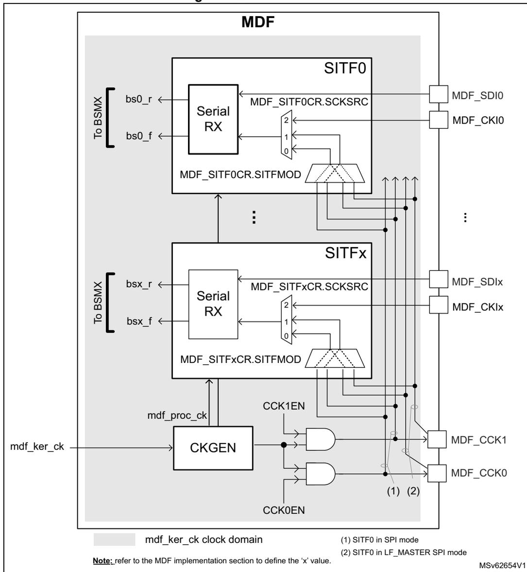
The diagram illustrates the internal architecture of the Multi-function digital filter (MDF). It shows a central clock generation block 'CKGEN' receiving 'mdf_ker_ck' and outputting 'mdf_proc_ck'. It generates 'CCK1EN' and 'CCK0EN' signals which pass through AND gates to external pins MDF_CCK1 and MDF_CCK0. These signals, along with external clock inputs MDF_CKI0 and MDF_CKIx, are routed through multiplexers controlled by MDF_SITF0CR.SCKSRC and MDF_SITFxCR.SCKSRC to the 'Serial RX' units of SITF0 and SITFx respectively. The 'Serial RX' units also receive data from MDF_SDI0 and MDF_SDIx. Output signals bs0_r, bs0_f, bsx_r, and bsx_f are sent 'To BSMX'. The diagram highlights two clocking paths: (1) SITF0 in SPI mode and (2) SITF0 in LF_MASTER SPI mode. A gray shaded area indicates the 'mdf_ker_ck clock domain'.
Legend:
- (1) SITF0 in SPI mode
- (2) SITF0 in LF_MASTER SPI mode
Note: refer to the MDF implementation section to define the 'x' value.
MSV62654V1
LF_MASTER and normal SPI modes
The LF_MASTER SPI mode is a special mode allowing the usage of a mdf_proc_ck clock frequency, only two times higher than the sensor clock. This mode is dedicated to low-power use-cases, using low-speed sensors.
In LF_MASTER SPI mode, the MDF must provide the bitstream clock to the external sensors via MDF_CCK0 and MDF_CCK1 pins, and receives the bitstream data via the serial data input MDF_SDIx.
For each SITFx, the application must select the same clock than the one provided to the external sensor (MDF_CCK0 or MDF_CCK1), in order to guarantee optimal timing performances. This selection is done via SCKSRC[1:0].
Warning: The MDF_CKIx pin cannot be used in LF_MASTER SPI mode.
The normal SPI interface is a more flexible interface than the LF_MASTER SPI, but the mdf_proc_ck frequency must be at least four times higher than the sensor clock.
The application can select MDF_CCK0, MDF_CCK1 or MDF_CKIx clock for the capture of the data received via the MDF_SDIx pin.
The MDF can generate a clock to the sensors via MDF_CCK0 or MDF_CCK1 if needed.
For all SPI modes, all SITFs can share the same clock input (MDF_CCK0 or MDF_CCK1), in order to optimize the amount of requested I/Os.
For all SPI modes, the serial data is captured using the rising and the falling edge of the selected clock. The SITFx always provides the following bitstreams:
- • bitstream received using the bitstream clock falling edge (bsx_f)
- • bitstream received using the bitstream clock rising edge (bsx_r)
According to the sensors connected, one of the two bitstreams may not be available.
The application can select the wanted stream via the BSMX matrix.
Figure 323. SPI timing example
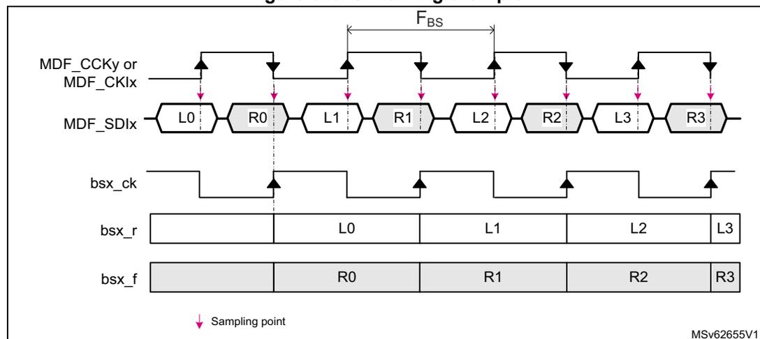
The diagram illustrates the timing for SPI data capture. The top signal is the clock (MDF_CCKy or MDF_CKIx). Below it is the data signal (MDF_SDIx) showing a sequence of bits: L0, R0, L1, R1, L2, R2, L3, R3. The third signal is the bitstream clock (bsx_ck). The fourth signal is the bitstream received on the rising edge (bsx_r), containing bits L0, L1, L2, L3. The fifth signal is the bitstream received on the falling edge (bsx_f), containing bits R0, R1, R2, R3. Pink downward arrows indicate the sampling points on the data signal relative to the clock edges. The period between two consecutive rising edges of the clock is labeled F_BS.
Sampling point
MSV62655V1
To properly synchronize/receive the data stream, the frequency of the mdf_proc_ck clock must be adjusted according to the constraints listed in Table 280 .
Clock absence detection
A no-clock-transition period may be detected when the serial interface works in normal SPI mode. This feature can be used to detect a clock failure in the SPI link.
The application can program a timeout value via the STH[4:0] bitfield of the corresponding SITFx. If the MDF does not detect clock transitions for a duration of \( STH[4:0] \times T_{mdf\_proc\_ck} \) , then the CKABF flag is set.
An interrupt can be generated if CKABIE is set to 1. The STH[4:0] bitfield is in the MDF serial interface control register x (MDF_SITFxCR) .
When the serial interface is enabled, the CKABF flag remains to 1 until a first clock transition is detected.
To avoid spurious clock absence detection, the following sequence must be respected:
- 1. Configure the serial interface in normal SPI mode and enable it.
- 2. Clear the CKABF flag by writing CKABF bit to 1.
If no clock transition is detected on the serial interface, the hardware immediately sets the CKABF flag to 1. - 3. Read the CKABF flag:
- – If CKABF = 1, go back to step 2.
- – If CKABF = 0, a clock has been detected. The CKABIE bit can be set to 1 if the application wants an interrupt on detection of a clock absence.
Note: The clock absence detection feature is not available in the LF_MASTER SPI mode.
Manchester mode
In Manchester coded format, the MDF receives data stream from the external sensor via the MDF_SDIx pin only.
The MDF_CKIx pins are not needed in this mode.
Decoded data and clock signals are recovered from serial stream after Manchester decoding. They are available on bsx_r. There are two possible settings of Manchester codings:
- • signal rising edge decoded as 0 and signal falling edge decoded as 1
- • signal rising edge decoded as 1 and signal falling edge decoded as 0
Figure 324. Manchester timing example (SITFMOD = 11)
![Figure 324. Manchester timing example (SITFMOD = 11). The diagram shows the timing relationship between the Data transferred (bits 1, 1, 0, 0, 1), MDF_SDix, mdf_proc_ck, STH[4:0] = 5, MCNT, bsx_ck, bsx_r, and CKABF. The Data transferred line shows a sequence of bits: 1, 1, 0, 0, 1. The MDF_SDix line shows the Manchester encoded signal. The mdf_proc_ck line shows a high-frequency clock. The STH[4:0] = 5 line shows a counter value of 5. The MCNT line shows the counter value. The bsx_ck line shows a lower-frequency clock. The bsx_r line shows the received data. The CKABF line shows the clock absence flag. The diagram includes a legend for signal absence, long transitions, and short transitions based on the STH counter value.](/RM0486-STM32N6x5-x7/4acf9f740458b21ac9f2f841dac157df_img.jpg)
The diagram illustrates the timing for a Manchester encoded stream. The top line shows the data bits: 1, 1, 0, 0, 1. Below it, the MDF_SDix signal shows the corresponding Manchester encoding. The mdf_proc_ck signal is a high-frequency clock. The STH[4:0] register is set to 5. The MCNT counter is shown, with its value increasing and then being reset by transitions in the MDF_SDix signal. The bsx_ck signal is a lower-frequency clock derived from the data. The bsx_r signal shows the received data, which is 'x' (unknown) initially and then becomes '0' and '0' as transitions are detected. The CKABF flag is shown, which is set to 1 when no transition is detected for a certain period. A legend at the bottom explains the background colors: green for signal absence if the STH counter is higher than 2*STH, light blue for long transitions if the STH counter is between STH and 2*STH, and pink for short transitions if the STH counter is lower than STH.
To decode the incoming Manchester stream, the user must program the STH[4:0] bitfield in the MDF serial interface control register x (MDF_SITFxC R ) . The STH[4:0] bitfield is used by the SITF x to estimate the Manchester symbol length and to detect a clock absence. An internal counter (MCNT) is restarted every time a transition is detected in the MDF_SD x input. It is used to detect short transitions, long transitions or clock absence. A long transition indicates that the data value changed. Figure 324 shows a case where the OVR is around height and STH[4:0] = 5.
The estimated Manchester symbol rate ( \( T_{SYMB} \) ) must respect the following formula:
It is recommended to compute STH as follows:
where OVR represents the ratio between the mdf_proc_ck frequency and the expected Manchester symbol frequency. OVR must be higher than five, and the mdf_proc_ck clock must be adjusted according to the constraints listed in Table 280 .
The clock absence flag CKABF is set to 1 when no transition is detected during more than \( 2 \times STH[4:0] \times T_{mdf\_proc\_ck} \) , or when the SITF x is not yet synchronized to the incoming Manchester stream. In addition, an interrupt can be generated if the bit CKABIE is set to 1.
When the serial interface is enabled, the MDF must first be synchronized to the incoming Manchester stream. The synchronization ends when a data transition from 0 to 1 or from 1 to 0 (pink circle in the Figure 324 ) is detected.
The end of the synchronization phase can be checked by following the software sequence:
- 1. Clear the CKABF flag in the MDF_DFLTx interrupt status register x (MDF_DFLTxISR) by writing CKABF bit to 1. If the serial interface is not yet synchronized, the hardware immediately sets the CKABF flag to 1.
- 2. Read the CKABF flag.
- – If CKABF = 1, go back to step 1.
- – If CKABF = 0, the Manchester interface is synchronized and provides valid data.
In the following example, the MDF kernel clock frequency ( \( F_{\text{mdf\_ker\_ck}} \) ) is 100 MHz and the received Manchester stream is at about 6 MHz ( \( F_{\text{SYMB}} \) ).
- 1. Provide a valid mdf_proc_ck to the SITFx.
The mdf_proc_ck frequency must be at least six times higher than the Manchester symbol frequency (means at least 36 MHz).
PROCDIV is programmed to 1 to perform a division by two of the kernel clock. In that case, \( F_{\text{mdf\_proc\_ck}} = 50 \) MHz (8.33 times higher than the Manchester symbol frequency).
- 2. Compute STH.
OVR is given by: \( \text{OVR} = F_{\text{mdf\_proc\_ck}} / F_{\text{SYMB}} = 50 \text{ MHz} / 6 \text{ MHz} = 8.33 \) .
The minimum allowed frequency for the Manchester stream is then:
The maximum allowed frequency for the Manchester stream is then:
35.4.4 ADC slave interface (ADCITF)
The ADCs are not always connected to the MDF. Refer to Section 35.3 to check the situation for this product.
The MDF allows the connection of up to two ADCs to the filter path. For each filter, the DATSRC[1:0] bitfield in the MDF digital filter configuration register x (MDF_DFLTxCICR) allows the application to select either data from the ADCs.
| Warning: | The MDF does not support receiving interleaved data from one of the ADCITF input. |
35.4.5 Clock generator (CKGEN)
The RCC (reset and clock controller) provides the following clocks to the MDF:
- • AHB clock (mdf_hclk) used for the register interface
- • kernel clock (mdf_ker_ck) mainly used by all other parts of the circuit via the CKGEN
Those clocks are not supposed to be phase locked, so all signals crossing those clock domains are resynchronized.
The clock generator (CKGEN) is responsible of the generation of the processing clock, and the clock provided to the MDF_CCK0 and MDF_CCK1 pins. All those clocks are generated from the mdf_ker_ck.
The processing clock (mdf_proc_ck) is used to run all the signals processing and to re-sample the incoming serial or parallel stream.
Note: The reshape filter (RSFLT) needs up to 24 cycles of mdf_proc_ck clock to process a sample.
To adapt the kernel clock frequency provided by the RCC, the following dividers are available:
- • PROCDIV[6:0] used to adapt the kernel clock frequency to the constraints of the parallel and serial interfaces, and to the processing blocks
- • CCKDIV[3:0] used to adapt the frequency of the MDF_CCK0 and MDF_CCK1 clocks
PROCDIV[6:0] and CCKDIV[3:0] must be programmed when no clock is provided to the dividers (CKGDEN = 0).
The mdf_proc_ck generation is controlled by CKGDEN.
In addition, the CKGMOD bit allows the application to define the way to trigger the CCKDIV divider:
- • When CKGMOD = 0, the CCKDIV divider is started as soon as CKGDEN is set to 1.
- • When CKGMOD = 1, the CCKDIV divider is started when CKGDEN is set to 1 and the programmed trigger condition occurred.
All bits and fields controlling the CKGEN are in MDF_CKGCR.
Figure 325. CKGEN overview
![Figure 325. CKGEN overview diagram showing the internal clock generation logic of the MDF block. The diagram includes inputs mdf_ker_ck and cck_trg (from TRIG_CK). The cck_trg signal is ANDed with CKGDEN and then passed through a divider (+1 to 128) controlled by PROCODIV[6:0]. The output of this divider is mdf_proc_ck. This signal is then ANDed with CKGMOD and passed through another divider (+1 to 16) controlled by CCKDIV[3:0]. The output of this second divider is connected to two external pins, MDF_CCK0 and MDF_CCK1, through switches controlled by CCK0EN, CCK0DIR, CCK1EN, and CCK1DIR. The mdf_proc_ck signal is also connected to TRIGx, Digital processing (DFLTx, SAD, OLD, SCD), and Interfaces (ADCITF[2:1], SITFx).](/RM0486-STM32N6x5-x7/41dbe1c96646d301f9c46e66c42061c4_img.jpg)
The trigger logic for CKGEN is handled by the TRG_CK block. As shown in Figure 334 , the CCKDIV divider can be triggered on the rising or falling edge of one of the 16 trigger sources. When the proper trigger condition occurs, the cck_trg signal goes to high, allowing the CCKDIV divider to start. The TRG_CK logic is reset when CKGDEN is set to 0.
This feature can be helpful to synchronize the MDF_CCKy (y = 0,1) clock of several MDF instances, or to synchronize the clock generation to a timer event.
The application can control the activation of the MDF_CCK0 or MDF_CCK1 pin CCK0EN/CCK1EN and CCK0DIR/CCK1DIR bits:
- • CCKyEN is used to enable the CCKDIV, and thus generates a clock for the external sensors.
- • CCKyDIR is used to control the direction of the ADF_CCKy pin (input or output)
| CCKyEN | CCKyDIR | Description |
|---|---|---|
| 0 | 0 | The MDF_CCKy pin is in input. An external clock can be connected to the MDF_CCKy pin and used by the SITFx in order to decode the serial stream |
| 0 | 1 | The MDF_CCKy pin is in output. No clock is generated, thus the MDF_CCKy pin is driven low. |
| 1 | 1 | The MDF_CCKy pin is in output. A clock is generated on the MDF_CCKy pin. The SITFx can use this pin as clock source in order to decode the serial stream |
1. The configuration with CCKyEN = 1 and CCKyDIR = 0 must be avoided (no interest).
When CCKyDIR = 1, as soon as the CCKyEN bit is set to 1, a clock is generated to the corresponding output without any spurs.
Note: The mdf_proc_ck must be enabled (by CKGDEN = 1) before enabling other blocks (such as SITFx or DFLT x ).
CKGEN activation sequence example
- 1. Set CKGDEN to 0.
- 2. Wait for CKGACTIVE = 0. If CKGDEN was previously enabled, this phase can take two periods of mdf_hclk and two periods of mdf_proc_ck.
- 3. Program PROCDIV[6:0], CKGMOD, CCKDIV[3:0], TRGSRC[3:0] and TRGSENS.
- 4. Set CKGDEN to 1.
- 5. Set CCKxDIR to 1 (optional).
- 6. Set CCKxEN to 1 (optional).
When needed, at any moment, the CCK0EN or CCK1EN value can be changed without disabling the clock generator.
Clock frequency constraints
The table below shows the frequency constraints to receive and process properly the samples.
Table 280. Clock constraints with respect to the incoming stream (1)
| SITFx mode | MDF clock constraints | |
|---|---|---|
| With RSFLT disabled | With RSFLT enabled | |
| LF_MASTER SPI | \( F_{MDF\_CCKy} \) max frequency limited to 5 MHz | |
| \(
F_{mdf\_proc\_ck} > 2 * F_{MDF\_CCKy}
\) and \( F_{mdf\_hclk} \geq F_{mdf\_proc\_ck} \) | \(
F_{mdf\_proc\_ck} > 24 * F_{MDF\_CCKy} / (MCICD+1)
\) and \( F_{mdf\_proc\_ck} > 2 * F_{MDF\_CCKy} \) and \( F_{mdf\_hclk} \geq F_{mdf\_proc\_ck} \) | |
| MASTER SPI SLAVE SPI | \( F_{MDF\_CKx} \) max frequency limited to 25 MHz | |
| \(
F_{mdf\_proc\_ck} > 4 * F_{MDF\_CCKy}
\) and \( F_{mdf\_hclk} \) higher or equal to \( F_{mdf\_proc\_ck} \) | \(
F_{mdf\_proc\_ck} > 24 * F_{MDF\_CCKy} / (MCICD+1)
\) and \( F_{mdf\_proc\_ck} \) higher than \( 4 * F_{MDF\_CCKy} \) and \( F_{mdf\_hclk} \) higher or equal to \( F_{mdf\_proc\_ck} \) | |
| Manchester | \( F_{SYMB} \) max frequency limited to 20 MHz | |
| \(
F_{mdf\_proc\_ck}
\)
higher than
\(
6 * F_{SYMB}
\) and \( F_{mdf\_hclk} \geq F_{mdf\_proc\_ck} \) | \(
F_{mdf\_proc\_ck}
\)
higher than
\(
24 * F_{MDF\_CCKy} / (MCICD+1)
\) and \( F_{mdf\_proc\_ck} > 6 * F_{SYMB} \) and \( F_{mdf\_hclk} \geq F_{mdf\_proc\_ck} \) | |
1. \( F_{MDF\_CCKy} \) represents the frequency of the clock received via MDF_CKIx and MDF_CCKy, or generated via MDF_CCKy. \( F_{SYMB} \) represents the frequency of the received symbol rate for Manchester mode.
35.4.6 Bitstream matrix (BSMX)
The BSMX receives the bitstreams from all serial interfaces (SITFx) and provides the selected input to the digital filters (DFLTx) and to the short-circuit detectors (SCDx). For each filter path, any of the bitstream input can be selected.
As shown in the Figure 322 , each SITFx block provides two bitstreams (bsx_r and bsx_f) to the BSMX.
The application to select the wanted stream via the MDF bitstream matrix control register x (MDF_BSMXxCR) . This selection is intended to be static.
Figure 326. BSMX overview
![Figure 326. BSMX overview diagram showing the internal architecture of the Multi-function digital filter (MDF). The diagram illustrates the signal flow from the ADCITF[2,1] input through various filter paths (DFLT0, SCD0, BSMX, SITF0, etc.) to the output. The BSMX block is a central switching matrix that routes signals based on configuration registers (MDF_BSMX0CR.BSSEL, MDF_BSMX1CR.BSSEL, etc.).](/RM0486-STM32N6x5-x7/c3e2118b1345005bd236122691f6883f_img.jpg)
The diagram shows the internal architecture of the Multi-function digital filter (MDF). On the left, the ADCITF[2,1] input is connected to a series of filter blocks: DFLT0 , DFLT1 , and DFLT(N-1) . Each filter block is associated with a SCD (Short-circuit detector) block: SCD0 , SCD1 , and SCD(N-1) . The SCD blocks output signals bs_fit0 , bs_fit1 , and bs_fit(N-1) . These signals are fed into the BSMX (Bitstream Matrix) block, which is a switching matrix. The BSMX block is controlled by configuration registers: MDF_BSMX0CR.BSSEL , MDF_BSMX1CR.BSSEL , and MDF_BSMX(N-1)CR.BSSEL . The BSMX block outputs multiple streams: bs0_r , bs0_f , bs1_r , bs1_f , ..., bs(N-1)_r , and bs(N-1)_f . These streams are then processed by SITF (Signal Interface and Transfer Function) blocks: SITF0 , SITF1 , and SITF(N-1) . The SITF blocks output the final filtered signals: bs0_r , bs0_f , bs1_r , bs1_f , ..., bs(N-1)_r , and bs(N-1)_f . The diagram is labeled with MSV62658V1 in the bottom right corner.
BSMX programming sequence example
The BSSEL[4:0] bitfield cannot be changed if the corresponding SCDx, OLDx or DFLTx is enabled. The following steps are needed to change the value of BSMX, for filter path x:
- 1. Set SCDEN of SCDx to 0.
- 2. Set DFLTEN of DFLTx to 0.
- 3. Set OLDEN of OLDx to 0.
- 4. Wait for BSMXACTIVE = 0.
- 5. Program BSSEL[4:0] of filter path x.
- 6. Set SCDEN of SCDx to 1 (optional).
- 7. Set DFLTEN of DFLTx to 1 (optional).
- 8. Set OLDEN of OLDx block to 1 (optional).
35.4.7 Short-circuit detectors (SCD)
The SCDx detects, with a very fast response time, if an analog signal reached saturated values (out-of-full scale ranges) and remained on this value for a given time.
This behavior can detect short-circuit or open-circuit errors (such as over current or over voltage). An interrupt event or/and a break signal can be generated.
Figure 327. SCD functional view
![Figure 327. SCD functional view block diagram showing the internal components of the Short Circuit Detector (SCD) within the MDF block. The SCD block contains a Transition detector, a Counter, and a Comparator. Inputs include mdf_ker_ck, bs_ftx_dat, and bs_ftx_ck (from BSMX). The Counter output scd_cnt[7:0] is compared against the threshold MDF_SCDxCR.SCDT[7:0]. The Comparator outputs scd_brkx (to break interface) and scd_evtX (to interrupts interface). The Counter is reset by the Transition detector. The diagram is labeled MSv62659V1.](/RM0486-STM32N6x5-x7/ce7f8c6026f6243e2a195b72e47dfe4b_img.jpg)
The SCDx is counting consecutive zeros or consecutive ones received from the serial interface (SITFx). A counter is restarted if there is a change in the data stream received. If this counter reaches a short-circuit threshold value (SCDT[7:0] in the MDF short circuit detector control register x (MDF_SCDxCR) ), then a short-circuit event is invoked. Each BSMX output has its own short-circuit detector. Any BSMX output can be continuously monitored by setting the corresponding SCDEN bit to 1 in MDF_SCDxCR. Each SCD has its own threshold settings (SCDT) and its own status bit (SCDF).
The figure below shows an example where SCDT[7:0] is set to six. The break signal remains high as long as the short circuit condition is present.
No overrun event is generated when the interrupt event is pending while a new short-circuit condition is detected.
Figure 328. SCD timing example
![Figure 328. SCD timing example timing diagram. It shows the relationship between bs_ftx_dat, bs_ftx_ck, scd_cnt[7:0], mdf_ker_ck, scd_brkx, and mdf_evt_Itx/mdf_itx. The counter scd_cnt[7:0] counts up to 6 (threshold) and then resets. The break signal scd_brkx is high when the counter reaches the threshold. The interrupt signal mdf_evt_Itx/mdf_itx is generated when the counter reaches the threshold and is cleared by writing 1 to SCDF. The diagram is labeled MSv62660V1.](/RM0486-STM32N6x5-x7/07299c5a2cf84eb2f279bc32f84e506c_img.jpg)
The SCDx event generated by the SCDx block can be assigned to break output signals mdf_break[3:0]. The break signal assignment to a given short-circuit detector event is done by BKSCD[3:0] in MDF_SCDxCR. The break outputs are shared with the over-current function.
Note: SCDs cannot be used to monitor the ADC data interface (ADCITF).
SCD activation sequence example
- 1. Enable and configure CKGEN to generate the mdf_proc_ck.
- 2. Set SCDEN to 0.
- 3. Wait for SCDACTIVE = 0. If SCDEN was previously enabled, this phase can take two periods of mdf_hclk, and two periods of mdf_proc_ck.
- 4. Program BKSCD[3:0] and SCDT[7:0].
- 5. Set SCDEN to 1.
Note: BKSCD[3:0] and SCDT[7:0] must not be changed when SCDACTIVE = 1.
35.4.8 Digital filter processing (DFLT)
The digital filter processing includes the following sub-blocks:
- • symbol remap (SBR)
- • source selector
- • clock skipper delay (DLY)
- • CIC decimation filter that can be configured:
- – in single Sinc 4 or Sinc 5 order CIC (MCIC)
- – in two CIC filters:
- - a main filter (MCIC), high resolution
- - an auxiliary filter (ACIC), low-latency, for the out-of-limit detector (OLD)
- - both MCIC and ACIC can be configured as Sinc 1 , Sinc 2 , Sinc 3 or FastSinc
- • gain control (SCALE)
- • signal saturation (SAT)
- • reshape filter (RSFLT)
- • high-pass filter (HPF)
- • integrator (INT)
- • receive RXFIFO
Figure 329 shows the filter-path configuration according to CICMOD[2:0]. Several configuration bits are available to configure the digital filter to the application needs.
Figure 329. DFLT overview
![Figure 329. DFLT overview block diagram showing the internal architecture of the digital filter. The diagram is divided into three frequency domains: F_PCM (PCM frequency domain), F_RS (RS frequency domain), and F_BS (BS frequency domain), all within the mdf_proc_ck clock domain. The signal flow starts from RX FIFO (PCM[23:0]) through an INT block (controlled by INTERVAL), then through HPF (controlled by HPFC, HPFBYP, and Discard logic), then through RSFLT (controlled by RSFLT, RSFLTBY, and SAT). The signal then enters the CIC filter (controlled by CICMOD, OEC, and OFFSET) which includes Out-of-limit detector (OLD) with CMP, D2, and ACICF blocks. The output of the CIC filter is then processed by a DLY block (controlled by DATSRC and SBR) and finally output via SCDx. The DATSRC block selects between data from ADCITF2, ADCITF1, and BSMX. The SBR block performs symbol remap, converting high levels to 16-bit signed number + 1 and low levels to 16-bit signed number - 1.](/RM0486-STM32N6x5-x7/3948e9e2a05fc7115dfff9388468e3e4_img.jpg)
Symbol remap and source selection
The symbol remap (SBR) converts the bitstream selected by the BSMX into data usable by the filter path. More especially:
- • The high levels are converted into a 16-bit signed number + 1.
- • The low levels are converted into a 16-bit signed number - 1.
The signal source of the digital filter can be selected via DATSRC[1:0] between the two following:
- • data coming from the BSMX
- • data coming from one of the ADC interfaces (ADCITF2 or 1)
Programmable micro-delay control (DLY)
The digital filter has a delay line that allows the timing adjustment of each stream with the resolution of the bitstream clock.
This feature is particularly helpful in the case of microphone beam forming applications where delays smaller than the final sampling rate, must be applied to the incoming stream. This feature is helpful when the MDF is synchronized with other ADF or MDF blocks for a beam forming application for example.
The delay is performed by discarding a given number of samples from the selected input stream, before samples enter into the CIC filter. This data discarding is performed by skipping a given number of data strobe, preventing the CIC filter to take into account those data.
When the wanted amount of data strobe has been skipped, the next incoming samples are strobed normally.
Figure 330 shows an example of how to apply dynamically small delay to an incoming stream. For simplification, the CIC filter performs a decimation by height in this example. CIC1 represents the CIC included in the ADF and CIC0 represents a filter from another ADF or MDF instance.
Figure 330. Programmable delay
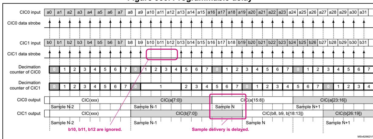
The diagram illustrates the timing of a programmable delay in a multi-function digital filter. It shows the following signals and their relationship over time:
- CIC0 input: A continuous stream of samples \( a_0, a_1, a_2, a_3, a_4, a_5, a_6, a_7, a_8, a_9, a_{10}, a_{11}, a_{12}, a_{13}, a_{14}, a_{15}, a_{16}, a_{17}, a_{18}, a_{19}, a_{20}, a_{21}, a_{22}, a_{23}, a_{24}, a_{25}, a_{26}, a_{27}, a_{28}, a_{29}, a_{30}, a_{31} \) .
- CIC0 data strobe: A series of upward arrows indicating the sampling clock for CIC0.
- CIC1 input: A stream of samples \( b_0, b_1, b_2, b_3, b_4, b_5, b_6, b_7, b_8, b_9, b_{10}, b_{11}, b_{12}, b_{13}, b_{14}, b_{15}, b_{16}, b_{17}, b_{18}, b_{19}, b_{20}, b_{21}, b_{22}, b_{23}, b_{24}, b_{25}, b_{26}, b_{27}, b_{28}, b_{29}, b_{30}, b_{31} \) . Samples \( b_{10}, b_{11}, b_{12} \) are skipped.
- CIC1 data strobe: A series of upward arrows indicating the sampling clock for CIC1. A pink box highlights the skipped samples \( b_{10}, b_{11}, b_{12} \) .
- Decimation counter of CIC0: A sequence of values: 0, 1, 2, 3, 4, 5, 6, 7, 0, 1, 2, 3, 4, 5, 6, 7, 0, 1, 2, 3, 4, 5, 6, 7, 0, 1, 2, 3, 4, 5, 6, 7.
- Decimation counter of CIC1: A sequence of values: 0, 1, 2, 3, 4, 5, 6, 7, 0, 1, 2, 3, 4, 5, 6, 7, 0, 1, 2, 3, 4, 5, 6, 7, 0, 1, 2, 3, 4. The counter is frozen during the skipping of \( b_{10}, b_{11}, b_{12} \) .
- CIC0 output: Output samples are generated from the input stream \( a \) . The output is labeled as \( CIC(xxx) \) , \( CIC(a[7:0]) \) , \( CIC(a[15:8]) \) , and \( CIC(a[23:16]) \) . The output sample \( N+1 \) is generated from input samples \( a[23:16] \) .
- CIC1 output: Output samples are generated from the input stream \( b \) . The output is labeled as \( CIC(xxx) \) , \( CIC(b[7:0]) \) , \( CIC(b[15:8]) \) , and \( CIC(b[23:16]) \) . The output sample \( N+1 \) is generated from input samples \( b[26:19] \) .
Annotations in the diagram:
- b10, b11, b12 are ignored. (indicated by a pink line pointing to the skipped samples)
- Sample delivery is delayed. (indicated by a pink line pointing to the output sample \( N+1 \) )
The CIC of filter 1 (CIC1) receives a command in order to skip three incoming samples. So the input samples named \( b_{10} \) , \( b_{11} \) and \( b_{12} \) are not processed by CIC1. As a consequence, the output sample \( N+1 \) generated by CIC0 is build from input samples \( a[23:16] \) while the sample \( N+1 \) of CIC1 is build from input samples \( b[26:19] \) .
Finally, the non-skipped data stream looks delayed by three bitstream periods.
Note: When the input data strobes are skipped, the decimation counter remains frozen. As a consequence, the samples delivered by the CIC1 are a bit delayed.
Warning: It is not recommended to apply a delay bigger than the programmed decimation ratio (CIC + RSFLT decimation), especially if the MDF is programmed in interleaved acquisition mode. There is a strong risk of data misalignment inside the FIFOs.
The following steps are needed to program the amount of bitstream clock periods to be skipped:
- 1. Wait for SKPBF equal to 0.
- 2. Write SKPDLY[6:0] to the wanted number of bitstream clock periods to be skipped. The SKPBF flag goes immediately to 1, indicating that the delay value entered into SKPDLY[6:0] is under process.
- – If the corresponding DFLT \( x \) is not yet enabled (DFLTEN = 0), then the DLY logic waits for DFLTEN = 1. When the application sets DFLTEN to 1, the DLY logic starts to skip the amount of wanted data strobes.
- – If the corresponding digital filter is already enabled (DFLTEN = 1), then the DLY logic immediately starts to skip the amount of wanted data strobes.
When the MDF skipped the amount of wanted data strobes, then SKPBF goes back to 0.
- 3. If the application needs to skip more data strobes, then the operation must be restarted from step 1.
The effect of the delay performed with this mechanism is cumulative as long as the MDF is enabled. In a given filter, if the application performs a D1 delay, followed by a D2 delay, then all other active filters are delayed by D1 + D2.
Data coming from ADCs can also benefit of this feature.
In interleaved acquisition mode, it is up to the application to insure that the delay applied on the different microphones is in line with the depth of the RXFIFO buffers. If the relative delay between each activated filter is less than the decimation ratio, then it costs one FIFO location.
If the interleaved acquisition mode is not used, then the delay value has no impact on the RXFIFO buffering.
Note: If SKPDLY[6:0] is written when SKPBF = 1, the write operation is ignored.
Cascaded-integrator-comb (CIC) filter
The CIC digital filters are an efficient implementation of low-pass filters, often used for decimation and interpolation. The CIC frequency response is equal to a \( \text{Sinc}^N \) function, this is why they are often called Sinc filters.
The \( \text{Sinc}^N \) digital filter embedded into the MDF is configurable according to the application targeted.
- • For audio applications, such as speech capture from digital microphones, the application can select a high-resolution low-pass decimation filter by setting CICMOD to 100 or 101.
- • If the targeted application is motor control or any other sensor capture, then the application can configure the CIC in order to offer a main filter path for acquisition (MCIC) and an auxiliary filter for fast-event generation (ACIC). This auxiliary filter can be used for example, to detect over-current conditions. This mode is selected by setting CICMOD[2:0] = 0xx.
When CICMOD[2:0] = 0xx, the following CIC filters are available:
- • main filter (MCIC)
- • auxiliary CIC filter (ACIC)
Both of them are configurable in FastSinc, \( \text{Sinc}^1 \) to \( \text{Sinc}^3 \) .
When CICMOD[2:0] = 100, the CIC is configured into a single \( \text{Sinc}^4 \) and when CICMOD[2:0] = 101, the CIC is configured into a single \( \text{Sinc}^5 \) filter.
The filters have the following transfer function (impulse response in z domain):
- •
\(
\text{Sinc}^N
\)
filter type:\[ H(z) = \left( \frac{1 - z^{-D}}{1 - z^{-1}} \right)^N \]
- • FastSinc filter type:\[ H(z) = \left( \frac{1 - z^{-D}}{1 - z^{-1}} \right)^2 \cdot (1 + z^{-(2 \cdot D)}) \]
where N can be 1, 2, 3, 4 or 5, and D is the decimation ratio.
D is equal to MCICD+1 or ACICD+1.
Figure 331. CIC3 and CIC5 frequency response with decimation ratio = 32
CIC output data size
The size of samples delivered by the CIC ( \( DS_{CIC} \) ) depends on the following parameters:
- • CIC order (N)
- • CIC decimation ratio (D)
- • data size of the input stream ( \( DS_{IN} \) )
The CIC order and decimation ratio must be programmed in order to insure that the data size does not exceed the 26-bit CIC capability.
The following formula gives the output data size ( \( DS_{CIC} \) ) according to the parameters above.
and the CIC gain is given by this formula:
The decimation ratio can be adjusted from 2 to 512 for the main CIC filter and from 1 to 32 for the auxiliary CIC filter.
The table below gives some data output size in bits for some decimation values, when the data source is a full-scale signal coming from the serial interface or from a 12-bit ADC.
Note: \( DS_{IN} = 1 \) bit for a serial bitstream but can be up to 16 bits when coming from the ADCITF.
Table 281. Data size according to CIC order and CIC decimation values
| Decimation | Data size (bits) when
\(
DS_{IN} = 1
\)
bit (data from SITFx) | Data size (bits) when
\(
DS_{IN} = 12
\)
bits (data from ADCITF) | ||||||||||
|---|---|---|---|---|---|---|---|---|---|---|---|---|
| Sinc 1 | Sinc 2 | FastSinc | Sinc 3 | Sinc 4 | Sinc 5 | Sinc 1 | Sinc 2 | FastSinc | Sinc 3 | Sinc 4 | Sinc 5 | |
| 4 | 3 | 5 | 6 | 7 | 9 | 11 | 14 | 16 | 17 | 18 | 20 | 22 |
| 8 | 4 | 7 | 8 | 10 | 13 | 16 | 15 | 18 | 19 | 21 | 24 | - |
| 12 | 5 | 9 | 9 | 12 | 16 | 19 | 16 | 20 | 21 | 23 | - | - |
| 16 | 5 | 9 | 10 | 13 | 17 | 21 | 16 | 20 | 21 | 24 | - | - |
| 24 | 6 | 11 | 12 | 15 | 20 | 24 | 17 | 22 | 23 | - | - | - |
| 32 | 6 | 11 | 12 | 16 | 21 | 26 | 17 | 22 | 23 | - | - | - |
| Decimation | Data size (bits) when
\(
DS_{IN} = 1
\)
bit (data from SITFx) | Data size (bits) when
\(
DS_{IN} = 12
\)
bits (data from ADCITF) | ||||||||||
|---|---|---|---|---|---|---|---|---|---|---|---|---|
| Sinc 1 | Sinc 2 | FastSinc | Sinc 3 | Sinc 4 | Sinc 5 | Sinc 1 | Sinc 2 | FastSinc | Sinc 3 | Sinc 4 | Sinc 5 | |
| 64 | 7 | 13 | 14 | 19 | 25 | - | 18 | 24 | 25 | - | - | - |
| 128 | 8 | 15 | 16 | 22 | - | - | 19 | 26 | - | - | - | - |
| 256 | 9 | 17 | 18 | 25 | - | - | 20 | - | - | - | - | - |
| 512 | 10 | 19 | 20 | - | - | - | 21 | - | - | - | - | - |
The LSB part of the data provided by the CIC is not necessarily significant: it depends on the sensor performances and the ability of the CIC to reject the out-of-band noise.
The sample size at CIC output can be adjusted thanks to the SCALE block.
The table below shows the maximum allowed decimation ratio for the CIC filter, depending on the input data size. Bigger decimation ratio causes a wrap-around of the signal at CIC output, for strong input signals.
Note: The MDF cannot detect or prevent a CIC wrap-around.
Table 282. Maximum decimation ratio versus order and input data size| Filter order | Max. decimation ratio when \( DS_{IN} = 1 \) bit (SITFx) | Max. decimation ratio when \( DS_{IN} = 12 \) bits (ADCITF) | Max. decimation ratio when \( DS_{IN} = 16 \) bits (ADCITF) |
|---|---|---|---|
| Sinc 1 | 512 | 512 | 512 |
| Sinc 2 | 512 | 128 | 32 |
| FastSinc | 512 | 90 | 22 |
| Sinc 3 | 322 | 25 | 10 |
| Sinc 4 | 76 | 11 | 5 |
| Sinc 5 | 32 | 6 | 4 |
Scaling (SCALE) and saturation (SAT)
The SCALE block allows the application to adjust the amplitude of the signal provided by the CIC, by steps of 3 dB ( \( \pm 0.5 \) dB).
The signal amplitude can be decreased by up to 8 bits ( \( - 48.2 \) dB) and can be increased by up to 12 bits ( \( + 72.2 \) dB).
The gain is adjusted by the SCALE[5:0] bitfield in the MDF digital filter configuration register x (MDF_DFLTxCICR) .
SCALE[5:0] can be changed even if the corresponding DLFTx is enabled. During the gain transition, the signal provided by the filter is disturbed.
Due to internal resynchronization, there is a delay of some cycles of mdf_proc_ck clock between the moment where the application writes the new gain, and the moment where the gain is effectively applied to the samples. If the application attempts to write a new gain value while the previous one is not yet applied, this new gain value is ignored. Reading back SCALE[5:0] informs the application on the current gain value.
The table below shows the possible gain values.
Table 283. Possible gain values
| SCALE[5:0] | Gain (dB) | SCALE[5:0] | Gain (dB) | SCALE[5:0] | Gain (dB) | SCALE[5:0] | Gain (dB) |
|---|---|---|---|---|---|---|---|
| 0x20 | - 48.2 | 0x2B | - 14.5 | 0x06 | + 18.1 | 0x11 | + 51.7 |
| 0x21 | - 44.6 | 0x2C | - 12.0 | 0x07 | + 21.6 | 0x12 | + 54.2 |
| 0x22 | - 42.1 | 0x2D | - 8.5 | 0x08 | + 24.1 | 0x13 | + 57.7 |
| 0x23 | - 38.6 | 0x2E | - 6.0 | 0x09 | + 27.6 | 0x14 | + 60.2 |
| 0x24 | - 36.1 | 0x2F | - 2.5 | 0x0A | + 30.1 | 0x15 | + 63.7 |
| 0x25 | - 32.6 | 0x00 | 0.0 | 0x0B | + 33.6 | 0x16 | + 66.2 |
| 0x26 | - 30.1 | 0x01 | + 3.5 | 0x0C | + 36.1 | 0x17 | + 69.7 |
| 0x27 | - 26.6 | 0x02 | + 6.0 | 0x0D | + 39.6 | 0x18 | + 72.2 |
| 0x28 | - 24.1 | 0x03 | + 9.5 | 0x0E | + 42.1 | - | - |
| 0x29 | - 20.6 | 0x04 | + 12.0 | 0x0F | + 45.7 | - | - |
| 0x2A | - 18.1 | 0x05 | + 15.6 | 0x10 | + 48.2 | - | - |
The SAT blocks avoid having a wrap-around of the binary code when the code exceeds its maximal or minimal value.
The MDF performs saturation operations at the following levels:
- • after the SCALE block (performed by the SAT block). The signal is saturated at 24 bits.
- • inside the RSFLT, to insure a good filter behavior
- • at the output of the HPF, to insure that the output signal does not exceed 24 bits
The SATF bit informs the application that a saturation occurred either after the SCALE, inside the RSFLT or after the HPF. In addition, an interrupt can be generated if SATIE is set to 1. As soon as a saturation is detected, the SATF flag is set to 1. It is up to the application to clear this flag in order to be able to detect a new saturation.
Those bits are in the MDF DFLT x interrupt enable register x (MDF_DFLT x IER) and MDF DFLT x interrupt status register x (MDF_DFLT x ISR) .
Gain adjustment policy
To get the best MDF performances, it is important to properly adjust the gain value via SCALE[5:0].
A usual way to adjust the gain is to select the SCALE[5:0] value that gives a final signal amplitude as close as possible to the 24-bit full scale, for the maximum input signal.
A way to select the optimal gain is detailed below:
- 1. Check that, for the expected input signal, the data size into the CIC filter does not exceed 26 bits. This can be checked using this formula:
where N represents the CIC order, D the decimation ratio and \( \text{SIN}_{\text{pp}} \) the maximum peak-to-peak amplitude of the input signal.
\( \text{SIN}_{\text{pp}} \) can take:
- – a maximum peak-to-peak amplitude of \( 2 (\pm 1) \) , for samples coming from SITF
- – a maximum peak-to-peak amplitude of 4095 (+ 2047, - 2048) for samples coming from a 12-bit ADC
Example: a \( \text{Sinc}^4 \) can be used with a decimation ratio of 96, if the maximum input signal does not exceed \( \pm 0.35 \) . Indeed:
- 2. Adjust the SCALE value.
To select the most appropriate SCALE value, the user must check if the RSFLT is used or not. If the RSFLT is used, the data size at SCALE output must not exceed 22 bits, otherwise the data size can be up to 24 bits.
The SCALE value in dB is selected using this formula:
where NB is equal to 22 if RSFLT is enabled, or 24 if RSFLT is bypassed. \( \text{SCALE}_{\text{dB}} \) represents the gain value selected by SCALE[5:0].
Example: for a \( \text{Sinc}^4 \) with a decimation ratio of 96 and a \( \text{SIN}_{\text{pp}} \) of 0.7:
- – If the RSFLT is bypassed:
\( \text{SCALE}_{\text{dB}} \) value must be lower than - 11 dB. The closest lower value is - 12dB (SCALE[5:0] = 0x2C).
- – If the RSFLT is enabled:
\( \text{SCALE}_{\text{dB}} \) value must be lower than - 23 dB, the closest lower value is - 24.1 dB (SCALE[5:0] = 0x28).
If SCALE[5:0] is set to a higher value, then a saturation may occur. An event flag informs the user if a saturation occurred.
The table below proposes gain values for different filter configurations, when the data comes from the SITFx, according to the CIC order, and the CIC decimation ratio. This table is not exhaustive, and considers a full-scale input signal (see Section 35.7.5 for details).
Table 284. Recommended maximum gain values versus CIC decimation ratios| CIC decimation ratio | Gain settings (dB) for configuration SITF + CICx + RSFLT (+ HPF) | Gain settings (dB) for configuration SITF + CICx (+ HPF) | ||||||||
|---|---|---|---|---|---|---|---|---|---|---|
| CIC5 | CIC4 | CIC3 | CIC2 | CIC1 | CIC5 | CIC4 | CIC3 | CIC2 | CIC1 | |
| 8 | 33.6 | 51.7 | 69.7 | 45.7 | 63.7 | |||||
| 12 | 18.1 | 39.6 | 60.2 | 72.2 | 30.1 | 51.7 | 72.2 | |||
| 16 | 3.5 | 27.6 | 51.7 | 15.6 | 39.6 | 63.7 | ||||
| 20 | - 6.0 | 21.6 | 48.2 | 6.0 | 33.6 | 60.2 | 72.2 | |||
| 24 | - 12.0 | 15.6 | 42.1 | 69.7 | 0 | 27.6 | 54.2 | |||
| 28 | - 20.6 | 9.5 | 36.1 | 66.2 | 72.2 | - 8.5 | 21.6 | 48.2 | 72.2 | |
| 32 | -26.6 | 3.5 | 33.6 | 63.7 | - 14.5 | 15.6 | 45.7 | |||
| 48 | - | - 8.5 | 24.1 | 57.7 | - | 3.5 | 31.6 | 69.7 | ||
| 64 | - | - 20.6 | 15.6 | 51.7 | - | -8.5 | 27.6 | 63.7 | ||
| 128 | - | - | - 2.5 | 39.6 | - | - | 9.5 | 51.7 | ||
| 256 | - | - | - 20.6 | 27.6 | - | - | -8.5 | 39.6 | ||
Reshaping filter (RSFLT)
In addition to the CIC, the MDF offers a reshaping IIR filter mainly dedicated to the audio application but also usable in other applications.
When the RSFLT is used, the sample size at its input must not exceed 22 bits.
The samples at the RSFLT output can be decimated by four or not according to the RSFLTD bit in the MDF reshape filter configuration register x (MDF_DFLTxRSFR) .
The RSFLT can be bypassed by setting RSFBYP to 1 in MDF_DFLTxRSFR .
The table below shows which sampling rate must be provided to the RSFLT in order to process the most common audio streams.
The RSFLT cutoff frequency ( \( F_C \) ) depends on the sample rates at its input ( \( F_{RS} \) ), and is given by the following formula:
| Sample rate (kHz) at RSFLT ( \( F_{RS} \) ) | Pass band (kHz) | D2 | PCM sampling rate (kHz) |
|---|---|---|---|
| 32 | 3.55 | 4 | 8 |
| 64 | 7.1 | 4 | 16 |
| 128 | 14.2 | 4 | 32 |
| 192 | 21.3 | 4 | 48 |
The figure below shows the frequency response of the reshape filter.
Figure 332. Reshape filter frequency response normalized ( \( F_{RS} / 2 = 1 \) )
The figure displays two plots of the reshape filter's frequency response. The top plot shows the magnitude response (in dB) versus normalized frequency ( \( x\pi \) rad/sample) from 0 to 1.0. The magnitude is approximately 10 dB at 0 normalized frequency, drops sharply between 0.2 and 0.3, and then exhibits several peaks and troughs between 0.3 and 1.0. The bottom plot is a zoomed-in view of the magnitude response from 0 to 0.2 normalized frequency, showing a relatively flat response around 9.3 dB.
The RSFLT gain is about 9.3 dB, so the output data size is a little bit lower than 24 bits for a 22-bit wide input signal.
The RSFLT takes 24 clock cycles of
mdf_proc_ck
clock to process one sample at
\(
F_{RS}
\)
. When the RSFLT is enabled, the application must insure that the
mdf_proc_ck
is at least 24 times faster
\(
F_{RS}
\)
.
The RSFLT generates an event (
rfov_evt
) and sets the RFOVRF flag, if the RSFLT receives a new sample while the previous one is still under processing.
When RFOVRF is set, the samples provided by the RSFLT are invalid. The application must then stop the data acquisition and provide a faster
mdf_proc_ck
clock to the RSFLT.
High-pass filter (HPF)
The high-pass filter suppresses the low-frequency content from the final output data stream in case of continuous conversion mode. The high-pass filter can be enabled or disabled via HPFBYP in the MDF reshape filter configuration register x (MDF_DFLTxRSFR) .
The HPF is useful when there is parasitic low-frequency noise (or DC signal) in the input data source and it must be removed from the final data.
The HPF is a first order IIR filter and the cut-off frequency can be selected via HPFC[1:0] in the MDF reshape filter configuration register x (MDF_DFLTxRSFR) , among the following values:
- • 0.000625 x \( F_{PCM} \)
- • 0.00125 x \( F_{PCM} \)
- • 0.00250 x \( F_{PCM} \)
- • 0.00950 x \( F_{PCM} \)
Table 286. HPF 3 dB cut-off frequencies examples
| HPFC | 3 dB cut-off frequency for common \( F_{PCM} \) frequencies (Hz) | ||
|---|---|---|---|
| \( F_{PCM} = 8 \) kHz | \( F_{PCM} = 16 \) kHz | \( F_{PCM} = 48 \) kHz | |
| 0 | 5 | 10 | 30 |
| 1 | 10 | 20 | 60 |
| 2 | 20 | 40 | 120 |
| 3 | 76 | 152 | 456 |
The HPF output is saturated at 24 bits. The SATF flag is set if a sample is saturated.
Offset error compensation (OEC)
Each digital filter has its own OEC. The offset correction is performed by subtracting to the signal provided by the CIC, the OFFSET[25:0] in the MDF offset error compensation control register x (MDF_OECxCR) .
Due to the internal resynchronization, there is a delay of some cycles of mdf_proc_ck clock between the moment where the application writes the new offset, and the moment where the new offset value is effectively applied to the samples. If the application attempts to write a new offset value while the previous one is not yet applied, this new offset value is ignored. Reading back OFFSET[25:0] informs the application on the current offset value.
Integrator (INT)
The INT performs additional decimation and a resolution increase of data coming from the digital filter. The INT simply performs the sum of data from a digital filter for a given number of data samples from a filter.
The INT is enabled by setting INTVAL[6:0] to a value different from 0.
The amount of integrated values can be defined by INTVAL[6:0] in the range of 2 to 128.
In order to control the data width at the integrator output, the resulting data can be divided by 1, 4, 32 or 128. This feature is controlled by INTDIV[1:0].
35.4.9 Out-of-limit detector (OLD)
The OLD triggers an event when a signal reaches or crosses given maximum and minimum threshold values. The generated event can drive an interrupt or break signals (mdf_break[3:0]) when conditions are met.
The OLD can be used only if the CIC filter is configured in motor and sensing mode (CICMOD[2:0] = 0xx).
The OLD takes the input signal selected by the main filter, process it using a Sinc N or FastSinc filter (ACIC), and compares the resulting signal to programmed thresholds.
The OLD is enabled via the OLDEN bit in MDF_OLD0CR. Once enabled, the input data are continuously monitored. There is no need to have the DFLT x enabled for using the OLD function.
The MDF offers a high- and low-threshold register that are compared with given data values.
The application can generate an event if the signal is inside or outside the boundary defined by those two thresholds. This behavior is controlled via THINB in the MDF_OLD0CR.
If the application only wants to generate an event when the input signal is higher than OLDTHH, then THINB and OLDTHL must both be cleared to 0.
If the application only wants to generate an event when the input signal is lower than OLDTHH, then THINB must be set to 1 and OLDTHL must be cleared to 0.
Note: It is not recommended to set a OLDTHL to a value bigger than OLDTHH.
The response time of the OLD depends on several parameters, the most important are listed hereafter:
- • sampling rate frequency used by the external sensor
- • ACIC decimation ratio
- • ACIC order
The OLD can be used for over-current detection but also as current limiter if the PWM signal is generated by a timer receiving a old_brk signal. Generally, to get a fast response time for over-current detection, it is recommended to use the ACIC with lowest order as possible and the minimum decimation ratio. FastSinc is also a good choice for over-current detection.
The application must perform a trade-off between the filter resolution and the response time.
Figure 333. Out-of-limit detector thresholds
![Figure 333: Out-of-limit detector thresholds. The diagram shows the internal logic of the Out-of-limit detector (OLD) and its timing behavior. The logic block includes a THINB input, a Logic block, two comparators (one for OLDTHH[25:0] and one for OLDTHL[25:0]), a D2 flip-flop, and an ACIC[3:1], ACICF block. The output of the Logic block is connected to 'To interrupt' (old_thh, old_evt, old_thl) and 'To break' (old_brk). The timing diagram shows the signal behavior over time, with the signal oscillating between +2^25 - 1 and -2^25. The THHF and THLF signals are shown as step functions. The mdf_evt_it[x]/mdf_it[x] signal is shown as a pulse that is cleared by writing 1 into the OLDF bit (position A). The old_brk[x] signal is shown as a pulse that is cleared by writing 1 into the OLDF bit (position A).](/RM0486-STM32N6x5-x7/0fe024ec05ef6aac4c1d0383887990ad_img.jpg)
Status flags are available in order to inform the application that an OLD event is detected. Latched events are cleared by writing 1 into the OLDF bit.
As shown in Figure 333, when THINB = 0, the interrupt signal remains active as long as the signal is outside the gray area. At position A, the application clears the interrupt, but the interrupt is re-asserted because the signal is still outside the gray area. When the application clears OLDF, THHF and THLF are cleared as well.
An OLD event can be assigned to one or several break output signals (mdf_break[3:0]). The break signal assignment to a given OLD event is done by BKOLD[3:0] in the MDF out-of limit detector control register x (MDF_OLDxCR) .
Note: The generation of break signals is independent from the interrupts generation.
OLD activation sequence example
- 1. Enable and configure CKGEN.
- 2. Set OLDEN to 0.
- 3. Wait for OLDACTIVE = 0. If OLDEN was previously enabled, this phase can take two periods of mdf_hclk and two periods of mdf_proc_ck.
- 4. Program BKOLD[3:0], ACICN[1:0], ACICD[4:0], THINB, OLDTHL[25:0] and OLDTHH[25:0].
- 5. Set OLDEN to 1.
35.4.10 Digital filter acquisition modes
The MDF offers the following modes to perform a data capture:
- • asynchronous continuous acquisition mode
- • asynchronous single-shot acquisition mode
- • synchronous continuous acquisition mode
- • synchronous single-shot acquisition mode
- • window continuous acquisition mode
- • synchronous snapshot acquisition mode
For each filter, one of these modes can be selected independently.
Note: To perform a data capture, the filters, the interfaces providing the data (SITFx or ADCITF) and the CKGEN must be enabled. If needed, MDF_CCK0 or MDF_CCK1 must be enabled as well.
The filter can be stopped immediately when DFLTEN is set to 0. This resets the filters and flushes the RXFIFO of the corresponding filter path. The DFLTACTIVE flag also goes back to 0 when the RXFIFO and the filters are reset.
The figure below shows a simplified view of the trigger logic available for each filter and for the clock generator.
Figure 334. Trigger logic for DFLT and CKGEN
A block common to all TRIG blocks performs the rising and falling edges detection and the resynchronization of the input triggers to the mdf_ker_ck clock domain. This implementation allows the application to use triggers with pulse width smaller than the mdf_ker_ck period.
In synchronous modes, the TRIG block offers the possibility to select one of the following trigger sources:
- • mdf_trgi[13:0] signals (refer to Table 277 for the trigger connections)
- • TRGO bit in MDF_GCR
- • OLD event of each filter path
The edge sensitivity can also be selected, except for TRGO and OLD events.
Asynchronous continuous acquisition mode
This mode allows the application to start a continuous acquisition on one or several filters by simply writing their DFLTEN bits to 1.
The Asynchronous continuous acquisition mode is selected when ACQMOD[2:0] = 0.
The sequence below shows the most important programming steps (assuming that DFLTEN bits of the filters are set to 0):
- 1. Configure and enable the clock generator (CKGEN) so that the mdf_proc_ck frequency is compatible with the targeted application (see examples in Table 290 ).
- 2. Enable the CKGEN (CKGDEN = 1) and, if needed, enable the MDF_CCK0 and MDF_CCK1 clocks.
- 3. Program the filter configuration and set the ACQMOD[2:0] to 0.
- 4. Set to 1 the SITFEN bit of the requested data interfaces.
- 5. Before setting DFLTEN to 1, wait for DFLTACTIVE = 0: it insures that the previous filter deactivation sequence terminated properly.
- 6. When DFLTEN is set to 1 for the filters to enable, the acquisition sequence starts immediately.
The figure below shows a simplified example of the samples generated by the DFLT x .
Figure 335. Asynchronous continuous mode (ACQMOD[2:0] = 0)
![Timing diagram for Asynchronous continuous mode (ACQMOD[2:0] = 0). The diagram shows five signal lines over time. 1. MDF_DFLTxC.R.DFLTEN: A control signal that goes high to start acquisition and low to stop it. 2. DFLTx output: Shows a 'Discard' phase (indicated by 'X' and '...') followed by samples S1, S2, ..., SN, and then 'OFF' when DFLTEN is low. A note 'Dropped !' points to the transition. 3. MDF_DFLTxC.R.DFLTREN: A signal that goes high when DFLTEN goes high and low when DFLTEN goes low. 4. MDF_DFLTxC.R.DFLTACTIVE: A signal that goes high when DFLTEN goes high and returns to low when DFLTEN goes low. 5. MDF_CCK/CKI: A constant clock signal. A note at the bottom left states 'Note: the discard phase is optional.' and a code 'MSv62676V1' is at the bottom right.](/RM0486-STM32N6x5-x7/423b382f5f3d48c23e4cab60df341913_img.jpg)
Note: the discard phase is optional. MSv62676V1
Note: The acquisition can be stopped by setting DFLTEN back to 0. This resets the filter and flushes the RXFIFO, so the samples located into the RXFIFO are lost. The ongoing DMA transfer is properly terminated. DFLTACTIVE goes back to 0 when the filter chain is reset and the RXFIFO flushed.
Asynchronous single-shot acquisition mode
This mode allows the application to start the acquisition of one sample on one or several filters by simply writing their DFLTEN bits to 1.
The Asynchronous single-shot acquisition mode is selected when ACQMOD[2:0] = 001.
The sequence below shows the most important programming steps (assuming that DFLTEN bits of the filters are cleared to 0):
- 1. Configure and enable the clock generator (CKGEN), so that the mdf_proc_ck frequency is compatible with the targeted application (see examples in Table 286 ).
- 2. Enable the CKGEN (CKGDEN = 1) and, if needed, enable the MDF_CCK0 and MDF_CCK1 clocks.
- 3. Program the filter configuration and set the ACQMOD[2:0] to 001.
- 4. Set to 1 the SITFEN bit of the requested data interfaces.
- 5. Before setting DFLTEN to 1, wait for DFLTACTIVE = 0: it insures that the previous filter deactivation sequence terminated properly.
- 6. When DFLTEN is set to 1 for the filters to enable, each selected filter provides one data to the RXFIFO and stops the acquisition.
To trigger a new acquisition, for each filter, the application must:
- 1. Check that the previous acquisition is completed, by waiting that DFLTRUN = 0.
- 2. Set again DFLTEN to 1.
This sequence can be repeated every time a new data must be converted.
As shown in the Figure 336 , every time DFLTEN is set to 1, an acquisition sequence is triggered. The first samples provided by the filter can be discarded if needed. At the end of each conversion, the decimation counters and filter taps are reset, and the filter is ready to start a new conversion.
If the DFLTEN is set to 0 while an acquisition is ongoing, the ongoing conversion is stopped (in the example, S3 is lost). This situation can be avoided with the following steps:
- 1. Wait for DFLTRUN = 0.
- 2. Read the sample from the RXFIFO.
- 3. Set DFLTEN to 0.
Figure 336. Asynchronous single-shot mode (ACQMOD[2:0] = 001)
Note: The acquisition can be stopped by setting DFLTEN back to 0. This resets the filter and flushes the RXFIFO, so the samples located into the RXFIFO are lost. The ongoing DMA transfer is properly terminated. DFLTACTIVE goes back to 0 when the filter chain is reset and the RXFIFO flushed.
Synchronous continuous acquisition mode
This mode allows the application to start a continuous acquisition on one or several filters by using the following trigger sources:
- • one of the mdf_trg[13:0] signals
- • OLD event of the corresponding filter
- • TRGO bit
The Synchronous continuous acquisition mode is selected when ACQMOD[2:0] = 010.
The sequence below shows the most important programming steps (assuming that DFLTEN bits of the filters are set to 0):
- 1. Configure and enable the clock generator (CKGEN), so that the frequency of mdf_proc_ck clock is compatible with the targeted application (see examples in Table 286 ).
- 2. Enable the CKGEN (CKGDEN = 1) and, if needed, enable the MDF_CCK0 and MDF_CCK1 clocks.
- 3. Program the filter configuration, and set the ACQMOD[2:0] to 010.
- 4. Set to 1 the SITFEN bit of the requested data interfaces.
- 5. Select the proper trigger source and sensitivity for each filter.
- 6. Before setting DFLTEN to 1, wait for DFLTACTIVE = 0: it insures that the previous filter deactivation sequence terminated properly.
- 7. Set DFLTEN to 1 for the filters to enable.
- 8. When the trigger condition is met, the filters start the acquisition.
The TRGSENS bit allows the selection of the trigger edge (rising or falling). The trigger is ignored if an acquisition is ongoing or if DFLTEN is set to 0.
The figure below shows a simplified example where the trigger logic is sensitive to a rising edge trigger (TRGSENS = 0). The first rising edge of the trigger signal is ignored because DFLTEN = 0. The next rising edge is taken into account and starts the acquisition. All other rising edges are ignored. The trigger logic is re-initialized when DFLTRUN goes back to 0.
Figure 337. Synchronous continuous mode (ACQMOD[2:0] = 010)
![Timing diagram for synchronous continuous mode (ACQMOD[2:0] = 010). The diagram shows five signal lines over time. 1. MDF_DFLTxCR.DFLTEN: A control signal that is initially low, then goes high to start acquisition, and later goes low to stop it. 2. mdf_trg[y]: A trigger signal with rising edges. The first rising edge occurs while DFLTEN is low and is ignored. Subsequent rising edges occur while DFLTEN is high and trigger acquisition. 3. DFLTx output: Shows a sequence of samples. It starts with a 'Discard (note)' phase containing samples 'X' and '...', followed by valid samples 'S1', 'S2', '...', and 'SN'. When DFLTEN goes low, the output becomes 'OFF' and a 'Dropped !' label appears. 4. MDF_DFLTxCR.DFLTRUN: A signal that goes high when DFLTEN goes high and low when DFLTEN goes low. 5. MDF_CCK/CKI: A constant clock signal shown as a grey bar at the bottom. Pink arrows indicate the relationship between trigger edges and sample acquisition phases.](/RM0486-STM32N6x5-x7/b9d39038a138c04d20843cc17a3fe6f3_img.jpg)
Note: the discard phase is optional. MSv62678V1
Note: The acquisition can be stopped by setting DFLTEN back to 0. This resets the filter and flushes the RXFIFO, so the samples located into the RXFIFO are lost. The ongoing DMA transfer is properly terminated. DFLTACTIVE goes back to 0 when the filter chain is reset and the RXFIFO flushed.
Synchronous single-shot acquisition mode
This mode allows the application to start a single acquisition on one or several filters by using the following trigger sources:
- • one of the mdf_trg[13:0] signals
- • OLD event of the corresponding filter
- • TRGO bit
The Synchronous single-shot acquisition mode is selected when ACQMOD[2:0] = 011.
The sequence below shows the most important programming steps (assuming that DFLTEN bits of the filters are set to 0):
- 1. Configure and enable the clock generator (CKGEN), so that the frequency of mdf_proc_ck clock is compatible with the targeted application (see examples in Table 286 ).
- 2. Enable the CKGEN and, if needed, enable the MDF_CCK0 and MDF_CCK1 clocks.
- 3. Program the wanted filter configuration and set the ACQMOD[2:0] to 011.
- 4. Set to 1 the SITFEN bit of the requested data interfaces.
- 5. Select the proper trigger source and sensitivity for each filter.
- 6. Before setting DFLTEN to 1, wait for DFLTACTIVE = 0: it insures that the previous filter deactivation sequence has been properly terminated.
- 7. Set DFLTEN to 1 for the filters to enable.
- 8. Then when the trigger condition is met, the filters start the acquisition and provide one data to the RXFIFO, then the filters are ready to accept a new trigger.
TRGSENS allows the selection of the trigger edge (rising or falling). The trigger is ignored if an acquisition is ongoing or if DFLTEN is set to 0.
The figure below shows a simplified example where the trigger logic is sensitive to a rising edge trigger (TRGSENS = 0). Every time a trigger rising edge is detected with DFLTEN = 1, an acquisition sequence is triggered. The first samples provided by the filter can be discarded if needed. At the end of each conversion, the decimation counters and filter taps are reset. DFLTRUN is set to 0 and the filter is ready to start a new conversion.
Figure 338. Synchronous single-shot mode (ACQMOD[2:0] = 011)
![Timing diagram for Figure 338 showing synchronous single-shot mode. The diagram plots several signals over time: MDF_DFLTxCR.DFLTEN (enable), mdf_trgi[y] (trigger), DFLTx output (samples), MDF_DFLTxCR.DFLTRUN (run), MDF_DFLTxCR.DFLTACTIVE (active), and MDF_CCK/CKI (clock). The first trigger rising edge starts an acquisition, producing samples X, ..., X, S1. The second trigger rising edge occurs while the first acquisition is still active (DFLTACTIVE=1), causing the second acquisition to be ignored ('Discard (note)'). The first acquisition completes (DFLTRUN=0, DFLTACTIVE=0), and the second acquisition then starts, producing samples X, ..., X, S2. The first sample of the second acquisition (X) is discarded because the filter is still active. The second sample (S2) is 'Dropped !' because DFLTEN is cleared to 0 before the acquisition completes. A note at the bottom states: 'Note: the discard phase is optional.' The diagram is labeled MSv62679V1.](/RM0486-STM32N6x5-x7/304922036d5aa6555b5b2b6ab3bc3d08_img.jpg)
Note: The acquisition can be stopped by setting DFLTEN back to 0. This resets the filter and flushes the RXFIFO, so the samples located into the RXFIFO are lost. The ongoing DMA transfer is properly terminated. DFLTACTIVE goes back to 0 when the filter chain is reset and the RXFIFO flushed.
Figure 338 shows a case where DFLTEN is cleared to 0 while an acquisition is ongoing: thus the sample S2 is lost. This situation can be avoided with the following steps:
- 1. Wait for DFLTRUN = 0.
- 2. Read the sample from the RXFIFO.
- 3. Clear DFLTEN to 0.
Note: The ongoing DMA transfer is properly terminated.
Window continuous acquisition mode
This mode allows the application to start or stop a continuous acquisition on one or several filters controlled by consecutive edges of one of the following trigger sources:
- one of the mdf_trg[13:0] signals
- TRGO bit
The window continuous acquisition mode is selected when ACQMOD[2:0] = 100.
The sequence below shows the most important programming steps (assuming that DFLTEN bits of the filters are set to 0):
- Configure and enable the clock generator (CKGEN), so that the frequency of mdf_proc_ck clock is compatible with the targeted application (see examples in Table 286 ).
- Enable the CKGEN and, if needed, enable the MDF_CCK0 and MDF_CCK1 clocks.
- Program the wanted filter settings and set the ACQMOD[2:0] to 100.
- Set to 1 the SITFEN bit of the requested data interfaces.
- Select the proper trigger source and sensitivity for each filter.
- Before setting DFLTEN to 1, wait for DFLTACTIVE = 0: it insures that the previous filter deactivation sequence has been properly terminated.
- Set DFLTEN to 1 for the filters to enable.
- If TRGSENS = 0, the acquisition starts on trigger rising edge and stops on trigger falling edge. If TRGSENS = 1, the acquisition starts on trigger falling edge and stops on trigger rising edge.
Note: The acquisition may restart if the trigger condition becomes again active.
Figure 339 shows a simplified example of window continuous acquisition mode, with TRGSENS = 1. Once DFLTEN is set to 1, the MDF waits for a falling edge on the selected trigger input. When the trigger condition is met, DFLTRUN goes to 1 and the acquisition starts. The acquisition stops if the MDF detects a rising edge on the selected trigger input. If DFLTEN is still set to 1, the MDF waits again for a falling edge on the selected trigger input.
Figure 339. Window continuous mode (ACQMOD[2:0] = 100)
![Timing diagram for Window continuous mode (ACQMOD[2:0] = 100). The diagram shows the relationship between the filter enable signal (MDF_DFLTxCR.DFLTEN), the trigger signal (mdf_trg[y]), the filter output (DFLTx output), the filter run signal (MDF_DFLTxCR.DFLTRUN), the filter active signal (MDF_DFLTxCR.DFLTACTIVE), and the filter clock (MDF_CCK/CKI). The trigger signal (mdf_trg[y]) is a square wave. The filter output (DFLTx output) shows a sequence of samples: 'Discard (note)' (X ... X), 'S1', 'S2', 'SN', 'Discard (note)' (X ... X), 'S1', 'S2', 'SN', 'Sk', 'OFF'. The filter run signal (MDF_DFLTxCR.DFLTRUN) is high when the filter is active. The filter active signal (MDF_DFLTxCR.DFLTACTIVE) is high when the filter is active. The filter clock (MDF_CCK/CKI) is a constant frequency clock. The diagram illustrates that the acquisition starts on a falling edge of the trigger signal and stops on a rising edge. The 'Discard (note)' phase is optional. The 'Dropped !' label indicates samples that are not captured.](/RM0486-STM32N6x5-x7/30d41760e6a85a647dc6db05e1b5731a_img.jpg)
Note: the discard phase is optional. MSV62680V1
Note: The acquisition can be stopped by setting DFLTEN back to 0. This resets the filter and flushes the RXFIFO, so the samples located into the RXFIFO are lost. The ongoing DMA
transfer is properly terminated. DFLTACTIVE goes back to 0 when the filter chain is reset and the RXFIFO flushed.
Synchronous snapshot acquisition mode
In the acquisition modes described on previous sections, the application must wait for filters settings time or the end of conversion before getting a new valid sample. For applications very critical in latency, the last valid sample can be get immediately, with an information on the age of this sample by using the snapshot acquisition mode.
In snapshot mode, the DFLT \( x \) is continuously acquiring the samples, but the processed samples are not stored into the RXFIFO. When a trigger occurs, the last valid sample, the current decimation value of MCIC and the sample counter of the INT are stored in MDF_SNPS0DR.
The possible trigger sources are the following:
- • one of the mdf_trg[13:0] signals
- • OLD event of the corresponding filter
- • TRGO bit
The Synchronous snapshot acquisition mode is selected when ACQMOD[2:0] = 101.
The sequence below shows the most important programming steps (assuming that DFLTEN bits of the filters are set to 0):
- 1. Configure and enable the clock generator (CKGEN), so that the frequency of mdf_proc_ck clock is compatible with the targeted application (see examples in Table 286 ).
- 2. Enable the CKGEN and, if needed, enable the MDF_CCK0 and MDF_CCK1 clocks.
- 3. Program the wanted filter settings and set the ACQMOD[2:0] to 101. FTH is usually cleared to 0 to receive an interrupt as soon as the RXFIFO is not empty.
- 4. Set the SITFEN bit of the requested data interfaces to 1.
- 5. Select the proper trigger source and sensitivity for each filter.
- 6. Before setting DFLTEN to 1, wait for DFLTACTIVE = 0: it insures that the previous filter deactivation sequence has been properly terminated,
- 7. Set DFLTEN to 1 for the filters to enable.
When the trigger condition is met,
- 1. The MDF stores the last valid data provided by the corresponding filter, the value of the MCIC decimation counter, and the counter value of INT if selected by SNPSFMT into a shadow register.
- 2. The snps_evt is activated, indicating that a data is ready. If SSDRIE is set to 1, the MDF requests the AHB clock.
- 3. When the AHB clock is available the shadow register is stored in MDF snapshot data register \( x \) (MDF_SNPS \( x \) DR) and an interrupt is generated.
- 4. In the interrupt sub-routine, the application must do the following:
- a) Read the data located in MDF_SNPS \( x \) DR.
- b) Clear the SSDRF flag by writing it to 1.
As shown in the Figure 340 , in snapshot mode, when the trigger event occurs, it is resynchronized with the processing clock (mdf_proc_ck), the decimation counter of the MCIC (MCIC_CNTR), the integrator counter (INT_CNTR) and the last valid sample ( \( S_{N+2} \) ), are stored into a shadow register, and the snps_evt event is generated. When the AHB
clock is available, an interrupt is generated and the shadow register is copied in
MDF_SNPSxDR
. The application can read immediately the sample and the timing information.
The SSOVRF overrun flag is also available, allowing the application to check if an overrun condition occurs. A snapshot overrun condition is detected when the SSDRF flag is set to 1 while a new trigger event occurs.
In that case, the new trigger event is not taken into account. The application must clear the SSOVRF flag.
Figure 340. Snapshot mode example
![Timing diagram for Figure 340. Snapshot mode example. The diagram shows the relationship between various signals over time. 1. ADCITF/SITF status: A long bar labeled 'RUNNING'. 2. Trigger: A signal that goes high at a certain point. 3. mdf_proc_ck: A constant high signal. 4. MDF_CCK[1:0] / MDF_CK1x: A high-frequency square wave clock. 5. MCIC_CNTR: A counter with values 2, N12, N12, N12, N12, N12, N12, k, N12, N12, N12, N12, N12. 6. INT_CNTR: A counter with values 4, 1, 2, 3, 4, 1, 2, 3, 4, 1, 2, 3. 7. INT output: Shows samples S_N, S_{N+1}, S_{N+2}, S_{N+3}. 8. snps_evt: A pulse that occurs when the trigger goes high. 9. SNPSxDR shadow reg.: A register that updates its value to 'INT_CNTR=2, MCIC_CNTR=k, S_{N+2}' upon the snps_evt. 10. mdf_hclk: A signal that goes high after the snps_evt. 11. MDF_SNPSxDR: A register that updates its value to 'INT_CNTR=2, MCIC_CNTR=k, S_{N+2}' upon the mdf_hclk rising edge. A 're-synchro!' label with an arrow points to the rising edge of the trigger signal.](/RM0486-STM32N6x5-x7/1534ece59efb9d7701036ca57efac77a_img.jpg)
Note:
When an activated filter did not receive a data strobe, the filter is frozen. If the interface providing the stream is not enabled (
SITF
or
ADCITF
), the filter is frozen. Once a
DFLT x
is activated,
CIC
,
HPF
,
IIR
and
INT
are reinitialized. For each filter a status bit indicates if the filter is currently running or not.
Starting several filters synchronously
To start the acquisition of several filters synchronously, the following sequence must be performed (assuming that
DFLTEN
is set to 0):
- 1. Enable the
CKGENand, if needed, enable theMDF_CCK0andMDF_CCK1clocks. - 2. Set the
SITFENbit of the requested data interfaces to 1. - 3. For each filter, set the acquisition mode to synchronous (
ACQMOD[2:0] = 01x). - 4. For each filter, set
TRGSRC[3:0]to 0 (TRGOis selected). - 5. For each filter, set
TRGSENSto 0 (rising edge). - 6. For each filter, set
DFLTENto 1. - 7. Read
TRGObit until it is read to 0. - 8. Set
TRGOto 1. Then the acquisition sequence for all selected filters starts immediately.
To trigger a new acquisition (in case of single-shot), the application must do the following:
- 1. Check that the previous acquisition is completed, by waiting DFLTRUN = 0.
- 2. Read TRGO until it is read to 0.
- 3. Set again TRGO to 1.
Discarded samples
The MDF offers the possibility to program the amount of samples to be discarded after each restart:
- • to avoid capturing samples affected by the impulse response of the filter
- • to delay the acquisition of filters by a specific amount of samples
The discard function is controlled via NBDIS[7:0] as follows:
- • When NBDIS[7:0] = 0, the discard function is disabled.
- • When NBDIS[7:0] ≠ 0, the discard function is activated in one of the following condition:
- – when the DFLTEN bit goes to 1
- – every time an acquisition is started in (A)synchronous single-shot modes
Refer to Figure 335 to Figure 339 , Figure 342 and Figure 343 .
In the example shown in the figure below, the discard function is used to drop the first five samples provided by the digital filter (S1 to S5). The first sample transferred to the RXFIFO (or INT block if enabled) is S6.
Figure 341. Discard function example
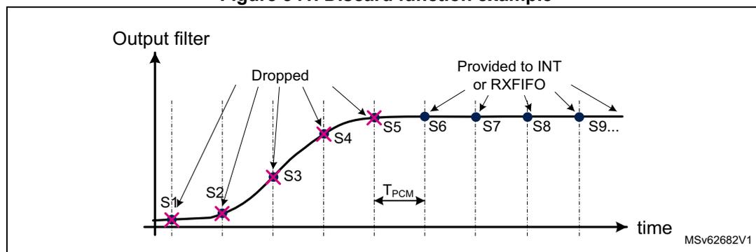
The figure is a graph titled 'Output filter' on the y-axis and 'time' on the x-axis. A curve starts at the origin and rises, then levels off. Along the curve, samples are marked at regular intervals. The first five samples, labeled S1, S2, S3, S4, and S5, are marked with red 'X's and have arrows pointing to them from the word 'Dropped'. The subsequent samples, labeled S6, S7, S8, and S9 (with an ellipsis), are marked with blue dots and have arrows pointing to them from the text 'Provided to INT or RXFIFO'. A horizontal double-headed arrow between the vertical lines of S5 and S6 is labeled T PCM . In the bottom right corner of the graph area, the text 'MSv62682V1' is present.
Warning: All filters working in interleaved DMA mode must have the same NBDIS[7:0] value.
Data interface activation
The data interfaces are enabled by setting the corresponding SITFEN or ADCITFEN bit to 1. Once the digital filter is enabled, it receives the serial data from the external \( \Sigma\Delta \) modulator or parallel internal data sources (ADC).
35.4.11 Start-up sequence examples
Figure 342 details an acquisition sequence start of a digital filter triggered by DFLTEN (ACQMOD[2:0] = 0), with NBDIS[7:0] = 3 (three samples to discard before acquisition).
The DFLTx is configured for audio application: MCIC, RSFLT and HPF activated. The data interface (SITFx or ADCITF) is assumed to be already activated.
Note: NBDIS[7:0] is set on purpose to a low value to simplify the drawing.
Figure 342. Start sequence with DFLTEN, in continuous mode, audio configuration
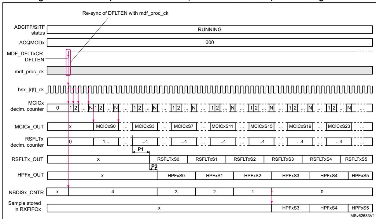
The diagram illustrates the start-up sequence of a digital filter. It shows the following signals and their states over time:
- ADCITF/SITF status: RUNNING
- ACQMODx: 000
- MDF_DFLTxCR.DFLTEN: High (indicated by a pink rectangle and a line labeled "Re-sync of DFLTEN with mdf_proc_ck")
- mdf_proc_ck: Clock signal
- bsx_irl_ck: Bitstream clock signal
- MCICx decim. counter: Counts from 0 to N (1, 2, ..., N, 1, 2, ..., N, 1, 2, ..., N, 1, 2, ..., N, 1, 2, ..., N, 1, 2, ..., N, 1, 2, ..., N)
- MCICx_OUT: Output samples (x, MCICxS0, ..., MCICxS3, ..., MCICxS7, ..., MCICxS11, ..., MCICxS15, ..., MCICxS19, ..., MCICxS23, ...)
- RSFLTx decim. counter: Counts from 0 to 4 (0, 1, ..., 4, ..., 4, ..., 4, ..., 4, ..., 4, ..., 4, ..., 4)
- RSFLTx_OUT: Output samples (x, ..., RSFLTxS0, RSFLTxS1, RSFLTxS2, RSFLTxS3, RSFLTxS4, RSFLTxS5)
- HPFx_OUT: Output samples (x, ..., HPFxS0, HPFxS1, HPFxS2, HPFxS3, HPFxS4, HPFxS5)
- NBDISx_CNTR: Counts from 3 down to 0 (3, 4, 3, 2, 1, 0)
- Sample stored in RXFIFOx: Samples stored in the FIFO (x, ..., HPFxS3, HPFxS4, HPFxS5)
Key events marked in the diagram:
- P1: A sample is delivered from the RSFLTx_OUT to the HPFx_OUT.
- P2: A sample is delivered from the HPFx_OUT to the RXFIFOx.
The DFLTEN bit is re-sampled into the MDF processing clock domain. When DFLTEN is detected high, the filter chain is enabled and the decimation counter of the MCIC filter is incremented at the rate of the bitstream clock.
When the MCIC decimation counter reaches its programmed value N, a sample is available for the RSFLT.
The RSFLT processes all the samples provided by the MCIC and delivers a sample to the HPF every time it processes four samples (decimation by 4). The RSFLT needs up to 24 cycles of mdf_proc_ck clock before delivering a sample (P1).
The HPF processes all the samples provided by the RSFLT, but the NBDIS function prevents the data writing in the RXFIFO as long as NBDIS_CNTR does not reach 0. This counter is decremented every time the HPF delivers a sample.
When NBDIS_CNTR reaches 0, the samples provided by the HPF are stored into the RXFIFO.
The example shown in Figure 343 is based in a motor-control filter configuration:
- • MCIC and INT are enabled.
- • SFLT and HPF are disabled.
- • ACQMOD[2:0] is set to 1 and uses a mdf_trgiy input as trigger.
- • NBDIS[7:0] is set to 3.
- • INTVAL[6:0] is set to 2.
The mdf_trgiy input signal is re-sampled into the MDF processing clock domain to avoid any metastability issues. When the trigger condition is met (rising edge), the decimation counter of the MCIC filter is incremented at the rate of the bitstream clock.
When the MCIC decimation counter reaches its programmed value N, a sample is available. The NBDIS function prevents the samples writing in the INT as long as NBDIS_CNTR does not reach 0. This counter is decremented every time the MCIC delivers a sample.
When NBDIS_CNTR reaches 0, the new samples are provided to the INT, that performs the integration of three consecutive samples and stores them into the RXFIFO.
Figure 343. Start sequence with trigger input, in continuous mode, motor configuration
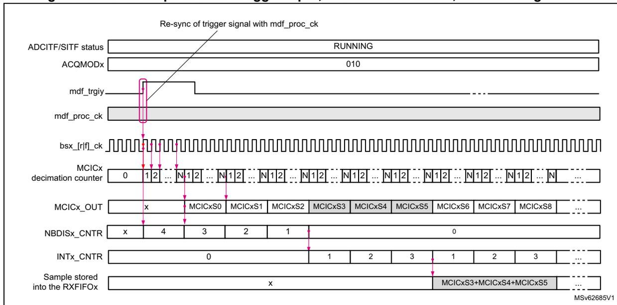
The diagram illustrates the timing sequence for the MDF filter's start-up. At the top, the ADCITF/SITF status is shown as 'RUNNING' and ACQMODx is set to '010'. The mdf_trgiy signal is a pulse that triggers the start. The mdf_proc_ck is a periodic clock. The bsx_rfl_ck is a higher-frequency bitstream clock. The MCICx decimation counter starts at 0 and counts up to N, then resets. MCICx_OUT provides samples S0 through S8. NBDISx_CNTR starts at 4 and counts down to 0. INTx_CNTR counts from 0 to 3. The Sample stored into the RXFIFOx shows the accumulation of samples S3, S4, and S5. A note indicates 'Re-sync of trigger signal with mdf_proc_ck'.
35.4.12 Break interface
The break interface merges the break events coming from the OLDx and SDCx blocks into four break signals connected to various peripherals of the product (see Table 278 for details).
As shown in Figure 344 , several blocks can share the same break line. A same block can also drive several break lines. The break interface is controlled via MDF_OLDxCR and MDF_SCDxCR.
Figure 344. Break interface simplified view
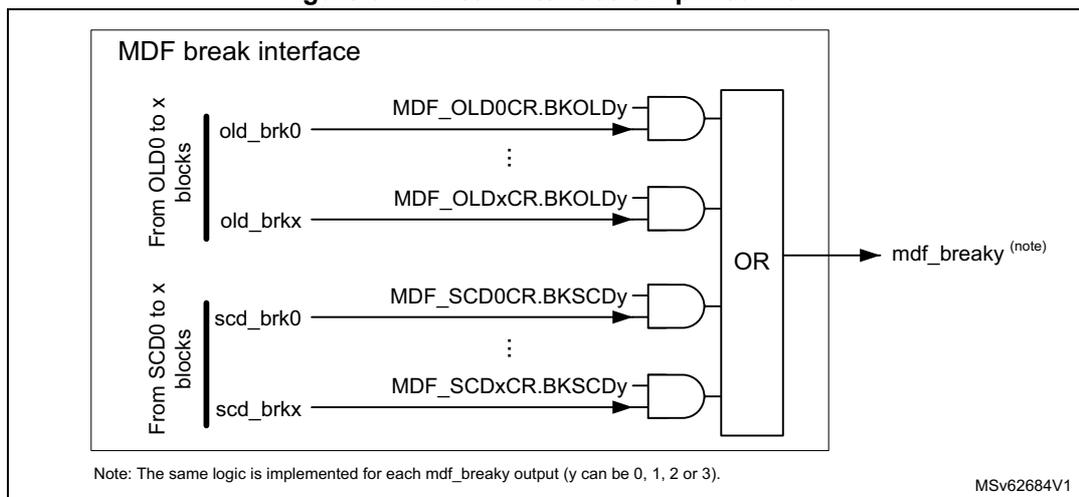
MDF break interface
From OLD0 to x blocks
old_brk0 → MDF_OLD0CR.BKOLDy → AND gate
⋮
old_brkx → MDF_OLDxCR.BKOLDy → AND gate
From SCD0 to x blocks
scd_brk0 → MDF_SCD0CR.BKSCDy → AND gate
⋮
scd_brkx → MDF_SCDxCR.BKSCDy → AND gate
All AND gate outputs → OR gate → mdf_breaky (note)
Note: The same logic is implemented for each mdf_breaky output (y can be 0, 1, 2 or 3). MSv62684V1
35.4.13 Data transfer to memory
Data format
The samples processed by DFLTx are stored into a RXFIFO. The application can read the samples stored into the FIFOs via the MDF digital filter data register x (MDF_DFLTxDR) . The samples inside this register are signed and left aligned. The bit 31 always represents the sign.
The MDF provides 24-bit left-aligned data. Performing a 16-bit access to MDF_DFLTxDR allows the application to get the 16 most significant bits. Performing a 32-bit access to MDF_DFLTxDR allows the application to get a 24-bit data size.
Figure 345. MDF_DFLTxDR data format
![Figure 345. MDF_DFLTxDR data format. The diagram shows the RXFIFO structure and the MDF_DFLTxDR register format. The RXFIFO has a width of 24 bits (bits 23 to 0) and a depth of FIFO_DEPTH. The MDF_DFLTxDR register is 32 bits wide (bits 31 to 0). It contains a 24-bit PCM[23:0] value left-aligned in the upper half (bits 31 to 8) and zero's in the lower half (bits 7 to 0). Bit 31 is the sign bit. A bracket on the left indicates that the 24-bit PCM value from the RXFIFO is copied into the MDF_DFLTxDR register.](/RM0486-STM32N6x5-x7/f62ac5fbddc8d05f5a7630f8d8669634_img.jpg)
RXFIFO width
23 0
1
⋮
FIFO_DEPTH
MDF_DFLTxDR
31 16 15 7 0
PCM[23:0]
zero's
MSv62689V1
Data resynchronization
The samples stored into the RXFIFOs can be transferred into the memory by using either DMA requests or interrupt signaling.
Note: The RXFIFOs are located into the mdf_ker_ck clock domain, while MDF_DFLTxDR are located into the mdf_hclk (AHB) clock domain.
When the AHB clock is available, if MDF_DFLTxDR is empty and if a sample is available into the RXFIFO, this sample is transferred into MDF_DFLTxDR.
The sample transfer from the RXFIFO to MDF_DFLT \( x \) DR takes two periods of the AHB clock (mdf_hclk) and two periods of the mdf_ker_ck clock. The MDF inserts automatically wait-states if the application performs a read operation of MDF_DFLT \( x \) DR while the transfer of the new sample from the RXFIFO to MDF_DFLT \( x \) DR is not yet completed.
Figure 346. Data resynchronization
The diagram illustrates the data flow within the MDF block. It is divided into two clock domains: the AHB clock domain (left, shaded grey) and the mdf_ker_ck clock domain (right, shaded light grey). In the mdf_ker_ck domain, data flows from 'Digital filter processing (DFLT \( x \) )' to 'RXFIFO'. From the RXFIFO, the data passes through a 'sync' block, which acts as a bridge between the two clock domains. In the AHB clock domain, the data flows from the 'sync' block to 'MDF_DFLT \( x \) DR'. A legend at the bottom indicates that the grey shaded area represents the AHB clock domain and the light grey shaded area represents the mdf_ker_ck clock domain. The identifier MSv62690V1 is shown in the bottom right corner of the diagram.
The MDF can also combine two transfer types: the independent-transfer and the interleaved-transfer modes.
Independent-transfer mode
In this mode, each RXFIFO has its own DMA channel and its own FTHF flag event.
Both single and burst DMA transfers are supported in this mode, but the application must care about the following points:
- • The RXFIFO must contain at least the same amount of samples than the burst size.
- • The burst mode efficiency may be reduced due to the data resynchronization explained in the previous section.
In addition, the application can select the RXFIFO threshold (FTH bit) to trigger the data transfer: a data transfer can be triggered as soon as the RXFIFO is not empty, or when the RXFIFO is half-full (containing depth / 2 samples).
For the DMA transfer, as soon as one of the RXFIFO reaches the threshold level, the corresponding DMA request is asserted in order to ask for data transfer. Successive DMA requests are performed as long as the corresponding RXFIFO is not empty.
The DMA mode of the RXFIFO \( x \) is enabled via the corresponding DMAEN bit in the MDF digital filter control register \( x \) (MDF_DFLT \( x \) CR) .
For the interrupt signaling, the following cases must be considered:
- • If FTH = 0, as soon as a data is available in MDF_DFLT \( x \) DR, the corresponding FTHF is set, allowing the generation of an interrupt. FTHF is released as soon as MDF_DFLT \( x \) DR is read.
- • If FTH = 1, as soon as one of the RXFIFO reaches the threshold level and a data is available into MDF_DFLT \( x \) DR, the corresponding FTHF is set, allowing the generation of an interrupt. The FTHF flag is released as soon as one data is read. FTHF is set again if the threshold condition is met again. In this mode, every time an interrupt occurs, the application is supposed to read FIFO_SIZE / 2 data.
The independent-transfer mode must be used when the sample rates provided by each filter paths are not perfectly synchronous, or when the streams are independent. This situation may occur for example:
- • when SITF is in SLAVE mode and each external sensor provides its own sampling clock
- • when the decimation ratios of the DFLT x are not the same
- • when all the streams are not starting at the same time
Interleaved-transfer mode
This mode optimizes the DMA request resources by sharing a single DMA request with several RXFIFOs.
Only single DMA transfers are supported in this mode.
In interleaved-transfer mode, FTH cannot be used and only the FTHF of RXFIFO0 is available for the interrupt signaling.
For the DMA transfer, when all the RXFIFOs working in interleaved-transfer mode are not empty, some DMA requests are generated in order to read sequentially one sample of each RXFIFOs, via MDF_DFLT0DR.
For the RXFIFOs working in interleaved-transfer mode, the DMA channel is enabled by setting to 1 DMAEN in MDF_DFLT0DR and by defining the amount of RXFIFOs working in interleaved mode via ILVNB[3:0]. DMAEN for the other RXFIFOs working in interleaved-transfer mode (RXFIFO 1 to ILVNB[3:0]) are not taken into account.
Figure 347 shows four RXFIFOs working in interleaved-transfer mode. Each RXFIFO has a delay due to the programming of the DLY block.
When all the RXFIFOs have at least one sample available (in this example the last FIFO receiving a sample is RXFIFO1), the MDF requests the data transfer to the memory (see 1 in Figure 347 ). In this figure, the DMA is assumed to be used for the data transfer to memory.
The acquisition can be simply stopped by setting DFLTEN to 0 for one of the filter configured in interleaved-transfer mode. In the example, when a DFLTEN is set to 0 (see 2 in Figure 347 ), the transfer to memory is immediately stopped. Samples M2S(N), M3S(N) and M4S(N) may be lost.
Figure 347. Data transfer in interleaved-transfer mode
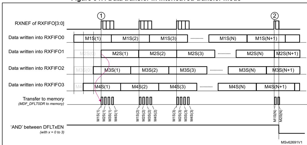
The diagram illustrates the data transfer process in interleaved-transfer mode across four RXFIFOs (RXFIFO0 to RXFIFO3).
-
RXNEF of RXFIFO[3:0]
: Shows pulses indicating when FIFOs are not empty.
-
Data written into RXFIFO0-3
: Shows blocks of data samples. RXFIFO0 has M1S(1) to M1S(N+1). RXFIFO1 has M2S(0) to M2S(N+1). RXFIFO2 has M3S(0) to M3S(N+1). RXFIFO3 has M4S(0) to M4S(N+1).
-
Transfer to memory (MDF_DFLT0DR to memory)
: Shows the interleaved reading of samples. At marker
1
, a burst of four transfers occurs: M1S(1), M2S(1), M3S(1), and M4S(1). This repeats for subsequent sample sets.
-
'AND' between DFLTxEN
: This signal stays high until marker
2
, where it drops to low (representing one DFLTEN being set to 0).
-
Result at marker 2
: The transfer to memory stops immediately after M1S(N). Samples M2S(N), M3S(N), and M4S(N) are shown as remaining in the FIFOs and not transferred.
In interrupt mode, when all the RXFIFOs working in interleaved-transfer mode have a data ready, the FTHF flag of RXFIFO0 is asserted to allow the interrupt generation. The application is then supposed to read sequentially one sample of each RXFIFOs, via MDF_DFLT0DR. The FTHF event is released when the first data is read.
For the RXFIFOs working in interleaved-transfer mode, the interrupt mode is enabled by setting FTHIE to 1 in MDF_DFLT0DR and by defining the amount of RXFIFOs working in interleaved-transfer mode via ILVNB[3:0]. FTHIE of the other RXFIFOs working in interleaved-transfer mode (RXFIFO1 to ILVNB[3:0]) are not taken into account.
The interleaved-transfer mode can only be applied starting at RXFIFO0 up to RXFIFO \( k \) . The number of RXFIFOs working in interleaved-transfer mode are defined by ILVNB[3:0].
When ILVNB[3:0] = 0, all RXFIFOs work in independent-transfer mode.
The interleaved-transfer mode can be used only for digital filters delivering samples perfectly synchronous each other. This is typically the case of sound capture with an array of digital microphones sharing the same bitstream clock.
Caution: To make the MDF working properly in interleaved-transfer mode, the following rules must be respected:
- • All filters working in interleaved-transfer mode must be all synchronized together, meaning that all filters must select the same ACQMOD[2:0] (must be equal to 010 or 011), the same trigger source and the same trigger sensitivity.
- • All filters working in interleaved-transfer mode must have the same configuration.
- • All sensors providing the data for the filters working in interleaved-transfer mode must use the same bitstream clock frequency.
- • The maximum delay difference applied with SPKDLY[6:0] for the filters working in interleaved-transfer mode must remain strictly lower than the RXFIFO depth. Normally this delay does not need to exceed one \( T_{PCM} \) period.
Note: Both independent- and interleaved-transfer modes can work in parallel: for example, the first RXFIFOs (RXFIFO0 to RXFIFO \( k \) ) may work in interleaved-transfer mode when the others (RXFIFO( \( k+1 \) ) to RXFIFO( \( N \) )) works in independent-transfer mode.
If the AHB clock is not present when a data transfer must be performed, the MDF first requests the AHB clock (refer to Section 35.4.5: Clock generator (CKGEN) for details).
The figure below shows the data path for a configuration in independent-transfer mode (left-hand figure) and a configuration mixing both independent- and interleaved-transfer modes (right-hand figure).
Figure 348. Data path for interleaved- and independent-transfer modes
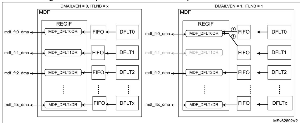
In the right-hand figure, the DFLT0 and DFLT1 filters are configured in interleaved-transfer mode. For those filters, FTH is no longer taken into account by the hardware. The samples provided by DFLT0 and DFLT1 are read from MDF_DFLT0DR. When both RXFIFOs are no longer empty, the MDF generates two DMA requests to read the sample from DFLT0 and the sample from DFLT1. If both RXFIFOs are not empty again, the same sequence is triggered.
Note: When one of the filter working in interleaved-transfer mode is disabled, the data transfer to memory of all filters in interleaved-transfer mode is stopped immediately as well.
RXFIFO overrun
A RXFIFO overrun condition is detected when the RXFIFO is full and a new sample from the DFLTx must be written.
In this case, DOVRF is set and the new sample is dropped. When the RXFIFO has at least one location available, the new incoming sample is written into the RXFIFO.
Figure 349 shows an example based on a RXFIFO depth of four words and FTH set to 1, so that FTHF goes to 1 when the RXFIFO is half-full.
The S7 sample is lost due to an overrun: the RXFIFO is full while S7 must be written into the RXFIFO. The S7 write operation is not performed. DOVRF is set to 1 at the moment where the write operation was expected. The overflow event remains to 1 as long as it is not cleared by the application.
In this example, DOVRIE is set to 1 to have an interrupt if an overrun condition is detected.
After the S7 sample, the application manages to read data from the RXFIFO and the MDF can write the S8 sample and consecutive. Later, the application clears DOVR, allowing the detection of a new overrun situation.
In the mdf_hclk line, the gray boxes indicate that the MDF requested the AHB clock. The figure below shows the AHB clock available only when the MDF requests it. In real applications, the AHB clock may also be present if the MDF does not request it.
Figure 349. Example of overflow and transfer to memory
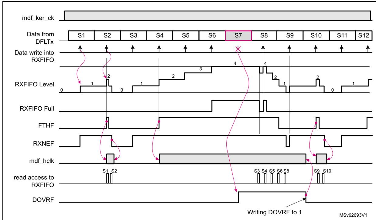
The timing diagram shows the following signals over time:
- mdf_hclk : Kernel clock, always high.
- Data from DFLTx : A sequence of samples S1 through S12. S7 is highlighted in pink.
- Data write into RXFIFO : Arrows indicate write attempts. S1, S2, S3, S4, S5, S6, S8, S9, S10, S11, and S12 are successfully written. S7 is marked with a pink 'X' because the RXFIFO is full at that time.
- RXFIFO Level : Shows the number of samples in the FIFO. It increases from 0 to 4 as samples S1-S4 are written. It reaches 4 again when S5-S8 are written. When S7 is attempted, the level is already 4 (full). It decreases when samples are read.
- RXFIFO Full : Goes high when the RXFIFO level reaches 4.
- FTHF : Threshold flag that goes high when the RXFIFO level reaches the configured threshold (e.g., 2).
- RXNEF : RXFIFO not empty flag that goes high when the RXFIFO level is non-zero.
- read access to RXFIFO : Pulses indicating data being read out. Samples S1 and S2 are read first, then S3, S4, S5, S6, and S8 are read later. S7 is never read because it was lost.
- DOVRF : Overflow flag that goes high when an overflow occurs (at S7) and is reset when writing DOVRF to 1.
MSv62693V1
Note: If the MDF works in interleaved-transfer mode, the application must check the overrun status of all RXFIFOs that works in interleaved-transfer mode.
35.4.14 Autonomous mode
The MDF can work even if the AHB bus clock is not available (Stop modes). The MDF uses the AHB clock only for the register interface. All the processing part is clocked with the kernel clock.
In Stop mode, the MDF receives a kernel clock if the selected clock source is an oscillator available in Stop mode
In Stop mode, the MDF receives the AHB clock if the following conditions are met:
- • The MDF autonomous mode is enabled in the RCC.
- • The MDF requests the AHB clock, in the following situations:
- – when the MDF must transfer data into the memory via the DMA
The data are directly transferred to the SRAM thanks to the DMA while the product remains in Stop mode. The AHB clock request is maintained until the DMA transfer is completed. - – when the MDF must generate an interrupt
An interrupt generally wakes up the device from Stop mode, as an action from the application is needed. Once the AHB clock is available, the interrupt is generated. The AHB clock request is maintained as long as an enabled interrupt
- – when the MDF must transfer data into the memory via the DMA
flag is active. More precisely, when an interrupt must be generated, the MDF requests the AHB clock.
35.4.15 Register protection
The MDF embeds some hardware protection to prevent invalid situations. The table below shows the list of write-protected and unprotected fields.
Table 287. Register protection summary
| Registers | Unprotected fields | Write-protected fields | Write-protection condition |
|---|---|---|---|
| MDF global control register (MDF_GCR) | TRGO | ILVNB[3:0] | DFLTACTIVE0 = 1 |
| MDF clock generator control register (MDF_CKGCR) | CKGDEN CCK0EN CCK1EN | PROC DIV[6:0], CCK DIV[3:0], CKG MOD, TRG SRC[3:0], TRG SENS, CCK[1:0]DIR | CKGACTIVE = 1 |
| MDF serial interface control register x (MDF_SITFxCr) | SITFEN | STH[4:0], SITF MOD[1:0], SCK SRC[1:0] | SITFACTIVEEx = 1 |
| MDF bitstream matrix control register x (MDF_BSMXxCR) | - | BSSEL[4:0] | DFLTACTIVEEx = 1 or SCDACTIVEEx = 1 or OLDACTIVEEx = 1 |
| MDF digital filter control register x (MDF_DFLTxCr) | DFLTEN | NBDIS[7:0], TRG SRC[3:0], TRG SENS, FTH, DMAEN, SNPSFMT, ACQ MOD[2:0] | DFLTACTIVEEx = 1 |
| MDF digital filter configuration register x (MDF_DFLTxCICR) | SCALE[5:0] | MCICD[8:0], CIC MOD[2:0], DAT SRC[1:0] | |
| MDF reshape filter configuration register x (MDF_DFLTxRSFR) | - | All fields | |
| MDF integrator configuration register x (MDF_DFLTxINTR) | - | All fields | |
| MDF out-of limit detector control register x (MDF_OLDxCr) | OLDEN | ACICD[4:0], ACICN[1:0], THINB BKOLD[3:0] | OLDACTIVEEx = 1 |
| MDF OLDx low threshold register x (MDF_OLDxTHLR) | - | All fields | |
| MDF OLDx high threshold register x (MDF_OLDxTHHR) | - | All fields | |
| MDF delay control register x (MDF_DLYxCR) | - | SKPDLY[6:0] | SKPBF = 1 |
| MDF short circuit detector control register x (MDF_SCDxCr) | SCDEN | BKSCD[3:0], SCDT[7:0] | SCDACTIVEEx = 1 |
| MDF DFLTx interrupt enable register x (MDF_DFLTxIER) | All fields | - | - |
| Registers | Unprotected fields | Write-protected fields | Write-protection condition |
|---|---|---|---|
| MDF DFLTx interrupt status register x (MDF_DFLTxISR) | All fields | - | - |
| MDF offset error compensation control register x (MDF_OECxCR) | OFFSET[25:0] | - | - |
All the MDF processing is performed in the mdf_proc_ck clock domain. For that reason, enabling or disabling a MDF sub-block may take some time due to the resynchronization between the AHB clock domain and the mdf_proc_ck clock domain. XXXACTIVE flags are available to allow the application to check that the synchronization between the two clock domains is completed.
To change a write-protected bitfield, the application must follow this sequence:
- 1. Set the enable bit of the sub-block to 0.
- 2. Wait for corresponding flag XXXACTIVE = 0.
- 3. Modify the wanted fields.
- 4. Set the enable bit of the sub-block to 1.
Refer to the description of each sub-block for more details.
35.5 MDF low-power modes
Table 288. Effect of low-power modes on MDF| Mode | Description |
|---|---|
| Sleep | No effect. MDF interrupts cause the device to exit Sleep mode. |
| Stop (1) | The MDF registers content is kept. If the MDF is clocked by an internal oscillator available in Stop mode, the MDF remains active. The interrupts cause the device to exit Stop mode. |
| Standby | The MDF is powered down and must be reinitialized after exiting Standby mode. |
- 1. Refer to Section 35.3: MDF implementation for details about Stop modes supported by the MDF.
35.6 MDF interrupts
To increase the CPU performance, the MDF offers the following interrupt lines per digital filter:
- • receive interrupt MDF_FLTx_RX (mdf_fltx_rx_it)
- • event interrupt MDF_FLTx_EVT (mdf_fltx_evt_it)
- • a combination of both interrupts MDF_FLTx (mdf_fltx_it)
Note:
Interrupts are not always connected to the device (see
Section 35.3: MDF implementation
for more details).
The status flags are available even if the corresponding interrupt enable flag is not enabled.
The interrupt interface is controlled via the MDF_DFLT x interrupt enable register x (MDF_DFLT x IER) and the MDF_DFLT x interrupt status register x (MDF_DFLT x ISR) .
Figure 350. MDF interrupt interface
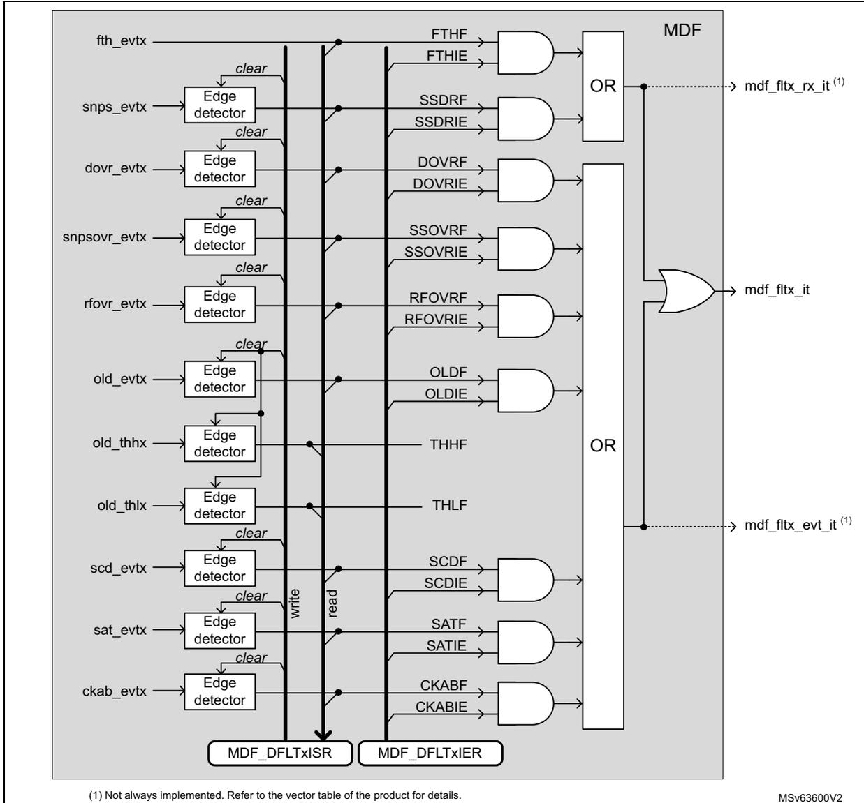
The diagram illustrates the interrupt interface for the Multi-function Digital Filter (MDF). On the left, there are several event inputs:
fth_evtx
,
snps_evtx
,
dovr_evtx
,
snpsvr_evtx
,
rfov_evtx
,
old_evtx
,
old_thhx
,
old_thlx
,
scd_evtx
,
sat_evtx
, and
ckab_evtx
. Most of these (except
fth_evtx
) pass through an "Edge detector" block. Each edge detector has a "clear" input connected to a vertical bus. Below the edge detectors are two registers:
MDF_DFLT
x
ISR
(Interrupt Status Register) and
MDF_DFLT
x
IER
(Interrupt Enable Register). A "write" bus connects to
MDF_DFLT
x
ISR
and a "read" bus connects to
MDF_DFLT
x
IER
. To the right of the registers, there are several signal lines:
FTHF
,
FTHIE
,
SSDRF
,
SSDRIE
,
DOVRF
,
DOVRIE
,
SSOVR
,
SSOVR
,
RFOVRF
,
RFOVRIE
,
OLDF
,
OLDIE
,
THHF
,
THLF
,
SCDF
,
SCDIE
,
SATF
,
SATIE
,
CKABF
, and
CKABIE
. These lines are connected to a series of AND gates. The first two AND gates take
FTHF
/
FTHIE
and
SSDRF
/
SSDRIE
as inputs. Their outputs are connected to an OR gate, which produces the interrupt signal
mdf_filtx_rx_it
(1)
. The next four AND gates take
DOVRF
/
DOVRIE
,
SSOVR
/
SSOVR
,
RFOVRF
/
RFOVRIE
, and
OLDF
/
OLDIE
as inputs. Their outputs are connected to another large OR gate, which produces the interrupt signal
mdf_filtx_evt_it
(1)
. The
THHF
and
THLF
lines are also connected to this large OR gate. The final two AND gates take
SCDF
/
SCDIE
,
SATF
/
SATIE
, and
CKABF
/
CKABIE
as inputs. Their outputs are also connected to the large OR gate. The
fth_evtx
input is connected directly to the
FTHF
line. The
old_evtx
input is connected to the
old_evtx
edge detector and also to the
THHF
and
THLF
lines. The
old_thhx
input is connected to the
old_thhx
edge detector and also to the
THHF
line. The
old_thlx
input is connected to the
old_thlx
edge detector and also to the
THLF
line. The
scd_evtx
input is connected to the
scd_evtx
edge detector and also to the
SCDF
line. The
sat_evtx
input is connected to the
sat_evtx
edge detector and also to the
SATF
line. The
ckab_evtx
input is connected to the
ckab_evtx
edge detector and also to the
CKABF
line.
(1) Not always implemented. Refer to the vector table of the product for details.
MSv63600V2
The table below shows which interrupt line is affected by which event, and how to clear and activate each interrupt/event.
Table 289. MDF interrupt requests
| Interrupt vectors | Interrupt event | Event flag | Event/interrupt clearing method | Exit Sleep mode | Exit Stop modes (1) | Exit Standby mode | |
|---|---|---|---|---|---|---|---|
| MDF_FLTx (2) | MDF_FLTx_RX (3) | RXFIFO threshold reached | FTHF | Read MDF_DFLTxD (3) until RXFIFO level is lower than the threshold. | Yes | Yes | No |
| Snapshot data ready | SSDRF | Write SSDRF to 1. | |||||
| MDF_FLTx_EVT (4) | Snapshot data overrun | SSOVR (4) | Write SSOVR to 1. | ||||
| RXFIFO overrun | DOVR (4) | Write DOVR to 1. | |||||
| RSFLT overrun | RFOVR (4) | Write RFOVR to 1. | |||||
| Short-circuit detector | SCDF | Write SCDF to 1. | |||||
| Saturation detection | SATF | Write SATF to 1. | |||||
| Channel clock absence detection | CKABF | Write CKABF to 1. | |||||
| Out-of-limit detector | OLDF | Write OLDF to 1. | |||||
| THHF | Write OLDF to 1. | - | - | - | |||
| - | - | THLF | Write OLDF to 1. | - | - | - | |
1. Refer to Section 35.3: MDF implementation for details.
2. MDF_FLTx vector corresponds to the assertion of mdf_fltx_it signal
3. MDF_FLTx_RX vector corresponds to the assertion of mdf_fltx_rx signal.
4. MDF_FLTx_EVT vector corresponds to the assertion of mdf_fltx_evt signal.
35.7 MDF application informations
35.7.1 MDF configuration examples for audio capture
Table 290 gives some examples of the MDF settings for the digital microphones, focusing on 16 and 48 kHz output data rate. In these examples, the following is expected:
- • The INT block is bypassed (INTVAL = 0).
- • The offset error compensation is disabled (OFFSET = 0).
Configurations #1 and #2 are for very low-power use-cases and have a reduced signal-to-noise ratio. The user must also insure that the selected digital microphone can work properly at 512 kHz. These configurations can be used for sound detection. The RSFLT is not used to reduce as much as possible the frequency of the kernel clock (mdf_ker_ck).
Configurations #3, #4, #9, #10, #11 give signal-to-noise ratios around 115 dB, with an ideal microphone model, with a sinus signal of 997 Hz. Using the RSFLT allows a good control on the in-band ripple and a good image rejection.
Configurations #7, #8, #10 give signal-to-noise ratio around 120 dB, with an ideal microphone model, using a sinus signal of 997 Hz.
Table 290. Examples of MDF settings for microphone capture
| Configuration | mdf_ker_ck (MHz) | PROC DIV + 1 | CCK DIV + 1 | CIC order (1) | MCICD + 1 | SCALE | RSFLT BYP | RSFLT D | HPF BYP | - | mdf_proc_ck (MHz) | Total dec. ratio | F RS (kHz) | F MDF_CCKx (MHz) | F PCM (kHz) |
|---|---|---|---|---|---|---|---|---|---|---|---|---|---|---|---|
| #1 | 1.024 | 1 | 2 | 4 | 64 | 0x2D (- 8.5 dB) | 1 | x | x | => | 1.024 | 64 | - | 0.512 | 8 |
| #2 | 1 | 2 | 5 | 32 | 0x2B (- 14.5 dB) | 32 | - | 16 | |||||||
| #3 | 1 | 2 | 5 | 16 | 0x01 (+ 3.5 dB) | 0 | 0 | 64 | 32 | 8 | |||||
| #4 | 2.048 | 1 | 2 | 5 | 16 | 0x01 (+ 3.5 dB) | 0 | 0 | 2.048 | 64 | 64 | 1.024 | 16 | ||
| #5 | 3.072 | 1 | 6 | 5 | 8 | 0x0B (+ 33.6 dB) | 0 | 0 | x | => | 3.072 | 32 | 32 | 0.512 | 8 |
| #6 | 2 | 2 | 5 | 12 | 0x06 (+ 18.1 dB) | 48 | 64 | 0.768 | 16 | ||||||
| #7 | 1 | 2 | 5 | 24 | 0x2C (- 12 dB) | 96 | 1.536 | ||||||||
| #8 | 4.096 | 1 | 2 | 5 | 32 | 0x27 (- 26.6 dB) | 0 | 0 | x | => | 4.096 | 128 | 64 | 2.048 | 16 |
| #9 | 6.144 | 3 | 2 | 5 | 16 | 0x02 (+ 6.0 dB) | 0 | 0 | 2.048 | 64 | 64 | 1.024 | 16 | ||
| #10 | 2 | 2 | 5 | 24 | 0x2C (- 12 dB) | 3.072 | 96 | 1.536 | |||||||
| #11 | 1 | 2 | 5 | 16 | 0x01 (+ 3.5 dB) | 6.144 | 64 | 192 | 3.072 | 48 | |||||
| #12 | 7.680 | 1 | 2 | 5 | 20 | 0x2E (- 6.0 dB) | 0 | 0 | 7.680 | 80 | 192 | 3.840 | 48 | ||
1. CICMOD = 100 for CIC order equal to 4. CICMOD = 101 for CIC order equal to 5.
35.7.2 Programming examples
This example describes how to capture sound from four microphones, assuming that each microphone pair shares the same data line. The MDF_SD0 and MDF_SD2 data lines are used. The microphone clock is provided by the MDF via MDF_CCK0 pin.
Table 291. Programming sequence
| Operations | Comments |
|---|---|
| Adjust the proper kernel clock frequency via the RCC block | Assuming that the RCC is programmed to provide a kernel clock (mdf_ker_ck) of 12.288 MHz |
| Select the proper MDF kernel clock source via the RCC block | Refer to the RCC of the product. |
| Enable the MDF clocks via the RCC block | Refer to the RCC of the product. |
| Reset the MDF via the RCC block | Refer to the RCC of the product. |
| AFMUX programming | Program the AFMUX to select MDF_SD0, MDF_SD2 and MDF_CCK0 function. |
Table 291. Programming sequence (continued)
| Operations | Comments |
|---|---|
| Enable MDF processing clock: MDF_CKGCR = 0x0103 0023 | PROCDIV = 1 (division by 2): mdf_proc_ck frequency is 6.144 MHz. CCKDIV = 3 (division by 4): MDF_CCK0 clock frequency is 1.536 MHz. The MDF_CCK0 pad is set in output and generates a clock so that the microphones can exit from low-power mode. |
| Serial interfaces configuration: MDF_SITF0CR = 0x0000 1F01 MDF_SITF2CR = 0x0000 1F01 | SCKSRC = 0 to select MDF_CCK0 as serial clock. SIFTMOD = 0 to select LF_MASTER mode. Clock absence feature is not working in this mode. The serial interfaces are enabled. |
| Bitstream matrix configuration: MDF_BSMX0CR = 0x0000 0000 MDF_BSMX1CR = 0x0000 0001 MDF_BSMX2CR = 0x0000 0004 MDF_BSMX3CR = 0x0000 0005 | DFLT0 filter takes the bitstream of SITF0, sampled on rising edge. DFLT1 filter takes the bitstream of SITF0, sampled on falling edge. DFLT2 filter takes the bitstream of SITF2, sampled on rising edge. DFLT3 filter takes the bitstream of SITF2, sampled on falling edge. |
| Filters configuration (CIC): MDF_DFLT0CICR = 0x02C0 1750 MDF_DFLT1CICR = 0x02C0 1750 MDF_DFLT2CICR = 0x02C0 1750 MDF_DFLT3CICR = 0x02C0 1750 | SCALE = 0x2C (- 12 dB) to avoid any saturation MCICD = 0x17 (decimation by 24) CICMOD = 5 to select a Sinc 5 DATSCR = 0 to select data coming from BSMX |
| Filters configuration (RSFLT and HPF): MDF_DFLT0RSFR = 0x0000 0100 MDF_DFLT1RSFR = 0x0000 0100 MDF_DFLT2RSFR = 0x0000 0100 MDF_DFLT3RSFR = 0x0000 0100 | HPFC = 1: cut-off frequency of 16 kHz * 0.00125 = 20 Hz HPFBYP = 0: HPF not bypassed RSFLTD = 0: RSFLT decimates by 4 RSFLTBY = 0: RSFLT is not bypassed |
| Filters configuration (INT): MDF_DFLT0INTR = 0x0000 0000 MDF_DFLT1INTR = 0x0000 0000 MDF_DFLT2INTR = 0x0000 0000 MDF_DFLT3INTR = 0x0000 0000 | INTVAL = 0: INT filter not used Other parameter is not significant. |
| Micro delay adjust: MDF_DLY0CR = 0x0000 0005 MDF_DLY0CR = 0x0000 0012 MDF_DLY0CR = 0x0000 0023 MDF_DLY0CR = 0x0000 0000 | Initial micro-delay for each microphone, values just given as example |
| Offset error correction: MDF_OEC0CR = 0x0000 0000 MDF_OEC1CR = 0x0000 0000 MDF_OEC2CR = 0x0000 0000 MDF_OEC3CR = 0x0000 0000 | No correction. DC offset is removed by HPF. |
Table 291. Programming sequence (continued)
| Operations | Comments |
|---|---|
| Short circuit detection: MDF_SCD0CR = 0x0000 0000 MDF_SCD1CR = 0x0000 0000 MDF_SCD2CR = 0x0000 0000 MDF_SCD3CR = 0x0000 0000 | SCD function for each filter is disabled. |
| Enable interrupt events: MDF_DFLT0IER = 0x0000 0202 MDF_DFLT1IER = 0x0000 0202 MDF_DFLT2IER = 0x0000 0202 MDF_DFLT3IER = 0x0000 0202 | Enable the interrupt event the application wants to handle. In this example, the SATIE and DOVRIE bits are set to 1 to have an interrupt if a saturation or an data overflow occurs. |
| Digital filter control: MDF_DFLT0CR = 0x0000 0027 MDF_DFLT1CR = 0x0000 0027 MDF_DFLT2CR = 0x0000 0027 MDF_DFLT3CR = 0x0000 0027 Wait for DFLTACTIVE = 0 for the filters | NBDIS = 0: no samples discarded TRGSRC = 0: TRGO selected as trigger source TRGSENS = 0: Trigger on rising edge ACQMOD = 2: Synchronous continuous acquisition mode DMAEN = 1: DMA interface enabled DFLTEN = 1: digital filter enabled |
| Clear status flags: MDF_DFLT0ISR = 0x0000 0FFF MDF_DFLT1ISR = 0x0000 0FFF MDF_DFLT2ISR = 0x0000 0FFF MDF_DFLT3ISR = 0x0000 0FFF | Clear all the status flags before running the filters. |
| Program the DMA Enable the DMA | The DMA must be programmed in order to read the data inside MDF_DFLT0DR every time a DMA request is generated. Note that when the MDF is in interleaved acquisition mode, data of filters 0, 1, 2, and 3 are read via MDF_DFLT0DR register. |
| Start acquisition: MDF_GCR = 0x0000 0031 | ILVNB = 3: interleaved mode with DFLT0,1,2, and 3 TRGO = 1 to trigger the acquisition of all filters waiting for TRGO rising edge event |
35.7.3 Connection examples
Figure 351 shows simple connection examples of the MDF to external sensors:
- • Picture on the left: four digital microphones connected to the MDF
In this connection, DMIC1 is intended to be used alone. This is why it uses a dedicated clock (MDF_CCK0). DMIC1 is also connected to a dedicated data line in case the application intends to power-down DMIC2/3/4, when only DMIC1 is used. If the application keeps DMIC2/3/4 powered, DMIC2 and DMIC1 can share the same data line, reducing the connection to four I/Os.
If the power consumption is not an issue, when a single microphone is used, all the microphones can be connected to the same common clock (MDF_CCK0) and each
microphone pair can share the same data line. In this case, only three I/Os are required.
In this example, the data transfer to memory can be performed either using the interleaved- or the independent-transfer mode.
- • Picture in the center: sensor providing several data lines with a common clock
Each data line can represent different parameters (such as current or voltage). The common clock can be provided either by the sensor or by the MDF. The data line can be shared or not by two sensors if the sensor allows it. In the figure below, the sensor does not allow the sharing of the data lines.
In this example, the data transfer to memory can be performed either using the interleaved- or independent-transfer mode.
- • Picture on the right: two independent sensors connected to the MDF
Each of them has its dedicated clock and data lines. In this case, the data transfer to memory must use the independent-transfer mode.
Figure 351. Sensor connection examples
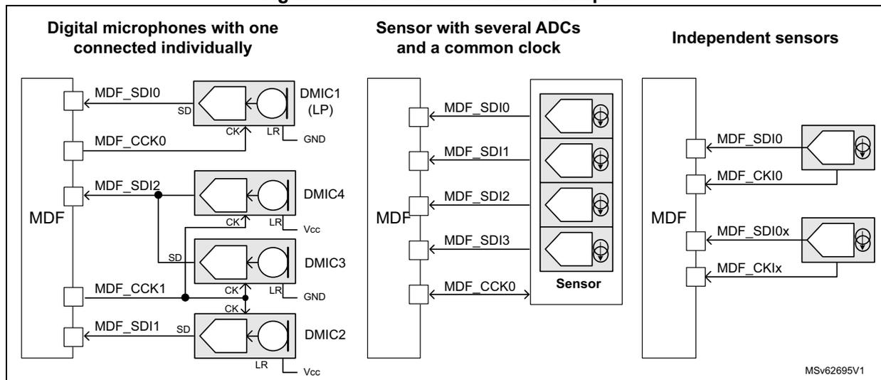
The diagram illustrates three sensor connection examples to an MDF:
- Digital microphones with one connected individually: Shows four DMICs (DMIC1 (LP), DMIC4, DMIC3, DMIC2) connected to the MDF. DMIC1 (LP) is connected to MDF_SDI0 and MDF_CCK0. DMIC4 is connected to MDF_SDI2 and MDF_CCK1. DMIC3 is connected to MDF_SDI2 and MDF_CCK1. DMIC2 is connected to MDF_SDI1 and MDF_CCK1. Each DMIC has SD, CK, LR, and GND/Vcc pins.
- Sensor with several ADCs and a common clock: Shows a single sensor block with four ADCs connected to the MDF. The ADCs are connected to MDF_SDI0, MDF_SDI1, MDF_SDI2, and MDF_SDI3. The sensor provides a common clock (MDF_CCK0) to all ADCs.
- Independent sensors: Shows two independent sensors connected to the MDF. The first sensor is connected to MDF_SDI0 and MDF_CK10. The second sensor is connected to MDF_SDI0x and MDF_CK1x. Each sensor has its own dedicated clock and data lines.
MSV62695V1
35.7.4 Global frequency response
Figure 352 shows the global frequency response for a 16 kHz audio signal with a digital microphone working at 1.024 MHz. The filter configuration is the following:
- • CIC order 4 or 5, with a decimation ratio of 16
- • RSFLT enabled, with a decimation ratio of 4
- • HPF enable with a cut-off frequency of 40 Hz
The figure below shows the theoretical frequency response using a CIC4 and a CIC5.
Figure 352. Global frequency response
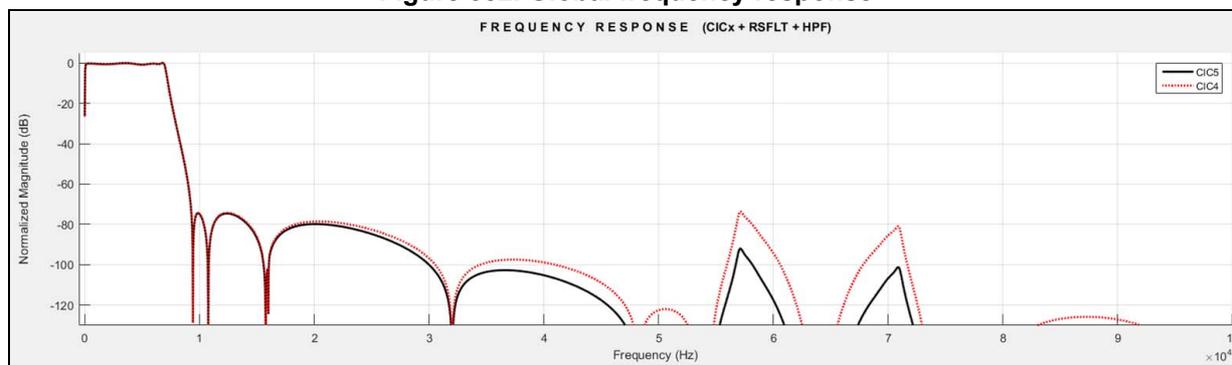
Figure 353 shows the in-band ripple for a 16 kHz audio signal with a digital microphone working at 1.024 MHz. The filter configuration is the following:
- • CIC order 4 or 5, with a decimation ratio of 16
- • RSFLT enabled, with a decimation ratio of 4
- • HPF enable with a cut-off frequency of 20 Hz
The resulting in-band ripple is \( \pm 0.41 \) dB for CIC5, and \( \pm 0.45 \) for CIC4.
The -3 dB cut-off frequency is 7061 Hz.
Figure 353. Detailed frequency response
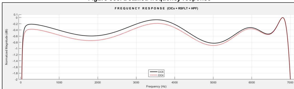
35.7.5 Total MDF gain
This section details how to compute the signal level provided by the MDF according to the filter settings. The formula does not take into account the filters transfer function.
A signal level may be expressed in dBFS (decibel full scale). A 0 dBFS level is assigned to the maximum possible digital level. For example, a signal that reaches 50 % of the maximum level, has a - 6 dBFS level (6 dB below full scale).
For example, for the MDF offering a final data width of 24 bits, a signal having an amplitude of \( 2 \times 10^6 \) LSB has a level of:
In addition, the data size of a signal having an amplitude (Amp) expressed in LSB is given by:
One bit need to be added for negative values.
So a signal having an amplitude of \( 2 \cdot 10^6 \) LSB, has a data size of 21.9 bits.
CIC gain
The CIC gain ( \( G_{\text{CIC}} \) and \( GdB_{\text{CIC}} \) ) can be deduced from the following formula giving data size in bits ( \( DS_{\text{CIC}} \) ).
And the bit growth is:
where N represents the CIC order (selected by CICMOD[2:0]), and D1 is the decimation ratio (given by MCICD).
\( DS_{\text{IN}} \) represents the data size (in bits) of the input signal.
Warning: \( DS_{\text{CIC}} \) is very important for CIC filters. In order to work fine, \( DS_{\text{CIC}} \) must not exceed 26 bits.
which gives, in decibels:
Note: The same formulas are valid for the ACIC.
Data size at SCALE output
The data size at SCALE output (including the CIC gain) is a key information as the RSFLT starts to have some saturations if the peak-to-peak signal amplitude at SCALE output is higher than 22 bits.
If the RSFLT is bypassed, then a peak-to-peak signal amplitude of 24 bits is accepted. The resulting data size is given by:
The data size at SCALE output ( \( DS_{\text{SCALE}} \) ) is expressed in bits and \( GdB_{\text{SCALE}} \) represents the gain selected by SCALE[5:0], in dB.
RSFLT gain
The RSFLT gain in the useful bandwidth is typically 9.5 dB, but due to ripple a margin of about \( \pm 0.5 \) dB must be considered. Typically, the RSFLT increases the bit size by \( BG_{RSFLT} \) :
INT gain
The INT block can also introduce a gain if the rescaling value is different from the integration value.
and:
The bit growth of the INT is then given by the following formula:
IVAL represents the integration value selected by INTVAL[6:0], and IDIV represents the integrator output division selected by INTDIV[1:0].
Note: The HPF filter has a gain of 0 dB.
The figure below shows a simplified view of the filter path, and gives for each significant component the expression of the bit growth and the gain.
Figure 354. Simplified DFLT view with gain information
![Figure 354: Simplified DFLT view with gain information. The diagram shows a signal flow from PCM[23:0] through various blocks: SAD, HPF, RSFLT, SAT, SCALE, D1, and CIC. Above the blocks, linear gain values are provided: GSAD = 0.00391, GHPF = 1, GRSFLT = 2.98, GSCALE = 10^(GdBSCALE/20), and GMCIC = D1^N. Below the blocks, gain in dB is provided: GdBSAD = -48.1 dB, GdBHPF = 0 dB, GdBRSFLT = 9.5 dB, GdBSCALE, and GdBMIC = 20 x log10(D1^N). The HPF, RSFLT, SAT, SCALE, D1, and CIC blocks are grouped under the label 'DFLTx'. A dashed box labeled (1) encloses the SAD block and its gain values. A note at the bottom left states: (1) The SAD is not always implemented (see the ADF implementation section for details). A code MSV62698V1 is in the bottom right.](/RM0486-STM32N6x5-x7/359cb0df2188bdb3a8275bf5ce858f5a_img.jpg)
(1) The SAD is not always implemented (see the ADF implementation section for details).
MSV62698V1
The table below summarizes the final data size for different filter configurations.
Table 292. Output signal levels
| Filter configurations | Final signal level (dBFS) | Final signal size (bits) |
|---|---|---|
| CIC + RSFLT (+ HPF) | \( SdB_{OUT} = 20 \times \log_{10} \left( \frac{2^{DS_{OUT}}}{2^{24}} \right) \) | \(
DS_{OUT} = DS_{SCALE} + 1.6
\)
bits \( DS_{SCALE} \) must be lower than 22 bits. |
| CIC + RSFLT (+ HPF) + INT | \(
DS_{OUT} = DS_{SCALE} + BG_{INT} + 1.6
\)
bits \( DS_{SCALE} \) must be lower than 22 bits. | |
| CIC (+ HPF) + INT | \(
DS_{OUT} = DS_{SCALE} + BG_{INT}
\) \( DS_{SCALE} \) must be lower than 24 bits. |
Example using the main filter chain
If the MDF filter is programmed as follows:
- • The input signal is coming from a serial interface ( \( DS_{IN} = 1 \) bit).
- • CIC order = 5 (N), with a decimation value of 24 (D1).
- • SCALE[5:0] is set to -12 dB.
- • RSFLT is enabled and the decimation by four is enabled.
- • HPF is enabled.
- • INT is disabled.
Check first the data size at CIC output:
The size is lower than 26 bits, so the CIC works in good conditions.
The data size at CIC output is very close to 24 bits, so the SCALE must be adjusted in order to provide a signal 22 bits max to the RSFLT. An attenuation of 12 dB is needed.
Then the signal level provided to the RSFLT is:
At the end, the final signal amplitude is:
or
The RSFLT ripple a margin of about \( \pm 0.41 \) dB (in this configuration) must be considered.
Example using the OLD filter chain
In the following example, the application wants to trigger an OLD event when the voltage coming from a shunt resistor reaches \( \pm 200 \) mV.
Hypothesis:
- • The \( \Sigma\Delta \) sensor is specified to support a full-scale signal of \( \pm 350 \) mV.
- • The ACIC decimation ratio (D2) is fixed to 32.
- • The ACIC order (N) is fixed to 3.
The \( \Sigma\Delta \) sensor provides a full-scale digital signal (amplitude of one bit) for a signal higher or equal to \( \pm 350 \) mV. If the input signal is equal 200 mV, then the digital signal amplitude provided by the sensor is \( 200 / 350 = 0.571 \) .
The gain of the ACIC filter is:
A signal having an amplitude of 200 mV at sensor input has then an amplitude of about \( 32768 * 0.571 = 18725 \) LSB at ACIC output.
OLDTHH must be set to 18725 and OLDTHL must be set to -18725.
35.8 MDF registers
All the MDF registers must be accessed either in word (32-bit) or half-word (16-bit) formats.
The registers are described for the MDF instance having the biggest number of filters.
For registers related to filters, the number of registers is equal to the amount of filters. Refer to Section 35.3 for details.
35.8.1 MDF global control register (MDF_GCR)
Address offset: 0x000
Reset value: 0x0000 0000
This register is used for controls common to all digital filters.
| 31 | 30 | 29 | 28 | 27 | 26 | 25 | 24 | 23 | 22 | 21 | 20 | 19 | 18 | 17 | 16 |
|---|---|---|---|---|---|---|---|---|---|---|---|---|---|---|---|
| Res. | Res. | Res. | Res. | Res. | Res. | Res. | Res. | Res. | Res. | Res. | Res. | Res. | Res. | Res. | Res. |
| 15 | 14 | 13 | 12 | 11 | 10 | 9 | 8 | 7 | 6 | 5 | 4 | 3 | 2 | 1 | 0 |
| Res. | Res. | Res. | Res. | Res. | Res. | Res. | Res. | ILVNB[3:0] | Res. | Res. | Res. | TRGO | |||
| rw | rw | rw | rw | rw | |||||||||||
Bits 31:8 Reserved, must be kept at reset value.
Bits 7:4 ILVNB[3:0] : Interleaved number
This bitfield is set and reset by software. it enables or disables the interleaved-transfer mode and defines how many digital filters work in this mode.
This bitfield cannot be changed when DFLTEN = 1 in MDF_DFLT0CR.
0000: Interleaved-transfer mode disabled
0001: Data from DFLT0 and DFLT1 are interleaved.
0010: Data from DFLT0, DFLT1 and DFLT2 are interleaved.
...
1111: Data from DFLT0 to DFLT15 are interleaved.
Note: This bitfield can be write-protected (refer to Section 35.4.15 for details).
Bits 3:1 Reserved, must be kept at reset value.
Bit 0 TRGO : Trigger output control
This bit is set by software and reset by hardware. It is used to start the acquisition of several filters synchronously. It is also able to synchronize several MDF together by controlling the mdf_trgo signal.
0: Write 0 has no effect. Read 0 means that the trigger can be set again to 1.
1: Write 1 generates a positive pulse on mdf_trgo signal and triggers the acquisition on the enabled filters having ACQMOD[2:0] = 0x1 and selecting TRGO as trigger. Read 1 means that the trigger pulse is still active.
35.8.2 MDF clock generator control register (MDF_CKGCR)
Address offset: 0x004
Reset value: 0x0000 0000
This register is used to control the clock generator. The mdf_proc_ck clock must be enabled before enabling other MDF parts.
| 31 | 30 | 29 | 28 | 27 | 26 | 25 | 24 | 23 | 22 | 21 | 20 | 19 | 18 | 17 | 16 |
|---|---|---|---|---|---|---|---|---|---|---|---|---|---|---|---|
| CKGA CTIVE | PROCDIV[6:0] | Res. | Res. | Res. | Res. | CCKDIV[3:0] | |||||||||
| r | rw | rw | rw | rw | rw | rw | rw | rw | rw | rw | rw | ||||
| 15 | 14 | 13 | 12 | 11 | 10 | 9 | 8 | 7 | 6 | 5 | 4 | 3 | 2 | 1 | 0 |
| TRGSRC[3:0] | Res. | Res. | Res. | TRGSE NS | Res. | CCK1D IR | CCK0D IR | CKGM OD | Res. | CCK1E N | CCK0E N | CKGD EN | |||
| rw | rw | rw | rw | rw | rw | rw | rw | rw | rw | rw | |||||
Bit 31 CKGACTIVE : Clock generator active flag
This bit is set and cleared by hardware. This flag must be used by the application to check if the clock generator is effectively enabled (active) or not. The protected fields of this function can only be updated when CKGACTIVE = 0 (refer to Section 35.4.15 for details). The delay between a transition on CKGDEN and a transition on CKGACTIVE is two periods of AHB clock and two periods of mdf_proc_ck.
0: The clock generator is not active and can be configured if needed.
1: The clock generator is active and protected fields cannot be configured.
Bits 30:24 PROCDIV[6:0] : Divider to control the serial interface clock
This bitfield is set and reset by software. It is used to adjust the frequency of the clock provided to the SITF.
This bitfield must not be changed if one of the filters is enabled (DFTEN = 1).
0: mdf_ker_ck provided to the SITF
1: mdf_ker_ck/2 provided to the SITF
2: mdf_ker_ck/3 provided to the SITF
...
127: mdf_ker_ck/128 provided to the SITF
Note: This bitfield can be write-protected (refer to Section 35.4.15 for details).
Bits 23:20 Reserved, must be kept at reset value.
Bits 19:16 CCKDIV[3:0] : Divider to control the MDF_CCK clock
This bitfield is set and reset by software. It is used to adjust the frequency of the MDF_CCK clock. The input clock of this divider is the clock provided to the SITF. More globally, the frequency of the MDF_CCK is given by the following formula:
This bitfield must not be changed if one of the filters is enabled (DFTEN = 1).
0000: The MDF_CCK clock is mdf_proc_ck.
0001: The MDF_CCK clock is mdf_proc_ck / 2.
0010: The MDF_CCK clock is mdf_proc_ck / 3.
...
1111: The MDF_CCK clock is mdf_proc_ck / 16.
Note: This bitfield can be write-protected (refer to Section 35.4.15 for details).
Bits 15:12 TRGSRC[3:0] : Digital filter trigger signal selection
This bitfield is set and cleared by software. It is used to select which external signals trigger for the corresponding filter. This bitfield is not significant if CKGMOD = 0.
000x: TRGO selected
0010: mdf_trg[0] selected
0011: mdf_trg[1] selected
...
1111: mdf_trg[13] selected
Note: This bitfield can be write-protected (refer to Section 35.4.15 for details).
Bits 11:9 Reserved, must be kept at reset value.
Bit 8 TRGSENS : CKGEN trigger sensitivity selection
This bit is set and cleared by software. It is used to select the trigger sensitivity of the trigger signals. This bit is not significant if the CKGMOD = 0.
0: A rising edge event triggers the activation of CKGEN dividers.
1: A falling edge even triggers the activation of CKGEN dividers.
Note: When the trigger source is TRGO, TRGSENS value is not taken into account. When TRGO is selected, the sensitivity is forced to falling edge. This bit can be write-protected (refer to Section 35.4.15 for details).
Bit 7 Reserved, must be kept at reset value.
Bit 6 CCK1DIR : MDF_CCK1 direction
This bit is set and reset by software. It is used to control the direction of the MDF_CCK1 pin.
0: MDF_CCK1 pin direction is in input.
1: MDF_CCK1 pin direction is in output.
Note: This bit can be write-protected (refer to Section 35.4.15 for details).
Bit 5 CCK0DIR : MDF_CCK0 direction
This bit is set and reset by software. It is used to control the direction of the MDF_CCK0 pin.
0: MDF_CCK0 pin direction is in input.
1: MDF_CCK0 pin direction is in output.
Note: This bit can be write-protected (refer to Section 35.4.15 for details).
Bit 4 CKGMOD : Clock generator mode
This bit is set and reset by software. It is used to define the way the clock generator is enabled. This bit must not be changed if one of the filters is enabled (DFTEN = 1).
0: The kernel clock is provided to the dividers as soon as CKGDEN is set to 1.
1: The kernel clock is provided to the dividers when CKGDEN is set to 1 and the trigger condition met.
Note: This bit can be write-protected (refer to Section 35.4.15 for details).
Bit 3 Reserved, must be kept at reset value.
Bit 2 CCK1EN : MDF_CCK1 clock enable
This bit is set and reset by software. It is used to control the generation of the bitstream clock on the MDF_CCK1 pin.
0: Bitstream clock not generated
1: Bitstream clock generated on the MDF_CCK1 pad
Bit 1 CCK0EN : MDF_CCK0 clock enable
This bit is set and reset by software. It is used to control the generation of the bitstream clock on the MDF_CCK0 pin.
0: Bitstream clock not generated
1: Bitstream clock generated on the MDF_CCK0 pad
Bit 0 CKGDEN : CKGEN dividers enable
This bit is set and reset by software. It is used to enable/disable the clock dividers of the CKGEN: PROCDIV and CCKDIV.
0: CKGEN dividers disabled
1: CKGEN dividers enabled
35.8.3 MDF serial interface control register x (MDF_SITFxCr)
Address offset: 0x080 + 0x80 * x, (x = 0 to 5)
Reset value: 0x0000 1F00
This register is used to control the serial interfaces (SITFx). The number of registers is equal to the amount of filters. Refer to Section 35.3 for details.
| 31 | 30 | 29 | 28 | 27 | 26 | 25 | 24 | 23 | 22 | 21 | 20 | 19 | 18 | 17 | 16 |
|---|---|---|---|---|---|---|---|---|---|---|---|---|---|---|---|
| SITFACTIVE | Res. | Res. | Res. | Res. | Res. | Res. | Res. | Res. | Res. | Res. | Res. | Res. | Res. | Res. | Res. |
| r | |||||||||||||||
| 15 | 14 | 13 | 12 | 11 | 10 | 9 | 8 | 7 | 6 | 5 | 4 | 3 | 2 | 1 | 0 |
| Res. | Res. | Res. | STH[4:0] | Res. | Res. | SITFMOD[1:0] | Res. | SCKSRC[1:0] | SITFEN | ||||||
| rw | rw | rw | rw | rw | rw | rw | rw | rw | rw | ||||||
Bit 31 SITFACTIVE : Serial interface active flag
This bit is set and cleared by hardware. It is used by the application to check if the serial interface is effectively enabled (active) or not. The protected fields of this function can only be updated when the SITFACTIVE is set to 0 (refer to Section 35.4.15 for details).
The delay between a transition on SITFEN and a transition on SITFACTIVE is two periods of AHB clock and two periods of mdf_proc_ck.
0: The serial interface is not active and can be configured if needed.
1: The serial interface is active and protected fields cannot be configured.
Bits 30:13 Reserved, must be kept at reset value.
Bits 12:8 STH[4:0] : Manchester symbol threshold/SPI threshold
This bitfield is set and cleared by software. It is used for Manchester mode to define the expected symbol threshold levels (refer to Manchester mode for details on computation). In addition this bitfield is used to define the timeout value for the clock absence detection in Normal SPI mode. STH[4:0] values lower than four are invalid.
Note: This bitfield can be write-protected (refer to Section 35.4.15 for details).
Bits 7:6 Reserved, must be kept at reset value.
Bits 5:4 SITFMOD[1:0] : Serial interface type
This bitfield is set and cleared by software. it is used to define the serial interface type.
00: LF_MASTER SPI mode
01: Normal SPI mode
10: Manchester mode: rising edge = logic 0, falling edge = logic 1
11: Manchester mode: rising edge = logic 1, falling edge = logic 0
Note: This bitfield can be write-protected (refer to Section 35.4.15 for details).
Bit 3 Reserved, must be kept at reset value.
Bits 2:1 SCKSRC[1:0] : Serial clock source
This bitfield is set and cleared by software. it is used to select the clock source of the serial interface.
00: Serial clock source is MDF_CCK0.
01: Serial clock source is MDF_CCK1.
1x: Serial clock source is MDF_CK1x (not allowed in LF_MASTER SPI mode).
Note: This bitfield can be write-protected (refer to Section 35.4.15 for details).
Bit 0 SITFEN : Serial interface enable
This bit is set and cleared by software. It is used to enable/disable the serial interface.
0: Serial interface disabled
1: Serial interface enabled
35.8.4 MDF bitstream matrix control register x (MDF_BSMXxCR)
Address offset: 0x084 + 0x80 * x, (x = 0 to 5)
Reset value: 0x0000 0000
This register is used to select the bitstream to be provided to the corresponding digital filter and to the SCD. The number of registers is equal to the amount of filters. Refer to Section 35.3 for details.
| 31 | 30 | 29 | 28 | 27 | 26 | 25 | 24 | 23 | 22 | 21 | 20 | 19 | 18 | 17 | 16 |
|---|---|---|---|---|---|---|---|---|---|---|---|---|---|---|---|
| BSMXA CTIVE | Res. | Res. | Res. | Res. | Res. | Res. | Res. | Res. | Res. | Res. | Res. | Res. | Res. | Res. | Res. |
| r | |||||||||||||||
| 15 | 14 | 13 | 12 | 11 | 10 | 9 | 8 | 7 | 6 | 5 | 4 | 3 | 2 | 1 | 0 |
| Res. | Res. | Res. | Res. | Res. | Res. | Res. | Res. | Res. | Res. | Res. | BSSEL[4:0] | ||||
| rw | rw | rw | rw | rw | |||||||||||
Bit 31 BSMXACTIVE : BSMX active flag
This bit is set and cleared by hardware. It is used by the application to check if the BSMX is effectively enabled (active) or not. BSSEL[4:0] can only be updated when the BSMXACTIVE is set to 0. This BSMXACTIVE flag is a logical OR between OLDACTIVE, DFLTACTIVE, and SCDACTIVE flags. Both of them must be set to 0 in order to update BSSEL[4:0] bitfield.
0: BSMX is not active and can be configured if needed.
1: BSMX is active and protected fields cannot be configured.
Bits 30:5 Reserved, must be kept at reset value.
Bits 4:0 BSSEL[4:0] : Bitstream Selection
This bitfield is set and cleared by software. It is used to select the bitstream to be processed for DFLTx and SCDx. The size of this bitfield depends on the number of DFLTx instantiated. If this bitfield selects a not instantiated input, the MDF selects the valid stream bsx_f having the higher index number.
00000: bs0_r provided to DFLTx and SCDx
00001: bs0_f provided to DFLTx and SCDx
00010: bs1_r provided to DFLTx and SCDx (if instantiated)
00011: bs1_f provided to DFLTx and SCDx (if instantiated)
...
11110: bs15_r provided to DFLTx and SCDx (if instantiated)
11111: bs15_f provided to DFLTx and SCDx (if instantiated)
Note: This bitfield can be write-protected (refer to Section 35.4.15 for details).
35.8.5 MDF digital filter control register x (MDF_DFLTxCR)
Address offset: 0x088 + 0x80 * x, (x = 0 to 5)
Reset value: 0x0000 0000
The number of registers is equal to the amount of filters. Refer to Section 35.3 for details.
| 31 | 30 | 29 | 28 | 27 | 26 | 25 | 24 | 23 | 22 | 21 | 20 | 19 | 18 | 17 | 16 |
|---|---|---|---|---|---|---|---|---|---|---|---|---|---|---|---|
| DFLTA CTIVE | DFLTR UN | Res. | Res. | NBDIS[7:0] | Res. | Res. | Res. | SNPSF MT | |||||||
| r | r | rw | rw | rw | rw | rw | rw | rw | rw | rw | |||||
| 15 | 14 | 13 | 12 | 11 | 10 | 9 | 8 | 7 | 6 | 5 | 4 | 3 | 2 | 1 | 0 |
| TRGSRC[3:0] | Res. | Res. | Res. | TRGSE NS | Res. | ACQMOD[2:0] | Res. | FTH | DMAE N | DFLTE N | |||||
| rw | rw | rw | rw | rw | rw | rw | rw | rw | rw | w | |||||
Bit 31 DFLTACTIVE : Digital filter active flag
This bit is set and cleared by hardware. It indicates if the digital filter is active: can be running or waiting for events.
0: Digital filter not active (can be re-enabled again, via DFLTEN, if needed)
1: Digital filter active
Bit 30 DFLTRUN : Digital filter run status flag
This bit is set and cleared by hardware. It indicates if the digital filter is running or not.
0: Digital filter not running and ready to accept a new trigger event
1: Digital filter running
Bits 29:28 Reserved, must be kept at reset value.
Bits 27:20 NBDIS[7:0] : Number of samples to be discarded
This bitfield is set and cleared by software. It is used to define the number of samples to be discarded every time the DFLT x is re-started.
0: No sample discarded
1: 1 sample discarded
2: 2 samples discarded
...
255: 255 samples discarded
Note: This bitfield can be write-protected (refer to Section 35.4.15 for details).
Bits 19:17 Reserved, must be kept at reset value.
Bit 16 SNPSFMT : Snapshot data format
This bit is set and cleared by software. It is used to select the data format for the snapshot mode.
0: Integrator counter (INT_CNT) not inserted into MDF_SNPS x DR, leaving a data resolution of 23 bits
1: Integrator counter (INT_CNT) inserted at position [15:9] of MDF_SNPS x DR, leaving a data resolution of 16 bits.
Note: This bit can be write-protected (refer to Section 35.4.15 for details).
Bits 15:12 TRGSRC[3:0] : Digital filter trigger signal selection
This bitfield is set and cleared by software. It is used to select which external signals trigger the corresponding filter.
0000: TRGO selected
0001: OLD
x
event selected
0010: mdf_trg[0] selected
...
1111: mdf_trg[13] selected
Note: This bitfield can be write-protected (refer to Section 35.4.15 for details).
Bits 11:9 Reserved, must be kept at reset value.
Bit 8 TRGSENS : Digital filter trigger sensitivity selection
This bit is set and cleared by software. It is used to select the trigger sensitivity of the external signals
0: A rising edge event triggers the acquisition.
1: A falling edge even triggers the acquisition.
Note: When the trigger source is TRGO or OLD x event, TRGSENS value is not taken into account. When TRGO is selected, the sensitivity is forced to falling edge, when OLD x event is selected, the sensitivity is forced to rising edge.
This bit can be write-protected (refer to Section 35.4.15 for details).
Bit 7 Reserved, must be kept at reset value.
Bits 6:4 ACQMOD[2:0] : Digital filter trigger mode
This bitfield is set and cleared by software. It is used to select the filter trigger mode.
000: Asynchronous continuous acquisition mode
001: Asynchronous single-shot acquisition mode
010: Synchronous continuous acquisition mode
011: Synchronous, single-shot acquisition mode
100: Window continuous acquisition mode
101: Synchronous snapshot mode
Others: same a 000
Note: This bitfield can be write-protected (refer to Section 35.4.15 for details).
Bit 3 Reserved, must be kept at reset value.
Bit 2 FTH : RXFIFO threshold selection
This bit is set and cleared by software. It is used to select the RXFIFO threshold. This bit is not significant for RXFIFOs working in interleaved-transfer mode (see Interleaved-transfer mode for details).
0: RXFIFO threshold event generated when the RXFIFO is not empty
1: RXFIFO threshold event generated when the RXFIFO is half-full
Note: This bit can be write-protected (refer to Section 35.4.15 for details).
Bit 1 DMAEN : DMA requests enable
This bit is set and cleared by software. It is used to control the generation of DMA request to transfer the processed samples into the memory.
0: DMA interface for the corresponding digital filter disabled
1: DMA interface for the corresponding digital filter enabled
Note: This bit can be write-protected (refer to Section 35.4.15 for details).
Bit 0 DFLTEN : Digital filter enable
This bit is set and cleared by software. It is used to control the start of acquisition of the corresponding digital filter path. This bit behavior depends on ACQMOD[2:0] and external events. The serial or parallel interface delivering the samples must be enabled as well.
0: Acquisition immediately stopped
1: Acquisition immediately started if ACQMOD[2:0] = 00x or 101, or acquisition started when the proper trigger event occurs if ACQMOD[2:0] = 01x or 100.
35.8.6 MDF digital filter configuration register x (MDF_DFLTxCICR)
Address offset: 0x08C + 0x80 * x, (x = 0 to 5)
Reset value: 0x0000 0000
This register is used to control the main CIC filter. The number of registers is equal to the amount of filters. Refer to Section 35.3 for details.
| 31 | 30 | 29 | 28 | 27 | 26 | 25 | 24 | 23 | 22 | 21 | 20 | 19 | 18 | 17 | 16 |
|---|---|---|---|---|---|---|---|---|---|---|---|---|---|---|---|
| Res. | Res. | Res. | Res. | Res. | Res. | SCALE[5:0] | Res. | Res. | Res. | MCICD 8 | |||||
| rw | rw | rw | rw | rw | rw | rw | |||||||||
| 15 | 14 | 13 | 12 | 11 | 10 | 9 | 8 | 7 | 6 | 5 | 4 | 3 | 2 | 1 | 0 |
| MCICD[7:0] | Res. | CICMOD[2:0] | Res. | Res. | DATSRC[1:0] | ||||||||||
| rw | rw | rw | rw | rw | rw | rw | rw | rw | rw | rw | rw | rw | |||
Bits 31:26 Reserved, must be kept at reset value.
Bits 25:20 SCALE[5:0] : Scaling factor selectionThis bitfield is set and cleared by software. It is used to select the gain to be applied at CIC output (refer to Table 283 for details). If the application attempts to write a new gain value while the previous one is not yet applied, this new gain value is ignored. Reading back this bitfield informs the application on the current gain value.
000000: 0 dB
000001: + 3.5 dB
000010: + 6 dB or shift left by 1 bit
...
011000: + 72 dB or shift left by 12 bits
100000: - 48.2 dB or shift right by 8 bits (default value)
100001: - 44.6 dB
100010: - 42.1 dB or shift right by 7 bits
100011: - 38.6 dB
...
101110: - 6 dB or shift right by 1 bit
101111: - 2.5 dB
Others: Reserved
Bits 19:17 Reserved, must be kept at reset value.
Bits 16:8 MCICD[8:0] : CIC decimation ratio selectionThis bitfield is set and cleared by software. It is used to select the CIC decimation ratio. A decimation ratio smaller than two is not allowed. The decimation ratio is given by (CICDEC+1).
0: Decimation ratio is 2.
1: Decimation ratio is 2.
2: Decimation ratio is 3..
3: Decimation ratio is 4
...
511: Decimation ratio is 512.
Note: This bitfield can be write-protected (refer to Section 35.4.15 for details).
Bit 7 Reserved, must be kept at reset value.
Bits 6:4 CICMOD[2:0] : Select the CIC modeThis bitfield is set and cleared by software. It is used to select the configuration and the order of the MCIC. When CICMOD[2:0] = 0xx, the CIC is split into two filters: the main CIC (MCIC) and the auxiliary CIC (ACIC, used for the out-of limit detector).
000: CIC split in two filters and MCIC configured in FastSinc filter
001: CIC split in two filters and MCIC configured in Sinc 1 filter
010: CIC split in two filters and MCIC configured in Sinc 2 filter
011: CIC split in two filters and MCIC configured in Sinc 3 filter
100: CIC configured in single Sinc 4 filter
others: CIC configured in single Sinc 5 filter
Note: This bitfield can be write-protected (refer to Section 35.4.15 for details).
Bits 3:2 Reserved, must be kept at reset value.
Bits 1:0 DATSRC[1:0] : Source data for the digital filterThis bitfield is set and cleared by software.
0x: Stream coming from the BSMX selected
10: Stream coming from the ADCITF1 selected
11: Stream coming from the ADCITF2 selected
Note: This bitfield can be write-protected (refer to Section 35.4.15 for details).
35.8.7 MDF reshape filter configuration register x (MDF_DFLTxRSFR)
Address offset: \( 0x090 + 0x80 * x \) , ( \( x = 0 \) to \( 5 \) )
Reset value: \( 0x0000\ 0000 \)
This register is used to control the reshape and HPF filters. The number of registers is equal to the amount of filters. Refer to Section 35.3 for details.
| 31 | 30 | 29 | 28 | 27 | 26 | 25 | 24 | 23 | 22 | 21 | 20 | 19 | 18 | 17 | 16 |
|---|---|---|---|---|---|---|---|---|---|---|---|---|---|---|---|
| Res. | Res. | Res. | Res. | Res. | Res. | Res. | Res. | Res. | Res. | Res. | Res. | Res. | Res. | Res. | Res. |
| 15 | 14 | 13 | 12 | 11 | 10 | 9 | 8 | 7 | 6 | 5 | 4 | 3 | 2 | 1 | 0 |
| Res. | Res. | Res. | Res. | Res. | Res. | HPFC[1:0] | HPFBYP | Res. | Res. | RSFLTD | Res. | Res. | Res. | Res. | RSFLT BYP |
| rw | rw | rw | rw | rw |
Bits 31:10 Reserved, must be kept at reset value.
Bits 9:8 HPFC[1:0] : High-pass filter cut-off frequency
This bitfield is set and cleared by software. It is used to select the cut-off frequency of the high-pass filter. \( F_{PCM} \) represents the sampling frequency at HPF input.
00: Cut-off frequency = \( 0.000625 \times F_{PCM} \)
01: Cut-off frequency = \( 0.00125 \times F_{PCM} \)
10: Cut-off frequency = \( 0.00250 \times F_{PCM} \)
11: Cut-off frequency = \( 0.00950 \times F_{PCM} \)
Note: This bitfield can be write-protected (refer to Section 35.4.15 for details).
Bit 7 HPFBYP : High-pass filter bypass
This bit is set and cleared by software. It is used to bypass the high-pass filter.
0: HPF not bypassed (default value)
1: HPF bypassed
Note: This bit can be write-protected (refer to Section 35.4.15 for details).
Bits 6:5 Reserved, must be kept at reset value.
Bit 4 RSFLTD : Reshaper filter decimation ratio
This bit is set and cleared by software. It is used to select the decimation ratio for the reshape filter.
0: Decimation ratio is 4 (default value).
1: Decimation ratio is 1.
Note: This bit can be write-protected (refer to Section 35.4.15 for details).
Bits 3:1 Reserved, must be kept at reset value.
Bit 0 RSFLT BYP : Reshaper filter bypass
This bit is set and cleared by software. It is used to bypass the reshape filter and its decimation block.
0: Reshape filter not bypassed (default value)
1: Reshape filter bypassed
Note: This bit can be write-protected (refer to Section 35.4.15 for details).
35.8.8 MDF integrator configuration register x (MDF_DFLTxINTR)
Address offset: 0x094 + 0x80 * x, (x = 0 to 5)
Reset value: 0x0000 0000
This register is used to the integrator (INT) settings. The number of registers is equal to the amount of filters. Refer to Section 35.3 for details.
| 31 | 30 | 29 | 28 | 27 | 26 | 25 | 24 | 23 | 22 | 21 | 20 | 19 | 18 | 17 | 16 |
|---|---|---|---|---|---|---|---|---|---|---|---|---|---|---|---|
| Res. | Res. | Res. | Res. | Res. | Res. | Res. | Res. | Res. | Res. | Res. | Res. | Res. | Res. | Res. | Res. |
| 15 | 14 | 13 | 12 | 11 | 10 | 9 | 8 | 7 | 6 | 5 | 4 | 3 | 2 | 1 | 0 |
| Res. | Res. | Res. | Res. | Res. | INTVAL[6:0] | Res. | Res. | INTDIV[1:0] | |||||||
| rw | rw | rw | rw | rw | rw | rw | rw | rw | |||||||
Bits 31:11 Reserved, must be kept at reset value.
Bits 10:4 INTVAL[6:0] : Integration value selection
This bitfield is set and cleared by software. It is used to select the integration value.
0: The integration value is 1, meaning bypass mode (default after reset).
1: The integration value is 2.
2: The integration value is 3.
...
127: The integration value is 128.
Note: This bitfield can be write-protected (refer to Section 35.4.15 for details).
Bits 3:2 Reserved, must be kept at reset value.
Bits 1:0 INTDIV[1:0] : Integrator output division
This bitfield is set and cleared by software. It is used to rescale the signal at the integrator output in order keep the data width lower than 24 bits.
00: The integrator data outputs are divided by 128 (default value).
01: The integrator data outputs are divided by 32.
10: The integrator data outputs are divided by 4.
11: The integrator data outputs are not divided.
Note: This bitfield can be write-protected (refer to Section 35.4.15 for details).
35.8.9 MDF out-of limit detector control register x (MDF_OLDxCR)
Address offset: 0x098 + 0x80 * x, (x = 0 to 5)
Reset value: 0x0000 0000
This register is used to configure the OLDx. The number of registers is equal to the amount of filters. Refer to Section 35.3 for details.
| 31 | 30 | 29 | 28 | 27 | 26 | 25 | 24 | 23 | 22 | 21 | 20 | 19 | 18 | 17 | 16 |
|---|---|---|---|---|---|---|---|---|---|---|---|---|---|---|---|
| OLDAC TIVE | Res. | Res. | Res. | Res. | Res. | Res. | Res. | Res. | Res. | ACICD[4:0] | Res. | ||||
| r | rw | rw | rw | rw | rw | ||||||||||
| 15 | 14 | 13 | 12 | 11 | 10 | 9 | 8 | 7 | 6 | 5 | 4 | 3 | 2 | 1 | 0 |
| Res. | Res. | ACICN[1:0] | Res. | Res. | Res. | Res. | BKOLD[3:0] | Res. | Res. | THINB | OLDEN | ||||
| rw | rw | rw | rw | rw | rw | rw | rw | ||||||||
This bit is set and cleared by hardware. It is used to check if the OLDx is effectively enabled (active) or not. The protected fields and registers of this function can only be updated when the OLDACTIVE is set to 0 (refer to Section 35.4.15 for details).
The delay between a transition on OLDEN and a transition on OLDACTIVE is two periods of AHB clock and two periods of mdf_proc_ck.
0: OLDx not active and can be configured if needed
1: OLDx active and protected fields cannot be configured
Bits 30:22 Reserved, must be kept at reset value.
Bits 21:17 ACICD[4:0] : OLDx CIC decimation ratio selectionThis bitfield is set and cleared by software. It is used to select the decimation ratio of the ACIC. It is only taken into account by the MDF when CICMOD[2:0] = 0xx. The decimation ratio is given by (ACICD + 1).
0: Decimation ratio is 1.
1: Decimation ratio is 2.
2: Decimation ratio is 3.
3: Decimation ratio is 4.
...
31: Decimation ratio is 32.
Note: This bitfield can be write-protected (refer to Section 35.4.15 for details).
Bits 16:14 Reserved, must be kept at reset value.
Bits 13:12 ACICN[1:0] : OLDx CIC order selectionThis bitfield is set and cleared by software. It is used to select the ACIC type and order. It is only taken into account by the MDF when CICMOD[2:0] = 0xx.
00: FastSinc filter type
01: Sinc 1 filter type
10: Sinc 2 filter type
11: Sinc 3 filter type
Note: This bitfield can be write-protected (refer to Section 35.4.15 for details).
Bits 11:8 Reserved, must be kept at reset value.
Bits 7:4 BKOLD[3:0] : Break signal assignment for out-of limit detectorThis bitfield is set and cleared by software.
BKOLD[i] = 0: Break signal (mdf_break[i]) not assigned to threshold event
BKOLD[i] = 1: Break signal (mdf_break[i]) assigned to threshold event
Note: This bitfield can be write-protected (refer to Section 35.4.15 for details).
Bits 3:2 Reserved, must be kept at reset value.
Bit 1 THINB : Threshold In bandThis bit is set and cleared by software.
0: The OLDx generates an event if the signal is lower than OLDTHL or higher than OLDTHH (default value).
1: The OLDx generates an event if the signal is lower than OLDTHH and higher than OLDTHL.
Note: This bit can be write-protected (refer to Section 35.4.15 for details).
Bit 0 OLDEN : OLDx enableThis bit is set and cleared by software.
0: OLDx disabled (default value)
1: OLDx enabled, including the ACIC filter working in continuous mode
35.8.10 MDF OLDx low threshold register x (MDF_OLDxTHLR)
Address offset: \( 0x09C + 0x80 * x \) , ( \( x = 0 \) to \( 5 \) )
Reset value: \( 0x0000\ 0000 \)
This register is used for the adjustment of the out-of-limit low threshold. The number of registers is equal to the amount of filters. Refer to Section 35.3 for details.
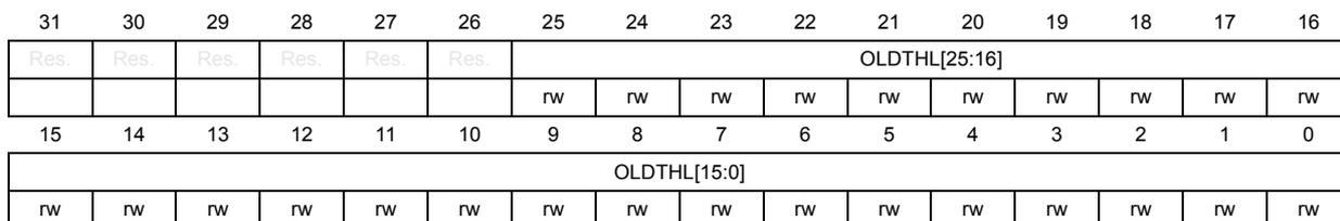
| 31 | 30 | 29 | 28 | 27 | 26 | 25 | 24 | 23 | 22 | 21 | 20 | 19 | 18 | 17 | 16 |
| Res. | Res. | Res. | Res. | Res. | Res. | OLDTHL[25:16] | |||||||||
| rw | rw | rw | rw | rw | rw | rw | rw | rw | rw | ||||||
| 15 | 14 | 13 | 12 | 11 | 10 | 9 | 8 | 7 | 6 | 5 | 4 | 3 | 2 | 1 | 0 |
| OLDTHL[15:0] | |||||||||||||||
| rw | rw | rw | rw | rw | rw | rw | rw | rw | rw | rw | rw | rw | rw | rw | rw |
Bits 31:26 Reserved, must be kept at reset value.
Bits 25:0 OLDTHL[25:0] : OLD low threshold value
This bitfield is set and cleared by software. OLDTHL represents a 26-bit signed value. The real threshold compared to the signal provided by the filter is OLDTHL.
Note: This bitfield can be write-protected (refer to Section 35.4.15 for details).
35.8.11 MDF OLDx high threshold register x (MDF_OLDxTHHR)
Address offset: \( 0x0A0 + 0x80 * x \) , ( \( x = 0 \) to \( 5 \) )
Reset value: \( 0x0000\ 0000 \)
This register is used for the adjustment of the OLDx high threshold. The number of registers is equal to the amount of filters. Refer to Section 35.3 for details.

| 31 | 30 | 29 | 28 | 27 | 26 | 25 | 24 | 23 | 22 | 21 | 20 | 19 | 18 | 17 | 16 |
| Res. | Res. | Res. | Res. | Res. | Res. | OLDTHH[25:16] | |||||||||
| rw | rw | rw | rw | rw | rw | rw | rw | rw | rw | ||||||
| 15 | 14 | 13 | 12 | 11 | 10 | 9 | 8 | 7 | 6 | 5 | 4 | 3 | 2 | 1 | 0 |
| OLDTHH[15:0] | |||||||||||||||
| rw | rw | rw | rw | rw | rw | rw | rw | rw | rw | rw | rw | rw | rw | rw | rw |
Bits 31:26 Reserved, must be kept at reset value.
Bits 25:0 OLDTHH[25:0] : OLDx high threshold value
This bitfield is set and cleared by software. OLDTHH represents a 26-bit signed value. The real threshold compared to the signal provided by the filter is OLDTHH.
Note: This bitfield can be write-protected (refer to Section 35.4.15 for details).
35.8.12 MDF delay control register x (MDF_DLYxCR)
Address offset: \( 0x0A4 + 0x80 * x \) , ( \( x = 0 \) to \( 5 \) )
Reset value: \( 0x0000\ 0000 \)
This register is used for the adjustment stream delays. The number of registers is equal to the amount of filters. Refer to Section 35.3 for details.
| 31 | 30 | 29 | 28 | 27 | 26 | 25 | 24 | 23 | 22 | 21 | 20 | 19 | 18 | 17 | 16 |
|---|---|---|---|---|---|---|---|---|---|---|---|---|---|---|---|
| SKPBF | Res. | Res. | Res. | Res. | Res. | Res. | Res. | Res. | Res. | Res. | Res. | Res. | Res. | Res. | Res. |
| r | |||||||||||||||
| 15 | 14 | 13 | 12 | 11 | 10 | 9 | 8 | 7 | 6 | 5 | 4 | 3 | 2 | 1 | 0 |
| Res. | Res. | Res. | Res. | Res. | Res. | Res. | Res. | Res. | SKPDLY[6:0] | ||||||
| rw | rw | rw | rw | rw | rw | rw | |||||||||
Bit 31 SKPBF : Skip busy flag
This bit is set and cleared by hardware. It is used to control if the delay sequence is completed.
0: MDF ready to accept a new value into SKPDLY[6:0]
1: Last valid SKPDLY[6:0] still under processing
Bits 30:7 Reserved, must be kept at reset value.
Bits 6:0 SKPDLY[6:0] : Delay to apply to a bitstream
This bitfield is set and cleared by software. It defines the number of input samples that are skipped. Skipping is applied immediately after writing to this bitfield, if SKPBF = 0 and the corresponding DFLTEN = 1. If SKPBF = 1, the value written into the register is ignored by the delay state machine.
0: No input sample skipped
1: 1 input sample skipped
...
127: 127 input samples skipped
35.8.13 MDF short circuit detector control register x (MDF_SCDxCR)
Address offset: \( 0x0A8 + 0x80 * x \) , ( \( x = 0 \) to \( 5 \) )
Reset value: \( 0x0000\ 0000 \)
This register is used for the adjustment stream delays. The number of registers is equal to the amount of filters. Refer to Section 35.3 for details.
| 31 | 30 | 29 | 28 | 27 | 26 | 25 | 24 | 23 | 22 | 21 | 20 | 19 | 18 | 17 | 16 |
|---|---|---|---|---|---|---|---|---|---|---|---|---|---|---|---|
| SCDAC TIVE | Res. | Res. | Res. | Res. | Res. | Res. | Res. | Res. | Res. | Res. | Res. | SCDT[7:4] | |||
| r | rw | rw | rw | rw | |||||||||||
| 15 | 14 | 13 | 12 | 11 | 10 | 9 | 8 | 7 | 6 | 5 | 4 | 3 | 2 | 1 | 0 |
| SCDT[3:0] | Res. | Res. | Res. | Res. | BKSCD[3:0] | Res. | Res. | Res. | SCDEN | ||||||
| rw | rw | rw | rw | rw | rw | rw | rw | rw | |||||||
Bit 31 SCDACTIVE : SCDx active flag
This bit is set and cleared by hardware. It is used to check if the SCDx is effectively enabled (active) or not. The protected fields of this function can only be updated when the SCDACTIVE is set to 0 (refer to Section 35.4.15 for details).
The delay between a transition on SCDEN and a transition on SCDACTIVE is two periods of AHB clock and two periods of mdf_proc_ck.
0: SCDx not active and can be configured if needed
1: SCDx active and protected fields cannot be configured
Bits 30:20 Reserved, must be kept at reset value.
Bits 19:12 SCDT[7:0] : SCDx threshold
This bitfield is set and cleared by software. These bits are written by software to define the threshold counter for SCDx. If this value is reached, a short-circuit detector event occurs on a given input stream.
0: 2 consecutive 1's or 0's generate an event.
1: 2 consecutive 1's or 0's generate an event.
2: 3 consecutive 1's or 0's generate an event.
...
255: 256 consecutive 1's or 0's generate an event.
Note: This bitfield can be write-protected (refer to Section 35.4.15 for details).
Bits 11:8 Reserved, must be kept at reset value.
Bits 7:4 BKSCD[3:0] : Break signal assignment for short circuit detector
This bitfield is set and cleared by software.
BKSCD[i] = 0: Break signal (mdf_break[i]) not assigned to this SCD event
BKSCD[i] = 1: Break signal (mdf_break[i]) assigned to this SCD event
Note: This bitfield can be write-protected (refer to Section 35.4.15 for details).
Bits 3:1 Reserved, must be kept at reset value.
Bit 0 SCDEN : SCDx enable
This bit is set and cleared by software.
0: SCDx disabled
1: SCDx enabled,
35.8.14 MDF DFLT0 interrupt enable register 0 (MDF_DFLT0IER)
Address offset: 0x0AC
Reset value: 0x0000 0000
This register is used for allowing or not the events to generate an interrupt.
| 31 | 30 | 29 | 28 | 27 | 26 | 25 | 24 | 23 | 22 | 21 | 20 | 19 | 18 | 17 | 16 |
|---|---|---|---|---|---|---|---|---|---|---|---|---|---|---|---|
| Res. | Res. | Res. | Res. | Res. | Res. | Res. | Res. | Res. | Res. | Res. | Res. | Res. | Res. | Res. | Res. |
| 15 | 14 | 13 | 12 | 11 | 10 | 9 | 8 | 7 | 6 | 5 | 4 | 3 | 2 | 1 | 0 |
| Res. | Res. | Res. | Res. | RFOVR IE | CKABI E | SATIE | SCDIE | SSOVR IE | Res. | Res. | OLDIE | Res. | SSDRI E | DOVRI E | FTHIE |
| rw | rw | rw | rw | rw | rw | rw | rw | rw |
Bits 31:12 Reserved, must be kept at reset value.
- Bit 11
RFOVRIE
: Reshape filter overrun interrupt enable
This bit is set and cleared by software.
0: Reshape filter overrun interrupt disabled
1: Reshape filter overrun interrupt enabled - Bit 10
CKABIE
: Clock absence detection interrupt enable
This bit is set and cleared by software.
0: Clock absence interrupt disabled
1: Clock absence interrupt enabled - Bit 9
SATIE
: Saturation detection interrupt enable
This bit is set and cleared by software.
0: Saturation interrupt disabled
1: Saturation interrupt enabled - Bit 8
SCDIE
: SCD0 interrupt enable
This bit is set and cleared by software.
0: SCD0 interrupt disabled
1: SCD0 interrupt enabled - Bit 7
SSOVRIE
: Snapshot overrun interrupt enable
This bit is set and cleared by software.
0: Snapshot overrun interrupt disabled
1: Snapshot overrun interrupt enabled - Bits 6:5 Reserved, must be kept at reset value.
- Bit 4
OLDIE
: OLD0 interrupt enable
This bit is set and cleared by software.
0: OLD0 event interrupt disabled
1: OLD0 event interrupt enabled - Bit 3 Reserved, must be kept at reset value.
- Bit 2
SSDRIE
: Snapshot data ready interrupt enable
This bit is set and cleared by software.
0: Snapshot data ready interrupt disabled
1: Snapshot data ready interrupt enabled - Bit 1
DOVRIE
: Data overflow interrupt enable
This bit is set and cleared by software.
0: Data overflow interrupt disabled
1: Data overflow interrupt enabled - Bit 0
FTHIE
: RXFIFO threshold interrupt enable
This bit is set and cleared by software.
0: RXFIFO threshold interrupt disabled
1: RXFIFO threshold interrupt enabled
35.8.15 MDF DFLT x interrupt enable register x (MDF_DFLT x IER)
Address offset: \( 0x12C + 0x80 * (x - 1) \) , ( \( x = 1 \) to 5)
Reset value: 0x0000 0000
This register is used for allowing or not, the events to generate an interrupt. The number of registers is equal to the amount of filters. Refer to Section 35.3 for details.
| 31 | 30 | 29 | 28 | 27 | 26 | 25 | 24 | 23 | 22 | 21 | 20 | 19 | 18 | 17 | 16 |
|---|---|---|---|---|---|---|---|---|---|---|---|---|---|---|---|
| Res. | Res. | Res. | Res. | Res. | Res. | Res. | Res. | Res. | Res. | Res. | Res. | Res. | Res. | Res. | Res. |
| 15 | 14 | 13 | 12 | 11 | 10 | 9 | 8 | 7 | 6 | 5 | 4 | 3 | 2 | 1 | 0 |
| Res. | Res. | Res. | Res. | RFOVR IE | CKABI E | SATIE | SCDIE | SSOVR IE | Res. | Res. | OLDIE | Res. | SSDRI E | DOVRI E | FTHIE |
| rw | rw | rw | rw | rw | rw | rw | rw | rw | |||||||
Bits 31:12 Reserved, must be kept at reset value.
Bit 11 RFOVRIE : Reshape filter overrun interrupt enable
- This bit is set and cleared by software.
- 0: Reshape filter overrun interrupt disabled
- 1: Reshape filter overrun interrupt enabled
Bit 10 CKABIE : Clock absence detection interrupt enable
- This bit is set and cleared by software.
- 0: Clock absence interrupt disabled
- 1: Clock absence interrupt enabled
Bit 9 SATIE : Saturation detection interrupt enable
- This bit is set and cleared by software.
- 0: Saturation interrupt disabled
- 1: Saturation interrupt enabled
Bit 8 SCDIE : SCD x interrupt enable
- This bit is set and cleared by software.
- 0: SCD x interrupt disabled
- 1: SCD x interrupt enabled
Bit 7 SSOVRIE : Snapshot overrun interrupt enable
- This bit is set and cleared by software.
- 0: Snapshot overrun interrupt disabled
- 1: Snapshot overrun interrupt enabled
Bits 6:5 Reserved, must be kept at reset value.
Bit 4 OLDIE : OLD x interrupt enable
- This bit is set and cleared by software.
- 0: OLD x event interrupt disabled
- 1: OLD x event interrupt enabled
Bit 3 Reserved, must be kept at reset value.
Bit 2 SSDRIE : Snapshot data ready interrupt enable
- This bit is set and cleared by software.
- 0: Snapshot data ready interrupt disabled
- 1: Snapshot data ready interrupt enabled
Bit 1 DOVRIE : Data overflow interrupt enable
This bit is set and cleared by software.
0: Data overflow interrupt disabled
1: Data overflow interrupt enabled
Bit 0 FTHIE : RXFIFO threshold interrupt enable
This bit is set and cleared by software.
0: RXFIFO threshold interrupt disabled
1: RXFIFO threshold interrupt enabled
35.8.16 MDF DFLT0 interrupt status register 0 (MDF_DFLT0ISR)
Address offset: 0x0B0
Reset value: 0x0000 0000
This register contains the status flags for each digital filter path.
| 31 | 30 | 29 | 28 | 27 | 26 | 25 | 24 | 23 | 22 | 21 | 20 | 19 | 18 | 17 | 16 |
|---|---|---|---|---|---|---|---|---|---|---|---|---|---|---|---|
| Res. | Res. | Res. | Res. | Res. | Res. | Res. | Res. | Res. | Res. | Res. | Res. | Res. | Res. | Res. | Res. |
| 15 | 14 | 13 | 12 | 11 | 10 | 9 | 8 | 7 | 6 | 5 | 4 | 3 | 2 | 1 | 0 |
| Res. | Res. | Res. | Res. | RFOVRF F | CKABF | SATF | SCDF | SSOVR F | THHF | THLF | OLDF | RXNEF | SSDRF | DOVRF | FTHF |
| rc_w1 | rc_w1 | rc_w1 | rc_w1 | rc_w1 | r | r | rc_w1 | r | rc_w1 | rc_w1 | r |
Bits 31:12 Reserved, must be kept at reset value.
Bit 11 RFOVRF : Reshape filter overrun detection flag
This bit is set by hardware and cleared by software by writing this bit to 1.
0: Read 0 means that no reshape filter overrun is detected. Write 0 has no effect.
1: Read 1 means that reshape filter overrun is detected. Write 1 clears this flag.
Bit 10 CKABF : Clock absence detection flag
This bit is set by hardware and cleared by software by writing this bit to 1.
0: Read 0 means that no clock absence is detected. Write 0 has no effect.
1: Read 1 means that a clock absence is detected. Write 1 clears this flag.
Bit 9 SATF : Saturation detection flag
This bit is set by hardware and cleared by software by writing this bit to 1.
0: Read 0 means that no saturation is detected. Write 0 has no effect.
1: Read 1 means that a saturation is detected. Write 1 clears this flag.
Bit 8 SCDF : Short-circuit detector flag
This bit is set by hardware and cleared by software by writing this bit to 1.
0: Read 0 means that no SCD0 event is detected. Write 0 has no effect.
1: Read 1 means that a SCD0 event is detected. Write 1 clears this flag.
Bit 7 SSOVR : Snapshot overrun flag
This bit is set by hardware and cleared by software by writing this bit to 1.
0: Read 0 means that no snapshot overrun event is detected. Write 0 has no effect.
1: Read 1 means that a snapshot overrun event is detected. Write 1 clears this flag.
Bit 6 THHF: High-threshold status flagThis bit is set by hardware and cleared by software by writing this bit to 1. It indicates the status of the high-threshold comparator when the last OLD0 event occurred. This bit gives additional information on the conditions triggering the last OLD0 event. It can be cleared by writing OLDF flag to 1.
0: The signal was lower than OLDTHH when the last OLD0 event occurred.
1: The signal was higher than OLDTHH when the last OLD0 event occurred.
Bit 5 THLF: Low-threshold status flagThis bit is set by hardware and cleared by software by writing this bit to 1. It indicates the status of the low-threshold comparator when the last OLD0 event occurred. This bit gives additional information on the conditions triggering the last OLD0 event. It can be cleared by writing OLDF flag to 1.
0: The signal was higher than OLDTHL when the last OLD0 event occurred.
1: The signal was lower than OLDTHL when the last OLD0 event occurred.
Bit 4 OLDF: OLD0 flagThis bit is set by hardware and cleared by software by writing this bit to 1.
0: Read 0 means that no OLD0 event is detected. Write 0 has no effect.
1: Read 1 means that an OLD0 event is detected. Write 1 clears THHF, THLF and OLDF.
Bit 3 RXNEF: RXFIFO not-empty flagThis bit is set and cleared by hardware according to the RXFIFO level.
0: RXFIFO empty
1: RXFIFO not empty
Bit 2 SSDRF: Snapshot data ready flagThis bit is set by hardware and cleared by software by writing this bit to 1.
0: Read 0 means that no data is available. Write 0 has no effect.
1: Read 1 means that a new data is available. Write 1 clears this flag.
Bit 1 DOVRF: Data overflow flagThis bit is set by hardware and cleared by software by writing this bit to 1.
0: Read 0 means that no overflow is detected. Write 0 has no effect.
1: Read 1 means that an overflow is detected; Write 1 clears this flag.
Bit 0 FTHF: RXFIFO threshold flagThis bit is set by hardware and cleared by hardware when the RXFIFO level is lower than the threshold.
0: RXFIFO threshold not reached
1: RXFIFO threshold reached
35.8.17 MDF DFLT x interrupt status register x (MDF_DFLT x ISR)
Address offset: 0x130 + 0x80 * (x - 1), (x = 1 to 5)
Reset value: 0x0000 0000
This register contains the status flags for each digital filter path. The number of registers is equal to the amount of filters. Refer to Section 35.3 for details.
| 31 | 30 | 29 | 28 | 27 | 26 | 25 | 24 | 23 | 22 | 21 | 20 | 19 | 18 | 17 | 16 |
|---|---|---|---|---|---|---|---|---|---|---|---|---|---|---|---|
| Res. | Res. | Res. | Res. | Res. | Res. | Res. | Res. | Res. | Res. | Res. | Res. | Res. | Res. | Res. | Res. |
| 15 | 14 | 13 | 12 | 11 | 10 | 9 | 8 | 7 | 6 | 5 | 4 | 3 | 2 | 1 | 0 |
| Res. | Res. | Res. | Res. | RFOVRF F | CKABF | SATF | SCDF | SSOVR F | THHF | THLF | OLDF | RXNEF | SSDRF | DOVRF | FTHF |
| rc_w1 | rc_w1 | rc_w1 | rc_w1 | rc_w1 | r | r | rc_w1 | r | rc_w1 | rc_w1 | r |
Bits 31:12 Reserved, must be kept at reset value.
Bit 11 RFOVRF : Reshape filter overrun detection flag
This bit is set by hardware and cleared by software by writing this bit to 1.
0: Read 0 means that no reshape filter overrun is detected. Write 0 has no effect.
1: Read 1 means that reshape filter overrun is detected. Write 1 clears this flag.
Bit 10 CKABF : Clock absence detection flag
This bit is set by hardware and cleared by software by writing this bit to 1.
0: Read 0 means that no clock absence is detected. Write 0 has no effect.
1: Read 1 means that a clock absence is detected. Write 1 clears this flag.
Bit 9 SATF : Saturation detection flag
This bit is set by hardware and cleared by software by writing this bit to 1.
0: Read 0 means that no saturation is detected. Write 0 has no effect.
1: Read 1 means that a saturation is detected. Write 1 clears this flag.
Bit 8 SCDF : Short-circuit detector flag
This bit is set by hardware and cleared by software by writing this bit to 1.
0: Read 0 means that no SCD event is detected. Write 0 has no effect.
1: Read 1 means that a SCD event is detected. Write 1 clears this flag.
Bit 7 SSOVRF : Snapshot overrun flag
This bit is set by hardware and cleared by software by writing this bit to 1.
0: Read 0 means that no snapshot overrun event is detected. Write 0 has no effect.
1: Read 1 means that a snapshot overrun event is detected. Write 1 clears this flag.
Bit 6 THHF : High-threshold status flag
This bit is set by hardware and cleared by software by writing this bit to 1. It indicates the status of the high-threshold comparator when the last OLD x event occurred. This bit gives additional information on the conditions triggering the last OLD x event. It can be cleared by writing OLDF flag to 1.
0: The signal was lower than OLDTHH when the last OLD x event occurred.
1: The signal was higher than OLDTHH when the last OLD x event occurred.
Bit 5 THLF : Low-threshold status flag
This bit is set by hardware and cleared by software by writing this bit to 1. It indicates the status of the low-threshold comparator when the last OLDx event occurred. This bit gives additional information on the conditions triggering the last OLDx event. It can be cleared by writing OLDF flag to 1.
0: The signal was higher than OLDTHL when the last OLDx event occurred.
1: The signal was lower than OLDTHL when the last OLDx event occurred.
Bit 4 OLDF : OLDx flag
This bit is set by hardware and cleared by software by writing this bit to 1.
0: Read 0 means that no OLDx event is detected. Write 0 has no effect.
1: Read 1 means that an OLDx event is detected. Write 1 clears THHF, THLF and OLDF.
Bit 3 RXNEF : RXFIFO not-empty flag
this bit is set and cleared by hardware according to the RXFIFO level.
0: RXFIFO empty
1: RXFIFO not empty
Bit 2 SSDRF : Snapshot data ready flag
This bit is set by hardware and cleared by software by writing this bit to 1.
0: Read 0 means that no data is available. Write 0 has no effect.
1: Read 1 means that a new data is available. Write 1 clears this flag.
Bit 1 DOVRF : Data overflow flag
This bit is set by hardware and cleared by software by writing this bit to 1.
0: Read 0 means that no overflow is detected. Write 0 has no effect.
1: Read 1 means that an overflow is detected; Write 1 clears this flag.
Bit 0 FTHF : RXFIFO threshold flag
This bit is set by hardware and cleared by hardware when the RXFIFO level is lower than the threshold.
0: RXFIFO threshold not reached
1: RXFIFO threshold reached
35.8.18 MDF offset error compensation control register x (MDF_OECxCR)
Address offset: 0x0B4 + 0x80 * x, (x = 0 to 5)
Reset value: 0x0000 0000
This register contains the offset compensation value. The number of registers is equal to the amount of filters. Refer to Section 35.3 for details.
| 31 | 30 | 29 | 28 | 27 | 26 | 25 | 24 | 23 | 22 | 21 | 20 | 19 | 18 | 17 | 16 |
|---|---|---|---|---|---|---|---|---|---|---|---|---|---|---|---|
| Res. | Res. | Res. | Res. | Res. | Res. | OFFSET[25:16] | |||||||||
| rw | rw | rw | rw | rw | rw | rw | rw | rw | rw | ||||||
| 15 | 14 | 13 | 12 | 11 | 10 | 9 | 8 | 7 | 6 | 5 | 4 | 3 | 2 | 1 | 0 |
| OFFSET[15:0] | |||||||||||||||
| rw | rw | rw | rw | rw | rw | rw | rw | rw | rw | rw | rw | rw | rw | rw | rw |
Bits 31:26 Reserved, must be kept at reset value.
Bits 25:0 OFFSET[25:0] : Offset error compensation
This bitfield is set and cleared by software. If the application attempts to write a new offset value while the previous one is not yet applied, this new offset value is ignored. Reading back this bitfield informs the application on the current offset value.
This bitfield represents the value to be subtracted to the signal before going to the SCALE.
35.8.19 MDF snapshot data register x (MDF_SNPSxDR)
Address offset: 0x0EC + 0x80 * x, (x = 0 to 5)
Reset value: 0x0000 0000
This register is used to read the data processed by each digital filter in snapshot mode. The number of registers is equal to the amount of filters. Refer to Section 35.3 for details.
| 31 | 30 | 29 | 28 | 27 | 26 | 25 | 24 | 23 | 22 | 21 | 20 | 19 | 18 | 17 | 16 |
| SDR[15:0] | |||||||||||||||
| r | r | r | r | r | r | r | r | r | r | r | r | r | r | r | r |
| 15 | 14 | 13 | 12 | 11 | 10 | 9 | 8 | 7 | 6 | 5 | 4 | 3 | 2 | 1 | 0 |
| EXTSDR[6:0] | MCICDC[8:0] | ||||||||||||||
| r | r | r | r | r | r | r | r | r | r | r | r | r | r | r | r |
Bits 31:16 SDR[15:0] : Contains the 16 MSB of the last valid data processed by the digital filter.
Bits 15:9 EXTSDR[6:0] : Extended data size
If SNPSFMT = 0, this bitfield contains the bits 7 to 1 of the last valid data processed by the digital filter.
If SNPSFMT = 1, this bitfield contains the INT accumulator counter value when the last trigger event occurs (INT_CNT).
Bits 8:0 MCICDC[8:0] : Contains the MCIC decimation counter value when the last trigger event occurs (MCIC_CNT)
35.8.20 MDF digital filter data register x (MDF_DFLTxDR)
Address offset: 0x0F0 + 0x80 * x, (x = 0 to 5)
Reset value: 0x0000 0000
This register is used to read the data processed by each digital filter. The number of registers is equal to the amount of filters. Refer to Section 35.3 for details.
| 31 | 30 | 29 | 28 | 27 | 26 | 25 | 24 | 23 | 22 | 21 | 20 | 19 | 18 | 17 | 16 |
| DR[23:8] | |||||||||||||||
| r | r | r | r | r | r | r | r | r | r | r | r | r | r | r | r |
| 15 | 14 | 13 | 12 | 11 | 10 | 9 | 8 | 7 | 6 | 5 | 4 | 3 | 2 | 1 | 0 |
| DR[7:0] | Res. | Res. | Res. | Res. | Res. | Res. | Res. | Res. | |||||||
| r | r | r | r | r | r | r | r | ||||||||
Bits 31:8 DR[23:0] : Data processed by digital filter
Bits 7:0 Reserved, must be kept at reset value.
35.8.21 MDF register map
Table 293. MDF register map and reset values
| Offset | Register name | 31 | 30 | 29 | 28 | 27 | 26 | 25 | 24 | 23 | 22 | 21 | 20 | 19 | 18 | 17 | 16 | 15 | 14 | 13 | 12 | 11 | 10 | 9 | 8 | 7 | 6 | 5 | 4 | 3 | 2 | 1 | 0 | |
|---|---|---|---|---|---|---|---|---|---|---|---|---|---|---|---|---|---|---|---|---|---|---|---|---|---|---|---|---|---|---|---|---|---|---|
| 0x000 | MDF_GCR | Res. | Res. | Res. | Res. | Res. | Res. | Res. | Res. | Res. | Res. | Res. | Res. | Res. | Res. | Res. | Res. | Res. | Res. | Res. | Res. | Res. | Res. | Res. | Res. | Res. | ILVNB [3:0] | Res. | Res. | Res. | TRGO | |||
| Reset value | 0 | 0 | 0 | 0 | 0 | |||||||||||||||||||||||||||||
| 0x004 | MDF_CKGCR | CKGACTIVE | PROCDIV[6:0] | Res. | Res. | Res. | Res. | CCKDIV [3:0] | TRGSRC [3:0] | Res. | Res. | Res. | Res. | Res. | TRGSENS | Res. | CCK1DIR | CCK0DIR | CKGMOD | Res. | CCK1EN | CCK0EN | CKGDEN | |||||||||||
| Reset value | 0 | 0 | 0 | 0 | 0 | 0 | 0 | 0 | 0 | 0 | 0 | 0 | 0 | 0 | 0 | 0 | 0 | 0 | 0 | 0 | 0 | 0 | 0 | 0 | 0 | |||||||||
| 0x008-0x07C | Reserved | |||||||||||||||||||||||||||||||||
| 0x080 + 0x80 * x (x = 0 to 5) | MDF_SITFxC R | SITFACTIVE | Res. | Res. | Res. | Res. | Res. | Res. | Res. | Res. | Res. | Res. | Res. | Res. | Res. | Res. | Res. | Res. | Res. | Res. | STH[4:0] | Res. | Res. | SITFMOD [1:0] | Res. | SCSRC [1:0] | SITFEN | |||||||
| Reset value | 0 | 1 | 1 | 1 | 1 | 0 | 0 | 0 | 0 | 0 | 0 | |||||||||||||||||||||||
| 0x084 + 0x80 * x (x = 0 to 5) | MDF_BSMxC R | BSMFACTIVE | Res. | Res. | Res. | Res. | Res. | Res. | Res. | Res. | Res. | Res. | Res. | Res. | Res. | Res. | Res. | Res. | Res. | Res. | Res. | Res. | Res. | Res. | Res. | Res. | Res. | Res. | Res. | BSSEL[4:0] | ||||
| Reset value | 0 | 0 | 0 | 0 | 0 | |||||||||||||||||||||||||||||
| 0x088 + 0x80 * x (x = 0 to 5) | MDF_DFLTxC R | DFLTACTIVE | DFLTTRUN | Res. | Res. | NBDIS[7:0] | Res. | Res. | SNPSFMT | Res. | TRGSRC [3:0] | Res. | Res. | Res. | Res. | Res. | Res. | Res. | TRGSENS | Res. | ACOMOD [2:0] | Res. | FTTH | DMAEN | DFLTEN | |||||||||
| Reset value | 0 | 0 | 0 | 0 | 0 | 0 | 0 | 0 | 0 | 0 | 0 | 0 | 0 | 0 | 0 | 0 | 0 | 0 | 0 | 0 | 0 | 0 | 0 | 0 | ||||||||||
| 0x08C + 0x80 * x (x = 0 to 5) | MDF_DFLTxC ICR | Res. | Res. | Res. | Res. | Res. | SCALE[5:0] | Res. | Res. | MCICD[8:0] | Res. | Res. | CIOMOD [2:0] | Res. | Res. | Res. | Res. | Res. | DATSRC [1:0] | |||||||||||||||
| Reset value | 0 | 0 | 0 | 0 | 0 | 0 | 0 | 0 | 0 | 0 | 0 | 0 | 0 | 0 | 0 | 0 | 0 | 0 | 0 | 0 | 0 | 0 | 0 | 0 | ||||||||||
| 0x090 + 0x80 * x (x = 0 to 5) | MDF_DFLTxRSFR | Res. | Res. | Res. | Res. | Res. | Res. | Res. | Res. | Res. | Res. | Res. | Res. | Res. | Res. | Res. | Res. | Res. | Res. | Res. | Res. | Res. | Res. | HPFC[1:0] | HPFBYP | Res. | Res. | Res. | RSFLTD | Res. | Res. | Res. | RSFLTBY | |
| Reset value | 0 | 0 | 0 | 0 | 0 | 0 | ||||||||||||||||||||||||||||
| 0x094 + 0x80 * x (x = 0 to 5) | MDF_DFLTxINTR | Res. | Res. | Res. | Res. | Res. | Res. | Res. | Res. | Res. | Res. | Res. | Res. | Res. | Res. | Res. | Res. | Res. | Res. | Res. | Res. | INTVAL[6:0] | Res. | Res. | Res. | INTDIV [1:0] | ||||||||
| Reset value | 0 | 0 | 0 | 0 | 0 | 0 | 0 | 0 | 0 | 0 | ||||||||||||||||||||||||
| 0x098 + 0x80 * x (x = 0 to 5) | MDF_OLDxC R | OLDACTIVE | Res. | Res. | Res. | Res. | Res. | Res. | Res. | Res. | ACICD[4:0] | Res. | Res. | Res. | ACICN [1:0] | Res. | Res. | Res. | Res. | Res. | BKOLD [3:0] | Res. | Res. | THINB | OLDEN | |||||||||
| Reset value | 0 | 0 | 0 | 0 | 0 | 0 | 0 | 0 | 0 | 0 | 0 | 0 | 0 | 0 | 0 | |||||||||||||||||||
Table 293. MDF register map and reset values (continued)
| Offset | Register name | 31 | 30 | 29 | 28 | 27 | 26 | 25 | 24 | 23 | 22 | 21 | 20 | 19 | 18 | 17 | 16 | 15 | 14 | 13 | 12 | 11 | 10 | 9 | 8 | 7 | 6 | 5 | 4 | 3 | 2 | 1 | 0 |
|---|---|---|---|---|---|---|---|---|---|---|---|---|---|---|---|---|---|---|---|---|---|---|---|---|---|---|---|---|---|---|---|---|---|
| 0x09C + 0x80 * x (x = 0 to 5) | MDF_OLDxTHLR | Res. | Res. | Res. | Res. | Res. | OLDTHL[25:0] | ||||||||||||||||||||||||||
| Reset value | 0 | 0 | 0 | 0 | 0 | 0 | 0 | 0 | 0 | 0 | 0 | 0 | 0 | 0 | 0 | 0 | 0 | 0 | 0 | 0 | 0 | 0 | 0 | 0 | 0 | 0 | 0 | ||||||
| 0x0A0 + 0x80 * x (x = 0 to 5) | MDF_OLDxTHHR | Res. | Res. | Res. | Res. | Res. | OLDTHH[25:0] | ||||||||||||||||||||||||||
| Reset value | 0 | 0 | 0 | 0 | 0 | 0 | 0 | 0 | 0 | 0 | 0 | 0 | 0 | 0 | 0 | 0 | 0 | 0 | 0 | 0 | 0 | 0 | 0 | 0 | 0 | 0 | |||||||
| 0x0A4 + 0x80 * x (x = 0 to 5) | MDF_DLYxCR | SKPBF | Res. | Res. | Res. | Res. | Res. | Res. | Res. | Res. | Res. | Res. | Res. | Res. | Res. | Res. | Res. | Res. | Res. | Res. | Res. | Res. | Res. | Res. | Res. | SKPBDLY[6:0] | |||||||
| Reset value | 0 | 0 | 0 | 0 | 0 | 0 | 0 | 0 | 0 | ||||||||||||||||||||||||
| 0x0A8 + 0x80 * x (x = 0 to 5) | MDF_SCDxCR | SCDACTIVE | Res. | Res. | Res. | Res. | Res. | Res. | Res. | Res. | Res. | Res. | Res. | SCDT[7:0] | Res. | Res. | Res. | Res. | BKSCD[3:0] | Res. | Res. | Res. | Res. | SCDEN | |||||||||
| Reset value | 0 | 0 | 0 | 0 | 0 | 0 | 0 | 0 | 0 | 0 | 0 | 0 | 0 | 0 | |||||||||||||||||||
| 0x0AC | MDF_DFLT0IER | Res. | Res. | Res. | Res. | Res. | Res. | Res. | Res. | Res. | Res. | Res. | Res. | Res. | Res. | Res. | Res. | Res. | Res. | Res. | Res. | RFOVRIE | CKABIE | SATIE | SCDIE | SSOVRIE | Res. | Res. | OLDIE | Res. | SSDRIE | DOVRIE | FTHIE |
| Reset value | 0 | 0 | 0 | 0 | 0 | 0 | 0 | 0 | 0 | ||||||||||||||||||||||||
| 0x0B0 | MDF_DFLT0ISR | Res. | Res. | Res. | Res. | Res. | Res. | Res. | Res. | Res. | Res. | Res. | Res. | Res. | Res. | Res. | Res. | Res. | Res. | Res. | Res. | RFOVRF | CKABF | SATF | SCDF | SSOVR | THHF | THLF | OLDF | RXNEF | SSDRF | DOVRF | FTHF |
| Reset value | 0 | 0 | 0 | 0 | 0 | 0 | 0 | 0 | 0 | 0 | 0 | 0 | |||||||||||||||||||||
| 0x0B4 + 0x80 * x (x = 0 to 5) | MDF_OECxCR | Res. | Res. | Res. | Res. | Res. | OFFSET[25:0] | ||||||||||||||||||||||||||
| Reset value | 0 | 0 | 0 | 0 | 0 | 0 | 0 | 0 | 0 | 0 | 0 | 0 | 0 | 0 | 0 | 0 | 0 | 0 | 0 | 0 | 0 | 0 | 0 | 0 | 0 | 0 | |||||||
| 0x0B8- 0x0E8 | Reserved | ||||||||||||||||||||||||||||||||
| 0x0EC + 0x80 * x (x = 0 to 5) | MDF_SNPSxDR | SDR[15:0] | |||||||||||||||||||||||||||||||
| Reset value | 0 | 0 | 0 | 0 | 0 | 0 | 0 | 0 | 0 | 0 | 0 | 0 | 0 | 0 | 0 | 0 | 0 | 0 | 0 | 0 | 0 | 0 | 0 | 0 | 0 | 0 | 0 | 0 | 0 | 0 | 0 | ||
| 0x0F0 + 0x80 * x (x = 0 to 5) | MDF_DFLTxDR | DR[23:0] | |||||||||||||||||||||||||||||||
| Reset value | 0 | 0 | 0 | 0 | 0 | 0 | 0 | 0 | 0 | 0 | 0 | 0 | 0 | 0 | 0 | 0 | 0 | 0 | 0 | 0 | 0 | 0 | 0 | 0 | 0 | 0 | 0 | 0 | 0 | 0 | 0 | ||
| 0x12C + 0x80*(x-1) (x=1 to 5) | MDF_DFLTxIER | Res. | Res. | Res. | Res. | Res. | Res. | Res. | Res. | Res. | Res. | Res. | Res. | Res. | Res. | Res. | Res. | Res. | Res. | Res. | Res. | RFOVRIE | CKABIE | SATIE | SCDIE | SSOVRIE | Res. | Res. | OLDIE | Res. | SSDRIE | DOVRIE | FTHIE |
| Reset value | 0 | 0 | 0 | 0 | 0 | 0 | 0 | 0 | 0 | ||||||||||||||||||||||||
| 0x130 + 0x80*(x-1) (x=1 to 5) | MDF_DFLTxISR | Res. | Res. | Res. | Res. | Res. | Res. | Res. | Res. | Res. | Res. | Res. | Res. | Res. | Res. | Res. | Res. | Res. | Res. | Res. | Res. | RFOVRF | CKABF | SATF | SCDF | SSOVR | THHF | THLF | OLDF | RXNEF | SSDRF | DOVRF | FTHF |
| Reset value | 0 | 0 | 0 | 0 | 0 | 0 | 0 | 0 | 0 | 0 | 0 | ||||||||||||||||||||||
Refer to Section 2.3: Memory organization for the register boundary addresses.