33. Digital temperature sensor (DTS)
33.1 Introduction
The DTS is a high-precision low-power junction temperature sensor (TS). It is composed of a configurable controller plus two embedded temperature sensors, TS0 and TS1. The controller features a generic interface that enables the DTS to be accessed in read and write modes, through the APB bus.
33.2 DTS main features
The temperature sensor main features are the following:
- • For each sensor:
- – Two programmable (rise or fall) hardware alarms incorporating hysteresis
- – Status registers recording the minimum and maximum data values received
- • A power-up timer with IRQ to support manual operation
33.3 DTS functional description
33.3.1 DTS block diagram
Figure 315 shows the DTS block diagram.
![Figure 315. DTS block diagram. The diagram shows the internal architecture of the Digital Temperature Sensor (DTS). It is contained within a 'DTS top-level wrapper'. On the left, external signals include dts_trg[3:0], ck_ker_dts, dts_rstn_mst, a 32-bit AMBA APB bus, dts_pclk, and dts_it. The AMBA APB bus connects to an 'Asynchronous bridge', which in turn connects to an 'AMBA APB interface'. This interface is connected to a 'Controller'. The Controller is connected to a 'PVT controller'. The PVT controller is connected to '2 TS wrappers' labeled TS0 and TS1. Each wrapper contains a 'Slave PVT interface' and 'Temperature sensor analog blocks'. The PVT controller provides signals clk_ts, rstn_ts, ts_sdi, and ts_sdo to the wrappers. The dts_it signal is an output from the PVT controller. The dts_trg[3:0] signals are inputs to the Controller. The dts_pclk signal is an input to the Asynchronous bridge. The ck_ker_dts and dts_rstn_mst signals are inputs to the Controller. The diagram is labeled MSv69513V8 in the bottom right corner.](/RM0486-STM32N6x5-x7/3a085933e4b67c54e178009a48c7f3b9_img.jpg)
Figure 315. DTS block diagram
The DTS incorporates an APB interface configured to control two temperature sensors, TS0 and TS1, through a process, voltage and temperature (PVT) controller.
33.3.2 DTS pins and internal signals
Table 257. DTS internal input/output signals
| Internal signal name | Signal type | Description |
|---|---|---|
| dts_pclk | Input | APB bus clock |
| ck_ker_dts | Input | DTS main clock |
| dts_rstn_mst | Input | Master reset (asynchronous, active low) |
| AMBA APB bus | Input/output | APB Interface |
| dts_it | Output | IRQ interrupt from the DTS peripheral |
| dts_trg[3:0] | Inputs | Trigger interface |
| Temperature sensor (TS) interface | ||
| clk_ts | Input | Temperature sensor SDA clock |
Table 257. DTS internal input/output signals (continued)
| Internal signal name | Signal type | Description |
|---|---|---|
| rstn_ts | Input | Temperature sensor SDA reset (asynchronous, active low) |
| ts_sdi | Input | Temperature sensor SDA slave data Input |
| ts_sdo | Output | Temperature sensor SDA slave data output |
Table 258. DTS interconnection
| Internal signal name | Source/Destination |
|---|---|
| dts_trg[0] | lptim4_out |
| dts_trg[1] | lptim2_ch1 |
| dts_trg[2] | lptim3_ch1 |
| dts_trg[3] | exti13 |
33.3.3 DTS reset and clocks
DTS clocks
The DTS is clocked by ck_ker_dts.
The PVT controller incorporates a clock synthesizer in the TS block. The synthesizers generate the clock and timing strobes for the slave serial data adapters (SDA) and the clock for the embedded TS blocks (clk_ts).
The synthesizer CLK_SYNTH_HI[7:0]/CLK_SYNTH_LO[7:0] counters allow the integer division of the ck_ker_dts clock to generate the TS clock (clk_ts) at frequency ratios from 1/2 to 1/512 (see DTS TSC clock synthesizer register (DTS_TSCCLKSYNTHR) ). Separate counters are used to generate timing control strobes that are aligned with the clk_ts clock. These timing strobes are used by the master serial adapters to control the sample point of the serial data inputs and the hold time of the serial data outputs.
The system clock ck_ker_dts frequency is determined by the RCC. CLK_SYNTH_HI[7:0] and CLK_SYNTH_LO[7:0] must be programmed so that the ratio CLK_SYNTH_HI[7:0]/CLK_SYNTH_LO[7:0] enables to obtain a clk_ts serial clock that falls within the TS operating frequency range (from 4 to 8 MHz).
The TS frequency is defined by:
For example:
For \( ck\_ker\_dts = 64.0 \) MHz and a TS operating frequency ranging between 4 and 8 MHz, setting the \( ck\_ker\_dts \) to \( clk\_ts \) divider factor to 8:1 (CLK_SYNTH_HI[7:0] and CLK_SYNTH_LO[7:0] both programmed to 0x03), returns an TS operating frequency of \( 64.0 \) MHz / 8 = 8 MHz, which falls within the acceptable operating frequency range of 4 to 8 MHz. This enables to obtain an overall divider factor of 8 and a \( ck\_ker\_dts \) serial clock duty cycle of 50/50.
For \( ck\_ker\_dts = 8 \) MHz, the configuration must be:
CLK_SYNTH_LO[7:0] = 0x0
CLK_SYNTH_HI[7:0] = 0x0
CLK_SYNTH_HOLD[3:0] = 0x1
\(
clk\_ts = 4
\)
MHz
\(
clk\_ts
\)
duty cycle = 50 %
The CLK_SYNTH_HOLD[3:0] value must be programmed to accommodate the worst-case serial data path propagation delays without exceeding the synthesized clock period, this means that:
DTS reset
The DTS is reset using the asynchronous active-low \( dts\_rstn\_mst \) input.
When the master \( dts\_rstn\_mst \) is asserted, the entire DTS is reset, all APB internal registers and the PVT controller. It also powers down and resets the embedded TS blocks.
When de-asserted, the APB interface responds to requests after a three clock-cycle delay.
33.3.4 DTS serial data adapter (SDA)
Figure 316. Serial data adapter
The diagram illustrates the internal architecture of the Serial Data Adapter (SDA) and its interaction with a PVT slave. On the left, the SDA block contains a 'Clock synthesizer' that takes 'dts_rstn_mst' and 'ck_ker_dts' as inputs. It outputs a 'Serial interface clock' to the PVT slave. Below the synthesizer is a 'PVT master' block containing 'Master serial data out' (MST SDO) and 'Master receive data interface' (MST SDI). The MST SDO connects to the 'ts_sdi' input of the PVT slave's 'Slave data interface'. The MST SDI connects to the 'ts_sdo' output of the 'Slave data interface'. A red dashed arrow labeled 'Loop-back' indicates a direct connection from the 'Slave data interface' output back to its input. The PVT slave block contains a 'Slave controller', 'Slave registers' (with fields SDATS_CR, SDATS_CFGR, SDATS_DR, and SDATS_TIMERR), and an 'Embedded TS block'. The 'Slave data interface' connects to the 'Slave controller', which in turn connects to the 'Slave registers' and the 'Embedded TS block'. The 'Slave registers' are connected to the 'Slave controller'. The 'Embedded TS block' is connected to the 'Slave controller' via 'Parallel signals' and receives 'clk_ts' from the 'Slave controller'. The entire PVT slave block is contained within a 'TS0 wrapper', which is further enclosed in a 'TS1 wrapper'. The diagram is labeled 'MSV68786V6' in the bottom right corner.
The serial data adapter (SDA) allows the TS blocks to be configured and controlled via serial data interfaces (SDIF). The purpose of the SDA is to minimize the number of signals that need to be routed from the PVT controller to each TS block.
A master usually transmits data to all its active PVT slave devices. However, it is possible to inhibit the programming of one or more slaves to allow different configuration options to be applied. To achieve power saving, it is also possible to disable completely a TS block by disabling its clock and forcing reset.
The serial data interface also provides loop-back functionality (shown in red in Figure 316 ) to support system integration testing without having to power up the embedded TS block.
SDA data format
The serial data streams consist of an active-high start bit, 3-bit register address (SDIF_ADDR[2:0]), register write/not read enable (SDIF_WRN), and 24-bit data field (SDIF_WDATA[23:0]). The input and output serial data stream formats are shown in Figure 317 . It must be noted that the serial data streams are little endian, meaning that the individual data fields are shifted LSB first.
Figure 317. SDA data format
![Figure 317. SDA data format. The diagram shows two bit stream formats: Master serial data out (SLV SDI) and Master serial data in (SLV SDO). Both formats show a 29-bit sequence from Bit 0 to Bit 28. Bit 0 is 'Start 0b1'. Bits 1-3 are 'SDIF_ADDR [0:2]'. Bit 4 is 'SDIF_WRN'. Bits 5-28 are 'SDIF_WDATA[0:23]' for SDI and 'SDIF_RDATA[0:23]' for SDO.](/RM0486-STM32N6x5-x7/5f48520d096832d054928002715b140e_img.jpg)
Master serial data out (SLV SDI)
| Bit 0 | Bit[1:3] | Bit 4 | Bit 5 | Bit 28 |
| Start 0b1 | SDIF_ADDR [0:2] | SDIF_ WRN | SDIF_WDATA[0:23] | |
Master serial data in (SLV SDO)
| Bit 0 | Bit[1:3] | Bit 4 | Bit 5 | Bit 28 |
| Start 0b1 | SDIF_ADDR [0:2] | SDIF_ WRN | SDIF_RDATA[0:23] | |
SDA read
When reading data from the SDA slave registers (SDIF_WRN = 0), the SLV SDI bit stream is shifted to SLV SDO (delayed by one clk_ts cycle) and the register read data value is output on SDIF_RDATA[23:0]. The read data value is then made available in the PVT controller DTS_TSnSDIFRDATAR register (where n corresponds to the TS instance number).
SDA write
When writing data to the SDA slave registers (SDIF_WRN = 1), the SLV SDI bit stream is automatically shifted to SLV SDO and SDIF_RDATA[23:0] = SDIF_WDATA[23:0]. The write data loop-back value is then made available in the corresponding PVT controller DTS_TSnSDIFRDATAR register.
A special loop-back mode is available by writing to the (read-only) SDATS_DR register when SDIF_WRN = 1 and SDIF_ADDR[2:0] = 0x3. In this mode, the loop-back data value is also written to the PVT controller TS data registers (DTS_TSnSDIFRDATAR). When writing loop-back data to the TS data registers, the SDA TS_DATA[23:0] field must be set to 0x0.
The DTS_TSnSDIFRDATAR loop-back functionality can be used to verify the integrity of the serial data transfer between the PVT controller and remote PVT slave devices.
The special DTS_TSnSDIFRDATAR loop-back functionality is provided to test the PVT controller operation without having to power up the embedded TS block, for example when a fault or alarm occurs.
The loop-back functionality is disabled whenever the PVT slave is configured to automatic data recovery when the TS_AUTO bit of PVT SDATS_CR register is asserted.
SDA automatic data recovery
The automatic data recovery is enabled through TS_AUTO bit of SDATS_CR register.
In automatic data recovery mode, the SDIF_LOCK flag is set in the DTS_TSCSDIF_SR register, the SDA interface becomes write-only and all SDA read requests are ignored. In this mode, the SLV automatically streams TS_DATA[23:0] to the PVT controller each time new data samples become available, while setting SDIF_ADDR[2:0] to 0x3 and SDIF_WRN to 1. The automatically recovered data are made available in the PVT controller DTS_TSnSDIFRDATAR and DTS_TSnSDIFRDATAR registers.
SDA SDIF programming
The SDA slave is accessed via the TS SDIF control register DTS_TSCSDIF_CFGR, by setting the SDIF_WDATA[23:0], the SDIF_ADDR[2:0] and the SDIF_WRN, and asserting the SDIF_PROG bit. This SDA read or write request is normally set up using a single PVT register write access.
Once a programming request has been issued, the SDIF_BUSY flag in the DTS_TSCSDIF_SR register is set, and any additional read or write programming requests is ignored until the current access completes.
SDA controller operation
The SDA slave controller features two operating modes: manual (default) and automatic. In both modes, the embedded TS block is configured through the SDATS_CFGR register.
In manual operating mode, when the TS_AUTO bit of SDATS_CR register is de-asserted, the embedded TS block is controlled directly through the SDATS_CR register fields TS_PD, TS_RSTN, TS_RUN_ONCE, TS_RUN_CONT and TS_CLOAD. In manual mode, the user is responsible for ensuring that the PD, RSTN, CLOAD and RUN signals are applied in the correct order and at appropriate times. Sample data from the TS block are captured in the SDA slave SDATS_DR register at the end of the conversion. The user must either poll the SDATS_DR register or leave sufficient time for the conversion to complete before reading the SDATS_DR register in order to recover the sample data from the slave SDA.
In automatic mode, when the TS_AUTO bit is asserted in SDATS_CR register, the embedded TS block is controlled by the slave SDA. When either TS_RUN_ONCE or TS_RUN_CONT bit of the TS_SDATS_CR register is asserted, the slave SDA sequences the PD, RSTN, CLOAD, and RUN signals that drive the TS block to perform one or more conversions. In this mode sample data from the TS block are captured in the SDA slave SDATS_DR register at the end of the conversion before being automatically streamed to the PVT controller.
In trigger mode, when a trigger is asserted at DTS top level, this value is compared to the value programmed in bits 18 to 16 (TRIG[2:0]) of the SDATS_CFGR register. If it is equal, the TS_RUN_ONCE bit is automatically asserted. Sample data from each TS block are captured in the SDA slave SDATS_DR register at the end of the conversion.
SDA slave registers
The serial data adapter registers are accessible through the SDIF interface of the PVT controller.
Table 259. SDA slave registers
| SDIF_ADDR[2:0] | Reset value | Register | Description |
|---|---|---|---|
| 0x0 | 0x000001 | SDATS_CR | TS control register (see Table 260 ) |
| 0x1 | 0x000000 | SDATS_CFGR | TS configuration register (see Table 261 ) |
| 0x3 | 0x000000 | SDATS_DR | TS data / SDA loop-back register (see Table 262 ) |
| 0x4 | - | Reserved | - |
| 0x5 | 0x000000 | SDATS_TIMERR | TS power-up Timer register (see Table 260 ) |
Table 260. SDA TS control register (SDATS_CR)
| Bitfield range | Bitfield description | Access type |
|---|---|---|
| Bits 23:10 | Reserved, must be kept at reset value. | - |
| Bit 9 | TS_STOP:
TS force stop This self-clearing bit immediately returns the slave TS controller to the default TS control state and terminates any serial data activity. This is not a clean shut-down and it may invalidate any data operations currently in progress. 0: TS not stopped 1: TS stopped | rs |
| Bit 8 | TS_AUTO:
TS automatic mode This bit is used in conjunction with TS_RUN_CONT and TS_RUN_ONCE to automatically power up the embedded TS and run conversions. Asserting TS_RUN_CONT triggers continuous conversions, while asserting TS_RUN_ONCE triggers a single conversion. If TS_AUTO is de-asserted while conversions are running, the controller waits for any active conversions to complete and then returns to the default TS control state. 0: Automatic mode disabled 1: Automatic mode enabled | rw |
| Bits 7:5 | Reserved, must be kept at reset value. | - |
| Bit 4 | TS_CLOAD:
TS configuration load This self-clearing bit provides the embedded TS load input in the default TS control state (TS automatic mode disabled). 0: TS configuration not loaded 1: TS configuration loaded | rs |
| Bit 3 | TS_RUN_CONT:
TS run continuous The TS_RUN_CONT control bit is ORed with TS_RUN_ONCE in order to provide the embedded TS run input in the default TS control state (TS automatic mode disabled). This bit is active high. | rw |
Table 260. SDA TS control register (SDATS_CR) (continued)
| Bitfield range | Bitfield description | Access type |
|---|---|---|
| Bit 2 | TS_RUN_ONCE:
TS run once Provided TS_RUN_CONT is not asserted, this self-clearing bit asserts the embedded TS run input for one clock cycle when it is in the default TS control state (TS automatic mode disabled). This bit is active on the rising edge. | rs |
| Bit 1 | TS_RSTN:
TS reset This bit provides the embedded TS rstn input in the default TS control state (TS automatic mode must be disabled). 0: TS reset 1: TS not reset | rw |
| Bit 0 | TS_PD:
TS power-down This bit provides the embedded TS pd input when in the default TS control state (TS automatic mode disabled). 0: No TS power-down 1: TS power-down | rw |
Table 261. SDA TS configuration register (SDATS_CFGR)
| Bitfield range | Bitfield description | Access type |
|---|---|---|
| Bits 23:20 | Reserved, must be kept at reset value. | - |
| Bit 19 | CLKDIS:
TS clock gating disable bit 0: Clock enabled 1: Clock disabled | rw |
| Bits 18:16 | TRIG[2:0]:
Trigger selection bits 000: no trigger source selected 001: dts_trg[0] selected 010: dts_trg[1] selected 011: dts_trg[2] selected 100: dts_trg[3] selected Others: Reserved, must not be used Refer to Section 33.3.7: Temperature sensor configuration for details. | rw |
| Bits 15:8 | TS1_CFG[7:0]:
TS1 configuration TS1_CFG[7:5]: TS1 resolution 000: 12 bits 001: 10 bits 010: 8 bits Other: reserved, must not be used TS1_CFG[4]: TS1 output mode 0: parallel interface 1: serial interface (default) TS1_CFG[3:0]: TS1 communication enable bit 0000: no communication 0001: communication enabled. Others: Reserved, must not be used. | rw |
Table 261. SDA TS configuration register (SDATS_CFGR)
| Bitfield range | Bitfield description | Access type |
|---|---|---|
| Bits 7:0 | TS0_CFG[7:0]:
TS0 configuration TS0_CFG[7:5]: TS0 resolution 000:12 bits 001:10 bits 010: 8 bits Other: reserved, must not be used TS0_CFGR[4]: TS0 output mode 0: parallel interface 1: serial interface (default) TS0_CFGR[3:0]: TS0 communication enable bit 0000: no communication 0001: communication enabled. Others: Reserved, must not be used. | rw |
Table 262. SDA TS data register (SDATS_DR)
| Bitfield range | Bitfield description | Access type |
|---|---|---|
| Bits 23:19 | Reserved, must be kept at reset value. | - |
| Bit 18 | TS_DONE:
TS sample done flag This bit provides a way to identify when a new data sample has been recovered while manually polling the SDATS_DR register. In manually polling, the TS_DONE flag is cleared when the SDATS_DR register is read. The sample done flag is asserted when new sample data becomes available. It is automatically cleared in TS automatic mode as the SDATS_DR value is transmitted to the PVT controller. 0: No new data sample 1: New data sample | r |
| Bit 17 | TS_FAULT:
TS sample fault When asserted, this bit indicates that the embedded TS has signaled a fault. The TS_FAULT flag is updated when new data are received. 0: No TS sample fault 1: TS sample fault | r |
| Bit 16 | TS_TYPE:
TS sample type The TS_TYPE flag is updated when new data is received. 0: Indicates valid data 1 Indicates either analog access, signature select or fault debug mode | r |
| Bits 15:0 | TS_DATA[15:0]: TS sample data | r |
Table 263. SDA TS timer register (SDATS_TIMERR)
| Bitfield range | Bitfield description | Access type |
|---|---|---|
| Bits 23:16 | Reserved, must be kept at reset value. | - |
| Bits 15:0 | TS_PU_DLY[15:0]:
TS power-up delay The value is expressed in units of clk_ts cycles. Typical power-up delays are 256 cycles. | rw |
33.3.5 Alarms
The DTS provides two alarms, alarm A and alarm B, for each TS block. The alarms feature programmable hysteresis and can be configured to detect either rising or falling sample values. They are disabled by setting the hysteresis threshold to a value that is equal to the alarm threshold (default condition). Once enabled, the alarms generate an interrupt if the value of the recovered data sample equals or exceeds the rising or falling alarm threshold. Once an alarm has been triggered, the hysteresis threshold provides a recovery window during which the alarm cannot trigger again.
Falling alarms
Figure 318. Falling alarms
Setting the hysteresis threshold greater than the alarm threshold creates a falling alarm. When configured as a falling alarm, the alarm is armed when the recovered sample value is greater than or equal to the hysteresis threshold. Once armed, a falling alarm triggers when the recovered sample value is less than or equal to the alarm threshold. An alarm is automatically disarmed once triggered and does not rearm until the recovered sample value is again greater than or equal to the hysteresis threshold. The alarm is also disarmed if an invalid sample value is received, that is if unexpected fault or type flags are detected.
Rising alarms
Figure 319. Rising alarms
Setting the hysteresis threshold less than the alarm threshold creates a rising alarm. When configured as a rising alarm, the alarm is armed when:
- 1. The associated clock synthesizer is first enabled (initial conversion).
- 2. The recovered sample value is less than or equal to the hysteresis threshold.
- 3. An invalid sample value is received, that is when an unexpected fault or type flags are detected.
Once armed, a rising alarm triggers when the recovered sample value is greater than or equal to the alarm threshold. The alarm is automatically disabled once triggered and does not rearm until the recovered sample value is again less than or equal to the hysteresis threshold.
33.3.6 Main APB programming routines
This section gives several examples of routines to configure the PVT controller, program the SDA registers, and perform single or continuous temperature conversions.
Configure the PVT controller
- 1. STEP 1: Configure the PVT controller Interrupts:
- a) Write DTS_PVT_IER register:
The timer is only intended to be used when using the TS block in bypass mode, so this interrupt must remain disabled. - b) Write DTS_TSn_IER register:
In the unlikely event of the TS block signaling a fault, the recovered data values are considered invalid and any active alarm is disabled until the fault is removed. The fault IRQ is generated the first time a TS that an TS block signals a fault. If the fault is not cleared by the user, then no further interrupts are raised. It is recommended to enable always this interrupt.
- a) Write DTS_PVT_IER register:
- 2. STEP 2: Configure the PVT controller alarms:
- a) Write DTS_TSnALARMA_CFGR register:
Alarms are enabled when the ALARM_THRESH is not equal to the HYST_THRESH.
When enabling alarms, make sure that the corresponding IRQ is also enabled. - b) Write DTS_TSnALARMB_CFGR register:
Alarms are enabled when the ALARM_THRESH is not equal to the HYST_THRESH.
When enabling alarms, make sure the corresponding IRQ is also enabled.
- a) Write DTS_TSnALARMA_CFGR register:
- 3. STEP 3: PVT sample control:
- a) Write DTS_TSCSMPL_CR register:
When SMPL_DISCARD is set, TS data samples are temporarily discarded, but the sample counter continues to increment.
When SMPL_CTR_HOLD is asserted, the sample counter is prevented from rolling over when the maximum sample count is reached.
When SMPL_CTR_DISABLE is asserted, the sample counter is disabled.
- a) Write DTS_TSCSMPL_CR register:
- 4. STEP 4: PVT sample control:
- a) Write DTS_TSnHILORESETR for each TS instance.
Configure the SDA registers
- 1. STEP 1: Program the SDA registers:
- a) Read DTS_TSCSDIF_SR register:
The SDIF_LOCK flag must be low, indicating that SDIF automatic mode has not been enabled.
Before proceeding further, make sure that the serial data interface is inactive by checking that the SDIF_BUSY flag is low. - b) Write DTS_TSCSDIF_CR register to fetch the remote slave SDA register value:
SDIF_PROG = 0x1
SDIF_WRN = 0x1
SDIF_ADDR[2:0]: this bitfield selects the desired SDA register.
SDIF_WDATA[23:0]: this bitfield provides the SDA write data value.
Program the SDA register bits in the following order:
SDATS_TIMERERR register
SDATS_CFGR register
SDATS_CR register (see notes below).
- a) Read DTS_TSCSDIF_SR register:
Note: Setting the TS_AUTO bit and either TS_RUN_ONCE or TS_RUN_CONT bit in the SDATS_CR register initiates a conversion and sets the SDIF_LOCK flag. Once the SDIF_LOCK flag is set, the SDA registers become write-only.
The SDIF_WDATA[23:0] value is also reflected in the DTS_TSnSDIFRDATAR registers.
- 2. STEP 2: Read the SDA register values:
- a) Read DTS_TSCSDIF_SR register:
The SDIF_LOCK flag must be low, indicating SDIF automatic mode has not been enabled.
Before proceeding further, make sure the serial data interface is inactive by checking that the SDIF_BUSY flag is low. - b) Write DTS_TSCSDIF_CR register to fetch the remote slave SDA register value:
SDIF_PROG = 0x1
SDIF_WRN = 0x0
SDIF_ADDR[2:0]: this bitfield selects the desired SDA register.
SDIF_WDATA[23:0]: this bitfield is not used and can be set to any value.
- a) Read DTS_TSCSDIF_SR register:
Note: Once the SDIF_LOCK flag is set, the SDA registers become write-only and any read requests is ignored.
The read data value (SDIF_RDATA[23:0]) is also reflected in the DTS_TSnSDIFRDATAR register.
- c) Read the SDA register value from the DTS_TSnSDIFRDATAR registers.
Run once
- 1. STEP 1:
- a) Read DTS_TSCSDIF_SR register:
The SDIF_LOCK flag is low indicating that the SDIF automatic sample mode is not enabled.
Verify that the serial data interface is not in use by checking that the SDIF_BUSY flag is low. - b) Write DTS_TSCSDIF_CR register:
SDIF_PROG = 0x1
SDIF_WRN = 0x1
SDIF_ADDR[2:0] = 0x0 to select the SDATS_CR register
SDIF_WDATA[23:0] = 0x000104 to assert TS_AUTO and the self-clearing TS_RUN_ONCE bits
- a) Read DTS_TSCSDIF_SR register:
- 2. STEP 2: Wait for a sample done IRQ
- a) Read the DTS_TSnSDIFDONER register:
Verify that one or more SDATS_DR registers have been updated by checking that the SDIF_SMPL_DONE flags are set to 0x1. - b) Read the DTS_TSCSMPLCNTR register:
The sample counter value contained in DTS_TSCSMPLCNTR increments whenever TS data (TS_DATA[23:0]) are updated. - c) Read the DTS_TSnSDIFRDATAR register:
Read the TS sample data, type and fault values.
If the fault bit is set, the sample data value is unreliable, and must be discarded.
The SDIF_SMPL_DONE flag in the DTS_TSnSDIFDONER register is automatically cleared when the SDATS_DR register is read.
- a) Read the DTS_TSnSDIFDONER register:
Continuous run
- 1. STEP 1
- a) Read DTS_TSCSDIF_SR register:
The SDIF_LOCK flag is low to indicate that the SDIF automatic sample mode is not enabled.
Verify that the serial data interface is not in use by checking that the SDIF_BUSY flag is low. - b) Write DTS_TSCSDIF_CR register:
SDIF_PROG = 0x1
SDIF_WRN = 0x1
SDIF_ADDR[2:0] = 0x0
SDIF_WDATA[23:0] = 0x000108 (value to assert TS_AUTO and the run continuous TS_RUN_CONT bits)
- a) Read DTS_TSCSDIF_SR register:
- 2. STEP 2: Wait for a sample done IRQ
- a) Read the DTS_TSnSDIFDONER register:
Verify that the SDATS_DR registers have been updated by checking that the sample done SDIF_SMPL_DONE flags are set to 0x1. - b) Read DTS_TSCSMPLCNTR register:
The sample counter increments whenever the DTS_TSnSDIFRDATA value is updated. - c) Read DTS_TSnSDIFRDATA register:
Read the TS sample data, type and fault values.
If the fault bit is set, the sample data value is unreliable, and must be discarded.
The SDIF_SMPL_DONE flag in the DTS_TSnSDIFDONER register is automatically cleared when the SDATS_DR register is read.
- a) Read the DTS_TSnSDIFDONER register:
33.3.7 Temperature sensor configuration
The temperature sensor can be configured through the internal register SDA TS configuration register (SDATS_CFGR) .
Selecting the conversion mode
The sensor operates only in a single mode to read the temperature value. This mode is selected by setting SDATS_CFGR[3:0] bits to 0b0001.
The temperature value is obtained using the formula provided in Calculating the temperature . It does not require any calibration.
Configuring the output options
The conversion time can be configured through SDATS_CFGR[7:5] bits. It can be shortened to reduce the counter output value with the drawback of degrading the temperature measurement accuracy (see Table 264 ).
The output data are available in the TS_DATA[15:0] bitfield of the SDATS_DR register.
Data can be output in parallel or serial mode depending on the setting of SDATS_CFGR[4] bit:
- • 0: parallel output
All the data bits are sent simultaneously through TS_DATA[11:0].
- • 1: serial output (default mode)
The data are sent serially on bit 11 of the TS_DATA bitfield.
Serial data are always 12-bit wide whatever the output options. Using a lower resolution (such as 10 bits) results in similar output values with trailing zeroes.
Table 264. Output resolution configuration
| Resolution | SDATS_CFGR[7:5] bits | Accuracy degradation | Comments |
|---|---|---|---|
| 12 bits | 0b000 | - | Temperature value available on TS_DATA[11:0] |
| 10 bits | 0b001 | ±0.4 °C | Temperature value available on TS_DATA[11:2] |
| 8 bits | 0b010 | ±1.5 °C | Temperature value available on TS_DATA[11:4] |
| Others not allowed | 0b011 | - | Not allowed |
| 0b1XX | - | Not allowed |
Calculating the temperature
The digital output is converted to an uncalibrated temperature value by using the following formula:
Where:
Temp = Temperature in degrees Celsius
Eqbs = Nbs/Cal5 – 0.5, Nbs being the digital output, TS_DATA[11:0], latched after conversion
F clk_ts = Temperature sensor SDA clock frequency (in MHz)
For G, H, J and Cal5 values, please refer to device datasheet"
Configuring the triggers
Triggers can be configured through bits 18 to 16 (TRIG[2:0]) of the SDATS_CFGR register:
TRIG[2:0] = 0b001: dts_trg[0] is selected.
TRIG[2:0] = 0b010: dts_trg[1] is selected.
TRIG[2:0] = 0b011: dts_trg[2] is selected.
TRIG[2:0] = 0b100: dts_trg[3] is selected.
Disabling the clock
The TS clock can be disabled by setting the CLKDIS of the SDATS_CFGR, when the TS is not used and it does not operate in automatic mode.
33.4 DTS interrupts
The DTS provides a single active high (level) hardware interrupt output from the controller. This is the logical OR of all the embedded TS interrupt sources and the common delay timer.
The enabling, masking, and status of the interrupts are readily available through the IRQ control registers. The interrupts from each TS instance are coalesced into a single interrupt, the status of which can be observed through the DTS_TSn_ISR register. The index number of a set bit indicates the source TS number with an interrupt condition.
Each TS block can generate an interrupt based on the following sources:
- • The irq_smpl indicates that sample data have been updated for the corresponding TS instance.
- • The irq_alarma indicates that the recovered sample value has exceeded the programmed alarm A threshold for the corresponding TS instance.
- • The irq_alarmb indicates that the recovered sample value has exceeded the programmed alarm B threshold for the corresponding TS instance.
- • The irq_fault indicates that the corresponding TS instance has signaled a fault.
When an interrupt event occurs, the rising edge is detected and the corresponding flag is set in the interrupt source register, DTS_TSn_ISR. The IRQ status bits are individually gated (logical AND) with their corresponding interrupt enabled in the DTS_TSn_IER register to generate interrupt request bits. These IRQ bits are then ORed together and registered by ck_ker_dts to generate the interrupt outputs for IRQ control registers.
Once set the interrupt source bits are sticky, they must be cleared by writing a 1 to the corresponding bit of the DTS_TSn_ICR register. This also clears the associated IRQ if it has been enabled.
Interrupt events are triggered when the following flags are asserted or the force bits in the DTS_TSnIRQTESTR register are set. The forcing allows interrupts to be manually generated for software test purposes.
- • irq_smpl: asserted whenever a new TS data sample is recovered.
- • irq_alarma: asserted whenever the alarm A thresholds have been reached.
- • irq_alarmb: asserted whenever the alarm B thresholds have been reached.
- • irq_fault: asserted whenever the TS block asserts its fault output.
Generally, the embedded temperature sensors run continuously relying on their alarms to signal out-of-bounds conditions. The user would usually disable the sample done flags for these TS types unless they wish to log every data sample.
Table 265. DTS interrupts
| Interrupt event | Event flag | Enable control bit | Interrupt clear method |
|---|---|---|---|
| irq_smpl | IRQ_STATUS_DONE | IRQ_EN_DONE | IRQ_CLEAR_DONE |
| irq_alarma | IRQ_STATUS_ALARM | IRQ_EN_ALARM | IRQ_CLEAR_ALARM |
Table 265. DTS interrupts
| Interrupt event | Event flag | Enable control bit | Interrupt clear method |
|---|---|---|---|
| irq_alarmb | IRQ_STATUS_ALARMb | IRQ_EN_ALARMb | IRQ_CLEAR_ALARMb |
| irq_fault | IRQ_STATUS_FAULT | IRQ_EN_FAULT | IRQ_CLEAR_FAULT |
33.5 DTS registers
The APB interface supports 32-bit word aligned addresses (byte access is not supported).
The memory map contains a mixture of read-only, read-write, and write-only register fields. The write-only bits are self-clearing bits that are generally used to create strobes. Reserved register fields and any undefined register addresses are read-only and return zero when read.
Table 266 shows the DTS memory map overview.
Table 266. DTS register memory map
| Address boundary | Register bank | Register block size | Address locations | Description |
|---|---|---|---|---|
| 0x0000 - 0x003F | PVT common registers | 0x40 | 16 | PVT common registers |
| 0x0040 - 0x007F | PVT interrupt registers | 0x40 | 16 | PVT interrupt registers |
| 0x0080 - 0x00BF | TS common registers | 0x40 | 16 | TS common registers |
| 0x00C0 - 0x00FF | TS 0 individual registers | 0x40 | 16 | TS0 dedicated registers (such as IRQ, alarms and samples) |
| 0x0100 - 0x013F | TS 1 individual registers | 0x40 | 16 | TS1 dedicated registers (such as IRQ, alarms and samples) |
33.5.1 DTS PVT common registers
The PVT common registers are used to configure the timer and read back the lock status.
DTS PVT register lock register (DTS_PVTREG_LOCKR)
The DTS can be locked by software using the DTS_PVTREG_LOCKR register. Any write to the register locks all DTS registers except for the PVT common registers.
Address offset: 0x010
Reset value: 0x0000 0000
| 31 | 30 | 29 | 28 | 27 | 26 | 25 | 24 | 23 | 22 | 21 | 20 | 19 | 18 | 17 | 16 |
|---|---|---|---|---|---|---|---|---|---|---|---|---|---|---|---|
| LOCK[31:16] | |||||||||||||||
| rw | rw | rw | rw | rw | rw | rw | rw | rw | rw | rw | rw | rw | rw | rw | rw |
| 15 | 14 | 13 | 12 | 11 | 10 | 9 | 8 | 7 | 6 | 5 | 4 | 3 | 2 | 1 | 0 |
| LOCK[15:0] | |||||||||||||||
| rw | rw | rw | rw | rw | rw | rw | rw | rw | rw | rw | rw | rw | rw | rw | rw |
Bits 31:0 LOCK[31:0] : PVT software lock register
Any write to this register locks all DTS registers except for the PVT common registers. Once locked, the DTS registers are read-only. The software lock can be removed by writing 0x1ACC E551.
DTS PVT lock status register (DTS_PVTLOCK_SR)
Address offset: 0x014
Reset value: 0x0000 0000
| 31 | 30 | 29 | 28 | 27 | 26 | 25 | 24 | 23 | 22 | 21 | 20 | 19 | 18 | 17 | 16 |
|---|---|---|---|---|---|---|---|---|---|---|---|---|---|---|---|
| Res. | Res. | Res. | Res. | Res. | Res. | Res. | Res. | Res. | Res. | Res. | Res. | Res. | Res. | Res. | Res. |
| 15 | 14 | 13 | 12 | 11 | 10 | 9 | 8 | 7 | 6 | 5 | 4 | 3 | 2 | 1 | 0 |
| Res. | Res. | Res. | Res. | Res. | Res. | Res. | Res. | Res. | Res. | Res. | Res. | Res. | Res. | HW_LOCK_STATUS | SW_LOCK_STATUS |
| r | r |
Bits 31:2 Reserved, must be kept at reset value.
Bit 1 HW_LOCK_STATUS : Hardware lock input status
This bit indicates the status of the hardware lock input to the PVT controller.
Bit 0 SW_LOCK_STATUS : Software lock input status
This bit indicates the current state of the lock register.
DTS PVT timer control register (DTS_PVTTMR_CR)
Address offset: 0x020
Reset value: 0x0000 0000
| 31 | 30 | 29 | 28 | 27 | 26 | 25 | 24 | 23 | 22 | 21 | 20 | 19 | 18 | 17 | 16 |
|---|---|---|---|---|---|---|---|---|---|---|---|---|---|---|---|
| Res. | Res. | Res. | Res. | Res. | Res. | Res. | Res. | Res. | Res. | Res. | Res. | Res. | Res. | Res. | TMR_RUN |
| 15 | 14 | 13 | 12 | 11 | 10 | 9 | 8 | 7 | 6 | 5 | 4 | 3 | 2 | 1 | 0 |
| rw | rw | rw | rw | rw | rw | rw | rw | rw | rw | rw | rw | rw | rw | rw | rw |
| TMR_DELAY[15:0] | |||||||||||||||
Bits 31:17 Reserved, must be kept at reset value.
Bit 16 TMR_RUN : Timer count enable bit
This bit enables the timer count function.
Bits 15:0 TMR_DELAY[15:0] : Timer delay
This bitfield can be used to configure the timer delay.
DTS PVT timer status register (DTS_PVTSMR_SR)Address offset: 0x024
Reset value: 0x0000 0000
| 31 | 30 | 29 | 28 | 27 | 26 | 25 | 24 | 23 | 22 | 21 | 20 | 19 | 18 | 17 | 16 |
|---|---|---|---|---|---|---|---|---|---|---|---|---|---|---|---|
| Res. | Res. | Res. | Res. | Res. | Res. | Res. | Res. | Res. | Res. | Res. | Res. | Res. | Res. | Res. | Res. |
| 15 | 14 | 13 | 12 | 11 | 10 | 9 | 8 | 7 | 6 | 5 | 4 | 3 | 2 | 1 | 0 |
| Res. | Res. | Res. | Res. | Res. | Res. | Res. | Res. | Res. | Res. | Res. | Res. | Res. | Res. | TMR_DONE | TMR_BUSY |
| r | r |
Bits 31:2 Reserved, must be kept at reset value.
Bit 1 TMR_DONE : Counter delay expiration flagThis bit is set when the counter delay has expired.
Bit 0 TMR_BUSY : Counter busy flagThis bit is set while the counter is active.
33.5.2 PVT IRQ registersThe PVT IRQ registers are present in all build configurations of the PVT controller.
DTS PVT IRQ enable register (DTS_PVT_IER)Address offset: 0x040
Reset value: 0x0000 0000
| 31 | 30 | 29 | 28 | 27 | 26 | 25 | 24 | 23 | 22 | 21 | 20 | 19 | 18 | 17 | 16 |
|---|---|---|---|---|---|---|---|---|---|---|---|---|---|---|---|
| Res. | Res. | Res. | Res. | Res. | Res. | Res. | Res. | Res. | Res. | Res. | Res. | Res. | Res. | Res. | Res. |
| 15 | 14 | 13 | 12 | 11 | 10 | 9 | 8 | 7 | 6 | 5 | 4 | 3 | 2 | 1 | 0 |
| Res. | Res. | Res. | Res. | Res. | Res. | Res. | Res. | Res. | Res. | Res. | Res. | Res. | Res. | TS_IRQ_ENABLE | TMR_IRQ_ENABLE |
| rw | rw |
Bits 31:2 Reserved, must be kept at reset value.
Bit 1 TS_IRQ_ENABLE : TS IRQ source enable bitSet this bit to enable the TS IRQ to the processor.
Bit 0 TMR_IRQ_ENABLE : Timer IRQ source enable bitSet this bit to enable the timer IRQ to the processor.
DTS PVT IRQ timer mask register (DTS_PVTIRQTRMASKR)Address offset: 0x050
Reset value: 0x0000 0000
| 31 | 30 | 29 | 28 | 27 | 26 | 25 | 24 | 23 | 22 | 21 | 20 | 19 | 18 | 17 | 16 |
|---|---|---|---|---|---|---|---|---|---|---|---|---|---|---|---|
| Res. | Res. | Res. | Res. | Res. | Res. | Res. | Res. | Res. | Res. | Res. | Res. | Res. | Res. | Res. | Res. |
| 15 | 14 | 13 | 12 | 11 | 10 | 9 | 8 | 7 | 6 | 5 | 4 | 3 | 2 | 1 | 0 |
| Res. | Res. | Res. | Res. | Res. | Res. | Res. | Res. | Res. | Res. | Res. | Res. | Res. | Res. | Res. | TMR_IRQ_MASK |
| rw |
Bits 31:1 Reserved, must be kept at reset value.
Bit 0 TMR_IRQ_MASK : Timer IRQ source mask bitSet this bit to mask the timer IRQ to the processor.
DTS PVT IRQ TS mask register (DTS_TS_MR)Address offset: 0x054
Reset value: 0x0000 0000
| 31 | 30 | 29 | 28 | 27 | 26 | 25 | 24 | 23 | 22 | 21 | 20 | 19 | 18 | 17 | 16 |
|---|---|---|---|---|---|---|---|---|---|---|---|---|---|---|---|
| Res. | Res. | Res. | Res. | Res. | Res. | Res. | Res. | Res. | Res. | Res. | Res. | Res. | Res. | Res. | Res. |
| 15 | 14 | 13 | 12 | 11 | 10 | 9 | 8 | 7 | 6 | 5 | 4 | 3 | 2 | 1 | 0 |
| Res. | Res. | Res. | Res. | Res. | Res. | Res. | Res. | Res. | Res. | Res. | Res. | Res. | Res. | TS1_IRQ_MASK | TS0_IRQ_MASK |
| rw | rw |
Bits 31:2 Reserved, must be kept at reset value.
Bit 1 TS1_IRQ_MASK : TS1 IRQ source mask bitSet this bit to mask TS1 IRQ to the processor.
Bit 0 TS0_IRQ_MASK : TS0 IRQ source mask bitSet this bit to mask TS0 IRQ to the processor.
DTS PVT IRQ timer status register (DTS_PVTTR_SR)Address offset: 0x060
Reset value: 0x0000 0000
| 31 | 30 | 29 | 28 | 27 | 26 | 25 | 24 | 23 | 22 | 21 | 20 | 19 | 18 | 17 | 16 |
|---|---|---|---|---|---|---|---|---|---|---|---|---|---|---|---|
| Res. | Res. | Res. | Res. | Res. | Res. | Res. | Res. | Res. | Res. | Res. | Res. | Res. | Res. | Res. | Res. |
| 15 | 14 | 13 | 12 | 11 | 10 | 9 | 8 | 7 | 6 | 5 | 4 | 3 | 2 | 1 | 0 |
| Res. | Res. | Res. | Res. | Res. | Res. | Res. | Res. | Res. | Res. | Res. | Res. | Res. | Res. | Res. | TMR_IRQ_STATUS |
| 1 |
Bits 31:1 Reserved, must be kept at reset value.
Bit 0 TMR_IRQ_STATUS : Timer IRQ status bit after maskingThis bit reflects the timer IRQ status after the mask has been applied.
DTS PVT IRQ TS status register (DTS_TS_ISR)Address offset: 0x064
Reset value: 0x0000 0000
| 31 | 30 | 29 | 28 | 27 | 26 | 25 | 24 | 23 | 22 | 21 | 20 | 19 | 18 | 17 | 16 |
|---|---|---|---|---|---|---|---|---|---|---|---|---|---|---|---|
| Res. | Res. | Res. | Res. | Res. | Res. | Res. | Res. | Res. | Res. | Res. | Res. | Res. | Res. | Res. | Res. |
| 15 | 14 | 13 | 12 | 11 | 10 | 9 | 8 | 7 | 6 | 5 | 4 | 3 | 2 | 1 | 0 |
| Res. | Res. | Res. | Res. | Res. | Res. | Res. | Res. | Res. | Res. | Res. | Res. | Res. | Res. | TS1_IRQ_STATUS | TS0_IRQ_STATUS |
| 1 | 1 |
Bits 2 Reserved, must be kept at reset value.
Bit 1 TS1_IRQ_STATUS : TS1 IRQ status bit after maskingThis bit reflects the timer IRQ status after the mask has been applied.
Note: The bit is set when the corresponding TS block has issued an IRQ interrupt to the processor. Bit 0 TS0_IRQ_STATUS : TS0 IRQ status bit after maskingThis bit reflects the timer IRQ status after the mask has been applied.
Note: The bit is set when the corresponding TS block has issued an IRQ interrupt to the processor. DTS PVT IRQ timer raw status register (DTS_PVTTMRAW_ISR)Address offset: 0x070
Reset value: 0x0000 0000
| 31 | 30 | 29 | 28 | 27 | 26 | 25 | 24 | 23 | 22 | 21 | 20 | 19 | 18 | 17 | 16 |
|---|---|---|---|---|---|---|---|---|---|---|---|---|---|---|---|
| Res. | Res. | Res. | Res. | Res. | Res. | Res. | Res. | Res. | Res. | Res. | Res. | Res. | Res. | Res. | Res. |
| 15 | 14 | 13 | 12 | 11 | 10 | 9 | 8 | 7 | 6 | 5 | 4 | 3 | 2 | 1 | 0 |
| Res. | Res. | Res. | Res. | Res. | Res. | Res. | Res. | Res. | Res. | Res. | Res. | Res. | Res. | Res. | TMR_IRQ_RAW_STATUS |
| 1 |
Bits 31:1 Reserved, must be kept at reset value.
Bit 0 TMR_IRQ_RAW_STATUS : TMR IRQ status bit before maskingThis bit reflects the timer IRQ status before the mask is applied.
DTS PVT IRQ TS raw status register (DTS_TSRAW_ISR)Address offset: 0x074
Reset value: 0x0000 0000
| 31 | 30 | 29 | 28 | 27 | 26 | 25 | 24 | 23 | 22 | 21 | 20 | 19 | 18 | 17 | 16 |
|---|---|---|---|---|---|---|---|---|---|---|---|---|---|---|---|
| Res. | Res. | Res. | Res. | Res. | Res. | Res. | Res. | Res. | Res. | Res. | Res. | Res. | Res. | Res. | Res. |
| 15 | 14 | 13 | 12 | 11 | 10 | 9 | 8 | 7 | 6 | 5 | 4 | 3 | 2 | 1 | 0 |
| Res. | Res. | Res. | Res. | Res. | Res. | Res. | Res. | Res. | Res. | Res. | Res. | Res. | Res. | TS1_IRQ_RAW_STATUS | TS0_IRQ_RAW_STATUS |
| 1 | 1 |
Bits 2 Reserved, must be kept at reset value.
Bit 1 TS1_IRQ_RAW_STATUS : TS1 IRQ status bit before maskingThis bit reflects the timer IRQ status before the mask is applied.
Bit 0 TS0_IRQ_RAW_STATUS : TS0 IRQ status bit before maskingThis bit reflects the timer IRQ status before the mask is applied.
33.5.3 TS common registers
DTS TSC clock synthesizer register (DTS_TSCCLKSYNTHR)
Address offset: 0x080
Reset value: 0x0001 0000
| 31 | 30 | 29 | 28 | 27 | 26 | 25 | 24 | 23 | 22 | 21 | 20 | 19 | 18 | 17 | 16 |
|---|---|---|---|---|---|---|---|---|---|---|---|---|---|---|---|
| Res. | Res. | Res. | Res. | Res. | Res. | Res. | CLK_SYTH_EN | Res. | Res. | Res. | Res. | CLK_SYNTH_HOLD[3:0] | |||
| rw | rw | rw | rw | rw | |||||||||||
| 15 | 14 | 13 | 12 | 11 | 10 | 9 | 8 | 7 | 6 | 5 | 4 | 3 | 2 | 1 | 0 |
| CLK_SYNTH_HI[7:0] | CLK_SYNTH_LO[7:0] | ||||||||||||||
| rw | rw | rw | rw | rw | rw | rw | rw | rw | rw | rw | rw | rw | rw | rw | rw |
Bits 31:25 Reserved, must be kept at reset value.
Bit 24 CLK_SYTH_EN : Synthesized clk_ts enable bit
0: Disabled
1: Enabled
Bits 23:20 Reserved, must be kept at reset value.
Bits 19:16 CLK_SYNTH_HOLD[3:0] : SDA master-to-SDA slave output hold delay/SDA slave-to-SDA master input setup delay
The delay is counted from the rising edge of clk_ts. It is expressed in units of ck_ker_dts cycles. The default value is 0b0001.
Bits 15:8 CLK_SYNTH_HI[7:0] : Synthesized clk_ts high period
This is a zero-Indexed value expressed in units of ck_ker_dts cycles.
Bits 7:0 CLK_SYNTH_LO[7:0] : Synthesized clk_ts low period
This is a zero-Indexed value expressed in units of ck_ker_dts cycles.
DTS TSC SDIF interface disable register (DTS_TSCSDIFDISABLER)Address offset: 0x084
Reset value: 0x0000 0000
| 31 | 30 | 29 | 28 | 27 | 26 | 25 | 24 | 23 | 22 | 21 | 20 | 19 | 18 | 17 | 16 |
|---|---|---|---|---|---|---|---|---|---|---|---|---|---|---|---|
| Res. | Res. | Res. | Res. | Res. | Res. | Res. | Res. | Res. | Res. | Res. | Res. | Res. | Res. | Res. | Res. |
| 15 | 14 | 13 | 12 | 11 | 10 | 9 | 8 | 7 | 6 | 5 | 4 | 3 | 2 | 1 | 0 |
| Res. | Res. | Res. | Res. | Res. | Res. | Res. | Res. | Res. | Res. | Res. | Res. | Res. | Res. | TS1_SDIF_DISABLE | TS0_SDIF_DISABLE |
| RW | RW |
Bits 2 Reserved, must be kept at reset value.
Bit 1 TS1_SDIF_DISABLE : TS1 serial data interface (SDIF) disable bitWhen this bit is asserted, it completely disables TS1 instance by forcing TS1 clock and reset low.
0: Enabled
1: Disabled
Bit 0 TS0_SDIF_DISABLE : TS0 serial data interface (SDIF) disable bitWhen this bit is asserted, it completely disables the selected TS0 instance by forcing TS0 clock and reset low.
0: Enabled
1: Disabled
Note: Any disable action must be applied before SDIF programming begins. DTS TSC SDIF status register (DTS_TSCSDIF_SR)Address offset: 0x088
Reset value: 0x0000 0000
| 31 | 30 | 29 | 28 | 27 | 26 | 25 | 24 | 23 | 22 | 21 | 20 | 19 | 18 | 17 | 16 |
|---|---|---|---|---|---|---|---|---|---|---|---|---|---|---|---|
| Res. | Res. | Res. | Res. | Res. | Res. | Res. | Res. | Res. | Res. | Res. | Res. | Res. | Res. | Res. | Res. |
| 15 | 14 | 13 | 12 | 11 | 10 | 9 | 8 | 7 | 6 | 5 | 4 | 3 | 2 | 1 | 0 |
| Res. | Res. | Res. | Res. | Res. | Res. | Res. | Res. | Res. | Res. | Res. | Res. | Res. | Res. | SDIF_LOCK | SDIF_BUSY |
| r | r |
Bits 31:2 Reserved, must be kept at reset value.
Bit 1 SDIF_LOCK : SDIF locked flagThis bit is set when the slave automatic mode is requested, to indicate that the serial data interface (SDIF) is now a write-only interface (see Section : SDA controller operation ).
In slave automatic mode, the data register (SDATS_DR) is automatically updated within the PVT controller whenever new TS data become available
0: Unlocked
1: Locked
Bit 0 SDIF_BUSY : SDIF busy flagWhen asserted, this bit indicates either that the serial data interface (SDIF) is busy and any SDIF programming requests are ignored, or the clock synthesizer/disable SDIF state is being updated.
0: SDIF not busy/no clock synthesizer/disable SDIF state update ongoing
1: SDIF busy/clock synthesizer/disable SDIF state update ongoing
DTS TSC SDIF register (DTS_TSCSDIF_CR)Address offset: 0x08C
Reset value: 0x0000 0000
| 31 | 30 | 29 | 28 | 27 | 26 | 25 | 24 | 23 | 22 | 21 | 20 | 19 | 18 | 17 | 16 |
| SDIF_PROG | Res. | Res. | Res. | SDIF_WRN | SDIF_ADDR[2:0] | SDIF_WDATA[23:16] | |||||||||
| w | rw | rw | rw | rw | rw | rw | rw | rw | rw | rw | rw | rw | |||
| 15 | 14 | 13 | 12 | 11 | 10 | 9 | 8 | 7 | 6 | 5 | 4 | 3 | 2 | 1 | 0 |
| SDIF_WDATA[15:0] | |||||||||||||||
| rw | rw | rw | rw | rw | rw | rw | rw | rw | rw | rw | rw | rw | rw | rw | rw |
Bit 31 SDIF_PROG : Serial interface program request
This self-clearing bit is ignored if the SDIF_BUSY or the SDIF_LOCK flag is set, and the request is a read request (SDIF_WRN = 0).
0: No SDIF program request
1: SDIF program requested
Bits 30:28 Reserved, must be kept at reset value.
Bit 27 SDIF_WRN : Serial interface write/no read control bit
0: SDIF read
1: SDIF write
Bits 26:24 SDIF_ADDR[2:0] : Serial interface register address
This bitfield contains the address of the target SDIF register, SDIF_ADDR[2:0].
Bits 23:0 SDIF_WDATA[23:0] : Serial interface write data
This bitfield contains the write data SDIF_WDATA[23:0].
DTS TSC SDIF halt register (DTS_TSCSDIFHALTR)Address offset: 0x090
Reset value: 0x0000 0000
| 31 | 30 | 29 | 28 | 27 | 26 | 25 | 24 | 23 | 22 | 21 | 20 | 19 | 18 | 17 | 16 |
|---|---|---|---|---|---|---|---|---|---|---|---|---|---|---|---|
| Res. | Res. | Res. | Res. | Res. | Res. | Res. | Res. | Res. | Res. | Res. | Res. | Res. | Res. | Res. | Res. |
| 15 | 14 | 13 | 12 | 11 | 10 | 9 | 8 | 7 | 6 | 5 | 4 | 3 | 2 | 1 | 0 |
| Res. | Res. | Res. | Res. | Res. | Res. | Res. | Res. | Res. | Res. | Res. | Res. | Res. | Res. | Res. | SDIF_STOP |
| w |
Bits 31:1 Reserved, must be kept at reset value.
Bit 0 SDIF_STOP : Serial data interface (SDIF) stopThis self-clearing bit immediately stops all SDIF programming activity in the unlikely event of it becoming locked. It must not be required during normal operation.
0: Not stopped
1: Stopped
DTS TSC SDIF control register (DTS_TSCSDIF_CFGR)Address offset: 0x094
Reset value: 0x0000 0000
| 31 | 30 | 29 | 28 | 27 | 26 | 25 | 24 | 23 | 22 | 21 | 20 | 19 | 18 | 17 | 16 |
|---|---|---|---|---|---|---|---|---|---|---|---|---|---|---|---|
| Res. | Res. | Res. | Res. | Res. | Res. | Res. | Res. | Res. | Res. | Res. | Res. | Res. | Res. | Res. | Res. |
| 15 | 14 | 13 | 12 | 11 | 10 | 9 | 8 | 7 | 6 | 5 | 4 | 3 | 2 | 1 | 0 |
| Res. | Res. | Res. | Res. | Res. | Res. | Res. | Res. | Res. | Res. | Res. | Res. | Res. | Res. | SDIF_INHIBIT[1:0] | SDIF_INHIBIT[1:0] |
| rw | rw |
Bits 31:2 Reserved, must be kept at reset value.
Bits 1:0 SDIF_INHIBIT[1:0] : Serial data interface (SDIF) programming inhibitWhen asserted, this bit inhibits the serial programming of the selected TS instance(s).
The inhibition must be applied before SDIF programming begins.
00: No Inhibition
01: TS0 inhibited/TS1 serial programming activated (SPA)
10: TS1 inhibited/TS0 serial programming activated (SPA)
11: TS1 and TS0 inhibited
DTS TSC sample control register (DTS_TSCSMPL_CR)
Address offset: 0x0A0
Reset value: 0x0000 0000
| 31 | 30 | 29 | 28 | 27 | 26 | 25 | 24 | 23 | 22 | 21 | 20 | 19 | 18 | 17 | 16 |
|---|---|---|---|---|---|---|---|---|---|---|---|---|---|---|---|
| Res. | Res. | Res. | Res. | Res. | Res. | Res. | Res. | Res. | Res. | Res. | Res. | Res. | Res. | Res. | Res. |
| 15 | 14 | 13 | 12 | 11 | 10 | 9 | 8 | 7 | 6 | 5 | 4 | 3 | 2 | 1 | 0 |
| Res. | Res. | Res. | Res. | Res. | Res. | Res. | Res. | Res. | Res. | Res. | Res. | Res. | SMPL_DISCARD | SMPL_CTR_HOLD | SMPL_CTR_DISABLE |
| rw | rw | rw |
Bits 31:3 Reserved, must be kept at reset value.
Bit 2 SMPL_DISCARD: Sample discard bit
This feature can be used to temporarily discard received data samples. When this bit is set, data recovery is disabled but the external TS may continue running.
0: Data samples not discarded
1: Data samples discarded
Bit 1 SMPL_CTR_HOLD: Sample counter hold bit
When this bit is asserted, the sample counter is prevented from rolling over when the maximum sample count is reached.
0: Counter not on hold
1: Counter on hold
Bit 0 SMPL_CTR_DISABLE: Sample counter disable bit
0: Sample counter enabled
1: Sample counter disabled
DTS TSC sample clear register (DTS_TSCSDIFSMPLCLRR)Address offset: 0x0A4
Reset value: 0x0000 0000
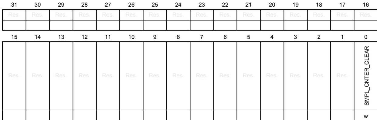
| 31 | 30 | 29 | 28 | 27 | 26 | 25 | 24 | 23 | 22 | 21 | 20 | 19 | 18 | 17 | 16 |
| Res. | Res. | Res. | Res. | Res. | Res. | Res. | Res. | Res. | Res. | Res. | Res. | Res. | Res. | Res. | Res. |
| 15 | 14 | 13 | 12 | 11 | 10 | 9 | 8 | 7 | 6 | 5 | 4 | 3 | 2 | 1 | 0 |
| Res. | Res. | Res. | Res. | Res. | Res. | Res. | Res. | Res. | Res. | Res. | Res. | Res. | Res. | Res. | SMPL_CNTER_CLEAR |
| w |
Bits 31:1 Reserved, must be kept at reset value.
Bit 0 SMPL_CNTER_CLEAR : Sample counter clear bitThe sample counter value is set to zero when this self-clearing bit is programmed to 1.
0: Counter value not cleared
1: Counter value cleared
DTS TSC sample count register (DTS_TSCSMPLCNTR)Address offset: 0x0A8
Reset value: 0x0000 0000
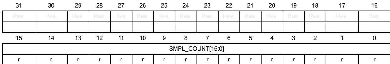
| 31 | 30 | 29 | 28 | 27 | 26 | 25 | 24 | 23 | 22 | 21 | 20 | 19 | 18 | 17 | 16 |
| Res. | Res. | Res. | Res. | Res. | Res. | Res. | Res. | Res. | Res. | Res. | Res. | Res. | Res. | Res. | Res. |
| 15 | 14 | 13 | 12 | 11 | 10 | 9 | 8 | 7 | 6 | 5 | 4 | 3 | 2 | 1 | 0 |
| SMPL_COUNT[15:0] | |||||||||||||||
| r | r | r | r | r | r | r | r | r | r | r | r | r | r | r | r |
Bits 31:16 Reserved, must be kept at reset value.
Bits 15:0 SMPL_COUNT[15:0] : Sample counterThe 16-bit counter increments each time a new data sample is available. The counter is cleared by writing 1 to DTS_TSCSDIFSMPLCLRR. The sample counter overflow operation is determined by SMPL_CTR_HOLD.
33.5.4 TS individual registers
DTS TSn IRQ enable register (DTS_TSn_IER)
Address offset: 0x0C0 + 0x40 * n, (n = 0 to 1)
Reset value: 0x0000 0000
| 31 | 30 | 29 | 28 | 27 | 26 | 25 | 24 | 23 | 22 | 21 | 20 | 19 | 18 | 17 | 16 |
|---|---|---|---|---|---|---|---|---|---|---|---|---|---|---|---|
| Res. | Res. | Res. | Res. | Res. | Res. | Res. | Res. | Res. | Res. | Res. | Res. | Res. | Res. | Res. | Res. |
| 15 | 14 | 13 | 12 | 11 | 10 | 9 | 8 | 7 | 6 | 5 | 4 | 3 | 2 | 1 | 0 |
| Res. | Res. | Res. | Res. | Res. | Res. | Res. | Res. | Res. | Res. | Res. | IRQ_EN_ALARM_B | IRQ_EN_ALARM_A | Res. | IRQ_EN_DONE | IRQ_EN_FAULT |
| nw | nw | nw | nw |
Bits 31:5 Reserved, must be kept at reset value.
Bit 4 IRQ_EN_ALARM_B : Alarm B IRQ enable bit
Bit 3 IRQ_EN_ALARM_A : Alarm A IRQ enable bit
Bit 2 Reserved, must be kept at reset value.
Bit 1 IRQ_EN_DONE : Sample done IRQ enable bit
Bit 0 IRQ_EN_FAULT : Fault IRQ enable bit
DTS TSn IRQ status register (DTS_TSn_ISR)
Address offset: 0x0C4 + 0x40 * n, (n = 0 to 1)
Reset value: 0x0000 0000
| 31 | 30 | 29 | 28 | 27 | 26 | 25 | 24 | 23 | 22 | 21 | 20 | 19 | 18 | 17 | 16 |
|---|---|---|---|---|---|---|---|---|---|---|---|---|---|---|---|
| Res. | Res. | Res. | Res. | Res. | Res. | Res. | Res. | Res. | Res. | Res. | Res. | Res. | Res. | Res. | Res. |
| 15 | 14 | 13 | 12 | 11 | 10 | 9 | 8 | 7 | 6 | 5 | 4 | 3 | 2 | 1 | 0 |
| Res. | Res. | Res. | Res. | Res. | Res. | Res. | Res. | Res. | Res. | Res. | IRQ_STATUS_ALARM_B | IRQ_STATUS_ALARM_A | Res. | IRQ_STATUS_DONE | IRQ_STATUS_FAULT |
| r | r | r | r |
Bits 31:5 Reserved, must be kept at reset value.
Bit 4 IRQ_STATUS_ALARM_B : Alarm B IRQ status bit
Bit 3 IRQ_STATUS_ALARM_A : Alarm A IRQ status bit
Bit 2 Reserved, must be kept at reset value.
Bit 1 IRQ_STATUS_DONE : Sample done IRQ status bit
Bit 0 IRQ_STATUS_FAULT : Fault IRQ status bit
DTS TSn IRQ clear register (DTS_TSn_ICR)Address offset: 0x0C8 + 0x40 * n, (n = 0 to 1)
Reset value: 0x0000 0000
| 31 | 30 | 29 | 28 | 27 | 26 | 25 | 24 | 23 | 22 | 21 | 20 | 19 | 18 | 17 | 16 |
|---|---|---|---|---|---|---|---|---|---|---|---|---|---|---|---|
| Res. | Res. | Res. | Res. | Res. | Res. | Res. | Res. | Res. | Res. | Res. | Res. | Res. | Res. | Res. | Res. |
| 15 | 14 | 13 | 12 | 11 | 10 | 9 | 8 | 7 | 6 | 5 | 4 | 3 | 2 | 1 | 0 |
| Res. | Res. | Res. | Res. | Res. | Res. | Res. | Res. | Res. | Res. | Res. | IRQ_CLEAR_ALARMB | IRQ_CLEAR_ALARMA | Res. | IRQ_CLEAR_DONE | IRQ_CLEAR_FAULT |
| w | w | w | w | ||||||||||||
Bits 31:5 Reserved, must be kept at reset value.
Bit 4 IRQ_CLEAR_ALARMB : Alarm B IRQ clear bit
Bit 3 IRQ_CLEAR_ALARMA : Alarm A IRQ clear bit
Bit 2 Reserved, must be kept at reset value.
Bit 1 IRQ_CLEAR_DONE : Sample done IRQ clear bit
Bit 0 IRQ_CLEAR_FAULT : Fault IRQ clear bit
DTS TSn IRQ test register (DTS_TSnIRQTESTR)Address offset: 0x0CC + 0x40 * n, (n = 0 to 1)
Reset value: 0x0000 0000
| 31 | 30 | 29 | 28 | 27 | 26 | 25 | 24 | 23 | 22 | 21 | 20 | 19 | 18 | 17 | 16 |
|---|---|---|---|---|---|---|---|---|---|---|---|---|---|---|---|
| Res. | Res. | Res. | Res. | Res. | Res. | Res. | Res. | Res. | Res. | Res. | Res. | Res. | Res. | Res. | Res. |
| 15 | 14 | 13 | 12 | 11 | 10 | 9 | 8 | 7 | 6 | 5 | 4 | 3 | 2 | 1 | 0 |
| Res. | Res. | Res. | Res. | Res. | Res. | Res. | Res. | Res. | Res. | Res. | IRQ_TEST_ALARM B | IRQ_TEST_ALARM A | Res. | IRQ_TEST_DONE | IRQ_TEST_FAULT |
| nw | nw | nw | nw |
Bits 31:5 Reserved, must be kept at reset value.
Bit 4 IRQ_TEST_ALARM B : Alarm B IRQ test bitBit 3 IRQ_TEST_ALARM A : Alarm A IRQ test bitBit 2 Reserved, must be kept at reset value.
Bit 1 IRQ_TEST_DONE : Sample done IRQ test bitBit 0 IRQ_TEST_FAULT : Fault IRQ test bit DTS TSn SDIF RDATA register (DTS_TSnSDIFRDATAR)Address offset: 0x0D0 + 0x40 * n, (n = 0 to 1)
Reset value: 0x0000 0000
| 31 | 30 | 29 | 28 | 27 | 26 | 25 | 24 | 23 | 22 | 21 | 20 | 19 | 18 | 17 | 16 |
|---|---|---|---|---|---|---|---|---|---|---|---|---|---|---|---|
| Res. | Res. | Res. | Res. | Res. | Res. | Res. | Res. | SDIF_RDATA[23:16] | |||||||
| r | r | r | r | r | r | r | r | ||||||||
| 15 | 14 | 13 | 12 | 11 | 10 | 9 | 8 | 7 | 6 | 5 | 4 | 3 | 2 | 1 | 0 |
| SDIF_RDATA[15:0] | |||||||||||||||
| r | r | r | r | r | r | r | r | r | r | r | r | r | r | r | r |
Bits 31:24 Reserved, must be kept at reset value.
Bits 23:0 SDIF_RDATA[23:0] : SDIF read data DTS TSn SDIF done register (DTS_TSnSDIFDONER)Address offset: 0x0D4 + 0x40 * n, (n = 0 to 1)
Reset value: 0x0000 0000
| 31 | 30 | 29 | 28 | 27 | 26 | 25 | 24 | 23 | 22 | 21 | 20 | 19 | 18 | 17 | 16 |
|---|---|---|---|---|---|---|---|---|---|---|---|---|---|---|---|
| Res. | Res. | Res. | Res. | Res. | Res. | Res. | Res. | Res. | Res. | Res. | Res. | Res. | Res. | Res. | Res. |
| 15 | 14 | 13 | 12 | 11 | 10 | 9 | 8 | 7 | 6 | 5 | 4 | 3 | 2 | 1 | 0 |
| Res. | Res. | Res. | Res. | Res. | Res. | Res. | Res. | Res. | Res. | Res. | Res. | Res. | Res. | Res. | SDIF_SMPL_DONE |
| r | |||||||||||||||
Bits 31:1 Reserved, must be kept at reset value.
Bit 0 SDIF_SMPL_DONE : Sample done flagThe sample done flag is asserted when a new data sample is available. The sample done flag is automatically cleared when the associated data register is read.
0: No new data sample available
1: New data sample available
DTS TSn SDIF data register (DTS_TSnSDIFDATAR)Address offset: 0x0D8 + 0x40 * n, (n = 0 to 1)
Reset value: 0x0000 0000
| 31 | 30 | 29 | 28 | 27 | 26 | 25 | 24 | 23 | 22 | 21 | 20 | 19 | 18 | 17 | 16 |
|---|---|---|---|---|---|---|---|---|---|---|---|---|---|---|---|
| Res. | Res. | Res. | Res. | Res. | Res. | Res. | Res. | Res. | Res. | Res. | Res. | Res. | Res. | SAMPLE_FAULT | SAMPLE_TYPE |
| r | r | ||||||||||||||
| 15 | 14 | 13 | 12 | 11 | 10 | 9 | 8 | 7 | 6 | 5 | 4 | 3 | 2 | 1 | 0 |
| SAMPLE_DATA[15:0] | |||||||||||||||
| r | r | r | r | r | r | r | r | r | r | r | r | r | r | r | r |
Bits 31:18 Reserved, must be kept at reset value.
Bit 17 SAMPLE_FAULT : Sample fault
This bit is set to indicate that the TS block has signaled a fault. The sample data must be discarded.
Bit 16 SAMPLE_TYPE : TS sample type
0: Indicates valid data
1: Indicates either analog access, signature select or fault debug mode
The TS_TYPE flag is updated when new data are received.
Bits 15:0 SAMPLE_DATA[15:0] : Sample data.
Reading this register clears the state of the SDIF_SMPL_DONE flag in DTS_TSnSDIFDONER register.
DTS TSn alarm A configuration register (DTS_TSnALARMA_CFGR)
Address offset: 0x0E0 + 0x40 * n, (n = 0 to 1)
Reset value: 0x0000 0000
| 31 | 30 | 29 | 28 | 27 | 26 | 25 | 24 | 23 | 22 | 21 | 20 | 19 | 18 | 17 | 16 |
|---|---|---|---|---|---|---|---|---|---|---|---|---|---|---|---|
| ALARMA_THRESH[15:0] | |||||||||||||||
| rw | rw | rw | rw | rw | rw | rw | rw | rw | rw | rw | rw | rw | rw | rw | rw |
| 15 | 14 | 13 | 12 | 11 | 10 | 9 | 8 | 7 | 6 | 5 | 4 | 3 | 2 | 1 | 0 |
| HYSTA_THRESH[15:0] | |||||||||||||||
| rw | rw | rw | rw | rw | rw | rw | rw | rw | rw | rw | rw | rw | rw | rw | rw |
Bits 31:16 ALARMA_THRESH[15:0] : Alarm A threshold
Bits 15:0 HYSTA_THRESH[15:0] : Alarm A hysteresis threshold
DTS TSn alarm B configuration register (DTS_TSnALARMB_CFGR)
Address offset: 0x0E4 + 0x40 * n, (n = 0 to 1)
Reset value: 0x0000 0000
| 31 | 30 | 29 | 28 | 27 | 26 | 25 | 24 | 23 | 22 | 21 | 20 | 19 | 18 | 17 | 16 |
|---|---|---|---|---|---|---|---|---|---|---|---|---|---|---|---|
| ALARMB_THRESH[15:0] | |||||||||||||||
| rw | rw | rw | rw | rw | rw | rw | rw | rw | rw | rw | rw | rw | rw | rw | rw |
| 15 | 14 | 13 | 12 | 11 | 10 | 9 | 8 | 7 | 6 | 5 | 4 | 3 | 2 | 1 | 0 |
| HYSTB_THRESH[15:0] | |||||||||||||||
| rw | rw | rw | rw | rw | rw | rw | rw | rw | rw | rw | rw | rw | rw | rw | rw |
Bits 31:16 ALARMB_THRESH[15:0] : Alarm B threshold
Bits 15:0 HYSTB_THRESH[15:0] : Alarm B hysteresis threshold
DTS TSn high/low sample register (DTS_TSnHLSAMPLER)Address offset: 0x0E8 + 0x40 * n, (n = 0 to 1)
Reset value: 0x0000 FFFF
| 31 | 30 | 29 | 28 | 27 | 26 | 25 | 24 | 23 | 22 | 21 | 20 | 19 | 18 | 17 | 16 |
|---|---|---|---|---|---|---|---|---|---|---|---|---|---|---|---|
| SMPL_HI[15:0] | |||||||||||||||
| r | r | r | r | r | r | r | r | r | r | r | r | r | r | r | r |
| 15 | 14 | 13 | 12 | 11 | 10 | 9 | 8 | 7 | 6 | 5 | 4 | 3 | 2 | 1 | 0 |
| SMPL_LO[15:0] | |||||||||||||||
| r | r | r | r | r | r | r | r | r | r | r | r | r | r | r | r |
Address offset: 0x0EC + 0x40 * n, (n = 0 to 1)
Reset value: 0x0000 0000
| 31 | 30 | 29 | 28 | 27 | 26 | 25 | 24 | 23 | 22 | 21 | 20 | 19 | 18 | 17 | 16 |
|---|---|---|---|---|---|---|---|---|---|---|---|---|---|---|---|
| Res. | Res. | Res. | Res. | Res. | Res. | Res. | Res. | Res. | Res. | Res. | Res. | Res. | Res. | Res. | Res. |
| 15 | 14 | 13 | 12 | 11 | 10 | 9 | 8 | 7 | 6 | 5 | 4 | 3 | 2 | 1 | 0 |
| Res. | Res. | Res. | Res. | Res. | Res. | Res. | Res. | Res. | Res. | Res. | Res. | Res. | Res. | SMPL_HI_CLR | SMPL_LO_SET |
| w | w |
Bits 31:2 Reserved, must be kept at reset value.
Bit 1 SMPL_HI_CLR : Sample high clear 0All the bits of the stored sample high value are initialized to 0 when written.
Bit 0 SMPL_LO_SET : Sample Low SetAll the bits of the stored sample low value are initialized to 1 when written.
33.5.5 DTS register map
Table 267. PVT common register map and reset values
| Offset | Register name reset value | 31 | 30 | 29 | 28 | 27 | 26 | 25 | 24 | 23 | 22 | 21 | 20 | 19 | 18 | 17 | 16 | 15 | 14 | 13 | 12 | 11 | 10 | 9 | 8 | 7 | 6 | 5 | 4 | 3 | 2 | 1 | 0 |
|---|---|---|---|---|---|---|---|---|---|---|---|---|---|---|---|---|---|---|---|---|---|---|---|---|---|---|---|---|---|---|---|---|---|
| 0x000- 0x00C | Reserved | Reserved | |||||||||||||||||||||||||||||||
| 0x010 | DTS_PVTREG_ LOCKR | LOCK[31:0] | |||||||||||||||||||||||||||||||
| Reset value | 0 | 0 | 0 | 0 | 0 | 0 | 0 | 0 | 0 | 0 | 0 | 0 | 0 | 0 | 0 | 0 | 0 | 0 | 0 | 0 | 0 | 0 | 0 | 0 | 0 | 0 | 0 | 0 | 0 | 0 | 0 | 0 | |
| 0x014 | DTS_PVTLOCK_ _SR | Res. | Res. | Res. | Res. | Res. | Res. | Res. | Res. | Res. | Res. | Res. | Res. | Res. | Res. | Res. | Res. | Res. | Res. | Res. | Res. | Res. | Res. | Res. | Res. | Res. | Res. | Res. | Res. | Res. | Res. | HW_LOCK_STATUS | SW_LOCK_STATUS |
| Reset value | 0 | 0 | |||||||||||||||||||||||||||||||
| 0x018 - 0x01C | Reserved | Reserved | |||||||||||||||||||||||||||||||
| 0x020 | DTS_PVTTMR_ CR | Res. | Res. | Res. | Res. | Res. | Res. | Res. | Res. | Res. | Res. | Res. | Res. | Res. | Res. | Res. | TMR_RUN | TMR_DELAY[15:0] | |||||||||||||||
| Reset value | 0 | 0 | 0 | 0 | 0 | 0 | 0 | 0 | 0 | 0 | 0 | 0 | 0 | 0 | 0 | 0 | 0 | ||||||||||||||||
| 0x024 | DTS_PVTTMR_ CR | Res. | Res. | Res. | Res. | Res. | Res. | Res. | Res. | Res. | Res. | Res. | Res. | Res. | Res. | Res. | Res. | Res. | Res. | Res. | Res. | Res. | Res. | Res. | Res. | Res. | Res. | Res. | Res. | Res. | Res. | TMR_DONE | TMR_BUSY |
| Reset value | 0 | 0 | |||||||||||||||||||||||||||||||
| 0x030 - 0x03C | Reserved | Reserved | |||||||||||||||||||||||||||||||
Table 268. PVT IRQ register map and reset values
| Offset | Register name reset value | 31 | 30 | 29 | 28 | 27 | 26 | 25 | 24 | 23 | 22 | 21 | 20 | 19 | 18 | 17 | 16 | 15 | 14 | 13 | 12 | 11 | 10 | 9 | 8 | 7 | 6 | 5 | 4 | 3 | 2 | 1 | 0 |
|---|---|---|---|---|---|---|---|---|---|---|---|---|---|---|---|---|---|---|---|---|---|---|---|---|---|---|---|---|---|---|---|---|---|
| 0x040 | DTS_PVT_IER | Res. | Res. | Res. | Res. | Res. | Res. | Res. | Res. | Res. | Res. | Res. | Res. | Res. | Res. | Res. | Res. | Res. | Res. | Res. | Res. | Res. | Res. | Res. | Res. | Res. | Res. | Res. | Res. | Res. | Res. | TS_IRQ_ENABLE | TMR_IRQ_ENABLE |
| Reset value | 0 | 0 | |||||||||||||||||||||||||||||||
| 0x044 - 0x04C | Reserved | Reserved | |||||||||||||||||||||||||||||||
| 0x050 | DTS_PVTIRQ TRMASKR | Res. | Res. | Res. | Res. | Res. | Res. | Res. | Res. | Res. | Res. | Res. | Res. | Res. | Res. | Res. | Res. | Res. | Res. | Res. | Res. | Res. | Res. | Res. | Res. | Res. | Res. | Res. | Res. | Res. | Res. | Res. | TMR_IRQ_MASK |
| Reset value | 0 | ||||||||||||||||||||||||||||||||
| 0x054 | DTS_TS_MR | Res. | Res. | Res. | Res. | Res. | Res. | Res. | Res. | Res. | Res. | Res. | Res. | Res. | Res. | Res. | Res. | Res. | Res. | Res. | Res. | Res. | Res. | Res. | Res. | Res. | Res. | Res. | Res. | Res. | Res. | TS1_IRQ_MASK | TS0_IRQ_MASK |
| Reset value | 0 | 0 | |||||||||||||||||||||||||||||||
Table 268. PVT IRQ register map and reset values (continued)
| Offset | Register name reset value | 31 | 30 | 29 | 28 | 27 | 26 | 25 | 24 | 23 | 22 | 21 | 20 | 19 | 18 | 17 | 16 | 15 | 14 | 13 | 12 | 11 | 10 | 9 | 8 | 7 | 6 | 5 | 4 | 3 | 2 | 1 | 0 |
|---|---|---|---|---|---|---|---|---|---|---|---|---|---|---|---|---|---|---|---|---|---|---|---|---|---|---|---|---|---|---|---|---|---|
| 0x058 - 0x05C | Reserved | Reserved | |||||||||||||||||||||||||||||||
| 0x060 | DTS_PVTTR_ SR | Res. | Res. | Res. | Res. | Res. | Res. | Res. | Res. | Res. | Res. | Res. | Res. | Res. | Res. | Res. | Res. | Res. | Res. | Res. | Res. | Res. | Res. | Res. | Res. | Res. | Res. | Res. | Res. | Res. | Res. | Res. | TMR_IRQ_STATUS |
| Reset value | 0 | ||||||||||||||||||||||||||||||||
| 0x064 | DTS_TS_ISR | Res. | Res. | Res. | Res. | Res. | Res. | Res. | Res. | Res. | Res. | Res. | Res. | Res. | Res. | Res. | Res. | Res. | Res. | Res. | Res. | Res. | Res. | Res. | Res. | Res. | Res. | Res. | Res. | Res. | Res. | TS1_IRQ_STATUS | TS0_IRQ_STATUS |
| Reset value | 0 | 0 | |||||||||||||||||||||||||||||||
| 0x068 - 0x06C | Reserved | Reserved | |||||||||||||||||||||||||||||||
| 0x070 | DTS_PVTTMR RAW_ISR | Res. | Res. | Res. | Res. | Res. | Res. | Res. | Res. | Res. | Res. | Res. | Res. | Res. | Res. | Res. | Res. | Res. | Res. | Res. | Res. | Res. | Res. | Res. | Res. | Res. | Res. | Res. | Res. | Res. | Res. | Res. | TMR_IRQ_RAW_STATUS |
| Reset value | 0 | ||||||||||||||||||||||||||||||||
| 0x074 | DTS_TSRAW_ ISR | Res. | Res. | Res. | Res. | Res. | Res. | Res. | Res. | Res. | Res. | Res. | Res. | Res. | Res. | Res. | Res. | Res. | Res. | Res. | Res. | Res. | Res. | Res. | Res. | Res. | Res. | Res. | Res. | Res. | Res. | TS1_IRQ_RAW_STATUS | TS0_IRQ_RAW_STATUS |
| Reset value | 0 | 0 | |||||||||||||||||||||||||||||||
| 0x078 - 0x07C | Reserved | Reserved | |||||||||||||||||||||||||||||||
Table 269. DTS TSC clock synthesizer register map and reset values
| Offset | Register name reset value | 31 | 30 | 29 | 28 | 27 | 26 | 25 | 24 | 23 | 22 | 21 | 20 | 19 | 18 | 17 | 16 | 15 | 14 | 13 | 12 | 11 | 10 | 9 | 8 | 7 | 6 | 5 | 4 | 3 | 2 | 1 | 0 |
|---|---|---|---|---|---|---|---|---|---|---|---|---|---|---|---|---|---|---|---|---|---|---|---|---|---|---|---|---|---|---|---|---|---|
| 0x080 | DTS_TSCCLK SYNTHR | Res. | Res. | Res. | Res. | Res. | Res. | Res. | CLK_SYTH_EN | Res. | Res. | Res. | Res. | CLK_SYNTH _HOLD[3:0] | CLK_SYNTH_HI[7:0] | CLK_SYNTH_LO[7:0] | |||||||||||||||||
| Reset value | 0 | 0 | 0 | 0 | 1 | 0 | 0 | 0 | 0 | 0 | 0 | 0 | 0 | 0 | 0 | 0 | 0 | 0 | 0 | 0 | 0 | ||||||||||||
Table 269. DTS TSC clock synthesizer register map and reset values (continued)
| Offset | Register name reset value | 31 | 30 | 29 | 28 | 27 | 26 | 25 | 24 | 23 | 22 | 21 | 20 | 19 | 18 | 17 | 16 | 15 | 14 | 13 | 12 | 11 | 10 | 9 | 8 | 7 | 6 | 5 | 4 | 3 | 2 | 1 | 0 | |
|---|---|---|---|---|---|---|---|---|---|---|---|---|---|---|---|---|---|---|---|---|---|---|---|---|---|---|---|---|---|---|---|---|---|---|
| 0x084 | DTS_TSCSDIF DISABLER | Res. | Res. | Res. | Res. | Res. | Res. | Res. | Res. | Res. | Res. | Res. | Res. | Res. | Res. | Res. | Res. | Res. | Res. | Res. | Res. | Res. | Res. | Res. | Res. | Res. | Res. | Res. | Res. | Res. | Res. | Res. | Res. | 0 |
| Reset value | 0 | |||||||||||||||||||||||||||||||||
| 0x088 | DTS_TSCSDIF_ SR | Res. | Res. | Res. | Res. | Res. | Res. | Res. | Res. | Res. | Res. | Res. | Res. | Res. | Res. | Res. | Res. | Res. | Res. | Res. | Res. | Res. | Res. | Res. | Res. | Res. | Res. | Res. | Res. | Res. | Res. | Res. | 0 | |
| Reset value | 0 | |||||||||||||||||||||||||||||||||
| 0x08C | DTS_TSCSDIF_ CR | SDIF_PROG | Res. | Res. | Res. | SDIF_WRN | SDIF_ADDR [2:0] | SDIF_WDATA[23:0] | 0 | |||||||||||||||||||||||||
| Reset value | 0 | 0 | 0 | 0 | 0 | 0 | 0 | 0 | 0 | 0 | 0 | 0 | 0 | 0 | 0 | 0 | 0 | 0 | 0 | 0 | 0 | 0 | 0 | 0 | 0 | 0 | 0 | 0 | ||||||
| 0x090 | DTS_TSCSDIF HALTR | Res. | Res. | Res. | Res. | Res. | Res. | Res. | Res. | Res. | Res. | Res. | Res. | Res. | Res. | Res. | Res. | Res. | Res. | Res. | Res. | Res. | Res. | Res. | Res. | Res. | Res. | Res. | Res. | Res. | Res. | Res. | 0 | |
| Reset value | 0 | |||||||||||||||||||||||||||||||||
| 0x094 | DTS_TSCSDIF_ CFGR | Res. | Res. | Res. | Res. | Res. | Res. | Res. | Res. | Res. | Res. | Res. | Res. | Res. | Res. | Res. | Res. | Res. | Res. | Res. | Res. | Res. | Res. | Res. | Res. | Res. | Res. | Res. | Res. | Res. | Res. | Res. | 0 | |
| Reset value | 0 | |||||||||||||||||||||||||||||||||
| 0x098 - 0x09C | Reserved | Reserved | ||||||||||||||||||||||||||||||||
| 0x0A0 | DTS_TSCSMPL_ CR | Res. | Res. | Res. | Res. | Res. | Res. | Res. | Res. | Res. | Res. | Res. | Res. | Res. | Res. | Res. | Res. | Res. | Res. | Res. | Res. | Res. | Res. | Res. | Res. | Res. | Res. | Res. | Res. | Res. | Res. | Res. | 0 | |
| Reset value | 0 | |||||||||||||||||||||||||||||||||
| 0x0A4 | DTS_TSCSDIF SMPLCLRR | Res. | Res. | Res. | Res. | Res. | Res. | Res. | Res. | Res. | Res. | Res. | Res. | Res. | Res. | Res. | Res. | Res. | Res. | Res. | Res. | Res. | Res. | Res. | Res. | Res. | Res. | Res. | Res. | Res. | Res. | Res. | 0 | |
| Reset value | 0 | |||||||||||||||||||||||||||||||||
| 0x0A8 | DTS_TSCSMPL_ CNTR | Res. | Res. | Res. | Res. | Res. | Res. | Res. | Res. | Res. | Res. | Res. | Res. | Res. | Res. | SMPL_COUNT[15:0] | 0 | |||||||||||||||||
| Reset value | 0 | 0 | 0 | 0 | 0 | 0 | 0 | 0 | 0 | 0 | 0 | 0 | 0 | 0 | 0 | 0 | 0 | |||||||||||||||||
| 0x0B0 - 0x0BF | Reserved | Reserved | ||||||||||||||||||||||||||||||||
Table 270. DTS TS individual register map and reset values
| Offset | Register name reset value | 31 | 30 | 29 | 28 | 27 | 26 | 25 | 24 | 23 | 22 | 21 | 20 | 19 | 18 | 17 | 16 | 15 | 14 | 13 | 12 | 11 | 10 | 9 | 8 | 7 | 6 | 5 | 4 | 3 | 2 | 1 | 0 |
|---|---|---|---|---|---|---|---|---|---|---|---|---|---|---|---|---|---|---|---|---|---|---|---|---|---|---|---|---|---|---|---|---|---|
| 0x0C0 + 0x40 * n, (n = 0 to 1) | DTS_TSn_IER | Res. | Res. | Res. | Res. | Res. | Res. | Res. | Res. | Res. | Res. | Res. | Res. | Res. | Res. | Res. | Res. | Res. | Res. | Res. | Res. | Res. | Res. | Res. | Res. | Res. | Res. | Res. | IRQ_EN_ALARMB | IRQ_EN_ALARMA | Res. | IRQ_EN_DONE | IRQ_EN_FAULT |
| Reset value | 0 | 0 | 0 | 0 | |||||||||||||||||||||||||||||
| 0x0C4 + 0x40 * n, (n = 0 to 1) | DTS_TSn_ISR | Res. | Res. | Res. | Res. | Res. | Res. | Res. | Res. | Res. | Res. | Res. | Res. | Res. | Res. | Res. | Res. | Res. | Res. | Res. | Res. | Res. | Res. | Res. | Res. | Res. | Res. | Res. | IRQ_STATUS_ALARMB | IRQ_STATUS_ALARMA | Res. | IRQ_STATUS_DONE | IRQ_STATUS_FAULT |
| Reset value | 0 | 0 | 0 | 0 | |||||||||||||||||||||||||||||
| 0x0C8 + 0x40 * n, (n = 0 to 1) | DTS_TSn_ICR | Res. | Res. | Res. | Res. | Res. | Res. | Res. | Res. | Res. | Res. | Res. | Res. | Res. | Res. | Res. | Res. | Res. | Res. | Res. | Res. | Res. | Res. | Res. | Res. | Res. | Res. | Res. | IRQ_CLEAR_ALARMB | IRQ_CLEAR_ALARMA | Res. | IRQ_CLEAR_DONE | IRQ_CLEAR_FAULT |
| Reset value | 0 | 0 | 0 | 0 | |||||||||||||||||||||||||||||
| 0x0CC + 0x40 * n, (n = 0 to 1) | DTS_TSnIRQ TESTR | Res. | Res. | Res. | Res. | Res. | Res. | Res. | Res. | Res. | Res. | Res. | Res. | Res. | Res. | Res. | Res. | Res. | Res. | Res. | Res. | Res. | Res. | Res. | Res. | Res. | Res. | Res. | IRQ_TEST_ALARMB | IRQ_TEST_ALARMA | Res. | IRQ_TEST_DONE | IRQ_TEST_FAULT |
| Reset value | 0 | 0 | 0 | 0 | |||||||||||||||||||||||||||||
| 0x0D0 + 0x40 * n, (n = 0 to 1) | DTS_TSnSDIF RDATAR | Res. | Res. | Res. | Res. | Res. | Res. | Res. | Res. | SDIF_RDATA[23:0] | |||||||||||||||||||||||
| Reset value | 0 | 0 | 0 | 0 | 0 | 0 | 0 | 0 | 0 | 0 | 0 | 0 | 0 | 0 | 0 | 0 | 0 | 0 | 0 | 0 | 0 | 0 | 0 | 0 | |||||||||
| 0x0D4 + 0x40 * n, (n = 0 to 1) | DTS_TSnSDIF DONER | Res. | Res. | Res. | Res. | Res. | Res. | Res. | Res. | Res. | Res. | Res. | Res. | Res. | Res. | Res. | Res. | Res. | Res. | Res. | Res. | Res. | Res. | Res. | Res. | Res. | Res. | Res. | Res. | Res. | Res. | Res. | SDIF_SMPL_DONE |
| Reset value | 0 | ||||||||||||||||||||||||||||||||
| 0x0D8 + 0x40 * n, (n = 0 to 1) | DTS_TSnSDIF DATAR | Res. | Res. | Res. | Res. | Res. | Res. | Res. | Res. | Res. | Res. | Res. | Res. | Res. | Res. | SAMPLE_FAULT | SAMPLE_TYPE | SAMPLE_DATA[15:0] | |||||||||||||||
| Reset value | 0 | 0 | 0 | 0 | 0 | 0 | 0 | 0 | 0 | 0 | 0 | 0 | 0 | 0 | 0 | 0 | 0 | 0 | |||||||||||||||
| 0x0DC - 0x0E8 | Reserved | Reserved | |||||||||||||||||||||||||||||||
| 0x0E0 + 0x40 * n, (n = 0 to 1) | DTS_TSn ALARMA_ CFGR | HYSTA_THRESH[15:0] | ALARMA_THRESH[15:0] | ||||||||||||||||||||||||||||||
| Reset value | 0 | 0 | 0 | 0 | 0 | 0 | 0 | 0 | 0 | 0 | 0 | 0 | 0 | 0 | 0 | 0 | 0 | 0 | 0 | 0 | 0 | 0 | 0 | 0 | 0 | 0 | 0 | 0 | 0 | 0 | 0 | 0 | |
Table 270. DTS TS individual register map and reset values (continued)
| Offset | Register name reset value | 31 | 30 | 29 | 28 | 27 | 26 | 25 | 24 | 23 | 22 | 21 | 20 | 19 | 18 | 17 | 16 | 15 | 14 | 13 | 12 | 11 | 10 | 9 | 8 | 7 | 6 | 5 | 4 | 3 | 2 | 1 | 0 |
|---|---|---|---|---|---|---|---|---|---|---|---|---|---|---|---|---|---|---|---|---|---|---|---|---|---|---|---|---|---|---|---|---|---|
| 0x0E4 + 0x40 * n, (n = 0 to 1) | DTS_TSn ALARMB_ CFG | HYSTB_THRESH[15:0] | ALARMB_THRESH[15:0] | ||||||||||||||||||||||||||||||
| Reset value | 0 | 0 | 0 | 0 | 0 | 0 | 0 | 0 | 0 | 0 | 0 | 0 | 0 | 0 | 0 | 0 | 0 | 0 | 0 | 0 | 0 | 0 | 0 | 0 | 0 | 0 | 0 | 0 | 0 | 0 | 0 | 0 | |
| 0x0E8 + 0x40 * n, (n = 0 to 1) | DTS_TSnHL SAMPLER | SMPL_HI[15:0] | SMPL_LO[15:0] | ||||||||||||||||||||||||||||||
| Reset value | 0 | 0 | 0 | 0 | 0 | 0 | 0 | 0 | 0 | 0 | 0 | 0 | 0 | 0 | 0 | 0 | 1 | 1 | 1 | 1 | 1 | 1 | 1 | 1 | 1 | 1 | 1 | 1 | 1 | 1 | 1 | 1 | |
| 0x0EC + 0x40 * n, (n = 0 to 1) | DTS_TSnHILO RESETR | Res. | Res. | Res. | Res. | Res. | Res. | Res. | Res. | Res. | Res. | Res. | Res. | Res. | Res. | Res. | Res. | Res. | Res. | Res. | Res. | Res. | Res. | Res. | Res. | Res. | Res. | Res. | Res. | Res. | Res. | Res. | Res. |
| Reset value | 0 | 0 | |||||||||||||||||||||||||||||||
Refer to Section 2.3 for the register boundary addresses.