31. Delay block (DLYB)
31.1 DLYB introduction
The delay block (DLYB) is used to generate two output clocks that are dephased from 2 input clocks. The phase of each output clock must be programmed by the user application. The output clocks are then used to clock the data transmitted/received by another peripheral such as an SDMMC.
31.2 DLYB main features
The delay block has the following features:
- • Frequency range for Lock mode is [50 MHz, 208 MHz]
- • 32 phases (delay taps)
- • Bypass mode for operation below 50 MHz
31.3 DLYB implementation
Table 234. STM32N6x5/x7xx features
| DLYB associated peripheral | DLYBSD1 | DLYBSD2 |
|---|---|---|
| SDMMC1 | X | - |
| SDMMC2 | - | X |
31.4 DLYB functional description
31.4.1 DLYB diagram
The delay block includes the following sub-blocks (shown in the figure below):
- • Digital block to generate commands for delay lines and phase selection. This block embeds lock FSM.
- • Delay line supporting the unit delays
- • Output clock selection multiplexer
Figure 260. DLYB block diagram
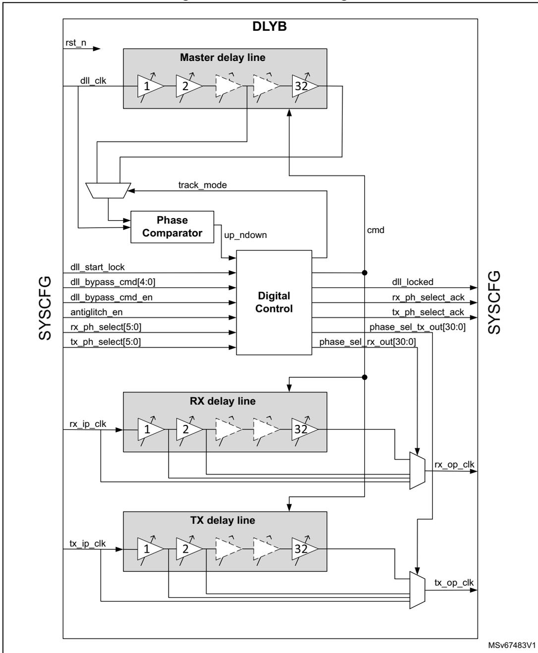
The diagram illustrates the internal architecture of the DLYB (Delay block). At the top, the Master delay line consists of 32 stages (labeled 1, 2, ..., 32) and is controlled by cmd and track_mode signals. A Phase Comparator receives inputs from the master delay line and dll_clk , outputting up_n and down signals to the Digital Control . The Digital Control block is connected to SYSCFG registers and manages the cmd signal for the delay lines. Below the control section are the RX delay line and TX delay line , each also with 32 stages. These lines are controlled by phase_sel and rx_out[30:0] / tx_out[30:0] signals. The RX delay line takes rx_ip_clk as input and produces rx_op_clk as output. The TX delay line takes tx_ip_clk as input and produces tx_op_clk as output. Various control signals from SYSCFG are shown on the left, including dll_start_lock , dll_bypass_cmd[4:0] , dll_bypass_cmd_en , antiglitch_en , rx_ph_select[5:0] , and tx_ph_select[5:0] . Acknowledge signals dll_locked , rx_ph_select_ack , and tx_ph_select_ack are shown on the right.
MSV67483V1
31.4.2 DLYB internal signals
Table 235 lists the DLYB functional signals.
Table 235. DLYB functional signals
| Signal name | Signal type | Description |
|---|---|---|
| dll_clk | Digital input | Free-running input clock used as reference clock for the Master delay line and FSM blocks |
| tx_ip_clk | Digital input | Input clock of the TX slave delay line |
| rx_ip_clk | Digital input | Input clock of the RX slave delay line |
| tx_op_clk | Digital output | Selected output clock of the TX slave delay line |
| rx_op_clk | Digital output | Selected output clock of the RX slave delay line |
| rst_n | Digital input | Asynchronous active low reset |
| dll_start_lock | Digital input | Enable of DLL when configured in Lock mode |
| dll_locked | Digital output | Lock indicator. When high, it indicates that the FSM has finished the lock sequence. The DLL can be used |
| tx_ph_select[5:0] | Digital input | Selection of the slave DLL phase shift over 33 for TX path 000000: 0 tap selection 000001: 1 tap selection 011111: 31 taps selection 1xxxxx: 32 taps selection |
| tx_ph_select_ack | Digital output | When high: phase selected by tx_ph_select is acknowledged When low: output clock tx_op_clk is tied low |
| rx_ph_select[5:0] | Digital input | Selection of the slave DLL phase shift over 33 for RX path 000000: 0 tap selection 000001: 1 tap selection 011111: 31 taps selection 1xxxxx: 32 taps selection |
| rx_ph_select_ack | Digital output | When high: phase selected by rx_ph_select is acknowledged When low: output clock rx_op_clk is tied low |
| antiglitch_en | Digital input | When high: output clocks (tx_op_clk or rx_op_clk) when minimum delay is selected (tx_ph_select = 0 or rx_ph_select=0) are gated to avoid any glitch when phase selection changes When low: output clocks (tx_op_clk or rx_op_clk) when minimum delay is selected (tx_ph_select = 0 or rx_ph_select=0) are not gated (possible glitches if input clocks (tx_ip_clk or rx_ip_clk) are enabled when phase selection changes) |
| dll_bypass_cmd_en | Digital input | Active high: use dll_bypass_cmd for command generation |
| dll_bypass_cmd[4:0] | Digital input | permits to force delays for all taps when dll_bypass_cmd_en high: 00000: not functional 00001: pass gate 0 is activated (min delay) 00010: pass gate 1 is activated 11000: pass gate 23 is activated 11001 to 11111: pass gate 23 is activated (max delay) |
Table 236 lists the DLYB interconnections. The SDMMCx DLYB registers (DLYBSDx) are highlighted in light gray, RCC registers in dark gray and peripheral ports in blue.
Table 236. DLYB interconnection
| Signal name | Source/destination | |
|---|---|---|
| SDMMC1 | SDMMC2 | |
| dll_clk | ClkDII (sdmmc1_ClkDII) | ClkDII (sdmmc2_ClkDII) |
| rx_ip_clk | CKio (sdmmc1_io_CKio) | CKio (sdmmc2_io_CKio) |
| tx_ip_clk | Not used | |
| rx_op_clk | FB_CLK (sdmmc1_fb_clk) | FB_CLK (sdmmc2_fb_clk) |
| tx_op_clk | Not used | |
| rst_n | RCC_MISCRSTR.SDMMC1DLLRST | RCC_MISCRSTR.SDMMC2DLLRST |
| dll_start_lock | DLYBSD_CFG
(1) SDMMC_DLL_EN | DLYBSD_CFG
(2) SDMMC_DLL_EN |
| dll_locked | DLYBSD_STATUS
(1) SDMMC_DLL_LOCK | DLYBSD_STATUS
(2) SDMMC_DLL_LOCK |
| tx_ph_select[5:0] | Not used | |
| tx_ph_select_ack | Not used | |
| rx_ph_select[5:0] | DLYBSD_CFG
(1) SDMMC_RX_TAP_SEL[5:0] | DLYBSD_CFG
(2) SDMMC_RX_TAP_SEL[5:0] |
| rx_ph_select_ack | DLYBSD_STATUS
(1) SDMMC_RX_TAP_SEL_ACK | DLYBSD_STATUS
(2) SDMMC_RX_TAP_SEL_ACK |
| antiglitch_en | DLYBSD_CFG
(1) SDMMC_DLL_ANTIGLITCH_EN | DLYBSD_CFG
(2) SDMMC_DLL_ANTIGLITCH_EN |
| dll_bypass_cmd_en | DLYBSD_CFG
(1) SDMMC_DLL_BYP_EN | DLYBSD_CFG
(2) SDMMC_DLL_BYP_EN |
| dll_bypass_cmd[4:0] | DLYBSD_CFG
(1) SDMMC_DLL_BYP_CMD[4:0] | DLYBSD_CFG
(2) SDMMC_DLL_BYP_CMD[4:0] |
1. Register in DLYB1 instance.
2. Register in DLYB2 instance.
31.4.3 General description
The delay block is structured around one master delay line and two slave delay lines (RX and TX) and there are two operating modes:
- • Lock mode (
dll_bypass_cmd_en
= 0)
- – This mode can only be used when the frequency of dll_clk is in the range [50 MHz, 208 MHz]
- – The delay block is enabled by setting dll_start_lock to '1'.
- – The delay block locks on the frequency of the dll_clk input clock and compensates for voltage and temperature variations. This process determines the command to be applied to each of the 32 delay units (a.k.a. tap) of the master delay line for the total master delay to represent one period of dll_clk . This command is copied to each delay unit of the RX and TX delay lines. The command varies with voltage and temperature for the DLL to remain locked. This guarantees that each delay unit of the RX and TX delay lines represents 1/32th of the input clock period.
- – Independent delay values can be selected for the RX and TX delay lines by controlling rx_ph_select[5:0] and tx_ph_select[5:0] parameters. The granularity of the delay is 1/32th of the input clock period.
- • Bypass mode (
dll_bypass_cmd_en
= 1)
- – This mode is required to be able to insert a delay between the rx_ip_clk (resp. tx_ip_clk ) input clock and the rx_op_clk (resp. tx_op_clk ) output clock when the operating frequency is lower than the minimum frequency supported by the delay block in lock mode (frequency < 50 MHz).
- – In this mode, delays in the RX and TX delay lines are used as “pure” delays, i.e. without trying to lock on the frequency of the dll_clk input clock. There is therefore no voltage nor temperature compensation in this mode and the RX and TX delay values vary with voltage and temperature. The command applied to each delay unit of the RX and TX delay lines is controlled by dll_bypass_cmd[4:0] . Each delay unit includes 24 delay elements. The number of delay elements which are enabled in each delay unit depends on the value of dll_bypass_cmd[4:0] .
- – Independent delay values can be selected for the RX and TX delay lines by controlling rx_ph_select[5:0] and tx_ph_select[5:0] parameters. The total delay inserted by the RX (resp. TX) delay line depends on rx_ph_select[5:0] (resp. tx_ph_select[5:0] ) and dll_bypass_cmd[4:0] values.
31.4.4 Lock mode procedure
For frequencies greater or equal to 50MHz, procedure is given below:
- 1. When rst_n is low, DLYB lock FSM is put in Idle mode. Note that dll_start_lock must be set to '0' during hard reset.
- 2. Once the input signal dll_clk is stable (after a frequency switch for example) the lock sequence can be started by setting dll_start_lock to '1' and maintain this value.
- 3. During lock sequence DLYB can not be used until dll_locked flag is set to '1'.
- 4. Once it is done, delay line for master and slaves are PVT compensated (tracking V and T evolution but not a frequency switch).
- 5. Then the phase can be programmed using tx_ph_select[5:0] and rx_ph_select[5:0] input signals. The selected delays are applied to TX output clock and RX output clock once tx_ph_select_ack and rx_ph_select_ack are set to '1' respectively.
- 6. If another lock sequence is needed, for a frequency switch for example, dll_start_lock signal must go to '0' and sequence can be restarted with step 2.
31.4.5 Bypass mode procedure
For frequencies lower the 50 MHz, procedure is given below:
- 1. When rst_n is low, DLYB lock FSM is put in Idle mode. Note that dll_start_lock must be set to '0' during hard reset.
- 2. Delay block is enabled by setting dll_bypass_cmd_en to '1'. The command applied to every delay unit is defined by dll_bypass_cmd[4:0] input (the value 0 is reserved and must not be used).
- 3. The phase can be programmed using tx_ph_select[5:0] and rx_ph_select[5:0] input signals. The selected delays are applied to TX output clock and RX output clock once tx_ph_select_ack and rx_ph_select_ack are set to '1' respectively. For minimum delay, tx_ph_select[5:0] (resp. rx_ph_select[5:0] ) must be set to 0.
31.5 DLYB SDMMC registers description
There is one DLYB module associated to each SDMMC (see Section 2.3: Memory organization ). It contains registers to configure the DLL for the RX path. The registers are described below.
31.5.1 Delay block SDMMC DLL configuration (DLYBSD_CFG)
Address offset: 0x0
Reset value: 0x0040 0000
SDMMC DLL configuration register.
| 31 | 30 | 29 | 28 | 27 | 26 | 25 | 24 | 23 | 22 | 21 | 20 | 19 | 18 | 17 | 16 |
|---|---|---|---|---|---|---|---|---|---|---|---|---|---|---|---|
| Res. | Res. | Res. | Res. | Res. | Res. | Res. | Res. | Res. | SDMMC_DLL_ANTIGLITCH_EN | SDMMC_DLL_BYP_CMD[4:0] | SDMMC_DLL_BYP_EN | ||||
| r/w | r/w | r/w | r/w | r/w | r/w | r/w | |||||||||
| 15 | 14 | 13 | 12 | 11 | 10 | 9 | 8 | 7 | 6 | 5 | 4 | 3 | 2 | 1 | 0 |
| Res. | Res. | Res. | Res. | Res. | Res. | Res. | Res. | Res. | SDMMC_RX_TAP_SEL[5:0] | SDMMC_DLL_EN | |||||
| r/w | r/w | r/w | r/w | r/w | r/w | r/w | |||||||||
Bits 31:23 Reserved, must be kept at reset value.
Bit 22 SDMMC_DLL_ANTIGLITCH_EN : Antiglitch logic enabled when 1
Bits 21:17 SDMMC_DLL_BYP_CMD[4:0] : Bypass command
It is applied on RX path and corresponds to the number of delay cells activated (when SDMMC_DLL_BYP_EN is high).
Bit 16 SDMMC_DLL_BYP_EN : DLL configuration
0: Lock mode
1: Pure delay
Bits 15:7 Reserved, must be kept at reset value.
Bits 6:1 SDMMC_RX_TAP_SEL[5:0] : selection of RX delay
In 1/32th of clock period.
Bit 0 SDMMC_DLL_EN : DLL enable
Used to enable the DLL when configured in lock mode.
31.5.2 Delay block SDMMC DLL status (DLYBSD_STATUS)
Address offset: 0x4
Reset value: 0x0000 0002
SDMMC DLL status register.
| 31 | 30 | 29 | 28 | 27 | 26 | 25 | 24 | 23 | 22 | 21 | 20 | 19 | 18 | 17 | 16 |
|---|---|---|---|---|---|---|---|---|---|---|---|---|---|---|---|
| Res. | Res. | Res. | Res. | Res. | Res. | Res. | Res. | Res. | Res. | Res. | Res. | Res. | Res. | Res. | Res. |
| 15 | 14 | 13 | 12 | 11 | 10 | 9 | 8 | 7 | 6 | 5 | 4 | 3 | 2 | 1 | 0 |
| Res. | Res. | Res. | Res. | Res. | Res. | Res. | Res. | Res. | Res. | Res. | Res. | Res. | Res. | SDMMC_RX_TAP_SEL_ACK | SDMMC_DLL_LOCK |
| rw | rw | ||||||||||||||
Bits 31:2 Reserved, must be kept at reset value.
Bit 1 SDMMC_RX_TAP_SEL_ACK : SDMMC RX delay selection acknowledge
This bit indicates that RX delay line has been configured with the delay selected by SDMMC_RX_TAP_SEL[5:0].
Bit 0 SDMMC_DLL_LOCK : SDMMC DLL lock
This bit indicates that DLL is locked to the input frequency.
31.5.3 DLYB register map
Table 237. DLYB register map and reset values
| Offset | Register name Reset value | 31 | 30 | 29 | 28 | 27 | 26 | 25 | 24 | 23 | 22 | 21 | 20 | 19 | 18 | 17 | 16 | 15 | 14 | 13 | 12 | 11 | 10 | 9 | 8 | 7 | 6 | 5 | 4 | 3 | 2 | 1 | 0 |
|---|---|---|---|---|---|---|---|---|---|---|---|---|---|---|---|---|---|---|---|---|---|---|---|---|---|---|---|---|---|---|---|---|---|
| 0x0 | DLYBSD_CFG | Res. | Res. | Res. | Res. | Res. | Res. | Res. | Res. | Res. | SDMMC_DLL_ANTIGLITCH_EN | Res. | Res. | SDMMC_DLL_BYP_CMD | Res. | Res. | SDMMC_DLL_BYP_EN | Res. | Res. | Res. | Res. | Res. | Res. | Res. | Res. | Res. | SDMMC_RX_TAP_SEL | SDMMC_DLL_EN | |||||
| Reset value | 1 | 0 | 0 | 0 | 0 | 0 | 0 | 0 | 0 | 0 | 0 | 0 | 0 | 0 | |||||||||||||||||||
Table 237. DLYB register map and reset values (continued)
| Offset | Register name Reset value | 31 | 30 | 29 | 28 | 27 | 26 | 25 | 24 | 23 | 22 | 21 | 20 | 19 | 18 | 17 | 16 | 15 | 14 | 13 | 12 | 11 | 10 | 9 | 8 | 7 | 6 | 5 | 4 | 3 | 2 | 1 | 0 |
|---|---|---|---|---|---|---|---|---|---|---|---|---|---|---|---|---|---|---|---|---|---|---|---|---|---|---|---|---|---|---|---|---|---|
| Res. | Res. | Res. | Res. | Res. | Res. | Res. | Res. | Res. | Res. | Res. | Res. | Res. | Res. | Res. | Res. | Res. | Res. | Res. | Res. | Res. | Res. | Res. | Res. | Res. | Res. | Res. | Res. | Res. | Res. | SDMMC_RX_TAP_SEL_ACK | SDMMC_DLL_LOCK | ||
| 0x4 | DLYBSD_ STATUS | ||||||||||||||||||||||||||||||||
| Reset value | 1 | 0 |
Refer to Section 2.3 on page 163 for the register boundary addresses.