27. Flexible memory controller (FMC)
The flexible memory controller (FMC) includes three memory controllers:
- • the NOR/PSRAM memory controller
- • the NAND memory controller
- • the synchronous DRAM (SDRAM/Mobile LPSDR SDRAM) controller
27.1 FMC main features
The FMC functional block makes the interface with: synchronous and asynchronous static memories, SDRAM memories, and NAND flash memory. Its main purposes are:
- • to translate AXI transactions into the appropriate external device protocol
- • to meet the access time requirements of the external memory devices
All external memories share the addresses, data and control signals with the controller. Each external device is accessed by means of a unique Chip Select. The FMC performs only one access at a time to an external device.
The main features of the FMC are the following:
- • Interface with static-memory mapped devices including:
- – Static random access memory (SRAM)
- – NOR flash memory/One NAND flash memory
- – PSRAM (4 memory subregions)
- – Ferroelectric RAM (FRAM)
- – NAND flash memory with ECC hardware to check up to 8 Kbytes of data
- • Interface with synchronous DRAM (SDRAM/Mobile LPSDR SDRAM) memories
- • Burst mode support for faster access to synchronous devices such as NOR flash memory, PSRAM and SDRAM
- • Programmable continuous clock output for asynchronous and synchronous accesses
- • 8-, 16- or 32-bit wide data bus
- • Independent chip-select control for each memory region
- • Independent configuration for each memory region
- • Write enable and byte lane select outputs for use with PSRAM, SRAM and SDRAM devices
- • External asynchronous wait control
At startup the FMC pins must be configured by the user application. The FMC input/output pins which are not used by the application can be used for other purposes.
After reset, the FMC is disabled. Once all the used memory controllers are configured, the FMC must be enabled by setting the FMCEN bit.
The FMC registers that define the external device type and associated characteristics are set at boot time and do not change until the next reset or power-up. If some registers have to be re-configured, the FMC must be disabled (FMCEN bit set to 0x0). However, only few bits can be changed on the fly:
- • FMCEN bit
- • ECCEN and PBEN bits in FMC_PCR register
- • FMC_CSQICR and FMC_CSQIER register bits
- • FMC command sequencer registers and FMC BCH registers
- • WEN bit in the FMC_PCR register
- • MODE[2:0], DS1/DS2, NRFS[3:0] and MRD[13:0] bits in FMC_SDCMR register
- • REIE and CRE bits in the FMC_SDRTR register.
If some parameters have to be modified while the FMC is enabled, the FMC must be first disabled so that no further access is allowed to any memory controller during register modification. Once all needed configurations are updated, enable the FMC as follows:
- 1. Disable FMC by resetting the FMCEN bit.
- 2. Wait ISOST[1:0] bits in FMC_SR register to be set to 0b11.
- 3. Wait until PEF flag is set in the FMC_SR register.
- 4. Program the registers with new values.
- 5. Enable the FMC by setting the FMCEN bit.
When the SDRAM controller is available, if the SDCLK clock ratio or refresh rate has to be modified after the initialization phase, the following procedure must be followed.
- 1. Stop by software, the AXI traffic from/to the SDRAM devices only.
- 2. Put all the SDRAM devices in self refresh and wait for the CMDOK command completion flag.
- 3. Change the clock ratio to the new value.
- 4. Send a normal mode command (NRM) to exit from SR and wait for the CMDOK command completion flag.
- 5. Send a load mode register command (LMR) as needed to update devices timing (optional)
- 6. Resume the AXI traffic to SDRAM devices.
27.2 FMC implementation
Table 146. FMC features
| Modes/features | FMC |
|---|---|
| NAND flash chip-select outputs | 4 |
| NAND flash ready/busy | 1 |
| NAND/NOR flash with common WAIT pin | No |
27.3 FMC block diagram
The FMC consists of the following main blocks:
- • The NOR flash/PSRAM/SRAM controller
- • The NAND controller
- • The SDRAM controller
- • The AXI interface
- • The AHB interface (including the FMC configuration registers)
The block diagram is shown in the below figure.
Figure 160. FMC block diagram
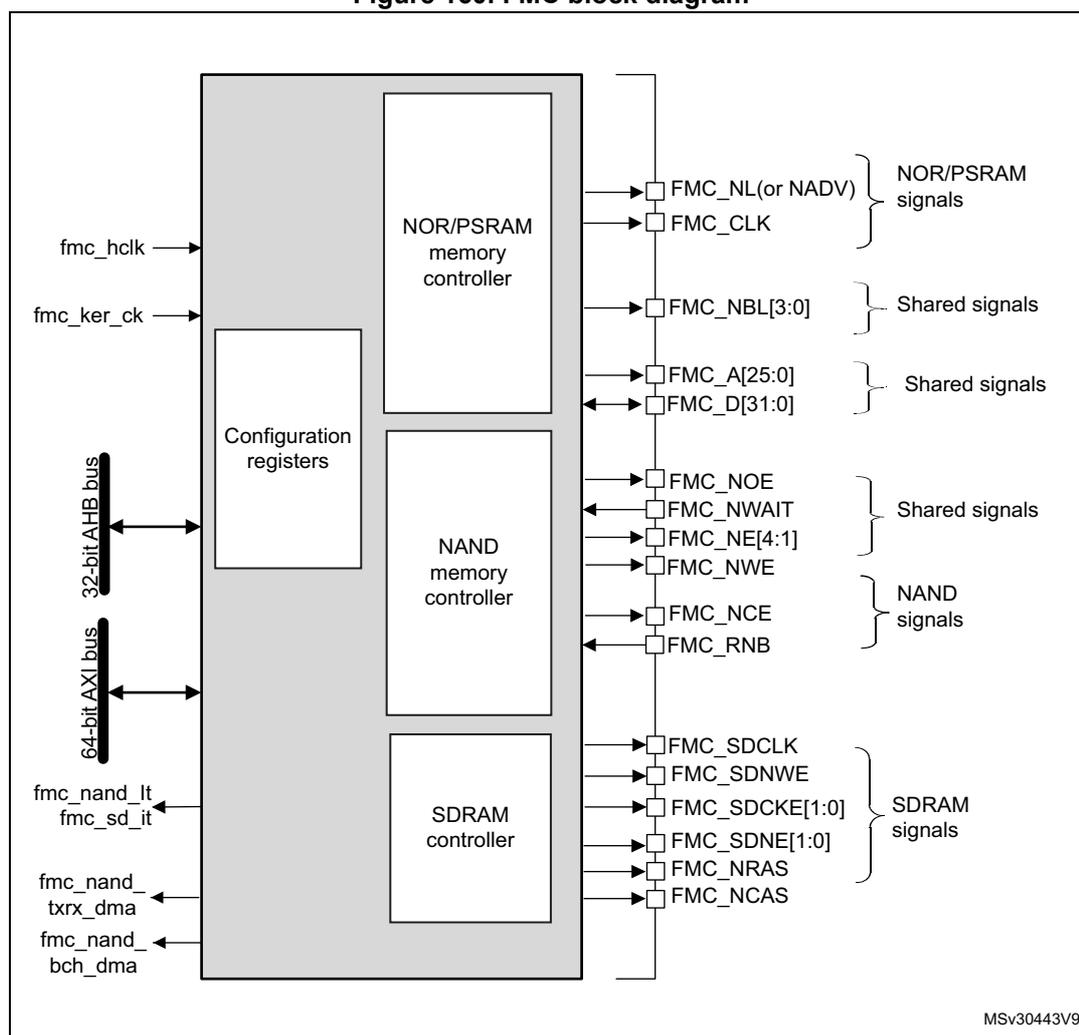
The block diagram illustrates the internal architecture and external connections of the Flexible Memory Controller (FMC). The main components and their connections are as follows:
- Internal Components:
- NOR/PSRAM memory controller: Located at the top right of the FMC block.
- NAND memory controller: Located in the middle right of the FMC block.
- SDRAM controller: Located at the bottom right of the FMC block.
- Configuration registers: Located in the center-left of the FMC block.
- External Connections (Left Side):
- fmc_hclk: Input signal to the top of the FMC block.
- fmc_ker_ck: Input signal to the middle of the FMC block.
- 32-bit AHB bus: Bidirectional connection to the configuration registers.
- 64-bit AXI bus: Bidirectional connection to the configuration registers.
- fmc_nand_it / fmc_sd_it: Input signals to the bottom of the FMC block.
- fmc_nand_txrx_dma: Input signal to the bottom of the FMC block.
- fmc_nand_bch_dma: Input signal to the bottom of the FMC block.
- External Connections (Right Side):
- NOR/PSRAM signals:
- FMC_NL(or NADV): Output signal.
- FMC_CLK: Output signal.
- Shared signals:
- FMC_NBL[3:0]: Output signal.
- FMC_A[25:0]: Output signal.
- FMC_D[31:0]: Bidirectional data bus.
- Shared signals:
- FMC_NOE: Output signal.
- FMC_NWAIT: Input signal.
- FMC_NE[4:1]: Output signal.
- FMC_NWE: Output signal.
- NAND signals:
- FMC_NCE: Output signal.
- FMC_RNB: Input signal.
- SDRAM signals:
- FMC_SDCLK: Output signal.
- FMC_SDNWE: Output signal.
- FMC_SDCKE[1:0]: Output signal.
- FMC_SDNE[1:0]: Output signal.
- FMC_NRAS: Output signal.
- FMC_NCAS: Output signal.
- NOR/PSRAM signals:
MSv30443V9
27.4 FMC internal signals
Table 147 gives the list of FMC internal signals. FMC pins (or external signals) are described in Section 27.8.1: External memory interface signals .
Table 147. FMC internal signals
| Names | Signal type | Description |
|---|---|---|
| fmc_nand_it | Digital output | FMC NAND flash interrupt |
| fmc_sd_it | Digital output | FMC SDRAM interrupt |
| fmc_ker_ck | Digital input | FMC kernel clock |
| fmc_hclk | Digital input | FMC interface clock |
| fmc_nand_txrx_dma | Digital output | DMA request for reading or writing data from/to NAND flash memory |
| fmc_nand_bch_dma | Digital output | DMA request for BCH results |
27.5 AHB interface
The AHB slave interface allows internal CPUs to configure the FMC registers.
The AHB clock (HCLK) is the reference clock for the FMC register accesses.
The FMC registers must be accessed by words (32 bits). For non 32-bit AHB accesses, FMC does not return an AHB bus error and the register value can be corrupted.
27.6 AXI interface
The AXI slave interface allows internal CPUs and other bus master peripherals to access the external memories.
AXI transactions are translated into the external device protocol. As the AXI data bus is 64-bit wide, the AXI transactions might be split into several consecutive 32- or 16- or 8-bit accesses according to data size accesses.
The FMC generates an AXI slave error when one of the following conditions is met:
- • When reading or writing to an FMC memory region (memory region 1 to 4) which is not enabled
- • When reading or writing to any FMC memory region while the FMC is disabled (FMCEN bit is reset)
- • When reading or writing by the command sequencer to NAND memory region while it is disabled
- • When reading or writing to the NOR flash memory region while the MBKEN bit is reset in the FMC_BCRx register
- • When writing to a write-protected SDRAM device (WP bit set in the SDRAM_SDCRx register)
- • When the SDRAM address range is violated (access to a reserved address range)
- • When reading or writing to an SDRAM device with the SDEN bit cleared in the FMC_SDCRx register
The FMC generates an AXI decoder error in the following conditions:
- • When ADDR[31:28] address bits are not supported by the FMC memory region base address following the BMAP[1:0] bits configuration
- • and when an access to an SDRAM or a NAND memory region is performed while the SDRAM or the NAND controller is not present.
The kernel clock for the FMC is the asynchronous fmc_ker_ck clock (refer the Reset and Clock control (RCC) section for details on fmc_ker_ck clock source selection).
27.6.1 Supported memories and transactions
General transaction rules
The requested AXI transaction data size can be 8-, 16-, 32- or 64-bit wide whereas the accessed external device has a fixed data width. This may lead to inconsistent transfers.
Therefore, some simple transaction rules must be followed:
- • AXI transaction size and memory data size must be equal to prevent issues from occurring.
- • AXI transaction size is greater than the memory size:
In this case, the FMC splits the AXI transaction into smaller consecutive memory accesses to meet the external data width.
- • AXI transaction size is smaller than the memory size:
The transfer may or not be consistent depending on the type of external device:
- – Accesses to devices that have the byte select feature (SRAM, ROM, PSRAM, SDRAM)
In this case, the FMC allows read/write transactions and accesses the right data through its byte lanes NBL[3:0].
Bytes to be written are addressed by NBL[3:0].
All memory bytes are read (NBL[3:0] are driven low during read transaction) and the useless ones are discarded.
- – Accesses to devices that do not have the byte select feature (NOR and NAND flash memories)
This situation occurs when a byte access is requested to a 16-bit wide flash memory. Since the device cannot be accessed in Byte mode (only 16-bit words can be read/written from/to the flash memory), write transactions are not allowed while read transactions are allowed (the controller reads the entire 16-bit memory word and uses only the required byte).
Wrap support for NOR flash/PSRAM
Synchronous memories must be configured in Linear burst mode of undefined length as not all masters can issue wrap transactions.
If a master generates a wrap transaction:
- • The read operation is split into two linear burst transactions.
- • The write operation is split into two linear burst transactions.
Configuration registers
The FMC can be configured through a set of registers. Refer to Section 27.8.6 , for a detailed description of the NOR flash/PSRAM controller registers. Refer to Section 27.9.9 , for a detailed description of the NAND flash registers and to Section 27.10.5 for a detailed description of the SDRAM controller registers.
27.7 External device address mapping
From the FMC point of view, the external memory is divided into fixed-size memory regions of 256 Mbytes each (see Table 148 ):
- • Memory region 1 is used to address up to 4 NOR flash memories or PSRAM devices. This region is split into four NOR/PSRAM subregions with four dedicated Chip Selects, as follows:
- – Subregion 1 - NOR/PSRAM 1
- – Subregion 2 - NOR/PSRAM 2
- – Subregion 3- NOR/PSRAM 3
- – Subregion 4 - NOR/PSRAM 4
Note: The Memory region 1 type attribute must be declared as 'device'.
- • Memory region 5 and 6 are used to address SDRAM devices (one device per region).
For each memory region, the type of memory to be used can be configured by the user application through the Configuration register.
Table 148. FMC memory regions (default mapping)
| Address | Memory region | Supported memory type |
|---|---|---|
| 0x6000 0000 - 0x6FFF FFFF | Memory region 1 | NOR flash memory/PSRAM/SRAM |
| 0xC000 0000 - 0xCFFF FFFF | Memory region 5 | SDRAM device 1 |
| 0xD000 0000 - 0xDFFF FFFF | Memory region 6 | SDRAM device 2 |
The mapping of FMC memory regions can be modified through the BMAP[1:0] bits in FMC_BCR1 register. Table 149 shows the configuration to swap the NOR/PSRAM and SDRAM memory regions or remap SDRAM device 1 and 2. Thus allowing to access the SDRAM devices at two different address mapping.
Table 149. FMC memory region remap using BMAP[1:0]
| FMC memory region | BMAP[1:0] = 00 (Default mapping) | BMAP[1:0] = 01 | BMAP[1:0] = 10 |
|---|---|---|---|
| Memory region 1 | NOR/PSRAM/SRAM | SDRAM device 1 | NOR/PSRAM/SRAM |
| Memory region 5 | SDRAM device 1 | NOR/PSRAM/SRAM | SDRAM device 1 |
| Memory region 6 | SDRAM device 2 | SDRAM device 2 | SDRAM device 2 |
27.7.1 NOR/PSRAM address mapping
ADDR[27:26] bits are used to select one of the four memory subregions as shown in Table 150 .
Table 150. NOR/PSRAM subregion selection
| ADDR[27:26] (1) | Selected subregion |
|---|---|
| 00 | Subregion 1 - NOR/PSRAM 1 |
| 01 | Subregion 2 - NOR/PSRAM 2 |
| 10 | Subregion 3- NOR/PSRAM 3 |
| 11 | Subregion 4- NOR/PSRAM 4 |
- 1. ADDR are internal address lines that are translated to external memory.
The ADDR[25:0] bits contain the external memory address. Since ADDR is a byte address whereas the memory is addressed at word level, the address actually issued to the memory varies according to the memory data width, as shown in the following table.
Table 151. NOR/PSRAM External memory address
| Memory width (1) | Data address issued to the memory | Maximum memory capacity (bits) |
|---|---|---|
| 8-bit | ADDR[25:0] | 64 Mbytes * 8 = 512 Mbit |
| 16-bit | ADDR[25:1] >> 1 | 64 Mbytes/2 * 16 = 512 Mbit |
| 32-bit | ADDR[25:2] >> 2 | 64 Mbytes/4 * 32 = 512 Mbit |
- 1. In case of a 16-bit external memory width, the FMC internally uses ADDR[25:1] to generate the address for external memory FMC_A[24:0]. In case of a 32-bit memory width, the FMC internally uses ADDR[25:2] to generate the external address.
Whatever the external memory width, FMC_A[0] must be connected to external memory address A[0].
27.7.2 NAND flash memory address mapping
The 4 Kbyte NAND flash address bits are mapped according to Table 152 .
Table 152. NAND access memory map
| Address field | FMC signal name | Function | Detailed description |
|---|---|---|---|
| ADDR[10] | NCE | NAND chip enable selection | 00: NCE1 |
| ADDR[9:8] | - | Reserved | - |
| ADDR[7] | - | Timing selection | 0: Common space, timing defined by FMC_PMEM 1: Attribute space, timing defined by FMC_PATT |
| ADDR[6] | - | Reserved | - |
| ADDR[5] | A[17] | Address (ALE) | 00: Data section 01: Command section 10: Address section 11: reserved |
| ADDR[4] (1) | A[16] | Command (CLE) |
- 1. Four address LSBs are don't care: each section has 16 bytes mapped to the alias region.
The application software uses the 3 sections to access the NAND flash memory:
- • To send a command to NAND flash memory , the software must write the command value to any memory location in the command section.
- • To specify the NAND flash address that must be read or written , the software must write the address value to any memory location in the address section. Since an address can be 4 or 5 bytes long (depending on the actual memory size), several consecutive write operations to the address section are required to specify the full address.
- • To read or write data , the software reads or writes the data from/to any memory location in the data section.
Since the NAND flash memory automatically increments addresses, there is no need to increment the address of the data section to access consecutive memory locations.
Note: The NAND region has to be accessed as a device and not as memory. Write accesses to command and address sections must be done in Byte mode and aligned with the section base address (offset = 0).
Read and Write accesses to NAND data section must be in Byte mode for 8-bit NAND flash memories and Byte or Half-word mode for 16-bit NAND flash memories.
Read and Write bursts must start at section base address (offset = 0) and must not cross the 16-byte section boundary.
27.7.3 SDRAM address mapping
Two SDRAM regions are available as indicated in Table 153 .
Table 153. SDRAM device selection
| Selected device | Control register | Timing register |
|---|---|---|
| SDRAM device 1 | FMC_SDCR1 | FMC_SDTR |
| SDRAM device 2 | FMC_SDCR2 |
The following table shows SDRAM mapping for an 13-bit row, a 11-bit column and 4 internal bank configuration.
Table 154. SDRAM address mapping
| Memory width (1) | Internal bank | Row address | Column address (2) | Maximum memory capacity (Mbytes) |
|---|---|---|---|---|
| 8-bit | ADDR[25:24] | ADDR[23:11] | ADDR[10:0] | 64 Mbytes: 4 * 8K * 2K |
| 16-bit | ADDR[26:25] | ADDR[24:12] | ADDR[11:1] | 128 Mbytes: 4 * 8K * 2K * 2 |
| 32-bit | ADDR[27:26] | ADDR[25:13] | ADDR[12:2] | 256 Mbytes: 4 * 8K * 2K * 4 |
1. When interfacing with a 16-bit memory, the FMC internally uses the ADDR[11:1] internal address lines to generate the external address. When interfacing with a 32-bit memory, the FMC internally uses ADDR[12:2] lines to generate the external address. Whatever the memory width, FMC_A[0] has to be connected to the SDRAM A[0].
2. The AutoPrecharge is not supported. However, FMC_A[10] must be connected to SDRAM A[0].
The ADDR[27:0] bits are translated to external SDRAM address depending on the SDRAM controller configuration:
- • Row size: 11, 12 or 13 bits
- • Column size: 8, 9, 10 or 11 bits
- • Number of internal banks: two or four internal banks
The following tables show the SDRAM address mapping versus the SDRAM controller configuration.
Table 155. SDRAM address mapping with 8-bit data bus width (1)(2)
| Row size configuration | ADDR (Internal address lines) | |||||||||||||||||||||||||||
|---|---|---|---|---|---|---|---|---|---|---|---|---|---|---|---|---|---|---|---|---|---|---|---|---|---|---|---|---|
| 27 | 26 | 25 | 24 | 23 | 22 | 21 | 20 | 19 | 18 | 17 | 16 | 15 | 14 | 13 | 12 | 11 | 10 | 9 | 8 | 7 | 6 | 5 | 4 | 3 | 2 | 1 | 0 | |
| 11-bit row size configuration | Res. | Bank [1:0] | Row[10:0] | Column[7:0] | ||||||||||||||||||||||||
| Res. | Bank [1:0] | Row[10:0] | Column[8:0] | |||||||||||||||||||||||||
| Res. | Bank [1:0] | Row[10:0] | Column[9:0] | |||||||||||||||||||||||||
| Res. | Bank [1:0] | Row[10:0] | Column[10:0] | |||||||||||||||||||||||||
| 12-bit row size configuration | Res. | Bank [1:0] | Row[11:0] | Column[7:0] | ||||||||||||||||||||||||
| Res. | Bank [1:0] | Row[11:0] | Column[8:0] | |||||||||||||||||||||||||
| Res. | Bank [1:0] | Row[11:0] | Column[9:0] | |||||||||||||||||||||||||
| Res. | Bank [1:0] | Row[11:0] | Column[10:0] | |||||||||||||||||||||||||
| 13-bit row size configuration | Res. | Bank [1:0] | Row[12:0] | Column[7:0] | ||||||||||||||||||||||||
| Res. | Bank [1:0] | Row[12:0] | Column[8:0] | |||||||||||||||||||||||||
| Res. | Bank [1:0] | Row[12:0] | Column[9:0] | |||||||||||||||||||||||||
| Res. | Bank [1:0] | Row[12:0] | Column[10:0] | |||||||||||||||||||||||||
1. BANK[1:0] are the Bank Address BA[1:0]. When only 2 internal banks are used, BA1 must always be cleared.
2. Access to Reserved (Res.) address range generates an AXI slave error.
Table 156. SDRAM address mapping with 16-bit data bus width (1)(2)
| Row size Configuration | ADDR (address Lines) | |||||||||||||||||||||||||||
|---|---|---|---|---|---|---|---|---|---|---|---|---|---|---|---|---|---|---|---|---|---|---|---|---|---|---|---|---|
| 27 | 26 | 25 | 24 | 23 | 22 | 21 | 20 | 19 | 18 | 17 | 16 | 15 | 14 | 13 | 12 | 11 | 10 | 9 | 8 | 7 | 6 | 5 | 4 | 3 | 2 | 1 | 0 | |
| 11-bit row size configuration | Res. | Bank [1:0] | Row[10:0] | Column[7:0] | BM0 (3) | |||||||||||||||||||||||
| Res. | Bank [1:0] | Row[10:0] | Column[8:0] | BM0 | ||||||||||||||||||||||||
| Res. | Bank [1:0] | Row[10:0] | Column[9:0] | BM0 | ||||||||||||||||||||||||
| Res. | Bank [1:0] | Row[10:0] | Column[10:0] | BM0 | ||||||||||||||||||||||||
| 12-bit row size configuration | Res. | Bank [1:0] | Row[11:0] | Column[7:0] | BM0 | |||||||||||||||||||||||
| Res. | Bank [1:0] | Row[11:0] | Column[8:0] | BM0 | ||||||||||||||||||||||||
| Res. | Bank [1:0] | Row[11:0] | Column[9:0] | BM0 | ||||||||||||||||||||||||
| Res. | Bank [1:0] | Row[11:0] | Column[10:0] | BM0 | ||||||||||||||||||||||||
| 13-bit row size configuration | Res. | Bank [1:0] | Row[12:0] | Column[7:0] | BM0 | |||||||||||||||||||||||
| Res. | Bank [1:0] | Row[12:0] | Column[8:0] | BM0 | ||||||||||||||||||||||||
| Res. | Bank [1:0] | Row[12:0] | Column[9:0] | BM0 | ||||||||||||||||||||||||
| Res. | Bank [1:0] | Row[12:0] | Column[10:0] | BM0 | ||||||||||||||||||||||||
- 1. BANK[1:0] are the Bank Address BA[1:0]. When only 2 internal banks are used, BA1 must always be cleared.
- 2. Access to Reserved space (Res.) generates an AXI Slave error.
- 3. BM0: is the byte mask for 16-bit access.
Table 157. SDRAM address mapping with 32-bit data bus width (1)(2)
| Row size configuration | ADDR (address Lines) | |||||||||||||||||||||||||||
|---|---|---|---|---|---|---|---|---|---|---|---|---|---|---|---|---|---|---|---|---|---|---|---|---|---|---|---|---|
| 27 | 26 | 25 | 24 | 23 | 22 | 21 | 20 | 19 | 18 | 17 | 16 | 15 | 14 | 13 | 12 | 11 | 10 | 9 | 8 | 7 | 6 | 5 | 4 | 3 | 2 | 1 | 0 | |
| 11-bit row size configuration | Res. | Bank [1:0] | Row[10:0] | Column[7:0] | BM[1:0] (3) | |||||||||||||||||||||||
| Res. | Bank [1:0] | Row[10:0] | Column[8:0] | BM[1:0] | ||||||||||||||||||||||||
| Res. | Bank [1:0] | Row[10:0] | Column[9:0] | BM[1:0] | ||||||||||||||||||||||||
| Res. | Bank [1:0] | Row[10:0] | Column[10:0] | BM[1:0] | ||||||||||||||||||||||||
| Row size configuration | ADDR (address Lines) | |||||||||||||||||||||||||||
|---|---|---|---|---|---|---|---|---|---|---|---|---|---|---|---|---|---|---|---|---|---|---|---|---|---|---|---|---|
| 27 | 26 | 25 | 24 | 23 | 22 | 21 | 20 | 19 | 18 | 17 | 16 | 15 | 14 | 13 | 12 | 11 | 10 | 9 | 8 | 7 | 6 | 5 | 4 | 3 | 2 | 1 | 0 | |
| 12-bit row size configuration | Res. | Bank [1:0] | Row[11:0] | Column[7:0] | BM[1:0] | |||||||||||||||||||||||
| Res. | Bank [1:0] | Row[11:0] | Column[8:0] | BM[1:0] | ||||||||||||||||||||||||
| Res. | Bank [1:0] | Row[11:0] | Column[9:0] | BM[1:0] | ||||||||||||||||||||||||
| Res. | Bank [1:0] | Row[11:0] | Column[10:0] | BM[1:0] | ||||||||||||||||||||||||
| 13-bit row size configuration | Res. | Bank [1:0] | Row[12:0] | Column[7:0] | BM[1:0] | |||||||||||||||||||||||
| Res. | Bank [1:0] | Row[12:0] | Column[8:0] | BM[1:0] | ||||||||||||||||||||||||
| Res. | Bank [1:0] | Row[12:0] | Column[9:0] | BM[1:0] | ||||||||||||||||||||||||
| Bank [1:0] | Row[12:0] | Column[10:0] | BM[1:0] | |||||||||||||||||||||||||
1. BANK[1:0] are the Bank Address BA[1:0]. When only 2 internal banks are used, BA1 must always be cleared.
2. Access to Reserved space (Res.) generates an AXI slave error.
3. BM[1:0]: is the byte mask for 32-bit access.
27.8 NOR flash/PSRAM controller
The FMC generates the appropriate signal timings to drive the following types of memories:
- • Asynchronous SRAM, FRAM and ROM
- – 8 bits
- – 16 bits
- – 32 bits
- • PSRAM (CellularRAM™)
- – Asynchronous mode
- – Burst mode for synchronous accesses with configurable option to split burst access when crossing boundary page for CRAM 1.5.
- – Multiplexed or non-multiplexed
- • NOR flash memory
- – Asynchronous mode
- – Burst mode for synchronous accesses
- – Multiplexed or non-multiplexed
The FMC outputs a unique Chip Select signal, NE[4:1], per memory region. All the other signals (addresses, data and control) are shared.
The FMC supports a wide range of devices through a programmable timings among which:
- • Programmable wait-states (up to 15)
- • Programmable bus turnaround cycles (up to 15)
- • Programmable output enable and write enable delays (up to 15)
- • Independent read and write timings and protocol to support the widest variety of memories and timings
- • Programmable continuous clock (FMC_CLK) output.
The FMC output Clock (FMC_CLK) is a submultiple of the fmc_ker_ck clock. It can be delivered to the selected external device either during synchronous accesses only or during asynchronous and synchronous accesses depending on the CCKEN bit configuration in the FMC_BCR1 register:
- • If the CCKEN bit is reset, the FMC generates the clock (FMC_CLK) only during synchronous accesses (Read/write transactions).
- • If the CCKEN bit is set, the FMC generates a continuous clock during asynchronous and synchronous accesses. To generate the FMC_CLK continuous clock, memory region 1 must be configured in synchronous mode (see Section 27.8.6: NOR/PSRAM controller registers ). Since the same clock is used for all synchronous memories, when a continuous output clock is generated and synchronous accesses are performed, the AXI data size has to be the same as the memory data width (MWID[1:0]) otherwise the FMC_CLK frequency is changed depending on AXI data transaction (refer to Section 27.8.5: Synchronous transactions for FMC_CLK divider ratio formula).
The size of each memory region is fixed and equal to 64 Mbytes. Each memory region is configured through dedicated registers (see Section 27.8.6: NOR/PSRAM controller registers ).
The programmable memory parameters include access times (see Table 158 ) and support for wait management (for PSRAM and NOR flash accessed in burst mode).
Table 158. Programmable NOR/PSRAM access parameters
| Parameter | Function | Access mode | Unit | Min. | Max. |
|---|---|---|---|---|---|
| Address setup | Duration of the address setup phase | Asynchronous | FMC clock cycle (fmc_ker_ck) | 0 | 15 |
| Address hold | Duration of the address hold phase | Asynchronous, muxed I/Os | FMC clock cycle (fmc_ker_ck) | 1 | 15 |
| NBL setup | Duration of the Byte lanes setup phase | Asynchronous | FMC clock cycle (fmc_ker_ck) | 0 | 3 |
| Data setup | Duration of the data setup phase | Asynchronous | FMC clock cycle (fmc_ker_ck) | 1 | 256 |
| Data hold | Duration of the data hold phase | Asynchronous | FMC clock cycle (fmc_ker_ck) | 0 | 3 |
| Bust turn | Duration of the bus turnaround phase | Asynchronous and synchronous read | FMC clock cycle (fmc_ker_ck) | 0 | 15 |
| Parameter | Function | Access mode | Unit | Min. | Max. |
|---|---|---|---|---|---|
| Clock divide ratio | Number of FMC clock cycles (fmc_ker_ck) to build one memory clock cycle (CLK) | Synchronous | FMC clock cycle (fmc_ker_ck) | 2 | 16 |
| Data latency | Number of clock cycles to issue to the memory before the first data of the burst | Synchronous | Memory clock cycle (fmc_ker_ck) | 2 | 17 |
27.8.1 External memory interface signals
Table 159 , Table 160 and Table 161 list the signals that are typically used to interface with NOR flash memory, SRAM and PSRAM.
Note: The prefix “N” identifies the signals which are active low.
NOR flash memory, non-multiplexed I/Os
Table 159. Non-multiplexed I/O NOR flash memory| FMC signal name | I/O | Function |
|---|---|---|
| CLK | O | Clock (for synchronous access) |
| A[25:0] | O | Address bus |
| D[31:0] | I/O | Bidirectional data bus |
| NE[x] | O | Chip Select, x = 1 to 4 |
| NOE | O | Output enable |
| NWE | O | Write enable |
| NL(=NADV) | O | Latch enable (this signal is called address valid, NADV, by some NOR flash devices) |
| NWAIT | I | NOR flash wait input signal to the FMC |
The maximum capacity is 512 Mbits (26 address lines).
NOR flash memory, 16-bit multiplexed I/Os
Table 160. 16-bit multiplexed I/O NOR flash memory| FMC signal name | I/O | Function |
|---|---|---|
| CLK | O | Clock (for synchronous access) |
| A[25:16] | O | Address bus |
| AD[15:0] | I/O | 16-bit multiplexed, bidirectional address/data bus (the 16-bit address A[15:0] and data D[15:0] are multiplexed on the databus) |
| NE[x] | O | Chip Select, x = 1 to 4 |
| NOE | O | Output enable |
| NWE | O | Write enable |
| FMC signal name | I/O | Function |
|---|---|---|
| NL(=NADV) | O | Latch enable (this signal is called address valid, NADV, by some NOR flash devices) |
| NWAIT | I | NOR flash wait input signal to the FMC |
The maximum capacity is 512 Mbits.
PSRAM/SRAM/FRAM, non-multiplexed I/Os
Table 161. Non-multiplexed I/Os PSRAM/SRAM| FMC signal name | I/O | Function |
|---|---|---|
| CLK | O | Clock (only for PSRAM synchronous access) |
| A[25:0] | O | Address bus |
| D[31:0] | I/O | Data bidirectional bus |
| NE[x] | O | Chip Select, x = 1 to 4 (called NCE by PSRAM (CellularRAM™, CRAM)) |
| NOE | O | Output enable |
| NWE | O | Write enable |
| NL(= NADV) | O | Address valid only for PSRAM input (memory signal name: NADV) |
| NWAIT | I | PSRAM wait input signal to the FMC |
| NBL[3:0] | O | Byte lane output (upper and lower byte enable) |
The maximum capacity is 512 Mbits.
PSRAM, 16-bit multiplexed I/Os
Table 162. 16-bit multiplexed I/O PSRAM| FMC signal name | I/O | Function |
|---|---|---|
| CLK | O | Clock (for synchronous access) |
| A[25:16] | O | Address bus |
| AD[15:0] | I/O | 16-bit multiplexed, bidirectional address/data bus (the 16-bit address A[15:0] and data D[15:0] are multiplexed on the databus) |
| NE[x] | O | Chip Select, x = 1 to 4 (called NCE by PSRAM (CellularRAM™, CRAM)) |
| NOE | O | Output enable |
| NWE | O | Write enable |
| NL(= NADV) | O | Address valid PSRAM input (memory signal name: NADV) |
| NWAIT | I | PSRAM wait input signal to the FMC |
| NBL[3:0] | O | Byte lane output (upper and lower byte enable) |
The maximum capacity is 512 Mbits (26 address lines).
27.8.2 Supported memories and transactions
Table 163 below shows an example of the supported devices, access modes and transactions when the memory data bus is 16-bit wide for NOR flash memory, PSRAM and SRAM. The transactions not allowed (or not supported) by the FMC are shown in gray in this example.
Table 163. NOR flash/PSRAM: Example of supported memories and transactions
| Device | Mode | R/W | AXI data size | Memory data size | Allowed/ not allowed | Comments |
|---|---|---|---|---|---|---|
| NOR flash (muxed I/Os and non-muxed I/Os) | Asynchronous | R | 8 | 16 | Y | - |
| Asynchronous | W | 8 | 16 | N | - | |
| Asynchronous | R | 16 | 16 | Y | - | |
| Asynchronous | W | 16 | 16 | Y | - | |
| Asynchronous | R | 32 | 16 | Y | Split into 2 FMC accesses | |
| Asynchronous | W | 32 | 16 | Y | Split into 2 FMC accesses | |
| Asynchronous | R | 64 | 16 | Y | Split into 4 FMC accesses | |
| Asynchronous | W | 64 | 16 | Y | Split into 4 FMC accesses | |
| Asynchronous page | R | - | 16 | N | Mode is not supported | |
| Synchronous | R | 8 | 16 | N | - | |
| Synchronous | R | 16 | 16 | Y | - | |
| Synchronous | R | 32 | 16 | Y | - | |
| Synchronous | R | 64 | 16 | Y | Split into 4 FMC accesses |
Table 163. NOR flash/PSRAM: Example of supported memories and transactions
| Device | Mode | R/W | AXI data size | Memory data size | Allowed/ not allowed | Comments |
|---|---|---|---|---|---|---|
| PSRAM (multiplexed I/Os and non- multiplexed I/Os) | Asynchronous | R | 8 | 16 | Y | - |
| Asynchronous | W | 8 | 16 | Y | Use of byte lanes NBL[3:0] | |
| Asynchronous | R | 16 | 16 | Y | - | |
| Asynchronous | W | 16 | 16 | Y | - | |
| Asynchronous | R | 32 | 16 | Y | Split into 2 FMC accesses | |
| Asynchronous | W | 32 | 16 | Y | Split into 2 FMC accesses | |
| Asynchronous | R | 64 | 16 | Y | Split into 4 FMC accesses | |
| Asynchronous | W | 64 | 16 | Y | Split into 4 FMC accesses | |
| Asynchronous page | R | - | 16 | N | Mode is not supported | |
| Synchronous | R | 8 | 16 | N | - | |
| Synchronous | R | 16 | 16 | Y | - | |
| Synchronous | R | 32/64 | 16 | Y | - | |
| Synchronous | W | 8 | 16 | Y | Use of byte lanes NBL[3:0] | |
| Synchronous | W | 16/32/64 | 16 | Y | - | |
| SRAM and ROM | Asynchronous | R | 8 / 16 | 16 | Y | - |
| Asynchronous | W | 8 / 16 | 16 | Y | Use of byte lanes NBL[3:0] | |
| Asynchronous | R | 32 | 16 | Y | Split into 2 FMC accesses | |
| Asynchronous | W | 32 | 16 | Y | Split into 2 FMC accesses | |
| Asynchronous | R | 64 | 16 | Y | Split into 4 FMC accesses | |
| Asynchronous | W | 64 | 16 | Y | Split into 4 FMC accesses |
27.8.3 General timing rules
Signals synchronization
- • All controller output signals change on the rising edge of the fmc_ker_ck clock
- • In synchronous mode (read or write), all output signals change on the rising edge of fmc_ker_ck clock.
- • NBL signals
They are applicable to memories which support byte enable.
- – The NBL signals are driven low:
from the start of a read memory transfer and optionally earlier according to NBLSET, when the device requires some setup time from NBL to NCE, for bytes to be written during data transfer and according to the first data bytes during the address transfer. - – The NBL signals are driven high two FMC_CLK clock cycles after the completion of the read or write transfer.
27.8.4 NOR flash/PSRAM controller asynchronous transactions
Asynchronous static memories (NOR flash, PSRAM, SRAM, FRAM)
- • Signals are synchronized by the internal clock fmc_ker_ck. This clock is not issued to the memory.
- • The FMC always samples the data before deasserting the Chip Select signal NE. This guarantees that the memory data hold timing constraint is met (minimum chip enable high to data transition is usually 0 ns).
- • If the extended mode is enabled (EXTMOD bit is set in the FMC_BCRx register), up to four extended modes (A, B, C and D) are available. It is possible to mix A, B, C and D modes for read and write operations. For example, read operation can be performed in mode A and write in mode B. The extended mode is not compatible with the muxed mode (EXTMOD bit must be kept cleared in muxed mode).
- • If the extended mode is disabled (EXTMOD bit is reset in the FMC_BCRx register), the FMC can operate in mode 1 or mode 2 as follows:
- – Mode 1 is the default mode when SRAM/PSRAM memory type is selected (MTYP[1:0] = 0x0 or 0x01 in the FMC_BCRx register)
- – Mode 2 is the default mode when NOR memory type is selected (MTYP[1:0] = 0x10 in the FMC_BCRx register).
Mode 1 - SRAM/FRAM/PSRAM (CRAM)
The next figures show the read and write transactions for the supported modes followed by the required configuration of FMC_BCRx, and FMC_BTRx/FMC_BWTRx registers.
Figure 161. Mode 1 read access waveforms
![Timing diagram for Mode 1 read access waveforms showing signals A[25:0], NBL[x:0], NEx, NOE, NWE, and Data bus over time with various setup and hold time parameters.](/RM0486-STM32N6x5-x7/f3f8841ae3b111d0d5d1100a018eeda4_img.jpg)
This timing diagram illustrates the read access waveforms for Mode 1. The signals shown are address lines A[25:0], byte lane signals NBL[x:0], active low address strobe NEx, active low output enable NOE, active low write enable NWE, and a multi-bit Data bus. The timing is measured in fmc_ker_ck cycles. The sequence starts with NBLSET, followed by ADDSET, then DATAST (when data is driven by memory), and finally DATAHLD. NWE is held high throughout the read transaction. The diagram is labeled MSV45371V1.
Figure 162. Mode 1 write access waveforms
![Timing diagram for Mode 1 write access waveforms showing signals A[25:0], NBL[x:0], NEx, NOE, NWE, and Data bus over time with various setup and hold time parameters.](/RM0486-STM32N6x5-x7/40f67e00366f8c9865fa5006f1407680_img.jpg)
This timing diagram illustrates the write access waveforms for Mode 1. The signals shown are address lines A[25:0], byte lane signals NBL[x:0], active low address strobe NEx, active low output enable NOE, active low write enable NWE, and a multi-bit Data bus. The timing is measured in fmc_ker_ck cycles. The sequence starts with NBLSET, followed by ADDSET, then DATAST (when data is driven by controller), and finally DATAHLD + 1. NWE is asserted low during the data transfer phase. The diagram is labeled MSV45372V1.
The DATAHLD time at the end of the read and write transaction guarantee the address and data hold time after the NOE/NWE rising edge. For write, the DATAST value must be greater than zero (DATAST > 0).
Table 164. FMC_BCRx bitfields (mode 1)
| Bit number | Bit name | Value to set |
|---|---|---|
| 31 | Reserved | 0x0 |
| 30-24 | Reserved | 0x00 |
| 23:22 | NBLSET[1:0] | As needed |
| 21:20 | CSCOUNT | As needed |
| 19 | CBURSTRW | 0x0 (no effect in asynchronous mode) |
| 18:16 | CPSIZE | 0x0 (no effect in asynchronous mode) |
| 15 | ASYNCWAIT | Set if the memory supports this feature. Otherwise keep cleared. |
| 14 | EXTMOD | 0x0 |
| 13 | WAITEN | 0x0 (no effect in asynchronous mode) |
| 12 | WREN | As needed |
| 11 | WAITCFG | Don't care |
| 10 | Reserved | 0x0 |
| 9 | WAITPOL | Meaningful only if bit 15 is 1 |
| 8 | BURSTEN | 0x0 |
| 7 | Reserved | 0x1 |
| 6 | Reserved | 0x0 |
| 5-4 | MWID[1:0] | As needed |
| 3-2 | MTYP | As needed, exclude 0x2 (NOR flash memory) |
| 1 | MUXE | 0x0 |
| 0 | MBKEN | 0x1 |
Table 165. FMC_BTRx bitfields (mode 1)
| Bit number | Bit name | Value to set |
|---|---|---|
| 31:30 | DATAHLD | Duration of the Data hold phase (DATAHLD fmc_ker_ck cycles) for read accesses. |
| 29-28 | ACCMOD | Don't care |
| 27-24 | DATLAT | Don't care |
| 23-20 | CLKDIV | Don't care |
| 19-16 | BUSTURN | Time between NEx high to NEx low (BUSTURN fmc_ker_ck) |
| 15-8 | DATAST | Duration of the second access phase (DATAST fmc_ker_ck cycles). |
Table 165. FMC_BTRx bitfields (mode 1) (continued)
| Bit number | Bit name | Value to set |
|---|---|---|
| 7-4 | ADDHLD | Don't care |
| 3-0 | ADDSET | Duration of the first access phase (ADDSET fmc_ker_ck cycles). Minimum value for ADDSET is 0. |
Mode A - SRAM/FRAM/PSRAM (CRAM) OE toggling
Figure 163. Mode A read access waveforms
![Timing diagram for Mode A read access waveforms showing signals A[25:0], NBL[x:0], NEx, NOE, NWE, and Data bus over time. The diagram illustrates the 'Memory transaction' period and various timing parameters: NBLSET, ADDSET, DATAST, and DATAHLD in fmc_ker_ck cycles. The Data bus is shown as 'Data driven by memory' during the transaction.](/RM0486-STM32N6x5-x7/5a3424c76b3674cce0dc31919ba42821_img.jpg)
The timing diagram shows the following signals and timing parameters:
- A[25:0]: Address lines, stable during the memory transaction.
- NBL[x:0]: Byte Lane signals, active low, toggling at the start and end of the transaction.
- NEx: Address Enable, active low, goes low at the start and high at the end of the transaction.
- NOE: Output Enable, active low, goes low to enable data output and high to disable it.
- NWE: Write Enable, active low, held high during this read transaction.
- Data bus: Bidirectional data bus, driven by memory when NOE is low.
- Timing parameters (in fmc_ker_ck cycles):
- NBLSET: Setup time for byte lane signals before the start of the transaction.
- ADDSET: Setup time for address and NEx signals before the start of the transaction.
- DATAST: Setup time for data signals before the end of the transaction.
- DATAHLD: Hold time for data signals after the end of the transaction.
Reference: MSV45373V1
Figure 164. Mode A write access waveforms
![Timing diagram for Mode A write access waveforms. The diagram shows the relationship between address (A[25:0]), non-byte-lane (NBL[x:0]), next (NEx), output enable (NOE), write enable (NWE), and data bus signals over time. The 'Memory transaction' period is marked. Timing parameters are defined: NBLSET (fmc_ker_ck cycles), ADDSET (fmc_ker_ck cycles), DATAST (fmc_ker_ck cycles), and DATAHLD + 1 (fmc_ker_ck cycles). The data bus is driven by the controller during the transaction. Reference MSV45372V1 is noted.](/RM0486-STM32N6x5-x7/ab3d9e0b5e0ab802e76381ca6f67ad3d_img.jpg)
The differences compared with mode 1 are the toggling of NOE and the independent read and write timings.
Table 166. FMC_BCRx bitfields (mode A)
| Bit number | Bit name | Value to set |
|---|---|---|
| 31 | Reserved | 0x0 |
| 30-24 | Reserved | 0x00 |
| 23:22 | NBLSET[1:0] | As needed |
| 21:20 | CSCOUNT | As needed |
| 19 | CBURSTRW | 0x0 (no effect in asynchronous mode) |
| 18:16 | CPSIZE | 0x0 (no effect in asynchronous mode) |
| 15 | ASYNCWAIT | Set if the memory supports this feature. Otherwise keep cleared. |
| 14 | EXTMOD | 0x1 |
| 13 | WAITEN | 0x0 (no effect in asynchronous mode) |
| 12 | WREN | As needed |
| 11 | WAITCFG | Don't care |
| 10 | Reserved | 0x0 |
| 9 | WAITPOL | Meaningful only if bit 15 is 1 |
| 8 | BURSTEN | 0x0 |
| Bit number | Bit name | Value to set |
|---|---|---|
| 7 | Reserved | 0x1 |
| 6 | Reserved | 0x0 |
| 5-4 | MWID[1:0] | As needed |
| 3-2 | MTYP | As needed, exclude 0x2 (NOR flash memory) |
| 1 | MUXEN | 0x0 |
| 0 | MBKEN | 0x1 |
| Bit number | Bit name | Value to set |
|---|---|---|
| 31:30 | DATAHLD | Duration of the Data hold phase (DATAHLD fmc_ker_ck cycles for read accesses). |
| 29-28 | ACCMOD | 0x0 |
| 27-24 | DATLAT | Don't care |
| 23-20 | CLKDIV | Don't care |
| 19-16 | BUSTURN | Time between NEx high to NEx low (BUSTURN fmc_ker_ck) |
| 15-8 | DATAST | Duration of the second access phase (DATAST fmc_ker_ck cycles) for read accesses. |
| 7-4 | ADDHLD | Don't care |
| 3-0 | ADDSET | Duration of the first access phase (ADDSET fmc_ker_ck cycles) for read accesses. Minimum value for ADDSET is 0. |
| Bit number | Bit name | Value to set |
|---|---|---|
| 31:30 | DATAHLD | Duration of the Data hold phase (DATAHLD+1 fmc_ker_ck cycles for write accesses). |
| 29-28 | ACCMOD | 0x0 |
| 27-20 | Reserved | 0x0 |
| 19-16 | BUSTURN | Time between NEx high to NEx low (BUSTURN fmc_ker_ck) |
| 15-8 | DATAST | Duration of the second access phase (DATAST fmc_ker_ck cycles) for write accesses. |
| 7-4 | ADDHLD | Don't care |
| 3-0 | ADDSET | Duration of the first access phase (ADDSET fmc_ker_ck cycles) for write accesses. Minimum value for ADDSET is 0. |
Mode 2/B - NOR flash
Figure 165. Mode 2 and mode B read access waveforms
![Timing diagram for Mode 2 and mode B read access waveforms. It shows signals A[25:0], NADV, NEx, NOE, NWE (High), and Data bus over time. The Data bus is driven by memory. Timing parameters include ADDSET, DATAST, and DATAHLD in fmc_ker_ck cycles. Reference MSv45374V1.](/RM0486-STM32N6x5-x7/57db40980dc77b81e222c422e60d3364_img.jpg)
This timing diagram illustrates the read access for Mode 2 and Mode B. The signals shown are address A[25:0], NADV (address valid), NEx (external memory enable), NOE (output enable), NWE (write enable, held high), and the Data bus. The Data bus is driven by the memory. The timing is defined by three parameters: ADDSET (address setup time), DATAST (data start time), and DATAHLD (data hold time), all measured in fmc_ker_ck cycles. The diagram is labeled MSv45374V1.
Figure 166. Mode 2 write access waveforms
![Timing diagram for Mode 2 write access waveforms. It shows signals A[25:0], NADV, NEx, NOE, NWE, and Data bus over time. The Data bus is driven by controller. Timing parameters include ADDSET, DATAST, and DATAHLD + 1 in fmc_ker_ck cycles. Reference MSv45375V1.](/RM0486-STM32N6x5-x7/b5f75de5c835ebd2fe5ffd4e32a17230_img.jpg)
This timing diagram illustrates the write access for Mode 2. The signals shown are address A[25:0], NADV (address valid), NEx (external memory enable), NOE (output enable), NWE (write enable), and the Data bus. The Data bus is driven by the controller. The timing is defined by three parameters: ADDSET (address setup time), DATAST (data start time), and DATAHLD + 1 (data hold time plus one cycle), all measured in fmc_ker_ck cycles. The diagram is labeled MSv45375V1.
Figure 167. Mode B write access waveforms
![Timing diagram for Mode B write access waveforms showing signals A[25:0], NADV, NEx, NOE, NWE, and Data bus over time. The diagram shows the relationship between address, control signals, and data bus during a memory transaction. Key timing parameters like ADDSET, DATAST, and DATAHLD are indicated in fmc_ker_ck HCLK cycles.](/RM0486-STM32N6x5-x7/342a85461c77f8ce6129d9961b6e03a7_img.jpg)
The diagram illustrates the timing for a Mode B write access. The signals shown are:
- A[25:0] : Address bus, stable during the memory transaction.
- NADV : Address Valid signal, goes low to indicate valid address.
- NEx : External memory signal, goes low to enable the memory.
- NOE : Output Enable signal, goes low to enable data output from memory.
- NWE : Write Enable signal, goes low to initiate a write.
- Data bus : Bidirectional data bus, driven by the controller during the write phase.
Timing parameters are defined relative to the fmc_ker_ck clock:
- ADDSET : Time from NADV falling edge to data bus driving start (in fmc_ker_ck HCLK cycles).
- DATAST : Time from data bus driving start to NWE falling edge (in fmc_ker_ck cycles).
- DATAHLD + 1 : Time from NWE falling edge to data bus tri-state (in fmc_ker_ck cycles).
Reference: MSV45376V1
The differences with mode 1 are the toggling of NWE and the independent read and write timings when extended mode is set (mode B).
Table 169. FMC_BCRx bitfields (mode 2/B)
| Bit number | Bit name | Value to set |
|---|---|---|
| 31 | Reserved | 0x0 |
| 30-24 | Reserved | 0x000 |
| 23:22 | NBLSET[1:0] | As needed |
| 21:20 | CSCOUNT | As needed |
| 19 | CBURSTRW | 0x0 (no effect in asynchronous mode) |
| 18:16 | CPSIZE | 0x0 (no effect in asynchronous mode) |
| 15 | ASYNCWAIT | Set if the memory supports this feature. Otherwise keep cleared. |
| 14 | EXTMOD | 0x1 for mode B, 0x0 for mode 2 |
| 13 | WAITEN | 0x0 (no effect in asynchronous mode) |
| 12 | WREN | As needed |
| 11 | WAITCFG | Don't care |
| 10 | Reserved | 0x0 |
| 9 | WAITPOL | Meaningful only if bit 15 is 1 |
| 8 | BURSTEN | 0x0 |
| Bit number | Bit name | Value to set |
|---|---|---|
| 7 | Reserved | 0x1 |
| 6 | Reserved | 0x0 |
| 5-4 | MWID[1:0] | As needed |
| 3-2 | MTYP | 0x2 (NOR flash memory) |
| 1 | MUXEN | 0x0 |
| 0 | MBKEN | 0x1 |
| Bit number | Bit name | Value to set |
|---|---|---|
| 31:30 | DATAHLD | Duration of the Data hold phase (DATAHLD fmc_ker_ck cycles for read accesses). |
| 29:28 | ACCMOD | 0x1 if extended mode is set |
| 27:24 | DATLAT | Don't care |
| 23:20 | CLKDIV | Don't care |
| 19:16 | BUSTURN | Time between NEx high to NEx low (BUSTURN fmc_ker_ck) |
| 15:8 | DATAST | Duration of the access second phase (DATAST fmc_ker_ck cycles) for read accesses. |
| 7:4 | ADDHLD | Don't care |
| 3:0 | ADDSET | Duration of the access first phase (ADDSET fmc_ker_ck cycles) for read accesses. Minimum value for ADDSET is 0. |
| Bit number | Bit name | Value to set |
|---|---|---|
| 31:30 | DATAHLD | Duration of the Data hold phase (DATAHLD+1 fmc_ker_ck cycles for write accesses). |
| 29:28 | ACCMOD | 0x1 if extended mode is set |
| 27:20 | Reserved | 0x0 |
| 19:16 | BUSTURN | Time between NEx high to NEx low (BUSTURN fmc_ker_ck) |
| 15:8 | DATAST | Duration of the access second phase (DATAST fmc_ker_ck cycles) for write accesses. |
| 7:4 | ADDHLD | Don't care |
| 3:0 | ADDSET | Duration of the access first phase (ADDSET fmc_ker_ck cycles) for write accesses. Minimum value for ADDSET is 0. |
Note: The FMC_BWTRx register is valid only if the extended mode is set (mode B), otherwise its content is don't care.
Mode C - NOR flash - OE toggling
Figure 168. Mode C read access waveforms
![Timing diagram for Mode C read access waveforms showing signals A[25:0], NADV, NEx, NOE, NWE, and Data bus over time. The diagram shows a memory transaction with timing parameters ADDSET, DATAST, and DATAHLD in fmc_ker_ck cycles. The data bus is driven by memory during the DATAST and DATAHLD phases.](/RM0486-STM32N6x5-x7/fd4b3638d88ebdc44ee9393123f62ab8_img.jpg)
The diagram illustrates the timing for a read access in Mode C. The signals shown are A[25:0] (address), NADV (address valid), NEx (external memory), NOE (output enable), NWE (write enable), and the Data bus. The timing is measured in fmc_ker_ck cycles. The memory transaction starts with the address and NADV signal. NEx is active low. NOE is toggled to enable data output from the memory. NWE is high during read operations. The data bus is driven by the memory during the DATAST and DATAHLD phases. The timing parameters are: ADDSET (address setup time), DATAST (data setup time), and DATAHLD (data hold time).
Figure 169. Mode C write access waveforms
![Timing diagram for Mode C write access waveforms showing signals A[25:0], NADV, NEx, NOE, NWE, and Data bus over time. The diagram shows a memory transaction with timing parameters ADDSET, DATAST, and DATAHLD + 1 in fmc_ker_ck cycles. The data bus is driven by the controller during the DATAST and DATAHLD + 1 phases.](/RM0486-STM32N6x5-x7/983f4833a1a6259ed7f6300f3855a7b9_img.jpg)
The diagram illustrates the timing for a write access in Mode C. The signals shown are A[25:0] (address), NADV (address valid), NEx (external memory), NOE (output enable), NWE (write enable), and the Data bus. The timing is measured in fmc_ker_ck cycles. The memory transaction starts with the address and NADV signal. NEx is active low. NOE is toggled to enable data output from the memory. NWE is active low during write operations. The data bus is driven by the controller during the DATAST and DATAHLD + 1 phases. The timing parameters are: ADDSET (address setup time), DATAST (data setup time), and DATAHLD + 1 (data hold time + 1 cycle).
The differences compared with mode 1 are the toggling of NOE and the independent read and write timings.
Table 172. FMC_BCRx bitfields (mode C)
| Bit No. | Bit name | Value to set |
|---|---|---|
| 31 | Reserved | 0x0 |
| 30-24 | Reserved | 0x00 |
| 23:22 | NBLSET[1:0] | As needed |
| 21:20 | CSCOUNT | As needed |
| 19 | CBURSTRW | 0x0 (no effect in asynchronous mode) |
| 18:16 | CPSIZE | 0x0 (no effect in asynchronous mode) |
| 15 | ASYNCWAIT | Set if the memory supports this feature. Otherwise keep cleared. |
| 14 | EXTMOD | 0x1 |
| 13 | WAITEN | 0x0 (no effect in asynchronous mode) |
| 12 | WREN | As needed |
| 11 | WAITCFG | Don't care |
| 10 | Reserved | 0x0 |
| 9 | WAITPOL | Meaningful only if bit 15 is 1 |
| 8 | BURSTEN | 0x0 |
| 7 | Reserved | 0x1 |
| 6 | Reserved | 0x0 |
| 5-4 | MWID[1:0] | As needed |
| 3-2 | MTYP[1:0] | 0x02 (NOR flash memory) |
| 1 | MUXEN | 0x0 |
| 0 | MBKEN | 0x1 |
Table 173. FMC_BTRx bitfields (mode C)
| Bit No. | Bit name | Value to set |
|---|---|---|
| 31:30 | DATAHLD | Duration of the Data hold phase (DATAHLD fmc_ker_ck cycles for read accesses). |
| 29-28 | ACCMOD | 0x2 |
| 27-24 | DATLAT | 0x0 |
| 23-20 | CLKDIV | 0x0 |
| 19-16 | BUSTURN | Time between NEx high to NEx low (BUSTURN fmc_ker_ck) |
| 15-8 | DATAST | Duration of the second access phase (DATAST fmc_ker_ck cycles) for read accesses. |
| 7-4 | ADDHLD | Don't care |
| 3-0 | ADDSET | Duration of the first access phase (ADDSET fmc_ker_ck cycles) for read accesses. Minimum value for ADDSET is 0. |
Table 174. FMC_BWTRx bitfields (mode C)
| Bit No. | Bit name | Value to set |
|---|---|---|
| 31:30 | DATAHLD | Duration of the Data hold phase (DATAHLD+1 fmc_ker_ck cycles for write accesses). |
| 29:28 | ACCMOD | 0x2 |
| 27:20 | Reserved | 0x0 |
| 19:16 | BUSTURN | Time between NEx high to NEx low (BUSTURN fmc_ker_ck) |
| 15:8 | DATAST | Duration of the second access phase (DATAST fmc_ker_ck cycles) for write accesses. |
| 7:4 | ADDHLD | Don't care |
| 3:0 | ADDSET | Duration of the first access phase (ADDSET fmc_ker_ck cycles) for write accesses. Minimum value for ADDSET is 0. |
Mode D - asynchronous access with extended address
Figure 170. Mode D read access waveforms
![Timing diagram for Mode D read access waveforms showing signals A[25:0], NADV, NBL[x:0], NEx, NOE, NWE, and Data bus over time. The diagram illustrates the sequence of a memory transaction with various setup and hold times defined in fmc_ker_ck cycles.](/RM0486-STM32N6x5-x7/b7ec06fff3a9266026541639b62c79f3_img.jpg)
The diagram shows the timing for a Mode D read access. The signals shown are:
- A[25:0] : Address lines, valid during the memory transaction.
- NADV : Address Valid signal, goes low to indicate valid address.
- NBL[x:0] : Byte Lane signals, go low to indicate active byte lanes.
- NEx : Next signal, goes high when the next transaction starts.
- NOE : Output Enable, goes low to enable data output from memory.
- NWE : Write Enable, stays high during read access.
- Data bus : Data lines, driven by memory when NOE is low.
Timing parameters defined in the diagram:
- NBLSET : fmc_ker_ck cycles (time from NADV falling edge to NBL[x:0] falling edge)
- ADDSET : fmc_ker_ck cycles (time from NADV falling edge to A[25:0] valid)
- ADDHLD : fmc_ker_ck cycles (time from A[25:0] valid to NEx rising edge)
- DATAST : fmc_ker_ck cycles (time from NOE falling edge to Data bus driven)
- DATAHLD : fmc_ker_ck cycles (time from Data bus driven to NOE rising edge)
MSV45378V1
Figure 171. Mode D write access waveforms
![Timing diagram for Mode D write access waveforms. The diagram shows the relationship between address (A[25:0]), NADV, NBL[x:0], NEx, NOE, NWE, and the Data bus over time. The 'Memory transaction' starts when A[25:0] is stable and NADV goes low. The Data bus is driven by the controller during the transaction. Timing parameters are defined in fmc_ker_ck cycles: NBLSET, ADDSET, ADDHLD, DATAST, and DATAHLD + 1.](/RM0486-STM32N6x5-x7/ffe54ceb5b4269688f30aed2cd48a84a_img.jpg)
The diagram illustrates the timing for a Mode D write access. The signals shown are A[25:0], NADV, NBL[x:0], NEx, NOE, NWE, and the Data bus. The 'Memory transaction' is indicated by a double-headed arrow spanning from the start of the address and NADV signal changes to the end of the data burst. The Data bus is labeled 'Data driven by controller' during the transaction. Timing parameters are defined in fmc_ker_ck cycles: NBLSET, ADDSET, ADDHLD, DATAST, and DATAHLD + 1. The reference MSv45379V1 is noted in the bottom right corner.
The differences with mode 1 are the toggling of NOE that goes on toggling after NADV changes and the independent read and write timings.
Table 175. FMC_BCRx bitfields (mode D)
| Bit No. | Bit name | Value to set |
|---|---|---|
| 31 | Reserved | 0x0 |
| 30-24 | Reserved | 0x00 |
| 23:22 | NBLSET[1:0] | As needed |
| 21:20 | CSCOUNT | As needed |
| 19 | CBURSTRW | 0x0 (no effect in asynchronous mode) |
| 18:16 | CPSIZE | 0x0 (no effect in asynchronous mode) |
| 15 | ASYNCWAIT | Set if the memory supports this feature. Otherwise keep cleared. The ASYNCWAIT feature is not supported in mode D mode. |
| 14 | EXTMOD | 0x1 |
| 13 | WAITEN | 0x0 (no effect in asynchronous mode) |
| 12 | WREN | As needed |
| 11 | WAITCFG | Don't care |
| 10 | Reserved | 0x0 |
| 9 | WAITPOL | Meaningful only if bit 15 is 1 |
| Bit No. | Bit name | Value to set |
|---|---|---|
| 8 | BURSTEN | 0x0 |
| 7 | Reserved | 0x1 |
| 6 | Reserved | 0x0 |
| 5-4 | MWID[1:0] | As needed |
| 3-2 | MTYP[1:0] | As needed |
| 1 | MUXEN | 0x0 |
| 0 | MBKEN | 0x1 |
| Bit No. | Bit name | Value to set |
|---|---|---|
| 31:30 | DATAHLD | Duration of the Data hold phase (DATAHLD fmc_ker_ck cycles for read accesses). |
| 29-28 | ACCMOD | 0x3 |
| 27-24 | DATLAT | Don't care |
| 23-20 | CLKDIV | Don't care |
| 19-16 | BUSTURN | Time between NEx high to NEx low (BUSTURN fmc_ker_ck) |
| 15-8 | DATAST | Duration of the second access phase (DATAST fmc_ker_ck cycles) for read accesses. |
| 7-4 | ADDHLD | Duration of the middle phase of the read access (ADDHLD fmc_ker_ck cycles) |
| 3-0 | ADDSET | Duration of the first access phase (ADDSET fmc_ker_ck cycles) for read accesses. Minimum value for ADDSET is 1. |
| Bit No. | Bit name | Value to set |
|---|---|---|
| 31:30 | DATAHLD | Duration of the Data hold phase (DATAHLD+1 fmc_ker_ck cycles for write accesses). |
| 29-28 | ACCMOD | 0x3 |
| 27:20 | Reserved | 0x0 |
| 19-16 | BUSTURN | Time between NEx high to NEx low (BUSTURN fmc_ker_ck) |
| 15-8 | DATAST | Duration of the second access phase (DATAST + 1 fmc_ker_ck cycles) for write accesses. |
| 7-4 | ADDHLD | Duration of the middle phase of the write access (ADDHLD fmc_ker_ck cycles) |
| 3-0 | ADDSET | Duration of the first access phase (ADDSET fmc_ker_ck cycles) for write accesses. Minimum value for ADDSET is 1. |
Muxed mode - multiplexed asynchronous access to NOR flash memory
Figure 172. Muxed read access waveforms
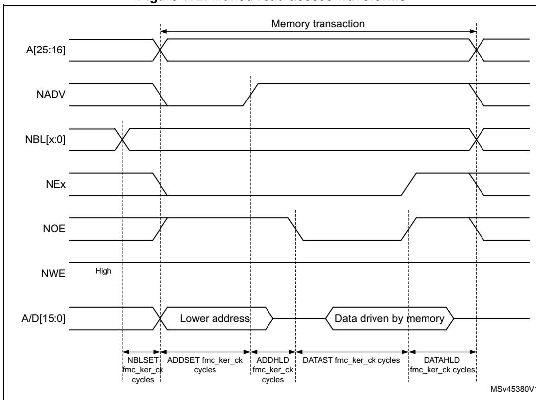
The diagram illustrates the timing for a muxed read access to NOR flash memory. It shows the relationship between address, data, and control signals over time, measured in fmc_ker_ck cycles.
Signals:
- A[25:16]: Address lines, stable during the memory transaction.
- NADV: Address Valid signal, goes low to indicate valid address and data.
- NBL[x:0]: Byte Lane signals, active-low.
- NEx: External memory signal, goes low to enable the memory.
- NOE: Output Enable signal, goes low to enable data output from the memory.
- NWE: Write Enable signal, held high during read access.
- A/D[15:0]: Multiplexed address/data lines. They carry the "Lower address" initially and then become "Data driven by memory".
Timing Parameters:
- NBLSET: Time from NBL[x:0] falling edge to the start of the address/data phase, in fmc_ker_ck cycles.
- ADDSET: Time from the start of the address/data phase to the start of the data phase, in fmc_ker_ck cycles.
- ADDHLD: Time from the start of the data phase to the end of the address/data phase, in fmc_ker_ck cycles.
- DATAST: Time from the start of the data phase to the end of the data phase, in fmc_ker_ck cycles.
- DATAHLD: Time from the end of the data phase to the end of the memory transaction, in fmc_ker_ck cycles.
The diagram also indicates the "Memory transaction" duration and the state of the A/D[15:0] lines as "Lower address" and "Data driven by memory". The identifier MSv45380V1 is shown in the bottom right corner.
Figure 173. Muxed write access waveforms
![Timing diagram for muxed write access waveforms showing signals A[25:16], NADV, NBL[x:0], NEx, NOE, NWE, and A/D[15:0] over time. The diagram illustrates the 'Memory transaction' period and the drive of 'Lower address' and 'Data driven by controller' on the A/D[15:0] bus. Timing parameters like NBLSET, ADDSET, ADDHLD, DATAST, and DATAHLD are indicated in fmc_ker_ck cycles.](/RM0486-STM32N6x5-x7/766e21426d9222eaddeb218061fad21d_img.jpg)
The figure shows the timing for a muxed write access. The signals shown are A[25:16], NADV, NBL[x:0], NEx, NOE, NWE, and A/D[15:0]. The A/D[15:0] bus is used for both address and data. The timing parameters are defined as follows:
- NBLSET : fmc_ker_ck cycles
- ADDSET : fmc_ker_ck cycles
- ADDHLD : fmc_ker_ck cycles
- DATAST : fmc_ker_ck cycles
- DATAHLD + 1 : fmc_ker_ck cycles
MSV45381V1
The difference with mode D is the drive of the lower address byte(s) on the data bus.
Table 178. FMC_BCRx bitfields (muxed mode)
| Bit No. | Bit name | Value to set |
|---|---|---|
| 31 | Reserved | 0x0 |
| 30-24 | Reserved | 0x00 |
| 23:22 | NBLSET[1:0] | As needed |
| 21:20 | CSCOUNT | As needed |
| 19 | CBURSTRW | 0x0 (no effect in asynchronous mode) |
| 18:16 | CPSIZE | 0x0 (no effect in asynchronous mode) |
| 15 | ASYNCWAIT | Set if the memory supports this feature. Otherwise keep cleared. The ASYNCWAIT feature is not supported in muxed mode. |
| 14 | EXTMOD | 0x0 |
| 13 | WAITEN | 0x0 (no effect in asynchronous mode) |
| 12 | WREN | As needed |
| 11 | WAITCFG | Don't care |
| 10 | Reserved | 0x0 |
| 9 | WAITPOL | Meaningful only if bit 15 is 1 |
| Bit No. | Bit name | Value to set |
|---|---|---|
| 8 | BURSTEN | 0x0 |
| 7 | Reserved | 0x1 |
| 6 | Reserved | 0x0 |
| 5-4 | MWID[1:0] | As needed |
| 3-2 | MTYP[1:0] | 0x2 (NOR flash memory) |
| 1 | MUXEN | 0x1 |
| 0 | MBKEN | 0x1 |
| Bit No. | Bit name | Value to set |
|---|---|---|
| 31:30 | DATAHLD | Duration of the Data hold phase (DATAHLD fmc_ker_ck cycles for read accesses, DATAHLD+1 fmc_ker_ck cycles for write accesses). |
| 29-28 | ACCMOD | 0x0 |
| 27-24 | DATLAT | Don't care |
| 23-20 | CLKDIV | Don't care |
| 19-16 | BUSTURN | Time between NEx high to NEx low (BUSTURN fmc_ker_ck) |
| 15-8 | DATAST | Duration of the second access phase (DATAST fmc_ker_ck cycles for read accesses and DATAST+1 fmc_ker_ck cycles for write accesses). |
| 7-4 | ADDHLD | Duration of the middle phase of the access (ADDHLD fmc_ker_ck cycles). |
| 3-0 | ADDSET | Duration of the first access phase (ADDSET fmc_ker_ck cycles). Minimum value for ADDSET is 1. |
WAIT management for asynchronous accesses
If the asynchronous memory asserts the WAIT signal to indicate that it is not yet ready to accept or to provide data, the ASYNCWAIT bit has to be set in FMC_BCRx register.
If the WAIT signal is active (high or low depending on the WAITPOL bit), the second access phase (Data setup phase), programmed by the DATAST bits, is extended until WAIT becomes inactive. Unlike the data setup phase, the first access phases (Address setup and Address hold phases), programmed by the ADDSET and ADDHLD bits, are not WAIT sensitive and so they are not prolonged.
The data setup phase must be programmed so that WAIT can be detected 4 fmc_ker_ck cycles before the end of the memory transaction. The following cases must be considered:
- 1. The memory asserts the WAIT signal aligned to NOE/NWE which toggles:
- 2. The memory asserts the WAIT signal aligned to NEx (or NOE/NWE not toggling):
if
then:
otherwise
where max_wait_assertion_time is the maximum time taken by the memory to assert the WAIT signal once NEx/NOE/NWE is low.
Figure 174 and Figure 175 show the number of fmc_ker_ck clock cycles that are added to the memory access phase after WAIT is released by the asynchronous memory (independently of the above cases).
Figure 174. Asynchronous wait during a read access waveforms
![Timing diagram for asynchronous wait during a read access. It shows signals A[25:0], NEx, NWAIT, NOE, and Data bus over time. The memory transaction is divided into an address phase and a data setup phase. NWAIT is shown as 'don't care' in both phases. Data is driven by memory during the data setup phase, with a setup time of 4 fmc_ker_ck.](/RM0486-STM32N6x5-x7/10ec4ad502af0e61defa0fcad0f3ed49_img.jpg)
The diagram illustrates the timing for an asynchronous wait during a read access. The signals shown are:
- A[25:0] : Address bus, stable during the address phase and data setup phase.
- NEx : Address Status signal, active low, goes low at the start of the address phase and high at the start of the data setup phase.
- NWAIT : Asynchronous wait signal, labeled as 'don't care' in both the address and data setup phases.
- NOE : Output Enable signal, active low, goes low at the start of the data setup phase and high at the end of the memory transaction.
- Data bus : Data is driven by memory during the data setup phase. The setup time is indicated as 4 fmc_ker_ck.
The memory transaction is divided into two phases: address phase and data setup phase . The address phase starts when NEx goes low and ends when NEx goes high. The data setup phase starts when NEx goes high and ends when NOE goes high. The data bus is driven by memory during the data setup phase, and the setup time is 4 fmc_ker_ck.
MSv40382V2
- 1. NWAIT polarity depends on WAITPOL bit setting in FMC_BCRx register.
Figure 175. Asynchronous wait during a write access waveforms
![Timing diagram for asynchronous wait during a write access. It shows signals A[25:0], NEx, NWAIT, NWE, and Data bus over time. The memory transaction is divided into an address phase and a data setup phase. NWAIT is shown as 'don't care' in both phases. Data is driven by FMC during the data setup phase, with a setup time of 3 fmc_ker_ck. NWE is shown going high 1 fmc_ker_ck after the data setup phase begins.](/RM0486-STM32N6x5-x7/52179e91740c104154f22856f25e588b_img.jpg)
The diagram illustrates the timing for an asynchronous wait during a write access. The signals shown are:
- A[25:0] : Address bus, stable during the address phase and data setup phase.
- NEx : Address Status signal, active low, goes low at the start of the address phase and high at the start of the data setup phase.
- NWAIT : Asynchronous wait signal, labeled as 'don't care' in both the address and data setup phases.
- NWE : Write Enable signal, active low, goes low at the start of the address phase and high at the start of the data setup phase. The setup time for NWE is 1 fmc_ker_ck.
- Data bus : Data is driven by FMC during the data setup phase. The setup time is indicated as 3 fmc_ker_ck.
The memory transaction is divided into two phases: address phase and data setup phase . The address phase starts when NEx goes low and ends when NEx goes high. The data setup phase starts when NEx goes high and ends when NWE goes high. The data bus is driven by FMC during the data setup phase, and the setup time is 3 fmc_ker_ck.
MSv40383V3
- 1. NWAIT polarity depends on WAITPOL bit setting in FMC_BCRx register.
CellularRAM™ (PSRAM) refresh management
The CellularRAM™ does not allow maintaining the chip select signal (NE) low for longer than the \( t_{CEM} \) timing specified in memory device. This timing can be programmed in the FMC_CFGR register. It defines the maximum duration of the NE low pulse (expressed in fmc_ker_ck cycles) in synchronous mode for PSRAM read or write accesses.
27.8.5 Synchronous transactions
The memory clock, FMC_CLK, is a submultiple of fmc_ker_ck. It depends on the value of CLKDIV.
NOR flash memories specify a minimum time from NADV assertion to FMC_CLK high. To meet this constraint, the FMC does not issue the clock to the memory during the first internal clock cycle of the synchronous access (before NADV assertion). This guarantees that the rising edge of the memory clock occurs in the middle of the NADV low pulse.
Data latency versus NOR memory latency
The data latency is the number of cycles to wait before sampling the data. The DATLAT value must be consistent with the latency value specified in the NOR flash configuration register. The FMC does not include the clock cycle when NADV is low in the data latency count.
Caution: Some NOR flash memories include the NADV Low cycle in the data latency count, so that the exact relation between the NOR flash latency and the FMC DATLAT parameter can be either:
- • NOR flash latency = (DATLAT + 2) CLK clock cycles
- • or NOR flash latency = (DATLAT + 3) CLK clock cycles
Some recent memories assert NWAIT during the latency phase. In such cases DATLAT can be set to its minimum value. As a result, the FMC samples the data and waits long enough to evaluate if the data are valid. Thus the FMC detects when the memory exits latency and real data are processed.
Other memories do not assert NWAIT during latency. In this case the latency must be set correctly for both the FMC and the memory, otherwise invalid data are mistaken for good data, or valid data are lost in the initial phase of the memory access.
Single-burst transfer
When the selected memory region is configured in burst mode for synchronous accesses, if for example a single-burst transaction is requested on 16-bit memories, the FMC performs a burst transaction of length 1 (if the AXI transfer is 16 bits), or length 2 (if the AXI transfer is 32 bits) and deassert the Chip Select signal when the last data is strobed.
Such transfers are not the most efficient in terms of cycles compared to asynchronous read operations. Nevertheless, a random asynchronous access first requires to re-program the memory access mode, which altogether lasts longer.
Cross boundary page for CellularRAM™ 1.5
CellularRAM™ 1.5 does not allow burst access to cross the page boundary. The FMC allows to split automatically the burst access when the memory page size is reached by configuring the CPSIZE bits in the FMC_BCR1 register following the memory page size.
Wait management
For synchronous NOR flash memories, NWAIT is evaluated after the programmed latency period, which corresponds to (DATLAT+2) FMC_CLK clock cycles.
If NWAIT is active (low level when WAITPOL = 0, high level when WAITPOL = 1), wait-states are inserted until NWAIT is inactive (high level when WAITPOL = 0, low level when WAITPOL = 1).
When NWAIT is inactive, the data is considered valid either immediately (bit WAITCFG = 1) or on the next clock edge (bit WAITCFG = 0).
During wait-state insertion via the NWAIT signal, the controller continues to send clock pulses to the memory, keeping the Chip Select and output enable signals valid. It does not consider the data as valid.
In burst mode, there are two timing configurations for the NOR flash NWAIT signal:
- • The flash memory asserts the NWAIT signal one data cycle before the wait-state (default after reset).
- • The flash memory asserts the NWAIT signal during the wait-state
The FMC supports both NOR flash wait-state configurations, for each Chip Select, thanks to the WAITCFG bit in the FMC_BCRx registers (x = 0 to 3).
Figure 176. Wait configuration waveforms
![Timing diagram showing FMC_CLK, A[25:16], NADV, NWAIT (WAITCFG = 0), NWAIT (WAITCFG = 1), and A/D[15:0] signals. The diagram illustrates the insertion of a wait state when NWAIT is active. The address is sent on A[25:16] and A/D[15:0]. Data is sent on A/D[15:0]. The NWAIT signal is active (low) during the wait state. The FMC_CLK signal is a periodic clock. The NADV signal is active (low) during the address phase. The A[25:16] signal is high-impedance (X) during the data phase. The A/D[15:0] signal is high-impedance (X) during the address phase. The NWAIT (WAITCFG = 0) signal is active (low) during the wait state. The NWAIT (WAITCFG = 1) signal is active (high) during the wait state. The inserted wait state is indicated by a double-headed arrow between the first and second data cycles. Data strobes are indicated by vertical arrows pointing to the data cycles.](/RM0486-STM32N6x5-x7/75a9d26a084d8a8f5695d96920844157_img.jpg)
The diagram shows the following signals and timing:
- FMC_CLK: A periodic clock signal.
- A[25:16]:
Address lines. It shows an address
addr[25:16]being sent, followed by high-impedance (X) states. - NADV: Address Valid signal, active low. It goes low during the address phase and returns high before the data phase.
- NWAIT (WAITCFG = 0): Wait signal, active low. It goes low before the second data cycle and returns high after the third data cycle.
- NWAIT (WAITCFG = 1): Wait signal, active high. It goes high during the second data cycle (the wait state) and returns low before the third data cycle.
- A/D[15:0]:
Address/Data lines. It shows an address
addr[15:0]being sent, followed by data cycles labeleddata. The first data cycle occurs while NWAIT (WAITCFG = 0) is low. The second data cycle is skipped because NWAIT (WAITCFG = 1) is high. The third data cycle occurs after NWAIT (WAITCFG = 1) goes low. - Data strobes: Vertical arrows pointing to the start of each valid data cycle.
- inserted wait state: A double-headed arrow between the first and third data cycles, indicating the skipped second cycle.
MSV40384V4
Figure 177. Synchronous multiplexed read mode waveforms - NOR, PSRAM (CRAM)
![Timing diagram showing waveforms for FMC_CLK, A[25:16], NEx, NOE, NWE, NADV, NWAIT, and A/D[15:0] signals during a synchronous multiplexed read operation. The diagram shows address phases, data phases with strobes, and an inserted wait state.](/RM0486-STM32N6x5-x7/a458ee0e471e1f3659df99e86b8daaea_img.jpg)
The timing diagram illustrates the signal transitions for a synchronous multiplexed read operation.
•
FMC_CLK
: A periodic clock signal.
•
A[25:16]
: Address lines, showing 'addr[25:16]' during the initial address phase.
•
NEx
: Address Status signal, active-low, goes low during the address phase and returns high at the start of the data phase.
•
NOE
: Output Enable signal, active-low, goes low to enable data output on the A/D[15:0] bus.
•
NWE
: Write Enable signal, active-low, held high throughout this read operation.
•
NADV
: Address Valid signal, active-low, goes low to indicate valid address and returns high when address is no longer valid.
•
NWAIT (WAITCFG=0)
: Wait signal, active-low, goes low to insert a wait state between data phases.
•
A/D[15:0]
: Multiplexed address/data bus. It starts with 'Addr[15:0]', followed by 'data' phases.
•
Data Strobes
: Pulses that indicate valid data on the bus during each 'data' phase.
•
Timing
: The interval between the start of the first data phase and the second is labeled '(DATLAT + 2) FMC_CLK'. The duration of the inserted wait state is also indicated. The initial address phase duration is marked as 'clock cycle'.
Table 180. FMC_BCRx bitfields (Synchronous multiplexed read mode)
| Bit No. | Bit name | Value to set |
|---|---|---|
| 31 | Reserved | 0x0 |
| 30-24 | Reserved | 0x00 |
| 23:22 | NBLSET[1:0] | As needed |
| 21:20 | CSCOUNT | As needed |
| 19 | CBURSTRW | As needed |
| 18:16 | CPSIZE | As needed. (0x1 when using CRAM 1.5) |
| 15 | ASYNCWAIT | 0x0 |
| 14 | EXTMOD | 0x0 |
| 13 | WAITEN | to be set if the memory supports this feature, to be kept cleared otherwise |
| 12 | WREN | no effect on synchronous read |
| 11 | WAITCFG | to be set according to memory |
| 10 | Reserved | 0x0 |
| 9 | WAITPOL | to be set according to memory |
| 8 | BURSTEN | 0x1 |
| 7 | Reserved | 0x1 |
| 6 | Reserved | 0x0 |
| Bit No. | Bit name | Value to set |
|---|---|---|
| 5-4 | MWID[1:0] | As needed |
| 3-2 | MTYP[1:0] | 0x1 or 0x2 |
| 1 | MUXEN | As needed |
| 0 | MBKEN | 0x1 |
| Bit No. | Bit name | Value to set |
|---|---|---|
| 31:30 | DATAHLD | Don't care |
| 29:28 | ACCMOD | 0x0 |
| 27-24 | DATLAT | Data latency |
| 27-24 | DATLAT | Data latency |
| 23-20 | CLKDIV | FMC_CLK divider ratio |
| 19-16 | BUSTURN | Time between NEx high to NEx low (BUSTURN fmc_ker_ck) |
| 15-8 | DATAST | Don't care |
| 7-4 | ADDHLD | Don't care |
| 3-0 | ADDSET | Don't care |
Figure 178. Synchronous multiplexed write mode waveforms - PSRAM (CRAM)
![Timing diagram for synchronous multiplexed write mode. It shows signals FMC_CLK, A[25:16] (addr[25:16]), NEx, Hi-Z, NOE, NWE, NADV, NWAIT (WAITCFG = 0), and A/D[15:0] (addr[15:0], data). The diagram illustrates the timing relationship between address, data, and control signals over several clock cycles. Key timing parameters shown include (DATLAT + 2) FMC_CLK cycles between address and data, and an 'inserted wait state' before the final data burst. Data strobes are indicated for each data burst.](/RM0486-STM32N6x5-x7/56eb872af4b63bd24305ab2599901752_img.jpg)
- 1. The memory must issue NWAIT signal one cycle in advance, accordingly WAITCFG must be programmed to 0.
Table 182. FMC_BCRx bitfields (Synchronous multiplexed write mode)
| Bit No. | Bit name | Value to set |
|---|---|---|
| 31 | Reserved | 0x0 |
| 30-24 | Reserved | 0x00 |
| 23:22 | NBLSET[1:0] | As needed |
| 21:20 | CSCOUNT | As needed |
| 19 | CBURSTRW | As needed |
| 18:16 | CPSIZE | As needed. (0x1 when using CRAM 1.5) |
| 15 | ASYNCWAIT | 0x0 |
| 14 | EXTMOD | 0x0 |
| 13 | WAITEN | to be set if the memory supports this feature, to be kept cleared otherwise. |
| 12 | WREN | 0x1 |
| 11 | WAITCFG | 0x0 |
| 10 | Reserved | 0x0 |
| 9 | WAITPOL | to be set according to memory |
| 8 | BURSTEN | 0x1 |
| 7 | Reserved | 0x1 |
Table 182. FMC_BCRx bitfields (Synchronous multiplexed write mode) (continued)
| Bit No. | Bit name | Value to set |
|---|---|---|
| 6 | Reserved | 0x0 |
| 5-4 | MWID[1:0] | As needed |
| 3-2 | MTYP[1:0] | 0x1 |
| 1 | MUXEN | As needed |
| 0 | MBKEN | 0x1 |
Table 183. FMC_BTRx bitfields (Synchronous multiplexed write mode)
| Bit No. | Bit name | Value to set |
|---|---|---|
| 31:30 | DATAHLD | Don't care |
| 29:28 | ACCMOD | 0x0 |
| 27-24 | DATLAT | Data latency |
| 23-20 | CLKDIV | FMC_CLK divider ratio |
| 19-16 | BUSTURN | Time between NEx high to NEx low (BUSTURN fmc_ker_ck) |
| 15-8 | DATAST | Don't care |
| 7-4 | ADDHLD | Don't care |
| 3-0 | ADDSET | Don't care |
27.8.6 NOR/PSRAM controller registers
The peripheral registers have to be accessed by words (32-bit)
SRAM/NOR flash chip-select control register for memory region x (FMC_BCRx)
Address offset: 0x00 + 0x08 * (x - 1), (x = 1 to 4)
Reset value: 0x0000 30DB, 0x0000 30D2, 0x0000 30D2, 0x0000 30D2
This register contains the control information of each memory region, used for SRAMs, PSRAM, FRAM and NOR flash memories.
| 31 | 30 | 29 | 28 | 27 | 26 | 25 | 24 | 23 | 22 | 21 | 20 | 19 | 18 | 17 | 16 |
|---|---|---|---|---|---|---|---|---|---|---|---|---|---|---|---|
| Res. | Res. | Res. | Res. | Res. | Res. | Res. | Res. | NBLSET[1:0] | CSCOUNT1 | CSCOUNT0 | CBURSTRW | CPSIZE[2:0] | |||
| rw | rw | rw | rw | rw | rw | rw | rw | ||||||||
| 15 | 14 | 13 | 12 | 11 | 10 | 9 | 8 | 7 | 6 | 5 | 4 | 3 | 2 | 1 | 0 |
| ASYNCWAIT | EXTMOD | WAITEN | WREN | WAITCFG | Res. | WAITPOL | BURSTEN | Res. | Res. | MWID[1:0] | MTYP[1:0] | MUXEN | MBKEN | ||
| rw | rw | rw | rw | rw | rw | rw | rw | rw | rw | rw | rw | rw |
Bit 31 Reserved, must be kept at reset value.
Bits 30:24 Reserved, must be kept at reset value.
Bits 23:22 NBLSET[1:0] : Byte lane (NBL) setup
These bits configure the NBL setup timing from NBLx low to Chip select NEx low.
00: NBL setup time is 0 fmc_ker_ck clock cycle.
01: NBL setup time is 1 fmc_ker_ck clock cycle.
10: NBL setup time is 2 fmc_ker_ck clock cycles.
11: NBL setup time is 3 fmc_ker_ck clock cycles.
Bits 21:20 CSCOUNT[1:0] : Chip Select (CS) counter
These bits define the maximum duration of Chip Select low for PSRAM synchronous mode and for each memory region.
The Chip Select counter is loaded into a timer which is decremented using the KCK_FMC while the NE is maintained low during PSRAM read or write access.
When the timer reaches 0, the PSRAM controller splits the current access and toggles NE to allow PSRAM device refresh.
The programmed counter value guarantees a maximum NE pulse width ( \( t_{CEM} \) ) as specified for PSRAM devices.
The counter is reloaded and starts decrementing each time a new access is triggered by a transition of NE from high to low.
0b00: Counter disabled
0b01: NEx deasserted after fmc_ker_ck clock cycle
0b10: NEx deasserted after 64 fmc_ker_ck clock cycles
0b11: NEx deasserted after 256 fmc_ker_ck clock cycles
Note: Most PSRAMs manage refresh transparently and do not require access split. CSCOUNT[1:0] must consequently be left at its default value (counter disabled), otherwise CSCOUNT[1:0] value and access split impact must be checked according to PSRAM timing parameters.
Bit 19 CBURSTRW : Write burst enable
For PSRAM (CRAM) operating in burst mode, the bit enables synchronous accesses during write operations. The enable bit for synchronous read accesses is the BURSTEN bit in the FMC_BCRx register.
0: Write operations are always performed in asynchronous mode
1: Write operations are performed in synchronous mode.
Bits 18:16 CPSIZE[2:0] : CRAM page size
These bits are used for CellularRAM™ 1.5 which does not allow burst accesses to cross the address boundaries between pages. When these bits are configured, the FMC automatically splits the burst access when the memory page size is reached (refer to memory datasheet for page size).
000: No burst split when crossing page boundary. (default after reset).
001: 128 bytes
010: 256 bytes
011: 512 bytes
100: 1024 bytes
Others: Reserved.
Bit 15 ASYNCWAIT : Wait signal during asynchronous transfers
This bit enables/disables wait signal usage by the FMC even during asynchronous transfers.
0: NWAIT signal not taken in to account during asynchronous transfers (default after reset)
1: NWAIT signal taken in to account during asynchronous transfers
Bit 14 EXTMOD: Extended mode enableThis bit enables write timing programming for asynchronous accesses inside the FMC_BWTR register, thus resulting in different timings for read and write operations.
0: Values inside FMC_BWTR register not taken into account (default after reset)
1: Values inside FMC_BWTR register taken into account
Note: When the extended mode is disabled, the FMC can operate in mode 1 or mode 2 as follows:
- – Mode 1 is the default mode when the SRAM/PSRAM memory type is selected (MTYP[1:0] = 0x0 or 0x01)
- – Mode 2 is the default mode when the NOR memory type is selected (MTYP[1:0] = 0x10).
This bit enables/disables wait-state insertion via the NWAIT signal when accessing the memory in synchronous mode.
0: NWAIT signal disabled (its level not taken into account, no wait-state inserted after the programmed flash latency period)
1: NWAIT signal enabled (its level is taken into account after the programmed latency period to insert wait-states if asserted) (default after reset)
Bit 12 WREN: Write enable bitThis bit indicates whether write operations to the memory region by the FMC are enabled/disabled:
0: Write operations to the memory region by the FMC disabled. An AXI slave error is reported,
1: Write operations to the memory region by the FMC enabled (default after reset).
Bit 11 WAITCFG: Wait timing configurationThe NWAIT signal indicates whether the data from the memory are valid or if a wait-state must be inserted when accessing the memory in synchronous mode. This configuration bit determines if NWAIT is asserted by the memory one clock cycle before the wait-state or during the wait-state:
0: NWAIT signal active one data cycle before wait-state (default after reset),
1: NWAIT signal active during wait-state (not used for PSRAM).
Bit 10 Reserved, must be kept at reset value. Bit 9 WAITPOL: Wait signal polarity bitThis bit defines the polarity of the wait signal from memory used for either in synchronous or asynchronous mode:
0: NWAIT active low (default after reset),
1: NWAIT active high.
Bit 8 BURSTEN: Burst enable bitThis bit enables/disables synchronous accesses during read operations. It is valid only for synchronous memories operating in burst mode:
0: Burst mode disabled (default after reset). Read accesses are performed in asynchronous mode.
1: Burst mode enable. Read accesses are performed in synchronous mode.
Bits 7:6 Reserved, must be kept at reset value.Bits 5:4 MWID[1:0] : Memory data bus width
This bit defines the external memory device width, valid for all type of memories.
- 00: 8 bits
- 01: 16 bits (default after reset)
- 10: 32 bits
- 11: Reserved.
Bits 3:2 MTYP[1:0] : Memory type
This bit defines the type of external memory attached to the corresponding memory region:
- 00: SRAM/ FRAM (default after reset for memory region 2...4)
- 01: PSRAM (CRAM)/FRAM
- 10: NOR flash/OneNAND flash (default after reset for memory region 1)
- 11: Reserved.
Bit 1 MUXEN : Address/data multiplexing enable bit
When this bit is set, the address and data values are multiplexed on the data bus, valid only with NOR and PSRAM memories:
- 0: Address/Data non-multiplexed
- 1: Address/Data multiplexed on databus (default after reset)
Bit 0 MBKEN : Memory region enable bit
This bit enables the memory region. After reset memory region 1 is enabled, all others are disabled. Accessing a disabled memory region causes an ERROR on AXI bus.
- 0: Corresponding memory region is disabled
- 1: Corresponding memory region is enabled
SRAM/NOR flash chip-select timing registers for memory region x (FMC_BTRx)
Address offset: 0x04 + 0x8 * (x - 1), (x = 1 to 4)
Reset value: 0x0FFF FFFF
This register contains the control information of each memory region, used for SRAMs, PSRAM and NOR flash memories. If the EXTMOD bit is set in the FMC_BCRx register, then this register is partitioned for write and read access, that is, two registers are available: one to configure read accesses (this register) and one to configure write accesses (FMC_BWTRx registers).
| 31 | 30 | 29 | 28 | 27 | 26 | 25 | 24 | 23 | 22 | 21 | 20 | 19 | 18 | 17 | 16 |
|---|---|---|---|---|---|---|---|---|---|---|---|---|---|---|---|
| DATAHLD[1:0] | ACCMOD[1:0] | DATLAT[3:0] | CLKDIV[3:0] | BUSTURN[3:0] | |||||||||||
| rw | rw | rw | rw | rw | rw | rw | rw | rw | rw | rw | rw | rw | rw | rw | rw |
| 15 | 14 | 13 | 12 | 11 | 10 | 9 | 8 | 7 | 6 | 5 | 4 | 3 | 2 | 1 | 0 |
| DATAST[7:0] | ADDHLD[3:0] | ADDSET[3:0] | |||||||||||||
| rw | rw | rw | rw | rw | rw | rw | rw | rw | rw | rw | rw | rw | rw | rw | rw |
These bits are written by software to define the duration of the data hold phase in fmc_ker_ck cycles (refer to Figure 174 to Figure 175 ), used in asynchronous accesses:
For read/write accesses:
00: DATAHLD phase duration = fmc_ker_ck clock cycle * 0 (default, read)/1 (default, write)
01: DATAHLD phase duration = fmc_ker_ck clock cycle * 1 (read)/2 (write)
10: DATAHLD phase duration = fmc_ker_ck clock cycle * 2 (read)/3 (write)
11: DATAHLD phase duration = fmc_ker_ck clock cycle * 3 (read)/4 (write)
Bits 29:28 ACCMOD[1:0]: Access modeThese bits specify the asynchronous access modes as shown in the timing diagrams. These bits are taken into account only when the EXTMOD bit in the FMC_BCRx register is 1.
00: Access mode A
01: Access mode B
10: Access mode C
11: Access mode D
Bits 27:24 DATLAT[3:0]: Data latency for synchronous memory (see note below bit descriptions)For synchronous access with read/write burst mode enabled (BURSTEN / CBURSTRW bits set), these bits define the number of memory clock cycles (+2) to issue to the memory before reading/writing the first data.
This timing parameter is not expressed in fmc_ker_ck periods, but in FMC_CLK periods.
For asynchronous access, this value is don't care.
0000: Data latency of 2 FMC_CLK clock cycles for first burst access
1111: Data latency of 17 FMC_CLK clock cycles for first burst access (default value after reset)
Bits 23:20 CLKDIV[3:0]: Clock divide ratio (for FMC_CLK signal)These bits define FMC_CLK clock output signal period, expressed in fmc_ker_ck cycles:
0000: FMC_CLK period= 1x fmc_ker_ck period
0001: FMC_CLK period = 2 × fmc_ker_ck periods
0010: FMC_CLK period = 3 × fmc_ker_ck periods
1111: FMC_CLK period = 16 × fmc_ker_ck periods (default value after reset)
This value is don't care when accessing NOR flash memories, SRAM and PSRAM in asynchronous mode.
Note: Refer to Section 27.8.5: Synchronous transactions for FMC_CLK divider ratio formula).
Note: CLKDIV[3:0] bits are don't care when CCLKEN bit of FMC_CFGR is set. In this case FMC_CLK clock output is controlled by CLKDIV of FMC_CFGR.
Bits 19:16 BUSTURN[3:0] : Bus turnaround phase durationThese bits are written by software to add a delay between the end of current read or write transaction and the next transaction on the same memory region.
This delay allows matching the minimum time between consecutive transactions ( \( t_{EHEL} \) from NEx high to NEx low) and the maximum time required by the memory to free the data bus after a read access ( \( t_{EHQZ} \) from chip enable high to output Hi-Z). This delay is recommended for mode D and muxed mode. For non-muxed memory, the bus turnaround delay can be set to a minimum value that respects the following condition:
For FRAMs, the bus turnaround delay must be configured to match the minimum precharge time ( \( t_{PC} \) ). This delay is inserted between all consecutive transactions on the same memory region (read/read, write/write, read/write and write/read) to match the \( t_{PC} \) memory timing, and the Chip select toggles between consecutive accesses.
0000: BUSTURN phase duration = 1 * fmc_ker_ck clock cycle added
...
1111: BUSTURN phase duration = 16 * fmc_ker_ck clock cycles added (default value after reset)
Bits 15:8 DATAST[7:0] : Data-phase duration
These bits are written by software to define the duration of the data phase (refer to Figure 174 to Figure 175 ) used in asynchronous accesses:
0000 0000: Reserved.
0000 0001: DATAST phase duration = 1 * fmc_ker_ck clock cycles
0000 0010: DATAST phase duration = 2 * fmc_ker_ck clock cycles
...
1111 1111: DATAST phase duration = 255 * fmc_ker_ck clock cycles (default value after reset)
For each memory type and access mode data-phase duration, refer to the respective figure ( Figure 174 to Figure 175 ).
Example of mode 1, write access, DATAST=1:
Data-phase duration= DATAST+1 = 2 *fmc_ker_ck clock cycles.
Note: This value is don't care in synchronous accesses.
Bits 7:4 ADDHLD[3:0] : Address-hold phase duration
These bits are written by software to define the duration of the address hold phase (refer to Figure 170 to Figure 173 ) used in mode D or multiplexed accesses:
0000: Reserved.
0001: ADDHLD phase duration = 1 * fmc_ker_ck clock cycle
0010: ADDHLD phase duration = 2 * fmc_ker_ck clock cycle
...
1111: ADDHLD phase duration = 15 * fmc_ker_ck clock cycles (default value after reset)
For each access mode address-hold phase duration, refer to the respective figure ( Figure 170 to Figure 173 ).
Note: This value is not used in synchronous accesses, and the address hold phase lasts always 1 memory clock period.
Bits 3:0 ADDSET[3:0] : Address setup phase duration
These bits are written by software to define the duration of the address setup phase (refer to Figure 174 to Figure 175 ), used in SRAMs, ROMs and asynchronous NOR flash memories:
0000: ADDSET phase duration = 0 * fmc_ker_ck clock cycle
...
1111: ADDSET phase duration = 15 * fmc_ker_ck clock cycles (default value after reset)
For each access mode address setup phase duration, refer to the respective figure (refer to Figure 174 to Figure 175 ).
Note: This value is don't care in synchronous accesses.
In muxed mode or mode D, the minimum value for ADDSET is 1.
Note: PSRAMs (CRAMs) have a variable latency due to internal refresh. Therefore these memories issue the NWAIT signal during the whole latency phase to extend the latency as needed.
On PSRAMs (CRAMs), DATLAT must be configured to 0 so that the FMC quickly exits its latency phase, starts sampling NWAIT from memory, and starts read or write operations when the memory is ready.
This method can be used also with the latest generation of synchronous flash memories, which, unlike older flash memories, issue the NWAIT signal (check the corresponding flash memory datasheet).
SRAM/NOR-flash write timing registers for memory region x (FMC_BWTRx) Address offset: \( 0x104 + 0x8 * (x - 1) \) , ( \( x = 1 \) to \( 4 \) )Reset value: 0x000F FFFF
This register contains the control information of each memory region. It is used for SRAMs, FRAMs, PSRAMs and NOR flash memories. When the EXTMOD bit is set in the FMC_BCRx register, then this register is active for write access.
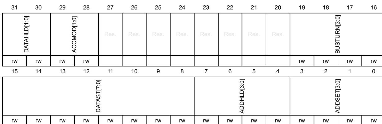
| 31 | 30 | 29 | 28 | 27 | 26 | 25 | 24 | 23 | 22 | 21 | 20 | 19 | 18 | 17 | 16 |
| DATAHLD[1:0] | ACCMOD[1:0] | Res. | Res. | Res. | Res. | Res. | Res. | Res. | Res. | BUSTURN[3:0] | |||||
| rw | rw | rw | rw | rw | rw | rw | rw | ||||||||
| 15 | 14 | 13 | 12 | 11 | 10 | 9 | 8 | 7 | 6 | 5 | 4 | 3 | 2 | 1 | 0 |
| DATAST[7:0] | ADDHLD[3:0] | ADDSET[3:0] | |||||||||||||
| rw | rw | rw | rw | rw | rw | rw | rw | rw | rw | rw | rw | rw | rw | rw | rw |
These bits are written by software to define the duration of the data hold phase in fmc_ker_ck cycles (refer to Figure 175 ), used in asynchronous write accesses:
- 00: DATAHLD phase duration = \( 1 * fmc\_ker\_ck \) clock cycle (default)
- 01: DATAHLD phase duration = \( 2 * fmc\_ker\_ck \) clock cycle
- 10: DATAHLD phase duration = \( 3 * fmc\_ker\_ck \) clock cycle
- 11: DATAHLD phase duration = \( 4 * fmc\_ker\_ck \) clock cycle
These bits specify the asynchronous access modes as shown in the next timing diagrams. These bits are taken into account only when the EXTMOD bit in the FMC_BCRx register is 1.
- 00: Access mode A
- 01: Access mode B
- 10: Access mode C
- 11: Access mode D
Bits 27:20 Reserved, must be kept at reset value.
Bits 19:16 BUSTURN[3:0]: Bus turnaround phase durationThese bits are written by software to add a delay between the end of current write transaction and the next transaction on the same memory region.
For FRAMs, the bus turnaround delay must be configured to match the minimum precharge time ( t PC ). The bus turnaround delay is inserted between all consecutive transactions on the same memory region (read/read, write/write, read/write and write/read), and the Chip select toggles between consecutive accesses.
\( (BUSTURN + 1) * fmc\_ker\_ck \text{ period} \geq t_{PCmin} \)
- 0000: BUSTURN phase duration = \( 1 * fmc\_ker\_ck \) clock cycle added
- ...
- 1111: BUSTURN phase duration = \( 16 * fmc\_ker\_ck \) clock cycles added (default value after reset)
Bits 15:8 DATAST[7:0] : Data-phase duration.
These bits are written by software to define the data phase duration (refer to
Figure 174
to
Figure 175
) used in asynchronous SRAM, PSRAM and NOR flash memory accesses:
0000 0000: Reserved.
0000 0001: DATAST phase duration = 1 * fmc_ker_ck clock cycles
0000 0010: DATAST phase duration = 2 * fmc_ker_ck clock cycles
...
1111 1111: DATAST phase duration = 255 * fmc_ker_ck clock cycles (default value after reset)
Bits 7:4 ADDHLD[3:0] : Address-hold phase duration.
These bits are written by software to define the duration of the address hold phase (refer to
Figure 172
to
Figure 173
) used in asynchronous multiplexed accesses:
0000: Reserved.
0001: ADDHLD phase duration = 1 * fmc_ker_ck clock cycle
0010: ADDHLD phase duration = 2 * fmc_ker_ck clock cycle
...
1111: ADDHLD phase duration = 15 * fmc_ker_ck clock cycles (default value after reset)
Note: In synchronous NOR flash accesses, this value is not used, and the address hold phase always lasts 1 flash clock period.
Bits 3:0 ADDSET[3:0] : Address setup phase duration.
These bits are written by software to define the duration of the address setup phase in fmc_ker_ck cycles (refer to
Figure 174
to
Figure 175
) used in asynchronous accesses:
0000: ADDSET phase duration = 0 * fmc_ker_ck clock cycle
...
1111: ADDSET phase duration = 15 * fmc_ker_ck clock cycles (default value after reset)
Note: In synchronous accesses, this value is not used, and the address setup phase always lasts 1 flash clock period. In muxed mode, the minimum ADDSET value is 1.
FMC common configuration register (FMC_CFGR)
Address offset: 0x020
Reset value: 0x0000 0000
This register is user to set configuration common to all controllers
| 31 | 30 | 29 | 28 | 27 | 26 | 25 | 24 | 23 | 22 | 21 | 20 | 19 | 18 | 17 | 16 |
|---|---|---|---|---|---|---|---|---|---|---|---|---|---|---|---|
| FMCEN | Res. | Res. | Res. | Res. | Res. | BMAP1 | BMAP0 | Res. | Res. | Res. | CCLKEN | CLKDIV[3:0] | |||
| rw | rw | rw | rw | rw | rw | rw | rw | ||||||||
| 15 | 14 | 13 | 12 | 11 | 10 | 9 | 8 | 7 | 6 | 5 | 4 | 3 | 2 | 1 | 0 |
| Res. | Res. | Res. | Res. | Res. | Res. | Res. | Res. | Res. | Res. | Res. | Res. | Res. | Res. | Res. | Res. |
Bit 31 FMCEN : FMC enable
This bit enables/disables the FMC.
0: FMC disabled
1: FMC enabled
Bits 30:26 Reserved, must be kept at reset value.
Bits 25:24 BMAP[1:0] : FMC memory region mapping
These bits allow the remapping of SDRAM device 2 or the swapping of FMC NOR/PSRAM and SDRAM memory regions.
00: Default mapping (refer to Table 148 )
01: Devices are remapped (refer to Table 149 )
10: Devices are remapped (refer to Table 149 )
11: All memory region accesses are ignored. A bus error is generated.
Bits 23:21 Reserved, must be kept at reset value.
Bit 20 CCLKEN : Continuous clock enable
This bit enables the FMC_CLK clock output to external memory devices.
0: The FMC_CLK is only generated during the synchronous memory access (read/write transaction). The FMC_CLK clock ratio is defined by the programmed CLKDIV value in the FMC_BCRx register (default after reset).
1: The FMC_CLK is generated continuously during asynchronous and synchronous access. If continuous clock mode is enabled, the synchronous memories connected to all memory regions are clocked by the same clock with the clock ratio defined by CLKDIV in FMC_CFGR. The CLKDIV value in FMC_BWTRx are don't care.
Bits 19:16 CLKDIV[3:0] : Clock divide ratio (for FMC_CLK signal)
These bits define the FMC_CLK clock output signal period, expressed in number of fmc_ker_ck cycles:
0000: FMC_CLK period= 1x fmc_ker_ck period
0001: FMC_CLK period = 2 × fmc_ker_ck periods
0010: FMC_CLK period = 3 × fmc_ker_ck periods
1111: FMC_CLK period = 16 × fmc_ker_ck periods (default value after reset)
This value is don't care when accessing NOR flash memories, SRAM and PSRAM in asynchronous mode.
Note: Refer to Section 27.8.5: Synchronous transactions for FMC_CLK divider ratio formula.
Bits 15:0 Reserved, must be kept at reset value.
27.9 NAND flash controller
The FMC generates the appropriate signal timings to drive 8- and 16-bit NAND flash memories
The NAND memory region is configured through dedicated registers ( Section 27.9.9 ). The programmable memory parameters include access timings (shown in Table 184 ) and ECC configuration.
The NAND controller supports the following features:
- • Programmable page size of 256, 512, 1024, 2048, 4096 or 8192 bytes
- • Programmable memory timings
- • Programmable Error Correction Capability using BCH code or Hamming code
- • Command sequencer: a hardware accelerator for read/write accesses within a page or within a block of configurable size.
This feature is useful when ECC computation is performed.
- • Programmable address offset for ECC bytes programming using the command sequencer
- • Interrupt generation on ECC error detection and page or sector transfer complete
Table 184. Programmable NAND flash access parameters
| Parameter | Function | Access mode | Unit | Min. | Max. |
|---|---|---|---|---|---|
| Memory setup time | Number of clock cycles (fmc_ker_ck) required to set up the address before the command assertion | Read/Write | FMC clock cycle (fmc_ker_ck) | 1 | 256 |
| Memory wait | Minimum duration (in fmc_ker_ck clock cycles) of the command assertion | Read/Write | FMC clock cycle (fmc_ker_ck) | 1 | 256 |
| Memory hold | Number of clock cycles (fmc_ker_ck) during which the address must be held (as well as the data if a write access is performed) after the command deassertion | Read/Write | FMC clock cycle (fmc_ker_ck) | 1 | 256 |
| Memory databus high-Z | Number of clock cycles (fmc_ker_ck) during which the data bus is kept in high-Z state after a write access has started | Write | FMC clock cycle (fmc_ker_ck) | 1 | 256 |
27.9.1 External memory interface signals
The following tables list the typical signals that are used to interface NAND flash memory.
Note: The “N” prefix identifies the signals which are active low.
8-bit NAND flash memory
Table 185. 8-bit NAND flash memory
| FMC signal name | I/O | Function |
|---|---|---|
| A[17] | O | NAND flash address latch enable (ALE) signal |
| A[16] | O | NAND flash command latch enable (CLE) signal |
| D[7:0] | I/O | 8-bit multiplexed, bidirectional address/data bus |
| NCE | O | Chip Select |
| NOE(= NRE) | O | Output enable (memory signal name: read enable, NRE) |
| FMC signal name | I/O | Function |
|---|---|---|
| NWE | O | Write enable |
| RNB | I | NAND flash Ready/Busy (RNB) input signal to the FMC |
Note: Theoretically, there is no capacity limitation as the FMC can manage as many address cycles as needed.
16-bit NAND flash memory
Table 186. 16-bit NAND flash memory| FMC signal name | I/O | Function |
|---|---|---|
| A[17] | O | NAND flash address latch enable (ALE) signal |
| A[16] | O | NAND flash command latch enable (CLE) signal |
| D[15:0] | I/O | 16-bit multiplexed, bidirectional address/data bus |
| NCE | O | Chip Select |
| NOE(= NRE) | O | Output enable (memory signal name: read enable, NRE) |
| NWE | O | Write enable |
| RNB | I | NAND flash Ready/Busy (RNB) input signal to the FMC |
Note: Theoretically, there is no capacity limitation as the FMC can manage as many address cycles as needed.
27.9.2 NAND flash supported memories and transactions
Table 187 shows the supported devices, access modes and transactions. Transactions not allowed (or not supported) by the NAND flash controller are shown in gray.
Table 187. Supported memories and transactions| Device | Mode | R/W | AXI data size | Memory data size | Allowed/ not allowed | Comments |
|---|---|---|---|---|---|---|
| NAND 8-bit | Asynchronous | R | 8 | 8 | Y | |
| Asynchronous | W | 8 | 8 | Y | ||
| Asynchronous | R | 16 | 8 | Y | Split into 2 FMC accesses | |
| Asynchronous | W | 16 | 8 | Y | Split into 2 FMC accesses | |
| Asynchronous | R | 32 | 8 | Y | Split into 4 FMC accesses | |
| Asynchronous | W | 32 | 8 | Y | Split into 4 FMC accesses | |
| Asynchronous | R | 64 | 8 | Y | Split into 8 FMC accesses | |
| Asynchronous | W | 64 | 8 | Y | Split into 8 FMC accesses |
Table 187. Supported memories and transactions (continued)
| Device | Mode | R/W | AXI data size | Memory data size | Allowed/not allowed | Comments |
|---|---|---|---|---|---|---|
| NAND 16-bit | Asynchronous | R | 8 | 16 | Y | |
| Asynchronous | W | 8 | 16 | N | ||
| Asynchronous | R | 16 | 16 | Y | ||
| Asynchronous | W | 16 | 16 | Y | ||
| Asynchronous | R | 32 | 16 | Y | Split into 2 FMC accesses | |
| Asynchronous | W | 32 | 16 | Y | Split into 2 FMC accesses | |
| Asynchronous | R | 64 | 16 | Y | Split into 4 FMC accesses | |
| Asynchronous | W | 64 | 16 | Y | Split into 4 FMC accesses |
27.9.3 Timing diagrams for NAND flash memory
The NAND flash memory region is managed through a set of registers:
- • Control register: FMC_PCR
- • Interrupt status register: FMC_SR
- • ECC register: FMC_HECCR
- • Timing register for Common memory space: FMC_PMEM
- • Timing register for Attribute memory space: FMC_PATT
Each timing configuration register contains three parameters used to define the number of fmc_ker_ck cycles for the different phases of any NAND flash access, plus one parameter that defines the timing to start driving the data bus when a write access is performed.
Figure 179 shows the timing parameter definitions for common memory accesses, knowing that Attribute memory space access timings are similar.
Figure 179. NAND flash controller waveforms for common memory access
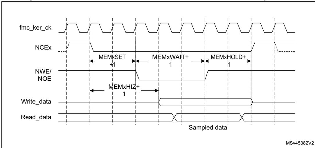
- 1. NOE remains high (inactive) during write accesses. NWE remains high (inactive) during read accesses.
- 2. If PWAITEN = 1, the programmed values of (MEMxSET + MEMxHOLD) must be > 1.
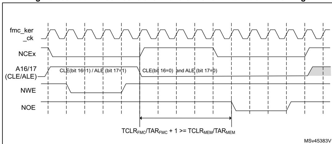
- 1. NOE remains high (inactive) during write accesses. NWE remains high (inactive) during read accesses.
27.9.4 NAND flash operations
The command latch enable (CLE) and address latch enable (ALE) signals of the NAND flash memory device are driven by address signals from the FMC. This means that to send a command or an address to the NAND flash memory, the CPU has to perform a write to a specific address in its memory space.
A typical page read operation from the NAND flash device requires the following steps:
- 1. Program and enable the NAND memory region by configuring the FMC_PCR and FMC_PMEM (and for some devices, FMC_PATT, see Section 27.9.5: NAND flash prewait function ) registers according to the characteristics of the NAND flash memory (PWID bits to configure NAND flash data bus width, PWAITEN set or cleared as needed, see Section 27.7.2: NAND flash memory address mapping for timing configuration).
- 2. The CPU performs a byte write to the common memory space, with a data byte value equal to one flash command byte (for example 0x00 for Samsung NAND flash devices). The NAND flash CLE input is active during the write strobe (low pulse on NWE), so that the written byte is interpreted as a command by the NAND flash memory. Once the command is latched by the memory device, it does not need to be written again for the following page read operations.
- 3. The CPU can send the start address for a read operation by writing a five-byte address to the common memory or the attribute space followed by the second read command. The NAND flash ALE input is active during the write strobe (low pulse on NWE), so that the written bytes are interpreted as the start address for read operations. Using the attribute memory space allows to use a different FMC timing configuration, which can
be used to implement the prewait function required for some NAND flash memories (see details in Section 27.9.5: NAND flash prewait function ).
- 4. The controller waits till the NAND flash memory is ready (RNB signal high), before starting a new access to the same memory region or to another memory region.
- 5. The CPU can then perform byte read operations from the common memory space to read the NAND flash page (data field + Spare field) byte by byte.
- 6. No CPU command or address write operation is required to read the next NAND flash page. This can be done in three different ways:
- – by simply performing the operation described in step 5,
- – a new random address can be accessed by restarting the operation at step 3,
- – a new command can be sent to the NAND flash device by restarting at step 2.
Note:
Non-‘CE don’t care’ NAND flash memories are not supported.
ONFI mode 4 and 5 EDO data output cycle timings are not supported.
27.9.5 NAND flash prewait function
The NAND controller must wait for RNB to be asserted low before sending its next command (see Figure 181 ). This timing constraint is set according to \( t_{WB} \) using MEMHOLD[7:0] bitfield in FMC_PMEM or ATTHOLD[7:0] in FMC_PATT.
Figure 181. Access to NAND flash memory
![Timing diagram for NAND flash memory access. The diagram shows the relationship between NCE, CLE, ALE, NWE, NOE, I/O[7:0], and RNB signals over time. The I/O[7:0] bus is used to send a command (CMD) and four addresses (ADD1, ADD2, ADD3, ADD4). The RNB signal is shown as a low-active signal that goes low after the last address is sent. The time interval between the falling edge of RNB and the next command/address sequence is labeled tWB. The time interval between the falling edge of RNB and the start of data output is labeled tR. The diagram also shows the NCE signal going high after the command/address sequence. The RNB signal is labeled (2) and the tWB interval is labeled (1).](/RM0486-STM32N6x5-x7/c3d8451f0be53d82be0625979f2a5ec8_img.jpg)
- 1. NCE can be deasserted for NAND flash memories since CE is don't care except for very old NAND flash devices that are not considered in this example.
- 2. RNB sampling can be delayed after \( t_{WB} \) by using ATTHOLD[7:0] bit of FMC_PATT. As an example, if \( fmc\_ker\_clk = 14 \) ns and ATTHOLD[7:0] = 7, the delay is \( 8 * 14 = 112 \) ns. The usual \( t_{WB} \) maximum value is 100 ns and the programmed delay must be higher than \( t_{WB} + 2 * fmc\_ker\_clk \) .
Any CPU read or write access to the NAND flash memory has a delay of \( (\text{MEMHOLD}[7:0] + 1) * \text{fmc\_ker\_ck} \) cycles after the NWE signal is asserted.
The ATTHOLD[7:0] bitfield in FMC_PATT register must be determined to satisfy \( t_{WB} \) timing constraints and selectively apply larger timing constraints to the last command or address byte in CPU mode. When setting ATTHOLD[7:0], the \( 2 * \text{fmc\_ker\_ck} \) delay required for the sampling of RNB by NAND sequencer must also taken into account.
27.9.6 NAND ECC controller
NAND flash memories include a spare memory area (or OOB) at the end of each page. This area is typically used to store some metadata (such as Bad Block Marker information to invalidate the whole page) or for error management functions.
The FMC supports on-the-fly error correction code (ECC) computation during data read/program from/to NAND flash memory. This mechanism reduces the host CPU workload when processing the ECC by software.
The user application can select one out of two algorithms:
- • Hamming code algorithm for 1-bit error code correction and 2-bit error detection per 256, 512, 1024, 2048, 4096 or 8192 bytes.
- • BCH (Bose, Chaudhuri and Hocquenghem) code for 4-bit error code correction and 8-bit error detection or 8-bit error code correction and 16-bit error detection per 512 bytes.
The principle of both ECC controllers is similar: the ECC modules monitor the NAND flash data bus and read/write signals (NCE and NWE) each time the NAND flash memory region is active. The ECC controllers operate as follows:
- • When accessing a NAND flash memory region, the data present on the D[7:0] or D[15:0] bus are latched and used for ECC computation.
- • When accessing any other address in NAND flash memory, the ECC logic is idle, and does not perform any operation. As a result, write operations to define commands or addresses to the NAND flash memory are not taken into account for ECC computation.
Once the desired number of bytes has been read/written from/to the NAND flash memory by the host CPU or DMA, the ECC result registers are updated.
Hamming code
The Hamming code implemented can perform 1-bit error correction and 2-bit error detection per 256, 512, 1024, 2048, 4096 or 8192 bytes read or written from/to the NAND flash memory. It consists in calculating the row and column parity. This algorithm is supported by 8-bit and 16-bit NAND flash memories.
Page write and read sequences with Hamming code are described below.
To perform a page program with Hamming ECC computation:
- 1. Enable the ECCEN bit in the FMC_PCR register.
- 2. Write data to the NAND flash memory page. While the NAND page is written, the ECC controller computes the ECC value.
- 3. Wait until the ECC code is ready (NWRF is set in the FMC_SR register).
- 4. Read the ECC value available in the FMC_HECCR register and store it in NAND flash spare area.
- 5. Clear the ECCEN bit and launch the page programming.
To perform a page read with Hamming ECC computation:
- 1. Enable the ECCEN bit in the FMC_PCR register before reading the NAND page. While the NAND page is read, the ECC block computes the ECC value.
- 2. Wait until the ECC code is ready (NWRF set in the FMC_SR register).
- 3. Read the ECC value available in the spare area as well also the ECC value, processed by Hamming controller, available in FMC_HECCR register.
- 4. If the two ECC values are identical, no correction is required. Otherwise an ECC error occurred, the software correction routine returns information on whether the error can be corrected or not, and corrects it when possible.
Depending on the spare area size, the page can be split into several sectors of identical size. This allows increasing the error correction capability for each page since 1 error can be corrected and 2 errors can be detected for each sector.
Example
For a NAND flash memory with 2 Kbytes + 64 bytes pages, each page can be split into 8 sectors of 256 bytes each. 3 bytes (22 bits) of ECC are required for each sector, which makes 24 bytes (8 * 3 bytes) to be stored in the spare area for the whole page. For the whole 2 Kbyte page, up to 8 errors can be corrected, respectively up to 16 errors detected, provided there is less than 1 error, respectively 2 errors, per sector.
BCH (Bose, Chaudhuri and Hocquenghem) code
To increase the error correction capability, the FMC embeds a BCH (Bose, Chaudhuri and Hocquenghem) encoder and decoder.
It supports 4-bit error code correction and 8-bit error detection or 8-bit error code correction, and 16-bit error detection per sector. BCH encoder/decoder module handles sectors of fixed size, equal to 512 bytes. Each page must consequently be split into 512-byte sectors. The number of parity bytes generated for each sector is given in Table 188 . For 16-bit NAND flash memories, a padding is added to align parity bytes to an even number (8 bytes and 14 bytes for 4-bit and 8-bit BCH code, respectively).
Table 188. Number of ECC parity bytes per sector
| Function | BCH code | |
|---|---|---|
| 4-bit | 8-bit | |
| Error correction | ||
| Number of parity bytes | 7 bytes | 13 bytes |
The BCH module detects errors and returns the bit position for each sector. To correct the errors, the software needs to flip the error bits at the provided bit position stored in the FMC_BCHPBRx register.
The BCH ECC controller supports 8-bit and 16-bit NAND flash memories.
During a page program operation, the BCH encoder generates the ECC bytes (7 or 13 bytes) for each sector of 512 bytes that must be written in the NAND flash spare area with a programmable offset. It must take into account some metadata at the beginning of the spare area. This operation must be executed for each sector. The BCH encoder does not process the spare area: metadata must have their own error protection mechanism.
The total number of ECC bytes (N) is given by the below equation:
Example
For an 8-bit NAND flash with 4096-byte pages and an error correction capability of 4-bit per 512 bytes, the number of sector per page is 8 (4096 / 512). The total number of ECC bytes is consequently:
The user application has to make sure that the spare area is large enough to store the metadata and parity bytes.
Page program and read sequences with BCH code are described below.
To perform a page program:
- 1. Enable write access by setting the WEN bit in the FMC_PCR register.
- 2. Enable the ECC by setting the ECCEN bit in FMC_PCR register.
- 3. Write 512 data bytes to the sector in the NAND flash memory page. While the sector is written, the BCH encoder computes the ECC value.
- 4. Wait until the BCH encoder parity bits are available by monitoring EPBRF bit of FMC_BCHISR register.
- 5. Read the ECC value available in the FMC_BCHPBRx registers and store it in the NAND flash spare area.
- 6. Disable ECC by resetting the ECCEN bit in FMC_PCR register.
- 7. Execute again step 2 to 6 for all sectors to be written in NAND flash memory.
- 8. Launch the page programming.
To perform a page read:
- 1. Enable read access by resetting the WEN bit in the FMC_PCR register.
- 2. Enable the ECC by setting the ECCEN bit in FMC_PCR register.
- 3. Read the NAND page sector (512 bytes).
- 4. Read the corresponding ECC bytes (7 or 13 bytes) from the NAND flash spare area.
- 5. During the read of data and parity bits, the syndrome is calculated. Then the error location search is launched.
- 6. Wait until the decoding error is ready (DERF bit set in the FMC_BCHISR register), then read the decoding results (errors detected if any, correctable or not, number of errors, bit position) in FMC_BCHDSR0 and FMC_BCHDSRx registers.
- 7. Thanks to the decoding results, the software can correct the errors in the sector (when possible).
- 8. Disable ECC by resetting the ECCEN bit in FMC_PCR register.
- 9. Execute again step 2 to 7 for all relevant sectors of the page.
27.9.7 FMC command sequencer
NAND flash page programming and reading can be performed by the CPU as described in the above sections.
Data sector programming/reading as well as ECC byte programming/reading can also be managed automatically by the FMC command sequencer for command and address transfers, and by DMA for data transfers.
The purpose of the command sequencer is to ease the programming/reading of NAND flash pages with ECC computation as well as free the CPU of sequencing tasks. The command sequencer enables the software to work on full NAND flash pages instead of sectors, which is more efficient and essential to achieve high throughput. The sequencer handles all the sectors in the page. It does not support sub-page read or program operations.
One DMA channel is required for write operations and two DMA channels for read operations.
A specific NAND flash page layout must be respected when using the BCH algorithm. See Figure 182 for an example of 2Kbyte page BCH layout.
Figure 182. NAND flash page (2 Kbytes) layout with BCH
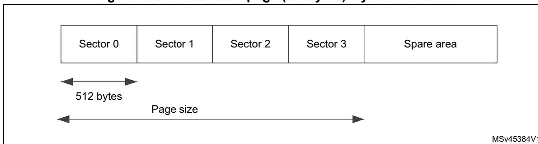
The diagram illustrates the layout of a 2 Kbyte NAND flash page. It is divided into four sectors (Sector 0, Sector 1, Sector 2, Sector 3) and a Spare area. Each sector is 512 bytes wide. The total page size is 2 Kbytes (2048 bytes). The diagram shows the sectors and the spare area, with arrows indicating the 512-byte width of a sector and the total page size. The label 'MSV45384V1' is present in the bottom right corner of the diagram.
Page program sequence
- 1. A data buffer located in SRAM has to be initialized with the data to be written to the NAND flash page.
- 2. The CPU configures the FMC command sequencer registers: page program command (0x80), address bytes, change write column command (0x85), ECC address offset, page size, sector size and sector number.
It also selects the ECC algorithm (Hamming or BCH) and configures one DMA channel to transfer data from the buffer to the NAND flash page. - 3. The CPU then launches the sequencer by setting the CSQSTART bit in the FMC_CSQCR register.
- 4. The command sequencer automatically generates the control and address cycles to the NAND flash memory, following the programmed timings configured either in FMC_PMEM or FMC_PATT register.
- 5. A DMA request is issued to start data transfer from the data buffer to NAND flash memory.
- 6. When the full sector is programmed, go to step 7 if ECC is enabled. Otherwise, jump to step 9.
- 7. The FMC command sequencer automatically issues a change write column command (0x85) followed by two address cycles. The command to be issued and the number of
address cycles are programmed in FMC_CSQCFGR2 register. The address is automatically generated from the programmed ECC address offset.
- 8. Once the parity bytes are available in ECC encoder (Hamming or BCH) module, they are automatically transferred to the NAND flash spare area. The FMC command sequencer can generate a sector transfer complete interrupt if it has been previously enabled.
- 9. The sequencer then repeats step 4 (except that it performs only a change write column command instead of a page program command) to step 8 to program the following sectors and their corresponding ECC parity bytes. The ECC address offset is automatically incremented for each sector transfer. When ECC is disabled, the sequencer repeats step 5.
- 10. The FMC command sequencer can generate a transfer complete interrupt or a transfer complete error interrupt by sector or when all sectors are written.
- 11. The CPU can program any further metadata in the NAND flash area, taking care not to overwrite parity bytes.
- 12. The program command (0x10) can then be written to the command section to program the NAND flash memory.
- 13. An interrupt, if enabled, is generated on the rising edge of the Ready/Busy (RNB) signal to indicate that the page program operation is complete.
Refer to Figure 183 for an overview of the page program sequence with BCH.
Figure 183. Example of 2 Kbyte page program sequence with 4-bit BCH
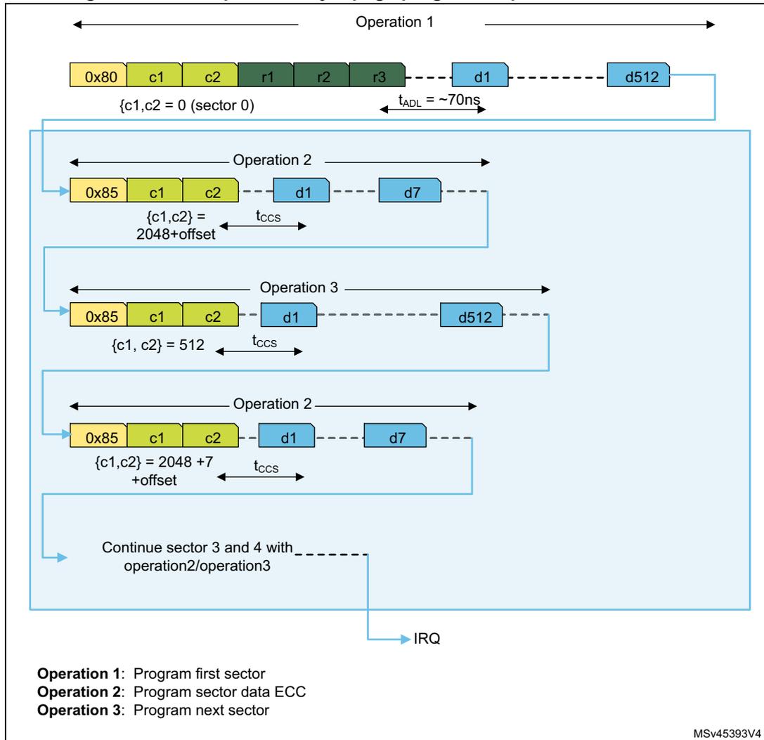
Operation 1
0x80 c1 c2 r1 r2 r3 --- d1 --- d512
{c1,c2} = 0 (sector 0)
\( t_{ADL} = \sim 70\text{ns} \)
Operation 2
0x85 c1 c2 --- d1 --- d7
{c1,c2} = 2048+offset
\( t_{CCS} \)
Operation 3
0x85 c1 c2 --- d1 --- d512
{c1,c2} = 512
\( t_{CCS} \)
Operation 2
0x85 c1 c2 --- d1 --- d7
{c1,c2} = 2048 + 7 + offset
\( t_{CCS} \)
Continue sector 3 and 4 with operation2/operation3
IRQ
Operation 1: Program first sector
Operation 2: Program sector data ECC
Operation 3: Program next sector
MSV45393V4
Page read sequence
- 1. A data buffer is allocated in SRAM to store the NAND flash page data. A decoding status buffer is also allocated to store result of ECC decoding.
- 2. The CPU programs the command sequencer registers: the page read first cycle command (0x00), address bytes, the page read second cycle command (0x30), change read column command (0x05), spare area offset, page size, sector size and sector number.
It configures the ECC algorithm if required (Hamming or BCH), one DMA channel to handle data transfers from the NAND flash page to the data buffer, and a second DMA
channel to transfer ECC decoding results from ECC status registers to the RAM decoding status buffer.
- 3. The CPU then launches the FMC sequencer by setting the CSQSTART bit in the FMC_CSQCR register.
- 4. The FMC command sequencer issues the command and address cycles to the NAND flash memory.
- 5. The command sequencer waits for a Ready/Busy (RNB) rising edge to start data transfer.
- 6. It sends a DMA request to launch the data transfer from the NAND flash page to the data buffer.
- 7. When all sector data are read, go to step 8 if ECC is enabled, otherwise go to step 9. The FMC command sequencer can generate a sector transfer complete interrupt if it has been previously enabled.
- 8. When ECC status registers are empty (because the Hamming error code or the BCH error position bits of previous sector have already been read), the ECC command sequencer automatically issues a change read column command (0xE0) followed by two address cycles and by the 0xE0 command, to read ECC bytes from NAND flash memory and store them in ECC registers. These commands as well as the number of address cycles are programmed in the FMC_CSQCFGR2 register (see
Figure 184
).
The address in spare area is extracted from the programmed ECC address offset.
When the Hamming algorithm is used, a DMA request to the second DMA channel is sent to transfer ECC codes (FMC_HPR and FMC_HECCR registers) to the decoding status buffer.
When BCH algorithm is used, once all the parity bytes have been read, the BCH decoder first processes the syndrome to detect errors and then searches for error positions if any.
As the BCH decoder is pipelined, it is possible to start reading a sector even if the decoding of the previous sector is not complete.
In parallel of the following steps, when BCH sector decoding is complete, the new error status is stored in the ECC status registers (FMC_BCHDSR0) and a DMA request to the second DMA channel is sent to transfer data from the status registers to the decoding status buffer located in RAM.
- 9. The FMC command sequencer then repeats step 4 (except that a change read column command is issued instead of the page read first cycle command) to step 8 to read the other sectors and their corresponding ECC bytes. The addresses are issued and incremented following the page size, number of sectors, spare area address offset address and BCH code selection. When the read sequence is complete, the command sequencer waits for \( t_{RHWL} \) before issuing a new command sequence (refer to Figure 183 ). When ECC is disabled, the sequencer repeats step 6.
- 10. Once all sectors within a page and the status registers (FMC_BCHDSRx) are transferred by the command sequencer, the ECC controller can generate the transfer complete interrupt or transfer complete error (when enabled).
- 11. By reading the decoding status buffer, the CPU can start processing the errors corresponding to each sector. If no error has been detected, the page stored in RAM is validated. Otherwise the CPU corrects the error(s) before validating the page buffer in RAM. If there are too many errors, the CPU can detect the page cannot be corrected and invalidate the data buffer.
Following the selected BCH code, if the number of detected errors exceeds the number of correctable errors, this bit is not significant and the DUE bit is set. If the number of errors the detected by the BCH decoder exceeds the maximum number of detectable errors, DEN and DUE bits are not significant.
The DMA channels can also send interrupts each time a data transfer is complete. This allows the CPU to process error(s) in a sector as soon as it is available.
Note: When using the sequencer and DMA channels, the CPU must not read the FMC_BCHPBRx and FMC_BCHDSRx registers before data of all sectors are transferred, that is when TCF flag is set in the FMC_CSQISR register.
Figure 184. Chained-page read command timings
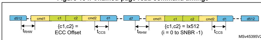
An example of 2 Kbyte page read sequence with BCH is described in Figure 185 . This example corresponds to four 512-byte sectors and 7 ECC bytes per data 512 bytes.
Figure 185. Example of 2-Kbyte page read sequence with 4-bit BCH
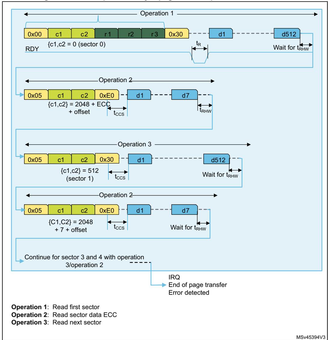
Operation 1
Command/Address: 0x00, c1, c2, r1, r2, r3, 0x30
{c1,c2} = 0 (sector 0)
RDY signal:
\(
t_R
\)
Data: d1 ... d512
Wait for
\(
t_{RHW}
\)
Operation 2
Command/Address: 0x05, c1, c2, 0xE0
{c1,c2} = 2048 + ECC + offset
Timing:
\(
t_{CCS}
\)
Data: d1 ... d7
\(
t_{RHW}
\)
Operation 3
Command/Address: 0x05, c1, c2, 0x30
{c1,c2} = 512 (sector 1)
Timing:
\(
t_{CCS}
\)
Data: d1 ... d512
Wait for
\(
t_{RHW}
\)
Operation 2
Command/Address: 0x05, c1, c2, 0xE0
{c1,c2} = 2048 + 7 + offset
Timing:
\(
t_{CCS}
\)
Data: d1 ... d7
Wait for
\(
t_{RHW}
\)
Continue for sector 3 and 4 with operation 3/operation 2
IRQ
End of page transfer
Error detected
Operation 1:
Read first sector
Operation 2:
Read sector data ECC
Operation 3:
Read next sector
MSV45394V3
The BCH controller resets the ECC computation whenever a page read (0x00), a page program (0x80), a random read (0x05) or a random program command ((0x85) is issued.
When only part of a page is written/read using the BCH, the command sequencer issues a random read/write command sequence only for the number of sectors to be read/written. This is done by programming the number of sector to be processed.
FMC command sequencer configuration- 1. Configure the FMC_CSQCFGR1 register: program the command1 and the command 2 (in case of read access), the number of address cycles to be issued, configure the read or write sequence, and select the timings to be used.
- 2. Configure the address bytes in FMC_CSQAR1 and FMC_CSQAR2 register.
- 3. In the FMC_CSQCFGR2 register, configure the change write or change read column commands and the timings to be used for ECC. Program the address offset for the random columns in the FMC_CSQAR2 register. Enable the DMA if it is needed for ECC status register transfer.
- 4. Configure the number of sectors and the address cycle timings in the FMC_CSQCFGR3 register.
- 5. Configure the ECC sector size, and select read or write access in the FMC_PCR register.
- 6. Enable the SQSDTEN bit in the FMC_CSQFCGR2 register. The ECCEN bit in the FMC_PCR register kept at 0.
- 7. Transfer complete, and transfer error complete or sector transfer complete can be enabled through the FMC_CSQIER register.
27.9.8 NAND flash controller interrupt
An interrupt can be generated on the following events:
- • RNB rising edge: an interrupt is generated when a rising edge is detected on RNB NAND flash signal
- • RNB falling edge: an interrupt is generated when a falling edge is detected on RNB NAND flash signal
- • RNB high-level: an interrupt is generated when a high-level is detected on RNB NAND flash signal.
- • Transfer complete: an interrupt is generated when the FMC command sequencer has completed all data transfers for all sectors or when the command sequencer was aborted.
- • Sector complete interrupt: an interrupt is generated when the FMC command sequencer has completed all data transfers for one sector.
- • Sector error interrupt: an interrupt is generated when the FMC command sequencer has completed a sector transfer with at least one error detected.
- • Sector uncorrectable error interrupt: an interrupt is generated when the FMC command sequencer has completed a sector transfer and detected an uncorrectable error.
- • Command transfer complete: the command sequencer has completed the transfer of programmed commands and addresses.
- • BCH encoder parity bits ready: an interrupt is generated when the BCH encoder has finished processing parity bits.
- • BCH decoder syndrome ready: an interrupt is generated when the BCH decoder has finished processing the syndrome and knows if errors have been detected or not.
- • BCH decoder error found: an interrupt is generated when the BCH decoder has detected an error.
- • BCH decoder error ready: an interrupt is generated when the BCH decoder has finished processing errors, has identified error locations and can then correct them.
- • BCH decoder uncorrectable error: an interrupt is generated when the BCH decoder has detected that the errors cannot be corrected (more than four or eight errors according to BCH error correction capability configuration).
The interrupt source can be enabled or disabled separately through the FMC_IER, FMC_CSQIER and FMC_BCHIER registers.
Table 189. FMC NAND controller interrupt request
| Interrupt event | Event Flag | Enable control bit |
|---|---|---|
| Transfer complete | TCF in FMC_CSQISR | TCIE in FMC_CSQIER |
| Sector complete | SCF in FMC_CSQISR | SCIE in FMC_CSQIER |
| Sector error | SEF in FMC_CSQISR | SEIE in FMC_CSQIER |
| Sector uncorrectable error | SUEF in FMC_CSQISR | SUEIE in FMC_CSQIER |
| Command transfer complete | CMDTCF in FMC_CSQISR | CMDTCIE in FMC_CSQIER |
| BCH encoder parity bits ready | EPBRF in FMC_BCHISR | EPBRIE in FMC_BCHIER |
| BCH decoder syndrome ready | DSRF in FMC_BCHISR | DSRIE in FMC_BCHIER |
| BCH decoder error found | DEFF in FMC_BCHISR | DEFIE in FMC_BCHIER |
Table 189. FMC NAND controller Interrupt request (continued)
| Interrupt event | Event Flag | Enable control bit |
|---|---|---|
| BCH decoder error ready | DERF in FMC_BCHISR | DERIE in FMC_BCHIER |
| BCH decoder uncorrectable error | DUEF in FMC_BCHISR | DUEIE in FMC_BCHIER |
27.9.9 NAND flash controller registers
NAND flash programmable control register (FMC_PCR)
Address offset: 0x80
Reset value: 0x0007 FE08
| 31 | 30 | 29 | 28 | 27 | 26 | 25 | 24 | 23 | 22 | 21 | 20 | 19 | 18 | 17 | 16 |
|---|---|---|---|---|---|---|---|---|---|---|---|---|---|---|---|
| Res. | Res. | Res. | Res. | Res. | Res. | WEN | BCHECC | Res. | Res. | Res. | Res. | ECCSS[2:0] | TAR [3] | ||
| rw | rw | rw | rw | rw | rw | ||||||||||
| 15 | 14 | 13 | 12 | 11 | 10 | 9 | 8 | 7 | 6 | 5 | 4 | 3 | 2 | 1 | 0 |
|---|---|---|---|---|---|---|---|---|---|---|---|---|---|---|---|
| TAR[2:0] | TCLR[3:0] | ECCALG | Res. | ECCEN | PWID[1:0] | Res. | PBKEN | PWAITEN | |||||||
| rw | rw | rw | rw | rw | rw | rw | rw | rw | rw | rw | rw | rw | Res. | ||
Bits 31:26 Reserved, must be kept at reset value.
Bit 25 WEN : Write enable
This bit enables read or write access. It must be configured when using the FMC sequencer or when the ECC with BCH code is enabled. It can only be modified when ECCEN bit is reset.
0: Read access enabled
1: Write access enabled
Bit 24 BCHECC : BCH error correction capability
0: 4-bit BCH (4-bit error correction and 8-bit error detection per 512 bytes)
1: 8-bit BCH (8-bit error correction and 16-bit error detection per 512 bytes)
Bits 23:20 Reserved, must be kept at reset value.
Bits 19:17 ECCSS[2:0] : ECC sector size (used to access spare area)
These bits define the sector size used for the ECC:
000: 256 bytes
001: 512 bytes
010: 1024 bytes
011: 2048 bytes (default)
100: 4096 bytes
101: Reserved.
11X: Reserved.
When the ECC is enabled with BCH code, the sector size must be programmed to 512 bytes.
Bits 16:13 TAR[3:0] : ALE to RE delay.
These bits define the time from ALE low to RE low in number of fmc_ker_ck clock cycles:
where \( t_{fmc\_ker\_ck} \) is the FMC clock period and \( t\_ar \) is the ALE to RE timing of NAND flash memories.
0000: 1 * fmc_ker_ck cycle
1111: 16 * fmc_ker_ck cycles (default)
Bits 12:9 TCLR[3:0] : CLE to RE delay.
These bits define the time from CLE low to RE low in number of fmc_ker_ck clock cycles:
where \( t_{fmc\_ker\_ck} \) is the FMC clock period and \( t\_clr \) is the CLE to RE timing of NAND flash memories.
0000: 1 * fmc_ker_ck cycle
1111: 16 * fmc_ker_ck cycles (default)
Bit 8 ECCALG : ECC algorithm
0: Hamming code is selected (default).
1: BCH code is selected.
Bit 7 Reserved, must be kept at reset value.
Bit 6 ECCEN : ECC computation logic enable bit
0: ECC logic is disabled and reset (default after reset),
1: ECC logic is enabled.
This bit must be kept reset when using the FMC sequencer
Bits 5:4 PWID[1:0] : Data bus width
These bits define the external memory device width.
00: 8 bits (default after reset).
01: 16 bits
1X: Reserved.
Bit 3 Reserved, must be kept at reset value.
Bit 2 PBKEN : NAND flash memory region enable bit
This bit enables the memory region. Accessing a disabled memory region causes an AXI bus error.
0: Corresponding memory region is disabled (default after reset)
1: Corresponding memory region is enabled.
Note: The NAND flash memory region must be disabled only when all NAND flash controller commands are complete.
Bit 1 PWAITEN : Wait feature enable bit
This bit enables the Wait feature for the NAND flash memory region:
0: disabled (default)
1: enabled
Bit 0 Reserved, must be kept at reset value.
FMC status register (FMC_SR)
Address offset: 0x84
Reset value: 0x0000 0053
This register contains information about the AXI interface isolation status and the NAND write requests status. The FMC has to be disabled before modifying some registers. As requests might be pending, it is necessary to wait till the AXI interface is stable and the core of the block is totally isolated from its AXI interface before reconfiguring the registers.
The PEF and NWEF bits indicate the status of the pipe. If Hamming algorithm is used, the ECC is calculated while data are written to the memory. To read the correct ECC, the software must consequently wait until no write request to the NAND controller are pending, by polling PEF and NWRF bits.
| 31 | 30 | 29 | 28 | 27 | 26 | 25 | 24 | 23 | 22 | 21 | 20 | 19 | 18 | 17 | 16 |
|---|---|---|---|---|---|---|---|---|---|---|---|---|---|---|---|
| Res. | Res. | Res. | Res. | Res. | Res. | Res. | Res. | Res. | Res. | Res. | Res. | Res. | Res. | Res. | Res. |
| 15 | 14 | 13 | 12 | 11 | 10 | 9 | 8 | 7 | 6 | 5 | 4 | 3 | 2 | 1 | 0 |
| Res. | Res. | Res. | Res. | Res. | Res. | Res. | Res. | Res. | NWRF | Res. | PEF | Res. | Res. | ISOST[1:0] | |
| r | r | r | r | ||||||||||||
Bits 31:7 Reserved, must be kept at reset value.
Bit 6 NWRF : NAND write request flag
This bit provides the status of the write request issued to the NAND flash memory. When this bit is set, all write requests to the NAND controller are served.
0: NAND flash write requests are pending
1: No NAND flash write requests pending
Bit 5 Reserved, must be kept at reset value.
Bit 4 PEF : Pipe Empty Flag
This bit indicates if the pipe contains requests.
Bits 3:2 Reserved, must be kept at reset value.
Bits 1:0 ISOST[1:0] : FMC isolation state with respect to the AXI interface
00: FMC is not isolated; AXI transactions are treated by the FMC and its controllers.
01: FMC has been enabled (FMCEN = 1) and waits for the end of pending AXI transactions (which leads to error responses) before going to “non-isolated” state.
10: FMC has been disabled (FMCEN = 0) and waits for the end of pending AXI transactions before going to isolation state.
11: FMC is isolated from its AXI interface. All AXI requests lead to error responses.
FMC common memory space timing register (FMC_PMEM)
Address offset: 0x88
Reset value: 0x0A0A 0A0A
The FMC_PMEM read/write register contains NAND flash memory region timing information. This information is used to access the NAND flash common memory space for command, address write accesses or data read/write accesses.
| 31 | 30 | 29 | 28 | 27 | 26 | 25 | 24 | 23 | 22 | 21 | 20 | 19 | 18 | 17 | 16 |
|---|---|---|---|---|---|---|---|---|---|---|---|---|---|---|---|
| MEMHIZ[7:0] | MEMHOLD[7:0] | ||||||||||||||
| rw | rw | rw | rw | rw | rw | rw | rw | rw | rw | rw | rw | rw | rw | rw | rw |
| 15 | 14 | 13 | 12 | 11 | 10 | 9 | 8 | 7 | 6 | 5 | 4 | 3 | 2 | 1 | 0 |
| MEMWAIT[7:0] | MEMSET[7:0] | ||||||||||||||
| rw | rw | rw | rw | rw | rw | rw | rw | rw | rw | rw | rw | rw | rw | rw | rw |
Bits 31:24 MEMHIZ[7:0] : Common memory data bus Hi-Z time
These bits define the number of fmc_ker_ck clock cycles (+1) during which the data bus is kept Hi-Z after starting a NAND flash write access to the common memory space. This is only valid for write transactions:
0000 0000: 1 * fmc_ker_ck cycle
0000 0001: 2 * fmc_ker_ck cycles
.....
1111 1111: 256 * fmc_ker_ck cycles
Bits 23:16 MEMHOLD[7:0] : Common memory hold time
These bits define the number of fmc_ker_ck clock cycles (+1) during which the address is held (and data for write accesses) after the command is deasserted (NWE, NOE), during NAND flash read or write accesses to the common memory space:
0000 0000: 1 * fmc_ker_ck cycle
0000 0001: 2 * fmc_ker_ck cycles
.....
1111 1111: 256 * fmc_ker_ck cycles
Bits 15:8 MEMWAIT[7:0] : Common memory wait time
These bits define the minimum number of fmc_ker_ck clock cycles (+1) to assert the command (NWE, NOE), during NAND flash read or write accesses to the common memory space. The duration of command assertion is extended if the wait signal (NWAIT) is active (low) at the end of the programmed value of fmc_ker_ck:
0000 0000: 1 * fmc_ker_ck cycles (+ wait cycle introduced by deasserting NWAIT)
0000 0001: 2 * fmc_ker_ck cycles (+ wait cycle introduced by deasserting NWAIT)
.....
1111 1111: 256 * fmc_ker_ck cycles (+ wait cycle introduced by deasserting NWAIT)
Bits 7:0 MEMSET[7:0] : Common memory setup time
These bits define the number of fmc_ker_ck clock cycles (+1) to set up the address before the command assertion (NWE, NOE), during NAND flash read or write accesses to the common memory space:
0000 0000: 1 * fmc_ker_ck cycles
0000 0001: 2 * fmc_ker_ck cycles
.....
1111 1111: 256 * fmc_ker_ck cycles
FMC attribute memory space timing registers (FMC_PATT)
Address offset: 0x8C
Reset value: 0x0A0A 0A0A
The FMC_PATT read/write register contains NAND flash memory region timing information. It is used for 8-bit accesses to the NAND flash attribute memory space during the last address write access when the timing differs from previous accesses (for Ready/Busy management, refer to Section 27.9.5: NAND flash prewait function ).
| 31 | 30 | 29 | 28 | 27 | 26 | 25 | 24 | 23 | 22 | 21 | 20 | 19 | 18 | 17 | 16 |
|---|---|---|---|---|---|---|---|---|---|---|---|---|---|---|---|
| ATTHIZ[7:0] | ATTHOLD[7:0] | ||||||||||||||
| rw | rw | rw | rw | rw | rw | rw | rw | rw | rw | rw | rw | rw | rw | rw | rw |
| 15 | 14 | 13 | 12 | 11 | 10 | 9 | 8 | 7 | 6 | 5 | 4 | 3 | 2 | 1 | 0 |
| ATTWAIT[7:0] | ATTSET[7:0] | ||||||||||||||
| rw | rw | rw | rw | rw | rw | rw | rw | rw | rw | rw | rw | rw | rw | rw | rw |
Bits 31:24 ATTHIZ[7:0]: Attribute memory data bus Hi-Z time
These bits define the number of fmc_ker_ck clock cycles (+1) during which the data bus is kept in Hi-Z after starting a NAND flash write access to the attribute memory space. These bits are only valid for write transactions:
0000 0000: 1 * fmc_ker_ck cycle
0000 0001: 2 * fmc_ker_ck cycle
.....
1111 1111: 256 * fmc_ker_ck cycles
Bits 23:16 ATTHOLD[7:0]: Attribute memory hold time
These bits define the number of fmc_ker_ck clock cycles (+1) during which the address is held (and data for write access) after the command deassertion (NWE, NOE), during NAND flash read or write accesses to the attribute memory space:
0000 0000: 1 * fmc_ker_ck cycle
0000 0001: 2 * fmc_ker_ck cycle
.....
1111 1111: 256 * fmc_ker_ck cycles.
Bits 15:8 ATTWAIT[7:0]: Attribute memory wait time
These bits define the minimum number of x fmc_ker_ck (+1) clock cycles to assert the command (NWE, NOE), during NAND flash read or write accesses to the attribute memory space. The duration of command assertion is extended if the wait signal (NWAIT) is active (low) at the end of the programmed value of fmc_ker_ck:
0000 0000: 1 * fmc_ker_ck cycle (+ wait cycle introduced by deassertion of NWAIT)
0000 0001: 2 * fmc_ker_ck cycles (+ wait cycle introduced by deassertion of NWAIT)
.....
1111 1111: 256 * fmc_ker_ck cycles (+ wait cycle introduced by deasserting NWAIT)
Bits 7:0 ATTSET[7:0]: Attribute memory setup time
These bits define the number of fmc_ker_ck clock cycles (+1) for address set up before the command assertion (NWE, NOE), during NAND flash read or write accesses to the attribute memory space:
0000 0000: 1 * fmc_ker_ck cycle
0000 0001: 2 * fmc_ker_ck cycle
.....
1111 1111: 256 * fmc_ker_ck cycles.
FMC Hamming parity result registers (FMC_HPR)
Address offset: 0x90
Reset value: 0x0000 0000
This register is used during read accesses in conjunction with the FMC sequencer. It contains the current error correction code value computed by the FMC NAND controller Hamming module. When the FMC sequencer reads data from a NAND flash memory page at the correct address, the data read are automatically processed by the Hamming computation module. When X bytes have been read (according to the sector size ECCSS field in the FMC_PCR register), the CPU must read the computed ECC value from the FMC_HECCR register. It then verifies if these computed parity data are the same as the parity value recorded in the spare area and stored in the and the FMC_HPR, to determine whether a page is valid, and to correct it otherwise. The FMC_HPR register must be cleared after being read by setting the ECCEN bit to 0. To compute a new data block, the ECCEN bit must be set.
| 31 | 30 | 29 | 28 | 27 | 26 | 25 | 24 | 23 | 22 | 21 | 20 | 19 | 18 | 17 | 16 |
| HPR[31:16] | |||||||||||||||
| r | r | r | r | r | r | r | r | r | r | r | r | r | r | r | r |
| 15 | 14 | 13 | 12 | 11 | 10 | 9 | 8 | 7 | 6 | 5 | 4 | 3 | 2 | 1 | 0 |
| HPR[15:0] | |||||||||||||||
| r | r | r | r | r | r | r | r | r | r | r | r | r | r | r | r |
Bits 31:0 HPR[31:0] : Hamming parity result
This field contains the parity value computed by the Hamming ECC computation module.
Table 190 describes the contents of these bitfields.
Table 190. HPR relevant bits
| ECCSS[2:0] | Sector size in bytes | HPR bits |
|---|---|---|
| 000 | 256 | HPR[21:0] |
| 001 | 512 | HPR[23:0] |
| 010 | 1024 | HPR[25:0] |
| 011 | 2048 | HPR[27:0] |
| 100 | 4096 | HPR[29:0] |
| 101 | 8192 | HPR[31:0] |
FMC Hamming code ECC result register (FMC_HECCR)
Address offset: 0x94
Reset value: 0x0000 0000
This register contain the current error correction code value computed by the FMC NAND controller Hamming module. When the CPU reads/writes data from/to a NAND flash memory page at the correct address (refer to Section 27.9.6: NAND ECC controller ), the data read/written from/to the NAND flash memory are automatically processed by the Hamming computation module. When X bytes have been read (according to the sector size ECCSS
field in the FMC_PCR register), the CPU must read the computed ECC value from the FMC_HECCR register. It then verifies if these computed parity data are the same as the parity value recorded in the spare area, to determine whether a page is valid, and to correct it otherwise. The FMC_HECCR register must be cleared after being read by setting the ECCEN bit to 0. To compute a new data block, the ECCEN bit must be set.
| 31 | 30 | 29 | 28 | 27 | 26 | 25 | 24 | 23 | 22 | 21 | 20 | 19 | 18 | 17 | 16 |
| HECC[31:16] | |||||||||||||||
| r | r | r | r | r | r | r | r | r | r | r | r | r | r | r | r |
| 15 | 14 | 13 | 12 | 11 | 10 | 9 | 8 | 7 | 6 | 5 | 4 | 3 | 2 | 1 | 0 |
| HECC[15:0] | |||||||||||||||
| r | r | r | r | r | r | r | r | r | r | r | r | r | r | r | r |
Bits 31:0 HECC[31:0] : ECC result
This field contains the value computed by the Hamming ECC computation logic. Table 191 describes the contents of these bitfields.
Table 191. ECC result relevant bits (1)
| ECCSS[2:0] | Sector size in bytes | HECC bits |
|---|---|---|
| 000 | 256 | HECC[21:0] |
| 001 | 512 | HECC[23:0] |
| 010 | 1024 | HECC[25:0] |
| 011 | 2048 | HECC[27:0] |
| 100 | 4096 | HECC[29:0] |
| 101 | 8192 | HECC[31:0] |
1. Only the relevant bits according to the sector size are valid.
FMC NAND interrupt enable register (FMC_IER)
Address offset: 0x180
Reset value: 0x0000 0000
This register configures the interrupt capability generation when the RNB signal is connected on FMC interrupt pin. An interrupt can be generated on the rising edge, falling edge or high level detected on the RNB signal.
| 31 | 30 | 29 | 28 | 27 | 26 | 25 | 24 | 23 | 22 | 21 | 20 | 19 | 18 | 17 | 16 |
| Res. | Res. | Res. | Res. | Res. | Res. | Res. | Res. | Res. | Res. | Res. | Res. | Res. | Res. | Res. | Res. |
| 15 | 14 | 13 | 12 | 11 | 10 | 9 | 8 | 7 | 6 | 5 | 4 | 3 | 2 | 1 | 0 |
| Res. | Res. | Res. | Res. | Res. | Res. | Res. | Res. | Res. | Res. | Res. | Res. | Res. | IFEE | IHLE | IREE |
| rw | rw | rw |
Bits 31:3 Reserved, must be kept at reset value.
Bit 2 IFEE : Interrupt falling edge detection enable bit
0: Interrupt falling edge detection request disabled
1: Interrupt falling edge detection request enabled
Bit 1 IHLE : Interrupt high-level detection enable bit
0: Interrupt high-level detection request disabled
1: Interrupt high-level detection request enabled
Bit 0 IREE : Interrupt rising edge detection enable bit
0: Interrupt rising edge detection request disabled
1: Interrupt rising edge detection request enabled
FMC interrupt status register (FMC_ISR)
Address offset: 0x184
Reset value: 0x0000 0000
| 31 | 30 | 29 | 28 | 27 | 26 | 25 | 24 | 23 | 22 | 21 | 20 | 19 | 18 | 17 | 16 |
|---|---|---|---|---|---|---|---|---|---|---|---|---|---|---|---|
| Res. | Res. | Res. | Res. | Res. | Res. | Res. | Res. | Res. | Res. | Res. | Res. | Res. | Res. | Res. | Res. |
| 15 | 14 | 13 | 12 | 11 | 10 | 9 | 8 | 7 | 6 | 5 | 4 | 3 | 2 | 1 | 0 |
| Res. | Res. | Res. | Res. | Res. | Res. | Res. | Res. | Res. | Res. | Res. | Res. | Res. | IFEF | IHLF | IREF |
| r | r | r |
Bits 31:3 Reserved, must be kept at reset value.
Bit 2 IFEF : Interrupt falling edge flag
The flag is set by hardware and cleared by setting the CFEIF bit.
0: No interrupt falling edge occurred
1: Interrupt falling edge occurred
Bit 1 IHLF : Interrupt high-level flag
The flag is set by hardware and cleared by setting the CHLIF bit.
0: No interrupt high-level occurred
1: Interrupt high-level occurred
Bit 0 IREF : Interrupt rising edge flag
The flag is set by hardware and cleared by setting the CREIF bit.
0: No interrupt rising edge occurred
1: Interrupt rising edge occurred
FMC NAND controller interrupt clear register (FMC_ICR)
Address offset: 0x188
Reset value: 0x0000 0000
Writing 1 in one of these bits clears the corresponding flag in the interrupt status register (FMC_ISR).
| 31 | 30 | 29 | 28 | 27 | 26 | 25 | 24 | 23 | 22 | 21 | 20 | 19 | 18 | 17 | 16 |
|---|---|---|---|---|---|---|---|---|---|---|---|---|---|---|---|
| Res. | Res. | Res. | Res. | Res. | Res. | Res. | Res. | Res. | Res. | Res. | Res. | Res. | Res. | Res. | Res. |
| 15 | 14 | 13 | 12 | 11 | 10 | 9 | 8 | 7 | 6 | 5 | 4 | 3 | 2 | 1 | 0 |
| Res. | Res. | Res. | Res. | Res. | Res. | Res. | Res. | Res. | Res. | Res. | Res. | Res. | CIFEF | CIHLF | CIREF |
| w | w | w |
Bits 31:3 Reserved, must be kept at reset value.
Bit 2 CIFEF : Clear Interrupt falling edge flag
0: No effect
1: Clears the IFEF flag in the FMC_ISR register
Bit 1 CIHLF : Clear Interrupt high-level flag
0: No effect
1: Clears the IHLF flag in the FMC_ISR register
Bit 0 CIREF : Clear Interrupt rising edge flag
0: No effect
1: Clear the IREF flag in the FMC_ISR register
FMC NAND command sequencer control register (FMC_CSQCR)
Address offset: 0x200
Reset value: 0x0000 0000
| 31 | 30 | 29 | 28 | 27 | 26 | 25 | 24 | 23 | 22 | 21 | 20 | 19 | 18 | 17 | 16 |
|---|---|---|---|---|---|---|---|---|---|---|---|---|---|---|---|
| Res. | Res. | Res. | Res. | Res. | Res. | Res. | Res. | Res. | Res. | Res. | Res. | Res. | Res. | Res. | Res. |
| 15 | 14 | 13 | 12 | 11 | 10 | 9 | 8 | 7 | 6 | 5 | 4 | 3 | 2 | 1 | 0 |
| Res. | Res. | Res. | Res. | Res. | Res. | Res. | Res. | Res. | Res. | Res. | Res. | Res. | Res. | Res. | CSQSTART |
| w |
Bits 31:1 Reserved, must be kept at reset value.
Bit 0 CSQSTART : Command Sequencer Enable
Writing 1 starts the Command sequencer.
Writing 0 has no effect.
Note: Write this bit to 1 to start the sequencer only when the FMC is enabled by setting FMCCEN bit of FMC_CFGGR to 1 and the NAND flash controller is activated by setting PBKEN bit of FMC_PCR to 1.
FMC NAND command sequencer configuration register 1 (FMC_CSQCFGR1)Address offset: 0x204
Reset value: 0x0000 0000
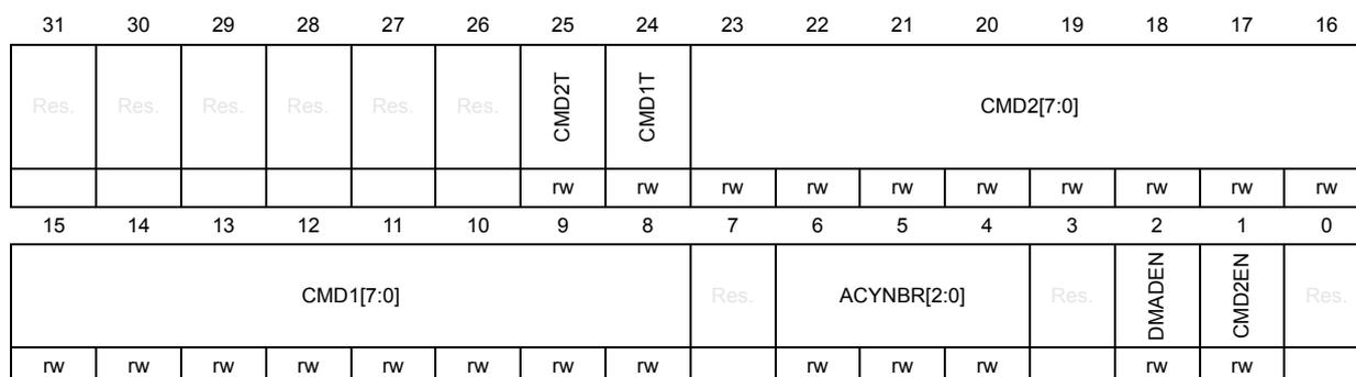
| 31 | 30 | 29 | 28 | 27 | 26 | 25 | 24 | 23 | 22 | 21 | 20 | 19 | 18 | 17 | 16 |
| Res. | Res. | Res. | Res. | Res. | Res. | CMD2T | CMD1T | CMD2[7:0] | |||||||
| rw | rw | rw | rw | rw | rw | rw | rw | rw | rw | ||||||
| 15 | 14 | 13 | 12 | 11 | 10 | 9 | 8 | 7 | 6 | 5 | 4 | 3 | 2 | 1 | 0 |
| CMD1[7:0] | Res. | ACYNBR[2:0] | Res. | DMADEN | CMD2EN | Res. | |||||||||
| rw | rw | rw | rw | rw | rw | rw | rw | rw | rw | rw | rw | rw | |||
Bits 31:26 Reserved, must be kept at reset value.
Bit 25 CMD2T : Command 2 Sequencer timings
This bit specifies if the Command 2 (CMD2) is issued to the NAND flash memory with the timings defined in FMC_PMEM or FMC_PATT register.
0: CMD2 issued with the timings programmed in FMC_PMEM
1: CMD2 issued with the timings programmed in FMC_PATT
Bit 24 CMD1T : Command 1 Sequencer timings
This bit specifies if the Command 1 (CMD1) is issued to the NAND flash memory with the timings programmed in FMC_PMEM or FMC_PATT register.
0: CMD1 issued with the timings programmed in FMC_PMEM
1: CMD1 issued with the timings programmed in FMC_PATT
Bits 23:16 CMD2[7:0] : Command 2 sequencer
These bits specify if the Command 2 is issued by the command sequencer for the command second cycle during read operations. This command is only issued when the CMD2EN bit is set.
Example: CMD2[7:0] bits must be programmed to 0x30 to issue the read column command.
Bits 15:8 CMD1[7:0] : Command 1 sequencer
These bits specify if the Command 1 is issued by the command sequencer for the first cycle during read or write operations.
Bit 7 Reserved, must be kept at reset value.
Bits 6:4 ACYNBR[2:0] : Address Cycle number
These bits define the number of address cycles to be generated by the command sequencer when issuing the command programmed in the registers.
000: No address cycle.
001: 1 address cycle
010: 2 address cycles
011: 3 address cycles
100: 4 address cycles
101: 5 address cycles
Others: Reserved.
Bit 3 Reserved, must be kept at reset value.
Bit 2 DMADEN : Command sequencer DMA request data enable
When this bit is set, the command sequencer generates a DMA request to the first DMA channel, to transfer data from/to NAND flash memory.
0: No DMA request transfer
1: A DMA request transfer
Bit 1 CMD2EN : Command cycle 2 Enable
This bit specifies that the command cycle 2 has to be generated by the command sequencer.
0: Command cycle 2 not issued.
1: Command cycle 2 (programmed CMD2[7:0]) sent by the command sequencer to the NAND flash memory after the address cycles.
Bit 0 Reserved, must be kept at reset value.
FMC NAND command sequencer configuration register 2 (FMC_CSQCFGR2)
Address offset: 0x208
Reset value: 0x0000 0000
This register is used to configure the command sequencer to issue random read/ write commands to read/ write data by sector and automatically read/write data from NAND flash memory at a programmable address offset. This is useful when performing a sector read/write operation followed by an ECC read/write operation in the NAND flash spare area. The command sequencer generates the random commands until all the sectors are read/written.
| 31 | 30 | 29 | 28 | 27 | 26 | 25 | 24 | 23 | 22 | 21 | 20 | 19 | 18 | 17 | 16 |
|---|---|---|---|---|---|---|---|---|---|---|---|---|---|---|---|
| Res. | Res. | Res. | Res. | Res. | Res. | RCMD2T | RCMD1T | RCMD2[7:0] | |||||||
| rw | rw | rw | rw | rw | rw | rw | rw | rw | rw | ||||||
| 15 | 14 | 13 | 12 | 11 | 10 | 9 | 8 | 7 | 6 | 5 | 4 | 3 | 2 | 1 | 0 |
| RCMD1[7:0] | Res. | Res. | Res. | Res. | Res. | DMASEN | RCMD2EN | SQSDTEN | |||||||
| rw | rw | rw | rw | rw | rw | rw | rw | rw | rw | rw | |||||
Bits 31:26 Reserved, must be kept at reset value.
Bit 25 RCMD2T : Command 1 sequencer timings
This bit specifies if the CMD1 is issued to the NAND flash memory with the timings programmed in FMC_PMEM or FMC_PATT register.
0: CMD1 issued with the timings programmed in FMC_PMEM
1: CMD1 issued with the timings programmed in FMC_PATT
Bit 24 RCMD1T : Command 1 sequencer timings
This bit specifies if the CMD1 is issued to the NAND flash memory with the timings flash memory in FMC_PMEM or FMC_PATT register.
0: CMD1 issued with the timings programmed in FMC_PMEM
1: CMD1 issued with the timings programmed in FMC_PATT
Bits 23:16 RCMD2[7:0] : Random Command 2 sequencer
These bits specify that the command 2 is issued by the command sequencer for the second cycle during read operations. This command is only issued when the RCMD2EN bit is set.
Example: the RCMD2 (0xE0) is required to issue the random read column command.
Bits 15:8 RCMD1[7:0] : Random Command 1 sequencer
These bits specify that the command 1 value is issued by the command sequencer for the first cycle during read or write accesses.
Bits 7:3 Reserved, must be kept at reset value.
Bit 2 DMASEN : Command sequencer DMA request decoding status enable
When this bit is set, the command sequencer generates a DMA request to the second DMA channel when valid bits are available in the ECC status register at the end of ECC processing (decoding).
0: No DMA request used for ECC status registers transfer
1: A DMA request used for ECC status registers transfer
Note: This bit must be set only during a page read sequence to offload the saving of the ECC results between sectors by using a second DMA channel.
Bit 1 RCMD2EN : Random Command 2 sequencer enable
This bit enables the command 2 to be issued by the command sequencer during read accesses. This command is issued only when the CMD2SQEN bit is set.
0: Command 2 not issued.
1: Command 2 (CMD2SQ[7:0]) issued by the command sequencer to NAND flash memory after the address cycle.
Bit 0 SQSDTEN : Sequencer spare data transfer enable
This bit enables the sequencer to access the spare data area after each sector transfer. It also enables the ECC when using the sequencer. ECCEN bit in FMC_PCR register must be reset.
0: ECC disabled and spare data area not accessed by the sequencer
1: ECC enabled and spare data area read or programmed by the sequencer after each sector transfer
FMC NAND sequencer configuration register 3 (FMC_CSQCFGR3)
Address offset: 0x20C
Reset value: 0x0000 0000
| 31 | 30 | 29 | 28 | 27 | 26 | 25 | 24 | 23 | 22 | 21 | 20 | 19 | 18 | 17 | 16 |
|---|---|---|---|---|---|---|---|---|---|---|---|---|---|---|---|
| Res. | Res. | Res. | Res. | Res. | Res. | Res. | Res. | RAC2T | RAC1T | SDT | AC5T | AC4T | AC3T | AC2T | AC1T |
| rw | rw | rw | rw | rw | rw | rw | rw | ||||||||
| 15 | 14 | 13 | 12 | 11 | 10 | 9 | 8 | 7 | 6 | 5 | 4 | 3 | 2 | 1 | 0 |
| Res. | Res. | SNBR[5:0] | Res. | Res. | Res. | Res. | Res. | Res. | Res. | Res. | |||||
| rw | rw | rw | rw | rw | rw | ||||||||||
Bits 31:24 Reserved, must be kept at reset value.
Bit 23 RAC2T : Random Address cycle 2 sequencer timings
This bit specifies if the random Address cycle 2 (ADDC2) is issued to the NAND flash memory with the timings programmed in FMC_PMEM or in FMC_PATT register.
0: Random ADDC2 issued with the timings programmed in FMC_PMEM
1: Random ADDC2 issued with the timings programmed in FMC_PATT
Bit 22 RAC1T : Random Address cycle 1 sequencer timings
This bit specifies if the random Address cycle 1 (ADDC1) is issued to the NAND flash memory with the timings programmed in FMC_PMEM or in FMC_PATT register.
0: Random ADDC1 issued with the timings programmed in FMC_PMEM
1: Random ADDC1 issued with the timings programmed in FMC_PATT
Bit 21 SDT : Spare data transfer sequencer timings
This bit specifies if the spare data transfer for read and write operations from/to the NAND flash memory are performed with the timings programmed in FMC_PMEM or FMC_PATT register.
0: Spare data transfer issued with the timings programmed in FMC_PMEM
1: Spare data transfer issued with the timings programmed in FMC_PATT
Bit 20 AC5T : Address cycle 5 sequencer timings
This bit defines if the Address cycle 5(ADDC1) is issued to the NAND flash memory with the timings programmed in FMC_PMEM or FMC_PATT register.
0: ADDC5 issued with the timings programmed in FMC_PMEM
1: ADDC5 issued with the timings programmed in FMC_PATT
Bit 19 AC4T : Address cycle 4sequencer timings
This bit defines if the Address cycle 4 (ADDC4) is issued to the NAND flash memory with the timings programmed in FMC_PMEM or FMC_PATT register.
0: ADDC4 issued with the timings programmed in FMC_PMEM
1: ADDC4 issued with the timings programmed in FMC_PATT
Bit 18 AC3T : Address cycle 3 sequencer timings
This bit defines if the Address cycle 3 (ADDC3) is issued to the NAND flash memory with the timings programmed in FMC_PMEM or FMC_PATT register.
0: ADDC3 issued with the timings programmed in FMC_PMEM
1: ADDC3 issued with the timings programmed in FMC_PATT
Bit 17 AC2T : Address cycle 2 sequencer timings
This bit defines if the Address cycle 2 (ADDC2) is issued to the NAND flash memory with the timings programmed in FMC_PMEM or FMC_PATT register.
0: ADDC2 issued with the timings programmed in FMC_PMEM
1: ADDC2 issued with the timings programmed in FMC_PATT
Bit 16 AC1T : Address cycle 1 sequencer timings
This bit defines if the Address cycle 1 (ADDC1) is issued to the NAND flash memory with the timings programmed in FMC_PMEM or FMC_PATT register.
0: ADDC1 issued with the timings programmed in FMC_PMEM
1: ADDC1 issued with the timings programmed in FMC_PATT
Bits 15:14 Reserved, must be kept at reset value.
Bits 13:8 SNBR[5:0] : Number of sectors to be read/written
These bits define the number of sectors that are processed by the sequencer. They are used to read/write part of a page or to use the ECC (in particular with the BCH code which requires 512-byte sectors):
000000: 1 sector
000001: 2 sectors
...
111111: 16 sectors
Others: Reserved.
Bits 7:0 Reserved, must be kept at reset value.
FMC NAND command sequencer address register 1 (FMC_CSQAR1)
Address offset: 0x210
Reset value: 0x0000 0000
This register is used to define the value of address cycles 1 to 4 to be issued by the command sequencer.
| 31 | 30 | 29 | 28 | 27 | 26 | 25 | 24 | 23 | 22 | 21 | 20 | 19 | 18 | 17 | 16 |
|---|---|---|---|---|---|---|---|---|---|---|---|---|---|---|---|
| ADDC4[7:0] | ADDC3[7:0] | ||||||||||||||
| rw | rw | rw | rw | rw | rw | rw | rw | rw | rw | rw | rw | rw | rw | rw | rw |
| 15 | 14 | 13 | 12 | 11 | 10 | 9 | 8 | 7 | 6 | 5 | 4 | 3 | 2 | 1 | 0 |
| ADDC2[7:0] | ADDC1[7:0] | ||||||||||||||
| rw | rw | rw | rw | rw | rw | rw | rw | rw | rw | rw | rw | rw | rw | rw | rw |
Bits 31:24 ADDC4[7:0] : Address Cycle 4
These bits define the value of address cycle 4 to be issued by the command sequencer during read or write accesses.
Bits 23:16 ADDC3[7:0] : Address Cycle 3
These bits define the value of address cycle 2 to be issued by the command sequencer during read or write accesses.
Bits 15:8 ADDC2[7:0] : Address Cycle 2
These bits define the value of address cycle 2 to be issued by the command sequencer during read or write accesses.
Bits 7:0 ADDC1[7:0] : Address Cycle 1
These bits define the value of address cycle 1 to be issued by the command sequencer during read or write accesses.
FMC NAND command sequencer address register 2 (FMC_CSQAR2)
Address offset: 0x214
Reset value: 0x0000 0000
This register is used to program the fifth address cycle and the address offset in spare area.
| 31 | 30 | 29 | 28 | 27 | 26 | 25 | 24 | 23 | 22 | 21 | 20 | 19 | 18 | 17 | 16 |
|---|---|---|---|---|---|---|---|---|---|---|---|---|---|---|---|
| SAO[15:0] | |||||||||||||||
| rw | rw | rw | rw | rw | rw | rw | rw | rw | rw | rw | rw | rw | rw | rw | rw |
| 15 | 14 | 13 | 12 | 11 | 10 | 9 | 8 | 7 | 6 | 5 | 4 | 3 | 2 | 1 | 0 |
| Res. | Res. | Res. | Res. | Res. | Res. | Res. | Res. | ADDC5[7:0] | |||||||
| rw | rw | rw | rw | rw | rw | rw | rw | ||||||||
Bits 31:16 SAO[15:0] : Spare Area Address Offset
These bits define the offset of the first ECC byte in the spare area for the program sequence.
Note: The minimum SAQ value is 2 since the first two bytes of the spare area are reserved for Bad block marking and metadata.
Bits 15:10 Reserved, must be kept at reset value.
Bits 9:8 Reserved, must be kept at reset value.
Bits 7:0 ADDC5[7:0] : Address Cycle 5
These bits define the value of address cycle 5 to be issued by the command sequencer during read or write accesses.
FMC NAND command sequencer interrupt enable register (FMC_CSQIER)
Address offset: 0x220
Reset value: 0x0000 0000
| 31 | 30 | 29 | 28 | 27 | 26 | 25 | 24 | 23 | 22 | 21 | 20 | 19 | 18 | 17 | 16 |
|---|---|---|---|---|---|---|---|---|---|---|---|---|---|---|---|
| Res. | Res. | Res. | Res. | Res. | Res. | Res. | Res. | Res. | Res. | Res. | Res. | Res. | Res. | Res. | Res. |
| 15 | 14 | 13 | 12 | 11 | 10 | 9 | 8 | 7 | 6 | 5 | 4 | 3 | 2 | 1 | 0 |
| Res. | Res. | Res. | Res. | Res. | Res. | Res. | Res. | Res. | Res. | Res. | CMDTCIE | SUEIE | SEIE | SCIE | TCIE |
| rw | rw | rw | rw | rw |
Bits 31:5 Reserved, must be kept at reset value.
Bit 4 CMDTCIE : Command Transfer Complete interrupt enable
0: Command Transfer Complete Interrupt disable
1: Command Transfer Complete Interrupt enable
Bit 3 SUEIE : Sector Uncorrectable Error interrupt enable
0: Command Transfer Complete Interrupt disable
1: Command Transfer Complete Interrupt enable
- Bit 2
SEIE
: Sector Error interrupt enable
0: Sector Error Interrupt disable
1: Sector Error Interrupt enable - Bit 1
SCIE
: Sector Complete interrupt enable
0: Sector Complete Interrupt disable
1: Sector Complete Interrupt enable - Bit 0
TCIE
: Transfer Complete Interrupt enable
0: Transfer Complete Interrupt disable
1: Transfer Complete Interrupt enable
FMC NAND command sequencer interrupt status register (FMC_CSQISR)
Address offset: 0x224
Reset value: 0x0000 0000
| 31 | 30 | 29 | 28 | 27 | 26 | 25 | 24 | 23 | 22 | 21 | 20 | 19 | 18 | 17 | 16 |
|---|---|---|---|---|---|---|---|---|---|---|---|---|---|---|---|
| Res. | Res. | Res. | Res. | Res. | Res. | Res. | Res. | Res. | Res. | Res. | Res. | Res. | Res. | Res. | Res. |
| 15 | 14 | 13 | 12 | 11 | 10 | 9 | 8 | 7 | 6 | 5 | 4 | 3 | 2 | 1 | 0 |
| Res. | Res. | Res. | Res. | Res. | Res. | Res. | Res. | Res. | Res. | Res. | CMDTCF | SUEF | SEF | SCF | TCF |
| rw | rw | rw | rw | rw |
Bits 31:5 Reserved, must be kept at reset value.
Bit 4 CMDTCF : Command Transfer Complete flag
This bit is set when the command sequencer has completed the transfer of programmed commands and addresses.
This bit is cleared by setting CCMDTCF bit. An interrupt can be generated if the CMDTCIE bit is set in the FMC_CSQICR register.
Note: The Sector Transfer Complete interrupt is not needed in sequencer mode.
Bit 3 SUEF : Sector Uncorrectable Error flag
This bit is set by hardware and cleared by writing 1 to the CSUEF bit in FMC_CSQICR.
When this bit is set, it indicates that the command sequencer detected an uncorrectable error when decoding a sector. An interrupt can be generated if the SUEIE bit is set in the FMC_CSQICR register.
Note: The SUEF bit is relevant only for BCH code to indicate uncorrectable errors. It must be ignored for Hamming code.
Bit 2 SEF : Sector Error flagThis bit is set by hardware and cleared by writing 1 to the CSEF bit in FMC_CSQICR.
This bit is set when the command sequencer has completed the sector data transfer with at least one error detection. An interrupt can be generated if the SEIE bit is set in the FMC_CSQICR register.
Note: The SEF bit is relevant only for BCH code to indicate that errors are present. It must be ignored for Hamming code.
Bit 1 SCF : Sector Complete flagThis bit is set by hardware and cleared by writing 1 to the CSCF bit in FMC_CSQICR.
This bit is set when the command sequencer has completed the sector data transfer. An interrupt can be generated if the SCIE bit is set in the FMC_CSQICR register.
Bit 0 TCF : Transfer Complete flagThis bit is set by hardware and cleared by writing 1 to the CTCF bit in FMC_CSQICR.
This bit is set when the command sequencer has transferred all the data for all sectors or when the command sequencer was aborted. An interrupt can be generated if the TCIE bit is set in the FMC_CSQICR register.
FMC NAND command sequencer interrupt clear register (FMC_CSQICR)
Address offset: 0x228
Reset value: 0x0000 0000
| 31 | 30 | 29 | 28 | 27 | 26 | 25 | 24 | 23 | 22 | 21 | 20 | 19 | 18 | 17 | 16 |
|---|---|---|---|---|---|---|---|---|---|---|---|---|---|---|---|
| Res. | Res. | Res. | Res. | Res. | Res. | Res. | Res. | Res. | Res. | Res. | Res. | Res. | Res. | Res. | Res. |
| 15 | 14 | 13 | 12 | 11 | 10 | 9 | 8 | 7 | 6 | 5 | 4 | 3 | 2 | 1 | 0 |
| Res. | Res. | Res. | Res. | Res. | Res. | Res. | Res. | Res. | Res. | Res. | CCMDTCF | CSUEF | CSEF | CSCF | CTCF |
| w | w | w | w | w |
Bits 31:5 Reserved, must be kept at reset value.
Bit 4 CCMDTCF : Clear Command Transfer Complete flagWriting one clears the CMTCF flag in the FMC_CSQISR register
Bit 3 CSUEF : Clear Sector uncorrectable Error flagWriting one clears the SUEF flag in the FMC_CSQISR register
Bit 2 CSEF : Clear Sector Error flagWriting one clears the SEF flag in the FMC_CSQISR register
Bit 1 CSCF : Clear Sector Complete flagWriting one clears the SCF flag in the FMC_CSQISR register
Bit 0 CTCF : Clear Transfer Complete flagWriting one clears the TCF flag in the FMC_CSQISR register
FMC command sequencer error mapping status register (FMC_CSQEMSR)
Address offset: 0x230
Reset value: 0x0000 0000
This register holds a sector error mapping status when the whole transfer is complete.
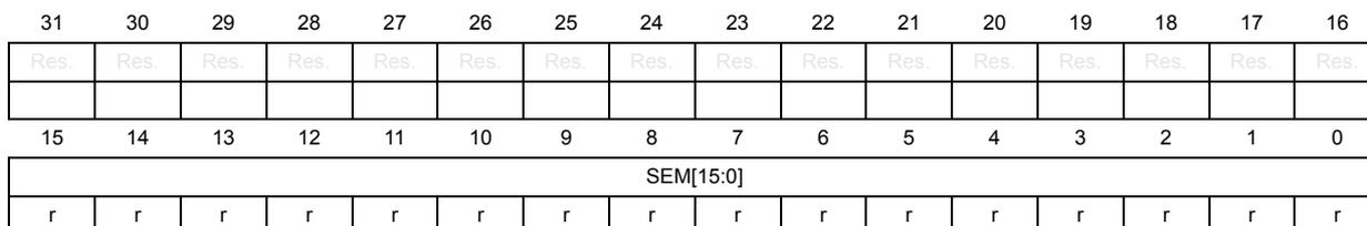
| 31 | 30 | 29 | 28 | 27 | 26 | 25 | 24 | 23 | 22 | 21 | 20 | 19 | 18 | 17 | 16 |
| Res. | Res. | Res. | Res. | Res. | Res. | Res. | Res. | Res. | Res. | Res. | Res. | Res. | Res. | Res. | Res. |
| 15 | 14 | 13 | 12 | 11 | 10 | 9 | 8 | 7 | 6 | 5 | 4 | 3 | 2 | 1 | 0 |
| SEM[15:0] | |||||||||||||||
| r | r | r | r | r | r | r | r | r | r | r | r | r | r | r | r |
Bits 31:16 Reserved, must be kept at reset value.
Bits 15:0
SEM[15:0]
: Sector Error mapping
When SEM[i] bit (
\(
0 \leq i \leq 15
\)
) is set, at least one error has been detected on sector i+1.
As an example, SEM[2] and SEM[1] bits are set when errors are detected in sector 3 and 2.
FMC BCH interrupt enable register (FMC_BCHIER)
Address offset: 0x250
Reset value: 0x0000 0000
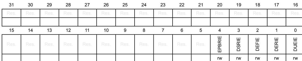
| 31 | 30 | 29 | 28 | 27 | 26 | 25 | 24 | 23 | 22 | 21 | 20 | 19 | 18 | 17 | 16 |
| Res. | Res. | Res. | Res. | Res. | Res. | Res. | Res. | Res. | Res. | Res. | Res. | Res. | Res. | Res. | Res. |
| 15 | 14 | 13 | 12 | 11 | 10 | 9 | 8 | 7 | 6 | 5 | 4 | 3 | 2 | 1 | 0 |
| Res. | Res. | Res. | Res. | Res. | Res. | Res. | Res. | Res. | Res. | Res. | EPBRIE | DSRIE | DEFIE | DERIE | DUEIE |
| rw | rw | rw | rw | rw |
Bits 31:5 Reserved, must be kept at reset value.
Bit 4 EPBRIE : Decoder Parity Bits Ready Interrupt enable
- 0: Decoder Parity Bits Ready Interrupt disable
- 1: Decoder Parity Bits Ready Interrupt enable
Bit 3 DSRIE : Decoder Syndrome Ready Interrupt enable
- 0: Decoder Syndrome Ready Interrupt disable
- 1: Decoder Syndrome Ready Interrupt enable
Bit 2 DEFIE : Decoder Error Found Interrupt enable
0: Decoder Error Found Interrupt disable
1: Decoder Error Found Interrupt enable
Bit 1 DERIE : Decoder Error Ready Interrupt enable
0: Decoder Error Ready Interrupt disable
1: Decoder Error Ready Interrupt enable
Bit 0 DUEIE : Decoder Uncorrectable Errors Interrupt enable
0: Decoder Uncorrectable Errors Interrupt disable
1: Decoder Uncorrectable Errors Interrupt enable
FMC BCH interrupt and status register (FMC_BCHISR)
Address offset: 0x254
Reset value: 0x0000 0000
This register holds the status of BCH encoder/decoder after processing each sector. When the sequencer is used, this register is automatically cleared and the corresponding interrupt must not be enabled through FMC_BCHIER register.
| 31 | 30 | 29 | 28 | 27 | 26 | 25 | 24 | 23 | 22 | 21 | 20 | 19 | 18 | 17 | 16 |
|---|---|---|---|---|---|---|---|---|---|---|---|---|---|---|---|
| Res. | Res. | Res. | Res. | Res. | Res. | Res. | Res. | Res. | Res. | Res. | Res. | Res. | Res. | Res. | Res. |
| 15 | 14 | 13 | 12 | 11 | 10 | 9 | 8 | 7 | 6 | 5 | 4 | 3 | 2 | 1 | 0 |
| Res. | Res. | Res. | Res. | Res. | Res. | Res. | Res. | Res. | Res. | Res. | EPBRF | DSRF | DEFF | DERF | DUEF |
| r | r | r | r | r |
Bits 31:5 Reserved, must be kept at reset value.
Bit 4 EPBRF : Encoder Parity Bits Ready flag
This bit is set when the BCH encoder parity bits are available in FMC_BCHPBR1 to 4.
Bit 3 DSRF : Decoder Syndrome Ready flag
This bit is set when the syndrome is ready and DEFF is a valid field.
Bit 2 DEFF : Decoder Error Found flag
This bit is set by hardware and cleared by writing 1 to CDEFF.
This bit indicates that at least one error has been detected in the sector.
Bit 1 DERF : Decoder Error Ready flag
This bit indicates that the decoder has finished searching errors and identifying their location.
The number of errors and their location are available in FMC_BCHDSR0 and FMC_BCHDSR1 to 4, respectively.
Bit 0 DUEF : Decoder Uncorrectable Errors flag
This field indicates that too many errors have been detected in the sector during the BCH decoding and that the sector is uncorrectable.
FMC BCH interrupt clear register (FMC_BCHICR)
Address offset: 0x258
Reset value: 0x0000 0000
| 31 | 30 | 29 | 28 | 27 | 26 | 25 | 24 | 23 | 22 | 21 | 20 | 19 | 18 | 17 | 16 |
|---|---|---|---|---|---|---|---|---|---|---|---|---|---|---|---|
| Res. | Res. | Res. | Res. | Res. | Res. | Res. | Res. | Res. | Res. | Res. | Res. | Res. | Res. | Res. | Res. |
| 15 | 14 | 13 | 12 | 11 | 10 | 9 | 8 | 7 | 6 | 5 | 4 | 3 | 2 | 1 | 0 |
| Res. | Res. | Res. | Res. | Res. | Res. | Res. | Res. | Res. | Res. | Res. | CEPBRF | CDSRF | CDEFF | CDERF | CDUEF |
| w | w | w | w | w |
Bits 31:5 Reserved, must be kept at reset value.
- Bit 4
CEPBRF
: Clear Encoder Parity Bits Ready flag
Writing 1 clears the EPBRF flag in FMC_BCHISR. - Bit 3
CDSRF
: Clear Decoder Syndrome Ready flag
Writing 1 clears the DSRF flag in FMC_BCHISR. - Bit 2
CDEFF
: Clear Decoder Error Found flag
Writing 1 clears the DEFF flag in FMC_BCHISR. - Bit 1
CDERF
: Clear Decoder Error ready flag
Writing 1 clears the DERF flag in FMC_BCHISR. - Bit 0
CDUEF
: Clear Decoder Uncorrectable Error flag
Writing 1 clears the DUEF flag in FMC_BCHISR.
FMC BCH parity bits register 1 (FMC_BCHPBR1)
Address offset: 0x260
Reset value: 0x0000 0000
These registers contain the BCH parity bits (BCHPB). For the BCH 4-bit, only BCHPB[51:0] are significant and for the BCH 8-bit BCHPB[103:0] are significant.
| 31 | 30 | 29 | 28 | 27 | 26 | 25 | 24 | 23 | 22 | 21 | 20 | 19 | 18 | 17 | 16 |
|---|---|---|---|---|---|---|---|---|---|---|---|---|---|---|---|
| BCHPB[31:16] | |||||||||||||||
| r | r | r | r | r | r | r | r | r | r | r | r | r | r | r | r |
| 15 | 14 | 13 | 12 | 11 | 10 | 9 | 8 | 7 | 6 | 5 | 4 | 3 | 2 | 1 | 0 |
| BCHPB[15:0] | |||||||||||||||
| r | r | r | r | r | r | r | r | r | r | r | r | r | r | r | r |
Bits 31:0 BCHPB[31:0] : BCH parity bits
FMC BCH parity bits register 2 (FMC_BCHPBR2)Address offset: 0x264
Reset value: 0x0000 0000
| 31 | 30 | 29 | 28 | 27 | 26 | 25 | 24 | 23 | 22 | 21 | 20 | 19 | 18 | 17 | 16 |
| BCHPB[63:48] | |||||||||||||||
| r | r | r | r | r | r | r | r | r | r | r | r | r | r | r | r |
| 15 | 14 | 13 | 12 | 11 | 10 | 9 | 8 | 7 | 6 | 5 | 4 | 3 | 2 | 1 | 0 |
| BCHPB[47:32] | |||||||||||||||
| r | r | r | r | r | r | r | r | r | r | r | r | r | r | r | r |
Address offset: 0x268
Reset value: 0x0000 0000
| 31 | 30 | 29 | 28 | 27 | 26 | 25 | 24 | 23 | 22 | 21 | 20 | 19 | 18 | 17 | 16 |
| BCHPB[95:80] | |||||||||||||||
| r | r | r | r | r | r | r | r | r | r | r | r | r | r | r | r |
| 15 | 14 | 13 | 12 | 11 | 10 | 9 | 8 | 7 | 6 | 5 | 4 | 3 | 2 | 1 | 0 |
| BCHPB[79:64] | |||||||||||||||
| r | r | r | r | r | r | r | r | r | r | r | r | r | r | r | r |
Address offset: 0x26C
Reset value: 0x0000 0000
| 31 | 30 | 29 | 28 | 27 | 26 | 25 | 24 | 23 | 22 | 21 | 20 | 19 | 18 | 17 | 16 |
| Res. | Res. | Res. | Res. | Res. | Res. | Res. | Res. | Res. | Res. | Res. | Res. | Res. | Res. | Res. | Res. |
| 15 | 14 | 13 | 12 | 11 | 10 | 9 | 8 | 7 | 6 | 5 | 4 | 3 | 2 | 1 | 0 |
| Res. | Res. | Res. | Res. | Res. | Res. | Res. | Res. | BCHPB[103:96] | |||||||
| r | r | r | r | r | r | r | r | ||||||||
Bits 31:8 Reserved, must be kept at reset value.
Bits 7:0 BCHPB[103:96] : BCH parity bits FMC BCH decoder status register 0 (FMC_BCHDSR0)Address offset: 0x27C
Reset value: 0x0000 0000
This register contains some fields already available in other registers but that require to be saved when error correction is performed on several sectors at a time (for example a whole NAND flash page). This allows a DMA channel to transfer the content of FMC_BCHDSR0 to 4 to a decoding status buffer.
| 31 | 30 | 29 | 28 | 27 | 26 | 25 | 24 | 23 | 22 | 21 | 20 | 19 | 18 | 17 | 16 |
| Res. | Res. | Res. | Res. | Res. | Res. | Res. | Res. | Res. | Res. | Res. | Res. | Res. | Res. | Res. | Res. |
| 15 | 14 | 13 | 12 | 11 | 10 | 9 | 8 | 7 | 6 | 5 | 4 | 3 | 2 | 1 | 0 |
| Res. | Res. | Res. | Res. | Res. | Res. | Res. | Res. | DEN[3:0] | Res. | Res. | DEF | DUE | |||
| r | r | r | r | r | r | ||||||||||
Bits 31:8 Reserved, must be kept at reset value.
Bits 7:4 DEN[3:0] : Decoder error number
When DEF bit is set, this field indicates the number of errors detected by the BCH decoder.
Following the selected BCH code, if the number of detected errors exceeds the number of correctable errors, this bit is not significant and DUE bit is set.
If the BCH decoder detects a number of errors that exceeds the maximum number of detectable errors, DEN is not significant.
Bits 3:2 Reserved, must be kept at reset value.
Bit 1 DEF : Decoder error found
This field indicates that the decoder has finished searching errors and identifying their location.
The number of errors and their location are available in FMC_BCHDSR0 and FMC_BCHDSR1 to 4, respectively.
Bit 0 DUE : Decoder uncorrectable error
This field indicates that too many errors have been detected in the sector during the BCH decoding and that the sector is uncorrectable.
If the BCH decoder detects a number of errors that exceeds the maximum number of detectable errors, DUE is not significant.
FMC BCH decoder status register for memory region 1 (FMC_BCHDSR1)
Address offset: 0x280
Reset value: 0x0000 0000
The maximum error correction capability of the BCH block embedded in the FMC is 8 errors. This register contains the positions of the 1st and 2nd error bits in EBP1 and EBP2 fields, respectively. If less than 8 errors are detected, the useless EPBx fields (x = 1 to 8) are “don’t care”.
| 31 | 30 | 29 | 28 | 27 | 26 | 25 | 24 | 23 | 22 | 21 | 20 | 19 | 18 | 17 | 16 |
|---|---|---|---|---|---|---|---|---|---|---|---|---|---|---|---|
| Res. | Res. | Res. | EBP2[12:0] | ||||||||||||
| r | r | r | r | r | r | r | r | r | r | r | r | r | |||
| 15 | 14 | 13 | 12 | 11 | 10 | 9 | 8 | 7 | 6 | 5 | 4 | 3 | 2 | 1 | 0 |
| Res. | Res. | Res. | EBP1[12:0] | ||||||||||||
| r | r | r | r | r | r | r | r | r | r | r | r | r | |||
Bits 31:29 Reserved, must be kept at reset value.
Bits 28:16 EBP2[12:0] : Error bit position for error number 2
Bits 15:13 Reserved, must be kept at reset value.
Bits 12:0 EBP1[12:0] : Error bit position for error number 1
FMC BCH decoder status register for memory region 2 (FMC_BCHDSR2)
Address offset: 0x284
Reset value: 0x0000 0000
The maximum error correction capability of the BCH block embedded in the FMC is 8 errors. This register contains the positions of the 3rd and 4th error bits in EBP3 and EBP4 fields, respectively. If less than 8 errors are detected, the useless EPBx fields (x = 1 to 8) are don’t care.
| 31 | 30 | 29 | 28 | 27 | 26 | 25 | 24 | 23 | 22 | 21 | 20 | 19 | 18 | 17 | 16 |
|---|---|---|---|---|---|---|---|---|---|---|---|---|---|---|---|
| Res. | Res. | Res. | EBP4[12:0] | ||||||||||||
| r | r | r | r | r | r | r | r | r | r | r | r | r | |||
| 15 | 14 | 13 | 12 | 11 | 10 | 9 | 8 | 7 | 6 | 5 | 4 | 3 | 2 | 1 | 0 |
| Res. | Res. | Res. | EBP3[12:0] | ||||||||||||
| r | r | r | r | r | r | r | r | r | r | r | r | r | |||
Bits 31:29 Reserved, must be kept at reset value.
Bits 28:16 EBP4[12:0] : Error bit position for error number 4
Bits 15:13 Reserved, must be kept at reset value.
Bits 12:0 EBP3[12:0] : Error bit position for error number 3
FMC BCH decoder status register for memory region 3 (FMC_BCHDSR3)Address offset: 0x288
Reset value: 0x0000 0000
The maximum error correction capability of the BCH block embedded in the FMC is 8 errors. This register contains the positions of the 5th and 6th error bits in EBP5 and EBP6 fields, respectively. If less than 8 errors are detected, the useless EPBx fields (x = 1 to 8) are don't care.
| 31 | 30 | 29 | 28 | 27 | 26 | 25 | 24 | 23 | 22 | 21 | 20 | 19 | 18 | 17 | 16 |
|---|---|---|---|---|---|---|---|---|---|---|---|---|---|---|---|
| Res. | Res. | Res. | EBP6[12:0] | ||||||||||||
| r | r | r | r | r | r | r | r | r | r | r | r | r | |||
| 15 | 14 | 13 | 12 | 11 | 10 | 9 | 8 | 7 | 6 | 5 | 4 | 3 | 2 | 1 | 0 |
| Res. | Res. | Res. | EBP5[12:0] | ||||||||||||
| r | r | r | r | r | r | r | r | r | r | r | r | r | |||
Bits 31:29 Reserved, must be kept at reset value.
Bits 28:16 EBP6[12:0] : Error bit position for error number 6Bits 15:13 Reserved, must be kept at reset value.
Bits 12:0 EBP5[12:0] : Error bit position for error number 5 FMC BCH decoder status register for memory region 4 (FMC_BCHDSR4)Address offset: 0x28C
Reset value: 0x0000 0000
The maximum error correction capability of the BCH block embedded in the FMC is 8 errors. This register contains the positions of the 7th and 8th error bits in EBP7 and EBP8 fields, respectively. If less than 8 errors are detected, the useless EPBx fields (x = 1 to 8) are don't care.
| 31 | 30 | 29 | 28 | 27 | 26 | 25 | 24 | 23 | 22 | 21 | 20 | 19 | 18 | 17 | 16 |
|---|---|---|---|---|---|---|---|---|---|---|---|---|---|---|---|
| Res. | Res. | Res. | EBP8[12:0] | ||||||||||||
| r | r | r | r | r | r | r | r | r | r | r | r | r | |||
| 15 | 14 | 13 | 12 | 11 | 10 | 9 | 8 | 7 | 6 | 5 | 4 | 3 | 2 | 1 | 0 |
| Res. | Res. | Res. | EBP7[12:0] | ||||||||||||
| r | r | r | r | r | r | r | r | r | r | r | r | r | |||
Bits 31:29 Reserved, must be kept at reset value.
Bits 28:16 EBP8[12:0] : Error bit position for error number 8Bits 15:13 Reserved, must be kept at reset value.
Bits 12:0 EBP7[12:0] : Error bit position for error number 727.10 SDRAM controller
27.10.1 SDRAM controller main features
The main features of the SDRAM controller are the following:
- • Two SDRAM devices with control registers
- • 8-bit, 16-bit, 32-bit data bus width with narrow width support using DQM byte masking
- • 11- to 13-bit Address Row, 8- to 11-bit Address Column, 2 to 4 internal banks
Maximum supported device configurations: 4 x 16 M x 32 bits (256 Mbytes), 4 x 16 M x 16 bits (128 Mbytes), 4 x 16 M x 8 bits (64 Mbytes) - • 64-bit AXI interface with word, half-word or byte access
- • SDRAM clock ratio programmable to 1, 2 or 3 (fmc_ker_ck, fmc_ker_ck/2 or fmc_ker_ck/3)
- • Automatic row and bank boundary crossing management
- • Multibank back-to-back access
- • Programmable timing parameters
- • Automatic refresh operation with programmable refresh rate
- • Self-refresh mode
- • Power-down mode
- • SDRAM power-up initialization by software
- • CAS latency of 1,2,3
27.10.2 SDRAM External memory interface signals
Table 192. SDRAM signals
| SDRAM signal | I/O type | Description | Alternate function |
|---|---|---|---|
| SDCLK | O | SDRAM clock | |
| SDCKE[1:0] | O | SDCKE0: SDRAM Bank 1 Clock Enable SDCKE1: SDRAM Bank 2 Clock Enable | |
| SDNE[1:0] | O | SDNE0: SDRAM Bank 1 chip enable SDNE1: SDRAM Bank 2 chip enable | |
| A[13:0] (1) | O | Address | FMC_A[13:0] |
| D[31:0] | I/O | Bidirectional data bus | FMC_D[31:0] |
| BA[1:0] | O | Bank Address | FMC_A[15:14] |
| NRAS | O | Row Address Strobe | |
| NCAS | O | Column Address Strobe | |
| SDNWE | O | Write Enable | |
| NBL[3:0] | O | Output byte mask for write accesses (memory signal name: DQM[3:0]) | FMC_NBL[3:0] |
- 1. A[13:0] address depends on the number of row address bits (NR) and the number of column address bits (NC).
A[10] is also used as a command parameter.
A[12] is asserted only when NR = 13.
A[13] is never asserted.
27.10.3 SDRAM controller functional description
All SDRAM controller outputs (signals, address and data) change on the falling edge of the memory clock (SDCLK).
SDRAM initialization
The initialization sequence is managed by software. If the two devices are used, the initialization sequence must be generated simultaneously to device 1 and device 2 by setting DS1 and DS2 bits in the FMC_SDCMR register:
- 1. Program the memory device features into the FMC_SDCRx register. The SDRAM clock and RPIPE[1:0] must be programmed in the FMC_SDCR1 register.
- 2. Program the memory device timing into the FMC_SDTR register.
- 3. Enable each SDRAM device by setting the corresponding SDEN bit in FMC_SDCRx register.
- 4. Set the FMCEN bit. The SDRAM clock starts when this step is complete.
- 5. Wait during the recommended delay period (100 µs). Refer to the SDRAM datasheet for the required delay after power-up.
- 6. Set the MODE[2:0] bitfield to 0x2 and configure the device select bits (DS1 and DS2) in the FMC_SDCMR register to issue a Precharge all banks (PALL) command.
- 7. Set the MODE[2:0] bitfield to 0x3 (Auto-refresh) and configure the device select bits (DS1 and DS2). The user application can either generate Auto-refresh commands by burst (NRFS[3:0]) in the FMC_SDCMR register or generate consecutive single Auto-refresh commands. Refer to the SDRAM datasheet for the number of Auto-refresh commands that must be issued during the initialization phase.
- 8. Perform load mode register: configure the MRD[13:0] bitfield in the FMC_SDCMR register, set the MODE[2:0] bitfield to 0x4, and configure the device select bits (DS1 and DS2) in the FMC_SDCMR register to issue a load mode register command to the memory devices. In particular, the burst length (BL) has to be set.
If the mode register value is not the same for both SDRAM devices, this step must be repeated twice, once for each device, and the device select bit has to be set accordingly. For mobile SDRAM devices, the MRD[13:0] bitfield is also used to configure the extended mode register while performing the load mode register.
- 9. Program the refresh rate in the FMC_SDRTR register. The refresh rate corresponds to the delay between refresh cycles. Its value must be adapted depending on the SDRAM device.
- 10. Set the SDINIT bit for all the enabled devices in the FMC_SDCRx register, to indicate to the hardware that the initialization procedure has been completed for all the enabled devices.
At the end of this step, the SDRAM device is ready to accept commands. If a system reset occurs during an ongoing SDRAM access, the data bus might still be driven by the SDRAM device.
Therefore, the SDRAM device must be first initialized again after reset before issuing any new access by the NOR flash/PSRAM/SRAM or NAND flash controller.
Any AXI request to SDRAM that is occurring before the end of SDRAM initialization returns a bus error and the request is lost.
During Initialization, only the commands PALL, AR and LMR are accepted, the other commands are ignored.
SDRAM controller write cycle
The SDRAM controller converts AXI single and burst write transfers into single memory accesses. Consecutive write transfers to the same page or to open pages in different banks can be presented as back-to-back write operations to the SDRAM.
Before performing any write access, the SDRAM bank write protection must be disabled by clearing the WP bit in the FMC_SDCRx register.
Figure 186. SDRAM burst write waveforms
(AXI 4-word transfer, no page boundary crossing)
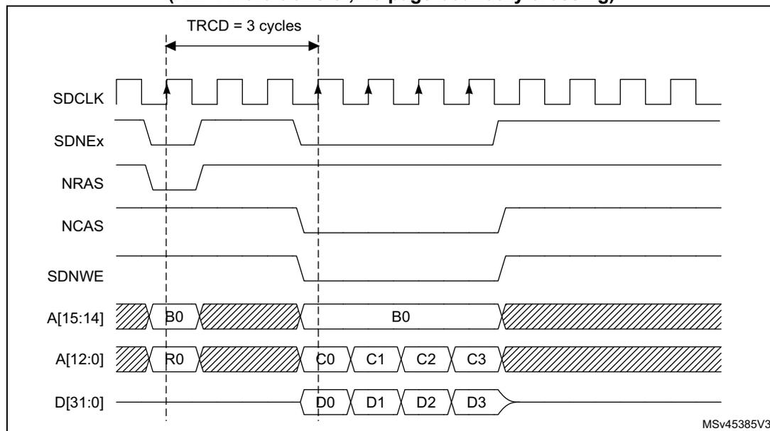
The diagram illustrates the timing for an SDRAM burst write operation. The signals shown are:
- SDCLK : SDRAM clock signal, shown as a periodic square wave.
- SDNEx : SDRAM external clock signal, active-low.
- NRAS : Row address strobe, active-low.
- NCAS : Column address strobe, active-low.
- SDNWE : SDRAM write enable, active-low.
- A[15:14] : Address lines for bank and row selection. The diagram shows a transition from address B0 to another B0 after a precharge and activate sequence (indicated by R0 and shaded regions).
- A[12:0] : Address lines for column selection. The diagram shows a sequence of addresses R0, C0, C1, C2, C3.
- D[31:0] : Data bus, showing a burst of four data words D0, D1, D2, D3.
The timing parameter TRCD = 3 cycles is indicated between the falling edge of NRAS and the start of the data burst. Vertical dashed lines mark the clock edges and signal transitions. The source identifier MSV45385V3 is shown in the bottom right corner.
The SDRAM controller always checks the next access.
- • If the next access is in the same row or in another active row, the write operation is carried out, and write commands can be back-to-back.
- • if the next access targets another row (not active), the SDRAM controller generates a Bank precharge command (PRE), activates the new row and initiates a write command.
SDRAM controller read cycle
The SDRAM controller converts single and burst read transfers into single memory accesses. Consecutive read transfers to the same page or to open pages in different banks can be presented as back-to-back read operations from the SDRAM.
Figure 187. SDRAM burst read waveforms
(AXI 4-word transfer, no page boundary crossing)
![Timing diagram for SDRAM burst read waveforms (AXI 4-word transfer, no page boundary crossing). The diagram shows the relationship between SDCLK, SDNEx, NRAS, NCAS, SDNWE, address lines A[15:14] and A[12:0], and data lines D[31:0].](/RM0486-STM32N6x5-x7/33c3d4aa603e864018f806aff060923a_img.jpg)
The timing diagram illustrates the SDRAM burst read cycle for an AXI 4-word transfer. The signals shown are:
- SDCLK: System clock signal.
- SDNEx: SDRAM chip select signal, active low.
- NRAS: Row address strobe signal, active low.
- NCAS: Column address strobe signal, active low.
- SDNWE: SDRAM write enable signal, active low.
- A[15:14]: Address lines for bank selection. The diagram shows a burst of four words (B0, B0, B0, B0) being read from the same bank.
- A[12:0]: Address lines for row and column selection. The diagram shows a burst of four words (R0, C0, C1, C2, C3) being read from the same row.
- D[31:0]: Data bus. The diagram shows four data words (D0, D1, D2, D3) being output sequentially.
Key timing parameters indicated:
- TRCD = 3 cycles: Time from row address to column address.
- CAS latency = 3 cycles: Time from column address to data output.
The diagram is labeled MSV45386V2.
The address management depends on the next AXI request:
- • Next request is performed at sequential address (burst access)
In this case, the SDRAM controller increments the address. - • Next request is not performed at sequential address
- – If the new read request targets the same row or another active row, the new address is passed to the memory and the master is stalled for the CAS latency period, waiting for the new data from memory.
- – If the new read request does not target an active row, the SDRAM controller generates a Bank precharge command (PRE), activates the new row, and initiates a read command.
Row and bank boundary management
When a read or write access crosses a row boundary, if the next read or write access is sequential and the current access was performed to a row boundary, the SDRAM controller executes the following operations:
- 1. Precharge of the active row, using the Bank precharge command (PRE)
- 2. Activation of the new row
- 3. Start of a read/write command.
At a row boundary, the automatic activation of the next row is supported for all columns and data bus width configurations.
If necessary, the SDRAM controller inserts additional clock cycles between the following commands:
- • Between Precharge and Activate commands to match TRP[3:0] parameter (only if the next access is in a different row in the same bank),
- • Between Activate and Read commands to match the TRCD[3:0] parameter.
These parameters are defined into the FMC_SDTR register.
Refer to Figure 188 and Figure 189 for read and burst write access crossing a row boundary.
Figure 188. SDRAM burst read crossing a row boundary
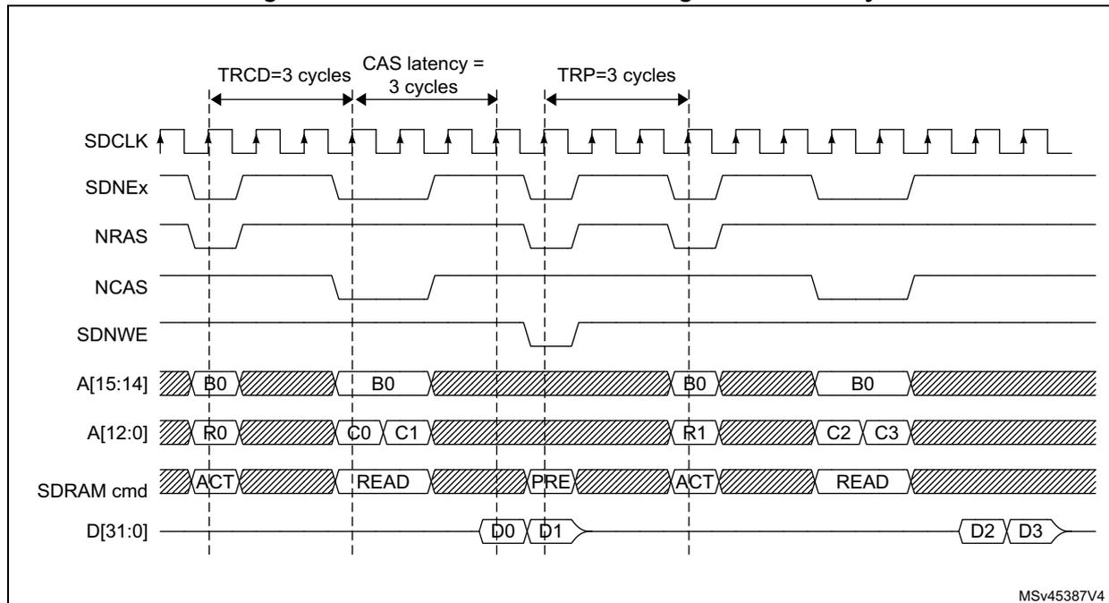
The timing diagram illustrates the sequence of signals and commands for an SDRAM burst read that crosses a row boundary. The signals shown are SDCLK (clock), SDNEx (address and command latching edge), NRAS (row address strobe), NCAS (column address strobe), SDNWE (write enable), A[15:14] (bank addresses), A[12:0] (row and column addresses), SDRAM cmd (commands), and D[31:0] (data). The diagram is divided into three main phases by vertical dashed lines representing clock edges:
- Phase 1: The SDRAM command is ACT (Activate) for row R0 in bank B0. The address A[12:0] is R0. The time interval between the ACT command and the subsequent READ command is labeled TRCD=3 cycles.
- Phase 2: The SDRAM command is READ for column C0 in row R0. The address A[12:0] is C0. Data D0 and D1 are output. The time interval between the READ command and the subsequent PRE (Precharge) command is labeled CAS latency = 3 cycles.
- Phase 3: The SDRAM command is PRE for row R0. The address A[12:0] is R0. This is followed by another ACT command for row R1 in bank B0. The time interval between the PRE command and the next ACT command is labeled TRP=3 cycles.
- Phase 4: The SDRAM command is READ for column C2 in row R1. The address A[12:0] is C2. Data D2 and D3 are output. The address A[15:14] shows bank B0 throughout the sequence.
The diagram also shows the SDNEx signal toggling on every clock cycle. The SDRAM cmd line shows the sequence: ACT, READ, PRE, ACT, READ. The data output sequence is D0, D1, D2, D3.
MSv45387V4
Figure 189. SDRAM burst write crossing a row boundary
![Timing diagram for SDRAM burst write crossing a row boundary. It shows signals SDCLK, SDNEx, NRAS, NCAS, SDNWE, address lines A[15:14] and A[12:0], SDRAM command, and data bus D[31:0]. Timing parameters TRCD=3, TWR=3, and TRP=3 cycles are indicated. The diagram shows two write bursts: the first at address R0 (bank B0) and the second at address R1 (bank B0), with a precharge command in between. Data D0, D1, D2, and D3 are shown being written.](/RM0486-STM32N6x5-x7/607c8b0cd09ce40fd9ba9c77e684f4f7_img.jpg)
MSV45388V4
An AXI burst operation crossing a row boundary between different banks is automatically split by AXI interconnect because the boundary address is a multiple of 4 Kbytes.
Consecutive read and write operations to the same SDRAM page are back-to-back as shown in Figure 190 and Figure 191.
Figure 190. Read followed by write operation
![Timing diagram for a read followed by write operation on the same SDRAM page. It shows signals SDCLK, SDNEx, NRAS, NCAS, SDNWE, address lines A[15:14] and A[12:0], SDRAM command, and data bus D[31:0]. Timing parameter TRCD=3 cycles is indicated. The diagram shows a read burst at address R0 (bank B0) followed by a write burst at address C4 (bank B0). Data D0-D3 are read, and data D4-D7 are written. A note at the bottom indicates 'AXI two 4 word burst, same page'.](/RM0486-STM32N6x5-x7/416dd1df12ddac1475c81611907cd024_img.jpg)
AXI two 4 word burst, same page
Figure 191. Write followed by read operation
![Timing diagram for a write followed by read operation in SDRAM. The diagram shows the relationship between SDCLK, SDNEx, NRAS, NCAS, SDNWE, address lines A[15:14] and A[12:0], SDRAM command, and data lines D[31:0]. It illustrates the TRCD (3 cycles) and CAS latency (3 cycles) parameters. The write operation occurs first, followed by a read operation, both using the same page (B0). The data is transferred in 4-word bursts (D0-D3 for write, D4-D7 for read).](/RM0486-STM32N6x5-x7/c3999cf08b1a191b21cb5ccf7e5660c9_img.jpg)
The diagram illustrates the timing for a write followed by a read operation in SDRAM. The signals shown are:
- SDCLK: System clock signal.
- SDNEx: SDRAM chip select signal, active low.
- NRAS: Row address strobe, active low.
- NCAS: Column address strobe, active low.
- SDNWE: Write enable, active low.
- A[15:14]: Address lines for bank selection (B0).
- A[12:0]: Address lines for row selection (R0, C0-C7).
- SDRAM command: Commands issued: ACT (Activate), WRITE, and READ.
- D[31:0]: Data lines, showing 4-word bursts (D0-D3 for write, D4-D7 for read).
Key timing parameters shown:
- TRCD = 3 cycles: Time from ACT command to WRITE/READ command.
- CAS latency = 3 cycles: Time from READ command to data output.
AXI two 4 word burst, same page
SDRAM controller refresh cycle
The Auto-refresh command is used to refresh the SDRAM device content. The SDRAM controller periodically issues Auto-refresh commands. An internal counter is loaded with the RFSCNT[12:0] value in the register FMC_SDRTR. This value defines the number of memory clock cycles between the refresh cycles (refresh rate). When this counter reaches zero, a refresh command is generated.
The Auto-refresh command is applied on SDRAM device that are enabled (SDEN = 1) and that are not in Self-refresh mode.
If a memory access is in progress, the Auto-refresh request is delayed until the end of the AXI transfer. However, if the memory access and Auto-refresh requests are generated simultaneously, the Auto-refresh takes precedence. In addition, an Auto-refresh request does not suspend consecutive Read or Write commands from an AXI burst. An AXI burst transfer is not interrupted by an Auto-refresh request, except when the Auto-refresh crosses a row or bank boundary. If the memory access occurs during a refresh operation, the request is buffered to be processed when the refresh is complete.
If a new Auto-refresh request occurs while the previous one was not served, the RE (Refresh Error) bit is set in the Status register. An Interrupt is generated if it has been enabled (REIE = 1).
If the SDRAM is not in idle state (not all row are closed), the SDRAM controller generates a PALL (Precharge all banks) command before the Auto-refresh.
If the Auto-refresh command is generated by the FMC_SDCMR register, a PALL command is generated by the SDRAM controller as it is keeping track of the SDRAM opened pages.
27.10.4 Low-power modes
Two low-power modes are available:
- • Self-refresh mode
The Auto-refresh cycles are performed by the SDRAM device itself to retain data without external clocking.
- • Power-down mode
The Auto-refresh cycles are performed by the SDRAM controller.
Self-refresh mode
SDRAM devices can be forced into Self-refresh by software according to the MODE[2:0], DS1, DS2 bits of the FMC_SDCMR register.
SDRAM devices exit Self-refresh either by a normal mode command from the FMC_SDCMR register (according to DS1 and DS2 bits), or upon the arrival of an AXI request (according to the device enabled through SDEN bit in the FMC_SDCRx).
Note: Exiting Self-refresh by software using FMC_SDCMR is defined on a per-device basis, while the Self-refresh exit upon receiving an AXI transfer is applicable to all devices, irrespectively of the AXI target controller, including NOR flash/PSRAM and NAND flash memories.
Changing the SDRAM frequency is possible only during Self-Refresh: RPIPE[1:0] and SDCLK[1:0] of a device FMC_SDCRx register must not be modified when the device is not in Self-Refresh mode.
Note: During Self-Refresh, any command other than normal mode configured in the FMC_SDCMR register, is ignored by the SDRAM controller.
Figure 192. SDRAM Self-refresh waveforms
![Figure 192. SDRAM Self-refresh waveforms. The diagram shows timing relationships between SDCLK, SDCKE, SDNEx, NRAS, NCAS, SDNWE, A10, Command, and D[31:0] signals during a self-refresh cycle. Key timing parameters shown are TRP=3 cycles, TRAS(min), and TXSR=3 cycles.](/RM0486-STM32N6x5-x7/13d2d55c2c50e83d5f6fe53b5e459651_img.jpg)
The figure illustrates the timing diagram for SDRAM Self-refresh mode. It shows the relationship between the clock (SDCLK), command and address signals (SDCKE, SDNEx, NRAS, NCAS, SDNWE, A10), and the command sequence (PALL, REF, ACT) over time. The timing parameters are defined as follows:
- TRP=3 cycles: The time interval between the falling edge of SDCLK and the falling edge of SDCKE.
- TRAS(min): The minimum time interval between the falling edge of SDCKE and the falling edge of SDNEx.
- TXSR=3 cycles: The time interval between the falling edge of SDNEx and the falling edge of SDCLK.
The command sequence shown is PALL (Precharge All), REF (Refresh), and ACT (Activate). The address lines (A10) are shown as a shaded area, indicating they are not used during the refresh command.
Power-down mode
SDRAM devices can be forced into Power-down by software according to the MODE[2:0], DS1, DS2 bits of the FMC_SDCMR register.
SDRAM devices exit Power-down either by a normal mode command from the FMC_SDCMR register (according to DS1 and DS2 bits) or upon the arrival of an AXI request (according to the device enabled through SDEN bit in the FMC_SDCRx).
Note: During Power-down, any command other than normal mode configured in the FMC_SDCMR register, is ignored by SDRAM controller.
Figure 193. Power-down mode
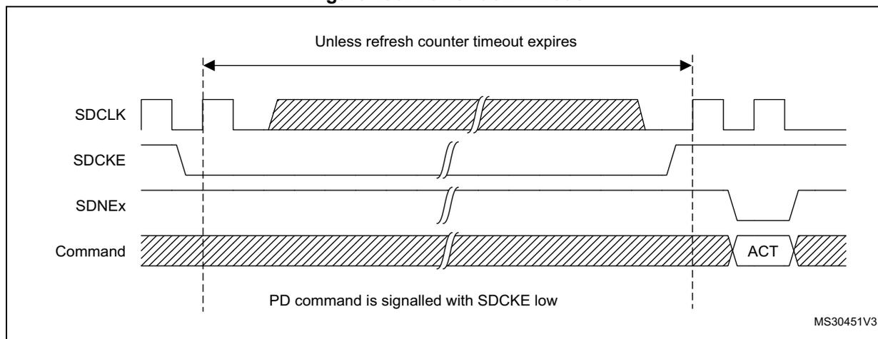
The diagram illustrates the timing for Power-down mode. It shows four signal lines: SDCLK (clock), SDCKE (power-down control), SDNEx (active-low data strobe), and Command.
SDCLK is a periodic square wave.
SDCKE is initially high, then goes low to signal the Power-Down (PD) command. It remains low until an 'ACT' command is received, at which point it goes high.
SDNEx is initially high, then goes low when the PD command is signaled, and returns high when the 'ACT' command is received.
The Command line shows a shaded region for the PD command, followed by a period where commands are ignored (also shaded), and finally an 'ACT' command which exits the Power-down mode.
A horizontal double-headed arrow at the top indicates the duration of the Power-down mode, labeled 'Unless refresh counter timeout expires'.
A label at the bottom states 'PD command is signalled with SDCKE low'.
The diagram is identified by the code 'MS30451V3' in the bottom right corner.
During Power-down mode, all SDRAM device input and output buffers are deactivated except for the SDCKE which remains low.
The SDRAM device cannot remain in Power-down mode longer than the refresh period and cannot perform the Auto-refresh cycles by itself. Therefore, the SDRAM controller carries out the refresh operation by executing the operations below:
- 1. Exit from Power-down mode and drive the SDCKE high
- 2. Generate the PALL command only if a row was active during Power-down mode
- 3. Generate the Auto-refresh command
- 4. Drive SDCKE low again to return to Power-down mode.
Figure 194. Power-down with Auto-refresh
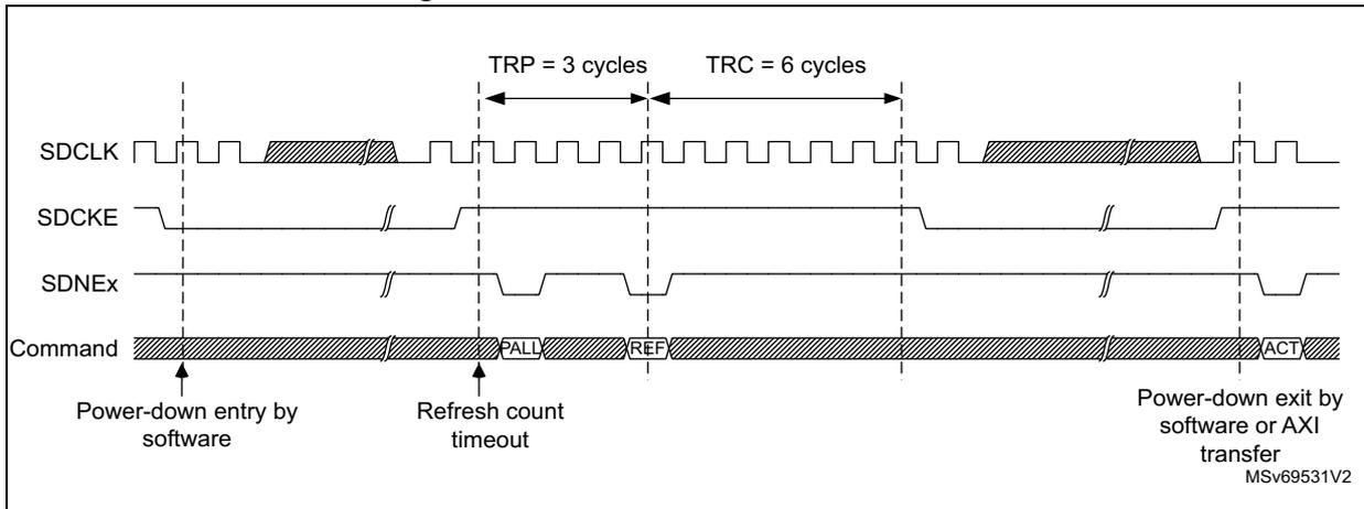
Clock stop during low-power modes
If all SDRAM devices are simultaneously in low-power mode, the controller stops the SDRAM clock generation. The clock is resumed when at least one device exits from low-power mode.
27.10.5 SDRAM controller registers
SDRAM control registers for SDRAM device 1 (FMC_SDCR1)
Address offset: 0x140
Reset value: 0x0000 02D0
This register contains the control parameters for SDRAM device 1.
| 31 | 30 | 29 | 28 | 27 | 26 | 25 | 24 | 23 | 22 | 21 | 20 | 19 | 18 | 17 | 16 |
|---|---|---|---|---|---|---|---|---|---|---|---|---|---|---|---|
| Res. | Res. | Res. | Res. | Res. | Res. | Res. | Res. | Res. | Res. | Res. | Res. | Res. | Res. | SDINIT | SDEN |
| rw | rw |
| 15 | 14 | 13 | 12 | 11 | 10 | 9 | 8 | 7 | 6 | 5 | 4 | 3 | 2 | 1 | 0 |
|---|---|---|---|---|---|---|---|---|---|---|---|---|---|---|---|
| Res. | RP1PE[1:0] | Res. | SDCLK[1:0] | WP | CAS[1:0] | NB | MWID[1:0] | NR[1:0] | NC[1:0] | ||||||
| rw | rw | rw | rw | rw | rw | rw | rw | rw | rw | rw | rw | rw | rw | ||
Bits 31:18 Reserved, must be kept at reset value.
Bit 17 SDINIT : SDRAM device initialization
1: Initialization is complete and the device is ready to be accessed
0: Initialization is not complete, the AXI accesses are rejected and an AXI slave error is generated.
Bit 16 SDEN : SDRAM device enable
1: SDRAM device enabled
0: SDRAM disabled
Bit 15 Reserved, must be kept at reset value.
Bits 14:13 RPIPE[1:0] : Read pipeThese bits define the delay, in fmc_ker_ck clock cycles, for reading data after CAS latency, and for both SDRAM devices.
00: No fmc_ker_ck clock cycle delay (default value)
01: One fmc_ker_ck clock cycle delay
10: Two fmc_ker_ck clock cycle delay
11: Reserved.
Bit 12 Reserved, must be kept at reset value.
Bits 11:10 SDCLK[1:0] : SDRAM clock configurationThese bits define the SDRAM clock period for both SDRAM devices and allow disabling the clock before changing the frequency.
00: SDCLK clock disabled
01: SDCLK period = 1 * fmc_ker_ck period
10: SDCLK period = 2 * fmc_ker_ck periods
11: SDCLK period = 3 * fmc_ker_ck periods
Note: SDRAM devices must be in Self-refresh mode before a clock frequency change, then all timing parameters are reprogrammed through FMC_SDTR, FMC_SDCRx, FMC_SDCMR and load mode register according to CAS latency.
Bit 9 WP : Write protectionThis bit enables write mode access to the SDRAM bank.
0: Write accesses allowed
1: Write accesses ignored
Bits 8:7 CAS[1:0] : CAS LatencyThese bits set the SDRAM CAS latency in number of memory clock cycles
00: Reserved.
01: 1 cycle
10: 2 cycles
11: 3 cycles
Note: CAS latency must have the same value for both devices as they operate on the same frequency.
Bit 6 NB : Number of banksThis bit sets the number of SDRAM banks.
0: Two banks
1: Four banks
Bits 5:4 MWID[1:0] : Memory data bus width.
These bits define the memory device width.
00: 8 bits
01: 16 bits
10: 32 bits
11: Reserved.
Bits 3:2 NR[1:0] : Number of row address bits
These bits define the number of bits of a row address.
00: 11 bit
01: 12 bits
10: 13 bits
11: Reserved.
Bits 1:0 NC[1:0] : Number of column address bits
These bits define the number of bits of a column address.
00: 8 bits
01: 9 bits
10: 10 bits
11: 11 bits.
SDRAM control registers for SDRAM device 2 (FMC_SDCR2)
Address offset: 0x144
Reset value: 0x0000 02D0
This register contains the control parameters for SDRAM device 2.
| 31 | 30 | 29 | 28 | 27 | 26 | 25 | 24 | 23 | 22 | 21 | 20 | 19 | 18 | 17 | 16 |
|---|---|---|---|---|---|---|---|---|---|---|---|---|---|---|---|
| Res. | Res. | Res. | Res. | Res. | Res. | Res. | Res. | Res. | Res. | Res. | Res. | Res. | Res. | SDINIT | SDEN |
| rw | rw | ||||||||||||||
| 15 | 14 | 13 | 12 | 11 | 10 | 9 | 8 | 7 | 6 | 5 | 4 | 3 | 2 | 1 | 0 |
| Res. | Res. | Res. | Res. | Res. | Res. | WP | CAS[1:0] | NB | MWID[1:0] | NR[1:0] | NC[1:0] | ||||
| rw | rw | rw | rw | rw | rw | rw | rw | rw | rw | ||||||
Bits 31:18 Reserved, must be kept at reset value.
Bit 17 SDINIT : SDRAM device initialization
1: Initialization is complete and the device is ready to be accessed
0: Initialization is not complete, the AXI accesses are rejected and an AXI slave error is generated.
Bit 16 SDEN : SDRAM device enable
1: SDRAM device enabled
0: SDRAM disabled
Bits 15:10 Reserved, must be kept at reset value.
Bit 9 WP : Write protection
This bit enables write mode access to the SDRAM bank.
0: Write accesses allowed
1: Write accesses ignored
Bits 8:7 CAS[1:0] : CAS Latency
These bits set the SDRAM CAS latency in number of memory clock cycles
00: Reserved.
01: 1 cycle
10: 2 cycles
11: 3 cycles
Note: CAS latency must have the same value for both devices as they operate on the same frequency.
Bit 6 NB : Number of banks
This bit sets the number of SDRAM banks.
0: Two banks
1: Four banks
Bits 5:4 MWID[1:0] : Memory data bus width.
These bits define the memory device width.
00: 8 bits
01: 16 bits
10: 32 bits
11: Reserved.
Bits 3:2 NR[1:0] : Number of row address bits
These bits define the number of bits of a row address.
00: 11 bit
01: 12 bits
10: 13 bits
11: Reserved.
Bits 1:0 NC[1:0] : Number of column address bits
These bits define the number of bits of a column address.
00: 8 bits
01: 9 bits
10: 10 bits
11: 11 bits.
SDRAM timing register (FMC_SDTR)
Address offset: 0x148
Reset value: 0x0FFF FFFF
This register contains the timing parameters. It is common to both SDRAM banks.
| 31 | 30 | 29 | 28 | 27 | 26 | 25 | 24 | 23 | 22 | 21 | 20 | 19 | 18 | 17 | 16 |
|---|---|---|---|---|---|---|---|---|---|---|---|---|---|---|---|
| Res. | Res. | Res. | Res. | TRCD[3:0] | TRP[3:0] | TWR[3:0] | |||||||||
| rw | rw | rw | rw | rw | rw | rw | rw | rw | rw | rw | rw | ||||
| 15 | 14 | 13 | 12 | 11 | 10 | 9 | 8 | 7 | 6 | 5 | 4 | 3 | 2 | 1 | 0 |
| TRC[3:0] | TRAS[3:0] | TXSR[3:0] | TMRD[3:0] | ||||||||||||
| rw | rw | rw | rw | rw | rw | rw | rw | rw | rw | rw | rw | rw | rw | rw | rw |
Bits 31:28 Reserved, must be kept at reset value.
Bits 27:24 TRCD[3:0] : Row to column delay
This bitfield defines the number of SDRAM clock cycles between an Activate command and a Read or Write command. Its value must meet the SDRAM TRCD timing requirement.
0000: 1 cycle.
0001: 2 cycles
....
1111: 16 cycles
Bits 23:20 TRP[3:0] : Row precharge delay
This bitfield defines the number of SDRAM clock cycles between a Precharge command and an Activate or Refresh command. Its value must meet the SDRAM TRP timing requirement.
0000: 1 cycle
0001: 2 cycles
....
1111: 16 cycles
Bits 19:16 TWR[3:0] : Recovery delay
This bitfield defines the number of SDRAM clock cycles between a Write command and a Precharge command. Its value must meet the SDRAM TWR timing requirement.
These bits define the delay between a Write and a Precharge command in number of memory clock cycles.
0000: 1 cycle
0001: 2 cycles
....
1111: 16 cycles
Note: The SDRAM write recovery ( \( t_{WR} \) ) can be determined as the highest of the three timings requirements, TWR, TRAS – TRCD and TRC – TRP – TRCD.
Bits 15:12 TRC[3:0] : Row cycle delay
This bitfield defines the number of SDRAM clock cycles between two Activate commands or between two Refresh commands. Its value must meet both SDRAM TRC and TRFC timing requirements.
0000: 1 cycle
0001: 2 cycles
....
1111: 16 cycles
Bits 11:8 TRAS[3:0] : Self-refresh timeThis bitfield defines the number of SDRAM clock cycles between an Activate command and a Precharge command. Its value must meet the SDRAM TRAS timing requirement.
0000: 1 cycle
0001: 2 cycles
....
1111: 16 cycles
Bits 7:4 TXSR[3:0] : Exit self-refresh delayThis bitfield defines the number of SDRAM clock cycles between a Self-refresh exit and an Activate command. Its value must meet the SDRAM TXSR timing requirement.
0000: 1 cycle
0001: 2 cycles
....
1111: 16 cycles
Bits 3:0 TMRD[3:0] : Load mode register to ActivateThis bitfield defines the number of SDRAM clock cycles between a load mode register command and an Activate or Refresh command. Its value must meet the SDRAM TMRD timing requirement.
0000: 1 cycle
0001: 2 cycles
....
1111: 16 cycles
SDRAM command mode register (FMC_SDCMR)
Address offset: 0x150
Reset value: 0x0000 0000
This register contains the command issued when the SDRAM device is accessed. This register is used to initialize the SDRAM device, and to activate the Self-refresh and the Power-down modes. As soon as the MODE[2:0] bitfield is written, the command is issued only to one or to both SDRAM banks according to DS1 and DS2 command bits. This register is the same for both SDRAM banks.
| 31 | 30 | 29 | 28 | 27 | 26 | 25 | 24 | 23 | 22 | 21 | 20 | 19 | 18 | 17 | 16 |
|---|---|---|---|---|---|---|---|---|---|---|---|---|---|---|---|
| Res. | Res. | Res. | Res. | Res. | Res. | Res. | Res. | Res. | MRD[13:7] | ||||||
| rw | rw | rw | rw | rw | rw | rw | |||||||||
| 15 | 14 | 13 | 12 | 11 | 10 | 9 | 8 | 7 | 6 | 5 | 4 | 3 | 2 | 1 | 0 |
| MRD[6:0] | NRFS[3:0] | DS1 | DS2 | MODE[2:0] | |||||||||||
| rw | rw | rw | rw | rw | rw | rw | rw | rw | rw | rw | w | w | w | w | w |
Bits 31:23 Reserved, must be kept at reset value.
Bits 22:9 MRD[13:0] : Mode register definition
The two MSBs, bits 13 and 12, are applied to BA[1:0] to support mode and extended mode register selection by LMR command.
The LSBs, bits 11 to 0, are applied to A[11:0] and define the value programmed by LMR command.
Bits 8:5 NRFS[3:0] : Number of Refresh commands
These bits define the number of consecutive Refresh commands.
0000: 1 Refresh cycle
0001: 2 Refresh cycles
....
1110: 15 Refresh cycles
1111: 16 Refresh cycles
Bit 4 DS1 : Command targeting SDRAM device 1
0: Command not issued to SDRAM device 1
1: Command issued to SDRAM device 1
Bit 3 DS2 : Command targeting SDRAM device 2
0: Command not issued to SDRAM device 2
1: Command issued to SDRAM device 2
Bits 2:0 MODE[2:0] : Command mode
These bits define the command issued to the SDRAM device.
000: Normal mode command (NRM)
010: Precharge all banks command (PALL)
011: Refresh command (REF)
100: Load mode register command (LMR)
101: Self-refresh command (SR)
110: Power-down command (PD)
Others: Reserved, must not be used.
Note: When a command is issued, at least one DSx must be set otherwise the command is ignored.
If two SDRAM devices are used, the Refresh and PALL command must be issued simultaneously to the two devices with DS1 and DS2 bits set.
If only one SDRAM device is used and a command is issued with the associated DSx bit set, the other DSx bit of the unused bank must be kept to 0.
When a device has been put in low-power mode following either a SR or a PD command, only a NRM command can exit it from this mode.
SDRAM refresh timer register (FMC_SDRTR)
Address offset: 0x154
Reset value: 0x0000 0000
This register sets the refresh rate in number of SDCLK clock cycles between the Refresh commands to meet the SDRAM refresh rate.
Example
where 64 ms is the SDRAM refresh period.
The refresh rate must be increased to obtain a safe margin.
This 13-bit field is loaded into a timer which is decremented using the SDRAM clock. This timer generates a Refresh command when zero is reached. The RFSCNT[12:0] value must be set at least to 41 SDRAM clock cycles.
As soon as the FMC_SDRTR register is programmed, the timer starts counting. If the value programmed in the register is 0, no refresh is carried out. This register must not be reprogrammed after the initialization procedure to avoid modifying the refresh rate.
Each time a refresh pulse is generated, RFSCNT[12:0] bitfield is reloaded into the counter.
This register is common to SDRAM bank 1 and bank 2.
| 31 | 30 | 29 | 28 | 27 | 26 | 25 | 24 | 23 | 22 | 21 | 20 | 19 | 18 | 17 | 16 |
|---|---|---|---|---|---|---|---|---|---|---|---|---|---|---|---|
| Res. | Res. | Res. | Res. | Res. | Res. | Res. | Res. | Res. | Res. | Res. | Res. | Res. | Res. | Res. | Res. |
| 15 | 14 | 13 | 12 | 11 | 10 | 9 | 8 | 7 | 6 | 5 | 4 | 3 | 2 | 1 | 0 |
| Res. | REIE | RFSCNT[12:0] | CRE | ||||||||||||
| rw | rw | rw | rw | rw | rw | rw | rw | rw | rw | rw | rw | rw | rw | w | |
Bits 31:15 Reserved, must be kept at reset value.
Bit 14 REIE : RES Interrupt Enable
0: Interrupt is disabled
1: An Interrupt is generated if RE = 1
Bits 13:1 RFSCNT[12:0] : Refresh Timer Count
This bitfield defines the number of SDRAM clock cycles between Refresh commands. Its value must meet the SDRAM Refresh timing requirement. For example an 8192-cycle refresh every 64 ms requires a 7.8 \( \mu\text{s} \) interval between Refresh commands. It is recommended to round down RFSCNT[12:0] to optimize the refresh rate.
Bit 0 CRE : Clear Refresh error flag
This bit is used to clear the Refresh Error Flag (RE) in the Status Register.
0: no effect
1: Refresh Error flag is cleared
Note: The programmed RFSCNT[12:0] value must not be equal to the sum of the following timings: \( T_{WR} + T_{RP} + T_{RC} + T_{TRCD} + 4 \) memory clock cycles.
SDRAM status register (FMC_SDSR)
Address offset: 0x158
Reset value: 0x0000 0000
| 31 | 30 | 29 | 28 | 27 | 26 | 25 | 24 | 23 | 22 | 21 | 20 | 19 | 18 | 17 | 16 |
|---|---|---|---|---|---|---|---|---|---|---|---|---|---|---|---|
| Res | Res | Res | Res | Res | Res | Res | Res | Res | Res | Res | Res | Res | Res | Res | Res |
| 15 | 14 | 13 | 12 | 11 | 10 | 9 | 8 | 7 | 6 | 5 | 4 | 3 | 2 | 1 | 0 |
| CMDOK | Res. | Res. | Res. | Res. | Res. | Res. | Res. | Res. | Res. | Res. | MODES2[1:0] | MODES1[1:0] | RE | ||
| r |
Bits 31:16 Reserved, must be kept at reset value.
Bit 15 CMDOK : Previous command statusThis bit defines the status of the previous command.
0: Command not complete
1: Command complete in the SDRAM clock domain
Note: In case of command chaining, CMDOK must be polled between commands, to insure correct command chaining.Bits 14:5 Reserved, must be kept at reset value.
Bits 4:3 MODES2[1:0] : Status mode for SDRAM device 2This bit defines the status mode of SDRAM device 2.
00: Normal mode, devices are not in Self-refresh or power-down
01: Self-refresh
10: Power-down
Bits 2:1 MODES1[1:0] : Status mode for SDRAM device 1This bit defines the status mode of SDRAM device 1.
00: Normal mode, devices are not in Self-refresh or power-down
01: Self-refresh
10: Power-down
Bit 0 RE : Refresh error flag0: No refresh error has been detected
1: A refresh error has been detected
An interrupt is generated if REIE = 1 and RE = 1
27.11 FMC register map
Table 193. FMC register map
| Offset | Register name reset value | 31 | 30 | 29 | 28 | 27 | 26 | 25 | 24 | 23 | 22 | 21 | 20 | 19 | 18 | 17 | 16 | 15 | 14 | 13 | 12 | 11 | 10 | 9 | 8 | 7 | 6 | 5 | 4 | 3 | 2 | 1 | 0 |
|---|---|---|---|---|---|---|---|---|---|---|---|---|---|---|---|---|---|---|---|---|---|---|---|---|---|---|---|---|---|---|---|---|---|
| 0x00 | FMC_BCR1 | Res. | Res. | Res. | Res. | Res. | Res. | Res. | Res. | NBLSET[1:0] | CSCOUNT1 | CSCOUNT0 | CBURSTRW | CPSIZE[2:0] | ASYNCWAIT | EXTMOD | WAITEN | WREN | WAITCFG | Res. | WAITPOL | BURSTEN | Res. | Res. | Res. | Res. | Res. | MWID[1:0] | MTYP[1:0] | MUXEN | MBKEN | ||
| Reset value | 0 0 | 0 0 | 0 0 | 0 0 | 0 0 | 0 0 | 0 0 | 0 0 | 0 0 | 0 0 | 0 0 | 0 0 | 1 1 | 0 1 | 1 0 | 1 1 | 1 1 |
Table 193. FMC register map (continued)
| Offset | Register name reset value | 31 | 30 | 29 | 28 | 27 | 26 | 25 | 24 | 23 | 22 | 21 | 20 | 19 | 18 | 17 | 16 | 15 | 14 | 13 | 12 | 11 | 10 | 9 | 8 | 7 | 6 | 5 | 4 | 3 | 2 | 1 | 0 |
|---|---|---|---|---|---|---|---|---|---|---|---|---|---|---|---|---|---|---|---|---|---|---|---|---|---|---|---|---|---|---|---|---|---|
| 0x08 | FMC_BCR2 | Res. | Res. | Res. | Res. | Res. | Res. | Res. | Res. | NBLSET[1:0] | 0 | CSCOUNT1 | 0 | CBURSTRW | 0 | 0 | 0 | 0 | 0 | 0 | 0 | 0 | 0 | 0 | 0 | 0 | 0 | 0 | 0 | 0 | 0 | 0 | 0 |
| Reset value | 0 | 0 | 0 | 0 | 0 | 0 | 0 | 0 | 0 | 0 | 0 | 0 | 0 | 0 | 0 | 0 | 0 | 0 | 0 | 0 | 0 | 0 | 0 | 0 | |||||||||
| 0x10 | FMC_BCR3 | Res. | Res. | Res. | Res. | Res. | Res. | Res. | Res. | NBLSET[1:0] | 0 | CSCOUNT1 | 0 | CBURSTRW | 0 | 0 | 0 | 0 | 0 | 0 | 0 | 0 | 0 | 0 | 0 | 0 | 0 | 0 | 0 | 0 | 0 | 0 | 0 |
| Reset value | 0 | 0 | 0 | 0 | 0 | 0 | 0 | 0 | 0 | 0 | 0 | 0 | 0 | 0 | 0 | 0 | 0 | 0 | 0 | 0 | 0 | 0 | 0 | 0 | |||||||||
| 0x18 | FMC_BCR4 | Res. | Res. | Res. | Res. | Res. | Res. | Res. | Res. | NBLSET[1:0] | 0 | CSCOUNT1 | 0 | CBURSTRW | 0 | 0 | 0 | 0 | 0 | 0 | 0 | 0 | 0 | 0 | 0 | 0 | 0 | 0 | 0 | 0 | 0 | 0 | 0 |
| Reset value | 0 | 0 | 0 | 0 | 0 | 0 | 0 | 0 | 0 | 0 | 0 | 0 | 0 | 0 | 0 | 0 | 0 | 0 | 0 | 0 | 0 | 0 | 0 | 0 | 0 | ||||||||
| 0x04 | FMC_BTR1 | DATAHLD | ACCMOD | ||||||||||||||||||||||||||||||
| Reset value | 0 | 0 | 0 | 0 | 1 | 1 | 1 | 1 | 1 | 1 | 1 | 1 | 1 | 1 | 1 | 1 | 1 | 1 | 1 | 1 | 1 | 1 | 1 | 1 | 1 | 1 | 1 | 1 | 1 | 1 | 1 | 1 | |
| 0x0C | FMC_BTR2 | DATAHLD | ACCMOD | ||||||||||||||||||||||||||||||
| Reset value | 0 | 0 | 0 | 0 | 1 | 1 | 1 | 1 | 1 | 1 | 1 | 1 | 1 | 1 | 1 | 1 | 1 | 1 | 1 | 1 | 1 | 1 | 1 | 1 | 1 | 1 | 1 | 1 | 1 | 1 | 1 | 1 | |
| 0x14 | FMC_BTR3 | DATAHLD | ACCMOD | ||||||||||||||||||||||||||||||
| Reset value | 0 | 0 | 0 | 0 | 1 | 1 | 1 | 1 | 1 | 1 | 1 | 1 | 1 | 1 | 1 | 1 | 1 | 1 | 1 | 1 | 1 | 1 | 1 | 1 | 1 | 1 | 1 | 1 | 1 | 1 | 1 | 1 | |
| 0x1C | FMC_BTR4 | DATAHLD | ACCMOD | ||||||||||||||||||||||||||||||
| Reset value | 0 | 0 | 0 | 0 | 1 | 1 | 1 | 1 | 1 | 1 | 1 | 1 | 1 | 1 | 1 | 1 | 1 | 1 | 1 | 1 | 1 | 1 | 1 | 1 | 1 | 1 | 1 | 1 | 1 | 1 | 1 | 1 | |
| 0x20 | FMC_CFGR | FMCCN | Res. | Res. | Res. | Res. | Res. | Res. | Res. | Res. | Res. | Res. | Res. | Res. | Res. | Res. | Res. | Res. | Res. | Res. | Res. | Res. | Res. | Res. | Res. | Res. | Res. | Res. | Res. | Res. | Res. | Res. | Res. |
| Reset value | 0 | ||||||||||||||||||||||||||||||||
| 0x80 | FMC_PCR | Res. | Res. | Res. | Res. | Res. | Res. | Res. | Res. | Res. | Res. | Res. | Res. | Res. | Res. | Res. | Res. | Res. | Res. | Res. | Res. | Res. | Res. | Res. | Res. | Res. | Res. | Res. | Res. | Res. | Res. | Res. | Res. |
| Reset value | |||||||||||||||||||||||||||||||||
| 0x84 | FMC_SR | Res. | Res. | Res. | Res. | Res. | Res. | Res. | Res. | Res. | Res. | Res. | Res. | Res. | Res. | Res. | Res. | Res. | Res. | Res. | Res. | Res. | Res. | Res. | Res. | Res. | Res. | Res. | Res. | Res. | Res. | Res. | Res. |
| Reset value | |||||||||||||||||||||||||||||||||
| 0x88 | FMC_PMEM | MEMHIZ | MEMHOLD | MEMWAIT | MEMSET | ||||||||||||||||||||||||||||
| Reset value | 0 | 0 | 0 | 0 | 1 | 0 | 1 | 0 | 0 | 0 | 0 | 0 | 1 | 0 | 1 | 0 | 0 | 0 | 0 | 0 | 1 | 0 | 1 | 0 | 0 | 0 | 0 | 0 | 1 | 0 | 1 | 0 | |
| 0x8C | FMC_PATT | ATTHIZ | ATTHOLD | ATTWAIT | ATTSET | ||||||||||||||||||||||||||||
| Reset value | 0 | 0 | 0 | 0 | 1 | 0 | 1 | 0 | 0 | 0 | 0 | 0 | 1 | 0 | 1 | 0 | 0 | 0 | 0 | 0 | 1 | 0 | 1 | 0 | 0 | 0 | 0 | 0 | 1 | 0 | 1 | 0 | |
| 0x90 | FMC_HPR | HPR[31:0] | |||||||||||||||||||||||||||||||
| Reset value | 0 | 0 | 0 | 0 | 0 | 0 | 0 | 0 | 0 | 0 | 0 | 0 | 0 | 0 | 0 | 0 | 0 | 0 | 0 | 0 | 0 | 0 | 0 | 0 | 0 | 0 | 0 | 0 | 0 | 0 | 0 | 0 | |
| 0x94 | FMC_HECCR | HECCR[31:0] | |||||||||||||||||||||||||||||||
| Reset value | 0 | 0 | 0 | 0 | 0 | 0 | 0 | 0 | 0 | 0 | 0 | 0 | 0 | 0 | 0 | 0 | 0 | 0 | 0 | 0 | 0 | 0 | 0 | 0 | 0 | 0 | 0 | 0 | 0 | 0 | 0 | 0 | |
| 0x98 | Reserved | Reserved | |||||||||||||||||||||||||||||||
Table 193. FMC register map (continued)
| Offset | Register name reset value | 31 | 30 | 29 | 28 | 27 | 26 | 25 | 24 | 23 | 22 | 21 | 20 | 19 | 18 | 17 | 16 | 15 | 14 | 13 | 12 | 11 | 10 | 9 | 8 | 7 | 6 | 5 | 4 | 3 | 2 | 1 | 0 |
|---|---|---|---|---|---|---|---|---|---|---|---|---|---|---|---|---|---|---|---|---|---|---|---|---|---|---|---|---|---|---|---|---|---|
| 0x104 | FMC_BWTR1 | DATAHLD | ACCMOD | Res. | BUSTURN | DATAST | ADDHLD | ADDSET | |||||||||||||||||||||||||
| Reset value | 0 | 0 | 0 | 0 | 1 | 1 | 1 | 1 | 1 | 1 | 1 | 1 | 1 | 1 | 1 | 1 | 1 | 1 | 1 | 1 | 1 | 1 | 1 | 1 | |||||||||
| 0x10C | FMC_BWTR2 | DATAHLD | ACCMOD | Res. | BUSTURN | DATAST | ADDHLD | ADDSET | |||||||||||||||||||||||||
| Reset value | 0 | 0 | 0 | 0 | 1 | 1 | 1 | 1 | 1 | 1 | 1 | 1 | 1 | 1 | 1 | 1 | 1 | 1 | 1 | 1 | 1 | 1 | 1 | 1 | |||||||||
| 0x114 | FMC_BWTR3 | DATAHLD | ACCMOD | Res. | BUSTURN | DATAST | ADDHLD | ADDSET | |||||||||||||||||||||||||
| Reset value | 0 | 0 | 0 | 0 | 1 | 1 | 1 | 1 | 1 | 1 | 1 | 1 | 1 | 1 | 1 | 1 | 1 | 1 | 1 | 1 | 1 | 1 | 1 | 1 | |||||||||
| 0x11C | FMC_BWTR4 | DATAHLD | ACCMOD | Res. | BUSTURN | DATAST | ADDHLD | ADDSET | |||||||||||||||||||||||||
| Reset value | 0 | 0 | 0 | 0 | 1 | 1 | 1 | 1 | 1 | 1 | 1 | 1 | 1 | 1 | 1 | 1 | 1 | 1 | 1 | 1 | 1 | 1 | 1 | 1 | |||||||||
| 0x140 | FMC_SDCR1 | Res. | SDINIT | SDEN | Res. | RPIPE[1:0] | Res. | SDCLK[1:0] | WP | CAS[1:0] | NB | MWID[1:0] | NR[1:0] | NC[1:0] | |||||||||||||||||||
| Reset value | 0 | 0 | 0 | 0 | 0 | 0 | 1 | 0 | 1 | 1 | 0 | 1 | 0 | 0 | 0 | 0 | |||||||||||||||||
| 0x144 | FMC_SDCR2 | Res. | SDINIT | SDEN | Res. | WP | CAS[1:0] | NB | MWID[1:0] | NR[1:0] | NC[1:0] | ||||||||||||||||||||||
| Reset value | 0 | 0 | 1 | 0 | 1 | 1 | 1 | 0 | 1 | 0 | 0 | 0 | 0 | 0 | |||||||||||||||||||
| 0x148 | FMC_SDTR | Res. | TRCD[3:0] | TRP[3:0] | TWR[3:0] | TRC[3:0] | TRAS[3:0] | TXSR[3:0] | TMRD[3:0] | ||||||||||||||||||||||||
| Reset value | 1 | 1 | 1 | 1 | 1 | 1 | 1 | 1 | 1 | 1 | 1 | 1 | 1 | 1 | 1 | 1 | 1 | 1 | 1 | 1 | 1 | 1 | 1 | 1 | 1 | 1 | 1 | 1 | |||||
| 0x14C | Reserved | ||||||||||||||||||||||||||||||||
| 0x150 | FMC_SDCMR | Res. | MRD[13:0] | NRFS[3:0] | DS1 | DS2 | MODE[2:0] | ||||||||||||||||||||||||||
| Reset value | 0 | 0 | 0 | 0 | 0 | 0 | 0 | 0 | 0 | 0 | 0 | 0 | 0 | 0 | 0 | 0 | 0 | 0 | 0 | 0 | 0 | 0 | 0 | ||||||||||
| 0x154 | FMC_SDRTR | Res. | REIE | Res. | RFSCNT[12:0] | CRE | |||||||||||||||||||||||||||
| Reset value | 0 | 0 | 0 | 0 | 0 | 0 | 0 | 0 | 0 | 0 | 0 | 0 | 0 | 0 | 0 | 0 | 0 | 0 | |||||||||||||||
| 0x158 | FMC_SDSR | Res. | CMDOK | Res. | MODES2[1:0] | MODES1[1:0] | RE | ||||||||||||||||||||||||||
| Reset value | 0 | 0 | 0 | 0 | 0 | 0 | |||||||||||||||||||||||||||
| 0x180 | FMC_IER | Res. | CIFE | IFEE | IHLE | IREE | |||||||||||||||||||||||||||
| Reset value | 0 | 0 | 0 | 0 | |||||||||||||||||||||||||||||
| 0x184 | FMC_ISR | Res. | CIF | IFE | IHL | IRE | |||||||||||||||||||||||||||
| Reset value | 0 | 0 | 0 | 0 | |||||||||||||||||||||||||||||
| 0x188 | FMC_ICR | Res. | CCIF | CIFE | CIHL | CIRE | |||||||||||||||||||||||||||
| Reset value | 0 | 0 | 0 | 0 | |||||||||||||||||||||||||||||
| Offset | Register name reset value | 31 | 30 | 29 | 28 | 27 | 26 | 25 | 24 | 23 | 22 | 21 | 20 | 19 | 18 | 17 | 16 | 15 | 14 | 13 | 12 | 11 | 10 | 9 | 8 | 7 | 6 | 5 | 4 | 3 | 2 | 1 | 0 | ||
|---|---|---|---|---|---|---|---|---|---|---|---|---|---|---|---|---|---|---|---|---|---|---|---|---|---|---|---|---|---|---|---|---|---|---|---|
| 0x200 | FMC_CSQCR | Res. | Res. | Res. | Res. | Res. | Res. | Res. | Res. | Res. | Res. | Res. | Res. | Res. | Res. | Res. | Res. | Res. | Res. | Res. | Res. | Res. | Res. | Res. | Res. | Res. | Res. | Res. | Res. | Res. | Res. | Res. | CSQSTART | ||
| Reset value | 0 | ||||||||||||||||||||||||||||||||||
| 0x204 | FMC_CSQCFGR1 | Res. | Res. | Res. | Res. | Res. | Res. | CMD2T | CMD1T | CMD2 | CMD1 | ACYNBR | Res. | DMADEN | CMD2EN | Res. | |||||||||||||||||||
| Reset value | 0 | 0 | 0 | 0 | 0 | 0 | 0 | 0 | 0 | 0 | 0 | 0 | 0 | 0 | 0 | 0 | 0 | 0 | 0 | 0 | 0 | 0 | 0 | 0 | |||||||||||
| 0x208 | FMC_CSQCFGR2 | Res. | Res. | Res. | Res. | Res. | Res. | RCMD2T | RCMD1T | RCMD2 | RCMD1 | Res. | Res. | Res. | Res. | Res. | RCMD2EN | RCMD1EN | SQSDTEN | ||||||||||||||||
| Reset value | 0 | 0 | 0 | 0 | 0 | 0 | 0 | 0 | 0 | 0 | 0 | 0 | 0 | 0 | 0 | 0 | 0 | 0 | 0 | 0 | 0 | ||||||||||||||
| 0x20C | FMC_CSQCFGR3 | Res. | Res. | Res. | Res. | Res. | Res. | Res. | Res. | RAC2T | RAC1T | SDT | AC5T | AC4T | AC3T | AC2T | AC1T | Res. | Res. | SNBR | Res. | Res. | Res. | Res. | Res. | Res. | Res. | Res. | |||||||
| Reset value | 0 | 0 | 0 | 0 | 0 | 0 | 0 | 0 | 0 | 0 | 0 | 0 | 0 | 0 | 0 | 0 | |||||||||||||||||||
| 0x210 | FMC_CSQAR1 | ADDCA4 | ADDC3 | ADDC2 | ADDC1 | ||||||||||||||||||||||||||||||
| Reset value | 0 | 0 | 0 | 0 | 0 | 0 | 0 | 0 | 0 | 0 | 0 | 0 | 0 | 0 | 0 | 0 | 0 | 0 | 0 | 0 | 0 | 0 | 0 | 0 | 0 | 0 | 0 | 0 | 0 | 0 | 0 | 0 | |||
| 0x214 | FMC_CSQAR2 | SAO | Res. | Res. | Res. | Res. | ADDC5 | ||||||||||||||||||||||||||||
| Reset value | 0 | 0 | 0 | 0 | 0 | 0 | 0 | 0 | 0 | 0 | 0 | 0 | 0 | 1 | 0 | 0 | 0 | 0 | 0 | 0 | 0 | 0 | 0 | 0 | |||||||||||
| 0x220 | FMC_CSQIER | Res. | Res. | Res. | Res. | Res. | Res. | Res. | Res. | Res. | Res. | Res. | Res. | Res. | Res. | Res. | Res. | Res. | Res. | Res. | Res. | Res. | Res. | Res. | Res. | Res. | Res. | Res. | CMDT CIE | SUEIE | SEIE | SCIE | TCIE | ||
| Reset value | 0 | 0 | 0 | 0 | 0 | ||||||||||||||||||||||||||||||
| 0x224 | FMC_CSQISR | Res. | Res. | Res. | Res. | Res. | Res. | Res. | Res. | Res. | Res. | Res. | Res. | Res. | Res. | Res. | Res. | Res. | Res. | Res. | Res. | Res. | Res. | Res. | Res. | Res. | Res. | Res. | CMDT CF | SUEF | SEF | SCF | TCF | ||
| Reset value | 0 | 0 | 0 | 0 | 0 | ||||||||||||||||||||||||||||||
| 0x228 | FMC_CSQICR | Res. | Res. | Res. | Res. | Res. | Res. | Res. | Res. | Res. | Res. | Res. | Res. | Res. | Res. | Res. | Res. | Res. | Res. | Res. | Res. | Res. | Res. | Res. | Res. | Res. | Res. | Res. | CCMDT CF | CSUEF | CSEF | CSCF | CTCF | ||
| Reset value | 0 | 0 | 0 | 0 | 0 | ||||||||||||||||||||||||||||||
| 0x22C | Reserved | Reserved | |||||||||||||||||||||||||||||||||
| 0x230 | FMC_CSQEMSR | Res. | Res. | Res. | Res. | Res. | Res. | Res. | Res. | Res. | Res. | Res. | Res. | Res. | Res. | Res. | Res. | SEM[15:0] | |||||||||||||||||
| Reset value | 0 | 0 | 0 | 0 | 0 | 0 | 0 | 0 | 0 | 0 | 0 | 0 | 0 | 0 | 0 | 0 | |||||||||||||||||||
| 0x240 | Reserved | Reserved | |||||||||||||||||||||||||||||||||
| 0x250 | FMC_BCHIER | Res. | Res. | Res. | Res. | Res. | Res. | Res. | Res. | Res. | Res. | Res. | Res. | Res. | Res. | Res. | Res. | Res. | Res. | Res. | Res. | Res. | Res. | Res. | Res. | Res. | Res. | EPBRIE | Res. | DSRIE | DEFIE | DERIE | DUEIE | ||
| Reset value | 0 | 0 | 0 | 0 | 0 | ||||||||||||||||||||||||||||||
| 0x254 | FMC_BCHISR | Res. | Res. | Res. | Res. | Res. | Res. | Res. | Res. | Res. | Res. | Res. | Res. | Res. | Res. | Res. | Res. | Res. | Res. | Res. | Res. | Res. | Res. | Res. | Res. | Res. | Res. | EPBRF | DSRF | DEFF | DERF | DUEF | Res. | ||
| Reset value | 0 | 0 | 0 | 0 | 0 | ||||||||||||||||||||||||||||||
| 0x258 | FMC_BCHICR | Res. | Res. | Res. | Res. | Res. | Res. | Res. | Res. | Res. | Res. | Res. | Res. | Res. | Res. | Res. | Res. | Res. | Res. | Res. | Res. | Res. | Res. | Res. | Res. | Res. | Res. | CEPBRF | CDSRF | CDEFF | CDERF | CDUEF | Res. | ||
| Reset value | 0 | 0 | 0 | 0 | 0 | ||||||||||||||||||||||||||||||
| 0x260 | FMC_BCHPBR1 | BCHPB[31:0] | |||||||||||||||||||||||||||||||||
| Reset value | 0 | 0 | 0 | 0 | 0 | 0 | 0 | 0 | 0 | 0 | 0 | 0 | 0 | 0 | 0 | 0 | 0 | 0 | 0 | 0 | 0 | 0 | 0 | 0 | 0 | 0 | 0 | 0 | 0 | 0 | 0 | 0 | |||
| 0x264 | FMC_BCHPBR2 | BCHPB[63:32] | |||||||||||||||||||||||||||||||||
| Reset value | 0 | 0 | 0 | 0 | 0 | 0 | 0 | 0 | 0 | 0 | 0 | 0 | 0 | 0 | 0 | 0 | 0 | 0 | 0 | 0 | 0 | 0 | 0 | 0 | 0 | 0 | 0 | 0 | 0 | 0 | 0 | 0 | |||
Table 193. FMC register map (continued)
| Offset | Register name reset value | 31 | 30 | 29 | 28 | 27 | 26 | 25 | 24 | 23 | 22 | 21 | 20 | 19 | 18 | 17 | 16 | 15 | 14 | 13 | 12 | 11 | 10 | 9 | 8 | 7 | 6 | 5 | 4 | 3 | 2 | 1 | 0 |
|---|---|---|---|---|---|---|---|---|---|---|---|---|---|---|---|---|---|---|---|---|---|---|---|---|---|---|---|---|---|---|---|---|---|
| 0x268 | FMC_BCHPBR3 | BCHPB[95:64] | |||||||||||||||||||||||||||||||
| Reset value | 0 | 0 | 0 | 0 | 0 | 0 | 0 | 0 | 0 | 0 | 0 | 0 | 0 | 0 | 0 | 0 | 0 | 0 | 0 | 0 | 0 | 0 | 0 | 0 | 0 | 0 | 0 | 0 | 0 | 0 | 0 | 0 | |
| 0x26C | FMC_BCHPBR4 | BCHPB[103:96] | |||||||||||||||||||||||||||||||
| Reset value | 0 | 0 | 0 | 0 | 0 | 0 | 0 | 0 | 0 | 0 | 0 | 0 | 0 | 0 | 0 | 0 | 0 | 0 | 0 | 0 | 0 | 0 | 0 | 0 | 0 | 0 | 0 | 0 | 0 | 0 | 0 | 0 | |
| 0x27C | FMC_BCHDSR0 | DEN | |||||||||||||||||||||||||||||||
| Reset value | 0 | 0 | 0 | 0 | 0 | 0 | 0 | 0 | 0 | 0 | 0 | 0 | 0 | 0 | 0 | 0 | 0 | 0 | 0 | 0 | 0 | 0 | 0 | 0 | 0 | 0 | 0 | 0 | 0 | 0 | 0 | 0 | |
| 0x280 | FMC_BCHDSR1 | EBP2[12:0] | |||||||||||||||||||||||||||||||
| Reset value | 0 | 0 | 0 | 0 | 0 | 0 | 0 | 0 | 0 | 0 | 0 | 0 | 0 | 0 | 0 | 0 | 0 | 0 | 0 | 0 | 0 | 0 | 0 | 0 | 0 | 0 | 0 | 0 | 0 | 0 | 0 | 0 | |
| 0x284 | FMC_BCHDSR2 | EBP4[12:0] | |||||||||||||||||||||||||||||||
| Reset value | 0 | 0 | 0 | 0 | 0 | 0 | 0 | 0 | 0 | 0 | 0 | 0 | 0 | 0 | 0 | 0 | 0 | 0 | 0 | 0 | 0 | 0 | 0 | 0 | 0 | 0 | 0 | 0 | 0 | 0 | 0 | 0 | |
| 0x288 | FMC_BCHDSR3 | EBP6[12:0] | |||||||||||||||||||||||||||||||
| Reset value | 0 | 0 | 0 | 0 | 0 | 0 | 0 | 0 | 0 | 0 | 0 | 0 | 0 | 0 | 0 | 0 | 0 | 0 | 0 | 0 | 0 | 0 | 0 | 0 | 0 | 0 | 0 | 0 | 0 | 0 | 0 | 0 | |
| 0x28C | FMC_BCHDSR4 | EBP8[12:0] | |||||||||||||||||||||||||||||||
| Reset value | 0 | 0 | 0 | 0 | 0 | 0 | 0 | 0 | 0 | 0 | 0 | 0 | 0 | 0 | 0 | 0 | 0 | 0 | 0 | 0 | 0 | 0 | 0 | 0 | 0 | 0 | 0 | 0 | 0 | 0 | 0 | 0 | |
Refer to Section 2.3: Memory organization for the register boundary addresses.