25. Extended interrupts and event controller (EXTI)
The extended interrupts and event controller (EXTI) manages the CPU and system wake-up through configurable and direct event inputs. It provides wake-up requests to the power control, and generates a combined secure/nonsecure interrupt request to the CPU NVIC, and events to the CPU event input. An additional event generation block (EVG) is needed to generate the CPU event signal.
The EXTI wake-up requests allow the system to be woken up from Stop modes, and the CPU to be woken up from CStop and CStandby modes.
The interrupt request and event request generation can be used also in Run modes.
25.1 EXTI main features
- • EXTI 73 input events supported
- • Most event inputs allow to wake up the system
- • Some events can only be used to generate a CPU wake-up
- • Events without an associated wake-up flag in the peripheral have a flag in the EXTI, and generate a combined secure/nonsecure interrupt to the CPUs from the EXTI
- • Events can be used to generate a CPU wake-up event
The asynchronous event inputs are classified in two groups:
- • configurable events (signals from I/Os or peripherals able to generate a pulse), with the following features:
- – Selectable active trigger edge
- – Interrupt pending status register bits independent for the rising and falling edge
- – Individual interrupt and event generation mask, used to condition the CPU wake-up, interrupt, and event generation
- – Individual interrupt lines per CPU
- – Software trigger possibility
- • direct events (interrupt and wake-up sources from peripherals having an associated flag, which requires to be cleared in the peripheral), with the following features:
- – Fixed rising edge active trigger
- – No interrupt pending status register bit in the EXTI (the interrupt pending status flag is provided by the peripheral generating the event)
- – Individual interrupt and event generation mask, used to condition the CPU wake-up and event generation
- – No software trigger possibility
- • Secure events
- – The access to control and configuration bits of secure input events can be made secure and or privileged
- • EXTI I/O port selection
25.2 EXTI implementation
Table 135. EXTI implementation
| EXTI features (1) | EXTI |
|---|---|
| EXTI I/O port selection | X |
| EXTI I/O port to interconnect other peripherals | - |
| Number of events | 73 |
| Security | X |
1. X = supported.
25.3 EXTI block diagram
The EXTI consists of the following blocks (see Figure 155):
- • register block accessed via an AHB interface, which contains all the EXTI registers
- • event input trigger block, which provides event input edge trigger logic
- • masking block, which provides the event input distribution to the different wake-up, interrupts, and event outputs, plus their masking
- • EXTI mux, which provides the I/O port selection on to the EXTI event signal
Figure 155. EXTI block diagram
![Figure 155. EXTI block diagram. The diagram shows the internal architecture of the EXTI. On the left, 'GPIO' and 'Peripherals' are connected to an 'EXTI mux'. The 'EXTI mux' has inputs for 'I/O ports' and 'Configurable event(15:0)'. Its output goes to an 'Event trigger' block. The 'Event trigger' block also receives 'Wake-up' and 'Interrupt' signals from 'Peripherals'. The 'Event trigger' output goes to a 'Masking' block. The 'Masking' block has multiple outputs: 'exti_ilac', 'exti[15:0] To interconnect', 'sys wakeup', 'c wakeup', 'it exti_c_per(y)*', 'c evt exti', and 'c evt rst'. The 'c evt exti' output goes to a 'Pulse' block, which then goes to a 'CPU' block. The 'CPU' block also receives 'c_event', 'c1_fclk', and 'nvic(sec/non-sec y) nvic(x)' signals. The 'Registers' block is connected to the 'AHB interface' and 'hclk' input. It is also connected to the 'EXTI mux', 'Event trigger', and 'Masking' blocks. The 'PWR' block receives 'sys wakeup' and 'c wakeup' signals. A note at the bottom left states: '* it_exti_c_per(y) and it_exti_c_nonsec_per(y) are only available for configurable events (y).'. A code 'MSv70430V1' is in the bottom right.](/RM0486-STM32N6x5-x7/ee3ecaa505505aaee229932153b3351f_img.jpg)
Table 136. EXTI signals
| Name | I/O | Description |
|---|---|---|
| AHB interface | I/O | EXTI register bus interface. When one event is configured to allow security, the AHB interface support secure accesses. |
| hclk | I | AHB bus clock and EXTI system clock. |
| exti_ilac | O | Illegal access event |
Table 136. EXTI signals (continued)
| Name | I/O | Description |
|---|---|---|
| Configurable event(y) | I | Asynchronous wake-up events from peripherals without an associated interrupt and flag in the peripheral |
| Direct event(x) | I | Synchronous and asynchronous wake-up events from peripherals with an associated interrupt and flag in the peripheral |
| I/O ports | I | GPIO I/O ports[15:0] |
| exti[15:0] | O | EXTI GPIO output port to trigger other peripherals |
| it_exti_c_per(y) | O | Combined secure/nonsecure interrupts to the CPU with configurable event (y) |
| c_evt_exti | O | High-level sensitive event output for the CPU |
| c_evt_rst | I | Asynchronous reset input to clear c_evt_exti |
| sys_wakeup | O | Asynchronous system wake-up request to PWR for ck_sys and hclk |
| c_wakeup | O | Wake-up request to PWR for the CPU, synchronous to hclk |
Table 137. EVG signals
| Name | I/O | Description |
|---|---|---|
| c_fclk | I | CPU free running clock |
| c_evt_in | I | High-level sensitive events input from EXTI, asynchronous to CPU clock |
| c_event | O | Event pulse, synchronous to CPU clock |
| c_evt_rst | O | Event reset signal, synchronous to CPU clock |
25.3.1 EXTI connections between peripherals and CPU
Peripherals able to generate wake-up or interrupt events when the system is in Stop mode or a CPU is in CStop mode, are connected to the EXTI.
Peripheral wake-up signals that generate a pulse, or which do not have interrupt status bits in the peripheral, are connected to an EXTI configurable event input. For these events, the EXTI provides a status pending bit, which requires to be cleared. It is the EXTI interrupt associated with the status bit that interrupts the CPU.
Peripheral interrupt and wake-up signals that have a status bit in the peripheral, which requires to be cleared in the peripheral, are connected to an EXTI direct event input. There is no status pending bit within the EXTI. The interrupt or wake-up is cleared by the CPU in the peripheral. It is the peripheral interrupt that interrupts the CPU directly.
All GPIO ports are inputs for the EXTI multiplexer and used to select a port pin to wake up the system via a configurable event.
EXTI configurable event interrupts are connected to the NVIC. A secure CPU receives both its secure and nonsecure interrupts on the combined secure/nonsecure it_exti_c_per(y) interrupt signal. A nonsecure CPU only receives its nonsecure interrupts on the it_exti_c_per(y) interrupt signal. The CPU has its dedicated individual interrupt signal, which allows CPU interrupt masking based on EXTI_IMRx settings.
The dedicated EXTI/EVG CPU event is connected to the CPU rxev input.
EXTI CPU wake-up signals are connected to the PWR, and are used to wake up the system and CPU subsystem bus clocks.
25.3.2 EXTI wake-up interrupt list
The wake-up sources are listed in the table below. Peripherals able to generate wake-up or interrupt events are connected to the EXTI.
All wake-up sources are able to generate an event to the CPU. The EXTI CPU wake-up signals are connected. They are used to wake up the system, and CPU subsystem bus clocks.
For CPU interrupt handling, see Section 24: Nested vectored interrupt controller (NVIC) .
Table 138. EXTI line connection
| EXTI index | Acronym | Input type | NVIC connected |
|---|---|---|---|
| 0 -15 | EXTI[15:0] | Configurable | Yes |
| 16 | Reserved | - | - |
| 17 | RTC secure wake-up | Direct | Yes |
| 18 | RTC nonsecure wake-up | Direct | Yes |
| 19 | TAMP wake-up | Direct | Yes |
| 20 | OTG1 VBUS plug/unplug | Configurable | Yes |
| 21 | OTG2 VBUS plug /unplug | Configurable | Yes |
| 22 | I2C1 wake-up | Direct | Yes |
| 23 | I2C2 wake-up | Direct | Yes |
| 24 | I2C3 wake-up | Direct | Yes |
| 25 | I2C4 wake-up | Direct | Yes |
| 26 | I3C1 wake-up | Direct | Yes |
| 27 | I3C2 wake-up | Direct | Yes |
| 28 | USART1 wake-up | Direct | Yes |
| 29 | USART2 wake-up | Direct | Yes |
| 30 | USART3 wake-up | Direct | Yes |
| 31 | UART4 wake-up | Direct | Yes |
| 32 | UART5 wake-up | Direct | Yes |
| 33 | USART6 wake-up | Direct | Yes |
| 34 | UART7 wake-up | Direct | Yes |
| 35 | UART8 wake-up | Direct | Yes |
| 36 | UART9 wake-up | Direct | Yes |
| 37 | USART10 wake-up | Direct | Yes |
| 38 | LPUART1 wake-up | Direct | Yes |
| 39 | ADF wake-up | Configurable | Yes |
| 40 | MDF1 wake-up | Configurable | Yes |
| 41 | SPI1 wake-up | Direct | Yes |
| 42 | SPI2 wake-up | Direct | Yes |
Extended interrupts and event controller (EXTI)
Table 138. EXTI line connection (continued)
| EXTI index | Acronym | Input type | NVIC connected |
|---|---|---|---|
| 43 | SPI3 wake-up | Direct | Yes |
| 44 | SPI4 wake-up | Direct | Yes |
| 45 | SPI5 wake-up | Direct | Yes |
| 46 | SPI6 wake-up | Direct | Yes |
| 47 | MDIOS wake-up | Direct | Yes |
| 48 | OTG1 wake-up | Direct | Yes |
| 49 | OTG2 wake-up | Direct | Yes |
| 50 | UCPD wake-up | Direct | Yes |
| 51 | ETH1 wake-up | Configurable | Yes |
| 52 | LPTIM1 wake-up | Direct | Yes |
| 53 | LPTIM2 wake-up | Direct | Yes |
| 54 | LPTIM2 _ch1 wake-up | Configurable | Yes |
| 55 | LPTIM3 wake-up | Direct | Yes |
| 56 | LPTIM3 _ch1 wake-up | Configurable | Yes |
| 57 | LPTIM4 wake-up | Direct | Yes |
| 58 | LPTIM5 wake-up | Direct | Yes |
| 59 | Reserved | - | - |
| 60 | Wake-up_PIN1 | Direct | Yes |
| 61 | Wake-up_PIN2 | Direct | Yes |
| 62 | Wake-up_PIN3 | Direct | Yes |
| 63 | Wake-up_PIN4 | Direct | Yes |
| 64 | WDGLS_EARLY | Direct | Yes |
| 65 | LSE_CSS | Direct | Yes |
| 66 | PVD wake-up | Configurable | Yes |
| 67 | Reserved | - | - |
| 68 | VM out wake-up | Configurable | Yes |
| 69 | pvm_VDDIO2 wake-up | Configurable | Yes |
| 70 | pvm_VDDIO3 wake-up | Configurable | Yes |
| 71 | pvm_VDDIO4 wake-up | Configurable | Yes |
| 72 | pvm_VDDIO5 wake-up | Configurable | Yes |
| 73 | pvm_VDD33USB wake-up | Configurable | Yes |
| 74 | pvm_VDDA18ADC wake-up | Configurable | Yes |
| 75 | Reserved | - | - |
| 76 | Reserved | - | - |
Table 138. EXTI line connection (continued)
| EXTI index | Acronym | Input type | NVIC connected |
|---|---|---|---|
| 77 | DTS wake-up | Direct | Yes |
| 78-96 | Reserved | - | - |
25.4 EXTI functional description
Depending on the EXTI event input type and wake-up targets, different logic implementations are used. The applicable features are controlled from register bits:
Table 139. EXTI event input configurations and register control
| Event input type | Logic implementation | EXTI_RTSR | EXTI_FTSR | EXTI_SWIER | EXTI_RPR | EXTI_FPR | EXTI_SECCFGR | EXTI_PRIVCFGR |
|---|---|---|---|---|---|---|---|---|
| Configurable | Configurable event input wake-up logic | X | X | X | X | X | X | X |
| Direct | Direct event input wake-up logic | - | - | - | - | - | X | X |
25.4.1 EXTI configurable event input wake-up
Figure 156 details the logic associated with configurable event inputs that wake up CPU subsystem bus clocks, and generate an EXTI pending flag and combined secure/non-secure interrupt to the CPU and/or a CPU wake-up event.
Figure 156. Configurable event trigger logic CPU wake-up
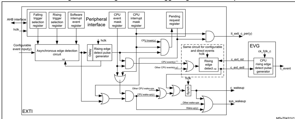
The software interrupt event register is used to trigger configurable events by software, writing the corresponding register bit, irrespective of the edge selection setting.
Rising and falling edge selection registers are used to enable and to select the configurable event active trigger edge or both edges.
Extended interrupts and event controller (EXTI)
The CPU has its dedicated wake-up (interrupt) mask register, and a dedicated event mask register. The enabled event is used to generate an event on the CPU. All CPU events are ORed together into a single CPU event signal. The event pending registers (EXTI_RPR and EXTI_FPR) are not set for an unmasked CPU event.
The configurable events have unique interrupt pending request register bits. The pending register is only set for an unmasked interrupt. Each configurable event provides dedicated combined secure/nonsecure interrupts to the CPU. The configurable event interrupts need to be acknowledged by software in EXTI_RPR and/or EXTI_FPR.
When a CPU wake-up (interrupt) or CPU event is enabled, the asynchronous edge detection circuit is reset by the clocked delay and rising edge detect pulse generator. This guarantees that the EXTI hclk clock is woken up before the asynchronous edge detection circuit is reset.
Note: A detected configurable event interrupt pending request can be cleared by the CPU with the correct access permission. The system is not able to enter into low-power modes as long as an interrupt pending request is active.
25.4.2 EXTI direct event input wake-up
Direct events do not have an associated EXTI interrupt. The EXTI only wakes up the system and CPU subsystem clocks, and can generate a CPU wake-up event. The peripheral synchronous interrupt, associated with the direct wake-up event, wakes up the CPU.
The EXTI direct event is able to generate a CPU event that wakes up the CPU. The CPU event may occur before the associated peripheral interrupt flag is set.
Figure 157. EXTI direct events
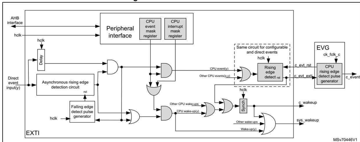
The diagram illustrates the internal logic of the EXTI direct event input wake-up mechanism. On the left, an 'AHB interface' and 'hclk' clock are shown. A 'Direct event input(y)' line enters the 'EXTI' block. Inside, this input is split: one path goes through a 'Delay' block and then an AND gate; another path goes through an 'Asynchronous rising edge detection circuit' (which also receives 'hclk' and a 'rst' signal) and then an OR gate. A 'Falling edge detect pulse generator' (receiving 'hclk') is connected to the OR gate output. The output of the pulse generator is connected to a 'CPU wake-up(y)' line and also to a 'Synch' block. The 'Synch' block also receives 'Other CPU wake-ups' and 'Wake-up(y)' signals and outputs 'c_wakeup' and 'sys_wakeup' signals. Above the OR gate, there is a 'Peripheral interface' block containing 'CPU event mask register' and 'CPU interrupt mask register'. The output of the AND gate is connected to an OR gate that also receives inputs from these registers. This OR gate's output is labeled 'CPU event(y)' and enters a dashed box labeled 'Same circuit for configurable and direct events'. Inside this box, 'CPU event(y)' and 'Other CPU events(x,y)' are ORed together and then passed through a 'Rising edge detect_rst' block (receiving 'hclk'). The output of this block is 'c_evt_rst', which enters an 'EVG' block containing 'ck_fclk_c' and a 'CPU rising edge detect pulse generator'. The final output of the EVG block is 'c_event'.
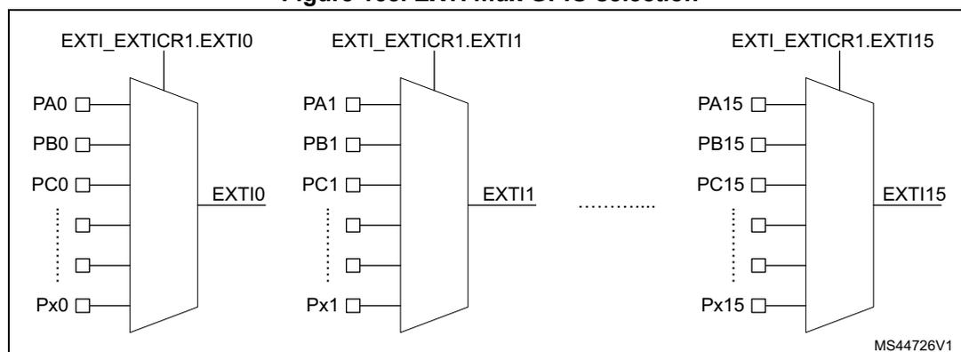
25.4.3 EXTI multiplexer selection
The EXTI multiplexer is used to select GPIOs as interrupts and wake-up. The GPIOs are connected via 16 EXTI multiplexers to the first 16 EXTI events as configurable event. The selection of GPIO port as EXTI multiplexer output is controlled by EXTIIn_EXTICRx (x = 1 to 4) registers.
Figure 158. EXTI mux GPIO selection
25.5 EXTI functional behavior
The direct event inputs are enabled in the respective peripheral generating the wake-up event. The configurable events are enabled by enabling at least one of the trigger edges.
Once an event input is enabled, the generation of the CPU wake-up is conditioned by the CPU interrupt mask and the CPU event mask.
Table 140. Masking functionality
| CPU interrupt enable EXTI_IMR.IMn | CPU event enable EXTI_EMR1.EMn | Configurable event inputs EXTI_RPR.RPIFn EXTI_FPR.FPIFn | exti(n) interrupt (1) | CPU event | CPU wake-up |
|---|---|---|---|---|---|
| 0 | 0 | No | Masked | Masked | Masked |
| 1 | No | Masked | Yes | Yes | |
| 1 | 0 | Status latched | Yes | Masked | Yes (2) |
| 1 | Status latched | Yes | Yes | Yes |
- 1. The CPU dedicated exti(n), combined secure/nonsecure interrupts, goes to the CPU. If no interrupt is required for the CPU, the exti(n) interrupt must be masked in EXTI_IMR.
- 2. Only if the CPU interrupt is enabled by IMn in EXTI_IMR.
For configurable event inputs, when the enabled edges occur on the event input, an event request is generated. When the associated CPU interrupt is unmasked, the corresponding RPIFn in EXTI_RPR and/or FPIFn in EXTI_FPR is/are set. The CPU subsystem is woken up, and the CPU combined secure/nonsecure interrupt signal is activated.
RPIFn in EXTI_RPR and/or FPIFn in EXTI_FPR must be cleared by software (writing them to 1). This clears the CPU interrupt. An interrupt is only generated on the dedicated interrupt line when it is enabled in EXTI_IMR.
For direct event inputs, when enabled in the associated peripheral, an event request is generated on the rising edge only. There is no corresponding CPU pending bit in the EXTI. When the associated CPU interrupt is unmasked, the corresponding CPU subsystem is woken up. The CPU is woken up (interrupted) by the peripheral synchronous interrupt.
The CPU event must be unmasked to generate an event. When an enabled edge occurs on the event input, a CPU event pulse is generated. There is no event pending bit.
For the configurable event inputs, an event request can be generated by software when writing 1 in EXTI_SWIERx. This generates a rising edge on the event. The rising edge event pending bit is set in EXTI_RPR, whatever the setting in EXTI_RTSR.
25.6 EXTI event protection
The EXTI is able to protect event register bits from being modified by nonsecure and unprivileged accesses. The protection can be activated individually per input event, via EXTI_SECCFGRx and EXTI_PRIVCFGRx. At EXTI level, the protection consists in preventing unauthorized write access to change settings of secure configurable events, change masking of secure input events, and clear pending status of secure input events.
Table 141. Register protection overview
| Register name | Access type | Security (1)(2) |
|---|---|---|
| EXTI_RTSRx | RW | Secure and privileged can be enabled bit-wise in EXTI_SECCFGRx and EXTI_PRIVCFGRx |
| EXTI_FTSRx | RW | |
| EXTI_SWIERx | RW | |
| EXTI_RPRx | RW | |
| EXTI_FPRx | RW | |
| EXTI_SECCFGRx | RW | Always secure and privileged |
| EXTI_PRIVCFGRx | RW | Always privileged, secure can be enabled bit-wise in EXTI_SECCFGRx |
| EXTI_EXTICRx | RW | Secure and privileged can be enabled bit-wise in EXTI_SECCFGRx and EXTI_PRIVCFGRx |
| EXTI_LOCKR | RW | Always secure and privileged |
| EXTI_IMRx | RW | Secure and privileged can be enabled bit-wise in EXTI_SECCFGRx and EXTI_PRIVCFGRx |
| EXTI_EMRx | RW |
- 1. Security is enabled with EXTI_SECCFGRx registers.
- 2. Privilege is enabled with EXTI_PRIVCFGRx registers.
25.6.1 EXTI register security protection
When security is enabled for an input event, the associated input event configuration and the control bits can only be modified and read by a secure access. A nonsecure write access is discarded and a read returns 0.
When input events are nonsecure, the security is disabled. The associated input event configuration and control bits can be modified and read by a secure access and nonsecure access.
The security configuration in EXTI_SECCFGRx can be globally locked after reset by GLOCK in EXTI_LOCKR.
25.6.2 EXTI register privilege protection
When the privilege is enabled for an input event, the associated input event configuration and control bits can only be modified and read by a privileged access. An unprivileged write access is discarded, and a read returns 0.
When input events are unprivileged, the privilege is disabled. The associated input event configuration and control bits can be modified and read by a privileged or unprivileged access.
The privilege configuration in EXTI_PRIVCFG \( R_x \) can be globally locked after reset by GLOCK in EXTI_LOCKR.
25.7 EXTI registers
The EXTI register map is divided in the following sections:
Table 142. EXTI register map sections
| Address offset | Description |
|---|---|
| 0x000 - 0x01C | General configurable event [31:0] configuration |
| 0x020 - 0x03C | General configurable event [63:32] configuration |
| 0x040 - 0x05C | General configurable event [95:64] configuration |
| 0x060 - 0x06C | EXTI I/O port mux selection |
| 0x070 | EXTI protection lock configuration |
| 0x080 - 0x0BC | CPU input event configuration |
All registers can be accessed with word (32-bit), half-word (16-bit), and byte (8-bit) access.
25.7.1 EXTI rising trigger selection register (EXTI_RTSR1)
Address offset: 0x000
Reset value: 0x0000 0000
This register contains only bits for configurable events.
| 31 | 30 | 29 | 28 | 27 | 26 | 25 | 24 | 23 | 22 | 21 | 20 | 19 | 18 | 17 | 16 |
| Res. | Res. | Res. | Res. | Res. | Res. | Res. | Res. | Res. | Res. | RT21 | RT20 | Res. | Res. | Res. | Res. |
| rw | rw | ||||||||||||||
| 15 | 14 | 13 | 12 | 11 | 10 | 9 | 8 | 7 | 6 | 5 | 4 | 3 | 2 | 1 | 0 |
| RT15 | RT14 | RT13 | RT12 | RT11 | RT10 | RT9 | RT8 | RT7 | RT6 | RT5 | RT4 | RT3 | RT2 | RT1 | RT0 |
| rw | rw | rw | rw | rw | rw | rw | rw | rw | rw | rw | rw | rw | rw | rw | rw |
Bits 31:22 Reserved, must be kept at reset value.
Extended interrupts and event controller (EXTI)
Bits 21:20 RTx : Rising trigger event configuration bit of configurable event input x (x = 21 to 20)
0: Rising trigger disabled (for event and interrupt) for input line
1: Rising trigger enabled (for event and interrupt) for input line
- | When SECx is disabled in EXTI_SECCFGR1, RTx can be accessed with nonsecure and secure access.
- | When SECx is enabled in EXTI_SECCFGR1, RTx can be accessed only with secure access. Nonsecure write to RTx is discarded. Nonsecure read returns 0.
- | When PRIVx is disabled in EXTI_PRIVCFGR1, RTx can be accessed with unprivileged and privileged access.
- | When PRIVx is enabled in EXTI_PRIVCFGR1, RTx can be accessed only with privileged access. Unprivileged write to RTx is discarded. Unprivileged read returns 0.
Note: The configurable event input is edge triggered. No glitch must be generated on this input. If a rising edge on the configurable event input occurs while writing to the register, the associated pending bit is not set.
Rising and falling edge triggers can be set for the same configurable event input. In this case, both edges generate a trigger.
Bits 19:16 Reserved, must be kept at reset value.
Bits 15:0 RTx : Rising trigger event configuration bit of configurable event input x (x = 15 to 0)
25.7.2 EXTI falling trigger selection register (EXTI_FTSR1)
Address offset: 0x004
Reset value: 0x0000 0000
This register contains only bits for configurable events.
| 31 | 30 | 29 | 28 | 27 | 26 | 25 | 24 | 23 | 22 | 21 | 20 | 19 | 18 | 17 | 16 |
|---|---|---|---|---|---|---|---|---|---|---|---|---|---|---|---|
| Res | Res | Res | Res | Res | Res | Res | Res | Res | Res | FT21 | FT20 | Res | Res | Res | Res |
| rw | rw | ||||||||||||||
| 15 | 14 | 13 | 12 | 11 | 10 | 9 | 8 | 7 | 6 | 5 | 4 | 3 | 2 | 1 | 0 |
| FT15 | FT14 | FT13 | FT12 | FT11 | FT10 | FT9 | FT8 | FT7 | FT6 | FT5 | FT4 | FT3 | FT2 | FT1 | FT0 |
| rw | rw | rw | rw | rw | rw | rw | rw | rw | rw | rw | rw | rw | rw | rw | rw |
Bits 31:22 Reserved, must be kept at reset value.
Bits 21:20 FTx : Falling trigger event configuration bit of configurable event input x (x = 21 to 20)
0: Falling trigger disabled (for event and interrupt) for input line
1: Falling trigger enabled (for event and interrupt) for input line.
- | When SECx is disabled in EXTI_SECCFGR1, FTx can be accessed with non-secure and secure access.
- | When SECx is enabled in EXTI_SECCFGR1, FTx can be accessed only with secure access. Nonsecure write to FTx is discarded. Nonsecure read returns 0.
- | When PRIVx is disabled in EXTI_PRIVCFGR1, FTx can be accessed with unprivileged and privileged access.
- | When PRIVx is enabled in EXTI_PRIVCFGR1, FTx can be accessed only with privileged access. Unprivileged write to FTx is discarded. Unprivileged read returns 0.
Note: The configurable event input is edge triggered. No glitch must be generated on this input. If a falling edge on the configurable event input occurs while writing to the register, the associated pending bit is not set.
Rising and falling edge triggers can be set for the same configurable event input. In this case, both edges generate a trigger.
Bits 19:16 Reserved, must be kept at reset value.
Bits 15:0 FTx : Falling trigger event configuration bit of configurable event input x (x = 15 to 0)
25.7.3 EXTI software interrupt event register (EXTI_SWIER1)
Address offset: 0x008
Reset value: 0x0000 0000
This register contains only bits for configurable events.
| 31 | 30 | 29 | 28 | 27 | 26 | 25 | 24 | 23 | 22 | 21 | 20 | 19 | 18 | 17 | 16 |
|---|---|---|---|---|---|---|---|---|---|---|---|---|---|---|---|
| Res | Res | Res | Res | Res | Res | Res | Res | Res | Res | SWI21 | SWI20 | Res | Res | Res | Res |
| rw | rw | ||||||||||||||
| 15 | 14 | 13 | 12 | 11 | 10 | 9 | 8 | 7 | 6 | 5 | 4 | 3 | 2 | 1 | 0 |
| SWI15 | SWI14 | SWI13 | SWI12 | SWI11 | SWI10 | SWI9 | SWI8 | SWI7 | SWI6 | SWI5 | SWI4 | SWI3 | SWI2 | SWI1 | SWI0 |
| rw | rw | rw | rw | rw | rw | rw | rw | rw | rw | rw | rw | rw | rw | rw | rw |
Bits 31:22 Reserved, must be kept at reset value.
Bits 21:20 SWIx : Software interrupt on event x (x = 21 to 20)
0: Writing 0 has no effect.
1: Writing 1 to this bit triggers a rising edge event on event x (bit auto cleared by hardware).
- | When SECx is disabled in EXTI_SECCFGR1, SWIx can be accessed with non-secure and secure access.
- | When SECx is enabled in EXTI_SECCFGR1, SWIx can be accessed only with secure access. Nonsecure write to SWIx is discarded. Nonsecure read returns 0.
- | When PRIVx is disabled in EXTI_PRIVCFGR1, SWIx can be accessed with unprivileged and privileged access.
- | When PRIVx is enabled in EXTI_PRIVCFGR1, SWIx can be accessed only with privileged access. Unprivileged write to SWIx is discarded. Unprivileged read returns 0.
- | A software interrupt is generated whatever the setting in EXTI_RTSR and EXTI_FTSR. It always returns 0 when read.
Bits 19:16 Reserved, must be kept at reset value.
Extended interrupts and event controller (EXTI)
Bits 15:0 SWIx : Software interrupt on event x (x = 15 to 0)
25.7.4 EXTI rising edge pending register (EXTI_RPR1)
Address offset: 0x00C
Reset value: 0x0000 0000
This register contains only bits for configurable events.
| 31 | 30 | 29 | 28 | 27 | 26 | 25 | 24 | 23 | 22 | 21 | 20 | 19 | 18 | 17 | 16 |
|---|---|---|---|---|---|---|---|---|---|---|---|---|---|---|---|
| Res. | Res. | Res. | Res. | Res. | Res. | Res. | Res. | Res. | Res. | RPIF21 | RPIF20 | Res. | Res. | Res. | Res. |
| 15 | 14 | 13 | 12 | 11 | 10 | 9 | 8 | 7 | 6 | 5 | 4 | 3 | 2 | 1 | 0 |
| RPIF15 | RPIF14 | RPIF13 | RPIF12 | RPIF11 | RPIF10 | RPIF9 | RPIF8 | RPIF7 | RPIF6 | RPIF5 | RPIF4 | RPIF3 | RPIF2 | RPIF1 | RPIF0 |
| rc_w1 | rc_w1 | rc_w1 | rc_w1 | rc_w1 | rc_w1 | rc_w1 | rc_w1 | rc_w1 | rc_w1 | rc_w1 | rc_w1 | rc_w1 | rc_w1 | rc_w1 | rc_w1 |
Bits 31:22 Reserved, must be kept at reset value.
Bits 21:20 RPIFx : Configurable event input x rising edge pending bit (x = 21 to 20)
This bit is set when the selected rising edge event or an EXTI_SWIER1 software trigger arrives on the configurable event line. This bit is cleared by writing a 1 into the bit.
0: No rising edge trigger request occurred
1: Rising edge trigger request occurred
- | When SECx is disabled in EXTI_SECCFGR1, RPIFx can be accessed with non-secure and secure access.
- | When SECx is enabled in EXTI_SECCFGR1, RPIFx can be accessed only with secure access. Nonsecure write to RPIFx is discarded. Nonsecure read returns 0.
- | When PRIVx is disabled in EXTI_PRIVCFGR1, RPIFx can be accessed with unprivileged and privileged access.
- | When PRIVx is enabled in EXTI_PRIVCFGR1, RPIFx can be accessed only with privileged access. Unprivileged write to RPIFx is discarded. Unprivileged read returns 0.
Bits 19:16 Reserved, must be kept at reset value.
Bits 15:0 RPIFx : Configurable event input x rising edge pending bit (x = 15 to 0)
25.7.5 EXTI falling edge pending register (EXTI_FPR1)
Address offset: 0x010
Reset value: 0x0000 0000
This register contains only bits for configurable events.
| 31 | 30 | 29 | 28 | 27 | 26 | 25 | 24 | 23 | 22 | 21 | 20 | 19 | 18 | 17 | 16 |
|---|---|---|---|---|---|---|---|---|---|---|---|---|---|---|---|
| Res. | Res. | Res. | Res. | Res. | Res. | Res. | Res. | Res. | Res. | FPIF21 | FPIF20 | Res. | Res. | Res. | Res. |
| 15 | 14 | 13 | 12 | 11 | 10 | 9 | 8 | 7 | 6 | 5 | 4 | 3 | 2 | 1 | 0 |
| FPIF15 | FPIF14 | FPIF13 | FPIF12 | FPIF11 | FPIF10 | FPIF9 | FPIF8 | FPIF7 | FPIF6 | FPIF5 | FPIF4 | FPIF3 | FPIF2 | FPIF1 | FPIF0 |
| rc_w1 | rc_w1 | rc_w1 | rc_w1 | rc_w1 | rc_w1 | rc_w1 | rc_w1 | rc_w1 | rc_w1 | rc_w1 | rc_w1 | rc_w1 | rc_w1 | rc_w1 | rc_w1 |
Bits 31:22 Reserved, must be kept at reset value.
Bits 21:20 FPIFx : configurable event input x falling edge pending bit (x = 21 to 20)
This bit is set when the falling edge event arrives on the configurable event line. This bit is cleared by writing a 1 into this bit.
0: No falling edge trigger request occurred
1: Falling edge trigger request occurred
- | When SECx is disabled in EXTI_SECCFGR1, FPIFx can be accessed with non-secure and secure access.
- | When SECx is enabled in EXTI_SECCFGR1, FPIFx can be accessed only with secure access. Nonsecure write to FPIFx is discarded. Nonsecure read returns 0.
- | When PRIVx is disabled in EXTI_PRIVCFGR1, FPIFx can be accessed with unprivileged and privileged access.
- | When PRIVx is enabled in EXTI_PRIVCFGR1, FPIFx can be accessed only with privileged access. Unprivileged write to FPIFx is discarded. Unprivileged read returns 0.
Bits 19:16 Reserved, must be kept at reset value.
Bits 15:0 FPIFx : Configurable event input x rising edge pending bit (x = 15 to 0)
25.7.6 EXTI security configuration register (EXTI_SECCFGR1)
Address offset: 0x014
Reset value: 0x0000 0000
This register provides write access security and privilege. A nonsecure or unprivileged write access is ignored, and causes the generation of an secure illegal access event. All read return the register data.
Write to this register is ignored if GLOCK is enabled in EXTI_LOCKR.
This register contains only bits for security capable input events.
| 31 | 30 | 29 | 28 | 27 | 26 | 25 | 24 | 23 | 22 | 21 | 20 | 19 | 18 | 17 | 16 |
|---|---|---|---|---|---|---|---|---|---|---|---|---|---|---|---|
| SEC 31 | SEC 30 | SEC 29 | SEC 28 | SEC 27 | SEC 26 | SEC 25 | SEC 24 | SEC 23 | SEC 22 | SEC 21 | SEC 20 | SEC 19 | SEC 18 | SEC 17 | Res. |
| rw | rw | rw | rw | rw | rw | rw | rw | rw | rw | rw | rw | rw | rw | rw | |
| 15 | 14 | 13 | 12 | 11 | 10 | 9 | 8 | 7 | 6 | 5 | 4 | 3 | 2 | 1 | 0 |
| SEC15 | SEC14 | SEC13 | SEC12 | SEC11 | SEC10 | SEC9 | SEC8 | SEC7 | SEC6 | SEC5 | SEC4 | SEC3 | SEC2 | SEC1 | SEC0 |
| rw | rw | rw | rw | rw | rw | rw | rw | rw | rw | rw | rw | rw | rw | rw | rw |
Bits 31:17 SECx : Security enable on event input x (x = 31 to 17)
0: Event security disabled (nonsecure)
1: Event security enabled (secure)
Bit 16 Reserved, must be kept at reset value.
Bits 15:0 SECx : Security enable on event input x (x = 15 to 0)
25.7.7 EXTI privilege configuration register (EXTI_PRIVCFGR1)
Address offset: 0x018
Reset value: 0x0000 0000
Extended interrupts and event controller (EXTI)
This register provides privileged write access protection. An unprivileged write access is discarded, and causes the generation of a privileged illegal access event. An unprivileged read returns the register data.
Write to this register are ignored if GLOCK is enabled in EXTI_LOCKR.
This register contains only bits for security capable input events.
| 31 | 30 | 29 | 28 | 27 | 26 | 25 | 24 | 23 | 22 | 21 | 20 | 19 | 18 | 17 | 16 |
|---|---|---|---|---|---|---|---|---|---|---|---|---|---|---|---|
| PRIV31 | PRIV30 | PRIV29 | PRIV28 | PRIV27 | PRIV26 | PRIV25 | PRIV24 | PRIV23 | PRIV22 | PRIV21 | PRIV20 | PRIV19 | PRIV18 | PRIV17 | Res. |
| rw | rw | rw | rw | rw | rw | rw | rw | rw | rw | rw | rw | rw | rw | rw |
| 15 | 14 | 13 | 12 | 11 | 10 | 9 | 8 | 7 | 6 | 5 | 4 | 3 | 2 | 1 | 0 |
|---|---|---|---|---|---|---|---|---|---|---|---|---|---|---|---|
| PRIV15 | PRIV14 | PRIV13 | PRIV12 | PRIV11 | PRIV10 | PRIV9 | PRIV8 | PRIV7 | PRIV6 | PRIV5 | PRIV4 | PRIV3 | PRIV2 | PRIV1 | PRIV0 |
| rw | rw | rw | rw | rw | rw | rw | rw | rw | rw | rw | rw | rw | rw | rw | rw |
Bits 31:17 PRIVx : Privilege enable on event input x (x = 31 to 17)
0: Event privilege disabled (unprivileged)
1: Event privilege enabled (privileged)
- | When SECx is disabled in EXT_SECCFGR1, PRIVx can be accessed with secure and nonsecure access.
- | When SECx is enabled in EXT_SECCFGR1, PRIVx can only be written with secure access. Nonsecure write to PRIVx is discarded.
Bit 16 Reserved, must be kept at reset value.
Bits 15:0 PRIVx : Privilege enable on event input x (x = 15 to 0)
25.7.8 EXTI rising trigger selection register (EXTI_RTSR2)
Address offset: 0x020
Reset value: 0x0000 0000
This register contains only bits for configurable events.
| 31 | 30 | 29 | 28 | 27 | 26 | 25 | 24 | 23 | 22 | 21 | 20 | 19 | 18 | 17 | 16 |
|---|---|---|---|---|---|---|---|---|---|---|---|---|---|---|---|
| Res. | Res. | Res. | Res. | Res. | Res. | Res. | RT56 | Res. | RT54 | Res. | Res. | RT51 | Res. | Res. | Res. |
| rw | rw | rw |
| 15 | 14 | 13 | 12 | 11 | 10 | 9 | 8 | 7 | 6 | 5 | 4 | 3 | 2 | 1 | 0 |
|---|---|---|---|---|---|---|---|---|---|---|---|---|---|---|---|
| Res. | Res. | Res. | Res. | Res. | Res. | Res. | RT40 | RT39 | Res. | Res. | Res. | Res. | Res. | Res. | Res. |
| rw | rw |
Bits 31:25 Reserved, must be kept at reset value.
Bit 24 RT56 : Rising trigger event configuration bit of configurable event input 56
0: Rising trigger disabled (for event and Interrupt) for input line x
1: Rising trigger enabled (for event and Interrupt) for input line x
- | When SECx is disabled in EXTI_SECCFGR2, RTx can be accessed with non-secure and secure access.
- | When SECx is enabled in EXTI_SECCFGR2, RTx can be accessed only with secure access. Nonsecure write to RTx is discarded. Nonsecure read returns 0.
- | When PRIVx is disabled in EXTI_PRIVCFGR2, RTx can be accessed with unprivileged and privileged access.
- | When PRIVx is enabled in EXTI_PRIVCFGR2, RTx can be accessed only with privileged access. Unprivileged write to RTx is discarded. Unprivileged read returns 0.
Note: The configurable event input is edge triggered. No glitch must be generated on this input. If a rising edge on the configurable event input occurs while writing to the register, the associated pending bit is not set.
Rising and falling edge triggers can be set for the same configurable event input. In this case, both edges generate a trigger.
Bit 23 Reserved, must be kept at reset value.
Bit 22 RT54 : Rising trigger event configuration bit of configurable event input 54
Bits 21:20 Reserved, must be kept at reset value.
Bit 19 RT51 : Rising trigger event configuration bit of configurable event input 51
Bits 18:9 Reserved, must be kept at reset value.
Bits 8:7 RTx : Rising trigger event configuration bit of configurable event input x (x = 40 to 39)
Bits 6:0 Reserved, must be kept at reset value.
25.7.9 EXTI falling trigger selection register (EXTI_FTSR2)
Address offset: 0x024
Reset value: 0x0000 0000
This register contains only bits for configurable events.
| 31 | 30 | 29 | 28 | 27 | 26 | 25 | 24 | 23 | 22 | 21 | 20 | 19 | 18 | 17 | 16 |
|---|---|---|---|---|---|---|---|---|---|---|---|---|---|---|---|
| Res. | Res. | Res. | Res. | Res. | Res. | Res. | FT56 | Res. | FT54 | Res. | Res. | FT51 | Res. | Res. | Res. |
| rw | rw | rw | |||||||||||||
| 15 | 14 | 13 | 12 | 11 | 10 | 9 | 8 | 7 | 6 | 5 | 4 | 3 | 2 | 1 | 0 |
| Res. | Res. | Res. | Res. | Res. | Res. | Res. | FT40 | FT39 | Res. | Res. | Res. | Res. | Res. | Res. | Res. |
| rw | rw |
Bits 31:25 Reserved, must be kept at reset value.
Extended interrupts and event controller (EXTI)
Bit 24 FT56 : Falling trigger event configuration bit of configurable event input 56
0: Falling trigger disabled (for event and Interrupt) for input line
1: Falling trigger enabled (for event and Interrupt) for input line.
- | When SECx is disabled in EXTI_SECCFGR2, FTx can be accessed with non-secure and secure access.
- | When SECx is enabled in EXTI_SECCFGR2, FTx can be accessed only with secure access. Nonsecure write to FTx is discarded. Nonsecure read returns 0.
- | When PRIVx is disabled in EXTI_PRIVCFGR2, FTx can be accessed with unprivileged and privileged access.
- | When PRIVx is enabled in EXTI_PRIVCFGR2, FTx can be accessed only with privileged access. Unprivileged write to FTx is discarded. Unprivileged read returns 0.
Note: The configurable event input is edge triggered. No glitch must be generated on this input. If a falling edge on the configurable event input occurs while writing to the register, the associated pending bit is not set.
Rising and falling edge triggers can be set for the same configurable event input. In this case, both edges generate a trigger.
Bit 23 Reserved, must be kept at reset value.
Bit 22 FT54 : Falling trigger event configuration bit of configurable event input 54
Bits 21:20 Reserved, must be kept at reset value.
Bit 19 FT51 : Falling trigger event configuration bit of configurable event input 51
Bits 18:9 Reserved, must be kept at reset value.
Bits 8:7 FTx : Falling trigger event configuration bit of configurable event input x (x = 40 to 39)
Bits 6:0 Reserved, must be kept at reset value.
25.7.10 EXTI software interrupt event register (EXTI_SWIER2)
Address offset: 0x028
Reset value: 0x0000 0000
This register contains only bits for configurable events.
| 31 | 30 | 29 | 28 | 27 | 26 | 25 | 24 | 23 | 22 | 21 | 20 | 19 | 18 | 17 | 16 |
|---|---|---|---|---|---|---|---|---|---|---|---|---|---|---|---|
| Res. | Res. | Res. | Res. | Res. | Res. | Res. | SWI56 | Res. | SWI54 | Res. | Res. | SWI51 | Res. | Res. | Res. |
| rw | rw | rw | |||||||||||||
| 15 | 14 | 13 | 12 | 11 | 10 | 9 | 8 | 7 | 6 | 5 | 4 | 3 | 2 | 1 | 0 |
| Res. | Res. | Res. | Res. | Res. | Res. | Res. | SWI40 | SWI39 | Res. | Res. | Res. | Res. | Res. | Res. | Res. |
| rw | rw |
Bits 31:25 Reserved, must be kept at reset value.
Bit 24 SWI56 : Software interrupt on event 56
0: Writing 0 has no effect.
1: Writing 1 to this bit triggers a rising edge event on event x (bit auto cleared by hardware).
- | When SECx is disabled in EXTI_SECCFGR2, SWIx can be accessed with non-secure and secure access.
- | When SECx is enabled in EXTI_SECCFGR2, SWIx can be accessed only with secure access. Nonsecure write to SWIx is discarded. Nonsecure read returns 0.
- | When PRIVx is disabled in EXTI_PRIVCFGR2, SWIx can be accessed with unprivileged and privileged access.
- | When PRIVx is enabled in EXTI_PRIVCFGR2, SWIx can be accessed only with privileged access. Unprivileged write to SWIx is discarded. Unprivileged read returns 0.
- | A software interrupt is generated whatever the setting in EXTI_RTSR and EXTI_FTSR. It always returns 0 when read.
Bit 23 Reserved, must be kept at reset value.
Bit 22 SWI54 : Software interrupt on event 54
Bits 21:20 Reserved, must be kept at reset value.
Bit 19 SWI51 : Software interrupt on event 51
Bits 18:9 Reserved, must be kept at reset value.
Bits 8:7 SWIx : Software interrupt on event x (x = 40 to 39)
Bits 6:0 Reserved, must be kept at reset value.
25.7.11 EXTI rising edge pending register (EXTI_RPR2)
Address offset: 0x02C
Reset value: 0x0000 0000
This register contains only bits for configurable events.
| 31 | 30 | 29 | 28 | 27 | 26 | 25 | 24 | 23 | 22 | 21 | 20 | 19 | 18 | 17 | 16 |
|---|---|---|---|---|---|---|---|---|---|---|---|---|---|---|---|
| Res. | Res. | Res. | Res. | Res. | Res. | Res. | RPIF56 | Res. | RPIF54 | Res. | Res. | RPIF51 | Res. | Res. | Res. |
| rc_w1 | rc_w1 | rc_w1 | |||||||||||||
| 15 | 14 | 13 | 12 | 11 | 10 | 9 | 8 | 7 | 6 | 5 | 4 | 3 | 2 | 1 | 0 |
| Res. | Res. | Res. | Res. | Res. | Res. | Res. | RPIF40 | RPIF39 | Res. | Res. | Res. | Res. | Res. | Res. | Res. |
| rc_w1 | rc_w1 |
Bits 31:25 Reserved, must be kept at reset value.
Extended interrupts and event controller (EXTI)
Bit 24 RPIF56 : Configurable event input 56 rising edge pending bit
This bit is set when the selected rising edge event or an EXTI_SWIER2 software trigger arrives on the configurable event line. This bit is cleared by writing a 1 into the bit.
0: No rising edge trigger request occurred
1: Rising edge trigger request occurred
- | When SECx is disabled in EXTI_SECCFGR2, RPIFx can be accessed with non-secure and secure access.
- | When SECx is enabled in EXTI_SECCFGR2, RPIFx can be accessed only with secure access. Nonsecure write to RPIFx is discarded. Nonsecure read returns 0.
- | When PRIVx is disabled in EXTI_PRIVCFGR2, RPIFx can be accessed with unprivileged and privileged access.
- | When PRIVx is enabled in EXTI_PRIVCFGR2, this bit can be accessed only with privileged access. Unprivileged write to RPIFx is discarded. Unprivileged read returns 0.
Bit 23 Reserved, must be kept at reset value.
Bit 22 RPIF54 : Configurable event input 54 rising edge pending bit
Bits 21:20 Reserved, must be kept at reset value.
Bit 19 RPIF51 : Configurable event input 51 rising edge pending bit
Bits 18:9 Reserved, must be kept at reset value.
Bits 8:7 RPIFx : Configurable event input x rising edge pending bit (x = 40 to 39)
Bits 6:0 Reserved, must be kept at reset value.
25.7.12 EXTI falling edge pending register (EXTI_FPR2)
Address offset: 0x030
Reset value: 0x0000 0000
This register contains only bits for configurable events.
| 31 | 30 | 29 | 28 | 27 | 26 | 25 | 24 | 23 | 22 | 21 | 20 | 19 | 18 | 17 | 16 |
|---|---|---|---|---|---|---|---|---|---|---|---|---|---|---|---|
| Res. | Res. | Res. | Res. | Res. | Res. | Res. | FPIF56 | Res. | FPIF54 | Res. | Res. | FPIF51 | Res. | Res. | Res. |
| rc_w1 | rc_w1 | rc_w1 | |||||||||||||
| 15 | 14 | 13 | 12 | 11 | 10 | 9 | 8 | 7 | 6 | 5 | 4 | 3 | 2 | 1 | 0 |
| Res. | Res. | Res. | Res. | Res. | Res. | Res. | FPIF40 | FPIF39 | Res. | Res. | Res. | Res. | Res. | Res. | Res. |
| rc_w1 | rc_w1 |
Bits 31:25 Reserved, must be kept at reset value.
Bit 24 FPIF56 : Configurable event input 56 falling edge pending bit
This bit is set when the falling edge event arrives on the configurable event line. This bit is cleared by writing a 1 into the bit.
0: No falling edge trigger request occurred
1: Falling edge trigger request occurred
- | When SECx is disabled in EXTI_SECCFGR2, FPIFx can be accessed with non-secure and secure access.
- | When SECx is enabled in EXTI_SECCFGR2, FPIFx can be accessed only with secure access. Nonsecure write to this FPIFx is discarded. Nonsecure read returns 0.
- | When PRIVx is disabled in EXTI_PRIVCFGR2, FPIFx can be accessed with unprivileged and privileged access.
- | When PRIVx is enabled in EXTI_PRIVCFGR2, FPIFx can be accessed only with privileged access. Unprivileged write to FPIFx is discarded. Unprivileged read returns 0.
Bit 23 Reserved, must be kept at reset value.
Bit 22 FPIF54 : Configurable event input 54 falling edge pending bit
Bits 21:20 Reserved, must be kept at reset value.
Bit 19 FPIF51 : Configurable event input 51 falling edge pending bit
Bits 18:9 Reserved, must be kept at reset value.
Bits 8:7 FPIFx : Configurable event input x falling edge pending bit (x = 40 to 39)
Bits 6:0 Reserved, must be kept at reset value.
25.7.13 EXTI security enable register (EXTI_SECCFGR2)
Address offset: 0x034
Reset value: 0x0000 0000
This register provides write access security and privilege. A nonsecure or unprivileged write access is ignored, and causes the generation of an secure illegal access event. All read return the register data.
Write to this register is ignored if GLOCK is enabled in EXTI_LOCKR.
This register contains only bits for security capable input events.
| 31 | 30 | 29 | 28 | 27 | 26 | 25 | 24 | 23 | 22 | 21 | 20 | 19 | 18 | 17 | 16 |
|---|---|---|---|---|---|---|---|---|---|---|---|---|---|---|---|
| SEC 63 | SEC 62 | SEC 61 | SEC 60 | Res. | SEC 58 | SEC 57 | SEC 56 | SEC 55 | SEC 54 | SEC 53 | SEC 52 | SEC 51 | SEC 50 | SEC 49 | SEC 48 |
| rw | rw | rw | rw | rw | rw | rw | rw | rw | rw | rw | rw | rw | rw | rw | |
| 15 | 14 | 13 | 12 | 11 | 10 | 9 | 8 | 7 | 6 | 5 | 4 | 3 | 2 | 1 | 0 |
| SEC 47 | SEC 46 | SEC 45 | SEC 44 | SEC 43 | SEC 42 | SEC 41 | SEC 40 | SEC 39 | SEC 38 | SEC 37 | SEC 36 | SEC 35 | SEC 34 | SEC 33 | SEC 32 |
| rw | rw | rw | rw | rw | rw | rw | rw | rw | rw | rw | rw | rw | rw | rw | rw |
Bits 31:28 SECx : Security enable on event input x (x = 63 to 60)
0: Event security disabled (nonsecure)
1: Event security enabled (secure)
Bit 27 Reserved, must be kept at reset value.
Bits 26:0 SECx : Security enable on event input x (x = 58 to 32)
25.7.14 EXTI privilege enable register (EXTI_PRIVCFGR2)
Address offset: 0x038
Reset value: 0x0000 0000
This register provides privileged write access protection. An unprivileged write access is discarded, and causes the generation of a privileged illegal access event. An unprivileged read returns the register data.
Write to this register is ignored if GLOCK is enabled in EXTI_LOCKR.
This register contains only bits for security capable input events.
| 31 | 30 | 29 | 28 | 27 | 26 | 25 | 24 | 23 | 22 | 21 | 20 | 19 | 18 | 17 | 16 |
|---|---|---|---|---|---|---|---|---|---|---|---|---|---|---|---|
| PRIV 63 | PRIV 62 | PRIV 61 | PRIV 60 | Res. | PRIV 58 | PRIV 57 | PRIV 56 | PRIV 55 | PRIV 54 | PRIV 53 | PRIV 52 | PRIV 51 | PRIV 50 | PRIV 49 | PRIV 48 |
| rw | rw | rw | rw | rw | rw | rw | rw | rw | rw | rw | rw | rw | rw | rw |
| 15 | 14 | 13 | 12 | 11 | 10 | 9 | 8 | 7 | 6 | 5 | 4 | 3 | 2 | 1 | 0 |
|---|---|---|---|---|---|---|---|---|---|---|---|---|---|---|---|
| PRIV 47 | PRIV 46 | PRIV 45 | PRIV 44 | PRIV 43 | PRIV 42 | PRIV 41 | PRIV 40 | PRIV 39 | PRIV 38 | PRIV 37 | PRIV 36 | PRIV 35 | PRIV 34 | PRIV 33 | PRIV 32 |
| rw | rw | rw | rw | rw | rw | rw | rw | rw | rw | rw | rw | rw | rw | rw | rw |
Bits 31:28 PRIVx : Privilege enable on event input x (x = 63 to 60)
0: Event privilege disabled (unprivileged)
1: Event privilege enabled (privileged)
- | When SECx is disabled in EXTI_SECCFGR2, PRIVx can be accessed with secure and nonsecure access.
- | When SECx is enabled in EXTI_SECCFGR2, PRIVx can be accessed only with secure access. Nonsecure write to PRIVx is discarded.
Bit 27 Reserved, must be kept at reset value.
Bits 26:0 PRIVx : Privilege enable on event input x (x = 58 to 32)
25.7.15 EXTI rising trigger selection register (EXTI_RTSR3)
Address offset: 0x040
Reset value: 0x0000 0000
This register contains only bits for configurable events.
| 31 | 30 | 29 | 28 | 27 | 26 | 25 | 24 | 23 | 22 | 21 | 20 | 19 | 18 | 17 | 16 |
|---|---|---|---|---|---|---|---|---|---|---|---|---|---|---|---|
| Res. | Res. | Res. | Res. | Res. | Res. | Res. | Res. | Res. | Res. | Res. | Res. | Res. | Res. | Res. | Res. |
| 15 | 14 | 13 | 12 | 11 | 10 | 9 | 8 | 7 | 6 | 5 | 4 | 3 | 2 | 1 | 0 |
|---|---|---|---|---|---|---|---|---|---|---|---|---|---|---|---|
| Res. | Res. | Res. | Res. | Res. | RT74 | RT73 | RT72 | RT71 | RT70 | RT69 | RT68 | Res. | RT66 | Res. | Res. |
| rw | rw | rw | rw | rw | rw | rw | rw |
Bits 31:11 Reserved, must be kept at reset value.
Bits 10:4 RTx : Rising trigger event configuration bit of configurable event input x (x = 74 to 68)
0: Rising trigger disabled (for event and interrupt) for input line
1: Rising trigger enabled (for event and interrupt) for input line
- | When SECx is disabled in EXTI_SECCFGR3, RTx can be accessed with non-secure and secure access.
- | When SECx is enabled in EXTI_SECCFGR3, RTx can be accessed only with secure access. Nonsecure write to RTx is discarded. Nonsecure read returns 0.
- | When PRIVx is disabled in EXTI_PRIVCFGR3, RTx can be accessed with unprivileged and privileged access.
- | When PRIVx is enabled in EXTI_PRIVCFGR3, RTx can be accessed only with privileged access. Unprivileged write to RTx is discarded. Unprivileged read returns 0.
Note: The configurable event input is edge triggered. No glitch must be generated on this input. If a rising edge on the configurable event input occurs while writing to the register, the associated pending bit is not set.
Rising and falling edge triggers can be set for the same configurable event input. In this case, both edges generate a trigger.
Bit 3 Reserved, must be kept at reset value.
Bit 2 RT66 : Rising trigger event configuration bit of configurable event input 66
Bits 1:0 Reserved, must be kept at reset value.
25.7.16 EXTI falling trigger selection register (EXTI_FTSR3)
Address offset: 0x044
Reset value: 0x0000 0000
This register contains only bits for configurable events.
| 31 | 30 | 29 | 28 | 27 | 26 | 25 | 24 | 23 | 22 | 21 | 20 | 19 | 18 | 17 | 16 |
|---|---|---|---|---|---|---|---|---|---|---|---|---|---|---|---|
| Res. | Res. | Res. | Res. | Res. | Res. | Res. | Res. | Res. | Res. | Res. | Res. | Res. | Res. | Res. | Res. |
| 15 | 14 | 13 | 12 | 11 | 10 | 9 | 8 | 7 | 6 | 5 | 4 | 3 | 2 | 1 | 0 |
| Res. | Res. | Res. | Res. | Res. | FT74 | FT73 | FT72 | FT71 | FT70 | FT69 | FT68 | Res. | FT66 | Res. | Res. |
| rw | rw | rw | rw | rw | rw | rw | rw |
Bits 31:11 Reserved, must be kept at reset value.
Extended interrupts and event controller (EXTI)
Bits 10:4 FTx : Falling trigger event configuration bit of configurable event input x (x = 74 to 68)
0: Falling trigger disabled (for event and interrupt) for input line
1: Falling trigger enabled (for event and interrupt) for input line
- | When SECx is disabled in EXTI_SECCFGR3, FTx can be accessed with nonsecure and secure access.
- | When SECx is enabled in EXTI_SECCFGR3, FTx can be accessed only with secure access. Nonsecure write to FTx is discarded. Nonsecure read returns 0.
- | When PRIVx is disabled in EXTI_PRIVCFGR3, FTx can be accessed with unprivileged and privileged access.
- | When PRIVx is enabled in EXTI_PRIVCFGR3, FTx can be accessed only with privileged access. Unprivileged write to FTx is discarded. Unprivileged read returns 0.
Note: The configurable event input is edge triggered. No glitch must be generated on this input. If a falling edge on the configurable event input occurs while writing to the register, the associated pending bit is not set.
Rising and falling edge triggers can be set for the same configurable event input. In this case, both edges generate a trigger.
Bit 3 Reserved, must be kept at reset value.
Bit 2 FT66 : Falling trigger event configuration bit of configurable event input 66
Bits 1:0 Reserved, must be kept at reset value.
25.7.17 EXTI software interrupt event register (EXTI_SWIER3)
Address offset: 0x048
Reset value: 0x0000 0000
This register contains only bits for configurable events.
| 31 | 30 | 29 | 28 | 27 | 26 | 25 | 24 | 23 | 22 | 21 | 20 | 19 | 18 | 17 | 16 |
|---|---|---|---|---|---|---|---|---|---|---|---|---|---|---|---|
| Res. | Res. | Res. | Res. | Res. | Res. | Res. | Res. | Res. | Res. | Res. | Res. | Res. | Res. | Res. | Res. |
| 15 | 14 | 13 | 12 | 11 | 10 | 9 | 8 | 7 | 6 | 5 | 4 | 3 | 2 | 1 | 0 |
| Res. | Res. | Res. | Res. | Res. | SWI74 | SWI73 | SWI72 | SWI71 | SWI70 | SWI69 | SWI68 | Res. | SWI66 | Res. | Res. |
| rw | rw | rw | rw | rw | rw | rw | rw |
Bits 31:11 Reserved, must be kept at reset value.
Bits 10:4 SWIx : Software interrupt on event x (x = 74 to 68)
0: Writing 0 has no effect.
1: Writing 1 to this bit triggers a rising edge event on event x (bit auto cleared by hardware).
- | When SECx is disabled in EXTI_SECCFGR3, SWIx can be accessed with non-secure and secure access.
- | When SECx is enabled in EXTI_SECCFGR3, SWIx can be accessed only with secure access. Nonsecure write to SWIx is discarded. Nonsecure read returns 0.
- | When PRIVx is disabled in EXTI_PRIVCFGR3, SWIx can be accessed with unprivileged and privileged access.
- | When PRIVx is enabled in EXTI_PRIVCFGR3, SWIx can be accessed only with privileged access. Unprivileged write to SWIx is discarded. Unprivileged read returns 0.
- | A software interrupt is generated whatever the setting in EXTI_RTSR and EXTI_FTSR. It always returns 0 when read.
Bit 3 Reserved, must be kept at reset value.
Bit 2 SWI66 : Software interrupt on event 66
Bits 1:0 Reserved, must be kept at reset value.
25.7.18 EXTI rising edge pending register (EXTI_RPR3)
Address offset: 0x04C
Reset value: 0x0000 0000
This register contains only bits for configurable events.
| 31 | 30 | 29 | 28 | 27 | 26 | 25 | 24 | 23 | 22 | 21 | 20 | 19 | 18 | 17 | 16 |
|---|---|---|---|---|---|---|---|---|---|---|---|---|---|---|---|
| Res. | Res. | Res. | Res. | Res. | Res. | Res. | Res. | Res. | Res. | Res. | Res. | Res. | Res. | Res. | Res. |
| 15 | 14 | 13 | 12 | 11 | 10 | 9 | 8 | 7 | 6 | 5 | 4 | 3 | 2 | 1 | 0 |
| Res. | Res. | Res. | Res. | Res. | RPIF74 | RPIF73 | RPIF72 | RPIF71 | RPIF70 | RPIF69 | RPIF68 | Res. | RPIF66 | Res. | Res. |
| rc_w1 | rc_w1 | rc_w1 | rc_w1 | rc_w1 | rc_w1 | rc_w1 | rc_w1 | ||||||||
Bits 31:11 Reserved, must be kept at reset value.
Bits 10:4 RPIFx : configurable event input x rising edge pending bit (x = 74 to 68)
This bit is set when the selected rising edge event or an EXTI_SWIER3 software trigger arrives on the configurable event line. This bit is cleared by writing a 1 into the bit.
0: No rising edge trigger request occurred
1: Rising edge trigger request occurred
- | When SECx is disabled in EXTI_SECCFGR3, RPIFx can be accessed with non-secure and secure access.
- | When SECx is enabled in EXTI_SECCFGR3, RPIFx can be accessed only with secure access. Nonsecure write to this RPIFx is discarded. Nonsecure read returns 0.
- | When PRIVx is disabled in EXTI_PRIVCFGR3, RPIFx can be accessed with unprivileged and privileged access.
- | When PRIVx is enabled in EXTI_PRIVCFGR3, RPIFx can be accessed only with privileged access. Unprivileged write to RPIFx is discarded. Unprivileged read returns 0.
Bit 3 Reserved, must be kept at reset value.
Bit 2 RPIF66 : configurable event input 66 rising edge pending bit
Bits 1:0 Reserved, must be kept at reset value.
25.7.19 EXTI falling edge pending register (EXTI_FPR3)
Address offset: 0x050
Reset value: 0x0000 0000
This register contains only bits for configurable events.
Extended interrupts and event controller (EXTI)
| 31 | 30 | 29 | 28 | 27 | 26 | 25 | 24 | 23 | 22 | 21 | 20 | 19 | 18 | 17 | 16 |
|---|---|---|---|---|---|---|---|---|---|---|---|---|---|---|---|
| Res. | Res. | Res. | Res. | Res. | Res. | Res. | Res. | Res. | Res. | Res. | Res. | Res. | Res. | Res. | Res. |
| 15 | 14 | 13 | 12 | 11 | 10 | 9 | 8 | 7 | 6 | 5 | 4 | 3 | 2 | 1 | 0 |
| Res. | Res. | Res. | Res. | Res. | FPIF74 | FPIF73 | FPIF72 | FPIF71 | FPIF70 | FPIF69 | FPIF68 | Res. | FPIF66 | Res. | Res. |
| rc_w1 | rc_w1 | rc_w1 | rc_w1 | rc_w1 | rc_w1 | rc_w1 | rc_w1 |
Bits 31:11 Reserved, must be kept at reset value.
Bits 10:4 FPIFx : configurable event input x falling edge pending bit (x = 74 to 68)
This bit is set when the falling edge event arrives on the configurable event line. This bit is cleared by writing a 1 into the bit.
0: No falling edge trigger request occurred
1: Falling edge trigger request occurred
- | When SECx is disabled in EXTI_SECCFGR3, FPIFx can be accessed with non-secure and secure access.
- | When SECx is enabled in EXTI_SECCFGR3, FPIFx can be accessed only with secure access. Nonsecure write to FPIFx is discarded. Nonsecure read returns 0.
- | When PRIVx is disabled in EXTI_PRIVCFGR3, FPIFx can be accessed with unprivileged and privileged access.
- | When PRIVx is enabled in EXTI_PRIVCFGR3, FPIFx can be accessed only with privileged access. Unprivileged write to FPIFx is discarded. Unprivileged read returns 0.
Bit 3 Reserved, must be kept at reset value.
Bit 2 FPIF66 : configurable event input 66 falling edge pending bit
Bits 1:0 Reserved, must be kept at reset value.
25.7.20 EXTI security enable register (EXTI_SECCFGR3)
Address offset: 0x054
Reset value: 0x0000 0000
This register provides write access security and privilege. A nonsecure or unprivileged write access is ignored and causes the generation of an secure illegal access event. All reads return the register data.
Write to this register are ignored if GLOCK is enabled in EXTI_LOCKR.
This register contains only bits for security capable input events.
| 31 | 30 | 29 | 28 | 27 | 26 | 25 | 24 | 23 | 22 | 21 | 20 | 19 | 18 | 17 | 16 |
|---|---|---|---|---|---|---|---|---|---|---|---|---|---|---|---|
| Res. | Res. | Res. | Res. | Res. | Res. | Res. | Res. | Res. | Res. | Res. | Res. | Res. | Res. | Res. | Res. |
| 15 | 14 | 13 | 12 | 11 | 10 | 9 | 8 | 7 | 6 | 5 | 4 | 3 | 2 | 1 | 0 |
| Res. | Res. | SEC 77 | Res. | Res. | SEC 74 | SEC 73 | SEC 72 | SEC 71 | SEC 70 | SEC 69 | SEC 68 | Res. | SEC 66 | SEC 65 | SEC 64 |
| rw | rw | rw | rw | rw | rw | rw | rw | rw | rw | rw |
Bits 31:14 Reserved, must be kept at reset value.
Bit 13 SEC77 : Security enable on event input 77
0: Event security disabled (nonsecure)
1: Event security enabled (secure)
Bits 12:11 Reserved, must be kept at reset value.
Bits 10:4 SECx : Security enable on event input x (x = 74 to 68)
Bit 3 Reserved, must be kept at reset value.
Bits 2:0 SECx : Security enable on event input x (x = 66 to 64)
25.7.21 EXTI privilege enable register (EXTI_PRIVCFGR3)
Address offset: 0x058
Reset value: 0x0000 0000
This register provides privileged write access protection. An unprivileged write access is discarded and causes the generation of a privileged illegal access event. An unprivileged read returns the register data.
Write to this register are ignored if GLOCK is enabled in EXTI_LOCKR.
This register contains only bits for security capable Input events.
| 31 | 30 | 29 | 28 | 27 | 26 | 25 | 24 | 23 | 22 | 21 | 20 | 19 | 18 | 17 | 16 |
|---|---|---|---|---|---|---|---|---|---|---|---|---|---|---|---|
| Res. | Res. | Res. | Res. | Res. | Res. | Res. | Res. | Res. | Res. | Res. | Res. | Res. | Res. | Res. | Res. |
| 15 | 14 | 13 | 12 | 11 | 10 | 9 | 8 | 7 | 6 | 5 | 4 | 3 | 2 | 1 | 0 |
| Res. | Res. | PRIV 77 | Res. | Res. | PRIV 74 | PRIV 73 | PRIV 72 | PRIV 71 | PRIV 70 | PRIV 69 | PRIV 68 | Res. | PRIV 66 | PRIV 65 | PRIV 64 |
| rw | rw | rw | rw | rw | rw | rw | rw | rw | rw | rw |
Bits 31:14 Reserved, must be kept at reset value.
Bit 13 PRIV77 : Privilege enable on event input 77
0: Event privilege disabled (unprivileged)
1: Event privilege enabled (privileged)
- | When SECx is disabled in EXTI_SECCFGR3, PRIVx can be accessed with secure and nonsecure access.
- | When SECx is enabled in EXTI_SECCFGR3, PRIVx can only be written with secure access. Nonsecure write to PRIVx is discarded.
Bits 12:11 Reserved, must be kept at reset value.
Bits 10:4 PRIVx : Privilege enable on event input x (x = 74 to 68)
Bit 3 Reserved, must be kept at reset value.
Bits 2:0 PRIVx : Privilege enable on event input x (x = 66 to 64)
25.7.22 EXTI external interrupt selection register 1 (EXTI_EXTICR1)
Address offset: 0x060
Reset value: 0x0000 0000
Extended interrupts and event controller (EXTI)
| 31 | 30 | 29 | 28 | 27 | 26 | 25 | 24 | 23 | 22 | 21 | 20 | 19 | 18 | 17 | 16 |
|---|---|---|---|---|---|---|---|---|---|---|---|---|---|---|---|
| EXTI3[7:0] | EXTI2[7:0] | ||||||||||||||
| rw | rw | rw | rw | rw | rw | rw | rw | rw | rw | rw | rw | rw | rw | rw | rw |
| 15 | 14 | 13 | 12 | 11 | 10 | 9 | 8 | 7 | 6 | 5 | 4 | 3 | 2 | 1 | 0 |
| EXTI1[7:0] | EXTI0[7:0] | ||||||||||||||
| rw | rw | rw | rw | rw | rw | rw | rw | rw | rw | rw | rw | rw | rw | rw | rw |
Bits 31:24 EXTI3[7:0] : EXTI3 GPIO port selection
These bits are written by software to select the source input for EXTI3 external interrupt.
0x00: PA3 pin
0x01: PB3 pin
0x02: PC3 pin
0x03: PD3 pin
0x04: PE3 pin
0x05: PF3 pin
0x06: PG3 pin
0x07: PH3 pin
0x08: PN3 pin
0x09: PO3 pin
0x0A: PP3 pin
0x0B: PQ3 pin
Others: reserved
- | When SEC3 is disabled in EXTI_SECCFGR1, this field can be accessed with non-secure and secure access.
- | When SEC3 is enabled in EXTI_SECCFGR1, this field can be accessed only with secure access. Nonsecure write is discarded. Nonsecure read returns 0.
- | When PRIV3 is disabled in EXTI_PRIVCFGR1, this field can be accessed with privileged and unprivileged access.
- | When PRIV3 is enabled in EXTI_PRIVCFGR1, this field can be accessed only with privileged access. Unprivileged write to this field is discarded, and read returns 0.
These bits are written by software to select the source input for EXTI2 external interrupt.
0x00: PA2 pin
0x01: PB2 pin
0x02: PC2 pin
0x03: PD2 pin
0x04: PE2 pin
0x05: PF2 pin
0x06: PG2 pin
0x07: PH2 pin
0x08: PN2 pin
0x09: PO2 pin
0x0A: PP2 pin
0x0B: PQ2 pin
Others: reserved
- I When SEC2 is disabled in EXTI_SECCFGR1, this field can be accessed with non-secure and secure access.
- I When SEC2 is enabled in EXTI_SECCFGR1, this field can be accessed only with secure access. Nonsecure write is discarded, nonsecure read returns 0.
- I When PRIV2 is disabled in EXTI_PRIVCFGR1, this field can be accessed with privileged and unprivileged access.
- I When PRIV2 is enabled in EXTI_PRIVCFGR1, this field can be accessed only with privileged access. Unprivileged write to this field is discarded and read returns 0.
These bits are written by software to select the source input for EXTI1 external interrupt.
0x00: PA1 pin
0x01: PB1 pin
0x02: PC1 pin
0x03: PD1 pin
0x04: PE1 pin
0x05: PF1 pin
0x06: PG1 pin
0x07: PH1 pin
0x08: PN1 pin
0x09: PO1 pin
0x0A: PP1 pin
0x0B: PQ1 pin
Others: reserved
- I When SEC1 is disabled in EXTI_SECCFGR1, this field can be accessed with non-secure and secure access.
- I When SEC1 is enabled in EXTI_SECCFGR1, this field can be accessed only with secure access. Nonsecure write is discarded, nonsecure read returns 0.
- I When PRIV1 is disabled in EXTI_PRIVCFGR1, this field can be accessed with privileged and unprivileged access.
- I When PRIV1 is enabled in EXTI_PRIVCFGR1, this field can be accessed only with privileged access. Unprivileged write to this field is discarded and read returns 0.
Extended interrupts and event controller (EXTI)
Bits 7:0 EXTI0[7:0] : EXTI0 GPIO port selection.
These bits are written by software to select the source input for EXTI0 external interrupt.
0x00: PA0 pin
0x01: PB0 pin
0x02: PC0 pin
0x03: PD0 pin
0x04: PE0 pin
0x05: PF0 pin
0x06: PG0 pin
0x07: PH0 pin
0x08: PN0 pin
0x09: PO0 pin
0x0A: PP0 pin
0x0B: PQ0 pin
Others: reserved
- | When SEC0 is disabled in EXTI_SECCFGR1 this field can be accessed with non-secure and secure access.
- | When SEC0 is enabled in EXTI_SECCFGR1, this field can be accessed only with secure access. Nonsecure write is discarded, nonsecure read returns 0.
- | When PRIV0 is disabled in EXTI_PRIVCFGR1, this field can be accessed with privileged and unprivileged access.
- | When PRIV0 is enabled in EXTI_PRIVCFGR1, this field can be accessed only with privileged access. Unprivileged write to this field is discarded and read returns 0.
25.7.23 EXTI external interrupt selection register 2 (EXTI_EXTICR2)
Address offset: 0x064
Reset value: 0x0000 0000
| 31 | 30 | 29 | 28 | 27 | 26 | 25 | 24 | 23 | 22 | 21 | 20 | 19 | 18 | 17 | 16 |
|---|---|---|---|---|---|---|---|---|---|---|---|---|---|---|---|
| EXTI7[7:0] | EXTI6[7:0] | ||||||||||||||
| rw | rw | rw | rw | rw | rw | rw | rw | rw | rw | rw | rw | rw | rw | rw | rw |
| 15 | 14 | 13 | 12 | 11 | 10 | 9 | 8 | 7 | 6 | 5 | 4 | 3 | 2 | 1 | 0 |
| EXTI5[7:0] | EXTI4[7:0] | ||||||||||||||
| rw | rw | rw | rw | rw | rw | rw | rw | rw | rw | rw | rw | rw | rw | rw | rw |
Bits 31:24 EXTI7[7:0] : EXTI7 GPIO port selection.
These bits are written by software to select the source input for EXTI7 external interrupt.
0x00: PA7 pin
0x01: PB7 pin
0x02: PC7 pin
0x03: PD7 pin
0x04: PE7 pin
0x05: PF7 pin
0x06: PG7 pin
0x07: PH7 pin
0x08: PN7 pin
0x09: PO7 pin
0x0A: PP7 pin
0x0B: PQ7 pin
Others: reserved
- I When SEC7 is disabled in EXTI_SECCFGR1 this field can be accessed with non-secure and secure access.
- I When SEC7 is enabled in EXTI_SECCFGR1, this field can be accessed only with secure access. Nonsecure write is discarded, nonsecure read returns 0.
- I When PRIV7 is disabled in EXTI_PRIVCFGR1, this field can be accessed with privileged and unprivileged access.
- I When PRIV7 is enabled in EXTI_PRIVCFGR1, this field can be accessed only with privileged access. Unprivileged write to this field is discarded and read returns 0.
Bits 23:16 EXTI6[7:0] : EXTI6 GPIO port selection.
These bits are written by software to select the source input for EXTI6 external interrupt.
0x00: PA6 pin
0x01: PB6 pin
0x02: PC6 pin
0x03: PD6 pin
0x04: PE6 pin
0x05: PF6 pin
0x06: PG6 pin
0x07: PH6 pin
0x08: PN6 pin
0x09: PO6 pin
0x0A: PP6 pin
0x0B: PQ6 pin
Others: reserved
- I When SEC6 is disabled in EXTI_SECCFGR1 this field can be accessed with non-secure and secure access.
- I When SEC6 is enabled in EXTI_SECCFGR1, this field can be accessed only with secure access. Nonsecure write is discarded, nonsecure read returns 0.
- I When PRIV6 is disabled in EXTI_PRIVCFGR1, this field can be accessed with privileged and unprivileged access.
- I When PRIV6 is enabled in EXTI_PRIVCFGR1, this field can be accessed only with privileged access. Unprivileged write to this field is discarded and read returns 0.
Extended interrupts and event controller (EXTI)
Bits 15:8 EXTI5[7:0] : EXTI5 GPIO port selection.
These bits are written by software to select the source input for EXTI5 external interrupt.
0x00: PA5 pin
0x01: PB5 pin
0x02: PC5 pin
0x03: PD5 pin
0x04: PE5 pin
0x05: PF5 pin
0x06: PG5 pin
0x07: PH5 pin
0x08: PN5 pin
0x09: PO5 pin
0x0A: PP5 pin
0x0B: PQ5 pin
Others: reserved
- | When SEC5 is disabled in EXTI_SECCFGR1 this field can be accessed with non-secure and secure access.
- | When SEC5 is enabled in EXTI_SECCFGR1, this field can be accessed only with secure access. Nonsecure write is discarded, nonsecure read returns 0.
- | When PRIV5 is disabled in EXTI_PRIVCFGR1, this field can be accessed with privileged and unprivileged access.
- | When PRIV5 is enabled in EXTI_PRIVCFGR1, this field can be accessed only with privileged access. Unprivileged write to this field is discarded and read returns 0.
Bits 7:0 EXTI4[7:0] : EXTI4 GPIO port selection.
These bits are written by software to select the source input for EXTI4 external interrupt.
0x00: PA4 pin
0x01: PB4 pin
0x02: PC4 pin
0x03: PD4 pin
0x04: PE4 pin
0x05: PF4 pin
0x06: PG4 pin
0x07: PH4 pin
0x08: PN4 pin
0x09: PO4 pin
0x0A: PP4 pin
0x0B: PQ4 pin
Others: reserved
- | When SEC4 is disabled in EXTI_SECCFGR1 this field can be accessed with non-secure and secure access.
- | When SEC4 is enabled in EXTI_SECCFGR1, this field can be accessed only with secure access. Nonsecure write is discarded, nonsecure read returns 0.
- | When PRIV4 is disabled in EXTI_PRIVCFGR1, this field can be accessed with privileged and unprivileged access.
- | When PRIV4 is enabled in EXTI_PRIVCFGR1, this field can be accessed only with privileged access. Unprivileged write to this field is discarded and read returns 0.
25.7.24 EXTI external interrupt selection register 3 (EXTI_EXTICR3)
Address offset: 0x068
Reset value: 0x0000 0000
| 31 | 30 | 29 | 28 | 27 | 26 | 25 | 24 | 23 | 22 | 21 | 20 | 19 | 18 | 17 | 16 |
|---|---|---|---|---|---|---|---|---|---|---|---|---|---|---|---|
| EXTI11[7:0] | EXTI10[7:0] | ||||||||||||||
| rw | rw | rw | rw | rw | rw | rw | rw | rw | rw | rw | rw | rw | rw | rw | rw |
| 15 | 14 | 13 | 12 | 11 | 10 | 9 | 8 | 7 | 6 | 5 | 4 | 3 | 2 | 1 | 0 |
| EXTI9[7:0] | EXTI8[7:0] | ||||||||||||||
| rw | rw | rw | rw | rw | rw | rw | rw | rw | rw | rw | rw | rw | rw | rw | rw |
Bits 31:24 EXTI11[7:0] : EXTI11 GPIO port selection.
These bits are written by software to select the source input for EXTI11 external interrupt.
0x00: PA11 pin
0x01: PB11 pin
0x02: PC11 pin
0x03: PD11 pin
0x04: PE11 pin
0x05: PF11 pin
0x06: PG11 pin
0x07: PH11 pin
0x08: PN11 pin
0x09: PO11 pin
0x0A: PP11 pin
0x0B: PQ11 pin
Others: reserved
- | When SEC11 is disabled in EXTI_SECCFGR1 this field can be accessed with non-secure and secure access.
- | When SEC11 is enabled in EXTI_SECCFGR1, this field can be accessed only with secure access. Nonsecure write is discarded, nonsecure read returns 0.
- | When PRIV11 is disabled in EXTI_PRIVCFGR1, this field can be accessed with privileged and unprivileged access.
- | When PRIV11 is enabled in EXTI_PRIVCFGR1, this field can be accessed only with privileged access. Unprivileged write to this field is discarded and read returns 0.
Extended interrupts and event controller (EXTI)
Bits 23:16 EXTI10[7:0] : EXTI10 GPIO port selection.
These bits are written by software to select the source input for EXTI10 external interrupt.
0x00: PA10 pin
0x01: PB10 pin
0x02: PC10 pin
0x03: PD10 pin
0x04: PE10 pin
0x05: PF10 pin
0x06: PG10 pin
0x07: PH10 pin
0x08: PN10 pin
0x09: PO10 pin
0x0A: PP10 pin
0x0B: PQ10 pin
Others: reserved
- | When SEC10 is disabled in EXTI_SECCFGR1 this field can be accessed with non-secure and secure access.
- | When SEC10 is enabled in EXTI_SECCFGR1, this field can be accessed only with secure access. Nonsecure write is discarded, nonsecure read returns 0.
- | When PRIV10 is disabled in EXTI_PRIVCFGR1, this field can be accessed with privileged and unprivileged access.
- | When PRIV10 is enabled in EXTI_PRIVCFGR1, this field can be accessed only with privileged access. Unprivileged write to this field is discarded and read returns 0.
Bits 15:8 EXTI9[7:0] : EXTI9 GPIO port selection.
These bits are written by software to select the source input for EXTI9 external interrupt.
0x00: PA9 pin
0x01: PB9 pin
0x02: PC9 pin
0x03: PD9 pin
0x04: PE9 pin
0x05: PF9 pin
0x06: PG9 pin
0x07: PH9 pin
0x08: PN9 pin
0x09: PO9 pin
0x0A: PP9 pin
0x0B: PQ9 pin
Others: reserved
- | When SEC9 is disabled in EXTI_SECCFGR1 this field can be accessed with non-secure and secure access.
- | When SEC9 is enabled in EXTI_SECCFGR1, this field can be accessed only with secure access. Nonsecure write is discarded, nonsecure read returns 0.
- | When PRIV9 is disabled in EXTI_PRIVCFGR1, this field can be accessed with privileged and unprivileged access.
- | When PRIV9 is enabled in EXTI_PRIVCFGR1, this field can be accessed only with privileged access. Unprivileged write to this field is discarded and read returns 0.
Bits 7:0 EXTI8[7:0] : EXTI8 GPIO port selection.
These bits are written by software to select the source input for EXTI8 external interrupt.
0x00: PA8 pin
0x01: PB8 pin
0x02: PC8 pin
0x03: PD8 pin
0x04: PE8 pin
0x05: PF8 pin
0x06: PG8 pin
0x07: PH8 pin
0x08: PN8 pin
0x09: PO8 pin
0x0A: PP8 pin
0x0B: PQ8 pin
Others: reserved
- | When SEC8 is disabled in EXTI_SECCFGR1 this field can be accessed with non-secure and secure access.
- | When SEC8 is enabled in EXTI_SECCFGR1, this field can be accessed only with secure access. Nonsecure write is discarded, nonsecure read returns 0.
- | When PRIV8 is disabled in EXTI_PRIVCFGR1, this field can be accessed with privileged and unprivileged access.
- | When PRIV8 is enabled in EXTI_PRIVCFGR1, this field can be accessed only with privileged access. Unprivileged write to this field is discarded and read returns 0.
25.7.25 EXTI external interrupt selection register 4 (EXTI_EXTICR4)
Address offset: 0x06C
Reset value: 0x0000 0000
| 31 | 30 | 29 | 28 | 27 | 26 | 25 | 24 | 23 | 22 | 21 | 20 | 19 | 18 | 17 | 16 |
|---|---|---|---|---|---|---|---|---|---|---|---|---|---|---|---|
| EXTI15[7:0] | EXTI14[7:0] | ||||||||||||||
| rw | rw | rw | rw | rw | rw | rw | rw | rw | rw | rw | rw | rw | rw | rw | rw |
| 15 | 14 | 13 | 12 | 11 | 10 | 9 | 8 | 7 | 6 | 5 | 4 | 3 | 2 | 1 | 0 |
| EXTI13[7:0] | EXTI12[7:0] | ||||||||||||||
| rw | rw | rw | rw | rw | rw | rw | rw | rw | rw | rw | rw | rw | rw | rw | rw |
Extended interrupts and event controller (EXTI)
Bits 31:24 EXTI15[7:0] : EXTI15 GPIO port selection.
These bits are written by software to select the source input for EXTI15 external interrupt.
0x00: PA15 pin
0x01: PB15 pin
0x02: PC15 pin
0x03: PD15 pin
0x04: PE15 pin
0x05: PF15 pin
0x06: PG15 pin
0x07: PH15 pin
0x08: PN15 pin
0x09: PO15 pin
0x0A: PP15 pin
0x0B: PQ15 pin
Others: reserved
- I When SEC15 is disabled in EXTI_SECCFGR1 this field can be accessed with non-secure and secure access.
- I When SEC15 is enabled in EXTI_SECCFGR1, this field can be accessed only with secure access. Nonsecure write is discarded, nonsecure read returns 0.
- I When PRIV15 is disabled in EXTI_PRIVCFGR1, this field can be accessed with privileged and unprivileged access.
- I When PRIV15 is enabled in EXTI_PRIVCFGR1, this field can be accessed only with privileged access. Unprivileged write to this field is discarded and read returns 0.
Bits 23:16 EXTI14[7:0] : EXTI14 GPIO port selection.
These bits are written by software to select the source input for EXTI14 external interrupt.
0x00: PA14 pin
0x01: PB14 pin
0x02: PC14 pin
0x03: PD14 pin
0x04: PE14 pin
0x05: PF14 pin
0x06: PG14 pin
0x07: PH14 pin
0x08: PN14 pin
0x09: PO14 pin
0x0A: PP14 pin
0x0B: PQ14 pin
Others: reserved
- I When SEC14 is disabled in EXTI_SECCFGR1 this field can be accessed with non-secure and secure access.
- I When SEC14 is enabled in EXTI_SECCFGR1, this field can be accessed only with secure access. Nonsecure write is discarded, nonsecure read returns 0.
- I When PRIV14 is disabled in EXTI_PRIVCFGR1, this field can be accessed with privileged and unprivileged access.
- I When PRIV14 is enabled in EXTI_PRIVCFGR1, this field can be accessed only with privileged access. Unprivileged write to this field is discarded and read returns 0.
These bits are written by software to select the source input for EXTI13 external interrupt.
0x00: PA13 pin
0x01: PB13 pin
0x02: PC13 pin
0x03: PD13 pin
0x04: PE13 pin
0x05: PF13 pin
0x06: PG13 pin
0x07: PH13 pin
0x08: PO13 pin
0x09: PP13 pin
0x0A: PQ13 pin
0x0B: PN13 pin
Others: reserved
- | When SEC13 is disabled in EXTI_SECCFGR1 this field can be accessed with non-secure and secure access.
- | When SEC13 is enabled in EXTI_SECCFGR1, this field can be accessed only with secure access. Nonsecure write is discarded, nonsecure read returns 0.
- | When PRIV13 is disabled in EXTI_PRIVCFGR1, this field can be accessed with privileged and unprivileged access.
- | When PRIV13 is enabled in EXTI_PRIVCFGR1, this field can be accessed only with privileged access. Unprivileged write to this field is discarded and read returns 0.
These bits are written by software to select the source input for EXTI12 external interrupt.
0x00: PA12 pin
0x01: PB12 pin
0x02: PC12 pin
0x03: PD12 pin
0x04: PE12 pin
0x05: PF12 pin
0x06: PG12 pin
0x07: PH12 pin
0x08: PO12 pin
0x09: PP12 pin
0x0A: PQ12 pin
0x0B: PN12 pin
Others: reserved
- | When SEC12 is disabled in EXTI_SECCFGR1 this field can be accessed with non-secure and secure access.
- | When SEC12 is enabled in EXTI_SECCFGR1, this field can be accessed only with secure access. Nonsecure write is discarded, nonsecure read returns 0.
- | When PRIV12 is disabled in EXTI_PRIVCFGR1, this field can be accessed with privileged and unprivileged access.
- | When PRIV12 is enabled in EXTI_PRIVCFGR1, this field can be accessed only with privileged access. Unprivileged write to this field is discarded and read returns 0.
25.7.26 EXTI lock register (EXTI_LOCKR)
Address offset: 0x070
Reset value: 0x0000 0000
This register can only be written by secure or privileged access. A write access from any other protection level is discarded, and any read returns zero value. Both illegal write and read access generate an illegal access event.
| 31 | 30 | 29 | 28 | 27 | 26 | 25 | 24 | 23 | 22 | 21 | 20 | 19 | 18 | 17 | 16 |
|---|---|---|---|---|---|---|---|---|---|---|---|---|---|---|---|
| Res. | Res. | Res. | Res. | Res. | Res. | Res. | Res. | Res. | Res. | Res. | Res. | Res. | Res. | Res. | Res. |
| 15 | 14 | 13 | 12 | 11 | 10 | 9 | 8 | 7 | 6 | 5 | 4 | 3 | 2 | 1 | 0 |
| Res. | Res. | Res. | Res. | Res. | Res. | Res. | Res. | Res. | Res. | Res. | Res. | Res. | Res. | Res. | GLOCK |
| rs |
Bits 31:1 Reserved, must be kept at reset value.
Bit 0 GLOCK : Global security privilege EXTI_SECCFGRx/PRIVCFGRx
This bit is written once after reset.
0: Security, privilege open can be modified.
1: Security, privilege locked can no longer be modified.
25.7.27 EXTI CPU wake-up with interrupt mask register 1 (EXTI_IMR1)
Address offset: 0x080
Reset value: 0x0000 0000
This register contains only bits for configurable events and direct events.
| 31 | 30 | 29 | 28 | 27 | 26 | 25 | 24 | 23 | 22 | 21 | 20 | 19 | 18 | 17 | 16 |
|---|---|---|---|---|---|---|---|---|---|---|---|---|---|---|---|
| IM31 | IM30 | IM29 | IM28 | IM27 | IM26 | IM25 | IM24 | IM23 | IM22 | IM21 | IM20 | IM19 | IM18 | IM17 | Res. |
| rw | rw | rw | rw | rw | rw | rw | rw | rw | rw | rw | rw | rw | rw | rw | |
| 15 | 14 | 13 | 12 | 11 | 10 | 9 | 8 | 7 | 6 | 5 | 4 | 3 | 2 | 1 | 0 |
| IM15 | IM14 | IM13 | IM12 | IM11 | IM10 | IM9 | IM8 | IM7 | IM6 | IM5 | IM4 | IM3 | IM2 | IM1 | IM0 |
| rw | rw | rw | rw | rw | rw | rw | rw | rw | rw | rw | rw | rw | rw | rw | rw |
Bits 31:17 IMx : CPU wake-up with interrupt mask on event input x (x = 31 to 17)
0: Wake-up and interrupt from input event x is masked.
1: Wake-up and interrupt from input event x is unmasked. CPU wake-up event and configurable event interrupt generated.
- | When SECx is disabled in EXTI_SECCFGR1, IMx can be accessed with nonsecure and secure access.
- | When SECx is enabled in EXTI_SECCFGR1, IMx can be accessed only with secure access. Nonsecure write to IMx is discarded. Nonsecure read returns 0.
- | When PRIVx is disabled in EXTI_PRIVCFGR1, IMx can be accessed with privileged and unprivileged access.
- | When PRIVx is enabled in EXTI_PRIVCFGR1, IMx can be accessed only with privileged access. Unprivileged write to IMx is discarded, and read returns 0.
Bit 16 Reserved, must be kept at reset value.
Bits 15:0 IMx : CPU wake-up with interrupt mask on event input x (x = 15 to 0)
25.7.28 EXTI CPU wake-up with event mask register 1 (EXTI_EMR1)
Address offset: 0x084
Reset value: 0x0000 0000
| 31 | 30 | 29 | 28 | 27 | 26 | 25 | 24 | 23 | 22 | 21 | 20 | 19 | 18 | 17 | 16 |
|---|---|---|---|---|---|---|---|---|---|---|---|---|---|---|---|
| EM31 | EM30 | EM29 | EM28 | EM27 | EM26 | EM25 | EM24 | EM23 | EM22 | EM21 | EM20 | EM19 | EM18 | EM17 | Res. |
| rw | rw | rw | rw | rw | rw | rw | rw | rw | rw | rw | rw | rw | rw | rw | |
| 15 | 14 | 13 | 12 | 11 | 10 | 9 | 8 | 7 | 6 | 5 | 4 | 3 | 2 | 1 | 0 |
| EM15 | EM14 | EM13 | EM12 | EM11 | EM10 | EM9 | EM8 | EM7 | EM6 | EM5 | EM4 | EM3 | EM2 | EM1 | EM0 |
| rw | rw | rw | rw | rw | rw | rw | rw | rw | rw | rw | rw | rw | rw | rw | rw |
Bits 31:17 EMx : CPU wake-up with event on event input x (x = 31 to 17)
0: Wake-up with event request from line x is masked.
1: Wake-up with event request from line x is unmasked.
- | When SECx is disabled in EXTI_SECCFGR1, EMx can be accessed with non-secure and secure access.
- | When SECx is enabled in EXTI_SECCFGR1, EMx can be accessed only with secure access. Nonsecure write to EMx is discarded. Nonsecure read returns 0.
- | When PRIVx is disabled in EXTI_PRIVCFGR1, EMx can be accessed with privileged and unprivileged access.
- | When PRIVx is enabled in EXTI_PRIVCFGR1, EMx can be accessed only with privileged access. Unprivileged write to EMx is discarded, and read returns 0.
Bit 16 Reserved, must be kept at reset value.
Bits 15:0 EMx : CPU wake-up with interrupt mask on event input x (x = 15 to 0)
25.7.29 EXTI CPU wake-up with interrupt mask register 2 (EXTI_IMR2)
Address offset: 0x090
Reset value: 0x0000 0000
This register contains only bits for configurable events and direct events.
| 31 | 30 | 29 | 28 | 27 | 26 | 25 | 24 | 23 | 22 | 21 | 20 | 19 | 18 | 17 | 16 |
|---|---|---|---|---|---|---|---|---|---|---|---|---|---|---|---|
| IM63 | IM62 | IM61 | IM60 | Res. | IM58 | IM57 | IM56 | IM55 | IM54 | IM53 | IM52 | IM51 | IM50 | IM49 | IM48 |
| rw | rw | rw | rw | rw | rw | rw | rw | rw | rw | rw | rw | rw | rw | rw | |
| 15 | 14 | 13 | 12 | 11 | 10 | 9 | 8 | 7 | 6 | 5 | 4 | 3 | 2 | 1 | 0 |
| IM47 | IM46 | IM45 | IM44 | IM43 | IM42 | IM41 | IM40 | IM39 | IM38 | IM37 | IM36 | IM35 | IM34 | IM33 | IM32 |
| rw | rw | rw | rw | rw | rw | rw | rw | rw | rw | rw | rw | rw | rw | rw | rw |
Extended interrupts and event controller (EXTI)
Bits 31:28 IMx : CPU wake-up with interrupt mask on event input x (x = 63 to 60)
0: Wake-up and interrupt from input event x is masked.
1: Wake-up and interrupt from input event x is unmasked. CPU wake-up event and configurable event interrupt generated.
- | When SECx is disabled in EXTI_SECCFGR2, IMx can be accessed with nonsecure and secure access.
- | When SECx is enabled in EXTI_SECCFGR2, IMx can be accessed only with secure access. Nonsecure write to IMx is discarded. Nonsecure read returns 0.
- | When PRIVx is disabled in EXTI_PRIVCFGR2, IMx can be accessed with privileged and unprivileged access.
- | When PRIVx is enabled in EXTI_PRIVCFGR2, IMx can be accessed only with privileged access. Unprivileged write to IMx is discarded, and read returns 0.
Bit 27 Reserved, must be kept at reset value.
Bits 26:0 IMx : CPU wake-up with interrupt mask on event input x (x = 58 to 32)
25.7.30 EXTI CPU wake-up with event mask register 2 (EXTI_EMR2)
Address offset: 0x094
Reset value: 0x0000 0000
| 31 | 30 | 29 | 28 | 27 | 26 | 25 | 24 | 23 | 22 | 21 | 20 | 19 | 18 | 17 | 16 |
|---|---|---|---|---|---|---|---|---|---|---|---|---|---|---|---|
| EM63 | EM62 | EM61 | EM60 | Res. | EM58 | EM57 | EM56 | EM55 | EM54 | EM53 | EM52 | EM51 | EM50 | EM49 | EM48 |
| rw | rw | rw | rw | rw | rw | rw | rw | rw | rw | rw | rw | rw | rw | rw |
| 15 | 14 | 13 | 12 | 11 | 10 | 9 | 8 | 7 | 6 | 5 | 4 | 3 | 2 | 1 | 0 |
|---|---|---|---|---|---|---|---|---|---|---|---|---|---|---|---|
| EM47 | EM46 | EM45 | EM44 | EM43 | EM42 | EM41 | EM40 | EM39 | EM38 | EM37 | EM36 | EM35 | EM34 | EM33 | EM32 |
| rw | rw | rw | rw | rw | rw | rw | rw | rw | rw | rw | rw | rw | rw | rw | rw |
Bits 31:28 EMx : CPU wake-up with event on event input x (x = 63 to 60)
0: Wake-up with event request from line x is masked.
1: Wake-up with event request from line x is unmasked.
- | When SECx is disabled in EXTI_SECCFGR2, EMx can be accessed with non-secure and secure access.
- | When SECx is enabled in EXTI_SECCFGR2, EMx can be accessed only with secure access. Nonsecure write to EMx is discarded. Nonsecure read returns 0.
- | When PRIVx is disabled in EXTI_PRIVCFGR2, EMx can be accessed with privileged and unprivileged access.
- | When PRIVx is enabled in EXTI_PRIVCFGR2, EMx can be accessed only with privileged access. Unprivileged write to EMx is discarded, and read returns 0.
Bit 27 Reserved, must be kept at reset value.
Bits 26:0 EMx : CPU wake-up with interrupt mask on event input x (x = 58 to 0)
25.7.31 EXTI CPU wake-up with interrupt mask register 3 (EXTI_IMR3)
Address offset: 0x0A0
Reset value: 0x0000 0000
This register contains only bits for configurable events and direct events.
Extended interrupts and event controller (EXTI)
| 31 | 30 | 29 | 28 | 27 | 26 | 25 | 24 | 23 | 22 | 21 | 20 | 19 | 18 | 17 | 16 |
|---|---|---|---|---|---|---|---|---|---|---|---|---|---|---|---|
| Res. | Res. | Res. | Res. | Res. | Res. | Res. | Res. | Res. | Res. | Res. | Res. | Res. | Res. | Res. | Res. |
| 15 | 14 | 13 | 12 | 11 | 10 | 9 | 8 | 7 | 6 | 5 | 4 | 3 | 2 | 1 | 0 |
| Res. | Res. | IM77 | Res. | Res. | IM74 | IM73 | IM72 | IM71 | IM70 | IM69 | IM68 | Res. | IM66 | IM65 | IM64 |
| rw | rw | rw | rw | rw | rw | rw | rw | rw | rw | rw |
Bits 31:14 Reserved, must be kept at reset value.
Bit 13 IM77 : CPU wake-up with interrupt mask on event input 77
0: Wake-up and interrupt from input event x is masked.
1: Wake-up and interrupt from input event x is unmasked. CPU wake-up event and configurable event interrupt generated.
- | When SECx is disabled in EXTI_SECCFGR3, IMx can be accessed with non-secure and secure access.
- | When SECx is enabled in EXTI_SECCFGR3, IMx can be accessed only with secure access. Nonsecure write to IMx is discarded. Nonsecure read returns 0.
- | When PRIVx is disabled in EXTI_PRIVCFGR3, IMx can be accessed with privileged and unprivileged access.
- | When PRIVx is enabled EXTI_PRIVCFGR3, IMx can be accessed only with privileged access. Unprivileged write to IMx is discarded and read returns 0.
Bits 12:11 Reserved, must be kept at reset value.
Bits 10:4 IMx : CPU wake-up with interrupt mask on event input x (x = 74 to 68)
Bit 3 Reserved, must be kept at reset value.
Bits 2:0 IMx : CPU wake-up with interrupt mask on event input x (x = 66 to 64)
25.7.32 EXTI CPU wake-up with event mask register 3 (EXTI_EM3)
Address offset: 0x0A4
Reset value: 0x0000 0000
| 31 | 30 | 29 | 28 | 27 | 26 | 25 | 24 | 23 | 22 | 21 | 20 | 19 | 18 | 17 | 16 |
|---|---|---|---|---|---|---|---|---|---|---|---|---|---|---|---|
| Res. | Res. | Res. | Res. | Res. | Res. | Res. | Res. | Res. | Res. | Res. | Res. | Res. | Res. | Res. | Res. |
| 15 | 14 | 13 | 12 | 11 | 10 | 9 | 8 | 7 | 6 | 5 | 4 | 3 | 2 | 1 | 0 |
| Res. | Res. | EM77 | Res. | Res. | EM74 | EM73 | EM72 | EM71 | EM70 | EM69 | EM68 | Res. | EM66 | EM65 | EM64 |
| rw | rw | rw | rw | rw | rw | rw | rw | rw | rw | rw |
Bits 31:14 Reserved, must be kept at reset value.
Extended interrupts and event controller (EXTI)
Bit 13 EM77 : CPU wake-up with event on event input 77
0: Wake-up with event request from line x is masked.
1: Wake-up with event request from line x is unmasked.
- | When SECx is disabled in EXTI_SECCFGR3, EMx can be accessed with non-secure and secure access.
- | When SECx is enabled in EXTI_SECCFGR3, EMx can be accessed only with secure access. Nonsecure write to EMx is discarded. Nonsecure read returns 0.
- | When PRIVx is disabled in EXTI_PRIVCFGR3, EMx can be accessed with privileged and unprivileged access.
- | When PRIVx is enabled in EXTI_PRIVCFGR3, EMx can be accessed only with privileged access. Unprivileged write to EMx is discarded, and read returns 0.
Bits 12:11 Reserved, must be kept at reset value.
Bits 10:4 EMx : CPU wake-up with interrupt mask on event input x (x = 74 to 68)
Bit 3 Reserved, must be kept at reset value.
Bits 2:0 EMx : CPU wake-up with interrupt mask on event input x (x = 66 to 64)
25.7.33 EXTI register map
Table 143. EXTI register map and reset values
| Offset | Register name | 31 | 30 | 29 | 28 | 27 | 26 | 25 | 24 | 23 | 22 | 21 | 20 | 19 | 18 | 17 | 16 | 15 | 14 | 13 | 12 | 11 | 10 | 9 | 8 | 7 | 6 | 5 | 4 | 3 | 2 | 1 | 0 |
|---|---|---|---|---|---|---|---|---|---|---|---|---|---|---|---|---|---|---|---|---|---|---|---|---|---|---|---|---|---|---|---|---|---|
| 0x000 | EXTI_RTSR1 | Res. | Res. | Res. | Res. | Res. | Res. | Res. | Res. | Res. | Res. | RT21 | RT20 | Res. | Res. | Res. | Res. | RT[15:0] | |||||||||||||||
| Reset value | 0 | 0 | 0 | 0 | 0 | 0 | 0 | 0 | 0 | 0 | 0 | 0 | 0 | 0 | 0 | 0 | 0 | 0 | |||||||||||||||
| 0x004 | EXTI_FTSR1 | Res. | Res. | Res. | Res. | Res. | Res. | Res. | Res. | Res. | Res. | FT21 | FT20 | Res. | Res. | Res. | Res. | FT[15:0] | |||||||||||||||
| Reset value | 0 | 0 | 0 | 0 | 0 | 0 | 0 | 0 | 0 | 0 | 0 | 0 | 0 | 0 | 0 | 0 | 0 | 0 | |||||||||||||||
| 0x008 | EXTI_SWIER1 | Res. | Res. | Res. | Res. | Res. | Res. | Res. | Res. | Res. | Res. | SW21 | SW20 | Res. | Res. | Res. | Res. | SWI[15:0] | |||||||||||||||
| Reset value | 0 | 0 | 0 | 0 | 0 | 0 | 0 | 0 | 0 | 0 | 0 | 0 | 0 | 0 | 0 | 0 | 0 | 0 | |||||||||||||||
| 0x00C | EXTI_RPR1 | Res. | Res. | Res. | Res. | Res. | Res. | Res. | Res. | Res. | Res. | RPIF21 | RPIF20 | Res. | Res. | Res. | Res. | RPIF[15:0] | |||||||||||||||
| Reset value | 0 | 0 | 0 | 0 | 0 | 0 | 0 | 0 | 0 | 0 | 0 | 0 | 0 | 0 | 0 | 0 | 0 | 0 | |||||||||||||||
| 0x010 | EXTI_FPR1 | Res. | Res. | Res. | Res. | Res. | Res. | Res. | Res. | Res. | Res. | FPIF21 | FPIF20 | Res. | Res. | Res. | Res. | FPIF[15:0] | |||||||||||||||
| Reset value | 0 | 0 | 0 | 0 | 0 | 0 | 0 | 0 | 0 | 0 | 0 | 0 | 0 | 0 | 0 | 0 | 0 | 0 | |||||||||||||||
| 0x014 | EXTI_SECCFGGR1 | SEC[31:17] | Res. | SEC[15:0] | |||||||||||||||||||||||||||||
| Reset value | 0 | 0 | 0 | 0 | 0 | 0 | 0 | 0 | 0 | 0 | 0 | 0 | 0 | 0 | 0 | 0 | 0 | 0 | 0 | 0 | 0 | 0 | 0 | 0 | 0 | 0 | 0 | 0 | 0 | 0 | 0 | ||
| 0x018 | EXTI_PRIVCFGGR1 | PRIV[31:17] | Res. | PRIV[15:0] | |||||||||||||||||||||||||||||
| Reset value | 0 | 0 | 0 | 0 | 0 | 0 | 0 | 0 | 0 | 0 | 0 | 0 | 0 | 0 | 0 | 0 | 0 | 0 | 0 | 0 | 0 | 0 | 0 | 0 | 0 | 0 | 0 | 0 | 0 | 0 | 0 | ||
| 0x01C | Reserved | Reserved | |||||||||||||||||||||||||||||||
| 0x020 | EXTI_RTSR2 | Res. | Res. | Res. | Res. | Res. | Res. | Res. | RT56 | Res. | RT54 | Res. | RT51 | Res. | Res. | Res. | Res. | Res. | Res. | Res. | Res. | Res. | Res. | Res. | Res. | RT40 | RT39 | Res. | Res. | Res. | Res. | Res. | Res. |
| Reset value | 0 | 0 | 0 | 0 | 0 | ||||||||||||||||||||||||||||
| 0x024 | EXTI_FTSR2 | Res. | Res. | Res. | Res. | Res. | Res. | Res. | FT56 | Res. | FT54 | Res. | FT51 | Res. | Res. | Res. | Res. | Res. | Res. | Res. | Res. | Res. | Res. | Res. | Res. | FT40 | FT39 | Res. | Res. | Res. | Res. | Res. | Res. |
| Reset value | 0 | 0 | 0 | 0 | 0 | ||||||||||||||||||||||||||||
| 0x028 | EXTI_SWIER2 | Res. | Res. | Res. | Res. | Res. | Res. | Res. | SW56 | Res. | SW54 | Res. | SW51 | Res. | Res. | Res. | Res. | Res. | Res. | Res. | Res. | Res. | Res. | Res. | Res. | SW40 | SW39 | Res. | Res. | Res. | Res. | Res. | Res. |
| Reset value | 0 | 0 | 0 | 0 | 0 | ||||||||||||||||||||||||||||
| 0x02C | EXTI_RPR2 | Res. | Res. | Res. | Res. | Res. | Res. | Res. | RPIF56 | Res. | RPIF54 | Res. | RPIF51 | Res. | Res. | Res. | Res. | Res. | Res. | Res. | Res. | Res. | Res. | Res. | Res. | RPIF40 | RPIF39 | Res. | Res. | Res. | Res. | Res. | Res. |
| Reset value | 0 | 0 | 0 | 0 | 0 | ||||||||||||||||||||||||||||
| 0x030 | EXTI_FPR2 | Res. | Res. | Res. | Res. | Res. | Res. | Res. | FPIF56 | Res. | FPIF54 | Res. | FPIF51 | Res. | Res. | Res. | Res. | Res. | Res. | Res. | Res. | Res. | Res. | Res. | Res. | FPIF40 | FPIF39 | Res. | Res. | Res. | Res. | Res. | Res. |
| Reset value | 0 | 0 | 0 | 0 | 0 | ||||||||||||||||||||||||||||
| 0x034 | EXTI_SECCFGGR2 | SEC[63:60] | Res. | SEC[58:32] | |||||||||||||||||||||||||||||
| Reset value | 0 | 0 | 0 | 0 | 0 | 0 | 0 | 0 | 0 | 0 | 0 | 0 | 0 | 0 | 0 | 0 | 0 | 0 | 0 | 0 | 0 | 0 | 0 | 0 | 0 | 0 | 0 | 0 | 0 | 0 | 0 | 0 | |
| 0x038 | EXTI_PRIVCFGGR2 | PRIV[63:60] | Res. | PRIV[58:32] | |||||||||||||||||||||||||||||
| Reset value | 0 | 0 | 0 | 0 | 0 | 0 | 0 | 0 | 0 | 0 | 0 | 0 | 0 | 0 | 0 | 0 | 0 | 0 | 0 | 0 | 0 | 0 | 0 | 0 | 0 | 0 | 0 | 0 | 0 | 0 | 0 | 0 | |
| 0x03C | Reserved | Reserved | |||||||||||||||||||||||||||||||
Extended interrupts and event controller (EXTI)
Table 143. EXTI register map and reset values (continued)
| Offset | Register name | 31 | 30 | 29 | 28 | 27 | 26 | 25 | 24 | 23 | 22 | 21 | 20 | 19 | 18 | 17 | 16 | 15 | 14 | 13 | 12 | 11 | 10 | 9 | 8 | 7 | 6 | 5 | 4 | 3 | 2 | 1 | 0 | |
|---|---|---|---|---|---|---|---|---|---|---|---|---|---|---|---|---|---|---|---|---|---|---|---|---|---|---|---|---|---|---|---|---|---|---|
| 0x040 | EXTI_RTSR3 | Res. | Res. | Res. | Res. | Res. | Res. | Res. | Res. | Res. | Res. | Res. | Res. | Res. | Res. | Res. | Res. | Res. | Res. | Res. | Res. | Res. | RT74 | RT73 | RT72 | RT71 | RT70 | RT69 | RT68 | Res. | RT66 | Res. | Res. | |
| Reset value | 0 | 0 | 0 | 0 | 0 | 0 | 0 | 0 | ||||||||||||||||||||||||||
| 0x044 | EXTI_FTSR3 | Res. | Res. | Res. | Res. | Res. | Res. | Res. | Res. | Res. | Res. | Res. | Res. | Res. | Res. | Res. | Res. | Res. | Res. | Res. | Res. | Res. | FT74 | FT73 | FT72 | FT71 | FT70 | FT69 | FT68 | Res. | FT66 | Res. | Res. | |
| Reset value | 0 | 0 | 0 | 0 | 0 | 0 | 0 | 0 | ||||||||||||||||||||||||||
| 0x048 | EXTI_SWIER3 | Res. | Res. | Res. | Res. | Res. | Res. | Res. | Res. | Res. | Res. | Res. | Res. | Res. | Res. | Res. | Res. | Res. | Res. | Res. | Res. | Res. | SWI74 | SWI73 | SWI72 | SWI71 | SWI70 | SWI69 | SWI68 | Res. | SWI66 | Res. | Res. | |
| Reset value | 0 | 0 | 0 | 0 | 0 | 0 | 0 | 0 | ||||||||||||||||||||||||||
| 0x04C | EXTI_RPR3 | Res. | Res. | Res. | Res. | Res. | Res. | Res. | Res. | Res. | Res. | Res. | Res. | Res. | Res. | Res. | Res. | Res. | Res. | Res. | Res. | Res. | RPIF74 | RPIF73 | RPIF72 | RPIF71 | RPIF70 | RPIF69 | RPIF68 | Res. | RPIF66 | Res. | Res. | |
| Reset value | 0 | 0 | 0 | 0 | 0 | 0 | 0 | 0 | ||||||||||||||||||||||||||
| 0x050 | EXTI_FPR3 | Res. | Res. | Res. | Res. | Res. | Res. | Res. | Res. | Res. | Res. | Res. | Res. | Res. | Res. | Res. | Res. | Res. | Res. | Res. | Res. | Res. | FPIF74 | FPIF73 | FPIF72 | FPIF71 | FPIF70 | FPIF69 | FPIF68 | Res. | FPIF66 | Res. | Res. | |
| Reset value | 0 | 0 | 0 | 0 | 0 | 0 | 0 | 0 | ||||||||||||||||||||||||||
| 0x054 | EXTI_SECCFGR3 | Res. | Res. | Res. | Res. | Res. | Res. | Res. | Res. | Res. | Res. | Res. | Res. | Res. | Res. | Res. | Res. | Res. | Res. | Res. | Res. | Res. | SEC74 | SEC73 | SEC72 | SEC71 | SEC70 | SEC69 | SEC68 | Res. | SEC66 | Res. | Res. | |
| Reset value | 0 | 0 | 0 | 0 | 0 | 0 | 0 | 0 | ||||||||||||||||||||||||||
| 0x058 | EXTI_PRIVCFGR3 | Res. | Res. | Res. | Res. | Res. | Res. | Res. | Res. | Res. | Res. | Res. | Res. | Res. | Res. | Res. | Res. | Res. | Res. | Res. | Res. | Res. | PRIV74 | PRIV73 | PRIV72 | PRIV71 | PRIV70 | PRIV69 | PRIV68 | Res. | PRIV66 | Res. | Res. | |
| Reset value | 0 | 0 | 0 | 0 | 0 | 0 | 0 | 0 | ||||||||||||||||||||||||||
| 0x05C | Reserved | Reserved | ||||||||||||||||||||||||||||||||
| 0x060 | EXTI_EXTICR1 | EXTI3[7:0] | EXTI2[7:0] | EXTI1[7:0] | EXTI0[7:0] | |||||||||||||||||||||||||||||
| Reset value | 0 | 0 | 0 | 0 | 0 | 0 | 0 | 0 | 0 | 0 | 0 | 0 | 0 | 0 | 0 | 0 | 0 | 0 | 0 | 0 | 0 | 0 | 0 | 0 | 0 | 0 | 0 | 0 | 0 | 0 | 0 | 0 | ||
| 0x064 | EXTI_EXTICR2 | EXTI7[7:0] | EXTI6[7:0] | EXTI5[7:0] | EXTI4[7:0] | |||||||||||||||||||||||||||||
| Reset value | 0 | 0 | 0 | 0 | 0 | 0 | 0 | 0 | 0 | 0 | 0 | 0 | 0 | 0 | 0 | 0 | 0 | 0 | 0 | 0 | 0 | 0 | 0 | 0 | 0 | 0 | 0 | 0 | 0 | 0 | 0 | 0 | ||
| 0x068 | EXTI_EXTICR3 | EXTI11[7:0] | EXTI10[7:0] | EXTI9[7:0] | EXTI8[7:0] | |||||||||||||||||||||||||||||
| Reset value | 0 | 0 | 0 | 0 | 0 | 0 | 0 | 0 | 0 | 0 | 0 | 0 | 0 | 0 | 0 | 0 | 0 | 0 | 0 | 0 | 0 | 0 | 0 | 0 | 0 | 0 | 0 | 0 | 0 | 0 | 0 | 0 | ||
| 0x06C | EXTI_EXTICR4 | EXTI15[7:0] | EXTI14[7:0] | EXTI13[7:0] | EXTI12[7:0] | |||||||||||||||||||||||||||||
| Reset value | 0 | 0 | 0 | 0 | 0 | 0 | 0 | 0 | 0 | 0 | 0 | 0 | 0 | 0 | 0 | 0 | 0 | 0 | 0 | 0 | 0 | 0 | 0 | 0 | 0 | 0 | 0 | 0 | 0 | 0 | 0 | 0 | ||
| 0x070 | EXTI_LOCKR | Res. | Res. | Res. | Res. | Res. | Res. | Res. | Res. | Res. | Res. | Res. | Res. | Res. | Res. | Res. | Res. | Res. | Res. | Res. | Res. | Res. | Res. | Res. | Res. | Res. | Res. | Res. | Res. | Res. | Res. | Res. | Res. | GLOCK |
| Reset value | 0 | |||||||||||||||||||||||||||||||||
| 0x074 to 0x07C | Reserved | Reserved | ||||||||||||||||||||||||||||||||
| 0x080 | EXTI_IMR1 | IM[31:17] | ||||||||||||||||||||||||||||||||
| Reset value | 0 | 0 | 0 | 0 | 0 | 0 | 0 | 0 | 0 | 0 | 0 | 0 | 0 | 0 | 0 | 0 | 0 | 0 | 0 | 0 | 0 | 0 | 0 | 0 | 0 | 0 | 0 | 0 | 0 | 0 | 0 | 0 | ||
| 0x084 | EXTI_EMR1 | EM[31:17] | ||||||||||||||||||||||||||||||||
| Reset value | 0 | 0 | 0 | 0 | 0 | 0 | 0 | 0 | 0 | 0 | 0 | 0 | 0 | 0 | 0 | 0 | 0 | 0 | 0 | 0 | 0 | 0 | 0 | 0 | 0 | 0 | 0 | 0 | 0 | 0 | 0 | 0 | ||
| 0x08C | Reserved | Reserved | ||||||||||||||||||||||||||||||||
Table 143. EXTI register map and reset values (continued)
| Offset | Register name | 31 | 30 | 29 | 28 | 27 | 26 | 25 | 24 | 23 | 22 | 21 | 20 | 19 | 18 | 17 | 16 | 15 | 14 | 13 | 12 | 11 | 10 | 9 | 8 | 7 | 6 | 5 | 4 | 3 | 2 | 1 | 0 |
|---|---|---|---|---|---|---|---|---|---|---|---|---|---|---|---|---|---|---|---|---|---|---|---|---|---|---|---|---|---|---|---|---|---|
| 0x090 | EXTI_IMR2 | IM[63:60] | Res. IM[58:32] | ||||||||||||||||||||||||||||||
| Reset value | 0 | 0 | 0 | 0 | |||||||||||||||||||||||||||||
| 0x094 | EXTI_EMR2 | EM[63:60] | Res. EM[58:32] | ||||||||||||||||||||||||||||||
| Reset value | 0 | 0 | 0 | 0 | |||||||||||||||||||||||||||||
| 0x09C | Reserved | Reserved | |||||||||||||||||||||||||||||||
| 0x0A0 | EXTI_IMR3 | Res. | Res. | Res. | Res. | Res. | Res. | Res. | Res. | Res. | Res. | Res. | Res. | Res. | Res. | Res. | Res. | Res. | Res. | IM77 | Res. | Res. | IM74 | IM73 | IM72 | IM71 | IM70 | IM69 | IM68 | Res. | IM66 | IM65 | IM64 |
| Reset value | 0 | 0 | 0 | 0 | 0 | 0 | 0 | 0 | 0 | 0 | 0 | ||||||||||||||||||||||
| 0x0A4 | EXTI_EMR3 | Res. | Res. | Res. | Res. | Res. | Res. | Res. | Res. | Res. | Res. | Res. | Res. | Res. | Res. | Res. | Res. | Res. | Res. | EM77 | Res. | Res. | EM74 | EM73 | EM72 | EM71 | EM70 | EM69 | EM68 | Res. | EM66 | EM65 | EM64 |
| Reset value | 0 | 0 | 0 | 0 | 0 | 0 | 0 | 0 | 0 | 0 | 0 | ||||||||||||||||||||||
Refer to Section 2.3 for the register boundary addresses.