20. Neural-ART accelerator™ (NPU)
20.1 NPU introduction
Neural-ART accelerator is a branded family of design-time parametric and runtime reconfigurable neural processing unit (NPU) cores. These cores are specifically designed to accelerate (in area-constrained embedded and IoT devices) the inference execution of a wide range of quantized convolutional neural network (CNN) models.
Figure 114. Stream processing engine
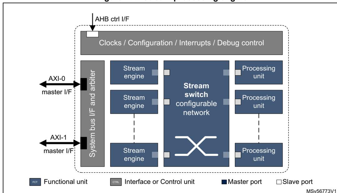
The diagram illustrates the internal architecture of the Stream processing engine. At the top, an 'AHB ctrl I/F' connects to a 'Clocks / Configuration / Interrupts / Debug control' block. Below this, a 'System bus I/F and arbiter' block is connected to two external 'AXI' interfaces: 'AXI-0 master I/F' and 'AXI-1 master I/F'. The central part of the engine features a 'Stream switch configurable network' block. To its left are three 'Stream engine' blocks, and to its right are three 'Processing unit' blocks. Each 'Stream engine' and 'Processing unit' is connected to the 'Stream switch' via dashed lines. The 'Stream switch' itself has multiple ports, indicated by small squares, which connect to the 'Stream engines' and 'Processing units'. A legend at the bottom identifies the components: 'FCT' (Functional unit) for the Stream engine and Processing unit blocks, 'CTRL' (Interface or Control unit) for the System bus I/F and arbiter and Clocks/Configuration/Interrupts/Debug control blocks, 'Master port' (dark blue square) for the AXI interfaces and Stream switch, and 'Slave port' (light blue square) for the connections between the Stream switch and the Stream engines/Processing units. The diagram is labeled 'MSv56773V1' in the bottom right corner.
Stream processing
The ST stream processing technology allows the creation of on-demand performance- and area-tailored instances to address artificial intelligence (AI) applications, from the lowest to the highest end class.
The ST stream processing technology is deemed far more flexible than a hardware data path, and more power-efficient than an on-chip memory bus. The core is a configurable data flow fabric, also known as stream switch, which can be programmed at runtime to create arbitrary virtual chains of processing units (PUs), implementing the sequence of operations to execute. Multiple chains can be active at the same time, provided there are enough available hardware resources.
In the virtual chains, data flow unidirectionally from one PU to the other, hence a processing chain cannot be faster than the slowest element in the chain. A back pressure mechanism controls the data flow in a virtual chain, and data streams can be easily forked or joined to feed multiple destinations, enabling multicasting, context switching, and filtering.
Chaining as many accelerators as possible in a single virtual chain reduces the number of useless and power consuming transfers from/to memory, thus reducing the overall memory traffic and the power consumption.
The resulting IP communicates with the rest of the system through stream engine units. These are smart half-DMA's that can read, and write the data to/from external memory to transfer from/to the IP internal buffers. Although not primarily intended for that, memory-to-memory transfers are possible, connecting two stream engines back to back.
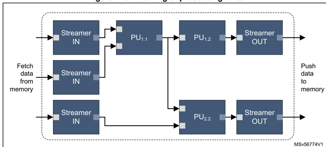
Figure 115. Chaining of processing units
Epoch definition
The execution of CNN models is organized into indivisible processing sequences called epochs. A hardware epoch is defined by the sequence that starts with the configuration of the NPU by the host CPU, and ends with an interrupt sent back to the CPU. The host CPU can then trigger another hardware epoch or execute some software computing for the layers not accelerated by the hardware.
20.2 NPU implementation
The Neural-ART 14 NPU uses a 4CA configuration with the functional units listed in Table 108.
Table 108. Neural-ART 14 NPU configuration
| Count | Unit | Description |
|---|---|---|
| 1 | STRSWITCH | Central data stream switch |
| 2 | DECUN | Decompression unit |
| 4 | CONVACC | Convolutional accelerator |
| 2 | POOL | Pooling unit |
| 2 | ACTIV | Activation unit |
| 4 | ARITH | Arithmetic unit for scalar arithmetic operators |
| 1 | RECBUF | Reconfigurable buffer (FIFO smart buffer) |
| 10 | STRENG | Stream engines , with embedded cipher |
| 2 | BUSIF | 64-bit AXI interface |
| 1 | EPOCH | Epoch controller |
Table 108. Neural-ART 14 NPU configuration (continued)
| Count | Unit | Description |
|---|---|---|
| 1 | DEBUG | Debug controller |
| - | SERVICES | Configuration network, Clock and reset manager, Interrupt controller |
20.3 NPU functional description
20.3.1 NPU block diagram
The internal organization of the NPU is shown in Figure 116 .
Figure 116. Neural-ART 14 NPU accelerator
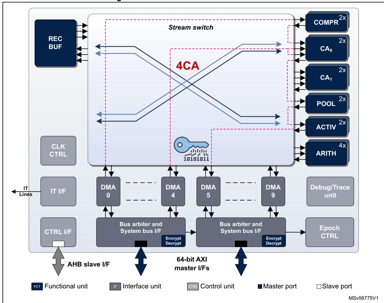
The diagram illustrates the internal architecture of the Neural-ART 14 NPU accelerator. At the top, a 'Stream switch' block (enclosed in a dashed pink box) is connected to a 'REC BUF' block on the left and a vertical stack of functional units on the right: 'COMPR 2x ', 'CA 0 2x ', 'CA 1 2x ', 'POOL 2x ', 'ACTIV 2x ', and 'ARITH 4x '. The 'Stream switch' contains a '4CA' label and a key icon with the binary sequence '10101011'. Below the stream switch, four 'DMA' blocks (0, 4, 5, and 9) are shown, each connected to a 'Bus arbiter and System bus I/F' block. These bus arbiters are connected to '64-bit AXI master I/Fs' at the bottom. On the left side, there are 'CLK CTRL', 'IT I/F' (connected to 'IT Lines'), and 'CTRL I/F' blocks. The 'CTRL I/F' is connected to an 'AHB slave I/F' at the bottom. On the right side, there are 'Debug/Trace unit' and 'Epoch CTRL' blocks. A legend at the bottom identifies the components: 'FCT' (Functional unit), 'IF' (Interface unit), 'CTRL' (Control unit), 'Master port' (dark blue square), and 'Slave port' (light blue square). The reference code 'MSV56775V1' is in the bottom right corner.
When the NPU is configured and started, it autonomously fetches data from the external memory to feed its internal dynamically interconnected processing units. Similarly, the result of the operation sequence is flushed to the external memory.
Inputs/sources can be the activations/features, but also parameters, such as weights and
biases constant data hosted in a memory-mapped nonvolatile memory. When the data-stream processing pipes are configured and started, the settings cannot be modified until the end-of-transfer event notifications of all DMA-outs and sinks.
20.3.2 NPU pins and internal signals
The NPU connects to the system through:
- • One AHB port, used for configuring and controlling the execution of the AI model
- • Two fully symmetrical AXI ports, used for fetching data and weights, and flushing outputs.
One interrupt signal fires when the processing for the current epoch is complete. Some additional signals are used for clock, reset, test, and debug. The complete list is given in Table 109 .
Table 109. Neural-ART 14 NPU signals
| Signal | Direction | Width | Description |
|---|---|---|---|
| ipu_clk | In | 1 | Main clock |
| ipu_rst_n | In | 1 | Reset |
| host_int | Out | 4 | Host interrupts |
| dbg_freeze_async | In | 1 | Debug freeze input signal (active high) |
| ext_triggers_async | In | 4 | External synchronization triggers (line based) |
| trig_sig | Out | 8 | Trigger signals to an external trace unit (available only in configurations including debug and trace unit) |
| AXI 0 | AXI master port 0 | See Arm specification | |
| AXI 1 | AXI master port 1 | ||
| AHB | AHB slave port | ||
| ATP | In | 26 | Memory test port |
| TBYPASS | In | 26 | |
| TBISTx | In | 26 | Memory BIST |
| HS | In | 26 | Memory speed select |
| STDBY | In | 26 | Memory standby |
| PSWLARGEMA | In | 26 | Memory power enable |
| PSWLARGEMP | In | 26 | |
| PSWSMALLMA | In | 26 | |
| PSWSMALLMP | In | 26 | |
| SLEEP | In | 26 | Memory sleep |
20.3.3 Configuration network
Each of the functional units, whether accelerator or interface, has a configuration space made of a collection of configuration registers. These registers are accessible through the AHB interface. Their detailed description is out of the scope of the present document.
The NPU embeds a configuration network that provides host processor access to the configuration space of the different units in the Neural-ART core. This configuration network connects to the system backbone through a 32-bit AHB5-lite port. It supports a single 32-bit wide read and write transaction, with no pipelining nor outstanding transactions.
20.3.4 Clock/reset manager
The purpose of this unit is twofold:
1. Clock control
The NPU uses a single functional clock provided by the RCC. This input clock is fed to the clock control unit from where it is gated and fed to the different units of the IP.
The clock unit generates clocks not gated, and clocks gated by default that need to be enabled after reset.
Clock gating is controlled by a configuration register bank, accessible via the configuration network, and programmed by the control code generated by the NPU compiler tool chain.
2. Reset control
The NPU uses a single functional reset provided by the RCC. This reset signal is synchronized inside the IP and fed to the different functional units.
Setting the clear bit in the control configuration register triggers a global NPU reset.
20.3.5 Stream link
A stream link is a unidirectional interconnection to transport data streams from accelerator units, stream engines, and interfaces to the stream switch and vice versa.
The stream consists of data, messages, or commands, and additional signaling information.
- • Data are transported over three 8-bit wide data channels that are either handled individually or can be interpreted as a single 24-bit data value.
- • Transported data can use different formats. A raster scan data stream allows the automatic detection of the geometrical dimensions of the received feature data tensor (width and height). A raw data format requires to program additional parameters to handle correctly the received data stream.
- • Signaling information is used to identify valid information on the stream link. It indicates the type and format of information transported, and whether this is the first or the last data transmitted.
20.3.6 Stream switch
This switch dynamically connects output stream link ports to input stream link ports, depending on the configuration data written to the configuration registers.
All input stream link ports can forward their data streams to one or multiple (multicast) output ports at the same time, allowing replication of the data stream.
Two stream links can be connected to a single output port of the switch. In this case, the output data are managed using a time-division context switch approach.
20.3.7 Stream engines
These engines manage the transfer from the system to the processing units and vice versa.
Figure 117. Stream engines
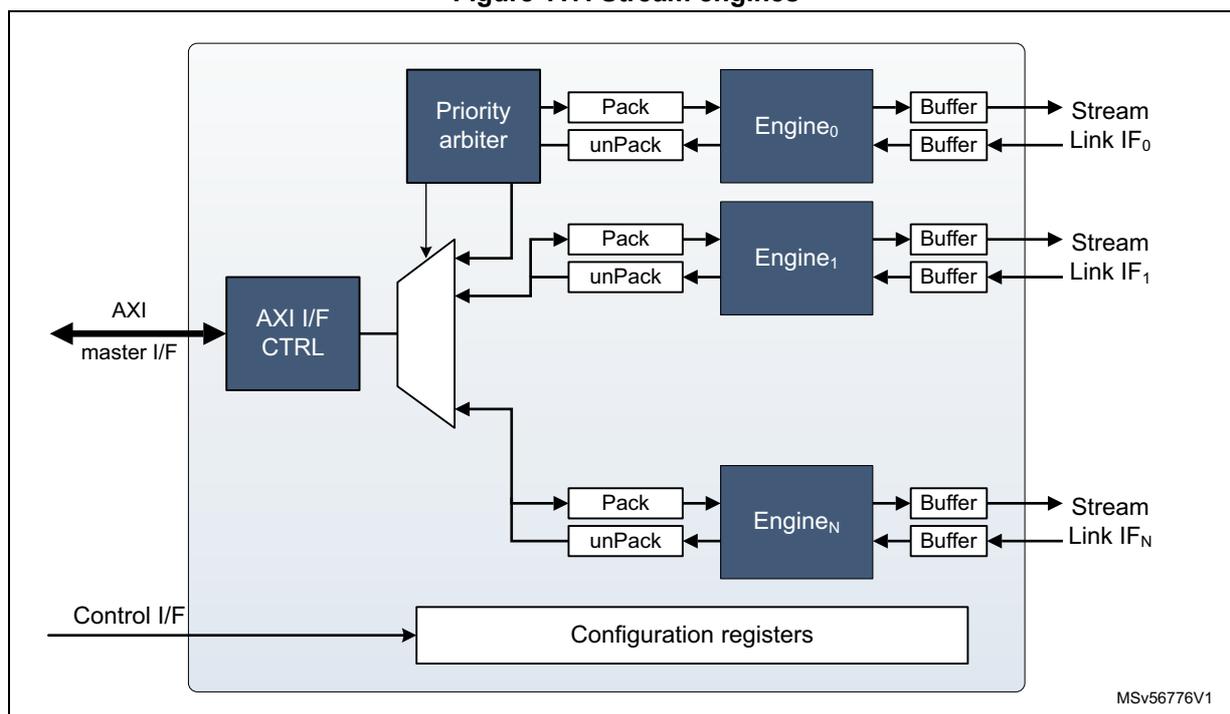
A stream engine connects to the stream switch by one input and one output stream link.
The stream engine offers a high configurability on read/write memory patterns:
- • 2D and 3D data representations
- • Gap management (interleaving)
- • High flexibility of data format (size, rounding, subsampling or resampling, MSB or LSB alignment with sign extension).
Linked lists are supported.
20.3.8 Encryption/Decryption unit
A low overhead/latency encryption/decryption unit based on Keccak-p[200] SHA-3 algorithm cipher, with a programmable number of rounds, is integrated in the bus interface, and can be shared between the different stream engines. It supports both weights and activation decryption and encryption.
20.3.9 Decompression unit
This unit supports on-the-fly decoding for scalar quantized data associated with kernels weights (with arbitrary quantization function), and decoding of vector quantized groups of weights.
An n-dimensional space can be described in a lossy way, by subdividing it into subvolumes, each described by its centroid. The subvolumes are obtained to minimize a predefined distortion function. The whole signal space can be represented with huge savings in terms of storage, as it is possible to represent the space of interest using only centroid values.
Figure 118. Two dimensional lossy compression
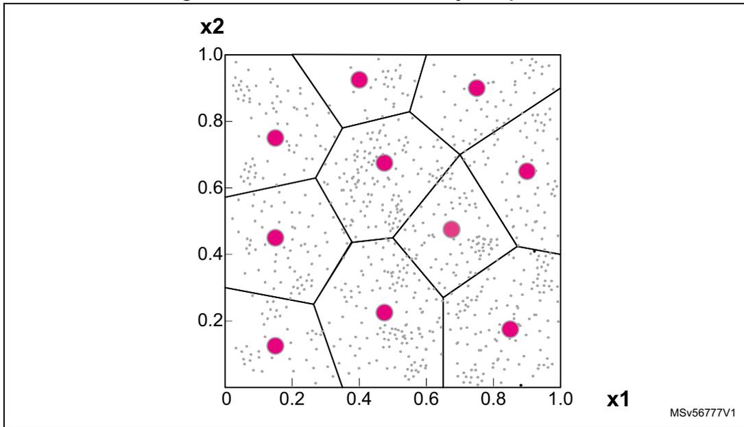
Quantization functions and/or vector quantizer code books (CB) are defined with an offline tool part of the NPU compiler toolchain. The encoder maps the input range into a finite range of rational values, called the code book. Any value stored by the CB is called a code vector. A code vector is made by up to eight code words. Each code book can store up to 256 code vectors (CV).
Figure 119. Decompression unit (DECUN)
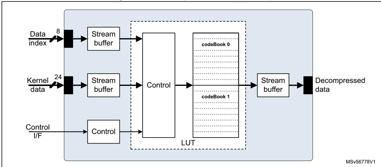
The decompression unit connects to the stream switch by two input stream links and one output stream link.
- • iSL 0 : receives the 8-bit indexes to decompress the data.
- • iSL 1 : receives the data to write in the code book, sent as raw data.
20.3.10 Convolutional accelerator
This is the core of the NPU. It implements clusters of multiply-accumulate (MAC) engines supporting fixed-point acceleration of the 3x3 convolutions used by many of the neural network models. It can be configured as 16- or 8-bit MACs, depending on which fixed-point precision for kernels and feature data is considered sufficient.
Figure 120. Convolutional accelerator (CONVACC)
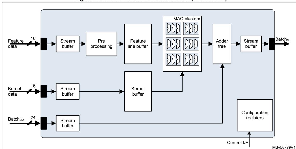
The convolution accelerator connects to the stream switch by three input stream links and one output stream link.
- • iSL 0 : receives the feature data as 8- or 16-bit raster scan or raw data. Data go through a bit rate adaptation stream buffer and is then transmitted to the feature data preprocessing unit before it is stored in the feature line buffer.
- • iSL 1 : receives the kernel data as 8- or 16-bit raster scan or raw data.
- • oSL: provides convolution results as 8- or 16-bit raster scan or raw data stream, with up to 24-bit wide signed data values.
- • iSL 2 : can receive intermediate 24-bit signed accumulator values to be accumulated with the convolution results.
Each convolution accelerator supports signed or unsigned arithmetic. It includes eighteen 16-bit MAC units grouped as six clusters of three MAC units. Each MAC performs a single 16x16-, two 16x8-, or four 8x8-bit multiply accumulate operation, which sums up to a maximum of 18 16x16-, 36 16x8-, or 72 8x8-bit multiply accumulate operations per clock cycle and per convolution accelerator unit.
The preprocessing unit implements the following sequence:
- 1. Format detection: determines if the data is raster scan or raw
- 2. Shift/round/saturation
- 3. HOR/VER cropping
- 4. Zero frame generation: on-the-fly extend the feature tensor structure.
- 5. Iteration control: simplifies the iterative processing of kernels larger than the 3x3 natively supported by the convolutional accelerator.
20.3.11 Pooling unit
This unit supports pooling operations like local 2D windowed (MxN) min, max, average pooling, as well as global max, min, or average pooling.
Supported features include:
- • Native pooling windows of dimensions up to 3x3
- • Horizontal and vertical strides ranging from 1 to 15
- • Batch size ranging from 1 to 8
- • Left, right, and top padding ranging from 0 to 7
- • Bottom padding, depending on the window height
Figure 121. Example of pooling operations
![Figure 121 shows two examples of pooling operations. The left example shows a 4x4 input grid with values [1, 1, 2, 4; 5, 6, 7, 8; 3, 2, 1, 0; 1, 2, 3, 4] being processed with a 2x2 filter and stride 2 to produce a 2x2 output grid [6, 8; 3, 4]. The right example shows a 4x4 input grid with values [0, 0, 2, 4; 2, 2, 6, 8; 9, 3, 2, 2; 7, 5, 2, 2] being processed with a 2x2 filter and stride 2 to produce a 2x2 output grid [1, 5; 6, 2].](/RM0486-STM32N6x5-x7/de2a27549ce8bc15071e9bc8e2a097cc_img.jpg)
Max pool with 2x2 filters and stride 2
Average pool with 2x2 filters and stride 2
MSV56780V1
Figure 122. Pooling unit (POOL)
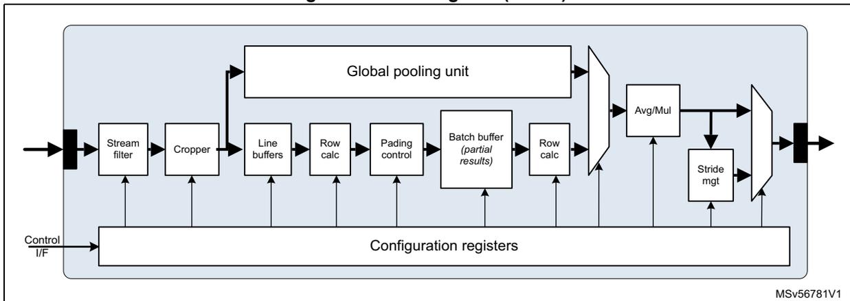
MSV56781V1
The pooling unit connects to the stream switch by one input and one output stream link:
- • iSL 0 : receives the activation input values as raster scan or raw data. Input is saturated to 16-bit.
- • oSL: produces the pooled output as raw data.
20.3.12 Activation unit
This unit implements the activation functions associated with convolutional neural networks. It provides a dedicated path to compute ReLU-like activations such as plain, parametric, and thresholded ReLUs. There is also a generic function evaluator using a second-degree piece-wise polynomial approximation ( \( y = ax^2 + bx + c \) or \( y = (ax + b) * x + c \) ). It uses a hierarchical uniform segmentation scheme to implement the evaluator.
Figure 123. Activation unit (ACTIV)
The unit connects to the stream switch by one input stream link and one output stream link.
- • iSL 0 : receives the activation input values as raster scan or raw data. Input is saturated to 16-bit.
- • oSL: produces the result output as raw data.
Table 110 provides examples of usual activation functions.
Table 110. Activation functions example
| Function | Plot | Equation | Derivative |
|---|---|---|---|
| Identity | Image: Plot of the identity function f(x) = x, showing a straight line with a slope of 1 passing through the origin on a grid. | \( f(x) = x \) | \( f'(x) = 1 \) |
Table 110. Activation functions example (continued)
| Function | Plot | Equation | Derivative |
|---|---|---|---|
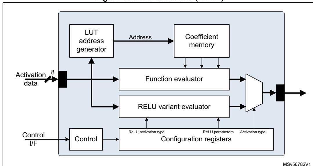
| Binary step | 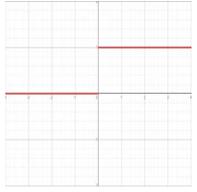 | \[
f(x) = \begin{cases} 0 & \text{for } x < 0 \\ 1 & \text{for } x \geq 0 \end{cases}
\] | \[
f'(x) = \begin{cases} 0 & \text{for } x \neq 0 \\ \infty & \text{for } x = 0 \end{cases}
\] |
| Logistic | 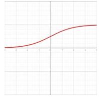 | \[
f(x) = \frac{1}{1 + e^{-x}}
\] | \[
f'(x) = f(x)(1 - f(x))
\] |
| Hyperbolic tangent | 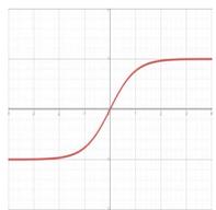 | \[
f(x) = \tanh(x)
\] \[
= \left( \frac{2}{1 + e^{-2x}} - 1 \right)
\] | \[
f'(x) = 1 - f(x)^2
\] |
| Arctan | 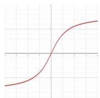 | \[
f(x) = \text{atan}(x)
\] | \[
f'(x) = \frac{1}{x^2 + 1}
\] |
| Rectified linear unit (ReLU) | 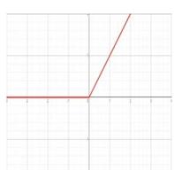 | \[
f(x) = \begin{cases} 0 & \text{for } x < 0 \\ x & \text{for } x \geq 0 \end{cases}
\] | \[
f'(x) = \begin{cases} 0 & \text{for } x < 0 \\ 1 & \text{for } x \geq 0 \end{cases}
\] |
| Parametric rectified linear unit (PReLU) | 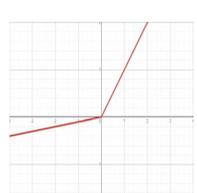 | \[
f(x) = \begin{cases} ax & \text{for } x < 0 \\ x & \text{for } x \geq 0 \end{cases}
\] | \[
f'(x) = \begin{cases} a & \text{for } x < 0 \\ 1 & \text{for } x \geq 0 \end{cases}
\] |
Table 110. Activation functions example (continued)
| Function | Plot | Equation | Derivative |
|---|---|---|---|
| Exponential linear unit (ELU) | 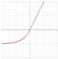 | \[
f(x) = \begin{cases} a(e^x - 1) \text{ for } x < 0 \\ x \text{ for } x \geq 0 \end{cases}
\] | \[
f'(x) = \begin{cases} f(x) + a \text{ for } x < 0 \\ 1 \text{ for } x \geq 0 \end{cases}
\] |
| SoftPlus | 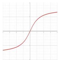 | \[
f(x) = \ln(1 + e^x)
\] | \[
f'(x) = \frac{1}{1 + e^{-x}}
\] |
20.3.13 Arithmetic unit
The arithmetic unit can handle outputs coming directly from the convolution accelerators. The main function is \( aX + bY + c \) , where X and Y are input data streams, supplied via two input stream link interfaces and a, b and c are constants that are either vectors or scalars, which are preloaded into an internal memory via the configuration interface.
The arithmetic unit can be configured to perform other operations:
- • \( x * y \) ;
- • MIN(x,y), MAX(x,y)
- • Logical {AND, OR, NOT(X)}
- • Bitwise {AND, OR, XOR, NOT(x)}
- • Comparison operations like =, <, ≤, >, ≥
- • Math operations like ABS(x), SIGN(x), and CLIP(x) with the 16-bit signed clip ranges supplied by the a coeff (min) and c coeff (max)
Based on the choice and type of coefficients, the unit can also perform element-wise operations like \( x - y \) , \( x + y \) , and similar ones.
Figure 124. Arithmetic unit (ARITH)
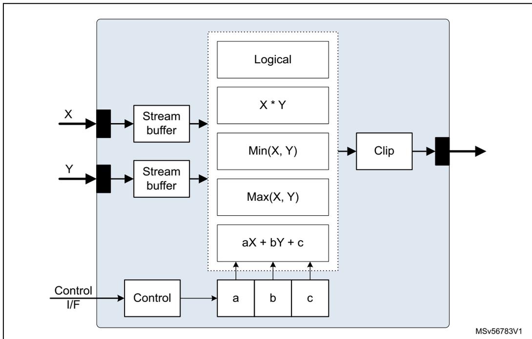
This unit connects to the stream switch by two input stream links and one output stream link.
- • \( iSL_{0,1} \) : receives the input values, denoted X & Y, as raster scan or raw data. Input is saturated to 16-bit.
- • \( oSL \) : produces the result output as raw data.
20.3.14 Reconfigurable buffer
The amount of data to process is usually divided using channel-wise data segmentation strategies. The data are then organized in execution epochs and channel data blocks along the three spatial dimensions. Data blocks are created considering the number of channels and the size of the incoming data. The partial data coming out from the different data blocks must then be reorganized and used in the next processing.
The reconfigurable buffer takes and stores the input data before making them available to the following units, which is useful to avoid deadlocks.
20.3.15 Epoch controller
This controller makes the NPU operation independent from the host CPU, which just provides a pointer to a 64-bit aligned “binary blob” placed in a memory space accessible through the AXI IF. The binary blob can be encrypted.
The core of the epoch controller is an FSM that decodes the control microinstructions, to appropriately configure all the processing units involved in the model execution using direct access to the NPU internal configuration bus.
The synchronization with the NPU is interrupt-based. An available step-by-step mode allows the execution of one microinstruction at a time. The execution is triggered by a write in a dedicated bit in the IRQ register.
The controller frees the AHB control bus for other uses, and improves the performance through a faster NPU programming. The binary blob is fetched through the AXI interface, which provides a larger bandwidth than the AHB. The direct access to the internal configuration bus allows bypassing all the bus external structure, where transactions from the host processor need to pass through.
20.3.16 Interrupt controller
Functional units can generate level-sensitive, active high, interrupts. These are collected by the interrupt controller, routed to four master interrupt lines, and forwarded to the host CPU.
When a master interrupt fires, the host CPU must read the INTREG register to identify the source of the current interrupt signaling. Interrupt routing to the four master interrupt lines and selective enabling are controlled by the INTORMSK and INTANDMSK mask registers, which have as many bits as interrupt sources.
- • INTORMSK: an interrupt is forwarded if any of the unmasked interrupts is active.
- • INTANDMSK: an interrupt is forwarded if all the unmasked interrupts are active.
20.4 Configuration examples
The following figures illustrate typical examples of streaming processing supported by the Neural-ART 14 NPU.
20.4.1 DMA transfer
The simplest possible chain involves one input streamer and one output streamer connected back-to-back, which (although not primarily intended for that) configures the NPU as a high-bandwidth DMA.
Figure 125. Memory to memory transfer
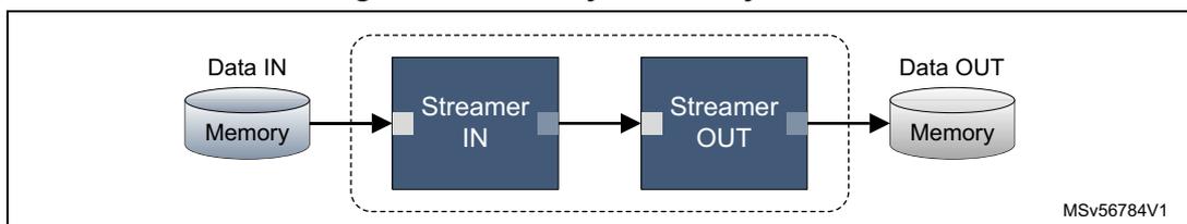
The diagram illustrates a memory-to-memory transfer setup. On the left, a cylinder labeled 'Data IN' and 'Memory' has an arrow pointing to a blue rectangular block labeled 'Streamer IN'. This 'Streamer IN' block is connected to another blue rectangular block labeled 'Streamer OUT'. Both streamer blocks are enclosed within a dashed rectangular box. An arrow points from the 'Streamer OUT' block to a cylinder on the right labeled 'Data OUT' and 'Memory'. In the bottom right corner of the diagram, the text 'MSV56784V1' is present.
20.4.2 Simple processing
The simplest processing chain involves one input streamer and one output streamer, with one processing unit in between.
Figure 126. Simple processing
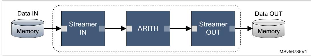
The diagram illustrates a simple processing chain. On the left, a 'Data IN' memory block feeds into a 'Streamer IN' block. This is followed by an 'ARITH' (arithmetic) block, then a 'Streamer OUT' block, which finally outputs to a 'Data OUT' memory block. The four central blocks are enclosed in a dashed box. A small label 'MSV56785V1' is in the bottom right corner.
20.4.3 Multiple processing
Implements several independent simple processing chains, like the one in Figure 126.
Figure 127. Multiple processing
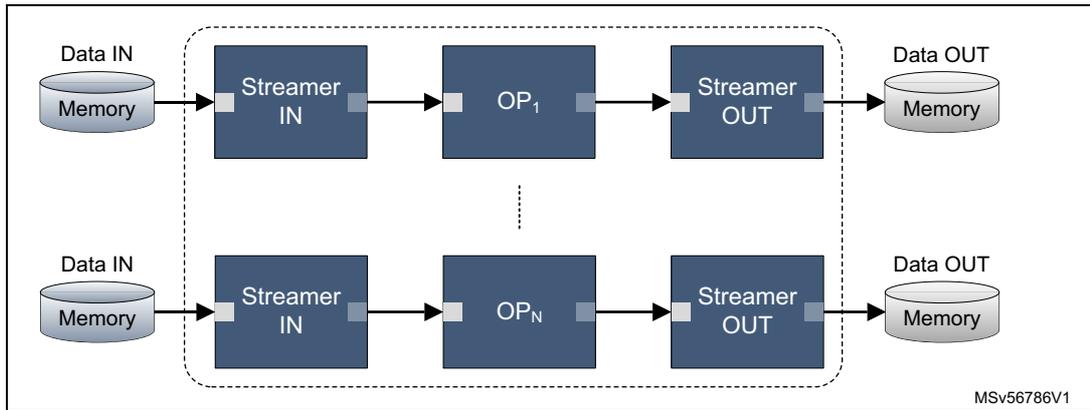
This diagram shows multiple independent processing chains. Two are explicitly shown: the top chain has 'Data IN' (Memory) -> 'Streamer IN' -> 'OP 1 ' -> 'Streamer OUT' -> 'Data OUT' (Memory); the bottom chain has 'Data IN' (Memory) -> 'Streamer IN' -> 'OP N ' -> 'Streamer OUT' -> 'Data OUT' (Memory). A vertical ellipsis between 'OP 1 ' and 'OP N ' indicates additional chains. Each chain's central part is in a dashed box. A small label 'MSV56786V1' is in the bottom right corner.
The number of independent chains is limited by the available hardware resources. It cannot exceed half the number of available stream engines, that is, five pairs of stream engines on Neural-ART 14, thus five chains.
20.4.4 Conv-Pool-ReLU
The virtual chain implementing the classical Conv-Pool-ReLU processing is illustrated in Figure 128.
Figure 128. Classical Conv-Pool-ReLU
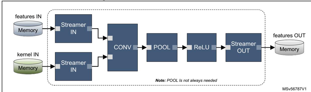
The diagram shows the 'Classical Conv-Pool-ReLU' processing flow. Two input streams, 'features IN' (Memory) and 'kernel IN' (Memory), each feed into a 'Streamer IN' block. Both 'Streamer IN' blocks then feed into a 'CONV' (convolution) block. This is followed by a 'POOL' (pooling) block, a 'ReLU' (rectified linear unit) block, and a 'Streamer OUT' block, which outputs to a 'features OUT' memory block. The five central blocks are enclosed in a dashed box. A note below the box states 'Note: POOL Is not always needed'. A small label 'MSV56787V1' is in the bottom right corner.
20.4.5 Chained convolutions
Figure 129 shows an example of chained convolutions.
Figure 129. Chained convolutions
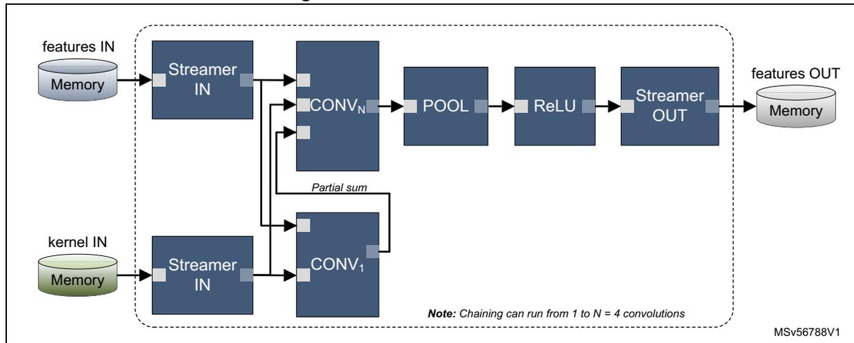
The diagram illustrates a chain of operations within a dashed box. It starts with 'features IN' and 'kernel IN' in 'Memory' blocks. 'features IN' connects to a 'Streamer IN' block, which then connects to a series of convolution blocks labeled 'CONV 1 ', 'CONV 2 ', ..., 'CONV N '. A 'Partial sum' line connects 'CONV 1 ' to 'CONV 2 '. This is followed by 'POOL', 'ReLU', and 'Streamer OUT' blocks. The output of 'Streamer OUT' goes to a 'features OUT' 'Memory' block. A note at the bottom states: 'Note: Chaining can run from 1 to N = 4 convolutions'. The identifier 'MSv56788V1' is in the bottom right corner.
Neural-ART 14 allows chaining up to four convolutions.
It is possible to use S CONVACCs in series, which requires (S times) more feature data bandwidth, but the same bandwidth for accumulation and output data as a single accelerator.
It is also possible to use P CONVACCs in parallel (see Figure 127), which reuse the same feature data requiring P times the amount of accumulation data and output data bandwidth.
20.4.6 Split convolutions
Figure 130 shows an example of split convolution.
Figure 130. Split convolution
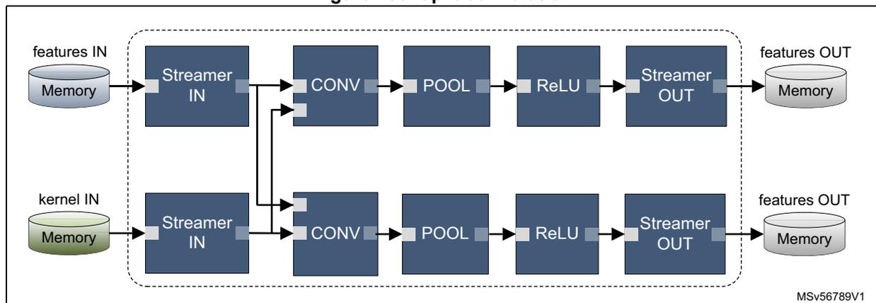
The diagram shows two parallel processing paths within a dashed box. Both paths start with 'features IN' and 'kernel IN' in 'Memory' blocks. Each path has its own 'Streamer IN' block. The first path consists of 'CONV', 'POOL', 'ReLU', and 'Streamer OUT' blocks, leading to a 'features OUT' 'Memory' block. The second path is identical to the first. The identifier 'MSv56789V1' is in the bottom right corner.
20.5 Address space
The configuration bus address mapping depends on the specific NPU instance configuration. Each of the functional units has a 4-Kbyte configuration space, which yields a 128-Kbyte configuration space for the total IP, organized as shown in Table 111 .
Table 111. Neural-ART 14 functional units memory base addresses (1)
| Offset | Unit | Description |
|---|---|---|
| 0x0000 | CLKCTRL | Clock and reset manager |
| 0x1000 | INTCTRL | Interrupt controller |
| 0x2000 | BUSIF0 | Bus interface 0 |
| 0x3000 | BUSIF1 | Bus interface 1 |
| 0x4000 | STRSWITCH | Stream switch |
| 0x5000 | STRENG0 | Stream engine 0 |
| 0x6000 | STRENG1 | Stream engine 1 |
| 0x7000 | STRENG2 | Stream engine 2 |
| 0x8000 | STRENG3 | Stream engine 3 |
| 0x9000 | STRENG4 | Stream engine 4 |
| 0xA000 | STRENG5 | Stream engine 5 |
| 0xB000 | STRENG6 | Stream engine 6 |
| 0xC000 | STRENG7 | Stream engine 7 |
| 0xD000 | STRENG8 | Stream engine 8 |
| 0xE000 | STRENG9 | Stream engine 9 |
| 0xF000 | CONVACC0 | Convolutional accelerator unit 1 |
| 0x10000 | CONVACC1 | Convolutional accelerator unit 2 |
| 0x11000 | CONVACC2 | Convolutional accelerator unit 3 |
| 0x12000 | CONVACC3 | Convolutional accelerator unit 4 |
| 0x13000 | DECUN0 | Decompression unit 0 |
| 0x14000 | DECUN1 | Decompression unit 1 |
| 0x15000 | ACTIV0 | Activation unit 0 |
| 0x16000 | ACTIV1 | Activation unit 1 |
| 0x17000 | ARITH0 | Arithmetic unit 0 |
| 0x18000 | ARITH1 | Arithmetic unit 1 |
| 0x19000 | ARITH2 | Arithmetic unit 2 |
| 0x1A000 | ARITH3 | Arithmetic unit 3 |
| 0x1B000 | POOL0 | Pooling unit 0 |
| 0x1C000 | POOL1 | Pooling unit 1 |
| 0x1D000 | RECBUF0 | Reconfigurable buffer 0 |
| Offset | Unit | Description |
|---|---|---|
| 0x1E000 | EPOCHCTRL0 | Epoch controller 0 |
| 0x1F000 | DEBUG0 | Debug and Trace unit 0 |
- 1. The base address is the offset relative to the first address location of the Neural-ART core, defined at integration level. Refer to the memory map.
20.6 System integration
20.6.1 System considerations
The amount of memory required by the NPU depends on the complexity (number of layers to execute, size of the input data) and target performance of the selected model of neural network. This amount can vary by 1.5 orders of magnitude.
To reach peak performance, the system memory must be configured with enough independent memory banks. These must have a separate AXI slave port on the system interconnect to guarantee the maximum internal memory bandwidth and to benefit of the AXI bus parallelism.
In addition to the on-chip memory, dedicated external memory interfaces are needed to access a nonvolatile memory, where the model parameters (weights and biases) are hosted. Additional RAMs can be used to address large(r) neural networks that cannot fit entirely in the embedded memory. The response time (latency) and the available bandwidth of these interfaces is a limiting factor in the achievable frame rate and efficiency of the NPU processing units (such as MACs) utilization.
20.6.2 Architecture intent
The system architecture is designed to provide 4.2 Mbytes of contiguous system memory that can be seamlessly shared between the host and the NPU subsystems. At the same time, it offers privileged access to a meaningful high(er)-speed portion of these 4.2 Mbytes to the NPU.
A dedicated NPU cache (CACHEAXI) allows the mitigation of the bandwidth limitation when accessing external memories. When not used for caching, it can be configured as an additional RAM.
The Neural-ART 14 NPU simply connects to the system by two master AXI 64-bit ports that provide the high throughput needed for efficient acceleration of neural network models. Synchronization with the Cortex-M host CPU is through a slave AHB 32-bit port for NPU configuration, and interrupts connected to the NVIC.
Figure 131. Neural-ART 14 integration
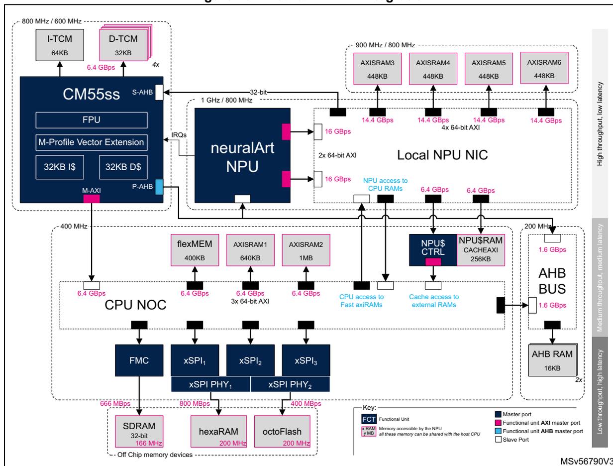
The diagram illustrates the integration of the Neural-ART 14 NPU with a Cortex-M55ss host CPU. The CM55ss (800 MHz / 600 MHz) includes I-TCM (64KB), D-TCM (32KB) with 6.4 GBps bandwidth, FPU, M-Profile Vector Extension, 32KB I$ and D$, and interfaces via S-AHB, M-AXI, and P-AHB. It connects to the neuralArt NPU (1 GHz / 800 MHz) via a 32-bit interface and IRQs. The NPU connects to the Local NPU NIC (900 MHz / 800 MHz) via two 64-bit AXI interfaces, each providing 16 GBps. The NIC connects to four AXISRAM banks (448KB each) with 14.4 GBps bandwidth each. The NPU also has access to CPU RAMs (6.4 GBps) and external RAMs (6.4 GBps). The CPU NOC (400 MHz) connects to flexMEM (400KB), AXISRAM1 (640KB), and AXISRAM2 (1MB) via 3x 64-bit AXI interfaces (6.4 GBps each). It also connects to NPU$ CTRL and NPU$ RAM (256KB) via CPU access to Fast axiRAMs and Cache access to external RAMs. The NOC connects to FMC, xSPI1, xSPI2, and xSPI3, which are further connected to xSPI PHY1 and xSPI PHY2. These PHYs connect to off-chip memory devices: SDRAM (32-bit, 166 MHz) with 666 MBps, hexaRAM (200 MHz) with 800 MBps, and octoFlash (200 MHz) with 400 MBps. The CPU NOC also connects to an AHB BUS (200 MHz) via 1.6 GBps interfaces, which in turn connects to AHB RAM (16KB) with 2x 1.6 GBps bandwidth. A key identifies Functional Units (FOT), Memory accessible by the NPU (xRAM), Memory accessible by the host CPU (yRAM), Master ports, Functional unit AXI master port, Functional unit AHB master port, and Slave Port. The diagram is labeled MSV56790V3.
Security
The Neural-ART 14 is not TrustZone aware. Therefore, multicontext and multitenancy are supported through the implementation of isolation compartments separated by CIDs. The AHB control interface is protected by a RISUP placed upstream. A RIMU is placed in the downstream of the AXI master interfaces, to assign CID values, so that NPU could only access the sole memories protected with that CID. Refer to the security chapter for further information.
Control interface
The Cortex-M55 host CPU configures the Neural-ART 14 NPU subsystem through the AHB slave port, which is connected to one of the ports of the AHB system bus matrix.
Data interface
The two 64-bit wide master AXI-4 ports of the NPU connect to a high-speed local interconnect that provides four 448-Kbyte banks of fast memory with a privileged, high-throughput / low-latency, asynchronous access. Each bank is implemented as four 112-Kbyte physical memory cuts, served by a full-duplex memory controller. This offers
14.4 Gbyte/s, provided reads/writes are done to different memory cuts, distant by at least 112 Kbytes.
The high-speed local NIC also connects to the main NOC through an asynchronous bridge, which gives access to medium throughput / medium latency on-chip memories:
- • The system memory, organized in three memory banks.
- – A 400-Kbyte- bank, known as flexMem, which can, at setup, be allocated to either extend ITCM or DTCM, or left to the system.
- – A 624-Kbyte bank, subdivided into eight 256-Kbyte memory cuts. A bandwidth of 6.4 Gbyte/s is achievable provided reads/writes are distant by at least 256 Kbytes.
- – A 1-Mbyte bank, subdivided into four 256-Kbyte memory cuts. A bandwidth of 6.4 Gbyte/s is achievable provided reads/writes are distant by at least 256 Kbytes.
- • The 256 Kbytes of the NPU cache memory (when cache is not enabled),
Finally, the NOC provides additional lower bandwidth / higher latency access to external memories connected to the FMC or xSPI controllers, with bandwidths of respectively 664 and 800 Mbyte/s.
The NPU does not have access to VENC or AHB memories.
Hardware triggers
The NPU provides four external asynchronous hardware trigger inputs. One of these is connected to the DCMIPP. The control SW can enable it to implement a CPU-less synchronization scheme between the camera pipeline and the NPU. This ancillary benefit of this pure hardware synchronization scheme is to reduce the size of the memory buffers used, as it is no longer needed to store a complete frame buffer.
Note: This synchronization scheme cannot be used if the model of CNN to execute requires preserving the input layer for the whole duration of the inference.
Virtual memPool
The actual amount of internal memory allocated to the NPU operation and the organization thereof is configurable by software.
Depending on the model of neural network to be executed, and of the size of the memory buffers it requires, the NPU compiler can dynamically decide to, either:
- • access the on-chip memories in parallel, thus improving the bandwidth of the data transfers,
- • consider them as fewer, virtual larger banks (a) , to keep the activation data in internal memories for the sake of the performance.
The compiler can create one or more virtual memory pools, which can group two or more of the contiguous memories accessible through the bus. This decision is frequency a/o protocol agnostic and only cares about address ranges. A virtual memory pool can thus group as many memory banks as needed and can extend from axiRAM1 (main NOC, clocked at 400 MHz) to axiRAM6 (NPU NIC, clocked at 1 GHz).
External memories accessible through the FMC or xSPI interfaces are not contiguous with any other on-chip memory and cannot be part of a virtual memory pool.
a. This grouping of two or more contiguous memory banks is known as a “virtual memory pool”.