15. General-purpose I/Os (GPIO)
15.1 Introduction
Each general-purpose I/O port has four 32-bit configuration registers (GPIOx_MODER, GPIOx_OTYPER, GPIOx_OSPEEDR, and GPIOx_PUPDR), two 32-bit data registers (GPIOx_IDR and GPIOx_ODR), a 16-bit reset register (GPIOx_BRR), and a 32-bit set/reset register (GPIOx_BSRR).
In addition, all GPIOs have a 32-bit locking register (GPIOx_LCKR), two couples of 32-bit advanced configuration registers (GPIOx_DELAYRL/H, GPIOx_ADVCFGRL/H), and two 32-bit alternate function selection registers (GPIOx_AFRH and GPIOx_AFRL).
Access to each general-purpose I/O configuration bit can be restricted to secure-only and/or privileged-only.
15.2 GPIO main features
- • Multiple choice of configurations per I/O port:
- – Input configuration in floating, pull-up/down, or analog state
- – Analog configuration (output buffer and Schmitt trigger input disabled)
- – Output configuration, or alternate function configuration, in push-pull or open drain state, with pull-up or pull-down activated
- • Data present on the I/O pin sampled to the input data register GPIOx_IDR (input configuration) or to the peripheral (alternate function configuration)
- • Output buffer on the I/O pin driven by the output data register GPIOx_ODR (output configuration) or by the peripheral (alternate function configuration)
- • I/O data output atomic read/modify through GPIOx_BSRR and GPIOx_BRR
- • Speed selection for each I/O (GPIOx_OSPEEDR)
- • Lock mechanism (GPIOx_LCKR) to selectively freeze the I/O port configurations
- • Highly-flexible pin multiplexing, enabling the use of I/O pins as GPIOs, or as one of several possible peripheral functions
- • Programmable delay to the input or the output path (GPIOx_DELAYR)
- • Double edge selection, clock inversion, and optional retiming (GPIOx_ADVCFG)
- • Possibility to restrict each I/O control to secure-only and/or privileged-only
15.3 GPIO functional description
The specific hardware characteristics of each I/O port are detailed in the datasheet.
Each port bit of the GPIO ports can be individually configured by software in several modes:
- • input floating
- • input pull-up
- • input pull-down
- • analog
- • output open-drain with pull-up or pull-down capability
- • output push-pull with pull-up or pull-down capability
- • alternate function push-pull with pull-up or pull-down capability
- • alternate function open-drain with pull-up or pull-down capability
Each I/O port bit is freely programmable, however the I/O port registers must be accessed as 32-bit words, half-words, or bytes. GPIOx_BSRR and GPIOx_BRR allow atomic read/modify accesses to any of GPIOx_ODR. In this way, there is no risk of IRQ occurring between the read and the modify access.
Figure 66 shows the basic structure of a standard I/O port bit.
Figure 66. Basic structure of an I/O port bit
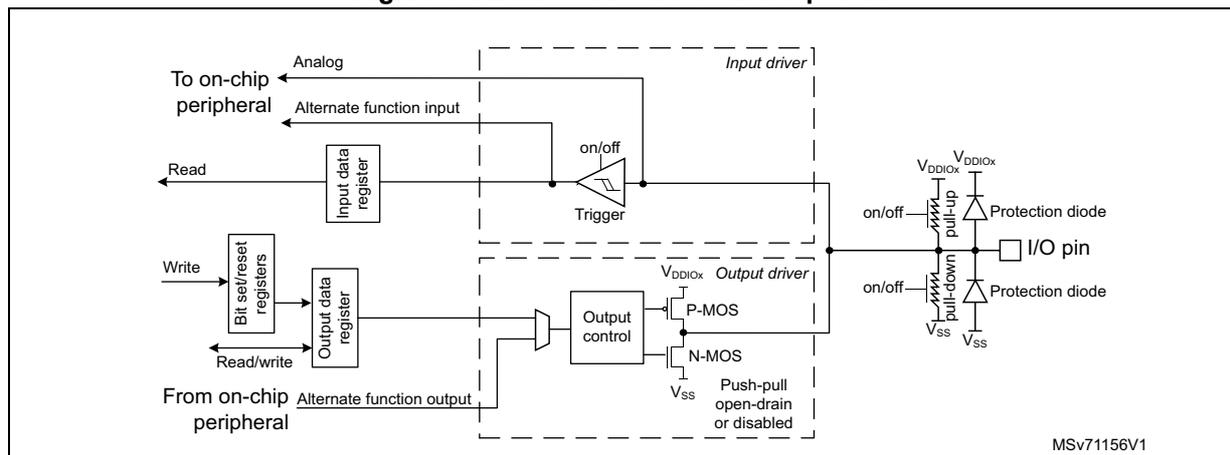
Table 78 gives the possible port bit configurations.
Table 78. Port x bit configurations
| Port x bit configurations | I/O configuration (1) | ||||
|---|---|---|---|---|---|
| MODEx[1:0] | OTx | OSPEEDx[1:0] | PUPDx[1:0] | ||
| 01 | 0 | SPEED[1:0] | 0 0 | GP output | PP |
| 0 1 | PP + PU | ||||
| 1 0 | PP + PD | ||||
| 1 1 | Reserved (GP output PP) | ||||
| 1 | 0 0 | GP output (open drain) | OD | ||
| 0 1 | OD + PU | ||||
| 1 0 | OD + PD | ||||
| 1 1 | Reserved (GP output OD) | ||||
Table 78. Port x bit configurations (continued)
| Port x bit configurations | I/O configuration (1) | ||||||
|---|---|---|---|---|---|---|---|
| MODEx[1:0] | OTx | OSPEEDx[1:0] | PUPDx[1:0] | ||||
| 10 | 0 | SPEED[1:0] | 0 | 0 | AF | PP | |
| 0 | 1 | PP + PU | |||||
| 1 | 0 | PP + PD | |||||
| 1 | 1 | Reserved (AF PP) | |||||
| 1 | 0 | 0 | AF (open drain) | OD | |||
| 0 | 1 | OD + PU | |||||
| 1 | 0 | OD + PD | |||||
| 1 | 1 | Reserved (AF OD) | |||||
| 00 | x | x | x | 0 | 0 | Input | Floating |
| x | x | x | 0 | 1 | PU | ||
| x | x | x | 1 | 0 | PD | ||
| x | x | x | 1 | 1 | Reserved (input floating) | ||
| 11 | x | x | x | 0 | 0 | Input/output | Analog |
| x | x | x | 0 | 1 | Analog | ||
| x | x | x | 1 | 0 | Analog + PD | ||
| x | x | x | 1 | 1 | Analog | ||
1. GP = general-purpose, PP = push-pull, PU = pull-up, PD = pull-down, OD = open-drain, AF = alternate function.
15.3.1 General-purpose I/O (GPIO)
During and just after reset, AFs (alternate functions) are not active, and most of the I/O ports are configured in analog mode, as defined through GPIOx_MODER register.
The debug pins are in AF pull-up/pull-down after reset:
- • PA15: JTDI in pull-up
- • PA14: JTCK/SWCLK in pull-down
- • PA13: JTMS/SWDIO in pull-up
- • PB4: NJTRST in pull-up
- • PB5: JTDO/TRACEWO in floating state no pull-up/pull-down
When the pin is configured as output, the value written to GPIOx_ODR is output on the I/O pin. The output driver can be used in push-pull mode or open-drain mode (only the low level is driven, high level is Hi-Z).
GPIOx_IDR captures the data present on the I/O pin at every AHB clock cycle.
All GPIO pins have weak internal pull-up and pull-down resistors, that can be activated or not, depending on the value in GPIOx_PUPDR.
15.3.2 I/O pin AF multiplexer and mapping
The device I/O pins are connected to on-board peripherals/modules through a multiplexer used to connect only one peripheral AF to an I/O pin at a time. There is no conflict between peripherals available on the same I/O pin.
Each I/O pin has a multiplexer with up to 16 AF inputs (AF0 to AF15), which can be configured through GPIOx_AFRL (for pins 0 to 7) and GPIOx_AFRH (for pins 8 to 15):
- • During and just after reset, AFs are not active and most of the I/O ports are configured in analog mode, as defined through GPIOx_MODER. When one AF is active, AF0 is selected by default.
- • Specific AF assignments for each I/O pin are detailed in the device datasheet.
This flexible I/O multiplexing architecture is used to optimize the number of peripherals available in smaller packages.
To use an I/O in a given configuration, the user must proceed as follows:
- • Debug function: after each device reset, these pins are assigned as AF pins immediately usable by the debugger host.
- • GPIO modes: the desired I/O is configured as output, input, or analog in GPIOx_MODER.
- • Peripheral AF:
- – For a given peripheral function, the 'Alternate functions' table in the datasheet helps to identify the AF to use with a given I/O. One of GPIOx_AFRL or GPIOx_AFRH must be used.
- – Configure the desired I/O as an AF in GPIOx_MODER. Select the type, pull-up/pull-down, and output speed via GPIOx_OTYPER, GPIOx_PUPDR, and GPIOx_OSPEEDR respectively.
- • Cortex®-M55 alternate function (EVENTOUT)
- – The output EVENTOUT signal can be used by configuring the I/O pin to output at AF15. An event can be signaled through the configured pin after executing SEV instruction.
- – EVENTOUT signal can be used internally as a trigger for some peripherals (see Section 17: Peripherals interconnect matrix )
- • Additional functions:
- – The additional functions listed in the datasheet give the peripheral functions that directly select/enable its allocated I/O port(s). Typical peripherals are RTC/TAMP, PWR (WKUPx pins), or RCC (oscillator pins). These functions have priority over the configuration in standard GPIO registers.
- – For ADCs, configure the desired I/O in analog mode in GPIOx_MODER, and configure the required function in ADC registers.
15.3.3 I/O port control registers
Each GPIO port has four 32-bit memory-mapped control registers to configure up to 16 I/Os:
- • GPIOx_MODER is used to select the I/O mode (input, output, AF, analog).
- • GPIOx_OTYPER and GPIOx_OSPEEDR are respectively used to select the output type (push-pull or open-drain) and the speed.
- • GPIOx_PUPDR is used to select the pull-up/pull-down whatever the I/O direction.
15.3.4 I/O port data registers
Each GPIO port has two 16-bit memory-mapped data registers: GPIOx_ODR. These read/writable register store the data to be output per I/O. Data input through each I/O are stored into read-only GPIOx_IDR.
15.3.5 I/O data bitwise handling
GPIOx_BSRR is a 32-bit register that allows the application to set/reset each individual bit in GPIOx_ODR). GPIOx_BSRR has twice the size of GPIOx_ODR.
To each bit in GPIOx_ODR, correspond two control bits in GPIOx_BSRR: BS(i) and BR(i). When written to 1, BS(i) sets the corresponding ODR(i). When written to 1, BR(i) resets the corresponding ODR(i).
Writing any bit to 0 in GPIOx_BSRR does not have any effect on the corresponding bit in GPIOx_ODR. If there is an attempt to both set and reset a bit in GPIOx_BSRR, the set action takes priority.
Using GPIOx_BSRR to change the values of individual bits in GPIOx_ODR is a one-shot effect that does not lock GPIOx_ODR bits: these bits can always be accessed directly. GPIOx_BSRR provides a way of performing atomic bitwise handling.
The software does not need to disable interrupts when programming GPIOx_ODR at bit level: one or more bits can be modified in a single atomic AHB write access.
15.3.6 GPIO locking mechanism
GPIO control registers can be frozen by applying a specific write sequence to GPIOx_LCKR. Indeed, each GPIOx_LCKR bit freezes the corresponding bit in the IO ports control registers (GPIOx_MODER, GPIOx_OTYPER, GPIOx_OSPEEDR, GPIOx_PUPDR, GPIOx_DELAYRL/H, GPIOx_ADVCFGR, and GPIOx_AFRL/H).
To write GPIOx_LCKR, a specific write/read sequence must be applied. When the right lock sequence is applied to bit 16 in this register, the value of LCKR[15:0] is used to lock the configuration of the I/Os (during the write sequence the LCKR[15:0] value must be the same, during the write sequence, only the IOs for which LCKR[15:0] stays to 1 for all the specific write sequence are locked; other IOs configuration are not (lock sequence aborted). When the lock sequence is applied to a port bit, the value of the port bit can no longer be modified until a next device or peripheral reset. Each GPIOx_LCKR bit freezes the corresponding bit in the control registers (GPIOx_MODER, GPIOx_OTYPER, GPIOx_OSPEEDR, GPIOx_PUPDR, GPIOx_DELAYRL/H, GPIOx_ADVCFGR, and GPIOx_AFRL/H).
The LOCK sequence can be performed only using a word (32-bit long) access to GPIOx_LCKR, because GPIOx_LCKR bit 16 must be set at the same time as the [15:0] bits.
Note: A lock sequence aborts in the event of an AHB bus error (see Section 15.1 ), or insufficient access rights (see Section 15.3.16 ).
A lock sequence automatically suspends when accessing a different register from GPIOx_LCKR. It resumes with the next access to GPIOx_LCKR.
15.3.7 I/O AF input/output
Two registers are provided to select one of the AF inputs/outputs available for each I/O: GPIOx_AFRH and GPIOx_AFRH. With these registers, the user can connect an AF to some other pin, as required by the application.
A number of possible peripheral functions are multiplexed on each GPIO using these registers. The application can select any one of the possible functions for each I/O. As the AF selection signal is common to the AF input and output, a single channel is selected for the AF input/output of a given I/O.
To know which functions are multiplexed on each GPIO pin, refer to the datasheet.
15.3.8 External interrupt/wake-up lines
All ports have external interrupt capability. To use external interrupt lines, the ports can be configured in input, output, or AF mode (the ports must not be configured in analog mode). Refer to Section 25: Extended interrupts and event controller (EXTI) for more details.
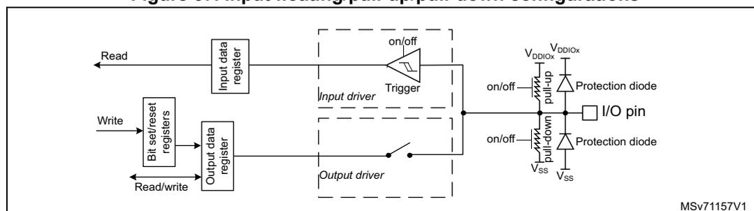
15.3.9 Input configuration
When the I/O port is programmed as input:
- • the output buffer is disabled
- • the Schmitt trigger input is activated
- • the pull-up and pull-down resistors are activated, depending on the value in GPIOx_PUPDR.
- • data present on the I/O pin are sampled into the input data register every AHB clock cycle
- • a read access to the input data register provides the I/O state
Figure 67 shows the input configuration of the I/O port bit.
Figure 67. Input floating/pull-up/pull-down configurations
15.3.10 Output configuration
When the I/O port is programmed as output:
- • The output buffer is enabled:
- – open-drain mode: a 0 in the output register activates the N-MOS, whereas a 1 in the output register leaves the port in Hi-Z (P-MOS never activated).
- – push-pull mode: a 0 in the output register activates the N-MOS, whereas a 1 in the output register activates the P-MOS.
- • The Schmitt trigger input is activated.
- • The pull-up and pull-down resistors are activated depending on the value in GPIOx_PUPDR.
- • Data present on the I/O pin are sampled into the input data register every AHB clock cycle.
- • A read access to the input data register gets the I/O state.
- • A read access to the output data register gets the last written value.
Figure 68 shows the output configuration of the I/O port bit.
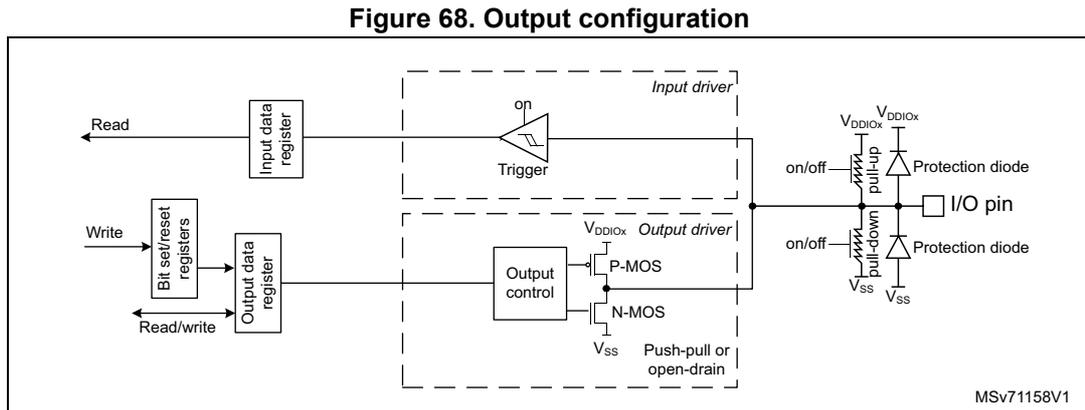
Figure 68. Output configuration
The diagram illustrates the internal architecture of a GPIO pin. On the left, the 'Input data register' is connected to the pin via an 'Input driver' containing a Schmitt trigger. A 'Read' operation is performed on this register. The 'Output data register' is connected to the pin via an 'Output driver' containing P-MOS and N-MOS transistors. This register is 'Written' to and 'Read/written' from. The 'Bit set/reset registers' are used to write to the output data register. The output driver can be configured for 'Push-pull or open-drain' mode. The pin is connected to 'V DDIOx ' and 'V SS ' through 'pull-up' and 'pull-down' resistors, which are controlled by 'on/off' switches. Protection diodes are also connected to the pin. The diagram is labeled 'MSV71158V1' in the bottom right corner.
15.3.11 AF configuration
When the I/O port is programmed as AF:
- • the output buffer can be configured in open-drain or push-pull mode
- • the output buffer is driven by the signals coming from the peripheral (transmitter enable and data)
- • the Schmitt trigger input is activated
- • the weak pull-up and pull-down resistors are activated or not, depending on the value in GPIOx_PUPDR
- • data present on the I/O pin are sampled into the input data register every AHB clock cycle
- • a read access to the input data register gets the I/O state.
Figure 69 shows the AF configuration of the I/O port bit.
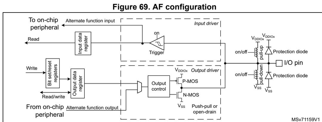
Figure 69. AF configuration
15.3.12 Analog configuration
When the I/O port is programmed as analog configuration:
- • The output buffer is disabled.
- • The Schmitt trigger input is deactivated, providing zero consumption for every analog value of the I/O pin. The output of the Schmitt trigger is forced to a constant value (0).
- • The weak pull-up resistor is disabled by hardware. The weak pull-down resistor is activated or not, depending on the value in GPIOx_PUPDR.
- • Read access to the input data register gets the value 0.
Figure 70 shows the programmable, analog-input configuration of the I/O port bits.
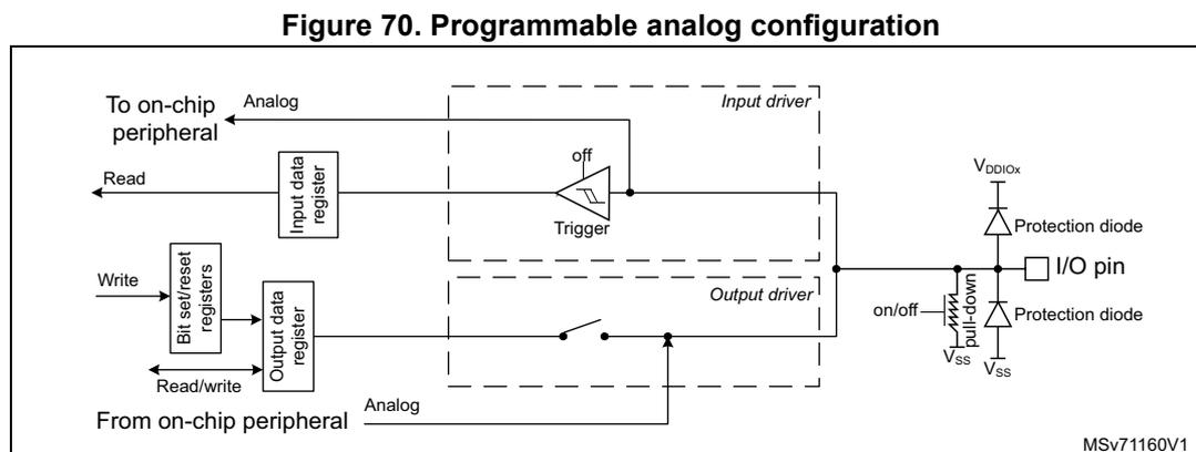
Figure 70. Programmable analog configuration
ADC analog configuration
The ADC voltage is 1.8 V. Refer to the product datasheet for more details on the allowed voltage on ADC input pins.
Warning: Permanent damage to the ADC can occur if the voltage on input pins exceeds 1.8 V.
15.3.13 Using HSE or LSE oscillator pins as GPIOs
When the HSE or LSE oscillator is switched off (default state after reset), the related oscillator pins can be used as normal GPIOs, but only in input mode (output mode is not supported).
When the HSE or LSE oscillator is switched on (HSEON or LSEON set in RCC_CSR), the oscillator takes control of its associated pins, and the GPIO configuration of these pins has no effect.
When the oscillator is configured in a user external clock mode, only the pin is reserved for clock input (OSC_OUT or OSC32_OUT pins can still be used, in input mode only).
15.3.14 Using GPIO pins in V SW supply domain
The functionality of PC13, PC14, PC15, and PQ7 GPIOs is lost when the core supply domain is powered off (the device enters Standby mode). If their GPIO configuration is not bypassed by the RTC/TAMP configuration or by the RCC (LSE), these pins are set in analog input mode.
For details about I/O control by the RTC, refer to Section 61.3: RTC functional description .
15.3.15 Advanced I/O configurations
I/O compensation cell
The I/O commutation slew rate ( \( t_{fall}/t_{rise} \) ) can be adapted by software depending on process, voltage, and temperature conditions, to reduce the I/O noise on the power supply. Refer to Section 16: System configuration controller (SYSCFG) for more details.
Input/output path configurable delay
A delay programmed in GPIOx_DELAYRL/H can be applied to either input or output path, based on DLYPATH in GPIOx_ADVCFGRL/R.
Input/output data double edge selection
Input and output data can be managed as single- or double-edge, according to DE in GPIOx_ADVCFGRL/R.
Input/output data retiming
When RET is set in GPIOx_ADVCFGRL/R, input and output data are retimed to either rising or falling clock edge, depending upon INVCLK value.
15.3.16 I/O pin isolation using TrustZone
As TrustZone-aware peripheral, each I/O pin of GPIO port x can be individually configured as secure through GPIOx_SECCFGR. After reset, all GPIO ports are secure.
The I/Os connected to peripheral functions can be conditioned by the peripheral security configuration:
- • Peripherals for which the I/O pin selection is done through GPIOx_AFRL/H
If the peripheral is configured as secure, it cannot be connected to a nonsecure I/O pin. If this is not respected, input data to the secure peripheral are forced to 0 (I/O input pin value ignored), and the output pin value is forced to 0, thus avoiding any secure
information leak through nonsecure I/Os. TrustZone-aware logic around GPIO ports is summarized in Table 79 .
- • Peripherals (like ADC) with embedded analog functions that directly select/enable its allocated I/O ports using analog switches
If the I/O is secure, this analog switch cannot be controlled by a nonsecure peripheral. If the peripheral is configured as nonsecure and the I/O is secure, the switch remains open. This prevents the redirection of secure data to a nonsecure peripheral or I/O through analog path. Refer to Section 3: System security for the list of peripherals using this security. - • The list of I/Os without a hardware protection linked to TrustZone is given in Section 3: System security . More specifically, the listed signals (input and/or outputs) are not blocked when the I/O is set as secure, and the associated peripheral is non secure. For each of these listed I/Os, a secure application must decide if a potential effect on data integrity or confidentiality is critical or not.
Refer to the pins definitions table in the datasheet for more information about AFs and additional functions mapping.
Table 79. Secure AF between peripherals and allocated I/Os
| Security configuration | AF logic | Comment | ||
|---|---|---|---|---|
| Peripheral | Allocated I/O pin | Input | Output | |
| Secure | Secure | I/O data | Peripheral data | - |
| Nonsecure | Out of reset configuration | |||
| Secure | Nonsecure | Zero | Zero | - |
| Nonsecure | I/O data | Peripheral data | ||
Table 80 gives a summary of the I/O port y secured bits, following the setting of SECy in GPIOx_SECCFGR. The following is valid for each register in the table:
- • When a bit is secured, read/write operations are only allowed by a secure access. Non-secure read or write accesses on secured bits are RAZ/WI, with no illegal access event generated.
- • When a bit is nonsecure, there is no TrustZone restriction. Read/write operations are allowed by both secure and nonsecure accesses.
Table 80. GPIO secured bits
| Secured bitfield(s) | Register name | Nonsecure access on secure bits |
|---|---|---|
| MODEy[1:0] | GPIOx_MODER | RAZ/WI |
| OTy | GPIOx_OTYPER | |
| OSPEEDy[1:0] | GPIOx_OSPEEDR | |
| PUPDy[1:0] | GPIOx_PUPDR | |
| IDy | GPIOx_IDR | |
| ODy | GPIOx_ODR | |
| BSy and BRy | GPIOx_BSRR |
Table 80. GPIO secured bits (continued)
| Secured bitfield(s) | Register name | Nonsecure access on secure bits |
|---|---|---|
| BRy | GPIOx_BRR | RAZ/WI |
| LCKy | GPIOx_LCKR | |
| AFSELy[3:0] | GPIOx_AFRH | |
| GPIOx_AFRl | ||
| DELAYy[3:0] | GPIOx_DELAYRL | |
| GPIOx_DELAYRH | ||
| RETy, INVCLKy, DEy, and DLYPATHy | GPIOx_ADVCFGRL GPIOx_ADVCFGGRH |
Note: GPIOx_SECCFGR is readable by any application. Each bit in this register is write-locked until the next device reset, when setting the corresponding bit in GPIOx_RCFGLOCKR.
15.3.17 I/O pin isolation using privilege
As RIF-aware peripheral, each I/O pin of GPIO port x can be individually configured as privileged through GPIOx_PRIVCFGR. After reset, all GPIO registers can be read and written by privileged and unprivileged accesses, if security is enough and the CPU is allowed.
Table 80 gives a summary of the I/O port y protected bits, following the setting of PRIVy in GPIOx_PRIVCFGR. The following is valid for each register in the table:
- • When a bit is privileged, read/write operations are only allowed by a privileged access. Unprivileged read or write accesses on privileged bits are RAZ/WI, with no illegal access event generated.
- • When a bit is unprivileged, there is no privilege restriction. Read and write operations are allowed by both privileged and unprivileged accesses.
Note: GPIOx_PRIVCFGR is readable by any application, writable by only privileged applications. Each bit in GPIOx_PRIVCFGR is write locked until next device reset, when setting the corresponding bit in GPIOx_RCFGLOCKR.
15.4 GPIO registers
GPIO registers are accessible through 32-bit word, half-word, or byte single access. Double-word and instruction fetch accesses trigger an AHB bus error. Byte or half-word writes to GPIOx_LCKR are silently ignored (no bus error).
15.4.1 GPIO port x mode register (GPIOx_MODER) (x = A to H, N to Q)
Address offset: 0x00
Reset value: Port A: 0xABFF EFFF
Reset value: Port B: 0xFFFF FAFF
Reset value: 0xFFFF FFFF (for the other ports)
| 31 | 30 | 29 | 28 | 27 | 26 | 25 | 24 | 23 | 22 | 21 | 20 | 19 | 18 | 17 | 16 |
|---|---|---|---|---|---|---|---|---|---|---|---|---|---|---|---|
| MODE15[1:0] | MODE14[1:0] | MODE13[1:0] | MODE12[1:0] | MODE11[1:0] | MODE10[1:0] | MODE9[1:0] | MODE8[1:0] | ||||||||
| rw | rw | rw | rw | rw | rw | rw | rw | rw | rw | rw | rw | rw | rw | rw | rw |
| 15 | 14 | 13 | 12 | 11 | 10 | 9 | 8 | 7 | 6 | 5 | 4 | 3 | 2 | 1 | 0 |
| MODE7[1:0] | MODE6[1:0] | MODE5[1:0] | MODE4[1:0] | MODE3[1:0] | MODE2[1:0] | MODE1[1:0] | MODE0[1:0] | ||||||||
| rw | rw | rw | rw | rw | rw | rw | rw | rw | rw | rw | rw | rw | rw | rw | rw |
Bits 31:0 MODEy[1:0] : Port x configuration I/O pin y (y = 15 to 0)
These bits are written by software to configure the I/O mode.
00: General-purpose input mode
01: General-purpose output mode
10: Alternate function mode (refer to device datasheet for available options)
11: Analog mode (reset state)
Note: Each bitfield is reserved and must be kept to reset value when the corresponding I/O is not available on the selected package.
Successful read or write to MODEy must be secure if SECy = 1 in GPIOx_SECCFGR, and must be privileged if PRIVy = 1 in GPIOx_PRIVCFGR.
15.4.2 GPIO port x output type register (GPIOx_OTYPER) (x = A to H, N to Q)
Address offset: 0x04
Reset value: 0x0000 0000
| 31 | 30 | 29 | 28 | 27 | 26 | 25 | 24 | 23 | 22 | 21 | 20 | 19 | 18 | 17 | 16 |
|---|---|---|---|---|---|---|---|---|---|---|---|---|---|---|---|
| Res. | Res. | Res. | Res. | Res. | Res. | Res. | Res. | Res. | Res. | Res. | Res. | Res. | Res. | Res. | Res. |
| 15 | 14 | 13 | 12 | 11 | 10 | 9 | 8 | 7 | 6 | 5 | 4 | 3 | 2 | 1 | 0 |
| OT15 | OT14 | OT13 | OT12 | OT11 | OT10 | OT9 | OT8 | OT7 | OT6 | OT5 | OT4 | OT3 | OT2 | OT1 | OT0 |
| rw | rw | rw | rw | rw | rw | rw | rw | rw | rw | rw | rw | rw | rw | rw | rw |
Bits 31:16 Reserved, must be kept at reset value.
Bits 15:0 OTy : Port x configuration I/O pin y (y = 15 to 0)
These bits are written by software to configure the I/O output type.
0: Output push-pull (reset state)
1: Output open-drain
Note: Each bit is reserved and must be kept to reset value when the corresponding I/O is not available on the selected package.
Successful read or write to OTy must be secure if SECy = 1 in GPIOx_SECCFGR, and must be privileged if PRIVy = 1 in GPIOx_PRIVCFGR.
15.4.3 GPIO port x output speed register (GPIOx_OSPEEDR)
(x = A to H, N to Q)
Address offset: 0x08
Reset value: Port A: 0x0C00 0000
Reset value: Port B: 0x0000 0C00
Reset value: 0x0000 0000 (for the other ports)
| 31 | 30 | 29 | 28 | 27 | 26 | 25 | 24 | 23 | 22 | 21 | 20 | 19 | 18 | 17 | 16 |
|---|---|---|---|---|---|---|---|---|---|---|---|---|---|---|---|
| OSPEED15[1:0] | OSPEED14[1:0] | OSPEED13[1:0] | OSPEED12[1:0] | OSPEED11[1:0] | OSPEED10[1:0] | OSPEED9[1:0] | OSPEED8[1:0] | ||||||||
| rw | rw | rw | rw | rw | rw | rw | rw | rw | rw | rw | rw | rw | rw | rw | rw |
| 15 | 14 | 13 | 12 | 11 | 10 | 9 | 8 | 7 | 6 | 5 | 4 | 3 | 2 | 1 | 0 |
| OSPEED7[1:0] | OSPEED6[1:0] | OSPEED5[1:0] | OSPEED4[1:0] | OSPEED3[1:0] | OSPEED2[1:0] | OSPEED1[1:0] | OSPEED0[1:0] | ||||||||
| rw | rw | rw | rw | rw | rw | rw | rw | rw | rw | rw | rw | rw | rw | rw | rw |
Bits 31:0 OSPEEDy[1:0] : Port x configuration I/O pin y (y = 15 to 0)
These bits are written by software to configure the I/O output speed.
00: Low speed
01: Medium speed
10: High speed
11: Very high speed
Note: Refer to the device datasheet for frequency specifications, power supply, and load conditions for each speed. Each bitfield is reserved and must be kept to reset value when the corresponding I/O is not available on the selected package.
Successful read or write to OSPEEDy must be secure if SECy = 1 in GPIOx_SECCFGR, and must be privileged if PRIVy = 1 in GPIOx_PRIVCFGR.
15.4.4 GPIO port x pull-up/pull-down register (GPIOx_PUPDR)
(x = A to H, N to Q)
Address offset: 0x0C
Reset value: Port A: 0x6400 0000
Reset value: Port B: 0x0000 0100
Reset value: 0x0000 0000 (for the other ports)
| 31 | 30 | 29 | 28 | 27 | 26 | 25 | 24 | 23 | 22 | 21 | 20 | 19 | 18 | 17 | 16 |
|---|---|---|---|---|---|---|---|---|---|---|---|---|---|---|---|
| PUPD15[1:0] | PUPD14[1:0] | PUPD13[1:0] | PUPD12[1:0] | PUPD11[1:0] | PUPD10[1:0] | PUPD9[1:0] | PUPD8[1:0] | ||||||||
| rw | rw | rw | rw | rw | rw | rw | rw | rw | rw | rw | rw | rw | rw | rw | rw |
| 15 | 14 | 13 | 12 | 11 | 10 | 9 | 8 | 7 | 6 | 5 | 4 | 3 | 2 | 1 | 0 |
| PUPD7[1:0] | PUPD6[1:0] | PUPD5[1:0] | PUPD4[1:0] | PUPD3[1:0] | PUPD2[1:0] | PUPD1[1:0] | PUPD0[1:0] | ||||||||
| rw | rw | rw | rw | rw | rw | rw | rw | rw | rw | rw | rw | rw | rw | rw | rw |
Bits 31:0 PUPDy[1:0] : Port x configuration I/O pin y (y = 15 to 0)
These bits are written by software to configure the I/O pull-up or pull-down
00: No pull-up, pull-down
01: Pull-up
10: Pull-down
11: Reserved
Note: Each bitfield is reserved and must be kept to reset value when the corresponding I/O is not available on the selected package.
Successful read or write to PUPDy must be secure if SECy = 1 in GPIOx_SECCFGR, and must be privileged if PRIVy = 1 in GPIOx_PRIVCFGR.
15.4.5 GPIO port x input data register (GPIOx_IDR) (x = A to H, N to Q)
Address offset: 0x10
Reset value: 0x0000 XXXX
| 31 | 30 | 29 | 28 | 27 | 26 | 25 | 24 | 23 | 22 | 21 | 20 | 19 | 18 | 17 | 16 |
|---|---|---|---|---|---|---|---|---|---|---|---|---|---|---|---|
| Res. | Res. | Res. | Res. | Res. | Res. | Res. | Res. | Res. | Res. | Res. | Res. | Res. | Res. | Res. | Res. |
| 15 | 14 | 13 | 12 | 11 | 10 | 9 | 8 | 7 | 6 | 5 | 4 | 3 | 2 | 1 | 0 |
| ID15 | ID14 | ID13 | ID12 | ID11 | ID10 | ID9 | ID8 | ID7 | ID6 | ID5 | ID4 | ID3 | ID2 | ID1 | ID0 |
| r | r | r | r | r | r | r | r | r | r | r | r | r | r | r | r |
Bits 31:16 Reserved, must be kept at reset value.
Bits 15:0 IDy : Port x input data I/O pin y (y = 15 to 0)
These bits are read-only. They contain the input value of the corresponding I/O port.
Note: Each bit is reserved and must be kept to reset value when the corresponding I/O is not available on the selected package.
Successful read to IDy must be secure if SECy = 1 in GPIOx_SECCFGR, and must be privileged if PRIVy = 1 in GPIOx_PRIVCFGR.
15.4.6 GPIO port x output data register (GPIOx_ODR) (x = A to H, N to Q)
Address offset: 0x14
Reset value: 0x0000 0000
| 31 | 30 | 29 | 28 | 27 | 26 | 25 | 24 | 23 | 22 | 21 | 20 | 19 | 18 | 17 | 16 |
|---|---|---|---|---|---|---|---|---|---|---|---|---|---|---|---|
| Res | Res | Res | Res | Res | Res | Res | Res | Res | Res | Res | Res | Res | Res | Res | Res |
| 15 | 14 | 13 | 12 | 11 | 10 | 9 | 8 | 7 | 6 | 5 | 4 | 3 | 2 | 1 | 0 |
| OD15 | OD14 | OD13 | OD12 | OD11 | OD10 | OD9 | OD8 | OD7 | OD6 | OD5 | OD4 | OD3 | OD2 | OD1 | OD0 |
| rw | rw | rw | rw | rw | rw | rw | rw | rw | rw | rw | rw | rw | rw | rw | rw |
Bits 31:16 Reserved, must be kept at reset value.
Bits 15:0 ODy : Port x output data I/O pin y (y = 15 to 0)
These bits can be read and written by software.
Note: For atomic bit set/reset, OD bits can be individually set and/or reset by writing to GPIOx_BSRR or GPIOx_BRR. Each bit is reserved and must be kept to reset value when the corresponding I/O is not available on the selected package.
Successful read or write to ODy must be secure if SECy= 1 in GPIOx_SECCFGR, and must be privileged if PRIVy = 1 in GPIOx_PRIVCFGR.
15.4.7 GPIO port x bit set/reset register (GPIOx_BSRR) (x = A to H, N to Q)
Address offset: 0x18
Reset value: 0x0000 0000
| 31 | 30 | 29 | 28 | 27 | 26 | 25 | 24 | 23 | 22 | 21 | 20 | 19 | 18 | 17 | 16 |
|---|---|---|---|---|---|---|---|---|---|---|---|---|---|---|---|
| BR15 | BR14 | BR13 | BR12 | BR11 | BR10 | BR9 | BR8 | BR7 | BR6 | BR5 | BR4 | BR3 | BR2 | BR1 | BR0 |
| w | w | w | w | w | w | w | w | w | w | w | w | w | w | w | w |
| 15 | 14 | 13 | 12 | 11 | 10 | 9 | 8 | 7 | 6 | 5 | 4 | 3 | 2 | 1 | 0 |
| BS15 | BS14 | BS13 | BS12 | BS11 | BS10 | BS9 | BS8 | BS7 | BS6 | BS5 | BS4 | BS3 | BS2 | BS1 | BS0 |
| w | w | w | w | w | w | w | w | w | w | w | w | w | w | w | w |
Bits 31:16 BRy : Port x reset I/O pin y (y = 15 to 0)
These bits are write-only. A read to these bits returns 0x0000.
0: No action on the corresponding ODy bit
1: Resets the corresponding ODy bit
Note: If both BSy and BRy are set, BSy has priority.
Each bit is reserved and must be kept to reset value when the corresponding I/O is not available on the selected package.
Successful write to BRy must be secure if SECy = 1 in GPIOx_SECCFGR, and must be privileged if PRIVy = 1 in GPIOx_PRIVCFGR.
Bits 15:0 BSy : Port x set I/O pin y (y = 15 to 0)
These bits are write-only. A read to these bits returns 0x0000.
0: No action on the corresponding ODx bit
1: Sets the corresponding ODx bit
Note: Each bit is reserved and must be kept to reset value when the corresponding I/O is not available on the selected package.
Successful write to BSy must be secure if SECy = 1 in GPIOx_SECCFGR, and must be privileged if PRIVy = 1 in GPIOx_PRIVCFGR.
15.4.8 GPIO port x configuration lock register (GPIOx_LCKR)
(x = A to H, N to Q)
Address offset: 0x1C
Reset value: 0x0000 0000
This register is used to lock the configuration of the port bits when a correct write sequence is applied to bit 16 (LCKK). The value of bits [15:0] is used to lock the GPIO configuration. During the lock sequence, only bit port unlock can be changed.
Note: Only word access (32-bit long) is allowed during this locking sequence.
Byte or half-word writes are silently ignored (no bus error, no abort to lock sequence).
When the LOCK sequence has been applied on a port bit, the value of this port bit can no longer be modified until the next MCU reset or peripheral reset. Each lock bit freezes a specific configuration register (control and AF registers). See Section 15.3.6 for details.
| 31 | 30 | 29 | 28 | 27 | 26 | 25 | 24 | 23 | 22 | 21 | 20 | 19 | 18 | 17 | 16 |
|---|---|---|---|---|---|---|---|---|---|---|---|---|---|---|---|
| Res. | Res. | Res. | Res. | Res. | Res. | Res. | Res. | Res. | Res. | Res. | Res. | Res. | Res. | Res. | LCKK |
| rw | |||||||||||||||
| 15 | 14 | 13 | 12 | 11 | 10 | 9 | 8 | 7 | 6 | 5 | 4 | 3 | 2 | 1 | 0 |
| LCK15 | LCK14 | LCK13 | LCK12 | LCK11 | LCK10 | LCK9 | LCK8 | LCK7 | LCK6 | LCK5 | LCK4 | LCK3 | LCK2 | LCK1 | LCK0 |
| rw | rw | rw | rw | rw | rw | rw | rw | rw | rw | rw | rw | rw | rw | rw | rw |
Bits 31:17 Reserved, must be kept at reset value.
Bit 16 LCKK : Lock key
This bit can be read any time. It can only be modified using the lock key write sequence.
0: Port configuration lock key not active
1: Port configuration lock key active. The GPIOx_LCKR register is locked until the next MCU reset or peripheral reset.
Lock key write sequence:
WR LCKR[16] = 1 + LCKR[15:0]
WR LCKR[16] = 0 + LCKR[15:0]
WR LCKR[16] = 1 + LCKR[15:0]
RD LCKR
RD LCKR[16] = 1 (this read operation is optional but it confirms that the lock is active)
Note: Any error in the sequence aborts the lock. After the first lock sequence on any bit of the port, any read access on LCKK bit returns 1 until the next device or peripheral reset.
Bits 15:0 LCKy : Port x lock I/O pin y (y = 15 to 0)
These bits are read/write but can only be written when LCKK = 0.
0: Port configuration not locked
1: Port configuration locked
Note: Each bit is reserved and must be kept to reset value when the corresponding I/O is not available on the selected package.
Successful read or write to LCKy must be secure if SECy = 1 in GPIOx_SECCFGR, and must be privileged if PRIVy = 1 in GPIOx_PRIVCFGR.
15.4.9 GPIO port x AF low register (GPIOx_AFRL) (x = A to H, N to Q)
Address offset: 0x20
Reset value: 0x0000 0000
| 31 | 30 | 29 | 28 | 27 | 26 | 25 | 24 | 23 | 22 | 21 | 20 | 19 | 18 | 17 | 16 |
|---|---|---|---|---|---|---|---|---|---|---|---|---|---|---|---|
| AFSEL7[3:0] | AFSEL6[3:0] | AFSEL5[3:0] | AFSEL4[3:0] | ||||||||||||
| rw | rw | rw | rw | rw | rw | rw | rw | rw | rw | rw | rw | rw | rw | rw | rw |
| 15 | 14 | 13 | 12 | 11 | 10 | 9 | 8 | 7 | 6 | 5 | 4 | 3 | 2 | 1 | 0 |
| AFSEL3[3:0] | AFSEL2[3:0] | AFSEL1[3:0] | AFSEL0[3:0] | ||||||||||||
| rw | rw | rw | rw | rw | rw | rw | rw | rw | rw | rw | rw | rw | rw | rw | rw |
Bits 31:0 AFSELy[3:0] : AF selection for port x I/O pin y (y = 7 to 0)
These bits are written by software to configure AF I/Os.
0000: AF0
0001: AF1
0010: AF2
0011: AF3
0100: AF4
0101: AF5
0110: AF6
0111: AF7
1000: AF8
1001: AF9
1010: AF10
1011: AF11
1100: AF12
1101: AF13
1110: AF14
1111: AF15
Note: Each bitfield is reserved and must be kept to reset value when the corresponding I/O is not available on the selected package.
Successful read or write to the bitfield AFSELy must be secure if SECy = 1 in GPIOx_SECCFGR, and must be privileged if PRIVy = 1 in GPIOx_PRIVCFGR.
15.4.10 GPIO port x AF high register (GPIOx_AFRH) (x = A to H, N to Q)
Address offset: 0x24
Reset value: 0x0000 0000
| 31 | 30 | 29 | 28 | 27 | 26 | 25 | 24 | 23 | 22 | 21 | 20 | 19 | 18 | 17 | 16 |
|---|---|---|---|---|---|---|---|---|---|---|---|---|---|---|---|
| AFSEL15[3:0] | AFSEL14[3:0] | AFSEL13[3:0] | AFSEL12[3:0] | ||||||||||||
| rw | rw | rw | rw | rw | rw | rw | rw | rw | rw | rw | rw | rw | rw | rw | rw |
| 15 | 14 | 13 | 12 | 11 | 10 | 9 | 8 | 7 | 6 | 5 | 4 | 3 | 2 | 1 | 0 |
| AFSEL11[3:0] | AFSEL10[3:0] | AFSEL9[3:0] | AFSEL8[3:0] | ||||||||||||
| rw | rw | rw | rw | rw | rw | rw | rw | rw | rw | rw | rw | rw | rw | rw | rw |
Bits 31:0 AFSELY[3:0] : AF selection for port x I/O pin y (y = 15 to 8)
These bits are written by software to configure AF I/Os (see GPIOx_AFRL for details).
Note: Each bitfield is reserved and must be kept to reset value when the corresponding I/O is not available on the selected package.
Successful read or write to the bitfield AFRHy must be secure if SECy = 1 in GPIOx_SECCFGR, and must be privileged if PRIVy = 1 in GPIOx_PRIVCFGR.
15.4.11 GPIO port x bit reset register (GPIOx_BRR) (x = A to H, N to Q)
Address offset: 0x28
Reset value: 0x0000 0000
| 31 | 30 | 29 | 28 | 27 | 26 | 25 | 24 | 23 | 22 | 21 | 20 | 19 | 18 | 17 | 16 |
|---|---|---|---|---|---|---|---|---|---|---|---|---|---|---|---|
| Res. | Res. | Res. | Res. | Res. | Res. | Res. | Res. | Res. | Res. | Res. | Res. | Res. | Res. | Res. | Res. |
| 15 | 14 | 13 | 12 | 11 | 10 | 9 | 8 | 7 | 6 | 5 | 4 | 3 | 2 | 1 | 0 |
| BR15 | BR14 | BR13 | BR12 | BR11 | BR10 | BR9 | BR8 | BR7 | BR6 | BR5 | BR4 | BR3 | BR2 | BR1 | BR0 |
| w | w | w | w | w | w | w | w | w | w | w | w | w | w | w | w |
Bits 31:16 Reserved, must be kept at reset value.
Bits 15:0 BRy : Port x reset IO pin y (y = 15 to 0)
These bits are write-only. A read to these bits returns 0x0000.
0: No action on the corresponding ODx bit
1: Reset the corresponding ODx bit
Note: Each bit is reserved and must be kept to reset value when the corresponding I/O is not available on the selected package.
Successful write to BRy must be secure if SECy = 1 in GPIOx_SECCFGR, and must be privileged if PRIVy = 1 in GPIOx_PRIVCFGR.
15.4.12 GPIO port x secure configuration register (GPIOx_SECCFGR) (x = A to H, N to Q)
Address offset: 0x30
Reset value: Port A: 0x0000 FFFF
Reset value: Port B: 0x0000 FFFF
Reset value: Port C: 0x0000 FFFF
Reset value: Port D: 0x0000 FFFF
Reset value: Port E: 0x0000 FFFF
Reset value: Port F: 0x0000 FFFF
Reset value: Port G: 0x0000 FFFF
Reset value: Port H: 0x0000 03FF
Reset value: Port N: 0x0000 1FFF
Reset value: Port O: 0x0000 003F
Reset value: Port P: 0x0000 FFFF
Reset value: Port Q: 0x0000 00FF
This register is used to configure a selected I/O as secure. Nonsecure or unprivileged writes to this register are ignored, while any read is allowed.
| 31 | 30 | 29 | 28 | 27 | 26 | 25 | 24 | 23 | 22 | 21 | 20 | 19 | 18 | 17 | 16 |
|---|---|---|---|---|---|---|---|---|---|---|---|---|---|---|---|
| Res. | Res. | Res. | Res. | Res. | Res. | Res. | Res. | Res. | Res. | Res. | Res. | Res. | Res. | Res. | Res. |
| 15 | 14 | 13 | 12 | 11 | 10 | 9 | 8 | 7 | 6 | 5 | 4 | 3 | 2 | 1 | 0 |
| SEC15 | SEC14 | SEC13 | SEC12 | SEC11 | SEC10 | SEC9 | SEC8 | SEC7 | SEC6 | SEC5 | SEC4 | SEC3 | SEC2 | SEC1 | SEC0 |
| rw | rw | rw | rw | rw | rw | rw | rw | rw | rw | rw | rw | rw | rw | rw | rw |
Bits 31:16 Reserved, must be kept at reset value.
Bits 15:0 SECy : I/O pin y of Port x security configuration (y = 15 to 0)
0: The I/O pin y is nonsecure. Secure access is also possible.
1: The I/O pin y is secure (see Table 80 for all corresponding secure bits).
Note: Each bit is reserved and must be kept to reset value when the corresponding I/O is not available on the selected package.
15.4.13 GPIO port x privileged configuration register (GPIOx_PRIVCFGR)
(x = A to H, N to Q)
Address offset: 0x34
Reset value: Port A: 0x0000 FFFF
Reset value: Port B: 0x0000 FFFF
Reset value: Port C: 0x0000 FFFF
Reset value: Port D: 0x0000 FFFF
Reset value: Port E: 0x0000 FFFF
Reset value: Port F: 0x0000 FFFF
Reset value: Port G: 0x0000 FFFF
Reset value: Port H: 0x0000 03FF
Reset value: Port N: 0x0000 1FFF
Reset value: Port O: 0x0000 003F
Reset value: Port P: 0x0000 FFFF
Reset value: Port Q: 0x0000 00FF
Unprivileged writes to this register are ignored, while any read is allowed.
| 31 | 30 | 29 | 28 | 27 | 26 | 25 | 24 | 23 | 22 | 21 | 20 | 19 | 18 | 17 | 16 |
|---|---|---|---|---|---|---|---|---|---|---|---|---|---|---|---|
| Res. | Res. | Res. | Res. | Res. | Res. | Res. | Res. | Res. | Res. | Res. | Res. | Res. | Res. | Res. | Res. |
| 15 | 14 | 13 | 12 | 11 | 10 | 9 | 8 | 7 | 6 | 5 | 4 | 3 | 2 | 1 | 0 |
| PRIV15 | PRIV14 | PRIV13 | PRIV12 | PRIV11 | PRIV10 | PRIV9 | PRIV8 | PRIV7 | PRIV6 | PRIV5 | PRIV4 | PRIV3 | PRIV2 | PRIV1 | PRIV0 |
| rw | rw | rw | rw | rw | rw | rw | rw | rw | rw | rw | rw | rw | rw | rw | rw |
Bits 31:16 Reserved, must be kept at reset value.
Bits 15:0 PRIVy : I/O pin y of Port x privilege configuration (y = 15 to 0)
0: The I/O pin y is unprivileged. Privileged access is also possible.
1: The I/O pin y is privileged only (see Table 80 for all corresponding protected bits).
If the corresponding SECy = 1 in GPIOx_SECCFGR, PRIVy can only be written by a secure privileged application.
Note: Each bit is reserved and must be kept to reset value when the corresponding I/O is not available on the selected package.
15.4.14 GPIO port x resource configuration lock register (GPIOx_RCFGLOCKR) (x = A to H, N to Q)
Address offset: 0x38
Reset value: 0x0000 0000
Secure privileged write access only. Write only by trusted domain CID. Any read access is allowed on this register.
| 31 | 30 | 29 | 28 | 27 | 26 | 25 | 24 | 23 | 22 | 21 | 20 | 19 | 18 | 17 | 16 |
|---|---|---|---|---|---|---|---|---|---|---|---|---|---|---|---|
| Res. | Res. | Res. | Res. | Res. | Res. | Res. | Res. | Res. | Res. | Res. | Res. | Res. | Res. | Res. | Res. |
| 15 | 14 | 13 | 12 | 11 | 10 | 9 | 8 | 7 | 6 | 5 | 4 | 3 | 2 | 1 | 0 |
| RLOCK15 | RLOCK14 | RLOCK13 | RLOCK12 | RLOCK11 | RLOCK10 | RLOCK9 | RLOCK8 | RLOCK7 | RLOCK6 | RLOCK5 | RLOCK4 | RLOCK3 | RLOCK2 | RLOCK1 | RLOCK0 |
| rs | rs | rs | rs | rs | rs | rs | rs | rs | rs | rs | rs | rs | rs | rs | rs |
Bits 31:16 Reserved, must be kept at reset value.
Bits 15:0 RLOCKy : I/O pin y of port x resource lock (y = 15 to 0)
This bit is set to lock this I/O resource. It is cleared by default, and once set, it cannot be cleared until the GPIOx is reset.
0: SECy in GPIOx_SECCFGR and PRIVy in GPIOx_PRIVCFGR are writable.
1: Writes to SECy in GPIOx_SECCFGR and PRIVy in GPIOx_PRIVCFGR are ignored.
Note: Each bit is reserved and must be kept to reset value when the corresponding I/O is not available on the selected package.
15.4.15 GPIO port x delay low register (GPIOx_DELAYRL) (x = A to H, N to Q)
Address offset: 0x40
Reset value: 0x0000 0000
| 31 | 30 | 29 | 28 | 27 | 26 | 25 | 24 | 23 | 22 | 21 | 20 | 19 | 18 | 17 | 16 |
|---|---|---|---|---|---|---|---|---|---|---|---|---|---|---|---|
| DLY7[3:0] | DLY6[3:0] | DLY5[3:0] | DLY4[3:0] | ||||||||||||
| rw | rw | rw | rw | rw | rw | rw | rw | rw | rw | rw | rw | rw | rw | rw | rw |
| 15 | 14 | 13 | 12 | 11 | 10 | 9 | 8 | 7 | 6 | 5 | 4 | 3 | 2 | 1 | 0 |
| DLY3[3:0] | DLY2[3:0] | DLY1[3:0] | DLY0[3:0] | ||||||||||||
| rw | rw | rw | rw | rw | rw | rw | rw | rw | rw | rw | rw | rw | rw | rw | rw |
Bits 31:0 DLYy[3:0] : Port x IO pin y delay setup (y = 7 to 0)
Configure delay applied to the input (data IN from the pin) or the output path (data OUT to the pin), depending on the value of the corresponding DLYPATHy in GPIOx_ADVCFGRL.
0000: No delay
0001: Delay 0.3 ns
0010: Delay 0.5 ns
0011: Delay 0.75 ns
0100: Delay 1.0 ns
0101: Delay 1.25 ns
0110: Delay 1.5 ns
0111: Delay 1.75 ns
1000: Delay 2.0 ns
1001: Delay 2.25 ns
1010: Delay 2.5 ns
1011: Delay 2.75 ns
1100: Delay 3.0 ns
1101: Delay 3.25 ns
1110 to 1111: Delay 3.25 ns (maximum)
Note: Each bitfield is reserved and must be kept to reset value when the corresponding I/O is not available on the selected package.
Successful read or write to DELAYy must be secure if SECy = 1 in GPIOx_SECCFGR, and must be privileged if PRIVy = 1 in GPIOx_PRIVCFGR.
15.4.16 GPIO port x delay high register (GPIOx_DELAYRH)
(x = A to H, N to Q)
Address offset: 0x44
Reset value: 0x0000 0000
| 31 | 30 | 29 | 28 | 27 | 26 | 25 | 24 | 23 | 22 | 21 | 20 | 19 | 18 | 17 | 16 |
|---|---|---|---|---|---|---|---|---|---|---|---|---|---|---|---|
| DLY15[3:0] | DLY14[3:0] | DLY13[3:0] | DLY12[3:0] | ||||||||||||
| rw | rw | rw | rw | rw | rw | rw | rw | rw | rw | rw | rw | rw | rw | rw | rw |
| 15 | 14 | 13 | 12 | 11 | 10 | 9 | 8 | 7 | 6 | 5 | 4 | 3 | 2 | 1 | 0 |
| DLY11[3:0] | DLY10[3:0] | DLY9[3:0] | DLY8[3:0] | ||||||||||||
| rw | rw | rw | rw | rw | rw | rw | rw | rw | rw | rw | rw | rw | rw | rw | rw |
Bits 31:0 DLYy[3:0] : Port x I/O pin y delay setup (y = 15 to 8)
Configure delay on input or output data prior to retiming (see GPIOx_DELAYRL for details).
Note: Each bitfield is reserved and must be kept to reset value when the corresponding I/O is not available on the selected package.
Successful read or write to DELAYy must be secure if SECy = 1 in GPIOx_SECCFGR, and must be privileged if PRIVy = 1 in GPIOx_PRIVCFGR.
15.4.17 GPIO port x advanced configuration low register (GPIOx_ADVCFGRL)
(x = A to H, N to Q)
Address offset: 0x48
Reset value: 0x0000 0000
| 31 | 30 | 29 | 28 | 27 | 26 | 25 | 24 | 23 | 22 | 21 | 20 | 19 | 18 | 17 | 16 |
|---|---|---|---|---|---|---|---|---|---|---|---|---|---|---|---|
| RET7 | INV CLK7 | DE7 | DLY PATH7 | RET6 | INV CLK6 | DE6 | DLY PATH6 | RET5 | INV CLK5 | DE5 | DLY PATH5 | RET4 | INV CLK4 | DE4 | DLY PATH4 |
| rw | rw | rw | rw | rw | rw | rw | rw | rw | rw | rw | rw | rw | rw | rw | rw |
| 15 | 14 | 13 | 12 | 11 | 10 | 9 | 8 | 7 | 6 | 5 | 4 | 3 | 2 | 1 | 0 |
|---|---|---|---|---|---|---|---|---|---|---|---|---|---|---|---|
| RET3 | INV CLK3 | DE3 | DLY PATH3 | RET2 | INV CLK2 | DE2 | DLY PATH2 | RET1 | INV CLK1 | DE1 | DLY PATH1 | RET0 | INV CLK0 | DE0 | DLY PATH0 |
| rw | rw | rw | rw | rw | rw | rw | rw | rw | rw | rw | rw | rw | rw | rw | rw |
Bits 31, 27, 23, 19, RETy : Data retiming selection (y = 7 to 0)
- 15, 11, 7, 3
- 0: Input and output data are not synchronized or retimed on clock edges.
- 1: Input and output data are retimed to rising or falling clock edge, depending upon value of INVCLKy.
Bits 30, 26, 22, 18, INVCLKy : Clock inversion selection (y = 7 to 0)
- 14, 10, 6, 2
- 0: I/O clocks are not inverted. Input and output data are retimed to rising clock edge.
- 1: I/O clocks are inverted. Input and output data are retimed to falling clock edge.
Bits 29, 25, 21, 17, DEy : Input/Output data double edge selection (cfg_double_edge) (y = 7 to 0)
- 13, 9, 5, 1
- 0: Input and output data is single-edge (changing on rising or falling clock edge, but not both)
- 1: Input and output data is double-edge (changing on both rising and falling clock edges)
Bits 28, 24, 20, 16, DLYPATHy : Clock inversion selection (y = 7 to 0)
- 12, 8, 4, 0
- Controls which path contains the configurable delay, input or output
- 0: Delay is switched into the output path, while the input path is set as pass through.
- 1: Delay is switched into the input path, while the output path is set as pass through.
15.4.18 GPIO port x advanced configuration high register (GPIOx_ADVCFGRH) (x = A to H, N to Q)
Address offset: 0x4C
Reset value: 0x0000 0000
| 31 | 30 | 29 | 28 | 27 | 26 | 25 | 24 | 23 | 22 | 21 | 20 | 19 | 18 | 17 | 16 |
|---|---|---|---|---|---|---|---|---|---|---|---|---|---|---|---|
| RET15 | INV CLK15 | DE15 | DLY PATH 15 | RET14 | INV CLK14 | DE14 | DLY PATH 14 | RET13 | INV CLK13 | DE13 | DLY PATH 13 | RET12 | INV CLK12 | DE12 | DLY PATH 12 |
| rw | rw | rw | rw | rw | rw | rw | rw | rw | rw | rw | rw | rw | rw | rw | rw |
| 15 | 14 | 13 | 12 | 11 | 10 | 9 | 8 | 7 | 6 | 5 | 4 | 3 | 2 | 1 | 0 |
|---|---|---|---|---|---|---|---|---|---|---|---|---|---|---|---|
| RET11 | INV CLK11 | DE11 | DLY PATH 11 | RET10 | INV CLK10 | DE10 | DLY PATH 10 | RET9 | INV CLK9 | DE9 | DLY PATH 9 | RET8 | INV CLK8 | DE8 | DLY PATH 8 |
| rw | rw | rw | rw | rw | rw | rw | rw | rw | rw | rw | rw | rw | rw | rw | rw |
Bits 31, 27, 23, 19, RETy : Data retiming selection (y = 15 to 8)
- 15, 11, 7, 3
- 0: Input and output data are not synchronized or retimed on clock edges.
- 1: Input and output data are retimed to rising or falling clock edge, depending upon value of INVCLKy.
Bits 30, 26, 22, 18, INVCLKy : Clock inversion selection (y = 15 to 8)
- 14, 10, 6, 2
- 0: I/O clocks are not inverted. Input and output data are retimed to rising clock edge.
- 1: I/O clocks are inverted. Input and output data are retimed to falling clock edge.
- Bits 29, 25, 21, 17,
DEy
: Input/Output data double edge selection (cfg_double_edge) (y = 15 to 8)
13, 9, 5, 1 0: Input and output data is single-edge (changing on rising or falling clock edge, but not both)
1: Input and output data is double-edge (changing on both rising and falling clock edges) - Bits 28, 24, 20, 16,
DLYPATHy
: Clock inversion selection (y = 15 to 8)
12, 8, 4, 0 Controls which path contains the configurable delay, input or output
0: Delay is switched into the output path, while the input path is set as pass through.
1: Delay is switched into the input path, while the output path is set as pass through.
15.4.19 GPIO register map
Table 81. GPIO register map and reset values
| Offset | Register name | 31 | 30 | 29 | 28 | 27 | 26 | 25 | 24 | 23 | 22 | 21 | 20 | 19 | 18 | 17 | 16 | 15 | 14 | 13 | 12 | 11 | 10 | 9 | 8 | 7 | 6 | 5 | 4 | 3 | 2 | 1 | 0 |
|---|---|---|---|---|---|---|---|---|---|---|---|---|---|---|---|---|---|---|---|---|---|---|---|---|---|---|---|---|---|---|---|---|---|
| 0x000 | GPIOx_MODER (x = A to H, N to Q) | MODE15 [1:0] | MODE14 [1:0] | MODE13 [1:0] | MODE12 [1:0] | MODE11 [1:0] | MODE10 [1:0] | MODE9 [1:0] | MODE8 [1:0] | MODE7 [1:0] | MODE6 [1:0] | MODE5 [1:0] | MODE4 [1:0] | MODE3 [1:0] | MODE2 [1:0] | MODE1 [1:0] | MODE0 [1:0] | ||||||||||||||||
| Reset value port A | 1 | 0 | 1 | 0 | 1 | 0 | 1 | 1 | 1 | 1 | 1 | 1 | 1 | 1 | 1 | 1 | 1 | 1 | 1 | 1 | 1 | 1 | 1 | 1 | 1 | 1 | 1 | 1 | 1 | 1 | 1 | 1 | |
| Reset value port B | 1 | 1 | 1 | 1 | 1 | 1 | 1 | 1 | 1 | 1 | 1 | 1 | 1 | 1 | 1 | 1 | 1 | 1 | 1 | 1 | 1 | 0 | 1 | 0 | 1 | 1 | 1 | 1 | 1 | 1 | 1 | 1 | |
| Reset value others | 1 | 1 | 1 | 1 | 1 | 1 | 1 | 1 | 1 | 1 | 1 | 1 | 1 | 1 | 1 | 1 | 1 | 1 | 1 | 1 | 1 | 1 | 1 | 1 | 1 | 1 | 1 | 1 | 1 | 1 | 1 | 1 | |
| 0x004 | GPIOx_OTYPER (x = A to H, N to Q) | Res | Res | Res | Res | Res | Res | Res | Res | Res | Res | Res | Res | Res | Res | Res | Res | OT15 | OT14 | OT13 | OT12 | OT11 | OT10 | OT9 | OT8 | OT7 | OT6 | OT5 | OT4 | OT3 | OT2 | OT1 | OT0 |
| Reset value | 0 | 0 | 0 | 0 | 0 | 0 | 0 | 0 | 0 | 0 | 0 | 0 | 0 | 0 | 0 | 0 | |||||||||||||||||
| 0x008 | GPIOx_OSPEEDR (x = A to H, N to Q) | OSPEED15 [1:0] | OSPEED14 [1:0] | OSPEED13 [1:0] | OSPEED12 [1:0] | OSPEED11 [1:0] | OSPEED10 [1:0] | OSPEED9 [1:0] | OSPEED8 [1:0] | OSPEED7 [1:0] | OSPEED6 [1:0] | OSPEED5 [1:0] | OSPEED4 [1:0] | OSPEED3 [1:0] | OSPEED2 [1:0] | OSPEED1 [1:0] | OSPEED0 [1:0] | ||||||||||||||||
| Reset value port A | 0 | 0 | 0 | 0 | 1 | 1 | 0 | 0 | 0 | 0 | 0 | 0 | 0 | 0 | 0 | 0 | 0 | 0 | 0 | 0 | 0 | 0 | 0 | 0 | 0 | 0 | 0 | 0 | 0 | 0 | 0 | 0 | |
| Reset value port B | 0 | 0 | 0 | 0 | 0 | 0 | 0 | 0 | 0 | 0 | 0 | 0 | 0 | 0 | 0 | 0 | 0 | 0 | 0 | 0 | 1 | 1 | 0 | 0 | 0 | 0 | 0 | 0 | 0 | 0 | 0 | 0 | |
| Reset value others | 0 | 0 | 0 | 0 | 0 | 0 | 0 | 0 | 0 | 0 | 0 | 0 | 0 | 0 | 0 | 0 | 0 | 0 | 0 | 0 | 0 | 0 | 0 | 0 | 0 | 0 | 0 | 0 | 0 | 0 | 0 | 0 | |
| 0x00C | GPIOx_PUPDR (x = A to H, N to Q) | PUPD15 [1:0] | PUPD14 [1:0] | PUPD13 [1:0] | PUPD12 [1:0] | PUPD11 [1:0] | PUPD10 [1:0] | PUPD9 [1:0] | PUPD8 [1:0] | PUPD7 [1:0] | PUPD6 [1:0] | PUPD5 [1:0] | PUPD4 [1:0] | PUPD3 [1:0] | PUPD2 [1:0] | PUPD1 [1:0] | PUPD0 [1:0] | ||||||||||||||||
| Reset value port A | 0 | 1 | 1 | 0 | 0 | 1 | 0 | 0 | 0 | 0 | 0 | 0 | 0 | 0 | 0 | 0 | 0 | 0 | 0 | 0 | 0 | 0 | 0 | 0 | 0 | 0 | 0 | 0 | 0 | 0 | 0 | 0 | |
| Reset value port B | 0 | 0 | 0 | 0 | 0 | 0 | 0 | 0 | 0 | 0 | 0 | 0 | 0 | 0 | 0 | 0 | 0 | 0 | 0 | 0 | 0 | 0 | 0 | 1 | 0 | 0 | 0 | 0 | 0 | 0 | 0 | 0 | |
| Reset value others | 0 | 0 | 0 | 0 | 0 | 0 | 0 | 0 | 0 | 0 | 0 | 0 | 0 | 0 | 0 | 0 | 0 | 0 | 0 | 0 | 0 | 0 | 0 | 0 | 0 | 0 | 0 | 0 | 0 | 0 | 0 | 0 | |
| 0x010 | GPIOx_IDR (x = A to H, N to Q) | Res | Res | Res | Res | Res | Res | Res | Res | Res | Res | Res | Res | Res | Res | Res | Res | ID15 | ID14 | ID13 | ID12 | ID11 | ID10 | ID9 | ID8 | ID7 | ID6 | ID5 | ID4 | ID3 | ID2 | ID1 | ID0 |
| Reset value | X | X | X | X | X | X | X | X | X | X | X | X | X | X | X | X | |||||||||||||||||
| 0x014 | GPIOx_ODR (x = A to H, N to Q) | Res | Res | Res | Res | Res | Res | Res | Res | Res | Res | Res | Res | Res | Res | Res | Res | OD15 | OD14 | OD13 | OD12 | OD11 | OD10 | OD9 | OD8 | OD7 | OD6 | OD5 | OD4 | OD3 | OD2 | OD1 | OD0 |
| Reset value | 0 | 0 | 0 | 0 | 0 | 0 | 0 | 0 | 0 | 0 | 0 | 0 | 0 | 0 | 0 | 0 | |||||||||||||||||
| 0x018 | GPIOx_BRR (x = A to H, N to Q) | BR15 | BR14 | BR13 | BR12 | BR11 | BR10 | BR9 | BR8 | BR7 | BR6 | BR5 | BR4 | BR3 | BR2 | BR1 | BR0 | BS15 | BS14 | BS13 | BS12 | BS11 | BS10 | BS9 | BS8 | BS7 | BS6 | BS5 | BS4 | BS3 | BS2 | BS1 | BS0 |
| Reset value | 0 | 0 | 0 | 0 | 0 | 0 | 0 | 0 | 0 | 0 | 0 | 0 | 0 | 0 | 0 | 0 | 0 | 0 | 0 | 0 | 0 | 0 | 0 | 0 | 0 | 0 | 0 | 0 | 0 | 0 | 0 | 0 | |
| 0x01C | GPIOx_LCKR (x = A to H, N to Q) | Res | Res | Res | Res | Res | Res | Res | Res | Res | Res | Res | Res | Res | Res | Res | Res | LCK15 | LCK14 | LCK13 | LCK12 | LCK11 | LCK10 | LCK9 | LCK8 | LCK7 | LCK6 | LCK5 | LCK4 | LCK3 | LCK2 | LCK1 | LCK0 |
| Reset value | 0 | 0 | 0 | 0 | 0 | 0 | 0 | 0 | 0 | 0 | 0 | 0 | 0 | 0 | 0 | 0 | |||||||||||||||||
| 0x020 | GPIOx_AFRL (x = A to H, N to Q) | AFRL7[3:0] | AFRL6[3:0] | AFRL5[3:0] | AFRL4[3:0] | AFRL3[3:0] | AFRL2[3:0] | AFRL1[3:0] | AFRL0[3:0] | ||||||||||||||||||||||||
| Reset value | 0 | 0 | 0 | 0 | 0 | 0 | 0 | 0 | 0 | 0 | 0 | 0 | 0 | 0 | 0 | 0 | 0 | 0 | 0 | 0 | 0 | 0 | 0 | 0 | 0 | 0 | 0 | 0 | 0 | 0 | 0 | 0 | |
| 0x024 | GPIOx_AFRH (x = A to H, N to Q) | AFRH15[3:0] | AFRH14[3:0] | AFRH13[3:0] | AFRH12[3:0] | AFRH11[3:0] | AFRH10[3:0] | AFRH9[3:0] | AFRH8[3:0] | ||||||||||||||||||||||||
| Reset value | 0 | 0 | 0 | 0 | 0 | 0 | 0 | 0 | 0 | 0 | 0 | 0 | 0 | 0 | 0 | 0 | 0 | 0 | 0 | 0 | 0 | 0 | 0 | 0 | 0 | 0 | 0 | 0 | 0 | 0 | 0 | 0 | |
| 0x028 | GPIOx_BRR (x = A to H, N to Q) | Res | Res | Res | Res | Res | Res | Res | Res | Res | Res | Res | Res | Res | Res | Res | Res | BR15 | BR14 | BR13 | BR12 | BR11 | BR10 | BR9 | BR8 | BR7 | BR6 | BR5 | BR4 | BR3 | BR2 | BR1 | BR0 |
| Reset value | 0 | 0 | 0 | 0 | 0 | 0 | 0 | 0 | 0 | 0 | 0 | 0 | 0 | 0 | 0 | 0 | |||||||||||||||||
| 0x02C | Reserved | Reserved | |||||||||||||||||||||||||||||||
| Offset | Register name | 31 | 30 | 29 | 28 | 27 | 26 | 25 | 24 | 23 | 22 | 21 | 20 | 19 | 18 | 17 | 16 | 15 | 14 | 13 | 12 | 11 | 10 | 9 | 8 | 7 | 6 | 5 | 4 | 3 | 2 | 1 | 0 |
|---|---|---|---|---|---|---|---|---|---|---|---|---|---|---|---|---|---|---|---|---|---|---|---|---|---|---|---|---|---|---|---|---|---|
| 0x030 | GPIOx_SECCFGGR (x = A to H, N to Q) | Res. | Res. | Res. | Res. | Res. | Res. | Res. | Res. | Res. | Res. | Res. | Res. | Res. | Res. | Res. | Res. | SEC15 | SEC14 | SEC13 | SEC12 | SEC11 | SEC10 | SEC9 | SEC8 | SEC7 | SEC6 | SEC5 | SEC4 | SEC3 | SEC2 | SEC1 | SEC0 |
| Reset value port A | 1 | 1 | 1 | 1 | 1 | 1 | 1 | 1 | 1 | 1 | 1 | 1 | 1 | 1 | 1 | 1 | |||||||||||||||||
| Reset value port B | 1 | 1 | 1 | 1 | 1 | 1 | 1 | 1 | 1 | 1 | 1 | 1 | 1 | 1 | 1 | 1 | |||||||||||||||||
| Reset value port C | 1 | 1 | 1 | 1 | 1 | 1 | 1 | 1 | 1 | 1 | 1 | 1 | 1 | 1 | 1 | 1 | |||||||||||||||||
| Reset value port D | 1 | 1 | 1 | 1 | 1 | 1 | 1 | 1 | 1 | 1 | 1 | 1 | 1 | 1 | 1 | 1 | |||||||||||||||||
| Reset value port E | 1 | 1 | 1 | 1 | 1 | 1 | 1 | 1 | 1 | 1 | 1 | 1 | 1 | 1 | 1 | 1 | |||||||||||||||||
| Reset value port F | 1 | 1 | 1 | 1 | 1 | 1 | 1 | 1 | 1 | 1 | 1 | 1 | 1 | 1 | 1 | 1 | |||||||||||||||||
| Reset value port G | 1 | 1 | 1 | 1 | 1 | 1 | 1 | 1 | 1 | 1 | 1 | 1 | 1 | 1 | 1 | 1 | |||||||||||||||||
| Reset value port H | 0 | 0 | 0 | 0 | 0 | 0 | 1 | 1 | 1 | 1 | 1 | 1 | 1 | 1 | 1 | 1 | |||||||||||||||||
| Reset value port N | 0 | 0 | 0 | 1 | 1 | 1 | 1 | 1 | 1 | 1 | 1 | 1 | 1 | 1 | 1 | 1 | |||||||||||||||||
| Reset value port O | 0 | 0 | 0 | 0 | 0 | 0 | 0 | 0 | 0 | 0 | 1 | 1 | 1 | 1 | 1 | 1 | |||||||||||||||||
| Reset value port P | 0 | 0 | 0 | 0 | 0 | 0 | 0 | 0 | 1 | 1 | 1 | 1 | 1 | 1 | 1 | 1 | |||||||||||||||||
| Reset value port Q | 0 | 0 | 0 | 0 | 0 | 0 | 0 | 0 | 1 | 1 | 1 | 1 | 1 | 1 | 1 | 1 | |||||||||||||||||
| 0x034 | GPIOx_PRIVCFGGR (x = A to H, N to Q) | Res. | Res. | Res. | Res. | Res. | Res. | Res. | Res. | Res. | Res. | Res. | Res. | Res. | Res. | Res. | Res. | PRIV15 | PRIV14 | PRIV13 | PRIV12 | PRIV11 | PRIV10 | PRIV9 | PRIV8 | PRIV7 | PRIV6 | PRIV5 | PRIV4 | PRIV3 | PRIV2 | PRIV1 | PRIV0 |
| Reset value port A | 1 | 1 | 1 | 1 | 1 | 1 | 1 | 1 | 1 | 1 | 1 | 1 | 1 | 1 | 1 | 1 | |||||||||||||||||
| Reset value port B | 1 | 1 | 1 | 1 | 1 | 1 | 1 | 1 | 1 | 1 | 1 | 1 | 1 | 1 | 1 | 1 | |||||||||||||||||
| Reset value port C | 1 | 1 | 1 | 1 | 1 | 1 | 1 | 1 | 1 | 1 | 1 | 1 | 1 | 1 | 1 | 1 | |||||||||||||||||
| Reset value port D | 1 | 1 | 1 | 1 | 1 | 1 | 1 | 1 | 1 | 1 | 1 | 1 | 1 | 1 | 1 | 1 | |||||||||||||||||
| Reset value port E | 1 | 1 | 1 | 1 | 1 | 1 | 1 | 1 | 1 | 1 | 1 | 1 | 1 | 1 | 1 | 1 | |||||||||||||||||
| Reset value port F | 1 | 1 | 1 | 1 | 1 | 1 | 1 | 1 | 1 | 1 | 1 | 1 | 1 | 1 | 1 | 1 | |||||||||||||||||
| Reset value port G | 1 | 1 | 1 | 1 | 1 | 1 | 1 | 1 | 1 | 1 | 1 | 1 | 1 | 1 | 1 | 1 | |||||||||||||||||
| Reset value port H | 0 | 0 | 0 | 0 | 0 | 0 | 1 | 1 | 1 | 1 | 1 | 1 | 1 | 1 | 1 | 1 | |||||||||||||||||
| Reset value port N | 0 | 0 | 0 | 1 | 1 | 1 | 1 | 1 | 1 | 1 | 1 | 1 | 1 | 1 | 1 | 1 | |||||||||||||||||
| Reset value port O | 0 | 0 | 0 | 0 | 0 | 0 | 0 | 0 | 0 | 0 | 1 | 1 | 1 | 1 | 1 | 1 | |||||||||||||||||
| Reset value port P | 0 | 0 | 0 | 0 | 0 | 0 | 0 | 0 | 1 | 1 | 1 | 1 | 1 | 1 | 1 | 1 | |||||||||||||||||
| Reset value port Q | 0 | 0 | 0 | 0 | 0 | 0 | 0 | 0 | 1 | 1 | 1 | 1 | 1 | 1 | 1 | 1 | |||||||||||||||||
| 0x038 | GPIOx_RCFGLOCKR (x = A to H, N to Q) | Res. | Res. | Res. | Res. | Res. | Res. | Res. | Res. | Res. | Res. | Res. | Res. | Res. | Res. | Res. | Res. | RLOCK15 | RLOCK14 | RLOCK13 | RLOCK12 | RLOCK11 | RLOCK10 | RLOCK9 | RLOCK8 | RLOCK7 | RLOCK6 | RLOCK5 | RLOCK4 | RLOCK3 | RLOCK2 | RLOCK1 | RLOCK0 |
| Reset value | 0 | 0 | 0 | 0 | 0 | 0 | 0 | 0 | 0 | 0 | 0 | 0 | 0 | 0 | 0 | 0 | |||||||||||||||||
| 0x03C | Reserved | Reserved | |||||||||||||||||||||||||||||||
| 0x040 | GPIOx_DELAYRL (x = A to H, N to Q) | DLY7[3:0] | DLY6[3:0] | DLY5[3:0] | DLY4[3:0] | DLY3[3:0] | DLY2[3:0] | DLY1[3:0] | DLY0[3:0] | ||||||||||||||||||||||||
| Reset value | 0 | 0 | 0 | 0 | 0 | 0 | 0 | 0 | 0 | 0 | 0 | 0 | 0 | 0 | 0 | 0 | 0 | 0 | 0 | 0 | 0 | 0 | 0 | 0 | 0 | 0 | 0 | 0 | 0 | 0 | 0 | 0 | |
| 0x044 | GPIOx_DELAYRH (x = A to H, N to Q) | DLY15 [3:0] | DLY14 [3:0] | DLY13 [3:0] | DLY12 [3:0] | DLY11 [3:0] | DLY10 [3:0] | DLY9[3:0] | DLY8[3:0] | ||||||||||||||||||||||||
| Reset value | 0 | 0 | 0 | 0 | 0 | 0 | 0 | 0 | 0 | 0 | 0 | 0 | 0 | 0 | 0 | 0 | 0 | 0 | 0 | 0 | 0 | 0 | 0 | 0 | 0 | 0 | 0 | 0 | 0 | 0 | 0 | 0 | |
| 0x048 | GPIOx_ADVCFGRL (x = A to H, N to Q) | RET7 | INVCLK7 | DE7 | DLYPATH7 | RET6 | INVCLK6 | DE6 | DLYPATH6 | RET5 | INVCLK5 | DE5 | DLYPATH5 | RET4 | INVCLK4 | DE4 | DLYPATH4 | RET3 | INVCLK3 | DE3 | DLYPATH3 | RET2 | INVCLK2 | DE2 | DLYPATH2 | RET1 | INVCLK1 | DE1 | DLYPATH1 | RET0 | INVCLK0 | DE0 | DLYPATH0 |
| Reset value | 0 | 0 | 0 | 0 | 0 | 0 | 0 | 0 | 0 | 0 | 0 | 0 | 0 | 0 | 0 | 0 | 0 | 0 | 0 | 0 | 0 | 0 | 0 | 0 | 0 | 0 | 0 | 0 | 0 | 0 | 0 | 0 | |
| 0x04C | GPIOx_ADVCFGRH (x = A to H, N to Q) | RET15 | INVCLK15 | DE15 | DLYPATH15 | RET14 | INVCLK14 | DE14 | DLYPATH14 | RET13 | INVCLK13 | DE13 | DLYPATH13 | RET12 | INVCLK12 | DE12 | DLYPATH12 | RET11 | INVCLK11 | DE11 | DLYPATH11 | RET10 | INVCLK10 | DE10 | DLYPATH10 | RET9 | INVCLK9 | DE9 | DLYPATH9 | RET8 | INVCLK8 | DE8 | DLYPATH8 |
| Reset value | 0 | 0 | 0 | 0 | 0 | 0 | 0 | 0 | 0 | 0 | 0 | 0 | 0 | 0 | 0 | 0 | 0 | 0 | 0 | 0 | 0 | 0 | 0 | 0 | 0 | 0 | 0 | 0 | 0 | 0 | 0 | 0 | |
Refer to Section 2.3 for the register boundary addresses.