14. Reset and clock control (RCC)
The RCC manages the clock and reset generation for the whole microcontroller.
The operating modes to which this section refers are defined in Section 13.6.1: Operating modes of the PWR.
14.1 RCC main features
- • AHB-Lite bus interface
- • RIF (resource isolation framework) aware
- • Reset part:
- – Generation of local and system reset
- – Bidirectional pin to reset the microcontroller and/or external devices
- – WWDG and IWDG reset supported
- – Power-on (POR) and brownout (BOR) resets initiated by the PWR
- • Clock generation:
- – Generation and dispatching of clocks for the complete device
- – Four separate PLLs using integer or fractional ratios
- – Clock gating to reduce power dissipation
- – Two external oscillators:
- > High-speed external oscillator (HSE) supporting a wide range of crystals from 8 to 48 MHz (when the USBHSPHY is used, the HSE frequency must be 19.2, 20, or 24 MHz)
- > Low-speed external oscillator (LSE) for a 32.768 kHz crystal
- – Four internal oscillators:
- > High-speed internal oscillator (HSI)
- > Low-power internal oscillator (MSI)
- > Low-speed internal oscillator (LSI)
- > High-speed internal secure oscillator (HSIS)
- – Buffered clock outputs for external devices
- – Generation of two types of interrupt lines:
- > Dedicated interrupt lines for clock failure management
- > General interrupt line for other events (separated into secure and nonsecure)
- – Clock generation handling in Stop and Standby modes
14.2 RCC power domains
RCC interfaces with four power domains, namely core ( \( V_{DDCORE} \) ), retention ( \( V_{DD} \) , \( V_{RET} \) ), backup ( \( V_{SW} \) , \( V_{BKP} \) ), and analog ( \( V_{DDA18ADC} \) ).
14.3 RCC block diagram
Figure 34. RCC block diagram
The diagram illustrates the internal architecture of the RCC. On the left, external components are connected to the RCC: IWDG, WWDG, PWR, TAMP, TIM1 (pins 8, 15, 16, 17), RIFSC, and NVIC. The PWR block provides signals like pwr_wkup, rcc_pwrd, pwr_bor_rst, pwr_por_rst, pwr_vcore_ok, pwr_vsw_rst, and dbg_stdby_rstn. The System reset control block receives inputs from these components and generates rcc_sft_rst, iwdg_out_rst, wwdg_out_rst, bsec_rst, bsec_srst, bsec_nrst, rcc_vcore_rst, rcc_perx_rst, rcc_vsw_rst, and rcc_dbg_rst. The Clock manager (CMU) receives inputs from the LSE/CSS (V sw domain), HSE/CSS (V DD domain), LSI, HSI, MSI, and HSIS. It also receives rcc_sft_rst, iwdg_out_rst, wwdg_out_rst, bsec_rst, bsec_srst, bsec_nrst, rcc_vcore_rst, rcc_perx_rst, rcc_vsw_rst, and rcc_dbg_rst. The CMU generates signals for the CPU (cpu_sleep, cpu_deepsleep), PERx (perx_ker_ckreq), and the System clock generation (SCGU). The SCGU generates rcc_bus_ck, rcc_cpu_ck, and rcc_bus2_dbg_ck. The Peripheral kernel clock selection (PKSU) generates rcc_perx_ker_ck and rcc_perx_bus_ck. The Register interface and control block is connected to the AHB Bus and provides control signals to the various RCC blocks. The diagram is labeled MSV70466V2.
14.4 RCC pins and internal signals
Table 64. RCC input/output signals connected to package pins or balls
| Name | Type | Description |
|---|---|---|
| NRST (1) | Reset | System reset, can be used to provide reset to external devices |
| OSC32_IN | I | 32 kHz oscillator input |
| OSC32_OUT | O | 32 kHz oscillator output |
| OSC_IN | I | System oscillator input |
| OSC_OUT | O | System oscillator output |
| MCO1 | O | Output clock 1 for external devices |
| Name | Type | Description |
|---|---|---|
| MCO2 | O | Output clock 2 for external devices |
| AUDIOCLK | I | External kernel clock input for digital audio interfaces: SPI/I2S, SAI, MDF, ADF |
1. Bidirectional reset pin with embedded weak pull-up resistor.
The RCC exchanges signals with all components of the product. Table 65 shows only the most significant internal signals.
Table 65. RCC internal input/output signals| Name | Type | Description |
|---|---|---|
| rcc_it | O | General interrupt request line (nonsecure) |
| rcc_s_it | O | General interrupt request line (secure) |
| rcc_hsecss_it | O | HSE clock security failure interrupt |
| rcc_lsecss_it | O | LSE clock security failure interrupt |
| rcc_hsecss_fail | O | Event indicating that an HSE clock security failure is detected |
| rcc_lsecss_fail | O | Event indicating that an LSE clock security failure is detected |
| nreset_rstn | I/O | Application reset |
| sys_rst | I/O | System reset |
| bsec_rstn | O | BSEC warm reset |
| bsec_srstn | O | BSEC scratch (cold) reset |
| bsec_hrstn | O | BSEC hot reset |
| fuse_ok | I | BSEC has finished loading the OTP (one-time programmable, which contains the option bytes) |
| option bytes | I | Configuration bits from BSEC, affecting RCC behavior (reset, clock, osc) |
| iwdg_out_rst | I | Reset line driven by the IWDG, indicating that a timeout occurred |
| wwdg_out_rst | I | Reset line driven by the WWDG, indicating that a timeout occurred |
| pwr_bor_rst | I | Brownout reset generated by the PWR |
| pwr_por_rst | I | Power-on reset generated by the PWR |
| pwr_vsw_rst | I | Power-on reset of the V SW domain generated by the PWR |
| dbg_stdby_rstn | I | Standby emulation mode reset generated by the PWR |
| rcc_perx_rst | O | Reset generated by the RCC for the peripherals |
| pwr_wkup | I | Wake-up request generated by the PWR, and used to restore the clocks |
| rcc_pwrd | O | Informs the PWR that the RCC has stopped all clocks (PWR can then go to Stop or Standby mode) |
| cpu_sleep | I | Signals generated by the CPU, indicating if it is in Run, Sleep, or Stop mode |
| cpu_deepsleep | I | |
| cpu_SLEEPHOLDACKn | I | When this signal is asserted, the CPU does not advance in execution, and does not perform any memory operation |
Table 65. RCC internal input/output signals (continued)
| Name | Type | Description |
|---|---|---|
| rcc_SLEEPHOLDREQn | O | Request to extend the CPU sleep state regardless of wake-up events. If the CPU acknowledges this request (SLEEPHOLDACKn asserted), the CPU remains idle even when it receives a wake-up event. |
| perx_ker_ckreq | I | Generated by some peripherals to request the activation of their kernel clock |
| rcc_perx_ker_ck | O | Kernel clock signals generated by the RCC for some peripherals |
| rcc_perx_bus_ck | O | Bus interface clock signals generated by the RCC for peripherals |
| rcc_bus_ck | O | Clocks generated by the RCC for APB, AHB, and AXI bridges |
| rcc_cpu_ck | O | Clocks generated by the RCC for the CPU |
| ck_cpu_dbg | O | |
| rcc_bus2_dbg_ck | O | Debug components clock |
| ck_cpu_tsgen | O | TSGEN clock (timestamp generator) |
| ck_cpu_tpiu | O | TPIU clock (double data rate) |
14.5 Functional description of RCC reset
The RCC handles the reset generation for the complete product, using events coming from different sources:
- assertion of the NRST pin from an external device
- a failure on the supply voltage applied to \( V_{DD} \) or \( V_{BAT} \)
- an exit from Standby mode
- a watchdog timeout
- a software command
The reset scope depends on the source that generates it.
14.5.1 Reset from the PWR
The PWR provides several reset signals to the RCC:
- power-on/off reset signal (pwr_por_rstn): asserted when the \( V_{DD} \) supply is lower than the \( V_{POR} \) threshold
- brownout reset signal (pwr_bor_rstn): asserted when the \( V_{DD} \) supply is lower than the \( V_{BOR} \) threshold
- core reset signal (pwr_okin_vcore_rstn): asserted when the \( V_{DDCORE} \) supply is not valid or available
Note: \( V_{DDCORE} \) is switched off when the product is in Standby mode. When the system exits Standby mode, pwr_okin_vcore_rstn is asserted while \( V_{DDCORE} \) from the regulator is not valid. pwr_okin_vcore_rstn is also asserted when the \( V_{DD} \) supply is not valid.
- \( V_{SW} \) domain reset signal (pwr_vsw_rstn): asserted when the \( V_{SW} \) supply is lower than the expected threshold
Refer to Table 66 for more details.
Figure 35. Simplified reset circuit
The diagram illustrates the simplified reset circuit for the microcontroller, organized into several functional blocks and voltage domains:
- V DDCORE domain: Contains the RCC – Reset control block. It includes an OR gate that combines signals from LCKRESET , SFTRESET , and lpwr_rst . The output of this gate is connected to cmd_pad_rst and rcc_pad_rst . cmd_pad_rst is connected to an RPCTL block, which in turn connects to the Pad block in the V DD domain .
- V DD domain: Contains the Pad block, which includes a pull-up resistor ( R PU ), a Pulse Stretcher , and a Filter . The NRST (external reset) pin is connected to this filter. The output of the filter is nreset_rstn (application reset).
- PWR block:
Provides power management signals:
- iwdg_out_rst (from IWDG ) and wwdg_out_rst (from WWDG ) are connected to the OR gate.
- pwr_bor_rstn and pwr_por_rstn are connected to inverters, whose outputs are connected to the OR gate.
- pwr_okin_vcore_rstn is connected to a NAND gate.
- pwr_vsw_rstn is connected to a Logic block in the V sw domain .
- Hardware system init control: Receives inputs from the NAND gate and Hardware system init done . It outputs app_rstn , rcc_vcore_rst , and pwr_por_rstn .
- RST logic: Combines app_rstn , rcc_vcore_rst , and Hardware system init done to generate sys_rst (system reset).
- BSEC block: Receives pwr_por_rstn , fuse_ok , and Option bytes, fuse_ok . It outputs bsec_rstn , bsec_srstn , and bsec_hrstn .
- MREPAIR block: Receives mrepair_req and mrepair_ack signals.
- V sw domain: Contains RCC_BDCR (outputting VSWRST ) and RCC_xxxRSTR (outputting rcc_perx_rst ), both connected to Logic blocks.
- TAMP block: Outputs tamp_rst to a Logic block.
- DAP block: Outputs cdmgrstreq/ack to a Logic block.
- RCC_MISCSTR block: Outputs dbgrst to a Logic block.
- Final Logic blocks: Combine various signals to generate rcc_vsw_rst , rcc_perx_rst , rcc_vcore_rst , and rcc_dbg_rst .
MSV70467V2
14.5.2 System and application resets (sys_rst, nreset_rstn)
A system reset ( sys_rst ) resets most of the registers to their default values, unless otherwise specified in the register description (summary in Table 66 ).
A system reset can be generated from one of the following sources:
- • an assertion of the NRST pin (external reset)
- • a reset from the power-on/off reset block (pwr_por_rstn)
- • a reset from the brownout reset block (pwr_bor_rstn), see Section 13.5.2: Brownout reset (BOR) for a detailed description of the BOR function
- • a reset from the independent watchdogs (iwdg_out_rst)
- • an exit from Standby mode (rcc_vcore_rst)
- • a reset from the window watchdogs depending on WWDG configuration (wwdg_out_rst)
- • a software reset (SFTRESET) signal, connected to SYSRESETREQ from the Cortex-M55 core
- • a lockup reset (LCKRESET) signal, connected to LOCKUP from the Cortex-M55 core
- • a reset from the low-power mode security reset, depending on the option byte configuration (lpwr_rst)
The application reset (nreset_rstn) is similar to the system reset, but it is not asserted when the system exits Standby mode.
Note: The sys_rst is actually a combination the native internal reset signal (int_sys_rstn) and the debug Standby reset signal (dbg_stdby_rstn). Some registers are reset by int_sys_rstn only. See Section 14.6.13 for more details about dbg_stdby_rstn.
The SYSRESETREQ bit in Cortex-M55 must be set to force a software reset on the device. Refer to the Cortex-M55 with FPU Technical Reference Manual for more details. There is also a SYSCFG register, which affects SYSRESETREQ.
14.5.3 NRST reset
The NRST is active low. A pulse stretcher guarantees a minimum reset pulse duration of 20 µs (see the datasheet for details). The NRST assertion can also be extended by adding the C R capacitor.
It is not recommended to leave the NRST pin unconnected. When not used, connect this pin to ground via a 4.7 to 10 nF capacitor (C R in Figure 35 ). As shown in Figure 35 , a filter is present to suppress spurious coming from the NRST pin.
14.5.4 Low-power mode security reset (lpwr_rst)
To prevent critical applications from mistakenly entering a low-power mode, two low-power mode security resets are available. When enabled through RST_STOP and RST_STDBY option bytes, a system reset (sys_rst) is generated if the following conditions are met:
- • The CPU mistakenly enters Stop mode.
This type of reset is enabled by setting RST_STOP user option byte. If a Stop mode entry sequence is successfully executed, a system reset is generated. - • The system mistakenly enters Standby mode.
This type of reset is enabled by setting RST_STDBY user option byte. If a Standby mode entry sequence is successfully executed, a system reset is generated.
LPWRRSTF bit in RCC_RSR indicates that a low-power mode security reset occurred (see row 8 in Table 67 ).
The lpwr_rst input is activated when a low-power mode security reset is required. This signal is generated by the PWR.
See Section 5: OTP mapping (OTP) for additional information, and Table 54: Operating mode summary for the overview of existing power modes.
14.5.5 Backup domain reset
A backup domain reset (rcc_vsw_rst) is generated when one of the following occurs:
- • a software reset, triggered by setting VSWRST in RCC_BDCR: the BKPSRAM is not affected.
- • V SW voltage outside the operating range: the BKPSRAM content is no longer valid.
The RCC_BDCR register and all bitfields in the backup domain (including RTC) return to their reset values: these include RTCEN, RTCLPEN, RTCPRE, RTCSEL, LSECSSRA, LSECSSD, LSECSSON, LSERDY, LSERDYF, LSEON, LSEDRV, LSEEXT, LSEBYP, LSEGON.
See Section 13.4.4: Backup domain and Section 3: System security for additional information.
14.5.6 CoreSight debug reset
CoreSight debug components can be reset in three different ways:
- • using the DAP by setting CDBGRSTREQ in DP_CTRLSTAT
This asserts the debug reset request signal (cdbgrstreq) connected to the RCC. The RCC then asserts the debug reset (rcc_dbg_rst), and a handshake signal cdbgrstack acknowledges the DAP request. The debug reset remains asserted while cdbgrstreq is asserted (see Figure 35 for details).
- • when the application sets DBGRST in RCC_MISCSTR
This asserts the rcc_dbg_rst reset, which is deasserted when DBGRST is cleared to 0.
- • when a V DDCORE power-on reset occurs (rcc_vcore_rst)
This reset is asserted after a POR, or when the product exits Standby mode.
Refer to Section 14.5.6 for details.
14.5.7 Option-byte loading
As shown in Figure 37 , the option-byte loading (OBL via OTP_LD) sequence happens after a POR or a pin reset.
The system reset (sys_rst) is released only after the OBL has completed.
The BSEC manages an OTP array of fuse words, which hold the option-byte configuration for the device. This configuration must be set every time an app_rstn is asserted, and the system stays in reset until this configuration has been properly loaded (fuse_ok signal is received from the BSEC module).
The BSEC handles the following reset sources:
- • a main reset (bsec_rstn) asserted when an app_rstn is asserted
- • a scratch reset (bsec_srstn) asserted when a pwr_por_rstn is asserted
- • a hot reset (bsec_hrstn) asserted when fuse_ok is low
14.5.8 Reset of peripherals
The application can reset individually any peripheral, whenever requested. This can be done via registers named
RCC_xxxxRSTR
(
xxxx
is the bus name on which the peripheral is connected).
To reset a peripheral, the corresponding reset bit must be set to 1 (peripheral clock not required), and then set back to 0 (peripheral clock must be enabled and running in advance). There is no need to enable a peripheral clock to reset a peripheral.
Caution: PKA, CRYP, SAES, and HASH may be reset directly in hardware upon a tamper event.
14.5.9 Reset pulse control (RPCTL)
The RPCTL allows the application to control the minimum activation time of the NRST pad. This feature is particularly helpful because some external devices may require a specific reset duration. In addition, the internal reset pulse, for example from IWDG, may be too short for external devices.
The RPCTL is located in the V DD domain, and is reset only after a power-on reset.
The RPCTL is controlled by
MRD[4:0]
in
RCC_RDCR
.
If
MRD
is 0, then the RPCTL is bypassed. The minimum activation time in this case is given by the pulse stretcher embedded in the reset pad (typically 20 μs).
If
MRD
is non-0, then the rising edge of
cmd_pad_rst
causes NRST to be immediately driven low, for at least the duration set by
MRD[4:0]
. The duration of the reset is unchanged if the
cmd_pad_rst
signal is active for longer than the duration set by
MRD[4:0]
. The minimum activation time is between 1 and 31 ms.
The RPCTL uses the LSI clock to measure time. When the
cmd_pad_rst
goes high, the RPCTL requests the LSI clock to control the reset duration. If the LSI was not enabled by another function, it may take some microseconds before obtaining LSI ready (T
LSI_SU
).
Figure 36 shows two scenarios.
Figure 36. NRST reset pulse control
The figure is a timing diagram illustrating two scenarios for NRST reset pulse control. It consists of four signal lines:
cmd_pad_rst
,
RPCTL_lsi_ck
,
RPCTL_cnt
, and
NRST
.
Top Scenario (Short pulse):
The
cmd_pad_rst
signal pulses low briefly. This triggers the
NRST
signal to go low. The
RPCTL_lsi_ck
becomes active after a startup time T
LSI_SU
. The
RPCTL_cnt
then counts down from
MRD
to 0. The
NRST
signal remains low until the counter reaches 0, resulting in a total pulse width of T
LSI_SU
+ MRD × 1ms.
Bottom Scenario (Long pulse):
The
cmd_pad_rst
signal stays low for a duration longer than the programmed RPCTL time. The
NRST
signal follows
cmd_pad_rst
and goes high only when
cmd_pad_rst
returns high, even though the
RPCTL_cnt
has already finished counting down to 0.
The diagram is labeled MSV71163V1.
14.5.10 Reset coverage summary
Table 66 gives a detailed view of the coverage of the most important reset sources.
Note: When \( V_{DD} \) is not valid, \( V_{DDCORE} \) is not valid as well.
Table 66. Reset coverage summary (1)
| Reset functions | Main reset lines | ||||||
|---|---|---|---|---|---|---|---|
| pwr_por_rstn (2) | rcc_vcore_rst (3) | sys_rst | nreset_rstn (4) | rcc_dbg_rst | rcc_perx_rst | rcc_vsw_rstn | |
| \( V_{DD} \) domain | X | - | - | - | - | - | - |
| MCU | X | X | X | - | - | - | - |
| WWDG | X | X | X | - | - | - | - |
| IWDG | X | - | - | X | - | - | - |
| AXI/AHB interconnections | X | X | X | - | - | - | - |
| Debug components (including DBGMCU): reset all the debug parts except the SWJ-DP function, which is reset by the NJTRST or rcc_vcore_rst resets. | X | X | - | - | X | - | - |
| Hardware system init: includes the memory repair. | X | X | - | - | - | - | - |
| RCC | RCC reset register (RCC_RSR) | X | - | - | - | - | - |
| RCC control register (RCC_CR) and RCC APB5 Sleep enable register (RCC_RDCR) | X | - | - | - | - | - | |
| RCC bitfields in the backup domain | - | - | - | - | - | X | |
| Other RCC registers | X | X | X | - | - | - | |
| PWR | PWR_CSR1 | - | - | - | - | - | X |
| PWR_CSR2 | X | - | - | - | - | - | |
| PWR_CSR3: individual bits of this register do not have the same reset condition (see Section 13: Power control (PWR) for details). | X | X | X | - | - | - | |
| PWR_WKUPCR, PWR_WKUPFR, and PWR_WKUPEPR | X | - | - | X | - | - | |
| Other registers | X | X | X | - | - | - | |
| RTC | Peripheral (except APB) | - | - | - | - | - | X |
| Peripheral APB | X | X | X | - | - | - | |
| BKPSRAM: after a reset of the \( V_{SW} \) domain, the BKPSRAM backup regulator is disabled. This function is controlled via BKPRBSEN (in PWR_BDCR2). If the rcc_vsw_rst reset is due to a too low \( V_{SW} \) voltage, the BKPSRAM content is lost. | - | - | - | - | - | - | X |
| Other peripherals | X | X | X | - | - | X | - |
1. 'X' means that the function is reset by the corresponding reset line. '-' means that the function is not reset by the corresponding reset line.
2. pwr_por_rstn is asserted when the voltage applied to \( V_{DD} \) is not valid. When pwr_por_rstn is asserted, the rcc_vcore_rst, NRST, sys_rst, and nreset_rstn are asserted as well.
- 3.
rcc_vcore_rstis asserted when the voltage applied to VDD is not valid, or when the system exits Standby mode (because \( V_{DDCORE} \) is switched off). Whenrcc_vcore_rstis asserted,sys_rstandpwr_dbg_rstare asserted as well. - 4. When
nreset_rstnis asserted,sys_rstis asserted as well.
14.5.11 Reset source identification
The CPU can identify the reset source by checking reset flags in RCC_RSR or PWR_CSR3 registers.
The CPU can clear flags in RCC_RSR by setting RMVF bit in this register.
Table 67 shows how the status bits behave according to the situation that generated the reset. For example, when an IWDG timeout occurs (row 7), if the CPU reads RCC_RSR during the boot phase, both PINRSTF and IWDGRSTF bits are set, indicating that the IWDG also generated a pin reset.
Table 67. Reset source identification (1)
| # | Situation generating a reset | SBF (2) | LPWRRSTF | IWDGRSTF | WWDGRSTF | LCKRSTF | SFTRSTF | BORRSTF | PINRSTF | PORRSTF |
|---|---|---|---|---|---|---|---|---|---|---|
| 1 | Power-on reset (
pwr_por_rstn
) | 0 | 0 | 0 | 0 | 0 | 0 | 1 | 1 | 1 |
| 2 | Pin reset (NRST) | 0 | 0 | 0 | 0 | 0 | 0 | 0 | 1 | 0 |
| 3 | Brownout reset (
pwr_bor_rstn
) | 0 | 0 | 0 | 0 | 0 | 0 | 1 | 1 | 0 |
| 4 | System reset generated by the CPU (SFTRESET) | 0 | 0 | 0 | 0 | 0 | 1 | 0 | 1 | 0 |
| 5 | System reset generated by the CPU (LCKRESET) | 0 | 0 | 0 | 0 | 1 | 0 | 0 | 1 | 0 |
| 6 | WWDG reset (
wwdg_out_rst
) | 0 | 0 | 0 | 1 | 0 | 0 | 0 | 1 | 0 |
| 7 | IWDG reset (
iwdg_out_rst
) | 0 | 0 | 1 | 0 | 0 | 0 | 0 | 1 | 0 |
| 8 | CPU erroneously enters Stop or Standby mode | 0 | 1 | 0 | 0 | 0 | 0 | 0 | 1 | 0 |
| 9 | The product exits Standby mode | 1 | 0 | 0 | 0 | 0 | 0 | 0 | 1 | 0 |
1. Grayed cells highlight the register bits that are set.
2. The SBF bit is located in PWR_CSR3 register.
14.5.12 Power-on and wake-up sequences
For detailed diagrams, refer to Section 13.4.1: System supply startup in the PWR.
The time interval between the event that exits the device from a low-power, and the moment where the CPU is able to execute code, depends on the system state and on its configuration. Figure 37 shows the most usual examples.
Power-on wake-up sequence
The sequence shown in Figure 37 gives the most significant phases of the power-on wake-up. It is the longest sequence since the circuit was not powered.
Note: This sequence remains unchanged whatever \( V_{BAT} \) is present or not.
Boot from pin reset (NRST)
When a pin reset occurs, \( V_{DD} \) is still present. As a result:
- the regulator settling time is faster since the reference voltage is already stable
- the HSI restart delay may be needed if the HSI was not enabled when the NRST occurred, otherwise this restart delay phase is skipped.
Boot from system standby
When waking up from system standby, the reference voltage is stable since \( V_{DD} \) has not been removed. As a result, the regulator settling time is fast. Since \( V_{DDCORE} \) was not present, the restart delay for the HSI and HSIS cannot be skipped.
sys_rst remains asserted until HSIS runs and the memory repair completes.
Restart from system stop
When restarting from system stop, \( V_{DD} \) is still present. As a result, the sequence is mainly composed of two steps:
- The regulator settling time reaches \( V_{OS1} \) (default voltage).
- HSI/MSI restart delay. This step can be skipped if HSISTOPEN = MSISTOPEN = 1 in RCC_STOPCR.
sys_rst remains asserted until HSIS runs.
Figure 37. Boot sequences versus system states
Figure 37. Boot sequences versus system states
The diagram illustrates four boot sequences over time:
- Power-on wake-up (with or without \( V_{BAT} \) ): Triggered by \( V_{DD} > POR \) . Sequence: REG + bandgap → HSIS (HSI) → OTP_LD → MEM → BR → RUN.
- Pin reset (internal or external): Triggered when NRST goes high. Sequence: REG → (HSIS) (HSI) → OTP_LD → BR → RUN.
- Wake-up from system Standby mode: Triggered by a wake-up event. Sequence: REG → HSIS (HSI) → MEM → RUN.
- Wake-up from system Stop mode: Triggered by a wake-up event. Sequence: REG_VOS1 → HSIS (HSI/MSI) → RUN.
Legend:
- REG + bandgap: Bandgap and regulator settling time
- REG_VOS1: REG settling time to reach the \( V_{OS1} \)
- REG: REG settling time
- OTP_LD: Option-bytes loading
- MEM: Memory repair delay
- BR: Boot ROM code
- RUN: CPU fetch
- HSIS/MSI: HSI or MSI restart delay
MSV70468V2
14.6 Functional description of RCC clocks
The RCC provides a wide choice of clock generators:
- HSI (high-speed internal oscillator) clock: ~ 8, 16, 32, or 64 MHz
- • HSE (high-speed external oscillator) clock: 8 to 48 MHz
- • LSE (low-speed external oscillator) clock: 32 kHz
- • LSI (low-speed internal oscillator) clock: ~ 32 kHz
- • MSI (low-power internal oscillator) clock: ~ 4 or 16 MHz
The RCC offers a high flexibility for the application to select the appropriate clock for the CPU and peripherals (in particular for peripherals that require a specific clock, such as SPI/I2S and SAI).
To optimize the power consumption, each clock source can be switched ON or OFF independently.
The RCC provides up to four PLLs; each of them can be configured in integer mode (with or without SSCG - spread spectrum clock generation), or fractional mode.
As shown in the Figure 38 , the RCC offers two clock outputs (MCO1 and MCO2), with flexibility on the clock selection and frequency adjustment.
The SCGU (system clock generation unit) contains several prescalers to configure the CPU and bus matrix clock frequencies.
The PKSU (peripheral kernel clock selection unit) provides several dynamic switches, which give a large choice of kernel clock distribution to peripherals.
The PKEU (peripheral kernel clock enable unit) performs the peripheral kernel clock gating. The SCEU (system clock enable unit) performs the clock gating for the bus interface, cores, and the bus matrix.
Figure 38. Top-level clock tree
![Top-level clock tree diagram for RCC. It shows various clock sources (LSI, LSE, HSE, MSI, HSIS) and their paths through dividers and PLLs (PLL1-4) to generate system clocks (sys[b,c,d]_ck) and peripheral clocks (ic1_ck to ic20_ck).](/RM0486-STM32N6x5-x7/d74ed29ed2b7aca01173043c14d46cab_img.jpg)
The diagram illustrates the top-level clock tree for the RCC. It shows the following components and paths:
- VDD domain: Contains LSI (activated by LSIEN or IWDG) and tempo. LSI provides lsi_ck to the IWDG.
- VSW (Backup): Contains LSE (activated by LSEON) and CSS. OSC32_IN and OSC32_OUT are connected to LSE. LSE provides lse_ck to the RTC.
- HSE: Activated by HSEON. OSC_IN and OSC_OUT are connected. HSE provides hse_osc_ck. This is divided by HSECSSBPRE (+1,2,16) to produce hse_div2_osc_ck and hse_cal_ck. HSE also provides hse_ck, which is divided by HSEPRE (+2 to 63) to produce hse_div2_ck.
- HSI: Activated by HSION. HSI provides hsi_osc_ck, which is divided by HSIIDIV (+1,2,4,8) to produce hsi_div_ck and hsi_div4_ck. HSI also provides hsi_ck, which is divided by HSIIDIV (+128) to produce msi_cal_ck.
- MSI: Activated by MSION. MSI provides msi_osc_ck, which is divided by tempo to produce msi_ck. MSI also provides msi_ck, which is divided by +128 to produce msi_cal_ck.
- HSIS: Activated by BSEC. HSIS provides hsis_osc_ck, which is divided by tempo to produce hsis_ck.
- RTCSEL: A multiplexer that selects the RTC clock source (0: LSI, 1: LSE, 2: HSE, 3: HSE_RTC). RTCEN enables the RTC clock (rcc_rtc_ck) to the RTC/AWU.
- PERSEL: A multiplexer that selects the PER clock source (0: hsi_ck, 1: msi_ck, 2: hse_ck, 3: ic19_ck, 4: ic5_ck, 5: ic10_ck, 6: ic15_ck, 7: ic20_ck). PER provides per_ck to the MCO1 and MCO2 outputs.
- CPU SW: A multiplexer that selects the CPU clock source (0: hsi_ck, 1: msi_ck, 2: hse_ck, 3: ic1_ck). CPU SW provides sysa_ck to the SCGU and SCEU.
- SYSSW: A multiplexer that selects the system clock source (0: hsi_ck, 1: msi_ck, 2: hse_ck, 3: ic2,6,11_ck). SYSSW provides sys[b,c,d]_ck to the SCGU and SCEU.
- PLL1-4: Each PLL consists of a DIVMx, VCO, DIVNx, FRACNx, and SSCGx. PLL1-4 are selected by PLL1SEL-4SEL (0: hsi_ck, 1: msi_ck, 2: hse_ck, 3: i2s_ckin). PLL1-4 provide pll1_ck to pll4_ck to the IC1-20.
- IC1-20: Integrated Circuits 1 through 20, each receiving a clock from the PLLs and providing ic1_ck to ic20_ck to the PKSU.
- SCGU (system clock generation): Receives sysa_ck and sysd_ck. It generates system clocks for the CPU, busses, and peripherals.
- SCEU (system clock enabling): Receives sysa_ck and sysd_ck. It enables clocks for the CPU, busses, and peripherals.
- PKSU (peripheral kernel clock selection): Receives ic1_ck to ic20_ck. It selects peripheral kernel clocks for the PKEU.
- PKEU (peripheral clock enabling): Receives sysa_ck, sysb_ck, sysc_ck, sysd_ck, and PKSU outputs. It enables peripheral clocks for the CPU, busses, and peripherals.
- AUDIOCLK: Provided by i2s_ckin. It is used for ETH1_CLK_SEL, ETH1_REF_CLK_SEL, and ETH1_SEL(2:0).
✱ Represents the selected mux input after a system reset.
MSV70469V5
14.6.1 Clock naming convention
The RCC provides clocks to the complete circuit. To avoid misunderstandings, the following terms are used in this document:
- • Peripheral clocks provided by the RCC to the peripherals
Two kinds of clock are available, namely bus interface and kernel clocks
A peripheral receives from the RCC a bus interface clock to access its registers, and thus control the peripheral operation. This clock is generally the AHB, APB, or AXI clock, depending on which bus the peripheral is connected to. Some peripherals need only a bus interface clock.
Some peripherals require also a dedicated clock (named kernel clock) to handle the interface function. As an example, SAI must generate specific and accurate master clock frequencies, which require dedicated kernel clock frequencies.
An advantage of decoupling the bus interface clock from the kernel clock is that the bus clock can be changed without reprogramming the peripheral.
- • CPU clock: derived from a dedicated system clock (sysa_ck), is asynchronous to the bus clocks.
- • Bus matrix clocks: provided to the different bridges (APB, AHB, AXI, or NoC), are derived from a system clock (sysb_ck).
- • NPU and NPU AXI clocks: the NPU clock is derived from a dedicated system clock, sysc_ck, also used for the AXI matrix close to the NPU.
- • AXISRAM1/2 clocks: derived from sysb_ck.
- • AXISRAM3/4/5/6 clocks: derived from sysd_ck.
14.6.2 Oscillator description
Table 68 shows the oscillator states versus system modes, when the oscillators are enabled via registers. Available means that the resource can be used if activated via registers.
Table 68. Oscillator states versus system modes
| System modes | V DDCORE domain | V DD domain | V SW domain | |||
|---|---|---|---|---|---|---|
| HSIS | HSE | HSI | MSI | LSI | LSE | |
| Exit from system reset | On | Off | On | Off | Available | Available |
| Exit from system stop | On | Off | On (1) | On (2) | Available | Available |
| In Run/Sleep mode | On | Available | Available | Available | Available | Available |
| In Stop mode | Off | Off | Available (3) | Available (4) | Available | Available |
| In Standby mode | Off | Off | Off | Off | Available | Available |
| In V BAT mode | Off | Off | Off | Off | Off | Available |
1. If STOPWUCK = 0.
2. If STOPWUCK = 1.
3. HSI can remain activated in Stop mode if HSISTOPEN = 1, or if a peripheral selecting HSI generates a kernel clock request. Caution: HSI must be off if the PWR is programmed to use SVOS low.
4. MSI can remain activated in Stop mode if MSISTOPEN = 1, or if the peripheral selecting MSI generates a kernel clock request. Caution: MSI must be off if the PWR is programmed to use SVOS low.
HSE oscillator
The HSE allows the application to provide a very accurate high-speed clock for the device. The HSE can generate an internal clock from two sources:
- • external clock source (analog or digital)
- • external crystal/ceramic resonator
Refer to the datasheet for the values of CL1, CL2, and R1.
Figure 39. HSE clock source
External clock source (HSE bypass)
In this mode, the oscillator is not used, and an external clock source must be provided to the OSC_IN pin. The external clock can be low swing (analog) or digital.
In order to allow the boot ROM to detect in which configuration the HSE is used, a resistor (R1) must be connected to GND or \( V_{DD} \) (see Figure 39 ).
The resistor must be connected to GND when the HSE uses an external digital clock, and to \( V_{DD} \) when the HSE is using an external analog clock. The resistor must be removed if a crystal or ceramic resonator is used.
The external clock signal can be digital or analog (square, sinus, or triangle). An analog clock signal with a reduced amplitude is supported thanks to an internal clock squarer.
The input signal must have a duty cycle close to 50% (refer to the datasheet for additional information).
This mode is selected when HSEBYP = 1 in RCC_HSECFGR and HSEON = 1 in RCC_CR. In case of an analog clock input (low swing) HSEEXT must be set to 0 in RCC_HSECFGR. For a digital clock input, HSEEXT must be set to 1.
Figure 40. HSE clock generation
External crystal/ceramic resonator
A crystal/resonator can be connected as shown in Figure 39 : the crystal/resonator and the load capacitors must be placed as close as possible to the oscillator pins in order to minimize the output distortion and startup stabilization time. The loading capacitance values must be adjusted according to the selected crystal or ceramic resonator. Refer to the electrical characteristics section of the datasheet for more details.
The oscillator mode is enabled by setting HSEBYP = 0 and HSEON = 1.
HSE ready logic
The HSERDY flag indicates when a valid clock is available at HSE output (hse_ck). When the HSE is enabled (HSEON = 1), the HSERDY flag goes to 1 when 1024 valid cycles of HSE have been detected. The hse_ck clock is not released until HSERDY goes to 1.
An interrupt can be generated if enabled in RCC_CIER.
HSE controls
The HSE can be switched on and off through HSEON.
The HSE is automatically disabled by hardware when the system enters Stop or Standby mode (see Table 68 ).
The HSE clock can also be driven to MCO1 and MCO2 outputs, and used as clock source for other application components.
HSE programming sequence
In order to initialize the HSE, the application must follow this sequence:
- 1. Make sure the HSE is not directly or indirectly used as system clock. If it is, switch to the HSI or MSI as clock source for system clock.
- 2. Disable the HSE by writing 0 to HSEON.
- 3. Check that the HSE is disabled by waiting HSERDY = 0.
- 4. If the oscillator mode is needed, select the oscillator mode with HSEBYP = 0.
- 5. If an external clock is connected to OSC_IN:
- – Select the bypass mode by setting HSEBYP = 1.
- – If the input clock is a full-swing digital signal, set HSEEXT = 1.
- – If the input clock is a low-swing signal, set HSEEXT = 0.
- Enable again the HSE by writing 1 to HSEON.
- Wait for HSERDY = 1, then the HSE is ready for use.
LSE oscillator
The LSE allows the application to provide a very accurate low-frequency clock for the device. The LSE can generate an internal clock from two possible sources:
- • external user clock
- • external crystal/ceramic resonator
External clock source (LSE bypass)
In this mode, the oscillator is not used, and an external clock source must be provided to the OSC32_IN pin. The OSC32_OUT pin must be left high-Z.
The external clock signal can have a frequency up to 32.768 kHz, and can be digital or analog (square, sinus, or triangle). An analog clock signal with a reduced amplitude is supported thanks to an internal clock squarer. The input signal must have a duty cycle close to 50%. Refer to the datasheet for additional information.
This mode is selected by setting LSEBYP = 1 in RCC_LSECFGR, and LSEON = 1 in RCC_CR. In case of an analog clock input (low swing), LSEEXT must be set to 0 in RCC_LSECFGR. For a digital clock input, LSEEXT must be set to 1.
Figure 41. LSE clock generation
External crystal/ceramic resonator source (LSE crystal)
The LSE clock is generated from a 32.768 kHz crystal or ceramic resonator. It provides a low-power highly accurate clock source to the RTC for clock/calendar, or other timing functions. A crystal/resonator can be connected as shown in Figure 39. The crystal/resonator and the load capacitors must be placed as close as possible to the oscillator pins to minimize output distortion and startup stabilization time. The loading capacitance values must be adjusted according to the selected crystal or ceramic resonator. Refer to the electrical characteristics section of the datasheet for more details.
The oscillator mode is selected by setting LSEBYP bit to 0 and LSEON bit to 1.
The LSE offers a programmable driving capability (LSEDRV in RCC_LSECFGR) to modulate the amplifier driving capability. This driving capability is chosen according to the external crystal/ceramic component requirement to ensure a stable oscillation.
The driving capability must be set before enabling the LSE oscillator.
Warning: The driving capability must not be changed when the LSE is enabled. The LSE behavior is not guaranteed in that case.
LSE ready logic
The LSE offers an LSERDY flag, which indicates whether the LSE clock is available or not. When the LSE is enabled (LSEON = 1), LSERDY goes to 1 in RCC_SR when a certain number of valid LSE clock cycles has been detected. The lse_ck clock is not released until LSERDY goes to 1.
When LSEBYP = 0, the RCC waits 4096 clocks cycles before activating the LSERDY flag. When LSEBYP = 1, the RCC waits 16 clocks cycles.
An interrupt can be generated if enabled in RCC_CIER.
LSE controls
LSEBYP, LSEEXT, LSEDRV, and LSEON are write-protected by DBP in PWR_DBPCR. In order to modify the bits, DBP must be set 1.
The LSE oscillator is switched on and off using the LSEON bit.
The LSE remains enabled when the system enters Stop, Standby, or V BAT mode (see Table 68 ).
The LSE clock can also be driven to MCOx outputs, and used as clock source for external components.
LSE programming sequence
To initialize the LSE, the application must follow the sequence hereafter:
- 1. Set DBP = 1 in PWR_DBPCR in order to allow write access.
- 2. Disable the LSE by writing to 0 to LSEON.
- 3. Check that the LSE is disabled by waiting LSERDY = 0.
- 4. If the oscillator mode is needed:
- – Select the oscillator mode by setting LSEBYP = 0.
- – Configure LSEDRV (if needed).
- 5. If an external clock is connected to OSC32_IN:
- – Select the bypass mode by setting LSEBYP = 1.
- – If the input clock is a full-swing digital signal, set LSEEXT = 1.
- – If the input clock is a low-swing signal, set LSEEXT = 0.
- 6. enable again the LSE by writing 1 to LSEON.
- 7. Wait for LSERDY = 1, then the LSE is ready for use.
- 8. If no further changes are needed, set DBP = 0 in PWR_DBPCR to write-protect the settings.
If the RTC is used, the LSE bypass must not be configured in digital mode, but in low-swing analog mode (default value after reset).
HSI oscillator
The HSI block provides the default clock to the device. It is a high-speed internal RC oscillator that can be used directly as system clock, peripheral clock, or as PLL input. A predivider allows the application to select an HSI output frequency of 8, 16, 32, or 64 MHz. This predivider is controlled by the HSIDIV in RCC_HSICFGR.
The HSI advantages are the following:
- • low-cost clock source (no external crystals required)
- • faster startup time than HSE (a few microseconds)
- • reduced power consumption
The HSI frequency, even with frequency calibration, is less accurate than an external crystal oscillator or ceramic resonator.
HSI controls
The HSI can be switched on and off using HSION in RCC_CR. The HSIRDY flag in RCC_SR indicates if the HSI is stable or not. At startup, the HSI output clock is not released until HSIRDY is set to 1 by hardware.
The HSI clock can also be used as a backup source (auxiliary clock) if the HSE fails (see CSS on HSE ).
The HSI can be disabled or not when the system enters Stop mode (see Table 68 ).
The HSI clock can also be driven to MCOx outputs, and used as clock source for other application components.
Care must be taken when the HSI is used as kernel clock for communication peripherals. The application must take into account the following parameters:
- • the time interval between the moment where the peripheral generates a kernel clock request, and the moment where the clock is really available
- • the frequency accuracy
HSI calibration
RC oscillator frequencies can vary from one chip to another due to manufacturing process variations. That is why each device is factory calibrated by STMicroelectronics to achieve an ACC HSI accuracy (refer to the product datasheet for more information).
After a power-on reset or pin reset, the factory calibration value is loaded in HSICAL[8:0] in RCC_HSICFGR.
If the application is subject to voltage or temperature variations, this may affect the RC oscillator frequency. The user application can trim the HSI frequency using HSITRIM[6:0] in RCC_HSICFGR.
Figure 42. HSI calibration flow
![Figure 42. HSI calibration flow diagram. The diagram shows the HSI calibration process within the RCC (Reset and Clock Control) block. An external 'Engineering option bytes (factory calibration)' block provides a value 'bsec_hsi_cal[8:0]' to an adder (+). The adder also receives a signed value 'HSITRIM[6:0]' from the 'RCC_HSICFGR' register. The output of the adder is 'hsi_cal[8:0]', which is then passed to the HSI block's 'CAL[8:0]' register. The 'CAL[8:0]' register outputs an unsigned value 'HSICAL[8:0]' back to the 'RCC_HSICFGR' register. The diagram is labeled 'MSV70473V1' in the bottom right corner.](/RM0486-STM32N6x5-x7/79af6440ba722a77eabbe7c089e03d66_img.jpg)
Note: The HSI clock divided by eight is also used for PAD compensation mechanism, and must be enabled if the PAD compensation mechanism is activated. Refer to Section 16: System configuration controller (SYSCFG) for additional details.
MSI oscillator
The MSI is a low-power RC oscillator that can be used directly as system clock, peripheral clock, or PLL input.
However, the following point must be considered: If the MSI clock is currently used as kernel clock for some peripherals, the application must ensure that the MSI frequency change does not disturb these peripherals.
The MSI advantages are the following:
- • low-cost clock source (no external crystals required)
- • faster startup time than HSE (a few microseconds)
- • very low-power consumption
The MSI provides a clock frequency of 4 MHz (default MSIFREQSEL) or 16 MHz, while the HSI is able to provide a clock up to 64 MHz.
The MSI frequency, even with frequency calibration, is less accurate than an external crystal oscillator or ceramic resonator.
MSI controls
The MSI can be switched on and off through the MSION in RCC_CR. The MSIRDY flag in RCC_SR indicates whether the MSI is stable or not. At startup, the MSI output clock is not released until MSIRDY is set by hardware.
The MSI can be disabled or not when the system enters Stop mode (see Table 68 ).
The MSI clock can also be driven to MCOx outputs, and used as clock source for other application components.
Even if the MSI settling time is faster than the HSI, care must be taken when the MSI is used as kernel clock for communication peripherals: the application must take into account the following parameters:
- • the interval between the moment when the peripheral generates a kernel clock request, and the moment when the clock is really available
- • the frequency precision
MSI calibration
RC oscillator frequencies can vary because of manufacturing process variations. Each device is factory calibrated by ST to achieve the specified ACC MSI accuracy (refer to the product datasheet for more information).
After a power-on or pin reset, the factory calibration value for 4 MHz is loaded in MSICAL[7:0] in RCC_MSICFGR.
If MSIFREQSEL is set to 16 MHz in RCC_MSICFGR, a different calibration value is provided by the BSEC.
Voltage or temperature variations can affect the RC oscillator frequency. The user application can trim the MSI frequency using MSITRIM[4:0] in RCC_MSICFGR.
Figure 43. MSI calibration flow
![Figure 43. MSI calibration flow diagram. The diagram shows the BSEC (Engineering option bytes (factory calibration)) providing msi_trim values (4mhz[7:0] and 16mhz[7:0]) to an RCC block. Inside the RCC block, a multiplexer (MSIFREQSEL) selects between these values based on the MSIFREQSEL signal. The selected value is added (indicated by a '+' symbol) to the MSITRIM[4:0] (signed) value from the RCC_MSICFGR register. The result is msi_cal[7:0], which is then used by the MSI CAL[7:0] block. The RCC_MSICFGR register also provides the MSICAL[7:0] (unsigned) value to the MSI CAL[7:0] block. The diagram is labeled MSv70474V2.](/RM0486-STM32N6x5-x7/31f8bb7414dd80674d3ca96b1c3031c7_img.jpg)
HSIS oscillator
The HSIS is a 64 MHz RC oscillator to clock only the BSEC. It is always activated after pwr_por_rstn or app_rstn reset.
When the system goes into Stop or Standby mode, the HSIS clock is disabled by hardware. Refer to Section 14.6.7 for additional information.
HSIS calibration
RC oscillator frequencies can vary from one device to another, due to manufacturing process variations. To compensate for this, there is an HSISCAL[8:0] input on the oscillator.
The BSEC provides two calibration values (ambient and not ambient). The RCC selects between these two values using a select signal from the BSEC.
After a power-on reset, or pad reset, the factory calibration value is loaded in HSISCAL[8:0].
LSI oscillator
The LSI acts as a very low-power clock source that can be kept running when the system is in Stop or Standby mode for the IWDG and the auto-wake-up unit (AWU). The clock frequency is around 32 kHz. For more details, refer to the electrical characteristics section of the datasheet.
The LSI can be switched on and off using LSION. The LSIRDY flag indicates whether the LSI oscillator is stable or not. If an independent watchdog is started either by hardware or software, the LSI is forced on, and cannot be disabled.
The LSI remains enabled when the system enters Stop or Standby mode (see Table 68 ).
At LSI startup, the clock is not provided until the hardware sets LSIRDY. An interrupt can be generated if enabled in RCC_CIER.
The LSI clock can also be driven to MCOx outputs, and used as a clock source for other application components.
14.6.3 Clock security system (CSS)
The CSS can detect a failure of either (or both) LSE and HSE oscillators. There are signals that can be connected to the TAMP (rcc_lsecss_fail and rcc_hsecss_fail), and signals for the interrupt controller (rcc_lsecss_it, rcc_hsecss_it, and rcc_it).
CSS on HSE
The CSS can be enabled by software via HSECSSON. This bit can be enabled even when HSEON = 0.
The CSS on HSE is activated when the HSE is enabled and ready, and when the software sets HSECSSON = 1. The CSS on HSE does no longer work when the HSE is disabled. For example, this function does not work when the system is in Stop mode.
HSECSSON cannot be cleared directly by software. It is cleared by hardware when a system reset occurs, or when the system enters Standby mode (see Section 14.5.2 ).
On an HSE failure, an HSI injection feature can automatically inject a divided HSI clock in replacement at the root of the HSE tree. Users of the failed HSE keep running, but potentially at a slightly lower frequency. The HSI injected clock is adapted to the HSE frequency by an integer division. The PLLs relocks, but at the same or lower speed.
To enable the automatic HSI injection, first configure HSECSSBPRE in RCC_HSECFGR, then set HSECSSBYP = 1.
The HSI division ratio is configured with HSECSSBPRE. For instance, with the HSI at 64 MHz and an HSE at 48 MHz, the division ratio must be configured to 2x (HSECSSBPRE = 1): a failed HSE is replaced by a clock at \( 64 / 2 = 32 \) MHz.
When the CSS on HSE is enabled, the following actions are done by the RCC if a failure is detected:
- • If the HSI injection feature is enabled, the HSI oscillator is forced active, and the HSE clock is replaced by hsi_css_ck.
- • rcc_hsecss_fail is asserted.
- • The clock failure event (rcc_hsecss_fail) is also sent to the break inputs of advanced-control timers (TIM1/8/15/16/17).
- • An NMI interrupt is generated to inform the software about the failure (rcc_hsecss_it). This allows the MCU to perform rescue operations. The NMI interrupt is asserted until HSECSSF = 0 in RCC_CICR. The HSECSSF flag can be cleared by setting HSECSSC = 1.
- • A tamper event can also be triggered to clear content of backup registers and BKPSRAM.
CSS on LSE
A CSS on the LSE oscillator can be enabled by software by programming LSECSSON. This bit is disabled by hardware if one of the following conditions is met:
- • after a \( V_{SW} \) hardware reset (pwr_vsw_rst)
- • after a \( V_{SW} \) software reset via VSWRST bit
The software can also disable the CSS after an LSE failure detection.
The CSS on LSE works in all modes (Run, Stop, and Standby modes) including \( V_{BAT} \) mode.
The LSECSS provides a re-arm feature, offering the possibility to the software to re-arm the LSECSS, and to re-enable the LSE clock when a failure has been detected. This feature allows the application to decide if the LSE must be provided again to the RTC even if a failure occurred, or if another action must be performed. For example, the application can decide to reset the \( V_{SW} \) domain only if a certain number of consecutive LSE failures occurred, within a time window.
The LSECSS offers two flag signals:
- • the LSECSSD able to retain an LSE failure even in \( V_{BAT} \) mode
- • the LSECSSF used to generate an interrupt in case of LSE failure (flag not affected by a failure detected when the product is in \( V_{BAT} \) mode)
The sequence hereafter describes the LSE that enables sequence with the CSS enabled:
- 1. Follow the LSE enable procedure given in LSE programming sequence , except the last step.
- 2. Select the LSE clock via RTCSEL[1:0].
- 3. Set the LSECSSON bit to 1.
- 4. If no further changes are needed, clear DBP to 0 in PWR_DBPCR to write-protect accesses.
Note: The LSECSSON bit must be enabled after the LSE is enabled (LSEON set by software) and ready (LSERDY set by hardware), and after the RTC clock has been selected through RTCSEL.
If a failure is detected on the LSE, the hardware does the following:
- • The LSE clock is no more delivered to the RTC.
- • RTCSEL, LSECSSON, and LSEON are not changed by the hardware.
- • A failure event is generated (rcc_lsecss_fail). This event allows the system to wake up from Standby mode, but also to protect the backup registers and BKPSRAM via TAMP. This event is also generated in \( V_{BAT} \) mode.
- • The LSECSSF is activated (except in \( V_{BAT} \) mode) in order to generate an interrupt (rcc_lsecss_it, enabled by LSECSSIE).
- • The LSECSSD is activated as well, retaining the first LSE failure even in \( V_{BAT} \) mode.
On the software side, different actions can be taken according to the application requirements. Three different cases are described hereafter in order to illustrate the hardware behavior, they can also be combined. The application can also decide to handle LSE failure differently.
Case A
The application no longer wants to use LSE when a failure is detected:
- 1. Unlock registers by setting DBP in PWR_DBPCR to 1.
- 2. Disable the CSS function (this step is mandatory):
- a) Clear LSECSSF if the interrupt was enabled for this event.
- b) Clear LSECSSON to 0.
- c) Clear LSEON to 0 in order to disable the LSE.
- 3. Change the clock source for the RTC if needed:
- a) Clear RTCEN to 0 to disable the RTC clock.
- b) Enable the new clock source for the RTC.
- c) Set RTCPRE if HSE is a new clock source.
- d) Select the proper clock source via RTCSEL.
- e) Set RTCEN to 1 to enable the RTC clock.
- 4. The application must perform specific actions for TAMP events if enabled (see
Section 4: Boot and security control (BSEC)
and
Section 61: Real-time clock (RTC)
).
- • Lock registers by clearing DBP to 0 in PWR_DBPCR
Case B
The application wants to re-initialize the \( V_{SW} \) domain:
- 1. Unlock registers by setting the DBP bit of PWR_DBPCR to 1
- 2. Perform a VSW reset by setting VSWRST bit to 1, then back to 0.
- 3. The application must perform specific actions for TAMP events if enabled (see Section 4: Boot and security control (BSEC) and Section 61: Real-time clock (RTC) ).
- 4. Re-initialize all components of the \( V_{SW} \) domain.
- 5. Lock registers by clearing DBP to 0 in PWR_DBPCR.
Case C
The application tries to reuse LSE when a failure is detected:
- 1. If the number of failures in a given time window is higher than a given threshold then go to case A or B. Otherwise, continue to next step.
- 2. Unlock registers by setting DBP to 1 in PWR_DBPCR.
- 3. Clear LSECSSF if interrupt was enabled for this event.
- 4. The application must perform specific actions for TAMP events if enabled (see Section 4: Boot and security control (BSEC) and Section 61: Real-time clock (RTC) ).
- 5. Clear LSECSSON to 0.
- 6. Rearm the LSECSS function by writing 1 to LSECSSRA, then back to 0.
- 7. Wait for LSERDY = 1. The LSERDY flag must go to 1 after the oscillator settling time delay plus, 4096 periods of LSE clock. If it is not the case, it probably means that the LSE failure is permanent. LSECSSON cannot be set to 1. It is recommended to execute case A or B.
- 8. Set LSECSSON to 1.
- 9. When LSECSSON = 1, the LSE is enabled, and protected by LSECSS.
- 10. Lock registers by clearing DBP to 0 in PWR_DBPCR.
14.6.4 Clock output generation (MCO1/MCO2)
There are two MCO1 and MCO2 microcontroller clock output pins. A clock source can be selected for each output. The selected clock can be divided thanks to a configurable prescaler (refer to Figure 38 for additional information on signal selection).
MCO1 and MCO2 are enabled using MCO1EN and MCO2EN in RCC_MISCENR.
The GPIO port corresponding to each MCO pin must be programmed in alternate function mode.
MCO1 and MCO2 are controlled via MCO1PRE[3:0], MCO1SEL[2:0], MCO2PRE[3:0], and MCO2SEL[2:0] located in RCC_CCIPR5.
MCO1PRE and MCO2PRE dividers provide a clock with a duty cycle of 50% for even divisions values, and around 53% for odd division values.
Note: MCO1 and MCO2 are available in Run, Stop, and Sleep modes.
Caution: The clock provided to the MCOx outputs must not exceed the maximum pin speed (refer to the product datasheet for information about the supported pin speed).
Table 69 shows the signals available on each MCO output.
Table 69. Clock output selection
| MCO1SEL | MCO2SEL | ||
|---|---|---|---|
| Position | Clock source | Position | Clock source |
| 0 | hsi_div_ck | 0 | hsi_div_ck |
| 1 | lse_ck | 1 | lse_ck |
| 2 | msi_ck | 2 | msi_ck |
| 3 | lsi_ck | 3 | lsi_ck |
| 4 | hse_ck | 4 | hse_ck |
| 5 | ic5_ck | 5 | ic15_ck |
| 6 | ic10_ck | 6 | ic20_ck |
| 7 | sysa_ck | 7 | sysb_ck |
14.6.5 PLL description
The RCC features four PLLs with the same features.
A typical allocation is:
- • PLL1, clocks to the CPU, buses, and storage (XSPI, SDMMC)
- • PLL2, clocks to NPU and audio peripherals
- • PLL3, clocks to CACHEAXI RAM and Ethernet
- • PLL4, clocks to display, camera, FDCAN, and other peripherals
Each PLL has the following features:
- • FREF frequency range:
- – 5 to 1200 MHz in integer mode
- – 10 to 1200 MHz in fractional mode
- • VCO frequency range from 800 to 3200 MHz
- • Three working modes:
- – fractional mode, using a 24-bit delta-sigma modulator (DSM)
- – integer mode
- – spread spectrum mode to reduce EMI. The fully digital spread spectrum clock generator (SSCG) is used in that case.
The internal post-dividers (POSTDIV1, POSTDIV2) are powered-off by default. They must be powered-on when the PLL is in use (PLLxPDIVEN).
The active post-dividers (ICx) are outside the PLL design. Each post-divider has a 4-way multiplexer before it, which can select any PLL output as input.
The DIVMx divider in RCC_PLLxCFGR1 must be properly programmed to keep the PFD input frequency below 50 MHz.
Figure 44. PLL block diagram
graph LR
    subgraph PLL_Block
    FREF[FREF 5-1200 MHz] --> DIV1["+1..63"] --> PFD
    PFD --> CP --> LPF --> VCO[VCO 800-3200 MHz]
    VCO --> FB_DIV["+16..640 int / +20..320 frac"] --> PFD
    VCO --> PD1["+ 1-7"] --> PD2["+ 1-7"] --> MUX
    FREF --> MUX
    MUX --> FOUTPOSTDIV
    SSCG --> DIV2["+1..15"] --> PFD
    DSM --> FB_DIV
    DAC --> LPF
    VCO --> LockDetect --> LOCK
    end
The PLL is enabled by setting PLLxON to 1 in RCC_CR. PLLxRDY in RCC_SR indicates that the PLL is ready (locked).
The DIVNx loop divider must be programmed to achieve the expected VCO output frequency before enabling the PLL. Changing the value on-the-fly can result in a spike on the VCO output proportional to the PFD frequency step. A frequency step of more than 0.01% per PFD clock period must be avoided. The SSCG typically steps the frequency by less than 0.005% per PFD clock period, so does not generate spikes.
The VCO output range must be respected.
The clock from FOUTPOSTDIV has a 50% duty-cycle ( \( \pm 3\% \) ).
The ICx post-dividers provide clocks with 50% duty-cycle when dividing by an even value.
If an ICx post-divider enable is set to 0, its value can be changed without disabling any PLL.
The PLLs are disabled by hardware when the system enters Stop or Standby mode.
PLLs using HSE as reference clock are also disabled by hardware if an HSE failure is detected.
PLL programming recommendations
- • Before enabling the PLLs, the user must ensure that the reference frequency (FREF) provided to the PLL is stable and in the correct range.
- • POSTDIV1 and POSTDIV2 must be set to 1.
- • PLLxPDIVN must be set to 1 to output the clock FOUTPOSTDIV.
- • When a PLL output is used, PLLxON and PLLxRDY must be set to 1. The application can then set any connected post-divider enable bits to 1 (in RCC_DIVEN).
- • When a PLL output is not used, PLLxON must be cleared to 0. The application must also set any connected post-divider enable bits to 0 (in RCC_DIVEN).
Caution: The 4 MHz setting for the MSI oscillator cannot be used as FREF.
The PLLs can work in three different modes:
- • integer
- • fractional
- • spread spectrum
Using PLLs in integer mode
The PLLx works in integer mode when the delta-sigma modulator (DSM) is loaded with a 0 value, and PLLxMODSSDIS = 1.
To load 0 into the DSM and to set DIVN, use the following sequence:
- 1. Clear PLLxON to 0.
- 2. Set DIVN value (valid range 16 to 640).
- 3. Clear DIVNFRAC (in RCC_PLLxCFGR2) and PLLxMODDSEN to 0.
- 4. Set PLLxMODSSRST to 1.
- 5. Set PLLxON to 1.
Caution: Do not update DIVN after the PLL has been enabled.
The VCO frequency (F VCO ) and output frequency expressions are the following:
Using the PLLs in fractional mode
This mode is enabled when DSM ≠ 0, PLLxMODDSEN = 1, and PLLxMODSSDIS = 1.
To load the value into the DSM perform the following sequence:
- 1. Clear PLLxON to 0.
- 2. Set DIVN value (valid range 20 to 320).
- 3. Set DIVNFRAC (in RCC_PLLxCFGR2) to the required value, and set PLLxMODDSEN = DACEN 1.
- 4. Set PLLxMODSSRST to 1.
- 5. Set PLLxON to 1.
Caution:
Do not update DIVN and DIVNFRAC after the PLL has been enabled.
The minimum FREF is 10 MHz in fractional mode.
The VCO frequency ( \( F_{VCO} \) ) and output frequency expressions are the following:
Using PLLs in spread spectrum mode
The spread spectrum mode is activated when the DSM is loaded with 0, and PLLxMODSSDIS is cleared to 0. This feature is available for all PLLs.
The spread spectrum method is to modulate the VCO frequency with a low-frequency triangular signal, in order to spread the clock energy into a wider frequency band. The amount of emitted EMI is then reduced.
The spread spectrum modulation is adjusted using the following fields:
- • MODDIV[3:0] to adjust the modulation frequency
- • MODSPR[4:0] to adjust the modulation depth (or modulation index)
- • MODSPRDW to define if the modulation is centered around the VCO frequency (center-spread), or lowered with respect to VCO frequency (down-spread)
MODDIV[3:0], MODSPR[4:0] and MODSPRDW are in RCC_PLLxCFGR3.
Figure 45 shows the SSCG modulating the nominal frequency ( \( F_N \) ), when MODSPRDW = 0 (center-spread), and MODSPRDW = 1 (down-spread). The nominal frequency is that output by the PLL in integer mode, when no clock spreading is applied.
Down-spread guarantees that the PLL output frequency does not exceed the programmed frequency value when SSCG is enabled.
Figure 45. Spread spectrum modulation
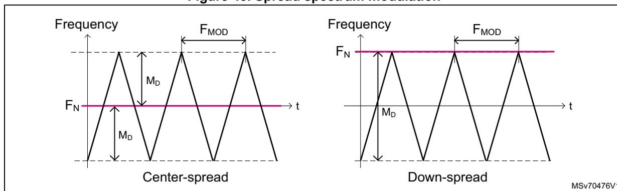
The peak modulation depth (in percentage) is given by the formula \( M_D (\%) = \text{MODSPR} / 10 \) .
Note: Modulation is turned off when MODSPR = 0.
The modulation frequency ( \( F_{MOD} \) ) is given by:
where 128 is the number of points in the internal wave table.
Note: When the PLL is locked, \( F_{CLKSSCG} = F_{PFD} \) . The upper limit of the frequency of modulation ( \( F_{MOD} \) ) is set by the PLL bandwidth. The PLL bandwidth limits the maximum modulation to \( F_{CLKSSCG} / 200 \) , where \( F_{CLKSSCG} = F_{REF} / DIVM \) or 50 MHz, whichever is lower.
To use the spread spectrum feature, to do the following:
- 1. Program the PLL to the nominal frequency ( \( F_N \) ) using the \( F_{OUTPOSTDIV} \) formula from Using PLLs in integer mode
- 2. Compute the MODDIV value according to the desired modulation frequency ( \( F_{MOD} \) ):
- 3. Compute the MODSPR value according to the desired modulation depth ( \( M_D \) ).
- 4. Set the MODSPRDW value according to the desired modulation type (center-spread or down-spread).
- 5. Compute DIVN accordingly ( \( DIVNFRAC=0 \) ):
- 6. Clear PLLxMODSSDIS, PLLxMODDSEN, and DACEN to 0.
- 7. Set PLLxMODSSRST to 1, and clear PLLxON to 0. PLLxON must be held at 0 for 1 \( \mu\text{s} \) to make sure the PLL is fully reset.
- 8. Set PLLxON, PLLxMODDSEN, and DACEN to 1 (see Note: ).
- 9. Wait until the first edge of CLKSSCG, and then clear PLLxMODSSRST to 0 (this can be done before or after the PLL is locked).
Note: The spread spectrum accuracy relies on the PLL fractional-N capability, so MODDSEN and DACEN must be set to 1.
The user can check \( F_{MIN} \) , \( F_{MAX} \) as follows:
- • Calculate \( F_N \) as above.
- • If MODSPRDW = 0 (center-spread):
\( F_{MIN} = F_N \times (1 - M_D / 100) \) and \( F_{MAX} = F_N \times (1 + M_D / 100) \) - • If MODSPRDW = 1 (down-spread):
\( F_{MIN} = F_N \times (1 - M_D / 100) \) and \( F_{MAX} = F_N \)
Programming sequence for spread spectrum mode
The programming sequence to enable SSCG and the PLL is:
- 1. Deassert PLLxMODSSRST.
- 2. Set PLLxDIVN, PLLxDIVNFRAC, and PLLxMODSSDIS to 0.
- 3. Assert PLLxMODDSEN and PLLxDACEN.
- 4. Assert PLLxMODSSRST and deassert PLLxON.
- 5. PLLxON must be deasserted for 1µs to make sure PLL is fully reset. Then assert PLLxON.
- 6. Wait until PLLxRDY is asserted, then deassert PLLxMODSSRST.
14.6.6 System clocks
System clock selection
After a system reset, the HSI is selected as system clock (sys[a,b,c,d]_ck), and all PLLs are switched off.
The system clock can be stopped by hardware when the system enters Stop or Standby mode.
When the system runs, the user can select system clocks (sys[a,b,c,d]_ck) from the four following sources:
- • HSE
- • HSI
- • MSI
- • ic[1,2,6,11]_ck
This function is controlled by programming RCC_CFGR1. A switch from one clock source to another occurs only if the target clock source is ready (clock stable after startup delay or PLL locked). If a clock source that is not yet ready is selected, the switch occurs when the clock source is ready.
The SYSSW only selects the ic[2,6,11]_ck if all three IC dividers are enabled.
SWS bits in RCC_CFGR1 indicate which clock sources are currently selected. Other status bits in RCC_CR indicate which clock(s) is (are) ready.
System clock generation
Figure 46 shows a simplified view of the clock distribution for the CPU and buses. All the dividers shown in the block diagram can be changed on-the-fly, without generating timing violations. This feature is a very simple solution to adapt bus frequencies to application needs, thus optimizing the power consumption.
The AXI sys_bus_ck is divided by HPRE to generate the AHB clock. HPRE is controlled by RCC_CFGR2.
In addition to the divide values shown, PPRE1, PPRE2, PPRE4, and PPRE5 can divide by 32, 64, and 128.
There is almost no clock protection, so the software must avoid configurations that can block the system.
Note:
The application must respect the maximum allowed frequencies:
\(
F_{CPUmax}
\)
and
\(
F_{BUSmax}
\)
.
\(
F_{BUS}
\)
represents the maximum allowed frequency for AHB and AXI buses (refer to the datasheet for the maximum values).
The trace clock (
ck_cpu_tpiu
) is generated from
sys_cpu_ck
clock, divided by eight. For additional information, refer to
Clock distribution for trace and debug
.
Figure 46. Core and bus clock generation
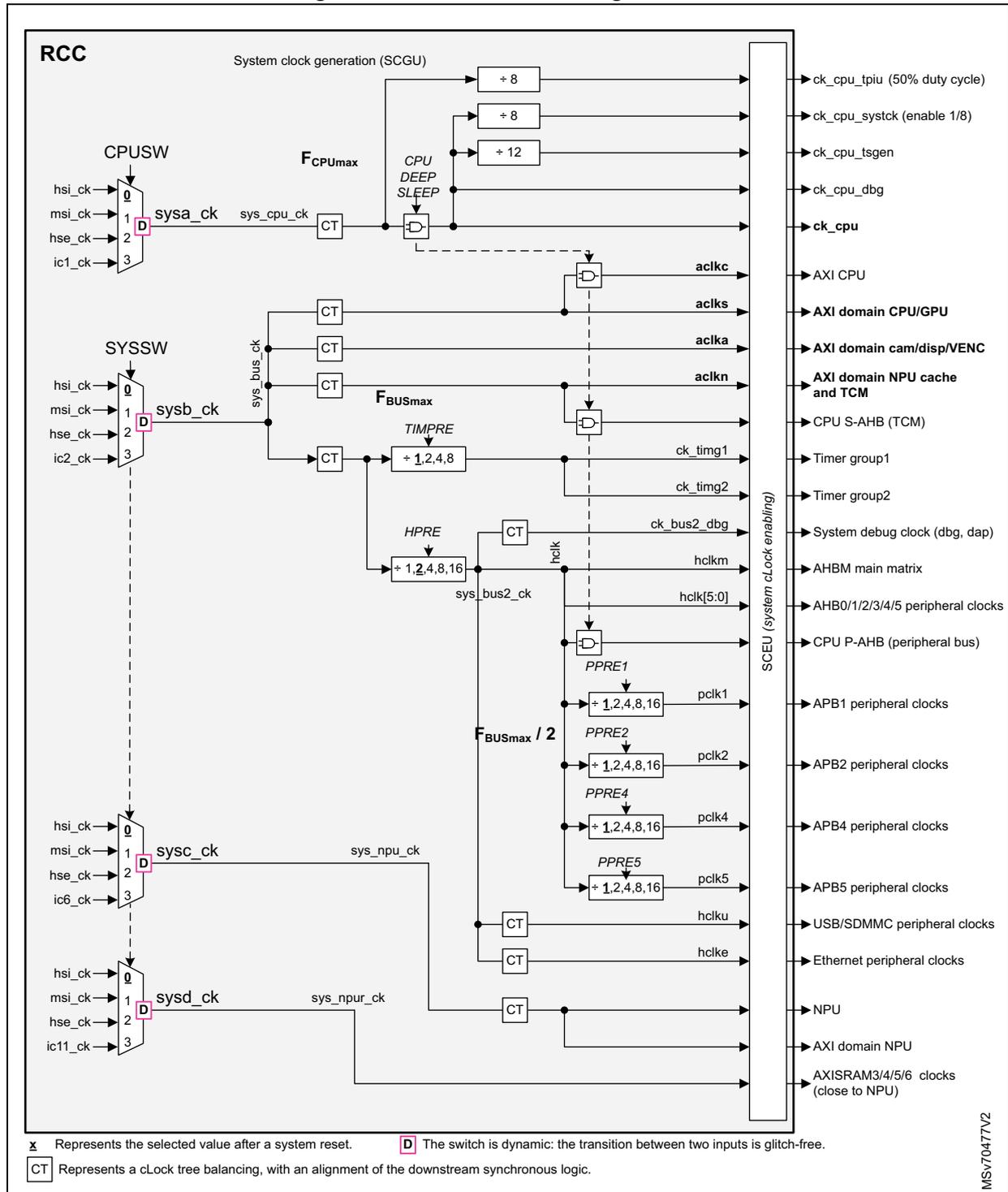
RCC
System clock generation (SCGU)
CPUSW
- hsi_ck → 0
- msi_ck → 1
- hse_ck → 2
- ic1_ck → 3
sysa_ck → sys_cpu_ck → [CT] → F CPUmax
F CPUmax paths:
- ÷ 8 → ck_cpu_tpiu (50% duty cycle)
- ÷ 8 → ck_cpu_systck (enable 1/8)
- ÷ 12 → ck_cpu_tsgen
- [CPU DEEP SLEEP] → [D] → ck_cpu_dbg
- ck_cpu
SYSSW
- hsi_ck → 0
- msi_ck → 1
- hse_ck → 2
- ic2_ck → 3
sysb_ck → sys_bus_ck → [CT] → F BUSmax
F BUSmax paths via SCEU (system cLock enabling):
- [CT] → [D] → aclkc → AXI CPU
- [CT] → aclks → AXI domain CPU/GPU
- [CT] → aclka → AXI domain cam/disp/VENC
- [CT] → aclkn → AXI domain NPU cache and TCM
- [CT] → [D] → CPU S-AHB (TCM)
- [CT] → TIMPRE → ÷ 1,2,4,8 → ck_timg1 → Timer group1
- ck_timg2 → Timer group2
- ck_bus2_dbg → System debug clock (dbg, dap)
- HPRE ÷ 1,2,4,8,16 → [CT] → hclk → AHBM main matrix
- hclk → hclk[5:0] → AHB0/1/2/3/4/5 peripheral clocks
- [D] → CPU P-AHB (peripheral bus)
- PPRE1 ÷ 1,2,4,8,16 → pclk1 → APB1 peripheral clocks
- PPRE2 ÷ 1,2,4,8,16 → pclk2 → APB2 peripheral clocks
- PPRE4 ÷ 1,2,4,8,16 → pclk4 → APB4 peripheral clocks
- PPRE5 ÷ 1,2,4,8,16 → pclk5 → APB5 peripheral clocks
- [CT] → hclku → USB/SDMMC peripheral clocks
- [CT] → hclke → Ethernet peripheral clocks
sysc_ck (from SYSCW) → sys_npu_ck → [CT] → NPU
sysd_ck (from SYSDW) → sys_npur_ck → [CT] → AXI domain NPU
AXISRAM3/4/5/6 clocks (close to NPU)
x Represents the selected value after a system reset.
D The switch is dynamic: the transition between two inputs is glitch-free.
CT Represents a cLock tree balancing, with an alignment of the downstream synchronous logic.
MSV70477V2
- 1. Dividers values can be changed on-the-fly. All dividers have 50% duty-cycles.
14.6.7 Clock generation in Stop and Standby modes
When the system enters Stop mode, all clocks (system and kernel) are stopped, and the following clock sources are disabled as well:
- • MSI, HSI
- • HSE
- • PLL1, PLL2, PLL3, PLL4
Note: The MSI and HSI stay active based on xxxSTOPEN bits in RCC_STOPCR.
HSIS is also disabled.
The content of the RCC registers is not altered, except CPUSW and SYSSW, forced to HSI or MSI (depending on STOPWUCK value), and PLLxON and HSEON, set to 0.
HSION and MSION are also modified, depending on STOPWUCK (see Table 70 ).
When the CPU requests to go in Stop mode, the RCC first stops all requested clocks, and informs the PWR that all clocks have been properly stopped. As shown in Figure 47 , three main signals are used to control power transitions:
- • rcc_pwrds: used to indicate to the PWR that the RCC stopped all clocks. The PWR can then go to Stop or Standby mode.
- • pwr_wkup is used to indicate to the RCC to re-enable the clocks.
- • The exti_wkup is used to indicate to the PWR that an event requests to exit the system from Stop mode.
Figure 47. Key signals controlling low-power modes
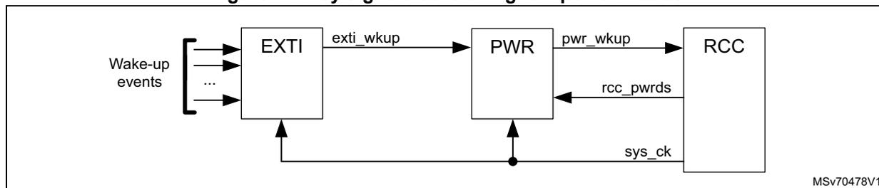
graph LR
    WE[Wake-up events] --> EXTI[EXTI]
    EXTI -- exti_wkup --> PWR[PWR]
    PWR -- pwr_wkup --> RCC[RCC]
    RCC -- rcc_pwrds --> PWR
    SC((sys_ck)) --> EXTI
    SC --> PWR
    SC --> RCC
MSv70478V1
Exiting Stop mode
When the device exits system Stop mode via a wake-up event, HSIS is started automatically.
Note: sys_rst is only deasserted after HSIS has successfully started.
The application can select which other oscillator (HSI and/or MSI) is used to restart the system. STOPWUCK in RCC_CFGR1 selects the oscillator used as system clock. Table 70 describes their behavior.
Table 70. STOPWUCK description
| STOPWUCK | Activated oscillator when system exits Stop mode | Distributed clocks when system exits Stop mode | |
|---|---|---|---|
| System clock | Kernel clock | ||
| 0 | HSI | HSI | HSI |
| 1 | MSI | MSI | MSI |
During Stop mode
There are two specific cases where the HSI or MSI can be enabled during system Stop mode:
- • When a dedicated peripheral requests the kernel clock, the peripheral receives the HSI or MSI according to the kernel clock source selected for this peripheral (via PERxSEL).
- • When HSISTOPEN or MSISTOPEN are set in RCC_STOPCR, the HSI and MSI are kept running during Stop mode but the outputs are gated. The clock is then available immediately when the system exits Stop mode, or when a peripheral requests the kernel clock (see Table 71 for details).
Caution: HSI and MSI are always off in Stop mode when the PWR is set to SVOS low.
Table 71. HSISTOPEN and MSISTOPEN behavior
| HSISTOPEN (MSISTOPEN) | HSI (MSI) state during Stop mode | HSI (MSI) setting time |
|---|---|---|
| 0 | Off | \( t_{su(HSI)} \) ( \( t_{su(MSI)} \) ) (1) |
| 1 | Running and gated | Immediate |
1. \( t_{su(HSI)} \) and \( t_{su(MSI)} \) are the startup times of the HSI and MSI oscillators (see the datasheet for their values).
When the microcontroller exits Standby mode, the HSI is selected as system and kernel clock. RCC registers are reset to their initial values except for the backup domain configurations (LSE in RCC_CR/RCC_LSECFG, RTC in RCC_CCIPR7, RCC_BDCR), and the reset cause (RCC_RSR, RCC_HWRCSR).
Caution: When leaving Stop mode without reset (but not from Standby mode), the RCC returns in the same state as before, except for the software that has been forced to select the STOPWUCK source. When leaving Standby mode, the application can restore previous CPU clock settings, if needed.
Caution: If the system clock switch selection (SYSSW) is HSI or MSI oscillator, STOPWUCK (system clock selection after a wake-up from system Stop) must select the same oscillator.
14.6.8 Peripheral clock distribution
Some peripherals are designed to work with two different clock domains, operating asynchronously:
- • a domain synchronous with the register and bus interface (ckg_bus_perx clock)
- • a domain generally synchronous with the peripheral (kernel clock)
Other peripherals only need a bus interface clock, hence the user application has more freedom to choose an optimized clock frequency for the CPU, bus matrix, and for the kernel part of the peripheral. The user can change the bus frequency without reprogramming peripherals (example: an ongoing transfer with UART is not disturbed if its APB clock is changed on-the-fly).
Table 72 summarizes the clocks from RCC to the peripherals. The clock named per_ck is the output of a mux (see Figure 38 ).
Table 72. Peripheral clock distribution summary
| Peripherals | Clock | Kernel clock MUX | Max kernel clock frequency (in MHz) | Type (1)(2) | ||
|---|---|---|---|---|---|---|
| Type | Source | Position | Control field | |||
| ADF1 | Kernel | hclk2 | 0 (3) | ADF1SEL | 200 | A |
| per_ck | 1 | |||||
| ic7_ck | 2 | |||||
| ic8_ck | 3 | |||||
| msi_ck | 4 | |||||
| hsi_div_ck | 5 | |||||
| I2S_CKIN | 6 | |||||
| timg_ck | 7 | |||||
| Bus | hclk2 | - | - | 200 | - | |
| ADC12 | Kernel | hclk1 | 0 (3) | ADC12SEL | 125 | A |
| per_ck | 1 | |||||
| ic7_ck | 2 | |||||
| ic8_ck | 3 | |||||
| msi_ck | 4 | |||||
| hsi_div_ck | 5 | |||||
| I2S_CKIN | 6 | |||||
| timg_ck | 7 | |||||
| Bus | hclk1 | - | - | 200 | - | |
| CACHEAXI | Bus | sys_bus_ck | - | - | 400 | - |
| hclk5 | - | - | 200 | - | ||
| CRC | Bus | hclk4 | - | - | 200 | - |
| CRYP | Bus | hclk3 | - | - | 200 | - |
| DBG | Kernel | sys_cpu_ck | - | - | 800 | A |
| Bus | ck_bus2_dbg | - | - | 200 | - | |
| DTS | Kernel | hsi_div8_ck | - | - | 10 | A |
| Bus | pclk4 | - | - | 100 | - | |
| CSI | Kernel | As DCMIPP | - | DCMIPPSEL | - | A |
| Bus | pclk5 | - | - | 200 | - | |
| CSIPHY | Kernel | ic18_ck | - | - | 20 | A |
| Bus | pclk5 | - | - | 200 | - | |
Table 72. Peripheral clock distribution summary (continued)
| Peripherals | Clock | Kernel clock MUX | Max kernel clock frequency (in MHz) | Type (1)(2) | ||
|---|---|---|---|---|---|---|
| Type | Source | Position | Control field | |||
| DCMIPP | Kernel | pclk5 | 0 | DCMIPPSEL | 333 | A |
| per_ck | 1 | |||||
| ic17_ck | 2 | |||||
| hsi_div_ck | 3 | |||||
| Bus | sys_busa_ck | - | - | 400 | - | |
| pclk5 | - | - | 200 | - | ||
| GPDMA1 | Bus | hclk1 | - | - | 200 | - |
| HPDMA1 | Bus | hclk5 | - | - | 200 | - |
| DMA2D | Bus | hclk5 | - | - | 200 | - |
| aclk | ||||||
| DTS | Kernel | hsi_div8_ck | - | - | 10 | A |
| Bus | pclk4 | - | - | 200 | - | |
| ETH1 | Kernel | ETH1_TX_CLK | - | - | 25 | A |
| ETH1_RX_CLK/ETH1_REF_CLK | 0 (3) | ETH1REFCLKSEL | 125 | A | ||
| eth1_clk_fb | 1 | |||||
| sys_bus2_ck | 0 (3) | ETH1CLKSEL | 125 | A | ||
| per_ck | 1 | |||||
| ic12_ck | 2 | |||||
| hse_ck | 3 | |||||
| sys_bus2_ck | 0 | ETH1PTPSEL | 200 | A | ||
| per_ck | 1 | |||||
| ic13_ck | 2 | |||||
| hse_ck | 3 | |||||
| Bus | hclk1 | - | - | 200 | - | |
| EXTI | Bus | pclk4 | - | - | 125 | - |
| FDCAN | Kernel | pclk1 | 0 (3) | FDCANSEL | 150 | A |
| per_ck | 1 | |||||
| ic19_ck | 2 | |||||
| hse_ck | 3 | |||||
| Bus | pclk1 | - | - | 200 | - | |
Table 72. Peripheral clock distribution summary (continued)
| Peripherals | Clock | Kernel clock MUX | Max kernel clock frequency (in MHz) | Type (1)(2) | ||
|---|---|---|---|---|---|---|
| Type | Source | Position | Control field | |||
| FMC | Kernel | hclk5 | 0 (3) | FMCSEL | 200 | A |
| per_ck | 1 | |||||
| ic3_ck | 2 | |||||
| ic4_ck | 3 | |||||
| Bus | sys_buss_ck | - | - | 400 | - | |
| hclk5 | - | |||||
| GPIOA-H, GPION-Q | Bus | hclk4 | - | - | 200 | - |
| GPU2D | Bus | sys_buss_ck | - | - | 400 | - |
| GFXMMU | Bus | sys_buss_ck | - | - | 400 | - |
| hclk5 | ||||||
| GFXTIM | Bus | pclk5 | - | - | 200 | - |
| HASH | Bus | hclk3 | - | - | 200 | - |
| I2C1, I2C2, I2C3 | Kernel | pclk1 | 0 (3) | I2C1SEL, I2C2SEL, I2C3SEL | 100 | A |
| per_ck | 1 | |||||
| ic10_ck | 2 | |||||
| ic15_ck | 3 | |||||
| msi_ck | 4 | |||||
| hsi_div_ck | 5 | |||||
| Bus | pclk1 | - | - | 100 | - | |
| I2C4 | Kernel | pclk1 | 0 (3) | I2C4SEL | 100 | A |
| per_ck | 1 | |||||
| ic10_ck | 2 | |||||
| ic15_ck | 3 | |||||
| msi_ck | 4 | |||||
| hsi_div_ck | 5 | |||||
| Bus | pclk4 | - | - | 100 | - | |
| I3C1, I3C2 | Kernel | pclk1 | 0 (3) | I3C1SEL, I3C2SEL | 100 | A |
| per_ck | 1 | |||||
| ic10_ck | 2 | |||||
| ic15_ck | 3 | |||||
| msi_ck | 4 | |||||
| hsi_div_ck | 5 | |||||
| Bus | pclk1 | - | - | 100 | - | |
Table 72. Peripheral clock distribution summary (continued)
| Peripherals | Clock | Kernel clock MUX | Max kernel clock frequency (in MHz) | Type (1)(2) | ||
|---|---|---|---|---|---|---|
| Type | Source | Position | Control field | |||
| IWDG | Kernel | lsi_ck | - | - | 1 | A |
| Bus | pclk4 | - | - | 100 | - | |
| JPEG | Bus | hclk5 | - | - | 200 | - |
| LPTIM1 | Kernel | pclk1 | 0 (3) | LPTIM1SEL | 200 | A |
| per_ck | 1 | |||||
| ic15_ck | 2 | |||||
| lse_ck | 3 | |||||
| lsi_ck | 4 | |||||
| timg_ck | 5 | |||||
| Bus | pclk1 | - | - | 200 | - | |
| LPTIM2, LPTIM3, LPTIM4, LPTIM5 | Kernel | pclk4 | 0 (3) | LPTIM2SEL. LPTIM3SEL. LPTIM4SEL, LPTIM5SEL | 200 | A |
| per_ck | 1 | |||||
| ic15_ck | 2 | |||||
| lse_ck | 3 | |||||
| lsi_ck | 4 | |||||
| timg_ck | 5 | |||||
| Bus | pclk4 | - | - | 200 | - | |
| LPUART1 | Kernel | pclk4 | 0 (3) | LPUART1SEL | 100 | A |
| per_ck | 1 | |||||
| ic9_ck | 2 | |||||
| ic14_ck | 3 | |||||
| lse_ck | 4 | |||||
| msi_ck | 5 | |||||
| hsi_div_ck | 6 | |||||
| Bus | pclk4 | - | - | 100 | - | |
| LTDC | Kernel | pclk5 | 0 | LTDCSEL | 86 | A |
| per_ck | 1 | |||||
| ic16_ck | 2 | |||||
| hsi_div_ck | 3 | |||||
| Bus | pclk5 | - | - | 200 | - | |
| sys_busa_ck | - | - | 400 | |||
| MCE1, MCE2, MCE3 | Bus | aclk | - | As XSPI1, XSPI2, XSPI3 | 200 | - |
| hclk5 | - | |||||
Table 72. Peripheral clock distribution summary (continued)
| Peripherals | Clock | Kernel clock MUX | Max kernel clock frequency (in MHz) | Type (1)(2) | ||
|---|---|---|---|---|---|---|
| Type | Source | Position | Control field | |||
| MCE4 | Bus | aclk | - | As FMC | 200 | - |
| hclk5 | - | |||||
| MDF1 | Kernel | hclk2 | 0 (4) | MDF1SEL | 200 | A |
| per_ck | 1 | |||||
| ic7_ck | 2 | |||||
| ic8_ck | 3 | |||||
| msi_ck | 4 | |||||
| hsi_div_ck | 5 | |||||
| I2S_CKIN | 6 | |||||
| timg_ck | 7 | |||||
| Bus | hclk2 | - | - | 200 | - | |
| MDIOS | Bus | pclk1 | - | - | 200 | - |
| NPU | Kernel | sys_npu_ck | - | - | 1000 | A |
| sys_npur_ck | - | - | 900 | A | ||
| Bus | sys_bus_ck | - | - | 400 | - | |
| sys_bus2_ck | - | - | 200 | - | ||
| OTGPHY1, OTGPHY2 | Kernel | hse_div2_ck | 0 (3) | OTGPHY1SEL, OTGPHY2SEL | 48 | A |
| per_ck | 1 | |||||
| ic15_ck | 2 | |||||
| hse_div2_osc_ck | 3 | |||||
| Kernel | otgphy1_ker_ck, otgphy2_ker_ck | 0 | OTGPHY1CK REFSEL, OTGPHY2CK REFSEL, | 200 | - | |
| hse_div2_osc_ck | 1 | |||||
| OTG1, OTG2 | Kernel | phyclock | - | - | 60 | A |
| Bus | hcku | - | - | 200 | - | |
| PKA | Bus | hclk3 | - | - | 200 | - |
| PWR | Bus | hclk4 | - | - | 200 | - |
| PSSI | Kernel | hclk5 | 0 (3) | PSSISEL | 40 | - |
| per_ck | 1 | - | ||||
| ic20_ck | 2 | - | ||||
| hsi_div_ck | 3 | - | ||||
| Bus | hclk5 | - | - | 200 | - | |
| RCC | Bus | hclk | - | - | 200 | - |
Table 72. Peripheral clock distribution summary (continued)
| Peripherals | Clock | Kernel clock MUX | Max kernel clock frequency (in MHz) | Type (1)(2) | ||
|---|---|---|---|---|---|---|
| Type | Source | Position | Control field | |||
| RNG | Kernel | hsis_osc_ck | - | - | 64 | A |
| Bus | hclk3 | - | - | 200 | - | |
| RTC (5) | Kernel | no clock | 0 (3) | RTCSEL | 4 | A |
| lse_ck | 1 | |||||
| lsi_ck | 2 | |||||
| hse_ker_ck / (RTCDIV+1) | 3 | |||||
| Bus | pclk4 | - | - | 100 | - | |
| SAES | Kernel | hclk3 | - | - | 200 | A |
| Bus | hclk3 | - | - | 200 | - | |
| SAI1, SAI2 | Kernel | pclk2 | 0 (3) | SAI1SEL, SAI2SEL | 200 | A |
| per_ck | 1 | |||||
| ic7_ck | 2 | |||||
| ic8_ck | 3 | |||||
| msi_ck | 4 | |||||
| hsi_div_ck | 5 | |||||
| I2S_CKIN | 6 | |||||
| spdif_symb_ck | 7 | |||||
| Bus | pclk2 | - | - | 200 | - | |
| SDMMC1 | Kernel | sys_bus2_ck | 0 (3) | SDMMC1SEL | 208 | A |
| per_ck | 1 | |||||
| ic4_ck | 2 | |||||
| ic5_ck | 3 | |||||
| Bus | sys_bus2_ck | - | - | 200 | - | |
| SDMMC2 | Kernel | sys_bus2_ck | 0 (3) | SDMMC2SEL | 208 | A |
| per_ck | 1 | |||||
| ic4_ck | 2 | |||||
| ic5_ck | 3 | |||||
| Bus | sys_bus2_ck | - | - | 200 | - | |
Table 72. Peripheral clock distribution summary (continued)
| Peripherals | Clock | Kernel clock MUX | Max kernel clock frequency (in MHz) | Type (1)(2) | ||
|---|---|---|---|---|---|---|
| Type | Source | Position | Control field | |||
| SPDIFRX1 | Kernel | pclk1 | 0 (3) | SPDIFRX1SEL | 200 | A |
| per_ck | 1 | |||||
| ic7_ck | 2 | |||||
| ic8_ck | 3 | |||||
| msi_ck | 4 | |||||
| hsi_div_ck | 5 | |||||
| I2S_CKIN | 6 | |||||
| Bus | pclk1 | - | - | 200 | - | |
| SPI1 | Kernel | pclk2 | 0 (3) | SPI1SEL | 200 | A |
| per_ck | 1 | |||||
| ic8_ck | 2 | |||||
| ic9_ck | 3 | |||||
| msi_ck | 4 | |||||
| hsi_div_ck | 5 | |||||
| I2S_CKIN | 6 | |||||
| Bus | pclk2 | - | - | 200 | - | |
| SPI2, SPI3 | Kernel | pclk1 | 0 (3) | SPI2SEL, SPI3SEL | 200 | A |
| per_ck | 1 | |||||
| ic8_ck | 2 | |||||
| ic9_ck | 3 | |||||
| msi_ck | 4 | |||||
| hsi_div_ck | 5 | |||||
| I2S_CKIN | 6 | |||||
| Bus | pclk1 | - | - | 200 | - | |
| SPI4, SPI5 | Kernel | pclk2 | 0 (3) | SPI4SEL, SPI5SEL | 133 | A |
| per_ck | 1 | |||||
| ic9_ck | 2 | |||||
| ic14_ck | 3 | |||||
| msi_ck | 4 | |||||
| hsi_div_ck | 5 | |||||
| hse_ck | 6 | |||||
| Bus | pclk2 | - | - | 200 | - | |
Table 72. Peripheral clock distribution summary (continued)
| Peripherals | Clock | Kernel clock MUX | Max kernel clock frequency (in MHz) | Type (1)(2) | ||
|---|---|---|---|---|---|---|
| Type | Source | Position | Control field | |||
| SPI6 | Kernel | pclk4 | 0 (3) | SPI1SEL | 200 | A |
| per_ck | 1 | |||||
| ic8_ck | 2 | |||||
| ic9_ck | 3 | |||||
| msi_ck | 4 | |||||
| hsi_div_ck | 5 | |||||
| I2S_CKIN | 6 | |||||
| Bus | pclk4 | - | - | 200 | - | |
| TIM2, TIM3, TIM4, TIM5, TIM6, TIM7, TIM10, TIM11, TIM12, TIM13, TIM14 | Kernel | timg1_ck | - | - | 400 | S |
| Bus | pclk1 | - | - | 200 | - | |
| TIM1, TIM8, TIM9, TIM15, TIM16, TIM17, TIM18 | Kernel | timg2_ck | - | - | 400 | S |
| Bus | pclk2 | - | - | 200 | - | |
| USART1 | Kernel | pclk2 | 0 (3) | USART1SEL | 100 | A |
| per_ck | 1 | |||||
| ic9_ck | 2 | |||||
| ic14_ck | 3 | |||||
| lse_ck | 4 | |||||
| msi_ck | 5 | |||||
| hsi_div_ck | 6 | |||||
| Bus | pclk2 | - | - | 100 | - | |
| USART2, USART3, UART4, UART5, UART7, UART8 | Kernel | pclk1 | 0 (3) | USART2SEL, USART3SEL, UART4SEL, UART5SEL, UART7SEL, UART8SEL | 100 | A |
| per_ck | 1 | |||||
| ic9_ck | 2 | |||||
| ic14_ck | 3 | |||||
| lse_ck | 4 | |||||
| msi_ck | 5 | |||||
| hsi_div_ck | 6 | |||||
| Bus | pclk1 | - | - | 100 | - | |
Table 72. Peripheral clock distribution summary (continued)
| Peripherals | Clock | Kernel clock MUX | Max kernel clock frequency (in MHz) | Type (1)(2) | ||
|---|---|---|---|---|---|---|
| Type | Source | Position | Control field | |||
| USART6, UART9, USART10 | Kernel | pclk2 | 0 (3) | USART6SEL, UART9SEL, USART10SEL | 100 | A |
| per_ck | 1 | |||||
| ic9_ck | 2 | |||||
| ic14_ck | 3 | |||||
| lse_ck | 4 | |||||
| msi_ck | 5 | |||||
| hsi_div_ck | 6 | |||||
| Bus | pclk2 | - | - | 100 | - | |
| UCPD1 | Kernel | hsi_div4_ck | - | - | 25 | A |
| Bus | pclk1 | - | - | 100 | - | |
| VENC | Bus | sys_busa_ck | - | - | 400 | - |
| pclk5 | - | - | 200 | - | ||
| VENCRAM | Bus | sys_buss_ck | - | - | 400 | - |
| VREFBUF | Bus | pclk4 | - | - | 200 | - |
| WWDG1 | Bus | pclk1 | - | - | 200 | - |
| XSPI1, XSPI2, XSPI3 | Kernel | hclk5 | 0 (3) | XSPI1SEL, XSPI2SEL, XSPI3SEL | 200 | A |
| per_ck | 1 | |||||
| ic3_ck | 2 | |||||
| ic4_ck | 3 | |||||
| Bus | sys_buss_ck | - | - | 200 | - | |
| XSPIM | Bus | hclk5 | - | - | 200 | - |
- 1. 'A' means that the kernel clock is asynchronous with respect to bus interface clock.
- 2. 'S' means that the kernel clock is synchronous with respect to bus interface clock.
- 3. Reset value.
- 4. Reset value.
- 5. The RTC switch is in the VSW voltage domain.
Clock distribution for the NPU
Figure 48. Clock distribution for the NPU
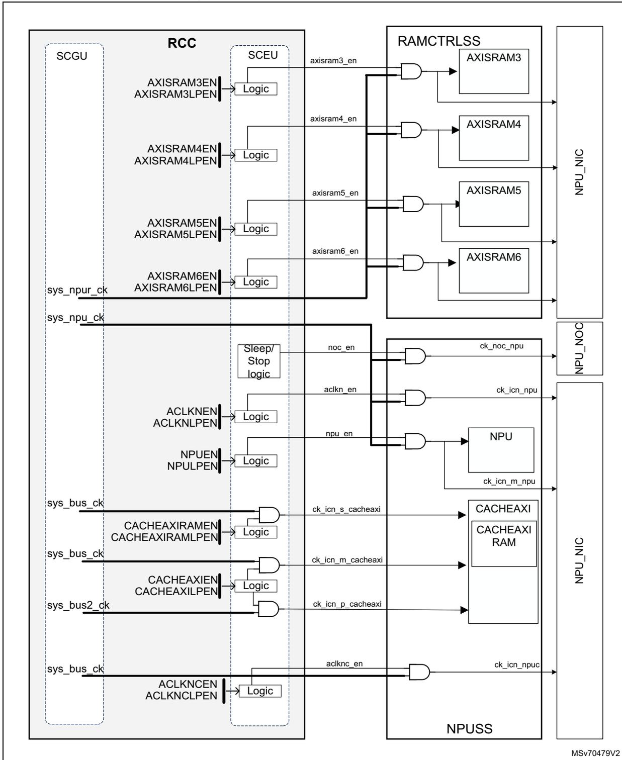
The diagram illustrates the clock distribution for the NPU within the STM32MP157 system. The main components and their interactions are as follows:
- SCGU (System Control and Global Unit):
Provides system clock signals:
sys_npur_ck,sys_npu_ck,sys_bus_ck, andsys_bus2_ck. - RCC (Reset and Clock Control):
Contains the
SCEU (System Clock Enable Unit)
which includes logic blocks for enabling various components based on configuration registers:
- AXISRAM3/4/5/6 Enable Logic:
Uses registers
AXISRAM3EN/AXISRAM3LPEN,AXISRAM4EN/AXISRAM4LPEN,AXISRAM5EN/AXISRAM5LPEN, andAXISRAM6EN/AXISRAM6LPENto generate enable signalsaxisram3_en,axisram4_en,axisram5_en, andaxisram6_en. - NPU Enable Logic:
Uses registers
ACLKNEN/ACLKNLPENandNPUEN/NPULPENto generatenoc_en,aclk_n_en, andnpu_en. - CACHEAXI RAM Enable Logic:
Uses registers
CACHEAXIRAMEN/CACHEAXIRAMPLPEN,CACHEAXIEN/CACHEAXILPEN, andACLKNCEN/ACLKNCLPENto generateck_icn_s_cacheaxi,ck_icn_m_cacheaxi,ck_icn_p_cacheaxi, andaclknc_en.
- AXISRAM3/4/5/6 Enable Logic:
Uses registers
- RAMCTRLSS (RAM Controller):
Contains
AXISRAM3
,
AXISRAM4
,
AXISRAM5
, and
AXISRAM6
. Each is enabled by an AND gate combining the corresponding
axisramX_ensignal with a common enable signal. - NPUSS (NPU Subsystem):
Contains the
NPU
,
CACHEAXI RAM
, and network interfaces
NPU_NIC
and
NPU_NOC
.
- The
NPU
is enabled by an AND gate combining
npu_enwithnoc_enandaclk_n_en, producingck_noc_npu,ck_icn_npu, andck_icn_m_npu. - The
CACHEAXI RAM
is enabled by AND gates combining
ck_icn_s_cacheaxi,ck_icn_m_cacheaxi, andck_icn_p_cacheaxiwithaclknc_en, producingck_icn_npuc.
- The
NPU
is enabled by an AND gate combining
MSv70479V2
Clock distribution for graphic blocks (GPU, LTDC, DCMIPP, and PSSI)
Figure 49. Clock distribution for PSSI, CSI, and DCMIPP
Legend:
- Bus interface clocks
- Kernel clocks
- D The switch is dynamic: the transition between two inputs is glitch-free.
- X represents the selected switch input after a system reset.
MSV70481V1
Figure 50. Clock distribution for GPU, ICACHE, and GFXMMU
The PSSI receives an AHB clock and a kernel clock (pxclk). The pxclk can be provided either by an external device via PSSI_PIXCK pin, or by the RCC.
Note: The clock generated by the RCC is provided to pxclk input by the feedback path of the PSSI_PIXCK pin. The drive of the PSSI_PIXCK is controlled by the PSSI.
Figure 51. Clock distribution for LTDC
[D]
The switch is dynamic: the transition between two inputs is glitch-free.
X represents the selected switch input after a system reset.
Figure 52. Clock distribution for VENC
Clock distribution for OTG1, OTG2, and UCPD1
Figure 53 shows the clock distribution for:
- • USB Type-C Power Delivery block (UCPD1): uses ucpd1_ker_ck as kernel clock. ucpd1_ker_ck is directly generated from the HSI output divided by four.
- • OTGPHYx: embeds a PLL that accepts a reference input frequency of 19.2, 20, or 24 MHz. The reference clock can be selected among one of the following:
- – hse_div2_osc_ck
- – hse_div2_ck
- – ic15_ck
- – per_ck
hse_div2_osc_ck is direct from the HSE oscillator, without the tempo delay. It can be selected to be HSE or HSE/2.
The OTGPHYx provides a 60 MHz clock (phyck) to the OTGx.
- • OTGx: uses the phyck when working in HS or FS mode.
The reference clock selection for the OTGPHYx is performed by a simple multiplexer. To change the clock source, the application must use the following sequence:
- 1. Disable the OTGPHYx clock by clearing OTGPHYxEN to 0.
- 2. Change the clock source selector (OTGPHYxSEL) to the desired value.
- 3. Enable the OTGPHYx clock by setting OTGPHYxEN to 1.
Clocks provided by the RCC are controlled by enable bits in RCC_AHB5ENR.
Note: Before programming OTG1PHYCTL_CR, OTG1EN must be asserted (the OTG1PHYCTL_CR logic requires the clock enabled by OTG1EN).
Figure 53. Clock distribution for OTG1, OTG2, and UCPD1
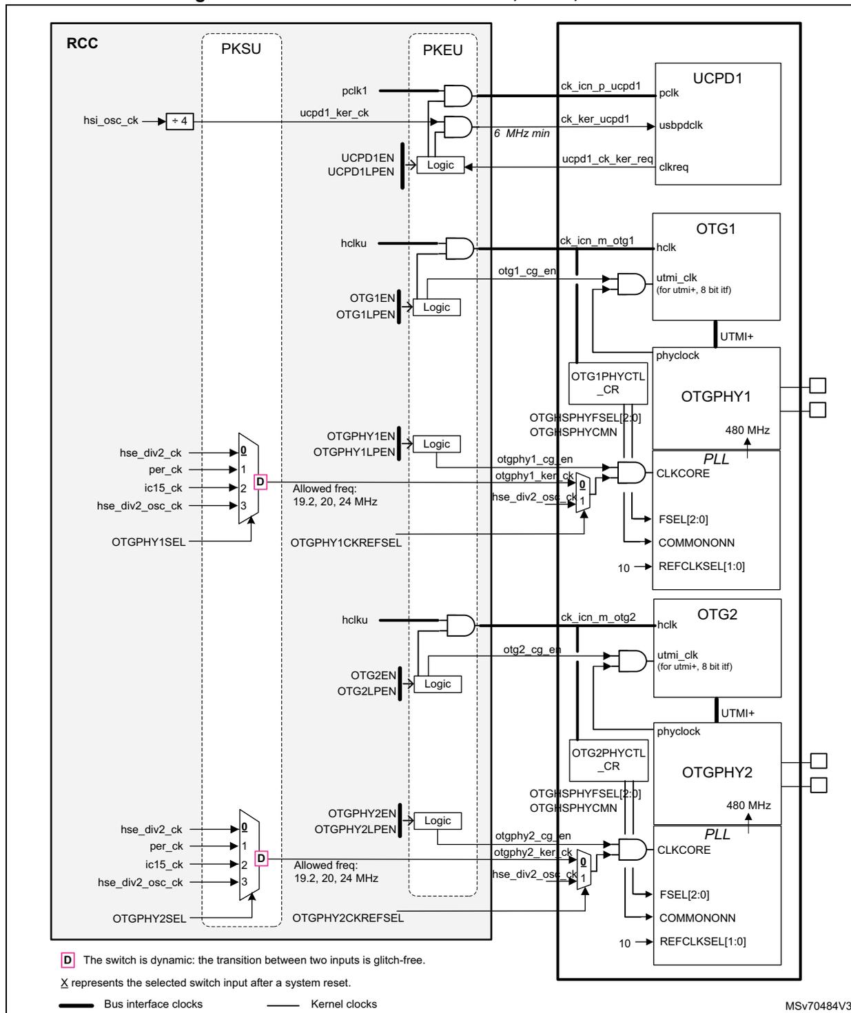
The diagram illustrates the clock distribution for OTG1, OTG2, and UCPD1. It is divided into three main functional blocks: RCC (Reset and Clock Control), PKSU , and PKEU , followed by the peripheral blocks: UCPD1 , OTG1 , OTGPHY1 , PLL , OTG2 , and OTGPHY2 .
- RCC
:
- Inputs:
hsi_osc_ck(divided by 4),hse_div2_ck,per_ck,ic15_ck,hse_div2_osc_ck,OTGPHY1SEL, andOTGPHY2SEL. - Outputs:
pclk1,ucpd1_ker_ck,hclku,UCPD1EN,UCPD1LPEN,OTG1EN,OTG1LPEN,OTGPHY1EN,OTGPHY1LPEN,OTGPHY1CKREFSEL,OTG2EN,OTG2LPEN,OTGPHY2EN,OTGPHY2LPEN,OTGPHY2CKREFSEL.
- Inputs:
- PKSU
and
PKEU
:
- Contain logic gates and multiplexers (marked with D ).
- Multiplexers for
hse_div2_ck,per_ck,ic15_ck, andhse_div2_osc_ckhave allowed frequencies of 19.2, 20, and 24 MHz.
- UCPD1
:
- Inputs:
ck_icn_p_ucpd1,ck_ker_ucpd1,ucpd1_ck_ker_req. - Outputs:
pclk,usbpdclk,clkreq. - Note:
6 MHz minforck_ker_ucpd1.
- Inputs:
- OTG1
:
- Inputs:
ck_icn_m_otg1,utmi_clk(for utmi+, 8 bit itf). - Outputs:
hclk.
- Inputs:
- OTGPHY1
:
- Inputs:
phyclock,OTG1PHYCTL_CR,OTG1SPHYFSEL[2:0],OTG1SPHYCMN. - Outputs:
480 MHz.
- Inputs:
- PLL (for OTGPHY1/2)
:
- Inputs:
CLKCORE,FSEL[2:0],COMMONONN,REFCLKSEL[1:0](fixed at 10). - Outputs:
480 MHz.
- Inputs:
- OTG2
:
- Inputs:
ck_icn_m_otg2,utmi_clk(for utmi+, 8 bit itf). - Outputs:
hclk.
- Inputs:
- OTGPHY2
:
- Inputs:
phyclock,OTG2PHYCTL_CR,OTG2SPHYFSEL[2:0],OTG2SPHYCMN. - Outputs:
480 MHz.
- Inputs:
Legend:
- D : The switch is dynamic; the transition between two inputs is glitch-free.
- X : represents the selected switch input after a system reset.
- ▬ Bus interface clocks
- — Kernel clocks
MSV70484V3
Clock distribution for ETH1
Kernel Ethernet clocks are provided by the RCC, who provides also clock selectors (CLK_SEL, REF_CLK_SEL, SEL), and clock enables for TX and RX used in the ETHSS.
Note: Bus and PTP clocks are gated via ETH1MACEN and ETH1MACLPEN bits.
Figure 54. Clock distribution for ETH1
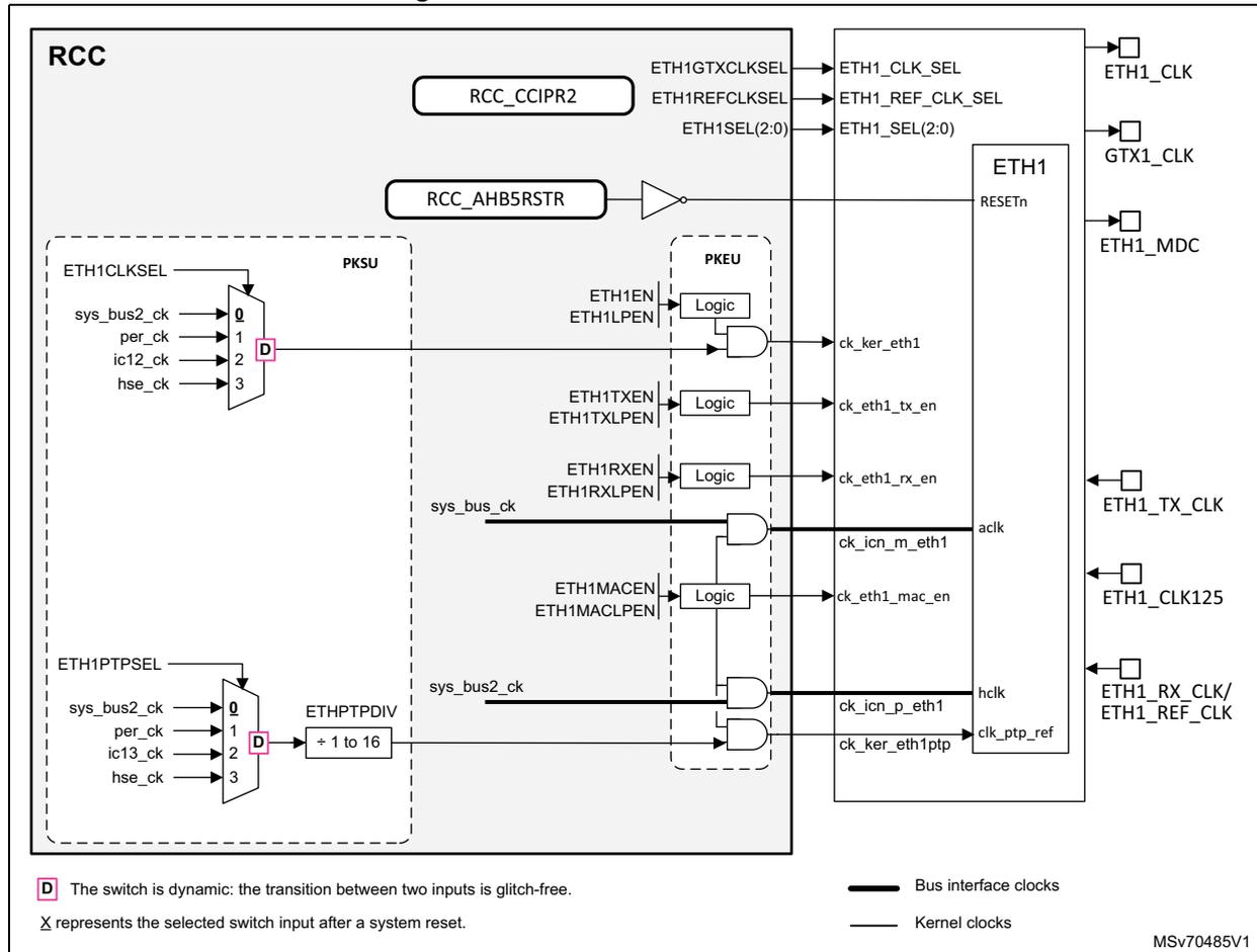
The ETH1 can generate a reference clock to the external PHY via the ETH1_CLK pin. The ETH1_CLK is generated only if all the following conditions are met:
- • ETH1EN is enabled.
- • The system is in Run or Sleep mode.
- • The clock source for ck_ker_eth1 is available.
The clock management for ETH is very flexible and based on the PHY interface mode (MII, RMII, or RGMII). All clock signals (enables, selection, and pins) are shown in Figure 55.
Figure 55. Clock management for ETH1
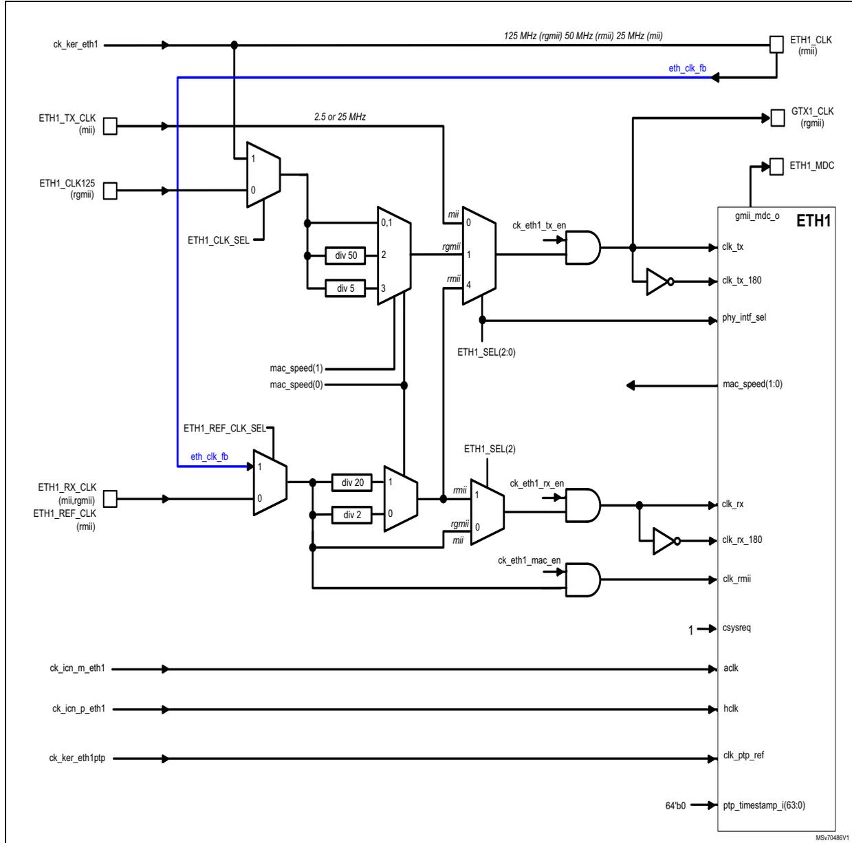
The diagram illustrates the clock management logic for the ETH1 peripheral. It features several input signals and internal processing blocks:
- ck_ker_eth1 : A primary clock input that branches to the ETH1_CLK (rmii) pin and an internal multiplexer.
- ETH1_TX_CLK (mii) and ETH1_CLK125 (rgmii) : Input signals for the transmit clock, connected to a multiplexer.
- ETH1_REF_CLK (mii, rgmii) and ETH1_REF_CLK (rmii) : Reference clock inputs connected to a second multiplexer.
- ck_icn_m_eth1 , ck_icn_p_eth1 , and ck_ker_eth1ptp : External clock inputs for the MAC and PTP, connected directly to the ETH1 block.
- Internal Logic
:
- The first multiplexer ( ETH1_CLK_SEL ) selects between ck_ker_eth1 and the TX clock. Its output is divided by 50 or 5 ( div 50 , div 5 ) and then multiplexed ( 0,1 ) based on mac_speed(1) and mac_speed(0) . This signal is labeled 2.5 or 25 MHz .
- The second multiplexer ( ETH1_REF_CLK_SEL ) selects between the reference clock inputs. Its output is divided by 20 or 2 ( div 20 , div 2 ) and then multiplexed ( 1 ) based on ETH1_SEL(2) .
- AND gates ( ck_eth1_tx_en , ck_eth1_rx_en , ck_eth1_mac_en ) combine these signals with enable inputs from the ETH1 block to generate internal clocks: clk_tx , clk_rx , and clk_rmii .
- Inverters generate clk_tx_180 and clk_rx_180 .
- Output Signals
:
- ETH1_CLK (rmii) : Output from ck_ker_eth1 , labeled 125 MHz (rgmii) 50 MHz (rmii) 25 MHz (mii) .
- GTXT1_CLK (rgmii) : Output from the 2.5 or 25 MHz signal.
- ETH1_MDC : Output from the gmii_mdc_o signal.
- clk_tx , clk_tx_180 , clk_rx , clk_rx_180 , clk_rmii : Internal clocks output to the ETH1 block.
- phy_intf_sel : Output from ETH1_SEL(2:0) .
- mac_speed(1:0) : Bidirectional signal.
- csysreq : Constant high signal ( 1 ).
- aclk , hclk , clk_ptp_ref : External clock inputs.
- ptp_timestamp_i(63:0) : 64-bit input signal ( 64'b0 ).
Clock distribution for MDIOS
MDIOS (MDIO slave) clocks are provided by the RCC.
Figure 56. Clock distribution for MDIOS
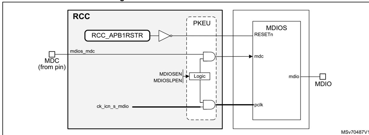
Clock distribution for FMC, XSPIs, and SDMMCs
The FMC kernel clock can be chosen between four different sources. For each XSPI, a clock switch can be used to select between four different sources. Each XSPI can be enabled independently.
The following steps are needed to correctly configure XSPI switches:
- 1. Switch on the desired clock source.
- 2. Ensure the clock source is ready, and conditions described above are met.
- 3. Set XSPIxSEL to the desired position.
- 4. Enable the XSPI clock (XSPIxEN = 1).
The XSPIs provide a clock to the external memory with a duty-cycle distortion lower than 5%. To this end, the kernel clock provided to the XSPIs has a typical duty cycle of 50%. In addition, the XSPIs embed a prescaler allowing clock division by even ratios.
Figure 57. Clock distribution for FMC and MCE4
The diagram illustrates the clock distribution system within the RCC (Reset and Clock Control) block and its connections to external components. The RCC block contains the following elements:
- Inputs: FMCRST, sys_rstn, MCE4EN, MCE4LPEN, RISAFEN, RISAFLPEN, FMCEN, FMCLPEN, and FMCEL.
- Logic: Several AND gates and 'Logic' blocks process the enable signals (MCE4EN, MCE4LPEN, RISAFEN, RISAFLPEN, FMCEN, FMCLPEN) to generate internal clock signals: ck_icn_p_mce4, ck_icn_p_risaf, ck_icn_s_fmc, ck_icn_p_fmc, and ck_ker_fmc.
- Switch: A dynamic switch (labeled 'D') selects between four inputs (0: hclk5, 1: per_ck, 2: ic3_ck, 3: ic4_ck) based on the FMCEL signal. The per_ck input (1) is the default selection after a system reset.
- Outputs: The RCC block outputs various clock signals to external blocks: RISUP (hclk), MCE4 (hclk, aclk), RISAF4 (aresetn, hresetn, hclk, aclk), and FMC (ack, hclk, fmc_ker_ck).
Legend:
- D The switch is dynamic: the transition between two inputs is glitch-free.
- X represents the selected switch input after a system reset.
- Bus interface clocks (thick line)
- Kernel clocks (thin line)
MSV70488V2
Figure 58. Clock distribution for XSPIs and MCE1/2/3
The diagram illustrates the clock distribution for XSPIs and MCE1/2/3. The RCC (Reset and Clock Control) block on the left provides various clock signals. XSPI1, XSPI2, and XSPI3 are connected to external PHYs (XSPI-PHY1, XSPI-PHY2) and DLLs (DLL_XSPI1, DLL_XSPI2). MCE1, MCE2, and MCE3 are connected to the XSPI-M bus. The diagram includes logic gates, multiplexers, and reset/clock control blocks (RISUP, RISAF, MCE).
Legend:
- D The switch is dynamic: the transition between two inputs is glitch-free. X represents the selected switch input after a system reset.
- — Bus interface clocks
- — Kernel clocks
MSv70489V3
The SDMMC1 and SDMMC2 have separate kernel clocks. A clock switch allows the selection between four different sources. Each SDMMC can be enabled independently.
When an SDMMC is enabled via its SDMMCxEN bit, the associated SDMMC_SYSCONF is also enabled.
The application must configure the SDMMC to match the duty-cycle constraint of the interface clock.
Table 73. SDMMC interface clock constraints| SDMMC mode | Mode name | Interface clock frequency | Duty cycle constraint |
|---|---|---|---|
| SDIO | SDR12 | 25 MHz or less | 30 - 70% |
| SDR25 | 50 MHz or less | 30 - 70% | |
| DDR50 | 50 MHz or less | 45 - 55% | |
| SDR50 | 100 MHz or less | 30 - 70% | |
| e.MMC | Backward compatible | 26 MHz or less | 30 - 70% |
| High-speed SDR | 52 MHz or less | 30 - 70% | |
| High-speed DDR | 52 MHz or less | 45 - 55% |
For example, if the SDMMC works in SDR50, a kernel clock of 50 MHz, with a duty cycle better than 30-70% is enough. If the SDMMC works in DDR50, it is recommended to provide a kernel clock of 100 MHz, and to divide the frequency of the kernel clock by two, using the SDMMC divider, to ensure a duty-cycle very close to 50% for the SDMMC_CK.
Figure 59. Clock distribution for SDMMCx and companions
D
The switch is dynamic: the transition between two inputs is glitch-free.
X represents the selected switch input after a system reset.
— Bus interface clocks
— Kernel clocks
MSV70490V1
Clock distribution for ADC1/2
If the application requires that the ADC is precisely triggered by a TIMx timer without any uncertainty (fixed trigger latency), ck_tim1 must be selected as the kernel clock source. The other clock sources are asynchronous to TIMx, which results in an uncertain trigger instant due to the resynchronization between the two clock domains. The LPTIMx timers are also asynchronous.
The ADCPRE[7:0] divide value is set in RCC_CCIPR1.
clk_adc_sync is generated by Pulse-gen, one ck_tim1 cycle before the adc_ck rising edge.
Figure 60. Clock distribution for ADCs
![Figure 60: Clock distribution for ADCs. This block diagram shows the internal clocking of the RCC (Reset and Clock Control) and its connection to ADC1-2 and TIMx. Inside the RCC, a PLL (PKSU) selects between various clock sources (hclk1, per_ck, ic7_ck, ic8_ck, msi_ck, hsi_div_ck, i2s_ckin, ck_tim1g) via a multiplexer. The selected clock is divided by a prescaler (ADCPRE[7:0]) ranging from +1 to 256. This divided clock is then passed through a logic block (PKEU) which also receives hclk1 and control signals (ADC12EN, ADC12LPEN). The output of the logic block is adclk, which is connected to ADC1-2. Another output from the logic block is clk_adc_sync, which is connected to TIMx. A pulse generator (ck_tim1g) is also shown within the RCC. A legend at the bottom indicates that 'D' represents a dynamic switch, 'X' represents the selected switch input after a system reset, a thick line represents bus interface clocks, and a thin line represents kernel clocks. The document code MSV70491V2 is shown in the bottom right corner.](/RM0486-STM32N6x5-x7/9a878752cd3be68ea704cb079fd068d1_img.jpg)
Clock distribution for RTC/AWU clock
The rtc_ck clock source can be one of the following:
- • hse_rtc_ck (hse_ker_ck divided by a programmable prescaler)
- • lse_ck
- • lsi_ck clock
The source clock is selected by programming RTCSEL and RTCPRE in RCC_CCIPR7. RTCSEL and RTCPRE are write-protected by DBP bit in PWR_DBPCR. In order to modify the bits, DBP must be set 1.
This selection cannot be modified without resetting the backup domain.
Figure 61. Clock distribution for RTC
If the LSE is selected as RTC clock, the RTC works normally even if the backup or the V DD supply disappears.
The LSE clock is in the backup domain, whereas the other oscillators are not, with the following consequences:
- • If LSE is selected as RTC clock, the RTC continues to work even if the \( V_{DD} \) supply is switched off, provided the \( V_{BAT} \) supply is maintained.
- • If LSI is selected as the RTC clock, the AWU state is not guaranteed if the \( V_{DD} \) supply is powered off.
- • If the HSE clock is used as RTC clock, the RTC state is not guaranteed if the \( V_{DD} \) supply is powered off, or if the \( V_{VDDCORE} \) supply is powered off. In addition, the HSE is not available if the system goes to Stop mode.
rtc_ker_ck is enabled through RTCEN in RCC_APB4ENR.
The RTC bus interface clock (APB clock) is enabled through RTCAPBEN in RCC_APB4ENR, and RTCAPBLPEN in RCC_APB4LLPENR.
Note: To read the RTC calendar register when the APB clock frequency is less than seven times the RTC clock frequency ( \( F_{APB} < 7 \times F_{RTCCLK} \) ), the software must read the calendar time and date registers twice. Data are correct if the second read access to RTC_TR gives the same result of the first one. Otherwise, a third read access must be performed.
Clock distribution for watchdogs
The RCC provides the clock for the two watchdogs: the independent watchdog (IWDG), connected to the LSI, and the window watchdog (WWDG), connected to the APB clock.
If an IWDG is started by either hardware option or software access, the LSI is forced on, and cannot be disabled. After the LSI oscillator setup delay, the clock is provided to the IWDG.
The WWDG clock (pclk1) can be enabled by setting WWDGEN in RCC_APB1ENR. The software cannot stop WWDG down-counting by clearing WWDGEN to 0. The WWDG is frozen when the device goes to Stop mode.
Figure 62. Clock distribution for IWDG and WWDG
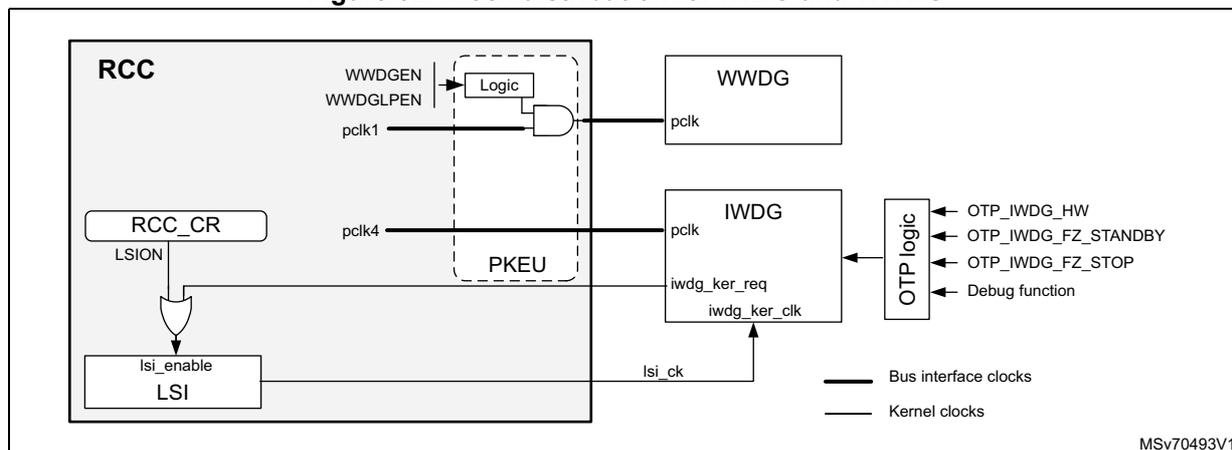
Clock distribution for trace and debug
The clock generation for the trace and debug is controlled by the DBGMCU.
DBGCLKEN in DBGMCU_CR allows the application to provide a clock to the debug components. This clock can also be enabled via the debug access port.
The trace clock generation is controlled via TRACECLKEN in DBGMCU_CR.
Figure 63. Clock distribution for trace and debug
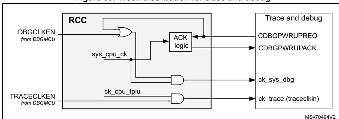
14.6.9 General clock concept overview
The RCC handles the distribution of the CPU, bus interface, and peripheral clocks for the system, according to the CPU operating mode (refer to Section 14.6.1 for details on clock definitions).
For each peripheral, the application can control the activation/deactivation of its kernel and bus interface clocks. Before using a peripheral, the CPU must enable it (by setting PERxEN to 1), and define if it remains active in Sleep mode (by setting PERxLPEN to 1). This is called allocation of a peripheral by the CPU (refer to Section 14.6.10 for more details).
The peripheral allocation is used:
- • by the RCC to automatically control the clock gating according to the CPU modes
- • by the PWR to control V DDCORE supply voltages
Memory handling
The CPU can access all memory areas available in the device:
- • AXISRAM1 to AXISRAM6, CACHEAXI RAM, and FLEXRAM
- • AHBSRAM1 and AHBSRAM2
- • BKPSRAM
CACHEAXI RAM, and VENCRAM are disabled by default, see RCC embedded memories enable register (RCC_MEMENR) . The CPU must enable them before using these memories.
Read or write accesses to a peripheral register or memory, without the clocks enabled in the RCC registers, result in a system freeze. A system reset is required to unlock this.
If the access is performed by a debug interface (as an example, from a debug session inside an IDE), then a power-on reset is required to unlock the device, as the debug interface is not affected by a system reset.
Note: The memory interface clocks (flash memory and RAM interfaces) can be stopped by software during Sleep mode (via SRAMyLPEN bits).
Refer to Section 14.6.11 and Section 14.6.12 for details on clock enabling.
14.6.10 Peripheral allocation
The CPU can allocate a peripheral (and hence control its kernel and bus interface clock) by setting the dedicated PERxEN bit to 1. The CPU can control the peripheral clock gating when it is in Sleep mode via PERxLPEN bits.
The peripheral allocation bits (PERxEN bits) are used by the hardware to provide the kernel and bus interface clocks to the peripherals. These bits are also used to link peripherals to the CPU. The hardware can then safely gate peripheral clocks and bus matrix clocks, according to CPU states.
Clock switches and gating
- Clock switching delays
The input selected by the clock switches can be changed dynamically without generating spurs or timing violation. For example, if PERxSEL (in Figure 64) goes from 0 to 1, the switch first disables the clock output using the currently selected clock (in0_ck), and enables again the clock output using the new selected clock (in1_ck). Disable and enable commands are re-synchronized to their respective clocks. If one of the two clocks are not present, the sequence cannot be completed, and no clock is output. To recover from this situation, the user must either provide a valid clock to in1_ck input, or set back PERxSEL to 0.
During the transition from one input to another, the kernel clock provided to the peripheral is gated, in the worst case, during two or three clock cycles of the new selected clock.
As shown in Figure 64, both input clocks must be present during transition time.
Figure 64. Kernel clock switching
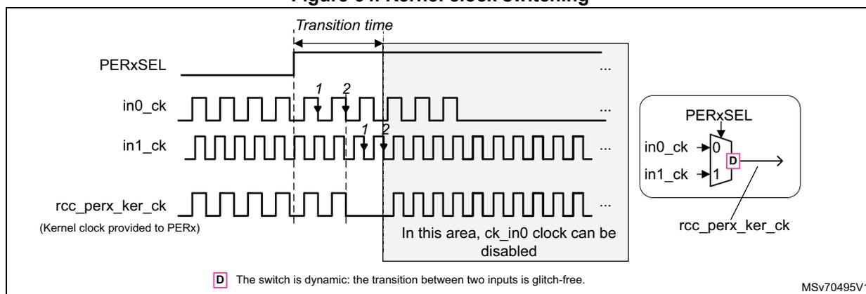
- Clock enabling delays
In the same way, the clock gating logic synchronizes the enable command (coming generally from a kernel clock request, or PERxEN bits) with the selected clock, in order to avoid generation of spurious:
- – A maximum delay of two periods of the enabled clock can occur between the enable command and the first rising edge of the clock. The enable command can
be the rising edge of PERxEN in RCC_xxxxENR, or a kernel clock request asserted by a peripheral.
- – A maximum delay of 1.5 periods of the disabled clock can occur between the disable command and the last falling edge of the clock. The disable command can be the falling edge of PERxEN in RCC_xxxxENR, or a kernel clock request released by a peripheral.
Note: Both kernel and bus interface clocks are affected by this re-synchronization delay.
14.6.11 Peripheral clock-gating control
As mentioned previously, each peripheral requires one or several bus interface clocks, named
rcc_perx_bus_ck
(for peripheral 'x'). These clocks can be an APB, AHB, or AXI clock, according to which bus(es) the peripheral is connected.
The clocks used as bus interface for peripherals can be
aclk[s,a,n]
,
hclk[m,u,e]
,
hclk[5:1]
,
pclk[5:4]
,
pclk[2:1]
, or
ck_timg[1,2]
, depending on the bus connected to each peripheral.
Some peripherals also require dedicated clocks for their communication interface. These clocks are generally asynchronous with respect to the bus interface clock. They are named kernel clocks (
perx_ker_ck
). Both bus interface and kernel clocks can be gated according to several conditions detailed hereafter.
As shown in Figure 65 , enabling kernel and bus interface clocks of each peripheral depends on several input signals:
- • PERxEN and PERxLPEN bits
PERxEN represents the peripheral enable (allocation) bit for the CPU. The CPU can write these bits to 1 via RCC_xxxxENR. - • CPU state (
cpu_sleepandcpu_deep sleepsignals) - • kernel clock request (
perx_ker_ckreq) of the peripheral itself, when the feature is available
Refer to Section 14.6.10 for more details.
Figure 65. Enable logic details for peripheral kernel clock
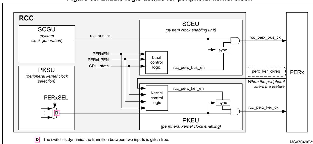
The diagram illustrates the enable logic for peripheral kernel and bus interface clocks. The RCC block contains several sub-blocks:
- SCGU (system clock generation)
: Provides the
rcc_bus_cksignal. - PKSU (peripheral kernel clock selection)
: Contains a dynamic switch (
PERxSEL
) that selects between the
rcc_bus_ckand theperx_ker_ckreqsignal. A note indicates that the switch is dynamic and glitch-free. - SCEU (system clock enabling unit)
: Contains
busif control logic
that takes
PERxEN,PERxLPEN, andCPU_stateas inputs to generatercc_perx_bus_en. This signal is ANDed withrcc_bus_ckthrough a sync block to producercc_perx_bus_ck. - PKEU (peripheral kernel clock enabling)
: Contains
Kernel control logic
that takes the same inputs (
PERxEN,PERxLPEN,CPU_state) to generatercc_perx_ker_en. This signal is ANDed with the output of the PERxSEL switch through another sync block to producercc_perx_ker_ck.
perx_ker_ckreq
signal is shown as a dashed box, indicating it is only present when the peripheral offers the feature. The final outputs
rcc_perx_bus_ck
and
rcc_perx_ker_ck
are sent to the peripheral
PERx
.The clocks for all AHB and APB buses (AHBM, AHB1/2/3/4/5, APB1/2/4/5) are automatically enabled when a dependent peripheral is active. This may induce a chain: a peripheral activation activates the APB that activates the AHB, and activates the AHBM.
For instance, the manual UART4 activation induces the automatic APB1 activation (APB1 is used to configure the UART4). This induces the automatic AHB1 bus activation (AHB1 is needed to drive the APB1). This induces the activation of the central AHBM matrix (AHBM is needed to drive the AHB1).
High-bandwidth interconnect
The NoC and the two NPU AXI bus clocks (ck_icn_npu and ck_icn_npuc, see Figure 48 ) are permanently enabled in Run and Sleep modes, and permanently disabled in Stop and Standby modes.
An internal automatic clock-gating optimizes the NoC power consumption: when no transaction is ongoing in a bus section, an automatic clock-gating clocks and gates this bus.
The NPU interconnect clock (ck_icn_npu) can be disabled by setting ACLKNEN = 0 (disabled in Run and Sleep modes), or ACLKNLPEN = 0 (disabled in Sleep mode only). If the clock is disabled, the NPU cannot work (no interconnect downstream), and the CPU cannot access AXISRAM3/4/5/6, the CACHEAXI RAM, or the FLEXRAM.
The clock of the NPU interconnect (ck_icn_npuc) can be disabled by setting ACLKNCEN = 0 (disabled in Run and Sleep modes), or ACLKNCLPEN = 0 (disabled in Sleep mode only). If the clock is disabled, neither the CPU or NPU can access AXISRAM3/4/5/6, the CACHEAXI, the CACHEAXI RAM, or the FLEXRAM.
Table 74 gives a detailed description of the enabling logic of the peripheral clocks for peripherals located in the CPU domain and allocated by the CPU.
Table 74. Peripheral clock enabling
| PERxEN | PERxLPEN | PERxSEL | perx_ker_ckreq | CPU state | rcc_perx_ker_ck | rcc_perx_bus_ck | Comments |
|---|---|---|---|---|---|---|---|
| 0 | X | X | X | X | - | - | No clock provided to the peripheral (PERxEN = 0) |
| 1 | X | X | X | Run | CK | CK | Kernel and bus interface clocks are provided to the peripheral (CPU in Run mode, and PERxEN = 1) |
| 1 | 0 | X | X | Sleep | - | - | No clock provided to the peripheral (CPU is in Sleep mode and PERxLPEN = 0) |
| 1 | 1 | CK | CK | Kernel and bus interface clocks are provided to the peripheral (CPU in Sleep mode and PERxLPEN = 1) |
Table 74. Peripheral clock enabling (continued)
| PERxEN | PERxLPEN | PERxSEL | perx_ker_ckreq | CPU state | rcc_perx_ker_ck | rcc_perx_bus_ck | Comments |
|---|---|---|---|---|---|---|---|
| 1 | 0 | X | X | - | - | No clock provided to the peripheral (PERxLPEN = 0) | |
| 1 | 1 | no lsi_ck and no lse_ck and no hsi_ker_ck and no msi_ker_ck | X | Stop | - | - | No clock provided to the peripheral (CPU in Stop mode, and lse_ck or lsi_ck or hsi_ker_ck or msi_ker_ck not selected as kernel clock) |
| 1 | 1 | lsi_ck or lse_ck | X | CK | - | Kernel clock provided to the peripheral (PERxEN = PERxLPEN = 1, and lsi_ck or lse_ck selected and enabled) Bus interface clock not provided as the CPU is in Stop mode | |
| 1 | 1 | hsi_ker_ck or msi_ker_ck | 1 | CK | - | Kernel clock provided to the peripheral (req_ker_perx = 1, PERxEN = PERxLPEN = 1, and hsi_ker_ck or msi_ker_ck selected and enabled) Bus interface clock not provided as the CPU is in Stop mode | |
| 1 | 1 | hsi_ker_ck or msi_ker_ck | 0 | - | - | No clock provided to the peripheral (CPU in Stop mode, and no kernel clock request pending) |
The kernel clock is provided to the peripherals when one of the following conditions is met:
- 1. The CPU is in Run mode and the peripheral is enabled.
- 2. The CPU is in Sleep mode and the peripheral is enabled with PERxLPEN = 1.
- 3. The CPU is in Stop mode, the peripheral is enabled with PERxLPEN = 1, the peripheral generates a kernel clock request, and the selected clock is hsi_ker_ck or msi_ker_ck.
- 4. The CPU is in Stop mode, the peripheral is enabled with PERxLPEN = 1, and the kernel source clock of the peripheral is lse_ck or lsi_ck.
The bus interface clock is provided to the peripherals only when conditions 1 or 2 are met.
14.6.12 CPU and bus matrix clock-gating control
The clocks of the CPU, AHB/AXI bridges, and APB buses are enabled as follows:
- • The CPU clock (rcc_cpu_ck) is enabled when the CPU is in Run or Sleep mode.
- • The AXI bridge clock is enabled when the CPU is in Run or Sleep mode.
- • The AHB bus matrix clock is enabled if one of the following conditions is met:
- – The CPU is in Run mode.
- – The CPU is in Sleep mode, and at least one peripheral connected to this bridge has both its PERxEN and PERxLPEN set to 1.
- – The CPU is in Sleep mode, and AHB1, 2, 3, 4, or 5 has its clock enabled.
- • The clocks of AHB1/2/3/4/5 bridges are enabled when one of the following conditions is met:
- – The CPU is in Run mode.
- – The CPU is in Sleep mode, and at least one peripheral connected to this bus has both its PERxEN and PERxLPEN set to 1.
- – The CPU is in Sleep mode, and the APB bus connected to the AHB bridge has its clock enabled.
- • The APB1/2/4/5 clock buses are enabled when one of the following conditions is met:
- – The CPU is in Run mode.
- – The CPU is in Sleep mode, and at least one peripheral connected to this bus has both its PERxEN and PERxLPEN set to 1.
Refer to Section 14.6.11 for details on the automatic clock-gating for AHBMEN, and all AHB/APB buses.
14.6.13 Low-power emulation modes
To ease the device debug, the RCC is able to handle an emulation mode for Stop and Standby modes.
Sleep emulation mode
The Sleep emulation mode is controlled by DBGSLEEP in DBGMCU_CR. When the processor goes to Sleep mode with DBGSLEEP = 1, the processor clock, the clocks of all enabled peripherals, debug parts, and interconnect are maintained activated.
Stop emulation mode
The Stop emulation mode is controlled by DBGSTOP in DBGMCU_CR. When the processor goes to Stop mode with DBGSTOP = 1:
- • The processor, peripheral, and interconnect clocks remain active.
- • The debug clock is active (ck_bus2_dbg, see Figure 46 ), and all debug parts remain clocked. All PLLs and OSCs remain active.
When a wake-up event occurs:
- • The peripheral waking up the system sends the interrupt to the NVIC via the EXTI.
- • If the PWR asserts the pwr_wkup signal, the RCC exits Stop mode. The RCC selects HSI or MSI as system clock, depending on STOPWUCK. The CPU exits Stop mode.
Standby emulation mode
The Standby emulation mode is controlled by DBGSTBY in DBGMCU_CR.
When the system goes to Standby mode with DBGSTBY = 1 and dbg_stdby_rstn = 0:
- • the V DDCORE voltage is not switched-off
- • all CPU, interconnect, and peripherals are under reset except the debug part
- • all PLLs and OSCs remain active
- • the debug part is clocked
- • peripherals on V SW or V DD domains are not reset
The system exits Standby mode when dbg_stdby_rstn is deasserted:
- • the RCC deasserts the rcc_pwrds signal
- • all peripherals are removed from reset
- • the RCC enters Run state
14.7 RCC interrupts
The RCC provides the following interrupt lines:
- •
rcc_it: general interrupt line that provides events when PLLs or oscillators are ready (for nonsecure bits) - •
rcc_s_it: general interrupt line that provides events when PLLs or oscillators are ready (for secure bits) - •
rcc_hsecss_it: interrupt line dedicated to the failure detection of the HSE CSS - •
rcc_lsecss_it: interrupt line dedicated to the failure detection of the LSE CSS
The interrupt enable is controlled via
RCC_CIER
, except for the HSE CSS failure. When the HSE CSS feature is enabled, the interrupt generation cannot be masked.
The interrupt flags can be checked via
RCC_CIFR
, and these flags can be cleared via
RCC_CICR
.
Note: The interrupt flags are not relevant if the corresponding interrupt enable bit is not set.
Table 75 gives a summary of the interrupt sources and the way to control them.
Table 75. Interrupt sources and control
| Interrupt source | Description | Interrupt enable | Action to clear interrupt | Interrupt line |
|---|---|---|---|---|
| LSIRDYF | LSI ready | LSIRDYIE | Set LSIRDYC to 1 | rcc_it
,
rcc_s_it |
| LSERDYF | LSE ready | LSERDYIE | Set LSERDYC to 1 | |
| HSIDRYF | HSI ready | HSIDRYIE | Set HSIRDYC to 1 | |
| HSERDYF | HSE ready | HSERDYIE | Set HSERDYC to 1 | |
| MSIRDYF | MSI ready | MSIRDYIE | Set MSIRDYC to 1 | |
| PLL1RDYF | PLL1 ready | PLL1RDYIE | Set PLL1RDYC to 1 | |
| PLL2RDYF | PLL2 ready | PLL2RDYIE | Set PLL2RDYC to 1 | |
| PLL3RDYF | PLL3 ready | PLL3RDYIE | Set PLL3RDYC to 1 | |
| PLL4RDYF | PLL4 ready | PLL4RDYIE | Set PLL4RDYC to 1 | |
| LSECSSF | LSE CSS failure | LSECSSIE (1) | Set LSECSSC to 1 | |
| HSECSSF | HSE CSS failure | -( 2 ) | Set HSECSSC to 1 | rcc_lsecss_it |
rcc_hsecss_it |
1. The security system feature must be enabled (
LSECSSON = 1
) to generate interrupts.
2. This interrupt cannot be masked when the security system feature is enabled (
HSECSSON = 1
).
14.8 RCC application information
14.8.1 HSE crystal auto-detection
The software can detect the frequency of the crystal connected to the HSE. The crystal choices are 19.2, 20.0, 24.0, 38.4, 40.0, 48.0 MHz. The closest crystal frequencies are 19.2 and 20 MHz (differing ~4%).
Measurement uses a timer clocked by a fast clock, triggered by the slower clock. Using the PWM input mode of input capture, it is possible to measure the full period of the slow clock.
LSE reference
If available, the LSE can trigger TIM16 to count hse_ck ticks. This is crystal accurate (better than using HSI).
Configure a PLL to generate (HSE * 8) MHz. Then set SYSSW to select ic2_ck for sysb_ck = ck_timg (TIMPRE = 1). This means sys_bus_ck relates to the HSE frequency.
LSE is connected to TIM16 - TI1_2.
Example: the multiplication by eight of hse_ck gives
\(
(40 \times 1000 \times 8) / 32.768 = 9765
\)
counts, and
\(
(38.4 \times 1000 \times 8) / 32.768 = 9375
\)
counts.
19.2, 20, 24, 38.4, 40, 48 = 4687, 4882, 5859, 9375, 9765, 11718 counts
sys_bus_ck = 153.6, 160, 192, 307.2, 320, 384 MHz
HSI reference
HSI can be used when LSE is not available. A trimmed HSI can vary by \( \pm 4\% \) (at \( 3\sigma \) ) across the full temperature range. This means that 19.2 and 20 MHz cannot be differentiated reliably.
If the DTS is available, the user can measure the temperature to compensate for the HSI drift.
The RCC generates an hse_cal_ck signal, which is HSE divided by 1024. This signal is connected to TIM17 - TI1_2.
hse_cal_ck has an expected frequency between 19.2 to 50 kHz. The HSI is about 64 MHz. To get 300 MHz, select HSI as input to a PLL, then ic2_ck for sysb_ck = ck_timg (TIMPRE = 1).
Example: The division by 1024 of hse_ck gives \( 300 \times 1024 / 40 = 7680 \) counts, and \( 300 \times 1024 / 38.4 = 8000 \) counts.
19.2, 20, 24, 38.4, 40, 48 = 16000, 15360, 12800, 8000, 7680, 6400 counts
A less accurate method is to use hse_ck output on MCO divided by 16. This gives, for example: \( 300 \times 16 / 40 = 120 \) counts, and \( 300 \times 16 / 38.4 = 125 \) counts.
19.2, 20, 24, 38.4, 40, 48 = 250, 240, 200, 125, 120, 100 counts
14.8.2 Calibration and clock frequency measurement using TIMx
Most of the clock source generator frequencies can be measured by means of the input capture of TIMx.
Calibrating HSI or MSI with the LSE
The main purpose of connecting the LSE to a TIMx input capture is to accurately measure the HSI or MSI. This requires to use the HSI or MSI as sys_bus_ck either directly, or via a PLL. The number of system clock counts between consecutive edges of the LSE signal gives a measurement of the internal clock period. Taking advantage of the high precision of LSE crystals (typically a few tens of ppm), the user can determine the internal clock frequency with the same resolution, and trim the source to compensate for variations due to manufacturing, temperature, or voltage.
The ratio between the two clock frequencies affects the measurement precision. The greater the ratio, the more accurate the calculation.
HSI and MSI oscillators have dedicated user-accessible calibration bits for this purpose (see RCC_HSICFGR and RCC_MSICFGR). When the HSI or MSI is used via a PLL, it is also possible to fine-tune the sys_bus_ck using the fractional divider of the PLL.
Calibrating LSI with HSI
The LSI frequency can also be measured. This is useful for applications that do not have a crystal. The ultra-low-power LSI oscillator has a large manufacturing process variation. The LSI clock frequency can be measured using the more precise HSI clock source. Using this measurement, the user can obtain a more accurate RTC timebase timeout (when LSI is used as RTC clock source), and/or a more accurate IWDG timeout.
14.8.3 Clock monitoring
Monitoring HSI with LSE
The purpose is to assist the software calibration procedure when the HSI frequency drifts out of a predefined range because of environmental variation (for example, temperature).
This monitoring can be enabled in all system modes where HSI is used, except Standby and V BAT modes. When enabled, the number of HSI clock ticks between consecutive edges of the LSE clock is counted.
The HSI monitoring control is based on RCC_HSIMCR and RCC_HSIMSR.
The following steps can be used to enable the monitoring:
- 1. Enable LSE signal:
- a) Set DBP = 1 in PWR_DBPCR.
- b) Write 1 to LSEON.
- c) Wait for LSERDY = 1.
- d) Set DBP = 0 in PWR_DBPCR.
- 2. Set up HSI clock period monitoring:
- a) Write 1 to HSIMONEN in RCC_HSIMCR to start the monitoring.
14.8.4 Clock frequency limits
The maximum frequencies that can be set for each peripheral are detailed in Table 76 .
Table 76. Maximum peripheral clock frequencies
| Peripheral | Maximum kernel clock frequency (MHz) |
|---|---|
| PWR | 200 |
| RNG | 64 |
| RTC | 4 |
| SAES | 200 |
| SAI1 | 200 |
| SAI2 | 200 |
| SDMMC1 | 208 |
| SDMMC2 | 208 |
| Peripheral | Maximum kernel clock frequency (MHz) |
|---|---|
| SPDIFRX1 | 200 |
| SPI1 | 200 |
| SPI2 | 200 |
| SPI3 | 200 |
| SPI4 | 133 |
| SPI5 | 133 |
| SPI6 | 200 |
| SYSCFG | 200 |
| TIMx | 400 |
| LPTIMx | 200 |
| DTS | 10 |
| USART1 | 100 |
| USART2 | 100 |
| USART3 | 100 |
| UART4 | 100 |
| UART5 | 100 |
| USART6 | 100 |
| UART7 | 100 |
| UART8 | 100 |
| UART9 | 100 |
| USART10 | 100 |
| LPUART1 | 100 |
| UCPD1 | 25 |
| VENC | 400 |
| VREFBUF | 200 |
| WWDG | 200 |
| MREPAIR | 64 |
As an example, the PLL configuration to achieve these frequencies would use HSI as reference clock (64 MHz), and program the VCO of PLL1, 2, 3, and 4, to respectively, 800, 993.52, 875, and 514.5 MHz.
14.9 RCC security
The system RIF protects bus accesses to the RCC and peripheral registers.
The RIFSC indicates if an access to the RCC or other peripherals is secure and/or privileged. Signals are connected from the RIFSC to the RCC to communicate this information. The notation for these signals is S, P.
The RCC is able to protect register bits from being modified by nonsecure and unprivileged accesses.
If a peripheral RISUP is programmed as secure (or privileged), the peripheral clock and reset bits become secure (or privileged).
If the peripheral is TrustZone-aware, the peripheral clock and reset bits become secure (or privileged) as soon as at least one function is configured as secure (or privileged) by RIFSC.
Peripheral configuration registers inside the RCC can be also be made secure (or privileged) via a global override bit (PERSEC in RCC_SECCFGR3, PERPRIV in RCC_PRIVCFGR3).
After an application reset or system reset, the RCC does not filter any access until the trusted agent has configured the system.
14.9.1 Internal register protection
The following can be made secure and/or privileged (via RCC_SECCFGRx and RCC_PRIVCFGRx):
- • internal and external oscillators (HSE, LSE, HSI, MSI, LSI)
- • PLLs and AHB prescalers
- • system clock-source selection
- • MCO clock outputs
- • reset flags
- • automatic internal oscillator wake-up configuration
There are four access controls for RCC registers:
- • SEC (secure)
- • PRIV (privileged)
- • LOCK (locked SEC and PRIV)
- • PUB (public)
SEC (in RCC_SECCFGRx)
xxxSEC defines the secure status required for a write to the xxx configuration registers (for example, HSISEC for the HSI oscillator). When this bit is set, configuration register bits are writable by secure software only. This bit can be locked (cannot be changed) with the xxxLOCK bit, and is readable by all. Write access to RCC_SECCFGRx is controlled by S, P.
PRIV (in RCC_PRIVCFGRx)
xxxPRIV defines the privileged status required for a write to the xxx configuration registers (such as HSIPRIV for the HSI oscillator). When this bit is set, the configuration register bits are writable only by privileged software. This bit can be locked (cannot be changed) with the xxxLOCK bit, and is readable by all. Write access to RCC_PRIVCFGRx is controlled by xxxSEC, P. xxxPRIV can be set/cleared by write to 1 registers.
LOCK (in RCC_LOCKCFGRx)
xxxLOCK, when set, locks definitively xxxSEC and xxxPRIV settings: xxxLOCK is readable by all. Write access to RCC_LOCKCFGRx is controlled by S, P. xxxLOCK is a set-once bit.
PUB (in RCC_PUBCFGRx)
xxxPUB grants read access to configuration/status bits, regardless of security or privilege.
For example, if HSIPUB bit is set, any software can read the HSI oscillator configuration and status. If not set then normal access controls are enforced.
xxxPUB is readable by all. Write access to RCC_PUBCFGRx is controlled by xxxSEC and xxxPRIV. xxxPUB can be set/cleared by write-to-1 registers.
14.9.2 Internal register write-protection
There are different controls for write-protecting a register bit.
- • xxxLOCK bits (described above)
- • other internal protection logic (controlled from internal or external signals)
Only protection logic using the pwr_lock_backup signal is implemented.
14.10 RCC registers
14.10.1 RCC control register (RCC_CR)
Address offset: 0x0
Reset value: 0x0000 0008
This register is used to enable the RCC oscillators and PLLs in Run or Sleep mode.
| 31 | 30 | 29 | 28 | 27 | 26 | 25 | 24 | 23 | 22 | 21 | 20 | 19 | 18 | 17 | 16 |
|---|---|---|---|---|---|---|---|---|---|---|---|---|---|---|---|
| Res. | Res. | Res. | Res. | Res. | Res. | Res. | Res. | Res. | Res. | Res. | Res. | Res. | Res. | Res. | Res. |
| 15 | 14 | 13 | 12 | 11 | 10 | 9 | 8 | 7 | 6 | 5 | 4 | 3 | 2 | 1 | 0 |
| Res. | Res. | Res. | Res. | PLL4 ON | PLL3 ON | PLL2 ON | PLL1 ON | Res. | Res. | Res. | HSE ON | HSI ON | MSI ON | LSE ON | LSI ON |
| rw | rw | rw | rw | rw | rw | rw | rw | rw |
Bits 31:12 Reserved, must be kept at reset value.
Bit 11 PLL4ON : PLL4 enable
This bit is reset by int_sys_rstn. It is security-protected by PLL4SEC or PLL4PRIV, and is publicly readable if PLL4PUB = 1. It can be set with PLL4ONS, and cleared with PLL4ONC. This bit is set and reset by software. It cannot be cleared if PLL4 is currently used to generate the CPU or system clock.
0: PLL4 is OFF (default after reset)
1: PLL4 is ON
Bit 10 PLL3ON: PLL3 enableThis bit is reset by int_sys_rstn . It is security-protected by PLL3SEC or PLL3PRIV , and is publicly readable if PLL3PUB = 1. It can be set with PLL3ONS , and cleared with PLL3ONC . This bit is set and reset by software. It cannot be cleared if PLL3 is currently used to generate the CPU or system clock.
0: PLL3 is OFF (default after reset)
1: PLL3 is ON
This bit is reset by int_sys_rstn . It is security-protected by PLL2SEC or PLL2PRIV , and is publicly readable if PLL2PUB = 1. It can be set with PLL2ONS , and cleared with PLL2ONC . This bit is set and reset by software. It cannot be cleared if PLL2 is currently used to generate the CPU or system clock.
0: PLL2 is OFF (default after reset)
1: PLL2 is ON
This bit is reset by int_sys_rstn . It is security-protected by PLL1SEC or PLL1PRIV , and is publicly readable if PLL1PUB = 1. It can be set with PLL1ONS , and cleared with PLL1ONC . This bit is set and reset by software. It cannot be cleared if PLL1 is currently used to generate the CPU or system clock.
0: PLL1 is OFF (default after reset)
1: PLL1 is ON
Bits 7:5 Reserved, must be kept at reset value.
Bit 4 HSEON: HSE oscillator enableThis bit is reset by int_sys_rstn . It is security-protected by HSESEC or HSEPRIV , and is publicly readable if HSEPUB = 1. It can be set with HSEONS , and cleared with HSEONC . This bit is set and reset by software.
0: HSE is OFF (default after reset)
1: HSE is ON
This bit is reset by int_sys_rstn . It is security-protected by HSISEC or HSIPRIV , and is publicly readable if HSIPUB = 1. It can be set with HSIONS , and cleared with HSIONC . This bit is set and reset by software.
0: HSI is OFF
1: HSI is ON (default after reset)
This bit is reset by int_sys_rstn . It is security-protected by MSISEC or MSIPRIV , and is publicly readable if MSIPUB = 1. It can be set with MSIONS , and cleared with MSIONC . This bit is set and reset by software.
0: MSI is OFF (default after reset)
1: MSI is ON
This bit is reset by rcc_vsw_rstn . It is in the V BKP voltage domain. It is write-protected by the pwr_lock_backup_n signal. It is security-protected by LSESEC , LSEPRIV , and is publicly readable if LSEPUB = 1. It can be set with LSEONS , and cleared with LSEONC . This bit is set and reset by software.
0: LSE is OFF (default after reset)
1: LSE is ON
Bit 0 LSION : LSI oscillator enable
This bit is reset by nreset_rstn. It is in the V RET voltage domain. This bit is security-protected by LSISEC or LSIPRIV, and is publicly readable if LSIPUB = 1. It can be set with LSIONS, and cleared with LSIONC. This bit is set and reset by software.
0: LSI is OFF (default after reset)
1: LSI is ON
14.10.2 RCC status register (RCC_SR)
Address offset: 0x4
Reset value: 0x0000 0000
This register is used to retrieve the status the RCC oscillators and PLLs.
| 31 | 30 | 29 | 28 | 27 | 26 | 25 | 24 | 23 | 22 | 21 | 20 | 19 | 18 | 17 | 16 |
|---|---|---|---|---|---|---|---|---|---|---|---|---|---|---|---|
| Res. | Res. | Res. | Res. | Res. | Res. | Res. | Res. | Res. | Res. | Res. | Res. | Res. | Res. | Res. | Res. |
| 15 | 14 | 13 | 12 | 11 | 10 | 9 | 8 | 7 | 6 | 5 | 4 | 3 | 2 | 1 | 0 |
| Res. | Res. | Res. | Res. | PLL4 RDY | PLL3 RDY | PLL2 RDY | PLL1 RDY | Res. | Res. | Res. | HSE RDY | HSI RDY | MSI RDY | LSE RDY | LSI RDY |
| r | r | r | r | r | r | r | r | r |
Bits 31:12 Reserved, must be kept at reset value.
Bit 11 PLL4RDY : PLL4 clock ready flag
This bit is security-protected by PLL4SEC or PLL4PRIV, and is publicly readable if PLL4PUB = 1. It is set by hardware to indicate that the PLL4 is locked.
0: PLL4 unlocked (default after reset)
1: PLL4 locked
Bit 10 PLL3RDY : PLL3 clock ready flag
This bit is security-protected by PLL3SEC or PLL3PRIV, and is publicly readable if PLL3PUB = 1. It is set by hardware to indicate that the PLL3 is locked.
0: PLL3 unlocked (default after reset)
1: PLL3 locked
Bit 9 PLL2RDY : PLL2 clock ready flag
This bit is security-protected by PLL2SEC or PLL2PRIV, and is publicly readable if PLL2PUB = 1. it is set by hardware to indicate that the PLL2 is locked.
0: PLL2 unlocked (default after reset)
1: PLL2 locked
Bit 8 PLL1RDY : PLL1 clock ready flag
This bit is security-protected by PLL1SEC or PLL1PRIV, and is publicly readable if PLL1PUB = 1. It is set by hardware to indicate that the PLL1 is locked.
0: PLL1 unlocked (default after reset)
1: PLL1 locked
Bits 7:5 Reserved, must be kept at reset value.
Bit 4 HSERDY : HSE clock ready flag
This bit is security-protected by HSESEC or HSEPRIV, and is publicly readable if HSEPUB = 1.
It is set by hardware to indicate that the HSE oscillator is stable.
0: HSE not ready (default after reset)
1: HSE ready
Bit 3 HSIRDY : HSI clock ready flag
This bit is security-protected by HSISEC or HSIPRIV, and is publicly readable if HSIPUB = 1.
It is set by hardware to indicate that the HSI oscillator is stable.
0: HSI not ready (default after reset)
1: HSI ready
Bit 2 MSIRDY : MSI clock ready flag
This bit is security-protected by MSISEC or MSIPRIV, and is publicly readable if MSIPUB = 1.
It is set and reset by hardware to indicate that the MSI oscillator is stable.
0: MSI not ready (default after reset)
1: MSI ready
Bit 1 LSERDY : LSE clock ready flag
This bit is security-protected by LSESEC or LSEPRIV, and is publicly readable if LSEPUB = 1. It is set and reset by hardware to indicate that the LSE oscillator is stable. This bit requires 6 cycles of lse_ck before it is deasserted.
0: LSE not ready (default after reset)
1: LSE ready
Bit 0 LSIRDY : LSI clock ready flag
This bit is security-protected by LSISEC or LSIPRIV, and is publicly readable if LSIPUB = 1. It is set by hardware to indicate that the LSI oscillator is stable.
0: LSI not ready (default after reset)
1: LSI ready
14.10.3 RCC Stop mode control register (RCC_STOPCR)
Address offset: 0x8
Reset value: 0x0000 0002
This register is used to enable the RCC oscillators in Stop mode.
| 31 | 30 | 29 | 28 | 27 | 26 | 25 | 24 | 23 | 22 | 21 | 20 | 19 | 18 | 17 | 16 |
|---|---|---|---|---|---|---|---|---|---|---|---|---|---|---|---|
| Res. | Res. | Res. | Res. | Res. | Res. | Res. | Res. | Res. | Res. | Res. | Res. | Res. | Res. | Res. | Res. |
| 15 | 14 | 13 | 12 | 11 | 10 | 9 | 8 | 7 | 6 | 5 | 4 | 3 | 2 | 1 | 0 |
| Res. | Res. | Res. | Res. | Res. | Res. | Res. | Res. | Res. | Res. | Res. | Res. | Res. | Res. | HSIST OPEN rw | MSIST OPEN rw |
Bits 31:2 Reserved, must be kept at reset value.
Bit 1 HSISTOPEN : HSI oscillator enable
This bit is reset by
int_sys_rstn
. It is security-protected by
HSISEC
or
HSIPRIV
, and is publicly readable if
HSIPUB
= 1. It can be set with
HSISTOPENS
, and cleared with
HSISTOPENC
. This bit is set and reset by software.
0: HSI is OFF
1: HSI is ON (default after reset)
Bit 0 MSISTOPEN : MSI oscillator enable
This bit is reset by
int_sys_rstn
. It is security-protected by
MSISEC
or
MSIPRIV
, and is publicly readable if
MSIPUB
= 1. It can be set with
MSISTOPENS
, and cleared with
MSISTOPENC
. This bit is set and reset by software.
0: MSI is OFF (default after reset)
1: MSI is ON
14.10.4 RCC configuration register 1 (RCC_CFGR1)
Address offset: 0x20
Reset value: 0x0000 0000
This register controls the selection of the CPU and system clocks, and their status (see
Figure 46
for various SYSSW inputs). The register is reset by
sys_rstn
, and is in the
\(
V_{CORE}
\)
voltage domain.
| 31 | 30 | 29 | 28 | 27 | 26 | 25 | 24 | 23 | 22 | 21 | 20 | 19 | 18 | 17 | 16 |
|---|---|---|---|---|---|---|---|---|---|---|---|---|---|---|---|
| Res. | Res. | SYSSWS[1:0] | Res. | Res. | SYSSW[1:0] | Res. | Res. | CPUSWS[1:0] | Res. | Res. | CPUSW[1:0] | ||||
| r | r | rw | rw | r | r | rw | rw | ||||||||
| 15 | 14 | 13 | 12 | 11 | 10 | 9 | 8 | 7 | 6 | 5 | 4 | 3 | 2 | 1 | 0 |
| Res. | Res. | Res. | Res. | Res. | Res. | Res. | Res. | Res. | Res. | Res. | Res. | Res. | Res. | Res. | STOP WUCK |
| rw |
Bits 31:30 Reserved, must be kept at reset value.
Bits 29:28 SYSSWS[1:0] : System clock switch status
This bitfield is security-protected by
SYSSEC
,
SYSPRIV
, and is publicly readable if
SYSPUB
= 1. It is set and reset by hardware to show the source of the system bus clocks (
sys_bus_ck
).
00: hsi_ck selected as sysb_ck, sysb_ck, sysd_ck system clocks (default after reset)
01: msi_ck selected as sysb_ck, sysb_ck, sysd_ck system clocks
10: hse_ck selected as sysb_ck, sysb_ck, sysd_ck system clocks
11: ic2_ck selected as sysb_ck, ic6_ck selected as sysb_ck, ic11_ck as sysd_ck system clocks
Bits 27:26 Reserved, must be kept at reset value.
Bits 25:24 SYSSW[1:0] : System clock switch selection
This bitfield is security-protected by
SYSSEC
,
SYSPRIV
, and is publicly readable if
SYSPUB
= 1. It is set by the software to select the source of the system bus clocks (
sys_bus_ck
).
00: hsi_ck selected as system clock (default after reset)
01: msi_ck selected as system clock
10: hse_ck selected as system clock
11: ic2_ck selected as system clock
Bits 23:22 Reserved, must be kept at reset value.
Bits 21:20 CPUSWS[1:0] : CPU clock switch status
This bitfield is security-protected by SYSSEC, SYSPRIV, and is publicly readable if SYSPUB = 1. It is set and reset by hardware to show the source of the CPU clock (sys_cpu_ck).
- 00: hsi_ck selected as system clock (default after reset)
- 01: msi_ck selected as system clock
- 10: hse_ck selected as system clock
- 11: ic1_ck selected as system clock
Bits 19:18 Reserved, must be kept at reset value.
Bits 17:16 CPUSW[1:0] : CPU clock switch selection
This bitfield is security-protected by SYSSEC, SYSPRIV, and is publicly readable if SYSPUB = 1. It is set by the software to select the source of the CPU clock (sys_cpu_ck).
- 00: hsi_ck selected as system clock (default after reset)
- 01: msi_ck selected as system clock
- 10: hse_ck selected as system clock
- 11: ic1_ck selected as system clock
Bits 15:1 Reserved, must be kept at reset value.
Bit 0 STOPWUCK : System clock selection after a wake up from system stop
This bit is security-protected by SYSSEC, SYSPRIV, and is publicly readable if SYSPUB = 1. It is set and reset by software to select the system wake-up clock from system stop.
- 0: HSI selected as wake-up clock from system stop (default after reset)
- 1: MSI selected as wake-up clock from system stop
14.10.5 RCC configuration register 2 (RCC_CFGR2)
Address offset: 0x24
Reset value: 0x0010 0000
This register controls the division factors of the central clocks: AHB, APB, and timer. It is reset by sys_rstn, and is in the V CORE voltage domain.
| 31 | 30 | 29 | 28 | 27 | 26 | 25 | 24 | 23 | 22 | 21 | 20 | 19 | 18 | 17 | 16 |
|---|---|---|---|---|---|---|---|---|---|---|---|---|---|---|---|
| Res. | Res. | Res. | Res. | Res. | Res. | TIMPRE[1:0] | Res. | HPRE[2:0] | Res. | PPRE5[2:0] | |||||
| rw | rw | rw | rw | rw | rw | rw | rw | ||||||||
| 15 | 14 | 13 | 12 | 11 | 10 | 9 | 8 | 7 | 6 | 5 | 4 | 3 | 2 | 1 | 0 |
| Res. | PPRE4[2:0] | Res. | Res. | Res. | Res. | Res. | PPRE2[2:0] | Res. | PPRE1[2:0] | ||||||
| rw | rw | rw | rw | rw | rw | rw | rw | rw | |||||||
Bits 31:26 Reserved, must be kept at reset value.
Bits 25:24 TIMPRE[1:0] : Timer clock prescaler selection
This bitfield is security-protected by a SEC signal from RIFSC, the SYSSEC bit, a PRIV signal from RIFSC, or the SYSPRIV bit, and is publicly readable if SYSPUB = 1. It is set and reset by software to control the clock frequency of all the timers connected to APB1 and APB2 domains.
- 00: timg_ck = sys_bus_ck (default after reset)
- 01: timg_ck = sys_bus_ck / 2
- 10: timg_ck = sys_bus_ck / 4
- 11: timg_ck = sys_bus_ck / 8
Bit 23 Reserved, must be kept at reset value.
Bits 22:20 HPRE[2:0] : AHB clock prescalerThis bitfield is security-protected by SYSSEC or SYSPRIV, and is publicly readable if SYSPUB = 1. It is set and reset by software to control the division factor of the clocks between the system AXI bus and the configuration AHB bus. The AXI sys_bus_ck source clock is divided in function of HPRE, to generate the AHB clock.
The division ratio is as follows:
000: sys_bus2_ck = sys_bus_ck
001: sys_bus2_ck = sys_bus_ck / 2 (default after reset)
010: sys_bus2_ck = sys_bus_ck / 4
011: sys_bus2_ck = sys_bus_ck / 8
100: sys_bus2_ck = sys_bus_ck / 16
101: sys_bus2_ck = sys_bus_ck / 32
110: sys_bus2_ck = sys_bus_ck / 64
111: sys_bus2_ck = sys_bus_ck / 128
Bit 19 Reserved, must be kept at reset value.
Bits 18:16 PPRE5[2:0] : CPU domain APB5 prescalerThis bitfield is security-protected by SYSSEC or SYSPRIV, and is publicly readable if SYSPUB = 1. It is set and reset by software to control the division factor of rcc_pclk5.
000: rcc_pclk5 = sys_bus2_ck (default after reset)
001: rcc_pclk5 = sys_bus2_ck / 2
010: rcc_pclk5 = sys_bus2_ck / 4
011: rcc_pclk5 = sys_bus2_ck / 8
100: rcc_pclk5 = sys_bus2_ck / 16
101: rcc_pclk5 = sys_bus2_ck / 32
110: rcc_pclk5 = sys_bus2_ck / 64
111: rcc_pclk5 = sys_bus2_ck / 128
Bit 15 Reserved, must be kept at reset value.
Bits 14:12 PPRE4[2:0] : CPU domain APB4 prescalerThis bitfield is security-protected by SYSSEC or SYSPRIV, and is publicly readable if SYSPUB = 1. It is set and reset by software to control the division factor of rcc_pclk4.
000: rcc_pclk4 = sys_bus2_ck (default after reset)
001: rcc_pclk4 = sys_bus2_ck / 2
010: rcc_pclk4 = sys_bus2_ck / 4
011: rcc_pclk4 = sys_bus2_ck / 8
100: rcc_pclk4 = sys_bus2_ck / 16
101: rcc_pclk4 = sys_bus2_ck / 32
110: rcc_pclk4 = sys_bus2_ck / 64
111: rcc_pclk4 = sys_bus2_ck / 128
Bits 11:7 Reserved, must be kept at reset value.
Bits 6:4 PPRE2[2:0] : CPU domain APB2 prescaler
This bitfield is security-protected by SYSSEC or SYSPRIV, and is publicly readable if SYSPUB = 1. It is set and reset by software to control the division factor of rcc_pclk2.
- 000: rcc_pclk2 = sys_bus2_ck (default after reset)
- 001: rcc_pclk2 = sys_bus2_ck / 2
- 010: rcc_pclk2 = sys_bus2_ck / 4
- 011: rcc_pclk2 = sys_bus2_ck / 8
- 100: rcc_pclk2 = sys_bus2_ck / 16
- 101: rcc_pclk2 = sys_bus2_ck / 32
- 110: rcc_pclk2 = sys_bus2_ck / 64
- 111: rcc_pclk2 = sys_bus2_ck / 128
Bit 3 Reserved, must be kept at reset value.
Bits 2:0 PPRE1[2:0] : CPU domain APB1 prescaler
This bitfield is security-protected by SYSSEC or SYSPRIV, and is publicly readable if SYSPUB = 1. Is it set and reset by software to control the division factor of rcc_pclk1.
- 000: rcc_pclk1 = sys_bus2_ck (default after reset)
- 001: rcc_pclk1 = sys_bus2_ck / 2
- 010: rcc_pclk1 = sys_bus2_ck / 4
- 011: rcc_pclk1 = sys_bus2_ck / 8
- 100: rcc_pclk1 = sys_bus2_ck / 16
- 101: rcc_pclk1 = sys_bus2_ck / 32
- 110: rcc_pclk1 = sys_bus2_ck / 64
- 111: rcc_pclk1 = sys_bus2_ck / 128
14.10.6 RCC backup domain protection register (RCC_BDCR)
Address offset: 0x2C
Reset value: 0x0000 0000
This register controls the reset of the backup domain. It is reset by pwr_vsw_rstn, and is in the V BKP voltage domain.
| 31 | 30 | 29 | 28 | 27 | 26 | 25 | 24 | 23 | 22 | 21 | 20 | 19 | 18 | 17 | 16 |
|---|---|---|---|---|---|---|---|---|---|---|---|---|---|---|---|
| VSW RST | Res. | Res. | Res. | Res. | Res. | Res. | Res. | Res. | Res. | Res. | Res. | Res. | Res. | Res. | Res. |
| 15 | 14 | 13 | 12 | 11 | 10 | 9 | 8 | 7 | 6 | 5 | 4 | 3 | 2 | 1 | 0 |
| Res. | Res. | Res. | Res. | Res. | Res. | Res. | Res. | Res. | Res. | Res. | Res. | Res. | Res. | Res. | Res. |
Bit 31 VSWRST : V switch (V SW ) domain software reset.
This bit is write-protected by the pwr_lock_backup_n signal. It is security-protected by a SEC signal from RIFSC, the RSTSEC bit, a PRIV signal from RIFSC, or the RSTPRIV bit, and is publicly readable if RSTPUB = 1. Writing 1 to this VSWRST bit by software generates a pulse that resets the V SW domain.
- 0: V SW domain not reset (default after reset)
- 1: V SW domain reset
Bits 30:0 Reserved, must be kept at reset value.
14.10.7 RCC reset status register for hardware (RCC_HWSRSR)
Address offset: 0x30
Reset value: 0x00A0 0000
This register is used to monitor the resets that occurred. It is reset by pwr_por_rstn, and is in the V BKP voltage domain.
| 31 | 30 | 29 | 28 | 27 | 26 | 25 | 24 | 23 | 22 | 21 | 20 | 19 | 18 | 17 | 16 |
|---|---|---|---|---|---|---|---|---|---|---|---|---|---|---|---|
| Res. | LPWR RSTF | Res. | WWDG RSTF | Res. | IWDGR STF | Res. | SFTRS TF | PORR STF | PINRS TF | BORR STF | Res. | Res. | Res. | LCKRS TF | RMVF |
| r | r | r | r | r | r | r | r | w | |||||||
| 15 | 14 | 13 | 12 | 11 | 10 | 9 | 8 | 7 | 6 | 5 | 4 | 3 | 2 | 1 | 0 |
| Res. | Res. | Res. | Res. | Res. | Res. | Res. | Res. | Res. | Res. | Res. | Res. | Res. | Res. | Res. | Res. |
Bit 31 Reserved, must be kept at reset value.
Bit 30 LPWRRSTF : Illegal Stop or Standby flag
This bit is set by hardware when the CPU goes erroneously in Stop or Standby mode. It is reset by software by writing HWRMVF.
0: No illegal reset occurred (default after power-on reset)
1: Illegal Stop or Standby reset occurred
Bit 29 Reserved, must be kept at reset value.
Bit 28 WWDGRSTF : Window watchdog reset flag
This bit is set by hardware when a window watchdog reset occurs. it is reset by software by writing HWRMVF.
0: No window watchdog reset occurred from WWDG (default after power-on reset)
1: Window watchdog reset occurred from WWDG
Bit 27 Reserved, must be kept at reset value.
Bit 26 IWDGRSTF : Independent watchdog reset flag
This bit is set by hardware when an independent watchdog reset occurs. It is reset by software by writing HWRMVF.
0: No independent watchdog reset occurred (default after power-on reset)
1: Independent watchdog reset occurred
Bit 25 Reserved, must be kept at reset value.
Bit 24 SFTRSTF : Software system reset flag
This bit is set by hardware when the software system reset is due to the CPU. The CPU can generate a software system reset by writing SYSRESETREQ in AIRCR register of the CPU. This bit is reset by software by writing HWRMVF.
0: No software system reset occurred (default after power-on reset)
1: A software system reset has been generated by the CPU.
Bit 23 PORRSTF : POR/PDR reset flag
This bit is set by hardware when a POR/PDR occurs. it is reset by software by writing HWRMVF.
0: No POR/PDR occurred
1: POR/PDR occurred (default after power-on reset)
Bit 22 PINRSTF : Pin reset flag (NRST)
This bit is set by hardware when a reset from pin occurs. it is reset by software by writing HWRMVF.
0: No reset from pin occurred
1: Reset from pin occurred (default after power-on reset)
Bit 21 BORRSTF : BOR reset flag
This bit is set by hardware when a BOR occurs (pwr_bor_rst). it is reset by software by writing HWRMVF.
0: No BOR occurred
1: BOR occurred (default after power-on reset)
Bits 20:18 Reserved, must be kept at reset value.
Bit 17 LCKRSTF : CPU lockup reset flag
This bit is set by hardware when a reset from a CPU lockup occurs. Is it reset by software by writing RMVF.
0: No reset from CPU lockup occurred
1: Reset from CPU lockup occurred
Bit 16 RMVF : Remove reset flag
This bit is write-protected by the security bit. It is security-protected by a SEC signal from RIFSC, the RSTSEC bit, a PRIV signal from RIFSC, or the RSTPRIV bit, and is publicly readable if RSTPUB = 1. This bit is written by software to clear the value of the reset flags in this register.
0: Clear of the reset flags not activated (default after power-on reset)
1: Clear the value of the reset flags
Bits 15:0 Reserved, must be kept at reset value.
14.10.8 RCC reset register (RCC_RSR)
Address offset: 0x34
Reset value: 0x00A0 0000
This register is used to monitor the resets that occurred. It is reset by pwr_por_rstn, and is in the V BKP voltage domain.
| 31 | 30 | 29 | 28 | 27 | 26 | 25 | 24 | 23 | 22 | 21 | 20 | 19 | 18 | 17 | 16 |
|---|---|---|---|---|---|---|---|---|---|---|---|---|---|---|---|
| Res. | LPWR RSTF | Res. | WWDG RSTF | Res. | IWDGR STF | Res. | SFTRS TF | PORR STF | PINRS TF | BORR STF | Res. | Res. | Res. | LCKRS TF | RMVF |
| r | r | r | r | r | r | r | r | w | |||||||
| 15 | 14 | 13 | 12 | 11 | 10 | 9 | 8 | 7 | 6 | 5 | 4 | 3 | 2 | 1 | 0 |
| Res. | Res. | Res. | Res. | Res. | Res. | Res. | Res. | Res. | Res. | Res. | Res. | Res. | Res. | Res. | Res. |
Bit 31 Reserved, must be kept at reset value.
Bit 30 LPWRRSTF : Illegal Stop or Standby flag
This bit is set by hardware when the CPU goes erroneously in Stop or Standby mode. It is reset by software by writing RMVF.
0: No illegal reset occurred (default after power-on reset)
1: Illegal Stop or Standby reset occurred
Bit 29 Reserved, must be kept at reset value.
- Bit 28
WWDGRSTF
: Window watchdog reset flag
This bit is set by hardware when a window watchdog reset occurs. It is reset by software by writing RMVF.
0: No window watchdog reset occurred from WWDG (default after power-on reset)
1: Window watchdog reset occurred from WWDG - Bit 27 Reserved, must be kept at reset value.
- Bit 26
IWDGRSTF
: Independent watchdog reset flag
This bit is set by hardware when an independent watchdog reset occurs. It is reset by software by writing RMVF.
0: No independent watchdog reset occurred (default after power-on reset)
1: Independent watchdog reset occurred - Bit 25 Reserved, must be kept at reset value.
- Bit 24
SFTRSTF
: Software system reset flag
This bit is set by hardware when the software system reset is due to the CPU. The CPU can generate a software system reset by writing SYSRESETREQ in AIRCR register of the CPU. This bit is reset by software by writing RMVF.
0: No software system reset occurred (default after power-on reset)
1: A software system reset has been generated by the CPU. - Bit 23
PORRSTF
: POR/PDR reset flag
This bit is set by hardware when a POR/PDR occurs. It is reset by software by writing RMVF.
0: No POR/PDR occurred
1: POR/PDR occurred (default after power-on reset) - Bit 22
PINRSTF
: Pin reset flag (NRST)
This bit is set by hardware when a reset from pin occurs. It is reset by software by writing RMVF.
0: No reset from pin occurred
1: Reset from pin occurred (default after power-on reset) - Bit 21
BORRSTF
: BOR reset flag
This bit is set by hardware when a BOR occurs (pwr_bor_rst). It is reset by software by writing RMVF.
0: No BOR occurred
1: BOR occurred (default after power-on reset) - Bits 20:18 Reserved, must be kept at reset value.
- Bit 17
LCKRSTF
: CPU lockup reset flag
This bit is set by hardware when a reset from a CPU lockup occurs. it is reset by software by writing RMVF.
0: No reset from CPU lockup occurred
1: Reset from CPU lockup occurred - Bit 16
RMVF
: Remove reset flag
This bit is write-protected by the security bit. It is security-protected by a SEC signal from RIFSC, the SYSSEC bit, a PRIV signal from RIFSC, or the SYSPRIV bit, and is publicly readable if SYSPUB = 1. This bit is written by software to clear the value of the reset flags in this register.
0: Clear of the reset flags not activated (default after power-on reset)
1: Clear the value of the reset flags - Bits 15:0 Reserved, must be kept at reset value.
14.10.9 RCC LSE configuration register (RCC_LSECFGR)
Address offset: 0x40
Reset value: 0x0000 0000
This register is used to configure the LSE oscillator. It is reset by rcc_vsw_rstn, and is in the V BKP voltage domain.
| 31 | 30 | 29 | 28 | 27 | 26 | 25 | 24 | 23 | 22 | 21 | 20 | 19 | 18 | 17 | 16 |
|---|---|---|---|---|---|---|---|---|---|---|---|---|---|---|---|
| Res. | Res. | Res. | Res. | Res. | Res. | Res. | Res. | Res. | Res. | Res. | Res. | LSEDRV[1:0] | LSE GFON | LSE EXT | |
| rw | rw | rw | rw | ||||||||||||
| 15 | 14 | 13 | 12 | 11 | 10 | 9 | 8 | 7 | 6 | 5 | 4 | 3 | 2 | 1 | 0 |
|---|---|---|---|---|---|---|---|---|---|---|---|---|---|---|---|
| LSE BYP | Res. | Res. | Res. | Res. | Res. | LSE CSSD | LSE CSSRA | LSE CSSON | Res. | Res. | Res. | Res. | Res. | Res. | Res. |
| rw | r | rw | w |
Bits 31:20 Reserved, must be kept at reset value.
Bits 19:18 LSEDRV[1:0] : LSE oscillator driving capability
This bitfield is write-protected by the pwr_lock_backup_n signal. It is security-protected by LSESEC or LSEPRIV, and is publicly readable if LSEPUB = 1. it is set by software to select the driving capability of the LSE oscillator.
00: Lowest drive (default after reset)
01: Medium-high drive
10: Medium-low drive
11: Highest drive
Bit 17 LSEGFON : LSE clock glitch filter enable
This bit is write-protected by the pwr_lock_backup_n signal. It is security-protected by LSESEC or LSEPRIV, and is publicly readable if LSEPUB = 1. This bit is set and cleared by software to enable the LSE clock glitch filter. it t can be written only when LSE is disabled (LSE ACT = 0).
0: LSE clock glitch filter disabled (default after reset)
1: LSE clock glitch filter enabled
Bit 16 LSEEXT : LSE clock type in bypass mode
This bit is write-protected by the pwr_lock_backup_n signal. It is security-protected by LSESEC or LSEPRIV, and is publicly readable if LSEPUB = 1. This bit is set and reset by software to select the external clock type (analog or digital).
The external clock must be enabled with the LSE enable bit to be used by the device.
This LSEEXT bit can be written only if the LSE oscillator is disabled.
0: LSE in analog mode (default after reset)
1: LSE in digital mode
Bit 15 LSEBYP : LSE clock bypass
This bit is write-protected by the pwr_lock_backup_n signal. It is security-protected by LSESEC or LSEPRIV, and is publicly readable if LSEPUB = 1. This bit is set and cleared by software to bypass the oscillator with an external clock.
The external clock must be enabled with the LSE enable bit to be used by the device.
This LSEBYP bit can be written even if the LSE oscillator is disabled.
0: LSE oscillator not bypassed (default after reset)
1: LSE oscillator bypassed with an external clock
Bits 14:10 Reserved, must be kept at reset value.
Bit 9 LSECSSD : LSE clock security system (CSS) failure detection
This bit is set by hardware to indicate when a failure has been detected by the CSS on the external LSE oscillator.
0: No failure detected on the oscillator (default after reset)
1: Failure detected on the oscillator
Bit 8 LSECSSRA : LSE clock security system (CSS) rearm function
This bit is write-protected by the pwr_lock_backup_n signal. It is security-protected by LSESEC or LSEPRIV, and is publicly readable if LSEPUB = 1. This bit is set by software.
After an LSE failure detection, the software can re-enable the LSECSS by writing this bit to 1. Reading this bit returns the written value. Prior to set this bit to 1, LSECSSON must be set to 0. Refer to CSS on LSE for details.
0: Writing 0 has no effect (default after reset).
1: Writing 1 generates a rearm pulse for the LSECSS function.
Bit 7 LSECSSON : LSE clock security system (CSS) enable
This bit is write-protected by the pwr_lock_backup_n signal. It is security-protected by LSESEC or LSEPRIV, and is publicly readable if LSEPUB = 1. This bit is set by software to enable the CSS on the LSE oscillator. Refer to LSE oscillator for details on the activation and deactivation sequences. Once this LSECSSON bit is enabled, it cannot be disabled, except after an LSE failure detection (LSECSSD = 1).
0: CSS on the LSE oscillator OFF (default after reset)
1: CSS on the LSE oscillator ON
Bits 6:0 Reserved, must be kept at reset value.
14.10.10 RCC MSI configuration register (RCC_MSICFGR)
Address offset: 0x44
Reset value: 0x0000 0000
This register is used to configure the MSI oscillator. It is reset by int_sys_rstn, and is in the V CORE voltage domain.
| 31 | 30 | 29 | 28 | 27 | 26 | 25 | 24 | 23 | 22 | 21 | 20 | 19 | 18 | 17 | 16 |
|---|---|---|---|---|---|---|---|---|---|---|---|---|---|---|---|
| Res. | MSICAL[7:0] | Res. | Res. | MSITRIM[4:0] | |||||||||||
| r | r | r | r | r | r | r | r | rw | rw | rw | rw | rw | |||
| 15 | 14 | 13 | 12 | 11 | 10 | 9 | 8 | 7 | 6 | 5 | 4 | 3 | 2 | 1 | 0 |
| Res. | Res. | Res. | Res. | Res. | Res. | MSIFR EQSEL | Res. | Res. | Res. | Res. | Res. | Res. | Res. | Res. | Res. |
| rw | |||||||||||||||
Bit 31 Reserved, must be kept at reset value.
Bits 30:23 MSICAL[7:0] : MSI clock calibration
This bitfield is set by hardware by option-byte loading during a system reset. It is adjusted by software through MSITRIM bitfield. This MSICAL bitfield represents the sum of the engineering-option-byte calibration value and MSITRIM[4:0] value.
Bits 22:21 Reserved, must be kept at reset value.
Bits 20:16 MSITRIM[4:0] : MSI clock trimming
This bitfield is set by software to adjust calibration. It is added to the engineering option bytes (CAL_BSEC_Fuse[7:0]) loaded during the reset phase (bsec_msi_cal[7:0]), to form the calibration trimming value.
\( MSICAL[7:0] = MSITRIM[4:0] + CAL\_BSEC\_Fuse[7:0] \) .
Bits 15:10 Reserved, must be kept at reset value.
Bit 9 MSIFREQSEL : MSI oscillator frequency selection
This bit is set and cleared by software.
0: MSI oscillator frequency is 4 MHz (default after backup domain reset).
1: MSI oscillator frequency is 16 MHz.
Bits 8:0 Reserved, must be kept at reset value.
14.10.11 RCC HSI configuration register (RCC_HSICFGR)
Address offset: 0x48
Reset value: 0x0000 0000
This register is used to configure the HSI oscillator. It is reset by pwr_okin_vcore_rstn, and is in the V CORE voltage domain.
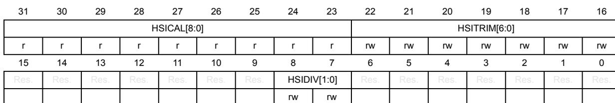
| 31 | 30 | 29 | 28 | 27 | 26 | 25 | 24 | 23 | 22 | 21 | 20 | 19 | 18 | 17 | 16 |
| HSICAL[8:0] | HSITRIM[6:0] | ||||||||||||||
| r | r | r | r | r | r | r | r | r | rw | rw | rw | rw | rw | rw | rw |
| 15 | 14 | 13 | 12 | 11 | 10 | 9 | 8 | 7 | 6 | 5 | 4 | 3 | 2 | 1 | 0 |
| Res. | Res. | Res. | Res. | Res. | Res. | Res. | HSIDIV[1:0] | Res. | Res. | Res. | Res. | Res. | Res. | Res. | |
| rw | rw | ||||||||||||||
Bits 31:23 HSICAL[8:0] : HSI clock calibration
This bitfield is set by hardware by option-byte loading during a system reset. It is adjusted by software through HSITRIM bitfield. This HSICAL bitfield represents the sum of the engineering option byte calibration value and HSITRIM[6:0] value.
Bits 22:16 HSITRIM[6:0] : HSI clock trimming
This bitfield is set by software to adjust calibration. It represents a signed value, added to the engineering option bytes (bsec_hsi_cal[8:0]) loaded during the reset phase (bsec_hsi_cal), to form the calibration trimming value: \( HSICAL[8:0] = HSITRIM[6:0] + bsec\_hsi\_cal[8:0] \) .
0x1-0x3F: \( bsec\_hsi\_cal[8:0] + \{V\} \)
0x40-0x7F: \( bsec\_hsi\_cal[8:0] - 128 + \{V\} \)
0x00: \( bsec\_hsi\_cal[8:0] \) (default after reset)
Bits 15:9 Reserved, must be kept at reset value.
Bits 8:7 HSIDIV[1:0] : HSI clock divider
This bitfield is set and reset by software to control the hsi_ck frequency (see Figure 38).
00: \( hsi\_div\_ck = hsi\_ck \) (default after reset)
01: \( hsi\_div\_ck = hsi\_ck / 2 \)
10: \( hsi\_div\_ck = hsi\_ck / 4 \)
11: \( hsi\_div\_ck = hsi\_ck / 8 \)
Bits 6:0 Reserved, must be kept at reset value.
14.10.12 RCC HSI monitor control register (RCC_HSIMCR)
Address offset: 0x4C
Reset value: 0x001F 07A1
This register is used to monitor and trim of the HSI oscillator. It is reset by int_sys_rstn, and is in the \( V_{CORE} \) voltage domain.
| 31 | 30 | 29 | 28 | 27 | 26 | 25 | 24 | 23 | 22 | 21 | 20 | 19 | 18 | 17 | 16 |
|---|---|---|---|---|---|---|---|---|---|---|---|---|---|---|---|
| HSI MONEN | Res. | Res. | Res. | Res. | Res. | Res. | Res. | Res. | Res. | HSIDEV[5:0] | |||||
| rw | rw | rw | rw | rw | rw | rw | |||||||||
| 15 | 14 | 13 | 12 | 11 | 10 | 9 | 8 | 7 | 6 | 5 | 4 | 3 | 2 | 1 | 0 |
| Res. | Res. | Res. | Res. | Res. | HSIREF[10:0] | ||||||||||
| rw | rw | rw | rw | rw | rw | rw | rw | rw | rw | rw | |||||
Bit 31 HSIMONEN : HSI clock period monitor enable
This bit is set and cleared by software.
0: Writing 0 disables the HSI clock period monitoring. Reading 0 means that the HSI clock period monitoring is disabled.
1: Writing 1 enables the HSI clock period monitoring. Reading 1 means that the HSI clock period monitoring is enabled.
Bits 30:22 Reserved, must be kept at reset value.
Bits 21:16 HSIDEV[5:0] : HSI clock count deviation value
This bitfield is set and cleared by software.
Bits 15:11 Reserved, must be kept at reset value.
Bits 10:0 HSIREF[10:0] : HSI clock-cycle counter reference value.
This bit contains the number of HSI clock cycles expected between two consecutive rising edges of the LSE signal. It is set by hardware.
14.10.13 RCC HSI monitor status register (RCC_HSIMSR)
Address offset: 0x50
Reset value: 0x0000 0000
This register is used to monitor and trim of the HSI oscillator. It is reset by int_sys_rstn, and is in the \( V_{CORE} \) voltage domain.
| 31 | 30 | 29 | 28 | 27 | 26 | 25 | 24 | 23 | 22 | 21 | 20 | 19 | 18 | 17 | 16 |
|---|---|---|---|---|---|---|---|---|---|---|---|---|---|---|---|
| Res. | Res. | Res. | Res. | Res. | Res. | Res. | Res. | Res. | Res. | Res. | Res. | Res. | Res. | Res. | Res. |
| 15 | 14 | 13 | 12 | 11 | 10 | 9 | 8 | 7 | 6 | 5 | 4 | 3 | 2 | 1 | 0 |
| Res. | Res. | Res. | Res. | Res. | HSIVAL[10:0] | ||||||||||
| r | r | r | r | r | r | r | r | r | r | r | |||||
Bits 31:11 Reserved, must be kept at reset value.
Bits 10:0 HSIVAL[10:0] : HSI clock-cycle counter measured value
This bitfield contains the number of HSI clock cycles measured between consecutive rising edges of the LSE signal. It is set by hardware.
14.10.14 RCC HSE configuration register (RCC_HSECFGR)
Address offset: 0x54
Reset value: 0x0000 0800
This register is used to configure the HSE oscillator. It is reset by int_sys_rstn, and is in the V CORE voltage domain.
| 31 | 30 | 29 | 28 | 27 | 26 | 25 | 24 | 23 | 22 | 21 | 20 | 19 | 18 | 17 | 16 |
|---|---|---|---|---|---|---|---|---|---|---|---|---|---|---|---|
| Res. | Res. | Res. | Res. | Res. | Res. | Res. | Res. | Res. | Res. | Res. | Res. | Res. | Res. | Res. | HSE EXT |
| rw | |||||||||||||||
| 15 | 14 | 13 | 12 | 11 | 10 | 9 | 8 | 7 | 6 | 5 | 4 | 3 | 2 | 1 | 0 |
| HSE BYP | HSECSSBPRE[3:0] | HSE CSSBYP | HSE CSSD | Res. | HSE CSSON | HSE DIV2SEL | Res. | Res. | Res. | Res. | Res. | Res. | |||
| rw | rw | rw | rw | rw | rw | r | rs | rw | |||||||
Bits 31:17 Reserved, must be kept at reset value.
Bit 16 HSEEXT : HSE clock type in bypass mode
This bit is set and reset by software to select the external clock type (analog or digital). The external clock must be enabled with the HSE enable bit to be used by the device. This HSEEXT bit can be written only if the HSE oscillator is disabled.
0: HSE in analog mode (default after reset)
1: HSE in digital mode
Bit 15 HSEBYP : HSE clock bypass
This bit is set and cleared by software to bypass the oscillator with an external clock. The external clock must be enabled with the HSE enable bit to be used by the device. This HSEBYP bit can be written even if the HSE oscillator is disabled.
0: HSE oscillator not bypassed (default after reset)
1: HSE oscillator bypassed with an external clock
Bits 14:11 HSECSSBPRE[3:0] : HSE CSS bypass divider
This bitfield is set and reset by software to divide the replacement internal HSI oscillator that bypasses the HSE oscillator when a failure is detected. Refer to HSE oscillator for details on the activation and deactivation sequences.
0000: HSI clock divided by 1
0001: HSI clock divided by 2
0010: HSI clock divided by 3
0011: HSI clock divided by 4
0100: HSI clock divided by 5
0101: HSI clock divided by 6
0110: HSI clock divided by 7
0111: HSI clock divided by 8
1000: HSI clock divided by 9
1001: HSI clock divided by 10
1010: HSI clock divided by 11
1011: HSI clock divided by 12
1100: HSI clock divided by 13
1101: HSI clock divided by 14
1110: HSI clock divided by 15
1111: HSI clock divided by 16
Bit 10 HSECSSBYP : HSE CSS bypass enable
This bit is set and reset by software to enable the CSS to bypass the HSE oscillator when a failure is detected, and to get a clock from the HSI oscillator. Refer to HSE oscillator for details on the activation and deactivation sequences.
0: CSS bypass of the HSE oscillator OFF (default after reset)
1: CSS bypass on the HSE oscillator ON
Bit 9 HSECSSD : HSE CSS failure detection
This bit is set by hardware to indicate when a failure has been detected by the CSS on the external HSE oscillator.
0: No failure detected on the oscillator (default after reset)
1: Failure detected on the oscillator
Bit 8 Reserved, must be kept at reset value.
Bit 7 HSECSSON : HSE CSS enable
This bit is set by software to enable the CSS on the HSE oscillator. Refer to HSE oscillator for details on the activation and deactivation sequences. Once this HSECSSON bit is enabled, it cannot be disabled, except after an HSE failure detection (HSECSSD = 1).
0: CSS on the HSE oscillator OFF (default after reset)
1: CSS on the HSE oscillator ON
Bit 6 HSEDI2SEL : HSE div2 clock source select
This bit is set and reset by software to select the source of the div2 output clock.
0: HSE: hse_div2_osc_ck = hse_osc_ck (default after reset)
1: HSE: hse_div2_osc_ck = hse_osc_ck/2
Bits 5:0 Reserved, must be kept at reset value.
14.10.15 RCC PLL1 configuration register 1 (RCC_PLL1CFGR1)
Address offset: 0x80
Reset value: 0x0820 2500
This register is used to configure the main features of PLL1. It is reset by int_sys_rst,n and is in the V CORE voltage domain.
| 31 | 30 | 29 | 28 | 27 | 26 | 25 | 24 | 23 | 22 | 21 | 20 | 19 | 18 | 17 | 16 |
|---|---|---|---|---|---|---|---|---|---|---|---|---|---|---|---|
| Res. | PLL1SEL[2:0] | PLL1BYP | Res. | PLL1DIVM[5:0] | PLL1DIVN[11:8] | ||||||||||
| rw | rw | rw | rw | rw | rw | rw | rw | rw | rw | rw | rw | rw | rw | ||
| 15 | 14 | 13 | 12 | 11 | 10 | 9 | 8 | 7 | 6 | 5 | 4 | 3 | 2 | 1 | 0 |
| PLL1DIVN[7:0] | Res. | Res. | Res. | Res. | Res. | Res. | Res. | Res. | |||||||
| rw | rw | rw | rw | rw | rw | rw | rw | ||||||||
Bit 31 Reserved, must be kept at reset value.
Bits 30:28 PLL1SEL[2:0] : PLL1 source selection of the reference clock
This bitfield is set and reset by software to select system clock source (sys_ck).
000: hsi_ck selected as reference clock
001: msi_ck selected as reference clock
010: hse_ck selected as reference clock
011: I2S_CKIN selected as reference clock
Bit 27 PLL1BYP : PLL1 bypassThis bit is set and cleared by software to bypass the VCO, and to feed the output with the PLL reference clock.
0: PLL output is driven by the VCO, via the optional POSTDIV division.
1: PLL output is bypassed and driven by the PLL reference clock (default after reset).
Bit 26 Reserved, must be kept at reset value.
Bits 25:20 PLL1DIVM[5:0] : PLL1 reference input clock divide frequency ratioThis bitfield is set and cleared by software.
0x00: Not applicable when the PLL is enabled
0x01: Reference clock divided by 1 (min value)
0x2-0x3F: Reference clock divided by {v}. It is recommended to configure the maximum divided reference clock frequency close to \( F_{VCO} / 16 \) .
Bits 19:8 PLL1DIVN[11:0] : PLL1 integer part for the VCO multiplication factorThis bitfield is set and cleared by software to control the multiplication factor of the VCO.
VCO output frequency = reference clock * DIVN / DIVM when FRACV = 0.
In integer mode, this value must be set between 0x10 (16) and 0x280 (640).
In fractional mode, this value must be set between 0x14 (20) and 0x140 (320).
Bits 7:0 Reserved, must be kept at reset value.
14.10.16 RCC PLL1 configuration register 2 (RCC_PLL1CFGR2)
Address offset: 0x84
Reset value: 0x0080 0000
This register is used to configure the optional fractional feedback division of PLL1. It is reset by int_sys_rstn, and is in the V CORE voltage domain.
| 31 | 30 | 29 | 28 | 27 | 26 | 25 | 24 | 23 22 21 20 19 18 17 16 | |||||||
|---|---|---|---|---|---|---|---|---|---|---|---|---|---|---|---|
| Res. | Res. | Res. | Res. | Res. | Res. | Res. | Res. | PLL1DIVNFRAC[23:16] | |||||||
| rw | rw | rw | rw | rw | rw | rw | rw | ||||||||
| 15 | 14 | 13 | 12 | 11 | 10 | 9 | 8 | 7 | 6 | 5 | 4 | 3 | 2 | 1 | 0 |
| PLL1DIVNFRAC[15:0] | |||||||||||||||
| rw | rw | rw | rw | rw | rw | rw | rw | rw | rw | rw | rw | rw | rw | rw | rw |
Bits 31:24 Reserved, must be kept at reset value.
Bits 23:0 PLL1DIVNFRAC[23:0] : PLL1 fractional part of the VCO multiplication factorThis bitfield is set and cleared by software to control the VCO fractional multiplication factor.
VCO output frequency = reference clock * \( (DIVN + DIVNFRAC / 2^{24}) / DIVM \) .
14.10.17 RCC PLL1 configuration register 3 (RCC_PLL1CFGR3)
Address offset: 0x88
Reset value: 0x4900 000D
This register is used to configure the SSCG and optional inner features of PLL1. It is reset by int_sys_rstn, and is in the V CORE voltage domain.
| 31 | 30 | 29 | 28 | 27 | 26 | 25 | 24 | 23 | 22 | 21 | 20 | 19 | 18 | 17 | 16 |
|---|---|---|---|---|---|---|---|---|---|---|---|---|---|---|---|
| Res. | PLL1P DIVEN | PLL1PDIV1[2:0] | PLL1PDIV2[2:0] | Res. | Res. | Res. | PLL1MODSPR[4:0] | ||||||||
| rw | rw | rw | rw | rw | rw | rw | rw | rw | rw | rw | rw | ||||
| 15 | 14 | 13 | 12 | 11 | 10 | 9 | 8 | 7 | 6 | 5 | 4 | 3 | 2 | 1 | 0 |
| Res. | Res. | Res. | Res. | PLL1MODDIV[3:0] | Res. | Res. | Res. | PLL1M ODSP RDW | PLL1M ODDS EN | PLL1M ODSS DIS | PLL1D ACEN | PLL1M ODSS RST | |||
| rw | rw | rw | rw | rw | rw | rw | rw | rw | |||||||
Bit 31 Reserved, must be kept at reset value.
Bit 30 PLL1PDIVEN : PLL1 post divider POSTDIV1, POSTDIV2, and PLL clock output enable
This bit is set and cleared by software to enable the post divider.
0: POSTDIV1 and POSTDIV2 powered down
1: POSTDIV1 and POSTDIV2 active (default after reset)
Bits 29:27 PLL1PDIV1[2:0] : PLL1 VCO frequency divider level 1
This bitfield is set and cleared by software to divide the VCO frequency output.
000: Not applicable
001: VCO output divided by 1 (minimum value) (default after reset)
010: VCO output divided by 2
011: VCO output divided by 3
100: VCO output divided by 4
101: VCO output divided by 5
110: VCO output divided by 6
111: VCO output divided by 7
Bits 26:24 PLL1PDIV2[2:0] : PLL1 VCO frequency divider level 2
This bitfield is set and cleared by software to divide the VCO frequency output.
000: Not applicable
001: VCO output divided by 1 (minimum value) (default after reset)
010: VCO output divided by 2
011: VCO output divided by 3
100: VCO output divided by 4
101: VCO output divided by 5
110: VCO output divided by 6
111: VCO output divided by 7
Bits 23:21 Reserved, must be kept at reset value.
Bits 20:16 PLL1MODSPR[4:0] : PLL1 modulation spread depth adjustment
This bitfield is set and cleared by software to adjust the modulation depth of the clock spreading generator.
Bits 15:12 Reserved, must be kept at reset value.
Bits 11:8 PLL1MODDIV[3:0] : PLL1 modulation division frequency adjustment
This bitfield is set and cleared by software to adjust the modulation frequency of the clock spreading generator. Corresponds to DIVVAL in Figure 44 .
Bits 7:5 Reserved, must be kept at reset value.
Bit 4 PLL1MODSPRDW : PLL1 modulation spread spectrum down
This bit is set and cleared by software to select the clock spreading mode of PLL1.
0: Center-spread modulation selected (default after reset)
1: Down-spread modulation selected
Bit 3 PLL1MODDSEN : PLL1 modulation spread spectrum (and fractional divide) enable
This bit is set and cleared by software to enable the delta-sigma modulator.
0: Modulation spread spectrum and fractional divide not active
1: Modulation spread spectrum and fractional divide active (default after reset)
Bit 2 PLL1MODSSDIS : PLL1 modulation spread spectrum disable
This bit is set and cleared by software to enable the clock spreading generator of PLL1.
0: Modulation spread spectrum active (and fractional divide inactive)
1: Fractional divide active (and modulation spread spectrum inactive) (default after reset)
Bit 1 PLL1DACEN : PLL1 noise canceling DAC enable in fractional mode
This bit is set and cleared by software to enable the noise cancellation in fractional mode.
0: DAC not active (default after reset)
1: DAC active
Bit 0 PLL1MODSSRST : PLL1 modulation spread spectrum reset
This bit is set and cleared by software.
0: PLL1 modulation spread spectrum reset module released
1: PLL1 modulation spread spectrum reset module asserted (default after reset)
14.10.18 RCC PLL2 configuration register 1 (RCC_PLL2CFGR1)
Address offset: 0x90
Reset value: 0x0800 0000
This register is used to configure the main features of PLL2. It is reset by
int_sys_rstn
, and is in the
\(
V_{CORE}
\)
voltage domain.
| 31 | 30 | 29 | 28 | 27 | 26 | 25 | 24 | 23 | 22 | 21 | 20 | 19 | 18 | 17 | 16 |
|---|---|---|---|---|---|---|---|---|---|---|---|---|---|---|---|
| Res. | PLL2SEL[2:0] | PLL2BYP | Res. | PLL2DIVM[5:0] | PLL2DIVN[11:8] | ||||||||||
| rw | rw | rw | rw | rw | rw | rw | rw | rw | rw | rw | rw | rw | rw | ||
| 15 | 14 | 13 | 12 | 11 | 10 | 9 | 8 | 7 | 6 | 5 | 4 | 3 | 2 | 1 | 0 |
| PLL2DIVN[7:0] | Res. | Res. | Res. | Res. | Res. | Res. | Res. | Res. | Res. | ||||||
| rw | rw | rw | rw | rw | rw | rw | rw | ||||||||
Bit 31 Reserved, must be kept at reset value.
Bits 30:28 PLL2SEL[2:0] : PLL2 source selection of the reference clock
This bitfield is set and reset by software to select system clock source (
sys_ck
).
000: hsi_ck selected as reference clock
001: msi_ck selected as reference clock
010: hse_ck selected as reference clock
011: I2S_CKIN selected as reference clock
Bit 27 PLL2BYP : PLL2 bypass
This bit is set and cleared by software to bypass the VCO and to feed the output with the PLL reference clock.
0: PLL output is driven by the VCO, via the optional POSTDIV division.
1: PLL output is bypassed and driven by the PLL reference clock (default after reset).
Bit 26 Reserved, must be kept at reset value.
Bits 25:20 PLL2DIVM[5:0] : PLL2 reference input clock divide frequency ratio
This bitfield is set and cleared by software.
0x2-0x3F: Reference clock is divided by {v}. The maximum divided reference clock frequency must be close to \( F_{VCO}/16 \) .
0x00: Not applicable when PLL is enabled
0x01: Reference clock is divided by 1 (min value).
Bits 19:8 PLL2DIVN[11:0] : PLL2 integer part for the VCO multiplication factor
This bitfield is set and cleared by software to control the multiplication factor of the VCO.
VCO output frequency = reference clock * DIVN / DIVM when FRACV = 0.
In integer mode, this value must be set between 0x10 (16) and 0x280 (640).
In fractional mode, this value must be set between 0x14 (20) and 0x140 (320).
Bits 7:0 Reserved, must be kept at reset value.
14.10.19 RCC PLL2 configuration register 2 (RCC_PLL2CFGR2)
Address offset: 0x94
Reset value: 0x0000 0000
This register is used to configure the optional fractional feedback division of PLL2. It is reset by
int_sys_rstn
, and is in the
\(
V_{CORE}
\)
voltage domain.
| 31 | 30 | 29 | 28 | 27 | 26 | 25 | 24 | 23 | 22 | 21 | 20 | 19 | 18 | 17 | 16 |
|---|---|---|---|---|---|---|---|---|---|---|---|---|---|---|---|
| Res. | Res. | Res. | Res. | Res. | Res. | Res. | Res. | PLL2DIVNFRAC[23:16] | |||||||
| rw | rw | rw | rw | rw | rw | rw | rw | ||||||||
| 15 | 14 | 13 | 12 | 11 | 10 | 9 | 8 | 7 | 6 | 5 | 4 | 3 | 2 | 1 | 0 |
| PLL2DIVNFRAC[15:0] | |||||||||||||||
| rw | rw | rw | rw | rw | rw | rw | rw | rw | rw | rw | rw | rw | rw | rw | rw |
Bits 31:24 Reserved, must be kept at reset value.
Bits 23:0 PLL2DIVNFRAC[23:0] : PLL2 fractional part of the VCO multiplication factor
This bitfield is set and cleared by software to control the VCO fractional multiplication factor.
VCO output frequency = reference clock * (DIVN + DIVNFRAC / \( 2^{24} \) ) / DIVM.
14.10.20 RCC PLL2 configuration register 3 (RCC_PLL2CFGR3)
Address offset: 0x98
Reset value: 0x4900 0005
This register is used to configure the SSCG and optional inner features of PLL2. It is reset by int_sys_rstn, and is in the V CORE voltage domain.
| 31 | 30 | 29 | 28 | 27 | 26 | 25 | 24 | 23 | 22 | 21 | 20 | 19 | 18 | 17 | 16 |
|---|---|---|---|---|---|---|---|---|---|---|---|---|---|---|---|
| Res. | PLL2P DIVEN | PLL2PDIV1[2:0] | PLL2PDIV2[2:0] | Res. | Res. | Res. | PLL2MODSPR[4:0] | ||||||||
| rw | rw | rw | rw | rw | rw | rw | rw | rw | rw | rw | rw | ||||
| 15 | 14 | 13 | 12 | 11 | 10 | 9 | 8 | 7 | 6 | 5 | 4 | 3 | 2 | 1 | 0 |
| Res. | Res. | Res. | Res. | PLL2MODDIV[3:0] | Res. | Res. | Res. | PLL2M ODSP RDW | PLL2M ODDS EN | PLL2M ODSS DIS | PLL2D ACEN | PLL2M ODSS RST | |||
| rw | rw | rw | rw | rw | rw | rw | rw | rw | |||||||
Bit 31 Reserved, must be kept at reset value.
Bit 30 PLL2PDIVEN : PLL2 post divider POSTDIV1, POSTDIV2, and PLL clock output enable
This bit is set and cleared by software to enable the post divider.
0: POSTDIV1 and POSTDIV2 powered down
1: POSTDIV1 and POSTDIV2 active (default after reset)
Bits 29:27 PLL2PDIV1[2:0] : PLL2 VCO frequency divider level 1
This bitfield is set and cleared by software to divide the VCO frequency output.
000: Not applicable
001: VCO output divided by 1 (minimum value) (default after reset)
010: VCO output divided by 2
011: VCO output divided by 3
100: VCO output divided by 4
101: VCO output divided by 5
110: VCO output divided by 6
111: VCO output divided by 7
Bits 26:24 PLL2PDIV2[2:0] : PLL2 VCO frequency divider level 2
This bitfield is set and cleared by software to divide the VCO frequency output.
000: Not applicable
001: VCO output divided by 1 (minimum value) (default after reset)
010: VCO output divided by 2
011: VCO output divided by 3
100: VCO output divided by 4
101: VCO output divided by 5
110: VCO output divided by 6
111: VCO output divided by 7
Bits 23:21 Reserved, must be kept at reset value.
Bits 20:16 PLL2MODSPR[4:0] : PLL2 modulation spread depth adjustment
This bitfield is set and cleared by software to adjust the modulation depth of the clock spreading generator.
Bits 15:12 Reserved, must be kept at reset value.
Bits 11:8 PLL2MODDIV[3:0] : PLL2 modulation division frequency adjustment
This bitfield is set and cleared by software to adjust the modulation frequency of the clock spreading generator. It corresponds to DIVVAL in Figure 44 .
Bits 7:5 Reserved, must be kept at reset value.
Bit 4 PLL2MODSPRDW : PLL2 modulation down spread
This bit is set and cleared by software to select the clock spreading mode of PLL2.
0: Center-spread modulation selected (default after reset)
1: Down-spread modulation selected
Bit 3 PLL2MODDSEN : PLL2 modulation spread spectrum (and fractional divide) enable
This bit is set and cleared by software to enable the delta-sigma modulator.
0: Modulation spread spectrum and fractional divide not active (default after reset)
1: Modulation spread spectrum and fractional divide active
Bit 2 PLL2MODSSDIS : PLL2 modulation spread spectrum disable
This bit is set and cleared by software to enable the clock spreading generator of PLL2.
0: Modulation spread spectrum active (and fractional divide inactive)
1: Fractional divide active (and the Modulation spread spectrum inactive) (default after reset)
Bit 1 PLL2DACEN : PLL2 noise canceling DAC enable in fractional mode
This bit is set and cleared by software to enable the noise cancellation in fractional mode.
0: DAC not active (default after reset)
1: DAC active
Bit 0 PLL2MODSSRST : PLL2 modulation spread spectrum reset
This bit is set and cleared by software.
0: PLL2 modulation spread spectrum reset module released
1: PLL2 modulation spread spectrum reset module asserted (default after reset)
14.10.21 RCC PLL3 configuration register 1 (RCC_PLL3CFGR1)
Address offset: 0xA0
Reset value: 0x0800 0000
This register is used to configure the main features of PLL3. It is reset by
int_sys_rstn
, and is in the
\(
V_{CORE}
\)
voltage domain.
| 31 | 30 | 29 | 28 | 27 | 26 | 25 | 24 | 23 | 22 | 21 | 20 | 19 | 18 | 17 | 16 |
|---|---|---|---|---|---|---|---|---|---|---|---|---|---|---|---|
| Res. | PLL3SEL[2:0] | PLL3BYP | Res. | PLL3DIVM[5:0] | PLL3DIVN[11:8] | ||||||||||
| rw | rw | rw | rw | rw | rw | rw | rw | rw | rw | rw | rw | rw | rw | ||
| 15 | 14 | 13 | 12 | 11 | 10 | 9 | 8 | 7 | 6 | 5 | 4 | 3 | 2 | 1 | 0 |
| PLL3DIVN[7:0] | Res. | Res. | Res. | Res. | Res. | Res. | Res. | Res. | Res. | ||||||
| rw | rw | rw | rw | rw | rw | rw | rw | ||||||||
Bit 31 Reserved, must be kept at reset value.
Bits 30:28 PLL3SEL[2:0] : PLL3 source selection of the reference clock
This bitfield is set and reset by software to select system clock source (
sys_ck
).
000: hsi_ck selected as reference clock
001: msi_ck selected as reference clock
010: hse_ck selected as reference clock
011: I2S_CKIN selected as reference clock
Bit 27 PLL3BYP : PLL3 bypass
This bit is set and cleared by software to bypass the VCO and feed the output with the PLL reference clock.
0: PLL output is driven by the VCO, via the optional POSTDIV division.
1: PLL output is bypassed and driven by the PLL reference clock (default after reset).
Bit 26 Reserved, must be kept at reset value.
Bits 25:20 PLL3DIVM[5:0] : PLL3 reference input clock divide frequency ratio
This bitfield is set and cleared by software.
0x2-0x3F: Reference clock is divided by {v}. The maximum divided reference clock frequency must be close to \( F_{VCO}/16 \) .
0x00: Not applicable when PLL is enabled
0x01: Reference clock is divided by 1 (min value)
Bits 19:8 PLL3DIVN[11:0] : PLL3 Integer part for the VCO multiplication factor
This bitfield is set and cleared by software to control the multiplication factor of the VCO.
VCO output frequency = reference clock * DIVN / DIVM when FRACV = 0.
In integer mode, this value must be set between 0x10 (16) and 0x280 (640).
In fractional mode, this value must be set between 0x14 (20) and 0x140 (320).
Bits 7:0 Reserved, must be kept at reset value.
14.10.22 RCC PLL3 configuration register 2 (RCC_PLL3CFGR2)
Address offset: 0xA4
Reset value: 0x0000 0000
This register is used to configure the optional fractional feedback division of PLL3. It is reset by
int_sys_rstn
, and is in the
\(
V_{CORE}
\)
voltage domain.
| 31 | 30 | 29 | 28 | 27 | 26 | 25 | 24 | 23 | 22 | 21 | 20 | 19 | 18 | 17 | 16 |
|---|---|---|---|---|---|---|---|---|---|---|---|---|---|---|---|
| Res. | Res. | Res. | Res. | Res. | Res. | Res. | Res. | PLL3DIVNFRAC[23:16] | |||||||
| rw | rw | rw | rw | rw | rw | rw | rw | ||||||||
| 15 | 14 | 13 | 12 | 11 | 10 | 9 | 8 | 7 | 6 | 5 | 4 | 3 | 2 | 1 | 0 |
| PLL3DIVNFRAC[15:0] | |||||||||||||||
| rw | rw | rw | rw | rw | rw | rw | rw | rw | rw | rw | rw | rw | rw | rw | rw |
Bits 31:24 Reserved, must be kept at reset value.
Bits 23:0 PLL3DIVNFRAC[23:0] : PLL3 fractional part of the VCO multiplication factor
This bitfield is set and cleared by software to control the VCO fractional multiplication factor.
VCO output frequency = reference clock * (DIVN + DIVNFRAC / \( 2^{24} \) ) / DIVM.
14.10.23 RCC PLL3 configuration register 3 (RCC_PLL3CFGR3)
Address offset: 0xA8
Reset value: 0x4900 0005
This register is used to configure the SSCG and optional inner features of PLL3. It is reset by int_sys_rstn, and is in the V CORE voltage domain.
| 31 | 30 | 29 | 28 | 27 | 26 | 25 | 24 | 23 | 22 | 21 | 20 | 19 | 18 | 17 | 16 |
|---|---|---|---|---|---|---|---|---|---|---|---|---|---|---|---|
| Res. | PLL3P DIVEN | PLL3PDIV1[2:0] | PLL3PDIV2[2:0] | Res. | Res. | Res. | PLL3MODSPR[4:0] | ||||||||
| rw | rw | rw | rw | rw | rw | rw | rw | rw | rw | rw | rw | ||||
| 15 | 14 | 13 | 12 | 11 | 10 | 9 | 8 | 7 | 6 | 5 | 4 | 3 | 2 | 1 | 0 |
| Res. | Res. | Res. | Res. | PLL3MODDIV[3:0] | Res. | Res. | Res. | PLL3M ODSP RDW | PLL3M ODDS EN | PLL3M ODSS DIS | PLL3D ACEN | PLL3M ODSS RST | |||
| rw | rw | rw | rw | rw | rw | rw | rw | rw | |||||||
Bit 31 Reserved, must be kept at reset value.
Bit 30 PLL3PDIVEN : PLL3 post divider POSTDIV1, POSTDIV2, and PLL clock output enable
This bit is set and cleared by software to enable the post divider.
0: POSTDIV1 and POSTDIV2 powered down
1: POSTDIV1 and POSTDIV2 active (default after reset)
Bits 29:27 PLL3PDIV1[2:0] : PLL3 VCO frequency divider level 1
This bitfield is set and cleared by software to divide the VCO frequency output.
000: Not applicable
001: VCO output divided by 1 (minimum value) (default after reset)
010: VCO output divided by 2
011: VCO output divided by 3
100: VCO output divided by 4
101: VCO output divided by 5
110: VCO output divided by 6
111: VCO output divided by 7
Bits 26:24 PLL3PDIV2[2:0] : PLL3 VCO frequency divider level 2
This bitfield is set and cleared by software to divide the VCO frequency output.
000: Not applicable
001: VCO output divided by 1 (minimum value) (default after reset)
010: VCO output divided by 2
011: VCO output divided by 3
100: VCO output divided by 4
101: VCO output divided by 5
110: VCO output divided by 6
111: VCO output divided by 7
Bits 23:21 Reserved, must be kept at reset value.
Bits 20:16 PLL3MODSPR[4:0] : PLL3 modulation spread depth adjustment
This bitfield is set and cleared by software to adjust the modulation depth of the clock spreading generator.
Bits 15:12 Reserved, must be kept at reset value.
Bits 11:8 PLL3MODDIV[3:0] : PLL3 modulation division frequency adjustment
This bitfield is set and cleared by software to adjust the modulation frequency of the clock spreading generator. It corresponds to DIVVAL in Figure 44 .
Bits 7:5 Reserved, must be kept at reset value.
Bit 4 PLL3MODSPRDW : PLL3 modulation down spread
This bit is set and cleared by software to select the clock spreading mode of PLL3.
0: Center-spread modulation selected (default after reset)
1: Down-spread modulation selected
Bit 3 PLL3MODDSEN : PLL3 modulation spread spectrum (and fractional divide) enable
This bit is set and cleared by software to enable the delta-sigma modulator.
0: Modulation spread spectrum and fractional divide not active (default after reset)
1: Modulation spread spectrum and fractional divide active
Bit 2 PLL3MODSSDIS : PLL3 modulation spread spectrum disable
This bit is set and cleared by software to enable the clock spreading generator of PLL3.
0: Modulation spread spectrum active (and fractional divide inactive)
1: Fractional divide active (and the modulation spread spectrum inactive) (default after reset)
Bit 1 PLL3DACEN : PLL3 noise canceling DAC enable in fractional mode
This bit is set and cleared by software to enable the noise cancellation in fractional mode.
0: DAC not active (default after reset)
1: DAC active
Bit 0 PLL3MODSSRST : PLL3 modulation spread spectrum reset
This bit is set and cleared by software.
0: PLL3 modulation spread spectrum reset module released
1: PLL3 modulation spread spectrum reset module asserted (default after reset)
14.10.24 RCC PLL4 configuration register 1 (RCC_PLL4CFGR1)
Address offset: 0xB0
Reset value: 0x0800 0000
This register is used to configure the main features of PLL4. It is reset by int_sys_rstn, and is in the V CORE voltage domain.
| 31 | 30 | 29 | 28 | 27 | 26 | 25 | 24 | 23 | 22 | 21 | 20 | 19 | 18 | 17 | 16 |
|---|---|---|---|---|---|---|---|---|---|---|---|---|---|---|---|
| Res. | PLL4SEL[2:0] | PLL4BYP | Res. | PLL4DIVM[5:0] | PLL4DIVN[11:8] | ||||||||||
| rw | rw | rw | rw | rw | rw | rw | rw | rw | rw | rw | rw | rw | rw | ||
| 15 | 14 | 13 | 12 | 11 | 10 | 9 | 8 | 7 | 6 | 5 | 4 | 3 | 2 | 1 | 0 |
| PLL4DIVN[7:0] | Res. | Res. | Res. | Res. | Res. | Res. | Res. | Res. | |||||||
| rw | rw | rw | rw | rw | rw | rw | rw | ||||||||
Bit 31 Reserved, must be kept at reset value.
Bits 30:28 PLL4SEL[2:0] : PLL4 source selection of the reference clock
This bitfield is set and reset by software to select system clock source (sys_ck).
000: hsi_ck selected as reference clock
001: msi_ck selected as reference clock
010: hse_ck selected as reference clock
011: I2S_CKIN selected as reference clock
Bit 27 PLL4BYP : PLL4 bypass
This bit is set and cleared by software to bypass the VCO, and to feed the output with the PLL reference clock.
0: PLL output is driven by the VCO, via the optional POSTDIV division.
1: PLL output is bypassed and driven by the PLL reference clock (default after reset).
Bit 26 Reserved, must be kept at reset value.
Bits 25:20 PLL4DIVM[5:0] : PLL4 reference input clock divide frequency ratio
This bitfield is set and cleared by software.
0x2-0x3F: Reference clock is divided by {v}. The maximum divided reference clock frequency must be close to \( F_{VCO}/16 \) .
0x00: Not applicable when PLL is enabled
0x01: Reference clock is divided by 1 (min value).
Bits 19:8 PLL4DIVN[11:0] : PLL4 integer part for the VCO multiplication factor
This bitfield is set and cleared by software to control the multiplication factor of the VCO.
VCO output frequency = reference clock * DIVN / DIVM when FRACV = 0.
In integer mode, this value must be set between 0x10 (16) and 0x280 (640).
In fractional mode, this value must be set between 0x14 (20) and 0x140 (320).
Bits 7:0 Reserved, must be kept at reset value.
14.10.25 RCC PLL4 configuration register 2 (RCC_PLL4CFGR2)
Address offset: 0xB4
Reset value: 0x0000 0000
This register is used to configure the optional fractional feedback division of PLL4. It is reset by
int_sys_rstn
, and is in the
\(
V_{CORE}
\)
voltage domain.
| 31 | 30 | 29 | 28 | 27 | 26 | 25 | 24 | 23 | 22 | 21 | 20 | 19 | 18 | 17 | 16 |
|---|---|---|---|---|---|---|---|---|---|---|---|---|---|---|---|
| Res. | Res. | Res. | Res. | Res. | Res. | Res. | Res. | PLL4DIVNFRAC[23:16] | |||||||
| rw | rw | rw | rw | rw | rw | rw | rw | ||||||||
| 15 | 14 | 13 | 12 | 11 | 10 | 9 | 8 | 7 | 6 | 5 | 4 | 3 | 2 | 1 | 0 |
| PLL4DIVNFRAC[15:0] | |||||||||||||||
| rw | rw | rw | rw | rw | rw | rw | rw | rw | rw | rw | rw | rw | rw | rw | rw |
Bits 31:24 Reserved, must be kept at reset value.
Bits 23:0 PLL4DIVNFRAC[23:0] : PLL4 fractional part of the VCO multiplication factor
This bitfield is set and cleared by software to control the VCO fractional multiplication factor.
VCO output frequency = reference clock * (DIVN + DIVNFRAC / \( 2^{24} \) ) / DIVM.
14.10.26 RCC PLL4 configuration register 3 (RCC_PLL4CFGR3)
Address offset: 0xB8
Reset value: 0x4900 0005
This register is used to configure the SSCG and optional inner features of PLL4. It is reset by
int_sys_rstn
, and is in the
\(
V_{CORE}
\)
voltage domain.
| 31 | 30 | 29 | 28 | 27 | 26 | 25 | 24 | 23 | 22 | 21 | 20 | 19 | 18 | 17 | 16 |
|---|---|---|---|---|---|---|---|---|---|---|---|---|---|---|---|
| Res. | PLL4P DIVEN | PLL4PDIV1[2:0] | PLL4PDIV2[2:0] | Res. | Res. | Res. | PLL4MODSPR[4:0] | ||||||||
| rw | rw | rw | rw | rw | rw | rw | rw | rw | rw | rw | rw | ||||
| 15 | 14 | 13 | 12 | 11 | 10 | 9 | 8 | 7 | 6 | 5 | 4 | 3 | 2 | 1 | 0 |
| Res. | Res. | Res. | Res. | PLL4MODDIV[3:0] | Res. | Res. | Res. | PLL4M ODSP RDW | PLL4M ODDS EN | PLL4M ODSS DIS | PLL4D ACEN | PLL4M ODSS RST | |||
| rw | rw | rw | rw | rw | rw | rw | rw | rw | |||||||
Bit 31 Reserved, must be kept at reset value.
Bit 30 PLL4PDIVEN : PLL4 post divider POSTDIV1, POSTDIV2, and PLL clock output enable
This bit is set and cleared by software to enable the post divider.
0: POSTDIV1 and POSTDIV2 powered down
1: POSTDIV1 and POSTDIV2 active (default after reset)
Bits 29:27 PLL4PDIV1[2:0] : PLL4 VCO frequency divider level 1
This bitfield is set and cleared by software to divide the VCO frequency output.
000: Not applicable
001: VCO output divided by 1 (minimum value) (default after reset)
010: VCO output divided by 2
011: VCO output divided by 3
100: VCO output divided by 4
101: VCO output divided by 5
110: VCO output divided by 6
111: VCO output divided by 7
Bits 26:24 PLL4PDIV2[2:0] : PLL4 VCO frequency divider level 2
This bitfield is set and cleared by software to divide the VCO frequency output.
000: Not applicable
001: VCO output divided by 1 (minimum value) (default after reset)
010: VCO output divided by 2
011: VCO output divided by 3
100: VCO output divided by 4
101: VCO output divided by 5
110: VCO output divided by 6
111: VCO output divided by 7
Bits 23:21 Reserved, must be kept at reset value.
Bits 20:16 PLL4MODSPR[4:0] : PLL4 modulation spread depth adjustment
This bitfield is set and cleared by software to adjust the modulation depth of the clock spreading generator.
Bits 15:12 Reserved, must be kept at reset value.
Bits 11:8 PLL4MODDIV[3:0] : PLL4 modulation division frequency adjustment
This bitfield is set and cleared by software to adjust the modulation frequency of the clock spreading generator. It corresponds to DIVVAL in Figure 44 .
Bits 7:5 Reserved, must be kept at reset value.
Bit 4 PLL4MODSPRDW : PLL4 modulation down spread
This bit is set and cleared by software to select the clock spreading mode of PLL4.
0: Center-spread modulation selected (default after reset)
1: Down-spread modulation selected
Bit 3 PLL4MODDSEN : PLL4 modulation spread spectrum (and fractional divide) enable
This bitfield is set and cleared by software to enable the delta-sigma modulator.
0: Modulation spread spectrum and fractional divide not active (default after reset)
1: Modulation spread spectrum and fractional divide active
Bit 2 PLL4MODSSDIS : PLL4 modulation spread spectrum disable
This bit is set and cleared by software to enable the clock spreading generator of PLL4.
0: Modulation spread spectrum active (and fractional divide inactive)
1: Fractional divide active (and modulation spread spectrum inactive) (default after reset)
Bit 1 PLL4DACEN : PLL4 noise canceling DAC enable in fractional mode
This bit is set and cleared by software to enable the noise cancellation in fractional mode.
0: DAC not active (default after reset)
1: DAC active
Bit 0 PLL4MODSSRST : PLL4 modulation spread spectrum reset
This bit is set and cleared by software.
0: PLL4 modulation spread spectrum reset module released
1: PLL4 modulation spread spectrum reset module asserted (default after reset)
14.10.27 RCC IC1 configuration register (RCC_IC1CFGR)
Address offset: 0xC4
Reset value: 0x0002 0000
This register is used to configure the IC1 divider. It is reset by
int_sys_rstn
, and is in the
\(
V_{CORE}
\)
voltage domain.
| 31 | 30 | 29 | 28 | 27 | 26 | 25 | 24 | 23 | 22 | 21 | 20 | 19 | 18 | 17 | 16 |
|---|---|---|---|---|---|---|---|---|---|---|---|---|---|---|---|
| Res. | Res. | IC1SEL[1:0] | Res. | Res. | Res. | Res. | IC1INT[7:0] | ||||||||
| rw | rw | rw | rw | rw | rw | rw | rw | rw | rw | ||||||
| 15 | 14 | 13 | 12 | 11 | 10 | 9 | 8 | 7 | 6 | 5 | 4 | 3 | 2 | 1 | 0 |
Bits 31:30 Reserved, must be kept at reset value.
Bits 29:28 IC1SEL[1:0] : Divider IC1 source selection
This bitfield is set and reset by software to select the PLL output to feed for the channel IC1.
00: pll1_ck selected (default after reset)
01: pll2_ck selected
10: pll3_ck selected
11: pll4_ck selected
Bits 27:24 Reserved, must be kept at reset value.
Bits 23:16 IC1INT[7:0] : Divider IC1 integer division factor
This bitfield is set and reset by software to control the frequency of the IC1 clock. The frequency is divided by the value \( IC1INT + 1 : \{v\} : IC1 = pll\_ck / \{v + 1\} \) .
0x00: \( IC1 = pll\_ck \)
0x01: \( IC1 = pll\_ck / 2 \)
0x02: \( IC1 = pll\_ck / 3 \) (default after reset)
0x03: \( IC1 = pll\_ck / 4 \)
...
0xFF: \( IC1 = pll\_ck / 256 \)
Bits 15:0 Reserved, must be kept at reset value.
14.10.28 RCC IC2 configuration register (RCC_IC2CFGR)
Address offset: 0xC8
Reset value: 0x0003 0000
This register is used to configure the IC2 divider. It is reset by
int_sys_rstn
, and is in the
\(
V_{CORE}
\)
voltage domain.
| 31 | 30 | 29 | 28 | 27 | 26 | 25 | 24 | 23 | 22 | 21 | 20 | 19 | 18 | 17 | 16 |
|---|---|---|---|---|---|---|---|---|---|---|---|---|---|---|---|
| Res. | Res. | IC2SEL[1:0] | Res. | Res. | Res. | Res. | IC2INT[7:0] | ||||||||
| rw | rw | rw | rw | rw | rw | rw | rw | rw | rw | ||||||
| 15 | 14 | 13 | 12 | 11 | 10 | 9 | 8 | 7 | 6 | 5 | 4 | 3 | 2 | 1 | 0 |
| Res. | Res. | Res. | Res. | Res. | Res. | Res. | Res. | Res. | Res. | Res. | Res. | Res. | Res. | Res. | Res. |
Bits 31:30 Reserved, must be kept at reset value.
Bits 29:28 IC2SEL[1:0] : Divider IC2 source selection
This bitfield is set and reset by software to select the PLL output to feed for the channel IC2.
00:
pll1_ck
selected (default after reset)
01:
pll2_ck
selected
10:
pll3_ck
selected
11:
pll4_ck
selected
Bits 27:24 Reserved, must be kept at reset value.
Bits 23:16 IC2INT[7:0] : Divider IC2 integer division factor
This bitfield is set and reset by software to control the frequency of the IC2 clock. The frequency is divided by the value \( IC2INT + 1 : \{v\} : IC2 = pll\_ck / \{v + 1\} \) .
0x00: \( IC2 = pll\_ck \)
0x01: \( IC2 = pll\_ck / 2 \)
0x02: \( IC2 = pll\_ck / 3 \)
0x03: \( IC2 = pll\_ck / 4 \) (default after reset)
...
0xFF: \( IC2 = pll\_ck / 256 \)
Bits 15:0 Reserved, must be kept at reset value.
14.10.29 RCC IC3 configuration register (RCC_IC3CFGR)
Address offset: 0xCC
Reset value: 0x0000 0000
This register is used to configure the IC3 divider. It is reset by int_sys_rstn, and is in the V CORE voltage domain.
| 31 | 30 | 29 | 28 | 27 | 26 | 25 | 24 | 23 | 22 | 21 | 20 | 19 | 18 | 17 | 16 |
|---|---|---|---|---|---|---|---|---|---|---|---|---|---|---|---|
| Res. | Res. | IC3SEL[1:0] | Res. | Res. | Res. | Res. | IC3INT[7:0] | ||||||||
| rw | rw | rw | rw | rw | rw | rw | rw | rw | rw | ||||||
| 15 | 14 | 13 | 12 | 11 | 10 | 9 | 8 | 7 | 6 | 5 | 4 | 3 | 2 | 1 | 0 |
| Res. | Res. | Res. | Res. | Res. | Res. | Res. | Res. | Res. | Res. | Res. | Res. | Res. | Res. | Res. | Res. |
Bits 31:30 Reserved, must be kept at reset value.
Bits 29:28 IC3SEL[1:0] : Divider IC3 source selection
This bitfield is set and reset by software to select the PLL output to feed for the channel IC3.
- 00: pll1_ck selected (default after reset)
- 01: pll2_ck selected
- 10: pll3_ck selected
- 11: pll4_ck selected
Bits 27:24 Reserved, must be kept at reset value.
Bits 23:16 IC3INT[7:0] : Divider IC3 integer division factor
This bitfield is set and reset by software to control the frequency of the IC3 clock. The frequency is divided by the value IC3INT + 1: {v}: \( IC3 = pll_{x}\_ck / \{v + 1\} \) .
- 0x00: \( IC3 = pll_{x}\_ck \) (default after reset)
- 0x01: \( IC3 = pll_{x}\_ck / 2 \)
- 0x02: \( IC3 = pll_{x}\_ck / 3 \)
- 0x03: \( IC3 = pll_{x}\_ck / 4 \)
- ...
- 0xFF: \( IC3 = pll_{x}\_ck / 256 \)
Bits 15:0 Reserved, must be kept at reset value.
14.10.30 RCC IC4 configuration register (RCC_IC4CFGR)
Address offset: 0xD0
Reset value: 0x0000 0000
This register is used to configure the IC4 divider. It is reset by int_sys_rstn and is in the V CORE voltage domain.
| 31 | 30 | 29 | 28 | 27 | 26 | 25 | 24 | 23 | 22 | 21 | 20 | 19 | 18 | 17 | 16 |
|---|---|---|---|---|---|---|---|---|---|---|---|---|---|---|---|
| Res. | Res. | IC4SEL[1:0] | Res. | Res. | Res. | Res. | IC4INT[7:0] | ||||||||
| rw | rw | rw | rw | rw | rw | rw | rw | rw | rw | ||||||
| 15 | 14 | 13 | 12 | 11 | 10 | 9 | 8 | 7 | 6 | 5 | 4 | 3 | 2 | 1 | 0 |
| Res. | Res. | Res. | Res. | Res. | Res. | Res. | Res. | Res. | Res. | Res. | Res. | Res. | Res. | Res. | Res. |
Bits 31:30 Reserved, must be kept at reset value.
Bits 29:28 IC4SEL[1:0] : Divider IC4 source selection
This bitfield is set and reset by software to select the PLL output to feed for the channel IC4.
00: pll1_ck selected (default after reset)
01: pll2_ck selected
10: pll3_ck selected
11: pll4_ck selected
Bits 27:24 Reserved, must be kept at reset value.
Bits 23:16 IC4INT[7:0] : Divider IC4 integer division factor
This bitfield is set and reset by software to control the frequency of the IC4 clock. The frequency is divided by the value IC4INT+1: {v}: IC4 = pllx_ck / {v + 1}.
0x00: IC4 = pllx_ck (default after reset)
0x01: IC4 = pllx_ck / 2
0x02: IC4 = pllx_ck / 3
0x03: IC4 = pllx_ck / 4
...
0xFF: IC4 = pllx_ck / 256
Bits 15:0 Reserved, must be kept at reset value.
14.10.31 RCC IC5 configuration register (RCC_IC5CFGR)
Address offset: 0xD4
Reset value: 0x0000 0000
This register is used to configure the IC5 divider. It is reset by int_sys_rstn, and is in the V CORE voltage domain.
| 31 | 30 | 29 | 28 | 27 | 26 | 25 | 24 | 23 | 22 | 21 | 20 | 19 | 18 | 17 | 16 |
|---|---|---|---|---|---|---|---|---|---|---|---|---|---|---|---|
| Res. | Res. | IC5SEL[1:0] | Res. | Res. | Res. | Res. | IC5INT[7:0] | ||||||||
| rw | rw | rw | rw | rw | rw | rw | rw | rw | rw | ||||||
| 15 | 14 | 13 | 12 | 11 | 10 | 9 | 8 | 7 | 6 | 5 | 4 | 3 | 2 | 1 | 0 |
| Res. | Res. | Res. | Res. | Res. | Res. | Res. | Res. | Res. | Res. | Res. | Res. | Res. | Res. | Res. | Res. |
Bits 31:30 Reserved, must be kept at reset value.
Bits 29:28 IC5SEL[1:0] : Divider IC5 source selection
This bitfield is set and reset by software to select the PLL output to feed for the channel IC5.
00: pll1_ck selected (default after reset)
01: pll2_ck selected
10: pll3_ck selected
11: pll4_ck selected
Bits 27:24 Reserved, must be kept at reset value.
Bits 23:16 IC5INT[7:0] : Divider IC5 integer division factor
This bitfield is set and reset by software to control the frequency of the IC5 clock. The frequency is divided by the value IC5INT + 1: {v}: IC5 = pllx_ck / {v + 1}.
0x00: IC5 = pllx_ck (default after reset)
0x01: IC5 = pllx_ck / 2
0x02: IC5 = pllx_ck / 3
0x03: IC5 = pllx_ck / 4
...
0xFF: IC5 = pllx_ck / 256
Bits 15:0 Reserved, must be kept at reset value.
14.10.32 RCC IC6 configuration register (RCC_IC6CFGR)
Address offset: 0xD8
Reset value: 0x0003 0000
This register is used to configure the IC6 divider. It is reset by int_sys_rstn, and is in the V CORE voltage domain.
| 31 | 30 | 29 | 28 | 27 | 26 | 25 | 24 | 23 | 22 | 21 | 20 | 19 | 18 | 17 | 16 |
|---|---|---|---|---|---|---|---|---|---|---|---|---|---|---|---|
| Res. | Res. | IC6SEL[1:0] | Res. | Res. | Res. | Res. | IC6INT[7:0] | ||||||||
| rw | rw | rw | rw | rw | rw | rw | rw | rw | rw | ||||||
| 15 | 14 | 13 | 12 | 11 | 10 | 9 | 8 | 7 | 6 | 5 | 4 | 3 | 2 | 1 | 0 |
| Res. | Res. | Res. | Res. | Res. | Res. | Res. | Res. | Res. | Res. | Res. | Res. | Res. | Res. | Res. | Res. |
Bits 31:30 Reserved, must be kept at reset value.
Bits 29:28 IC6SEL[1:0] : Divider IC6 source selection
This bitfield is set and reset by software to select the PLL output to feed for the channel IC6.
00: pll1_ck selected (default after reset)
01: pll2_ck selected
10: pll3_ck selected
11: pll4_ck selected
Bits 27:24 Reserved, must be kept at reset value.
Bits 23:16 IC6INT[7:0] : Divider IC6 integer division factor
This bitfield is set and reset by software to control the frequency of the IC6 clock. The frequency is divided by the value IC6INT+1: {v}: IC6 = pllx_ck / {v + 1}.
0x00: IC6 = pllx_ck
0x01: IC6 = pllx_ck / 2
0x02: IC6 = pllx_ck / 3
0x03: IC6 = pllx_ck / 4 (default after reset)
...
0xFF: IC6 = pllx_ck / 256
Bits 15:0 Reserved, must be kept at reset value.
14.10.33 RCC IC7 configuration register (RCC_IC7CFGR)
Address offset: 0xDC
Reset value: 0x1000 0000
This register is used to configure the IC7 divider. It is reset by int_sys_rstn, and is in the \( V_{CORE} \) voltage domain.
| 31 | 30 | 29 | 28 | 27 | 26 | 25 | 24 | 23 | 22 | 21 | 20 | 19 | 18 | 17 | 16 |
|---|---|---|---|---|---|---|---|---|---|---|---|---|---|---|---|
| Res. | Res. | IC7SEL[1:0] | Res. | Res. | Res. | Res. | IC7INT[7:0] | ||||||||
| rw | rw | rw | rw | rw | rw | rw | rw | rw | rw | ||||||
| 15 | 14 | 13 | 12 | 11 | 10 | 9 | 8 | 7 | 6 | 5 | 4 | 3 | 2 | 1 | 0 |
| Res. | Res. | Res. | Res. | Res. | Res. | Res. | Res. | Res. | Res. | Res. | Res. | Res. | Res. | Res. | Res. |
Bits 31:30 Reserved, must be kept at reset value.
Bits 29:28 IC7SEL[1:0] : Divider IC7 source selection
This bitfield is set and reset by software to select the PLL output to feed for the channel IC7.
00: pll1_ck selected
01: pll2_ck selected (default after reset)
10: pll3_ck selected
11: pll4_ck selected
Bits 27:24 Reserved, must be kept at reset value.
Bits 23:16 IC7INT[7:0] : Divider IC7 integer division factor
This bitfield is set and reset by software to control the frequency of the IC7 clock. The frequency is divided by the value IC7INT + 1: {v}: \( IC7 = pll_x\_ck / \{v + 1\} \) .
0x00: IC7 = \( pll_x\_ck \) (default after reset)
0x01: IC7 = \( pll_x\_ck / 2 \)
0x02: IC7 = \( pll_x\_ck / 3 \)
0x03: IC7 = \( pll_x\_ck / 4 \)
...
0xFF: IC7 = \( pll_x\_ck / 256 \)
Bits 15:0 Reserved, must be kept at reset value.
14.10.34 RCC IC8 configuration register (RCC_IC8CFGR)
Address offset: 0xE0
Reset value: 0x1000 0000
This register is used to configure the IC8 divider. It is reset by int_sys_rstn, and is in the \( V_{CORE} \) voltage domain.
| 31 | 30 | 29 | 28 | 27 | 26 | 25 | 24 | 23 | 22 | 21 | 20 | 19 | 18 | 17 | 16 |
|---|---|---|---|---|---|---|---|---|---|---|---|---|---|---|---|
| Res. | Res. | IC8SEL[1:0] | Res. | Res. | Res. | Res. | IC8INT[7:0] | ||||||||
| rw | rw | rw | rw | rw | rw | rw | rw | rw | rw | ||||||
| 15 | 14 | 13 | 12 | 11 | 10 | 9 | 8 | 7 | 6 | 5 | 4 | 3 | 2 | 1 | 0 |
| Res. | Res. | Res. | Res. | Res. | Res. | Res. | Res. | Res. | Res. | Res. | Res. | Res. | Res. | Res. | Res. |
Bits 31:30 Reserved, must be kept at reset value.
Bits 29:28 IC8SEL[1:0] : Divider IC8 source selection
This bitfield is set and reset by software to select the PLL output to feed for the channel IC8.
00: pll1_ck selected
01: pll2_ck selected (default after reset)
10: pll3_ck selected
11: pll4_ck selected
Bits 27:24 Reserved, must be kept at reset value.
Bits 23:16 IC8INT[7:0] : Divider IC8 integer division factor
This bitfield is set and reset by software to control the frequency of the IC8 clock. The frequency is divided by the value IC8INT + 1: {v}: \( IC8 = pll_x\_ck / \{v + 1\} \) .
0x00: IC8 = \( pll_x\_ck \) (default after reset)
0x01: IC8 = \( pll_x\_ck / 2 \)
0x02: IC8 = \( pll_x\_ck / 3 \)
0x03: IC8 = \( pll_x\_ck / 4 \)
...
0xFF: IC8 = \( pll_x\_ck / 256 \)
Bits 15:0 Reserved, must be kept at reset value.
14.10.35 RCC IC9 configuration register (RCC_IC9CFGR)
Address offset: 0xE4
Reset value: 0x1000 0000
This register is used to configure the IC9 divider. It is reset by
int_sys_rstn
, and is in the
\(
V_{CORE}
\)
voltage domain.
| 31 | 30 | 29 | 28 | 27 | 26 | 25 | 24 | 23 | 22 | 21 | 20 | 19 | 18 | 17 | 16 |
|---|---|---|---|---|---|---|---|---|---|---|---|---|---|---|---|
| Res. | Res. | IC9SEL[1:0] | Res. | Res. | Res. | Res. | IC9INT[7:0] | ||||||||
| rw | rw | rw | rw | rw | rw | rw | rw | rw | rw | ||||||
| 15 | 14 | 13 | 12 | 11 | 10 | 9 | 8 | 7 | 6 | 5 | 4 | 3 | 2 | 1 | 0 |
| Res. | Res. | Res. | Res. | Res. | Res. | Res. | Res. | Res. | Res. | Res. | Res. | Res. | Res. | Res. | Res. |
Bits 31:30 Reserved, must be kept at reset value.
Bits 29:28 IC9SEL[1:0] : Divider IC9 source selection
This bitfield is set and reset by software to select the PLL output to feed for the channel IC9.
00: pll1_ck selected
01: pll2_ck selected (default after reset)
10: pll3_ck selected
11: pll4_ck selected
Bits 27:24 Reserved, must be kept at reset value.
Bits 23:16 IC9INT[7:0] : Divider IC9 integer division factor
This bitfield is set and reset by software to control the frequency of the IC9 clock. The frequency is divided by the value \( IC9INT + 1 \) : {v}: \( IC9 = pll\_x\_ck / \{v + 1\} \) .
0x00: \( IC9 = pll\_x\_ck \) (default after reset)
0x01: \( IC9 = pll\_x\_ck / 2 \)
0x02: \( IC9 = pll\_x\_ck / 3 \)
0x03: \( IC9 = pll\_x\_ck / 4 \)
...
0xFF: \( IC9 = pll\_x\_ck / 256 \)
Bits 15:0 Reserved, must be kept at reset value.
14.10.36 RCC IC10 configuration register (RCC_IC10CFGR)
Address offset: 0xE8
Reset value: 0x1000 0000
This register is used to configure the IC10 divider. It is reset by
int_sys_rstn
, and is in the
\(
V_{CORE}
\)
voltage domain.
| 31 | 30 | 29 | 28 | 27 | 26 | 25 | 24 | 23 | 22 | 21 | 20 | 19 | 18 | 17 | 16 |
|---|---|---|---|---|---|---|---|---|---|---|---|---|---|---|---|
| Res. | Res. | IC10SEL[1:0] | Res. | Res. | Res. | Res. | IC10INT[7:0] | ||||||||
| rw | rw | rw | rw | rw | rw | rw | rw | rw | rw | ||||||
| 15 | 14 | 13 | 12 | 11 | 10 | 9 | 8 | 7 | 6 | 5 | 4 | 3 | 2 | 1 | 0 |
| Res. | Res. | Res. | Res. | Res. | Res. | Res. | Res. | Res. | Res. | Res. | Res. | Res. | Res. | Res. | Res. |
Bits 31:30 Reserved, must be kept at reset value.
Bits 29:28 IC10SEL[1:0] : Divider IC10 source selection
This bitfield is set and reset by software to select the PLL output to feed for the channel IC10.
00:
pll1_ck
selected
01:
pll2_ck
selected (default after reset)
10:
pll3_ck
selected
11:
pll4_ck
selected
Bits 27:24 Reserved, must be kept at reset value.
Bits 23:16 IC10INT[7:0] : Divider IC10 integer division factor
This bitfield is set and reset by software to control the frequency of the IC10 clock. The frequency is divided by the value \( IC10INT + 1 \) : {v}: \( IC10 = pll\_x\_ck / \{v + 1\} \) .
0x00: \( IC10 = pll\_x\_ck \) (default after reset)
0x01: \( IC10 = pll\_x\_ck / 2 \)
0x02: \( IC10 = pll\_x\_ck / 3 \)
0x03: \( IC10 = pll\_x\_ck / 4 \)
...
0xFF: \( IC10 = pll\_x\_ck / 256 \)
Bits 15:0 Reserved, must be kept at reset value.
14.10.37 RCC IC11 configuration register (RCC_IC11CFGR)
Address offset: 0xEC
Reset value: 0x0003 0000
This register is used to configure the IC11 divider. It is reset by
int_sys_rstn
, and is in the
\(
V_{CORE}
\)
voltage domain.
| 31 | 30 | 29 | 28 | 27 | 26 | 25 | 24 | 23 | 22 | 21 | 20 | 19 | 18 | 17 | 16 |
|---|---|---|---|---|---|---|---|---|---|---|---|---|---|---|---|
| Res. | Res. | IC11SEL[1:0] | Res. | Res. | Res. | Res. | IC11INT[7:0] | ||||||||
| rw | rw | rw | rw | rw | rw | rw | rw | rw | rw | ||||||
| 15 | 14 | 13 | 12 | 11 | 10 | 9 | 8 | 7 | 6 | 5 | 4 | 3 | 2 | 1 | 0 |
| Res. | Res. | Res. | Res. | Res. | Res. | Res. | Res. | Res. | Res. | Res. | Res. | Res. | Res. | Res. | Res. |
Bits 31:30 Reserved, must be kept at reset value.
Bits 29:28 IC11SEL[1:0] : Divider IC11 source selection
This bitfield is set and reset by software to select the PLL output to feed for the channel IC11.
00: pll1_ck selected (default after reset)
01: pll2_ck selected
10: pll3_ck selected
11: pll4_ck selected
Bits 27:24 Reserved, must be kept at reset value.
Bits 23:16 IC11INT[7:0] : Divider IC11 integer division factor
This bitfield is set and reset by software to control the frequency of the IC11 clock. The frequency is divided by the value \( IC11INT + 1 \) : \( \{v\} \) : \( IC11 = pll_x\_ck / \{v + 1\} \) .
0x00: \( IC11 = pll_x\_ck \)
0x01: \( IC11 = pll_x\_ck / 2 \)
0x02: \( IC11 = pll_x\_ck / 3 \)
0x03: \( IC11 = pll_x\_ck / 4 \) (default after reset)
...
0xFF: \( IC11 = pll_x\_ck / 256 \)
Bits 15:0 Reserved, must be kept at reset value.
14.10.38 RCC IC12 configuration register (RCC_IC12CFGR)
Address offset: 0xF0
Reset value: 0x2000 0000
This register is used to configure the IC12 divider. It is reset by
int_sys_rstn
, and is in the
\(
V_{CORE}
\)
voltage domain.
| 31 | 30 | 29 | 28 | 27 | 26 | 25 | 24 | 23 | 22 | 21 | 20 | 19 | 18 | 17 | 16 |
|---|---|---|---|---|---|---|---|---|---|---|---|---|---|---|---|
| Res. | Res. | IC12SEL[1:0] | Res. | Res. | Res. | Res. | IC12INT[7:0] | ||||||||
| rw | rw | rw | rw | rw | rw | rw | rw | rw | rw | ||||||
| 15 | 14 | 13 | 12 | 11 | 10 | 9 | 8 | 7 | 6 | 5 | 4 | 3 | 2 | 1 | 0 |
| Res. | Res. | Res. | Res. | Res. | Res. | Res. | Res. | Res. | Res. | Res. | Res. | Res. | Res. | Res. | Res. |
Bits 31:30 Reserved, must be kept at reset value.
Bits 29:28 IC12SEL[1:0] : Divider IC12 source selection
This bitfield is set and reset by software to select the PLL output to feed for the channel IC12.
00: pll1_ck selected
01: pll2_ck selected
10: pll3_ck selected (default after reset)
11: pll4_ck selected
Bits 27:24 Reserved, must be kept at reset value.
Bits 23:16 IC12INT[7:0] : Divider IC12 integer division factor
This bitfield is set and reset by software to control the frequency of the IC12 clock. The frequency is divided by the value IC12INT + 1: {v}: \( IC12 = pll_x\_ck / \{v + 1\} \) .
0x00: IC12 = pll_x_ck (default after reset)
0x01: IC12 = pll_x_ck / 2
0x02: IC12 = pll_x_ck / 3
0x03: IC12 = pll_x_ck / 4
...
0xFF: IC12 = pll_x_ck / 256
Bits 15:0 Reserved, must be kept at reset value.
14.10.39 RCC IC13 configuration register (RCC_IC13CFGR)
Address offset: 0xF4
Reset value: 0x2000 0000
This register is used to configure the IC13 divider. It is reset by int_sys_rstn, and is in the V CORE voltage domain.
| 31 | 30 | 29 | 28 | 27 | 26 | 25 | 24 | 23 | 22 | 21 | 20 | 19 | 18 | 17 | 16 |
|---|---|---|---|---|---|---|---|---|---|---|---|---|---|---|---|
| Res. | Res. | IC13SEL[1:0] | Res. | Res. | Res. | Res. | IC13INT[7:0] | ||||||||
| rw | rw | rw | rw | rw | rw | rw | rw | rw | rw | ||||||
| 15 | 14 | 13 | 12 | 11 | 10 | 9 | 8 | 7 | 6 | 5 | 4 | 3 | 2 | 1 | 0 |
| Res. | Res. | Res. | Res. | Res. | Res. | Res. | Res. | Res. | Res. | Res. | Res. | Res. | Res. | Res. | Res. |
Bits 31:30 Reserved, must be kept at reset value.
Bits 29:28 IC13SEL[1:0] : Divider IC13 source selection
This bitfield is set and reset by software to select the PLL output to feed for the channel IC13.
00: pll1_ck selected
01: pll2_ck selected
10: pll3_ck selected (default after reset)
11: pll4_ck selected
Bits 27:24 Reserved, must be kept at reset value.
Bits 23:16 IC13INT[7:0] : Divider IC13 integer division factor
This bitfield is set and reset by software to control the frequency of the IC13 clock. The frequency is divided by the value \( IC13INT + 1 \) : \( \{v\} \) : \( IC13 = pll\_ck / \{v + 1\} \) .
0x00: IC13 = pll x _ck (default after reset)
0x01: IC13 = pll x _ck / 2
0x02: IC13 = pll x _ck / 3
0x03: IC13 = pll x _ck / 4
...
0xFF: IC13 = pll x _ck / 256
Bits 15:0 Reserved, must be kept at reset value.
14.10.40 RCC IC14 configuration register (RCC_IC14CFGR)
Address offset: 0xF8
Reset value: 0x2000 0000
This register is used to configure the IC14 divider. It is reset by
int_sys_rstn
, and is in the V
CORE
voltage domain.
| 31 | 30 | 29 | 28 | 27 | 26 | 25 | 24 | 23 | 22 | 21 | 20 | 19 | 18 | 17 | 16 |
|---|---|---|---|---|---|---|---|---|---|---|---|---|---|---|---|
| Res. | Res. | IC14SEL[1:0] | Res. | Res. | Res. | Res. | IC14INT[7:0] | ||||||||
| rw | rw | rw | rw | rw | rw | rw | rw | rw | rw | ||||||
| 15 | 14 | 13 | 12 | 11 | 10 | 9 | 8 | 7 | 6 | 5 | 4 | 3 | 2 | 1 | 0 |
| Res. | Res. | Res. | Res. | Res. | Res. | Res. | Res. | Res. | Res. | Res. | Res. | Res. | Res. | Res. | Res. |
Bits 31:30 Reserved, must be kept at reset value.
Bits 29:28 IC14SEL[1:0] : Divider IC14 source selection
This bitfield is set and reset by software to select the PLL output to feed for the channel IC14.
00: pll1 x _ck selected
01: pll2 x _ck selected
10: pll3 x _ck selected (default after reset)
11: pll4 x _ck selected
Bits 27:24 Reserved, must be kept at reset value.
Bits 23:16 IC14INT[7:0] : Divider IC14 integer division factor
This bitfield is set and reset by software to control the frequency of the IC14 clock. The frequency is divided by the value \( IC14INT + 1 \) : \( \{v\} \) : \( IC14 = pll\_ck / \{v + 1\} \) .
0x00: IC14 = pll x _ck (default after reset)
0x01: IC14 = pll x _ck / 2
0x02: IC14 = pll x _ck / 3
0x03: IC14 = pll x _ck / 4
...
0xFF: IC14 = pll x _ck / 256
Bits 15:0 Reserved, must be kept at reset value.
14.10.41 RCC IC15 configuration register (RCC_IC15CFGR)
Address offset: 0xFC
Reset value: 0x2000 0000
This register is used to configure the IC15 divider. It is reset by
int_sys_rstn
, and is in the
\(
V_{CORE}
\)
voltage domain.
| 31 | 30 | 29 | 28 | 27 | 26 | 25 | 24 | 23 | 22 | 21 | 20 | 19 | 18 | 17 | 16 |
|---|---|---|---|---|---|---|---|---|---|---|---|---|---|---|---|
| Res. | Res. | IC15SEL[1:0] | Res. | Res. | Res. | Res. | IC15INT[7:0] | ||||||||
| rw | rw | rw | rw | rw | rw | rw | rw | rw | rw | ||||||
| 15 | 14 | 13 | 12 | 11 | 10 | 9 | 8 | 7 | 6 | 5 | 4 | 3 | 2 | 1 | 0 |
| Res. | Res. | Res. | Res. | Res. | Res. | Res. | Res. | Res. | Res. | Res. | Res. | Res. | Res. | Res. | Res. |
Bits 31:30 Reserved, must be kept at reset value.
Bits 29:28 IC15SEL[1:0] : Divider IC15 source selection
This bitfield is set and reset by software to select the PLL output to feed for the channel IC15.
- 00: pll1_ck selected
- 01: pll2_ck selected
- 10: pll3_ck selected (default after reset)
- 11: pll4_ck selected
Bits 27:24 Reserved, must be kept at reset value.
Bits 23:16 IC15INT[7:0] : Divider IC15 integer division factor
This bitfield is set and reset by software to control the frequency of the IC15 clock. The frequency is divided by the value IC15INT + 1: \( \{v\} \) : \( IC15 = pll_x\_ck / \{v + 1\} \) .
- 0x00: \( IC15 = pll_x\_ck \) (default after reset)
- 0x01: \( IC15 = pll_x\_ck / 2 \)
- 0x02: \( IC15 = pll_x\_ck / 3 \)
- 0x03: \( IC15 = pll_x\_ck / 4 \)
- ...
- 0xFF: \( IC15 = pll_x\_ck / 256 \)
Bits 15:0 Reserved, must be kept at reset value.
14.10.42 RCC IC16 configuration register (RCC_IC16CFGR)
Address offset: 0x100
Reset value: 0x3000 0000
This register is used to configure the IC16 divider. It is reset by
int_sys_rstn
, and is in the
\(
V_{CORE}
\)
voltage domain.
| 31 | 30 | 29 | 28 | 27 | 26 | 25 | 24 | 23 | 22 | 21 | 20 | 19 | 18 | 17 | 16 |
|---|---|---|---|---|---|---|---|---|---|---|---|---|---|---|---|
| Res. | Res. | IC16SEL[1:0] | Res. | Res. | Res. | Res. | IC16INT[7:0] | ||||||||
| rw | rw | rw | rw | rw | rw | rw | rw | rw | rw | ||||||
| 15 | 14 | 13 | 12 | 11 | 10 | 9 | 8 | 7 | 6 | 5 | 4 | 3 | 2 | 1 | 0 |
| Res. | Res. | Res. | Res. | Res. | Res. | Res. | Res. | Res. | Res. | Res. | Res. | Res. | Res. | Res. | Res. |
Bits 31:30 Reserved, must be kept at reset value.
Bits 29:28 IC16SEL[1:0] : Divider IC16 source selection
This bitfield is set and reset by software to select the PLL output to feed for the channel IC16.
00: pll1_ck selected
01: pll2_ck selected
10: pll3_ck selected
11: pll4_ck selected (default after reset)
Bits 27:24 Reserved, must be kept at reset value.
Bits 23:16 IC16INT[7:0] : Divider IC16 integer division factor
This bitfield is set and reset by software to control the frequency of the IC16 clock. The frequency is divided by the value IC16INT + 1: {v}: \( IC16 = pll_x\_ck / \{v + 1\} \) .
0x00: \( IC16 = pll_x\_ck \) (default after reset)
0x01: \( IC16 = pll_x\_ck / 2 \)
0x02: \( IC16 = pll_x\_ck / 3 \)
0x03: \( IC16 = pll_x\_ck / 4 \)
Bits 15:0 Reserved, must be kept at reset value.
14.10.43 RCC IC17 configuration register (RCC_IC17CFGR)
Address offset: 0x104
Reset value: 0x3000 0000
This register is used to configure the IC17 divider. It is reset by int_sys_rstn, and is in the V CORE voltage domain.
| 31 | 30 | 29 | 28 | 27 | 26 | 25 | 24 | 23 | 22 | 21 | 20 | 19 | 18 | 17 | 16 |
|---|---|---|---|---|---|---|---|---|---|---|---|---|---|---|---|
| Res. | Res. | IC17SEL[1:0] | Res. | Res. | Res. | Res. | IC17INT[7:0] | ||||||||
| rw | rw | rw | rw | rw | rw | rw | rw | rw | rw | ||||||
| 15 | 14 | 13 | 12 | 11 | 10 | 9 | 8 | 7 | 6 | 5 | 4 | 3 | 2 | 1 | 0 |
| Res. | Res. | Res. | Res. | Res. | Res. | Res. | Res. | Res. | Res. | Res. | Res. | Res. | Res. | Res. | Res. |
Bits 31:30 Reserved, must be kept at reset value.
Bits 29:28 IC17SEL[1:0] : Divider IC17 source selection
This bitfield is set and reset by software to select the PLL output to feed for the channel IC17.
00: pll1_ck selected
01: pll2_ck selected
10: pll3_ck selected
11: pll4_ck selected (default after reset)
Bits 27:24 Reserved, must be kept at reset value.
Bits 23:16 IC17INT[7:0] : Divider IC17 integer division factor
This bitfield is set and reset by software to control the frequency of the IC17 clock. The frequency is divided by the value IC17INT + 1: {v}: \( IC17 = pll_x\_ck / \{v + 1\} \) .
0x00: \( IC17 = pll_x\_ck \) (default after reset)
0x01: \( IC17 = pll_x\_ck / 2 \)
0x02: \( IC17 = pll_x\_ck / 3 \)
0x03: \( IC17 = pll_x\_ck / 4 \)
Bits 15:0 Reserved, must be kept at reset value.
14.10.44 RCC IC18 configuration register (RCC_IC18CFGR)
Address offset: 0x108
Reset value: 0x3000 0000
This register is used to configure the IC18 divider. It is reset by
int_sys_rstn
, and is in the
\(
V_{CORE}
\)
voltage domain.
| 31 | 30 | 29 | 28 | 27 | 26 | 25 | 24 | 23 | 22 | 21 | 20 | 19 | 18 | 17 | 16 |
|---|---|---|---|---|---|---|---|---|---|---|---|---|---|---|---|
| Res. | Res. | IC18SEL[1:0] | Res. | Res. | Res. | Res. | IC18INT[7:0] | ||||||||
| rw | rw | rw | rw | rw | rw | rw | rw | rw | rw | ||||||
| 15 | 14 | 13 | 12 | 11 | 10 | 9 | 8 | 7 | 6 | 5 | 4 | 3 | 2 | 1 | 0 |
| Res. | Res. | Res. | Res. | Res. | Res. | Res. | Res. | Res. | Res. | Res. | Res. | Res. | Res. | Res. | Res. |
Bits 31:30 Reserved, must be kept at reset value.
Bits 29:28 IC18SEL[1:0] : Divider IC18 source selection
This bitfield is set and reset by software to select the PLL output to feed for the channel IC18.
- 00: pll1_ck selected
- 01: pll2_ck selected
- 10: pll3_ck selected
- 11: pll4_ck selected (default after reset)
Bits 27:24 Reserved, must be kept at reset value.
Bits 23:16 IC18INT[7:0] : Divider IC18 integer division factor
This bitfield is set and reset by software to control the frequency of the IC18 clock. The frequency is divided by the value IC18INT + 1: \( \{v\}: IC18 = pll_x\_ck / \{v + 1\} \) .
- 0x00: \( IC18 = pll_x\_ck \) (default after reset)
- 0x01: \( IC18 = pll_x\_ck / 2 \)
- 0x02: \( IC18 = pll_x\_ck / 3 \)
- 0x03: \( IC18 = pll_x\_ck / 4 \)
Bits 15:0 Reserved, must be kept at reset value.
14.10.45 RCC IC19 configuration register (RCC_IC19CFGR)
Address offset: 0x10C
Reset value: 0x3000 0000
This register is used to configure the IC19 divider. It is reset by
int_sys_rstn
, and is in the
\(
V_{CORE}
\)
voltage domain.
| 31 | 30 | 29 | 28 | 27 | 26 | 25 | 24 | 23 | 22 | 21 | 20 | 19 | 18 | 17 | 16 |
|---|---|---|---|---|---|---|---|---|---|---|---|---|---|---|---|
| Res. | Res. | IC19SEL[1:0] | Res. | Res. | Res. | Res. | IC19INT[7:0] | ||||||||
| rw | rw | rw | rw | rw | rw | rw | rw | rw | rw | ||||||
| 15 | 14 | 13 | 12 | 11 | 10 | 9 | 8 | 7 | 6 | 5 | 4 | 3 | 2 | 1 | 0 |
| Res. | Res. | Res. | Res. | Res. | Res. | Res. | Res. | Res. | Res. | Res. | Res. | Res. | Res. | Res. | Res. |
Bits 31:30 Reserved, must be kept at reset value.
Bits 29:28 IC19SEL[1:0] : Divider IC19 source selection
This bitfield is set and reset by software to select the PLL output to feed for the channel IC19.
00: pll1_ck selected
01: pll2_ck selected
10: pll3_ck selected
11: pll4_ck selected (default after reset)
Bits 27:24 Reserved, must be kept at reset value.
Bits 23:16 IC19INT[7:0] : Divider IC19 integer division factor
This bitfield is set and reset by software to control the frequency of the IC19 clock. The frequency is divided by the value \( IC19INT + 1 \) : \( \{v\} \) : \( IC19 = pll_x\_ck / \{v + 1\} \) .
0x00: \( IC19 = pll_x\_ck \) (default after reset)
0x01: \( IC19 = pll_x\_ck / 2 \)
0x02: \( IC19 = pll_x\_ck / 3 \)
0x03: \( IC19 = pll_x\_ck / 4 \)
Bits 15:0 Reserved, must be kept at reset value.
14.10.46 RCC IC20 configuration register (RCC_IC20CFGR)
Address offset: 0x110
Reset value: 0x3000 0000
This register is used to configure the IC20 divider. It is reset by
int_sys_rstn
, and is in the
\(
V_{CORE}
\)
voltage domain.
| 31 | 30 | 29 | 28 | 27 | 26 | 25 | 24 | 23 | 22 | 21 | 20 | 19 | 18 | 17 | 16 |
|---|---|---|---|---|---|---|---|---|---|---|---|---|---|---|---|
| Res. | Res. | IC20SEL[1:0] | Res. | Res. | Res. | Res. | IC20INT[7:0] | ||||||||
| rw | rw | rw | rw | rw | rw | rw | rw | rw | rw | ||||||
| 15 | 14 | 13 | 12 | 11 | 10 | 9 | 8 | 7 | 6 | 5 | 4 | 3 | 2 | 1 | 0 |
| Res. | Res. | Res. | Res. | Res. | Res. | Res. | Res. | Res. | Res. | Res. | Res. | Res. | Res. | Res. | Res. |
Bits 31:30 Reserved, must be kept at reset value.
Bits 29:28 IC20SEL[1:0] : Divider IC20 source selection
This bitfield is set and reset by software to select the PLL output to feed for the channel IC20.
00: pll1_ck selected
01: pll2_ck selected
10: pll3_ck selected
11: pll4_ck selected (default after reset)
Bits 27:24 Reserved, must be kept at reset value.
Bits 23:16 IC20INT[7:0] : Divider IC20 integer division factor
This bitfield is set and reset by software to control the frequency of the IC20 clock. The frequency is divided by the value \( IC20INT + 1 \) : \( \{v\} \) : \( IC20 = pll_x\_ck / \{v + 1\} \) .
0x00: \( IC20 = pll_x\_ck \) (default after reset)
0x01: \( IC20 = pll_x\_ck / 2 \)
0x02: \( IC20 = pll_x\_ck / 3 \)
0x03: \( IC20 = pll_x\_ck / 4 \)
Bits 15:0 Reserved, must be kept at reset value.
14.10.47 RCC clock-source interrupt enable register (RCC_CIER)
Address offset: 0x124
Reset value: 0x0002 0000
This register controls the enabling (unmasking) of the interrupts.
| 31 | 30 | 29 | 28 | 27 | 26 | 25 | 24 | 23 | 22 | 21 | 20 | 19 | 18 | 17 | 16 |
|---|---|---|---|---|---|---|---|---|---|---|---|---|---|---|---|
| Res. | Res. | Res. | Res. | Res. | Res. | Res. | WKUPI E | Res. | Res. | Res. | Res. | Res. | Res. | HSECS SIE | LSECS SIE |
| rw | rw | rw | |||||||||||||
| 15 | 14 | 13 | 12 | 11 | 10 | 9 | 8 | 7 | 6 | 5 | 4 | 3 | 2 | 1 | 0 |
| Res. | Res. | Res. | Res. | PLL4R DYIE | PLL3R DYIE | PLL2R DYIE | PLL1R DYIE | Res. | Res. | Res. | HSERD YIE | HSIRD YIE | MSIRD YIE | LSE RD YIE | LSIRD YIE |
| rw | rw | rw | rw | rw | rw | rw | rw | rw |
Bits 31:25 Reserved, must be kept at reset value.
Bit 24 WKUPIE : CPU wake-up from Stop interrupt enable
This bit is set and reset by software to enable/disable interrupt caused by CPU wake-up from Stop mode.
0: Wake-up interrupt disabled (default after reset)
1: Wake-up interrupt enabled
Bits 23:18 Reserved, must be kept at reset value.
Bit 17 HSECSSIE : HSE CSS interrupt enable
This bit is set and reset by software to enable/disable interrupt caused by the CSS on external 32 kHz oscillator.
0: HSE CSS interrupt disabled
1: HSE CSS interrupt enabled (default after reset)
Bit 16 LSECSSIE : LSE CSS interrupt enable
This bit is set and reset by software to enable/disable interrupt caused by the CSS on external 32 kHz oscillator.
0: LSE CSS interrupt disabled (default after reset)
1: LSE CSS interrupt enabled
Bits 15:12 Reserved, must be kept at reset value.
Bit 11 PLL4RDYIE : PLL4 ready interrupt enable
This bit is set and reset by software to enable/disable interrupt caused by PLL4 lock.
0: PLL4 lock interrupt disabled (default after reset)
1: PLL4 lock interrupt enabled
Bit 10 PLL3RDYIE : PLL3 ready interrupt enable
This bit is set and reset by software to enable/disable interrupt caused by PLL3 lock.
0: PLL3 lock interrupt disabled (default after reset)
1: PLL3 lock interrupt enabled
Bit 9 PLL2RDYIE : PLL2 ready interrupt enable
This bit is set and reset by software to enable/disable interrupt caused by PLL2 lock.
0: PLL2 lock interrupt disabled (default after reset)
1: PLL2 lock interrupt enabled
Bit 8 PLL1RDYIE : PLL1 ready interrupt enable
This bit is set and reset by software to enable/disable interrupt caused by PLL1 lock.
0: PLL1 lock interrupt disabled (default after reset)
1: PLL1 lock interrupt enabled
Bits 7:5 Reserved, must be kept at reset value.
Bit 4 HSERDYIE : HSE ready interrupt enable
This bit is set and reset by software to enable/disable interrupt caused by the HSE oscillator stabilization.
0: HSE ready interrupt disabled (default after reset)
1: HSE ready interrupt enabled
Bit 3 HSIRDYIE : HSI ready interrupt enable
This bit is set and reset by software to enable/disable interrupt caused by the HSI oscillator stabilization.
0: HSI ready interrupt disabled (default after reset)
1: HSI ready interrupt enabled
Bit 2 MSIRDYIE : MSI ready interrupt enable
This bit is set and reset by software to enable/disable interrupt caused by the MSI oscillator stabilization.
0: MSI ready interrupt disabled (default after reset)
1: MSI ready interrupt enabled
Bit 1 LSERDYIE : LSE ready interrupt enable
This bit is set and reset by software to enable/disable interrupt caused by the LSE oscillator stabilization.
0: LSE ready interrupt disabled (default after reset)
1: LSE ready interrupt enabled
Bit 0 LSIRDYIE : LSI ready interrupt enable
This bit is set and reset by software to enable/disable interrupt caused by the LSI oscillator stabilization.
0: LSI ready interrupt disabled (default after reset)
1: LSI ready interrupt enabled
14.10.48 RCC clock-source interrupt flag register (RCC_CIFR)
Address offset: 0x128
Reset value: 0x0000 0000
This register returns the triggered interrupts. It is reset by sys_rstn.
| 31 | 30 | 29 | 28 | 27 | 26 | 25 | 24 | 23 | 22 | 21 | 20 | 19 | 18 | 17 | 16 |
|---|---|---|---|---|---|---|---|---|---|---|---|---|---|---|---|
| Res. | Res. | Res. | Res. | Res. | Res. | Res. | WKUP F | Res. | Res. | Res. | Res. | Res. | Res. | HSECS SF | LSECS SF |
| r | r | r | |||||||||||||
| 15 | 14 | 13 | 12 | 11 | 10 | 9 | 8 | 7 | 6 | 5 | 4 | 3 | 2 | 1 | 0 |
| Res. | Res. | Res. | Res. | PLL4R DYF | PLL3R DYF | PLL2R DYF | PLL1R DYF | Res. | Res. | Res. | HSERD YF | HSIRD YF | MSIRD YF | LSERD YF | LSIRD YF |
| r | r | r | r | r | r | r | r | r |
Bits 31:25 Reserved, must be kept at reset value.
Bit 24 WKUPF : CPU wake-up from Stop interrupt flag
This bit is reset by software by writing the WKUPFC bit. It is set by hardware when the CPU needs to exit Stop mode.
0: No wake-up interrupt caused by the PWR (default after reset)
1: Wake-up interrupt caused by the PWR
Bits 23:18 Reserved, must be kept at reset value.
Bit 17 HSECSSF : HSE ready interrupt flag
This bit is reset by software by writing the HSECSSC bit. It is set by hardware when the HSE clock becomes stable and HSECSSIE is set.
0: No clock ready interrupt caused by the HSE (default after reset)
1: Clock ready interrupt caused by the HSE
Bit 16 LSECSSF : LSE ready interrupt flag
This bit is reset by software by writing the LSECSSC bit. It is set by hardware when the LSE clock becomes stable and LSECSSIE is set.
0: No clock ready interrupt caused by the LSE (default after reset)
1: Clock ready interrupt caused by the LSE
Bits 15:12 Reserved, must be kept at reset value.
Bit 11 PLL4RDYF : PLL4 ready interrupt flag
This bit is reset by software by writing the PLL4RDYC bit. It is set by hardware when the PLL4 clock becomes stable and PLL4RDYIE is set.
0: No clock ready interrupt caused by the PLL4 (default after reset)
1: Clock ready interrupt caused by the PLL4
Bit 10 PLL3RDYF : PLL3 ready interrupt flag
This bit is reset by software by writing the PLL3RDYC bit. It is set by hardware when the PLL3 clock becomes stable and PLL3RDYIE is set.
0: No clock ready interrupt caused by the PLL3 (default after reset)
1: Clock ready interrupt caused by the PLL3
Bit 9 PLL2RDYF : PLL2 ready interrupt flag
This bit is reset by software by writing the PLL2RDYC bit. It is set by hardware when the PLL2 clock becomes stable and PLL2RDYIE is set.
0: No clock ready interrupt caused by the PLL2 (default after reset)
1: Clock ready interrupt caused by the PLL2
Bit 8 PLL1RDYF : PLL1 ready interrupt flag
This bit is reset by software by writing the PLL1RDYC bit. It is set by hardware when the PLL1 clock becomes stable and PLL1RDYIE is set.
0: No clock ready interrupt caused by the PLL1 (default after reset)
1: Clock ready interrupt caused by the PLL1
Bits 7:5 Reserved, must be kept at reset value.
Bit 4 HSERDYF : HSE ready interrupt flag
This bit is reset by software by writing the HSERDYC bit. It is set by hardware when the HSE clock becomes stable and HSERDYIE is set.
0: No clock ready interrupt caused by the HSE (default after reset)
1: Clock ready interrupt caused by the HSE
Bit 3 HSIRDYF : HSI ready interrupt flagThis bit is reset by software by writing the HSIRDYC bit. It is set by hardware when the HSI clock becomes stable and HSIRDYIE is set.
0: No clock ready interrupt caused by the HSI (default after reset)
1: Clock ready interrupt caused by the HSI
Bit 2 MSIRDYF : MSI ready interrupt flagThis bit is reset by software by writing the MSIRDYC bit. It is set by hardware when the MSI clock becomes stable and MSIRDYIE is set.
0: No clock ready interrupt caused by the MSI (default after reset)
1: Clock ready interrupt caused by the MSI
Bit 1 LSERDYF : LSE ready interrupt flagThis bit is reset by software by writing the LSERDYC bit. It is set by hardware when the LSE clock becomes stable and LSERDYIE is set.
0: No clock ready interrupt caused by the LSE (default after reset)
1: Clock ready interrupt caused by the LSE
Bit 0 LSIRDYF : LSI ready interrupt flagThis bit is reset by software by writing the LSIRDYC bit. It is set by hardware when the LSI clock becomes stable and LSIRDYIE is set.
0: No clock ready interrupt caused by the LSI (default after reset)
1: Clock ready interrupt caused by the LSI
14.10.49 RCC clock-source interrupt clear register (RCC_CICR)
Address offset: 0x12C
Reset value: 0x0000 0000
This register clears the interrupts.
| 31 | 30 | 29 | 28 | 27 | 26 | 25 | 24 | 23 | 22 | 21 | 20 | 19 | 18 | 17 | 16 |
|---|---|---|---|---|---|---|---|---|---|---|---|---|---|---|---|
| Res. | Res. | Res. | Res. | Res. | Res. | Res. | WKUP FC | Res. | Res. | Res. | Res. | Res. | Res. | HSECS SC | LSECS SC |
| w | w | w | |||||||||||||
| 15 | 14 | 13 | 12 | 11 | 10 | 9 | 8 | 7 | 6 | 5 | 4 | 3 | 2 | 1 | 0 |
| Res. | Res. | Res. | Res. | PLL4R DYC | PLL3R DYC | PLL2R DYC | PLL1R DYC | Res. | Res. | Res. | HSERD YC | HSIRD YC | MSIRD YC | LSERD YC | LSIRD YC |
| w | w | w | w | w | w | w | w | w |
Bits 31:25 Reserved, must be kept at reset value.
Bit 24 WKUPFC : CPU wake-up ready interrupt clearThis bit is set by software to clear WKUPF. It is reset by hardware when clear done.
0: WKUPF not modified (default after reset)
1: WKUPF cleared
Bits 23:18 Reserved, must be kept at reset value.
Bit 17 HSECSSC : HSE ready interrupt clearThis bit is set by software to clear HSECSSF. it is reset by hardware when clear done.
0: HSECSSF not modified (default after reset)
1: HSECSSF cleared
Bit 16 LSECSSC : LSE ready interrupt clear
This bit is set by software to clear LSECSSF. It is reset by hardware when clear done.
0: LSECSSF not modified (default after reset)
1: LSECSSF cleared
Bits 15:12 Reserved, must be kept at reset value.
Bit 11 PLL4RDYC : PLL4 ready interrupt clear
This bit is set by software to clear PLL4RDYF. It is reset by hardware when clear done.
0: PLL4RDYF not modified (default after reset)
1: PLL4RDYF cleared
Bit 10 PLL3RDYC : PLL3 ready interrupt clear
This bit is set by software to clear PLL3RDYF. it is reset by hardware when clear done.
0: PLL3RDYF not modified (default after reset)
1: PLL3RDYF cleared
Bit 9 PLL2RDYC : PLL2 ready interrupt clear
This bit is set by software to clear PLL2RDYF. It is reset by hardware when clear done.
0: PLL2RDYF not modified (default after reset)
1: PLL2RDYF cleared
Bit 8 PLL1RDYC : PLL1 ready interrupt clear
This bit is set by software to clear PLL1RDYF. It is reset by hardware when clear done.
0: PLL1RDYF not modified (default after reset)
1: PLL1RDYF cleared
Bits 7:5 Reserved, must be kept at reset value.
Bit 4 HSERDYC : HSE ready interrupt clear
This bit is set by software to clear HSERDYF. It is reset by hardware when clear done.
0: HSERDYF not modified (default after reset)
1: HSERDYF cleared
Bit 3 HSIRDYC : HSI ready interrupt clear
This bit is set by software to clear HSIRDYF. It is reset by hardware when clear done.
0: HSIRDYF not modified (default after reset)
1: HSIRDYF cleared
Bit 2 MSIRDYC : MSI ready interrupt clear
This bit is set by software to clear MSIRDYF. It is reset by hardware when clear done.
0: MSIRDYF not modified (default after reset)
1: MSIRDYF cleared
Bit 1 LSERDYC : LSE ready interrupt clear
This bit is set by software to clear LSERDYF. it is reset by hardware when clear done.
0: LSERDYF not modified (default after reset)
1: LSERDYF cleared
Bit 0 LSIRDYC : LSI ready interrupt clear
This bit is set by software to clear LSIRDYF. It is reset by hardware when clear done.
0: LSIRDYF not modified (default after reset)
1: LSIRDYF cleared
14.10.50 RCC clock configuration for independent peripheral register 1 (RCC_CCIPR1)
Address offset: 0x144
Reset value: 0x0000 0000
This register is used to configure various clocks. It is reset by sys_rstn, and is in the V CORE voltage domain.
| 31 | 30 | 29 | 28 | 27 | 26 | 25 | 24 | 23 | 22 | 21 | 20 | 19 | 18 | 17 | 16 | ||
|---|---|---|---|---|---|---|---|---|---|---|---|---|---|---|---|---|---|
| Res. | Res. | Res. | Res. | Res. | Res. | Res. | Res. | Res. | Res. | DCMIPPSEL[1:0] | Res. | Res. | Res. | Res. | Res. | ||
| rw | rw | ||||||||||||||||
| 15 | 14 | 13 | 12 | 11 | 10 | 9 | 8 | 7 | 6 | 5 | 4 | 3 | 2 | 1 | 0 | ||
| ADCPRE[7:0] | Res. | ADC12SEL[2:0] | Res. | ADF1SEL[2:0] | |||||||||||||
| rw | rw | rw | rw | rw | rw | rw | rw | rw | rw | rw | rw | rw | rw | ||||
Bits 31:22 Reserved, must be kept at reset value.
Bits 21:20 DCMIPPSEL[1:0] : Source selection for the DCMIPP kernel clock
This bitfield is set and reset by software.
00: pclk5 selected as reference clock
01: per_ck selected as reference clock
10: ic17_ck selected as reference clock
11: hsi_div_ck selected as reference clock
Bits 19:16 Reserved, must be kept at reset value.
Bits 15:8 ADCPRE[7:0] : ADC12 kernel clock divider selection (for clock ck_ker_adc12)
This bitfield is set and reset by software. The division ratio is linear: {v}: ck_ker_adc12 / {v+1}.
0x00: ck_ker_adc12 divided by 1
0x01: ck_ker_adc12 divided by 2
Bit 7 Reserved, must be kept at reset value.
Bits 6:4 ADC12SEL[2:0] : Source selection for the ADC12 kernel clock
This bitfield is set and reset by software.
000: hclk1 selected as reference clock
001: per_ck selected as reference clock
010: ic7_ck selected as reference clock
011: ic8_ck selected as reference clock
100: msi_ck selected as reference clock
101: hsi_div_ck selected as reference clock
110: I2S_CKIN selected as reference clock
111: timg_ck selected as reference clock
Bit 3 Reserved, must be kept at reset value.
Bits 2:0 ADF1SEL[2:0] : Source selection for the ADF1 kernel clock
This bitfield is set and reset by software.
000: hclk2 selected as reference clock
001: per_ck selected as reference clock
010: ic7_ck selected as reference clock
011: ic8_ck selected as reference clock
100: msi_ck selected as reference clock
101: hsi_div_ck selected as reference clock
110: I2S_CKIN selected as reference clock
111: timg_ck selected as reference clock
14.10.51 RCC clock configuration for independent peripheral register 2 (RCC_CCIPR2)
Address offset: 0x148
Reset value: 0x0000 0000
This register is used to configure various clocks. It is reset by sys_rstn, and is in the V CORE voltage domain.
| 31 | 30 | 29 | 28 | 27 | 26 | 25 | 24 | 23 | 22 | 21 | 20 | 19 | 18 | 17 | 16 |
|---|---|---|---|---|---|---|---|---|---|---|---|---|---|---|---|
| Res. | Res. | Res. | Res. | Res. | Res. | Res. | ETH1GTXCLKSEL | Res. | Res. | Res. | ETH1REFCLKSEL | Res. | ETH1SEL[2:0] | ||
| rw | rw | rw | rw | rw | |||||||||||
| 15 | 14 | 13 | 12 | 11 | 10 | 9 | 8 | 7 | 6 | 5 | 4 | 3 | 2 | 1 | 0 |
| Res. | Res. | ETH1CLKSEL [1:0] | Res. | Res. | Res. | ETH1PWRDOWNGRACE | ETH1PTPDIV[3:0] | Res. | Res. | ETH1PTPSEL [1:0] | |||||
| rw | rw | r | rw | rw | rw | rw | rw | rw | |||||||
Bits 31:25 Reserved, must be kept at reset value.
Bit 24 ETH1GTXCLKSEL : Ethernet 1 reference Tx RGMII 125 MHz clock selection
This bit is set and reset by software.
0: External clock (ETH1_CLK125) is used. Need to program AFmux.
1: Internal clock from the RCC is used.
Bits 23:21 Reserved, must be kept at reset value.
Bit 20 ETH1REFCLKSEL : Ethernet 1 reference Rx clock selection
This bit is set and reset by software.
0: External clock (ETH_RX/REF_CLK) is used. This is RX clock for an RGMII or MII PHY, or REF clock for an RMII PHY. Need to program AFmux.
1: Internal clock (ck_ker_eth1 from RCC) is used. To be used when the RMII 50 MHz (pad ETH1_CLK) is generated to the RMII PHY.
Bit 19 Reserved, must be kept at reset value.
Bits 18:16 ETH1SEL[2:0] : Ethernet 1 PHY interface selection
This bitfield is set and reset by software.
Note: Apply this configuration while the ETH1 is under reset, before enabling the ETH1 clocks.
000: MII
001: RGMII
100: RMII
Others: Reserved
Bits 15:14 Reserved, must be kept at reset value.
Bits 13:12 ETH1CLKSEL[1:0] : Source selection for the ETH1 kernel clock
This bitfield is set and reset by software.
00: hclke selected as reference clock
01: per_ck selected as reference clock
10: ic12_ck selected as reference clock
11: hse_ck selected as reference clock
Bits 11:9 Reserved, must be kept at reset value.
Bit 8 ETH1PWRDOWNACK : Ethernet 1 Power-down status
This bit is set and reset by software. It is asserted when the power-down sequence start has been acknowledged.
0: Power-down sequence start not yet acknowledged
1: Power-down sequence start acknowledged
Bits 7:4 ETH1PTPDIV[3:0] : ETH1 kernel clock divider selection (for clock ck_ker_eth1ptp)
This bitfield is set and reset by software. The division ratio is linear.
0000: ck_ker_eth1ptp divided by 1
0001: ck_ker_eth1ptp divided by 2
0010: ck_ker_eth1ptp divided by 3
0011: ck_ker_eth1ptp divided by 4
0100: ck_ker_eth1ptp divided by 5
0101: ck_ker_eth1ptp divided by 6
0110: ck_ker_eth1ptp divided by 7
0111: ck_ker_eth1ptp divided by 8
1000: ck_ker_eth1ptp divided by 9
1001: ck_ker_eth1ptp divided by 10
1010: ck_ker_eth1ptp divided by 11
1011: ck_ker_eth1ptp divided by 12
1100: ck_ker_eth1ptp divided by 13
1101: ck_ker_eth1ptp divided by 14
1110: ck_ker_eth1ptp divided by 15
1111: ck_ker_eth1ptp divided by 16
Bits 3:2 Reserved, must be kept at reset value.
Bits 1:0 ETH1PTPSEL[1:0] : Source selection for the ETH1 kernel clock
This bitfield is set and reset by software.
00: hclke selected as reference clock
01: per_ck selected as reference clock
10: ic13_ck selected as reference clock
11: hse_ck selected as reference clock
14.10.52 RCC clock configuration for independent peripheral register 3 (RCC_CCIPR3)
Address offset: 0x14C
Reset value: 0x0000 0003
This register is used to configure various clocks. It is reset by sys_rstn, and is in the V CORE voltage domain.
| 31 | 30 | 29 | 28 | 27 | 26 | 25 | 24 | 23 | 22 | 21 | 20 | 19 | 18 | 17 | 16 |
|---|---|---|---|---|---|---|---|---|---|---|---|---|---|---|---|
| Res. | Res. | Res. | Res. | Res. | Res. | Res. | Res. | Res. | Res. | Res. | Res. | Res. | Res. | Res. | Res. |
| 15 | 14 | 13 | 12 | 11 | 10 | 9 | 8 | 7 | 6 | 5 | 4 | 3 | 2 | 1 | 0 |
| Res. | Res. | Res. | Res. | Res. | Res. | Res. | Res. | Res. | Res. | FMCSEL[1:0] | Res. | Res. | Res. | FDCANSEL[1:0] | Res. |
| rw | rw | rw | rw |
Bits 31:6 Reserved, must be kept at reset value.
Bits 5:4 FMCSEL[1:0] : Source selection for the FMC kernel clock
This bitfield is set and reset by software.
00: hclk5 selected as reference clock
01: per_ck selected as reference clock
10: ic3_ck selected as reference clock
11: ic4_ck selected as reference clock
Others: Reserved, no clock provided as reference clock
Bits 3:2 Reserved, must be kept at reset value.
Bits 1:0 FDCANSEL[1:0] : Source selection for the FDCAN kernel clock
This bitfield is set and reset by software.
00: pclk1 selected as reference clock
01: per_ck selected as reference clock
10: ic19_ck selected as reference clock
11: hse_ck selected as reference clock
Others: Reserved, no clock provided as reference clock
14.10.53 RCC clock configuration for independent peripheral register 4 (RCC_CCIPR4)
Address offset: 0x150
Reset value: 0x0000 0000
This register is used to configure various clocks. It is reset by sys_rstn, and is in the V CORE voltage domain.
| 31 | 30 | 29 | 28 | 27 | 26 | 25 | 24 | 23 | 22 | 21 | 20 | 19 | 18 | 17 | 16 |
|---|---|---|---|---|---|---|---|---|---|---|---|---|---|---|---|
| Res. | Res. | Res. | Res. | Res. | Res. | LTDCSEL[1:0] | Res. | Res. | I3C2SEL[2:0] | Res. | Res. | Res. | I3C1SEL[2:0] | Res. | Res. |
| rw | rw | rw | rw | rw | rw | rw | rw | ||||||||
| 15 | 14 | 13 | 12 | 11 | 10 | 9 | 8 | 7 | 6 | 5 | 4 | 3 | 2 | 1 | 0 |
| Res. | I2C4SEL[2:0] | Res. | Res. | Res. | I2C3SEL[2:0] | Res. | Res. | Res. | I2C2SEL[2:0] | Res. | Res. | Res. | I2C1SEL[2:0] | Res. | Res. |
| rw | rw | rw | rw | rw | rw | rw | rw | rw | rw | rw | rw |
Bits 31:26 Reserved, must be kept at reset value.
Bits 25:24 LTDCSEL[1:0] : Source selection for the LTDC kernel clock
This bitfield is set and reset by software.
00: pclk5 selected as reference clock
01: per_ck selected as reference clock
10: ic16_ck selected as reference clock
11: hsi_div_ck selected as reference clock
Others: Reserved, no clock provided as reference clock
Bit 23 Reserved, must be kept at reset value.
Bits 22:20 I3C2SEL[2:0] : Source selection for the I3C2 kernel clock
This bitfield is set and reset by software.
000: pclk1 selected as reference clock
001: per_ck selected as reference clock
010: ic10_ck selected as reference clock
011: ic15_ck selected as reference clock
100: msi_ck selected as reference clock
101: hsi_div_ck selected as reference clock
Others: Reserved, no clock provided as reference clock
Bit 19 Reserved, must be kept at reset value.
Bits 18:16 I3C1SEL[2:0] : Source selection for the I3C1 kernel clock
This bitfield is set and reset by software.
000: pclk1 selected as reference clock
001: per_ck selected as reference clock
010: ic10_ck selected as reference clock
011: ic15_ck selected as reference clock
100: msi_ck selected as reference clock
101: hsi_div_ck selected as reference clock
Others: Reserved, no clock provided as reference clock
Bit 15 Reserved, must be kept at reset value.
Bits 14:12 I2C4SEL[2:0] : Source selection for the I2C4 kernel clock
This bitfield is set and reset by software.
000: pclk1 selected as reference clock
001: per_ck selected as reference clock
010: ic10_ck selected as reference clock
011: ic15_ck selected as reference clock
100: msi_ck selected as reference clock
101: hsi_div_ck selected as reference clock
Others: Reserved, no clock provided as reference clock
Bit 11 Reserved, must be kept at reset value.
Bits 10:8 I2C3SEL[2:0] : Source selection for the I2C3 kernel clock
This bitfield is set and reset by software.
000: pclk1 selected as reference clock
001: per_ck selected as reference clock
010: ic10_ck selected as reference clock
011: ic15_ck selected as reference clock
100: msi_ck selected as reference clock
101: hsi_div_ck selected as reference clock
Others: Reserved, no clock provided as reference clock
Bit 7 Reserved, must be kept at reset value.
Bits 6:4 I2C2SEL[2:0] : Source selection for the I2C2 kernel clock
This bitfield is set and reset by software.
000: pclk1 selected as reference clock
001: per_ck selected as reference clock
010: ic10_ck selected as reference clock
011: ic15_ck selected as reference clock
100: msi_ck selected as reference clock
101: hsi_div_ck selected as reference clock
Others: Reserved, no clock provided as reference clock
Bit 3 Reserved, must be kept at reset value.
Bits 2:0 I2C1SEL[2:0] : Source selection for the I2C1 kernel clock
This bitfield is set and reset by software.
000: pclk1 selected as reference clock
001: per_ck selected as reference clock
010: ic10_ck selected as reference clock
011: ic15_ck selected as reference clock
100: msi_ck selected as reference clock
101: hsi_div_ck selected as reference clock
Others: Reserved, no clock provided as reference clock
14.10.54 RCC clock configuration for independent peripheral register 5 (RCC_CCIPR5)
Address offset: 0x154
Reset value: 0x0000 F0F0
This register is used to configure various clocks. It is reset by sys_rstn, and is in the V CORE voltage domain.
| 31 | 30 | 29 | 28 | 27 | 26 | 25 | 24 | 23 | 22 | 21 | 20 | 19 | 18 | 17 | 16 |
|---|---|---|---|---|---|---|---|---|---|---|---|---|---|---|---|
| Res. | Res. | Res. | Res. | Res. | Res. | Res. | Res. | Res. | Res. | Res. | Res. | Res. | MDF1SEL[2:0] | ||
| rw | rw | rw | |||||||||||||
| 15 | 14 | 13 | 12 | 11 | 10 | 9 | 8 | 7 | 6 | 5 | 4 | 3 | 2 | 1 | 0 |
| MCO2PRE[3:0] | Res. | MCO2SEL[2:0] | MCO1PRE[3:0] | Res. | MCO1SEL[2:0] | ||||||||||
| rw | rw | rw | rw | rw | rw | rw | rw | rw | rw | rw | rw | rw | rw | ||
Bits 31:19 Reserved, must be kept at reset value.
Bits 18:16 MDF1SEL[2:0] : Source selection for the MDF1 kernel clock
This bitfield is set and reset by software.
000: hclk2 selected as reference clock
001: per_ck selected as reference clock
010: ic7_ck selected as reference clock
011: ic8_ck selected as reference clock
100: msi_ck selected as reference clock
101: hsi_div_ck selected as reference clock
110: I2S_CKIN selected as reference clock
111: timg_ck selected as reference clock
Bits 15:12 MCO2PRE[3:0] : MCO2 Kernel clock divider selection (for clock MCO2)
This bitfield is set and reset by software. The division ratio is linear.
0000: MCO2 divided by 1
0001: MCO2 divided by 2
0010: MCO2 divided by 3
0011: MCO2 divided by 4
0100: MCO2 divided by 5
0101: MCO2 divided by 6
0110: MCO2 divided by 7
0111: MCO2 divided by 8
1000: MCO2 divided by 9
1001: MCO2 divided by 10
1010: MCO2 divided by 11
1011: MCO2 divided by 12
1100: MCO2 divided by 13
1101: MCO2 divided by 14
1110: MCO2 divided by 15
1111: MCO2 divided by 16
Bit 11 Reserved, must be kept at reset value.
Bits 10:8 MCO2SEL[2:0] : Source selection for the MCO2 kernel clock
This bitfield is set and reset by software.
000: hsi_div_ck selected as reference clock (default after reset)
001: lse_ck selected as reference clock
010: msi_ck selected as reference clock
011: lsi_ck selected as reference clock
100: hse_ck selected as reference clock
101: ic15_ck selected as reference clock
110: ic20_ck selected as reference clock
111: sysb_ck selected as reference clock
Bits 7:4 MCO1PRE[3:0] : MCO1 Kernel clock divider selection (for clock MCO1)
This bitfield is set and reset by software. The division ratio is linear.
- 0000: MCO1 divided by 1
- 0001: MCO1 divided by 2
- 0010: MCO1 divided by 3
- 0011: MCO1 divided by 4
- 0100: MCO1 divided by 5
- 0101: MCO1 divided by 6
- 0110: MCO1 divided by 7
- 0111: MCO1 divided by 8
- 1000: MCO1 divided by 9
- 1001: MCO1 divided by 10
- 1010: MCO1 divided by 11
- 1011: MCO1 divided by 12
- 1100: MCO1 divided by 13
- 1101: MCO1 divided by 14
- 1110: MCO1 divided by 15
- 1111: MCO1 divided by 16
Bit 3 Reserved, must be kept at reset value.
Bits 2:0 MCO1SEL[2:0] : Source selection for the MCO1 kernel clock
This bitfield is set and reset by software.
- 000: hsi_div_ck selected as reference clock (default after reset)
- 001: lse_ck selected as reference clock
- 010: msi_ck selected as reference clock
- 011: lsi_ck selected as reference clock
- 100: hse_ck selected as reference clock
- 101: ic5_ck selected as reference clock
- 110: ic10_ck selected as reference clock
- 111: sysa_ck selected as reference clock
14.10.55 RCC clock configuration for independent peripheral register 6 (RCC_CCIPR6)
Address offset: 0x158
Reset value: 0x0000 0000
This register is used to configure various clocks. It is reset by sys_rstn, and is in the V CORE voltage domain.
| 31 | 30 | 29 | 28 | 27 | 26 | 25 | 24 | 23 | 22 | 21 | 20 | 19 | 18 | 17 | 16 |
|---|---|---|---|---|---|---|---|---|---|---|---|---|---|---|---|
| Res. | Res. | Res. | Res. | Res. | Res. | Res. | OTG PHY2CK REF SEL | Res. | Res. | OTG PHY2 SEL[1:0] | Res. | Res. | Res. | OTG PHY1CK REF SEL | |
| rw | rw | rw | rw | ||||||||||||
| 15 | 14 | 13 | 12 | 11 | 10 | 9 | 8 | 7 | 6 | 5 | 4 | 3 | 2 | 1 | 0 |
| Res | Res | OTG PHY1SEL[1:0] | Res | Res | XSPI3SEL[1:0] | Res | Res | XSPI2SEL[1:0] | Res | Res | XSPI1SEL[1:0] | ||||
| rw | rw | rw | rw | rw | rw | rw | rw | ||||||||
Bits 31:25 Reserved, must be kept at reset value.
Bit 24 OTGPHY2CKREFSEL:This bitfield is set and reset by software.
0: otgphy2_ker_ck selected
1: hse_div2_osc_ck selected
Bits 23:22 Reserved, must be kept at reset value.
Bits 21:20 OTGPHY2SEL[1:0]: Source selection for the OTGPHY2 kernel clockThis bitfield is set and reset by software.
00: hse_div2_ck selected as reference clock
01: per_ck selected as reference clock
10: ic15_ck selected as reference clock
11: hse_div2_osc_ck selected as reference clock
Others: Reserved, no clock provided as reference clock
Bits 19:17 Reserved, must be kept at reset value.
Bit 16 OTGPHY1CKREFSEL:This bitfield is set and reset by software.
0: otgphy1_ker_ck selected
1: hse_div2_osc_ck selected
Bits 15:14 Reserved, must be kept at reset value.
Bits 13:12 OTGPHY1SEL[1:0]: Source selection for the OTGPHY1 kernel clockThis bitfield is set and reset by software.
00: hse_div2_ck selected as reference clock
01: per_ck selected as reference clock
10: ic15_ck selected as reference clock
11: hse_div2_osc_ck selected as reference clock
Others: Reserved, no clock provided as reference clock
Bits 11:10 Reserved, must be kept at reset value.
Bits 9:8 XSPI3SEL[1:0]: Source selection for the XSPI3 kernel clockThis bitfield is set and reset by software.
00: hclk5 selected as reference clock
01: per_ck selected as reference clock
10: ic3_ck selected as reference clock
11: ic4_ck selected as reference clock
Others: Reserved, no clock provided as reference clock
Bits 7:6 Reserved, must be kept at reset value.
Bits 5:4 XSPI2SEL[1:0]: Source selection for the XSPI2 kernel clockThis bitfield is set and reset by software.
00: hclk5 selected as reference clock
01: per_ck selected as reference clock
10: ic3_ck selected as reference clock
11: ic4_ck selected as reference clock
Others: Reserved, no clock provided as reference clock
Bits 3:2 Reserved, must be kept at reset value.
Bits 1:0 XSPI1SEL[1:0] : Source selection for the XSPI1 kernel clock
This bitfield is set and reset by software.
00: hclk5 selected as reference clock
01: per_ck selected as reference clock
10: ic3_ck selected as reference clock
11: ic4_ck selected as reference clock
Others: Reserved, no clock provided as reference clock
14.10.56 RCC clock configuration for independent peripheral register 7 (RCC_CCIPR7)
Address offset: 0x15C
Reset value: 0x0000 0200
This register is used to configure various clocks. It is reset by sys_rstn, and is in the V CORE voltage domain.
| 31 | 30 | 29 | 28 | 27 | 26 | 25 | 24 | 23 | 22 | 21 | 20 | 19 | 18 | 17 | 16 |
|---|---|---|---|---|---|---|---|---|---|---|---|---|---|---|---|
| Res. | Res. | Res. | Res. | Res. | SAI2SEL[2:0] | Res. | SAI1SEL[2:0] | Res. | Res. | RTCPRE[5:4] | |||||
| rw | rw | rw | rw | rw | rw | rw | rw | ||||||||
| 15 | 14 | 13 | 12 | 11 | 10 | 9 | 8 | 7 | 6 | 5 | 4 | 3 | 2 | 1 | 0 |
| RTCPRE[3:0] | Res. | Res. | RTCSEL[1:0] | Res. | Res. | PSSISEL[1:0] | Res. | PERSEL[2:0] | |||||||
| rw | rw | rw | rw | rw | rw | rw | rw | rw | rw | rw | |||||
Bits 31:27 Reserved, must be kept at reset value.
Bits 26:24 SAI2SEL[2:0] : Source selection for the SAI2 kernel clock
This bitfield is set and reset by software.
000: pclk2 selected as reference clock
001: per_ck selected as reference clock
010: ic7_ck selected as reference clock
011: ic8_ck selected as reference clock
100: msi_ck selected as reference clock
101: hsi_div_ck selected as reference clock
110: I2S_CKIN selected as reference clock
111: spdif_symb_ck selected as reference clock
Bit 23 Reserved, must be kept at reset value.
Bits 22:20 SAI1SEL[2:0] : Source selection for the SAI1 kernel clock
This bitfield is set and reset by software.
000: pclk2 selected as reference clock
001: per_ck selected as reference clock
010: ic7_ck selected as reference clock
011: ic8_ck selected as reference clock
100: msi_ck selected as reference clock
101: hsi_div_ck selected as reference clock
110: I2S_CKIN selected as reference clock
111: spdif_symb_ck selected as reference clock
Bits 19:18 Reserved, must be kept at reset value.
Bits 17:12 RTCPRE[5:0] : RTC OSC clock divider selection (for clock hse_ck)
This bitfield is set and reset by software. The division ratio is linear: \( \{v\}: hse\_ck / \{v+1\} \) .
0x00: hse_ck divided by 1
0x01: hse_ck divided by 2
Bits 11:10 Reserved, must be kept at reset value.
Bits 9:8 RTCSEL[1:0] : Source selection for the RTC kernel clock
This bitfield is write-protected by the pwr_lock_backup_n signal. It is security-protected by a SEC signal from RIFSC, the PERSEC bit, a PRIV signal from RIFSC, or the PERPRIV bit.
This bitfield is set and reset by software.
01: lse_ck selected as reference clock
10: lsi_ck selected as reference clock
11: hse_rtc_ck selected as reference clock
Others: Reserved, no clock provided as reference clock
Bits 7:6 Reserved, must be kept at reset value.
Bits 5:4 PSSISEL[1:0] : Source selection for the PSSI kernel clock
This bitfield is set and reset by software.
00: hclk5 selected as reference clock
01: per_ck selected as reference clock
10: ic20_ck selected as reference clock
11: hsi_div_ck selected as reference clock
Others: Reserved, no clock provided as reference clock
Bit 3 Reserved, must be kept at reset value.
Bits 2:0 PERSEL[2:0] : Source selection for the PER kernel clock
This bitfield is set and reset by software.
000: hsi_ck selected as reference clock
001: msi_ck selected as reference clock
010: hse_ck selected as reference clock
011: ic19_ck selected as reference clock
100: ic5_ck selected as reference clock
101: ic10_ck selected as reference clock
110: ic15_ck selected as reference clock
111: ic20_ck selected as reference clock
14.10.57 RCC clock configuration for independent peripheral register 8 (RCC_CCIPR8)
Address offset: 0x160
Reset value: 0x0000 0000
This register is used to configure various clocks. It is reset by sys_rstn, and is in the V CORE voltage domain.
| 31 | 30 | 29 | 28 | 27 | 26 | 25 | 24 | 23 | 22 | 21 | 20 | 19 | 18 | 17 | 16 |
|---|---|---|---|---|---|---|---|---|---|---|---|---|---|---|---|
| Res. | Res. | Res. | Res. | Res. | Res. | Res. | Res. | Res. | Res. | Res. | Res. | Res. | Res. | Res. | Res. |
| 15 | 14 | 13 | 12 | 11 | 10 | 9 | 8 | 7 | 6 | 5 | 4 | 3 | 2 | 1 | 0 |
| Res. | Res. | Res. | Res. | Res. | Res. | Res. | Res. | Res. | Res. | SDMMC2SEL [1:0] | Res. | Res. | SDMMC1SEL [1:0] | ||
| rw | rw | rw | rw |
Bits 31:6 Reserved, must be kept at reset value.
Bits 5:4 SDMMC2SEL[1:0] : Source selection for the SDMMC2 kernel clock
This bitfield is set and reset by software.
00: hclk selected as reference clock
01: per_ck selected as reference clock
10: ic4_ck selected as reference clock
11: ic5_ck selected as reference clock
Others: Reserved, no clock provided as reference clock
Bits 3:2 Reserved, must be kept at reset value.
Bits 1:0 SDMMC1SEL[1:0] : Source selection for the SDMMC1 kernel clock
This bitfield is set and reset by software.
00: hclk selected as reference clock
01: per_ck selected as reference clock
10: ic4_ck selected as reference clock
11: ic5_ck selected as reference clock
Others: Reserved, no clock provided as reference clock
14.10.58 RCC clock configuration for independent peripheral register 9 (RCC_CCIPR9)
Address offset: 0x164
Reset value: 0x0000 0000
This register is used to configure various clocks. It is reset by sys_rstn, and is in the V CORE voltage domain.
| 31 | 30 | 29 | 28 | 27 | 26 | 25 | 24 | 23 | 22 | 21 | 20 | 19 | 18 | 17 | 16 |
|---|---|---|---|---|---|---|---|---|---|---|---|---|---|---|---|
| Res. | Res. | Res. | Res. | Res. | SPI6SEL[2:0] | Res. | SPI5SEL[2:0] | Res. | SPI4SEL[2:0] | ||||||
| rw | rw | rw | rw | rw | rw | rw | rw | rw | |||||||
| 15 | 14 | 13 | 12 | 11 | 10 | 9 | 8 | 7 | 6 | 5 | 4 | 3 | 2 | 1 | 0 |
| Res. | SPI3SEL[2:0] | Res. | SPI2SEL[2:0] | Res. | SPI1SEL[2:0] | Res. | SPDIFRX1SEL[2:0] | ||||||||
| rw | rw | rw | rw | rw | rw | rw | rw | rw | rw | rw | rw | ||||
Bits 31:27 Reserved, must be kept at reset value.
Bits 26:24 SPI6SEL[2:0] : Source selection for the SPI6 kernel clock
This bitfield is set and reset by software.
000: pclk4 selected as reference clock
001: per_ck selected as reference clock
010: ic8_ck selected as reference clock
011: ic9_ck selected as reference clock
100: msi_ck selected as reference clock
101: hsi_div_ck selected as reference clock
110: I2S_CKIN selected as reference clock
Others: Reserved, no clock provided as reference clock
Bit 23 Reserved, must be kept at reset value.
Bits 22:20 SPI5SEL[2:0] : Source selection for the SPI5 kernel clock
This bitfield is set and reset by software.
000: pclk2 selected as reference clock
001: per_ck selected as reference clock
010: ic9_ck selected as reference clock
011: ic14_ck selected as reference clock
100: msi_ck selected as reference clock
101: hsi_div_ck selected as reference clock
110: hse_ck selected as reference clock
Others: Reserved, no clock provided as reference clock
Bit 19 Reserved, must be kept at reset value.
Bits 18:16 SPI4SEL[2:0] : Source selection for the SPI4 kernel clock
This bitfield is set and reset by software.
000: pclk2 selected as reference clock
001: per_ck selected as reference clock
010: ic9_ck selected as reference clock
011: ic14_ck selected as reference clock
100: msi_ck selected as reference clock
101: hsi_div_ck selected as reference clock
110: hse_ck selected as reference clock
Others: Reserved, no clock provided as reference clock
Bit 15 Reserved, must be kept at reset value.
Bits 14:12 SPI3SEL[2:0] : Source selection for the SPI3 kernel clock
This bitfield is set and reset by software.
000: pclk1 selected as reference clock
001: per_ck selected as reference clock
010: ic8_ck selected as reference clock
011: ic9_ck selected as reference clock
100: msi_ck selected as reference clock
101: hsi_div_ck selected as reference clock
110: I2S_CKIN selected as reference clock
Others: Reserved, no clock provided as reference clock
Bit 11 Reserved, must be kept at reset value.
Bits 10:8 SPI2SEL[2:0] : Source selection for the SPI2 kernel clock
This bitfield is set and reset by software.
000: pclk1 selected as reference clock
001: per_ck selected as reference clock
010: ic8_ck selected as reference clock
011: ic9_ck selected as reference clock
100: msi_ck selected as reference clock
101: hsi_div_ck selected as reference clock
110: I2S_CKIN selected as reference clock
Others: Reserved, no clock provided as reference clock
Bit 7 Reserved, must be kept at reset value.
Bits 6:4 SPI1SEL[2:0] : Source selection for the SPI1 kernel clock
This bitfield is set and reset by software.
000: pclk2 selected as reference clock
001: per_ck selected as reference clock
010: ic8_ck selected as reference clock
011: ic9_ck selected as reference clock
100: msi_ck selected as reference clock
101: hsi_div_ck selected as reference clock
110: I2S_CKIN selected as reference clock
Others: Reserved, no clock provided as reference clock
Bit 3 Reserved, must be kept at reset value.
Bits 2:0 SPDIFRX1SEL[2:0] : Source selection for the SPDIFRX1 kernel clock
This bitfield is set and reset by software.
000: pclk1 selected as reference clock
001: per_ck selected as reference clock
010: ic7_ck selected as reference clock
011: ic8_ck selected as reference clock
100: msi_ck selected as reference clock
101: hsi_div_ck selected as reference clock
110: I2S_CKIN selected as reference clock
Others: Reserved, no clock provided as reference clock
14.10.59 RCC clock configuration for independent peripheral register 12 (RCC_CCIPR12)
Address offset: 0x170
Reset value: 0x0000 0000
This register is used to configure various clocks. It is reset by sys_rstn, and is in the V CORE voltage domain.
| 31 | 30 | 29 | 28 | 27 | 26 | 25 | 24 | 23 | 22 | 21 | 20 | 19 | 18 | 17 | 16 |
|---|---|---|---|---|---|---|---|---|---|---|---|---|---|---|---|
| Res. | Res. | Res. | Res. | Res. | LPTIM5SEL[2:0] | Res. | LPTIM4SEL[2:0] | Res. | LPTIM3SEL[2:0] | ||||||
| rw | rw | rw | rw | rw | rw | rw | rw | rw | |||||||
| 15 | 14 | 13 | 12 | 11 | 10 | 9 | 8 | 7 | 6 | 5 | 4 | 3 | 2 | 1 | 0 |
|---|---|---|---|---|---|---|---|---|---|---|---|---|---|---|---|
| Res. | LPTIM2SEL[2:0] | Res. | LPTIM1SEL[2:0] | Res. | Res. | Res. | Res. | Res. | Res. | Res. | Res. | ||||
| rw | rw | rw | rw | rw | rw | ||||||||||
Bits 31:27 Reserved, must be kept at reset value.
Bits 26:24 LPTIM5SEL[2:0] : Source selection for the LPTIM5 kernel clock
This bitfield is set and reset by software.
000: pclk4 selected as reference clock
001: per_ck selected as reference clock
010: ic15_ck selected as reference clock
011: lse_ck selected as reference clock
100: lsi_ck selected as reference clock
101: timg_ck selected as reference clock
Others: Reserved, no clock provided as reference clock
Bit 23 Reserved, must be kept at reset value.
Bits 22:20 LPTIM4SEL[2:0] : Source selection for the LPTIM4 kernel clock
This bitfield is set and reset by software.
000: pclk4 selected as reference clock
001: per_ck selected as reference clock
010: ic15_ck selected as reference clock
011: lse_ck selected as reference clock
100: lsi_ck selected as reference clock
101: timg_ck selected as reference clock
Others: Reserved, no clock provided as reference clock
Bit 19 Reserved, must be kept at reset value.
Bits 18:16 LPTIM3SEL[2:0] : Source selection for the LPTIM3 kernel clock
This bitfield is set and reset by software.
000: pclk4 selected as reference clock
001: per_ck selected as reference clock
010: ic15_ck selected as reference clock
011: lse_ck selected as reference clock
100: lsi_ck selected as reference clock
101: timg_ck selected as reference clock
Others: Reserved, no clock provided as reference clock
Bit 15 Reserved, must be kept at reset value.
Bits 14:12 LPTIM2SEL[2:0] : Source selection for the LPTIM2 kernel clock
This bitfield is set and reset by software.
000: pclk4 selected as reference clock
001: per_ck selected as reference clock
010: ic15_ck selected as reference clock
011: lse_ck selected as reference clock
100: lsi_ck selected as reference clock
101: timg_ck selected as reference clock
Others: Reserved, no clock provided as reference clock
Bit 11 Reserved, must be kept at reset value.
Bits 10:8 LPTIM1SEL[2:0] : Source selection for the LPTIM1 kernel clock
This bitfield is set and reset by software.
000: pclk1 selected as reference clock
001: per_ck selected as reference clock
010: ic15_ck selected as reference clock
011: lse_ck selected as reference clock
100: lsi_ck selected as reference clock
101: timg_ck selected as reference clock
Others: Reserved, no clock provided as reference clock
Bits 7:0 Reserved, must be kept at reset value.
14.10.60 RCC clock configuration for independent peripheral register 13 (RCC_CCIPR13)
Address offset: 0x174
Reset value: 0x0000 0000
This register is used to configure various clocks. It is reset by sys_rstn, and is in the V CORE voltage domain.
| 31 | 30 | 29 | 28 | 27 | 26 | 25 | 24 | 23 | 22 | 21 | 20 | 19 | 18 | 17 | 16 |
|---|---|---|---|---|---|---|---|---|---|---|---|---|---|---|---|
| Res. | UART8SEL[2:0] | Res. | UART7SEL[2:0] | Res. | USART6SEL[2:0] | Res. | UART5SEL[2:0] | ||||||||
| rw | rw | rw | rw | rw | rw | rw | rw | rw | rw | rw | rw | ||||
| 15 | 14 | 13 | 12 | 11 | 10 | 9 | 8 | 7 | 6 | 5 | 4 | 3 | 2 | 1 | 0 |
Bit 31 Reserved, must be kept at reset value.
Bits 30:28 UART8SEL[2:0] : Source selection for the UART8 kernel clock
This bitfield is set and reset by software.
000: pclk1 selected as reference clock
001: per_ck selected as reference clock
010: ic9_ck selected as reference clock
011: ic14_ck selected as reference clock
100: lse_ck selected as reference clock
101: msi_ck selected as reference clock
110: hsi_div_ck selected as reference clock
Others: Reserved, no clock provided as reference clock
Bit 27 Reserved, must be kept at reset value.
Bits 26:24 UART7SEL[2:0] : Source selection for the UART7 kernel clock
This bitfield is set and reset by software.
000: pclk1 selected as reference clock
001: per_ck selected as reference clock
010: ic9_ck selected as reference clock
011: ic14_ck selected as reference clock
100: lse_ck selected as reference clock
101: msi_ck selected as reference clock
110: hsi_div_ck selected as reference clock
Others: Reserved, no clock provided as reference clock
Bit 23 Reserved, must be kept at reset value.
Bits 22:20 USART6SEL[2:0] : Source selection for the USART6 kernel clock
This bitfield is set and reset by software.
000: pclk2 selected as reference clock
001: per_ck selected as reference clock
010: ic9_ck selected as reference clock
011: ic14_ck selected as reference clock
100: lse_ck selected as reference clock
101: msi_ck selected as reference clock
110: hsi_div_ck selected as reference clock
Others: Reserved, no clock provided as reference clock
Bit 19 Reserved, must be kept at reset value.
Bits 18:16 UART5SEL[2:0] : Source selection for the UART5 kernel clock
This bitfield is set and reset by software.
000: pclk1 selected as reference clock
001: per_ck selected as reference clock
010: ic9_ck selected as reference clock
011: ic14_ck selected as reference clock
100: lse_ck selected as reference clock
101: msi_ck selected as reference clock
110: hsi_div_ck selected as reference clock
Others: Reserved, no clock provided as reference clock
Bit 15 Reserved, must be kept at reset value.
Bits 14:12 UART4SEL[2:0] : Source selection for the UART4 kernel clock
This bitfield is set and reset by software.
000: pclk1 selected as reference clock
001: per_ck selected as reference clock
010: ic9_ck selected as reference clock
011: ic14_ck selected as reference clock
100: lse_ck selected as reference clock
101: msi_ck selected as reference clock
110: hsi_div_ck selected as reference clock
Others: Reserved, no clock provided as reference clock
Bit 11 Reserved, must be kept at reset value.
Bits 10:8 USART3SEL[2:0] : Source selection for the USART3 kernel clock
This bitfield is set and reset by software.
000: pclk1 selected as reference clock
001: per_ck selected as reference clock
010: ic9_ck selected as reference clock
011: ic14_ck selected as reference clock
100: lse_ck selected as reference clock
101: msi_ck selected as reference clock
110: hsi_div_ck selected as reference clock
Others: Reserved, no clock provided as reference clock
Bit 7 Reserved, must be kept at reset value.
Bits 6:4 USART2SEL[2:0] : Source selection for the USART2 kernel clock
This bitfield is set and reset by software.
000: pclk1 selected as reference clock
001: per_ck selected as reference clock
010: ic9_ck selected as reference clock
011: ic14_ck selected as reference clock
100: lse_ck selected as reference clock
101: msi_ck selected as reference clock
110: hsi_div_ck selected as reference clock
Others: Reserved, no clock provided as reference clock
Bit 3 Reserved, must be kept at reset value.
Bits 2:0 USART1SEL[2:0] : Source selection for the USART1 kernel clock
This bitfield is set and reset by software.
000: pclk2 selected as reference clock
001: per_ck selected as reference clock
010: ic9_ck selected as reference clock
011: ic14_ck selected as reference clock
100: lse_ck selected as reference clock
101: msi_ck selected as reference clock
110: hsi_div_ck selected as reference clock
Others: Reserved, no clock provided as reference clock
14.10.61 RCC clock configuration for independent peripheral register 14 (RCC_CCIPR14)
Address offset: 0x178
Reset value: 0x0000 0000
This register is used to configure various clocks. It is reset by sys_rstn, and is in the V CORE voltage domain.
| 31 | 30 | 29 | 28 | 27 | 26 | 25 | 24 | 23 | 22 | 21 | 20 | 19 | 18 | 17 | 16 |
|---|---|---|---|---|---|---|---|---|---|---|---|---|---|---|---|
| Res. | Res. | Res. | Res. | Res. | Res. | Res. | Res. | Res. | Res. | Res. | Res. | Res. | Res. | Res. | Res. |
| 15 | 14 | 13 | 12 | 11 | 10 | 9 | 8 | 7 | 6 | 5 | 4 | 3 | 2 | 1 | 0 |
| Res. | Res. | Res. | Res. | Res. | LPUART1SEL[2:0] | Res. | USART10SEL[2:0] | Res. | UART9SEL[2:0] | ||||||
| rw | rw | rw | rw | rw | rw | rw | rw | rw | |||||||
Bits 31:11 Reserved, must be kept at reset value.
Bits 10:8 LPUART1SEL[2:0] : Source selection for the LPUART1 kernel clock
This bitfield is set and reset by software.
000: pclk4 selected as reference clock
001: per_ck selected as reference clock
010: ic9_ck selected as reference clock
011: ic14_ck selected as reference clock
100: lse_ck selected as reference clock
101: msi_ck selected as reference clock
110: hsi_div_ck selected as reference clock
Others: Reserved, no clock provided as reference clock
Bit 7 Reserved, must be kept at reset value.
Bits 6:4 USART10SEL[2:0] : Source selection for the USART10 kernel clock
This bitfield is set and reset by software.
000: pclk2 selected as reference clock
001: per_ck selected as reference clock
010: ic9_ck selected as reference clock
011: ic14_ck selected as reference clock
100: lse_ck selected as reference clock
101: msi_ck selected as reference clock
110: hsi_div_ck selected as reference clock
Others: Reserved, no clock provided as reference clock
Bit 3 Reserved, must be kept at reset value.
Bits 2:0 UART9SEL[2:0] : Source selection for the UART9 kernel clock
This bitfield is set and reset by software.
000: pclk2 selected as reference clock
001: per_ck selected as reference clock
010: ic9_ck selected as reference clock
011: ic14_ck selected as reference clock
100: lse_ck selected as reference clock
101: msi_ck selected as reference clock
110: hsi_div_ck selected as reference clock
Others: Reserved, no clock provided as reference clock
14.10.62 RCC miscellaneous configurations reset register (RCC_MISCRSTR)
Address offset: 0x208
Reset value: 0x0000 0000
This register is used to reset the miscellaneous configurations. It is reset by sys_rstn, and is in the V CORE voltage domain.
| 31 | 30 | 29 | 28 | 27 | 26 | 25 | 24 | 23 | 22 | 21 | 20 | 19 | 18 | 17 | 16 |
|---|---|---|---|---|---|---|---|---|---|---|---|---|---|---|---|
| Res. | Res. | Res. | Res. | Res. | Res. | Res. | Res. | Res. | Res. | Res. | Res. | Res. | Res. | Res. | Res. |
| 15 | 14 | 13 | 12 | 11 | 10 | 9 | 8 | 7 | 6 | 5 | 4 | 3 | 2 | 1 | 0 |
| Res. | Res. | Res. | Res. | Res. | Res. | Res. | SDMMC C2DLL RST | SDMMC C1DLL RST | Res. | XSPIPHY 2 RST | XSPIPHY 1 RST | Res. | Res. | Res. | DBG RST |
| rw | rw | rw | rw | rw |
Bits 31:9 Reserved, must be kept at reset value.
Bit 8 SDMMC2DLLRST : SDMMC2DLL reset
This bit is security-protected by a SEC signal from RIFSC, the PERSEC bit, a PRIV signal from RIFSC, or the PERPRIV bit. It can be set with SDMMC2DLLRSTS, and cleared with SDMMC2DLLRSTC. This bit is set and reset by software.
0: SDMMC2DLL not under reset (default after reset)
1: SDMMC2DLL under reset
Bit 7 SDMMC1DLLRST : SDMMC1DLL reset
This bit is security-protected by a SEC signal from RIFSC, the PERSEC bit, a PRIV signal from RIFSC, or the PERPRIV bit. It can be set with SDMMC1DLLRSTS, and cleared with SDMMC1DLLRSTC. This bit is set and reset by software.
0: SDMMC1DLL not under reset (default after reset)
1: SDMMC1DLL under reset
Bit 6 Reserved, must be kept at reset value.
Bit 5 XSPIPHY2RST : XSPIPHY2 reset
This bit is security-protected by a SEC signal from RIFSC, the PERSEC bit, a PRIV signal from RIFSC, or the PERPRIV bit. It can be set with XSPIPHY2RSTS and cleared with XSPIPHY2RSTC. This bit is set and reset by software.
0: XSPIPHY2 not under reset (default after reset)
1: XSPIPHY2 under reset
Bit 4 XSPIPHY1RST : XSPIPHY1 reset
This bit is security-protected by a SEC signal from RIFSC, the PERSEC bit, a PRIV signal from RIFSC, or the PERPRIV bit. It can be set with XSPIPHY1RSTS, and cleared with XSPIPHY1RSTC. This bit is set and reset by software.
0: XSPIPHY1 not under reset (default after reset)
1: XSPIPHY1 under reset
Bits 3:1 Reserved, must be kept at reset value.
Bit 0 DBGIRST : DBG reset
This bit is always security-protected. It can be set with DBGIRSTS, and cleared with DBGIRSTC. This bit is set and reset by software.
0: DBG not under reset (default after reset)
1: DBG under reset
14.10.63 RCC embedded memories reset register (RCC_MEMRSTR)
Address offset: 0x20C
Reset value: 0x0000 0000
This register is used to reset the embedded memories. It is reset by sys_rstn, and is in the V CORE voltage domain.
| 31 | 30 | 29 | 28 | 27 | 26 | 25 | 24 | 23 | 22 | 21 | 20 | 19 | 18 | 17 | 16 |
|---|---|---|---|---|---|---|---|---|---|---|---|---|---|---|---|
| Res. | Res. | Res. | Res. | Res. | Res. | Res. | Res. | Res. | Res. | Res. | Res. | Res. | Res. | Res. | Res. |
| 15 | 14 | 13 | 12 | 11 | 10 | 9 | 8 | 7 | 6 | 5 | 4 | 3 | 2 | 1 | 0 |
| Res. | Res. | Res. | BOOTROMRST | VENCRAMRST | CACHEAXIRAMRST | FLEXRAMRST | AXISR AM2RST | AXISR AM1RST | Res. | AHBSR AM2RST | AHBSR AM1RST | AXISR AM6RST | AXISR AM5RST | AXISR AM4RST | AXISR AM3RST |
| rw | rw | rw | rw | rw | rw | rw | rw | rw | rw | rw | rw |
Bits 31:13 Reserved, must be kept at reset value.
Bit 12 BOOTROMRST : BootROM reset
This bit is always security-protected. It can be set with BOOTROMRSTS, and cleared with BOOTROMRSTC. This bit is set and reset by software.
0: BootROM not under reset (default after reset)
1: BootROM under reset
Bit 11 VENCRAMRST : VENCRAM reset
This bit is security-protected by a SEC or a PRIV signal from RIFSC, and is publicly readable if VENCRAMPUB = 1. It can be set with VENCRAMRSTS, and cleared with VENCRAMRSTC. This bit is set and reset by software.
0: VENCRAM not under reset (default after reset)
1: VENCRAM under reset
Bit 10 CACHEAXIRAMRST : CACHEAXIRAM reset
This bit is security-protected by a SEC or a PRIV signal from RIFSC, and is publicly readable if CACHEAXIRAMPUB = 1. It can be set with CACHEAXIRAMRSTS, and cleared with CACHEAXIRAMRSTC. This bit is set and reset by software.
0: CACHEAXIRAM not under reset (default after reset)
1: CACHEAXIRAM under reset
Bit 9 FLEXRAMRST: FLEXRAM resetThis bit is security-protected by a SEC or a PRIV signal from RIFSC, and is publicly readable if FLEXRAMPUB = 1. It can be set with FLEXRAMRSTS, and cleared with FLEXRAMRSTC. This bit is set and reset by software.
0: FLEXRAM not under reset (default after reset)
1: FLEXRAM under reset
Bit 8 AXISRAM2RST: AXISRAM2 resetThis bit is security-protected by a SEC or a PRIV signal from RIFSC, and is publicly readable if AXISRAM2PUB = 1. It can be set with AXISRAM2RSTS, and cleared with AXISRAM2RSTC. This bit is set and reset by software.
0: AXISRAM2 not under reset (default after reset)
1: AXISRAM2 under reset
Bit 7 AXISRAM1RST: AXISRAM1 resetThis bit is security-protected by a SEC or a PRIV signal from RIFSC, and is publicly readable if AXISRAM1PUB = 1. It can be set with AXISRAM1RSTS, and cleared with AXISRAM1RSTC. This bit is set and reset by software.
0: AXISRAM1 not under reset (default after reset)
1: AXISRAM1 under reset
Bit 6 Reserved, must be kept at reset value.
Bit 5 AHBSRAM2RST: AHBSRAM2 resetThis bit is security-protected by a SEC or a PRIV signal from RIFSC, and is publicly readable if AHBSRAM2PUB = 1. It can be set with AHBSRAM2RSTS, and cleared with AHBSRAM2RSTC. This bit is set and reset by software.
0: AHBSRAM2 not under reset (default after reset)
1: AHBSRAM2 under reset
Bit 4 AHBSRAM1RST: AHBSRAM1 resetThis bit is security-protected by a SEC or a PRIV signal from RIFSC, and is publicly readable if AHBSRAM1PUB = 1. It can be set with AHBSRAM1RSTS, and cleared with AHBSRAM1RSTC. This bit is set and reset by software.
0: AHBSRAM1 not under reset (default after reset)
1: AHBSRAM1 under reset
Bit 3 AXISRAM6RST: AXISRAM6 resetThis bit is security-protected by a SEC or a PRIV signal from RIFSC, and is publicly readable if AXISRAM6PUB = 1. It can be set with AXISRAM6RSTS, and cleared with AXISRAM6RSTC. This bit is set and reset by software.
0: AXISRAM6 not under reset (default after reset)
1: AXISRAM6 under reset
Bit 2 AXISRAM5RST: AXISRAM5 resetThis bit is security-protected by a SEC or a PRIV signal from RIFSC, and is publicly readable if AXISRAM5PUB = 1. It can be set with AXISRAM5RSTS, and cleared with AXISRAM5RSTC. This bit is set and reset by software.
0: AXISRAM5 not under reset (default after reset)
1: AXISRAM5 under reset
Bit 1 AXISRAM4RST: AXISRAM4 resetThis bit is security-protected by a SEC or a PRIV signal from RIFSC, and is publicly readable if AXISRAM4PUB = 1. It can be set with AXISRAM4RSTS, and cleared with AXISRAM4RSTC. This bit is set and reset by software.
0: AXISRAM4 not under reset (default after reset)
1: AXISRAM4 under reset
Bit 0 AXISRAM3RST : AXISRAM3 reset
This bit is security-protected by a SEC or a PRIV signal from RIFSC, and is publicly readable if AXISRAM3PUB = 1. It can be set with AXISRAM3RSTS, and cleared with AXISRAM3RSTC. This bit is set and reset by software.
0: AXISRAM3 not under reset (default after reset)
1: AXISRAM3 under reset
14.10.64 RCC AHB1 reset register (RCC_AHB1RSTR)
Address offset: 0x210
Reset value: 0x0000 0000
This register is used to reset the AHB1. It is reset by sys_rstn, and is in the V CORE voltage domain.
| 31 | 30 | 29 | 28 | 27 | 26 | 25 | 24 | 23 | 22 | 21 | 20 | 19 | 18 | 17 | 16 |
|---|---|---|---|---|---|---|---|---|---|---|---|---|---|---|---|
| Res. | Res. | Res. | Res. | Res. | Res. | Res. | Res. | Res. | Res. | Res. | Res. | Res. | Res. | Res. | Res. |
| 15 | 14 | 13 | 12 | 11 | 10 | 9 | 8 | 7 | 6 | 5 | 4 | 3 | 2 | 1 | 0 |
| Res. | Res. | Res. | Res. | Res. | Res. | Res. | Res. | Res. | Res. | ADC12 RST | GPDMA A1RST | Res. | Res. | Res. | Res. |
| rw | rw |
Bits 31:6 Reserved, must be kept at reset value.
Bit 5 ADC12RST : ADC12 reset
This bit is security-protected by a SEC signal from RIFSC, the PERSEC bit, a PRIV signal from RIFSC, or the PERPRIV bit. It can be set with ADC12RSTS and cleared with ADC12RSTC. This bit is set and reset by software.
0: ADC12 not under reset (default after reset)
1: ADC12 under reset
Bit 4 GPDMA1RST : GPDMA1 reset
This bit is security-protected by a SEC signal from RIFSC, the PERSEC bit, a PRIV signal from RIFSC, or the PERPRIV bit. It can be set with GPDMA1RSTS and cleared with GPDMA1RSTC. This bit is set and reset by software.
0: GPDMA1 not under reset (default after reset)
1: GPDMA1 under reset
Bits 3:0 Reserved, must be kept at reset value.
14.10.65 RCC AHB2 reset register (RCC_AHB2RSTR)
Address offset: 0x214
Reset value: 0x0000 0000
This register is used to reset the AHB2. It is reset by sys_rstn, and is in the V CORE voltage domain.
| 31 | 30 | 29 | 28 | 27 | 26 | 25 | 24 | 23 | 22 | 21 | 20 | 19 | 18 | 17 | 16 |
|---|---|---|---|---|---|---|---|---|---|---|---|---|---|---|---|
| Res. | Res. | Res. | Res. | Res. | Res. | Res. | Res. | Res. | Res. | Res. | Res. | Res. | Res. | ADF1RST | MDF1RST |
| rw | rw | ||||||||||||||
| 15 | 14 | 13 | 12 | 11 | 10 | 9 | 8 | 7 | 6 | 5 | 4 | 3 | 2 | 1 | 0 |
| Res. | Res. | Res. | RAMCFGRST | Res. | Res. | Res. | Res. | Res. | Res. | Res. | Res. | Res. | Res. | Res. | Res. |
| rw |
Bits 31:18 Reserved, must be kept at reset value.
Bit 17 ADF1RST : ADF1 reset
This bit is security-protected by a SEC signal from RIFSC, the PERSEC bit, a PRIV signal from RIFSC, or the PERPRIV bit. It can be set with ADF1RSTS and cleared with ADF1RSTC. This bit is set and reset by software.
0: ADF1 not under reset (default after reset)
1: ADF1 under reset
Bit 16 MDF1RST : MDF1 reset
This bit is security-protected by a SEC signal from RIFSC, the PERSEC bit, a PRIV signal from RIFSC, or the PERPRIV bit. It can be set with MDF1RSTS and cleared with MDF1RSTC. This bit is set and reset by software.
0: MDF1 not under reset (default after reset)
1: MDF1 under reset
Bits 15:13 Reserved, must be kept at reset value.
Bit 12 RAMCFGRST : RAMCFG reset
This bit is security-protected by a SEC signal from RIFSC, the PERSEC bit, a PRIV signal from RIFSC, or the PERPRIV bit. It can be set with RAMCFGRSTS and cleared with RAMCFGRSTC. This bit is set and reset by software.
0: RAMCFG not under reset (default after reset)
1: RAMCFG under reset
Bits 11:0 Reserved, must be kept at reset value.
14.10.66 RCC AHB3 reset register (RCC_AHB3RSTR)
Address offset: 0x218
Reset value: 0x0000 0000
This register is used to reset the AHB3. It is reset by sys_rstn, and is in the V CORE voltage domain.
| 31 | 30 | 29 | 28 | 27 | 26 | 25 | 24 | 23 | 22 | 21 | 20 | 19 | 18 | 17 | 16 |
|---|---|---|---|---|---|---|---|---|---|---|---|---|---|---|---|
| Res. | Res. | Res. | Res. | Res. | Res. | Res. | Res. | Res. | Res. | Res. | Res. | Res. | Res. | Res. | Res. |
| 15 | 14 | 13 | 12 | 11 | 10 | 9 | 8 | 7 | 6 | 5 | 4 | 3 | 2 | 1 | 0 |
| Res. | Res. | Res. | Res. | Res. | IAC RST | Res. | PKA RST | Res. | Res. | Res. | SAES RST | Res. | CRYP RST | HASH RST | RNG RST |
| rw | rw | rw | rw | rw | rw |
Bits 31:11 Reserved, must be kept at reset value.
Bit 10 IACRST : IAC reset
This bit is always security-protected. It can be set with IACRSTS, and cleared with IACRSTC.
This bit is set and reset by software.
0: IAC not under reset (default after reset)
1: IAC under reset
Bit 9 Reserved, must be kept at reset value.
Bit 8 PKARST : PKA reset
This bit is security-protected by the SYSSEC bit, the SYSPRIV bit. It can be set with PKARSTS, and cleared with PKARSTC. This bit is set and reset by software.
0: PKA not under reset (default after reset)
1: PKA under reset
Bits 7:5 Reserved, must be kept at reset value.
Bit 4 SAESRST : SAES reset
This bit is security-protected by a SEC signal from RIFSC, the PERSEC bit, a PRIV signal from RIFSC, or the PERPRIV bit. It can be set with SAESRSTS, and cleared with SAESRSTC. This bit is set and reset by software.
0: SAES not under reset (default after reset)
1: SAES under reset
Bit 3 Reserved, must be kept at reset value.
Bit 2 CRYPRST : CRYP reset
This bit is security-protected by a SEC signal from RIFSC, the PERSEC bit, a PRIV signal from RIFSC, or the PERPRIV bit. It can be set with CRYPRSTS, and cleared with CRYPRSTC. This bit is set and reset by software.
0: CRYP not under reset (default after reset)
1: CRYP under reset
Bit 1 HASHRST : HASH reset
This bit is security-protected by a SEC signal from RIFSC, the PERSEC bit, a PRIV signal from RIFSC, or the PERPRIV bit. It can be set with HASHRSTS, and cleared with HASHRSTC. This bit is set and reset by software.
0: HASH not under reset (default after reset)
1: HASH under reset
Bit 0 RNGRST : RNG reset
This bit is security-protected by a SEC signal from RIFSC, the PERSEC bit, a PRIV signal from RIFSC, or the PERPRIV bit. It can be set with RNGRSTS, and cleared with RNGRSTC. This bit is set and reset by software.
0: RNG not under reset (default after reset)
1: RNG under reset
14.10.67 RCC AHB4 reset register (RCC_AHB4RSTR)
Address offset: 0x21C
Reset value: 0x0000 0000
This register is used to reset the AHB4. It is reset by sys_rstn, and is in the V CORE voltage domain.
| 31 | 30 | 29 | 28 | 27 | 26 | 25 | 24 | 23 | 22 | 21 | 20 | 19 | 18 | 17 | 16 |
|---|---|---|---|---|---|---|---|---|---|---|---|---|---|---|---|
| Res. | Res. | Res. | Res. | Res. | Res. | Res. | Res. | Res. | Res. | Res. | Res. | CRCR ST | PWRR ST | Res. | GPIOQ RST |
| rw | rw | rw | |||||||||||||
| 15 | 14 | 13 | 12 | 11 | 10 | 9 | 8 | 7 | 6 | 5 | 4 | 3 | 2 | 1 | 0 |
| GPIOP RST | GPIOO RST | GPIO N RST | Res. | Res. | Res. | Res. | Res. | GPIOH RST | GPIOG RST | GPIOF RST | GPIOE RST | GPIO D RST | GPIO C RST | GPIO B RST | GPIO A RST |
| rw | rw | rw | rw | rw | rw | rw | rw | rw | rw | rw |
Bits 31:20 Reserved, must be kept at reset value.
Bit 19 CRCRST : CRC reset
This bit is security-protected by a SEC signal from RIFSC, the PERSEC bit, a PRIV signal from RIFSC, or the PERPRIV bit. It can be set with CRCRSTS and cleared with CRCRSTC. This bit is set and reset by software.
0: CRC not under reset (default after reset)
1: CRC under reset
Bit 18 PWRRST : PWR reset
This bit is always security-protected. It can be set with PWRRSTS, and cleared with PWRRSTC. This bit is set and reset by software.
0: PWR not under reset (default after reset)
1: PWR under reset
Bit 17 Reserved, must be kept at reset value.
Bit 16 GPIOQRST : GPIO Q reset
This bit is security-protected by a SEC signal from RIFSC, the PERSEC bit, a PRIV signal from RIFSC, or the PERPRIV bit. It can be set with GPIOQRSTS, and cleared with GPIOQRSTC. This bit is set and reset by software.
0: GPIO Q not under reset (default after reset)
1: GPIO Q under reset
Bit 15 GPIOPRST : GPIO P reset
This bit is security-protected by a SEC signal from RIFSC, the PERSEC bit, a PRIV signal from RIFSC, or the PERPRIV bit. It can be set with GPIOPRSTS, and cleared with GPIOPRSTC. This bit is set and reset by software.
0: GPIO P not under reset (default after reset)
1: GPIO P under reset
Bit 14 GPIOORST : GPIO O resetThis bit is security-protected by a SEC signal from RIFSC, the PERSEC bit, a PRIV signal from RIFSC, or the PERPRIV bit. It can be set with GPIOORSTS, and cleared with GPIOORSTC. This bit is set and reset by software.
0: GPIO O not under reset (default after reset)
1: GPIO O under reset
Bit 13 GPIONRST : GPIO N resetThis bit is security-protected by a SEC signal from RIFSC, the PERSEC bit, a PRIV signal from RIFSC, or the PERPRIV bit. It can be set with GPIONRSTS, and cleared with GPIONRSTC. This bit is set and reset by software.
0: GPIO N not under reset (default after reset)
1: GPIO N under reset
Bits 12:8 Reserved, must be kept at reset value.
Bit 7 GPIOHRST : GPIO H resetThis bit is security-protected by a SEC signal from RIFSC, the PERSEC bit, a PRIV signal from RIFSC, or the PERPRIV bit. It can be set with GPIOHRSTS, and cleared with GPIOHRSTC. This bit is set and reset by software.
0: GPIO H not under reset (default after reset)
1: GPIO H under reset
Bit 6 GPIOGRST : GPIO G resetThis bit is security-protected by a SEC signal from RIFSC, the PERSEC bit, a PRIV signal from RIFSC, or the PERPRIV bit. It can be set with GPIOGRSTS, and cleared with GPIOGRSTC. This bit is set and reset by software.
0: GPIO G not under reset (default after reset)
1: GPIO G under reset
Bit 5 GPIOFRST : GPIO F resetThis bit is security-protected by a SEC signal from RIFSC, the PERSEC bit, a PRIV signal from RIFSC, or the PERPRIV bit. It can be set with GPIOFRSTS, and cleared with GPIOFRSTC. This bit is set and reset by software.
0: GPIO F not under reset (default after reset)
1: GPIO F under reset
Bit 4 GPIOERST : GPIO E resetThis bit is security-protected by a SEC signal from RIFSC, the PERSEC bit, a PRIV signal from RIFSC, or the PERPRIV bit. It can be set with GPIOERSTS, and cleared with GPIOERSTC. This bit is set and reset by software.
0: GPIO E not under reset (default after reset)
1: GPIO E under reset
Bit 3 GPIO DRST : GPIO D resetThis bit is security-protected by a SEC signal from RIFSC, the PERSEC bit, a PRIV signal from RIFSC, or the PERPRIV bit. It can be set with GPIO DRSTS, and cleared with GPIO DRSTC. This bit is set and reset by software.
0: GPIO D not under reset (default after reset)
1: GPIO D under reset
Bit 2 GPIOCRST : GPIO C resetThis bit is security-protected by a SEC signal from RIFSC, the PERSEC bit, a PRIV signal from RIFSC, or the PERPRIV bit. It can be set with GPIOCRSTS, and cleared with GPIOCRSTC. This bit is set and reset by software.
0: GPIO C not under reset (default after reset)
1: GPIO C under reset
Bit 1 GPIOBRST : GPIO B resetThis bit is security-protected by a SEC signal from RIFSC, the PERSEC bit, a PRIV signal from RIFSC, or the PERPRIV bit. It can be set with GPIOBRSTS, and cleared with GPIOBRSTC. This bit is set and reset by software.
0: GPIO B not under reset (default after reset)
1: GPIO B under reset
Bit 0 GPIOARST : GPIO A resetThis bit is security-protected by a SEC signal from RIFSC, the PERSEC bit, a PRIV signal from RIFSC, or the PERPRIV bit. It can be set with GPIOARSTS, and cleared with GPIOARSTC. This bit is set and reset by software.
0: GPIO A not under reset (default after reset)
1: GPIO A under reset
14.10.68 RCC AHB5 reset register (RCC_AHB5RSTR)
Address offset: 0x220
Reset value: 0x0000 0000
This register is used to reset the AHB5. It is reset by sys_rstn, and is in the V CORE voltage domain.
| 31 | 30 | 29 | 28 | 27 | 26 | 25 | 24 | 23 | 22 | 21 | 20 | 19 | 18 | 17 | 16 |
|---|---|---|---|---|---|---|---|---|---|---|---|---|---|---|---|
| NPU RST | CACHE AXI RST | OTG2R ST | OTGP HY2 RST | OTGP HY1 RST | OTG1 RST | ETH1 RST | OTG2P HYCTL RST | OTG1P HYCTL RST | Res. | Res. | GPU2D RST | GFXM MU RST | Res. | XSPI3 RST | Res. |
| rw | rw | rw | rw | rw | rw | rw | rw | rw | rw | rw | rw | ||||
| 15 | 14 | 13 | 12 | 11 | 10 | 9 | 8 | 7 | 6 | 5 | 4 | 3 | 2 | 1 | 0 |
| Res. | Res. | XSPIM RST | XSPI2 RST | Res. | Res. | Res. | SDMM C1 RST | SDMM C2 RST | PSSI RST | XSPI1 RST | FMC RST | JPEG RST | Res. | DMA2D RST | HP DMA1 RST |
| rw | rw | rw | rw | rw | rw | rw | rw | rw | rw |
This bit is security-protected by a SEC signal from RIFSC, the PERSEC bit, a PRIV signal from RIFSC, or the PERPRIV bit. It can be set with NPURSTS, and cleared with NPURSTC. This bit is set and reset by software.
0: NPU not under reset (default after reset)
1: NPU under reset
Bit 30 CACHEAXIRST : CACHEAXI resetThis bit is security-protected by a SEC signal from RIFSC, the PERSEC bit, a PRIV signal from RIFSC, or the PERPRIV bit. It can be set with CACHEAXIRSTS, and cleared with CACHEAXIRSTC. This bit is set and reset by software.
0: CACHEAXI not under reset (default after reset)
1: CACHEAXI under reset
Bit 29 OTG2RST : OTG2 resetThis bit is security-protected by a SEC signal from RIFSC, the PERSEC bit, a PRIV signal from RIFSC, or the PERPRIV bit. It can be set with OTG2RSTS, and cleared with OTG2RSTC. This bit is set and reset by software.
0: OTG2 not under reset (default after reset)
1: OTG2 under reset
Bit 28 OTGPHY2RST : OTGPHY2 resetThis bit is security-protected by a SEC signal from RIFSC, the PERSEC bit, a PRIV signal from RIFSC, or the PERPRIV bit. It can be set with OTGPHY2RSTS, and cleared with OTGPHY2RSTC. This bit is set and reset by software.
0: OTGPHY2 not under reset (default after reset)
1: OTGPHY2 under reset
Bit 27 OTGPHY1RST : OTGPHY1 resetThis bit is security-protected by a SEC signal from RIFSC, the PERSEC bit, a PRIV signal from RIFSC, or the PERPRIV bit. It can be set with OTGPHY1RSTS, and cleared with OTGPHY1RSTC. This bit is set and reset by software.
0: OTGPHY1 not under reset (default after reset)
1: OTGPHY1 under reset
Bit 26 OTG1RST : OTG1 resetThis bit is security-protected by a SEC signal from RIFSC, the PERSEC bit, a PRIV signal from RIFSC, or the PERPRIV bit. It can be set with OTG1RSTS, and cleared with OTG1RSTC. This bit is set and reset by software.
0: OTG1 not under reset (default after reset)
1: OTG1 under reset
Bit 25 ETH1RST : ETH1 resetThis bit is security-protected by a SEC signal from RIFSC, the PERSEC bit, a PRIV signal from RIFSC, or the PERPRIV bit. It can be set with ETH1RSTS, and cleared with ETH1RSTC. This bit is set and reset by software.
0: ETH1 not under reset (default after reset)
1: ETH1 under reset
Bit 24 OTG2PHYCTLRST : OTG2PHYCTL resetThis bit is security-protected by a SEC signal from RIFSC, the PERSEC bit, a PRIV signal from RIFSC, or the PERPRIV bit. It can be set with OTG2PHYCTLRSTS, and cleared with OTG2PHYCTLRSTC. This bit is set and reset by software.
0: OTG2PHYCTL not under reset (default after reset)
1: OTG2PHYCTL under reset
Bit 23 OTG1PHYCTLRST : OTG1PHYCTL resetThis bit is security-protected by a SEC signal from RIFSC, the PERSEC bit, a PRIV signal from RIFSC, or the PERPRIV bit. It can be set with OTG1PHYCTLRSTS, and cleared with OTG1PHYCTLRSTC. This bit is set and reset by software.
0: OTG1PHYCTL not under reset (default after reset)
1: OTG1PHYCTL under reset
Bits 22:21 Reserved, must be kept at reset value.
Bit 20 GPU2DRST : GPU2D resetThis bit is security-protected by a SEC signal from RIFSC, the PERSEC bit, a PRIV signal from RIFSC, or the PERPRIV bit. It can be set with GPURSTS, and cleared with GPURSTC. This bit is set and reset by software.
0: GPU2D not under reset (default after reset)
1: GPU2D under reset
Bit 19 GFXMMURST : GFXMMU resetThis bit is security-protected by a SEC signal from RIFSC, the PERSEC bit, a PRIV signal from RIFSC, or the PERPRIV bit. It can be set with GFXMMURSTS, and cleared with GFXMMURSTC. This bit is set and reset by software.
0: GFXMMU not under reset (default after reset)
1: GFXMMU under reset
Bit 18 Reserved, must be kept at reset value.
Bit 17 XSPI3RST : XSPI3 reset
This bit is security-protected by a SEC signal from RIFSC, the PERSEC bit, a PRIV signal from RIFSC, or the PERPRIV bit. It can be set with XSPI3RSTS, and cleared with XSPI3RSTC. This bit is set and reset by software.
0: XSPI3 not under reset (default after reset)
1: XSPI3 under reset
Bits 16:14 Reserved, must be kept at reset value.
Bit 13 XSPIMRST : XSPIM reset
This bit is security-protected by a SEC signal from RIFSC, the PERSEC bit, a PRIV signal from RIFSC, or the PERPRIV bit. It can be set with XSPIMRSTS, and cleared with XSPIMRSTC. This bit is set and reset by software.
0: XSPIM not under reset (default after reset)
1: XSPIM under reset
Bit 12 XSPI2RST : XSPI2 reset
This bit is security-protected by a SEC signal from RIFSC, the PERSEC bit, a PRIV signal from RIFSC, or the PERPRIV bit. It can be set with XSPI2RSTS, and cleared with XSPI2RSTC. This bit is set and reset by software.
0: XSPI2 not under reset (default after reset)
1: XSPI2 under reset
Bits 11:9 Reserved, must be kept at reset value.
Bit 8 SDMMC1RST : SDMMC1 reset
This bit is security-protected by a SEC signal from RIFSC, the PERSEC bit, a PRIV signal from RIFSC, or the PERPRIV bit. It can be set with SDMMC1RSTS, and cleared with SDMMC1RSTC. This bit is set and reset by software.
0: SDMMC1 not under reset (default after reset)
1: SDMMC1 under reset
Bit 7 SDMMC2RST : SDMMC2 reset
This bit is security-protected by a SEC signal from RIFSC, the PERSEC bit, a PRIV signal from RIFSC, or the PERPRIV bit. It can be set with SDMMC2RSTS, and cleared with SDMMC2RSTC. This bit is set and reset by software.
0: SDMMC2 not under reset (default after reset)
1: SDMMC2 under reset
Bit 6 PSSIRST : PSSI reset
This bit is security-protected by a SEC signal from RIFSC, the PERSEC bit, a PRIV signal from RIFSC, or the PERPRIV bit. It can be set with PSSIRSTS, and cleared with PSSIRSTC.
This bit is set and reset by software.
0: PSSI not under reset (default after reset)
1: PSSI under reset
Bit 5 XSPI1RST : XSPI1 reset
This bit is security-protected by a SEC signal from RIFSC, the PERSEC bit, a PRIV signal from RIFSC, or the PERPRIV bit. It can be set with XSPI1RSTS, and cleared with XSPI1RSTC. This bit is set and reset by software.
0: XSPI1 not under reset (default after reset)
1: XSPI1 under reset
Bit 4 FMCRST : FMC resetThis bit is security-protected by a SEC signal from RIFSC, the PERSEC bit, a PRIV signal from RIFSC, or the PERPRIV bit. It can be set with FMCRSTS and cleared with FMCRSTC. This bit is set and reset by software.
0: FMC not under reset (default after reset)
1: FMC under reset
Bit 3 JPEGRST : JPEG resetThis bit is security-protected by a SEC signal from RIFSC, the PERSEC bit, a PRIV signal from RIFSC, or the PERPRIV bit. It can be set with JPEGRSTS, and cleared with JPEGRSTC. This bit is set and reset by software.
0: JPEG not under reset (default after reset)
1: JPEG under reset
Bit 2 Reserved, must be kept at reset value.
Bit 1 DMA2DRST : DMA2D resetThis bit is security-protected by a SEC signal from RIFSC, the PERSEC bit, a PRIV signal from RIFSC, or the PERPRIV bit. It can be set with DMA2DRSTS, and cleared with DMA2DRSTC. This bit is set and reset by software.
0: DMA2D not under reset (default after reset)
1: DMA2D under reset
Bit 0 HPDMA1RST : HPDMA1 resetThis bit is security-protected by a SEC signal from RIFSC, the PERSEC bit, a PRIV signal from RIFSC, or the PERPRIV bit. It can be set with HPDMA1RSTS, and cleared with HPDMA1RSTC. This bit is set and reset by software.
0: HPDMA1 not under reset (default after reset)
1: HPDMA1 under reset
14.10.69 RCC APB1L reset register (RCC_APB1LRSTR)
Address offset: 0x224
Reset value: 0x0000 0000
This register is used to reset the APB1L. It is reset by sys_rstn, and is in the V CORE voltage domain.
| 31 | 30 | 29 | 28 | 27 | 26 | 25 | 24 | 23 | 22 | 21 | 20 | 19 | 18 | 17 | 16 |
|---|---|---|---|---|---|---|---|---|---|---|---|---|---|---|---|
| UART8 RST | UART7 RST | Res. | Res. | Res. | Res. | I3C2 RST | I3C1 RST | I2C3 RST | I2C2 RST | I2C1 RST | UART5 RST | UART4 RST | USART3 RST | USART2 RST | SPDIF RX1 RST |
| rw | rw | rw | rw | rw | rw | rw | rw | rw | rw | rw | rw | ||||
| 15 | 14 | 13 | 12 | 11 | 10 | 9 | 8 | 7 | 6 | 5 | 4 | 3 | 2 | 1 | 0 |
| SPI3 RST | SPI2 RST | TIM11 RST | TIM10 RST | WWDG RST | Res. | LPTIM1 RST | TIM14 RST | TIM13 RST | TIM12 RST | TIM7 RST | TIM6 RST | TIM5 RST | TIM4 RST | TIM3 RST | TIM2 RST |
| rw | rw | rw | rw | rw | rw | rw | rw | rw | rw | rw | rw | rw | rw | rw |
This bit is security-protected by a SEC signal from RIFSC, the PERSEC bit, a PRIV signal from RIFSC, or the PERPRIV bit. It can be set with UART8RSTS, and cleared with UART8RSTC. This bit is set and reset by software.
0: UART8 not under reset (default after reset)
1: UART8 under reset
Bit 30 UART7RST: UART7 resetThis bit is security-protected by a SEC signal from RIFSC, the PERSEC bit, a PRIV signal from RIFSC, or the PERPRIV bit. It can be set with UART7RSTS, and cleared with UART7RSTC. This bit is set and reset by software.
0: UART7 not under reset (default after reset)
1: UART7 under reset
Bits 29:26 Reserved, must be kept at reset value.
Bit 25 I3C2RST: I3C2 resetThis bit is security-protected by a SEC signal from RIFSC, the PERSEC bit, a PRIV signal from RIFSC, or the PERPRIV bit. It can be set with I3C2RSTS, and cleared with I3C2RSTC. This bit is set and reset by software.
0: I3C2 not under reset (default after reset)
1: I3C2 under reset
Bit 24 I3C1RST: I3C1 resetThis bit is security-protected by a SEC signal from RIFSC, the PERSEC bit, a PRIV signal from RIFSC, or the PERPRIV bit. It can be set with I3C1RSTS, and cleared with I3C1RSTC. This bit is set and reset by software.
0: I3C1 not under reset (default after reset)
1: I3C1 under reset
Bit 23 I2C3RST: I2C3 resetThis bit is security-protected by a SEC signal from RIFSC, the PERSEC bit, a PRIV signal from RIFSC, or the PERPRIV bit. It can be set with I2C3RSTS, and cleared with I2C3RSTC. This bit is set and reset by software.
0: I2C3 not under reset (default after reset)
1: I2C3 under reset
Bit 22 I2C2RST: I2C2 resetThis bit is security-protected by a SEC signal from RIFSC, the PERSEC bit, a PRIV signal from RIFSC, or the PERPRIV bit. It can be set with I2C2RSTS, and cleared with I2C2RSTC. This bit is set and reset by software.
0: I2C2 not under reset (default after reset)
1: I2C2 under reset
Bit 21 I2C1RST: I2C1 resetThis bit is security-protected by a SEC signal from RIFSC, the PERSEC bit, a PRIV signal from RIFSC, or the PERPRIV bit. It can be set with I2C1RSTS, and cleared with I2C1RSTC. This bit is set and reset by software.
0: I2C1 not under reset (default after reset)
1: I2C1 under reset
Bit 20 UART5RST: UART5 resetThis bit is security-protected by a SEC signal from RIFSC, the PERSEC bit, a PRIV signal from RIFSC, or the PERPRIV bit. It can be set with UART5RSTS, and cleared with UART5RSTC. This bit is set and reset by software.
0: UART5 not under reset (default after reset)
1: UART5 under reset
Bit 19 UART4RST: UART4 resetThis bit is security-protected by a SEC signal from RIFSC, the PERSEC bit, a PRIV signal from RIFSC, or the PERPRIV bit. It can be set with UART4RSTS, and cleared with UART4RSTC. This bit is set and reset by software.
0: UART4 not under reset (default after reset)
1: UART4 under reset
Bit 18 USART3RST: USART3 resetThis bit is security-protected by a SEC signal from RIFSC, the PERSEC bit, a PRIV signal from RIFSC, or the PERPRIV bit. It can be set with USART3RSTS, and cleared with USART3RSTC.
This bit is set and reset by software.
0: USART3 not under reset (default after reset)
1: USART3 under reset
Bit 17 USART2RST: USART2 resetThis bit is security-protected by a SEC signal from RIFSC, the PERSEC bit, a PRIV signal from RIFSC, or the PERPRIV bit. It can be set with USART2RSTS, and cleared with USART2RSTC.
This bit is set and reset by software.
0: USART2 not under reset (default after reset)
1: USART2 under reset
Bit 16 SPDIFRX1RST: SPDIFRX1 resetThis bit is security-protected by a SEC signal from RIFSC, the PERSEC bit, a PRIV signal from RIFSC, or the PERPRIV bit. It can be set with SPDIFRX1RSTS, and cleared with SPDIFRX1RSTC. This bit is set and reset by software.
0: SPDIFRX1 not under reset (default after reset)
1: SPDIFRX1 under reset
Bit 15 SPI3RST: SPI3 resetThis bit is security-protected by a SEC signal from RIFSC, the PERSEC bit, a PRIV signal from RIFSC, or the PERPRIV bit. It can be set with SPI3RSTS, and cleared with SPI3RSTC. This bit is set and reset by software.
0: SPI3 not under reset (default after reset)
1: SPI3 under reset
Bit 14 SPI2RST: SPI2 resetThis bit is security-protected by a SEC signal from RIFSC, the PERSEC bit, a PRIV signal from RIFSC, or the PERPRIV bit. It can be set with SPI2RSTS, and cleared with SPI2RSTC. This bit is set and reset by software.
0: SPI2 not under reset (default after reset)
1: SPI2 under reset
Bit 13 TIM11RST: TIM11 resetThis bit is security-protected by a SEC signal from RIFSC, the PERSEC bit, a PRIV signal from RIFSC, or the PERPRIV bit. It can be set with TIM11RSTS, and cleared with TIM11RSTC. This bit is set and reset by software.
0: TIM11 not under reset (default after reset)
1: TIM11 under reset
Bit 12 TIM10RST: TIM10 resetThis bit is security-protected by a SEC signal from RIFSC, the PERSEC bit, a PRIV signal from RIFSC, or the PERPRIV bit. It can be set with TIM10RSTS, and cleared with TIM10RSTC. This bit is set and reset by software.
0: TIM10 not under reset (default after reset)
1: TIM10 under reset
Bit 11 WWDGRST: WWDG resetThis bit is security-protected by a SEC signal from RIFSC, the PERSEC bit, a PRIV signal from RIFSC, or the PERPRIV bit. It can be set with WWDGRSTS, and cleared with WWDGRSTC. This bit is set and reset by software.
0: WWDG not under reset (default after reset)
1: WWDG under reset
Bit 10 Reserved, must be kept at reset value.
Bit 9 LPTIM1RST : LPTIM1 reset
This bit is security-protected by a SEC signal from RIFSC, the PERSEC bit, a PRIV signal from RIFSC, or the PERPRIV bit. It can be set with LPTIM1RSTS, and cleared with LPTIM1RSTC. This bit is set and reset by software.
0: LPTIM1 not under reset (default after reset)
1: LPTIM1 under reset
Bit 8 TIM14RST : TIM14 reset
This bit is security-protected by a SEC signal from RIFSC, the PERSEC bit, a PRIV signal from RIFSC, or the PERPRIV bit. It can be set with TIM14RSTS, and cleared with TIM14RSTC. This bit is set and reset by software.
0: TIM14 not under reset (default after reset)
1: TIM14 under reset
Bit 7 TIM13RST : TIM13 reset
This bit is security-protected by a SEC signal from RIFSC, the PERSEC bit, a PRIV signal from RIFSC, or the PERPRIV bit. It can be set with TIM13RSTS, and cleared with TIM13RSTC. This bit is set and reset by software.
0: TIM13 not under reset (default after reset)
1: TIM13 under reset
Bit 6 TIM12RST : TIM12 reset
This bit is security-protected by a SEC signal from RIFSC, the PERSEC bit, a PRIV signal from RIFSC, or the PERPRIV bit. It can be set with TIM12RSTS, and cleared with TIM12RSTC. This bit is set and reset by software.
0: TIM12 not under reset (default after reset)
1: TIM12 under reset
Bit 5 TIM7RST : TIM7 reset
This bit is security-protected by a SEC signal from RIFSC, the PERSEC bit, a PRIV signal from RIFSC, or the PERPRIV bit. It can be set with TIM7RSTS, and cleared with TIM7RSTC. This bit is set and reset by software.
0: TIM7 not under reset (default after reset)
1: TIM7 under reset
Bit 4 TIM6RST : TIM6 reset
This bit is security-protected by a SEC signal from RIFSC, the PERSEC bit, a PRIV signal from RIFSC, or the PERPRIV bit. It can be set with TIM6RSTS, and cleared with TIM6RSTC. This bit is set and reset by software.
0: TIM6 not under reset (default after reset)
1: TIM6 under reset
Bit 3 TIM5RST : TIM5 reset
This bit is security-protected by a SEC signal from RIFSC, the PERSEC bit, a PRIV signal from RIFSC, or the PERPRIV bit. It can be set with TIM5RSTS, and cleared with TIM5RSTC. This bit is set and reset by software.
0: TIM5 not under reset (default after reset)
1: TIM5 under reset
Bit 2 TIM4RST : TIM4 reset
This bit is security-protected by a SEC signal from RIFSC, the PERSEC bit, a PRIV signal from RIFSC, or the PERPRIV bit. It can be set with TIM4RSTS, and cleared with TIM4RSTC. This bit is set and reset by software.
0: TIM4 not under reset (default after reset)
1: TIM4 under reset
Bit 1 TIM3RST : TIM3 reset
This bit is security-protected by a SEC signal from RIFSC, the PERSEC bit, a PRIV signal from RIFSC, or the PERPRIV bit. It can be set with TIM3RSTS, and cleared with TIM3RSTC. This bit is set and reset by software.
0: TIM3 not under reset (default after reset)
1: TIM3 under reset
Bit 0 TIM2RST : TIM2 reset
This bit is security-protected by a SEC signal from RIFSC, the PERSEC bit, a PRIV signal from RIFSC, or the PERPRIV bit. It can be set with TIM2RSTS, and cleared with TIM2RSTC. This bit is set and reset by software.
0: TIM2 not under reset (default after reset)
1: TIM2 under reset
14.10.70 RCC APB1H reset register (RCC_APB1HRSTR)
Address offset: 0x228
Reset value: 0x0000 0000
This register is used to reset the APB1H. It is reset by sys_rstn, and is in the V CORE voltage domain.
| 31 | 30 | 29 | 28 | 27 | 26 | 25 | 24 | 23 | 22 | 21 | 20 | 19 | 18 | 17 | 16 |
|---|---|---|---|---|---|---|---|---|---|---|---|---|---|---|---|
| Res. | Res. | Res. | Res. | Res. | Res. | Res. | Res. | Res. | Res. | Res. | Res. | Res. | UCPD1 RST | Res. | Res. |
| rw | |||||||||||||||
| 15 | 14 | 13 | 12 | 11 | 10 | 9 | 8 | 7 | 6 | 5 | 4 | 3 | 2 | 1 | 0 |
| Res. | Res. | Res. | Res. | Res. | Res. | Res. | FDCAN RST | Res. | Res. | MDIOS RST | Res. | Res. | Res. | Res. | Res. |
| rw | rw |
Bits 31:19 Reserved, must be kept at reset value.
Bit 18 UCPD1RST : UCPD1 reset
This bit is security-protected by a SEC signal from RIFSC, the PERSEC bit, a PRIV signal from RIFSC, or the PERPRIV bit. It can be set with UCPD1RSTS, and cleared with UCPD1RSTC. This bit is set and reset by software.
0: UCPD1 not under reset (default after reset)
1: UCPD1 under reset
Bits 17:9 Reserved, must be kept at reset value.
Bit 8 FDCANRST : FDCAN reset
This bit is security-protected by a SEC signal from RIFSC, the PERSEC bit, a PRIV signal from RIFSC, or the PERPRIV bit. It can be set with FDCANRSTS, and cleared with FDCANRSTC. This bit is set and reset by software.
0: FDCAN not under reset (default after reset)
1: FDCAN under reset
Bits 7:6 Reserved, must be kept at reset value.
Bit 5 MDIOSRST : MDIOS reset
This bit is security-protected by a SEC signal from RIFSC, the PERSEC bit, a PRIV signal from RIFSC, or the PERPRIV bit. It can be set with MDIOSRSTS, and cleared with MDIOSRSTC. This bit is set and reset by software.
0: MDIOS not under reset (default after reset)
1: MDIOS under reset
Bits 4:0 Reserved, must be kept at reset value.
14.10.71 RCC APB2 reset register (RCC_APB2RSTR)
Address offset: 0x22C
Reset value: 0x0000 0000
This register is used to reset the APB2. It is reset by sys_rstn, and is in the V CORE voltage domain.
| 31 | 30 | 29 | 28 | 27 | 26 | 25 | 24 | 23 | 22 | 21 | 20 | 19 | 18 | 17 | 16 |
|---|---|---|---|---|---|---|---|---|---|---|---|---|---|---|---|
| Res. | Res. | Res. | Res. | Res. | Res. | Res. | Res. | Res. | SAI2RST | SAI1RST | SPI5RST | TIM9RST | TIM17RST | TIM16RST | TIM15RST |
| rw | rw | rw | rw | rw | rw | rw | |||||||||
| 15 | 14 | 13 | 12 | 11 | 10 | 9 | 8 | 7 | 6 | 5 | 4 | 3 | 2 | 1 | 0 |
| TIM18RST | Res. | SPI4RST | SPI1RST | Res. | Res. | Res. | Res. | USART10RST | UART9RST | USART6RST | USART1RST | Res. | Res. | TIM8RST | TIM1RST |
| rw | rw | rw | rw | rw | rw | rw | rw | rw |
Bits 31:23 Reserved, must be kept at reset value.
Bit 22 SAI2RST : SAI2 reset
This bit is security-protected by a SEC signal from RIFSC, the PERSEC bit, a PRIV signal from RIFSC, or the PERPRIV bit. It can be set with SAI2RSTS, and cleared with SAI2RSTC. This bit is set and reset by software.
0: SAI2 not under reset (default after reset)
1: SAI2 under reset
Bit 21 SAI1RST : SAI1 reset
This bit is security-protected by a SEC signal from RIFSC, the PERSEC bit, a PRIV signal from RIFSC, or the PERPRIV bit. It can be set with SAI1RSTS, and cleared with SAI1RSTC. This bit is set and reset by software.
0: SAI1 not under reset (default after reset)
1: SAI1 under reset
Bit 20 SPI5RST : SPI5 reset
This bit is security-protected by a SEC signal from RIFSC, the PERSEC bit, a PRIV signal from RIFSC, or the PERPRIV bit. It can be set with SPI5RSTS, and cleared with SPI5RSTC. This bit is set and reset by software.
0: SPI5 not under reset (default after reset)
1: SPI5 under reset
Bit 19 TIM9RST : TIM9 reset
This bit is security-protected by a SEC signal from RIFSC, the PERSEC bit, a PRIV signal from RIFSC, or the PERPRIV bit. It can be set with TIM9RSTS, and cleared with TIM9RSTC. This bit is set and reset by software.
0: TIM9 not under reset (default after reset)
1: TIM9 under reset
Bit 18 TIM17RST : TIM17 resetThis bit is security-protected by a SEC signal from RIFSC, the PERSEC bit, a PRIV signal from RIFSC, or the PERPRIV bit. It can be set with TIM17RSTS, and cleared with TIM17RSTC. This bit is set and reset by software.
0: TIM17 not under reset (default after reset)
1: TIM17 under reset
Bit 17 TIM16RST : TIM16 resetThis bit is security-protected by a SEC signal from RIFSC, the PERSEC bit, a PRIV signal from RIFSC, or the PERPRIV bit. It can be set with TIM16RSTS, and cleared with TIM16RSTC. This bit is set and reset by software.
0: TIM16 not under reset (default after reset)
1: TIM16 under reset
Bit 16 TIM15RST : TIM15 resetThis bit is security-protected by a SEC signal from RIFSC, the PERSEC bit, a PRIV signal from RIFSC, or the PERPRIV bit. It can be set with TIM15RSTS, and cleared with TIM15RSTC. This bit is set and reset by software.
0: TIM15 not under reset (default after reset)
1: TIM15 under reset
Bit 15 TIM18RST : TIM18 resetThis bit is security-protected by a SEC signal from RIFSC, the PERSEC bit, a PRIV signal from RIFSC, or the PERPRIV bit. It can be set with TIM18RSTS, and cleared with TIM18RSTC. This bit is set and reset by software.
0: TIM18 not under reset (default after reset)
1: TIM18 under reset
Bit 14 Reserved, must be kept at reset value.
Bit 13 SPI4RST : SPI4 resetThis bit is security-protected by a SEC signal from RIFSC, the PERSEC bit, a PRIV signal from RIFSC, or the PERPRIV bit. It can be set with SPI4RSTS, and cleared with SPI4RSTC. This bit is set and reset by software.
0: SPI4 not under reset (default after reset)
1: SPI4 under reset
Bit 12 SPI1RST : SPI1 resetThis bit is security-protected by a SEC signal from RIFSC, the PERSEC bit, a PRIV signal from RIFSC, or the PERPRIV bit. It can be set with SPI1RSTS, and cleared with SPI1RSTC. This bit is set and reset by software.
0: SPI1 not under reset (default after reset)
1: SPI1 under reset
Bits 11:8 Reserved, must be kept at reset value.
Bit 7 USART10RST : USART10 resetThis bit is security-protected by a SEC signal from RIFSC, the PERSEC bit, a PRIV signal from RIFSC, or the PERPRIV bit. It can be set with USART10RSTS, and cleared with USART10RSTC. This bit is set and reset by software.
0: USART10 not under reset (default after reset)
1: USART10 under reset
Bit 6 UART9RST : UART9 resetThis bit is security-protected by a SEC signal from RIFSC, the PERSEC bit, a PRIV signal from RIFSC, or the PERPRIV bit. It can be set with UART9RSTS, and cleared with UART9RSTC. This bit is set and reset by software.
0: UART9 not under reset (default after reset)
1: UART9 under reset
Bit 5 USART6RST : USART6 resetThis bit is security-protected by a SEC signal from RIFSC, the PERSEC bit, a PRIV signal from RIFSC, or the PERPRIV bit. It can be set with USART6RSTS, and cleared with USART6RSTC. This bit is set and reset by software.
0: USART6 not under reset (default after reset)
1: USART6 under reset
Bit 4 USART1RST : USART1 resetThis bit is security-protected by a SEC signal from RIFSC, the PERSEC bit, a PRIV signal from RIFSC, or the PERPRIV bit. It can be set with USART1RSTS, and cleared with USART1RSTC. This bit is set and reset by software.
0: USART1 not under reset (default after reset)
1: USART1 under reset
Bits 3:2 Reserved, must be kept at reset value.
Bit 1 TIM8RST : TIM8 resetThis bit is security-protected by a SEC signal from RIFSC, the PERSEC bit, a PRIV signal from RIFSC, or the PERPRIV bit. It can be set with TIM8RSTS, and cleared with TIM8RSTC. This bit is set and reset by software.
0: TIM8 not under reset (default after reset)
1: TIM8 under reset
Bit 0 TIM1RST : TIM1 resetThis bit is security-protected by a SEC signal from RIFSC, the PERSEC bit, a PRIV signal from RIFSC, or the PERPRIV bit. It can be set with TIM1RSTS, and cleared with TIM1RSTC. This bit is set and reset by software.
0: TIM1 not under reset (default after reset)
1: TIM1 under reset
14.10.72 RCC APB4L reset register (RCC_APB4LRSTR)
Address offset: 0x234
Reset value: 0x0000 0000
This register is used to reset the APB4L. It is reset by sys_rstn, and is in the V CORE voltage domain.
| 31 | 30 | 29 | 28 | 27 | 26 | 25 | 24 | 23 | 22 | 21 | 20 | 19 | 18 | 17 | 16 |
|---|---|---|---|---|---|---|---|---|---|---|---|---|---|---|---|
| Res. | Res. | Res. | Res. | Res. | Res. | Res. | Res. | Res. | Res. | Res. | Res. | Res. | Res. | Res. | RTCRST |
| rw | |||||||||||||||
| 15 | 14 | 13 | 12 | 11 | 10 | 9 | 8 | 7 | 6 | 5 | 4 | 3 | 2 | 1 | 0 |
| VREFBUFRST | Res. | Res. | LPTIM5RST | LPTIM4RST | LPTIM3RST | LPTIM2RST | Res. | I2C4RST | Res. | SPI6RST | Res. | LPUART1RST | HDPRS | Res. | Res. |
| rw | rw | rw | rw | rw | rw | rw | rw | rw |
Bits 31:17 Reserved, must be kept at reset value.
Bit 16 RTCRST : RTC resetThis bit is security-protected by a SEC signal from RIFSC, the PERSEC bit, a PRIV signal from RIFSC, or the PERPRIV bit. it can be set with RTCRSTS, and cleared with RTCRSTC. This bit is set and reset by software.
0: RTC not under reset (default after reset)
1: RTC under reset
Bit 15 VREFBUFRST : VREFBUF resetThis bit is security-protected by a SEC signal from RIFSC, the PERSEC bit, a PRIV signal from RIFSC, or the PERPRIV bit. it can be set with VREFBUFRSTS, and cleared with VREFBUFRSTC. This bit is set and reset by software.
0: VREFBUF not under reset (default after reset)
1: VREFBUF under reset
Bits 14:13 Reserved, must be kept at reset value.
Bit 12 LPTIM5RST : LPTIM5 resetThis bit is security-protected by a SEC signal from RIFSC, the PERSEC bit, a PRIV signal from RIFSC, or the PERPRIV bit. it can be set with LPTIM5RSTS, and cleared with LPTIM5RSTC. This bit is set and reset by software.
0: LPTIM5 not under reset (default after reset)
1: LPTIM5 under reset
Bit 11 LPTIM4RST : LPTIM4 resetThis bit is security-protected by a SEC signal from RIFSC, the PERSEC bit, a PRIV signal from RIFSC, or the PERPRIV bit. it can be set with LPTIM4RSTS, and cleared with LPTIM4RSTC. This bit is set and reset by software.
0: LPTIM4 not under reset (default after reset)
1: LPTIM4 under reset
Bit 10 LPTIM3RST : LPTIM3 resetThis bit is security-protected by a SEC signal from RIFSC, the PERSEC bit, a PRIV signal from RIFSC, or the PERPRIV bit. it can be set with LPTIM3RSTS, and cleared with LPTIM3RSTC. This bit is set and reset by software.
0: LPTIM3 not under reset (default after reset)
1: LPTIM3 under reset
Bit 9 LPTIM2RST : LPTIM2 resetThis bit is security-protected by a SEC signal from RIFSC, the PERSEC bit, a PRIV signal from RIFSC, or the PERPRIV bit. it can be set with LPTIM2RSTS, and cleared with LPTIM2RSTC. This bit is set and reset by software.
0: LPTIM2 not under reset (default after reset)
1: LPTIM2 under reset
Bit 8 Reserved, must be kept at reset value.
Bit 7 I2C4RST : I2C4 resetThis bit is security-protected by a SEC signal from RIFSC, the PERSEC bit, a PRIV signal from RIFSC, or the PERPRIV bit. it can be set with I2C4RSTS, and cleared with I2C4RSTC. This bit is set and reset by software.
0: I2C4 not under reset (default after reset)
1: I2C4 under reset
Bit 6 Reserved, must be kept at reset value.
Bit 5 SPI6RST : SPI6 resetThis bit is security-protected by a SEC signal from RIFSC, the PERSEC bit, a PRIV signal from RIFSC, or the PERPRIV bit. It can be set with SPI6RSTS, and cleared with SPI6RSTC. This bit is set and reset by software.
0: SPI6 not under reset (default after reset)
1: SPI6 under reset
Bit 4 Reserved, must be kept at reset value.
Bit 3 LPUART1RST : LPUART1 resetThis bit is security-protected by a SEC signal from RIFSC, the PERSEC bit, a PRIV signal from RIFSC, or the PERPRIV bit. It can be set with LPUART1RST, S and cleared with LPUART1RSTC. This bit is set and reset by software.
0: LPUART1 not under reset (default after reset)
1: LPUART1 under reset
Bit 2 HDPRST : HDP resetThis bit is security-protected by a SEC signal from RIFSC, the PERSEC bit, a PRIV signal from RIFSC, or the PERPRIV bit. It can be set with HDPRSTS, and cleared with HDPRSTC. This bit is set and reset by software.
0: HDP not under reset (default after reset)
1: HDP under reset
Bits 1:0 Reserved, must be kept at reset value.
14.10.73 RCC APB4H reset register (RCC_APB4HRSTR)
Address offset: 0x238
Reset value: 0x0000 0000
This register is used to reset the APB4H. It is reset by sys_rstn, and is in the V CORE voltage domain.
| 31 | 30 | 29 | 28 | 27 | 26 | 25 | 24 | 23 | 22 | 21 | 20 | 19 | 18 | 17 | 16 |
|---|---|---|---|---|---|---|---|---|---|---|---|---|---|---|---|
| Res. | Res. | Res. | Res. | Res. | Res. | Res. | Res. | Res. | Res. | Res. | Res. | Res. | Res. | Res. | Res. |
| 15 | 14 | 13 | 12 | 11 | 10 | 9 | 8 | 7 | 6 | 5 | 4 | 3 | 2 | 1 | 0 |
| Res. | Res. | Res. | Res. | Res. | Res. | Res. | Res. | Res. | Res. | Res. | Res. | Res. | DTSRST | Res. | SYSCFGRST |
| rw | rw |
Bits 31:3 Reserved, must be kept at reset value.
Bit 2 DTSRST : DTS resetThis bit is security-protected by a SEC signal from RIFSC, the PERSEC bit, a PRIV signal from RIFSC, or the PERPRIV bit. It can be set with DTSRSTS, and cleared with DTSRSTC. This bit is set and reset by software.
0: DTS not under reset (default after reset)
1: DTS under reset
Bit 1 Reserved, must be kept at reset value.
Bit 0 SYSCFGRST : SYSCFG reset
This bit is security-protected by a SEC signal from RIFSC, the PERSEC bit, a PRIV signal from RIFSC, or the PERPRIV bit. It can be set with SYSCFGRSTS, and cleared with SYSCFGRSTC. This bit is set and reset by software.
0: SYSCFG not under reset (default after reset)
1: SYSCFG under reset
14.10.74 RCC APB5 reset register (RCC_APB5RSTR)
Address offset: 0x23C
Reset value: 0x0000 0000
This register is used to reset the APB5. It is reset by sys_rstn, and is in the V CORE voltage domain.
| 31 | 30 | 29 | 28 | 27 | 26 | 25 | 24 | 23 | 22 | 21 | 20 | 19 | 18 | 17 | 16 |
|---|---|---|---|---|---|---|---|---|---|---|---|---|---|---|---|
| Res. | Res. | Res. | Res. | Res. | Res. | Res. | Res. | Res. | Res. | Res. | Res. | Res. | Res. | Res. | Res. |
| 15 | 14 | 13 | 12 | 11 | 10 | 9 | 8 | 7 | 6 | 5 | 4 | 3 | 2 | 1 | 0 |
| Res. | Res. | Res. | Res. | Res. | Res. | Res. | Res. | Res. | CSIRST | VENCRST | GFXTIMRST | Res. | DCMIPRST | LTDCCRST | Res. |
| rw | rw | rw | rw | rw |
Bits 31:7 Reserved, must be kept at reset value.
Bit 6 CSIRST : CSI reset
This bit is security-protected by a SEC signal from RIFSC, the PERSEC bit, a PRIV signal from RIFSC, or the PERPRIV bit. It can be set with CSIRSTS, and cleared with CSIRSTC. This bit is set and reset by software.
0: CSI not under reset (default after reset)
1: CSI under reset
Bit 5 VENCRST : VENC reset
This bit is security-protected by a SEC signal from RIFSC, the PERSEC bit, a PRIV signal from RIFSC, or the PERPRIV bit. It can be set with VENCRSTS, and cleared with VENCRSTC. This bit is set and reset by software.
0: VENC not under reset (default after reset)
1: VENC under reset
Bit 4 GFXTIMRST : GFXTIM reset
This bit is security-protected by a SEC signal from RIFSC, the PERSEC bit, a PRIV signal from RIFSC, or the PERPRIV bit. It can be set with GFXTIMRSTS, and cleared with GFXTIMRSTC.
This bit is set and reset by software.
0: GFXTIM not under reset (default after reset)
1: GFXTIM under reset
Bit 3 Reserved, must be kept at reset value.
Bit 2 DCMIPPRST : DCMIPP reset
This bit is security-protected by a SEC signal from RIFSC, the PERSEC bit, a PRIV signal from RIFSC, or the PERPRIV bit. It can be set with DCMIPPRSTS, and cleared with DCMIPPRSTC.
This bit is set and reset by software.
0: DCMIPP not under reset (default after reset)
1: DCMIPP under reset
Bit 1 LTDCRST : LTDC reset
This bit is security-protected by a SEC signal from RIFSC, the PERSEC bit, a PRIV signal from RIFSC, or the PERPRIV bit. It can be set with LTDCRST, S and cleared with LTDCRSTC. This bit is set and reset by software.
0: LTDC not under reset (default after reset)
1: LTDC under reset
Bit 0 Reserved, must be kept at reset value.
14.10.75 RCC IC dividers enable register (RCC_DIVENR)
Address offset: 0x240
Reset value: 0x0000 0000
This register is used to enable the IC dividers in Run, Sleep, and Stop modes. It is reset by int_sys_rstn, and is in the V CORE voltage domain.
| 31 | 30 | 29 | 28 | 27 | 26 | 25 | 24 | 23 | 22 | 21 | 20 | 19 | 18 | 17 | 16 |
|---|---|---|---|---|---|---|---|---|---|---|---|---|---|---|---|
| Res. | Res. | Res. | Res. | Res. | Res. | Res. | Res. | Res. | Res. | Res. | Res. | IC20EN | IC19EN | IC18EN | IC17EN |
| rw | rw | rw | rw | ||||||||||||
| 15 | 14 | 13 | 12 | 11 | 10 | 9 | 8 | 7 | 6 | 5 | 4 | 3 | 2 | 1 | 0 |
| IC16EN | IC15EN | IC14EN | IC13EN | IC12EN | IC11EN | IC10EN | IC9EN | IC8EN | IC7EN | IC6EN | IC5EN | IC4EN | IC3EN | IC2EN | IC1EN |
| rw | rw | rw | rw | rw | rw | rw | rw | rw | rw | rw | rw | rw | rw | rw | rw |
Bits 31:20 Reserved, must be kept at reset value.
Bit 19 IC20EN : IC20 enable
This bit is security-protected by IC20SEC or IC20PRIV, and is publicly readable if IC20PUB = 1. It can be set with IC20ENS, and cleared with IC20ENC. This bit is set and reset by software.
0: IC20 disabled (default after reset)
1: IC20 enabled
Bit 18 IC19EN : IC19 enable
This bit is security-protected by IC19SEC or IC19PRIV, and is publicly readable if IC19PUB = 1. It can be set with IC19ENS, and cleared with IC19ENC. This bit is set and reset by software.
0: IC19 disabled (default after reset)
1: IC19 enabled
Bit 17 IC18EN : IC18 enable
This bit is security-protected by IC18SEC or IC18PRIV, and is publicly readable if IC18PUB = 1. It can be set with IC18ENS, and cleared with IC18ENC. This bit is set and reset by software.
0: IC18 disabled (default after reset)
1: IC18 enabled
Bit 16 IC17EN: IC17 enableThis bit is security-protected by IC17SEC or IC17PRIV, and is publicly readable if IC17PUB = 1. It can be set with IC17ENS, and cleared with IC17ENC. This bit is set and reset by software.
0: IC17 disabled (default after reset)
1: IC17 enabled
Bit 15 IC16EN: IC16 enableThis bit is security-protected by IC16SEC or IC16PRIV, and is publicly readable if IC16PUB = 1. It can be set with IC16ENS, and cleared with IC16ENC. This bit is set and reset by software.
0: IC16 disabled (default after reset)
1: IC16 enabled
Bit 14 IC15EN: IC15 enableThis bit is security-protected by IC15SEC or IC15PRIV, and is publicly readable if IC15PUB = 1. It can be set with IC15ENS, and cleared with IC15ENC. This bit is set and reset by software.
0: IC15 disabled (default after reset)
1: IC15 enabled
Bit 13 IC14EN: IC14 enableThis bit is security-protected by IC14SEC or IC14PRIV, and is publicly readable if IC14PUB = 1. It can be set with IC14ENS, and cleared with IC14ENC. This bit is set and reset by software.
0: IC14 disabled (default after reset)
1: IC14 enabled
Bit 12 IC13EN: IC13 enableThis bit is security-protected by IC13SEC or IC13PRIV, and is publicly readable if IC13PUB = 1. It can be set with IC13ENS, and cleared with IC13ENC. This bit is set and reset by software.
0: IC13 disabled (default after reset)
1: IC13 enabled
Bit 11 IC12EN: IC12 enableThis bit is security-protected by IC12SEC or IC12PRIV, and is publicly readable if IC12PUB = 1. It can be set with IC12ENS, and cleared with IC12ENC. This bit is set and reset by software.
0: IC12 disabled (default after reset)
1: IC12 enabled
Bit 10 IC11EN: IC11 enableThis bit is security-protected by IC11SEC or IC11PRIV, and is publicly readable if IC11PUB = 1. It can be set with IC11ENS, and cleared with IC11ENC. This bit is set and reset by software.
0: IC11 disabled (default after reset)
1: IC11 enabled
Bit 9 IC10EN: IC10 enableThis bit is security-protected by IC10SEC or IC10PRIV, and is publicly readable if IC10PUB = 1. It can be set with IC10ENS, and cleared with IC10ENC. This bit is set and reset by software.
0: IC10 disabled (default after reset)
1: IC10 enabled
Bit 8 IC9EN : IC9 enableThis bit is security-protected by IC9SEC or IC9PRIV, and is publicly readable if IC9PUB = 1. It can be set with IC9ENS, and cleared with IC9ENC. This bit is set and reset by software.
0: IC9 disabled (default after reset)
1: IC9 enabled
Bit 7 IC8EN : IC8 enableThis bit is security-protected by IC8SEC or IC8PRIV, and is publicly readable if IC8PUB = 1. It can be set with IC8ENS, and cleared with IC8ENC. This bit is set and reset by software.
0: IC8 disabled (default after reset)
1: IC8 enabled
Bit 6 IC7EN : IC7 enableThis bit is security-protected by IC7SEC or IC7PRIV, and is publicly readable if IC7PUB = 1. It can be set with IC7ENS, and cleared with IC7ENC. This bit is set and reset by software.
0: IC7 disabled (default after reset)
1: IC7 enabled
Bit 5 IC6EN : IC6 enableThis bit is security-protected by IC6SEC or IC6PRIV, and is publicly readable if IC6PUB = 1. It can be set with IC6ENS, and cleared with IC6ENC. This bit is set and reset by software.
0: IC6 disabled (default after reset)
1: IC6 enabled
Bit 4 IC5EN : IC5 enableThis bit is security-protected by IC5SEC or IC5PRIV, and is publicly readable if IC5PUB = 1. It can be set with IC5ENS, and cleared with IC5ENC. This bit is Set and reset by software.
0: IC5 disabled (default after reset)
1: IC5 enabled
Bit 3 IC4EN : IC4 enableThis bit is security-protected by IC4SEC or IC4PRIV, and is publicly readable if IC4PUB = 1. It can be set with IC4ENS, and cleared with IC4ENC. This bit is set and reset by software.
0: IC4 disabled (default after reset)
1: IC4 enabled
Bit 2 IC3EN : IC3 enableThis bit is security-protected by IC3SEC or IC3PRIV, and is publicly readable if IC3PUB = 1. It can be set with IC3ENS, and cleared with IC3ENC. This bit is set and reset by software.
0: IC3 disabled (default after reset)
1: IC3 enabled
Bit 1 IC2EN : IC2 enableThis bit is security-protected by IC2SEC or IC2PRIV, and is publicly readable if IC2PUB = 1. It can be set with IC2ENS, and cleared with IC2ENC. This bit is set and reset by software.
0: IC2 disabled (default after reset)
1: IC2 enabled
Bit 0 IC1EN : IC1 enableThis bit is security-protected by IC1SEC or IC1PRIV, and is publicly readable if IC1PUB = 1. It can be set with IC1ENS, and cleared with IC1ENC. This bit is set and reset by software.
0: IC1 disabled (default after reset)
1: IC1 enabled
14.10.76 RCC embedded buses enable register (RCC_BUSENR)
Address offset: 0x244
Reset value: 0x0000 0003
This register is used to enable the embedded buses in Run and Sleep modes (in Sleep mode, each bit of this register is AND-ed with the LPEN bit). It is reset by sys_rst, and is in the V CORE voltage domain.
| 31 | 30 | 29 | 28 | 27 | 26 | 25 | 24 | 23 | 22 | 21 | 20 | 19 | 18 | 17 | 16 |
|---|---|---|---|---|---|---|---|---|---|---|---|---|---|---|---|
| Res. | Res. | Res. | Res. | Res. | Res. | Res. | Res. | Res. | Res. | Res. | Res. | Res. | Res. | Res. | Res. |
| 15 | 14 | 13 | 12 | 11 | 10 | 9 | 8 | 7 | 6 | 5 | 4 | 3 | 2 | 1 | 0 |
| Res. | Res. | Res. | APB5 EN | APB4 EN | APB3 EN | APB2 EN | APB1 EN | AHB5 EN | AHB4 EN | AHB3 EN | AHB2 EN | AHB1 EN | AHBM EN | ACLKNC EN | ACLKN EN |
| rw | rw | rw | rw | rw | rw | rw | rw | rw | rw | rw | rw | rw |
Bits 31:13 Reserved, must be kept at reset value.
Bit 12 APB5EN: APB5 enable
This bit is security-protected by the APB5SEC bit, the APB5PV bit, and is publicly readable if APB5PUB = 1. It can be set with APB5ENS, and cleared with APB5ENC. The bit field is non-user. Set and reset by software. Debug field, must be kept at reset value.
0: APB5 disabled (default after reset)
1: APB5 enabled
Bit 11 APB4EN: APB4 enable
The bit field is security-protected by the APB4SEC bit, the APB4PV bit, and is publicly readable if APB4PUB=1. The bit can be set with APB4ENS and cleared with APB4ENC. The bit field is non-user. Set and reset by software. Debug field, must be kept at reset value.
0: APB4 disabled (default after reset)
1: APB4 enabled
Bit 10 APB3EN: APB3 enable
The bit field is security-protected by the APB3SEC bit, the APB3PV bit, and is publicly readable if APB3PUB=1. The bit can be set with APB3ENS and cleared with APB3ENC. The bit field is non-user. Set and reset by software. Debug field, must be kept at reset value.
0: APB3 disabled (default after reset)
1: APB3 enabled
Bit 9 APB2EN: APB2 enable
The bit field is security-protected by the APB2SEC bit, the APB2PV bit, and is publicly readable if APB2PUB=1. The bit can be set with APB2ENS and cleared with APB2ENC. The bit field is non-user. Set and reset by software. Debug field, must be kept at reset value.
0: APB2 is disabled (default after reset)
1: APB2 is enabled
Bit 8 APB1EN: APB1 enable
The bit field is security-protected by the APB1SEC bit, the APB1PV bit, and is publicly readable if APB1PUB=1. The bit can be set with APB1ENS and cleared with APB1ENC. The bit field is non-user. Set and reset by software. Debug field, must be kept at reset value.
0: APB1 is disabled (default after reset)
1: APB1 is enabled
Bit 7 AHB5EN: AHB5 enableThe bit field is security-protected by the AHB5SEC bit, the AHB5PV bit, and is publicly readable if AHB5PUB=1. The bit can be set with AHB5ENS and cleared with AHB5ENC. The bit field is non-user. Set and reset by software. Debug field, must be kept at reset value.
0: AHB5 is disabled (default after reset)
1: AHB5 is enabled
Bit 6 AHB4EN: AHB4 enableThe bit field is security-protected by the AHB4SEC bit, the AHB4PV bit, and is publicly readable if AHB4PUB=1. The bit can be set with AHB4ENS and cleared with AHB4ENC. The bit field is non-user. Set and reset by software. Debug field, must be kept at reset value.
0: AHB4 is disabled (default after reset)
1: AHB4 is enabled
Bit 5 AHB3EN: AHB3 enableThe bit field is security-protected by the AHB3SEC bit, the AHB3PV bit, and is publicly readable if AHB3PUB=1. The bit can be set with AHB3ENS and cleared with AHB3ENC. The bit field is non-user. Set and reset by software. Debug field, must be kept at reset value.
0: AHB3 is disabled (default after reset)
1: AHB3 is enabled
Bit 4 AHB2EN: AHB2 enableThe bit field is security-protected by the AHB2SEC bit, the AHB2PV bit, and is publicly readable if AHB2PUB=1. The bit can be set with AHB2ENS and cleared with AHB2ENC. The bit field is non-user. Set and reset by software. Debug field, must be kept at reset value.
0: AHB2 is disabled (default after reset)
1: AHB2 is enabled
Bit 3 AHB1EN: AHB1 enableThe bit field is security-protected by the AHB1SEC bit, the AHB1PV bit, and is publicly readable if AHB1PUB=1. The bit can be set with AHB1ENS and cleared with AHB1ENC. The bit field is non-user. Set and reset by software. Debug field, must be kept at reset value.
0: AHB1 is disabled (default after reset)
1: AHB1 is enabled
Bit 2 AHBMEN: AHBM enableThe bit field is security-protected by the AHBMSEC bit, the AHBMPV bit, and is publicly readable if AHBMPUB = 1. The bit can be set with AHBMENS and cleared with AHBMENC. The bit field is non-user. Set and reset by software. Debug field, must be kept at reset value.
0: AHBM is disabled (default after reset)
1: AHBM is enabled
Bit 1 ACLKNCEN: ACLKNC enableThis bit is security-protected by ACLKNCSEC or ACLKNCPRIV, and is publicly readable if ACLKNCPUB = 1. It can be set with ACLKNCENS, and cleared with ACLKNCENC. This bit is set and reset by software.
0: ACLKNC disabled
1: ACLKNC enabled (default after reset)
Bit 0 ACLKNEN: ACLKN enableThis bit is security-protected by ACLKNSEC or ACLKNPRIV, and is publicly readable if ACLKNPUB = 1. It can be set with ACLKNENS, and cleared with ACLKNENC. This bit is set and reset by software.
0: ACLKN disabled
1: ACLKN enabled (default after reset)
14.10.77 RCC miscellaneous configurations enable register (RCC_MISCENR)
Address offset: 0x248
Reset value: 0x0000 0000
This register is used to enable the miscellaneous configurations in Run and Sleep modes (in Sleep mode, each bit of this register is AND-ed with the LPEN bit). It is reset by
int_sys_rstn
, and is in the
\(
V_{CORE}
\)
voltage domain.
| 31 | 30 | 29 | 28 | 27 | 26 | 25 | 24 | 23 | 22 | 21 | 20 | 19 | 18 | 17 | 16 |
|---|---|---|---|---|---|---|---|---|---|---|---|---|---|---|---|
| Res. | Res. | Res. | Res. | Res. | Res. | Res. | Res. | Res. | Res. | Res. | Res. | Res. | Res. | Res. | Res. |
| 15 | 14 | 13 | 12 | 11 | 10 | 9 | 8 | 7 | 6 | 5 | 4 | 3 | 2 | 1 | 0 |
| Res. | Res. | Res. | Res. | Res. | Res. | Res. | Res. | Res. | PEREN | Res. | Res. | XSPIPHYCOMPEN | MCO2EN | MCO1EN | DBGEN |
| rw | rw | rw | rw | rw |
Bits 31:7 Reserved, must be kept at reset value.
Bit 6 PEREN : PER enable
This bit is security-protected by PERSEC or PERPRIV. It can be set with PERENS, and cleared with PERENC. This bit is set and reset by software.
0: PER disabled (default after reset)
1: PER enabled
Bits 5:4 Reserved, must be kept at reset value.
Bit 3 XSPIPHYCOMPEN : XSPIPHYCOMP enable
This bit is security-protected by a SEC signal from RIFSC, the PERSEC bit, a PRIV signal from RIFSC, or the PERPRIV bit. It can be set with XSPIPHYCOMPENS, and cleared with XSPIPHYCOMPENC. This bit is set and reset by software.
0: XSPIPHYCOMP disabled (default after reset)
1: XSPIPHYCOMP enabled
Bit 2 MCO2EN : MCO2 enable
This bit is security-protected by a SEC signal from RIFSC, the PERSEC bit, a PRIV signal from RIFSC, or the PERPRIV bit. It can be set with MCO2ENS, and cleared with MCO2ENC. This bit is set and reset by software.
0: MCO2 disabled (default after reset)
1: MCO2 enabled
Bit 1 MCO1EN : MCO1 enable
This bit is security-protected by a SEC signal from RIFSC, the PERSEC bit, a PRIV signal from RIFSC, or the PERPRIV bit. It can be set with MCO1ENS, and cleared with MCO1ENC. This bit is set and reset by software.
0: MCO1 disabled (default after reset)
1: MCO1 enabled
Bit 0 DBGEN : DBG enable
This bit is always security-protected. It can be set with DBGENS, and cleared with DBGENC. This bit is set and reset by software.
0: DBG disabled (default after reset)
1: DBG enabled
14.10.78 RCC embedded memories enable register (RCC_MEMENR)
Address offset: 0x24C
Reset value: 0x0000 13F0
This register is used to enable the embedded memories in Run and Sleep modes (in Sleep mode, each bit of this register is AND-ed with the LPEN bit). It is reset by sys_rstn, and is in the V CORE voltage domain.
| 31 | 30 | 29 | 28 | 27 | 26 | 25 | 24 | 23 | 22 | 21 | 20 | 19 | 18 | 17 | 16 |
|---|---|---|---|---|---|---|---|---|---|---|---|---|---|---|---|
| Res. | Res. | Res. | Res. | Res. | Res. | Res. | Res. | Res. | Res. | Res. | Res. | Res. | Res. | Res. | Res. |
| 15 | 14 | 13 | 12 | 11 | 10 | 9 | 8 | 7 | 6 | 5 | 4 | 3 | 2 | 1 | 0 |
| Res. | Res. | Res. | BOOTROMEN | VENCRAMEN | CACHEAXIRAMEN | FLEXRAMEN | AXISRAM2EN | AXISRAM1EN | BKPSRAMEN | AHBSRAM2EN | AHBSRAM1EN | AXISRAM6EN | AXISRAM5EN | AXISRAM4EN | AXISRAM3EN |
| rw | rw | rw | rw | rw | rw | rw | rw | rw | rw | rw | rw | rw |
Bits 31:13 Reserved, must be kept at reset value.
Bit 12 BOOTROMEN: BootROM enable
This bit is always security-protected. It can be set with BOOTROMENS, and cleared with BOOTROMENC. This bit is set and reset by software.
0: BootROM disabled
1: BootROM enabled (default after reset)
Bit 11 VENCRAMEN: VENCRAM enable
This bit is security-protected by a SEC or a PRIV signal from RIFSC, and is publicly readable if VENCRAMPUB = 1. It can be set with VENCRAMENS, and cleared with VENCRAMENC. This bit is set and reset by software.
0: VENCRAM disabled (default after reset)
1: VENCRAM enabled
Bit 10 CACHEAXIRAMEN: CACHEAXIRAM enable
This bit is security-protected by a SEC or a PRIV signal from RIFSC, and is publicly readable if CACHEAXIRAMPUB = 1. It can be set with CACHEAXIRAMENS, and cleared with CACHEAXIRAMENC. This bit is set and reset by software.
0: CACHEAXIRAM disabled (default after reset)
1: CACHEAXIRAM enabled
Bit 9 FLEXRAMEN: FLEXRAM enable
This bit is security-protected by a SEC or a PRIV signal from RIFSC, and is publicly readable if FLEXRAMPUB = 1. It can be set with FLEXRAMENS, and cleared with FLEXRAMENC. This bit is set and reset by software.
0: FLEXRAM disabled
1: FLEXRAM enabled (default after reset)
Bit 8 AXISRAM2EN: AXISRAM2 enable
This bit is security-protected by a SEC or a PRIV signal from RIFSC, and is publicly readable if AXISRAM2PUB = 1. It can be set with AXISRAM2ENS, and cleared with AXISRAM2ENC. This bit is set and reset by software.
0: AXISRAM2 disabled
1: AXISRAM2 enabled (default after reset)
Bit 7 AXISRAM1EN: AXISRAM1 enableThis bit is security-protected by a SEC or a PRIV signal from RIFSC, and is publicly readable if AXISRAM1PUB = 1. It can be set with AXISRAM1ENS, and cleared with AXISRAM1ENC. This bit is set and reset by software.
0: AXISRAM1 disabled
1: AXISRAM1 enabled (default after reset)
Bit 6 BKPSRAMEN: BKPSRAM enableThis bit is security-protected by a SEC or a PRIV signal from RIFSC, and is publicly readable if BKPSRAMPUB = 1. It can be set with BKPSRAMENS, and cleared with BKPSRAMENC. This bit is set and reset by software.
0: BKPSRAM disabled
1: BKPSRAM enabled (default after reset)
Bit 5 AHBSRAM2EN: AHBSRAM2 enableThis bit is security-protected by a SEC or a PRIV signal from RIFSC, and is publicly readable if AHBSRAM2PUB = 1. It can be set with AHBSRAM2ENS, and cleared with AHBSRAM2ENC. This bit is set and reset by software.
0: AHBSRAM2 disabled
1: AHBSRAM2 enabled (default after reset)
Bit 4 AHBSRAM1EN: AHBSRAM1 enableThis bit is security-protected by a SEC or a PRIV signal from RIFSC, and is publicly readable if AHBSRAM1PUB = 1. It can be set with AHBSRAM1ENS, and cleared with AHBSRAM1ENC. This bit is set and reset by software.
0: AHBSRAM1 disabled
1: AHBSRAM1 enabled (default after reset)
Bit 3 AXISRAM6EN: AXISRAM6 enableThis bit is security-protected by a SEC or a PRIV signal from RIFSC, and is publicly readable if AXISRAM6PUB = 1. It can be set with AXISRAM6ENS, and cleared with AXISRAM6ENC. This bit is set and reset by software.
0: AXISRAM6 disabled (default after reset)
1: AXISRAM6 enabled
Bit 2 AXISRAM5EN: AXISRAM5 enableThis bit is security-protected by a SEC or a PRIV signal from RIFSC, and is publicly readable if AXISRAM5PUB = 1. It can be set with AXISRAM5ENS, and cleared with AXISRAM5ENC. This bit is set and reset by software.
0: AXISRAM5 disabled (default after reset)
1: AXISRAM5 enabled
Bit 1 AXISRAM4EN: AXISRAM4 enableThis bit is security-protected by a SEC or a PRIV signal from RIFSC, and is publicly readable if AXISRAM4PUB = 1. It can be set with AXISRAM4ENS, and cleared with AXISRAM4ENC. This bit is set and reset by software.
0: AXISRAM4 disabled (default after reset)
1: AXISRAM4 enabled
Bit 0 AXISRAM3EN: AXISRAM3 enableThis bit is security-protected by a SEC or a PRIV signal from RIFSC, and is publicly readable if AXISRAM3PUB = 1. It can be set with AXISRAM3ENS, and cleared with AXISRAM3ENC. This bit is set and reset by software.
0: AXISRAM3 disabled (default after reset)
1: AXISRAM3 enabled
14.10.79 RCC AHB1 enable register (RCC_AHB1ENR)
Address offset: 0x250
Reset value: 0x0000 0000
This register is used to enable the AHB1 in Run and Sleep modes (in Sleep mode, each bit of this register is AND-ed with the LPEN bit). It is reset by sys_rstn, and is in the V CORE voltage domain.
| 31 | 30 | 29 | 28 | 27 | 26 | 25 | 24 | 23 | 22 | 21 | 20 | 19 | 18 | 17 | 16 |
|---|---|---|---|---|---|---|---|---|---|---|---|---|---|---|---|
| Res. | Res. | Res. | Res. | Res. | Res. | Res. | Res. | Res. | Res. | Res. | Res. | Res. | Res. | Res. | Res. |
| 15 | 14 | 13 | 12 | 11 | 10 | 9 | 8 | 7 | 6 | 5 | 4 | 3 | 2 | 1 | 0 |
| Res. | Res. | Res. | Res. | Res. | Res. | Res. | Res. | Res. | Res. | ADC12 EN | GPDMA1 EN | Res. | Res. | Res. | Res. |
| rw | rw |
Bits 31:6 Reserved, must be kept at reset value.
Bit 5 ADC12EN : ADC12 enable
This bit is security-protected by a SEC signal from RIFSC, the PERSEC bit, a PRIV signal from RIFSC, or the PERPRIV bit. It can be set with ADC12ENS, and cleared with ADC12ENC. This bit is set and reset by software.
0: ADC12 disabled (default after reset)
1: ADC12 enabled
Bit 4 GPDMA1EN : GPDMA1 enable
This bit is security-protected by a SEC signal from RIFSC, the PERSEC bit, a PRIV signal from RIFSC, or the PERPRIV bit. It can be set with GPDMA1ENS, and cleared with GPDMA1ENC. This bit is set and reset by software.
0: GPDMA1 disabled (default after reset)
1: GPDMA1 enabled
Bits 3:0 Reserved, must be kept at reset value.
14.10.80 RCC AHB2 enable register (RCC_AHB2ENR)
Address offset: 0x254
Reset value: 0x0000 1000
This register is used to enable the AHB2 in Run and Sleep modes (in Sleep mode, each bit of this register is AND-ed with the LPEN bit). It is reset by sys_rstn, and is in the V CORE voltage domain.
| 31 | 30 | 29 | 28 | 27 | 26 | 25 | 24 | 23 | 22 | 21 | 20 | 19 | 18 | 17 | 16 |
|---|---|---|---|---|---|---|---|---|---|---|---|---|---|---|---|
| Res. | Res. | Res. | Res. | Res. | Res. | Res. | Res. | Res. | Res. | Res. | Res. | Res. | Res. | ADF1E N | MDF1E N |
| 15 | 14 | 13 | 12 | 11 | 10 | 9 | 8 | 7 | 6 | 5 | 4 | 3 | 2 | 1 | 0 |
| Res. | Res. | Res. | RAMC FGEN | Res. | Res. | Res. | Res. | Res. | Res. | Res. | Res. | Res. | Res. | Res. | Res. |
| rw |
Bits 31:18 Reserved, must be kept at reset value.
Bit 17 ADF1EN : ADF1 enableThis bit is security-protected by a SEC signal from RIFSC, the PERSEC bit, a PRIV signal from RIFSC, or the PERPRIV bit. It can be set with ADF1ENS, and cleared with ADF1ENC. This bit is set and reset by software.
0: ADF1 disabled (default after reset)
1: ADF1 enabled
Bit 16 MDF1EN : MDF1 enableThis bit is security-protected by a SEC signal from RIFSC, the PERSEC bit, a PRIV signal from RIFSC, or the PERPRIV bit. It can be set with MDF1ENS, and cleared with MDF1ENC. This bit is set and reset by software.
0: MDF1 disabled (default after reset)
1: MDF1 enabled
Bits 15:13 Reserved, must be kept at reset value.
Bit 12 RAMCFGEN : RAMCFG enableThis bit is security-protected by a SEC signal from RIFSC, the PERSEC bit, a PRIV signal from RIFSC, or the PERPRIV bit. It can be set with RAMCFGENS, and cleared with RAMCFGENC. This bit is set and reset by software.
0: RAMCFG disabled
1: RAMCFG enabled (default after reset)
Bits 11:0 Reserved, must be kept at reset value.
14.10.81 RCC AHB3 enable register (RCC_AHB3ENR)
Address offset: 0x258
Reset value: 0x0000 4600
This register is used to enable the AHB3 in Run and Sleep modes (in Sleep mode, each bit of this register is AND-ed with the LPEN bit). It is reset by sys_rstn, and is in the V CORE voltage domain.
| 31 | 30 | 29 | 28 | 27 | 26 | 25 | 24 | 23 | 22 | 21 | 20 | 19 | 18 | 17 | 16 |
|---|---|---|---|---|---|---|---|---|---|---|---|---|---|---|---|
| Res. | Res. | Res. | Res. | Res. | Res. | Res. | Res. | Res. | Res. | Res. | Res. | Res. | Res. | Res. | Res. |
| 15 | 14 | 13 | 12 | 11 | 10 | 9 | 8 | 7 | 6 | 5 | 4 | 3 | 2 | 1 | 0 |
| Res. | RISAFEN | Res. | Res. | Res. | IACEN | RIFSCEN | PKAEN | Res. | Res. | Res. | SAESEN | Res. | CRYPTEN | HASHEN | RNGEN |
| rw | rw | rw | rw | rw | rw | rw | rw |
Bits 31:15 Reserved, must be kept at reset value.
Bit 14 RISAFEN : RISAF enableThis bit is always security-protected. It can be set with RISAFENS, and cleared with RISAFENC. This bit is set and reset by software.
0: RISAF disabled
1: RISAF enabled (default after reset)
Bits 13:11 Reserved, must be kept at reset value.
Bit 10 IACEN : IAC enableThis bit is always security-protected. It can be set with IACENS, and cleared with IACENC. This bit is set and reset by software.
0: IAC disabled
1: IAC enabled (default after reset)
Bit 9 RIFSCEN : RIFSC enableThis bit is always security-protected. It can be set with RIFSCENS, and cleared with RIFSCENC. This bit is set and reset by software.
0: RIFSC disabled
1: RIFSC enabled (default after reset)
Bit 8 PKAEN : PKA enableThis bit is security-protected by SYSSEC or SYSPRIV. It can be set with PKAENS, and cleared with PKAENC. This bit is set and reset by software.
0: PKA disabled (default after reset)
1: PKA enabled
Bits 7:5 Reserved, must be kept at reset value.
Bit 4 SAESEN : SAES enableThis bit is security-protected by a SEC signal from RIFSC, the PERSEC bit, a PRIV signal from RIFSC, or the PERPRIV bit. It can be set with SAESENS, and cleared with SAESENC. This bit is set and reset by software.
0: SAES disabled (default after reset)
1: SAES enabled
Bit 3 Reserved, must be kept at reset value.
Bit 2 CRYPEN : CRYP enableThis bit is security-protected by a SEC signal from RIFSC, the PERSEC bit, a PRIV signal from RIFSC, or the PERPRIV bit. It can be set with CRYPENS, and cleared with CRYPTENC. This bit is set and reset by software.
0: CRYP disabled (default after reset)
1: CRYP enabled
Bit 1 HASHEN : HASH enableThis bit is security-protected by a SEC signal from RIFSC, the PERSEC bit, a PRIV signal from RIFSC, or the PERPRIV bit. It can be set with HASHENS, and cleared with HASHENC. This bit is set and reset by software.
0: HASH disabled (default after reset)
1: HASH enabled
Bit 0 RNGEN : RNG enableThis bit is security-protected by a SEC signal from RIFSC, the PERSEC bit, a PRIV signal from RIFSC, or the PERPRIV bit. It can be set with RNGENS, and cleared with RNGENC. This bit is set and reset by software.
0: RNG disabled (default after reset)
1: RNG enabled
14.10.82 RCC AHB4 enable register (RCC_AHB4ENR)
Address offset: 0x25C
Reset value: 0x0004 0000
This register is used to enable the AHB4 in Run and Sleep modes (in Sleep mode, each bit of this register is AND-ed with the LPEN bit). It is reset by sys_rstn, and is in the V CORE voltage domain.
| 31 | 30 | 29 | 28 | 27 | 26 | 25 | 24 | 23 | 22 | 21 | 20 | 19 | 18 | 17 | 16 |
|---|---|---|---|---|---|---|---|---|---|---|---|---|---|---|---|
| Res. | Res. | Res. | Res. | Res. | Res. | Res. | Res. | Res. | Res. | Res. | Res. | CRC EN | PWR EN | Res. | GPIOQ EN |
| rw | rw | rw | |||||||||||||
| 15 | 14 | 13 | 12 | 11 | 10 | 9 | 8 | 7 | 6 | 5 | 4 | 3 | 2 | 1 | 0 |
| GPIO P EN | GPIO O EN | GPIO N EN | Res. | Res. | Res. | Res. | Res. | GPIO H EN | GPIO G EN | GPIO F EN | GPIO E EN | GPIO D EN | GPIO C EN | GPIO B EN | GPIO A EN |
| rw | rw | rw | rw | rw | rw | rw | rw | rw | rw | rw |
Bits 31:20 Reserved, must be kept at reset value.
Bit 19 CRCEN : CRC enable
This bit is security-protected by a SEC signal from RIFSC, the PERSEC bit, a PRIV signal from RIFSC, or the PERPRIV bit. It can be set with CRCENS, and cleared with CRCENC.
This bit is set and reset by software.
0: CRC disabled (default after reset)
1: CRC enabled
Bit 18 PWREN : PWR enable
This bit is always security-protected. It can be set with PWRENS, and cleared with PWRENC. This bit is set and reset by software.
0: PWR disabled
1: PWR enabled (default after reset)
Bit 17 Reserved, must be kept at reset value.
Bit 16 GPIOQEN : GPIO Q enable
This bit is security-protected by a SEC signal from RIFSC, the PERSEC bit, a PRIV signal from RIFSC, or the PERPRIV bit. It can be set with GPIOQENS, and cleared with GPIOQENC. This bit is set and reset by software.
0: GPIO Q disabled (default after reset)
1: GPIO Q enabled
Bit 15 GPIO PEN : GPIO P enable
This bit is security-protected by a SEC signal from RIFSC, the PERSEC bit, a PRIV signal from RIFSC, or the PERPRIV bit. It can be set with GPIO PENS, and cleared with GPIO PENC. This bit is set and reset by software.
0: GPIO P disabled (default after reset)
1: GPIO P enabled
Bit 14 GPIOOEN : GPIO O enable
This bit is security-protected by a SEC signal from RIFSC, the PERSEC bit, a PRIV signal from RIFSC, or the PERPRIV bit. It can be set with GPIOOENS, and cleared with GPIOOENC. This bit is set and reset by software.
0: GPIO O disabled (default after reset)
1: GPIO O enabled
Bit 13 GPIONEN: GPIO N enableThis bit is security-protected by a SEC signal from RIFSC, the PERSEC bit, a PRIV signal from RIFSC, or the PERPRIV bit. It can be set with GPIONENS, and cleared with GPIONENC. This bit is set and reset by software.
0: GPIO N disabled (default after reset)
1: GPIO N enabled
Bits 12:8 Reserved, must be kept at reset value.
Bit 7 GPIOHEN: GPIO H enableThis bit is security-protected by a SEC signal from RIFSC, the PERSEC bit, a PRIV signal from RIFSC, or the PERPRIV bit. It can be set with GPIOHENS, and cleared with GPIOHENC. This bit is set and reset by software.
0: GPIO H disabled (default after reset)
1: GPIO H enabled
Bit 6 GPIOGEN: GPIO G enableThis bit is security-protected by a SEC signal from RIFSC, the PERSEC bit, a PRIV signal from RIFSC, or the PERPRIV bit. It can be set with GPIOGENS, and cleared with GPIOGENC. This bit is set and reset by software.
0: GPIO G disabled (default after reset)
1: GPIO G enabled
Bit 5 GPIOFEN: GPIO F enableThis bit is security-protected by a SEC signal from RIFSC, the PERSEC bit, a PRIV signal from RIFSC, or the PERPRIV bit. It can be set with GPIOFENS, and cleared with GPIOFENC. This bit is set and reset by software.
0: GPIO F disabled (default after reset)
1: GPIO F enabled
Bit 4 GPIOEEN: GPIO E enableThis bit is security-protected by a SEC signal from RIFSC, the PERSEC bit, a PRIV signal from RIFSC, or the PERPRIV bit. It can be set with GPIOEENS, and cleared with GPIOEENC. This bit is set and reset by software.
0: GPIO E disabled (default after reset)
1: GPIO E enabled
Bit 3 GPIODEN: GPIO D enableThis bit is security-protected by a SEC signal from RIFSC, the PERSEC bit, a PRIV signal from RIFSC, or the PERPRIV bit. It can be set with GPIODENS, and cleared with GPIODENC. This bit is set and reset by software.
0: GPIO D disabled (default after reset)
1: GPIO D enabled
Bit 2 GPIOCEN: GPIO C enableThis bit is security-protected by a SEC signal from RIFSC, the PERSEC bit, a PRIV signal from RIFSC, or the PERPRIV bit. It can be set with GPIOCENS, and cleared with GPIOCENC. This bit is set and reset by software.
0: GPIO C disabled (default after reset)
1: GPIO C enabled
Bit 1 GPIOBEN: GPIO B enableThis bit is security-protected by a SEC signal from RIFSC, the PERSEC bit, a PRIV signal from RIFSC, or the PERPRIV bit. It can be set with GPIOBENS, and cleared with GPIOBENC. This bit is set and reset by software.
0: GPIO B disabled (default after reset)
1: GPIO B enabled
Bit 0 GPIOAEN : GPIO A enable
This bit is security-protected by a SEC signal from RIFSC, the PERSEC bit, a PRIV signal from RIFSC, or the PERPRIV bit. It can be set with GPIOAENS, and cleared with GPIOAENC. This bit is set and reset by software.
0: GPIO A disabled (default after reset)
1: GPIO A enabled
14.10.83 RCC AHB5 enable register (RCC_AHB5ENR)
Address offset: 0x260
Reset value: 0x0000 0000
This register is used to enable the AHB5 in Run and Sleep modes (in Sleep mode, each bit of this register is AND-ed with the LPEN bit). It is reset by sys_rstn, and is in the V CORE voltage domain.
| 31 | 30 | 29 | 28 | 27 | 26 | 25 | 24 | 23 | 22 | 21 | 20 | 19 | 18 | 17 | 16 |
|---|---|---|---|---|---|---|---|---|---|---|---|---|---|---|---|
| NPU EN | CACHE AXI EN | OTG2 EN | OTG PHY2 EN | OTG PHY1 EN | OTG1 EN | ETH1 EN | ETH1 RX EN | ETH1 TX EN | ETH1 MAC EN | Res. | GPU2D EN | GFX MMU EN | MCE4 EN | XSPI3 EN | MCE3 EN |
| rw | rw | rw | rw | rw | rw | rw | rw | rw | rw | rw | rw | rw | rw | rw |
| 15 | 14 | 13 | 12 | 11 | 10 | 9 | 8 | 7 | 6 | 5 | 4 | 3 | 2 | 1 | 0 |
|---|---|---|---|---|---|---|---|---|---|---|---|---|---|---|---|
| MCE2 EN | MCE1 EN | XSPIM EN | XSPI2 EN | Res. | Res. | Res. | SDMM C1 EN | SDMM C2 EN | PSSI EN | XSPI1 EN | FMC EN | JPEG EN | Res. | DMA2D EN | HP DMA1 EN |
| rw | rw | rw | rw | rw | rw | rw | rw | rw | rw | rw | rw |
Bit 31 NPUEN : NPU enable
This bit is security-protected by a SEC signal from RIFSC, the PERSEC bit, a PRIV signal from RIFSC, or the PERPRIV bit. It can be set with NPUENS, and cleared with NPUENC. This bit is set and reset by software.
0: NPU disabled (default after reset)
1: NPU enabled
Bit 30 CACHEAXIEN : CACHEAXI enable
This bit is security-protected by a SEC signal from RIFSC, the PERSEC bit, a PRIV signal from RIFSC, or the PERPRIV bit. It can be set with CACHEAXIENS and cleared with CACHEAXIENC. This bit is set and reset by software.
0: CACHEAXI disabled (default after reset)
1: CACHEAXI enabled
Bit 29 OTG2EN : OTG2 enable
This bit is security-protected by a SEC signal from RIFSC, the PERSEC bit, a PRIV signal from RIFSC, or the PERPRIV bit. It can be set with OTG2ENS, and cleared with OTG2ENC. This bit is set and reset by software.
0: OTG2 disabled (default after reset)
1: OTG2 enabled
Bit 28 OTGPHY2EN : OTGPHY2 enable
This bit is security-protected by a SEC signal from RIFSC, the PERSEC bit, a PRIV signal from RIFSC, or the PERPRIV bit. It can be set with OTGPHY2ENS, and cleared with OTGPHY2ENC. This bit is set and reset by software.
0: OTGPHY2 disabled (default after reset)
1: OTGPHY2 enabled
Bit 27 OTGPHY1EN: OTGPHY1 enableThis bit is security-protected by a SEC signal from RIFSC, the PERSEC bit, a PRIV signal from RIFSC, or the PERPRIV bit. It can be set with OTGPHY1ENS, and cleared with OTGPHY1ENC. This bit is set and reset by software.
0: OTGPHY1 disabled (default after reset)
1: OTGPHY1 enabled
Bit 26 OTG1EN: OTG1 enableThis bit is security-protected by a SEC signal from RIFSC, the PERSEC bit, a PRIV signal from RIFSC, or the PERPRIV bit. It can be set with OTG1ENS, and cleared with OTG1ENC. This bit is set and reset by software.
0: OTG1 disabled (default after reset)
1: OTG1 enabled
Bit 25 ETH1EN: ETH1 enableThis bit is security-protected by a SEC signal from RIFSC, the PERSEC bit, a PRIV signal from RIFSC, or the PERPRIV bit. It can be set with ETH1ENS, and cleared with ETH1ENC. This bit is set and reset by software.
0: ETH1 disabled (default after reset)
1: ETH1 enabled
Bit 24 ETH1RXEN: ETH1RX enableThis bit is security-protected by a SEC signal from RIFSC, the PERSEC bit, a PRIV signal from RIFSC, or the PERPRIV bit. It can be set with ETH1RXENS, and cleared with ETH1RXENC. This bit is set and reset by software.
0: ETH1RX disabled (default after reset)
1: ETH1RX enabled
Bit 23 ETH1TXEN: ETH1TX enableThis bit is security-protected by a SEC signal from RIFSC, the PERSEC bit, a PRIV signal from RIFSC, or the PERPRIV bit. It can be set with ETH1TXENS, and cleared with ETH1TXENC. This bit is set and reset by software.
0: ETH1TX disabled (default after reset)
1: ETH1TX enabled
Bit 22 ETH1MACEN: ETH1MAC enableThis bit is security-protected by a SEC signal from RIFSC, the PERSEC bit, a PRIV signal from RIFSC, or the PERPRIV bit. It can be set with ETH1MACENS, and cleared with ETH1MACENC. This bit is set and reset by software.
0: ETH1MAC disabled (default after reset)
1: ETH1MAC enabled
Bit 21 Reserved, must be kept at reset value.
Bit 20 GPU2DEN: GPU2D enableThis bit is security-protected by a SEC signal from RIFSC, the PERSEC bit, a PRIV signal from RIFSC, or the PERPRIV bit. It can be set with GPU2DENS, and cleared with GPU2DENC. This bit is set and reset by software.
0: GPU2D disabled (default after reset)
1: GPU enabled
Bit 19 GFXMMUEN: GFXMMU enableThis bit is security-protected by a SEC signal from RIFSC, the PERSEC bit, a PRIV signal from RIFSC, or the PERPRIV bit. It can be set with GFXMMUENS, and cleared with GFXMMUENC. This bit is set and reset by software.
0: GFXMMU disabled (default after reset)
1: GFXMMU enabled
Bit 18 MCE4EN : MCE4 enableThis bit is security-protected by a SEC signal from RIFSC, the PERSEC bit, a PRIV signal from RIFSC, or the PERPRIV bit. It can be set with MCE4ENS, and cleared with MCE4ENC. This bit is set and reset by software.
0: MCE4 disabled (default after reset)
1: MCE4 enabled
Bit 17 XSPI3EN : XSPI3 enableThis bit is security-protected by a SEC signal from RIFSC, the PERSEC bit, a PRIV signal from RIFSC, or the PERPRIV bit. It can be set with XSPI3ENS, and cleared with XSPI3ENC. This bit is set and reset by software.
0: XSPI3 disabled (default after reset)
1: XSPI3 enabled
Bit 16 MCE3EN : MCE3 enableThis bit is security-protected by a SEC signal from RIFSC, the PERSEC bit, a PRIV signal from RIFSC, or the PERPRIV bit. It can be set with MCE3ENS, and cleared with MCE3ENC. This bit is set and reset by software.
0: MCE3 disabled (default after reset)
1: MCE3 enabled
Bit 15 MCE2EN : MCE2 enableThis bit is security-protected by a SEC signal from RIFSC, the PERSEC bit, a PRIV signal from RIFSC, or the PERPRIV bit. It can be set with MCE2ENS, and cleared with MCE2ENC. This bit is set and reset by software.
0: MCE2 disabled (default after reset)
1: MCE2 enabled
Bit 14 MCE1EN : MCE1 enableThis bit is security-protected by a SEC signal from RIFSC, the PERSEC bit, a PRIV signal from RIFSC, or the PERPRIV bit. It can be set with MCE1ENS, and cleared with MCE1ENC. This bit is set and reset by software.
0: MCE1 disabled (default after reset)
1: MCE1 enabled
Bit 13 XPIMEN : XPIM enableThis bit is security-protected by a SEC signal from RIFSC, the PERSEC bit, a PRIV signal from RIFSC, or the PERPRIV bit. It can be set with XPIMENS, and cleared with XPIMENC. This bit is set and reset by software.
0: XPIM disabled (default after reset)
1: XPIM enabled
Bit 12 XSPI2EN : XSPI2 enableThis bit is security-protected by a SEC signal from RIFSC, the PERSEC bit, a PRIV signal from RIFSC, or the PERPRIV bit. It can be set with XSPI2ENS, and cleared with XSPI2ENC. This bit is set and reset by software.
0: XSPI2 disabled (default after reset)
1: XSPI2 enabled
Bits 11:9 Reserved, must be kept at reset value.
Bit 8 SDMMC1EN : SDMMC1 enableThis bit is security-protected by a SEC signal from RIFSC, the PERSEC bit, a PRIV signal from RIFSC, or the PERPRIV bit. It can be set with SDMMC1ENS, and cleared with SDMMC1ENC. This bit is set and reset by software.
0: SDMMC1 disabled (default after reset)
1: SDMMC1 enabled
Bit 7 SDMMC2EN: SDMMC2 enableThis bit is security-protected by a SEC signal from RIFSC, the PERSEC bit, a PRIV signal from RIFSC, or the PERPRIV bit. It can be set with SDMMC2ENS, and cleared with SDMMC2ENC. This bit is set and reset by software.
0: SDMMC2 disabled (default after reset)
1: SDMMC2 enabled
Bit 6 PSS1EN: PSS1 enableThis bit is security-protected by a SEC signal from RIFSC, the PERSEC bit, a PRIV signal from RIFSC, or the PERPRIV bit. It can be set with PSS1ENS, and cleared with PSS1ENC. This bit is set and reset by software.
0: PSS1 disabled (default after reset)
1: PSS1 enabled
Bit 5 XSPI1EN: XSPI1 enableThis bit is security-protected by a SEC signal from RIFSC, the PERSEC bit, a PRIV signal from RIFSC, or the PERPRIV bit. It can be set with XSPI1ENS, and cleared with XSPI1ENC. This bit is set and reset by software.
0: XSPI1 disabled (default after reset)
1: XSPI1 enabled
Bit 4 FMCPEN: FMC enableThis bit is security-protected by a SEC signal from RIFSC, the PERSEC bit, a PRIV signal from RIFSC, or the PERPRIV bit. It can be set with FMCPENS, and cleared with FMPCENC. This bit is set and reset by software.
0: FMC disabled (default after reset)
1: FMC enabled
Bit 3 JPEGEN: JPEG enableThis bit is security-protected by a SEC signal from RIFSC, the PERSEC bit, a PRIV signal from RIFSC, or the PERPRIV bit. It can be set with JPEGENS, and cleared with JPEGENC. This bit is set and reset by software.
0: JPEG disabled (default after reset)
1: JPEG enabled
Bit 2 Reserved, must be kept at reset value.
Bit 1 DMA2DEN: DMA2D enableThis bit is security-protected by a SEC signal from RIFSC, the PERSEC bit, a PRIV signal from RIFSC, or the PERPRIV bit. It can be set with DMA2DENS, and cleared with DMA2DENC. This bit is set and reset by software.
0: DMA2D disabled (default after reset)
1: DMA2D enabled
Bit 0 HPDMA1EN: HPDMA1 enableThis bit is security-protected by a SEC signal from RIFSC, the PERSEC bit, a PRIV signal from RIFSC, or the PERPRIV bit. It can be set with HPDMA1ENS, and cleared with HPDMA1ENC. This bit is set and reset by software.
0: HPDMA1 disabled (default after reset)
1: HPDMA1 enabled
14.10.84 RCC APB1L enable register (RCC_APB1LENR)
Address offset: 0x264
Reset value: 0x0000 0000
This register is used to enable the APB1L in Run and Sleep modes (in Sleep mode, each bit of this register is AND-ed with the LPEN bit). It is reset by sys_rstn, and is in the V CORE voltage domain.
| 31 | 30 | 29 | 28 | 27 | 26 | 25 | 24 | 23 | 22 | 21 | 20 | 19 | 18 | 17 | 16 |
|---|---|---|---|---|---|---|---|---|---|---|---|---|---|---|---|
| UART8 EN | UART7 EN | Res. | Res. | Res. | Res. | I3C2EN | I3C1EN | I2C3EN | I2C2EN | I2C1EN | UART5 EN | UART4 EN | USART 3EN | USART 2EN | SPDIF RX1EN |
| rw | rw | rw | rw | rw | rw | rw | rw | rw | rw | rw | rw |
| 15 | 14 | 13 | 12 | 11 | 10 | 9 | 8 | 7 | 6 | 5 | 4 | 3 | 2 | 1 | 0 |
|---|---|---|---|---|---|---|---|---|---|---|---|---|---|---|---|
| SPI3E N | SPI2E N | TIM11E N | TIM10E N | WWDG EN | Res. | LPTIM1 EN | TIM14E N | TIM13E N | TIM12E N | TIM7E N | TIM6E N | TIM5E N | TIM4E N | TIM3E N | TIM2E N |
| rw | rw | rw | rw | rs | rw | rw | rw | rw | rw | rw | rw | rw | rw | rw |
Bit 31 UART8EN: UART8 enable
This bit is security-protected by a SEC signal from RIFSC, the PERSEC bit, a PRIV signal from RIFSC, or the PERPRIV bit. It can be set with UART8ENS, and cleared with UART8ENC. This bit is set and reset by software.
0: UART8 disabled (default after reset)
1: UART8 enabled
Bit 30 UART7EN: UART7 enable
This bit is security-protected by a SEC signal from RIFSC, the PERSEC bit, a PRIV signal from RIFSC, or the PERPRIV bit. It can be set with UART7ENS, and cleared with UART7ENC. This bit is set and reset by software.
0: UART7 disabled (default after reset)
1: UART7 enabled
Bits 29:26 Reserved, must be kept at reset value.
Bit 25 I3C2EN: I3C2 enable
This bit is security-protected by a SEC signal from RIFSC, the PERSEC bit, a PRIV signal from RIFSC, or the PERPRIV bit. It can be set with I3C2ENS, and cleared with I3C2ENC. This bit is set and reset by software.
0: I3C2 disabled (default after reset)
1: I3C2 enabled
Bit 24 I3C1EN: I3C1 enable
This bit is security-protected by a SEC signal from RIFSC, the PERSEC bit, a PRIV signal from RIFSC, or the PERPRIV bit. It can be set with I3C1ENS, and cleared with I3C1ENC. This bit is set and reset by software.
0: I3C1 disabled (default after reset)
1: I3C1 enabled
Bit 23 I2C3EN: I2C3 enable
This bit is security-protected by a SEC signal from RIFSC, the PERSEC bit, a PRIV signal from RIFSC, or the PERPRIV bit. It can be set with I2C3ENS, and cleared with I2C3ENC. This bit is set and reset by software.
0: I2C3 disabled (default after reset)
1: I2C3 enabled
Bit 22 I2C2EN: I2C2 enableThis bit is security-protected by a SEC signal from RIFSC, the PERSEC bit, a PRIV signal from RIFSC, or the PERPRIV bit. It can be set with I2C2ENS, and cleared with I2C2ENC.
This bit is set and reset by software.
0: I2C2 disabled (default after reset)
1: I2C2 enabled
Bit 21 I2C1EN: I2C1 enableThis bit is security-protected by a SEC signal from RIFSC, the PERSEC bit, a PRIV signal from RIFSC, or the PERPRIV bit. It can be set with I2C1ENS, and cleared with I2C1ENC.
This bit is set and reset by software.
0: I2C1 disabled (default after reset)
1: I2C1 enabled
Bit 20 UART5EN: UART5 enableThis bit is security-protected by a SEC signal from RIFSC, the PERSEC bit, a PRIV signal from RIFSC, or the PERPRIV bit. It can be set with UART5ENS, and cleared with UART5ENC. This bit is set and reset by software.
0: UART5 disabled (default after reset)
1: UART5 enabled
Bit 19 UART4EN: UART4 enableThis bit is security-protected by a SEC signal from RIFSC, the PERSEC bit, a PRIV signal from RIFSC, or the PERPRIV bit. It can be set with UART4ENS, and cleared with UART4ENC. This bit is set and reset by software.
0: UART4 disabled (default after reset)
1: UART4 enabled
Bit 18 USART3EN: USART3 enableThis bit is security-protected by a SEC signal from RIFSC, the PERSEC bit, a PRIV signal from RIFSC, or the PERPRIV bit. It can be set with USART3ENS, and cleared with USART3ENC. This bit is set and reset by software.
0: USART3 disabled (default after reset)
1: USART3 enabled
Bit 17 USART2EN: USART2 enableThis bit is security-protected by a SEC signal from RIFSC, the PERSEC bit, a PRIV signal from RIFSC, or the PERPRIV bit. It can be set with USART2ENS, and cleared with USART2ENC. This bit is set and reset by software.
0: USART2 disabled (default after reset)
1: USART2 enabled
Bit 16 SPDIFRX1EN: SPDIFRX1 enableThis bit is security-protected by a SEC signal from RIFSC, the PERSEC bit, a PRIV signal from RIFSC, or the PERPRIV bit. It can be set with SPDIFRX1ENS, and cleared with SPDIFRX1ENC. This bit is set and reset by software.
0: SPDIFRX1 disabled (default after reset)
1: SPDIFRX1 enabled
Bit 15 SPI3EN: SPI3 enableThis bit is security-protected by a SEC signal from RIFSC, the PERSEC bit, a PRIV signal from RIFSC, or the PERPRIV bit. It can be set with SPI3ENS, and cleared with SPI3ENC.
This bit is set and reset by software.
0: SPI3 disabled (default after reset)
1: SPI3 enabled
Bit 14 SPI2EN : SPI2 enableThis bit is security-protected by a SEC signal from RIFSC, the PERSEC bit, a PRIV signal from RIFSC, or the PERPRIV bit. It can be set with SPI2ENS, and cleared with SPI2ENC. This bit is set and reset by software.
0: SPI2 disabled (default after reset)
1: SPI2 enabled
Bit 13 TIM11EN : TIM11 enableThis bit is security-protected by a SEC signal from RIFSC, the PERSEC bit, a PRIV signal from RIFSC, or the PERPRIV bit. It can be set with TIM11ENS, and cleared with TIM11ENC. This bit is set and reset by software.
0: TIM11 disabled (default after reset)
1: TIM11 enabled
Bit 12 TIM10EN : TIM10 enableThis bit is security-protected by a SEC signal from RIFSC, the PERSEC bit, a PRIV signal from RIFSC, or the PERPRIV bit. It can be set with TIM10ENS, and cleared with TIM10ENC. This bit is set and reset by software.
0: TIM10 disabled (default after reset)
1: TIM10 enabled
Bit 11 WWDGEN : WWDG enableThis bit is security-protected by a SEC signal from RIFSC, the PERSEC bit, a PRIV signal from RIFSC, or the PERPRIV bit. It can be set with WWDGENS. This bit is set and reset by software.
0: WWDG is disabled (default after reset)
1: WWDG is enabled
Bit 10 Reserved, must be kept at reset value.
Bit 9 LPTIM1EN : LPTIM1 enableThis bit is security-protected by a SEC signal from RIFSC, the PERSEC bit, a PRIV signal from RIFSC, or the PERPRIV bit. It can be set with LPTIM1ENS, and cleared with LPTIM1ENC. This bit is set and reset by software.
0: LPTIM1 is disabled (default after reset)
1: LPTIM1 is enabled
Bit 8 TIM14EN : TIM14 enableThis bit is security-protected by a SEC signal from RIFSC, the PERSEC bit, a PRIV signal from RIFSC, or the PERPRIV bit. It can be set with TIM14ENS, and cleared with TIM14ENC. This bit is set and reset by software.
0: TIM14 is disabled (default after reset)
1: TIM14 is enabled
Bit 7 TIM13EN : TIM13 enableThis bit is security-protected by a SEC signal from RIFSC, the PERSEC bit, a PRIV signal from RIFSC, or the PERPRIV bit. It can be set with TIM13ENS, and cleared with TIM13ENC. This bit is set and reset by software.
0: TIM13 disabled (default after reset)
1: TIM13 enabled
Bit 6 TIM12EN : TIM12 enableThis bit is security-protected by a SEC signal from RIFSC, the PERSEC bit, a PRIV signal from RIFSC, or the PERPRIV bit. It can be set with TIM12ENS, and cleared with TIM12ENC. This bit is set and reset by software.
0: TIM12 disabled (default after reset)
1: TIM12 enabled
Bit 5 TIM7EN : TIM7 enableThis bit is security-protected by a SEC signal from RIFSC, the PERSEC bit, a PRIV signal from RIFSC, or the PERPRIV bit. It can be set with TIM7ENS, and cleared with TIM7ENC. This bit is set and reset by software.
0: TIM7 disabled (default after reset)
1: TIM7 enabled
Bit 4 TIM6EN : TIM6 enableThis bit is security-protected by a SEC signal from RIFSC, the PERSEC bit, a PRIV signal from RIFSC, or the PERPRIV bit. It can be set with TIM6ENS, and cleared with TIM6ENC. This bit is set and reset by software.
0: TIM6 disabled (default after reset)
1: TIM6 enabled
Bit 3 TIM5EN : TIM5 enableThis bit is security-protected by a SEC signal from RIFSC, the PERSEC bit, a PRIV signal from RIFSC, or the PERPRIV bit. It can be set with TIM5ENS, and cleared with TIM5ENC. This bit is set and reset by software.
0: TIM5 disabled (default after reset)
1: TIM5 enabled
Bit 2 TIM4EN : TIM4 enableThis bit is security-protected by a SEC signal from RIFSC, the PERSEC bit, a PRIV signal from RIFSC, or the PERPRIV bit. It can be set with TIM4ENS, and cleared with TIM4ENC. This bit is set and reset by software.
0: TIM4 disabled (default after reset)
1: TIM4 enabled
Bit 1 TIM3EN : TIM3 enableThis bit is security-protected by a SEC signal from RIFSC, the PERSEC bit, a PRIV signal from RIFSC, or the PERPRIV bit. It can be set with TIM3ENS, and cleared with TIM3ENC. This bit is set and reset by software.
0: TIM3 disabled (default after reset)
1: TIM3 enabled
Bit 0 TIM2EN : TIM2 enableThis bit is security-protected by a SEC signal from RIFSC, the PERSEC bit, a PRIV signal from RIFSC, or the PERPRIV bit. It can be set with TIM2ENS, and cleared with TIM2ENC. This bit is set and reset by software.
0: TIM2 disabled (default after reset)
1: TIM2 enabled
14.10.85 RCC APB1H enable register (RCC_APB1HENR)
Address offset: 0x268
Reset value: 0x0000 0000
This register is used to enable the APB1H in Run and Sleep modes (in Sleep mode, each bit of this register is AND-ed with the LPEN bit). It is reset by sys_rstn, and is in the V CORE voltage domain.
| 31 | 30 | 29 | 28 | 27 | 26 | 25 | 24 | 23 | 22 | 21 | 20 | 19 | 18 | 17 | 16 |
|---|---|---|---|---|---|---|---|---|---|---|---|---|---|---|---|
| Res. | Res. | Res. | Res. | Res. | Res. | Res. | Res. | Res. | Res. | Res. | Res. | Res. | UCPD1 EN | Res. | Res. |
| rw | |||||||||||||||
| 15 | 14 | 13 | 12 | 11 | 10 | 9 | 8 | 7 | 6 | 5 | 4 | 3 | 2 | 1 | 0 |
| Res. | Res. | Res. | Res. | Res. | Res. | Res. | FDCAN EN | Res. | Res. | MDIOS EN | Res. | Res. | Res. | Res. | Res. |
| rw | rw |
Bits 31:19 Reserved, must be kept at reset value.
Bit 18 UCPD1EN : UCPD1 enable
This bit is security-protected by a SEC signal from RIFSC, the PERSEC bit, a PRIV signal from RIFSC, or the PERPRIV bit. It can be set with UCPD1ENS, and cleared with UCPD1ENC. This bit is set and reset by software.
0: UCPD1 disabled (default after reset)
1: UCPD1 enabled
Bits 17:9 Reserved, must be kept at reset value.
Bit 8 FDCANEN : FDCAN enable
This bit is security-protected by a SEC signal from RIFSC, the PERSEC bit, a PRIV signal from RIFSC, or the PERPRIV bit. It can be set with FDCANENS, and cleared with FDCANENC. This bit is set and reset by software.
0: FDCAN disabled (default after reset)
1: FDCAN enabled
Bits 7:6 Reserved, must be kept at reset value.
Bit 5 MDIOSEN : MDIOS enable
This bit is security-protected by a SEC signal from RIFSC, the PERSEC bit, a PRIV signal from RIFSC, or the PERPRIV bit. It can be set with MDIOSENS, and cleared with MDIOSENC. This bit is set and reset by software.
0: MDIOS disabled (default after reset)
1: MDIOS enabled
Bits 4:0 Reserved, must be kept at reset value.
14.10.86 RCC APB2 enable register (RCC_APB2ENR)
Address offset: 0x26C
Reset value: 0x0000 0000
This register is used to enable the APB2 in Run and Sleep modes (in Sleep mode, each bit of this register is AND-ed with the LPEN bit). It is reset by sys_rstn, and is in the V CORE voltage domain.
| 31 | 30 | 29 | 28 | 27 | 26 | 25 | 24 | 23 | 22 | 21 | 20 | 19 | 18 | 17 | 16 |
|---|---|---|---|---|---|---|---|---|---|---|---|---|---|---|---|
| Res. | Res. | Res. | Res. | Res. | Res. | Res. | Res. | Res. | SAI2E N | SAI1E N | SPI5E N | TIM9E N | TIM17E N | TIM16E N | TIM15E N |
| rw | rw | rw | rw | rw | rw | rw | |||||||||
| 15 | 14 | 13 | 12 | 11 | 10 | 9 | 8 | 7 | 6 | 5 | 4 | 3 | 2 | 1 | 0 |
| TIM18E N | Res. | SPI4E N | SPI1E N | Res. | Res. | Res. | Res. | USART 10EN | UART9 EN | USART 6EN | USART 1EN | Res. | Res. | TIM8E N | TIM1E N |
| rw | rw | rw | rw | rw | rw | rw | rw | rw |
Bits 31:23 Reserved, must be kept at reset value.
Bit 22 SAI2EN : SAI2 enable
This bit is security-protected by a SEC signal from RIFSC, the PERSEC bit, a PRIV signal from RIFSC, or the PERPRIV bit. It can be set with SAI2ENS, and cleared with SAI2ENC.
This bit is set and reset by software.
0: SAI2 disabled (default after reset)
1: SAI2 enabled
Bit 21 SAI1EN : SAI1 enable
This bit is security-protected by a SEC signal from RIFSC, the PERSEC bit, a PRIV signal from RIFSC, or the PERPRIV bit. It can be set with SAI1EN, and cleared with SAI1ENC. This bit is set and reset by software.
0: SAI1 disabled (default after reset)
1: SAI1 enabled
Bit 20 SPI5EN : SPI5 enable
This bit is security-protected by a SEC signal from RIFSC, the PERSEC bit, a PRIV signal from RIFSC, or the PERPRIV bit. It can be set with SPI5ENS, and cleared with SPI5ENC. This bit is set and reset by software.
0: SPI5 disabled (default after reset)
1: SPI5 enabled
Bit 19 TIM9EN : TIM9 enable
This bit is security-protected by a SEC signal from RIFSC, the PERSEC bit, a PRIV signal from RIFSC, or the PERPRIV bit. It can be set with TIM9ENS, and cleared with TIM9ENC.
This bit is set and reset by software.
0: TIM9 disabled (default after reset)
1: TIM9 enabled
Bit 18 TIM17EN : TIM17 enable
This bit is security-protected by a SEC signal from RIFSC, the PERSEC bit, a PRIV signal from RIFSC, or the PERPRIV bit. It can be set with TIM17ENS, and cleared with TIM17ENC. This bit is set and reset by software.
0: TIM17 disabled (default after reset)
1: TIM17 enabled
Bit 17 TIM16EN : TIM16 enable
This bit is security-protected by a SEC signal from RIFSC, the PERSEC bit, a PRIV signal from RIFSC, or the PERPRIV bit. It can be set with TIM16ENS, and cleared with TIM16ENC. This bit is set and reset by software.
0: TIM16 disabled (default after reset)
1: TIM16 enabled
Bit 16 TIM15EN : TIM15 enable
This bit is security-protected by a SEC signal from RIFSC, the PERSEC bit, a PRIV signal from RIFSC, or the PERPRIV bit. It can be set with TIM15ENS, and cleared with TIM15ENC.
This bit is set and reset by software.
0: TIM15 disabled (default after reset)
1: TIM15 enabled
Bit 15 TIM18EN : TIM18 enable
This bit is security-protected by a SEC signal from RIFSC, the PERSEC bit, a PRIV signal from RIFSC, or the PERPRIV bit. It can be set with TIM18ENS, and cleared with TIM18ENC. This bit is set and reset by software.
0: TIM18 disabled (default after reset)
1: TIM18 enabled
Bit 14 Reserved, must be kept at reset value.
Bit 13 SPI4EN : SPI4 enable
This bit is security-protected by a SEC signal from RIFSC, the PERSEC bit, a PRIV signal from RIFSC, or the PERPRIV bit. It can be set with SPI4ENS, and cleared with SPI4ENC. This bit is set and reset by software.
0: SPI4 disabled (default after reset)
1: SPI4 enabled
Bit 12 SPI1EN : SPI1 enable
This bit is security-protected by a SEC signal from RIFSC, the PERSEC bit, a PRIV signal from RIFSC, or the PERPRIV bit. It can be set with SPI1ENS, and cleared with SPI1ENC. This bit is set and reset by software.
0: SPI1 disabled (default after reset)
1: SPI1 enabled
Bits 11:8 Reserved, must be kept at reset value.
Bit 7 USART10EN : USART10 enable
This bit is security-protected by a SEC signal from RIFSC, the PERSEC bit, a PRIV signal from RIFSC, or the PERPRIV bit. It can be set with USART10ENS, and cleared with USART10ENC. This bit is set and reset by software.
0: USART10 disabled (default after reset)
1: USART10 enabled
Bit 6 UART9EN : UART9 enable
This bit is security-protected by a SEC signal from RIFSC, the PERSEC bit, a PRIV signal from RIFSC, or the PERPRIV bit. It can be set with UART9ENS, and cleared with UART9ENC. This bit is set and reset by software.
0: UART9 disabled (default after reset)
1: UART9 enabled
Bit 5 USART6EN : USART6 enable
This bit is security-protected by a SEC signal from RIFSC, the PERSEC bit, a PRIV signal from RIFSC, or the PERPRIV bit. It can be set with USART6ENS, and cleared with USART6ENC. This bit is set and reset by software.
0: USART6 disabled (default after reset)
1: USART6 enabled
Bit 4 USART1EN : USART1 enable
This bit is security-protected by a SEC signal from RIFSC, the PERSEC bit, a PRIV signal from RIFSC, or the PERPRIV bit. It can be set with USART1ENS, and cleared with USART1ENC. This bit is set and reset by software.
0: USART1 disabled (default after reset)
1: USART1 enabled
Bits 3:2 Reserved, must be kept at reset value.
Bit 1 TIM8EN : TIM8 enable
This bit is security-protected by a SEC signal from RIFSC, the PERSEC bit, a PRIV signal from RIFSC, or the PERPRIV bit. It can be set with TIM8ENS, and cleared with TIM8ENC. This bit is set and reset by software.
0: TIM8 disabled (default after reset)
1: TIM8 enabled
Bit 0 TIM1EN : TIM1 enable
This bit is security-protected by a SEC signal from RIFSC, the PERSEC bit, a PRIV signal from RIFSC, or the PERPRIV bit. It can be set with TIM1ENS, and cleared with TIM1ENC. This bit is set and reset by software.
0: TIM1 disabled (default after reset)
1: TIM1 enabled
14.10.87 RCC APB3 enable register (RCC_APB3ENR)
Address offset: 0x270
Reset value: 0x0000 0000
This register is used to enable the APB3 in Run and Sleep modes (in Sleep mode, each bit of this register is AND-ed with the LPEN bit). It is reset by sys_rstn, and is in the V CORE voltage domain.
| 31 | 30 | 29 | 28 | 27 | 26 | 25 | 24 | 23 | 22 | 21 | 20 | 19 | 18 | 17 | 16 |
|---|---|---|---|---|---|---|---|---|---|---|---|---|---|---|---|
| Res. | Res. | Res. | Res. | Res. | Res. | Res. | Res. | Res. | Res. | Res. | Res. | Res. | Res. | Res. | Res. |
| 15 | 14 | 13 | 12 | 11 | 10 | 9 | 8 | 7 | 6 | 5 | 4 | 3 | 2 | 1 | 0 |
| Res. | Res. | Res. | Res. | Res. | Res. | Res. | Res. | Res. | Res. | Res. | Res. | Res. | DFTEN | Res. | Res. |
| rw |
Bits 31:3 Reserved, must be kept at reset value.
Bit 2 DFTEN : DFT enable
This bit is security-protected by DFTSEC or DFTPRIV. It can be set with DFTENS, and cleared with DFTENC. This bit is set and reset by software.
0: DFT disabled (default after reset)
1: DFT enabled
Bits 1:0 Reserved, must be kept at reset value.
14.10.88 RCC APB4L enable register (RCC_APB4LENR)
Address offset: 0x274
Reset value: 0x0000 0000
This register is used to enable the APB4L in Run and Sleep modes (in Sleep mode, each bit of this register is AND-ed with the LPEN bit). It is reset by sys_rstn, and is in the V CORE voltage domain.
| 31 | 30 | 29 | 28 | 27 | 26 | 25 | 24 | 23 | 22 | 21 | 20 | 19 | 18 | 17 | 16 |
|---|---|---|---|---|---|---|---|---|---|---|---|---|---|---|---|
| Res. | Res. | Res. | Res. | Res. | Res. | Res. | Res. | Res. | Res. | Res. | Res. | Res. | Res. | RTCAPBEN | RTCCEN |
| 15 | 14 | 13 | 12 | 11 | 10 | 9 | 8 | 7 | 6 | 5 | 4 | 3 | 2 | 1 | 0 |
| VREFBUFEN | Res. | Res. | LPTIM5EN | LPTIM4EN | LPTIM3EN | LPTIM2EN | Res. | I2C4EN | Res. | SPI6EN | Res. | LPUART1EN | HDPEN | Res. | Res. |
| rw | rw | rw | rw | rw | rw | rw | rw | rw |
Bits 31:18 Reserved, must be kept at reset value.
Bit 17 RTCAPBEN: RTCAPB enableThis bit is security-protected by a SEC signal from RIFSC, the PERSEC bit, a PRIV signal from RIFSC, or the PERPRIV bit. It can be set with RTCAPBENS, and cleared with RTCAPBENC. This bit is set and reset by software.
0: RTCAPB disabled (default after reset)
1: RTCAPB enabled
Bit 16 RTCEN: RTC enableThis bit is write-protected by the pwr_lock_backup_n signal. It is security-protected by a SEC signal from RIFSC, the PERSEC bit, a PRIV signal from RIFSC, or the PERPRIV bit. This bit can be set with RTCENS, and cleared with RTCENC.
0: RTC disabled (default after reset)
1: RTC enabled
Bit 15 VREFBUFEN: VREFBUF enableThis bit is security-protected by a SEC signal from RIFSC, the PERSEC bit, a PRIV signal from RIFSC, or the PERPRIV bit. It can be set with VREFBUFENS, and cleared with VREFBUFENC. This bit is set and reset by software.
0: VREFBUF disabled (default after reset)
1: VREFBUF enabled
Bits 14:13 Reserved, must be kept at reset value.
Bit 12 LPTIM5EN: LPTIM5 enableThis bit is security-protected by a SEC signal from RIFSC, the PERSEC bit, a PRIV signal from RIFSC, or the PERPRIV bit. It can be set with LPTIM5ENS, and cleared with LPTIM5ENC. This bit is set and reset by software.
0: LPTIM5 disabled (default after reset)
1: LPTIM5 enabled
Bit 11 LPTIM4EN: LPTIM4 enableThis bit is security-protected by a SEC signal from RIFSC, the PERSEC bit, a PRIV signal from RIFSC, or the PERPRIV bit. It can be set with LPTIM4ENS, and cleared with LPTIM4ENC. This bit is set and reset by software.
0: LPTIM4 disabled (default after reset)
1: LPTIM4 enabled
Bit 10 LPTIM3EN: LPTIM3 enableThis bit is security-protected by a SEC signal from RIFSC, the PERSEC bit, a PRIV signal from RIFSC, or the PERPRIV bit. It can be set with LPTIM3ENS, and cleared with LPTIM3ENC. This bit is set and reset by software.
0: LPTIM3 disabled (default after reset)
1: LPTIM3 enabled
Bit 9 LPTIM2EN: LPTIM2 enableThis bit is security-protected by a SEC signal from RIFSC, the PERSEC bit, a PRIV signal from RIFSC, or the PERPRIV bit. It can be set with LPTIM2ENS, and cleared with LPTIM2ENC. This bit is set and reset by software.
0: LPTIM2 disabled (default after reset)
1: LPTIM2 enabled
Bit 8 Reserved, must be kept at reset value.
Bit 7 I2C4EN : I2C4 enableThis bit is security-protected by a SEC signal from RIFSC, the PERSEC bit, a PRIV signal from RIFSC, or the PERPRIV bit. It can be set with I2C4ENS, and cleared with I2C4ENC.
This bit is set and reset by software.
0: I2C4 disabled (default after reset)
1: I2C4 enabled
Bit 6 Reserved, must be kept at reset value.
Bit 5 SPI6EN : SPI6 enableThis bit is security-protected by a SEC signal from RIFSC, the PERSEC bit, a PRIV signal from RIFSC, or the PERPRIV bit. It can be set with SPI6ENS, and cleared with SPI6ENC.
This bit is set and reset by software.
0: SPI6 disabled (default after reset)
1: SPI6 enabled
Bit 4 Reserved, must be kept at reset value.
Bit 3 LPUART1EN : LPUART1 enableThis bit is security-protected by a SEC signal from RIFSC, the PERSEC bit, a PRIV signal from RIFSC, or the PERPRIV bit. It can be set with LPUART1ENS, and cleared with LPUART1ENC. This bit is set and reset by software.
0: LPUART1 disabled (default after reset)
1: LPUART1 enabled
Bit 2 HDPEN : HDP enableThis bit is security-protected by a SEC signal from RIFSC, the PERSEC bit, a PRIV signal from RIFSC, or the PERPRIV bit. It can be set with HDPENS, and cleared with HDPENC.
This bit is set and reset by software.
0: HDP disabled (default after reset)
1: HDP enabled
Bits 1:0 Reserved, must be kept at reset value.
14.10.89 RCC APB4H enable register (RCC_APB4HENR)
Address offset: 0x278
Reset value: 0x0000 0002
This register is used to enable the APB4H in Run and Sleep modes (in Sleep mode, each bit of this register is AND-ed with the LPEN bit). It is reset by sys_rstn, and is in the V CORE voltage domain.
| 31 | 30 | 29 | 28 | 27 | 26 | 25 | 24 | 23 | 22 | 21 | 20 | 19 | 18 | 17 | 16 |
|---|---|---|---|---|---|---|---|---|---|---|---|---|---|---|---|
| Res. | Res. | Res. | Res. | Res. | Res. | Res. | Res. | Res. | Res. | Res. | Res. | Res. | Res. | Res. | Res. |
| 15 | 14 | 13 | 12 | 11 | 10 | 9 | 8 | 7 | 6 | 5 | 4 | 3 | 2 | 1 | 0 |
| Res. | Res. | Res. | Res. | Res. | Res. | Res. | Res. | Res. | Res. | Res. | Res. | Res. | DTSEN | BSECE N | SYSCF GEN |
| rw | rw | rw |
Bits 31:3 Reserved, must be kept at reset value.
Bit 2 DTSEN : DTS enableThis bit is security-protected by a SEC signal from RIFSC, the PERSEC bit, a PRIV signal from RIFSC, or the PERPRIV bit. It can be set with DTSENS, and cleared with DTSENC. This bit is set and reset by software.
0: DTS disabled (default after reset)
1: DTS enabled
Bit 1 BSECEN : BSEC enableThis bit is always security-protected. It can be set with BSECENS, and cleared with BSECENC. This bit is set and reset by software.
0: BSEC disabled
1: BSEC enabled (default after reset)
Bit 0 SYSCFGEN : SYSCFG enableThis bit is security-protected by a SEC signal from RIFSC, the PERSEC bit, a PRIV signal from RIFSC, or the PERPRIV bit. It can be set with SYSCFGENS, and cleared with SYSCFGENC. This bit is set and reset by software.
0: SYSCFG disabled (default after reset)
1: SYSCFG enabled
14.10.90 RCC APB5 enable register (RCC_APB5ENR)
Address offset: 0x27C
Reset value: 0x0000 0000
This register is used to enable the APB5 in both Run and Sleep modes (in Sleep mode, each bit of this register is AND-ed with the LPEN bit). It is reset by sys_rstn, and is in the V CORE voltage domain.
| 31 | 30 | 29 | 28 | 27 | 26 | 25 | 24 | 23 | 22 | 21 | 20 | 19 | 18 | 17 | 16 |
|---|---|---|---|---|---|---|---|---|---|---|---|---|---|---|---|
| Res. | Res. | Res. | Res. | Res. | Res. | Res. | Res. | Res. | Res. | Res. | Res. | Res. | Res. | Res. | Res. |
| 15 | 14 | 13 | 12 | 11 | 10 | 9 | 8 | 7 | 6 | 5 | 4 | 3 | 2 | 1 | 0 |
| Res. | Res. | Res. | Res. | Res. | Res. | Res. | Res. | Res. | CSIEN | VENCEN | GFXTIMEN | Res. | DCMIPEN | LTDCE | Res. |
| rw | rw | rw | rw | rw |
Bits 31:7 Reserved, must be kept at reset value.
Bit 6 CSIEN : CSI enableThis bit is security-protected by a SEC signal from RIFSC, the PERSEC bit, a PRIV signal from RIFSC, or the PERPRIV bit. It can be set with CSIENS, and cleared with CSIENC. This bit is set and reset by software.
0: CSI disabled (default after reset)
1: CSI enabled
Bit 5 VENCEN : VENC enableThis bit is security-protected by a SEC signal from RIFSC, the PERSEC bit, a PRIV signal from RIFSC, or the PERPRIV bit. It can be set with VENCENS, and cleared with VENCENC. This bit is set and reset by software.
0: VENC disabled (default after reset)
1: VENC enabled
Bit 4 GFXTIMEN : GFXTIM enableThis bit is security-protected by a SEC signal from RIFSC, the PERSEC bit, a PRIV signal from RIFSC, or the PERPRIV bit. It can be set with GFXTIMENS, and cleared with GFXTIMENC. This bit is set and reset by software.
0: GFXTIM disabled (default after reset)
1: GFXTIM enabled
Bit 3 Reserved, must be kept at reset value.
Bit 2 DCMIPPEN : DCMIPP enableThis bit is security-protected by a SEC signal from RIFSC, the PERSEC bit, a PRIV signal from RIFSC, or the PERPRIV bit. It can be set with DCMIPPENS, and cleared with DCMIPPENC. This bit is set and reset by software.
0: DCMIPP disabled (default after reset)
1: DCMIPP enabled
Bit 1 LTDCEN : LTDC enableThis bit is security-protected by a SEC signal from RIFSC, the PERSEC bit, a PRIV signal from RIFSC, or the PERPRIV bit. It can be set with LTDCENS, and cleared with LTDCENC. This bit is set and reset by software.
0: LTDC disabled (default after reset)
1: LTDC enabled
Bit 0 Reserved, must be kept at reset value.
14.10.91 RCC embedded buses sleep enable register (RCC_BUSLPENR)
Address offset: 0x284
Reset value: 0x0000 0003
This register is used to enable the embedded buses in Sleep mode (each bit in this register is AND-ed with the EN bit). It is reset by sys_rstn, and is in the V CORE voltage domain.
| 31 | 30 | 29 | 28 | 27 | 26 | 25 | 24 | 23 | 22 | 21 | 20 | 19 | 18 | 17 | 16 |
|---|---|---|---|---|---|---|---|---|---|---|---|---|---|---|---|
| Res. | Res. | Res. | Res. | Res. | Res. | Res. | Res. | Res. | Res. | Res. | Res. | Res. | Res. | Res. | Res. |
| 15 | 14 | 13 | 12 | 11 | 10 | 9 | 8 | 7 | 6 | 5 | 4 | 3 | 2 | 1 | 0 |
| Res. | Res. | Res. | Res. | Res. | Res. | Res. | Res. | Res. | Res. | Res. | Res. | Res. | Res. | ACLKN CLPEN rw | ACLKN LPEN rw |
Bits 31:2 Reserved, must be kept at reset value.
Bit 1 ACLKNCLPEN : ACLKNC enableThis bit is security-protected by ACLKNCSEC or ACLKNCPRIV, and is publicly readable if ACLKNC PUB = 1. It can be set with ACLKNCLPENS, and cleared with ACLKNCLPENC. This bit is set and reset by software.
0: ACLKNC disabled in Sleep mode
1: ACLKNC enabled in Sleep mode (default after reset)
Bit 0 ACLKNLPEN : ACLKN enable
This bit is security-protected by ACLKNSEC or ACLKNPRIV, and is publicly readable if ACLKNPUB = 1. It can be set with ACLKNLPENS, and cleared with ACLKNLPENC. This bit is set and reset by software.
0: ACLKN disabled in Sleep mode
1: ACLKN enabled in Sleep mode (default after reset)
14.10.92 RCC miscellaneous configurations sleep enable register (RCC_MISCLPENR)
Address offset: 0x288
Reset value: 0x0000 0000
This register is used to enable the miscellaneous configurations in Sleep mode (each bit of this register is AND-ed with the EN bit). It is reset by sys_rstn, and is in the V CORE voltage domain.
| 31 | 30 | 29 | 28 | 27 | 26 | 25 | 24 | 23 | 22 | 21 | 20 | 19 | 18 | 17 | 16 |
|---|---|---|---|---|---|---|---|---|---|---|---|---|---|---|---|
| Res. | Res. | Res. | Res. | Res. | Res. | Res. | Res. | Res. | Res. | Res. | Res. | Res. | Res. | Res. | Res. |
| 15 | 14 | 13 | 12 | 11 | 10 | 9 | 8 | 7 | 6 | 5 | 4 | 3 | 2 | 1 | 0 |
| Res. | Res. | Res. | Res. | Res. | Res. | Res. | Res. | Res. | PERLPEN | Res. | Res. | XSPIPHYCOMPLPEN | Res. | Res. | DBGLPEN |
| rw | rw | rw |
Bits 31:7 Reserved, must be kept at reset value.
Bit 6 PERLPEN : PER enable
This bit is security-protected by PERSEC or PERPRIV. It can be set with PERLPENS, and cleared with PERLPENC. This bit is set and reset by software.
0: PER disabled in Sleep mode (default after reset)
1: PER enabled in Sleep mode
Bits 5:4 Reserved, must be kept at reset value.
Bit 3 XSPIPHYCOMPLPEN : XSPIPHYCOMP enable
This bit is security-protected by a SEC signal from RIFSC, the PERSEC bit, a PRIV signal from RIFSC, or the PERPRIV bit. It can be set with XSPIPHYCOMPLPENS, and cleared with XSPIPHYCOMPLPENC. This bit is set and reset by software.
0: XSPIPHYCOMP disabled in Sleep mode (default after reset)
1: XSPIPHYCOMP enabled in Sleep mode
Bits 2:1 Reserved, must be kept at reset value.
Bit 0 DBGLPEN : DBG enable
This bit is always security-protected. It can be set with DBGLPENS, and cleared with DBGLPENC. This bit is set and reset by software.
0: DBG disabled in Sleep mode (default after reset)
1: DBG enabled in Sleep mode
14.10.93 RCC embedded memories sleep enable register (RCC_MEMLPENR)
Address offset: 0x28C
Reset value: 0x0000 0000
This register is used to enable the embedded memories in Sleep mode (each bit of this register is AND-ed with the EN bit). It is reset by sys_rstn, and is in the V CORE voltage domain.
| 31 | 30 | 29 | 28 | 27 | 26 | 25 | 24 | 23 | 22 | 21 | 20 | 19 | 18 | 17 | 16 |
|---|---|---|---|---|---|---|---|---|---|---|---|---|---|---|---|
| Res. | Res. | Res. | Res. | Res. | Res. | Res. | Res. | Res. | Res. | Res. | Res. | Res. | Res. | Res. | Res. |
| 15 | 14 | 13 | 12 | 11 | 10 | 9 | 8 | 7 | 6 | 5 | 4 | 3 | 2 | 1 | 0 |
| Res. | Res. | Res. | BOOTROMLPEN | VENCRAMLPE N | CACHEAXIRAMLPEN | FLEXRAMLPEN | AXISRAM2LPEN | AXISRAM1LPEN | BKPSRAMLPEN | AHBSRAM2LPEN | AHBSRAM1LPEN | AXISRAM6LPEN | AXISRAM5LPEN | AXISRAM4LPEN | AXISRAM3LPEN |
| rw | rw | rw | rw | rw | rw | rw | rw | rw | rw | rw | rw | rw |
Bits 31:13 Reserved, must be kept at reset value.
Bit 12 BOOTROMLPEN: BootROM enable
This bit is always security-protected. It can be set with BOOTROMLPENS, and cleared with BOOTROMLPENC. This bit is set and reset by software.
0: BootROM disabled in Sleep mode (default after reset)
1: BootROM enabled in Sleep mode
Bit 11 VENCRAMLPEN: VENCRAM enable
This bit is security-protected by a SEC or a PRIV signal from RIFSC, and is publicly readable if VENCRAMPUB = 1. It can be set with VENCRAMLPENS, and cleared with VENCRAMLPENC. This bit is set and reset by software.
0: VENCRAM disabled in Sleep mode (default after reset)
1: VENCRAM enabled in Sleep mode
Bit 10 CACHEAXIRAMLPEN: CACHEAXIRAM enable
This bit is security-protected by a SEC or a PRIV signal from RIFSC, and is publicly readable if CACHEAXIRAMPUB = 1. It can be set with CACHEAXIRAMLPENS and cleared with CACHEAXIRAMLPENC. This bit is set and reset by software.
0: CACHEAXIRAM disabled in Sleep mode (default after reset)
1: CACHEAXIRAM enabled in Sleep mode
Bit 9 FLEXRAMLPEN: FLEXRAM enable
This bit is security-protected by a SEC or a PRIV signal from RIFSC, and is publicly readable if FLEXRAMPUB = 1. It can be set with FLEXRAMLPENS, and cleared with FLEXRAMLPENC. This bit is set and reset by software.
0: FLEXRAM disabled in Sleep mode (default after reset)
1: FLEXRAM enabled in Sleep mode
Bit 8 AXISRAM2LPEN: AXISRAM2 enable
This bit is security-protected by a SEC or a PRIV signal from RIFSC, and is publicly readable if AXISRAM2PUB = 1. It can be set with AXISRAM2LPENS, and cleared with AXISRAM2LPENC. This bit is set and reset by software.
0: AXISRAM2 disabled in Sleep mode (default after reset)
1: AXISRAM2 enabled in Sleep mode
Bit 7 AXISRAM1LPEN: AXISRAM1 enableThis bit is security-protected by a SEC or a PRIV signal from RIFSC, and is publicly readable if AXISRAM1PUB = 1. It can be set with AXISRAM1LPENS, and cleared with AXISRAM1LPENC. This bit is set and reset by software.
0: AXISRAM1 disabled in Sleep mode (default after reset)
1: AXISRAM1 enabled in Sleep mode
Bit 6 BKPSRAMLPEN: BKPSRAM enableThis bit is security-protected by a SEC or a PRIV signal from RIFSC, and is publicly readable if BKPSRAMPUB = 1. It can be set with BKPSRAMLPENS, and cleared with BKPSRAMLPENC. This bit is set and reset by software.
0: BKPSRAM disabled in Sleep mode (default after reset)
1: BKPSRAM enabled in Sleep mode
Bit 5 AHBSRAM2LPEN: AHBSRAM2 enableThis bit is security-protected by a SEC or a PRIV signal from RIFSC, and is publicly readable if AHBSRAM2PUB = 1. It can be set with AHBSRAM2LPENS, and cleared with AHBSRAM2LPENC. This bit is set and reset by software.
0: AHBSRAM2 disabled in Sleep mode (default after reset)
1: AHBSRAM2 enabled in Sleep mode
Bit 4 AHBSRAM1LPEN: AHBSRAM1 enableThis bit is security-protected by a SEC or a PRIV signal from RIFSC, and is publicly readable if AHBSRAM1PUB = 1. It can be set with AHBSRAM1LPENS, and cleared with AHBSRAM1LPENC. This bit is set and reset by software.
0: AHBSRAM1 disabled in Sleep mode (default after reset)
1: AHBSRAM1 enabled in Sleep mode
Bit 3 AXISRAM6LPEN: AXISRAM6 enableThis bit is security-protected by a SEC or a PRIV signal from RIFSC, and is publicly readable if AXISRAM6PUB = 1. It can be set with AXISRAM6LPENS, and cleared with AXISRAM6LPENC. This bit is set and reset by software.
0: AXISRAM6 disabled in Sleep mode (default after reset)
1: AXISRAM6 enabled in Sleep mode
Bit 2 AXISRAM5LPEN: AXISRAM5 enableThis bit is security-protected by a SEC or a PRIV signal from RIFSC, and is publicly readable if AXISRAM5PUB = 1. It can be set with AXISRAM5LPENS, and cleared with AXISRAM5LPENC. This bit is set and reset by software.
0: AXISRAM5 disabled in Sleep mode (default after reset)
1: AXISRAM5 enabled in Sleep mode
Bit 1 AXISRAM4LPEN: AXISRAM4 enableThis bit is security-protected by a SEC or a PRIV signal from RIFSC, and is publicly readable if AXISRAM4PUB = 1. It can be set with AXISRAM4LPENS, and cleared with AXISRAM4LPENC. This bit is set and reset by software.
0: AXISRAM4 disabled in Sleep mode (default after reset)
1: AXISRAM4 enabled in Sleep mode
Bit 0 AXISRAM3LPEN: AXISRAM3 enableThis bit is security-protected by a SEC or a PRIV signal from RIFSC, and is publicly readable if AXISRAM3PUB = 1. It can be set with AXISRAM3LPENS, and cleared with AXISRAM3LPENC. This bit is set and reset by software.
0: AXISRAM3 disabled in Sleep mode (default after reset)
1: AXISRAM3 enabled in Sleep mode
14.10.94 RCC AHB1 sleep enable register (RCC_AHB1LPENR)
Address offset: 0x290
Reset value: 0x0000 0000
This register is used to enable the AHB1 in Sleep mode (each bit in this register is AND-ed with the EN bit). It is reset by sys_rstn, and is in the V CORE voltage domain.
| 31 | 30 | 29 | 28 | 27 | 26 | 25 | 24 | 23 | 22 | 21 | 20 | 19 | 18 | 17 | 16 |
|---|---|---|---|---|---|---|---|---|---|---|---|---|---|---|---|
| Res. | Res. | Res. | Res. | Res. | Res. | Res. | Res. | Res. | Res. | Res. | Res. | Res. | Res. | Res. | Res. |
| 15 | 14 | 13 | 12 | 11 | 10 | 9 | 8 | 7 | 6 | 5 | 4 | 3 | 2 | 1 | 0 |
| Res. | Res. | Res. | Res. | Res. | Res. | Res. | Res. | Res. | Res. | ADC12 LPEN | GPDM A1LPEN | Res. | Res. | Res. | Res. |
| rw | rw |
Bits 31:6 Reserved, must be kept at reset value.
Bit 5 ADC12LPEN : ADC12 enable
This bit is security-protected by a SEC signal from RIFSC, the PERSEC bit, a PRIV signal from RIFSC, or the PERPRIV bit. It can be set with ADC12LPENS, and cleared with ADC12LPENC. This bit is set and reset by software.
0: ADC12 disabled in Sleep mode (default after reset)
1: ADC12 enabled in Sleep mode
Bit 4 GPDMA1LPEN : GPDMA1 enable
This bit is security-protected by a SEC signal from RIFSC, the PERSEC bit, a PRIV signal from RIFSC, or the PERPRIV bit. It can be set with GPDMA1LPENS, and cleared with GPDMA1LPENC. This bit is set and reset by software.
0: GPDMA1 disabled in Sleep mode (default after reset)
1: GPDMA1 enabled in Sleep mode
Bits 3:0 Reserved, must be kept at reset value.
14.10.95 RCC AHB2 sleep enable register (RCC_AHB2LPENR)
Address offset: 0x294
Reset value: 0x0000 0000
This register is used to enable the AHB2 in Sleep mode (each bit in this register is AND-ed with the EN bit). It is reset by sys_rstn, and is in the V CORE voltage domain.
| 31 | 30 | 29 | 28 | 27 | 26 | 25 | 24 | 23 | 22 | 21 | 20 | 19 | 18 | 17 | 16 |
|---|---|---|---|---|---|---|---|---|---|---|---|---|---|---|---|
| Res. | Res. | Res. | Res. | Res. | Res. | Res. | Res. | Res. | Res. | Res. | Res. | Res. | Res. | ADF1 LPEN | MDF1 LPEN |
| 15 | 14 | 13 | 12 | 11 | 10 | 9 | 8 | 7 | 6 | 5 | 4 | 3 | 2 | 1 | 0 |
| Res. | Res. | Res. | RAMCFG LPEN | Res. | Res. | Res. | Res. | Res. | Res. | Res. | Res. | Res. | Res. | Res. | Res. |
| rw |
Bits 31:18 Reserved, must be kept at reset value.
Bit 17 ADF1LPEN : ADF1 enableThis bit is security-protected by a SEC signal from RIFSC, the PERSEC bit, a PRIV signal from RIFSC, or the PERPRIV bit. It can be set with ADF1LPENS, and cleared with ADF1LPENC. This bit is set and reset by software.
0: ADF1 disabled in Sleep mode (default after reset)
1: ADF1 enabled in Sleep mode
Bit 16 MDF1LPEN : MDF1 enableThis bit is security-protected by a SEC signal from RIFSC, the PERSEC bit, a PRIV signal from RIFSC, or the PERPRIV bit. It can be set with MDF1LPENS, and cleared with MDF1LPENC. This bit is set and reset by software.
0: MDF1 disabled in Sleep mode (default after reset)
1: MDF1 enabled in Sleep mode
Bits 15:13 Reserved, must be kept at reset value.
Bit 12 RAMCFG LPEN : RAMCFG enableThis bit is security-protected by a SEC signal from RIFSC, the PERSEC bit, a PRIV signal from RIFSC, or the PERPRIV bit. It can be set with RAMCFG LPENS, and cleared with RAMCFG LPENC. This bit is set and reset by software.
0: RAMCFG disabled in Sleep mode (default after reset)
1: RAMCFG enabled in Sleep mode
Bits 11:0 Reserved, must be kept at reset value.
14.10.96 RCC AHB3 sleep enable register (RCC_AHB3LPENR)
Address offset: 0x298
Reset value: 0x0000 0400
This register is used to enable the AHB3 in Sleep mode (each bit of this register is AND-ed with the EN bit). It is reset by sys_rstn, and is in the V CORE voltage domain.
| 31 | 30 | 29 | 28 | 27 | 26 | 25 | 24 | 23 | 22 | 21 | 20 | 19 | 18 | 17 | 16 |
|---|---|---|---|---|---|---|---|---|---|---|---|---|---|---|---|
| Res. | Res. | Res. | Res. | Res. | Res. | Res. | Res. | Res. | Res. | Res. | Res. | Res. | Res. | Res. | Res. |
| 15 | 14 | 13 | 12 | 11 | 10 | 9 | 8 | 7 | 6 | 5 | 4 | 3 | 2 | 1 | 0 |
| Res. | RISAFLPEN | Res. | Res. | Res. | IACLPEN | RIFSC LPEN | PKALPEN | Res. | Res. | Res. | SAESLPEN | Res. | CRYPLPEN | HASHLPEN | RNGLPEN |
| rw | rw | rw | rw | rw | rw | rw | rw |
Bits 31:15 Reserved, must be kept at reset value.
Bit 14 RISAFLPEN : RISAF enableThis bit is always security-protected. It can be set with RISAFLPENS, and cleared with RISAFLPENC. This bit is set and reset by software.
0: RISAF disabled in Sleep mode (default after reset)
1: RISAF enabled in Sleep mode
Bits 13:11 Reserved, must be kept at reset value.
Bit 10 IACLPEN : IAC enableThis bit is always security-protected. It can be set with IACLPENS, and cleared with IACLPENC. This bit is set and reset by software.
0: IAC disabled in Sleep mode
1: IAC enabled in Sleep mode (default after reset)
Bit 9 RIFSLPEN: RIFSC enableThis bit is always security-protected. It can be set with RIFSLPENS, and cleared with RIFSLPENC. This bit is set and reset by software.
0: RIFSC disabled in Sleep mode (default after reset)
1: RIFSC enabled in Sleep mode
Bit 8 PKALPEN: PKA enableThis bit is security-protected by SYSSEC or SYSPRIV. It can be set with PKALPENS, and cleared with PKALPENC. This bit is set and reset by software.
0: PKA disabled in Sleep mode (default after reset)
1: PKA enabled in Sleep mode
Bits 7:5 Reserved, must be kept at reset value.
Bit 4 SAESLPEN: SAES enableThis bit is security-protected by a SEC signal from RIFSC, the PERSEC bit, a PRIV signal from RIFSC, or the PERPRIV bit. It can be set with SAESLPENS, and cleared with SAESLPENC. This bit is set and reset by software.
0: SAES disabled in Sleep mode (default after reset)
1: SAES enabled in Sleep mode
Bit 3 Reserved, must be kept at reset value.
Bit 2 CRYPLPEN: CRYP enableThis bit is security-protected by a SEC signal from RIFSC, the PERSEC bit, a PRIV signal from RIFSC, or the PERPRIV bit. It can be set with CRYPLPENS, and cleared with CRYPLPENC. This bit is set and reset by software.
0: CRYP disabled in Sleep mode (default after reset)
1: CRYP enabled in Sleep mode
Bit 1 HASHLPEN: HASH enableThis bit is security-protected by a SEC signal from RIFSC, the PERSEC bit, a PRIV signal from RIFSC, or the PERPRIV bit. It can be set with HASHLPENS, and cleared with HASHLPENC. This bit is set and reset by software.
0: HASH disabled in Sleep mode (default after reset)
1: HASH enabled in Sleep mode
Bit 0 RNGLPEN: RNG enableThis bit is security-protected by a SEC signal from RIFSC, the PERSEC bit, a PRIV signal from RIFSC, or the PERPRIV bit. It can be set with RNGLPENS, and cleared with RNGLPENC. This bit is set and reset by software.
0: RNG disabled in Sleep mode (default after reset)
1: RNG enabled in Sleep mode
14.10.97 RCC AHB4 sleep enable register (RCC_AHB4LPENR)
Address offset: 0x29C
Reset value: 0x0004 0000
This register is used to enable the AHB4 in Sleep mode (each bit of this register is AND-ed with the EN bit). It is reset by sys_rstn, and is in the V CORE voltage domain.
| 31 | 30 | 29 | 28 | 27 | 26 | 25 | 24 | 23 | 22 | 21 | 20 | 19 | 18 | 17 | 16 |
|---|---|---|---|---|---|---|---|---|---|---|---|---|---|---|---|
| Res. | Res. | Res. | Res. | Res. | Res. | Res. | Res. | Res. | Res. | Res. | Res. | CRCLP EN | PWRL PEN | Res. | GPIOQ LPEN |
| rw | rw | rw | |||||||||||||
| 15 | 14 | 13 | 12 | 11 | 10 | 9 | 8 | 7 | 6 | 5 | 4 | 3 | 2 | 1 | 0 |
| GPIO LPEN | GPIO LPEN | GPIO LPEN | Res. | Res. | Res. | Res. | Res. | GPIO LPEN | GPIO LPEN | GPIO LPEN | GPIO LPEN | GPIO LPEN | GPIO LPEN | GPIO LPEN | GPIO LPEN |
| rw | rw | rw | rw | rw | rw | rw | rw | rw | rw | rw |
Bits 31:20 Reserved, must be kept at reset value.
Bit 19 CRCLPEN: CRC enable
This bit is security-protected by a SEC signal from RIFSC, the PERSEC bit, a PRIV signal from RIFSC, or the PERPRIV bit. It can be set with CRCLPENS, and cleared with CRCLPENC. This bit is set and reset by software.
0: CRC disabled in Sleep mode (default after reset)
1: CRC enabled in Sleep mode
Bit 18 PWRLPEN: PWR enable
This bit is always security-protected. It can be set with PWRLPENS, and cleared with PWRLPENC. This bit is set and reset by software.
0: PWR disabled in Sleep mode
1: PWR enabled in Sleep mode (default after reset)
Bit 17 Reserved, must be kept at reset value.
Bit 16 GPIOQLPEN: GPIO Q enable
This bit is security-protected by a SEC signal from RIFSC, the PERSEC bit, a PRIV signal from RIFSC, or the PERPRIV bit. It can be set with GPIOQLPENS, and cleared with GPIOQLPENC. This bit is set and reset by software.
0: GPIO Q disabled in Sleep mode (default after reset)
1: GPIO Q enabled in Sleep mode
Bit 15 GPIOPLPEN: GPIO P enable
This bit is security-protected by a SEC signal from RIFSC, the PERSEC bit, a PRIV signal from RIFSC, or the PERPRIV bit. It can be set with GPIOPLPENS, and cleared with GPIOPLPENC. This bit is set and reset by software.
0: GPIO P disabled in Sleep mode (default after reset)
1: GPIO P enabled in Sleep mode
Bit 14 GPIOOLPEN: GPIO O enable
This bit is security-protected by a SEC signal from RIFSC, the PERSEC bit, a PRIV signal from RIFSC, or the PERPRIV bit. It can be set with GPIOOLPENS, and cleared with GPIOOLPENC. This bit is set and reset by software.
0: GPIO O disabled in Sleep mode (default after reset)
1: GPIO O enabled in Sleep mode
Bit 13 GPIONLPEN: GPIO N enable
This bit is security-protected by a SEC signal from RIFSC, the PERSEC bit, a PRIV signal from RIFSC, or the PERPRIV bit. It can be set with GPIONLPENS, and cleared with GPIONLPENC. This bit is set and reset by software.
0: GPIO N disabled in Sleep mode (default after reset)
1: GPIO N enabled in Sleep mode
Bits 12:8 Reserved, must be kept at reset value.
Bit 7 GPIOHLPEN: GPIO H enableThis bit is security-protected by a SEC signal from RIFSC, the PERSEC bit, a PRIV signal from RIFSC, or the PERPRIV bit. It can be set with GPIOHLPENS, and cleared with GPIOHLPENC. This bit is set and reset by software.
0: GPIO H disabled in Sleep mode (default after reset)
1: GPIO H enabled in Sleep mode
Bit 6 GPIOGLPEN: GPIO G enableThis bit is security-protected by a SEC signal from RIFSC, the PERSEC bit, a PRIV signal from RIFSC, or the PERPRIV bit. It can be set with GPIOGLPENS, and cleared with GPIOGLPENC. This bit is set and reset by software.
0: GPIO G disabled in Sleep mode (default after reset)
1: GPIO G enabled in Sleep mode
Bit 5 GPIOFLPEN: GPIO F enableThis bit is security-protected by a SEC signal from RIFSC, the PERSEC bit, a PRIV signal from RIFSC, or the PERPRIV bit. It can be set with GPIOFLPENS, and cleared with GPIOFLPENC. This bit is set and reset by software.
0: GPIO F disabled in Sleep mode (default after reset)
1: GPIO F enabled in Sleep mode
Bit 4 GPIOELPEN: GPIO E enableThis bit is security-protected by a SEC signal from RIFSC, the PERSEC bit, a PRIV signal from RIFSC, or the PERPRIV bit. It can be set with GPIOELPENS, and cleared with GPIOELPENC. This bit is set and reset by software.
0: GPIO E disabled in Sleep mode (default after reset)
1: GPIO E enabled in Sleep mode
Bit 3 GPIODLPEN: GPIO D enableThis bit is security-protected by a SEC signal from RIFSC, the PERSEC bit, a PRIV signal from RIFSC, or the PERPRIV bit. It can be set with GPIODLPENS, and cleared with GPIODLPENC. This bit is set and reset by software.
0: GPIO D disabled in Sleep mode (default after reset)
1: GPIO D enabled in Sleep mode
Bit 2 GPIOCLPEN: GPIO C enableThis bit is security-protected by a SEC signal from RIFSC, the PERSEC bit, a PRIV signal from RIFSC, or the PERPRIV bit. It can be set with GPIOCLPENS, and cleared with GPIOCLPENC. This bit is set and reset by software.
0: GPIO C disabled in Sleep mode (default after reset)
1: GPIO C enabled in Sleep mode
Bit 1 GPIOBLPEN: GPIO B enableThis bit is security-protected by a SEC signal from RIFSC, the PERSEC bit, a PRIV signal from RIFSC, or the PERPRIV bit. It can be set with GPIOBLPENS, and cleared with GPIOBLPENC. This bit is set and reset by software.
0: GPIO B disabled in Sleep mode (default after reset)
1: GPIO B enabled in Sleep mode
Bit 0 GPIOALPEN: GPIO A enableThis bit is security-protected by a SEC signal from RIFSC, the PERSEC bit, a PRIV signal from RIFSC, or the PERPRIV bit. It can be set with GPIOALPENS, and cleared with GPIOALPENC. This bit is set and reset by software.
0: GPIO A disabled in Sleep mode (default after reset)
1: GPIO A enabled in Sleep mode
14.10.98 RCC AHB5 sleep enable register (RCC_AHB5LPENR)
Address offset: 0x2A0
Reset value: 0x0000 0000
This register is used to enable the AHB5 in Sleep mode (each bit of this register is AND-ed with the EN bit). It is reset by sys_rstn, and is in the V CORE voltage domain.
| 31 | 30 | 29 | 28 | 27 | 26 | 25 | 24 | 23 | 22 | 21 | 20 | 19 | 18 | 17 | 16 |
|---|---|---|---|---|---|---|---|---|---|---|---|---|---|---|---|
| NPULP EN | CACHE AXILPE N | OTG2L PEN | OTGPHY2LP EN | OTGPHY1LP EN | OTG1L PEN | ETH1L PEN | ETH1R XLPEN | ETH1T XLPEN | ETH1M ACLPE N | Res. | GPU2D LPEN | GFXM MULPE N | MCE4L PEN | XSPI3L PEN | MCE3L PEN |
| rw | rw | rw | rw | rw | rw | rw | rw | rw | rw | rw | rw | rw | rw | rw | |
| 15 | 14 | 13 | 12 | 11 | 10 | 9 | 8 | 7 | 6 | 5 | 4 | 3 | 2 | 1 | 0 |
| MCE2L PEN | MCE1L PEN | XSPIM LPEN | XSPI2L PEN | Res. | Res. | Res. | SDMM C1LPE N | SDMM C2LPE N | PSSILP EN | XSPI1L PEN | FMCLP EN | JPEGL PEN | Res. | DMA2D LPEN | HPDM A1LPE N |
| rw | rw | rw | rw | rw | rw | rw | rw | rw | rw | rw | rw |
Bit 31 NPULPEN: NPU enable
This bit is security-protected by a SEC signal from RIFSC, the PERSEC bit, a PRIV signal from RIFSC, or the PERPRIV bit. It can be set with NPULPENS, and cleared with NPULPENC. This bit is set and reset by software.
0: NPU disabled in Sleep mode (default after reset)
1: NPU enabled in Sleep mode
Bit 30 CACHEAXILPEN: CACHEAXI enable
This bit is security-protected by a SEC signal from RIFSC, the PERSEC bit, a PRIV signal from RIFSC, or the PERPRIV bit. It can be set with CACHEAXILPENS, and cleared with CACHEAXILPENC. This bit is set and reset by software.
0: CACHEAXI disabled in Sleep mode (default after reset)
1: CACHEAXI enabled in Sleep mode
Bit 29 OTG2LPEN: OTG2 enable
This bit is security-protected by a SEC signal from RIFSC, the PERSEC bit, a PRIV signal from RIFSC, or the PERPRIV bit. It can be set with OTG2LPENS, and cleared with OTG2LPENC. This bit is set and reset by software.
0: OTG2 disabled in Sleep mode (default after reset)
1: OTG2 enabled in Sleep mode
Bit 28 OTGPHY2LPEN: OTGPHY2 enable
This bit is security-protected by a SEC signal from RIFSC, the PERSEC bit, a PRIV signal from RIFSC, or the PERPRIV bit. It can be set with OTGPHY2LPENS, and cleared with OTGPHY2LPENC. This bit is set and reset by software.
0: OTGPHY2 disabled in Sleep mode (default after reset)
1: OTGPHY2 enabled in Sleep mode
Bit 27 OTGPHY1LPEN: OTGPHY1 enable
This bit is security-protected by a SEC signal from RIFSC, the PERSEC bit, a PRIV signal from RIFSC, or the PERPRIV bit. It can be set with OTGPHY1LPENS, and cleared with OTGPHY1LPENC. This bit is set and reset by software.
0: OTGPHY1 disabled in Sleep mode (default after reset)
1: OTGPHY1 enabled in Sleep mode
Bit 26 OTG1LPEN: OTG1 enableThis bit is security-protected by a SEC signal from RIFSC, the PERSEC bit, a PRIV signal from RIFSC, or the PERPRIV bit. It can be set with OTG1LPENS, and cleared with OTG1LPENC. This bit is set and reset by software.
0: OTG1 disabled in Sleep mode (default after reset)
1: OTG1 enabled in Sleep mode
Bit 25 ETH1LPEN: ETH1 enableThis bit is security-protected by a SEC signal from RIFSC, the PERSEC bit, a PRIV signal from RIFSC, or the PERPRIV bit. It can be set with ETH1LPENS, and cleared with ETH1LPENC. This bit is set and reset by software.
0: ETH1 disabled in Sleep mode (default after reset)
1: ETH1 enabled in Sleep mode
Bit 24 ETH1RXLPEN: ETH1RX enableThis bit is security-protected by a SEC signal from RIFSC, the PERSEC bit, a PRIV signal from RIFSC, or the PERPRIV bit. It can be set with ETH1RXLPENS, and cleared with ETH1RXLPENC. This bit is set and reset by software.
0: ETH1RX disabled in Sleep mode (default after reset)
1: ETH1RX enabled in Sleep mode
Bit 23 ETH1TXLPEN: ETH1TX enableThis bit is security-protected by a SEC signal from RIFSC, the PERSEC bit, a PRIV signal from RIFSC, or the PERPRIV bit. It can be set with ETH1TXLPENS, and cleared with ETH1TXLPENC. This bit is set and reset by software.
0: ETH1TX disabled in Sleep mode (default after reset)
1: ETH1TX enabled in Sleep mode
Bit 22 ETH1MACLPEN: ETH1MAC enableThis bit is security-protected by a SEC signal from RIFSC, the PERSEC bit, a PRIV signal from RIFSC, or the PERPRIV bit. It can be set with ETH1MACLPENS, and cleared with ETH1MACLPENC. This bit is set and reset by software.
0: ETH1MAC disabled in Sleep mode (default after reset)
1: ETH1MAC enabled in Sleep mode
Bit 21 Reserved, must be kept at reset value.
Bit 20 GPU2DLPEN: GPU2D enableThis bit is security-protected by a SEC signal from RIFSC, the PERSEC bit, a PRIV signal from RIFSC, or the PERPRIV bit. It can be set with GPU2DLPENS, and cleared with GPU2DLPENC. This bit is set and reset by software.
0: GPU2D disabled in Sleep mode (default after reset)
1: GPU2D enabled in Sleep mode
Bit 19 GFXMMULPEN: GFXMMU enableThis bit is security-protected by a SEC signal from RIFSC, the PERSEC bit, a PRIV signal from RIFSC, or the PERPRIV bit. It can be set with GFXMMULPENS, and cleared with GFXMMULPENC. This bit is set and reset by software.
0: GFXMMU disabled in Sleep mode (default after reset)
1: GFXMMU enabled in Sleep mode
Bit 18 MCE4LPEN: MCE4 enableThis bit is security-protected by a SEC signal from RIFSC, the PERSEC bit, a PRIV signal from RIFSC, or the PERPRIV bit. It can be set with MCE4LPENS, and cleared with MCE4LPENC. This bit is set and reset by software.
0: MCE4 disabled in Sleep mode (default after reset)
1: MCE4 enabled in Sleep mode
Bit 17 XSPI3LPEN: XSPI3 enableThis bit is security-protected by a SEC signal from RIFSC, the PERSEC bit, a PRIV signal from RIFSC, or the PERPRIV bit. It can be set with XSPI3LPENS, and cleared with XSPI3LPENC. This bit is set and reset by software.
0: XSPI3 disabled in Sleep mode (default after reset)
1: XSPI3 enabled in Sleep mode
Bit 16 MCE3LPEN: MCE3 enableThis bit is security-protected by a SEC signal from RIFSC, the PERSEC bit, a PRIV signal from RIFSC, or the PERPRIV bit. It can be set with MCE3LPENS, and cleared with MCE3LPENC. This bit is set and reset by software.
0: MCE3 disabled in Sleep mode (default after reset)
1: MCE3 enabled in Sleep mode
Bit 15 MCE2LPEN: MCE2 enableThis bit is security-protected by a SEC signal from RIFSC, the PERSEC bit, a PRIV signal from RIFSC, or the PERPRIV bit. It can be set with MCE2LPENS, and cleared with MCE2LPENC. This bit is set and reset by software.
0: MCE2 disabled in Sleep mode (default after reset)
1: MCE2 enabled in Sleep mode
Bit 14 MCE1LPEN: MCE1 enableThis bit is security-protected by a SEC signal from RIFSC, the PERSEC bit, a PRIV signal from RIFSC, or the PERPRIV bit. It can be set with MCE1LPENS, and cleared with MCE1LPENC. This bit is set and reset by software.
0: MCE1 disabled in Sleep mode (default after reset)
1: MCE1 enabled in Sleep mode
Bit 13 XSPIMLPEN: XSPIM enableThis bit is security-protected by a SEC signal from RIFSC, the PERSEC bit, a PRIV signal from RIFSC, or the PERPRIV bit. It can be set with XSPIMLPENS, and cleared with XSPIMLPENC. This bit is set and reset by software.
0: XSPIM disabled in Sleep mode (default after reset)
1: XSPIM enabled in sleep mode
Bit 12 XSPI2LPEN: XSPI2 enableThis bit is security-protected by a SEC signal from RIFSC, the PERSEC bit, a PRIV signal from RIFSC, or the PERPRIV bit. It can be set with XSPI2LPENS, and cleared with XSPI2LPENC. This bit is set and reset by software.
0: XSPI2 disabled in Sleep mode (default after reset)
1: XSPI2 enabled in Sleep mode
Bits 11:9 Reserved, must be kept at reset value.
Bit 8 SDMMC1LPEN: SDMMC1 enableThis bit is security-protected by a SEC signal from RIFSC, the PERSEC bit, a PRIV signal from RIFSC, or the PERPRIV bit. It can be set with SDMMC1LPENS, and cleared with SDMMC1LPENC. This bit is set and reset by software.
0: SDMMC1 disabled in Sleep mode (default after reset)
1: SDMMC1 enabled in Sleep mode
Bit 7 SDMMC2LPEN: SDMMC2 enableThis bit is security-protected by a SEC signal from RIFSC, the PERSEC bit, a PRIV signal from RIFSC, or the PERPRIV bit. It can be set with SDMMC2LPENS, and cleared with SDMMC2LPENC. This bit is set and reset by software.
0: SDMMC2 disabled in Sleep mode (default after reset)
1: SDMMC2 enabled in Sleep mode
Bit 6 PSSILPEN: PSSI enableThis bit is security-protected by a SEC signal from RIFSC, the PERSEC bit, a PRIV signal from RIFSC, or the PERPRIV bit. It can be set with PSSILPENS, and cleared with PSSILPENC. This bit is set and reset by software.
0: PSSI disabled in Sleep mode (default after reset)
1: PSSI enabled in Sleep mode
Bit 5 XSPI1LPEN: XSPI1 enableThis bit is security-protected by a SEC signal from RIFSC, the PERSEC bit, a PRIV signal from RIFSC, or the PERPRIV bit. It can be set with XSPI1LPENS, and cleared with XSPI1LPENC. This bit is set and reset by software.
0: XSPI1 disabled in Sleep mode (default after reset)
1: XSPI1 enabled in Sleep mode
Bit 4 FMCLPEN: FMC enableThis bit is security-protected by a SEC signal from RIFSC, the PERSEC bit, a PRIV signal from RIFSC, or the PERPRIV bit. It can be set with FMCLPENS, and cleared with FMCLPENC. This bit is set and reset by software.
0: FMC disabled in Sleep mode (default after reset)
1: FMC enabled in Sleep mode
Bit 3 JPEGLPEN: JPEG enableThis bit is security-protected by a SEC signal from RIFSC, the PERSEC bit, a PRIV signal from RIFSC, or the PERPRIV bit. It can be set with JPEGLPENS, and cleared with JPEGLPENC. This bit is set and reset by software.
0: JPEG disabled in Sleep mode (default after reset)
1: JPEG enabled in Sleep mode
Bit 2 Reserved, must be kept at reset value.
Bit 1 DMA2DLPEN: DMA2D enableThis bit is security-protected by a SEC signal from RIFSC, the PERSEC bit, a PRIV signal from RIFSC, or the PERPRIV bit. It can be set with DMA2DLPENS, and cleared with DMA2DLPENC. This bit is set and reset by software.
0: DMA2D disabled in Sleep mode (default after reset)
1: DMA2D enabled in Sleep mode
Bit 0 HPDMA1LPEN: HPDMA1 enableThis bit is security-protected by a SEC signal from RIFSC, the PERSEC bit, a PRIV signal from RIFSC, or the PERPRIV bit. It can be set with HPDMA1LPENS, and cleared with HPDMA1LPENC. This bit is set and reset by software.
0: HPDMA1 disabled in Sleep mode (default after reset)
1: HPDMA1 enabled in Sleep mode
14.10.99 RCC APB1L sleep enable register (RCC_APB1LLPENR)
Address offset: 0x2A4
Reset value: 0x0000 0000
This register is used to enable the APB1L in Sleep mode (each bit of this register is AND-ed with the EN bit). It is reset by sys_rstn, and is in the V CORE voltage domain.
| 31 | 30 | 29 | 28 | 27 | 26 | 25 | 24 | 23 | 22 | 21 | 20 | 19 | 18 | 17 | 16 |
|---|---|---|---|---|---|---|---|---|---|---|---|---|---|---|---|
| UART8 LPEN | UART7 LPEN | Res. | Res. | Res. | Res. | I3C2LP EN | I3C1LP EN | I2C3LP EN | I2C2LP EN | I2C1LP EN | UART5 LPEN | UART4 LPEN | USART 3LPEN | USART 2LPEN | SPDIF RX1LP EN |
| rw | rw | rw | rw | rw | rw | rw | rw | rw | rw | rw | rw | ||||
| 15 | 14 | 13 | 12 | 11 | 10 | 9 | 8 | 7 | 6 | 5 | 4 | 3 | 2 | 1 | 0 |
| SPI3LP EN | SPI2LP EN | TIM11LP EN | TIM10LP EN | WWDG LPEN | Res. | LPTIM1 LPEN | TIM14LP EN | TIM13LP EN | TIM12LP EN | TIM7LP EN | TIM6LP EN | TIM5LP EN | TIM4LP EN | TIM3LP EN | TIM2LP EN |
| rw | rw | rw | rw | rw | rw | rw | rw | rw | rw | rw | rw | rw | rw | rw |
This bit is security-protected by a SEC signal from RIFSC, the PERSEC bit, a PRIV signal from RIFSC, or the PERPRIV bit. It can be set with UART8LPENS, and cleared with UART8LPENC. This bit is set and reset by software.
0: UART8 disabled in Sleep mode (default after reset)
1: UART8 enabled in Sleep mode
Bit 30 UART7LPEN: UART7 enableThis bit is security-protected by a SEC signal from RIFSC, the PERSEC bit, a PRIV signal from RIFSC, or the PERPRIV bit. It can be set with UART7LPENS, and cleared with UART7LPENC. This bit is set and reset by software.
0: UART7 disabled in Sleep mode (default after reset)
1: UART7 enabled in Sleep mode
Bits 29:26 Reserved, must be kept at reset value.
Bit 25 I3C2LPEN: I3C2 enableThis bit is security-protected by a SEC signal from RIFSC, the PERSEC bit, a PRIV signal from RIFSC, or the PERPRIV bit. It can be set with I3C2LPENS, and cleared with I3C2LPENC. This bit is set and reset by software.
0: I3C2 disabled in Sleep mode (default after reset)
1: I3C2 enabled in Sleep mode
Bit 24 I3C1LPEN: I3C1 enableThis bit is security-protected by a SEC signal from RIFSC, the PERSEC bit, a PRIV signal from RIFSC, or the PERPRIV bit. It can be set with I3C1LPENS, and cleared with I3C1LPENC. This bit is set and reset by software.
0: I3C1 disabled in Sleep mode (default after reset)
1: I3C1 enabled in Sleep mode
Bit 23 I2C3LPEN: I2C3 enableThis bit is security-protected by a SEC signal from RIFSC, the PERSEC bit, a PRIV signal from RIFSC, or the PERPRIV bit. It can be set with I2C3LPENS, and cleared with I2C3LPENC. This bit is set and reset by software.
0: I2C3 disabled in Sleep mode (default after reset)
1: I2C3 enabled in Sleep mode
Bit 22 I2C2LPEN: I2C2 enableThis bit is security-protected by a SEC signal from RIFSC, the PERSEC bit, a PRIV signal from RIFSC, or the PERPRIV bit. It can be set with I2C2LPENS, and cleared with I2C2LPENC. This bit is set and reset by software.
0: I2C2 disabled in Sleep mode (default after reset)
1: I2C2 enabled in Sleep mode
Bit 21 I2C1LPEN: I2C1 enableThis bit is security-protected by a SEC signal from RIFSC, the PERSEC bit, a PRIV signal from RIFSC, or the PERPRIV bit. It can be set with I2C1LPENS, and cleared with I2C1LPENC. This bit is set and reset by software.
0: I2C1 disabled in Sleep mode (default after reset)
1: I2C1 enabled in Sleep mode
Bit 20 UART5LPEN: UART5 enableThis bit is security-protected by a SEC signal from RIFSC, the PERSEC bit, a PRIV signal from RIFSC, or the PERPRIV bit. It can be set with UART5LPENS, and cleared with UART5LPENC. This bit is set and reset by software.
0: UART5 disabled in Sleep mode (default after reset)
1: UART5 enabled in Sleep mode
Bit 19 UART4LPEN: UART4 enableThis bit is security-protected by a SEC signal from RIFSC, the PERSEC bit, a PRIV signal from RIFSC, or the PERPRIV bit. It can be set with UART4LPENS, and cleared with UART4LPENC. This bit is set and reset by software.
0: UART4 disabled in Sleep mode (default after reset)
1: UART4 enabled in Sleep mode
Bit 18 USART3LPEN: USART3 enableThis bit is security-protected by a SEC signal from RIFSC, the PERSEC bit, a PRIV signal from RIFSC, or the PERPRIV bit. It can be set with USART3LPENS, and cleared with USART3LPENC. This bit is set and reset by software.
0: USART3 disabled in Sleep mode (default after reset)
1: USART3 enabled in Sleep mode
Bit 17 USART2LPEN: USART2 enableThis bit is security-protected by a SEC signal from RIFSC, the PERSEC bit, a PRIV signal from RIFSC, or the PERPRIV bit. It can be set with USART2LPENS, and cleared with USART2LPENC. This bit is set and reset by software.
0: USART2 disabled in Sleep mode (default after reset)
1: USART2 enabled in Sleep mode
Bit 16 SPDIFRX1LPEN: SPDIFRX1 enableThis bit is security-protected by a SEC signal from RIFSC, the PERSEC bit, a PRIV signal from RIFSC, or the PERPRIV bit. It can be set with SPDIFRX1LPENS, and cleared with SPDIFRX1LPENC. This bit is set and reset by software.
0: SPDIFRX1 disabled in Sleep mode (default after reset)
1: SPDIFRX1 enabled in Sleep mode
Bit 15 SPI3LPEN: SPI3 enableThis bit is security-protected by a SEC signal from RIFSC, the PERSEC bit, a PRIV signal from RIFSC, or the PERPRIV bit. It can be set with SPI3LPENS, and cleared with SPI3LPENC. This bit is set and reset by software.
0: SPI3 disabled in Sleep mode (default after reset)
1: SPI3 enabled in Sleep mode
Bit 14 SPI2LPEN: SPI2 enableThis bit is security-protected by a SEC signal from RIFSC, the PERSEC bit, a PRIV signal from RIFSC, or the PERPRIV bit. It can be set with SPI2LPENS, and cleared with SPI2LPENC. This bit is set and reset by software.
0: SPI2 disabled in Sleep mode (default after reset)
1: SPI2 enabled in Sleep mode
Bit 13 TIM11LPEN: TIM11 enableThis bit is security-protected by a SEC signal from RIFSC, the PERSEC bit, a PRIV signal from RIFSC, or the PERPRIV bit. It can be set with TIM11LPENS, and cleared with TIM11LPENC. This bit is set and reset by software.
0: TIM11 disabled in Sleep mode (default after reset)
1: TIM11 enabled in Sleep mode
Bit 12 TIM10LPEN: TIM10 enableThis bit is security-protected by a SEC signal from RIFSC, the PERSEC bit, a PRIV signal from RIFSC, or the PERPRIV bit. It can be set with TIM10LPENS, and cleared with TIM10LPENC. This bit is set and reset by software.
0: TIM10 disabled in Sleep mode (default after reset)
1: TIM10 enabled in Sleep mode
Bit 11 WWDGLPEN: WWDG enableThis bit is security-protected by a SEC signal from RIFSC, the PERSEC bit, a PRIV signal from RIFSC, or the PERPRIV bit. It can be set with WWDGLPENS, and cleared with WWDGLPENC. This bit is set and reset by software.
0: WWDG disabled in Sleep mode (default after reset)
1: WWDG enabled in Sleep mode
Bit 10 Reserved, must be kept at reset value. Bit 9 LPTIM1LPEN: LPTIM1 enableThis bit is security-protected by a SEC signal from RIFSC, the PERSEC bit, a PRIV signal from RIFSC, or the PERPRIV bit. It can be set with LPTIM1LPENS, and cleared with LPTIM1LPENC. This bit is set and reset by software.
0: LPTIM1 disabled in Sleep mode (default after reset)
1: LPTIM1 enabled in Sleep mode
Bit 8 TIM14LPEN: TIM14 enableThis bit is security-protected by a SEC signal from RIFSC, the PERSEC bit, a PRIV signal from RIFSC, or the PERPRIV bit. It can be set with TIM14LPENS, and cleared with TIM14LPENC. This bit is set and reset by software.
0: TIM14 disabled in Sleep mode (default after reset)
1: TIM14 enabled in Sleep mode
Bit 7 TIM13LPEN: TIM13 enableThis bit is security-protected by a SEC signal from RIFSC, the PERSEC bit, a PRIV signal from RIFSC, or the PERPRIV bit. It can be set with TIM13LPENS and cleared with TIM13LPENC. This bit is set and reset by software.
0: TIM13 disabled in Sleep mode (default after reset)
1: TIM13 enabled in Sleep mode
Bit 6 TIM12LPEN: TIM12 enableThis bit is security-protected by a SEC signal from RIFSC, the PERSEC bit, a PRIV signal from RIFSC, or the PERPRIV bit. It can be set with TIM12LPENS, and cleared with TIM12LPENC. This bit is set and reset by software.
0: TIM12 disabled in Sleep mode (default after reset)
1: TIM12 enabled in Sleep mode
Bit 5 TIM7LPEN: TIM7 enableThis bit is security-protected by a SEC signal from RIFSC, the PERSEC bit, a PRIV signal from RIFSC, or the PERPRIV bit. It can be set with TIM7LPENS, and cleared with TIM7LPENC. This bit is set and reset by software.
0: TIM7 disabled in Sleep mode (default after reset)
1: TIM7 enabled in Sleep mode
Bit 4 TIM6LPEN : TIM6 enableThis bit is security-protected by a SEC signal from RIFSC, the PERSEC bit, a PRIV signal from RIFSC, or the PERPRIV bit. It can be set with TIM6LPENS, and cleared with TIM6LPENC. This bit is set and reset by software.
0: TIM6 disabled in Sleep mode (default after reset)
1: TIM6 enabled in Sleep mode
Bit 3 TIM5LPEN : TIM5 enableThis bit is security-protected by a SEC signal from RIFSC, the PERSEC bit, a PRIV signal from RIFSC, or the PERPRIV bit. It can be set with TIM5LPENS, and cleared with TIM5LPENC. This bit is set and reset by software.
0: TIM5 disabled in Sleep mode (default after reset)
1: TIM5 enabled in Sleep mode
Bit 2 TIM4LPEN : TIM4 enableThis bit is security-protected by a SEC signal from RIFSC, the PERSEC bit, a PRIV signal from RIFSC, or the PERPRIV bit. It can be set with TIM4LPENS, and cleared with TIM4LPENC. This bit is set and reset by software.
0: TIM4 disabled in Sleep mode (default after reset)
1: TIM4 enabled in Sleep mode
Bit 1 TIM3LPEN : TIM3 enableThis bit is security-protected by a SEC signal from RIFSC, the PERSEC bit, a PRIV signal from RIFSC, or the PERPRIV bit. It can be set with TIM3LPENS, and cleared with TIM3LPENC. This bit is set and reset by software.
0: TIM3 disabled in Sleep mode (default after reset)
1: TIM3 enabled in Sleep mode
Bit 0 TIM2LPEN : TIM2 enableThis bit is security-protected by a SEC signal from RIFSC, the PERSEC bit, a PRIV signal from RIFSC, or the PERPRIV bit. It can be set with TIM2LPENS, and cleared with TIM2LPENC. This bit is set and reset by software.
0: TIM2 disabled in Sleep mode (default after reset)
1: TIM2 enabled in Sleep mode
14.10.100 RCC APB1H sleep enable register (RCC_APB1HLPENR)
Address offset: 0x2A8
Reset value: 0x0000 0000
This register is used to enable the APB1H in Sleep mode (each bit of this register is AND-ed with the EN bit). It is reset by sys_rstn, and is in the V CORE voltage domain.
| 31 | 30 | 29 | 28 | 27 | 26 | 25 | 24 | 23 | 22 | 21 | 20 | 19 | 18 | 17 | 16 |
|---|---|---|---|---|---|---|---|---|---|---|---|---|---|---|---|
| Res. | Res. | Res. | Res. | Res. | Res. | Res. | Res. | Res. | Res. | Res. | Res. | Res. | UCPD1 LPEN | Res. | Res. |
| rw | |||||||||||||||
| 15 | 14 | 13 | 12 | 11 | 10 | 9 | 8 | 7 | 6 | 5 | 4 | 3 | 2 | 1 | 0 |
| Res. | Res. | Res. | Res. | Res. | Res. | Res. | FDCAN LPEN | Res. | Res. | MDIOS LPEN | Res. | Res. | Res. | Res. | Res. |
| rw | rw |
Bits 31:19 Reserved, must be kept at reset value.
Bit 18 UCPD1LPEN : UCPD1 enable in Sleep mode
This bit is security-protected by a SEC signal from RIFSC, the PERSEC bit, a PRIV signal from RIFSC, or the PERPRIV bit. It can be set with UCPD1LPENS, and cleared with UCPD1LPENC. This bit is set and reset by software.
0: UCPD1 disabled in Sleep mode (default after reset)
1: UCPD1 enabled in Sleep mode
Bits 17:9 Reserved, must be kept at reset value.
Bit 8 FDCANLPEN : FDCAN enable in Sleep mode
This bit is security-protected by a SEC signal from RIFSC, the PERSEC bit, a PRIV signal from RIFSC, or the PERPRIV bit. It can be set with FDCANLPENS, and cleared with FDCANLPENC. This bit is set and reset by software.
0: FDCAN disabled in Sleep mode (default after reset)
1: FDCAN enabled in Sleep mode
Bits 7:6 Reserved, must be kept at reset value.
Bit 5 MDIOSLPEN : MDIOS enable in Sleep mode
This bit is security-protected by a SEC signal from RIFSC, the PERSEC bit, a PRIV signal from RIFSC, or the PERPRIV bit. It can be set with MDIOSLPENS, and cleared with MDIOSLPENC. This bit is set and reset by software.
0: MDIOS disabled in Sleep mode (default after reset)
1: MDIOS enabled in Sleep mode
Bits 4:0 Reserved, must be kept at reset value.
14.10.101 RCC APB2 sleep enable register (RCC_APB2LPENR)
Address offset: 0x2AC
Reset value: 0x0000 0000
This register is used to enable the APB2 in Sleep mode (each bit of this register is AND-ed with the EN bit). It is reset by sys_rstn, and is in the V CORE voltage domain.
| 31 | 30 | 29 | 28 | 27 | 26 | 25 | 24 | 23 | 22 | 21 | 20 | 19 | 18 | 17 | 16 |
|---|---|---|---|---|---|---|---|---|---|---|---|---|---|---|---|
| Res. | Res. | Res. | Res. | Res. | Res. | Res. | Res. | Res. | SAI2LP EN | SAI1LP EN | SPI5LP EN | TIM9LP EN | TIM17L PEN | TIM16L PEN | TIM15L PEN |
| rw | rw | rw | rw | rw | rw | rw |
| 15 | 14 | 13 | 12 | 11 | 10 | 9 | 8 | 7 | 6 | 5 | 4 | 3 | 2 | 1 | 0 |
|---|---|---|---|---|---|---|---|---|---|---|---|---|---|---|---|
| TIM18L PEN | Res. | SPI4LP EN | SPI1LP EN | Res. | Res. | Res. | Res. | USART 10LPE N | UART9 LPEN | USART 6LPEN | USART 1LPEN | Res. | Res. | TIM8LP EN | TIM1LP EN |
| rw | rw | rw | rw | rw | rw | rw | rw | rw |
Bits 31:23 Reserved, must be kept at reset value.
Bit 22 SAI2LPEN : SAI2 enable
This bit is security-protected by a SEC signal from RIFSC, the PERSEC bit, a PRIV signal from RIFSC, or the PERPRIV bit. It can be set with SAI2LPENS, and cleared with SAI2LPENC. This bit is set and reset by software.
0: SAI2 disabled in Sleep mode (default after reset)
1: SAI2 enabled in Sleep mode
Bit 21 SAI1LPEN: SAI1 enableThis bit is security-protected by a SEC signal from RIFSC, the PERSEC bit, a PRIV signal from RIFSC, or the PERPRIV bit. It can be set with SAI1LPENS, and cleared with SAI1LPENC. This bit is set and reset by software.
0: SAI1 disabled in Sleep mode (default after reset)
1: SAI1 enabled in Sleep mode
Bit 20 SPI5LPEN: SPI5 enableThis bit is security-protected by a SEC signal from RIFSC, the PERSEC bit, a PRIV signal from RIFSC, or the PERPRIV bit. It can be set with SPI5LPENS, and cleared with SPI5LPENC. This bit is set and reset by software.
0: SPI5 disabled in Sleep mode (default after reset)
1: SPI5 enabled in Sleep mode
Bit 19 TIM9LPEN: TIM9 enableThis bit is security-protected by a SEC signal from RIFSC, the PERSEC bit, a PRIV signal from RIFSC, or the PERPRIV bit. It can be set with TIM9LPENS, and cleared with TIM9LPENC. This bit is set and reset by software.
0: TIM9 disabled in Sleep mode (default after reset)
1: TIM9 enabled in Sleep mode
Bit 18 TIM17LPEN: TIM17 enableThis bit is security-protected by a SEC signal from RIFSC, the PERSEC bit, a PRIV signal from RIFSC, or the PERPRIV bit. It can be set with TIM17LPENS, and cleared with TIM17LPENC. This bit is set and reset by software.
0: TIM17 disabled in Sleep mode (default after reset)
1: TIM17 enabled in Sleep mode
Bit 17 TIM16LPEN: TIM16 enableThis bit is security-protected by a SEC signal from RIFSC, the PERSEC bit, a PRIV signal from RIFSC, or the PERPRIV bit. It can be set with TIM16LPENS, and cleared with TIM16LPENC. This bit is set and reset by software.
0: TIM16 disabled in Sleep mode (default after reset)
1: TIM16 enabled in Sleep mode
Bit 16 TIM15LPEN: TIM15 enableThis bit is security-protected by a SEC signal from RIFSC, the PERSEC bit, a PRIV signal from RIFSC, or the PERPRIV bit. It can be set with TIM15LPENS, and cleared with TIM15LPENC. This bit is set and reset by software.
0: TIM15 disabled in Sleep mode (default after reset)
1: TIM15 enabled in Sleep mode
Bit 15 TIM18LPEN: TIM18 enableThis bit is security-protected by a SEC signal from RIFSC, the PERSEC bit, a PRIV signal from RIFSC, or the PERPRIV bit. It can be set with TIM18LPENS, and cleared with TIM18LPENC. This bit is set and reset by software.
0: TIM18 disabled in Sleep mode (default after reset)
1: TIM18 enabled in Sleep mode
Bit 14 Reserved, must be kept at reset value.
Bit 13 SPI4LPEN: SPI4 enableThis bit is security-protected by a SEC signal from RIFSC, the PERSEC bit, a PRIV signal from RIFSC, or the PERPRIV bit. It can be set with SPI4LPENS, and cleared with SPI4LPENC. This bit is set and reset by software.
0: SPI4 disabled in Sleep mode (default after reset)
1: SPI4 enabled in Sleep mode
Bit 12 SPI1LPEN : SPI1 enableThis bit is security-protected by a SEC signal from RIFSC, the PERSEC bit, a PRIV signal from RIFSC, or the PERPRIV bit. It can be set with SPI1LPENS, and cleared with SPI1LPENC. This bit is set and reset by software.
0: SPI1 disabled in Sleep mode (default after reset)
1: SPI1 enabled in Sleep mode
Bits 11:8 Reserved, must be kept at reset value.
Bit 7 USART10LPEN : USART10 enableThis bit is security-protected by a SEC signal from RIFSC, the PERSEC bit, a PRIV signal from RIFSC, or the PERPRIV bit. It can be set with USART10LPENS, and cleared with USART10LPENC. This bit is set and reset by software.
0: USART10 disabled in Sleep mode (default after reset)
1: USART10 enabled in Sleep mode
Bit 6 UART9LPEN : UART9 enableThis bit is security-protected by a SEC signal from RIFSC, the PERSEC bit, a PRIV signal from RIFSC, or the PERPRIV bit. It can be set with UART9LPENS, and cleared with UART9LPENC. This bit is set and reset by software.
0: UART9 disabled in Sleep mode (default after reset)
1: UART9 enabled in Sleep mode
Bit 5 USART6LPEN : USART6 enableThis bit is security-protected by a SEC signal from RIFSC, the PERSEC bit, a PRIV signal from RIFSC, or the PERPRIV bit. It can be set with USART6LPENS, and cleared with USART6LPENC. This bit is set and reset by software.
0: USART6 disabled in Sleep mode (default after reset)
1: USART6 enabled in Sleep mode
Bit 4 USART1LPEN : USART1 enableThis bit is security-protected by a SEC signal from RIFSC, the PERSEC bit, a PRIV signal from RIFSC, or the PERPRIV bit. It can be set with USART1LPENS, and cleared with USART1LPENC. This bit is set and reset by software.
0: USART1 disabled in Sleep mode (default after reset)
1: USART1 enabled in Sleep mode
Bits 3:2 Reserved, must be kept at reset value.
Bit 1 TIM8LPEN : TIM8 enableThis bit is security-protected by a SEC signal from RIFSC, the PERSEC bit, a PRIV signal from RIFSC, or the PERPRIV bit. It can be set with TIM8LPENS, and cleared with TIM8LPENC. This bit is set and reset by software.
0: TIM8 disabled in Sleep mode (default after reset)
1: TIM8 enabled in Sleep mode
Bit 0 TIM1LPEN : TIM1 enableThis bit is security-protected by a SEC signal from RIFSC, the PERSEC bit, a PRIV signal from RIFSC, or the PERPRIV bit. It can be set with TIM1LPENS, and cleared with TIM1LPENC. This bit is set and reset by software.
0: TIM1 disabled in Sleep mode (default after reset)
1: TIM1 enabled in Sleep mode
14.10.102 RCC APB3 sleep enable register (RCC_APB3LPENR)Address offset: 0x2B0
Reset value: 0x0000 0000
This register is used to enable the APB3 in Sleep mode (each bit of this register is AND-ed with the EN bit). It is reset by sys_rstn, and is in the \( V_{CORE} \) voltage domain.
| 31 | 30 | 29 | 28 | 27 | 26 | 25 | 24 | 23 | 22 | 21 | 20 | 19 | 18 | 17 | 16 |
|---|---|---|---|---|---|---|---|---|---|---|---|---|---|---|---|
| Res. | Res. | Res. | Res. | Res. | Res. | Res. | Res. | Res. | Res. | Res. | Res. | Res. | Res. | Res. | Res. |
| 15 | 14 | 13 | 12 | 11 | 10 | 9 | 8 | 7 | 6 | 5 | 4 | 3 | 2 | 1 | 0 |
| Res. | Res. | Res. | Res. | Res. | Res. | Res. | Res. | Res. | Res. | Res. | Res. | Res. | DFTLP EN | Res. | Res. |
| rw |
Bits 31:3 Reserved, must be kept at reset value.
Bit 2 DFTLPEN: DFT enable
This bit is security-protected by DFTSEC or DFTPRIV. It can be set with DFTLPENS, and cleared with DFTLPENC. This bit is set and reset by software.
0: DFT disabled in Sleep mode (default after reset)
1: DFT enabled in Sleep mode
Bits 1:0 Reserved, must be kept at reset value.
14.10.103 RCC APB4L sleep enable register (RCC_APB4LLPENR)
Address offset: 0x2B4
Reset value: 0x0000 0000
This register is used to enable the APB4L in Sleep mode (each bit of this register is AND-ed with the EN bit). It is reset by sys_rstn, and is in the \( V_{CORE} \) voltage domain.
| 31 | 30 | 29 | 28 | 27 | 26 | 25 | 24 | 23 | 22 | 21 | 20 | 19 | 18 | 17 | 16 |
|---|---|---|---|---|---|---|---|---|---|---|---|---|---|---|---|
| Res. | Res. | Res. | Res. | Res. | Res. | Res. | Res. | Res. | Res. | Res. | Res. | Res. | Res. | RTCAP BLPEN | RTCLP EN |
| 15 | 14 | 13 | 12 | 11 | 10 | 9 | 8 | 7 | 6 | 5 | 4 | 3 | 2 | 1 | 0 |
| VREFB UFLPE N | Res. | Res. | LPTIM5 LPEN | LPTIM4 LPEN | LPTIM3 LPEN | LPTIM2 LPEN | Res. | I2C4LP EN | Res. | SPI6LP EN | Res. | LPUAR T1LPE N | HDPLP EN | Res. | Res. |
| rw | rw | rw | rw | rw | rw | rw | rw | rw |
Bits 31:18 Reserved, must be kept at reset value.
Bit 17 RTCAPBLPEN: RTCAPB enable
This bit is security-protected by a SEC signal from RIFSC, the PERSEC bit, a PRIV signal from RIFSC, or the PERPRIV bit. It can be set with RTCAPBLPENS, and cleared with RTCAPBLPENC. This bit is set and reset by software.
0: RTCAPB disabled in Sleep mode (default after reset)
1: RTCAPB enabled in Sleep mode
Bit 16 RTCLPEN: RTC enable
This bit is write-protected by the pwr_lock_backup_n signal. It is security-protected by a SEC signal from RIFSC, the PERSEC bit, a PRIV signal from RIFSC, or the PERPRIV bit. This bit can be set with RTCLPENS, and cleared with RTCLPENC.
0: RTC disabled in Sleep mode (default after reset)
1: RTC enabled in Sleep mode
Bit 15 VREFBUFLPEN: VREFBUF enableThis bit is security-protected by a SEC signal from RIFSC, the PERSEC bit, a PRIV signal from RIFSC, or the PERPRIV bit. It can be set with VREFBUFLPENS, and cleared with VREFBUFLPENC. This bit is set and reset by software.
0: VREFBUF disabled in Sleep mode (default after reset)
1: VREFBUF enabled in Sleep mode
Bits 14:13 Reserved, must be kept at reset value.
Bit 12 LPTIM5LPEN: LPTIM5 enableThis bit is security-protected by a SEC signal from RIFSC, the PERSEC bit, a PRIV signal from RIFSC, or the PERPRIV bit. It can be set with LPTIM5LPENS, and cleared with LPTIM5LPENC. This bit is set and reset by software.
0: LPTIM5 disabled in Sleep mode (default after reset)
1: LPTIM5 enabled in Sleep mode
Bit 11 LPTIM4LPEN: LPTIM4 enableThis bit is security-protected by a SEC signal from RIFSC, the PERSEC bit, a PRIV signal from RIFSC, or the PERPRIV bit. It can be set with LPTIM4LPENS, and cleared with LPTIM4LPENC. This bit is set and reset by software.
0: LPTIM4 disabled in Sleep mode (default after reset)
1: LPTIM4 enabled in Sleep mode
Bit 10 LPTIM3LPEN: LPTIM3 enableThis bit is security-protected by a SEC signal from RIFSC, the PERSEC bit, a PRIV signal from RIFSC, or the PERPRIV bit. It can be set with LPTIM3LPENS, and cleared with LPTIM3LPENC. This bit is set and reset by software.
0: LPTIM3 disabled in Sleep mode (default after reset)
1: LPTIM3 enabled in Sleep mode
Bit 9 LPTIM2LPEN: LPTIM2 enableThis bit is security-protected by a SEC signal from RIFSC, the PERSEC bit, a PRIV signal from RIFSC, or the PERPRIV bit. It can be set with LPTIM2LPENS, and cleared with LPTIM2LPENC. This bit is set and reset by software.
0: LPTIM2 disabled in Sleep mode (default after reset)
1: LPTIM2 enabled in Sleep mode
Bit 8 Reserved, must be kept at reset value.
Bit 7 I2C4LPEN: I2C4 enableThis bit is security-protected by a SEC signal from RIFSC, the PERSEC bit, a PRIV signal from RIFSC, or the PERPRIV bit. It can be set with I2C4LPENS, and cleared with I2C4LPENC. This bit is set and reset by software.
0: I2C4 disabled in Sleep mode (default after reset)
1: I2C4 enabled in Sleep mode
Bit 6 Reserved, must be kept at reset value.
Bit 5 SPI6LPEN: SPI6 enableThis bit is security-protected by a SEC signal from RIFSC, the PERSEC bit, a PRIV signal from RIFSC, or the PERPRIV bit. It can be set with SPI6LPENS, and cleared with SPI6LPENC. This bit is set and reset by software.
0: SPI6 disabled in Sleep mode (default after reset)
1: SPI6 enabled in Sleep mode
Bit 4 Reserved, must be kept at reset value.
Bit 3 LPUART1LPEN : LPUART1 enable
This bit is security-protected by a SEC signal from RIFSC, the PERSEC bit, a PRIV signal from RIFSC, or the PERPRIV bit. It can be set with LPUART1LPENS, and cleared with LPUART1LPENC. This bit is set and reset by software.
0: LPUART1 disabled in Sleep mode (default after reset)
1: LPUART1 enabled in Sleep mode
Bit 2 HDPLPEN : HDP enable
This bit is security-protected by a SEC signal from RIFSC, the PERSEC bit, a PRIV signal from RIFSC, or the PERPRIV bit. It can be set with HDPLPENS, and cleared with HDPLPENC. This bit is set and reset by software.
0: HDP disabled in Sleep mode (default after reset)
1: HDP enabled in Sleep mode
Bits 1:0 Reserved, must be kept at reset value.
14.10.104 RCC APB4H sleep enable register (RCC_APB4HPENR)
Address offset: 0x2B8
Reset value: 0x0000 0002
This register is used to enable the APB4H in Sleep mode (each bit of this register is AND-ed with the EN bit). It is reset by sys_rst, and is in the V CORE voltage domain.
| 31 | 30 | 29 | 28 | 27 | 26 | 25 | 24 | 23 | 22 | 21 | 20 | 19 | 18 | 17 | 16 |
|---|---|---|---|---|---|---|---|---|---|---|---|---|---|---|---|
| Res. | Res. | Res. | Res. | Res. | Res. | Res. | Res. | Res. | Res. | Res. | Res. | Res. | Res. | Res. | Res. |
| 15 | 14 | 13 | 12 | 11 | 10 | 9 | 8 | 7 | 6 | 5 | 4 | 3 | 2 | 1 | 0 |
| Res. | Res. | Res. | Res. | Res. | Res. | Res. | Res. | Res. | Res. | Res. | Res. | Res. | DTSLP EN | BSECL PEN | SYSCF GLPEN |
| rw | rw | rw |
Bits 31:3 Reserved, must be kept at reset value.
Bit 2 DTSLPEN : DTS enable
This bit is security-protected by a SEC signal from RIFSC, the PERSEC bit, a PRIV signal from RIFSC, or the PERPRIV bit. it can be set with DTSLPENS, and cleared with DTSLPENC. This bit is set and reset by software.
0: DTS disabled in Sleep mode (default after reset)
1: DTS enabled in Sleep mode
Bit 1 BSECLPEN : BSEC enable
This bit is always security-protected. it can be set with BSECLPENS, and cleared with BSECLPENC. This bit is set and reset by software.
0: BSEC disabled in Sleep mode
1: BSEC enabled in Sleep mode (default after reset)
Bit 0 SYSCFGLPEN : SYSCFG enable
This bit is security-protected by a SEC signal from RIFSC, the PERSEC bit, a PRIV signal from RIFSC, or the PERPRIV bit. It can be set with SYSCFGLPENS, and cleared with SYSCFGLPENC. This bit is Set and reset by software.
0: SYSCFG disabled in Sleep mode (default after reset)
1: SYSCFG enabled in Sleep mode
14.10.105 RCC APB5 sleep enable register (RCC_APB5LPENR)
Address offset: 0x2BC
Reset value: 0x0000 0000
This register is used to enable the APB5 in Sleep mode (each bit of this register is AND-ed with the EN bit). It is reset by sys_rstn, and is in the V CORE voltage domain.
| 31 | 30 | 29 | 28 | 27 | 26 | 25 | 24 | 23 | 22 | 21 | 20 | 19 | 18 | 17 | 16 |
|---|---|---|---|---|---|---|---|---|---|---|---|---|---|---|---|
| Res. | Res. | Res. | Res. | Res. | Res. | Res. | Res. | Res. | Res. | Res. | Res. | Res. | Res. | Res. | Res. |
| 15 | 14 | 13 | 12 | 11 | 10 | 9 | 8 | 7 | 6 | 5 | 4 | 3 | 2 | 1 | 0 |
| Res. | Res. | Res. | Res. | Res. | Res. | Res. | Res. | Res. | CSILP EN | VENCL PEN | GFXTI MLPEN | Res. | DCMIP PLPEN | LTDCL PEN | Res. |
| rw | rw | rw | rw | rw |
Bits 31:7 Reserved, must be kept at reset value.
Bit 6 CSILPEN: CSI enable
This bit is security-protected by a SEC signal from RIFSC, the PERSEC bit, a PRIV signal from RIFSC, or the PERPRIV bit. It can be set with CSILPENS, and cleared with CSILPENC. This bit is set and reset by software.
0: CSI disabled in Sleep mode (default after reset)
1: CSI enabled in Sleep mode
Bit 5 VENCLPEN: VENC enable
This bit is security-protected by a SEC signal from RIFSC, the PERSEC bit, a PRIV signal from RIFSC, or the PERPRIV bit. It can be set with VENCLPENS, and cleared with VENCLPENC. This bit is set and reset by software.
0: VENC disabled in Sleep mode (default after reset)
1: VENC enabled in Sleep mode
Bit 4 GFXTIMLPEN: GFXTIM enable
This bit is security-protected by a SEC signal from RIFSC, the PERSEC bit, a PRIV signal from RIFSC, or the PERPRIV bit. It can be set with GFXTIMLPENS, and cleared with GFXTIMLPENC. This bit is set and reset by software.
0: GFXTIM disabled in Sleep mode (default after reset)
1: GFXTIM enabled in Sleep mode
Bit 3 Reserved, must be kept at reset value.
Bit 2 DCMIPPLPEN: DCMIPP enable
This bit is security-protected by a SEC signal from RIFSC, the PERSEC bit, a PRIV signal from RIFSC, or the PERPRIV bit. It can be set with DCMIPPLPENS, and cleared with DCMIPPLPENC. This bit is set and reset by software.
0: DCMIPP disabled in Sleep mode (default after reset)
1: DCMIPP enabled in Sleep mode
Bit 1 LTDCLPEN: LTDC enable
This bit is security-protected by a SEC signal from RIFSC, the PERSEC bit, a PRIV signal from RIFSC, or the PERPRIV bit. It can be set with LTDCLPENS, and cleared with LTDCLPENC. This bit is set and reset by software.
0: LTDC disabled in Sleep mode (default after reset)
1: LTDC enabled in Sleep mode
Bit 0 Reserved, must be kept at reset value.
14.10.106 RCC reset duration control register (RCC_RDCR)
Address offset: 0x44C
Reset value: 0x0600 0000
This register is used to control the minimum sys_rstn active duration. It is reset by pwr_por_rstn, and is in the V RET voltage domain.
| 31 | 30 | 29 | 28 | 27 | 26 | 25 | 24 | 23 | 22 | 21 | 20 | 19 | 18 | 17 | 16 |
|---|---|---|---|---|---|---|---|---|---|---|---|---|---|---|---|
| Res. | Res. | Res. | Res. | EADLY[3:0] | Res. | Res. | Res. | MRD[4:0] | |||||||
| rw | rw | rw | rw | rw | rw | rw | rw | rw | |||||||
| 15 | 14 | 13 | 12 | 11 | 10 | 9 | 8 | 7 | 6 | 5 | 4 | 3 | 2 | 1 | 0 |
| Res. | Res. | Res. | Res. | Res. | Res. | Res. | Res. | Res. | Res. | Res. | Res. | Res. | Res. | Res. | Res. |
Bits 31:28 Reserved, must be kept at reset value.
Bits 27:24 EADLY[3:0] : External access delay
The bit field is security-protected by the 1 bit. Set and reset by software.
Time to wait before the BOOTROM performs any external device access
0000: No extra delay added by the BOOTROM
0001: 100 µs
0010: 200 µs
0011: 500 µs
0100: 1 ms
0101: 2 ms
0110: 5 ms (default after reset)
0111: 10 ms
1000: 20 ms
1001: 50 ms
1010: 100 ms
1011: 200 ms
1100: 500 ms
1101: 1 s
1110: 2 s
1111: 5 s
Bits 23:21 Reserved, must be kept at reset value.
Bits 20:16 MRD[4:0] : Minimum reset duration
This bit is always security-protected. It is set and reset by software. It defines the minimum guaranteed duration of the NRST assertion. The LSI oscillator is automatically enabled when needed by the RPCTL.
0x00: NRST duration is guaranteed by the pulse stretcher of the PAD. The RPCTL is bypassed (default after reset).
0x01: The guaranteed NRST duration is about 1 ms (1 x 32 lsi_ck cycles).
0x02: The guaranteed NRST duration is about 2 ms (2 x 32 lsi_ck cycles).
{v}: guaranteed NRST duration is about {v} ms ({v} x 32 lsi_ck cycles).
Bits 15:0 Reserved, must be kept at reset value.
14.10.107 RCC oscillator secure configuration register 0 (RCC_SECCFGR0)
Address offset: 0x780
Reset value: 0x0000 0000
This register is used to control the secure access rights to the configuration register of the oscillators. It is reset by sys_rstn, and is in the V CORE voltage domain. Each xxSEC bit defines the secure protection for the configuration registers of the oscillator: a write access is denied if the access is nonsecure while the respective bit is set.
| 31 | 30 | 29 | 28 | 27 | 26 | 25 | 24 | 23 | 22 | 21 | 20 | 19 | 18 | 17 | 16 |
|---|---|---|---|---|---|---|---|---|---|---|---|---|---|---|---|
| Res. | Res. | Res. | Res. | Res. | Res. | Res. | Res. | Res. | Res. | Res. | Res. | Res. | Res. | Res. | Res. |
| 15 | 14 | 13 | 12 | 11 | 10 | 9 | 8 | 7 | 6 | 5 | 4 | 3 | 2 | 1 | 0 |
| Res. | Res. | Res. | Res. | Res. | Res. | Res. | Res. | Res. | Res. | Res. | HSE SEC | HSI SEC | MSI SEC | LSE SEC | LSI SEC |
| rw | rw | rw | rw | rw |
Bits 31:5 Reserved, must be kept at reset value.
Bit 4 HSESEC : Secure protection of HSE oscillator configuration bits
This bit is set and reset by secure privileged software only. It can be read by any software.
0: HSE configuration bits are accessible by nonsecure software only (default after reset).
1: HSE configuration bits are accessible by secure software only.
Bit 3 HSISEC : Secure protection of HSI oscillator configuration bits
This bit is set and reset by secure privileged software only. It can be read by any software.
0: HSI configuration bits are accessible by nonsecure software only (default after reset).
1: HSI configuration bits are accessible by secure software only.
Bit 2 MSISEC : Secure protection of MSI oscillator configuration bits
This bit is set and reset by secure privileged software only. It can be read by any software.
0: MSI configuration bits are accessible by nonsecure software only (default after reset).
1: MSI configuration bits are accessible by secure software only.
Bit 1 LSESEC : Secure protection of LSE oscillator configuration bits
This bit is set and reset by secure privileged software only. It can be read by any software.
0: LSE configuration bits are accessible by nonsecure software only (default after reset).
1: LSE configuration bits are accessible by secure software only.
Bit 0 LSISEC : Secure protection of LSI oscillator configuration bits
This bit is set and reset by secure privileged software only. It can be read by any software.
0: LSI configuration bits are accessible by nonsecure software only (default after reset).
1: LSI configuration bits are accessible by secure software only.
14.10.108 RCC oscillator privilege configuration register 0 (RCC_PRIVCFGR0)
Address offset: 0x784
Reset value: 0x0000 0000
This register is used to control the privilege access rights to the configuration register of the oscillators. It is reset by sys_rstn, and is in the V CORE voltage domain. Each xxPRIV bit
defines the privileged protection for the configuration registers of the oscillator: a write access is denied if the access is unprivileged while the respective bit is set.
| 31 | 30 | 29 | 28 | 27 | 26 | 25 | 24 | 23 | 22 | 21 | 20 | 19 | 18 | 17 | 16 |
|---|---|---|---|---|---|---|---|---|---|---|---|---|---|---|---|
| Res. | Res. | Res. | Res. | Res. | Res. | Res. | Res. | Res. | Res. | Res. | Res. | Res. | Res. | Res. | Res. |
| 15 | 14 | 13 | 12 | 11 | 10 | 9 | 8 | 7 | 6 | 5 | 4 | 3 | 2 | 1 | 0 |
| Res. | Res. | Res. | Res. | Res. | Res. | Res. | Res. | Res. | Res. | Res. | HSEPRIV | HSIPRIV | MSIPRIV | LSEPRIV | LSIPRIV |
| rw | rw | rw | rw | rw |
Bits 31:5 Reserved, must be kept at reset value.
Bit 4 HSEPRIV : Privileged protection of HSE oscillator configuration bits
This bit is set and reset by secure privileged software only. It can be read by any software.
0: HSE configuration bits are accessible by unprivileged software only (default after reset).
1: HSE configuration bits are accessible by privileged software only.
Bit 3 HSIPRIV : Privileged protection of HSI oscillator configuration bits
This bit is set and reset by secure privileged software only. It can be read by any software.
0: HSI configuration bits are accessible by unprivileged software only (default after reset).
1: HSI configuration bits are accessible by privileged software only.
Bit 2 MSIPRIV : Privileged protection of MSI oscillator configuration bits
This bit is set and reset by secure privileged software only. It can be read by any software.
0: MSI configuration bits are accessible by unprivileged software only (default after reset).
1: MSI configuration bits are accessible by privileged software only.
Bit 1 LSEPRIV : Privileged protection of LSE oscillator configuration bits
This bit is set and reset by secure privileged software only. It can be read by any software.
0: LSE configuration bits are accessible by unprivileged software only (default after reset).
1: LSE configuration bits are accessible by privileged software only.
Bit 0 LSIPRIV : Privileged protection of LSI oscillator configuration bits
This bit is set and reset by secure privileged software only. It can be read by any software.
0: LSI configuration bits are accessible by unprivileged software only (default after reset.)
1: LSI configuration bits are accessible by privileged software only.
14.10.109 RCC oscillator lock configuration register 0 (RCC_LOCKCFG0)
Address offset: 0x788
Reset value: 0x0000 0000
This register is used to control the locked access rights to the configuration register of the oscillators. It is reset by sys_rst, n and is in the V CORE voltage domain. Each xxLOCK bit defines the lock protection for the configuration registers of the oscillator: a write access is denied if the access is unlocked while the respective bit is set.
| 31 | 30 | 29 | 28 | 27 | 26 | 25 | 24 | 23 | 22 | 21 | 20 | 19 | 18 | 17 | 16 |
|---|---|---|---|---|---|---|---|---|---|---|---|---|---|---|---|
| Res. | Res. | Res. | Res. | Res. | Res. | Res. | Res. | Res. | Res. | Res. | Res. | Res. | Res. | Res. | Res. |
| 15 | 14 | 13 | 12 | 11 | 10 | 9 | 8 | 7 | 6 | 5 | 4 | 3 | 2 | 1 | 0 |
| Res. | Res. | Res. | Res. | Res. | Res. | Res. | Res. | Res. | Res. | Res. | HSE LOCK | HSI LOCK | MSI LOCK | LSE LOCK | LSI LOCK |
| w | w | w | w | w |
Bits 31:5 Reserved, must be kept at reset value.
Bit 4 HSELOCK : Locked protection of HSE oscillator configuration bits
This bit is set and reset by secure privileged software only. It can be read by any software.
0: HSE configuration bits are accessible by unlocked software only (default after reset).
1: HSE configuration bits are accessible by locked software only.
Bit 3 HSILOCK : Locked protection of HSI oscillator configuration bits
This bit is set and reset by secure privileged software only. It can be read by any software.
0: HSI configuration bits are accessible by unlocked software only (default after reset).
1: HSI configuration bits are accessible by locked software only.
Bit 2 MSILOCK : Locked protection of MSI oscillator configuration bits
This bit is set and reset by secure privileged software only. It can be read by any software.
0: MSI configuration bits are accessible by unlocked software only (default after reset).
1: MSI configuration bits are accessible by locked software only.
Bit 1 LSELOCK : Locked protection of LSE oscillator configuration bits
This bit is set and reset by secure privileged software only. It can be read by any software.
0: LSE configuration bits are accessible by unlocked software only (default after reset).
1: LSE configuration bits are accessible by locked software only.
Bit 0 LSILOCK : Locked protection of LSI oscillator configuration bits
This bit is set and reset by secure privileged software only. It can be read by any software.
0: LSI configuration bits are accessible by unlocked software only (default after reset).
1: LSI configuration bits are accessible by locked software only.
14.10.110 RCC oscillator public configuration register 0 (RCC_PUBCFGR0)
Address offset: 0x78C
Reset value: 0x0000 0000
This register is used to control the public access rights to the configuration register of the oscillators. It is reset by sys_rstn, and is in the V CORE voltage domain. Each xxPUB bit defines the public protection for the configuration registers of the oscillator: a write access is denied if the access is non-public while the respective bit is set.
| 31 | 30 | 29 | 28 | 27 | 26 | 25 | 24 | 23 | 22 | 21 | 20 | 19 | 18 | 17 | 16 |
|---|---|---|---|---|---|---|---|---|---|---|---|---|---|---|---|
| Res. | Res. | Res. | Res. | Res. | Res. | Res. | Res. | Res. | Res. | Res. | Res. | Res. | Res. | Res. | Res. |
| 15 | 14 | 13 | 12 | 11 | 10 | 9 | 8 | 7 | 6 | 5 | 4 | 3 | 2 | 1 | 0 |
| Res. | Res. | Res. | Res. | Res. | Res. | Res. | Res. | Res. | Res. | Res. | HSE PUB | HSI PUB | MSI PUB | LSE PUB | LSI PUB |
| rw | rw | rw | rw | rw |
Bits 31:5 Reserved, must be kept at reset value.
Bit 4 HSE PUB : Public protection of HSE oscillator configuration bits
This bit is set and reset by secure privileged software only. It can be read by any software.
0: HSE configuration bits are accessible by non-public software only (default after reset).
1: HSE configuration bits are accessible by public software only.
Bit 3 HSI PUB : Public protection of HSI oscillator configuration bits
This bit is set and reset by secure privileged software only. It can be read by any software.
0: HSI configuration bits are accessible by non-public software only (default after reset).
1: HSI configuration bits are accessible by public software only.
Bit 2 MSI PUB : Public protection of MSI oscillator configuration bits
This bit is set and reset by secure privileged software only. It can be read by any software.
0: MSI configuration bits are accessible by non-public software only (default after reset).
1: MSI configuration bits are accessible by public software only.
Bit 1 LSE PUB : Public protection of LSE oscillator configuration bits.
This bit is set and reset by secure privileged software only. It can be read by any software.
0: LSE configuration bits are accessible by non-public software only (default after reset).
1: LSE configuration bits are accessible by public software only.
Bit 0 LSI PUB : Public protection of LSI oscillator configuration bits.
This bit is set and reset by secure privileged software only. It can be read by any software.
0: LSI configuration bits are accessible by non-public software only (default after reset).
1: LSI configuration bits are accessible by public software only.
14.10.111 RCC PLL secure configuration register 1 (RCC_SECCFGR1)
Address offset: 0x790
Reset value: 0x0000 0000
This register is used to control the secure access rights to the configuration register of the PLLs. It is reset by sys_rstn, and is in the V CORE voltage domain. Each xxSEC bit defines the secure protection for the configuration registers of the PLL: a write access is denied if the access is nonsecure while the respective bit here is set.
| 31 | 30 | 29 | 28 | 27 | 26 | 25 | 24 | 23 | 22 | 21 | 20 | 19 | 18 | 17 | 16 |
|---|---|---|---|---|---|---|---|---|---|---|---|---|---|---|---|
| Res. | Res. | Res. | Res. | Res. | Res. | Res. | Res. | Res. | Res. | Res. | Res. | Res. | Res. | Res. | Res. |
| 15 | 14 | 13 | 12 | 11 | 10 | 9 | 8 | 7 | 6 | 5 | 4 | 3 | 2 | 1 | 0 |
| Res. | Res. | Res. | Res. | Res. | Res. | Res. | Res. | Res. | Res. | Res. | Res. | PLL4 SEC | PLL3 SEC | PLL2 SEC | PLL1 SEC |
| rw | rw | rw | rw |
Bits 31:4 Reserved, must be kept at reset value.
Bit 3 PLL4SEC : Secure protection of PLL4 configuration bits
This bit is set and reset by secure privileged software only. It can be read by any software.
0: PLL4 configuration bits are accessible by nonsecure software only (default after reset).
1: PLL4 configuration bits are accessible by secure software only.
Bit 2 PLL3SEC : Secure protection of PLL3 configuration bits
This bit is set and reset by secure privileged software only. It can be read by any software.
0: PLL3 configuration bits are accessible by nonsecure software only (default after reset).
1: PLL3 configuration bits are accessible by secure software only.
Bit 1 PLL2SEC : Secure protection of PLL2 configuration bits
This bit is set and reset by secure privileged software only. It be read by any software.
0: PLL2 configuration bits are accessible by nonsecure software only (default after reset).
1: PLL2 configuration bits are accessible by secure software only.
Bit 0 PLL1SEC : Secure protection of PLL1 configuration bits.
This bit is set and reset by secure privileged software only. It can be read by any software.
0: PLL1 configuration bits are accessible by nonsecure software only (default after reset).
1: PLL1 configuration bits are accessible by secure software only.
14.10.112 RCC PLL privilege configuration register 1 (RCC_PRIVCFGR1)
Address offset: 0x794
Reset value: 0x0000 0000
This register is used to control the privileged access rights to the configuration register of the PLLs. It is reset by sys_rstn, and is in the V CORE voltage domain. Each xxPRIV defines the privileged protection for the configuration registers of the PLL: a write access is denied if the access is unprivileged while the respective bit is set.
| 31 | 30 | 29 | 28 | 27 | 26 | 25 | 24 | 23 | 22 | 21 | 20 | 19 | 18 | 17 | 16 |
|---|---|---|---|---|---|---|---|---|---|---|---|---|---|---|---|
| Res. | Res. | Res. | Res. | Res. | Res. | Res. | Res. | Res. | Res. | Res. | Res. | Res. | Res. | Res. | Res. |
| 15 | 14 | 13 | 12 | 11 | 10 | 9 | 8 | 7 | 6 | 5 | 4 | 3 | 2 | 1 | 0 |
| Res. | Res. | Res. | Res. | Res. | Res. | Res. | Res. | Res. | Res. | Res. | Res. | PLL4P RIV | PLL3P RIV | PLL2P RIV | PLL1P RIV |
| rw | rw | rw | rw |
Bits 31:4 Reserved, must be kept at reset value.
Bit 3 PLL4PRIV : Privileged protection of PLL4 configuration bits
This bit is set and reset by secure privileged software only. It can be read by any software.
0: PLL4 configuration bits are accessible by unprivileged software only (default after reset).
1: PLL4 configuration bits are accessible by privileged software only.
Bit 2 PLL3PRIV : Privileged protection of PLL3 configuration bits
This bit is set and reset by secure privileged software only. It can be read by any software.
0: PLL3 configuration bits are accessible by unprivileged software only (default after reset).
1: PLL3 configuration bits are accessible by privileged software only.
Bit 1 PLL2PRIV : Privileged protection of PLL2 configuration bits
This bit is set and reset by secure privileged software only. It can be read by any software.
0: PLL2 configuration bits are accessible by unprivileged software only (default after reset).
1: PLL2 configuration bits are accessible by privileged software only.
Bit 0 PLL1PRIV : Privileged protection of PLL1 configuration bits
This bit is set and reset by secure privileged software only. It can be read by any software.
0: PLL1 configuration bits are accessible by unprivileged software only (default after reset).
1: PLL1 configuration bits are accessible by privileged software only.
14.10.113 RCC PLL lock configuration register 1 (RCC_LOCKCFGR1)
Address offset: 0x798
Reset value: 0x0000 0000
This register is used to control the locked access rights to the configuration register of the PLLs. It is reset by
sys_rstn
, and is in the
\(
V_{CORE}
\)
voltage domain. Each
xxLOCK
bit defines the locked protection for the configuration registers of the PLL: a write access is denied if the access is unlocked while the respective bit is set.
| 31 | 30 | 29 | 28 | 27 | 26 | 25 | 24 | 23 | 22 | 21 | 20 | 19 | 18 | 17 | 16 |
|---|---|---|---|---|---|---|---|---|---|---|---|---|---|---|---|
| Res. | Res. | Res. | Res. | Res. | Res. | Res. | Res. | Res. | Res. | Res. | Res. | Res. | Res. | Res. | Res. |
| 15 | 14 | 13 | 12 | 11 | 10 | 9 | 8 | 7 | 6 | 5 | 4 | 3 | 2 | 1 | 0 |
| Res. | Res. | Res. | Res. | Res. | Res. | Res. | Res. | Res. | Res. | Res. | Res. | PLL4 LOCK | PLL3 LOCK | PLL2 LOCK | PLL1 LOCK |
| w | w | w | w |
Bits 31:4 Reserved, must be kept at reset value.
Bit 3 PLL4LOCK : Locked protection of PLL4 configuration bits
This bit is set and reset by secure privileged software only. It can be read by any software.
0: PLL4 configuration bits are accessible by unlocked software only (default after reset).
1: PLL4 configuration bits are accessible by locked software only.
Bit 2 PLL3LOCK : Locked protection of PLL3 configuration bits
This bit is set and reset by secure privileged software only. It can be read by any software.
0: PLL3 configuration bits are accessible by unlocked software only (default after reset).
1: PLL3 configuration bits are accessible by locked software only.
Bit 1 PLL2LOCK : Locked protection of PLL2 configuration bits
This bit is set and reset by secure privileged software only. It can be read by any software.
0: PLL2 configuration bits are accessible by unlocked software only (default after reset).
1: PLL2 configuration bits are accessible by locked software only.
Bit 0 PLL1LOCK : Locked protection of PLL1 configuration bits
This bit is set and reset by secure privileged software only. It can be read by any software.
0: PLL1 configuration bits are accessible by unlocked software only (default after reset).
1: PLL1 configuration bits are accessible by locked software only.
14.10.114 RCC PLL public configuration register1 (RCC_PUBCFGR1)
Address offset: 0x79C
Reset value: 0x0000 0000
This register is used to control the public access rights to the configuration register of the PLLs. It is reset by
sys_rstn
, and is in the
\(
V_{CORE}
\)
voltage domain. Each
xxPUB
defines the public protection for the configuration registers of the PLL: a write access is denied if the access is unlocked while the respective bit is set.
| 31 | 30 | 29 | 28 | 27 | 26 | 25 | 24 | 23 | 22 | 21 | 20 | 19 | 18 | 17 | 16 |
|---|---|---|---|---|---|---|---|---|---|---|---|---|---|---|---|
| Res. | Res. | Res. | Res. | Res. | Res. | Res. | Res. | Res. | Res. | Res. | Res. | Res. | Res. | Res. | Res. |
| 15 | 14 | 13 | 12 | 11 | 10 | 9 | 8 | 7 | 6 | 5 | 4 | 3 | 2 | 1 | 0 |
| Res. | Res. | Res. | Res. | Res. | Res. | Res. | Res. | Res. | Res. | Res. | Res. | PLL4 PUB | PLL3 PUB | PLL2 PUB | PLL1 PUB |
| rw | rw | rw | rw |
Bits 31:4 Reserved, must be kept at reset value.
Bit 3 PLL4PUB : Public protection of PLL4 configuration bits
This bit is set and reset by secure privileged software only. It can be read by any software.
0: PLL4 configuration bits are accessible by non-public software only (default after reset).
1: PLL4 configuration bits are accessible by public software only.
Bit 2 PLL3PUB : Public protection of PLL3 configuration bits
This bit is set and reset by secure privileged software only. It can be read by any software.
0: PLL3 configuration bits are accessible by non-public software only (default after reset).
1: PLL3 configuration bits are accessible by public software only.
Bit 1 PLL2PUB : Public protection of PLL2 configuration bits
This bit is set and reset by secure privileged software only. It can be read by any software.
0: PLL2 configuration bits are accessible by non-public software only (default after reset).
1: PLL2 configuration bits are accessible by public software only.
Bit 0 PLL1PUB : Public protection of PLL1 configuration bits
This bit is set and reset by secure privileged software only. It can be read by any software.
0: PLL1 configuration bits are accessible by non-public software only (default after reset).
1: PLL1 configuration bits are accessible by public software only.
14.10.115 RCC divider secure configuration register 2 (RCC_SECCFGR2)
Address offset: 0x7A0
Reset value: 0x0000 0000
This register is used to control the secure access rights to the configuration register of the dividers. It is reset by sys_rstn, and is in the V CORE voltage domain. Each xxSEC bit defines the secure protection for the configuration registers of the divider: a write access is denied if the access is nonsecure while the respective bit is set.
| 31 | 30 | 29 | 28 | 27 | 26 | 25 | 24 | 23 | 22 | 21 | 20 | 19 | 18 | 17 | 16 |
|---|---|---|---|---|---|---|---|---|---|---|---|---|---|---|---|
| Res. | Res. | Res. | Res. | Res. | Res. | Res. | Res. | Res. | Res. | Res. | Res. | IC20 SEC | IC19 SEC | IC18 SEC | IC17 SEC |
| rw | rw | rw | rw | ||||||||||||
| 15 | 14 | 13 | 12 | 11 | 10 | 9 | 8 | 7 | 6 | 5 | 4 | 3 | 2 | 1 | 0 |
| IC16 SEC | IC15 SEC | IC14 SEC | IC13 SEC | IC12 SEC | IC11 SEC | IC10 SEC | IC9 SEC | IC8 SEC | IC7 SEC | IC6 SEC | IC5 SEC | IC4 SEC | IC3 SEC | IC2 SEC | IC1 SEC |
| rw | rw | rw | rw | rw | rw | rw | rw | rw | rw | rw | rw | rw | rw | rw | rw |
Bits 31:20 Reserved, must be kept at reset value.
Bit 19 IC20SEC : Secure protection of IC20 divider configuration bits
This bit is set and reset by secure privileged software only. It can be read by any software.
0: IC20 configuration bits are accessible by nonsecure software only (default after reset).
1: IC20 configuration bits are accessible by secure software only.
Bit 18 IC19SEC : Secure protection of IC19 divider configuration bits
This bit is set and reset by secure privileged software only. It can be read by any software.
0: IC19 configuration bits are accessible by nonsecure software only (default after reset).
1: IC19 configuration bits are accessible by secure software only.
Bit 17 IC18SEC : Secure protection of IC18 divider configuration bits
This bit is set and reset by secure privileged software only. It can be read by any software.
0: IC18 configuration bits are accessible by nonsecure software only (default after reset).
1: IC18 configuration bits are accessible by secure software only.
Bit 16 IC17SEC : Secure protection of IC17 divider configuration bits
This bit is set and reset by secure privileged software only. It can be read by any software.
0: IC17 configuration bits are accessible by nonsecure software only (default after reset).
1: IC17 configuration bits are accessible by secure software only.
Bit 15 IC16SEC : Secure protection of IC16 divider configuration bits
This bit is set and reset by secure privileged software only. It can be read by any software.
0: IC16 configuration bits are accessible by nonsecure software only (default after reset).
1: IC16 configuration bits are accessible by secure software only.
Bit 14 IC15SEC : Secure protection of IC15 divider configuration bits
This bit is set and reset by secure privileged software only. It can be read by any software.
0: IC15 configuration bits are accessible by nonsecure software only (default after reset).
1: IC15 configuration bits are accessible by secure software only.
Bit 13 IC14SEC : Secure protection of IC14 divider configuration bits
This bit is set and reset by secure privileged software only. It can be read by any software.
0: IC14 configuration bits are accessible by nonsecure software only (default after reset).
1: IC14 configuration bits are accessible by secure software only.
Bit 12 IC13SEC : Secure protection of IC13 divider configuration bits
This bit is set and reset by secure privileged software only. It can be read by any software.
0: IC13 configuration bits are accessible by nonsecure software only (default after reset).
1: IC13 configuration bits are accessible by secure software only.
Bit 11 IC12SEC : Secure protection of IC12 divider configuration bits
This bit is set and reset by secure privileged software only. It can be read by any software.
0: IC12 configuration bits are accessible by nonsecure software only (default after reset).
1: IC12 configuration bits are accessible by secure software only.
Bit 10 IC11SEC : Secure protection of IC11 divider configuration bits
Set and reset by secure privileged software only. It can read by any software.
0: IC11 configuration bits are accessible by nonsecure software only (default after reset).
1: IC11 configuration bits are accessible by secure software only.
Bit 9 IC10SEC : Secure protection of IC10 divider configuration bits
This bit is set and reset by secure privileged software only. It can be read by any software.
0: IC10 configuration bits are accessible by nonsecure software only (default after reset)
1: IC10 configuration bits are accessible by secure software only
Bit 8 IC9SEC : Secure protection of IC9 divider configuration bits
This bit is set and reset by secure privileged software only. It can be read by any software.
0: IC9 configuration bits are accessible by nonsecure software only (default after reset).
1: IC9 configuration bits are accessible by secure software only.
Bit 7 IC8SEC : Secure protection of IC8 divider configuration bits
This bit is set and reset by secure privileged software only. It can be read by any software.
0: IC8 configuration bits are accessible by nonsecure software only (default after reset).
1: IC8 configuration bits are accessible by secure software only.
Bit 6 IC7SEC : Secure protection of IC7 divider configuration bits
This bit is set and reset by secure privileged software only. It can be read by any software.
0: IC7 configuration bits are accessible by nonsecure software only (default after reset).
1: IC7 configuration bits are accessible by secure software only.
Bit 5 IC6SEC : Secure protection of IC6 divider configuration bits
This bit is set and reset by secure privileged software only. It can be read by any software.
0: IC6 configuration bits are accessible by nonsecure software only (default after reset).
1: IC6 configuration bits are accessible by secure software only.
Bit 4 IC5SEC : Secure protection of IC5 divider configuration bits
This bit is set and reset by secure privileged software only. It can be read by any software.
0: IC5 configuration bits are accessible by nonsecure software only (default after reset)
1: IC5 configuration bits are accessible by secure software only
Bit 3 IC4SEC : Secure protection of IC4 divider configuration bits
This bit is set and reset by secure privileged software only. It can be read by any software.
0: IC4 configuration bits are accessible by nonsecure software only (default after reset).
1: IC4 configuration bits are accessible by secure software only.
Bit 2 IC3SEC : Secure protection of IC3 divider configuration bits
This bit is set and reset by secure privileged software only. It can be read by any software.
0: IC3 configuration bits are accessible by nonsecure software only (default after reset).
1: IC3 configuration bits are accessible by secure software only.
Bit 1 IC2SEC : Secure protection of IC2 divider configuration bits
This bit is set and reset by secure privileged software only. It can be read by any software.
0: IC2 configuration bits are accessible by nonsecure software only (default after reset).
1: IC2 configuration bits are accessible by secure software only.
Bit 0 IC1SEC : Secure protection of IC1 divider configuration bits
This bit is set and reset by secure privileged software only. It can be read by any software.
0: IC1 configuration bits are accessible by nonsecure software only (default after reset).
1: IC1 configuration bits are accessible by secure software only.
14.10.116 RCC divider privilege configuration register 2 (RCC_PRIVCFGR2)
Address offset: 0x7A4
Reset value: 0x0000 0000
This register is used to control the privileged access rights to the configuration register of the dividers. It is reset by sys_rstn, and is in the V CORE voltage domain. Each xxPRIV bit defines the privileged protection for the configuration registers of the divider: a write access is denied if the access is unprivileged while the respective bit is set.
| 31 | 30 | 29 | 28 | 27 | 26 | 25 | 24 | 23 | 22 | 21 | 20 | 19 | 18 | 17 | 16 |
|---|---|---|---|---|---|---|---|---|---|---|---|---|---|---|---|
| Res. | Res. | Res. | Res. | Res. | Res. | Res. | Res. | Res. | Res. | Res. | Res. | IC20 PRIV | IC19 PRIV | IC18 PRIV | IC17 PRIV |
| rw | rw | rw | rw | ||||||||||||
| 15 | 14 | 13 | 12 | 11 | 10 | 9 | 8 | 7 | 6 | 5 | 4 | 3 | 2 | 1 | 0 |
| IC16 PRIV | IC15 PRIV | IC14 PRIV | IC13 PRIV | IC12 PRIV | IC11 PRIV | IC10 PRIV | IC9 PRIV | IC8 PRIV | IC7 PRIV | IC6 PRIV | IC5 PRIV | IC4 PRIV | IC3 PRIV | IC2 PRIV | IC1 PRIV |
| rw | rw | rw | rw | rw | rw | rw | rw | rw | rw | rw | rw | rw | rw | rw | rw |
Bits 31:20 Reserved, must be kept at reset value.
Bit 19 IC20PRIV : Privileged protection of IC20 divider configuration bits
This bit is set and reset by secure privileged software only. It can be read by any software.
0: IC20 configuration bits are accessible by unprivileged software only (default after reset).
1: IC20 configuration bits are accessible by privileged software only.
Bit 18 IC19PRIV : Privileged protection of IC19 divider configuration bits
This bit is set and reset by secure privileged software only. It can be read by any software.
0: IC19 configuration bits are accessible by unprivileged software only (default after reset).
1: IC19 configuration bits are accessible by privileged software only.
Bit 17 IC18PRIV : Privilege protection of IC18 divider configuration bits
This bit is set and reset by secure privileged software only. It can be read by any software.
0: IC18 configuration bits are accessible by unprivileged software only (default after reset).
1: IC18 configuration bits are accessible by privileged software only.
Bit 16 IC17PRIV : Privileges protection of IC17 divider configuration bits
This bit is set and reset by secure privileged software only. It can be read by any software.
0: IC17 configuration bits are accessible by unprivileged software only (default after reset).
1: IC17 configuration bits are accessible by privileged software only.
Bit 15 IC16PRIV : Privileged protection of IC16 divider configuration bits.
This bit is set and reset by secure privileged software only. It can be read by any software.
0: IC16 configuration bits are accessible by unprivileged software only (default after reset).
1: IC16 configuration bits are accessible by privileged software only.
Bit 14 IC15PRIV : Privileged protection of IC15 divider configuration bits.
This bit is set and reset by secure privileged software only. It can be read by any software.
0: IC15 configuration bits are accessible by unprivileged software only (default after reset).
1: IC15 configuration bits are accessible by privileged software only.
Bit 13 IC14PRIV : Privileged protection of IC14 divider configuration bits
This bit is set and reset by secure privileged software only. It can be read by any software.
0: IC14 configuration bits are accessible by unprivileged software only (default after reset).
1: IC14 configuration bits are accessible by privileged software only.
Bit 12 IC13PRIV : Privileged protection of IC13 divider configuration bits
This bit is set and reset by secure privileged software only. It can be read by any software.
0: IC13 configuration bits are accessible by unprivileged software only (default after reset).
1: IC13 configuration bits are accessible by privileged software only.
Bit 11 IC12PRIV : Privileged protection of IC12 divider configuration bits
This bit is set and reset by secure privileged software only. It can be read by any software.
0: IC12 configuration bits are accessible by unprivileged software only (default after reset).
1: IC12 configuration bits are accessible by privileged software only.
Bit 10 IC11PRIV : Privileged protection of IC11 divider configuration bits
This bit is set and reset by secure privileged software only. It can be read by any software.
0: IC11 configuration bits are accessible by unprivileged software only (default after reset).
1: IC11 configuration bits are accessible by privileged software only.
Bit 9 IC10PRIV : Privileged protection of IC10 divider configuration bits
This bit is set and reset by secure privileged software only. It can be read by any software.
0: IC10 configuration bits are accessible by unprivileged software only (default after reset).
1: IC10 configuration bits are accessible by privileged software only.
Bit 8 IC9PRIV : Privileged protection of IC9 divider configuration bits
This bit is set and reset by secure privileged software only. It can be read by any software.
0: IC9 configuration bits are accessible by unprivileged software only (default after reset).
1: IC9 configuration bits are accessible by privileged software only.
Bit 7 IC8PRIV : Privileged protection of IC8 divider configuration bits
This bit is set and reset by secure privileged software only. It can be read by any software.
0: IC8 configuration bits are accessible by unprivileged software only (default after reset).
1: IC8 configuration bits are accessible by privileged software only.
Bit 6 IC7PRIV : Privileged protection of IC7 divider configuration bits
This bit is set and reset by secure privileged software only. It can be read by any software.
0: IC7 configuration bits are accessible by unprivileged software only (default after reset).
1: IC7 configuration bits are accessible by privileged software only.
Bit 5 IC6PRIV : Privileged protection of IC6 divider configuration bits
This bit is set and reset by secure privileged software only. It can be read by any software.
0: IC6 configuration bits are accessible by unprivileged software only (default after reset).
1: IC6 configuration bits are accessible by privileged software only.
Bit 4 IC5PRIV : Privileged protection of IC5 divider configuration bits
This bit is set and reset by secure privileged software only. It can be read by any software.
0: IC5 configuration bits are accessible by unprivileged software only (default after reset).
1: IC5 configuration bits are accessible by privileged software only.
Bit 3 IC4PRIV : Privileged protection of IC4 divider configuration bits
This bit is set and reset by secure privileged software only. It can be read by any software.
0: IC4 configuration bits are accessible by unprivileged software only (default after reset).
1: IC4 configuration bits are accessible by privileged software only.
Bit 2 IC3PRIV : Privileged protection of IC3 divider configuration bits
This bit is set and reset by secure privileged software only. It can be read by any software.
0: IC3 configuration bits are accessible by unprivileged software only (default after reset).
1: IC3 configuration bits are accessible by privileged software only.
Bit 1 IC2PRIV : Privileged protection of IC2 divider configuration bits
This bit is set and reset by secure privileged software only. It can be read by any software.
0: IC2 configuration bits are accessible by unprivileged software only (default after reset).
1: IC2 configuration bits are accessible by privileged software only.
Bit 0 IC1PRIV : Privileged protection of IC1 divider configuration bits
This bit is set and reset by secure privileged software only. It can be read by any software.
0: IC1 configuration bits are accessible by unprivileged software only (default after reset).
1: IC1 configuration bits are accessible by privileged software only.
14.10.117 RCC divider lock configuration register 2 (RCC_LOCKCFGR2)
Address offset: 0x7A8
Reset value: 0x0000 0000
This register is used to control the locked access rights to the configuration register of the dividers. It is reset by sys_rstn, and is in the V CORE voltage domain. Each xxLOCK bit defines the locked protection for the configuration registers of the divider: a write access is denied if the access is unlocked while the respective bit is set.
| 31 | 30 | 29 | 28 | 27 | 26 | 25 | 24 | 23 | 22 | 21 | 20 | 19 | 18 | 17 | 16 |
|---|---|---|---|---|---|---|---|---|---|---|---|---|---|---|---|
| Res. | Res. | Res. | Res. | Res. | Res. | Res. | Res. | Res. | Res. | Res. | Res. | IC20LO CK | IC19LO CK | IC18LO CK | IC17LO CK |
| w | w | w | w | ||||||||||||
| 15 | 14 | 13 | 12 | 11 | 10 | 9 | 8 | 7 | 6 | 5 | 4 | 3 | 2 | 1 | 0 |
| IC16LO CK | IC15LO CK | IC14LO CK | IC13LO CK | IC12LO CK | IC11LO CK | IC10LO CK | IC9LO CK | IC8LO CK | IC7LO CK | IC6LO CK | IC5LO CK | IC4LO CK | IC3LO CK | IC2LO CK | IC1LO CK |
| w | w | w | w | w | w | w | w | w | w | w | w | w | w | w | w |
Bits 31:20 Reserved, must be kept at reset value.
Bit 19 IC20LOCK : Locked protection of IC20 divider configuration bits
This bit is set and reset by secure privileged software only. It can be read by any software.
0: IC20 configuration bits are accessible by unlocked software only (default after reset).
1: IC20 configuration bits are accessible by locked software only.
Bit 18 IC19LOCK : Locked protection of IC19 divider configuration bits
This bit is set and reset by secure privileged software only. It can be read by any software.
0: IC19 configuration bits are accessible by unlocked software only (default after reset).
1: IC19 configuration bits are accessible by locked software only.
Bit 17 IC18LOCK : Locked protection of IC18 divider configuration bits
This bit is set and reset by secure privileged software only. It can be read by any software.
0: IC18 configuration bits are accessible by unlocked software only (default after reset).
1: IC18 configuration bits are accessible by locked software only.
Bit 16 IC17LOCK : Locked protection of IC17 divider configuration bits
This bit is set and reset by secure privileged software only. It can be read by any software.
0: IC17 configuration bits are accessible by unlocked software only (default after reset).
1: IC17 configuration bits are accessible by locked software only.
Bit 15 IC16LOCK : Locked protection of IC16 divider configuration bits
This bit is set and reset by secure privileged software only. It can be read by any software.
0: IC16 configuration bits are accessible by unlocked software only (default after reset).
1: IC16 configuration bits are accessible by locked software only.
Bit 14 IC15LOCK : Locked protection of IC15 divider configuration bits
This bit is set and reset by secure privileged software only. It can be read by any software.
0: IC15 configuration bits are accessible by unlocked software only (default after reset).
1: IC15 configuration bits are accessible by locked software only.
Bit 13 IC14LOCK : Locked protection of IC14 divider configuration bits
This bit is set and reset by secure privileged software only. It can be read by any software.
0: IC14 configuration bits are accessible by unlocked software only (default after reset).
1: IC14 configuration bits are accessible by locked software only.
Bit 12 IC13LOCK : Locked protection of IC13 divider configuration bits
This bit is set and reset by secure privileged software only. It can be read by any software.
0: IC13 configuration bits are accessible by unlocked software only (default after reset).
1: IC13 configuration bits are accessible by locked software only.
Bit 11 IC12LOCK : Locked protection of IC12 divider configuration bits
This bit is set and reset by secure privileged software only. It can be read by any software.
0: IC12 configuration bits are accessible by unlocked software only (default after reset).
1: IC12 configuration bits are accessible by locked software only.
Bit 10 IC11LOCK: Locked protection of IC11 divider configuration bitsThis bit is set and reset by secure privileged software only. It can be read by any software.
0: IC11 configuration bits are accessible by unlocked software only (default after reset).
1: IC11 configuration bits are accessible by locked software only.
Bit 9 IC10LOCK: Locked protection of IC10 divider configuration bitsThis bit is set and reset by secure privileged software only. It can be read by any software.
0: IC10 configuration bits are accessible by unlocked software only (default after reset).
1: IC10 configuration bits are accessible by locked software only.
Bit 8 IC9LOCK: Locked protection of IC9 divider configuration bitsThis bit is set and reset by secure privileged software only. It can be read by any software.
0: IC9 configuration bits are accessible by unlocked software only (default after reset).
1: IC9 configuration bits are accessible by locked software only.
Bit 7 IC8LOCK: Locked protection of IC8 divider configuration bitsThis bit is set and reset by secure privileged software only. It can be read by any software.
0: IC8 configuration bits are accessible by unlocked software only (default after reset).
1: IC8 configuration bits are accessible by locked software only.
Bit 6 IC7LOCK: Locked protection of IC7 divider configuration bitsThis bit is set and reset by secure privileged software only. It can be read by any software.
0: IC7 configuration bits are accessible by unlocked software only (default after reset).
1: IC7 configuration bits are accessible by locked software only.
Bit 5 IC6LOCK: Locked protection of IC6 divider configuration bitsThis bit is set and reset by secure privileged software only. It can be read by any software.
0: IC6 configuration bits are accessible by unlocked software only (default after reset).
1: IC6 configuration bits are accessible by locked software only.
Bit 4 IC5LOCK: Locked protection of IC5 divider configuration bitsThis bit is set and reset by secure privileged software only. It can be read by any software.
0: IC5 configuration bits are accessible by unlocked software only (default after reset).
1: IC5 configuration bits are accessible by locked software only.
Bit 3 IC4LOCK: Locked protection of IC4 divider configuration bitsThis bit is set and reset by secure privileged software only. It can be read by any software.
0: IC4 configuration bits are accessible by unlocked software only (default after reset).
1: IC4 configuration bits are accessible by locked software only.
Bit 2 IC3LOCK: Locked protection of IC3 divider configuration bitsThis bit is set and reset by secure privileged software only. It can be read by any software.
0: IC3 configuration bits are accessible by unlocked software only (default after reset).
1: IC3 configuration bits are accessible by locked software only.
Bit 1 IC2LOCK: Locked protection of IC2 divider configuration bitsThis bit is set and reset by secure privileged software only. It can be read by any software.
0: IC2 configuration bits are accessible by unlocked software only (default after reset).
1: IC2 configuration bits are accessible by locked software only.
Bit 0 IC1LOCK: Locked protection of IC1 divider configuration bitsThis bit is set and reset by secure privileged software only. It can be read by any software.
0: IC1 configuration bits are accessible by unlocked software only (default after reset).
1: IC1 configuration bits are accessible by locked software only.
14.10.118 RCC divider public configuration register 2 (RCC_PUBCFGR2)
Address offset: 0x7AC
Reset value: 0x0000 0000
This register is used to control the public access rights to the configuration register of the dividers. It is reset by sys_rstn, and is in the V CORE voltage domain. Each xxPUB bit defines the public protection for the configuration registers of the divider: a write access is denied if the access is non-public while the respective bit here is set.
| 31 | 30 | 29 | 28 | 27 | 26 | 25 | 24 | 23 | 22 | 21 | 20 | 19 | 18 | 17 | 16 |
|---|---|---|---|---|---|---|---|---|---|---|---|---|---|---|---|
| Res. | Res. | Res. | Res. | Res. | Res. | Res. | Res. | Res. | Res. | Res. | Res. | IC20PU B | IC19PU B | IC18PU B | IC17PU B |
| rw | rw | rw | rw | ||||||||||||
| 15 | 14 | 13 | 12 | 11 | 10 | 9 | 8 | 7 | 6 | 5 | 4 | 3 | 2 | 1 | 0 |
| IC16PU B | IC15PU B | IC14PU B | IC13PU B | IC12PU B | IC11PU B | IC10PU B | IC9PU B | IC8PU B | IC7PU B | IC6PU B | IC5PU B | IC4PU B | IC3PU B | IC2PU B | IC1PU B |
| rw | rw | rw | rw | rw | rw | rw | rw | rw | rw | rw | rw | rw | rw | rw | rw |
Bits 31:20 Reserved, must be kept at reset value.
Bit 19 IC20PUB : Public protection of IC20 divider configuration bits
This bit is set and reset by secure privileged software only. It can be read by any software.
0: IC20 configuration bits are accessible by non-public software only (default after reset).
1: IC20 configuration bits are accessible by public software only.
Bit 18 IC19PUB : Public protection of IC19 divider configuration bits
This bit is set and reset by secure privileged software only. It can be read by any software.
0: IC19 configuration bits are accessible by non-public software only (default after reset).
1: IC19 configuration bits are accessible by public software only.
Bit 17 IC18PUB : Public protection of IC18 divider configuration bits
This bit is set and reset by secure privileged software only. It can be read by any software.
0: IC18 configuration bits are accessible by non-public software only (default after reset).
1: IC18 configuration bits are accessible by public software only.
Bit 16 IC17PUB : Public protection of IC17 divider configuration bits
This bit is set and reset by secure privileged software only. It can be read by any software.
0: IC17 configuration bits are accessible by non-public software only (default after reset).
1: IC17 configuration bits are accessible by public software only.
Bit 15 IC16PUB : Public protection of IC16 divider configuration bits
This bit is set and reset by secure privileged software only. It can be read by any software.
0: IC16 configuration bits are accessible by non-public software only (default after reset).
1: IC16 configuration bits are accessible by public software only.
Bit 14 IC15PUB : Public protection of IC15 divider configuration bits
This bit is set and reset by secure privileged software only. It can be read by any software.
0: IC15 configuration bits are accessible by non-public software only (default after reset).
1: IC15 configuration bits are accessible by public software only.
Bit 13 IC14PUB : Public protection of IC14 divider configuration bits
This bit is set and reset by secure privileged software only. It can be read by any software.
0: IC14 configuration bits are accessible by non-public software only (default after reset).
1: IC14 configuration bits are accessible by public software only.
Bit 12 IC13PUB: Public protection of IC13 divider configuration bitsThis bit is set and reset by secure privileged software only. It can be read by any software.
0: IC13 configuration bits are accessible by non-public software only (default after reset).
1: IC13 configuration bits are accessible by public software only.
Bit 11 IC12PUB: Public protection of IC12 divider configuration bitsThis bit is set and reset by secure privileged software only. It can be read by any software.
0: IC12 configuration bits are accessible by non-public software only (default after reset).
1: IC12 configuration bits are accessible by public software only.
Bit 10 IC11PUB: Public protection of IC11 divider configuration bitsThis bit is set and reset by secure privileged software only. It can be read by any software.
0: IC11 configuration bits are accessible by non-public software only (default after reset).
1: IC11 configuration bits are accessible by public software only.
Bit 9 IC10PUB: Public protection of IC10 divider configuration bitsThis bit is set and reset by secure privileged software only. It can be read by any software.
0: IC10 configuration bits are accessible by non-public software only (default after reset).
1: IC10 configuration bits are accessible by public software only.
Bit 8 IC9PUB: Public protection of IC9 divider configuration bitsThis bit is set and reset by secure privileged software only. It can be read by any software.
0: IC9 configuration bits are accessible by non-public software only (default after reset).
1: IC9 configuration bits are accessible by public software only.
Bit 7 IC8PUB: Public protection of IC8 divider configuration bitsThis bit is set and reset by secure privileged software only. It can be read by any software.
0: IC8 configuration bits are accessible by non-public software only (default after reset).
1: IC8 configuration bits are accessible by public software only.
Bit 6 IC7PUB: Public protection of IC7 divider configuration bitsThis bit is set and reset by secure privileged software only. It can be read by any software.
0: IC7 configuration bits are accessible by non-public software only (default after reset).
1: IC7 configuration bits are accessible by public software only.
Bit 5 IC6PUB: Public protection of IC6 divider configuration bitsThis bit is set and reset by secure privileged software only. It can be read by any software.
0: IC6 configuration bits are accessible by non-public software only (default after reset).
1: IC6 configuration bits are accessible by public software only.
Bit 4 IC5PUB: Public protection of IC5 divider configuration bitsThis bit is set and reset by secure privileged software only. It can be read by any software.
0: IC5 configuration bits are accessible by non-public software only (default after reset).
1: IC5 configuration bits are accessible by public software only.
Bit 3 IC4PUB: Public protection of IC4 divider configuration bitsThis bit is set and reset by secure privileged software only. It can be read by any software.
0: IC4 configuration bits are accessible by non-public software only (default after reset).
1: IC4 configuration bits are accessible by public software only.
Bit 2 IC3PUB: Public protection of IC3 divider configuration bitsThis bit is set and reset by secure privileged software only. It can be read by any software.
0: IC3 configuration bits are accessible by non-public software only (default after reset).
1: IC3 configuration bits are accessible by public software only.
Bit 1 IC2PUB : Public protection of IC2 divider configuration bits
This bit is set and reset by secure privileged software only. It can be read by any software.
0: IC2 configuration bits are accessible by non-public software only (default after reset).
1: IC2 configuration bits are accessible by public software only.
Bit 0 IC1PUB : Public protection of IC1 divider configuration bits
This bit is set and reset by secure privileged software only. It can be read by any software.
0: IC1 configuration bits are accessible by non-public software only (default after reset).
1: IC1 configuration bits are accessible by public software only.
14.10.119 RCC system secure configuration register 3 (RCC_SECCFGR3)
Address offset: 0x7B0
Reset value: 0x0000 0000
This register is used to control the secure access rights to the system configuration registers. It is reset by sys_rstn, and is in the V CORE voltage domain. Each xxSEC bit defines the secure protection for the configuration registers: a write access is denied if the access is nonsecure while the respective bit is set.
| 31 | 30 | 29 | 28 | 27 | 26 | 25 | 24 | 23 | 22 | 21 | 20 | 19 | 18 | 17 | 16 |
|---|---|---|---|---|---|---|---|---|---|---|---|---|---|---|---|
| Res. | Res. | Res. | Res. | Res. | Res. | Res. | Res. | Res. | Res. | Res. | Res. | Res. | Res. | Res. | Res. |
| 15 | 14 | 13 | 12 | 11 | 10 | 9 | 8 | 7 | 6 | 5 | 4 | 3 | 2 | 1 | 0 |
| Res. | Res. | Res. | Res. | Res. | Res. | Res. | Res. | Res. | Res. | RST SEC | INT SEC | PER SEC | BUS SEC | SYS SEC | MOD SEC |
| rw | rw | rw | rw | rw | rw |
Bits 31:6 Reserved, must be kept at reset value.
Bit 5 RSTSEC : Secure protection of RST system configuration bits
This bit is set and reset by secure privileged software only. It can be read by any software.
0: RST configuration bits are accessible by nonsecure software only (default after reset).
1: RST configuration bits are accessible by secure software only.
Bit 4 INTSEC : Secure protection of INT system configuration bits.
This bit is set and reset by secure privileged software only. It can be read by any software.
0: INT configuration bits are accessible by nonsecure software only (default after reset).
1: INT configuration bits are accessible by secure software only.
Bit 3 PERSEC : Secure protection of PER system configuration bits
This bit is set and reset by secure privileged software only. It can be read by any software.
0: PER configuration bits are accessible by nonsecure software only (default after reset).
1: PER configuration bits are accessible by secure software only.
Bit 2 BUSSEC : Secure protection of BUS system configuration bits
This bit is set and reset by secure privileged software only. It can be read by any software.
0: BUS configuration bits are accessible by nonsecure software only (default after reset).
1: BUS configuration bits are accessible by secure software only.
Bit 1 SYSSEC : Secure protection of SYS system configuration bit.
This bit is set and reset by secure privileged software only. It can be read by any software.
0: SYS configuration bits are accessible by nonsecure software only (default after reset).
1: SYS configuration bits are accessible by secure software only.
Bit 0 MODSEC : Secure protection of MOD system configuration bits
This bit is set and reset by secure privileged software only. It can be read by any software.
0: MOD configuration bits are accessible by nonsecure software only (default after reset).
1: MOD configuration bits are accessible by secure software only.
14.10.120 RCC system privilege configuration register3 (RCC_PRIVCFGR3)
Address offset: 0x7B4
Reset value: 0x0000 0000
This register is used to control the privileged access rights to the system configuration registers. It is reset by
sys_rstn
, and is in the
\(
V_{CORE}
\)
voltage domain. Each
xxPRIV
bit defines the privileged protection for the system configuration registers: a write access is denied if the access is unprivileged while the respective bit is set.
| 31 | 30 | 29 | 28 | 27 | 26 | 25 | 24 | 23 | 22 | 21 | 20 | 19 | 18 | 17 | 16 |
|---|---|---|---|---|---|---|---|---|---|---|---|---|---|---|---|
| Res. | Res. | Res. | Res. | Res. | Res. | Res. | Res. | Res. | Res. | Res. | Res. | Res. | Res. | Res. | Res. |
| 15 | 14 | 13 | 12 | 11 | 10 | 9 | 8 | 7 | 6 | 5 | 4 | 3 | 2 | 1 | 0 |
| Res. | Res. | Res. | Res. | Res. | Res. | Res. | Res. | Res. | Res. | RST PRIV | INT PRIV | PER PRIV | BUS PRIV | SYS PRIV | MOD PRIV |
| rw | rw | rw | rw | rw | rw | ||||||||||
Bits 31:6 Reserved, must be kept at reset value.
Bit 5 RSTPRIV : Privileged protection of RST system configuration bits
This bit is set and reset by secure privileged software only. It can be read by any software.
0: RST configuration bits are accessible by unprivileged software only (default after reset).
1: RST configuration bits are accessible by privileged software only.
Bit 4 INTPRIV : Privileged protection of INT system configuration bits
This bit is set and reset by secure privileged software only. It can be read by any software.
0: INT configuration bits are accessible by unprivileged software only (default after reset).
1: INT configuration bits are accessible by privileged software only.
Bit 3 PERPRIV : Privileged protection of PER system configuration bits
This bit is set and reset by secure privileged software only. It can be read by any software.
0: PER configuration bits are accessible by unprivileged software only (default after reset).
1: PER configuration bits are accessible by privileged software only.
Bit 2 BUSPRIV : Privileged protection of BUS system configuration bits
This bit is set and reset by secure privileged software only. It can be read by any software.
0: BUS configuration bits are accessible by unprivileged software only (default after reset).
1: BUS configuration bits are accessible by privileged software only.
Bit 1 SYSPRIV : Privileged protection of SYS system configuration bits
This bit is set and reset by secure privileged software only. It can be read by any software.
0: SYS configuration bits are accessible by unprivileged software only (default after reset).
1: SYS configuration bits are accessible by privileged software only.
Bit 0 MODPRIV : Privileged protection of MOD system configuration bits
This bit is set and reset by secure privileged software only. It can be read by any software.
0: MOD configuration bits are accessible by unprivileged software only (default after reset).
1: MOD configuration bits are accessible by privileged software only.
14.10.121 RCC system lock configuration register 3 (RCC_LOCKCFGR3)
Address offset: 0x7B8
Reset value: 0x0000 0000
This register is used to control the locked access rights to the system configuration registers. It is reset by sys_rstn, and is in the V CORE voltage domain. Each xxLOCK bit defines the locked protection for the system configuration registers: a write access is denied if the access is unlocked while the respective bit is set.
| 31 | 30 | 29 | 28 | 27 | 26 | 25 | 24 | 23 | 22 | 21 | 20 | 19 | 18 | 17 | 16 |
|---|---|---|---|---|---|---|---|---|---|---|---|---|---|---|---|
| Res. | Res. | Res. | Res. | Res. | Res. | Res. | Res. | Res. | Res. | Res. | Res. | Res. | Res. | Res. | Res. |
| 15 | 14 | 13 | 12 | 11 | 10 | 9 | 8 | 7 | 6 | 5 | 4 | 3 | 2 | 1 | 0 |
| Res. | Res. | Res. | Res. | Res. | Res. | Res. | Res. | Res. | Res. | RST LOCK | INT LOCK | PER LOCK | BUS LOCK | SYS LOCK | MOD LOCK |
| w | w | w | w | w | w |
Bits 31:6 Reserved, must be kept at reset value.
Bit 5 RSTLOCK : Locked protection of RST system configuration bits
This bit is set and reset by secure privileged software only. It can be read by any software.
0: RST configuration bits are accessible by unlocked software only (default after reset).
1: RST configuration bits are accessible by locked software only.
Bit 4 INTLOCK : Locked protection of INT system configuration bits
This bit is set and reset by secure privileged software only. It can be read by any software.
0: INT configuration bits are accessible by unlocked software only (default after reset).
1: INT configuration bits are accessible by locked software only.
Bit 3 PERLOCK : Locked protection of PER system configuration bits
This bit is set and reset by secure privileged software only. It can be read by any software.
0: PER configuration bits are accessible by unlocked software only (default after reset).
1: PER configuration bits are accessible by locked software only.
Bit 2 BUSLOCK : Locked protection of BUS system configuration bits
This bit is set and reset by secure privileged software only. It can be read by any software.
0: BUS configuration bits are accessible by unlocked software only (default after reset).
1: BUS configuration bits are accessible by locked software only.
Bit 1 SYSLOCK : Locked protection of SYS system configuration bits
This bit is set and reset by secure privileged software only. It can be read by any software.
0: SYS configuration bits are accessible by unlocked software only (default after reset).
1: SYS configuration bits are accessible by locked software only.
Bit 0 MODLOCK : Locked protection of MOD system configuration bits
This bit is set and reset by secure privileged software only. It can be read by any software.
0: MOD configuration bits are accessible by unlocked software only (default after reset).
1: MOD configuration bits are accessible by locked software only.
14.10.122 RCC system public configuration register 3 (RCC_PUBCFGR3)
Address offset: 0x7BC
Reset value: 0x0000 0000
This register is used to control the public access rights to the system configuration registers. It is reset by sys_rstn, and is in the V CORE voltage domain. Each xxPUB defines the public protection for the system configuration registers: a write access is denied if the access is non-public while the respective bit is set.
| 31 | 30 | 29 | 28 | 27 | 26 | 25 | 24 | 23 | 22 | 21 | 20 | 19 | 18 | 17 | 16 |
|---|---|---|---|---|---|---|---|---|---|---|---|---|---|---|---|
| Res. | Res. | Res. | Res. | Res. | Res. | Res. | Res. | Res. | Res. | Res. | Res. | Res. | Res. | Res. | Res. |
| 15 | 14 | 13 | 12 | 11 | 10 | 9 | 8 | 7 | 6 | 5 | 4 | 3 | 2 | 1 | 0 |
| Res. | Res. | Res. | Res. | Res. | Res. | Res. | Res. | Res. | Res. | RST PUB | INT PUB | PER PUB | BUS PUB | SYS PUB | MOD PUB |
| rw | rw | rw | rw | rw | rw |
Bits 31:6 Reserved, must be kept at reset value.
Bit 5 RSTPUB : Public protection of RST system configuration bits
This bit is set and reset by secure privileged software only. It can be read by any software.
0: RST configuration bits are accessible by non-public software only (default after reset).
1: RST configuration bits are accessible by public software only.
Bit 4 INTPUB : Public protection of INT system configuration bits
This bit is set and reset by secure privileged software only. It can be read by any software.
0: INT configuration bits are accessible by non-public software only (default after reset).
1: INT configuration bits are accessible by public software only.
Bit 3 PERPUB : Public protection of PER system configuration bits
This bit is set and reset by secure privileged software only. It can be read by any software.
0: PER configuration bits are accessible by non-public software only (default after reset).
1: PER configuration bits are accessible by public software only.
Bit 2 BUSPUB : Public protection of BUS system configuration bits
This bit is set and reset by secure privileged software only. It can be read by any software.
0: BUS configuration bits are accessible by non-public software only (default after reset).
1: BUS configuration bits are accessible by public software only.
Bit 1 SYSPUB : Public protection of SYS system configuration bits
This bit is set and reset by secure privileged software only. It can be read by any software.
0: SYS configuration bits are accessible by non-public software only (default after reset).
1: SYS configuration bits are accessible by public software only.
Bit 0 MODPUB : Public protection of MOD system configuration bits
This bit is set and reset by secure privileged software only. It can be read by any software.
0: MOD configuration bits are accessible by non-public software only (default after reset).
1: MOD configuration bits are accessible by public software only.
14.10.123 RCC bus secure configuration register 4 (RCC_SECCFGR4)
Reset value: 0x0000 0000
Address offset: 0x7C0
This register is used to control the secure access rights to the configuration register of the buses. It is reset by sys_rstn, and is in the V CORE voltage domain. Each xxSEC pub defines the secure protection for the configuration registers of the bus: a write access is denied if the access is nonsecure while the respective bit is set.
| 31 | 30 | 29 | 28 | 27 | 26 | 25 | 24 | 23 | 22 | 21 | 20 | 19 | 18 | 17 | 16 |
|---|---|---|---|---|---|---|---|---|---|---|---|---|---|---|---|
| Res. | Res. | Res. | Res. | Res. | Res. | Res. | Res. | Res. | Res. | Res. | Res. | Res. | Res. | Res. | Res. |
| 15 | 14 | 13 | 12 | 11 | 10 | 9 | 8 | 7 | 6 | 5 | 4 | 3 | 2 | 1 | 0 |
| Res. | Res. | NOC SEC | APB5 SEC | APB4 SEC | APB3 SEC | APB2 SEC | APB1 SEC | AHB5 SEC | AHB4 SEC | AHB3 SEC | AHB2 SEC | AHB1 SEC | AHBM SEC | ACLKNC SEC | ACLKN SEC |
| rw | rw | rw | rw | rw | rw | rw | rw | rw | rw | rw | rw | rw | rw |
Bits 31:14 Reserved, must be kept at reset value.
Bit 13 NOCSEC : Secure protection of NOC bus configuration bits
This bit is set and reset by secure privileged software only. It can be read by any software.
0: NOC configuration bits are accessible by nonsecure software only (default after reset).
1: NOC configuration bits are accessible by secure software only.
Bit 12 APB5SEC : Secure protection of APB5 bus configuration bits
This bit is set and reset by secure privileged software only. It can be read by any software.
0: APB5 configuration bits are accessible by nonsecure software only (default after reset).
1: APB5 configuration bits are accessible by secure software only.
Bit 11 APB4SEC : Secure protection of APB4 bus configuration bits
This bit is set and reset by secure privileged software only. It can be read by any software.
0: APB4 configuration bits are accessible by nonsecure software only (default after reset).
1: APB4 configuration bits are accessible by secure software only.
Bit 10 APB3SEC : Secure protection of APB3 bus configuration bits
This bit is set and reset by secure privileged software only. It can be read by any software.
0: APB3 configuration bits are accessible by nonsecure software only (default after reset).
1: APB3 configuration bits are accessible by secure software only.
Bit 9 APB2SEC : Secure protection of APB2 bus configuration bits
This bit is set and reset by secure privileged software only. It can be read by any software.
0: APB2 configuration bits are accessible by nonsecure software only (default after reset).
1: APB2 configuration bits are accessible by secure software only.
Bit 8 APB1SEC : Secure protection of APB1 bus configuration bits
This bit is set and reset by secure privileged software only. It can be read by any software.
0: APB1 configuration bits are accessible by nonsecure software only (default after reset).
1: APB1 configuration bits are accessible by secure software only.
Bit 7 AHB5SEC : Secure protection of AHB5 bus configuration bits
This bit is set and reset by secure privileged software only. It can be read by any software.
0: AHB5 configuration bits are accessible by nonsecure software only (default after reset).
1: AHB5 configuration bits are accessible by secure software only.
Bit 6 AHB4SEC : Secure protection of AHB4 bus configuration bits
This bit is set and reset by secure privileged software only. It can be read by any software.
0: AHB4 configuration bits are accessible by nonsecure software only (default after reset).
1: AHB4 configuration bits are accessible by secure software only.
Bit 5 AHB3SEC : Secure protection of AHB3 bus configuration bits
This bit is set and reset by secure privileged software only. It can be read by any software.
0: AHB3 configuration bits are accessible by nonsecure software only (default after reset).
1: AHB3 configuration bits are accessible by secure software only.
Bit 4 AHB2SEC : Secure protection of AHB2 bus configuration bits
This bit is set and reset by secure privileged software only. It can be read by any software.
0: AHB2 configuration bits are accessible by nonsecure software only (default after reset).
1: AHB2 configuration bits are accessible by secure software only.
Bit 3 AHB1SEC : Secure protection of AHB1 bus configuration bits
This bit is set and reset by secure privileged software only. It can be read by any software.
0: AHB1 configuration bits are accessible by nonsecure software only (default after reset).
1: AHB1 configuration bits are accessible by secure software only.
Bit 2 AHBMSEC : Secure protection of AHBM bus configuration bits
This bit is set and reset by secure privileged software only. It can be read by any software.
0: AHBM configuration bits are accessible by nonsecure software only (default after reset).
1: AHBM configuration bits are accessible by secure software only.
Bit 1 ACLKNCSEC : Secure protection of ACLKNC bus configuration bits
This bit is set and reset by secure privileged software only. It can be read by any software.
0: ACLKNC configuration bits are accessible by nonsecure software only (default after reset).
1: ACLKNC configuration bits are accessible by secure software only.
Bit 0 ACLKNSEC : Secure protection of ACLKN bus configuration bits
This bit is set and reset by secure privileged software only. It can be read by any software.
0: ACLKN configuration bits are accessible by nonsecure software only (default after reset).
1: ACLKN configuration bits are accessible by secure software only.
14.10.124 RCC bus privilege configuration register 4 (RCC_PRIVCFGR4)
Address offset: 0x7C4
Reset value: 0x0000 0000
This register is used to control the privileged access rights to the configuration register of the bus. It is reset by sys_rstn, and is in the V CORE voltage domain. Each xxPRIV bit defines the privileged protection for the configuration registers of the bus: a write access is denied if the access is unprivileged while the respective bit is set.
| 31 | 30 | 29 | 28 | 27 | 26 | 25 | 24 | 23 | 22 | 21 | 20 | 19 | 18 | 17 | 16 |
|---|---|---|---|---|---|---|---|---|---|---|---|---|---|---|---|
| Res. | Res. | Res. | Res. | Res. | Res. | Res. | Res. | Res. | Res. | Res. | Res. | Res. | Res. | Res. | Res. |
| 15 | 14 | 13 | 12 | 11 | 10 | 9 | 8 | 7 | 6 | 5 | 4 | 3 | 2 | 1 | 0 |
| Res. | Res. | NOC PRIV | APB5 PRIV | APB4 PRIV | APB3 PRIV | APB2 PRIV | APB1 PRIV | AHB5 PRIV | AHB4 PRIV | AHB3 PRIV | AHB2 PRIV | AHB1 PRIV | AHBM PRIV | ACLKNC PRIV | ACLKN PRIV |
| rw | rw | rw | rw | rw | rw | rw | rw | rw | rw | rw | rw | rw | rw |
Bits 31:14 Reserved, must be kept at reset value.
Bit 13 NOCPRIV : Privileged protection of NOC bus configuration bits
This bit is set and reset by secure privileged software only. It can be read by any software.
0: NOC configuration bits are accessible by unprivileged software only (default after reset).
1: NOC configuration bits are accessible by privileged software only.
Bit 12 APB5PRIV: Privileged protection of APB5 bus configuration bitsThis bit is set and reset by secure privileged software only. It can be read by any software.
0: APB5 configuration bits are accessible by unprivileged software only (default after reset).
1: APB5 configuration bits are accessible by privileged software only.
Bit 11 APB4PRIV: Privileged protection of APB4 bus configuration bitsThis bit is set and reset by secure privileged software only. It can be read by any software.
0: APB4 configuration bits are accessible by unprivileged software only (default after reset).
1: APB4 configuration bits are accessible by privileged software only.
Bit 10 APB3PRIV: Privileged protection of APB3 bus configuration bitsThis bit is set and reset by secure privileged software only. It can be read by any software.
0: APB3 configuration bits are accessible by unprivileged software only (default after reset).
1: APB3 configuration bits are accessible by privileged software only.
Bit 9 APB2PRIV: Privileged protection of APB2 bus configuration bitsThis bit is set and reset by secure privileged software only. It can be read by any software.
0: APB2 configuration bits are accessible by unprivileged software only (default after reset).
1: APB2 configuration bits are accessible by privileged software only.
Bit 8 APB1PRIV: Privileged protection of APB1 bus configuration bitsThis bit is set and reset by secure privileged software only. It can be read by any software.
0: APB1 configuration bits are accessible by unprivileged software only (default after reset).
1: APB1 configuration bits are accessible by privileged software only.
Bit 7 AHB5PRIV: Privileged protection of AHB5 bus configuration bitsThis bit is set and reset by secure privileged software only. It can be read by any software.
0: AHB5 configuration bits are accessible by unprivileged software only (default after reset).
1: AHB5 configuration bits are accessible by privileged software only.
Bit 6 AHB4PRIV: Privileged protection of AHB4 bus configuration bitsThis bit is set and reset by secure privileged software only. It can be read by any software.
0: AHB4 configuration bits are accessible by unprivileged software only (default after reset).
1: AHB4 configuration bits are accessible by privileged software only.
Bit 5 AHB3PRIV: Privileged protection of AHB3 bus configuration bitsThis bit is set and reset by secure privileged software only. It can be read by any software.
0: AHB3 configuration bits are accessible by unprivileged software only (default after reset).
1: AHB3 configuration bits are accessible by privileged software only.
Bit 4 AHB2PRIV: Privileged protection of AHB2 bus configuration bitsThis bit is set and reset by secure privileged software only. It can be read by any software.
0: AHB2 configuration bits are accessible by unprivileged software only (default after reset).
1: AHB2 configuration bits are accessible by privileged software only.
Bit 3 AHB1PRIV: Privileged protection of AHB1 bus configuration bitsThis bit is set and reset by secure privileged software only. It can be read by any software.
0: AHB1 configuration bits are accessible by unprivileged software only (default after reset).
1: AHB1 configuration bits are accessible by privileged software only.
Bit 2 AHBMPRIV: Privileged protection of AHBM bus configuration bitsThis bit is set and reset by secure privileged software only. It can be read by any software.
0: AHBM configuration bits are accessible by unprivileged software only (default after reset).
1: AHBM configuration bits are accessible by privileged software only.
Bit 1 ACLKNCPRIV : Privileged protection of ACLKNC bus configuration bits
This bit is set and reset by secure privileged software only. It can be read by any software.
0: ACLKNC configuration bits are accessible by unprivileged software only (default after reset).
1: ACLKNC configuration bits are accessible by privileged software only.
Bit 0 ACLKNPRIV : Privileged protection of ACLKN bus configuration bits
This bit is set and reset by secure privileged software only. It can be read by any software.
0: ACLKN configuration bits are accessible by unprivileged software only (default after reset).
1: ACLKN configuration bits are accessible by privileged software only.
14.10.125 RCC bus lock configuration register 4 (RCC_LOCKCFGR4)
Address offset: 0x7C8
Reset value: 0x0000 0000
This register is used to control the locked access rights to the configuration register of the bus. It is reset by sys_rstn, and is in the V CORE voltage domain. Each xxLOCK defines the locked protection for the configuration registers of the bus: a write access is denied if the access is unlocked while the respective bit is set.
| 31 | 30 | 29 | 28 | 27 | 26 | 25 | 24 | 23 | 22 | 21 | 20 | 19 | 18 | 17 | 16 |
|---|---|---|---|---|---|---|---|---|---|---|---|---|---|---|---|
| Res. | Res. | Res. | Res. | Res. | Res. | Res. | Res. | Res. | Res. | Res. | Res. | Res. | Res. | Res. | Res. |
| 15 | 14 | 13 | 12 | 11 | 10 | 9 | 8 | 7 | 6 | 5 | 4 | 3 | 2 | 1 | 0 |
| Res. | Res. | NOCLOCK | APB5LOCK | APB4LOCK | APB3LOCK | APB2LOCK | APB1LOCK | AHB5LOCK | AHB4LOCK | AHB3LOCK | AHB2LOCK | AHB1LOCK | AHBMLLOCK | ACLKNCLOCK | ACLKNLOCK |
| w | w | w | w | w | w | w | w | w | w | w | w | w | w |
Bits 31:14 Reserved, must be kept at reset value.
Bit 13 NOCLOCK : Locked protection of NOC bus configuration bits
This bit is set and reset by secure privileged software only. It can be read by any software.
0: NOC configuration bits are accessible by unlocked software only (default after reset).
1: NOC configuration bits are accessible by locked software only.
Bit 12 APB5LOCK : Locked protection of APB5 bus configuration bits
This bit is set and reset by secure privileged software only. It can be read by any software.
0: APB5 configuration bits are accessible by unlocked software only (default after reset).
1: APB5 configuration bits are accessible by locked software only.
Bit 11 APB4LOCK : Locked protection of APB4 bus configuration bits
This bit is set and reset by secure privileged software only. It can be read by any software.
0: APB4 configuration bits are accessible by unlocked software only (default after reset).
1: APB4 configuration bits are accessible by lock software only.
Bit 10 APB3LOCK : Locked protection of APB3 bus configuration bits
This bit is set and reset by secure privileged software only. It can be read by any software.
0: APB3 configuration bits are accessible by unlocked software only (default after reset).
1: APB3 configuration bits are accessible by locked software only.
Bit 9 APB2LOCK : Locked protection of APB2 bus configuration bits
This bit is set and reset by secure privileged software only. It can be read by any software.
0: APB2 configuration bits are accessible by unlocked software only (default after reset).
1: APB2 configuration bits are accessible by locked software only.
Bit 8 APB1LOCK : Locked protection of APB1 bus configuration bits
This bit is set and reset by secure privileged software only. It can be read by any software.
0: APB1 configuration bits are accessible by unlocked software only (default after reset).
1: APB1 configuration bits are accessible by locked software only.
Bit 7 AHB5LOCK : Locked protection of AHB5 bus configuration bits
This bit is set and reset by secure privileged software only. It can be read by any software.
0: AHB5 configuration bits are accessible by unlocked software only (default after reset).
1: AHB5 configuration bits are accessible by locked software only.
Bit 6 AHB4LOCK : Locked protection of AHB4 bus configuration bits
This bit is set and reset by secure privileged software only. It can be read by any software.
0: AHB4 configuration bits are accessible by unlocked software only (default after reset).
1: AHB4 configuration bits are accessible by locked software only.
Bit 5 AHB3LOCK : Locked protection of AHB3 bus configuration bits
This bit is set and reset by secure privileged software only. It can be read by any software.
0: AHB3 configuration bits are accessible by unlocked software only (default after reset).
1: AHB3 configuration bits are accessible by locked software only.
Bit 4 AHB2LOCK : Locked protection of AHB2 bus configuration bits
This bit is set and reset by secure privileged software only. It can be read by any software.
0: AHB2 configuration bits are accessible by unlocked software only (default after reset).
1: AHB2 configuration bits are accessible by locked software only.
Bit 3 AHB1LOCK : Locked protection of AHB1 bus configuration bits
This bit is set and reset by secure privileged software only. It can be read by any software.
0: AHB1 configuration bits are accessible by unlocked software only (default after reset).
1: AHB1 configuration bits are accessible by locked software only.
Bit 2 AHBMLOCK : Locked protection of AHBM bus configuration bits
This bit is set and reset by secure privileged software only. It can be read by any software.
0: AHBM configuration bits are accessible by unlocked software only (default after reset).
1: AHBM configuration bits are accessible by locked software only.
Bit 1 ACLKNCLOCK : Locked protection of ACLKNC bus configuration bits
This bit is set and reset by secure privileged software only. It can be read by any software.
0: ACLKNC configuration bits are accessible by unlocked software only (default after reset).
1: ACLKNC configuration bits are accessible by locked software only.
Bit 0 ACLKNLOCK : Locked protection of ACLKN bus configuration bits
This bit is set and reset by secure privileged software only. It can be read by any software.
0: ACLKN configuration bits are accessible by unlocked software only (default after reset).
1: ACLKN configuration bits are accessible by locked software only.
14.10.126 RCC bus public configuration register 4 (RCC_PUBCFGR4)
Address offset: 0x7CC
Reset value: 0x0000 0000
This register is used to control the public access rights to the configuration register of the bus. It is reset by
sys_rstn
, and is in the
\(
V_{CORE}
\)
voltage domain. Each
xxPUB
defines the public protection for the configuration registers of the bus: a write access is denied if the access is non-public while the respective bit is set.
| 31 | 30 | 29 | 28 | 27 | 26 | 25 | 24 | 23 | 22 | 21 | 20 | 19 | 18 | 17 | 16 |
|---|---|---|---|---|---|---|---|---|---|---|---|---|---|---|---|
| Res. | Res. | Res. | Res. | Res. | Res. | Res. | Res. | Res. | Res. | Res. | Res. | Res. | Res. | Res. | Res. |
| 15 | 14 | 13 | 12 | 11 | 10 | 9 | 8 | 7 | 6 | 5 | 4 | 3 | 2 | 1 | 0 |
| Res. | Res. | NOC PUB | APB5 PUB | APB4 PUB | APB3 PUB | APB2 PUB | APB1 PUB | AHB5 PUB | AHB4 PUB | AHB3 PUB | AHB2 PUB | AHB1 PUB | AHB PUB | ACLKN CPUB | ACLKN PUB |
| rw | rw | rw | rw | rw | rw | rw | rw | rw | rw | rw | rw | rw | rw |
Bits 31:14 Reserved, must be kept at reset value.
Bit 13 NOCPUB: Public protection of NOC bus configuration bits
This bit is set and reset by secure privileged software only. It can be read by any software.
0: NOC configuration bits are accessible by non-public software only (default after reset).
1: NOC configuration bits are accessible by public software only.
Bit 12 APB5PUB: Public protection of APB5 bus configuration bits
This bit is set and reset by secure privileged software only. It can be read by any software.
0: APB5 configuration bits are accessible by non-public software only (default after reset)
1: APB5 configuration bits are accessible by public software only
Bit 11 APB4PUB: Public protection of APB4 bus configuration bits
This bit is set and reset by secure privileged software only. It can be read by any software.
0: APB4 configuration bits are accessible by non-public software only (default after reset).
1: APB4 configuration bits are accessible by public software only.
Bit 10 APB3PUB: Public protection of APB3 bus configuration bits
This bit is set and reset by secure privileged software only. It can be read by any software.
0: APB3 configuration bits are accessible by non-public software only (default after reset).
1: APB3 configuration bits are accessible by public software only.
Bit 9 APB2PUB: Public protection of APB2 bus configuration bits
This bit is set and reset by secure privileged software only. It can be read by any software.
0: APB2 configuration bits are accessible by non-public software only (default after reset).
1: APB2 configuration bits are accessible by public software only.
Bit 8 APB1PUB: Public protection of APB1 bus configuration bits
This bit is set and reset by secure privileged software only. It can be read by any software.
0: APB1 configuration bits are accessible by non-public software only (default after reset).
1: APB1 configuration bits are accessible by public software only.
Bit 7 AHB5PUB: Public protection of AHB5 bus configuration bits
This bit is set and reset by secure privileged software only. It can be read by any software.
0: AHB5 configuration bits are accessible by non-public software only (default after reset).
1: AHB5 configuration bits are accessible by public software only.
Bit 6 AHB4PUB: Public protection of AHB4 bus configuration bits
This bit is set and reset by secure privileged software only. It can be read by any software.
0: AHB4 configuration bits are accessible by non-public software only (default after reset).
1: AHB4 configuration bits are accessible by public software only.
Bit 5 AHB3PUB : Public protection of AHB3 bus configuration bits
This bit is set and reset by secure privileged software only. It can be read by any software.
0: AHB3 configuration bits are accessible by non-public software only (default after reset).
1: AHB3 configuration bits are accessible by public software only.
Bit 4 AHB2PUB : Public protection of AHB2 bus configuration bits
This bit is set and reset by secure privileged software only. It can be read by any software.
0: AHB2 configuration bits are accessible by non-public software only (default after reset).
1: AHB2 configuration bits are accessible by public software only.
Bit 3 AHB1PUB : Public protection of AHB1 bus configuration bits
This bit is set and reset by secure privileged software only. It can be read by any software.
0: AHB1 configuration bits are accessible by non-public software only (default after reset).
1: AHB1 configuration bits are accessible by public software only.
Bit 2 AHBM PUB : Public protection of AHBM bus configuration bits
This bit is set and reset by secure privileged software only. It can be read by any software.
0: AHBM configuration bits are accessible by non-public software only (default after reset).
1: AHBM configuration bits are accessible by public software only.
Bit 1 ACLKNC PUB : Public protection of ACLKNC bus configuration bits
This bit is set and reset by secure privileged software only. It can be read by any software.
0: ACLKNC configuration bits are accessible by non-public software only (default after reset).
1: ACLKNC configuration bits are accessible by public software only.
Bit 0 ACLKN PUB : Public protection of the ACLKN bus configuration bits
This bit is set and reset by secure privileged software only. It can be read by any software.
0: ACLKN configuration bits are accessible by non-public software only (default after reset).
1: ACLKN configuration bits are accessible by public software only.
14.10.127 RCC bus public configuration register 4 (RCC_PUBCFGR5)
Address offset: 0x7D0
Reset value: 0x0000 0000
This register is used to control the public access rights to the configuration register of the bus. It is reset by
sys_rstn
, and is in the
\(
V_{CORE}
\)
voltage domain. Each
xxPUB
bit defines the public protection for the configuration registers of the bus: a write access is denied if the access is non-public while the respective bit is set.
| 31 | 30 | 29 | 28 | 27 | 26 | 25 | 24 | 23 | 22 | 21 | 20 | 19 | 18 | 17 | 16 |
|---|---|---|---|---|---|---|---|---|---|---|---|---|---|---|---|
| Res. | Res. | Res. | Res. | Res. | Res. | Res. | Res. | Res. | Res. | Res. | Res. | Res. | Res. | Res. | Res. |
| 15 | 14 | 13 | 12 | 11 | 10 | 9 | 8 | 7 | 6 | 5 | 4 | 3 | 2 | 1 | 0 |
| Res. | Res. | Res. | Res. | VENCR AMPU B | CACHE AXIRA MPUB | FLEXR AMPU B | AXISR AM2PU B | AXISR AM1PU B | BKPSR AMPU B | AHBSR AM2PU B | AHBSR AM1PU B | AXISR AM6PU B | AXISR AM5PU B | AXISR AM4PU B | AXISR AM3PU B |
| rw | rw | rw | rw | rw | rw | rw | rw | rw | rw | rw | rw |
Bits 31:12 Reserved, must be kept at reset value.
Bit 11 VENCAMPUB: Public protection of VENCRAM bus configuration bitsThis bit is set and reset by secure privileged software only. It can be read by any software.
0: VENCRAM configuration bits are accessible by non-public software only (default after reset).
1: VENCRAM configuration bits are accessible by public software only.
Bit 10 CACHEAXIRAMPUB: Public protection of CACHEAXIRAM bus configuration bitsThis bit is set and reset by secure privileged software only. It can be read by any software.
0: CACHEAXIRAM configuration bits are accessible by non-public software only (default after reset).
1: CACHEAXIRAM configuration bits are accessible by public software only.
Bit 9 FLEXRAMPUB: Public protection of FLEXRAM bus configuration bitsThis bit is set and reset by secure privileged software only. It can be read by any software.
0: FLEXRAM configuration bits are accessible by non-public software only (default after reset).
1: FLEXRAM configuration bits are accessible by public software only.
Bit 8 AXISRAM2PUB: Public protection of AXISRAM2 bus configuration bitsThis bit is set and reset by secure privileged software only. It can be read by any software.
0: AXISRAM2 configuration bits are accessible by non-public software only (default after reset).
1: AXISRAM2 configuration bits are accessible by public software only.
Bit 7 AXISRAM1PUB: Public protection of AXISRAM1 bus configuration bitsThis bit is set and reset by secure privileged software only. It can be read by any software.
0: AXISRAM1 configuration bits are accessible by non-public software only (default after reset).
1: AXISRAM1 configuration bits are accessible by public software only.
Bit 6 BKPSRAMPUB: Public protection of BKPSRAM bus configuration bitsThis bit is set and reset by secure privileged software only. It can be read by any software.
0: BKPSRAM configuration bits are accessible by non-public software only (default after reset).
1: BKPSRAM configuration bits are accessible by public software only.
Bit 5 AHBSRAM2PUB: Public protection of AHBSRAM2 bus configuration bitsThis bit is set and reset by secure privileged software only. It can be read by any software.
0: AHBSRAM2 configuration bits are accessible by non-public software only (default after reset).
1: AHBSRAM2 configuration bits are accessible by public software only.
Bit 4 AHBSRAM1PUB: Public protection of AHBSRAM1 bus configuration bitsThis bit is set and reset by secure privileged software only. It can be read by any software.
0: AHBSRAM1 configuration bits are accessible by non-public software only (default after reset).
1: AHBSRAM1 configuration bits are accessible by public software only.
Bit 3 AXISRAM6PUB: Public protection of AXISRAM6 bus configuration bitsThis bit is set and reset by secure privileged software only. It can be read by any software.
0: AXISRAM6 configuration bits are accessible by non-public software only (default after reset).
1: AXISRAM6 configuration bits are accessible by public software only.
Bit 2 AXISRAM5PUB : Public protection of AXISRAM5 bus configuration bits
This bit is set and reset by secure privileged software only. It can be read by any software.
0: AXISRAM5 configuration bits are accessible by non-public software only (default after reset).
1: AXISRAM5 configuration bits are accessible by public software only.
Bit 1 AXISRAM4PUB : Public protection of AXISRAM4 bus configuration bits
This bit is set and reset by secure privileged software only. It can be read by any software.
0: AXISRAM4 configuration bits are accessible by non-public software only (default after reset).
1: AXISRAM4 configuration bits are accessible by public software only.
Bit 0 AXISRAM3PUB : Public protection of AXISRAM3 bus configuration bits
This bit is set and reset by secure privileged software only. It can be read by any software.
0: AXISRAM3 configuration bits are accessible by non-public software only (default after reset).
1: AXISRAM3 configuration bits are accessible by public software only.
14.10.128 RCC control set register (RCC_CSR)
Address offset: 0x800
Reset value: 0x0000 0000
This register is used to enable the RCC oscillators and PLLs in Run or Sleep mode. It is reset by nreset_rstn, and is in the V CORE voltage domain.
| 31 | 30 | 29 | 28 | 27 | 26 | 25 | 24 | 23 | 22 | 21 | 20 | 19 | 18 | 17 | 16 |
|---|---|---|---|---|---|---|---|---|---|---|---|---|---|---|---|
| Res. | Res. | Res. | Res. | Res. | Res. | Res. | Res. | Res. | Res. | Res. | Res. | Res. | Res. | Res. | Res. |
| 15 | 14 | 13 | 12 | 11 | 10 | 9 | 8 | 7 | 6 | 5 | 4 | 3 | 2 | 1 | 0 |
| Res. | Res. | Res. | Res. | PLL4O NS | PLL3O NS | PLL2O NS | PLL1O NS | Res. | Res. | Res. | HSEO NS | HSION S | MSION S | LSEON S | LSION S |
| w | w | w | w | w | w | w | w | w |
Bits 31:12 Reserved, must be kept at reset value.
Bit 11 PLL4ONS : PLL4 oscillator enable
Written at 1 to set PLL4ON.
Bit 10 PLL3ONS : PLL3 oscillator enable
Written at 1 to set PLL3ON.
Bit 9 PLL2ONS : PLL2 oscillator enable
Written at 1 to set PLL2ON.
Bit 8 PLL1ONS : PLL1 oscillator enable
Written at 1 to set PLL1ON.
Bits 7:5 Reserved, must be kept at reset value.
Bit 4 HSEONS : HSE oscillator enable
Written at 1 to set HSEON.
Bit 3 HSIONS : HSI oscillator enable
Written at 1 to set HSION.
Bit 2 MSIONS : MSI oscillator enable
Written at 1 to set MSION.
Bit 1 LSEONS : LSE oscillator enable
Written at 1 to set LSEON.
Bit 0 LSIONS : LSI oscillator enable
Written at 1 to set LSION.
14.10.129 RCC Stop mode configuration set register (RCC_STOPCSR)
Address offset: 0x808
Reset value: 0x0000 0000
This register is used to enable the RCC oscillators and PLLs in Stop mode. It is reset by sys_rstn, and is in the V CORE voltage domain.
| 31 | 30 | 29 | 28 | 27 | 26 | 25 | 24 | 23 | 22 | 21 | 20 | 19 | 18 | 17 | 16 |
|---|---|---|---|---|---|---|---|---|---|---|---|---|---|---|---|
| Res. | Res. | Res. | Res. | Res. | Res. | Res. | Res. | Res. | Res. | Res. | Res. | Res. | Res. | Res. | Res. |
| 15 | 14 | 13 | 12 | 11 | 10 | 9 | 8 | 7 | 6 | 5 | 4 | 3 | 2 | 1 | 0 |
| Res. | Res. | Res. | Res. | Res. | Res. | Res. | Res. | Res. | Res. | Res. | Res. | Res. | Res. | HSIST OPENS | MSIST OPENS |
| w | w |
Bits 31:2 Reserved, must be kept at reset value.
Bit 1 HSISTOPENS : HSI oscillator enable
Written at 1 to set HSISTOPEN.
Bit 0 MSISTOPENS : MSI oscillator enable
Written at 1 to set MSISTOPEN.
14.10.130 RCC miscellaneous reset register (RCC_MISCRRSTSR)
Address offset: 0xA08
Reset value: 0x0000 0000
This register is used to reset the RCC miscellaneous. It is reset by sys_rstn, and is in the V CORE voltage domain.
| 31 | 30 | 29 | 28 | 27 | 26 | 25 | 24 | 23 | 22 | 21 | 20 | 19 | 18 | 17 | 16 |
|---|---|---|---|---|---|---|---|---|---|---|---|---|---|---|---|
| Res. | Res. | Res. | Res. | Res. | Res. | Res. | Res. | Res. | Res. | Res. | Res. | Res. | Res. | Res. | Res. |
| 15 | 14 | 13 | 12 | 11 | 10 | 9 | 8 | 7 | 6 | 5 | 4 | 3 | 2 | 1 | 0 |
| Res. | Res. | Res. | Res. | Res. | Res. | Res. | SDMMC C2DLL RSTS | SDMMC C1DLL RSTS | Res. | XSPI HY2RS TS | XSPI HY1RS TS | Res. | Res. | Res. | DBG R STS |
| w | w | w | w | w |
Bits 31:9 Reserved, must be kept at reset value.
Bit 8 SDMMC2DLLRSTS : SDMMC2DLL reset
Written at 1 to set SDMMC2DLLRST.
Bit 7
SDMMC1DLLRSTS
: SDMMC1DLL reset
Written at 1 to set SDMMC1DLLRST.
Bit 6 Reserved, must be kept at reset value.
Bit 5
XSPIPHY2RSTS
: XSPIPHY2 reset
Written at 1 to set XSPIPHY2RST.
Bit 4
XSPIPHY1RSTS
: XSPIPHY1 reset
Written at 1 to set XSPIPHY1RST.
Bits 3:1 Reserved, must be kept at reset value.
Bit 0
DBGIRSTS
: DBG reset
Written at 1 to set DBGIRST.
14.10.131 RCC memory reset register (RCC_MEMRSTSR)
Address offset: 0xA0C
Reset value: 0x0000 0000
This register is used to reset the RCC memories. It is reset by sys_rstn, and is in the V CORE voltage domain.
| 31 | 30 | 29 | 28 | 27 | 26 | 25 | 24 | 23 | 22 | 21 | 20 | 19 | 18 | 17 | 16 |
|---|---|---|---|---|---|---|---|---|---|---|---|---|---|---|---|
| Res. | Res. | Res. | Res. | Res. | Res. | Res. | Res. | Res. | Res. | Res. | Res. | Res. | Res. | Res. | Res. |
| 15 | 14 | 13 | 12 | 11 | 10 | 9 | 8 | 7 | 6 | 5 | 4 | 3 | 2 | 1 | 0 |
| Res. | Res. | Res. | BOOTROMRSTS | VENCRAMRSTS | CACHEAXIRAMRSTS | FLEXRAMRSTS | AXISR AM2RSTS | AXISR AM1RSTS | Res. | AHBSRAM2RSTS | AHBSRAM1RSTS | AXISR AM6RSTS | AXISR AM5RSTS | AXISR AM4RSTS | AXISR AM3RSTS |
| w | w | w | w | w | w | w | w | w | w | w | w |
Bits 31:13 Reserved, must be kept at reset value.
Bit 12
BOOTROMRSTS
: BootROM reset
Written at 1 to set BOOTROMRST.
Bit 11
VENCRAMRSTS
: VENCRAM reset
Written at 1 to set VENCRAMRST.
Bit 10
CACHEAXIRAMRSTS
: CACHEAXIRAM reset
Written at 1 to set CACHEAXIRAMRST.
Bit 9
FLEXRAMRSTS
: FLEXRAM reset
Written at 1 to set FLEXRAMRST.
Bit 8
AXISR AM2RSTS
: AXISRAM2 reset
Written at 1 to set AXISRAM2RST.
Bit 7
AXISR AM1RSTS
: AXISRAM1 reset
Written at 1 to set AXISRAM1RST.
Bit 6 Reserved, must be kept at reset value.
Bit 5
AHBSRAM2RSTS
: AHBSRAM2 reset
Written at 1 to set AHBSRAM2RST.
- Bit 4
AHBSRAM1RSTS
: AHBSRAM1 reset
Written at 1 to set AHBSRAM1RST. - Bit 3
AXISRAM6RSTS
: AXISRAM6 reset
Written at 1 to set AXISRAM6RST. - Bit 2
AXISRAM5RSTS
: AXISRAM5 reset
Written at 1 to set AXISRAM5RST. - Bit 1
AXISRAM4RSTS
: AXISRAM4 reset
Written at 1 to set AXISRAM4RST. - Bit 0
AXISRAM3RSTS
: AXISRAM3 reset
Written at 1 to set AXISRAM3RST.
14.10.132 RCC AHB1 reset register (RCC_AHB1RSTSR)
Address offset: 0xA10
Reset value: 0x0000 0000
This register is used to reset the RCC AHB1. It is reset by sys_rstn, and is in the V CORE voltage domain.
| 31 | 30 | 29 | 28 | 27 | 26 | 25 | 24 | 23 | 22 | 21 | 20 | 19 | 18 | 17 | 16 |
|---|---|---|---|---|---|---|---|---|---|---|---|---|---|---|---|
| Res. | Res. | Res. | Res. | Res. | Res. | Res. | Res. | Res. | Res. | Res. | Res. | Res. | Res. | Res. | Res. |
| 15 | 14 | 13 | 12 | 11 | 10 | 9 | 8 | 7 | 6 | 5 | 4 | 3 | 2 | 1 | 0 |
| Res. | Res. | Res. | Res. | Res. | Res. | Res. | Res. | Res. | Res. | ADC12RSTS | GPDMA1RSTS | Res. | Res. | Res. | Res. |
| w | w |
- Bits 31:6 Reserved, must be kept at reset value.
- Bit 5
ADC12RSTS
: ADC12 reset
Written at 1 to set ADC12RST. - Bit 4
GPDMA1RSTS
: GPDMA1 reset
Written at 1 to set GPDMA1RST. - Bits 3:0 Reserved, must be kept at reset value.
14.10.133 RCC AHB2 reset register (RCC_AHB2RSTSR)
Address offset: 0xA14
Reset value: 0x0000 0000
This register is used to reset the RCC AHB2. It is reset by sys_rstn, and is in the V CORE voltage domain.
| 31 | 30 | 29 | 28 | 27 | 26 | 25 | 24 | 23 | 22 | 21 | 20 | 19 | 18 | 17 | 16 |
|---|---|---|---|---|---|---|---|---|---|---|---|---|---|---|---|
| Res. | Res. | Res. | Res. | Res. | Res. | Res. | Res. | Res. | Res. | Res. | Res. | Res. | Res. | ADF1 RSTS | MDF1 RSTS |
| w | w | ||||||||||||||
| 15 | 14 | 13 | 12 | 11 | 10 | 9 | 8 | 7 | 6 | 5 | 4 | 3 | 2 | 1 | 0 |
| Res. | Res. | Res. | RAMCFG RSTS | Res. | Res. | Res. | Res. | Res. | Res. | Res. | Res. | Res. | Res. | Res. | Res. |
| w |
Bits 31:18 Reserved, must be kept at reset value.
Bit 17 ADF1RSTS : ADF1 reset
Written at 1 to set ADF1RST.
Bit 16 MDF1RSTS : MDF1 reset
Written at 1 to set MDF1RST.
Bits 15:13 Reserved, must be kept at reset value.
Bit 12 RAMCFG RSTS : RAMCFG reset
Written at 1 to set RAMCFG RST.
Bits 11:0 Reserved, must be kept at reset value.
14.10.134 RCC AHB3 reset register (RCC_AHB3RSTSR)
Address offset: 0xA18
Reset value: 0x0000 0000
This register is used to reset the RCC AHB3. It is reset by sys_rstn, and is in the V CORE voltage domain.
| 31 | 30 | 29 | 28 | 27 | 26 | 25 | 24 | 23 | 22 | 21 | 20 | 19 | 18 | 17 | 16 |
|---|---|---|---|---|---|---|---|---|---|---|---|---|---|---|---|
| Res. | Res. | Res. | Res. | Res. | Res. | Res. | Res. | Res. | Res. | Res. | Res. | Res. | Res. | Res. | Res. |
| 15 | 14 | 13 | 12 | 11 | 10 | 9 | 8 | 7 | 6 | 5 | 4 | 3 | 2 | 1 | 0 |
| Res. | Res. | Res. | Res. | Res. | IACRS TS | Res. | PKARS TS | Res. | Res. | Res. | SAESR STS | Res. | CRYPR STS | HASHR STS | RNGR STS |
| w | w | w | w | w | w |
Bits 31:11 Reserved, must be kept at reset value.
Bit 10 IACRSTS : IAC reset
Written at 1 to set IACRST.
Bit 9 Reserved, must be kept at reset value.
Bit 8 PKARSTS : PKA reset
Written at 1 to set PKARST.
Bits 7:5 Reserved, must be kept at reset value.
Bit 4 SAESRSTS : SAES reset
Written at 1 to set SAESRST.
Bit 3 Reserved, must be kept at reset value.
- Bit 2
CRYPRSTS
: CRYPT reset
Written at 1 to set CRYPTRST. - Bit 1
HASHRSTS
: HASH reset
Written at 1 to set HASHRST. - Bit 0
RNGRSTS
: RNG reset
Written at 1 to set RNGRST.
14.10.135 RCC AHB4 reset register (RCC_AHB4RSTSR)
Address offset: 0xA1C
Reset value: 0x0000 0000
This register is used to reset the RCC AHB4. It is reset by sys_rstn, and is in the V CORE voltage domain.
| 31 | 30 | 29 | 28 | 27 | 26 | 25 | 24 | 23 | 22 | 21 | 20 | 19 | 18 | 17 | 16 |
|---|---|---|---|---|---|---|---|---|---|---|---|---|---|---|---|
| Res. | Res. | Res. | Res. | Res. | Res. | Res. | Res. | Res. | Res. | Res. | Res. | CRCR STS | PWRR STS | Res. | GPIOQ RSTS |
| w | w | w | |||||||||||||
| 15 | 14 | 13 | 12 | 11 | 10 | 9 | 8 | 7 | 6 | 5 | 4 | 3 | 2 | 1 | 0 |
| GPIOP RSTS | GPIOO RSTS | GPION RSTS | Res. | Res. | Res. | Res. | Res. | GPIOH RSTS | GPIOG RSTS | GPIOF RSTS | GPIOE RSTS | GPIOD RSTS | GPIOC RSTS | GPIOB RSTS | GPIOA RSTS |
| w | w | w | w | w | w | w | w | w | w | w |
Bits 31:20 Reserved, must be kept at reset value.
- Bit 19
CRCRSTS
: CRC reset
Written at 1 to set CRCRST.
- Bit 18
PWRRSTS
: PWR reset
Written at 1 to set PWRRST.
Bit 17 Reserved, must be kept at reset value.
- Bit 16
GPIOQRSTS
: GPIO Q reset
Written at 1 to set GPIOQRST.
- Bit 15
GPIOPRSTS
: GPIO P reset
Written at 1 to set GPIOPRST.
- Bit 14
GPIOORSTS
: GPIO O reset
Written at 1 to set GPIOORST.
- Bit 13
GPIONRSTS
: GPIO N reset
Written at 1 to set GPIONRST.
Bits 12:8 Reserved, must be kept at reset value.
- Bit 7
GPIOHRSTS
: GPIO H reset
Written at 1 to set GPIOHRST.
- Bit 6
GPIOGRSTS
: GPIO G reset
Written at 1 to set GPIOGRST.
- Bit 5
GPIOFRSTS
: GPIO F reset
Written at 1 to set GPIOFRST.
- Bit 4
GPIOERSTS
: GPIO E reset
Written at 1 to set GPIOERST. - Bit 3
GPIODRSTS
: GPIO D reset
Written at 1 to set GPIODRST. - Bit 2
GPIOCRSTS
: GPIO C reset
Written at 1 to set GPIOCRST. - Bit 1
GPIOBRSTS
: GPIO B reset
Written at 1 to set GPIOBRST. - Bit 0
GPIOARSTS
: GPIO A reset
Written at 1 to set GPIOARST.
14.10.136 RCC AHB5 reset register (RCC_AHB5RSTSR)
Address offset: 0xA20
Reset value: 0x0000 0000
This register is used to reset the RCC AHB5. It is reset by sys_rstn, and is in the V CORE voltage domain.
| 31 | 30 | 29 | 28 | 27 | 26 | 25 | 24 | 23 | 22 | 21 | 20 | 19 | 18 | 17 | 16 |
|---|---|---|---|---|---|---|---|---|---|---|---|---|---|---|---|
| NPURSTS | CACHEAXIRSTS | OTG2RSTS | OTGPHY2RSTS | OTGPHY1RSTS | OTG1RSTS | ETH1RSTS | OTG2PHYCTLRSTS | OTG1PHYCTLRSTS | Res. | Res. | GPU2DRSTS | GFXMURSTS | Res. | XSPI3RSTS | Res. |
| w | w | w | w | w | w | w | w | w | w | w | w | ||||
| 15 | 14 | 13 | 12 | 11 | 10 | 9 | 8 | 7 | 6 | 5 | 4 | 3 | 2 | 1 | 0 |
| Res. | Res. | XSPIMRSTS | XSPI2RSTS | Res. | Res. | Res. | SDMMC1RST | SDMMC2RST | PSSIRSTS | XSPI1RSTS | FMCRSTS | JPEGRSTS | Res. | DMA2DRSTS | HPDMA1RST |
| w | w | w | w | w | w | w | w | w | w |
- Bit 31
NPURSTS
: NPU reset
Written at 1 to set NPURST. - Bit 30
CACHEAXIRSTS
: CACHEAXI reset
Written at 1 to set CACHEAXIRST. - Bit 29
OTG2RSTS
: OTG2 reset
Written at 1 to set OTG2RST. - Bit 28
OTGPHY2RSTS
: OTGPHY2 reset
Written at 1 to set OTGPHY2RST. - Bit 27
OTGPHY1RSTS
: OTGPHY1 reset
Written at 1 to set OTGPHY1RST. - Bit 26
OTG1RSTS
: OTG1 reset
Written at 1 to set OTG1RST. - Bit 25
ETH1RSTS
: ETH1 reset
Written at 1 to set ETH1RST. - Bit 24
OTG2PHYCTLRSTS
: OTG2PHYCTL reset
Written at 1 to set OTG2PHYCTLRST.
- Bit 23
OTG1PHYCTLRSTS
: OTG1PHYCTL reset
Written at 1 to set OTG1PHYCTLRST. - Bits 22:21 Reserved, must be kept at reset value.
- Bit 20
GPU2DRSTS
: GPU2D reset
Written at 1 to set GPU2DRST. - Bit 19
GFXMMURSTS
: GFXMMU reset
Written at 1 to set GFXMMURST. - Bit 18 Reserved, must be kept at reset value.
- Bit 17
XSPI3RSTS
: XSPI3 reset
Written at 1 to set XSPI3RST. - Bits 16:14 Reserved, must be kept at reset value.
- Bit 13
XPIMRSTS
: XSPIM reset
Written at 1 to set XSPIMRST. - Bit 12
XSPI2RSTS
: XSPI2 reset
Written at 1 to set XSPI2RST. - Bits 11:9 Reserved, must be kept at reset value.
- Bit 8
SDMMC1RSTS
: SDMMC1 reset
Written at 1 to set SDMMC1RST. - Bit 7
SDMMC2RSTS
: SDMMC2 reset
Written at 1 to set SDMMC2RST. - Bit 6
PSSIRSTS
: PSSI reset
Written at 1 to set PSSIRST. - Bit 5
XSPI1RSTS
: XSPI1 reset
Written at 1 to set XSPI1RST. - Bit 4
FMCRSTS
: FMC reset
Written at 1 to set FMCRST. - Bit 3
JPEGRSTS
: JPEG reset
Written at 1 to set JPEGRST. - Bit 2 Reserved, must be kept at reset value.
- Bit 1
DMA2DRSTS
: DMA2D reset
Written at 1 to set DMA2DRST. - Bit 0
HPDMA1RSTS
: HPDMA1 reset
Written at 1 to set HPDMA1RST.
14.10.137 RCC APB1L reset register (RCC_APB1LRSTSR)
Address offset: 0xA24
Reset value: 0x0000 0000
This register is used to reset the RCC APB1L. It is reset by sys_rstn, and is in the V CORE voltage domain.
| 31 | 30 | 29 | 28 | 27 | 26 | 25 | 24 | 23 | 22 | 21 | 20 | 19 | 18 | 17 | 16 |
|---|---|---|---|---|---|---|---|---|---|---|---|---|---|---|---|
| UART8 RSTS | UART7 RSTS | Res. | Res. | Res. | Res. | I3C2RS TS | I3C1RS TS | I2C3RS TS | I2C2RS TS | I2C1RS TS | UART5 RSTS | UART4 RSTS | USART 3RSTS | USART 2RSTS | SPDIF RX1RS TS |
| w | w | w | w | w | w | w | w | w | w | w | w | ||||
| 15 | 14 | 13 | 12 | 11 | 10 | 9 | 8 | 7 | 6 | 5 | 4 | 3 | 2 | 1 | 0 |
| SPI3R STS | SPI2R STS | TIM11R STS | TIM10 RSTS | WWDG RSTS | Res. | LPTIM1 RSTS | TIM14 RSTS | TIM13 RSTS | TIM12 RSTS | TIM7R STS | TIM6R STS | TIM5R STS | TIM4R STS | TIM3R STS | TIM2R STS |
| w | w | w | w | w | w | w | w | w | w | w | w | w | w | w |
Bit 31 UART8RSTS : UART8 reset
Written at 1 to set UART8RST.
Bit 30 UART7RSTS : UART7 reset
Written at 1 to set UART7RST.
Bits 29:26 Reserved, must be kept at reset value.
Bit 25 I3C2RSTS : I3C2 reset
Written at 1 to set I3C2RST.
Bit 24 I3C1RSTS : I3C1 reset
Written at 1 to set I3C1RST.
Bit 23 I2C3RSTS : I2C3 reset
Written at 1 to set I2C3RST.
Bit 22 I2C2RSTS : I2C2 reset
Written at 1 to set I2C2RST.
Bit 21 I2C1RSTS : I2C1 reset
Written at 1 to set I2C1RST.
Bit 20 UART5RSTS : UART5 reset
Written at 1 to set UART5RST.
Bit 19 UART4RSTS : UART4 reset
Written at 1 to set UART4RST.
Bit 18 USART3RSTS : USART3 reset
Written at 1 to set USART3RST.
Bit 17 USART2RSTS : USART2 reset
Written at 1 to set USART2RST.
Bit 16 SPDIFRX1RSTS : SPDIFRX1 reset
Written at 1 to set SPDIFRX1RST.
Bit 15 SPI3RSTS : SPI3 reset
Written at 1 to set SPI3RST.
Bit 14 SPI2RSTS : SPI2 reset
Written at 1 to set SPI2RST.
Bit 13 TIM11RSTS : TIM11 reset
Written at 1 to set TIM11RST.
Bit 12 TIM10RSTS : TIM10 reset
Written at 1 to set TIM10RST.
- Bit 11
WWDGIRSTS
: WWDG reset
Written at 1 to set WWDGRST. - Bit 10 Reserved, must be kept at reset value.
- Bit 9
LPTIM1IRSTS
: LPTIM1 reset
Written at 1 to set LPTIM1RST. - Bit 8
TIM14IRSTS
: TIM14 reset
Written at 1 to set TIM14RST. - Bit 7
TIM13IRSTS
: TIM13 reset
Written at 1 to set TIM13RST. - Bit 6
TIM12IRSTS
: TIM12 reset
Written at 1 to set TIM12RST. - Bit 5
TIM7IRSTS
: TIM7 reset
Written at 1 to set TIM7RST. - Bit 4
TIM6IRSTS
: TIM6 reset
Written at 1 to set TIM6RST. - Bit 3
TIM5IRSTS
: TIM5 reset
Written at 1 to set TIM5RST. - Bit 2
TIM4IRSTS
: TIM4 reset
Written at 1 to set TIM4RST. - Bit 1
TIM3IRSTS
: TIM3 reset
Written at 1 to set TIM3RST. - Bit 0
TIM2IRSTS
: TIM2 reset
Written at 1 to set TIM2RST.
14.10.138 RCC APB1H reset register (RCC_APB1HRSTSR)
Address offset: 0xA28
Reset value: 0x0000 0000
This register is used to reset the RCC APB1H. It is reset by sys_rstn, and is in the V CORE voltage domain.
| 31 | 30 | 29 | 28 | 27 | 26 | 25 | 24 | 23 | 22 | 21 | 20 | 19 | 18 | 17 | 16 |
|---|---|---|---|---|---|---|---|---|---|---|---|---|---|---|---|
| Res. | Res. | Res. | Res. | Res. | Res. | Res. | Res. | Res. | Res. | Res. | Res. | Res. | UCPD1RSTS | Res. | Res. |
| w | |||||||||||||||
| 15 | 14 | 13 | 12 | 11 | 10 | 9 | 8 | 7 | 6 | 5 | 4 | 3 | 2 | 1 | 0 |
| Res. | Res. | Res. | Res. | Res. | Res. | Res. | FDCANRSTS | Res. | Res. | MDIOSRSTS | Res. | Res. | Res. | Res. | Res. |
| w | w |
Bits 31:19 Reserved, must be kept at reset value.
Bit 18
UCPD1IRSTS
: UCPD1 reset
Written at 1 to set UCPD1RST.
Bits 17:9 Reserved, must be kept at reset value.
Bit 8 FDCANRSTS : FDCAN reset
Written at 1 to set FDCANRST.
Bits 7:6 Reserved, must be kept at reset value.
Bit 5 MDIOSRSTS : MDIOS reset
Written at 1 to set MDIOSRST.
Bits 4:0 Reserved, must be kept at reset value.
14.10.139 RCC APB2 reset register (RCC_APB2RSTSR)
Address offset: 0xA2C
Reset value: 0x0000 0000
This register is used to reset the RCC APB2. It is reset by sys_rstn, and is in the V CORE voltage domain.
| 31 | 30 | 29 | 28 | 27 | 26 | 25 | 24 | 23 | 22 | 21 | 20 | 19 | 18 | 17 | 16 |
|---|---|---|---|---|---|---|---|---|---|---|---|---|---|---|---|
| Res. | Res. | Res. | Res. | Res. | Res. | Res. | Res. | Res. | SAI2R STS | SAI1R STS | SPI5R STS | TIM9R STS | TIM17 RSTS | TIM16 RSTS | TIM15 RSTS |
| w | w | w | w | w | w | w | |||||||||
| 15 | 14 | 13 | 12 | 11 | 10 | 9 | 8 | 7 | 6 | 5 | 4 | 3 | 2 | 1 | 0 |
| TIM18 RSTS | Res. | SPI4R STS | SPI1R STS | Res. | Res. | Res. | Res. | USART 10RST S | UART9 RSTS | USART 6RSTS | USART 1RSTS | Res. | Res. | TIM8R STS | TIM1R STS |
| w | w | w | w | w | w | w | w | w |
Bits 31:23 Reserved, must be kept at reset value.
Bit 22 SAI2RSTS : SAI2 reset
Written at 1 to set SAI2RST.
Bit 21 SAI1RSTS : SAI1 reset
Written at 1 to set SAI1RST.
Bit 20 SPI5RSTS : SPI5 reset
Written at 1 to set SPI5RST.
Bit 19 TIM9RSTS : TIM9 reset
Written at 1 to set TIM9RST.
Bit 18 TIM17RSTS : TIM17 reset
Written at 1 to set TIM17RST.
Bit 17 TIM16RSTS : TIM16 reset
Written at 1 to set TIM16RST.
Bit 16 TIM15RSTS : TIM15 reset
Written at 1 to set TIM15RST.
Bit 15 TIM18RSTS : TIM18 reset
Written at 1 to set TIM18RST.
Bit 14 Reserved, must be kept at reset value.
Bit 13 SPI4RSTS : SPI4 reset
Written at 1 to set SPI4RST.
Bit 12
SPI1RSTS
: SPI1 reset
Written at 1 to set SPI1RST.
Bits 11:8 Reserved, must be kept at reset value.
Bit 7
USART10RSTS
: USART10 reset
Written at 1 to set USART10RST.
Bit 6
UART9RSTS
: UART9 reset
Written at 1 to set UART9RST.
Bit 5
USART6RSTS
: USART6 reset
Written at 1 to set USART6RST.
Bit 4
USART1RSTS
: USART1 reset
Written at 1 to set USART1RST.
Bits 3:2 Reserved, must be kept at reset value.
Bit 1
TIM8RSTS
: TIM8 reset
Written at 1 to set TIM8RST.
Bit 0
TIM1RSTS
: TIM1 reset
Written at 1 to set TIM1RST.
14.10.140 RCC APB4L reset register (RCC_APB4LRSTSR)
Address offset: 0xA34
Reset value: 0x0000 0000
This register is used to reset the RCC APB4L. It is reset by sys_rstn, and is in the V CORE voltage domain.
| 31 | 30 | 29 | 28 | 27 | 26 | 25 | 24 | 23 | 22 | 21 | 20 | 19 | 18 | 17 | 16 |
|---|---|---|---|---|---|---|---|---|---|---|---|---|---|---|---|
| Res. | Res. | Res. | Res. | Res. | Res. | Res. | Res. | Res. | Res. | Res. | Res. | Res. | Res. | Res. | RTCRS TS |
| w | |||||||||||||||
| 15 | 14 | 13 | 12 | 11 | 10 | 9 | 8 | 7 | 6 | 5 | 4 | 3 | 2 | 1 | 0 |
| VREFBUFRS TS | Res. | Res. | LPTIM5 RSTS | LPTIM4 RSTS | LPTIM3 RSTS | LPTIM2 RSTS | Res. | I2C4RS TS | Res. | SPI6R STS | Res. | LPUART1 RSTS | HDPRS TS | Res. | Res. |
| w | w | w | w | w | w | w | w | w |
Bits 31:17 Reserved, must be kept at reset value.
Bit 16
RTCRSTS
: RTC reset
Written at 1 to set RTCRST.
Bit 15
VREFBUFRSTS
: VREFBUF reset
Written at 1 to set VREFBUFRST.
Bits 14:13 Reserved, must be kept at reset value.
Bit 12
LPTIM5RSTS
: LPTIM5 reset
Written at 1 to set LPTIM5RST.
Bit 11
LPTIM4RSTS
: LPTIM4 reset
Written at 1 to set LPTIM4RST.
- Bit 10
LPTIM3RSTS
: LPTIM3 reset
Written at 1 to set LPTIM3RST. - Bit 9
LPTIM2RSTS
: LPTIM2 reset
Written at 1 to set LPTIM2RST. - Bit 8 Reserved, must be kept at reset value.
- Bit 7
I2C4RSTS
: I2C4 reset
Written at 1 to set I2C4RST. - Bit 6 Reserved, must be kept at reset value.
- Bit 5
SPI6RSTS
: SPI6 reset
Written at 1 to set SPI6RST. - Bit 4 Reserved, must be kept at reset value.
- Bit 3
LPUART1RSTS
: LPUART1 reset
Written at 1 to set LPUART1RST. - Bit 2
HDPRSTS
: HDP reset
Written at 1 to set HDPRST. - Bits 1:0 Reserved, must be kept at reset value.
14.10.141 RCC APB4H reset register (RCC_APB4HRSTSR)
Address offset: 0xA38
Reset value: 0x0000 0000
This register is used to reset the RCC APB4H. It is reset by sys_rstn, and is in the V CORE voltage domain.
| 31 | 30 | 29 | 28 | 27 | 26 | 25 | 24 | 23 | 22 | 21 | 20 | 19 | 18 | 17 | 16 |
|---|---|---|---|---|---|---|---|---|---|---|---|---|---|---|---|
| Res. | Res. | Res. | Res. | Res. | Res. | Res. | Res. | Res. | Res. | Res. | Res. | Res. | Res. | Res. | Res. |
| 15 | 14 | 13 | 12 | 11 | 10 | 9 | 8 | 7 | 6 | 5 | 4 | 3 | 2 | 1 | 0 |
| Res. | Res. | Res. | Res. | Res. | Res. | Res. | Res. | Res. | Res. | Res. | Res. | Res. | DTSRS TS | Res. | SYSCF GRSTS |
| w | w |
- Bits 31:3 Reserved, must be kept at reset value.
- Bit 2
DTSRSTS
: DTS reset
Written at 1 to set DTSRST. - Bit 1 Reserved, must be kept at reset value.
- Bit 0
SYSCFGRSTS
: SYSCFG reset
Written at 1 to set SYSCFGRST.
14.10.142 RCC APB5 reset register (RCC_APB5RSTSR)
Address offset: 0xA3C
Reset value: 0x0000 0000
This register is used to reset the RCC APB5. It is reset by sys_rstn, and is in the V CORE voltage domain.
| 31 | 30 | 29 | 28 | 27 | 26 | 25 | 24 | 23 | 22 | 21 | 20 | 19 | 18 | 17 | 16 |
|---|---|---|---|---|---|---|---|---|---|---|---|---|---|---|---|
| Res. | Res. | Res. | Res. | Res. | Res. | Res. | Res. | Res. | Res. | Res. | Res. | Res. | Res. | Res. | Res. |
| 15 | 14 | 13 | 12 | 11 | 10 | 9 | 8 | 7 | 6 | 5 | 4 | 3 | 2 | 1 | 0 |
| Res. | Res. | Res. | Res. | Res. | Res. | Res. | Res. | Res. | CSIRSTS | VENCRSTS | GFXTIMRSTS | Res. | DCMIPPRSTS | LTDCRSTS | Res. |
| w | w | w | w | w |
Bits 31:7 Reserved, must be kept at reset value.
Bit 6 CSIRSTS : CSI reset
Written at 1 to set CSIRST.
Bit 5 VENCRSTS : VENC reset
Written at 1 to set VENCRST.
Bit 4 GFXTIMRSTS : GFXTIM reset
Written at 1 to set GFXTIMRST.
Bit 3 Reserved, must be kept at reset value.
Bit 2 DCMIPPRSTS : DCMIPP reset
Written at 1 to set DCMIPPRST.
Bit 1 LTDCRSTS : LTDC reset
Written at 1 to set LTDCRST.
Bit 0 Reserved, must be kept at reset value.
14.10.143 RCC divider enable register (RCC_DIVENSR)
Address offset: 0xA40
Reset value: 0x0000 0000
This register is used to enable the RCC IC dividers in Run, Sleep, or Stop mode. It is reset by sys_rstn, and is in the V CORE voltage domain.
| 31 | 30 | 29 | 28 | 27 | 26 | 25 | 24 | 23 | 22 | 21 | 20 | 19 | 18 | 17 | 16 |
|---|---|---|---|---|---|---|---|---|---|---|---|---|---|---|---|
| Res. | Res. | Res. | Res. | Res. | Res. | Res. | Res. | Res. | Res. | Res. | Res. | IC20ENS | IC19ENS | IC18ENS | IC17ENS |
| 15 | 14 | 13 | 12 | 11 | 10 | 9 | 8 | 7 | 6 | 5 | 4 | 3 | 2 | 1 | 0 |
| IC16ENS | IC15ENS | IC14ENS | IC13ENS | IC12ENS | IC11ENS | IC10ENS | IC9ENS | IC8ENS | IC7ENS | IC6ENS | IC5ENS | IC4ENS | IC3ENS | IC2ENS | IC1ENS |
| w | w | w | w | w | w | w | w | w | w | w | w | w | w | w | w |
Bits 31:20 Reserved, must be kept at reset value.
Bit 19 IC20ENS : IC20 enable
Written at 1 to set IC20EN.
Bit 18 IC19ENS : IC19 enable
Written at 1 to set IC19EN.
- Bit 17
IC18ENS
: IC18 enable
Written at 1 to set IC18EN. - Bit 16
IC17ENS
: IC17 enable
Written at 1 to set IC17EN. - Bit 15
IC16ENS
: IC16 enable
Written at 1 to set IC16EN. - Bit 14
IC15ENS
: IC15 enable
Written at 1 to set IC15EN. - Bit 13
IC14ENS
: IC14 enable
Written at 1 to set IC14EN. - Bit 12
IC13ENS
: IC13 enable
Written at 1 to set IC13EN. - Bit 11
IC12ENS
: IC12 enable
Written at 1 to set IC12EN. - Bit 10
IC11ENS
: IC11 enable
Written at 1 to set IC11EN. - Bit 9
IC10ENS
: IC10 enable
Written at 1 to set IC10EN. - Bit 8
IC9ENS
: IC9 enable
Written at 1 to set IC9EN. - Bit 7
IC8ENS
: IC8 enable
Written at 1 to set IC8EN. - Bit 6
IC7ENS
: IC7 enable
Written at 1 to set IC7EN. - Bit 5
IC6ENS
: IC6 enable
Written at 1 to set IC6EN. - Bit 4
IC5ENS
: IC5 enable
Written at 1 to set IC5EN. - Bit 3
IC4ENS
: IC4 enable
Written at 1 to set IC4EN. - Bit 2
IC3ENS
: IC3 enable
Written at 1 to set IC3EN. - Bit 1
IC2ENS
: IC2 enable
Written at 1 to set IC2EN. - Bit 0
IC1ENS
: IC1 enable
Written at 1 to set IC1EN.
14.10.144 RCC bus enable register (RCC_BUSENSR)
Address offset: 0xA44
Reset value: 0x0000 0000
This register is used to enable the RCC bus in Run and Sleep modes (in Sleep mode, each bit of this register is AND-ed with the LPEN bit). It is reset by sys_rstn, and is in the V CORE voltage domain.
| 31 | 30 | 29 | 28 | 27 | 26 | 25 | 24 | 23 | 22 | 21 | 20 | 19 | 18 | 17 | 16 |
|---|---|---|---|---|---|---|---|---|---|---|---|---|---|---|---|
| Res. | Res. | Res. | Res. | Res. | Res. | Res. | Res. | Res. | Res. | Res. | Res. | Res. | Res. | Res. | Res. |
| 15 | 14 | 13 | 12 | 11 | 10 | 9 | 8 | 7 | 6 | 5 | 4 | 3 | 2 | 1 | 0 |
| Res. | Res. | Res. | Res. | Res. | Res. | Res. | Res. | Res. | Res. | Res. | Res. | Res. | Res. | ACLKNCENS w | ACLKNENS w |
Bits 31:2 Reserved, must be kept at reset value.
Bit 1
ACLKNCENS
: ACLKNC enable
Written at 1 to set ACLKNCEN.
Bit 0
ACLKNENS
: ACLKN enable
Written at 1 to set ACLKNEN.
14.10.145 RCC miscellaneous enable register (RCC_MISCENSR)
Address offset: 0xA48
Reset value: 0x0000 0000
This register is used to enable the RCC miscellaneous in Run and Sleep modes (in Sleep mode, each bit of this register is AND-ed with the LPEN bit). It is reset by sys_rstn, and is in the V CORE voltage domain.
| 31 | 30 | 29 | 28 | 27 | 26 | 25 | 24 | 23 | 22 | 21 | 20 | 19 | 18 | 17 | 16 |
|---|---|---|---|---|---|---|---|---|---|---|---|---|---|---|---|
| Res. | Res. | Res. | Res. | Res. | Res. | Res. | Res. | Res. | Res. | Res. | Res. | Res. | Res. | Res. | Res. |
| 15 | 14 | 13 | 12 | 11 | 10 | 9 | 8 | 7 | 6 | 5 | 4 | 3 | 2 | 1 | 0 |
| Res. | Res. | Res. | Res. | Res. | Res. | Res. | Res. | Res. | PERENS w | Res. | Res. | XSPIPHYCOMPENS w | MCO2ENS w | MCO1ENS w | DBGENS w |
Bits 31:7 Reserved, must be kept at reset value.
Bit 6
PERENS
: PER enable
Written at 1 to set PEREN.
Bits 5:4 Reserved, must be kept at reset value.
Bit 3
XSPIPHYCOMPENS
: XSPIPHYCOMP enable
Written at 1 to set XSPIPHYCOMPEN.
Bit 2
MCO2ENS
: MCO2 enable
Written at 1 to set MCO2EN.
Bit 1
MCO1ENS
: MCO1 enable
Written at 1 to set MCO1EN.
Bit 0
DBGENS
: DBG enable
Written at 1 to set DBGEN.
14.10.146 RCC memory enable register (RCC_MEMENSR)
Address offset: 0xA4C
Reset value: 0x0000 0000
This register is used to enable the RCC memory in Run and Sleep modes (in Sleep mode, each bit of this register is AND-ed with the LPEN bit). It is reset by sys_rstn, and is in the V CORE voltage domain.
| 31 | 30 | 29 | 28 | 27 | 26 | 25 | 24 | 23 | 22 | 21 | 20 | 19 | 18 | 17 | 16 |
|---|---|---|---|---|---|---|---|---|---|---|---|---|---|---|---|
| Res. | Res. | Res. | Res. | Res. | Res. | Res. | Res. | Res. | Res. | Res. | Res. | Res. | Res. | Res. | Res. |
| 15 | 14 | 13 | 12 | 11 | 10 | 9 | 8 | 7 | 6 | 5 | 4 | 3 | 2 | 1 | 0 |
| Res. | Res. | Res. | BOOT ROMEN S | VENC RAMEN S | CACHE AXIRAM ENS | FLEXR AMEN S | AXISR AM2EN S | AXISR AM1EN S | BKPSR AMEN S | AHBSR AM2EN S | AHBSR AM1EN S | AXISR AM6EN S | AXISR AM5EN S | AXISR AM4EN S | AXISR AM3EN S |
| w | w | w | w | w | w | w | w | w | w | w | w | w |
Bits 31:13 Reserved, must be kept at reset value.
Bit 12
BOOTROMENS
: BootROM enable
Written at 1 to set BOOTROMEN.
Bit 11
VENCRAMENS
: VENCRAM enable
Written at 1 to set VENCRAMEN.
Bit 10
CACHEAXIRAMENS
: CACHEAXIRAM enable
Written at 1 to set CACHEAXIRAMEN.
Bit 9
FLEXRAMENS
: FLEXRAM enable
Written at 1 to set FLEXRAMEN.
Bit 8
AXISRAM2ENS
: AXISRAM2 enable
Written at 1 to set AXISRAM2EN.
Bit 7
AXISRAM1ENS
: AXISRAM1 enable
Written at 1 to set AXISRAM1EN.
Bit 6
BKPSRAMENS
: BKPSRAM enable
Written at 1 to set BKPSRAMEN.
Bit 5
AHBSRAM2ENS
: AHBSRAM2 enable
Written at 1 to set AHBSRAM2EN.
Bit 4
AHBSRAM1ENS
: AHBSRAM1 enable
Written at 1 to set AHBSRAM1EN.
Bit 3
AXISRAM6ENS
: AXISRAM6 enable
Written at 1 to set AXISRAM6EN.
Bit 2
AXISRAM5ENS
: AXISRAM5 enable
Written at 1 to set AXISRAM5EN.
Bit 1
AXISRAM4ENS
: AXISRAM4 enable
Written at 1 to set AXISRAM4EN.
Bit 0
AXISRAM3ENS
: AXISRAM3 enable
Written at 1 to set AXISRAM3EN.
14.10.147 RCC AHB1 enable register (RCC_AHB1ENSR)
Address offset: 0xA50
Reset value: 0x0000 0000
This register is used to enable the RCC AHB1 in Run and Sleep modes (in Sleep mode, each bit of this register is AND-ed with the LPEN bit). It is reset by sys_rstn, and is in the V CORE voltage domain.
| 31 | 30 | 29 | 28 | 27 | 26 | 25 | 24 | 23 | 22 | 21 | 20 | 19 | 18 | 17 | 16 |
|---|---|---|---|---|---|---|---|---|---|---|---|---|---|---|---|
| Res. | Res. | Res. | Res. | Res. | Res. | Res. | Res. | Res. | Res. | Res. | Res. | Res. | Res. | Res. | Res. |
| 15 | 14 | 13 | 12 | 11 | 10 | 9 | 8 | 7 | 6 | 5 | 4 | 3 | 2 | 1 | 0 |
| Res. | Res. | Res. | Res. | Res. | Res. | Res. | Res. | Res. | Res. | ADC12 ENS | GPDMA 1ENS | Res. | Res. | Res. | Res. |
| w | w |
Bits 31:6 Reserved, must be kept at reset value.
Bit 5
ADC12ENS
: ADC12 enable
Written at 1 to set ADC12EN.
Bit 4
GPDMA1ENS
: GPDMA1 enable
Written at 1 to set GPDMA1EN.
Bits 3:0 Reserved, must be kept at reset value.
14.10.148 RCC AHB2 enable register (RCC_AHB2ENSR)
Address offset: 0xA54
Reset value: 0x0000 0000
This register is used to enable the RCC AHB2 in Run and Sleep modes (in Sleep mode, each bit of this register is AND-ed with the LPEN bit). It is reset by sys_rstn, and is in the V CORE voltage domain.
| 31 | 30 | 29 | 28 | 27 | 26 | 25 | 24 | 23 | 22 | 21 | 20 | 19 | 18 | 17 | 16 |
|---|---|---|---|---|---|---|---|---|---|---|---|---|---|---|---|
| Res. | Res. | Res. | Res. | Res. | Res. | Res. | Res. | Res. | Res. | Res. | Res. | Res. | Res. | ADF1E NS | MDF1E NS |
| 15 | 14 | 13 | 12 | 11 | 10 | 9 | 8 | 7 | 6 | 5 | 4 | 3 | 2 | 1 | 0 |
| Res. | Res. | Res. | RAMC FGENS | Res. | Res. | Res. | Res. | Res. | Res. | Res. | Res. | Res. | Res. | Res. | Res. |
| w |
Bits 31:18 Reserved, must be kept at reset value.
Bit 17
ADF1ENS
: ADF1 enable
Written at 1 to set ADF1EN.
Bit 16
MDF1ENS
: MDF1 enable
Written at 1 to set MDF1EN.
Bits 15:13 Reserved, must be kept at reset value.
Bit 12
RAMCFGENS
: RAMCFG enable
Written at 1 to set RAMCFGEN.
Bits 11:0 Reserved, must be kept at reset value.
14.10.149 RCC AHB3 enable register (RCC_AHB3ENSR)
Address offset: 0xA58
Reset value: 0x0000 0000
This register is used to enable the RCC AHB3 in Run and Sleep modes (in Sleep mode, each bit of this register is AND-ed with the LPEN bit). It is reset by sys_rstn, and is in the V CORE voltage domain.
| 31 | 30 | 29 | 28 | 27 | 26 | 25 | 24 | 23 | 22 | 21 | 20 | 19 | 18 | 17 | 16 |
|---|---|---|---|---|---|---|---|---|---|---|---|---|---|---|---|
| Res. | Res. | Res. | Res. | Res. | Res. | Res. | Res. | Res. | Res. | Res. | Res. | Res. | Res. | Res. | Res. |
| 15 | 14 | 13 | 12 | 11 | 10 | 9 | 8 | 7 | 6 | 5 | 4 | 3 | 2 | 1 | 0 |
| Res. | RISAFENS | Res. | Res. | Res. | IACENS | RIFSCENS | PKAENS | Res. | Res. | Res. | SAESENS | Res. | CRYPENS | HASHENS | RNGENS |
| w | w | w | w | w | w | w | w |
Bits 31:15 Reserved, must be kept at reset value.
Bit 14
RISAFENS
: RISAF enable
Written at 1 to set RISAFEN.
Bits 13:11 Reserved, must be kept at reset value.
Bit 10
IACENS
: IAC enable
Written at 1 to set IACEN.
Bit 9
RIFSCENS
: RIFSC enable
Written at 1 to set RIFSCEN.
Bit 8
PKAENS
: PKA enable
Written at 1 to set PKAEN.
Bits 7:5 Reserved, must be kept at reset value.
Bit 4
SAESENS
: SAES enable
Written at 1 to set SAESEN.
Bit 3 Reserved, must be kept at reset value.
Bit 2
CRYPENS
: CRYP enable
Written at 1 to set CRYPTEN.
Bit 1
HASHENS
: HASH enable
Written at 1 to set HASHEN.
Bit 0
RNGENS
: RNG enable
Written at 1 to set RNGEN.
14.10.150 RCC AHB4 enable register (RCC_AHB4ENSR)
Address offset: 0xA5C
Reset value: 0x0000 0000
This register is used to enable the RCC AHB4 in Run and Sleep modes (in Sleep mode, each bit of this register is AND-ed with the LPEN bit). It is reset by sys_rstn, and is in the V CORE voltage domain.
| 31 | 30 | 29 | 28 | 27 | 26 | 25 | 24 | 23 | 22 | 21 | 20 | 19 | 18 | 17 | 16 |
|---|---|---|---|---|---|---|---|---|---|---|---|---|---|---|---|
| Res. | Res. | Res. | Res. | Res. | Res. | Res. | Res. | Res. | Res. | Res. | Res. | CRCE NS | PWRE NS | Res. | GPIOQ ENS |
| w | w | w | |||||||||||||
| 15 | 14 | 13 | 12 | 11 | 10 | 9 | 8 | 7 | 6 | 5 | 4 | 3 | 2 | 1 | 0 |
| GPIOPE NS | GPIOO ENS | GPION ENS | Res. | Res. | Res. | Res. | Res. | GPIOH ENS | GPIOG ENS | GPIOF ENS | GPIOE ENS | GPIO D ENS | GPIO C ENS | GPIO B ENS | GPIO A ENS |
| w | w | w | w | w | w | w | w | w | w | w |
Bits 31:20 Reserved, must be kept at reset value.
Bit 19 CRCE : CRC enable
Written at 1 to set CRCEN.
Bit 18 PWREN : PWR enable
Written at 1 to set PWREN.
Bit 17 Reserved, must be kept at reset value.
Bit 16 GPIOQENS : GPIO Q enable
Written at 1 to set GPIOQEN.
Bit 15 GPIOPE : GPIO P enable
Written at 1 to set GPIOPE.
Bit 14 GPIOOENS : GPIO O enable
Written at 1 to set GPIOOEN.
Bit 13 GPIONENS : GPIO N enable
Written at 1 to set GPIONEN.
Bits 12:8 Reserved, must be kept at reset value.
Bit 7 GPIOHENS : GPIO H enable
Written at 1 to set GPIOHEN.
Bit 6 GPIOGENS : GPIO G enable
Written at 1 to set GPIOGEN.
Bit 5 GPIOFENS : GPIO F enable
Written at 1 to set GPIOFEN.
Bit 4 GPIOEENS : GPIO E enable
Written at 1 to set GPIOEEN.
Bit 3 GPIOENS : GPIO D enable
Written at 1 to set GPIOEN.
Bit 2 GPIOCENS : GPIO C enable
Written at 1 to set GPIOCEN.
Bit 1
GPIOBENS
: GPIO B enable
Written at 1 to set GPIOBEN.
Bit 0
GPIOAENS
: GPIO A enable
Written at 1 to set GPIOAEN.
14.10.151 RCC AHB5 enable register (RCC_AHB5ENSR)
Address offset: 0xA60
Reset value: 0x0000 0000
This register is used to enable the RCC AHB5 in Run and Sleep modes (in Sleep mode, each bit of this register is AND-ed with the LPEN bit). It is reset by sys_rstn, and is in the V CORE voltage domain.
| 31 | 30 | 29 | 28 | 27 | 26 | 25 | 24 | 23 | 22 | 21 | 20 | 19 | 18 | 17 | 16 |
|---|---|---|---|---|---|---|---|---|---|---|---|---|---|---|---|
| NPUENS | CACHEAXIENS | OTG2ENS | OTGPHY2ENS | OTGPHY1ENS | OTG1ENS | ETH1ENS | ETH1RXENS | ETH1TXENS | ETH1MACENS | Res. | GPU2ENS | GFXMUMUENS | MCE4ENS | XSPI3ENS | MCE3ENS |
| w | w | w | w | w | w | w | w | w | w | w | w | w | w | w | |
| 15 | 14 | 13 | 12 | 11 | 10 | 9 | 8 | 7 | 6 | 5 | 4 | 3 | 2 | 1 | 0 |
| MCE2ENS | MCE1ENS | XPIMENS | XSPI2ENS | Res. | Res. | Res. | SDMMC1ENS | SDMMC2ENS | PSSIEENS | XSPI1ENS | FMCEENS | JPEGEENS | Res. | DMA2DENS | HPDMA1ENS |
| w | w | w | w | w | w | w | w | w | w | w | w |
Bit 31
NPUENS
: NPU enable
Written at 1 to set NPUEN.
Bit 30
CACHEAXIENS
: CACHEAXI enable
Written at 1 to set CACHEAXIEN.
Bit 29
OTG2ENS
: OTG2 enable
Written at 1 to set OTG2EN.
Bit 28
OTGPHY2ENS
: OTGPHY2 enable
Written at 1 to set OTGPHY2EN.
Bit 27
OTGPHY1ENS
: OTGPHY1 enable
Written at 1 to set OTGPHY1EN.
Bit 26
OTG1ENS
: OTG1 enable
Written at 1 to set OTG1EN.
Bit 25
ETH1ENS
: ETH1 enable
Written at 1 to set ETH1EN.
Bit 24
ETH1RXENS
: ETH1RX enable
Written at 1 to set ETH1RXEN.
Bit 23
ETH1TXENS
: ETH1TX enable
Written at 1 to set ETH1TXEN.
Bit 22
ETH1MACENS
: ETH1MAC enable
Written at 1 to set ETH1MACEN.
Bit 21 Reserved, must be kept at reset value.
- Bit 20
GPU2DENS
: GPU2D enable
Written at 1 to set GPU2DEN. - Bit 19
GFXMMUENS
: GFXMMU enable
Written at 1 to set GFXMMUEN. - Bit 18
MCE4ENS
: MCE4 enable
Written at 1 to set MCE4EN. - Bit 17
XSPI3ENS
: XSPI3 enable
Written at 1 to set XSPI3EN. - Bit 16
MCE3ENS
: MCE3 enable
Written at 1 to set MCE3EN. - Bit 15
MCE2ENS
: MCE2 enable
Written at 1 to set MCE2EN. - Bit 14
MCE1ENS
: MCE1 enable
Written at 1 to set MCE1EN. - Bit 13
XSPIMENS
: XSPIM enable
Written at 1 to set XSPIMEN. - Bit 12
XSPI2ENS
: XSPI2 enable
Written at 1 to set XSPI2EN. - Bits 11:9 Reserved, must be kept at reset value.
- Bit 8
SDMMC1ENS
: SDMMC1 enable
Written at 1 to set SDMMC1EN. - Bit 7
SDMMC2ENS
: SDMMC2 enable
Written at 1 to set SDMMC2EN. - Bit 6
PSSIENS
: PSSI enable
Written at 1 to set PSSIEN. - Bit 5
XSPI1ENS
: XSPI1 enable
Written at 1 to set XSPI1EN. - Bit 4
FMENS
: FMC enable
Written at 1 to set FMEN. - Bit 3
JPEGENS
: JPEG enable
Written at 1 to set JPEGEN. - Bit 2 Reserved, must be kept at reset value.
- Bit 1
DMA2DENS
: DMA2D enable
Written at 1 to set DMA2DEN. - Bit 0
HPDMA1ENS
: HPDMA1 enable
Written at 1 to set HPDMA1EN.
14.10.152 RCC APB1L enable register (RCC_APB1LENSR)
Address offset: 0xA64
Reset value: 0x0000 0000
This register is used to enable the RCC APB1L in Run and Sleep modes (in Sleep mode, each bit of this register is AND-ed with the LPEN bit). It is reset by sys_rstn, and is in the V CORE voltage domain.
| 31 | 30 | 29 | 28 | 27 | 26 | 25 | 24 | 23 | 22 | 21 | 20 | 19 | 18 | 17 | 16 |
|---|---|---|---|---|---|---|---|---|---|---|---|---|---|---|---|
| UART8 ENS | UART7 ENS | Res. | Res. | Res. | Res. | I3C2EN S | I3C1EN S | I2C3EN S | I2C2EN S | I2C1EN S | UART5 ENS | UART4 ENS | USART 3ENS | USART 2ENS | SPDIF RX1EN S |
| w | w | w | w | w | w | w | w | w | w | w | w |
| 15 | 14 | 13 | 12 | 11 | 10 | 9 | 8 | 7 | 6 | 5 | 4 | 3 | 2 | 1 | 0 |
|---|---|---|---|---|---|---|---|---|---|---|---|---|---|---|---|
| SPI3E NS | SPI2E NS | TIM11E NS | TIM10E NS | WWDG ENS | Res. | LPTIM1 ENS | TIM14E NS | TIM13E NS | TIM12E NS | TIM7E NS | TIM6E NS | TIM5E NS | TIM4E NS | TIM3E NS | TIM2E NS |
| w | w | w | w | w | w | w | w | w | w | w | w | w | w | w |
Bit 31
UART8ENS
: UART8 enable
Written at 1 to set UART8EN.
Bit 30
UART7ENS
: UART7 enable
Written at 1 to set UART7EN.
Bits 29:26 Reserved, must be kept at reset value.
Bit 25
I3C2ENS
: I3C2 enable
Written at 1 to set I3C2EN.
Bit 24
I3C1ENS
: I3C1 enable
Written at 1 to set I3C1EN.
Bit 23
I2C3ENS
: I2C3 enable
Written at 1 to set I2C3EN.
Bit 22
I2C2ENS
: I2C2 enable
Written at 1 to set I2C2EN.
Bit 21
I2C1ENS
: I2C1 enable
Written at 1 to set I2C1EN.
Bit 20
UART5ENS
: UART5 enable
Written at 1 to set UART5EN.
Bit 19
UART4ENS
: UART4 enable
Written at 1 to set UART4EN.
Bit 18
USART3ENS
: USART3 enable
Written at 1 to set USART3EN.
Bit 17
USART2ENS
: USART2 enable
Written at 1 to set USART2EN.
Bit 16
SPDIFRX1ENS
: SPDIFRX1 enable
Written at 1 to set SPDIFRX1EN.
Bit 15
SPI3ENS
: SPI3 enable
Written at 1 to set SPI3EN.
Bit 14
SPI2ENS
: SPI2 enable
Written at 1 to set SPI2EN.
Bit 13
TIM11ENS
: TIM11 enable
Written at 1 to set TIM11EN.
- Bit 12
TIM10ENS
: TIM10 enable
Written at 1 to set TIM10EN. - Bit 11
WWDGENS
: WWDG enable
Written at 1 to set WWDGEN. - Bit 10 Reserved, must be kept at reset value.
- Bit 9
LPTIM1ENS
: LPTIM1 enable
Written at 1 to set LPTIM1EN. - Bit 8
TIM14ENS
: TIM14 enable
Written at 1 to set TIM14EN. - Bit 7
TIM13ENS
: TIM13 enable
Written at 1 to set TIM13EN. - Bit 6
TIM12ENS
: TIM12 enable
Written at 1 to set TIM12EN. - Bit 5
TIM7ENS
: TIM7 enable
Written at 1 to set TIM7EN. - Bit 4
TIM6ENS
: TIM6 enable
Written at 1 to set TIM6EN. - Bit 3
TIM5ENS
: TIM5 enable
Written at 1 to set TIM5EN. - Bit 2
TIM4ENS
: TIM4 enable
Written at 1 to set TIM4EN. - Bit 1
TIM3ENS
: TIM3 enable
Written at 1 to set TIM3EN. - Bit 0
TIM2ENS
: TIM2 enable
Written at 1 to set TIM2EN.
14.10.153 RCC APB1H enable register (RCC_APB1HENSR)
Address offset: 0xA68
Reset value: 0x0000 0000
This register is used to enable the RCC APB1H in Run and Sleep modes (in Sleep mode, each bit of this register is AND-ed with the LPEN bit). It is reset by sys_rstn, and is in the V CORE voltage domain.
| 31 | 30 | 29 | 28 | 27 | 26 | 25 | 24 | 23 | 22 | 21 | 20 | 19 | 18 | 17 | 16 |
|---|---|---|---|---|---|---|---|---|---|---|---|---|---|---|---|
| Res. | Res. | Res. | Res. | Res. | Res. | Res. | Res. | Res. | Res. | Res. | Res. | Res. | UCPD1ENS | Res. | Res. |
| w | |||||||||||||||
| 15 | 14 | 13 | 12 | 11 | 10 | 9 | 8 | 7 | 6 | 5 | 4 | 3 | 2 | 1 | 0 |
| Res. | Res. | Res. | Res. | Res. | Res. | Res. | FDCANENS | Res. | Res. | MDIOSENS | Res. | Res. | Res. | Res. | Res. |
| w | w |
Bits 31:19 Reserved, must be kept at reset value.
Bit 18
UCPD1ENS
: UCPD1 enable
Written at 1 to set UCPD1EN.
Bits 17:9 Reserved, must be kept at reset value.
Bit 8
FDCANENS
: FDCAN enable
Written at 1 to set FDCANEN.
Bits 7:6 Reserved, must be kept at reset value.
Bit 5
MDIOSENS
: MDIOS enable
Written at 1 to set MDIOSEN.
Bits 4:0 Reserved, must be kept at reset value.
14.10.154 RCC APB2 enable register (RCC_APB2ENSR)
Address offset: 0xA6C
Reset value: 0x0000 0000
This register is used to enable the RCC APB2 in Run and Sleep modes (in Sleep mode, each bit in this register is AND-ed with the LPEN bit). It is reset by sys_rstn, and is in the V CORE voltage domain.
| 31 | 30 | 29 | 28 | 27 | 26 | 25 | 24 | 23 | 22 | 21 | 20 | 19 | 18 | 17 | 16 |
|---|---|---|---|---|---|---|---|---|---|---|---|---|---|---|---|
| Res. | Res. | Res. | Res. | Res. | Res. | Res. | Res. | Res. | SAI2E NS | SAI1E NS | SPI5E NS | TIM9E NS | TIM17E NS | TIM16E NS | TIM15E NS |
| w | w | w | w | w | w | w | |||||||||
| 15 | 14 | 13 | 12 | 11 | 10 | 9 | 8 | 7 | 6 | 5 | 4 | 3 | 2 | 1 | 0 |
| TIM18E NS | Res. | SPI4E NS | SPI1E NS | Res. | Res. | Res. | Res. | USART 10ENS | UART9 ENS | USART 6ENS | USART 1ENS | Res. | Res. | TIM8E NS | TIM1E NS |
| w | w | w | w | w | w | w | w | w |
Bits 31:23 Reserved, must be kept at reset value.
Bit 22
SAI2ENS
: SAI2 enable
Written at 1 to set SAI2EN.
Bit 21
SAI1ENS
: SAI1 enable
Written at 1 to set SAI1EN.
Bit 20
SPI5ENS
: SPI5 enable
Written at 1 to set SPI5EN.
Bit 19
TIM9ENS
: TIM9 enable
Written at 1 to set TIM9EN.
Bit 18
TIM17ENS
: TIM17 enable
Written at 1 to set TIM17EN.
Bit 17
TIM16ENS
: TIM16 enable
Written at 1 to set TIM16EN.
Bit 16
TIM15ENS
: TIM15 enable
Written at 1 to set TIM15EN.
Bit 15
TIM18ENS
: TIM18 enable
Written at 1 to set TIM18EN.
- Bit 14 Reserved, must be kept at reset value.
- Bit 13
SPI4ENS
: SPI4 enable
Written at 1 to set SPI4EN. - Bit 12
SPI1ENS
: SPI1 enable
Written at 1 to set SPI1EN. - Bits 11:8 Reserved, must be kept at reset value.
- Bit 7
USART10ENS
: USART10 enable
Written at 1 to set USART10EN. - Bit 6
UART9ENS
: UART9 enable
Written at 1 to set UART9EN. - Bit 5
USART6ENS
: USART6 enable
Written at 1 to set USART6EN. - Bit 4
USART1ENS
: USART1 enable
Written at 1 to set USART1EN. - Bits 3:2 Reserved, must be kept at reset value.
- Bit 1
TIM8ENS
: TIM8 enable
Written at 1 to set TIM8EN. - Bit 0
TIM1ENS
: TIM1 enable
Written at 1 to set TIM1EN.
14.10.155 RCC APB3 enable register (RCC_APB3ENSR)
Address offset: 0xA70
Reset value: 0x0000 0000
This register is used to enable the RCC APB3 in Run and Sleep modes (in Sleep mode, each bit of this register is AND-ed with the LPEN bit). It is reset by sys_rstn, and is in the V CORE voltage domain.
| 31 | 30 | 29 | 28 | 27 | 26 | 25 | 24 | 23 | 22 | 21 | 20 | 19 | 18 | 17 | 16 |
|---|---|---|---|---|---|---|---|---|---|---|---|---|---|---|---|
| Res. | Res. | Res. | Res. | Res. | Res. | Res. | Res. | Res. | Res. | Res. | Res. | Res. | Res. | Res. | Res. |
| 15 | 14 | 13 | 12 | 11 | 10 | 9 | 8 | 7 | 6 | 5 | 4 | 3 | 2 | 1 | 0 |
| Res. | Res. | Res. | Res. | Res. | Res. | Res. | Res. | Res. | Res. | Res. | Res. | Res. | DFTENS w | Res. | Res. |
- Bits 31:3 Reserved, must be kept at reset value.
- Bit 2
DFTENS
: DFT enable
Written at 1 to set DFTEN. - Bits 1:0 Reserved, must be kept at reset value.
14.10.156 RCC APB4L enable register (RCC_APB4LENSR)
Address offset: 0xA74
Reset value: 0x0000 0000
This register is used to enable the RCC APB4L in Run and Sleep modes (in Sleep mode, each bit of this register is AND-ed with the LPEN bit). It is reset by sys_rstrn, and is in the V CORE voltage domain.
| 31 | 30 | 29 | 28 | 27 | 26 | 25 | 24 | 23 | 22 | 21 | 20 | 19 | 18 | 17 | 16 |
|---|---|---|---|---|---|---|---|---|---|---|---|---|---|---|---|
| Res. | Res. | Res. | Res. | Res. | Res. | Res. | Res. | Res. | Res. | Res. | Res. | Res. | Res. | RTCAPBENS | RTCENS |
| w | w | ||||||||||||||
| 15 | 14 | 13 | 12 | 11 | 10 | 9 | 8 | 7 | 6 | 5 | 4 | 3 | 2 | 1 | 0 |
| VREFBUFENS | Res. | Res. | LPTIM5ENS | LPTIM4ENS | LPTIM3ENS | LPTIM2ENS | Res. | I2C4ENS | Res. | SPI6ENS | Res. | LPUART1ENS | HDPENS | Res. | Res. |
| w | w | w | w | w | w | w | w | w |
Bits 31:18 Reserved, must be kept at reset value.
Bit 17
RTCAPBENS
: RTCAPB enable
Written at 1 to set RTCAPBEN.
Bit 16
RTCENS
: RTC enable
Written at 1 to set RTCEN.
Bit 15
VREFBUFENS
: VREFBUF enable
Written at 1 to set VREFBUFEN.
Bits 14:13 Reserved, must be kept at reset value.
Bit 12
LPTIM5ENS
: LPTIM5 enable
Written at 1 to set LPTIM5EN.
Bit 11
LPTIM4ENS
: LPTIM4 enable
Written at 1 to set LPTIM4EN.
Bit 10
LPTIM3ENS
: LPTIM3 enable
Written at 1 to set LPTIM3EN.
Bit 9
LPTIM2ENS
: LPTIM2 enable
Written at 1 to set LPTIM2EN.
Bit 8 Reserved, must be kept at reset value.
Bit 7
I2C4ENS
: I2C4 enable
Written at 1 to set I2C4EN.
Bit 6 Reserved, must be kept at reset value.
Bit 5
SPI6ENS
: SPI6 enable
Written at 1 to set SPI6EN.
Bit 4 Reserved, must be kept at reset value.
Bit 3
LPUART1ENS
: LPUART1 enable
Written at 1 to set LPUART1EN.
Bit 2
HDPENS
: HDP enable
Written at 1 to set HDPEN.
Bits 1:0 Reserved, must be kept at reset value.
14.10.157 RCC APB4H enable register (RCC_APB4HENSR)
Address offset: 0xA78
Reset value: 0x0000 0000
This register is used to enable the RCC APB4H in Run and Sleep modes (in Sleep mode, each bit of this register is AND-ed with the LPEN bit). It is reset by sys_rstn, and is in the V CORE voltage domain.
| 31 | 30 | 29 | 28 | 27 | 26 | 25 | 24 | 23 | 22 | 21 | 20 | 19 | 18 | 17 | 16 |
|---|---|---|---|---|---|---|---|---|---|---|---|---|---|---|---|
| Res. | Res. | Res. | Res. | Res. | Res. | Res. | Res. | Res. | Res. | Res. | Res. | Res. | Res. | Res. | Res. |
| 15 | 14 | 13 | 12 | 11 | 10 | 9 | 8 | 7 | 6 | 5 | 4 | 3 | 2 | 1 | 0 |
| Res. | Res. | Res. | Res. | Res. | Res. | Res. | Res. | Res. | Res. | Res. | Res. | Res. | DTSEN S | BSECEN S | SYSCFG GENS |
| w | w | w |
Bits 31:3 Reserved, must be kept at reset value.
Bit 2 DTSENS : DTS enable
Written at 1 to set DTSEN.
Bit 1 BSECENS : BSEC enable
Written at 1 to set BSECEN.
Bit 0 SYSCFGENS : SYSCFG enable
Written at 1 to set SYSCFGEN.
14.10.158 RCC APB5 enable register (RCC_APB5ENSR)
Address offset: 0xA7C
Reset value: 0x0000 0000
This register is used to enable the RCC APB5 in Run and Sleep modes (in Sleep mode, each bit of this register is AND-ed with the LPEN bit). It is reset by sys_rstn, and is in the V CORE voltage domain.
| 31 | 30 | 29 | 28 | 27 | 26 | 25 | 24 | 23 | 22 | 21 | 20 | 19 | 18 | 17 | 16 |
|---|---|---|---|---|---|---|---|---|---|---|---|---|---|---|---|
| Res. | Res. | Res. | Res. | Res. | Res. | Res. | Res. | Res. | Res. | Res. | Res. | Res. | Res. | Res. | Res. |
| 15 | 14 | 13 | 12 | 11 | 10 | 9 | 8 | 7 | 6 | 5 | 4 | 3 | 2 | 1 | 0 |
| Res. | Res. | Res. | Res. | Res. | Res. | Res. | Res. | Res. | CSIEN S | VENCE NS | GFXTI MENS | Res. | DCMIP PENS | LTDCE NS | Res. |
| w | w | w | w | w |
Bits 31:7 Reserved, must be kept at reset value.
Bit 6 CSIENS : CSI enable
Written at 1 to set CSIEN.
Bit 5 VENCENS : VENC enable
Written at 1 to set VENCEN.
Bit 4 GFXTIMENS : GFXTIM enable
Written at 1 to set GFXTIMEN.
Bit 3 Reserved, must be kept at reset value.
Bit 2
DCMIPPENS
: DCMIPP enable
Written at 1 to set DCMIPPEN.
Bit 1
LTDCENS
: LTDC enable
Written at 1 to set LTDCEN.
Bit 0 Reserved, must be kept at reset value.
14.10.159 RCC bus sleep enable register (RCC_BUSLPENSR)
Address offset: 0xA84
Reset value: 0x0000 0000
This register is used to enable the RCC bus in Sleep mode (each bit of this register is AND-ed with the EN bit). It is reset by sys_rstn, and is in the V CORE voltage domain.
| 31 | 30 | 29 | 28 | 27 | 26 | 25 | 24 | 23 | 22 | 21 | 20 | 19 | 18 | 17 | 16 |
|---|---|---|---|---|---|---|---|---|---|---|---|---|---|---|---|
| Res. | Res. | Res. | Res. | Res. | Res. | Res. | Res. | Res. | Res. | Res. | Res. | Res. | Res. | Res. | Res. |
| 15 | 14 | 13 | 12 | 11 | 10 | 9 | 8 | 7 | 6 | 5 | 4 | 3 | 2 | 1 | 0 |
| Res. | Res. | Res. | Res. | Res. | Res. | Res. | Res. | Res. | Res. | Res. | Res. | Res. | Res. | ACLKNC LPENS | ACLKN LPENS |
| w | w | ||||||||||||||
Bits 31:2 Reserved, must be kept at reset value.
Bit 1
ACLKNCLPENS
: ACLKNC enable
Written at 1 to set ACLKNCLPEN.
Bit 0
ACLKNLPENS
: ACLKN enable
Written at 1 to set ACLKNLPEN.
14.10.160 RCC miscellaneous sleep enable register (RCC_MISCLPENSR)
Address offset: 0xA88
Reset value: 0x0000 0000
This register is used to enable the RCC miscellaneous in Sleep mode (each bit of this register is AND-ed with the EN bit). It is reset by sys_rstn, and is in the V CORE voltage domain.
| 31 | 30 | 29 | 28 | 27 | 26 | 25 | 24 | 23 | 22 | 21 | 20 | 19 | 18 | 17 | 16 |
|---|---|---|---|---|---|---|---|---|---|---|---|---|---|---|---|
| Res. | Res. | Res. | Res. | Res. | Res. | Res. | Res. | Res. | Res. | Res. | Res. | Res. | Res. | Res. | Res. |
| 15 | 14 | 13 | 12 | 11 | 10 | 9 | 8 | 7 | 6 | 5 | 4 | 3 | 2 | 1 | 0 |
| Res. | Res. | Res. | Res. | Res. | Res. | Res. | Res. | Res. | PERLP ENS | Res. | Res. | XSPIPH YCOMP LPENS | Res. | Res. | DBGLP ENS |
| w | w | w | |||||||||||||
Bits 31:7 Reserved, must be kept at reset value.
Bit 6 PERLPENS : PER enable
Written at 1 to set PERLPEN.
Bits 5:4 Reserved, must be kept at reset value.
Bit 3 XSPIPHYCOMPLPENS : XSPIPHYCOMP enable
Written at 1 to set XSPIPHYCOMPLPEN.
Bits 2:1 Reserved, must be kept at reset value.
Bit 0 DBGLPENS : DBG enable
Written at 1 to set DBGLPEN.
14.10.161 RCC memory sleep enable register (RCC_MEMLPENS)
Address offset: 0xA8C
Reset value: 0x0000 0000
This register is used to enable the RCC memory in Sleep mode (each bit of this register is AND-ed with the EN bit). It is reset by sys_rstn, and is in the V CORE voltage domain.
| 31 | 30 | 29 | 28 | 27 | 26 | 25 | 24 | 23 | 22 | 21 | 20 | 19 | 18 | 17 | 16 |
|---|---|---|---|---|---|---|---|---|---|---|---|---|---|---|---|
| Res. | Res. | Res. | Res. | Res. | Res. | Res. | Res. | Res. | Res. | Res. | Res. | Res. | Res. | Res. | Res. |
| 15 | 14 | 13 | 12 | 11 | 10 | 9 | 8 | 7 | 6 | 5 | 4 | 3 | 2 | 1 | 0 |
| Res. | Res. | Res. | BOOTROMLPENS | VENCRAMLPE NS | CACHEAXIRAMLPE NS | FLEXRAMLPENS | AXISR AM2LP ENS | AXISR AM1LP ENS | BKPSR AMLPE NS | AHBSR AM2LP ENS | AHBSR AM1LP ENS | AXISR AM6LP ENS | AXISR AM5LP ENS | AXISR AM4LP ENS | AXISR AM3LP ENS |
| w | w | w | w | w | w | w | w | w | w | w | w | w |
Bits 31:13 Reserved, must be kept at reset value.
Bit 12 BOOTROMLPENS : BootROM enable
Written at 1 to set BOOTROMLPEN.
Bit 11 VENCRAMLPENS : VENCRAM enable
Written at 1 to set VENCRAMLPEN.
Bit 10 CACHEAXIRAMLPENS : CACHEAXIRAM enable
Written at 1 to set CACHEAXIRAMLPEN.
Bit 9 FLEXRAMLPENS : FLEXRAM enable
Written at 1 to set FLEXRAMLPEN.
Bit 8 AXISRAM2LPENS : AXISRAM2 enable
Written at 1 to set AXISRAM2LPEN.
Bit 7 AXISRAM1LPENS : AXISRAM1 enable
Written at 1 to set AXISRAM1LPEN.
Bit 6 BKPSRAMLPENS : BKPSRAM enable
Written at 1 to set BKPSRAMLPEN.
Bit 5 AHBSRAM2LPENS : AHBSRAM2 enable
Written at 1 to set AHBSRAM2LPEN.
Bit 4 AHBSRAM1LPENS : AHBSRAM1 enable
Written at 1 to set AHBSRAM1LPEN.
Bit 3
AXISRAM6LPENS
: AXISRAM6 enable
Written at 1 to set AXISRAM6LPEN.
Bit 2
AXISRAM5LPENS
: AXISRAM5 enable
Written at 1 to set AXISRAM5LPEN.
Bit 1
AXISRAM4LPENS
: AXISRAM4 enable
Written at 1 to set AXISRAM4LPEN.
Bit 0
AXISRAM3LPENS
: AXISRAM3 enable
Written at 1 to set AXISRAM3LPEN.
14.10.162 RCC AHB1 sleep enable register (RCC_AHB1LPENSR)
Address offset: 0xA90
Reset value: 0x0000 0000
This register is used to enable the RCC AHB1 in Sleep mode (each bit of this register is AND-ed with the EN bit). It is reset by sys_rstn, and is in the \( V_{CORE} \) voltage domain.
| 31 | 30 | 29 | 28 | 27 | 26 | 25 | 24 | 23 | 22 | 21 | 20 | 19 | 18 | 17 | 16 |
|---|---|---|---|---|---|---|---|---|---|---|---|---|---|---|---|
| Res. | Res. | Res. | Res. | Res. | Res. | Res. | Res. | Res. | Res. | Res. | Res. | Res. | Res. | Res. | Res. |
| 15 | 14 | 13 | 12 | 11 | 10 | 9 | 8 | 7 | 6 | 5 | 4 | 3 | 2 | 1 | 0 |
| Res. | Res. | Res. | Res. | Res. | Res. | Res. | Res. | Res. | Res. | ADC12LPENS | GPDMA1LPENS | Res. | Res. | Res. | Res. |
| w | w |
Bits 31:6 Reserved, must be kept at reset value.
Bit 5
ADC12LPENS
: ADC12 enable
Written at 1 to set ADC12LPEN.
Bit 4
GPDMA1LPENS
: GPDMA1 enable
Written at 1 to set GPDMA1LPEN.
Bits 3:0 Reserved, must be kept at reset value.
14.10.163 RCC AHB2 sleep enable register (RCC_AHB2LPENSR)
Address offset: 0xA94
Reset value: 0x0000 0000
This register is used to enable the RCC AHB2 in Sleep mode (each bit of this register is AND-ed with the EN bit). It is reset by sys_rstn, and is in the \( V_{CORE} \) voltage domain.
| 31 | 30 | 29 | 28 | 27 | 26 | 25 | 24 | 23 | 22 | 21 | 20 | 19 | 18 | 17 | 16 |
|---|---|---|---|---|---|---|---|---|---|---|---|---|---|---|---|
| Res. | Res. | Res. | Res. | Res. | Res. | Res. | Res. | Res. | Res. | Res. | Res. | Res. | Res. | ADF1LPENS | MDF1LPENS |
| w | w | ||||||||||||||
| 15 | 14 | 13 | 12 | 11 | 10 | 9 | 8 | 7 | 6 | 5 | 4 | 3 | 2 | 1 | 0 |
| Res. | Res. | Res. | RAMCFGLPENS | Res. | Res. | Res. | Res. | Res. | Res. | Res. | Res. | Res. | Res. | Res. | Res. |
| w |
- Bits 31:18 Reserved, must be kept at reset value.
- Bit 17
ADF1LPENS
: ADF1 enable
Written at 1 to set ADF1LPEN. - Bit 16
MDF1LPENS
: MDF1 enable
Written at 1 to set MDF1LPEN. - Bits 15:13 Reserved, must be kept at reset value.
- Bit 12
RAMCFG LPENS
: RAMCFG enable
Written at 1 to set RAMCFG LPEN. - Bits 11:0 Reserved, must be kept at reset value.
14.10.164 RCC AHB3 sleep enable register (RCC_AHB3LPENSR)
Address offset: 0xA98
Reset value: 0x0000 0000
This register is used to enable the RCC AHB3 in Sleep mode (each bit of this register is AND-ed with the EN bit). It is reset by sys_rstn, and is in the V CORE voltage domain.
| 31 | 30 | 29 | 28 | 27 | 26 | 25 | 24 | 23 | 22 | 21 | 20 | 19 | 18 | 17 | 16 |
|---|---|---|---|---|---|---|---|---|---|---|---|---|---|---|---|
| Res. | Res. | Res. | Res. | Res. | Res. | Res. | Res. | Res. | Res. | Res. | Res. | Res. | Res. | Res. | Res. |
| 15 | 14 | 13 | 12 | 11 | 10 | 9 | 8 | 7 | 6 | 5 | 4 | 3 | 2 | 1 | 0 |
| Res. | RISAFLPENS | Res. | Res. | Res. | IACLPENS | RIFSC LPENS | PKALPENS | Res. | Res. | Res. | SAESLPENS | Res. | CRYPLPENS | HASHLPENS | RNGLPENS |
| w | w | w | w | w | w | w | w |
- Bits 31:15 Reserved, must be kept at reset value.
- Bit 14
RISAFLPENS
: RISAF enable
Written at 1 to set RISAFLPEN. - Bits 13:11 Reserved, must be kept at reset value.
- Bit 10
IACLPENS
: IAC enable in Sleep mode
Written at 1 to set IACLPEN. - Bit 9
RIFSC LPENS
: RIFSC enable
Written at 1 to set RIFSC LPEN. - Bit 8
PKALPENS
: PKA enable
Written at 1 to set PKALPEN. - Bits 7:5 Reserved, must be kept at reset value.
- Bit 4
SAESLPENS
: SAES enable
Written at 1 to set SAESLPEN. - Bit 3 Reserved, must be kept at reset value.
- Bit 2
CRYPLPENS
: CRYP enable
Written at 1 to set CRYPLPEN. - Bit 1
HASHLPENS
: HASH enable
Written at 1 to set HASHLPEN.
Bit 0 RNGLPENS : RNG enable
Written at 1 to set RNGLPEN.
14.10.165 RCC AHB4 sleep enable register (RCC_AHB4LPENSR)
Address offset: 0xA9C
Reset value: 0x0000 0000
This register is used to enable the RCC AHB4 in Sleep mode (each bit of this register is AND-ed with the EN bit). It is reset by sys_rstn, and is in the \( V_{CORE} \) voltage domain.
| 31 | 30 | 29 | 28 | 27 | 26 | 25 | 24 | 23 | 22 | 21 | 20 | 19 | 18 | 17 | 16 |
|---|---|---|---|---|---|---|---|---|---|---|---|---|---|---|---|
| Res. | Res. | Res. | Res. | Res. | Res. | Res. | Res. | Res. | Res. | Res. | Res. | CRCLPENS | PWRLPENS | Res. | GPIOQLPENS |
| w | w | w | |||||||||||||
| 15 | 14 | 13 | 12 | 11 | 10 | 9 | 8 | 7 | 6 | 5 | 4 | 3 | 2 | 1 | 0 |
| GPIOPLPENS | GPIOOLPENS | GPIONLPENS | Res. | Res. | Res. | Res. | Res. | GPIOHLPENS | GPIOGLPENS | GPIOFLPENS | GPIOELPENS | GPIODLPENS | GPIOCLPENS | GPIOBLPENS | GPIOALPENS |
| w | w | w | w | w | w | w | w | w | w | w |
Bits 31:20 Reserved, must be kept at reset value.
Bit 19 CRCLPENS : CRC enable
Written at 1 to set CRCLPEN.
Bit 18 PWRLPENS : PWR enable
Written at 1 to set PWRLPEN.
Bit 17 Reserved, must be kept at reset value.
Bit 16 GPIOQLPENS : GPIO Q enable
Written at 1 to set GPIOQLPEN.
Bit 15 GPIOPLPENS : GPIO P enable
Written at 1 to set GPIOPLPEN.
Bit 14 GPIOOLPENS : GPIO O enable
Written at 1 to set GPIOOLPEN.
Bit 13 GPIONLPENS : GPIO N enable
Written at 1 to set GPIONLPEN.
Bits 12:8 Reserved, must be kept at reset value.
Bit 7 GPIOHLPENS : GPIO H enable
Written at 1 to set GPIOHLPEN.
Bit 6 GPIOGLPENS : GPIO G enable
Written at 1 to set GPIOGLPEN.
Bit 5 GPIOFLPENS : GPIO F enable
Written at 1 to set GPIOFLPEN.
Bit 4 GPIOELPENS : GPIO E enable
Written at 1 to set GPIOELPEN.
Bit 3 GPIODLPENS : GPIO D enable
Written at 1 to set GPIODLPEN.
- Bit 2
GPIOCLPENS
: GPIO C enable
Written at 1 to set GPIOCLPEN. - Bit 1
GPIOBLPENS
: GPIO B enable
Written at 1 to set GPIOBLPEN. - Bit 0
GPIOALPENS
: GPIO A enable
Written at 1 to set GPIOALPEN.
14.10.166 RCC AHB5 sleep enable register (RCC_AHB5LPENSR)
Address offset: 0xAA0
Reset value: 0x0000 0000
This register is used to enable the RCC AHB5 in Sleep mode (each bit of this register is AND-ed with the EN bit). It is reset by sys_rstn, and is in the V CORE voltage domain.
| 31 | 30 | 29 | 28 | 27 | 26 | 25 | 24 | 23 | 22 | 21 | 20 | 19 | 18 | 17 | 16 |
|---|---|---|---|---|---|---|---|---|---|---|---|---|---|---|---|
| NPULPENS | CACHEAXILPENS | OTG2LPENS | OTGPHY2LPENS | OTGPHY1LPENS | OTG1LPENS | ETH1LPENS | ETH1RXLPENS | ETH1TXLPENS | ETH1MACLPENS | Res. | GPU2DLPENS | GFXMULPENS | MCE4LPENS | XSPI3LPENS | MCE3LPENS |
| w | w | w | w | w | w | w | w | w | w | w | w | w | w | w | |
| 15 | 14 | 13 | 12 | 11 | 10 | 9 | 8 | 7 | 6 | 5 | 4 | 3 | 2 | 1 | 0 |
| MCE2LPENS | MCE1LPENS | XPIMLPENS | XSPI2LPENS | Res. | Res. | Res. | SDMMC1LPENS | SDMMC2LPENS | PSSILPENS | XSPI1LPENS | FMCLPENS | JPEGLPENS | Res. | DMA2DLPENS | HPDMA1LPENS |
| w | w | w | w | w | w | w | w | w | w | w | w |
- Bit 31
NPULPENS
: NPU enable
Written at 1 to set NPULPEN. - Bit 30
CACHEAXILPENS
: CACHEAXI enable
Written at 1 to set CACHEAXILPEN. - Bit 29
OTG2LPENS
: OTG2 enable
Written at 1 to set OTG2LPEN. - Bit 28
OTGPHY2LPENS
: OTGPHY2 enable
Written at 1 to set OTGPHY2LPEN. - Bit 27
OTGPHY1LPENS
: OTGPHY1 enable
Written at 1 to set OTGPHY1LPEN. - Bit 26
OTG1LPENS
: OTG1 enable
Written at 1 to set OTG1LPEN. - Bit 25
ETH1LPENS
: ETH1 enable
Written at 1 to set ETH1LPEN. - Bit 24
ETH1RXLPENS
: ETH1RX enable
Written at 1 to set ETH1RXLPEN. - Bit 23
ETH1TXLPENS
: ETH1TX enable
Written at 1 to set ETH1TXLPEN. - Bit 22
ETH1MACLPENS
: ETH1MAC enable
Written at 1 to set ETH1MACLPEN.
- Bit 21 Reserved, must be kept at reset value.
- Bit 20
GPU2DPENS
: GPU2D enable
Written at 1 to set GPU2DPEN. - Bit 19
GFXMMULPENS
: GFXMMU enable
Written at 1 to set GFXMMULPEN. - Bit 18
MCE4LPENS
: MCE4 enable
Written at 1 to set MCE4LPEN. - Bit 17
XSPI3LPENS
: XSPI3 enable
Written at 1 to set XSPI3LPEN. - Bit 16
MCE3LPENS
: MCE3 enable
Written at 1 to set MCE3LPEN. - Bit 15
MCE2LPENS
: MCE2 enable
Written at 1 to set MCE2LPEN. - Bit 14
MCE1LPENS
: MCE1 enable
Written at 1 to set MCE1LPEN. - Bit 13
XSPIMLPENS
: XSPIM enable
Written at 1 to set XSPIMLPEN. - Bit 12
XSPI2LPENS
: XSPI2 enable
Written at 1 to set XSPI2LPEN. - Bits 11:9 Reserved, must be kept at reset value.
- Bit 8
SDMMC1LPENS
: SDMMC1 enable
Written at 1 to set SDMMC1LPEN. - Bit 7
SDMMC2LPENS
: SDMMC2 enable
Written at 1 to set SDMMC2LPEN. - Bit 6
PSSILPENS
: PSSI enable
Written at 1 to set PSSILPEN. - Bit 5
XSPI1LPENS
: XSPI1 enable
Written at 1 to set XSPI1LPEN. - Bit 4
FMCLPENS
: FMC enable
Written at 1 to set FMCLPEN. - Bit 3
JPEGLPENS
: JPEG enable
Written at 1 to set JPEGLPEN. - Bit 2 Reserved, must be kept at reset value.
- Bit 1
DMA2DPENS
: DMA2D enable
Written at 1 to set DMA2DPEN. - Bit 0
HPDMA1LPENS
: HPDMA1 enable
Written at 1 to set HPDMA1LPEN.
14.10.167 RCC APB1L sleep enable register (RCC_APB1LLPENSR)
Address offset: 0xAA4
Reset value: 0x0000 0000
This register is used to enable the RCC APB1L in Sleep mode (each bit of this register is AND-ed with the EN bit). It is reset by sys_rstn, and is in the V CORE voltage domain.
| 31 | 30 | 29 | 28 | 27 | 26 | 25 | 24 | 23 | 22 | 21 | 20 | 19 | 18 | 17 | 16 |
|---|---|---|---|---|---|---|---|---|---|---|---|---|---|---|---|
| UART8 LPENS | UART7 LPENS | Res. | Res. | Res. | Res. | I3C2LP ENS | I3C1LP ENS | I2C3LP ENS | I2C2LP ENS | I2C1LP ENS | UART5 LPENS | UART4 LPENS | USART3LPEN S | USART2LPEN S | SPDIF RX1LP ENS |
| w | w | w | w | w | w | w | w | w | w | w | w |
| 15 | 14 | 13 | 12 | 11 | 10 | 9 | 8 | 7 | 6 | 5 | 4 | 3 | 2 | 1 | 0 |
|---|---|---|---|---|---|---|---|---|---|---|---|---|---|---|---|
| SPI3LP ENS | SPI2LP ENS | TIM11LP ENS | TIM10LP ENS | WWDG LPENS | Res. | LPTIM1 LPENS | TIM14LP ENS | TIM13LP ENS | TIM12LP ENS | TIM7LP ENS | TIM6LP ENS | TIM5LP ENS | TIM4LP ENS | TIM3LP ENS | TIM2LP ENS |
| w | w | w | w | w | w | w | w | w | w | w | w | w | w | w |
Bit 31
UART8LPENS
: UART8 enable
Written at 1 to set UART8LPEN.
Bit 30
UART7LPENS
: UART7 enable
Written at 1 to set UART7LPEN.
Bits 29:26 Reserved, must be kept at reset value.
Bit 25
I3C2LPENS
: I3C2 enable
Written at 1 to set I3C2LPEN.
Bit 24
I3C1LPENS
: I3C1 enable
Written at 1 to set I3C1LPEN.
Bit 23
I2C3LPENS
: I2C3 enable
Written at 1 to set I2C3LPEN.
Bit 22
I2C2LPENS
: I2C2 enable
Written at 1 to set I2C2LPEN.
Bit 21
I2C1LPENS
: I2C1 enable
Written at 1 to set I2C1LPEN.
Bit 20
UART5LPENS
: UART5 enable
Written at 1 to set UART5LPEN.
Bit 19
UART4LPENS
: UART4 enable
Written at 1 to set UART4LPEN.
Bit 18
USART3LPENS
: USART3 enable
Written at 1 to set USART3LPEN.
Bit 17
USART2LPENS
: USART2 enable
Written at 1 to set USART2LPEN.
Bit 16
SPDIFRX1LPENS
: SPDIFRX1 enable
Written at 1 to set SPDIFRX1LPEN.
Bit 15
SPI3LPENS
: SPI3 enable
Written at 1 to set SPI3LPEN.
Bit 14
SPI2LPENS
: SPI2 enable
Written at 1 to set SPI2LPEN.
Bit 13
TIM11LPENS
: TIM11 enable
Written at 1 to set TIM11LPEN.
- Bit 12
TIM10LPENS
: TIM10 enable
Written at 1 to set TIM10LPEN. - Bit 11
WWDGLPENS
: WWDG enable
Written at 1 to set WWDGLPEN. - Bit 10 Reserved, must be kept at reset value.
- Bit 9
LPTIM1LPENS
: LPTIM1 enable
Written at 1 to set LPTIM1LPEN. - Bit 8
TIM14LPENS
: TIM14 enable
Written at 1 to set TIM14LPEN. - Bit 7
TIM13LPENS
: TIM13 enable
Written at 1 to set TIM13LPEN. - Bit 6
TIM12LPENS
: TIM12 enable
Written at 1 to set TIM12LPEN. - Bit 5
TIM7LPENS
: TIM7 enable
Written at 1 to set TIM7LPEN. - Bit 4
TIM6LPENS
: TIM6 enable
Written at 1 to set TIM6LPEN. - Bit 3
TIM5LPENS
: TIM5 enable
Written at 1 to set TIM5LPEN. - Bit 2
TIM4LPENS
: TIM4 enable
Written at 1 to set TIM4LPEN. - Bit 1
TIM3LPENS
: TIM3 enable
Written at 1 to set TIM3LPEN. - Bit 0
TIM2LPENS
: TIM2 enable
Written at 1 to set TIM2LPEN.
14.10.168 RCC APB1H sleep enable register (RCC_APB1HLPENSR)
Address offset: 0xAA8
Reset value: 0x0000 0000
This register is used to enable the RCC APB1H in Sleep mode (each bit of this register is AND-ed with the EN bit). It is reset by sys_rstn, and is in the V CORE voltage domain.
| 31 | 30 | 29 | 28 | 27 | 26 | 25 | 24 | 23 | 22 | 21 | 20 | 19 | 18 | 17 | 16 |
|---|---|---|---|---|---|---|---|---|---|---|---|---|---|---|---|
| Res. | Res. | Res. | Res. | Res. | Res. | Res. | Res. | Res. | Res. | Res. | Res. | Res. | UCPD1 LPENS | Res. | Res. |
| w | |||||||||||||||
| 15 | 14 | 13 | 12 | 11 | 10 | 9 | 8 | 7 | 6 | 5 | 4 | 3 | 2 | 1 | 0 |
| Res. | Res. | Res. | Res. | Res. | Res. | Res. | FDCAN LPENS | Res. | Res. | MDIOS LPENS | Res. | Res. | Res. | Res. | Res. |
| w | w |
Bits 31:19 Reserved, must be kept at reset value.
Bit 18
UCPD1LPENS
: UCPD1 enable
Written at 1 to set UCPD1LPEN.
Bits 17:9 Reserved, must be kept at reset value.
Bit 8
FDCANLPENS
: FDCAN enable
Written at 1 to set FDCANLPEN.
Bits 7:6 Reserved, must be kept at reset value.
Bit 5
MDIOSLPENS
: MDIOS enable
Written at 1 to set MDIOSLPEN.
Bits 4:0 Reserved, must be kept at reset value.
14.10.169 RCC APB2 sleep enable register (RCC_APB2LPENSR)
Address offset: 0xAAC
Reset value: 0x0000 0000
This register is used to enable the RCC APB2 in Sleep mode (each bit of this register is AND-ed with the EN bit). It is reset by sys_rstn, and is in the V CORE voltage domain.
| 31 | 30 | 29 | 28 | 27 | 26 | 25 | 24 | 23 | 22 | 21 | 20 | 19 | 18 | 17 | 16 |
|---|---|---|---|---|---|---|---|---|---|---|---|---|---|---|---|
| Res. | Res. | Res. | Res. | Res. | Res. | Res. | Res. | Res. | SAI2LP ENS | SAI1LP ENS | SPI5LP ENS | TIM9LP ENS | TIM17L PENS | TIM16L PENS | TIM15L PENS |
| w | w | w | w | w | w | w | |||||||||
| 15 | 14 | 13 | 12 | 11 | 10 | 9 | 8 | 7 | 6 | 5 | 4 | 3 | 2 | 1 | 0 |
| TIM18L PENS | Res. | SPI4LP ENS | SPI1LP ENS | Res. | Res. | Res. | Res. | USART 10LPEN S | UART9 LPENS | USART 6LPEN S | USART 1LPEN S | Res. | Res. | TIM8LP ENS | TIM1LP ENS |
| w | w | w | w | w | w | w | w | w |
Bits 31:23 Reserved, must be kept at reset value.
Bit 22
SAI2LPENS
: SAI2 enable
Written at 1 to set SAI2LPEN.
Bit 21
SAI1LPENS
: SAI1 enable
Written at 1 to set SAI1LPEN.
Bit 20
SPI5LPENS
: SPI5 enable
Written at 1 to set SPI5LPEN.
Bit 19
TIM9LPENS
: TIM9 enable
Written at 1 to set TIM9LPEN.
Bit 18
TIM17LPENS
: TIM17 enable
Written at 1 to set TIM17LPEN.
Bit 17
TIM16LPENS
: TIM16 enable
Written at 1 to set TIM16LPEN.
Bit 16
TIM15LPENS
: TIM15 enable
Written at 1 to set TIM15LPEN.
Bit 15
TIM18LPENS
: TIM18 enable
Written at 1 to set TIM18LPEN.
- Bit 14 Reserved, must be kept at reset value.
- Bit 13
SPI4LPENS
: SPI4 enable
Written at 1 to set SPI4LPEN. - Bit 12
SPI1LPENS
: SPI1 enable
Written at 1 to set SPI1LPEN. - Bits 11:8 Reserved, must be kept at reset value.
- Bit 7
USART10LPENS
: USART10 enable
Written at 1 to set USART10LPEN. - Bit 6
UART9LPENS
: UART9 enable
Written at 1 to set UART9LPEN. - Bit 5
USART6LPENS
: USART6 enable
Written at 1 to set USART6LPEN. - Bit 4
USART1LPENS
: USART1 enable
Written at 1 to set USART1LPEN. - Bits 3:2 Reserved, must be kept at reset value.
- Bit 1
TIM8LPENS
: TIM8 enable
Written at 1 to set TIM8LPEN. - Bit 0
TIM1LPENS
: TIM1 enable
Written at 1 to set TIM1LPEN.
14.10.170 RCC APB3 sleep enable register (RCC_APB3LPENSR)
Address offset: 0xAB0
Reset value: 0x0000 0000
This register is used to enable the RCC APB3 in Sleep mode (each bit of this register is AND-ed with the EN bit). It is reset by sys_rstn, and is in the V CORE voltage domain.
| 31 | 30 | 29 | 28 | 27 | 26 | 25 | 24 | 23 | 22 | 21 | 20 | 19 | 18 | 17 | 16 |
|---|---|---|---|---|---|---|---|---|---|---|---|---|---|---|---|
| Res. | Res. | Res. | Res. | Res. | Res. | Res. | Res. | Res. | Res. | Res. | Res. | Res. | Res. | Res. | Res. |
| 15 | 14 | 13 | 12 | 11 | 10 | 9 | 8 | 7 | 6 | 5 | 4 | 3 | 2 | 1 | 0 |
| Res. | Res. | Res. | Res. | Res. | Res. | Res. | Res. | Res. | Res. | Res. | Res. | Res. | DFTLP ENS | Res. | Res. |
| w |
- Bits 31:3 Reserved, must be kept at reset value.
- Bit 2
DFTLPENS
: DFT enable
Written at 1 to set DFTLPEN. - Bits 1:0 Reserved, must be kept at reset value.
14.10.171 RCC APB4L sleep enable register (RCC_APB4LLPENSR)
Address offset: 0xAB4
Reset value: 0x0000 0000
This register is used to enable the RCC APB4L in Sleep mode (each bit of this register is AND-ed with the EN bit). It is reset by
sys_rstn
, and is in the
\(
V_{CORE}
\)
voltage domain.
| 31 | 30 | 29 | 28 | 27 | 26 | 25 | 24 | 23 | 22 | 21 | 20 | 19 | 18 | 17 | 16 |
|---|---|---|---|---|---|---|---|---|---|---|---|---|---|---|---|
| Res. | Res. | Res. | Res. | Res. | Res. | Res. | Res. | Res. | Res. | Res. | Res. | Res. | Res. | RTCAPBLPENS | RTCLPENS |
| w | w | ||||||||||||||
| 15 | 14 | 13 | 12 | 11 | 10 | 9 | 8 | 7 | 6 | 5 | 4 | 3 | 2 | 1 | 0 |
| VREFBUFLPENS | Res. | Res. | LPTIM5LPENS | LPTIM4LPENS | LPTIM3LPENS | LPTIM2LPENS | Res. | I2C4LPENS | Res. | SPI6LPENS | Res. | LPUART1LPENS | HDPLPENS | Res. | Res. |
| w | w | w | w | w | w | w | w | w |
Bits 31:18 Reserved, must be kept at reset value.
Bit 17
RTCAPBLPENS
: RTCAPB enable
Written at 1 to set RTCAPBLPEN.
Bit 16
RTCLPENS
: RTC enable
Written at 1 to set RTCLPEN.
Bit 15
VREFBUFLPENS
: VREFBUF enable
Written at 1 to set VREFBUFLPEN.
Bits 14:13 Reserved, must be kept at reset value.
Bit 12
LPTIM5LPENS
: LPTIM5 enable
Written at 1 to set LPTIM5LPEN.
Bit 11
LPTIM4LPENS
: LPTIM4 enable
Written at 1 to set LPTIM4LPEN.
Bit 10
LPTIM3LPENS
: LPTIM3 enable
Written at 1 to set LPTIM3LPEN.
Bit 9
LPTIM2LPENS
: LPTIM2 enable
Written at 1 to set LPTIM2LPEN.
Bit 8 Reserved, must be kept at reset value.
Bit 7
I2C4LPENS
: I2C4 enable
Written at 1 to set I2C4LPEN.
Bit 6 Reserved, must be kept at reset value.
Bit 5
SPI6LPENS
: SPI6 enable
Written at 1 to set SPI6LPEN.
Bit 4 Reserved, must be kept at reset value.
Bit 3
LPUART1LPENS
: LPUART1 enable
Written at 1 to set LPUART1LPEN.
Bit 2
HDPLPENS
: HDP enable
Written at 1 to set HDPLPEN.
Bits 1:0 Reserved, must be kept at reset value.
14.10.172 RCC APB4H sleep enable register (RCC_APB4HLPENSR)
Address offset: 0xAB8
Reset value: 0x0000 0000
This register is used to enable the RCC APB4H in Sleep mode (each bit of this register is AND-ed with the EN bit). It is reset by sys_rstn, and is in the V CORE voltage domain.
| 31 | 30 | 29 | 28 | 27 | 26 | 25 | 24 | 23 | 22 | 21 | 20 | 19 | 18 | 17 | 16 |
|---|---|---|---|---|---|---|---|---|---|---|---|---|---|---|---|
| Res. | Res. | Res. | Res. | Res. | Res. | Res. | Res. | Res. | Res. | Res. | Res. | Res. | Res. | Res. | Res. |
| 15 | 14 | 13 | 12 | 11 | 10 | 9 | 8 | 7 | 6 | 5 | 4 | 3 | 2 | 1 | 0 |
| Res. | Res. | Res. | Res. | Res. | Res. | Res. | Res. | Res. | Res. | Res. | Res. | Res. | DTSLPENS | BSECLPENS | SYSCFGLPENS |
| w | w | w |
Bits 31:3 Reserved, must be kept at reset value.
Bit 2 DTSLPENS : DTS enable
Written at 1 to set DTSLPEN.
Bit 1 BSECLPENS : BSEC enable
Written at 1 to set BSECLPEN.
Bit 0 SYSCFGLPENS : SYSCFG enable
Written at 1 to set SYSCFGLPEN.
14.10.173 RCC APB5 sleep enable register (RCC_APB5LPENSR)
Address offset: 0xABC
Reset value: 0x0000 0000
This register is used to enable the RCC APB5 in Sleep mode (each bit of this register is AND-ed with the EN bit). It is reset by sys_rstn, and is in the V CORE voltage domain.
| 31 | 30 | 29 | 28 | 27 | 26 | 25 | 24 | 23 | 22 | 21 | 20 | 19 | 18 | 17 | 16 |
|---|---|---|---|---|---|---|---|---|---|---|---|---|---|---|---|
| Res. | Res. | Res. | Res. | Res. | Res. | Res. | Res. | Res. | Res. | Res. | Res. | Res. | Res. | Res. | Res. |
| 15 | 14 | 13 | 12 | 11 | 10 | 9 | 8 | 7 | 6 | 5 | 4 | 3 | 2 | 1 | 0 |
| Res. | Res. | Res. | Res. | Res. | Res. | Res. | Res. | Res. | CSI LPENS | VENC LPENS | GFXTIM LPENS | Res. | DCMIPP LPENS | LTDC LPENS | Res. |
| w | w | w | w | w |
Bits 31:7 Reserved, must be kept at reset value.
Bit 6 CSILPENS : CSI enable
Written at 1 to set CSILPEN.
Bit 5 VENCLPENS : VENC enable
Written at 1 to set VENCLPEN.
Bit 4 GFXTIMLPENS : GFXTIM enable
Written at 1 to set GFXTIMLPEN.
Bit 3 Reserved, must be kept at reset value.
Bit 2 DCMIPPLPENS : DCMIPP enable
Written at 1 to set DCMIPPLPEN.
Bit 1 LTDCLPENS : LTDC enable
Written at 1 to set LTDCLPEN.
Bit 0 Reserved, must be kept at reset value.
14.10.174 RCC oscillator privilege configuration set register 0 (RCC_PRIVCFGSR0)
Address offset: 0xF84
Reset value: 0x0000 0000
This register is used to control the privileged access rights to the configuration register of the oscillators. It is reset by sys_rstn, and is in the V CORE voltage domain. Each xxPRIV bit defines the privileged protection for the configuration registers of the oscillator: a write access is denied if the access is unprivileged while the respective bit is set.
| 31 | 30 | 29 | 28 | 27 | 26 | 25 | 24 | 23 | 22 | 21 | 20 | 19 | 18 | 17 | 16 |
|---|---|---|---|---|---|---|---|---|---|---|---|---|---|---|---|
| Res. | Res. | Res. | Res. | Res. | Res. | Res. | Res. | Res. | Res. | Res. | Res. | Res. | Res. | Res. | Res. |
| 15 | 14 | 13 | 12 | 11 | 10 | 9 | 8 | 7 | 6 | 5 | 4 | 3 | 2 | 1 | 0 |
| Res. | Res. | Res. | Res. | Res. | Res. | Res. | Res. | Res. | Res. | Res. | HSE PRIVS | HSIP RIVS | MSI PRIVS | LSE PRIVS | LSI PRIVS |
| w | w | w | w | w |
Bits 31:5 Reserved, must be kept at reset value.
Bit 4 HSEPRIVS : Privileged protection of HSE configuration bits (enable, ready, divider)
Written at 1 to set HSEPRIV by secure privileged software only. It can be read by any software.
Bit 3 HSIPRIVS : Privileged protection of HSI configuration bits (enable, ready, divider)
Written at 1 to set HSIPRIV by secure privileged software only. It can be read by any software.
Bit 2 MSIPRIVS : Privileged protection of MSI configuration bits (enable, ready, divider)
Written at 1 to set MSIPRIV by secure privileged software only. It can be read by any software.
Bit 1 LSEPRIVS : Privileged protection of LSE configuration bits (enable, ready, divider)
Written at 1 to set LSEPRIV by secure privileged software only. It can be read by any software.
Bit 0 LSIPRIVS : Privileged protection of the LSI configuration bits (enable, ready, divider)
Written at 1 to set LSIPRIV by secure privileged software only. It can be read by any software.
14.10.175 RCC oscillator public configuration set register 0 (RCC_PUBCFGSR0)
Address offset: 0xF8C
Reset value: 0x0000 0000
This register is used to control the public access rights to the configuration register of the oscillators. It is reset by
sys_rstn
, and is in the
\(
V_{CORE}
\)
voltage domain. Each
xxPUB
bit defines the public protection for the configuration registers of the oscillator: a write access is denied if the access is non-public while the respective bit is set.
| 31 | 30 | 29 | 28 | 27 | 26 | 25 | 24 | 23 | 22 | 21 | 20 | 19 | 18 | 17 | 16 |
|---|---|---|---|---|---|---|---|---|---|---|---|---|---|---|---|
| Res. | Res. | Res. | Res. | Res. | Res. | Res. | Res. | Res. | Res. | Res. | Res. | Res. | Res. | Res. | Res. |
| 15 | 14 | 13 | 12 | 11 | 10 | 9 | 8 | 7 | 6 | 5 | 4 | 3 | 2 | 1 | 0 |
| Res. | Res. | Res. | Res. | Res. | Res. | Res. | Res. | Res. | Res. | Res. | HSE PUBS | HSI PUBS | MSI PUBS | LSE PUBS | LSI PUBS |
| w | w | w | w | w |
Bits 31:5 Reserved, must be kept at reset value.
Bit 4 HSE PUBS : Public protection of the HSE configuration bits (enable, ready, divider)
Written at 1 to set HSE PUB by secure privileged software only. It can be read by any software.
Bit 3 HSI PUBS : Public protection of HSI configuration bits (enable, ready, divider)
Written at 1 to set HSI PUB by secure privileged software only. It can be read by any software.
Bit 2 MSI PUBS : Public protection of MSI configuration bits (enable, ready, divider)
Written at 1 to set MSI PUB by secure privileged software only. It can be read by any software.
Bit 1 LSE PUBS : Public protection of LSE configuration bits (enable, ready, divider)
Written at 1 to set LSE PUB by secure privileged software only. It can be read by any software.
Bit 0 LSI PUBS : Public protection of LSI configuration bits (enable, ready, divider)
Written at 1 to set LSI PUB by secure privileged software only. It can be read by any software.
14.10.176 RCC PLL privilege configuration set register 1 (RCC_PRIVCFGSR1)
Address offset: 0xF94
Reset value: 0x0000 0000
This register is used to control the privileged access rights to the configuration register of the PLLs. It is reset by
sys_rst
, and is in the
\(
V_{CORE}
\)
voltage domain. Each
xxPRIV
bit defines the privileged protection for the configuration registers of the PLL: a write access is denied if the access is unprivileged while the respective bit is set.
| 31 | 30 | 29 | 28 | 27 | 26 | 25 | 24 | 23 | 22 | 21 | 20 | 19 | 18 | 17 | 16 |
|---|---|---|---|---|---|---|---|---|---|---|---|---|---|---|---|
| Res. | Res. | Res. | Res. | Res. | Res. | Res. | Res. | Res. | Res. | Res. | Res. | Res. | Res. | Res. | Res. |
| 15 | 14 | 13 | 12 | 11 | 10 | 9 | 8 | 7 | 6 | 5 | 4 | 3 | 2 | 1 | 0 |
| Res. | Res. | Res. | Res. | Res. | Res. | Res. | Res. | Res. | Res. | Res. | Res. | PLL4P RIVS | PLL3P RIVS | PLL2P RIVS | PLL1P RIVS |
| w | w | w | w |
Bits 31:4 Reserved, must be kept at reset value.
- Bit 3
PLL4PRIVS
: Privileged protection of PLL4 configuration bits (enable, ready, divider)
Written at 1 to set PLL4PRIV by secure privileged software only. It can be read by any software. - Bit 2
PLL3PRIVS
: Privileged protection of PLL3 configuration bits (enable, ready, divider)
Written at 1 to set PLL3PRIV by secure privileged software only. It can be read by any software. - Bit 1
PLL2PRIVS
: Privileged protection of PLL2 configuration bits (enable, ready, divider)
Written at 1 to set PLL2PRIV by secure privileged software only. It can be read by any software. - Bit 0
PLL1PRIVS
: Privileged protection of PLL1 configuration bits (enable, ready, divider)
Written at 1 to set PLL1PRIV by secure privileged software only. It can be read by any software.
14.10.177 RCC PLL public configuration set register 1 (RCC_PUBCFGSR1)
Address offset: 0xF9C
Reset value: 0x0000 0000
This register is used to control the public access rights to the configuration register of the PLLs. It is reset by sys_rstn, and is in the V CORE voltage domain. Each xxPUB bit defines the public protection for the configuration registers of the PLL: a write access is denied if the access is non-public while the respective bit is set.
| 31 | 30 | 29 | 28 | 27 | 26 | 25 | 24 | 23 | 22 | 21 | 20 | 19 | 18 | 17 | 16 |
|---|---|---|---|---|---|---|---|---|---|---|---|---|---|---|---|
| Res. | Res. | Res. | Res. | Res. | Res. | Res. | Res. | Res. | Res. | Res. | Res. | Res. | Res. | Res. | Res. |
| 15 | 14 | 13 | 12 | 11 | 10 | 9 | 8 | 7 | 6 | 5 | 4 | 3 | 2 | 1 | 0 |
| Res. | Res. | Res. | Res. | Res. | Res. | Res. | Res. | Res. | Res. | Res. | Res. | PLL4PUBS | PLL3PUBS | PLL2PUBS | PLL1PUBS |
| w | w | w | w |
Bits 31:4 Reserved, must be kept at reset value.
- Bit 3
PLL4PUBS
: Public protection of PLL4 configuration bits (enable, ready, divider)
Written at 1 to set PLL4PUB by secure privileged software only. It can be read by any software. - Bit 2
PLL3PUBS
: Public protection of PLL3 configuration bits (enable, ready, divider)
Written at 1 to set PLL3PUB by secure privileged software only. It can be read by any software. - Bit 1
PLL2PUBS
: Public protection of PLL2 configuration bits (enable, ready, divider)
Written at 1 to set PLL2PUB by secure privileged software only. It can be read by any software. - Bit 0
PLL1PUBS
: Public protection of PLL1 configuration bits (enable, ready, divider)
Written at 1 to set PLL1PUB by secure privileged software only. It can be read by any software.
14.10.178 RCC divider privilege configuration set register 2 (RCC_PRIVCFGSR2)
Address offset: 0xFA4
Reset value: 0x0000 0000
This register is used to control the privileged access rights to the configuration register of the dividers. It is reset by sys_rstn, and is in the V CORE voltage domain. Each xxPRIV bit defines the privileged protection for the configuration registers of the divider: a write access is denied if the access is unprivileged while the respective bit is set.
| 31 | 30 | 29 | 28 | 27 | 26 | 25 | 24 | 23 | 22 | 21 | 20 | 19 | 18 | 17 | 16 |
|---|---|---|---|---|---|---|---|---|---|---|---|---|---|---|---|
| Res. | Res. | Res. | Res. | Res. | Res. | Res. | Res. | Res. | Res. | Res. | Res. | IC20PRIVS | IC19PRIVS | IC18PRIVS | IC17PRIVS |
| w | w | w | w | ||||||||||||
| 15 | 14 | 13 | 12 | 11 | 10 | 9 | 8 | 7 | 6 | 5 | 4 | 3 | 2 | 1 | 0 |
| IC16PRIVS | IC15PRIVS | IC14PRIVS | IC13PRIVS | IC12PRIVS | IC11PRIVS | IC10PRIVS | IC9PRIVS | IC8PRIVS | IC7PRIVS | IC6PRIVS | IC5PRIVS | IC4PRIVS | IC3PRIVS | IC2PRIVS | IC1PRIVS |
| w | w | w | w | w | w | w | w | w | w | w | w | w | w | w | w |
Bits 31:20 Reserved, must be kept at reset value.
Bit 19 IC20PRIVS : Privileged protection of IC20 configuration bits (enable, ready, divider)
Written at 1 to set IC20PRIV by secure privileged software only. It can be read by any software.
Bit 18 IC19PRIVS : Privileged protection of IC19 configuration bits (enable, ready, divider)
Written at 1 to set IC19PRIV by secure privileged software only. It can be read by any software.
Bit 17 IC18PRIVS : Privileged protection of IC18 configuration bits (enable, ready, divider)
Written at 1 to set IC18PRIV by secure privileged software only. It can be read by any software.
Bit 16 IC17PRIVS : Privileged protection of IC17 configuration bits (enable, ready, divider)
Written at 1 to set IC17PRIV by secure privileged software only. It can be read by any software.
Bit 15 IC16PRIVS : Privileged protection of IC16 configuration bits (enable, ready, divider)
Written at 1 to set IC16PRIV by secure privileged software only. It can be read by any software.
Bit 14 IC15PRIVS : Privileged protection of IC15 configuration bits (enable, ready, divider)
Written at 1 to set IC15PRIV by secure privileged software only. It can be read by any software.
Bit 13 IC14PRIVS : Privileged protection of IC14 configuration bits (enable, ready, divider)
Written at 1 to set IC14PRIV by secure privileged software only. It can be read by any software.
Bit 12 IC13PRIVS : Privileged protection of IC13 configuration bits (enable, ready, divider)
Written at 1 to set IC13PRIV by secure privileged software only. It can be read by any software.
Bit 11 IC12PRIVS : Privileged protection of IC12 configuration bits (enable, ready, divider)
Written at 1 to set IC12PRIV by secure privileged software only. It can be read by any software.
- Bit 10
IC11PRIVS
: Privileged protection of IC11 configuration bits (enable, ready, divider)
Written at 1 to set IC11PRIV by secure privileged software only. It can be read by any software. - Bit 9
IC10PRIVS
: Privileged protection of IC10 configuration bits (enable, ready, divider)
Written at 1 to set IC10PRIV by secure privileged software only. It can be read by any software. - Bit 8
IC9PRIVS
: Privileged protection of IC9 configuration bits (enable, ready, divider)
Written at 1 to set IC9PRIV by secure privileged software only. It can be read by any software. - Bit 7
IC8PRIVS
: Privileged protection of IC8 configuration bits (enable, ready, divider)
Written at 1 to set IC8PRIV by secure privileged software only. It can be read by any software. - Bit 6
IC7PRIVS
: Privileged protection of IC7 configuration bits (enable, ready, divider)
Written at 1 to set IC7PRIV by secure privileged software only. It can be read by any software. - Bit 5
IC6PRIVS
: Privileged protection of IC6 configuration bits (enable, ready, divider)
Written at 1 to set IC6PRIV by secure privileged software only. It can be read by any software. - Bit 4
IC5PRIVS
: Privileged protection of IC5 configuration bits (enable, ready, divider)
Written at 1 to set IC5PRIV by secure privileged software only. It can be read by any software. - Bit 3
IC4PRIVS
: Privileged protection of IC4 configuration bits (enable, ready, divider)
Written at 1 to set IC4PRIV by secure privileged software only. It can be read by any software. - Bit 2
IC3PRIVS
: Privileged protection of IC3 configuration bits (enable, ready, divider)
Written at 1 to set IC3PRIV by secure privileged software only. It can be read by any software. - Bit 1
IC2PRIVS
: Privileged protection of IC2 configuration bits (enable, ready, divider)
Written at 1 to set IC2PRIV by secure privileged software only. It can be read by any software. - Bit 0
IC1PRIVS
: Privileged protection of IC1 configuration bits (enable, ready, divider)
Written at 1 to set IC1PRIV by secure privileged software only. It can be read by any software.
14.10.179 RCC divider public configuration set register 2
(RCC_PUBCFGSR2)
Address offset: 0xFAC
Reset value: 0x0000 0000
This register is used to control the public access rights to the configuration register of the dividers. It is reset by sys_rstn, and is in the \( V_{CORE} \) voltage domain. Each xxPUB bit defines
the public protection for the configuration registers of the divider: a write access is denied if the access is non-public while the respective bit is set.
| 31 | 30 | 29 | 28 | 27 | 26 | 25 | 24 | 23 | 22 | 21 | 20 | 19 | 18 | 17 | 16 |
|---|---|---|---|---|---|---|---|---|---|---|---|---|---|---|---|
| Res. | Res. | Res. | Res. | Res. | Res. | Res. | Res. | Res. | Res. | Res. | Res. | IC20PU BS | IC19PU BS | IC18PU BS | IC17PU BS |
| w | w | w | w | ||||||||||||
| 15 | 14 | 13 | 12 | 11 | 10 | 9 | 8 | 7 | 6 | 5 | 4 | 3 | 2 | 1 | 0 |
| IC16PU BS | IC15PU BS | IC14PU BS | IC13PU BS | IC12PU BS | IC11PU BS | IC10PU BS | IC9PU BS | IC8PU BS | IC7PU BS | IC6PU BS | IC5PU BS | IC4PU BS | IC3PU BS | IC2PU BS | IC1PU BS |
| w | w | w | w | w | w | w | w | w | w | w | w | w | w | w | w |
Bits 31:20 Reserved, must be kept at reset value.
Bit 19 IC20PUBS : Public protection of IC20 configuration bits (enable, ready, divider)
Written at 1 to set IC20PUB by secure privileged software only. It can be read by any software.
Bit 18 IC19PUBS : Public protection of IC19 configuration bits (enable, ready, divider)
Written at 1 to set IC19PUB by secure privileged software only. It can be read by any software.
Bit 17 IC18PUBS : Public protection of IC18 configuration bits (enable, ready, divider)
Written at 1 to set IC18PUB by secure privileged software only. It can be read by any software.
Bit 16 IC17PUBS : Public protection of IC17 configuration bits (enable, ready, divider)
Written at 1 to set IC17PUB by secure privileged software only. It can be read by any software.
Bit 15 IC16PUBS : Public protection of th IC16 configuration bits (enable, ready, divider)
Written at 1 to set IC16PUB by secure privileged software only. It can be read by any software.
Bit 14 IC15PUBS : Public protection of IC15 configuration bits (enable, ready, divider)
Written at 1 to set IC15PUB by secure privileged software only. It can be read by any software.
Bit 13 IC14PUBS : Public protection of IC14 configuration bits (enable, ready, divider)
Written at 1 to set IC14PUB by secure privileged software only. It can be read by any software.
Bit 12 IC13PUBS : Public protection of IC13 configuration bits (enable, ready, divider)
Written at 1 to set IC13PUB by secure privileged software only. It can be read by any software.
Bit 11 IC12PUBS : Public protection of IC12 configuration bits (enable, ready, divider)
Written at 1 to set IC12PUB by secure privileged software only. It can be read by any software.
Bit 10 IC11PUBS : Public protection of IC11 configuration bits (enable, ready, divider)
Written at 1 to set IC11PUB by secure privileged software only. It can be read by any software.
Bit 9 IC10PUBS : Public protection of IC10 configuration bits (enable, ready, divider)
Written at 1 to set IC10PUB by secure privileged software only. It can be read by any software.
- Bit 8
IC9PUBS
: Public protection of IC9 configuration bits (enable, ready, divider)
Written at 1 to set IC9PUB by secure privileged software only. It can be read by any software. - Bit 7
IC8PUBS
: Public protection of IC8 configuration bits (enable, ready, divider)
Written at 1 to set IC8PUB by secure privileged software only. It can be read by any software. - Bit 6
IC7PUBS
: Public protection of IC7 configuration bits (enable, ready, divider)
Written at 1 to set IC7PUB by secure privileged software only. It can be read by any software. - Bit 5
IC6PUBS
: Public protection of IC6 configuration bits (enable, ready, divider)
Written at 1 to set IC6PUB by secure privileged software only. It can be read by any software. - Bit 4
IC5PUBS
: Public protection of IC5 configuration bits (enable, ready, divider)
Written at 1 to set IC5PUB by secure privileged software only. It can be read by any software. - Bit 3
IC4PUBS
: Public protection of IC4 configuration bits (enable, ready, divider)
Written at 1 to set IC4PUB by secure privileged software only. It can be read by any software. - Bit 2
IC3PUBS
: Public protection of IC3 configuration bits (enable, ready, divider)
Written at 1 to set IC3PUB by secure privileged software only. It can be read by any software. - Bit 1
IC2PUBS
: Public protection of IC2 configuration bits (enable, ready, divider)
Written at 1 to set IC2PUB by secure privileged software only. It can be read by any software. - Bit 0
IC1PUBS
: Public protection of IC1 configuration bits (enable, ready, divider)
Written at 1 to set IC1PUB by secure privileged software only. It can be read by any software.
14.10.180 RCC system privilege configuration set register 3 (RCC_PRIVCFGSR3)
Address offset: 0xFB4
Reset value: 0x0000 0000
This register is used to control the privileged access rights to the configuration register of the system. It is reset by sys_rstn, and is in the V CORE voltage domain. Each xxPRIV bit defines the privilege protection for the configuration registers of the system: a write access is denied if the access is unprivileged while the respective bit is set.
| 31 | 30 | 29 | 28 | 27 | 26 | 25 | 24 | 23 | 22 | 21 | 20 | 19 | 18 | 17 | 16 |
|---|---|---|---|---|---|---|---|---|---|---|---|---|---|---|---|
| Res. | Res. | Res. | Res. | Res. | Res. | Res. | Res. | Res. | Res. | Res. | Res. | Res. | Res. | Res. | Res. |
| 15 | 14 | 13 | 12 | 11 | 10 | 9 | 8 | 7 | 6 | 5 | 4 | 3 | 2 | 1 | 0 |
| Res. | Res. | Res. | Res. | Res. | Res. | Res. | Res. | Res. | DFTPRIVS | RSTPRIVS | INTPRIVS | PERPRIVS | BUSPRIVS | SYSPRIVS | MODPRIVS |
| w | w | w | w | w | w | w | |||||||||
Bits 31:7 Reserved, must be kept at reset value.
- Bit 6
DFTPRIVS
: Privileged protection of DFT configuration bits (enable, ready, divider)
Written at 1 to set DFTPRIV by secure privileged software only. It can be read by any software. - Bit 5
RSTPRIVS
: Privileged protection of RST configuration bits (enable, ready, divider)
Written at 1 to set RSTPRIV by secure privileged software only. It can be read by any software.
- Bit 4
INTPRIVS
: Privileged protection of INT configuration bits (enable, ready, divider)
Written at 1 to set INTPRIV by secure privileged software only. It can be read by any software. - Bit 3
PERPRIVS
: Privileged protection of PER configuration bits (enable, ready, divider)
Written at 1 to set PERPRIV by secure privileged software only. It can be read by any software. - Bit 2
BUSPRIVS
: Privileged protection of BUS configuration bits (enable, ready, divider)
Written at 1 to set BUSPRIV by secure privileged software only. It can be read by any software. - Bit 1
SYSPRIVS
: Privileged protection of SYS configuration bits (enable, ready, divider)
Written at 1 to set SYSPRIV by secure privileged software only. It can be read by any software. - Bit 0
MODPRIVS
: Privileged protection of MOD configuration bits (enable, ready, divider)
Written at 1 to set MODPRIV by secure privileged software only. It can be read by any software.
14.10.181 RCC system public configuration set register 3 (RCC_PUBCFGSR3)
Address offset: 0xFBC
Reset value: 0x0000 0000
This register is used to control the public access rights to the configuration register of the system. It is reset by sys_rstn, and is in the \( V_{CORE} \) voltage domain. Each xxPUB bit defines the public protection for the configuration registers of the system: a write access is denied if the access is non-public while the respective bit is set.
| 31 | 30 | 29 | 28 | 27 | 26 | 25 | 24 | 23 | 22 | 21 | 20 | 19 | 18 | 17 | 16 |
|---|---|---|---|---|---|---|---|---|---|---|---|---|---|---|---|
| Res. | Res. | Res. | Res. | Res. | Res. | Res. | Res. | Res. | Res. | Res. | Res. | Res. | Res. | Res. | Res. |
| 15 | 14 | 13 | 12 | 11 | 10 | 9 | 8 | 7 | 6 | 5 | 4 | 3 | 2 | 1 | 0 |
| Res. | Res. | Res. | Res. | Res. | Res. | Res. | Res. | Res. | Res. | RSTPU BS | INTPU BS | PERPU BS | BUSPU BS | SYSPU BS | MODP UBS |
| w | w | w | w | w | w |
Bits 31:6 Reserved, must be kept at reset value.
- Bit 5
RSTPUBS
: Public protection of RST configuration bits (enable, ready, divider)
Written at 1 to set RSTPUB by secure privileged software only. It can be read by any software. - Bit 4
INTPUBS
: Public protection of INT configuration bits (enable, ready, divider)
Written at 1 to set INTPUB by secure privileged software only. It can be read by any software. - Bit 3
PERPUBS
: Public protection of PER configuration bits (enable, ready, divider)
Written at 1 to set PERPUB by secure privileged software only. It can be read by any software. - Bit 2
BUSPUBS
: Public protection of BUS configuration bits (enable, ready, divider)
Written at 1 to set BUSPUB by secure privileged software only. It can be read by any software.
Bit 1
SYSPUBS
: Public protection of SYS configuration bits (enable, ready, divider)
Written at 1 to set SYSPUB by secure privileged software only. It can be read by any software.
Bit 0
MODPUBS
: Public protection of MOD configuration bits (enable, ready, divider)
Written at 1 to set MODPUB by secure privileged software only. It can be read by any software.
14.10.182 RCC privilege configuration set register 4 (RCC_PRIVCFGSR4)
Address offset: 0xFC4
Reset value: 0x0000 0000
This register is used to control the privileged access rights to the configuration register of the buses. It is reset by sys_rstn, and is in the V CORE voltage domain. Each xxPRIV bit defines the privileged protection for the configuration registers of each bus: a write access is denied if the access is unprivileged while the respective bit is set.
| 31 | 30 | 29 | 28 | 27 | 26 | 25 | 24 | 23 | 22 | 21 | 20 | 19 | 18 | 17 | 16 |
|---|---|---|---|---|---|---|---|---|---|---|---|---|---|---|---|
| Res. | Res. | Res. | Res. | Res. | Res. | Res. | Res. | Res. | Res. | Res. | Res. | Res. | Res. | Res. | Res. |
| 15 | 14 | 13 | 12 | 11 | 10 | 9 | 8 | 7 | 6 | 5 | 4 | 3 | 2 | 1 | 0 |
| Res. | Res. | NOCPRIVS | APB5PRIVS | APB4PRIVS | APB3PRIVS | APB2PRIVS | APB1PRIVS | AHB5PRIVS | AHB4PRIVS | AHB3PRIVS | AHB2PRIVS | AHB1PRIVS | AHBMPRIVS | ACLKNCPRIVS | ACLKNPRIVS |
| w | w | w | w | w | w | w | w | w | w | w | w | w | w |
Bits 31:14 Reserved, must be kept at reset value.
Bit 13
NOCPRIVS
: Privileged protection of NOC configuration bits (enable, ready, divider)
Written at 1 to set NOCPRIV by secure privileged software only. It can be read by any software.
Bit 12
APB5PRIVS
: Privileged protection of APB5 configuration bits (enable, ready, divider)
Written at 1 to set APB5PRIV by secure privileged software only. It can be read by any software.
Bit 11
APB4PRIVS
: Privileged protection of APB4 configuration bits (enable, ready, divider)
Written at 1 to set APB4PRIV by secure privileged software only. It can be read by any software.
Bit 10
APB3PRIVS
: Privileged protection of APB3 configuration bits (enable, ready, divider)
Written at 1 to set APB3PRIV by secure privileged software only. It can be read by any software.
Bit 9
APB2PRIVS
: Privileged protection of APB2 configuration bits (enable, ready, divider)
Written at 1 to set APB2PRIV by secure privileged software only. It can be read by any software.
Bit 8
APB1PRIVS
: Privileged protection of APB1 configuration bits (enable, ready, divider)
Written at 1 to set APB1PRIV by secure privileged software only. It can be read by any software.
Bit 7
AHB5PRIVS
: Privileged protection of AHB5 configuration bits (enable, ready, divider)
Written at 1 to set AHB5PRIV by secure privileged software only. It can be read by any software.
- Bit 6
AHB4PRIVS
: Privileged protection of AHB4 configuration bits (enable, ready, divider)
Written at 1 to set AHB4PRIV by secure privileged software only. It can be read by any software. - Bit 5
AHB3PRIVS
: Privileged protection of AHB3 configuration bits (enable, ready, divider)
Written at 1 to set AHB3PRIV by secure privileged software only. It can be read by any software. - Bit 4
AHB2PRIVS
: Privileged protection of AHB2 configuration bits (enable, ready, divider)
Written at 1 to set AHB2PRIV by secure privileged software only. It can be read by any software. - Bit 3
AHB1PRIVS
: Privileged protection of AHB1 configuration bits (enable, ready, divider)
Written at 1 to set AHB1PRIV by secure privileged software only. It can be read by any software. - Bit 2
AHBMPRIVS
: Privileged protection of AHBM configuration bits (enable, ready, divider)
Written at 1 to set AHBMPRIV by secure privileged software only. It can be read by any software. - Bit 1
ACLKNCPRIVS
: Privileged protection of the ACLKNC configuration bits (enable, ready, divider)
Written at 1 to set ACLKNCPRIV by secure privileged software only. It can be read by any software. - Bit 0
ACLKNPRIVS
: Privileged protection of ACLKN configuration bits (enable, ready, divider)
Written at 1 to set ACLKNPRIV by secure privileged software only. It can be read by any software.
14.10.183 RCC public configuration set register 4 (RCC_PUBCFGSR4)
Address offset: 0xFCC
Reset value: 0x0000 0000
This register is used to control the public access rights to the configuration register of the buses. It is reset by sys_rstn, and is in the V CORE voltage domain. Each xxPUB bit defines the public protection for the configuration registers of each bus: a write access is denied if the access is non-public while the respective bit is set.
| 31 | 30 | 29 | 28 | 27 | 26 | 25 | 24 | 23 | 22 | 21 | 20 | 19 | 18 | 17 | 16 |
|---|---|---|---|---|---|---|---|---|---|---|---|---|---|---|---|
| Res. | Res. | Res. | Res. | Res. | Res. | Res. | Res. | Res. | Res. | Res. | Res. | Res. | Res. | Res. | Res. |
| 15 | 14 | 13 | 12 | 11 | 10 | 9 | 8 | 7 | 6 | 5 | 4 | 3 | 2 | 1 | 0 |
| Res. | Res. | NOCPU BS | APB5P UBS | APB4P UBS | APB3P UBS | APB2P UBS | APB1P UBS | AHB5P UBS | AHB4P UBS | AHB3P UBS | AHB2P UBS | AHB1P UBS | AHBM PUBS | ACLKN CPUBS | ACLKN PUBS |
| w | w | w | w | w | w | w | w | w | w | w | w | w | w |
Bits 31:14 Reserved, must be kept at reset value.
- Bit 13
NOCPUBS
: Public protection of NOC configuration bits (enable, ready, divider)
Written at 1 to set NOCPUB by secure privileged software only. It can be read by any software. - Bit 12
APB5PUBS
: Public protection of APB5 configuration bits (enable, ready, divider)
Written at 1 to set APB5PUB by secure privileged software only. It can be read by any software.
- Bit 11
APB4PUBS
: Public protection of APB4 configuration bits (enable, ready, divider)
Written at 1 to set APB4PUB by secure privileged software only. It can be read by any software. - Bit 10
APB3PUBS
: Public protection of APB3 configuration bits (enable, ready, divider)
Written at 1 to set APB3PUB by secure privileged software only. It can be read by any software. - Bit 9
APB2PUBS
: Public protection of APB2 configuration bits (enable, ready, divider)
Written at 1 to set APB2PUB by secure privileged software only. It can be read by any software. - Bit 8
APB1PUBS
: Public protection of APB1 configuration bits (enable, ready, divider)
Written at 1 to set APB1PUB by secure privileged software only. It can be read by any software. - Bit 7
AHB5PUBS
: Public protection of AHB5 configuration bits (enable, ready, divider)
Written at 1 to set AHB5PUB by secure privileged software only. It can be read by any software. - Bit 6
AHB4PUBS
: Public protection of AHB4 configuration bits (enable, ready, divider)
Written at 1 to set AHB4PUB by secure privileged software only. It can be read by any software. - Bit 5
AHB3PUBS
: Public protection of AHB3 configuration bits (enable, ready, divider)
Written at 1 to set AHB3PUB by secure privileged software only. It can be read by any software. - Bit 4
AHB2PUBS
: Public protection of AHB2 configuration bits (enable, ready, divider)
Written at 1 to set AHB2PUB by secure privileged software only. It can be read by any software. - Bit 3
AHB1PUBS
: Public protection of AHB1 configuration bits (enable, ready, divider)
Written at 1 to set AHB1PUB by secure privileged software only. It can be read by any software. - Bit 2
AHBMPUBS
: Public protection of AHBM configuration bits (enable, ready, divider)
Written at 1 to set AHBMPUB by secure privileged software only. It can be read by any software. - Bit 1
ACLKNCPUBS
: Public protection of ACLKNC configuration bits (enable, ready, divider)
Written at 1 to set ACLKNCPUB by secure privileged software only. It can be read by any software. - Bit 0
ACLKNPUBS
: Public protection of ACLKN configuration bits (enable, ready, divider)
Written at 1 to set ACLKNPUB by secure privileged software only. It can be read by any software.
14.10.184 RCC public configuration set register 5 (RCC_PUBCFGSR5)
Address offset: 0xFD0
Reset value: 0x0000 0000
This register is used to control the public access rights to the configuration register of the SRAMs. It is reset by sys_rstn, and is in the V CORE voltage domain. Each xxPUB bit defines the public protection for the configuration registers of each SRAM: a write access is denied if the access is non-public while the respective bit is set.
| 31 | 30 | 29 | 28 | 27 | 26 | 25 | 24 | 23 | 22 | 21 | 20 | 19 | 18 | 17 | 16 |
|---|---|---|---|---|---|---|---|---|---|---|---|---|---|---|---|
| Res. | Res. | Res. | Res. | Res. | Res. | Res. | Res. | Res. | Res. | Res. | Res. | Res. | Res. | Res. | Res. |
| 15 | 14 | 13 | 12 | 11 | 10 | 9 | 8 | 7 | 6 | 5 | 4 | 3 | 2 | 1 | 0 |
| Res. | Res. | Res. | Res. | VENCRAMPUBS AMPU BS | CACHEAXIRAMPUBS MPUBS | FLEXRAMPU BS | AXISRAM2PU BS | AXISRAM1PU BS | BKPSRAMPU BS | AHBSRAM2PU BS | AHBSRAM1PU BS | AXISRAM6PU BS | AXISRAM5PU BS | AXISRAM4PU BS | AXISRAM3PU BS |
| w | w | w | w | w | w | w | w | w | w | w | w |
Bits 31:12 Reserved, must be kept at reset value.
- Bit 11
VENCRAMPUBS
: Public protection of VENCRAM configuration bits (enable, ready, divider)
Written at 1 to set VENCRAMPUB by secure privileged software only. It can be read by any software. - Bit 10
CACHEAXIRAMPUBS
: Public protection of CACHEAXIRAM configuration bits (enable, ready, divider)
Written at 1 to set CACHEAXIRAMPUB by secure privileged software only. It can be read by any software. - Bit 9
FLEXRAMPUBS
: Public protection of FLEXRAM configuration bits (enable, ready, divider)
Written at 1 to set FLEXRAMPUB by secure privileged software only. It can be read by any software. - Bit 8
AXISRAM2PUBS
: Public protection of AXISRAM2 configuration bits (enable, ready, divider)
Written at 1 to set AXISRAM2PUB by secure privileged software only. It can be read by any software. - Bit 7
AXISRAM1PUBS
: Public protection of AXISRAM1 configuration bits (enable, ready, divider)
Written at 1 to set AXISRAM1PUB by secure privileged software only. It can be read by any software. - Bit 6
BKPSRAMPUBS
: Public protection of BKPSRAM configuration bits (enable, ready, divider)
Written at 1 to set BKPSRAMPUB by secure privileged software only. It can be read by any software. - Bit 5
AHBSRAM2PUBS
: Public protection of AHBSRAM2 configuration bits (enable, ready, divider)
Written at 1 to set AHBSRAM2PUB by secure privileged software only. It can be read by any software. - Bit 4
AHBSRAM1PUBS
: Public protection of AHBSRAM1 configuration bits (enable, ready, divider)
Written at 1 to set AHBSRAM1PUB by secure privileged software only. It can be read by any software. - Bit 3
AXISRAM6PUBS
: Public protection of AXISRAM6 configuration bits (enable, ready, divider)
Written at 1 to set AXISRAM6PUB by secure privileged software only. It can be read by any software. - Bit 2
AXISRAM5PUBS
: Public protection of AXISRAM5 configuration bits (enable, ready, divider)
Written at 1 to set AXISRAM5PUB by secure privileged software only. It can be read by any software. - Bit 1
AXISRAM4PUBS
: Public protection of AXISRAM4 configuration bits (enable, ready, divider)
Written at 1 to set AXISRAM4PUB by secure privileged software only. It can be read by any software.
Bit 0
AXISRAM3PUBS
: Public protection of AXISRAM3 configuration bits (enable, ready, divider)
Written at 1 to set AXISRAM3PUB by secure privileged software only. It can be read by any software.
14.10.185 RCC control clear register (RCC_CCR)
Address offset: 0x1000
Reset value: 0x0000 0000
This register is used to enable the RCC oscillators and PLLs in Run or Sleep mode. It is reset by nreset_rstn, and is in the V CORE voltage domain.
| 31 | 30 | 29 | 28 | 27 | 26 | 25 | 24 | 23 | 22 | 21 | 20 | 19 | 18 | 17 | 16 |
|---|---|---|---|---|---|---|---|---|---|---|---|---|---|---|---|
| Res. | Res. | Res. | Res. | Res. | Res. | Res. | Res. | Res. | Res. | Res. | Res. | Res. | Res. | Res. | Res. |
| 15 | 14 | 13 | 12 | 11 | 10 | 9 | 8 | 7 | 6 | 5 | 4 | 3 | 2 | 1 | 0 |
| Res. | Res. | Res. | Res. | PLL4ONC | PLL3ONC | PLL2ONC | PLL1ONC | Res. | Res. | Res. | HSEONC | HSIONC | MSIONC | LSEONC | LSIONC |
| w | w | w | w | w | w | w | w | w |
Bits 31:12 Reserved, must be kept at reset value.
Bit 11
PLL4ONC
: PLL4 oscillator enable
Written at 1 to clear PLL4ON.
Bit 10
PLL3ONC
: PLL3 oscillator enable
Written at 1 to clear PLL3ON.
Bit 9
PLL2ONC
: PLL2 oscillator enable
Written at 1 to clear PLL2ON.
Bit 8
PLL1ONC
: PLL1 oscillator enable
Written at 1 to clear PLL1ON.
Bits 7:5 Reserved, must be kept at reset value.
Bit 4
HSEONC
: HSE oscillator enable
Written at 1 to clear HSEON.
Bit 3
HSIONC
: HSI oscillator enable
Written at 1 to clear HSION.
Bit 2
MSIONC
: MSI oscillator enable
Written at 1 to clear MSION.
Bit 1
LSEONC
: LSE oscillator enable
Written at 1 to clear LSEON.
Bit 0
LSIONC
: LSI oscillator enable
Written at 1 to clear LSION.
14.10.186 RCC Stop mode configuration clear register (RCC_STOPCCR)
Address offset: 0x1008
Reset value: 0x0000 0000
This register is used to enable the RCC oscillators and PLLs in Stop mode. It is reset by
sys_rstn
, and is in the
\(
V_{CORE}
\)
voltage domain.
| 31 | 30 | 29 | 28 | 27 | 26 | 25 | 24 | 23 | 22 | 21 | 20 | 19 | 18 | 17 | 16 |
|---|---|---|---|---|---|---|---|---|---|---|---|---|---|---|---|
| Res. | Res. | Res. | Res. | Res. | Res. | Res. | Res. | Res. | Res. | Res. | Res. | Res. | Res. | Res. | Res. |
| 15 | 14 | 13 | 12 | 11 | 10 | 9 | 8 | 7 | 6 | 5 | 4 | 3 | 2 | 1 | 0 |
| Res. | Res. | Res. | Res. | Res. | Res. | Res. | Res. | Res. | Res. | Res. | Res. | Res. | Res. | HSISTO PENC | MSISTO PENC |
| w | w |
Bits 31:2 Reserved, must be kept at reset value.
Bit 1
HSISTOPENC
: HSI oscillator enable
Written at 1 to clear HSISTOPEN.
Bit 0
MSISTOPENC
: MSI oscillator enable
Written at 1 to clear MSISTOPEN.
14.10.187 RCC miscellaneous reset clear register (RCC_MISCRSTCR)
Address offset: 0x1208
Reset value: 0x0000 0000
This register is used to clear miscellaneous RCC resets. It is reset by
sys_rstn
, and is in the
\(
V_{CORE}
\)
voltage domain.
| 31 | 30 | 29 | 28 | 27 | 26 | 25 | 24 | 23 | 22 | 21 | 20 | 19 | 18 | 17 | 16 |
|---|---|---|---|---|---|---|---|---|---|---|---|---|---|---|---|
| Res. | Res. | Res. | Res. | Res. | Res. | Res. | Res. | Res. | Res. | Res. | Res. | Res. | Res. | Res. | Res. |
| 15 | 14 | 13 | 12 | 11 | 10 | 9 | 8 | 7 | 6 | 5 | 4 | 3 | 2 | 1 | 0 |
| Res. | Res. | Res. | Res. | Res. | Res. | Res. | SDMMC C2DLL RSTC | SDMMC C1DLL RSTC | Res. | XSPIPHY 2RS TC | XSPIPHY 1RS TC | Res. | Res. | Res. | DBG RSTC |
| w | w | w | w | w |
Bits 31:9 Reserved, must be kept at reset value.
Bit 8
SDMMC2DLLRSTC
: SDMMC2DLL reset
Written at 1 to clear SDMMC2DLLRST.
Bit 7
SDMMC1DLLRSTC
: SDMMC1DLL reset
Written at 1 to clear SDMMC1DLLRST.
Bit 6 Reserved, must be kept at reset value.
Bit 5
XSPIPHY2RSTC
: XSPIPHY2 reset
Written at 1 to clear XSPIPHY2RST.
Bit 4
XSPIPHY1RSTC
: XSPIPHY1 reset
Written at 1 to clear XSPIPHY1RST.
Bits 3:1 Reserved, must be kept at reset value.
Bit 0
DBG RSTC
: DBG reset
Written at 1 to clear DBGRST.
14.10.188 RCC memory reset clear register (RCC_MEMRSTCR)
Address offset: 0x120C
Reset value: 0x0000 0000
This register is used to reset the RCC memory. It is reset by sys_rstn, and is in the V CORE voltage domain.
| 31 | 30 | 29 | 28 | 27 | 26 | 25 | 24 | 23 | 22 | 21 | 20 | 19 | 18 | 17 | 16 |
|---|---|---|---|---|---|---|---|---|---|---|---|---|---|---|---|
| Res. | Res. | Res. | Res. | Res. | Res. | Res. | Res. | Res. | Res. | Res. | Res. | Res. | Res. | Res. | Res. |
| 15 | 14 | 13 | 12 | 11 | 10 | 9 | 8 | 7 | 6 | 5 | 4 | 3 | 2 | 1 | 0 |
| Res. | Res. | Res. | BOOTROMRSTC | VENCRAMRSTC | CACHEAXIRAMRSTC | FLEXRAMRSTC | AXISRAM2RSTC | AXISRAM1RSTC | Res. | AHBSRAM2RSTC | AHBSRAM1RSTC | AXISRAM6RSTC | AXISRAM5RSTC | AXISRAM4RSTC | AXISRAM3RSTC |
| w | w | w | w | w | w | w | w | w | w | w | w |
Bits 31:13 Reserved, must be kept at reset value.
Bit 12
BOOTROMRSTC
: BootROM reset
Written at 1 to clear BOOTROMRST.
Bit 11
VENCRAMRSTC
: VENCRAM reset
Written at 1 to clear VENCRAMRST.
Bit 10
CACHEAXIRAMRSTC
: CACHEAXIRAM reset
Written at 1 to clear CACHEAXIRAMRST.
Bit 9
FLEXRAMRSTC
: FLEXRAM reset
Written at 1 to clear FLEXRAMRST.
Bit 8
AXISRAM2RSTC
: AXISRAM2 reset
Written at 1 to clear AXISRAM2RST.
Bit 7
AXISRAM1RSTC
: AXISRAM1 reset
Written at 1 to clear AXISRAM1RST.
Bit 6 Reserved, must be kept at reset value.
Bit 5
AHBSRAM2RSTC
: AHBSRAM2 reset
Written at 1 to clear AHBSRAM2RST.
Bit 4
AHBSRAM1RSTC
: AHBSRAM1 reset
Written at 1 to clear AHBSRAM1RST.
Bit 3
AXISRAM6RSTC
: AXISRAM6 reset
Written at 1 to clear AXISRAM6RST.
Bit 2
AXISRAM5RSTC
: AXISRAM5 reset
Written at 1 to clear AXISRAM5RST.
Bit 1
AXISRAM4RSTC
: AXISRAM4 reset
Written at 1 to clear AXISRAM4RST.
Bit 0
AXISRAM3RSTC
: AXISRAM3 reset
Written at 1 to clear AXISRAM3RST.
14.10.189 RCC AHB1 reset clear register (RCC_AHB1RSTCR)
Address offset: 0x1210
Reset value: 0x0000 0000
This register is used to reset the RCC AHB1. It is reset by sys_rstn, and is in the V CORE voltage domain.
| 31 | 30 | 29 | 28 | 27 | 26 | 25 | 24 | 23 | 22 | 21 | 20 | 19 | 18 | 17 | 16 |
|---|---|---|---|---|---|---|---|---|---|---|---|---|---|---|---|
| Res. | Res. | Res. | Res. | Res. | Res. | Res. | Res. | Res. | Res. | Res. | Res. | Res. | Res. | Res. | Res. |
| 15 | 14 | 13 | 12 | 11 | 10 | 9 | 8 | 7 | 6 | 5 | 4 | 3 | 2 | 1 | 0 |
| Res. | Res. | Res. | Res. | Res. | Res. | Res. | Res. | Res. | Res. | ADC12 RSTC | GPDMA1 RSTC | Res. | Res. | Res. | Res. |
| w | w |
Bits 31:6 Reserved, must be kept at reset value.
Bit 5 ADC12RSTC : ADC12 reset
Written at 1 to clear ADC12RST.
Bit 4 GPDMA1RSTC : GPDMA1 reset
Written at 1 to clear GPDMA1RST.
Bits 3:0 Reserved, must be kept at reset value.
14.10.190 RCC AHB2 reset clear register (RCC_AHB2RSTCR)
Address offset: 0x1214
Reset value: 0x0000 0000
This register is used to reset the RCC AHB2. It is reset by sys_rstn, and is in the V CORE voltage domain.
| 31 | 30 | 29 | 28 | 27 | 26 | 25 | 24 | 23 | 22 | 21 | 20 | 19 | 18 | 17 | 16 |
|---|---|---|---|---|---|---|---|---|---|---|---|---|---|---|---|
| Res. | Res. | Res. | Res. | Res. | Res. | Res. | Res. | Res. | Res. | Res. | Res. | Res. | Res. | ADF1R STC | MDF1R STC |
| 15 | 14 | 13 | 12 | 11 | 10 | 9 | 8 | 7 | 6 | 5 | 4 | 3 | 2 | 1 | 0 |
| Res. | Res. | Res. | RAMC FGRST C | Res. | Res. | Res. | Res. | Res. | Res. | Res. | Res. | Res. | Res. | Res. | Res. |
| w |
Bits 31:18 Reserved, must be kept at reset value.
Bit 17 ADF1RSTC : ADF1 reset
Written at 1 to clear ADF1RST.
Bit 16 MDF1RSTC : MDF1 reset
Written at 1 to clear MDF1RST.
Bits 15:13 Reserved, must be kept at reset value.
Bit 12 RAMCFGRSTC : RAMCFG reset
Written at 1 to clear RAMCFGRST.
Bits 11:0 Reserved, must be kept at reset value.
14.10.191 RCC AHB3 reset clear register (RCC_AHB3RSTCR)
Address offset: 0x1218
Reset value: 0x0000 0000
This register is used to reset the RCC AHB3. It is reset by sys_rstn, and is in the V CORE voltage domain.
| 31 | 30 | 29 | 28 | 27 | 26 | 25 | 24 | 23 | 22 | 21 | 20 | 19 | 18 | 17 | 16 |
|---|---|---|---|---|---|---|---|---|---|---|---|---|---|---|---|
| Res. | Res. | Res. | Res. | Res. | Res. | Res. | Res. | Res. | Res. | Res. | Res. | Res. | Res. | Res. | Res. |
| 15 | 14 | 13 | 12 | 11 | 10 | 9 | 8 | 7 | 6 | 5 | 4 | 3 | 2 | 1 | 0 |
| Res. | Res. | Res. | Res. | Res. | IACRS TC | Res. | PKARS TC | Res. | Res. | Res. | SAESR STC | Res. | CRYPR STC | HASHR STC | RNGR STC |
| w | w | w | w | w | w |
Bits 31:11 Reserved, must be kept at reset value.
Bit 10 IACRSTC : IAC reset
Written at 1 to clear IACRST.
Bit 9 Reserved, must be kept at reset value.
Bit 8 PKARSTC : PKA reset
Written at 1 to clear PKARST.
Bits 7:5 Reserved, must be kept at reset value.
Bit 4 SAESRSTC : SAES reset
Written at 1 to clear SAESRST.
Bit 3 Reserved, must be kept at reset value.
Bit 2 CRYPRSTC : CRYP reset
Written at 1 to clear CRYPRST.
Bit 1 HASHRSTC : HASH reset
Written at 1 to clear HASHRST.
Bit 0 RNGRSTC : RNG reset
Written at 1 to clear RNGRST.
14.10.192 RCC AHB4 reset clear register (RCC_AHB4RSTCR)
Address offset: 0x121C
Reset value: 0x0000 0000
This register is used to reset the RCC AHB4. It is reset by sys_rstn, and is in the V CORE voltage domain.
| 31 | 30 | 29 | 28 | 27 | 26 | 25 | 24 | 23 | 22 | 21 | 20 | 19 | 18 | 17 | 16 |
|---|---|---|---|---|---|---|---|---|---|---|---|---|---|---|---|
| Res. | Res. | Res. | Res. | Res. | Res. | Res. | Res. | Res. | Res. | Res. | Res. | CRCR STC | PWRR STC | Res. | GPIOQ RSTC |
| w | w | w | |||||||||||||
| 15 | 14 | 13 | 12 | 11 | 10 | 9 | 8 | 7 | 6 | 5 | 4 | 3 | 2 | 1 | 0 |
| GPIOP RSTC | GPIOO RSTC | GPION RSTC | Res. | Res. | Res. | Res. | Res. | GPIOH RSTC | GPIOG RSTC | GPIOF RSTC | GPIOE RSTC | GPIO D RSTC | GPIOC RSTC | GPIOB RSTC | GPIOA RSTC |
| w | w | w | w | w | w | w | w | w | w | w |
Bits 31:20 Reserved, must be kept at reset value.
Bit 19 CRCRSTC : CRC reset
Written at 1 to clear CRCRST.
Bit 18 PWRRSTC : PWR reset
Written at 1 to clear PWRRST.
Bit 17 Reserved, must be kept at reset value.
Bit 16 GPIOQRSTC : GPIO Q reset
Written at 1 to clear GPIOQRST.
Bit 15 GPIOPRSTC : GPIO P reset
Written at 1 to clear GPIOPRST.
Bit 14 GPIOORSTC : GPIO O reset
Written at 1 to clear GPIOORST.
Bit 13 GPIONRSTC : GPIO N reset
Written at 1 to clear GPIONRST.
Bits 12:8 Reserved, must be kept at reset value.
Bit 7 GPIOHRSTC : GPIO H reset
Written at 1 to clear GPIOHRST.
Bit 6 GPIOGRSTC : GPIO G reset
Written at 1 to clear GPIOGRST.
Bit 5 GPIOFRSTC : GPIO F reset
Written at 1 to clear GPIOFRST.
Bit 4 GPIOERSTC : GPIO E reset
Written at 1 to clear GPIOERST.
Bit 3 GPIO DRSTC : GPIO D reset
Written at 1 to clear GPIO DRST.
Bit 2 GPIOCRSTC : GPIO C reset
Written at 1 to clear GPIOCRST.
Bit 1 GPIOBRSTC : GPIO B reset
Written at 1 to clear GPIOBRST.
Bit 0 GPIOARSTC : GPIO A reset
Written at 1 to clear GPIOARST.
14.10.193 RCC AHB5 reset clear register (RCC_AHB5RSTCR)
Address offset: 0x1220
Reset value: 0x0000 0000
This register is used to reset the RCC AHB5. It is reset by sys_rstn, and is in the V CORE voltage domain.
| 31 | 30 | 29 | 28 | 27 | 26 | 25 | 24 | 23 | 22 | 21 | 20 | 19 | 18 | 17 | 16 |
|---|---|---|---|---|---|---|---|---|---|---|---|---|---|---|---|
| NPU RSTC | CACHE AXI RSTC | OTG2 RSTC | OTG PHY2 RSTC | OTG PHY1 RSTC | OTG1 RSTC | ETH1 RSTC | OTG2 PHY CTL RSTC | OTG1 PHY CTL RSTC | Res. | Res. | GPU2D RSTC | GFX MMU RSTC | Res. | XSPI3 RSTC | Res. |
| w | w | w | w | w | w | w | w | w | w | w | w | ||||
| 15 | 14 | 13 | 12 | 11 | 10 | 9 | 8 | 7 | 6 | 5 | 4 | 3 | 2 | 1 | 0 |
| Res. | Res. | XSPIM RSTC | XSPI2 RSTC | Res. | Res. | Res. | SDMM C1 RSTC | SDMM C2 RSTC | PSSI RSTC | XSPI1 RSTC | FMC RSTC | JPEG RSTC | Res. | DMA2D RSTC | HPD MA1 RSTC |
| w | w | w | w | w | w | w | w | w | w |
Bit 31 NPURSTC : NPU reset
Written at 1 to clear NPURST.
Bit 30 CACHEAXIRSTC : CACHEAXI reset
Written at 1 to clear CACHEAXIRST.
Bit 29 OTG2RSTC : OTG2 reset
Written at 1 to clear OTG2RST.
Bit 28 OTGPHY2RSTC : OTGPHY2 reset
Written at 1 to clear OTGPHY2RST.
Bit 27 OTGPHY1RSTC : OTGPHY1 reset
Written at 1 to clear OTGPHY1RST.
Bit 26 OTG1RSTC : OTG1 reset
Written at 1 to clear OTG1RST.
Bit 25 ETH1RSTC : ETH1 reset
Written at 1 to clear ETH1RST.
Bit 24 OTG2PHYCTLRSTC : OTG2PHYCTL reset
Written at 1 to clear OTG2PHYCTLRST.
Bit 23 OTG1PHYCTLRSTC : OTG1PHYCTL reset
Written at 1 to clear OTG1PHYCTLRST.
Bits 22:21 Reserved, must be kept at reset value.
Bit 20 GPU2DRSTC : GPU2D reset
Written at 1 to clear GPU2DRST.
Bit 19 GFXMMURSTC : GFXMMU reset
Written at 1 to clear GFXMMURST.
Bit 18 Reserved, must be kept at reset value.
Bit 17 XSPI3RSTC : XSPI3 reset
Written at 1 to clear XSPI3RST.
Bits 16:14 Reserved, must be kept at reset value.
Bit 13 XSPIMRSTC : XSPIM reset
Written at 1 to clear XSPIMRST.
- Bit 12
XSPI2RSTC
: XSPI2 reset
Written at 1 to clear XSPI2RST. - Bits 11:9 Reserved, must be kept at reset value.
- Bit 8
SDMMC1RSTC
: SDMMC1 reset
Written at 1 to clear SDMMC1RST. - Bit 7
SDMMC2RSTC
: SDMMC2 reset
Written at 1 to clear SDMMC2RST. - Bit 6
PSSIRSTC
: PSSI reset
Written at 1 to clear PSSIRST. - Bit 5
XSPI1RSTC
: XSPI1 reset
Written at 1 to clear XSPI1RST. - Bit 4
FMCRSTC
: FMC reset
Written at 1 to clear FMCRST. - Bit 3
JPEGRSTC
: JPEG reset
Written at 1 to clear JPEGRST. - Bit 2 Reserved, must be kept at reset value.
- Bit 1
DMA2DRSTC
: DMA2D reset
Written at 1 to clear DMA2DRST. - Bit 0
HPDMA1RSTC
: HPDMA1 reset
Written at 1 to clear HPDMA1RST.
14.10.194 RCC APB1L reset clear register (RCC_APB1LRSTCR)
Address offset: 0x1224
Reset value: 0x0000 0000
This register is used to reset the RCC APB1L. It is reset by sys_rstn, and is in the V CORE voltage domain.
| 31 | 30 | 29 | 28 | 27 | 26 | 25 | 24 | 23 | 22 | 21 | 20 | 19 | 18 | 17 | 16 |
|---|---|---|---|---|---|---|---|---|---|---|---|---|---|---|---|
| UART8 RSTC | UART7 RSTC | Res. | Res. | Res. | Res. | I3C2RS TC | I3C1RS TC | I2C3RS TC | I2C2RS TC | I2C1RS TC | UART5 RSTC | UART4 RSTC | USART 3RSTC | USART 2RSTC | SPDIF RX1RS TC |
| w | w | w | w | w | w | w | w | w | w | w | w |
| 15 | 14 | 13 | 12 | 11 | 10 | 9 | 8 | 7 | 6 | 5 | 4 | 3 | 2 | 1 | 0 |
|---|---|---|---|---|---|---|---|---|---|---|---|---|---|---|---|
| SPI3R STC | SPI2R STC | TIM11R STC | TIM10 RSTC | WWDG RSTC | Res. | LPTIM1 RSTC | TIM14 RSTC | TIM13 RSTC | TIM12 RSTC | TIM7R STC | TIM6R STC | TIM5R STC | TIM4R STC | TIM3R STC | TIM2R STC |
| w | w | w | w | w | w | w | w | w | w | w | w | w | w | w |
- Bit 31
UART8RSTC
: UART8 reset
Written at 1 to clear UART8RST. - Bit 30
UART7RSTC
: UART7 reset
Written at 1 to clear UART7RST. - Bits 29:26 Reserved, must be kept at reset value.
- Bit 25
I3C2RSTC
: I3C2 reset
Written at 1 to clear I3C2RST.
- Bit 24
I3C1RSTC
: I3C1 reset
Written at 1 to clear I3C1RST. - Bit 23
I2C3RSTC
: I2C3 reset
Written at 1 to clear I2C3RST. - Bit 22
I2C2RSTC
: I2C2 reset
Written at 1 to clear I2C2RST. - Bit 21
I2C1RSTC
: I2C1 reset
Written at 1 to clear I2C1RST. - Bit 20
UART5RSTC
: UART5 reset
Written at 1 to clear UART5RST. - Bit 19
UART4RSTC
: UART4 reset
Written at 1 to clear UART4RST. - Bit 18
USART3RSTC
: USART3 reset
Written at 1 to clear USART3RST. - Bit 17
USART2RSTC
: USART2 reset
Written at 1 to clear USART2RST. - Bit 16
SPDIFRX1RSTC
: SPDIFRX1 reset
Written at 1 to clear SPDIFRX1RST. - Bit 15
SPI3RSTC
: SPI3 reset
Written at 1 to clear SPI3RST. - Bit 14
SPI2RSTC
: SPI2 reset
Written at 1 to clear SPI2RST. - Bit 13
TIM11RSTC
: TIM11 reset
Written at 1 to clear TIM11RST. - Bit 12
TIM10RSTC
: TIM10 reset
Written at 1 to clear TIM10RST. - Bit 11
WWDGRSTC
: WWDG reset
Written at 1 to clear WWDGRST. - Bit 10 Reserved, must be kept at reset value.
- Bit 9
LPTIM1RSTC
: LPTIM1 reset
Written at 1 to clear LPTIM1RST. - Bit 8
TIM14RSTC
: TIM14 reset
Written at 1 to clear TIM14RST. - Bit 7
TIM13RSTC
: TIM13 reset
Written at 1 to clear TIM13RST. - Bit 6
TIM12RSTC
: TIM12 reset
Written at 1 to clear TIM12RST. - Bit 5
TIM7RSTC
: TIM7 reset
Written at 1 to clear TIM7RST. - Bit 4
TIM6RSTC
: TIM6 reset
Written at 1 to clear TIM6RST.
- Bit 3
TIM5RSTC
: TIM5 reset
Written at 1 to clear TIM5RST. - Bit 2
TIM4RSTC
: TIM4 reset
Written at 1 to clear TIM4RST. - Bit 1
TIM3RSTC
: TIM3 reset
Written at 1 to clear TIM3RST. - Bit 0
TIM2RSTC
: TIM2 reset
Written at 1 to clear TIM2RST.
14.10.195 RCC APB1H reset clear register (RCC_APB1HRSTCR)
Address offset: 0x1228
Reset value: 0x0000 0000
This register is used to reset the RCC APB1H. It is reset by sys_rstn, and is in the V CORE voltage domain.
| 31 | 30 | 29 | 28 | 27 | 26 | 25 | 24 | 23 | 22 | 21 | 20 | 19 | 18 | 17 | 16 |
|---|---|---|---|---|---|---|---|---|---|---|---|---|---|---|---|
| Res. | Res. | Res. | Res. | Res. | Res. | Res. | Res. | Res. | Res. | Res. | Res. | Res. | UCPD1 RSTC | Res. | Res. |
| w | |||||||||||||||
| 15 | 14 | 13 | 12 | 11 | 10 | 9 | 8 | 7 | 6 | 5 | 4 | 3 | 2 | 1 | 0 |
| Res. | Res. | Res. | Res. | Res. | Res. | Res. | FDCAN RSTC | Res. | Res. | MDIOS RSTC | Res. | Res. | Res. | Res. | Res. |
| w | w |
Bits 31:19 Reserved, must be kept at reset value.
- Bit 18
UCPD1RSTC
: UCPD1 reset
Written at 1 to clear UCPD1RST.
Bits 17:9 Reserved, must be kept at reset value.
- Bit 8
FDCANRSTC
: FDCAN reset
Written at 1 to clear FDCANRST.
Bits 7:6 Reserved, must be kept at reset value.
- Bit 5
MDIOSRSTC
: MDIOS reset
Written at 1 to clear MDIOSRST.
Bits 4:0 Reserved, must be kept at reset value.
14.10.196 RCC APB2 reset clear register (RCC_APB2RSTCR)
Address offset: 0x122C
Reset value: 0x0000 0000
This register is used to reset the RCC APB2. It is reset by sys_rstn, and is in the V CORE voltage domain.
| 31 | 30 | 29 | 28 | 27 | 26 | 25 | 24 | 23 | 22 | 21 | 20 | 19 | 18 | 17 | 16 |
|---|---|---|---|---|---|---|---|---|---|---|---|---|---|---|---|
| Res. | Res. | Res. | Res. | Res. | Res. | Res. | Res. | Res. | SAI2R STC | SAI1R STC | SPI5R STC | TIM9R STC | TIM17 RSTC | TIM16 RSTC | TIM15 RSTC |
| w | w | w | w | w | w | w | |||||||||
| 15 | 14 | 13 | 12 | 11 | 10 | 9 | 8 | 7 | 6 | 5 | 4 | 3 | 2 | 1 | 0 |
| TIM18 RSTC | Res. | SPI4R STC | SPI1R STC | Res. | Res. | Res. | Res. | USART 10RST C | UART9 RSTC | USART 6RSTC | USART 1RSTC | Res. | Res. | TIM8R STC | TIM1R STC |
| w | w | w | w | w | w | w | w | w |
Bits 31:23 Reserved, must be kept at reset value.
Bit 22
SAI2RSTC
: SAI2 reset
Written at 1 to clear SAI2RST.
Bit 21
SAI1RSTC
: SAI1 reset
Written at 1 to clear SAI1RST.
Bit 20
SPI5RSTC
: SPI5 reset
Written at 1 to clear SPI5RST.
Bit 19
TIM9RSTC
: TIM9 reset
Written at 1 to clear TIM9RST.
Bit 18
TIM17RSTC
: TIM17 reset
Written at 1 to clear TIM17RST.
Bit 17
TIM16RSTC
: TIM16 reset
Written at 1 to clear TIM16RST.
Bit 16
TIM15RSTC
: TIM15 reset
Written at 1 to clear TIM15RST.
Bit 15
TIM18RSTC
: TIM18 reset
Written at 1 to clear TIM18RST.
Bit 14 Reserved, must be kept at reset value.
Bit 13
SPI4RSTC
: SPI4 reset
Written at 1 to clear SPI4RST.
Bit 12
SPI1RSTC
: SPI1 reset
Written at 1 to clear SPI1RST.
Bits 11:8 Reserved, must be kept at reset value.
Bit 7
USART10RSTC
: USART10 reset
Written at 1 to clear USART10RST.
Bit 6
UART9RSTC
: UART9 reset
Written at 1 to clear UART9RST.
Bit 5
USART6RSTC
: USART6 reset
Written at 1 to clear USART6RST.
Bit 4
USART1RSTC
: USART1 reset
Written at 1 to clear USART1RST.
Bits 3:2 Reserved, must be kept at reset value.
Bit 1 TIM8RSTC : TIM8 reset
Written at 1 to clear TIM8RST.
Bit 0 TIM1RSTC : TIM1 reset
Written at 1 to clear TIM1RST.
14.10.197 RCC APB4L reset clear register (RCC_APB4LRSTCR)
Address offset: 0x1234
Reset value: 0x0000 0000
This register is used to reset the RCC APB4L. It is reset by sys_rstn, and is in the V CORE voltage domain.
| 31 | 30 | 29 | 28 | 27 | 26 | 25 | 24 | 23 | 22 | 21 | 20 | 19 | 18 | 17 | 16 |
|---|---|---|---|---|---|---|---|---|---|---|---|---|---|---|---|
| Res. | Res. | Res. | Res. | Res. | Res. | Res. | Res. | Res. | Res. | Res. | Res. | Res. | Res. | Res. | RTC RSTC |
| w | |||||||||||||||
| 15 | 14 | 13 | 12 | 11 | 10 | 9 | 8 | 7 | 6 | 5 | 4 | 3 | 2 | 1 | 0 |
| VREFBUF RSTC | Res. | Res. | LPTIM5 RSTC | LPTIM4 RSTC | LPTIM3 RSTC | LPTIM2 RSTC | Res. | I2C4 RSTC | Res. | SPI6 RSTC | Res. | LPUART1 RSTC | HDP RSTC | Res. | Res. |
| w | w | w | w | w | w | w | w | w |
Bits 31:17 Reserved, must be kept at reset value.
Bit 16 RTCRSTC : RTC reset
Written at 1 to clear RTCRST.
Bit 15 VREFBUFRSTC : VREFBUF reset
Written at 1 to clear VREFBUFRST.
Bits 14:13 Reserved, must be kept at reset value.
Bit 12 LPTIM5RSTC : LPTIM5 reset
Written at 1 to clear LPTIM5RST.
Bit 11 LPTIM4RSTC : LPTIM4 reset
Written at 1 to clear LPTIM4RST.
Bit 10 LPTIM3RSTC : LPTIM3 reset
Written at 1 to clear LPTIM3RST.
Bit 9 LPTIM2RSTC : LPTIM2 reset
Written at 1 to clear LPTIM2RST.
Bit 8 Reserved, must be kept at reset value.
Bit 7 I2C4RSTC : I2C4 reset
Written at 1 to clear I2C4RST.
Bit 6 Reserved, must be kept at reset value.
Bit 5 SPI6RSTC : SPI6 reset
Written at 1 to clear SPI6RST.
Bit 4 Reserved, must be kept at reset value.
Bit 3 LPUART1RSTC : LPUART1 reset
Written at 1 to clear LPUART1RST.
Bit 2 HDPRSTC : HDP reset
Written at 1 to clear HDPRST.
Bits 1:0 Reserved, must be kept at reset value.
14.10.198 RCC APB4H reset clear register (RCC_APB4HRSTCR)
Address offset: 0x1238
Reset value: 0x0000 0000
This register is used to reset the RCC APB4H. It is reset by sys_rstn, and is in the V CORE voltage domain.
| 31 | 30 | 29 | 28 | 27 | 26 | 25 | 24 | 23 | 22 | 21 | 20 | 19 | 18 | 17 | 16 |
|---|---|---|---|---|---|---|---|---|---|---|---|---|---|---|---|
| Res. | Res. | Res. | Res. | Res. | Res. | Res. | Res. | Res. | Res. | Res. | Res. | Res. | Res. | Res. | Res. |
| 15 | 14 | 13 | 12 | 11 | 10 | 9 | 8 | 7 | 6 | 5 | 4 | 3 | 2 | 1 | 0 |
| Res. | Res. | Res. | Res. | Res. | Res. | Res. | Res. | Res. | Res. | Res. | Res. | Res. | DTSRS TC | Res. | SYSCF GRSTC |
| w | w |
Bits 31:3 Reserved, must be kept at reset value.
Bit 2 DTSRSTC : DTS reset
Written at 1 to clear DTSRST.
Bit 1 Reserved, must be kept at reset value.
Bit 0 SYSCFGRSTC : SYSCFG reset
Written at 1 to clear SYSCFGRST.
14.10.199 RCC APB5 reset clear register (RCC_APB5RSTCR)
Address offset: 0x123C
Reset value: 0x0000 0000
This register is used to clear the reset of APB5 peripherals. It is reset by sys_rstn, and is in the V CORE voltage domain.
| 31 | 30 | 29 | 28 | 27 | 26 | 25 | 24 | 23 | 22 | 21 | 20 | 19 | 18 | 17 | 16 |
|---|---|---|---|---|---|---|---|---|---|---|---|---|---|---|---|
| Res. | Res. | Res. | Res. | Res. | Res. | Res. | Res. | Res. | Res. | Res. | Res. | Res. | Res. | Res. | Res. |
| 15 | 14 | 13 | 12 | 11 | 10 | 9 | 8 | 7 | 6 | 5 | 4 | 3 | 2 | 1 | 0 |
| Res. | Res. | Res. | Res. | Res. | Res. | Res. | Res. | Res. | CSIRS TC | VENCR STC | GFXTIM RSTC | Res. | DCMIP PRSTC | LTDCR STC | Res. |
| w | w | w | w | w |
Bits 31:7 Reserved, must be kept at reset value.
Bit 6 CSIRSTC : CSI reset
Written at 1 to clear CSIRST.
Bit 5 VENCRSTC : VENC reset
Written at 1 to clear VENCRST.
- Bit 4
GFXTIMRSTC
: GFXTIM reset
Written at 1 to clear GFXTIMRST. - Bit 3 Reserved, must be kept at reset value.
- Bit 2
DCMIPPRSTC
: DCMIPP reset
Written at 1 to clear DCMIPPRST. - Bit 1
LTDCRSTC
: LTDC reset
Written at 1 to clear LTDCRST. - Bit 0 Reserved, must be kept at reset value.
14.10.200 RCC divider enable clear register (RCC_DIVENCR)
Address offset: 0x1240
Reset value: 0x0000 0000
This register is used to enable the RCC IC dividers in Run, Sleep, or Stop mode. It is reset by sys_rstn, and is in the V CORE voltage domain.
| 31 | 30 | 29 | 28 | 27 | 26 | 25 | 24 | 23 | 22 | 21 | 20 | 19 | 18 | 17 | 16 |
|---|---|---|---|---|---|---|---|---|---|---|---|---|---|---|---|
| Res. | Res. | Res. | Res. | Res. | Res. | Res. | Res. | Res. | Res. | Res. | Res. | IC20EN C | IC19EN C | IC18EN C | IC17EN C |
| w | w | w | w | ||||||||||||
| 15 | 14 | 13 | 12 | 11 | 10 | 9 | 8 | 7 | 6 | 5 | 4 | 3 | 2 | 1 | 0 |
| IC16EN C | IC15EN C | IC14EN C | IC13EN C | IC12EN C | IC11EN C | IC10EN C | IC9EN C | IC8EN C | IC7EN C | IC6EN C | IC5EN C | IC4EN C | IC3EN C | IC2EN C | IC1EN C |
| w | w | w | w | w | w | w | w | w | w | w | w | w | w | w | w |
Bits 31:20 Reserved, must be kept at reset value.
- Bit 19
IC20ENC
: IC20 enable
Written at 1 to clear IC20EN. - Bit 18
IC19ENC
: IC19 enable
Written at 1 to clear IC19EN. - Bit 17
IC18ENC
: IC18 enable
Written at 1 to clear IC18EN. - Bit 16
IC17ENC
: IC17 enable
Written at 1 to clear IC17EN. - Bit 15
IC16ENC
: IC16 enable
Written at 1 to clear IC16EN. - Bit 14
IC15ENC
: IC15 enable
Written at 1 to clear IC15EN. - Bit 13
IC14ENC
: IC14 enable
Written at 1 to clear IC14EN. - Bit 12
IC13ENC
: IC13 enable
Written at 1 to clear IC13EN. - Bit 11
IC12ENC
: IC12 enable
Written at 1 to clear IC12EN.
- Bit 10
IC11ENC
: IC11 enable
Written at 1 to clear IC11EN. - Bit 9
IC10ENC
: IC10 enable
Written at 1 to clear IC10EN. - Bit 8
IC9ENC
: IC9 enable
Written at 1 to clear IC9EN. - Bit 7
IC8ENC
: IC8 enable
Written at 1 to clear IC8EN. - Bit 6
IC7ENC
: IC7 enable
Written at 1 to clear IC7EN. - Bit 5
IC6ENC
: IC6 enable
Written at 1 to clear IC6EN. - Bit 4
IC5ENC
: IC5 enable
Written at 1 to clear IC5EN. - Bit 3
IC4ENC
: IC4 enable
Written at 1 to clear IC4EN. - Bit 2
IC3ENC
: IC3 enable
Written at 1 to clear IC3EN. - Bit 1
IC2ENC
: IC2 enable
Written at 1 to clear IC2EN. - Bit 0
IC1ENC
: IC1 enable
Written at 1 to clear IC1EN.
14.10.201 RCC bus enable clear register (RCC_BUSENCR)
Address offset: 0x1244
Reset value: 0x0000 0000
This register is used to enable the RCC bus in Run and Sleep modes (in Sleep mode, each bit of this register is AND-ed with the LPEN bit). It is reset by sys_rstn, and is in the V CORE voltage domain.
| 31 | 30 | 29 | 28 | 27 | 26 | 25 | 24 | 23 | 22 | 21 | 20 | 19 | 18 | 17 | 16 |
|---|---|---|---|---|---|---|---|---|---|---|---|---|---|---|---|
| Res. | Res. | Res. | Res. | Res. | Res. | Res. | Res. | Res. | Res. | Res. | Res. | Res. | Res. | Res. | Res. |
| 15 | 14 | 13 | 12 | 11 | 10 | 9 | 8 | 7 | 6 | 5 | 4 | 3 | 2 | 1 | 0 |
| Res. | Res. | Res. | Res. | Res. | Res. | Res. | Res. | Res. | Res. | Res. | Res. | Res. | Res. | ACLKNCENC w | ACLKNENC w |
Bits 31:2 Reserved, must be kept at reset value.
- Bit 1
ACLKNCENC
: ACLKNC enable
Written at 1 to clear ACLKNCEN. - Bit 0
ACLKNENC
: ACLKN enable
Written at 1 to clear ACLKNEN.
14.10.202 RCC miscellaneous enable clear register (RCC_MISCENCR)
Address offset: 0x1248
Reset value: 0x0000 0000
This register is used to enable the RCC miscellaneous in Run and Sleep modes (in Sleep mode, each bit of this register is AND-ed with the LPEN bit). It is reset by sys_rstn, and is in the V CORE voltage domain.
| 31 | 30 | 29 | 28 | 27 | 26 | 25 | 24 | 23 | 22 | 21 | 20 | 19 | 18 | 17 | 16 |
|---|---|---|---|---|---|---|---|---|---|---|---|---|---|---|---|
| Res. | Res. | Res. | Res. | Res. | Res. | Res. | Res. | Res. | Res. | Res. | Res. | Res. | Res. | Res. | Res. |
| 15 | 14 | 13 | 12 | 11 | 10 | 9 | 8 | 7 | 6 | 5 | 4 | 3 | 2 | 1 | 0 |
| Res. | Res. | Res. | Res. | Res. | Res. | Res. | Res. | Res. | PER ENC | Res. | Res. | XSPIPHY COMP ENC | MCO2 ENC | MCO1 ENC | DBG ENC |
| w | w | w | w | w |
Bits 31:7 Reserved, must be kept at reset value.
Bit 6
PERENC
: PER enable
Written at 1 to clear PEREN.
Bits 5:4 Reserved, must be kept at reset value.
Bit 3
XSPIPHYCOMPENC
: XSPIPHYCOMP enable
Written at 1 to clear XSPIPHYCOMPEN.
Bit 2
MCO2ENC
: MCO2 enable
Written at 1 to clear MCO2EN.
Bit 1
MCO1ENC
: MCO1 enable
Written at 1 to clear MCO1EN.
Bit 0
DBGENC
: DBG enable
Written at 1 to clear DBGEN.
14.10.203 RCC memory enable clear register (RCC_MEMENCR)
Address offset: 0x124C
Reset value: 0x0000 0000
This register is used to enable the RCC memory in Run and Sleep modes (in Sleep mode, each bit of this register is AND-ed with the LPEN bit). It is reset by sys_rstn, and is in the V CORE voltage domain.
| 31 | 30 | 29 | 28 | 27 | 26 | 25 | 24 | 23 | 22 | 21 | 20 | 19 | 18 | 17 | 16 |
|---|---|---|---|---|---|---|---|---|---|---|---|---|---|---|---|
| Res. | Res. | Res. | Res. | Res. | Res. | Res. | Res. | Res. | Res. | Res. | Res. | Res. | Res. | Res. | Res. |
| 15 | 14 | 13 | 12 | 11 | 10 | 9 | 8 | 7 | 6 | 5 | 4 | 3 | 2 | 1 | 0 |
| Res. | Res. | Res. | BOOT ROME NC | VENC AMEN C | CACHE AXIRA MENC | FLEXR AMEN C | AXISR AM2EN C | AXISR AM1EN C | BKPSR AMEN C | AHBSR AM2EN C | AHBSR AM1EN C | AXISR AM6EN C | AXISR AM5EN C | AXISR AM4EN C | AXISR AM3EN C |
| w | w | w | w | w | w | w | w | w | w | w | w | w |
Bits 31:13 Reserved, must be kept at reset value.
Bit 12
BOOTROMENC
: BootROM enable
Written at 1 to clear BOOTROMEN.
Bit 11
VENCRAMENC
: VENCRAM enable
Written at 1 to clear VENCRAMEN.
Bit 10
CACHEAXIRAMENC
: CACHEAXIRAM enable
Written at 1 to clear CACHEAXIRAMEN.
Bit 9
FLEXRAMENC
: FLEXRAM enable
Written at 1 to clear FLEXRAMEN.
Bit 8
AXISRAM2ENC
: AXISRAM2 enable
Written at 1 to clear AXISRAM2EN.
Bit 7
AXISRAM1ENC
: AXISRAM1 enable
Written at 1 to clear AXISRAM1EN.
Bit 6
BKPSRAMENC
: BKPSRAM enable
Written at 1 to clear BKPSRAMEN.
Bit 5
AHBSRAM2ENC
: AHBSRAM2 enable
Written at 1 to clear AHBSRAM2EN.
Bit 4
AHBSRAM1ENC
: AHBSRAM1 enable
Written at 1 to clear AHBSRAM1EN.
Bit 3
AXISRAM6ENC
: AXISRAM6 enable
Written at 1 to clear AXISRAM6EN.
Bit 2
AXISRAM5ENC
: AXISRAM5 enable
Written at 1 to clear AXISRAM5EN.
Bit 1
AXISRAM4ENC
: AXISRAM4 enable
Written at 1 to clear AXISRAM4EN.
Bit 0
AXISRAM3ENC
: AXISRAM3 enable
Written at 1 to clear AXISRAM3EN.
14.10.204 RCC AHB1 enable clear register (RCC_AHB1ENCR)
Address offset: 0x1250
Reset value: 0x0000 0000
This register is used to enable the RCC AHB1 in Run and Sleep modes (in Sleep mode, each bit of this register is AND-ed with the LPEN bit). It is reset by sys_rstn, and is in the V CORE voltage domain.
| 31 | 30 | 29 | 28 | 27 | 26 | 25 | 24 | 23 | 22 | 21 | 20 | 19 | 18 | 17 | 16 |
|---|---|---|---|---|---|---|---|---|---|---|---|---|---|---|---|
| Res. | Res. | Res. | Res. | Res. | Res. | Res. | Res. | Res. | Res. | Res. | Res. | Res. | Res. | Res. | Res. |
| 15 | 14 | 13 | 12 | 11 | 10 | 9 | 8 | 7 | 6 | 5 | 4 | 3 | 2 | 1 | 0 |
| Res. | Res. | Res. | Res. | Res. | Res. | Res. | Res. | Res. | Res. | ADC12 ENC | GPDM A1ENC | Res. | Res. | Res. | Res. |
| w | w |
Bits 31:6 Reserved, must be kept at reset value.
Bit 5 ADC12ENC : ADC12 enable
Written at 1 to clear ADC12EN.
Bit 4 GPDMA1ENC : GPDMA1 enable
Written at 1 to clear GPDMA1EN.
Bits 3:0 Reserved, must be kept at reset value.
14.10.205 RCC AHB2 enable clear register (RCC_AHB2ENCR)
Address offset: 0x1254
Reset value: 0x0000 0000
This register is used to enable the RCC AHB2 in Run and Sleep modes (in Sleep mode, each bit of this register is AND-ed with the LPEN bit). It is reset by sys_rstn, and is in the V CORE voltage domain.
| 31 | 30 | 29 | 28 | 27 | 26 | 25 | 24 | 23 | 22 | 21 | 20 | 19 | 18 | 17 | 16 |
|---|---|---|---|---|---|---|---|---|---|---|---|---|---|---|---|
| Res. | Res. | Res. | Res. | Res. | Res. | Res. | Res. | Res. | Res. | Res. | Res. | Res. | Res. | ADF1E NC | MDF1E NC |
| w | w | ||||||||||||||
| 15 | 14 | 13 | 12 | 11 | 10 | 9 | 8 | 7 | 6 | 5 | 4 | 3 | 2 | 1 | 0 |
| Res. | Res. | Res. | RAMC FGENC | Res. | Res. | Res. | Res. | Res. | Res. | Res. | Res. | Res. | Res. | Res. | Res. |
| w |
Bits 31:18 Reserved, must be kept at reset value.
Bit 17 ADF1ENC : ADF1 enable
Written at 1 to clear ADF1EN.
Bit 16 MDF1ENC : MDF1 enable
Written at 1 to clear MDF1EN.
Bits 15:13 Reserved, must be kept at reset value.
Bit 12 RAMCFGENC : RAMCFG enable
Written at 1 to clear RAMCFGEN.
Bits 11:0 Reserved, must be kept at reset value.
14.10.206 RCC AHB3 enable clear register (RCC_AHB3ENCR)
Address offset: 0x1258
Reset value: 0x0000 0000
This register is used to enable the RCC AHB3 in Run and Sleep modes (in Sleep mode, each bit in this register is AND-ed with the LPEN bit). It is reset by sys_rstn, and is in the V CORE voltage domain.
| 31 | 30 | 29 | 28 | 27 | 26 | 25 | 24 | 23 | 22 | 21 | 20 | 19 | 18 | 17 | 16 |
|---|---|---|---|---|---|---|---|---|---|---|---|---|---|---|---|
| Res. | Res. | Res. | Res. | Res. | Res. | Res. | Res. | Res. | Res. | Res. | Res. | Res. | Res. | Res. | Res. |
| 15 | 14 | 13 | 12 | 11 | 10 | 9 | 8 | 7 | 6 | 5 | 4 | 3 | 2 | 1 | 0 |
| Res. | RISAF ENC | Res. | Res. | Res. | IACEN C | RIFSC ENC | PKAEN C | Res. | Res. | Res. | SAESE NC | Res. | CRYPE NC | HASHE NC | RNGE NC |
| w | w | w | w | w | w | w | w |
Bits 31:15 Reserved, must be kept at reset value.
Bit 14 RISAFENC : RISAF enable
Written at 1 to clear RISAFEN.
Bits 13:11 Reserved, must be kept at reset value.
Bit 10 IACENC : IAC enable
Written at 1 to clear IACEN.
Bit 9 RIFSCENC : RIFSC enable
Written at 1 to clear RIFSCEN.
Bit 8 PKAENC : PKA enable
Written at 1 to clear PKAEN.
Bits 7:5 Reserved, must be kept at reset value.
Bit 4 SAESENC : SAES enable
Written at 1 to clear SAesen.
Bit 3 Reserved, must be kept at reset value.
Bit 2 CRYPENC : CRYP enable
Written at 1 to clear CRYPTEN.
Bit 1 HASHENC : HASH enable
Written at 1 to clear HASHEN.
Bit 0 RNGENC : RNG enable
Written at 1 to clear RNGEN.
14.10.207 RCC AHB4 enable clear register (RCC_AHB4ENCR)
Address offset: 0x125C
Reset value: 0x0000 0000
This register is used to enable the RCC AHB4 in Run and Sleep modes (in Sleep mode, each bit of this register is AND-ed with the LPEN bit). It is reset by sys_rstn, and is in the V CORE voltage domain.
| 31 | 30 | 29 | 28 | 27 | 26 | 25 | 24 | 23 | 22 | 21 | 20 | 19 | 18 | 17 | 16 |
|---|---|---|---|---|---|---|---|---|---|---|---|---|---|---|---|
| Res. | Res. | Res. | Res. | Res. | Res. | Res. | Res. | Res. | Res. | Res. | Res. | CRCE NC | PWRE NC | Res. | GPIOQ ENC |
| w | w | w | |||||||||||||
| 15 | 14 | 13 | 12 | 11 | 10 | 9 | 8 | 7 | 6 | 5 | 4 | 3 | 2 | 1 | 0 |
| GPIOP ENC | GPIOO ENC | GPIOI ENC | Res. | Res. | Res. | Res. | Res. | GPIOH ENC | GPIOG ENC | GPIOF ENC | GPIOE ENC | GPIO D ENC | GPIO C ENC | GPIO B ENC | GPIO A ENC |
| w | w | w | w | w | w | w | w | w | w | w |
- Bits 31:20 Reserved, must be kept at reset value.
- Bit 19
CRCENC
: CRC enable
Written at 1 to clear CRCEN. - Bit 18
PWREN
: PWR enable
Written at 1 to clear PWREN. - Bit 17 Reserved, must be kept at reset value.
- Bit 16
GPIOQENC
: GPIO Q enable
Written at 1 to clear GPIOQEN. - Bit 15
GIOPENC
: GPIO P enable
Written at 1 to clear GIOPEN. - Bit 14
GPIOOENC
: GPIO O enable
Written at 1 to clear GPIOOEN. - Bit 13
GPIONENC
: GPIO N enable
Written at 1 to clear GPIONEN. - Bits 12:8 Reserved, must be kept at reset value.
- Bit 7
GPIOHENC
: GPIO H enable
Written at 1 to clear GPIOHEN. - Bit 6
GPIOGENC
: GPIO G enable
Written at 1 to clear GPIOGEN. - Bit 5
GPIOFENC
: GPIO F enable
Written at 1 to clear GPIOFEN. - Bit 4
GPIOEENC
: GPIO E enable
Written at 1 to clear GPIOEEN. - Bit 3
GIODENC
: GPIO D enable
Written at 1 to clear GIODEN. - Bit 2
GPIOCENC
: GPIO C enable
Written at 1 to clear GPIOCEN. - Bit 1
GPIOBENC
: GPIO B enable
Written at 1 to clear GPIOBEN. - Bit 0
GPIOAENC
: GPIO A enable
Written at 1 to clear GPIOAEN.
14.10.208 RCC AHB5 enable clear register (RCC_AHB5ENCR)
Address offset: 0x1260
Reset value: 0x0000 0000
This register is used to enable the RCC AHB5 in Run and Sleep modes (in Sleep mode, each bit of this register is AND-ed with the LPEN bit). It is reset by sys_rstn, and is in the V CORE voltage domain.
| 31 | 30 | 29 | 28 | 27 | 26 | 25 | 24 | 23 | 22 | 21 | 20 | 19 | 18 | 17 | 16 |
|---|---|---|---|---|---|---|---|---|---|---|---|---|---|---|---|
| NPUENC | CACHEAXIENC | OTG2ENC | OTGPHY2ENC | OTGPHY1ENC | OTG1ENC | ETH1ENC | ETH1RXENC | ETH1TXENC | ETH1MACENC | Res. | GPU2DENC | GFXMMUENC | MCE4ENC | XSPI3ENC | MCE3ENC |
| w | w | w | w | w | w | w | w | w | w | w | w | w | w | w |
| 15 | 14 | 13 | 12 | 11 | 10 | 9 | 8 | 7 | 6 | 5 | 4 | 3 | 2 | 1 | 0 |
|---|---|---|---|---|---|---|---|---|---|---|---|---|---|---|---|
| MCE2ENC | MCE1ENC | XSPIMENC | XSPI2ENC | Res. | Res. | Res. | SDMMC1ENC | SDMMC2ENC | PSSIEENC | XSPI1ENC | FMCEENC | JPEGEENC | Res. | DMA2DENC | HPDMA1ENC |
| w | w | w | w | w | w | w | w | w | w | w | w |
Bit 31 NPUENC : NPU enable
Written at 1 to clear NPUEN.
Bit 30 CACHEAXIENC : CACHEAXI enable
Written at 1 to clear CACHEAXIEN.
Bit 29 OTG2ENC : OTG2 enable
Written at 1 to clear OTG2EN.
Bit 28 OTGPHY2ENC : OTGPHY2 enable
Written at 1 to clear OTGPHY2EN.
Bit 27 OTGPHY1ENC : OTGPHY1 enable
Written at 1 to clear OTGPHY1EN.
Bit 26 OTG1ENC : OTG1 enable
Written at 1 to clear OTG1EN.
Bit 25 ETH1ENC : ETH1 enable
Written at 1 to clear ETH1EN.
Bit 24 ETH1RXENC : ETH1RX enable
Written at 1 to clear ETH1RXEN.
Bit 23 ETH1TXENC : ETH1TX enable
Written at 1 to clear ETH1TXEN.
Bit 22 ETH1MACENC : ETH1MAC enable
Written at 1 to clear ETH1MACEN.
Bit 21 Reserved, must be kept at reset value.
Bit 20 GPU2DENC : GPU2D enable
Written at 1 to clear GPU2DEN.
Bit 19 GFXMMUENC : GFXMMU enable
Written at 1 to clear GFXMMUEN.
Bit 18 MCE4ENC : MCE4 enable
Written at 1 to clear MCE4EN.
Bit 17 XSPI3ENC : XSPI3 enable
Written at 1 to clear XSPI3EN.
Bit 16 MCE3ENC : MCE3 enable
Written at 1 to clear MCE3EN.
Bit 15 MCE2ENC : MCE2 enable
Written at 1 to clear MCE2EN.
- Bit 14
MCE1ENC
: MCE1 enable
Written at 1 to clear MCE1EN. - Bit 13
XSPIMENC
: XSPIM enable
Written at 1 to clear XSPIMEN. - Bit 12
XSPI2ENC
: XSPI2 enable
Written at 1 to clear XSPI2EN. - Bits 11:9 Reserved, must be kept at reset value.
- Bit 8
SDMMC1ENC
: SDMMC1 enable
Written at 1 to clear SDMMC1EN. - Bit 7
SDMMC2ENC
: SDMMC2 enable
Written at 1 to clear SDMMC2EN. - Bit 6
PSSIENC
: PSSI enable
Written at 1 to clear PSSIEN. - Bit 5
XSPI1ENC
: XSPI1 enable
Written at 1 to clear XSPI1EN. - Bit 4
FMCENC
: FMC enable
Written at 1 to clear FMCEN. - Bit 3
JPEGENC
: JPEG enable
Written at 1 to clear JPEGEN. - Bit 2 Reserved, must be kept at reset value.
- Bit 1
DMA2DENC
: DMA2D enable
Written at 1 to clear DMA2DEN. - Bit 0
HPDMA1ENC
: HPDMA1 enable
Written at 1 to clear HPDMA1EN.
14.10.209 RCC APB1L enable clear register (RCC_APB1LENCR)
Address offset: 0x1264
Reset value: 0x0000 0000
This register is used to enable the RCC APB1L in Run and Sleep modes (in Sleep mode, each bit of this register is AND-ed with the LPEN bit). It is reset by sys_rstn, and is in the V CORE voltage domain.
| 31 | 30 | 29 | 28 | 27 | 26 | 25 | 24 | 23 | 22 | 21 | 20 | 19 | 18 | 17 | 16 |
|---|---|---|---|---|---|---|---|---|---|---|---|---|---|---|---|
| UART8 ENC | UART7 ENC | Res. | Res. | Res. | Res. | I3C2EN C | I3C1EN C | I2C3EN C | I2C2EN C | I2C1EN C | UART5 ENC | UART4 ENC | USART 3ENC | USART 2ENC | SPDIF RX1EN C |
| w | w | w | w | w | w | w | w | w | w | w | w |
| 15 | 14 | 13 | 12 | 11 | 10 | 9 | 8 | 7 | 6 | 5 | 4 | 3 | 2 | 1 | 0 |
|---|---|---|---|---|---|---|---|---|---|---|---|---|---|---|---|
| SPI3E NC | SPI2E NC | TIM11E NC | TIM10E NC | Res. | Res. | LPTIM1 ENC | TIM14E NC | TIM13E NC | TIM12E NC | TIM7E NC | TIM6E NC | TIM5E NC | TIM4E NC | TIM3E NC | TIM2E NC |
| w | w | w | w | w | w | w | w | w | w | w | w | w | w |
- Bit 31
UART8ENC
: UART8 enable
Written at 1 to clear UART8EN.
- Bit 30
UART7ENC
: UART7 enable
Written at 1 to clear UART7EN. - Bits 29:26 Reserved, must be kept at reset value.
- Bit 25
I3C2ENC
: I3C2 enable
Written at 1 to clear I3C2EN. - Bit 24
I3C1ENC
: I3C1 enable
Written at 1 to clear I3C1EN. - Bit 23
I2C3ENC
: I2C3 enable
Written at 1 to clear I2C3EN. - Bit 22
I2C2ENC
: I2C2 enable
Written at 1 to clear I2C2EN. - Bit 21
I2C1ENC
: I2C1 enable
Written at 1 to clear I2C1EN. - Bit 20
UART5ENC
: UART5 enable
Written at 1 to clear UART5EN. - Bit 19
UART4ENC
: UART4 enable
Written at 1 to clear UART4EN. - Bit 18
USART3ENC
: USART3 enable
Written at 1 to clear USART3EN. - Bit 17
USART2ENC
: USART2 enable
Written at 1 to clear USART2EN. - Bit 16
SPDIFRX1ENC
: SPDIFRX1 enable
Written at 1 to clear SPDIFRX1EN. - Bit 15
SPI3ENC
: SPI3 enable
Written at 1 to clear SPI3EN. - Bit 14
SPI2ENC
: SPI2 enable
Written at 1 to clear SPI2EN. - Bit 13
TIM11ENC
: TIM11 enable
Written at 1 to clear TIM11EN. - Bit 12
TIM10ENC
: TIM10 enable
Written at 1 to clear TIM10EN. - Bits 11:10 Reserved, must be kept at reset value.
- Bit 9
LPTIM1ENC
: LPTIM1 enable
Written at 1 to clear LPTIM1EN. - Bit 8
TIM14ENC
: TIM14 enable
Written at 1 to clear TIM14EN. - Bit 7
TIM13ENC
: TIM13 enable
Written at 1 to clear TIM13EN. - Bit 6
TIM12ENC
: TIM12 enable
Written at 1 to clear TIM12EN.
- Bit 5
TIM7ENC
: TIM7 enable
Written at 1 to clear TIM7EN. - Bit 4
TIM6ENC
: TIM6 enable
Written at 1 to clear TIM6EN. - Bit 3
TIM5ENC
: TIM5 enable
Written at 1 to clear TIM5EN. - Bit 2
TIM4ENC
: TIM4 enable
Written at 1 to clear TIM4EN. - Bit 1
TIM3ENC
: TIM3 enable
Written at 1 to clear TIM3EN. - Bit 0
TIM2ENC
: TIM2 enable
Written at 1 to clear TIM2EN.
14.10.210 RCC APB1H enable clear register (RCC_APB1HENCR)
Address offset: 0x1268
Reset value: 0x0000 0000
This register is used to enable the RCC APB1H in Run and Sleep modes (in Sleep mode, each bit of this register is AND-ed with the LPEN bit). It is reset by sys_rstn, and is in the V CORE voltage domain.
| 31 | 30 | 29 | 28 | 27 | 26 | 25 | 24 | 23 | 22 | 21 | 20 | 19 | 18 | 17 | 16 |
|---|---|---|---|---|---|---|---|---|---|---|---|---|---|---|---|
| Res. | Res. | Res. | Res. | Res. | Res. | Res. | Res. | Res. | Res. | Res. | Res. | Res. | UCPD1 ENC | Res. | Res. |
| w | |||||||||||||||
| 15 | 14 | 13 | 12 | 11 | 10 | 9 | 8 | 7 | 6 | 5 | 4 | 3 | 2 | 1 | 0 |
| Res. | Res. | Res. | Res. | Res. | Res. | Res. | FDCAN ENC | Res. | Res. | MDIOS ENC | Res. | Res. | Res. | Res. | Res. |
| w | w |
Bits 31:19 Reserved, must be kept at reset value.
- Bit 18
UCPD1ENC
: UCPD1 enable
Written at 1 to clear UCPD1EN.
Bits 17:9 Reserved, must be kept at reset value.
- Bit 8
FDCANENC
: FDCAN enable
Written at 1 to clear FDCANEN.
Bits 7:6 Reserved, must be kept at reset value.
- Bit 5
MDIOSENC
: MDIOS enable
Written at 1 to clear MDIOSEN.
Bits 4:0 Reserved, must be kept at reset value.
14.10.211 RCC APB2 enable clear register (RCC_APB2ENCR)
Address offset: 0x126C
Reset value: 0x0000 0000
This register is used to enable the RCC APB2 in Run and Sleep modes (in Sleep mode, each bit of this register is AND-ed with the LPEN bit). It is reset by sys_rstn, and is in the V CORE voltage domain.
| 31 | 30 | 29 | 28 | 27 | 26 | 25 | 24 | 23 | 22 | 21 | 20 | 19 | 18 | 17 | 16 |
|---|---|---|---|---|---|---|---|---|---|---|---|---|---|---|---|
| Res. | Res. | Res. | Res. | Res. | Res. | Res. | Res. | Res. | SAI2E NC | SAI1E NC | SPI5E NC | TIM9E NC | TIM17E NC | TIM16E NC | TIM15E NC |
| w | w | w | w | w | w | w |
| 15 | 14 | 13 | 12 | 11 | 10 | 9 | 8 | 7 | 6 | 5 | 4 | 3 | 2 | 1 | 0 |
|---|---|---|---|---|---|---|---|---|---|---|---|---|---|---|---|
| TIM18E NC | Res. | SPI4E NC | SPI1E NC | Res. | Res. | Res. | Res. | USART 10ENC | UART9 ENC | USART 6ENC | USART 1ENC | Res. | Res. | TIM8E NC | TIM1E NC |
| w | w | w | w | w | w | w | w | w |
Bits 31:23 Reserved, must be kept at reset value.
Bit 22 SAI2ENC : SAI2 enable
Written at 1 to clear SAI2EN.
Bit 21 SAI1ENC : SAI1 enable
Written at 1 to clear SAI1EN.
Bit 20 SPI5ENC : SPI5 enable
Written at 1 to clear SPI5EN.
Bit 19 TIM9ENC : TIM9 enable
Written at 1 to clear TIM9EN.
Bit 18 TIM17ENC : TIM17 enable
Written at 1 to clear TIM17EN.
Bit 17 TIM16ENC : TIM16 enable
Written at 1 to clear TIM16EN.
Bit 16 TIM15ENC : TIM15 enable
Written at 1 to clear TIM15EN.
Bit 15 TIM18ENC : TIM18 enable
Written at 1 to clear TIM18EN.
Bit 14 Reserved, must be kept at reset value.
Bit 13 SPI4ENC : SPI4 enable
Written at 1 to clear SPI4EN.
Bit 12 SPI1ENC : SPI1 enable
Written at 1 to clear SPI1EN.
Bits 11:8 Reserved, must be kept at reset value.
Bit 7 USART10ENC : USART10 enable
Written at 1 to clear USART10EN.
Bit 6 UART9ENC : UART9 enable
Written at 1 to clear UART9EN.
Bit 5
USART6ENC
: USART6 enable
Written at 1 to clear USART6EN.
Bit 4
USART1ENC
: USART1 enable
Written at 1 to clear USART1EN.
Bits 3:2 Reserved, must be kept at reset value.
Bit 1
TIM8ENC
: TIM8 enable
Written at 1 to clear TIM8EN.
Bit 0
TIM1ENC
: TIM1 enable
Written at 1 to clear TIM1EN.
14.10.212 RCC APB3 enable clear register (RCC_APB3ENCR)
Address offset: 0x1270
Reset value: 0x0000 0000
This register is used to enable the RCC APB3 in Run and Sleep modes (in Sleep mode, each bit of this register is AND-ed with the LPEN bit). It is reset by sys_rstn, and is in the V CORE voltage domain.
| 31 | 30 | 29 | 28 | 27 | 26 | 25 | 24 | 23 | 22 | 21 | 20 | 19 | 18 | 17 | 16 |
|---|---|---|---|---|---|---|---|---|---|---|---|---|---|---|---|
| Res. | Res. | Res. | Res. | Res. | Res. | Res. | Res. | Res. | Res. | Res. | Res. | Res. | Res. | Res. | Res. |
| 15 | 14 | 13 | 12 | 11 | 10 | 9 | 8 | 7 | 6 | 5 | 4 | 3 | 2 | 1 | 0 |
| Res. | Res. | Res. | Res. | Res. | Res. | Res. | Res. | Res. | Res. | Res. | Res. | Res. | DFTENC w | Res. | Res. |
Bits 31:3 Reserved, must be kept at reset value.
Bit 2
DFTENC
: DFT enable
Written at 1 to clear DFTEN.
Bits 1:0 Reserved, must be kept at reset value.
14.10.213 RCC APB4L enable clear register (RCC_APB4LENCR)
Address offset: 0x1274
Reset value: 0x0000 0000
This register is used to enable the RCC APB4L in Run and Sleep modes (in Sleep mode, each bit of this register is AND-ed with the LPEN bit). It is reset by sys_rstn, and is in the V CORE voltage domain.
| 31 | 30 | 29 | 28 | 27 | 26 | 25 | 24 | 23 | 22 | 21 | 20 | 19 | 18 | 17 | 16 |
|---|---|---|---|---|---|---|---|---|---|---|---|---|---|---|---|
| Res. | Res. | Res. | Res. | Res. | Res. | Res. | Res. | Res. | Res. | Res. | Res. | Res. | Res. | RTCAPBENC w | RTCENC w |
| 15 | 14 | 13 | 12 | 11 | 10 | 9 | 8 | 7 | 6 | 5 | 4 | 3 | 2 | 1 | 0 |
| VREFBUFENC w | Res. | Res. | LPTIM5ENC w | LPTIM4ENC w | LPTIM3ENC w | LPTIM2ENC w | Res. | I2C4ENC w | Res. | SPI6ENC w | Res. | LPUART1ENC w | HDPENC w | Res. | Res. |
- Bits 31:18 Reserved, must be kept at reset value.
- Bit 17
RTCAPBENC
: RTCAPB enable
Written at 1 to clear RTCAPBEN. - Bit 16
RTCENC
: RTC enable
Written at 1 to clear RTCEN. - Bit 15
VREFBUFENC
: VREFBUF enable
Written at 1 to clear VREFBUFEN. - Bits 14:13 Reserved, must be kept at reset value.
- Bit 12
LPTIM5ENC
: LPTIM5 enable
Written at 1 to clear LPTIM5EN. - Bit 11
LPTIM4ENC
: LPTIM4 enable
Written at 1 to clear LPTIM4EN. - Bit 10
LPTIM3ENC
: LPTIM3 enable
Written at 1 to clear LPTIM3EN. - Bit 9
LPTIM2ENC
: LPTIM2 enable
Written at 1 to clear LPTIM2EN. - Bit 8 Reserved, must be kept at reset value.
- Bit 7
I2C4ENC
: I2C4 enable
Written at 1 to clear I2C4EN. - Bit 6 Reserved, must be kept at reset value.
- Bit 5
SPI6ENC
: SPI6 enable
Written at 1 to clear SPI6EN. - Bit 4 Reserved, must be kept at reset value.
- Bit 3
LPUART1ENC
: LPUART1 enable
Written at 1 to clear LPUART1EN. - Bit 2
HDPENC
: HDP enable
Written at 1 to clear HDPEN. - Bits 1:0 Reserved, must be kept at reset value.
14.10.214 RCC APB4H enable clear register (RCC_APB4HENCR)
Address offset: 0x1278
Reset value: 0x0000 0000
This register is used to enable the RCC APB4H in Run and Sleep modes (in Sleep mode, each bit of this register is AND-ed with the LPEN bit). It is reset by sys_rstn, and is in the V CORE voltage domain.
| 31 | 30 | 29 | 28 | 27 | 26 | 25 | 24 | 23 | 22 | 21 | 20 | 19 | 18 | 17 | 16 |
|---|---|---|---|---|---|---|---|---|---|---|---|---|---|---|---|
| Res. | Res. | Res. | Res. | Res. | Res. | Res. | Res. | Res. | Res. | Res. | Res. | Res. | Res. | Res. | Res. |
| 15 | 14 | 13 | 12 | 11 | 10 | 9 | 8 | 7 | 6 | 5 | 4 | 3 | 2 | 1 | 0 |
| Res. | Res. | Res. | Res. | Res. | Res. | Res. | Res. | Res. | Res. | Res. | Res. | Res. | DTSENC | BSECENC | SYSCFGENC |
| w | w | w |
Bits 31:3 Reserved, must be kept at reset value.
Bit 2 DTSENC : DTS enable
Written at 1 to clear DTSEN.
Bit 1 BSECENC : BSEC enable
Written at 1 to clear BSECEN.
Bit 0 SYSCFGENC : SYSCFG enable
Written at 1 to clear SYSCFGEN.
14.10.215 RCC APB5 enable clear register (RCC_APB5ENCR)
Address offset: 0x127C
Reset value: 0x0000 0000
This register is used to enable the RCC APB5 in Run and Sleep modes (in Sleep mode, each bit of this register is AND-ed with the LPEN bit). It is reset by sys_rstn, and is in the V CORE voltage domain.
| 31 | 30 | 29 | 28 | 27 | 26 | 25 | 24 | 23 | 22 | 21 | 20 | 19 | 18 | 17 | 16 |
|---|---|---|---|---|---|---|---|---|---|---|---|---|---|---|---|
| Res. | Res. | Res. | Res. | Res. | Res. | Res. | Res. | Res. | Res. | Res. | Res. | Res. | Res. | Res. | Res. |
| 15 | 14 | 13 | 12 | 11 | 10 | 9 | 8 | 7 | 6 | 5 | 4 | 3 | 2 | 1 | 0 |
| Res. | Res. | Res. | Res. | Res. | Res. | Res. | Res. | Res. | CSIENC | VENCENC | GFXTIMENC | Res. | DCMIPPENC | LTDCENC | Res. |
| w | w | w | w | w |
Bits 31:7 Reserved, must be kept at reset value.
Bit 6 CSIENC : CSI enable
Written at 1 to clear CSIEN.
Bit 5 VENCENC : VENC enable
Written at 1 to clear VENCEN.
Bit 4 GFXTIMENC : GFXTIM enable
Written at 1 to clear GFXTIMEN.
Bit 3 Reserved, must be kept at reset value.
Bit 2 DCMIPPENC : DCMIPP enable
Written at 1 to clear DCMIPPEN.
Bit 1 LTDCENC : LTDC enable
Written at 1 to clear LTDCEN.
Bit 0 Reserved, must be kept at reset value.
14.10.216 RCC bus sleep enable clear register (RCC_BUSLPENCR)
Address offset: 0x1284
Reset value: 0x0000 0000
This register is used to enable the RCC ACLKN bus in Sleep mode (each bit of this register is AND-ed with the EN bit). It is reset by sys_rstn, and is in the V CORE voltage domain.
| 31 | 30 | 29 | 28 | 27 | 26 | 25 | 24 | 23 | 22 | 21 | 20 | 19 | 18 | 17 | 16 |
|---|---|---|---|---|---|---|---|---|---|---|---|---|---|---|---|
| Res. | Res. | Res. | Res. | Res. | Res. | Res. | Res. | Res. | Res. | Res. | Res. | Res. | Res. | Res. | Res. |
| 15 | 14 | 13 | 12 | 11 | 10 | 9 | 8 | 7 | 6 | 5 | 4 | 3 | 2 | 1 | 0 |
| Res. | Res. | Res. | Res. | Res. | Res. | Res. | Res. | Res. | Res. | Res. | Res. | Res. | Res. | ACLKN CLPEN C | ACLKN LPENC |
| w | w |
Bits 31:2 Reserved, must be kept at reset value.
Bit 1 ACLKNCLPENC : ACLKNC enable in Sleep mode
Written at 1 to clear ACLKNCLPEN.
Bit 0 ACLKNLPENC : ACLKN enable in Sleep mode
Written at 1 to clear ACLKNLPEN.
14.10.217 RCC miscellaneous sleep enable clear register (RCC_MISCLPENCR)
Address offset: 0x1288
Reset value: 0x0000 0000
This register is used to enable the RCC DBG miscellaneous in Sleep mode (each bit of this register is AND-ed with the EN bit). It is reset by sys_rstn, and is in the V CORE voltage domain.
| 31 | 30 | 29 | 28 | 27 | 26 | 25 | 24 | 23 | 22 | 21 | 20 | 19 | 18 | 17 | 16 |
|---|---|---|---|---|---|---|---|---|---|---|---|---|---|---|---|
| Res. | Res. | Res. | Res. | Res. | Res. | Res. | Res. | Res. | Res. | Res. | Res. | Res. | Res. | Res. | Res. |
| 15 | 14 | 13 | 12 | 11 | 10 | 9 | 8 | 7 | 6 | 5 | 4 | 3 | 2 | 1 | 0 |
| Res. | Res. | Res. | Res. | Res. | Res. | Res. | Res. | Res. | PERLP ENC | Res. | Res. | XSPIPHY COMPLPENC | Res. | Res. | DBGLP ENC |
| w | w | w |
Bits 31:7 Reserved, must be kept at reset value.
Bit 6 PERLPENC : PER enable in Sleep mode
Written at 1 to clear PERLPEN.
Bits 5:4 Reserved, must be kept at reset value.
Bit 3 XSPIPHYCOMPLPENC : XSPIPHYCOMP enable in Sleep mode
Written at 1 to clear XSPIPHYCOMPLPEN.
Bits 2:1 Reserved, must be kept at reset value.
Bit 0
DBGLPENC
: DBG enable in Sleep mode
Written at 1 to clear DBGLPEN.
14.10.218 RCC memory sleep enable clear register (RCC_MEMLPENC)
Address offset: 0x128C
Reset value: 0x0000 0000
This register is used to enable the RCC AXISRAM3 memory in Sleep mode (each bit of this register is AND-ed with the EN bit). It is reset by sys_rstn, and is in the V CORE voltage domain.
| 31 | 30 | 29 | 28 | 27 | 26 | 25 | 24 | 23 | 22 | 21 | 20 | 19 | 18 | 17 | 16 |
|---|---|---|---|---|---|---|---|---|---|---|---|---|---|---|---|
| Res. | Res. | Res. | Res. | Res. | Res. | Res. | Res. | Res. | Res. | Res. | Res. | Res. | Res. | Res. | Res. |
| 15 | 14 | 13 | 12 | 11 | 10 | 9 | 8 | 7 | 6 | 5 | 4 | 3 | 2 | 1 | 0 |
| Res. | Res. | Res. | BOOTROMLPENC | VENCRAMLPENC | CACHEAXIRAMLPENC | FLEXRAMLPENC | AXISRAM2LPENC | AXISRAM1LPENC | BKPSRAMLPENC | AHBSRAM2LPENC | AHBSRAM1LPENC | AXISRAM6LPENC | AXISRAM5LPENC | AXISRAM4LPENC | AXISRAM3LPENC |
| w | w | w | w | w | w | w | w | w | w | w | w | w |
Bits 31:13 Reserved, must be kept at reset value.
Bit 12
BOOTROMLPENC
: BootROM enable in Sleep mode
Written at 1 to clear BOOTROMLPEN.
Bit 11
VENCRAMLPENC
: VENCRAm enable in Sleep mode
Written at 1 to clear VENCRAMLPEN.
Bit 10
CACHEAXIRAMLPENC
: CACHEAXIRAM enable in Sleep mode
Written at 1 to clear CACHEAXIRAMLPEN.
Bit 9
FLEXRAMLPENC
: FLEXRAM enable in Sleep mode
Written at 1 to clear FLEXRAMLPEN.
Bit 8
AXISRAM2LPENC
: AXISRAM2 enable in Sleep mode
Written at 1 to clear AXISRAM2LPEN.
Bit 7
AXISRAM1LPENC
: AXISRAM1 enable in Sleep mode
Written at 1 to clear AXISRAM1LPEN.
Bit 6
BKPSRAMLPENC
: BKPSRAM enable in Sleep mode
Written at 1 to clear BKPSRAMLPEN.
Bit 5
AHBSRAM2LPENC
: AHBSRAM2 enable in Sleep mode
Written at 1 to clear AHBSRAM2LPEN.
Bit 4
AHBSRAM1LPENC
: AHBSRAM1 enable in Sleep mode
Written at 1 to clear AHBSRAM1LPEN.
Bit 3
AXISRAM6LPENC
: AXISRAM6 enable in Sleep mode
Written at 1 to clear AXISRAM6LPEN.
Bit 2
AXISRAM5LPENC
: AXISRAM5 enable in Sleep mode
Written at 1 to clear AXISRAM5LPEN.
Bit 1
AXISRAM4LPENC
: AXISRAM4 enable in Sleep mode
Written at 1 to clear AXISRAM4LPEN.
Bit 0
AXISRAM3LPENC
: AXISRAM3 enable in Sleep mode
Written at 1 to clear AXISRAM3LPEN.
14.10.219 RCC AHB1 sleep enable clear register (RCC_AHB1LPENCR)
Address offset: 0x1290
Reset value: 0x0000 0000
This register is used to enable the RCC AHB1 in Sleep mode (each bit of this register is AND-ed with the EN bit). It is reset by sys_rstn, and is in the V CORE voltage domain.
| 31 | 30 | 29 | 28 | 27 | 26 | 25 | 24 | 23 | 22 | 21 | 20 | 19 | 18 | 17 | 16 |
|---|---|---|---|---|---|---|---|---|---|---|---|---|---|---|---|
| Res. | Res. | Res. | Res. | Res. | Res. | Res. | Res. | Res. | Res. | Res. | Res. | Res. | Res. | Res. | Res. |
| 15 | 14 | 13 | 12 | 11 | 10 | 9 | 8 | 7 | 6 | 5 | 4 | 3 | 2 | 1 | 0 |
| Res. | Res. | Res. | Res. | Res. | Res. | Res. | Res. | Res. | Res. | ADC12 LPENC | GPDMA1LPENC | Res. | Res. | Res. | Res. |
| w | w |
Bits 31:6 Reserved, must be kept at reset value.
Bit 5
ADC12LPENC
: ADC12 enable in Sleep mode
Written at 1 to clear ADC12LPEN.
Bit 4
GPDMA1LPENC
: GPDMA1 enable in Sleep mode
Written at 1 to clear GPDMA1LPEN.
Bits 3:0 Reserved, must be kept at reset value.
14.10.220 RCC AHB2 sleep enable clear register (RCC_AHB2LPENCR)
Address offset: 0x1294
Reset value: 0x0000 0000
This register is used to enable the RCC AHB2 in Sleep mode (each bit of this register is AND-ed with the EN bit). It is reset by sys_rstn, and is in the V CORE voltage domain.
| 31 | 30 | 29 | 28 | 27 | 26 | 25 | 24 | 23 | 22 | 21 | 20 | 19 | 18 | 17 | 16 |
|---|---|---|---|---|---|---|---|---|---|---|---|---|---|---|---|
| Res. | Res. | Res. | Res. | Res. | Res. | Res. | Res. | Res. | Res. | Res. | Res. | Res. | Res. | ADF1LPENC | MDF1LPENC |
| w | w | ||||||||||||||
| 15 | 14 | 13 | 12 | 11 | 10 | 9 | 8 | 7 | 6 | 5 | 4 | 3 | 2 | 1 | 0 |
| Res. | Res. | Res. | RAMCFG LPENC | Res. | Res. | Res. | Res. | Res. | Res. | Res. | Res. | Res. | Res. | Res. | Res. |
| w |
Bits 31:18 Reserved, must be kept at reset value.
Bit 17 ADF1LPENC : ADF1 enable in Sleep mode
Written at 1 to clear ADF1LPEN.
Bit 16 MDF1LPENC : MDF1 enable in Sleep mode
Written at 1 to clear MDF1LPEN.
Bits 15:13 Reserved, must be kept at reset value.
Bit 12 RAMCFG LPENC : RAMCFG enable in Sleep mode
Written at 1 to clear RAMCFG LPEN.
Bits 11:0 Reserved, must be kept at reset value.
14.10.221 RCC AHB3 sleep enable clear register (RCC_AHB3LPENCR)
Address offset: 0x1298
Reset value: 0x0000 0000
This register is used to enable the RCC RNG AHB3 in Sleep mode (each bit of this register is AND-ed with the EN bit). It is reset by sys_rstn, and is in the V CORE voltage domain.
| 31 | 30 | 29 | 28 | 27 | 26 | 25 | 24 | 23 | 22 | 21 | 20 | 19 | 18 | 17 | 16 |
|---|---|---|---|---|---|---|---|---|---|---|---|---|---|---|---|
| Res. | Res. | Res. | Res. | Res. | Res. | Res. | Res. | Res. | Res. | Res. | Res. | Res. | Res. | Res. | Res. |
| 15 | 14 | 13 | 12 | 11 | 10 | 9 | 8 | 7 | 6 | 5 | 4 | 3 | 2 | 1 | 0 |
| Res. | RISAFLPENC | Res. | Res. | Res. | IACLPENC | RIFSC LPENC | PKALPENC | Res. | Res. | Res. | SAESLPENC | Res. | CRYPLPENC | HASHPENC | RNGLPENC |
| w | w | w | w | w | w | w | w |
Bits 31:15 Reserved, must be kept at reset value.
Bit 14 RISAFLPENC : RISAF enable in Sleep mode
Written at 1 to clear RISAFLPEN.
Bits 13:11 Reserved, must be kept at reset value.
Bit 10 IACLPENC : IAC enable in Sleep mode
Written at 1 to clear IACLPEN.
Bit 9 RIFSC LPENC : RIFSC enable in Sleep mode
Written at 1 to clear RIFSC LPEN.
Bit 8 PKALPENC : PKA enable in Sleep mode
Written at 1 to clear PKALPEN.
Bits 7:5 Reserved, must be kept at reset value.
Bit 4 SAESLPENC : SAES enable in Sleep mode
Written at 1 to clear SAESLPEN.
Bit 3 Reserved, must be kept at reset value.
Bit 2 CRYPLPENC : CRYP enable in Sleep mode
Written at 1 to clear CRYPLPEN.
Bit 1 HASHPENC : HASH enable in Sleep mode
Written at 1 to clear HASHPEN.
Bit 0
RNGLPENC
: RNG enable in Sleep mode
Written at 1 to clear RNGLPEN.
14.10.222 RCC AHB4 sleep enable clear register (RCC_AHB4LPENCR)
Address offset: 0x129C
Reset value: 0x0000 0000
This register is used to enable the RCC GPIOA AHB4 in Sleep mode (each bit of this register is AND-ed with the EN bit). It is reset by sys_rstn, and is in the V CORE voltage domain.
| 31 | 30 | 29 | 28 | 27 | 26 | 25 | 24 | 23 | 22 | 21 | 20 | 19 | 18 | 17 | 16 |
|---|---|---|---|---|---|---|---|---|---|---|---|---|---|---|---|
| Res. | Res. | Res. | Res. | Res. | Res. | Res. | Res. | Res. | Res. | Res. | Res. | CRCLP ENC | PWRL PENC | Res. | GPIOQ LPENC |
| w | w | w | |||||||||||||
| 15 | 14 | 13 | 12 | 11 | 10 | 9 | 8 | 7 | 6 | 5 | 4 | 3 | 2 | 1 | 0 |
| GPIO LPENC | GPIO LPENC | GPIO LPENC | Res. | Res. | Res. | Res. | Res. | GPIO LPENC | GPIO LPENC | GPIO LPENC | GPIO LPENC | GPIO LPENC | GPIO LPENC | GPIO LPENC | GPIO LPENC |
| w | w | w | w | w | w | w | w | w | w | w |
Bits 31:20 Reserved, must be kept at reset value.
Bit 19
CRCLPENC
: CRC enable in Sleep mode
Written at 1 to clear CRCLPEN.
Bit 18
PWRLPENC
: PWR enable in Sleep mode
Written at 1 to clear PWRLPEN.
Bit 17 Reserved, must be kept at reset value.
Bit 16
GPIOQLPENC
: GPIO Q enable in Sleep mode
Written at 1 to clear GPIOQLPEN.
Bit 15
GPIOPLPENC
: GPIO P enable in Sleep mode
Written at 1 to clear GPIOPLPEN.
Bit 14
GPIOOLPENC
: GPIO O enable in Sleep mode
Written at 1 to clear GPIOOLPEN.
Bit 13
GPIONLPENC
: GPIO N enable in Sleep mode
Written at 1 to clear GPIONLPEN.
Bits 12:8 Reserved, must be kept at reset value.
Bit 7
GPIOHLPENC
: GPIO H enable in Sleep mode
Written at 1 to clear GPIOHLPEN.
Bit 6
GPIOGLPENC
: GPIO G enable in Sleep mode
Written at 1 to clear GPIOGLPEN.
Bit 5
GPIOFLPENC
: GPIO F enable in Sleep mode
Written at 1 to clear GPIOFLPEN.
Bit 4
GPIOELPENC
: GPIO E enable in Sleep mode
Written at 1 to clear GPIOELPEN.
- Bit 3
GPIO DLPENC
: GPIO D enable in Sleep mode
Written at 1 to clear GPIO DLPEN. - Bit 2
GPIO CLPENC
: GPIO C enable in Sleep mode
Written at 1 to clear GPIO CLPEN. - Bit 1
GPIO BLPENC
: GPIO B enable in Sleep mode
Written at 1 to clear GPIO BLPEN. - Bit 0
GPIO ALPENC
: GPIO A enable in Sleep mode
Written at 1 to clear GPIO ALPEN.
14.10.223 RCC AHB5 sleep enable clear register (RCC_AHB5LPENCR)
Address offset: 0x12A0
Reset value: 0x0000 0000
This register is used to enable the RCC HPDMA1 AHB5 in Sleep mode (each bit of this register is AND-ed with the EN bit). It is reset by sys_rstn, and is in the V CORE voltage domain.
| 31 | 30 | 29 | 28 | 27 | 26 | 25 | 24 | 23 | 22 | 21 | 20 | 19 | 18 | 17 | 16 |
|---|---|---|---|---|---|---|---|---|---|---|---|---|---|---|---|
| NPULPENC | CACHEAXILPENC | OTG2LPENC | OTGPHY2LPENC | OTGPHY1LPENC | OTG1LPENC | ETH1LPENC | ETH1RXLPENC | ETH1TXLPENC | ETH1M ACLPE NC | Res. | GPU2DLPENC | GFXM MULPE NC | MCE4LPENC | XSPI3LPENC | MCE3LPENC |
| w | w | w | w | w | w | w | w | w | w | w | w | w | w | w | |
| 15 | 14 | 13 | 12 | 11 | 10 | 9 | 8 | 7 | 6 | 5 | 4 | 3 | 2 | 1 | 0 |
| MCE2LPENC | MCE1LPENC | XSPIMLPENC | XSPI2LPENC | Res. | Res. | Res. | SDMM C1LPENC | SDMM C2LPENC | PSSILPENC | XSPI1LPENC | FMCLPENC | JPEGLPENC | Res. | DMA2DLPENC | HPDMA1LPENC |
| w | w | w | w | w | w | w | w | w | w | w | w |
- Bit 31
NPULPENC
: NPU enable in Sleep mode
Written at 1 to clear NPULPEN. - Bit 30
CACHEAXILPENC
: CACHEAXI enable in Sleep mode
Written at 1 to clear CACHEAXILPEN. - Bit 29
OTG2LPENC
: OTG2 enable in Sleep mode
Written at 1 to clear OTG2LPEN. - Bit 28
OTGPHY2LPENC
: OTGPHY2 enable in Sleep mode
Written at 1 to clear OTGPHY2LPEN. - Bit 27
OTGPHY1LPENC
: OTGPHY1 enable in Sleep mode
Written at 1 to clear OTGPHY1LPEN. - Bit 26
OTG1LPENC
: OTG1 enable in Sleep mode
Written at 1 to clear OTG1LPEN. - Bit 25
ETH1LPENC
: ETH1 enable in Sleep mode
Written at 1 to clear ETH1LPEN. - Bit 24
ETH1RXLPENC
: ETH1RX enable in Sleep mode
Written at 1 to clear ETH1RXLPEN. - Bit 23
ETH1TXLPENC
: ETH1TX enable in Sleep mode
Written at 1 to clear ETH1TXLPEN.
- Bit 22
ETH1MACLPENC
: ETH1MAC enable in Sleep mode
Written at 1 to clear ETH1MACLPEN. - Bit 21 Reserved, must be kept at reset value.
- Bit 20
GPU2DLPENC
: GPU2D enable in Sleep mode
Written at 1 to clear GPULPEN. - Bit 19
GFXMMULPENC
: GFXMMU enable in Sleep mode
Written at 1 to clear GFXMMULPEN. - Bit 18
MCE4LPENC
: MCE4 enable in Sleep mode
Written at 1 to clear MCE4LPEN. - Bit 17
XSPI3LPENC
: XSPI3 enable in Sleep mode
Written at 1 to clear XSPI3LPEN. - Bit 16
MCE3LPENC
: MCE3 enable in Sleep mode
Written at 1 to clear MCE3LPEN. - Bit 15
MCE2LPENC
: MCE2 enable in Sleep mode
Written at 1 to clear MCE2LPEN. - Bit 14
MCE1LPENC
: MCE1 enable in Sleep mode
Written at 1 to clear MCE1LPEN. - Bit 13
XSPIMLPENC
: XSPIM enable in Sleep mode
Written at 1 to clear XSPIMLPEN. - Bit 12
XSPI2LPENC
: XSPI2 enable in Sleep mode
Written at 1 to clear XSPI2LPEN. - Bits 11:9 Reserved, must be kept at reset value.
- Bit 8
SDMMC1LPENC
: SDMMC1 enable in Sleep mode
Written at 1 to clear SDMMC1LPEN. - Bit 7
SDMMC2LPENC
: SDMMC2 enable in Sleep mode
Written at 1 to clear SDMMC2LPEN. - Bit 6
PSSILPENC
: PSS1 enable in Sleep mode
Written at 1 to clear PSSILPEN. - Bit 5
XSPI1LPENC
: XSPI1 enable in Sleep mode
Written at 1 to clear XSPI1LPEN. - Bit 4
FMCLPENC
: FMC enable in Sleep mode
Written at 1 to clear FMCLPEN. - Bit 3
JPEGLPENC
: JPEG enable in Sleep mode
Written at 1 to clear JPEGLPEN. - Bit 2 Reserved, must be kept at reset value.
- Bit 1
DMA2DLPENC
: DMA2D enable in Sleep mode
Written at 1 to clear DMA2DLPEN. - Bit 0
HPDMA1LPENC
: HPDMA1 enable in Sleep mode
Written at 1 to clear HPDMA1LPEN.
14.10.224 RCC APB1L sleep enable clear register (RCC_APB1LLPENCR)
Address offset: 0x12A4
Reset value: 0x0000 0000
This register is used to enable the RCC APB1L in Sleep mode (each bit in this register is AND-ed with the EN bit). It is reset by sys_rstn, and is in the V CORE voltage domain.
| 31 | 30 | 29 | 28 | 27 | 26 | 25 | 24 | 23 | 22 | 21 | 20 | 19 | 18 | 17 | 16 |
|---|---|---|---|---|---|---|---|---|---|---|---|---|---|---|---|
| UART8 LPENC | UART7 LPENC | Res. | Res. | Res. | Res. | I3C2LP ENC | I3C1LP ENC | I2C3LP ENC | I2C2LP ENC | I2C1LP ENC | UART5 LPENC | UART4 LPENC | USART 3LPEN C | USART 2LPEN C | SPDIF RX1LP ENC |
| w | w | w | w | w | w | w | w | w | w | w | w | ||||
| 15 | 14 | 13 | 12 | 11 | 10 | 9 | 8 | 7 | 6 | 5 | 4 | 3 | 2 | 1 | 0 |
| 15 | 14 | 13 | 12 | 11 | 10 | 9 | 8 | 7 | 6 | 5 | 4 | 3 | 2 | 1 | 0 |
|---|---|---|---|---|---|---|---|---|---|---|---|---|---|---|---|
| SPI3LP ENC | SPI2LP ENC | TIM11L PENC | TIM10L PENC | WWDG LPENC | Res. | LPTIM1 LPENC | TIM14L PENC | TIM13L PENC | TIM12L PENC | TIM7LP ENC | TIM6LP ENC | TIM5LP ENC | TIM4LP ENC | TIM3LP ENC | TIM2LP ENC |
| w | w | w | w | w | w | w | w | w | w | w | w | w | w | w |
Bit 31 UART8LPENC : UART8 enable
Written at 1 to clear UART8LPEN.
Bit 30 UART7LPENC : UART7 enable
Written at 1 to clear UART7LPEN.
Bits 29:26 Reserved, must be kept at reset value.
Bit 25 I3C2LPENC : I3C2 enable
Written at 1 to clear I3C2LPEN.
Bit 24 I3C1LPENC : I3C1 enable
Written at 1 to clear I3C1LPEN.
Bit 23 I2C3LPENC : I2C3 enable
Written at 1 to clear I2C3LPEN.
Bit 22 I2C2LPENC : I2C2 enable
Written at 1 to clear I2C2LPEN.
Bit 21 I2C1LPENC : I2C1 enable
Written at 1 to clear I2C1LPEN.
Bit 20 UART5LPENC : UART5 enable
Written at 1 to clear UART5LPEN.
Bit 19 UART4LPENC : UART4 enable
Written at 1 to clear UART4LPEN.
Bit 18 USART3LPENC : USART3 enable
Written at 1 to clear USART3LPEN.
Bit 17 USART2LPENC : USART2 enable
Written at 1 to clear USART2LPEN.
Bit 16 SPDIFRX1LPENC : SPDIFRX1 enable
Written at 1 to clear SPDIFRX1LPEN.
Bit 15 SPI3LPENC : SPI3 enable
Written at 1 to clear SPI3LPEN.
- Bit 14
SPI2LPENC
: SPI2 enable
Written at 1 to clear SPI2LPEN. - Bit 13
TIM11LPENC
: TIM11 enable
Written at 1 to clear TIM11LPEN. - Bit 12
TIM10LPENC
: TIM10 enable
Written at 1 to clear TIM10LPEN. - Bit 11
WWDGLPENC
: WWDG enable
Written at 1 to clear WWDGLPEN. - Bit 10 Reserved, must be kept at reset value.
- Bit 9
LPTIM1LPENC
: LPTIM1 enable
Written at 1 to clear LPTIM1LPEN. - Bit 8
TIM14LPENC
: TIM14 enable
Written at 1 to clear TIM14LPEN. - Bit 7
TIM13LPENC
: TIM13 enable
Written at 1 to clear TIM13LPEN. - Bit 6
TIM12LPENC
: TIM12 enable
Written at 1 to clear TIM12LPEN. - Bit 5
TIM7LPENC
: TIM7 enable
Written at 1 to clear TIM7LPEN. - Bit 4
TIM6LPENC
: TIM6 enable
Written at 1 to clear TIM6LPEN. - Bit 3
TIM5LPENC
: TIM5 enable
Written at 1 to clear TIM5LPEN. - Bit 2
TIM4LPENC
: TIM4 enable
Written at 1 to clear TIM4LPEN. - Bit 1
TIM3LPENC
: TIM3 enable
Written at 1 to clear TIM3LPEN. - Bit 0
TIM2LPENC
: TIM2 enable
Written at 1 to clear TIM2LPEN.
14.10.225 RCC APB1H sleep enable clear register (RCC_APB1HLPENCR)
Address offset: 0x12A8
Reset value: 0x0000 0000
This register is used to enable the RCC APB1H in Sleep mode (each bit of this register is AND-ed with the EN bit). It is reset by sys_rstn, and is in the V CORE voltage domain.
| 31 | 30 | 29 | 28 | 27 | 26 | 25 | 24 | 23 | 22 | 21 | 20 | 19 | 18 | 17 | 16 |
|---|---|---|---|---|---|---|---|---|---|---|---|---|---|---|---|
| Res. | Res. | Res. | Res. | Res. | Res. | Res. | Res. | Res. | Res. | Res. | Res. | Res. | UCPD1LPENC | Res. | Res. |
| w | |||||||||||||||
| 15 | 14 | 13 | 12 | 11 | 10 | 9 | 8 | 7 | 6 | 5 | 4 | 3 | 2 | 1 | 0 |
| Res. | Res. | Res. | Res. | Res. | Res. | Res. | FDCANLPENC | Res. | Res. | MDIOSLPENC | Res. | Res. | Res. | Res. | Res. |
| w | w |
Bits 31:19 Reserved, must be kept at reset value.
Bit 18 UCPD1LPENC : UCPD1 enable
Written at 1 to clear UCPD1LPEN.
Bits 17:9 Reserved, must be kept at reset value.
Bit 8 FDCANLPENC : FDCAN enable
Written at 1 to clear FDCANLPEN.
Bits 7:6 Reserved, must be kept at reset value.
Bit 5 MDIOSLPENC : MDIOS enable
Written at 1 to clear MDIOSLPEN.
Bits 4:0 Reserved, must be kept at reset value.
14.10.226 RCC APB2 sleep enable clear register (RCC_APB2LPENCR)
Address offset: 0x12AC
Reset value: 0x0000 0000
This register is used to enable the RCC APB2 in Sleep mode (each bit of this register is AND-ed with the EN bit). It is reset by sys_rstn, and is in the V CORE voltage domain.
| 31 | 30 | 29 | 28 | 27 | 26 | 25 | 24 | 23 | 22 | 21 | 20 | 19 | 18 | 17 | 16 |
|---|---|---|---|---|---|---|---|---|---|---|---|---|---|---|---|
| Res. | Res. | Res. | Res. | Res. | Res. | Res. | Res. | Res. | SAI2LPENC | SAI1LPENC | SPI5LPENC | TIM9LPENC | TIM17LPENC | TIM16LPENC | TIM15LPENC |
| w | w | w | w | w | w | w | |||||||||
| 15 | 14 | 13 | 12 | 11 | 10 | 9 | 8 | 7 | 6 | 5 | 4 | 3 | 2 | 1 | 0 |
| TIM18LPENC | Res. | SPI4LPENC | SPI1LPENC | Res. | Res. | Res. | Res. | USART10LPENC | UART9LPENC | USART6LPENC | USART1LPENC | Res. | Res. | TIM8LPENC | TIM1LPENC |
| w | w | w | w | w | w | w | w | w |
Bits 31:23 Reserved, must be kept at reset value.
Bit 22 SAI2LPENC : SAI2 enable
Written at 1 to clear SAI2LPEN.
Bit 21 SAI1LPENC : SAI1 enable
Written at 1 to clear SAI1LPEN.
Bit 20 SPI5LPENC : SPI5 enable
Written at 1 to clear SPI5LPEN.
Bit 19 TIM9LPENC : TIM9 enable
Written at 1 to clear TIM9LPEN.
- Bit 18
TIM17LPENC
: TIM17 enable
Written at 1 to clear TIM17LPEN. - Bit 17
TIM16LPENC
: TIM16 enable
Written at 1 to clear TIM16LPEN. - Bit 16
TIM15LPENC
: TIM15 enable
Written at 1 to clear TIM15LPEN. - Bit 15
TIM18LPENC
: TIM18 enable
Written at 1 to clear TIM18LPEN. - Bit 14 Reserved, must be kept at reset value.
- Bit 13
SPI4LPENC
: SPI4 enable
Written at 1 to clear SPI4LPEN. - Bit 12
SPI1LPENC
: SPI1 enable
Written at 1 to clear SPI1LPEN. - Bits 11:8 Reserved, must be kept at reset value.
- Bit 7
USART10LPENC
: USART10 enable
Written at 1 to clear USART10LPEN. - Bit 6
UART9LPENC
: UART9 enable
Written at 1 to clear UART9LPEN. - Bit 5
USART6LPENC
: USART6 enable
Written at 1 to clear USART6LPEN. - Bit 4
USART1LPENC
: USART1 enable
Written at 1 to clear USART1LPEN. - Bits 3:2 Reserved, must be kept at reset value.
- Bit 1
TIM8LPENC
: TIM8 enable
Written at 1 to clear TIM8LPEN. - Bit 0
TIM1LPENC
: TIM1 enable
Written at 1 to clear TIM1LPEN.
14.10.227 RCC APB3 sleep enable clear register (RCC_APB3LPENCR)
Address offset: 0x12B0
Reset value: 0x0000 0000
This register is used to enable the RCC- APB3 in Sleep mode (each bit of this register is AND-ed with the EN bit). It is reset by sys_rstn, and is in the V CORE voltage domain.
| 31 | 30 | 29 | 28 | 27 | 26 | 25 | 24 | 23 | 22 | 21 | 20 | 19 | 18 | 17 | 16 |
|---|---|---|---|---|---|---|---|---|---|---|---|---|---|---|---|
| Res. | Res. | Res. | Res. | Res. | Res. | Res. | Res. | Res. | Res. | Res. | Res. | Res. | Res. | Res. | Res. |
| 15 | 14 | 13 | 12 | 11 | 10 | 9 | 8 | 7 | 6 | 5 | 4 | 3 | 2 | 1 | 0 |
| Res. | Res. | Res. | Res. | Res. | Res. | Res. | Res. | Res. | Res. | Res. | Res. | Res. | DFTLP ENC | Res. | Res. |
| w | |||||||||||||||
Bits 31:3 Reserved, must be kept at reset value.
Bit 2 DFTLPENC : DFT enable
Written at 1 to clear DFTLPEN.
Bits 1:0 Reserved, must be kept at reset value.
14.10.228 RCC APB4L sleep enable clear register (RCC_APB4LLPENCR)
Address offset: 0x12B4
Reset value: 0x0000 0000
This register is used to enable the RCC APB4L in Sleep mode (each bit of this register is AND-ed with the EN bit). It is reset by sys_rstn, and is in the V CORE voltage domain.
| 31 | 30 | 29 | 28 | 27 | 26 | 25 | 24 | 23 | 22 | 21 | 20 | 19 | 18 | 17 | 16 |
|---|---|---|---|---|---|---|---|---|---|---|---|---|---|---|---|
| Res. | Res. | Res. | Res. | Res. | Res. | Res. | Res. | Res. | Res. | Res. | Res. | Res. | Res. | RTCAPBLPENC | RTCLPENC |
| w | w | ||||||||||||||
| 15 | 14 | 13 | 12 | 11 | 10 | 9 | 8 | 7 | 6 | 5 | 4 | 3 | 2 | 1 | 0 |
| VREFBUFLPENC | Res. | Res. | LPTIM5LPENC | LPTIM4LPENC | LPTIM3LPENC | LPTIM2LPENC | Res. | I2C4LPENC | Res. | SPI6LPENC | Res. | LPUART1LPENC | HDPLPENC | Res. | Res. |
| w | w | w | w | w | w | w | w | w |
Bits 31:18 Reserved, must be kept at reset value.
Bit 17 RTCAPBLPENC : RTCAPB enable
Written at 1 to clear RTCAPBLPEN.
Bit 16 RTCLPENC : RTC enable
Written at 1 to clear RTCLPEN.
Bit 15 VREFBUFLPENC : VREFBUF enable
Written at 1 to clear VREFBUFLPEN.
Bits 14:13 Reserved, must be kept at reset value.
Bit 12 LPTIM5LPENC : LPTIM5 enable
Written at 1 to clear LPTIM5LPEN.
Bit 11 LPTIM4LPENC : LPTIM4 enable
Written at 1 to clear LPTIM4LPEN.
Bit 10 LPTIM3LPENC : LPTIM3 enable
Written at 1 to clear LPTIM3LPEN.
Bit 9 LPTIM2LPENC : LPTIM2 enable
Written at 1 to clear LPTIM2LPEN.
Bit 8 Reserved, must be kept at reset value.
Bit 7 I2C4LPENC : I2C4 enable
Written at 1 to clear I2C4LPEN.
Bit 6 Reserved, must be kept at reset value.
Bit 5 SPI6LPENC : SPI6 enable
Written at 1 to clear SPI6LPEN.
Bit 4 Reserved, must be kept at reset value.
Bit 3
LPUART1LPENC
: LPUART1 enable
Written at 1 to clear LPUART1LPEN.
Bit 2
HDPLPENC
: HDP enable
Written at 1 to clear HDPLPEN.
Bits 1:0 Reserved, must be kept at reset value.
14.10.229 RCC APB4H sleep enable clear register (RCC_APB4HLPENCR)
Address offset: 0x12B8
Reset value: 0x0000 0000
This register is used to enable the RCC APB4H in Sleep mode (each bit of this register is AND-ed with the EN bit). It is reset by sys_rstn, and is in the V CORE voltage domain.
| 31 | 30 | 29 | 28 | 27 | 26 | 25 | 24 | 23 | 22 | 21 | 20 | 19 | 18 | 17 | 16 |
|---|---|---|---|---|---|---|---|---|---|---|---|---|---|---|---|
| Res. | Res. | Res. | Res. | Res. | Res. | Res. | Res. | Res. | Res. | Res. | Res. | Res. | Res. | Res. | Res. |
| 15 | 14 | 13 | 12 | 11 | 10 | 9 | 8 | 7 | 6 | 5 | 4 | 3 | 2 | 1 | 0 |
| Res. | Res. | Res. | Res. | Res. | Res. | Res. | Res. | Res. | Res. | Res. | Res. | Res. | DTSLP ENC | BSECL PENC | SYSCF GLPEN C |
| w | w | w |
Bits 31:3 Reserved, must be kept at reset value.
Bit 2
DTSLPENC
: DTS enable
Written at 1 to clear DTSLPEN.
Bit 1
BSECLPENC
: BSEC enable
Written at 1 to clear BSECLPEN.
Bit 0
SYSCFGLPENC
: SYSCFG enable
Written at 1 to clear SYSCFGLPEN.
14.10.230 RCC APB5 sleep enable clear register (RCC_APB5LPENCR)
Address offset: 0x12BC
Reset value: 0x0000 0000
This register is used to enable the RCC- APB5 in Sleep mode (each bit in this register is AND-ed with the EN bit). It is reset by sys_rstn, and is in the V CORE voltage domain.
| 31 | 30 | 29 | 28 | 27 | 26 | 25 | 24 | 23 | 22 | 21 | 20 | 19 | 18 | 17 | 16 |
|---|---|---|---|---|---|---|---|---|---|---|---|---|---|---|---|
| Res. | Res. | Res. | Res. | Res. | Res. | Res. | Res. | Res. | Res. | Res. | Res. | Res. | Res. | Res. | Res. |
| 15 | 14 | 13 | 12 | 11 | 10 | 9 | 8 | 7 | 6 | 5 | 4 | 3 | 2 | 1 | 0 |
| Res. | Res. | Res. | Res. | Res. | Res. | Res. | Res. | Res. | CSILP ENC | VENCL PENC | GFXTI MLPEN C | Res. | DCMIP PLPEN C | LTDCL PENC | Res. |
| w | w | w | w | w |
Bits 31:7 Reserved, must be kept at reset value.
Bit 6
CSILPENC
: CSI sleep enable
Written at 1 to clear CSILPEN.
Bit 5
VENCLPENC
: VENC sleep enable
Written at 1 to clear VENCLPEN.
Bit 4
GFXTIMLPENC
: GFXTIM sleep enable
Written at 1 to clear GFXTIMLPEN.
Bit 3 Reserved, must be kept at reset value.
Bit 2
DCMIPPLPENC
: DCMIPP sleep enable
Written at 1 to clear DCMIPPLPEN.
Bit 1
LTDCLPENC
: LTDC sleep enable
Written at 1 to clear LTDCLPEN.
Bit 0 Reserved, must be kept at reset value.
14.10.231 RCC oscillator privilege configuration clear register 0 (RCC_PRIVCFGCR0)
Address offset: 0x1784
Reset value: 0x0000 0000
This register is used to control the privileged access rights to the configuration register of the oscillators. It is reset by sys_rstn, and is in the \( V_{CORE} \) voltage domain. Each xxPRIV bit defines the privileged protection for the configuration registers of the oscillator: a write access is denied if the access is unprivileged while the respective bit is set.
| 31 | 30 | 29 | 28 | 27 | 26 | 25 | 24 | 23 | 22 | 21 | 20 | 19 | 18 | 17 | 16 |
|---|---|---|---|---|---|---|---|---|---|---|---|---|---|---|---|
| Res. | Res. | Res. | Res. | Res. | Res. | Res. | Res. | Res. | Res. | Res. | Res. | Res. | Res. | Res. | Res. |
| 15 | 14 | 13 | 12 | 11 | 10 | 9 | 8 | 7 | 6 | 5 | 4 | 3 | 2 | 1 | 0 |
| Res. | Res. | Res. | Res. | Res. | Res. | Res. | Res. | Res. | Res. | Res. | HSEPR IVC | HSIPRI VC | MSIPRI VC | LSEPR IVC | LSIPRI VC |
| w | w | w | w | w |
Bits 31:5 Reserved, must be kept at reset value.
Bit 4
HSEPRIVC
: Privileged protection of HSE configuration bits (enable, ready, divider)
Written at 1 to clear HSEPRIV by secure privileged software only. It can be read by any software.
Bit 3
HSIPRIVC
: Privileged protection of HSI configuration bits (enable, ready, divider)
Written at 1 to clear HSIPRIV by secure privileged software only. It can be read by any software.
Bit 2
MSIPRIVC
: Privileged protection of MSI configuration bits (enable, ready, divider)
Written at 1 to clear MSIPRIV by secure privileged software only. It can be read by any software.
Bit 1
LSEPRIVC
: Privileged protection of LSE configuration bits (enable, ready, divider)
Written at 1 to clear LSEPRIV by secure privileged software only. It can be read by any software.
Bit 0
LSIPRIVC
: Privileged protection of LSI configuration bits (enable, ready, divider)
Written at 1 to clear LSIPRIV by secure privileged software only. It can be read by any software.
14.10.232 RCC oscillator public configuration clear register 0 (RCC_PUBCFGCR0)
Address offset: 0x178C
Reset value: 0x0000 0000
This register is used to control the public access rights to the configuration register of the oscillators. It is reset by sys_rstn and is in VCORE voltage domain. Each xxPUB bit defines the public protection for the configuration registers of the oscillator: a write access is denied if the access is non-public while the respective bit is set.
| 31 | 30 | 29 | 28 | 27 | 26 | 25 | 24 | 23 | 22 | 21 | 20 | 19 | 18 | 17 | 16 |
|---|---|---|---|---|---|---|---|---|---|---|---|---|---|---|---|
| Res. | Res. | Res. | Res. | Res. | Res. | Res. | Res. | Res. | Res. | Res. | Res. | Res. | Res. | Res. | Res. |
| 15 | 14 | 13 | 12 | 11 | 10 | 9 | 8 | 7 | 6 | 5 | 4 | 3 | 2 | 1 | 0 |
| Res. | Res. | Res. | Res. | Res. | Res. | Res. | Res. | Res. | Res. | Res. | HSEPU BC | HSIPU BC | MSIPU BC | LSEPU BC | LSIPU BC |
| w | w | w | w | w |
Bits 31:5 Reserved, must be kept at reset value.
Bit 4
HSEPUBC
: Public protection of HSE configuration bits (enable, ready, divider)
Written at 1 to clear HSEPUB by secure privileged software only. It can be read by any software.
Bit 3
HSIPUBC
: Public protection of HSI configuration bits (enable, ready, divider)
Written at 1 to clear HSIPUB by secure privileged software only. It can be read by any software.
Bit 2
MSIPUBC
: Public protection of MSI configuration bits (enable, ready, divider)
Written at 1 to clear MSIPUB by secure privileged software only. It can be read by any software.
Bit 1
LSEPUBC
: Public protection of LSE configuration bits (enable, ready, divider)
Written at 1 to clear LSEPUB by secure privileged software only. It can be read by any software.
Bit 0
LSIPUBC
: Public protection of LSI configuration bits (enable, ready, divider)
Written at 1 to clear LSIPUB by secure privileged software only. It can be read by any software.
14.10.233 RCC PLL privilege configuration clear register 1 (RCC_PRIVCFGCR1)
Address offset: 0x1794
Reset value: 0x0000 0000
This register is used to control the privileged access rights to the configuration register of the PLLs. It is reset by sys_rstn and is in VCORE voltage domain. Each xxPRIV bit defines the privileged protection for the configuration registers of the PLL: a write access is denied if the access is unprivileged while the respective bit is set.
| 31 | 30 | 29 | 28 | 27 | 26 | 25 | 24 | 23 | 22 | 21 | 20 | 19 | 18 | 17 | 16 |
|---|---|---|---|---|---|---|---|---|---|---|---|---|---|---|---|
| Res. | Res. | Res. | Res. | Res. | Res. | Res. | Res. | Res. | Res. | Res. | Res. | Res. | Res. | Res. | Res. |
| 15 | 14 | 13 | 12 | 11 | 10 | 9 | 8 | 7 | 6 | 5 | 4 | 3 | 2 | 1 | 0 |
| Res. | Res. | Res. | Res. | Res. | Res. | Res. | Res. | Res. | Res. | Res. | Res. | PLL4P RIVC | PLL3P RIVC | PLL2P RIVC | PLL1P RIVC |
| w | w | w | w |
Bits 31:4 Reserved, must be kept at reset value.
Bit 3 PLL4PRIVC : Privileged protection of PLL4 configuration bits (enable, ready, divider)
Written at 1 to clear PLL4PRIV by secure privileged software only. It can be read by any software.
Bit 2 PLL3PRIVC : Privileged protection of PLL3 configuration bits (enable, ready, divider)
Written at 1 to clear PLL3PRIV by secure privileged software only. It can be read by any software.
Bit 1 PLL2PRIVC : Privileged protection of PLL2 configuration bits (enable, ready, divider)
Written at 1 to clear PLL2PRIV by secure privileged software only. It can be read by any software.
Bit 0 PLL1PRIVC : Privileged protection of PLL1 configuration bits (enable, ready, divider)
Written at 1 to clear PLL1PRIV by secure privileged software only. It can be read by any software.
14.10.234 RCC PLL public configuration clear register 1 (RCC_PUBCFGCR1)
Address offset: 0x179C
Reset value: 0x0000 0000
This register is used to control the public access rights to the configuration register of the PLLs. It is reset by sys_rstn, and is in the VCORE voltage domain. Each xxPUB bit defines the public protection for the configuration registers of the PLL: a write access is denied if the access is non-public while the respective bit is set.
| 31 | 30 | 29 | 28 | 27 | 26 | 25 | 24 | 23 | 22 | 21 | 20 | 19 | 18 | 17 | 16 |
|---|---|---|---|---|---|---|---|---|---|---|---|---|---|---|---|
| Res. | Res. | Res. | Res. | Res. | Res. | Res. | Res. | Res. | Res. | Res. | Res. | Res. | Res. | Res. | Res. |
| 15 | 14 | 13 | 12 | 11 | 10 | 9 | 8 | 7 | 6 | 5 | 4 | 3 | 2 | 1 | 0 |
| Res. | Res. | Res. | Res. | Res. | Res. | Res. | Res. | Res. | Res. | Res. | Res. | PLL4P UBC | PLL3P UBC | PLL2P UBC | PLL1P UBC |
| w | w | w | w |
Bits 31:4 Reserved, must be kept at reset value.
Bit 3 PLL4PUBC : Public protection of PLL4 configuration bits (enable, ready, divider)
Written at 1 to clear PLL4PUB by secure privileged software only. It can be read by any software.
- Bit 2
PLL3PUBC
: Public protection of PLL3 configuration bits (enable, ready, divider)
Written at 1 to clear PLL3PUB by secure privileged software only. It can be read by any software. - Bit 1
PLL2PUBC
: Public protection of the PLL2 configuration bits (enable, ready, divider)
Written at 1 to clear PLL2PUB by secure privileged software only. It can be read by any software. - Bit 0
PLL1PUBC
: Public protection of the PLL1 configuration bits (enable, ready, divider)
Written at 1 to clear PLL1PUB by secure privileged software only. It can be read by any software.
14.10.235 RCC divider privilege configuration clear register 2 (RCC_PRIVCFGCR2)
Address offset: 0x17A4
Reset value: 0x0000 0000
This register is used to control the privilege access rights to the configuration register of the dividers. It is reset by sys_rstn, and is in the V CORE voltage domain. Each xxPRIV bit defines the privileged protection for the configuration registers of the divider: a write access is denied if the access is unprivileged while the respective bit is set.
| 31 | 30 | 29 | 28 | 27 | 26 | 25 | 24 | 23 | 22 | 21 | 20 | 19 | 18 | 17 | 16 |
|---|---|---|---|---|---|---|---|---|---|---|---|---|---|---|---|
| Res. | Res. | Res. | Res. | Res. | Res. | Res. | Res. | Res. | Res. | Res. | Res. | IC20PRIVC | IC19PRIVC | IC18PRIVC | IC17PRIVC |
| w | w | w | w |
| 15 | 14 | 13 | 12 | 11 | 10 | 9 | 8 | 7 | 6 | 5 | 4 | 3 | 2 | 1 | 0 |
|---|---|---|---|---|---|---|---|---|---|---|---|---|---|---|---|
| IC16PRIVC | IC15PRIVC | IC14PRIVC | IC13PRIVC | IC12PRIVC | IC11PRIVC | IC10PRIVC | IC9PRIVC | IC8PRIVC | IC7PRIVC | IC6PRIVC | IC5PRIVC | IC4PRIVC | IC3PRIVC | IC2PRIVC | IC1PRIVC |
| w | w | w | w | w | w | w | w | w | w | w | w | w | w | w | w |
Bits 31:20 Reserved, must be kept at reset value.
- Bit 19
IC20PRIVC
: Privileged protection of IC20 configuration bits (enable, ready, divider)
Written at 1 to clear IC20PRIV by secure privileged software only. It can be read by any software. - Bit 18
IC19PRIVC
: Privileged protection of IC19 configuration bits (enable, ready, divider)
Written at 1 to clear IC19PRIV by secure privileged software only. It can be read by any software. - Bit 17
IC18PRIVC
: Privileged protection of IC18 configuration bits (enable, ready, divider)
Written at 1 to clear IC18PRIV by secure privileged software only. It can be read by any software. - Bit 16
IC17PRIVC
: Privileged protection of IC17 configuration bits (enable, ready, divider)
Written at 1 to clear IC17PRIV by secure privileged software only. It can be read by any software. - Bit 15
IC16PRIVC
: Privileged protection of IC16 configuration bits (enable, ready, divider)
Written at 1 to clear IC16PRIV by secure privileged software only. It can be read by any software.
- Bit 14
IC15PRIVC
: Privileged protection of IC15 configuration bits (enable, ready, divider)
Written at 1 to clear IC15PRIV by secure privileged software only. It can be read by any software. - Bit 13
IC14PRIVC
: Privileged protection of IC14 configuration bits (enable, ready, divider)
Written at 1 to clear IC14PRIV by secure privileged software only. It can be read by any software. - Bit 12
IC13PRIVC
: Privileged protection of IC13 configuration bits (enable, ready, divider)
Written at 1 to clear IC13PRIV by secure privileged software only. It can be read by any software. - Bit 11
IC12PRIVC
: Privileged protection of IC12 configuration bits (enable, ready, divider)
Written at 1 to clear IC12PRIV by secure privileged software only. It can be read by any software. - Bit 10
IC11PRIVC
: Privileged protection of IC11 configuration bits (enable, ready, divider)
Written at 1 to clear IC11PRIV by secure privileged software only. It can be read by any software. - Bit 9
IC10PRIVC
: Privileged protection of IC10 configuration bits (enable, ready, divider)
Written at 1 to clear IC10PRIV by secure privileged software only. It can be read by any software. - Bit 8
IC9PRIVC
: Privileged protection of IC9 configuration bits (enable, ready, divider)
Written at 1 to clear IC9PRIV by secure privileged software only. It can be read by any software. - Bit 7
IC8PRIVC
: Privileged protection of IC8 configuration bits (enable, ready, divider)
Written at 1 to clear IC8PRIV by secure privileged software only. It can be read by any software. - Bit 6
IC7PRIVC
: Privileged protection of IC7 configuration bits (enable, ready, divider)
Written at 1 to clear IC7PRIV by secure privileged software only. It can be read by any software. - Bit 5
IC6PRIVC
: Privileged protection of IC6 configuration bits (enable, ready, divider)
Written at 1 to clear IC6PRIV by secure privileged software only. It can be read by any software. - Bit 4
IC5PRIVC
: Privileged protection of the IC5 configuration bits (enable, ready, divider).
Written at 1 to clear IC5PRIV by secure privileged software only. It can read by any software. - Bit 3
IC4PRIVC
: Privileged protection of the IC4 configuration bits (enable, ready, divider).
Written at 1 to clear IC4PRIV by secure privileged software only. It can read by any software. - Bit 2
IC3PRIVC
: Privileged protection of the IC3 configuration bits (enable, ready, divider).
Written at 1 to clear IC3PRIV by secure privileged software only. It can read by any software. - Bit 1
IC2PRIVC
: Privileged protection of the IC2 configuration bits (enable, ready, divider).
Written at 1 to clear IC2PRIV by secure privileged software only. It can read by any software. - Bit 0
IC1PRIVC
: Privileged protection of the IC1 configuration bits (enable, ready, divider).
Written at 1 to clear IC1PRIV by secure privileged software only. It can read by any software.
14.10.236 RCC divider public configuration clear register 2
(RCC_PUBCFGCR2)
Address offset: 0x17AC
Reset value: 0x0000 0000
This register is used to control the public access rights to the configuration register of the dividers. It is reset by
sys_rstn
, and is in the
\(
V_{CORE}
\)
voltage domain. Each
xxPUB
bit defines the public protection for the configuration registers of the divider: a write access is denied if the access is non-public while the respective bit here is set.
| 31 | 30 | 29 | 28 | 27 | 26 | 25 | 24 | 23 | 22 | 21 | 20 | 19 | 18 | 17 | 16 |
|---|---|---|---|---|---|---|---|---|---|---|---|---|---|---|---|
| Res. | Res. | Res. | Res. | Res. | Res. | Res. | Res. | Res. | Res. | Res. | Res. | IC20PU BC | IC19PU BC | IC18PU BC | IC17PU BC |
| w | w | w | w | ||||||||||||
| 15 | 14 | 13 | 12 | 11 | 10 | 9 | 8 | 7 | 6 | 5 | 4 | 3 | 2 | 1 | 0 |
| IC16PU BC | IC15PU BC | IC14PU BC | IC13PU BC | IC12PU BC | IC11PU BC | IC10PU BC | IC9PU BC | IC8PU BC | IC7PU BC | IC6PU BC | IC5PU BC | IC4PU BC | IC3PU BC | IC2PU BC | IC1PU BC |
| w | w | w | w | w | w | w | w | w | w | w | w | w | w | w | w |
Bits 31:20 Reserved, must be kept at reset value.
Bit 19 IC20PUBC : Public protection of IC20 configuration bits (enable, ready, divider)
Written at 1 to clear IC20PUB by secure privileged software only. It can be read by any software.
Bit 18 IC19PUBC : Public protection of IC19 configuration bits (enable, ready, divider)
Written at 1 to clear IC19PUB by secure privileged software only. It can be read by any software.
Bit 17 IC18PUBC : Public protection of IC18 configuration bits (enable, ready, divider)
Written at 1 to clear IC18PUB by secure privileged software only. It can be read by any software.
Bit 16 IC17PUBC : Public protection of IC17 configuration bits (enable, ready, divider)
Written at 1 to clear IC17PUB by secure privileged software only. It can be read by any software.
Bit 15 IC16PUBC : Public protection of IC16 configuration bits (enable, ready, divider)
Written at 1 to clear IC16PUB by secure privileged software only. It can be read by any software.
Bit 14 IC15PUBC : Public protection of IC15 configuration bits (enable, ready, divider)
Written at 1 to clear IC15PUB by secure privileged software only. It can be read by any software.
Bit 13 IC14PUBC : Public protection of IC14 configuration bits (enable, ready, divider)
Written at 1 to clear IC14PUB by secure privileged software only. It can be read by any software.
Bit 12 IC13PUBC : Public protection of IC13 configuration bits (enable, ready, divider)
Written at 1 to clear IC13PUB by secure privileged software only. It can be read by any software.
Bit 11 IC12PUBC : Public protection of IC12 configuration bits (enable, ready, divider)
Written at 1 to clear IC12PUB by secure privileged software only. It can be read by any software.
Bit 10 IC11PUBC : Public protection of IC11 configuration bits (enable, ready, divider)
Written at 1 to clear IC11PUB by secure privileged software only. It can be read by any software.
- Bit 9
IC10PUBC
: Public protection of IC10 configuration bits (enable, ready, divider)
Written at 1 to clear IC10PUB by secure privileged software only. It can be read by any software. - Bit 8
IC9PUBC
: Public protection of IC9 configuration bits (enable, ready, divider)
Written at 1 to clear IC9PUB by secure privileged software only. It can be read by any software. - Bit 7
IC8PUBC
: Public protection of IC8 configuration bits (enable, ready, divider)
Written at 1 to clear IC8PUB by secure privileged software only. It can be read by any software. - Bit 6
IC7PUBC
: Public protection of IC7 configuration bits (enable, ready, divider)
Written at 1 to clear IC7PUB by secure privileged software only. It can be read by any software. - Bit 5
IC6PUBC
: Public protection of IC6 configuration bits (enable, ready, divider)
Written at 1 to clear IC6PUB by secure privileged software only. It can be read by any software. - Bit 4
IC5PUBC
: Public protection of IC5 configuration bits (enable, ready, divider)
Written at 1 to clear IC5PUB by secure privileged software only. It can be read by any software. - Bit 3
IC4PUBC
: Public protection of IC4 configuration bits (enable, ready, divider)
Written at 1 to clear IC4PUB by secure privileged software only. It can be read by any software. - Bit 2
IC3PUBC
: Public protection of IC3 configuration bits (enable, ready, divider)
Written at 1 to clear IC3PUB by secure privileged software only. It can be read by any software. - Bit 1
IC2PUBC
: Public protection of IC2 configuration bits (enable, ready, divider)
Written at 1 to clear IC2PUB by secure privileged software only. It can be read by any software. - Bit 0
IC1PUBC
: Public protection of IC1 configuration bits (enable, ready, divider)
Written at 1 to clear IC1PUB by secure privileged software only. It can be read by any software.
14.10.237 RCC system privilege configuration clear register 3 (RCC_PRIVCFGCR3)
Address offset: 0x17B4
Reset value: 0x0000 0000
This register is used to control the privilege access rights to the configuration register of the system. It is reset by sys_rstn, and is in the V CORE voltage domain. Each xxPRIV bit defines the privileged protection for the configuration registers of the system: a write access is denied if the access is unprivileged while the respective bit is set.
| 31 | 30 | 29 | 28 | 27 | 26 | 25 | 24 | 23 | 22 | 21 | 20 | 19 | 18 | 17 | 16 |
|---|---|---|---|---|---|---|---|---|---|---|---|---|---|---|---|
| Res. | Res. | Res. | Res. | Res. | Res. | Res. | Res. | Res. | Res. | Res. | Res. | Res. | Res. | Res. | Res. |
| 15 | 14 | 13 | 12 | 11 | 10 | 9 | 8 | 7 | 6 | 5 | 4 | 3 | 2 | 1 | 0 |
| Res. | Res. | Res. | Res. | Res. | Res. | Res. | Res. | Res. | DFTPR IVC | RSTPR IVC | INTPRI VC | PERPR IVC | BUSPR IVC | SYSPR IVC | MODP RIVC |
| w | w | w | w | w | w | w |
Bits 31:7 Reserved, must be kept at reset value.
Bit 6 DFTPRIVC : Privileged protection of DFT configuration bits (enable, ready, divider)
Written at 1 to clear DFTPRIV by secure privileged software only. It can be read by any software.
Bit 5 RSTPRIVC : Privileged protection of RST configuration bits (enable, ready, divider)
Written at 1 to clear RSTPRIV by secure privileged software only. It can be read by any software.
Bit 4 INTPRIVC : Privileged protection of INT configuration bits (enable, ready, divider)
Written at 1 to clear INTPRIV by secure privileged software only. It can be read by any software.
Bit 3 PERPRIVC : Privileged protection of PER configuration bits (enable, ready, divider)
Written at 1 to clear PERPRIV by secure privileged software only. It can be read by any software.
Bit 2 BUSPRIVC : Privileged protection of BUS configuration bits (enable, ready, divider)
Written at 1 to clear BUSPRIV by secure privileged software only. It can be read by any software.
Bit 1 SYSPRIVC : Privileged protection of SYS configuration bits (enable, ready, divider)
Written at 1 to clear SYSPRIV by secure privileged software only. It can be read by any software.
Bit 0 MODPRIVC : Privileged protection of MOD configuration bits (enable, ready, divider)
Written at 1 to clear MODPRIV by secure privileged software only. It can be read by any software.
14.10.238 RCC system public configuration clear register 3 (RCC_PUBCFGCR3)
Address offset: 0x17BC
Reset value: 0x0000 0000
This register is used to control the public access rights to the configuration register of the system. It is reset by sys_rstn, and is in the V CORE voltage domain. Each xxPUB defines the public protection for the configuration registers of the system: a write access is denied if the access is non-public while the respective bit is set.
| 31 | 30 | 29 | 28 | 27 | 26 | 25 | 24 | 23 | 22 | 21 | 20 | 19 | 18 | 17 | 16 |
|---|---|---|---|---|---|---|---|---|---|---|---|---|---|---|---|
| Res. | Res. | Res. | Res. | Res. | Res. | Res. | Res. | Res. | Res. | Res. | Res. | Res. | Res. | Res. | Res. |
| 15 | 14 | 13 | 12 | 11 | 10 | 9 | 8 | 7 | 6 | 5 | 4 | 3 | 2 | 1 | 0 |
| Res. | Res. | Res. | Res. | Res. | Res. | Res. | Res. | Res. | Res. | RSTPU BC | INTPU BC | PERPU BC | BUSPU BC | SYSPU BC | MODP UBC |
| w | w | w | w | w | w |
Bits 31:6 Reserved, must be kept at reset value.
Bit 5 RSTPUBC : Public protection of RST configuration bits (enable, ready, divider)
Written at 1 to clear RSTPUB by secure privileged software only. It can be read by any software.
Bit 4 INTPUBC : Public protection of INT configuration bits (enable, ready, divider)
Written at 1 to clear INTPUB by secure privileged software only. It can be read by any software.
Bit 3 PERPUBC : Public protection of PER configuration bits (enable, ready, divider)
Written at 1 to clear PERPUB by secure privileged software only. It can be read by any software.
Bit 2 BUSPUBC : Public protection of BUS configuration bits (enable, ready, divider)
Written at 1 to clear BUSPUB by secure privileged software only. It can be read by any software.
Bit 1 SYSPUBC : Public protection of SYS configuration bits (enable, ready, divider)
Written at 1 to clear SYSPUB by secure privileged software only. It can be read by any software.
Bit 0 MODPUBC : Public protection of MOD configuration bits (enable, ready, divider)
Written at 1 to clear MODPUB by secure privileged software only. It can be read by any software.
14.10.239 RCC privilege configuration clear register 4 (RCC_PRIVCFGCR4)
Address offset: 0x17C4
Reset value: 0x0000 0000
This register is used to control the privileged access rights to the configuration register of the buses. It is reset by sys_rstn, and is in the \( V_{CORE} \) voltage domain. Each xxPRIV bit defines the privileged protection for the configuration registers of each bus: a write access is denied if the access is unprivileged while the respective bit here is set.
| 31 | 30 | 29 | 28 | 27 | 26 | 25 | 24 | 23 | 22 | 21 | 20 | 19 | 18 | 17 | 16 |
|---|---|---|---|---|---|---|---|---|---|---|---|---|---|---|---|
| Res. | Res. | Res. | Res. | Res. | Res. | Res. | Res. | Res. | Res. | Res. | Res. | Res. | Res. | Res. | Res. |
| 15 | 14 | 13 | 12 | 11 | 10 | 9 | 8 | 7 | 6 | 5 | 4 | 3 | 2 | 1 | 0 |
| Res. | Res. | NOCP RIVC | APB5P RIVC | APB4P RIVC | APB3P RIVC | APB2P RIVC | APB1P RIVC | AHB5P RIVC | AHB4P RIVC | AHB3P RIVC | AHB2P RIVC | AHB1P RIVC | AHBM PRIVC | ACLKN CPRIV C | ACLKN PRIVC |
| w | w | w | w | w | w | w | w | w | w | w | w | w | w |
Bits 31:14 Reserved, must be kept at reset value.
- Bit 13
NOCPRIVC
: Privileged protection of NOC configuration bits (enable, ready, divider)
Written at 1 to clear NOCPRIV by secure privileged software only. It can be read by any software. - Bit 12
APB5PRIVC
: Privileged protection of APB5 configuration bits (enable, ready, divider)
Written at 1 to clear APB5PRIV by secure privileged software only. It can be read by any software. - Bit 11
APB4PRIVC
: Privileged protection of APB4 configuration bits (enable, ready, divider)
Written at 1 to clear APB4PRIV by secure privileged software only. It can be read by any software. - Bit 10
APB3PRIVC
: Privileged protection of APB3 configuration bits (enable, ready, divider)
Written at 1 to clear APB3PRIV by secure privileged software only. It can be read by any software. - Bit 9
APB2PRIVC
: Privileged protection of APB2 configuration bits (enable, ready, divider)
Written at 1 to clear APB2PRIV by secure privileged software only. It can be read by any software. - Bit 8
APB1PRIVC
: Privileged protection of APB1 configuration bits (enable, ready, divider)
Written at 1 to clear APB1PRIV by secure privileged software only. It can be read by any software. - Bit 7
AHB5PRIVC
: Privileged protection of AHB5 configuration bits (enable, ready, divider)
Written at 1 to clear AHB5PRIV by secure privileged software only. It can be read by any software. - Bit 6
AHB4PRIVC
: Privileged protection of AHB4 configuration bits (enable, ready, divider)
Written at 1 to clear AHB4PRIV by secure privileged software only. It can be read by any software. - Bit 5
AHB3PRIVC
: Privileged protection of AHB3 configuration bits (enable, ready, divider)
Written at 1 to clear AHB3PRIV by secure privileged software only. It can be read by any software. - Bit 4
AHB2PRIVC
: Privileged protection of AHB2 configuration bits (enable, ready, divider)
Written at 1 to clear AHB2PRIV by secure privileged software only. It can be read by any software. - Bit 3
AHB1PRIVC
: Privileged protection of AHB1 configuration bits (enable, ready, divider)
Written at 1 to clear AHB1PRIV by secure privileged software only. It can be read by any software. - Bit 2
AHBMPRIVC
: Privileged protection of AHBM configuration bits (enable, ready, divider)
Written at 1 to clear AHBMPRIV by secure privileged software only. It can be read by any software. - Bit 1
ACLKNCPRIVC
: Privileged protection of ACLKNC configuration bits (enable, ready, divider)
Written at 1 to clear ACLKNCPRIV by secure privileged software only. It can read by any software. - Bit 0
ACLKNPRIVC
: Privileged protection of ACLKN configuration bits (enable, ready, divider)
Written at 1 to clear ACLKNPRIV by secure privileged software only. It can read by any software.
14.10.240 RCC public configuration clear register 4 (RCC_PUBCFGCR4)
Address offset: 0x17CC
Reset value: 0x0000 0000
This register is used to control the public access rights to the configuration register of the buses. It is reset by sys_rstn, and is in the V CORE voltage domain. Each xxPUB bit defines the public protection for the configuration registers of each bus: a write access is denied if the access is non-public while the respective bit is set.
| 31 | 30 | 29 | 28 | 27 | 26 | 25 | 24 | 23 | 22 | 21 | 20 | 19 | 18 | 17 | 16 |
|---|---|---|---|---|---|---|---|---|---|---|---|---|---|---|---|
| Res. | Res. | Res. | Res. | Res. | Res. | Res. | Res. | Res. | Res. | Res. | Res. | Res. | Res. | Res. | Res. |
| 15 | 14 | 13 | 12 | 11 | 10 | 9 | 8 | 7 | 6 | 5 | 4 | 3 | 2 | 1 | 0 |
| Res. | Res. | NOCPUBC | APB5PUBC | APB4PUBC | APB3PUBC | APB2PUBC | APB1PUBC | AHB5PUBC | AHB4PUBC | AHB3PUBC | AHB2PUBC | AHB1PUBC | AHBM PUBC | ACLKN CPUBC | ACLKN PUBC |
| w | w | w | w | w | w | w | w | w | w | w | w | w | w |
Bits 31:14 Reserved, must be kept at reset value.
Bit 13 NOCPUBC : Public protection of NOC configuration bits (enable, ready, divider)
Written at 1 to clear NOCPUB by secure privileged software only. It can be read by any software.
Bit 12 APB5PUBC : Public protection of APB5 configuration bits (enable, ready, divider)
Written at 1 to clear APB5PUB by secure privileged software only. It can be read by any software.
Bit 11 APB4PUBC : Public protection of APB4 configuration bits (enable, ready, divider)
Written at 1 to clear APB4PUB by secure privileged software only. It can be read by any software.
Bit 10 APB3PUBC : Public protection of APB3 configuration bits (enable, ready, divider)
Written at 1 to clear APB3PUB by secure privileged software only. It can be read by any software.
Bit 9 APB2PUBC : Public protection of APB2 configuration bits (enable, ready, divider)
Written at 1 to clear APB2PUB by secure privileged software only. It can be read by any software.
Bit 8 APB1PUBC : Public protection of APB1 configuration bits (enable, ready, divider)
Written at 1 to clear APB1PUB by secure privileged software only. It can be read by any software.
Bit 7 AHB5PUBC : Public protection of AHB5 configuration bits (enable, ready, divider)
Written at 1 to clear AHB5PUB by secure privileged software only. It can be read by any software.
Bit 6 AHB4PUBC : Public protection of AHB4 configuration bits (enable, ready, divider)
Written at 1 to clear AHB4PUB by secure privileged software only. It can be read by any software.
Bit 5 AHB3PUBC : Public protection of AHB3 configuration bits (enable, ready, divider)
Written at 1 to clear AHB3PUB by secure privileged software only. It can be read by any software.
- Bit 4
AHB2PUBC
: Public protection of AHB2 configuration bits (enable, ready, divider)
Written at 1 to clear AHB2PUB by secure privileged software only. It can be read by any software. - Bit 3
AHB1PUBC
: Public protection of AHB1 configuration bits (enable, ready, divider)
Written at 1 to clear AHB1PUB by secure privileged software only. It can be read by any software. - Bit 2
AHBMPUBC
: Public protection of AHBM configuration bits (enable, ready, divider)
Written at 1 to clear AHBMPUB by secure privileged software only. It can be read by any software. - Bit 1
ACLKNCPUB
: Public protection of ACLKNC configuration bits (enable, ready, divider)
Written at 1 to clear ACLKNCPUB by secure privileged software only. It can be read by any software. - Bit 0
ACLKNPUBC
: Public protection of ACLKN configuration bits (enable, ready, divider)
Written at 1 to clear ACLKNPUBC by secure privileged software only. It can be read by any software.
14.10.241 RCC public configuration clear register 4 (RCC_PUBCFGCR5)
Address offset: 0x17D0
Reset value: 0x0000 0000
This register is used to control the public access rights to the configuration register of the SRAMs. It is reset by sys_rstn, and is in the \( V_{CORE} \) voltage domain. Each xxPUB bit defines the public protection for the configuration registers of each SRAM: a write access is denied if the access is non-public while the respective bit is set.
| 31 | 30 | 29 | 28 | 27 | 26 | 25 | 24 | 23 | 22 | 21 | 20 | 19 | 18 | 17 | 16 |
|---|---|---|---|---|---|---|---|---|---|---|---|---|---|---|---|
| Res. | Res. | Res. | Res. | Res. | Res. | Res. | Res. | Res. | Res. | Res. | Res. | Res. | Res. | Res. | Res. |
| 15 | 14 | 13 | 12 | 11 | 10 | 9 | 8 | 7 | 6 | 5 | 4 | 3 | 2 | 1 | 0 |
| Res. | Res. | Res. | Res. | VENCR AMPU BC | CACHE AXIRA MPUB C | FLEXR AMPU BC | AXISR AM2PU BC | AXISR AM1PU BC | BKPSR AMPU BC | AHBSR AM2PU BC | AHBSR AM1PU BC | AXISR AM6PU BC | AXISR AM5PU BC | AXISR AM4PU BC | AXISR AM3PU BC |
| w | w | w | w | w | w | w | w | w | w | w | w | ||||
Bits 31:12 Reserved, must be kept at reset value.
- Bit 11
VENCRAMPUBC
: Public protection of VENCRAM configuration bits (enable, ready, divider)
This bit is written to 1 to clear VENCRAMPUB by secure privileged software only. It can be read by any software. - Bit 10
CACHEAXIRAMPUBC
: Public protection of CACHEAXIRAM configuration bits (enable, ready, divider)
This bit is written to 1 to clear CACHEEXIRAMPUB by secure privileged software only. It can be read by any software. - Bit 9
FLEXRAMPUBC
: Public protection of FLEXRAM configuration bits (enable, ready, divider)
This bit is written to 1 to clear FLEXRAMPUB by secure privileged software only. It can be read by any software.
- Bit 8
AXISRAM2PUBC
: Public protection of AXISRAM2 configuration bits (enable, ready, divider)
This bit is written to 1 to clear AXISRAM2PUB by secure privileged software only. It can be read by any software. - Bit 7
AXISRAM1PUBC
: Public protection of AXISRAM1 configuration bits (enable, ready, divider)
This bit is written to 1 to clear AXISRAM1PUB by secure privileged software only. It can be read by any software. - Bit 6
BKPSRAMPUBC
: Public protection of BKPSRAM configuration bits (enable, ready, divider)
This bit is written to 1 to clear BKPSRAMPUB by secure privileged software only. It can be read by any software. - Bit 5
AHBSRAM2PUBC
: Public protection of AHBSRAM2 configuration bits (enable, ready, divider)
This bit is written to 1 to clear AHBSRAM2PUB by secure privileged software only. It can be read by any software. - Bit 4
AHBSRAM1PUBC
: Public protection of AHBSRAM1 configuration bits (enable, ready, divider)
This bit is written to 1 to clear AHBSRAM1PUB by secure privileged software only. It can be read by any software. - Bit 3
AXISRAM6PUBC
: Public protection of AXISRAM6 configuration bits (enable, ready, divider)
This bit is written to 1 to clear AXISRAM6PUB by secure privileged software only. It can be read by any software. - Bit 2
AXISRAM5PUBC
: Public protection of AXISRAM5 configuration bits (enable, ready, divider)
Written at 1 to clear AXISRAM5PUB by secure privileged software only. It can be read by any software. - Bit 1
AXISRAM4PUBC
: Public protection of AXISRAM4 configuration bits (enable, ready, divider)
Written at 1 to clear AXISRAM4PUB by secure privileged software only. It can be read by any software. - Bit 0
AXISRAM3PUBC
: Public protection of AXISRAM3 configuration bits (enable, ready, divider)
Written at 1 to clear AXISRAM3PUB by secure privileged software only. It can be read by any software.
14.10.242 RCC register map
Table 77. RCC register map and reset values
| Offset | Register name | 31 | 30 | 29 | 28 | 27 | 26 | 25 | 24 | 23 | 22 | 21 | 20 | 19 | 18 | 17 | 16 | 15 | 14 | 13 | 12 | 11 | 10 | 9 | 8 | 7 | 6 | 5 | 4 | 3 | 2 | 1 | 0 | |
|---|---|---|---|---|---|---|---|---|---|---|---|---|---|---|---|---|---|---|---|---|---|---|---|---|---|---|---|---|---|---|---|---|---|---|
| 0x000 | RCC_CR | Res. | Res. | Res. | Res. | Res. | Res. | Res. | Res. | Res. | Res. | Res. | Res. | Res. | Res. | Res. | Res. | Res. | Res. | Res. | Res. | 0 | PLL4ON | 0 | PLL3ON | 0 | PLL2ON | 0 | PLL1ON | Res. | Res. | 0 | HSEON | 0 |
| Reset value | 0 | 0 | 0 | 0 | 0 | 0 | 0 | 0 | 0 | 1 | 0 | 0 | 0 | |||||||||||||||||||||
| 0x004 | RCC_SR | Res. | Res. | Res. | Res. | Res. | Res. | Res. | Res. | Res. | Res. | Res. | Res. | Res. | Res. | Res. | Res. | Res. | Res. | Res. | Res. | PLL4RDY | PLL3RDY | PLL2RDY | PLL1RDY | Res. | Res. | Res. | Res. | Res. | Res. | Res. | Res. | Res. |
| Reset value | 0 | 0 | 0 | 0 | 0 | 0 | 0 | |||||||||||||||||||||||||||
| 0x008 | RCC_STOPCR | Res. | Res. | Res. | Res. | Res. | Res. | Res. | Res. | Res. | Res. | Res. | Res. | Res. | Res. | Res. | Res. | Res. | Res. | Res. | Res. | Res. | Res. | Res. | Res. | Res. | Res. | Res. | Res. | Res. | Res. | Res. | Res. | Res. |
| Reset value | 1 | |||||||||||||||||||||||||||||||||
| 0x00C-0x01C | Reserved | Reserved | ||||||||||||||||||||||||||||||||
| 0x020 | RCC_CFGR1 | Res. | Res. | SYSSWS [1:0] | Res. | Res. | SYSSW [1:0] | Res. | Res. | Res. | Res. | CPUSWS [1:0] | Res. | Res. | CPUSW [1:0] | Res. | Res. | Res. | Res. | Res. | Res. | Res. | Res. | Res. | Res. | Res. | Res. | Res. | Res. | Res. | Res. | Res. | STOPWUCK | |
| Reset value | 0 0 | 0 0 | 0 0 | 0 0 | 0 | |||||||||||||||||||||||||||||
| 0x024 | RCC_CFGR2 | Res. | Res. | Res. | Res. | Res. | TMPRE [1:0] | Res. | Res. | Res. | HPRE [2:0] | Res. | Res. | Res. | PPRE5 [2:0] | Res. | Res. | Res. | Res. | PPRE4 [2:0] | Res. | Res. | Res. | Res. | Res. | Res. | Res. | Res. | Res. | Res. | Res. | Res. | Res. | Res. |
| Reset value | 0 0 | 0 0 1 | 0 0 0 | 0 0 0 | 0 0 0 | |||||||||||||||||||||||||||||
| 0x028 | Reserved | Reserved | ||||||||||||||||||||||||||||||||
| 0x02C | RCC_BDCR | VSWRST | Res. | Res. | Res. | Res. | Res. | Res. | Res. | Res. | Res. | Res. | Res. | Res. | Res. | Res. | Res. | Res. | Res. | Res. | Res. | Res. | Res. | Res. | Res. | Res. | Res. | Res. | Res. | Res. | Res. | Res. | Res. | Res. |
| Reset value | 0 | |||||||||||||||||||||||||||||||||
| 0x030 | RCC_HWRSR | Res. | LPWRRSTF | Res. | WWDGRSTF | Res. | IWDGRSTF | Res. | SFTRSTF | Res. | PORRSTF | PINRSTF | BORRSTF | Res. | Res. | Res. | LCKRSTF | RMVF | Res. | Res. | Res. | Res. | Res. | Res. | Res. | Res. | Res. | Res. | Res. | Res. | Res. | Res. | Res. | Res. |
| Reset value | 0 | 0 | 0 | 0 | 1 | 0 | 1 | 0 | 0 | |||||||||||||||||||||||||
| 0x034 | RCC_RSR | Res. | LPWRRSTF | Res. | WWDGRSTF | Res. | IWDGRSTF | Res. | SFTRSTF | Res. | PORRSTF | PINRSTF | BORRSTF | Res. | Res. | Res. | LCKRSTF | RMVF | Res. | Res. | Res. | Res. | Res. | Res. | Res. | Res. | Res. | Res. | Res. | Res. | Res. | Res. | Res. | Res. |
| Reset value | 0 | 0 | 0 | 0 | 1 | 0 | 1 | 0 | 0 | |||||||||||||||||||||||||
| 0x038-0x03C | Reserved | Reserved | ||||||||||||||||||||||||||||||||
Table 77. RCC register map and reset values (continued)
| Offset | Register name | 31 | 30 | 29 | 28 | 27 | 26 | 25 | 24 | 23 | 22 | 21 | 20 | 19 | 18 | 17 | 16 | 15 | 14 | 13 | 12 | 11 | 10 | 9 | 8 | 7 | 6 | 5 | 4 | 3 | 2 | 1 | 0 | |||
|---|---|---|---|---|---|---|---|---|---|---|---|---|---|---|---|---|---|---|---|---|---|---|---|---|---|---|---|---|---|---|---|---|---|---|---|---|
| 0x040 | RCC_LSECFGR | Res. | Res. | Res. | Res. | Res. | Res. | Res. | Res. | Res. | Res. | Res. | Res. | LSEDRV[1:0] | Res. | LSEGFON | LSEEXT | LSEBYP | Res. | Res. | Res. | Res. | Res. | LSECSSD | LSECSSRA | LSECSSON | Res. | Res. | Res. | Res. | Res. | Res. | Res. | Res. | ||
| Reset value | 0 | 0 | 0 | 0 | 0 | 0 | 0 | 0 | ||||||||||||||||||||||||||||
| 0x044 | RCC_MSICFGR | Res. | MSICAL[7:0] | Res. | Res. | MSITRIM[4:0] | Res. | Res. | Res. | Res. | Res. | Res. | MSIFREOSEL | Res. | Res. | Res. | Res. | Res. | Res. | Res. | Res. | Res. | Res. | |||||||||||||
| Reset value | 0 | 0 | 0 | 0 | 0 | 0 | 0 | 0 | 0 | 0 | 0 | 0 | 0 | 0 | ||||||||||||||||||||||
| 0x048 | RCC_HSICFGR | Res. | HSICAL[8:0] | HSITRIM[6:0] | Res. | Res. | Res. | Res. | Res. | Res. | Res. | Res. | HSIDIV[1:0] | Res. | Res. | Res. | Res. | Res. | Res. | Res. | Res. | |||||||||||||||
| Reset value | 0 | 0 | 0 | 0 | 0 | 0 | 0 | 0 | 0 | 0 | 0 | 0 | 0 | 0 | 0 | 0 | 0 | 0 | ||||||||||||||||||
| 0x04C | RCC_HSIMCR | HSIMONEN | Res. | Res. | Res. | Res. | Res. | Res. | Res. | Res. | Res. | HSIDEV[5:0] | Res. | Res. | Res. | Res. | Res. | Res. | HSIREF[10:0] | |||||||||||||||||
| Reset value | 0 | 0 | 1 | 1 | 1 | 1 | 1 | 1 | 1 | 1 | 1 | 0 | 1 | 0 | 0 | 0 | 0 | 1 | ||||||||||||||||||
| 0x050 | RCC_HSIMSR | Res. | Res. | Res. | Res. | Res. | Res. | Res. | Res. | Res. | Res. | Res. | Res. | Res. | Res. | Res. | Res. | Res. | Res. | Res. | Res. | Res. | HSIVAL[10:0] | |||||||||||||
| Reset value | 0 | 0 | 0 | 0 | 0 | 0 | 0 | 0 | 0 | 0 | 0 | |||||||||||||||||||||||||
| 0x054 | RCC_HSECFGR | Res. | Res. | Res. | Res. | Res. | Res. | Res. | Res. | Res. | Res. | Res. | Res. | HSEDRV[1:0] | Res. | HSEGFON | HSEEXT | HSEBYP | Res. | Res. | HSECSSBPRE[3:0] | HSECSSBYP | HSECSSD | HSECSSRA | HSECSSON | HSEDIV2SEL | Res. | Res. | Res. | Res. | Res. | |||||
| Reset value | 0 | 0 | 0 | 0 | 0 | 0 | 0 | 0 | 1 | 0 | 0 | 0 | 0 | 0 | ||||||||||||||||||||||
| 0x058-0x07C | Reserved | Reserved | ||||||||||||||||||||||||||||||||||
| 0x080 | RCC_PLL1CFGR1 | Res. | PLL1SEL[2:0] | Res. | PLL1BYP | Res. | PLL1DIVM[5:0] | PLL1DIVN[11:0] | Res. | Res. | Res. | Res. | Res. | Res. | Res. | Res. | ||||||||||||||||||||
| Reset value | 0 | 0 | 0 | 1 | 0 | 0 | 0 | 0 | 1 | 0 | 0 | 0 | 0 | 0 | 0 | 0 | 1 | 0 | 0 | 1 | 0 | 1 | ||||||||||||||
| 0x084 | RCC_PLL1CFGR2 | Res. | Res. | Res. | Res. | Res. | Res. | Res. | Res. | PLL1DIVNFRAC[23:0] | ||||||||||||||||||||||||||
| Reset value | 1 | 0 | 0 | 0 | 0 | 0 | 0 | 0 | 0 | 0 | 0 | 0 | 0 | 0 | 0 | 0 | 0 | 0 | 0 | 0 | 0 | 0 | 0 | 0 | 0 | 0 | ||||||||||
| 0x088 | RCC_PLL1CFGR3 | Res. | PLL1PDIVEN | PLL1PDIV1[2:0] | Res. | PLL1PDIV2[2:0] | Res. | Res. | Res. | PLL1MODSPR[4:0] | Res. | Res. | Res. | Res. | PLL1MODDIV[3:0] | Res. | Res. | Res. | Res. | Res. | PLL1MODSPRDW | PLL1MODDSEN | PLL1MODSSDIS | PLL1DACEN | PLL1MODSSRST | |||||||||||
| Reset value | 1 | 0 | 0 | 1 | 0 | 0 | 1 | 0 | 0 | 0 | 0 | 0 | 0 | 0 | 0 | 0 | 0 | 1 | 1 | 0 | 1 | |||||||||||||||
| 0x08C | Reserved | Reserved | ||||||||||||||||||||||||||||||||||
| 0x090 | RCC_PLL2CFGR1 | Res. | PLL2SEL[2:0] | Res. | PLL2BYP | Res. | PLL2DIVM[5:0] | PLL2DIVN[11:0] | Res. | Res. | Res. | Res. | Res. | Res. | Res. | Res. | ||||||||||||||||||||
| Reset value | 0 | 0 | 0 | 1 | 0 | 0 | 0 | 0 | 0 | 0 | 0 | 0 | 0 | 0 | 0 | 0 | 0 | 0 | 0 | 0 | 0 | 0 | ||||||||||||||
Table 77. RCC register map and reset values (continued)
| Offset | Register name | 31 | 30 | 29 | 28 | 27 | 26 | 25 | 24 | 23 | 22 | 21 | 20 | 19 | 18 | 17 | 16 | 15 | 14 | 13 | 12 | 11 | 10 | 9 | 8 | 7 | 6 | 5 | 4 | 3 | 2 | 1 | 0 |
|---|---|---|---|---|---|---|---|---|---|---|---|---|---|---|---|---|---|---|---|---|---|---|---|---|---|---|---|---|---|---|---|---|---|
| 0x094 | RCC_PLL2CFGR2 | Res. | Res. | Res. | Res. | Res. | Res. | Res. | Res. | PLL2DIVNFRAC[23:0] | |||||||||||||||||||||||
| Reset value | 0 | 0 | 0 | 0 | 0 | 0 | 0 | 0 | 0 | 0 | 0 | 0 | 0 | 0 | 0 | 0 | 0 | 0 | 0 | 0 | 0 | 0 | 0 | 0 | |||||||||
| 0x098 | RCC_PLL2CFGR3 | Res. | PLL2PDIVEN | PLL2PDIV1 [2:0] | PLL2PDIV2 [2:0] | Res. | Res. | Res. | PLL2MODSPR [4:0] | Res. | Res. | Res. | Res. | PLL2MODDIV [3:0] | Res. | Res. | Res. | PLL2MODSPRDW | PLL2MODDSEN | PLL2MODSSDIS | PLL2DACEN | PLL2MODSSRST | |||||||||||
| Reset value | 1 | 0 | 0 | 1 | 0 | 0 | 1 | 0 | 0 | 0 | 0 | 0 | 0 | 0 | 0 | 0 | 0 | 0 | 1 | 0 | 1 | ||||||||||||
| 0x09C | Reserved | Reserved | |||||||||||||||||||||||||||||||
| 0x0A0 | RCC_PLL3CFGR1 | Res. | PLL3SEL [2:0] | PLL3BYP | Res. | PLL3DIVM[5:0] | PLL3DIVN[11:0] | Res. | Res. | Res. | Res. | Res. | Res. | Res. | Res. | ||||||||||||||||||
| Reset value | 0 | 0 | 0 | 1 | 0 | 0 | 0 | 0 | 0 | 0 | 0 | 0 | 0 | 0 | 0 | 0 | 0 | 0 | 0 | 0 | 0 | 0 | |||||||||||
| 0x0A4 | RCC_PLL3CFGR2 | Res. | Res. | Res. | Res. | Res. | Res. | Res. | Res. | PLL3DIVNFRAC[23:0] | |||||||||||||||||||||||
| Reset value | 0 | 0 | 0 | 0 | 0 | 0 | 0 | 0 | 0 | 0 | 0 | 0 | 0 | 0 | 0 | 0 | 0 | 0 | 0 | 0 | 0 | 0 | 0 | 0 | |||||||||
| 0x0A8 | RCC_PLL3CFGR3 | Res. | PLL3PDIVEN | PLL3PDIV1 [2:0] | PLL3PDIV2 [2:0] | Res. | Res. | Res. | PLL3MODSPR [4:0] | Res. | Res. | Res. | Res. | PLL3MODDIV [3:0] | Res. | Res. | Res. | PLL3MODSPRDW | PLL3MODDSEN | PLL3MODSSDIS | PLL3DACEN | PLL3MODSSRST | |||||||||||
| Reset value | 1 | 0 | 0 | 1 | 0 | 0 | 1 | 0 | 0 | 0 | 0 | 0 | 0 | 0 | 0 | 0 | 0 | 0 | 1 | 0 | 1 | ||||||||||||
| 0x0AC | Reserved | Reserved | |||||||||||||||||||||||||||||||
| 0x0B0 | RCC_PLL4CFGR1 | Res. | PLL4SEL [2:0] | PLL4BYP | Res. | PLL4DIVM[5:0] | PLL4DIVN[11:0] | Res. | Res. | Res. | Res. | Res. | Res. | Res. | Res. | ||||||||||||||||||
| Reset value | 0 | 0 | 0 | 1 | 0 | 0 | 0 | 0 | 0 | 0 | 0 | 0 | 0 | 0 | 0 | 0 | 0 | 0 | 0 | 0 | 0 | 0 | |||||||||||
| 0x0B4 | RCC_PLL4CFGR2 | Res. | Res. | Res. | Res. | Res. | Res. | Res. | Res. | PLL4DIVNFRAC[23:0] | |||||||||||||||||||||||
| Reset value | 0 | 0 | 0 | 0 | 0 | 0 | 0 | 0 | 0 | 0 | 0 | 0 | 0 | 0 | 0 | 0 | 0 | 0 | 0 | 0 | 0 | 0 | 0 | 0 | |||||||||
| 0x0B8 | RCC_PLL4CFGR3 | Res. | PLL4PDIVEN | PLL4PDIV1 [2:0] | PLL4PDIV2 [2:0] | Res. | Res. | Res. | PLL4MODSPR [4:0] | Res. | Res. | Res. | Res. | PLL4MODDIV [3:0] | Res. | Res. | Res. | PLL4MODSPRDW | PLL4MODDSEN | PLL4MODSSDIS | PLL4DACEN | PLL4MODSSRST | |||||||||||
| Reset value | 1 | 0 | 0 | 1 | 0 | 0 | 1 | 0 | 0 | 0 | 0 | 0 | 0 | 0 | 0 | 0 | 0 | 0 | 1 | 0 | 1 | ||||||||||||
| 0x0BC- 0x0C0 | Reserved | Reserved | |||||||||||||||||||||||||||||||
| 0x0C4 | RCC_IC1CFGR | Res. | Res. | IC1SEL[1:0] | Res. | Res. | Res. | Res. | IC1INT[7:0] | Res. | Res. | Res. | Res. | Res. | Res. | Res. | Res. | Res. | Res. | Res. | Res. | Res. | Res. | Res. | Res. | ||||||||
| Reset value | 0 | 0 | 0 | 0 | 0 | 0 | 0 | 0 | 1 | 0 | |||||||||||||||||||||||
| Offset | Register name | 31 | 30 | 29 | 28 | 27 | 26 | 25 | 24 | 23 | 22 | 21 | 20 | 19 | 18 | 17 | 16 | 15 | 14 | 13 | 12 | 11 | 10 | 9 | 8 | 7 | 6 | 5 | 4 | 3 | 2 | 1 | 0 |
|---|---|---|---|---|---|---|---|---|---|---|---|---|---|---|---|---|---|---|---|---|---|---|---|---|---|---|---|---|---|---|---|---|---|
| 0x0C8 | RCC_IC2CFGR | Res. | Res. | IC2SEL[1:0] | Res. | Res. | Res. | Res. | IC2INT[7:0] | Res. | Res. | Res. | Res. | Res. | Res. | Res. | Res. | Res. | Res. | Res. | Res. | Res. | Res. | Res. | Res. | ||||||||
| Reset value | 0 | 0 | 0 | 0 | 0 | 0 | 0 | 0 | 1 | 1 | |||||||||||||||||||||||
| 0x0CC | RCC_IC3CFGR | Res. | Res. | IC3SEL[1:0] | Res. | Res. | Res. | Res. | IC3INT[7:0] | Res. | Res. | Res. | Res. | Res. | Res. | Res. | Res. | Res. | Res. | Res. | Res. | Res. | Res. | Res. | Res. | ||||||||
| Reset value | 0 | 0 | 0 | 0 | 0 | 0 | 0 | 0 | 0 | 0 | |||||||||||||||||||||||
| 0x0D0 | RCC_IC4CFGR | Res. | Res. | IC4SEL[1:0] | Res. | Res. | Res. | Res. | IC4INT[7:0] | Res. | Res. | Res. | Res. | Res. | Res. | Res. | Res. | Res. | Res. | Res. | Res. | Res. | Res. | Res. | Res. | ||||||||
| Reset value | 0 | 0 | 0 | 0 | 0 | 0 | 0 | 0 | 0 | 0 | |||||||||||||||||||||||
| 0x0D4 | RCC_IC5CFGR | Res. | Res. | IC5SEL[1:0] | Res. | Res. | Res. | Res. | IC5INT[7:0] | Res. | Res. | Res. | Res. | Res. | Res. | Res. | Res. | Res. | Res. | Res. | Res. | Res. | Res. | Res. | Res. | ||||||||
| Reset value | 0 | 0 | 0 | 0 | 0 | 0 | 0 | 0 | 0 | 0 | |||||||||||||||||||||||
| 0x0D8 | RCC_IC6CFGR | Res. | Res. | IC6SEL[1:0] | Res. | Res. | Res. | Res. | IC6INT[7:0] | Res. | Res. | Res. | Res. | Res. | Res. | Res. | Res. | Res. | Res. | Res. | Res. | Res. | Res. | Res. | Res. | ||||||||
| Reset value | 0 | 0 | 0 | 0 | 0 | 0 | 0 | 0 | 1 | 1 | |||||||||||||||||||||||
| 0x0DC | RCC_IC7CFGR | Res. | Res. | IC7SEL[1:0] | Res. | Res. | Res. | Res. | IC7INT[7:0] | Res. | Res. | Res. | Res. | Res. | Res. | Res. | Res. | Res. | Res. | Res. | Res. | Res. | Res. | Res. | Res. | ||||||||
| Reset value | 0 | 1 | 0 | 0 | 0 | 0 | 0 | 0 | 0 | 0 | |||||||||||||||||||||||
| 0x0E0 | RCC_IC8CFGR | Res. | Res. | IC8SEL[1:0] | Res. | Res. | Res. | Res. | IC8INT[7:0] | Res. | Res. | Res. | Res. | Res. | Res. | Res. | Res. | Res. | Res. | Res. | Res. | Res. | Res. | Res. | Res. | ||||||||
| Reset value | 0 | 1 | 0 | 0 | 0 | 0 | 0 | 0 | 0 | 0 | |||||||||||||||||||||||
| 0x0E4 | RCC_IC9CFGR | Res. | Res. | IC9SEL[1:0] | Res. | Res. | Res. | Res. | IC9INT[7:0] | Res. | Res. | Res. | Res. | Res. | Res. | Res. | Res. | Res. | Res. | Res. | Res. | Res. | Res. | Res. | Res. | ||||||||
| Reset value | 0 | 1 | 0 | 0 | 0 | 0 | 0 | 0 | 0 | 0 | |||||||||||||||||||||||
| 0x0E8 | RCC_IC10CFGR | Res. | Res. | IC10SEL[1:0] | Res. | Res. | Res. | Res. | IC10INT[7:0] | Res. | Res. | Res. | Res. | Res. | Res. | Res. | Res. | Res. | Res. | Res. | Res. | Res. | Res. | Res. | Res. | ||||||||
| Reset value | 0 | 1 | 0 | 0 | 0 | 0 | 0 | 0 | 0 | 0 | |||||||||||||||||||||||
| 0x0EC | RCC_IC11CFGR | Res. | Res. | IC11SEL[1:0] | Res. | Res. | Res. | Res. | IC11INT[7:0] | Res. | Res. | Res. | Res. | Res. | Res. | Res. | Res. | Res. | Res. | Res. | Res. | Res. | Res. | Res. | Res. | ||||||||
| Reset value | 0 | 0 | 0 | 0 | 0 | 0 | 0 | 0 | 1 | 1 | |||||||||||||||||||||||
Table 77. RCC register map and reset values (continued)
| Offset | Register name | 31 | 30 | 29 | 28 | 27 | 26 | 25 | 24 | 23 | 22 | 21 | 20 | 19 | 18 | 17 | 16 | 15 | 14 | 13 | 12 | 11 | 10 | 9 | 8 | 7 | 6 | 5 | 4 | 3 | 2 | 1 | 0 |
|---|---|---|---|---|---|---|---|---|---|---|---|---|---|---|---|---|---|---|---|---|---|---|---|---|---|---|---|---|---|---|---|---|---|
| 0x0F0 | RCC_IC12CFGGR | Res. | Res. | IC12SEL [1:0] | Res. | Res. | Res. | Res. | Res. | IC12INT[7:0] | Res. | Res. | Res. | Res. | Res. | Res. | Res. | Res. | Res. | Res. | Res. | Res. | Res. | Res. | Res. | Res. | |||||||
| Reset value | 1 0 | 0 | 0 | 0 | 0 | 0 | 0 | 0 | 0 | ||||||||||||||||||||||||
| 0x0F4 | RCC_IC13CFGGR | Res. | Res. | IC13SEL [1:0] | Res. | Res. | Res. | Res. | Res. | IC13INT[7:0] | Res. | Res. | Res. | Res. | Res. | Res. | Res. | Res. | Res. | Res. | Res. | Res. | Res. | Res. | Res. | Res. | |||||||
| Reset value | 1 0 | 0 | 0 | 0 | 0 | 0 | 0 | 0 | 0 | ||||||||||||||||||||||||
| 0x0F8 | RCC_IC14CFGGR | Res. | Res. | IC14SEL [1:0] | Res. | Res. | Res. | Res. | Res. | IC14INT[7:0] | Res. | Res. | Res. | Res. | Res. | Res. | Res. | Res. | Res. | Res. | Res. | Res. | Res. | Res. | Res. | Res. | |||||||
| Reset value | 1 0 | 0 | 0 | 0 | 0 | 0 | 0 | 0 | 0 | ||||||||||||||||||||||||
| 0x0FC | RCC_IC15CFGGR | Res. | Res. | IC15SEL [1:0] | Res. | Res. | Res. | Res. | Res. | IC15INT[7:0] | Res. | Res. | Res. | Res. | Res. | Res. | Res. | Res. | Res. | Res. | Res. | Res. | Res. | Res. | Res. | Res. | |||||||
| Reset value | 1 0 | 0 | 0 | 0 | 0 | 0 | 0 | 0 | 0 | ||||||||||||||||||||||||
| 0x100 | RCC_IC16CFGGR | Res. | Res. | IC16SEL [1:0] | Res. | Res. | Res. | Res. | Res. | IC16INT[7:0] | Res. | Res. | Res. | Res. | Res. | Res. | Res. | Res. | Res. | Res. | Res. | Res. | Res. | Res. | Res. | Res. | |||||||
| Reset value | 1 1 | 0 | 0 | 0 | 0 | 0 | 0 | 0 | 0 | ||||||||||||||||||||||||
| 0x104 | RCC_IC17CFGGR | Res. | Res. | IC17SEL [1:0] | Res. | Res. | Res. | Res. | Res. | IC17INT[7:0] | Res. | Res. | Res. | Res. | Res. | Res. | Res. | Res. | Res. | Res. | Res. | Res. | Res. | Res. | Res. | Res. | |||||||
| Reset value | 1 1 | 0 | 0 | 0 | 0 | 0 | 0 | 0 | 0 | ||||||||||||||||||||||||
| 0x108 | RCC_IC18CFGGR | Res. | Res. | IC18SEL [1:0] | Res. | Res. | Res. | Res. | Res. | IC18INT[7:0] | Res. | Res. | Res. | Res. | Res. | Res. | Res. | Res. | Res. | Res. | Res. | Res. | Res. | Res. | Res. | Res. | |||||||
| Reset value | 1 1 | 0 | 0 | 0 | 0 | 0 | 0 | 0 | 0 | ||||||||||||||||||||||||
| 0x10C | RCC_IC19CFGGR | Res. | Res. | IC19SEL [1:0] | Res. | Res. | Res. | Res. | Res. | IC19INT[7:0] | Res. | Res. | Res. | Res. | Res. | Res. | Res. | Res. | Res. | Res. | Res. | Res. | Res. | Res. | Res. | Res. | |||||||
| Reset value | 1 1 | 0 | 0 | 0 | 0 | 0 | 0 | 0 | 0 | ||||||||||||||||||||||||
| 0x110 | RCC_IC20CFGGR | Res. | Res. | IC20SEL [1:0] | Res. | Res. | Res. | Res. | Res. | IC20INT[7:0] | Res. | Res. | Res. | Res. | Res. | Res. | Res. | Res. | Res. | Res. | Res. | Res. | Res. | Res. | Res. | Res. | |||||||
| Reset value | 1 1 | 0 | 0 | 0 | 0 | 0 | 0 | 0 | 0 | ||||||||||||||||||||||||
| 0x114- 0x120 | Reserved | Reserved | |||||||||||||||||||||||||||||||
| 0x124 | RCC_CIER | Res. | Res. | Res. | Res. | Res. | Res. | Res. | WKUPIE | Res. | Res. | Res. | Res. | Res. | HSECCSSIE | LSECCSSIE | Res. | Res. | Res. | Res. | Res. | PLL4RDYIE | PLL3RDYIE | PLL2RDYIE | PLL1RDYIE | Res. | Res. | Res. | HSE RDYIE | HSIRDYIE | MSIRDYIE | LSERDIE | LSIRDYIE |
| Reset value | 0 | 1 | 0 | 0 | 0 | 0 | 0 | 0 | 0 | 0 | 0 | 0 | |||||||||||||||||||||
| 0x128 | RCC_CIFR | Res. | Res. | Res. | Res. | Res. | Res. | Res. | WKUPF | Res. | Res. | Res. | Res. | Res. | HSECCSSF | LSECCSSF | Res. | Res. | Res. | Res. | Res. | PLL4RDYF | PLL3RDYF | PLL2RDYF | PLL1RDYF | Res. | Res. | Res. | HSE RDYF | HSIRDYF | MSIRDYF | LSERDIF | LSIRDF |
| Reset value | 0 | 0 | 0 | 0 | 0 | 0 | 0 | 0 | 0 | 0 | 0 | 0 | |||||||||||||||||||||
Table 77. RCC register map and reset values (continued)
| Offset | Register name | 31 | 30 | 29 | 28 | 27 | 26 | 25 | 24 | 23 | 22 | 21 | 20 | 19 | 18 | 17 | 16 | 15 | 14 | 13 | 12 | 11 | 10 | 9 | 8 | 7 | 6 | 5 | 4 | 3 | 2 | 1 | 0 |
|---|---|---|---|---|---|---|---|---|---|---|---|---|---|---|---|---|---|---|---|---|---|---|---|---|---|---|---|---|---|---|---|---|---|
| 0x12C | RCC_CICR | Res | Res | Res | Res | Res | Res | Res | WKJUPFC | Res | Res | Res | Res | Res | Res | HSECSSC | LSECSSC | Res | Res | Res | Res | PLL4RDYC | PLL3RDYC | PLL2RDYC | PLL1RDYC | Res | Res | Res | HSERDYC | HSIRDYC | MSIRDYC | LSERDYC | LSIRDYC |
| Reset value | 0 | 0 | 0 | 0 | 0 | 0 | 0 | 0 | 0 | 0 | 0 | 0 | |||||||||||||||||||||
| 0x130- 0x140 | Reserved | Reserved | |||||||||||||||||||||||||||||||
| 0x144 | RCC_CCIPR1 | Res | Res | Res | Res | Res | Res | Res | Res | Res | Res | DCMIPPSSEL [1:0] | Res | Res | Res | Res | ADCPRE[7:0] | Res | ADC12SEL [2:0] | Res | ADF1SEL [2:0] | ||||||||||||
| Reset value | 0 | 0 | 0 | 0 | 0 | 0 | 0 | 0 | 0 | 0 | 0 | 0 | 0 | 0 | 0 | 0 | 0 | ||||||||||||||||
| 0x148 | RCC_CCIPR2 | Res | Res | Res | Res | Res | Res | Res | ETH1GTCLKSEL | Res | Res | Res | ETH1REFCLKSEL | Res | ETH1SEL[2:0] | Res | Res | Res | ETH1CLKSEL[1:0] | Res | Res | Res | Res | ETH1PWRDOWNACK | ETH1PTPDIV[3:0] | Res | Res | Res | Res | ETH1PTPSEL[1:0] | |||
| Reset value | 0 | 0 | 0 | 0 | 0 | 0 | 0 | 0 | 0 | 0 | 0 | 0 | 0 | 0 | 0 | 0 | |||||||||||||||||
| 0x14C | RCC_CCIPR3 | Res | Res | Res | Res | Res | Res | Res | Res | Res | Res | Res | Res | Res | Res | Res | Res | Res | Res | Res | Res | Res | Res | Res | Res | Res | FMCSEL [1:0] | Res | FDCANSEL [1:0] | ||||
| Reset value | 0 | 0 | -1 | 1 | |||||||||||||||||||||||||||||
| 0x150 | RCC_CCIPR4 | Res | Res | Res | Res | Res | Res | Res | LTDCSEL [1:0] | Res | I3C2SEL [2:0] | Res | Res | I3C1SEL [2:0] | Res | I2C4SEL [2:0] | Res | Res | I2C3SEL [2:0] | Res | I2C2SEL [2:0] | Res | I2C1SEL [2:0] | ||||||||||
| Reset value | 0 | 0 | 0 | 0 | 0 | 0 | 0 | 0 | 0 | 0 | 0 | 0 | 0 | 0 | 0 | 0 | 0 | 0 | 0 | ||||||||||||||
| 0x154 | RCC_CCIPR5 | Res | Res | Res | Res | Res | Res | Res | Res | Res | Res | Res | Res | Res | MDF1SEL [2:0] | MCO2PRE [3:0] | Res | Res | MCO2SEL [2:0] | Res | MCO1PRE [3:0] | Res | MCO1SEL [2:0] | ||||||||||
| Reset value | 0 | 0 | 0 | 1 | 1 | 1 | 1 | 0 | 0 | 0 | 1 | 1 | 1 | 1 | 0 | 0 | 0 | ||||||||||||||||
| 0x158 | RCC_CCIPR6 | Res | Res | Res | Res | Res | Res | Res | OTGPHY2CKREFSEL | Res | OTGPHY2SEL[1:0] | Res | Res | OTGPHY1CKREFSEL | Res | OTGPHY1SEL[1:0] | Res | Res | Res | XSPI3SEL[1:0] | Res | XSPI2SEL[1:0] | Res | XSPI1SEL[1:0] | |||||||||
| Reset value | 0 | 0 | 0 | 0 | 0 | 0 | 0 | 0 | 0 | 0 | 0 | 0 | 0 | ||||||||||||||||||||
| 0x15C | RCC_CCIPR7 | Res | Res | Res | Res | Res | SAI2SEL [2:0] | Res | Res | Res | SAI1SEL [2:0] | Res | Res | RTCPRE[5:0] | Res | Res | RTCSEL [1:0] | Res | Res | PSSISE L | Res | PERSEL [2:0] | |||||||||||
| Reset value | 0 | 0 | 0 | 0 | 0 | 0 | 0 | 0 | 0 | 0 | 0 | 0 | 1 | 0 | 0 | 0 | 0 | 0 | 0 | ||||||||||||||
Table 77. RCC register map and reset values (continued)
| Offset | Register name | 31 | 30 | 29 | 28 | 27 | 26 | 25 | 24 | 23 | 22 | 21 | 20 | 19 | 18 | 17 | 16 | 15 | 14 | 13 | 12 | 11 | 10 | 9 | 8 | 7 | 6 | 5 | 4 | 3 | 2 | 1 | 0 |
|---|---|---|---|---|---|---|---|---|---|---|---|---|---|---|---|---|---|---|---|---|---|---|---|---|---|---|---|---|---|---|---|---|---|
| 0x160 | RCC_CCIPR8 | Res. | Res. | Res. | Res. | Res. | Res. | Res. | Res. | Res. | Res. | Res. | Res. | Res. | Res. | Res. | Res. | Res. | Res. | Res. | Res. | Res. | Res. | Res. | Res. | Res. | Res. | SDMMC2SEL [1:0] | Res. | Res. | SDMMC1SEL [1:0] | ||
| Reset value | 0 | 0 | 0 | 0 | |||||||||||||||||||||||||||||
| 0x164 | RCC_CCIPR9 | Res. | Res. | Res. | Res. | Res. | SPI6SEL[2:0] | Res. | SPI5SEL[2:0] | Res. | SPI4SEL[2:0] | Res. | SPI3SEL[2:0] | Res. | SPI2SEL[2:0] | Res. | SPI1SEL[2:0] | Res. | SPDIFRX1SEL[2:0] | ||||||||||||||
| Reset value | 0 | 0 | 0 | 0 | 0 | 0 | 0 | 0 | 0 | 0 | 0 | 0 | 0 | 0 | 0 | 0 | 0 | 0 | 0 | 0 | 0 | ||||||||||||
| 0x168-0x16C | Reserved | Reserved | |||||||||||||||||||||||||||||||
| 0x170 | RCC_CCIPR12 | Res. | Res. | Res. | Res. | Res. | LPTIM5SEL[2:0] | Res. | LPTIM4SEL[2:0] | Res. | LPTIM3SEL[2:0] | Res. | LPTIM2SEL[2:0] | Res. | LPTIM1SEL[2:0] | Res. | Res. | Res. | Res. | Res. | Res. | Res. | Res. | ||||||||||
| Reset value | 0 | 0 | 0 | 0 | 0 | 0 | 0 | 0 | 0 | 0 | 0 | 0 | 0 | 0 | 0 | ||||||||||||||||||
| 0x174 | RCC_CCIPR13 | Res. | UART8SEL[2:0] | Res. | UART7SEL[2:0] | Res. | USART6SEL[2:0] | Res. | UART5SEL[2:0] | Res. | UART4SEL[2:0] | Res. | USART3SEL[2:0] | Res. | USART2SEL[2:0] | Res. | USART1SEL[2:0] | ||||||||||||||||
| Reset value | 0 | 0 | 0 | 0 | 0 | 0 | 0 | 0 | 0 | 0 | 0 | 0 | 0 | 0 | 0 | 0 | 0 | 0 | 0 | 0 | 0 | 0 | 0 | 0 | |||||||||
| 0x178 | RCC_CCIPR14 | Res. | Res. | Res. | Res. | Res. | Res. | Res. | Res. | Res. | Res. | Res. | Res. | Res. | Res. | Res. | Res. | Res. | Res. | Res. | Res. | Res. | LPUART1SEL[2:0] | Res. | USART10SEL[2:0] | Res. | UART9SEL[2:0] | ||||||
| Reset value | 0 | 0 | 0 | 0 | 0 | 0 | 0 | 0 | 0 | ||||||||||||||||||||||||
| 0x17C-0x204 | Reserved | Reserved | |||||||||||||||||||||||||||||||
| 0x208 | RCC_MISCSTR | Res. | Res. | Res. | Res. | Res. | Res. | Res. | Res. | Res. | Res. | Res. | Res. | Res. | Res. | Res. | Res. | Res. | Res. | Res. | Res. | Res. | Res. | SDMMC2DLLRS | SDMMC1DLLRS | Res. | Res. | XSPIPHY2RST | XSPIPHY1RST | Res. | Res. | Res. | DBGRST |
| Reset value | 0 | 0 | 0 | 0 | 0 | ||||||||||||||||||||||||||||
| 0x20C | RCC_MEMRSTR | Res. | Res. | Res. | Res. | Res. | Res. | Res. | Res. | Res. | Res. | Res. | Res. | Res. | Res. | Res. | Res. | BOOTROMRST | VENCRAMRST | CACHEAXIRAMRST | FLEXRAMRST | AXISRAM2RST | AXISRAM1RST | Res. | AHBSRAM2RST | AHBSRAM1RST | AXISRAM6RST | AXISRAM5RST | AXISRAM4RST | AXISRAM3RST | Res. | Res. | Res. |
| Reset value | 0 | 0 | 0 | 0 | 0 | 0 | 0 | 0 | 0 | 0 | 0 | 0 | |||||||||||||||||||||
Table 77. RCC register map and reset values (continued)
| Offset | Register name | 31 | 30 | 29 | 28 | 27 | 26 | 25 | 24 | 23 | 22 | 21 | 20 | 19 | 18 | 17 | 16 | 15 | 14 | 13 | 12 | 11 | 10 | 9 | 8 | 7 | 6 | 5 | 4 | 3 | 2 | 1 | 0 | |
|---|---|---|---|---|---|---|---|---|---|---|---|---|---|---|---|---|---|---|---|---|---|---|---|---|---|---|---|---|---|---|---|---|---|---|
| 0x210 | RCC_AHB1RSTR | Res. | Res. | Res. | Res. | Res. | Res. | Res. | Res. | Res. | Res. | Res. | Res. | Res. | Res. | Res. | Res. | Res. | Res. | Res. | Res. | Res. | Res. | Res. | Res. | Res. | Res. | Res. | ADC12RST | GPDMA1RST | Res. | Res. | Res. | Res. |
| Reset value | 0 | 0 | ||||||||||||||||||||||||||||||||
| 0x214 | RCC_AHB2RSTR | Res. | Res. | Res. | Res. | Res. | Res. | Res. | Res. | Res. | Res. | Res. | Res. | Res. | Res. | ADF1RST | MDF1RST | Res. | Res. | Res. | Res. | RAMCFGRST | Res. | Res. | Res. | Res. | Res. | Res. | Res. | Res. | Res. | Res. | Res. | Res. |
| Reset value | 0 | 0 | 0 | |||||||||||||||||||||||||||||||
| 0x218 | RCC_AHB3RSTR | Res. | Res. | Res. | Res. | Res. | Res. | Res. | Res. | Res. | Res. | Res. | Res. | Res. | Res. | Res. | Res. | Res. | Res. | Res. | Res. | Res. | Res. | Res. | Res. | Res. | Res. | Res. | Res. | SAESRST | Res. | GRYPRST | HASHRST | FNNGRST |
| Reset value | 0 | 0 | 0 | 0 | 0 | |||||||||||||||||||||||||||||
| 0x21C | RCC_AHB4RSTR | Res. | Res. | Res. | Res. | Res. | Res. | Res. | Res. | Res. | Res. | Res. | Res. | Res. | Res. | Res. | GPIOQRST | GPIOPRST | GPIOORST | GPIONRST | Res. | Res. | Res. | Res. | Res. | Res. | Res. | Res. | Res. | Res. | GPIOORST | GPIOCRST | GPIOBRST | GPIOARST |
| Reset value | 0 | 0 | 0 | 0 | 0 | 0 | 0 | |||||||||||||||||||||||||||
| 0x220 | RCC_AHB5RSTR | NPURST | CACHEAXIRST | OTG2RST | OTGPHY2RST | OTGPHY1RST | OTG1RST | ETH1RST | OTG2PHYCTLIRST | OTG1PHYCTLIRST | Res. | Res. | Res. | Res. | Res. | Res. | Res. | Res. | Res. | Res. | Res. | Res. | Res. | Res. | Res. | Res. | Res. | Res. | Res. | Res. | Res. | Res. | Res. | |
| Reset value | 0 | 0 | 0 | 0 | 0 | 0 | 0 | 0 | 0 | 0 | 0 | 0 | 0 | |||||||||||||||||||||
| 0x224 | RCC_APB1LRSTR | UART8RST | UART7RST | Res. | Res. | Res. | Res. | Res. | Res. | Res. | Res. | Res. | Res. | Res. | Res. | Res. | Res. | Res. | Res. | Res. | Res. | Res. | Res. | Res. | Res. | Res. | Res. | Res. | Res. | Res. | Res. | Res. | Res. | |
| Reset value | 0 | 0 | ||||||||||||||||||||||||||||||||
| 0x228 | RCC_APB1HRSTR | Res. | Res. | Res. | Res. | Res. | Res. | Res. | Res. | Res. | Res. | Res. | Res. | Res. | Res. | Res. | Res. | Res. | Res. | Res. | Res. | Res. | Res. | Res. | Res. | Res. | Res. | Res. | Res. | Res. | Res. | Res. | Res. | |
| Reset value | ||||||||||||||||||||||||||||||||||
| 0x22C | RCC_APB2RSTR | Res. | Res. | Res. | Res. | Res. | Res. | Res. | Res. | Res. | Res. | Res. | Res. | Res. | Res. | Res. | Res. | Res. | Res. | Res. | Res. | Res. | Res. | Res. | Res. | Res. | Res. | Res. | Res. | Res. | Res. | Res. | Res. | |
| Reset value | ||||||||||||||||||||||||||||||||||
| 0x230 | Reserved | Reserved | ||||||||||||||||||||||||||||||||
Table 77. RCC register map and reset values (continued)
| Offset | Register name | 31 | 30 | 29 | 28 | 27 | 26 | 25 | 24 | 23 | 22 | 21 | 20 | 19 | 18 | 17 | 16 | 15 | 14 | 13 | 12 | 11 | 10 | 9 | 8 | 7 | 6 | 5 | 4 | 3 | 2 | 1 | 0 | |
|---|---|---|---|---|---|---|---|---|---|---|---|---|---|---|---|---|---|---|---|---|---|---|---|---|---|---|---|---|---|---|---|---|---|---|
| 0x234 | RCC_APB4LRSTR | Res. | Res. | Res. | Res. | Res. | Res. | Res. | Res. | Res. | Res. | Res. | Res. | Res. | Res. | Res. | RTCST | VREFBUFRST | Res. | Res. | Res. | LPTIM5RST | LPTIM4RST | LPTIM3RST | LPTIM2RST | Res. | I2C4RST | Res. | Res. | SPI6RST | Res. | LPUART1RST | HDPRST | Res. |
| Reset value | 0 | 0 | 0 | 0 | 0 | 0 | 0 | 0 | 0 | 0 | ||||||||||||||||||||||||
| 0x238 | RCC_APB4HRSTR | Res. | Res. | Res. | Res. | Res. | Res. | Res. | Res. | Res. | Res. | Res. | Res. | Res. | Res. | Res. | Res. | Res. | Res. | Res. | Res. | Res. | Res. | Res. | Res. | Res. | Res. | Res. | Res. | Res. | Res. | DTSRST | Res. | SYSCFGRST |
| Reset value | 0 | 0 | ||||||||||||||||||||||||||||||||
| 0x23C | RCC_APB5RSTR | Res. | Res. | Res. | Res. | Res. | Res. | Res. | Res. | Res. | Res. | Res. | Res. | Res. | Res. | Res. | Res. | Res. | Res. | Res. | Res. | Res. | Res. | Res. | Res. | Res. | CSIRST | VENCIRST | GFXTIMIRST | Res. | Res. | DCMIPPRST | LTDCCRST | Res. |
| Reset value | 0 | 0 | 0 | 0 | 0 | |||||||||||||||||||||||||||||
| 0x240 | RCC_DIVENR | Res. | Res. | Res. | Res. | Res. | Res. | Res. | Res. | Res. | Res. | Res. | Res. | IC20EN | IC19EN | IC18EN | IC17EN | IC16EN | IC15EN | IC14EN | IC13EN | IC12EN | IC11EN | IC10EN | IC9EN | IC8EN | IC7EN | IC6EN | IC5EN | IC4EN | IC3EN | IC2EN | IC1EN | |
| Reset value | 0 | 0 | 0 | 0 | 0 | 0 | 0 | 0 | 0 | 0 | 0 | 0 | 0 | 0 | 0 | 0 | 0 | 0 | 0 | 0 | ||||||||||||||
| 0x244 | RCC_BUSENR | Res. | Res. | Res. | Res. | Res. | Res. | Res. | Res. | Res. | Res. | Res. | Res. | Res. | Res. | Res. | Res. | Res. | Res. | Res. | Res. | Res. | Res. | Res. | Res. | Res. | Res. | Res. | Res. | Res. | Res. | ACLKNCN | ACLKNEN | |
| Reset value | 1 | 1 | ||||||||||||||||||||||||||||||||
| 0x248 | RCC_MISCENR | Res. | Res. | Res. | Res. | Res. | Res. | Res. | Res. | Res. | Res. | Res. | Res. | Res. | Res. | Res. | Res. | Res. | Res. | Res. | Res. | Res. | Res. | Res. | Res. | Res. | PEREN | Res. | Res. | Res. | XSPIPHYCOMPEN | MCO2EN | MCO1EN | DBGEN |
| Reset value | 0 | 0 | 0 | 0 | 0 | |||||||||||||||||||||||||||||
| 0x24C | RCC_MEMENR | Res. | Res. | Res. | Res. | Res. | Res. | Res. | Res. | Res. | Res. | Res. | Res. | Res. | Res. | Res. | Res. | Res. | Res. | Res. | BOOTROMEN | VENCRAMEN | CACHEAXIRAMEN | FLEXRAMEN | AXISRAM2EN | AXISRAM1EN | BKPSRAMEN | AHBSRAM2EN | AHBSRAM1EN | AXISRAM6EN | AXISRAM5EN | AXISRAM4EN | AXISRAM3EN | |
| Reset value | 1 | 0 | 0 | 1 | 1 | 1 | 1 | 1 | 1 | 0 | 0 | 0 | 0 | |||||||||||||||||||||
| 0x250 | RCC_AHB1ENR | Res. | Res. | Res. | Res. | Res. | Res. | Res. | Res. | Res. | Res. | Res. | Res. | Res. | Res. | Res. | Res. | Res. | Res. | Res. | Res. | Res. | Res. | Res. | Res. | Res. | Res. | ADC12EN | GPDMA1EN | Res. | Res. | Res. | Res. | |
| Reset value | 0 | 0 | ||||||||||||||||||||||||||||||||
| 0x254 | RCC_AHB2ENR | Res. | Res. | Res. | Res. | Res. | Res. | Res. | Res. | Res. | Res. | Res. | Res. | Res. | Res. | Res. | ADF1EN | MDF1EN | Res. | Res. | RAMCFGEN | Res. | Res. | Res. | Res. | Res. | Res. | Res. | Res. | Res. | Res. | Res. | Res. | |
| Reset value | 0 | 0 | 1 |
Table 77. RCC register map and reset values (continued)
| Offset | Register name | 31 | 30 | 29 | 28 | 27 | 26 | 25 | 24 | 23 | 22 | 21 | 20 | 19 | 18 | 17 | 16 | 15 | 14 | 13 | 12 | 11 | 10 | 9 | 8 | 7 | 6 | 5 | 4 | 3 | 2 | 1 | 0 | |
|---|---|---|---|---|---|---|---|---|---|---|---|---|---|---|---|---|---|---|---|---|---|---|---|---|---|---|---|---|---|---|---|---|---|---|
| 0x258 | RCC_AHB3ENR | Res. | Res. | Res. | Res. | Res. | Res. | Res. | Res. | Res. | Res. | Res. | Res. | Res. | Res. | Res. | Res. | Res. | RISAFEN | Res. | Res. | Res. | IACEN | RIFSCEN | PKAEN | Res. | Res. | Res. | SAESEN | Res. | CRYPEN | HASHEN | RNGEN | |
| Reset value | 1 | 1 | 1 | 0 | 0 | 0 | 0 | 0 | ||||||||||||||||||||||||||
| 0x25C | RCC_AHB4ENR | Res. | Res. | Res. | Res. | Res. | Res. | Res. | Res. | Res. | Res. | Res. | Res. | RCRGEN | PWREN | Res. | GPIOQEN | GPIOQEN | GPIOQEN | GPIOQEN | Res. | Res. | Res. | Res. | Res. | GPIOHEN | GPIOGEN | GPIOFEN | GPIOEEN | GPIODEN | GPIOCEN | GPIOBEN | GPIOAEN | |
| Reset value | 0 | 1 | 0 | 0 | 0 | 0 | 0 | 0 | 0 | 0 | 0 | 0 | 0 | 0 | ||||||||||||||||||||
| 0x260 | RCC_AHB5ENR | NPUEN | CACHEAXIEN | OTG2EN | OTGPHY2EN | OTGPHY1EN | OTG1EN | ETH1EN | ETH1RXEN | ETH1TXEN | ETH1MACEN | Res. | GPU2DEN | GFXMMUEN | MCE4EN | XSPI3EN | MCE3EN | MCE2EN | MCE1EN | XSPIMEN | XSPI2EN | Res. | Res. | Res. | SDMMC1EN | SDMMC2EN | PSSIEN | XSPI1EN | FMCEEN | JPEGEN | Res. | DMA2DEN | HPDMA1EN | |
| Reset value | 0 | 0 | 0 | 0 | 0 | 0 | 0 | 0 | 0 | 0 | 0 | 0 | 0 | 0 | 0 | 0 | 0 | 0 | 0 | 0 | 0 | 0 | 0 | 0 | 0 | 0 | 0 | |||||||
| 0x264 | RCC_APB1LENR | UART8EN | UART7EN | Res. | Res. | Res. | Res. | I3C2EN | I3C1EN | I2C3EN | I2C2EN | I2C1EN | UART5EN | UART4EN | USART3EN | USART2EN | SPDIFRX1EN | SPI3EN | SPI2EN | TIM11EN | TIM10EN | WWDGEN | Res. | LPTIM1EN | TIM14EN | TIM13EN | TIM12EN | TIM7EN | TIM6EN | TIM5EN | TIM4EN | TIM3EN | TIM2EN | |
| Reset value | 0 | 0 | 0 | 0 | 0 | 0 | 0 | 0 | 0 | 0 | 0 | 0 | 0 | 0 | 0 | 0 | 0 | 0 | 0 | 0 | 0 | 0 | 0 | 0 | 0 | 0 | ||||||||
| 0x268 | RCC_APB1HENR | Res. | Res. | Res. | Res. | Res. | Res. | Res. | Res. | Res. | Res. | Res. | Res. | Res. | UCPD1EN | Res. | Res. | Res. | Res. | Res. | Res. | Res. | Res. | Res. | FDCANEN | Res. | Res. | Res. | MDIOSEN | Res. | Res. | Res. | Res. | |
| Reset value | 0 | 0 | 0 | |||||||||||||||||||||||||||||||
| 0x26C | RCC_APB2ENR | Res. | Res. | Res. | Res. | Res. | Res. | Res. | Res. | Res. | SAI2EN | SAI1EN | SPI5EN | TIM9EN | TIM17EN | TIM16EN | TIM15EN | TIM18EN | Res. | SPI4EN | SPI1EN | Res. | Res. | Res. | Res. | USART10EN | UART9EN | USART6EN | USART1EN | Res. | Res. | TIM8EN | TIM1EN | |
| Reset value | 0 | 0 | 0 | 0 | 0 | 0 | 0 | 0 | 0 | 0 | 0 | 0 | 0 | 0 | 0 | 0 | ||||||||||||||||||
| 0x270 | RCC_APB3ENR | Res. | Res. | Res. | Res. | Res. | Res. | Res. | Res. | Res. | Res. | Res. | Res. | Res. | Res. | Res. | Res. | Res. | Res. | Res. | Res. | Res. | Res. | Res. | Res. | Res. | Res. | Res. | Res. | Res. | Res. | DFTEN | Res. | |
| Reset value | 0 | |||||||||||||||||||||||||||||||||
| 0x274 | RCC_APB4LENR | Res. | Res. | Res. | Res. | Res. | Res. | Res. | Res. | Res. | Res. | Res. | Res. | Res. | Res. | RTCAPBEN | RTCEN | VREFBUFEN | Res. | Res. | LPTIM5EN | LPTIM4EN | LPTIM3EN | LPTIM2EN | Res. | I2C4EN | Res. | Res. | Res. | Res. | Res. | Res. | Res. | |
| Reset value | 0 | 0 | 0 | 0 | 0 | 0 | 0 | 0 | ||||||||||||||||||||||||||
| 0x278 | RCC_APB4HENR | Res. | Res. | Res. | Res. | Res. | Res. | Res. | Res. | Res. | Res. | Res. | Res. | Res. | Res. | Res. | Res. | Res. | Res. | Res. | Res. | Res. | Res. | Res. | Res. | Res. | Res. | Res. | Res. | Res. | Res. | DTSEN | BSECEN | SYSCFGEN |
| Reset value | 0 | 1 | 0 | |||||||||||||||||||||||||||||||
| 0x27C | RCC_APB5ENR | Res. | Res. | Res. | Res. | Res. | Res. | Res. | Res. | Res. | Res. | Res. | Res. | Res. | Res. | Res. | Res. | Res. | Res. | Res. | Res. | Res. | Res. | Res. | Res. | CS1EN | VENCEN | GFXTIMEN | Res. | Res. | Res. | DOMIPPEN | LTDEN | Res. |
| Reset value | 0 | 0 | 0 | 0 | 0 | |||||||||||||||||||||||||||||
| 0x280 | Reserved | Reserved | ||||||||||||||||||||||||||||||||
Table 77. RCC register map and reset values (continued)
| Offset | Register name | 31 | 30 | 29 | 28 | 27 | 26 | 25 | 24 | 23 | 22 | 21 | 20 | 19 | 18 | 17 | 16 | 15 | 14 | 13 | 12 | 11 | 10 | 9 | 8 | 7 | 6 | 5 | 4 | 3 | 2 | 1 | 0 |
|---|---|---|---|---|---|---|---|---|---|---|---|---|---|---|---|---|---|---|---|---|---|---|---|---|---|---|---|---|---|---|---|---|---|
| 0x284 | RCC_BUSLPENR | Res. | Res. | Res. | Res. | Res. | Res. | Res. | Res. | Res. | Res. | Res. | Res. | Res. | Res. | Res. | Res. | Res. | Res. | Res. | Res. | Res. | Res. | Res. | Res. | Res. | Res. | Res. | Res. | Res. | Res. | ACLKNCLPEN | ACLKNLPN |
| Reset value | 1 | 1 | |||||||||||||||||||||||||||||||
| 0x288 | RCC_MISCLPENR | Res. | Res. | Res. | Res. | Res. | Res. | Res. | Res. | Res. | Res. | Res. | Res. | Res. | Res. | Res. | Res. | Res. | Res. | Res. | Res. | Res. | Res. | Res. | PERLPEN | Res. | Res. | Res. | Res. | Res. | XSPIPHYCOMPLPEN | Res. | DBGLPEN |
| Reset value | 0 | 0 | 0 | ||||||||||||||||||||||||||||||
| 0x28C | RCC_MEMLPENR | Res. | Res. | Res. | Res. | Res. | Res. | Res. | Res. | Res. | Res. | Res. | Res. | Res. | Res. | Res. | Res. | Res. | Res. | Res. | BOOTROMLPEN | VENCRAMLPEN | CACHEAXIRAMLPEN | FLEXRAMLPEN | AXISRAM2LPEN | AXISRAM1LPEN | BKPSRAMLPEN | AHBSRAM2LPEN | AHBSRAM1LPEN | AXISRAM6LPEN | AXISRAM5LPEN | AXISRAM4LPEN | AXISRAM3LPEN |
| Reset value | 0 | 0 | 0 | 0 | 0 | 0 | 0 | 0 | 0 | 0 | 0 | 0 | 0 | ||||||||||||||||||||
| 0x290 | RCC_AHB1LPENR | Res. | Res. | Res. | Res. | Res. | Res. | Res. | Res. | Res. | Res. | Res. | Res. | Res. | Res. | Res. | Res. | Res. | Res. | Res. | Res. | Res. | Res. | Res. | Res. | Res. | ADC12LPEN | GPDMA1LPEN | Res. | Res. | Res. | Res. | Res. |
| Reset value | 0 | 0 | |||||||||||||||||||||||||||||||
| 0x294 | RCC_AHB2LPENR | Res. | Res. | Res. | Res. | Res. | Res. | Res. | Res. | Res. | Res. | Res. | Res. | Res. | ADF1LPEN | MDF1LPEN | Res. | Res. | Res. | Res. | RAMCFGLPEN | Res. | Res. | Res. | Res. | Res. | Res. | Res. | Res. | Res. | Res. | Res. | Res. |
| Reset value | 0 | 0 | 0 | ||||||||||||||||||||||||||||||
| 0x298 | RCC_AHB3LPENR | Res. | Res. | Res. | Res. | Res. | Res. | Res. | Res. | Res. | Res. | Res. | Res. | Res. | Res. | Res. | Res. | Res. | RISAFLPEN | Res. | Res. | Res. | IACLPEN | RIFSCLPEN | PKALPEN | Res. | Res. | Res. | SAESLPEN | Res. | CRYPLPEN | HASHLPEN | RNGLPEN |
| Reset value | 0 | 1 | 0 | 0 | 0 | 0 | 0 | 0 | |||||||||||||||||||||||||
| 0x29C | RCC_AHB4LPENR | Res. | Res. | Res. | Res. | Res. | Res. | Res. | Res. | Res. | Res. | Res. | Res. | CRCLPEN | PWRLPEN | Res. | GPIOPLPEN | GPIONLPEN | GPIOMLPEN | GPIOLLPEN | GPIOKLPEN | Res. | Res. | Res. | Res. | GPIOHLPEN | GPIOGLPEN | GPIOFLPEN | GPIOELPEN | GPIODLPEN | GPIOCLPEN | GPIOBLPEN | GPIOALPEN |
| Reset value | 0 | 1 | 0 | 0 | 0 | 0 | 0 | 0 | 0 | 0 | 0 | 0 | 0 | 0 | 0 | ||||||||||||||||||
| 0x2A0 | RCC_AHB5LPENR | NPULPEN | CACHEAXILPEN | OTG2LPEN | OTGPHY2LPEN | OTGPHY1LPEN | OTG1LPEN | ETH1LPEN | ETH1RXLPEN | ETH1TXLPEN | ETH1MACLPEN | Res. | GPU2DLPEN | GFXMULLPEN | MCE4LPEN | XSPI3LPEN | MCE3LPEN | MCE2LPEN | MCE1LPEN | XSPIMLPEN | XSPI2LPEN | Res. | Res. | SDMMC1LPEN | SDMMC2LPEN | PSSILPEN | XSPI1LPEN | FMCLPEN | JPEGLPEN | Res. | DMA2DLPEN | HPDMA1LPEN | Res. |
| Reset value | 0 | 0 | 0 | 0 | 0 | 0 | 0 | 0 | 0 | 0 | 0 | 0 | 0 | 0 | 0 | 0 | 0 | 0 | 0 | 0 | 0 | 0 | 0 | 0 | 0 | 0 | 0 |
Table 77. RCC register map and reset values (continued)
| Offset | Register name | 31 | 30 | 29 | 28 | 27 | 26 | 25 | 24 | 23 | 22 | 21 | 20 | 19 | 18 | 17 | 16 | 15 | 14 | 13 | 12 | 11 | 10 | 9 | 8 | 7 | 6 | 5 | 4 | 3 | 2 | 1 | 0 | |
|---|---|---|---|---|---|---|---|---|---|---|---|---|---|---|---|---|---|---|---|---|---|---|---|---|---|---|---|---|---|---|---|---|---|---|
| 0x2A4 | RCC_APB1LLPENR | UART8LPEN | UART7LPEN | Res. | Res. | Res. | Res. | I3C2LPEN | I3C1LPEN | I2C3LPEN | I2C2LPEN | I2C1LPEN | UART5LPEN | UART4LPEN | USART3LPEN | USART2LPEN | SPDFRX1LPEN | SP3LPEN | SP2LPEN | TIM11LPEN | TIM10LPEN | WWDGLPEN | Res. | LPTIM1LPEN | TIM14LPEN | TIM13LPEN | TIM12LPEN | TIM7LPEN | TIM6LPEN | TIM5LPEN | TIM4LPEN | TIM3LPEN | TIM2LPEN | |
| Reset value | 0 | 0 | 0 | 0 | 0 | 0 | 0 | 0 | 0 | 0 | 0 | 0 | 0 | 0 | 0 | 0 | 0 | 0 | 0 | 0 | 0 | 0 | 0 | 0 | 0 | 0 | ||||||||
| 0x2A8 | RCC_APB1HLPENR | Res. | Res. | Res. | Res. | Res. | Res. | Res. | Res. | Res. | Res. | Res. | Res. | Res. | UOPD1LPEN | Res. | Res. | Res. | Res. | Res. | Res. | Res. | Res. | Res. | Res. | FDCANLPEN | Res. | Res. | MDIOSLPEN | Res. | Res. | Res. | Res. | |
| Reset value | 0 | 0 | 0 | |||||||||||||||||||||||||||||||
| 0x2AC | RCC_APB2LPENR | Res. | Res. | Res. | Res. | Res. | Res. | Res. | Res. | Res. | SAI2LPEN | SAI1LPEN | SPI6LPEN | TIM9LPEN | TIM17LPEN | TIM16LPEN | TIM15LPEN | TIM18LPEN | Res. | SP4LPEN | SP1LPEN | Res. | Res. | Res. | Res. | USART10LPEN | USART9LPEN | USART8LPEN | USART1LPEN | Res. | Res. | TIM8LPEN | TIM1LPEN | |
| Reset value | 0 | 0 | 0 | 0 | 0 | 0 | 0 | 0 | 0 | 0 | 0 | 0 | 0 | 0 | 0 | 0 | ||||||||||||||||||
| 0x2B0 | RCC_APB3LPENR | Res. | Res. | Res. | Res. | Res. | Res. | Res. | Res. | Res. | Res. | Res. | Res. | Res. | Res. | Res. | Res. | Res. | Res. | Res. | Res. | Res. | Res. | Res. | Res. | Res. | Res. | Res. | Res. | Res. | Res. | DFTLPEN | Res. | |
| Reset value | 0 | |||||||||||||||||||||||||||||||||
| 0x2B4 | RCC_APB4LPENR | Res. | Res. | Res. | Res. | Res. | Res. | Res. | Res. | Res. | Res. | Res. | Res. | Res. | Res. | RTCAPLPEN | RTCLPEN | VREFBUFLPEN | Res. | Res. | LPTIM5LPEN | LPTIM4LPEN | LPTIM3LPEN | LPTIM2LPEN | Res. | Res. | I2C4LPEN | Res. | Res. | SP6LPEN | Res. | LPUART1LPEN | HDLPEN | Res. |
| Reset value | 0 | 0 | 0 | 0 | 0 | 0 | 0 | 0 | 0 | 0 | ||||||||||||||||||||||||
| 0x2B8 | RCC_APB4HLPENR | Res. | Res. | Res. | Res. | Res. | Res. | Res. | Res. | Res. | Res. | Res. | Res. | Res. | Res. | Res. | Res. | Res. | Res. | Res. | Res. | Res. | Res. | Res. | Res. | Res. | Res. | Res. | Res. | Res. | Res. | DTSLPEN | BSECLPEN | |
| Reset value | 0 | 1 | ||||||||||||||||||||||||||||||||
| 0x2BC | RCC_APB5LPENR | Res. | Res. | Res. | Res. | Res. | Res. | Res. | Res. | Res. | Res. | Res. | Res. | Res. | Res. | Res. | Res. | Res. | Res. | Res. | Res. | Res. | Res. | Res. | Res. | Res. | CSILPEN | VENC1LPEN | GFXTIMLPEN | Res. | DOMIP1LPEN | LTDOLPEN | Res. | |
| Reset value | 0 | 0 | 0 | 0 | 0 | |||||||||||||||||||||||||||||
| 0x2C0- 0x448 | Reserved | Reserved | ||||||||||||||||||||||||||||||||
| 0x44C | RCC_RDCR | Res. | Res. | Res. | Res. | EADLY[3:0] | Res. | Res. | Res. | Res. | Res. | Res. | MRD[4:0] | Res. | Res. | Res. | Res. | Res. | Res. | Res. | Res. | Res. | Res. | Res. | Res. | Res. | Res. | Res. | Res. | Res. | Res. | Res. | Res. | |
| Reset value | 0 0 0 0 | 0 0 0 0 0 | ||||||||||||||||||||||||||||||||
| 0x450- 0x77C | Reserved | Reserved | ||||||||||||||||||||||||||||||||
| 0x780 | RCC_SECCFGR0 | Res. | Res. | Res. | Res. | Res. | Res. | Res. | Res. | Res. | Res. | Res. | Res. | Res. | Res. | Res. | Res. | Res. | Res. | Res. | Res. | Res. | Res. | Res. | Res. | Res. | Res. | Res. | HSESEC | HSISEC | MSISEC | LSESEC | LSISEC | |
| Reset value | 0 | 0 | 0 | 0 | 0 | |||||||||||||||||||||||||||||
Table 77. RCC register map and reset values (continued)
| Offset | Register name | 31 | 30 | 29 | 28 | 27 | 26 | 25 | 24 | 23 | 22 | 21 | 20 | 19 | 18 | 17 | 16 | 15 | 14 | 13 | 12 | 11 | 10 | 9 | 8 | 7 | 6 | 5 | 4 | 3 | 2 | 1 | 0 | |
|---|---|---|---|---|---|---|---|---|---|---|---|---|---|---|---|---|---|---|---|---|---|---|---|---|---|---|---|---|---|---|---|---|---|---|
| 0x784 | RCC_PRIVCFGR0 | Res. | Res. | Res. | Res. | Res. | Res. | Res. | Res. | Res. | Res. | Res. | Res. | Res. | Res. | Res. | Res. | Res. | Res. | Res. | Res. | Res. | Res. | Res. | Res. | Res. | Res. | Res. | Res. | HSEPRIV | HSIPRIV | MSIPRIV | LSEPRIV | LSIPRIV |
| Reset value | 0 | 0 | 0 | 0 | 0 | |||||||||||||||||||||||||||||
| 0x788 | RCC_LOCKCFGR0 | Res. | Res. | Res. | Res. | Res. | Res. | Res. | Res. | Res. | Res. | Res. | Res. | Res. | Res. | Res. | Res. | Res. | Res. | Res. | Res. | Res. | Res. | Res. | Res. | Res. | Res. | Res. | Res. | HSELOCK | HSILLOCK | MSILLOCK | LSELOCK | LSILLOCK |
| Reset value | 0 | 0 | 0 | 0 | 0 | |||||||||||||||||||||||||||||
| 0x78C | RCC_PUBCFGR0 | Res. | Res. | Res. | Res. | Res. | Res. | Res. | Res. | Res. | Res. | Res. | Res. | Res. | Res. | Res. | Res. | Res. | Res. | Res. | Res. | Res. | Res. | Res. | Res. | Res. | Res. | Res. | Res. | HSEPUB | HSIPUB | MSIPUB | LSEPUB | LSIPUB |
| Reset value | 0 | 0 | 0 | 0 | 0 | |||||||||||||||||||||||||||||
| 0x790 | RCC_SECCFGR1 | Res. | Res. | Res. | Res. | Res. | Res. | Res. | Res. | Res. | Res. | Res. | Res. | Res. | Res. | Res. | Res. | Res. | Res. | Res. | Res. | Res. | Res. | Res. | Res. | Res. | Res. | Res. | Res. | PLL4SEC | PLL3SEC | PLL2SEC | PLL1SEC | PLL1SEC |
| Reset value | 0 | 0 | 0 | 0 | 0 | |||||||||||||||||||||||||||||
| 0x794 | RCC_PRIVCFGR1 | Res. | Res. | Res. | Res. | Res. | Res. | Res. | Res. | Res. | Res. | Res. | Res. | Res. | Res. | Res. | Res. | Res. | Res. | Res. | Res. | Res. | Res. | Res. | Res. | Res. | Res. | Res. | Res. | PLL4PRIV | PLL3PRIV | PLL2PRIV | PLL1PRIV | PLL1PRIV |
| Reset value | 0 | 0 | 0 | 0 | 0 | |||||||||||||||||||||||||||||
| 0x798 | RCC_LOCKCFGR1 | Res. | Res. | Res. | Res. | Res. | Res. | Res. | Res. | Res. | Res. | Res. | Res. | Res. | Res. | Res. | Res. | Res. | Res. | Res. | Res. | Res. | Res. | Res. | Res. | Res. | Res. | Res. | Res. | PLL4LOCK | PLL3LOCK | PLL2LOCK | PLL1LOCK | PLL1LOCK |
| Reset value | 0 | 0 | 0 | 0 | 0 | |||||||||||||||||||||||||||||
| 0x79C | RCC_PUBCFGR1 | Res. | Res. | Res. | Res. | Res. | Res. | Res. | Res. | Res. | Res. | Res. | Res. | Res. | Res. | Res. | Res. | Res. | Res. | Res. | Res. | Res. | Res. | Res. | Res. | Res. | Res. | Res. | Res. | PLL4PUB | PLL3PUB | PLL2PUB | PLL1PUB | PLL1PUB |
| Reset value | 0 | 0 | 0 | 0 | 0 | |||||||||||||||||||||||||||||
| 0x7A0 | RCC_SECCFGR2 | Res. | Res. | Res. | Res. | Res. | Res. | Res. | Res. | Res. | Res. | Res. | Res. | IC20SEC | IC19SEC | IC18SEC | IC17SEC | IC16SEC | IC15SEC | IC14SEC | IC13SEC | IC12SEC | IC11SEC | IC10SEC | IC9SEC | IC8SEC | IC7SEC | IC6SEC | IC5SEC | IC4SEC | IC3SEC | IC2SEC | IC1SEC | |
| Reset value | 0 | 0 | 0 | 0 | 0 | 0 | 0 | 0 | 0 | 0 | 0 | 0 | 0 | 0 | 0 | 0 | 0 | 0 | 0 | 0 | ||||||||||||||
| 0x7A4 | RCC_PRIVCFGR2 | Res. | Res. | Res. | Res. | Res. | Res. | Res. | Res. | Res. | Res. | Res. | Res. | IC20PRIV | IC19PRIV | IC18PRIV | IC17PRIV | IC16PRIV | IC15PRIV | IC14PRIV | IC13PRIV | IC12PRIV | IC11PRIV | IC10PRIV | IC9PRIV | IC8PRIV | IC7PRIV | IC6PRIV | IC5PRIV | IC4PRIV | IC3PRIV | IC2PRIV | IC1PRIV | |
| Reset value | 0 | 0 | 0 | 0 | 0 | 0 | 0 | 0 | 0 | 0 | 0 | 0 | 0 | 0 | 0 | 0 | 0 | 0 | 0 | 0 | ||||||||||||||
| 0x7A8 | RCC_LOCKCFGR2 | Res. | Res. | Res. | Res. | Res. | Res. | Res. | Res. | Res. | Res. | Res. | Res. | IC20LOCK | IC19LOCK | IC18LOCK | IC17LOCK | IC16LOCK | IC15LOCK | IC14LOCK | IC13LOCK | IC12LOCK | IC11LOCK | IC10LOCK | IC9LOCK | IC8LOCK | IC7LOCK | IC6LOCK | IC5LOCK | IC4LOCK | IC3LOCK | IC2LOCK | IC1LOCK | |
| Reset value | 0 | 0 | 0 | 0 | 0 | 0 | 0 | 0 | 0 | 0 | 0 | 0 | 0 | 0 | 0 | 0 | 0 | 0 | 0 | 0 | ||||||||||||||
| 0x7AC | RCC_PUBCFGR2 | Res. | Res. | Res. | Res. | Res. | Res. | Res. | Res. | Res. | Res. | Res. | Res. | IC20PUB | IC19PUB | IC18PUB | IC17PUB | IC16PUB | IC15PUB | IC14PUB | IC13PUB | IC12PUB | IC11PUB | IC10PUB | IC9PUB | IC8PUB | IC7PUB | IC6PUB | IC5PUB | IC4PUB | IC3PUB | IC2PUB | IC1PUB | |
| Reset value | 0 | 0 | 0 | 0 | 0 | 0 | 0 | 0 | 0 | 0 | 0 | 0 | 0 | 0 | 0 | 0 | 0 | 0 | 0 | 0 |
Table 77. RCC register map and reset values (continued)
| Offset | Register name | 31 | 30 | 29 | 28 | 27 | 26 | 25 | 24 | 23 | 22 | 21 | 20 | 19 | 18 | 17 | 16 | 15 | 14 | 13 | 12 | 11 | 10 | 9 | 8 | 7 | 6 | 5 | 4 | 3 | 2 | 1 | 0 | |
|---|---|---|---|---|---|---|---|---|---|---|---|---|---|---|---|---|---|---|---|---|---|---|---|---|---|---|---|---|---|---|---|---|---|---|
| 0x7B0 | RCC_SECCFGR3 | Res. | Res. | Res. | Res. | Res. | Res. | Res. | Res. | Res. | Res. | Res. | Res. | Res. | Res. | Res. | Res. | Res. | Res. | Res. | Res. | Res. | Res. | Res. | Res. | Res. | Res. | Res. | RSTSEC | INTSEC | PERSEC | BUSSEC | SYSSEC | MODSEC |
| Reset value | 0 | 0 | 0 | 0 | 0 | 0 | ||||||||||||||||||||||||||||
| 0x7B4 | RCC_PRIVCFGR3 | Res. | Res. | Res. | Res. | Res. | Res. | Res. | Res. | Res. | Res. | Res. | Res. | Res. | Res. | Res. | Res. | Res. | Res. | Res. | Res. | Res. | Res. | Res. | Res. | Res. | Res. | Res. | RSTPRIV | INTPRIV | PERPRIV | BUSPRIV | SYSPRIV | MODPRIV |
| Reset value | 0 | 0 | 0 | 0 | 0 | 0 | ||||||||||||||||||||||||||||
| 0x7B8 | RCC_LOCKCFGR3 | Res. | Res. | Res. | Res. | Res. | Res. | Res. | Res. | Res. | Res. | Res. | Res. | Res. | Res. | Res. | Res. | Res. | Res. | Res. | Res. | Res. | Res. | Res. | Res. | Res. | Res. | Res. | RSTLOCK | INTLOCK | PERLOCK | BUSLOCK | SYSLOCK | MODLOCK |
| Reset value | 0 | 0 | 0 | 0 | 0 | 0 | ||||||||||||||||||||||||||||
| 0x7BC | RCC_PUBCFGR3 | Res. | Res. | Res. | Res. | Res. | Res. | Res. | Res. | Res. | Res. | Res. | Res. | Res. | Res. | Res. | Res. | Res. | Res. | Res. | Res. | Res. | Res. | Res. | Res. | Res. | Res. | Res. | RSTPUB | INTPUB | PERPUB | BUSPUB | SYSPUB | MODPUB |
| Reset value | 0 | 0 | 0 | 0 | 0 | 0 | ||||||||||||||||||||||||||||
| 0x7C0 | RCC_SECCFGR4 | Res. | Res. | Res. | Res. | Res. | Res. | Res. | Res. | Res. | Res. | Res. | Res. | Res. | Res. | Res. | Res. | Res. | Res. | NOCSEC | APB5SEC | APB4SEC | APB3SEC | APB2SEC | APB1SEC | AHB5SEC | AHB4SEC | AHB3SEC | AHB2SEC | AHB1SEC | AHBMSSEC | ACLKNCSEC | ACLKNSSEC | |
| Reset value | 0 | 0 | 0 | 0 | 0 | 0 | 0 | 0 | 0 | 0 | 0 | 0 | 0 | |||||||||||||||||||||
| 0x7C4 | RCC_PRIVCFGR4 | Res. | Res. | Res. | Res. | Res. | Res. | Res. | Res. | Res. | Res. | Res. | Res. | Res. | Res. | Res. | Res. | Res. | Res. | NOCPRIV | APB5PRIV | APB4PRIV | APB3PRIV | APB2PRIV | APB1PRIV | AHB5PRIV | AHB4PRIV | AHB3PRIV | AHB2PRIV | AHB1PRIV | AHBMPRIV | ACKNCPRIV | ACKNPRIV | |
| Reset value | 0 | 0 | 0 | 0 | 0 | 0 | 0 | 0 | 0 | 0 | 0 | 0 | 0 | |||||||||||||||||||||
| 0x7C8 | RCC_LOCKCFGR4 | Res. | Res. | Res. | Res. | Res. | Res. | Res. | Res. | Res. | Res. | Res. | Res. | Res. | Res. | Res. | Res. | Res. | Res. | NOCLOCK | APB5LOCK | APB4LOCK | APB3LOCK | APB2LOCK | APB1LOCK | AHB5LOCK | AHB4LOCK | AHB3LOCK | AHB2LOCK | AHB1LOCK | AHBMLLOCK | ACKNLOCK | ACKNLLOCK | |
| Reset value | 0 | 0 | 0 | 0 | 0 | 0 | 0 | 0 | 0 | 0 | 0 | 0 | 0 | |||||||||||||||||||||
| 0x7CC | RCC_PUBCFGR4 | Res. | Res. | Res. | Res. | Res. | Res. | Res. | Res. | Res. | Res. | Res. | Res. | Res. | Res. | Res. | Res. | Res. | Res. | NOCPUB | APB5PUB | APB4PUB | APB3PUB | APB2PUB | APB1PUB | AHB5PUB | AHB4PUB | AHB3PUB | AHB2PUB | AHB1PUB | AHBMPUB | ACKNCPUB | ACKNPUB | |
| Reset value | 0 | 0 | 0 | 0 | 0 | 0 | 0 | 0 | 0 | 0 | 0 | 0 | 0 | |||||||||||||||||||||
| 0x7D0 | RCC_PUBCFGR5 | Res. | Res. | Res. | Res. | Res. | Res. | Res. | Res. | Res. | Res. | Res. | Res. | Res. | Res. | Res. | Res. | Res. | Res. | Res. | VENCRAMPUB | CACHEAXIRAMPUB | FLEXRAMPUB | AXISRAM2PUB | AXISRAM1PUB | BKPSRAMPUB | AHBSRAM2PUB | AHBSRAM1PUB | AXISRAM6PUB | AXISRAM5PUB | AXISRAM4PUB | AXISRAM3PUB | ||
| Reset value | 0 | 0 | 0 | 0 | 0 | 0 | 0 | 0 | 0 | 0 | 0 | 0 | ||||||||||||||||||||||
| 0x7D4- 0x7FC | Reserved | Reserved | ||||||||||||||||||||||||||||||||
Table 77. RCC register map and reset values (continued)
| Offset | Register name | 31 | 30 | 29 | 28 | 27 | 26 | 25 | 24 | 23 | 22 | 21 | 20 | 19 | 18 | 17 | 16 | 15 | 14 | 13 | 12 | 11 | 10 | 9 | 8 | 7 | 6 | 5 | 4 | 3 | 2 | 1 | 0 | |
|---|---|---|---|---|---|---|---|---|---|---|---|---|---|---|---|---|---|---|---|---|---|---|---|---|---|---|---|---|---|---|---|---|---|---|
| 0x800 | RCC_CSR | Res. | Res. | Res. | Res. | Res. | Res. | Res. | Res. | Res. | Res. | Res. | Res. | Res. | Res. | Res. | Res. | Res. | Res. | Res. | Res. | PLL4ON | PLL3ON | PLL2ON | PLL1ON | Res. | Res. | Res. | HSEON | HSION | MSION | LSEON | LSION | |
| Reset value | 0 | 0 | 0 | 0 | 0 | 0 | 0 | 0 | 0 | |||||||||||||||||||||||||
| 0x804 | Reserved | Reserved | ||||||||||||||||||||||||||||||||
| 0x808 | RCC_STOPCSR | Res. | Res. | Res. | Res. | Res. | Res. | Res. | Res. | Res. | Res. | Res. | Res. | Res. | Res. | Res. | Res. | Res. | Res. | Res. | Res. | Res. | Res. | Res. | Res. | Res. | Res. | Res. | Res. | Res. | Res. | HSISTOPEN | MSISTOPEN | |
| Reset value | 0 | 0 | ||||||||||||||||||||||||||||||||
| 0x80C-0xA04 | Reserved | Reserved | ||||||||||||||||||||||||||||||||
| 0xA08 | RCC_MISCRSTSR | Res. | Res. | Res. | Res. | Res. | Res. | Res. | Res. | Res. | Res. | Res. | Res. | Res. | Res. | Res. | Res. | Res. | Res. | Res. | Res. | Res. | Res. | Res. | SDMMC2DLLRST | SDMMC1DLLRST | Res. | Res. | XSPIPHY2RST | XSPIPHY1RST | Res. | Res. | DBGRSTS | |
| Reset value | 0 | 0 | 0 | 0 | 0 | |||||||||||||||||||||||||||||
| 0xA0C | RCC_MEMRSTSR | Res. | Res. | Res. | Res. | Res. | Res. | Res. | Res. | Res. | Res. | Res. | Res. | Res. | Res. | Res. | Res. | Res. | Res. | Res. | BOOTROMRSTS | VENCAMRSTS | CACHEAXIRAMRSTS | FLEXRAMRSTS | AXISRAM2RSTS | AXISRAM1RSTS | Res. | Res. | AHBSRAM2RSTS | AHBSRAM1RSTS | AXISRAM6RSTS | AXISRAM5RSTS | AXISRAM4RSTS | AXISRAM3RSTS |
| Reset value | 0 | 0 | 0 | 0 | 0 | 0 | 0 | 0 | 0 | 0 | 0 | 0 | ||||||||||||||||||||||
| 0xA10 | RCC_AHB1RSTSR | Res. | Res. | Res. | Res. | Res. | Res. | Res. | Res. | Res. | Res. | Res. | Res. | Res. | Res. | Res. | Res. | Res. | Res. | Res. | Res. | Res. | Res. | Res. | Res. | Res. | Res. | ADC12RSTS | GPDMA1RSTS | Res. | Res. | Res. | Res. | |
| Reset value | 0 | 0 | ||||||||||||||||||||||||||||||||
| 0xA14 | RCC_AHB2RSTSR | Res. | Res. | Res. | Res. | Res. | Res. | Res. | Res. | Res. | Res. | Res. | Res. | Res. | Res. | ADF1RSTS | MDF1RSTS | Res. | Res. | Res. | RAMCFGRSTS | Res. | Res. | Res. | Res. | Res. | Res. | Res. | Res. | Res. | Res. | Res. | Res. | |
| Reset value | 0 | 0 | 0 | |||||||||||||||||||||||||||||||
| 0xA18 | RCC_AHB3RSTSR | Res. | Res. | Res. | Res. | Res. | Res. | Res. | Res. | Res. | Res. | Res. | Res. | Res. | Res. | Res. | Res. | Res. | Res. | Res. | Res. | IACRSTS | PKARSTS | Res. | Res. | Res. | Res. | Res. | SAESRSTS | CRYPRSTS | HASHRSTS | RNGRSTS | Res. | |
| Reset value | 0 | 0 | 0 | 0 | 0 | 0 | ||||||||||||||||||||||||||||
| 0xA1C | RCC_AHB4RSTSR | Res. | Res. | Res. | Res. | Res. | Res. | Res. | Res. | Res. | Res. | Res. | Res. | Res. | Res. | Res. | Res. | Res. | Res. | Res. | Res. | Res. | Res. | Res. | Res. | Res. | Res. | Res. | Res. | Res. | Res. | Res. | Res. | |
| Reset value | 0 | 0 | 0 | 0 | 0 | 0 | 0 | 0 | 0 | 0 | 0 | 0 | 0 | 0 | 0 | 0 | 0 | 0 | 0 | 0 | 0 | |||||||||||||
| Offset | Register name | 31 | 30 | 29 | 28 | 27 | 26 | 25 | 24 | 23 | 22 | 21 | 20 | 19 | 18 | 17 | 16 | 15 | 14 | 13 | 12 | 11 | 10 | 9 | 8 | 7 | 6 | 5 | 4 | 3 | 2 | 1 | 0 |
|---|---|---|---|---|---|---|---|---|---|---|---|---|---|---|---|---|---|---|---|---|---|---|---|---|---|---|---|---|---|---|---|---|---|
| 0xA20 | RCC_AHB5RSTSR | NPURSTS | CACHEAXIRSTS | OTG2RSTS | OTGPHY2RSTS | OTGPHY1RSTS | OTG1RSTS | ETH1RSTS | OTG2PHYCTLRSTS | OTG1PHYCTLRSTS | Res. | Res. | GPU2DRSTS | GFXMMURSTS | Res. | XSPI3RSTS | Res. | Res. | Res. | XSPIMRSTS | XSPI2RSTS | Res. | Res. | Res. | SDMMC1RSTS | SDMMC2RSTS | PSSIRSTS | XSPI1RSTS | FMCRSTS | JPEGRSTS | Res. | DMA2DRSTS | HPDMA1RSTS |
| Reset value | 0 | 0 | 0 | 0 | 0 | 0 | 0 | 0 | 0 | 0 | 0 | 0 | 0 | 0 | 0 | 0 | 0 | 0 | 0 | 0 | 0 | 0 | |||||||||||
| 0xA24 | RCC_APB1LRSTSR | UART8RSTS | UART7RSTS | Res. | Res. | Res. | Res. | I3C2RSTS | I3C1RSTS | I2C3RSTS | I2C2RSTS | I2C1RSTS | UART5RSTS | UART4RSTS | USART3RSTS | USART2RSTS | SPDIFRX1RSTS | SPI3RSTS | SPI2RSTS | TIM11RSTS | TIM10RSTS | WWDGRSTS | Res. | LPTIM1RSTS | TIM14RSTS | TIM13RSTS | TIM12RSTS | TIM7RSTS | TIM6RSTS | TIM5RSTS | TIM4RSTS | TIM3RSTS | TIM2RSTS |
| Reset value | 0 | 0 | 0 | 0 | 0 | 0 | 0 | 0 | 0 | 0 | 0 | 0 | 0 | 0 | 0 | 0 | 0 | 0 | 0 | 0 | 0 | 0 | 0 | 0 | 0 | 0 | 0 | ||||||
| 0xA28 | RCC_APB1HRSTSR | Res. | Res. | Res. | Res. | Res. | Res. | Res. | Res. | Res. | Res. | Res. | Res. | Res. | UCPD1RSTS | Res. | Res. | Res. | Res. | Res. | Res. | Res. | Res. | Res. | FDCANRSTS | Res. | Res. | MDIOSRSTS | Res. | Res. | Res. | Res. | Res. |
| Reset value | 0 | 0 | 0 | ||||||||||||||||||||||||||||||
| 0xA2C | RCC_APB2RSTSR | Res. | Res. | Res. | Res. | Res. | Res. | Res. | Res. | Res. | SAI2RSTS | SAI1RSTS | SPI5RSTS | TIM9RSTS | TIM17RSTS | TIM16RSTS | TIM15RSTS | TIM18RSTS | Res. | SPI4RSTS | SPI1RSTS | Res. | Res. | Res. | Res. | USART10RSTS | UART9RSTS | USART6RSTS | USART1RSTS | Res. | Res. | TIM8RSTS | TIM1RSTS |
| Reset value | 0 | 0 | 0 | 0 | 0 | 0 | 0 | 0 | 0 | 0 | 0 | 0 | 0 | 0 | 0 | 0 | |||||||||||||||||
| 0xA30 | Reserved | Reserved | |||||||||||||||||||||||||||||||
| 0xA34 | RCC_APB4LRSTSR | Res. | Res. | Res. | Res. | Res. | Res. | Res. | Res. | Res. | Res. | Res. | Res. | Res. | Res. | Res. | RTCRSTS | VREFBUFRSTS | Res. | Res. | LPTIM5RSTS | LPTIM4RSTS | LPTIM3RSTS | LPTIM2RSTS | Res. | I2C4RSTS | Res. | SPI6RSTS | Res. | LPUART1RSTS | HDPRSTS | Res. | Res. |
| Reset value | 0 | 0 | 0 | 0 | 0 | 0 | 0 | 0 | 0 | 0 | |||||||||||||||||||||||
| 0xA38 | RCC_APB4HRSTSR | Res. | Res. | Res. | Res. | Res. | Res. | Res. | Res. | Res. | Res. | Res. | Res. | Res. | Res. | Res. | Res. | Res. | Res. | Res. | Res. | Res. | Res. | Res. | Res. | Res. | Res. | Res. | Res. | Res. | DTSRSTS | Res. | SYSCFGRSTS |
| Reset value | 0 | 0 | |||||||||||||||||||||||||||||||
| 0xA3C | RCC_APB5RSTSR | Res. | Res. | Res. | Res. | Res. | Res. | Res. | Res. | Res. | Res. | Res. | Res. | Res. | Res. | Res. | Res. | Res. | Res. | Res. | Res. | Res. | Res. | Res. | Res. | Res. | CSIRSTS | VENCRSTS | GFXTIMRSTS | Res. | DCMIPPRSTS | LTDCRSTS | Res. |
| Reset value | 0 | 0 | 0 | 0 | 0 | ||||||||||||||||||||||||||||
| 0xA40 | RCC_DIVENSR | Res. | Res. | Res. | Res. | Res. | Res. | Res. | Res. | Res. | Res. | Res. | Res. | IC20ENS | IC19ENS | IC18ENS | IC17ENS | IC16ENS | IC15ENS | IC14ENS | IC13ENS | IC12ENS | IC11ENS | IC10ENS | IC9ENS | IC8ENS | IC7ENS | IC6ENS | IC5ENS | IC4ENS | IC3ENS | IC2ENS | IC1ENS |
| Reset value | 0 | 0 | 0 | 0 | 0 | 0 | 0 | 0 | 0 | 0 | 0 | 0 | 0 | 0 | 0 | 0 | 0 | 0 | 0 | 0 | |||||||||||||
Table 77. RCC register map and reset values (continued)
| Offset | Register name | 31 | 30 | 29 | 28 | 27 | 26 | 25 | 24 | 23 | 22 | 21 | 20 | 19 | 18 | 17 | 16 | 15 | 14 | 13 | 12 | 11 | 10 | 9 | 8 | 7 | 6 | 5 | 4 | 3 | 2 | 1 | 0 | |
|---|---|---|---|---|---|---|---|---|---|---|---|---|---|---|---|---|---|---|---|---|---|---|---|---|---|---|---|---|---|---|---|---|---|---|
| 0xA44 | RCC_BUSENSR | Res. | Res. | Res. | Res. | Res. | Res. | Res. | Res. | Res. | Res. | Res. | Res. | Res. | Res. | Res. | Res. | Res. | Res. | Res. | Res. | Res. | Res. | Res. | Res. | Res. | Res. | Res. | Res. | Res. | Res. | ACKNCENS | ACLKNENS | |
| Reset value | 0 | 0 | ||||||||||||||||||||||||||||||||
| 0xA48 | RCC_MISCENSR | Res. | Res. | Res. | Res. | Res. | Res. | Res. | Res. | Res. | Res. | Res. | Res. | Res. | Res. | Res. | Res. | Res. | Res. | Res. | Res. | Res. | Res. | Res. | Res. | Res. | Res. | PERENS | Res. | Res. | XSPIPHYCOMPENS | MCO2ENS | MCO1ENS | DBGENS |
| Reset value | 0 | 0 | 0 | 0 | 0 | |||||||||||||||||||||||||||||
| 0xA4C | RCC_MEMENSR | Res. | Res. | Res. | Res. | Res. | Res. | Res. | Res. | Res. | Res. | Res. | Res. | Res. | Res. | Res. | Res. | Res. | Res. | Res. | BOOTROMENS | VENCRAMENS | CACHEAXIRAMENS | FLEXRAMENS | AXISRAM2ENS | AXISRAM1ENS | BKPSRAMENS | AHBSRAM2ENS | AHBSRAM1ENS | AXISRAM6ENS | AXISRAM5ENS | AXISRAM4ENS | AXISRAM3ENS | |
| Reset value | 0 | 0 | 0 | 0 | 0 | 0 | 0 | 0 | 0 | 0 | 0 | 0 | 0 | |||||||||||||||||||||
| 0xA50 | RCC_AHB1ENSR | Res. | Res. | Res. | Res. | Res. | Res. | Res. | Res. | Res. | Res. | Res. | Res. | Res. | Res. | Res. | Res. | Res. | Res. | Res. | Res. | Res. | Res. | Res. | Res. | Res. | ADC12ENS | GPDMA1ENS | Res. | Res. | Res. | Res. | Res. | |
| Reset value | 0 | 0 | ||||||||||||||||||||||||||||||||
| 0xA54 | RCC_AHB2ENSR | Res. | Res. | Res. | Res. | Res. | Res. | Res. | Res. | Res. | Res. | Res. | Res. | Res. | ADF1ENS | MDF1ENS | Res. | Res. | Res. | RAMCFGENS | Res. | Res. | Res. | Res. | Res. | Res. | Res. | Res. | Res. | Res. | Res. | Res. | Res. | |
| Reset value | 0 | 0 | 0 | |||||||||||||||||||||||||||||||
| 0xA58 | RCC_AHB3ENSR | Res. | Res. | Res. | Res. | Res. | Res. | Res. | Res. | Res. | Res. | Res. | Res. | Res. | Res. | Res. | RISAFENS | Res. | Res. | Res. | IACENS | RIFSCENS | PKAENS | Res. | Res. | Res. | Res. | SAESENS | Res. | CRYPENS | HASHENS | RNGENS | Res. | |
| Reset value | 0 | 0 | 0 | 0 | 0 | 0 | 0 | 0 | ||||||||||||||||||||||||||
| 0xA5C | RCC_AHB4ENSR | Res. | Res. | Res. | Res. | Res. | Res. | Res. | Res. | Res. | Res. | Res. | Res. | CRCENS | PWRENS | Res. | GPIOIENS | GPIOHENS | GPIOGENS | GPIOFENS | Res. | Res. | Res. | GPIOEENS | GPIODENS | GPIOCENS | GPIOBENS | GPIOAENS | Res. | Res. | Res. | Res. | Res. | |
| Reset value | 0 | 0 | 0 | 0 | 0 | 0 | 0 | 0 | 0 | 0 | 0 | |||||||||||||||||||||||
| 0xA60 | RCC_AHB5ENSR | NPUENS | CACHEAXIENS | OTG2ENS | OTGPHY2ENS | OTGPHY1ENS | OTG1ENS | ETH1ENS | ETH1RXENS | ETH1TXENS | ETH1MACENS | Res. | GPU2DENS | GFXMMUENS | MCE4ENS | XSPI3ENS | MCE3ENS | MCE2ENS | MCE1ENS | XSPIMENS | XSPI2ENS | Res. | Res. | SDMMC1ENS | SDMMC2ENS | PSSENS | XSPI1ENS | FMCENS | JPEGENS | Res. | DMA2DENS | HPDMA1ENS | Res. | |
| Reset value | 0 | 0 | 0 | 0 | 0 | 0 | 0 | 0 | 0 | 0 | 0 | 0 | 0 | 0 | 0 | 0 | 0 | 0 | 0 | 0 | 0 | 0 | 0 | 0 | 0 | 0 | 0 |
Table 77. RCC register map and reset values (continued)
| Offset | Register name | 31 | 30 | 29 | 28 | 27 | 26 | 25 | 24 | 23 | 22 | 21 | 20 | 19 | 18 | 17 | 16 | 15 | 14 | 13 | 12 | 11 | 10 | 9 | 8 | 7 | 6 | 5 | 4 | 3 | 2 | 1 | 0 | |
|---|---|---|---|---|---|---|---|---|---|---|---|---|---|---|---|---|---|---|---|---|---|---|---|---|---|---|---|---|---|---|---|---|---|---|
| 0xA64 | RCC_APB1LENSR | UART8ENS | UART7ENS | Res. | Res. | Res. | Res. | I3C2ENS | I3C1ENS | I2C3ENS | I2C2ENS | I2C1ENS | UART5ENS | UART4ENS | USART3ENS | USART2ENS | SPDIFRX1ENS | SPI3ENS | SPI2ENS | TIM11ENS | TIM10ENS | WWDGENS | Res. | LPTIM1ENS | TIM14ENS | TIM13ENS | TIM12ENS | TIM7ENS | TIM6ENS | TIM5ENS | TIM4ENS | TIM3ENS | TIM2ENS | |
| Reset value | 0 | 0 | 0 | 0 | 0 | 0 | 0 | 0 | 0 | 0 | 0 | 0 | 0 | 0 | 0 | 0 | 0 | 0 | 0 | 0 | 0 | 0 | 0 | 0 | 0 | 0 | 0 | |||||||
| 0xA68 | RCC_APB1HENSR | Res. | Res. | Res. | Res. | Res. | Res. | Res. | Res. | Res. | Res. | Res. | Res. | Res. | UCPD1ENS | Res. | Res. | Res. | Res. | Res. | Res. | Res. | Res. | Res. | FDCANENS | Res. | Res. | MDIOSENS | Res. | Res. | Res. | Res. | Res. | |
| Reset value | 0 | 0 | 0 | |||||||||||||||||||||||||||||||
| 0xA6C | RCC_APB2ENSR | Res. | Res. | Res. | Res. | Res. | Res. | Res. | Res. | Res. | SAI2ENS | SAI1ENS | SPI5ENS | TIM9ENS | TIM17ENS | TIM16ENS | TIM15ENS | TIM18ENS | Res. | SPI4ENS | SPI1ENS | Res. | Res. | Res. | Res. | Res. | USART10ENS | UART9ENS | USART8ENS | USART1ENS | Res. | Res. | TIM8ENS | TIM1ENS |
| Reset value | 0 | 0 | 0 | 0 | 0 | 0 | 0 | 0 | 0 | 0 | 0 | 0 | 0 | 0 | 0 | 0 | ||||||||||||||||||
| 0xA70 | RCC_APB3ENSR | Res. | Res. | Res. | Res. | Res. | Res. | Res. | Res. | Res. | Res. | Res. | Res. | Res. | Res. | Res. | Res. | Res. | Res. | Res. | Res. | Res. | Res. | Res. | Res. | Res. | Res. | Res. | Res. | Res. | DFTENS | Res. | Res. | |
| Reset value | 0 | |||||||||||||||||||||||||||||||||
| 0xA74 | RCC_APB4LENSR | Res. | Res. | Res. | Res. | Res. | Res. | Res. | Res. | Res. | Res. | Res. | Res. | Res. | Res. | RTCAPBENS | RTCENS | VREFBUFENS | Res. | Res. | LPTIM5ENS | LPTIM4ENS | LPTIM3ENS | LPTIM2ENS | Res. | Res. | I2C4ENS | Res. | SPI6ENS | Res. | LPUART1ENS | HDPENS | Res. | Res. |
| Reset value | 0 | 0 | 0 | 0 | 0 | 0 | 0 | 0 | 0 | 0 | 0 | |||||||||||||||||||||||
| 0xA78 | RCC_APB4HENSR | Res. | Res. | Res. | Res. | Res. | Res. | Res. | Res. | Res. | Res. | Res. | Res. | Res. | Res. | Res. | Res. | Res. | Res. | Res. | Res. | Res. | Res. | Res. | Res. | Res. | Res. | Res. | Res. | DTSENS | BSECENS | SYSCFGENS | ||
| Reset value | 0 | 0 | 0 | |||||||||||||||||||||||||||||||
| 0xA7C | RCC_APB5ENSR | Res. | Res. | Res. | Res. | Res. | Res. | Res. | Res. | Res. | Res. | Res. | Res. | Res. | Res. | Res. | Res. | Res. | Res. | Res. | Res. | Res. | Res. | Res. | Res. | Res. | CSIENS | VENCENS | GFXTIMENS | Res. | DCMIPPENS | LTDCCENS | Res. | |
| Reset value | 0 | 0 | 0 | 0 | 0 | |||||||||||||||||||||||||||||
| 0xA80 | Reserved | Reserved | ||||||||||||||||||||||||||||||||
| 0xA84 | RCC_BUSLPENSR | Res. | Res. | Res. | Res. | Res. | Res. | Res. | Res. | Res. | Res. | Res. | Res. | Res. | Res. | Res. | Res. | Res. | Res. | Res. | Res. | Res. | Res. | Res. | Res. | Res. | Res. | Res. | Res. | Res. | Res. | ACLKNCLPENS | ACLKNLPENS | |
| Reset value | 0 | 0 | ||||||||||||||||||||||||||||||||
Table 77. RCC register map and reset values (continued)
| Offset | Register name | 31 | 30 | 29 | 28 | 27 | 26 | 25 | 24 | 23 | 22 | 21 | 20 | 19 | 18 | 17 | 16 | 15 | 14 | 13 | 12 | 11 | 10 | 9 | 8 | 7 | 6 | 5 | 4 | 3 | 2 | 1 | 0 | |
|---|---|---|---|---|---|---|---|---|---|---|---|---|---|---|---|---|---|---|---|---|---|---|---|---|---|---|---|---|---|---|---|---|---|---|
| 0xA88 | RCC_MISCLPENS | Res. | Res. | Res. | Res. | Res. | Res. | Res. | Res. | Res. | Res. | Res. | Res. | Res. | Res. | Res. | Res. | Res. | Res. | Res. | Res. | Res. | Res. | Res. | Res. | Res. | PERILPENS | Res. | Res. | XSPIPHYCOMPLPENS | Res. | Res. | DBGLPENS | |
| Reset value | 0 | 0 | 0 | |||||||||||||||||||||||||||||||
| 0xA8C | RCC_MEMLPENS | Res. | Res. | Res. | Res. | Res. | Res. | Res. | Res. | Res. | Res. | Res. | Res. | Res. | Res. | Res. | Res. | Res. | Res. | Res. | BOOTROMLPENS | VENCRAMLPENS | CACHEAXIRAMLPENS | FLEXRAMLPENS | AXISRAM2LPENS | AXISRAM1LPENS | BKPSRAMLPENS | AHBSRAM2LPENS | AHBSRAM1LPENS | AXISRAM6LPENS | AXISRAM5LPENS | AXISRAM4LPENS | AXISRAM3LPENS | |
| Reset value | 0 | 0 | 0 | 0 | 0 | 0 | 0 | 0 | 0 | 0 | 0 | 0 | 0 | |||||||||||||||||||||
| 0xA90 | RCC_AHB1LPENS | Res. | Res. | Res. | Res. | Res. | Res. | Res. | Res. | Res. | Res. | Res. | Res. | Res. | Res. | Res. | Res. | Res. | Res. | Res. | Res. | Res. | Res. | Res. | Res. | Res. | ADC12LPENS | Res. | Res. | GPDMA1LPENS | Res. | Res. | Res. | |
| Reset value | 0 | 0 | ||||||||||||||||||||||||||||||||
| 0xA94 | RCC_AHB2LPENS | Res. | Res. | Res. | Res. | Res. | Res. | Res. | Res. | Res. | Res. | Res. | Res. | Res. | Res. | ADF1LPENS | MDF1LPENS | Res. | Res. | Res. | RAMCFGLPENS | Res. | Res. | Res. | Res. | Res. | Res. | Res. | Res. | Res. | Res. | Res. | Res. | |
| Reset value | 0 | 0 | 0 | |||||||||||||||||||||||||||||||
| 0xA98 | RCC_AHB3LPENS | Res. | Res. | Res. | Res. | Res. | Res. | Res. | Res. | Res. | Res. | Res. | Res. | Res. | Res. | Res. | Res. | Res. | RISAFLPENS | Res. | Res. | Res. | IACLPENS | RIFSCLPENS | PKALPENS | Res. | Res. | Res. | SAESLPENS | Res. | Res. | CRYPLPENS | HASHLPENS | RNGLPENS |
| Reset value | 0 | 0 | 0 | 0 | 0 | 0 | 0 | 0 | ||||||||||||||||||||||||||
| 0xA9C | RCC_AHB4LPENS | Res. | Res. | Res. | Res. | Res. | Res. | Res. | Res. | Res. | Res. | Res. | Res. | CRCLPENS | PWRLPENS | Res. | GPIOQLPENS | GPIOPLPENS | GPIOOLPENS | GPIONLPENS | Res. | Res. | Res. | Res. | Res. | Res. | GPIOHLPENS | GPIOGLPENS | GPIOFLPENS | GPIOELPENS | GPIODLPENS | GPIOCLPENS | GPIOBLPENS | GPIOALPENS |
| Reset value | 0 | 0 | 0 | 0 | 0 | 0 | 0 | 0 | 0 | 0 | 0 | 0 | 0 | 0 | ||||||||||||||||||||
| 0xAA0 | RCC_AHB5LPENS | NPULPENS | CACHEAXILPENS | OTG2LPENS | OTGPHY2LPENS | OTGPHY1LPENS | OTG1LPENS | ETH1LPENS | ETH1RXLPENS | ETH1TXLPENS | ETH1MACLPENS | Res. | GPU2DLPENS | GFXMMLPENS | MCE4LPENS | XSPI3LPENS | MCE3LPENS | MCE2LPENS | MCE1LPENS | XSPIMLPENS | XSPI2LPENS | Res. | Res. | Res. | Res. | SDMMC1LPENS | SDMMC2LPENS | PSSILPENS | XSPI1LPENS | FMCLPENS | JPEGLPENS | Res. | DMA2DLPENS | HPDMA1LPENS |
| Reset value | 0 | 0 | 0 | 0 | 0 | 0 | 0 | 0 | 0 | 0 | 0 | 0 | 0 | 0 | 0 | 0 | 0 | 0 | 0 | 0 | 0 | 0 | 0 | 0 | 0 | 0 | 0 |
Table 77. RCC register map and reset values (continued)
| Offset | Register name | 31 | 30 | 29 | 28 | 27 | 26 | 25 | 24 | 23 | 22 | 21 | 20 | 19 | 18 | 17 | 16 | 15 | 14 | 13 | 12 | 11 | 10 | 9 | 8 | 7 | 6 | 5 | 4 | 3 | 2 | 1 | 0 | |
|---|---|---|---|---|---|---|---|---|---|---|---|---|---|---|---|---|---|---|---|---|---|---|---|---|---|---|---|---|---|---|---|---|---|---|
| 0xAA4 | RCC_APB1LPENSR | UART8LPENS | UART7LPENS | Res. | Res. | Res. | Res. | I3C2LPENS | I3C1LPENS | I2C3LPENS | I2C2LPENS | I2C1LPENS | UART5LPENS | UART4LPENS | USART3LPENS | USART2LPENS | SPDFRX1LPENS | SP3LPENS | SP2LPENS | TIM11LPENS | TIM10LPENS | WWDGLPENS | Res. | LPTIM1LPENS | TIM14LPENS | TIM13LPENS | TIM12LPENS | TIM7LPENS | TIM6LPENS | TIM5LPENS | TIM4LPENS | TIM3LPENS | TIM2LPENS | |
| Reset value | 0 | 0 | 0 | 0 | 0 | 0 | 0 | 0 | 0 | 0 | 0 | 0 | 0 | 0 | 0 | 0 | 0 | 0 | 0 | 0 | 0 | 0 | 0 | 0 | 0 | 0 | 0 | |||||||
| 0xAA8 | RCC_APB1HLPENSR | Res. | Res. | Res. | Res. | Res. | Res. | Res. | Res. | Res. | Res. | Res. | Res. | Res. | UCPD1LPENS | Res. | Res. | Res. | Res. | Res. | Res. | Res. | Res. | Res. | FDSCANLPENS | Res. | Res. | Res. | MDIOSLPENS | Res. | Res. | Res. | Res. | |
| Reset value | 0 | 0 | 0 | |||||||||||||||||||||||||||||||
| 0xAAE | RCC_APB2LPENSR | Res. | Res. | Res. | Res. | Res. | Res. | Res. | Res. | Res. | SAI2LPENS | SAI1LPENS | SP5LPENS | TIM9LPENS | TIM17LPENS | TIM16LPENS | TIM15LPENS | TIM18LPENS | Res. | SP4LPENS | SP1LPENS | Res. | Res. | Res. | Res. | Res. | USART10LPENS | UART9LPENS | USART6LPENS | USART1LPENS | Res. | Res. | Res. | Res. |
| Reset value | 0 | 0 | 0 | 0 | 0 | 0 | 0 | 0 | 0 | 0 | 0 | 0 | 0 | 0 | 0 | 0 | ||||||||||||||||||
| 0xAB0 | RCC_APB3LPENSR | Res. | Res. | Res. | Res. | Res. | Res. | Res. | Res. | Res. | Res. | Res. | Res. | Res. | Res. | Res. | Res. | Res. | Res. | Res. | Res. | Res. | Res. | Res. | Res. | Res. | Res. | Res. | Res. | Res. | Res. | DFTLPENS | Res. | |
| Reset value | 0 | |||||||||||||||||||||||||||||||||
| 0xAB4 | RCC_APB4LPENSR | Res. | Res. | Res. | Res. | Res. | Res. | Res. | Res. | Res. | Res. | Res. | Res. | Res. | Res. | RTCAPLPENS | RTCLPENS | VREFBULPENS | Res. | Res. | LPTIM5LPENS | LPTIM4LPENS | LPTIM3LPENS | LPTIM2LPENS | Res. | Res. | I2C4LPENS | Res. | SP6LPENS | Res. | LPUART1LPENS | HDPLPENS | Res. | Res. |
| Reset value | 0 | 0 | 0 | 0 | 0 | 0 | 0 | 0 | 0 | 0 | 0 | |||||||||||||||||||||||
| 0xAB8 | RCC_APB4HLPENSR | Res. | Res. | Res. | Res. | Res. | Res. | Res. | Res. | Res. | Res. | Res. | Res. | Res. | Res. | Res. | Res. | Res. | Res. | Res. | Res. | Res. | Res. | Res. | Res. | Res. | Res. | Res. | Res. | Res. | Res. | DTSLPENS | BSECLPENS | |
| Reset value | 0 | 0 | ||||||||||||||||||||||||||||||||
| 0xABE | RCC_APB5LPENSR | Res. | Res. | Res. | Res. | Res. | Res. | Res. | Res. | Res. | Res. | Res. | Res. | Res. | Res. | Res. | Res. | Res. | Res. | Res. | Res. | Res. | Res. | Res. | Res. | Res. | CSILPENS | VENCLPENS | GFXTMLPENS | Res. | DCMIPPLPENS | LTDCLPENS | Res. | |
| Reset value | 0 | 0 | 0 | 0 | 0 | |||||||||||||||||||||||||||||
| 0xAC0- 0xF80 | Reserved | Reserved | ||||||||||||||||||||||||||||||||
| 0xF84 | RCC_PRIVCFGSR0 | Res. | Res. | Res. | Res. | Res. | Res. | Res. | Res. | Res. | Res. | Res. | Res. | Res. | Res. | Res. | Res. | Res. | Res. | Res. | Res. | Res. | Res. | Res. | Res. | Res. | Res. | Res. | Res. | HSEPRIVS | HSIPRIVS | MSIPRIVS | LSIPRIVS | |
| Reset value | 0 | 0 | 0 | 0 | ||||||||||||||||||||||||||||||
| 0xF88 | Reserved | Reserved | ||||||||||||||||||||||||||||||||
Table 77. RCC register map and reset values (continued)
| Offset | Register name | 31 | 30 | 29 | 28 | 27 | 26 | 25 | 24 | 23 | 22 | 21 | 20 | 19 | 18 | 17 | 16 | 15 | 14 | 13 | 12 | 11 | 10 | 9 | 8 | 7 | 6 | 5 | 4 | 3 | 2 | 1 | 0 |
|---|---|---|---|---|---|---|---|---|---|---|---|---|---|---|---|---|---|---|---|---|---|---|---|---|---|---|---|---|---|---|---|---|---|
| 0xF8C | RCC_PUBCFGSR0 | Res. | Res. | Res. | Res. | Res. | Res. | Res. | Res. | Res. | Res. | Res. | Res. | Res. | Res. | Res. | Res. | Res. | Res. | Res. | Res. | Res. | Res. | Res. | Res. | Res. | Res. | Res. | Res. | HSEPUBS | HSIPUBS | MSIPUBS | LSEPUBS |
| Reset value | 0 | 0 | 0 | 0 | |||||||||||||||||||||||||||||
| 0xF90 | Reserved | Reserved | |||||||||||||||||||||||||||||||
| 0xF94 | RCC_PRIVCFGSR1 | Res. | Res. | Res. | Res. | Res. | Res. | Res. | Res. | Res. | Res. | Res. | Res. | Res. | Res. | Res. | Res. | Res. | Res. | Res. | Res. | Res. | Res. | Res. | Res. | Res. | Res. | Res. | Res. | Res. | PLL4PRIVS | PLL3PRIVS | PLL2PRIVS |
| Reset value | 0 | 0 | 0 | ||||||||||||||||||||||||||||||
| 0xF98 | Reserved | Reserved | |||||||||||||||||||||||||||||||
| 0xF9C | RCC_PUBCFGSR1 | Res. | Res. | Res. | Res. | Res. | Res. | Res. | Res. | Res. | Res. | Res. | Res. | Res. | Res. | Res. | Res. | Res. | Res. | Res. | Res. | Res. | Res. | Res. | Res. | Res. | Res. | Res. | Res. | Res. | PLL3PUBS | PLL2PUBS | PLL1PUBS |
| Reset value | 0 | 0 | 0 | ||||||||||||||||||||||||||||||
| 0xFA0 | Reserved | Reserved | |||||||||||||||||||||||||||||||
| 0xFA4 | RCC_PRIVCFGSR2 | Res. | Res. | Res. | Res. | Res. | Res. | Res. | Res. | Res. | Res. | Res. | Res. | IC20PRIVS | IC19PRIVS | IC18PRIVS | IC17PRIVS | IC16PRIVS | IC15PRIVS | IC14PRIVS | IC13PRIVS | IC12PRIVS | IC11PRIVS | IC10PRIVS | IC9PRIVS | IC8PRIVS | IC7PRIVS | IC6PRIVS | IC5PRIVS | IC4PRIVS | IC3PRIVS | IC2PRIVS | |
| Reset value | 0 | 0 | 0 | 0 | 0 | 0 | 0 | 0 | 0 | 0 | 0 | 0 | 0 | 0 | 0 | 0 | 0 | 0 | 0 | ||||||||||||||
| 0xFA8 | Reserved | Reserved | |||||||||||||||||||||||||||||||
| 0xFAC | RCC_PUBCFGSR2 | Res. | Res. | Res. | Res. | Res. | Res. | Res. | Res. | Res. | Res. | Res. | Res. | IC20PUBS | IC19PUBS | IC18PUBS | IC17PUBS | IC16PUBS | IC15PUBS | IC14PUBS | IC13PUBS | IC12PUBS | IC11PUBS | IC10PUBS | IC9PUBS | IC8PUBS | IC7PUBS | IC6PUBS | IC5PUBS | IC4PUBS | IC3PUBS | IC2PUBS | |
| Reset value | 0 | 0 | 0 | 0 | 0 | 0 | 0 | 0 | 0 | 0 | 0 | 0 | 0 | 0 | 0 | 0 | 0 | 0 | 0 | ||||||||||||||
| 0xFB0 | Reserved | Reserved | |||||||||||||||||||||||||||||||
| 0xFB4 | RCC_PRIVCFGSR3 | Res. | Res. | Res. | Res. | Res. | Res. | Res. | Res. | Res. | Res. | Res. | Res. | Res. | Res. | Res. | Res. | Res. | Res. | Res. | Res. | Res. | Res. | Res. | Res. | Res. | Res. | Res. | Res. | DFTPRIVS | RSTPRIVS | INTRIVS | |
| Reset value | 0 | 0 | 0 | ||||||||||||||||||||||||||||||
| 0xFB8 | Reserved | Reserved | |||||||||||||||||||||||||||||||
| 0xFBC | RCC_PUBCFGSR3 | Res. | Res. | Res. | Res. | Res. | Res. | Res. | Res. | Res. | Res. | Res. | Res. | Res. | Res. | Res. | Res. | Res. | Res. | Res. | Res. | Res. | Res. | Res. | Res. | Res. | Res. | Res. | Res. | RSTPUBS | INTPUBS | PERPUBS | |
| Reset value | 0 | 0 | 0 | ||||||||||||||||||||||||||||||
| 0xFC0 | Reserved | Reserved | |||||||||||||||||||||||||||||||
| 0xFC4 | RCC_PRIVCFGSR4 | Res. | Res. | Res. | Res. | Res. | Res. | Res. | Res. | Res. | Res. | Res. | Res. | Res. | Res. | Res. | Res. | Res. | Res. | NOCPRIVS | APB5PRIVS | APB4PRIVS | APB3PRIVS | APB2PRIVS | APB1PRIVS | AHB5PRIVS | AHB4PRIVS | AHB3PRIVS | AHB2PRIVS | AHB1PRIVS | AHBMPRIVS | ACLKNCPRIVS | |
| Reset value | 0 | 0 | 0 | 0 | 0 | 0 | 0 | 0 | 0 | 0 | 0 | 0 | 0 | ||||||||||||||||||||
| 0xFC8 | Reserved | Reserved | |||||||||||||||||||||||||||||||
Table 77. RCC register map and reset values (continued)
| Offset | Register name | 31 | 30 | 29 | 28 | 27 | 26 | 25 | 24 | 23 | 22 | 21 | 20 | 19 | 18 | 17 | 16 | 15 | 14 | 13 | 12 | 11 | 10 | 9 | 8 | 7 | 6 | 5 | 4 | 3 | 2 | 1 | 0 | |
|---|---|---|---|---|---|---|---|---|---|---|---|---|---|---|---|---|---|---|---|---|---|---|---|---|---|---|---|---|---|---|---|---|---|---|
| 0xFCC | RCC_PUBCFGSR4 | Res. | Res. | Res. | Res. | Res. | Res. | Res. | Res. | Res. | Res. | Res. | Res. | Res. | Res. | Res. | Res. | Res. | Res. | NOCPUBS | APB5PUBS | APB4PUBS | APB3PUBS | APB2PUBS | APB1PUBS | AHB5PUBS | AHB4PUBS | AHB3PUBS | AHB2PUBS | AHB1PUBS | AHBMPUBS | ACLKNCPUBS | ACLKNPUBS | |
| Reset value | 0 | 0 | 0 | 0 | 0 | 0 | 0 | 0 | 0 | 0 | 0 | 0 | 0 | 0 | ||||||||||||||||||||
| 0xFD0 | RCC_PUBCFGSR5 | Res. | Res. | Res. | Res. | Res. | Res. | Res. | Res. | Res. | Res. | Res. | Res. | Res. | Res. | Res. | Res. | Res. | Res. | Res. | VENCRAMPUBS | CACHEAXIRAMPUBS | FLEXRAMPUBS | AXISRAM2PUBS | AXISRAM1PUBS | BKPSRAMPUBS | AHBSRAM2PUBS | AHBSRAM1PUBS | AHBSRAM6PUBS | AHBSRAM5PUBS | AHBSRAM4PUBS | AXISRAM3PUBS | ||
| Reset value | 0 | 0 | 0 | 0 | 0 | 0 | 0 | 0 | 0 | 0 | 0 | 0 | ||||||||||||||||||||||
| 0xFD4-0xFFC | Reserved | Reserved | ||||||||||||||||||||||||||||||||
| 0x1000 | RCC_CCR | Res. | Res. | Res. | Res. | Res. | Res. | Res. | Res. | Res. | Res. | Res. | Res. | Res. | Res. | Res. | Res. | Res. | Res. | Res. | PLL4ONC | PLL3ONC | PLL2ONC | PLL1ONC | Res. | Res. | Res. | HSEONC | HSIONC | MSIONC | LSEONC | LSIONC | ||
| Reset value | 0 | 0 | 0 | 0 | 0 | 0 | 0 | 0 | 0 | |||||||||||||||||||||||||
| 0x1004 | Reserved | Reserved | ||||||||||||||||||||||||||||||||
| 0x1008 | RCC_STOPCCR | Res. | Res. | Res. | Res. | Res. | Res. | Res. | Res. | Res. | Res. | Res. | Res. | Res. | Res. | Res. | Res. | Res. | Res. | Res. | Res. | Res. | Res. | Res. | Res. | Res. | Res. | Res. | Res. | Res. | HSISTOPENC | MSISTOPENC | ||
| Reset value | 0 | 0 | ||||||||||||||||||||||||||||||||
| 0x100C-0x1204 | Reserved | Reserved | ||||||||||||||||||||||||||||||||
| 0x1208 | RCC_MISCRSTCR | Res. | Res. | Res. | Res. | Res. | Res. | Res. | Res. | Res. | Res. | Res. | Res. | Res. | Res. | Res. | Res. | Res. | Res. | Res. | SDMMC2DLLRSTC | SDMMC1DLLRSTC | Res. | Res. | Res. | Res. | Res. | Res. | XSPIPHY2RSTC | XSPIPHY1RSTC | Res. | Res. | DBGRSTC | |
| Reset value | 0 | 0 | 0 | 0 | 0 | |||||||||||||||||||||||||||||
| 0x120C | RCC_MEMRSTCR | Res. | Res. | Res. | Res. | Res. | Res. | Res. | Res. | Res. | Res. | Res. | Res. | Res. | Res. | Res. | Res. | Res. | Res. | Res. | BOOTROMRSTC | VENCRAMRSTC | CACHEAXIRAMRSTC | FLEXRAMRSTC | AXISRAM2RSTC | AXISRAM1RSTC | Res. | AHBSRAM2RSTC | AHBSRAM1RSTC | AXISRAM6RSTC | AXISRAM5RSTC | AXISRAM4RSTC | AXISRAM3RSTC | |
| Reset value | 0 | 0 | 0 | 0 | 0 | 0 | 0 | 0 | 0 | 0 | 0 | 0 | ||||||||||||||||||||||
| 0x1210 | RCC_AHB1RSTCR | Res. | Res. | Res. | Res. | Res. | Res. | Res. | Res. | Res. | Res. | Res. | Res. | Res. | Res. | Res. | Res. | Res. | Res. | Res. | ADC12RSTC | GPDMA1RSTC | Res. | Res. | Res. | Res. | Res. | Res. | Res. | Res. | Res. | Res. | Res. | Res. |
| Reset value | 0 | 0 | ||||||||||||||||||||||||||||||||
Table 77. RCC register map and reset values (continued)
| Offset | Register name | 31 | 30 | 29 | 28 | 27 | 26 | 25 | 24 | 23 | 22 | 21 | 20 | 19 | 18 | 17 | 16 | 15 | 14 | 13 | 12 | 11 | 10 | 9 | 8 | 7 | 6 | 5 | 4 | 3 | 2 | 1 | 0 | |
|---|---|---|---|---|---|---|---|---|---|---|---|---|---|---|---|---|---|---|---|---|---|---|---|---|---|---|---|---|---|---|---|---|---|---|
| 0x1214 | RCC_AHB2RSTCR | Res. | Res. | Res. | Res. | Res. | Res. | Res. | Res. | Res. | Res. | Res. | Res. | Res. | Res. | ADF1RSTC | MDF1RSTC | Res. | Res. | Res. | Res. | RAMCFGRSTC | Res. | Res. | Res. | Res. | Res. | Res. | Res. | Res. | Res. | Res. | Res. | Res. |
| Reset value | 0 | 0 | 0 | |||||||||||||||||||||||||||||||
| 0x1218 | RCC_AHB3RSTCR | Res. | Res. | Res. | Res. | Res. | Res. | Res. | Res. | Res. | Res. | Res. | Res. | Res. | Res. | Res. | Res. | Res. | Res. | Res. | Res. | Res. | IACRSTC | Res. | PKARSTC | Res. | Res. | Res. | SAESRSTC | Res. | CRYPRSTC | HASHRSTC | RNGRSTC | |
| Reset value | 0 | 0 | 0 | 0 | 0 | 0 | ||||||||||||||||||||||||||||
| 0x121C | RCC_AHB4RSTCR | Res. | Res. | Res. | Res. | Res. | Res. | Res. | Res. | Res. | Res. | Res. | Res. | CRCRSTC | PWRSTC | Res. | GPIOQRSTC | GPIOPRSTC | GPIOORSTC | GPIONRSTC | Res. | Res. | Res. | Res. | Res. | GPIOHRSTC | GPIOGRSTC | GPIOFRSTC | GPIOERSTC | GPIODRSTC | GPIOCRSTC | GPIOBRSTC | GPIOARSTC | |
| Reset value | 0 | 0 | 0 | 0 | 0 | 0 | 0 | 0 | 0 | 0 | 0 | 0 | 0 | 0 | ||||||||||||||||||||
| 0x1220 | RCC_AHB5RSTCR | NPURSTC | CACHEAXIRSTC | OTG2RSTC | OTGPHY2RSTC | OTGPHY1RSTC | OTG1RSTC | ETH1RSTC | OTG2PHYCTLRSTC | OTG1PHYCTLRSTC | Res. | Res. | GPU2DRSTC | GFXMMURSTC | Res. | XSPI3RSTC | Res. | Res. | Res. | Res. | XSPIMRSTC | XSPI2RSTC | Res. | Res. | Res. | SDMMC1RSTC | SDMMC2RSTC | PSSIRSTC | XSPI1RSTC | FMCRSTC | JPEGRSTC | Res. | DMA2DRSTC | HPDMA1RSTC |
| Reset value | 0 | 0 | 0 | 0 | 0 | 0 | 0 | 0 | 0 | 0 | 0 | 0 | 0 | 0 | 0 | 0 | 0 | 0 | 0 | 0 | 0 | 0 | ||||||||||||
| 0x1224 | RCC_APB1RSTCR | UART8RSTC | UART7RSTC | Res. | Res. | Res. | Res. | I2C2RSTC | I2C1RSTC | I2C3RSTC | I2C2RSTC | I2C1RSTC | UART5RSTC | UART4RSTC | USART3RSTC | USART2RSTC | SPDIFRX1RSTC | SPI3RSTC | SPI2RSTC | TIM11RSTC | TIM10RSTC | WWDGRSTC | Res. | LPTIM1RSTC | TIM14RSTC | TIM13RSTC | TIM12RSTC | TIM7RSTC | TIM6RSTC | TIM5RSTC | TIM4RSTC | TIM3RSTC | TIM2RSTC | |
| Reset value | 0 | 0 | 0 | 0 | 0 | 0 | 0 | 0 | 0 | 0 | 0 | 0 | 0 | 0 | 0 | 0 | 0 | 0 | 0 | 0 | 0 | 0 | 0 | 0 | 0 | 0 | ||||||||
| 0x1228 | RCC_APB1HRSTCR | Res. | Res. | Res. | Res. | Res. | Res. | Res. | Res. | Res. | Res. | Res. | Res. | Res. | UCPD1RSTC | Res. | Res. | Res. | Res. | Res. | Res. | Res. | Res. | Res. | FDCANRSTC | Res. | Res. | Res. | MDIOSRSTC | Res. | Res. | Res. | Res. | |
| Reset value | 0 | 0 | 0 | |||||||||||||||||||||||||||||||
| 0x122C | RCC_APB2RSTCR | Res. | Res. | Res. | Res. | Res. | Res. | Res. | Res. | Res. | SAI2RSTC | SAI1RSTC | SPI5RSTC | TIM9RSTC | TIM17RSTC | TIM16RSTC | TIM15RSTC | TIM18RSTC | Res. | SPI4RSTC | SPI1RSTC | Res. | Res. | Res. | Res. | USART10RSTC | UART9RSTC | USART6RSTC | USART1RSTC | Res. | Res. | TIM8RSTC | TIM1RSTC | |
| Reset value | 0 | 0 | 0 | 0 | 0 | 0 | 0 | 0 | 0 | 0 | 0 | 0 | 0 | 0 | 0 | 0 | ||||||||||||||||||
| 0x1230 | Reserved | Reserved | ||||||||||||||||||||||||||||||||
| 0x1234 | RCC_APB4RSTCR | Res. | Res. | Res. | Res. | Res. | Res. | Res. | Res. | Res. | Res. | Res. | Res. | Res. | Res. | Res. | RTCRSTC | VREFBUFRSTC | Res. | Res. | LPTIM5RSTC | LPTIM4RSTC | LPTIM3RSTC | LPTIM2RSTC | Res. | I2C4RSTC | Res. | Res. | SPI6RSTC | Res. | LPUART1RSTC | HDPFRSTC | Res. | |
| Reset value | 0 | 0 | 0 | 0 | 0 | 0 | 0 | 0 | 0 | 0 | ||||||||||||||||||||||||
Table 77. RCC register map and reset values (continued)
| Offset | Register name | 31 | 30 | 29 | 28 | 27 | 26 | 25 | 24 | 23 | 22 | 21 | 20 | 19 | 18 | 17 | 16 | 15 | 14 | 13 | 12 | 11 | 10 | 9 | 8 | 7 | 6 | 5 | 4 | 3 | 2 | 1 | 0 |
|---|---|---|---|---|---|---|---|---|---|---|---|---|---|---|---|---|---|---|---|---|---|---|---|---|---|---|---|---|---|---|---|---|---|
| 0x1238 | RCC_APB4HRSTCR | Res. | Res. | Res. | Res. | Res. | Res. | Res. | Res. | Res. | Res. | Res. | Res. | Res. | Res. | Res. | Res. | Res. | Res. | Res. | Res. | Res. | Res. | Res. | Res. | Res. | Res. | Res. | Res. | Res. | DTSRSTC | Res. | SYSCFGRSTC |
| Reset value | 0 | 0 | |||||||||||||||||||||||||||||||
| 0x123C | RCC_APB5RSTCR | Res. | Res. | Res. | Res. | Res. | Res. | Res. | Res. | Res. | Res. | Res. | Res. | Res. | Res. | Res. | Res. | Res. | Res. | Res. | Res. | Res. | Res. | Res. | Res. | Res. | CSIRSTC | VENCRSTC | GFXTMRSTC | Res. | DCMIPPRSTC | LTIDCRSTC | Res. |
| Reset value | 0 | 0 | 0 | 0 | 0 | ||||||||||||||||||||||||||||
| 0x1240 | RCC_DIVENCR | Res. | Res. | Res. | Res. | Res. | Res. | Res. | Res. | Res. | Res. | Res. | Res. | IC20ENC | IC19ENC | IC18ENC | IC17ENC | IC16ENC | IC15ENC | IC14ENC | IC13ENC | IC12ENC | IC11ENC | IC10ENC | IC9ENC | IC8ENC | IC7ENC | IC6ENC | IC5ENC | IC4ENC | IC3ENC | IC2ENC | IC1ENC |
| Reset value | 0 | 0 | 0 | 0 | 0 | 0 | 0 | 0 | 0 | 0 | 0 | 0 | 0 | 0 | 0 | 0 | 0 | 0 | 0 | 0 | |||||||||||||
| 0x1244 | RCC_BUSENCR | Res. | Res. | Res. | Res. | Res. | Res. | Res. | Res. | Res. | Res. | Res. | Res. | Res. | Res. | Res. | Res. | Res. | Res. | Res. | Res. | Res. | Res. | Res. | Res. | Res. | Res. | Res. | Res. | Res. | Res. | ACLKNCENC | ACLKNENC |
| Reset value | 0 | 0 | |||||||||||||||||||||||||||||||
| 0x1248 | RCC_MISCENCR | Res. | Res. | Res. | Res. | Res. | Res. | Res. | Res. | Res. | Res. | Res. | Res. | Res. | Res. | Res. | Res. | Res. | Res. | Res. | Res. | Res. | Res. | Res. | Res. | Res. | PERENC | Res. | Res. | XSPIPHYCOMPENC | MCO2ENC | MCO1ENC | DBGENCR |
| Reset value | 0 | 0 | 0 | 0 | 0 | ||||||||||||||||||||||||||||
| 0x124C | RCC_MEMENCR | Res. | Res. | Res. | Res. | Res. | Res. | Res. | Res. | Res. | Res. | Res. | Res. | Res. | Res. | Res. | Res. | Res. | Res. | Res. | BOOTROMENC | VENCRAMENC | CACHEAXIRAMENC | FLEXRAMENC | AXISRAM2ENC | AXISRAM1ENC | BKPSRAMENC | AHBSRAM2ENC | AHBSRAM1ENC | AXISRAM6ENC | AXISRAM5ENC | AXISRAM4ENC | AXISRAM3ENC |
| Reset value | 0 | 0 | 0 | 0 | 0 | 0 | 0 | 0 | 0 | 0 | 0 | 0 | 0 | ||||||||||||||||||||
| 0x1250 | RCC_AHB1ENCR | Res. | Res. | Res. | Res. | Res. | Res. | Res. | Res. | Res. | Res. | Res. | Res. | Res. | Res. | Res. | Res. | Res. | Res. | Res. | Res. | Res. | Res. | Res. | Res. | Res. | Res. | ADC12ENC | GPDMA1ENC | Res. | Res. | Res. | Res. |
| Reset value | 0 | 0 | |||||||||||||||||||||||||||||||
| 0x1254 | RCC_AHB2ENCR | Res. | Res. | Res. | Res. | Res. | Res. | Res. | Res. | Res. | Res. | Res. | Res. | Res. | Res. | ADF1ENC | MDF1ENC | Res. | Res. | Res. | RAMCFGENC | Res. | Res. | Res. | Res. | Res. | Res. | Res. | Res. | Res. | Res. | Res. | Res. |
| Reset value | 0 | 0 | 0 |
Table 77. RCC register map and reset values (continued)
| Offset | Register name | 31 | 30 | 29 | 28 | 27 | 26 | 25 | 24 | 23 | 22 | 21 | 20 | 19 | 18 | 17 | 16 | 15 | 14 | 13 | 12 | 11 | 10 | 9 | 8 | 7 | 6 | 5 | 4 | 3 | 2 | 1 | 0 | |
|---|---|---|---|---|---|---|---|---|---|---|---|---|---|---|---|---|---|---|---|---|---|---|---|---|---|---|---|---|---|---|---|---|---|---|
| 0x1258 | RCC_AHB3ENCR | Res. | Res. | Res. | Res. | Res. | Res. | Res. | Res. | Res. | Res. | Res. | Res. | Res. | Res. | Res. | Res. | Res. | RISAFENC | Res. | Res. | Res. | IACENC | RIFSCENC | PKAENC | Res. | Res. | Res. | SAEENC | Res. | CRYPENC | HASHENC | RNGENC | |
| Reset value | 0 | 0 | 0 | 0 | 0 | 0 | 0 | 0 | ||||||||||||||||||||||||||
| 0x125C | RCC_AHB4ENCR | Res. | Res. | Res. | Res. | Res. | Res. | Res. | Res. | Res. | Res. | Res. | Res. | CRCENC | PWRENC | Res. | GPIOQENC | GPIOPEC | GPIOOENC | GPIONENC | GPIOMENC | Res. | Res. | Res. | Res. | Res. | GPIOHENC | GPIOGENC | GPIOFENC | GPIOEENC | GPIODENC | GPIOCENC | GPIOBENC | GPIOAENC |
| Reset value | 0 | 0 | 0 | 0 | 0 | 0 | 0 | 0 | 0 | 0 | 0 | 0 | 0 | 0 | 0 | |||||||||||||||||||
| 0x1260 | RCC_AHB5ENCR | NPUENC | CACHEAXIENC | OTG2ENC | OTGPHY2ENC | OTGPHY1ENC | OTG1ENC | ETH1ENC | ETH1RXENC | ETH1TXENC | ETH1MACENC | Res. | GPU2DENC | GFXMMUENC | MCE4ENC | XSPI3ENC | MCE3ENC | MCE2ENC | MCE1ENC | XSPIMENC | XSPI2ENC | Res. | Res. | Res. | SDMMC1ENC | SDMMC2ENC | PSSIENC | XSPI1ENC | FMCENC | JPEGENC | Res. | DMA2DENC | HPDMA1ENC | |
| Reset value | 0 | 0 | 0 | 0 | 0 | 0 | 0 | 0 | 0 | 0 | 0 | 0 | 0 | 0 | 0 | 0 | 0 | 0 | 0 | 0 | 0 | 0 | 0 | 0 | 0 | 0 | 0 | |||||||
| 0x1264 | RCC_APB1LENCR | UART8ENC | UART7ENC | Res. | Res. | Res. | Res. | I3C2ENC | I3C1ENC | I2C3ENC | I2C2ENC | I2C1ENC | UART5ENC | UART4ENC | USART3ENC | USART2ENC | SPDIFRX1ENC | SPI3ENC | SPI2ENC | TIM11ENC | TIM10ENC | Res. | Res. | LPTIM1ENC | TIM14ENC | TIM13ENC | TIM12ENC | TIM7ENC | TIM6ENC | TIM5ENC | TIM4ENC | TIM3ENC | TIM2ENC | |
| Reset value | 0 | 0 | 0 | 0 | 0 | 0 | 0 | 0 | 0 | 0 | 0 | 0 | 0 | 0 | 0 | 0 | 0 | 0 | 0 | 0 | 0 | 0 | 0 | 0 | 0 | 0 | ||||||||
| 0x1268 | RCC_APB1HENCR | Res. | Res. | Res. | Res. | Res. | Res. | Res. | Res. | Res. | Res. | Res. | Res. | Res. | UCPD1ENC | Res. | Res. | Res. | Res. | Res. | Res. | Res. | Res. | Res. | FDCANENC | Res. | Res. | MDIOSENC | Res. | Res. | Res. | Res. | Res. | |
| Reset value | 0 | 0 | 0 | |||||||||||||||||||||||||||||||
| 0x126C | RCC_APB2ENCR | Res. | Res. | Res. | Res. | Res. | Res. | Res. | Res. | Res. | SAI2ENC | SAI1ENC | SPI5ENC | TIM9ENC | TIM17ENC | TIM16ENC | TIM15ENC | TIM18ENC | Res. | SPI4ENC | SPI1ENC | Res. | Res. | Res. | Res. | USART10ENC | UART9ENC | USART6ENC | USART1ENC | Res. | Res. | TIM8ENC | TIM1ENC | |
| Reset value | 0 | 0 | 0 | 0 | 0 | 0 | 0 | 0 | 0 | 0 | 0 | 0 | 0 | 0 | 0 | 0 | ||||||||||||||||||
| 0x1270 | RCC_APB3ENCR | Res. | Res. | Res. | Res. | Res. | Res. | Res. | Res. | Res. | Res. | Res. | Res. | Res. | Res. | Res. | Res. | Res. | Res. | Res. | Res. | Res. | Res. | Res. | Res. | Res. | Res. | Res. | Res. | Res. | DFTENC | Res. | Res. | |
| Reset value | 0 | |||||||||||||||||||||||||||||||||
| 0x1274 | RCC_APB4LENCR | Res. | Res. | Res. | Res. | Res. | Res. | Res. | Res. | Res. | Res. | Res. | Res. | RTCAPBENC | RTCENC | VREFBUFENC | Res. | Res. | Res. | LPTIM5ENC | LPTIM4ENC | LPTIM3ENC | LPTIM2ENC | Res. | I2C4ENC | Res. | Res. | SPI6ENC | Res. | LPUART1ENC | HDPENC | Res. | Res. | |
| Reset value | 0 | 0 | 0 | 0 | 0 | 0 | 0 | 0 | 0 | 0 | 0 | |||||||||||||||||||||||
| 0x1278 | RCC_APB4HENCR | Res. | Res. | Res. | Res. | Res. | Res. | Res. | Res. | Res. | Res. | Res. | Res. | Res. | Res. | Res. | Res. | Res. | Res. | Res. | Res. | Res. | Res. | Res. | Res. | Res. | Res. | Res. | Res. | Res. | DTSENC | BSECENC | SYSCFGENC | |
| Reset value | 0 | 0 | 0 |
Table 77. RCC register map and reset values (continued)
| Offset | Register name | 31 | 30 | 29 | 28 | 27 | 26 | 25 | 24 | 23 | 22 | 21 | 20 | 19 | 18 | 17 | 16 | 15 | 14 | 13 | 12 | 11 | 10 | 9 | 8 | 7 | 6 | 5 | 4 | 3 | 2 | 1 | 0 |
|---|---|---|---|---|---|---|---|---|---|---|---|---|---|---|---|---|---|---|---|---|---|---|---|---|---|---|---|---|---|---|---|---|---|
| 0x127C | RCC_APB5ENCR | Res. | Res. | Res. | Res. | Res. | Res. | Res. | Res. | Res. | Res. | Res. | Res. | Res. | Res. | Res. | Res. | Res. | Res. | Res. | Res. | Res. | Res. | Res. | Res. | Res. | CSIENC | VENCENC | GFXTIMENC | Res. | DCMIPPENC | LTDENC | Res. |
| Reset value | 0 | 0 | 0 | 0 | 0 | ||||||||||||||||||||||||||||
| 0x1280 | Reserved | Reserved | |||||||||||||||||||||||||||||||
| 0x1284 | RCC_BUSLPENCR | Res. | Res. | Res. | Res. | Res. | Res. | Res. | Res. | Res. | Res. | Res. | Res. | Res. | Res. | Res. | Res. | Res. | Res. | Res. | Res. | Res. | Res. | Res. | Res. | Res. | Res. | Res. | Res. | Res. | Res. | ACLKNLPENC | ACLKNLPENC |
| Reset value | 0 | 0 | |||||||||||||||||||||||||||||||
| 0x1288 | RCC_MISCLPENCR | Res. | Res. | Res. | Res. | Res. | Res. | Res. | Res. | Res. | Res. | Res. | Res. | Res. | Res. | Res. | Res. | Res. | Res. | Res. | Res. | Res. | Res. | Res. | Res. | Res. | PERLPENC | Res. | Res. | XSPIPHYCOMPLPENC | Res. | Res. | DBGLPENC |
| Reset value | 0 | 0 | 0 | ||||||||||||||||||||||||||||||
| 0x128C | RCC_MEMLPENCR | Res. | Res. | Res. | Res. | Res. | Res. | Res. | Res. | Res. | Res. | Res. | Res. | Res. | Res. | Res. | Res. | Res. | Res. | Res. | BOOTROMLPENC | VENCRMLPENC | CACHEAXIRAMLPENC | FLEXRAMLPENC | AXISRAM2LPENC | AXISRAM1LPENC | BKPSRAMLPENC | AHBSRAM2LPENC | AHBSRAM1LPENC | AXISRAM6LPENC | AXISRAM5LPENC | AXISRAM4LPENC | AXISRAM3LPENC |
| Reset value | 0 | 0 | 0 | 0 | 0 | 0 | 0 | 0 | 0 | 0 | 0 | 0 | 0 | ||||||||||||||||||||
| 0x1290 | RCC_AHB1LPENCR | Res. | Res. | Res. | Res. | Res. | Res. | Res. | Res. | Res. | Res. | Res. | Res. | Res. | Res. | Res. | Res. | Res. | Res. | Res. | Res. | Res. | Res. | Res. | Res. | Res. | Res. | ADC12LPENC | GPDMA1LPENC | Res. | Res. | Res. | Res. |
| Reset value | 0 | 0 | |||||||||||||||||||||||||||||||
| 0x1294 | RCC_AHB2LPENCR | Res. | Res. | Res. | Res. | Res. | Res. | Res. | Res. | Res. | Res. | Res. | Res. | Res. | Res. | ADF1LPENC | MDF1LPENC | Res. | Res. | Res. | RAMCFGLPENC | Res. | Res. | Res. | Res. | Res. | Res. | Res. | Res. | Res. | Res. | Res. | Res. |
| Reset value | 0 | 0 | 0 | ||||||||||||||||||||||||||||||
| 0x1298 | RCC_AHB3LPENCR | Res. | Res. | Res. | Res. | Res. | Res. | Res. | Res. | Res. | Res. | Res. | Res. | Res. | Res. | Res. | Res. | RISAF LPENC | Res. | Res. | IACL PENC | RIFSC LPENC | PKAL PENC | Res. | Res. | Res. | SAES LPENC | Res. | Res. | CRYP LPENC | HASH LPENC | RNGL PENC | Res. |
| Reset value | 0 | 0 | 0 | 0 | 0 | 0 | 0 | 0 | |||||||||||||||||||||||||
Table 77. RCC register map and reset values (continued)
| Offset | Register name | 31 | 30 | 29 | 28 | 27 | 26 | 25 | 24 | 23 | 22 | 21 | 20 | 19 | 18 | 17 | 16 | 15 | 14 | 13 | 12 | 11 | 10 | 9 | 8 | 7 | 6 | 5 | 4 | 3 | 2 | 1 | 0 | ||
|---|---|---|---|---|---|---|---|---|---|---|---|---|---|---|---|---|---|---|---|---|---|---|---|---|---|---|---|---|---|---|---|---|---|---|---|
| 0x129C | RCC_AHB4LPENCR | Res. | Res. | Res. | Res. | Res. | Res. | Res. | Res. | Res. | Res. | Res. | Res. | CRCLPENC | PWRLPENC | Res. | GPIOQLPENC | GPIOPLPENC | GPIOOLPENC | GPIOILPENC | Res. | Res. | Res. | Res. | Res. | Res. | GPIOHLPENC | GPIOGLPENC | GPIOFLPENC | GPIOELPENC | GPIODLPENC | GPIOCLPENC | GPIOBLPENC | GPIOALPENC | |
| Reset value | 0 | 0 | 0 | 0 | 0 | 0 | 0 | 0 | 0 | 0 | 0 | 0 | 0 | 0 | |||||||||||||||||||||
| 0x12A0 | RCC_AHB5LPENCR | NPULPENC | CACHEAXILPENC | OTG2LPENC | OTGPHY2LPENC | OTGPHY1LPENC | OTG1LPENC | ETH1LPENC | ETH1RXLPENC | ETH1TXLPENC | ETH1MACLPENC | Res. | GPU2DLPENC | GFXMMULPENC | MCE4LPENC | XSP3LPENC | MCE3LPENC | MCE2LPENC | MCE1LPENC | XSP1MLPENC | XSP12LPENC | Res. | Res. | Res. | Res. | SDMMC1LPENC | SDMMC2LPENC | PSSILPENC | XSPI1LPENC | FMCLPENC | JPEGLPENC | Res. | DMA2DLPENC | HPDMA1LPENC | |
| Reset value | 0 | 0 | 0 | 0 | 0 | 0 | 0 | 0 | 0 | 0 | 0 | 0 | 0 | 0 | 0 | 0 | 0 | 0 | 0 | 0 | 0 | 0 | 0 | 0 | 0 | 0 | 0 | ||||||||
| 0x12A4 | RCC_APB1LPENCR | UART8LPENC | UART7LPENC | Res. | Res. | Res. | Res. | I3C2LPENC | I3C1LPENC | I2C3LPENC | I2C2LPENC | I2C1LPENC | UART5LPENC | UART4LPENC | USART3LPENC | USART2LPENC | SPDIFRX1LPENC | SPI3LPENC | SPI2LPENC | TIM11LPENC | TIM10LPENC | WWDGLPENC | Res. | LPTIM1LPENC | TIM14LPENC | TIM13LPENC | TIM12LPENC | TIM7LPENC | TIM6LPENC | TIM5LPENC | TIM4LPENC | TIM3LPENC | TIM2LPENC | ||
| Reset value | 0 | 0 | 0 | 0 | 0 | 0 | 0 | 0 | 0 | 0 | 0 | 0 | 0 | 0 | 0 | 0 | 0 | 0 | 0 | 0 | 0 | 0 | 0 | 0 | 0 | 0 | 0 | ||||||||
| 0x12A8 | RCC_APB1HLPENCR | Res. | Res. | Res. | Res. | Res. | Res. | Res. | Res. | Res. | Res. | Res. | Res. | Res. | UCPD1LPENC | Res. | Res. | Res. | Res. | Res. | Res. | Res. | Res. | Res. | Res. | FDCANLPENC | Res. | Res. | MDIOSLPENC | Res. | Res. | Res. | Res. | ||
| Reset value | 0 | 0 | 0 | ||||||||||||||||||||||||||||||||
| 0x12AC | RCC_APB2LPENCR | Res. | Res. | Res. | Res. | Res. | Res. | Res. | Res. | Res. | SAI2LPENC | SAI1LPENC | SPI5LPENC | TIM9LPENC | TIM17LPENC | TIM16LPENC | TIM15LPENC | TIM18LPENC | Res. | SPI4LPENC | SPI1LPENC | Res. | Res. | Res. | Res. | USART10LPENC | UART9LPENC | USART6LPENC | USART1LPENC | Res. | Res. | TIM8LPENC | TIM1LPENC | ||
| Reset value | 0 | 0 | 0 | 0 | 0 | 0 | 0 | 0 | 0 | 0 | 0 | 0 | 0 | 0 | 0 | 0 | |||||||||||||||||||
| 0x12B0 | RCC_APB3LPENCR | Res. | Res. | Res. | Res. | Res. | Res. | Res. | Res. | Res. | Res. | Res. | Res. | Res. | Res. | Res. | Res. | Res. | Res. | Res. | Res. | Res. | Res. | Res. | Res. | Res. | Res. | Res. | Res. | Res. | DFTLPENC | Res. | Res. | ||
| Reset value | 0 | ||||||||||||||||||||||||||||||||||
| 0x12B4 | RCC_APB4LPENCR | Res. | Res. | Res. | Res. | Res. | Res. | Res. | Res. | Res. | Res. | Res. | Res. | Res. | Res. | RTCAPBLPENC | RTCLPENC | VREFBUFLPENC | Res. | Res. | LPTIM5LPENC | LPTIM4LPENC | LPTIM3LPENC | LPTIM2LPENC | Res. | Res. | I2C4LPENC | Res. | Res. | SPI6LPENC | Res. | LPUART1LPENC | HDPLPENC | Res. | Res. |
| Reset value | 0 | 0 | 0 | 0 | 0 | 0 | 0 | 0 | 0 | 0 | 0 | ||||||||||||||||||||||||
| 0x12B8 | RCC_APB4HLPENCR | Res. | Res. | Res. | Res. | Res. | Res. | Res. | Res. | Res. | Res. | Res. | Res. | Res. | Res. | Res. | Res. | Res. | Res. | Res. | Res. | Res. | Res. | Res. | Res. | Res. | Res. | Res. | Res. | Res. | DTSLPENC | BSECLPENC | SYSCFGLPENC | ||
| Reset value | 0 | 0 | 0 |
Table 77. RCC register map and reset values (continued)
| Offset | Register name | 31 | 30 | 29 | 28 | 27 | 26 | 25 | 24 | 23 | 22 | 21 | 20 | 19 | 18 | 17 | 16 | 15 | 14 | 13 | 12 | 11 | 10 | 9 | 8 | 7 | 6 | 5 | 4 | 3 | 2 | 1 | 0 | |
|---|---|---|---|---|---|---|---|---|---|---|---|---|---|---|---|---|---|---|---|---|---|---|---|---|---|---|---|---|---|---|---|---|---|---|
| 0x12BC | RCC_APB5LPENCR | Res. | Res. | Res. | Res. | Res. | Res. | Res. | Res. | Res. | Res. | Res. | Res. | Res. | Res. | Res. | Res. | Res. | Res. | Res. | Res. | Res. | Res. | Res. | Res. | Res. | Res. | CSILPENC | VENCLPENC | GFXTIMLPENC | Res. | DOMIPPLPENC | LTDOLPENC | Res. |
| Reset value | 0 | 0 | 0 | 0 | 0 | |||||||||||||||||||||||||||||
| 0x12C0- 0x1780 | Reserved | Reserved | ||||||||||||||||||||||||||||||||
| 0x1784 | RCC_PRIVCFGCR0 | Res. | Res. | Res. | Res. | Res. | Res. | Res. | Res. | Res. | Res. | Res. | Res. | Res. | Res. | Res. | Res. | Res. | Res. | Res. | Res. | Res. | Res. | Res. | Res. | Res. | Res. | Res. | HSEPRIVC | HSIPRIVC | MSIPRIVC | LSEPRIVC | LSIPRIVC | |
| Reset value | 0 | 0 | 0 | 0 | 0 | |||||||||||||||||||||||||||||
| 0x1788 | Reserved | Reserved | ||||||||||||||||||||||||||||||||
| 0x178C | RCC_PUBCFGCR0 | Res. | Res. | Res. | Res. | Res. | Res. | Res. | Res. | Res. | Res. | Res. | Res. | Res. | Res. | Res. | Res. | Res. | Res. | Res. | Res. | Res. | Res. | Res. | Res. | Res. | Res. | Res. | HSE PUBC | HSIPUBC | MSIPUBC | LSE PUBC | LSIPUBC | |
| Reset value | 0 | 0 | 0 | 0 | 0 | |||||||||||||||||||||||||||||
| 0x1790 | Reserved | Reserved | ||||||||||||||||||||||||||||||||
| 0x1794 | RCC_PRIVCFGCR1 | Res. | Res. | Res. | Res. | Res. | Res. | Res. | Res. | Res. | Res. | Res. | Res. | Res. | Res. | Res. | Res. | Res. | Res. | Res. | Res. | Res. | Res. | Res. | Res. | Res. | Res. | Res. | Res. | PLL4PRIVC | PLL3PRIVC | PLL2PRIVC | PLL1PRIVC | |
| Reset value | 0 | 0 | 0 | 0 | ||||||||||||||||||||||||||||||
| 0x1798 | Reserved | Reserved | ||||||||||||||||||||||||||||||||
| 0x179C | RCC_PUBCFGCR1 | Res. | Res. | Res. | Res. | Res. | Res. | Res. | Res. | Res. | Res. | Res. | Res. | Res. | Res. | Res. | Res. | Res. | Res. | Res. | Res. | Res. | Res. | Res. | Res. | Res. | Res. | Res. | Res. | PLL4 PUBC | PLL3 PUBC | PLL2 PUBC | PLL1 PUBC | |
| Reset value | 0 | 0 | 0 | 0 | ||||||||||||||||||||||||||||||
| 0x17A0 | Reserved | Reserved | ||||||||||||||||||||||||||||||||
| 0x17A4 | RCC_PRIVCFGCR2 | Res. | Res. | Res. | Res. | Res. | Res. | Res. | Res. | Res. | Res. | Res. | Res. | IC20PRIVC | IC19PRIVC | IC18PRIVC | IC17PRIVC | IC16PRIVC | IC15PRIVC | IC14PRIVC | IC13PRIVC | IC12PRIVC | IC11PRIVC | IC10PRIVC | IC9PRIVC | IC8PRIVC | IC7PRIVC | IC6PRIVC | IC5PRIVC | IC4PRIVC | IC3PRIVC | IC2PRIVC | IC1PRIVC | |
| Reset value | 0 | 0 | 0 | 0 | 0 | 0 | 0 | 0 | 0 | 0 | 0 | 0 | 0 | 0 | 0 | 0 | 0 | 0 | 0 | 0 | ||||||||||||||
| 0x17A8 | Reserved | Reserved | ||||||||||||||||||||||||||||||||
| 0x17AC | RCC_PUBCFGCR2 | Res. | Res. | Res. | Res. | Res. | Res. | Res. | Res. | Res. | Res. | Res. | Res. | IC20 PUBC | IC19 PUBC | IC18 PUBC | IC17 PUBC | IC16 PUBC | IC15 PUBC | IC14 PUBC | IC13 PUBC | IC12 PUBC | IC11 PUBC | IC10 PUBC | IC9 PUBC | IC8 PUBC | IC7 PUBC | IC6 PUBC | IC5 PUBC | IC4 PUBC | IC3 PUBC | IC2 PUBC | IC1 PUBC | |
| Reset value | 0 | 0 | 0 | 0 | 0 | 0 | 0 | 0 | 0 | 0 | 0 | 0 | 0 | 0 | 0 | 0 | 0 | 0 | 0 | 0 | ||||||||||||||
| 0x17B0 | Reserved | Reserved | ||||||||||||||||||||||||||||||||
| 0x17B4 | RCC_PRIVCFGCR3 | Res. | Res. | Res. | Res. | Res. | Res. | Res. | Res. | Res. | Res. | Res. | Res. | Res. | Res. | Res. | Res. | Res. | Res. | Res. | Res. | Res. | Res. | Res. | Res. | Res. | Res. | DFTPRIVC | RSTPRIVC | INTRPRIVC | PERPRIVC | BUSPRIVC | SYSPRIVC | MODPRIVC |
| Reset value | 0 | 0 | 0 | 0 | 0 | 0 | 0 | |||||||||||||||||||||||||||
| 0x17B8 | Reserved | Reserved | ||||||||||||||||||||||||||||||||
Table 77. RCC register map and reset values (continued)
| Offset | Register name | 31 | 30 | 29 | 28 | 27 | 26 | 25 | 24 | 23 | 22 | 21 | 20 | 19 | 18 | 17 | 16 | 15 | 14 | 13 | 12 | 11 | 10 | 9 | 8 | 7 | 6 | 5 | 4 | 3 | 2 | 1 | 0 |
|---|---|---|---|---|---|---|---|---|---|---|---|---|---|---|---|---|---|---|---|---|---|---|---|---|---|---|---|---|---|---|---|---|---|
| 0x17BC | RCC_PUBCFGCR3 | Res. | Res. | Res. | Res. | Res. | Res. | Res. | Res. | Res. | Res. | Res. | Res. | Res. | Res. | Res. | Res. | Res. | Res. | Res. | Res. | Res. | Res. | Res. | Res. | Res. | Res. | RSTPUBC | INTPUBC | PERPUBC | BUSPUBC | SYSPUBC | MODPUBC |
| Reset value | 0 | 0 | 0 | 0 | 0 | 0 | |||||||||||||||||||||||||||
| 0x17C0 | Reserved | Reserved | |||||||||||||||||||||||||||||||
| 0x17C4 | RCC_PRIVCFGCR4 | Res. | Res. | Res. | Res. | Res. | Res. | Res. | Res. | Res. | Res. | Res. | Res. | Res. | Res. | Res. | Res. | Res. | Res. | NOCPRIVC | APB5PRIVC | APB4PRIVC | APB3PRIVC | APB2PRIVC | APB1PRIVC | AHB5PRIVC | AHB4PRIVC | AHB3PRIVC | AHB2PRIVC | AHB1PRIVC | AHBMPRIVC | ACLKNCPRIVC | ACLKNPRIVC |
| Reset value | 0 | 0 | 0 | 0 | 0 | 0 | 0 | 0 | 0 | 0 | 0 | 0 | 0 | 0 | |||||||||||||||||||
| 0x17C8 | Reserved | Reserved | |||||||||||||||||||||||||||||||
| 0x17CC | RCC_PUBCFGCR4 | Res. | Res. | Res. | Res. | Res. | Res. | Res. | Res. | Res. | Res. | Res. | Res. | Res. | Res. | Res. | Res. | Res. | Res. | NOCPUBC | APB5PUBC | APB4PUBC | APB3PUBC | APB2PUBC | APB1PUBC | AHB5PUBC | AHB4PUBC | AHB3PUBC | AHB2PUBC | AHB1PUBC | AHBMPUBC | ACLKNCPUBC | ACLKNPUBC |
| Reset value | 0 | 0 | 0 | 0 | 0 | 0 | 0 | 0 | 0 | 0 | 0 | 0 | 0 | 0 | |||||||||||||||||||
| 0x17D0 | RCC_PUBCFGCR5 | Res. | Res. | Res. | Res. | Res. | Res. | Res. | Res. | Res. | Res. | Res. | Res. | Res. | Res. | Res. | Res. | Res. | Res. | Res. | Res. | VENCRAMPUBC | CACHEAXIRAMPUBC | FLEXRAMPUBC | AXISRAM2PUBC | AXISRAM1PUBC | BKPSRAMPUBC | AHB5SRAM2PUBC | AHB5SRAM1PUBC | AXISRAM6PUBC | AXISRAM5PUBC | AXISRAM4PUBC | AXISRAM3PUBC |
| Reset value | 0 | 0 | 0 | 0 | 0 | 0 | 0 | 0 | 0 | 0 | 0 | 0 | |||||||||||||||||||||