13. Power control (PWR)
13.1 PWR introduction
This section gives an overview of the supply architecture for the different power domains and of the supply configuration controller. It also describes the features of the power-supply supervisors, and explains how the \( V_{CORE} \) supply domain is configured, depending upon the operating modes, the selected performance (clock frequency), and the voltage scaling.
13.2 PWR main features
- • Power supplies and supply domains
- – Core domains ( \( V_{CORE} = V_{DDCORE} \) )
- – \( V_{DD} \) domain ( \( V_{RET} \) )
- – Backup domain ( \( V_{SW} \) , \( V_{BKP} \) )
- – Analog domain ( \( V_{DDA18ADC} \) )
- • System supply voltage regulation
- – Switched-mode power supply power-efficient voltage down-converter (SMPS step-down converter)
- – 0v8 backup regulator (external to the PWR)
- • Power supply supervision
- – POR/PDR monitor
- – BOR monitor
- – VDDA18PMU monitor
- – PVD monitor
- – PVM monitor ( \( V_{DDIO2} \) , \( V_{DDIO3} \) , \( V_{DDIO4} \) , \( V_{DDIO5} \) , \( V_{DD33USB} \) , \( V_{DDA18ADC} \) )
- – \( V_{08CAP} \) thresholds
- – Temperature thresholds
- – \( V_{DDCORE} \) monitor
- • Power management
- – Operating modes
- – Voltage scaling control
- – Low-power modes
13.3 PWR block diagram
Figure 15. Power control block diagram
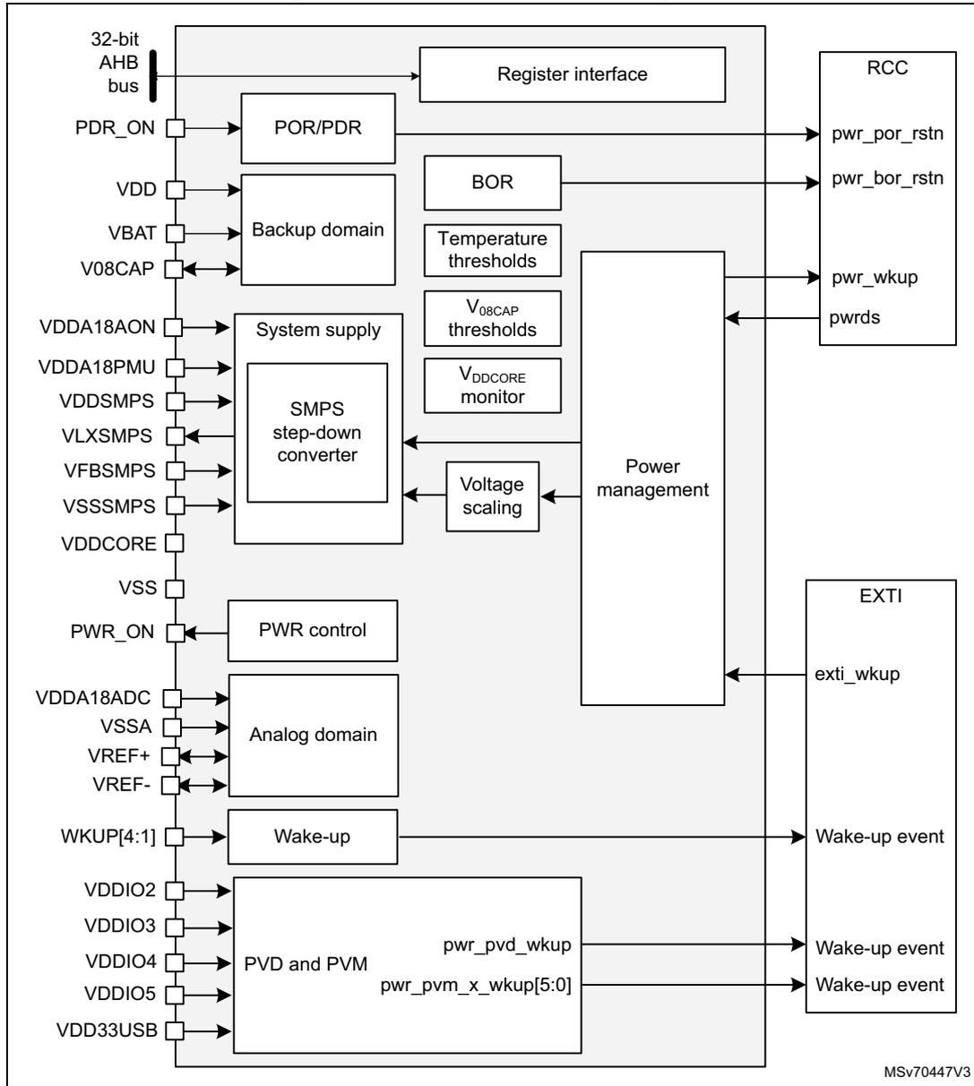
The diagram illustrates the internal architecture of the Power control (PWR) block. On the left, a vertical column of pins is shown, each connected to a specific internal component. The pins include:
- PDR_ON : Connected to the POR/PDR block.
- VDD : Connected to the Backup domain block.
- VBAT : Connected to the Backup domain block.
- V08CAP : Connected to the Backup domain block.
- VDDA18AON : Connected to the System supply block.
- VDDA18PMU : Connected to the System supply block.
- VDDSMPS : Connected to the SMPS step-down converter block.
- VLXSMPS : Connected to the SMPS step-down converter block.
- VFBSMPS : Connected to the SMPS step-down converter block.
- VSSSMPS : Connected to the SMPS step-down converter block.
- VDDCORE : Connected to the System supply block.
- VSS : Connected to the PWR control block.
- PWR_ON : Connected to the PWR control block.
- VDDA18ADC : Connected to the Analog domain block.
- VSSA : Connected to the Analog domain block.
- VREF+ : Connected to the Analog domain block.
- VREF- : Connected to the Analog domain block.
- WKUP[4:1] : Connected to the Wake-up block.
- VDDIO2 , VDDIO3 , VDDIO4 , VDDIO5 : Connected to the PVD and PVM block.
- VDD33USB : Connected to the PVD and PVM block.
- A 32-bit AHB bus connects to a Register interface .
- The Register interface connects to the POR/PDR block.
- The POR/PDR block outputs pwr_por_rstn to the RCC .
- The BOR block outputs pwr_bor_rstn to the RCC .
- The Backup domain block is connected to the System supply and Analog domain blocks.
- The System supply block is connected to the SMPS step-down converter and the Analog domain block.
- The SMPS step-down converter is connected to the Voltage scaling block.
- The Voltage scaling block is connected to the Power management block.
- The Power management block is connected to the RCC (outputting pwr_wkup and pwrds ) and the EXTI (outputting exti_wkup ).
- Monitoring blocks ( Temperature thresholds , V 08CAP thresholds , and V DDCORE monitor ) are connected to the Power management block.
- The Wake-up block outputs a Wake-up event signal.
- The PVD and PVM block outputs pwr_pvd_wkup and pwr_pvm_x_wkup[5:0] signals, which generate Wake-up event signals.
13.3.1 PWR pins and internal signals
Table 50 lists the PWR inputs and output signals connected to package pins or balls, while Table 51 shows the internal PWR signals.
Table 50. PWR input/output signals connected to package pins or balls| Pin name | Signal type | Description |
|---|---|---|
| VDD | Input | Main I/O and V DD domain supply input |
| VDDA18AON | Input | Main analog supply input |
| VBAT | Input | Backup battery supply input |
| VDDA18PMU | Input | Step-down converter analog supply input |
| VDDSMPS | Input | Step-down converter supply input |
| VLXSMPS | Output | Step-down converter supply output |
| VFBSMPS | Input | Step-down converter feedback voltage sense |
| VSSSMPS | Input | Step-down converter ground |
| V08CAP | Input/output | Digital backup domain supply |
| VDDCORE | Input | Core domain supply |
| VDDA18ADC | Input | ADC analog supply |
| VREF+, VREF- | Input/output | External reference voltage for ADCs |
| VDDIO2 | Input | Independent I/O supply 2 (PO[5:0] and PP[15:0]), usually for XSPI1M_P1 (XSPI) |
| VDDIO3 | Input | Independent I/O supply 3 (PN[12:0]), usually for XSPI1M_P2 (XSPI) |
| VDDIO4 | Input | Independent I/O supply 4 (PC[1], PC[12:6] and PH[2,9]), usually for eMMC |
| VDDIO5 | Input | Independent I/O supply 5 (PC[0], PC[5:2] and PE[4]), usually for SD-Card. |
| VDD33USB | Input | USB HS PHYs and USB Type C PHY 3V3 supply input |
| VDDA18USB | Input | USB HS PHYs analog supply input |
| VDDA18PLL | Input | PLL analog supply |
| VDDCSI | Input | CSI PHY digital supply input |
| VDDA18CSI | Input | CSI PHY analog 1v8 supply input |
| VSS | Input | Main ground |
| VSSA | Input | Analog ground |
| PWR_ON | Output | Step-down converter or core supply enable output |
| NRST (1) | Reset | System reset, can be used to provide reset to external devices |
| PDR_ON | Input | Power-down reset enable |
| WKUPx | Input | Wake-up pins |
| PWR_CSLEEP | Output | MCU in Sleep mode |
| PWR_CSTOP | Output | MCU in Stop modes |
1. Bidirectional reset pin with embedded weak pull-up resistor.
Table 51. PWR internal input/output signals| Signal name | Signal type | Description |
|---|---|---|
| AHB | Input/output | AHB register interface |
| pwr_pvd_wkup | Output | Programmable voltage detector output |
| Signal name | Signal type | Description |
|---|---|---|
| pwr_pvm_x_wkup[5:0] | Output | Peripheral voltage monitor output |
| pwr_por_rstn | Output | Power-on reset |
| pwr_bor_rstn | Output | Brownout reset |
| exti_wkup | Input | Wake-up request |
| pwr_wkup | Output | Bus matrix clock wake-up request (system clock) |
Each wake-up event (WKUPx) can be generated from four pins or internal events.
Table 52. Wake-up source selection| Port | Wake-up event |
|---|---|
| PA0 | WKUP1 |
| PA2 | WKUP2 |
| PC13 | WKUP3 |
| PD2 | WKUP4 |
13.4 Power supplies
The system requires supply on V DD , V DDA18AON , V DDA18PMU , V DDSMPS , and V DDCORE to start, and allows independent supplies for V DDA18ADC , V BAT , V DD33USB , V DDIO2 , V DDIO3 , V DDIO4 , and V DDIO5 .
- • V DD : external power supply for I/Os (can be 1.8 V or 3.3 V typical)
- • V BAT : optional external power supply for backup domain when V DD is not present (V BAT mode)
This power supply must be connected to V DD when no battery is used.
- • V DDA18AON : external power supply for system analog such as reset, power management, oscillators, and OTP
- • V
DDSMPS
: external power supply for the SMPS step-down converter
This power supply must be tied to V SS when the SMPS is not used. - • V
DDA18PMU
: external analog power supply for the SMPS step-down converter
This power supply can be connected to V DDSMPS through an inductor-based filter. It must be tied to V SS when the SMPS is not used. - • V LXSMPS : step-down converter supply output
- • V FBSMPS : step-down converter sense feedback
- • V SSSMPS : separate step-down converter ground
- • V
DDCORE
: digital core domain supply, dependent on V
DD
supply
V DD must be present before V DDCORE . The V CORE is delivered by an external power supply through V DDCORE pin, or by the SMPS step-down converter.
V DDCSI must usually be connected to V DDCORE . - • V DDA18ADC : external analog power supply for ADCs and voltage reference buffers, independent from any other supply
- •
\(
V_{REF+}
\)
: external reference voltage for ADCs, independent from any other supply
- – When the voltage reference buffer is enabled, \( V_{REF+} \) and \( V_{REF-} \) are delivered by the internal voltage reference buffer.
- – When the voltage reference buffer is disabled, \( V_{REF+} \) is delivered by an independent external reference supply.
- • \( V_{SSA} \) : separate analog and reference voltage ground
- • \( V_{DDIO2} \) : external power supply for 22 I/Os (PO[5:0] and PP[15:0]), independent from any other supply
- • \( V_{DDIO3} \) : external power supply for 13 I/Os (PN[12:0]), independent from any other supply
- • \( V_{DDIO4} \) : external power supply for 10 I/Os (PC[1], PC[12:6], and PH[9:2]), independent from any other supply
- • \( V_{DDIO5} \) : external power supply for six I/Os (PC[0], PC[5:2], and PE[4]), independent from any other supply
- • \( V_{DD33USB} \) : external power supply for USB2 HS PHYs and USB Type-C ® (CC1 and CC2 pins), independent from any other supply
- • \( V_{DDA18USB} \) : external analog power supply for USB2 HS PHYs
- • \( V_{DDA18CSI} \) : external analog power supply for CSI D-PHY
- • \( V_{DDA18PLL} \) : external analog power supplies for PLLs
- • \( V_{SS} \) : common ground for all supplies except for step-down converter and analog peripherals.
Note: Depending upon the operating power supply range, some peripherals can be used with limited features and performance. For more details, refer to General operating conditions in the datasheet.
Figure 16. Power supply overview
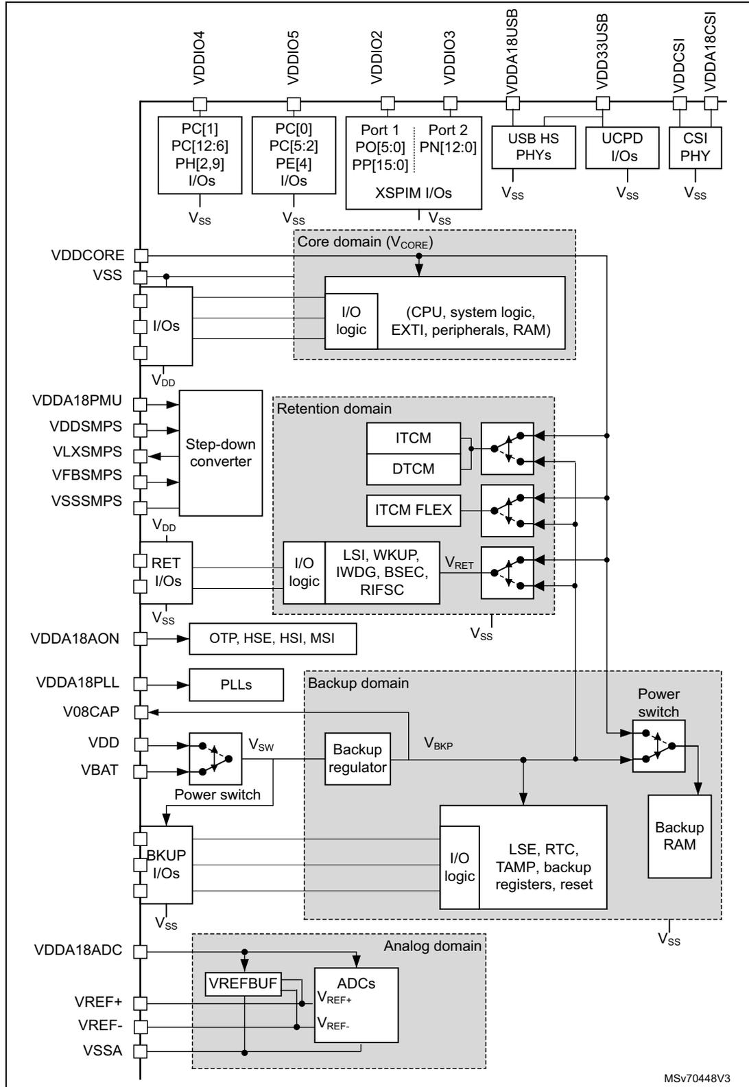
The diagram illustrates the power supply architecture of the microcontroller, organized into several functional domains and their interconnections:
- Core domain (V CORE ): Contains the CPU, system logic, EXTI, peripherals, and RAM. It is connected to VDDCORE and VSS pins. I/O logic within this domain connects to various I/O pins.
- Retention domain: Maintains data and state during low-power modes. It includes ITCM, DTCM, and ITCM FLEX memory blocks, along with I/O logic and a block for LSI, WKP, IWDG, BSEC, and RIFSC. It is powered by V DD and V RET pins.
- Backup domain: Includes a Backup regulator, Power switch, Backup RAM, and a block for LSE, RTC, TAMP, backup registers, and reset. It is connected to V BKP and V BAT pins.
- Analog domain: Contains the VREFBUF and ADCs. It is connected to VDDA18ADC, VREF+, VREF-, and VSSA pins.
- Power Regulation and Distribution:
- A Step-down converter takes VDDA18PMU as input and provides V DD to the Core and Retention domains. It also receives feedback from VLXSMPS, VFB SMPS, and VSS SMPS pins.
- PLLs are connected to VDDA18PLL and V08CAP pins.
- OTP, HSE, HSI, MSI blocks are connected to VDDA18AON pins.
- Power switches manage the flow of power between V DD , V BAT , and the Backup domain.
- External I/O and PHYs:
- PC[1], PC[12:6], PH[2,9] I/Os are connected to VDDIO4 pins.
- PC[0], PC[5:2], PE[4] I/Os are connected to VDDIO5 pins.
- Port 1 PO[5:0], Port 2 PN[12:0], PP[15:0] XSPIM I/Os are connected to VDDIO2 and VDDIO3 pins.
- USB HS PHYs are connected to VDDA18USB pins.
- UCPD I/Os are connected to VDD33USB pins.
- CSI PHY is connected to VDDCSI and VDDA18CSI pins.
Reference code: MSV70448V3
By configuring the SMPS step-down converter, the supply configurations shown in Figure 17 are supported for the \( V_{CORE} \) domain.
Figure 17. System supply configurations
The different supply configurations are controlled through SDEN in PWR_CR1, according to Table 53 . When the internal SMPS step-down converter is disabled, write SDEN bit in PWR_CR1 to 0 as soon as possible
Table 53. Supply configuration control
| Supply configuration | SDEN | Description |
|---|---|---|
| Startup configuration | 1 | \(
V_{CORE}
\)
power domains are supplied from external source. SMPS step-down converter enabled at 0.8 V can be used to supply the \( V_{CORE} \) . |
| SMPS step-down converter supply | 1 | \(
V_{CORE}
\)
power domains are supplied from SMPS step-down converter according to VOS. SMPS step-down converter power mode (MR, LP, off) follows system low-power modes. |
| SMPS step-down converter disabled | 0 | \(
V_{CORE}
\)
supplied from external source. SMPS step-down converter disabled, voltage monitoring still active. |
13.4.1 System supply startup
The system startup sequence from power-on in different supply configurations is the following (see Figure 17 for direct SMPS supply and external supply, respectively):
\( V_{CORE} \) directly supplied from the SMPS step-down converter
- 1. When the system is powered on, the POR monitors \( V_{DD} \) and \( V_{DDA18AON} \) supplies. Once the supplies are above the POR threshold level, the external voltage regulator providing \( V_{DDA18PMU} \) and \( V_{DDSMPS} \) supplies is enabled via the PWR_ON signal.
- 2. The SMPS step-down converter is kept in reset as long as \( V_{DDA18PMU} \) and \( V_{DDSMPS} \) are not stable.
- 3. Once \( V_{DDA18PMU} \) and \( V_{DDSMPS} \) supplies are above the \( V_{dda18pmu\_ok} \) threshold level, the SMPS step-down converter is taken out of reset, and the output level is set by default at 0.8 V (VOS low). The system is kept in reset mode as long as \( V_{DDCORE} \) is stable.
- Once \( V_{DDCORE} \) supply is above the \( V_{ddcore\_ok} \) threshold level, the system is taken out of reset, and the HSI oscillator is enabled.
- Once the oscillator is stable, the system is initialized: option bytes are loaded, and the CPU starts in Run mode.
Figure 18. Device startup ( \( V_{CORE} \) supplied directly from SMPS step-down converter)
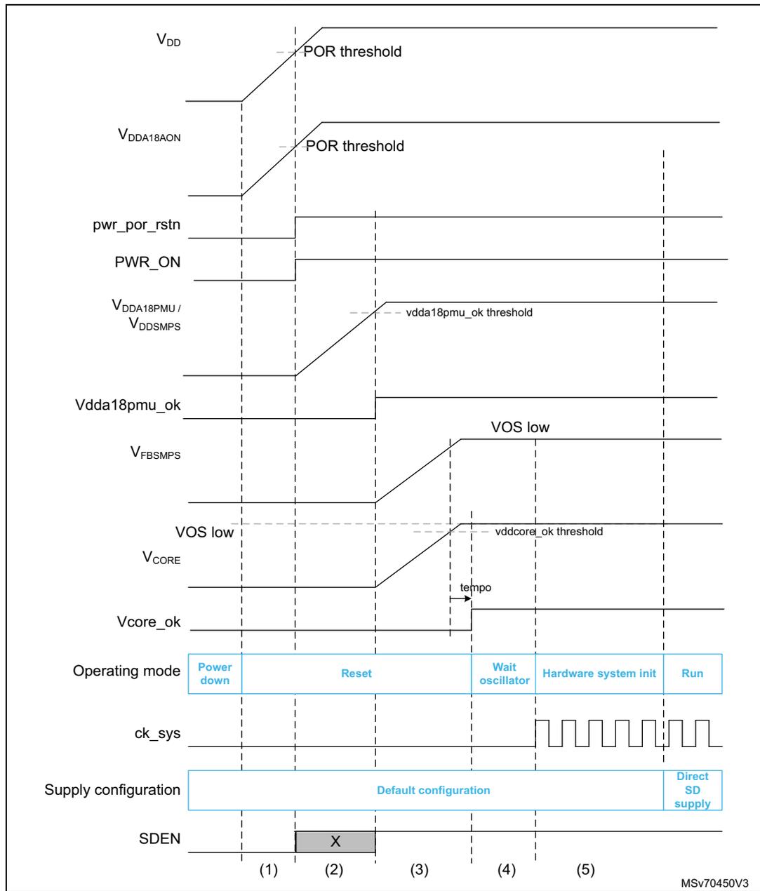
The figure is a timing diagram illustrating the device startup sequence when \( V_{CORE} \) is supplied directly from an SMPS step-down converter. It shows the relationship between various voltage levels, control signals, and the operating mode over five time intervals labeled (1) through (5).
- Signals:
- \( V_{DD} \) : Rises from 0V to a level above the POR threshold.
- \( V_{DDA18AON} \) : Rises from 0V to a level above the POR threshold.
- \( pwr\_por\_rstn \) : Active-low reset signal that goes high when \( V_{DD} \) and \( V_{DDA18AON} \) are above their POR thresholds.
- \( PWR\_ON \) : Power-on signal that goes high at the start of the sequence.
- \( V_{DDA18PMU}/V_{DDSMPS} \) : Rises from 0V to a level above the \( v_{dda18pmu\_ok} \) threshold.
- \( V_{dda18pmu\_ok} \) : Indicates that \( V_{DDA18PMU}/V_{DDSMPS} \) is above its threshold.
- \( V_{FBSMPS} \) : Rises from 0V to a level labeled \( V_{OS\ low} \) .
- \( V_{OS\ low} \) : A reference voltage level for \( V_{CORE} \) .
- \( V_{CORE} \) : Rises from 0V, crossing the \( V_{OS\ low} \) threshold and then the \( v_{ddcore\_ok} \) threshold. A 'tempo' parameter indicates the rise time.
- \( V_{core\_ok} \) : Indicates that \( V_{CORE} \) is above the \( v_{ddcore\_ok} \) threshold.
- \( ck\_sys \) : System clock signal that starts oscillating during the 'Hardware system init' phase.
- Operating mode: Divided into five phases: (1) Power down, (2) Reset, (3) Wait oscillator, (4) Hardware system init, (5) Run.
- Supply configuration: Set to 'Default configuration' during phases (1) through (4), and switches to 'Direct SD supply' in phase (5).
- SDEN: SMPS enable signal. It is low in phase (1), goes high ('X') in phase (2), and remains high through phase (5).
- Timeline:
- (1) Power down: All signals are at 0V or low levels.
- (2) Reset: \( V_{DD} \) and \( V_{DDA18AON} \) rise above POR thresholds. \( pwr\_por\_rstn \) goes high. \( SDEN \) goes high.
- (3) Wait oscillator: \( V_{DDA18PMU}/V_{DDSMPS} \) rises above \( v_{dda18pmu\_ok} \) threshold. \( V_{FBSMPS} \) rises to \( V_{OS\ low} \) .
- (4) Hardware system init: \( V_{CORE} \) rises above \( v_{ddcore\_ok} \) threshold. \( V_{core\_ok} \) goes high. Oscillator starts.
- (5) Run: System is in full operation. \( ck\_sys \) is active. Supply configuration changes to 'Direct SD supply'.
When exiting Standby mode, the supply configuration is known by the system, as the PWR_CR1 content is retained.
\( V_{CORE} \) supplied in bypass mode (SMPS off)
The devices that feature the SMPS can be used in bypass mode.
- 1. When the system is powered on, the POR monitors \( V_{DD} \) and \( V_{DDA18AON} \) supplies. Once the supplies are above the POR threshold level, the external voltage regulator providing the \( V_{DDCORE} \) supply is enabled via the PWR_ON signal.
- 2. The system is kept in reset mode as long as \( V_{DDCORE} \) is not stable.
- 3. Once \( V_{DDCORE} \) supply is above the Vddcore_ok threshold level, the system is taken out of reset, and the HSI oscillator is enabled.
- 4. Once the oscillator is stable, the system is initialized: option bytes are loaded, and the CPU starts in Run mode. The software must disable SMPS bit clearing SDEN in PWR_CR1.
Note: In SMPS off mode or bypass mode, reading SDEN returns 0. The SW must write 0 to SDEN in PWR_CR1 register for the low power features to work properly.
Figure 19. Device startup ( \( V_{CORE} \) supplied from an external regulator)
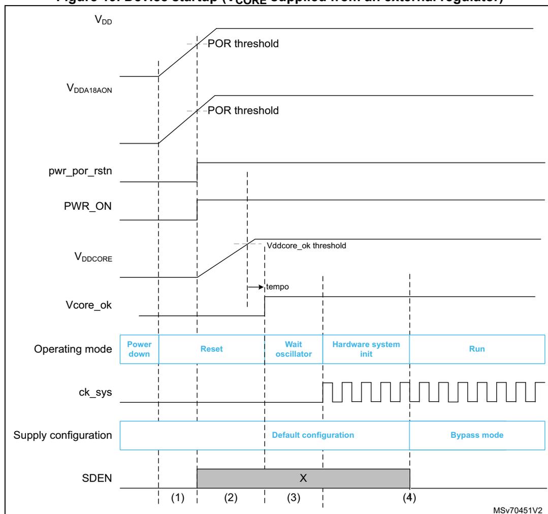
The diagram illustrates the power-up sequence of the device. It shows the following signals and states over time:
- \( V_{DD} \) : Power supply voltage, rising from 0V to a level above the POR threshold.
- \( V_{DDA18AON} \) : Analog power supply voltage, rising from 0V to a level above the POR threshold.
- pwr_por_rstn : Power-on reset signal, active low. It goes high when \( V_{DD} \) and \( V_{DDA18AON} \) are above their POR thresholds.
- PWR_ON : Power-on signal, goes high when \( V_{DD} \) and \( V_{DDA18AON} \) are above their POR thresholds.
- \( V_{DDCORE} \) : Core supply voltage, rising from 0V to a level above the Vddcore_ok threshold. The rise time is labeled as tempo .
- Vcore_ok : Core voltage OK signal, goes high when \( V_{DDCORE} \) is above the Vddcore_ok threshold.
- Operating mode : Shows the sequence: Power down (until 1), Reset (1 to 2), Wait oscillator (2 to 3), Hardware system init (3 to 4), and Run (after 4).
- ck_sys : System clock, which is a square wave starting at time (3).
- Supply configuration : Default configuration (until 4), then Bypass mode (after 4).
- SDEN : SMPS Enable signal. It is high (X) from time (2) to (4), indicating the SMPS is disabled during this period.
The diagram is divided into four time intervals by vertical dashed lines:
- (1) Power down : All signals are at their initial levels.
- (2) Reset : \( V_{DD} \) and \( V_{DDA18AON} \) rise above POR thresholds. pwr_por_rstn goes high, PWR_ON goes high.
- (3) Wait oscillator : \( V_{DDCORE} \) rises above Vddcore_ok threshold. Vcore_ok goes high, ck_sys starts oscillating. SDEN is high (X).
- (4) Hardware system init : System initialization occurs. Supply configuration changes to Bypass mode. SDEN goes low.
MSV70451V2
13.4.2 Core domain
The \( V_{CORE} \) core domain supply can be provided by the SMPS step-down converter, or by an external supply ( \( V_{DDCORE} \) ). \( V_{CORE} \) supplies all the digital circuitries, except for the backup domain and the retention domain in Standby mode. When a system reset occurs,
the SMPS step-down converter is enabled to deliver 0.8 V. This allows the system to start up in any supply configuration (see Figure 17 ).
After a power-on reset, the software must configure the used supply configuration in PWR_CR1 before changing VOS in PWR_VOSCR, or the RCC sys_ck frequency. The different system supply configurations are controlled as shown in Table 53 .
SMPS step-down converter regulator
The SMPS requires an external coil to be connected between the VLXSMPS pin and (via a capacitor) VSS. The converter can be used to supply directly the V CORE domain. It works in three different power modes: main (MR), low-power (LP), or off.
The converter operating modes depend upon the system modes (Run, Stop, or Standby mode), and are configured through the associated VOS and SVOS levels:
- •
Run mode
The SMPS step-down converter operates in MR mode, and provides full power to the V CORE domain (core, memories, and digital peripherals). PWR_ON is set high. The regulator output voltage can be scaled by software to different voltage levels (VOS low and VOS high) that are configured through VOS in PWR_VOSCR. The VOS voltage scaling is used to optimize the power consumption when the system is clocked below the maximum frequency. By default, VOS low is selected after a system reset. VOS can be changed on-the-fly to adapt to the required system performance. - •
Stop mode
The SMPS step-down converter supplies the V CORE domain to retain the content of registers and internal memories, and must be set in low-power mode. The voltage regulator mode is selected through SVOS in PWR_CPUCR. In low-power mode, only SVOS low and SVOS high scaling are allowed. Due to a lower voltage level for the SVOS low, the Stop mode consumption can be further reduced. - •
Standby mode
The SMPS step-down converter is off, and V CORE domains are powered down. The content of registers and memories are lost except for the retention domain, and the backup domain.
The PWR_ON signal is set low. The external regulator supplying V DDA18PMU and V DDSMPs can be switched off.
13.4.3 PWR external supply
When V CORE is supplied from an external source (bypass mode), different operating modes can be used, depending upon the system operating modes:
- •
In Run mode
The external source supplies full power to the V CORE domain. PWR_ON is set high. The external source output voltage is scalable through different voltage levels (VOS low and VOS high). Setting VOS in PWR_VOSCR has no effect on the external supply. The application can use the register value to track the status of the external supplied voltage, it is responsible to set properly the external supply voltage. Other PWR_VOSCR register fields have default settings, and are "don't care" in external supply. - •
In Stop mode
The external source supplies V CORE domain to retain the content of registers and internal memories. In low-power mode, only SVOS high scaling is allowed.
- • In Standby mode
The PWR_ON signal is set low, the external regulator is switched off, and the \( V_{CORE} \) domain is powered down. The content of registers and memories is lost except for the retention domain and the backup domain.
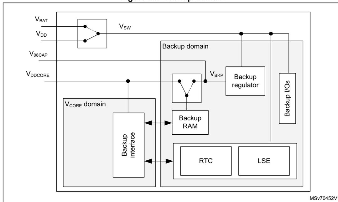
13.4.4 Backup domain
To retain the content of the backup domain (RTC, backup registers, and backup RAM) when \( V_{DD} \) is turned off, the VBAT pin can be connected to an optional voltage supplied from a battery or from another source.
The switching to \( V_{BAT} \) is controlled by the power-down reset (PDR) embedded in the reset block that monitors the \( V_{DD} \) supply.
Warning:
During
\(
t_{RSTTEMPO}
\)
(temporization at
\(
V_{DD}
\)
startup), or after a PDR is detected, the power switch between
\(
V_{BAT}
\)
and
\(
V_{DD}
\)
remains connected to VBAT.
During the startup phase, if
\(
V_{DD}
\)
is established in less than
\(
t_{RSTTEMPO}
\)
(see the datasheet for the value of
\(
t_{RSTTEMPO}
\)
), and
\(
V_{DD} > V_{BAT} + 0.6
\)
V, a current may be injected into VBAT through an internal diode connected between
\(
V_{DD}
\)
and the power switch (
\(
V_{BAT}
\)
).
If the power supply/battery connected to the VBAT pin cannot support this current injection, it is strongly recommended to connect an external low-drop diode between this power supply and the VBAT pin.
When the \( V_{DD} \) supply is present, the backup domain is supplied from \( V_{DD} \) , to save \( V_{BAT} \) power supply battery life time. If no external battery is used in the application, it is recommended to connect VBAT externally to \( V_{DD} \) , and add a 100 nF external ceramic capacitor between VBAT and VSS.
When the backup domain is supplied by VBAT (analog switch connected to VBAT), the following pins are available:
- • PC13, PC14, and PC15, which can be configured by RTC or LSE (see Section 61.3: RTC functional description ).
- • PC13, PQ7 (TAMP_IN/OUT), and PD8, PH4 (only TAMP_IN) when they are configured by the TAMP peripheral as tamper pins.
Accessing the backup domain
After reset, the backup domain (RCC_BDCR, RCC_RTC, TAMP registers, backup registers, and backup RAM) is protected against possible unwanted write accesses. To enable access to the backup domain, set DBP in PWR_DBPCR.
For more detail on RTC and backup RAM access, refer to Section 14: Reset and clock control (RCC) .
Backup RAM (BKPSRAM)
The backup domain includes 8 Kbytes of BKPSRAM accessible in 32-, 16-, or 8-bit data mode.
- • In Run and Stop (SVOS high) modes, the BKPSRAM is supplied from \( V_{CORE} \) supply.
- • In Stop (SVOS low) mode, the BKPSRAM is supplied through the backup regulator in \( V_{SW} \) domain.
- • In Standby and \( V_{BAT} \) modes, the BKPSRAM can be supplied through the backup regulator in \( V_{SW} \) domain.
When the backup supply is enabled through BKPRBSEN in PWR_BDCR2, the BKPSRAM content is retained even in Standby and/or \( V_{BAT} \) mode.
Figure 20. Backup domain
The diagram illustrates the internal architecture of the backup domain. On the left, the \( V_{CORE} \) domain contains a 'Backup interface' block. This interface is connected to the 'Backup RAM', 'RTC', and 'LSE' blocks within the 'Backup domain'. The 'Backup domain' also contains a 'Backup regulator' block. Power inputs include \( V_{BAT} \) , \( V_{DD} \) , \( V_{08CAP} \) , and \( V_{DDCORE} \) . \( V_{BAT} \) and \( V_{DD} \) are connected to a switch that outputs \( V_{SW} \) . \( V_{SW} \) is connected to the 'Backup regulator', which outputs \( V_{BKP} \) . \( V_{BKP} \) is connected to the 'Backup RAM', 'RTC', and 'LSE' blocks. The 'Backup interface' in the \( V_{CORE} \) domain is connected to the 'Backup RAM', 'RTC', and 'LSE' blocks. The diagram is labeled MSv70452V1.
13.4.5 Retention domain
The retention domain includes boot, OTP controller (BSEC), independent watchdog (IWDG), resource isolation framework controller (RIFSC), I-TCM, D-TCM, and I-TCM FLEXRAMs.
- • In Run and Stop (SVOS high) modes, the retention domain is supplied from the \( V_{CORE} \) supply.
- • In Stop (SVOS low) and Standby modes, the retention domain is supplied through the backup regulator.
The content of the domain is retained in Standby mode (not powered in \( V_{BAT} \) mode).
Figure 21. Retention domain
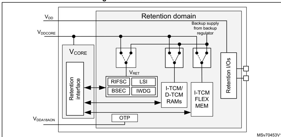
The diagram illustrates the power connections within the retention domain of a microcontroller. It shows the following components and their power sources:
- V CORE : The main core voltage supply, connected to the Retention interface .
- V DDCORE : The core supply voltage, connected to the Retention domain .
- V DDA18AON : The AON supply voltage, connected to the Retention domain .
- Retention domain
: A large box containing several components:
- Retention interface : Connected to V CORE and the OTP block.
- OTP : One-Time Programmable memory, connected to V DDA18AON and the Retention interface .
- RIFSC , LSI , BSEC , and IWDG : These components are connected to a V RET supply, which is derived from V DDCORE via a switch.
- I-TCM/ D-TCM RAMs : Instruction and Data TCM RAMs, connected to V DDCORE via a switch.
- I-TCM FLEX MEM : I-TCM FlexMem, connected to V DDCORE via a switch.
- Backup supply from backup regulator : A backup supply connected to the Retention domain via a switch.
- Retention I/Os : Retention I/Os, connected to the Backup supply from backup regulator .
MSV70453V1
I-TCM and D-TCM RAMs
The retention domain includes 64 + 128 K bytes (instruction/data) of TCM for Cortex-M55.
- • In Run and Stop (SVOS high) modes, I-TCM, and D-TCM memories are supplied from the V CORE supply.
- • In Stop (SVOS low) mode, I-TCM, and D-TCM memories are supplied through the backup regulator in the V SW domain.
- • In Standby mode, I-TCM and D-TCM memories can be supplied through the backup regulator in the V SW domain.
When the backup supply is enabled by TCMRBSEN in PWR_CR4, the content of these memories is retained even in Standby mode.
I-TCM FLEXMEM
The retention domain includes 64 Kbytes of extended TCMs for the Cortex-M55 (the I-TCM FLEXMEM extension). This memory can be allocated to I-TCM or to system AXI RAM (see Section 10: SRAM configuration controller (RAMCFG) for details)
- • In Run and Stop (SVOS high) modes, the I-TCM FLEXMEM is supplied from the V CORE supply.
- • In Stop (SVOS low) mode, the I-TCM FLEXMEM is supplied through the backup regulator in the V SW domain.
- • In Standby mode, the I-TCM FLEXMEM can be supplied through the backup regulator in the V SW domain.
When the backup supply is enabled by TCMFLRBSEN in PWR_CR4, the content of these memories is retained even in Standby mode.
13.4.6 Analog supply
Separate \( V_{DDA18ADC} \) analog supply
The analog supply domain is powered by dedicated \( V_{DDA18ADC} \) and \( V_{SSA} \) pins that allow the supply to be filtered and shielded from noise on the PCB, thus improving ADC conversion accuracy:
- • The analog supply voltage input is available on a separate \( V_{DDA18ADC} \) pin.
- • An isolated supply ground connection is provided on \( V_{SSA} \) pin.
Analog reference voltage \( V_{REF+}/V_{REF-} \)
To achieve better accuracy low-voltage signals, the ADC has a separate reference voltage, available on \( V_{REF+} \) pin. The user can connect a separate external reference voltage on \( V_{REF+} \) .
\( V_{REF+} \) controls the highest voltage, represented by the full scale value. The lower voltage reference ( \( V_{REF-} \) ) must be connected to \( V_{SSA} \) .
When enabled by ENVR in VREFBUF_CSR, \( V_{REF+} \) is provided from the internal voltage reference buffer, which can also deliver a reference voltage to external components through \( V_{REF+}/V_{REF-} \) pins.
When the internal voltage reference buffer is disabled by ENVR, \( V_{REF+} \) is delivered by an independent external reference supply voltage.
13.5 Power supply supervision
Power supply level monitoring is available on the following supplies:
- •
\(
V_{DD}/V_{DDA18AON}
\)
via POR/PDR (see
Section 13.5.1
), BOR (see
Section 13.5.2
), and PVD monitor (see
Section 13.5.6
)
- – The POR/PDR monitoring flag is available from PORRSTF in the RCC.
- – The BOR monitoring flag is available from BORRSTF in the RCC.
- – The PVD monitoring flag is available from PVDO in PWR_CR2. In addition, an interrupt and wake-up can be generated via EXTI.
- •
\(
V_{DDA18PMU}
\)
via
\(
V_{dda18pmu\_ok}
\)
, which keeps in reset the SMPS, as long as the level is not correct.
- – The \( V_{DDA18PMU} \) monitoring has no flags.
- •
\(
V_{BAT}
\)
via
\(
V_{BAT}
\)
threshold (see
Section 13.5.8
)
- – The \( V_{08CAP} \) monitoring flags are available from \( V_{08CAPH} \) and \( V_{08CAPL} \) in PWR_BDCR1. In addition, an interrupt and wake-up can be generated via EXTI.
- •
\(
V_{DDCORE}
\)
via
\(
V_{core\_ok}
\)
, which keeps the
\(
V_{CORE}
\)
domain in reset as long as the level is not correct (see
Section 13.5.3
).
- – The \( V_{DDCORE} \) ok monitoring flag is available from SBF in PWR_CPUCR when exiting the Standby mode.
- •
\(
V_{DDCORE}
\)
via
\(
V_{CORE}
\)
threshold (see
Section 13.5.5
)
- – The \( V_{DDCORE} \) monitoring flags are available from \( V_{COREH} \) and \( V_{COREL} \) in PWR_CR3. In addition, an interrupt and wake-up can be generated via EXTI.
- • \( V_{DDIO2} \) , \( V_{DDIO3} \) , \( V_{DDIO4} \) , \( V_{DDIO5} \) , \( V_{DD33USB} \) , \( V_{DDA18ADC} \) via peripheral voltage monitor (see Section 13.5.7 )
- •
\(
V_{SW}
\)
via
rst_vsw, which keeps \( V_{SW} \) domain in reset mode as long as the level is not the correct one- – The \( V_{SW} \) monitoring has no flag. \( V_{SW} \) registers reset value can be used.
- •
\(
V_{FBSMPS}
\)
can be monitored via
VOSRDYinPWR_VOSCR.
13.5.1 Power-on reset (POR)/power-down reset (PDR)
The system has an integrated POR/PDR circuitry that ensures proper start-up operation.
The system remains in reset mode when \( V_{DD} \) and \( V_{DDA18AON} \) are below a specified \( V_{POR} \) threshold, without the need for an external reset circuit. Once these supply levels are above the \( V_{POR} \) threshold, the system is taken out of reset (see Figure 22 ). For more details concerning these thresholds, refer to the electrical characteristics in the datasheet.
The POR/PDR generate also an application reset (
NRST
).
The PDR can be enabled/disabled by the device
PDR_ON
input pin.
Figure 22. POR/PDR waveform
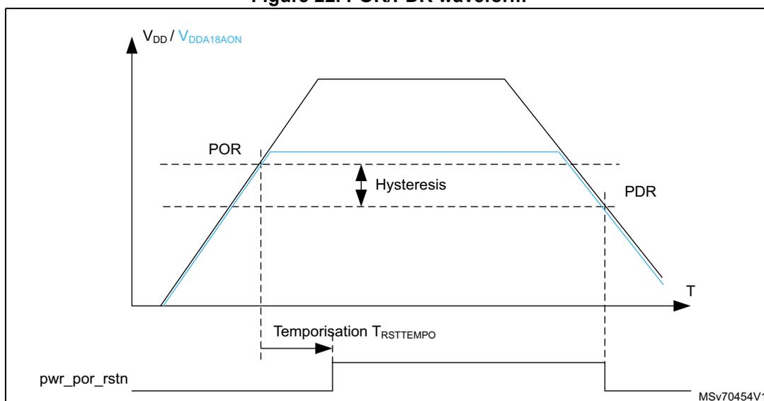
- 1. For thresholds and hysteresis values, refer to the datasheets.
13.5.2 Brownout reset (BOR)
During power-on, the brownout reset (BOR) keeps the system under reset until the \( V_{DD} \) supply voltage reaches the specified \( V_{BOR} \) threshold.
The \( V_{BOR} \) threshold is configured through system option bytes. By default, the BOR is off. The selection of another BOR threshold takes effect only after the device has loaded the option bytes. The following programmable \( V_{BOR} \) thresholds can be selected:
- • BOR off ( \( V_{BOR0} \) ): reset threshold level above 1.67 V
- • BOR level 1 ( \( V_{BOR1} \) ): reset threshold level above 2.7 V
For more details on these thresholds, refer to the electrical characteristics in the datasheet.
When the BOR is enabled and the
\(
V_{DD}
\)
supply voltage drops below the selected
\(
V_{BOR}
\)
threshold, an application reset (
NRST
) is generated.
The BOR can be disabled by programming the system option bytes. To disable it, \( V_{DD} \) must have been higher than \( V_{BOR0} \) to start the system option byte programming sequence. The power-down is then monitored by the PDR (see Section 13.5.1 ).
Figure 23. BOR thresholds
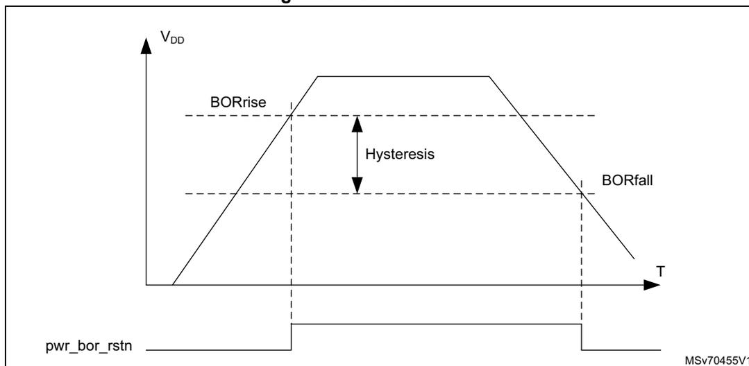
The graph shows the relationship between \( V_{DD} \) (Y-axis) and Temperature \( T \) (X-axis). A trapezoidal curve represents the \( V_{DD} \) level over time. Two horizontal dashed lines indicate the BOR thresholds: \( BOR_{rise} \) for the rising edge and \( BOR_{fall} \) for the falling edge. The vertical distance between these two lines is labeled 'Hysteresis'. Below the graph, a signal labeled \( pwr\_bor\_rstn \) is shown. This signal is low when \( V_{DD} \) is below the \( BOR_{fall} \) threshold and goes high when \( V_{DD} \) rises above the \( BOR_{rise} \) threshold. The signal remains high until \( V_{DD} \) falls below the \( BOR_{fall} \) threshold. The identifier MSv70455V1 is in the bottom right corner.
- 1. For thresholds and hysteresis values, refer to the datasheets.
13.5.3 \( V_{dda18pmu\_ok} \) reset
The system integrates a circuit for proper startup of the integrated SMPS.
The SMPS remains in reset mode when \( V_{DDA18PMU} \) is below the threshold \( V_{dda18pmu\_ok} \) . Once the \( V_{DDA18PMU} \) supply level is above \( V_{dda18pmu\_ok} \) , the SMPS is taken out of reset, and the output level is set by default at 0.8 V (VOS low). For more details concerning this reset threshold, refer to the electrical characteristics in the datasheet.
Figure 24.\( V_{dda18pmu\_ok} \) reset threshold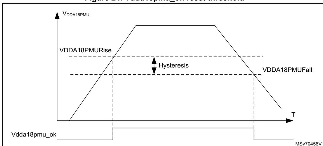
The graph shows the relationship between \( V_{DDA18PMU} \) (Y-axis) and Temperature \( T \) (X-axis). A trapezoidal curve represents the \( V_{DDA18PMU} \) level over time. Two horizontal dashed lines indicate the reset thresholds: \( V_{DDA18PMU_{rise}} \) for the rising edge and \( V_{DDA18PMU_{fall}} \) for the falling edge. The vertical distance between these two lines is labeled 'Hysteresis'. Below the graph, a signal labeled \( V_{dda18pmu\_ok} \) is shown. This signal is low when \( V_{DDA18PMU} \) is below the \( V_{DDA18PMU_{fall}} \) threshold and goes high when \( V_{DDA18PMU} \) rises above the \( V_{DDA18PMU_{rise}} \) threshold. The signal remains high until \( V_{DDA18PMU} \) falls below the \( V_{DDA18PMU_{fall}} \) threshold. The identifier MSv70456V1 is in the bottom right corner.
13.5.4 Vddcore_ok reset
The system has an integrated circuit for proper startup of the \( V_{CORE} \) domain.
The \( V_{CORE} \) domain remains in reset mode when \( V_{DDCORE} \) is below the operation threshold \( V_{ddcore\_ok} \) . Once the \( V_{DDCORE} \) supply level is above \( V_{ddcore\_ok} \) , the \( V_{CORE} \) domain is taken out of reset. For more details concerning this reset threshold, refer to the electrical characteristics in the datasheet.
When SVOS is cleared in PWR_CPUCR, the \( V_{DDCORE} \) supply level can be lowered in Stop mode (SVOS low).
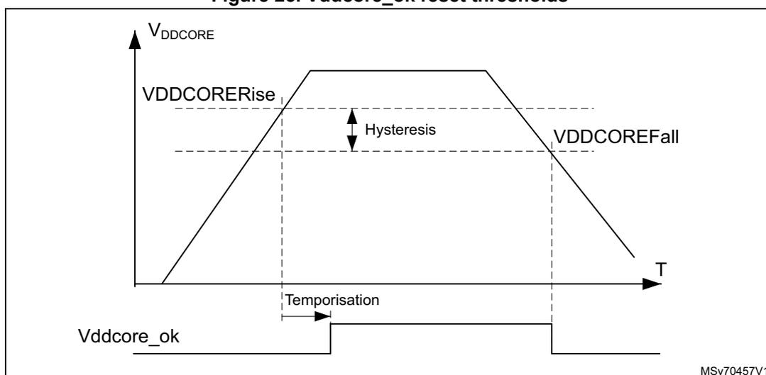
Figure 25. Vddcore_ok reset thresholds
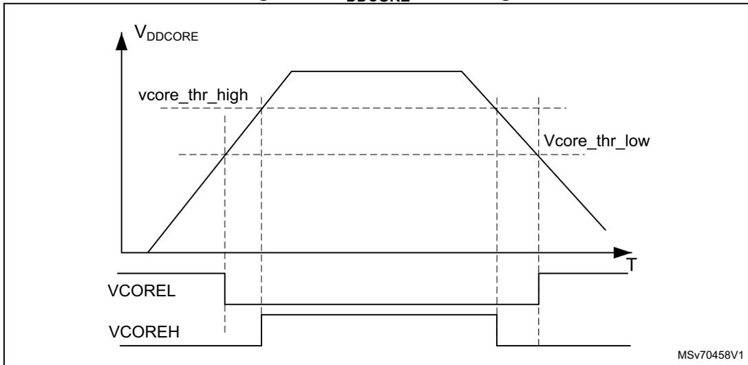
13.5.5 \( V_{DDCORE} \) monitoring
The system has a detection circuitry that detects if the \( V_{DDCORE} \) supply voltage is below or above the operating range. The detection is done by comparing the \( V_{DDCORE} \) with two thresholds (high and low threshold). The level of the low threshold can be selected by VCORELLS in PWR_CR3. The high level is fixed.
VCOREH and VCOREL flags are available in PWR_CR3, to indicate if \( V_{DDCORE} \) is higher or lower than the thresholds. VCOREH and VCOREL flags are available on tamper signals but also connected to the EXTI, and can generate an interrupt if enabled through EXTI registers.
The detection is enabled by setting VCOREMONEN in PWR_CR3.
The \( V_{DDCORE} \) voltage thresholds, when enabled, are not available in Stop, Standby, and \( V_{BAT} \) modes.
Note: The low threshold of \( V_{DDCORE} \) monitoring is inaccurate. To ensure the value of voltage threshold use ADC.
Figure 26. V DDCORE monitoring
13.5.6 Programmable voltage detector (PVD)
The PVD can be used to monitor a voltage level on PVD_IN pin. The voltage level on PVD_IN is compared to the internal VREFINT level. The PVD is enabled by setting PVDEN in PWR_CR2. The PVD is not available in Standby mode.
A PVDO flag is available in PWR_CR2 to indicate if the voltage level on PVD_IN is higher or lower than the PVD threshold. This event is internally connected to the EXTI, and can generate an interrupt if enabled through the EXTI registers.
The PVDO output interrupt can be generated when the voltage level on PVD_IN drops below the PVD threshold, and/or when the voltage level on PVD_IN rises above the PVD threshold depending on EXTI rising/falling edge configuration. As an example, the service routine can perform emergency shutdown tasks.
Figure 27. PVD thresholds
1. For thresholds and hysteresis values, refer to the datasheets.
13.5.7 Peripheral voltage monitoring (PVM)
Only \( V_{DD} \) is monitored by default, as it is the only supply required for all system-related functions. The other supplies ( \( V_{DDIO2} \) , \( V_{DDIO3} \) , \( V_{DDIO4} \) , \( V_{DDIO5} \) , \( V_{DD33USB} \) , and \( V_{DDA18ADC} \) ) can be independent from \( V_{DD} \) , and can be monitored with six peripheral voltages (PVM):
- • VDDIO2VM monitors the PO[5:0] and PP[15:0] I/Os supply \( V_{DDIO2} \) . VDDIO2RDY indicates if \( V_{DDIO2} \) is higher or lower than the VIO2VM threshold.
- • VDDIO3VM monitors the PN[12:0] I/Os supply \( V_{DDIO3} \) . VDDIO3RDY indicates if \( V_{DDIO3} \) is higher or lower than the VIO3VM threshold.
- • VDDIO4VM monitors PC[1], PC[12:6], and PH[9,2] I/Os supply \( V_{DDIO4} \) . VDDIO4RDY indicates if \( V_{DDIO4} \) is higher or lower than the VIO4VM threshold.
- • VDDIO5VM monitors the PC[0], PC[5:2] and PE[4] I/Os supply \( V_{DDIO5} \) . VDDIO5RDY indicates if \( V_{DDIO5} \) is higher or lower than the VIO5VM threshold.
- • USB33VM monitors the USB supply \( V_{DD33USB} \) . USB33RDY indicates if \( V_{DD33USB} \) is higher or lower than the VUSB33VM threshold.
- • AVM monitors the ADC supply \( V_{DDA18ADC} \) . ARDY indicates if \( V_{DDA18ADC} \) is higher or lower than the VAVM threshold.
For thresholds and hysteresis, refer to the datasheet.
Each PVM output is connected to an EXTI line, and can generate an interrupt if enabled through the EXTI registers. The EXTI_PVM_x output interrupt is generated when the independent power supply drops below the PVM threshold, and/or when it rises above the PVM threshold, depending on EXTI line rising/falling edge configuration.
The PVM is not available in Standby mode.
The independent supplies ( \( V_{DDIO2} \) , \( V_{DDIO3} \) , \( V_{DDIO4} \) , \( V_{DDIO5} \) , \( V_{DD33USB} \) , and \( V_{DDA18ADC} \) ) are not considered as present by default, and a logical and electrical isolation is applied to ignore any information coming from the peripherals supplied by these dedicated supplies.
- • If these supplies are shorted externally to \( V_{DD} \) , the application must assume they are available without enabling any peripheral voltage monitoring, and the power isolation can be removed by setting the corresponding supply valid bits.
- • If these supplies are independent from \( V_{DD} \) , the PVM can be enabled to confirm whether the supply is present or not.
The following sequence must be done before using the USB HS PHYs:
- 1. If
\(
V_{DD33USB}
\)
is independent from
\(
V_{DD}
\)
:
- a) Enable the USB33VM by setting USB33VMEN in PWR_SVMCR3.
- b) Wait for the USB33VM wake-up time.
- c) Wait until USB33RDY is set in PWR_SVMCR3.
- d) Optional: Disable the USB33VM for consumption saving.
- 2. Set USB33SV in PWR_SVMCR3 to remove the \( V_{DD33USB} \) power isolation.
The following sequence must be done before using the analog-to-digital converters:
- 1. If
\(
V_{DDA18ADC}
\)
is independent from
\(
V_{DD}
\)
:
- a) Enable the AVM by setting AVMEN in PWR_SVMCR3.
- b) Wait for the AVM wake-up time.
- c) Wait until ARDY is set in PWR_SVMCR3.
- d) Optional: Disable the AVM for consumption saving.
- 2. Set ASV in PWR_SVMCR3 to remove the \( V_{DDA18ADC} \) power isolation.
GPIOs can work in the 1.8 V or 3.3 V power supply ranges. It is needed to select the supply range of the I/Os before using them (the 3.3 V range is selected by default). The voltage range configuration for \( V_{DD} \) , \( V_{DDIO2} \) , and \( V_{DDIO3} \) is retained in Standby mode.
The configuration can be retained for \( V_{DDIO4} \) and \( V_{DDIO5} \) in Standby mode when VDDIO4VRSTBY is set in PWR_SVMCR1 (and VDDIO5VRSTBY in PWR_SVMCR2). The voltage range must not be retained if the supply range may change when exiting Standby mode (SD card).
The following sequence must be done before using VDDIO4 I/Os:
- 1. If
\(
V_{DDIO4}
\)
is independent from
\(
V_{DD}
\)
:
- a) Enable the VDDIO4VM by setting VDDIO4VMEN in PWR_SVMCR1.
- b) Wait for the VDDIO4VM wake-up time.
- c) Wait until VDDIO4RDY is set in PWR_SVMCR1.
- d) Optional: Disable the VDDIO4VM for consumption saving.
- e) If \( V_{DDIO4} \) is in 1.8 V range: Set the \( V_{DDIO4} \) voltage range by setting VDDIO4VRSEL in PWR_SVMCR1.
- f) Optional: Retain VDDIO4VRSEL configuration by setting VDDIO4VRSTBY in PWR_SVMCR1.
- 2. Set VDDIO4SV in PWR_SVMCR1 to remove the \( V_{DDIO4} \) power isolation.
Same sequence must be done for VDDIO5 I/Os.
The following sequence must be done before using VDDIO2 I/Os:
- 1. If
\(
V_{DDIO2}
\)
is independent from
\(
V_{DD}
\)
:
- a) Enable the VDDIO2VM by setting VDDIO2VMEN in PWR_SVMCR3.
- b) Wait for the VDDIO2VM wake-up time.
- c) Wait until VDDIO2RDY is set in PWR_SVMCR3.
- d) Optional: Disable the VDDIO2VM for consumption saving.
- e) If \( V_{DDIO2} \) is in 1.8 V range: Set the \( V_{DDIO2} \) voltage range by setting VDDIO2VRSEL in PWR_SVMCR3.
- 2. Set VDDIO2SV in PWR_SVMCR3 to remove the \( V_{DDIO2} \) power isolation.
Same sequence must be done for the VDDIO3 I/Os.
13.5.8 Battery voltage thresholds
The battery voltage \( V_{BAT} \) supply can be monitored by comparing it with two threshold levels: \( V_{08CAPHigh} \) and \( V_{08CAPLow} \) . V08CAPH and V08CAPL flags in PWR_BDCR1 indicate if \( V_{SW} \) is higher or lower than the thresholds.
The \( V_{BAT} \) supply monitoring can be enabled/disabled via MONEN in the PWR_BDCR1. When \( V_{08CAP} \) monitoring is enabled, the battery voltage thresholds increase the power consumption. As an example, \( V_{SW} \) levels monitoring can be used to trigger a tamper event for an over or under voltage of the RTC power supply domain (available in \( V_{BAT} \) mode).
The battery voltage thresholds, when enabled, are also available in Standby and \( V_{BAT} \) modes.
V08CAPH and V08CAPL are connected to RTC tamper signals (see Section 61: Real-time clock (RTC) ).
Note: When the device does not operate in \( V_{BAT} \) mode, the battery voltage monitoring checks the \( V_{DD} \) level. When \( V_{DD} \) is available, \( V_{SW} \) is connected to \( V_{DD} \) through the internal power switch (see Section 13.4.4 ).
Figure 28. \( V_{08CAP} \) thresholds
The figure illustrates the relationship between battery voltage ( \( V_{BAT} \) ) and two monitoring thresholds, \( V_{08CAPhigh} \) and \( V_{08CAPlow} \) , over time ( \( t \) ). The top graph shows \( V_{BAT} \) rising to a peak and then falling. The bottom graph shows the \( V_{08CAPH} \) signal going high when \( V_{BAT} \) exceeds \( V_{08CAPhigh} \) and returning low as \( V_{BAT} \) falls below it. Simultaneously, the \( V_{08CAPL} \) signal goes low when \( V_{BAT} \) falls below \( V_{08CAPlow} \) and returns high as \( V_{BAT} \) rises above it. Vertical dashed lines mark the transition points for both signals.
- 1. For thresholds and hysteresis values, refer to the datasheets.
13.5.9 Temperature thresholds
The junction temperature can be monitored by comparing it with two threshold levels, \( TEMP_{high} \) and \( TEMP_{low} \) . \( TEMPH \) and \( TEMPL \) flags in \( PWR\_BDRC1 \) indicate whether the device temperature is higher or lower than the thresholds. The temperature monitoring can be enabled/disabled via \( MONEN \) in \( PWR\_BDRC1 \) . When the temperature monitoring is enabled, the temperature thresholds increase the power consumption. As an example, threshold levels can be used to trigger a routine to perform temperature control tasks.
The temperature thresholds, when the monitoring is enabled, are also available in Standby and \( V_{BAT} \) modes.
\( TEMPH \) and \( TEMPL \) wake-up interrupts are available on the RTC tamper signals (see Section 61: Real-time clock (RTC) ).
Figure 29. Temperature thresholds
- 1. For thresholds and hysteresis values, refer to the datasheets.
13.6 Power management
The power management block controls the \( V_{CORE} \) supply in accordance with the system operation modes (see Section 13.6.1 ).
The device power domains can operate in one of the following operating modes:
- • Run (power on, clock on)
- • Sleep (power on, core clock stopped, peripherals kept running)
- • Stop (power on, clock off)
- • Standby (power off, clock off)
The \( V_{CORE} \) supply level follows the system operating mode (Run, Stop, or Standby mode).
The following voltage scaling features allow the power to be controlled with respect to the required system performance (see Table 54 ):
- • To obtain a given system performance, the corresponding voltage scaling must be set in accordance with the system clock frequency. To do this, configure VOS bits to the Run mode voltage scaling.
- • To obtain the best trade-off between power consumption and latency when exiting Stop mode, configure SVOS bit to Stop mode voltage scaling.
13.6.1 Operating modes
Several system operating modes are available to tune the system according to the performance required (when the CPU does not need to execute code, and waits for an external event). The user must select the operating mode that gives the best compromise between low power consumption, short start-up time, and available wake-up sources.
The operating modes are used to control the clock distribution to the different system blocks, and to power them.
In Run mode, the power consumption can be reduced by one of the following means:
- • Lower the system performance by slowing down the system clocks, and reducing the \( V_{CORE} \) supply level through VOS voltage scaling bit.
- • Gate the clocks to APBx and AHBx peripherals when they are not used, through PERxEN bits.
Table 54. Operating mode summary
| System | Entry | Wake-up | System oscillator | System clock | ON Peripheral clock | CPU clock | Voltage regulator | PWR_ON |
|---|---|---|---|---|---|---|---|---|
| Run | - | - | ON | |||||
| Sleep | WFI or return from ISR or WFE (2) | See Table 55 | ON | ON | ON/OFF (3) | ON (1) | ON (VOS low/high) | 1 |
| Stop SVOS high | SVOS + SLEEPDEEP + WFI or return from ISR, WFE, or wake-up source cleared (4) | ON/OFF (5) | OFF | OFF | ON (SVOS high) | |||
| Stop SVOS low | SLEEPDEEP + WFI or return from ISR, WFE, or wake-up source cleared (3) | OFF | OFF | ON (SVOS low) | ||||
| Standby | PDDS + SLEEPDEEP + WFI or return from ISR, WFE, or wake-up source cleared (3) | WKUP pins rising or falling edge, RTC alarm (alarm A or alarm B), RTC wake-up event, RTC tamper events, RTC timestamp event, external reset in NRST pin, IWDG reset | OFF | OFF | OFF | OFF | OFF | 0 (6) |
1. The clock is gated in the core in Sleep mode.
2. WFI = wait for interrupt, ISR = interrupt service routine, WFE = wait for event.
3. The CPU subsystem peripherals that have a PERxLPEN bit, operate accordingly.
4. When the CPU is in Stop mode, the last EXTI wake-up source must be cleared by software.
5. When HSI or MSI is used, the state is controlled by HSISTOPEN and MSISTOPEN, otherwise the system oscillator is off.
6. A guaranteed minimum PWR_ON pulse low time can be defined by POPL bits in PWR_CR1.
Table 55. Functionalities depending on system operating mode
| Peripheral (1) | Run mode | Stop mode SVOS high | Stop mode SVOS low | Standby mode | V BAT mode | |||
|---|---|---|---|---|---|---|---|---|
| - | Wake-up capability | - | Wake-up capability | - | Wake-up capability | |||
| CPU | Y | R | - | R | - | - | - | - |
| NPU | O | O | - | R | - | - | - | - |
| Debug | O | O | O | R | - | - | - | - |
| ROM memory | Y | R | - | R | - | - | - | - |
| RAMCFG | O | R | - | R | - | - | - | - |
| I-TCM | O | R | - | R | - | R | - | - |
| I-TCM FLEXMEM | O | R | - | R | - | R | - | - |
| D-TCM | O | R | - | R | - | R | - | - |
| AXISRAM1 | O | R | - | R | - | R (2) | - | - |
| AXISRAMx (x = 2, 3, 4) | O | O | - | R | - | - | - | - |
| I-TCM FLEXMEM extension | O | O | - | R | - | R (3) | - | - |
| D-TCM FLEXMEM extension | O | O | - | R | - | - | - | - |
| CACHEAXI | O | O | - | R | - | - | - | - |
| VENCRAM | O | O | - | R | - | - | - | - |
| GPU RAM | O | O | - | R | - | - | - | - |
| BKPSRAM | O | R | - | R | - | O | - | O |
| AHBSRAMx (x = 1, 2) | O | O | - | R | - | - | - | - |
| XSPIx (x = 1, 2, 3) | O | R | - | R | - | - | - | - |
| XSPIM | O | R | - | R | - | - | - | - |
| MCEx (x = 1, 2, 3, 4) | O | R | - | R | - | - | - | - |
| FMC | O | R | - | R | - | - | - | - |
| Backup registers | Y | R | - | R | - | R | - | R |
| Brownout reset (BOR) | Y | Y | Y | Y | Y | Y | Y | - |
| Programmable voltage detector (PVD) | O | O | O | O | O | - | - | - |
| Peripheral voltage monitor (PVM) | O | O | O | O | O | - | - | - |
| V08CAPH/V08CAPL monitoring | O | O | O | O | O | O | O | O |
| TEMPH/TEMPL monitoring | O | O | O | O | O | O | O | O |
| GPDMA1 | O | R | - | R | - | - | - | - |
| HPDMA1 | O | R | - | R | - | - | - | - |
Table 55. Functionalities depending on system operating mode (continued)
| Peripheral (1) | Run mode | Stop mode SVOS high | Stop mode SVOS low | Standby mode | V BAT mode | |||
|---|---|---|---|---|---|---|---|---|
| - | Wake-up capability | - | Wake-up capability | - | Wake-up capability | |||
| High-speed internal (HSI) | O | O | - | - | - | - | - | - |
| High-speed external (HSE) | O | - | - | - | - | - | - | - |
| Low-speed internal (LSI) | O | O | - | O | - | O | - | - |
| Low-speed external (LSE) | O | O | - | O | - | O | - | O |
| Multi-speed internal (MSI) | O | O | - | - | - | - | - | - |
| HSE CSS (clock security system) | O | - | - | - | - | - | - | - |
| LSE CSS | O | O | O | O | O | O | O | O |
| RTC/auto wake-up | O | O | O | O | O | O | O | O |
| TAMP, number of tamper pins | 7 | 7 | O | 4 | O | 4 | O | 4 |
| USB1HS | O | R | O | R | - | - | - | - |
| USB2HS | O | R | O | R | - | - | - | - |
| UCPD1 | O | R | O | R | - | - | - | - |
| SDMMCx (x = 1, 2) | O | R | - | R | - | - | - | - |
| FDCAN | O | R | - | R | - | - | - | - |
| MDIOS | O | R | O | R | - | - | - | - |
| ETH1 | O | R | O | R | - | - | - | - |
| LPUART1 | O | O | O | R | - | - | - | - |
| U(S)ARTx (x = 1 to 10) | O | O | O | R | - | - | - | - |
| I2Cx (x = 1 to 4) | O | O | O | R | - | - | - | - |
| I3Cx (x = 1, 2) | O | O | O | R | - | - | - | - |
| SPIx (x = 1 to 6) | O | O | O | R | - | - | - | - |
| SAIx (x = 1, 2) | O | R | - | R | - | - | - | - |
| ADF1 | O | O | O | R | - | - | - | - |
| MDF1 | O | O | O | R | - | - | - | - |
| DCMI | O | R | - | R | - | - | - | - |
| PSSI | O | R | - | R | - | - | - | - |
| DCMIPP | O | R | - | R | - | - | - | - |
| GPU | O | R | - | R | - | - | - | - |
| DMA2D | O | R | - | R | - | - | - | - |
Table 55. Functionalities depending on system operating mode (continued)
| Peripheral (1) | Run mode | Stop mode SVOS high | Stop mode SVOS low | Standby mode | V BAT mode | |||
|---|---|---|---|---|---|---|---|---|
| - | Wake-up capability | - | Wake-up capability | - | Wake-up capability | |||
| GFXTIM | O | R | - | R | - | - | - | - |
| GFXMMU | O | R | - | R | - | - | - | - |
| JPEG | O | R | - | R | - | - | - | - |
| VENC | O | R | - | R | - | - | - | - |
| LTDC | O | R | - | R | - | - | - | - |
| ADCx (x = 1, 2) | O | R | - | R | - | - | - | - |
| VREFBUF | O | R | - | R | - | - | - | - |
| DTS | O | R | O | R | - | - | - | - |
| TIMx (x = 1 to 18) | O | R | - | R | - | - | - | - |
| LPTIMx (x = 1 to 5) | O | O | O | R | - | - | - | - |
| IWDG | O | O | O | O | O | O | O | - |
| WWDG | O | R | - | R | - | - | - | - |
| RNG | O | R | - | R | - | - | - | - |
| SAES | O | R | - | R | - | - | - | - |
| CRYP | O | R | - | R | - | - | - | - |
| HASH | O | R | - | R | - | - | - | - |
| CRC | O | R | - | R | - | - | - | - |
| GPIOs | O | O | O | O | O 4 pins | O | O 4 pins | - |
- Legend: Y = Yes (enable). O = Optional (disable by default. Can be enabled by software). R = data/state retained. - = not available.
- Only the first 80 Kbytes can optionally be retained (see Section 10: SRAM configuration controller (RAMCFG) for details).
- Only the first 64 Kbytes can optionally be retained (see Section 10: SRAM configuration controller (RAMCFG) for details).
Debug mode
By default, the debug connection is lost if the application puts the MCU in Stop or Standby mode while debug features are used (the Cortex-M55 core is no longer clocked or powered).
However, by setting some configuration bits in DBGMCU control registers, the software can be debugged even when using the low-power modes extensively. For more details, refer to Debug and low-power modes .
13.6.2 Voltage scaling
The \( V_{CORE} \) domain is supplied from a single voltage regulator that supports voltage scaling with the following features:
- • Run mode voltage scaling
- – VOS low
- – VOS high
- • Stop mode voltage scaling
- – SVOS low
- – SVOS high
For more details on voltage scaling values, refer to the product datasheets.
When using the internal SMPS step-down converter, after reset, the system starts on the lowest Run mode voltage scaling (VOS low). The voltage scaling can be changed on-the-fly by programming VOS in PWR_VOSCR, according to the required system performance.
Before entering Stop mode, the software can preselect the SVOS level in PWR_CPUCR. The Stop mode voltage scaling for SVOS low and SVOS high also sets the voltage regulator in low-power mode, to further reduce power consumption.
When exiting Stop mode, the MCU is in Run mode same range as before entering Stop mode. When exiting Standby mode, the Run mode voltage scaling is reset to the default VOS low value.
In Standby mode, the \( V_{CORE} \) supply is switched off.
Figure 30. \( V_{CORE} \) voltage scaling versus system power modes
The diagram illustrates the voltage scaling levels for the \( V_{CORE} \) domain across different system power modes:
- Run Mode: Contains two voltage scaling options: "Main VOS low" and "Main VOS high". A green double-headed arrow indicates a software transition between them. A "Reset" arrow points to "Main VOS low".
- Stop Mode: Contains two voltage scaling options: "LP SVOS low" and "LP SVOS high". Blue arrows labeled "Stop" lead from both "Main VOS low" and "Main VOS high" to both "LP SVOS low" and "LP SVOS high". Blue arrows labeled "Wake-up" lead from both "LP SVOS low" and "LP SVOS high" back to both "Main VOS low" and "Main VOS high".
- Standby Mode: Contains a "Power down" option. Purple arrows labeled "Standby" lead from both "Main VOS low" and "Main VOS high" to "Power down". A purple arrow labeled "Wake-up reset" leads from "Power down" back to "Main VOS low".
Legend:
- Green double-headed arrow: Software Run mode
- Blue single-headed arrow: Stop mode
- Purple single-headed arrow: Standby mode
MSV70462V1
13.6.3 Power management examples
Example of \( V_{CORE} \) voltage scaling behavior in Run mode
Figure 31 illustrates the following system operation sequence example:
- 1. After reset, the system starts from HSI with VOS low.
- 2. The system performance is then increased to a high-speed clock from the PLL with voltage scaling VOS high. To do this:
- a) Program the voltage scaling to VOS high.
- b) Once the \( V_{CORE} \) supply has reached the required level indicated by VOSRDY, increase the clock frequency by enabling the PLL.
- c) Once the PLL is locked, switch the system clock.
- 3. Reduce the system performance to HSI clock with voltage scaling VOS low. To do this:
- a) Switch the clock to HSI.
- b) Disable the PLL.
- c) Decrease the voltage scaling to VOS low.
- 4. The system performance can then be increased to high-speed clock from the PLL. To do this:
- a) Program the voltage scaling to VOS high.
- b) Once the \( V_{CORE} \) supply has reached the required level indicated by VOSRDY, increase the clock frequency by enabling the PLL.
- c) Once the PLL is locked, switch the system clock.
When the system performance (clock frequency) is changed, VOS must be set accordingly.
Figure 31. Dynamic voltage scaling in Run mode
| Run | Wait VOSRDY | Wait PLL | Run | Wait VOSRDY | Run | Wait VOSRDY | Wait PLL | Run |
| Run from HSI | Run from PLL | Run from HSI | Run from PLL | |||||
MSv70463V1
- 1. The status of the register bits at each step is shown in blue.
Example of \( V_{CORE} \) voltage scaling behavior in Stop mode
Figure 32 illustrates the following system operation sequence example:
- 1. The system runs from the PLL in high-performance mode (VOS high voltage scaling).
- 2. The CPU subsystem enters Stop mode, and the system enters Stop mode. The system clock is stopped, and the hardware lowers the voltage scaling to the software preselected SVOS low.
- 3. The CPU subsystem is then woken up. The system exits Stop mode, and the CPU subsystem exits Stop mode. The hardware always sets the same voltage range as before entering Stop mode, and waits for the requested supply level to be reached before enabling the HSI clock. Once the HSI clock is stable, the system clock is enabled and switch in Run mode under HSI clock.
- 4. The clock frequency can be increased by enabling the PLL. Once the PLL is locked, the system clock can be switched.
Figure 32. Dynamic voltage scaling behavior in Stop mode
The diagram illustrates the dynamic voltage scaling behavior in Stop mode. The top section shows signal levels for VOS high, VOS low, and SVOS low (collectively labeled \( V_{CORE} \) ). The VOS signal starts at VOS high, drops to SVOS low when entering Stop mode, and returns to VOS high when exiting Stop mode. The VOSRDY signal indicates when the voltage scaling is complete. The exti_c_wkup signal is used to wake up the system. The PLLnON signal is used to enable the PLL. The ck_sys and ck_hclk signals show the system and HSI clock frequencies. The bottom section is a state transition table showing the system modes: Run, Stop, Wait VOSRDY, Wait HSI, Run, Wait PLL, and Run. The Run mode is further divided into 'Run from PLL' and 'Run from HSI'. The Stop mode is labeled 'Clock stopped'.
| Run | Stop | Wait VOSRDY | Wait HSI | Run | Wait PLL | Run |
| Run from PLL | Clock stopped | Run from HSI | Run from PLL | |||
MSV70464V1
- 1. The status of the register bits at each step is shown in blue.
Example of \( V_{CORE} \) voltage regulator and voltage scaling behavior in Standby mode
Figure 33 illustrates the following system operation sequence example:
- 1. The system runs from the PLL in high-performance mode (VOS high voltage scaling).
- 2. The CPU subsystem deallocates all the peripherals, and the \( V_{CORE} \) supply is switched off. The system enters Standby mode. The PWR_ON signal request \( V_{DDA18PMU} \) and \( V_{DDSMPS} \) supplies to be powered off. If needed, a guarantee minimum PWR_ON pulse low time can be defined by POPL bits in PWR_CR1.
- 3. On a wake-up event, the external regulator supplying \( V_{DDA18PMU} \) and \( V_{DDSMPS} \) is requested, via the PWR_ON signal. The system exits Standby mode. The hardware sets the voltage scaling to the default VOS low, and waits for the requested supply level
to be reached before enabling the default HSI oscillator. Once the HSI clock is stable, the system clock is enabled.
- 4. In a next step, increase the system performance with the following:
- a) The software first increases the voltage scaling to VOS high.
- b) Before enabling the PLL, the software waits for the requested supply level to be reached by monitoring VOSRDY.
- c) Once the PLL is locked, the system clock can be switched.
Figure 33. Dynamic Voltage Scaling from Standby mode
| Run | Standby | Reset | Wait HSI | Run | Wait VOSRDY | Wait PLL | Run | |
| Run from PLL | Power down | Run from HSI | Run from PLL | |||||
MSV70465V1
1. The status of the register bits at each step is shown in blue.
13.7 Low-power modes
Several low-power modes are available to save power when the CPU does not need to execute code (when waiting for an external event). The user must select the mode that gives the best compromise between low power consumption, short start-up time, and available wake-up sources:
- • slowing down system clocks (see Section 14.6.6: System clocks )
- • controlling individual peripheral clocks (see Section 14.6.11: Peripheral clock-gating control )
- • low-power modes
- – Sleep (CPU clock stopped and still in Run mode)
- – Stop (system clock stopped)
- – Standby (system powered down)
13.7.1 Slowing down system clocks
In Run mode, the speed of the system clocks sys[a,b,c,d]_ck can be reduced. For more details, refer to Section 14.6.6: System clocks .
13.7.2 Controlling peripheral clocks
In Run mode, the peripherals bus clock can be stopped by configuring at any time PERxEN in RCC_xxxxENR to reduce power consumption.
To reduce power consumption in Sleep mode, the individual peripheral clocks can be disabled by configuring PERxLPEN bit in RCC_xxxxLPENR. For the peripherals still receiving a clock in Sleep mode, their clock can be slowed down before entering Sleep mode.
Example: For APB2 peripherals, the RCC register is RCC_APB2ENR, which contains bits like SPI4EN or SAI1EN.
13.7.3 Entering low-power modes
CPU subsystem Sleep and Stop modes are entered by the device when executing WFI or WFE instructions, or when SLEEPONEXIT is set on return-from-ISR in the Cortex-M55 System Control register.
The system can enter Stop or Standby mode when all EXTI wake-up sources are cleared.
13.7.4 Exiting low-power modes
The CPU subsystem exits Sleep mode through any interrupt or event; depending on how the low-power mode was entered:
- • If the WFI instruction or return from ISR was used to enter the low-power mode, any peripheral interrupt acknowledged by the NVIC can wake up the system.
- • If the WFE instruction is used to enter the low-power mode, the CPU exits the low-power mode as soon as an event occurs. The wake-up event can be generated by:
- – an NVIC IRQ interrupt
When SEVONPEND = 0 in the Cortex-M55 System Control register, the interrupt must be enabled in the peripheral control register, and in the NVIC.
When the MCU resumes from WFE, the peripheral interrupt pending bit and the NVIC peripheral IRQ channel pending bit in the NVIC interrupt clear pending register, have to be cleared. Only NVIC interrupts with sufficient priority wake up and interrupt the MCU.
When SEVONPEND = 1 in the Cortex-M55 System Control register, the interrupt must be enabled in the peripheral control register and optionally in the NVIC. When the MCU resumes from WFE, the peripheral interrupt pending bit and, when enabled, the NVIC peripheral IRQ channel pending bit (in the NVIC interrupt clear pending register) have to be cleared.
All NVIC interrupts wake up the MCU, even the disabled ones.
Only enabled NVIC interrupts with sufficient priority wake-up and interrupt the MCU.
- – an event
An EXTI line must be configured in event mode. When the CPU resumes from WFE, it is not necessary to clear the EXTI interrupt pending bit or the NVIC IRQ
channel pending bit, as pending bit corresponding to the event line is not set. The interrupt flag may have to be cleared in the peripheral.
The CPU subsystem exits Stop mode by enabling an EXTI interrupt or event depending on how the low-power mode was entered (see above).
The CPU subsystem exits Standby mode by enabling an external reset (NRST pin), an IWDG reset, an enabled WKUPx pin, or an RTC event.
Program execution restarts as after a system reset by fetching the vector tables in SYSCFG_INITSVTORCR and SYSCFG_INITNSVTORCR registers.
The default boot address can be changed to allow a fast restart on TCM when exiting a low power mode. The content of the vector table registers is maintained in Standby mode.
13.7.5 Sleep mode
The Sleep mode applies only to the CPU subsystem. In Sleep mode, the CPU clock is stopped. The CPU subsystem peripheral clocks operate according to the values of PERxLPEN bits in RCC_xxxxLPENR.
Entering Sleep mode
This mode is entered according to Section 13.7.3 , when SLEEPDEEP bit in Cortex-M55 System Control register is cleared. Refer to Table 56 for details on how to enter Sleep mode.
Exiting Sleep mode
The Sleep mode is exited according to Section 13.7.4 . Refer to the table below for more details on how to exit Sleep mode.
Table 56. Sleep mode
| Sleep mode | Description |
|---|---|
| Mode entry | WFI or WFE while:
|
| Mode exit | If WFI or return from ISR was used for entry:
|
| Wake-up latency | None |
13.7.6 Stop mode
The Stop mode applies to the MCU. In Stop mode, the CPU clock is stopped. All CPU subsystem peripheral clocks are stopped too, and only the CPU subsystem peripherals having a PERxLPEN bit operate accordingly.
In Stop mode, CPU subsystem peripherals having a kernel clock request can still request their kernel clock. For the peripheral having a PERxLPEN bit, this bit must be set to be able to request the kernel clock.
HSI or MSI can remain enabled in system Stop mode (HSISTOPEN and MSISTOPEN set in RCC_STOPCR). After exiting Stop mode, the clock is quickly available as kernel clock for peripherals. Other system oscillator sources are stopped in Stop mode, and require a starting time after exiting Stop mode.
In Stop mode and SVOS high, peripherals using the LSI or LSE clock, and peripherals having a kernel clock request, are still able to operate.
In system Stop mode, the following features can be selected to remain active by programming individual control bits:
- • independent watchdog (IWDG)
The IWDG is started by writing to its key register or by hardware option. Once started, it cannot be stopped except by a reset (see Section 59: Independent watchdog (IWDG) ). - • real-time clock (RTC) that is configured via RTCEN in RCC_BDCR
- • internal RC oscillator (LSI RC) that is configured via LSION in RCC_CSR
- • external 32.768 kHz oscillator (LSE OSC) that is configured via LSEON in RCC_CSR.
- • peripherals capable of running on the LSI or LSE clock
- • peripherals having a kernel clock request
- • internal RC oscillators (HSI and MSI) that are configured via HSISTOPEN and MSISTOPEN in RCC_STOPCR
- • The ADCs can also consume power during Stop mode, unless they are disabled before entering this mode. To disable them, ADON bit in ADC_CR2 must be written to 0.
The selected SVOS low levels add an additional start-up delay when exiting from system Stop mode.
Entering Stop mode
The Stop mode is entered according to Section 13.7.3 , when SLEEPDEEP bit in the Cortex-M55 System Control register is set.
The low-power mode security filter must be disabled by system option bytes (NRST_STOP) to enter Stop mode. Refer to Section 14.5.4: Low-power mode security reset (lpwr_rst) for details.
Refer to the tables below for details on how to enter to Stop mode.
Table 57. Stop mode SVOS high
| Stop mode | Description |
|---|---|
| Mode entry | WFI or WFE while:
On return from ISR while:
|
| Mode exit | If WFI or return from ISR was used for entry:
|
| Wake-up latency | SMPS wake-up time from low-power mode (Run mode operating supply level to restore) + EXTI and RCC wake-up synchronization (see Section 14: Reset and clock control (RCC) ) |
Table 58. Stop mode SVOS low
| Stop mode | Description |
|---|---|
| Mode entry | WFI or WFE while:
On return from ISR while:
|
| Stop mode | Description |
|---|---|
| Mode exit | WKUP pins rising or falling edge, RTC alarm (alarm A and alarm B), RTC wake-up, tamper event, timestamp event, external reset in NRST pin, IWDG reset |
| Wake-up latency | SMPS wake-up time from low-power mode (Run mode operating supply level to restore) + EXTI and RCC wake-up synchronization (see Section 14.5.12: Power-on and wake-up sequences ) |
To allow peripherals having a kernel clock request to operate in Stop mode, the system must use SVOS high.
Note: Use a DSB instruction to ensure that outstanding memory transactions complete before entering Stop mode.
Exiting Stop mode
The Stop mode is exited according to Section 13.7.4 .
Refer to Table 57 and Table 58 for more details on how to exit Stop mode.
When exiting Stop mode, the MCU is in Run mode same range as before entering Stop mode. The system starts on HSI or MSI.
STOPF status flag in PWR_CPUCR indicates that the system exited Stop mode.
I/O states in Stop mode
I/O pin configuration remains unchanged in Stop mode.
13.7.7 Standby mode
The Standby mode is used to achieve the lowest power consumption. Like Stop mode, it is based on CPU subsystem Stop mode. However, the V CORE supply regulator is powered off.
When the system enters Standby mode, the voltage regulator is disabled. The complete V CORE domain is consequently powered off. PLLs, HSI oscillator, MSI oscillator, and HSE oscillator are also switched off. SRAM and register contents are lost except for backup domain registers (RTC registers, RTC backup register, and backup RAM), and the retention domain (see Section 13.4.4 and Section 13.4.5 ).
In system Standby mode, the following features can be selected by programming individual control bits:
- • independent watchdog (IWDG)
The IWDG is started by programming its key register or by hardware option. Once started, it cannot be stopped except by a reset (see Section 59.3: IWDG implementation ). - • real-time clock (RTC) that is configured via RTCEN in RCC_BDCR
- • internal RC oscillator (LSI RC) that is configured by LSION in RCC_CSR
- • External 32.768 kHz oscillator (LSE OSC) that is configured by LSEON in RCC_CSR
Entering Standby mode
The Standby mode is entered according to Section 13.7.3 , when PDDS is set to one in PWR_CPUCR.
The low-power mode security filter must be disabled by system option bytes (nRST_STDBY) to enter in Standby mode. Refer to Section 14.5.4: Low-power mode security reset (lpwr_rst) for details.
Refer to Table 60 for more details on how to enter Standby mode.
Exiting Standby mode
The Standby mode is exited according to Section 13.7.4 .
The system exits Standby mode when an external reset (NRST pin), an IWDG reset, a WKUP pin event, an RTC alarm, a tamper event, or a timestamp event is detected. All registers are reset after waking up from Standby except for power control and status registers:
- • PWR_CR1, PWR_CR4, PWR_BDCR1, PWR_BDCR2
- • SBF and PDDS in PWR_CPUCR
- • VDDIO4VRSTBY and VDDIO4VRSEL in PWR_SVMCR1
- • VDDIO5VRSTBY and VDDIO5VRSEL in PWR_SVMCR2
- • VDDIOxVRSEL in PWR_SVMCR3
- • PWR_WKUPCR, PWR_WKUPSR, PWR_WKUPEPR
A pad or watchdog reset during Standby mode causes the program execution to start as after an application reset (rerun the boot ROM).
An enabled WKUP pin or an RTC event during Standby mode causes the program execution to start as after a system reset (fetch from SYSCFG_INITSVTORCR)
The default boot address can be changed to allow a fast restart on TCM when exiting a low power mode.
Refer to Table 60 for more details on how to exit Standby mode.
SBF in PWR_CPUCR indicates that the system has exited Standby mode.
Table 59. Standby and Stop flags
| SBF | STOPF | Description |
|---|---|---|
| 0 | 1 | System has been in Stop mode. |
| 1 | 0 | System has been in Standby mode. |
Table 60. Standby mode
| Standby mode | Description |
|---|---|
| Mode entry | The CPU subsystem is in Stop mode, and there is no active EXTI wake-up source. PDDS bit for select Standby All WKUPF bits in PWR_WKUPSR cleared |
| Mode exit | WKUP pins rising or falling edge, RTC alarm (alarm A and alarm B), RTC wake-up, tamper event, timestamp event, external reset in NRST pin, IWDG reset |
| Wake-up latency | System reset phase (see Section 14.5.2: System and application resets (sys_rst, nreset_rstn) ) |
I/O states in Standby mode
In Standby mode, all I/O pins are high impedance without pull, except for:
- • RESET and PWR_ON pins (still available)
- • RTC_AF1 pin if configured for tamper, time stamp, RTC alarm out, or RTC clock calibration out
- • WKUP pins (if enabled): WKUP pin pull configuration can be defined through WKUPPUPD bits in PWR_WKUPEPR
13.7.8 Power mode output pins
To help the debug, the following signals are available as alternate functions:
- • PWR_CSLEEP
When set, PWR_CSLEEP indicates that the CPU is in Sleep mode:
- – WFI or WFE has been executed, and CPU stops execution.
When cleared, PWR_CSLEEP indicates that the CPU is in Run mode.
- • PWR_CSTOP
When set, PWR_CSTOP indicates that the device is in Stop mode, meaning that the following conditions are true:
- – WFI or WFE has been executed with CPU SLEEPDEEP = 1.
When cleared, PWR_CSTOP indicates that the device is in Run mode.
Table 61. Power mode output states versus MCU power modes
| PWR_CSTOP | PWR_CSLEEP | MCU power modes (1) |
|---|---|---|
| X | 0 | Run mode (CPU executing) |
| 0 | 1 | Sleep mode (CPU sleep) |
| 1 | 1 | Stop mode (CPU SleepDeep) |
- 1. PWR_CSLEEP and PWR_CSTOP are generated in the core domain, then they are not driven in Standby mode.
13.8 PWR security and privileged protection
After any application reset or system reset, the PWR does not filter any access (default configuration: nonsecure, any privileged) until the trusted agent has programmed the security and privileged protection.
The PWR is able to protect register bits from being modified by nonsecure and unprivileged accesses. The protection can be activated for the following features through PWR_SECCFGR and PWR_PRIVCFGR:
- • system supply configuration
- • voltage scaling
- • low-power mode
- • wake-up (WKUP) pins
- • voltage detection and monitoring
- • V BAT mode
Table 62 summarizes the security and privilege configuration bits.
Table 62. PWR register security overview
| PWR register | Secure/privilege configuration bit | Access type (1) | Description |
|---|---|---|---|
| PWR_CR1 | PWR_SECCFGR.SEC[0] PWR_PRIVCFGR.PRIV[0] | RW/RWO | System supply configuration |
| PWR_CR2 | PWR_SECCFGR.SEC[1] PWR_PRIVCFGR.PRIV[1] | RW | Programmable voltage detector |
| PWR_CR3 | PWR_SECCFGR.SEC[2] PWR_PRIVCFGR.PRIV[2] | RW | V DDCORE monitor |
| PWR_CR4 | PWR_SECCFGR.SEC[3] PWR_PRIVCFGR.PRIV[3] | RW | I-TCM, D-TCM, and I-TCM FLEX MEM low-power control |
| PWR_VOSCR | PWR_SECCFGR.SEC[4] PWR_PRIVCFGR.PRIV[4] | RW | Voltage scaling selection |
| PWR_BDCR1 | PWR_SECCFGR.SEC[5] PWR_PRIVCFGR.PRIV[5] | RW | V BAT and temperature monitor |
| PWR_BDCR2 | RW | BKPSRAM low-power control | |
| PWR_DBPCR | RW | Disable backup domain write protection | |
| PWR_CPUCR | PWR_SECCFGR.SEC[6] PWR_PRIVCFGR.PRIV[6] | RW | CPU power control |
| PWR_SVMCR1 | PWR_SECCFGR.SEC[7] PWR_PRIVCFGR.PRIV[7] | RW | V DDIO4 peripheral voltage monitor |
| PWR_SVMCR2 | RW | V DDIO5 peripheral voltage monitor | |
| PWR_SVMCR3 | RW | V DDIO2 , V DDIO3 , V DD33USB , and V DDA18ADC peripheral voltage monitor | |
| PWR_WKUPCR | PWR_SECCFGR.WKUPSEC[x] PWR_PRIVCFGR.WKUPPRIV[x] (X = 1 to 4) | W | Wake-up pin x (x = 1 to 4) clear register |
| PWR_WKUPSR | R | Wake-up pin x (x = 1 to 4) status register | |
| PWR_WKUPEPR | RW | Wake-up pin x (x = 1 to 4) enable and polarity register | |
1. RW: read or write, R: read, W: write, RWO: read or write once.
RC_WO: read or clear by writing 0. Writing 1 has no effect on the bit value.
13.8.1 Secure/nonsecure access filtering
To enable the filtering access based on this attribute, the authorized master agent must set SECx in PWR_SECCFGR related to the PWR feature.
When a register is configured as secure, read and write operations are allowed only by a secure access. Nonsecure read or write accesses are denied (RAZ/WI).
An illegal secure access event is generated to the IAC (illegal access controller). There is no bus error generated.
When a register is configured as nonsecure, read and write operations are allowed by both secure and nonsecure accesses.
13.8.2 Privileged/unprivileged access filtering
To enable the filtering access based on this attribute, the authorized master agent has to set PRIVx in PWR_PRIVCFGR related to the PWR feature.
When a register is configured as privileged, read and write operations are only allowed by a privileged access. Unprivileged read or write accesses are denied (RAZ/WI). An illegal privileged access event is generated to the IAC. There is no bus error generated.
When a register is configured as unprivileged, read and write operations are allowed by both privileged and unprivileged accesses.
13.9 PWR registers
The PWR registers can be accessed in word, half-word and byte format, unless otherwise specified.
13.9.1 PWR control register 1 (PWR_CR1)
Address offset: 0x000
Reset value: 0x0000 002X
This register is not reset by wake-up from Standby mode and application reset (such as NRST or IWDG), but only reset by V DD POR.
Secure restriction is defined by SEC0 in PWR_SECCFGR. Privileged restriction is defined by PRIV0 in PWR_PRIVCFGR.
| 31 | 30 | 29 | 28 | 27 | 26 | 25 | 24 | 23 | 22 | 21 | 20 | 19 | 18 | 17 | 16 |
|---|---|---|---|---|---|---|---|---|---|---|---|---|---|---|---|
| Res. | Res. | Res. | Res. | Res. | Res. | Res. | Res. | Res. | Res. | Res. | POPL[4:0] | ||||
| rw | rw | rw | rw | rw | |||||||||||
| 15 | 14 | 13 | 12 | 11 | 10 | 9 | 8 | 7 | 6 | 5 | 4 | 3 | 2 | 1 | 0 |
| Res. | Res. | Res. | Res. | Res. | Res. | Res. | Res. | Res. | Res. | LPDS08V | MODE_PDN | Res. | SDEN | Res. | Res. |
| rw | rw | rwo | |||||||||||||
Bits 31:21 Reserved, must be kept at reset value.
Bits 20:16 POPL[4:0] : pwr_on pulse low configuration.
These bits are set and cleared by software. They define the minimum guaranteed duration of the pwr_on low pulse in Standby mode. The LSI oscillator is automatically enabled when needed by the POPL pulse low configuration.
00000: No guaranteed minimum low time
00001: ~ 1 ms guaranteed minimum low time (1 x 32 LSI cycles)
00010: ~ 2 ms guaranteed minimum low time (2 x 32 LSI cycles)
...
11111: ~ 31 ms guaranteed minimum low time (31 x 32 LSI cycles)
Bits 15:6 Reserved, must be kept at reset value.
Bit 5 LPDS08V : SMPS low-power mode enable (SVOS high only)
This bit is used to keep the SMPS in PWM mode (MR) in Stop SVOS high.
0: SMPS low-power mode disabled
1: SMPS low-power mode enabled (high-efficiency mode) (default)
Bit 4 MODE_PDN : Enables the pull down on output voltage during power-down mode
0: Pull-down disabled. The output is in high impedance during the shutdown (default).
1: Pull-down enabled
Bit 3 Reserved, must be kept at reset value.
Bit 2 SDEN : SMPS step-down converter enable
0: SMPS step-down converter disabled
1: SMPS step-down converter enabled (default)
This bit must be written as soon as possible after device start, and it can be written only once after POR.
When in bypass mode, SMPS is off, reading this bit returns 0, Write it to 0 as soon as possible after POR, or it will be impossible to enter low power modes. When SMPS is on, reading this bit returns 1 (default).
Bits 1:0 Reserved, must be kept at reset value.
13.9.2 PWR control register 2 (PWR_CR2)
Address offset: 0x004
Reset value: 0x0000 0000
Reset on any system reset.
Secure restriction is defined by SEC1 in PWR_SECCFGR. Privilege restriction is defined by PRIV1 in PWR_PRIVCFGR.
| 31 | 30 | 29 | 28 | 27 | 26 | 25 | 24 | 23 | 22 | 21 | 20 | 19 | 18 | 17 | 16 |
|---|---|---|---|---|---|---|---|---|---|---|---|---|---|---|---|
| Res. | Res. | Res. | Res. | Res. | Res. | Res. | Res. | Res. | Res. | Res. | Res. | Res. | Res. | Res. | Res. |
| 15 | 14 | 13 | 12 | 11 | 10 | 9 | 8 | 7 | 6 | 5 | 4 | 3 | 2 | 1 | 0 |
| Res. | Res. | Res. | Res. | Res. | Res. | Res. | PVDO | Res. | Res. | Res. | Res. | Res. | Res. | Res. | PVDEN |
| r | nw |
Bits 31:9 Reserved, must be kept at reset value.
Bit 8 PVDO : Programmable voltage detect output
This bit is set and cleared by hardware. It is valid only if PVD is enabled by PVDEN.
0: Voltage level on PVD_IN is equal or higher than the internal VREFINT.
1: Voltage level on PVD_IN is lower than the internal VREFINT.
Note: The PVD is disabled in Standby mode, and after a system reset. For this reason, this bit is equal to 0 after Standby and system reset.
Bits 7:1 Reserved, must be kept at reset value.
Bit 0 PVDEN : Programmable voltage detector enable
This bit is read only when PVDL is set in SYSCFG_CBR (when PVDL is set, there is no bus errors generated when writing this register).
0: PVD disabled
1: PVD enabled
13.9.3 PWR control register 3 (PWR_CR3)
Address offset: 0x008
Reset value: 0x0000 0000
Reset on any system reset.
Secure restriction is defined by SEC2 in PWR_SECCFGR. Privilege restriction is defined by PRIV2 in PWR_PRIVCFGR.
| 31 | 30 | 29 | 28 | 27 | 26 | 25 | 24 | 23 | 22 | 21 | 20 | 19 | 18 | 17 | 16 |
|---|---|---|---|---|---|---|---|---|---|---|---|---|---|---|---|
| Res. | Res. | Res. | Res. | Res. | Res. | Res. | Res. | Res. | Res. | Res. | Res. | Res. | Res. | Res. | Res. |
| 15 | 14 | 13 | 12 | 11 | 10 | 9 | 8 | 7 | 6 | 5 | 4 | 3 | 2 | 1 | 0 |
| Res. | Res. | Res. | Res. | Res. | Res. | VCORE H | VCORE L | Res. | Res. | Res. | VCORE LLS | Res. | Res. | Res. | VCORE MONEN |
| r | r | rw | rw |
Bits 31:10 Reserved, must be kept at reset value.
Bit 9 VCOREH : Monitored V DDCORE level above high threshold
0: V DDCORE level below high threshold level, or monitor disabled
1: V DDCORE level equal or above high threshold level
Bit 8 VCOREL : Monitored V DDCORE level above low threshold
0: V DDCORE level above low threshold level, or monitor disabled
1: V DDCORE level equal or below low threshold level
Bits 7:5 Reserved, must be kept at reset value.
Bit 4 VCORELLS : V DDCORE voltage detector low-level selection
This bit selects the low-voltage threshold detected by the monitoring.
0: V DDCORE low-voltage threshold 1 selected (VOS low)
1: V DDCORE low-voltage threshold 2 selected (VOS high)
Bits 3:1 Reserved, must be kept at reset value.
Bit 0 VCOREMONEN : V DDCORE monitoring enable
When this bit is set, the V DDCORE supply monitoring is enabled.
0: V DDCORE monitoring disabled
1: V DDCORE monitoring enabled
13.9.4 PWR control register 4 (PWR_CR4)
Address offset: 0x00C
Reset value: 0x0000 0000
This register is not reset by wake-up from Standby mode, but by any application reset (such as NRST or IWDG). Access 6 wait states when writing this register.
When a system reset occurs during the register write cycle, the written data are not guaranteed.
Secure restriction is defined by SEC3 in PWR_SECCFGR. Privilege restriction is defined by PRIV3 in PWR_PRIVCFGR.
| 31 | 30 | 29 | 28 | 27 | 26 | 25 | 24 | 23 | 22 | 21 | 20 | 19 | 18 | 17 | 16 |
|---|---|---|---|---|---|---|---|---|---|---|---|---|---|---|---|
| Res. | Res. | Res. | Res. | Res. | Res. | Res. | Res. | Res. | Res. | Res. | Res. | Res. | Res. | Res. | Res. |
| 15 | 14 | 13 | 12 | 11 | 10 | 9 | 8 | 7 | 6 | 5 | 4 | 3 | 2 | 1 | 0 |
| Res. | Res. | Res. | Res. | Res. | Res. | Res. | Res. | Res. | Res. | Res. | TCMFLXRBSEN | Res. | Res. | Res. | TCMRBSEN |
| rw | rw |
Bits 31:5 Reserved, must be kept at reset value.
Bit 4 TCMFLXRBSEN : I-TCM FLEXMEM backup supply enable (used to maintain I-TCM FLEXMEM content in Standby mode)
When this bit is set, the I-TCM FLEXMEM is supplied from backup regulator in Standby mode. When this bit is reset, the I-TCM FLEXMEM can still be used in Run and Stop modes, but its content is lost in Standby mode.
0: I-TCM FLEXMEM backup supply disabled
1: I-TCM FLEXMEM backup supply enabled in Standby mode
Bits 3:1 Reserved, must be kept at reset value.
Bit 0 TCMRBSEN : I-TCM and D-TCM RAMs backup supply enable (used to maintain TCM RAMs content in Standby mode)
When this bit is set, I-TCM and D-TCM RAMs are supplied from backup regulator in Standby mode. When this bit is reset, I-TCM and D-TCM RAMs can still be used in Run and Stop modes, but their content is lost in Standby mode.
0: I-TCM and D-TCM RAMs backup supply disabled
1: I-TCM and D-TCM RAMs backup supply enabled in Standby mode
13.9.5 PWR voltage scaling control register (PWR_VOSCR)
Address offset: 0x020
Reset value: 0x0002 0002
Reset on any system reset.
Secure restriction is defined by SEC4 bit in PWR_SECCFGR. Privilege restriction is defined by PRIV4 bit in PWR_PRIVCFGR.
| 31 | 30 | 29 | 28 | 27 | 26 | 25 | 24 | 23 | 22 | 21 | 20 | 19 | 18 | 17 | 16 |
|---|---|---|---|---|---|---|---|---|---|---|---|---|---|---|---|
| Res. | Res. | Res. | Res. | Res. | Res. | Res. | Res. | Res. | Res. | Res. | Res. | Res. | Res. | ACTVOSRDY | ACTVOS |
| r | r | ||||||||||||||
| 15 | 14 | 13 | 12 | 11 | 10 | 9 | 8 | 7 | 6 | 5 | 4 | 3 | 2 | 1 | 0 |
| Res. | Res. | Res. | Res. | Res. | Res. | Res. | Res. | Res. | Res. | Res. | Res. | Res. | Res. | VOSRDY | VOS |
| r | rw |
Bits 31:18 Reserved, must be kept at reset value.
Bit 17 ACTVOSRDY : Voltage level ready bit for currently used ACTVOS
This bit is set to 1 by hardware when the SMPS step-down converter is disabled in PWR_CR1.
0: Voltage level invalid, above or below current ACTVOS
1: Voltage level valid, at current ACTVOS
Bit 16 ACTVOS : VOS currently applied for \( V_{CORE} \) voltage scaling selection
When the SMPS step-down converter is disabled, this bit is tied to 0, when the converter is enabled, this bit reflects the last VOS value applied to the PMU.
0: VOS low
1: VOS high
Bits 15:2 Reserved, must be kept at reset value.
Bit 1 VOSRDY : VOS ready bit for \( V_{CORE} \) voltage scaling output selection
When the internal SMPS step-down converter is used, this bit indicates that all features allowed by the selected VOS can be used.
This bit is set to 1 by hardware when the SMPS step-down converter is disabled in PWR_CR1.
0: Not ready, voltage level below VOS selected level
1: Ready, voltage level at or above VOS selected level
Bit 0 VOS : Voltage scaling selection according to performance
When the SMPS step-down converter is disabled, this bit has no impact on the external supply voltage. It can be read/written to keep track of the external supply voltage setting.
When the SMPS step-down converter is enabled this bit controls the \( V_{CORE} \) voltage level, and is used to obtain the best trade-off between power consumption and performance:
- – When increasing the performance, the voltage scaling must be changed before increasing the system frequency.
- – When decreasing performance, the system frequency must be decreased before changing the voltage scaling.
0: VOS low level (default)
1: VOS high level
Note: Refer to electrical characteristics in the datasheet for more details.
13.9.6 PWR backup domain control register 1 (PWR_BDCR1)
Address offset: 0x024
Reset value: 0x0000 0000
This register is not reset by wake-up from Standby mode, application reset (such as NRST or IWDG), or \( V_{DD} \) POR, but it only by \( V_{SW} \) POR and VSWRST.
This register must not be accessed when VSWRST in RCC_BDCR resets the \( V_{SW} \) domain.
After reset, PWR_BDCR1 is write-protected. Prior to modifying its content, DBP must be set in PWR_DBPCR to disable the write protection.
Secure restriction is defined by SEC5 in PWR_SECCFGR. Privilege restriction is defined by PRIV5 in PWR_PRIVCFGR.
| 31 | 30 | 29 | 28 | 27 | 26 | 25 | 24 | 23 | 22 | 21 | 20 | 19 | 18 | 17 | 16 |
|---|---|---|---|---|---|---|---|---|---|---|---|---|---|---|---|
| Res. | Res. | Res. | Res. | Res. | Res. | Res. | Res. | Res. | Res. | Res. | Res. | TEMPH | TEMPL | V08CA PH | V08CA PL |
| r | r | r | r | ||||||||||||
| 15 | 14 | 13 | 12 | 11 | 10 | 9 | 8 | 7 | 6 | 5 | 4 | 3 | 2 | 1 | 0 |
| Res. | Res. | Res. | Res. | Res. | Res. | Res. | Res. | Res. | Res. | Res. | Res. | Res. | Res. | Res. | MONE N |
| rw |
Bits 31:20 Reserved, must be kept at reset value.
Bit 19 TEMPH : Temperature level monitoring versus high threshold
0: Temperature below high threshold level
1: Temperature equal or above high threshold level
Bit 18 TEMPL : Temperature level monitoring versus low threshold
0: Temperature above low threshold level
1: Temperature equal or below low threshold level
Bit 17 V08CAPH : V 08CAP level monitoring versus high threshold
0: V BAT level below high threshold level.
1: V BAT level equal or above high threshold level
Bit 16 V08CAPL : V 08CAP level monitoring versus low threshold
0: V BAT level above low threshold level
1: V BAT level equal or below low threshold level
Bits 15:1 Reserved, must be kept at reset value.
Bit 0 MONEN : V BAT and temperature monitoring enable
When this bit is set, the V BAT supply and temperature monitoring are enabled.
0: V BAT and temperature monitoring disabled
1: V BAT and temperature monitoring enabled
13.9.7 PWR backup domain control register 2 (PWR_BDCR2)
Address offset: 0x028
Reset value: 0x0000 0000
This register is not reset by wake-up from Standby mode, application reset (such as NRST or IWDG), or V DD POR, but it is only reset by V SW POR and VSWRST.
This register must not be accessed when VSWRST in RCC_BDCR resets the V SW domain.
After reset, PWR_BDCR2 is write-protected. Prior to modifying its content, DBP must be set in PWR_DBPCR register to disable the write protection.
Secure restriction is defined by SEC5 in PWR_SECCFGR. Privilege restriction is defined by PRIV5 in PWR_PRIVCFGR.
| 31 | 30 | 29 | 28 | 27 | 26 | 25 | 24 | 23 | 22 | 21 | 20 | 19 | 18 | 17 | 16 |
|---|---|---|---|---|---|---|---|---|---|---|---|---|---|---|---|
| Res. | Res. | Res. | Res. | Res. | Res. | Res. | Res. | Res. | Res. | Res. | Res. | Res. | Res. | Res. | Res. |
| 15 | 14 | 13 | 12 | 11 | 10 | 9 | 8 | 7 | 6 | 5 | 4 | 3 | 2 | 1 | 0 |
| Res. | Res. | Res. | Res. | Res. | Res. | Res. | Res. | Res. | Res. | Res. | Res. | Res. | Res. | Res. | BKPRB SEN |
| rw | |||||||||||||||
Bits 31:1 Reserved, must be kept at reset value.
Bit 0 BKPRBSEN : BKPSRAM backup supply enable (used to maintain BKPSRAM content in Standby and V BAT modes).
When this bit is set, the backup ram is supplied from backup regulator in Standby and V BAT modes. When this bit is reset, the backup ram can still be used in Run and Stop modes, but its content is lost in Standby and V BAT modes.
0: BKPSRAM backup supply disabled
1: BKPSRAM backup supply enabled
13.9.8 PWR disable backup protection control register (PWR_DBPCR)
Address offset: 0x02C
Reset value: 0x0000 0000
Reset on any system reset
Secure restriction is defined by SEC5 in PWR_SECCFGR . Privilege restriction is defined by PRIV5 in PWR_PRIVCFGR .
| 31 | 30 | 29 | 28 | 27 | 26 | 25 | 24 | 23 | 22 | 21 | 20 | 19 | 18 | 17 | 16 |
|---|---|---|---|---|---|---|---|---|---|---|---|---|---|---|---|
| Res. | Res. | Res. | Res. | Res. | Res. | Res. | Res. | Res. | Res. | Res. | Res. | Res. | Res. | Res. | Res. |
| 15 | 14 | 13 | 12 | 11 | 10 | 9 | 8 | 7 | 6 | 5 | 4 | 3 | 2 | 1 | 0 |
| Res. | Res. | Res. | Res. | Res. | Res. | Res. | Res. | Res. | Res. | Res. | Res. | Res. | Res. | Res. | DBP |
| rw | |||||||||||||||
Bits 31:1 Reserved, must be kept at reset value.
Bit 0 DBP : Disable backup domain write protection
In reset state, all registers and SRAM in backup domain are protected against parasitic write access. This bit must be set to enable write access to these registers.
0: Write access to backup domain disabled
1: Write access to backup domain enabled
13.9.9 PWR CPU control register (PWR_CPUCR)
Address offset: 0x030
Reset value: 0x0001 0000
See individual bits for reset condition. Access six wait states when writing this register.
When a system reset occurs during the register write cycle, the written data are not guaranteed.
Secure restriction is defined by SEC6 in PWR_SECCFGR. Privilege restriction is defined by PRIV6 in PWR_PRIVCFGR.
| 31 | 30 | 29 | 28 | 27 | 26 | 25 | 24 | 23 | 22 | 21 | 20 | 19 | 18 | 17 | 16 |
|---|---|---|---|---|---|---|---|---|---|---|---|---|---|---|---|
| Res. | Res. | Res. | Res. | Res. | Res. | Res. | Res. | Res. | Res. | Res. | Res. | Res. | Res. | Res. | SVOS |
| rw | |||||||||||||||
| 15 | 14 | 13 | 12 | 11 | 10 | 9 | 8 | 7 | 6 | 5 | 4 | 3 | 2 | 1 | 0 |
| Res. | Res. | Res. | Res. | Res. | Res. | SBF | STOPF | Res. | Res. | Res. | Res. | Res. | Res. | CSSF | PDDS |
| r | r | rc_w1 | rw |
Bits 31:17 Reserved, must be kept at reset value.
Bit 16 SVOS : System Stop mode voltage scaling selection
This bit is reset on any system reset.
0: SVOS low
1: SVOS high (default)
Bits 15:10 Reserved, must be kept at reset value.
Bit 9 SBF : Standby flag
This bit is set by hardware and cleared only by a POR or by setting the CSSF bit.
0: System has not been in Standby mode.
1: System has been in Standby mode.
Bit 8 STOPF : Stop flag
This bit is set by hardware and cleared by any reset, or by setting the CSSF bit.
0: System has not been in Stop mode.
1: System has been in Stop mode.
Bits 7:2 Reserved, must be kept at reset value.
Bit 1 CSSF : Clear Standby and Stop flags (always read as 0)
This bit is reset on any system reset.
0: No effect
1: When written, clears the CPU flags (STOPF, SBF).
Note: This bit is cleared to 0 by hardware.
Bit 0 PDDS : Power-down deepsleep selection
This bit is reset only by a V DD POR reset (not reset when exit standby mode). It allows the CPU to define the deepsleep mode for the system.
0: Stop mode when device enters deepsleep
1: Standby mode when device enters deepsleep
13.9.10 PWR supply voltage monitoring control register 1 (PWR_SVMCR1)
Address offset: 0x034
Reset value: 0x0000 0000
See individual bits for reset condition. Access six wait states when writing this register.
When a system reset occurs during the register write cycle, the written data are not guaranteed.
Secure restriction is defined by SEC7 in PWR_SECCFGR. Privilege restriction is defined by PRIV7 in PWR_PRIVCFGR.
| 31 | 30 | 29 | 28 | 27 | 26 | 25 | 24 | 23 | 22 | 21 | 20 | 19 | 18 | 17 | 16 |
|---|---|---|---|---|---|---|---|---|---|---|---|---|---|---|---|
| Res. | Res. | Res. | Res. | Res. | Res. | VDDIO4 VRSTBY | VDDIO4 VRSEL | Res. | Res. | Res. | Res. | Res. | Res. | Res. | VDDIO4 RDY |
| rw | rw | r | |||||||||||||
| 15 | 14 | 13 | 12 | 11 | 10 | 9 | 8 | 7 | 6 | 5 | 4 | 3 | 2 | 1 | 0 |
| Res. | Res. | Res. | Res. | Res. | Res. | Res. | VDDIO4 SV | Res. | Res. | Res. | Res. | Res. | Res. | Res. | VDDIO4 VMEN |
| rw | rw |
Bits 31:26 Reserved, must be kept at reset value.
Bit 25 VDDIO4VRSTBY : V DDIO4 I/O voltage range Standby mode
When this bit is set, the VDDIO4VRSEL configuration is retained in Standby mode.
This bit must be set if the V DDIO4 is in 1v8 range in Standby mode, and when exiting Standby mode. It must not be set when V DDIO4 is in 3v3 range in Standby mode, or when exiting Standby mode. This bit is not reset by wake-up from Standby mode, but by any application reset (such as NRST or IWDG).
0: VDDIO4VRSEL not retained in Standby mode
1: VDDIO4VRSEL retained in Standby mode
Bit 24 VDDIO4VRSEL : V DDIO4 I/O voltage range selection
This bit is used to select the voltage range supported by I/Os supplied by V DDIO4 . It is not reset by wake-up from Standby mode, but by any application reset (such as NRST or IWDG), when VDDIO4VRSTBY is set, otherwise this bit is reset on any system reset.
0: 3v3 voltage range selected. If V DDIO4 is in 1v8 range with this setting, I/Os work in degraded mode.
1: 1v8 voltage range selected. HSLV_VDDIO4 option bit must be set to allow 1v8 voltage range operation. Setting this configuration while V DDIO4 is in 3v3 range damages the device.
Bits 23:17 Reserved, must be kept at reset value.
Bit 16 VDDIO4RDY : V DDIO4 ready
0: V DDIO4 is below the threshold of the V DDIO4 voltage monitor.
1: V DDIO4 is equal or above the threshold of the V DDIO4 voltage monitor.
Bits 15:9 Reserved, must be kept at reset value.
Bit 8 VDDIO4SV : V DDIO4 independent I/O supply valid.
This bit is used to validate the V DDIO4 supply for electrical and logical isolation purpose.
Setting this bit is mandatory to use PC[1], PC[12:6], and PH[9:2] I/Os. If V DDIO4 is not always present in the application, the V DDIO4 voltage monitor can be used to determine whether this supply is ready or not. This bit is reset on any system reset.
0: V DDIO4 is not present. Logical and electrical isolation is applied to ignore this supply.
1: V DDIO4 is valid.
Bits 7:1 Reserved, must be kept at reset value.
Bit 0 VDDIO4VMEN : V DDIO4 independent I/O voltage monitor enable
This bit is reset on any system reset.
0: V DDIO4 voltage monitor disabled
1: V DDIO4 voltage monitor enabled
13.9.11 PWR supply voltage monitoring control register 2 (PWR_SVMCR2)
Address offset: 0x038
Reset value: 0x0000 0000
See individual bits for reset condition. Access six wait states when writing this register.
When a system reset occurs during the register write cycle, the written data are not guaranteed.
Secure restriction is defined by SEC7 in PWR_SECCFGR. Privilege restriction is defined by PRIV7 in PWR_PRIVCFGR.
| 31 | 30 | 29 | 28 | 27 | 26 | 25 | 24 | 23 | 22 | 21 | 20 | 19 | 18 | 17 | 16 |
|---|---|---|---|---|---|---|---|---|---|---|---|---|---|---|---|
| Res. | Res. | Res. | Res. | Res. | Res. | VDDIO5 VRSTBY | VDDIO5 VRSEL | Res. | Res. | Res. | Res. | Res. | Res. | Res. | VDDIO5 RDY |
| rw | rw | r | |||||||||||||
| 15 | 14 | 13 | 12 | 11 | 10 | 9 | 8 | 7 | 6 | 5 | 4 | 3 | 2 | 1 | 0 |
| Res. | Res. | Res. | Res. | Res. | Res. | Res. | VDDIO5 SV | Res. | Res. | Res. | Res. | Res. | Res. | Res. | VDDIO5 VMEN |
| rw | rw |
Bits 31:26 Reserved, must be kept at reset value.
Bit 25 VDDIO5VRSTBY : V DDIO5 I/O voltage range Standby mode
When this bit is set, VDDIO5VRSEL configuration is retained in Standby mode.
This bit must be set if the V DDIO5 is in 1v8 range in Standby mode, and when exiting Standby mode. It must not be set when V DDIO5 is in 3v3 range in Standby mode, or when exiting Standby mode. This bit is not reset by wake-up from Standby mode, but by any application reset (such as NRST or IWDG).
0: VDDIO5VRSEL not retained in Standby mode
1: VDDIO5VRSEL retained in Standby mode.
Bit 24 VDDIO5VRSEL : V DDIO5 I/O voltage range selection
This bit is used to select the voltage range supported by I/Os supplied by V DDIO5 . It is not reset by wake-up from Standby mode, but by any application reset (such as NRST or IWDG), when VDDIO5VRSTBY bit is set, otherwise this bit is reset on any system reset.
0: 3v3 voltage range selected. If V DDIO5 is in 1v8 range with this setting, I/Os work in degraded mode.
1: 1v8 voltage range selected. HSLV_VDDIO5 option bit must be set to allow 1v8 voltage range operation. Setting this configuration while V DDIO5 is in 3v3 range damages the device.
Bits 23:17 Reserved, must be kept at reset value.
Bit 16 VDDIO5RDY : V DDIO5 ready
0: V DDIO5 is below the threshold of the V DDIO5 voltage monitor.
1: V DDIO5 is equal or above the threshold of the V DDIO5 voltage monitor.
Bits 15:9 Reserved, must be kept at reset value.
Bit 8 VDDIO5SV : V DDIO5 independent supply valid
This bit is used to validate the V DDIO5 supply for electrical and logical isolation purpose.
Setting this bit is mandatory to use PC[0], PC[5:2] and PE[4] I/Os. If V DDIO5 is not always present in the application, the V DDIO5 voltage monitor can be used to determine whether this supply is ready or not. This bit is reset on any system reset.
0: V DDIO5 is not present. Logical and electrical isolation is applied to ignore this supply.
1: V DDIO5 is valid.
Bits 7:1 Reserved, must be kept at reset value.
Bit 0 VDDIO5VMEN : V DDIO5 independent voltage monitor enable
This bit is reset on any system reset.
0: V DDIO5 voltage monitor disabled
1: V DDIO5 voltage monitor enabled
13.9.12 PWR supply voltage monitoring control register 3 (PWR_SVMCR3)
Address offset: 0x03C
Reset value: 0x0000 0000
See individual bits for reset condition. Access six wait states when writing this register.
When a system reset occurs during the register write cycle, the written data are not guaranteed.
Secure restriction is defined by SEC7 in PWR_SECCFGR. Privilege restriction is defined by PRIV7 in PWR_PRIVCFGR.
| 31 | 30 | 29 | 28 | 27 | 26 | 25 | 24 | 23 | 22 | 21 | 20 | 19 | 18 | 17 | 16 |
|---|---|---|---|---|---|---|---|---|---|---|---|---|---|---|---|
| Res. | Res. | Res. | Res. | Res. | VDDIO 3VRSE L | VDDIO 2VRSE L | VDDIO VRSEL | Res. | Res. | Res. | ARDY | Res. | USB33 RDY | VDDIO 3RDY | VDDIO 2RDY |
| rw | rw | rw | r | r | r | r | |||||||||
| 15 | 14 | 13 | 12 | 11 | 10 | 9 | 8 | 7 | 6 | 5 | 4 | 3 | 2 | 1 | 0 |
| Res. | Res. | Res. | ASV | Res. | USB33 SV | VDDIO 3SV | VDDIO 2SV | Res. | Res. | Res. | AVMEN | Res. | USB33 VMEN | VDDIO 3VMEN | VDDIO 2VMEN |
| rw | rw | rw | rw | rw | rw | rw | rw |
Bits 31:27 Reserved, must be kept at reset value.
Bit 26 VDDIO3VRSEL : V DDIO3 I/O voltage range selection
This bit is used to select the voltage range supported by I/Os supplied by V DDIO3 . It is not reset by wake-up from Standby mode, but by any application reset (such as NRST or IWDG).
0: 3v3 voltage range selected. If V DDIO3 is in 1v8 range with this setting, I/Os work in degraded mode.
1: 1v8 voltage range selected. HSLV_VDDIO3 option bit must be set to allow 1v8 voltage range operation. Setting this configuration while V DDIO3 is in 3v3 range damages the device.
Bit 25 VDDIO2VRSEL : V DDIO2 I/O voltage range selection
This bit is used to select the voltage range supported by I/Os supplied by V DDIO2 . It is not reset by wake-up from Standby mode, but by any application reset (such as NRST or IWDG).
0: 3v3 voltage range selected. If V DDIO2 is in 1v8 range with this setting, I/Os work in degraded mode.
1: 1v8 voltage range selected. HSLV_VDDIO2 option bit must be set to allow 1v8 voltage range operation. Setting this configuration while V DDIO2 is in 3v3 range damages the device.
Bit 24 VDDIOVRSEL : V DD I/O voltage range selection
This bit is used to select the voltage range supported by I/Os supplied by V DD . It is not reset by wake-up from Standby mode, but by any application reset (such as NRST or IWDG).
0: 3v3 voltage range selected. If V DD is in 1v8 range with this setting, I/Os work in degraded mode.
1: 1v8 voltage range selected. HSLV_VDD option bit must be set to allow 1v8 voltage range operation. Setting this configuration while V DD is in 3v3 range damages the device.
Bits 23:21 Reserved, must be kept at reset value.
Bit 20 ARDY : \( V_{DDA18ADC} \) ready
0: \( V_{DDA18ADC} \) is below the threshold of the \( V_{DDA18ADC} \) voltage monitor.
1: \( V_{DDA18ADC} \) is equal or above the threshold of the \( V_{DDA18ADC} \) voltage monitor.
Bit 19 Reserved, must be kept at reset value.
Bit 18 USB33RDY : \( V_{DD33USB} \) ready
0: \( V_{DD33USB} \) is below the threshold of the USB33 voltage monitor.
1: \( V_{DD33USB} \) is equal or above the threshold of the USB33 voltage monitor.
Bit 17 VDDIO3RDY : \( V_{DDIO3} \) ready
0: \( V_{DDIO3} \) is below the threshold of the \( V_{DDIO3} \) voltage monitor.
1: \( V_{DDIO3} \) is equal or above the threshold of the \( V_{DDIO3} \) voltage monitor.
Bit 16 VDDIO2RDY : \( V_{DDIO2} \) ready
0: \( V_{DDIO2} \) is below the threshold of the \( V_{DDIO2} \) voltage monitor.
1: \( V_{DDIO2} \) is equal or above the threshold of the \( V_{DDIO2} \) voltage monitor.
Bits 15:13 Reserved, must be kept at reset value.
Bit 12 ASV : \( V_{DDA18ADC} \) independent supply valid
This bit is used to validate the \( V_{DDA18ADC} \) supply for electrical and logical isolation purpose.
Setting this bit is mandatory to use the analog to digital converters. If \( V_{DDA18ADC} \) is not always present in the application, the \( V_{DDA18ADC} \) voltage monitor can be used to determine whether this supply is ready or not. This bit is reset on any system reset.
0: \( V_{DDA18ADC} \) is not present. Logical and electrical isolation is applied to ignore this supply.
1: \( V_{DDA18ADC} \) is valid.
Bit 11 Reserved, must be kept at reset value.
Bit 10 USB33SV : \( V_{DD33USB} \) independent supply valid
This bit is used to validate the \( V_{DD33USB} \) supply for electrical and logical isolation purpose.
Setting this bit is mandatory to use the USB2 HS PHYs. If \( V_{DD33USB} \) is not always present in the application, the \( V_{DD33USB} \) voltage monitor can be used to determine whether this supply is ready or not. This bit is reset on any system reset.
0: \( V_{DD33USB} \) is not present. Logical and electrical isolation is applied to ignore this supply.
1: \( V_{DD33USB} \) is valid.
Bit 9 VDDIO3SV : \( V_{DDIO3} \) independent supply valid
This bit is used to validate the \( V_{DDIO3} \) supply for electrical and logical isolation purpose.
Setting this bit is mandatory to use PN[12:0] I/Os. If \( V_{DDIO3} \) is not always present in the application, the \( V_{DDIO3} \) voltage monitor can be used to determine whether this supply is ready or not. This bit is reset on any system reset.
0: \( V_{DDIO3} \) is not present. Logical and electrical isolation is applied to ignore this supply.
1: \( V_{DDIO3} \) is valid.
Bit 8 VDDIO2SV : \( V_{DDIO2} \) independent supply valid
This bit is used to validate the \( V_{DDIO2} \) supply for electrical and logical isolation purpose.
Setting this bit is mandatory to use PO[5:0] and PP[15:0] I/Os. If \( V_{DDIO2} \) is not always present in the application, the \( V_{DDIO2} \) voltage monitor can be used to determine whether this supply is ready or not. This bit is reset on any system reset.
0: \( V_{DDIO2} \) is not present. Logical and electrical isolation is applied to ignore this supply.
1: \( V_{DDIO2} \) is valid.
Bits 7:5 Reserved, must be kept at reset value.
Bit 4 AVMEN : V DDA18ADC independent ADC voltage monitor enable
This bit is reset on any system reset.
0: V DDA18ADC voltage monitor disabled
1: V DDA18ADC voltage monitor enabled
Bit 3 Reserved, must be kept at reset value.
Bit 2 USB33VMEN : V DD33USB independent USB 33 voltage monitor enable.
This bit is reset on any system reset.
0: V DD33USB voltage monitor disabled
1: V DD33USB voltage monitor enabled
Bit 1 VDDIO3VMEN : V DDIO3 independent voltage monitor enable
This bit is reset on any system reset.
0: V DDIO3 voltage monitor disabled
1: V DDIO3 voltage monitor enabled
Bit 0 VDDIO2VMEN : V DDIO2 independent voltage monitor enable
This bit is reset on any system reset.
0: V DDIO2 voltage monitor disabled
1: V DDIO2 voltage monitor enabled
13.9.13 PWR wake-up clear register (PWR_WKUPCR)
Address offset: 0x050
Reset value: 0x0000 0000
This register is not reset on any system reset. Access six wait states when writing this register.
When a system reset occurs during the register write cycle, the written data are not guaranteed.
Secure restriction of each it WKUPCx (x = 1 to 4) is defined by WUPxSEC in PWR_SECCFGR. Privilege restriction of each WKUPCx (x = 1 to 4) is defined by WUPxPRIV in PWR_PRIVCFGR.
| 31 | 30 | 29 | 28 | 27 | 26 | 25 | 24 | 23 | 22 | 21 | 20 | 19 | 18 | 17 | 16 |
|---|---|---|---|---|---|---|---|---|---|---|---|---|---|---|---|
| Res. | Res. | Res. | Res. | Res. | Res. | Res. | Res. | Res. | Res. | Res. | Res. | Res. | Res. | Res. | Res. |
| 15 | 14 | 13 | 12 | 11 | 10 | 9 | 8 | 7 | 6 | 5 | 4 | 3 | 2 | 1 | 0 |
| Res. | Res. | Res. | Res. | Res. | Res. | Res. | Res. | Res. | Res. | Res. | Res. | WKUP C4 | WKUP C3 | WKUP C2 | WKUP C1 |
| w | w | w | w |
Bits 31:4 Reserved, must be kept at reset value.
Bit 3 WKUPC4 : Clear wake-up flag for WKUP4 pin
These bits are always read as 0.
0: No effect
1: Writing 1 clears WKUPF4 in PWR_WKUPSR.
Note: This bit is cleared to 0 by hardware.
Bit 2 WKUPC3 : Clear wake-up flag for WKUP3 pin
These bits are always read as 0.
0: No effect
1: Writing 1 clears WKUPF3 in PWR_WKUPSR.
Note: This bit is cleared to 0 by hardware.
Bit 1 WKUPC2 : Clear wake-up flag for WKUP2 pin
These bits are always read as 0.
0: No effect
1: Writing 1 clears WKUPF2 in PWR_WKUPSR.
Note: This bit is cleared to 0 by hardware.
Bit 0 WKUPC1 : Clear wake-up flag for WKUP1 pin
These bits are always read as 0.
0: No effect
1: Writing 1 clears WKUPF1 in PWR_WKUPSR.
Note: This bit is cleared to 0 by hardware.
13.9.14 PWR wake-up status register (PWR_WKUPSR)
Address offset: 0x054
Reset value: 0x0000 0000
This register is not reset by wake-up from Standby mode, but by any application reset (such as NRST or IWDG).
When clearing a WKUPFx, the AHB write access completes after the WKUPFx has been cleared.
When a system reset occurs during the register write cycle, the written data are not guaranteed.
Secure restriction of each WKUPFx (x = 1 to 4) is defined by WUPxSEC in PWR_SECCFGR. Privilege restriction of each WKUPFx (x = 1 to 4) is defined by WUPxPRIV in PWR_PRIVCFGR.
| 31 | 30 | 29 | 28 | 27 | 26 | 25 | 24 | 23 | 22 | 21 | 20 | 19 | 18 | 17 | 16 |
|---|---|---|---|---|---|---|---|---|---|---|---|---|---|---|---|
| Res. | Res. | Res. | Res. | Res. | Res. | Res. | Res. | Res. | Res. | Res. | Res. | Res. | Res. | Res. | Res. |
| 15 | 14 | 13 | 12 | 11 | 10 | 9 | 8 | 7 | 6 | 5 | 4 | 3 | 2 | 1 | 0 |
| Res. | Res. | Res. | Res. | Res. | Res. | Res. | Res. | Res. | Res. | Res. | Res. | WKUP F4 | WKUP F3 | WKUP F2 | WKUP F1 |
| r | r | r | r |
Bits 31:4 Reserved, must be kept at reset value.
Bit 3 WKUPF4 : Wake-up flag for WKUP4 pin before enable
This bit is set by hardware and cleared only by a NRST reset, or by setting the WKUPC4 bit.
0: No wake-up event occurred
1: A wake-up event was received from WKUP4 pin.
Bit 2 WKUPF3 : Wake-up flag for WKUP3 pin before enable
This bit is set by hardware and cleared only by a NRST reset, or by setting the WKUPC3 bit.
0: No wake-up event occurred
1: A wake-up event was received from WKUP3 pin.
Bit 1 WKUPF2 : Wake-up flag for WKUP2 pin before enable
This bit is set by hardware and cleared only by a NRST reset, or by setting the WKUPC2 bit.
0: No wake-up event occurred
1: A wake-up event was received from WKUP2 pin.
Bit 0 WKUPF1 : Wake-up flag for WKUP1 pin before enable
This bit is set by hardware and cleared only by a NRST reset, or by setting the WKUPC1 bit.
0: No wake-up event occurred
1: A wake-up event was received from WKUP1 pin.
13.9.15 PWR wake-up enable and polarity register (PWR_WKUPEPR)
Address offset: 0x058
Reset value: 0x0000 0000
This register is not reset by wake-up from Standby mode, but by any application reset (such as NRST or IWDG). Access six wait states when writing this register.
When a system reset occurs during the register write cycle, the written data are not guaranteed.
Secure restriction of each WKUPENx, WKUPPx, and WKUPPUPDx (x = 1 to 4) is defined by WUPxSEC in PWR_SECCFGR. Privilege restriction of each WKUPENx, WKUPPx, and WKUPPUPDx (x = 1 to 4) is defined by WUPxPRIV in PWR_PRIVCFGR.
| 31 | 30 | 29 | 28 | 27 | 26 | 25 | 24 | 23 | 22 | 21 | 20 | 19 | 18 | 17 | 16 |
|---|---|---|---|---|---|---|---|---|---|---|---|---|---|---|---|
| Res. | Res. | Res. | Res. | Res. | Res. | Res. | Res. | WKUPPUPD4[1:0] | WKUPPUPD3[1:0] | WKUPPUPD2[1:0] | WKUPPUPD1[1:0] | ||||
| rw | rw | rw | rw | rw | rw | rw | rw | ||||||||
| 15 | 14 | 13 | 12 | 11 | 10 | 9 | 8 | 7 | 6 | 5 | 4 | 3 | 2 | 1 | 0 |
| Res. | Res. | Res. | Res. | WKUP P4 | WKUP P3 | WKUP P2 | WKUP P1 | Res. | Res. | Res. | Res. | WKUP EN4 | WKUP EN3 | WKUP EN2 | WKUP EN1 |
| rw | rw | rw | rw | rw | rw | rw | rw |
Bits 31:24 Reserved, must be kept at reset value.
Bits 23:22 WKUPPUPD4[1:0] : Wake-up pull configuration for WKUP4 pin
These bits define the I/O pad pull configuration used when WKUPEN4 = 1 (the associated GPIO port pull configuration must be set to the same value or 00). The WKUP pin pull configuration is maintained in Standby mode.
00: No pulls
01: Pull-up
10: Pull-down
11: Reserved
Bits 21:20 WKUPPUD3[1:0] : Wake-up pull configuration for WKUP3 pin
These bits define the I/O pad pull configuration used when WKUPEN3 = 1 (the associated GPIO port pull configuration must be set to the same value or 00). The WKUP pin pull configuration is maintained in Standby mode.
00: No pulls
01: Pull-up
10: Pull-down
11: Reserved
Bits 19:18 WKUPPUD2[1:0] : Wake-up pull configuration for WKUP2 pin
These bits define the I/O pad pull configuration used when WKUPEN2 = 1 (the associated GPIO port pull configuration must be set to the same value or 00). The WKUP pin pull configuration is maintained in Standby mode.
00: No pulls
01: Pull-up
10: Pull-down
11: Reserved
Bits 17:16 WKUPPUD1[1:0] : Wake-up pull configuration for WKUP1 pin
These bits define the I/O pad pull configuration used when WKUPEN1 = 1 (the associated GPIO port pull configuration must be set to the same value or 00). The WKUP pin pull configuration is maintained in Standby mode.
00: No pulls
01: Pull-up
10: Pull-down
11: Reserved
Bits 15:12 Reserved, must be kept at reset value.
Bit 11 WKUPP4 : Wake-up polarity bit for WKUP4 pin
This bit defines the polarity used for event detection on external WKUP4 pin.
0: Detection on high level (rising edge)
1: Detection on low level (falling edge)
Bit 10 WKUPP3 : Wake-up polarity bit for WKUP3 pin
This bit defines the polarity used for event detection on external WKUP3 pin.
0: Detection on high level (rising edge)
1: Detection on low level (falling edge)
Bit 9 WKUPP2 : Wake-up polarity bit for WKUP2 pin
This bit defines the polarity used for event detection on external WKUP2 pin.
0: Detection on high level (rising edge)
1: Detection on low level (falling edge)
Bit 8 WKUPP1 : Wake-up polarity bit for WKUP1 pin
This bit defines the polarity used for event detection on external WKUP1 pin.
0: Detection on high level (rising edge)
1: Detection on low level (falling edge)
Bits 7:4 Reserved, must be kept at reset value.
Bit 3 WKUPEN4 : Enable WKUP4 pin
0: An event on WKUP4 pin does not wake up the system from Standby and Stop modes.
1: A rising or falling edge on WKUP4 pin wakes up the system from Standby and Stop modes.
Bit 2 WKUPEN3 : Enable WKUP3 pin
0: An event on WKUP3 pin does not wake up the system from Standby and Stop modes.
1: A rising or falling edge on WKUP3 pin wakes up the system from Standby and Stop modes.
Bit 1 WKUPEN2 : Enable WKUP2 pin
0: An event on WKUP2 pin does not wake up the system from Standby and Stop modes.
1: A rising or falling edge on WKUP2 pin wakes up the system from Standby and Stop modes.
Bit 0 WKUPEN1 : Enable WKUP1 pin
0: An event on WKUP1 pin does not wake up the system from Standby and Stop modes.
1: A rising or falling edge on WKUP1 pin wakes up the system from Standby and Stop modes.
13.9.16 PWR security configuration register (PWR_SECCFGR)
Address offset: 0x070
Reset value: 0x0000 0000
Reset on any system reset.
Nonsecure or unprivileged writes to this register are ignored, while any read is allowed.
| 31 | 30 | 29 | 28 | 27 | 26 | 25 | 24 | 23 | 22 | 21 | 20 | 19 | 18 | 17 | 16 |
|---|---|---|---|---|---|---|---|---|---|---|---|---|---|---|---|
| Res. | Res. | Res. | Res. | Res. | Res. | Res. | Res. | Res. | Res. | Res. | Res. | WKUP SEC4 | WKUP SEC3 | WKUP SEC2 | WKUP SEC1 |
| rw | rw | rw | rw | ||||||||||||
| 15 | 14 | 13 | 12 | 11 | 10 | 9 | 8 | 7 | 6 | 5 | 4 | 3 | 2 | 1 | 0 |
| Res. | Res. | Res. | Res. | Res. | Res. | Res. | Res. | SEC7 | SEC6 | SEC5 | SEC4 | SEC3 | SEC2 | SEC1 | SEC0 |
| rw | rw | rw | rw | rw | rw | rw | rw |
Bits 31:20 Reserved, must be kept at reset value.
Bit 19 WKUPSEC4 : WKUP4 pin secure protection
0: Bits related to WKUP4 pin in PWR_WKUPCR, PWR_WKUPSR, and PWR_WKUPEPR can be read and written with secure or nonsecure access.
1: Bits related to WKUP4 pin in PWR_WKUPCR, PWR_WKUPSR, and PWR_WKUPEPR can be read and written only with secure access.
Bit 18 WKUPSEC3 : WKUP3 pin secure protection
0: Bits related to WKUP3 pin in PWR_WKUPCR, PWR_WKUPSR, and PWR_WKUPEPR can be read and written with secure or nonsecure access.
1: Bits related to WKUP3 pin in PWR_WKUPCR, PWR_WKUPSR, and PWR_WKUPEPR can be read and written only with secure access.
Bit 17 WKUPSEC2 : WKUP2 pin secure protection
0: Bits related to WKUP2 pin in PWR_WKUPCR, PWR_WKUPSR, and PWR_WKUPEPR can be read and written with secure or nonsecure access.
1: Bits related to WKUP2 pin in PWR_WKUPCR, PWR_WKUPSR, and PWR_WKUPEPR can be read and written only with secure access.
Bit 16 WKUPSEC1 : WKUP1 pin secure protection
0: Bits related to WKUP1 pin in PWR_WKUPCR, PWR_WKUPSR, and PWR_WKUPEPR can be read and written with secure or nonsecure access.
1: Bits related to WKUP1 pin in PWR_WKUPCR, PWR_WKUPSR, and PWR_WKUPEPR can be read and written only with secure access.
Bits 15:8 Reserved, must be kept at reset value.
Bit 7 SEC7 : Peripheral voltage monitor secure protection
0: PWR_SVMCR1, PWR_SVMCR2, and PWR_SVMCR3 can be read and written with secure or nonsecure access.
1: PWR_SVMCR1, PWR_SVMCR2, and PWR_SVMCR3 can be read and written only with secure access.
Bit 6 SEC6 : CPU power control secure protection
0: PWR_CPUCR can be read and written with secure or nonsecure access.
1: PWR_CPUCR can be read and written only with secure access.
Bit 5 SEC5 : Backup domain secure protection
0: PWR_BDCR1, PWR_BDCR2, and PWR_DBPCR can be read and written with secure or nonsecure access.
1: PWR_BDCR1, PWR_BDCR2, and PWR_DBPCR can be read and written only with secure access.
Bit 4 SEC4 : Voltage scaling selection secure protection
0: PWR_VOSCR can be read and written with secure or nonsecure access.
1: PWR_VOSCR can be read and written only with secure access.
Bit 3 SEC3 : I-TCM, D-TCM, and I-TCM FLEXMEM low power control secure protection
0: PWR_CR4 can be read and written with secure or nonsecure access.
1: PWR_CR4 can be read and written only with secure access.
Bit 2 SEC2 : V DDCORE monitor secure protection
0: PWR_CR3 can be read and written with secure or nonsecure access.
1: PWR_CR3 can be read and written only with secure access.
Bit 1 SEC1 : Programmable voltage detector secure protection
0: PWR_CR2 can be read and written with secure or nonsecure access.
1: PWR_CR2 can be read and written only with secure access.
Bit 0 SEC0 : System supply configuration secure protection
0: PWR_CR1 can be read and written with secure or nonsecure access.
1: PWR_CR1 can be read and written only with secure access.
13.9.17 PWR privilege configuration register (PWR_PRIVCFGR)
Address offset: 0x074
Reset value: 0x0000 0000
Reset on any system reset.
Write access to this register is privileged only. Any read access is allowed on this register.
| 31 | 30 | 29 | 28 | 27 | 26 | 25 | 24 | 23 | 22 | 21 | 20 | 19 | 18 | 17 | 16 |
|---|---|---|---|---|---|---|---|---|---|---|---|---|---|---|---|
| Res. | Res. | Res. | Res. | Res. | Res. | Res. | Res. | Res. | Res. | Res. | Res. | WKUP PRIV4 | WKUP PRIV3 | WKUP PRIV2 | WKUP PRIV1 |
| rw | rw | rw | rw | ||||||||||||
| 15 | 14 | 13 | 12 | 11 | 10 | 9 | 8 | 7 | 6 | 5 | 4 | 3 | 2 | 1 | 0 |
| Res. | Res. | Res. | Res. | Res. | Res. | Res. | Res. | PRIV7 | PRIV6 | PRIV5 | PRIV4 | PRIV3 | PRIV2 | PRIV1 | PRIV0 |
| rw | rw | rw | rw | rw | rw | rw | rw |
Bits 31:20 Reserved, must be kept at reset value.
Bit 19 WKUPPRIV4 : WKUP4 pin privileged protection
0: Bits related to WKUP4 pin in PWR_WKUPCR, PWR_WKUPSR, and PWR_WKUPEPR can be read and written with privileged or unprivileged access.
1: Bits related to WKUP4 pin in PWR_WKUPCR, PWR_WKUPSR, and PWR_WKUPEPR can be read and written only with privileged access.
This bit can only be written by privileged application. If corresponding WKUPSEC4 is set in PWR_SECCFGR, this bit can only be written by secure privileged application.
Bit 18 WKUPPRIV3 : WKUP3 pin privileged protection
0: Bits related to WKUP3 pin in PWR_WKUPCR, PWR_WKUPSR, and PWR_WKUPEPR can be read and written with privileged or unprivileged access.
1: Bits related to WKUP3 pin in PWR_WKUPCR, PWR_WKUPSR, and PWR_WKUPEPR can be read and written only with privileged access.
This bit can only be written by privileged application. If corresponding WKUPSEC3 is set in PWR_SECCFGR, this bit can only be written by secure privileged application.
Bit 17 WKUPPRIV2 : WKUP2 pin privileged protection
0: Bits related to WKUP2 pin in PWR_WKUPCR, PWR_WKUPSR, and PWR_WKUPEPR can be read and written with privileged or unprivileged access.
1: Bits related to WKUP2 pin in PWR_WKUPCR, PWR_WKUPSR, and PWR_WKUPEPR can be read and written only with privileged access.
This bit can only be written by privileged application. If corresponding WKUPSEC2 is set in PWR_SECCFGR, this bit can only be written by secure privileged application.
Bit 16 WKUPPRIV1 : WKUP1 pin privileged protection
0: Bits related to WKUP1 pin in PWR_WKUPCR, PWR_WKUPSR, and PWR_WKUPEPR can be read and written with privileged or unprivileged access.
1: Bits related to WKUP1 pin in PWR_WKUPCR, PWR_WKUPSR, and PWR_WKUPEPR can be read and written only with privileged access.
This bit can only be written by privileged application. If corresponding WKUPSEC1 is set in PWR_SECCFGR, this bit can only be written by secure privileged application.
Bits 15:8 Reserved, must be kept at reset value.
Bit 7 PRIV7 : Peripheral voltage monitor privileged protection
0: PWR_SVMCR1, PWR_SVMCR2, and PWR_SVMCR3 can be read and written with privileged or unprivileged access.
1: PWR_SVMCR1, PWR_SVMCR2, and PWR_SVMCR3 can be read and written only with privileged access.
This bit can only be written by privileged application. If corresponding SEC7 is set in PWR_SECCFGR, this bit can only be written by secure privileged application.
Bit 6 PRIV6 : CPU power control privileged protection0: PWR_CPUCR can be read and written with privileged or unprivileged access.
1: PWR_CPUCR can be read and written only with privileged access.
This bit can only be written by privileged application. If corresponding SEC6 is set in PWR_SECCFGR, this bit can only be written by secure privileged application.
Bit 5 PRIV5 : Backup domain privileged protection0: PWR_BDCR1, PWR_BDCR2, and PWR_DBPCR can be read and written with privileged or unprivileged access.
1: PWR_BDCR1, PWR_BDCR2, and PWR_DBPCR can be read and written only with privileged access.
This bit can only be written by privileged application. If corresponding SEC5 is set in PWR_SECCFGR, this bit can only be written by secure privileged application.
Bit 4 PRIV4 : Voltage scaling selection privileged protection0: PWR_VOSCR can be read and written with privileged or unprivileged access.
1: PWR_VOSCR can be read and written only with privileged access.
This bit can only be written by privileged application. If corresponding SEC4 is set in PWR_SECCFGR, this bit can only be written by secure privileged application.
Bit 3 PRIV3 : I-TCM, D-TCM, and I-TCM FLEX MEM low power control privileged protection0: PWR_CR4 can be read and written with privileged or unprivileged access.
1: PWR_CR4 can be read and written only with privileged access.
This bit can only be written by privileged application. If corresponding SEC3 is set in PWR_SECCFGR, this bit can only be written by secure privileged application.
Bit 2 PRIV2 : V DDCORE monitor privileged protection0: PWR_CR3 can be read and written with privileged or unprivileged access.
1: PWR_CR3 can be read and written only with privileged access.
This bit can only be written by privileged application. If corresponding SEC2 is set in PWR_SECCFGR, this bit can only be written by secure privileged application.
Bit 1 PRIV1 : Programmable voltage detector privileged protection0: PWR_CR2 can be read and written with privileged or unprivileged access.
1: PWR_CR2 can be read and written only with privileged access.
This bit can only be written by privileged application. If corresponding SEC1 is set in PWR_SECCFGR, this bit can only be written by secure privileged application.
Bit 0 PRIV0 : System supply configuration privileged protection0: PWR_CR1 can be read and written with privileged or unprivileged access.
1: PWR_CR1 can be read and written only with privileged access.
This bit can only be written by privileged application. If corresponding SEC0 is set in PWR_SECCFGR, this bit can only be written by secure privileged application.
13.9.18 PWR debug control register 1 (PWR_CRCFG1)
Address offset: 0x080
Reset value: 0xD000 0000
Bits [15:0] are not reset by wake-up from STANDBY mode, application reset (such as NRST, IWDG) and \( V_{DD} \) POR, but only by \( V_{SW} \) POR and VSWRST. Bits [31:16] are reset by system reset and when waking up from STANDBY mode.
Write access is protected and software must write a KEY (0XCAFECAFE) as a word access in this register to unlock a single write access. Once unlocked, the register accepts a single written access (byte, half word, or word), after it relocks.
Secure privileged write access only. Any read access is allowed on this register.
| 31 | 30 | 29 | 28 | 27 | 26 | 25 | 24 | 23 | 22 | 21 | 20 | 19 | 18 | 17 | 16 |
|---|---|---|---|---|---|---|---|---|---|---|---|---|---|---|---|
| SD_OK START | SD_VS _READY | SD_LP M | VDDA1 8PMUR DY | SD_STATUS_SPARE[3:0] | Res. | Res. | Res. | RLPSN | Res. | Res. | MODE _DVS | SYNC_ ADC | |||
| r | r | r | r | r | r | r | r | rw | rw | rw | |||||
| 15 | 14 | 13 | 12 | 11 | 10 | 9 | 8 | 7 | 6 | 5 | 4 | 3 | 2 | 1 | 0 |
| Res. | Res. | Res. | Res. | Res. | SEL_DLY_NOVL[2:0] | SEL_LC[1:0] | SLOPE_SFST [1:0] | SDFP WMEN | SDDISI _LM | MERG E_CLK _FSM | UNLOC KED | ||||
| rw | rw | rw | rw | rw | rw | rw | rw | rw | rw | rw | |||||
Bit 31 SD_OKSTART : Step down converter start up phase status
Bit 30 SD_VS_READY : Step down converter voltage scaling status
Bit 29 SD_LPM : Step down converter low power mode status
Bit 28 VDDA18PMURDY : \( V_{DDA18PMU} \) ready.
- 0: \( V_{DDA18PMU} \) is below the threshold of the \( V_{DDA18PMU} \) voltage monitor.
- 1: \( V_{DDA18PMU} \) is equal or above the threshold of the \( V_{DDA18PMU} \) voltage monitor.
Bits 27:24 SD_STATUS_SPARE[3:0] : Step down converter spare status bits
Bits 23:21 Reserved, must be kept at reset value.
Bit 20 RLPSN : RAM low power mode disable in STOP.
When set the RAMs does not enter low power mode when the system enters STOP
- 0: RAM enters low power mode when system enters STOP
- 1: RAM remains in normal mode when system enters STOP
Bits 19:18 Reserved, must be kept at reset value.
Bit 17 MODE_DVS : Mode selection during voltage scaling of the SD converter
Bit 16 SYNC_ADC :
- 0: SD_Converter clock free running
- 1: SD_Converter clock synchronized to ADC
Bits 15:11 Reserved, must be kept at reset value.
Bits 10:8 SEL_DLY_NOVL[2:0] : NOVL delay selection
Bits 7:6 SEL_LC[1:0] : External inductor/capacitor selection for SD converter
Bits 5:4 SLOPE_SFST[1:0] : Set slope of the voltage ramp during the startup.
- Bit 3
SDFPWMEN
: Step down converter force PWM mode
- 0: SD_Converter Normal mode
- 1: SD_Converter forced PWM mode
- Bit 2
SDDISILM
: Step down converter current limitation disabling
- 0: Current limitation disabled
- 1: Current limitation enabled
- Bit 1 MERGE_CLK_FSM : Synchronous clk in Ramp and Mos FSM
- Bit 0
UNLOCKED
: Debug register unlocked
- 0: accessed locked: key was not written and after each register write access
- 1: after key 0xCAFECAFE was written in this register
13.9.19 PWR debug control register 2 (PWR_CRCFG2)
Address offset: 0x084
Reset value: 0x0000 0000
Reset on any system reset.
Write access is protected and software must write a KEY (0xCAFECAFE) as a word access in this register to unlock a single write access. Once unlocked, the register accepts a single written access (byte, half word, or word), after it relocks.
Secure privileged write access only. Any read access is allowed on this register.
| 31 | 30 | 29 | 28 | 27 | 26 | 25 | 24 | 23 | 22 | 21 | 20 | 19 | 18 | 17 | 16 |
|---|---|---|---|---|---|---|---|---|---|---|---|---|---|---|---|
| Res. | Res. | Res. | Res. | DBG_FSM[11:0] | |||||||||||
| rw | rw | rw | rw | rw | rw | rw | rw | rw | rw | rw | rw | ||||
| 15 | 14 | 13 | 12 | 11 | 10 | 9 | 8 | 7 | 6 | 5 | 4 | 3 | 2 | 1 | 0 |
| SEL_DLY_FSM[11:0] | Res. | DBG_OUT_EN | DBG_IN_EN | UNLOCKED | |||||||||||
| rw | rw | rw | rw | rw | rw | rw | rw | rw | rw | rw | rw | rw | rw | rw | |
Bits 31:28 Reserved, must be kept at reset value.
Bits 27:16 DBG_FSM[11:0] :
Bits 15:4 SEL_DLY_FSM[11:0] : Various delay in the asynchronous FSM
- Bit 3 Reserved, must be kept at reset value.
- Bit 2 DBG_OUT_EN : Enable SD debug status outputs
- Bit 1 DBG_IN_EN : Enable SD debug control inputs
- Bit 0
UNLOCKED
: Debug register unlocked
- 0: accessed locked: key was not written and after each register write access
- 1: after key 0xCAFECAFE was written in this register
13.9.20 PWR Debug control register 3 (PWR_CRCFG3)
Address offset: 0x088
Reset value: 0x0000 0000
Reset on any system reset.
Write access is protected and software must write a KEY (0xCAFECAFE) as a word access in this register to unlock a single write access. Once unlocked, the register accepts a single written access (byte, half word, or word), after it relocks.
Secure privileged write access only. Any read access is allowed on this register.
| 31 | 30 | 29 | 28 | 27 | 26 | 25 | 24 | 23 | 22 | 21 | 20 | 19 | 18 | 17 | 16 |
|---|---|---|---|---|---|---|---|---|---|---|---|---|---|---|---|
| Res. | Res. | Res. | Res. | Res. | Res. | Res. | Res. | Res. | Res. | Res. | Res. | Res. | Res. | Res. | Res. |
| 15 | 14 | 13 | 12 | 11 | 10 | 9 | 8 | 7 | 6 | 5 | 4 | 3 | 2 | 1 | 0 |
| Res. | Res. | Res. | DBG_CFG_BIT[11:0] | UNLOCKED | |||||||||||
| rw | rw | rw | rw | rw | rw | rw | rw | rw | rw | rw | rw | rw | |||
Bits 31:13 Reserved, must be kept at reset value.
Bits 12:1 DBG_CFG_BIT[11:0] : Spare configuration bits
Bit 0 UNLOCKED : Debug register unlocked
0: accessed locked: key was not written and after each register write access
1: after key 0xCAFECAFE was written in this register
13.9.21 PWR register map
Table 63. PWR register map and reset values
| Offset | Register name | 31 | 30 | 29 | 28 | 27 | 26 | 25 | 24 | 23 | 22 | 21 | 20 | 19 | 18 | 17 | 16 | 15 | 14 | 13 | 12 | 11 | 10 | 9 | 8 | 7 | 6 | 5 | 4 | 3 | 2 | 1 | 0 |
|---|---|---|---|---|---|---|---|---|---|---|---|---|---|---|---|---|---|---|---|---|---|---|---|---|---|---|---|---|---|---|---|---|---|
| 0x000 | PWR_CR1 | Res. | Res. | Res. | Res. | Res. | Res. | Res. | Res. | Res. | Res. | Res. | POPL[4:0] | Res. | Res. | Res. | Res. | Res. | Res. | Res. | Res. | Res. | Res. | Res. | Res. | LPDS08V | MODE_PDN | SDEN | Res. | ||||
| Reset value | 0 | 0 | 0 | 0 | 0 | 1 | 0 | 1 | |||||||||||||||||||||||||
| 0x004 | PWR_CR2 | Res. | Res. | Res. | Res. | Res. | Res. | Res. | Res. | Res. | Res. | Res. | Res. | Res. | Res. | Res. | Res. | Res. | Res. | Res. | Res. | Res. | Res. | Res. | PVDDO | Res. | Res. | Res. | Res. | Res. | Res. | Res. | PVDEN |
| Reset value | 0 | 0 | |||||||||||||||||||||||||||||||
| 0x008 | PWR_CR3 | Res. | Res. | Res. | Res. | Res. | Res. | Res. | Res. | Res. | Res. | Res. | Res. | Res. | Res. | Res. | Res. | Res. | Res. | Res. | Res. | Res. | Res. | VCOREH | VCOREL | Res. | Res. | Res. | VCORELLS | Res. | Res. | Res. | VCOREMONEN |
| Reset value | 0 | 0 | 0 | 0 | |||||||||||||||||||||||||||||
| 0x00C | PWR_CR4 | Res. | Res. | Res. | Res. | Res. | Res. | Res. | Res. | Res. | Res. | Res. | Res. | Res. | Res. | Res. | Res. | Res. | Res. | Res. | Res. | Res. | Res. | Res. | Res. | Res. | Res. | Res. | TCMFLXRBSN | Res. | Res. | Res. | TCMRBSN |
| Reset value | 0 | 0 | |||||||||||||||||||||||||||||||
| 0x010 - 0x01C | Reserved | Reserved | |||||||||||||||||||||||||||||||
| 0x020 | PWR_VOSCR | Res. | Res. | Res. | Res. | Res. | Res. | Res. | Res. | Res. | Res. | Res. | Res. | Res. | ACTVOSRDY | ACTVOS | Res. | Res. | Res. | Res. | Res. | Res. | Res. | Res. | Res. | Res. | Res. | Res. | Res. | Res. | Res. | VOSRDY | VOS |
| Reset value | 1 | 0 | 1 | 0 | |||||||||||||||||||||||||||||
| 0x024 | PWR_BDCR1 | Res. | Res. | Res. | Res. | Res. | Res. | Res. | Res. | Res. | Res. | Res. | Res. | TEMPH | TEMPL | V08CAPH | V08CAPL | Res. | Res. | Res. | Res. | Res. | Res. | Res. | Res. | Res. | Res. | Res. | Res. | Res. | Res. | Res. | MONEN |
| Reset value | 0 | 0 | 0 | 0 | 0 | ||||||||||||||||||||||||||||
| 0x028 | PWR_BDCR2 | Res. | Res. | Res. | Res. | Res. | Res. | Res. | Res. | Res. | Res. | Res. | Res. | Res. | Res. | Res. | Res. | Res. | Res. | Res. | Res. | Res. | Res. | Res. | Res. | Res. | Res. | Res. | Res. | Res. | Res. | Res. | BKPRBSN |
| Reset value | 0 | ||||||||||||||||||||||||||||||||
| 0x02C | PWR_DBPCR | Res. | Res. | Res. | Res. | Res. | Res. | Res. | Res. | Res. | Res. | Res. | Res. | Res. | Res. | Res. | Res. | Res. | Res. | Res. | Res. | Res. | Res. | Res. | Res. | Res. | Res. | Res. | Res. | Res. | Res. | Res. | DBP |
| Reset value | 0 | ||||||||||||||||||||||||||||||||
| 0x030 | PWR_CPUCR | Res. | Res. | Res. | Res. | Res. | Res. | Res. | Res. | Res. | Res. | Res. | Res. | Res. | Res. | SVOS | Res. | Res. | Res. | Res. | Res. | Res. | Res. | SBF | STOPF | Res. | Res. | Res. | Res. | Res. | CSF | PDDS | |
| Reset value | 1 | 0 | 0 | 0 | 0 | ||||||||||||||||||||||||||||
| 0x034 | PWR_SVMCR1 | Res. | Res. | Res. | Res. | Res. | Res. | Res. | Res. | Res. | Res. | Res. | Res. | Res. | Res. | VDDIO4RDY | Res. | Res. | Res. | Res. | Res. | Res. | Res. | Res. | Res. | VDDIO4SV | Res. | Res. | Res. | Res. | Res. | Res. | VDDIO4VMEN |
| Reset value | 0 | 0 | 0 | ||||||||||||||||||||||||||||||
| Offset | Register name | 31 | 30 | 29 | 28 | 27 | 26 | 25 | 24 | 23 | 22 | 21 | 20 | 19 | 18 | 17 | 16 | 15 | 14 | 13 | 12 | 11 | 10 | 9 | 8 | 7 | 6 | 5 | 4 | 3 | 2 | 1 | 0 | ||
|---|---|---|---|---|---|---|---|---|---|---|---|---|---|---|---|---|---|---|---|---|---|---|---|---|---|---|---|---|---|---|---|---|---|---|---|
| 0x038 | PWR_SVMCR2 | Res. | Res. | Res. | Res. | Res. | Res. | VDDIO5VRSTBY | VDDIO5VRSEL | Res. | Res. | Res. | Res. | Res. | Res. | Res. | VDDIO5RDY | Res. | Res. | Res. | Res. | Res. | Res. | Res. | VDDIO5SV | Res. | Res. | Res. | Res. | Res. | Res. | Res. | VDDIO5VMEN | ||
| Reset value | 0 | 0 | 0 | 0 | 0 | ||||||||||||||||||||||||||||||
| 0x03C | PWR_SVMCR3 | Res. | Res. | Res. | Res. | Res. | VDDIO3VRSEL | VDDIO2VRSEL | VDDIOVRSEL | Res. | Res. | Res. | ARDY | Res. | USB33RDY | VDDIO3RDY | VDDIO2RDY | Res. | Res. | Res. | ASV | Res. | USB33SV | VDDIO3SV | VDDIO2SV | Res. | Res. | Res. | Res. | AVMEN | Res. | USB33VMEN | VDDIO3VMEN | VDDIO2VMEN | |
| Reset value | 0 | 0 | 0 | 0 | 0 | 0 | 0 | 0 | 0 | 0 | 0 | 0 | 0 | 0 | 0 | ||||||||||||||||||||
| 0x040 - 0x04C | Reserved | Reserved | |||||||||||||||||||||||||||||||||
| 0x050 | PWR_WKUPCR | Res. | WKUPC4 | WKUPC3 | WKUPC2 | WKUPC1 | |||||||||||||||||||||||||||||
| Reset value | 0 | 0 | 0 | 0 | |||||||||||||||||||||||||||||||
| 0x054 | PWR_WKUPSR | Res. | WKUPF4 | WKUPF3 | WKUPF2 | WKUPF1 | |||||||||||||||||||||||||||||
| Reset value | 0 | 0 | 0 | 0 | |||||||||||||||||||||||||||||||
| 0x058 | PWR_WKUPEPR | Res. | WKUPPUPD4[1:0] | WKUPPUPD3[1:0] | WKUPPUPD2[1:0] | WKUPPUPD1[1:0] | Res. | WKUPP4 | WKUPP3 | WKUPP2 | WKUPP1 | Res. | WKUPEN4 | WKUPEN3 | WKUPEN2 | WKUPEN1 | |||||||||||||||||||
| Reset value | 0 | 0 | 0 | 0 | 0 | 0 | 0 | 0 | 0 | 0 | 0 | 0 | |||||||||||||||||||||||
| 0x05C - 0x06C | Reserved | Reserved | |||||||||||||||||||||||||||||||||
| 0x070 | PWR_SECCFGR | Res. | WKUPSEC4 | WKUPSEC3 | WKUPSEC2 | WKUPSEC1 | Res. | SEC7 | SEC6 | SEC5 | SEC4 | SEC3 | SEC2 | SEC1 | SEC0 | ||||||||||||||||||||
| Reset value | 0 | 0 | 0 | 0 | 0 | 0 | 0 | 0 | 0 | 0 | 0 | 0 | |||||||||||||||||||||||
| 0x074 | PWR_PRIVCFGR | Res. | WKUPPRIV4 | WKUPPRIV3 | WKUPPRIV2 | WKUPPRIV1 | Res. | PRIV7 | PRIV6 | PRIV5 | PRIV4 | PRIV3 | PRIV2 | PRIV1 | PRIV0 | ||||||||||||||||||||
| Reset value | 0 | 0 | 0 | 0 | 0 | 0 | 0 | 0 | 0 | 0 | 0 | 0 | |||||||||||||||||||||||
| 0x080 | PWR_CRCFG1 | SD_OKSTART | SD_VS_READY | SD_PLIM | VDDA18PMURDY | SD_STATUS_SPARE [3:0] | Res. | RLPSN | Res. | MODE_DVS | SYNC_ADC | Res. | SEL_DLY_NOVL [2:0] | SEL_LC[1:0] | SLOPE_SFST [1:0] | SDFPWMEN | SDDISILM | MERGE_CLK_FSM | UNLOCKED | ||||||||||||||||
| Reset value | 1 | 1 | 0 | 1 | 0 | 0 | 0 | 0 | 0 | 0 | 0 | 0 | 0 | 0 | 0 | 0 | |||||||||||||||||||
Table 63. PWR register map and reset values (continued)
| Offset | Register name | 31 | 30 | 29 | 28 | 27 | 26 | 25 | 24 | 23 | 22 | 21 | 20 | 19 | 18 | 17 | 16 | 15 | 14 | 13 | 12 | 11 | 10 | 9 | 8 | 7 | 6 | 5 | 4 | 3 | 2 | 1 | 0 | |
|---|---|---|---|---|---|---|---|---|---|---|---|---|---|---|---|---|---|---|---|---|---|---|---|---|---|---|---|---|---|---|---|---|---|---|
| 0x084 | PWR_CRCFG2 | Res. | Res. | Res. | Res. | DBG_FSM[11:0] | SEL_DLY_FSM[11:0] | Res. | DBG_OUT_EN | DBG_IN_EN | UNLOCKED | |||||||||||||||||||||||
| Reset value | 0 | 0 | 0 | 0 | 0 | 0 | 0 | 0 | 0 | 0 | 0 | 0 | 0 | 0 | 0 | 0 | 0 | 0 | 0 | 0 | 0 | 0 | 0 | 0 | 0 | 0 | 0 | 0 | ||||||
| 0x088 | PWR_CRCFG3 | Res. | Res. | Res. | Res. | Res. | Res. | Res. | Res. | Res. | Res. | Res. | Res. | Res. | Res. | Res. | Res. | Res. | Res. | Res. | DBG_CFG_BIT[11:0] | UNLOCKED | ||||||||||||
| Reset value | 0 | 0 | 0 | 0 | 0 | 0 | 0 | 0 | 0 | 0 | 0 | 0 | ||||||||||||||||||||||