12. AXI cache (CACHEAXI)
12.1 CACHEAXI introduction
The AXI cache (CACHEAXI) is introduced on the AXI interconnect driven by the NeuralNetwork peripheral (NPU), to improve the performance of data traffic, by caching the NPU data accessed in the external memories. This feature is available only on STM32N6x7xx devices.
When configured as an SRAM, the CACHEAXI can be accessed by the NPU, and also by the Cortex-M55 processor or by any AXI master peripheral.
12.2 CACHEAXI main features
The main features of the CACHEAXI are described below:
- • Bus interface
- – 64-bit AXI slave port (from AXI interconnect, receiving master requests), with independent read and write channels (read address and data channels; write address, data and response channels)
- – 64-bit AXI master port (to AXI interconnect, accessing main memories), with independent read and write channels (read address and data channels; write address, data, and response channels)
- – 32-bit AHB slave port for control (input from AHB peripherals interconnect, for CACHEAXI registers access)
- • The CACHEAXI can be configured to behave as an SRAM:
- – Reuse all data SRAM banks (so same size as in cache mode)
- – Dedicated 64-bit AXI slave SRAM port, to access the CACHEAXI in SRAM mode, with independent read and write channels (read address and data channels; write address, data, and response channels)
- – Pipelined AXI accesses with a deep acceptance capability of up to six requests on the read AXI channel and up to five requests on the write AXI channel
- • Cache access
- – One read or write access per cycle (priority to write access in case of simultaneous read and write requests)
- – Pipelined AXI accesses with a deep acceptance capability of up to 7 requests on both read and write AXI channels
- – Throughput: 1 read or write hit access served per AXI clock cycle
- – N-ways set-associative cache
- – Supports both write-back and write-through policies (selectable with AXI transaction WT/WB attribute)
- – Supports both allocate and nonallocate policies (selectable with AXI transaction allocate attribute):
- - Read can allocate or not
- - Write-back always allocate
- - Write-through always nonallocate (write-around)
- – Supports byte (8-bit), half-word (16-bit), word (32-bit), or double-word (64-bit) read or write transfer beat sizes
- • Replacement and refill
- – pLRU-t replacement policy (pseudo-least-recently-used, based on binary tree), algorithm with best complexity/performance balance
- – Allocation size: on cache miss, refill request size set as cache line size
- – Prefetch hint forwarded to master port to inform downstream logic/memory to prefetch data
- – Two eviction buffers, for missing requests with cache line refill (allocate) not to be blocked by potential cache line eviction operation
- • System compartments support:
- – Cache lines tagged by a 3-bit compartment identifier that reflects compartment attribute of the input request on slave port, and that is used on eviction or clean
- operation to set compartment attribute at the output master port
- • TrustZone security support
- • Maintenance operations
- – Cache invalidate: full cache invalidation (fast command, noninterruptible)
- – a Cache clean range: cleans cache lines whose address belongs to programmed range (background task, interruptible)
- – Cache clean and invalidate range: cleans and invalidates cache lines whose address belongs to a programmed range (background task, interruptible)
- • Performance counters
- – 2 hit monitor counters (32-bit): number of read hits, number of write hits
- – 2 miss monitor counters (32-bit): number of read misses, number of write misses
- – 2 allocation monitor counters (32-bit): number of read-allocate misses, number of write-allocate misses
- – Write-through monitor counter: number of write-through transactions
- – Eviction monitor counter: number of dirty cache line evictions (on read-allocate misses or on write-allocate misses).
- • Error management
- – Propagates the AXI bus error on the AXI master cache port back to the corresponding AXI slave cache port (on noncacheable request, or on refill of cacheable request with allocation that misses).
- – Detects error for master port request initiated by the CACHEAXI itself (a dirty cache line written back into the main memory, because of an eviction or a clean operation), flags this error, and optionally raises an interrupt
12.3 CACHEAXI implementation
In STM32N6x7 devices, the CACHEAXI is a read/write cache placed on the AXI interconnect driven by two master ports of the NeuralNetwork peripheral (NPU).
The CACHEAXI caches the external memory regions accessed through XSPI manager port 1 and port 2, or FMC interfaces.
By placing an interconnect demultiplexing node in front of its slave cache port, the CACHEAXI receives only NPU memory requests that address the external memories (address in range 0x6000 0000:0xDFFF FFFF), and that are cacheable. Noncacheable memory requests are routed away from the slave cache port and address directly the external memories.
Table 45. CACHEAXI features
| Features | CACHEAXI1 |
|---|---|
| RW cache | 1 (read-write) |
| SRAM port | 1 (support SRAM port) |
| Cache size | 256 Kbytes |
| Number of ways | 8 |
| Cache line width | 64 bytes |
| Features | CACHEAXI1 |
|---|---|
| Data size of AXI Slave and Master interfaces | 64 bits |
| No Privilege | 0 (Privilege bit in TAG) |
| No CID | 0 (CID bits in TAG) |
12.4 CACHEAXI functional description
The purpose of the CACHEAXI is to cache external memories data, when accessed by a master peripheral through an AXI interconnect.
By default (at reset), EN = 0 in CACHEAXI_CR1, and the CACHEAXI behaves as an SRAM.
When its hardware configuration is read-write cache, the CACHEAXI manages both read and write transactions (received on its AXI read slave port, AXI write slave port, respectively).
When configured (by software) to behave as an SRAM, the CACHEAXI manages memory request received on its slave SRAM port (CACHEAXI internal data memories are mapped as a dedicated SRAM region in the system global memory map). Both read and write transactions are supported in SRAM mode.
12.4.1 CACHEAXI block diagram
Figure 13. CACHEAXI block diagram
12.4.2 CACHEAXI reset and clocks
At reset, cache is disabled (EN = 0 in CACHEAXI_CR1), which means that cache mode is disabled.
CACHEAXI transactions on slave cache port are clocked on the (Master) AXI interconnect clock received on slave cache port. The CACHEAXI master port clock is always a copy of the slave cache port clock, in any of the following conditions:
- • The cache mode is disabled, and input requests received on slave cache port are just copied to the CACHEAXI master port (including the AXI clock).
- • The cache mode is enabled, and the CACHEAXI master port drives the refill requests or the noncacheable transactions (that are forwarded from the slave cache port).
When the CACHEAXI hardware configuration supports the optional SRAM mode and logic, and when the CACHEAXI is disabled, it is configured in SRAM mode:
- • The CACHEAXI is clocked on the Master AXI interconnect clock received on slave SRAM port.
- • CACHEAXI data memories can be accessed by data request on slave SRAM port.
- • The cache mode is disabled, but cache TAG memories are initialized (see invalidate procedure below).
When the CACHEAXI reset signal is released, a cache invalidate procedure is automatically launched, making the CACHEAXI busy (CACHEAXI_SR = 0x0000 0001).
When this procedure is finished:
- • The cache control logic and TAG memories are initialized: all cache line valid, dirty, compartment ID and privilege TAG bits = 0.
- • CACHEAXI_SR = 0x0000 0002 (reflecting the cache control logic is no longer busy).
- • The cache mode is still disabled (EN bit in CACHEAXI_CR1 holds its reset state = 0), but CACHEAXI is ready to be switched in cache mode.
Then, when cache mode is enabled (EN = 1 in CACHEAXI_CR1):
- • The CACHEAXI is clocked on the (Master) AXI interconnect clock received on its slave cache port.
- • The CACHEAXI is in “cold cache” state, and can serve input requests received on its slave cache port.
When the cache mode is enabled, the SRAM mode is disabled, and input requests received on slave SRAM port are not served: write requests are ignored, and read requests are responded with 0s.
Access to CACHEAXI registers is always clocked by the clock of the AHB configuration slave port.
12.4.3 CACHEAXI TAG memory
The CACHEAXI TAG memory contains:
- • Address tags that indicate which data are contained in the cache data memories
- • Valid bits
- • Dirty bits
- • Privilege bits
- • Compartment ID (CID) bits
There is one valid bit (V), one privilege bit (P), one 3-bit CID (CID[2:0]) and one dirty bit (D) per cache line (per way).
The valid bit enables/disables access to the data cache line: if the line is not valid, the data access (read or write) is performed in the main memory.
The valid bit is set when the cache line is written (allocated by either a read-allocate miss or a write-back miss).
The valid bits are reset in any of the below cases:
- • After CACHEAXI reset is released
- • When cache mode is disabled (by setting EN low in CACHEAXI_CR1, by software)
- • When executing the full invalidate command, when software sets CACHEINV = 1 in CACHEAXI_CR1
- • When executing the clean and invalidate range command, when software sets CACHECMD = 0b11 and STARTCMD = 1 in CACHEAXI_CR2.
See Section 12.4.10: CACHEAXI maintenance for details on cache maintenance commands.
The dirty bit indicates that the cache line has up-to-date values with respect to the main memory content (in other words, cache has last right value, main memory is not up to date).
The dirty bit is set when the cache line is written by a slave cache port write transaction (only in case of an access with write-back attribute).
The dirty bits are reset in any of the below cases:
- • After CACHEAXI reset is released
- • When a line refill is performed on a read miss (on a write-back miss, the refilled cache line is modified by the written data and dirty bit = 1)
- • When cache invalidation is performed
- • When executing one of the CACHEAXI clean operations (cache line written back to the main memory), setting by software CACHECMD = 0b01 or 0b011 in CACHEAXI_CR2
The privilege bit indicates if the data is managed by a privileged entity. It is assigned according to the value of AXI privileged attribute at slave cache port, for the first access to this line (it is written only during a line allocation). The privilege bit holds same polarity as the privileged attribute: 1 for privileged access, 0 for unprivileged access.
The privilege bits are reset:
- • After CACHEAXI reset is released
- • When the cache is invalidated.
The 3-bit CID indicates to which processing compartment a data belongs to. It is assigned according to the value of AXI user-defined CID attribute at slave cache port for the first access to this line (it is written only during a line allocation).
The CID bits (C[2:0]) are reset:
- • After CACHEAXI reset is released
- • When the cache is invalidated.
When a cacheable transaction is received at the slave cache port, its AXI transfer address (AxADDR_in[31:0]; either ARADDR_in if on the AXI read channel, or AWADDR_in if on AXI write channel) is split into the following fields (see the table below for B and W values):
- • AxADDR_in[B-1:0]: address byte offset, indicates which byte to select inside a cache line
- • AxADDR_in[B+W-1:B]: address way index indicates which cache line to select inside each way
- • AxADDR_in[31:B+W]: tag address, to be compared to TAG memory address to check if the requested data is already available (meaning valid) inside CACHEAXI
The table below gives the main CACHEAXI parameters for TAG memory dimensioning.
Table 46. TAG memory dimensioning parameters
| Parameter | Value | Example |
|---|---|---|
| Cache size | \( S \text{ Kbytes} = s \text{ bytes } (s = 1024 \times S) \) | 256 Kbytes = 262144 bytes |
| Cache number of ways | \( n \) | 8 |
| Cache line size | \( L\text{-byte} = l\text{-bit } (l = 8 \times L) \) | 64-byte = 512-bit |
| Number of cache lines (per way) | \( LpW = s / (n \times L) \text{ lines/way} \) | 512 lines/way |
| Address byte offset size | \( B = \log_2(L) \text{ bit} \) | 6-bit |
| Address way index size | \( W = \log_2(LpW) \text{ bit} \) | 9-bit |
| TAG address size | \( T = (32 - W - B) \text{ bit} \) | 17-bit |
Figure 14. shows the functional view of TAG and data memories, for an n-way set associative CACHEAXI.
Figure 14. CACHEAXI TAG and data memories functional view
The diagram illustrates the functional view of the CACHEAXI TAG and data memories. At the top, the AXI address (AxADDR_in) is split into three fields: TAG (T-bit), Index (W-bit), and Offset (B-bit). The AXI CID attribute (AxUSER_CID_in[2:0]) is also shown. The Index field is used to select one of the n ways in both the TAG memory and the Data memory. The TAG memory is organized into n ways, with each way containing LpW lines. Each line in the TAG memory consists of several fields: Vn-1, Pn-1, Dn-1, Cn-1[], TAG_Way(n-1), V0, P0, D0, C0[2:0], and TAG_Way0. The Data memory is similarly organized into n ways and LpW lines per way, with each line being l-bit wide. A way selection logic block (pLRU-t) for replacement is connected to the TAG memory. Comparison logic (indicated by '==') compares the TAG from the selected way with the incoming TAG. This is followed by AND gates to generate the Cache hit/miss signals for Way(n-1) and Way0. The diagram is labeled with MSv70420V1.
12.4.4 CACHEAXI enable
To activate the CACHEAXI functioning as a cache, EN must be set in CACHEAXI_CR1.
When the CACHEAXI is disabled, it is in SRAM mode, and then bypassed by input requests received on the slave cache port (all these transactions are copied from slave cache port to master port in the same clock cycle, and no comparison is performed with TAG memory).
CACHEAXI is in SRAM mode at boot time (cache mode disabled by default) and can be addressed by any memory request received on slave SRAM port.
12.4.5 Cacheable and noncacheable AXI traffic to slave cache port
The CACHEAXI is developed for AXI bus master peripheral and, when in cache mode, it caches the memory regions addressable by the AXI bus connected to its master port.
The AXI bus traffic to the main memory regions can also be cacheable or noncacheable. An incoming memory request to CACHEAXI slave cache port is defined as cacheable according to its AXI 4-bit memory attribute (cache attribute).
The CACHEAXI supports the allocate or nonallocate policy for both read or write missing transactions. In case of write transaction, the CACHEAXI write policy can be defined as write-through or write-back. Allocation and write policies are defined by the AXI 4-bit memory attribute. This attribute is driven by the master peripheral that initiates the memory request.
Table 47. CACHEAXI supported AXI 4-bit memory/cache attribute
| Read or write AXI channel | AXI memory attribute | CACHEAXI behavior |
|---|---|---|
| Read | ARCACHE[3:0] = 0010 | Read, noncacheable nonbufferable: no look-up, read from memory (cache bypassed, read forwarded to master port) |
| ARCACHE[3:0] = 1111 | Read, cacheable allocate: hit read from cache, miss read from memory, with allocation | |
| ARCACHE[3:0] = 1010 | Read, cacheable nonallocate: hit read from cache, miss read from memory, without allocation | |
| Write | AWCACHE[3:0] = 0010 | Write, noncacheable nonbufferable: no look-up, write to memory (cache bypassed, write forwarded to master port) |
| AWCACHE[3:0] = 1111 | Write-back, cacheable allocate: hit write to cache, miss read-allocate-modify (write data only into allocated cache line) | |
| AWCACHE[3:0] = 0110 | Write-through, cacheable nonallocate: hit write to cache and to memory, miss write to memory only, without allocation. |
In case of noncacheable access, the CACHEAXI is bypassed: the AXI transaction is propagated unchanged from the slave cache port to the master output port, including all the standard AXI4 attributes (except the cache type ones, which are useless for an AXI request to a main memory), and also the user-defined attributes.
- • A noncacheable read transaction on the AXI read channel (of slave cache port) is forwarded to the AXI read channel (of master port).
- • A noncacheable write transaction on the AXI write channel (of slave cache port) is forwarded to the AXI write channel (of master port).
The bypass does not increase the latency of the access to the targeted memory.
AXI attribute signals are set by the master peripheral that initiates the AXI memory request.
In case of cacheable access on slave cache port, the CACHEAXI behaves as explained in the next section.
12.4.6 Cacheable accesses
When the CACHEAXI receives a cacheable transaction from the AXI master peripheral on its slave cache port, it checks if the requested address and the compartment ID are present in its TAG memory, and if the corresponding cache line is valid. Regarding the hit/miss check, the compartment ID can be seen as a 3-bit extension of the address. In the next paragraphs, the address considered for the comparison with the TAG addresses is made of both the address itself and of the CID: the address matches if both the actual address and the CID match; the address mismatches if one of them mismatches.
For read transaction , the following alternatives exist:
- • The address matches the one of a valid cache line TAG: cache read hit , the data is read from the cache and provided to the master peripheral.
- • The address does not match a valid cache line TAG: cache read miss , the data is read from the main memory and provided to the master peripheral.
Depending on the read transaction allocate attribute, a cache line refill is performed, or not. If the allocation must be done, the read request to main memory has the cache line size. If not, the read request to main memory has simply the size of the input request (propagated from slave cache port to master port).
The AXI protection attribute and CID/prefetch user-defined attributes are also propagated from the slave cache port to the master port, for the (nonallocated) simple data access or cache line refill request.
Note: The first read transaction that misses, blocks the cache slave port: no further cacheable transaction makes a lookup in cache lines TAG until missing read is served by the CACHEAXI (data read, and if a read-allocate, cache line refilled).
For write-back transaction (write transaction, with cacheable write-back allocate attributes), the following alternatives exist:
- • The address matches the one of a valid cache line TAG: cache write-back hit , the data is written in cache (in the matching cache line).
- • The address does not match a valid cache line TAG: cache write-back miss .
A line allocation is performed by reading the entire cache line data from main memory.
The AXI protection attribute and the user-defined attribute for the cache line refill request are propagated from the slave cache port to the master port.
Once the refilled line has been written in the CACHEAXI, the initial data provided on slave cache port is written in the CACHEAXI (it overwrites a part of the cache line that was refilled just before).
Note: The first write-back transaction that misses, blocks the cache slave port: no further cacheable transaction makes a lookup in cache lines TAG until missing write-back is served by the CACHEAXI (cache line refilled and data written).
For write-through transaction (write transaction, with cacheable write-through nonallocate attributes, the following alternatives exist:
- • Address matches the one of a valid cache line TAG: cache write-through hit , the data is written both in cache and in main memory (through master port).
- • Address does not match a valid cache line TAG: cache write-through miss , the data incoming at slave cache port is written only in main memory (unlike the write-back miss, there is no line allocation and data is not written in cache).
In case of cache refill (due to cache miss), the CACHEAXI selects which cache line is written with the refill data: as an n-way set associative cache, one line among n can be used (the line pointed by the address index, in each of the n ways). The way selection is based on a pLRU-t replacement algorithm. This algorithm points, for each index, on the way candidate for the next refill.
If ever the cache line where the refill data must be written is already valid, the targeted cache line must be evicted first:
- • If the dirty tag of this line equals 0 (a clean cache line), the line is simply invalidated.
- • If the dirty tag of this line equals 1 (a dirty cache line), the evicted cache line is written into an eviction buffer, before to be written back in the main memory (see Section 12.4.7 ).
The CACHEAXI generates an AXI burst write transaction on its master port, with burst type set to INCR and with AXI memory transaction attribute signals set as detailed below:
- – privileged = evicted line TAG privilege bit (P)
- – data (not instruction)
- – CID[2:0] = evicted line TAG CID bits (C[2:0])
These AXI attributes cannot be propagated from the slave port (as it is the case for all other transactions emitted on CACHEAXI master port) because the evicting transaction has no relation with the initial missing transaction (that made the refill of the cache line to evict).
12.4.7 AXI traffic to master port
To improve the throughput of the refill traffic generated by the CACHEAXI on its master port (to improve global CACHEAXI performance), the CACHEAXI implements the following feature:
- • Prefetch hint forwarded from slave read cache port to master port to inform downstream logic/memory to prefetch extra data from main memory (in addition to the ones requested by this master port refill request)
In order to improve CACHEAXI eviction performance, the following feature is implemented:
- • An eviction buffer receives the AXI write transaction that corresponds to the dirty cache line evicted from cache. When either a cache read-with-allocation, or a cache write-back request misses, it initiates a cache line refill operation, that potentially implies the eviction of a dirty cache line (when the n ways of the cache line index to be used for the refill are already all valid).
The eviction buffer allows the CACHEAXI not to block a missing request beyond the occurrence of the refill operation, and not to wait for the evicted cache line operation (write to main memory) to be performed on the CACHEAXI master port. The eviction operation is just sent to the eviction buffer, that initiates it on master port in the background (when the master port is available for that).
12.4.8 AXI traffic to slave SRAM port
When the CACHEAXI is in SRAM mode it addresses 256 Kbytes SRAM area (SRAM7). This region is mapped in the system global memory map, and the SRAM size equals the CACHEAXI (cache) size.
When in SRAM mode (CACHEAXI_CR1.EN = 0), the CACHEAXI SRAM can be addressed by the Cortex core or other AXI bus master peripheral on its dedicated slave SRAM port (hardware configuration option).
This AXI slave SRAM port has independent read and write channels (read address and data channels; write address, data and response channels), as the AXI slave cache port.
The read or write AXI transaction received on AXI slave SRAM port has the following characteristics:
- • The relevant address field is restricted to the CACHEAXI size (for instance, only the 17 last significant bits of the address are relevant to address a 128-Kbyte CACHEAXI).
- • Byte (8-bit), half-word (16-bit), word (32-bit) or double-word (64-bit) transfer beat size.
- • No cache type attribute (useless to access an SRAM).
- • No support of AXI standard protection attributes, and no support of AXI user-defined attributes (since they are filtered, upstream of AXI slave SRAM port).
12.4.9 CACHEAXI security
The CACHEAXI implements an Armv8-M TrustZone.
CACHEAXI configuration registers are protected at system level.
12.4.10 CACHEAXI maintenance
The CACHEAXI features several maintenance operations that the software can program in CACHEAXI_CR1 and CACHEAXI_CR2 control registers:
- • Full invalidate: invalidates the whole cache, noninterruptible task.
The software can invalidate the whole CACHEAXI content by programming CACHEINV in CACHEAXI_CR1.
When CACHEINV is set, the CACHEAXI control logic sets the BUSYF flag in CACHEAXI_SR, and performs the operation of cache invalidation, in each cache line TAG, resetting:
- – the valid bit (V = 0)
- – the dirty bit (D = 0)
- – the privilege bit (P = 0)
- – the compartment ID bits (C[2:0] = 000)
to prevent unknown values at next cache line validation.
CACHEINV in CACHEAXI_CR1 is automatically cleared.
Once the full invalidate operation is finished, the CACHEAXI automatically clears BUSYF and sets BSYENDF in CACHEAXI_SR.
If enabled on this flag condition (BSYENDIE = 1 in CACHEAXI_IER), the CACHEAXI interrupt is raised, on cacheaxi_it signal. The (empty) cache is available again.
This full invalidate operation is not interruptible, meaning that the cache does not treat any cacheable request while BUSYF is set (the incoming request is blocked until the full invalidate is finished). However, the noncacheable traffic is treated (since the
request address is not compared to TAG ones) as the CACHEAXI is bypassed in the same clock cycle (same behavior as when CACHEAXI cache mode is disabled).
- • Clean range: cleans a certain range of addresses in the cache, background task (interruptible).
Cleaning a cache line means making sure that main memory content is up-to-date with the data which may have been modified in cache. The clean operation consists in performing the write-back in main memory of the cache lines that are tagged as “dirty” (the ones with TAG dirty bit set).
The software can clean a given data region in the CACHEAXI by programming STARTCMD = 1, and CACHECMD = 0b01 in CACHEAXI_CR2, after the address range was programmed into CACHEAXI_CMDRSADDRR (range start address) and CACHEAXI_CMDREADDRR (range end address).
The CACHEAXI control logic then parses the whole TAG memory. If the read line address (TAG address + line index) falls in the programmed address range (CACHEAXI_CMDRSADDRR \( \leq \) Line Addr \( \leq \) CACHEAXI_CMDREADDRR) and the corresponding line is dirty, this line is cleaned: the whole cache line is written-back in memory through the CACHEAXI master port, and its TAG dirty bit is cleared.
When STARTCMD is set, the CACHEAXI control logic sets BUSYCMDF in CACHEAXI_SR, and launches the clean range operation. STARTCMD in CACHEAXI_CR2 is also automatically cleared.
Once the operation is finished (all TAG memory parsed), the CACHEAXI automatically clears BUSYCMDF and sets CMDENDF in CACHEAXI_SR.
If enabled on this flag condition (CMDENDIE = 1 in CACHEAXI_IER), the CACHEAXI interrupt is raised, on cacheaxi_it signal.
During this clean range operation, the CACHEAXI is interruptible: it can accept new incoming requests that take higher priority than the cleaning process. The TAG memory is accessed for clean range operation only if not already accessed by an external cache request. This implies that clean range execution is usually not performed in one go, but can be interrupted.
It is under the software responsibility that no bus initiator attempts to change the content of the region being cleaned until the clean range is completed. The software must take advantage of BUSYCMDF in CACHEAXI_SR, and polls this flag to prevent any spurious access to the area being cleaned. Alternatively the software can also rely on the command end flag (CMDENDF) or on the CACHEAXI interrupt to detect the end of the clean range execution.
- • Clean and invalidate range: cleans and invalidates a certain range of addresses in the cache, background task (interruptible).
This operation cleans the “dirty” cache lines that belong to the operation address range (the same as clean range operation), and also invalidates all the (valid) cache lines that belong to this address range (whether they are dirty or not).
Note: When a cache line is invalidated, the pLRU-t pointer (for this cache line index) is updated to point to the way that was just invalidated (best candidate for the next allocation).
The software can launch this clean and invalidate range operation, by programming STARTCMD = 1, and CACHECMD = 0b11 in CACHEAXI_CR2, after the address range was programmed into CACHEAXI_CMDRSADDRR (range start address) and CACHEAXI_CMDREADDRR (range end address).
This sets and clears the same flags, and potentially the same interrupt as clean range operation.
12.4.11 CACHEAXI performance monitoring
The CACHEAXI provides the following monitors for performance analysis:
- • The read-hit monitor counts the cacheable AXI read transactions on the slave cache port that hit the CACHEAXI content.
- • The write-hit monitor counts the cacheable AXI write transactions on slave cache port that hit the CACHEAXI content.
- • The read-miss monitor counts the cacheable AXI read transactions on slave cache port that miss the CACHEAXI content.
- • The write-miss monitor counts the cacheable AXI write transactions on slave cache port that miss the CACHEAXI content.
The hit and miss monitors above actually count the number of lookups (in the CACHEAXI TAG memory) implied by the AXI transactions:
- – when an AXI burst transaction results in several data transfers (or beats) that target the same cache line address range, only one lookup occurs, and the hit or miss monitor only increments by 1.
- – when the data transfers (or beats) of a given AXI burst target several cache line address ranges, the hit/miss monitor increment globally by the number of looked-up cache lines (some can hit, others can miss).
- • The read-allocate-miss monitor counts the cache line refill operations (main memory reads) implied by cacheable AXI read-allocate transactions that miss.
- • The write-allocate-miss monitor counts the cache line refill operations (main memory reads) implied by cacheable AXI write-back transactions, that miss (and then allocate).
- • The write-through monitor counts the total amount of main memory write operations implied by cacheable AXI write-through transactions (whether they hit or miss).
- • The eviction monitor counts:
- – the total amount of (dirty) cache lines evicted by the refill operations resulting from either read-allocate misses or write-allocate (write-back) misses,
- – and also, the amount of cache lines 'evicted' by a clean operation, meaning the number of dirty lines with an address included in the address range specified by a given 'clean range' or 'clean and invalidate range' maintenance operation, and that are dirty.
Only dirty cache lines written back to main memory are counted; eviction of non dirty cache lines, that are simply invalidated, are not counted.
The monitors count is effective only when the CACHEAXI is enabled (in cache mode).
Noncacheable read or write transactions are not counted.
Upon reaching their maximum values, the monitors do not wrap over.
The software can perform the following tasks:
- • Enable/stop the read (write) hit monitor, through R(W)HITMEN in CACHEAXI_CR1.
- • Reset the read (write) hit monitor, by setting R(W)HITMRST in CACHEAXI_CR1.
- • Enable/stop the read (write) miss monitor, through R(W)MISSMEN in CACHEAXI_CR1.
- • Reset the read (write) miss monitor, by setting R(W)MISSMRST in CACHEAXI_CR1.
- • Enable/stop the read-allocate (write-allocate) miss monitor, through R(W)AMMEN in CACHEAXI_CR1.
- • Reset the read-allocate (write-allocate) miss monitor, by setting R(W)AMMRST in CACHEAXI_CR1.
- • Enable/stop the write-through monitor, through WTMEN in CACHEAXI_CR1.
- • Reset the write-through monitor, by setting WTMRST in CACHEAXI_CR1.
- • Enable/stop the eviction monitor, through EVIMEN in CACHEAXI_CR1.
- • Reset the eviction monitor, by setting EVIMRST in CACHEAXI_CR1.
To reduce power consumption, these monitors are disabled (stopped) by default.
12.4.12 CACHEAXI boot
The CACHEAXI is disabled (EN = 0 in CACHEAXI_CR1) at boot: cache mode is disabled and the CACHEAXI behaves as an SRAM.
Once the boot is finished, the CACHEAXI cache mode can be enabled (by setting EN in CACHEAXI_CR1).
12.5 CACHEAXI low-power modes
Using the CACHEAXI reduces the power consumption at device level by, most of the time, loading/storing data from/to the internal CACHEAXI rather than from the bigger main memories (more power consuming). This reduction is even much higher when the cached main memories are external.
At CACHEAXI level, the access to a given cache line is pipelined: the TAG memory is accessed first (for lookup operation to determine if the access misses all the ways, or hits a given way). In case of hit, the data memory is accessed in a second cycle, and only the data memory cut holding the hitting way is accessed. Accessing only one way among all the n ways available reduces CACHEAXI power consumption to the minimum.
12.6 CACHEAXI error management and interrupts
A transaction initiated on the CACHEAXI master port may return an error (a write attempt into a read-only memory, a security issue or an address decoding issue, for instance).
If the master port request was propagated from a slave cache port request (non-cacheable request, or cacheable request with allocation that misses), the CACHEAXI propagates the AXI bus error from the AXI master cache port back to the corresponding AXI slave cache port.
If ever the master port request is initiated by the CACHEAXI itself (dirty cache line written-back into the main memory because of an eviction or a clean operation), the CACHEAXI
receives this functional error, and flags it internally by setting ERRF in CACHEAXI_SR. And an interrupt is generated if the corresponding interrupt enable bit is set (ERRIE = 1 in CACHEAXI_IER).
Another case of interrupt generation is at the end of a full invalidate operation: when the cache busy state is finished, the CACHEAXI sets BSYENDF in CACHEAXI_SR. An interrupt is then generated if the corresponding interrupt enable bit is set (BSYENDIE = 1 in CACHEAXI_IER).
The last case is at the end of a maintenance range operation (clean/invalidate range): when the command busy state is finished, the CACHEAXI sets CMDENDF in CACHEAXI_SR. An interrupt is generated if the corresponding interrupt enable bit is set (CMDENDIE = 1 in CACHEAXI_IER).
The CACHEAXI has a unique interrupt signal, cacheaxi_it (and then use the same interrupt vector whatever the interrupt source).
Table 48. CACHEAXI interrupts
| Interrupt vector | Interrupt event | Event flag | Enable control bit | Interrupt clear method |
|---|---|---|---|---|
| CACHEAXI | Functional error | ERRF flag in CACHEAXI_SR | ERRIE bit in CACHEAXI_IER | Set CERRF bit to 1 in CACHEAXI_FCR |
| CACHEAXI | End of busy state (full invalidate finished) | BSYENDF flag in CACHEAXI_SR | BSYENDIE bit in CACHEAXI_IER | Set CBSYENDF bit to 1 in CACHEAXI_FCR |
| CACHEAXI | End of cache range operation (address range based) | CMDENDF flag in CACHEAXI_SR | CMDENDIE bit in CACHEAXI_IER | Set CCMENDF bit to 1 in CACHEAXI_FCR |
12.7 CACHEAXI registers
12.7.1 CACHEAXI control register 1 (CACHEAXI_CR1)
Address offset: 0x000
Reset value: 0x0000 0000
| 31 | 30 | 29 | 28 | 27 | 26 | 25 | 24 | 23 | 22 | 21 | 20 | 19 | 18 | 17 | 16 |
|---|---|---|---|---|---|---|---|---|---|---|---|---|---|---|---|
| EVIMRST | WTMRST | EVIMEN | WTMEN | WAMMRST | RAMMRST | WAMMEN | RAMMEN | WMISSMRST | WHITMRST | WMISSMEN | WHITMEN | RMISSMRST | RHITMRST | RMISSMEN | RHITMEN |
| w | w | rw | rw | w | w | rw | rw | w | w | rw | rw | w | w | rw | rw |
| 15 | 14 | 13 | 12 | 11 | 10 | 9 | 8 | 7 | 6 | 5 | 4 | 3 | 2 | 1 | 0 |
| Res. | Res. | Res. | Res. | Res. | Res. | Res. | Res. | Res. | Res. | Res. | Res. | Res. | Res. | CACHEINV | EN |
| w | rw |
Bit 31 EVIMRST : eviction monitor reset
0: no effect
1: reset cache eviction monitor
Bit 30 WTMRST : write-through monitor reset
0: no effect
1: reset cache write-through monitor
Bit 29 EVIMEN : eviction monitor enable
0: cache eviction monitor switched off. Stopping the monitor does not reset it.
1: cache eviction monitor enabled
Bit 28 WTMEN : write-through monitor enable
0: cache write-through monitor switched off. Stopping the monitor does not reset it.
1: cache write-through monitor enabled
Bit 27 WAMMRST : write-allocate miss monitor reset
0: no effect
1: reset cache write-allocate miss monitor
Bit 26 RAMMRST : read-allocate miss monitor reset
0: no effect
1: reset cache read-allocate miss monitor
Bit 25 WAMMEN : write-allocate miss monitor enable
0: cache write-allocate miss monitor switched off. Stopping the monitor does not reset it.
1: cache write-allocate miss monitor enabled
Bit 24 RAMMEN : read-allocate miss monitor enable
0: cache read-allocate miss monitor switched off. Stopping the monitor does not reset it.
1: cache read-allocate miss monitor enabled
Bit 23 WMISSMRST : write-miss monitor reset
0: no effect
1: reset cache write-miss monitor
- Bit 22
WHITMRST
: write-hit monitor reset
- 0: no effect
- 1: reset cache write-hit monitor
- Bit 21
WMISSMEN
: write-miss monitor enable
- 0: cache write-miss monitor switched off. Stopping the monitor does not reset it.
- 1: cache write-miss monitor enabled
- Bit 20
WHITMEN
: write-hit monitor enable
- 0: cache write-hit monitor switched off. Stopping the monitor does not reset it.
- 1: cache write-hit monitor enabled
- Bit 19
RMISSMRST
: read-miss monitor reset
- 0: no effect
- 1: reset cache read-miss monitor
- Bit 18
RHITMRST
: read-hit monitor reset
- 0: no effect
- 1: reset cache read-hit monitor
- Bit 17
RMISSMEN
: read-miss monitor enable
- 0: cache read-miss monitor switched off. Stopping the monitor does not reset it.
- 1: cache read-miss monitor enabled
- Bit 16
RHITMEN
: read-hit monitor enable
- 0: cache read-hit monitor switched off. Stopping the monitor does not reset it.
- 1: cache read-hit monitor enabled
- Bits 15:2 Reserved, must be kept at reset value.
- Bit 1
CACHEINV
: full cache invalidation
- Can be set by software, only when EN = 1.
- Cleared by hardware when the BUSYF flag is set (during full cache invalidation operation).
- Writing 0 has no effect.
- 0: no effect
- 1: invalidate entire cache (all cache lines valid bit = 0)
- Bit 0
EN
: enable
- 0: cache mode disabled (cache port bypassed and SRAM7 port active)
- 1: cache mode enabled (SRAM7 port not active)
12.7.2 CACHEAXI status register (CACHEAXI_SR)
Address offset: 0x004
Reset value: 0x0000 0001
| 31 | 30 | 29 | 28 | 27 | 26 | 25 | 24 | 23 | 22 | 21 | 20 | 19 | 18 | 17 | 16 |
|---|---|---|---|---|---|---|---|---|---|---|---|---|---|---|---|
| Res. | Res. | Res. | Res. | Res. | Res. | Res. | Res. | Res. | Res. | Res. | Res. | Res. | Res. | Res. | Res. |
| 15 | 14 | 13 | 12 | 11 | 10 | 9 | 8 | 7 | 6 | 5 | 4 | 3 | 2 | 1 | 0 |
| Res. | Res. | Res. | Res. | Res. | Res. | Res. | Res. | Res. | Res. | Res. | CMDENDF | BUSYCMDF | ERRF | BSYENDF | BUSYF |
| r | r | r | r | r |
Bits 31:5 Reserved, must be kept at reset value.
Bit 4 CMDENDF : command end flag
Cleared by writing CACHEAXI_FCR.CCMDENDF = 1.
0: cache busy or in idle
1: CACHECMD command finished
Bit 3 BUSYCMDF : command busy flag
0: cache not busy on a CACHECMD command
1: cache busy on a CACHECMD command (clean or clean-and-invalidate an address range)
Bit 2 ERRF : cache error flag
Cleared by writing CACHEAXI_FCR.CERRF = 1.
0: no error
1: an error occurred during the operation (eviction or clean operation write-back error).
Bit 1 BSYENDF : full invalidate busy end flag
Cleared by writing CACHEAXI_FCR.CBSYENDF = 1.
0: cache busy or in idle
1: full invalidate CACHEINV operation finished
Bit 0 BUSYF : full invalidate busy flag
0: cache not busy on a CACHEINV operation
1: cache executing a full invalidate CACHEINV operation
12.7.3 CACHEAXI interrupt enable register (CACHEAXI_IER)
Address offset: 0x008
Reset value: 0x0000 0000
| 31 | 30 | 29 | 28 | 27 | 26 | 25 | 24 | 23 | 22 | 21 | 20 | 19 | 18 | 17 | 16 |
|---|---|---|---|---|---|---|---|---|---|---|---|---|---|---|---|
| Res. | Res. | Res. | Res. | Res. | Res. | Res. | Res. | Res. | Res. | Res. | Res. | Res. | Res. | Res. | Res. |
| 15 | 14 | 13 | 12 | 11 | 10 | 9 | 8 | 7 | 6 | 5 | 4 | 3 | 2 | 1 | 0 |
| Res. | Res. | Res. | Res. | Res. | Res. | Res. | Res. | Res. | Res. | Res. | CMDENDIE | Res. | ERRIE | BSYENDIE | Res. |
| rw | rw | rw |
Bits 31:5 Reserved, must be kept at reset value.
Bit 4 CMDENDIE : interrupt enable on command end
Set by software to enable an interrupt generation at the end of a cache command (clean or clean-and-invalidate an address range)
0: interrupt disabled on command end
1: interrupt enabled on command end
Bit 3 Reserved, must be kept at reset value.
Bit 2 ERRIE : interrupt enable on cache error
Set by software to enable an interrupt generation in case of cache functional error (eviction or clean operation write-back error)
0: interrupt disabled on error
1: interrupt enabled on error
Bit 1 BSYENDIE : interrupt enable on busy end
Set by SW to enable an interrupt generation at the end of a cache full invalidate operation.
0: Interrupt disabled on busy end
1: Interrupt enabled on busy end
Bit 0 Reserved, must be kept at reset value.
12.7.4 CACHEAXI flag clear register (CACHEAXI_FCR)
Address offset: 0x00C
Reset value: 0x0000 0000
| 31 | 30 | 29 | 28 | 27 | 26 | 25 | 24 | 23 | 22 | 21 | 20 | 19 | 18 | 17 | 16 |
|---|---|---|---|---|---|---|---|---|---|---|---|---|---|---|---|
| Res. | Res. | Res. | Res. | Res. | Res. | Res. | Res. | Res. | Res. | Res. | Res. | Res. | Res. | Res. | Res. |
| 15 | 14 | 13 | 12 | 11 | 10 | 9 | 8 | 7 | 6 | 5 | 4 | 3 | 2 | 1 | 0 |
| Res. | Res. | Res. | Res. | Res. | Res. | Res. | Res. | Res. | Res. | Res. | CCMDENDF | Res. | CERRF | CBSYENDF | Res. |
| w | w | w |
Bits 31:5 Reserved, must be kept at reset value.
Bit 4 CCMDENDF : clear command end flag
Set by software.
0: no effect
1: clears CMDENDF flag in CACHEAXI_SR.
Bit 3 Reserved, must be kept at reset value.
Bit 2 CERRF : clear cache error flag
Set by software.
0: no effect
1: clears ERRF flag in CACHEAXI_SR.
Bit 1 CBSYENDF : clear full invalidate busy end flag
Set by software.
0: no effect
1: clears BSYENDF flag in CACHEAXI_SR.
Bit 0 Reserved, must be kept at reset value.
12.7.5 CACHEAXI read-hit monitor register (CACHEAXI_RHMONR)
Address offset: 0x010
Reset value: 0x0000 0000
| 31 | 30 | 29 | 28 | 27 | 26 | 25 | 24 | 23 | 22 | 21 | 20 | 19 | 18 | 17 | 16 |
| RHITMON[31:16] | |||||||||||||||
| r | r | r | r | r | r | r | r | r | r | r | r | r | r | r | r |
| 15 | 14 | 13 | 12 | 11 | 10 | 9 | 8 | 7 | 6 | 5 | 4 | 3 | 2 | 1 | 0 |
| RHITMON[15:0] | |||||||||||||||
| r | r | r | r | r | r | r | r | r | r | r | r | r | r | r | r |
Bits 31:0 RHITMON[31:0] : cache read-hit monitor counter
12.7.6 CACHEAXI read-miss monitor register (CACHEAXI_RMMONR)
Address offset: 0x014
Reset value: 0x0000 0000
| 31 | 30 | 29 | 28 | 27 | 26 | 25 | 24 | 23 | 22 | 21 | 20 | 19 | 18 | 17 | 16 |
| RMISSMON[31:16] | |||||||||||||||
| r | r | r | r | r | r | r | r | r | r | r | r | r | r | r | r |
| 15 | 14 | 13 | 12 | 11 | 10 | 9 | 8 | 7 | 6 | 5 | 4 | 3 | 2 | 1 | 0 |
| RMISSMON[15:0] | |||||||||||||||
| r | r | r | r | r | r | r | r | r | r | r | r | r | r | r | r |
Bits 31:0 RMISSMON[31:0] : cache read-miss monitor counter
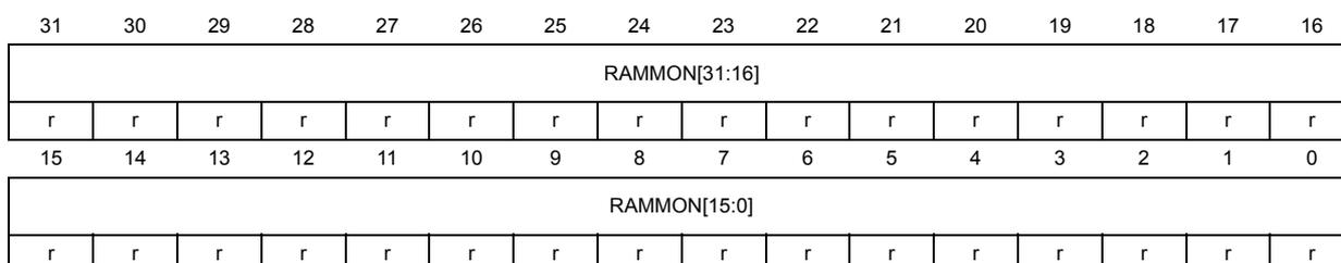
12.7.7 CACHEAXI read-allocate miss monitor register (CACHEAXI_RAMMONR)
Address offset: 0x018
Reset value: 0x0000 0000
| 31 | 30 | 29 | 28 | 27 | 26 | 25 | 24 | 23 | 22 | 21 | 20 | 19 | 18 | 17 | 16 |
| RAMMON[31:16] | |||||||||||||||
| r | r | r | r | r | r | r | r | r | r | r | r | r | r | r | r |
| 15 | 14 | 13 | 12 | 11 | 10 | 9 | 8 | 7 | 6 | 5 | 4 | 3 | 2 | 1 | 0 |
| RAMMON[15:0] | |||||||||||||||
| r | r | r | r | r | r | r | r | r | r | r | r | r | r | r | r |
Bits 31:0 RAMMON[31:0] : cache read-allocate miss monitor counter
12.7.8 CACHEAXI eviction monitor register (CACHEAXI_EVIMONR)
Address offset: 0x01C
Reset value: 0x0000 0000
| 31 | 30 | 29 | 28 | 27 | 26 | 25 | 24 | 23 | 22 | 21 | 20 | 19 | 18 | 17 | 16 |
|---|---|---|---|---|---|---|---|---|---|---|---|---|---|---|---|
| EVIMON[31:16] | |||||||||||||||
| r | r | r | r | r | r | r | r | r | r | r | r | r | r | r | r |
| 15 | 14 | 13 | 12 | 11 | 10 | 9 | 8 | 7 | 6 | 5 | 4 | 3 | 2 | 1 | 0 |
| EVIMON[15:0] | |||||||||||||||
| r | r | r | r | r | r | r | r | r | r | r | r | r | r | r | r |
Bits 31:0 EVIMON[31:0] : cache eviction monitor counter
12.7.9 CACHEAXI write-hit monitor register (CACHEAXI_WHMONR)
Address offset: 0x020
Reset value: 0x0000 0000
| 31 | 30 | 29 | 28 | 27 | 26 | 25 | 24 | 23 | 22 | 21 | 20 | 19 | 18 | 17 | 16 |
|---|---|---|---|---|---|---|---|---|---|---|---|---|---|---|---|
| WHITMON[31:16] | |||||||||||||||
| r | r | r | r | r | r | r | r | r | r | r | r | r | r | r | r |
| 15 | 14 | 13 | 12 | 11 | 10 | 9 | 8 | 7 | 6 | 5 | 4 | 3 | 2 | 1 | 0 |
| WHITMON[15:0] | |||||||||||||||
| r | r | r | r | r | r | r | r | r | r | r | r | r | r | r | r |
Bits 31:0 WHITMON[31:0] : cache write-hit monitor counter
12.7.10 CACHEAXI write-miss monitor register (CACHEAXI_WMMONR)
Address offset: 0x024
Reset value: 0x0000 0000
| 31 | 30 | 29 | 28 | 27 | 26 | 25 | 24 | 23 | 22 | 21 | 20 | 19 | 18 | 17 | 16 |
|---|---|---|---|---|---|---|---|---|---|---|---|---|---|---|---|
| WMISSMON[31:16] | |||||||||||||||
| r | r | r | r | r | r | r | r | r | r | r | r | r | r | r | r |
| 15 | 14 | 13 | 12 | 11 | 10 | 9 | 8 | 7 | 6 | 5 | 4 | 3 | 2 | 1 | 0 |
| WMISSMON[15:0] | |||||||||||||||
| r | r | r | r | r | r | r | r | r | r | r | r | r | r | r | r |
Bits 31:0 WMISSMON[31:0] : cache write-miss monitor counter
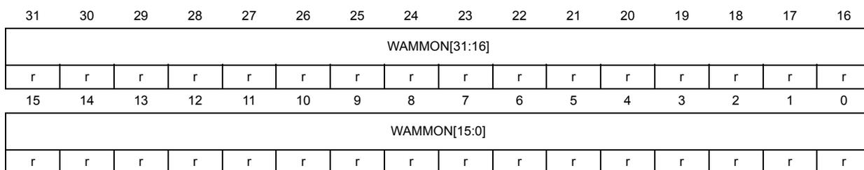
12.7.11 CACHEAXI write-allocate miss monitor register (CACHEAXI_WAMMONR)
Address offset: 0x028
Reset value: 0x0000 0000
| 31 | 30 | 29 | 28 | 27 | 26 | 25 | 24 | 23 | 22 | 21 | 20 | 19 | 18 | 17 | 16 |
|---|---|---|---|---|---|---|---|---|---|---|---|---|---|---|---|
| WAMMON[31:16] | |||||||||||||||
| r | r | r | r | r | r | r | r | r | r | r | r | r | r | r | r |
| 15 | 14 | 13 | 12 | 11 | 10 | 9 | 8 | 7 | 6 | 5 | 4 | 3 | 2 | 1 | 0 |
| WAMMON[15:0] | |||||||||||||||
| r | r | r | r | r | r | r | r | r | r | r | r | r | r | r | r |
Bits 31:0 WAMMON[31:0] : cache write-allocate miss monitor counter
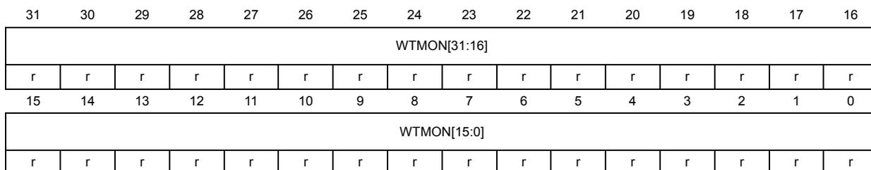
12.7.12 CACHEAXI write-through monitor register (CACHEAXI_WTMONR)
Address offset: 0x02C
Reset value: 0x0000 0000
| 31 | 30 | 29 | 28 | 27 | 26 | 25 | 24 | 23 | 22 | 21 | 20 | 19 | 18 | 17 | 16 |
|---|---|---|---|---|---|---|---|---|---|---|---|---|---|---|---|
| WTMON[31:16] | |||||||||||||||
| r | r | r | r | r | r | r | r | r | r | r | r | r | r | r | r |
| 15 | 14 | 13 | 12 | 11 | 10 | 9 | 8 | 7 | 6 | 5 | 4 | 3 | 2 | 1 | 0 |
| WTMON[15:0] | |||||||||||||||
| r | r | r | r | r | r | r | r | r | r | r | r | r | r | r | r |
Bits 31:0 WTMON[31:0] : cache write-through monitor counter
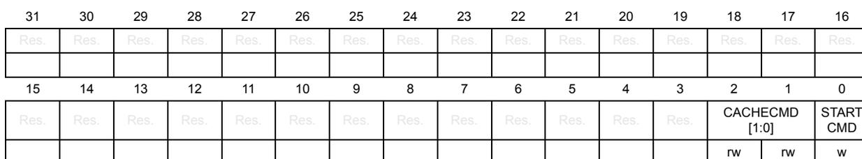
12.7.13 CACHEAXI control register 2 (CACHEAXI_CR2)
Address offset: 0x100
Reset value: 0x0000 0000
| 31 | 30 | 29 | 28 | 27 | 26 | 25 | 24 | 23 | 22 | 21 | 20 | 19 | 18 | 17 | 16 |
|---|---|---|---|---|---|---|---|---|---|---|---|---|---|---|---|
| Res. | Res. | Res. | Res. | Res. | Res. | Res. | Res. | Res. | Res. | Res. | Res. | Res. | Res. | Res. | Res. |
| 15 | 14 | 13 | 12 | 11 | 10 | 9 | 8 | 7 | 6 | 5 | 4 | 3 | 2 | 1 | 0 |
| Res. | Res. | Res. | Res. | Res. | Res. | Res. | Res. | Res. | Res. | Res. | Res. | Res. | CACHECMD [1:0] | START CMD | |
| rw | rw | w |
Bits 31:3 Reserved, must be kept at reset value.
Bits 2:1 CACHECMD[1:0] : cache command maintenance operation (clean or clean-and-invalidate an address range)
This field can be set and cleared by software, only when no maintenance command is ongoing (BUSYCMDF = 0).
00: no operation
01: clean range
11: clean and invalidate range
others: reserved
Bit 0 STARTCMD : starts maintenance range command (maintenance operation defined in CACHECMD).
This bit can be set by software, only when EN = 1, BUSYCMDF = 0, BUSYF = 0, and CACHECMD[1:0] = 0b01 or 0b11.
It is cleared by hardware when BUSYCMDF is set (during cache maintenance operation).
Writing 0 to this bit has no effect.
0: command operation (cache maintenance) finished
1: start maintenance command (cache maintenance)
12.7.14 CACHEAXI command range start address register (CACHEAXI_CMDRSADDRR)
Address offset: 0x104
Reset value: 0x0000 0000
| 31 | 30 | 29 | 28 | 27 | 26 | 25 | 24 | 23 | 22 | 21 | 20 | 19 | 18 | 17 | 16 |
|---|---|---|---|---|---|---|---|---|---|---|---|---|---|---|---|
| CMDSTARTADDR[31:16] | |||||||||||||||
| rw | rw | rw | rw | rw | rw | rw | rw | rw | rw | rw | rw | rw | rw | rw | rw |
| 15 | 14 | 13 | 12 | 11 | 10 | 9 | 8 | 7 | 6 | 5 | 4 | 3 | 2 | 1 | 0 |
| CMDSTARTADDR[15:6] | Res. | Res. | Res. | Res. | Res. | Res. | |||||||||
| rw | rw | rw | rw | rw | rw | rw | rw | rw | rw | ||||||
Bits 31:6 CMDSTARTADDR[31:6] : start address of range to which the cache maintenance command specified in CACHEAXI_CR2.CACHECMD field applies
This field must be set before CACHEAXI_CR2.CACHECMD is written.
Bits 5:0 Reserved, must be kept at reset value.
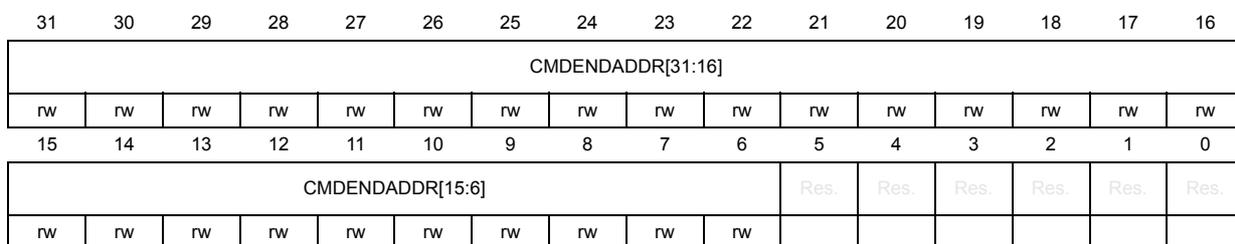
12.7.15 CACHEAXI command range end address register (CACHEAXI_CMDREADRR)
Address offset: 0x108
Reset value: 0x0000 0000
| 31 | 30 | 29 | 28 | 27 | 26 | 25 | 24 | 23 | 22 | 21 | 20 | 19 | 18 | 17 | 16 |
| CMDENDADDR[31:16] | |||||||||||||||
| rw | rw | rw | rw | rw | rw | rw | rw | rw | rw | rw | rw | rw | rw | rw | rw |
| 15 | 14 | 13 | 12 | 11 | 10 | 9 | 8 | 7 | 6 | 5 | 4 | 3 | 2 | 1 | 0 |
| CMDENDADDR[15:6] | Res. | Res. | Res. | Res. | Res. | Res. | |||||||||
| rw | rw | rw | rw | rw | rw | rw | rw | rw | rw | ||||||
Bits 31:6 CMDENDADDR[31:6] : end address of range to which the cache maintenance command specified in CACHEAXI_CR2.CACHECMD field applies
This field must be set before CACHEAXI_CR2.CACHECMD is written.
Bits 5:0 Reserved, must be kept at reset value.
12.7.16 CACHEAXI register map
Table 49. CACHEAXI register map and reset values
| Offset | Register name | 31 | 30 | 29 | 28 | 27 | 26 | 25 | 24 | 23 | 22 | 21 | 20 | 19 | 18 | 17 | 16 | 15 | 14 | 13 | 12 | 11 | 10 | 9 | 8 | 7 | 6 | 5 | 4 | 3 | 2 | 1 | 0 | |
|---|---|---|---|---|---|---|---|---|---|---|---|---|---|---|---|---|---|---|---|---|---|---|---|---|---|---|---|---|---|---|---|---|---|---|
| 0x000 | CACHEAXI_CR1 | EVMRST | WTMRST | EVIMEN | WTMEN | WAMMRST | RAMMRST | WAMMEN | RAMMEN | WMISSMRST | WHITMRST | WMISSMEN | WHITMEN | RMISSMRST | RHITMRST | RMISSMEN | RHITMEN | Res. | Res. | Res. | Res. | Res. | Res. | Res. | Res. | Res. | Res. | Res. | Res. | Res. | Res. | CACHEINV | EN | |
| Reset value | 0 | 0 | 0 | 0 | 0 | 0 | 0 | 0 | 0 | 0 | 0 | 0 | 0 | 0 | 0 | 0 | 0 | 0 | ||||||||||||||||
| 0x004 | CACHEAXI_SR | Res. | Res. | Res. | Res. | Res. | Res. | Res. | Res. | Res. | Res. | Res. | Res. | Res. | Res. | Res. | Res. | Res. | Res. | Res. | Res. | Res. | Res. | Res. | Res. | Res. | Res. | Res. | Res. | CMDENDF | BUSYCMDF | ERRF | BSYENDF | BUSYF |
| Reset value | 0 | 0 | 0 | 0 | 1 | |||||||||||||||||||||||||||||
| 0x008 | CACHEAXI_IER | Res. | Res. | Res. | Res. | Res. | Res. | Res. | Res. | Res. | Res. | Res. | Res. | Res. | Res. | Res. | Res. | Res. | Res. | Res. | Res. | Res. | Res. | Res. | Res. | Res. | Res. | Res. | Res. | CMDENDIE | BUSYCMDIE | ERRIE | BSYENDIE | Res. |
| Reset value | 0 | 0 | 0 | 0 | ||||||||||||||||||||||||||||||
| 0x00C | CACHEAXI_FCR | Res. | Res. | Res. | Res. | Res. | Res. | Res. | Res. | Res. | Res. | Res. | Res. | Res. | Res. | Res. | Res. | Res. | Res. | Res. | Res. | Res. | Res. | Res. | Res. | Res. | Res. | Res. | Res. | CCMDENDF | CBUSYCMDF | CERRF | CBSYENDF | Res. |
| Reset value | 0 | 0 | 0 | 0 | ||||||||||||||||||||||||||||||
| 0x010 | CACHEAXI_RHMONR | RHITMON[31:0] | ||||||||||||||||||||||||||||||||
| Reset value | 0 | 0 | 0 | 0 | 0 | 0 | 0 | 0 | 0 | 0 | 0 | 0 | 0 | 0 | 0 | 0 | 0 | 0 | 0 | 0 | 0 | 0 | 0 | 0 | 0 | 0 | 0 | 0 | 0 | 0 | 0 | 0 | ||
| 0x014 | CACHEAXI_RMMONR | RMISSMON[31:0] | ||||||||||||||||||||||||||||||||
| Reset value | 0 | 0 | 0 | 0 | 0 | 0 | 0 | 0 | 0 | 0 | 0 | 0 | 0 | 0 | 0 | 0 | 0 | 0 | 0 | 0 | 0 | 0 | 0 | 0 | 0 | 0 | 0 | 0 | 0 | 0 | 0 | 0 | ||
| 0x018 | CACHEAXI_RAMMONR | RAMMON[31:0] | ||||||||||||||||||||||||||||||||
| Reset value | 0 | 0 | 0 | 0 | 0 | 0 | 0 | 0 | 0 | 0 | 0 | 0 | 0 | 0 | 0 | 0 | 0 | 0 | 0 | 0 | 0 | 0 | 0 | 0 | 0 | 0 | 0 | 0 | 0 | 0 | 0 | 0 | ||
Table 49. CACHEAXI register map and reset values (continued)
| Offset | Register name | 31 | 30 | 29 | 28 | 27 | 26 | 25 | 24 | 23 | 22 | 21 | 20 | 19 | 18 | 17 | 16 | 15 | 14 | 13 | 12 | 11 | 10 | 9 | 8 | 7 | 6 | 5 | 4 | 3 | 2 | 1 | 0 |
|---|---|---|---|---|---|---|---|---|---|---|---|---|---|---|---|---|---|---|---|---|---|---|---|---|---|---|---|---|---|---|---|---|---|
| 0x01C | CACHEAXI_EVIMONR | EVIMON[31:0] | |||||||||||||||||||||||||||||||
| Reset value | 0 | 0 | 0 | 0 | 0 | 0 | 0 | 0 | 0 | 0 | 0 | 0 | 0 | 0 | 0 | 0 | 0 | 0 | 0 | 0 | 0 | 0 | 0 | 0 | 0 | 0 | 0 | 0 | 0 | 0 | 0 | 0 | |
| 0x020 | CACHEAXI_WHMONR | WHITMON[31:0] | |||||||||||||||||||||||||||||||
| Reset value | 0 | 0 | 0 | 0 | 0 | 0 | 0 | 0 | 0 | 0 | 0 | 0 | 0 | 0 | 0 | 0 | 0 | 0 | 0 | 0 | 0 | 0 | 0 | 0 | 0 | 0 | 0 | 0 | 0 | 0 | 0 | 0 | |
| 0x024 | CACHEAXI_WMMONR | WMISSMON[31:0] | |||||||||||||||||||||||||||||||
| Reset value | 0 | 0 | 0 | 0 | 0 | 0 | 0 | 0 | 0 | 0 | 0 | 0 | 0 | 0 | 0 | 0 | 0 | 0 | 0 | 0 | 0 | 0 | 0 | 0 | 0 | 0 | 0 | 0 | 0 | 0 | 0 | 0 | |
| 0x028 | CACHEAXI_WAMMONR | WAMMON[31:0] | |||||||||||||||||||||||||||||||
| Reset value | 0 | 0 | 0 | 0 | 0 | 0 | 0 | 0 | 0 | 0 | 0 | 0 | 0 | 0 | 0 | 0 | 0 | 0 | 0 | 0 | 0 | 0 | 0 | 0 | 0 | 0 | 0 | 0 | 0 | 0 | 0 | 0 | |
| 0x02C | CACHEAXI_WTMONR | WTMON[31:0] | |||||||||||||||||||||||||||||||
| Reset value | 0 | 0 | 0 | 0 | 0 | 0 | 0 | 0 | 0 | 0 | 0 | 0 | 0 | 0 | 0 | 0 | 0 | 0 | 0 | 0 | 0 | 0 | 0 | 0 | 0 | 0 | 0 | 0 | 0 | 0 | 0 | 0 | |
| 0x030-0x0FC | Reserved | Reserved | |||||||||||||||||||||||||||||||
| 0x100 | CACHEAXI_CR2 | Res | Res | Res | Res | Res | Res | Res | Res | Res | Res | Res | Res | Res | Res | Res | Res | Res | Res | Res | Res | Res | Res | Res | Res | Res | Res | Res | Res | Res | CACHECMD [1:0] | STARTCMD | |
| Reset value | 0 | 0 | 0 | ||||||||||||||||||||||||||||||
| 0x104 | CACHEAXI_CMDRS_ADDR | CMDSTARTADDR[31:5] (1) | Res | Res | Res | Res | |||||||||||||||||||||||||||
| Reset value | 0 | 0 | 0 | 0 | 0 | 0 | 0 | 0 | 0 | 0 | 0 | 0 | 0 | 0 | 0 | 0 | 0 | 0 | 0 | 0 | 0 | 0 | 0 | 0 | 0 | 0 | 0 | ||||||
| 0x108 | CACHEAXI_CMDRE_ADDR | CMDENDADDR[31:5] (1) | Res | Res | Res | Res | |||||||||||||||||||||||||||
| Reset value | 0 | 0 | 0 | 0 | 0 | 0 | 0 | 0 | 0 | 0 | 0 | 0 | 0 | 0 | 0 | 0 | 0 | 0 | 0 | 0 | 0 | 0 | 0 | 0 | 0 | 0 | 0 | ||||||
1. Bit 5 is reserved (=0) for CACHEAXI configuration with 64-bytes cache line width.
Refer to Section 2.3 for the register boundary addresses.