10. SRAM configuration controller (RAMCFG)
10.1 RAMCFG introduction
The RAMCFG configures the features of the internal SRAMs: AHBSRAM1/2, AXISRAM1 to 6, BKPSRAM, FLEXRAM, and VENCRAM.
10.2 RAMCFG main features
The internal SRAM supports the following features, configured in the RAMCFG:
- • Error code correction (ECC):
- – Single-error detection and correction with interrupt generation
- – Double-error detection with interrupt generation
- – Status with failing address
- • SRAM hardware erase: on reset or dedicated event, the RAM content is automatically erased (written as 0).
- • SRAM software erase: the software can trigger an SRAM erase through RAMCFG registers.
10.3 RAMCFG functional description
10.3.1 Internal SRAM features
The following SRAMs are embedded in the devices, each with specific features:
- • AXISRAM1 to 6 are the main SRAMs. AHBSRAM1/2 are preferably for DMA-controlled peripheral-to-memory data flow.
AXISRAM2 to 6 can be shut down when the application is in Run mode.
- • FLEXMEM can be allocated as Cortex-M55 TCM, or as system RAM (FLEXRAM).
80 Kbytes of the FLEXMEM are retained in Standby mode, either allocated as extended ITCM (64 +16-Kbyte ECC), or allocated as FLEXRAM. - • The BKPSRAM content is retained in low-power modes, even when \( V_{DD} \) is off in \( V_{BAT} \) mode. On a tamper-event detection, the BKPSRAM content is erased.
- • The AXISRAM8/VENCRAM implements hardware and software erases. It can be used at system level when the VENC is not used by the application. In this case, the AXISRAM8 is addressed.
- • The RAMCFG embeds registers that are related to the internal SRAMs ECC, shutdown control, and software erase.
- • SRAM7 (256 KB) is used as default at the system level.
- – On STM32N6x5 devices it is used only as internal RAM at system level.
- – On STM32N6x7 devices, after configuration (CACHEAXI_CR1 register, bit 0 EN: enable) this area is used as cache memory dedicated to Neural ART and is no longer accessible at system level. Due to this capacity, SRAM7 is controlled directly in the CACHEAXI registers, and is not under RAMCFG.
Note: The baseline I/D-TCM content can be retained in Standby mode (as BKPSRAM and 80 Kbytes of FLEXMEM), but this is not under RAMCFG control.
The CACHEAXI internal RAM can be used at system level when the NPU does not use its cache (as the VENCRAM). This is controlled directly in the CACHEAXI, and is not under RAMCFG.
Table 33 summarizes the features supported by each internal SRAM.
Table 33. Internal SRAM features
| SRAM feature | AXISRAM1 | AXISRAM2 | FLEXRAM | AXISRAM3 | AXISRAM4 | AXISRAM5 | AXISRAM6 | AXISRAM7 | AHBSRAM1 | AHBSRAM2 | VENCRAM/ AXISRAM8 | BKPSRAM |
|---|---|---|---|---|---|---|---|---|---|---|---|---|
| Size (Kbytes) | 624 | 1024 | Up to 400 | 448 | 448 | 448 | 448 | 256 | 16 | 16 | 128 | 8 |
| Word size | 64 | 64 | 64 | 64 | 64 | 64 | 64 | 64 | 32 | 32 | 64 | 39 (1) |
| Retention in Standby mode | - | - | X (2) | - | - | - | - | - | - | - | - | X |
| Retention in V BAT mode | - | - | - | - | - | - | - | - | - | - | - | X |
| Block on potential tamper, erase on confirmed tamper | - | - | - | - | - | - | - | - | - | X | - | X |
| Hardware erase on reset | X | X | - | - | - | - | - | - | - | X | - | - |
| Software erase | X | X | X | X | X | X | X | X | X | X | X | X |
| ECC | - | - | X (3) | - | - | - | - | - | - | - | - | X |
1. 32 bits of effective data, and 7 bits of embedded ECC.
2. Only the 80 Kbytes that correspond to the first portion of the I-TCM extension can be retained.
3. The ECC concerns only the FLEXMEM when used as extended TCM. It is under control of the Cortex-M55 TCM interface.
Table 34 details the conditions for the hardware erase.
Table 34. Hardware-erase conditions for internal SRAMs
| SRAM | Conditional hardware erase | Condition |
|---|---|---|
| AXISRAM1 | No | Erase on system reset |
| AXISRAM2 | ||
| AHBSRAM2 | No | Erase on system reset and on confirmed tamper |
10.3.2 FLEXRAM control
STM32N6x5/x7xx devices include a Cortex-M55 core that exposes a TCM interface. This TCM interface is spread in one 39-bit (32 effective data bits + 7 ECC protection bits) I-TCM (instruction TCM interface), and four parallel 39-bit D-TCMs (data TCM interfaces).
STM32N6x5/x7xx devices also embed 4096 Kbytes of RAM accessible on the AXI interconnect. The first half (FLEXRAM, AXISRAM1/2) is in the CPU frequency domain, and is preferably used for CPU storage. The second half of this memory (AXISRAM3/4/5/6/7) is in the NPU frequency domain, and is preferably used for the AI computing storage.
To let customers tailor the SRAM use to their needs, the FLEXMEM offers the possibility to allocate part of the CPU side SRAM (FLEXRAM part) as extended TCM, both on I-TCM and D-TCM interfaces. Table 35 lists the supported allocations.
Table 35. FLEXRAM supported configurations
| Config I-TCM | Config D-TCM | I-TCM fix | I-TCM flex (+ ECC) | I-TCM total | D-TCM fix | D-TCM flex (+ ECC) | D-TCM total | AXI-side FLEXRAM |
|---|---|---|---|---|---|---|---|---|
| 0 | 0 | 1 x 64 | 0 | 64 | 4 x 32 | 0 | 128 | 400 |
| 0 | 1 | 1 x 64 | 0 | 64 | 4 x 32 | 4 x 32 (+ 8) | 256 | 240 |
| 1 | 0 | 1 x 64 | 1 x 64 (+16) | 128 | 4 x 32 | 0 | 128 | 320 |
| 1 | 1 | 1 x 64 | 1 x 64 (+16) | 128 | 4 x 32 | 4 x 32 (+ 8) | 256 | 160 |
| 2 | 0 | 1 x 64 | 1 x 192 (+ 48) | 256 | 4 x 32 | 0 | 128 | 160 |
| 2 | 1 | 1 x 64 | 1 x 192 (+ 48) | 256 | 4 x 32 | 4 x 32 (+ 8) | 256 | 0 |
The retention regions are detailed in Table 36 and Figure 10 , sharing the same color code.
Table 36. FLEXMEM versus retention
| Configuration | FLEXRAM base address (1) | I-TCM extension | D-TCM extension | Retention region |
|---|---|---|---|---|
| 00 | 0x2400 0000 | 0 KB | 0 KB | RAM region: 0x2400 0000 to 0x2401 3FFF |
| 10 | 0x2401 4000 | 64 KB (+16 KB ECC) | I-TCM extension: first 64 KB (+16 KB ECC) | |
| 20 | 0x2403 C000 | 192 KB (+48 KB ECC) | ||
| 01 | 0x2402 8000 | 0 KB | 128 KB (+32 KB ECC) | RAM region: 0x2402 8000 to 0x2403 BFFF |
| 11 | 0x2403 C000 | 64 KB (+16 KB ECC) | I-TCM extension: first 64 KB (+16 KB ECC) | |
| 21 | No RAM | 192 KB (+48 KB ECC) |
1. All addresses considered as their non secure aliases.
Figure 10. FLEXMEM versus retention
| Address Range | VENCRAM AXISRAM8 128 kB | VENCRAM AXISRAM8 128 kB | VENCRAM AXISRAM8 128 kB | VENCRAM AXISRAM8 128 kB | VENCRAM AXISRAM8 128 kB | VENCRAM AXISRAM8 128 kB |
|---|---|---|---|---|---|---|
| S 0x3440 0000 NS 0x2440 0000 | AXISRAM7 CACHEAXI 256 kB | AXISRAM7 CACHEAXI 256 kB | AXISRAM7 CACHEAXI 256 kB | AXISRAM7 CACHEAXI 256 kB | AXISRAM7 CACHEAXI 256 kB | AXISRAM7 CACHEAXI 256 kB |
| S 0x343C 0000 NS 0x243C 0000 | AXISRAM6 448 kB | AXISRAM6 448 kB | AXISRAM6 448 kB | AXISRAM6 448 kB | AXISRAM6 448 kB | AXISRAM6 448 kB |
| S 0x3435 0000 NS 0x2435 0000 | AXISRAM5 448 kB | AXISRAM5 448 kB | AXISRAM5 448 kB | AXISRAM5 448 kB | AXISRAM5 448 kB | AXISRAM5 448 kB |
| S 0x342E 0000 NS 0x242E 0000 | AXISRAM4 448 kB | AXISRAM4 448 kB | AXISRAM4 448 kB | AXISRAM4 448 kB | AXISRAM4 448 kB | AXISRAM4 448 kB |
| S 0x3427 0000 NS 0x2427 0000 | AXISRAM3 448 kB | AXISRAM3 448 kB | AXISRAM3 448 kB | AXISRAM3 448 kB | AXISRAM3 448 kB | AXISRAM3 448 kB |
| S 0x3420 0000 NS 0x2420 0000 | AXISRAM2 1024 kB | AXISRAM2 1024 kB | AXISRAM2 1024 kB | AXISRAM2 1024 kB | AXISRAM2 1024 kB | AXISRAM2 1024 kB |
| S 0x3410 0000 NS 0x2410_0000 | AXISRAM1 624 kB | AXISRAM1 624 kB | AXISRAM1 624 kB | AXISRAM1 624 kB | AXISRAM1 624 kB | AXISRAM1 624 kB |
| S 0x3406 4000 NS 0x2406 4000 | FLEXRAM | RAM 320 kB | RAM 160 kB | RAM 160 kB | RAM 160 kB | |
| 0x2403 C000 | RAM retention 80 kB | |||||
| 0x2402 8000 | ||||||
| 0x2401 4000 | RAM retention 80 kB | |||||
| 0x2400 0000 | ||||||
| 0x2004 0000 | D-TCM | D-TCM baseline 128 kB | D-TCM 128 kB | D-TCM 128 kB | D-TCM 128 kB | |
| 0x2002_0000 | D-TCM baseline 128 kB | D-TCM baseline 128 kB | D-TCM baseline 128 kB | |||
| 0x2000_0000 | ||||||
| 0x0004_0000 | ITCM | ITCM retention 64 kB | ITCM retention 128 kB | ITCM retention 128 kB | ||
| 0x0002_0000 | ITCM retention 64 kB | I-TCM retention 64 kB | ITCM retention 64 kB | |||
| 0x0001_0000 | ITCM baseline (ret.) 64 kB | ITCM baseline (ret.) 64 kB | ITCM baseline (ret.) 64 kB | ITCM baseline (ret.) 64 kB | ||
| 0x0000_0000 | ||||||
| 00 | 10 | 20 | 01 | 11 | 21 |
Note: AXISRAM1 start address is 0x2406 4000 (aliased at 0x3406 4000 in secure boundary), whatever the FLEXMEM configuration.
The FLEXMEM configuration depends upon CFGDTCMSZ[3:0] and CFGITCMSZ[3:0] in SYSCFG_CM55TCMCR. Its configuration cannot be changed at runtime, a reboot is needed.
Use in low-power modes
The I-TCM and D-TCM baselines can be kept in retention when the device is in Standby mode. This allows the CPU to restart from the TCM content.
The first 64 Kbytes (+16 Kbytes for ECC) of extended I-TCM through the FLEXMEM can also be kept in retention. This allows a maximum of 128 Kbytes of I-TCM in retention.
When only the I-TCM baseline is used for the Cortex-M55, 80 Kbytes of the AXI RAM can be kept in retention.
The total amount of TCM that can be kept in retention is 320 Kbytes:
- • 64 Kbytes of I-TCM baseline (+ 16 Kbytes for ECC)
- • 64 Kbytes of I-TCM extended (+ 16 Kbytes for ECC)
- • 4 x 32 Kbytes of D-TCM baseline (+ 4 x 8 Kbytes for ECC)
10.3.3 ECC (BKPSRAM)
The ECC is supported by the BKPSRAM. Seven ECC bits are added per 32 bits of SRAM: this allows a 2-bit error detection, and a 1-bit error correction on memory read access.
As the ECC is calculated and checked for a 32-bit word, byte and half-word write accesses are managed by the SRAM interface: it first reads the whole word, then writes the word again with the new byte/half-word value. ECC double errors are also detected during these byte or half-word AHB write accesses (read/modify/write done by the interface). The byte or half-word write access latency is two AHB clock cycles.
Caution: In case of a byte or half-word write on the SRAM with ECC, the read/modify/write operation is done in a buffer. The buffer content is written into the SRAM two AHB clock cycles after the SRAM AHB is released (when the SRAM is no more accessed).
The ECC is also available on the Cortex-M55 I-TCM and D-TCM.
When the FLEXMEM is used as I/D-TCM, it supports ECC through specific memory cut/word organization. When the FLEXMEM is used as FLEXRAM, it does not support ECC, even for the part that can be set in retention
Single and double ECC errors
When a single error is detected, it is automatically corrected, and SEDC (single error detected and corrected) is set in RAMCFG_BKPSRAMISR.
An interrupt is generated if enabled by SEIE in RAMCFG_BKPSRAMIER. The failing address is stored in RAMCFG_BKPSRAMESEAR, if ALE is set in RAMCFG_BKPRAMCR.
Caution: Single errors are not reported if SEDC is not cleared in time when a new error happens.
When a double error is detected, DED is set in RAMCFG_BKPSRAMISR. An interrupt is generated if enabled by DEIE in RAMCFG_BKPSRAMIER. The failing address is stored in RAMCFG_BKPSRAMEDEAR if ALE is set in RAMCFG_BKPSRAMCR.
Caution: Double errors are not reported if DED is not cleared. Double errors are not corrected, and must be managed by exception.
The ECC can be activated/deactivated by executing the following software sequence:
- 1. Write 0xAE in RAMCFG_BKSRAMECCKEYR.
- 2. Write 0x75 in RAMCFG_BKSRAMECCKEYR.
- 3. Write 1 to ECCE in RAMCFG_BKPSRAMCR to activate the ECC (write 0 to this bit to deactivate the ECC).
Fault injection
The RAMCFG supports a software loop for runtime fault injection in the BKPSRAM when the ECC is activated:
- 1. With the ECC enabled, the application writes at a given address.
- 2. The application disables the ECC writing.
- 3. The application writes a different data at the same address as previously. Data are updated but the matching ECC word is not modified.
- 4. The application enables ECC writing.
- 5. The application reads at the same address as previously. An interrupt is expected due to either one error corrected, or several errors detected. The application can check that the desired address appears in RAMCFG_BKPSRAMSEAR or _BKPSRAMDEAR.
10.4 RAMCFG low-power modes
After a reset, by default, the RAM is controlled by the RAM clock through the RCC embedded memories enable register (RCC_MEMENR). The following configurations apply:
- • AXISRAM1 and AXISRAM2 are enabled.
- • AXISRAM3 to AXISRAM6 are in power-down (shutdown) mode.
- • AXISRAM7 operates as internal RAM at system level, and AXISRAM8 is in power-down (shutdown) mode.
- • BKPSRAM is enabled.
When RAMs are in shutdown mode, their content is not retained. The following controls and behaviors apply:
- • SRAMSD in AXISRAMx_CR (x = 2, 3, 4, 5, or 6) determines whether the RAM is in shutdown mode.
- • When a RAM is in shutdown mode:
- – Writing to it has no effect.
- – Reading from it returns 0.
- – Upon exiting the shutdown state, the memory is not immediately accessible. A safe period of 40 ns must elapse before the memory becomes functional.
Sequences to safely enter or exit shutdown mode:
- • To enter shutdown:
- a) Disable the RAM clock through the RCC (RCC_MEMENR)
- b) Shut the RAM down by writing 1 to SRAMSD in RAMCFG_AXISRAMxCR
- • To exit shutdown:
- a) Power the RAM up by writing 0 to SRAMSD in RAMCFG_AXISRAMxCR
- b) Read back the value from the RAMCFG (alternatively, wait 40 ns)
- c) Enable the RAM clock through the RCC. (RCC_MEMENR)
d) The RAM is now ready for use.
Note: AXISRAM3 to AXISRAM6 are interleaved at the system level under software control through SYSCFG_NPU_ICNCR. Interleaving must be deactivated before shutting down these memories, especially if only part of them is set to shutdown.
Low power mode:
- • Run mode: AXISRAM2 to AXISRAM6 can be set to power down (shutdown) under software control, AXISRAM7 and AXISRAM8 cannot
- • Stop mode: all RAMs are set to low-power mode under the control of PWR control register
- • Standby mode: all RAMs are off except BKPSRAM, BKPSRAM and 80 Kbytes of the FLEXRAM are set to retention under software control
10.5 RAMCFG interrupts
Two interrupts (maskable by software) are generated internally, and a global interrupt request is exported to the interrupt controller. Table 37 lists RAMCFG interrupt requests.
Table 37. RAMCFG interrupt requests
| Interrupt acronym | Memory | Interrupt event | Event flag (1) | Enable control bit | Interrupt clear method |
|---|---|---|---|---|---|
| RAMCFG | BKPSRAM | ECC single error detection and correction | SEDC | SEIE | Write 1 in CSEDC |
| ECC double error detection | DED | DEIE | Write 1 in CDED |
1. All these bits are in RAMCFG_BKPSRAMISR.
10.6 RAMCFG registers
The RAMCFG registers can be accessed in word, half-word, and byte format, unless differently specified.
10.6.1 RAMCFG AXISRAM1 control register (RAMCFG_AXISRAM1CR)
Address offset: 0x000
Reset value: 0x0000 0000
Reset on any system reset.
| 31 | 30 | 29 | 28 | 27 | 26 | 25 | 24 | 23 | 22 | 21 | 20 | 19 | 18 | 17 | 16 |
|---|---|---|---|---|---|---|---|---|---|---|---|---|---|---|---|
| Res. | Res. | Res. | Res. | Res. | Res. | Res. | Res. | Res. | Res. | Res. | Res. | Res. | Res. | Res. | Res. |
| 15 | 14 | 13 | 12 | 11 | 10 | 9 | 8 | 7 | 6 | 5 | 4 | 3 | 2 | 1 | 0 |
| Res. | Res. | Res. | Res. | Res. | Res. | Res. | SRAM ER rw | Res. | Res. | Res. | Res. | Res. | Res. | Res. | Res. |
Bits 31:9 Reserved, must be kept at reset value.
Bit 8 SRAMER : SRAM erase
This bit can be set by software only after writing the unlock sequence in ERASEKEY of RAMCFG_AXISRAM1ERKEYR. Setting this bit starts the SRAM erase. This bit is automatically cleared by hardware at the end of the erase operation.
0: No erase operation ongoing
1: Erase operation ongoing
Bits 7:0 Reserved, must be kept at reset value.
10.6.2 RAMCFG AXISRAMx interrupt status register (RAMCFG_AXISRAMxISR)
Address offset: 0x008 + 0x80 * (x - 1), (x = 1 to 6)
Reset value: 0x0000 0000
Reset on any system reset.
| 31 | 30 | 29 | 28 | 27 | 26 | 25 | 24 | 23 | 22 | 21 | 20 | 19 | 18 | 17 | 16 |
|---|---|---|---|---|---|---|---|---|---|---|---|---|---|---|---|
| Res. | Res. | Res. | Res. | Res. | Res. | Res. | Res. | Res. | Res. | Res. | Res. | Res. | Res. | Res. | Res. |
| 15 | 14 | 13 | 12 | 11 | 10 | 9 | 8 | 7 | 6 | 5 | 4 | 3 | 2 | 1 | 0 |
| Res. | Res. | Res. | Res. | Res. | Res. | Res. | SRAM BUSY r | Res. | Res. | Res. | Res. | Res. | Res. | Res. | Res. |
Bits 31:9 Reserved, must be kept at reset value.
Bit 8 SRAMBUSY : SRAM busy with erase operation
Depending on the SRAM, the erase operation can be performed due to software request, system reset if the option is not disabled by software and tamper detection (see Table 33 ).
0: No erase operation ongoing
1: Erase operation ongoing
Bits 7:0 Reserved, must be kept at reset value.
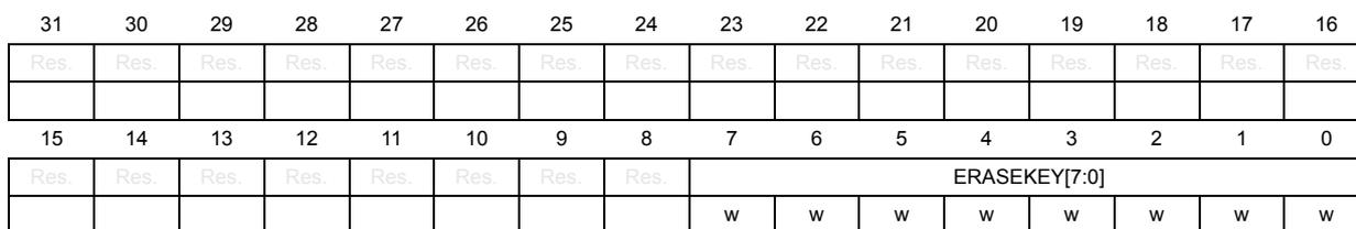
10.6.3 RAMCFG AXISRAMx erase key register (RAMCFG_AXISRAMxERKEYR)
Address offset: 0x028 + 0x80 * (x - 1), (x = 1 to 6)
Reset value: 0x0000 0000
Reset on any system reset.
| 31 | 30 | 29 | 28 | 27 | 26 | 25 | 24 | 23 | 22 | 21 | 20 | 19 | 18 | 17 | 16 |
|---|---|---|---|---|---|---|---|---|---|---|---|---|---|---|---|
| Res. | Res. | Res. | Res. | Res. | Res. | Res. | Res. | Res. | Res. | Res. | Res. | Res. | Res. | Res. | Res. |
| 15 | 14 | 13 | 12 | 11 | 10 | 9 | 8 | 7 | 6 | 5 | 4 | 3 | 2 | 1 | 0 |
| Res. | Res. | Res. | Res. | Res. | Res. | Res. | Res. | ||||||||
| w | w | w | w | w | w | w | w |
Bits 31:8 Reserved, must be kept at reset value.
Bits 7:0 ERASEKEY[7:0] : Erase write protection key
The following steps are required to unlock the write protection of SRAMER in RAMCFG_AXISRAMxCR.
a) Write 0xCA into this field.
b) Write 0x53 into this field.
Note: Writing a wrong key reactivates the write protection.
10.6.4 RAMCFG AXISRAMx control register (RAMCFG_AXISRAMxCR)
Address offset: 0x080 + 0x80 * (x - 2), (x = 2 to 6)
Reset value: 0x0000 0000, 0x0010 0000, 0x0010 0000, 0x0010 0000, 0x0010 0000
Reset on any system reset.
| 31 | 30 | 29 | 28 | 27 | 26 | 25 | 24 | 23 | 22 | 21 | 20 | 19 | 18 | 17 | 16 |
|---|---|---|---|---|---|---|---|---|---|---|---|---|---|---|---|
| Res. | Res. | Res. | Res. | Res. | Res. | Res. | Res. | Res. | Res. | Res. | SRAM SD rw | Res. | Res. | Res. | Res. |
| 15 | 14 | 13 | 12 | 11 | 10 | 9 | 8 | 7 | 6 | 5 | 4 | 3 | 2 | 1 | 0 |
| Res. | Res. | Res. | Res. | Res. | Res. | Res. | SRAM ER rw | Res. | Res. | Res. | Res. | Res. | Res. | Res. | Res. |
Bits 31:21 Reserved, must be kept at reset value.
Bit 20
SRAMSD
: Shutdown AXISRAMx
0: AXISRAMx memory is powered.
1: AXISRAMx memory is in shutdown, and its content is not retained.
Bits 19:9 Reserved, must be kept at reset value.
Bit 8 SRAMER : SRAM erase
This bit can be set by software only after writing the unlock sequence in ERASEKEY of RAMCFG_AXISRAMxERKEYR. Setting this bit starts the SRAM erase. This bit is automatically cleared by hardware at the end of the erase operation.
0: No erase operation ongoing
1: Erase operation ongoing
Bits 7:0 Reserved, must be kept at reset value.
10.6.5 RAMCFG AHBSRAMx control register (RAMCFG_AHBSRAMxCR)
Address offset: \( 0x300 + 0x80 \times (x - 1) \) , ( \( x = 1 \) to 2)
Reset value: 0x0000 0000
Reset on any system reset.
| 31 | 30 | 29 | 28 | 27 | 26 | 25 | 24 | 23 | 22 | 21 | 20 | 19 | 18 | 17 | 16 |
|---|---|---|---|---|---|---|---|---|---|---|---|---|---|---|---|
| Res. | Res. | Res. | Res. | Res. | Res. | Res. | Res. | Res. | Res. | Res. | Res. | Res. | Res. | Res. | Res. |
| 15 | 14 | 13 | 12 | 11 | 10 | 9 | 8 | 7 | 6 | 5 | 4 | 3 | 2 | 1 | 0 |
| Res. | Res. | Res. | Res. | Res. | Res. | Res. | SRAM ER | Res. | Res. | Res. | Res. | Res. | Res. | Res. | Res. |
| rw |
Bits 31:9 Reserved, must be kept at reset value.
Bit 8 SRAMER : SRAM erase
This bit can be set by software only after writing the unlock sequence in ERASEKEY of RAMCFG_AHBSRAMxERKEYR. Setting this bit starts the SRAM erase. This bit is automatically cleared by hardware at the end of the erase operation.
0: No erase operation ongoing
1: Erase operation ongoing
Bits 7:0 Reserved, must be kept at reset value.
10.6.6 RAMCFG AHBSRAMx interrupt status register (RAMCFG_AHBSRAMxISR)
Address offset: \( 0x308 + 0x80 \times (x - 1) \) , ( \( x = 1 \) to 2)
Reset value: 0x0000 0000
Reset on any system reset.
| 31 | 30 | 29 | 28 | 27 | 26 | 25 | 24 | 23 | 22 | 21 | 20 | 19 | 18 | 17 | 16 |
|---|---|---|---|---|---|---|---|---|---|---|---|---|---|---|---|
| Res. | Res. | Res. | Res. | Res. | Res. | Res. | Res. | Res. | Res. | Res. | Res. | Res. | Res. | Res. | Res. |
| 15 | 14 | 13 | 12 | 11 | 10 | 9 | 8 | 7 | 6 | 5 | 4 | 3 | 2 | 1 | 0 |
| Res. | Res. | Res. | Res. | Res. | Res. | Res. | SRAM BUSY | Res. | Res. | Res. | Res. | Res. | Res. | Res. | Res. |
| r |
Bits 31:9 Reserved, must be kept at reset value.
Bit 8 SRAMBUSY : SRAM busy with erase operation
Depending on the SRAM, the erase operation can be performed due to software request, system reset if the option is not disabled by software and tamper detection (see Table 33 ).
0: No erase operation ongoing
1: Erase operation ongoing
Bits 7:0 Reserved, must be kept at reset value.
10.6.7 RAMCFG AHBSRAMx erase key register (RAMCFG_AHBSRAMxERKEYR)
Address offset: 0x328 + 0x80 * (x - 1), (x = 1 to 2)
Reset value: 0x0000 0000
Reset on any system reset.
| 31 | 30 | 29 | 28 | 27 | 26 | 25 | 24 | 23 | 22 | 21 | 20 | 19 | 18 | 17 | 16 |
|---|---|---|---|---|---|---|---|---|---|---|---|---|---|---|---|
| Res. | Res. | Res. | Res. | Res. | Res. | Res. | Res. | Res. | Res. | Res. | Res. | Res. | Res. | Res. | Res. |
| 15 | 14 | 13 | 12 | 11 | 10 | 9 | 8 | 7 | 6 | 5 | 4 | 3 | 2 | 1 | 0 |
| Res. | Res. | Res. | Res. | Res. | Res. | Res. | Res. | ERASEKEY[7:0] | |||||||
| w | w | w | w | w | w | w | w | ||||||||
Bits 31:8 Reserved, must be kept at reset value.
Bits 7:0 ERASEKEY[7:0] : Erase write protection key
To unlock the write protection of SRAMER in RAMCFG_AHBSRAMxCR.
a) Write 0xCA into this field.
b) Write 0x53 into this field.
Note: Writing a wrong key reactivates the write protection.
10.6.8 RAMCFG VENCGRAM control register (RAMCFG_VENCGRAMCR)
Address offset: 0x400
Reset value: 0x0000 0000
Reset on any system reset.
| 31 | 30 | 29 | 28 | 27 | 26 | 25 | 24 | 23 | 22 | 21 | 20 | 19 | 18 | 17 | 16 |
|---|---|---|---|---|---|---|---|---|---|---|---|---|---|---|---|
| Res. | Res. | Res. | Res. | Res. | Res. | Res. | Res. | Res. | Res. | Res. | Res. | Res. | Res. | Res. | Res. |
| 15 | 14 | 13 | 12 | 11 | 10 | 9 | 8 | 7 | 6 | 5 | 4 | 3 | 2 | 1 | 0 |
| Res. | Res. | Res. | Res. | Res. | Res. | Res. | SRAM ER | Res. | Res. | Res. | Res. | Res. | Res. | Res. | Res. |
| rw |
Bits 31:9 Reserved, must be kept at reset value.
Bit 8 SRAMER : SRAM erase
This bit can be set by software only after writing the unlock sequence in ERASEKEY of RAMCFG_VENCRAMERKEYR. Setting this bit starts the SRAM erase. This bit is automatically cleared by hardware at the end of the erase operation.
0: No erase operation ongoing
1: Erase operation ongoing
Bits 7:0 Reserved, must be kept at reset value.
10.6.9 RAMCFG VENCRAM interrupt status register (RAMCFG_VENCRAMISR)
Address offset: 0x408
Reset value: 0x0000 0000
Reset on any system reset.
| 31 | 30 | 29 | 28 | 27 | 26 | 25 | 24 | 23 | 22 | 21 | 20 | 19 | 18 | 17 | 16 |
|---|---|---|---|---|---|---|---|---|---|---|---|---|---|---|---|
| Res. | Res. | Res. | Res. | Res. | Res. | Res. | Res. | Res. | Res. | Res. | Res. | Res. | Res. | Res. | Res. |
| 15 | 14 | 13 | 12 | 11 | 10 | 9 | 8 | 7 | 6 | 5 | 4 | 3 | 2 | 1 | 0 |
| Res. | Res. | Res. | Res. | Res. | Res. | Res. | SRAM BUSY | Res. | Res. | Res. | Res. | Res. | Res. | Res. | Res. |
| r |
Bits 31:9 Reserved, must be kept at reset value.
Bit 8 SRAMBUSY : SRAM busy with erase operation
Depending on the SRAM, the erase operation can be performed due to software request, system reset if the option is not disabled by software and tamper detection (see Table 33 ).
0: No erase operation ongoing
1: Erase operation ongoing
Bits 7:0 Reserved, must be kept at reset value.
10.6.10 RAMCFG VENCRAM erase key register (RAMCFG_VENCRAMERKEYR)
Address offset: 0x428
Reset value: 0x0000 0000
Reset on any system reset.
| 31 | 30 | 29 | 28 | 27 | 26 | 25 | 24 | 23 | 22 | 21 | 20 | 19 | 18 | 17 | 16 |
| Res. | Res. | Res. | Res. | Res. | Res. | Res. | Res. | Res. | Res. | Res. | Res. | Res. | Res. | Res. | Res. |
| 15 | 14 | 13 | 12 | 11 | 10 | 9 | 8 | 7 | 6 | 5 | 4 | 3 | 2 | 1 | 0 |
| Res. | Res. | Res. | Res. | Res. | Res. | Res. | Res. | ERASEKEY[7:0] | |||||||
| w | w | w | w | w | w | w | w | ||||||||
Bits 31:8 Reserved, must be kept at reset value.
Bits 7:0 ERASEKEY[7:0] : Erase write protection key
To unlock the write protection of SRAMER in RAMCFG_VENCRAMCR.
a) Write 0xCA into this field.
b) Write 0x53 into this field.
Note: Writing a wrong key reactivates the write protection.
10.6.11 RAMCFG BKPSRAM control register (RAMCFG_BKPSRAMCR)
Address offset: 0x480
Reset value: 0x0000 0000
Reset on any system reset.
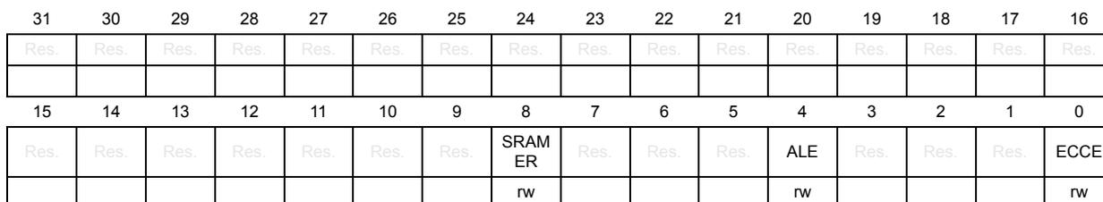
| 31 | 30 | 29 | 28 | 27 | 26 | 25 | 24 | 23 | 22 | 21 | 20 | 19 | 18 | 17 | 16 |
| Res. | Res. | Res. | Res. | Res. | Res. | Res. | Res. | Res. | Res. | Res. | Res. | Res. | Res. | Res. | Res. |
| 15 | 14 | 13 | 12 | 11 | 10 | 9 | 8 | 7 | 6 | 5 | 4 | 3 | 2 | 1 | 0 |
| Res. | Res. | Res. | Res. | Res. | Res. | Res. | SRAM ER | Res. | Res. | Res. | ALE | Res. | Res. | Res. | ECCE |
| rw | rw | rw |
Bits 31:9 Reserved, must be kept at reset value.
Bit 8 SRAMER : SRAM erase
This bit can be set by software only after writing the unlock sequence in ERASEKEY of RAMCFG_BKPSRAMERKEYR. Setting this bit starts the SRAM erase. This bit is automatically cleared by hardware at the end of the erase operation.
0: No erase operation ongoing
1: Erase operation ongoing
Bits 7:5 Reserved, must be kept at reset value.
Bit 4 ALE : Address latch enable
0: Failing address not stored in RAMCFG_BKPSRAMESEAR or _BKPSRAMEDEAR
1: Failing address stored in RAMCFG_BKPSRAMESEAR or _BKPSRAMEDEAR
Bits 3:1 Reserved, must be kept at reset value.
Bit 0 ECCE : ECC enable
When set, this bit can be cleared by software only after writing the unlock sequence in RAMCFG_BKPSRAMECCKEYR.
0: ECC disabled
1: ECC enabled
10.6.12 RAMCFG BKPSRAM interrupt enable register (RAMCFG_BKPSRAMIER)
Address offset: 0x484
Reset value: 0x0000 0000
Reset on any system reset.
| 31 | 30 | 29 | 28 | 27 | 26 | 25 | 24 | 23 | 22 | 21 | 20 | 19 | 18 | 17 | 16 |
|---|---|---|---|---|---|---|---|---|---|---|---|---|---|---|---|
| Res. | Res. | Res. | Res. | Res. | Res. | Res. | Res. | Res. | Res. | Res. | Res. | Res. | Res. | Res. | Res. |
| 15 | 14 | 13 | 12 | 11 | 10 | 9 | 8 | 7 | 6 | 5 | 4 | 3 | 2 | 1 | 0 |
| Res. | Res. | Res. | Res. | Res. | Res. | Res. | Res. | Res. | Res. | Res. | Res. | Res. | Res. | DEIE | SEIE |
| rw | rw |
Bits 31:2 Reserved, must be kept at reset value.
Bit 1 DEIE : ECC double error interrupt enable
0: Double error interrupt disabled
1: Double error interrupt enabled
Bit 0 SEIE : ECC single error interrupt enable
0: Single error interrupt disabled
1: Single error interrupt enabled
10.6.13 RAMCFG BKPSRAM interrupt status register (RAMCFG_BKPSRAMISR)
Address offset: 0x488
Reset value: 0x0000 0000
Reset on any system reset.
| 31 | 30 | 29 | 28 | 27 | 26 | 25 | 24 | 23 | 22 | 21 | 20 | 19 | 18 | 17 | 16 |
|---|---|---|---|---|---|---|---|---|---|---|---|---|---|---|---|
| Res. | Res. | Res. | Res. | Res. | Res. | Res. | Res. | Res. | Res. | Res. | Res. | Res. | Res. | Res. | Res. |
| 15 | 14 | 13 | 12 | 11 | 10 | 9 | 8 | 7 | 6 | 5 | 4 | 3 | 2 | 1 | 0 |
| Res. | Res. | Res. | Res. | Res. | Res. | Res. | SRAM BUSY | Res. | Res. | Res. | Res. | Res. | Res. | DED | SEDC |
| r | r | r |
Bits 31:9 Reserved, must be kept at reset value.
Bit 8 SRAMBUSY : SRAM busy with erase operation
Depending on the SRAM, the erase operation can be performed due to software request, system reset if the option is not disabled by software and tamper detection (see Table 33 ).
0: No erase operation ongoing
1: Erase operation ongoing
Bits 7:2 Reserved, must be kept at reset value.
- Bit 1
DED
: ECC double-error detected
- 0: No double error
- 1: Double error detected
- Bit 0
SEDC
: ECC single error detected and corrected
- 0: No single error detected
- 1: Single error detected and corrected
10.6.14 RAMCFG BKPSRAM single error address register (RAMCFG_BKPSRAMESEAR)
Address offset: 0x48C
Reset value: 0x0000 0000
Reset on any system reset.
| 31 | 30 | 29 | 28 | 27 | 26 | 25 | 24 | 23 | 22 | 21 | 20 | 19 | 18 | 17 | 16 |
|---|---|---|---|---|---|---|---|---|---|---|---|---|---|---|---|
| Res. | Res. | Res. | Res. | Res. | Res. | Res. | Res. | Res. | Res. | Res. | Res. | Res. | Res. | Res. | Res. |
| 15 | 14 | 13 | 12 | 11 | 10 | 9 | 8 | 7 | 6 | 5 | 4 | 3 | 2 | 1 | 0 |
| Res. | Res. | Res. | Res. | Res. | ESEA[10:0] | ||||||||||
| w | w | w | w | w | w | w | w | w | w | w | |||||
Bits 31:11 Reserved, must be kept at reset value.
- Bits 10:0
ESEA[10:0]
: ECC single error address
- When ALE is set in RAMCFG_BKPSRAMCR, this field is updated with the word address corresponding to the ECC single error.
10.6.15 RAMCFG BKPSRAM double error address register (RAMCFG_BKPSRAMEDEAR)
Address offset: 0x490
Reset value: 0x0000 0000
Reset on any system reset.
| 31 | 30 | 29 | 28 | 27 | 26 | 25 | 24 | 23 | 22 | 21 | 20 | 19 | 18 | 17 | 16 |
|---|---|---|---|---|---|---|---|---|---|---|---|---|---|---|---|
| Res. | Res. | Res. | Res. | Res. | Res. | Res. | Res. | Res. | Res. | Res. | Res. | Res. | Res. | Res. | Res. |
| 15 | 14 | 13 | 12 | 11 | 10 | 9 | 8 | 7 | 6 | 5 | 4 | 3 | 2 | 1 | 0 |
| Res. | Res. | Res. | Res. | Res. | EDEA[10:0] | ||||||||||
| w | w | w | w | w | w | w | w | w | w | w | |||||
Bits 31:11 Reserved, must be kept at reset value.
- Bits 10:0
EDEA[10:0]
: ECC double error address
- When ALE is set in RAMCFG_BKPSRAMCR, this field is updated with the word address corresponding to the ECC double error.
10.6.16 RAMCFG BKPSRAM interrupt clear register (RAMCFG_BKPSRAMICR)
Address offset: 0x494
Reset value: 0x0000 0000
Reset on any system reset.
| 31 | 30 | 29 | 28 | 27 | 26 | 25 | 24 | 23 | 22 | 21 | 20 | 19 | 18 | 17 | 16 |
|---|---|---|---|---|---|---|---|---|---|---|---|---|---|---|---|
| Res. | Res. | Res. | Res. | Res. | Res. | Res. | Res. | Res. | Res. | Res. | Res. | Res. | Res. | Res. | Res. |
| 15 | 14 | 13 | 12 | 11 | 10 | 9 | 8 | 7 | 6 | 5 | 4 | 3 | 2 | 1 | 0 |
| Res. | Res. | Res. | Res. | Res. | Res. | Res. | Res. | Res. | Res. | Res. | Res. | Res. | Res. | CDED w | CSEDC w |
Bits 31:2 Reserved, must be kept at reset value.
Bit 1 CDED : Clear ECC double-error interrupt
Writing 1 to this flag clears DED in RAMCFG_BKPSRAMISR.
Bit 0 CSEDC : Clear ECC single-error interrupt
Writing 1 to this flag clears SEDC in RAMCFG_BKPSRAMISR.
10.6.17 RAMCFG BKPSRAM ECC key register (RAMCFG_BKPSRAMECCKEYR)
Address offset: 0x4A4
Reset value: 0x0000 0000
Reset on any system reset.
| 31 | 30 | 29 | 28 | 27 | 26 | 25 | 24 | 23 | 22 | 21 | 20 | 19 | 18 | 17 | 16 |
|---|---|---|---|---|---|---|---|---|---|---|---|---|---|---|---|
| Res. | Res. | Res. | Res. | Res. | Res. | Res. | Res. | Res. | Res. | Res. | Res. | Res. | Res. | Res. | Res. |
| 15 | 14 | 13 | 12 | 11 | 10 | 9 | 8 | 7 | 6 | 5 | 4 | 3 | 2 | 1 | 0 |
| Res. | Res. | Res. | Res. | Res. | Res. | Res. | Res. | w | w | w | w | w | w | w | w |
Bits 31:8 Reserved, must be kept at reset value.
Bits 7:0 ECCKEY[7:0] : ECC write protection key
The following steps are required to unlock the write protection of ECCE in RAMCFG_BKPSRAMCR.
a) Write 0xAE into this field.
b) Write 0x75 into this field.
Note: Writing a wrong key reactivates the write protection.
10.6.18 RAMCFG BKPSRAM erase key register (RAMCFG_BKPSRAMERKEYR)
Address offset: 0x4A8
Reset value: 0x0000 0000
Reset on any system reset.
| 31 | 30 | 29 | 28 | 27 | 26 | 25 | 24 | 23 | 22 | 21 | 20 | 19 | 18 | 17 | 16 |
|---|---|---|---|---|---|---|---|---|---|---|---|---|---|---|---|
| Res. | Res. | Res. | Res. | Res. | Res. | Res. | Res. | Res. | Res. | Res. | Res. | Res. | Res. | Res. | Res. |
| 15 | 14 | 13 | 12 | 11 | 10 | 9 | 8 | 7 | 6 | 5 | 4 | 3 | 2 | 1 | 0 |
| Res. | Res. | Res. | Res. | Res. | Res. | Res. | Res. | ERASEKEY[7:0] | |||||||
| w | w | w | w | w | w | w | w | ||||||||
Bits 31:8 Reserved, must be kept at reset value.
Bits 7:0 ERASEKEY[7:0] : Erase write protection key
The following steps are required to unlock the write protection of SRAMER in RAMCFG_BKPSRAMCR.
- a) Write 0xCA into this field.
- b) Write 0x53 into this field.
Note: Writing a wrong key reactivates the write protection.
10.6.19 RAMCFG FLEXRAM control register (RAMCFG_FLEXRAMCR)
Address offset: 0x500
Reset value: 0x0000 0000
Reset on any system reset.
| 31 | 30 | 29 | 28 | 27 | 26 | 25 | 24 | 23 | 22 | 21 | 20 | 19 | 18 | 17 | 16 |
|---|---|---|---|---|---|---|---|---|---|---|---|---|---|---|---|
| Res. | Res. | Res. | Res. | Res. | Res. | Res. | Res. | Res. | Res. | Res. | Res. | Res. | Res. | Res. | Res. |
| 15 | 14 | 13 | 12 | 11 | 10 | 9 | 8 | 7 | 6 | 5 | 4 | 3 | 2 | 1 | 0 |
| Res. | Res. | Res. | Res. | Res. | Res. | Res. | SRAMER | Res. | Res. | Res. | Res. | Res. | Res. | Res. | Res. |
| rw |
Bits 31:9 Reserved, must be kept at reset value.
Bit 8 SRAMER : SRAM erase
This bit can be set by software only after writing the unlock sequence in ERASEKEY of RAMCFG_FLEXRAMERKEYR. Setting this bit starts the SRAM erase. This bit is automatically cleared by hardware at the end of the erase operation.
- 0: No erase operation ongoing
- 1: Erase operation ongoing
Bits 7:0 Reserved, must be kept at reset value.
10.6.20 RAMCFG FLEXRAM interrupt status register (RAMCFG_FLEXRAMISR)
Address offset: 0x508
Reset value: 0x0000 0000
Reset on any system reset.
| 31 | 30 | 29 | 28 | 27 | 26 | 25 | 24 | 23 | 22 | 21 | 20 | 19 | 18 | 17 | 16 |
|---|---|---|---|---|---|---|---|---|---|---|---|---|---|---|---|
| Res. | Res. | Res. | Res. | Res. | Res. | Res. | Res. | Res. | Res. | Res. | Res. | Res. | Res. | Res. | Res. |
| 15 | 14 | 13 | 12 | 11 | 10 | 9 | 8 | 7 | 6 | 5 | 4 | 3 | 2 | 1 | 0 |
| Res. | Res. | Res. | Res. | Res. | Res. | Res. | SRAM BUSY | Res. | Res. | Res. | Res. | Res. | Res. | Res. | Res. |
| r |
Bits 31:9 Reserved, must be kept at reset value.
Bit 8 SRAMBUSY : SRAM busy with erase operation
Depending on the SRAM, the erase operation can be performed due to software request, system reset if the option is not disabled by software and tamper detection (see Table 33 ).
0: No erase operation ongoing
1: Erase operation ongoing
Bits 7:0 Reserved, must be kept at reset value.
10.6.21 RAMCFG FLEXRAM erase key register (RAMCFG_FLEXRAMERKEYR)
Address offset: 0x528
Reset value: 0x0000 0000
Reset on any system reset.
| 31 | 30 | 29 | 28 | 27 | 26 | 25 | 24 | 23 | 22 | 21 | 20 | 19 | 18 | 17 | 16 |
|---|---|---|---|---|---|---|---|---|---|---|---|---|---|---|---|
| Res. | Res. | Res. | Res. | Res. | Res. | Res. | Res. | Res. | Res. | Res. | Res. | Res. | Res. | Res. | Res. |
| 15 | 14 | 13 | 12 | 11 | 10 | 9 | 8 | 7 | 6 | 5 | 4 | 3 | 2 | 1 | 0 |
| Res. | Res. | Res. | Res. | Res. | Res. | Res. | Res. | ERASEKEY[7:0] | |||||||
| w | w | w | w | w | w | w | w | ||||||||
Bits 31:8 Reserved, must be kept at reset value.
Bits 7:0 ERASEKEY[7:0] : Erase write protection key
The following steps are required to unlock the write protection of SRAMER in RAMCFG_FLEXRAMCR.
a) Write 0xCA into this field.
b) Write 0x53 into this field.
Note: Writing a wrong key reactivates the write protection.
10.6.22 RAMCFG register map
Table 38. RAMCFG register map and reset values
| Offset | Register name | 31 | 30 | 29 | 28 | 27 | 26 | 25 | 24 | 23 | 22 | 21 | 20 | 19 | 18 | 17 | 16 | 15 | 14 | 13 | 12 | 11 | 10 | 9 | 8 | 7 | 6 | 5 | 4 | 3 | 2 | 1 | 0 |
|---|---|---|---|---|---|---|---|---|---|---|---|---|---|---|---|---|---|---|---|---|---|---|---|---|---|---|---|---|---|---|---|---|---|
| 0x000 | RAMCFG_AXISRAM1CR | Res. | Res. | Res. | Res. | Res. | Res. | Res. | Res. | Res. | Res. | Res. | Res. | Res. | Res. | Res. | Res. | Res. | Res. | Res. | Res. | Res. | Res. | Res. | SRAMER | Res. | Res. | Res. | Res. | Res. | Res. | Res. | Res. |
| Reset value | 0 | ||||||||||||||||||||||||||||||||
| 0x004 | Reserved | Reserved | |||||||||||||||||||||||||||||||
| 0x008 + 0x80 * (x - 1) (x = 1 to 6) | RAMCFG_AXISRAMxISR | Res. | Res. | Res. | Res. | Res. | Res. | Res. | Res. | Res. | Res. | Res. | Res. | Res. | Res. | Res. | Res. | Res. | Res. | Res. | Res. | Res. | Res. | Res. | SRAMBUSY | Res. | Res. | Res. | Res. | Res. | Res. | Res. | Res. |
| Reset value | 0 | ||||||||||||||||||||||||||||||||
| 0x028 + 0x80 * (x - 1) (x = 1 to 6) | RAMCFG_AXISRAMxERKEYR | Res. | Res. | Res. | Res. | Res. | Res. | Res. | Res. | Res. | Res. | Res. | Res. | Res. | Res. | Res. | Res. | Res. | Res. | Res. | Res. | Res. | Res. | Res. | Res. | ERASEKEY[7:0] | |||||||
| Reset value | 0 | 0 | 0 | 0 | 0 | 0 | 0 | 0 | |||||||||||||||||||||||||
| 0x080 + 0x80 * (x - 2) (x = 2 to 6) | RAMCFG_AXISRAMxCR | Res. | Res. | Res. | Res. | Res. | Res. | Res. | Res. | Res. | Res. | Res. | SRAMSD | Res. | Res. | Res. | Res. | Res. | Res. | Res. | Res. | Res. | Res. | Res. | SRAMER | Res. | Res. | Res. | Res. | Res. | Res. | Res. | Res. |
| Reset value | 0 | 0 | |||||||||||||||||||||||||||||||
| 0x300 + 0x80 * (x - 1) (x = 1 to 2) | RAMCFG_AHBSRAMxCR | Res. | Res. | Res. | Res. | Res. | Res. | Res. | Res. | Res. | Res. | Res. | Res. | Res. | Res. | Res. | Res. | Res. | Res. | Res. | Res. | Res. | Res. | Res. | SRAMER | Res. | Res. | Res. | Res. | Res. | Res. | Res. | Res. |
| Reset value | 0 | ||||||||||||||||||||||||||||||||
| 0x308 + 0x80 * (x - 1) (x = 1 to 2) Last address: 0x388 | RAMCFG_AHBSRAMxISR | Res. | Res. | Res. | Res. | Res. | Res. | Res. | Res. | Res. | Res. | Res. | Res. | Res. | Res. | Res. | Res. | Res. | Res. | Res. | Res. | Res. | Res. | Res. | SRAMBUSY | Res. | Res. | Res. | Res. | Res. | Res. | Res. | Res. |
| Reset value | 0 | ||||||||||||||||||||||||||||||||
| 0x328 + 0x80 * (x - 1) (x = 1 to 2) Last address: 0x3A8 | RAMCFG_AHBSRAMxERKEYR | Res. | Res. | Res. | Res. | Res. | Res. | Res. | Res. | Res. | Res. | Res. | Res. | Res. | Res. | Res. | Res. | Res. | Res. | Res. | Res. | Res. | Res. | Res. | Res. | ERASEKEY[7:0] | |||||||
| Reset value | 0 | 0 | 0 | 0 | 0 | 0 | 0 | 0 | 0 | ||||||||||||||||||||||||
| 0x3AC - 0x3FC | Reserved | Reserved | |||||||||||||||||||||||||||||||
| 0x400 | RAMCFG_VENCRAMCR | Res. | Res. | Res. | Res. | Res. | Res. | Res. | Res. | Res. | Res. | Res. | Res. | Res. | Res. | Res. | Res. | Res. | Res. | Res. | Res. | Res. | Res. | Res. | SRAMER | Res. | Res. | Res. | Res. | Res. | Res. | Res. | Res. |
| Reset value | 0 | ||||||||||||||||||||||||||||||||
| 0x404 | Reserved | Reserved | |||||||||||||||||||||||||||||||
| 0x408 | RAMCFG_VENCRAMISR | Res. | Res. | Res. | Res. | Res. | Res. | Res. | Res. | Res. | Res. | Res. | Res. | Res. | Res. | Res. | Res. | Res. | Res. | Res. | Res. | Res. | Res. | Res. | SRAMBUSY | Res. | Res. | Res. | Res. | Res. | Res. | Res. | Res. |
| Reset value | 0 | ||||||||||||||||||||||||||||||||
| 0x40C - 0x424 | Reserved | Reserved | |||||||||||||||||||||||||||||||
| 0x428 | RAMCFG_VENCRAMERKEYR | Res. | Res. | Res. | Res. | Res. | Res. | Res. | Res. | Res. | Res. | Res. | Res. | Res. | Res. | Res. | Res. | Res. | Res. | Res. | Res. | Res. | Res. | Res. | Res. | ERASEKEY[7:0] | |||||||
| Reset value | 0 | 0 | 0 | 0 | 0 | 0 | 0 | 0 | |||||||||||||||||||||||||
Table 38. RAMCFG register map and reset values (continued)
| Offset | Register name | 31 | 30 | 29 | 28 | 27 | 26 | 25 | 24 | 23 | 22 | 21 | 20 | 19 | 18 | 17 | 16 | 15 | 14 | 13 | 12 | 11 | 10 | 9 | 8 | 7 | 6 | 5 | 4 | 3 | 2 | 1 | 0 |
|---|---|---|---|---|---|---|---|---|---|---|---|---|---|---|---|---|---|---|---|---|---|---|---|---|---|---|---|---|---|---|---|---|---|
| 0x42C - 0x47C | Reserved | Reserved | |||||||||||||||||||||||||||||||
| 0x480 | RAMCFG_BKPSRAMCR | Res. | Res. | Res. | Res. | Res. | Res. | Res. | Res. | Res. | Res. | Res. | Res. | Res. | Res. | Res. | Res. | Res. | Res. | Res. | Res. | Res. | Res. | Res. | SRAMER | Res. | Res. | Res. | Res. | Res. | Res. | Res. | ECCE |
| Reset value | 0 | 0 | |||||||||||||||||||||||||||||||
| 0x484 | RAMCFG_BKPSRAMIER | Res. | Res. | Res. | Res. | Res. | Res. | Res. | Res. | Res. | Res. | Res. | Res. | Res. | Res. | Res. | Res. | Res. | Res. | Res. | Res. | Res. | Res. | Res. | Res. | Res. | Res. | Res. | Res. | Res. | Res. | DEIE | SEIE |
| Reset value | 0 | ||||||||||||||||||||||||||||||||
| 0x488 | RAMCFG_BKPSRAMISR | Res. | Res. | Res. | Res. | Res. | Res. | Res. | Res. | Res. | Res. | Res. | Res. | Res. | Res. | Res. | Res. | Res. | Res. | Res. | Res. | Res. | Res. | Res. | SRAMBUSY | Res. | Res. | Res. | Res. | Res. | Res. | DED | SEDC |
| Reset value | 0 | 0 | 0 | ||||||||||||||||||||||||||||||
| 0x48C | RAMCFG_BKPSRAMESEAR | Res. | Res. | Res. | Res. | Res. | Res. | Res. | Res. | Res. | Res. | Res. | Res. | Res. | Res. | Res. | Res. | Res. | Res. | Res. | Res. | Res. | Res. | ESEA[10:0] | |||||||||
| Reset value | 0 | 0 | 0 | 0 | 0 | 0 | 0 | 0 | |||||||||||||||||||||||||
| 0x490 | RAMCFG_BKPSRAMEDEAR | Res. | Res. | Res. | Res. | Res. | Res. | Res. | Res. | Res. | Res. | Res. | Res. | Res. | Res. | Res. | Res. | Res. | Res. | Res. | Res. | Res. | Res. | EDEA[10:0] | |||||||||
| Reset value | 0 | 0 | 0 | 0 | 0 | 0 | 0 | 0 | |||||||||||||||||||||||||
| 0x494 | RAMCFG_BKPSRAMICR | Res. | Res. | Res. | Res. | Res. | Res. | Res. | Res. | Res. | Res. | Res. | Res. | Res. | Res. | Res. | Res. | Res. | Res. | Res. | Res. | Res. | Res. | Res. | Res. | Res. | Res. | Res. | Res. | Res. | Res. | ODED | CSEDC |
| Reset value | 0 | ||||||||||||||||||||||||||||||||
| 0x498 - 0x4A0 | Reserved | Reserved | |||||||||||||||||||||||||||||||
| 0x4A4 | RAMCFG_BKPSRAMECCKEYR | Res. | Res. | Res. | Res. | Res. | Res. | Res. | Res. | Res. | Res. | Res. | Res. | Res. | Res. | Res. | Res. | Res. | Res. | Res. | Res. | Res. | Res. | ECCKEY[7:0] | |||||||||
| Reset value | 0 | 0 | 0 | 0 | 0 | 0 | 0 | 0 | |||||||||||||||||||||||||
| 0x4A8 | RAMCFG_BKPSRAMERKEYR | Res. | Res. | Res. | Res. | Res. | Res. | Res. | Res. | Res. | Res. | Res. | Res. | Res. | Res. | Res. | Res. | Res. | Res. | Res. | Res. | Res. | Res. | ERASEKEY[7:0] | |||||||||
| Reset value | 0 | 0 | 0 | 0 | 0 | 0 | 0 | 0 | |||||||||||||||||||||||||
| 0x4AC | Reserved | Reserved | |||||||||||||||||||||||||||||||
| 0x500 | RAMCFG_FLEXRAMCR | Res. | Res. | Res. | Res. | Res. | Res. | Res. | Res. | Res. | Res. | Res. | Res. | Res. | Res. | Res. | Res. | Res. | Res. | Res. | Res. | Res. | Res. | Res. | SRAMER | Res. | Res. | Res. | Res. | Res. | Res. | Res. | Res. |
| Reset value | 0 | ||||||||||||||||||||||||||||||||
| 0x504 | Reserved | Reserved | |||||||||||||||||||||||||||||||
| 0x508 | RAMCFG_FLEXRAMISR | Res. | Res. | Res. | Res. | Res. | Res. | Res. | Res. | Res. | Res. | Res. | Res. | Res. | Res. | Res. | Res. | Res. | Res. | Res. | Res. | Res. | Res. | Res. | SRAMBUSY | Res. | Res. | Res. | Res. | Res. | Res. | Res. | Res. |
| Reset value | 0 | ||||||||||||||||||||||||||||||||
| 0x50C - 0x524 | Reserved | Reserved | |||||||||||||||||||||||||||||||
| 0x528 | RAMCFG_FLEXRAMERKEYR | Res. | Res. | Res. | Res. | Res. | Res. | Res. | Res. | Res. | Res. | Res. | Res. | Res. | Res. | Res. | Res. | Res. | Res. | Res. | Res. | Res. | Res. | ERASEKEY[7:0] | |||||||||
| Reset value | 0 | 0 | 0 | 0 | 0 | 0 | 0 | 0 | |||||||||||||||||||||||||