6. Resource isolation framework security controller (RIFSC)
6.1 Introduction
Resource isolation framework (RIF) is a set of hardware blocks designed to enforce and manage isolation of STM32 hardware resources like memory and peripherals. Some resources (such as GP/HPDMA) manage their own security configuration internally (they are configured locally). Such resources are called “RIF-aware”. Most resources are “non-RIF-aware”. The RIFSC centralizes the security configuration of such non-RIF-aware resources.
6.2 RIFSC main features
- • RISC registers associated with RISUP logic (resource isolation slave unit for peripherals) sitting in front of the configuration port of non-RIF-aware peripherals, and with RCC peripheral clock control logic, assigning security and privilege levels to peripheral access and peripheral clock control.
- • RIMC registers associated with RIMU logic (resource isolation master unit), assigning non-RIF-aware bus masters the secure, privilege and compartment (CID) information they drive onto the system bus when initiating AXI transactions.
- • Secure guard, where an AXI bus master port is forced to be nonsecure when its associated configuration port is programmed nonsecure
- • Support for a special debug domain, giving greater access for the debugger
6.3 RIFSC functional description
6.3.1 RIFSC reset and clocks
The RIFSC has a single reset. After a system reset, all non-RIF-aware peripherals become non-secure and unprivileged, reachable by any CID.
6.3.2 RISUP
RISUP blocks are instantiated in front of the AHB configuration port of non-RIF-aware peripherals to filter configuration accesses.
Each non-RIF-aware peripheral is assigned a unique “RISUP index” \( p < 128 \) . Whenever the RISUP in front of peripheral \( p \) blocks an illegal access, it sends an “illegal access event” pulse to the IAC. The IAC records this event in the IAFp bit of the relevant IAC_ISRx register. Thus, the RISUP index is aligned with the IAC index.
For \( x < 4 \) and \( i < 32 \) , the filtering is determined as follows.
- • If \( \text{RIFSC\_RISC\_SECCFGx}[i] = 1 \) , then nonsecure accesses to peripheral \( p = i + 32x \) are blocked. Also, nonsecure world attempts to program RCC registers to turn off the clock of (or reset) peripheral \( p \) are blocked.
- • If RIFSC_RISC_PRIVCFGRx[i] = 1, then user accesses to peripheral p = i + 32x are blocked. Also, attempts by a user process to program RCC registers to turn off the clock of (or reset) peripheral p are blocked.
Whenever the RCC detects an illegal attempt to turn off a clock of (or reset) a peripheral, it sends an event pulse to the IAC (recorded in the IAF136 bit of the relevant IAC_ISRx register).
Note: There is no record of which peripheral was the object of this illegal attempt.
Table 20 identifies the RISUP index of each non-RIF-aware peripheral.
Table 20. RISUP indexes
| RISUPs 31 to 0 (see RIFSC_RISC_PRIVCFGR0 / SECCFGR0 / RCFGLOCKR0) | |||||||||||||||||||||||||||||||
|---|---|---|---|---|---|---|---|---|---|---|---|---|---|---|---|---|---|---|---|---|---|---|---|---|---|---|---|---|---|---|---|
| 31 | 30 | 29 | 28 | 27 | 26 | 25 | 24 | 23 | 22 | 21 | 20 | 19 | 18 | 17 | 16 | 15 | 14 | 13 | 12 | 11 | 10 | 9 | 8 | 7 | 6 | 5 | 4 | 3 | 2 | 1 | 0 |
| TIM5 | TIM4 | TIM3 | TIM2 | TIM1 | FDCAN1/2/3 | LPUART1 | USART10 | UART9 | UART8 | UART7 | USART6 | UART5 | UART4 | USART3 | USART2 | USART1 | I3C2 | I3C1 | I2C4 | I2C3 | I2C2 | I2C1 | SAI2 | - | SAI1 | SPI6/I2S6 | SPI5 | SPI4 | SPI3/I2S3 | SPI2/I2S2 | SPI1/I2S1 |
| RISUPs 63 to 32 (see RIFSC_RISC_PRIVCFGR1 / SECCFGR1 / RCFGLOCKR1) | |||||||||||||||||||||||||||||||
| 63 | 62 | 61 | 60 | 59 | 58 | 57 | 56 | 55 | 54 | 53 | 52 | 51 | 50 | 49 | 48 | 47 | 46 | 45 | 44 | 43 | 42 | 41 | 40 | 39 | 38 | 37 | 36 | 35 | 34 | 33 | 32 |
| - | SYSCFG | SPDIFRX | ETH1 | - | UCPD1 | OTG2_HS | OTG1_HS | MDIOS | SDMMC2 | SDMMC1 | MDF1 | ADF1 | LPTIM5 | LPTIM4 | LPTIM3 | LPTIM2 | LPTIM1 | GFXTIM | TIM18 | TIM17 | TIM16 | TIM15 | TIM14 | TIM13 | TIM12 | TIM11 | TIM10 | TIM9 | TIM8 | TIM7 | TIM6 |
| RISUPs 95 to 64 (see RIFSC_RISC_PRIVCFGR2 / SECCFGR2 / RCFGLOCKR2) | |||||||||||||||||||||||||||||||
| 95 | 94 | 93 | 92 | 91 | 90 | 89 | 88 | 87 | 86 | 85 | 84 | 83 | 82 | 81 | 80 | 79 | 78 | 77 | 76 | 75 | 74 | 73 | 72 | 71 | 70 | 69 | 68 | 67 | 66 | 65 | 64 |
| - | DCMI | DCMIPP | CSI2HOST | - | FMC | XSPIM | XSPI3 | XSPI2 | XSPI1 | - | MCE4 | MCE3 | MCE2 | MCE1 | CRYP1 | HASH | SAES | PKA | RNG | - | - | - | - | - | - | WWDG | IWDG | CRC | - | VREFBUF | ADC12 |
| RISUPs 127 to 96 (see RIFSC_RISC_PRIVCFGR3 / SECCFGR3 / RCFGLOCKR3) | |||||||||||||||||||||||||||||||
| 127 | 126 | 125 | 124 | 123 | 122 | 121 | 120 | 119 | 118 | 117 | 116 | 115 | 114 | 113 | 112 | 111 | 110 | 109 | 108 | 107 | 106 | 105 | 104 | 103 | 102 | 101 | 100 | 99 | 98 | 97 | 96 |
| - | - | - | - | - | - | - | - | - | - | - | - | - | - | - | - | - | - | - | - | - | NPU | - | LTDC_L2 | LTDC_L1 | LTDC_CMN | DMA2D | GFXMMU | GPU | ICACHE | VENC | JPEG |
The RISUP generates a bus error if an instruction fetch arrives at the peripheral.
6.3.3 RCC security settings for RIF-aware peripherals and RAMs
Table 21 shows the use made of the RIFSC to configure the security and privilege access rights for resetting or gating the clock of RIF-aware peripherals and RAMs (resources that
do not have RISUPs in front of them). Just as for all the non-RIF-aware peripherals with RISUPs mentioned above, the outputs of the registers below are also wired to the RCC.
Table 21. RISC indexes purely for RCC security control
| RCC security controls 159 to 128 (RIFSC_RISC_PRIVCFGR4 / SECCFGR4 / RCFGLOCKR4) | |||||||||||||||||||||||||||||||
|---|---|---|---|---|---|---|---|---|---|---|---|---|---|---|---|---|---|---|---|---|---|---|---|---|---|---|---|---|---|---|---|
| 159 | 158 | 157 | 156 | 155 | 154 | 153 | 152 | 151 | 150 | 149 | 148 | 147 | 146 | 145 | 144 | 143 | 142 | 141 | 140 | 139 | 138 | 137 | 136 | 135 | 134 | 133 | 132 | 131 | 130 | 129 | 128 |
| GPIOA | - | BKPSRAM | AHBRAM2 | AHBRAM1 | - | NPU config | - | - | - | - | - | VENCRAM | CACHEAXI RAM | FLEXRAM | - | - | - | CPU RAM1 | CPU RAM0 | - | - | - | - | - | - | RTC | - | HPDMA1 | GPDMA1 | - | - |
| ⋮ | |||||||||||||||||||||||||||||||
| RCC security controls 191 to 160 (RIFSC_RISC_PRIVCFGR5 / SECCFGR5 / RCFGLOCKR5) | |||||||||||||||||||||||||||||||
| 191 | 190 | 189 | 188 | 187 | 186 | 185 | 184 | 183 | 182 | 181 | 180 | 179 | 178 | 177 | 176 | 175 | 174 | 173 | 172 | 171 | 170 | 169 | 168 | 167 | 166 | 165 | 164 | 163 | 162 | 161 | 160 |
| - | RAMCFG | - | - | HDP | - | - | XSPIPHY2 | XSPIPHY1 | XSPIPHYCOMP | - | NPU_RAM3 | NPU_RAM2 | NPU_RAM1 | NPU_RAM0 | - | MCO2 | MCO1 | DTS | - | GPIOQ | GPIO P | GPIO O | GPIO N | - | GPIO H | GPIO G | GPIO F | GPIO E | GPIO D | GPIO C | GPIO B |
Note: For the RIF-aware peripherals, it is the responsibility of the trusted domain software to make sure this security configuration of the control of the clock and reset of the peripheral is consistent with the internal security configuration of this peripheral.
6.3.4 RIMU
The security attributes (CID, security, privilege) of accesses made by a non-RIF-aware peripheral that is an AXI bus master, can be configured in RIMC_ATTRx registers, where x is the “RIMU index” of the peripheral. Table 22 gives the index of each of these AXI bus master peripherals, and the index of the related RISUP protecting the configuration port of this peripheral. If nonsecure world software is permitted to configure the peripheral, then the RIMU_ATTRx[MSEC] setting is ignored, and all AXI accesses initiated by the peripheral are forced to be nonsecure too. This override mechanism is referred to as “secure guard”.
Table 22. RIMU resource assignment
| Master index | Master name | Secure guard RISUP index |
|---|---|---|
| 0 | Trace (ETR) | No RISUP |
| 1 | NPU | 106 |
| 2 | SDMMC1 | 53 |
| 3 | SDMMC2 | 54 |
| 4 | OTG1 | 56 |
| 5 | OTG2 | 57 |
| 6 | ETH1 | 60 |
Table 22. RIMU resource assignment (continued)
| Master index | Master name | Secure guard RISUP index |
|---|---|---|
| 7 | GPU | 99 |
| 8 | DMA2D | 101 |
| 9 | DCMIPP | 93 |
| 10 | LTDC_L1 | 103 |
| 11 | LTDC_L2 | 104 |
| 12 | VENC | 97 |
RIMC registers must be initialized by the secure privileged software after the device reset. Optionally, this software can set the GLOCK bit in RIMC_CR, preventing further writes to all RIMC registers. This bit can only be cleared by a power-on reset.
The RISC_RIMC_CR register contains a DAPCID field that gives the CID value used by debugger (DAP) accesses onto the AXI bus. The reset value of this register is 0x7. All RISAFs treat a 0x7 as a legal CID value, regardless of their configuration. The secure privileged master can reprogram the DAPCID to allow the DAP to mimic another compartment (for example, to debug the security configuration).
6.4 RIFSC registers
These registers are accessible through the register interface of the RIFSC peripheral.
6.4.1 RIFSC RISC slave configuration register x (RIFSC_RISC_CR)
Address offset: 0x000
Reset value: 0x0000 0000
Secure privileged write access only. Any read access is allowed on this register. Writes are ignored if GLOCK is set in this register.
| 31 | 30 | 29 | 28 | 27 | 26 | 25 | 24 | 23 | 22 | 21 | 20 | 19 | 18 | 17 | 16 |
|---|---|---|---|---|---|---|---|---|---|---|---|---|---|---|---|
| Res. | Res. | Res. | Res. | Res. | Res. | Res. | Res. | Res. | Res. | Res. | Res. | Res. | Res. | Res. | Res. |
| 15 | 14 | 13 | 12 | 11 | 10 | 9 | 8 | 7 | 6 | 5 | 4 | 3 | 2 | 1 | 0 |
| Res. | Res. | Res. | Res. | Res. | Res. | Res. | Res. | Res. | Res. | Res. | Res. | Res. | Res. | Res. | GLOCK |
| rs |
Bits 31:1 Reserved, must be kept at reset value.
Bit 0 GLOCK : Global lock
This bit locks the configuration of RIFSC RISC registers until next reset. This bit is cleared by default and, once set, it cannot be reset until global RIFSC reset.
0: RIFSC RISC registers are writable.
1: All writes to RIFSC RISC registers are ignored.
6.4.2 RIFSC RISC slave security configuration register x (RIFSC_RISC_SECCFGRx)
Address offset: 0x010 + 0x4 * x, (x = 0 to 5)
Reset value: 0x0000 0000
Nonsecure or unprivileged writes to this register are ignored, while any read is allowed. Writes are ignored if GLOCK is set in RIFSC_RISC_CR.
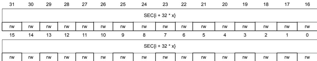
| 31 | 30 | 29 | 28 | 27 | 26 | 25 | 24 | 23 | 22 | 21 | 20 | 19 | 18 | 17 | 16 |
| SEC{i + 32 * x} | |||||||||||||||
| rw | rw | rw | rw | rw | rw | rw | rw | rw | rw | rw | rw | rw | rw | rw | rw |
| 15 | 14 | 13 | 12 | 11 | 10 | 9 | 8 | 7 | 6 | 5 | 4 | 3 | 2 | 1 | 0 |
| SEC{i + 32 * x} | |||||||||||||||
| rw | rw | rw | rw | rw | rw | rw | rw | rw | rw | rw | rw | rw | rw | rw | rw |
Bits 31:0 SEC{i + 32 * x} : security configuration for peripheral {i + 32 * x} (i = 0 to 31)
0: Secure and nonsecure data access are granted to the peripheral {i + 32 * x}.
1: Secure data access only are granted to the peripheral {i + 32 * x}.
6.4.3 RIFSC RISFC slave privileged register x (RIFSC_RISC_PRIVCFGRx)
Address offset: 0x030 + 0x4 * x, (x = 0 to 5)
Reset value: 0x0000 0000
Unprivileged writes to this register are ignored, while any read is allowed. Writes are ignored if GLOCK is set in RIFSC_RISC_CR.
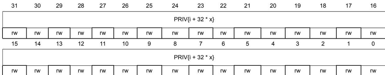
| 31 | 30 | 29 | 28 | 27 | 26 | 25 | 24 | 23 | 22 | 21 | 20 | 19 | 18 | 17 | 16 |
| PRIV{i + 32 * x} | |||||||||||||||
| rw | rw | rw | rw | rw | rw | rw | rw | rw | rw | rw | rw | rw | rw | rw | rw |
| 15 | 14 | 13 | 12 | 11 | 10 | 9 | 8 | 7 | 6 | 5 | 4 | 3 | 2 | 1 | 0 |
| PRIV{i + 32 * x} | |||||||||||||||
| rw | rw | rw | rw | rw | rw | rw | rw | rw | rw | rw | rw | rw | rw | rw | rw |
Bits 31:0 PRIV{i + 32 * x} : privileged-only access permission for peripheral {i + 32 * x} (i = 0 to 31)
0: Privileged and unprivileged data access are granted to the peripheral {i + 32 * x}.
1: Privileged data access only are granted to the peripheral {i + 32 * x}.
Note: If corresponding SEC{i + 32 * x} bit is set in RIFSC_RISC_SECCFGRx, this bit can only be written by a secure privileged application.
6.4.4 RIFSC RISC slave resource configuration lock register x (RIFSC_RISC_RCFGLOCKRx)
Address offset: 0x050 + 0x4 * x, (x = 0 to 5)
Reset value: 0x0000 0000
Secure privileged write access only. Any read access is allowed on this register. Writes are ignored if GLOCK is set in this register.

| 31 | 30 | 29 | 28 | 27 | 26 | 25 | 24 | 23 | 22 | 21 | 20 | 19 | 18 | 17 | 16 |
| RLOCK{i + 32 * x} | |||||||||||||||
| rs | rs | rs | rs | rs | rs | rs | rs | rs | rs | rs | rs | rs | rs | rs | rs |
| 15 | 14 | 13 | 12 | 11 | 10 | 9 | 8 | 7 | 6 | 5 | 4 | 3 | 2 | 1 | 0 |
| RLOCK{i + 32 * x} | |||||||||||||||
| rs | rs | rs | rs | rs | rs | rs | rs | rs | rs | rs | rs | rs | rs | rs | rs |
Bits 31:0 RLOCK{i + 32 * x} : resource lock for peripheral {i + 32 * x} (i = 0 to 31)
This bit is set to lock the peripheral resource {i + 32 * x}. It is cleared by default and, once set, this bit cannot be cleared until the RIFSC RISC peripheral is reset.
0: SEC{i + 32 * x} in RIFSC_RISC_SECCFGRx and PRIV{i + 32 * x} in RIFSC_RISC_PRIVCFG Rx are writable.
1: Writes to SEC{i + 32 * x} and PRIV{i + 32 * x} are ignored.
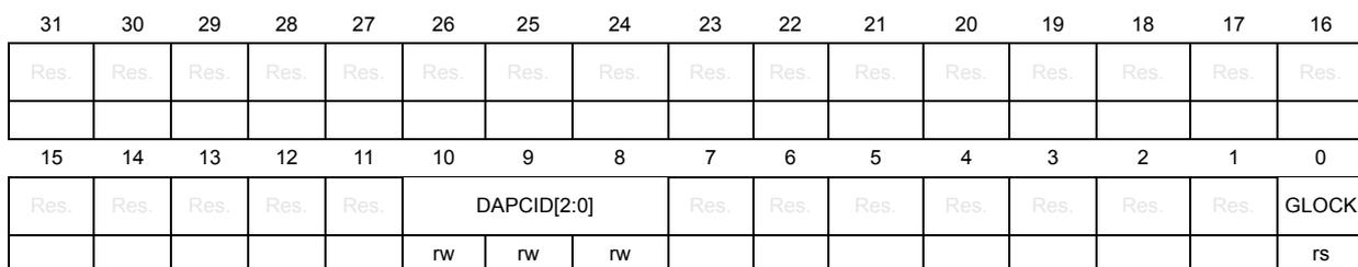
6.4.5 RIFSC RIMC master configuration register (RIFSC_RIMC_CR)
Address offset: 0xC00
Reset value: 0x0000 0710
Secure privileged write access only. Any read access is allowed on this register. Writes are ignored if GLOCK is set in RIFSC_RIMC_CR.
| 31 | 30 | 29 | 28 | 27 | 26 | 25 | 24 | 23 | 22 | 21 | 20 | 19 | 18 | 17 | 16 |
| Res. | Res. | Res. | Res. | Res. | Res. | Res. | Res. | Res. | Res. | Res. | Res. | Res. | Res. | Res. | Res. |
| 15 | 14 | 13 | 12 | 11 | 10 | 9 | 8 | 7 | 6 | 5 | 4 | 3 | 2 | 1 | 0 |
| Res. | Res. | Res. | Res. | Res. | DAPCID[2:0] | Res. | Res. | Res. | Res. | Res. | Res. | Res. | GLOCK | ||
| rw | rw | rw | rs | ||||||||||||
Bits 31:11 Reserved, must be kept at reset value.
Bits 10:8 DAPCID[2:0] : debug access port compartment ID
This bitfield defines the CID of the DAP.
Bits 7:1 Reserved, must be kept at reset value.
Bit 0 GLOCK : global lock
This bit is used to lock the configuration of RIFSC RIMC registers until next reset. This bit is cleared by default and, once set, it cannot be reset until global RIFSC reset.
0: RIFSC RIMC registers are writable.
1: All writes to RIFSC RIMC registers are ignored.
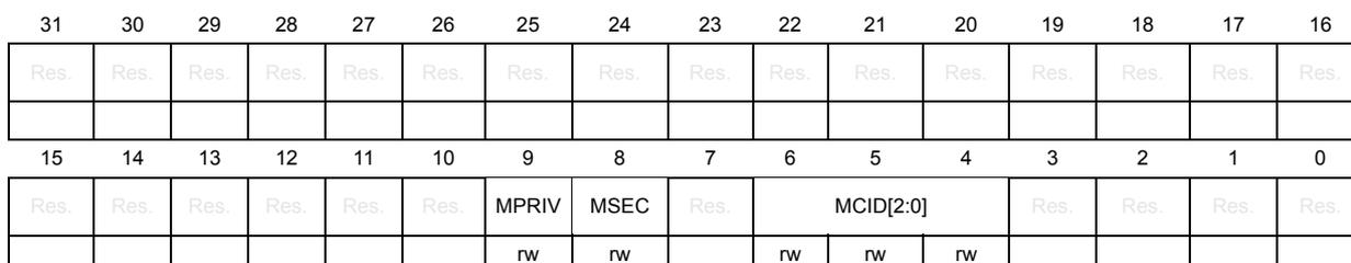
6.4.6 RIFSC RIMC master attribute register x (RIFSC_RIMC_ATTRx)
Address offset: 0xC10 + x * 0x4 (x = 0 to 12)
Reset value: 0x0000 0000
Secure privileged write access only. Any read access is allowed on this register.
| 31 | 30 | 29 | 28 | 27 | 26 | 25 | 24 | 23 | 22 | 21 | 20 | 19 | 18 | 17 | 16 |
| Res. | Res. | Res. | Res. | Res. | Res. | Res. | Res. | Res. | Res. | Res. | Res. | Res. | Res. | Res. | Res. |
| 15 | 14 | 13 | 12 | 11 | 10 | 9 | 8 | 7 | 6 | 5 | 4 | 3 | 2 | 1 | 0 |
| Res. | Res. | Res. | Res. | Res. | Res. | MPRIV | MSEC | Res. | MCID[2:0] | Res. | Res. | Res. | Res. | ||
| rw | rw | rw | rw | rw | |||||||||||
Bits 31:10 Reserved, must be kept at reset value.
Bit 9 MPRIV : master privileged
Value of the privileged flag on the interconnect for this master.
0: This master is unprivileged.
1: This master is privileged.
Bit 8 MSEC : master secure
Value of the secure flag on the interconnect for this master.
0: This master is nonsecure.
1: This master is secure.
Bit 7 Reserved, must be kept at reset value.
Bits 6:4 MCID[2:0] : master CID
Value of the CID flag on the interconnect for this master. This bitfield cannot be written with a value of 0x7 (write to MCID[2:0] is ignored).
Bits 3:0 Reserved, must be kept at reset value.
6.4.7 RIFSC peripheral protection status register 0 (RIFSC_PPSR0)
Address offset: 0xFB0
Reset value: 0xFFFF FF7F
| 31 | 30 | 29 | 28 | 27 | 26 | 25 | 24 | 23 | 22 | 21 | 20 | 19 | 18 | 17 | 16 |
| PPEN{i} | |||||||||||||||
| r | r | r | r | r | r | r | r | r | r | r | r | r | r | r | r |
| 15 | 14 | 13 | 12 | 11 | 10 | 9 | 8 | 7 | 6 | 5 | 4 | 3 | 2 | 1 | 0 |
| PPEN{i} | |||||||||||||||
| r | r | r | r | r | r | r | r | r | r | r | r | r | r | r | r |
Bits 31:0 PPEN{i} : peripheral protection enable {i} ( \( i = 0 \) to \( 31 \) )
0: SEC{i}, PRIV{i}, and RLOCK{i} bits are not present.
1: SEC{i}, PRIV{i}, and RLOCK{i} bits are present.
6.4.8 RIFSC peripheral protection status register 1 (RIFSC_PPSR1)
Address offset: 0xFB4
Reset value: 0x77FF FFFF

| 31 | 30 | 29 | 28 | 27 | 26 | 25 | 24 | 23 | 22 | 21 | 20 | 19 | 18 | 17 | 16 |
| PPEN{i + 32} | |||||||||||||||
| r | r | r | r | r | r | r | r | r | r | r | r | r | r | r | r |
| 15 | 14 | 13 | 12 | 11 | 10 | 9 | 8 | 7 | 6 | 5 | 4 | 3 | 2 | 1 | 0 |
| PPEN{i + 32} | |||||||||||||||
| r | r | r | r | r | r | r | r | r | r | r | r | r | r | r | r |
Bits 31:0 PPEN{i + 32} : peripheral protection enable {i + 32} (i = 0 to 31)
- 0: SEC{i + 32}, PRIV{i + 32}, and RLOCK{i + 32} bits are not present.
- 1: SEC{i + 32}, PRIV{i + 32}, and RLOCK{i + 32} bits are present.
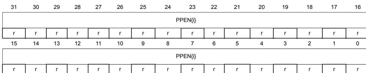
6.4.9 RIFSC peripheral protection status register 2 (RIFSC_PPSR2)
Address offset: 0xFB8
Reset value: 0xF7DF F03B
| 31 | 30 | 29 | 28 | 27 | 26 | 25 | 24 | 23 | 22 | 21 | 20 | 19 | 18 | 17 | 16 |
| PPEN{i + 64} | |||||||||||||||
| r | r | r | r | r | r | r | r | r | r | r | r | r | r | r | r |
| 15 | 14 | 13 | 12 | 11 | 10 | 9 | 8 | 7 | 6 | 5 | 4 | 3 | 2 | 1 | 0 |
| PPEN{i + 64} | |||||||||||||||
| r | r | r | r | r | r | r | r | r | r | r | r | r | r | r | r |
Bits 31:0 PPEN{i + 64} : peripheral protection enable {i + 64} (i = 0 to 31)
- 0: SEC{i + 64}, PRIV{i + 64}, and RLOCK{i + 64} bits are not present.
- 1: SEC{i + 64}, PRIV{i + 64}, and RLOCK{i + 64} bits are present.
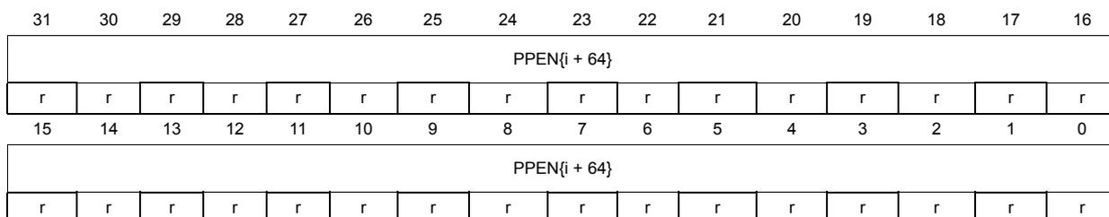
6.4.10 RIFSC peripheral protection status register 3 (RIFSC_PPSR3)
Address offset: 0xFBC
Reset value: 0x0000 05FF
| 31 | 30 | 29 | 28 | 27 | 26 | 25 | 24 | 23 | 22 | 21 | 20 | 19 | 18 | 17 | 16 |
| PPEN{i + 96} | |||||||||||||||
| r | r | r | r | r | r | r | r | r | r | r | r | r | r | r | r |
| 15 | 14 | 13 | 12 | 11 | 10 | 9 | 8 | 7 | 6 | 5 | 4 | 3 | 2 | 1 | 0 |
| PPEN{i + 96} | |||||||||||||||
| r | r | r | r | r | r | r | r | r | r | r | r | r | r | r | r |
Bits 31:0 PPEN{i + 96} : peripheral protection enable {i + 96} (i = 0 to 31)
0: SEC{i + 96}, PRIV{i + 96}, and RLOCK{i + 96} bits are not present.
1: SEC{i + 96}, PRIV{i + 96}, and RLOCK{i + 96} bits are present.
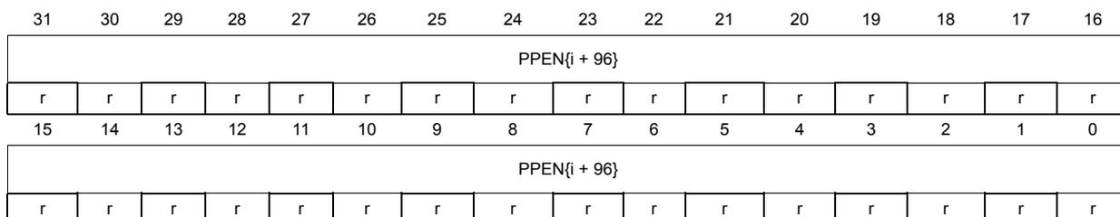
6.4.11 RIFSC peripheral protection status register 4 (RIFSC_PPSR4)
Address offset: 0xFC0
Reset value: 0xBBEF FFEF
| 31 | 30 | 29 | 28 | 27 | 26 | 25 | 24 | 23 | 22 | 21 | 20 | 19 | 18 | 17 | 16 |
| PPEN{i + 128} | |||||||||||||||
| r | r | r | r | r | r | r | r | r | r | r | r | r | r | r | r |
| 15 | 14 | 13 | 12 | 11 | 10 | 9 | 8 | 7 | 6 | 5 | 4 | 3 | 2 | 1 | 0 |
| PPEN{i + 128} | |||||||||||||||
| r | r | r | r | r | r | r | r | r | r | r | r | r | r | r | r |
Bits 31:0 PPEN{i + 128} : peripheral protection enable {i + 128} (i = 0 to 31)
0: SEC{i + 128}, PRIV{i + 128}, and RLOCK{i + 128} bits are not present.
1: SEC{i + 128}, PRIV{i + 128}, and RLOCK{i + 128} bits are present.
6.4.12 RIFSC peripheral protection status register 5 (RIFSC_PPSR5)
Address offset: 0xFC4
Reset value: 0x7DDE EF7F
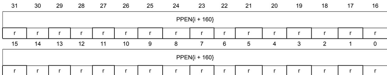
| 31 | 30 | 29 | 28 | 27 | 26 | 25 | 24 | 23 | 22 | 21 | 20 | 19 | 18 | 17 | 16 |
| PPEN{i + 160} | |||||||||||||||
| r | r | r | r | r | r | r | r | r | r | r | r | r | r | r | r |
| 15 | 14 | 13 | 12 | 11 | 10 | 9 | 8 | 7 | 6 | 5 | 4 | 3 | 2 | 1 | 0 |
| PPEN{i + 160} | |||||||||||||||
| r | r | r | r | r | r | r | r | r | r | r | r | r | r | r | r |
Bits 31:0 PPEN{i + 160} : peripheral protection enable {i + 160} (i = 0 to 31)
0: SEC{i + 160}, PRIV{i + 160}, and RLOCK{i + 160} bits are not present.
1: SEC{i + 160}, PRIV{i + 160}, and RLOCK{i + 160} bits are present.
6.4.13 RIFSC register map
Table 23. RIFSC register map and reset values
| Offset | Register name | 31 | 30 | 29 | 28 | 27 | 26 | 25 | 24 | 23 | 22 | 21 | 20 | 19 | 18 | 17 | 16 | 15 | 14 | 13 | 12 | 11 | 10 | 9 | 8 | 7 | 6 | 5 | 4 | 3 | 2 | 1 | 0 | |
|---|---|---|---|---|---|---|---|---|---|---|---|---|---|---|---|---|---|---|---|---|---|---|---|---|---|---|---|---|---|---|---|---|---|---|
| 0x000 | RIFSC_RISC_CR | Res. | Res. | Res. | Res. | Res. | Res. | Res. | Res. | Res. | Res. | Res. | Res. | Res. | Res. | Res. | Res. | Res. | Res. | Res. | Res. | Res. | Res. | Res. | Res. | Res. | Res. | Res. | Res. | Res. | Res. | Res. | Res. | 0 |
| Reset value | 0 | |||||||||||||||||||||||||||||||||
| 0x010 + 0x4 * x (x = 0 to 5) Last address: 0x024 | RIFSC_RISC_SECCFGRx | SEC{i + 32 * x} | ||||||||||||||||||||||||||||||||
| Reset value | 0 | 0 | 0 | 0 | 0 | 0 | 0 | 0 | 0 | 0 | 0 | 0 | 0 | 0 | 0 | 0 | 0 | 0 | 0 | 0 | 0 | 0 | 0 | 0 | 0 | 0 | 0 | 0 | 0 | 0 | 0 | 0 | ||
| 0x028-0x02C | Reserved | Reserved | ||||||||||||||||||||||||||||||||
| 0x030 + 0x4 * x (x = 0 to 5) Last address: 0x044 | RIFSC_RISC_PRIVCFG Rx | PRIV{i + 32 * x} | ||||||||||||||||||||||||||||||||
| Reset value | 0 | 0 | 0 | 0 | 0 | 0 | 0 | 0 | 0 | 0 | 0 | 0 | 0 | 0 | 0 | 0 | 0 | 0 | 0 | 0 | 0 | 0 | 0 | 0 | 0 | 0 | 0 | 0 | 0 | 0 | 0 | 0 | ||
| 0x048-0x04C | Reserved | Reserved | ||||||||||||||||||||||||||||||||
| 0x050 + 0x4 * x (x = 0 to 5) Last address: 0x064 | RIFSC_RISC_RCFGLOCKRx | RLOCK{i + 32 * x} | ||||||||||||||||||||||||||||||||
| Reset value | 0 | 0 | 0 | 0 | 0 | 0 | 0 | 0 | 0 | 0 | 0 | 0 | 0 | 0 | 0 | 0 | 0 | 0 | 0 | 0 | 0 | 0 | 0 | 0 | 0 | 0 | 0 | 0 | 0 | 0 | 0 | 0 | ||
| 0x068-0xBFC | Reserved | Reserved | ||||||||||||||||||||||||||||||||
| 0xC00 | RIFSC_RIMC_CR | Res. | Res. | Res. | Res. | Res. | Res. | Res. | Res. | Res. | Res. | Res. | Res. | Res. | Res. | Res. | Res. | Res. | Res. | Res. | Res. | Res. | DAPCID [2:0] | Res. | Res. | Res. | Res. | Res. | Res. | Res. | Res. | Res. | 0 | |
| Reset value | 1 | 1 | 1 | 0 | ||||||||||||||||||||||||||||||
| 0xC04-0xC0C | Reserved | Reserved | ||||||||||||||||||||||||||||||||
| 0xC10 + 0x4 * x (x = 0 to 12) Last address: 0xC40 | RIFSC_RIMC_ATTRx | Res. | Res. | Res. | Res. | Res. | Res. | Res. | Res. | Res. | Res. | Res. | Res. | Res. | Res. | Res. | Res. | Res. | Res. | Res. | Res. | Res. | MPRIV | MSEC | Res. | MCID[2:0] | Res. | Res. | Res. | Res. | Res. | Res. | Res. | |
| Reset value | 0 | 0 | 0 | 0 | 0 | |||||||||||||||||||||||||||||
| 0xC44 to 0xFAC | Reserved | Reserved | ||||||||||||||||||||||||||||||||
| 0xFB0 | RIFSC_PPSR0 | PPEN{i} | ||||||||||||||||||||||||||||||||
| Reset value | 1 | 1 | 1 | 1 | 1 | 1 | 1 | 1 | 1 | 1 | 1 | 1 | 1 | 1 | 1 | 1 | 1 | 1 | 1 | 1 | 1 | 1 | 1 | 1 | 1 | 1 | 1 | 1 | 1 | 1 | 1 | 1 | ||
| 0xFB4 | RIFSC_PPSR1 | PPEN{i + 32} | ||||||||||||||||||||||||||||||||
| Reset value | 0 | 1 | 1 | 1 | 0 | 1 | 1 | 1 | 1 | 1 | 1 | 1 | 1 | 1 | 1 | 1 | 1 | 1 | 1 | 1 | 1 | 1 | 1 | 1 | 1 | 1 | 1 | 1 | 1 | 1 | 1 | 1 | ||
| 0xFB8 | RIFSC_PPSR2 | PPEN{i + 64} | ||||||||||||||||||||||||||||||||
| Reset value | 1 | 1 | 1 | 1 | 0 | 1 | 1 | 1 | 1 | 1 | 0 | 1 | 1 | 1 | 1 | 1 | 1 | 1 | 1 | 1 | 1 | 1 | 1 | 1 | 1 | 1 | 1 | 1 | 1 | 1 | 1 | 1 | ||
| 0xFBC | RIFSC_PPSR3 | PPEN{i + 96} | ||||||||||||||||||||||||||||||||
| Reset value | 0 | 0 | 0 | 0 | 0 | 0 | 0 | 0 | 0 | 0 | 0 | 0 | 0 | 0 | 0 | 0 | 0 | 0 | 0 | 0 | 0 | 0 | 0 | 0 | 0 | 0 | 0 | 0 | 0 | 0 | 0 | 0 | ||
| 0xFC0 | RIFSC_PPSR4 | PPEN{i + 128} | ||||||||||||||||||||||||||||||||
| Reset value | 1 | 0 | 1 | 1 | 1 | 0 | 1 | 1 | 1 | 1 | 1 | 1 | 1 | 1 | 1 | 1 | 1 | 1 | 1 | 1 | 1 | 1 | 1 | 1 | 1 | 1 | 1 | 1 | 1 | 1 | 1 | 1 | ||
| 0xFC4 | RIFSC_PPSR5 | PPEN{i + 160} | ||||||||||||||||||||||||||||||||
| Reset value | 0 | 1 | 1 | 1 | 1 | 1 | 0 | 1 | 1 | 1 | 1 | 0 | 1 | 1 | 1 | 1 | 1 | 1 | 1 | 1 | 1 | 1 | 1 | 1 | 1 | 1 | 1 | 1 | 1 | 1 | 1 | 1 | ||