4. Boot and security control (BSEC)
4.1 Introduction
The boot and security control (BSEC) peripheral manages the accesses to an embedded one time programmable (OTP) array of fuses. Those fuses are used to store on-chip, non-volatile data like boot and security parameters.
Embedded non-volatile secrets are stored in BSEC upper area that is only accessible while BSEC is operating in its BSEC-closed state. When the BSEC state is BSEC-open, those non-volatile secrets are permanently hidden.
4.2 BSEC main features
- • APB peripheral, accessible through 32-bit word accesses only.
- • 12 Kbits of OTP (effective)
- – 4096 lower OTP bits, bitwise (1-bit) programmable
- – 4096 middle OTP bits, bulk (32-bit) programmable
- – 4096 upper OTP bits, bulk (32-bit) programmable, only accessible when BSEC is in the BSEC-closed state.
- • Reading and programming of OTP fuses, with detailed status reporting
- • Shadowing in register flops of predefined fuse words, loaded at BSEC cold and warm resets. Shadow fuse registers are writable unless write locked until next BSEC cold or warm reset.
- • Locking of OTP word programming, permanently or until next BSEC cold and warm resets. Option of global programming lock until next BSEC cold and warm reset.
- • Read locking of fuse words (word granularity) until next BSEC cold or warm reset
- – Locked shadowed words cannot be reloaded from the fuse array (fixed value)
- – Locked unshadowed words read as 0.
- • Device lifecycle management.
- – Read as 0 of upper fuse words (including RHUK) when STMicroelectronics engineering modes are enabled (BSEC-open state).
- – Possibility to go to BSEC open state using a 128-bit password (four trials).
- – Non-volatile key storage revocation counter (epoch).
- • Four 32-bit scratch registers to store values persistent across device warm reboot.
- • IN and OUT 32-bit registers to communicate information with external agent via JTAG.
- • Monotonic hide protection level counter allowing temporal isolation of keys and debug ability.
- • Support for TrustZone® and STM32 resource isolation framework (RIF).
- • Non-volatile storage of randomly generated 256-bit root hardware unique key (RHUK), directly delivered to SAES peripheral. This key is never readable by any software, and it can be zeroed until next BSEC cold or warm reset.
4.3 BSEC functional description
4.3.1 BSEC block diagram
Figure 4 shows the BSEC block diagram.
Figure 4. BSEC block diagram
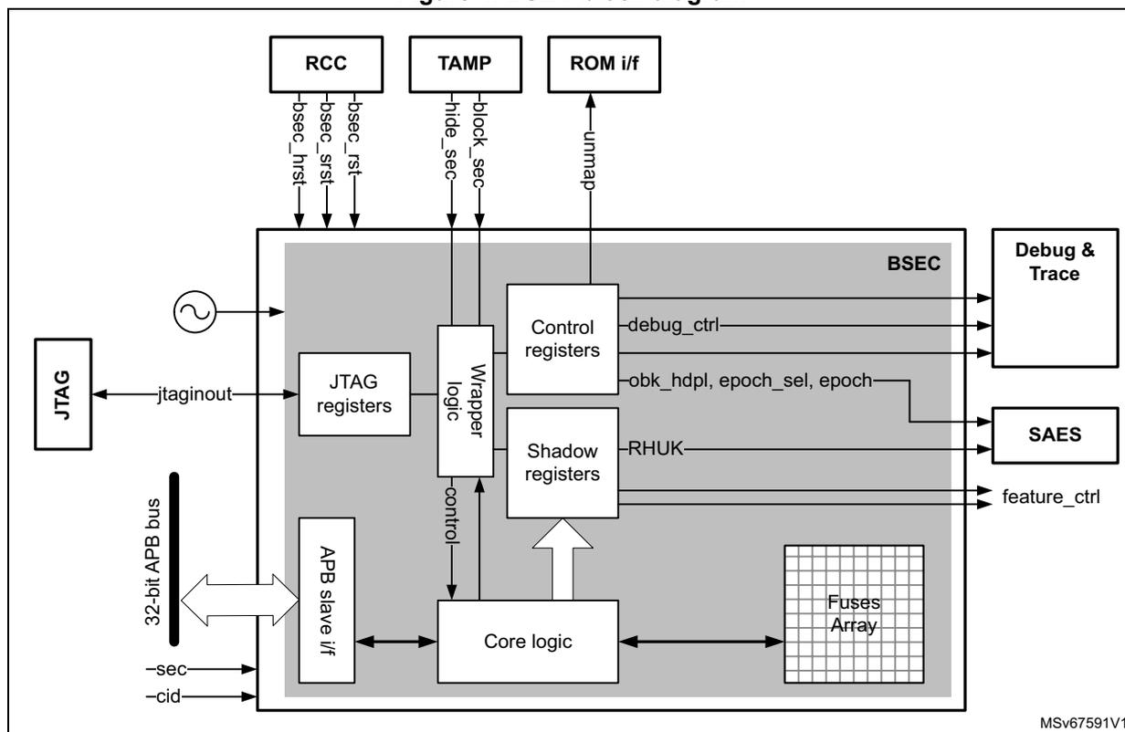
4.3.2 BSEC internal signals
Table 9 describes the user relevant internal signals interfacing the BSEC peripheral.
Table 9. BSEC internal input/output signals
| Signal name | Signal type | Description |
|---|---|---|
| bsec_rst | Digital input | BSEC cold/warm resets from RCC (see Section 4.3.17 ). |
| bsec_srst | ||
| bsec_hrst | BSEC hot reset from RCC (see Section 4.3.17 ). | |
| jtaginout | Digital input and output | Interface to JTAG, including clock and reset. |
| hide_sec | Digital input | Set by TAMP in case of confirmed tamper (see Section 4.3.17 ). |
| block_sec | Digital input | Set by TAMP in case of potential tamper (see Section 4.3.17 ). |
| rhuk | Digital output | 256-bit root hardware unique key output to SAES peripheral. |
| Signal name | Signal type | Description |
|---|---|---|
| obk_hdpl | Digital output | Control outputs to SAES peripheral to influence generation of DHUK. |
| epoch_sel epoch | Digital output | Control outputs to SAES peripheral to influence generation of DHUK. |
| debug_ctrl | Digital output | Device debug and trace control signals (see Section 4.3.11 ). |
| feature_ctrl | Digital output | Device feature control signals (see Section 4.3.12 ). |
| bsec_done | Digital output | End of BSEC cold/warm reset operation to RCC. |
4.3.3 BSEC reset and clocks
BSEC is clocked by a device-embedded oscillator (RCBSEC). Because BSEC is clocked by an internal oscillator, an access to fuse array is robust against external fault injection on clocks.
The BSEC has three resets:
- • a cold POR (power-on reset) directly driving bsec_srst .
- • a warm system reset ( bsec_rst ) asserted when POR is asserted, but also by other sources of system reset, including a PAD reset.
- • a hot reset input ( bsec_hrst ), driven directly by bsec_done .
BSEC flops on the cold reset retain their values through warm reset, while the rest of the system remains in reset until the auto-load process has completed ( bsec_done = 1) and fuse output values are stable.
On a POR, the BSEC temporarily emerges from warm reset for the duration of the auto-load process, even if bsec_rst remains asserted, so that the auto-load process can determine values for flops on the cold reset. This means when the device is powered up, the security state is immediately established, so that a debugger may be allowed to perform discovery operations soon after power-up, even if the PAD reset is still being asserted.
Some flops in the BSEC are on bsec_hrst , so they remain in reset until bsec_done is asserted. This reset is asserted while the Cortex-M is under reset.
4.3.4 Organization and use of fuses
Organization of fuses
One-time programmable fuse bits are organized in three groups of 32-bit words, as shown on Figure 5.
Figure 5. BSEC fuse mapping overview
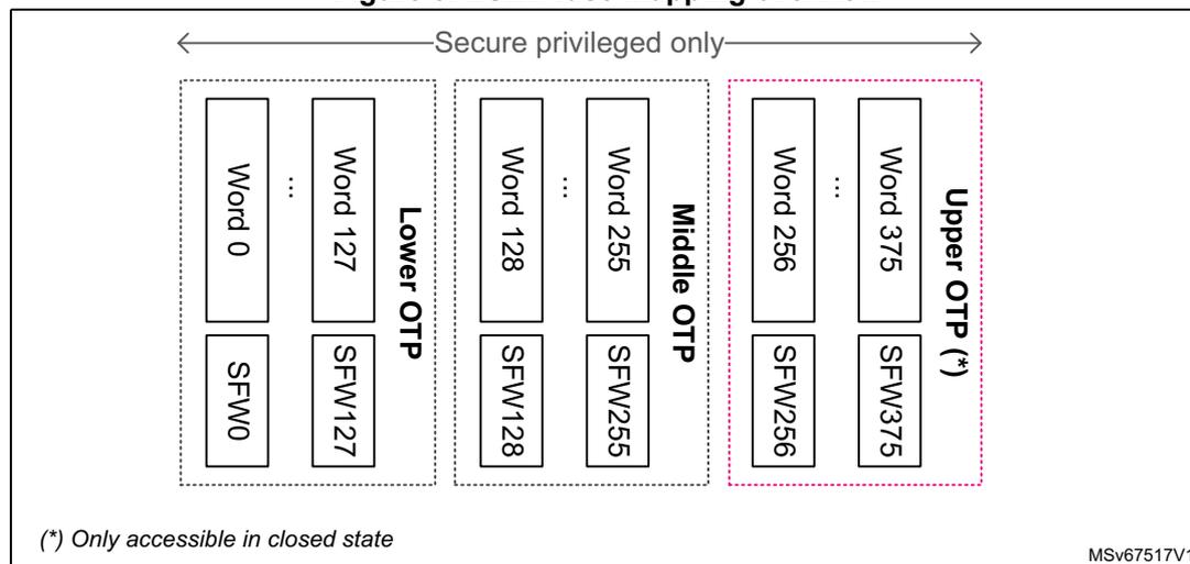
(*) Only accessible in closed state
MSV67517V1
The lower fuses region is used to store non-volatile, non-secret information that may require bitwise update during the life of the product.
The middle fuses region is used to store non-volatile, non-secret information that are written once, in 32-bit words bulk.
The upper fuses region is similar to the middle region, except that it is hidden when in the BSEC-open state (see Section 4.3.7 ). Hence it is used to store secrets like symmetric keys or private asymmetric keys.
Each fuse word w is either “shadowed” or “unshadowed”, as defined by flag bit SFVW w in corresponding BSEC_SFSRx register. A shadowed fuse word is loaded into flops at cold or warm reset, and can be read quickly by software. An unshadowed fuse word is not read out of the fuse memory at reset, then stored permanently in flops. It needs to be reloaded from the fuse memory each time it is needed. See Reading fuses in Section 4.3.5 for details.
Note:
The whole OTP space can only be controlled by a secure privileged CPU.
Each individual lower fuse bit is one-time programmable, from 0 to 1. Transitions from 1 to 0 are not possible.
Details on fuse usage are described in Section 5: OTP mapping (OTP) .
4.3.5 Operations on fuses
Reading fuses
If fuse word \( w \) is shadowed (SFW \( w \) bit set in corresponding BSEC_SFSRx register), and either the state is BSEC-closed or \( w < 256 \) , then BSEC_FVR \( w \) register is auto-loaded at cold or warm reset with the contents of fuse word \( w \) .
If fuse word \( w \) is accessible and shadowed, then if SRLOCK \( w = 0 \) the contents of fuse \( w \) can be reloaded by software into BSEC_FVR \( w \) register.
If fuse word \( w \) is accessible and unshadowed (SFW \( w \) bit cleared in corresponding BSEC_SFSRx register), a read to BSEC_FVR \( w \) register returns the content of fuse word \( w \) if the last operation on the fuse memory successfully reloaded word \( w \) , and if no unshadowed fuse word has been read since that reload.
Each time the application reloads the content of a word stored in fuse memory using BSEC_OTPCR register with PROG bit cleared, BUSY bit and error status should be checked in BSEC_OTPSR (see Section 4.3.6 ).
Note: Unshadowed fuse word information stored in BSEC_FVR \( w \) is cleared as soon as it is read.
Writing shadow registers
When a fuse word \( w = \{i + 32 * x\} \) above word 9 is shadowed (SFW \( w \) bit set in BSEC_SFSRx) the application can update its shadowed value by writing directly to BSEC_FVR \( w \) register, if SWLOCK \( w \) bit is cleared in BSEC_SWLOCK \( x \) register.
Note: A shadow register write does not change the underlying fuse value.
Programming fuses
When programming is not blocked, lower fuse words can be blown bit-per-bit at different times. Middle and upper fuses must be programmed 32-bits at a time, only once. As reprogramming middle and upper fuses can let them with invalid content (an ECC error might be reported), it is strongly recommended to set PPLOCK = 1 after the first (and only) programming of the middle and upper fuses.
The procedure for blowing fuse word \( w \) is as follows:
- 1. Write the value to be blown in BSEC_WDR, then set ADDR = \( w \) , PROG = 1 and PPLOCK = 0 in BSEC_OTPCR register.
- 2. When BUSY bit is cleared in BSEC_OTPSR, verify that PROGFAIL is cleared. If PROGFAIL is set try again step 1.
- 3. Reload the fuse word \( w \) using BSEC_OTPCR with PROG bit cleared.
- 4. When BUSY bit is cleared in BSEC_OTPSR, verify that BSEC_FVR \( w \) register returns the correct value. If not, try again step 1.
Note: OTP bits are initially set to 0 and once a bit is set to 1 it cannot be programmed back to 0 (bit stays at 1). Bitfields with 0s in BSEC_WDR are not programmed, while bitfields with 1s are programmed.
As lower fuse words can be programmed multiple times, when the application requests a specific bit to be programmed to 1 more than once, BSEC does the burning only once.
Permanent program lock (PPLOCK)
The application can make further programming of fuse word \( w \) impossible by following the sequence:
- 1. Clear BSEC_WDR register, then set ADDR = \( w \) , PROG = 1 and PPLOCK = 1 in BSEC_OTPCR register.
- 2. When BUSY bit is cleared in BSEC_OTPSR, verify that PROGFAIL is cleared. If PROGFAIL is set try again step 1.
- 3. Reload the fuse word \( w \) using BSEC_OTPCR with PROG bit cleared.
- 4. When BUSY bit is cleared in BSEC_OTPSR, verify that the PPLF in BSEC_OTPSR is set. If not, try again step 1.
There is no register in BSEC to store PPLOCK information. When the application needs to know if a fuse word programming is permanently locked, it has first to perform a reload of this word using BSEC_OTPCR and then check if the PPLF bit in BSEC_OTPSR register is set. See Table 11 for details.
Fuse word locking features
In order to make fuse usage suitable for security, for example to implement the isolation scheme detailed in Section 4.3.10 , BSEC has the following locking features:
Sticky program lock (SPLOCK)
The application can prevent fuse word \( w = \{i + 32 * x\} \) programming until next BSEC reset (cold or warm) by setting the SPLOCK \( w \) bit in BSEC_SPLOCK \( x \) register.
Sticky write lock (SWLOCK)
The application can make the BSEC_FVR \( w \) register of a shadowed fuse word \( w = \{i + 32 * x\} \) unwritable until next BSEC reset (cold or warm) by setting the SWLOCK \( w \) bit in BSEC_SWLOCK \( x \) register.
Sticky reload lock (SRLOCK)
Reload of word \( w = \{i + 32 * x\} \) using BSEC_OTPCR register can be blocked until next BSEC reset (cold or warm) by setting the SRLOCK \( w \) bit in BSEC_SRLOCK \( x \) register.
When read is sticky-locked, unshadowed fuse words return 0 while shadowed fuse words return their current value (value is not zeroed).
Upper fuses read and write locking (HIDEUP)
When HIDEUP bit is set by hardware in BSEC_OTPSR, neither read nor write are possible to fuse words located in the upper region.
4.3.6 BSEC read and programming status reporting
After a cold and warm reset BSEC performs a first set of OTP reads, reporting the specific status structure defined in Table 10 .
Table 10. BSEC initial status reporting structure
| Bit offset | BSEC_OTPSR bit | Name | Error flag | Meaning when bit is set |
|---|---|---|---|---|
| 0 | [0] | BUSY | No | BSEC ongoing operation is not completed. |
| 1 | [1] | INIT_DONE | BSEC initialized following a cold or warm reset. | |
| 2 | [2] | HIDEUP | Upper fuses are not accessible to the application. | |
| 4 | [4] | OTPNVIR | BSEC is not virgin. This bit should always be set. | |
| 5 | [5] | OTPERR | Yes | At least one error has been detected during the reading of shadowed fuse words, as reported in BSEC_OTPVLD registers (VLDF bit = 0). The recommended mitigation is to reload the faulty fuse word using BSEC_OTPCR and analyze the 8-bit error structure in BSEC_OTPSR, as detailed below. |
| 6 | [6] | OTPSEC | At least one single-error has been corrected during the reading of shadowed fuse words, as reported in BSEC_OTPVLD registers (VLDF bit = 0). In this case the shadowed fuse word value is correct, hence if OTPSEC = 1 and OTPERR = 0 the application does not need to reload the faulty fuse word. |
After any read or programming request, the BUSY bit is cleared, and BSEC reports the specific status structure defined in Table 11 . When this structure is different than 0 the read or program operation might have failed, as indicated in the table.
Table 11. BSEC ad-hoc error/status reporting structure
| Bit offset | BSEC_OTPSR bit | Name | Failed operation | Retry if error (1) | Error description |
|---|---|---|---|---|---|
| 0 | [16] | PROGFAIL | Write | Yes | Programming operation failed. |
| 1 | [17] | DISTURB | Read | Integrity of the fuse value is not guaranteed. | |
| 2 | [18] | DEDF | Double error detected. Fuse word is corrupted. | ||
| 3 | [19] | SECF | No | Single bit error correction. | |
| 4 | [20] | PPLF | Permanent programming lock detected. | ||
| 5 | [21] | PPLMF | Yes | Permanent programming lock information on the two lower fuse values in the array is not identical. | |
| 6 | [22] | AMEF (2) | Fuse address mismatch. Fuse value cannot be trusted, and should be read again. | ||
1. For reads: need to reload the fuse (reported value cannot be trusted). For writes: need to retry the programming operation.
2. Always be 0 in normal operating conditions.
4.3.7 Lifecycle management
BSEC state initialization
Following a cold or warm reset BSEC can be in the following possible security states, defined in Table 12 .
Table 12. BSEC states definition
| BSEC states (1) | Upper fuses | DHUK in SAES (2) | Full debug | BootROM access | Fuse programming |
|---|---|---|---|---|---|
| BSEC-open | Inaccessible (3) | Unusable | yes (4) | partial | Enabled |
| BSEC-closed | Accessible | Hardware unique | no (5) | full (6) | |
| BSEC-invalid | Inaccessible (3) | Unusable | no | partial | Disabled |
- 1. Defined in NVSTATE bitfield in BSEC_SR register (0x16: BSEC-open, 0x0D: BSEC-closed).
- 2. Derived hardware unique key in SAES peripheral uses RHUK information from BSEC (see Section 4.3.15 ).
- 3. Cannot be read or programmed by any means (functional or non-functional).
- 4. ST engineering modes are also available.
- 5. Root of trust application can unlock debug features unless any of the debug_lock bits (25/24/23/22) is blown in WORD18. ST engineering modes are disabled, by hardware, provided bit 20 of fuse word 124 is blown.
- 6. At the end of its execution the boot ROM writes 0xB9D8 FF1F to BSEC_UNMAPR, reverting boot ROM access to partial.
Errors following a BSEC initialization are detailed in Section 4.3.6 . Details about reset management can be found in Section 4.3.17 .
When neither BSEC-open nor BSEC-closed state (NVSTATE different than 0x16 or 0x0D), the security state is considered invalid, and the most conservative security configuration is applied: that is, fuse programming is disabled, upper fuses read as 0, debug is disabled, ROM is partially unmapped and shadow registers are read only. When NVSTATE = 0x23, a confirmed tamper is active in the device (see Section 4.3.17 ).
Note: On any reset, including hot reset, if the state is BSEC-closed, the BSEC_UNMAPR register is set to 0xA1C0 DE0D, ensuring the whole boot ROM is visible.
Opening BSEC
BSEC can transition from BSEC-closed to BSEC-open only if the user enters the programmed 128-bit password via JTAG, and then performs a global reset (JTAG + device), clearing all secrets.
The recommended JTAG password programming sequence is:
- 1. Write the four password words to upper fuses words 256 to 259 with PPLOCK bit cleared in BSEC_OTPCR. JTAG_PSWD0 is stored in word 256, while JTAG_PSWD3 is stored in word 259.
- 2. Read back password value to verify it is correct
- 3. Write 0x0 to the same fuse words 256 to 259, with PPLOCK bit set in BSEC_OTPCR. After this, password words cannot be read nor programmed anymore by the application.
The BSEC opening sequence is described below:
- 1. Bring the device TAP out of reset, and enter the device secret password sequentially using the JTAG commands 0100 (SET_JTAG_PSWD0), 0101 (SET_JTAG_PSWD1), 0110 (SET_JTAG_PSWD2) then 0111 (SET_JTAG_PSWD3).
- 2. Trigger a device reset, without causing a TAP reset. When BSEC emerges from reset, it blows the RMA fuse word with adequate values.
- 3. Trigger a TAP reset to destroy any record of the entered password, and after the next cold or warm reset, the BSEC changes its NVSTATE to “BSEC-open” in BSEC_SR. It can be verified using the JTAG command 0011 (READ_SEC). BSEC returns 0x1 for an BSEC-open device, 0x2 for a BSEC-closed device.
- 4. Ship the device to STMicroelectronics for field return analysis (RMA)
Once the device has been opened it can be closed again by blowing to 0xF the next unblown 4-bit nibble in BSEC_FVR1 (see Closing BSEC ). At most four device re-opening attempts are allowed, regardless of whether they are successful or unsuccessful.
By blowing at least one bit in BSEC_FVR1[27:24], the application can reduce the number of re-opening cycles to only one.
If the application blows at least one bit in BSEC_FVR1[31:28] a closed device can never be re-opened.
The application can also ensure that if a closed device is ever re-opened, it is not possible to subsequently re-close it again. It is done by blowing the permanent programming lock (PPLOCK) of fuse word 1, writing 0x00000000 to BSEC_WDR then writing 0x00006001 to BSEC_OTPCR.
Note: By default BSEC opening password is 0x0. It is advised to change it.
Closing BSEC
BSEC can transition from BSEC-open to BSEC-closed by blowing some bits such that \( s[7:0] \) becomes greater than \( r[7:0] \) , or \( s[7] = 1 \) . Bytes \( s[7:0] \) and \( r[7:0] \) are defined as follows:
With the following conventions:
- • “|” is concatenation operand
- • \( \text{OR}(\text{bits}[1:0]) = \text{bit}[1] \text{ OR } \text{bit}[0] \)
- • \( \text{AND}(\text{bits}[1:0]) = \text{bit}[1] \text{ AND } \text{bit}[0] \)
When the device is being closed, the application can limit re-opening cycles to only one attempt by blowing at least one bit in BSEC_FVR1[27:24]. To reduce re-opening cycles to zero, the application must blow at least one bit in BSEC_FVR1[31:28].
Note: For the device to become BSEC-closed, the application must perform a BSEC cold or warm reset.
4.3.8 Epoch registers
There are two 32-bit readable registers, BSEC_EPOCHR0 and BSEC_EPOCHR1, that are writable only by boot ROM accesses. It is the responsibility of the boot ROM to read bitwise fuses and populate these registers.
There is a 1-bit programmable register BSEC_EPOCHSEL CR (output on epoch_sel ) that, when programmed to n , ensures that BSEC_EPOCHR n is output on epoch . Both epoch and epoch_sel are wired to the SAES where they influence the generation of DHUK, derived from the RHUK.
Secure software can blow additional bits in the appropriate fuse word to increment an Epoch, thereby making impossible the use of all keys derived from the RHUK prior to that point.
4.3.9 BSEC local access control
Any access that is not both secure and privileged is blocked, with read data zeroed and write accesses ignored.
4.3.10 Temporal isolation in BSEC
In order to enforce isolation between boot stages the running application in each boot level must hide the secrets it was using before proceeding to the next level of code in the boot chain. Such protections must remain until the next boot sequence.
Four boot levels, with its corresponding hide protection level (HDPL), are defined:
- • Level 0 (HDPL0) corresponds to hardware state machine or ROM code execution.
- • Level 1 (HDPL1) corresponds to the execution of STMicroelectronics signed code or ROMed code. This code is the first stage of the secure boot.
- • Level 2 (HDPL2) corresponds to the execution of the OEM signed code, stored in embedded SRAM. This code is the second stage of the secure boot.
- • Level 3 (HDPL3) corresponds to the application run-time.
To help enforcing such isolation between boot stages, the ROM code and the application secure boot can use the following temporal isolation hardware capabilities of BSEC:
- • When BSEC is in a closed state, ROM partially hides itself at the end of its execution in level 0 or level 1, writing 0xB9D8 FF1F to BSEC_UNMAPR register.
- • When BSEC is in a closed state, fuse words 364 to 375 are reloadable only when BSEC_UNMAP=0xA1C0DE0D
- • Any 32-bit OTP word can be made non-readable and/or non-writable until next cold or warm reset. It can also be made non-programmable, permanently. See Fuse word locking features and Permanent program lock (PPLOCK) methods in Section 4.3.5 .
Note: Details on fuse usage are described in Section 5: OTP mapping (OTP) .
The register BSEC_HDPLSR determines the current hide protection level of the device. The encoding offers physical robustness.
Table 13. Current HDPL coding
| BSEC_HDPLSR[HDPL] | Level |
|---|---|
| 0xB4 | 0 |
| 0x51 | 1 |
| 0x8A | 2 |
| 0x6F | 3 |
| others | undefined |
The register is reset to 0xB4 by bsec_hrst . The register is not directly writable. If less than 3, the current level can be incremented by writing a value of 0x60B166E7 to BSEC_HDPLCR.
The 2-bit INCR field of the BSEC_NEXTHDPLCR register is added to the level given by BSEC_HDPLSR (but clamped at a ceiling of 3), and the result is output on obk_hdpi[7:0] as follows.
Table 14. BSEC Next HDPL register usage
| obk_hdpi [7:0] | BSEC_NEXTHDPLCR [INCR] | ||||
|---|---|---|---|---|---|
| 0 | 1 | 2 | 3 | ||
| BSEC_HDPLSR [HDPL] | 0 (0xB4) | 0xB4 | 0x51 | 0x8A | 0x6F |
| 1 (0x51) | 0x51 | 0x8A | 0x6F | ||
| 2 (0x8A) | 0x8A | ||||
| 3 (0x6F) | 0x6F | 0x6F | |||
| others (0xPQ) | 0xPQ | ||||
The obk_hdpi output goes to the SAES where it influences the generation of DHUK, derived from the RHUK. This mechanism allows keys for a later temporal level to be generated in advance.
4.3.11 BSEC debug and trace control
The wrapper contains a BSEC_DBGCR register, reset to zero on the scratch reset, and writeable only once per warm reset. The bytes of this register are named as follows
Table 15. BSEC debug register legal values
| BSEC_DBGCR | field name | legal values |
|---|---|---|
| 31:24 | AUTH_SEC | 0x00, 0xB4 |
| 23:16 | AUTH_HDPL | 0x00, 0xB4, 0x51, 0x8A, 0x6F |
| 15:8 | UNLOCK | 0x00, 0xB4 |
| 7:0 | reserved | - |
AUTH_HDPL encodes levels in the same way as HDPL field in BSEC_HDPLSR register.
Any attempt to write a non-legal byte value into these fields results in a 0x00 being written in that byte field.
The register is forced to zero (writes have no effect) whenever the device is BSEC-open.
The dbg_unlocked output, when taking the value of 0xB4, signifies that nonsecure debug is possible. The dbg_unlocked_sec output, when it also takes the value of 0xB4, signifies that secure debug is possible.
Both outputs are set to 0xB4 whenever the state is BSEC-open.
Whenever the BSEC state is not BSEC-open, then if HDPL = 0xB4, or AUTH_HDPL is undefined or indicates a level greater than that given by HDPL, they are both set to 0x00, otherwise dbg_unlocked takes the value of UNLOCK, and dbg_unlocked_sec takes the
value of AUTH_SEC. This implies that secure boot is enforced on a BSEC-closed device. It is the responsibility of the customer's signed code to decide on whether debug becomes unlocked at a certain level. This decision (i.e. the register write) only has to be made once per power cycle, since the register is on the scratch reset and retains its value across warm resets.
Note: If a warm reset occurs during a debug session, then during the reset, the debugger becomes temporarily locked, since HDPL is reset to 0. On a BSEC-open device, it becomes unlocked again as soon as the BSEC has booted. On a BSEC-closed device, it becomes unlocked again as soon as HDPL is non-zero and matches or surpasses AUTH_HDPL.
The BSEC_AP_UNLOCK register is forced to zero (writes have no effect) whenever the state is BSEC-open. The ap_unlocked output, when taking the value 0xB4, indicates that the debugger can access the CM55 Debug Subsystem. It is set to 0xB4 whenever the state is BSEC-open, otherwise it is directly driven by the BSEC_AP_UNLOCK register, which is reset to 0 on a scratch reset.
A rising edge on hide_sec (a confirmed tamper) resets these registers to zero, and close debug. They are not writeable until the next cold or warm reset.
Note: These registers are on the scratch reset so that if software authorizes a debug, that authorization survives subsequent warm resets, and doesn't have to be re-authorized.
4.3.12 Device features control
Device features are controlled through read-only shadowed fuse word 9. See Section 5: OTP mapping (OTP) for details.
4.3.13 Scratch registers
The four BSEC_SCRATCHRx registers are only reset by a cold boot. They are therefore useful to store values that must remain persistent for the application across warm boots.
The eight BSEC_WOSCRx registers are only reset by a cold or warm boot. They are therefore useful to store values that must remain persistent for the application across hot boots.
Note: BSEC_WOSCRx registers are write once.
4.3.14 JTAG registers
The BSEC_JTAGINR and BSEC_JTAGOUTR registers are available to facilitate communication between the application (for example ROM) and the debug tools connected through the JTAG interface.
4.3.15 STM32 root hardware unique key (RHUK)
BSEC stores a root HUK that has been programmed by STMicroelectronics during the device manufacturing. A successful provisioning is indicated with HVALID bit set in BSEC_SR register.
The value of this key is obtained from the RNG peripheral of the device, without disclosure to the outside world. This key cannot be read or programmed by any secure application nor debugger.
When BSEC detects an integrity issue while reading the key information from non-volatile memory, or when application sets the sticky HKLOCK bit in BSEC_LOCKR, the key is indicated as invalid. When the key is invalid the SAES peripheral uses a default fixed value.
4.3.16 BSEC error management
Shadowed fuse word automatic readout errors
After a cold or warm reset, shadowed fuse words are automatically loaded into BSEC_FVR registers. At the end of this process, when INIT_DONE is set in BSEC_OTPSR, additional error information can be found in this register, as described in Section 4.3.6 .
Individual fuse loading errors
Upon each fuse loading from OTP memory array, an 8-bit error structure in BSEC_OTPSR register is updated to tell the application if there was a problem with this particular fuse load. This structure is defined in Section 4.3.6 .
4.3.17 BSEC tamper response mechanisms
This device uses tamper-detection and response mechanisms that can make it immediately inoperable, resulting in the automatic and immediate erasure of any sensitive data that may be stored in the device. The device also supports the concept of potential tamper event, where the device secrets are blocked while application software verifies that such tamper event is confirmed or not.
BSEC manages above mechanisms in the following way:
- • When a tamper source triggers a potential tamper event in TAMP peripheral (NOERASE = 1), BSEC masks the RHUK value to SAES, and upper fuses read as 0 (unless BSEC_UNMAP = 0xA1C0 DE0D, meaning that the boot CPU is executing).
- • When a tamper source triggers a confirmed tamper event in TAMP peripheral (NOERASE = 0), or a potential tamper becomes a confirmed tamper, fuses cannot be blown or reloaded, upper fuses read as 0, BSEC_DBGCR and BSEC_AP_UNLOCK registers are cleared, RHUK information is physically cleared to 0 & invalidated, and NVSTATE is set to 0x23 in BSEC_SR register. These limitations are deactivated after device secrets have been erased, and a SoC reset has been applied.
Above limitations are deactivated when the application clears the active tamper source(s) in TAMP peripheral. See Section 62: Tamper and backup registers (TAMP) for details.
Note: While tamper events are active the boot CPU can always execute the application firmware following an application reset or an exit from Standby for the boot CPU.
4.4 BSEC interrupts
BSEC does not support any interrupt.
4.5 BSEC registers
Those registers are accessible through the register interface of the BSEC peripheral.
4.5.1 BSEC fuse word w value register (BSEC_FVRw)
Address offset: 0x000 + 0x4 * w, (w = 0 to 375)
Reset value: 0xXXXX XXXX
Note: The reset value is 0x0000 0000 if the fuse word is unshadowed, defined by the fuse value if the fuse word is shadowed.
Secure privileged read and write only. Illegal reads return 0, illegal writes are ignored.
See the bitfield description for further details on fuse word accessibility.
| 31 | 30 | 29 | 28 | 27 | 26 | 25 | 24 | 23 | 22 | 21 | 20 | 19 | 18 | 17 | 16 |
| FV[31:16] | |||||||||||||||
| rw | rw | rw | rw | rw | rw | rw | rw | rw | rw | rw | rw | rw | rw | rw | rw |
| 15 | 14 | 13 | 12 | 11 | 10 | 9 | 8 | 7 | 6 | 5 | 4 | 3 | 2 | 1 | 0 |
| FV[15:0] | |||||||||||||||
| rw | rw | rw | rw | rw | rw | rw | rw | rw | rw | rw | rw | rw | rw | rw | rw |
Bits 31:0 FV[31:0] : fuse value
If fuse word {w} is shadowed (SFW{w} bit set in corresponding BSEC_SFSRx register), and either the state is BSEC-closed or {w} < 256, then this register is auto-loaded at cold or warm reset with the contents of fuse word w.
If fuse word {w} is accessible and shadowed, then:
- – if SRLOCK{w} = 0, fuse word {w} can be reloaded by software into this register
- – if SWLOCK{w} = 0, and {w} > 9, this register can be written to (otherwise, writes are ignored).
If fuse word {w} is accessible and unshadowed (SFW{w} bit cleared in corresponding BSEC_SFSRx register), writes are ignored and provided:
- – the last operation on the fuse memory successfully reloaded word {w}
- – no unshadowed fuse words have been read since that reload
then a read to this register returns the content of fuse word {w} (otherwise it returns 0).
If the fuse word {w} is inaccessible, then writes are ignored and reads return 0.
Unshadowed fuse word information stored in this register is cleared as soon as it is read.
When the state is BSEC-closed:
- – Fuse words 364 to 375 are accessible only when BSEC_UNMAP=0xA1C0DE0D and when the access is from boot CPU.
- – Fuse words 256 to 259 read as zero when permanent programming lock is set for those words.
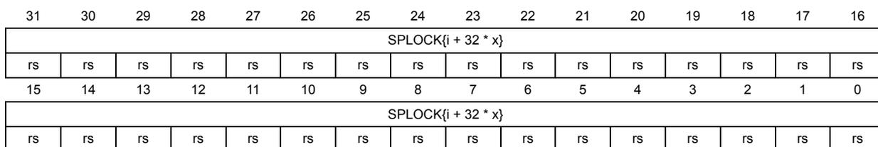
4.5.2 BSEC sticky programming lock register x (BSEC_SPLOCKx)
Address offset: 0x800 + 0x4 * x (x = 0 to 11)
Reset value: 0x0000 0000
Secure privileged read and write only. Illegal reads return 0, illegal writes are ignored.
| 31 | 30 | 29 | 28 | 27 | 26 | 25 | 24 | 23 | 22 | 21 | 20 | 19 | 18 | 17 | 16 |
| SPLOCK{i + 32 * x} | |||||||||||||||
| rs | rs | rs | rs | rs | rs | rs | rs | rs | rs | rs | rs | rs | rs | rs | rs |
| 15 | 14 | 13 | 12 | 11 | 10 | 9 | 8 | 7 | 6 | 5 | 4 | 3 | 2 | 1 | 0 |
| SPLOCK{i + 32 * x} | |||||||||||||||
| rs | rs | rs | rs | rs | rs | rs | rs | rs | rs | rs | rs | rs | rs | rs | rs |
Bits 31:0 SPLOCK{i + 32 * x} : Sticky programming lock for word {i + 32 * x} (i = 0 to 31)
Setting this bit prevents permanent programming for the fuse word {i + 32 * x} until next cold or warm reset.
0: Fuse word {i + 32 * x} can be burnt in fuse memory array
1: Attempt to program fuse word {i + 32 * x} in OTP memory array is silently ignored
While BUSY is set in BSEC_OTPSR, writes have no effect, and reads return 0.
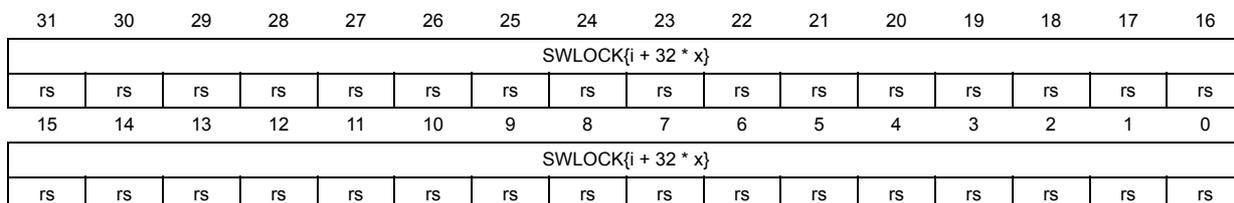
4.5.3 BSEC sticky write lock register x (BSEC_SWLOCKx)
Address offset: 0x840 + 0x4 * x (x=0 to 11)
Reset value: 0x0000 0000
Secure privileged read and write only. Illegal reads return 0, illegal writes are ignored.
| 31 | 30 | 29 | 28 | 27 | 26 | 25 | 24 | 23 | 22 | 21 | 20 | 19 | 18 | 17 | 16 |
| SWLOCK{i + 32 * x} | |||||||||||||||
| rs | rs | rs | rs | rs | rs | rs | rs | rs | rs | rs | rs | rs | rs | rs | rs |
| 15 | 14 | 13 | 12 | 11 | 10 | 9 | 8 | 7 | 6 | 5 | 4 | 3 | 2 | 1 | 0 |
| SWLOCK{i + 32 * x} | |||||||||||||||
| rs | rs | rs | rs | rs | rs | rs | rs | rs | rs | rs | rs | rs | rs | rs | rs |
Bits 31:0 SWLOCK{i + 32 * x} : sticky write lock for shadow register {i + 32 * x} (i = 0 to 31)
When fuse word {i + 32 * x} is shadowed, setting this bit prevents the writing of the shadow register of this fuse word until next cold or warm reset.
0: Write to shadow register BSEC_FVR{i + 32 * x} is allowed
1: Writes to shadow register BSEC_FVR{i + 32 * x} are silently ignored
While BUSY is set in BSEC_OTPSR, writes have no effect, and reads return 0.
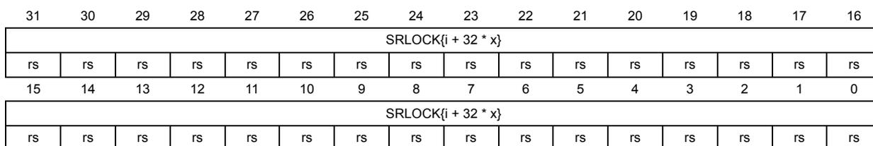
4.5.4 BSEC sticky reload lock register x (BSEC_SRLOCKx)
Address offset: \( 0x880 + 0x4 \times x \) ( \( x = 0 \) to \( 11 \) )
Reset value: \( 0x0000\ 0000 \)
Secure privileged read and write only. Illegal reads return 0, illegal writes are ignored.
| 31 | 30 | 29 | 28 | 27 | 26 | 25 | 24 | 23 | 22 | 21 | 20 | 19 | 18 | 17 | 16 |
| SRLOCK{i + 32 * x} | |||||||||||||||
| rs | rs | rs | rs | rs | rs | rs | rs | rs | rs | rs | rs | rs | rs | rs | rs |
| 15 | 14 | 13 | 12 | 11 | 10 | 9 | 8 | 7 | 6 | 5 | 4 | 3 | 2 | 1 | 0 |
| SRLOCK{i + 32 * x} | |||||||||||||||
| rs | rs | rs | rs | rs | rs | rs | rs | rs | rs | rs | rs | rs | rs | rs | rs |
Bits 31:0 SRLOCK{i + 32 * x} : sticky reload lock for fuse word {i + 32 * x} ( \( i = 0 \) to \( 31 \) )
Setting this bit locks reloading of fuse word {i + 32 * x} from the OTP memory array until next cold or warm reset.
0: Fuse word {i + 32 * x} loading through BSEC_OTPCR is authorized.
1: Fuse word {i + 32 * x} loading through BSEC_OTPCR is denied until next cold or warm reset.
While BUSY is set in BSEC_OTPSR, writes have no effect, and reads return 0.
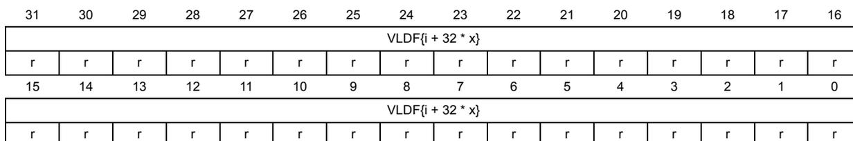
4.5.5 BSEC OTP valid register x (BSEC_OTPVLDx)
Address offset: \( 0x8C0 + 0x4 \times x \) ( \( x = 0 \) to \( 11 \) )
Reset value: \( 0x0000\ 0000 \)
Secure privileged read only (return 0 otherwise).
| 31 | 30 | 29 | 28 | 27 | 26 | 25 | 24 | 23 | 22 | 21 | 20 | 19 | 18 | 17 | 16 |
| VLDF{i + 32 * x} | |||||||||||||||
| r | r | r | r | r | r | r | r | r | r | r | r | r | r | r | r |
| 15 | 14 | 13 | 12 | 11 | 10 | 9 | 8 | 7 | 6 | 5 | 4 | 3 | 2 | 1 | 0 |
| VLDF{i + 32 * x} | |||||||||||||||
| r | r | r | r | r | r | r | r | r | r | r | r | r | r | r | r |
Bits 31:0 VLDF{i + 32 * x} : Valid flag for shadow register {i + 32 * x} ( \( i = 0 \) to \( 31 \) )
This bit represents the validity of the last reload of fuse word {i + 32 * x}.
0: An error occurred while fuse word {i + 32 * x} was last reloaded. The value read from BSEC_FVR{i + 32 * x} register cannot be relied on.
1: Last reload of fuse word {i + 32 * x} was done without error.
Each VLDF bit is updated when BSEC or the allowed application reloads corresponding fuse word from the OTP array.
4.5.6 BSEC shadowed fuses status register x (BSEC_SFSRx)
Address offset: 0x940 + 0x4 * x (x = 0 to 11)
Reset value: 0x0001 EBFF (SFSR0)
Reset value: 0xFF00 000F (SFSR3)
Reset value: 0x0000 000F (SFSR8)
Reset value: 0xFF00 0000 (SFSR11)
Reset value: 0x0000 0000 (others)
Secure privileged read-only (return 0 otherwise).
| 31 | 30 | 29 | 28 | 27 | 26 | 25 | 24 | 23 | 22 | 21 | 20 | 19 | 18 | 17 | 16 |
|---|---|---|---|---|---|---|---|---|---|---|---|---|---|---|---|
| SFW{i + 32 * x} | |||||||||||||||
| r | r | r | r | r | r | r | r | r | r | r | r | r | r | r | r |
| 15 | 14 | 13 | 12 | 11 | 10 | 9 | 8 | 7 | 6 | 5 | 4 | 3 | 2 | 1 | 0 |
| SFW{i + 32 * x} | |||||||||||||||
| r | r | r | r | r | r | r | r | r | r | r | r | r | r | r | r |
Bits 31:0 SFW{i + 32 * x} : Shadowed fuse word {i + 32 * x} (i = 0 to 31)
This bit indicates whether fuse word {i + 32 * x} is shadowed or not.
0: Fuse word {i + 32 * x} is not shadowed. Fuse value must be reloaded using BSEC_OTPCR before reading BSEC_FVR{i + 32 * x} register.
1: Fuse word is shadowed in BSEC_FVR{i + 32 * x} register. Reloading the fuse value using BSEC_OTPCR is only required if the fuse value changed since the last BSEC cold or warm reset.
4.5.7 BSEC OTP control register (BSEC_OTPCR)
Address offset: 0xC04
Reset value: 0x0000 0000
Writing to this register causes an access to be made to the fuse memory.
Secure privileged read and write only. Illegal reads return 0, illegal writes are ignored.
| 31 | 30 | 29 | 28 | 27 | 26 | 25 | 24 | 23 | 22 | 21 | 20 | 19 | 18 | 17 | 16 |
|---|---|---|---|---|---|---|---|---|---|---|---|---|---|---|---|
| Res. | Res. | Res. | Res. | Res. | Res. | Res. | Res. | Res. | Res. | LASTCID[2:0] | Res. | Res. | Res. | ||
| r | r | r | |||||||||||||
| 15 | 14 | 13 | 12 | 11 | 10 | 9 | 8 | 7 | 6 | 5 | 4 | 3 | 2 | 1 | 0 |
| Res. | PP LOCK | PROG | Res. | Res. | Res. | Res. | ADDR[8:0] | ||||||||
| rw | rw | rw | rw | rw | rw | rw | rw | rw | rw | rw | |||||
Bits 31:22 Reserved, must be kept at reset value.
Bits 21:19 LASTCID[2:0] : Last CID
This always returns the value 001.
Bits 18:15 Reserved, must be kept at reset value.
Bit 14 PPLOCK : Permanent programming lock
When this bit is set together with PROG bit, no further write to this fuse word is possible.
0: Fuse word at address ADDR[8:0] is programmed normally.
1: Fuse word at address ADDR[8:0] is locked, preventing further modifications.
Permanent programming lock mechanism is immutable, as it is committed in the fuse memory.
Bit 13 PROG : Fuse word programming
This bit determines whether BSEC operation is a read or a write. If a write is selected, the data stored in BSEC_WDR is programmed in the fuse word indexed by ADDR bitfield.
0: Fuse word read operation is required
1: Fuse word programming operation is required
While BUSY is set in BSEC_OTPSR, writes to PROG bit have no effect.
Bits 12:9 Reserved, must be kept at reset value.
Bits 8:0 ADDR[8:0] : Fuse word address
This bitfield represents the address of the fuse word in the OTP memory array.
When a lower fuse address is selected two fuse words are addressed by BSEC.
When fuse words 376 to 383 are selected, read or programming requests are denied.
When fuse words 368 to 375 are selected, programming requests are ignored.
4.5.8 BSEC write data register (BSEC_WDR)
Address offset: 0xC08
Reset value: 0x0000 0000
Secure privileged write only. Any reads return 0.

| 31 | 30 | 29 | 28 | 27 | 26 | 25 | 24 | 23 | 22 | 21 | 20 | 19 | 18 | 17 | 16 |
| WRDATA[31:16] | |||||||||||||||
| w | w | w | w | w | w | w | w | w | w | w | w | w | w | w | w |
| 15 | 14 | 13 | 12 | 11 | 10 | 9 | 8 | 7 | 6 | 5 | 4 | 3 | 2 | 1 | 0 |
| WRDATA[15:0] | |||||||||||||||
| w | w | w | w | w | w | w | w | w | w | w | w | w | w | w | w |
Bits 31:0 WRDATA[31:0] : OTP write data
The value written to this register can be written to fuse memory. This happens when the BSEC_OTPCR register is written with the PROG bit set.
When a lower fuse address is selected in BSEC_OTPCR (ADDR=0x0 to 0x3F), two fuse words are programmed by BSEC (one fuse word is programmed otherwise).
While BUSY is set in BSEC_OTPSR, writes to this register have no effect.
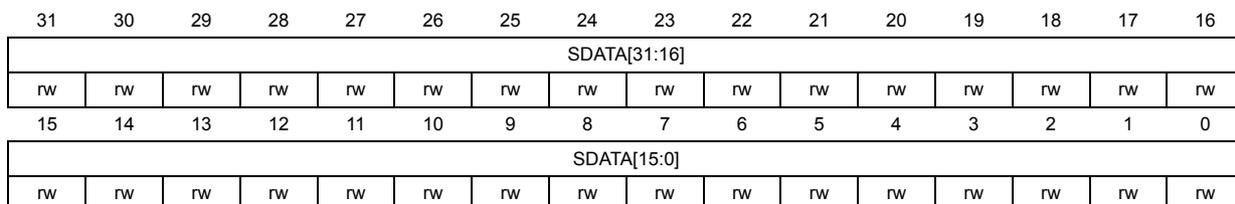
4.5.9 BSEC scratch register x (BSEC_SCRATCHRx)
Address offset: 0xE00 + 0x4 * x (x = 0 to 3)
Reset value: 0x0000 0000
This register is reset when bsec_srst is asserted.
Secure privileged read and write only. Illegal reads return 0, illegal writes are ignored.
| 31 | 30 | 29 | 28 | 27 | 26 | 25 | 24 | 23 | 22 | 21 | 20 | 19 | 18 | 17 | 16 |
| SDATA[31:16] | |||||||||||||||
| rw | rw | rw | rw | rw | rw | rw | rw | rw | rw | rw | rw | rw | rw | rw | rw |
| 15 | 14 | 13 | 12 | 11 | 10 | 9 | 8 | 7 | 6 | 5 | 4 | 3 | 2 | 1 | 0 |
| SDATA[15:0] | |||||||||||||||
| rw | rw | rw | rw | rw | rw | rw | rw | rw | rw | rw | rw | rw | rw | rw | rw |
Bits 31:0 SDATA[31:0] : Scratch data
This register can be used to store values that needs to be persistent across warm reset.
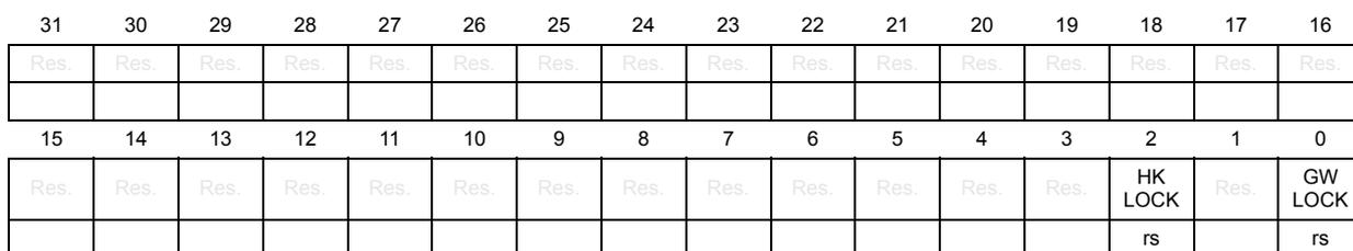
4.5.10 BSEC lock register (BSEC_LOCKR)
Address offset: 0xE10
Reset value: 0x0000 0000
Secure privileged read and write only. Illegal reads return 0, illegal writes are ignored.
| 31 | 30 | 29 | 28 | 27 | 26 | 25 | 24 | 23 | 22 | 21 | 20 | 19 | 18 | 17 | 16 |
| Res. | Res. | Res. | Res. | Res. | Res. | Res. | Res. | Res. | Res. | Res. | Res. | Res. | Res. | Res. | Res. |
| 15 | 14 | 13 | 12 | 11 | 10 | 9 | 8 | 7 | 6 | 5 | 4 | 3 | 2 | 1 | 0 |
| Res. | Res. | Res. | Res. | Res. | Res. | Res. | Res. | Res. | Res. | Res. | Res. | Res. | HK LOCK | Res. | GW LOCK |
| rs | rs |
Bits 31:3 Reserved, must be kept at reset value.
Bit 2 HKLOCK : Hardware key lock
- 0: Derived hardware unique key (DHUK) in SAES peripheral is usable if HVALID is set in BSEC_SR
- 1: Derived hardware unique key (DHUK) in SAES peripheral is not usable.
Once set, this bit is cleared only by BSEC cold or warm reset.
Bit 1 Reserved, must be kept at reset value.
Bit 0 GWLOCK : Global write lock
- 0: Writes to BSEC registers are allowed
- 1: Writes to BSEC registers are ignored (fuse programming and fuse reload disabled)
Once set, this bit is cleared only by BSEC cold or warm reset.
4.5.11 BSEC JTAG input register (BSEC_JTAGINR)
Address offset: 0xE14
Reset value: 0x0000 0000
Secure privileged read only (return 0 otherwise).
| 31 | 30 | 29 | 28 | 27 | 26 | 25 | 24 | 23 | 22 | 21 | 20 | 19 | 18 | 17 | 16 |
|---|---|---|---|---|---|---|---|---|---|---|---|---|---|---|---|
| JDATAIN[31:16] | |||||||||||||||
| r | r | r | r | r | r | r | r | r | r | r | r | r | r | r | r |
| 15 | 14 | 13 | 12 | 11 | 10 | 9 | 8 | 7 | 6 | 5 | 4 | 3 | 2 | 1 | 0 |
| JDATAIN[15:0] | |||||||||||||||
| r | r | r | r | r | r | r | r | r | r | r | r | r | r | r | r |
Bits 31:0 JDATAIN[31:0] : JTAG input data
Reads give the last input value from the JTAG interface
4.5.12 BSEC JTAG output register (BSEC_JTAGOUTR)
Address offset: 0xE18
Reset value: 0x0000 0000
Secure privileged write only (write ignored otherwise).
| 31 | 30 | 29 | 28 | 27 | 26 | 25 | 24 | 23 | 22 | 21 | 20 | 19 | 18 | 17 | 16 |
|---|---|---|---|---|---|---|---|---|---|---|---|---|---|---|---|
| JDATAOUT[31:16] | |||||||||||||||
| w | w | w | w | w | w | w | w | w | w | w | w | w | w | w | w |
| 15 | 14 | 13 | 12 | 11 | 10 | 9 | 8 | 7 | 6 | 5 | 4 | 3 | 2 | 1 | 0 |
| JDATAOUT[15:0] | |||||||||||||||
| w | w | w | w | w | w | w | w | w | w | w | w | w | w | w | w |
Bits 31:0 JDATAOUT[31:0] : JTAG output data
Application can write any value in this field to be output on the JTAG interface.
4.5.13 BSEC unmap register (BSEC_UNMAPR)
Address offset: 0xE24
Reset value: 0xXXXX XXXX
Note: The reset value is 0xA1C0 DE0D on a BSEC-closed device, 0xFFFF FFFF on a BSEC-open device.
Register bits cannot be cleared by application, they can only be set to 1.
Secure privileged read and write only. Illegal reads return 0, illegal writes are ignored. Only BootROM code can access.
| 31 | 30 | 29 | 28 | 27 | 26 | 25 | 24 | 23 | 22 | 21 | 20 | 19 | 18 | 17 | 16 |
|---|---|---|---|---|---|---|---|---|---|---|---|---|---|---|---|
| UNMAP[31:16] | |||||||||||||||
| rs | rs | rs | rs | rs | rs | rs | rs | rs | rs | rs | rs | rs | rs | rs | rs |
| 15 | 14 | 13 | 12 | 11 | 10 | 9 | 8 | 7 | 6 | 5 | 4 | 3 | 2 | 1 | 0 |
| UNMAP[15:0] | |||||||||||||||
| rs | rs | rs | rs | rs | rs | rs | rs | rs | rs | rs | rs | rs | rs | rs | rs |
Bits 31:0 UNMAP[31:0] : Unmap key
If this bitfield equals 0xA1C0 DE0D, the whole ROM is visible, else ROM is partially hidden.
4.5.14 BSEC status register (BSEC_SR)
Address offset: 0xE40
Reset value: 0x0000 0000
Secure privileged read only (return 0 otherwise).
| 31 | 30 | 29 | 28 | 27 | 26 | 25 | 24 | 23 | 22 | 21 | 20 | 19 | 18 | 17 | 16 |
|---|---|---|---|---|---|---|---|---|---|---|---|---|---|---|---|
| NVSTATE[5:0] | Res. | Res. | Res. | Res. | Res. | Res. | Res. | Res. | Res. | DBGREQ | |||||
| r | r | r | r | r | r | r | |||||||||
| 15 | 14 | 13 | 12 | 11 | 10 | 9 | 8 | 7 | 6 | 5 | 4 | 3 | 2 | 1 | 0 |
| Res. | Res. | Res. | Res. | Res. | Res. | Res. | Res. | Res. | Res. | Res. | Res. | Res. | Res. | HVALID | Res. |
| r | |||||||||||||||
Bits 31:26 NVSTATE[5:0] : Non-volatile state
0x16: BSEC-open state
0x0D: BSEC-closed state
0x7: BSEC-invalid state
0x23: BSEC-invalid state, with an active confirmed tamper triggered in the device
The BSEC state is evaluated each time INIT_DONE is set in BSEC_OTPSR.
For more information, refer to Section 4.3.7: Lifecycle management
Bits 25:17 Reserved, must be kept at reset value.
Bit 16 DBGREQ : debug request
0: Host debugger is not requesting debug
1: Host debugger is requesting debug
Bits 15:2 Reserved, must be kept at reset value.
Bit 1 HVALID : Hardware key valid
0: Derived hardware unique key (DHUK) feature cannot be used in SAES peripheral.
1: Derived hardware unique key (DHUK) feature can be used in SAES peripheral.
Bit 0 Reserved, must be kept at reset value.
4.5.15 BSEC OTP status register (BSEC_OTPSR)
Address offset: 0xE44
Reset value: 0x0000 0000
This register is refreshed each time a fuse operation is triggered through BSEC_OTPCR.
Secure privileged read only (return 0 otherwise).
| 31 | 30 | 29 | 28 | 27 | 26 | 25 | 24 | 23 | 22 | 21 | 20 | 19 | 18 | 17 | 16 |
|---|---|---|---|---|---|---|---|---|---|---|---|---|---|---|---|
| Res. | Res. | Res. | Res. | Res. | Res. | Res. | Res. | Res. | AMEF | PPLMF | PPLF | SECF | DEDF | DISTURBF | PROG FAIL |
| r | r | r | r | r | r | r | |||||||||
| 15 | 14 | 13 | 12 | 11 | 10 | 9 | 8 | 7 | 6 | 5 | 4 | 3 | 2 | 1 | 0 |
| Res. | Res. | Res. | Res. | Res. | Res. | Res. | Res. | Res. | OTP SEC | OTP ERR | OTP NVIR | Res. | HIDE UP | INIT DONE | BUSY |
| r | r | r | r | r | r |
Bits 31:23 Reserved, must be kept at reset value.
Bit 22 AMEF : Addresses mismatch error flag
This bit is set when the address used by BSEC to read a fuse word is different from the programmed address (either by BSEC or by the application). Such event should never happen in normal BSEC operations.
Bit 21 PPLMF : Permanent programming lock mismatch flag
This bit is set when the two words constituting a lower fuse word are reporting different permanent programming lock statuses after BSEC reset or after the latest read.
For more details about permanent programming lock, refer to PPLOCK in BSEC_OTPCR.
Bit 20 PPLF : Permanent programming lock flag
This bit is set when the most recently read word is detected permanently locked.
For more details about permanent programming lock, refer to PPLOCK in BSEC_OTPCR.
Bit 19 SECF : Single error correction flag
This bit is set when a single-bit-error correction is detected after BSEC reset or after the latest read.
Bit 18 DEDF : Double error detection flag
This bit is set when a double error is detected after BSEC reset or after the latest read.
When DEDF bit is set after reading fuse word w, the value in BSEC_FVRw is the one read from OTP memory.
Bit 17 DISTURBF : Disturb flag
This bit is set when an unexpected error occurred after BSEC reset or after the latest read. When DISTURBF bit is set after reading fuse word w, the value in BSEC_FVRw is the one read from OTP memory.
Bit 16 PROGFAIL : Programming failed
This bit is set when last OTP programming by BSEC failed.
Bits 15:7 Reserved, must be kept at reset value.
Bit 6 OTPSEC : OTP with single error correction
This bit is set when at least one single-error correction is detected during BSEC reset operations. In this case shadow registers are usable.
Bit 5 OTPERR : OTP with error
This bit is set when at least one error is detected during BSEC reset operations.
Bit 4 OTPNVIR : OTP not virgin
This bit is set when first fuse word 0 is detected non-0 after BSEC reset operations.
Bit 3 Reserved, must be kept at reset value.
Bit 2 HIDEUP : Hide upper fuse words
This bit is set when application secret fuse words 256 to 383 becomes physically inaccessible, that is functionally hidden fuse words read as 0 and programming requests are ignored.
Bit 1 INIT_DONE : Initialization done
This bit is set when BSEC reset operations are completed. All shadowed fuses are readable in BSEC_FVRw registers, and status bits in BSEC_SR and BSEC_OTPSR are up to date.
Bit 0 BUSY : Busy flag
0: BSEC is idle.
1: BSEC is busy.
4.5.16 BSEC epoch register (BSEC_EPOCHRx)
Address offset: 0xE80 + 0x4 * x (x = 0 to 1)
Reset value: 0x0000 0000
Writeable by boot ROM only, readable by secure privileged trusted domain or BootROM code only. Illegal reads return 0, illegal writes are ignored.
| 31 | 30 | 29 | 28 | 27 | 26 | 25 | 24 | 23 | 22 | 21 | 20 | 19 | 18 | 17 | 16 |
|---|---|---|---|---|---|---|---|---|---|---|---|---|---|---|---|
| EPOCH[31:16] | |||||||||||||||
| rw | rw | rw | rw | rw | rw | rw | rw | rw | rw | rw | rw | rw | rw | rw | rw |
| 15 | 14 | 13 | 12 | 11 | 10 | 9 | 8 | 7 | 6 | 5 | 4 | 3 | 2 | 1 | 0 |
| EPOCH[15:0] | |||||||||||||||
| rw | rw | rw | rw | rw | rw | rw | rw | rw | rw | rw | rw | rw | rw | rw | rs |
Bits 31:0 EPOCH[31:0] : epoch
This value is wired out to the SAES peripheral, depending on the EPOCH_SEL bit in BSEC_EPOCHSELCR.
4.5.17 BSEC epoch selection control register (BSEC_EPOCHSELCR)
Address offset: 0xE88
Reset value: 0x0000 0000
Secure privileged read and write only. Illegal reads return 0, illegal writes are ignored.
| 31 | 30 | 29 | 28 | 27 | 26 | 25 | 24 | 23 | 22 | 21 | 20 | 19 | 18 | 17 | 16 |
|---|---|---|---|---|---|---|---|---|---|---|---|---|---|---|---|
| Res. | Res. | Res. | Res. | Res. | Res. | Res. | Res. | Res. | Res. | Res. | Res. | Res. | Res. | Res. | Res. |
| 15 | 14 | 13 | 12 | 11 | 10 | 9 | 8 | 7 | 6 | 5 | 4 | 3 | 2 | 1 | 0 |
| Res. | Res. | Res. | Res. | Res. | Res. | Res. | Res. | Res. | Res. | Res. | Res. | Res. | Res. | Res. | EPOCH_SEL |
| rw |
Bits 31:1 Reserved, must be kept at reset value.
Bit 0 EPOCH_SEL : Selection of the epoch value to be sent to the SAES
0: SAES peripheral uses BSEC_EPOCHR0 as EPOCH value.
1: SAES peripheral uses BSEC_EPOCHR1 as EPOCH value.
4.5.18 BSEC debug control register (BSEC_DBGCR)
Address offset: 0xE8C
Reset value: 0x0000 0000
Secure privileged read and write only. Writeable only on a BSEC-closed device, once per warm reset. Illegal reads return 0, illegal writes are ignored. Reset to zero on bsec_srst (cold reset).
The AUTH_HDPL byte field indicates a temporal isolation level, as follows: the value 0xB4 means level 0, the value 0x51 means level 1, the value 0x8A means level 2, and the value 0x6F means level 3. All other byte values are undefined.
When the state is BSEC-open, the dbg_unlocked and dbg_unlocked_sec outputs to the DBG_MCU block are set to 0xB4, and the register is zeroed.
When the state is not BSEC-open, both outputs are zeroed whenever either AUTH_HDPL or BSEC_HDPLSR[HDPL] are undefined, or BSEC_HDPLSR[HDPL] = 0xB4, or the level indicated by AUTH_HDPL is greater than that of BSEC_HDPLSR[HDPL]. Otherwise, the UNLOCK is placed on the dbg_unlocked output, and (UNLOCK and AUTH_SEC) is placed on the dbg_unlocked_sec output.
| 31 | 30 | 29 | 28 | 27 | 26 | 25 | 24 | 23 | 22 | 21 | 20 | 19 | 18 | 17 | 16 |
|---|---|---|---|---|---|---|---|---|---|---|---|---|---|---|---|
| AUTH_SEC[7:0] | AUTH_HDPL[7:0] | ||||||||||||||
| rw | rw | rw | rw | rw | rw | rw | rw | rw | rw | rw | rw | rw | rw | rw | rw |
| 15 | 14 | 13 | 12 | 11 | 10 | 9 | 8 | 7 | 6 | 5 | 4 | 3 | 2 | 1 | 0 |
| UNLOCK[7:0] | Res. | ||||||||||||||
| rw | rw | rw | rw | rw | rw | rw | rw | ||||||||
0xB4: Secure debug authorized when UNLOCK = 0xB4 and the level indicated in BSEC_HDPLSR is greater than or equal to the level indicated by AUTH_HDPL
Others: Secure debug not authorized (provided state is not BSEC-open)
0xB4: Level 0
0x51: Level 1
0x8A: Level 2
0x6F: Level 3
Others: Undefined
0xB4: Nonsecure debug authorized when the level indicated in BSEC_HDPLSR is greater than or equal to the level given by AUTH_HDPL
Others: Debug not authorized (provided state is not BSEC-open)
Bits 7:0 Reserved, must be kept at reset value.
4.5.19 BSEC AP unlock (BSEC_AP_UNLOCK)
Address offset: 0xE90
Reset value: 0x0000 0000
Secure privileged read and write only. Writeable only on a BSEC-closed device, once per warm reset. Illegal reads return 0, illegal writes are ignored. Reset to zero on bsec_srst (cold reset). Bit 5 is reset to zero on every warm reset.
When the state is BSEC-open, the ap_unlocked output to the DBG_MCU block is set to 0xB4, and the register is zeroed. When the BSEC state is not BSEC-open, it takes the value of the 8-bit UNLOCK field.
| 31 | 30 | 29 | 28 | 27 | 26 | 25 | 24 | 23 | 22 | 21 | 20 | 19 | 18 | 17 | 16 |
|---|---|---|---|---|---|---|---|---|---|---|---|---|---|---|---|
| Res. | Res. | Res. | Res. | Res. | Res. | Res. | Res. | Res. | Res. | Res. | Res. | Res. | Res. | Res. | Res. |
| 15 | 14 | 13 | 12 | 11 | 10 | 9 | 8 | 7 | 6 | 5 | 4 | 3 | 2 | 1 | 0 |
| Res. | Res. | Res. | Res. | Res. | Res. | Res. | Res. | UNLOCK[7:0] | |||||||
| rw | rw | rw | rw | rw | rw | rw | rw | ||||||||
Bits 31:8 Reserved, must be kept at reset value.
Bits 7:0 UNLOCK[7:0]:0xB4: Unlock debug access port.
Others: Do not unlock.
4.5.20 BSEC HDPL status register (BSEC_HDPLSR)
Address offset: 0xE94
Reset value: 0x0000 00B4
Secure privileged read only. Illegal reads return 0, writes are ignored. Reset to 0xB4 on bsec_hrst (hot reset).
When coding a value of less than 3, it can be incremented by writing 0x60B166E7 to BSEC_HDPLCR.
| 31 | 30 | 29 | 28 | 27 | 26 | 25 | 24 | 23 | 22 | 21 | 20 | 19 | 18 | 17 | 16 |
|---|---|---|---|---|---|---|---|---|---|---|---|---|---|---|---|
| Res. | Res. | Res. | Res. | Res. | Res. | Res. | Res. | Res. | Res. | Res. | Res. | Res. | Res. | Res. | Res. |
| 15 | 14 | 13 | 12 | 11 | 10 | 9 | 8 | 7 | 6 | 5 | 4 | 3 | 2 | 1 | 0 |
| Res. | Res. | Res. | Res. | Res. | Res. | Res. | Res. | HDPL[7:0] | |||||||
| r | r | r | r | r | r | r | r | ||||||||
Bits 31:8 Reserved, must be kept at reset value.
Bits 7:0 HDPL[7:0] : Current HDPL
0xB4: Level 0
0x51: Level 1
0x8A: Level 2
0x6F: Level 3
Others: Undefined
4.5.21 BSEC HDPL control register (BSEC_HDPLCR)
Address offset: 0xE98
Reset value: 0x0000 0000
Secure privileged write only. Illegal reads return 0, writes are ignored.
When BSEC_HDPLSR codes a value of less than 3, BSEC_HDPLSR can be incremented by writing 0x60B166E7 to BSEC_HDPLCR.
| 31 | 30 | 29 | 28 | 27 | 26 | 25 | 24 | 23 | 22 | 21 | 20 | 19 | 18 | 17 | 16 |
|---|---|---|---|---|---|---|---|---|---|---|---|---|---|---|---|
| INCR_HDPL[31:16] | |||||||||||||||
| w | w | w | w | w | w | w | w | w | w | w | w | w | w | w | w |
| 15 | 14 | 13 | 12 | 11 | 10 | 9 | 8 | 7 | 6 | 5 | 4 | 3 | 2 | 1 | 0 |
| INCR_HDPL[15:0] | |||||||||||||||
| w | w | w | w | w | w | w | w | w | w | w | w | w | w | w | w |
Bits 31:0 INCR_HDPL[31:0] : Increment HDPL
When HDPL is less than 3, writing 0x60B1 66E7 increments HDPL by one in BSEC_HDPLSR.
Otherwise, writes are ignored. Reads return zero.
4.5.22 BSEC next HDPL control register (BSEC_NEXTHDPLCR)
Address offset: 0xE9C
Reset value: 0x0000 0000
Secure privileged read and write only. Illegal reads return 0, writes are ignored.
This value determines the amount to add to the level indicated by BSEC_HDPLSR to output to the SAES on obk_hdpl.
| 31 | 30 | 29 | 28 | 27 | 26 | 25 | 24 | 23 | 22 | 21 | 20 | 19 | 18 | 17 | 16 |
|---|---|---|---|---|---|---|---|---|---|---|---|---|---|---|---|
| Res. | Res. | Res. | Res. | Res. | Res. | Res. | Res. | Res. | Res. | Res. | Res. | Res. | Res. | Res. | Res. |
| 15 | 14 | 13 | 12 | 11 | 10 | 9 | 8 | 7 | 6 | 5 | 4 | 3 | 2 | 1 | 0 |
| Res. | Res. | Res. | Res. | Res. | Res. | Res. | Res. | Res. | Res. | Res. | Res. | Res. | Res. | INCR[1:0] | |
| rw | rw |
Bits 31:2 Reserved, must be kept at reset value.
Bits 1:0 INCR[1:0] : Increment
Amount to add to BSEC_HDPLSR to generate obk_hdpl[7:0] output (clamped at 3).
4.5.23 BSEC write once scratch register x (BSEC_WOSCRx)
Address offset: 0xF40 + 0x4 * x (x = 0 to 7)
Reset value: 0x0000 0000
This register is reset when bsec_rst is asserted.
Secure privileged read and write only. Illegal reads return 0, illegal writes are ignored.
| 31 | 30 | 29 | 28 | 27 | 26 | 25 | 24 | 23 | 22 | 21 | 20 | 19 | 18 | 17 | 16 |
|---|---|---|---|---|---|---|---|---|---|---|---|---|---|---|---|
| WOSDATA[31:16] | |||||||||||||||
| rwo | rwo | rwo | rwo | rwo | rwo | rwo | rwo | rwo | rwo | rwo | rwo | rwo | rwo | rwo | rwo |
| 15 | 14 | 13 | 12 | 11 | 10 | 9 | 8 | 7 | 6 | 5 | 4 | 3 | 2 | 1 | 0 |
| WOSDATA[15:0] | |||||||||||||||
| rwo | rwo | rwo | rwo | rwo | rwo | rwo | rwo | rwo | rwo | rwo | rwo | rwo | rwo | rwo | rwo |
Bits 31:0 WOSDATA[31:0] : Write once scratch data
ROM code can use this register to store values that need to be persistent across hot resets. It is writable once, reset by either cold or warm BSEC reset.
4.5.24 BSEC hot reset count register (BSEC_HRCR)
Address offset: 0xFE8
Reset value: 0x0000 0000
This register is reset when bsec_rst is asserted.
Secure privileged read only (return 0 otherwise).
| 31 | 30 | 29 | 28 | 27 | 26 | 25 | 24 | 23 | 22 | 21 | 20 | 19 | 18 | 17 | 16 |
|---|---|---|---|---|---|---|---|---|---|---|---|---|---|---|---|
| HRC[31:16] | |||||||||||||||
| r | r | r | r | r | r | r | r | r | r | r | r | r | r | r | r |
| 15 | 14 | 13 | 12 | 11 | 10 | 9 | 8 | 7 | 6 | 5 | 4 | 3 | 2 | 1 | 0 |
| HRC[15:0] | |||||||||||||||
| r | r | r | r | r | r | r | r | r | r | r | r | r | r | r | r |
Bits 31:0 HRC[31:0] : Hot reset counter
This bitfield counts the number of hot resets since the last BSEC cold/warm reset.
See Section 4.3.3: BSEC reset and clocks for details about resets.
4.5.25 BSEC warm reset count register (BSEC_WRCR)
Address offset: 0xFEC
Reset value: 0x0000 0000
This register is reset when bsec_srst is asserted.
Secure privileged read only (return 0 otherwise).
| 31 | 30 | 29 | 28 | 27 | 26 | 25 | 24 | 23 | 22 | 21 | 20 | 19 | 18 | 17 | 16 |
|---|---|---|---|---|---|---|---|---|---|---|---|---|---|---|---|
| WRC[31:16] | |||||||||||||||
| r | r | r | r | r | r | r | r | r | r | r | r | r | r | r | r |
| 15 | 14 | 13 | 12 | 11 | 10 | 9 | 8 | 7 | 6 | 5 | 4 | 3 | 2 | 1 | 0 |
| WRC[15:0] | |||||||||||||||
| r | r | r | r | r | r | r | r | r | r | r | r | r | r | r | r |
Bits 31:0 WRC[31:0] : Warm reset counter
This bitfield counts the number of warm resets since the last BSEC cold reset.
See Section 4.3.3: BSEC reset and clocks for details about resets.
4.5.26 BSEC register map
Table 16. BSEC register map and reset values
| Offset | Register name Reset value | 31 | 30 | 29 | 28 | 27 | 26 | 25 | 24 | 23 | 22 | 21 | 20 | 19 | 18 | 17 | 16 | 15 | 14 | 13 | 12 | 11 | 10 | 9 | 8 | 7 | 6 | 5 | 4 | 3 | 2 | 1 | 0 |
|---|---|---|---|---|---|---|---|---|---|---|---|---|---|---|---|---|---|---|---|---|---|---|---|---|---|---|---|---|---|---|---|---|---|
| FV[31:0] | |||||||||||||||||||||||||||||||||
| 0x000 + 0x4 * w, (w=0 to 375) | BSEC_FVRw | FV[31:0] | |||||||||||||||||||||||||||||||
| Reset value (1) | x | x | x | x | x | x | x | x | x | x | x | x | x | x | x | x | x | x | x | x | x | x | x | x | x | x | x | x | x | x | x | x | |
| 0x5E0 - 0x7FC | Reserved | Res. | |||||||||||||||||||||||||||||||
Table 16. BSEC register map and reset values (continued)
| Offset | Register name Reset value | 31 | 30 | 29 | 28 | 27 | 26 | 25 | 24 | 23 | 22 | 21 | 20 | 19 | 18 | 17 | 16 | 15 | 14 | 13 | 12 | 11 | 10 | 9 | 8 | 7 | 6 | 5 | 4 | 3 | 2 | 1 | 0 |
|---|---|---|---|---|---|---|---|---|---|---|---|---|---|---|---|---|---|---|---|---|---|---|---|---|---|---|---|---|---|---|---|---|---|
| 0x800 + 0x4 * x, (x=0 to 11) | BSEC_SPLOCKx | SPLOCK{i + 32 * x} (i = 31 to 0) | |||||||||||||||||||||||||||||||
| Reset value | 0 | 0 | 0 | 0 | 0 | 0 | 0 | 0 | 0 | 0 | 0 | 0 | 0 | 0 | 0 | 0 | 0 | 0 | 0 | 0 | 0 | 0 | 0 | 0 | 0 | 0 | 0 | 0 | 0 | 0 | 0 | 0 | |
| 0x830 - 0x83C | Reserved | Res. | |||||||||||||||||||||||||||||||
| 0x840 + 0x4 * x (x=0 to 11) | BSEC_SWLOCKx | SWLOCK{i + 32 * x} (i = 31 to 0) | |||||||||||||||||||||||||||||||
| Reset value | 0 | 0 | 0 | 0 | 0 | 0 | 0 | 0 | 0 | 0 | 0 | 0 | 0 | 0 | 0 | 0 | 0 | 0 | 0 | 0 | 0 | 0 | 0 | 0 | 0 | 0 | 0 | 0 | 0 | 0 | 0 | 0 | |
| 0x870 - 0x87C | Reserved | Res. | |||||||||||||||||||||||||||||||
| 0x880 + 0x4 * x (x=0 to 11) | BSEC_SRLOCKx | SRLOCK{i + 32 * x} (i = 31 to 0) | |||||||||||||||||||||||||||||||
| Reset value | 0 | 0 | 0 | 0 | 0 | 0 | 0 | 0 | 0 | 0 | 0 | 0 | 0 | 0 | 0 | 0 | 0 | 0 | 0 | 0 | 0 | 0 | 0 | 0 | 0 | 0 | 0 | 0 | 0 | 0 | 0 | 0 | |
| 0x8B0 - 0x8BC | Reserved | Res. | |||||||||||||||||||||||||||||||
| 0x8C0 + 0x4 * x (x=0 to 11) | BSEC_OTPVLDRx | VLDF{i + 32 * x} (i = 31 to 0) | |||||||||||||||||||||||||||||||
| Reset value | 0 | 0 | 0 | 0 | 0 | 0 | 0 | 0 | 0 | 0 | 0 | 0 | 0 | 0 | 0 | 0 | 0 | 0 | 0 | 0 | 0 | 0 | 0 | 0 | 0 | 0 | 0 | 0 | 0 | 0 | 0 | 0 | |
| 0x8F0 - 0x93C | Reserved | Res. | |||||||||||||||||||||||||||||||
| 0x940 + 0x4 * x (x=0 to 11) | BSEC_SFSRx | SFW{i + 32 * x} (i = 31 to 0) | |||||||||||||||||||||||||||||||
| Reset value (1) | x | x | x | x | x | x | x | x | 0 | 0 | 0 | 0 | 0 | 0 | x | x | x | x | 0 | x | 0 | x | x | x | x | x | x | x | x | x | x | x | |
| 0x970 - 0xC00 | Reserved | Res. | |||||||||||||||||||||||||||||||
| 0xC04 | BSEC_OTPCR | Res. | Res. | Res. | Res. | Res. | Res. | Res. | Res. | Res. | LASTCID [2:0] | Res. | Res. | Res. | Res. | PPLOCK | PROG | Res. | Res. | Res. | Res. | ADDR[8:0] | |||||||||||
| Reset value | 0 | 0 | 0 | 0 | 0 | 0 | 0 | 0 | 0 | 0 | 0 | 0 | 0 | 0 | |||||||||||||||||||
| 0xC08 | BSEC_WDR | WRDATA[31:0] | |||||||||||||||||||||||||||||||
| Reset value | 0 | 0 | 0 | 0 | 0 | 0 | 0 | 0 | 0 | 0 | 0 | 0 | 0 | 0 | 0 | 0 | 0 | 0 | 0 | 0 | 0 | 0 | 0 | 0 | 0 | 0 | 0 | 0 | 0 | 0 | 0 | 0 | |
| 0xC0C - 0xDFC | Reserved | Res. | |||||||||||||||||||||||||||||||
| 0xE00 + 0x4 * x (x=0 to 3) | BSEC_SCRATCHRx | SDATA[31:0] | |||||||||||||||||||||||||||||||
| Reset value | x | x | x | x | x | x | x | x | x | x | x | x | x | x | x | x | x | x | x | x | x | x | x | x | x | x | x | x | x | x | x | x | |
| 0xE10 | BSEC_LOCKR | Res. | Res. | Res. | Res. | Res. | Res. | Res. | Res. | Res. | Res. | Res. | Res. | Res. | Res. | Res. | Res. | Res. | Res. | Res. | Res. | Res. | Res. | Res. | Res. | Res. | Res. | Res. | Res. | Res. | HKLOCK | Res. | GWLOCK |
| Reset value | 0 | 0 | |||||||||||||||||||||||||||||||
| 0xE14 | BSEC_JTAGINR | JDATAIN[31:0] | |||||||||||||||||||||||||||||||
| Reset value | 0 | 0 | 0 | 0 | 0 | 0 | 0 | 0 | 0 | 0 | 0 | 0 | 0 | 0 | 0 | 0 | 0 | 0 | 0 | 0 | 0 | 0 | 0 | 0 | 0 | 0 | 0 | 0 | 0 | 0 | 0 | 0 | |
| 0xE18 | BSEC_JTAGOUTR | JDATAOUT[31:0] | |||||||||||||||||||||||||||||||
| Reset value | 0 | 0 | 0 | 0 | 0 | 0 | 0 | 0 | 0 | 0 | 0 | 0 | 0 | 0 | 0 | 0 | 0 | 0 | 0 | 0 | 0 | 0 | 0 | 0 | 0 | 0 | 0 | 0 | 0 | 0 | 0 | 0 | |
| 0xE1C | Reserved | Reserved | |||||||||||||||||||||||||||||||
| 0xE20 | Reserved | Res. | |||||||||||||||||||||||||||||||
| 0xE24 | BSEC_UNMAPR | UNMAP[31:0] | |||||||||||||||||||||||||||||||
| Reset value (1) | x | x | x | x | x | x | x | x | x | x | x | x | x | x | x | x | x | x | x | x | x | x | x | x | x | x | x | x | x | x | x | x | |
| 0xE28 - 0xE3C | Reserved | Res. | |||||||||||||||||||||||||||||||
| 0xE40 | BSEC_SR | NVSTATE[5:0] | Res. | Res. | Res. | Res. | Res. | Res. | Res. | Res. | Res. | DBGREQ | Res. | Res. | Res. | Res. | Res. | Res. | Res. | Res. | Res. | Res. | Res. | Res. | Res. | Res. | HVALID | Res. | |||||
| Reset value | 0 | 0 | 0 | 0 | 0 | 0 | 0 | 0 | |||||||||||||||||||||||||
Table 16. BSEC register map and reset values (continued)
| Offset | Register name Reset value | 31 | 30 | 29 | 28 | 27 | 26 | 25 | 24 | 23 | 22 | 21 | 20 | 19 | 18 | 17 | 16 | 15 | 14 | 13 | 12 | 11 | 10 | 9 | 8 | 7 | 6 | 5 | 4 | 3 | 2 | 1 | 0 | |
|---|---|---|---|---|---|---|---|---|---|---|---|---|---|---|---|---|---|---|---|---|---|---|---|---|---|---|---|---|---|---|---|---|---|---|
| 0xE44 | BSEC_OTPSR | Res. | Res. | Res. | Res. | Res. | Res. | Res. | Res. | Res. | AMEF | PPLMF | PPLF | SECF | DEDF | DISTURBF | PROGFAIL | Res. | Res. | Res. | Res. | Res. | Res. | Res. | Res. | Res. | Res. | OTPSEC | OTPERR | OTPNVIR | Res. | HIDEUP | INIT_DONE | BUSY |
| Reset value | 0 | 0 | 0 | 0 | 0 | 0 | 0 | 0 | 0 | 0 | 0 | 0 | 0 | |||||||||||||||||||||
| 0xE48 - 0xE7C | Reserved | Res. | ||||||||||||||||||||||||||||||||
| 0xE80 + 0x4 * x (x= 0 to 1) | BSEC_EPOCHRx | EPOCH[31:0] | ||||||||||||||||||||||||||||||||
| Reset value | 0 | 0 | 0 | 0 | 0 | 0 | 0 | 0 | 0 | 0 | 0 | 0 | 0 | 0 | 0 | 0 | 0 | 0 | 0 | 0 | 0 | 0 | 0 | 0 | 0 | 0 | 0 | 0 | 0 | 0 | 0 | 0 | ||
| 0xE88 | BSEC_EPOCHSELCLR | Res. | Res. | Res. | Res. | Res. | Res. | Res. | Res. | Res. | Res. | Res. | Res. | Res. | Res. | Res. | Res. | Res. | Res. | Res. | Res. | Res. | Res. | Res. | Res. | Res. | Res. | Res. | Res. | Res. | Res. | Res. | Res. | EPOCH_SEL |
| Reset value | 0 | |||||||||||||||||||||||||||||||||
| 0xE8C | BSEC_DBGCR | AUTH_SEC[7:0] | AUTH_HDPL[7:0] | UNLOCK[7:0] | ||||||||||||||||||||||||||||||
| Reset value | 0 | 0 | 0 | 0 | 0 | 0 | 0 | 0 | 0 | 0 | 0 | 0 | 0 | 0 | 0 | 0 | 0 | 0 | 0 | 0 | 0 | 0 | 0 | 0 | 0 | 0 | 0 | 0 | 0 | 0 | 0 | 0 | ||
| 0xE90 | BSEC_AP_UNLOCK | Res. | Res. | Res. | Res. | Res. | Res. | Res. | Res. | Res. | Res. | Res. | Res. | Res. | Res. | Res. | Res. | Res. | Res. | Res. | Res. | Res. | Res. | Res. | Res. | Res. | UNLOCK[7:0] | |||||||
| Reset value | 0 | 0 | 0 | 0 | 0 | 0 | 0 | |||||||||||||||||||||||||||
| 0xE94 | BSEC_HDPLSR | Res. | Res. | Res. | Res. | Res. | Res. | Res. | Res. | Res. | Res. | Res. | Res. | Res. | Res. | Res. | Res. | Res. | Res. | Res. | Res. | Res. | Res. | Res. | Res. | Res. | HDPL[7:0] | |||||||
| Reset value | 0 | 0 | 0 | 0 | 0 | 0 | B 4 | |||||||||||||||||||||||||||
| 0xE98 | BSEC_HDPLCR | INCR_HDPL[31:0] | ||||||||||||||||||||||||||||||||
| Reset value | 0 | 0 | 0 | 0 | 0 | 0 | 0 | 0 | 0 | 0 | 0 | 0 | 0 | 0 | 0 | 0 | 0 | 0 | 0 | 0 | 0 | 0 | 0 | 0 | 0 | 0 | 0 | 0 | 0 | 0 | 0 | 0 | ||
| 0xE9C | BSEC_NEXTHDPLCR | Res. | Res. | Res. | Res. | Res. | Res. | Res. | Res. | Res. | Res. | Res. | Res. | Res. | Res. | Res. | Res. | Res. | Res. | Res. | Res. | Res. | Res. | Res. | Res. | Res. | Res. | Res. | Res. | Res. | Res. | Res. | INCR [1:0] | |
| Reset value | 0 | 0 | ||||||||||||||||||||||||||||||||
| 0xEA0 - 0xEA8 | Reserved | Reserved | ||||||||||||||||||||||||||||||||
| 0xEA8 - 0xEB8 | Reserved | Reserved | ||||||||||||||||||||||||||||||||
| 0xEC0 - 0xF3C | Reserved | Reserved | ||||||||||||||||||||||||||||||||
| 0xF40 + 0x4*x (x=0 to 7) | BSEC_WOSCRx | WOSDATA[31:0] | ||||||||||||||||||||||||||||||||
| Reset value | 0 | 0 | 0 | 0 | 0 | 0 | 0 | 0 | 0 | 0 | 0 | 0 | 0 | 0 | 0 | 0 | 0 | 0 | 0 | 0 | 0 | 0 | 0 | 0 | 0 | 0 | 0 | 0 | 0 | 0 | 0 | 0 | ||
| 0xF60 - 0xFE4 | Reserved | Res. | ||||||||||||||||||||||||||||||||
| 0xFE8 | BSEC_HRCR | HRC[31:0] | ||||||||||||||||||||||||||||||||
| Reset value | 0 | 0 | 0 | 0 | 0 | 0 | 0 | 0 | 0 | 0 | 0 | 0 | 0 | 0 | 0 | 0 | 0 | 0 | 0 | 0 | 0 | 0 | 0 | 0 | 0 | 0 | 0 | 0 | 0 | 0 | 0 | 0 | ||
| 0xFEC | BSEC_WRCR | WRC[31:0] | ||||||||||||||||||||||||||||||||
| Reset value | 0 | 0 | 0 | 0 | 0 | 0 | 0 | 0 | 0 | 0 | 0 | 0 | 0 | 0 | 0 | 0 | 0 | 0 | 0 | 0 | 0 | 0 | 0 | 0 | 0 | 0 | 0 | 0 | 0 | 0 | 0 | 0 | ||
1. See register description.
Refer to Section 2.3 for the register boundary addresses.