3. System security
3.1 Key security features
- • Security isolation using the TrustZone technology of the Arm Cortex-M55
- • OS and dynamic user isolation using the Cortex-M55 MPU technology with firewalling
- • Multi-tenancy support: configurable firewalls to allow a trusted OS to ensure software apps installed by different AI providers cannot use the NPU engine or DMA engines to access each other's data
- • Secure provisioning of customer keys and firmware
- • Secure boot-from-ROM authenticating and decrypting images loaded from an external flash memory or downloaded through UART, USB, I 2 C, SPI, FDCAN, or JTAG
- • Nonvolatile antifuse storage of, for example:
- – hardware-unique key (HUK) directly wired to DPA-resistant AES engine
- – private key used for secure provisioning of customer keys
- – customer-provisioned firmware signing and encryption keys
- – customer-provisioned key for managing return material analysis (RMA)
- – irreversible counters for key/certificates revocation, updates, factory resets
- • Battery-backed volatile storage of, for example:
- – customer-provisioned secret boot hardware key (BHK), directly wired to DPA-resistant AES engine, automatically erased in case of tamper
- – anti-rollback counters
- • Provisioning of AES keys in non-volatile storage (for example external flash memory), encrypted with unviewable device-unique keys derived from HUK: a provisioned AES key is never again viewable on the device, and is only used directly in AES hardware accelerators to encrypt and decrypt data
- • General-purpose cryptographic acceleration:
- – Two AES 256-bit engine, supporting ECB, CBC, CTR, GCM, and CCM chaining modes: one engine DPA-resistant with side-channel counter-measures, and one fast-implementation engine without DPA-resistance
- – HASH processor, supporting SHA-2 secure hash
- – PKA (public key accelerator) for RSA/DH (up to 4096 bits) and ECC (up to 640 bits): implements side-channel counter measures and mitigations when manipulating secrets
- – RNG (true random number generator), NIST SP800-90B pre-certified
- • Memory cipher engines for on-the-fly decryption of data in external memories: implements a key derivation function to increase protection against side-channel attacks (SCA)
- • Low-latency encryption engines on NPU bus interfaces: allows AI data to be stored in encrypted format in both external and internal memories
- • Arm PSA temporal isolation enforced by hardware using HDPL (hide protection level)
- • Debug authentication scheme based on certificates: confers rights on the debugger at an authorized security level
- • Active tamper and protection against temperature, voltage, and frequency attacks:
- – Up to seven (inputs, outputs) tamper pins, available in all power modes
- – Immediate erase of battery-backed volatile secrets on confirmed tamper detection
3.2 Secure boot
On an application reset, the Cortex-M55 always boots from the start of an on-chip ROM. This ROM code is used to authenticate and decrypt images loaded into the internal memory from an external flash memory, or through UART, USB, I 2 C, SPI, FDCAN, or JTAG.
The lifecycle state of the device is represented in the values of specific fuses. Transforming from one lifecycle state to the next always involves blowing fuses. The boot ROM acts in accordance with what it finds to be the current lifecycle state.
Lifecycle states can be partitioned into two underlying categories: BSEC-open or BSEC-closed (refer to Section 4.3.7: Lifecycle management for more details). This is determined by hardware on every system reset by examining the state of the lifecycle fuses.
If the hardware determines at power-up that the device is BSEC-open, it immediately enables debug, and disables any access to fused secrets and secure parts of the ROM. This is referred to as nonsecure boot. The device is in a BSEC-open lifecycle state at the start of manufacturing. It can be transformed back into a BSEC-open lifecycle state if there is a fault requiring the part to be returned for analysis.
If the hardware determines that the device is BSEC-closed, the debug remains disabled. The secure boot from ROM is then enforced, and the boot ROM then consults additional fuses to determine the precise lifecycle state.
Devices are delivered to customers in a BSEC-closed state, so the boot ROM execution is enforced.
On a BSEC-closed device, if the secure_boot fuse bit (see Section 5: OTP mapping (OTP) ) is still unblown, then the boot ROM behavior depends on the DEV_BOOT pin:
- • If the DEV_BOOT pin is set, the boot ROM disables the access to secrets, and opens the debug to allow customer development.
- • If the DEV_BOOT pin is not set, the boot ROM executes the boot image regardless of whether it is correctly signed.
However, on a BSEC-closed device, once the secure_boot fuse bit is blown, authenticated secure boot is enforced.
STMicroelectronics supplies signing tools to allow customers to create signed and encrypted boot images. The boot image is sometimes referred as an FSBL (first-stage bootloader), or as an uRoT (updatable root-of-trust firmware).
3.3 Secure provisioning
ST supplies customers with an RSSE (Root Security Services extension) code image to implement SFI (secure firmware install) functionality. The boot ROM authenticates this RSSE code with a hard-coded public key. ST also provisions an ST-certified device-unique key pair into fuses. When customers receive the device, they can boot the supplied SFI image to securely provision their own keys into fuses. The boot ROM uses these keys, whenever it boots, to authenticate and decrypt the customer boot images. The ST-certified
device-unique key pair ensures that this provisioning process is secure and counted. This protects against cloning.
The boot ROM supports up to eight irreversible revocations of firmware signing keys.
The boot image header contains a constant decrypted by the boot ROM using the provisioned firmware encryption key. This derived key is used to decrypt the actual image.
3.4 Temporal isolation
The Arm PSA specification states:
- 1. The code in each stage must execute its tasks, complete, then terminate, and handover execution to the next stage.
- 2. The code in each stage must leave boot state to carry forward results and data from one stage to the next.
- 3. Private data for one stage (especially secrets) must not be directly accessible from later stages.
The STM32N6x5/x7xx devices define four HDPL:
- • 0: Boot ROM
- • 1: Updatable root of trust (uRoT)
- • 2: Level 2
- • 3: Level 3
The HDPL is represented with a monotonically increasing 2-bit counter register BSEC_HDPLSR (on the system reset), which does not wrap back to zero. Only a secure privileged software increments this counter (see Section 4: Boot and security control (BSEC) ).
The SAES (secure AES engine) uses an HDPL input when performing a derivation of the fused HUK to create the DHUK (derived-HUK). The HDPL value seen by the SAES can be increased to a value higher than the current value, to provision data ready for the next temporal stage. However, the generated DHUK with a particular HDPL value cannot be re-generated during later temporal stages (see Section 48: Secure AES coprocessor (SAES) ).
Temporal isolation can also be implemented in the fuse wrapper (BSEC) via sticky read locks and sticky programming locks. The BSEC hardware also ensures that only the boot ROM accesses certain fuse secrets.
3.5 Resource isolation
In STM32N6x5/x7xx, the runtime software isolation is based on TrustZone.
Each memory address is defined to exist either in the secure or the non-secure world. Some CPU resources (such as stack-pointer registers, MPU registers, interrupt vector tables, or timers), are physically banked between worlds. When the CPU executes a secure code (that is, code fetched from secure-world addresses), it uses the secure-world versions of these resources. When the CPU executes nonsecure code (that is, code fetched from nonsecure world addresses), it uses the nonsecure world versions of these resources. However, for the most part, secure and nonsecure codes use the same CPU hardware.
A nonsecure code is blocked from accessing secure world addresses. It can call only secure code (that is, move into the secure world) via SG (secure gate) instructions, which reside in special secure-world NSC (nonsecure callable) regions.
Trustzone ensures that the operation of a secure code and its data cannot be corrupted by nonsecure code.
3.5.1 Trustzone filtering using IDAU/SAU
The 256-Mbyte address ranges starting at the even addresses 0x00000000, 0x20000000, and 0x40000000, are physically aliased at ranges starting at the odd addresses 0x10000000, 0x30000000, and 0x50000000, respectively.
The intention is that the secure world accesses resources via the odd aliases, and the non-secure world accesses resources via the even aliases.
The address security (S for secure, NSC for nonsecure callable, or NS for non-secure, in descending security order) is determined by the device IDAU (implementation defined attribution unit), and the SAU (security attribution unit). Each of these two units proposes a security level for each address, the resulting level is the higher of the two proposals. The accesses to addresses determined to be S or NSC travel out on the bus marked as secure, those determined to be NS travel out on the bus marked as nonsecure.
The secure OS can define up to eight SAU regions, each of which can be configured as NS or NSC. Any address falling outside a defined SAU region remains secure, hence, at reset, the SAU unilaterally determines that the entire memory is secure.
The SAU is typically configured to open up NS regions for nonsecure code, data, and peripherals in the even address aliases. Locations from 0x10000000 to 0x1FFFFFFF (that contain SG instructions) must be covered by explicit SAU regions configured as NSC.
The IDAU determination of the security of each address is hardwired fixed.
Table 4 shows aliased targets, and the IDAU security assignment.
Table 4. Aliasing
| Address region | IDAU assignment | Aliased targets |
|---|---|---|
| 0x5----- | NSC (secure) | Peripherals |
| 0x4----- | NS (nonsecure) | |
| 0x3----- | NSC (secure) | Internal RAMs, DTCM |
| 0x2----- | NS (nonsecure) | |
| 0x1----- | NSC (secure) | Boot ROM, ITCM |
| 0x0----- | NS (nonsecure) |
If the SAU is configured sensibly, the IDAU is normally irrelevant. The only potential effect of the IDAU is to prevent any attempt via the SAU to demote any of the three “odd” NSC regions listed above to be nonsecure.
A secure software configures the firewalls in front of physical resources (aliased in ranges listed in Table 4 ) to determine in which world the access destination resides. This blocks accesses that arrive marked with a mismatching security attribute. A nonsecure code cannot access destinations that reside in the secure world (as designated by the firewall). Destinations are then dedicated for use by the secure world.
External memories are mapped at addresses from 0x60000000 upwards (not aliased). The SAU can be configured to allocate portions of these memories to the non-secure world. These memories have RISAF firewalls in front of them, that can be configured to mirror SAU settings, and to ensure that DMAs are subject to the same restrictions as CPU code.
3.5.2 Privileged OS-controlled isolation
The Cortex-M55 MPU (memory protection unit) facilitates the isolation between a privileged operating system, and the user processes it schedules.
The MPU is banked between the secure and nonsecure worlds as follows:
- • Secure-world accesses to MPU registers update physical registers in the MPU_S, which filters accesses that emerge from the SAU marked secure.
- • Nonsecure world accesses to MPU registers update physical registers in the MPU_NS, which filters accesses emerging from the SAU marked nonsecure.
For each world, attributes are defined for 16 non-overlapping regions, and for the remaining background. The MPU blocks user code from accessing regions marked privileged.
If the MPU is configured to designate a memory region as normal, then all transactions initiated by the Cortex-55 on the AXI bus emerge as privileged (even if originated from a user process). Only the MPU prevents CPU user processes from accessing privileged normal data in SRAM and external flash memories.
When switching from one user process to another, the OS can re-program the MPU and peripheral firewalls to ensure each process can only access its own data. A user application may need to use a peripheral with an AXI initiator that continues to operate in background after the user has been descheduled. To avoid the peripheral being blocked by a modified MPU regime, the user process must ask the OS to configure the peripheral to operate in privilege mode on the user's behalf. It is up to the OS to sanity-check the requested operation. The HPDMA on the AXI bus is a special case (see Section 3.5.4 ).
The Cortex-M55 PAHBCR register must enable the P-AHB, and configure it to allow accesses to the peripheral region on the P-AHB bus. The MPU must be configured so that the peripheral region is execute-never device memory. Accesses to peripherals on the P-AHB carry the correct privilege level: to save wasting MPU regions, the MPU can be configured to make the whole peripheral region user-accessible, and to rely on the RISUP downstream filtering to restrict certain peripherals to OS control.
The Cortex-M55 introduces a PXN (privilege-execute-never) region attribute to prevent the OS from being tricked into jumping to user code.
3.5.3 RIF infrastructure
Thanks to hardware mechanisms in the bus, the secure OS ensures that resources and data are available only to agents that operate in the appropriate world, and at the appropriate privilege level. This infrastructure is named RIF (resource isolation framework).
The RIF consists of five components:
- • RIMU: placed on AXI bus initiators to determine which attributes are attached to accesses
- • RISUP: firewalls placed in front of peripheral bus targets to determine which security and privilege level is allowed to access that peripheral
- • RIFSC: centralized block that contains the configuration registers controlling all RIMUs and RISUPs, and determining other general RIF parameters
- • RISAF: firewalls placed in front of each memory target, with self-contained (local) configuration registers
- • IAC (interrupt access controller): recording all security violation events from all firewalls around the device, in order to present a single interrupt to the CPU
Some peripherals have built-in firewalls, which are configured locally inside the peripheral. These peripherals are called RIF-aware.
The IAC has room for 256 interrupt sources, each corresponding to an IAC index from 0 to 255. Interrupts from the RISUPs occupy most of the first 128 indexes. Interrupts from RIF-aware peripherals and RISAFs occupy indexes from 128 onwards. RISUP and IAC indexes are aligned. The RISUP associated with the IAC index \( 32 \times x + y \) is programmed to be secure by setting RISC_SECCFGx[y]. It is programmed to be privileged by setting RISC_PRIVCFGx[y].
For all RIF firewalling, the security setting of a resource can be configured only by a secure privileged access: the secure OS can assign a RISAF base region to the nonsecure OS. The nonsecure OS determines the position, privilege, and readability of subregions within the base region.
If the resource is set to secure, nonsecure accesses to this resource are blocked. If the resource is set to nonsecure, secure accesses to memories are blocked (no restrictions for peripherals).
For all RIF firewalling, the privilege setting of a resource is only configurable by a privileged access: if the resource has already been configured to be secure, the access must also be secure. If a resource is set to privileged, only privileged accesses are allowed (no restriction if set to unprivileged).
By default, the reset condition for peripheral firewalls is nonsecure unprivileged, for memories is secure privileged. In any case, the Cortex-55 boots in secure mode: the secure software can immediately establish a security regime.
On detecting a violation, a RISAF records locally the attributes of the violating access, and sets an output error signal: its rising edge is captured in the IAC, which can then interrupt the CPU. The handler must first clear the associated flag in the IAC, then clear the error condition recorded in the RISAF.
An illegal access generates a bus error only if it is an instruction fetch.
3.5.4 Multi-tenancy
Several AI network providers may need to have their private NPU data on the device at the same time. This is referred to as multi-tenancy, where providers are considered as tenants on the device.
The secure OS needs to ensure that one tenant cannot snoop or corrupt the private NPU data of another tenant.
Note: Tenants must all trust the secure OS to implement the isolation.
To facilitate the isolation between the NPU networks of distinct tenants, and other CPU software, the RIF and bus infrastructure support the concept of compartments. An AXI bus transaction carries a 3-bit CID value that identifies the transaction initiator compartment. The secure OS configure the RISAF firewalls in front of memories on the AXI buses to filter accesses according to the carried CID.
RISAF treats a CID = 7 as a wildcard: if it allows an access with CID = n, it also allows it with CID = 7. The CID used by AXI transactions from the DAP is defined by DAPCID in RIFSC_RIMC_CR. This bitfield is reset to 7, but can be changed by a secure privileged access.
The CPU always issues transactions on the AXI bus with CID = 1. Only the CPU initiates transactions on the AHB bus (directly, or indirectly via the DMA). The AHB does not carry a CID bus: implicitly all transactions to peripherals occurring on the AHB bus have CID = 1.
In a multi-tenancy scenario, a distinct CID (values ≠ 1 and ≠ 7) is assigned to each tenant. The secure OS configures the RISAFs to ensure tenant data are only accessible by accesses carrying the tenant CID. Before allocating temporary exclusive NPU use to a particular tenant, the secure OS configures the RIFSC: the NPU RIMUs ensure AXI reads and writes are made with the CID of this tenant. This ensures the NPU cannot be used to snoop the data of a different tenant.
A mechanism on STM32N6x5/x7xx devices allows a secure tenant to use the HPDMA to move its own data, but no-one else's. The secure OS can allocate an HPDMA channel n to a tenant c by setting SCID = c in HPDMA_CnCIDCFGR. This ensures that transfers on this channel can be set up only by configuration writes that carry CID = c. Tenants operate as user processes, so such an allocated channel n must be configured with bit n = 0 in HPDMA_PRIVCFGR (unprivileged). The mechanism is available only for tenants operating in the secure world, so the secure OS must set bit n = 1 in HPDMA_SECCFGR. AXI transactions made by the channel carry security, privilege, and cid attributes that match what these registers are set to.
Just before scheduling a tenant's user process, the secure OS must write the tenant CID in SYSCFG_SEC_AIDCR. This ensures that all AHB secure user accesses which arrive at the HPDMA, appear to carry that CID. The tenant's secure user process is then only able to use secure HPDMA channels allocated to its own CID. When descheduling the tenant's secure user process, the secure OS resets SYSCFG_SEC_AIDCR to 1. The tenant's HPDMA job continues to operate in the background. Other user processes cannot interfere with HPDMA channels belonging to that tenant.
The SYSCFG_SECPRIV_AIDCR register plays the same role for AHB secure privileged accesses which arrive at the HPDMA. The interrupt handler for a DMA channel allocated to a tenant user must configure this register in order to interrogate and clear the interrupt registers in this DMA channel.
SYSCFG_SEC_AIDCR and SYSCFG_SECPRIV_AIDCR affect only the CID of secure accesses. Nonsecure accesses always carry a CID of 1 (for example the CPU).
All other AXI initiators have RIMUs: what was described above for the NPU can be applied to other AXI initiators (but using the RISUP and RIMUs).
3.5.5 NPU timeslicing
If two AI networks come from different tenants who expect their data to be isolated from each other, a privileged software (trusted by both networks and running at a higher privilege or security level) must decide which tenant has exclusive use of the NPU at any given time. The OS only opens the RISUP on the NPU configuration port to user accesses while this particular tenant user process is running.
Before allocating exclusive NPU use to a tenant network, the secure OS arranges for the following:
- • Reprogram all keys in the NPU.
- • Clean the internal NPU state (registers and internal RAM).
- • Program the NPU RIMC with a CID used in the RISAFs to protect the tenant data.
The RIMUs on the NPU initiator ports ensure that NPU accesses made on behalf of the tenant are made with the appropriate CID.
Note: Any software that accesses the NPU configuration port thereby accesses any data that the NPU accessed to. Each tenant trusts the secure OS to ensure that, while the NPU operates with a tenant CID, only the tenant software driver process accesses the NPU configuration port via the RISUP. When the secure OS switches to another tenant driver process, it must close the NPU RISUP: other processes cannot take control of the NPU while it is still processing the current tenant data.
3.5.6 NPU cache (CACHEAXI) management
The CID and security bits of an access that arrives at the CACHEAXI are treated exactly as if they were four extra address tag bits. This implies that cached data cannot be shared between two NPU networks with distinct CIDs: this may result in the same physical memory data appearing in two distinct cache lines (incoherency). The software must ensure that such shared data is uncacheable.
The privileged bit of an access is also stored in the cache line, and used during eviction. It is not treated as an address tag bit (not taken into account in deciding whether there is a HIT or MISS). The code must not attempt to lower the privilege level in the NPU RIMC without first flushing the cache: this may result in the user-level network reading data that had been left in the cache when the network was privileged.
With these mechanisms, it is not necessary to flush the whole CACHEAXI when the secure OS hands the NPU use from one tenant to another, at a time period boundary.
The CACHEAXI has a configuration port that allows the software to perform maintenance operations. For example, the user software may need to ensure dirty cache lines are cleaned (written back to memory) in order to restore system coherency with the CPU. Some dirty cache lines may must be invalidated without cleaning them (for example, when there is a problem with the downstream memory). Such an invalidate-only operation could be used by an NPU user to subvert the operation of another NPU user. The RISAF filter in front of each cache configuration port can be configured to ensure that invalidate-only operations are performed only by commands (written on the cache configuration port) coming from the secure OS (highest authority).
3.5.7 Memory firewalls
Each RISAF protecting a memory supports up to seven base regions: two subregions are associated with each base region.
Only the secure OS configures the permissions of a base region. Locations outside any enabled region belong to the secure OS.
If the secure OS configures a base region to reside in the nonsecure world, it can delegate control of the corresponding two subregions to the nonsecure OS. The nonsecure OS can then position subregion windows for tenants.
Note: The security level of a subregion cannot be raised relative to its encompassing base region. Although a base region can be made accessible by several CIDs, a subregion is dedicated to a single CID.
If the nonsecure OS needs to control more subregions (for example four), the secure OS can set up two identical base regions, both delegated to the nonsecure OS.
3.5.8 RIF-aware peripherals
Direct memory access controllers (GP/HPDMA)
The security attributes of each DMA channel can be configured separately. When a DMA channel is configured as secure, the source and destination transfers can be independently set as secure or nonsecure by a secure application: this is done with SSEC and DSEC in GP/HPDMA_CxTR1. Linked lists must be in the secure-world memory.
When a DMA channel is configured to be nonsecure, linked lists must be in the nonsecure world memory. SSEC and DSEC must also both be zero, otherwise the transfer does not proceed.
When a DMA channel is configured to be unprivileged, the linked lists, source, and destination must all be in unprivileged locations.
As mentioned in Section 3.5.4 , HPDMA channels can be allocated to a compartment. The OS can allow a scheduled user process to use this channel. Accesses made by this channel (even after a user process descheduling) carry the compartment CID: this facilitates isolation between user processes.
See Section 18: High-performance direct memory access controller (HPDMA) . The software should leave HPDMA_CxCIDCFGR[SEM_EN] = 0, since a semaphore mechanism is intended to allow multiple concurrent CPUs to share a resource, and there is only one CPU.
Power control (PWR)
PWR registers are secured through PWR_SECCFGR and PWR_PRIVCFGR, individually protecting the following features:
- • system supply configuration
- • voltage scaling
- • low-power mode
- • wake-up (WKUP) pins
- • voltage detection and monitoring
- • backup domain control.
When a GPIOx is configured as secure (respectively privileged), the corresponding bits in PWR_IORETENRx and PWR_IORETRx (control the pin standby configuration) become secure (respectively privileged) (see Section 13: Power control (PWR) for details).
Secure clock and reset (RCC)
RIFSC security settings are transmitted to the RCC. If a peripheral RISUP is programmed as secure (respectively privileged), the peripheral clock and reset bits become secure (respectively privileged).
The following configurations can be made secure-only and/or privileged-only, using RCC_SECCFGR and RCC_PRIVCFGR:
- • external clock (such as HSE or LSE), internal oscillator (such as HSI, MSI, or LSI)
- • main PLL and AHB prescaler
- • system clock-source selection
- • MCO clock output
- • reset flag
- • automatic internal oscillator wake-up configuration
See Section 14: Reset and clock control (RCC) for details.
Real time clock (RTC)
The following RTC features can be individually made secure-only and/or privileged-only: alarm A, alarm B, calibration, initialization, timestamping, and wake-up (see Section 61: Real-time clock (RTC) for details).
Note: The RTC security configuration is not affected by a system reset.
Tamper and backup registers (TAMP)
The control of the main tamper functionality can be made secure-only and/or privileged-only.
The TAMP also contains a monotonic counter register for anti-rollback functions. Its use can be made secure-only and/or privileged-only.
The backup registers can be partitioned by a secure privileged software into three zones:
- • protection zone 1: fully accessible for both secure and nonsecure
- • protection zone 2: secure read/write, but read-only for nonsecure
- • protection zone 3: secure-privileged
The privilege level of zones 1 and 2 can also be individually configured (see Section 62: Tamper and backup registers (TAMP) for details).
Liquid-crystal thin-film transistor display controller (LTDC)
The LTDC address space is split into three sections (common, layer1, and layer2), which are protected by a RISUP. Security and privilege settings of each region are determined by RIFSC registers.
The hardware ensures that, if both layers are configured to occupy the same virtual level, layer2 is displayed on top of layer1. When both secure and nonsecure softwares use a layer, the secure software must configure:
- • layer1 as nonsecure
- • layer2 as secure
- • layer2 to occupy the top virtual layer (malicious nonsecure software never obscures it)
The common section can be set as secure or nonsecure.
General-purpose I/Os (GPIO)
Each GPIO port contains two 16-bit registers: GPIOx_SECCFGR and GPIOx_PRIVCFGR. These registers are only writable by the secure OS. They determine the security and privilege levels to configure each of the 16 pins of a GPIO port. Outputs of these registers are also wired to the PWR, where they determine permission to configure the retention behavior of each pin.
At reset, unlike all other peripherals, each GPIO pin is configured as secure by default. This simply an extra-physical-robustness feature: the CPU boots in secure-privileged mode, and can initialize all GPIOs as secure anyway.
When a digital AF is used (input/output mode), if the peripheral is configured as secure, the I/O pin must also be secure, otherwise input and output are zeroed. This stops non-secure software snooping or interfering with a secure I/O communication.
The ADC12 can control an analog switch in the GPIO. This switch is forced open when the ADC12 is nonsecure and the I/O is secure: this prevents secure analog inputs to be directed to a nonsecure peripheral.
Table 5 lists input/output signals that are not blocked when the I/O is set as secure and the associated peripheral is nonsecure.
Example: when a secure application sets PA0 as secure to be used as UART4_TX, if TAMP is nonsecure, it can be programmed to capture the USART input traffic through the TAMP_IN signal.
For each case described in the table below, the secure application must decide whether there is a potential effect on data integrity or confidentiality, and whether it is critical or not.
Table 5. Nonsecure peripheral functions that can be connected to secure I/Os
| Peripheral | Signal (1) | Input | Output | Bitfield to set to make the peripheral secure |
|---|---|---|---|---|
| TAMP | TAMP_INx (x = 1 to 7) | X | - | TAMPSEC in TAMP_SECCFGR |
| TAMP_OUTx (x = 1 to 6, 8) | - | X | ||
| RTC | RTC_OUTx (x = 1, 2) | - | X | SEC in RTC_SECCFGR |
| RTC_TS | X | - | TSSEC in RTC_SECCFGR | |
| PWR | WKUPx (x = 1 to 8) | X | - | WKUPxSEC in PWR_SECCFGR |
| RCC | LSCO | - | X | LSSEC in RCC_SECCFGR |
| EXTI | EXTIx (x=0 to 22) | X | - | SECx in EXTI_SECCFGR |
1. To find the I/O corresponding to the signal/function on the package, refer to the product datasheet.
Refer to Section 15: General-purpose I/Os (GPIO) for more details.
Extended interrupts and event controller (EXTI)
The EXTI can be configured to make individual events secure-only and/or privileged-only (see Section 25: Extended interrupts and event controller (EXTI) for more details).
System configuration controller (SYSCFG)
All SYSCFG registers are secure-writable only (see Section 16: System configuration controller (SYSCFG) for more details).
Microcontroller debug unit (DBGMCU)
The MCU debug component (DBGMCU) contains registers to stop (freeze) a peripheral.
If a secure debug is not authorized, the DAP is only able to make nonsecure accesses on the bus. It is not possible to freeze secure peripherals. The stop bits are writable in accordance with the security level of the associated peripheral.
Refer to Section 78: Debug support (DBG) for more details
3.6 Secure storage
3.6.1 Battery backup registers
Secrets can be stored in backup registers. The secure-privileged software ensures that some or all registers are not accessible to lower security or privileged levels.
The 256-bit BHK is wired directly to a key derivation block in the SAES: it is used to derive further secret keys. The BHK can be made unreadable after being written.
Use of the BHK and access to backup registers and backup RAM, are blocked while a potential tamper is flagged.
The secrets are erased by a reset of the \( V_{BAT} \) battery-backup domain. Such a reset may be as a result of a legitimate “factory-reset” procedure, or because of a confirmed tamper. The secrets can subsequently be updated, if the device needs to be re-deployed.
3.6.2 Secure RAM and registers
The 16-Kbyte AHB SRAM2 aliased at 0x28004000 and 0x38004000 is called secure RAM: it is erased on reset and on a confirmed tamper, and blocked during a potential tamper (reads are zeroed, writes are ineffective). See Section 62: Tamper and backup registers (TAMP) for details of the tamper mechanism.
MCE key registers are also considered as security assets: they are immediately erased on a confirmed tamper.
Some SRAMs are erased by hardware on reset (see Section 10.3: RAMCFG functional description ).
3.6.3 Fuse secrets
These are provisioned by ST, or by the customer. The secrets can only be read from the BSEC by secure-privileged software. The BSEC offers the possibility to sticky-read-lock fuse secrets: a secure software can hide a secret after it has been used (that is, implement HDPL). Fused secrets can never subsequently be updated.
The HUK is the fuse words 376 to 383 automatically provisioned with a random number during manufacturing. The fuse value is wired directly to the hardware SAES engine, and cannot be handled by software. It is unique to the device, and not readable by it. It constitutes a PU (physically unclonable function).
3.6.4 Hardware key management
Figure 3 shows how key management service applications use the DPA-resistant SAES engine to provision keys to the external flash memory, or fuses in encrypted form (encrypted with a device-unique key derived from HUK and/or BHK). The provisioned key can subsequently be used to encrypt/decrypt data, it cannot be directly handled by the software.
Figure 3. Key management principle
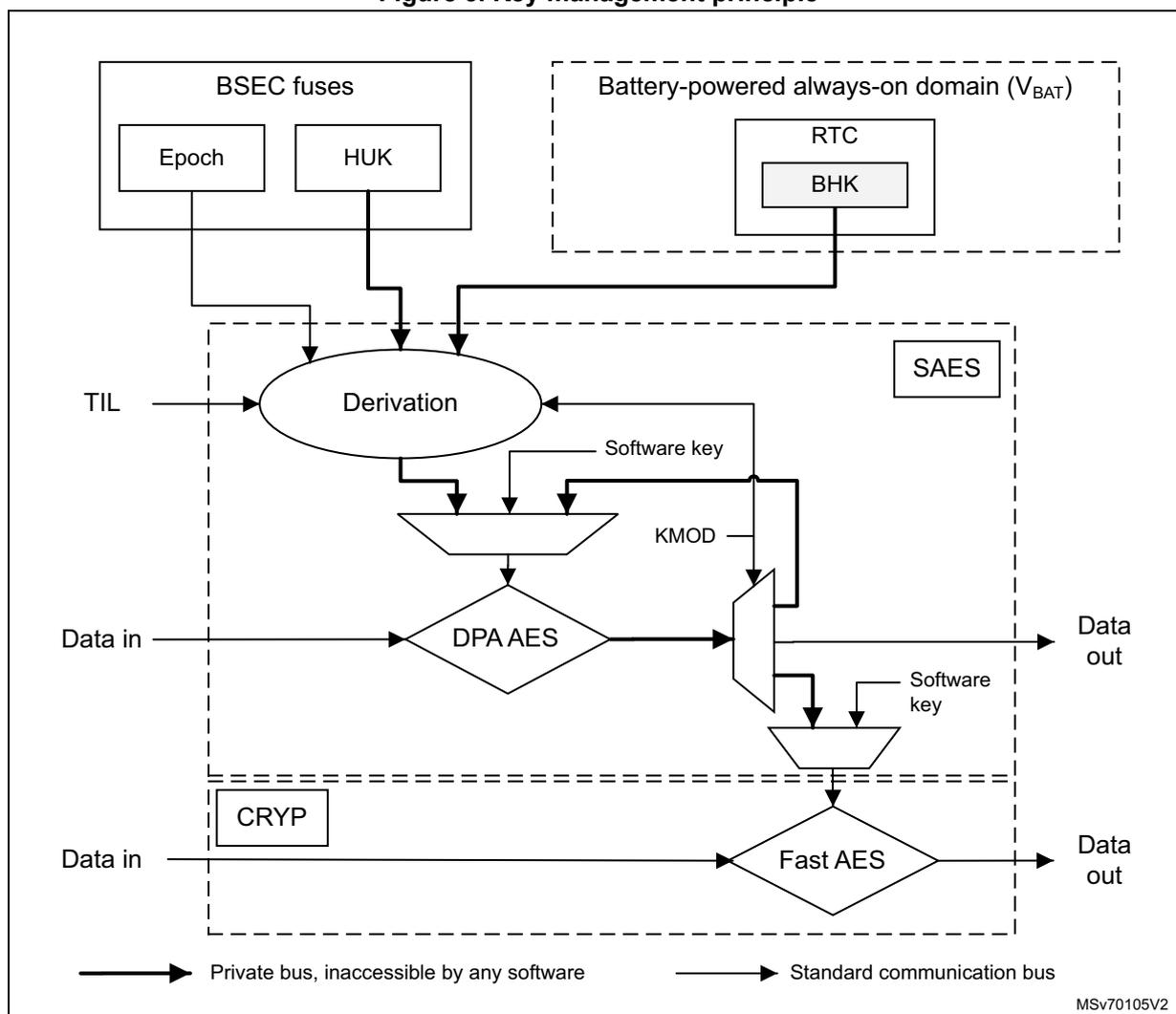
The diagram illustrates the key management principle. At the top left, a box labeled 'BSEC fuses' contains 'Epoch' and 'HUK'. At the top right, a dashed box labeled 'Battery-powered always-on domain (V BAT )' contains 'RTC' and 'BHK'. Below these, a large dashed box labeled 'SAES' contains several components: 'Derivation' (an oval), 'DPA AES' (a diamond), 'CRYP' (a rectangle), and 'Fast AES' (a diamond). 'TIL' enters from the left and points to 'Derivation'. 'Epoch' and 'HUK' also point to 'Derivation'. 'Derivation' outputs a 'Software key' to a trapezoidal block. 'KMOD' enters from the right and points to this trapezoidal block. 'Data in' enters from the left and points to 'DPA AES'. 'DPA AES' outputs to a switch. The switch selects between the 'Software key' from the trapezoidal block and another 'Software key' from a lower trapezoidal block. The output of the switch goes to 'Data out' on the right. Below a dashed line, 'Data in' enters from the left and points to 'Fast AES'. 'Fast AES' outputs to 'Data out' on the right. A legend at the bottom indicates that thick arrows represent 'Private bus, inaccessible by any software' and thin arrows represent 'Standard communication bus'. The code 'MSV70105V2' is in the bottom right corner.
The mechanism is based on KMOD[1:0] and KEYSEL[2:0] in SAES_CR. The decryption result is read out and handled by software only when KMOD = 0b00. If KMOD ≠ 0 and KEYSEL is selecting the output of the derivation function, the decryption result goes directly on dedicated buses to key registers in the SAES (when KMOD = 0b01), or (when KMOD = 0b10) to the fast CRYP1. KMOD is also an input to the derivation function that processes the device secret HUK and BHK.
A key to be provisioned in the device can be encrypted with a device-unique key (derived from HUK and/or BHK) with KMOD = 0b01 or 0b10 in SAES_CR. This key is then stored somewhere in encrypted format. When this encrypted key needs to be used, it can only be successfully decrypted with the same KMOD setting. The key cannot now be output as clear text and handled by software: it can only be directly placed in unreadable key registers, and used to decrypt or encrypt data. Once the key has been provisioned, it can never again be viewed on the device in clear.
The derivation function depends on the epoch input from the BSEC: if epoch fuses are incremented, any keys provisioned during a previous epoch are never again usable.
The derivation function also depends on the 2-bit TIL input from the BSEC. The software can set this input value to something later than the current HDPL, but can never set it to anything earlier. Keys are always provisioned for use up to a particular HDPL stage. Once that stage has finished, this key is no longer usable.
The KEYSEL field in SAES_CR selects the source of the key used in the SAES.
- • 0b001: derived key based only on the HUK
- • 0b010: derived key based only on the BHK
- • 0b100: derived key based on a combination of HUK and BHK
- • 0b000: software loadable (but unreadable) key register
3.6.5 Unique ID
The device stores a 96-bit ID, unique to each device (see Section 79: Device electronic signature ).
Application services use this unique identity key to identify the product in the cloud network, or to make it difficult for counterfeit devices or clones to inject untrusted data in the network.
Alternatively, the 256-bit device unique key (HUK) can be used (see Section 3.8.1 ).
3.7 Tamper detection and response
The STM32N6x5/x7xx devices include active protection of critical security assets against temperature, voltage, and frequency attacks. The detection of such attacks is managed in the RTC, which resides on \( V_{BAT} \) domain (see Section 61: Real-time clock (RTC) for details).
The devices support eight input/output tamper pins, which allow four independent active-tamper meshes (or up to seven if the same output pin is shared by several input pins). Four pins are in the \( V_{BAT} \) domain.
Active pins are clocked by the LSE, and are functional in all system operating modes (Run, Sleep, Stop, Standby, or Shutdown), and in \( V_{BAT} \) mode.
The detection time is programmable, and a digital filtering is available (tamper triggered after two false comparisons in four consecutive comparison samples).
Timestamps are automatically generated when a tamper event occurs.
Table 6. Internal tampers in TAMP
| Tamper input | NOER bit number in TAMP_CR3 | Tamper source |
|---|---|---|
| ITAMP1 | 0 | RTC voltage domain ( \( V_{SW} \) ) monitoring |
| ITAMP2 | 1 | Temperature monitoring |
| ITAMP3 | 2 | LSE monitoring (1) |
| ITAMP4 | 3 | HSE monitoring |
| ITAMP5 | 4 | RTC calendar overflow (rtc_calovf) |
| ITAMP6 | 5 | JTAG/SWD access when closed |
| ITAMP7 | 6 | \( V_{CORE} \) monitoring |
| ITAMP8 | 7 | Monotonic counter overflow |
Table 6. Internal tampers in TAMP (continued)
| Tamper input | NOER bit number in TAMP_CR3 | Tamper source |
|---|---|---|
| ITAMP9 | 8 | Fault detected in SAES, PKA, SAES, or RNG |
| ITAMP10 | - | Reserved |
| ITAMP11 | 10 | IWDG_reset and TAMP_potential_tamper |
1. LSE missing or over frequency detection (> 2 MHz), glitch filter (> 2 MHz).
Each tamper source, whether internal or external, can be enabled or disabled.
When the event associated with an enabled tamper source occurs, it is called tamper event, and it results in the following:
- • BHK and HUK (dedicated keybuses to SAES) are masked to zero and invalidated.
- • PKA, SAES, CRYPT, and HASH are reset, unless the boot ROM has set the SYSCFG_POTTAMPRSTCR register to indicate it safely controls them.
- • The backup RAM and registers, and the secure RAM (16-Kbyte AHB SRAM2 aliased at 0x28004000 and 0x38004000) are inaccessible (read-as-zero).
- • Fuse secrets are un-reloadable by anyone except the boot ROM.
Each tamper source can be further configured to generate an immediate erase of device secrets. An event on a tamper that is configured to do no erase, is called a potential tamper. The secure software must decide on the response.
Note: The boot ROM always sets SYSCONF_POTTAMPRSTCR to override any potential tamper, and to ensure it can access the firmware key, and use the crypto accelerators.
The boot ROM can load the FSBL even if a potential tamper occurs before or during boot.
Once the application analyzes the situation following a potential tamper event notification, there are two possible cases:
- • The application launches secret erase with a software command by setting BKERASE in TAMP_CR2.
- • The application just clears the flags to release secret blocking (false tamper).
An event on a tamper configured to perform immediate erase of device secrets is called a confirmed tamper. The device secrets consist of the backup registers, MCE key registers, the content of the PKA SRAM, and the secure AHB SRAM2 (erased as soon as \( V_{DD} \) is present). There is a configurable option that says that the content of the backup RAM must also be considered as device secrets, and erased on a confirmed tamper. It is optional because the expectation is that the backup RAM only ever contains secrets stored in a form encrypted by a key in backup registers, and when they need to be used, they are decrypted into the secure AHB SRAM2.
Each source of tamper can be configured to trigger the following events:
- • Generate an interrupt, able to wake up the device from Stop and Standby modes.
- • Generate an hardware trigger for the low-power timers.
The system includes a watchdog that the software needs to refresh regularly (and eventually fires if the software hangs). If the watchdog fires, and there is a potential tamper flagged (not yet analyzed by the software), ITAMP11 is set.
ITAMP11 must be configured as a confirmed tamper (performs an immediate erase of device secrets).
Note: SYSCONF_POTTAMPRSTCR only overrides a potential tamper. If a confirmed tamper occurs while the boot ROM operates, fuse secrets are made inaccessible until the next system reset. This may cause the authentication to fail, and a system reset is eventually triggered by the watchdog. By this time, all device secrets have been erased, and SYSCONF_POTTAMPRSTCR can override blocks that caused the flagging of a tamper event. The software can boot, and, for example, display a message indicating the occurrence of the confirmed tamper.
The effect of low-power modes on a tamper detection are summarized in the table below.
Table 7. Effect of low-power modes on TAMP
| Mode | Description |
|---|---|
| Sleep | No effect on tamper detection features TAMP interrupts cause the device to exit Sleep mode. |
| Stop | No effect on tamper detection features, except for level detection with filtering and active tamper modes that remain active only when the clock source is LSE or LSI. Tamper events cause the device to exit Stop mode. |
| Standby | No effect on tamper detection features, except for level detection with filtering and active tamper modes which remain active only when the clock source is LSE or LSI. Tamper events cause the device to exit Standby mode. |
| Shutdown | No effect on tamper detection features, except for level detection with filtering and active tamper modes which remain active only when the clock source is LSE. Tamper events cause the device to exit Shutdown mode. |
3.8 Crypto engines
3.8.1 Accelerators
The device implements cryptographic algorithms as recommended by national security agencies (such as NIST for the U.S.A, BSI for Germany, or ANSSI for France). These algorithms are used to support privacy, authentication, integrity, entropy, and identity attestation.
The embedded crypto engines enable lower processing times, and lower power consumption when performing cryptographic operations. This offloads these computations from the Cortex-M55. The SAES engine offers two important features, which cannot be implemented by software: pure hardware key handling, and DPA resistance.
For product certification purposes, ST provides certified device information on how these security functions are implemented and validated.
For more information on crypto engine processing times, refer to the dedicated section in the reference manual.
Table 8 lists the available accelerated cryptographic operations.
Table 8. Accelerated cryptographic operations
| Operations | Algorithm | Specification | Key lengths (in bit) | Modes |
|---|---|---|---|---|
| Get entropy | RNG | NIST SP800-90B (1) | N/A | Software and hardware (2) modes running in parallel |
| Encryption, decryption | AES (3) | FIPS PUB 197 NIST SP800-38A | 128, 256 (192 in CRYP only) | ECB, CBC, CTR |
| Authenticated encryption or decryption | NIST SP800-38C NIST SP800-38D | GCM, CCM | ||
| Cipher-based message authentication code | NIST SP800-38D | GMAC | ||
| Checksum | SHA-1 | FIPS PUB 180-4 | N/A | Digest 160-bit |
| Cryptographic hash | SHA-2 | SHA-224, SHA-256, SHA-384, SHA-512 | ||
| Keyed-hashing for message authentication | HMAC | FIPS PUB 198-1 IETF RFC 2104 | Short, long | All supported algorithms |
| Encryption/decryption key-pair generation (4) | RSA | IETF RFC 8017 NIST SP800-56B | Up to 4160 | RSAES-OAEP |
| Signature
(4)
with hashing Signature verification | RSA | IETF RFC 8017 FIPS PUB 186-4 | Up to 4160 | PKCS1-v1_5, PSS |
| ECDSA | ANSI X9.62 IETF RFC 7027 FIPS PUB 186-4 | Up to 640 | Refer to the Section 52: Public key accelerator (PKA) for details | |
| Key agreement | ECDH | ANSI X9.42 |
- 1. Certifiable using STMicroelectronics reviewed documents.
- 2. Random number distribution to the SAES and the PKA, using a dedicated hardware bus.
- 3. ECB, CBC, CTR, GCM, and CCM chaining modes are protected against side-channel and timing attacks in SAES (see Section 3.8.2 ).
- 4. Private-key cryptography is protected against side-channel and timing attacks.
The PKA accelerates asymmetric crypto operations (such as key pair generation, ECC scalar multiplication, point on curve check). See Section 52: Public key accelerator (PKA) for more details.
The STM32N6x5/x7xx devices have two AES engines:
- • The CRYP includes a fast AES engine with 11 cycles per 16-byte block (see Section 49: Cryptographic processor (CRYP) ).
- • The SAES contains a DPA-resistant AES engine, which implements counter-measures and mitigations against power and electromagnetic side-channel attacks. The SAES is much slower.
SAES and CRYP engines support the chaining modes mentioned in Table 8 .
As shown in Section 3.6 , the SAES can be used for extra-secure on-chip storage for sensitive information. For more information, refer to Section 48: Secure AES coprocessor (SAES) .
3.8.2 Memory cipher engine (MCE)
The MCE implements an on-the-fly encryption/decryption of data to/from external memories, which are more vulnerable to side-channel attack than internal memories (traffic on the interface is accessible). The MCE is then designed to make such attacks prohibitively expensive.
The MCE is instantiated in front of each external memory interface (memory-mapped at addresses above 0x60000000). The MCE is used to define four non-overlapping regions of target memory. Each region can be configured to be encrypted in a different way.
Secure software writes master keys into unreadable MCE registers, and then configure each region: define which master key is used for encrypting data in this region.
For each 32-byte memory block in a region, the MCE uses this block address to derive a specific key for encrypting data in this block. This is done on-the-fly, using the selected master-key. Side-channel attacks are then much more expensive, since an individual attack only uncovers 32 bytes of data.
The user chooses once, at application start, whether to use AES (128 or 256) or NOEKEON for the final data encryption (NOEKEON being faster).
Each master key is defined with an algorithm attribute that determines one of the following:
- • It is input to a strong derivation for each block.
- • It is input to a faster but weaker derivation.
- • It is used directly as a very-fast but weak stream cipher (only suitable for read-only data).
Each key and its attributes are sticky-lockable. A key cannot be partially overwritten. If its attributes are changed, the key is zeroed.
When a tamper event is confirmed in the TAMP, all MCE keys are erased, encrypted regions are read as zero, and writes ignored, until the MCE is properly initialized again.
A typical MCE use is detailed in Section 3.8.2 . For more details on the MCE programming, refer to Section 51: Memory cipher engine (MCE) .
3.8.3 NPU encryption
The encryption that uses the MCE has a latency of at least 11 cycles, and a block size of 16 bytes. This imposes an heavy overhead on NPU memory transactions. Therefore the NPU is equipped with its own low-latency encryption engines on its 8-byte-wide AXI initiator ports.
The formula for creating a 64-bit ciphertext \( C_x \) , from plaintext \( P_x \) , which resides at an address \( addr_x \) , is:
where:
- • H is the cryptographic function.
- • \( K_{128} \) is a 128-bit key written to configuration registers in the NPU.
- • ID y is a value that software can modify when the NPU rewrites a new value to the same address.
The latency through the NPU encryption engine is 3 or 4 cycles (depending on a strength option selected by the software). See Section 20: Neural-ART accelerator™ (NPU) .
3.9 Access controlled debug
The BSEC and DBGMCU hardware support an Arm PSA-compliant debug authentication mechanism.
A secure debug is where the debugger arranges to make secure privileged accesses on its AXI initiator. A nonsecure debug is more restricted: the debugger can only make non-secure privileged accesses via its AXI port.
On power-up, regardless of whether or not the reset pin is still asserted, fuses are immediately read to determine whether the device is BSEC-open or BSEC-closed. If the device is BSEC-open, an attached debugger can perform a “chip discovery” (reading various CPU identification registers), even while holding the device in reset via the RESET pin.
On a BSEC-closed device, the debug access depends on the content of BSEC_DBGCR and BSEC_AP_UNLOCK, which are only writable once by secure-privileged code after the boot ROM has completed. The debug opens when both conditions are met:
- • DBG_UNLOCK = 0xB4 in BSEC_DBGCR.
- • UNLOCK = 0xB4 in BSEC_AP_UNLOCK.
The current HDPL (reported in BSEC_HDPLSR) must also be non-zero. It must reach the level defined by DBG_AUTH_TIL in BSEC_DBGCR. DBG_AUTH_SEC in BSEC_DBGCR determines whether it is secure or nonsecure debug (see Section 4: Boot and security control (BSEC) for more details).
In order to control the debug reopening, the uRoT can impose a debug authentication protocol. This protocol must implement a challenge response mechanism based on asymmetric cryptography to authenticate requests from the host (relying on an OEM debug public key stored in the device by the OEM).
The protocol can implement a bidirectional communication between the host and the device through a mailbox interface located in the DBGMCU. The host debugger writes to the mailbox via the JTAG/SWD interface, and expects to get responses and messages from the device via the same mailbox.
The debug authentication protocol is launched on a power-up of the device, when an open-request message is posted by the host, while the device is still under reset. Trusted DBG_AUTH code sees this, and generates a random challenge token. The debugger appends this token to a certificate chain that confers certain rights to the debugger, signs this “debug certificate” structure, and submits it back to the device. The DBG_AUTH code validates it with respect to a root public key provisioned in fuses by the OEM. The random token stops any later replay of the same interaction.
The debug certificate determines whether the debug is secure or nonsecure.
BSEC_DBGCR is only reset on power-up: it retains its value through warm resets. The debugger does not have to repeat the authentication procedure on system resets.