59. Debug support (DBG)
59.1 DBG introduction
A comprehensive set of debug features is provided to support software development and system integration:
- • Breakpoint debugging of the CPU core
- • Code execution tracing
- • Software instrumentation
- • Cross-triggering
The debug features can be controlled via a JTAG/Serial-wire debug access port, using industry-standard debugging tools. A trace port allows data to be captured for logging and analysis.
The debug features are based on Arm ® CoreSight ™ components.
- – SWJ-DP: JTAG/Serial-wire debug port
- – AHB-AP: AHB access port
- – ROM table
- – System control space (SCS)
- – Breakpoint unit (BPU)
- – Data watchpoint and trace unit (DWT)
- – Instrumentation trace macrocell (ITM)
- – Embedded Trace Macrocell ™ (ETM)
- – Cross-trigger interface (CTI)
- – Trace port interface unit (TPU)
The debug features are accessible by the debugger via the AHB-AP.
Additional information can be found in the Arm ® documents referenced in Section 59.13 .
59.2 DBG functional description
59.2.1 DBG block diagram
Figure 850. Block diagram of debug support infrastructure
![Block diagram of debug support infrastructure showing the internal architecture of the CPU Cortex-M33 and its debug components. The diagram includes the JTAG/Serial-wire port (SWJ-DP, DAP, APB-AP), the CPU Core, DWT, BPU, ITM, TPIU, ETM, CTI, Processor ROM table, MCU ROM table, DBG_MCU, System bus matrix, APB mux, and System ROM table. The Trace port includes TRACECK, TRACED[3:0], and TRACESWO pins.](/RM0481-STM32H523-33-562-63-573/58edcffd125bcc0a49703d4611d2efba_img.jpg)
59.2.2 DBG pins and internal signals
Table 709. JTAG/Serial-wire debug port pins
| Pin name | JTAG debug port | SW debug port | Pin assignment | ||
|---|---|---|---|---|---|
| Type | Description | Type | Description | ||
| JTMS/SWDIO | I | JTAG test mode select | IO | Serial-wire data in/out | PA13 |
| JTCK/SWCLK | I | JTAG test clock | I | Serial-wire clock | PA14 |
| JTDI (1) | I | JTAG test data input | - | - | PA15 |
| JTDO | O | JTAG test data output | - | - | PB3 |
| nJTRST | I | JTAG test reset | - | - | PB4 |
1. TDI is hosted on the same I/O as a USBBPD-CC line. To avoid pull-up/down conflict, a user option can help to decide whether the pad is used as TDI or as CC.
Table 710. Trace port pins
| Pin name | Type | Description | Pin assignment |
|---|---|---|---|
| TRACED0 | O | Trace synchronous data out 0 | Refer to the datasheet |
| TRACED1 | Trace synchronous data out 1 | ||
| TRACED2 | Trace synchronous data out 2 | ||
| TRACED3 | Trace synchronous data out 3 | ||
| TRACECK | Trace clock |
| Pin name | Type | Description | Pin assignment |
|---|---|---|---|
| TRACESWO | O | Single-wire trace asynchronous data out | PB3 (1) |
- 1. TRACESWO is multiplexed with JTDO. This means that a single-wire trace is only available when using the serial-wire debug interface, and not when using JTAG.
59.2.3 DBG reset and clocks
The debug port (SWJ-DP) is reset by a power-on reset and when waking up from Standby mode.
The debugger supplies the clock for the debug port via the debug interface pin JTCK/SWCLK. This clock is used to register the serial input data in both serial-wire and JTAG modes, as well as to operate the state machines and internal logic of the debug port. This clock must therefore continue to toggle for several cycles after the end of an access, to ensure that the debug port returns to the idle state.
The SWJ-DP contains an asynchronous interface to the DCLK domain that covers the rest of the SWJ-DP and the access port.
The DCLK is a gated version of the system clock.
The DCLK domain is enabled by the debugger using the CDBGPWRUPREQ bit in the DP control and status register (DP_CTRLSTATR) . The clock must be enabled before the debugger can access any of the debug features on the device. The availability of the clock is reflected in the CDBGPWRUPACK bit in DP_CTRL/STATR. The DCLK is disabled at power-up, and must be disabled when the debugger is disconnected, to avoid wasting energy.
The debug and trace components included in the processor are clocked with the processor clock.
59.2.4 DBG power domains
The debug components are located in the core power domain. This means that the debugger connection is not possible in Shutdown or Standby low-power mode. To avoid losing the connection when the device enters Standby mode, the power can be maintained to the core by setting a bit in the DBGMCU configuration register (DBGMCU_CR) . This also keeps the processor clocks active and holds off the reset, so that the debug session is maintained.
59.2.5 Debug and low-power modes
The devices include power-saving features that allow the core power domain to be switched off or stopped when not required. If the power is switched off or if the core is not clocked, all debug components are inaccessible to the debugger. To avoid this, power-saving mode emulation is implemented. If the emulation is enabled for a domain, the domain still enters power-saving mode, but its clock and power are maintained. In other words, the domain behaves as if it is in power-saving mode, but the debugger does not lose the connection.
The emulation mode is programmed in the microcontroller debug (DBGMCU) unit. For more information, refer to Section 59.12 .
59.2.6 Security
The trace and debug components allow a high degree of access to the processor and system during product development. In order to protect user code and ensure that the debug features cannot be used to alter or compromise the normal operation of the finished product, these features can be disabled or limited in scope. For example, secure software debug and trace can be disabled without preventing the debug of nonsecure code.
Debugger access to secure memory (when permitted) must be performed using secure transactions on the debug AHB, that is, with the PROT[6] bit set in the AP1 control/status word register (AP1_CSWR) .
Debugger access is disabled while the processor is booting from system flash memory.
The following authentication signals are used by the system to determine which debug features are enabled or disabled:
- •
dbgen
: global enable for all debug features
- 0: All debug features are disabled.
- 1: Debug features in the nonsecure state are enabled. Debug features in the secure state are dependent on the state of the spiden signal.
- •
spiden
: enables debug in the secure state when
dbgen
= 1.
- 0: Debug features are disabled in the secure state.
- 1: Debug features are enabled in the secure state.
- •
niden
: enables trace and performance monitoring (noninvasive debug).
- 0: Trace generation is disabled.
- 1: Trace generation in the nonsecure state is enabled. Trace generation in the secure state is dependent on the state of the spniden signal.
- •
spniden
: enables trace and performance monitoring in the secure state when
niden
= 1.
- 0: Trace generation is disabled in the secure state.
- 1: Trace generation is enabled in the secure state.
For detailed information on the behavior of each component according to the state of the authentication signals, refer to the relevant chapter, or to the relevant Arm® technical documentation.
The state of the signals is set according to the debug state as shown in Table 712 , when TrustZone® is enabled (TZEN = 0xB4), and Table 713 when TrustZone is disabled (TZEN = 0xC3).
Table 712. Authentication signal states with TrustZone enabled (TZEN = 0xB4)
| Debug state | Authentication signal state | Description |
|---|---|---|
| OPEN | dbgen = 1 spiden = 1 niden = 1 spniden = 1 | Debug and trace is enabled whatever the state of the processor. Debugger access to secure memory is permitted. |
| CLOSED SECURE | dbgen = 1 spiden = 0 niden = 1 spniden = 0 | Debug and trace is enabled when the processor is in nonsecure state. Debugger access to nonsecure memory is permitted. Debugger access to secure memory is disabled. |
| CLOSED | dbgen = 0 spiden = 0 niden = 0 spniden = 0 | Debug and trace is disabled. |
Table 713. Authentication signal states with TrustZone disabled (TZEN = 0xC3)
| Debug state | Authentication signal state | Description |
|---|---|---|
| OPEN | dbgen = 1 spiden = 1 niden = 1 spniden = 1 | Debug and trace is enabled whatever the state of the processor. All memory and resources are considered nonsecure and accessible to the debugger. |
| CLOSED | dbgen = 0 spiden = 0 niden = 0 spniden = 0 | Debug and trace is disabled. |
The state of the authentication signals can be read from the DAUTHSTATUS register in the system control space (SCS) of the Cortex®-M33.
The debug state depends upon the product life cycle state and the debug authentication state (see Section 59.2.7 ).
Table 714. Life cycle state and debug states
| Product life cycle state | Debug state |
|---|---|
| OPEN | OPEN |
| TZ_CLOSED | CLOSED-SECURE |
| CLOSED (debug not authenticated) | CLOSED |
Table 714. Life cycle state and debug states
| Product life cycle state | Debug state |
|---|---|
| CLOSED (debug constrained) | OPEN/CLOSED-SECURE (1) |
| LOCKED | CLOSED |
1. Depends on authorization level.
59.2.7 Debug authentication
Figure 851. Product life cycle states and debug authentication
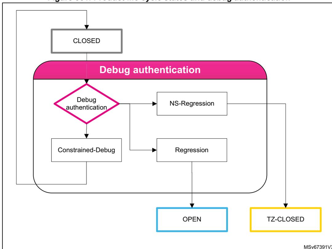
The flowchart illustrates the transition between product life cycle states and debug states. It begins with a 'CLOSED' state box at the top. An arrow points down to a large pink rounded rectangle labeled 'Debug authentication'. Inside this box, an arrow points to a pink diamond labeled 'Debug authentication'. From this diamond, three arrows branch out: one pointing down to a 'Constrained-Debug' box, one pointing right to an 'NS-Regression' box, and one pointing right to a 'Regression' box. From the 'Constrained-Debug' box, an arrow points left and then up, exiting the 'Debug authentication' box to loop back to the 'CLOSED' state. From the 'Regression' box, an arrow points down, exiting the 'Debug authentication' box to a blue box labeled 'OPEN'. From the 'NS-Regression' box, an arrow points right and then down, exiting the 'Debug authentication' box to a yellow box labeled 'TZ-CLOSED'. The text 'MSV67391V3' is in the bottom right corner of the diagram.
Figure 851 shows the product life cycle and debug authentication states.
If the device is in CLOSED (product life cycle) state, the debug state is CLOSED. The debug authentication procedure allows a trusted debugger to reopen access without compromising sensitive information called the Root Of Trust (ROT).
Reopening the debug is possible only if sensitive asset security is ensured (and TrustZone is enabled (TZEN = 0xB4). This is called Constrained Debug, as constraints ensure the security of the ROT information.
Alternatively, a partial or full regression mechanism can be used when security of sensitive information cannot be guaranteed. This is called Regression, as regression ensures removal of the sensitive information before reopening the debug.
- • Partial regression corresponds to releasing nonsecure code and assets. The intermediate state which allows partial regression management is called NS-Regression.
- • Full regression corresponds to releasing all code and assets. The intermediate state allowing full regression management is called Regression.
Debug authentication control principle
The debug authentication is one of the most critical security features of the system considering that with a debugger the user can access a large part of the system.
To control the reopening of the debug, the device imposes a debug authentication protocol.
The protocol implements a challenge response mechanism based on asymmetric cryptography to authenticate the host. It relies on a key pair, with a Public Key stored in the device, and a Private Key from the host library, used to sign a random value (the challenge) generated by the device.
The protocol implements a bidirectional communication between the host and the device through a mailbox interface located in the DBGMCU.
The host can write to the mailbox via the JTAG/SWD interface. It expects to get responses and messages from the device via the same mailbox.
The debug authentication protocol is launched on a power-on reset of the device, when an “open request” message is posted by the host.
The protocol is based on:
- • Initial message: posted by the host combined with a reset to launch the debug authentication process on the device.
- • Challenge message: the device generates a random value, to be signed by the host, when sending back the response.
- • Response: the host sends a message to the device proving its authenticity. This is done using a tool to generate a token.
The implementation is ensured by code embedded in the system flash. This code is called automatically after reset if an initial message has been posted by the host in the mailbox.
After a first sequence of mutual authentication to align on protocol version, type of device, and similar parameters, the device generates a random value that to be signed by the host with a private key when building the response.
The STMicroelectronics implementation is based on the Arm® PSA-ADAC solution for debug authentication.
The debug authentication can be implemented using a proprietary or open-source protocol.
As this feature is critical for security, the STM32H5 devices come with debug authentication provisioned in system flash. STMicroelectronics provides the host tools integrated with some debug environments (IDEs).
Debug authentication provisioning
Debug authentication is natively supported by the STM32H5 platform. The data used by ST debug authentication (ST-DA) must be provisioned at a defined location in the secure key storage area (OBKeys defined in flash memory).
The debug authentication configuration must be done only when the PRODUCT_STATE is “Provisioning”, cannot be performed when PRODUCT_STATE is “Open”.
The following data must be provisioned (refer to Section 7.7.2: RSS user functions ):
- • Data must be provisioned at the very beginning of the OBK_HDPL1 mapping (0x0FFD 0100) (see Section 7.5.2: OBK access per HDPL level )
- • RSS_Lib encryption option must be set for STM32H533/573xx devices
- • RSS_Lib encryption option must be reset for STM32H523/56xxx devices
The data to provision are defined in Table 715 . They depend upon the TZEN option byte setting (enabled or disabled).
Table 715. Definition of data to provision
| Data size | TZEN enabled (certificates) | TZEN disabled (password: only full regression is allowed) |
|---|---|---|
| 32 bytes | SHA256 of the overall blob (i.e. the two next fields) | |
| SHA256 of the ROT certificate public key | SHA256 of the password | |
| 16 bytes | 128-bis permission mask (see Table 716 ) | 128 bits are reserved, to be set to 0 |
Caution: Configure debug authentication as explained above before changing to states different from Open or Provisioning.
Table 716. Permission mask (Endianness: Little Endian)
| Bit(s) | Description |
|---|---|
| Bit 0 | When set it allows Intrusive debug from HDPL1 – NS |
| Bit 1 | When set it allows Intrusive debug from HDPL2 – NS |
| Bit 2 | When set it allows Intrusive debug from HDPL3 – NS |
| Bit 3 | Reserved |
| Bit 4 | When set it allows Intrusive debug from HDPL1 – S |
| Bit 5 | When set it allows Intrusive debug from HDPL2 – S |
| Bit 6 | When set it allows Intrusive debug from HDPL3 – S |
| Bits 7:11 | Reserved |
| Bit 12 | Regression to TZ-Closed, when 1 regression to TZ-Closed is allowed |
| Bit 13 | Reserved |
| Bit 14 | Regression (Full regression), when 1 full regression is allowed |
| Bit 15:127 | Reserved |
59.3 Serial-wire and JTAG debug port (SWJ-DP)
The SWJ-DP is a CoreSight component that implements an external access port for connecting debugging equipment.
Two types of interface can be configured:
- • A 5-pin standard JTAG interface (JTAG-DP)
- • A 2-pin (clock + data) serial-wire debug port (SW-DP)
These two modes are mutually exclusive, since they share the same I/O pins.
By default, the JTAG-DP is selected after a system or a power-on reset. The five I/O pins are configured by hardware in debug alternative function mode. The SWJ-DP incorporates pull-up resistors on JTDI, JTMS/SWDIO, and nJTRST, as well as a pull-down resistor on JTCK/SWCLK.
A debugger can select the SW-DP by transmitting the following serial data sequence on JTMS/SWDIO:
... (50 or more ones) ..., 0, 1, 1, 1, 1, 0, 0, 1, 1, 1, 1, 0, 0, 1, 1, 1, ... (50 or more ones) ...
JTCK/SWCLK must be cycled for each data bit.
In SW-DP mode, the unused JTAG pins JTDI, JTDO, and nJTRST can be used for other functions.
Note: All SWJ port I/Os can be reconfigured to other functions by software, but debugging is no longer possible.
59.3.1 JTAG debug port
The JTAG-DP implements a TAP state machine (TAPSM), shown in the figure below, based on IEEE Std 1149.1-1990. The state machine controls two scan chains, one associated with an instruction register (IR) and the other one with a number of data registers (DR).
Figure 852. JTAG TAP state machine
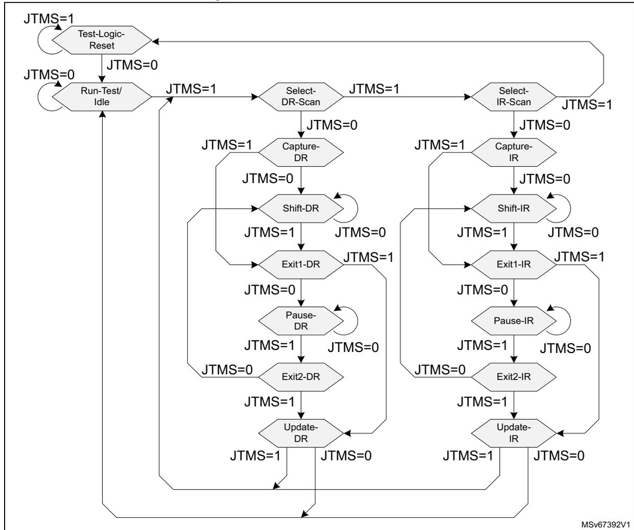
stateDiagram-v2
    [*] --> Test-Logic-Reset: JTMS=1
    Test-Logic-Reset --> Run-Test/Idle: JTMS=0
    Run-Test/Idle --> Select-DR-Scan: JTMS=1
    Run-Test/Idle --> Select-IR-Scan: JTMS=1
    Select-DR-Scan --> Capture-DR: JTMS=0
    Select-IR-Scan --> Capture-IR: JTMS=0
    Capture-DR --> Shift-DR: JTMS=0
    Capture-IR --> Shift-IR: JTMS=0
    Shift-DR --> Shift-DR: JTMS=0
    Shift-DR --> Exit1-DR: JTMS=1
    Shift-IR --> Shift-IR: JTMS=0
    Shift-IR --> Exit1-IR: JTMS=1
    Exit1-DR --> Pause-DR: JTMS=0
    Exit1-IR --> Pause-IR: JTMS=0
    Pause-DR --> Pause-DR: JTMS=0
    Pause-DR --> Exit2-DR: JTMS=1
    Pause-IR --> Pause-IR: JTMS=0
    Pause-IR --> Exit2-IR: JTMS=1
    Exit2-DR --> Update-DR: JTMS=1
    Exit2-IR --> Update-IR: JTMS=1
    Update-DR --> Run-Test/Idle: JTMS=0
    Update-DR --> Select-DR-Scan: JTMS=1
    Update-IR --> Run-Test/Idle: JTMS=0
    Update-IR --> Select-IR-Scan: JTMS=1
The diagram illustrates the JTAG TAP state machine (TAPSM) with the following states and transitions:
- Test-Logic-Reset : Initial state, entered when JTMS=1. Transitions to Run-Test/Idle when JTMS=0.
- Run-Test/Idle : Idle state, entered when JTMS=0. Transitions to Select-DR-Scan or Select-IR-Scan when JTMS=1.
- Select-DR-Scan : State entered when JTMS=1. Transitions to Capture-DR when JTMS=0.
- Select-IR-Scan : State entered when JTMS=1. Transitions to Capture-IR when JTMS=0.
- Capture-DR : State entered when JTMS=0. Transitions to Shift-DR when JTMS=0.
- Capture-IR : State entered when JTMS=0. Transitions to Shift-IR when JTMS=0.
- Shift-DR : State entered when JTMS=0. Transitions to Shift-DR (self-loop) when JTMS=0, or to Exit1-DR when JTMS=1.
- Shift-IR : State entered when JTMS=0. Transitions to Shift-IR (self-loop) when JTMS=0, or to Exit1-IR when JTMS=1.
- Exit1-DR : State entered when JTMS=1. Transitions to Pause-DR when JTMS=0.
- Exit1-IR : State entered when JTMS=1. Transitions to Pause-IR when JTMS=0.
- Pause-DR : State entered when JTMS=0. Transitions to Pause-DR (self-loop) when JTMS=0, or to Exit2-DR when JTMS=1.
- Pause-IR : State entered when JTMS=0. Transitions to Pause-IR (self-loop) when JTMS=0, or to Exit2-IR when JTMS=1.
- Exit2-DR : State entered when JTMS=1. Transitions to Update-DR when JTMS=1.
- Exit2-IR : State entered when JTMS=1. Transitions to Update-IR when JTMS=1.
- Update-DR : State entered when JTMS=1. Transitions to Run-Test/Idle when JTMS=0, or to Select-DR-Scan when JTMS=1.
- Update-IR : State entered when JTMS=1. Transitions to Run-Test/Idle when JTMS=0, or to Select-IR-Scan when JTMS=1.
MSv67392V1
The operation of the JTAG-DP is as follows:
- 1. When the TAPSM goes through the Capture-IR state, 0b0001 is transferred to the instruction register (IR) scan chain. The IR scan chain is connected between JTDI and JTDO.
- 2. While the TAPSM is in the Shift-IR state, the IR scan chain shifts one bit for each rising edge of JTCK. This means that on the first tick:
- – The LSB of the IR scan chain is output on JTDO.
- – Bit[n] of the IR scan chain is transferred to bit[n-1].
- – The value on JTDI is transferred to the MSB of the IR scan chain.
- 3. When the TAPSM goes through the Update-IR state, the value scanned into the IR scan chain is transferred to the instruction register.
- 4. When the TAPSM goes through the Capture-DR state, a value is transferred from one of the data registers to one of the DR scan chains, connected between JTDI and JTDO.
- 5. The value held in the instruction register determines which data register, and associated DR scan chain, are selected.
- 6. This data is then shifted while the TAPSM is in the Shift-DR state, in the same manner as the IR shifts in the Shift-IR state.
- 7. When the TAPSM goes through the Update-DR state, the value scanned into the DR scan chain is transferred to the selected data register.
- 8. When the TAPSM is in the Run-Test/Idle state, no special actions occur. The IDCODE instruction is loaded in IR.
When active, the nJTRST signal resets the state machine asynchronously to the test-logic-reset state.
The data registers corresponding to the 4-bit IR instructions are listed in the table below.
Table 717. JTAG-DP data registers
| IR instruction | DR register | Scan chain length | Description |
|---|---|---|---|
| 0000 to 0111 | (BYPASS) | 1 | Not implemented: BYPASS selected |
| 1000 | ABORT | 35 | ABORT register – bits 34:3 = APABORT[31:0]: Write 0x0000 0001 to abort an ongoing access port transaction – bits 2:1 = A[3:2] = 00 – bit 0 = RnW = 0: write only |
| 1001 | (BYPASS) | 1 | Reserved: BYPASS selected |
Table 717. JTAG-DP data registers (continued)
| IR instruction | DR register | Scan chain length | Description |
|---|---|---|---|
| 1010 | DPACC | 35 | Debug port access register Initiates the debug port and gives access to a debug port register.
|
| 1011 | APACC | 35 | Access port access register Initiates an access port and gives access to an access port register.
|
| 1100 | (BYPASS) | 1 | Reserved: BYPASS selected |
| 1101 | (BYPASS) | 1 | Reserved: BYPASS selected |
| 1110 | IDCODE | 32 | Identification code 0x6BA0 0477: Cortex ® -M33 JTAG debug port ID code |
| 1111 | BYPASS | 1 | Bypass A single JTCK cycle delay is inserted between JTDI and JTDO. |
The DR registers are described in more detail in the Arm ® Debug Interface Architecture Specification (see Section 59.13 ).
59.3.2 Serial-wire debug port
The serial-wire debug protocol uses the following pins:
- • SWCLK: clock from host to target
- • SWDIO: bidirectional serial data (100 k \( \Omega \) pull-up required)
Serial data is transferred LSB first, synchronously with the clock.
A transfer comprises three phases:
- 1. Packet request (8 bits) transmitted by the host, see Table 718
- 2. Acknowledge response (3 bits) transmitted by the target, see Table 719
- 3. Data transfer (33 bits) transmitted by the host (in case of a write) or target (in case of a read), see Table 720
The data transfer only occurs if the acknowledge response is OK.
Between each phase, if the direction of the data is reversed, a single clock-cycle turn-around time is inserted.
Table 718. Packet request
| Bit field | Name | Description |
|---|---|---|
| 0 | Start | Must be 1 |
| 1 | APnDP | – 0: DP register access - see
Section 59.3.3 – 1: AP register access - see Section 59.4 |
| 2 | RnW | – 0: write request – 1: read request |
| 4:3 | A(3:2) | Address field of the DP or AP register (refer to Table 722 or Table 724 ) |
| 5 | Parity | Single bit parity of preceding bits |
| 6 | Stop | 0 |
| 7 | Park | Not driven by host, must be read as 1 by target |
Table 719. ACK response
| Bit field | Name | Description |
|---|---|---|
| 2:0 | ACK | – 000: FAULT – 010: WAIT – 100: OK |
Table 720. Data transfer
| Bit field | Name | Description |
|---|---|---|
| 31:0 | WDATA or RDATA | Write or read data |
| 32 | Parity | Single-bit parity of 32 data bits |
In the case of a FAULT or WAIT ACK response from the target, the data transfer phase is canceled, unless overrun detection is enabled: in this case, the data is ignored by the target (in the case of a write), or not driven (in the case of a read).
A line reset must be generated by the host when it is first connected, or following a protocol error. The line reset consists in 50 or more SWCLK cycles with SWDIO high, followed by two SWCLK cycles with SWDIO low.
For more details on the serial-wire debug protocol, refer to the Arm ® Debug Interface Architecture Specification [1] .
Note: The SWJ-DP implements SWD protocol version 2.
59.3.3 Debug port registers
Both the SW-DP and the JTAG-DP access the debug port (DP) registers listed in Table 722 .
The debugger can access the DP registers as follows:
- 1. Program the A(3:2) field in the DPACC register, if using JTAG, with the register address within the bank. Program the RnW bit to select a read or write. In the case of a write, program the data field with the write data. If using SWD, the A(3:2) and RnW fields are part of the packet request word sent to the SW-DP with the APnDP bit reset (see Table 718 ). The write data are sent in the data phase.
- 2. To access one of the banked DP registers at the address 0x4, the register number must first be written to the DP_SELECTR register at the address 0x8. Any subsequent read or write to address 0x4 accesses the register corresponding to the contents of the DP_SELECTR register.
Table 721. Debug port registers
| Address | A(3:2) value | R/W | Description |
|---|---|---|---|
| 0x0 | 00 | R | DP debug port identification register (DP_PIDR) contains the IDCODE for the debug port. |
| W | DP abort register (DP_ABORTR) (1) aborts the current AP transaction. This register is also used to clear the error flags in the DP_CTRLSTATR register. | ||
| 0x4 | 01 | R/W | If DP_SELECTR.DPBANKSEL[3:0] = 0x0, DP control and status register (DP_CTRLSTATR) controls the DP and provides status information. |
| If DP_SELECTR.DPBANKSEL[3:0] = 0x1, DP data link control register (DP_DLCR) (2) controls the operating mode of the SWD data link. | |||
| If DP_SELECTR.DPBANKSEL[3:0] = 0x2, DP target identification register (DP_TARGETIDR) provides target identification information. | |||
| If DP_SELECTR.DPBANKSEL[3:0] = 0x3, DP data link protocol identification register (DP_DLPIDR) (2) provides the SWD protocol version. | |||
| 0x8 | 10 | R | DP event status register (DP_RESENR) (2) returns the value that was returned by the last AP read or DP_RDBUFF read. Used in the event of a corrupted read transfer. |
| W | DP access port select register (DP_SELECTR) selects the access port, access port register bank, and DP register at the address 0x4. | ||
| 0xC | 11 | R | DP read buffer register (DP_RDBUFFR) – Via JTAG-DP, this register allows the debugger to get the final result after a sequence of operations (without requesting new JTAG-DP operation) – Via SW-DP, this register contains the result of the preceding AP read access, allowing a new AP access to be avoided. |
1. Access to the AP ABORT register from the JTAG-DP is done using the ABORT instruction.
2. Only accessible via SW-DP. Register is “reserved” via JTAG-DP.
DP debug port identification register (DP_PIDR)
Address offset: 0x0
Reset value: 0x6BA0 2477
| 31 | 30 | 29 | 28 | 27 | 26 | 25 | 24 | 23 | 22 | 21 | 20 | 19 | 18 | 17 | 16 |
|---|---|---|---|---|---|---|---|---|---|---|---|---|---|---|---|
| REVISION[3:0] | PARTNO[7:0] | Res. | Res. | Res. | MIN | ||||||||||
| r | r | r | r | r | r | r | r | r | r | r | r | r | |||
| 15 | 14 | 13 | 12 | 11 | 10 | 9 | 8 | 7 | 6 | 5 | 4 | 3 | 2 | 1 | 0 |
| VERSION[3:0] | DESIGNER[10:0] | Res. | |||||||||||||
| r | r | r | r | r | r | r | r | r | r | r | r | r | r | r | |
Bits 31:28 REVISION[3:0] : revision code
0x6: Rev 6
Bits 27:20 PARTNO[7:0] : part number for the debug port
0xBA
Bits 19:17 Reserved, must be kept at reset value.
Bit 16 MIN : minimal debug port (MINDP) implementation
0x0: MINDP not implemented
Bits 15:12 VERSION[3:0] : debug port architecture version
0x2: DPv2
Bits 11:1 DESIGNER[10:0] : JEDEC designer identity code
0x23B: Arm® JEDEC code
Bit 0 Reserved, must be kept at reset value.
DP abort register (DP_ABORTR)
Address offset: 0x0
Reset value: 0x0000 0000
| 31 | 30 | 29 | 28 | 27 | 26 | 25 | 24 | 23 | 22 | 21 | 20 | 19 | 18 | 17 | 16 |
|---|---|---|---|---|---|---|---|---|---|---|---|---|---|---|---|
| Res. | Res. | Res. | Res. | Res. | Res. | Res. | Res. | Res. | Res. | Res. | Res. | Res. | Res. | Res. | Res. |
| 15 | 14 | 13 | 12 | 11 | 10 | 9 | 8 | 7 | 6 | 5 | 4 | 3 | 2 | 1 | 0 |
| Res. | Res. | Res. | Res. | Res. | Res. | Res. | Res. | Res. | Res. | Res. | ORUNERRCLR | WDERRCLR | STKERRCLR | Res. | DAPABORT |
| w | w | w | w |
Bits 31:5 Reserved, must be kept at reset value.
Bit 4 ORUNERRCLR : overrun error clear
0: no effect
1: STICKYORUN bit cleared in DP_CTRL/STATR register
Bit 3 WDERRCLR : write data error clear
0: no effect
1: WDATAERR bit cleared in DP_CTRL/STATR register
Bit 2 STKERRCLR : sticky error clear
0: no effect
1: STICKYERR bit cleared in DP_CTRL/STATR register
Bit 1 Reserved, must be kept at reset value.
Bit 0 DAPABORT : current AP transaction aborted if excessive number of WAIT responses returned
This bit indicates that the transaction is stalled.
0: no effect
1: transaction aborted
DP control and status register (DP_CTRLSTATR)
Address offset: 0x4
Reset value: 0x0000 0000
This register is accessible when DP_SELECTR.DPBANKSEL[3:0] = 0x0.
| 31 | 30 | 29 | 28 | 27 | 26 | 25 | 24 | 23 | 22 | 21 | 20 | 19 | 18 | 17 | 16 |
|---|---|---|---|---|---|---|---|---|---|---|---|---|---|---|---|
| Res. | Res. | CDBGPWRUPACK | CDBGPWRUPREQ | Res. | Res. | Res. | Res. | Res. | Res. | Res. | Res. | Res. | Res. | Res. | Res. |
| r | r | ||||||||||||||
| 15 | 14 | 13 | 12 | 11 | 10 | 9 | 8 | 7 | 6 | 5 | 4 | 3 | 2 | 1 | 0 |
| Res. | Res. | Res. | Res. | Res. | Res. | Res. | Res. | WDATAERR | READOK | STICKYERR | Res. | Res. | Res. | STICKYORUN | ORUNDETECT |
| r | r | r | r | r |
Bits 31:30 Reserved, must be kept at reset value.
Bit 29 CDBGPWRUPACK : debug power-up acknowledge
See description in Section 59.2.5: Debug and low-power modes .
0: DCLK gated
1: DCLK enabled
Bit 28 CDBGPWRUPREQ : debug power-up request
This bit controls the DCLK enable request signal.
0: requests DCLK gating
1: requests DCLK enable
Bits 27:8 Reserved, must be kept at reset value.
Bit 7 WDATAERR : write data error (read-only) in SW-DP
This bit indicates that there is a parity or framing error on the data phase of a write, or a write accepted by the DP is then discarded without being submitted to the AP.
This bit is reset by writing 1 to the ABORT.WDERRCLR bit.
0: no error
1: an error occurred
Note: This bit is reserved in JTAG-DP.
Bit 6 READOK : AP read response (read-only) in SW-DP
This bit indicates the response to the last AP read access.
0: read not OK
1: read OK
Note: This bit is reserved in JTAG-DP.
Bit 5 STICKYERR : transaction error (read-only in SW-DP, read/write in JTAG-DP)
This bit indicates that an error occurred in an AP transaction. It is reset by writing 1 to the DP_ABORTR.STKERRCLR bit (in SW-DP and JTAG-DP)
0: no error
1: an error occurred
Bits 4:2 Reserved, must be kept at reset value.
Bit 1 STICKYORUN : overrun (read-only in SW-DP, read/write in JTAG-DP).
This bit indicates that an overrun occurred (new transaction received before previous transaction completed). This bit is only set if the ORUNDETECT bit is set. It is reset by writing 1 to the DP_ABORTR.ORUNERRCLR bit (in SW-DP and JTAG-DP).
0: no overrun
1: an overrun occurred
Bit 0 ORUNDETECT : overrun detection mode enable.
0: disabled
1: enabled. In the event of an overrun, the STICKYORUN bit is set and subsequent transactions are blocked until the STICKYORUN bit is cleared.
DP data link control register (DP_DLCR)
Address offset: 0x4
Reset value: 0x0000 0000
This register is accessible when DP_SELECTR.DPBANKSEL[3:0] = 0x1 .
| 31 | 30 | 29 | 28 | 27 | 26 | 25 | 24 | 23 | 22 | 21 | 20 | 19 | 18 | 17 | 16 |
|---|---|---|---|---|---|---|---|---|---|---|---|---|---|---|---|
| Res. | Res. | Res. | Res. | Res. | Res. | Res. | Res. | Res. | Res. | Res. | Res. | Res. | Res. | Res. | Res. |
| 15 | 14 | 13 | 12 | 11 | 10 | 9 | 8 | 7 | 6 | 5 | 4 | 3 | 2 | 1 | 0 |
| Res. | Res. | Res. | Res. | Res. | Res. | TURNROUND[1:0] | WIREMODE[1:0] | Res. | Res. | Res. | Res. | Res. | Res. | ||
| r | r | r | r |
Bits 31:10 Reserved, must be kept at reset value.
Bits 9:8 TURNROUND[1:0] : tristate period for SWDIO
0x0: 1 data bit period
Bits 7:6 WIREMODE[1:0] : SW-DP mode
0x0: synchronous mode
Bits 5:0 Reserved, must be kept at reset value.
DP target identification register (DP_TARGETIDR)
Address offset: 0x4
Reset value: 0xXXXX 0041
This register is accessible when DP_SELECTR.DPBANKSEL[3:0] = 0x2.
| 31 | 30 | 29 | 28 | 27 | 26 | 25 | 24 | 23 | 22 | 21 | 20 | 19 | 18 | 17 | 16 |
|---|---|---|---|---|---|---|---|---|---|---|---|---|---|---|---|
| TREVISION[3:0] | TPARTNO[15:4] | ||||||||||||||
| r | r | r | r | r | r | r | r | r | r | r | r | r | r | r | r |
| 15 | 14 | 13 | 12 | 11 | 10 | 9 | 8 | 7 | 6 | 5 | 4 | 3 | 2 | 1 | 0 |
| TPARTNO[3:0] | TDESIGNER[10:0] | Res. | |||||||||||||
| r | r | r | r | r | r | r | r | r | r | r | r | r | r | r | |
Bits 31:28 TREVISION[3:0] : target revision
Bits 27:12 TPARTNO[15:0] : target part number
0x4840: STM32H562/563/573
0x4780: STM32H523/533
Bits 11:1 TDESIGNER[10:0] : target designer JEDEC code
0x020: STMicroelectronics
Bit 0 Reserved, must be kept at reset value.
DP data link protocol identification register (DP_DLPIDR)
Address offset: 0x4
Reset value: 0x0000 0001
This register is accessible when DP_SELECTR.DPBANKSEL[3:0] = 0x3.
| 31 | 30 | 29 | 28 | 27 | 26 | 25 | 24 | 23 | 22 | 21 | 20 | 19 | 18 | 17 | 16 |
|---|---|---|---|---|---|---|---|---|---|---|---|---|---|---|---|
| TINSTANCE[3:0] | Res. | Res. | Res. | Res. | Res. | Res. | Res. | Res. | Res. | Res. | Res. | Res. | |||
| r | r | r | r | ||||||||||||
| 15 | 14 | 13 | 12 | 11 | 10 | 9 | 8 | 7 | 6 | 5 | 4 | 3 | 2 | 1 | 0 |
| Res. | Res. | Res. | Res. | Res. | Res. | Res. | Res. | Res. | Res. | Res. | Res. | PROTSVN[3:0] | |||
| r | r | r | r | ||||||||||||
Bits 31:28 TINSTANCE[3:0] : target instance number
this field defines the instance number for the device in a multi-drop system.
0x0: instance number 0
Bits 27:4 Reserved, must be kept at reset value.
Bits 3:0 PROTSVN[3:0] : Serial-wire debug protocol version
0x1: version 2
DP event status register (DP_RESENR)
Address offset: 0x8
Reset value: 0x0000 0000
| 31 | 30 | 29 | 28 | 27 | 26 | 25 | 24 | 23 | 22 | 21 | 20 | 19 | 18 | 17 | 16 |
|---|---|---|---|---|---|---|---|---|---|---|---|---|---|---|---|
| RESEND[31:16] | |||||||||||||||
| r | r | r | r | r | r | r | r | r | r | r | r | r | r | r | r |
| 15 | 14 | 13 | 12 | 11 | 10 | 9 | 8 | 7 | 6 | 5 | 4 | 3 | 2 | 1 | 0 |
| RESEND[15:0] | |||||||||||||||
| r | r | r | r | r | r | r | r | r | r | r | r | r | r | r | r |
Bits 31:0 RESEND[31:0] : value returned by the last AP read or DP_RDBUFF read
This register is used in the event of a corrupted read transfer.
DP access port select register (DP_SELECTR)
Address offset: 0x8
Reset value: 0xXXXX XXXX
| 31 | 30 | 29 | 28 | 27 | 26 | 25 | 24 | 23 | 22 | 21 | 20 | 19 | 18 | 17 | 16 |
|---|---|---|---|---|---|---|---|---|---|---|---|---|---|---|---|
| APSEL[7:0] | Res. | Res. | Res. | Res. | Res. | Res. | Res. | Res. | |||||||
| w | w | w | w | w | w | w | w | ||||||||
| 15 | 14 | 13 | 12 | 11 | 10 | 9 | 8 | 7 | 6 | 5 | 4 | 3 | 2 | 1 | 0 |
| Res. | Res. | Res. | Res. | Res. | Res. | Res. | Res. | APBANKSEL[3:0] | DPBANKSEL[3:0] | ||||||
| w | w | w | w | w | w | w | w | ||||||||
Bits 31:24 APSEL[7:0] : access port select
This field selects the access port for the next transaction.
0x00: AP0 - System debug access port (APB-AP)
0x01: AP1 - Cortex ® -M33 debug access port (AHB-AP)
Others: reserved
Bits 23:8 Reserved, must be kept at reset value.
Bits 7:4 APBANKSEL[3:0] : AP register bank select
This field selects the 4-word register bank on the active AP for the next transaction.
Bits 3:0 DPBANKSEL[3:0] : DP register bank select
This field selects the register at the address 0x4 of the debug port.
- 0x0: DP_CTRLSTAT register
- 0x1: DP_DLCR register
- 0x2: DP_TARGETID register
- 0x3: DP_DPIDR register
- Others: reserved
DP read buffer register (DP_RDBUFR)
Address offset: 0xC
Reset value: 0x0000 0000
| 31 | 30 | 29 | 28 | 27 | 26 | 25 | 24 | 23 | 22 | 21 | 20 | 19 | 18 | 17 | 16 |
| RDBUFF[31:16] | |||||||||||||||
| r | r | r | r | r | r | r | r | r | r | r | r | r | r | r | r |
| 15 | 14 | 13 | 12 | 11 | 10 | 9 | 8 | 7 | 6 | 5 | 4 | 3 | 2 | 1 | 0 |
| RDBUFF[15:0] | |||||||||||||||
| r | r | r | r | r | r | r | r | r | r | r | r | r | r | r | r |
Bits 31:0 RDBUFF[31:0] : value returned by the last AP read access
The value returned by an AP read access can be obtained using a second read access to the same address (initiates a new transaction on the corresponding bus), or can be read from this register, in which case no new AP transaction occurs.
59.3.4 Debug port register map and reset values
These registers are not on the CPU memory bus. They are accessed only through the SW-DP and JTAG-DP debug interfaces.
The debug port address offset is 4-bit wide, where the two most significant bits are defined in the JTAG-DP register DPACC or SW-DP packet request A[3:2] field. The two least significant bits are 00.
Table 722. Debug port register map and reset values
| Offset | Register name | 31 | 30 | 29 | 28 | 27 | 26 | 25 | 24 | 23 | 22 | 21 | 20 | 19 | 18 | 17 | 16 | 15 | 14 | 13 | 12 | 11 | 10 | 9 | 8 | 7 | 6 | 5 | 4 | 3 | 2 | 1 | 0 |
|---|---|---|---|---|---|---|---|---|---|---|---|---|---|---|---|---|---|---|---|---|---|---|---|---|---|---|---|---|---|---|---|---|---|
| 0x0 | DP_DPIDR | REVISION [3:0] | PARTNO[7:0] | Res. | Res. | Res. | MIN | VERSION [3:0] | DESIGNER[10:0] | Res. | |||||||||||||||||||||||
| Reset value | 0 | 1 | 1 | 0 | 1 | 0 | 1 | 1 | 1 | 0 | 1 | 0 | 0 | 0 | 0 | 1 | 0 | 0 | 1 | 0 | 0 | 0 | 1 | 1 | 1 | 0 | 1 | 1 | 1 | ||||
| 0x0 | DP_ABORTR | Res. | ORUNERRCLR | WDERRCLR | STKERRCLR | Res. | DAPABORT | ||||||||||||||||||||||||||
| Reset value | 0 | 0 | 0 | 0 | |||||||||||||||||||||||||||||
Table 722. Debug port register map and reset values (continued)
| Offset | Register name | 31 | 30 | 29 | 28 | 27 | 26 | 25 | 24 | 23 | 22 | 21 | 20 | 19 | 18 | 17 | 16 | 15 | 14 | 13 | 12 | 11 | 10 | 9 | 8 | 7 | 6 | 5 | 4 | 3 | 2 | 1 | 0 |
|---|---|---|---|---|---|---|---|---|---|---|---|---|---|---|---|---|---|---|---|---|---|---|---|---|---|---|---|---|---|---|---|---|---|
| 0x4 (1) | DP_CTRLSTATR | Res. | Res. | CDBGPWURUPACK | CDBGPWURUPREQ | Res. | Res. | Res. | Res. | Res. | Res. | Res. | Res. | Res. | Res. | Res. | Res. | Res. | Res. | Res. | Res. | Res. | Res. | Res. | Res. | WDATAERR | READOK | STICKYERR | Res. | Res. | Res. | STICKYORUN | ORUNDETECT |
| Reset value | 0 | 0 | 0 | 0 | 0 | 0 | 0 | ||||||||||||||||||||||||||
| 0x4 (2) | DP_DLCR | Res. | Res. | Res. | Res. | Res. | Res. | Res. | Res. | Res. | Res. | Res. | Res. | Res. | Res. | Res. | Res. | Res. | Res. | Res. | Res. | Res. | Res. | TURNROUND[1:0] | WIREDMODE[1:0] | Res. | Res. | Res. | Res. | Res. | Res. | Res. | Res. |
| Reset value | 0 | 0 | 0 | 0 | |||||||||||||||||||||||||||||
| 0x4 (3) | DP_TARGETIDR | TREVISION[3:0] | TPARTNO[15:0] | Res. | |||||||||||||||||||||||||||||
| Reset value | X | X | X | X | X | X | X | X | X | X | X | X | X | X | X | X | 0 | 0 | 0 | 0 | 0 | 0 | 0 | 0 | 0 | 1 | 0 | 0 | 0 | 0 | 0 | 0 | |
| 0x4 (4) | DP_DLPIDR | TINSTANCE[3:0] | Res. | Res. | Res. | Res. | Res. | Res. | Res. | Res. | Res. | Res. | Res. | Res. | Res. | Res. | Res. | Res. | Res. | Res. | Res. | Res. | Res. | Res. | Res. | Res. | Res. | Res. | Res. | Res. | Res. | PROTSVN[3:0] | |
| Reset value | 0 | 0 | 0 | 0 | 0 | 1 | |||||||||||||||||||||||||||
| 0x8 | DP_RESENR | RESEND[31:0] | |||||||||||||||||||||||||||||||
| Reset value | 0 | 0 | 0 | 0 | 0 | 0 | 0 | 0 | 0 | 0 | 0 | 0 | 0 | 0 | 0 | 0 | 0 | 0 | 0 | 0 | 0 | 0 | 0 | 0 | 0 | 0 | 0 | 0 | 0 | 0 | 0 | 0 | |
| 0x8 | DP_SELECTR | APSEL[7:0] | Res. | Res. | Res. | Res. | Res. | Res. | Res. | Res. | Res. | Res. | Res. | Res. | Res. | Res. | Res. | Res. | APBANKSEL[3:0] | DPBANKSEL[3:0] | |||||||||||||
| Reset value | x | x | x | x | x | x | x | x | x | x | x | x | x | x | x | x | |||||||||||||||||
| 0xC | DP_RDBUFR | RDBUFF[31:0] | |||||||||||||||||||||||||||||||
| Reset value | 0 | 0 | 0 | 0 | 0 | 0 | 0 | 0 | 0 | 0 | 0 | 0 | 0 | 0 | 0 | 0 | 0 | 0 | 0 | 0 | 0 | 0 | 0 | 0 | 0 | 0 | 0 | 0 | 0 | 0 | 0 | 0 | |
- 1. DP_SELECTR.DPBANKSEL[3:0] = 0x0.
- 2. DP_SELECTR.DPBANKSEL[3:0] = 0x1.
- 3. DP_SELECTR.DPBANKSEL[3:0] = 0x2.
- 4. DP_SELECTR.DPBANKSEL[3:0] = 0x3.
59.4 Access ports
There are two access ports (AP) attached to the DP.
- • System debug access port (AP0): Enables access to the DBGMCU and the system ROM table via an APB bus.
- • Cortex ® -M33 debug access port (AP1): Enables access to the debug and trace features integrated in the Cortex ® -M33 processor core via its internal AHB bus.
59.4.1 Access port registers
The access ports are of type MEM-AP: the debug and trace component registers are mapped in the address space of the AHB. The AP is seen by the debugger as a set of 32-bit registers organized in banks of four registers each. Some of these registers are used to configure or monitor the AP itself, while others are used to perform a transfer on the bus. The AP registers are listed in Table 724 .
The address of the AP registers is composed of the following fields:
- • bits [7:4]: content of the APBANKSEL[3:0] field in the DP access port select register (DP_SELECTR)
- • bits [3:2]: content of the A(3:2) field of the APACC data register in the JTAG-DP (see Table 717 ), or of the SW-DP packet request (see Table 718 ), depending on the debug interface used
- • bits [1:0]: always set to 0
The content of the DP_SELECTR.APSEL[3:0] field defines which MEM-AP is being accessed.
Table 723. MEM-AP registers
| Address | APBANKSEL | A(3:2) | Name | Description |
|---|---|---|---|---|
| 0x00 | 0x0 | 0 | CSWR | Control/status word register |
| 0x04 | 0x0 | 1 | TAR | Transfer address register Target address for the bus transaction. |
| 0x08 | - | - | - | Reserved |
| 0x0C | 0x0 | 3 | DRWR | Data read/write register Access to this register triggers a corresponding transaction on the debug bus to the address in TAR[31:0] |
| 0x10 | 0x1 | 0 | BD0R | Banked data 0 register Access to this register triggers a corresponding transaction on the debug bus to the address in TAR[31:4] + 0x0. |
| 0x14 | 0x1 | 1 | BD1R | Banked data 1 register Access to this register triggers a corresponding transaction on the debug bus to the address in TAR[31:4] + 0x4. |
| 0x18 | 0x1 | 2 | BD2R | Banked data 2 register Access to this register triggers a corresponding transaction on the debug bus to the address in TAR[31:4] + 0x8. |
| 0x1C | 0x1 | 3 | BD3R | Banked data 3 register Access to this register triggers a corresponding transaction on the debug bus to the address in TAR[31:4] + 0xC. |
| 0x20 | - | - | - | Reserved |
| 0x24 to 0xEC | - | - | - | Reserved |
| 0xF0 | - | - | - | Reserved |
| 0xF4 | 0xF | 1 | CFGR | Configuration register (read only) |
| 0xF8 | 0xF | 2 | BASER | Debug base address register (read only) Base address of the ROM table |
Table 723. MEM-AP registers (continued)
| Address | APBANKSEL | A(3:2) | Name | Description |
|---|---|---|---|---|
| 0xFC | 0xF | 3 | IDR | Identification register (read only) |
The debugger can access the AP registers as follows:
- 1. Program the APSEL[3:0] field in the DP access port select register (DP_SELECTR) to choose the AP, and the APBANKSEL[3:0] field in DP_SELECTR to select the register bank to be accessed.
- 2. Program the A(3:2) field in the APACC data register, if using JTAG, with the register address within the bank. Program the RnW bit to select a read or write. In the case of a write, program the DATA field with the write data. If using SWD, the A(3:2) and RnW fields are part of the packet request word sent to the SW-DP with the APnDP bit set (see Table 718 ). The write data is sent in the data phase.
The debugger can access the memory mapped debug component registers through the AP registers (using the above AP register access procedure) as follows:
- 1. Program the transaction target address in the APx transfer address register (APx_TAR) ( \( x = 0, 1 \) ).
- 2. Program the AP1 control/status word register (AP1_CSWR) , if necessary, with the transfer parameters (AddrInc for example).
- 3. Write to or read from the APx data read/write register (APx_DRWR) ( \( x = 0, 1 \) ) to initiate a bus transaction at the address held in AP_TAR. Alternatively, a read or write to the APx banked data n register (APx_BDnR) ( \( x = 0, 1 \) ) triggers access to the TAR[31:4] + n address, allowing up to four consecutive addresses to be accessed without changing the address in the AP_TAR register.
For more detailed information on the MEM-AP refer to the Arm ® Debug Interface Architecture Specification [1].
AP0 control/status word register (AP0_CSWR)
Address offset: 0x0
Reset value: 0x8000 0042
| 31 | 30 | 29 | 28 | 27 | 26 | 25 | 24 | 23 | 22 | 21 | 20 | 19 | 18 | 17 | 16 |
|---|---|---|---|---|---|---|---|---|---|---|---|---|---|---|---|
| DBGSWEN | Res. | Res. | Res. | Res. | Res. | Res. | Res. | Res. | Res. | Res. | Res. | Res. | Res. | Res. | Res. |
| 15 | 14 | 13 | 12 | 11 | 10 | 9 | 8 | 7 | 6 | 5 | 4 | 3 | 2 | 1 | 0 |
| Res. | Res. | Res. | Res. | MODE[3:0] | TRIN PROG | DEVIC EEN | ADDRINC[1:0] | Res. | SIZE[2:0] | ||||||
| rw | rw | rw | rw | r | r | rw | rw | r | r | r | |||||
Bit 31 DBGSWEN : software access enable
Enables or disables software access to the APB bus
0: disable software access
1: enable software access
Bits 30:12 Reserved, must be kept at reset value.
Bits 11:8 MODE[3:0] : mode of operation
0b0000: normal download or upload
other: reserved
Bit 7 TRINPROG : transfer in progress (read only)
This field indicates whether a transfer is currently in progress on the APB master port
0: no APB transfer in progress
1: APB transfer in progress
Bit 6 DEVICEEN : device enable status (read only)
1: APB transfers always enabled
Bits 5:4 ADDRINC[1:0] : auto-increment mode
Defines whether TAR address is automatically incremented after a transaction.
0x0: no auto-increment
0x1: address incremented by the size in bytes of the transaction (SIZE field)
other: reserved
Bit 3 Reserved, must be kept at reset value.
Bits 2:0 SIZE[2:0] : size of next memory access transaction
0x2: word (32-bit)
AP1 control/status word register (AP1_CSWR)
Address offset: 0x0
Reset value: 0x43X0 00X2
| 31 | 30 | 29 | 28 | 27 | 26 | 25 | 24 | 23 | 22 | 21 | 20 | 19 | 18 | 17 | 16 |
|---|---|---|---|---|---|---|---|---|---|---|---|---|---|---|---|
| Res. | SPROT | Res. | Res. | PROT[3:0] | SPSTATUS | Res. | Res. | Res. | Res. | Res. | Res. | Res. | |||
| rw | rw | rw | rw | rw | r | ||||||||||
| 15 | 14 | 13 | 12 | 11 | 10 | 9 | 8 | 7 | 6 | 5 | 4 | 3 | 2 | 1 | 0 |
| Res. | Res. | Res. | Res. | Res. | Res. | Res. | Res. | TRINPROG | DBGSTATUS | ADDRINC[1:0] | Res. | SIZE[2:0] | |||
| r | r | rw | rw | rw | rw | rw | |||||||||
Bit 31 Reserved, must be kept at reset value.
Bit 30 SPROT : secure transfer request
This field sets the protection attribute HPROT[6] of the bus transfer.
0: secure transfer, HPROT[6] = low
1: nonsecure transfer, HPROT[6] = high
If SPIDEN = 0 and SPROT = 0, no bus transfer occurs
Bits 29:28 Reserved, must be kept at reset value.
Bits 27:24 PROT[3:0] : bus transfer protection
This field sets the protection attributes HPROT[3:0] of the bus transfer.
0bXXX0: instruction access
0bXXX1: data access
0bXX0X: user mode
0bXX1X: privilege mode
0bX0XX: non-bufferable
0bX1XX: bufferable
0b0XXX: non-shareable, no look-up, non-modifiable
0b1XXX: shareable, look-up, modifiable
Bit 23 SPISTATUS : secure debug authentication status
This field indicates the state of the SPIDEN signal
0: No secure AHB transfers allowed
1: Secure AHB transfers allowed
Bits 22:8 Reserved, must be kept at reset value.
Bit 7 TRINPROG : transfer in progress (read only)
This field indicates whether a transfer is currently in progress on the APB master port
0: No AHB transfer in progress
1: AHB transfer in progress
Bit 6 DBGSTATUS : debug enable (DBGEN) status
0: AHB transfers blocked
1: AHB transfers enabled
Bits 5:4 ADDRINC[1:0] : auto-increment mode
Defines whether TAR address is automatically incremented after a transaction.
0x0: no auto-increment
0x1: address incremented by the size of the transaction (SIZE field), in bytes. Single transfer.
0x2: address incremented by the size of the transaction (SIZE field), in bytes. Packs four 8-bit or two 16-bit transfers into a 32-bit DAP transfer. Multiple transactions are carried out on the AHB interface.
Others: reserved
Bit 3 Reserved, must be kept at reset value.
Bits 2:0 SIZE[2:0] : size of next memory access transaction
0x0: byte (8-bit)
0x1: halfword (16-bit)
0x2: word (32-bit)
Others: reserved
APx transfer address register (APx_TAR) (x = 0, 1)
Address offset: 0x04
Reset value: 0xXXXX XXXX
| 31 | 30 | 29 | 28 | 27 | 26 | 25 | 24 | 23 | 22 | 21 | 20 | 19 | 18 | 17 | 16 |
| TA[31:16] | |||||||||||||||
| rw | rw | rw | rw | rw | rw | rw | rw | rw | rw | rw | rw | rw | rw | rw | rw |
| 15 | 14 | 13 | 12 | 11 | 10 | 9 | 8 | 7 | 6 | 5 | 4 | 3 | 2 | 1 | 0 |
| TA[15:0] | |||||||||||||||
| rw | rw | rw | rw | rw | rw | rw | rw | rw | rw | rw | rw | rw | rw | rw | rw |
Bits 31:0 TA[31:0] : address of current transfer. In AP0, TA[1:0] are fixed at 0.
APx data read/write register (APx_DRWR) (x = 0, 1)
Address offset: 0x0C
Reset value: 0xXXXX XXXX
| 31 | 30 | 29 | 28 | 27 | 26 | 25 | 24 | 23 | 22 | 21 | 20 | 19 | 18 | 17 | 16 |
| TD[31:16] | |||||||||||||||
| rw | rw | rw | rw | rw | rw | rw | rw | rw | rw | rw | rw | rw | rw | rw | rw |
| 15 | 14 | 13 | 12 | 11 | 10 | 9 | 8 | 7 | 6 | 5 | 4 | 3 | 2 | 1 | 0 |
| TD[15:0] | |||||||||||||||
| rw | rw | rw | rw | rw | rw | rw | rw | rw | rw | rw | rw | rw | rw | rw | rw |
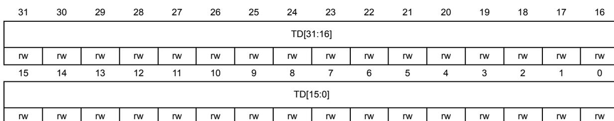
Bits 31:0 TD[31:0] : data of current transfer
APx banked data n register (APx_BDnR) (x = 0, 1)
Address offset: 0x10 + 0x4 * n, (n = 0 to 3)
Reset value: 0x0000 0000
| 31 | 30 | 29 | 28 | 27 | 26 | 25 | 24 | 23 | 22 | 21 | 20 | 19 | 18 | 17 | 16 |
| DATA[31:16] | |||||||||||||||
| rw | rw | rw | rw | rw | rw | rw | rw | rw | rw | rw | rw | rw | rw | rw | rw |
| 15 | 14 | 13 | 12 | 11 | 10 | 9 | 8 | 7 | 6 | 5 | 4 | 3 | 2 | 1 | 0 |
| DATA[15:0] | |||||||||||||||
| rw | rw | rw | rw | rw | rw | rw | rw | rw | rw | rw | rw | rw | rw | rw | rw |
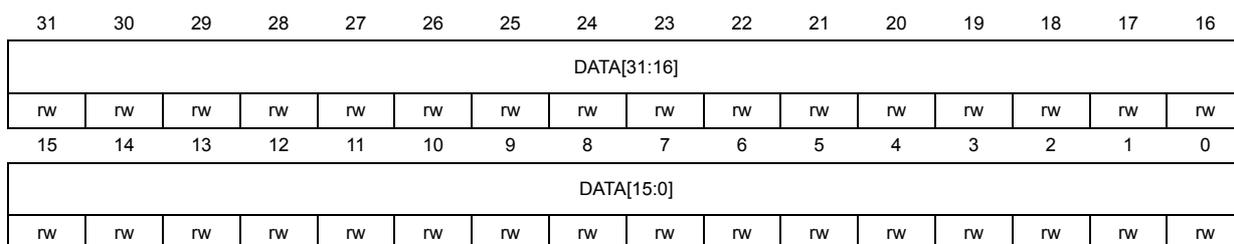
Bits 31:0 DATA[31:0] : banked data of current transfer to address TA [31:4] + 4 * n.
Auto address incrementing is not performed on APx_BD0-3R. Banked transfers are only supported for word transfers.
APx base address register (APx_BASER) (x = 0, 1)
Address offset: 0xF8
Reset value: AP 0: 0xE00E 0003
Reset value: AP 1: 0xE00F E003
| 31 | 30 | 29 | 28 | 27 | 26 | 25 | 24 | 23 | 22 | 21 | 20 | 19 | 18 | 17 | 16 |
| BASEADDR[31:16] | |||||||||||||||
| r | r | r | r | r | r | r | r | r | r | r | r | r | r | r | r |
| 15 | 14 | 13 | 12 | 11 | 10 | 9 | 8 | 7 | 6 | 5 | 4 | 3 | 2 | 1 | 0 |
| BASEADDR[15:12] | Res. | Res. | Res. | Res. | Res. | Res. | Res. | Res. | Res. | Res. | FORMAT | ENTRYPRESENT | |||
| r | r | r | r | r | r | ||||||||||
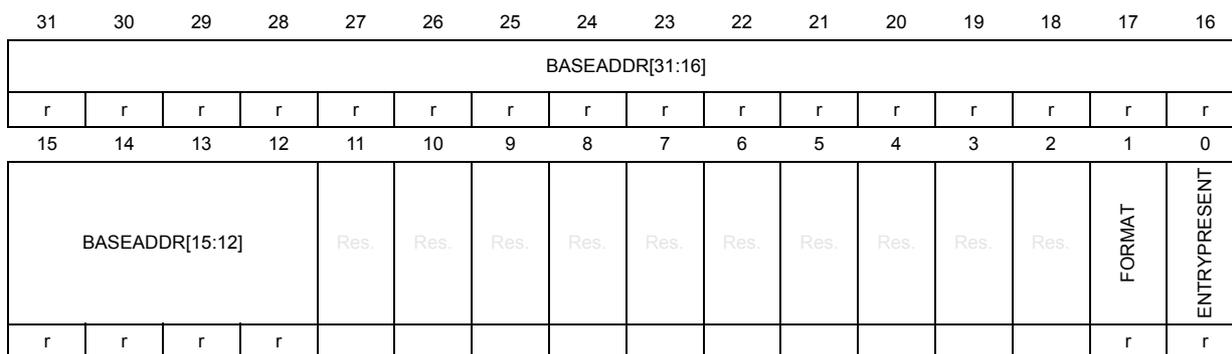
Bits 31:12 BASEADDR[31:12] : base address (bits 31 to 12) of the first ROM table
The 12 LSBs are zero since the ROM table must be aligned on a 4-Kbyte boundary.
0xE00E0: AP0
0xE00FE: AP1
Bits 11:2 Reserved, must be kept at reset value.
Bit 1 FORMAT : base-address register format
1: Arm® debug interface v5
Bit 0 ENTRYPRESENT : debug components presence
Indicates that debug components are present on the access port bus.
1: debug components present
APx identification register (APx_IDR) (x = 0, 1)
Address offset: 0xFC
Reset value: AP 0: 0x5477 0002
Reset value: AP 1: 0x8477 0001
| 31 | 30 | 29 | 28 | 27 | 26 | 25 | 24 | 23 | 22 | 21 | 20 | 19 | 18 | 17 | 16 | |
| REVISION[3:0] | JEDECBANK[3:0] | JEDECCODE[6:0] | CLASS[3] | |||||||||||||
| r | r | r | r | r | r | r | r | r | r | r | r | r | r | r | r | |
| 15 | 14 | 13 | 12 | 11 | 10 | 9 | 8 | 7 | 6 | 5 | 4 | 3 | 2 | 1 | 0 | |
| CLASS[2:0] | Res. | Res. | Res. | Res. | Res. | IDENTITY[7:0] | ||||||||||
| r | r | r | r | r | r | r | r | r | r | r | ||||||
Bits 31:28 REVISION[3:0] : revision number
0x5: r1p0
0x8: r0p9
Bits 27:24 JEDECBANK[3:0] : JEDEC bank
0x4: Arm®
Bits 23:17 JEDECCODE[6:0] : JEDEC code
0x3B: Arm®
Bits 16:13
CLASS[3:0]
:
0x1: MEM-AP
Bits 12:8 Reserved, must be kept at reset value.
Bits 7:0
IDENTITY[7:0]
:
0x1: AHB-AP
0x2: APB-AP
59.4.2 Access port register map
These registers are not on the CPU memory bus. They are only accessed through SW-DP and JTAG-DP debug interfaces.
The access port address is 8-bit wide, defined by DP_SELECTR.APBANKSEL[3:0] field and by JTAG-DP register DPACC or SW-DP packet request A[3:2] field.
Table 724. Access port register map and reset values
| Offset | Register name | 31 | 30 | 29 | 28 | 27 | 26 | 25 | 24 | 23 | 22 | 21 | 20 | 19 | 18 | 17 | 16 | 15 | 14 | 13 | 12 | 11 | 10 | 9 | 8 | 7 | 6 | 5 | 4 | 3 | 2 | 1 | 0 |
|---|---|---|---|---|---|---|---|---|---|---|---|---|---|---|---|---|---|---|---|---|---|---|---|---|---|---|---|---|---|---|---|---|---|
| 0x00 | AP0_CSWR | DBGSWEN | Res. | Res. | Res. | Res. | Res. | Res. | Res. | Res. | Res. | Res. | Res. | Res. | Res. | Res. | Res. | Res. | Res. | Res. | Res. | MODE[3:0] | TRINPROG | DEVICEEN | ADDRINC[1:0] | Res. | SIZE[2:0] | ||||||
| Reset value | 1 | 0 | 0 | 0 | 0 | 0 | 1 | 0 | 0 | 0 | 1 | 0 | |||||||||||||||||||||
| 0x00 | AP1_CSWR | Res. | SPROT | Res. | PROT[3:0] | SPISTATUS | Res. | Res. | Res. | Res. | Res. | Res. | Res. | Res. | Res. | Res. | Res. | Res. | MODE[3:0] | TRINPROG | DBGSTATUS | ADDRINC[1:0] | Res. | SIZE[2:0] | |||||||||
| Reset value | 1 | 0 | 0 | 1 | 1 | X | 0 | 0 | 0 | 0 | 0 | X | 0 | 0 | 0 | 1 | 0 | ||||||||||||||||
| 0x04 | APx_TAR | TA[31:0] | |||||||||||||||||||||||||||||||
| Reset value | X | X | X | X | X | X | X | X | X | X | X | X | X | X | X | X | X | X | X | X | X | X | X | X | X | X | X | X | X | X | X | X | |
| 0x08 | Reserved | Reserved | |||||||||||||||||||||||||||||||
| 0x0C | APx_DRWR | TD[31:0] | |||||||||||||||||||||||||||||||
| Reset value | X | X | X | X | X | X | X | X | X | X | X | X | X | X | X | X | X | X | X | X | X | X | X | X | X | X | X | X | X | X | X | X | |
| 0x10 | APx_BD0R | DATA[31:0] | |||||||||||||||||||||||||||||||
| Reset value | 0 | 0 | 0 | 0 | 0 | 0 | 0 | 0 | 0 | 0 | 0 | 0 | 0 | 0 | 0 | 0 | 0 | 0 | 0 | 0 | 0 | 0 | 0 | 0 | 0 | 0 | 0 | 0 | 0 | 0 | 0 | 0 | |
| 0x14 | APx_BD1R | DATA[31:0] | |||||||||||||||||||||||||||||||
| Reset value | 0 | 0 | 0 | 0 | 0 | 0 | 0 | 0 | 0 | 0 | 0 | 0 | 0 | 0 | 0 | 0 | 0 | 0 | 0 | 0 | 0 | 0 | 0 | 0 | 0 | 0 | 0 | 0 | 0 | 0 | 0 | 0 | |
| 0x18 | APx_BD2R | DATA[31:0] | |||||||||||||||||||||||||||||||
| Reset value | 0 | 0 | 0 | 0 | 0 | 0 | 0 | 0 | 0 | 0 | 0 | 0 | 0 | 0 | 0 | 0 | 0 | 0 | 0 | 0 | 0 | 0 | 0 | 0 | 0 | 0 | 0 | 0 | 0 | 0 | 0 | 0 | |
| 0x1C | APx_BD3R | DATA[31:0] | |||||||||||||||||||||||||||||||
| Reset value | 0 | 0 | 0 | 0 | 0 | 0 | 0 | 0 | 0 | 0 | 0 | 0 | 0 | 0 | 0 | 0 | 0 | 0 | 0 | 0 | 0 | 0 | 0 | 0 | 0 | 0 | 0 | 0 | 0 | 0 | 0 | 0 | |
| 0x20 to 0xF4 | Reserved | Reserved | |||||||||||||||||||||||||||||||
| 0xF8 | AP0_BASER | BASEADDR[31:12] | Res. | Res. | Res. | Res. | Res. | Res. | Res. | Res. | Res. | Res. | FORMAT | ENTRYPRESENT | |||||||||||||||||||
| Reset value | 1 | 1 | 1 | 0 | 0 | 0 | 0 | 0 | 0 | 0 | 0 | 0 | 1 | 1 | 1 | 0 | 0 | 0 | 0 | 0 | 1 | 1 | |||||||||||
Table 724. Access port register map and reset values (continued)
| Offset | Register name | 31 | 30 | 29 | 28 | 27 | 26 | 25 | 24 | 23 | 22 | 21 | 20 | 19 | 18 | 17 | 16 | 15 | 14 | 13 | 12 | 11 | 10 | 9 | 8 | 7 | 6 | 5 | 4 | 3 | 2 | 1 | 0 |
|---|---|---|---|---|---|---|---|---|---|---|---|---|---|---|---|---|---|---|---|---|---|---|---|---|---|---|---|---|---|---|---|---|---|
| 0xF8 | AP1_BASER | BASEADDR[31:12] | Res. | Res. | Res. | Res. | Res. | Res. | Res. | Res. | Res. | FORMAT | ENTRYPRESENT | ||||||||||||||||||||
| Reset value | 1 | 1 | 1 | 0 | 0 | 0 | 0 | 0 | 0 | 0 | 0 | 0 | 1 | 1 | 1 | 1 | 1 | 1 | 1 | 0 | 1 | 1 | |||||||||||
| 0xFC | AP0_IDR | REVISION[3:0] | JEDECBANK[3:0] | JEDECCODE[6:0] | CLASS[3:0] | Res. | Res. | Res. | Res. | IDENTITY[7:0] | |||||||||||||||||||||||
| Reset value | 0 | 1 | 0 | 1 | 0 | 1 | 0 | 0 | 0 | 1 | 1 | 1 | 0 | 1 | 1 | 1 | 0 | 0 | 0 | 0 | 0 | 0 | 0 | 0 | 0 | 0 | 1 | ||||||
| 0xFC | AP0_IDR | REVISION[3:0] | JEDECBANK[3:0] | JEDECCODE[6:0] | CLASS[3:0] | Res. | Res. | Res. | Res. | IDENTITY[7:0] | |||||||||||||||||||||||
| Reset value | 1 | 0 | 0 | 0 | 0 | 1 | 0 | 0 | 0 | 1 | 1 | 1 | 0 | 1 | 1 | 1 | 0 | 0 | 0 | 0 | 0 | 0 | 0 | 0 | 0 | 0 | 1 | ||||||
59.5 ROM tables
The ROM table is a CoreSight component that contains the base addresses of the CoreSight debug components accessible via the access port to which it is attached. These tables allow a debugger to discover the topology of the CoreSight system automatically.
There is one top-level ROM table behind each access port, APn. The base address of this ROM table can be obtained by reading the APn_BASER register of the access port. The top-level ROM table may point in turn to other ROM tables.
The system ROM table is pointed to by the AP0 base register, AP0_BASER. It contains the base address pointer for the DBGMCU.
The system ROM table occupies a 4-Kbyte, 32-bit wide chunk of address space, from 0xE00E 4000 to 0xE00E 4FFC, when accessed by the debugger. It can be accessed by the CPU at the address range 0x4402 4000 to 0x4402 4FFC.
Table 725. System ROM table
| Address offset in ROM table | Component name | Component base address | Component address offset | Size (Kbytes) | Entry |
|---|---|---|---|---|---|
| 0x000 | DBGMCU | 0xE00E 4000 (debugger) 0x4402 4000 (CPU) | 0x0000 4000 | 4 | 0x0000 4003 |
| 0x004 | Top of table | - | - | - | 0x0000 0000 |
| 0x008 to 0xFC8 | Reserved | - | - | - | 0x0000 0000 |
| 0xFCC to 0xFFC | ROM table registers | - | - | - | See Table 728 |
There are two ROM tables in the CPU subsystem. The MCU ROM table is pointed to by the AP1 base register, AP1_BASER. It contains the base-address pointer for the processor ROM table and for the TPIU registers.
The MCU ROM table (see the table below) occupies a 4-Kbyte, 32-bit wide chunk of address space, from 0xE00F E000 to 0xE00F EFFC.
Table 726. MCU ROM table
| Address offset in ROM table | Component name | Component base address | Component address offset | Size (Kbytes) | Entry |
|---|---|---|---|---|---|
| 0x000 | Processor ROM table | 0xE00F F000 | 0x0000 1000 | 4 | 0x0000 1003 |
| 0x004 | TPIU | 0xE004 0000 | 0xFFF4 2000 | 4 | 0xFFF4 2003 |
| 0x008 | Reserved | - | - | - | 0x1FF0 2002 |
| 0x00C | Reserved | - | - | - | 0x1FF0 2002 |
| 0x010 | Top of table | - | - | - | 0x0000 0000 |
| 0x014 to 0xFC8 | Reserved | - | - | - | 0x0000 0000 |
| 0xFCC to 0xFFC | ROM table registers | - | - | - | See Table 729 |
The processor ROM table contains the base-address pointer for the system control space (SCS) registers, that allow the debugger to identify the CPU core, as well as for the BPU, DWT, ITM, ETM, and CTI.
The processor ROM table (see Table 727 ) occupies a 4-Kbyte, 32-bit wide chunk of address space, from 0xE00F F000 to 0xE00F FFFC.
Table 727. Processor ROM table
| Address in ROM table | Component name | Component base address | Component address offset | Size (Kbytes) | Entry |
|---|---|---|---|---|---|
| 0xE00F F000 | SCS | 0xE000 E000 | 0xFFF0 F000 | 4 | 0xFFF0 F003 |
| 0xE00F F004 | DWT | 0xE000 1000 | 0xFFF0 2000 | 4 | 0xFFF0 2003 |
| 0xE00F F008 | BPU | 0xE000 2000 | 0xFFF0 3000 | 4 | 0xFFF0 3003 |
| 0xE00F F00C | ITM | 0xE000 0000 | 0xFFF0 1000 | 4 | 0xFFF0 1003 |
| 0xE00F F010 | Reserved | - | - | - | 0xFFF4 1002 |
| 0xE00F F014 | ETM | 0xE004 1000 | 0xFFF4 2000 | 4 | 0xFFF4 2003 |
| 0xE00F F018 | CTI | 0xE004 2000 | 0xFFF4 3000 | 4 | 0xFFF4 3003 |
| 0xE00F F01C | Reserved | - | - | - | 0xFFF4 4002 |
| 0xE00F F020 | Top of table | - | - | - | 0x0000 0000 |
| 0xE00F F024 to 0xE00F FFC8 | Reserved | - | - | - | 0x0000 0000 |
| 0xE00F FFCC to 0xE00F FFFC | ROM table registers | - | - | - | See Table 730 |
Figure 853. CoreSight topology
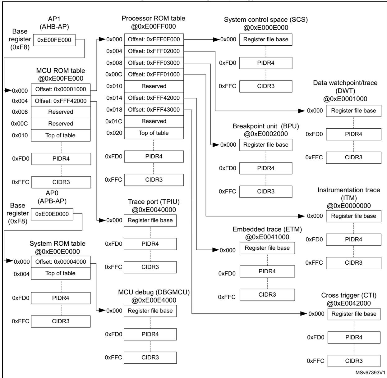
The diagram illustrates the CoreSight topology, showing the interconnections between various debug and trace components. The components are organized into three main columns: Left (APs and ROM tables), Middle (ROM table, Trace port, MCU debug), and Right (SCS, BPU, ETM, DWT, ITM, CTI).
- Left Column:
- AP1 (AHB-AP): Base register (0xF8) at 0xE00FE000. It connects to the MCU ROM table at 0xE00FE000 and the Processor ROM table at 0xE00FF000.
- MCU ROM table at 0xE00FE000: Contains entries for Offset: 0x00001000, Offset: 0xFFF42000, Reserved, Reserved, and Top of table. It also includes PIDR4 at 0xFD0 and CIDR3 at 0xFFC.
- AP0 (APB-AP): Base register (0xF8) at 0xE00E0000. It connects to the System ROM table at 0xE00E0000 and the Trace port (TPIU) at 0xE0040000.
- System ROM table at 0xE00E0000: Contains entries for Offset: 0x00004000 and Top of table. It also includes PIDR4 at 0xFD0 and CIDR3 at 0xFFC.
- Middle Column:
- Processor ROM table at 0xE00FF000: Contains entries for Offset: 0xFFF0F000, Offset: 0xFFF02000, Offset: 0xFFF03000, Offset: 0xFFF01000, Reserved, Offset: 0xFFF42000, Offset: 0xFFF43000, Reserved, and Top of table. It also includes PIDR4 at 0xFD0 and CIDR3 at 0xFFC.
- Trace port (TPIU) at 0xE0040000: Contains a Register file base at 0x000, PIDR4 at 0xFD0, and CIDR3 at 0xFFC.
- MCU debug (DBGMCU) at 0xE00E4000: Contains a Register file base at 0x000, PIDR4 at 0xFD0, and CIDR3 at 0xFFC.
- Right Column:
- System control space (SCS) at 0xE000E000: Contains Register file base at 0x000, PIDR4 at 0xFD0, and CIDR3 at 0xFFC.
- Breakpoint unit (BPU) at 0xE0002000: Contains Register file base at 0x000, PIDR4 at 0xFD0, and CIDR3 at 0xFFC.
- Embedded trace (ETM) at 0xE0041000: Contains Register file base at 0x000, PIDR4 at 0xFD0, and CIDR3 at 0xFFC.
- Data watchdog/trace (DWT) at 0xE0001000: Contains Register file base at 0x000, PIDR4 at 0xFD0, and CIDR3 at 0xFFC.
- Instrumentation trace (ITM) at 0xE0000000: Contains Register file base at 0x000, PIDR4 at 0xFD0, and CIDR3 at 0xFFC.
- Cross trigger (CTI) at 0xE0042000: Contains Register file base at 0x000, PIDR4 at 0xFD0, and CIDR3 at 0xFFC.
Connections are shown via arrows indicating the flow of data and control signals between the components. For example, the AP1 base register connects to the MCU ROM table and the Processor ROM table. The Processor ROM table entries point to the SCS, BPU, ETM, DWT, ITM, and CTI components. The AP0 base register connects to the System ROM table and the TPIU. The System ROM table entries point to the TPIU and the DBGMCU. The TPIU, DBGMCU, and System ROM table entries point to the ETM. The ETM entries point to the DWT, ITM, and CTI components.
MSv67393V1
59.5.1 System ROM table registers
System ROM memory type register (SYSROM_MEMTYPER)
Address offset: 0xFCC
Reset value: 0x0000 0001
| 31 | 30 | 29 | 28 | 27 | 26 | 25 | 24 | 23 | 22 | 21 | 20 | 19 | 18 | 17 | 16 |
|---|---|---|---|---|---|---|---|---|---|---|---|---|---|---|---|
| Res. | Res. | Res. | Res. | Res. | Res. | Res. | Res. | Res. | Res. | Res. | Res. | Res. | Res. | Res. | Res. |
| 15 | 14 | 13 | 12 | 11 | 10 | 9 | 8 | 7 | 6 | 5 | 4 | 3 | 2 | 1 | 0 |
| Res. | Res. | Res. | Res. | Res. | Res. | Res. | Res. | Res. | Res. | Res. | Res. | Res. | Res. | Res. | SYSTEM r |
Bits 31:1 Reserved, must be kept at reset value.
Bit 0 SYSTEM : system memory
0x1: system memory present on this bus
System ROM CoreSight peripheral identity register 4 (SYSROM_PIDR4)
Address offset: 0xFD0
Reset value: 0x0000 0000
| 31 | 30 | 29 | 28 | 27 | 26 | 25 | 24 | 23 | 22 | 21 | 20 | 19 | 18 | 17 | 16 |
|---|---|---|---|---|---|---|---|---|---|---|---|---|---|---|---|
| Res. | Res. | Res. | Res. | Res. | Res. | Res. | Res. | Res. | Res. | Res. | Res. | Res. | Res. | Res. | Res. |
| 15 | 14 | 13 | 12 | 11 | 10 | 9 | 8 | 7 | 6 | 5 | 4 | 3 | 2 | 1 | 0 |
| Res. | Res. | Res. | Res. | Res. | Res. | Res. | Res. | SIZE[3:0] | JEP106CON[3:0] | ||||||
| r | r | r | r | r | r | r | r | ||||||||
Bits 31:8 Reserved, must be kept at reset value.
Bits 7:4 SIZE[3:0] : register file size
0x0: The register file occupies a single 4-Kbyte region.
Bits 3:0 JEP106CON[3:0] : JEP106 continuation code
0x0: STMicroelectronics JEDEC continuation code
System ROM CoreSight peripheral identity register 0 (SYSROM_PIDR0)
Address offset: 0xFE0
Reset value: 0x0000 00XX
| 31 | 30 | 29 | 28 | 27 | 26 | 25 | 24 | 23 | 22 | 21 | 20 | 19 | 18 | 17 | 16 |
|---|---|---|---|---|---|---|---|---|---|---|---|---|---|---|---|
| Res. | Res. | Res. | Res. | Res. | Res. | Res. | Res. | Res. | Res. | Res. | Res. | Res. | Res. | Res. | Res. |
| 15 | 14 | 13 | 12 | 11 | 10 | 9 | 8 | 7 | 6 | 5 | 4 | 3 | 2 | 1 | 0 |
| Res. | Res. | Res. | Res. | Res. | Res. | Res. | Res. | PARTNUM[7:0] | |||||||
| r | r | r | r | r | r | r | r | ||||||||
Bits 31:8 Reserved, must be kept at reset value.
Bits 7:0 PARTNUM[7:0] : part number bits [7:0]
0x84: STM32H562/563/573
0x78: STM32H523/533
System ROM CoreSight peripheral identity register 1 (SYSROM_PIDR1)
Address offset: 0xFE4
Reset value: 0x0000 000X
| 31 | 30 | 29 | 28 | 27 | 26 | 25 | 24 | 23 | 22 | 21 | 20 | 19 | 18 | 17 | 16 |
|---|---|---|---|---|---|---|---|---|---|---|---|---|---|---|---|
| Res. | Res. | Res. | Res. | Res. | Res. | Res. | Res. | Res. | Res. | Res. | Res. | Res. | Res. | Res. | Res. |
| 15 | 14 | 13 | 12 | 11 | 10 | 9 | 8 | 7 | 6 | 5 | 4 | 3 | 2 | 1 | 0 |
| Res. | Res. | Res. | Res. | Res. | Res. | Res. | Res. | JEP106ID[3:0] | PARTNUM[11:8] | ||||||
| r | r | r | r | r | r | r | r | ||||||||
Bits 31:8 Reserved, must be kept at reset value.
Bits 7:4 JEP106ID[3:0] : JEP106 identity code bits [3:0]
0x0: STMicroelectronics JEDEC code
Bits 3:0 PARTNUM[11:8] : part number bits [11:8]
0x4: STM32H5 series
System ROM CoreSight peripheral identity register 2 (SYSROM_PIDR2)
Address offset: 0xFE8
Reset value: 0x0000 000A
| 31 | 30 | 29 | 28 | 27 | 26 | 25 | 24 | 23 | 22 | 21 | 20 | 19 | 18 | 17 | 16 |
|---|---|---|---|---|---|---|---|---|---|---|---|---|---|---|---|
| Res. | Res. | Res. | Res. | Res. | Res. | Res. | Res. | Res. | Res. | Res. | Res. | Res. | Res. | Res. | Res. |
| 15 | 14 | 13 | 12 | 11 | 10 | 9 | 8 | 7 | 6 | 5 | 4 | 3 | 2 | 1 | 0 |
| Res. | Res. | Res. | Res. | Res. | Res. | Res. | Res. | REVISION[3:0] | JEDEC | JEP106ID[6:4] | |||||
| r | r | r | r | r | r | r | r | ||||||||
Bits 31:8 Reserved, must be kept at reset value.
Bits 7:4 REVISION[3:0] : component revision number
0x0: rev r0p0
Bit 3 JEDEC : JEDEC assigned value
1: designer identification specified by JEDEC
Bits 2:0 JEP106ID[6:4] : JEP106 identity code bits [6:4]
0x2: STMicroelectronics JEDEC code
System ROM CoreSight peripheral identity register 3 (SYSROM_PIDR3)
Address offset: 0xFEC
Reset value: 0x0000 0000
| 31 | 30 | 29 | 28 | 27 | 26 | 25 | 24 | 23 | 22 | 21 | 20 | 19 | 18 | 17 | 16 |
|---|---|---|---|---|---|---|---|---|---|---|---|---|---|---|---|
| Res. | Res. | Res. | Res. | Res. | Res. | Res. | Res. | Res. | Res. | Res. | Res. | Res. | Res. | Res. | Res. |
| 15 | 14 | 13 | 12 | 11 | 10 | 9 | 8 | 7 | 6 | 5 | 4 | 3 | 2 | 1 | 0 |
| Res. | Res. | Res. | Res. | Res. | Res. | Res. | Res. | REVAND[3:0] | CMOD[3:0] | ||||||
| r | r | r | r | r | r | r | r | ||||||||
Bits 31:8 Reserved, must be kept at reset value.
Bits 7:4 REVAND[3:0] : metal fix version
0x0: No metal fix
Bits 3:0 CMOD[3:0] : customer modified
0x0: No customer modifications
System ROM CoreSight component identity register 0 (SYSROM_CIDR0)
Address offset: 0xFF0
Reset value: 0x0000 000D
| 31 | 30 | 29 | 28 | 27 | 26 | 25 | 24 | 23 | 22 | 21 | 20 | 19 | 18 | 17 | 16 |
|---|---|---|---|---|---|---|---|---|---|---|---|---|---|---|---|
| Res. | Res. | Res. | Res. | Res. | Res. | Res. | Res. | Res. | Res. | Res. | Res. | Res. | Res. | Res. | Res. |
| 15 | 14 | 13 | 12 | 11 | 10 | 9 | 8 | 7 | 6 | 5 | 4 | 3 | 2 | 1 | 0 |
| Res. | Res. | Res. | Res. | Res. | Res. | Res. | Res. | PREAMBLE[7:0] | |||||||
| r | r | r | r | r | r | r | r | ||||||||
Bits 31:8 Reserved, must be kept at reset value.
Bits 7:0 PREAMBLE[7:0] : component identification bits [7:0]
0x0D: Common identification value
System ROM CoreSight peripheral identity register 1 (SYSROM_CIDR1)
Address offset: 0xFF4
Reset value: 0x0000 0010
| 31 | 30 | 29 | 28 | 27 | 26 | 25 | 24 | 23 | 22 | 21 | 20 | 19 | 18 | 17 | 16 |
|---|---|---|---|---|---|---|---|---|---|---|---|---|---|---|---|
| Res. | Res. | Res. | Res. | Res. | Res. | Res. | Res. | Res. | Res. | Res. | Res. | Res. | Res. | Res. | Res. |
| 15 | 14 | 13 | 12 | 11 | 10 | 9 | 8 | 7 | 6 | 5 | 4 | 3 | 2 | 1 | 0 |
| Res. | Res. | Res. | Res. | Res. | Res. | Res. | Res. | ||||||||
| CLASS[3:0] | PREAMBLE[11:8] | ||||||||||||||
| r | r | r | r | r | r | r | r | ||||||||
Bits 31:8 Reserved, must be kept at reset value.
Bits 7:4 CLASS[3:0] : Component identification bits [15:12] - component class
0x1: ROM table component
Bits 3:0 PREAMBLE[11:8] : Component identification bits [11:8]
0x0: Common identification value
System ROM CoreSight component identity register 2 (SYSROM_CIDR2)
Address offset: 0xFF8
Reset value: 0x0000 0005
| 31 | 30 | 29 | 28 | 27 | 26 | 25 | 24 | 23 | 22 | 21 | 20 | 19 | 18 | 17 | 16 |
|---|---|---|---|---|---|---|---|---|---|---|---|---|---|---|---|
| Res. | Res. | Res. | Res. | Res. | Res. | Res. | Res. | Res. | Res. | Res. | Res. | Res. | Res. | Res. | Res. |
| 15 | 14 | 13 | 12 | 11 | 10 | 9 | 8 | 7 | 6 | 5 | 4 | 3 | 2 | 1 | 0 |
| Res. | Res. | Res. | Res. | Res. | Res. | Res. | Res. | ||||||||
| PREAMBLE[19:12] | |||||||||||||||
| r | r | r | r | r | r | r | r | ||||||||
Bits 31:8 Reserved, must be kept at reset value.
Bits 7:0 PREAMBLE[19:12] : component identification bits [23:16]
0x05: common identification value
System ROM CoreSight component identity register 3 (SYSROM_CIDR3)
Address offset: 0xFFC
Reset value: 0x0000 00B1
| 31 | 30 | 29 | 28 | 27 | 26 | 25 | 24 | 23 | 22 | 21 | 20 | 19 | 18 | 17 | 16 |
|---|---|---|---|---|---|---|---|---|---|---|---|---|---|---|---|
| Res. | Res. | Res. | Res. | Res. | Res. | Res. | Res. | Res. | Res. | Res. | Res. | Res. | Res. | Res. | Res. |
| 15 | 14 | 13 | 12 | 11 | 10 | 9 | 8 | 7 | 6 | 5 | 4 | 3 | 2 | 1 | 0 |
| Res. | Res. | Res. | Res. | Res. | Res. | Res. | Res. | PREAMBLE[27:20] | |||||||
| r | r | r | r | r | r | r | r | ||||||||
Bits 31:8 Reserved, must be kept at reset value.
Bits 7:0 PREAMBLE[27:20] : Component identification bits [31:24]
0xB1: Common identification value
59.5.2 System ROM table register map
Table 728. System ROM table register map and reset values
| Offset | Register name | 31 | 30 | 29 | 28 | 27 | 26 | 25 | 24 | 23 | 22 | 21 | 20 | 19 | 18 | 17 | 16 | 15 | 14 | 13 | 12 | 11 | 10 | 9 | 8 | 7 | 6 | 5 | 4 | 3 | 2 | 1 | 0 |
|---|---|---|---|---|---|---|---|---|---|---|---|---|---|---|---|---|---|---|---|---|---|---|---|---|---|---|---|---|---|---|---|---|---|
| 0xFCC | SYSROM_ MEMTYPER | Res. | SYSMEM | ||||||||||||||||||||||||||||||
| Reset value | 1 | ||||||||||||||||||||||||||||||||
| 0xFD0 | SYSROM_PIDR4 | Res. | SIZE [3:0] | JEP106CON [3:0] | |||||||||||||||||||||||||||||
| Reset value | 0 | 0 | 0 | 0 | 0 | 0 | 0 | 0 | |||||||||||||||||||||||||
| 0xFD4 to 0xFDC | Reserved | ||||||||||||||||||||||||||||||||
| 0xFE0 | SYSROM_PIDR0 | Res. | PARTNUM[7:0] | ||||||||||||||||||||||||||||||
| Reset value | X X X X X X X X | ||||||||||||||||||||||||||||||||
| 0xFE4 | SYSROM_PIDR1 | Res. | JEP106ID [3:0] | PARTNUM [11:8] | |||||||||||||||||||||||||||||
| Reset value | 0 | 0 | 0 | 0 | X X X X | ||||||||||||||||||||||||||||
| 0xFE8 | SYSROM_PIDR2 | Res. | REVISION [3:0] | JEDEC | JEP106ID [6:4] | ||||||||||||||||||||||||||||
| Reset value | 0 | 0 | 0 | 0 | 1 | 0 | 1 | 0 | |||||||||||||||||||||||||
| 0xFEC | SYSROM_PIDR3 | Res. | REVAND[3:0] | CMOD[3:0] | |||||||||||||||||||||||||||||
| Reset value | 0 | 0 | 0 | 0 | 0 | 0 | 0 | 0 | |||||||||||||||||||||||||
| 0xFF0 | SYSROM_CIDR0 | Res. | PREAMBLE[7:0] | ||||||||||||||||||||||||||||||
| Reset value | 0 0 0 0 1 1 0 1 | ||||||||||||||||||||||||||||||||
| 0xFF4 | SYSROM_CIDR1 | Res. | CLASS[3:0] | PREAMBLE [11:8] | |||||||||||||||||||||||||||||
| Reset value | 0 | 0 | 0 | 1 | 0 | 0 | 0 | 0 | |||||||||||||||||||||||||
| 0xFF8 | SYSROM_CIDR2 | Res. | PREAMBLE[19:12] | ||||||||||||||||||||||||||||||
| Reset value | 0 0 0 0 0 1 0 1 | ||||||||||||||||||||||||||||||||
| 0xFFC | SYSROM_CIDR3 | Res. | PREAMBLE[27:20] | ||||||||||||||||||||||||||||||
| Reset value | 1 0 1 1 0 0 0 1 | ||||||||||||||||||||||||||||||||
Refer to Table 725 for register boundary addresses.
59.5.3 MCU ROM table registers
MCU ROM memory type register (MCUROM_MEMTYPER)
Address offset: 0xFCC
Reset value: 0x0000 0001
| 31 | 30 | 29 | 28 | 27 | 26 | 25 | 24 | 23 | 22 | 21 | 20 | 19 | 18 | 17 | 16 |
|---|---|---|---|---|---|---|---|---|---|---|---|---|---|---|---|
| Res. | Res. | Res. | Res. | Res. | Res. | Res. | Res. | Res. | Res. | Res. | Res. | Res. | Res. | Res. | Res. |
| 15 | 14 | 13 | 12 | 11 | 10 | 9 | 8 | 7 | 6 | 5 | 4 | 3 | 2 | 1 | 0 |
|---|---|---|---|---|---|---|---|---|---|---|---|---|---|---|---|
| Res. | Res. | Res. | Res. | Res. | Res. | Res. | Res. | Res. | Res. | Res. | Res. | Res. | Res. | Res. | SYSTEM |
| r |
Bits 31:1 Reserved, must be kept at reset value.
Bit 0 SYSTEM : system memory
0x1: system memory present on this bus
MCU ROM CoreSight peripheral identity register 4 (MCUROM_PIDR4)
Address offset: 0xFD0
Reset value: 0x0000 0000
| 31 | 30 | 29 | 28 | 27 | 26 | 25 | 24 | 23 | 22 | 21 | 20 | 19 | 18 | 17 | 16 |
|---|---|---|---|---|---|---|---|---|---|---|---|---|---|---|---|
| Res. | Res. | Res. | Res. | Res. | Res. | Res. | Res. | Res. | Res. | Res. | Res. | Res. | Res. | Res. | Res. |
| 15 | 14 | 13 | 12 | 11 | 10 | 9 | 8 | 7 | 6 | 5 | 4 | 3 | 2 | 1 | 0 |
|---|---|---|---|---|---|---|---|---|---|---|---|---|---|---|---|
| Res. | Res. | Res. | Res. | Res. | Res. | Res. | Res. | SIZE[3:0] | JEP106CON[3:0] | ||||||
| r | r | r | r | r | r | r | r | ||||||||
Bits 31:8 Reserved, must be kept at reset value.
Bits 7:4 SIZE[3:0] : register file size
0x0: The register file occupies a single 4-Kbyte region.
Bits 3:0 JEP106CON[3:0] : JEP106 continuation code
0x0: STMicroelectronics JEDEC continuation code
MCU ROM CoreSight peripheral identity register 0 (MCUROM_PIDR0)
Address offset: 0xFE0
Reset value: 0x0000 00XX
| 31 | 30 | 29 | 28 | 27 | 26 | 25 | 24 | 23 | 22 | 21 | 20 | 19 | 18 | 17 | 16 |
|---|---|---|---|---|---|---|---|---|---|---|---|---|---|---|---|
| Res. | Res. | Res. | Res. | Res. | Res. | Res. | Res. | Res. | Res. | Res. | Res. | Res. | Res. | Res. | Res. |
| 15 | 14 | 13 | 12 | 11 | 10 | 9 | 8 | 7 | 6 | 5 | 4 | 3 | 2 | 1 | 0 |
| Res. | Res. | Res. | Res. | Res. | Res. | Res. | Res. | ||||||||
| r | r | r | r | r | r | r | r |
Bits 31:8 Reserved, must be kept at reset value.
Bits 7:0 PARTNUM[7:0] : part number bits [7:0]
0x84: STM32H562/563/573
0x78: STM32H523/533
MCU ROM CoreSight peripheral identity register 1 (MCUROM_PIDR1)
Address offset: 0xFE4
Reset value: 0x0000 000X
| 31 | 30 | 29 | 28 | 27 | 26 | 25 | 24 | 23 | 22 | 21 | 20 | 19 | 18 | 17 | 16 |
|---|---|---|---|---|---|---|---|---|---|---|---|---|---|---|---|
| Res. | Res. | Res. | Res. | Res. | Res. | Res. | Res. | Res. | Res. | Res. | Res. | Res. | Res. | Res. | Res. |
| 15 | 14 | 13 | 12 | 11 | 10 | 9 | 8 | 7 | 6 | 5 | 4 | 3 | 2 | 1 | 0 |
| Res. | Res. | Res. | Res. | Res. | Res. | Res. | Res. | ||||||||
| r | r | r | r | r | r | r | r |
Bits 31:8 Reserved, must be kept at reset value.
Bits 7:4 JEP106ID[3:0] : JEP106 identity code bits [3:0]
0x0: STMicroelectronics JEDEC code
Bits 3:0 PARTNUM[11:8] : part number bits [11:8]
0x4: STM32H5 series
MCU ROM CoreSight peripheral identity register 2 (MCUROM_PIDR2)
Address offset: 0xFE8
Reset value: 0x0000 000A
| 31 | 30 | 29 | 28 | 27 | 26 | 25 | 24 | 23 | 22 | 21 | 20 | 19 | 18 | 17 | 16 |
|---|---|---|---|---|---|---|---|---|---|---|---|---|---|---|---|
| Res. | Res. | Res. | Res. | Res. | Res. | Res. | Res. | Res. | Res. | Res. | Res. | Res. | Res. | Res. | Res. |
| 15 | 14 | 13 | 12 | 11 | 10 | 9 | 8 | 7 | 6 | 5 | 4 | 3 | 2 | 1 | 0 |
| Res. | Res. | Res. | Res. | Res. | Res. | Res. | Res. | REVISION[3:0] | JEDEC | JEP106ID[6:4] | |||||
| r | r | r | r | r | r | r | r | ||||||||
Bits 31:8 Reserved, must be kept at reset value.
Bits 7:4 REVISION[3:0] : component revision number
0x0: rev r0p0
Bit 3 JEDEC : JEDEC assigned value
1: designer identification specified by JEDEC
Bits 2:0 JEP106ID[6:4] : JEP106 identity code bits [6:4]
0x2: STMicroelectronics JEDEC code
MCU ROM CoreSight peripheral identity register 3 (MCUROM_PIDR3)
Address offset: 0xFEC
Reset value: 0x0000 0000
| 31 | 30 | 29 | 28 | 27 | 26 | 25 | 24 | 23 | 22 | 21 | 20 | 19 | 18 | 17 | 16 |
|---|---|---|---|---|---|---|---|---|---|---|---|---|---|---|---|
| Res. | Res. | Res. | Res. | Res. | Res. | Res. | Res. | Res. | Res. | Res. | Res. | Res. | Res. | Res. | Res. |
| 15 | 14 | 13 | 12 | 11 | 10 | 9 | 8 | 7 | 6 | 5 | 4 | 3 | 2 | 1 | 0 |
| Res. | Res. | Res. | Res. | Res. | Res. | Res. | Res. | REVAND[3:0] | CMOD[3:0] | ||||||
| r | r | r | r | r | r | r | r | ||||||||
Bits 31:8 Reserved, must be kept at reset value.
Bits 7:4 REVAND[3:0] : metal fix version
0x0: No metal fix
Bits 3:0 CMOD[3:0] : customer modified
0x0: No customer modifications
MCU ROM CoreSight component identity register 0 (MCUROM_CIDR0)
Address offset: 0xFF0
Reset value: 0x0000 000D
| 31 | 30 | 29 | 28 | 27 | 26 | 25 | 24 | 23 | 22 | 21 | 20 | 19 | 18 | 17 | 16 |
|---|---|---|---|---|---|---|---|---|---|---|---|---|---|---|---|
| Res. | Res. | Res. | Res. | Res. | Res. | Res. | Res. | Res. | Res. | Res. | Res. | Res. | Res. | Res. | Res. |
| 15 | 14 | 13 | 12 | 11 | 10 | 9 | 8 | 7 | 6 | 5 | 4 | 3 | 2 | 1 | 0 |
| Res. | Res. | Res. | Res. | Res. | Res. | Res. | Res. | PREAMBLE[7:0] | |||||||
| r | r | r | r | r | r | r | r | ||||||||
Bits 31:8 Reserved, must be kept at reset value.
Bits 7:0 PREAMBLE[7:0] : component identification bits [7:0]
0x0D: Common identification value
MCU ROM CoreSight peripheral identity register 1 (MCUROM_PIDR1)
Address offset: 0xFF4
Reset value: 0x0000 0010
| 31 | 30 | 29 | 28 | 27 | 26 | 25 | 24 | 23 | 22 | 21 | 20 | 19 | 18 | 17 | 16 |
|---|---|---|---|---|---|---|---|---|---|---|---|---|---|---|---|
| Res. | Res. | Res. | Res. | Res. | Res. | Res. | Res. | Res. | Res. | Res. | Res. | Res. | Res. | Res. | Res. |
| 15 | 14 | 13 | 12 | 11 | 10 | 9 | 8 | 7 | 6 | 5 | 4 | 3 | 2 | 1 | 0 |
| Res. | Res. | Res. | Res. | Res. | Res. | Res. | Res. | CLASS[3:0] | PREAMBLE[11:8] | ||||||
| r | r | r | r | r | r | r | r | ||||||||
Bits 31:8 Reserved, must be kept at reset value.
Bits 7:4 CLASS[3:0] : Component identification bits [15:12] - component class
0x1: ROM table component
Bits 3:0 PREAMBLE[11:8] : Component identification bits [11:8]
0x0: Common identification value
MCU ROM CoreSight component identity register 2 (MCUROM_CIDR2)
Address offset: 0xFF8
Reset value: 0x0000 0005
| 31 | 30 | 29 | 28 | 27 | 26 | 25 | 24 | 23 | 22 | 21 | 20 | 19 | 18 | 17 | 16 |
|---|---|---|---|---|---|---|---|---|---|---|---|---|---|---|---|
| Res. | Res. | Res. | Res. | Res. | Res. | Res. | Res. | Res. | Res. | Res. | Res. | Res. | Res. | Res. | Res. |
| 15 | 14 | 13 | 12 | 11 | 10 | 9 | 8 | 7 | 6 | 5 | 4 | 3 | 2 | 1 | 0 |
| Res. | Res. | Res. | Res. | Res. | Res. | Res. | Res. | PREAMBLE[19:12] | |||||||
| r | r | r | r | r | r | r | r | ||||||||
Bits 31:8 Reserved, must be kept at reset value.
Bits 7:0 PREAMBLE[19:12] : component identification bits [23:16]
0x05: common identification value
MCU ROM CoreSight component identity register 3 (MCUROM_CIDR3)
Address offset: 0xFFC
Reset value: 0x0000 00B1
| 31 | 30 | 29 | 28 | 27 | 26 | 25 | 24 | 23 | 22 | 21 | 20 | 19 | 18 | 17 | 16 |
|---|---|---|---|---|---|---|---|---|---|---|---|---|---|---|---|
| Res. | Res. | Res. | Res. | Res. | Res. | Res. | Res. | Res. | Res. | Res. | Res. | Res. | Res. | Res. | Res. |
| 15 | 14 | 13 | 12 | 11 | 10 | 9 | 8 | 7 | 6 | 5 | 4 | 3 | 2 | 1 | 0 |
| Res. | Res. | Res. | Res. | Res. | Res. | Res. | Res. | PREAMBLE[27:20] | |||||||
| r | r | r | r | r | r | r | r | ||||||||
Bits 31:8 Reserved, must be kept at reset value.
Bits 7:0 PREAMBLE[27:20] : Component identification bits [31:24]
0xB1: Common identification value
59.5.4 MCU ROM table register map
Table 729. MCU ROM table register map and reset values
| Offset | Register name | 31 | 30 | 29 | 28 | 27 | 26 | 25 | 24 | 23 | 22 | 21 | 20 | 19 | 18 | 17 | 16 | 15 | 14 | 13 | 12 | 11 | 10 | 9 | 8 | 7 | 6 | 5 | 4 | 3 | 2 | 1 | 0 |
|---|---|---|---|---|---|---|---|---|---|---|---|---|---|---|---|---|---|---|---|---|---|---|---|---|---|---|---|---|---|---|---|---|---|
| 0xFCC | MCUROM_MEMTYPE | Res. | Res. | Res. | Res. | Res. | Res. | Res. | Res. | Res. | Res. | Res. | Res. | Res. | Res. | Res. | Res. | Res. | Res. | Res. | Res. | Res. | Res. | Res. | Res. | Res. | Res. | Res. | Res. | Res. | Res. | Res. | SYSTEMEM |
| Reset value | 1 | ||||||||||||||||||||||||||||||||
| 0xFD0 | MCUROM_PIDR4 | Res. | Res. | Res. | Res. | Res. | Res. | Res. | Res. | Res. | Res. | Res. | Res. | Res. | Res. | Res. | Res. | Res. | Res. | Res. | Res. | Res. | Res. | Res. | Res. | Res. | Res. | SIZE [3:0] | SIZE [3:0] | JEP106CON [3:0] | JEP106CON [3:0] | JEP106CON [3:0] | |
| Reset value | 0 | 0 | 0 | 0 | 0 | ||||||||||||||||||||||||||||
| 0xFD4 to FDC | Reserved | ||||||||||||||||||||||||||||||||
Table 729. MCU ROM table register map and reset values (continued)
| Offset | Register name | 31 | 30 | 29 | 28 | 27 | 26 | 25 | 24 | 23 | 22 | 21 | 20 | 19 | 18 | 17 | 16 | 15 | 14 | 13 | 12 | 11 | 10 | 9 | 8 | 7 | 6 | 5 | 4 | 3 | 2 | 1 | 0 |
|---|---|---|---|---|---|---|---|---|---|---|---|---|---|---|---|---|---|---|---|---|---|---|---|---|---|---|---|---|---|---|---|---|---|
| 0xFE0 | MCUROM_PIDR0 | Res. | Res. | Res. | Res. | Res. | Res. | Res. | Res. | Res. | Res. | Res. | Res. | Res. | Res. | Res. | Res. | Res. | Res. | Res. | Res. | Res. | Res. | Res. | PARTNUM[7:0] | ||||||||
| Reset value | X | X | X | X | X | X | X | X | X | ||||||||||||||||||||||||
| 0xFE4 | MCUROM_PIDR1 | Res. | Res. | Res. | Res. | Res. | Res. | Res. | Res. | Res. | Res. | Res. | Res. | Res. | Res. | Res. | Res. | Res. | Res. | Res. | Res. | Res. | Res. | JEP106ID [3:0] | PARTNUM [11:8] | ||||||||
| Reset value | 0 | 0 | 0 | 0 | 0 | X | X | X | X | ||||||||||||||||||||||||
| 0xFE8 | MCUROM_PIDR2 | Res. | Res. | Res. | Res. | Res. | Res. | Res. | Res. | Res. | Res. | Res. | Res. | Res. | Res. | Res. | Res. | Res. | Res. | Res. | Res. | Res. | Res. | REVISION [3:0] | JEDEC JEP106ID [6:4] | ||||||||
| Reset value | 0 | 0 | 0 | 0 | 0 | 1 | 0 | 1 | 0 | ||||||||||||||||||||||||
| 0xFEC | MCUROM_PIDR3 | Res. | Res. | Res. | Res. | Res. | Res. | Res. | Res. | Res. | Res. | Res. | Res. | Res. | Res. | Res. | Res. | Res. | Res. | Res. | Res. | Res. | Res. | REVAND[3:0] | CMOD[3:0] | ||||||||
| Reset value | 0 | 0 | 0 | 0 | 0 | 0 | 0 | 0 | 0 | ||||||||||||||||||||||||
| 0xFF0 | MCUROM_CIDR0 | Res. | Res. | Res. | Res. | Res. | Res. | Res. | Res. | Res. | Res. | Res. | Res. | Res. | Res. | Res. | Res. | Res. | Res. | Res. | Res. | Res. | Res. | PREAMBLE[7:0] | |||||||||
| Reset value | 0 | 0 | 0 | 0 | 1 | 1 | 0 | 1 | |||||||||||||||||||||||||
| 0xFF4 | MCUROM_CIDR1 | Res. | Res. | Res. | Res. | Res. | Res. | Res. | Res. | Res. | Res. | Res. | Res. | Res. | Res. | Res. | Res. | Res. | Res. | Res. | Res. | Res. | Res. | CLASS[3:0] | PREAMBLE [11:8] | ||||||||
| Reset value | 0 | 0 | 0 | 1 | 0 | 0 | 0 | 0 | 0 | ||||||||||||||||||||||||
| 0xFF8 | MCUROM_CIDR2 | Res. | Res. | Res. | Res. | Res. | Res. | Res. | Res. | Res. | Res. | Res. | Res. | Res. | Res. | Res. | Res. | Res. | Res. | Res. | Res. | Res. | Res. | PREAMBLE[19:12] | |||||||||
| Reset value | 0 | 0 | 0 | 0 | 0 | 1 | 0 | 1 | |||||||||||||||||||||||||
| 0xFFC | MCUROM_CIDR3 | Res. | Res. | Res. | Res. | Res. | Res. | Res. | Res. | Res. | Res. | Res. | Res. | Res. | Res. | Res. | Res. | Res. | Res. | Res. | Res. | Res. | Res. | PREAMBLE[27:20] | |||||||||
| Reset value | 1 | 0 | 1 | 1 | 0 | 0 | 0 | 1 | |||||||||||||||||||||||||
Refer to Table 726 for register boundary addresses.
59.5.5 Processor ROM table registers
CPU ROM memory type register (CPUROM_MEMTYPER)
Address offset: 0xFCC
Reset value: 0x0000 0001
| 31 | 30 | 29 | 28 | 27 | 26 | 25 | 24 | 23 | 22 | 21 | 20 | 19 | 18 | 17 | 16 |
|---|---|---|---|---|---|---|---|---|---|---|---|---|---|---|---|
| Res. | Res. | Res. | Res. | Res. | Res. | Res. | Res. | Res. | Res. | Res. | Res. | Res. | Res. | Res. | Res. |
| 15 | 14 | 13 | 12 | 11 | 10 | 9 | 8 | 7 | 6 | 5 | 4 | 3 | 2 | 1 | 0 |
| Res. | Res. | Res. | Res. | Res. | Res. | Res. | Res. | Res. | Res. | Res. | Res. | Res. | Res. | Res. | SYSTEM r |
Bits 31:1 Reserved, must be kept at reset value.
Bit 0 SYSTEM : system memory
1: system memory present on this bus
CPU ROM CoreSight peripheral identity register 4 (CPUROM_PIDR4)
Address offset: 0xFD0
Reset value: 0x0000 0004
| 31 | 30 | 29 | 28 | 27 | 26 | 25 | 24 | 23 | 22 | 21 | 20 | 19 | 18 | 17 | 16 |
|---|---|---|---|---|---|---|---|---|---|---|---|---|---|---|---|
| Res. | Res. | Res. | Res. | Res. | Res. | Res. | Res. | Res. | Res. | Res. | Res. | Res. | Res. | Res. | Res. |
| 15 | 14 | 13 | 12 | 11 | 10 | 9 | 8 | 7 | 6 | 5 | 4 | 3 | 2 | 1 | 0 |
| Res. | Res. | Res. | Res. | Res. | Res. | Res. | Res. | ||||||||
| r | r | r | r | r | r | r | r | ||||||||
| SIZE[3:0] | JEP106CON[3:0] | ||||||||||||||
Bits 31:8 Reserved, must be kept at reset value.
Bits 7:4 SIZE[3:0] : register file size
0x0: The register file occupies a single 4-Kbyte region.
Bits 3:0 JEP106CON[3:0] : JEP106 continuation code
0x4: ARM ® JEDEC continuation code
CPU ROM CoreSight peripheral identity register 0 (CPUROM_PIDR0)
Address offset: 0xFE0
Reset value: 0x0000 00C9
| 31 | 30 | 29 | 28 | 27 | 26 | 25 | 24 | 23 | 22 | 21 | 20 | 19 | 18 | 17 | 16 |
|---|---|---|---|---|---|---|---|---|---|---|---|---|---|---|---|
| Res. | Res. | Res. | Res. | Res. | Res. | Res. | Res. | Res. | Res. | Res. | Res. | Res. | Res. | Res. | Res. |
| 15 | 14 | 13 | 12 | 11 | 10 | 9 | 8 | 7 | 6 | 5 | 4 | 3 | 2 | 1 | 0 |
| Res. | Res. | Res. | Res. | Res. | Res. | Res. | Res. | ||||||||
| r | r | r | r | r | r | r | r | ||||||||
| PARTNUM[7:0] | |||||||||||||||
Bits 31:8 Reserved, must be kept at reset value.
Bits 7:0 PARTNUM[7:0] : Part number bits [7:0]
0xC9: Cortex ® -M33
CPU ROM CoreSight peripheral identity register 1 (CPUROM_PIDR1)
Address offset: 0xFE4
Reset value: 0x0000 00B4
| 31 | 30 | 29 | 28 | 27 | 26 | 25 | 24 | 23 | 22 | 21 | 20 | 19 | 18 | 17 | 16 |
|---|---|---|---|---|---|---|---|---|---|---|---|---|---|---|---|
| Res. | Res. | Res. | Res. | Res. | Res. | Res. | Res. | Res. | Res. | Res. | Res. | Res. | Res. | Res. | Res. |
| 15 | 14 | 13 | 12 | 11 | 10 | 9 | 8 | 7 | 6 | 5 | 4 | 3 | 2 | 1 | 0 |
| Res. | Res. | Res. | Res. | Res. | Res. | Res. | Res. | JEP106ID[3:0] | PARTNUM[11:8] | ||||||
| r | r | r | r | r | r | r | r | ||||||||
Bits 31:8 Reserved, must be kept at reset value.
Bits 7:4 JEP106ID[3:0] : JEP106 identity code bits [3:0]
0xB: ARM® JEDEC code
Bits 3:0 PARTNUM[11:8] : part number bits [11:8]
0x4: Cortex®-M33
CPU ROM CoreSight peripheral identity register 2 (CPUROM_PIDR2)
Address offset: 0xFE8
Reset value: 0x0000 000B
| 31 | 30 | 29 | 28 | 27 | 26 | 25 | 24 | 23 | 22 | 21 | 20 | 19 | 18 | 17 | 16 |
|---|---|---|---|---|---|---|---|---|---|---|---|---|---|---|---|
| Res. | Res. | Res. | Res. | Res. | Res. | Res. | Res. | Res. | Res. | Res. | Res. | Res. | Res. | Res. | Res. |
| 15 | 14 | 13 | 12 | 11 | 10 | 9 | 8 | 7 | 6 | 5 | 4 | 3 | 2 | 1 | 0 |
| Res. | Res. | Res. | Res. | Res. | Res. | Res. | Res. | REVISION[3:0] | JEDEC | JEP106ID[6:4] | |||||
| r | r | r | r | r | r | r | r | ||||||||
Bits 31:8 Reserved, must be kept at reset value.
Bits 7:4 REVISION[3:0] : component revision number
0x0: rev r0p0
Bit 3 JEDEC : JEDEC assigned value
1: Designer ID specified by JEDEC
Bits 2:0 JEP106ID[6:4] : JEP106 identity code bits [6:4]
0x3: Arm® JEDEC code
CPU ROM CoreSight peripheral identity register 3 (CPUROM_PIDR3)
Address offset: 0xFEC
Reset value: 0x0000 0000
| 31 | 30 | 29 | 28 | 27 | 26 | 25 | 24 | 23 | 22 | 21 | 20 | 19 | 18 | 17 | 16 |
|---|---|---|---|---|---|---|---|---|---|---|---|---|---|---|---|
| Res. | Res. | Res. | Res. | Res. | Res. | Res. | Res. | Res. | Res. | Res. | Res. | Res. | Res. | Res. | Res. |
| 15 | 14 | 13 | 12 | 11 | 10 | 9 | 8 | 7 | 6 | 5 | 4 | 3 | 2 | 1 | 0 |
| Res. | Res. | Res. | Res. | Res. | Res. | Res. | Res. | REVAND[3:0] | CMOD[3:0] | ||||||
| r | r | r | r | r | r | r | r | ||||||||
Bits 31:8 Reserved, must be kept at reset value.
Bits 7:4 REVAND[3:0] : metal fix version
0x0: No metal fix
Bits 3:0 CMOD[3:0] : customer modified
0x0: no customer modifications
CPU ROM CoreSight component identity register 0 (CPUROM_CIDR0)
Address offset: 0xFF0
Reset value: 0x0000 000D
| 31 | 30 | 29 | 28 | 27 | 26 | 25 | 24 | 23 | 22 | 21 | 20 | 19 | 18 | 17 | 16 |
|---|---|---|---|---|---|---|---|---|---|---|---|---|---|---|---|
| Res. | Res. | Res. | Res. | Res. | Res. | Res. | Res. | Res. | Res. | Res. | Res. | Res. | Res. | Res. | Res. |
| 15 | 14 | 13 | 12 | 11 | 10 | 9 | 8 | 7 | 6 | 5 | 4 | 3 | 2 | 1 | 0 |
| Res. | Res. | Res. | Res. | Res. | Res. | Res. | Res. | PREAMBLE[7:0] | |||||||
| r | r | r | r | r | r | r | r | ||||||||
Bits 31:8 Reserved, must be kept at reset value.
Bits 7:0 PREAMBLE[7:0] : Component identification bits [7:0]
0x0D: Common identification value
CPU ROM CoreSight peripheral identity register 1 (CPUROM_CIDR1)
Address offset: 0xFF4
Reset value: 0x0000 0010
| 31 | 30 | 29 | 28 | 27 | 26 | 25 | 24 | 23 | 22 | 21 | 20 | 19 | 18 | 17 | 16 |
|---|---|---|---|---|---|---|---|---|---|---|---|---|---|---|---|
| Res. | Res. | Res. | Res. | Res. | Res. | Res. | Res. | Res. | Res. | Res. | Res. | Res. | Res. | Res. | Res. |
| 15 | 14 | 13 | 12 | 11 | 10 | 9 | 8 | 7 | 6 | 5 | 4 | 3 | 2 | 1 | 0 |
| Res. | Res. | Res. | Res. | Res. | Res. | Res. | Res. | ||||||||
| CLASS[3:0] | PREAMBLE[11:8] | ||||||||||||||
| r | r | r | r | r | r | r | r | ||||||||
Bits 31:8 Reserved, must be kept at reset value.
Bits 7:4 CLASS[3:0] : Component identification bits [15:12] - component class
0x1: ROM table component
Bits 3:0 PREAMBLE[11:8] : Component identification bits [11:8]
0x0: Common identification value
CPU ROM CoreSight component identity register 2 (CPUROM_CIDR2)
Address offset: 0xFF8
Reset value: 0x0000 0005
| 31 | 30 | 29 | 28 | 27 | 26 | 25 | 24 | 23 | 22 | 21 | 20 | 19 | 18 | 17 | 16 |
|---|---|---|---|---|---|---|---|---|---|---|---|---|---|---|---|
| Res. | Res. | Res. | Res. | Res. | Res. | Res. | Res. | Res. | Res. | Res. | Res. | Res. | Res. | Res. | Res. |
| 15 | 14 | 13 | 12 | 11 | 10 | 9 | 8 | 7 | 6 | 5 | 4 | 3 | 2 | 1 | 0 |
| Res. | Res. | Res. | Res. | Res. | Res. | Res. | Res. | ||||||||
| PREAMBLE[19:12] | |||||||||||||||
| r | r | r | r | r | r | r | r | ||||||||
Bits 31:8 Reserved, must be kept at reset value.
Bits 7:0 PREAMBLE[19:12] : component identification bits [23:16]
0x05: common identification value
CPU ROM CoreSight component identity register 3 (CPUROM_CIDR3)
Address offset: 0xFFC
Reset value: 0x0000 00B1
| 31 | 30 | 29 | 28 | 27 | 26 | 25 | 24 | 23 | 22 | 21 | 20 | 19 | 18 | 17 | 16 |
|---|---|---|---|---|---|---|---|---|---|---|---|---|---|---|---|
| Res. | Res. | Res. | Res. | Res. | Res. | Res. | Res. | Res. | Res. | Res. | Res. | Res. | Res. | Res. | Res. |
| 15 | 14 | 13 | 12 | 11 | 10 | 9 | 8 | 7 | 6 | 5 | 4 | 3 | 2 | 1 | 0 |
| Res. | Res. | Res. | Res. | Res. | Res. | Res. | Res. | PREAMBLE[27:20] | |||||||
| r | r | r | r | r | r | r | r | ||||||||
Bits 31:8 Reserved, must be kept at reset value.
Bits 7:0 PREAMBLE[27:20] : component identification bits [31:24]
0xB1: common identification value
59.5.6 Processor ROM table register map
Table 730. CPU ROM table register map and reset values
| Offset | Register name | 31 | 30 | 29 | 28 | 27 | 26 | 25 | 24 | 23 | 22 | 21 | 20 | 19 | 18 | 17 | 16 | 15 | 14 | 13 | 12 | 11 | 10 | 9 | 8 | 7 | 6 | 5 | 4 | 3 | 2 | 1 | 0 | ||||||
|---|---|---|---|---|---|---|---|---|---|---|---|---|---|---|---|---|---|---|---|---|---|---|---|---|---|---|---|---|---|---|---|---|---|---|---|---|---|---|---|
| 0xFCC | CPUROM_MEMTYPE | Res. | Res. | Res. | Res. | Res. | Res. | Res. | Res. | Res. | Res. | Res. | Res. | Res. | Res. | Res. | Res. | Res. | Res. | Res. | Res. | Res. | Res. | Res. | Res. | Res. | Res. | Res. | Res. | Res. | Res. | Res. | SYSTEMEM | ||||||
| Reset value | 1 | ||||||||||||||||||||||||||||||||||||||
| 0xFD4 to FDC | Reserved | ||||||||||||||||||||||||||||||||||||||
| 0xFD0 | CPUROM_PIDR4 | Res. | Res. | Res. | Res. | Res. | Res. | Res. | Res. | Res. | Res. | Res. | Res. | Res. | Res. | Res. | Res. | Res. | Res. | Res. | Res. | Res. | Res. | Res. | Res. | Res. | Res. | SIZE [3:0] | Res. | Res. | Res. | JEP106CON [3:0] | |||||||
| Reset value | 0 | 0 | 0 | 0 | 0 | 1 | 0 | 0 | |||||||||||||||||||||||||||||||
| 0xFE0 | CPUROM_PIDR0 | Res. | Res. | Res. | Res. | Res. | Res. | Res. | Res. | Res. | Res. | Res. | Res. | Res. | Res. | Res. | Res. | Res. | Res. | Res. | Res. | Res. | Res. | Res. | Res. | Res. | Res. | Res. | Res. | Res. | Res. | Res. | PARTNUM[7:0] | ||||||
| Reset value | 1 | 1 | 0 | 0 | 1 | 0 | 0 | 1 | |||||||||||||||||||||||||||||||
| 0xFE4 | CPUROM_PIDR1 | Res. | Res. | Res. | Res. | Res. | Res. | Res. | Res. | Res. | Res. | Res. | Res. | Res. | Res. | Res. | Res. | Res. | Res. | Res. | Res. | Res. | Res. | Res. | Res. | Res. | Res. | Res. | Res. | Res. | Res. | JEP106ID [3:0] | PARTNUM [11:8] | ||||||
| Reset value | 1 | 0 | 1 | 1 | 1 | 0 | 1 | 0 | 0 | ||||||||||||||||||||||||||||||
| 0xFE8 | CPUROM_PIDR2 | Res. | Res. | Res. | Res. | Res. | Res. | Res. | Res. | Res. | Res. | Res. | Res. | Res. | Res. | Res. | Res. | Res. | Res. | Res. | Res. | Res. | Res. | Res. | Res. | Res. | Res. | Res. | Res. | Res. | Res. | REVISION [3:0] | JEDEC | JEP106ID [6:4] | |||||
| Reset value | 0 | 0 | 0 | 0 | 0 | 1 | 0 | 1 | 1 | ||||||||||||||||||||||||||||||
| 0xFEC | CPUROM_PIDR3 | Res. | Res. | Res. | Res. | Res. | Res. | Res. | Res. | Res. | Res. | Res. | Res. | Res. | Res. | Res. | Res. | Res. | Res. | Res. | Res. | Res. | Res. | Res. | Res. | Res. | Res. | Res. | Res. | Res. | Res. | Res. | REVAND[3:0] | CMOD[3:0] | |||||
| Reset value | 0 | 0 | 0 | 0 | 0 | 0 | 0 | 0 | 0 | ||||||||||||||||||||||||||||||
| 0xFF0 | CPUROM_CIDR0 | Res. | Res. | Res. | Res. | Res. | Res. | Res. | Res. | Res. | Res. | Res. | Res. | Res. | Res. | Res. | Res. | Res. | Res. | Res. | Res. | Res. | Res. | Res. | Res. | Res. | Res. | Res. | Res. | Res. | Res. | Res. | PREAMBLE[7:0] | ||||||
| Reset value | 0 | 0 | 0 | 0 | 0 | 1 | 1 | 0 | 1 | ||||||||||||||||||||||||||||||
| 0xFF4 | CPUROM_CIDR1 | Res. | Res. | Res. | Res. | Res. | Res. | Res. | Res. | Res. | Res. | Res. | Res. | Res. | Res. | Res. | Res. | Res. | Res. | Res. | Res. | Res. | Res. | Res. | Res. | Res. | Res. | Res. | Res. | Res. | Res. | Res. | CLASS[3:0] | PREAMBLE [11:8] | |||||
| Reset value | 0 | 0 | 0 | 0 | 1 | 0 | 0 | 0 | 0 | ||||||||||||||||||||||||||||||
| 0xFF8 | CPUROM_CIDR2 | Res. | Res. | Res. | Res. | Res. | Res. | Res. | Res. | Res. | Res. | Res. | Res. | Res. | Res. | Res. | Res. | Res. | Res. | Res. | Res. | Res. | Res. | Res. | Res. | Res. | Res. | Res. | Res. | Res. | Res. | Res. | PREAMBLE[19:12] | ||||||
| Reset value | 0 | 0 | 0 | 0 | 0 | 0 | 1 | 0 | 1 | ||||||||||||||||||||||||||||||
| 0xFFC | CPUROM_CIDR3 | Res. | Res. | Res. | Res. | Res. | Res. | Res. | Res. | Res. | Res. | Res. | Res. | Res. | Res. | Res. | Res. | Res. | Res. | Res. | Res. | Res. | Res. | Res. | Res. | Res. | Res. | Res. | Res. | Res. | Res. | Res. | PREAMBLE[27:20] | ||||||
| Reset value | 1 | 0 | 1 | 1 | 1 | 0 | 0 | 0 | 1 | ||||||||||||||||||||||||||||||
Refer to Table 727 for register boundary addresses.
59.6 Data watchpoint and trace unit (DWT)
The DWT provides four comparators that can be used as one of the following:
- • Watchpoint
- • ETM trigger
- • PC sampling trigger
- • Data address sampling trigger
- • Data comparator (COMP 1 only)
- • Clock cycle counter comparator (COMP 0 only)
It also contains counters for:
- • Clock cycles
- • Folded instructions
- • Load store unit (LSU) operations
- • Sleep cycles
- • Number of cycles per instruction
- • Interrupt overhead
A DWT comparator compares the value held in its DWT comparator x register (DWT_COMPxR) with one of the following:
- • A data address
- • An instruction address
- • A data value
- • The cycle-count value, for COMP 0 only
For address matching, the comparator can use a mask, so it matches a range of addresses.
On a successful match, the comparator generates one of the following:
- • One or more DWT data trace packets, containing one or more of:
- – The address of the instruction that caused a data access
- – An address offset, bits[15:0] of the data access address
- – The matched data value
- • A watchpoint debug event, on either the PC value or the accessed data address
- • A CMPMATCH[N] event that signals the match outside the DWT unit
A watchpoint debug event either generates a DebugMonitor exception, or causes the processor to halt execution and enter the debug state.
For more details on how to use the DWT, refer to the Arm ® v8-M Architecture Reference Manual [4] .
59.6.1 DWT registers
The DWT registers are located at the address range 0xE000 1000 to 0xE000 1FFC.
DWT control register (DWT_CTRLR)
Address offset: 0x000
Reset value: 0x4000 0000
| 31 | 30 | 29 | 28 | 27 | 26 | 25 | 24 | 23 | 22 | 21 | 20 | 19 | 18 | 17 | 16 |
|---|---|---|---|---|---|---|---|---|---|---|---|---|---|---|---|
| NUMCOMP[3:0] | NOTRPCKT | NOEXTRIG | NOCYCCNT | NOPRCNT | CYCDISS | CYCEVTENA | FOLDEVTENA | LSUEVTENA | SLEEPEVTENA | EXCEVTENA | CPIVTENA | EXCTRCENA | |||
| r | r | r | r | r | r | r | r | rw | rw | rw | rw | rw | rw | rw | rw |
| 15 | 14 | 13 | 12 | 11 | 10 | 9 | 8 | 7 | 6 | 5 | 4 | 3 | 2 | 1 | 0 |
| Res. | Res. | Res. | PCSAMPLENA | SYNCTAP[1:0] | CYCTAP | POSTINIT[3:0] | POSTRESET[3:0] | CYCCNTENA | |||||||
| rw | rw | rw | rw | rw | rw | rw | rw | rw | rw | rw | rw | rw | |||
Bits 31:28 NUMCOMP[3:0] : number of comparators implemented (read only)
0x4: four comparators
Bit 27 NOTRPCKT : trace sampling and exception tracing support (read only)
0: supported
Bit 26 NOEXTRIG : external match signal, CMPMATCH support (read only)
0: supported
Bit 25 NOCYCCNT : cycle counter support (read only)
0: supported
Bit 24 NOPRCNT : profiling counter support (read only)
0: supported
Bit 23 CYCDISS : cycle counter disabled secure.
Controls whether the cycle counter is disabled in secure mode.
0: no effect
1: disable incrementing of the cycle counter when the processor is in secure state
Bit 22 CYCEVTENA : enable for POSTCNT underflow event counter packet generation
0: disabled
1: enabled
Bit 21 FOLDEVTENA : enable for folded instruction counter overflow event generation
0: disabled
1: enabled
Bit 20 LSUEVTENA : enable for LSU counter overflow event generation
0: disabled
1: enabled
Bit 19 SLEEPEVTENA : enable for sleep counter overflow event generation
0: disabled
1: enabled
Bit 18 EXCEVTENA : enable for exception overhead counter overflow event generation
0: disabled
1: enabled
Bit 17 CPIEVTPENA : enable for CPI counter overflow event generation
0: disabled
1: enabled
Bit 16 EXCTRCENA : enable for exception trace generation
0: disabled
1: enabled
Bits 15:13 Reserved, must be kept at reset value.
Bit 12 PCSAMPLENA : enable for POSTCNT counter to be used as a timer for periodic PC sample packet generation
0: disabled
1: enabled
Bits 11:10 SYNCTAP[1:0] : position of the synchronization packet counter tap on the CYCCNT counter
This field determines the synchronization packet rate.
00: disabled, no synchronization packets
01: Tap at CYCCNT[24]
10: Tap at CYCCNT[26]
11: Tap at CYCCNT[28]
Bit 9 CYCTAP : Selects the position of the POSTCNT tap on the CYCCNT counter.
0: Tap at CYCCNT[6]
1: Tap at CYCCNT[10]
Bits 8:5 POSTINIT[3:0] : initial value of the POSTCNT counter
Writes to this field are ignored if POSTCNT counter is enabled. CYCEVTENA or PCSAMPLENA bits must be reset prior to writing POSTINIT.
Bits 4:1 POSTRESET[3:0] : reload value of the POSTCNT counter
Bit 0 CYCCNTENA : enable CYCCNT counter
0: disabled
1: enabled
DWT cycle count register (DWT_CYCCNTR)
Address offset: 0x004
Reset value: 0x0000 0000
| 31 | 30 | 29 | 28 | 27 | 26 | 25 | 24 | 23 | 22 | 21 | 20 | 19 | 18 | 17 | 16 |
|---|---|---|---|---|---|---|---|---|---|---|---|---|---|---|---|
| CYCCNT[31:16] | |||||||||||||||
| r | r | r | r | r | r | r | r | r | r | r | r | r | r | r | r |
| 15 | 14 | 13 | 12 | 11 | 10 | 9 | 8 | 7 | 6 | 5 | 4 | 3 | 2 | 1 | 0 |
| CYCCNT[15:0] | |||||||||||||||
| r | r | r | r | r | r | r | r | r | r | r | r | r | r | r | r |
Bits 31:0 CYCCNT[31:0] : processor clock-cycle counter
DWT CPI count register (DWT_CPICNTR)
Address offset: 0x008
Reset value: 0xXXXX XXXX
| 31 | 30 | 29 | 28 | 27 | 26 | 25 | 24 | 23 | 22 | 21 | 20 | 19 | 18 | 17 | 16 |
|---|---|---|---|---|---|---|---|---|---|---|---|---|---|---|---|
| Res. | Res. | Res. | Res. | Res. | Res. | Res. | Res. | Res. | Res. | Res. | Res. | Res. | Res. | Res. | Res. |
| 15 | 14 | 13 | 12 | 11 | 10 | 9 | 8 | 7 | 6 | 5 | 4 | 3 | 2 | 1 | 0 |
| Res. | Res. | Res. | Res. | Res. | Res. | Res. | Res. | CPICNT[7:0] | |||||||
| rw | rw | rw | rw | rw | rw | rw | rw | ||||||||
Bits 31:8 Reserved, must be kept at reset value.
Bits 7:0 CPICNT[7:0] : CPI counter
Counts additional cycles required to execute multi-cycle instructions, except those recorded by DWT_LSUCNTR, and counts any instruction fetch stalls.
DWT exception count register (DWT_EXCCNTR)
Address offset: 0x00C
Reset value: 0xXXXX XXXX
| 31 | 30 | 29 | 28 | 27 | 26 | 25 | 24 | 23 | 22 | 21 | 20 | 19 | 18 | 17 | 16 |
|---|---|---|---|---|---|---|---|---|---|---|---|---|---|---|---|
| Res. | Res. | Res. | Res. | Res. | Res. | Res. | Res. | Res. | Res. | Res. | Res. | Res. | Res. | Res. | Res. |
| 15 | 14 | 13 | 12 | 11 | 10 | 9 | 8 | 7 | 6 | 5 | 4 | 3 | 2 | 1 | 0 |
| Res. | Res. | Res. | Res. | Res. | Res. | Res. | Res. | EXCCNT[7:0] | |||||||
| rw | rw | rw | rw | rw | rw | rw | rw | ||||||||
Bits 31:8 Reserved, must be kept at reset value.
Bits 7:0 EXCCNT[7:0] : exception overhead cycle counter
Counts the number of cycles spent in exception processing.
DWT sleep count register (DWT_SLPCNTR)
Address offset: 0x010
Reset value: 0xXXXX XXXX
| 31 | 30 | 29 | 28 | 27 | 26 | 25 | 24 | 23 | 22 | 21 | 20 | 19 | 18 | 17 | 16 |
|---|---|---|---|---|---|---|---|---|---|---|---|---|---|---|---|
| Res. | Res. | Res. | Res. | Res. | Res. | Res. | Res. | Res. | Res. | Res. | Res. | Res. | Res. | Res. | Res. |
| 15 | 14 | 13 | 12 | 11 | 10 | 9 | 8 | 7 | 6 | 5 | 4 | 3 | 2 | 1 | 0 |
| Res. | Res. | Res. | Res. | Res. | Res. | Res. | Res. | SLEEPCNT[7:0] | |||||||
| rw | rw | rw | rw | rw | rw | rw | rw | ||||||||
Bits 31:8 Reserved, must be kept at reset value.
Bits 7:0 SLEEP_CNT[7:0] : sleep cycle counter
Counts the number of cycles spent in sleep mode (WFI, WFE, sleep-on-exit).
DWT LSU count register (DWT_LSUCNTR)
Address offset: 0x014
Reset value: 0xXXXX XXXX
| 31 | 30 | 29 | 28 | 27 | 26 | 25 | 24 | 23 | 22 | 21 | 20 | 19 | 18 | 17 | 16 |
|---|---|---|---|---|---|---|---|---|---|---|---|---|---|---|---|
| Res. | Res. | Res. | Res. | Res. | Res. | Res. | Res. | Res. | Res. | Res. | Res. | Res. | Res. | Res. | Res. |
| 15 | 14 | 13 | 12 | 11 | 10 | 9 | 8 | 7 | 6 | 5 | 4 | 3 | 2 | 1 | 0 |
| Res. | Res. | Res. | Res. | Res. | Res. | Res. | Res. | LSUCNT[7:0] | |||||||
| rw | rw | rw | rw | rw | rw | rw | rw | ||||||||
Bits 31:8 Reserved, must be kept at reset value.
Bits 7:0 LSUCNT[7:0] : load store counter
Counts additional cycles required to execute load and store instructions.
DWT fold count register (DWT_FOLDCNTR)
Address offset: 0x018
Reset value: 0xXXXX XXXX
| 31 | 30 | 29 | 28 | 27 | 26 | 25 | 24 | 23 | 22 | 21 | 20 | 19 | 18 | 17 | 16 |
|---|---|---|---|---|---|---|---|---|---|---|---|---|---|---|---|
| Res. | Res. | Res. | Res. | Res. | Res. | Res. | Res. | Res. | Res. | Res. | Res. | Res. | Res. | Res. | Res. |
| 15 | 14 | 13 | 12 | 11 | 10 | 9 | 8 | 7 | 6 | 5 | 4 | 3 | 2 | 1 | 0 |
| Res. | Res. | Res. | Res. | Res. | Res. | Res. | Res. | FOLDCNT[7:0] | |||||||
| rw | rw | rw | rw | rw | rw | rw | rw | ||||||||
Bits 31:8 Reserved, must be kept at reset value.
Bits 7:0 FOLDCNT[7:0] : folded instruction counter
Increments on each instruction that takes 0 cycles.
DWT program counter sample register (DWT_PCSR)
Address offset: 0x01C
Reset value: 0xXXXX XXXX
| 31 | 30 | 29 | 28 | 27 | 26 | 25 | 24 | 23 | 22 | 21 | 20 | 19 | 18 | 17 | 16 |
|---|---|---|---|---|---|---|---|---|---|---|---|---|---|---|---|
| EIASAMPLE[31:16] | |||||||||||||||
| r | r | r | r | r | r | r | r | r | r | r | r | r | r | r | r |
| 15 | 14 | 13 | 12 | 11 | 10 | 9 | 8 | 7 | 6 | 5 | 4 | 3 | 2 | 1 | 0 |
| EIASAMPLE[15:0] | |||||||||||||||
| r | r | r | r | r | r | r | r | r | r | r | r | r | r | r | r |
Bits 31:0
EIASAMPLE[31:0]
: executed instruction address sample value.
Samples the current value of the program counter.
DWT comparator x register (DWT_COMPxR)
Address offset: 0x020 + 0x010 * x, (x = 0 to 3)
Reset value: 0xFFFF XXXX
| 31 | 30 | 29 | 28 | 27 | 26 | 25 | 24 | 23 | 22 | 21 | 20 | 19 | 18 | 17 | 16 |
|---|---|---|---|---|---|---|---|---|---|---|---|---|---|---|---|
| COMP[31:16] | |||||||||||||||
| r | r | r | r | r | r | r | r | r | r | r | r | r | r | r | r |
| 15 | 14 | 13 | 12 | 11 | 10 | 9 | 8 | 7 | 6 | 5 | 4 | 3 | 2 | 1 | 0 |
| COMP[15:0] | |||||||||||||||
| r | r | r | r | r | r | r | r | r | r | r | r | r | r | r | r |
Bits 31:0 COMP[31:0] : reference value for comparison
DWT function register 0 (DWT_FUNCTR0)
Address offset: 0x028
Reset value: 0x5800 0000
| 31 | 30 | 29 | 28 | 27 | 26 | 25 | 24 | 23 | 22 | 21 | 20 | 19 | 18 | 17 | 16 |
|---|---|---|---|---|---|---|---|---|---|---|---|---|---|---|---|
| ID[4:0] | Res. | Res. | MATCHED | Res. | Res. | Res. | Res. | Res. | Res. | Res. | Res. | ||||
| r | r | r | r | r | r | ||||||||||
| 15 | 14 | 13 | 12 | 11 | 10 | 9 | 8 | 7 | 6 | 5 | 4 | 3 | 2 | 1 | 0 |
| Res. | Res. | Res. | Res. | DATAVSIZE[1:0] | Res. | Res. | Res. | Res. | ACTION[1:0] | MATCH[3:0] | |||||
| rw | rw | rw | rw | rw | rw | rw | rw | ||||||||
Bits 31:27
ID[4:0]
: capability identification
Identifies the capability for match for comparator 0.
0b01011: Cycle Counter, Instruction Address, Data Address and Data Address With Value
Bits 26:25 Reserved, must be kept at reset value.
Bit 24 MATCHED : comparator match
Indicates if a comparator match has occurred since the register was last read.
0: no match
1: a match occurred
Bits 23:12 Reserved, must be kept at reset value.
Bits 11:10 DATAVSIZE[1:0] : data value size
Defines the size of the object being watched for by Data Value and Data Address comparators.
0x0: 1 byte
0x1: 2 bytes
0x2: 4 bytes
0x3: reserved
Bits 9:6 Reserved, must be kept at reset value.
Bits 5:4 ACTION[1:0] : action on match
0x0: trigger only
0x1: generate debug event
0x2: For a Cycle Counter, Instruction Address, Data Address, Data Value or Linked Data Value comparator, generate a Data Trace Match packet. For a Data Address With Value comparator, generate a Data Trace Data Value packet.
0x3: For a Data Address Limit comparator, generate a Data Trace Data Address packet. For a Cycle Counter, Instruction Address Limit, or Data Address comparator, generate a Data Trace PC Value packet. For a Data Address With Value comparator, generate both a Data Trace PC Value packet and a Data Trace Data Value packet.
Bits 3:0 MATCH[3:0] : match type
Controls the type of match generated by comparator 0.
For possible values of this field, refer to [4].
DWT function register 1 (DWT_FUNCTR1)
Address offset: 0x038
Reset value: 0xD000 0000
| 31 | 30 | 29 | 28 | 27 | 26 | 25 | 24 | 23 | 22 | 21 | 20 | 19 | 18 | 17 | 16 |
|---|---|---|---|---|---|---|---|---|---|---|---|---|---|---|---|
| ID[4:0] | Res. | Res. | MATCHED | Res. | Res. | Res. | Res. | Res. | Res. | Res. | Res. | ||||
| r | r | r | r | r | r | ||||||||||
| 15 | 14 | 13 | 12 | 11 | 10 | 9 | 8 | 7 | 6 | 5 | 4 | 3 | 2 | 1 | 0 |
| Res. | Res. | Res. | Res. | DATAVSIZE[1:0] | Res. | Res. | Res. | Res. | ACTION[1:0] | MATCH[3:0] | |||||
| rw | rw | rw | rw | rw | rw | rw | rw | ||||||||
Bits 31:27 ID[4:0] : capability identification
Identifies the capability for match for comparator 1.
0b11010: Instruction Address, Instruction Address Limit, Data Address, Data Address Limit, and Data Address With Value
Bits 26:25 Reserved, must be kept at reset value.
Bit 24 MATCHED : Comparator match
Indicates if a comparator match has occurred since the register was last read.
- 0: no match
- 1: a match occurred
Bits 23:12 Reserved, must be kept at reset value.
Bits 11:10 DATAVSIZE[1:0] : data value size
Defines the size of the object being watched for by Data Value and Data Address comparators.
- 0x0: 1 byte
- 0x1: 2 bytes
- 0x2: 4 bytes
- 0x3: reserved
Bits 9:6 Reserved, must be kept at reset value.
Bits 5:4 ACTION[1:0] : action on match
- 0x0: trigger only
- 0x1: generate debug event
- 0x2: For a Cycle Counter, Instruction Address, Data Address, Data Value or Linked Data Value comparator, generate a Data Trace Match packet. For a Data Address With Value comparator, generate a Data Trace Data Value packet.
- 0x3: For a Data Address Limit comparator, generate a Data Trace Data Address packet. For a Cycle Counter, Instruction Address Limit, or Data Address comparator, generate a Data Trace PC Value packet. For a Data Address With Value comparator, generate both a Data Trace PC Value packet and a Data Trace Data Value packet.
Bits 3:0 MATCH[3:0] : match type
Controls the type of match generated by comparator 1.
For possible values of this field, refer to [4].
DWT function register 2 (DWT_FUNCTR2)
Address offset: 0x048
Reset value: 0x5000 0000
| 31 | 30 | 29 | 28 | 27 | 26 | 25 | 24 | 23 | 22 | 21 | 20 | 19 | 18 | 17 | 16 |
|---|---|---|---|---|---|---|---|---|---|---|---|---|---|---|---|
| ID[4:0] | Res. | Res. | MATCHED | Res. | Res. | Res. | Res. | Res. | Res. | Res. | Res. | ||||
| r | r | r | r | r | r | ||||||||||
| 15 | 14 | 13 | 12 | 11 | 10 | 9 | 8 | 7 | 6 | 5 | 4 | 3 | 2 | 1 | 0 |
| Res. | Res. | Res. | Res. | DATAVSIZE[1:0] | Res. | Res. | Res. | Res. | ACTION[1:0] | MATCH[3:0] | |||||
| rw | rw | rw | rw | rw | rw | rw | rw | ||||||||
Bits 31:27 ID[4:0] : capability identification
Identifies the capability for MATCH for comparator 2
0b01010: Instruction Address, Data Address, and Data Address With Value
Bits 26:25 Reserved, must be kept at reset value.
Bit 24 MATCHED : comparator match
Indicates if a comparator match has occurred since the register was last read.
0: no match
1: a match occurred
Bits 23:12 Reserved, must be kept at reset value.
Bits 11:10 DATAVSIZE[1:0] : Data value size:
Defines the size of the object being watched for by Data Value and Data Address comparators.
0x0: 1 byte
0x1: 2 bytes
0x2: 4 bytes
0x3: reserved
Bits 9:6 Reserved, must be kept at reset value.
Bits 5:4 ACTION[1:0] : action on match
0x0: trigger only
0x1: Generate debug event
0x2: For a Cycle Counter, Instruction Address, Data Address, Data Value or Linked Data Value comparator, generate a Data Trace Match packet. For a Data Address With Value comparator, generate a Data Trace Data Value packet.
0x3: For a Data Address Limit comparator, generate a Data Trace Data Address packet. For a Cycle Counter, Instruction Address Limit, or Data Address comparator, generate a Data Trace PC Value packet. For a Data Address With Value comparator, generate both a Data Trace PC Value packet and a Data Trace Data Value packet.
Bits 3:0 MATCH[3:0] : match type
Controls the type of match generated by comparator 2.
For possible values of this field, refer to [4]
DWT function register 3 (DWT_FUNCTR3)
Address offset: 0x058
Reset value: 0xF000 0000
| 31 | 30 | 29 | 28 | 27 | 26 | 25 | 24 | 23 | 22 | 21 | 20 | 19 | 18 | 17 | 16 |
|---|---|---|---|---|---|---|---|---|---|---|---|---|---|---|---|
| ID[4:0] | Res. | Res. | MATCHED | Res. | Res. | Res. | Res. | Res. | Res. | Res. | Res. | ||||
| r | r | r | r | r | 1 | ||||||||||
| 15 | 14 | 13 | 12 | 11 | 10 | 9 | 8 | 7 | 6 | 5 | 4 | 3 | 2 | 1 | 0 |
| Res. | Res. | Res. | Res. | DATAVSIZE[1:0] | Res. | Res. | Res. | Res. | ACTION[1:0] | MATCH[3:0] | |||||
| rw | rw | rw | rw | rw | rw | rw | rw | ||||||||
Bits 31:27 ID[4:0] : capability identification
Identifies the capability for MATCH for comparator 2.
0b11110: Instruction Address, Instruction Address Limit, Data Address, Data Address Limit, Data value, Linked Data Value, and Data Address With Value
Bits 26:25 Reserved, must be kept at reset value.
Bit 24 MATCHED : comparator match
Indicates if a comparator match has occurred since the register was last read.
0: no match
1: a match occurred
Bits 23:12 Reserved, must be kept at reset value.
Bits 11:10 DATAVSIZE[1:0] : data value size
Defines the size of the object being watched for by Data Value and Data Address comparators.
0x0: 1 byte
0x1: 2 bytes
0x2: 4 bytes
0x3: reserved
Bits 9:6 Reserved, must be kept at reset value.
Bits 5:4 ACTION[1:0] : action on match
0x0: trigger only
0x1: Generate debug event
0x2: For a Cycle Counter, Instruction Address, Data Address, Data Value or Linked Data Value comparator, generate a Data Trace Match packet. For a Data Address With Value comparator, generate a Data Trace Data Value packet.
0x3: For a Data Address Limit comparator, generate a Data Trace Data Address packet. For a Cycle Counter, Instruction Address Limit, or Data Address comparator, generate a Data Trace PC Value packet. For a Data Address With Value comparator, generate both a Data Trace PC Value packet and a Data Trace Data Value packet.
Bits 3:0 MATCH[3:0] : match type
Controls the type of match generated by comparator 2.
For possible values of this field, refer to [4]
DWT device type architecture register (DWT_DEVARCHR)
Address offset: 0xFC8
Reset value: 0x4770 1A02
| 31 | 30 | 29 | 28 | 27 | 26 | 25 | 24 | 23 | 22 | 21 | 20 | 19 | 18 | 17 | 16 |
|---|---|---|---|---|---|---|---|---|---|---|---|---|---|---|---|
| ARCHITECT[10:0] | PRESENT | REVISION[3:0] | |||||||||||||
| r | r | r | r | r | r | r | r | r | r | r | r | r | r | r | r |
| 15 | 14 | 13 | 12 | 11 | 10 | 9 | 8 | 7 | 6 | 5 | 4 | 3 | 2 | 1 | 0 |
| ARCHVER[3:0] | ARCHPART[11:0] | ||||||||||||||
| r | r | r | r | r | r | r | r | r | r | r | r | r | r | r | r |
Bits 31:21 ARCHITECT[10:0] : architect JEP106 code
0x23B: JEP106 continuation code 0x4, JEP106 ID code 0x3B. Arm® limited.
Bit 20 PRESENT : DWT_DEVARCH register present
0x1: present
Bits 19:16 REVISION[3:0] : architecture revision
0x0: DWT architecture v2.0
Bits 15:12 ARCHVER[3:0] : architecture version
0x1: DWT architecture v2.0
Bits 11:0 ARCHPART[11:0] : architecture part
0xA02: DWT architecture
DWT device type register (DWT_DEVTYPE)
Address offset: 0xFCC
Reset value: 0x0000 0000
| 31 | 30 | 29 | 28 | 27 | 26 | 25 | 24 | 23 | 22 | 21 | 20 | 19 | 18 | 17 | 16 |
|---|---|---|---|---|---|---|---|---|---|---|---|---|---|---|---|
| Res. | Res. | Res. | Res. | Res. | Res. | Res. | Res. | Res. | Res. | Res. | Res. | Res. | Res. | Res. | Res. |
| 15 | 14 | 13 | 12 | 11 | 10 | 9 | 8 | 7 | 6 | 5 | 4 | 3 | 2 | 1 | 0 |
| Res. | Res. | Res. | Res. | Res. | Res. | Res. | Res. | SUB[3:0] | MAJOR[3:0] | ||||||
| r | r | r | r | r | r | r | r | ||||||||
Bits 31:8 Reserved, must be kept at reset value.
Bits 7:4 SUB[3:0] : sub-type
0x0: other
Bits 3:0 MAJOR[3:0] : major type
0x0: miscellaneous
DWT CoreSight peripheral identity register 4 (DWT_PIDR4)
Address offset: 0xFD0
Reset value: 0x0000 0004
| 31 | 30 | 29 | 28 | 27 | 26 | 25 | 24 | 23 | 22 | 21 | 20 | 19 | 18 | 17 | 16 |
|---|---|---|---|---|---|---|---|---|---|---|---|---|---|---|---|
| Res. | Res. | Res. | Res. | Res. | Res. | Res. | Res. | Res. | Res. | Res. | Res. | Res. | Res. | Res. | Res. |
| 15 | 14 | 13 | 12 | 11 | 10 | 9 | 8 | 7 | 6 | 5 | 4 | 3 | 2 | 1 | 0 |
| Res. | Res. | Res. | Res. | Res. | Res. | Res. | Res. | SIZE[3:0] | JEP106CON[3:0] | ||||||
| r | r | r | r | r | r | r | r | ||||||||
Bits 31:8 Reserved, must be kept at reset value.
Bits 7:4 SIZE[3:0] : register file size
0x0: The register file occupies a single 4-Kbyte region.
Bits 3:0 JEP106CON[3:0] : JEP106 continuation code
0x4: Arm® JEDEC code
DWT CoreSight peripheral identity register 0 (DWT_PIDR0)
Address offset: 0xFE0
Reset value: 0x0000 0021
| 31 | 30 | 29 | 28 | 27 | 26 | 25 | 24 | 23 | 22 | 21 | 20 | 19 | 18 | 17 | 16 |
|---|---|---|---|---|---|---|---|---|---|---|---|---|---|---|---|
| Res. | Res. | Res. | Res. | Res. | Res. | Res. | Res. | Res. | Res. | Res. | Res. | Res. | Res. | Res. | Res. |
| 15 | 14 | 13 | 12 | 11 | 10 | 9 | 8 | 7 | 6 | 5 | 4 | 3 | 2 | 1 | 0 |
| Res. | Res. | Res. | Res. | Res. | Res. | Res. | Res. | ||||||||
| r | r | r | r | r | r | r | r | ||||||||
| PARTNUM[7:0] | |||||||||||||||
Bits 31:8 Reserved, must be kept at reset value.
Bits 7:0
PARTNUM[7:0]
: part number bits [7:0]
0x21: Cortex
®
-M33 DWT part number
DWT CoreSight peripheral identity register 1 (DWT_PIDR1)
Address offset: 0xFE4
Reset value: 0x0000 00BD
| 31 | 30 | 29 | 28 | 27 | 26 | 25 | 24 | 23 | 22 | 21 | 20 | 19 | 18 | 17 | 16 |
|---|---|---|---|---|---|---|---|---|---|---|---|---|---|---|---|
| Res. | Res. | Res. | Res. | Res. | Res. | Res. | Res. | Res. | Res. | Res. | Res. | Res. | Res. | Res. | Res. |
| 15 | 14 | 13 | 12 | 11 | 10 | 9 | 8 | 7 | 6 | 5 | 4 | 3 | 2 | 1 | 0 |
| Res. | Res. | Res. | Res. | Res. | Res. | Res. | Res. | ||||||||
| r | r | r | r | r | r | r | r | ||||||||
| JEP106ID[3:0] | PARTNUM[11:8] | ||||||||||||||
Bits 31:8 Reserved, must be kept at reset value.
Bits 7:4
JEP106ID[3:0]
: JEP106 identity code bits [3:0]
0xB: Arm
®
JEDEC code
Bits 3:0
PARTNUM[11:8]
: part number bits [11:8]
0xD: Cortex
®
-M33 DWT part number
DWT CoreSight peripheral identity register 2 (DWT_PIDR2)
Address offset: 0xFE8
Reset value: 0x0000 000B
| 31 | 30 | 29 | 28 | 27 | 26 | 25 | 24 | 23 | 22 | 21 | 20 | 19 | 18 | 17 | 16 |
|---|---|---|---|---|---|---|---|---|---|---|---|---|---|---|---|
| Res. | Res. | Res. | Res. | Res. | Res. | Res. | Res. | Res. | Res. | Res. | Res. | Res. | Res. | Res. | Res. |
| 15 | 14 | 13 | 12 | 11 | 10 | 9 | 8 | 7 | 6 | 5 | 4 | 3 | 2 | 1 | 0 |
| Res. | Res. | Res. | Res. | Res. | Res. | Res. | Res. | REVISION[3:0] | JEDEC | JEP106ID[6:4] | |||||
| r | r | r | r | r | r | r | r | ||||||||
Bits 31:8 Reserved, must be kept at reset value.
Bits 7:4 REVISION[3:0] : component revision number
0x0: r0p0
Bit 3 JEDEC : JEDEC assigned value
0x1: designer identification specified by JEDEC
Bits 2:0 JEP106ID[6:4] : JEP106 identity code bits [6:4]
0x3: Arm® JEDEC code
DWT CoreSight peripheral identity register 3 (DWT_PIDR3)
Address offset: 0xFEC
Reset value: 0x0000 0000
| 31 | 30 | 29 | 28 | 27 | 26 | 25 | 24 | 23 | 22 | 21 | 20 | 19 | 18 | 17 | 16 |
|---|---|---|---|---|---|---|---|---|---|---|---|---|---|---|---|
| Res. | Res. | Res. | Res. | Res. | Res. | Res. | Res. | Res. | Res. | Res. | Res. | Res. | Res. | Res. | Res. |
| 15 | 14 | 13 | 12 | 11 | 10 | 9 | 8 | 7 | 6 | 5 | 4 | 3 | 2 | 1 | 0 |
| Res. | Res. | Res. | Res. | Res. | Res. | Res. | Res. | REVAND[3:0] | CMOD[3:0] | ||||||
| r | r | r | r | r | r | r | r | ||||||||
Bits 31:8 Reserved, must be kept at reset value.
Bits 7:4 REVAND[3:0] : metal fix version
0x0: no metal fix
Bits 3:0 CMOD[3:0] : customer modified
0x0: No customer modifications
DWT CoreSight component identity register 0 (DWT_CIDR0)
Address offset: 0xFF0
Reset value: 0x0000 000D
| 31 | 30 | 29 | 28 | 27 | 26 | 25 | 24 | 23 | 22 | 21 | 20 | 19 | 18 | 17 | 16 |
|---|---|---|---|---|---|---|---|---|---|---|---|---|---|---|---|
| Res. | Res. | Res. | Res. | Res. | Res. | Res. | Res. | Res. | Res. | Res. | Res. | Res. | Res. | Res. | Res. |
| 15 | 14 | 13 | 12 | 11 | 10 | 9 | 8 | 7 | 6 | 5 | 4 | 3 | 2 | 1 | 0 |
| Res. | Res. | Res. | Res. | Res. | Res. | Res. | Res. | PREAMBLE[7:0] | |||||||
| r | r | r | r | r | r | r | r | ||||||||
Bits 31:8 Reserved, must be kept at reset value.
Bits 7:0 PREAMBLE[7:0] : component identification bits [7:0]
0x0D: Common identification value
DWT CoreSight peripheral identity register 1 (DWT_CIDR1)
Address offset: 0xFF4
Reset value: 0x0000 0090
| 31 | 30 | 29 | 28 | 27 | 26 | 25 | 24 | 23 | 22 | 21 | 20 | 19 | 18 | 17 | 16 |
|---|---|---|---|---|---|---|---|---|---|---|---|---|---|---|---|
| Res. | Res. | Res. | Res. | Res. | Res. | Res. | Res. | Res. | Res. | Res. | Res. | Res. | Res. | Res. | Res. |
| 15 | 14 | 13 | 12 | 11 | 10 | 9 | 8 | 7 | 6 | 5 | 4 | 3 | 2 | 1 | 0 |
| Res. | Res. | Res. | Res. | Res. | Res. | Res. | Res. | CLASS[3:0] | PREAMBLE[11:8] | ||||||
| r | r | r | r | r | r | r | r | ||||||||
Bits 31:8 Reserved, must be kept at reset value.
Bits 7:4 CLASS[3:0] : component identification bits [15:12] - component class
0x9: debug component
Bits 3:0 PREAMBLE[11:8] : component identification bits [11:8]
0x0: common identification value
DWT CoreSight component identity register 2 (DWT_CIDR2)
Address offset: 0xFF8
Reset value: 0x0000 0005
| 31 | 30 | 29 | 28 | 27 | 26 | 25 | 24 | 23 | 22 | 21 | 20 | 19 | 18 | 17 | 16 |
|---|---|---|---|---|---|---|---|---|---|---|---|---|---|---|---|
| Res. | Res. | Res. | Res. | Res. | Res. | Res. | Res. | Res. | Res. | Res. | Res. | Res. | Res. | Res. | Res. |
| 15 | 14 | 13 | 12 | 11 | 10 | 9 | 8 | 7 | 6 | 5 | 4 | 3 | 2 | 1 | 0 |
| Res. | Res. | Res. | Res. | Res. | Res. | Res. | Res. | PREAMBLE[19:12] | |||||||
| r | r | r | r | r | r | r | r | ||||||||
Bits 31:8 Reserved, must be kept at reset value.
Bits 7:0
PREAMBLE[19:12]
: component identification bits [23:16]
0x05: common identification value
DWT CoreSight component identity register 3 (DWT_CIDR3)
Address offset: 0xFFC
Reset value: 0x0000 00B1
| 31 | 30 | 29 | 28 | 27 | 26 | 25 | 24 | 23 | 22 | 21 | 20 | 19 | 18 | 17 | 16 |
|---|---|---|---|---|---|---|---|---|---|---|---|---|---|---|---|
| Res. | Res. | Res. | Res. | Res. | Res. | Res. | Res. | Res. | Res. | Res. | Res. | Res. | Res. | Res. | Res. |
| 15 | 14 | 13 | 12 | 11 | 10 | 9 | 8 | 7 | 6 | 5 | 4 | 3 | 2 | 1 | 0 |
| Res. | Res. | Res. | Res. | Res. | Res. | Res. | Res. | PREAMBLE[27:20] | |||||||
| r | r | r | r | r | r | r | r | ||||||||
Bits 31:8 Reserved, must be kept at reset value.
Bits 7:0
PREAMBLE[27:20]
: component identification bits [31:24]
0xB1: common identification value
59.6.2 DWT register map
The DWT registers are located at the address range 0xE000 1000 to 0xE000 1FFC.
Table 731. DWT register map and reset values
| Offset | Register name | 31 | 30 | 29 | 28 | 27 | 26 | 25 | 24 | 23 | 22 | 21 | 20 | 19 | 18 | 17 | 16 | 15 | 14 | 13 | 12 | 11 | 10 | 9 | 8 | 7 | 6 | 5 | 4 | 3 | 2 | 1 | 0 |
|---|---|---|---|---|---|---|---|---|---|---|---|---|---|---|---|---|---|---|---|---|---|---|---|---|---|---|---|---|---|---|---|---|---|
| 0x000 | DWT_CTRLR | NUMCOMP[3:0] | NOTRCPKT | NOEXTTRIG | NOCYCCNT | NOPRFCNT | CYCDISS | CYCEVTENA | FOLDEVENA | LSUEVTENA | SLEEPEVTENA | EXCEVTENA | CPIEVENA | EXCTRCENA | Res. | Res. | Res. | PCSAMPLENA | SYNCTAP[1:0] | CYCTAP | POSTINIT[3:0] | POSTPRESET[3:0] | CYCCNTENA | ||||||||||
| Reset value | 0 | 1 | 0 | 0 | 0 | 0 | 0 | 0 | 0 | 0 | 0 | 0 | 0 | 0 | 0 | 0 | 0 | 0 | 0 | 0 | 0 | 0 | 0 | 0 | 0 | 0 | 0 | 0 | 0 | ||||
| 0x004 | DWT_CYCCNTR | CYCCNT[31:0] | |||||||||||||||||||||||||||||||
| Reset value | 0 | 0 | 0 | 0 | 0 | 0 | 0 | 0 | 0 | 0 | 0 | 0 | 0 | 0 | 0 | 0 | 0 | 0 | 0 | 0 | 0 | 0 | 0 | 0 | 0 | 0 | 0 | 0 | 0 | 0 | 0 | 0 | |
| 0x008 | DWT_CPICNTR | Res. | CPICNT[7:0] | ||||||||||||||||||||||||||||||
| Reset value | X | X | X | X | X | X | X | X | |||||||||||||||||||||||||
| 0x00C | DWT_EXCCNTR | Res. | EXCCNT[7:0] | ||||||||||||||||||||||||||||||
| Reset value | X | X | X | X | X | X | X | X | |||||||||||||||||||||||||
| 0x010 | DWT_SLPCNTR | Res. | SLEEPCNT[7:0] | ||||||||||||||||||||||||||||||
| Reset value | X | X | X | X | X | X | X | X | |||||||||||||||||||||||||
| 0x014 | DWT_LSUCNTR | Res. | LSUCNT[7:0] | ||||||||||||||||||||||||||||||
| Reset value | X | X | X | X | X | X | X | X | |||||||||||||||||||||||||
| 0x018 | DWT_FOLDCNTR | Res. | FOLDCNT[7:0] | ||||||||||||||||||||||||||||||
| Reset value | X | X | X | X | X | X | X | X | |||||||||||||||||||||||||
Table 731. DWT register map and reset values (continued)
| Offset | Register name | 31 | 30 | 29 | 28 | 27 | 26 | 25 | 24 | 23 | 22 | 21 | 20 | 19 | 18 | 17 | 16 | 15 | 14 | 13 | 12 | 11 | 10 | 9 | 8 | 7 | 6 | 5 | 4 | 3 | 2 | 1 | 0 |
|---|---|---|---|---|---|---|---|---|---|---|---|---|---|---|---|---|---|---|---|---|---|---|---|---|---|---|---|---|---|---|---|---|---|
| 0x01C | DWT_PCSR | EIASAMPLE[31:0] | |||||||||||||||||||||||||||||||
| Reset value | X | X | X | X | X | X | X | X | X | X | X | X | X | X | X | X | X | X | X | X | X | X | X | X | X | X | X | X | X | X | X | ||
| 0x020 | DWT_COMP0R | COMP[31:0] | |||||||||||||||||||||||||||||||
| Reset value | X | X | X | X | X | X | X | X | X | X | X | X | X | X | X | X | X | X | X | X | X | X | X | X | X | X | X | X | X | X | X | ||
| 0x024 | Reserved | Reserved | |||||||||||||||||||||||||||||||
| 0x028 | DWT_FUNCTR0 | ID[4:0] | Res | Res | MATCHED | Res | Res | Res | Res | Res | Res | Res | Res | Res | Res | Res | Res | Res | Res | Res | Res | DATAVSIZE[1:0] | Res | Res | Res | Res | Res | ACTION[1:0] | MATCH[3:0] | ||||
| Reset value | 0 | 1 | 0 | 1 | 1 | 0 | 0 | 0 | 0 | 0 | 0 | 0 | |||||||||||||||||||||
| 0x02C | Reserved | Reserved | |||||||||||||||||||||||||||||||
| 0x030 | DWT_COMP1R | COMP[31:0] | |||||||||||||||||||||||||||||||
| Reset value | X | X | X | X | X | X | X | X | X | X | X | X | X | X | X | X | X | X | X | X | X | X | X | X | X | X | X | X | X | X | X | ||
| 0x034 | Reserved | Reserved | |||||||||||||||||||||||||||||||
| 0x038 | DWT_FUNCTR1 | ID[4:0] | Res | Res | MATCHED | Res | Res | Res | Res | Res | Res | Res | Res | Res | Res | Res | Res | Res | Res | Res | Res | DATAVSIZE[1:0] | Res | Res | Res | Res | Res | ACTION[1:0] | MATCH[3:0] | ||||
| Reset value | 1 | 1 | 0 | 1 | 0 | 0 | 0 | 0 | 0 | 0 | 0 | 0 | |||||||||||||||||||||
| 0x03C | Reserved | Reserved | |||||||||||||||||||||||||||||||
| 0x040 | DWT_COMP2R | COMP[31:0] | |||||||||||||||||||||||||||||||
| Reset value | X | X | X | X | X | X | X | X | X | X | X | X | X | X | X | X | X | X | X | X | X | X | X | X | X | X | X | X | X | X | X | ||
| 0x044 | Reserved | Reserved | |||||||||||||||||||||||||||||||
| 0x048 | DWT_FUNCTR2 | ID[4:0] | Res | Res | MATCHED | Res | Res | Res | Res | Res | Res | Res | Res | Res | Res | Res | Res | Res | Res | Res | Res | DATAVSIZE[1:0] | Res | Res | Res | Res | Res | ACTION[1:0] | MATCH[3:0] | ||||
| Reset value | 0 | 1 | 0 | 1 | 0 | 0 | 0 | 0 | 0 | 0 | 0 | 0 | |||||||||||||||||||||
| 0x04C | Reserved | Reserved | |||||||||||||||||||||||||||||||
| 0x050 | DWT_COMP3R | COMP[31:0] | |||||||||||||||||||||||||||||||
| Reset value | X | X | X | X | X | X | X | X | X | X | X | X | X | X | X | X | X | X | X | X | X | X | X | X | X | X | X | X | X | X | X | ||
| 0x054 | Reserved | Reserved | |||||||||||||||||||||||||||||||
| 0x058 | DWT_FUNCTR3 | ID[4:0] | Res | Res | MATCHED | Res | Res | Res | Res | Res | Res | Res | Res | Res | Res | Res | Res | Res | Res | Res | Res | DATAVSIZE[1:0] | Res | Res | Res | Res | Res | ACTION[1:0] | MATCH[3:0] | ||||
| Reset value | 1 | 1 | 1 | 1 | 0 | 0 | 0 | 0 | 0 | 0 | 0 | 0 | |||||||||||||||||||||
| 0x05C to 0xFC4 | Reserved | Reserved | |||||||||||||||||||||||||||||||
| 0xFC8 | DWT_DEVARCHR | ARCHITECT[10:0] | PRESENT | REVISION[3:0] | ARCHVER[3:0] | ARCHPART[11:0] | |||||||||||||||||||||||||||
| Reset value | 0 | 1 | 0 | 0 | 0 | 1 | 1 | 1 | 0 | 1 | 1 | 1 | 0 | 0 | 0 | 0 | 0 | 0 | 0 | 1 | 1 | 0 | 1 | 0 | 0 | 0 | 0 | 0 | 0 | 0 | 1 | ||
Table 731. DWT register map and reset values (continued)
| Offset | Register name | 31 | 30 | 29 | 28 | 27 | 26 | 25 | 24 | 23 | 22 | 21 | 20 | 19 | 18 | 17 | 16 | 15 | 14 | 13 | 12 | 11 | 10 | 9 | 8 | 7 | 6 | 5 | 4 | 3 | 2 | 1 | 0 | |
|---|---|---|---|---|---|---|---|---|---|---|---|---|---|---|---|---|---|---|---|---|---|---|---|---|---|---|---|---|---|---|---|---|---|---|
| 0xFCC | DWT_DEVTYPE | Res. | Res. | Res. | Res. | Res. | Res. | Res. | Res. | Res. | Res. | Res. | Res. | Res. | Res. | Res. | Res. | Res. | Res. | Res. | Res. | Res. | Res. | Res. | Res. | Res. | Res. | SUB[3:0] | MAJOR[3:0] | |||||
| Reset value | 0 | 0 | 0 | 0 | 0 | 0 | 0 | |||||||||||||||||||||||||||
| 0xFD0 | DWT_PIDR4 | Res. | Res. | Res. | Res. | Res. | Res. | Res. | Res. | Res. | Res. | Res. | Res. | Res. | Res. | Res. | Res. | Res. | Res. | Res. | Res. | Res. | Res. | Res. | Res. | Res. | Res. | SIZE[3:0] | JEP106CON[3:0] | |||||
| Reset value | 0 | 0 | 0 | 0 | 0 | 1 | 0 | |||||||||||||||||||||||||||
| 0xFD4 to 0xFDC | Reserved | |||||||||||||||||||||||||||||||||
| 0xFE0 | DWT_PIDR0 | Res. | Res. | Res. | Res. | Res. | Res. | Res. | Res. | Res. | Res. | Res. | Res. | Res. | Res. | Res. | Res. | Res. | Res. | Res. | Res. | Res. | Res. | Res. | Res. | Res. | Res. | Res. | PARTNUM[7:0] | |||||
| Reset value | 0 | 0 | 1 | 0 | 0 | |||||||||||||||||||||||||||||
| 0xFE4 | DWT_PIDR1 | Res. | Res. | Res. | Res. | Res. | Res. | Res. | Res. | Res. | Res. | Res. | Res. | Res. | Res. | Res. | Res. | Res. | Res. | Res. | Res. | Res. | Res. | Res. | Res. | Res. | Res. | Res. | JEP106ID[3:0] | PARTNUM[11:8] | ||||
| Reset value | 1 | 0 | 1 | 1 | 1 | |||||||||||||||||||||||||||||
| 0xFE8 | DWT_PIDR2 | Res. | Res. | Res. | Res. | Res. | Res. | Res. | Res. | Res. | Res. | Res. | Res. | Res. | Res. | Res. | Res. | Res. | Res. | Res. | Res. | Res. | Res. | Res. | Res. | Res. | Res. | Res. | REVISION[3:0] | JEDEC | ||||
| Reset value | 0 | 0 | 0 | 0 | 1 | |||||||||||||||||||||||||||||
| 0xFEC | DWT_PIDR3 | Res. | Res. | Res. | Res. | Res. | Res. | Res. | Res. | Res. | Res. | Res. | Res. | Res. | Res. | Res. | Res. | Res. | Res. | Res. | Res. | Res. | Res. | Res. | Res. | Res. | Res. | Res. | REVAND[3:0] | CMOD[3:0] | ||||
| Reset value | 0 | 0 | 0 | 0 | 0 | |||||||||||||||||||||||||||||
| 0xFF0 | DWT_CIDR0 | Res. | Res. | Res. | Res. | Res. | Res. | Res. | Res. | Res. | Res. | Res. | Res. | Res. | Res. | Res. | Res. | Res. | Res. | Res. | Res. | Res. | Res. | Res. | Res. | Res. | Res. | Res. | PREAMBLE[7:0] | |||||
| Reset value | 0 | 0 | 0 | 0 | 1 | |||||||||||||||||||||||||||||
| 0xFF4 | DWT_CIDR1 | Res. | Res. | Res. | Res. | Res. | Res. | Res. | Res. | Res. | Res. | Res. | Res. | Res. | Res. | Res. | Res. | Res. | Res. | Res. | Res. | Res. | Res. | Res. | Res. | Res. | Res. | Res. | CLASS[3:0] | PREAMBLE[11:8] | ||||
| Reset value | 1 | 0 | 0 | 1 | 0 | |||||||||||||||||||||||||||||
| 0xFF8 | DWT_CIDR2 | Res. | Res. | Res. | Res. | Res. | Res. | Res. | Res. | Res. | Res. | Res. | Res. | Res. | Res. | Res. | Res. | Res. | Res. | Res. | Res. | Res. | Res. | Res. | Res. | Res. | Res. | Res. | PREAMBLE[19:12] | |||||
| Reset value | 0 | 0 | 0 | 0 | 1 | |||||||||||||||||||||||||||||
| 0xFFC | DWT_CIDR3 | Res. | Res. | Res. | Res. | Res. | Res. | Res. | Res. | Res. | Res. | Res. | Res. | Res. | Res. | Res. | Res. | Res. | Res. | Res. | Res. | Res. | Res. | Res. | Res. | Res. | Res. | Res. | PREAMBLE[27:20] | |||||
| Reset value | 1 | 0 | 1 | 1 | 0 | |||||||||||||||||||||||||||||
59.7 Instrumentation trace macrocell (ITM)
The ITM generates trace information in packets. Three sources can generate packets. If multiple sources generate packets at the same time, the ITM arbitrates the order in which packets are output. The three sources in decreasing order of priority are the following:
- • Software trace
The software can write directly to any of the 32 x 32-bit ITM stimuli registers to generate packets. The permission level for each port can be programmed. When software writes to an enabled stimulus port, the ITM combines the identity of the port, the size of the write access and the data written, into a packet that it writes to a FIFO. The ITM outputs packets from the FIFO onto the trace bus. Reading a stimulus port register returns the status of the stimulus register (empty or pending) in bit 0.
- • Hardware trace
The DWT generates trace packets in response to a data trace event, a PC sample or a performance profiling counter wraparound. The ITM outputs these packets on the trace bus.
- • Local timestamping
The ITM contains a 21-bit counter clocked by the (predivided) processor clock. The counter value is output in a timestamp packet on the trace bus. The counter is reset to zero every time a timestamp packet is generated. The timestamps thus indicate the time elapsed since the previous timestamp packet.
For more information on the ITM and how to use it, refer to [4].
59.7.1 ITM registers
The ITM registers are located at the address range 0xE000 0000 to 0xE000 0FFC.
ITM stimulus register x (ITM_STIMRx)
Address offset: 0x000 + 0x004 * x, (x = 0 to 31)
Reset value: 0xXXXX XXXX
Condition: when writing
| 31 | 30 | 29 | 28 | 27 | 26 | 25 | 24 | 23 | 22 | 21 | 20 | 19 | 18 | 17 | 16 |
|---|---|---|---|---|---|---|---|---|---|---|---|---|---|---|---|
| STIMULUS[31:16] | |||||||||||||||
| w | w | w | w | w | w | w | w | w | w | w | w | w | w | w | w |
| 15 | 14 | 13 | 12 | 11 | 10 | 9 | 8 | 7 | 6 | 5 | 4 | 3 | 2 | 1 | 0 |
| STIMULUS[15:0] | |||||||||||||||
| w | w | w | w | w | w | w | w | w | w | w | w | w | w | rw | rw |
Bits 31:0
STIMULUS[31:0]
: trace output data
write data is output on the trace bus as a software event packet.
ITM stimulus register x [alternate] (ITM_STIMRx)
Address offset: 0x000 + 0x004 * x, (x = 0 to 31)
Reset value: 0xXXXX XXXX
Condition: when reading
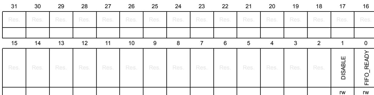
| 31 | 30 | 29 | 28 | 27 | 26 | 25 | 24 | 23 | 22 | 21 | 20 | 19 | 18 | 17 | 16 |
| Res. | Res. | Res. | Res. | Res. | Res. | Res. | Res. | Res. | Res. | Res. | Res. | Res. | Res. | Res. | Res. |
| 15 | 14 | 13 | 12 | 11 | 10 | 9 | 8 | 7 | 6 | 5 | 4 | 3 | 2 | 1 | 0 |
| Res. | Res. | Res. | Res. | Res. | Res. | Res. | Res. | Res. | Res. | Res. | Res. | Res. | Res. | DISABLE | FIFO_READY |
| rw | rw | ||||||||||||||
Bits 31:2 Reserved, must be kept at reset value.
Bit 1
DISABLE
: Disable flag
0: stimulus port and ITM enabled
1: stimulus port and ITM disabled
Bit 0
FIFO_READY
: FIFO ready indicator
0: stimulus port buffer is full (or port is disabled)
1: stimulus port can accept new write data
ITM trace enable register (ITM_TER)
Address offset: 0xE00
Reset value: 0x0000 0000
| 31 | 30 | 29 | 28 | 27 | 26 | 25 | 24 | 23 | 22 | 21 | 20 | 19 | 18 | 17 | 16 |
| STIMENA[31:16] | |||||||||||||||
| rw | rw | rw | rw | rw | rw | rw | rw | rw | rw | rw | rw | rw | rw | rw | rw |
| 15 | 14 | 13 | 12 | 11 | 10 | 9 | 8 | 7 | 6 | 5 | 4 | 3 | 2 | 1 | 0 |
| STIMENA[15:0] | |||||||||||||||
| rw | rw | rw | rw | rw | rw | rw | rw | rw | rw | rw | rw | rw | rw | rw | rw |
Bits 31:0
STIMENA[31:0]
: stimulus port enable
Each bit x(0 to 31) enables the stimulus port associated with the ITM_STIMRx register.
0: port disabled
1: port enabled
ITM trace privilege register (ITM_TPR)
Address offset: 0xE40
Reset value: 0x0000 0000
| 31 | 30 | 29 | 28 | 27 | 26 | 25 | 24 | 23 | 22 | 21 | 20 | 19 | 18 | 17 | 16 |
|---|---|---|---|---|---|---|---|---|---|---|---|---|---|---|---|
| Res. | Res. | Res. | Res. | Res. | Res. | Res. | Res. | Res. | Res. | Res. | Res. | Res. | Res. | Res. | Res. |
| 15 | 14 | 13 | 12 | 11 | 10 | 9 | 8 | 7 | 6 | 5 | 4 | 3 | 2 | 1 | 0 |
| Res. | Res. | Res. | Res. | Res. | Res. | Res. | Res. | Res. | Res. | Res. | Res. | PRIVMASK[3:0] | |||
| r | r | r | r | ||||||||||||
Bits 31:4 Reserved, must be kept at reset value.
Bits 3:0 PRIVMASK[3:0] : disable unprivileged access to ITM stimulus ports
- Each bit controls eight stimulus ports.
- XXX0: unprivileged access permitted on ports 0 to 7
- XXX1: only privileged access permitted on ports 0 to 7
- XX0X: unprivileged access permitted on ports 8 to 15
- XX1X: only privileged access permitted on ports 8 to 15
- X0XX: unprivileged access permitted on ports 16 to 23
- X1XX: only privileged access permitted on ports 16 to 23
- 0XXX: unprivileged access permitted on ports 24 to 31
- 1XXX: only privileged access permitted on ports 24 to 31
ITM trace control register (ITM_TCR)
Address offset: 0xE80
Reset value: 0x0000 0000
| 31 | 30 | 29 | 28 | 27 | 26 | 25 | 24 | 23 | 22 | 21 | 20 | 19 | 18 | 17 | 16 |
|---|---|---|---|---|---|---|---|---|---|---|---|---|---|---|---|
| Res. | Res. | Res. | Res. | Res. | Res. | Res. | Res. | BUSY | TRACEBUSID[6:0] | ||||||
| r | rw | rw | rw | rw | rw | rw | rw | ||||||||
| 15 | 14 | 13 | 12 | 11 | 10 | 9 | 8 | 7 | 6 | 5 | 4 | 3 | 2 | 1 | 0 |
| Res. | Res. | Res. | Res. | Res. | Res. | TSPRESCALE[1:0] | Res. | Res. | STALLena | SWOena | TXena | SYNCena | TSEna | ITMena | |
| rw | rw | rw | r | rw | rw | rw | rw | ||||||||
Bits 31:24 Reserved, must be kept at reset value.
Bit 23 BUSY : indicates whether the ITM is currently processing events
- 0: not busy
- 1: busy
Bits 22:16 TRACEBUSID[6:0] : identifier for multi-source trace stream formatting
If multi-source trace is in use, the debugger must write a non-zero value to this field.
Note: Different identifiers must be used for each trace source in the system.
Bits 15:10 Reserved, must be kept at reset value.
Bits 9:8 TSPRESCALE[1:0] : local timestamp prescaler, used with the trace packet reference clock
0x0: no prescaling
0x1: Divide by 4.
0x2: Divide by 16.
0x3: Divide by 64.
Bits 7:6 Reserved, must be kept at reset value.
Bit 5 STALLena : stall enable
0: Drop hardware source packets and generate an overflow if the ITM output is stalled.
1: Stall the processor to guarantee delivery of data trace packets.
Bit 4 SWOena : SWO enable
Enables asynchronous clocking of the timestamp counter (read only).
0: Timestamp counter uses processor clock.
Bit 3 TXena : transmit enable
Enables forwarding of hardware event packets from the DWT unit to the trace port.
0: disabled
1: enabled
Bit 2 SYNCena : synchronization packet transmission enable
The debugger setting this bit must also configure the DWT_CTRLR.SYNCTAP field for the correct synchronization speed.
0: disabled
1: enabled
Bit 1 TSena : local timestamp generation enable
0: disabled
1: enabled
Bit 0 ITMena : ITM enable
0: disabled
1: enabled
ITM device type architecture register (ITM_DEVARCHR)
Address offset: 0xFBC
Reset value: 0x4770 1A01
| 31 | 30 | 29 | 28 | 27 | 26 | 25 | 24 | 23 | 22 | 21 | 20 | 19 | 18 | 17 | 16 |
|---|---|---|---|---|---|---|---|---|---|---|---|---|---|---|---|
| ARCHITECT[10:0] | PRESENT | REVISION[3:0] | |||||||||||||
| r | r | r | r | r | r | r | r | r | r | r | r | r | r | r | r |
| 15 | 14 | 13 | 12 | 11 | 10 | 9 | 8 | 7 | 6 | 5 | 4 | 3 | 2 | 1 | 0 |
| ARCHVER[3:0] | ARCHPART[11:0] | ||||||||||||||
| r | r | r | r | r | r | r | r | r | r | r | r | r | r | r | r |
Bits 31:21 ARCHITECT[10:0] : architect JEP106 code
0x23B: JEP106 continuation code 0x4, JEP106 ID code 0x3B. Arm® limited.
Bit 20 PRESENT : DEVARCH register presence
0x1: present
Bits 19:16
REVISION[3:0]
: architecture revision
0x0: ITM architecture v2.0
Bits 15:12
ARCHVER[3:0]
: architecture version
0x1: ITM architecture v2.0
Bits 11:0
ARCHPART[11:0]
: architecture part
0xA01: ITM architecture
ITM device type register (ITM_DEVTYPER)
Address offset: 0xFCC
Reset value: 0x0000 0043
| 31 | 30 | 29 | 28 | 27 | 26 | 25 | 24 | 23 | 22 | 21 | 20 | 19 | 18 | 17 | 16 |
|---|---|---|---|---|---|---|---|---|---|---|---|---|---|---|---|
| Res. | Res. | Res. | Res. | Res. | Res. | Res. | Res. | Res. | Res. | Res. | Res. | Res. | Res. | Res. | Res. |
| 15 | 14 | 13 | 12 | 11 | 10 | 9 | 8 | 7 | 6 | 5 | 4 | 3 | 2 | 1 | 0 |
| Res. | Res. | Res. | Res. | Res. | Res. | Res. | Res. | SUB[3:0] | MAJOR[3:0] | ||||||
| r | r | r | r | r | r | r | r | ||||||||
Bits 31:8 Reserved, must be kept at reset value.
Bits 7:4
SUB[3:0]
: sub-type
0x4: associated with a bus, stimulus derived from bus activity
Bits 3:0
MAJOR[3:0]
: major type
0x3: trace source
ITM CoreSight peripheral identity register 4 (ITM_PIDR4)
Address offset: 0xFD0
Reset value: 0x0000 0004
| 31 | 30 | 29 | 28 | 27 | 26 | 25 | 24 | 23 | 22 | 21 | 20 | 19 | 18 | 17 | 16 |
|---|---|---|---|---|---|---|---|---|---|---|---|---|---|---|---|
| Res. | Res. | Res. | Res. | Res. | Res. | Res. | Res. | Res. | Res. | Res. | Res. | Res. | Res. | Res. | Res. |
| 15 | 14 | 13 | 12 | 11 | 10 | 9 | 8 | 7 | 6 | 5 | 4 | 3 | 2 | 1 | 0 |
| Res. | Res. | Res. | Res. | Res. | Res. | Res. | Res. | SIZE[3:0] | JEP106CON[3:0] | ||||||
| r | r | r | r | r | r | r | r | ||||||||
Bits 31:8 Reserved, must be kept at reset value.
Bits 7:4
SIZE[3:0]
: register file size
0x0: The register file occupies a single 4-Kbyte region.
Bits 3:0
JEP106CON[3:0]
: JEP106 continuation code
0x4: Arm® JEDEC code
Address offset: 0xFE0
Reset value: 0x0000 0021
| 31 | 30 | 29 | 28 | 27 | 26 | 25 | 24 | 23 | 22 | 21 | 20 | 19 | 18 | 17 | 16 |
|---|---|---|---|---|---|---|---|---|---|---|---|---|---|---|---|
| Res. | Res. | Res. | Res. | Res. | Res. | Res. | Res. | Res. | Res. | Res. | Res. | Res. | Res. | Res. | Res. |
| 15 | 14 | 13 | 12 | 11 | 10 | 9 | 8 | 7 | 6 | 5 | 4 | 3 | 2 | 1 | 0 |
| Res. | Res. | Res. | Res. | Res. | Res. | Res. | Res. | PARTNUM[7:0] | |||||||
| r | r | r | r | r | r | r | r | ||||||||
Bits 31:8 Reserved, must be kept at reset value.
Bits 7:0 PARTNUM[7:0] : part number bits [7:0]0x21: ITM part number
ITM CoreSight peripheral identity register 1 (ITM_PIDR1)Address offset: 0xFE4
Reset value: 0x0000 00BD
| 31 | 30 | 29 | 28 | 27 | 26 | 25 | 24 | 23 | 22 | 21 | 20 | 19 | 18 | 17 | 16 |
|---|---|---|---|---|---|---|---|---|---|---|---|---|---|---|---|
| Res. | Res. | Res. | Res. | Res. | Res. | Res. | Res. | Res. | Res. | Res. | Res. | Res. | Res. | Res. | Res. |
| 15 | 14 | 13 | 12 | 11 | 10 | 9 | 8 | 7 | 6 | 5 | 4 | 3 | 2 | 1 | 0 |
| Res. | Res. | Res. | Res. | Res. | Res. | Res. | Res. | JEP106ID[3:0] | PARTNUM[11:8] | ||||||
| r | r | r | r | r | r | r | r | ||||||||
Bits 31:8 Reserved, must be kept at reset value.
Bits 7:4 JEP106ID[3:0] : JEP106 identity code bits [3:0]0xB: Arm® JEDEC code
Bits 3:0 PARTNUM[11:8] : part number bits [11:8]0xD: ITM part number
ITM CoreSight peripheral identity register 2 (ITM_PIDR2)Address offset: 0xFE8
Reset value: 0x0000 000B
| 31 | 30 | 29 | 28 | 27 | 26 | 25 | 24 | 23 | 22 | 21 | 20 | 19 | 18 | 17 | 16 |
|---|---|---|---|---|---|---|---|---|---|---|---|---|---|---|---|
| Res. | Res. | Res. | Res. | Res. | Res. | Res. | Res. | Res. | Res. | Res. | Res. | Res. | Res. | Res. | Res. |
| 15 | 14 | 13 | 12 | 11 | 10 | 9 | 8 | 7 | 6 | 5 | 4 | 3 | 2 | 1 | 0 |
| Res. | Res. | Res. | Res. | Res. | Res. | Res. | Res. | REVISION[3:0] | JEDEC | JEP106ID[6:4] | |||||
| r | r | r | r | r | r | r | r | ||||||||
Bits 31:8 Reserved, must be kept at reset value.
Bits 7:4 REVISION[3:0] : component revision number
0x0: r0p0
Bit 3 JEDEC : JEDEC assigned value
0x1: designer identification specified by JEDEC
Bits 2:0 JEP106ID[6:4] : JEP106 identity code bits [6:4]
0x3: Arm® JEDEC code
ITM CoreSight peripheral identity register 3 (ITM_PIDR3)
Address offset: 0xFEC
Reset value: 0x0000 0000
| 31 | 30 | 29 | 28 | 27 | 26 | 25 | 24 | 23 | 22 | 21 | 20 | 19 | 18 | 17 | 16 |
|---|---|---|---|---|---|---|---|---|---|---|---|---|---|---|---|
| Res. | Res. | Res. | Res. | Res. | Res. | Res. | Res. | Res. | Res. | Res. | Res. | Res. | Res. | Res. | Res. |
| 15 | 14 | 13 | 12 | 11 | 10 | 9 | 8 | 7 | 6 | 5 | 4 | 3 | 2 | 1 | 0 |
| Res. | Res. | Res. | Res. | Res. | Res. | Res. | Res. | REVAND[3:0] | CMOD[3:0] | ||||||
| r | r | r | r | r | r | r | r | ||||||||
Bits 31:8 Reserved, must be kept at reset value.
Bits 7:4 REVAND[3:0] : metal fix version
0x0: no metal fix
Bits 3:0 CMOD[3:0] : customer modified
0x0: no customer modifications
ITM CoreSight component identity register 0 (ITM_CIDR0)
Address offset: 0xFF0
Reset value: 0x0000 000D
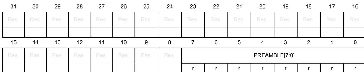
| 31 | 30 | 29 | 28 | 27 | 26 | 25 | 24 | 23 | 22 | 21 | 20 | 19 | 18 | 17 | 16 |
|---|---|---|---|---|---|---|---|---|---|---|---|---|---|---|---|
| Res. | Res. | Res. | Res. | Res. | Res. | Res. | Res. | Res. | Res. | Res. | Res. | Res. | Res. | Res. | Res. |
| 15 | 14 | 13 | 12 | 11 | 10 | 9 | 8 | 7 | 6 | 5 | 4 | 3 | 2 | 1 | 0 |
| Res. | Res. | Res. | Res. | Res. | Res. | Res. | Res. | PREAMBLE[7:0] | |||||||
| r | r | r | r | r | r | r | r | ||||||||
Bits 31:8 Reserved, must be kept at reset value.
Bits 7:0 PREAMBLE[7:0] : Component identification bits [7:0]
0x0D: Common identification value
ITM CoreSight peripheral identity register 1 (ITM_CIDR1)
Address offset: 0xFF4
Reset value: 0x0000 00E0
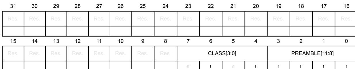
| 31 | 30 | 29 | 28 | 27 | 26 | 25 | 24 | 23 | 22 | 21 | 20 | 19 | 18 | 17 | 16 |
|---|---|---|---|---|---|---|---|---|---|---|---|---|---|---|---|
| Res. | Res. | Res. | Res. | Res. | Res. | Res. | Res. | Res. | Res. | Res. | Res. | Res. | Res. | Res. | Res. |
| 15 | 14 | 13 | 12 | 11 | 10 | 9 | 8 | 7 | 6 | 5 | 4 | 3 | 2 | 1 | 0 |
| Res. | Res. | Res. | Res. | Res. | Res. | Res. | Res. | CLASS[3:0] | PREAMBLE[11:8] | ||||||
| r | r | r | r | r | r | r | r | ||||||||
Bits 31:8 Reserved, must be kept at reset value.
Bits 7:4 CLASS[3:0] : Component identification bits [15:12] - component class
0xE: Trace generator component
Bits 3:0 PREAMBLE[11:8] : Component identification bits [11:8]
0x0: Common identification value
ITM CoreSight component identity register 2 (ITM_CIDR2)
Address offset: 0xFF8
Reset value: 0x0000 0005

| 31 | 30 | 29 | 28 | 27 | 26 | 25 | 24 | 23 | 22 | 21 | 20 | 19 | 18 | 17 | 16 |
|---|---|---|---|---|---|---|---|---|---|---|---|---|---|---|---|
| Res. | Res. | Res. | Res. | Res. | Res. | Res. | Res. | Res. | Res. | Res. | Res. | Res. | Res. | Res. | Res. |
| 15 | 14 | 13 | 12 | 11 | 10 | 9 | 8 | 7 | 6 | 5 | 4 | 3 | 2 | 1 | 0 |
| Res. | Res. | Res. | Res. | Res. | Res. | Res. | Res. | PREAMBLE[19:12] | |||||||
| r | r | r | r | r | r | r | r | ||||||||
Bits 31:8 Reserved, must be kept at reset value.
Bits 7:0
PREAMBLE[19:12]
: Component identification bits [23:16]
0x05: Common identification value
ITM CoreSight component identity register 3 (ITM_CIDR3)
Address offset: 0xFFC
Reset value: 0x0000 00B1
| 31 | 30 | 29 | 28 | 27 | 26 | 25 | 24 | 23 | 22 | 21 | 20 | 19 | 18 | 17 | 16 |
|---|---|---|---|---|---|---|---|---|---|---|---|---|---|---|---|
| Res. | Res. | Res. | Res. | Res. | Res. | Res. | Res. | Res. | Res. | Res. | Res. | Res. | Res. | Res. | Res. |
| 15 | 14 | 13 | 12 | 11 | 10 | 9 | 8 | 7 | 6 | 5 | 4 | 3 | 2 | 1 | 0 |
| Res. | Res. | Res. | Res. | Res. | Res. | Res. | Res. | PREAMBLE[27:20] | |||||||
| r | r | r | r | r | r | r | r | ||||||||
Bits 31:8 Reserved, must be kept at reset value.
Bits 7:0
PREAMBLE[27:20]
: Component identification bits [31:24]
0xB1: Common identification value
59.7.2 ITM register map
The ITM registers are located at the address range 0xE000 0000 to 0xE000 0FFC.
Table 732. ITM register map and reset values
| Offset | Register name | 31 | 30 | 29 | 28 | 27 | 26 | 25 | 24 | 23 | 22 | 21 | 20 | 19 | 18 | 17 | 16 | 15 | 14 | 13 | 12 | 11 | 10 | 9 | 8 | 7 | 6 | 5 | 4 | 3 | 2 | 1 | 0 |
|---|---|---|---|---|---|---|---|---|---|---|---|---|---|---|---|---|---|---|---|---|---|---|---|---|---|---|---|---|---|---|---|---|---|
| 0x000 to 0x07C | ITM_STIMR0 to ITM_STIMR31 | STIMULUS[31:0] | |||||||||||||||||||||||||||||||
| Reset value | X | X | X | X | X | X | X | X | X | X | X | X | X | X | X | X | X | X | X | X | X | X | X | X | X | X | X | X | X | X | X | ||
| 0x07C to 0xDFC | Reserved | ||||||||||||||||||||||||||||||||
| 0xE00 | ITM_TER | STIMENA[31:0] | |||||||||||||||||||||||||||||||
| Reset value | 0 | 0 | 0 | 0 | 0 | 0 | 0 | 0 | 0 | 0 | 0 | 0 | 0 | 0 | 0 | 0 | 0 | 0 | 0 | 0 | 0 | 0 | 0 | 0 | 0 | 0 | 0 | 0 | 0 | 0 | |||
| 0xE04 to 0xE3C | Reserved | ||||||||||||||||||||||||||||||||
| 0xE40 | ITM_TPR | Res | Res | Res | Res | Res | Res | Res | Res | Res | Res | Res | Res | Res | Res | Res | Res | Res | Res | Res | Res | Res | Res | Res | Res | Res | Res | Res | Res | PRIVMASK [3:0] | |||
| Reset value | 0 | 0 | |||||||||||||||||||||||||||||||
| 0xE44 to 0xE7C | Reserved | ||||||||||||||||||||||||||||||||
| 0xE80 | ITM_TCR | Res | Res | Res | Res | Res | Res | Res | Res | BUSY | TRACEBUSID[6:0] | Res | Res | Res | Res | Res | Res | Res | Res | Res | Res | Res | STALLena | SWOena | TXena | SYNCena | TSena | ||||||
| Reset value | 0 | 0 | 0 | 0 | 0 | 0 | 0 | 0 | 0 | 0 | 0 | ||||||||||||||||||||||
| 0xE84 to 0xFB8 | Reserved | ||||||||||||||||||||||||||||||||
Table 732. ITM register map and reset values (continued)
| Offset | Register name | 31 | 30 | 29 | 28 | 27 | 26 | 25 | 24 | 23 | 22 | 21 | 20 | 19 | 18 | 17 | 16 | 15 | 14 | 13 | 12 | 11 | 10 | 9 | 8 | 7 | 6 | 5 | 4 | 3 | 2 | 1 | 0 |
|---|---|---|---|---|---|---|---|---|---|---|---|---|---|---|---|---|---|---|---|---|---|---|---|---|---|---|---|---|---|---|---|---|---|
| 0xFBC | ITM_DEVARCHR | ARCHITECT[10:0] | PRESEN | REVISION [3:0] | ARCHVER [3:0] | ARCHPART[3:0] | |||||||||||||||||||||||||||
| Reset value | 0 | 1 | 0 | 0 | 0 | 1 | 1 | 1 | 0 | 1 | 1 | 1 | 0 | 0 | 0 | 0 | 0 | 0 | 0 | 1 | 1 | 0 | 1 | 0 | 0 | 0 | 0 | 0 | 0 | 0 | 0 | 1 | |
| 0xFC0 to 0xFC8 | Reserved | ||||||||||||||||||||||||||||||||
| 0xFCC | ITM_DEVTYPEP | Res. (repeated) | SUB[3:0] | MAJOR[3:0] | |||||||||||||||||||||||||||||
| Reset value | 0 | 1 | 0 | 0 | 0 | 0 | 1 | 1 | |||||||||||||||||||||||||
| 0xFD0 | ITM_PIDR4 | Res. (repeated) | SIZE [3:0] | JEP106CON [3:0] | |||||||||||||||||||||||||||||
| Reset value | 0 | 0 | 0 | 0 | 0 | 1 | 0 | 0 | |||||||||||||||||||||||||
| 0xFD4 to 0xFDC | Reserved | ||||||||||||||||||||||||||||||||
| 0xFE0 | ITM_PIDR0 | Res. (repeated) | PARTNUM[7:0] | ||||||||||||||||||||||||||||||
| Reset value | 0 | 0 | 1 | 0 | 0 | 0 | 0 | 1 | |||||||||||||||||||||||||
| 0xFE4 | ITM_PIDR1 | Res. (repeated) | JEP106ID [3:0] | PARTNUM [11:8] | |||||||||||||||||||||||||||||
| Reset value | 1 | 0 | 1 | 1 | 1 | 1 | 0 | 1 | |||||||||||||||||||||||||
| 0xFE8 | ITM_PIDR2 | Res. (repeated) | REVISION [3:0] | JEDEC | JEP106ID [6:4] | ||||||||||||||||||||||||||||
| Reset value | 0 | 0 | 0 | 0 | 1 | 0 | 1 | 1 | |||||||||||||||||||||||||
| 0xFEC | ITM_PIDR3 | Res. (repeated) | REVAND[3:0] | CMOD[3:0] | |||||||||||||||||||||||||||||
| Reset value | 0 | 0 | 0 | 0 | 0 | 0 | 0 | 0 | |||||||||||||||||||||||||
| 0xFF0 | ITM_CIDR0 | Res. (repeated) | PREAMBLE[7:0] | ||||||||||||||||||||||||||||||
| Reset value | 0 | 0 | 0 | 0 | 1 | 1 | 0 | 1 | |||||||||||||||||||||||||
| 0xFF4 | ITM_CIDR1 | Res. (repeated) | CLASS[3:0] | PREAMBLE [11:8] | |||||||||||||||||||||||||||||
| Reset value | 1 | 1 | 1 | 0 | 0 | 0 | 0 | 0 | |||||||||||||||||||||||||
| 0xFF8 | ITM_CIDR2 | Res. (repeated) | PREAMBLE[19:12] | ||||||||||||||||||||||||||||||
| Reset value | 0 | 0 | 0 | 0 | 0 | 1 | 0 | 1 | |||||||||||||||||||||||||
| 0xFFC | ITM_CIDR3 | Res. (repeated) | PREAMBLE[27:20] | ||||||||||||||||||||||||||||||
| Reset value | 1 | 0 | 1 | 1 | 0 | 0 | 0 | 1 | |||||||||||||||||||||||||
59.8 Breakpoint unit (BPU)
The BPU allows the user to set hardware breakpoints. It contains eight comparators that monitor the instruction fetch address. If a match occurs, the instruction comparators can be configured to generate a breakpoint instruction.
For more information on the breakpoint unit and how to use it, refer to [4].
59.8.1 BPU registers
The BPU registers are located at the address range 0xE0002000 to 0xE0002FFC.
BPU control register (BPU_CTRLR)
Address offset: 0x000
Reset value: 0x1000 0080
| 31 | 30 | 29 | 28 | 27 | 26 | 25 | 24 | 23 | 22 | 21 | 20 | 19 | 18 | 17 | 16 |
|---|---|---|---|---|---|---|---|---|---|---|---|---|---|---|---|
| REV[3:0] | Res. | Res. | Res. | Res. | Res. | Res. | Res. | Res. | Res. | Res. | Res. | Res. | |||
| r | r | r | r | ||||||||||||
| 15 | 14 | 13 | 12 | 11 | 10 | 9 | 8 | 7 | 6 | 5 | 4 | 3 | 2 | 1 | 0 |
| Res. | NUM_CODE[6:4] | Res. | Res. | Res. | Res. | NUM_CODE[3:0] | Res. | Res. | KEY | ENABLE | |||||
| r | r | r | r | r | r | r | rw | rw | |||||||
Bits 31:28 REV[3:0] : revision number
0x1: BPU version 2
Bits 27:15 Reserved, must be kept at reset value.
Bits 14:12, 7:4 NUM_CODE[6:0] : number of instruction address comparators supported
0x08: 8 instruction comparators supported
Bits 11:8, 3:2 Reserved, must be kept at reset value.
Bit 1 KEY : Write protect key
A write to FPB_CTRLR register is ignored if this bit is not set to 1.
Bit 0 ENABLE : FPB enable
0: disabled
1: enabled
BPU comparator x register (BPU_COMPxR)
Address offset: 0x008 + 0x004 * x, (x = 0 to 7)
Reset value: 0x0000 0000
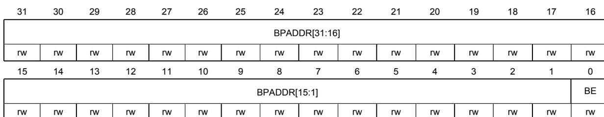
| 31 | 30 | 29 | 28 | 27 | 26 | 25 | 24 | 23 | 22 | 21 | 20 | 19 | 18 | 17 | 16 |
| BPADDR[31:16] | |||||||||||||||
| rw | rw | rw | rw | rw | rw | rw | rw | rw | rw | rw | rw | rw | rw | rw | rw |
| 15 | 14 | 13 | 12 | 11 | 10 | 9 | 8 | 7 | 6 | 5 | 4 | 3 | 2 | 1 | 0 |
| BPADDR[15:1] | BE | ||||||||||||||
| rw | rw | rw | rw | rw | rw | rw | rw | rw | rw | rw | rw | rw | rw | rw | rw |
Bits 31:1 BPADDR[31:1] : breakpoint address
Bit 0 BE : breakpoint enable
0: disabled
1: enabled
BPU device type architecture register (BPU_DEVARCHR)
Address offset: 0xFBC
Reset value: 0x4770 1A03
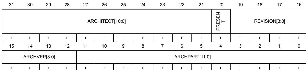
| 31 | 30 | 29 | 28 | 27 | 26 | 25 | 24 | 23 | 22 | 21 | 20 | 19 | 18 | 17 | 16 |
| ARCHITECT[10:0] | PRESENT 1 | REVISION[3:0] | |||||||||||||
| r | r | r | r | r | r | r | r | r | r | r | r | r | r | r | r |
| 15 | 14 | 13 | 12 | 11 | 10 | 9 | 8 | 7 | 6 | 5 | 4 | 3 | 2 | 1 | 0 |
| ARCHVER[3:0] | ARCHPART[11:0] | ||||||||||||||
| r | r | r | r | r | r | r | r | r | r | r | r | r | r | r | r |
Bits 31:21 ARCHITECT[10:0] : architect JEP106 code
0x23B: JEP106 continuation code 0x4, JEP106 ID code 0x3B. Arm® limited.
Bit 20 PRESENT : DEVARCH register present
0x1: present
Bits 19:16 REVISION[3:0] : architecture revision
0x0: BPU architecture v2.0
Bits 15:12 ARCHVER[3:0] : architecture version
0x1: BPU architecture v2.0
Bits 11:0 ARCHPART[11:0] : architecture part
0xA03: BPU architecture
BPU device type register (BPU_DEVTYPER)
Address offset: 0xFCC
Reset value: 0x0000 0000
| 31 | 30 | 29 | 28 | 27 | 26 | 25 | 24 | 23 | 22 | 21 | 20 | 19 | 18 | 17 | 16 |
|---|---|---|---|---|---|---|---|---|---|---|---|---|---|---|---|
| Res. | Res. | Res. | Res. | Res. | Res. | Res. | Res. | Res. | Res. | Res. | Res. | Res. | Res. | Res. | Res. |
| 15 | 14 | 13 | 12 | 11 | 10 | 9 | 8 | 7 | 6 | 5 | 4 | 3 | 2 | 1 | 0 |
| Res. | Res. | Res. | Res. | Res. | Res. | Res. | Res. | SUB[3:0] | MAJOR[3:0] | ||||||
| r | r | r | r | r | r | r | r | ||||||||
Bits 31:8 Reserved, must be kept at reset value.
Bits 7:4 SUB[3:0] : sub-type
0x0: other
Bits 3:0 MAJOR[3:0] : major type
0x0: miscellaneous
BPU CoreSight peripheral identity register 4 (BPU_PIDR4)
Address offset: 0xFD0
Reset value: 0x0000 0004
| 31 | 30 | 29 | 28 | 27 | 26 | 25 | 24 | 23 | 22 | 21 | 20 | 19 | 18 | 17 | 16 |
|---|---|---|---|---|---|---|---|---|---|---|---|---|---|---|---|
| Res. | Res. | Res. | Res. | Res. | Res. | Res. | Res. | Res. | Res. | Res. | Res. | Res. | Res. | Res. | Res. |
| 15 | 14 | 13 | 12 | 11 | 10 | 9 | 8 | 7 | 6 | 5 | 4 | 3 | 2 | 1 | 0 |
| Res. | Res. | Res. | Res. | Res. | Res. | Res. | Res. | SIZE[3:0] | JEP106CON[3:0] | ||||||
| r | r | r | r | r | r | r | r | ||||||||
Bits 31:8 Reserved, must be kept at reset value.
Bits 7:4 SIZE[3:0] : register file size
0x0: The register file occupies a single 4-Kbyte region.
Bits 3:0 JEP106CON[3:0] : JEP106 continuation code
0x4: Arm® JEDEC code
BPU CoreSight peripheral identity register 0 (BPU_PIDR0)
Address offset: 0xFE0
Reset value: 0x0000 0021
| 31 | 30 | 29 | 28 | 27 | 26 | 25 | 24 | 23 | 22 | 21 | 20 | 19 | 18 | 17 | 16 |
|---|---|---|---|---|---|---|---|---|---|---|---|---|---|---|---|
| Res. | Res. | Res. | Res. | Res. | Res. | Res. | Res. | Res. | Res. | Res. | Res. | Res. | Res. | Res. | Res. |
| 15 | 14 | 13 | 12 | 11 | 10 | 9 | 8 | 7 | 6 | 5 | 4 | 3 | 2 | 1 | 0 |
| Res. | Res. | Res. | Res. | Res. | Res. | Res. | Res. | PARTNUM[7:0] | |||||||
| r | r | r | r | r | r | r | r | ||||||||
Bits 31:8 Reserved, must be kept at reset value.
Bits 7:0
PARTNUM[7:0]
: part number bits [7:0]
0x21: BPU part number
BPU CoreSight peripheral identity register 1 (BPU_PIDR1)
Address offset: 0xFE4
Reset value: 0x0000 00BD
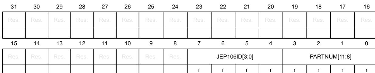
| 31 | 30 | 29 | 28 | 27 | 26 | 25 | 24 | 23 | 22 | 21 | 20 | 19 | 18 | 17 | 16 |
|---|---|---|---|---|---|---|---|---|---|---|---|---|---|---|---|
| Res. | Res. | Res. | Res. | Res. | Res. | Res. | Res. | Res. | Res. | Res. | Res. | Res. | Res. | Res. | Res. |
| 15 | 14 | 13 | 12 | 11 | 10 | 9 | 8 | 7 | 6 | 5 | 4 | 3 | 2 | 1 | 0 |
|---|---|---|---|---|---|---|---|---|---|---|---|---|---|---|---|
| Res. | Res. | Res. | Res. | Res. | Res. | Res. | Res. | JEP106ID[3:0] | PARTNUM[11:8] | ||||||
| r | r | r | r | r | r | r | r | ||||||||
Bits 31:8 Reserved, must be kept at reset value.
Bits 7:4
JEP106ID[3:0]
: JEP106 identity code bits [3:0]
0xB: Arm
®
JEDEC code
Bits 3:0
PARTNUM[11:8]
: part number bits [11:8]
0xD: BPU part number
BPU CoreSight peripheral identity register 2 (BPU_PIDR2)
Address offset: 0xFE8
Reset value: 0x0000 000B
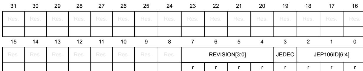
| 31 | 30 | 29 | 28 | 27 | 26 | 25 | 24 | 23 | 22 | 21 | 20 | 19 | 18 | 17 | 16 |
|---|---|---|---|---|---|---|---|---|---|---|---|---|---|---|---|
| Res. | Res. | Res. | Res. | Res. | Res. | Res. | Res. | Res. | Res. | Res. | Res. | Res. | Res. | Res. | Res. |
| 15 | 14 | 13 | 12 | 11 | 10 | 9 | 8 | 7 | 6 | 5 | 4 | 3 | 2 | 1 | 0 |
|---|---|---|---|---|---|---|---|---|---|---|---|---|---|---|---|
| Res. | Res. | Res. | Res. | Res. | Res. | Res. | Res. | REVISION[3:0] | JEDEC | JEP106ID[6:4] | |||||
| r | r | r | r | r | r | r | r | ||||||||
Bits 31:8 Reserved, must be kept at reset value.
Bits 7:4
REVISION[3:0]
: component revision number
0x0: r0p0
Bit 3
JEDEC
: JEDEC assigned value
0x1: designer identification specified by JEDEC
Bits 2:0
JEP106ID[6:4]
: JEP106 identity code bits [6:4]
0x3: Arm
®
JEDEC code
BPU CoreSight peripheral identity register 3 (BPU_PIDR3)
Address offset: 0xFEC
Reset value: 0x0000 0000
| 31 | 30 | 29 | 28 | 27 | 26 | 25 | 24 | 23 | 22 | 21 | 20 | 19 | 18 | 17 | 16 |
|---|---|---|---|---|---|---|---|---|---|---|---|---|---|---|---|
| Res. | Res. | Res. | Res. | Res. | Res. | Res. | Res. | Res. | Res. | Res. | Res. | Res. | Res. | Res. | Res. |
| 15 | 14 | 13 | 12 | 11 | 10 | 9 | 8 | 7 | 6 | 5 | 4 | 3 | 2 | 1 | 0 |
| Res. | Res. | Res. | Res. | Res. | Res. | Res. | Res. | REVAND[3:0] | CMOD[3:0] | ||||||
| r | r | r | r | r | r | r | r | ||||||||
Bits 31:8 Reserved, must be kept at reset value.
Bits 7:4 REVAND[3:0] : metal fix version
0x0: no metal fix
Bits 3:0 CMOD[3:0] : customer modified
0x0: no customer modifications
BPU CoreSight component identity register 0 (BPU_CIDR0)
Address offset: 0xFF0
Reset value: 0x0000 000D
| 31 | 30 | 29 | 28 | 27 | 26 | 25 | 24 | 23 | 22 | 21 | 20 | 19 | 18 | 17 | 16 |
|---|---|---|---|---|---|---|---|---|---|---|---|---|---|---|---|
| Res. | Res. | Res. | Res. | Res. | Res. | Res. | Res. | Res. | Res. | Res. | Res. | Res. | Res. | Res. | Res. |
| 15 | 14 | 13 | 12 | 11 | 10 | 9 | 8 | 7 | 6 | 5 | 4 | 3 | 2 | 1 | 0 |
| Res. | Res. | Res. | Res. | Res. | Res. | Res. | Res. | PREAMBLE[7:0] | |||||||
| r | r | r | r | r | r | r | r | ||||||||
Bits 31:8 Reserved, must be kept at reset value.
Bits 7:0 PREAMBLE[7:0] : component identification bits [7:0]
0x0D: common identification value
BPU CoreSight peripheral identity register 1 (BPU_CIDR1)
Address offset: 0xFF4
Reset value: 0x0000 0090
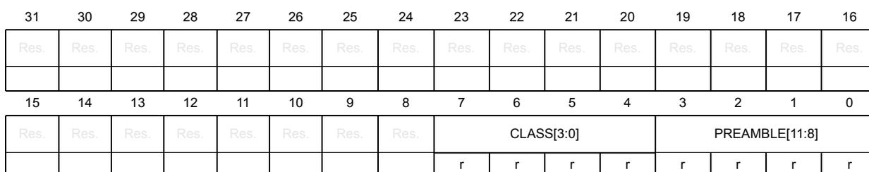
| 31 | 30 | 29 | 28 | 27 | 26 | 25 | 24 | 23 | 22 | 21 | 20 | 19 | 18 | 17 | 16 |
|---|---|---|---|---|---|---|---|---|---|---|---|---|---|---|---|
| Res. | Res. | Res. | Res. | Res. | Res. | Res. | Res. | Res. | Res. | Res. | Res. | Res. | Res. | Res. | Res. |
| 15 | 14 | 13 | 12 | 11 | 10 | 9 | 8 | 7 | 6 | 5 | 4 | 3 | 2 | 1 | 0 |
|---|---|---|---|---|---|---|---|---|---|---|---|---|---|---|---|
| Res. | Res. | Res. | Res. | Res. | Res. | Res. | Res. | CLASS[3:0] | PREAMBLE[11:8] | ||||||
| r | r | r | r | r | r | r | r | ||||||||
Bits 31:8 Reserved, must be kept at reset value.
Bits 7:4 CLASS[3:0] : component identification bits [15:12] - component class
0x9: debug component
Bits 3:0 PREAMBLE[11:8] : component identification bits [11:8]
0x0: common identification value
BPU CoreSight component identity register 2 (BPU_CIDR2)
Address offset: 0xFF8
Reset value: 0x0000 0005
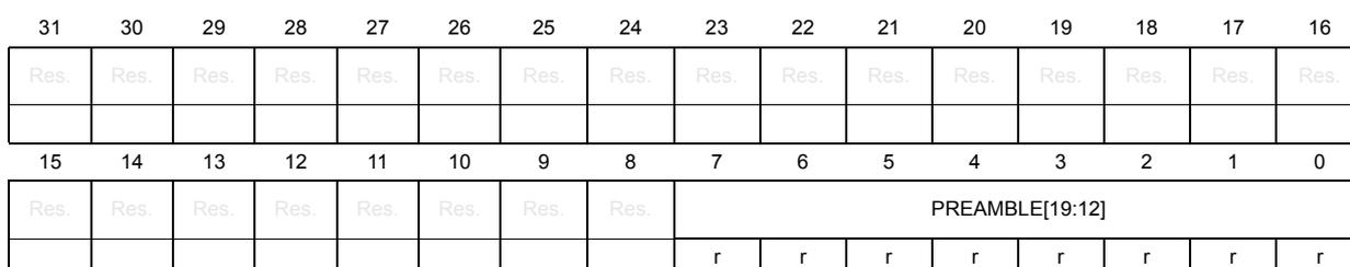
| 31 | 30 | 29 | 28 | 27 | 26 | 25 | 24 | 23 | 22 | 21 | 20 | 19 | 18 | 17 | 16 |
|---|---|---|---|---|---|---|---|---|---|---|---|---|---|---|---|
| Res. | Res. | Res. | Res. | Res. | Res. | Res. | Res. | Res. | Res. | Res. | Res. | Res. | Res. | Res. | Res. |
| 15 | 14 | 13 | 12 | 11 | 10 | 9 | 8 | 7 | 6 | 5 | 4 | 3 | 2 | 1 | 0 |
|---|---|---|---|---|---|---|---|---|---|---|---|---|---|---|---|
| Res. | Res. | Res. | Res. | Res. | Res. | Res. | Res. | PREAMBLE[19:12] | |||||||
| r | r | r | r | r | r | r | r | ||||||||
Bits 31:8 Reserved, must be kept at reset value.
Bits 7:0 PREAMBLE[19:12] : component identification bits [23:16]
0x05: common identification value
BPU CoreSight component identity register 3 (BPU_CIDR3)
Address offset: 0xFFC
Reset value: 0x0000 00B1
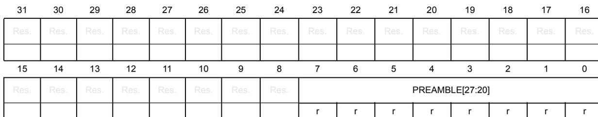
| 31 | 30 | 29 | 28 | 27 | 26 | 25 | 24 | 23 | 22 | 21 | 20 | 19 | 18 | 17 | 16 |
|---|---|---|---|---|---|---|---|---|---|---|---|---|---|---|---|
| Res. | Res. | Res. | Res. | Res. | Res. | Res. | Res. | Res. | Res. | Res. | Res. | Res. | Res. | Res. | Res. |
| 15 | 14 | 13 | 12 | 11 | 10 | 9 | 8 | 7 | 6 | 5 | 4 | 3 | 2 | 1 | 0 |
|---|---|---|---|---|---|---|---|---|---|---|---|---|---|---|---|
| Res. | Res. | Res. | Res. | Res. | Res. | Res. | Res. | PREAMBLE[27:20] | |||||||
| r | r | r | r | r | r | r | r | ||||||||
Bits 31:8 Reserved, must be kept at reset value.
Bits 7:0
PREAMBLE[27:20]
: component identification bits [31:24]
0xB1: common identification value
59.8.2 BPU register map
The BPU registers are located at the address range 0xE000 2000 to 0xE000 2FFC.
Table 733. BPU register map and reset values
| Offset | Register name | 31 | 30 | 29 | 28 | 27 | 26 | 25 | 24 | 23 | 22 | 21 | 20 | 19 | 18 | 17 | 16 | 15 | 14 | 13 | 12 | 11 | 10 | 9 | 8 | 7 | 6 | 5 | 4 | 3 | 2 | 1 | 0 |
|---|---|---|---|---|---|---|---|---|---|---|---|---|---|---|---|---|---|---|---|---|---|---|---|---|---|---|---|---|---|---|---|---|---|
| 0x000 | BPU_CTRLR | REV[3:0] | Res. | Res. | Res. | Res. | Res. | Res. | Res. | Res. | Res. | Res. | Res. | Res. | Res. | Res. | NUM_CODE [6:4] | Res. | Res. | Res. | Res. | Res. | Res. | Res. | NUM_CODE [3:0] | Res. | Res. | Res. | Res. | KEY | ENABLE | ||
| Reset value | 0 | 0 | 0 | 1 | 0 | 0 | 0 | 1 | 0 | 0 | 0 | 0 | 0 | ||||||||||||||||||||
| 0x004 | Reserved | ||||||||||||||||||||||||||||||||
| 0x008 to 0x024 | BPU_COMP0R to BPU_COMP7R | BPADDR[31:1] | BE | ||||||||||||||||||||||||||||||
| Reset value | 0 | 0 | 0 | 0 | 0 | 0 | 0 | 0 | 0 | 0 | 0 | 0 | 0 | 0 | 0 | 0 | 0 | 0 | 0 | 0 | 0 | 0 | 0 | 0 | 0 | 0 | 0 | 0 | 0 | 0 | 0 | 0 | |
| 0x028 to 0xFB8 | Reserved | ||||||||||||||||||||||||||||||||
| 0xFB8 | BPU_DEVARCHR | ARCHITECT[10:0] | PRESEN | REVISION [3:0] | ARCHVER [3:0] | ARCHPART[11:0] | |||||||||||||||||||||||||||
| Reset value | 0 | 1 | 0 | 0 | 0 | 1 | 1 | 1 | 0 | 1 | 1 | 1 | 0 | 0 | 0 | 0 | 0 | 0 | 0 | 1 | 1 | 0 | 1 | 0 | 0 | 0 | 0 | 0 | 0 | 0 | 1 | 1 | |
| 0xFC0 to 0xFC8 | Reserved | ||||||||||||||||||||||||||||||||
| 0xFCC | BPU_DEVTYPE | Res. | Res. | Res. | Res. | Res. | Res. | Res. | Res. | Res. | Res. | Res. | Res. | Res. | Res. | Res. | Res. | Res. | Res. | Res. | Res. | Res. | Res. | Res. | Res. | Res. | SUB[3:0] | MAJOR[3:0] | |||||
| Reset value | 0 | 0 | 0 | 0 | 0 | 0 | 0 | ||||||||||||||||||||||||||
| 0xFD0 | BPU_PIDR4 | Res. | Res. | Res. | Res. | Res. | Res. | Res. | Res. | Res. | Res. | Res. | Res. | Res. | Res. | Res. | Res. | Res. | Res. | Res. | Res. | Res. | Res. | Res. | Res. | Res. | SIZE [3:0] | JEP106CON [3:0] | |||||
| Reset value | 0 | 0 | 0 | 0 | 0 | 1 | 0 | ||||||||||||||||||||||||||
| 0xFD4 to 0xFDC | Reserved | ||||||||||||||||||||||||||||||||
| 0xFE0 | BPU_PIDR0 | Res. | Res. | Res. | Res. | Res. | Res. | Res. | Res. | Res. | Res. | Res. | Res. | Res. | Res. | Res. | Res. | Res. | Res. | Res. | Res. | Res. | Res. | Res. | Res. | Res. | PARTNUM[7:0] | ||||||
| Reset value | 0 | 0 | 1 | 0 | 0 | 0 | 1 | ||||||||||||||||||||||||||
| 0xFE4 | BPU_PIDR1 | Res. | Res. | Res. | Res. | Res. | Res. | Res. | Res. | Res. | Res. | Res. | Res. | Res. | Res. | Res. | Res. | Res. | Res. | Res. | Res. | Res. | Res. | Res. | Res. | Res. | JEP106ID [3:0] | PARTNUM [11:8] | |||||
| Reset value | 1 | 0 | 1 | 1 | 1 | 1 | 0 | ||||||||||||||||||||||||||
| 0xFE8 | BPU_PIDR2 | Res. | Res. | Res. | Res. | Res. | Res. | Res. | Res. | Res. | Res. | Res. | Res. | Res. | Res. | Res. | Res. | Res. | Res. | Res. | Res. | Res. | Res. | Res. | Res. | Res. | REVISION [3:0] | JEDEC | JEP106ID [6:4] | ||||
| Reset value | 0 | 0 | 0 | 0 | 1 | 0 | 1 | ||||||||||||||||||||||||||
| 0xFEC | BPU_PIDR3 | Res. | Res. | Res. | Res. | Res. | Res. | Res. | Res. | Res. | Res. | Res. | Res. | Res. | Res. | Res. | Res. | Res. | Res. | Res. | Res. | Res. | Res. | Res. | Res. | Res. | REVAND[3:0] | CMOD[3:0] | |||||
| Reset value | 0 | 0 | 0 | 0 | 0 | 0 | 0 | ||||||||||||||||||||||||||
| 0xFF0 | BPU_CIDR0 | Res. | Res. | Res. | Res. | Res. | Res. | Res. | Res. | Res. | Res. | Res. | Res. | Res. | Res. | Res. | Res. | Res. | Res. | Res. | Res. | Res. | Res. | Res. | Res. | Res. | PREAMBLE[7:0] | ||||||
| Reset value | 0 | 0 | 0 | 0 | 1 | 1 | 0 | ||||||||||||||||||||||||||
| 0xFF4 | BPU_CIDR1 | Res. | Res. | Res. | Res. | Res. | Res. | Res. | Res. | Res. | Res. | Res. | Res. | Res. | Res. | Res. | Res. | Res. | Res. | Res. | Res. | Res. | Res. | Res. | Res. | Res. | CLASS[3:0] | PREAMBLE [11:8] | |||||
| Reset value | 1 | 0 | 0 | 1 | 0 | 0 | 0 | ||||||||||||||||||||||||||
Table 733. BPU register map and reset values (continued)
| Offset | Register name | 31 | 30 | 29 | 28 | 27 | 26 | 25 | 24 | 23 | 22 | 21 | 20 | 19 | 18 | 17 | 16 | 15 | 14 | 13 | 12 | 11 | 10 | 9 | 8 | 7 | 6 | 5 | 4 | 3 | 2 | 1 | 0 |
|---|---|---|---|---|---|---|---|---|---|---|---|---|---|---|---|---|---|---|---|---|---|---|---|---|---|---|---|---|---|---|---|---|---|
| 0xFF8 | BPU_CIDR2 | Res. | Res. | Res. | Res. | Res. | Res. | Res. | Res. | Res. | Res. | Res. | Res. | Res. | Res. | Res. | Res. | Res. | Res. | Res. | Res. | Res. | Res. | Res. | Res. | PREAMBLE[19:12] | |||||||
| Reset value | 0 | 0 | 0 | 0 | 0 | 1 | 0 | 1 | |||||||||||||||||||||||||
| 0xFFC | BPU_CIDR3 | Res. | Res. | Res. | Res. | Res. | Res. | Res. | Res. | Res. | Res. | Res. | Res. | Res. | Res. | Res. | Res. | Res. | Res. | Res. | Res. | Res. | Res. | Res. | Res. | PREAMBLE[27:20] | |||||||
| Reset value | 1 | 0 | 1 | 1 | 0 | 0 | 0 | 1 | |||||||||||||||||||||||||
Refer to Table 727: Processor ROM table for register boundary addresses.
59.9 Embedded Trace Macrocell (ETM)
The ETM is a CoreSight™ component closely coupled to the CPU. The ETM generates trace packets that allow the execution of the Cortex®-M33 core to be traced. In the STM32H5 devices, the ETM is configured for instruction trace only. Data accesses are not included in the trace information.
The ETM receives information from the CPU over the processor trace interface, including:
- • Number of instructions executed in the same cycle
- • Changes in program flow
- • Current processor instruction state
- • Addresses of memory locations accessed by load and store instructions
- • Type, direction, and size of a transfer
- • Condition code information
- • Exception information
- • Wait for interrupt state information
For more information, refer to the Arm® CoreSight™ ETM-M33 Technical Reference Manual [6] .
59.9.1 ETM registers
The ETM registers are located at the address range 0xE004 1000 to 0xE004 1FFC.
ETM programming control register (ETM_PRGCTLR)
Address offset: 0x004
Reset value: 0x0000 0000
| 31 | 30 | 29 | 28 | 27 | 26 | 25 | 24 | 23 | 22 | 21 | 20 | 19 | 18 | 17 | 16 |
|---|---|---|---|---|---|---|---|---|---|---|---|---|---|---|---|
| Res. | Res. | Res. | Res. | Res. | Res. | Res. | Res. | Res. | Res. | Res. | Res. | Res. | Res. | Res. | Res. |
| 15 | 14 | 13 | 12 | 11 | 10 | 9 | 8 | 7 | 6 | 5 | 4 | 3 | 2 | 1 | 0 |
| Res. | Res. | Res. | Res. | Res. | Res. | Res. | Res. | Res. | Res. | Res. | Res. | Res. | Res. | Res. | EN |
| rw |
Bits 31:1 Reserved, must be kept at reset value.
Bit 0 EN : trace unit enable
0: disabled
1: enabled
ETM status register (ETM_STATR)
Address offset: 0x00C
Reset value: 0xXXXX XXXX
| 31 | 30 | 29 | 28 | 27 | 26 | 25 | 24 | 23 | 22 | 21 | 20 | 19 | 18 | 17 | 16 |
|---|---|---|---|---|---|---|---|---|---|---|---|---|---|---|---|
| Res. | Res. | Res. | Res. | Res. | Res. | Res. | Res. | Res. | Res. | Res. | Res. | Res. | Res. | Res. | Res. |
| 15 | 14 | 13 | 12 | 11 | 10 | 9 | 8 | 7 | 6 | 5 | 4 | 3 | 2 | 1 | 0 |
| Res. | Res. | Res. | Res. | Res. | Res. | Res. | Res. | Res. | Res. | Res. | Res. | Res. | Res. | PMSTABLE | IDLE |
| r | r |
Bits 31:2 Reserved, must be kept at reset value.
Bit 1 PMSTABLE : stability status
Indicates that the ETM-M33 registers are stable and can be read.
0: not stable
1: stable
Bit 0 IDLE : trace unit status
Indicates that the trace unit is inactive.
0: not idle
1: idle
ETM configuration register (ETM_CONFIGR)
Address offset: 0x010
Reset value: 0xXXXX XXXX
| 31 | 30 | 29 | 28 | 27 | 26 | 25 | 24 | 23 | 22 | 21 | 20 | 19 | 18 | 17 | 16 |
|---|---|---|---|---|---|---|---|---|---|---|---|---|---|---|---|
| Res. | Res. | Res. | Res. | Res. | Res. | Res. | Res. | Res. | Res. | Res. | Res. | Res. | Res. | Res. | Res. |
| 15 | 14 | 13 | 12 | 11 | 10 | 9 | 8 | 7 | 6 | 5 | 4 | 3 | 2 | 1 | 0 |
| Res. | Res. | Res. | RS | Res. | COND[5:0] | CCI | BB | Res. | Res. | Res. | |||||
| rw | rw | rw | rw | rw | rw | rw | rw | rw | |||||||
Bits 31:13 Reserved, must be kept at reset value.
Bit 12 RS : return stack enable
0: disabled
1: enabled
Bit 11 Reserved, must be kept at reset value.
Bits 10:5 COND[5:0] : conditional instruction tracing
0x0: conditional instruction tracing disabled
0x1: conditional load instructions traced
0x2: conditional store instructions traced
0x3: conditional load and store instructions traced
0x7: All conditional instructions traced
Bit 4 CCI : cycle counting in instruction trace
0: disabled
1: enabled
Bit 3 BB : branch broadcast mode
0: disabled
1: enabled
Bits 2:0 Reserved, must be kept at reset value.
ETM event control 0 register (ETM_EVENTCTL0R)
Address offset: 0x020
Reset value: 0xXXXX XXXX
| 31 | 30 | 29 | 28 | 27 | 26 | 25 | 24 | 23 | 22 | 21 | 20 | 19 | 18 | 17 | 16 |
|---|---|---|---|---|---|---|---|---|---|---|---|---|---|---|---|
| Res. | Res. | Res. | Res. | Res. | Res. | Res. | Res. | Res. | Res. | Res. | Res. | Res. | Res. | Res. | Res. |
| 15 | 14 | 13 | 12 | 11 | 10 | 9 | 8 | 7 | 6 | 5 | 4 | 3 | 2 | 1 | 0 |
| TYPE1 | Res. | Res. | Res. | SEL1[3:0] | TYPE0 | Res. | Res. | Res. | SEL0[3:0] | ||||||
| rw | rw | rw | rw | rw | rw | rw | rw | rw | rw | ||||||
Bits 31:16 Reserved, must be kept at reset value.
Bit 15 TYPE1 : resource type for event1
0: single selected resource
1: boolean combined resource pair
Bits 14:12 Reserved, must be kept at reset value.
Bits 11:8 SEL1[3:0] : resource number based on TYPE1
Selects the resource number, based on the value of TYPE1.
When TYPE1 = 0, a single resource from 0-15 defined by SEL1[3:0] is selected.
When TYPE1 = 1, a boolean combined resource pair defined by SEL1[2:0] is selected.
Bit 7 TYPE0 : resource type for event0
0: single selected resource
1: boolean combined resource pair
Bits 6:4 Reserved, must be kept at reset value.
Bits 3:0 SEL0[3:0] : resource number based on TYPE0
Selects the resource number, based on the value of TYPE0.
When TYPE0 = 0, a single resource from 0-15 defined by SEL0[3:0] is selected.
When TYPE0 = 1, a boolean combined resource pair defined by SEL0[2:0] is selected.
ETM event control 1 register (ETM_EVENTCTL1R)
Address offset: 0x024
Reset value: 0xXXXX XXXX
| 31 | 30 | 29 | 28 | 27 | 26 | 25 | 24 | 23 | 22 | 21 | 20 | 19 | 18 | 17 | 16 |
|---|---|---|---|---|---|---|---|---|---|---|---|---|---|---|---|
| Res. | Res. | Res. | Res. | Res. | Res. | Res. | Res. | Res. | Res. | Res. | Res. | Res. | Res. | Res. | Res. |
| 15 | 14 | 13 | 12 | 11 | 10 | 9 | 8 | 7 | 6 | 5 | 4 | 3 | 2 | 1 | 0 |
| Res. | Res. | Res. | LPOVERRIDE | ATB | Res. | Res. | Res. | Res. | Res. | Res. | Res. | Res. | Res. | INSTEN[1:0] | |
| rw | rw | rw | rw |
Bits 31:13 Reserved, must be kept at reset value.
Bit 12 LPOVERRIDE : low-power state behavior override
0: normal low-power state behavior
1: The resources and event trace generation are not affected by entry to a low-power state.
Bit 11 ATB : ATB trigger enable
0: disabled
1: enabled
Bits 10:2 Reserved, must be kept at reset value.
Bits 1:0 INSTEN[1:0] : instruction event generation
Enables generation of an event element in the instruction stream.
0bX0: Event0 does not cause an event element.
0bX1: Event0 causes an event element when it occurs.
0b0X: Event1 does not cause an event element.
0b1X: Event1 causes an event element when it occurs.
ETM stall control register (ETM_STALLCTLR)
Address offset: 0x02C
Reset value: 0xXXXX XXXX
| 31 | 30 | 29 | 28 | 27 | 26 | 25 | 24 | 23 | 22 | 21 | 20 | 19 | 18 | 17 | 16 |
|---|---|---|---|---|---|---|---|---|---|---|---|---|---|---|---|
| Res. | Res. | Res. | Res. | Res. | Res. | Res. | Res. | Res. | Res. | Res. | Res. | Res. | Res. | Res. | Res. |
| 15 | 14 | 13 | 12 | 11 | 10 | 9 | 8 | 7 | 6 | 5 | 4 | 3 | 2 | 1 | 0 |
| Res. | Res. | Res. | Res. | Res. | INSTPRIORITY | Res. | ISTALL | Res. | Res. | Res. | Res. | LEVEL[3:0] | |||
| rw | rw | rw | rw | rw | rw | ||||||||||
Bits 31:11 Reserved, must be kept at reset value.
Bit 10 INSTPRIORITY : instruction trace priority
Prioritizes instruction trace if instruction trace buffer space is less than LEVEL[3:0].
0: The ETM must not prioritize instruction trace.
1: The ETM can prioritize instruction trace.
Bit 9 Reserved, must be kept at reset value.
Bit 8 ISTALL : processor stalling
Stalls processor based on instruction trace buffer space.
0: The ETM must not stall the processor.
1: The ETM can stall the processor.
Bits 7:4 Reserved, must be kept at reset value.
Bits 3:0 LEVEL[3:0] : Threshold at which stalling becomes active
This field provides four levels. This level can be varied to optimize the level of invasion caused by stalling, balanced against the risk of a FIFO overflow.
0x0: zero invasion, but greater risk of FIFO overflow
...
0xF: maximum invasion but less risk of FIFO overflow
ETM synchronization period register (ETM_SYNCPR)
Address offset: 0x034
Reset value: 0x0000 000A
| 31 | 30 | 29 | 28 | 27 | 26 | 25 | 24 | 23 | 22 | 21 | 20 | 19 | 18 | 17 | 16 |
|---|---|---|---|---|---|---|---|---|---|---|---|---|---|---|---|
| Res. | Res. | Res. | Res. | Res. | Res. | Res. | Res. | Res. | Res. | Res. | Res. | Res. | Res. | Res. | Res. |
| 15 | 14 | 13 | 12 | 11 | 10 | 9 | 8 | 7 | 6 | 5 | 4 | 3 | 2 | 1 | 0 |
| Res. | Res. | Res. | Res. | Res. | Res. | Res. | Res. | Res. | Res. | Res. | PERIOD[4:0] | ||||
| r | r | r | r | r | |||||||||||
Bits 31:5 Reserved, must be kept at reset value.
Bits 4:0 PERIOD[4:0] : synchronization period
Defines the number of bytes of trace between trace synchronization requests as a total of the number of bytes generated by the instruction stream.
0xA: 1024 bytes
ETM cycle count control register (ETM_CCCTLR)
Address offset: 0x038
Reset value: 0xXXXX XXXX
| 31 | 30 | 29 | 28 | 27 | 26 | 25 | 24 | 23 | 22 | 21 | 20 | 19 | 18 | 17 | 16 |
|---|---|---|---|---|---|---|---|---|---|---|---|---|---|---|---|
| Res. | Res. | Res. | Res. | Res. | Res. | Res. | Res. | Res. | Res. | Res. | Res. | Res. | Res. | Res. | Res. |
| 15 | 14 | 13 | 12 | 11 | 10 | 9 | 8 | 7 | 6 | 5 | 4 | 3 | 2 | 1 | 0 |
| Res. | Res. | Res. | Res. | THRESHOLD[11:0] | |||||||||||
| rw | rw | rw | rw | rw | rw | rw | rw | rw | rw | rw | rw | ||||
Bits 31:12 Reserved, must be kept at reset value.
Bits 11:0 THRESHOLD[11:0] : instruction trace cycle count threshold
Sets the threshold value for instruction trace cycle counting. The threshold represents the minimum interval between cycle-count trace packets.
ETM trace identification register (ETM_TRACEIDR)
Address offset: 0x040
Reset value: 0xXXXX XXXX
| 31 | 30 | 29 | 28 | 27 | 26 | 25 | 24 | 23 | 22 | 21 | 20 | 19 | 18 | 17 | 16 |
|---|---|---|---|---|---|---|---|---|---|---|---|---|---|---|---|
| Res. | Res. | Res. | Res. | Res. | Res. | Res. | Res. | Res. | Res. | Res. | Res. | Res. | Res. | Res. | Res. |
| 15 | 14 | 13 | 12 | 11 | 10 | 9 | 8 | 7 | 6 | 5 | 4 | 3 | 2 | 1 | 0 |
| Res. | Res. | Res. | Res. | Res. | Res. | Res. | Res. | Res. | TRACEID[6:0] | ||||||
| rw | rw | rw | rw | rw | rw | rw | |||||||||
Bits 31:7 Reserved, must be kept at reset value.
Bits 6:0 TRACEID[6:0] : Trace identification to output onto the trace bus
This field must be programmed with a unique value to differentiate it from other trace sources in the system.
Values 0x00 and 0x70-0x7F are reserved.
ETM ViewInst main control register (ETM_VICTLR)
Address offset: 0x080
Reset value: 0xXXXX XXXX
| 31 | 30 | 29 | 28 | 27 | 26 | 25 | 24 | 23 | 22 | 21 | 20 | 19 | 18 | 17 | 16 |
|---|---|---|---|---|---|---|---|---|---|---|---|---|---|---|---|
| Res. | Res. | Res. | Res. | Res. | Res. | Res. | Res. | Res. | Res. | Res. | Res. | EXLEVEL_S[3:0] | |||
| rw | rw | rw | rw | ||||||||||||
| 15 | 14 | 13 | 12 | 11 | 10 | 9 | 8 | 7 | 6 | 5 | 4 | 3 | 2 | 1 | 0 |
| Res. | Res. | Res. | Res. | TRCERR | TRCRESET | SSSTATUS | Res. | EVENT[7:0] | |||||||
| rw | rw | rw | rw | rw | rw | rw | rw | rw | rw | rw | |||||
Bits 31:20 Reserved, must be kept at reset value.
Bits 19:16 EXLEVEL_S[3:0] : exception level in secure state
Controls whether instruction tracing is enabled for the corresponding exception level, in secure state.
0bXXX0: instruction trace not generated in secure state, for exception level 0
0bXXX1: instruction trace generated in secure state, for exception level 0
0b0XXX: instruction trace not generated in secure state, for exception level 3
0b1XXX: instruction trace generated in secure state, for exception level 3
Bits 15:12 Reserved, must be kept at reset value.
Bit 11 TRCERR : trace system error exception
0: The system error exception is traced only if the instruction or exception immediately before the system error exception is traced.
1: The system error exception is always traced.
Bit 10 TRCRESET : trace reset exception
0: The reset exception is traced only if the instruction or exception immediately before the reset exception is traced.
1: The reset exception is always traced.
Bit 9 SSSTATUS : start/stop logic status
0: stopped
1: started
Bit 8 Reserved, must be kept at reset value.
Bits 7:0 EVENT[7:0] : event selector
ETM counter reload value register 0 (ETM_CNTRLDVR0)
Address offset: 0x140
Reset value: 0xXXXX XXXX
| 31 | 30 | 29 | 28 | 27 | 26 | 25 | 24 | 23 | 22 | 21 | 20 | 19 | 18 | 17 | 16 |
|---|---|---|---|---|---|---|---|---|---|---|---|---|---|---|---|
| Res. | Res. | Res. | Res. | Res. | Res. | Res. | Res. | Res. | Res. | Res. | Res. | Res. | Res. | Res. | Res. |
| 15 | 14 | 13 | 12 | 11 | 10 | 9 | 8 | 7 | 6 | 5 | 4 | 3 | 2 | 1 | 0 |
| VALUE[15:0] | |||||||||||||||
| rw | rw | rw | rw | rw | rw | rw | rw | rw | rw | rw | rw | rw | rw | rw | rw |
Bits 31:16 Reserved, must be kept at reset value.
Bits 15:0 VALUE[15:0] : counter reload value
This value is loaded in to the counter each time the reload event occurs.
ETM identification register 8 (ETM_IDR8)
Address offset: 0x180
Reset value: 0x0000 0000
| 31 | 30 | 29 | 28 | 27 | 26 | 25 | 24 | 23 | 22 | 21 | 20 | 19 | 18 | 17 | 16 |
| MAXSPEC[31:16] | |||||||||||||||
| r | r | r | r | r | r | r | r | r | r | r | r | r | r | r | r |
| 15 | 14 | 13 | 12 | 11 | 10 | 9 | 8 | 7 | 6 | 5 | 4 | 3 | 2 | 1 | 0 |
| MAXSPEC[15:0] | |||||||||||||||
| r | r | r | r | r | r | r | r | r | r | r | r | r | r | r | r |
Bits 31:0 MAXSPEC[31:0] : maximum speculation depth
Indicates the maximum speculation depth of the instruction trace stream. This is the maximum number of P0 elements that have not been committed in the trace stream at any one time.
0x0: The maximum trace speculation depth is zero.
ETM identification register 9 (ETM_IDR9)
Address offset: 0x184
Reset value: 0x0000 0000
| 31 | 30 | 29 | 28 | 27 | 26 | 25 | 24 | 23 | 22 | 21 | 20 | 19 | 18 | 17 | 16 |
| NUMP0KEY[31:16] | |||||||||||||||
| r | r | r | r | r | r | r | r | r | r | r | r | r | r | r | r |
| 15 | 14 | 13 | 12 | 11 | 10 | 9 | 8 | 7 | 6 | 5 | 4 | 3 | 2 | 1 | 0 |
| NUMP0KEY[15:0] | |||||||||||||||
| r | r | r | r | r | r | r | r | r | r | r | r | r | r | r | r |
Bits 31:0 NUMP0KEY[31:0] : number of P0 right-hand keys used
0x0: no P0 right-hand keys used in instruction trace
ETM identification register 10 (ETM_IDR10)
Address offset: 0x188
Reset value: 0x0000 0000
| 31 | 30 | 29 | 28 | 27 | 26 | 25 | 24 | 23 | 22 | 21 | 20 | 19 | 18 | 17 | 16 |
| NUMP1KEY[31:16] | |||||||||||||||
| r | r | r | r | r | r | r | r | r | r | r | r | r | r | r | r |
| 15 | 14 | 13 | 12 | 11 | 10 | 9 | 8 | 7 | 6 | 5 | 4 | 3 | 2 | 1 | 0 |
| NUMP1KEY[15:0] | |||||||||||||||
| r | r | r | r | r | r | r | r | r | r | r | r | r | r | r | r |
Bits 31:0 NUMP1KEY[31:0] : number of P1 right-hand keys used (including normal and special keys)
0x0: no P1 right-hand keys used in instruction trace
ETM identification register 11 (ETM_IDR11)Address offset: 0x18C
Reset value: 0x0000 0000
| 31 | 30 | 29 | 28 | 27 | 26 | 25 | 24 | 23 | 22 | 21 | 20 | 19 | 18 | 17 | 16 |
|---|---|---|---|---|---|---|---|---|---|---|---|---|---|---|---|
| NUMP1SPC[31:16] | |||||||||||||||
| r | r | r | r | r | r | r | r | r | r | r | r | r | r | r | r |
| 15 | 14 | 13 | 12 | 11 | 10 | 9 | 8 | 7 | 6 | 5 | 4 | 3 | 2 | 1 | 0 |
| NUMP1SPC[15:0] | |||||||||||||||
| r | r | r | r | r | r | r | r | r | r | r | r | r | r | r | r |
Bits 31:0
NUMP1SPC[31:0]
: number of special P1 right-hand keys used
0x0: no special P1 right-hand keys used in any configuration
Address offset: 0x190
Reset value: 0x0000 0001
| 31 | 30 | 29 | 28 | 27 | 26 | 25 | 24 | 23 | 22 | 21 | 20 | 19 | 18 | 17 | 16 |
|---|---|---|---|---|---|---|---|---|---|---|---|---|---|---|---|
| NUMCONDKEY[31:16] | |||||||||||||||
| r | r | r | r | r | r | r | r | r | r | r | r | r | r | r | r |
| 15 | 14 | 13 | 12 | 11 | 10 | 9 | 8 | 7 | 6 | 5 | 4 | 3 | 2 | 1 | 0 |
| NUMCONDKEY[15:0] | |||||||||||||||
| r | r | r | r | r | r | r | r | r | r | r | r | r | r | r | r |
Bits 31:0
NUMCONDKEY[31:0]
: number of conditional instruction right-hand keys used (including normal and special keys)
0x1: one conditional instruction right-hand key implemented
Address offset: 0x194
Reset value: 0x0000 0000
| 31 | 30 | 29 | 28 | 27 | 26 | 25 | 24 | 23 | 22 | 21 | 20 | 19 | 18 | 17 | 16 |
|---|---|---|---|---|---|---|---|---|---|---|---|---|---|---|---|
| NUMCONDSPC[31:16] | |||||||||||||||
| r | r | r | r | r | r | r | r | r | r | r | r | r | r | r | r |
| 15 | 14 | 13 | 12 | 11 | 10 | 9 | 8 | 7 | 6 | 5 | 4 | 3 | 2 | 1 | 0 |
| NUMCONDSPC[15:0] | |||||||||||||||
| r | r | r | r | r | r | r | r | r | r | r | r | r | r | r | r |
Bits 31:0
NUMCONDSPC[31:0]
: number of special conditional instruction right-hand keys used
0x0: no special conditional instruction right-hand keys implemented
ETM implementation specific register 0 (ETM_IMSPEC0)
Address offset: 0x1C0
Reset value: 0x0000 0000
| 31 | 30 | 29 | 28 | 27 | 26 | 25 | 24 | 23 | 22 | 21 | 20 | 19 | 18 | 17 | 16 |
|---|---|---|---|---|---|---|---|---|---|---|---|---|---|---|---|
| Res. | Res. | Res. | Res. | Res. | Res. | Res. | Res. | Res. | Res. | Res. | Res. | Res. | Res. | Res. | Res. |
| 15 | 14 | 13 | 12 | 11 | 10 | 9 | 8 | 7 | 6 | 5 | 4 | 3 | 2 | 1 | 0 |
| Res. | Res. | Res. | Res. | Res. | Res. | Res. | Res. | Res. | Res. | Res. | Res. | SUPPORT[3:0] | |||
| r | r | r | r | ||||||||||||
Bits 31:4 Reserved, must be kept at reset value.
Bits 3:0
SUPPORT[3:0]
: implementation specific extension support
0x0: no implementation specific extensions are supported
ETM identification register 0 (ETM_IDR0)
Address offset: 0x1E0
Reset value: 0x2800 06E1
| 31 | 30 | 29 | 28 | 27 | 26 | 25 | 24 | 23 | 22 | 21 | 20 | 19 | 18 | 17 | 16 |
|---|---|---|---|---|---|---|---|---|---|---|---|---|---|---|---|
| Res. | Res. | COMMOPT | Res. | Res. | Res. | Res. | Res. | Res. | Res. | Res. | Res. | Res. | Res. | TRCEXDATA A | QSUPP[1] |
| r | r | r | |||||||||||||
| 15 | 14 | 13 | 12 | 11 | 10 | 9 | 8 | 7 | 6 | 5 | 4 | 3 | 2 | 1 | 0 |
| QSUPP[0] | Res. | CONDTYPE[1:0] | NUMEVENT[1:0] | RETSTACK | Res. | TRCCCI | TRCCOND | TRCBB | TRCDATA[1:0] | INSTP0[1:0] | Res. | ||||
| r | r | r | r | r | r | r | r | r | r | r | r | r | |||
Bits 31:30 Reserved, must be kept at reset value.
Bit 29
COMMOPT
: commit field meaning
Indicates the meaning of the commit field in some packets.
1: commit mode 1
Bits 28:18 Reserved, must be kept at reset value.
Bit 17
TRCEXDATA
: trace data transfers for exceptions
Indicates support for the tracing of data transfers for exceptions and exception returns.
0: not implemented
Bits 16:15
QSUPP[1:0]
: Q element support
0: not supported
Bit 14 Reserved, must be kept at reset value.
Bits 13:12 CONDTYPE[1:0] : conditional results tracing
Indicates how conditional results are traced.
0: The trace unit indicates only if a conditional instruction passes or fails its condition code check
Bits 11:10 NUMEVENT[1:0] : Number of events supported
0x1: two events
Bit 9 RETSTACK : return stack support
1: two entry return stacks
Bit 8 Reserved, must be kept at reset value.
Bit 7 TRCCCI : cycle counting support
1: cycle counting implemented
Bit 6 TRCCOND : conditional instruction support
1: conditional instruction tracing implemented
Bit 5 TRCBB : branch broadcast support
1: branch broadcast tracing implemented
Bits 4:3 TRCDATA[1:0] : data tracing support
0x0: data tracing not supported
Bits 2:1 INSTP0[1:0] : support for tracing of load and store instructions as P0 elements
0x0: not supported
Bit 0 Reserved, must be kept at reset value.
ETM identification register 1 (ETM_IDR1)
Address offset: 0x1E4
Reset value: 0x4100 F421
| 31 | 30 | 29 | 28 | 27 | 26 | 25 | 24 | 23 | 22 | 21 | 20 | 19 | 18 | 17 | 16 |
|---|---|---|---|---|---|---|---|---|---|---|---|---|---|---|---|
| DESIGNER[7:0] | Res. | Res. | Res. | Res. | Res. | Res. | Res. | Res. | |||||||
| r | r | r | r | r | r | r | r | ||||||||
| 15 | 14 | 13 | 12 | 11 | 10 | 9 | 8 | 7 | 6 | 5 | 4 | 3 | 2 | 1 | 0 |
| Res. | Res. | Res. | Res. | TRCARCHMAJ[3:0] | TRCARCHMIN[3:0] | REVISION[3:0] | |||||||||
| r | r | r | r | r | r | r | r | r | r | r | r | ||||
Bits 31:24 DESIGNER[7:0] : trace unit designer
0x41: Arm ®
Bits 23:12 Reserved, must be kept at reset value.
Bits 11:8 TRCARCHMAJ[3:0] : major trace unit architecture version number
0x4: ETMv4
Bits 7:4 TRCARCHMIN[3:0] : minor trace unit architecture version number
0x2: minor revision 2
Bits 3:0 REVISION[3:0] : implementation revision number
0x1: implementation revision 1
ETM identification register 2 (ETM_IDR2)Address offset: 0x1E8
Reset value: 0x0000 0004
| 31 | 30 | 29 | 28 | 27 | 26 | 25 | 24 | 23 | 22 | 21 | 20 | 19 | 18 | 17 | 16 |
|---|---|---|---|---|---|---|---|---|---|---|---|---|---|---|---|
| Res. | Res. | Res. | CCSIZE[3:0] | DVSIZE[4:0] | DASIZE[4:1] | ||||||||||
| r | r | r | r | r | r | r | r | r | r | r | r | r | |||
| 15 | 14 | 13 | 12 | 11 | 10 | 9 | 8 | 7 | 6 | 5 | 4 | 3 | 2 | 1 | 0 |
| DASIZE[0] | VMIDSIZE[4:0] | CIDSIZE[4:0] | IASIZE[4:0] | ||||||||||||
| r | r | r | r | r | r | r | r | r | r | r | r | r | r | r | r |
Bits 31:29 Reserved, must be kept at reset value.
Bits 28:25 CCSIZE[3:0] : cycle counter size0x0: 12 bits
Bits 24:20 DVSIZE[4:0] : data value size0x0: data value size not supported
Bits 19:15 DASIZE[4:0] : data address size.0x0: data address size not supported
Bits 14:10 VMIDSIZE[4:0] : virtual machine ID size0x0: virtual machine ID tracing not implemented
Bits 9:5 CIDSIZE[4:0] : context ID size0x0: context ID tracing not implemented
Bits 4:0 IASIZE[4:0] : instruction address size0x4: maximum 32-bit address size
ETM identification register 3 (ETM_IDR3)Address offset: 0x1EC
Reset value: 0x0F09 0004
| 31 | 30 | 29 | 28 | 27 | 26 | 25 | 24 | 23 | 22 | 21 | 20 | 19 | 18 | 17 | 16 |
|---|---|---|---|---|---|---|---|---|---|---|---|---|---|---|---|
| NOOVERFLOW | NUMPROC[2:0] | SYSSTALL | STALLCTL | SYNOPR | TRCERR | Res. | Res. | Res. | Res. | EXLEVEL_S[3:0] | |||||
| r | r | r | r | r | r | r | r | r | r | r | r | ||||
| 15 | 14 | 13 | 12 | 11 | 10 | 9 | 8 | 7 | 6 | 5 | 4 | 3 | 2 | 1 | 0 |
| Res. | Res. | Res. | Res. | CCITMIN[11:0] | |||||||||||
| r | r | r | r | r | r | r | r | r | r | r | r | ||||
0: not implemented
Bits 30:28 NUMPROC[2:0] : number of processors available for tracing
0x0: one processor
Bit 27 SYSSTALL : system support for stall control of the processor
1: system supports stall control
Bit 26 STALLCTL : stall control support
1: ETM_STALLCTLR implemented
Bit 25 SYNCPR : trace synchronization period support
1: ETM_SYNCPR is read-only for instruction trace only configuration. The trace synchronization period is fixed.
Bit 24 TRCERR : ETM_VICTLR.TRCERR implementation
0x1: implemented
Bits 23:20 Reserved, must be kept at reset value.
Bits 19:16 EXLEVEL_S[3:0] : privilege levels implementation
0x9: privilege levels thread and handler implemented
Bits 15:12 Reserved, must be kept at reset value.
Bits 11:0 CCITMIN[11:0] : minimum value that can be programmed to TRCCCCTLR.THRESHOLD
Defines the minimum cycle counting threshold.
0x4: minimum of four-instruction trace cycles
ETM identification register 4 (ETM_IDR4)
Address offset: 0x1F0
Reset value: 0x0011 4000
| 31 | 30 | 29 | 28 | 27 | 26 | 25 | 24 | 23 | 22 | 21 | 20 | 19 | 18 | 17 | 16 |
|---|---|---|---|---|---|---|---|---|---|---|---|---|---|---|---|
| NUMVMIDC[3:0] | NUMCIDC[3:0] | NUMSSCC[3:0] | NUMRSPAIR[3:0] | ||||||||||||
| r | r | r | r | r | r | r | r | r | r | r | r | r | r | r | r |
| 15 | 14 | 13 | 12 | 11 | 10 | 9 | 8 | 7 | 6 | 5 | 4 | 3 | 2 | 1 | 0 |
| NUMPC[3:0] | Res. | Res. | Res. | SUPPDAC | NUMDVC[3:0] | NUMACPAIRS[3:0] | |||||||||
| r | r | r | r | r | r | r | r | r | r | r | r | r | |||
Bits 31:28 NUMVMIDC[3:0] : number of virtual machine ID (VMID) comparators
0x0: VMID comparators not implemented
Bits 27:24 NUMCIDC[3:0] : number of context ID comparators
0x0: context ID comparators not supported
Bits 23:20 NUMSSCC[3:0] : number of single-shot comparator controls
0x1: one single-shot comparator control implemented
Bits 19:16 NUMRSPAIR[3:0] : number of resource selection pairs
0x1: two resource selection pairs implemented
Bits 15:12 NUMPC[3:0] : number of processor comparator inputs for the DWT
0x4: four processor comparator inputs implemented
Bits 11:9 Reserved, must be kept at reset value.
- Bit 8
SUPPDAC
: data address comparisons
- 0: data address comparisons not supported
- Bits 7:4
NUMDVC[3:0]
: number of data value comparators
- 0x0: no data value comparators implemented
- Bits 3:0
NUMACPAIRS[3:0]
: number of address comparator pairs
- 0x0: no address comparator pairs implemented
ETM identification register 5 (ETM_IDR5)
Address offset: 0x1F4
Reset value: 0x90C7 0004
| 31 | 30 | 29 | 28 | 27 | 26 | 25 | 24 | 23 | 22 | 21 | 20 | 19 | 18 | 17 | 16 |
|---|---|---|---|---|---|---|---|---|---|---|---|---|---|---|---|
| REDFUNCNTR | NUMCNTR[2:0] | NUMSEQSTATE[2:0] | Res. | LPOVERRIDE | ATBTRIG | TRACEIDSIZE[5:0] | |||||||||
| r | r | r | r | r | r | r | r | r | r | r | r | r | r | r | |
| 15 | 14 | 13 | 12 | 11 | 10 | 9 | 8 | 7 | 6 | 5 | 4 | 3 | 2 | 1 | 0 |
| Res. | Res. | Res. | Res. | NUMEXTINSEL[2:0] | NUMEXTIN[8:0] | ||||||||||
| r | r | r | r | r | r | r | r | r | r | r | r | ||||
- Bit 31
REDFUNCNTR
: reduced function counter
- 1: counter 0 implemented as a reduced function counter
- Bits 30:28
NUMCNTR[2:0]
: number of counters
- 0x1: one counter implemented.
- Bits 27:25
NUMSEQSTATE[2:0]
: number of sequencer states
- 0x0: no sequencer states implemented.
- Bit 24 Reserved, must be kept at reset value.
- Bit 23
LPOVERRIDE
: low-power state override support
- 1: low-power state override support implemented
- Bit 22
ATBTRIG
: ATB trigger support
- 1: ATB trigger support implemented
- Bits 21:16
TRACEIDSIZE[5:0]
: number of bits of trace identification
- 0x7: 7-bit trace identification implemented
- Bits 15:12 Reserved, must be kept at reset value.
- Bits 11:9
NUMEXTINSEL[2:0]
: number of external input selectors
- 0x0: no external input selectors implemented.
- Bits 8:0
NUMEXTIN[8:0]
: number of external inputs
- 0x004: four external inputs implemented.
Address offset: 0x208
Reset value: 0xXXXX XXXX
| 31 | 30 | 29 | 28 | 27 | 26 | 25 | 24 | 23 | 22 | 21 | 20 | 19 | 18 | 17 | 16 |
|---|---|---|---|---|---|---|---|---|---|---|---|---|---|---|---|
| Res. | Res. | Res. | Res. | Res. | Res. | Res. | Res. | Res. | Res. | PAIRINV | INV | Res. | GROUP[2:0] | ||
| rw | rw | rw | rw | rw | |||||||||||
| 15 | 14 | 13 | 12 | 11 | 10 | 9 | 8 | 7 | 6 | 5 | 4 | 3 | 2 | 1 | 0 |
| Res. | Res. | Res. | Res. | Res. | Res. | Res. | Res. | SELECT[7:0] | |||||||
| rw | rw | rw | rw | rw | rw | rw | rw | ||||||||
Bits 31:22 Reserved, must be kept at reset value.
Bit 21 PAIRINV : result of a combined pair of resources inversion0: not inverted
1: inverted
Bit 20 INV : selected resources inversion0: not inverted
1: inverted
Bit 19 Reserved, must be kept at reset value.
Bits 18:16 GROUP[2:0] : group of resources selection0x0: external input selectors (select 0-3)
0x1: inputs from processor DWT comparators element (select 0-3)
0x2: counter at zero (select 0)
0x3: single-shot comparator (select 0)
Others: reserved
Bits 15:8 Reserved, must be kept at reset value.
Bits 7:0 SELECT[7:0] : more resources selectionSelects one or more resources from the group selected in GROUP[2:0].
ETM resource register 3 (ETM_RSCTLR3)Address offset: 0x20C
Reset value: 0xXXXX XXXX
| 31 | 30 | 29 | 28 | 27 | 26 | 25 | 24 | 23 | 22 | 21 | 20 | 19 | 18 | 17 | 16 |
|---|---|---|---|---|---|---|---|---|---|---|---|---|---|---|---|
| Res. | Res. | Res. | Res. | Res. | Res. | Res. | Res. | Res. | Res. | Res. | INV | Res. | GROUP[2:0] | ||
| rw | rw | rw | rw | ||||||||||||
| 15 | 14 | 13 | 12 | 11 | 10 | 9 | 8 | 7 | 6 | 5 | 4 | 3 | 2 | 1 | 0 |
| Res. | Res. | Res. | Res. | Res. | Res. | Res. | Res. | SELECT[7:0] | |||||||
| rw | rw | rw | rw | rw | rw | rw | rw | ||||||||
Bits 31:21 Reserved, must be kept at reset value.
Bit 20 INV : selected resources inversion
0: not inverted
1: inverted
Bit 19 Reserved, must be kept at reset value.
Bits 18:16 GROUP[2:0] : group of resources selection
0x0: external input selectors (select 0-3)
0x1: inputs from processor DWT comparators element (select 0-3)
0x2: counter at zero (select 0)
0x3: single-shot comparator (select 0)
Others: reserved
Bits 15:8 Reserved, must be kept at reset value.
Bits 7:0 SELECT[7:0] : more resources selection
Selects one or more resources from the group selected in GROUP[2:0].
ETM single-shot comparator control register 0 (ETM_SSCCR0)
Address offset: 0x280
Reset value: 0xXXXX XXXX
| 31 | 30 | 29 | 28 | 27 | 26 | 25 | 24 | 23 | 22 | 21 | 20 | 19 | 18 | 17 | 16 |
|---|---|---|---|---|---|---|---|---|---|---|---|---|---|---|---|
| Res. | Res. | Res. | Res. | Res. | Res. | Res. | RST | Res. | Res. | Res. | Res. | Res. | Res. | Res. | Res. |
| 15 | 14 | 13 | 12 | 11 | 10 | 9 | 8 | 7 | 6 | 5 | 4 | 3 | 2 | 1 | 0 |
| Res. | Res. | Res. | Res. | Res. | Res. | Res. | Res. | Res. | Res. | Res. | Res. | Res. | Res. | Res. | Res. |
| rw |
Bits 31:25 Reserved, must be kept at reset value.
Bit 24 RST : single-shot comparator reset
Enables the single-shot comparator resource to be reset when it occurs, to enable another comparator match to be detected.
1: reset enabled
Bits 23:0 Reserved, must be kept at reset value.
ETM single-shot comparator status register 0 (ETM_SSCSR0)
Address offset: 0x2A0
Reset value: 0xXXXX XXXX
| 31 | 30 | 29 | 28 | 27 | 26 | 25 | 24 | 23 | 22 | 21 | 20 | 19 | 18 | 17 | 16 |
|---|---|---|---|---|---|---|---|---|---|---|---|---|---|---|---|
| STATUS | Res. | Res. | Res. | Res. | Res. | Res. | Res. | Res. | Res. | Res. | Res. | Res. | Res. | Res. | Res. |
| 15 | 14 | 13 | 12 | 11 | 10 | 9 | 8 | 7 | 6 | 5 | 4 | 3 | 2 | 1 | 0 |
| Res. | Res. | Res. | Res. | Res. | Res. | Res. | Res. | Res. | Res. | Res. | Res. | PC | DV | DA | INST |
| r | r | r | r |
Bit 31 STATUS : single-shot comparator status
Indicates whether any of the selected comparators have matched.
0: no match occurred
1: at least one match occurred
Bits 30:4 Reserved, must be kept at reset value.
Bit 3 PC : processor comparator input sensitivity
1: single-shot comparator sensitive to processor comparator inputs
Bit 2 DV : data value comparator support
0: single-shot data value comparisons not supported
Bit 1 DA : data address comparator support
0: single-shot data address comparisons not supported
Bit 0 INST : instruction address comparator support
0: single-shot instruction address comparisons not supported
ETM single-shot processor comparator input control register 0 (ETM_SSPCICR0)
Address offset: 0x2C0
Reset value: 0xXXXX XXXX
| 31 | 30 | 29 | 28 | 27 | 26 | 25 | 24 | 23 | 22 | 21 | 20 | 19 | 18 | 17 | 16 |
|---|---|---|---|---|---|---|---|---|---|---|---|---|---|---|---|
| Res. | Res. | Res. | Res. | Res. | Res. | Res. | Res. | Res. | Res. | Res. | Res. | Res. | Res. | Res. | Res. |
| 15 | 14 | 13 | 12 | 11 | 10 | 9 | 8 | 7 | 6 | 5 | 4 | 3 | 2 | 1 | 0 |
| Res. | Res. | Res. | Res. | Res. | Res. | Res. | Res. | Res. | Res. | Res. | Res. | PC[3:0] | |||
| rw | rw | rw | rw | ||||||||||||
Bits 31:4 Reserved, must be kept at reset value.
Bits 3:0 PC[3:0] : processor comparator inputs selection for single-shot control
0xXXXX0: processor comparator input 0 not selected
0xXXXX1: processor comparator input 0 selected
0xXX0X: Processor comparator input 1 not selected
0xXX1X: processor comparator input 1 selected
0xX0XX: processor comparator input 2 not selected
0xX1XX: processor comparator input 2 selected
0x0XXX: processor comparator input 3 not selected
0x1XXX: processor comparator input 3 selected
ETM power-down control register (ETM_PDCR)
Address offset: 0x310
Reset value: 0x0000 0000
| 31 | 30 | 29 | 28 | 27 | 26 | 25 | 24 | 23 | 22 | 21 | 20 | 19 | 18 | 17 | 16 |
|---|---|---|---|---|---|---|---|---|---|---|---|---|---|---|---|
| Res. | Res. | Res. | Res. | Res. | Res. | Res. | Res. | Res. | Res. | Res. | Res. | Res. | Res. | Res. | Res. |
| 15 | 14 | 13 | 12 | 11 | 10 | 9 | 8 | 7 | 6 | 5 | 4 | 3 | 2 | 1 | 0 |
| Res. | Res. | Res. | Res. | Res. | Res. | Res. | Res. | Res. | Res. | Res. | Res. | PU | Res. | Res. | Res. |
| rw |
Bits 31:4 Reserved, must be kept at reset value.
Bit 3 PU : power-up request
0: power-up not requested
1: power-up requested
Bits 2:0 Reserved, must be kept at reset value.
ETM power-down status register (ETM_PDSR)
Address offset: 0x314
Reset value: 0x0000 0003
| 31 | 30 | 29 | 28 | 27 | 26 | 25 | 24 | 23 | 22 | 21 | 20 | 19 | 18 | 17 | 16 |
|---|---|---|---|---|---|---|---|---|---|---|---|---|---|---|---|
| Res. | Res. | Res. | Res. | Res. | Res. | Res. | Res. | Res. | Res. | Res. | Res. | Res. | Res. | Res. | Res. |
| 15 | 14 | 13 | 12 | 11 | 10 | 9 | 8 | 7 | 6 | 5 | 4 | 3 | 2 | 1 | 0 |
| Res. | Res. | Res. | Res. | Res. | Res. | Res. | Res. | Res. | Res. | Res. | Res. | Res. | Res. | STICKYPD | POWER |
| r | r |
Bits 31:2 Reserved, must be kept at reset value.
Bit 1 STICKYPD : sticky power-down state
0: Trace register power has not been removed since the ETM_PDSR was last read.
1: Trace register power has been removed since the ETM_PDSR was last read.
Bit 0 POWER : ETM power-up status
1: ETM powered up
ETM claim tag set register (ETM_CLAIMSETR)Address offset: 0xFA0
Reset value: 0x0000 000F
| 31 | 30 | 29 | 28 | 27 | 26 | 25 | 24 | 23 | 22 | 21 | 20 | 19 | 18 | 17 | 16 |
|---|---|---|---|---|---|---|---|---|---|---|---|---|---|---|---|
| Res. | Res. | Res. | Res. | Res. | Res. | Res. | Res. | Res. | Res. | Res. | Res. | Res. | Res. | Res. | Res. |
| 15 | 14 | 13 | 12 | 11 | 10 | 9 | 8 | 7 | 6 | 5 | 4 | 3 | 2 | 1 | 0 |
| Res. | Res. | Res. | Res. | Res. | Res. | Res. | Res. | Res. | Res. | Res. | Res. | CLAIMSET[3:0] | |||
| rw | rw | rw | rw | ||||||||||||
Bits 31:4 Reserved, must be kept at reset value.
Bits 3:0 CLAIMSET[3:0] : claim tag bits settingWrite:
0000: no effect
xxx1: Sets bit 0.
xx1x: Sets bit 1.
x1xx: Sets bit 2.
1xxx: Sets bit 3.
Read:
0xF: Indicates there are four bits in claim tag.
ETM claim tag clear register (ETM_CLAIMCLR)Address offset: 0xFA4
Reset value: 0x0000 0000
| 31 | 30 | 29 | 28 | 27 | 26 | 25 | 24 | 23 | 22 | 21 | 20 | 19 | 18 | 17 | 16 |
|---|---|---|---|---|---|---|---|---|---|---|---|---|---|---|---|
| Res. | Res. | Res. | Res. | Res. | Res. | Res. | Res. | Res. | Res. | Res. | Res. | Res. | Res. | Res. | Res. |
| 15 | 14 | 13 | 12 | 11 | 10 | 9 | 8 | 7 | 6 | 5 | 4 | 3 | 2 | 1 | 0 |
| Res. | Res. | Res. | Res. | Res. | Res. | Res. | Res. | Res. | Res. | Res. | Res. | CLAIMCLR[3:0] | |||
| rw | rw | rw | rw | ||||||||||||
Bits 31:4 Reserved, must be kept at reset value.
Bits 3:0 CLAIMCLR[3:0] : claim tag bits resetWrite:
0000: no effect
xxx1: Clears bit 0.
xx1x: Clears bit 1.
x1xx: Clears bit 2.
1xxx: Clears bit 3.
Read: Returns current value of claim tag.
ETM authentication status register (ETM_AUTHSTATR)
Address offset: 0xFB8
Reset value: 0xXXXX XXXX
| 31 | 30 | 29 | 28 | 27 | 26 | 25 | 24 | 23 | 22 | 21 | 20 | 19 | 18 | 17 | 16 |
|---|---|---|---|---|---|---|---|---|---|---|---|---|---|---|---|
| Res. | Res. | Res. | Res. | Res. | Res. | Res. | Res. | Res. | Res. | Res. | Res. | Res. | Res. | Res. | Res. |
| 15 | 14 | 13 | 12 | 11 | 10 | 9 | 8 | 7 | 6 | 5 | 4 | 3 | 2 | 1 | 0 |
| Res. | Res. | Res. | Res. | Res. | Res. | Res. | Res. | SNID[1:0] | SID[1:0] | NSNID[1:0] | NSID[1:0] | ||||
| r | r | r | r | r | r | r | r |
Bits 31:8 Reserved, must be kept at reset value.
Bits 7:6 SNID[1:0] : security level for secure non-invasive debug
0x2: secure non-invasive debug disabled
0x3: secure non-invasive debug enabled
Bits 5:4 SID[1:0] : security level for secure invasive debug
0x0: not implemented
Bits 3:2 NSNID[1:0] : security level for non-secure non-invasive debug
0x2: non-secure non-invasive debug disabled
0x3: non-secure non-invasive debug enabled
Bits 1:0 NSID[1:0] : security level for non-secure invasive debug
0x0: not implemented
ETM device type architecture register (ETM_DEVARCHR)
Address offset: 0xFBC
Reset value: 0x4772 4A13
| 31 | 30 | 29 | 28 | 27 | 26 | 25 | 24 | 23 | 22 | 21 | 20 | 19 | 18 | 17 | 16 |
|---|---|---|---|---|---|---|---|---|---|---|---|---|---|---|---|
| ARCHITECT[10:0] | PRESENT | REVISION[3:0] | |||||||||||||
| r | r | r | r | r | r | r | r | r | r | r | r | r | r | r | r |
| 15 | 14 | 13 | 12 | 11 | 10 | 9 | 8 | 7 | 6 | 5 | 4 | 3 | 2 | 1 | 0 |
| ARCHVER[3:0] | ARCHPART[11:0] | ||||||||||||||
| r | r | r | r | r | r | r | r | r | r | r | r | r | r | r | r |
Bits 31:21 ARCHITECT[10:0] : architect JEP106 code
0x23B: JEP106 continuation code 0x4, JEP106 ID code 0x3B. Arm® limited.
Bit 20 PRESENT : DEVARCH register presence
0x1: present
Bits 19:16 REVISION[3:0] : architecture revision
0x2: ETM architecture v4.2
Bits 15:12 ARCHVER[3:0] : architecture version
0x4: ETM architecture v4.2
Bits 11:0 ARCHPART[11:0] : architecture part
0xA13: ETM architecture
ETM CoreSight device type register (ETM_DEVTYPE)
Address offset: 0xFCC
Reset value: 0x0000 0013
| 31 | 30 | 29 | 28 | 27 | 26 | 25 | 24 | 23 | 22 | 21 | 20 | 19 | 18 | 17 | 16 |
|---|---|---|---|---|---|---|---|---|---|---|---|---|---|---|---|
| Res. | Res. | Res. | Res. | Res. | Res. | Res. | Res. | Res. | Res. | Res. | Res. | Res. | Res. | Res. | Res. |
| 15 | 14 | 13 | 12 | 11 | 10 | 9 | 8 | 7 | 6 | 5 | 4 | 3 | 2 | 1 | 0 |
| Res. | Res. | Res. | Res. | Res. | Res. | Res. | Res. | SUBTYPE[3:0] | MAJORTYPE[3:0] | ||||||
| r | r | r | r | r | r | r | r | ||||||||
Bits 31:8 Reserved, must be kept at reset value.
Bits 7:4 SUBTYPE[3:0] : device sub-type identifier
0x1: processor trace
Bits 3:0 MAJORTYPE[3:0] : device main type identifier
0x3: trace source
ETM CoreSight peripheral identity register 4 (ETM_PIDR4)
Address offset: 0xFD0
Reset value: 0x0000 0004
| 31 | 30 | 29 | 28 | 27 | 26 | 25 | 24 | 23 | 22 | 21 | 20 | 19 | 18 | 17 | 16 |
|---|---|---|---|---|---|---|---|---|---|---|---|---|---|---|---|
| Res. | Res. | Res. | Res. | Res. | Res. | Res. | Res. | Res. | Res. | Res. | Res. | Res. | Res. | Res. | Res. |
| 15 | 14 | 13 | 12 | 11 | 10 | 9 | 8 | 7 | 6 | 5 | 4 | 3 | 2 | 1 | 0 |
| Res. | Res. | Res. | Res. | Res. | Res. | Res. | Res. | SIZE[3:0] | JEP106CON[3:0] | ||||||
| r | r | r | r | r | r | r | r | ||||||||
Bits 31:8 Reserved, must be kept at reset value.
Bits 7:4 SIZE[3:0] : register file size
0x0: The register file occupies a single 4-Kbyte region.
Bits 3:0 JEP106CON[3:0] : JEP106 continuation code
0x4: Arm® JEDEC code
ETM CoreSight peripheral identity register 0 (ETM_PIDR0)Address offset: 0xFE0
Reset value: 0x0000 0021
| 31 | 30 | 29 | 28 | 27 | 26 | 25 | 24 | 23 | 22 | 21 | 20 | 19 | 18 | 17 | 16 |
|---|---|---|---|---|---|---|---|---|---|---|---|---|---|---|---|
| Res. | Res. | Res. | Res. | Res. | Res. | Res. | Res. | Res. | Res. | Res. | Res. | Res. | Res. | Res. | Res. |
| 15 | 14 | 13 | 12 | 11 | 10 | 9 | 8 | 7 | 6 | 5 | 4 | 3 | 2 | 1 | 0 |
| Res. | Res. | Res. | Res. | Res. | Res. | Res. | Res. | ||||||||
| PARTNUM[7:0] | |||||||||||||||
| r | r | r | r | r | r | r | r | ||||||||
Bits 31:8 Reserved, must be kept at reset value.
Bits 7:0 PARTNUM[7:0] : part number bits [7:0]0x21: ETM part number
ETM CoreSight peripheral identity register 1 (ETM_PIDR1)Address offset: 0xFE4
Reset value: 0x0000 00BD
| 31 | 30 | 29 | 28 | 27 | 26 | 25 | 24 | 23 | 22 | 21 | 20 | 19 | 18 | 17 | 16 |
|---|---|---|---|---|---|---|---|---|---|---|---|---|---|---|---|
| Res. | Res. | Res. | Res. | Res. | Res. | Res. | Res. | Res. | Res. | Res. | Res. | Res. | Res. | Res. | Res. |
| 15 | 14 | 13 | 12 | 11 | 10 | 9 | 8 | 7 | 6 | 5 | 4 | 3 | 2 | 1 | 0 |
| Res. | Res. | Res. | Res. | Res. | Res. | Res. | Res. | ||||||||
| JEP106ID[3:0] | PARTNUM[11:8] | ||||||||||||||
| r | r | r | r | r | r | r | r | ||||||||
Bits 31:8 Reserved, must be kept at reset value.
Bits 7:4 JEP106ID[3:0] : JEP106 identity code bits [3:0]0xB: Arm® JEDEC code
Bits 3:0 PARTNUM[11:8] : part number bits [11:8]0xD: ETM part number
ETM CoreSight peripheral identity register 2 (ETM_PIDR2)Address offset: 0xFE8
Reset value: 0x0000 001B
| 31 | 30 | 29 | 28 | 27 | 26 | 25 | 24 | 23 | 22 | 21 | 20 | 19 | 18 | 17 | 16 |
|---|---|---|---|---|---|---|---|---|---|---|---|---|---|---|---|
| Res. | Res. | Res. | Res. | Res. | Res. | Res. | Res. | Res. | Res. | Res. | Res. | Res. | Res. | Res. | Res. |
| 15 | 14 | 13 | 12 | 11 | 10 | 9 | 8 | 7 | 6 | 5 | 4 | 3 | 2 | 1 | 0 |
| Res. | Res. | Res. | Res. | Res. | Res. | Res. | Res. | REVISION[3:0] | JEDEC | JEP106ID[6:4] | |||||
| r | r | r | r | r | r | r | r | ||||||||
Bits 31:8 Reserved, must be kept at reset value.
Bits 7:4 REVISION[3:0] : component revision number
0x1: r0p1
Bit 3 JEDEC : JEDEC assigned value
0x1: designer identification specified by JEDEC
Bits 2:0 JEP106ID[6:4] : JEP106 identity code bits [6:4]
0x3: Arm® JEDEC code
ETM CoreSight peripheral identity register 3 (ETM_PIDR3)
Address offset: 0xFEC
Reset value: 0x0000 0000
| 31 | 30 | 29 | 28 | 27 | 26 | 25 | 24 | 23 | 22 | 21 | 20 | 19 | 18 | 17 | 16 |
|---|---|---|---|---|---|---|---|---|---|---|---|---|---|---|---|
| Res. | Res. | Res. | Res. | Res. | Res. | Res. | Res. | Res. | Res. | Res. | Res. | Res. | Res. | Res. | Res. |
| 15 | 14 | 13 | 12 | 11 | 10 | 9 | 8 | 7 | 6 | 5 | 4 | 3 | 2 | 1 | 0 |
| Res. | Res. | Res. | Res. | Res. | Res. | Res. | Res. | REVAND[3:0] | CMOD[3:0] | ||||||
| r | r | r | r | r | r | r | r | ||||||||
Bits 31:8 Reserved, must be kept at reset value.
Bits 7:4 REVAND[3:0] : metal fix version
0x0: no metal fix
Bits 3:0 CMOD[3:0] : customer modified
0x0: no customer modifications
ETM CoreSight component identity register 0 (ETM_CIDR0)
Address offset: 0xFF0
Reset value: 0x0000 000D
| 31 | 30 | 29 | 28 | 27 | 26 | 25 | 24 | 23 | 22 | 21 | 20 | 19 | 18 | 17 | 16 |
|---|---|---|---|---|---|---|---|---|---|---|---|---|---|---|---|
| Res. | Res. | Res. | Res. | Res. | Res. | Res. | Res. | Res. | Res. | Res. | Res. | Res. | Res. | Res. | Res. |
| 15 | 14 | 13 | 12 | 11 | 10 | 9 | 8 | 7 | 6 | 5 | 4 | 3 | 2 | 1 | 0 |
| Res. | Res. | Res. | Res. | Res. | Res. | Res. | Res. | PREAMBLE[7:0] | |||||||
| r | r | r | r | r | r | r | r | ||||||||
Bits 31:8 Reserved, must be kept at reset value.
Bits 7:0 PREAMBLE[7:0] : component identification bits [7:0]
0x0D: common identification value
ETM CoreSight peripheral identity register 1 (ETM_CIDR1)
Address offset: 0xFF4
Reset value: 0x0000 0090
| 31 | 30 | 29 | 28 | 27 | 26 | 25 | 24 | 23 | 22 | 21 | 20 | 19 | 18 | 17 | 16 |
|---|---|---|---|---|---|---|---|---|---|---|---|---|---|---|---|
| Res. | Res. | Res. | Res. | Res. | Res. | Res. | Res. | Res. | Res. | Res. | Res. | Res. | Res. | Res. | Res. |
| 15 | 14 | 13 | 12 | 11 | 10 | 9 | 8 | 7 | 6 | 5 | 4 | 3 | 2 | 1 | 0 |
| Res. | Res. | Res. | Res. | Res. | Res. | Res. | Res. | CLASS[3:0] | PREAMBLE[11:8] | ||||||
| r | r | r | r | r | r | r | r | ||||||||
Bits 31:8 Reserved, must be kept at reset value.
Bits 7:4 CLASS[3:0] : component identification bits [15:12] - component class
0x9: trace generator component
Bits 3:0 PREAMBLE[11:8] : component identification bits [11:8]
0x0: common identification value
ETM CoreSight component identity register 2 (ETM_CIDR2)
Address offset: 0xFF8
Reset value: 0x0000 0005
| 31 | 30 | 29 | 28 | 27 | 26 | 25 | 24 | 23 | 22 | 21 | 20 | 19 | 18 | 17 | 16 |
|---|---|---|---|---|---|---|---|---|---|---|---|---|---|---|---|
| Res. | Res. | Res. | Res. | Res. | Res. | Res. | Res. | Res. | Res. | Res. | Res. | Res. | Res. | Res. | Res. |
| 15 | 14 | 13 | 12 | 11 | 10 | 9 | 8 | 7 | 6 | 5 | 4 | 3 | 2 | 1 | 0 |
| Res. | Res. | Res. | Res. | Res. | Res. | Res. | Res. | PREAMBLE[19:12] | |||||||
| r | r | r | r | r | r | r | r | ||||||||
Bits 31:8 Reserved, must be kept at reset value.
Bits 7:0
PREAMBLE[19:12]
: component identification bits [23:16]
0x05: common identification value
ETM CoreSight component identity register 3 (ETM_CIDR3)
Address offset: 0xFFC
Reset value: 0x0000 00B1
| 31 | 30 | 29 | 28 | 27 | 26 | 25 | 24 | 23 | 22 | 21 | 20 | 19 | 18 | 17 | 16 |
|---|---|---|---|---|---|---|---|---|---|---|---|---|---|---|---|
| Res. | Res. | Res. | Res. | Res. | Res. | Res. | Res. | Res. | Res. | Res. | Res. | Res. | Res. | Res. | Res. |
| 15 | 14 | 13 | 12 | 11 | 10 | 9 | 8 | 7 | 6 | 5 | 4 | 3 | 2 | 1 | 0 |
| Res. | Res. | Res. | Res. | Res. | Res. | Res. | Res. | PREAMBLE[27:20] | |||||||
| r | r | r | r | r | r | r | r | ||||||||
Bits 31:8 Reserved, must be kept at reset value.
Bits 7:0
PREAMBLE[27:20]
: component identification bits [31:24]
0xB1: common identification value
59.9.2 ETM register map
The ETM registers are accessed by the debugger at the address range 0xE0041000 to 0xE0041FFC.
Table 734. ETM register map and reset values
| Offset | Register name | 31 | 30 | 29 | 28 | 27 | 26 | 25 | 24 | 23 | 22 | 21 | 20 | 19 | 18 | 17 | 16 | 15 | 14 | 13 | 12 | 11 | 10 | 9 | 8 | 7 | 6 | 5 | 4 | 3 | 2 | 1 | 0 |
|---|---|---|---|---|---|---|---|---|---|---|---|---|---|---|---|---|---|---|---|---|---|---|---|---|---|---|---|---|---|---|---|---|---|
| 0x004 | ETM_PRGCTLRL | Res. | Res. | Res. | Res. | Res. | Res. | Res. | Res. | Res. | Res. | Res. | Res. | Res. | Res. | Res. | Res. | Res. | Res. | Res. | Res. | Res. | Res. | Res. | Res. | Res. | Res. | Res. | Res. | Res. | Res. | Res. | EN |
| Reset value | 0 | ||||||||||||||||||||||||||||||||
| 0x008 | Reserved | ||||||||||||||||||||||||||||||||
| 0x00C | ETM_STATR | Res. | Res. | Res. | Res. | Res. | Res. | Res. | Res. | Res. | Res. | Res. | Res. | Res. | Res. | Res. | Res. | Res. | Res. | Res. | Res. | Res. | Res. | Res. | Res. | Res. | Res. | Res. | Res. | Res. | Res. | PMSTABLE IDLE | |
| Reset value | X | ||||||||||||||||||||||||||||||||
| 0x010 | ETM_CONFIGR | Res. | Res. | Res. | Res. | Res. | Res. | Res. | Res. | Res. | Res. | Res. | Res. | Res. | Res. | Res. | Res. | Res. | Res. | Res. | RS | COND[5:0] | OCI | BB | Res. | Res. | |||||||
| Reset value | X | X | X | X | X | X | X | X | X | X | |||||||||||||||||||||||
| 0x014 to 0x01C | Reserved | ||||||||||||||||||||||||||||||||
| 0x020 | ETM_EVENTCTL0R | Res. | Res. | Res. | Res. | Res. | Res. | Res. | Res. | Res. | Res. | Res. | Res. | Res. | Res. | Res. | Res. | TYPE1 | Res. | Res. | Res. | SEL1[3:0] | TYPE0 | Res. | Res. | Res. | SEL0[3:0] | ||||||
| Reset value | X | X | X | X | X | X | X | X | X | X | |||||||||||||||||||||||
| 0x024 | ETM_EVENTCTL1R | Res. | Res. | Res. | Res. | Res. | Res. | Res. | Res. | Res. | Res. | Res. | Res. | Res. | Res. | Res. | Res. | Res. | Res. | Res. | LP OVERRIDE ATB | Res. | Res. | Res. | Res. | Res. | Res. | Res. | Res. | Res. | Res. | Res. | INSTEN[1:0] |
| Reset value | X | X | X | ||||||||||||||||||||||||||||||
| 0x028 | Reserved | ||||||||||||||||||||||||||||||||
Table 734. ETM register map and reset values (continued)
| Offset | Register name | 31 | 30 | 29 | 28 | 27 | 26 | 25 | 24 | 23 | 22 | 21 | 20 | 19 | 18 | 17 | 16 | 15 | 14 | 13 | 12 | 11 | 10 | 9 | 8 | 7 | 6 | 5 | 4 | 3 | 2 | 1 | 0 | |
|---|---|---|---|---|---|---|---|---|---|---|---|---|---|---|---|---|---|---|---|---|---|---|---|---|---|---|---|---|---|---|---|---|---|---|
| 0x02C | ETM_STALLCTLR | Res. | Res. | Res. | Res. | Res. | Res. | Res. | Res. | Res. | Res. | Res. | Res. | Res. | Res. | Res. | Res. | Res. | Res. | Res. | Res. | Res. | INSTPRIORITY | Res. | ISTALL | Res. | Res. | Res. | Res. | LEVEL[3:0] | ||||
| Reset value | X | X | X | X | X | X | ||||||||||||||||||||||||||||
| 0x030 | Reserved | |||||||||||||||||||||||||||||||||
| 0x034 | ETM_SYNCPR | Res. | Res. | Res. | Res. | Res. | Res. | Res. | Res. | Res. | Res. | Res. | Res. | Res. | Res. | Res. | Res. | Res. | Res. | Res. | Res. | Res. | Res. | Res. | Res. | Res. | Res. | Res. | Res. | PERIOD[4:0] | ||||
| Reset value | 0 | 1 | 0 | 1 | 0 | |||||||||||||||||||||||||||||
| 0x038 | ETM_CCCTLR | Res. | Res. | Res. | Res. | Res. | Res. | Res. | Res. | Res. | Res. | Res. | Res. | Res. | Res. | Res. | Res. | Res. | Res. | Res. | Res. | THRESHOLD[11:0] | ||||||||||||
| Reset value | X | X | X | X | X | X | X | X | X | X | X | |||||||||||||||||||||||
| 0x03C | Reserved | |||||||||||||||||||||||||||||||||
| 0x040 | ETM_TRACEIDR | Res. | Res. | Res. | Res. | Res. | Res. | Res. | Res. | Res. | Res. | Res. | Res. | Res. | Res. | Res. | Res. | Res. | Res. | Res. | Res. | Res. | Res. | Res. | Res. | Res. | Res. | Res. | Res. | TRACEID[6:0] | ||||
| Reset value | X | X | X | X | X | |||||||||||||||||||||||||||||
| 0x044 to 0x07C | Reserved | |||||||||||||||||||||||||||||||||
| 0x080 | ETM_VICTLR | Res. | Res. | Res. | Res. | Res. | Res. | Res. | Res. | Res. | Res. | Res. | Res. | EXLEVEL_S [3:0] | Res. | Res. | Res. | Res. | TRCERR | TRCRESET | SSSTATUS | Res. | EVENT[7:0] | |||||||||||
| Reset value | X | X | X | X | X | X | X | X | X | X | X | X | X | X | ||||||||||||||||||||
| 0x084 to 0x13C | Reserved | |||||||||||||||||||||||||||||||||
| 0x140 | ETM_CNTRLDVR0 | Res. | Res. | Res. | Res. | Res. | Res. | Res. | Res. | Res. | Res. | Res. | Res. | Res. | Res. | Res. | Res. | Res. | VALUE[15:0] | |||||||||||||||
| Reset value | X | X | X | X | X | X | X | X | X | X | X | X | X | X | ||||||||||||||||||||
| 0x144 to 0x17C | Reserved | |||||||||||||||||||||||||||||||||
| 0x180 | ETM_IDR8 | MAXSPEC[31:0] | ||||||||||||||||||||||||||||||||
| Reset value | 0 | 0 | 0 | 0 | 0 | 0 | 0 | 0 | 0 | 0 | 0 | 0 | 0 | 0 | 0 | 0 | 0 | 0 | 0 | 0 | 0 | 0 | 0 | 0 | 0 | 0 | 0 | 0 | 0 | 0 | 0 | 0 | ||
| 0x184 | ETM_IDR9 | NUMP0KEY[31:0] | ||||||||||||||||||||||||||||||||
| Reset value | 0 | 0 | 0 | 0 | 0 | 0 | 0 | 0 | 0 | 0 | 0 | 0 | 0 | 0 | 0 | 0 | 0 | 0 | 0 | 0 | 0 | 0 | 0 | 0 | 0 | 0 | 0 | 0 | 0 | 0 | 0 | 0 | ||
| 0x188 | ETM_IDR10 | NUMP1KEY[31:0] | ||||||||||||||||||||||||||||||||
| Reset value | 0 | 0 | 0 | 0 | 0 | 0 | 0 | 0 | 0 | 0 | 0 | 0 | 0 | 0 | 0 | 0 | 0 | 0 | 0 | 0 | 0 | 0 | 0 | 0 | 0 | 0 | 0 | 0 | 0 | 0 | 0 | 0 | ||
| 0x18C | ETM_IDR11 | NUMP1SPC[31:0] | ||||||||||||||||||||||||||||||||
| Reset value | 0 | 0 | 0 | 0 | 0 | 0 | 0 | 0 | 0 | 0 | 0 | 0 | 0 | 0 | 0 | 0 | 0 | 0 | 0 | 0 | 0 | 0 | 0 | 0 | 0 | 0 | 0 | 0 | 0 | 0 | 0 | 0 | ||
| 0x190 | ETM_IDR12 | NUMCONDKEY[31:0] | ||||||||||||||||||||||||||||||||
| Reset value | 0 | 0 | 0 | 0 | 0 | 0 | 0 | 0 | 0 | 0 | 0 | 0 | 0 | 0 | 0 | 0 | 0 | 0 | 0 | 0 | 0 | 0 | 0 | 0 | 0 | 0 | 0 | 0 | 0 | 0 | 0 | 1 | ||
| 0x194 | ETM_IDR13 | NUMCONDSPC[31:0] | ||||||||||||||||||||||||||||||||
| Reset value | 0 | 0 | 0 | 0 | 0 | 0 | 0 | 0 | 0 | 0 | 0 | 0 | 0 | 0 | 0 | 0 | 0 | 0 | 0 | 0 | 0 | 0 | 0 | 0 | 0 | 0 | 0 | 0 | 0 | 0 | 0 | 0 | ||
| 0x198 to 0x1BC | Reserved | |||||||||||||||||||||||||||||||||
| 0x1C0 | ETM_IMSPECRO | Res. | Res. | Res. | Res. | Res. | Res. | Res. | Res. | Res. | Res. | Res. | Res. | Res. | Res. | Res. | Res. | Res. | Res. | Res. | Res. | Res. | Res. | Res. | Res. | Res. | Res. | Res. | Res. | SUPPORT [3:0] | ||||
| Reset value | 0 | 0 | 0 | 0 | ||||||||||||||||||||||||||||||
| 0x1C4 to 0x1DC | Reserved | |||||||||||||||||||||||||||||||||
Table 734. ETM register map and reset values (continued)
| Offset | Register name | 31 | 30 | 29 | 28 | 27 | 26 | 25 | 24 | 23 | 22 | 21 | 20 | 19 | 18 | 17 | 16 | 15 | 14 | 13 | 12 | 11 | 10 | 9 | 8 | 7 | 6 | 5 | 4 | 3 | 2 | 1 | 0 |
|---|---|---|---|---|---|---|---|---|---|---|---|---|---|---|---|---|---|---|---|---|---|---|---|---|---|---|---|---|---|---|---|---|---|
| 0x1E0 | ETM_IDR0 | Res. | Res. | COMMOPT | Res. | Res. | Res. | Res. | Res. | Res. | Res. | Res. | Res. | Res. | Res. | TRCEXDATA | QSUPP[1:0] | Res. | Res. | CONDTYPE [1:0] | Res. | NUMEVENT [1:0] | Res. | REITSTACK | Res. | TRCCCI | TRCCOND | TRCBB | TRCDATA[1:0] | INSTP0[1:0] | Res. | Res. | |
| Reset value | 1 | 0 | 0 | 0 | 0 | 0 | 0 | 1 | 1 | 1 | 1 | 1 | 0 | 0 | 0 | 0 | 0 | ||||||||||||||||
| 0x1E4 | ETM_IDR1 | DESIGNER[7:0] | Res. | Res. | Res. | Res. | Res. | Res. | Res. | Res. | Res. | Res. | Res. | Res. | TRCARCHM AJ [3:0] | TRCARCHMI N [3:0] | REVISION [3:0] | ||||||||||||||||
| Reset value | 0 | 1 | 0 | 0 | 0 | 0 | 0 | 1 | 0 | 1 | 0 | 0 | 0 | 0 | 1 | 0 | 0 | 0 | 0 | 1 | |||||||||||||
| 0x1E8 | ETM_IDR2 | Res. | Res. | CCSIZE[3:0] | DVSIZE[4:0] | DASIZE[4:0] | VMIDSIZE[4:0] | CIDSIZE[4:0] | IASIZE[4:0] | ||||||||||||||||||||||||
| Reset value | 0 | 0 | 0 | 0 | 0 | 0 | 0 | 0 | 0 | 0 | 0 | 0 | 0 | 0 | 0 | 0 | 0 | 0 | 0 | 0 | 0 | 0 | 0 | 0 | 0 | 0 | 0 | 1 | 0 | ||||
| 0x1EC | ETM_IDR3 | NOOVERFLOW | NUMPROC[2:0] | Res. | Res. | Res. | Res. | Res. | Res. | Res. | Res. | Res. | Res. | Res. | Res. | EXLEVEL_S [3:0] | Res. | Res. | Res. | Res. | Res. | CCITMIN[11:0] | |||||||||||
| Reset value | 0 | 0 | 0 | 0 | 1 | 1 | 1 | 1 | 1 | 0 | 0 | 1 | 0 | 0 | 0 | 0 | 0 | 0 | 0 | 0 | 0 | 1 | 0 | ||||||||||
| 0x1F0 | ETM_IDR4 | NUMVMIDC [3:0] | Res. | Res. | Res. | Res. | Res. | Res. | Res. | Res. | Res. | Res. | Res. | Res. | Res. | NUMRSPAIR [3:0] | Res. | Res. | Res. | NUMPC [3:0] | Res. | Res. | Res. | SUPPDAC | Res. | Res. | NUMDVC [3:0] | Res. | Res. | Res. | Res. | Res. | NUMAPAIRS [3:0] |
| Reset value | 0 | 0 | 0 | 0 | 0 | 0 | 0 | 0 | 0 | 0 | 0 | 0 | 0 | 0 | 1 | 0 | 1 | 0 | 0 | 0 | 0 | 0 | 0 | 0 | 0 | 0 | 0 | 0 | 0 | ||||
| 0x1F4 | ETM_IDR5 | REDFUNCNTR | NUMCNTR[2:0] | Res. | Res. | Res. | Res. | Res. | Res. | Res. | Res. | Res. | Res. | Res. | Res. | TRACEIDSIZE [5:0] | Res. | Res. | Res. | Res. | Res. | NUMEXTINSEL [2:0] | Res. | Res. | Res. | Res. | Res. | Res. | Res. | Res. | Res. | Res. | NUMEXTIN[8:0] |
| Reset value | 1 | 0 | 0 | 1 | 0 | 0 | 0 | 0 | 1 | 1 | 0 | 0 | 0 | 1 | 1 | 1 | 0 | 0 | 0 | 0 | 0 | 0 | 0 | 0 | 0 | 0 | 1 | 0 | |||||
| 0x1F8 to 0x204 | Reserved | ||||||||||||||||||||||||||||||||
| 0x208 | ETM_RSCTLR2 | Res. | Res. | Res. | Res. | Res. | Res. | Res. | Res. | Res. | Res. | Res. | Res. | Res. | Res. | PAIRINV | INV | Res. | GROUP [2:0] | Res. | Res. | Res. | Res. | Res. | Res. | Res. | Res. | Res. | Res. | Res. | Res. | Res. | SELECT[7:0] |
| Reset value | X | X | X | X | X | X | X | ||||||||||||||||||||||||||
| 0x20C | ETM_RSCTLR3 | Res. | Res. | Res. | Res. | Res. | Res. | Res. | Res. | Res. | Res. | Res. | Res. | Res. | Res. | Res. | Res. | Res. | GROUP [2:0] | Res. | Res. | Res. | Res. | Res. | Res. | Res. | Res. | Res. | Res. | Res. | Res. | Res. | SELECT[7:0] |
| Reset value | X | X | X | X | X | X | |||||||||||||||||||||||||||
| 0x210 to 0x27C | Reserved | ||||||||||||||||||||||||||||||||
| 0x280 | ETM_SSCCR0 | Res. | Res. | Res. | Res. | Res. | Res. | Res. | Res. | Res. | Res. | Res. | Res. | Res. | Res. | Res. | Res. | Res. | Res. | Res. | Res. | Res. | Res. | Res. | Res. | Res. | Res. | Res. | Res. | Res. | Res. | Res. | Res. |
| Reset value | |||||||||||||||||||||||||||||||||
| 0x284 to 0x29C | Reserved | ||||||||||||||||||||||||||||||||
| 0x2A0 | ETM_SSCSR0 | STATUS | Res. | Res. | Res. | Res. | Res. | Res. | Res. | Res. | Res. | Res. | Res. | Res. | Res. | Res. | Res. | Res. | Res. | Res. | Res. | Res. | Res. | Res. | Res. | Res. | Res. | Res. | Res. | Res. | PC | DV | DA |
| Reset value | X | X | X | X | X | ||||||||||||||||||||||||||||
| 0x2A4 to 0x2BC | Reserved | ||||||||||||||||||||||||||||||||
Table 734. ETM register map and reset values (continued)
| Offset | Register name | 31 | 30 | 29 | 28 | 27 | 26 | 25 | 24 | 23 | 22 | 21 | 20 | 19 | 18 | 17 | 16 | 15 | 14 | 13 | 12 | 11 | 10 | 9 | 8 | 7 | 6 | 5 | 4 | 3 | 2 | 1 | 0 |
|---|---|---|---|---|---|---|---|---|---|---|---|---|---|---|---|---|---|---|---|---|---|---|---|---|---|---|---|---|---|---|---|---|---|
| 0x2C0 | ETM_SSPICR0 | Res | Res | Res | Res | Res | Res | Res | Res | Res | Res | Res | Res | Res | Res | Res | Res | Res | Res | Res | Res | Res | Res | Res | Res | Res | Res | Res | Res | Res | PC[3:0] | ||
| Reset value | X | X | X | X | |||||||||||||||||||||||||||||
| 0x2C4 to 0x30C | Reserved | ||||||||||||||||||||||||||||||||
| 0x310 | ETM_PDCR | Res | Res | Res | Res | Res | Res | Res | Res | Res | Res | Res | Res | Res | Res | Res | Res | Res | Res | Res | Res | Res | Res | Res | Res | Res | Res | Res | Res | PU | Res | Res | Res |
| Reset value | 0 | ||||||||||||||||||||||||||||||||
| 0x314 | ETM_PDSR | Res | Res | Res | Res | Res | Res | Res | Res | Res | Res | Res | Res | Res | Res | Res | Res | Res | Res | Res | Res | Res | Res | Res | Res | Res | Res | Res | Res | Res | STICKY | POWER | |
| Reset value | 1 | 1 | |||||||||||||||||||||||||||||||
| 0x318 to 0xF9C | Reserved | ||||||||||||||||||||||||||||||||
| 0xFA0 | ETM_CLAIMSETR | Res | Res | Res | Res | Res | Res | Res | Res | Res | Res | Res | Res | Res | Res | Res | Res | Res | Res | Res | Res | Res | Res | Res | Res | Res | Res | Res | Res | CLAIMSET [3:0] | |||
| Reset value | 1 | 1 | 1 | 1 | |||||||||||||||||||||||||||||
| 0xFA4 | ETM_CLAIMCLR | Res | Res | Res | Res | Res | Res | Res | Res | Res | Res | Res | Res | Res | Res | Res | Res | Res | Res | Res | Res | Res | Res | Res | Res | Res | Res | Res | Res | CLAIMCLR [3:0] | |||
| Reset value | 0 | 0 | 0 | 0 | |||||||||||||||||||||||||||||
| 0xFA8 to 0xFB4 | Reserved | ||||||||||||||||||||||||||||||||
| 0xFB8 | ETM_AUTHSTATR | Res | Res | Res | Res | Res | Res | Res | Res | Res | Res | Res | Res | Res | Res | Res | Res | Res | Res | Res | Res | Res | Res | Res | Res | Res | Res | SNID [1:0] | SID [1:0] | NSID [1:0] | NSID [1:0] | ||
| Reset value | X | X | X | X | X | X | |||||||||||||||||||||||||||
| 0xFBC | ETM_DEVARCHR | ARCHITECT[10:0] | PRESENT | REVISION [3:0] | ARCHVER [3:0] | ARCHPART[11:0] | |||||||||||||||||||||||||||
| Reset value | 0 | 1 | 0 | 0 | 0 | 1 | 1 | 1 | 0 | 1 | 1 | 1 | 0 | 0 | 1 | 0 | 0 | 1 | 0 | 0 | 1 | 0 | 1 | 0 | 0 | 0 | 0 | 1 | 0 | 0 | 1 | 1 | |
| 0xFC0 to 0xFC8 | Reserved | ||||||||||||||||||||||||||||||||
| 0xFCC | ETM_DEVTYPE | Res | Res | Res | Res | Res | Res | Res | Res | Res | Res | Res | Res | Res | Res | Res | Res | Res | Res | Res | Res | Res | Res | Res | Res | Res | Res | Res | Res | SUBTYPE [3:0] | MAJORTYP [3:0] | ||
| Reset value | 0 | 0 | 0 | 1 | |||||||||||||||||||||||||||||
| 0xFD0 | ETM_PIDR4 | Res | Res | Res | Res | Res | Res | Res | Res | Res | Res | Res | Res | Res | Res | Res | Res | Res | Res | Res | Res | Res | Res | Res | Res | Res | Res | Res | Res | SIZE [3:0] | JEP106CON [3:0] | ||
| Reset value | 0 | 0 | 0 | 0 | |||||||||||||||||||||||||||||
| 0xFD4 to 0xFDC | Reserved | ||||||||||||||||||||||||||||||||
| 0xFE0 | ETM_PIDR0 | Res | Res | Res | Res | Res | Res | Res | Res | Res | Res | Res | Res | Res | Res | Res | Res | Res | Res | Res | Res | Res | Res | Res | Res | Res | Res | Res | Res | PARTNUM[7:0] | |||
| Reset value | 0 | 0 | 1 | 0 | |||||||||||||||||||||||||||||
| 0xFE4 | ETM_PIDR1 | Res | Res | Res | Res | Res | Res | Res | Res | Res | Res | Res | Res | Res | Res | Res | Res | Res | Res | Res | Res | Res | Res | Res | Res | Res | Res | Res | Res | JEP106ID [3:0] | PARTNUM [11:8] | ||
| Reset value | 1 | 0 | 1 | 1 | |||||||||||||||||||||||||||||
| 0xFE8 | ETM_PIDR2 | Res | Res | Res | Res | Res | Res | Res | Res | Res | Res | Res | Res | Res | Res | Res | Res | Res | Res | Res | Res | Res | Res | Res | Res | Res | Res | Res | Res | REVISION [3:0] | JEP106ID [6:4] | ||
| Reset value | 0 | 0 | 0 | 1 | |||||||||||||||||||||||||||||
| 0xFEC | ETM_PIDR3 | Res | Res | Res | Res | Res | Res | Res | Res | Res | Res | Res | Res | Res | Res | Res | Res | Res | Res | Res | Res | Res | Res | Res | Res | Res | Res | Res | Res | REVAND[3:0] | CMOD[3:0] | ||
| Reset value | 0 | 0 | 0 | 0 | |||||||||||||||||||||||||||||
Table 734. ETM register map and reset values (continued)
| Offset | Register name | 31 | 30 | 29 | 28 | 27 | 26 | 25 | 24 | 23 | 22 | 21 | 20 | 19 | 18 | 17 | 16 | 15 | 14 | 13 | 12 | 11 | 10 | 9 | 8 | 7 | 6 | 5 | 4 | 3 | 2 | 1 | 0 |
|---|---|---|---|---|---|---|---|---|---|---|---|---|---|---|---|---|---|---|---|---|---|---|---|---|---|---|---|---|---|---|---|---|---|
| 0xFF0 | ETM_CIDR0 | PREAMBLE[7:0] | |||||||||||||||||||||||||||||||
| Reset value | 0 | 0 | 0 | 0 | 1 | 1 | 0 | 1 | |||||||||||||||||||||||||
| 0xFF4 | ETM_CIDR1 | CLASS[3:0] | PREAMBLE [11:8] | ||||||||||||||||||||||||||||||
| Reset value | 1 | 0 | 0 | 1 | 0 | 0 | 0 | 0 | |||||||||||||||||||||||||
| 0xFF8 | ETM_CIDR2 | PREAMBLE[19:12] | |||||||||||||||||||||||||||||||
| Reset value | 0 | 0 | 0 | 0 | 0 | 1 | 0 | 1 | |||||||||||||||||||||||||
| 0xFFC | ETM_CIDR3 | PREAMBLE[27:20] | |||||||||||||||||||||||||||||||
| Reset value | 1 | 0 | 1 | 1 | 0 | 0 | 0 | 1 | |||||||||||||||||||||||||
Refer to Table 727: Processor ROM table for register boundary addresses.
59.10 Trace port interface unit (TPIU)
The TPIU formats the trace stream and outputs it on the external trace port signals. As shown in the figure below, the TPIU has two ATB slave ports for incoming trace data from the ETM and ITM respectively. The trace port is a synchronous parallel port, comprising a clock output, TRACECLK, and four data outputs, TRACEDATA(3:0). The trace port width is programmable in the range 1 to 4. Using a smaller port width reduces the number of test points/connector pins needed, and frees up I/Os for other purposes, at the expenses of bandwidth restriction of the trace port, and hence of the quantity of trace information that can be output in real time.
Figure 854. Trace port interface unit (TPIU)
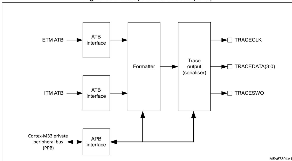
graph LR
    subgraph Inputs
        ETM[ETM ATB] --> ATB1[ATB interface]
        ITM[ITM ATB] --> ATB2[ATB interface]
    end
    ATB1 --> Formatter[Formatter]
    ATB2 --> Formatter
    PPB[Cortex-M33 private peripheral bus (PPB)] <--> APB[APB interface]
    APB --> Formatter
    APB --> Serialiser[Trace output (serialiser)]
    Formatter --> Serialiser
    Serialiser --> TRACECLK[TRACECLK]
    Serialiser --> TRACEDATA[TRACEDATA(3:0)]
    Serialiser --> TRACESWO[TRACESWO]
Trace data can also be output on the serial-wire output, TRACESWO.
For more information on the trace port interface in the Cortex®-M33, refer to the Arm® Cortex®-M33 Technical Reference Manual [5].
59.10.1 TPIU registers
TPIU supported port size register (TPIU_SSPSR)
Address offset: 0x000
Reset value: 0x0000 000F
| 31 | 30 | 29 | 28 | 27 | 26 | 25 | 24 | 23 | 22 | 21 | 20 | 19 | 18 | 17 | 16 |
|---|---|---|---|---|---|---|---|---|---|---|---|---|---|---|---|
| PORTSIZE[31:16] | |||||||||||||||
| r | r | r | r | r | r | r | r | r | r | r | r | r | r | r | r |
| 15 | 14 | 13 | 12 | 11 | 10 | 9 | 8 | 7 | 6 | 5 | 4 | 3 | 2 | 1 | 0 |
| PORTSIZE[15:0] | |||||||||||||||
| r | r | r | r | r | r | r | r | r | r | r | r | r | r | r | r |
Bits 31:0 PORTSIZE[31:0] : trace port sizes, from 1 to 32 pins
Bit n-1 when set, indicates that port size n is supported.
0x0000 000F: port sizes 1 to 4 supported
TPIU current port size register (TPIU_CSPSR)
Address offset: 0x004
Reset value: 0x0000 0001
| 31 | 30 | 29 | 28 | 27 | 26 | 25 | 24 | 23 | 22 | 21 | 20 | 19 | 18 | 17 | 16 |
|---|---|---|---|---|---|---|---|---|---|---|---|---|---|---|---|
| PORTSIZE[31:16] | |||||||||||||||
| r | r | r | r | r | r | r | r | r | r | r | r | r | r | r | r |
| 15 | 14 | 13 | 12 | 11 | 10 | 9 | 8 | 7 | 6 | 5 | 4 | 3 | 2 | 1 | 0 |
| PORTSIZE[15:0] | |||||||||||||||
| r | r | r | r | r | r | r | r | r | r | r | r | r | r | r | r |
Bits 31:0 PORTSIZE[31:0] : current trace port size
Bit n-1 when set, indicates that the current port size is n pins. The value of n must be within the range of supported port sizes (1-4). Only one bit can be set, or unpredictable behavior may result.
This register must only be modified when the formatter is stopped.
TPIU asynchronous clock prescaler register (TPIU_ACPR)
Address offset: 0x010
Reset value: 0x0000 0000
| 31 | 30 | 29 | 28 | 27 | 26 | 25 | 24 | 23 | 22 | 21 | 20 | 19 | 18 | 17 | 16 |
|---|---|---|---|---|---|---|---|---|---|---|---|---|---|---|---|
| Res. | Res. | Res. | Res. | Res. | Res. | Res. | Res. | Res. | Res. | Res. | Res. | Res. | Res. | Res. | Res. |
| 15 | 14 | 13 | 12 | 11 | 10 | 9 | 8 | 7 | 6 | 5 | 4 | 3 | 2 | 1 | 0 |
| Res. | Res. | Res. | PRESCALER[12:0] | ||||||||||||
| rw | rw | rw | rw | rw | rw | rw | rw | rw | rw | rw | rw | rw | |||
Bits 31:13 Reserved, must be kept at reset value.
Bits 12:0 PRESCALER[12:0] : baud rate for the asynchronous output, TRACESWO
The baud rate is given by the TRACECLKIN frequency divided by (PRESCALER + 1).
TPIU selected pin protocol register (TPIU_SPPR)
Address offset: 0x0F0
Reset value: 0x0000 0001
| 31 | 30 | 29 | 28 | 27 | 26 | 25 | 24 | 23 | 22 | 21 | 20 | 19 | 18 | 17 | 16 |
|---|---|---|---|---|---|---|---|---|---|---|---|---|---|---|---|
| Res. | Res. | Res. | Res. | Res. | Res. | Res. | Res. | Res. | Res. | Res. | Res. | Res. | Res. | Res. | Res. |
| 15 | 14 | 13 | 12 | 11 | 10 | 9 | 8 | 7 | 6 | 5 | 4 | 3 | 2 | 1 | 0 |
| Res. | Res. | Res. | Res. | Res. | Res. | Res. | Res. | Res. | Res. | Res. | Res. | Res. | Res. | TXMODE[1:0] | |
| rw | rw | ||||||||||||||
Bits 31:2 Reserved, must be kept at reset value.
Bits 1:0 TXMODE[1:0] : protocol used for trace output
0x0: parallel trace port mode
0x1: asynchronous SWO using Manchester encoding
0x2: asynchronous SWO using NRZ encoding
0x3: reserved
TPIU formatter and flush status register (TPIU_FFSR)
Address offset: 0x300
Reset value: 0x0000 0008
| 31 | 30 | 29 | 28 | 27 | 26 | 25 | 24 | 23 | 22 | 21 | 20 | 19 | 18 | 17 | 16 |
|---|---|---|---|---|---|---|---|---|---|---|---|---|---|---|---|
| Res. | Res. | Res. | Res. | Res. | Res. | Res. | Res. | Res. | Res. | Res. | Res. | Res. | Res. | Res. | Res. |
| 15 | 14 | 13 | 12 | 11 | 10 | 9 | 8 | 7 | 6 | 5 | 4 | 3 | 2 | 1 | 0 |
| Res. | Res. | Res. | Res. | Res. | Res. | Res. | Res. | Res. | Res. | Res. | Res. | FTNONSTOP | TCPRESENT | FTSTOPPED | FLINPROG |
| 1 | 1 | 1 | 1 |
Bits 31:4 Reserved, must be kept at reset value.
Bit 3 FTNONSTOP : formatter stop
Indicates whether formatter can be stopped or not.
1: The formatter cannot be stopped.
Bit 2 TCPRESENT : TRACECTL output pin availability
Indicates whether the optional TRACECTL output pin is available for use.
0: TRACECTL pin is not present in this device.
Bit 1 FTSTOPPED : formatter stop
The formatter has received a stop request signal and all trace data and post-amble is sent.
Any additional trace data on the ATB interface is ignored.
0: The formatter has not stopped.
Bit 0 FLINPROG : flush in progress
Indicates whether a flush on the ATB slave port is in progress. This bit reflects the status of the AFVALIDS output. A flush can be initiated by the flush control bits in the TPIU_FFCR register.
0: no flush in progress
1: flush in progress
TPIU formatter and flush control register (TPIU_FFCR)
Address offset: 0x304
Reset value: 0x0000 0102
| 31 | 30 | 29 | 28 | 27 | 26 | 25 | 24 | 23 | 22 | 21 | 20 | 19 | 18 | 17 | 16 |
|---|---|---|---|---|---|---|---|---|---|---|---|---|---|---|---|
| Res. | Res. | Res. | Res. | Res. | Res. | Res. | Res. | Res. | Res. | Res. | Res. | Res. | Res. | Res. | Res. |
| 15 | 14 | 13 | 12 | 11 | 10 | 9 | 8 | 7 | 6 | 5 | 4 | 3 | 2 | 1 | 0 |
| Res. | Res. | Res. | Res. | Res. | Res. | Res. | TRIGIN | Res. | FONMAN | Res. | Res. | Res. | Res. | ENFCONT | Res. |
| r | rw | rw |
Bits 31:9 Reserved, must be kept at reset value.
Bit 8 TRIGIN : trigger on trigger in
1: Indicates a trigger in the trace stream when the TRIGIN input is asserted.
Bit 7 Reserved, must be kept at reset value.
Bit 6 FONMAN : flush on manual
0: flush completed
1: Generates a flush.
Bits 5:2 Reserved, must be kept at reset value.
Bit 1 ENFCONT : continuous formatting enable
Setting this bit to zero in SWO mode bypasses the formatter and only ITM/DWT trace is output, ETM trace is discarded.
0: continuous formatting disabled
1: continuous formatting enabled
Bit 0 Reserved, must be kept at reset value.
TPIU periodic synchronization counter register (TPIU_PSCR)
Address offset: 0x308
Reset value: 0x0000 0000
| 31 | 30 | 29 | 28 | 27 | 26 | 25 | 24 | 23 | 22 | 21 | 20 | 19 | 18 | 17 | 16 |
|---|---|---|---|---|---|---|---|---|---|---|---|---|---|---|---|
| Res. | Res. | Res. | Res. | Res. | Res. | Res. | Res. | Res. | Res. | Res. | Res. | Res. | Res. | Res. | Res. |
| 15 | 14 | 13 | 12 | 11 | 10 | 9 | 8 | 7 | 6 | 5 | 4 | 3 | 2 | 1 | 0 |
| Res. | Res. | Res. | PSCOUNT[12:0] | ||||||||||||
| rw | rw | rw | rw | rw | rw | rw | rw | rw | rw | rw | rw | rw | |||
Bits 31:13 Reserved, must be kept at reset value.
Bits 12:0 PSCOUNT[12:0] : formatter frames counter
Enables effective use of different sized TPAs without wasting large amounts of the storage capacity of the capture device. This counter contains the number of formatter frames since the last synchronization packet of 128 bits. It is a 12-bit counter with a maximum count value of 4096. This equates to synchronization every 65536 bytes, that is, 4096 packets x 16 bytes per packet. The default is set up for a synchronization packet every 1024 bytes, that is, every 64 formatter frames. If the formatter is configured for continuous mode, full and half-word synchronization frames are inserted during normal operation. Under these circumstances, the count value is the maximum number of complete frames between full synchronization packets.
TPIU claim tag set register (TPIU_CLAIMSETR)
Address offset: 0xFA0
Reset value: 0x0000 000F
| 31 | 30 | 29 | 28 | 27 | 26 | 25 | 24 | 23 | 22 | 21 | 20 | 19 | 18 | 17 | 16 |
|---|---|---|---|---|---|---|---|---|---|---|---|---|---|---|---|
| Res. | Res. | Res. | Res. | Res. | Res. | Res. | Res. | Res. | Res. | Res. | Res. | Res. | Res. | Res. | Res. |
| 15 | 14 | 13 | 12 | 11 | 10 | 9 | 8 | 7 | 6 | 5 | 4 | 3 | 2 | 1 | 0 |
| Res. | Res. | Res. | Res. | Res. | Res. | Res. | Res. | Res. | Res. | Res. | Res. | CLAIMSET[3:0] | |||
| rw | rw | rw | rw | ||||||||||||
Bits 31:4 Reserved, must be kept at reset value.
Bits 3:0
CLAIMSET[3:0]
: claim tag bits setting
Write:
0000: no effect
xxx1: Sets bit 0.
xx1x: Sets bit 1.
x1xx: Sets bit 2.
1xxx: Sets bit 3.
Read:
0xF: Indicates there are four bits in claim tag.
TPIU claim tag clear register (TPIU_CLAIMCLR)
Address offset: 0xFA4
Reset value: 0x0000 0000
| 31 | 30 | 29 | 28 | 27 | 26 | 25 | 24 | 23 | 22 | 21 | 20 | 19 | 18 | 17 | 16 |
|---|---|---|---|---|---|---|---|---|---|---|---|---|---|---|---|
| Res. | Res. | Res. | Res. | Res. | Res. | Res. | Res. | Res. | Res. | Res. | Res. | Res. | Res. | Res. | Res. |
| 15 | 14 | 13 | 12 | 11 | 10 | 9 | 8 | 7 | 6 | 5 | 4 | 3 | 2 | 1 | 0 |
| Res. | Res. | Res. | Res. | Res. | Res. | Res. | Res. | Res. | Res. | Res. | Res. | CLAIMCLR[3:0] | |||
| rw | rw | rw | rw | ||||||||||||
Bits 31:4 Reserved, must be kept at reset value.
Bits 3:0
CLAIMCLR[3:0]
: claim tag bits reset
Write:
0000: no effect
xxx1: Clears bit 0.
xx1x: Clears bit 1.
x1xx: Clears bit 2.
1xxx: Clears bit 3.
Read: Returns current value of claim tag.
TPIU device configuration register (TPIU_DEVIDR)
Address offset: 0xFC8
Reset value: 0x0000 0CA1
| 31 | 30 | 29 | 28 | 27 | 26 | 25 | 24 | 23 | 22 | 21 | 20 | 19 | 18 | 17 | 16 |
|---|---|---|---|---|---|---|---|---|---|---|---|---|---|---|---|
| Res. | Res. | Res. | Res. | Res. | Res. | Res. | Res. | Res. | Res. | Res. | Res. | Res. | Res. | Res. | Res. |
| 15 | 14 | 13 | 12 | 11 | 10 | 9 | 8 | 7 | 6 | 5 | 4 | 3 | 2 | 1 | 0 |
| Res. | Res. | Res. | Res. | SWOUARTNRZ | SWOMAN | TCLKDATA | FIFOSIZE[2:0] | CLKRELAT | MAXNUM[4:0] | ||||||
| r | r | r | r | r | r | r | r | r | r | r | r | ||||
Bits 31:12 Reserved, must be kept at reset value.
Bit 11 SWOUARTNRZ : Serial-wire output, NRZ support
0x1: supported
Bit 10 SWOMAN : Serial-wire output, Manchester encoded format, support
0x1: supported
Bit 9 TCLKDATA : trace clock plus data support
0x0: supported
Bits 8:6 FIFOSIZE[2:0] : FIFO size in powers of 2
0x2: FIFO size = 4 bytes
Bit 5 CLKRELAT : ATB clock and TRACECLKIN relationship (synchronous or asynchronous)
0x1: asynchronous
Bits 4:0 MAXNUM[4:0] : number/type of ATB input port multiplexing
0x1: two input ports
TPIU device type identifier register (TPIU_DEVTYPE)
Address offset: 0xFCC
Reset value: 0x0000 0011
| 31 | 30 | 29 | 28 | 27 | 26 | 25 | 24 | 23 | 22 | 21 | 20 | 19 | 18 | 17 | 16 |
|---|---|---|---|---|---|---|---|---|---|---|---|---|---|---|---|
| Res. | Res. | Res. | Res. | Res. | Res. | Res. | Res. | Res. | Res. | Res. | Res. | Res. | Res. | Res. | Res. |
| 15 | 14 | 13 | 12 | 11 | 10 | 9 | 8 | 7 | 6 | 5 | 4 | 3 | 2 | 1 | 0 |
| Res. | Res. | Res. | Res. | Res. | Res. | Res. | Res. | SUBTYPE[3:0] | MAJORTYPE[3:0] | ||||||
| r | r | r | r | r | r | r | r | ||||||||
Bits 31:8 Reserved, must be kept at reset value.
Bits 7:4 SUBTYPE[3:0] : sub-classification
0x1: trace port component
Bits 3:0 MAJORTYPE[3:0] : major classification
0x1: trace sink component
TPIU CoreSight peripheral identity register 4 (TPIU_PIDR4)
Address offset: 0xFD0
Reset value: 0x0000 0004
| 31 | 30 | 29 | 28 | 27 | 26 | 25 | 24 | 23 | 22 | 21 | 20 | 19 | 18 | 17 | 16 |
|---|---|---|---|---|---|---|---|---|---|---|---|---|---|---|---|
| Res. | Res. | Res. | Res. | Res. | Res. | Res. | Res. | Res. | Res. | Res. | Res. | Res. | Res. | Res. | Res. |
| 15 | 14 | 13 | 12 | 11 | 10 | 9 | 8 | 7 | 6 | 5 | 4 | 3 | 2 | 1 | 0 |
| Res. | Res. | Res. | Res. | Res. | Res. | Res. | Res. | SIZE[3:0] | JEP106CON[3:0] | ||||||
| r | r | r | r | r | r | r | r | ||||||||
Bits 31:8 Reserved, must be kept at reset value.
Bits 7:4 SIZE[3:0] : register file size
0x0: The register file occupies a single 4-Kbyte region.
Bits 3:0 JEP106CON[3:0] : JEP106 continuation code
0x4: Arm® JEDEC code
TPIU CoreSight peripheral identity register 0 (TPIU_PIDR0)
Address offset: 0xFE0
Reset value: 0x0000 0021
| 31 | 30 | 29 | 28 | 27 | 26 | 25 | 24 | 23 | 22 | 21 | 20 | 19 | 18 | 17 | 16 |
|---|---|---|---|---|---|---|---|---|---|---|---|---|---|---|---|
| Res. | Res. | Res. | Res. | Res. | Res. | Res. | Res. | Res. | Res. | Res. | Res. | Res. | Res. | Res. | Res. |
| 15 | 14 | 13 | 12 | 11 | 10 | 9 | 8 | 7 | 6 | 5 | 4 | 3 | 2 | 1 | 0 |
| Res. | Res. | Res. | Res. | Res. | Res. | Res. | Res. | PARTNUM[7:0] | |||||||
| r | r | r | r | r | r | r | r | ||||||||
Bits 31:8 Reserved, must be kept at reset value.
Bits 7:0 PARTNUM[7:0] : part number bits [7:0]
0x21: TPIU part number
TPIU CoreSight peripheral identity register 1 (TPIU_PIDR1)
Address offset: 0xFE4
Reset value: 0x0000 00BD
| 31 | 30 | 29 | 28 | 27 | 26 | 25 | 24 | 23 | 22 | 21 | 20 | 19 | 18 | 17 | 16 |
|---|---|---|---|---|---|---|---|---|---|---|---|---|---|---|---|
| Res. | Res. | Res. | Res. | Res. | Res. | Res. | Res. | Res. | Res. | Res. | Res. | Res. | Res. | Res. | Res. |
| 15 | 14 | 13 | 12 | 11 | 10 | 9 | 8 | 7 | 6 | 5 | 4 | 3 | 2 | 1 | 0 |
| Res. | Res. | Res. | Res. | Res. | Res. | Res. | Res. | JEP106ID[3:0] | PARTNUM[11:8] | ||||||
| r | r | r | r | r | r | r | r | ||||||||
Bits 31:8 Reserved, must be kept at reset value.
Bits 7:4 JEP106ID[3:0] : JEP106 identity code bits [3:0]
0xB: Arm® JEDEC code
Bits 3:0 PARTNUM[11:8] : part number bits [11:8]
0xD: TPIU part number
TPIU CoreSight peripheral identity register 2 (TPIU_PIDR2)
Address offset: 0xFE8
Reset value: 0x0000 000B
| 31 | 30 | 29 | 28 | 27 | 26 | 25 | 24 | 23 | 22 | 21 | 20 | 19 | 18 | 17 | 16 |
|---|---|---|---|---|---|---|---|---|---|---|---|---|---|---|---|
| Res. | Res. | Res. | Res. | Res. | Res. | Res. | Res. | Res. | Res. | Res. | Res. | Res. | Res. | Res. | Res. |
| 15 | 14 | 13 | 12 | 11 | 10 | 9 | 8 | 7 | 6 | 5 | 4 | 3 | 2 | 1 | 0 |
| Res. | Res. | Res. | Res. | Res. | Res. | Res. | Res. | REVISION[3:0] | JEDEC | JEP106ID[6:4] | |||||
| r | r | r | r | r | r | r | r | ||||||||
Bits 31:8 Reserved, must be kept at reset value.
Bits 7:4 REVISION[3:0] : component revision number
0x0: r0p0
Bit 3 JEDEC : JEDEC assigned value
0x1: designer identification specified by JEDEC
Bits 2:0 JEP106ID[6:4] : JEP106 identity code bits [6:4]
0x3: Arm® JEDEC code
TPIU CoreSight peripheral identity register 3 (TPIU_PIDR3)
Address offset: 0xFEC
Reset value: 0x0000 0000
| 31 | 30 | 29 | 28 | 27 | 26 | 25 | 24 | 23 | 22 | 21 | 20 | 19 | 18 | 17 | 16 |
|---|---|---|---|---|---|---|---|---|---|---|---|---|---|---|---|
| Res. | Res. | Res. | Res. | Res. | Res. | Res. | Res. | Res. | Res. | Res. | Res. | Res. | Res. | Res. | Res. |
| 15 | 14 | 13 | 12 | 11 | 10 | 9 | 8 | 7 | 6 | 5 | 4 | 3 | 2 | 1 | 0 |
| Res. | Res. | Res. | Res. | Res. | Res. | Res. | Res. | REVAND[3:0] | CMOD[3:0] | ||||||
| r | r | r | r | r | r | r | r | ||||||||
Bits 31:8 Reserved, must be kept at reset value.
Bits 7:4 REVAND[3:0] : metal fix version
0x0: no metal fix
Bits 3:0 CMOD[3:0] : customer modified
0x0: no customer modifications
TPIU CoreSight component identity register 0 (TPIU_CIDR0)
Address offset: 0xFF0
Reset value: 0x0000 000D
| 31 | 30 | 29 | 28 | 27 | 26 | 25 | 24 | 23 | 22 | 21 | 20 | 19 | 18 | 17 | 16 |
|---|---|---|---|---|---|---|---|---|---|---|---|---|---|---|---|
| Res. | Res. | Res. | Res. | Res. | Res. | Res. | Res. | Res. | Res. | Res. | Res. | Res. | Res. | Res. | Res. |
| 15 | 14 | 13 | 12 | 11 | 10 | 9 | 8 | 7 | 6 | 5 | 4 | 3 | 2 | 1 | 0 |
| Res. | Res. | Res. | Res. | Res. | Res. | Res. | Res. | PREAMBLE[7:0] | |||||||
| r | r | r | r | r | r | r | r | ||||||||
Bits 31:8 Reserved, must be kept at reset value.
Bits 7:0 PREAMBLE[7:0] : component identification bits [7:0]
0x0D: common identification value
TPIU CoreSight peripheral identity register 1 (TPIU_CIDR1)
Address offset: 0xFF4
Reset value: 0x0000 0090
| 31 | 30 | 29 | 28 | 27 | 26 | 25 | 24 | 23 | 22 | 21 | 20 | 19 | 18 | 17 | 16 |
|---|---|---|---|---|---|---|---|---|---|---|---|---|---|---|---|
| Res. | Res. | Res. | Res. | Res. | Res. | Res. | Res. | Res. | Res. | Res. | Res. | Res. | Res. | Res. | Res. |
| 15 | 14 | 13 | 12 | 11 | 10 | 9 | 8 | 7 | 6 | 5 | 4 | 3 | 2 | 1 | 0 |
| Res. | Res. | Res. | Res. | Res. | Res. | Res. | Res. | CLASS[3:0] | PREAMBLE[11:8] | ||||||
| r | r | r | r | r | r | r | r | ||||||||
Bits 31:8 Reserved, must be kept at reset value.
Bits 7:4 CLASS[3:0] : component ID bits [15:12] - component class
0x9: CoreSight™ component
Bits 3:0 PREAMBLE[11:8] : component identification bits [11:8]
0x0: common identification value
TPIU CoreSight component identity register 2 (TPIU_CIDR2)
Address offset: 0xFF8
Reset value: 0x0000 0005
| 31 | 30 | 29 | 28 | 27 | 26 | 25 | 24 | 23 | 22 | 21 | 20 | 19 | 18 | 17 | 16 |
|---|---|---|---|---|---|---|---|---|---|---|---|---|---|---|---|
| Res. | Res. | Res. | Res. | Res. | Res. | Res. | Res. | Res. | Res. | Res. | Res. | Res. | Res. | Res. | Res. |
| 15 | 14 | 13 | 12 | 11 | 10 | 9 | 8 | 7 | 6 | 5 | 4 | 3 | 2 | 1 | 0 |
| Res. | Res. | Res. | Res. | Res. | Res. | Res. | Res. | PREAMBLE[19:12] | |||||||
| r | r | r | r | r | r | r | r | ||||||||
Bits 31:8 Reserved, must be kept at reset value.
Bits 7:0
PREAMBLE[19:12]
: component identification bits [23:16]
0x05: common identification value
TPIU CoreSight component identity register 3 (TPIU_CIDR3)
Address offset: 0xFFC
Reset value: 0x0000 00B1
| 31 | 30 | 29 | 28 | 27 | 26 | 25 | 24 | 23 | 22 | 21 | 20 | 19 | 18 | 17 | 16 |
|---|---|---|---|---|---|---|---|---|---|---|---|---|---|---|---|
| Res. | Res. | Res. | Res. | Res. | Res. | Res. | Res. | Res. | Res. | Res. | Res. | Res. | Res. | Res. | Res. |
| 15 | 14 | 13 | 12 | 11 | 10 | 9 | 8 | 7 | 6 | 5 | 4 | 3 | 2 | 1 | 0 |
| Res. | Res. | Res. | Res. | Res. | Res. | Res. | Res. | PREAMBLE[27:20] | |||||||
| r | r | r | r | r | r | r | r | ||||||||
Bits 31:8 Reserved, must be kept at reset value.
Bits 7:0
PREAMBLE[27:20]
: component identification bits [31:24]
0xB1: common identification value
59.10.2 TPIU register map
Table 735. TPIU register map and reset values
| Offset | Register name | 31 | 30 | 29 | 28 | 27 | 26 | 25 | 24 | 23 | 22 | 21 | 20 | 19 | 18 | 17 | 16 | 15 | 14 | 13 | 12 | 11 | 10 | 9 | 8 | 7 | 6 | 5 | 4 | 3 | 2 | 1 | 0 |
|---|---|---|---|---|---|---|---|---|---|---|---|---|---|---|---|---|---|---|---|---|---|---|---|---|---|---|---|---|---|---|---|---|---|
| 0x000 | TPIU_SSPSR | PORTSIZE[31:0] | |||||||||||||||||||||||||||||||
| Reset value | 0 | 0 | 0 | 0 | 0 | 0 | 0 | 0 | 0 | 0 | 0 | 0 | 0 | 0 | 0 | 0 | 0 | 0 | 0 | 0 | 0 | 0 | 0 | 0 | 0 | 0 | 0 | 0 | 0 | 1 | 1 | 1 | 1 |
| 0x004 | TPIU_CSPSR | PORTSIZE[31:0] | |||||||||||||||||||||||||||||||
| Reset value | 0 | 0 | 0 | 0 | 0 | 0 | 0 | 0 | 0 | 0 | 0 | 0 | 0 | 0 | 0 | 0 | 0 | 0 | 0 | 0 | 0 | 0 | 0 | 0 | 0 | 0 | 0 | 0 | 0 | 0 | 0 | 1 | |
| 0x008 | Reserved | ||||||||||||||||||||||||||||||||
| 0x010 | TPIU_ACPR | Res. | Res. | Res. | Res. | Res. | Res. | Res. | Res. | Res. | Res. | Res. | Res. | Res. | Res. | Res. | Res. | Res. | Res. | Res. | PRESCALER[12:0] | ||||||||||||
| Reset value | 0 | 0 | 0 | 0 | 0 | 0 | 0 | 0 | 0 | 0 | 0 | 0 | 0 | ||||||||||||||||||||
| 0x014 to 0x0EC | Reserved | ||||||||||||||||||||||||||||||||
| 0x0F0 | TPIU_SPPR | Res. | Res. | Res. | Res. | Res. | Res. | Res. | Res. | Res. | Res. | Res. | Res. | Res. | Res. | Res. | Res. | Res. | Res. | Res. | Res. | Res. | Res. | Res. | Res. | Res. | Res. | Res. | Res. | Res. | Res. | TXMODE [1:0] | |
| Reset value | 0 | 1 | |||||||||||||||||||||||||||||||
| 0x0F4 to 0x2FC | Reserved | ||||||||||||||||||||||||||||||||
| 0x300 | TPIU_FFSR | Res. | Res. | Res. | Res. | Res. | Res. | Res. | Res. | Res. | Res. | Res. | Res. | Res. | Res. | Res. | Res. | Res. | Res. | Res. | Res. | Res. | Res. | Res. | Res. | Res. | Res. | Res. | Res. | FTNONSTOP | TCPRESENT | FTSTOPPED | FLINPROG |
| Reset value | 1 | 0 | 0 | 0 | |||||||||||||||||||||||||||||
| 0x304 | TPIU_FFCR | Res. | Res. | Res. | Res. | Res. | Res. | Res. | Res. | Res. | Res. | Res. | Res. | Res. | Res. | Res. | Res. | Res. | Res. | Res. | Res. | Res. | Res. | Res. | Res. | Res. | Res. | Res. | Res. | TRIGIN | FONMAN | ENFCONT | Res. |
| Reset value | 1 | 0 | 1 | ||||||||||||||||||||||||||||||
Table 735. TPIU register map and reset values (continued)
| Offset | Register name | 31 | 30 | 29 | 28 | 27 | 26 | 25 | 24 | 23 | 22 | 21 | 20 | 19 | 18 | 17 | 16 | 15 | 14 | 13 | 12 | 11 | 10 | 9 | 8 | 7 | 6 | 5 | 4 | 3 | 2 | 1 | 0 | |
|---|---|---|---|---|---|---|---|---|---|---|---|---|---|---|---|---|---|---|---|---|---|---|---|---|---|---|---|---|---|---|---|---|---|---|
| 0x308 | TPIU_PSCR | Res. | Res. | Res. | Res. | Res. | Res. | Res. | Res. | Res. | Res. | Res. | Res. | Res. | Res. | Res. | Res. | Res. | Res. | Res. | PSCOUNT[12:0] | |||||||||||||
| Reset value | 0 | 0 | 0 | 0 | 0 | 0 | 0 | 0 | 0 | 0 | 0 | 0 | 0 | |||||||||||||||||||||
| 030C to 0xF9C | Reserved | |||||||||||||||||||||||||||||||||
| 0xFA0 | TPIU_CLAIMSETR | Res. | Res. | Res. | Res. | Res. | Res. | Res. | Res. | Res. | Res. | Res. | Res. | Res. | Res. | Res. | Res. | Res. | Res. | Res. | Res. | Res. | Res. | Res. | Res. | Res. | Res. | Res. | Res. | Res. | Res. | CLAIMSET [3:0] | ||
| Reset value | 1 | 1 | 1 | 1 | ||||||||||||||||||||||||||||||
| 0xFA4 | TPIU_CLAIMCLR | Res. | Res. | Res. | Res. | Res. | Res. | Res. | Res. | Res. | Res. | Res. | Res. | Res. | Res. | Res. | Res. | Res. | Res. | Res. | Res. | Res. | Res. | Res. | Res. | Res. | Res. | Res. | Res. | Res. | Res. | CLAIMCLR [3:0] | ||
| Reset value | 0 | 0 | 0 | 0 | ||||||||||||||||||||||||||||||
| 0FA8 to 0xFC4 | Reserved | |||||||||||||||||||||||||||||||||
| 0xFC8 | TPIU_DEVIDR | Res. | Res. | Res. | Res. | Res. | Res. | Res. | Res. | Res. | Res. | Res. | Res. | Res. | Res. | Res. | Res. | Res. | Res. | Res. | SWOUARTNRZ | SWOMAN | TCLKDATA | FIFOSIZE[2:0] | CLKRELAT | MaXNUM[4:0] | ||||||||
| Reset value | 1 | 1 | 0 | 0 | 1 | 0 | 1 | 0 | 0 | 0 | 0 | 1 | ||||||||||||||||||||||
| 0xFCC | TPIU_DEVTYPE | Res. | Res. | Res. | Res. | Res. | Res. | Res. | Res. | Res. | Res. | Res. | Res. | Res. | Res. | Res. | Res. | Res. | Res. | Res. | Res. | Res. | Res. | SUBTYPE [3:0] | MAJORTYPE [3:0] | |||||||||
| Reset value | 0 | 0 | 0 | 1 | 0 | 0 | 0 | 1 | ||||||||||||||||||||||||||
| 0xFD0 | TPIU_PIDR4 | Res. | Res. | Res. | Res. | Res. | Res. | Res. | Res. | Res. | Res. | Res. | Res. | Res. | Res. | Res. | Res. | Res. | Res. | Res. | Res. | Res. | Res. | SIZE [3:0] | JEP106CON [3:0] | |||||||||
| Reset value | 0 | 0 | 0 | 0 | 0 | 1 | 0 | 0 | ||||||||||||||||||||||||||
| 0xFE0 | TPIU_PIDR0 | Res. | Res. | Res. | Res. | Res. | Res. | Res. | Res. | Res. | Res. | Res. | Res. | Res. | Res. | Res. | Res. | Res. | Res. | Res. | Res. | Res. | Res. | PARTNUM[7:0] | ||||||||||
| Reset value | 0 | 0 | 1 | 0 | 0 | 0 | 0 | 1 | ||||||||||||||||||||||||||
| 0xFE4 | TPIU_PIDR1 | Res. | Res. | Res. | Res. | Res. | Res. | Res. | Res. | Res. | Res. | Res. | Res. | Res. | Res. | Res. | Res. | Res. | Res. | Res. | Res. | Res. | Res. | JEP106ID [3:0] | PARTNUM [11:8] | |||||||||
| Reset value | 1 | 0 | 1 | 1 | 1 | 1 | 0 | 1 | ||||||||||||||||||||||||||
| 0xFE8 | TPIU_PIDR2 | Res. | Res. | Res. | Res. | Res. | Res. | Res. | Res. | Res. | Res. | Res. | Res. | Res. | Res. | Res. | Res. | Res. | Res. | Res. | Res. | Res. | Res. | REVISION [3:0] | JEDEC [6:4] | |||||||||
| Reset value | 0 | 0 | 0 | 0 | 1 | 0 | 1 | 1 | ||||||||||||||||||||||||||
| 0xFEC | TPIU_PIDR3 | Res. | Res. | Res. | Res. | Res. | Res. | Res. | Res. | Res. | Res. | Res. | Res. | Res. | Res. | Res. | Res. | Res. | Res. | Res. | Res. | Res. | Res. | REVAND[3:0] | CMOD[3:0] | |||||||||
| Reset value | 0 | 0 | 0 | 0 | 0 | 0 | 0 | 0 | ||||||||||||||||||||||||||
| 0xFF0 | TPIU_CIDR0 | Res. | Res. | Res. | Res. | Res. | Res. | Res. | Res. | Res. | Res. | Res. | Res. | Res. | Res. | Res. | Res. | Res. | Res. | Res. | Res. | Res. | Res. | PREAMBLE[7:0] | ||||||||||
| Reset value | 0 | 0 | 0 | 0 | 1 | 1 | 0 | 1 | ||||||||||||||||||||||||||
| 0xFF4 | TPIU_CIDR1 | Res. | Res. | Res. | Res. | Res. | Res. | Res. | Res. | Res. | Res. | Res. | Res. | Res. | Res. | Res. | Res. | Res. | Res. | Res. | Res. | Res. | Res. | CLASS[3:0] | PREAMBLE [11:8] | |||||||||
| Reset value | 1 | 0 | 0 | 1 | 0 | 0 | 0 | 0 | ||||||||||||||||||||||||||
| 0xFF8 | TPIU_CIDR2 | Res. | Res. | Res. | Res. | Res. | Res. | Res. | Res. | Res. | Res. | Res. | Res. | Res. | Res. | Res. | Res. | Res. | Res. | Res. | Res. | Res. | Res. | PREAMBLE[19:12] | ||||||||||
| Reset value | 0 | 0 | 0 | 0 | 0 | 1 | 0 | 1 | ||||||||||||||||||||||||||
| 0xFFC | TPIU_CIDR3 | Res. | Res. | Res. | Res. | Res. | Res. | Res. | Res. | Res. | Res. | Res. | Res. | Res. | Res. | Res. | Res. | Res. | Res. | Res. | Res. | Res. | Res. | PREAMBLE[27:20] | ||||||||||
| Reset value | 1 | 0 | 1 | 1 | 0 | 0 | 0 | 1 | ||||||||||||||||||||||||||
Refer to Table 726: MCU ROM table for register boundary addresses.
59.11 Cross-trigger interface (CTI)
The CTI (see Figure 855 ) allows cross triggering between the processor and the ETM.
Figure 855. Embedded cross trigger
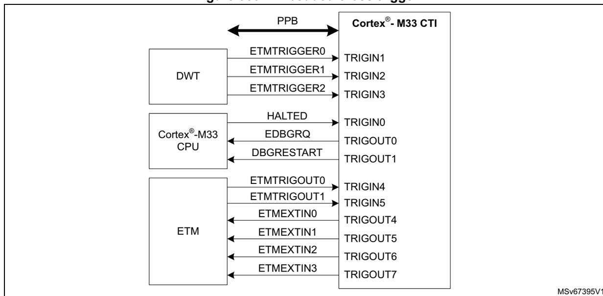
MSv67395V1
The CTI enables events from various sources to trigger debug and/or trace activity. For example, a watchpoint reached in the processor can start or stop code trace, or a trace comparator can halt the processor.
The trigger input and output signals for the CTI are listed in the tables below.
Table 736. CTI inputs
| Number | Source signal | Source component | Comments |
|---|---|---|---|
| 0 | HALTED | CPU | Processor halted - CPU is in debug mode |
| 1 | ETMTRIGGER0 | DWT | DWT comparator output 0 |
| 2 | ETMTRIGGER1 | DWT | DWT comparator output 1 |
| 3 | ETMTRIGGER2 | DWT | DWT comparator output 2 |
| 4 | ETMTRIGOUT0 | ETM | ETM event output 0 |
| 5 | ETMTRIGOUT1 | ETM | ETM event output 1 |
| 6 | - | - | Not used |
| 7 | - | - | Not used |
Table 737. CTI outputs
| Number | Source signal | Destination component | Comments |
|---|---|---|---|
| 0 | EDBGREQ | CPU | CPU halt request - Puts CPU in debug mode |
| 1 | DBGRESTART | CPU | CPU restart request - CPU exits debug mode |
Table 737. CTI outputs (continued)
| Number | Source signal | Destination component | Comments |
|---|---|---|---|
| 2 | ETMEXTIN0 | ETM | ETM event input 0 |
| 3 | ETMEXTIN1 | ETM | ETM event input 1 |
| 4 | ETMEXTIN2 | ETM | ETM event input 2 |
| 5 | ETMEXTIN3 | ETM | ETM event input 3 |
| 6 | - | - | Not used |
| 7 | - | - | Not used |
For more information on the cross-trigger interface CoreSight™ component, refer to the Arm® CoreSight™ SoC-400 Technical Reference Manual [2].
59.11.1 CTI registers
The register file base address for the CTI is 0xE004 2000.
CTI control register (CTI_CONTROLR)
Address offset: 0x000
Reset value: 0x0000 0000
| 31 | 30 | 29 | 28 | 27 | 26 | 25 | 24 | 23 | 22 | 21 | 20 | 19 | 18 | 17 | 16 |
| Res. | Res. | Res. | Res. | Res. | Res. | Res. | Res. | Res. | Res. | Res. | Res. | Res. | Res. | Res. | Res. |
| 15 | 14 | 13 | 12 | 11 | 10 | 9 | 8 | 7 | 6 | 5 | 4 | 3 | 2 | 1 | 0 |
| Res. | Res. | Res. | Res. | Res. | Res. | Res. | Res. | Res. | Res. | Res. | Res. | Res. | Res. | Res. | GLBEN rw |
Bits 31:1 Reserved, must be kept at reset value.
Bit 0 GLBEN : global CTI enable
0: disabled
1: enabled
CTI trigger acknowledge register (CTI_INTACKR)
Address offset: 0x010
Reset value: 0xXXXX XXXX
| 31 | 30 | 29 | 28 | 27 | 26 | 25 | 24 | 23 | 22 | 21 | 20 | 19 | 18 | 17 | 16 |
| Res. | Res. | Res. | Res. | Res. | Res. | Res. | Res. | Res. | Res. | Res. | Res. | Res. | Res. | Res. | Res. |
| 15 | 14 | 13 | 12 | 11 | 10 | 9 | 8 | 7 | 6 | 5 | 4 | 3 | 2 | 1 | 0 |
| Res. | Res. | Res. | Res. | Res. | Res. | Res. | Res. | INTACK[7:0] | |||||||
| w | w | w | w | w | w | w | w | ||||||||
Bits 31:8 Reserved, must be kept at reset value.
Bits 7:0 INTACK[7:0] : trigger acknowledge
There is one bit of the register for each CTITRIGOUT output. When a 1 is written to a bit in this register, the corresponding CTITRIGOUT output is acknowledged, causing it to be cleared.
CTI application trigger set register (CTI_APPSETR)
Address offset: 0x014
Reset value: 0x0000 0000
| 31 | 30 | 29 | 28 | 27 | 26 | 25 | 24 | 23 | 22 | 21 | 20 | 19 | 18 | 17 | 16 |
|---|---|---|---|---|---|---|---|---|---|---|---|---|---|---|---|
| Res. | Res. | Res. | Res. | Res. | Res. | Res. | Res. | Res. | Res. | Res. | Res. | Res. | Res. | Res. | Res. |
| 15 | 14 | 13 | 12 | 11 | 10 | 9 | 8 | 7 | 6 | 5 | 4 | 3 | 2 | 1 | 0 |
| Res. | Res. | Res. | Res. | Res. | Res. | Res. | Res. | Res. | Res. | Res. | Res. | APPSET[3:0] | |||
| rw | rw | rw | rw | ||||||||||||
Bits 31:4 Reserved, must be kept at reset value.
Bits 3:0 APPSET[3:0] : channel event setting
Read:
XXX0: channel 0 event inactive
XXX1: channel 0 event active
XX0X: channel 1 event inactive
XX1X: channel 1 event active
X0XX: channel 2 event inactive
X1XX: channel 2 event active
0XXX: channel 3 event inactive
1XXX: channel 3 event active
Write:
XXX0: no effect
XXX1: Sets event on channel 0.
XX0X: no effect
XX1X: Sets event on channel 1.
X0XX: no effect
X1XX: Sets event on channel 2.
0XXX: no effect
1XXX: Sets event on channel 3.
CTI application trigger clear register (CTI_APPCLEAR)
Address offset: 0x018
Reset value: 0x0000 0000
| 31 | 30 | 29 | 28 | 27 | 26 | 25 | 24 | 23 | 22 | 21 | 20 | 19 | 18 | 17 | 16 |
|---|---|---|---|---|---|---|---|---|---|---|---|---|---|---|---|
| Res. | Res. | Res. | Res. | Res. | Res. | Res. | Res. | Res. | Res. | Res. | Res. | Res. | Res. | Res. | Res. |
| 15 | 14 | 13 | 12 | 11 | 10 | 9 | 8 | 7 | 6 | 5 | 4 | 3 | 2 | 1 | 0 |
| Res. | Res. | Res. | Res. | Res. | Res. | Res. | Res. | Res. | Res. | Res. | Res. | APPCLEAR[3:0] | |||
| rw | rw | rw | rw | ||||||||||||
Bits 31:4 Reserved, must be kept at reset value.
Bits 3:0 APPCLEAR[3:0] : channel event clear
0000: no effect
XXX1: Clears event on channel 0.
XX1X: Clears event on channel 1.
X1XX: Clears event on channel 2.
1XXX: Clears event on channel 3.
CTI application pulse register (CTI_APPPULSER)
Address offset: 0x01C
Reset value: 0xXXXX XXXX
| 31 | 30 | 29 | 28 | 27 | 26 | 25 | 24 | 23 | 22 | 21 | 20 | 19 | 18 | 17 | 16 |
|---|---|---|---|---|---|---|---|---|---|---|---|---|---|---|---|
| Res. | Res. | Res. | Res. | Res. | Res. | Res. | Res. | Res. | Res. | Res. | Res. | Res. | Res. | Res. | Res. |
| 15 | 14 | 13 | 12 | 11 | 10 | 9 | 8 | 7 | 6 | 5 | 4 | 3 | 2 | 1 | 0 |
| Res. | Res. | Res. | Res. | Res. | Res. | Res. | Res. | Res. | Res. | Res. | Res. | APPULSE[3:0] | |||
| w | w | w | w | ||||||||||||
Bits 31:4 Reserved, must be kept at reset value.
Bits 3:0 APPULSE[3:0] : pulse channel event
This register clears itself immediately.
0000: no effect
XXX1: Generates pulse on channel 0.
XX1X: Generates pulse on channel 1.
X1XX: Generates pulse on channel 2.
1XXX: Generates pulse on channel 3.
CTI trigger input x enable register (CTI_INENxR)
Address offset: 0x020 + 0x004 * x, (x = 0 to 7)
Reset value: 0x0000 0000
| 31 | 30 | 29 | 28 | 27 | 26 | 25 | 24 | 23 | 22 | 21 | 20 | 19 | 18 | 17 | 16 |
|---|---|---|---|---|---|---|---|---|---|---|---|---|---|---|---|
| Res. | Res. | Res. | Res. | Res. | Res. | Res. | Res. | Res. | Res. | Res. | Res. | Res. | Res. | Res. | Res. |
| 15 | 14 | 13 | 12 | 11 | 10 | 9 | 8 | 7 | 6 | 5 | 4 | 3 | 2 | 1 | 0 |
| Res. | Res. | Res. | Res. | Res. | Res. | Res. | Res. | Res. | Res. | Res. | Res. | TRIGINEN[3:0] | |||
| rw | rw | rw | rw | ||||||||||||
Bits 31:4 Reserved, must be kept at reset value.
Bits 3:0 TRIGINEN[3:0] : trigger input event enable
Enables or disables a cross trigger event on each of the four channels when CTITRIGINx is activated (x = 0 to 7).
0000: Trigger does not generate events on channels.
XXX1: Trigger x generates events on channel 0.
XX1X: Trigger x generates events on channel 1.
X1XX: Trigger x generates events on channel 2.
1XXX: Trigger x generates events on channel 3.
CTI trigger output x enable register (CTI_OUTENxR)
Address offset: 0x0A0 + 0x004 * x, (x = 0 to 7)
Reset value: 0x0000 0000
| 31 | 30 | 29 | 28 | 27 | 26 | 25 | 24 | 23 | 22 | 21 | 20 | 19 | 18 | 17 | 16 |
|---|---|---|---|---|---|---|---|---|---|---|---|---|---|---|---|
| Res. | Res. | Res. | Res. | Res. | Res. | Res. | Res. | Res. | Res. | Res. | Res. | Res. | Res. | Res. | Res. |
| 15 | 14 | 13 | 12 | 11 | 10 | 9 | 8 | 7 | 6 | 5 | 4 | 3 | 2 | 1 | 0 |
| Res. | Res. | Res. | Res. | Res. | Res. | Res. | Res. | Res. | Res. | Res. | Res. | TRIGOUTEN[3:0] | |||
| rw | rw | rw | rw | ||||||||||||
Bits 31:4 Reserved, must be kept at reset value.
Bits 3:0 TRIGOUTEN[3:0] : trigger output event enable
For each channel, defines whether an event on that channel generates a trigger on CTITRIGOUTx (x = 0 to 7).
0000: Channel events do not generate triggers on trigger outputs.
XXX1: Channel 0 events generate triggers on trigger output x.
XX1X: Channel 1 events generate triggers on trigger output x.
X1XX: Channel 2 events generate triggers on trigger output x.
1XXX: Channel 3 events generate triggers on trigger output x.
CTI trigger input status register (CTI_TRGISTSR)
Address offset: 0x130
Reset value: 0x0000 0000
| 31 | 30 | 29 | 28 | 27 | 26 | 25 | 24 | 23 | 22 | 21 | 20 | 19 | 18 | 17 | 16 |
|---|---|---|---|---|---|---|---|---|---|---|---|---|---|---|---|
| Res. | Res. | Res. | Res. | Res. | Res. | Res. | Res. | Res. | Res. | Res. | Res. | Res. | Res. | Res. | Res. |
| 15 | 14 | 13 | 12 | 11 | 10 | 9 | 8 | 7 | 6 | 5 | 4 | 3 | 2 | 1 | 0 |
| Res. | Res. | Res. | Res. | Res. | Res. | Res. | Res. | TRIGINSTATUS[7:0] | |||||||
| r | r | r | r | r | r | r | r | ||||||||
Bits 31:8 Reserved, must be kept at reset value.
Bits 7:0 TRIGINSTATUS[7:0] : trigger input status
There is one bit of the register for each CTITRIGINx input. When a bit is set to 1, it indicates that the corresponding trigger input is active. When it is set to 0, the corresponding trigger input is inactive.
CTI trigger output status register (CTI_TRGOSTSR)
Address offset: 0x134
Reset value: 0x0000 0000
| 31 | 30 | 29 | 28 | 27 | 26 | 25 | 24 | 23 | 22 | 21 | 20 | 19 | 18 | 17 | 16 |
|---|---|---|---|---|---|---|---|---|---|---|---|---|---|---|---|
| Res. | Res. | Res. | Res. | Res. | Res. | Res. | Res. | Res. | Res. | Res. | Res. | Res. | Res. | Res. | Res. |
| 15 | 14 | 13 | 12 | 11 | 10 | 9 | 8 | 7 | 6 | 5 | 4 | 3 | 2 | 1 | 0 |
| Res. | Res. | Res. | Res. | Res. | Res. | Res. | Res. | TRIGOUTSTATUS[7:0] | |||||||
| r | r | r | r | r | r | r | r | ||||||||
Bits 31:8 Reserved, must be kept at reset value.
Bits 7:0 TRIGOUTSTATUS[7:0] : trigger output status
There is one bit of the register for each CTITRIGOUT output. When a bit is set to 1, it indicates that the corresponding trigger output is active. When it is set to 0, the corresponding trigger output is inactive.
CTI channel input status register (CTI_CHINSTSR)
Address offset: 0x138
Reset value: 0x0000 0000
| 31 | 30 | 29 | 28 | 27 | 26 | 25 | 24 | 23 | 22 | 21 | 20 | 19 | 18 | 17 | 16 |
|---|---|---|---|---|---|---|---|---|---|---|---|---|---|---|---|
| Res. | Res. | Res. | Res. | Res. | Res. | Res. | Res. | Res. | Res. | Res. | Res. | Res. | Res. | Res. | Res. |
| 15 | 14 | 13 | 12 | 11 | 10 | 9 | 8 | 7 | 6 | 5 | 4 | 3 | 2 | 1 | 0 |
| Res. | Res. | Res. | Res. | Res. | Res. | Res. | Res. | Res. | Res. | Res. | Res. | CHINSTATUS[3:0] | |||
| r | r | r | r | ||||||||||||
Bits 31:4 Reserved, must be kept at reset value.
Bits 3:0 CHINSTATUS[3:0] : channel input status
There is one bit of the register for each channel input. When a bit is set to 1 it indicates that the corresponding channel input is active. When it is set to 0, the corresponding channel input is inactive.
CTI channel output status register (CTI_CHOUTSTSR)
Address offset: 0x13C
Reset value: 0x0000 0000
| 31 | 30 | 29 | 28 | 27 | 26 | 25 | 24 | 23 | 22 | 21 | 20 | 19 | 18 | 17 | 16 |
|---|---|---|---|---|---|---|---|---|---|---|---|---|---|---|---|
| Res. | Res. | Res. | Res. | Res. | Res. | Res. | Res. | Res. | Res. | Res. | Res. | Res. | Res. | Res. | Res. |
| 15 | 14 | 13 | 12 | 11 | 10 | 9 | 8 | 7 | 6 | 5 | 4 | 3 | 2 | 1 | 0 |
| Res. | Res. | Res. | Res. | Res. | Res. | Res. | Res. | Res. | Res. | Res. | Res. | ||||
| CHOUTSTATUS[3:0] | |||||||||||||||
| r | r | r | r | ||||||||||||
Bits 31:4 Reserved, must be kept at reset value.
Bits 3:0 CHOUTSTATUS[3:0] : channel output status
There is one bit of the register for each channel output. When a bit is set to 1 it indicates that the corresponding channel output is active. When it is set to 0, the corresponding channel output is inactive.
CTI channel gate register (CTI_GATER)
Address offset: 0x140
Reset value: 0x0000 000F
| 31 | 30 | 29 | 28 | 27 | 26 | 25 | 24 | 23 | 22 | 21 | 20 | 19 | 18 | 17 | 16 |
|---|---|---|---|---|---|---|---|---|---|---|---|---|---|---|---|
| Res. | Res. | Res. | Res. | Res. | Res. | Res. | Res. | Res. | Res. | Res. | Res. | Res. | Res. | Res. | Res. |
| 15 | 14 | 13 | 12 | 11 | 10 | 9 | 8 | 7 | 6 | 5 | 4 | 3 | 2 | 1 | 0 |
| Res. | Res. | Res. | Res. | Res. | Res. | Res. | Res. | Res. | Res. | Res. | Res. | ||||
| GATEEN[3:0] | |||||||||||||||
| rw | rw | rw | rw | ||||||||||||
Bits 31:4 Reserved, must be kept at reset value.
Bits 3:0 GATEEN[3:0] : channel output enable
For each channel, defines whether an event on that channel can propagate over the CTM to other CTIs.
0000: Channels events do not propagate.
XXX1: Channel 0 events propagate.
XX1X: Channel 1 events propagate.
X1XX: Channel 2 events propagate.
1XXX: Channel 3 events propagate.
CTI device configuration register (CTI_DEVIDR)Address offset: 0xFC8
Reset value: 0x0004 0800
| 31 | 30 | 29 | 28 | 27 | 26 | 25 | 24 | 23 | 22 | 21 | 20 | 19 | 18 | 17 | 16 |
|---|---|---|---|---|---|---|---|---|---|---|---|---|---|---|---|
| Res. | Res. | Res. | Res. | Res. | Res. | Res. | Res. | Res. | Res. | Res. | Res. | NUMCH[3:0] | |||
| r | r | r | r | ||||||||||||
| 15 | 14 | 13 | 12 | 11 | 10 | 9 | 8 | 7 | 6 | 5 | 4 | 3 | 2 | 1 | 0 |
| NUMTRIG[7:0] | Res. | Res. | Res. | EXTMUXNUM[4:0] | |||||||||||
| r | r | r | r | r | r | r | r | r | r | r | r | r | |||
Bits 31:20 Reserved, must be kept at reset value.
Bits 19:16 NUMCH[3:0] : number of ECT channels available0x4: four channels
Bits 15:8 NUMTRIG[7:0] : number of ECT triggers available0x8: height trigger inputs and height trigger outputs
Bits 7:5 Reserved, must be kept at reset value.
Bits 4:0 EXTMUXNUM[4:0] : number of trigger input/output multiplexers0x0: none
CTI device type identifier register (CTI_DEVTYPE)Address offset: 0xFCC
Reset value: 0x0000 0014
| 31 | 30 | 29 | 28 | 27 | 26 | 25 | 24 | 23 | 22 | 21 | 20 | 19 | 18 | 17 | 16 |
|---|---|---|---|---|---|---|---|---|---|---|---|---|---|---|---|
| Res. | Res. | Res. | Res. | Res. | Res. | Res. | Res. | Res. | Res. | Res. | Res. | Res. | Res. | Res. | Res. |
| 15 | 14 | 13 | 12 | 11 | 10 | 9 | 8 | 7 | 6 | 5 | 4 | 3 | 2 | 1 | 0 |
| Res. | Res. | Res. | Res. | Res. | Res. | Res. | Res. | SUBTYPE[3:0] | MAJORTYPE[3:0] | ||||||
| r | r | r | r | r | r | r | r | ||||||||
Bits 31:8 Reserved, must be kept at reset value.
Bits 7:4 SUBTYPE[3:0] : sub-classification0x1: cross-triggering component.
Bits 3:0 MAJORTYPE[3:0] : major classification0x4: Indicates that this component allows a debugger to control other components in a CoreSight™ SoC-400 system.
CTI CoreSight peripheral identity register 4 (CTI_PIDR4)Address offset: 0xFD0
Reset value: 0x0000 0004
| 31 | 30 | 29 | 28 | 27 | 26 | 25 | 24 | 23 | 22 | 21 | 20 | 19 | 18 | 17 | 16 |
|---|---|---|---|---|---|---|---|---|---|---|---|---|---|---|---|
| Res. | Res. | Res. | Res. | Res. | Res. | Res. | Res. | Res. | Res. | Res. | Res. | Res. | Res. | Res. | Res. |
| 15 | 14 | 13 | 12 | 11 | 10 | 9 | 8 | 7 | 6 | 5 | 4 | 3 | 2 | 1 | 0 |
| Res. | Res. | Res. | Res. | Res. | Res. | Res. | Res. | SIZE[3:0] | JEP106CON[3:0] | ||||||
| r | r | r | r | r | r | r | r | ||||||||
Bits 31:8 Reserved, must be kept at reset value.
Bits 7:4 SIZE[3:0] : register file size
0x0: The register file occupies a single 4-Kbyte region.
Bits 3:0 JEP106CON[3:0] : JEP106 continuation code
0x4: Arm® JEDEC code
CTI CoreSight peripheral identity register 0 (CTI_PIDR0)
Address offset: 0xFE0
Reset value: 0x0000 0021
| 31 | 30 | 29 | 28 | 27 | 26 | 25 | 24 | 23 | 22 | 21 | 20 | 19 | 18 | 17 | 16 |
|---|---|---|---|---|---|---|---|---|---|---|---|---|---|---|---|
| Res. | Res. | Res. | Res. | Res. | Res. | Res. | Res. | Res. | Res. | Res. | Res. | Res. | Res. | Res. | Res. |
| 15 | 14 | 13 | 12 | 11 | 10 | 9 | 8 | 7 | 6 | 5 | 4 | 3 | 2 | 1 | 0 |
| Res. | Res. | Res. | Res. | Res. | Res. | Res. | Res. | PARTNUM[7:0] | |||||||
| r | r | r | r | r | r | r | r | ||||||||
Bits 31:8 Reserved, must be kept at reset value.
Bits 7:0 PARTNUM[7:0] : part number bits [7:0]
0x21: CTI part number
CTI CoreSight peripheral identity register 1 (CTI_PIDR1)
Address offset: 0xFE4
Reset value: 0x0000 00BD
| 31 | 30 | 29 | 28 | 27 | 26 | 25 | 24 | 23 | 22 | 21 | 20 | 19 | 18 | 17 | 16 |
|---|---|---|---|---|---|---|---|---|---|---|---|---|---|---|---|
| Res. | Res. | Res. | Res. | Res. | Res. | Res. | Res. | Res. | Res. | Res. | Res. | Res. | Res. | Res. | Res. |
| 15 | 14 | 13 | 12 | 11 | 10 | 9 | 8 | 7 | 6 | 5 | 4 | 3 | 2 | 1 | 0 |
| Res. | Res. | Res. | Res. | Res. | Res. | Res. | Res. | JEP106ID[3:0] | PARTNUM[11:8] | ||||||
| r | r | r | r | r | r | r | r | ||||||||
Bits 31:8 Reserved, must be kept at reset value.
Bits 7:4
JEP106ID[3:0]
: JEP106 identity code bits [3:0]
0xB: Arm® JEDEC code
Bits 3:0
PARTNUM[11:8]
: part number bits [11:8]
0xD: CTI part number
CTI CoreSight peripheral identity register 2 (CTI_PIDR2)
Address offset: 0xFE8
Reset value: 0x0000 000B
| 31 | 30 | 29 | 28 | 27 | 26 | 25 | 24 | 23 | 22 | 21 | 20 | 19 | 18 | 17 | 16 |
|---|---|---|---|---|---|---|---|---|---|---|---|---|---|---|---|
| Res. | Res. | Res. | Res. | Res. | Res. | Res. | Res. | Res. | Res. | Res. | Res. | Res. | Res. | Res. | Res. |
| 15 | 14 | 13 | 12 | 11 | 10 | 9 | 8 | 7 | 6 | 5 | 4 | 3 | 2 | 1 | 0 |
| Res. | Res. | Res. | Res. | Res. | Res. | Res. | Res. | REVISION[3:0] | JEDEC | JEP106ID[6:4] | |||||
| r | r | r | r | r | r | r | r | ||||||||
Bits 31:8 Reserved, must be kept at reset value.
Bits 7:4
REVISION[3:0]
: component revision number
0x0: r0p0
Bit 3
JEDEC
: JEDEC assigned value
0x1: designer identification specified by JEDEC
Bits 2:0
JEP106ID[6:4]
: JEP106 identity code bits [6:4]
0x3: Arm® JEDEC code
CTI CoreSight peripheral identity register 3 (CTI_PIDR3)
Address offset: 0xFEC
Reset value: 0x0000 0000
| 31 | 30 | 29 | 28 | 27 | 26 | 25 | 24 | 23 | 22 | 21 | 20 | 19 | 18 | 17 | 16 |
|---|---|---|---|---|---|---|---|---|---|---|---|---|---|---|---|
| Res. | Res. | Res. | Res. | Res. | Res. | Res. | Res. | Res. | Res. | Res. | Res. | Res. | Res. | Res. | Res. |
| 15 | 14 | 13 | 12 | 11 | 10 | 9 | 8 | 7 | 6 | 5 | 4 | 3 | 2 | 1 | 0 |
| Res. | Res. | Res. | Res. | Res. | Res. | Res. | Res. | REVAND[3:0] | CMOD[3:0] | ||||||
| r | r | r | r | r | r | r | r | ||||||||
Bits 31:8 Reserved, must be kept at reset value.
Bits 7:4
REVAND[3:0]
: metal fix version
0x0: no metal fix
Bits 3:0
CMOD[3:0]
: customer modified
0x0: no customer modifications
CTI CoreSight component identity register 0 (CTI_CIDR0)
Address offset: 0xFF0
Reset value: 0x0000 000D
| 31 | 30 | 29 | 28 | 27 | 26 | 25 | 24 | 23 | 22 | 21 | 20 | 19 | 18 | 17 | 16 |
|---|---|---|---|---|---|---|---|---|---|---|---|---|---|---|---|
| Res. | Res. | Res. | Res. | Res. | Res. | Res. | Res. | Res. | Res. | Res. | Res. | Res. | Res. | Res. | Res. |
| 15 | 14 | 13 | 12 | 11 | 10 | 9 | 8 | 7 | 6 | 5 | 4 | 3 | 2 | 1 | 0 |
| Res. | Res. | Res. | Res. | Res. | Res. | Res. | Res. | PREAMBLE[7:0] | |||||||
| r | r | r | r | r | r | r | r | ||||||||
Bits 31:8 Reserved, must be kept at reset value.
Bits 7:0 PREAMBLE[7:0] : component identification bits [7:0]
0x0D: common identification value
CTI CoreSight peripheral identity register 1 (CTI_PIDR1)
Address offset: 0xFF4
Reset value: 0x0000 0090
| 31 | 30 | 29 | 28 | 27 | 26 | 25 | 24 | 23 | 22 | 21 | 20 | 19 | 18 | 17 | 16 |
|---|---|---|---|---|---|---|---|---|---|---|---|---|---|---|---|
| Res. | Res. | Res. | Res. | Res. | Res. | Res. | Res. | Res. | Res. | Res. | Res. | Res. | Res. | Res. | Res. |
| 15 | 14 | 13 | 12 | 11 | 10 | 9 | 8 | 7 | 6 | 5 | 4 | 3 | 2 | 1 | 0 |
| Res. | Res. | Res. | Res. | Res. | Res. | Res. | Res. | CLASS[3:0] | PREAMBLE[11:8] | ||||||
| r | r | r | r | r | r | r | r | ||||||||
Bits 31:8 Reserved, must be kept at reset value.
Bits 7:4 CLASS[3:0] : component identification bits [15:12] - component class
0x9: CoreSight™ component
Bits 3:0 PREAMBLE[11:8] : component identification bits [11:8]
0x0: common identification value
CTI CoreSight component identity register 2 (CTI_CIDR2)
Address offset: 0xFF8
Reset value: 0x0000 0005
| 31 | 30 | 29 | 28 | 27 | 26 | 25 | 24 | 23 | 22 | 21 | 20 | 19 | 18 | 17 | 16 |
|---|---|---|---|---|---|---|---|---|---|---|---|---|---|---|---|
| Res. | Res. | Res. | Res. | Res. | Res. | Res. | Res. | Res. | Res. | Res. | Res. | Res. | Res. | Res. | Res. |
| 15 | 14 | 13 | 12 | 11 | 10 | 9 | 8 | 7 | 6 | 5 | 4 | 3 | 2 | 1 | 0 |
| Res. | Res. | Res. | Res. | Res. | Res. | Res. | Res. | PREAMBLE[19:12] | |||||||
| r | r | r | r | r | r | r | r | ||||||||
Bits 31:8 Reserved, must be kept at reset value.
Bits 7:0 PREAMBLE[19:12] : component identification bits [23:16]
0x05: common identification value
CTI CoreSight component identity register 3 (CTI_CIDR3)
Address offset: 0xFFC
Reset value: 0x0000 00B1
| 31 | 30 | 29 | 28 | 27 | 26 | 25 | 24 | 23 | 22 | 21 | 20 | 19 | 18 | 17 | 16 |
|---|---|---|---|---|---|---|---|---|---|---|---|---|---|---|---|
| Res. | Res. | Res. | Res. | Res. | Res. | Res. | Res. | Res. | Res. | Res. | Res. | Res. | Res. | Res. | Res. |
| 15 | 14 | 13 | 12 | 11 | 10 | 9 | 8 | 7 | 6 | 5 | 4 | 3 | 2 | 1 | 0 |
| Res. | Res. | Res. | Res. | Res. | Res. | Res. | Res. | PREAMBLE[27:20] | |||||||
| r | r | r | r | r | r | r | r | ||||||||
Bits 31:8 Reserved, must be kept at reset value.
Bits 7:0 PREAMBLE[27:20] : component identification bits [31:24]
0xB1: common identification value
59.11.2 CTI register map
Table 738. CTI register map and reset values
| Offset | Register name | 31 | 30 | 29 | 28 | 27 | 26 | 25 | 24 | 23 | 22 | 21 | 20 | 19 | 18 | 17 | 16 | 15 | 14 | 13 | 12 | 11 | 10 | 9 | 8 | 7 | 6 | 5 | 4 | 3 | 2 | 1 | 0 |
|---|---|---|---|---|---|---|---|---|---|---|---|---|---|---|---|---|---|---|---|---|---|---|---|---|---|---|---|---|---|---|---|---|---|
| 0x000 | CTI_CONTROLLER | Res. | Res. | Res. | Res. | Res. | Res. | Res. | Res. | Res. | Res. | Res. | Res. | Res. | Res. | Res. | Res. | Res. | Res. | Res. | Res. | Res. | Res. | Res. | Res. | Res. | Res. | Res. | Res. | Res. | Res. | GLBEN | |
| Reset value | 0 | ||||||||||||||||||||||||||||||||
| 0x004 to 0x00C | Reserved | ||||||||||||||||||||||||||||||||
| 0x010 | CTI_INTACKR | Res. | Res. | Res. | Res. | Res. | Res. | Res. | Res. | Res. | Res. | Res. | Res. | Res. | Res. | Res. | Res. | Res. | Res. | Res. | Res. | Res. | Res. | Res. | Res. | INTACK[7:0] | |||||||
| Reset value | X | X | X | X | X | X | X | ||||||||||||||||||||||||||
| 0x014 | CTI_APPSETR | Res. | Res. | Res. | Res. | Res. | Res. | Res. | Res. | Res. | Res. | Res. | Res. | Res. | Res. | Res. | Res. | Res. | Res. | Res. | Res. | Res. | Res. | Res. | Res. | Res. | Res. | Res. | Res. | Res. | Res. | APPSET[3:0] | |
| Reset value | 0 | 0 | 0 | 0 | |||||||||||||||||||||||||||||
| 0x018 | CTI_APPCLEAR | Res. | Res. | Res. | Res. | Res. | Res. | Res. | Res. | Res. | Res. | Res. | Res. | Res. | Res. | Res. | Res. | Res. | Res. | Res. | Res. | Res. | Res. | Res. | Res. | Res. | Res. | Res. | Res. | Res. | Res. | APPCLEAR[3:0] | |
| Reset value | 0 | 0 | 0 | 0 | |||||||||||||||||||||||||||||
Table 738. CTI register map and reset values (continued)
| Offset | Register name | 31 | 30 | 29 | 28 | 27 | 26 | 25 | 24 | 23 | 22 | 21 | 20 | 19 | 18 | 17 | 16 | 15 | 14 | 13 | 12 | 11 | 10 | 9 | 8 | 7 | 6 | 5 | 4 | 3 | 2 | 1 | 0 |
|---|---|---|---|---|---|---|---|---|---|---|---|---|---|---|---|---|---|---|---|---|---|---|---|---|---|---|---|---|---|---|---|---|---|
| 0x01C | CTI_APPPULSER | Res. | Res. | Res. | Res. | Res. | Res. | Res. | Res. | Res. | Res. | Res. | Res. | Res. | Res. | Res. | Res. | Res. | Res. | Res. | Res. | Res. | Res. | Res. | Res. | Res. | Res. | Res. | Res. | Res. | APPULSE [3:0] | ||
| Reset value | X | X | X | X | |||||||||||||||||||||||||||||
| 0x020 to 0x03C | CTI_INEN0R to CTI_INEN7R | Res. | Res. | Res. | Res. | Res. | Res. | Res. | Res. | Res. | Res. | Res. | Res. | Res. | Res. | Res. | Res. | Res. | Res. | Res. | Res. | Res. | Res. | Res. | Res. | Res. | Res. | Res. | Res. | Res. | TRIGINEN [3:0] | ||
| Reset value | 0 | 0 | 0 | 0 | |||||||||||||||||||||||||||||
| 0x040 to 0x09C | Reserved | ||||||||||||||||||||||||||||||||
| 0x0A0 to 0x0BC | CTI_OUTEN0R to CTI_OUTEN7R | Res. | Res. | Res. | Res. | Res. | Res. | Res. | Res. | Res. | Res. | Res. | Res. | Res. | Res. | Res. | Res. | Res. | Res. | Res. | Res. | Res. | Res. | Res. | Res. | Res. | Res. | Res. | Res. | Res. | TRIGOUTEN [3:0] | ||
| Reset value | 0 | 0 | 0 | 0 | |||||||||||||||||||||||||||||
| 0x0C0 to 0x12C | Reserved | ||||||||||||||||||||||||||||||||
| 0x130 | CTI_TRGISTSR | Res. | Res. | Res. | Res. | Res. | Res. | Res. | Res. | Res. | Res. | Res. | Res. | Res. | Res. | Res. | Res. | Res. | Res. | Res. | Res. | Res. | Res. | Res. | Res. | Res. | Res. | Res. | Res. | Res. | TRIGINSTATUS[7:0] | ||
| Reset value | 0 | 0 | 0 | 0 | |||||||||||||||||||||||||||||
| 0x134 | CTI_TRGOSTSR | Res. | Res. | Res. | Res. | Res. | Res. | Res. | Res. | Res. | Res. | Res. | Res. | Res. | Res. | Res. | Res. | Res. | Res. | Res. | Res. | Res. | Res. | Res. | Res. | Res. | Res. | Res. | Res. | Res. | TRIGOUTSTATUS[7:0] | ||
| Reset value | 0 | 0 | 0 | 0 | |||||||||||||||||||||||||||||
| 0x138 | CTI_CHINSTSR | Res. | Res. | Res. | Res. | Res. | Res. | Res. | Res. | Res. | Res. | Res. | Res. | Res. | Res. | Res. | Res. | Res. | Res. | Res. | Res. | Res. | Res. | Res. | Res. | Res. | Res. | Res. | Res. | Res. | CHINSTSTATUS [3:0] | ||
| Reset value | 0 | 0 | 0 | 0 | |||||||||||||||||||||||||||||
| 0x13C | CTI_CHOUTSTSR | Res. | Res. | Res. | Res. | Res. | Res. | Res. | Res. | Res. | Res. | Res. | Res. | Res. | Res. | Res. | Res. | Res. | Res. | Res. | Res. | Res. | Res. | Res. | Res. | Res. | Res. | Res. | Res. | Res. | CHOUTSTATUS[3:0] | ||
| Reset value | 0 | 0 | 0 | 0 | |||||||||||||||||||||||||||||
| 0x140 | CTI_GATER | Res. | Res. | Res. | Res. | Res. | Res. | Res. | Res. | Res. | Res. | Res. | Res. | Res. | Res. | Res. | Res. | Res. | Res. | Res. | Res. | Res. | Res. | Res. | Res. | Res. | Res. | Res. | Res. | Res. | GATEEN[3:0] | ||
| Reset value | 1 | 1 | 1 | 1 | |||||||||||||||||||||||||||||
| 0x144 to 0xFC4 | Reserved | ||||||||||||||||||||||||||||||||
| 0xFC8 | CTI_DEVIDR | Res. | Res. | Res. | Res. | Res. | Res. | Res. | Res. | Res. | Res. | Res. | Res. | Res. | Res. | Res. | Res. | Res. | Res. | Res. | Res. | Res. | Res. | Res. | Res. | Res. | Res. | Res. | Res. | Res. | NUMCH[3:0] | NUMTRIG[7:0] | EXTMUXNUM [4:0] |
| Reset value | 0 | 1 | 0 | 0 | |||||||||||||||||||||||||||||
| 0xFCC | CTI_DEVTYPE | Res. | Res. | Res. | Res. | Res. | Res. | Res. | Res. | Res. | Res. | Res. | Res. | Res. | Res. | Res. | Res. | Res. | Res. | Res. | Res. | Res. | Res. | Res. | Res. | Res. | Res. | Res. | Res. | Res. | SUB[3:0] | MAJOR[3:0] | |
| Reset value | 0 | 0 | 0 | 1 | |||||||||||||||||||||||||||||
| 0xFD0 | CTI_PIDR4 | Res. | Res. | Res. | Res. | Res. | Res. | Res. | Res. | Res. | Res. | Res. | Res. | Res. | Res. | Res. | Res. | Res. | Res. | Res. | Res. | Res. | Res. | Res. | Res. | Res. | Res. | Res. | Res. | Res. | SIZE [3:0] | JEP106CON [3:0] | |
| Reset value | 0 | 0 | 0 | 0 | |||||||||||||||||||||||||||||
| 0xFD4 to 0xFDC | Reserved | ||||||||||||||||||||||||||||||||
| 0xFEC | CTI_PIDR0 | Res. | Res. | Res. | Res. | Res. | Res. | Res. | Res. | Res. | Res. | Res. | Res. | Res. | Res. | Res. | Res. | Res. | Res. | Res. | Res. | Res. | Res. | Res. | Res. | Res. | Res. | Res. | Res. | Res. | PARTNUM[7:0] | ||
| Reset value | 0 | 0 | 0 | 1 | |||||||||||||||||||||||||||||
| 0xFE4 | CTI_PIDR1 | Res. | Res. | Res. | Res. | Res. | Res. | Res. | Res. | Res. | Res. | Res. | Res. | Res. | Res. | Res. | Res. | Res. | Res. | Res. | Res. | Res. | Res. | Res. | Res. | Res. | Res. | Res. | Res. | Res. | JEP106ID [3:0] | PARTNUM [11:8] | |
| Reset value | 1 | 0 | 1 | 1 | |||||||||||||||||||||||||||||
Table 738. CTI register map and reset values (continued)
| Offset | Register name | 31 | 30 | 29 | 28 | 27 | 26 | 25 | 24 | 23 | 22 | 21 | 20 | 19 | 18 | 17 | 16 | 15 | 14 | 13 | 12 | 11 | 10 | 9 | 8 | 7 | 6 | 5 | 4 | 3 | 2 | 1 | 0 |
|---|---|---|---|---|---|---|---|---|---|---|---|---|---|---|---|---|---|---|---|---|---|---|---|---|---|---|---|---|---|---|---|---|---|
| 0xFE8 | CTI_PIDR2 | Res | Res | Res | Res | Res | Res | Res | Res | Res | Res | Res | Res | Res | Res | Res | Res | Res | Res | Res | Res | Res | Res | Res | Res | REVISION [3:0] | JEDID | JEP106ID [6:4] | |||||
| Reset value | 0 | 0 | 0 | 0 | 1 | 0 | 1 | 1 | |||||||||||||||||||||||||
| 0xFEC | CTI_PIDR3 | Res | Res | Res | Res | Res | Res | Res | Res | Res | Res | Res | Res | Res | Res | Res | Res | Res | Res | Res | Res | Res | Res | Res | Res | REVAND[3:0] | CMOD[3:0] | ||||||
| Reset value | 0 | 0 | 0 | 0 | 0 | 0 | 0 | 0 | |||||||||||||||||||||||||
| 0xFF0 | CTI_CIDR0 | Res | Res | Res | Res | Res | Res | Res | Res | Res | Res | Res | Res | Res | Res | Res | Res | Res | Res | Res | Res | Res | Res | Res | PREAMBLE[7:0] | ||||||||
| Reset value | 0 | 0 | 0 | 0 | 1 | 1 | 0 | 1 | |||||||||||||||||||||||||
| 0xFF4 | CTI_CIDR1 | Res | Res | Res | Res | Res | Res | Res | Res | Res | Res | Res | Res | Res | Res | Res | Res | Res | Res | Res | Res | Res | Res | Res | CLASS[3:0] | PREAMBLE [11:8] | |||||||
| Reset value | 1 | 0 | 0 | 1 | 0 | 0 | 0 | 0 | |||||||||||||||||||||||||
| 0xFF8 | CTI_CIDR2 | Res | Res | Res | Res | Res | Res | Res | Res | Res | Res | Res | Res | Res | Res | Res | Res | Res | Res | Res | Res | Res | Res | Res | PREAMBLE[19:12] | ||||||||
| Reset value | 0 | 0 | 0 | 0 | 0 | 1 | 0 | 1 | |||||||||||||||||||||||||
| 0xFFC | CTI_CIDR3 | Res | Res | Res | Res | Res | Res | Res | Res | Res | Res | Res | Res | Res | Res | Res | Res | Res | Res | Res | Res | Res | Res | Res | PREAMBLE[27:20] | ||||||||
| Reset value | 1 | 0 | 1 | 1 | 0 | 0 | 0 | 1 | |||||||||||||||||||||||||
Refer to Table 727: Processor ROM table for register boundary addresses.
59.12 Microcontroller debug unit (DBGMCU)
The DBGMCU is a component containing a number of registers that control the power and clock behavior in debug mode. It allows the debugger (or the software) to:
- • Maintain the clock and power to the process cores when in low-power modes (Sleep, Stop Stop, or Standby)
- • Maintain the clock and power to the system debug and trace components when in low-power modes
- • stop the clock to certain peripherals (SMBUS timeout, watchdogs, timers, RTC) when either processor core is stopped in the debug mode
59.12.1 Device ID
The DBGMCU includes an identity code register, DBGMCU_IDCODE. This register contains the ID code for the device. Debug tools can locate this register via the CoreSight™ discovery procedure described in Section 59.5 .
59.12.2 Low-power mode emulation
When the device enters either Stop mode (clocks are stopped) or Standby mode (core power is switched off), the debugger can no longer access the debug access port and loses the connection with the device. To avoid this, the debugger (or software) can set the DBG_STANDBY and/or DBG_STOP bits in the DBGMCU configuration register (DBGMCU_CR) . These bits, when set, maintain the clock and power to the processor while the device is in the corresponding low-power mode. The processor remains in Sleep mode, and exits the low-power mode in the normal way. However, peripheral devices continue to operate, so the device behavior may not be identical to that of the actual low-power mode.
59.12.3 Peripheral clock freeze
The DBGMCU peripheral clock freeze registers allow to suspend operation of certain peripherals in debug mode. The peripherals supporting this feature are listed in Table 739 .
Table 739. Peripheral clock freeze control bits
| Bus | Control register | Peripheral | Description |
|---|---|---|---|
| APB1L | DBGMCU_APB1LFZR | I3C1 | I3C1 SCL stall timeout counter |
| I2C2 | I2C2 SMBUS timeout | ||
| I2C1 | I2C1 SMBUS timeout | ||
| IWDG | Independent watchdog | ||
| WWDG | Window watchdog | ||
| TIM14 | General purpose timer 14 | ||
| TIM13 | General purpose timer 13 | ||
| TIM12 | General purpose timer 12 | ||
| TIM7 | General purpose timer 7 | ||
| TIM6 | General purpose timer 6 | ||
| TIM5 | General purpose timer 5 | ||
| TIM4 | General purpose timer 4 | ||
| TIM3 | General purpose timer 3 | ||
| TIM2 | General purpose timer 2 | ||
| APB1H | DBGMCU_APB1HFZR | LPTIM2 | Low power timer 2 |
| APB2 | DBGMCU_APB2FZR | TIM17 | General purpose timer 17 |
| TIM16 | General purpose timer 16 | ||
| TIM15 | General purpose timer 15 | ||
| TIM8 | General purpose timer 8 | ||
| TIM1 | General purpose timer 1 | ||
| APB3 | DBGMCU_APB3FZR | RTC | Real time clock |
| LPTIM6 | Low power timer 6 | ||
| LPTIM5 | Low power timer 5 | ||
| LPTIM4 | Low power timer 4 | ||
| LPTIM3 | Low power timer 3 | ||
| LPTIM1 | Low power timer 1 | ||
| I2C4 | I2C4 SMBUS timeout | ||
| I2C3 | I2C3 SMBUS timeout | ||
| AHB1 | DBGMCU_AHB1FZR | GPDMA2 0 to 7 | General purpose DMA2 channels 0 to 7 |
| GPDMA1 0 to 7 | General purpose DMA1 channels 0 to 7 |
Each peripheral unit or DMA channel has a corresponding control bit, DBG_xxx_STOP, where xxx is the acronym of the peripheral (or DMA channel). The control bits are organized in DBGMCU_zzzFZR registers, where zzz corresponds to the name of the bus (AHB or APB). For example, DBGMCU_APB1LFZR contains the control bits for peripherals on the APB1L bus.
The control bit, when set, causes the corresponding peripheral operation to be suspended when the CPU is stopped in debug (HALTED = 1), according to the table below:
Table 740. Peripheral behaviour in debug mode
| HALTED | DBG_xxx_STOP | Peripheral behaviour |
|---|---|---|
| 0 | X | The operation continues. |
| 1 | 0 | The operation continues. |
| 1 | 1 | The operation is suspended. |
The accessibility of the bits DBG_xxx_STOP by the debugger depends on the state of the authentication signal spiden.
When spiden = 1 (secure privilege debug enabled), all bits can be modified and read by both debugger and software (secure or nonsecure).
When spiden = 0 (secure privilege debug disabled), only bits corresponding to nonsecure peripherals (or DMA channels) can be modified by the debugger or software. All bits can be read.
The status (secure or nonsecure) of a TrustZone-aware peripheral or a DMA channel, is signaled to the DBGMCU by the peripheral.
59.12.4 DBGMCU registers
The DBGMCU registers are reset only by a power-on reset.
They are accessible to the debugger via the AHB access port at base address 0xE00E 4000, and to software at base address 0x4402 4000.
DBGMCU identity code register (DBGMCU_IDCODE)
Address offset: 0x00
Reset value: 0xXXXX 6XXX
This register is always accessible.
| 31 | 30 | 29 | 28 | 27 | 26 | 25 | 24 | 23 | 22 | 21 | 20 | 19 | 18 | 17 | 16 |
| REV_ID[15:0] | |||||||||||||||
| r | r | r | r | r | r | r | r | r | r | r | r | r | r | r | r |
| 15 | 14 | 13 | 12 | 11 | 10 | 9 | 8 | 7 | 6 | 5 | 4 | 3 | 2 | 1 | 0 |
| Res. | Res. | Res. | Res. | DEV_ID[11:0] | |||||||||||
| r | r | r | r | r | r | r | r | r | r | r | r | ||||
Bits 31:16 REV_ID[15:0] : Revision
A: 0x1000
Z: 0x1001
X: 0x1007
Bits 15:12 Reserved, must be kept at reset value.
Bits 11:0 DEV_ID[11:0] : Device identification
0x484: STM32H562/563/573
0x478: STM32H523/533
DBGMCU configuration register (DBGMCU_CR)
Address offset: 0x04
Reset value: 0x0000 0000
This register is accessible to the debugger and to the CPU after successful authentication. Prior to this, debugger accesses are ignored.
| 31 | 30 | 29 | 28 | 27 | 26 | 25 | 24 | 23 | 22 | 21 | 20 | 19 | 18 | 17 | 16 |
|---|---|---|---|---|---|---|---|---|---|---|---|---|---|---|---|
| Res. | Res. | Res. | Res. | Res. | Res. | Res. | Res. | Res. | Res. | Res. | Res. | Res. | Res. | Res. | DCRT |
| rw | |||||||||||||||
| 15 | 14 | 13 | 12 | 11 | 10 | 9 | 8 | 7 | 6 | 5 | 4 | 3 | 2 | 1 | 0 |
| Res. | Res. | Res. | Res. | Res. | Res. | Res. | Res. | TRACE_MODE [1:0] | TRACE_EN | TRACE_IOEN | Res. | DBG_STANDBY | DBG_STOP | Res. | |
| rw | rw | rw | rw | rw | rw |
Bits 31:17 Reserved, must be kept at reset value.
Bit 16 DCRT : Debug credentials reset type
This bit selects which type of reset is used to revoke the debug authentication credentials
0: System reset
1: Power reset
Bits 15:8 Reserved, must be kept at reset value.
Bits 7:6 TRACE_MODE[1:0] : trace pin assignment
0x0: trace pins assigned for asynchronous mode (TRACESWO)
0x1: trace pins assigned for synchronous mode with a port width of 1 (TRACECK, TRACED0)
0x2: trace pins assigned for synchronous mode with a port width of 2 ((TRACECK, TRACED0-1)
0x3: trace pins assigned for synchronous mode with a port width of 4 ((TRACECK, TRACED0-3)
Bit 5 TRACE_EN : trace port and clock enable.
This bit enables the trace port clock, TRACECK.
0: disabled
1: enabled
Bit 4 TRACE_IOEN : trace pin enable
0: disabled - trace pins not assigned
1: enabled - trace pins assigned according to the value of TRACE_MODE field
Bit 3 Reserved, must be kept at reset value.
Bit 2 DBG_STANDBY : Allows debug in Standby mode
0: normal operation
All clocks are disabled and the core powered down automatically in Standby mode.
1: automatic clock stop/power down disabled
All active clocks and oscillators continue to run during Standby mode, and the core supply is maintained, allowing full debug capability. On exit from Standby mode, a system reset is performed.
Bit 1 DBG_STOP : Allows debug in Stop mode
0: normal operation
All clocks are disabled automatically in Stop mode.
1: automatic clock stop disabled
All active clocks and oscillators continue to run during Stop mode, allowing full debug capability. On exit from Stop mode, the clock settings are set to the Stop mode exit state.
Bit 0 Reserved, must be kept at reset value.
DBGMCU_APB1L peripheral freeze register (DBGMCU_APB1LFZR)
Address offset: 0x08
Reset value: 0x0000 0000
This register is accessible to the debugger and to the CPU after successful authentication. Prior to this, accesses are ignored.
| 31 | 30 | 29 | 28 | 27 | 26 | 25 | 24 | 23 | 22 | 21 | 20 | 19 | 18 | 17 | 16 |
|---|---|---|---|---|---|---|---|---|---|---|---|---|---|---|---|
| Res. | Res. | Res. | Res. | Res. | Res. | Res. | Res. | DBG_I3C1_STOP | DBG_I2C2_STOP | DBG_I2C1_STOP | Res. | Res. | Res. | Res. | Res. |
| rw | rw | rw | |||||||||||||
| 15 | 14 | 13 | 12 | 11 | 10 | 9 | 8 | 7 | 6 | 5 | 4 | 3 | 2 | 1 | 0 |
| Res. | Res. | Res. | DBG_IWDG_STOP | DBG_WWDG_STOP | Res. | Res. | DBG_TIM14_STOP | DBG_TIM13_STOP | DBG_TIM12_STOP | DBG_TIM7_STOP | DBG_TIM6_STOP | DBG_TIM5_STOP | DBG_TIM4_STOP | DBG_TIM3_STOP | DBG_TIM2_STOP |
| rw | rw | rw | rw | rw | rw | rw | rw | rw | rw | rw |
Bits 31:24 Reserved, must be kept at reset value.
Bit 23 DBG_I3C1_STOP : I3C1 SCL stall counter stop in debug
0: normal operation. I3C1 SCL stall timeout counter continues to operate while CPU is in debug mode.
1: stop in debug. I3C1 SCL stall timeout counter is frozen while CPU is in debug mode.
Bit 22 DBG_I2C2_STOP : I2C2 SMBUS timeout stop in debug
0: normal operation. I2C2 SMBUS timeout continues to operate while CPU is in debug mode.
1: stop in debug. I2C2 SMBUS timeout is frozen while CPU is in debug mode.
Bit 21 DBG_I2C1_STOP : I2C1 SMBUS timeout stop in debug
0: normal operation. I2C1 SMBUS timeout continues to operate while CPU is in debug mode.
1: stop in debug. I2C1 SMBUS timeout is frozen while CPU is in debug mode.
Bits 20:13 Reserved, must be kept at reset value.
Bit 12 DBG_IWDG_STOP : IWDG stop in debug
0: normal operation. IWDG continues to operate while CPU is in debug mode.
1: stop in debug. IWDG is frozen while CPU is in debug mode.
Bit 11 DBG_WWDG_STOP : WWDG stop in debug
0: normal operation. WWDG continues to operate while CPU is in debug mode.
1: stop in debug. WWDG is frozen while CPU is in debug mode.
Bits 10:9 Reserved, must be kept at reset value.
Bit 8 DBG_TIM14_STOP : TIM14 stop in debug
0: normal operation. TIM14 continues to operate while CPU is in debug mode.
1: stop in debug. TIM14 is frozen while CPU is in debug mode.
Bit 7 DBG_TIM13_STOP : TIM13 stop in debug
0: normal operation. TIM13 continues to operate while CPU is in debug mode.
1: stop in debug. TIM13 is frozen while CPU is in debug mode.
Bit 6 DBG_TIM12_STOP : TIM12 stop in debug
0: normal operation. TIM12 continues to operate while CPU is in debug mode.
1: stop in debug. TIM12 is frozen while CPU is in debug mode.
Bit 5 DBG_TIM7_STOP : TIM7 stop in debug
0: normal operation. TIM7 continues to operate while CPU is in debug mode.
1: stop in debug. TIM7 is frozen while CPU is in debug mode.
Bit 4 DBG_TIM6_STOP : TIM6 stop in debug
0: normal operation. TIM6 continues to operate while CPU is in debug mode.
1: stop in debug. TIM6 is frozen while CPU is in debug mode.
Bit 3 DBG_TIM5_STOP : TIM5 stop in debug
0: normal operation. TIM5 continues to operate while CPU is in debug mode.
1: Stop in debug. TIM5 is frozen while CPU is in debug mode.
Bit 2 DBG_TIM4_STOP : TIM4 stop in debug
0: normal operation. TIM4 continues to operate while CPU is in debug mode.
1: stop in debug. TIM4 is frozen while CPU is in debug mode.
Bit 1 DBG_TIM3_STOP : TIM3 stop in debug
0: normal operation. TIM3 continues to operate while CPU is in debug mode.
1: stop in debug. TIM3 is frozen while CPU is in debug mode.
Bit 0 DBG_TIM2_STOP : TIM2 stop in debug
0: normal operation. TIM2 continues to operate while CPU is in debug mode.
1: stop in debug. TIM2 is frozen while CPU is in debug mode.
DBGMCU APB1H peripheral freeze register (DBGMCU_APB1HFZR)
Address offset: 0x0C
Reset value: 0x0000 0000
This register is accessible to the debugger and to the CPU after successful authentication. Prior to this, accesses are ignored.
| 31 | 30 | 29 | 28 | 27 | 26 | 25 | 24 | 23 | 22 | 21 | 20 | 19 | 18 | 17 | 16 |
|---|---|---|---|---|---|---|---|---|---|---|---|---|---|---|---|
| Res. | Res. | Res. | Res. | Res. | Res. | Res. | Res. | Res. | Res. | Res. | Res. | Res. | Res. | Res. | Res. |
| 15 | 14 | 13 | 12 | 11 | 10 | 9 | 8 | 7 | 6 | 5 | 4 | 3 | 2 | 1 | 0 |
| Res. | Res. | Res. | Res. | Res. | Res. | Res. | Res. | Res. | Res. | DBG_LPTIM2_STOP | Res. | Res. | Res. | Res. | Res. |
| rw | |||||||||||||||
Bits 31:6 Reserved, must be kept at reset value.
Bit 5 DBG_LPTIM2_STOP : LPTIM2 stop in debug- 0: normal operation. LPTIM2 continues to operate while CPU is in debug mode.
- 1: stop in debug. LPTIM2 is frozen while CPU is in debug mode.
Bits 4:0 Reserved, must be kept at reset value.
DBGMCU APB2 peripheral freeze register (DBGMCU_APB2FZR)
Address offset: 0x10
Reset value: 0x0000 0000
This register is accessible to the debugger and to the CPU after successful authentication. Prior to this, accesses are ignored.
| 31 | 30 | 29 | 28 | 27 | 26 | 25 | 24 | 23 | 22 | 21 | 20 | 19 | 18 | 17 | 16 |
|---|---|---|---|---|---|---|---|---|---|---|---|---|---|---|---|
| Res. | Res. | Res. | Res. | Res. | Res. | Res. | Res. | Res. | Res. | Res. | Res. | Res. | DBG_TIM17_STOP | DBG_TIM16_STOP | DBG_TIM15_STOP |
| rw | rw | rw | |||||||||||||
| 15 | 14 | 13 | 12 | 11 | 10 | 9 | 8 | 7 | 6 | 5 | 4 | 3 | 2 | 1 | 0 |
| Res. | Res. | DBG_TIM8_STOP | Res. | DBG_TIM1_STOP | Res. | Res. | Res. | Res. | Res. | Res. | Res. | Res. | Res. | Res. | Res. |
| rw | rw |
Bits 31:19 Reserved, must be kept at reset value.
Bit 18 DBG_TIM17_STOP : TIM17 stop in debug
0: normal operation. TIM17 continues to operate while CPU is in debug mode.
1: stop in debug. TIM17 is frozen while CPU is in debug mode.
Bit 17 DBG_TIM16_STOP : TIM16 stop in debug
0: normal operation. TIM16 continues to operate while CPU is in debug mode.
1: stop in debug. TIM16 is frozen while CPU is in debug mode.
Bit 16 DBG_TIM15_STOP : TIM15 stop in debug
0: normal operation. TIM15 continues to operate while CPU is in debug mode.
1: stop in debug. TIM15 is frozen while CPU is in debug mode.
Bits 15:14 Reserved, must be kept at reset value.
Bit 13 DBG_TIM8_STOP : TIM8 stop in debug
0: normal operation. TIM8 continues to operate while CPU is in debug mode.
1: stop in debug. TIM8 is frozen while CPU is in debug mode.
Bit 12 Reserved, must be kept at reset value.
Bit 11 DBG_TIM1_STOP : TIM1 stop in debug
0: normal operation. TIM1 continues to operate while CPU is in debug mode.
1: stop in debug. TIM1 is frozen while CPU is in debug mode.
Bits 10:0 Reserved, must be kept at reset value.
DBGMCU APB3 peripheral freeze register (DBGMCU_APB3FZR)
Address offset: 0x14
Reset value: 0x0000 0000
This register is accessible to the debugger and to the CPU after successful authentication. Prior to this, accesses are ignored.
| 31 | 30 | 29 | 28 | 27 | 26 | 25 | 24 | 23 | 22 | 21 | 20 | 19 | 18 | 17 | 16 |
|---|---|---|---|---|---|---|---|---|---|---|---|---|---|---|---|
| Res. | DBG_RTC_STOP | Res. | Res. | Res. | Res. | Res. | Res. | Res. | Res. | DBG_LPTIM6_STOP | DBG_LPTIM5_STOP | DBG_LPTIM4_STOP | DBG_LPTIM3_STOP | DBG_LPTIM1_STOP | Res. |
| rw | rw | rw | rw | rw | rw | ||||||||||
| 15 | 14 | 13 | 12 | 11 | 10 | 9 | 8 | 7 | 6 | 5 | 4 | 3 | 2 | 1 | 0 |
| Res. | Res. | Res. | Res. | DBG_I2C4_STOP | DBG_I2C3_STOP | Res. | Res. | Res. | Res. | Res. | Res. | Res. | Res. | Res. | Res. |
| rw | rw |
Bit 31 Reserved, must be kept at reset value.
Bit 30 DBG_RTC_STOP : RTC stop in debug
0: normal operation. RTC continues to operate while CPU is in debug mode.
1: stop in debug. RTC is frozen while CPU is in debug mode.
Bits 29:22 Reserved, must be kept at reset value.
Bit 21 DBG_LPTIM6_STOP : LPTIM6 stop in debug
0: normal operation. LPTIM6 continues to operate while CPU is in debug mode.
1: stop in debug. LPTIM6 is frozen while CPU is in debug mode.
Bit 20 DBG_LPTIM5_STOP : LPTIM5 stop in debug
0: normal operation. LPTIM5 continues to operate while CPU is in debug mode.
1: stop in debug. LPTIM5 is frozen while CPU is in debug mode.
Bit 19 DBG_LPTIM4_STOP : LPTIM4 stop in debug
0: normal operation. LPTIM4 continues to operate while CPU is in debug mode.
1: stop in debug. LPTIM4 is frozen while CPU is in debug mode.
Bit 18 DBG_LPTIM3_STOP : LPTIM3 stop in debug
0: normal operation. LPTIM3 continues to operate while CPU is in debug mode.
1: stop in debug. LPTIM3 is frozen while CPU is in debug mode.
Bit 17 DBG_LPTIM1_STOP : LPTIM1 stop in debug
0: normal operation. LPTIM1 continues to operate while CPU is in debug mode.
1: stop in debug. LPTIM1 is frozen while CPU is in debug mode.
Bits 16:12 Reserved, must be kept at reset value.
Bit 11 DBG_I2C4_STOP : I2C4 SMBUS timeout stop in debug
0: normal operation. I2C4 SMBUS timeout counter continues to operate while CPU is in debug mode.
1: stop in debug. I2C4 SMBUS timeout counter is frozen while CPU is in debug mode.
Bit 10 DBG_I2C3_STOP : I2C3 SMBUS timeout stop in debug
0: normal operation. I2C3 SMBUS timeout counter continues to operate while CPU is in debug mode.
1: stop in debug. I2C3 SMBUS timeout counter is frozen while CPU is in debug mode.
Bits 9:0 Reserved, must be kept at reset value.
DBGMCU_AHB1 peripheral freeze register (DBGMCU_AHB1FZR)
Address offset: 0x20
Reset value: 0x0000 0000
This register is accessible to the debugger and to the CPU after successful authentication. Prior to this, accesses are ignored.
| 31 | 30 | 29 | 28 | 27 | 26 | 25 | 24 | 23 | 22 | 21 | 20 | 19 | 18 | 17 | 16 |
|---|---|---|---|---|---|---|---|---|---|---|---|---|---|---|---|
| Res. | Res. | Res. | Res. | Res. | Res. | Res. | Res. | DBG_GPDMA2_7_STOP | DBG_GPDMA2_6_STOP | DBG_GPDMA2_5_STOP | DBG_GPDMA2_4_STOP | DBG_GPDMA2_3_STOP | DBG_GPDMA2_2_STOP | DBG_GPDMA2_1_STOP | DBG_GPDMA2_0_STOP |
| r/w | r/w | r/w | r/w | r/w | r/w | r/w | r/w | ||||||||
| 15 | 14 | 13 | 12 | 11 | 10 | 9 | 8 | 7 | 6 | 5 | 4 | 3 | 2 | 1 | 0 |
| Res. | Res. | Res. | Res. | Res. | Res. | Res. | Res. | DBG_GPDMA1_7_STOP | DBG_GPDMA1_6_STOP | DBG_GPDMA1_5_STOP | DBG_GPDMA1_4_STOP | DBG_GPDMA1_3_STOP | DBG_GPDMA1_2_STOP | DBG_GPDMA1_1_STOP | DBG_GPDMA1_0_STOP |
| r/w | r/w | r/w | r/w | r/w | r/w | r/w | r/w |
Bits 31:24 Reserved, must be kept at reset value.
Bit 23 DBG_GPDMA2_7_STOP : GPDMA2 channel 7 stop in debug
0: normal operation. GPDMA2 channel 7 continues to operate while CPU is in debug mode.
1: stop in debug. GPDMA2 channel 7 is frozen while CPU is in debug mode.
Bit 22 DBG_GPDMA2_6_STOP : GPDMA2 channel 6 stop in debug
0: normal operation. GPDMA2 channel 6 continues to operate while CPU is in debug mode.
1: stop in debug. GPDMA2 channel 6 is frozen while CPU is in debug mode.
Bit 21 DBG_GPDMA2_5_STOP : GPDMA2 channel 5 stop in debug
0: normal operation. GPDMA2 channel 5 continues to operate while CPU is in debug mode.
1: stop in debug. GPDMA2 channel 5 is frozen while CPU is in debug mode.
Bit 20 DBG_GPDMA2_4_STOP : GPDMA2 channel 4 stop in debug
0: normal operation. GPDMA2 channel 4 continues to operate while CPU is in debug mode.
1: stop in debug. GPDMA2 channel 4 is frozen while CPU is in debug mode.
Bit 19 DBG_GPDMA2_3_STOP : GPDMA2 channel 3 stop in debug
0: normal operation. GPDMA2 channel 3 continues to operate while CPU is in debug mode.
1: stop in debug. GPDMA2 channel 3 is frozen while CPU is in debug mode.
Bit 18 DBG_GPDMA2_2_STOP : GPDMA2 channel 2 stop in debug
0: normal operation. GPDMA2 channel 2 continues to operate while CPU is in debug mode.
1: stop in debug. GPDMA2 channel 2 is frozen while CPU is in debug mode.
Bit 17 DBG_GPDMA2_1_STOP : GPDMA2 channel 1 stop in debug
0: normal operation. GPDMA2 channel 1 continues to operate while CPU is in debug mode.
1: stop in debug. GPDMA2 channel 1 is frozen while CPU is in debug mode.
Bit 16 DBG_GPDMA2_0_STOP : GPDMA2 channel 0 stop in debug
0: normal operation. GPDMA2 channel 0 continues to operate while CPU is in debug mode.
1: stop in debug. GPDMA2 channel 0 is frozen while CPU is in debug mode.
Bits 15:8 Reserved, must be kept at reset value.
- Bit 7
DBG_GPDMA1_7_STOP
: GPDMA1 channel 7 stop in debug
- 0: normal operation. GPDMA1 channel 7 continues to operate while CPU is in debug mode.
- 1: stop in debug. GPDMA1 channel 7 is frozen while CPU is in debug mode.
- Bit 6
DBG_GPDMA1_6_STOP
: GPDMA1 channel 6 stop in debug
- 0: normal operation. GPDMA1 channel 6 continues to operate while CPU is in debug mode.
- 1: stop in debug. GPDMA1 channel 6 is frozen while CPU is in debug mode.
- Bit 5
DBG_GPDMA1_5_STOP
: GPDMA1 channel 5 stop in debug
- 0: normal operation. GPDMA1 channel 5 continues to operate while CPU is in debug mode.
- 1: stop in debug. GPDMA1 channel 5 is frozen while CPU is in debug mode.
- Bit 4
DBG_GPDMA1_4_STOP
: GPDMA1 channel 4 stop in debug
- 0: normal operation. GPDMA1 channel 4 continues to operate while CPU is in debug mode.
- 1: stop in debug. GPDMA1 channel 4 is frozen while CPU is in debug mode.
- Bit 3
DBG_GPDMA1_3_STOP
: GPDMA1 channel 3 stop in debug
- 0: normal operation. GPDMA1 channel 3 continues to operate while CPU is in debug mode.
- 1: stop in debug. GPDMA1 channel 3 is frozen while CPU is in debug mode.
- Bit 2
DBG_GPDMA1_2_STOP
: GPDMA1 channel 2 stop in debug
- 0: normal operation. GPDMA1 channel 2 continues to operate while CPU is in debug mode.
- 1: stop in debug. GPDMA1 channel 2 is frozen while CPU is in debug mode.
- Bit 1
DBG_GPDMA1_1_STOP
: GPDMA1 channel 1 stop in debug
- 0: normal operation. GPDMA1 channel 1 continues to operate while CPU is in debug mode.
- 1: stop in debug. GPDMA1 channel 1 is frozen while CPU is in debug mode.
- Bit 0
DBG_GPDMA1_0_STOP
: GPDMA1 channel 0 stop in debug
- 0: normal operation. GPDMA1 channel 0 continues to operate while CPU is in debug mode.
- 1: stop in debug. GPDMA1 channel 0 is frozen while CPU is in debug mode.
DBGMCU status register (DBGMCU_SR)
Address offset: 0xFC
Reset value: 0x0001 XX03
This register is always accessible.
| 31 | 30 | 29 | 28 | 27 | 26 | 25 | 24 | 23 | 22 | 21 | 20 | 19 | 18 | 17 | 16 |
|---|---|---|---|---|---|---|---|---|---|---|---|---|---|---|---|
| AP_ENABLED[15:0] | |||||||||||||||
| r | r | r | r | r | r | r | r | r | r | r | r | r | r | r | r |
| 15 | 14 | 13 | 12 | 11 | 10 | 9 | 8 | 7 | 6 | 5 | 4 | 3 | 2 | 1 | 0 |
| AP_PRESENT[15:0] | |||||||||||||||
| r | r | r | r | r | r | r | r | r | r | r | r | r | r | r | r |
- Bits 31:16
AP_ENABLED[15:0]
: Bit n identifies whether access port AP n is open (can be accessed via the debug port) or locked (debug access to the AP is blocked)
- Bit n = 0: APn locked
- Bit n = 1: APn enabled
- Bits 15:0
AP_PRESENT[15:0]
: Bit n identifies whether access port AP n is present in device
- Bit n = 0: APn absent
- Bit n = 1: APn present
DBGMCU debug authentication mailbox host register (DBGMCU_DBG_AUTH_HOST)
Address offset: 0x100
Reset value: 0xXXXX XXXX
This register is read only when accessed by the CPU, writes have no effect.
This register can be written and read by an external debugger when system reset is asserted, or when access is granted during the authentication process.
| 31 | 30 | 29 | 28 | 27 | 26 | 25 | 24 | 23 | 22 | 21 | 20 | 19 | 18 | 17 | 16 |
| MESSAGE[31:16] | |||||||||||||||
| rw | rw | rw | rw | rw | rw | rw | rw | rw | rw | rw | rw | rw | rw | rw | rw |
| 15 | 14 | 13 | 12 | 11 | 10 | 9 | 8 | 7 | 6 | 5 | 4 | 3 | 2 | 1 | 0 |
| MESSAGE[15:0] | |||||||||||||||
| rw | rw | rw | rw | rw | rw | rw | rw | rw | rw | rw | rw | rw | rw | rw | rw |
Bits 31:0 MESSAGE[31:0] : Debug host to device mailbox message.
The debug host requests authentication by writing a value to this register prior to releasing the system reset. During debug authentication the debug host communicates with the device (CPU) via this register.
DBGMCU debug authentication mailbox device register (DBGMCU_DBG_AUTH_DEVICE)
Address offset: 0x104
Reset value: 0xXXXX XXXX
This register is read only when accessed via the debug port, writes have no effect.
This register can be written and read by the CPU.
| 31 | 30 | 29 | 28 | 27 | 26 | 25 | 24 | 23 | 22 | 21 | 20 | 19 | 18 | 17 | 16 |
| MESSAGE[31:16] | |||||||||||||||
| rw | rw | rw | rw | rw | rw | rw | rw | rw | rw | rw | rw | rw | rw | rw | rw |
| 15 | 14 | 13 | 12 | 11 | 10 | 9 | 8 | 7 | 6 | 5 | 4 | 3 | 2 | 1 | 0 |
| MESSAGE[15:0] | |||||||||||||||
| rw | rw | rw | rw | rw | rw | rw | rw | rw | rw | rw | rw | rw | rw | rw | rw |
Bits 31:0 MESSAGE[31:0] : Device to debug host mailbox message.
During debug authentication the device (CPU) communicates with the debug host via this register.
DBGMCU debug authentication mailbox acknowledge register (DBGMCU_DBG_AUTH_ACK)
Address offset: 0x108
Reset value: 0x0000 0000
This register is always accessible.
| 31 | 30 | 29 | 28 | 27 | 26 | 25 | 24 | 23 | 22 | 21 | 20 | 19 | 18 | 17 | 16 |
|---|---|---|---|---|---|---|---|---|---|---|---|---|---|---|---|
| Res. | Res. | Res. | Res. | Res. | Res. | Res. | Res. | Res. | Res. | Res. | Res. | Res. | Res. | Res. | Res. |
| 15 | 14 | 13 | 12 | 11 | 10 | 9 | 8 | 7 | 6 | 5 | 4 | 3 | 2 | 1 | 0 |
| Res. | Res. | Res. | Res. | Res. | Res. | Res. | Res. | Res. | Res. | Res. | Res. | Res. | Res. | DEV_ACK | HOST_ACK |
| r | r |
Bits 31:2 Reserved, must be kept at reset value.
Bit 1 DEV_ACK : Device to host acknowledge.
This bit is set by hardware when the device (CPU) writes a message in the DBGMCU_DBG_AUTH_DEVICE register. It is reset automatically when the host (debugger) reads the message.
0: DBGMCU_DBG_AUTH_DEVICE register is empty
1. DBGMCU_DBG_AUTH_DEVICE register contains an unread message
Bit 0 HOST_ACK : Host to device acknowledge.
This bit is set by hardware when the host (debugger) writes a message in the DBGMCU_DBG_AUTH_HOST register. It is reset automatically when the device (CPU) reads the message.
0: DBGMCU_DBG_AUTH_HOST register is empty
1. DBGMCU_DBG_AUTH_HOST register contains an unread message
DBGMCU CoreSight peripheral identity register 4 (DBGMCU_PIDR4)
Address offset: 0xFD0
Reset value: 0x0000 0000
This register is always accessible.
| 31 | 30 | 29 | 28 | 27 | 26 | 25 | 24 | 23 | 22 | 21 | 20 | 19 | 18 | 17 | 16 |
|---|---|---|---|---|---|---|---|---|---|---|---|---|---|---|---|
| Res. | Res. | Res. | Res. | Res. | Res. | Res. | Res. | Res. | Res. | Res. | Res. | Res. | Res. | Res. | Res. |
| 15 | 14 | 13 | 12 | 11 | 10 | 9 | 8 | 7 | 6 | 5 | 4 | 3 | 2 | 1 | 0 |
| Res. | Res. | Res. | Res. | Res. | Res. | Res. | Res. | SIZE[3:0] | JEP106CON[3:0] | ||||||
| r | r | r | r | r | r | r | r | ||||||||
Bits 31:8 Reserved, must be kept at reset value.
Bits 7:4 SIZE[3:0] : register file size
0x0: The register file occupies a single 4-Kbyte region.
Bits 3:0 JEP106CON[3:0] : JEP106 continuation code
0x0: STMicroelectronics JEDEC code
DBGMCU CoreSight peripheral identity register 0 (DBGMCU_PIDR0)
Address offset: 0xFE0
Reset value: 0x0000 0000
This register is always accessible.
| 31 | 30 | 29 | 28 | 27 | 26 | 25 | 24 | 23 | 22 | 21 | 20 | 19 | 18 | 17 | 16 |
|---|---|---|---|---|---|---|---|---|---|---|---|---|---|---|---|
| Res. | Res. | Res. | Res. | Res. | Res. | Res. | Res. | Res. | Res. | Res. | Res. | Res. | Res. | Res. | Res. |
| 15 | 14 | 13 | 12 | 11 | 10 | 9 | 8 | 7 | 6 | 5 | 4 | 3 | 2 | 1 | 0 |
| Res. | Res. | Res. | Res. | Res. | Res. | Res. | Res. | PARTNUM[7:0] | |||||||
| r | r | r | r | r | r | r | r | ||||||||
Bits 31:8 Reserved, must be kept at reset value.
Bits 7:0 PARTNUM[7:0] : part number bits [7:0]
0x00: DBGMCU part number
DBGMCU CoreSight peripheral identity register 1 (DBGMCU_PIDR1)
Address offset: 0xFE4
Reset value: 0x0000 0000
This register is always accessible
| 31 | 30 | 29 | 28 | 27 | 26 | 25 | 24 | 23 | 22 | 21 | 20 | 19 | 18 | 17 | 16 |
|---|---|---|---|---|---|---|---|---|---|---|---|---|---|---|---|
| Res. | Res. | Res. | Res. | Res. | Res. | Res. | Res. | Res. | Res. | Res. | Res. | Res. | Res. | Res. | Res. |
| 15 | 14 | 13 | 12 | 11 | 10 | 9 | 8 | 7 | 6 | 5 | 4 | 3 | 2 | 1 | 0 |
| Res. | Res. | Res. | Res. | Res. | Res. | Res. | Res. | JEP106ID[3:0] | PARTNUM[11:8] | ||||||
| r | r | r | r | r | r | r | r | ||||||||
Bits 31:8 Reserved, must be kept at reset value.
Bits 7:4 JEP106ID[3:0] : JEP106 identity code bits [3:0]
0x0: STMicroelectronics JEDEC code
Bits 3:0 PARTNUM[11:8] : part number bits [11:8]
0x0: DBGMCU part number
DBGMCU CoreSight peripheral identity register 2 (DBGMCU_PIDR2)Address offset: 0xFE8
Reset value: 0x0000 000A
This register is always accessible.
| 31 | 30 | 29 | 28 | 27 | 26 | 25 | 24 | 23 | 22 | 21 | 20 | 19 | 18 | 17 | 16 |
|---|---|---|---|---|---|---|---|---|---|---|---|---|---|---|---|
| Res. | Res. | Res. | Res. | Res. | Res. | Res. | Res. | Res. | Res. | Res. | Res. | Res. | Res. | Res. | Res. |
| 15 | 14 | 13 | 12 | 11 | 10 | 9 | 8 | 7 | 6 | 5 | 4 | 3 | 2 | 1 | 0 |
| Res. | Res. | Res. | Res. | Res. | Res. | Res. | Res. | REVISION[3:0] | JEDEC | JEP106ID[6:4] | |||||
| r | r | r | r | r | r | r | r | ||||||||
Bits 31:8 Reserved, must be kept at reset value.
Bits 7:4 REVISION[3:0] : component revision number0x0: r0p0
Bit 3 JEDEC : JEDEC assigned value0x1: designer identification specified by JEDEC
Bits 2:0 JEP106ID[6:4] : JEP106 identity code bits [6:4]0x2: STMicroelectronics JEDEC code
DBGMCU CoreSight peripheral identity register 3 (DBGMCU_PIDR3)Address offset: 0xFEC
Reset value: 0x0000 0000
This register is always accessible.
| 31 | 30 | 29 | 28 | 27 | 26 | 25 | 24 | 23 | 22 | 21 | 20 | 19 | 18 | 17 | 16 |
|---|---|---|---|---|---|---|---|---|---|---|---|---|---|---|---|
| Res. | Res. | Res. | Res. | Res. | Res. | Res. | Res. | Res. | Res. | Res. | Res. | Res. | Res. | Res. | Res. |
| 15 | 14 | 13 | 12 | 11 | 10 | 9 | 8 | 7 | 6 | 5 | 4 | 3 | 2 | 1 | 0 |
| Res. | Res. | Res. | Res. | Res. | Res. | Res. | Res. | REVAND[3:0] | CMOD[3:0] | ||||||
| r | r | r | r | r | r | r | r | ||||||||
Bits 31:8 Reserved, must be kept at reset value.
Bits 7:4 REVAND[3:0] : metal fix version0x0: no metal fix
Bits 3:0 CMOD[3:0] : customer modified0x0: no customer modifications
DBGMCU CoreSight component identity register 0 (DBGMCU_CIDR0)Address offset: 0xFF0
Reset value: 0x0000 000D
This register is always accessible.
| 31 | 30 | 29 | 28 | 27 | 26 | 25 | 24 | 23 | 22 | 21 | 20 | 19 | 18 | 17 | 16 |
|---|---|---|---|---|---|---|---|---|---|---|---|---|---|---|---|
| Res. | Res. | Res. | Res. | Res. | Res. | Res. | Res. | Res. | Res. | Res. | Res. | Res. | Res. | Res. | Res. |
| 15 | 14 | 13 | 12 | 11 | 10 | 9 | 8 | 7 | 6 | 5 | 4 | 3 | 2 | 1 | 0 |
| Res. | Res. | Res. | Res. | Res. | Res. | Res. | Res. | PREAMBLE[7:0] | |||||||
| r | r | r | r | r | r | r | r | ||||||||
Bits 31:8 Reserved, must be kept at reset value.
Bits 7:0 PREAMBLE[7:0] : component identification bits [7:0]0x0D: common identification value
DBGMCU CoreSight component identity register 1 (DBGMCU_CIDR1)Address offset: 0xFF4
Reset value: 0x0000 00F0
This register is always accessible.
| 31 | 30 | 29 | 28 | 27 | 26 | 25 | 24 | 23 | 22 | 21 | 20 | 19 | 18 | 17 | 16 |
|---|---|---|---|---|---|---|---|---|---|---|---|---|---|---|---|
| Res. | Res. | Res. | Res. | Res. | Res. | Res. | Res. | Res. | Res. | Res. | Res. | Res. | Res. | Res. | Res. |
| 15 | 14 | 13 | 12 | 11 | 10 | 9 | 8 | 7 | 6 | 5 | 4 | 3 | 2 | 1 | 0 |
| Res. | Res. | Res. | Res. | Res. | Res. | Res. | Res. | CLASS[3:0] | PREAMBLE[11:8] | ||||||
| r | r | r | r | r | r | r | r | ||||||||
Bits 31:8 Reserved, must be kept at reset value.
Bits 7:4 CLASS[3:0] : component identification bits [15:12] - component class0xF: Non-CoreSight component
Bits 3:0 PREAMBLE[11:8] : component identification bits [11:8]0x0: common identification value
DBGMCU CoreSight component identity register 2 (DBGMCU_CIDR2)Address offset: 0xFF8
Reset value: 0x0000 0005
This register is always accessible.
| 31 | 30 | 29 | 28 | 27 | 26 | 25 | 24 | 23 | 22 | 21 | 20 | 19 | 18 | 17 | 16 |
|---|---|---|---|---|---|---|---|---|---|---|---|---|---|---|---|
| Res. | Res. | Res. | Res. | Res. | Res. | Res. | Res. | Res. | Res. | Res. | Res. | Res. | Res. | Res. | Res. |
| 15 | 14 | 13 | 12 | 11 | 10 | 9 | 8 | 7 | 6 | 5 | 4 | 3 | 2 | 1 | 0 |
| Res. | Res. | Res. | Res. | Res. | Res. | Res. | Res. | PREAMBLE[19:12] | |||||||
| r | r | r | r | r | r | r | r | ||||||||
Bits 31:8 Reserved, must be kept at reset value.
Bits 7:0 PREAMBLE[19:12] : component identification bits [23:16]
0x05: common identification value
DBGMCU CoreSight component identity register 3 (DBGMCU_CIDR3)
Address offset: 0xFFC
Reset value: 0x0000 00B1
This register is always accessible.
| 31 | 30 | 29 | 28 | 27 | 26 | 25 | 24 | 23 | 22 | 21 | 20 | 19 | 18 | 17 | 16 |
|---|---|---|---|---|---|---|---|---|---|---|---|---|---|---|---|
| Res. | Res. | Res. | Res. | Res. | Res. | Res. | Res. | Res. | Res. | Res. | Res. | Res. | Res. | Res. | Res. |
| 15 | 14 | 13 | 12 | 11 | 10 | 9 | 8 | 7 | 6 | 5 | 4 | 3 | 2 | 1 | 0 |
| Res. | Res. | Res. | Res. | Res. | Res. | Res. | Res. | PREAMBLE[27:20] | |||||||
| r | r | r | r | r | r | r | r | ||||||||
Bits 31:8 Reserved, must be kept at reset value.
Bits 7:0 PREAMBLE[27:20] : component identification bits [31:24]
0xB1: common identification value
59.12.5 DBGMCU register map
Table 741. DBGMCU register map and reset values
| Offset | Register name | 31 | 30 | 29 | 28 | 27 | 26 | 25 | 24 | 23 | 22 | 21 | 20 | 19 | 18 | 17 | 16 | 15 | 14 | 13 | 12 | 11 | 10 | 9 | 8 | 7 | 6 | 5 | 4 | 3 | 2 | 1 | 0 |
|---|---|---|---|---|---|---|---|---|---|---|---|---|---|---|---|---|---|---|---|---|---|---|---|---|---|---|---|---|---|---|---|---|---|
| 0x000 | DBGMCU_IDCODE | REV_ID[15:0] | DEV_ID[11:0] | ||||||||||||||||||||||||||||||
| Reset value | X | X | X | X | X | X | X | X | X | X | X | X | X | X | X | X | |||||||||||||||||
| 0x004 | DBGMCU_CR | Res. | Res. | Res. | Res. | Res. | Res. | Res. | Res. | Res. | Res. | Res. | Res. | Res. | Res. | Res. | DCRT | Res. | Res. | Res. | Res. | Res. | Res. | Res. | Res. | TRACE_MODE [1:0] | TRACE_EN | TRACE_IOEN | Res. | DBG_STANDBY | DBG_STOP | Res. | |
| Reset value | 0 | 0 | 0 | 0 | 0 | 0 | 0 | ||||||||||||||||||||||||||
| Offset | Register name | 31 | 30 | 29 | 28 | 27 | 26 | 25 | 24 | 23 | 22 | 21 | 20 | 19 | 18 | 17 | 16 | 15 | 14 | 13 | 12 | 11 | 10 | 9 | 8 | 7 | 6 | 5 | 4 | 3 | 2 | 1 | 0 | |
|---|---|---|---|---|---|---|---|---|---|---|---|---|---|---|---|---|---|---|---|---|---|---|---|---|---|---|---|---|---|---|---|---|---|---|
| 0x008 | DBGMCU_APB1LFZR | Res. | Res. | Res. | Res. | Res. | Res. | Res. | Res. | DBG_I3C1_STOP | DBG_I2C2_STOP | DBG_I2C1_STOP | Res. | Res. | Res. | Res. | Res. | Res. | Res. | Res. | DBG_IWDG_STOP | DBG_WWDG_STOP | Res. | Res. | DBG_TIM14_STOP | DBG_TIM13_STOP | DBG_TIM12_STOP | DBG_TIM7_STOP | DBG_TIM6_STOP | DBG_TIM5_STOP | DBG_TIM4_STOP | DBG_TIM3_STOP | DBG_TIM2_STOP | |
| Reset value | 0 | 0 | 0 | 0 | 0 | 0 | 0 | 0 | 0 | 0 | 0 | 0 | 0 | 0 | ||||||||||||||||||||
| 0x0C0 | DBGMCU_APB1HFZR | Res. | Res. | Res. | Res. | Res. | Res. | Res. | Res. | Res. | Res. | Res. | Res. | Res. | Res. | Res. | Res. | Res. | Res. | Res. | Res. | Res. | Res. | Res. | Res. | Res. | Res. | DBG_LPTIM2_STOP | Res. | Res. | Res. | Res. | Res. | |
| Reset value | 0 | |||||||||||||||||||||||||||||||||
| 0x010 | DBGMCU_APB2FZR | Res. | Res. | Res. | Res. | Res. | Res. | Res. | Res. | Res. | Res. | Res. | Res. | Res. | DBG_TIM17_STOP | DBG_TIM16_STOP | DBG_TIM15_STOP | Res. | Res. | DBG_TIM8_STOP | Res. | DBG_TIM1_STOP | Res. | Res. | Res. | Res. | Res. | Res. | Res. | Res. | Res. | Res. | Res. | |
| Reset value | 0 | 0 | 0 | 0 | 0 | |||||||||||||||||||||||||||||
| 0x04 | DBGMCU_APB3FZR | Res. | DBG_RTC_STOP | Res. | Res. | Res. | Res. | Res. | Res. | Res. | Res. | Res. | DBG_LPTIM6_STOP | DBG_LPTIM5_STOP | DBG_LPTIM4_STOP | DBG_LPTIM3_STOP | DBG_LPTIM1_STOP | Res. | Res. | Res. | Res. | DBG_I2C4_STOP | DBG_I2C3_STOP | Res. | Res. | Res. | Res. | Res. | Res. | Res. | Res. | Res. | Res. | |
| Reset value | 0 | 0 | 0 | 0 | 0 | 0 | 0 | 0 | ||||||||||||||||||||||||||
| 0x018 to 0x01C | Reserved | |||||||||||||||||||||||||||||||||
| 0x020 | DBGMCU_AHB1FZR | Res. | Res. | Res. | Res. | Res. | Res. | Res. | Res. | DBG_GPDMA2_7_STOP | DBG_GPDMA2_6_STOP | DBG_GPDMA2_5_STOP | DBG_GPDMA2_4_STOP | DBG_GPDMA2_3_STOP | DBG_GPDMA2_2_STOP | DBG_GPDMA2_1_STOP | DBG_GPDMA2_0_STOP | Res. | Res. | Res. | Res. | Res. | Res. | Res. | Res. | Res. | DBG_GPDMA1_7_STOP | DBG_GPDMA1_6_STOP | DBG_GPDMA1_5_STOP | DBG_GPDMA1_4_STOP | DBG_GPDMA1_3_STOP | DBG_GPDMA1_2_STOP | DBG_GPDMA1_1_STOP | DBG_GPDMA1_0_STOP |
| Reset value | 0 | 0 | 0 | 0 | 0 | 0 | 0 | 0 | 0 | 0 | 0 | 0 | 0 | 0 | 0 | 0 | ||||||||||||||||||
| 0x024 to 0x0F8 | Reserved | |||||||||||||||||||||||||||||||||
| 0x0FC | DBGMCU_SR | AP_ENABLED[15:0] | AP_PRESENT[15:0] | |||||||||||||||||||||||||||||||
| Reset value | 0 | 0 | 0 | 0 | 0 | 0 | 0 | 0 | 0 | 0 | 0 | 0 | 0 | 0 | 0 | 1 | 0 | 0 | 0 | 0 | 0 | 0 | 0 | 0 | 0 | 0 | 0 | 0 | 0 | 0 | 1 | 1 | ||
| 0x100 | DBGMCU_DBG_AUTH_HOST | MESSAGE[31:0] | ||||||||||||||||||||||||||||||||
| Reset value | X | X | X | X | X | X | X | X | X | X | X | X | X | X | X | X | X | X | X | X | X | X | X | X | X | X | X | X | X | X | X | X | ||
| 0x104 | DBGMCU_DBG_AUTH_DEVICE | MESSAGE[31:0] | ||||||||||||||||||||||||||||||||
| Reset value | X | X | X | X | X | X | X | X | X | X | X | X | X | X | X | X | X | X | X | X | X | X | X | X | X | X | X | X | X | X | X | X | ||
Table 741. DBGMCU register map and reset values (continued)
| Offset | Register name | 31 | 30 | 29 | 28 | 27 | 26 | 25 | 24 | 23 | 22 | 21 | 20 | 19 | 18 | 17 | 16 | 15 | 14 | 13 | 12 | 11 | 10 | 9 | 8 | 7 | 6 | 5 | 4 | 3 | 2 | 1 | 0 | |
|---|---|---|---|---|---|---|---|---|---|---|---|---|---|---|---|---|---|---|---|---|---|---|---|---|---|---|---|---|---|---|---|---|---|---|
| 0x108 | DBGMCU_DBG_AUTH_ACK | Res. | Res. | Res. | Res. | Res. | Res. | Res. | Res. | Res. | Res. | Res. | Res. | Res. | Res. | Res. | Res. | Res. | Res. | Res. | Res. | Res. | Res. | Res. | Res. | Res. | Res. | Res. | Res. | Res. | Res. | Res. | DEV_ACK | 0 |
| Reset value | 0 | 0 | ||||||||||||||||||||||||||||||||
| 0x10C to 0xFBC | Reserved | |||||||||||||||||||||||||||||||||
| 0xFD0 | DBGMCU_PIDR4 | Res. | Res. | Res. | Res. | Res. | Res. | Res. | Res. | Res. | Res. | Res. | Res. | Res. | Res. | Res. | Res. | Res. | Res. | Res. | Res. | Res. | Res. | Res. | Res. | Res. | SIZE [3:0] | Res. | Res. | Res. | Res. | JEP106CON [3:0] | 0 | |
| Reset value | 0 | 0 | 0 | 0 | 0 | 0 | 0 | |||||||||||||||||||||||||||
| 0xFD4 to 0xFDC | Reserved | |||||||||||||||||||||||||||||||||
| 0xFE0 | DBGMCU_PIDR0 | Res. | Res. | Res. | Res. | Res. | Res. | Res. | Res. | Res. | Res. | Res. | Res. | Res. | Res. | Res. | Res. | Res. | Res. | Res. | Res. | Res. | Res. | Res. | Res. | Res. | Res. | Res. | Res. | Res. | Res. | PARTNUM[7:0] | 0 | |
| Reset value | 0 | 0 | ||||||||||||||||||||||||||||||||
| 0xFE4 | DBGMCU_PIDR1 | Res. | Res. | Res. | Res. | Res. | Res. | Res. | Res. | Res. | Res. | Res. | Res. | Res. | Res. | Res. | Res. | Res. | Res. | Res. | Res. | Res. | Res. | Res. | Res. | Res. | Res. | JEP106ID [3:0] | Res. | Res. | Res. | PARTNUM [11:8] | 0 | |
| Reset value | 0 | 0 | 0 | 0 | 0 | 0 | 0 | |||||||||||||||||||||||||||
| 0xFE8 | DBGMCU_PIDR2 | Res. | Res. | Res. | Res. | Res. | Res. | Res. | Res. | Res. | Res. | Res. | Res. | Res. | Res. | Res. | Res. | Res. | Res. | Res. | Res. | Res. | Res. | Res. | Res. | Res. | REVISION [3:0] | JEDEC | Res. | Res. | Res. | JEP106ID [6:4] | 0 | |
| Reset value | 0 | 0 | 0 | 0 | 1 | 0 | 1 | |||||||||||||||||||||||||||
| 0xFEC | DBGMCU_PIDR3 | Res. | Res. | Res. | Res. | Res. | Res. | Res. | Res. | Res. | Res. | Res. | Res. | Res. | Res. | Res. | Res. | Res. | Res. | Res. | Res. | Res. | Res. | Res. | Res. | Res. | REVAND[3:0] | Res. | Res. | Res. | Res. | CMOD[3:0] | 0 | |
| Reset value | 0 | 0 | 0 | 0 | 0 | 0 | 0 | |||||||||||||||||||||||||||
| 0xFF0 | DBGMCU_CIDR0 | Res. | Res. | Res. | Res. | Res. | Res. | Res. | Res. | Res. | Res. | Res. | Res. | Res. | Res. | Res. | Res. | Res. | Res. | Res. | Res. | Res. | Res. | Res. | Res. | Res. | Res. | Res. | Res. | Res. | Res. | PREAMBLE[7:0] | 0 | |
| Reset value | 0 | 1 | ||||||||||||||||||||||||||||||||
| 0xFF4 | DBGMCU_CIDR1 | Res. | Res. | Res. | Res. | Res. | Res. | Res. | Res. | Res. | Res. | Res. | Res. | Res. | Res. | Res. | Res. | Res. | Res. | Res. | Res. | Res. | Res. | Res. | Res. | Res. | Res. | CLASS[3:0] | Res. | Res. | Res. | PREAMBLE [11:8] | 1 | |
| Reset value | 1 | 1 | 1 | 1 | 0 | 0 | ||||||||||||||||||||||||||||
| 0xFF8 | DBGMCU_CIDR2 | Res. | Res. | Res. | Res. | Res. | Res. | Res. | Res. | Res. | Res. | Res. | Res. | Res. | Res. | Res. | Res. | Res. | Res. | Res. | Res. | Res. | Res. | Res. | Res. | Res. | Res. | Res. | Res. | Res. | Res. | PREAMBLE[19:12] | 0 | |
| Reset value | 0 | 1 | ||||||||||||||||||||||||||||||||
| 0xFFC | DBGMCU_CIDR3 | Res. | Res. | Res. | Res. | Res. | Res. | Res. | Res. | Res. | Res. | Res. | Res. | Res. | Res. | Res. | Res. | Res. | Res. | Res. | Res. | Res. | Res. | Res. | Res. | Res. | Res. | Res. | Res. | Res. | Res. | PREAMBLE[27:20] | 1 | |
| Reset value | 0 | 1 | ||||||||||||||||||||||||||||||||
Refer to Section 2.3 for register boundary addresses.
59.13 References
- 1. IHI 0031C (ID080813) - Arm ® Debug Interface Architecture Specification ADIv5.0 to ADIv5.2, Issue C, 8th Aug 2013
- 2. DDI 0480F (ID100313) - Arm ® CoreSight ™ SoC-400 r3p2 Technical Reference Manual, Issue G, 16th March 2015
- 3. DDI 0314H - Arm ® CoreSight ™ Components Technical Reference Manual, Issue H, 10 July, 2009
- 4. DDI 0553A (ID092917) - Arm ® v8-M Architecture Reference Manual, Issue A.f, 29 September 2017
- 5. 100230_0002_00_en - Arm ® Cortex ® -M33 Processor r0p2 Technical Reference Manual, Issue 0002-00, 10 May 2017
- 6. 100232_0001_00_en - Arm ® CoreSight ™ ETM-M33 r0p1 Technical Reference Manual, Issue 0001-00, 3 February 2017