43. Low-power timer (LPTIM)
43.1 LPTIM introduction
The LPTIM is a 16-bit timer that benefits from the ultimate developments in power consumption reduction. Thanks to its diversity of clock sources, the LPTIM is able to keep running in all power modes except for Standby mode. Given its capability to run even with no internal clock source, the LPTIM can be used as a “Pulse Counter” which can be useful in some applications. The LPTIM capability to wake up the system from low-power modes, makes it suitable to realize “Timeout functions” with extremely low power consumption.
The LPTIM introduces a flexible clock scheme that provides the needed functionalities and performance, while minimizing the power consumption.
43.2 LPTIM main features
- • 16-bit upcounter
- • 3-bit prescaler with 8 possible dividing factors (1,2,4,8,16,32,64,128)
- • Selectable clock
- – Internal clock sources: configurable internal clock source (see RCC section)
- – External clock source over LPTIM input (working with no LP oscillator running, used by pulse counter application)
- • 16-bit ARR autoreload register
- • 16-bit capture/compare register
- • Continuous/One-shot mode
- • Selectable software/hardware input trigger
- • Programmable digital glitch filter
- • Configurable output: Pulse, PWM
- • Configurable I/O polarity
- • Encoder mode
- • Repetition counter
- • Up to 2 independent channels for:
- – Input capture
- – PWM generation (edge-aligned mode)
- – One-pulse mode output
- • Interrupt generation on 10 events
- • DMA request generation on the following events:
- – Update event
- – Input capture
43.3 LPTIM implementation
Table 466 describes LPTIM implementation on STM32H5 devices. The full set of features is implemented in LPTIM1, 2, 3, 5 and 6. LPTIM4 supports a smaller set of features.
Table 466. STM32H5 LPTIM features (1)| LPTIM modes/features (2) | LPTIM1 | LPTIM2 | LPTIM3 | LPTIM4 | LPTIM5 | LPTIM6 |
|---|---|---|---|---|---|---|
| Encoder mode | X | X | X | - | X | X |
| PWM mode | X | X | X | X | X | X |
| Input Capture | X | X | X | - | X | X |
| Number of channels | 2 | 2 | 2 | 0 | 2 | 2 |
| Number of DMA requests | 3 | 3 | 3 | 0 | 3 | 3 |
| Wake-up from Stop mode | X | X | X | X | X | X |
| Autonomous mode | - | - | - | - | - | - |
1. STM32H523/533 devices implement only LPTIM1/2.
2. X = supported.
43.4 LPTIM functional description
43.4.1 LPTIM block diagram
Figure 601. LPTIM1/2/3/5/6 block diagram (1)
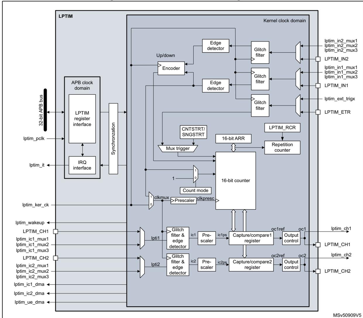
The diagram illustrates the internal architecture of the LPTIM1/2/3/5/6. It is divided into two main clock domains: the APB clock domain and the Kernel clock domain.
- APB clock domain: Contains the LPTIM register interface connected to a 32-bit APB bus . It also includes an IRQ interface and a Synchronization block. External signals lptim_pclk and lptim_it are connected here.
- Kernel clock domain:
The central part of the timer, containing:
- An Encoder block with Up/down control, connected to two Edge detector blocks.
- Three Glitch filter blocks connected to external inputs lptim_in2_mux1/2/3 (LPTIM_IN2), lptim_in1_mux1/2/3 (LPTIM_IN1), and lptim_ext_trig (LPTIM_ETR).
- A Mux trigger block receiving inputs from CNTSTRT/SNGSTRT and 16-bit ARR .
- A 16-bit counter block connected to 16-bit ARR and LPTIM_RCR (Repetition counter).
- A Prescaler block (labeled clkpresc ) receiving lptim_ker_ck and Count mode inputs.
- Two Capture/compare register blocks (labeled ic1ps and ic2ps ) connected to the counter and Output control blocks (labeled oc1ref and oc2ref ).
- Two Glitch filter & edge detector blocks (labeled lpti1 and lpti2 ) connected to external inputs lptim_ic1_mux1/2/3 (LPTIM_CH1) and lptim_ic2_mux1/2/3 (LPTIM_CH2).
- External I/Os:
- lptim_pclk : APB clock input.
- lptim_it : Interrupt output.
- lptim_ker_ck : Kernel clock input.
- lptim_wakeup : Wakeup input.
- LPTIM_CH1 : Channel 1 input/output, controlled by lptim_ic1_mux1/2/3 .
- LPTIM_CH2 : Channel 2 input/output, controlled by lptim_ic2_mux1/2/3 .
- lptim_ic1_dma , lptim_ic2_dma , and lptim_ue_dma : DMA request signals.
- lptim_in1 , lptim_in2 , and lptim_etr : External input pins.
MSV50909V5
1. Some I/Os may not be available, refer to Section 43.4.2: LPTIM pins and internal signals .
Figure 602. LPTIM4 block diagram (1)
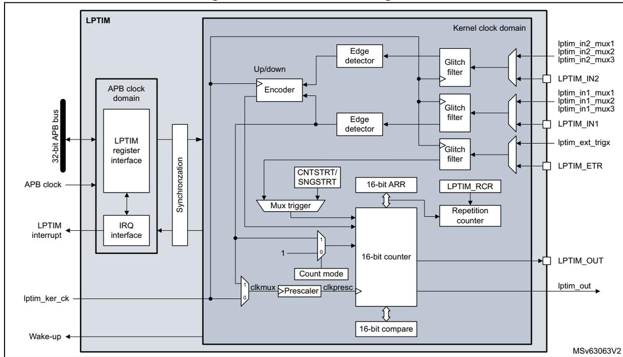
The diagram illustrates the internal architecture of the LPTIM4. It is divided into two main clock domains: the APB clock domain and the Kernel clock domain. In the APB clock domain, there is an LPTIM register interface connected to a 32-bit APB bus, an IRQ interface for LPTIM interrupt, and a Synchronization block. The Kernel clock domain contains a 16-bit counter, a 16-bit ARR (Auto-Reload Register), a 16-bit RCR (Repetition Counter), a Mux trigger, a Count mode block, a Prescaler, and a 16-bit compare block. External inputs include LPTIM_IN1, LPTIM_IN2, LPTIM_EXT_TRIG, and LPTIM_ETR, which pass through glitch filters and edge detectors. The LPTIM_OUT pin is generated by the 16-bit counter. Other internal signals include Up/down, Encoder, CNTSTRT/SNGSTRT, and clk mux. The diagram is labeled MSv63063V2.
1. Some I/Os may not be available, refer to Section 43.4.2: LPTIM pins and internal signals .
43.4.2 LPTIM pins and internal signals
The following tables provide the list of LPTIM pins and internal signals, respectively.
Table 467. LPTIM1/2/3/5/6 input/output pins
| Pin name | Pin type | Description |
|---|---|---|
| LPTIM_IN1 | Digital input | LPTIM Input 1 from GPIO pin on mux input 0 |
| LPTIM_IN2 | Digital input | LPTIM Input 2 from GPIO pin on mux input 0 |
| LPTIM_ETR | Digital input | LPTIM external trigger GPIO pin |
| LPTIM_CH1 | Digital input/output | LPTIM channel 1 input/output GPIO pin |
| LPTIM_CH2 | Digital input/output | LPTIM channel 2 input/output GPIO pin |
Table 468. LPTIM4 input/output pins
| Pin name | Pin type | Description |
|---|---|---|
| LPTIM_IN1 | Digital input | LPTIM Input 1 from GPIO pin on mux input 0 |
| LPTIM_ETR | Digital input | LPTIM external trigger GPIO pin |
| LPTIM_OUT | Digital output | LPTIM Output GPIO pin |
| Signal name | Signal type | Description |
|---|---|---|
| lptim_pclk | Digital input | LPTIM APB clock domain |
| lptim_ker_ck | Digital input | LPTIM kernel clock |
| lptim_in1_mux1 | Digital input | Internal LPTIM input 1 connected to mux input 1 |
| lptim_in1_mux2 | Digital input | Internal LPTIM input 1 connected to mux input 2 |
| lptim_in1_mux3 | Digital input | Internal LPTIM input 1 connected to mux input 3 |
| lptim_in2_mux1 | Digital input | Internal LPTIM input 2 connected to mux input 1 |
| lptim_in2_mux2 | Digital input | Internal LPTIM input 2 connected to mux input 2 |
| lptim_in2_mux3 | Digital input | Internal LPTIM input 2 connected to mux input 3 |
| lptim_ic1_mux1 | Digital input | Internal LPTIM input capture 1 connected to mux input 1 |
| lptim_ic1_mux2 | Digital input | Internal LPTIM input capture 1 connected to mux input 2 |
| lptim_ic1_mux3 | Digital input | Internal LPTIM input capture 1 connected to mux input 3 |
| lptim_ic2_mux1 | Digital input | Internal LPTIM input capture 2 connected to mux input 1 |
| lptim_ic2_mux2 | Digital input | Internal LPTIM input capture 2 connected to mux input 2 |
| lptim_ic2_mux3 | Digital input | Internal LPTIM input capture 2 connected to mux input 3 |
| lptim_ext_trigx | Digital input | LPTIM external trigger input x |
| lptim_it | Digital output | LPTIM global interrupt |
| lptim_wakeup | Digital output | LPTIM wake-up event |
| lptim_ic1_dma | Digital output | LPTIM input capture 1 DMA request |
| lptim_ic2_dma | Digital output | LPTIM input capture 2 DMA request |
| lptim_ue_dma | Digital output | LPTIM update event DMA request |
| Signal name | Signal type | Description |
|---|---|---|
| lptim_pclk | Digital input | LPTIM APB clock domain |
| lptim_ker_ck | Digital input | LPTIM kernel clock |
| lptim_in1_mux1 | Digital input | Internal LPTIM input 1 connected to mux input 1 |
| lptim_in1_mux2 | Digital input | Internal LPTIM input 1 connected to mux input 2 |
| lptim_in1_mux3 | Digital input | Internal LPTIM input 1 connected to mux input 3 |
| lptim_ext_trigx | Digital input | LPTIM external trigger input x |
| lptim_out | Digital output | LPTIM counter output |
| lptim_it | Digital output | LPTIM global interrupt |
| lptim_wakeup | Digital output | LPTIM wake-up event |
43.4.3 LPTIM input and trigger mapping
The LPTIM external trigger and input connections are detailed hereafter.
Table 471. LPTIM1/2/3/4/5/6 external trigger connections
| TRIGSEL | External trigger | |||||
|---|---|---|---|---|---|---|
| LPTIM1 | LPTIM2 | LPTIM3 | LPTIM4 | LPTIM5 | LPTIM6 | |
| lptim_ext_trig0 | GPIO | GPIO | GPIO | GPIO | GPIO | GPIO |
| lptim_ext_trig1 | rtc_alra_trg | rtc_alra_trg | rtc_alra_trg | rtc_alra_trg | rtc_alra_trg | rtc_alra_trg |
| lptim_ext_trig2 | rtc_alrb_trg | rtc_alrb_trg | rtc_alrb_trg | rtc_alrb_trg | rtc_alrb_trg | rtc_alrb_trg |
| lptim_ext_trig3 | tamp_trg1 | tamp_trg1 | tamp_trg1 | tamp_trg1 | tamp_trg1 | tamp_trg1 |
| lptim_ext_trig4 | tamp_trg2 | gpdma_ch0_tcf | Reserved | Reserved | Reserved | Reserved |
| lptim_ext_trig5 | gpdma_ch1_tcf | gpdma_ch4_tcf | Reserved | Reserved | Reserved | Reserved |
| lptim_ext_trig6 | Reserved | Reserved | Reserved | Reserved | Reserved | Reserved |
| lptim_ext_trig7 | Reserved | Reserved | Reserved | Reserved | Reserved | Reserved |
Table 472. LPTIM1/2/3/5/6 input 1 connections
| lptim_in1_mux | LPTIM1/2/3/4 input 1 connected to |
|---|---|
| lptim_in1_mux0 | GPIO |
| lptim_in1_mux1 | Reserved |
| lptim_in1_mux2 | Reserved |
| lptim_in1_mux3 | Reserved |
Table 473. LPTIM1/2/3/5/6 input 2 connections
| lptim_in2_mux | LPTIM1/2 input 2 connected to |
|---|---|
| lptim_in2_mux0 | GPIO |
| lptim_in2_mux1 | Reserved |
| lptim_in2_mux2 | Reserved |
| lptim_in2_mux3 | Reserved |
Table 474. LPTIM1/2/3/5/6 input capture 1 connections
| lptim_ic1_mux | LPTIM1/2/3 input capture 1 connected to |
|---|---|
| lptim_ic1_mux0 | GPIO |
| lptim_ic1_mux1 | Reserved |
| lptim_ic1_mux2 | Reserved |
| lptim_ic1_mux3 | Reserved |
| lptim_ic2_mux | LPTIM1 input capture 2 connected to |
|---|---|
| lptim_ic2_mux0 | I/O |
| lptim_ic2_mux1 | LSI |
| lptim_ic2_mux2 | LSE |
| lptim_ic2_mux3 | Reserved |
| lptim_ic2_mux | LPTIM2 input capture 2 connected to |
|---|---|
| lptim_ic2_mux0 | I/O |
| lptim_ic2_mux1 | HSI/1024 |
| lptim_ic2_mux2 | CSI/128 |
| lptim_ic2_mux3 | HSI/8 |
| lptim_ic2_mux | LPTIM3 input capture 2 connected to |
|---|---|
| lptim_ic2_mux0 | I/O |
| lptim_ic2_mux1 | Reserved |
| lptim_ic2_mux2 | Reserved |
| lptim_ic2_mux3 | Reserved |
43.4.4 LPTIM reset and clocks
The LPTIM can be clocked using several clock sources. It can be clocked using an internal clock signal which can be any configurable internal clock source selectable through the RCC (see RCC section for more details). Also, the LPTIM can be clocked using an external clock signal injected on its external Input1. When clocked with an external clock source, the LPTIM can run in one of the following configurations:
- • The first configuration is when the LPTIM is clocked by an external signal but in the same time an internal clock signal is provided to the LPTIM from configurable internal clock source (see RCC section).
- • The second configuration is when the LPTIM is solely clocked by an external clock source through its external Input1. This configuration is the one used to realize Timeout function or pulse counter function when all the embedded oscillators are turned off after entering a low-power mode.
Programming the CKSEL and COUNTMODE bits allows controlling whether the LPTIM uses an external clock source or an internal one.
When configured to use an external clock source, the CKPOL bits are used to select the external clock signal active edge. If both edges are configured to be active ones, an internal clock signal must also be provided (first configuration). In this case, the internal clock signal frequency must be at least four times higher than the external clock signal frequency.
43.4.5 Glitch filter
The LPTIM inputs, either external (mapped to GPIOs) or internal (mapped on the chip-level to other embedded peripherals), are protected with digital filters that prevent any glitches and noise perturbations to propagate inside the LPTIM. This is in order to prevent spurious counts or triggers.
Before activating the digital filters, an internal clock source must first be provided to the LPTIM. This is necessary to guarantee the proper operation of the filters.
The digital filters are divided into three groups:
- • The first group of digital filters protects the LPTIM internal or external inputs. The digital filters sensitivity is controlled by the CKFLT bits
- • The second group of digital filters protects the LPTIM internal or external trigger inputs. The digital filters sensitivity is controlled by the TRGFLT bits.
- • The third group of digital filters protects the LPTIM internal or external input captures. The digital filters sensitivity is controlled by the ICxF bits.
Note: The digital filters sensitivity is controlled by groups. It is not possible to configure each digital filter sensitivity separately inside the same group.
The filter sensitivity acts on the number of consecutive equal samples that is detected on one of the LPTIM inputs to consider a signal level change as a valid transition. Figure 603 shows an example of glitch filter behavior in case of a two consecutive samples programmed.
Figure 603. Glitch filter timing diagram
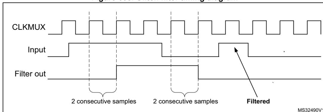
The diagram illustrates the glitch filter's operation. The top waveform, CLKMUX, is a periodic square wave representing the clock. The middle waveform, Input, shows a signal that transitions from high to low and back to high. A short high-level pulse (the glitch) occurs while the signal is otherwise low. The bottom waveform, Filter out, shows the output of the filter. It remains low until the glitch occurs, then it transitions to high and stays high until the glitch ends, at which point it returns to low. Vertical dashed lines mark the clock edges. Brackets below the Input signal indicate two consecutive samples taken at the first and second clock edges after the glitch starts. Another bracket indicates two consecutive samples at the third and fourth clock edges after the glitch starts. An arrow points to the Filter out signal with the label 'Filtered'. The bottom right corner of the diagram contains the text 'MS32490V1'.
Note: In case no internal clock signal is provided, the digital filter must be deactivated by setting the CKFLT, ICxF and TRGFLT bits to 0. In this case, an external analog filter can be used to protect the LPTIM external inputs against glitches.
43.4.6 Prescaler
The LPTIM 16-bit counter is preceded by a configurable power-of-2 prescaler. The prescaler division ratio is controlled by the PRESC[2:0] field. The table below lists all the possible division ratios:
Table 478. Prescaler division ratios
| Programming | Dividing factor |
|---|---|
| 000 | /1 |
| 001 | /2 |
| 010 | /4 |
| 011 | /8 |
| 100 | /16 |
| 101 | /32 |
| 110 | /64 |
| 111 | /128 |
43.4.7 Trigger multiplexer
The LPTIM counter can be started either by software or after the detection of an active edge on one of the eight trigger inputs.
TRIGEN[1:0] is used to determine the LPTIM trigger source:
- • When TRIGEN[1:0] equals 00, the LPTIM counter is started as soon as one of the CNTSTRT or the SNGSTRT bits is set by software. The three remaining possible values for the TRIGEN[1:0] are used to configure the active edge used by the trigger inputs. The LPTIM counter starts as soon as an active edge is detected.
- • When TRIGEN[1:0] is different than 00, TRIGSEL[2:0] is used to select which of the eight trigger inputs is used to start the counter.
The external triggers are considered asynchronous signals for the LPTIM. After a trigger detection, a two-counter-clock period latency is needed before the timer starts running due to the synchronization.
If a new trigger event occurs when the timer is already started it is ignored (unless timeout function is enabled).
Note: The timer must be enabled before setting the SNGSTRT/CNTSTRT bits. Any write on these bits when the timer is disabled is discarded by hardware.
Note: When starting the counter by software (TRIGEN[1:0] = 00), there is a delay of 3 kernel clock cycles between the LPTIM_CR register update (set one of SNGSTRT or CNTSTRT bits) and the effective start of the counter.
43.4.8 Operating mode
The LPTIM features two operating modes:
- • Continuous mode: the timer is free running, the timer is started from a trigger event and never stops until the timer is disabled
- • One-shot mode: the timer is started from a trigger event and stops when an LPTIM update event is generated.
One-shot mode
To enable the one-shot counting, the SNGSTRT bit must be set.
A new trigger event re-starts the timer. Any trigger event occurring after the counter starts and before the next LPTIM update event, is discarded.
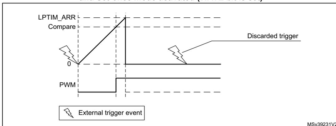
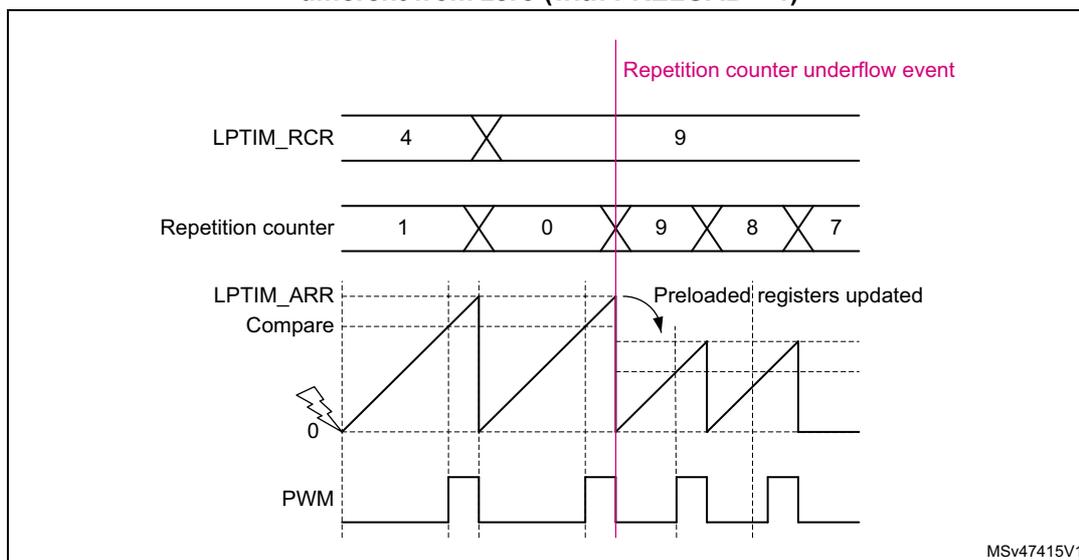
In case an external trigger is selected, each external trigger event arriving after the SNGSTRT bit is set, and after the repetition counter has stopped (after the update event), and if the repetition register content is different from zero, the repetition counter gets reloaded with the value already contained by the repetition register and a new one-shot counting cycle is started as shown in Figure 604 .
Figure 604. LPTIM output waveform, single-counting mode configuration when repetition register content is different than zero (with PRELOAD = 1)
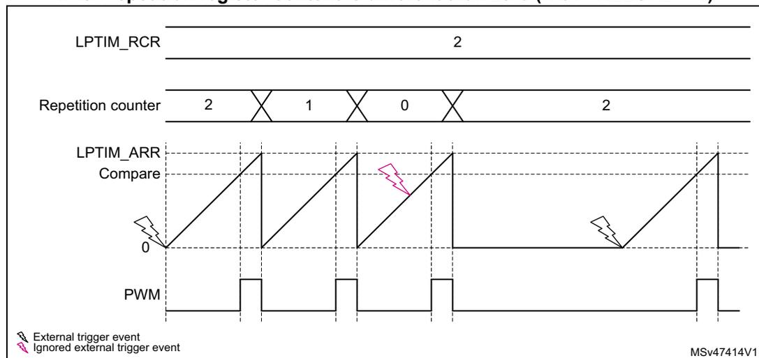
The figure is a timing diagram illustrating the LPTIM output waveform in single-counting mode. It consists of four horizontal lines representing different signals over time:
- LPTIM_RCR: A constant value of 2.
- Repetition counter: Shows a sequence of counts: 2, 1, 0, followed by a reload to 2. The counts 2, 1, and 0 are separated by 'X' marks, indicating the end of each count. The counter starts at 2 upon a valid trigger and counts down to 0.
- LPTIM_ARR Compare: A sawtooth waveform that starts at 0 and rises linearly to a compare level. When the counter reaches 0, the waveform resets to 0. External trigger events (black lightning bolts) start the counter, while ignored events (pink lightning bolts) occur while the counter is still running.
- PWM: A pulse-width modulated signal that is high when the repetition counter is non-zero and low when it reaches 0.
Legend:
- External trigger event
- Ignored external trigger event
MSV47414V1
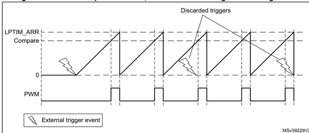
- Set-once mode activated:
Note that when the WAVE bitfield in the LPTIM_CFGR register is set, the Set-once mode is activated. In this case, the counter is only started once following the first trigger, and any subsequent trigger event is discarded as shown in Figure 605 .
Figure 605. LPTIM output waveform, single-counting mode configuration and Set-once mode activated (WAVE bit is set)
In case of software start (TRIGEN[1:0] = 00), the SNGSTRT setting starts the counter for one-shot counting.
Continuous mode
To enable the continuous counting, the CNTSTRT bit must be set.
In case an external trigger is selected, an external trigger event arriving after CNTSTRT is set, starts the counter for continuous counting. Any subsequent external trigger event is discarded as shown in Figure 606 .
In case of software start (TRIGEN[1:0] = 00), setting CNTSTRT starts the counter for continuous counting.
Figure 606. LPTIM output waveform, Continuous counting mode configuration
SNGSTRT and CNTSTRT bits can only be set when the timer is enabled (ENABLE bit set to 1). It is possible to change “on the fly” from One-shot mode to Continuous mode.
If the Continuous mode was previously selected, setting SNGSTRT switches the LPTIM to the One-shot mode. The counter (if active) stops as soon as an LPTIM update event is generated.
If the One-shot mode was previously selected, setting CNTSTRT switches the LPTIM to the Continuous mode. The counter (if active) restarts as soon as it reaches ARR.
43.4.9 Timeout function
The detection of an active edge on one selected trigger input can be used to reset the LPTIM counter. This feature is controlled through the TIMEOUT bit.
The first trigger event starts the timer, any successive trigger event resets the LPTIM counter and the repetition counter and the timer restarts.
A low-power timeout function can be realized. The timeout value corresponds to the compare value; if no trigger occurs within the expected time frame, the MCU is waked-up by the compare match event.
43.4.10 Waveform generation
Two 16-bit registers, the LPTIM_ARR (autoreload register) and LPTIM_CCRx (capture/compare register), are used to generate several different waveforms on LPTIM output
The timer can generate the following waveforms:
- • The PWM mode: the LPTIM output is set as soon as the counter value in LPTIM_CNT exceeds the compare value in LPTIM_CCRx. The LPTIM output is reset as soon as a match occurs between the LPTIM_ARR and the LPTIM_CNT register. For more details see Section 43.4.19: PWM mode .
- • The One-pulse mode: the output waveform is similar to the one of the PWM mode for the first pulse, then the output is permanently reset
- • The Set-once mode: the output waveform is similar to the One-pulse mode except that the output is kept to the last signal level (depends on the output configured polarity).
The above described modes require the LPTIM_ARR register value to be strictly greater than the LPTIM_CCRx register value.
The LPTIM output waveform can be configured through the WAVE bit as follow:
- • Resetting the WAVE bit to 0 forces the LPTIM to generate either a PWM waveform or a One pulse waveform depending on which bit is set: CNTSTRT or SNGSTRT.
- • Setting the WAVE bit to 1 forces the LPTIM to generate a Set-once mode waveform.
The WAVPOL/CCxP bit controls the LPTIM output polarity. The change takes effect immediately, so the output default value changes immediately after the polarity is re-configured, even before the timer is enabled.
Signals with frequencies up to the LPTIM clock frequency divided by two can be generated. Figure 607 below shows the three possible waveforms that can be generated on the LPTIM output. Also, it shows the effect of the polarity change using the WAVPOL/CCxP bit.
Figure 607. Waveform generation
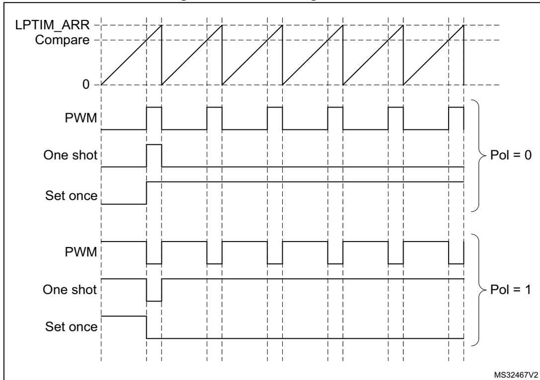
The figure is a timing diagram illustrating waveform generation using an LPTIM. The top signal, labeled 'LPTIM_ARR Compare', shows a periodic sawtooth waveform. Below this, the diagram is divided into two sections based on polarity: 'Pol = 0' and 'Pol = 1'. In the 'Pol = 0' section, the 'PWM' signal is high when the counter is below the compare value. The 'One shot' signal is a pulse that goes high at each compare event. The 'Set once' signal is a pulse that goes high at the first compare event and remains high. In the 'Pol = 1' section, the 'PWM' signal is low when the counter is below the compare value. The 'One shot' signal is a pulse that goes low at each compare event. The 'Set once' signal is a pulse that goes low at the first compare event and remains low. Vertical dashed lines indicate the timing of the compare events. The bottom right corner of the diagram is labeled 'MS32467V2'.
43.4.11 Register update
The LPTIM_ARR register, the LPTIM_RCR register and the LPTIM_CCRx register are updated immediately after the APB bus write operation or in synchronization with the next LPTIM update event if the timer is already started.
The PRELOAD bit controls how the LPTIM_ARR, the LPTIM_RCR and the LPTIM_CCRx registers are updated:
- • When the PRELOAD bit is reset to 0, the LPTIM_ARR, the LPTIM_RCR and the LPTIM_CCRx registers are immediately updated after any write access.
- • When the PRELOAD bit is set to 1, the LPTIM_ARR, the LPTIM_RCR and the LPTIM_CCRx registers are updated at next LPTIM update event, if the timer has been already started.
The LPTIM APB interface and the LPTIM kernel logic use different clocks, so there is some latency between the APB write and the moment when these values are available to the counter comparator. Within this latency period, any additional write into these registers must be avoided.
The ARROK flag, the REPOK flag and the CMPxOK flag in the LPTIM_ISR register indicate when the write operation is completed to respectively the LPTIM_ARR register, the LPTIM_RCR register and the LPTIM_CCRx register.
After a write to the LPTIM_ARR, the LPTIM_RCR or the LPTIM_CCRx register, a new write operation to the same register can only be performed when the previous write operation is completed. Any successive write before respectively the ARROK flag, the REPOK flag or the CMPxOK flag be set, leads to unpredictable results.
43.4.12 Counter mode
The LPTIM counter can be used to count external events on the LPTIM input1 or it can be used to count internal clock cycles. The CKSEL and COUNTMODE bits control which source is used for updating the counter.
In case the LPTIM is configured to count external events on Input1, the counter can be updated following a rising edge, falling edge or both edges depending on the value written to the CKPOL[1:0] bits.
The count modes below can be selected, depending on CKSEL and COUNTMODE values:
- • CKSEL = 0: the LPTIM is clocked by an internal clock source
- – COUNTMODE = 0
The LPTIM is configured to be clocked by an internal clock source and the LPTIM counter is configured to be updated following each internal clock pulse. - – COUNTMODE = 1
The LPTIM external Input1 is sampled with the internal clock provided to the LPTIM.
Consequently, in order not to miss any event, the frequency of the changes on the external Input1 signal must never exceed the frequency of the internal clock provided to the LPTIM. Also, the internal clock provided to the LPTIM must not be prescaled (PRESC[2:0] = 000).
- – COUNTMODE = 0
- • CKSEL = 1: the LPTIM is clocked by an external clock source
COUNTMODE value is don't care.
In this configuration, the LPTIM has no need for an internal clock source (except if the glitch filters are enabled). The signal injected on the LPTIM external input1 is used as system clock for the LPTIM. This configuration is suitable for operation modes where no embedded oscillator is enabled.
For this configuration, the LPTIM counter can be updated either on rising edges or falling edges of the input1 clock signal but not on both rising and falling edges.
Since the signal injected on the LPTIM external input1 is also used to clock the LPTIM kernel logic, there is some initial latency (after the LPTIM is enabled) before the counter is incremented. More precisely, the first five active edges on the LPTIM external Input1 (after LPTIM is enable) are lost.
43.4.13 Timer enable
The ENABLE bit located in the LPTIM_CR register is used to enable/disable the LPTIM kernel logic. After setting the ENABLE bit, a delay of two counter clock cycles is needed before the LPTIM is actually enabled.
The LPTIM_CFGR register must be modified only when the LPTIM is disabled.
43.4.14 Timer counter reset
In order to reset the content of LPTIM_CNT register, two reset mechanisms are implemented:
- • The synchronous reset mechanism: the synchronous reset is controlled by the COUNTRST bit in the LPTIM_CR register. After setting the COUNTRST bitfield to '1', the reset signal is propagated in the LPTIM kernel clock domain. So it is important to note that a few clock pulses of the LPTIM kernel logic elapse before the reset is taken into account. This makes the LPTIM counter count few extra pluses between the time when the reset is triggered and it become effective. Since the COUNTRST bit is located in the APB clock domain and the LPTIM counter is located in the LPTIM kernel clock domain, a delay of 3 clock cycles of the kernel clock is needed to synchronize the reset signal issued by the APB clock domain when writing '1' to the COUNTRST bit.
Note: The software should ensure that COUNRST bit is '0' before generating every synchronous reset.
- • The asynchronous reset mechanism: the asynchronous reset is controlled by the RSTARE bit located in the LPTIM_CR register. When this bit is set to '1', any read access to the LPTIM_CNT register resets its content to zero. Asynchronous reset must be triggered within a timeframe in which no LPTIM core clock is provided. For example when LPTIM Input1 is used as external clock source, the asynchronous reset must be applied only when there is enough insurance that no toggle occurs on the LPTIM Input1.
To read reliably the content of the LPTIM_CNT register two successive read accesses must be performed and compared. A read access can be considered reliable when the value of the two read accesses is equal. Unfortunately when asynchronous reset is enabled there is no possibility to read twice the LPTIM_CNT register.
Warning: There is no mechanism inside the LPTIM that prevents the two reset mechanisms from being used simultaneously. The developer must make sure that these two mechanisms are used exclusively.
43.4.15 Encoder mode
This mode allows handling signals from quadrature encoders used to detect angular position of rotary elements. Encoder interface mode acts simply as an external clock with direction selection. This means that the counter just counts continuously between 0 and the auto-reload value programmed into the LPTIM_ARR register (0 up to ARR or ARR down to 0 depending on the direction). Therefore LPTIM_ARR must be configured before starting the counter. From the two external input signals, Input1 and Input2, a clock signal is generated to clock the LPTIM counter. The phase between those two signals determines the counting direction.
The Encoder mode is only available when the LPTIM is clocked by an internal clock source. The signals frequency on both Input1 and Input2 inputs must not exceed the LPTIM internal clock frequency divided by 4. This is mandatory in order to guarantee a proper operation of the LPTIM.
Direction change is signaled by the two down and up flags in the LPTIM_ISR register. An interrupt can be generated for both direction change events if enabled through the DOWNIE bit.
To activate the Encoder mode the ENC bit has to be set to 1. The LPTIM must first be configured in Continuous mode.
When Encoder mode is active, the LPTIM counter is modified automatically following the speed and the direction of the incremental encoder. Therefore, its content always represents the encoder's position. The count direction, signaled by the Up and Down flags, correspond to the rotation direction of the encoder rotor.
According to the edge sensitivity configured using the CKPOL[1:0] bits, different counting scenarios are possible. The following table summarizes the possible combinations, assuming that Input1 and Input2 do not switch at the same time.
Table 479. Encoder counting scenarios
| Active edge | Level on opposite signal (Input1 for Input2, Input2 for Input1) | Input1 signal | Input2 signal | ||
|---|---|---|---|---|---|
| Rising | Falling | Rising | Falling | ||
| Rising Edge (Encoder sub-mode 1) | High | Down | No count | Up | No count |
| Low | Up | No count | Down | No count | |
| Falling Edge (Encoder sub-mode 2) | High | No count | Up | No count | Down |
| Low | No count | Down | No count | Up | |
| Both Edges (Encoder sub-mode 3) | High | Down | Up | Up | Down |
| Low | Up | Down | Down | Up | |
The following figure shows a counting sequence for Encoder mode where both-edge sensitivity is configured.
Caution: In this mode the LPTIM must be clocked by an internal clock source, so the CKSEL bit must be maintained to its reset value which is equal to 0. Also, the prescaler division ratio must be equal to its reset value which is 1 (PRESC[2:0] bits must be 000).
Figure 608. Encoder mode counting sequence
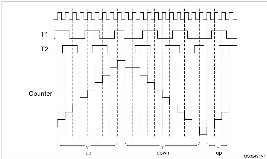
The figure is a timing diagram illustrating the encoder mode counting sequence. It features three horizontal waveforms. The top waveform is labeled 'T1' and shows a series of pulses. The second waveform is labeled 'T2' and also shows a series of pulses, generally out of phase with T1. The third waveform, labeled 'Counter', is a staircase-like signal. It starts at a low level and increases in steps ('up') as T1 goes high and T2 has falling edges. It then decreases in steps ('down') as T1 goes low and T2 has falling edges. Finally, it increases again ('up'). Below the Counter waveform, there are three brackets labeled 'up', 'down', and 'up' from left to right, indicating the direction of the count. In the bottom right corner of the diagram area, the text 'MS32491V1' is present.
43.4.16 Repetition counter
The LPTIM features a repetition counter that decrements by 1 each time an LPTIM counter overflow event occurs. A repetition counter underflow event is generated when the repetition counter contains zero and the LPTIM counter overflows. Next to each repetition counter underflow event, the repetition counter gets loaded with the content of the REP[7:0] bitfield which belongs to the repetition register LPTIM_RCR.
A repetition underflow event is generated on each and every LPTIM counter overflow when the REP[7:0] register is set to 0.
When PRELOAD = 1, writing to the REP[7:0] bitfield has no effect on the content of the repetition counter until the next repetition underflow event occurs. The repetition counter continues to decrement each LPTIM counter overflow event and only when a repetition underflow event is generated, the new value written into REP[7:0] is loaded into the repetition counter. This behavior is depicted in Figure 609 .
Figure 609. Continuous counting mode when repetition register LPTIM_RCR different from zero (with PRELOAD = 1)
A repetition counter underflow event is systematically associated with LPTIM preloaded registers update (refer to Section 43.4.11: Register update for more information).
Repetition counter underflow event is signaled to the software through the update event (UE) flag mapped into the LPTIM_ISR register. When set, the UE flag can trigger an LPTIM interrupt if its respective update event interrupt enable (UEIE) control bit, mapped to the LPTIM_DIER register, is set.
The repetition register LPTIM_RCR is located in the APB bus interface clock domain where the repetition counter itself is located in the LPTIM kernel clock domain. Each time a new value is written to the LPTIM_RCR register, this new content is propagated from the APB bus interface clock domain to the LPTIM kernel clock domain. The new written value is then loaded to the repetition counter immediately after a repetition counter underflow event. The synchronization delay for the new written content is four APB clock cycles plus three LPTIM kernel clock cycles and it is signaled by the REPOK flag located in the LPTIM_ISR register when it is elapsed. When the LPTIM kernel clock cycle is relatively slow, for instance when the LPTIM kernel is being clocked by the LSI clock source, it can be lengthy to keep polling on the REPOK flag by software to detect that the synchronization of the LPTIM_RCR register content is finished. For that reason, the REPOK flag, when set, can generate an interrupt if its associated REPOKIE control bit in the LPTIM_DIER register is set.
Note: After a write to the LPTIM_RCR register, a new write operation to the same register can only be performed when the previous write operation is completed. Any successive writes before the REPOK flag is set, lead to unpredictable results.
Caution: When using repetition counter with PRELOAD = 0, LPTIM_RCR register must be changed at least five counter cycles before the autoreload match event, otherwise an unpredictable behavior may occur.
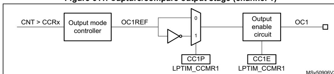
43.4.17 Capture/compare channels
Each capture/compare channel is built around a capture/compare register, an input stage for capture (with digital filter, multiplexing and prescaler) and an output stage (with comparator and output control) for PWM.
Input stage
The input stage samples the corresponding LPTIx input to generate a filtered signal LPTIxF. Then, an edge detector with polarity selection generates ICx signal used as the capture command. It is prescaled to generate the capture command signal (ICxPS).
Figure 610. Capture/compare input stage (channel 1)
![Figure 610: Capture/compare input stage (channel 1) block diagram. The diagram shows the signal flow from LPTI1 input through a Glitch filter (controlled by IC1F[3:0] in LPTIM_CCMR1) to produce LPTI1F. This signal then passes through an Edge detector (controlled by CC1P[1:0] in LPTIM_CCMR1) to produce IC1. Finally, IC1 is divided by a Divider (with prescalers /1, /2, /4, /8, controlled by IC1PSC[1:0] and CC1E in LPTIM_CCMR1) to produce the output IC1PS. The diagram is labeled MSV50905V1.](/RM0481-STM32H523-33-562-63-573/5769e5210dcd1bc8f3abc55b3bbbf5cd_img.jpg)
Output stage
The output stage generates an intermediate waveform which is then used for reference: OCxREF (active high). The polarity acts at the end of the chain.
Figure 611. Capture/compare output stage (channel 1)
43.4.18 Input capture mode
In Input capture mode, the capture/compare registers (LPTIM_CCRx) are used to latch the value of the counter after a transition detected by the corresponding ICx signal. Assuming input capture is enabled on a channel x (CCxE set) and when a capture occurs, the corresponding CCxIF flag (LPTIM_ISR register) is set and an interrupt or a DMA request can be sent if they are enabled. If a capture occurs while the CCxIF flag was already high, then the over-capture flag CCxOF (LPTIM_ISR register) is set. CCxIF can be cleared by software by writing the CCxICF to 1 or by reading the captured data stored in the LPTIM_CCRx register. CCxOF is cleared by writing CCxOCF to 1.
Note: In DMA mode, the input capture channel have to be enabled (set CCxE bit) the last, after enabling the DMA request and after starting the counter. This is in order to prevent generating an input capture DMA request when the counter is not started yet.
Input capture Glitch filter latency
When a trigger event arrives on channel x input (LPTIx) and depending on the configured glitch filter (ICxF[1:0] field in CCMRx register) and on the kernel clock prescaler value (PRESC[2:0] field in CFGR register), there is a variable latency that leads to a systematic offset (see Table 480 ) between the captured value stored in the CCRx register and the real value corresponding to the capture trigger.
This offset has no impact on pulse width measurement as it is systematic and compensated between two captures.
The real capture value corresponding to the input capture trigger can be calculated using the below formula:
Real capture value = captured(LPTIM_CCRx) - offset
The relevant offset must be used depending on the glitch filter and on the kernel clock prescaler value (PRESC field in CFGR register)
Example: determining the real capture value when PRESC[2:0] = 0x2 and ICxF = 0x3.
For this configuration (PRESC[2:0] = 0x2 and ICxF = 0x3) and according to the Table 480 , the offset is 5.
Assuming that the captured value in CCRx is 9 (LPTIM_CNT = 9), this means that the capture trigger occurred when the LPTIM_CNT was equal to 9 - 5 = 4.
Table 480. Input capture Glitch filter latency (in counter step unit)
| Prescaler PRESC[2:0] | ICxF[1:0] | Offset |
|---|---|---|
| 0 | 0 | 2 |
| 1 | 7 | |
| 2 | 9 | |
| 3 | 13 | |
| 1 | 0 | 3 |
| 1 | 5 | |
| 2 | 6 | |
| 3 | 8 | |
| 2 | 0 | 2 |
| 1 | 3 | |
| 2 | 4 | |
| 3 | 5 | |
| 3 | 0 | 2 |
| 1 | 2 | |
| 2 | 3 | |
| 3 | 3 | |
| 4 | 0 | 2 |
| 1 | 2 | |
| 2 | 2 | |
| 3 | 2 | |
| 5 | 0 | 2 |
| 1 | 2 | |
| 2 | 2 | |
| 3 | 2 |
Table 480. Input capture Glitch filter latency (in counter step unit) (continued)
| Prescaler PRESC[2:0] | ICxF[1:0] | Offset |
|---|---|---|
| 6 | 0 | 2 |
| 1 | 2 | |
| 2 | 2 | |
| 3 | 2 | |
| 7 | 0 | 2 |
| 1 | 2 | |
| 2 | 2 | |
| 3 | 2 |
43.4.19 PWM mode
The PWM mode enables to generate a signal with a frequency determined by the value of the LPTIM_ARR register and a duty cycle determined by the value of the LPTIM_CCRx register. The LPTIM is able to generate PWM in edge-aligned mode.
OCx polarity is software programmable using the CCxP bit in the LPTIM_CCMRx register. It can be programmed as active high or active low. OCx output is enabled by the CCxE bit in the LPTIM_CCMRx register. Refer to the LPTIM_CCMRx register description for more details.
Figure 612 gives an example where the LPTIM channel 1 is configured in PWM mode with LPTIM_CCR1 = 6 then 1 and LPTIM_ARR=10.
Figure 612. Edge-aligned PWM mode (PRELOAD = 1)
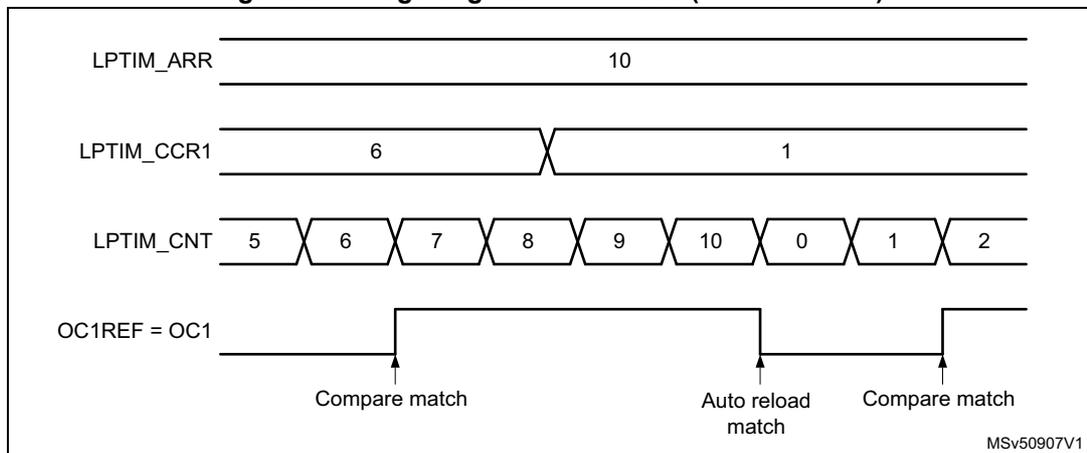
In the following example the reference PWM signal OCxREF is low as long as LPTIM_CNT ≤ LPTIM_CCRx else it becomes high.
Figure 613 shows some edge-aligned PWM waveforms in an example where LPTIM_ARR = 8.
Figure 613. Edge-aligned PWM waveforms (ARR=8 and CCxP = 0)
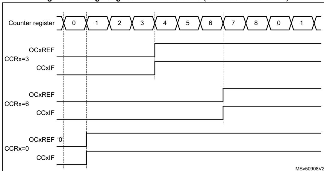
The figure is a timing diagram illustrating edge-aligned PWM waveforms. The top row shows the 'Counter register' values over time: 0, 1, 2, 3, 4, 5, 6, 7, 8, 0, 1. Vertical dashed lines mark the transitions between these values. Below the counter, three sets of signals are shown for different compare register (CCR) values:
- CCRx=3: The OCxREF signal is initially high. At the counter value of 3, it transitions to low. The CCxIF flag is shown as a pulse at this transition.
- CCRx=6: The OCxREF signal is initially low. At the counter value of 6, it transitions to high. The CCxIF flag is shown as a pulse at this transition.
- CCRx=0: The OCxREF signal is initially low. At the counter value of 0 (after 8), it transitions to high. The CCxIF flag is shown as a pulse at this transition.
The diagram demonstrates that the OCxREF signal level changes immediately when the counter reaches the compare value, without waiting for the end of the current PWM period (counter value 8). The text 'MSV50908V2' is visible in the bottom right corner of the diagram area.
PWM mode with immediate update PRELOAD = 0
The PWM mode with PRELOAD = 0 enables the early change of the output level within the current PWM cycle. Based on the immediate update (PRELOAD = 0) of the LPTIM_CCRx register and on the continuous comparison of LPTIM_CNT and LPTIM_CCRx registers, it permits to have a new duty cycle value applied as soon as possible within the current PWM cycle, without having to wait for the completion of the current PWM period.
When the (PRELOAD = 0), the OCxREF signal level can be changed on-the-fly by software (or DMA) by updating the compare value in the LPTIM_CCRx register.
Depending on the written compare value and on the current counter and compare values, the OCxREF level is re-assigned as illustrated below:
- • If the new compare value does not exceed the current counter value and the current compare value exceeds the counter, OCxREF level is re-assigned high as soon as the new compare value is written.
- • If the new compare value exceeds the counter value and the current compare value does not exceed the counter, OCxREF level is re-assigned low as soon as the new compare value is written.
The output reference signal OCxREF level is left unchanged when none of the new compare value and the current compare value exceed the counter. Figure 614 illustrates the behavior of the OCxREF signal level when PRELOAD = 0 and PRELOAD = 1.
Figure 614. PWM mode with immediate update versus preloaded update
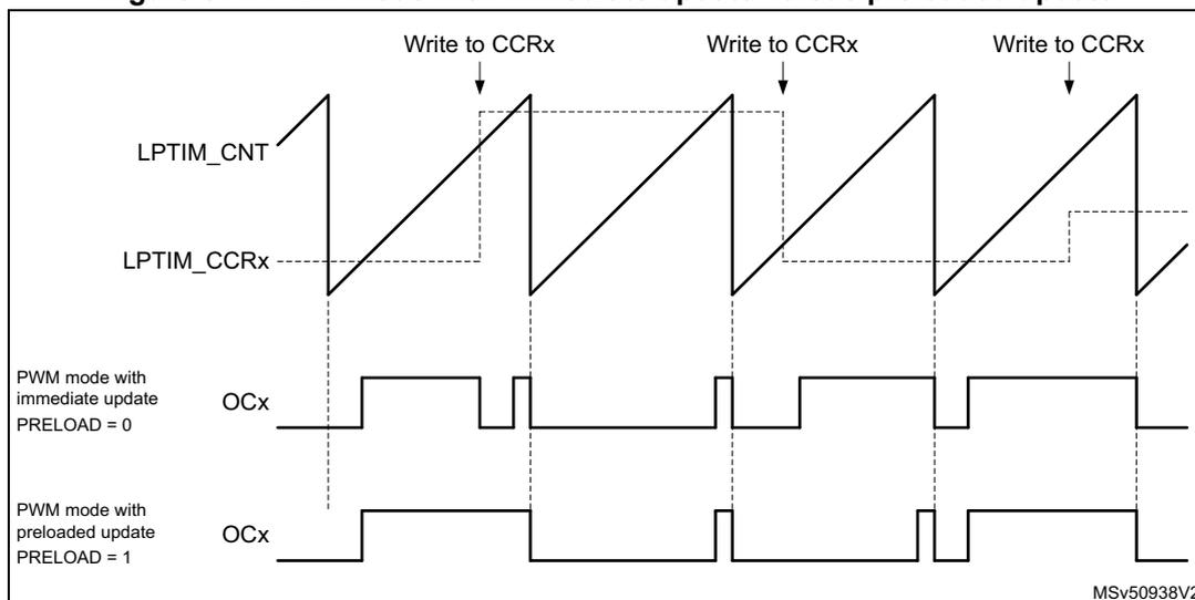
Note: For both PWM modes, the compare match, auto-reload match, and the update event flags are set one LPTIM counter cycle later after the corresponding event, the OCxREF level is also changed one LPTIM counter cycle later after the corresponding event. For instance when the LPTIM_CCRx is set to 3 the CCxIF is set when the LPTIM_CNT = 4. Figure 612 illustrates this behavior.
43.4.20 DMA requests
The LPTIM can generate two categories of DMA requests:
- • DMA requests used to retrieve the input-capture counter values
- • DMA update requests used to re-program part of the LPTIM, multiple times, at regular intervals, without software overhead
Input capture DMA request
Each LPTIM channel has its dedicated input capture DMA request. A DMA request is generated (if CCxDE bit is set in LPTIM_DIER) and CCxIF is set each time a capture is ready in the LPTIM_CCRx register. The captured values in LPTIM_CCRx can then be transferred regularly by DMA to the desired memory destination. The CCxIF is automatically cleared by hardware when the captured value in LPTIM_CCRx register is read.
Note: The ICx DMA request signal lptim_icx_dma is reset in the following conditions:
- - if the corresponding DMA request is disabled (clear CCxDE bit in the LPTIM_DIER register)
- - or if the channel x is disabled (clear CCxE bit)
- - or if the LPTIM is disabled (clear the ENABLE bit in the LPTIM_CR register)
Update event DMA request
A DMA request is generated (if UEDE is set in LPTIM_DIER) and the UE flag is set at each update event. DMA request can be used to regularly update the LPTIM_ARR, the LPTIM_RCR or the LPTIM_CCRx registers permitting to generate custom PWM waveforms.
The UE is automatically cleared by hardware upon any bus master (like CPU or DMA) write access to the LPTIM_ARR register.
- Note: The UE DMA request signal lptim_ue_dma is reset in the following conditions:
- - if the corresponding DMA request is disabled (clear UEDE bit in the LPTIM_DIER register)
- - or if the LPTIM is disabled (clear the ENABLE bit in the LPTIM_CR register)
- - or if the channel x is disabled (clear CCxE bit) and all the other channels are already disabled
43.4.21 Debug mode
When the microcontroller enters debug mode (core halted), the LPTIM counter either continues to work normally or stops, depending on the timer dedicated bit configuration in the debug support (DBG) peripheral.
For further details, refer to section debug support (DBG).
43.5 LPTIM low-power modes
Table 481. Effect of low-power modes on the LPTIM
| Mode | Description |
|---|---|
| Sleep | No effect. LPTIM interrupts cause the device to exit Sleep mode. |
| Stop | If the LPTIM is clocked by an oscillator available in Stop mode, LPTIM is functional and the interrupts cause the device to exit the Stop mode. |
| Standby | The LPTIM peripheral is powered down and must be reinitialized after exiting Standby mode. |
- Note: All DMA requests must be disabled (reset UEDE and CCxDE bits) before entering Sleep, Stop and Standby modes.
43.6 LPTIM interrupts
The following events generate an interrupt/wake-up event, if they are enabled through the LPTIM_DIER register:
- • Compare match
- • Auto-reload match (whatever the direction if Encoder mode)
- • External trigger event
- • Autoreload register write completed
- • Compare register write completed
- • Direction change (Encoder mode), programmable (up / down / both).
- • Update Event
- • Repetition register update OK
- • Input capture occurred
- • Over-capture occurred
- • Interrupt enable register update OK
Note: If any bit in the LPTIM_DIER register is set after that its corresponding flag in the LPTIM_ISR register (status register) is set, the interrupt is not asserted.
Table 482. Interrupt events
| Interrupt vector | Interrupt event | Event flag | Enable control bit | Interrupt clear method | Exit from Sleep mode | Exit from Stop mode (1) |
|---|---|---|---|---|---|---|
| LPTIMx | Compare match | CCxIF | CCxIE | Write 1 to CCxCF | Yes | Yes |
| Input capture (2) | CCxIF | CCxIE | Write 1 to CCxCF | Yes | Yes | |
| Over-capture (2) | CCxOF | CCxOIE | Write 1 to CCxOCF | Yes | Yes | |
| Auto-reload match | ARRM | ARRMIE | Write 1 to ARRMC | Yes | Yes | |
| External trigger event | EXTTRIG | EXTTRIGIE | Write 1 to EXTTRIGCF | Yes | Yes | |
| Auto-reload register update OK | ARROK | ARROKIE | Write 1 to ARROKCF | Yes | Yes | |
| Capture/compare register update OK | CMPxOK | CMPxOKIE | Write 1 to CMPxOKCF | Yes | Yes | |
| Direction change to up (3) | UP | UPIE | Write 1 to UPCF | Yes | Yes | |
| Direction change to down (3) | DOWN | DOWNIE | Write 1 to DOWNCF | Yes | Yes | |
| Update event | UE | UEIE | Write 1 to UECF | Yes | Yes | |
| Repetition register update OK | REPOK | REPOKIE | Write 1 to REPOKCF | Yes | Yes |
- 1. Each LPTIM event can wake up the device from Stop mode only if the LPTIM instance supports the wake-up from Stop mode feature. Refer to Section 43.3: LPTIM implementation .
- 2. If LPTIM does not implement any channel this event does not exist. Refer to Section 43.3: LPTIM implementation .
- 3. If LPTIM does not support Encoder mode feature, this event does not exist. Refer to Section 43.3: LPTIM implementation .
43.7 LPTIM registers
Refer to Section 1.2: List of abbreviations for registers on page 104 for a list of abbreviations used in register descriptions.
The peripheral registers can only be accessed by words (32-bit).
43.7.1 LPTIM4 interrupt and status register (LPTIM4_ISR)
Address offset: 0x000
Reset value: 0x0000 0000
| 31 | 30 | 29 | 28 | 27 | 26 | 25 | 24 | 23 | 22 | 21 | 20 | 19 | 18 | 17 | 16 |
|---|---|---|---|---|---|---|---|---|---|---|---|---|---|---|---|
| Res. | Res. | Res. | Res. | Res. | Res. | Res. | DIER OK | Res. | Res. | Res. | Res. | Res. | Res. | Res. | Res. |
| r | |||||||||||||||
| 15 | 14 | 13 | 12 | 11 | 10 | 9 | 8 | 7 | 6 | 5 | 4 | 3 | 2 | 1 | 0 |
| Res. | Res. | Res. | Res. | Res. | Res. | Res. | REP OK | UE | DOWN | UP | ARR OK | CMP1 OK | EXT TRIG | ARRM | CC1IF |
| r | r | r | r | r | r | r | r | r |
Bits 31:25 Reserved, must be kept at reset value.
Bit 24 DIEROK : Interrupt enable register update OK
DIEROK is set by hardware to inform application that the APB bus write operation to the LPTIM_DIER register has been successfully completed. DIEROK flag can be cleared by writing 1 to the DIEROKCF bit in the LPTIM_ICR register.
Bits 23:9 Reserved, must be kept at reset value.
Bit 8 REPOK : Repetition register update OK
REPOK is set by hardware to inform application that the APB bus write operation to the LPTIM_RCR register has been successfully completed. REPOK flag can be cleared by writing 1 to the REPOKCF bit in the LPTIM_ICR register.
Bit 7 UE : LPTIM update event occurred
UE is set by hardware to inform application that an update event was generated. UE flag can be cleared by writing 1 to the UECF bit in the LPTIM_ICR register.
Bit 6 DOWN : Counter direction change up to down
In Encoder mode, DOWN bit is set by hardware to inform application that the counter direction has changed from up to down. DOWN flag can be cleared by writing 1 to the DOWNCF bit in the LPTIM_ICR register.
Note: If the LPTIM does not support Encoder mode feature, this bit is reserved. Refer to Section 43.3: LPTIM implementation .
Bit 5 UP : Counter direction change down to up
In Encoder mode, UP bit is set by hardware to inform application that the counter direction has changed from down to up. UP flag can be cleared by writing 1 to the UPCF bit in the LPTIM_ICR register.
Note: If the LPTIM does not support Encoder mode feature, this bit is reserved. Refer to Section 43.3: LPTIM implementation .
Bit 4 ARROK : Autoreload register update OK
ARROK is set by hardware to inform application that the APB bus write operation to the LPTIM_ARR register has been successfully completed. ARROK flag can be cleared by writing 1 to the ARROKCF bit in the LPTIM_ICR register.
Bit 3 CMP1OK : Compare register 1 update OK
CMP1OK is set by hardware to inform application that the APB bus write operation to the LPTIM_CCR1 register has been successfully completed. CMP1OK flag can be cleared by writing 1 to the CMP1OKCF bit in the LPTIM_ICR register.
Bit 2 EXTTRIG : External trigger edge event
EXTTRIG is set by hardware to inform application that a valid edge on the selected external trigger input has occurred. If the trigger is ignored because the timer has already started, then this flag is not set. EXTTRIG flag can be cleared by writing 1 to the EXTTRIGCF bit in the LPTIM_ICR register.
Bit 1 ARRM : Autoreload match
ARRM is set by hardware to inform application that LPTIM_CNT register's value reached the LPTIM_ARR register's value. ARRM flag can be cleared by writing 1 to the ARRMCF bit in the LPTIM_ICR register.
Bit 0 CC1IF : Compare 1 interrupt flag
The CC1IF flag is set by hardware to inform application that LPTIM_CNT register value matches the compare register's value. The CC1IF flag can be cleared by writing 1 to the CC1CF bit in the LPTIM_ICR register.
0: No match
1: The content of the counter LPTIM_CNT register value has matched the LPTIM_CCR1 register's value
43.7.2 LPTIMx interrupt and status register [alternate] (LPTIMx_ISR) (x = 1 to 3, 5, 6)
This description of the register can only be used for output compare mode. See next section for input capture mode.
Address offset: 0x000
Reset value: 0x0000 0000
| 31 | 30 | 29 | 28 | 27 | 26 | 25 | 24 | 23 | 22 | 21 | 20 | 19 | 18 | 17 | 16 |
|---|---|---|---|---|---|---|---|---|---|---|---|---|---|---|---|
| Res. | Res. | Res. | Res. | Res. | Res. | Res. | DIEROK | Res. | Res. | Res. | Res. | CMP2OK | Res. | Res. | Res. |
| r | r | ||||||||||||||
| 15 | 14 | 13 | 12 | 11 | 10 | 9 | 8 | 7 | 6 | 5 | 4 | 3 | 2 | 1 | 0 |
| Res. | Res. | Res. | Res. | Res. | Res. | CC2IF | REPOK | UE | DOWN | UP | ARROK | CMP1OK | EXTTRIG | ARRM | CC1IF |
| r | r | r | r | r | r | r | r | r | r |
Bits 31:25 Reserved, must be kept at reset value.
Bit 24 DIEROK : Interrupt enable register update OK
DIEROK is set by hardware to inform application that the APB bus write operation to the LPTIM_DIER register has been successfully completed. DIEROK flag can be cleared by writing 1 to the DIEROKCF bit in the LPTIM_ICR register.
Bits 23:22 Reserved, must be kept at reset value.
Bit 21 Reserved, must be kept at reset value.
Bit 20 Reserved, must be kept at reset value.
Bit 19 CMP2OK : Compare register 2 update OK
CMP2OK is set by hardware to inform application that the APB bus write operation to the LPTIM_CCR2 register has been successfully completed. CMP2OK flag can be cleared by writing 1 to the CMP2OKCF bit in the LPTIM_ICR register.
Note: If LPTIM does not implement at least 2 channels this bit is reserved. Refer to Section 43.3.
Bits 18:12 Reserved, must be kept at reset value.
Bit 11 Reserved, must be kept at reset value.
Bit 10 Reserved, must be kept at reset value.
Bit 9 CC2IF : Compare 2 interrupt flag
If channel CC2 is configured as output:
The CC2IF flag is set by hardware to inform application that LPTIM_CNT register value matches the compare register's value. CC2IF flag can be cleared by writing 1 to the CC2CF bit in the LPTIM_ICR register.
0: No match
1: The content of the counter LPTIM_CNT register value has matched the LPTIM_CCR2 register's value
Note: If LPTIM does not implement at least 2 channels this bit is reserved. Refer to Section 43.3.
Bit 8 REPOK : Repetition register update OK
REPOK is set by hardware to inform application that the APB bus write operation to the LPTIM_RCR register has been successfully completed. REPOK flag can be cleared by writing 1 to the REPOKCF bit in the LPTIM_ICR register.
Bit 7 UE : LPTIM update event occurred
UE is set by hardware to inform application that an update event was generated. The corresponding interrupt or DMA request is generated if enabled. UE flag can be cleared by writing 1 to the UECF bit in the LPTIM_ICR register. The UE flag is automatically cleared by hardware once the LPTIM_ARR register is written by any bus master like CPU or DMA.
Bit 6 DOWN : Counter direction change up to down
In Encoder mode, DOWN bit is set by hardware to inform application that the counter direction has changed from up to down. DOWN flag can be cleared by writing 1 to the DOWNCF bit in the LPTIM_ICR register.
Note: If the LPTIM does not support Encoder mode feature, this bit is reserved. Refer to Section 43.3.
Bit 5 UP : Counter direction change down to up
In Encoder mode, UP bit is set by hardware to inform application that the counter direction has changed from down to up. UP flag can be cleared by writing 1 to the UPCF bit in the LPTIM_ICR register.
Note: If the LPTIM does not support Encoder mode feature, this bit is reserved. Refer to Section 43.3.
Bit 4 ARROK : Autoreload register update OK
ARROK is set by hardware to inform application that the APB bus write operation to the LPTIM_ARR register has been successfully completed. ARROK flag can be cleared by writing 1 to the ARROKCF bit in the LPTIM_ICR register.
Bit 3 CMP1OK : Compare register 1 update OK
CMP1OK is set by hardware to inform application that the APB bus write operation to the LPTIM_CCR1 register has been successfully completed. CMP1OK flag can be cleared by writing 1 to the CMP1OKCF bit in the LPTIM_ICR register.
Bit 2 EXTTRIG : External trigger edge eventEXTTRIG is set by hardware to inform application that a valid edge on the selected external trigger input has occurred. If the trigger is ignored because the timer has already started, then this flag is not set. EXTTRIG flag can be cleared by writing 1 to the EXTTRIGCF bit in the LPTIM_ICR register.
Bit 1 ARRM : Autoreload matchARRM is set by hardware to inform application that LPTIM_CNT register's value reached the LPTIM_ARR register's value. ARRM flag can be cleared by writing 1 to the ARRMCF bit in the LPTIM_ICR register.
Bit 0 CC1IF : Compare 1 interrupt flag If channel CC1 is configured as output:The CC1IF flag is set by hardware to inform application that LPTIM_CNT register value matches the compare register's value. CC1IF flag can be cleared by writing 1 to the CC1CF bit in the LPTIM_ICR register.
0: No match
1: The content of the counter LPTIM_CNT register value has matched the LPTIM_CCR1 register's value
43.7.3 LPTIMx interrupt and status register [alternate] (LPTIMx_ISR)
(x = 1 to 3, 5, 6)
This description of the register can only be used for input capture mode. See previous section for output compare mode.
Address offset: 0x000
Reset value: 0x0000 0000
| 31 | 30 | 29 | 28 | 27 | 26 | 25 | 24 | 23 | 22 | 21 | 20 | 19 | 18 | 17 | 16 |
|---|---|---|---|---|---|---|---|---|---|---|---|---|---|---|---|
| Res. | Res. | Res. | Res. | Res. | Res. | Res. | DIEROK | Res. | Res. | Res. | Res. | Res. | Res. | Res. | Res. |
| r | |||||||||||||||
| 15 | 14 | 13 | 12 | 11 | 10 | 9 | 8 | 7 | 6 | 5 | 4 | 3 | 2 | 1 | 0 |
| Res. | Res. | CC2OF | CC1OF | Res. | Res. | CC2IF | REPOK | UE | DOWN | UP | ARROK | Res. | EXTTRIG | ARRM | CC1IF |
| r | r | r | r | r | r | r | r | r | r | r |
Bits 31:25 Reserved, must be kept at reset value.
Bit 24 DIEROK : Interrupt enable register update OKDIEROK is set by hardware to inform application that the APB bus write operation to the LPTIM_DIER register has been successfully completed. DIEROK flag can be cleared by writing 1 to the DIEROKCF bit in the LPTIM_ICR register.
Bits 23:16 Reserved, must be kept at reset value.
Bit 15 Reserved, must be kept at reset value.
Bit 14 Reserved, must be kept at reset value.
Bit 13 CC2OF : Capture 2 over-capture flagThis flag is set by hardware only when the corresponding channel is configured in input capture mode. It is cleared by software by writing 1 to the CC2OCF bit in the LPTIM_ICR register.
0: No over-capture has been detected.
1: The counter value has been captured in LPTIM_CCR2 register while CC2IF flag was already set.
Note: If LPTIM does not implement at least 2 channels this bit is reserved. Refer to Section 43.3.
Bit 12 CC1OF : Capture 1 over-capture flagThis flag is set by hardware only when the corresponding channel is configured in input capture mode. It is cleared by software by writing 1 to the CC1OCF bit in the LPTIM_ICR register.
0: No over-capture has been detected.
1: The counter value has been captured in LPTIM_CCR1 register while CC1IF flag was already set.
Note: If LPTIM does not implement at least 1 channel this bit is reserved. Refer to Section 43.3.
Bit 11 Reserved, must be kept at reset value.
Bit 10 Reserved, must be kept at reset value.
Bit 9 CC2IF : Capture 2 interrupt flag If channel CC2 is configured as input:CC2IF is set by hardware to inform application that the current value of the counter is captured in LPTIM_CCR2 register. The corresponding interrupt or DMA request is generated if enabled. The CC2OF flag is set if the CC2IF flag was already high.
0: No input capture occurred
1: The counter value has been captured in the LPTIM_CCR2 register. (An edge has been detected on IC2 which matches the selected polarity). The CC2IF flag is automatically cleared by hardware once the captured value is read (CPU or DMA). The CC2IF flag can be cleared by writing 1 to the CC2CF bit in the LPTIM_ICR register.
Note: If LPTIM does not implement at least 2 channels this bit is reserved. Refer to Section 43.3.
Bit 8 REPOK : Repetition register update OKREPOK is set by hardware to inform application that the APB bus write operation to the LPTIM_RCR register has been successfully completed. REPOK flag can be cleared by writing 1 to the REPOKCF bit in the LPTIM_ICR register.
Bit 7 UE : LPTIM update event occurredUE is set by hardware to inform application that an update event was generated. The corresponding interrupt or DMA request is generated if enabled. The UE flag can be cleared by writing 1 to the UECF bit in the LPTIM_ICR register. The UE flag is automatically cleared by hardware once the LPTIM_ARR register is written by any bus master like CPU or DMA.
Bit 6 DOWN : Counter direction change up to downIn Encoder mode, DOWN bit is set by hardware to inform application that the counter direction has changed from up to down. DOWN flag can be cleared by writing 1 to the DOWNCF bit in the LPTIM_ICR register.
Note: If the LPTIM does not support Encoder mode feature, this bit is reserved. Refer to Section 43.3.
Bit 5 UP : Counter direction change down to upIn Encoder mode, UP bit is set by hardware to inform application that the counter direction has changed from down to up. UP flag can be cleared by writing 1 to the UPCF bit in the LPTIM_ICR register.
Note: If the LPTIM does not support Encoder mode feature, this bit is reserved. Refer to Section 43.3.
Bit 4 ARROK : Autoreload register update OKARROK is set by hardware to inform application that the APB bus write operation to the LPTIM_ARR register has been successfully completed. ARROK flag can be cleared by writing 1 to the ARROKCF bit in the LPTIM_ICR register.
Bit 3 Reserved, must be kept at reset value.
Bit 2 EXTTRIG : External trigger edge event
EXTTRIG is set by hardware to inform application that a valid edge on the selected external trigger input has occurred. If the trigger is ignored because the timer has already started, then this flag is not set. EXTTRIG flag can be cleared by writing 1 to the EXTTRIGCF bit in the LPTIM_ICR register.
Bit 1 ARRM : Autoreload match
ARRM is set by hardware to inform application that LPTIM_CNT register's value reached the LPTIM_ARR register's value. ARRM flag can be cleared by writing 1 to the ARRMCF bit in the LPTIM_ICR register.
Bit 0 CC1IF : capture 1 interrupt flag
If channel CC1 is configured as input:
CC1IF is set by hardware to inform application that the current value of the counter is captured in LPTIM_CCR1 register. The corresponding interrupt or DMA request is generated if enabled. The CC1OF flag is set if the CC1IF flag was already high.
0: No input capture occurred
1: The counter value has been captured in the LPTIM_CCR1 register. (An edge has been detected on IC1 which matches the selected polarity). The CC1IF flag is automatically cleared by hardware once the captured value is read (CPU or DMA). CC1IF flag can be cleared by writing 1 to the CC1CF bit in the LPTIM_ICR register.
43.7.4 LPTIM4 interrupt clear register (LPTIM4_ICR)
Address offset: 0x004
Reset value: 0x0000 0000
| 31 | 30 | 29 | 28 | 27 | 26 | 25 | 24 | 23 | 22 | 21 | 20 | 19 | 18 | 17 | 16 |
|---|---|---|---|---|---|---|---|---|---|---|---|---|---|---|---|
| Res. | Res. | Res. | Res. | Res. | Res. | Res. | DIER OKCF | Res. | Res. | Res. | Res. | Res. | Res. | Res. | Res. |
| w | |||||||||||||||
| 15 | 14 | 13 | 12 | 11 | 10 | 9 | 8 | 7 | 6 | 5 | 4 | 3 | 2 | 1 | 0 |
| Res. | Res. | Res. | Res. | Res. | Res. | Res. | REPOK CF | UECF | DOWN CF | UPCF | ARRO KCF | CMP1 OKCF | EXTTR IGCF | ARRM CF | CC1CF |
| w | w | w | w | w | w | w | w | w |
Bits 31:25 Reserved, must be kept at reset value.
Bit 24 DIEROKCF : Interrupt enable register update OK clear flag
Writing 1 to this bit clears the DIEROK flag in the LPTIM_ISR register.
Bits 23:9 Reserved, must be kept at reset value.
Bit 8 REPOKCF : Repetition register update OK clear flag
Writing 1 to this bit clears the REPOK flag in the LPTIM_ISR register.
Bit 7 UECF : Update event clear flag
Writing 1 to this bit clear the UE flag in the LPTIM_ISR register.
Bit 6 DOWNCF : Direction change to down clear flag
Writing 1 to this bit clear the DOWN flag in the LPTIM_ISR register.
Note: If the LPTIM does not support Encoder mode feature, this bit is reserved. Refer to Section 43.3.
Bit 5 UPCF : Direction change to UP clear flag
Writing 1 to this bit clear the UP flag in the LPTIM_ISR register.
Note: If the LPTIM does not support Encoder mode feature, this bit is reserved. Refer to Section 43.3.
- Bit 4
ARROKCF
: Autoreload register update OK clear flag
Writing 1 to this bit clears the ARROK flag in the LPTIM_ISR register. - Bit 3
CMP1OKCF
: Compare register 1 update OK clear flag
Writing 1 to this bit clears the CMP1OK flag in the LPTIM_ISR register. - Bit 2
EXTTRIGCF
: External trigger valid edge clear flag
Writing 1 to this bit clears the EXTTRIG flag in the LPTIM_ISR register. - Bit 1
ARRMCF
: Autoreload match clear flag
Writing 1 to this bit clears the ARRM flag in the LPTIM_ISR register. - Bit 0
CC1CF
: Capture/compare 1 clear flag
Writing 1 to this bit clears the CC1F flag in the LPTIM_ISR register.
43.7.5 LPTIMx interrupt clear register [alternate] (LPTIMx_ICR)
(x = 1 to 3, 5, 6)
This description of the register can only be used for output compare mode. See next section for input capture compare mode.
Address offset: 0x004
Reset value: 0x0000 0000
| 31 | 30 | 29 | 28 | 27 | 26 | 25 | 24 | 23 | 22 | 21 | 20 | 19 | 18 | 17 | 16 |
|---|---|---|---|---|---|---|---|---|---|---|---|---|---|---|---|
| Res. | Res. | Res. | Res. | Res. | Res. | Res. | DIEROKCF | Res. | Res. | Res. | Res. | CMP2OKCF | Res. | Res. | Res. |
| w | w | ||||||||||||||
| 15 | 14 | 13 | 12 | 11 | 10 | 9 | 8 | 7 | 6 | 5 | 4 | 3 | 2 | 1 | 0 |
| Res. | Res. | Res. | Res. | Res. | Res. | CC2CF | REPOKCF | UECF | DOWNCF | UPCF | ARROKCF | CMP1OKCF | EXTTRIGCF | ARRMCF | CC1CF |
| w | w | w | w | w | w | w | w | w | w |
Bits 31:25 Reserved, must be kept at reset value.
- Bit 24
DIEROKCF
: Interrupt enable register update OK clear flag
Writing 1 to this bit clears the DIEROK flag in the LPTIM_ISR register.
Bits 23:22 Reserved, must be kept at reset value.
Bit 21 Reserved, must be kept at reset value.
Bit 20 Reserved, must be kept at reset value.
- Bit 19
CMP2OKCF
: Compare register 2 update OK clear flag
Writing 1 to this bit clears the CMP2OK flag in the LPTIM_ISR register.
Note: If LPTIM does not implement at least 2 channels this bit is reserved. Refer to Section 43.3.
Bits 18:12 Reserved, must be kept at reset value.
Bit 11 Reserved, must be kept at reset value.
Bit 10 Reserved, must be kept at reset value.
- Bit 9
CC2CF
: Capture/compare 2 clear flag
Writing 1 to this bit clears the CC2F flag in the LPTIM_ISR register.
Note: If LPTIM does not implement at least 2 channels this bit is reserved. Refer to Section 43.3.
Bit 8 REPOKCF : Repetition register update OK clear flag
Writing 1 to this bit clears the REPOK flag in the LPTIM_ISR register.
Bit 7 UECF : Update event clear flag
Writing 1 to this bit clear the UE flag in the LPTIM_ISR register.
Bit 6 DOWNCF : Direction change to down clear flag
Writing 1 to this bit clear the DOWN flag in the LPTIM_ISR register.
Note: If the LPTIM does not support Encoder mode feature, this bit is reserved. Refer to Section 43.3.
Bit 5 UPCF : Direction change to UP clear flag
Writing 1 to this bit clear the UP flag in the LPTIM_ISR register.
Note: If the LPTIM does not support Encoder mode feature, this bit is reserved. Refer to Section 43.3.
Bit 4 ARROKCF : Autoreload register update OK clear flag
Writing 1 to this bit clears the ARROK flag in the LPTIM_ISR register
Bit 3 CMP1OKCF : Compare register 1 update OK clear flag
Writing 1 to this bit clears the CMP1OK flag in the LPTIM_ISR register.
Bit 2 EXTTRIGCF : External trigger valid edge clear flag
Writing 1 to this bit clears the EXTTRIG flag in the LPTIM_ISR register
Bit 1 ARRMCF : Autoreload match clear flag
Writing 1 to this bit clears the ARRM flag in the LPTIM_ISR register
Bit 0 CC1CF : Capture/compare 1 clear flag
Writing 1 to this bit clears the CC1IF flag in the LPTIM_ISR register.
43.7.6 LPTIMx interrupt clear register [alternate] (LPTIMx_ICR)
(x = 1 to 3, 5, 6)
This description of the register can only be used for input capture mode. See previous section for output compare mode.
Address offset: 0x004
Reset value: 0x0000 0000
| 31 | 30 | 29 | 28 | 27 | 26 | 25 | 24 | 23 | 22 | 21 | 20 | 19 | 18 | 17 | 16 |
|---|---|---|---|---|---|---|---|---|---|---|---|---|---|---|---|
| Res. | Res. | Res. | Res. | Res. | Res. | Res. | DIER OKCF | Res. | Res. | Res. | Res. | Res. | Res. | Res. | Res. |
| w | |||||||||||||||
| 15 | 14 | 13 | 12 | 11 | 10 | 9 | 8 | 7 | 6 | 5 | 4 | 3 | 2 | 1 | 0 |
| Res. | Res. | CC2 OCF | CC1 OCF | Res. | Res. | CC2CF | REPOK CF | UECF | DOWN CF | UPCF | ARRO KCF | Res. | EXTTR IGCF | ARRM CF | CC1CF |
| w | w | w | w | w | w | w | w | w | w | w |
Bits 31:25 Reserved, must be kept at reset value.
Bit 24 DIEROKCF : Interrupt enable register update OK clear flag
Writing 1 to this bit clears the DIEROK flag in the LPTIM_ISR register.
Bits 23:16 Reserved, must be kept at reset value.
Bit 15 Reserved, must be kept at reset value.
Bit 14 Reserved, must be kept at reset value.
- Bit 13
CC2OCF
: Capture/compare 2 over-capture clear flag
Writing 1 to this bit clears the CC2OF flag in the LPTIM_ISR register.
Note: If LPTIM does not implement at least 2 channels this bit is reserved. Refer to Section 43.3. - Bit 12
CC1OCF
: Capture/compare 1 over-capture clear flag
Writing 1 to this bit clears the CC1OF flag in the LPTIM_ISR register.
Note: If LPTIM does not implement at least 1 channel this bit is reserved. Refer to Section 43.3. - Bit 11 Reserved, must be kept at reset value.
- Bit 10 Reserved, must be kept at reset value.
- Bit 9
CC2CF
: Capture/compare 2 clear flag
Writing 1 to this bit clears the CC2IF flag in the LPTIM_ISR register.
Note: If LPTIM does not implement at least 2 channels this bit is reserved. Refer to Section 43.3. - Bit 8
REPOKCF
: Repetition register update OK clear flag
Writing 1 to this bit clears the REPOK flag in the LPTIM_ISR register. - Bit 7
UECF
: Update event clear flag
Writing 1 to this bit clear the UE flag in the LPTIM_ISR register. - Bit 6
DOWNCF
: Direction change to down clear flag
Writing 1 to this bit clear the DOWN flag in the LPTIM_ISR register.
Note: If the LPTIM does not support Encoder mode feature, this bit is reserved. Refer to Section 43.3. - Bit 5
UPCF
: Direction change to UP clear flag
Writing 1 to this bit clear the UP flag in the LPTIM_ISR register.
Note: If the LPTIM does not support Encoder mode feature, this bit is reserved. Refer to Section 43.3. - Bit 4
ARROKCF
: Autoreload register update OK clear flag
Writing 1 to this bit clears the ARROK flag in the LPTIM_ISR register - Bit 3 Reserved, must be kept at reset value.
- Bit 2
EXTTRIGCF
: External trigger valid edge clear flag
Writing 1 to this bit clears the EXTTRIG flag in the LPTIM_ISR register - Bit 1
ARRMCF
: Autoreload match clear flag
Writing 1 to this bit clears the ARRM flag in the LPTIM_ISR register - Bit 0
CC1CF
: Capture/compare 1 clear flag
Writing 1 to this bit clears the CC1IF flag in the LPTIM_ISR register.
43.7.7 LPTIM4 interrupt enable register (LPTIM4_DIER)
Address offset: 0x008
Reset value: 0x0000 0000
| 31 | 30 | 29 | 28 | 27 | 26 | 25 | 24 | 23 | 22 | 21 | 20 | 19 | 18 | 17 | 16 |
|---|---|---|---|---|---|---|---|---|---|---|---|---|---|---|---|
| Res. | Res. | Res. | Res. | Res. | Res. | Res. | Res. | Res. | Res. | Res. | Res. | Res. | Res. | Res. | Res. |
| 15 | 14 | 13 | 12 | 11 | 10 | 9 | 8 | 7 | 6 | 5 | 4 | 3 | 2 | 1 | 0 |
| Res. | Res. | Res. | Res. | Res. | Res. | Res. | REPOKIE | UEIE | DOWNIE | UPIE | ARROKIE | CMP1OKIE | EXTTRIGIE | ARRMIE | CC1IE |
| rw | rw | rw | rw | rw | rw | rw | rw | rw | |||||||
Bits 31:9 Reserved, must be kept at reset value.
Bit 8 REPOKIE : Repetition register update OK interrupt Enable
0: Repetition register update OK interrupt disabled
1: Repetition register update OK interrupt enabled
Bit 7 UEIE : Update event interrupt enable
0: Update event interrupt disabled
1: Update event interrupt enabled
Bit 6 DOWNIE : Direction change to down Interrupt Enable
0: DOWN interrupt disabled
1: DOWN interrupt enabled
Note: If the LPTIM does not support Encoder mode feature, this bit is reserved. Refer to Section 43.3.
Bit 5 UPIE : Direction change to UP Interrupt Enable
0: UP interrupt disabled
1: UP interrupt enabled
Note: If the LPTIM does not support Encoder mode feature, this bit is reserved. Refer to Section 43.3.
Bit 4 ARROKIE : Autoreload register update OK Interrupt Enable
0: ARROK interrupt disabled
1: ARROK interrupt enabled
Bit 3 CMP1OKIE : Compare register 1 update OK interrupt enable
0: CMPOK register 1 interrupt disabled
1: CMPOK register 1 interrupt enabled
Bit 2 EXTTRIGIE : External trigger valid edge Interrupt Enable
0: EXTTRIG interrupt disabled
1: EXTTRIG interrupt enabled
Bit 1 ARRMIE : Autoreload match Interrupt Enable
0: ARRM interrupt disabled
1: ARRM interrupt enabled
Bit 0 CC1IE : Capture/compare 1 interrupt enable
0: Capture/compare 1 interrupt disabled
1: Capture/compare 1 interrupt enabled
Caution: The LPTIMx_DIER register must only be modified when the LPTIM is enabled (ENABLE bit set to 1). After a write to the LPTIMx_DIER register, a new write operation to the same register can only be performed when the previous write operation is completed. Any successive write before the DIEROK flag is set, leads to unpredictable results.
43.7.8 LPTIMx interrupt enable register [alternate] (LPTIMx_DIER)
(x = 1 to 3, 5, 6)
This description of the register can only be used for output compare mode. See next section for input capture compare mode.
Address offset: 0x008
Reset value: 0x0000 0000
| 31 | 30 | 29 | 28 | 27 | 26 | 25 | 24 | 23 | 22 | 21 | 20 | 19 | 18 | 17 | 16 |
|---|---|---|---|---|---|---|---|---|---|---|---|---|---|---|---|
| Res. | Res. | Res. | Res. | Res. | Res. | Res. | Res. | UEDE | Res. | Res. | Res. | CMP2OKIE | Res. | Res. | Res. |
| rw | rw | ||||||||||||||
| 15 | 14 | 13 | 12 | 11 | 10 | 9 | 8 | 7 | 6 | 5 | 4 | 3 | 2 | 1 | 0 |
| Res. | Res. | Res. | Res. | Res. | Res. | CC2IE | REPOKIE | UEIE | DOWNIE | UPIE | ARROKIE | CMP1OKIE | EXTTRIGIE | ARRMIE | CC1IE |
| rw | rw | rw | rw | rw | rw | rw | rw | rw | rw |
Bits 31:24 Reserved, must be kept at reset value.
Bit 23 UEDE : Update event DMA request enable
0: UE DMA request disabled. Writing '0' to the UEDE bit resets the associated ue_dma_req signal.
1: UE DMA request enabled
Note: If LPTIM does not implement at least 1 channel this bit is reserved. Refer to Section 43.3.
Bit 22 Reserved, must be kept at reset value.
Bit 21 Reserved, must be kept at reset value.
Bit 20 Reserved, must be kept at reset value.
Bit 19 CMP2OKIE : Compare register 2 update OK interrupt enable
0: CMPOK register 2 interrupt disabled
1: CMPOK register 2 interrupt enabled
Note: If LPTIM does not implement at least 2 channels this bit is reserved. Refer to Section 43.3.
Bits 18:12 Reserved, must be kept at reset value.
Bit 11 Reserved, must be kept at reset value.
Bit 10 Reserved, must be kept at reset value.
Bit 9 CC2IE : Capture/compare 2 interrupt enable
0: Capture/compare 2 interrupt disabled
1: Capture/compare 2 interrupt enabled
Note: If LPTIM does not implement at least 2 channels this bit is reserved. Refer to Section 43.3.
Bit 8 REPOKIE : Repetition register update OK interrupt Enable
0: Repetition register update OK interrupt disabled
1: Repetition register update OK interrupt enabled
Bit 7 UEIE : Update event interrupt enable
0: Update event interrupt disabled
1: Update event interrupt enabled
Bit 6 DOWNIE : Direction change to down Interrupt Enable
0: DOWN interrupt disabled
1: DOWN interrupt enabled
Note: If the LPTIM does not support Encoder mode feature, this bit is reserved. Refer to Section 43.3.
Bit 5 UPIE : Direction change to UP Interrupt Enable
0: UP interrupt disabled
1: UP interrupt enabled
Note: If the LPTIM does not support Encoder mode feature, this bit is reserved. Refer to Section 43.3.
Bit 4 ARROKIE : Autoreload register update OK Interrupt Enable
0: ARROK interrupt disabled
1: ARROK interrupt enabled
Bit 3 CMP1OKIE : Compare register 1 update OK interrupt enable
0: CMPOK register 1 interrupt disabled
1: CMPOK register 1 interrupt enabled
Bit 2 EXTTRIGIE : External trigger valid edge Interrupt Enable
0: EXTTRIG interrupt disabled
1: EXTTRIG interrupt enabled
Bit 1 ARRMIE : Autoreload match Interrupt Enable
0: ARRM interrupt disabled
1: ARRM interrupt enabled
Bit 0 CC1IE : Capture/compare 1 interrupt enable
0: Capture/compare 1 interrupt disabled
1: Capture/compare 1 interrupt enabled
Caution: The LPTIMx_DIER register must only be modified when the LPTIM is enabled (ENABLE bit set to 1). After a write to the LPTIMx_DIER register, a new write operation to the same register can only be performed when the previous write operation is completed. Any successive write before the DIEROK flag is set, leads to unpredictable results.
43.7.9 LPTIMx interrupt enable register [alternate] (LPTIMx_DIER)
(x = 1 to 3, 5, 6)
This description of the register can only be used for input capture mode. See previous section for output compare mode.
Address offset: 0x008
Reset value: 0x0000 0000
| 31 | 30 | 29 | 28 | 27 | 26 | 25 | 24 | 23 | 22 | 21 | 20 | 19 | 18 | 17 | 16 |
|---|---|---|---|---|---|---|---|---|---|---|---|---|---|---|---|
| Res. | Res. | Res. | Res. | Res. | Res. | CC2DE | Res. | UEDE | Res. | Res. | Res. | Res. | Res. | Res. | CC1DE |
| rw | rw | rw | |||||||||||||
| 15 | 14 | 13 | 12 | 11 | 10 | 9 | 8 | 7 | 6 | 5 | 4 | 3 | 2 | 1 | 0 |
| Res. | Res. | CC2OIE | CC1OIE | Res. | Res. | CC2IE | REPOKIE | UEIE | DOWNIE | UPIE | ARROKIE | Res. | EXTTRIGIE | ARRMIE | CC1IE |
| rw | rw | rw | rw | rw | rw | rw | rw | rw | rw | rw |
Bits 31:28 Reserved, must be kept at reset value.
Bit 27 Reserved, must be kept at reset value.
Bit 26 Reserved, must be kept at reset value.
Bit 25 CC2DE : Capture/compare 2 DMA request enable
0: CC2 DMA request disabled. Writing '0' to the CC2DE bit resets the associated ic2_dma_req signal.
1: CC2 DMA request enabled
Note: If LPTIM does not implement at least 2 channels this bit is reserved. Refer to Section 43.3.
Bit 24 Reserved, must be kept at reset value.
Bit 23 UEDE : Update event DMA request enable
0: UE DMA request disabled. Writing '0' to the UEDE bit resets the associated ue_dma_req signal.
1: UE DMA request enabled
Note: If LPTIM does not implement at least 1 channel this bit is reserved. Refer to Section 43.3.
Bits 22:17 Reserved, must be kept at reset value.
Bit 16 CC1DE : Capture/compare 1 DMA request enable
0: CC1 DMA request disabled. Writing '0' to the CC1DE bit resets the associated ic1_dma_req signal.
1: CC1 DMA request enabled
Note: If LPTIM does not implement at least 1 channel this bit is reserved. Refer to Section 43.3.
Bit 15 Reserved, must be kept at reset value.
Bit 14 Reserved, must be kept at reset value.
Bit 13 CC2OIE : Capture/compare 2 over-capture interrupt enable
0: CC2 over-capture interrupt disabled
1: CC2 over-capture interrupt enabled
Note: If LPTIM does not implement at least 2 channels this bit is reserved. Refer to Section 43.3.
Bit 12 CC1OIE : Capture/compare 1 over-capture interrupt enable
0: CC1 over-capture interrupt disabled
1: CC1 over-capture interrupt enabled
Note: If LPTIM does not implement at least 1 channel this bit is reserved. Refer to Section 43.3.
Bit 11 Reserved, must be kept at reset value.
Bit 10 Reserved, must be kept at reset value.
Bit 9 CC2IE : Capture/compare 2 interrupt enable
0: Capture/compare 2 interrupt disabled
1: Capture/compare 2 interrupt enabled
Note: If LPTIM does not implement at least 2 channels this bit is reserved. Refer to Section 43.3.
Bit 8 REPOKIE : Repetition register update OK interrupt Enable
0: Repetition register update OK interrupt disabled
1: Repetition register update OK interrupt enabled
Bit 7 UEIE : Update event interrupt enable
0: Update event interrupt disabled
1: Update event interrupt enabled
Bit 6 DOWNIE : Direction change to down Interrupt Enable
0: DOWN interrupt disabled
1: DOWN interrupt enabled
Note: If the LPTIM does not support Encoder mode feature, this bit is reserved. Refer to Section 43.3.
Bit 5 UPIE : Direction change to UP Interrupt Enable
0: UP interrupt disabled
1: UP interrupt enabled
Note: If the LPTIM does not support Encoder mode feature, this bit is reserved. Refer to Section 43.3.
Bit 4 ARROKIE : Autoreload register update OK Interrupt Enable
0: ARROK interrupt disabled
1: ARROK interrupt enabled
Bit 3 Reserved, must be kept at reset value.
Bit 2 EXTTRIGIE : External trigger valid edge Interrupt Enable
0: EXTTRIG interrupt disabled
1: EXTTRIG interrupt enabled
Bit 1 ARRMIE : Autoreload match Interrupt Enable
0: ARRM interrupt disabled
1: ARRM interrupt enabled
Bit 0 CC1IE : Capture/compare 1 interrupt enable
0: Capture/compare 1 interrupt disabled
1: Capture/compare 1 interrupt enabled
Caution: The LPTIMx_DIER register must only be modified when the LPTIM is enabled (ENABLE bit set to 1). After a write to the LPTIMx_DIER register, a new write operation to the same register can only be performed when the previous write operation is completed. Any successive write before the DIEROK flag is set, leads to unpredictable results.
43.7.10 LPTIM configuration register (LPTIM_CFGR)
Address offset: 0x00C
Reset value: 0x0000 0000
| 31 | 30 | 29 | 28 | 27 | 26 | 25 | 24 | 23 | 22 | 21 | 20 | 19 | 18 | 17 | 16 |
|---|---|---|---|---|---|---|---|---|---|---|---|---|---|---|---|
| Res. | Res. | Res. | Res. | Res. | Res. | Res. | ENC | COUNT MODE | PRE LOAD | WAV POL | WAVE | TIMOUT | TRIGEN[1:0] | Res. | |
| rw | rw | rw | rw | rw | rw | rw | rw | ||||||||
| 15 | 14 | 13 | 12 | 11 | 10 | 9 | 8 | 7 | 6 | 5 | 4 | 3 | 2 | 1 | 0 |
| TRIGSEL[2:0] | Res. | Res. | Res. | PRESC[2:0] | Res. | Res. | TRGFLT[1:0] | Res. | CKFLT[1:0] | CKPOL[1:0] | CKSEL | ||||
| rw | rw | rw | rw | rw | rw | rw | rw | rw | rw | rw | rw | rw |
Bits 31:30 Reserved, must be kept at reset value.
Bit 29 Reserved, must be kept at reset value.
Bits 28:25 Reserved, must be kept at reset value.
Bit 24 ENC : Encoder mode enable
The ENC bit controls the Encoder mode
0: Encoder mode disabled
1: Encoder mode enabled
Note: If the LPTIM does not support Encoder mode feature, this bit is reserved. Refer to Section 43.3.
Bit 23 COUNTMODE : counter mode enabled
The COUNTMODE bit selects which clock source is used by the LPTIM to clock the counter:
0: The counter is incremented following each internal clock pulse
1: The counter is incremented following each valid clock pulse on the LPTIM external Input1
Bit 22 PRELOAD : Registers update mode
The PRELOAD bit controls the LPTIM_ARR, LPTIM_RCR and the LPTIM_CCRx registers update modality
0: Registers are updated after each APB bus write access
1: Registers are updated at the end of the current LPTIM period
Bit 21 WAVPOL : Waveform shape polarity
The WAVPOL bit controls the output polarity
0: The LPTIM output reflects the compare results between LPTIM_CNT and LPTIM_CCRx registers
1: The LPTIM output reflects the inverse of the compare results between LPTIM_CNT and LPTIM_CCRx registers
Note: If the LPTIM implements at least one capture/compare channel, this bit is reserved. Refer to Section 43.3.
Bit 20 WAVE : Waveform shape
The WAVE bit controls the output shape
0: Deactivate Set-once mode
1: Activate the Set-once mode
Bit 19 TIMOUT : Timeout enable
The TIMOUT bit controls the Timeout feature
0: A trigger event arriving when the timer is already started is ignored
1: A trigger event arriving when the timer is already started resets and restarts the LPTIM counter and the repetition counter
Bits 18:17 TRIGEN[1:0] : Trigger enable and polarity
The TRIGEN bits controls whether the LPTIM counter is started by an external trigger or not. If the external trigger option is selected, three configurations are possible for the trigger active edge:
00: Software trigger (counting start is initiated by software)
01: Rising edge is the active edge
10: Falling edge is the active edge
11: Both edges are active edges
Bit 16 Reserved, must be kept at reset value.
Bits 15:13 TRIGSEL[2:0] : Trigger selectorThe TRIGSEL bits select the trigger source that serves as a trigger event for the LPTIM among the below 8 available sources:
- 000: lptim_ext_trig0
- 001: lptim_ext_trig1
- 010: lptim_ext_trig2
- 011: lptim_ext_trig3
- 100: lptim_ext_trig4
- 101: lptim_ext_trig5
- 110: lptim_ext_trig6
- 111: lptim_ext_trig7
See Section 43.4.3: LPTIM input and trigger mapping for details.
Bit 12 Reserved, must be kept at reset value.
Bits 11:9 PRESC[2:0] : Clock prescalerThe PRESC bits configure the prescaler division factor. It can be one among the following division factors:
- 000: /1
- 001: /2
- 010: /4
- 011: /8
- 100: /16
- 101: /32
- 110: /64
- 111: /128
Bit 8 Reserved, must be kept at reset value.
Bits 7:6 TRGFLT[1:0] : Configurable digital filter for triggerThe TRGFLT value sets the number of consecutive equal samples that are detected when a level change occurs on an internal trigger before it is considered as a valid level transition. An internal clock source must be present to use this feature
- 00: Any trigger active level change is considered as a valid trigger
- 01: Trigger active level change must be stable for at least 2 clock periods before it is considered as valid trigger.
- 10: Trigger active level change must be stable for at least 4 clock periods before it is considered as valid trigger.
- 11: Trigger active level change must be stable for at least 8 clock periods before it is considered as valid trigger.
Bit 5 Reserved, must be kept at reset value.
Bits 4:3 CKFLT[1:0] : Configurable digital filter for external clockThe CKFLT value sets the number of consecutive equal samples that are detected when a level change occurs on an external clock signal before it is considered as a valid level transition. An internal clock source must be present to use this feature
- 00: Any external clock signal level change is considered as a valid transition
- 01: External clock signal level change must be stable for at least 2 clock periods before it is considered as valid transition.
- 10: External clock signal level change must be stable for at least 4 clock periods before it is considered as valid transition.
- 11: External clock signal level change must be stable for at least 8 clock periods before it is considered as valid transition.
Bits 2:1 CKPOL[1:0] : Clock polarity
When the LPTIM is clocked by an external clock source, CKPOL bits is used to configure the active edge or edges used by the counter:
00: The rising edge is the active edge used for counting.
If the LPTIM is configured in Encoder mode (ENC bit is set), the Encoder sub-mode 1 is active.
01: The falling edge is the active edge used for counting.
If the LPTIM is configured in Encoder mode (ENC bit is set), the Encoder sub-mode 2 is active.
10: Both edges are active edges. When both external clock signal edges are considered active ones, the LPTIM must also be clocked by an internal clock source with a frequency equal to at least four times the external clock frequency.
If the LPTIM is configured in Encoder mode (ENC bit is set), the Encoder sub-mode 3 is active.
11: Not allowed
Refer to Section 43.4.15: Encoder mode for more details about Encoder sub-modes.
Bit 0 CKSEL : Clock selector
The CKSEL bit selects which clock source the LPTIM uses:
0: LPTIM is clocked by internal clock source (APB clock or any of the embedded oscillators)
1: LPTIM is clocked by an external clock source through the LPTIM external Input1
Caution: The LPTIM_CFGR register must only be modified when the LPTIM is disabled (ENABLE bit reset to 0).
43.7.11 LPTIM control register (LPTIM_CR)
Address offset: 0x010
Reset value: 0x0000 0000
| 31 | 30 | 29 | 28 | 27 | 26 | 25 | 24 | 23 | 22 | 21 | 20 | 19 | 18 | 17 | 16 |
|---|---|---|---|---|---|---|---|---|---|---|---|---|---|---|---|
| Res. | Res. | Res. | Res. | Res. | Res. | Res. | Res. | Res. | Res. | Res. | Res. | Res. | Res. | Res. | Res. |
| 15 | 14 | 13 | 12 | 11 | 10 | 9 | 8 | 7 | 6 | 5 | 4 | 3 | 2 | 1 | 0 |
| Res. | Res. | Res. | Res. | Res. | Res. | Res. | Res. | Res. | Res. | Res. | RSTARE | COUNTRST | CNTSTRT | SNGSTRT | ENABLE |
| rw | rs | rw | rw | rw |
Bits 31:5 Reserved, must be kept at reset value.
Bit 4 RSTARE : Reset after read enable
This bit is set and cleared by software. When RSTARE is set to '1', any read access to LPTIM_CNT register asynchronously resets LPTIM_CNT register content.
This bit can be set only when the LPTIM is enabled.
Bit 3 COUNTRST : Counter reset
This bit is set by software and cleared by hardware. When set to '1' this bit triggers a synchronous reset of the LPTIM_CNT counter register. Due to the synchronous nature of this reset, it only takes place after a synchronization delay of 3 LPTimer core clock cycles (LPTimer core clock can be different from APB clock).
This bit can be set only when the LPTIM is enabled. It is automatically reset by hardware.
Caution: COUNTRST must never be set to '1' by software before it is already cleared to '0' by hardware. Software must consequently check that COUNTRST bit is already cleared to '0' before attempting to set it to '1'.
Bit 2 CNTSTRT: Timer start in Continuous modeThis bit is set by software and cleared by hardware.
In case of software start (TRIGEN[1:0] = 00), setting this bit starts the LPTIM in Continuous mode.
If the software start is disabled (TRIGEN[1:0] different than 00), setting this bit starts the timer in Continuous mode as soon as an external trigger is detected.
If this bit is set when a single pulse mode counting is ongoing, then the timer does not stop at the next match between the LPTIM_ARR and LPTIM_CNT registers and the LPTIM counter keeps counting in Continuous mode.
This bit can be set only when the LPTIM is enabled. It is automatically reset by hardware.
Bit 1 SNGSTRT: LPTIM start in Single modeThis bit is set by software and cleared by hardware.
In case of software start (TRIGEN[1:0] = 00), setting this bit starts the LPTIM in single pulse mode.
If the software start is disabled (TRIGEN[1:0] different than 00), setting this bit starts the LPTIM in single pulse mode as soon as an external trigger is detected.
If this bit is set when the LPTIM is in continuous counting mode, then the LPTIM stops at the following match between LPTIM_ARR and LPTIM_CNT registers.
This bit can only be set when the LPTIM is enabled. It is automatically reset by hardware.
Bit 0 ENABLE: LPTIM enableThe ENABLE bit is set and cleared by software.
0: LPTIM is disabled. Writing '0' to the ENABLE bit resets all the DMA request signals (input capture and update event DMA requests).
1: LPTIM is enabled
43.7.12 LPTIM compare register 1 (LPTIM_CCR1)Address offset: 0x014
Reset value: 0x0000 0000
| 31 | 30 | 29 | 28 | 27 | 26 | 25 | 24 | 23 | 22 | 21 | 20 | 19 | 18 | 17 | 16 |
|---|---|---|---|---|---|---|---|---|---|---|---|---|---|---|---|
| Res. | Res. | Res. | Res. | Res. | Res. | Res. | Res. | Res. | Res. | Res. | Res. | Res. | Res. | Res. | Res. |
| 15 | 14 | 13 | 12 | 11 | 10 | 9 | 8 | 7 | 6 | 5 | 4 | 3 | 2 | 1 | 0 |
| CCR1[15:0] | |||||||||||||||
| rw | rw | rw | rw | rw | rw | rw | rw | rw | rw | rw | rw | rw | rw | rw | rw |
Bits 31:16 Reserved, must be kept at reset value.
Bits 15:0 CCR1[15:0]: Capture/compare 1 value If channel CC1 is configured as output:CCR1 is the value to be loaded in the capture/compare 1 register.
Depending on the PRELOAD option, the CCR1 register is immediately updated if the PRELOAD bit is reset and updated at next LPTIM update event if PRELOAD bit is reset.
The capture/compare register 1 contains the value to be compared to the counter LPTIM_CNT and signaled on OC1 output.
If channel CC1 is configured as input:CCR1 becomes read-only, it contains the counter value transferred by the last input capture 1 event.
The LPTIM_CCR1 register is read-only and cannot be programmed.
If LPTIM does not implement any channel:The compare register 1 contains the value to be compared to the counter LPTIM_CNT and signaled on LPTIM output.
Caution: The LPTIM_CCR1 register must only be modified when the LPTIM is enabled (ENABLE bit set to 1).
43.7.13 LPTIM autoreload register (LPTIM_ARR)
Address offset: 0x018
Reset value: 0x0000 0001
| 31 | 30 | 29 | 28 | 27 | 26 | 25 | 24 | 23 | 22 | 21 | 20 | 19 | 18 | 17 | 16 |
|---|---|---|---|---|---|---|---|---|---|---|---|---|---|---|---|
| Res. | Res. | Res. | Res. | Res. | Res. | Res. | Res. | Res. | Res. | Res. | Res. | Res. | Res. | Res. | Res. |
| 15 | 14 | 13 | 12 | 11 | 10 | 9 | 8 | 7 | 6 | 5 | 4 | 3 | 2 | 1 | 0 |
| ARR[15:0] | |||||||||||||||
| rw | rw | rw | rw | rw | rw | rw | rw | rw | rw | rw | rw | rw | rw | rw | rw |
Bits 31:16 Reserved, must be kept at reset value.
Bits 15:0 ARR[15:0] : Auto reload value
ARR is the autoreload value for the LPTIM.
This value must be strictly greater than the CCRx[15:0] value.
Caution: The LPTIM_ARR register must only be modified when the LPTIM is enabled (ENABLE bit set to 1).
43.7.14 LPTIM counter register (LPTIM_CNT)
Address offset: 0x01C
Reset value: 0x0000 0000
| 31 | 30 | 29 | 28 | 27 | 26 | 25 | 24 | 23 | 22 | 21 | 20 | 19 | 18 | 17 | 16 |
|---|---|---|---|---|---|---|---|---|---|---|---|---|---|---|---|
| Res. | Res. | Res. | Res. | Res. | Res. | Res. | Res. | Res. | Res. | Res. | Res. | Res. | Res. | Res. | Res. |
| 15 | 14 | 13 | 12 | 11 | 10 | 9 | 8 | 7 | 6 | 5 | 4 | 3 | 2 | 1 | 0 |
| CNT[15:0] | |||||||||||||||
| r | r | r | r | r | r | r | r | r | r | r | r | r | r | r | r |
Bits 31:16 Reserved, must be kept at reset value.
Bits 15:0 CNT[15:0] : Counter value
When the LPTIM is running, reading the LPTIM_CNT register may return unreliable values. In this case it is necessary to perform consecutive reads until two returned values are identical.
43.7.15 LPTIM configuration register 2 (LPTIM_CFGR2)
Address offset: 0x024
Reset value: 0x0000 0000
| 31 | 30 | 29 | 28 | 27 | 26 | 25 | 24 | 23 | 22 | 21 | 20 | 19 | 18 | 17 | 16 |
|---|---|---|---|---|---|---|---|---|---|---|---|---|---|---|---|
| Res. | Res. | Res. | Res. | Res. | Res. | Res. | Res. | Res. | Res. | IC2SEL[1:0] | Res. | Res. | IC1SEL[1:0] | ||
| rw | rw | rw | rw | ||||||||||||
| 15 | 14 | 13 | 12 | 11 | 10 | 9 | 8 | 7 | 6 | 5 | 4 | 3 | 2 | 1 | 0 |
| Res. | Res. | Res. | Res. | Res. | Res. | Res. | Res. | Res. | Res. | IN2SEL[1:0] | Res. | Res. | IN1SEL[1:0] | ||
| rw | rw | rw | rw | ||||||||||||
Bits 31:22 Reserved, must be kept at reset value.
Bits 21:20 IC2SEL[1:0] : LPTIM input capture 2 selection
The IC2SEL bits control the LPTIM Input capture 2 multiplexer, which connects LPTIM Input capture 2 to one of the available inputs.
00: lptim_ic2_mux0
01: lptim_ic2_mux1
10: lptim_ic2_mux2
11: lptim_ic2_mux3
For connection details refer to Section 43.4.3: LPTIM input and trigger mapping .
Bits 19:18 Reserved, must be kept at reset value.
Bits 17:16 IC1SEL[1:0] : LPTIM input capture 1 selection
The IC1SEL bits control the LPTIM Input capture 1 multiplexer, which connects LPTIM Input capture 1 to one of the available inputs.
00: lptim_ic1_mux0
01: lptim_ic1_mux1
10: lptim_ic1_mux2
11: lptim_ic1_mux3
For connection details refer to Section 43.4.3: LPTIM input and trigger mapping .
Bits 15:6 Reserved, must be kept at reset value.
Bits 5:4 IN2SEL[1:0] : LPTIM input 2 selection
The IN2SEL bits control the LPTIM input 2 multiplexer, which connects LPTIM input 2 to one of the available inputs.
00: lptim_in2_mux0
01: lptim_in2_mux1
10: lptim_in2_mux2
11: lptim_in2_mux3
For connection details refer to Section 43.4.3: LPTIM input and trigger mapping .
Bits 3:2 Reserved, must be kept at reset value.
Bits 1:0 IN1SEL[1:0] : LPTIM input 1 selection
The IN1SEL bits control the LPTIM input 1 multiplexer, which connects LPTIM input 1 to one of the available inputs.
00: lptim_in1_mux0
01: lptim_in1_mux1
10: lptim_in1_mux2
11: lptim_in1_mux3
For connection details refer to Section 43.4.3: LPTIM input and trigger mapping .
43.7.16 LPTIM repetition register (LPTIM_RCR)
Address offset: 0x028
Reset value: 0x0000 0000
| 31 | 30 | 29 | 28 | 27 | 26 | 25 | 24 | 23 | 22 | 21 | 20 | 19 | 18 | 17 | 16 |
|---|---|---|---|---|---|---|---|---|---|---|---|---|---|---|---|
| Res. | Res. | Res. | Res. | Res. | Res. | Res. | Res. | Res. | Res. | Res. | Res. | Res. | Res. | Res. | Res. |
| 15 | 14 | 13 | 12 | 11 | 10 | 9 | 8 | 7 | 6 | 5 | 4 | 3 | 2 | 1 | 0 |
| Res. | Res. | Res. | Res. | Res. | Res. | Res. | Res. | REP[7:0] | |||||||
| rw | rw | rw | rw | rw | rw | rw | rw | ||||||||
Bits 31:8 Reserved, must be kept at reset value.
Bits 7:0 REP[7:0] : Repetition register value
REP is the repetition value for the LPTIM.
Caution: The LPTIM_RCR register must only be modified when the LPTIM is enabled (ENABLE bit set to 1). When using repetition counter with PRELOAD = 0, LPTIM_RCR register must be changed at least five counter cycles before the auto reload match event, otherwise an unpredictable behavior may occur.
43.7.17 LPTIM capture/compare mode register 1 (LPTIM_CCMR1)
Address offset: 0x02C
Reset value: 0x0000 0000
The channels can be used in input (capture mode) or in output (PWM mode). The direction of a channel is defined by configuring the corresponding CCxSEL bits.
| 31 | 30 | 29 | 28 | 27 | 26 | 25 | 24 | 23 | 22 | 21 | 20 | 19 | 18 | 17 | 16 |
|---|---|---|---|---|---|---|---|---|---|---|---|---|---|---|---|
| Res. | Res. | IC2F[1:0] | Res. | Res. | IC2PSC[1:0] | Res. | Res. | Res. | Res. | CC2P[1:0] | CC2E | CC2 SEL | |||
| rw | rw | rw | rw | rw | rw | rw | rw | rw | rw | ||||||
| 15 | 14 | 13 | 12 | 11 | 10 | 9 | 8 | 7 | 6 | 5 | 4 | 3 | 2 | 1 | 0 |
| Res. | Res. | IC1F[1:0] | Res. | Res. | IC1PSC[1:0] | Res. | Res. | Res. | Res. | CC1P[1:0] | CC1E | CC1 SEL | |||
| rw | rw | rw | rw | rw | rw | rw | rw | rw | rw |
Bits 31:30 Reserved, must be kept at reset value.
Bits 29:28 IC2F[1:0] : Input capture 2 filter
This bitfield defines the number of consecutive equal samples that are detected when a level change occurs on an external input capture signal before it is considered as a valid level transition. An internal clock source must be present to use this feature.
00: Any external input capture signal level change is considered as a valid transition
01: External input capture signal level change must be stable for at least 2 clock periods before it is considered as valid transition.
10: External input capture signal level change must be stable for at least 4 clock periods before it is considered as valid transition.
11: External input capture signal level change must be stable for at least 8 clock periods before it is considered as valid transition.
Bits 27:26 Reserved, must be kept at reset value.
Bits 25:24 IC2PSC[1:0] : Input capture 2 prescaler
This bitfield defines the ratio of the prescaler acting on the CC2 input (IC2).
00: No prescaler, capture is done each time an edge is detected on the capture input
01: Capture is done once every 2 events
10: Capture is done once every 4 events
11: Capture is done once every 8 events
Bits 23:20 Reserved, must be kept at reset value.
Bits 19:18 CC2P[1:0] : Capture/compare 2 output polarity.
Condition: CC2 as output
Only bit2 is used to set polarity when output mode is enabled, bit3 is don't care.
0: OC2 active high
1: OC2 active low
Condition: CC2 as input
This field is used to select the IC2 polarity for capture operations.
00: Rising edge, circuit is sensitive to IC2 rising edge
01: Falling edge, circuit is sensitive to IC2 falling edge
10: Reserved, do not use this configuration.
11: Both edges, circuit is sensitive to both IC2 rising and falling edges.
Bit 17 CC2E : Capture/compare 2 output enable.
Condition: CC2 as output
0: Off - OC2 is not active. Writing '0' to the CC2E bit resets the ue_dma_req signal only if all the other LPTIM channels are disabled.
1: On - OC2 signal is output on the corresponding output pin
Condition: CC2 as input
This bit determines if a capture of the counter value can actually be done into the input capture/compare register 2 (LPTIM_CCR2) or not.
0: Capture disabled. Writing '0' to the CC2E bit resets the associated ic2_dma_req signal.
1: Capture enabled.
Bit 16 CC2SEL : Capture/compare 2 selection
This bitfield defines the direction of the channel, input (capture) or output mode.
0: CC2 channel is configured in output PWM mode
1: CC2 channel is configured in input capture mode
Bits 15:14 Reserved, must be kept at reset value.
Bits 13:12 IC1F[1:0] : Input capture 1 filter
This bitfield defines the number of consecutive equal samples that are detected when a level change occurs on an external input capture signal before it is considered as a valid level transition. An internal clock source must be present to use this feature.
00: Any external input capture signal level change is considered as a valid transition
01: External input capture signal level change must be stable for at least 2 clock periods before it is considered as valid transition.
10: External input capture signal level change must be stable for at least 4 clock periods before it is considered as valid transition.
11: External input capture signal level change must be stable for at least 8 clock periods before it is considered as valid transition.
Bits 11:10 Reserved, must be kept at reset value.
Bits 9:8 IC1PSC[1:0] : Input capture 1 prescaler
This bitfield defines the ratio of the prescaler acting on the CC1 input (IC1).
00: No prescaler, capture is done each time an edge is detected on the capture input
01: Capture is done once every 2 events
10: Capture is done once every 4 events
11: Capture is done once every 8 events
Bits 7:4 Reserved, must be kept at reset value.
Bits 3:2 CC1P[1:0] : Capture/compare 1 output polarity.
Condition: CC1 as output
Only bit2 is used to set polarity when output mode is enabled, bit3 is don't care.
0: OC1 active high, the LPTIM output reflects the compare results between LPTIM_ARR and LPTIM_CCRx registers
1: OC1 active low, the LPTIM output reflects the inverse of the compare results between LPTIM_ARR and LPTIM_CCRx registers
Condition: CC1 as input
This field is used to select the IC1 polarity for capture operations.
00: Rising edge, circuit is sensitive to IC1 rising edge
01: Falling edge, circuit is sensitive to IC1 falling edge
10: Reserved, do not use this configuration.
11: Both edges, circuit is sensitive to both IC1 rising and falling edges.
Bit 1 CC1E : Capture/compare 1 output enable.
Condition: CC1 as output
0: Off - OC1 is not active. Writing '0' to the CC1E bit resets the ue_dma_req signal only if all the other LPTIM channels are disabled.
1: On - OC1 signal is output on the corresponding output pin
Condition: CC1 as input
This bit determines if a capture of the counter value can actually be done into the input capture/compare register 1 (LPTIM_CCR1) or not.
0: Capture disabled. Writing '0' to the CC1E bit resets the associated ic1_dma_req signal.
1: Capture enabled.
Bit 0 CC1SEL : Capture/compare 1 selection
This bitfield defines the direction of the channel input (capture) or output mode.
0: CC1 channel is configured in output PWM mode
1: CC1 channel is configured in input capture mode
Caution: After a write to the LPTIM_CCMRx register, a new write operation to the same register can only be performed after a delay that must be equal or greater than the value of (PRESC × 3)
kernel clock cycles, PRESC[2:0] being the clock decimal division factor (1, 2, 4,..128). Any successive write violating this delay, leads to unpredictable results.
Caution: The CCxSEL, ICxF[1:0], CCxP[1:0] and ICxPSC[1:0] fields must only be modified when the channel x is disabled (CCxE bit reset to 0).
If LPTIM does not implement any channel this register is reserved. Refer to Section 43.3 .
43.7.18 LPTIM compare register 2 (LPTIM_CCR2)
Address offset: 0x034
Reset value: 0x0000 0000
| 31 | 30 | 29 | 28 | 27 | 26 | 25 | 24 | 23 | 22 | 21 | 20 | 19 | 18 | 17 | 16 |
|---|---|---|---|---|---|---|---|---|---|---|---|---|---|---|---|
| Res. | Res. | Res. | Res. | Res. | Res. | Res. | Res. | Res. | Res. | Res. | Res. | Res. | Res. | Res. | Res. |
| 15 | 14 | 13 | 12 | 11 | 10 | 9 | 8 | 7 | 6 | 5 | 4 | 3 | 2 | 1 | 0 |
| CCR2[15:0] | |||||||||||||||
| rw | rw | rw | rw | rw | rw | rw | rw | rw | rw | rw | rw | rw | rw | rw | rw |
Bits 31:16 Reserved, must be kept at reset value.
Bits 15:0
CCR2[15:0]
: Capture/compare 2 value
If channel CC2 is configured as output:
CCR2 is the value to be loaded in the capture/compare 2 register.
Depending on the PRELOAD option, the CCR2 register is immediately updated if the PRELOAD bit is reset and updated at next LPTIM update event if PRELOAD bit is reset.
The capture/compare register 2 contains the value to be compared to the counter LPTIM_CNT and signaled on OC2 output.
If channel CC2 is configured as input:
CCR2 becomes read-only, it contains the counter value transferred by the last input capture 2 event.
The LPTIM_CCR2 register is read-only and cannot be programmed.
Caution: The LPTIM_CCR2 register must only be modified when the LPTIM is enabled (ENABLE bit set to 1).
Note: If the LPTIM implements less than 2 channels this register is reserved. Refer to Section 43.3: LPTIM implementation .
43.7.19 LPTIM register map
The following table summarizes the LPTIM registers.
Table 483. LPTIM register map and reset values
| Offset | Register name | 31 | 30 | 29 | 28 | 27 | 26 | 25 | 24 | 23 | 22 | 21 | 20 | 19 | 18 | 17 | 16 | 15 | 14 | 13 | 12 | 11 | 10 | 9 | 8 | 7 | 6 | 5 | 4 | 3 | 2 | 1 | 0 |
|---|---|---|---|---|---|---|---|---|---|---|---|---|---|---|---|---|---|---|---|---|---|---|---|---|---|---|---|---|---|---|---|---|---|
| 0x000 | LPTIM4_ISR | Res. | Res. | Res. | Res. | Res. | Res. | Res. | DIEROK | Res. | Res. | Res. | Res. | Res. | Res. | Res. | Res. | Res. | Res. | Res. | Res. | Res. | Res. | Res. | REPOK | UE | DOWN (2) | UP (2) | ARROK | CMP1OK | EXTTRIG | ARRM | CC1IF |
| Reset value | 0 | 0 | 0 | 0 | 0 | 0 | 0 | 0 | 0 | 0 |
| Offset | Register name | 31 | 30 | 29 | 28 | 27 | 26 | 25 | 24 | 23 | 22 | 21 | 20 | 19 | 18 | 17 | 16 | 15 | 14 | 13 | 12 | 11 | 10 | 9 | 8 | 7 | 6 | 5 | 4 | 3 | 2 | 1 | 0 | |||||
|---|---|---|---|---|---|---|---|---|---|---|---|---|---|---|---|---|---|---|---|---|---|---|---|---|---|---|---|---|---|---|---|---|---|---|---|---|---|---|
| 0x000 | LPTIMx_ISR (x = 1 to 3, 5, 6) Output compare mode | Res. | Res. | Res. | Res. | Res. | Res. | Res. | DIEROK | Res. | Res. | Res. | Res. | CMP2OK (1) | Res. | Res. | Res. | Res. | Res. | Res. | Res. | Res. | Res. | CC2IF (1) | REPOK | UE | DOWN (2) | UP (2) | ARROK | CMP1OK | EXTRIG | ARRM | CC1IF | |||||
| Reset value | 0 | 0 | 0 | 0 | 0 | 0 | 0 | 0 | 0 | 0 | 0 | 0 | ||||||||||||||||||||||||||
| LPTIMx_ISR (x = 1 to 3, 5, 6) Input capture mode | Res. | Res. | Res. | Res. | Res. | Res. | Res. | DIEROK | Res. | Res. | Res. | Res. | Res. | Res. | Res. | Res. | Res. | Res. | CC2OF (1) | CC1OF | Res. | Res. | CC2IF (1) | REPOK | UE | DOWN (2) | UP (2) | ARROK | Res. | EXTRIG | ARRM | CC1IF | ||||||
| Reset value | 0 | 0 | 0 | 0 | 0 | 0 | 0 | 0 | 0 | 0 | 0 | 0 | ||||||||||||||||||||||||||
| 0x004 | LPTIM4_ICR | Res. | Res. | Res. | Res. | Res. | Res. | Res. | DIEROKCF | Res. | Res. | Res. | Res. | Res. | Res. | Res. | Res. | Res. | Res. | Res. | Res. | Res. | Res. | Res. | REPOKCF | UECF | DOWNCF (2) | UPCF (2) | ARROKCF | CMP1OKCF | EXTRIGCF | ARRMCF | CC1CF | |||||
| Reset value | 0 | 0 | 0 | 0 | 0 | 0 | 0 | 0 | 0 | 0 | ||||||||||||||||||||||||||||
| 0x004 | LPTIMx_ICR (x = 1 to 3, 5, 6) Output compare mode | Res. | Res. | Res. | Res. | Res. | Res. | Res. | DIEROKCF | Res. | Res. | Res. | Res. | CMP2OKCF (1) | Res. | Res. | Res. | Res. | Res. | Res. | Res. | Res. | Res. | CC2CF (1) | REPOKCF | UECF | DOWNCF (2) | UPCF (2) | ARROKCF | CMP1OKCF | EXTRIGCF | ARRMCF | CC1CF | |||||
| Reset value | 0 | 0 | 0 | 0 | 0 | 0 | 0 | 0 | 0 | 0 | 0 | 0 | ||||||||||||||||||||||||||
| LPTIMx_ICR (x = 1 to 3, 5, 6) Input capture mode | Res. | Res. | Res. | Res. | Res. | Res. | Res. | DIEROKCF | Res. | Res. | Res. | Res. | Res. | Res. | Res. | Res. | Res. | Res. | CC2OCF (1) | CC1OCF | Res. | Res. | CC2CF (1) | REPOKCF | UECF | DOWNCF (2) | UPCF (2) | ARROKCF | Res. | EXTRIGCF | ARRMCF | CC1CF | ||||||
| Reset value | 0 | 0 | 0 | 0 | 0 | 0 | 0 | 0 | 0 | 0 | 0 | 0 | ||||||||||||||||||||||||||
| 0x008 | LPTIM4_DIER | Res. | Res. | Res. | Res. | Res. | Res. | Res. | Res. | Res. | Res. | Res. | Res. | Res. | Res. | Res. | Res. | Res. | Res. | Res. | Res. | Res. | Res. | Res. | REPOKIE | UEIE | DOWNIE (2) | UPIE (2) | ARROKIE | CMP1OKIE | EXTRIGIE | ARRMIE | CC1IE | |||||
| Reset value | 0 | 0 | 0 | 0 | 0 | 0 | 0 | 0 | 0 | |||||||||||||||||||||||||||||
| 0x008 | LPTIMx_DIER (x = 1 to 3, 5, 6) Output compare mode | Res. | Res. | Res. | Res. | Res. | Res. | Res. | Res. | UEDE | Res. | Res. | Res. | CMP2OKIE (1) | Res. | Res. | Res. | Res. | Res. | Res. | Res. | Res. | Res. | CC2IE (1) | REPOKIE | UEIE | DOWNIE (2) | UPIE (2) | ARROKIE | CMP1OKIE | EXTRIGIE | ARRMIE | CC1IE | |||||
| Reset value | 0 | 0 | 0 | 0 | 0 | 0 | 0 | 0 | 0 | 0 | 0 | 0 | ||||||||||||||||||||||||||
| LPTIMx_DIER (x = 1 to 3, 5, 6) Input capture mode | Res. | Res. | Res. | Res. | Res. | Res. | CC2DE (1) | Res. | UEDE | Res. | Res. | Res. | Res. | Res. | CC1DE | Res. | Res. | Res. | CC2OE (1) | CC1OE | Res. | Res. | CC2IE (1) | REPOKIE | UEIE | DOWNIE (2) | UPIE (2) | ARROKIE | Res. | EXTRIGIE | ARRMIE | CC1IE | ||||||
| Reset value | 0 | 0 | 0 | 0 | 0 | 0 | 0 | 0 | 0 | 0 | 0 | 0 | 0 | 0 | ||||||||||||||||||||||||
| 0x00C | LPTIM_CFGR | Res. | Res. | Res. | Res. | Res. | Res. | ENC (2) | COUNTMODE | PRELOAD | WAVPOL (3) | WAVE | TIMOUT | TRIGEN | Res. | Res. | Res. | Res. | TRIGSEL[2:0] | Res. | Res. | PRESC | Res. | Res. | TRGFLT | Res. | Res. | CKFLT | Res. | CKPOL | Res. | CKSEL | ||||||
| Reset value | 0 | 0 | 0 | 0 | 0 | 0 | 0 | 0 | 0 | 0 | 0 | 0 | 0 | 0 | 0 | 0 | 0 | 0 | 0 | |||||||||||||||||||
| 0x010 | LPTIM_CR | Res. | Res. | Res. | Res. | Res. | Res. | Res. | Res. | Res. | Res. | Res. | Res. | Res. | Res. | Res. | Res. | Res. | Res. | Res. | Res. | Res. | Res. | Res. | Res. | Res. | Res. | Res. | RSTART | COUNTRST | CNTSTR | SNGSTR | ENABLE | |||||
| Reset value | 0 | 0 | 0 | 0 | 0 | |||||||||||||||||||||||||||||||||
| 0x014 | LPTIM_CCR1 | Res. | Res. | Res. | Res. | Res. | Res. | Res. | Res. | Res. | Res. | Res. | Res. | Res. | Res. | Res. | Res. | CCR1[15:0] | ||||||||||||||||||||
| Reset value | 0 | 0 | 0 | 0 | 0 | 0 | 0 | 0 | 0 | 0 | 0 | 0 | 0 | 0 | 0 | 0 | ||||||||||||||||||||||
Table 483. LPTIM register map and reset values (continued)
| Offset | Register name | 31 | 30 | 29 | 28 | 27 | 26 | 25 | 24 | 23 | 22 | 21 | 20 | 19 | 18 | 17 | 16 | 15 | 14 | 13 | 12 | 11 | 10 | 9 | 8 | 7 | 6 | 5 | 4 | 3 | 2 | 1 | 0 |
|---|---|---|---|---|---|---|---|---|---|---|---|---|---|---|---|---|---|---|---|---|---|---|---|---|---|---|---|---|---|---|---|---|---|
| 0x018 | LPTIM_ARR | ARR[15:0] | |||||||||||||||||||||||||||||||
| Reset value | 0 | 0 | 0 | 0 | 0 | 0 | 0 | 0 | 0 | 0 | 0 | 0 | 0 | 0 | 0 | 0 | 0 | 0 | 0 | 0 | 0 | 0 | 0 | 0 | 0 | 0 | 0 | 0 | 0 | 0 | 0 | 1 | |
| 0x01C | LPTIM_CNT | CNT[15:0] | |||||||||||||||||||||||||||||||
| Reset value | 0 | 0 | 0 | 0 | 0 | 0 | 0 | 0 | 0 | 0 | 0 | 0 | 0 | 0 | 0 | 0 | 0 | 0 | 0 | 0 | 0 | 0 | 0 | 0 | 0 | 0 | 0 | 0 | 0 | 0 | 0 | 0 | |
| 0x024 | LPTIM_CFGR2 | Res. | Res. | Res. | Res. | Res. | Res. | Res. | Res. | Res. | Res. | IC2SEL[1:0] | Res. | Res. | Res. | IC1SEL[1:0] | Res. | Res. | Res. | Res. | Res. | Res. | Res. | Res. | Res. | Res. | Res. | IN2SEL[1:0] | Res. | Res. | Res. | IN1SEL[1:0] | Res. |
| Reset value | 0 | 0 | 0 | 0 | 0 | 0 | 0 | 0 | |||||||||||||||||||||||||
| 0x028 | LPTIM_RCR | REP[7:0] | |||||||||||||||||||||||||||||||
| Reset value | |||||||||||||||||||||||||||||||||
| 0x02C | LPTIM_CCMR1 (4) | Res. | Res. | IC2F[1:0] | Res. | Res. | Res. | IC2PSC[1:0] | Res. | Res. | Res. | Res. | Res. | CC2P[1:0] | CC2E | CC2SEL | Res. | Res. | Res. | IC1F[1:0] | Res. | Res. | Res. | IC1PSC[1:0] | Res. | Res. | Res. | Res. | Res. | CC1P[1:0] | CC1E | CC1SEL | Res. |
| Reset value | 0 | 0 | 0 | 0 | 0 | 0 | 0 | 0 | 0 | 0 | 0 | 0 | 0 | 0 | 0 | ||||||||||||||||||
| 0x034 | LPTIM_CCR2 (5) | CCR2[15:0] | |||||||||||||||||||||||||||||||
| Reset value | 0 | 0 | 0 | 0 | 0 | 0 | 0 | 0 | 0 | 0 | 0 | 0 | 0 | 0 | 0 | 0 | 0 | 0 | 0 | 0 | 0 | 0 | 0 | 0 | 0 | 0 | 0 | 0 | 0 | 0 | 0 | 0 | |
- 1. If LPTIM does not implement at least 2 channels this bit is reserved. Refer to Section 43.3: LPTIM implementation .
- 2. If LPTIM does not support Encoder mode feature, this bit is reserved. Refer to Section 43.3: LPTIM implementation .
- 3. If the LPTIM implements at least one capture/compare channel, this bit is reserved. Refer to Section 43.3: LPTIM implementation .
- 4. If LPTIM does not implement any channel this register is reserved. Refer to Section 43.3: LPTIM implementation .
- 5. If the LPTIM implements less than 2 channels this register is reserved. Refer to Section 43.3: LPTIM implementation .
Refer to Section 2.3: Memory organization for the register boundary addresses.