34. Secure AES coprocessor (SAES)
This section only applies to STM32H533/573xx products.
34.1 SAES introduction
The secure AES coprocessor (SAES) encrypts or decrypts data in compliance with the advanced encryption standard (AES) defined by NIST. It incorporates a protection against side-channel attacks (SCA), including differential power analysis (DPA), certified SESIP and PSA security assurance level 3.
SAES supports ECB, CBC, CTR, GCM, GMAC, and CCM chaining modes for key sizes of 128 or 256 bits, as well as special modes such as hardware secret key encryption/decryption (wrapped-key mode) and key sharing with faster AES peripheral (shared-key mode).
SAES has the possibility to load by hardware STM32 hardware secret master keys (boot hardware key BHK and derived hardware unique key DHUK), usable but not readable by the application.
The peripheral supports DMA single transfers for incoming and outgoing data (two DMA channels are required). It is hardware-linked with the true random number generator (TRNG) and with the AES peripheral.
34.2 SAES main features
- • Compliant with NIST FIPS publication 197 “ Advanced encryption standard (AES) ” (November 2001)
- • Encryption and decryption with multiple chaining modes:
- – Electronic codebook (ECB) mode
- – Cipher block chaining (CBC) mode
- – Counter (CTR) mode
- – Galois counter mode (GCM)
- – Galois message authentication code (GMAC) mode
- – Counter with CBC-MAC (CCM) mode
- • Protection against side-channel attacks (SCA), incl. differential power analysis (DPA), certified SESIP and PSA security assurance level 3
- • 128-bit data block processing, supporting cipher key lengths of 128-bit and 256-bit
- – 480 or 680 clock cycle latency in ECB mode for processing one 128-bit block with, respectively, 128-bit or 256-bit key
- • Hardware secret key encryption/ decryption (Wrapped-key mode)
- • Using dedicated key bus, optional key sharing with faster AES peripheral (shared-key mode), controlled by SAES
- • Integrated key scheduler to compute the last round key for ECB/CBC decryption
- • 256-bit of write-only registers for storing cryptographic keys (eight 32-bit registers)
- – Optional 128-bit or 256-bit hardware loading of two hardware secret keys (BHK, DHUK) that can be XOR-ed together
- • Security context enforcement for keys
- • 128-bit of registers for storing initialization vectors (four 32-bit registers)
- • 32-bit buffer for data input and output
- • Automatic data flow control supporting two direct memory access (DMA) channels, one for incoming data, one for processed data. Only single transfers are supported.
- • Data-swapping logic to support 1-, 8-, 16-, or 32-bit data
- • AMBA AHB slave peripheral, accessible through 32-bit word single accesses only. Other access types generate an AHB error, and other than 32-bit writes may corrupt the register content.
- • Possibility for software (in CPU mode only, not in DMA mode) to suspend a message if SAES needs to process another message with a higher priority, then resume the original message
34.3 SAES implementation
The devices have one SAES peripheral, implemented as per the following table. It shares the key with the AES peripheral. For comparison, the AES peripheral is also included in the table.
Table 330. AES versus SAES features
| Modes or features (1) | AES | SAES |
|---|---|---|
| ECB, CBC chaining | X | X |
| CTR, CCM, GCM chaining | X | X |
| AES 128-bit ECB encryption in cycles | 51 | 480 |
| DHUK and BHK key selection | - | X |
| Resistance to side-channel attacks | - | X |
| Shared key between SAES and AES | X | |
| Key sizes in bits | 128, 256 | 128, 256 |
1. X = supported.
34.4 SAES functional description
34.4.1 SAES block diagram
Figure 314 shows the block diagram of SAES.
Figure 314. SAES block diagram
The diagram illustrates the internal architecture of the SAES peripheral. At the center is the 'AES Core (AEA)' which is connected to 'Control Logic'. The 'Control Logic' is interfaced with an 'AHB interface', a 'DMA interface', and an 'IRQ interface'. The 'AHB interface' connects to a '32-bit AHB bus' and provides access to 'Banked registers' including 'SAES_KEYRx', 'SAES_IVRx', 'SAES_SR', 'SAES_CR', 'SAES_DOUTR', and 'SAES_DINR'. A 'PRNG' block is connected to the 'RNG bus' and provides 'sca/dpa protections'. The 'AES Core (AEA)' also connects to a 'TAMP' block containing 'TAMP_BKP0R' and 'TAMP_BKP7R' via a 'BHK' signal. Other signals include 'Shared key', 'KEY', 'IVI', 'DOUT', 'DIN', 'swap', 'DHUK', 'KGen', 'SOID', and 'RHUK'. The 'saes_hclk' input is connected to the AHB interface, and the 'saes_ker_ck' input is connected to the AES Core (AEA).
Note: AES represents the AES peripheral.
34.4.2 SAES internal signals
Table 331 describes the user relevant internal signals interfacing the SAES peripheral.
Table 331. SAES internal input/output signals
| Signal name | Signal type | Description |
|---|---|---|
| saes_hclk | Input | AHB bus clock |
| saes_ker_ck | Input | SAES kernel clock. |
| saes_it | Output | SAES interrupt request |
| saes_in_dma | Input/Output | SAES incoming data DMA single request/acknowledge |
| saes_out_dma | Input/Output | SAES processed data DMA single request/acknowledge |
| saes_itamp_out | Output | Tamper event signal to TAMP (XOR-ed), triggered when an unexpected hardware fault occurs. When this signal is triggered, SAES automatically clears key registers. A reset is required for SAES to be usable again. |
| RHUK | Input | 256-bit root hardware unique key (non-volatile, unique per device and secret to software), used to internally compute the derived hardware unique key (DHUK) |
Table 331. SAES internal input/output signals (continued)
| Signal name | Signal type | Description |
|---|---|---|
| BHK (1) | Input | 256-bit boot hardware key (BHK) stored in tamper-resistant secure backup registers and written by a secure code during boot. Once written, this key cannot be read nor written by any application until the next product reset. |
| SOID | Input | Static operating ID hardware input used during each DHUK computation. Its change causes the erasure of key registers and sets the KEIF flag. |
- 1. Connected to a set of backup registers in TAMP peripheral that are written, then read/write locked, by the application software (see Section 34.4.17 for details).
34.4.3 SAES reset and clocks
The SAES peripheral is clocked by the AHB bus clock. It has a dedicated reset bit and a dedicated kernel clock, controlled through the RCC.
The SAES reset in RCC is mandatory when a hardware tamper event occurs in SAES. Refer to Managing tamper errors in Section 34.4.19 for details.
After clocking then releasing the reset of the SAES peripheral in the RCC, SAES automatically draws random numbers from the RNG, setting the BUSY bit of the SAES_SR register. Refer to the RNG error interrupt flag (RNGEIF) in Section 34.4.19 for details.
This background task must be completed before the device enters a low-power mode.
34.4.4 SAES symmetric cipher implementation
The secure AES coprocessor (SAES) is a 32-bit AHB peripheral that encrypts or decrypts 16-byte blocks of data using the advanced encryption standard (AES). It also implements a set of approved AES symmetric key security functions summarized in Table 332 . Those functions can be certified NIST PUB 140-3.
Table 332. SAES approved symmetric key functions
| Operations | Algorithm | Specification | Key bit lengths | Chaining modes |
|---|---|---|---|---|
| Encryption, decryption | AES | FIPS PUB 197 NIST SP800-38A | 128, 256 | ECB, CBC, CTR |
| Authenticated encryption or decryption | NIST SP800-38C NIST SP800-38D | GCM, CCM | ||
| Cipher-based message authentication code | NIST SP800-38D | GMAC |
SAES can be used directly by the CPU, or indirectly, using two DMA channels (one for the plaintext, one for the ciphertext).
It is possible to suspend then resume any SAES processing, following the sequence described in Section 34.4.8 .
34.4.5 SAES encryption or decryption typical usage
The following figure shows a typical operation for encryption or decryption.
Figure 315. Encryption/ decryption typical usage
graph TD
    Start([Start]) --> Init([Initialization])
    Init --> Dec{ECB or CBC decryption?}
    Dec -- Yes --> RoundKey([Round key preparation])
    Dec -- No --> DataAppend([Data append])
    RoundKey --> LastBlock{Last block?}
    DataAppend --> LastBlock
    LastBlock -- No --> DataAppend
    LastBlock -- Yes --> AllBytesValid{All bytes valid?}
    AllBytesValid -- No --> DataPadding([Data padding])
    AllBytesValid -- Yes --> Finalize([Finalize])
    DataPadding --> Chaining{ECB or CBC chaining?}
    Chaining -- Yes --> DataStealing([Data stealing])
    Chaining -- No --> Finalize
    Finalize --> End([End])
    DataStealing --> End
Initialization
The SAES peripheral is initialized according to the chaining mode. Refer to Section 34.4.9: SAES basic chaining modes (ECB, CBC) and Section 34.4.10: SAES counter (CTR) mode for details.
Data append
This section describes different ways of appending data for processing. For ECB or CBC chaining modes, refer to Section 34.4.7: SAES ciphertext stealing and data padding if the size of data to process is not a multiple of 16 bytes. The last block management in these cases is more complex than what is described in this section.
Appending data using the CPU in polling mode
This method uses flag polling to control the data append through the following sequence:
- 1. Enable the SAES peripheral when KEYVALID is set, by setting the EN bit of the SAES_CR register (if not already done).
- 2. Repeat the following sub-sequence until the payload is entirely processed:
- a) Write four input data words into the SAES_DINR register.
- b) Wait until the status flag CCF is set in the SAES_ISR register, then read the four data words from the SAES_DOUTR register.
- c) Clear the CCF flag, by setting the CCF bit of the SAES_ICR register.
- d) If the next processing block is the last block, pad (when applicable) the data with zeros to obtain a complete block, and specify the number of non-valid bytes (using
NPBLB[3:0]) in case of GCM payload encryption or CCM payload decryption (otherwise the tag computation is wrong).
- As the data block just processed is the last block of the message, optionally discard the data that is not part of the message/payload, then disable the SAES peripheral by clearing EN.
Note: Up to three wait cycles are automatically inserted between two consecutive writes to the SAES_DINR register, to allow sending the key to the AES co-processor.
NPBLB[3:0] bitfield is not used in header phase of GCM, GMAC and CCM chaining modes.
Appending data using the CPU in interrupt mode
The method uses interrupt from the SAES peripheral to control the data append, through the following sequence:
- Enable interrupts from SAES, by setting the CCFIE bit of the SAES_IER register.
- Enable the SAES peripheral when KEYVALID is set, by setting EN (if not already done).
- Write first four input data words into the SAES_DINR register.
- Handle the data in the SAES interrupt service routine. Upon each interrupt:
- Read four output data words from the SAES_DOUTR register.
- Clear the CCF flag and thus the pending interrupt, by setting the CCF bit of the SAES_ICR register.
- If the next processing block is the last block of the message, pad (when applicable) the data with zeros to obtain a complete block, and specify the number of non-valid bytes (through NPBLB[3:0]) in case of GCM payload encryption or CCM payload decryption (otherwise the tag computation is wrong). Then proceed with point 4e).
- If the data block just processed is the last block of the message, optionally discard the data that are not part of the message/payload, then disable the SAES peripheral by clearing EN and quit the interrupt service routine.
- Write next four input data words into the SAES_DINR register and quit the interrupt service routine.
Note: SAES is tolerant of delays between consecutive read or write operations, which allows, for example, an interrupt from another peripheral to be served between two SAES computations.
The NPBLB[3:0] bitfield is not used in the header phase of GCM, GMAC, and CCM chaining modes.
Appending data using DMA
With this method, all the transfers and processing are managed by DMA and SAES. Proceed as follows:
- If the last block of the message to process is shorter than 16 bytes, prepare the last four-word data block by padding the remainder of the block with zeros.
- Configure the DMA controller so as to transfer the data to process from the memory to the SAES peripheral input and the processed data from the SAES peripheral output to the memory, as described in Section 34.6: SAES DMA requests . Configure the DMA controller so as to generate an interrupt on transfer completion. For GCM payload encryption or CCM payload decryption, the DMA transfer must not include the last four-word block if padded with zeros. The sequence described in Appending data using the CPU in polling mode must be used instead for this last block, because the
NPBLB[3:0] bitfield must be set up before processing the block, for SAES to compute a correct tag.
- 3. Enable the SAES peripheral when KEYVALID is set, by setting EN (if not already done).
- 4. Enable DMA requests, by setting DMAINEN and DMAOUTEN.
- 5. Upon DMA interrupt indicating the transfer completion, get the SAES-processed data from the memory.
When appending data using DMA, the suspend/resume operation as described in Section 34.4.8 is not supported.
Note: The CCF flag has no use with this method because the reading of the SAES_DOUTR register is managed by DMA automatically, without any software action, at the end of the computation phase. The NPBLB[3:0] bitfield is not used in the header phase of GCM, GMAC, and CCM chaining modes.
34.4.6 SAES authenticated encryption, decryption, and cipher-based message authentication
The following figure shows a typical operation for authenticated encryption or decryption, and for cipher-based message authentication.
Figure 316. Typical operation with authentication
graph TD
    Start([Start]) --> Init([Initialization])
    Init --> HeaderInit([Header phase init])
    HeaderInit --> HeaderDataAppend([Header data append])
    HeaderDataAppend --> LastBlockHeader{Last block?}
    LastBlockHeader -- No --> HeaderDataAppend
    LastBlockHeader -- Yes --> AllBytesValidHeader{All bytes valid?}
    AllBytesValidHeader -- No --> DataPaddingHeader([Data padding])
    AllBytesValidHeader -- Yes --> CipherAuth{cipher-based* authentication?}
    DataPaddingHeader --> CipherAuth
    CipherAuth -- Yes --> Finalization([Finalization])
    CipherAuth -- No --> PayloadInit([Payload phase init])
    PayloadInit --> PayloadDataAppend([Payload data append])
    PayloadDataAppend --> LastBlockPayload{Last block?}
    LastBlockPayload -- No --> PayloadDataAppend
    LastBlockPayload -- Yes --> AllBytesValidPayload{All bytes valid?}
    AllBytesValidPayload -- No --> DataPaddingPayload([Data padding])
    AllBytesValidPayload -- Yes --> Finalization
    DataPaddingPayload --> CipherAuth
    Finalization --> End([End])
    style * note: such as GMAC
Section 34.4.11: SAES Galois/counter mode (GCM) and Section 34.4.13: SAES counter with CBC-MAC (CCM) describe detailed sequences supported by SAES.
Cipher-based message authentication flow omits the payload phase, as shown in the figure. Detailed sequence supported by SAES is described in Section 34.4.12: SAES Galois message authentication code (GMAC) .
34.4.7 SAES ciphertext stealing and data padding
When using SAES in ECB or CBC modes to manage messages the size of which is not a multiple of the block size (16 bytes), the application must use ciphertext stealing techniques such as those described in NIST Special Publication 800-38A, Recommendation for Block Cipher Modes of Operation: Three Variants of Ciphertext Stealing for CBC Mode . Since SAES does not implement such techniques, the application must complete the last block of input data using data from the second last block .
Note: Ciphertext stealing techniques are not documented in this reference manual.
Similarly, in modes other than ECB or CBC, an incomplete input data block (that is, a block with input data shorter than 16 bytes) must be padded with zeros prior to encryption. That is, extra bits must be appended to the trailing end of the data string. After decryption, the extra bits must be discarded. Since SAES does not implement automatic data padding operation to the last block , the application must follow the recommendation given in this document to manage messages the size of which is not a multiple of 16 bytes.
34.4.8 SAES suspend and resume operations
A message can be suspended to process another message with a higher priority. When the higher-priority message is sent, the suspended message can resume. This applies to both encryption and decryption mode.
Suspend and resume operations do not break the chaining operation. The message processing can resume as soon as SAES is enabled again, to receive a next data block.
The suspend and resume operations are only supported when SAES is used in CPU mode, not in DMA mode.
Figure 317 gives an example of suspend and resume operations: Message 1 is suspended in order to send a shorter and higher-priority Message 2.
Figure 317. Example of suspend mode management
The diagram illustrates the flow of data blocks for two messages, Message 1 and Message 2, during suspend and resume operations. Message 1 consists of six 128-bit blocks. Message 2 consists of two 128-bit blocks. A callout bubble indicates that Message 2 is a 'New higher-priority message 2 to be processed'. The flow shows Message 1 blocks 1, 2, and 3 being processed, then suspended via an 'AES suspend sequence'. Message 2 blocks 1 and 2 are then processed. After Message 2, an 'AES resume sequence' is used to resume Message 1 with blocks 4, 5, and 6. The diagram is labeled MSv42148V1 in the bottom right corner.
A detailed description of suspend and resume operations is in the sections dedicated to each chaining mode.
34.4.9 SAES basic chaining modes (ECB, CBC)
ECB is the simplest mode of operation. There are no chaining operations, and no special initialization stage. The message is divided into blocks and each block is encrypted or decrypted separately. When decrypting in ECB, a special key scheduling is required before processing the first block.
Figure 318 and Figure 319 describe the electronic codebook (ECB) chaining implementation in encryption and in decryption, respectively. To select ECB chaining mode, write CHMOD[2:0] with 0x0.
Figure 318. ECB encryption
![Diagram of ECB encryption showing two blocks, Block 1 and Block 2, processed independently. Each block has a DIN (plaintext) input, a Swap management block, an Encrypt block, and a DOUT (ciphertext) output. A KEY is input to the Encrypt block. DATATYPE[1:0] is input to the Swap management blocks. A legend indicates that light gray boxes are input and dark gray boxes are output.](/RM0481-STM32H523-33-562-63-573/c42ae4834a44db27afb297e6e1517b62_img.jpg)
The diagram illustrates the ECB encryption process for two blocks, Block 1 and Block 2. Each block is processed independently. For Block 1, the DIN (plaintext P1) is input to a Swap management block, which also receives DATATYPE[1:0]. The output of the Swap management block (I1) is input to the Encrypt block, which also receives a KEY. The output of the Encrypt block (O1) is input to another Swap management block, which also receives DATATYPE[1:0]. The output of this second Swap management block is the DOUT (ciphertext C1). The same process is repeated for Block 2, with DIN (plaintext P2), I2, O2, and DOUT (ciphertext C2). A legend indicates that light gray boxes represent input and dark gray boxes represent output.
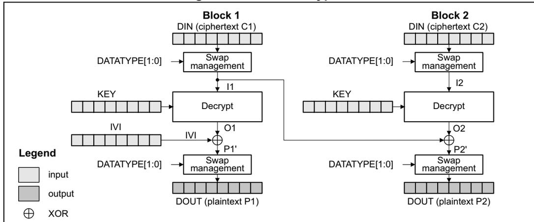
Figure 319. ECB decryption
![Diagram of ECB decryption showing two blocks, Block 1 and Block 2, processed independently. Each block has a DIN (ciphertext) input, a Swap management block, a Decrypt block, and a DOUT (plaintext) output. A KEY is input to the Decrypt block. DATATYPE[1:0] is input to the Swap management blocks. A legend indicates that light gray boxes are input and dark gray boxes are output.](/RM0481-STM32H523-33-562-63-573/91a6d9e7f14cf6eece2f1f3c2608957a_img.jpg)
The diagram illustrates the ECB decryption process for two blocks, Block 1 and Block 2. Each block is processed independently. For Block 1, the DIN (ciphertext C1) is input to a Swap management block, which also receives DATATYPE[1:0]. The output of the Swap management block (I1) is input to the Decrypt block, which also receives a KEY. The output of the Decrypt block (O1) is input to another Swap management block, which also receives DATATYPE[1:0]. The output of this second Swap management block is the DOUT (plaintext P1). The same process is repeated for Block 2, with DIN (ciphertext C2), I2, O2, and DOUT (plaintext P2). A legend indicates that light gray boxes represent input and dark gray boxes represent output.
In CBC encryption mode the output of each block chains with the input of the following block. To make each message unique, an initialization vector is used during the first block processing. When decrypting in CBC, a special key scheduling is required before processing the first block.
Figure 320 and Figure 321 describe the cipher block chaining (CBC) implementation in encryption and in decryption, respectively. To select this chaining mode, write CHMOD[2:0] with 0x1.
Figure 320. CBC encryption
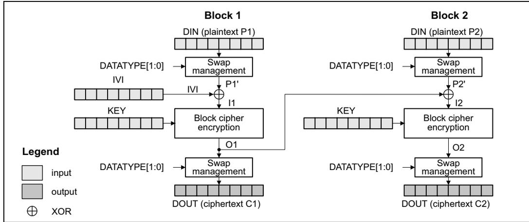
Figure 321. CBC decryption
For more details, refer to NIST Special Publication 800-38A, Recommendation for Block Cipher Modes of Operation .
ECB and CBC encryption process
This process is described in Section 34.4.5 , with the following sequence of events:
- 1. Disable the SAES peripheral, by clearing EN.
- 2. Wait until BUSY is cleared (no RNG random number fetch in progress).
- 3. Initialize the SAES_CR register as follows:
- – Select ECB or CBC chaining mode (write CHMOD[2:0] with 0x0 or 0x1) in encryption mode (write MODE[1:0] with 0x0).
- – Configure the data type, through DATATYPE[1:0].
- – Configure the key size, through KEYSIZE. If the key must not be shared with a different security context (different secure attribute), the KEYPROT bit must also be set.
- – Select normal key mode by writing KMOD[1:0] with 0x0. For the other KMOD[1:0] values, refer to Section 34.4.14 (wrapped keys) and Section 34.4.15 (shared keys).
- 4. Write the initialization vector into the SAES_IVRx registers if CBC mode is selected in the previous step.
- 5. Write the key into the SAES_KEYRx registers. Alternatively, select a key source different from the key registers by writing KEYSEL[2:0] with a value different from 0x0. Refer to Section 34.4.17: SAES key registers for details.
- 6. Wait until KEYVALID is set (the key loading completed).
- 7. Enable the SAES peripheral, by setting EN.
- 8. Append cleartext data:
- a) If it is the second-last or the last block and the plaintext size of the message is not a multiple of 16 bytes, follow the guidance in Section 34.4.7 .
- b) Append the cleartext block into SAES as described in Section 34.4.5 , then read the SAES_DOUTR register four times to save the ciphertext block.
- c) Repeat the step b) until the third-last plaintext block is encrypted. For the last two blocks, follow the steps a) and b) .
- 9. Finalize the sequence: disable the SAES peripheral, by clearing EN.
ECB/CBC decryption process
This process is described in Section 34.4.5 , with the following sequence of events:
- 1. Disable the SAES peripheral, by clearing EN.
- 2. Wait until BUSY is cleared (no RNG random number fetch in progress).
- 3. Initialize the SAES_CR register as follows:
- – Select the key derivation mode (write MODE[1:0] with 0x1). The CHMOD[2:0] bitfield is not significant during this operation.
- – Configure the data type, through DATATYPE[1:0].
- – Configure the key size, through KEYSIZE. If the key must not be shared with a different security context (different secure attribute), the KEYPROT bit must also be set.
- – Select normal key mode by writing KMOD[1:0] with 0x0. For the other KMOD[1:0] values, refer to Section 34.4.14 (wrapped keys) and Section 34.4.15 (shared keys).
- 4. Write the key into the SAES_KEYRx registers. Alternatively, select a key source different from the key registers by writing KEYSEL[2:0] with a value different from 0x0. Refer to Section 34.4.17: SAES key registers for details.
- 5. Wait until KEYVALID is set (the key loading completed).
- 6. Enable the SAES peripheral, by setting EN. The peripheral immediately starts an AES round for key preparation.
- 7. Wait until the CCF flag in the SAES_ISR register is set.
- 8. Clear the CCF flag, by setting the CCF bit of the SAES_ICR register. The decryption key is available in the AES core and SAES is disabled automatically.
- 9. Select ECB or CBC chaining mode (write CHMOD[2:0] with 0x0 or 0x1) in decryption mode (write MODE[1:0] with 0x2). Do not change other parameters.
- 10. Write the initialization vector into the SAES_IVRx registers if CBC mode is selected in the previous step.
- 11. Enable the SAES peripheral, by setting EN.
- 12. Append encrypted data:
- a) If it is the second-last or the last block and the ciphertext size of the message is not a multiple of 16 bytes, follow the guidance in Section 34.4.7 .
- b) Append the ciphertext block into SAES as described in Section 34.4.5 , then read the SAES_DOUTR register four times to save the plaintext block (MSB first).
- c) Repeat the step b) until the third-last ciphertext block is decrypted. For the last two blocks, follow the steps a) and b) .
- 13. Finalize the sequence: disable the SAES peripheral, by clearing EN.
Suspend/resume operations in ECB/CBC modes
The following sequences are valid for normal key mode (KMOD[1:0] at 0x0).
The suspend and resume operations are only supported when SAES is used in CPU mode, not in DMA mode.
To suspend the processing of a message , proceed as follows:
- 1. Wait until the CCF flag in the SAES_ISR register is set (computation completed).
- 2. Read four times the SAES_DOUTR register to save the last processed block.
- 3. Clear the CCF flag, by setting the CCF bit of the SAES_ICR register.
- 4. Save initialization vector registers (only required in CBC mode as the SAES_IVRx registers are altered during the data processing).
- 5. Disable the SAES peripheral, by clearing EN.
- 6. Save the SAES_CR register and clear the key registers if they are not needed, to process the higher-priority message.
To resume the processing of a message , proceed as follows:
- 1. Disable the SAES peripheral, by clearing EN.
- 2. Restore the SAES_CR register (with correct KEYSIZE) then restore the SAES_KEYRx registers. For KEYSEL[2:0] selecting a key source different from key registers, refer to Section 34.4.17: SAES key registers for details.
- 3. Prepare the decryption key, as described in ECB/CBC decryption process (only required for ECB or CBC decryption).
- 4. Restore the SAES_IVRx registers, using the saved configuration (only required in CBC mode).
- 5. Enable the SAES peripheral, by setting EN.
Note: It is not required to save the key registers as the application knows the original key.
34.4.10 SAES counter (CTR) mode
The CTR mode uses the AES core to generate a key stream. The keys are then XOR-ed with the plaintext to obtain the ciphertext. Unlike with ECB and CBC modes, no key scheduling is required for the CTR decryption since the AES core is always used in encryption mode.
A typical message construction in CTR mode is given in Figure 322 .
Figure 322. Message construction in CTR mode
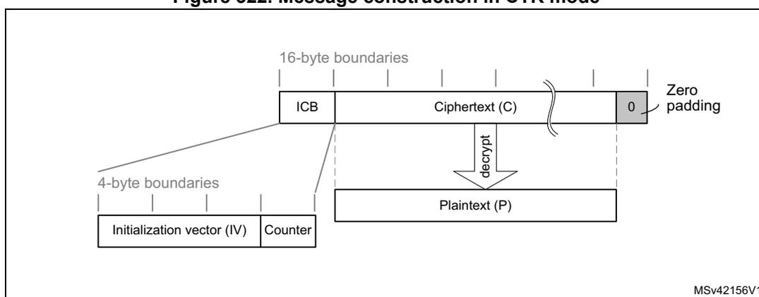
The diagram shows the structure of a message in CTR mode. At the top, a horizontal bar represents the message structure with '16-byte boundaries' indicated by vertical lines. The first 16-byte block is the 'ICB' (Initial Counter Block). This is followed by 'Ciphertext (C)', which is shown with a break in the bar. The end of the message is marked with '0' and 'Zero padding'. Below the ICB, a line points to a box containing 'Initialization vector (IV)' and 'Counter', which are separated by a vertical line. This box is under '4-byte boundaries'. Below the Ciphertext (C), a downward arrow labeled 'decrypt' points to a box labeled 'Plaintext (P)'.
The structure of this message is:
- • A 16-byte initial counter block (ICB), composed of two distinct fields:
- – Initialization vector (IV) : a 96-bit value that must be unique for each encryption cycle with a given key.
- – Counter : a 32-bit big-endian integer that is incremented each time a block processing is completed. The initial value of the counter must be set to 1.
- • The plaintext P is encrypted as ciphertext C, with a known length. This length can be non-multiple of 16 bytes, in which case a plaintext padding is required.
For more details, refer to NIST Special Publication 800-38A, Recommendation for Block Cipher Modes of Operation .
CTR encryption and decryption
Figure 323 describes the counter (CTR) chaining implementation in the SAES peripheral (encryption). To select this chaining mode, write CHMOD[2:0] with 0x2.
Figure 323. CTR encryption
![Diagram of CTR encryption process showing two blocks, Block 1 and Block 2. Each block consists of an IVI (Nonce + 32-bit counter) being encrypted with a KEY to produce an output O. The output O is XORed with the plaintext DIN (P1 or P2) to produce the ciphertext DOUT (C1 or C2). A 'Swap management' block is used to handle the data type (DATATYPE[1:0]). The counter is incremented by 1 for each block.](/RM0481-STM32H523-33-562-63-573/d44693d516d0d53988513d2f2c338075_img.jpg)
The diagram illustrates the CTR encryption process for two blocks, Block 1 and Block 2. In Block 1, the IVI (Nonce + 32-bit counter) is input to an 'Encrypt' block along with a 'KEY'. The 'Encrypt' block produces an output O1. O1 is XORed with the plaintext DIN (P1) to produce the ciphertext DOUT (C1). A 'Swap management' block is used to handle the data type (DATATYPE[1:0]). The counter is incremented by 1 for the next block. In Block 2, the IVI (Nonce + 32-bit counter + 1) is input to an 'Encrypt' block along with a 'KEY'. The 'Encrypt' block produces an output O2. O2 is XORed with the plaintext DIN (P2) to produce the ciphertext DOUT (C2). A 'Swap management' block is used to handle the data type (DATATYPE[1:0]).
Legend
- input (light gray rectangle)
- output (dark gray rectangle)
- XOR (circle with a cross)
MSv69567V1
Initialization vectors in SAES must be initialized as shown in Table 333 .
Table 333. Counter mode initialization vector definition
| SAES_IVR3[31:0] | SAES_IVR2[31:0] | SAES_IVR1[31:0] | SAES_IVR0[31:0] |
|---|---|---|---|
| IVI[127:96] | IVI[95:64] | IVI[63:32] | IVI[31:0] 32-bit counter = 0x0001 |
CTR encryption and decryption process
This process is described in Section 34.4.5 , with the following sequence of events:
- Disable the SAES peripheral, by clearing EN.
- Wait until BUSY is cleared (no RNG random number fetch in progress).
- Initialize the SAES_CR register:
- Select CTR chaining mode (write CHMOD[2:0] with 0x2) in encryption or decryption mode (write MODE[1:0] with 0x0 or 0x2).
- Configure the data type, through DATATYPE[1:0].
- Configure the key size, through KEYSIZE. If the key must not be shared with a different security context (different secure attribute), the KEYPROT bit must also be set.
- Select normal key mode, by writing KMOD[1:0] with 0x0. For the other KMOD[1:0] values, refer to Section 34.4.14 (wrapped keys) and Section 34.4.15 (shared keys).
- Write the initialization vector into the SAES_IVRx registers according to Table 333 .
- Write the key into the SAES_KEYRx registers. Alternatively, select a key source different from the key registers by writing KEYSEL[2:0] with a value different from 0x0. Refer to Section 34.4.17: SAES key registers for details.
- Wait until KEYVALID is set (the key loading completed).
- Enable the SAES peripheral, by setting EN.
- 8. Append data:
- a) If it is the last block and the plaintext (encryption) or ciphertext (decryption) size in the block is less than 16 bytes, pad the remainder of the block with zeros.
- b) Append the data block into SAES as described in Section 34.4.5 , then read the SAES_DOUTR register four times to save the resulting block (MSB first).
- c) Repeat the step b) until the second-last block is processed. For the last block of plaintext (encryption only), follow the steps a) and b). For the last block, discard the bits that are not part of the message when the last block is smaller than 16 bytes.
- 9. Finalize the sequence: disable the SAES peripheral, by clearing EN.
Suspend/resume operations in CTR mode
Like for the CBC mode, it is possible to interrupt a message to send a higher-priority message, then resume the interrupted message. Detailed CBC suspend and resume sequence is described in Section 34.4.9: SAES basic chaining modes (ECB, CBC) .
The suspend and resume operations are only supported when SAES is used in CPU mode, not in DMA mode.
Note: Like for CBC mode, the IV registers must be reloaded during the resume operation.
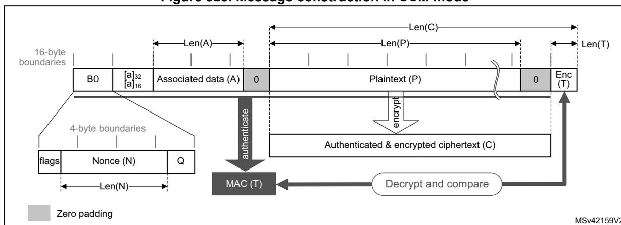
34.4.11 SAES Galois/counter mode (GCM)
The AES Galois/counter mode (GCM) allows encrypting and authenticating a plaintext message into the corresponding ciphertext and tag (also known as message authentication code).
GCM mode is based on AES in counter mode for confidentiality. It uses a multiplier over a fixed finite field for computing the message authentication code. The following figure shows a typical message construction in GCM mode.
Figure 324. Message construction in GCM
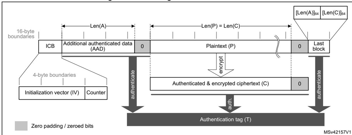
The diagram illustrates the message construction in GCM mode. It shows the following components and flow:
- Initialization vector (IV) and Counter: These are 4-byte boundary components that feed into the ICB (Initialization Counter Block).
- ICB: A 16-byte boundary block that starts the process.
- Additional authenticated data (AAD): A variable-length data block of length \( Len(A) \) that is authenticated but not encrypted. It is followed by zero padding to reach a 16-byte boundary.
- Plaintext (P): A variable-length data block of length \( Len(P) = Len(C) \) that is both encrypted and authenticated.
- Authenticated & encrypted ciphertext (C): The result of encrypting the plaintext. It is followed by zero padding to reach a 16-byte boundary.
- Last block: A final 16-byte block containing the 64-bit lengths \( [Len(A)]_{64} \) and \( [Len(C)]_{64} \) .
- Authentication tag (T): A 16-byte block that provides message authentication, generated by the authentication function.
- Operations:
- authenticate: A vertical arrow indicating the authentication process applied to the ICB, AAD, and ciphertext.
- encrypt: A vertical arrow indicating the encryption of Plaintext (P) into Ciphertext (C).
- auth.: A small vertical arrow indicating the final authentication step for the tag.
- Zero padding / zeroed bits: Indicated by grey blocks at the end of the AAD and ciphertext segments.
The message has the following structure:
- •
16-byte initial counter block (ICB)
, composed of two distinct fields:
- – Initialization vector (IV) : a 96-bit value that must be unique for each encryption cycle with a given key. The GCM standard supports IVs with less than 96 bits, but in this case strict rules apply.
- – Counter : a 32-bit big-endian integer that is incremented each time a block processing is completed. According to NIST specification, the counter value is 0x2 when processing the first block of payload.
- • Authenticated header AAD (also known as additional authentication data) has a known length \( \text{Len}(A) \) that may be a non-multiple of 16 bytes, and must not exceed \( 2^{64} - 1 \) bits. This part of the message is only authenticated, not encrypted.
- • Plaintext message P is both authenticated and encrypted as ciphertext C, with a known length \( \text{Len}(P) \) that may be non-multiple of 16 bytes, and cannot exceed \( 2^{32} - 2 \) 16-byte blocks.
- • Last block contains the AAD header length (bits [32:63]) and the payload length (bits [96:127]) information, as shown in Table 335 .
The GCM standard specifies that ciphertext C has the same bit length as the plaintext P.
When a part of the message (AAD or P) has a length that is a non-multiple of 16-bytes a special padding scheme is required.
For more details, refer to NIST Special Publication 800-38D, Recommendation for Block Cipher Modes of Operation - Galois/Counter Mode (GCM) and GMAC .
Figure 325 describes the GCM chaining implementation in the SAES peripheral (encryption). To select this chaining mode, write CHMOD[2:0] with 0x3.
Figure 325. GCM authenticated encryption
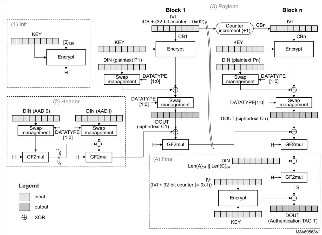
The diagram illustrates the GCM authenticated encryption process, divided into four main stages:
- (1) Init: A KEY is input to an Encrypt block along with an initial vector [0]128. The output is H.
- (2) Header: This stage processes the AAD (Additional Authentication Data). It shows DIN (AAD 0) and DIN (AAD i) being processed through Swap management (controlled by DATATYPE [1:0]) and GF2mul blocks using H. The outputs are XORed together.
- (3) Payload:
This stage shows the encryption of multiple blocks (Block 1 to Block n).
- Block 1: An Initial Counter Block (ICB) with a 32-bit counter set to 0x02 is input to an Encrypt block with KEY. The output is CB1. CB1 is XORed with DIN (plaintext P1) after Swap management (DATATYPE [1:0]) to produce DOUT (ciphertext C1). CB1 is also passed to a Counter increment (+1) block to produce CBn for Block n.
- Block n: CBn is input to an Encrypt block with KEY. The output is XORed with DIN (plaintext Pn) after Swap management (DATATYPE [1:0]) to produce DOUT (ciphertext Cn).
- All ciphertext outputs (C1 to Cn) are passed through GF2mul blocks using H and XORed together.
- (4) Final:
This stage generates the Authentication TAG (T).
- The DIN is set to Len(A)64 || Len(C)64.
- The IVI is set to (IVI + 32-bit counter) = 0x1.
- Both are input to an Encrypt block with KEY. The output is XORed with the accumulated GF2mul output (S) to produce the final DOUT (Authentication TAG T).
Legend:
- input (light gray rectangle)
- output (dark gray rectangle)
- XOR (circle with cross)
MSv69568V1
The first counter block (CB1) is derived from the initial counter block ICB by the application software, as defined in Table 334.
Table 334. Initialization of IV registers in GCM mode
| SAES_IVR3[31:0] | SAES_IVR2[31:0] | SAES_IVR1[31:0] | SAES_IVR0[31:0] |
|---|---|---|---|
| ICB[127:96] | ICB[95:64] | ICB[63:32] | ICB[31:0] 32-bit counter = 0x0002 |
The last block of a GCM message contains the AAD header length and the payload length information, as shown in Table 335.
Table 335. GCM last block definition
| Word order to SAES_DINR | First word | Second word | Third word | Fourth word |
|---|---|---|---|---|
| Input data | AAD length[63:32] | AAD length[31:0] | Payload length[63:32] | Payload length[31:0] |
GCM encryption and decryption process
This process is described in Section 34.4.6 , with the following sequence of events:
GCM initialize
- 1. Disable the SAES peripheral, by clearing EN.
- 2. Wait until BUSY is cleared (no RNG random number fetch in progress).
- 3. Initialize the SAES_CR register:
- – Select GCM chaining mode (write CHMOD[2:0] with 0x3) in encryption or decryption mode (write MODE[1:0] with 0x0 or 0x2). Do not write MODE[1:0] with 0x1.
- – Configure the data type, through DATATYPE[1:0]
- – Configure the key size, through KEYSIZE. If the key must not be shared with a different security context (such as secure, nonsecure, specific CPU), also set KEYPROT.
- – Select normal key mode, by writing KMOD[1:0] with 0x0. For the other KMOD[1:0] values, refer to Section 34.4.14 (wrapped keys) and Section 34.4.15 (shared keys).
- – Select the GCM initialization phase, by writing GCMPH[1:0] with 0x0.
- 4. Write the initialization vector in SAES_IVRx registers according to Table 334 .
- 5. Write the key into the SAES_KEYRx registers. Alternatively, select a key source different from the key registers by writing KEYSEL[2:0] with a value different from 0x0. Refer to Section 34.4.17: SAES key registers for details.
- 6. Wait until KEYVALID is set (the key loading completed).
- 7. Set EN to start the calculation of the hash key. EN is automatically cleared when the calculation is completed.
- 8. Wait until the CCF flag is set in the SAES_ISR register, indicating that the GCM hash subkey (H) computation is completed.
- 9. Clear the CCF flag by setting the CCF bit of the SAES_ICR register.
GCM header phase
- 10. Initialize header phase:
- a) Select the GCM header phase, by writing 0x1 to GCMPH[1:0]. Do not change the other configurations written during GCM initialization.
- b) Enable the SAES peripheral, by setting EN.
- 11. Append header data:
- a) If it is the last block and the AAD in the block is smaller than 16 bytes, pad the remainder of the block with zeros.
- b) Append the data block into SAES as described in Section 34.4.5 .
- c) Repeat the step b) until the second-last AAD data block is processed. For the last block, follow the steps a) and b) .
Note: This phase can be skipped if there is no AAD, that is, Len(A) = 0.
No data are read during header phase.
GCM payload phase
- 12. Initialize payload phase:
- a) Select the GCM payload phase, by writing GCM PH [1:0] with 0x2. Do not change the other configurations written during GCM initialization.
- b) If the header phase is skipped, enable the SAES peripheral by setting EN.
- 13. Append payload data:
- a) If it is the last block and the message in the block is smaller than 16 bytes, pad the remainder of the block with zeros.
- b) Append the data block into SAES as described in Section 34.4.5 , then read the SAES_DOUTR register four times to save the resulting block
- c) Repeat the step b) until the second-last plaintext block is encrypted or until the last block of ciphertext is decrypted. For the last block of plaintext (encryption only), follow the steps a) and b) . For the last block, discard the bits that are not part of the payload when the last block is smaller than 16 bytes.
Note: This phase can be skipped if there is no payload, that is, Len(C)=0 (see GMAC mode).
GCM finalization
- 14. Encryption only: wait until the BUSY flag in the SAES_SR register is cleared.
- 15. Select the GCM final phase, by writing GCM PH [1:0] with 0x3. Do not change the other configurations written during GCM initialization.
- 16. Write the final GCM block into the SAES_DINR register. It is the concatenated AAD bit and payload bit lengths, as shown in Table 335 .
- 17. Wait until the CCF flag in the SAES_ISR register is set.
- 18. Get the GCM authentication tag, by reading the SAES_DOUTR register four times.
- 19. Clear the CCF flag, by setting the CCF bit of the SAES_ICR register.
- 20. Disable the SAES peripheral, by clearing EN. If it is an authenticated decryption, compare the generated tag with the expected tag passed with the message.
Note: In the final phase, data are written to SAES_DINR normally (no swapping), while swapping is applied to tag data read from SAES_DOUTR.
When transiting from the header or the payload phase to the final phase, the SAES peripheral must not be disabled, otherwise the result is wrong.
Suspend/resume operations in GCM mode
Suspend/resume operations are not supported in GCM mode.
34.4.12 SAES Galois message authentication code (GMAC)
The Galois message authentication code (GMAC) allows the authentication of a plaintext, generating the corresponding tag information (also known as message authentication code).
GMAC is similar to GCM, except that it is applied on a message composed only by plaintext authenticated data (that is, only header, no payload). The following figure shows typical message construction for GMAC.
Figure 326. Message construction in GMAC mode
![Figure 326: Message construction in GMAC mode. The diagram shows a message structure with 16-byte boundaries. It starts with an ICB (Initialization Counter Block), followed by 'Authenticated data' of length Len(A). The last block is split into two 8-byte parts: [Len(A)]64 and [0]64. Below the ICB, a 4-byte boundary separates the 'Initialization vector (IV)' and 'Counter'. An arrow labeled 'auth.' points from the 'Authenticated data' to an 'Authentication tag (T)'. A legend indicates that grey boxes represent 'Zero padding'. The reference MSv42158V2 is shown in the bottom right.](/RM0481-STM32H523-33-562-63-573/382db96e4d3b34cc9ae5f4269e745ed3_img.jpg)
For more details, refer to NIST Special Publication 800-38D, Recommendation for Block Cipher Modes of Operation - Galois/Counter Mode (GCM) and GMAC .
Figure 327 describes the GMAC chaining implementation in the SAES peripheral. To select this chaining mode, write CHMOD[2:0] with 0x3.
Figure 327. GMAC authentication mode
![Figure 327: GMAC authentication mode. This diagram illustrates the four-step process: (1) Init, (2) Header, (3) Payload (omitted), and (4) Final. (1) Init: A KEY is input to an Encrypt block along with [0]128 to produce H. (2) Header: Message blocks (DIN) are processed through 'Swap management' (controlled by DATATYPE [1:0]) and then GF2mul with H. (4) Final: The KEY is input to an Encrypt block with IVI + 32-bit counter (= 0x0) to produce S. The final input is DIN || len(A)64 || [0]64, which is XORed with H and then GF2mul with S to produce the DOUT (authentication tag T). A legend defines input (white box), output (grey box), and XOR (circle with cross). The reference MSv69569V1 is shown in the bottom right.](/RM0481-STM32H523-33-562-63-573/f779753de5dcbd3011f1f8caed2939d6_img.jpg)
The GMAC algorithm corresponds to the GCM algorithm applied on a message that only contains a header. As a consequence, all steps and settings are the same as with the GCM, except that the payload phase is omitted.
Suspend/resume operations in GMAC
Suspend/resume operations are not supported in GMAC mode.
34.4.13 SAES counter with CBC-MAC (CCM)
The AES counter with cipher block chaining-message authentication code (CCM) algorithm allows encryption and authentication of plaintext, generating the corresponding ciphertext and tag (also known as message authentication code). To ensure confidentiality, the CCM algorithm is based on AES counter mode processing. It uses cipher block chaining technique to generate the message authentication code. This is commonly called CBC-MAC.
Note: NIST does not approve CBC-MAC as an authentication mode outside the context of the CCM specification.
The following figure shows typical message construction for CCM.
Figure 328. Message construction in CCM mode
The structure of the message is:
- 16-byte first authentication block (B0)
, composed of three distinct fields:
- Q: a bit string representation of the octet length of P (Len(P))
- Nonce (N): a single-use value (that is, a new nonce must be assigned to each new communication) of Len(N) size. The sum Len(N) + Len(P) must be equal to 15 bytes.
- Flags: most significant octet containing four flags for control information, as specified by the standard. It contains two 3-bit strings to encode the values t (MAC length expressed in bytes) and Q (plaintext length such that \( \text{Len}(P) < 2^{8Q} \) bytes). The counter blocks range associated to Q is equal to \( 2^{8Q-4} \) , that is, if the maximum value of Q is 8, the counter blocks used in cipher must be on 60 bits.
- 16-byte blocks (B)
associated to the associated data (A).
This part of the message is only authenticated, not encrypted. This section has a known length Len(A) that can be a non-multiple of 16 bytes (see Figure 328). The standard also states that, on MSB bits of the first message block (B1), the associated data length expressed in bytes (a) must be encoded as follows:
- If \( 0 < a < 2^{16} - 2^8 \) , then it is encoded as \( [a]_{16} \) , that is, on two bytes.
- If \( 2^{16} - 2^8 < a < 2^{32} \) , then it is encoded as \( 0\text{xff} \parallel 0\text{xfe} \parallel [a]_{32} \) , that is, on six bytes.
- If \( 2^{32} < a < 2^{64} \) , then it is encoded as \( 0\text{xff} \parallel 0\text{xff} \parallel [a]_{64} \) , that is, on ten bytes.
- • 16-byte blocks (B) associated to the plaintext message P, which is both authenticated and encrypted as ciphertext C, with a known length Len(P). This length can be a non-multiple of 16 bytes (see Figure 328 ).
- • Encrypted MAC (T) of length Len(T) appended to the ciphertext C of overall length Len(C).
When a part of the message (A or P) has a length that is a non-multiple of 16-bytes, a special padding scheme is required.
Note: CCM chaining mode can also be used with associated data only (that is, no payload).
As an example, the C.1 section in NIST Special Publication 800-38C gives the following values (hexadecimal numbers):
N: 10111213 141516 (Len(N) = 56 bits or 7 bytes)
A: 00010203 04050607 (Len(A) = 64 bits or 8 bytes)
P: 20212223 (Len(P) = 32 bits or 4 bytes)
T: 6084341B (Len(T) = 32 bits or t = 4)
B0: 4F101112 13141516 00000000 00000004
B1: 00080001 02030405 06070000 00000000
B2: 20212223 00000000 00000000 00000000
CTR0: 0710111213 141516 00000000 00000000
CTR1: 0710111213 141516 00000000 00000001
For more details, refer to NIST Special Publication 800-38C, Recommendation for Block Cipher Modes of Operation - The CCM Mode for Authentication and Confidentiality .
Figure 329 describes the CCM chaining implementation in the SAES peripheral (encryption). To select this chaining mode, write CHMOD[2:0] with 0x4.
Figure 329. CCM mode authenticated encryption
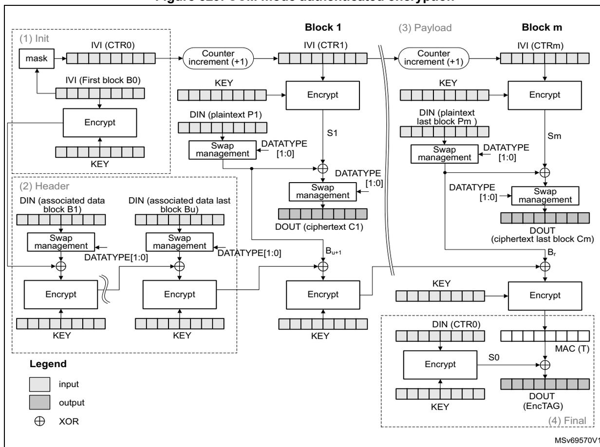
The diagram illustrates the CCM chaining implementation for encryption, divided into four main stages:
- (1) Init: The process starts with the IVI (CTR0) register. A mask is applied to the IVI (First block B0) to generate the initial counter value. This is encrypted using the KEY to produce S0. The counter is then incremented (+1) to produce IVI (CTR1).
- (2) Header: The header consists of associated data blocks (B1 to Bu). Each block is processed through a Swap management block (controlled by DATATYPE [1:0]) and then encrypted using the KEY. The output of one block is XORed with the next block (DIN) before being encrypted.
- (3) Payload: The payload consists of plaintext blocks (P1 to Pm). Each block is encrypted using the KEY and the current counter value (IVI (CTR1 to CTRm)). The output is XORed with the previous ciphertext block (S1 to Sm) to produce the ciphertext (DOUT). The counter is incremented (+1) for each block.
- (4) Final: The final stage involves the MAC (T) calculation. The S0 value from the Init stage is XORed with the output of the last payload block (Sm) and then encrypted using the KEY to produce the MAC (T) value, which is stored in the DOUT (EncTAG) register.
Legend:
- input (light gray box)
- output (dark gray box)
- XOR (circle with a cross)
MSv69570V1
The first block of a CCM message (B0) must be prepared by the application as defined in Table 336.
Table 336. Initialization of IV registers in CCM mode
| SAES_IVR3[31:0] | SAES_IVR2[31:0] | SAES_IVR1[31:0] | SAES_IVR0[31:0] |
|---|---|---|---|
| B0[127:96] (1) | B0[95:64] | B0[63:32] | B0[31:0] (2) |
- 1. The five most significant bits are cleared (flag bits).
- 2. Q length bits are cleared, except for the bit 0 that is set.
SAES supports counters up to 64 bits, as specified by NIST.
CCM encryption and decryption process
This process is described in Section 34.4.6 , with the following sequence of events:
CCM initialize
- 1. Disable the SAES peripheral, by clearing EN.
- 2. Wait until BUSY is cleared (no RNG random number fetch in progress).
- 3. Initialize the SAES_CR register:
- – Select CCM chaining mode (write CHMOD[2:0] with 0x4) in encryption or decryption mode (write MODE[1:0] with 0x0 or 0x2). Do not write MODE[1:0] with 0x1.
- – Configure the data type, through DATATYPE[1:0]
- – Configure the key size, through KEYSIZE. If the key must not be shared with a different security context, also set the KEYPROT bit.
- – Select normal key mode, by writing KMOD[1:0] with 0x0. For the other KMOD[1:0] values, refer to Section 34.4.14 (wrapped keys) and Section 34.4.15 (shared keys).
- – Select the CCM initialization phase, by writing GCMPH[1:0] with 0x0.
- 4. Write the B0 data in SAES_IVRx registers according to Table 336 .
- 5. Write the key into the SAES_KEYRx registers. Alternatively, select a key source different from the key registers by writing KEYSEL[2:0] with a value different from 0x0. Refer to Section 34.4.17: SAES key registers for details.
- 6. Wait until KEYVALID is set (the key loading completed).
- 7. Set EN to start the first mask calculation. The EN bit is automatically cleared when the calculation is completed.
- 8. Wait until the CCF flag in the SAES_ISR register is set.
- 9. Clear the CCF flag, by setting the CCF bit of the SAES_ICR register.
CCM header phase
- 10. Initialize header phase:
- a) Prepare the first block of the (B1) data associated with the message, in accordance with CCM chaining rules.
- b) Select the CCM header phase, by writing GCMPH[1:0] with 0x1. Do not change the other configurations written during the CCM initialization.
- c) Enable the SAES peripheral, by setting EN.
- 11. Append header data:
- a) If it is the last block and the associated data in the block is smaller than 16 bytes, pad the remainder of the block with zeros.
- b) Append the data block into SAES as described in Section 34.4.5 .
- c) Repeat the step b) until the second-last associated data block is processed. For the last block, follow the steps a) and b) .
Note: This phase can be skipped if there is no associated data, that is, Len(A) = 0
No data are read during the header phase.
CCM payload phase
- 12. Initialize payload phase:
- a) Select the CCM payload phase, by writing GCMPH[1:0] with 0x2. Do not change the other configurations written during the CCM initialization.
- b) If the header phase is skipped, enable the SAES peripheral, by setting EN.
- 13. Append payload data:
- a) In encryption only, if it is the last block and the plaintext in the block is smaller than 16 bytes, pad the remainder of the block with zeros.
- b) Append the data block into SAES as described in Section 34.4.5 , then read the SAES_DOUTR register four times to save the resulting block.
- c) Repeat the step b) until the second-last plaintext block is encrypted or until the last block of ciphertext is decrypted. For the last block of plaintext (encryption only), follow the steps a) and b) . For the last block, discard the bits that are not part of the payload when the last block is smaller than 16 bytes.
Note: This phase can be skipped if there is no payload, that is, \( Len(P) = 0 \) or \( Len(C) = Len(T) \) . Remove \( LSB_{Len(T)}(C) \) encrypted tag information when decrypting ciphertext C.
CCM finalization
- 14. Select the CCM final phase, by writing GCMPH[1:0] with 0x3. Do not change the other configurations written during the CCM initialization.
- 15. Wait until CCF flag in the SAES_ISR register is set.
- 16. Get the CCM authentication tag, by reading the SAES_DOUTR register four times.
- 17. Clear the CCF flag, by setting the CCF bit of the SAES_ICR register.
- 18. Disable the SAES peripheral, by clearing EN. If it is an authenticated decryption, compare the generated tag with the expected tag passed with the message. Mask the authentication tag output with tag length to obtain a valid tag.
Note: In the final phase, swapping is applied to tag data read from SAES_DOUTR register.
When transiting from the header or the payload phase to the final phase, the SAES peripheral must not be disabled, otherwise the result is wrong.
Suspend and resume operations in CCM mode
The suspend and resume operations are only supported when SAES is used in CPU mode, not in DMA mode.
To suspend the processing of a message in header or payload phase , proceed as follows:
- 1. Wait until the CCF flag of the SAES_ISR register is set (computation completed).
- 2. In the payload phase, read four times the SAES_DOUTR register to save the last-processed block.
- 3. Clear the CCF flag in the SAES_ISR register, by setting the CCF bit of the SAES_ICR register.
- 4. Save the SAES_SUSPRx registers in the memory.
- 5. Save the IV registers as they are altered during the data processing.
- 6. Disable the SAES peripheral, by clearing EN.
- 7. Save the current SAES_CR configuration in the memory. Key registers do not need to be saved as the original key value is known by the application.
To resume the processing of a message, proceed as follows:
- 1. Disable the SAES peripheral, by clearing EN.
- 2. Write the suspend register values, previously saved in the memory, back into their corresponding SAES_SUSPRx registers.
- 3. Restore SAES_IVRx registers using the saved configuration.
- 4. Restore the initial setting values in the SAES_CR and SAES_KEYRx registers. For KEYSEL[2:0] selecting a key source different from the key registers, refer to Section 34.4.17: SAES key registers for details.
- 5. Enable the SAES peripheral, by setting EN.
34.4.14 SAES operation with wrapped keys
SAES peripheral can wrap (encrypt) and unwrap (decrypt) application keys using hardware-secret key DHUK, XOR-ed or not with application key BHK. With this feature, AES keys can be made usable by application software without being exposed in clear-text (unencrypted).
Wrapped key sequences are too small to be suspended/resumed. SAES cannot unwrap a key using an unwrapped key.
Operation with wrapped keys for SAES in ECB and CBC modes
Figure 330 summarizes how to wrap or unwrap keys for SAES in ECB and CBC modes. To protect the wrapped key, select DHUK by writing KEYSEL[2:0] with 0x1 or 0x4. Alternatively, select BHK by writing KEYSEL[2:0] with 0x2 if the corresponding registers are read/write-locked in the TAMP peripheral.
Figure 330. Operation with wrapped keys for SAES in ECB and CBC modes
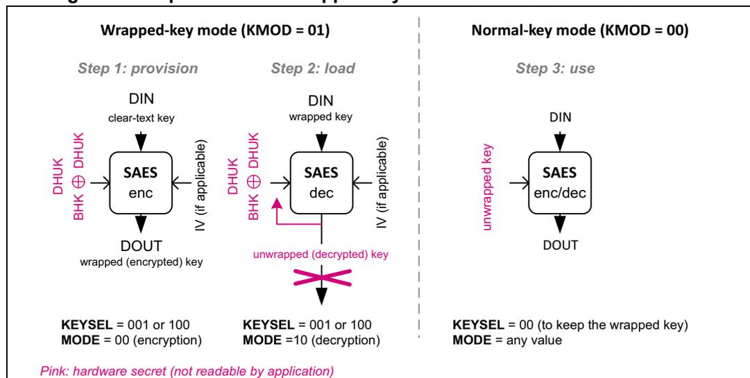
Wrapped-key mode (KMOD = 01)
Step 1: provision
DIN: clear-text key
DHUK ⊕ BHK → SAES enc → DOUT: wrapped (encrypted) key
IV (if applicable)
KEYSEL = 001 or 100
MODE = 00 (encryption)
Step 2: load
DIN: wrapped key
DHUK ⊕ BHK → SAES dec → unwrapped (decrypted) key (discarded)
IV (if applicable)
KEYSEL = 001 or 100
MODE = 10 (decryption)
Normal-key mode (KMOD = 00)
Step 3: use
DIN: unwrapped key
SAES enc/dec → DOUT
KEYSEL = 00 (to keep the wrapped key)
MODE = any value
Pink: hardware secret (not readable by application)
Note: DHUK value depends on privilege, security, KMOD[1:0], KEYSEL[2:0], CHMOD[2:0], and KEYSIZE.
Key wrapping for SAES
The recommended sequence to wrap (that is, encrypt) a key is as follows:
- 1. Disable the SAES peripheral, by clearing EN.
- 2. Wait until BUSY is cleared (no RNG random number fetch in progress).
- 3. Initialize the SAES_CR register as follow:
- – Select ECB or CBC chaining mode (write CHMOD[2:0] with 0x0 or 0x1) in encryption mode (MODE[1:0] at 0x0)
- – Select 32-bit data type (DATATYPE[1:0] at 0x0)
- – Configure the key size with KEYSIZE. This information is used both for the encryption key and for the key to be encrypt.
- – Select wrapped key mode by writing KMOD[1:0] with 0x1
- 4. Write the initialization vector in SAES_IVRx registers if CBC mode has been selected in previous step.
- 5. Select the DHUK key source by writing KEYSEL[2:0] with 0x1 or 0x4. Optionally, select the BHK, by writing KEYSEL[2:0] with 0x2. Refer to Section 34.4.17 for details on the use of KEYSEL[2:0].
- 6. Wait until KEYVALID is set (DHUK loading completed).
- 7. Enable the SAES peripheral, by setting EN.
- 8. Write the SAES_DINR register four times to input the key to encrypt (MSB first, see Table 338 ).
- 9. Wait until CCF flag is set in the SAES_ISR register.
- 10. Get the encrypted key (MSB first) by reading the SAES_DOUTR register four times. Then clear the CCF flag, by setting the CCF bit in SAES_ICR register.
- 11. Repeat steps 8 to 10. if KEYSIZE is set.
- 12. Disable the SAES peripheral, by clearing EN.
Note: Encryption in Wrapped-key mode is only supported when ECB or CBC is selected.
Key unwrapping for SAES
The recommended sequence to unwrap (or decrypt) a wrapped (encrypted) key using ECB/CBC is as follows:
- 1. Disable the SAES peripheral, by clearing EN.
- 2. Wait until BUSY is cleared (no RNG random number fetch in progress).
- 3. Initialize the SAES_CR register as follow:
- – Select the chaining mode used during the wrapping process (CHMOD[2:0] at 0x0 or 0x1) in key derivation mode (MODE[1:0] at 0x1)
- – Select 32-bit data type (DATATYPE[1:0] at 0x0)
- – Configure the key size used during the wrapping process, with KEYSIZE. This information is used both for the decryption key and for the key to decrypt.
- – Select wrapped key mode, by writing KMOD[1:0] with 0x1.
- 4. With KEYSEL[2:0], select the same key source as when the key was wrapped/encrypted.
- 5. Wait until KEYVALID is set (the key loading completed).
- 6. Set EN bit in SAES_CR to enable the peripheral
- 7. Wait until CCF flag is set in the SAES_ISR register.
- 8. Clear the CCF flag, by setting the CCF bit in SAES_ICR register. The decryption key is available in the AES core, and SAES is disabled automatically.
- 9. Select the decryption mode (MODE[1:0] at 0x2). Other parameters are unchanged.
- 10. Write the initialization vector in SAES_IVRx registers if CBC mode has been selected in previous step.
- 11. Enable the SAES peripheral, by setting EN.
- 12. Write the SAES_DINR register four times to input the key to decrypt (MSB first, see Table 338 ).
- 13. Wait until CCF flag is set in the SAES_ISR register. Then clear the CCF flag by setting the CCF bit in SAES_ICR register. Reading SAES_DOUTR returns zero and triggers a read error (RDERRF).
- 14. Repeat steps 12. and 13. if KEYSIZE is set.
- 15. Disable the SAES peripheral, by clearing EN.
At the end of this sequence, the decrypted wrapped key is immediately usable by the application for any AES operation (normal key mode, that is, with KMOD[1:0] = 0x0).
Decrypted wrapped key can be shared with an application running in a different security context (different security attribute) if KEYPROT bit was cleared during step 3.
Note: When KMOD[1:0] = 0x1 (wrapped key) and MODE[1:0] = 0x2 (decryption) a read access to SAES_DOUTR register triggers a read error (RDERRF).
When KEYSEL[2:0] is at 0x1 (DHUK) or 0x4 (DHUK XOR BHK), the application software must use the same privilege, security, KMOD[1:0], CHMOD[2:0] and KEYSIZE context for encryption and decryption. Otherwise, the result is incorrect.
Operation with wrapped keys for SAES in CTR mode
Figure 331 summarizes how to unwrap keys for SAES in CTR mode. To protect the derived key, select DHUK by writing KEYSEL[2:0] with 0x1 or 0x4. Alternatively, select BHK by
writing KEYSEL[2:0] with 0x2 if the corresponding registers are read/write-locked in the TAMP peripheral.
Figure 331. Operation with wrapped keys for SAES in CTR mode
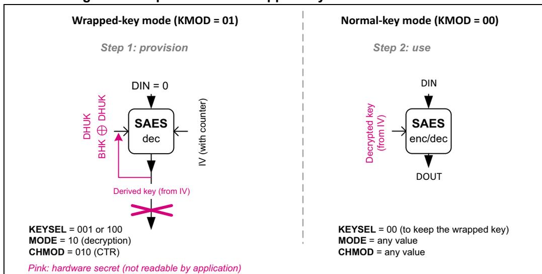
Wrapped-key mode (KMOD = 01)
Step 1: provision
DIN = 0
DHUK \( \oplus \) BHK \( \oplus \) DHUK
SAES dec
IV (with counter)
Derived key (from IV)
KEYSEL = 001 or 100
MODE = 10 (decryption)
CHMOD = 010 (CTR)
Normal-key mode (KMOD = 00)
Step 2: use
DIN
Decrypted key (from IV)
SAES enc/dec
DOUT
KEYSEL = 00 (to keep the wrapped key)
MODE = any value
CHMOD = any value
Pink: hardware secret (not readable by application)
Note: DHUK value depends on privilege, security, KMOD[1:0], KEYSEL[2:0], CHMOD[2:0], and KEYSIZE.
The recommended sequence for SAES wrapped key mode using CTR is as follows:
- 1. Disable the SAES peripheral, by clearing EN.
- 2. Wait until BUSY is cleared (no RNG random number fetch in progress).
- 3. Initialize the SAES_CR register as follow:
- – Select the CTR chaining mode (CHMOD[2:0] at 0x2) in decryption mode (MODE[1:0] at 0x2). Other MODE[1:0] values are not supported.
- – Select 32-bit data type (DATATYPE[1:0] at 0x0)
- – Configure the key size with KEYSIZE. It is used for encryption key and for the key to share.
- – Select wrapped key mode, by writing KMOD[1:0] with 0x1.
- 4. Write the initialization vector in SAES_IVRx registers, keeping the two least significant bits of SAES_IVR0 at zero.
- 5. Select the DHUK key source by writing KEYSEL[2:0] with 0x1 or 0x4. Optionally, select the BHK, by writing KEYSEL[2:0] with 0x2. Refer to Section 34.4.17 for details on the use of KEYSEL[2:0].
- 6. Wait until KEYVALID is set (the key loading completed).
- 7. Enable the SAES peripheral, by setting EN.
- 8. Wait until CCF flag is set in the SAES_ISR register.
- 9. Clear the CCF flag, by setting the CCF bit in SAES_ICR register. The derived hardware secret key is available in SAES_KEYRx registers.
- 10. Repeat steps 8. and 9. if KEYSIZE is set.
- 11. Disable the SAES peripheral, by clearing EN.
At the end of this sequence, the hardware secret key derived from the public data in the SAES_IVRx registers is then immediately usable by the application for any AES operation (normal key mode, that is, with KMOD[1:0] = 0x0).
Note: The configuration KMOD[1:0] at 0x1 (wrapped key), CHMOD[2:0] at 0x2 (CTR chaining), and MODE at 0x0 (encryption) disables the peripheral, by automatically clearing the EN bit of the SAES_CR register.
34.4.15 SAES operation with shared keys
SAES peripheral can share application keys wrapped with hardware-secret key DHUK, XOR-ed or not with application key BHK. With this feature, the application software can make the AES keys available to the AES peripheral, without exposing them in clear-text (unencrypted).
Shared key sequences are too small to be suspended/resumed. SAES cannot unwrap a shared key using an unwrapped key.
Note: When a key stored in SAES is shared with AES, the protection given by KEYPROT bit is lost. The protection is detailed in Section 34.4.17: SAES key registers .
Figure 332 summarizes how to wrap or unwrap keys to share with AES peripheral. To protect the shared key, DHUK must be selected, by writing KEYSEL[2:0] with 0x1 or 0x4. Alternatively, select BHK by writing KEYSEL[2:0] with 0x2 if the corresponding registers are read/write-locked in the TAMP peripheral.
Figure 332. Usage of Shared-key mode
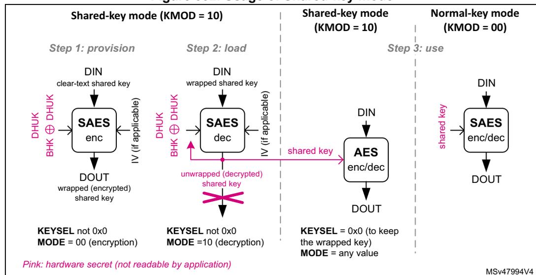
The diagram illustrates the usage of Shared-key mode for SAES, divided into three steps:
- Step 1: provision (Shared-key mode (KMOD = 10)): The SAES peripheral takes a clear-text shared key (DIN) and produces a wrapped (encrypted) shared key (DOUT). The key is derived from DHUK and BHK. The configuration is KEYSEL not 0x0 and MODE = 00 (encryption).
- Step 2: load (Shared-key mode (KMOD = 10)): The SAES peripheral takes a wrapped shared key (DIN) and produces an unwrapped (decrypted) shared key (DOUT). The key is derived from DHUK and BHK. The configuration is KEYSEL not 0x0 and MODE = 10 (decryption). A pink arrow labeled "shared key" points from the unwrapped key to the AES peripheral.
- Step 3: use
: This step is split into two modes:
- Shared-key mode (KMOD = 10) : The AES peripheral takes a shared key (DIN) and produces a DOUT. The configuration is KEYSEL = 0x0 (to keep the wrapped key) and MODE = any value.
- Normal-key mode (KMOD = 00) : The SAES peripheral takes a shared key (DIN) and produces a DOUT. The configuration is KEYSEL = 0x0 and MODE = 00 (encryption).
Pink: hardware secret (not readable by application)
MSv47994V4
Note: DHUK value depends on privilege, security, KMOD[1:0], KSHAREID, KEYSEL[2:0], CHMOD[2:0], and KEYSIZE.
In the step 3, AES represents the AES peripheral.
Key wrapping for AES peripheral
Before SAES can share a key with the AES peripheral, the key must be encrypted (wrapped) once. The encryption sequence of a shared key is the same as for a wrapped
key, with KMOD[1:0] at 0x2 (shared key) and KSHAREID[1:0] kept at 0x0 in the step 3 in Figure 332 . See Key wrapping for SAES for details.
Note: Encryption in Shared-key mode is only supported when ECB or CBC is selected.
Key unwrapping for AES peripheral (shared key)
Each time SAES needs to share a key with the AES peripheral, shared encrypted key must be decrypted (unwrapped) in SAES, then loaded by AES. The overall sequence is described next.
Sequence in the SAES peripheral
The decryption sequence of a shared key is the same as for a wrapped key, with KMOD[1:0] at 0x2 (shared key) and KSHAREID[1:0] kept at 0x0 in the step 3 in Figure 332 . See Key unwrapping for SAES for details.
In shared key mode when decryption mode is selected (MODE[1:0] at 0x2), a read access to the SAES_DOUTR register triggers a read error (RDERRF).
Note: Instead of being shared, a decrypted shared key can be used directly in SAES as the KEYSEL[2:0] bitfield is automatically cleared. In this case, KMOD[1:0] must be written with 0x0 (normal key mode).
Sequence in the AES peripheral
Once the shared key is decrypted in SAES key registers, it can be shared with the AES peripheral, while SAES peripheral remains in key sharing state, that is, with KMOD[1:0] at 0x2 and KEYVALID set. The sequence in the AES key share target peripheral is described in AES key sharing with secure AES co-processor of the corresponding section in this document. It can be run multiple times (for example, to manage a suspend/resume situation) as long as SAES is unused and duly remains in key sharing state.
Note: When KMOD[1:0] is at 0x2 and BUSY set in the AES peripheral, and KEYSIZE value of AES and SAES differs, the key sharing fails and the KEIF flag is raised in both peripherals.
When KEYSEL[2:0] is at 0x1 (DHUK) or 0x4 (DHUK XOR BHK), the application software must use the same privilege, security, KMOD[1:0] / KSHAREID[1:0], CHMOD[2:0], and KEYSIZE context for encryption and decryption. Otherwise, the result is incorrect.
34.4.16 SAES data registers and data swapping
Data input and output
A 16-byte data block enters the SAES peripheral with four successive 32-bit word writes into the SAES_DINR register (bitfield DIN[31:0]), the most significant word (bits [127:96]) first, the least significant word (bits [31:0]) last.
A 16-byte data block is retrieved from the SAES peripheral with four successive 32-bit word reads of the SAES_DOUTR register (bitfield DOUT[31:0]), the most significant word (bits [127:96]) first, the least significant word (bits [31:0]) last.
The four 32-bit words of a 16-byte data block must be stored in the memory consecutively and in big-endian order, that is, with the most significant word on the lowest address. See Table 337 “no swapping” option for details.
Data swapping
The SAES peripheral can be configured to perform a bit-, a byte-, a half-word-, or no swapping on the input data word in the SAES_DINR register, before loading it to the AES processing core, and on the data output from the AES processing core, before sending it to the SAES_DOUTR register. The choice depends on the type of data. For example, a byte swapping is used for an ASCII text stream.
The data swap type is selected through DATATYPE[1:0]. The selection applies to both SAES input and output.
Note: The data in SAES key registers (SAES_KEYRx) and initialization vector registers (SAES_IVRx) are not sensitive to the swap mode selection.
The SAES data swapping feature is summarized in Table 337 and Figure 333 .
Table 337. AES data swapping example
| DATATYPE[1:0] | Swapping performed | Data block |
|---|---|---|
| System memory data (big-endian) | ||
| 0x0 | No swapping | Block[127..64]: 0x04EEF672 2E04CE96 Block[63..0]: 0x4E6F7720 69732074 |
| Address @, word[127..96]: 0x04EEF672 Address @ + 0x4, word[95..64]: 0x2E04CE96 Address @ + 0x8, word[63..32]: 0x4E6F7720 Address @ + 0xC, word[31..0]: 0x69732074 | ||
| 0x1 | Half-word (16-bit) swapping | Block[63..0]: 0x 4E6F 7720 6973 2074 |
| Address @, word[63..32]: 0x7720
4E6F Address @ + 0x4, word[31..0]: 0x2074 6973 | ||
| 0x2 | Byte (8-bit) swapping | Block[63..0]: 0x 4E 6F 77 20 69 73 20 74 |
| Address @, word[63..32]: 0x
2077
6F4E Address @ + 0x4, word[31..0]: 0x 7420 7369 | ||
| 0x3 | Bit swapping | Block[63..32]: 0x4E6F7720 0100 1110 0110 1111 0111 0111 0010 0000 Block[31..0]: 0x69732074 0110 1001 0111 0011 0010 0000 0111 0100 |
| Address @, word[63..32]: 0x04EE F672 0000 0100 1110 1110 1111 0110 0111 0010 Address @ + 0x4, word[31..0]: 0x2E04 CE96 0010 1110 0000 0100 1100 1110 1001 0110 |
Figure 333. 128-bit block construction according to the data type
![Figure 333: 128-bit block construction according to the data type. The diagram shows four examples of data block construction based on DATATYPE[1:0] settings: 00 (no swapping), 01 (16-bit (half-word) swapping), 10 (8-bit (byte) swapping), and 11 (bit swapping). Each example shows four words (Word 0 to Word 3) and their corresponding bit sequences (D0 to D127) being mapped into a 128-bit block. Arrows indicate the order of write to data input / read from data output register (1 to 4). A legend defines the symbols: Dx for input/output data bit 'x', double-headed arrows for data swap, shaded boxes for zero padding, and dashed boxes for AES core input/output data.](/RM0481-STM32H523-33-562-63-573/0c7cdf9d20f93c63e41e53c41f6fc3ce_img.jpg)
DATATYPE[1:0] = 00: no swapping
Word 3: D127...D96, Word 2: D95...D64, Word 1: D63...D32, Word 0: D31...D0
DATATYPE[1:0] = 01: 16-bit (half-word) swapping
Word 3: D127...D112, D96...D80, D79...D64, D111...D95, Word 2: D80...D64, D95...D80, D79...D64, D111...D95, Word 1: D63...D48, D47...D32, D63...D48, D32...D16, Word 0: D31...D16, D15...D0, D31...D16, D15...D0
DATATYPE[1:0] = 10: 8-bit (byte) swapping
Word 3: D127...D120, D119...D112, D111...D104, D103...D96, Word 2: D95...D88, D87...D80, D79...D72, D71...D64, Word 1: D63...D56, D55...D48, D47...D40, D39...D32, Word 0: D31...D24, D23...D16, D15...D8, D7...D0
DATATYPE[1:0] = 11: bit swapping
Word 3: D127...D126, D125...D98, D97...D96, Word 2: D95...D94, D93...D66, D65...D64, Word 1: D63...D62, D61...D34, D33...D32, Word 0: D31...D30, D29...D2, D1...D0
Legend:
- Dx input/output data bit 'x'
- ↔ Data swap
- ①...④ Order of write to data input / read from data output register
- ▨ Zero padding (example)
- --- AES core input/output data
MSv66122V1
Data padding
Figure 333 also gives an example of memory data block padding with zeros such that the zeroed bits after the data swap form a contiguous zone at the MSB end of the AES core input buffer. The example shows the padding of an input data block containing:
- • 84 message bits, with DATATYPE[1:0] = 0x0
- • 48 message bits, with DATATYPE[1:0] = 0x1
- • 56 message bits, with DATATYPE[1:0] = 0x2
- • 34 message bits, with DATATYPE[1:0] = 0x3
34.4.17 SAES key registers
The eight SAES_KEYRx write-only registers store the encryption or decryption key information, as shown on Table 338 . Reads are not allowed for security reason.
Note: In memory and in SAES key registers, keys are stored in little-endian format, with most significant byte on the highest address.
Table 338. Key endianness in SAES_KEYRx registers (128/256-bit keys)
| SAES_KEYR 7 [31:0] | SAES_KEYR 6 [31:0] | SAES_KEYR 5 [31:0] | SAES_KEYR 4 [31:0] | SAES_KEYR 3 [31:0] | SAES_KEYR 2 [31:0] | SAES_KEYR 1 [31:0] | SAES_KEYR 0 [31:0] |
|---|---|---|---|---|---|---|---|
| - | - | - | - | KEY[127:96] | KEY[95:64] | KEY[63:32] | KEY[31:0] |
| KEY[255:224] | KEY[223:192] | KEY[191:160] | KEY[159:128] | KEY[127:96] | KEY[95:64] | KEY[63:32] | KEY[31:0] |
| TAMP_BKP7R [31:0] | TAMP_BKP6R [31:0] | TAMP_BKP5R [31:0] | TAMP_BKP4R [31:0] | TAMP_BKP3R [31:0] | TAMP_BKP2R [31:0] | TAMP_BKP1R [31:0] | TAMP_BKP0R [31:0] |
The key registers are not affected by the data swapping feature controlled by the DATATYPE[1:0] bitfield.
Write operations to the SAES_KEYRx registers are ignored when SAES peripheral is enabled (EN bit set) and KEYSEL[2:0] is different from zero. The application must check this before modifying key registers.
The entire key must be written before starting an AES computation.
In normal key mode (KMOD[1:0] at 0x0), with KEYSEL[2:0] at 0x0, the key registers must always be written in either ascending or descending order. The write sequence becomes:
- • SAES_KEYRx (x = 0 to 3 or x=3 to 0) for KEYSIZE cleared
- • SAES_KEYRx (x = 0 to 7 or x=7 to 0) for KEYSIZE set
Note: KEYSIZE must be written before the key.
As soon as the first key register is written, the KEYVALID flag is cleared. Once the key registers writing sequence is completed, KEYVALID is set and EN becomes writable. If an error occurs, KEYVALID is cleared and KEIF set (see Section 34.4.19 ).
Key selection
With KEYSEL[2:0] at 0x0, the application must write the key in the SAES_KEYRx registers.
With KEYSEL[2:0] at 0x1, a derived hardware unique key (DHUK), computed inside SAES from a non-volatile and secret root hardware unique key, is loaded directly into key registers, based on KEYSIZE information. Thanks to the key derivation function, the computed DHUK depends on the SAES usage (privilege, security, KMOD[1:0] / KSHAREID[1:0], CHMOD[2:0], CPU, and KEYSIZE context).
With KEYSEL[2:0] at 0x2, the boot hardware key (BHK), stored in tamper-resistant secure backup registers, is entirely transferred into key registers upon a secure application performing a single read of all TAMP_BKPxR registers (x = 0 to 3 for KEYSIZE cleared, x = 0 to 7 for KEYSIZE set) in ascending order. Refer to Table 338 .
With KEYSEL[2:0] at 0x4, the XOR combination of DHUK and BHK is entirely transferred into key registers upon a secure application performing a single read of all TAMP_BKPxR
registers ( \( x = 0 \) to \( 3 \) for KEYSIZE cleared, \( x = 0 \) to \( 7 \) for KEYSIZE set) in ascending order. Refer to Table 338 .
Repeated writing of KEYSEL[2:0] with the same non-zero value only triggers the loading of DHUK or BHK if KEYVALID is cleared. The recommended method to clear KEYVALID is to set IPRST . Such method is required for example when switching from ECB decryption to ECB encryption, selecting the same BHK ( KEYSEL[2:0] at 0x2 ).
For all KEYSEL[2:0] values, initiating the key-loading sequence sets the BUSY flag and clears the KEYVALID flag. Once the amount of bits defined by KEYSIZE is transferred to the SAES_KEYRx registers, BUSY is cleared, KEYVALID set and the EN bit becomes writable. If an error occurs, BUSY and KEYVALID are cleared and KEIF set (see Section 34.4.19 ).
Note: DHUK, BHK and their XOR combination are not readable by any software (even secure).
Key protection
As depicted in Figure 334 , when an application sets the KEYPROT bit before writing a key in SAES_KEYRx , any application executing in a different security context (that is, different security attribute) triggers a KEIF error flag upon access to any SAES register when KEYVALID is set.
Note: KEYSEL[2:0] values different from zero (normal key) automatically protect the key registers.
Figure 334. Key protection mechanisms
![Diagram illustrating key protection mechanisms. It shows two security contexts, A and B. Context A (secure) has a key loaded in SAES with KEYVALID = 1. Context B (nonsecure) attempts to access the SAES. If KEYPROT = 0 and KEYSEL[2:0] = 000, access is allowed. If KEYPROT = 1 or KEYSEL ≠ 000, access is blocked, triggering a KEIF error flag.](/RM0481-STM32H523-33-562-63-573/85514caeca7319d2aa1ef38cbbb219e2_img.jpg)
The diagram illustrates two security contexts, A and B, interacting with the SAES peripheral. Context A (for example secure) has a key loaded in the SAES, indicated by a key icon and KEYVALID = 1 . Context B (for example nonsecure) attempts to access the SAES. Two scenarios are shown:
- If KEYPROT = 0 and KEYSEL[2:0] = 000 , Context B can access the SAES (indicated by an arrow pointing to the SAES box with a key icon).
- If KEYPROT = 1 or KEYSEL ≠ 000 , Context B's access is blocked, triggering a KEIF error flag (indicated by a lightning bolt and a crossed-out key icon).
34.4.18 SAES initialization vector registers
The four SAES_IVRx registers store the initialization vector (IV) information, as shown in Table 339 . They can only be written if the SAES peripheral is disabled ( EN cleared).
Note: In memory and in SAES IV registers, initialization vectors are stored in little-endian format, with most significant byte on the highest address.
Table 339. IVI bitfield spread over SAES_IVRx registers
| SAES_IVR3[31:0] | SAES_IVR2[31:0] | SAES_IVR1[31:0] | SAES_IVR0[31:0] |
|---|---|---|---|
| IVI[127:96] | IVI[95:64] | IVI[63:32] | IVI[31:0] |
Initialization vector information depends on the chaining mode selected. When used, SAES_IVRx registers are updated upon each AES computation cycle (useful for managing suspend mode).
The initialization vector registers are not affected by the data swapping feature controlled through DATATYPE[1:0].
34.4.19 SAES error management
The SAES peripheral manages the errors described in this section.
Read error flag (RDERRF)
Unexpected read attempt of the SAES_DOUTR register returns zero, setting the RDERRF flag and the RWEIF flag. RDERRF is triggered during the computation phase or during the input phase.
Note: Unless otherwise indicated, SAES is not disabled when RDERRF rises and it continues processing.
An interrupt is generated if the RWEIE bit is set. For more details, refer to Section 34.5: SAES interrupts .
The RDERRF and RWEIF flags are cleared by setting the RWEIF bit of the SAES_ICR register.
Write error flag (WRERRF)
Unexpected write attempt of the SAES_DINR register is ignored, setting the WRERRF and the RWEIF flags. WRERRF is triggered during the computation phase or during the output phase.
Note: Unless otherwise indicated, SAES is not disabled when WRERRF rises and it continues processing.
An interrupt is generated if the RWEIE bit is set. For more details, refer to Section 34.5: SAES interrupts .
The WRERRF and RWEIF flags are cleared by setting the RWEIF bit of the SAES_ICR register.
Key error interrupt flag (KEIF)
There are multiple sources of errors that set the KEIF flag of the SAES_ISR register and clear the KEYVALID bit of the SAES_SR register:
- • Key protection error: while KEYVALID is set, then if KEYPROT is set or KEYSEL[2:0] is different from zero, this error is triggered when an application executing in a security context different from the one used to load the key (that is, different security attribute) accesses SAES.
- • Key writing sequence error: triggered upon detecting an incorrect sequence of writing key registers. See Section 34.4.17: SAES key registers for details.
- • Key sharing size mismatch error: triggered when KMOD[1:0] is at 0x2 and KEYSIZE in AES peripheral does not match KEYSIZE in SAES peripheral.
- • Key sharing error: triggered upon failing transfer of SAES shared key to AES peripheral. See Section 34.4.15: SAES operation with shared keys for details.
- • Hardware secret key loading error: triggered upon failing load of DHUK or BHK into SAES. KEYSEL[2:0] at 0x1 (DHUK), 0x2 (BHK) or 0x4 (DHUK XOR BHK) is not functional.
The KEIF flag is cleared with corresponding bit of the SAES_ICR register. An interrupt is generated if the KEIE bit of the SAES_IER register is set. For more details, refer to Section 34.5: SAES interrupts .
Upon a key selection error, clearing the KEIF flag automatically restarts the key selection process. Persisting problems (for example, RHUK load failing) may require a power-on reset.
Upon a key sharing error, reset both AES and SAES peripherals through the IPRST bit of their corresponding control register, then restart the key sharing sequence.
Note: For any key error, clear KEIF flag prior to disabling and re-configuring SAES.
RNG error interrupt flag (RNGEIF)
SAES fetches random numbers from the RNG peripheral automatically after an IP reset triggered in the RCC. SAES cannot be used when RNGEIF is set.
An error detected while fetching a random number from RNG peripheral (due to, for example, bad entropy) sets the RNGEIF flag of the SAES_ISR register. The flag is cleared by setting the corresponding bit of the SAES_ICR register. An interrupt is generated if the RNGEIF bit of the SAES_IER register is set. For more details, refer to Section 34.5: SAES interrupts .
Upon an RNG error:
- • Make sure that the RNG peripheral is properly configured.
- • Verify that the RNG peripheral AHB clock is enabled and no noise source (or seed) error is pending in this peripheral.
- • Clear RNGEIF or reset the peripheral by setting IPRST. The clearance of the BUSY flag then indicates the completion of the random number fetch from RNG.
Note: To avoid RNGEIF errors, it is recommended to activate the RNG AHB clock each time SAES AHB clock is activated.
Managing tamper errors
An unexpected error triggers an SAES internal tamper event in the TAMP peripheral, and stops any SAES co-processor processing.
To resume normal operation, reset the SAES peripheral through RCC or global reset.
34.5 SAES interrupts
There are multiple individual maskable interrupt sources generated by the SAES peripheral to signal the following events:
- • computation completed (CCF)
- • read error (RDERRF)
- • write error (WRERRF)
- • key error (KEIF)
- • RNG error (RNGEIF)
See Section 34.4.19: SAES error management for details on SAES errors.
These sources are combined into a common interrupt signal from the SAES peripheral that connects to the Cortex® CPU interrupt controller. Application can enable or disable SAES interrupt sources individually by setting/clearing the corresponding enable bit of the SAES_IER register.
The status of the individual maskable interrupt sources can be read from the SAES_ISR register. They are cleared by setting the corresponding bit of the SAES_ICR register.
Table 340 gives a summary of the available features.
Table 340. SAES interrupt requests
| Interrupt acronym | Interrupt event | Event flag | Enable bit | Interrupt clear method |
|---|---|---|---|---|
| SAES | computation completed flag | CCF | CCFIE | set CCF (1) |
| read error flag | RDERRF (2) | RWEIE | set RWEIF (1) | |
| write error flag | WRERRF (2) | |||
| key error flag | KEIF | KEIE | set KEIF (1) | |
| RNG error flag | RNGEIF | RNGEIE | set RNGEIF (1) |
1. Bit of the SAES_ICR register.
2. Flag of the SAES_SR register, mirrored by the flag RWEIF of the SAES_ISR register.
34.6 SAES DMA requests
The SAES peripheral provides an interface to connect to the DMA (direct memory access) controller. The DMA operation is controlled through the DMAINEN and DMAOUTEN bits of the SAES_CR register. When key derivation is selected (MODE[1:0] is at 0x1), setting those bits has no effect.
SAES only supports single DMA requests.
Suspend and resume operations are not supported in DMA mode.
Detailed usage of DMA with SAES can be found in Appending data using DMA subsection of Section 34.4.5: SAES encryption or decryption typical usage .
Data input using DMA
Setting DMAINEN enables DMA writing into SAES. SAES then initiates, during the input phase, a set of single DMA requests for each 16-byte data block to write to the SAES_DINR register (quadruple 32-bit word, MSB first).
Note: According to the algorithm and the mode selected, special padding / ciphertext stealing might be required (see Section 34.4.7).
Data output using DMA
Setting DMAOUTEN enables DMA reading from SAES. SAES then initiates, during the output phase, a set of single DMA requests for each 16-byte data block to read from the SAES_DOUTR register (quadruple 32-bit word, MSB first).
After the output phase, at the end of processing of a 16-byte data block, SAES switches automatically to a new input phase for the next data block, if any.
In DMA mode, the CCF flag has no use because the reading of the SAES_DOUTR register is managed by DMA automatically at the end of the computation phase. The CCF flag must only be cleared when transiting back to managing the data transfers by software.
Note: According to the message size, extra bytes might need to be discarded by application in the last block.
Stopping DMA transfers
All DMA request signals are de-asserted when SAES is disabled (EN cleared) or the DMA enable bit (DMAINEN for input data, DMAOUTEN for output data) is cleared.
34.7 SAES processing latency
The following tables provide the 16-byte data block processing latency per operating mode.
Table 341. Processing latency for ECB, CBC and CTR
| Key size | Mode of operation | Chaining algorithm | Clock cycles (1) |
|---|---|---|---|
| 128-bit | Encryption or decryption (2) | ECB, CBC, CTR | 480 |
| Key preparation | - | 145 | |
| 256-bit | Encryption or decryption (2) | ECB, CBC, CTR | 680 |
| Key preparation | - | 230 |
1. SAES kernel clock
2. Excluding key preparation time (ECB and CBC only).
Table 342. Processing latency for GCM and CCM (in SAES kernel clock cycles)
| Key size | Mode of operation | Chaining algorithm | Initialization phase | Header phase (1) | Payload phase (1) | Final phase (1) |
|---|---|---|---|---|---|---|
| 128-bit | Mode 1: Encryption/ Mode 3: Decryption | GCM | 490 | 72 (2) | 480 (3) | 490 |
| CCM | 490 | 490 | 800 | 490 | ||
| 256-bit | Mode 1: Encryption/ Mode 3: Decryption | GCM | 650 | 72 (2) | 690 (3) | 650 |
| CCM | 650 | 680 | 1350 | 650 |
- 1. Data insertion can include wait states forced by SAES on the AHB bus (maximum 3 cycles, typical 1 cycle).
- 2. SAES AHB clock cycles instead of kernel clock cycle (Galois multiplier only).
- 3. As a worst case in encryption mode, add extra 72 AHB clock cycles for the last block computation.
34.8 SAES registers
The registers are accessible through 32-bit word single accesses only. Other access types generate an AHB error, and other than 32-bit writes may corrupt the register content.
34.8.1 SAES control register (SAES_CR)
Address offset: 0x000
Reset value: 0x0000 0000
| 31 | 30 | 29 | 28 | 27 | 26 | 25 | 24 | 23 | 22 | 21 | 20 | 19 | 18 | 17 | 16 |
|---|---|---|---|---|---|---|---|---|---|---|---|---|---|---|---|
| IPRST | KEYSEL[2:0] | KSHAREID[1:0] | KMOD[1:0] | NPBLB[3:0] | KEYPROT | KEYSIZE | Res. | CHMOD[2] | |||||||
| rw | rw | rw | rw | rw | rw | rw | rw | rw | rw | rw | rw | rw | rw | rw | |
| 15 | 14 | 13 | 12 | 11 | 10 | 9 | 8 | 7 | 6 | 5 | 4 | 3 | 2 | 1 | 0 |
|---|---|---|---|---|---|---|---|---|---|---|---|---|---|---|---|
| Res. | GCMPH[1:0] | DMAOUTEN | DMAINEN | Res. | Res. | Res. | Res. | CHMOD[1:0] | MODE[1:0] | DATATYPE[1:0] | EN | ||||
| rw | rw | rw | rw | rw | rw | rw | rw | rw | rw | rw | |||||
Bit 31 IPRST: SAES peripheral software reset
Setting the bit resets the SAES peripheral, putting all registers to their default values, except the IPRST bit itself. Hence, any key-relative data are lost. For this reason, it is recommended to set the bit before handing over the SAES to a less secure application.
The bit must be kept low while writing any configuration registers.
Bits 30:28 KEYSEL[2:0]: Key selection
The bitfield defines the source of the key information to use in the AES cryptographic core.
0x0: Software key, loaded in key registers SAES_KEYx
0x1: Derived hardware unique key (DHUK)
0x2: Boot hardware key (BHK)
0x4: XOR of DHUK and BHK
Others: Reserved (if used, unfreeze SAES with IPRST)
When KEYSEL[2:0] is different from zero, selected key value is available in key registers when BUSY bit is cleared and KEYVALID is set in the SAES_SR register. Otherwise, the key error flag KEIF is set. Repeated writing of KEYSEL[2:0] with the same non-zero value only triggers the loading of DHUK or BHK when KEYVALID is cleared.
When the application software changes the key selection by writing the KEYSEL[2:0] bitfield, the key registers are immediately erased and the KEYVALID flag cleared.
At the end of the decryption process, if KMOD[1:0] is other than zero, KEYSEL[2:0] is cleared.
With the bitfield value other than zero and KEYVALID set, the application cannot transfer the ownership of SAES with a loaded key to an application running in another security context (such as secure, nonsecure). More specifically, when security of an access to any register does not match the information recorded by SAES, the KEIF flag is set.
Attempts to write the bitfield are ignored when the BUSY flag of SAES_SR register is set, as well as when the EN bit of the SAES_CR register is set before the write access and it is not cleared by that write access.
Bits 27:26 KSHAREID[1:0]: Key share identificationThis bitfield defines, at the end of a decryption process with KMOD[1:0] at 0x2 (shared key), which target can read the SAES key registers using a dedicated hardware bus.
0x0: AES peripheral
Others: Reserved
Attempts to write the bitfield are ignored when BUSY is set, as well as when EN is set before the write access and it is not cleared by that write access.
Bits 25:24 KMOD[1:0]: Key mode selectionThe bitfield defines how the SAES key can be used by the application. KEYSIZE must be correctly initialized when setting KMOD[1:0] different from zero.
0x0: Normal key mode. Key registers are freely usable and no specific use or protection applies to SAES_DINR and SAES_DOUTR registers.
0x1: Wrapped key for SAES mode. Key loaded in key registers can only be used to encrypt or decrypt AES keys. Hence, when a decryption is selected, read-as-zero SAES_DOUTR register is automatically loaded into SAES key registers after a successful decryption process.
0x2: Shared key mode. After a successful decryption process (unwrapping), SAES key registers are shared with the peripheral described in KSHAREID[1:0] bitfield. This sharing is valid only while KMOD[1:0] is at 0x2 and KEYVALID=1. When a decryption is selected, read-as-zero SAES_DOUTR register is automatically loaded into SAES key registers after a successful decryption process.
Others: Reserved
With KMOD[1:0] other than zero, any attempt to configure the SAES peripheral for use by an application belonging to a different security context (such as secure or nonsecure) results in automatic key erasure and setting of the KEIF flag.
Attempts to write the bitfield are ignored when BUSY is set, as well as when EN is set before the write access and it is not cleared by that write access.
Bits 23:20 NPBLB[3:0]: Number of padding bytes in last blockThis padding information must be filled by software before processing the last block of GCM payload encryption or CCM payload decryption, otherwise authentication tag computation is incorrect.
0x0: All bytes are valid (no padding)
0x1: Padding for the last LSB byte
...
0xF: Padding for the 15 LSB bytes of last block.
Bit 19 KEYPROT: Key protectionWhen set, hardware-based key protection is enabled.
0: When KEYVALID is set and KEYSEL[2:0] = 0 application can transfer the ownership of the SAES, with its loaded key, to an application running in another security context (such as nonsecure, secure).
1: When KEYVALID is set, key error flag (KEIF) is set when an access to any registers is detected, this access having a security context (for example, secure, nonsecure) that does not match the one of the application that loaded the key.
Attempts to write the bit are ignored when BUSY is set, as well as when EN is set before the write access and it is not cleared by that write access.
Bit 18 KEYSIZE: Key size selectionThis bitfield defines the key length in bits of the key used by SAES.
0: 128-bit
1: 256-bit
When KMOD[1:0] is at 0x1 or 0x2, KEYSIZE also defines the length of the key to encrypt or decrypt.
Attempts to write the bit are ignored when BUSY is set, as well as when the EN is set before the write access and it is not cleared by that write access.
Bit 17 Reserved, must be kept at reset value.Bit 15 Reserved, must be kept at reset value.
Bits 14:13 GCM PH [1:0] : GCM or CCM phase selection
This bitfield selects the phase, applicable only with GCM, GMAC or CCM chaining modes.
0x0: Initialization phase
0x1: Header phase
0x2: Payload phase
0x3: Final phase
Bit 12 DMAOUTEN : DMA output enable
This bit enables automatic generation of DMA requests during the data phase, for outgoing data transfers from SAES via DMA.
0: Disable
1: Enable
Setting this bit is ignored when MODE[1:0] is at 0x1 (key derivation).
Bit 11 DMAINEN : DMA input enable
This bit enables automatic generation of DMA requests during the data phase, for incoming data transfers to SAES via DMA.
0: Disable
1: Enable
Setting this bit is ignored when MODE[1:0] is at 0x1 (key derivation).
Bits 10:7 Reserved, must be kept at reset value.
Bits 16, 6:5 CHMOD[2:0] : Chaining mode
This bitfield selects the AES chaining mode:
0x0: Electronic codebook (ECB)
0x1: Cipher-block chaining (CBC)
0x2: Counter mode (CTR)
0x3: Galois counter mode (GCM) and Galois message authentication code (GMAC)
0x4: Counter with CBC-MAC (CCM)
others: Reserved
Attempts to write the bitfield are ignored when BUSY is set, as well as when EN is set before the write access and it is not cleared by that write access.
Bits 4:3 MODE[1:0] : Operating mode
This bitfield selects the SAES operating mode:
0x0: Encryption
0x1: Key derivation (or key preparation), for ECB/CBC decryption only
0x2: Decryption
0x3: Reserved
Attempts to write the bitfield are ignored when BUSY is set, as well as when EN is set before the write access and it is not cleared by that write access.
Bits 2:1 DATATYPE[1:0] : Data type
This bitfield defines the format of data written in the SAES_DINR register or read from the SAES_DOUTR register, through selecting the mode of data swapping. This swapping is defined in Section 34.4.16: SAES data registers and data swapping .
0x0: No swapping (32-bit data).
0x1: Half-word swapping (16-bit data)
0x2: Byte swapping (8-bit data)
0x3: Bit-level swapping
Attempts to write the bitfield are ignored when BUSY is set, as well as when EN is set before the write access and it is not cleared by that write access.
Bit 0 EN : Enable
This bit enables/disables the SAES peripheral.
0: Disable
1: Enable
At any moment, clearing then setting the bit re-initializes the SAES peripheral. When KMOD[1:0] is different from 0x0, using IPRST bit is recommended instead.
This bit is automatically cleared by hardware upon the completion of the key preparation (MODE[1:0] at 0x1) and upon the completion of GCM/GMAC/CCM initialization phase.
The bit cannot be set as long as KEYVALID is cleared, or when SAES is in one of the following configurations:
- – KMOD[1:0] at 0x1 (wrap), CHMOD[2:0] at 0x3 (GCM)
- – KMOD[1:0] at 0x1 (wrap), CHMOD[2:0] at 0x2 (CTR), MODE[1:0] at 0x0 (encryption).
34.8.2 SAES status register (SAES_SR)
Address offset: 0x004
Reset value: 0x0000 0000
| 31 | 30 | 29 | 28 | 27 | 26 | 25 | 24 | 23 | 22 | 21 | 20 | 19 | 18 | 17 | 16 |
|---|---|---|---|---|---|---|---|---|---|---|---|---|---|---|---|
| Res. | Res. | Res. | Res. | Res. | Res. | Res. | Res. | Res. | Res. | Res. | Res. | Res. | Res. | Res. | Res. |
| 15 | 14 | 13 | 12 | 11 | 10 | 9 | 8 | 7 | 6 | 5 | 4 | 3 | 2 | 1 | 0 |
| Res. | Res. | Res. | Res. | Res. | Res. | Res. | Res. | KEYVALID | Res. | Res. | Res. | BUSY | WRERRF | RDERRF | Res. |
| r | r | r | r |
Bits 31:8 Reserved, must be kept at reset value.
Bit 7 KEYVALID : Key valid flag
This bit is set by hardware when the key of size defined by KEYSIZE is loaded in SAES_KEYRx key registers.
0: Key not valid
1: Key valid
The EN bit can only be set when KEYVALID is set.
In normal mode when KEYSEL[2:0] is at zero, the key must be written in the key registers in the correct sequence, otherwise the KEIF flag is set and KEYVALID remains cleared.
When KEYSEL[2:0] is different from zero, the BUSY flag is automatically set by SAES. When the key is loaded successfully, BUSY is cleared and KEYVALID set. Upon an error, KEIF is set, BUSY cleared and KEYVALID remains cleared.
If set, KEIF must be cleared through the SAES_ICR register, otherwise KEYVALID cannot be set.
See the KEIF flag description for more details.
For further information on key loading, refer to Section 34.4.17: SAES key registers .
Bits 6:4 Reserved, must be kept at reset value.
Bit 3 BUSY : Busy
This flag indicates whether SAES is idle or busy.
0: Idle
1: Busy
SAES is flagged as idle when disabled (when EN is low) or when the last processing is completed. SAES is flagged as busy when processing a block data, preparing a key (ECB or CBC decryption only), fetching random number from the RNG, or transferring a shared key to the target peripheral. When GCM encryption payload phase is selected, this flag must be at zero before suspending current process to manage a higher-priority message. BUSY must also be cleared before selecting the GCM final phase.
Bit 2 WRERRF : Write error flag
This bit is set when an unexpected write to the SAES_DINR register occurred. When set WRERRF bit has no impact on the SAES operations.
0: No error
1: Unexpected write to SAES_DINR register occurred during computation or data output phase.
The flag setting generates an interrupt if the RWEIE bit of the SAES_IER register is set.
The flag is cleared by setting the RWEIF bit of the SAES_ICR register.
Bit 1 RDERRF : Read error flag
This bit is set when an unexpected read to the SAES_DOUTR register occurred. When set RDERRF bit has no impact on the SAES operations.
0: No error
1: Unexpected read to SAES_DOUTR register occurred during computation or data input phase.
The flag setting generates an interrupt if the RWEIE bit of the SAES_IER register is set.
The flag is cleared by setting the RWEIF bit of the SAES_ICR register.
Bit 0 Reserved, must be kept at reset value.
34.8.3 SAES data input register (SAES_DINR)
Address offset: 0x008
Reset value: 0x0000 0000
| 31 | 30 | 29 | 28 | 27 | 26 | 25 | 24 | 23 | 22 | 21 | 20 | 19 | 18 | 17 | 16 |
| DIN[31:16] | |||||||||||||||
| w | w | w | w | w | w | w | w | w | w | w | w | w | w | w | w |
| 15 | 14 | 13 | 12 | 11 | 10 | 9 | 8 | 7 | 6 | 5 | 4 | 3 | 2 | 1 | 0 |
| DIN[15:0] | |||||||||||||||
| w | w | w | w | w | w | w | w | w | w | w | w | w | w | w | w |
Bits 31:0 DIN[31:0] : Data input
A four-fold sequential write to this bitfield during the Input phase results in writing a complete 16-bytes block of input data to the SAES peripheral. From the first to the fourth write, the corresponding data weights are [127:96], [95:64], [63:32], and [31:0]. Upon each write, the data from the 32-bit input buffer are handled by the data swap block according to the DATATYPE[1:0] bitfield, then written into the AES core 16-bytes input buffer.
Reads return zero.
34.8.4 SAES data output register (SAES_DOUTR)
Address offset: 0x00C
Reset value: 0x0000 0000
Read when KMOD[1:0] is at 0x1 or 0x2 while MODE[1:0] is at 0x2 and EN is set triggers a read error.
| 31 | 30 | 29 | 28 | 27 | 26 | 25 | 24 | 23 | 22 | 21 | 20 | 19 | 18 | 17 | 16 |
| DOUT[31:16] | |||||||||||||||
| r | r | r | r | r | r | r | r | r | r | r | r | r | r | r | r |
| 15 | 14 | 13 | 12 | 11 | 10 | 9 | 8 | 7 | 6 | 5 | 4 | 3 | 2 | 1 | 0 |
| DOUT[15:0] | |||||||||||||||
| r | r | r | r | r | r | r | r | r | r | r | r | r | r | r | r |
Bits 31:0 DOUT[31:0] : Data output
This read-only bitfield fetches a 32-bit output buffer. A four-fold sequential read of this bitfield, upon the computation completion (CCF flag set), virtually reads a complete 16-byte block of output data from the SAES peripheral. Before reaching the output buffer, the data produced by the AES core are handled by the data swap block according to the DATATYPE[1:0] bitfield.
Data weights from the first to the fourth read operation are: [127:96], [95:64], [63:32], and [31:0].
34.8.5 SAES key register 0 (SAES_KEYR0)
Address offset: 0x010
Reset value: 0x0000 0000
| 31 | 30 | 29 | 28 | 27 | 26 | 25 | 24 | 23 | 22 | 21 | 20 | 19 | 18 | 17 | 16 |
| KEY[31:16] | |||||||||||||||
| w | w | w | w | w | w | w | w | w | w | w | w | w | w | w | w |
| 15 | 14 | 13 | 12 | 11 | 10 | 9 | 8 | 7 | 6 | 5 | 4 | 3 | 2 | 1 | 0 |
| KEY[15:0] | |||||||||||||||
| w | w | w | w | w | w | w | w | w | w | w | w | w | w | w | w |
Bits 31:0 KEY[31:0] : Cryptographic key, bits [31:0]
These are bits [31:0] of the write-only bitfield KEY[255:0] AES encryption or decryption key, depending on the MODE[1:0] bitfield of the SAES_CR register.
Writes to SAES_KEYRx registers are ignored when SAES is enabled (EN bit set). When KEYSEL[2:0] is different from 0 and KEYVALID is 0, writes to key registers are also ignored and they result in setting the KEIF bit of the SAES_ISR register.
With KMOD[1:0] at 0x0, a special writing sequence is required. In this sequence, any valid write to AES_KEYRx register clears the KEYVALID flag except for the sequence-completing write that sets it. Also refer to the description of the KEYVALID flag in the AES_SR register.
34.8.6 SAES key register 1 (SAES_KEYR1)
Address offset: 0x014
Reset value: 0x0000 0000
| 31 | 30 | 29 | 28 | 27 | 26 | 25 | 24 | 23 | 22 | 21 | 20 | 19 | 18 | 17 | 16 |
| KEY[63:48] | |||||||||||||||
| w | w | w | w | w | w | w | w | w | w | w | w | w | w | w | w |
| 15 | 14 | 13 | 12 | 11 | 10 | 9 | 8 | 7 | 6 | 5 | 4 | 3 | 2 | 1 | 0 |
| KEY[47:32] | |||||||||||||||
| w | w | w | w | w | w | w | w | w | w | w | w | w | w | w | w |
Bits 31:0 KEY[63:32] : Cryptographic key, bits [63:32]
Refer to the SAES_KEYR0 register for description of the KEY[255:0] bitfield and for information relative to writing SAES_KEYRx registers.
34.8.7 SAES key register 2 (SAES_KEYR2)
Address offset: 0x018
Reset value: 0x0000 0000
| 31 | 30 | 29 | 28 | 27 | 26 | 25 | 24 | 23 | 22 | 21 | 20 | 19 | 18 | 17 | 16 |
| KEY[95:80] | |||||||||||||||
| w | w | w | w | w | w | w | w | w | w | w | w | w | w | w | w |
| 15 | 14 | 13 | 12 | 11 | 10 | 9 | 8 | 7 | 6 | 5 | 4 | 3 | 2 | 1 | 0 |
| KEY[79:64] | |||||||||||||||
| w | w | w | w | w | w | w | w | w | w | w | w | w | w | w | w |
Bits 31:0 KEY[95:64] : Cryptographic key, bits [95:64]
Refer to the SAES_KEYR0 register for description of the KEY[255:0] bitfield and for information relative to writing SAES_KEYRx registers.
34.8.8 SAES key register 3 (SAES_KEYR3)
Address offset: 0x01C
Reset value: 0x0000 0000
| 31 | 30 | 29 | 28 | 27 | 26 | 25 | 24 | 23 | 22 | 21 | 20 | 19 | 18 | 17 | 16 |
| KEY[127:112] | |||||||||||||||
| w | w | w | w | w | w | w | w | w | w | w | w | w | w | w | w |
| 15 | 14 | 13 | 12 | 11 | 10 | 9 | 8 | 7 | 6 | 5 | 4 | 3 | 2 | 1 | 0 |
| KEY[111:96] | |||||||||||||||
| w | w | w | w | w | w | w | w | w | w | w | w | w | w | w | w |
Bits 31:0 KEY[127:96] : Cryptographic key, bits [127:96]
Refer to the SAES_KEYR0 register for description of the KEY[255:0] bitfield and for information relative to writing SAES_KEYRx registers.
34.8.9 SAES initialization vector register 0 (SAES_IVR0)
Address offset: 0x020
Reset value: 0x0000 0000
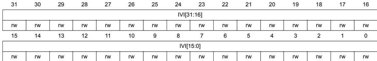
| 31 | 30 | 29 | 28 | 27 | 26 | 25 | 24 | 23 | 22 | 21 | 20 | 19 | 18 | 17 | 16 |
| IVI[31:16] | |||||||||||||||
| rw | rw | rw | rw | rw | rw | rw | rw | rw | rw | rw | rw | rw | rw | rw | rw |
| 15 | 14 | 13 | 12 | 11 | 10 | 9 | 8 | 7 | 6 | 5 | 4 | 3 | 2 | 1 | 0 |
| IVI[15:0] | |||||||||||||||
| rw | rw | rw | rw | rw | rw | rw | rw | rw | rw | rw | rw | rw | rw | rw | rw |
Bits 31:0 IVI[31:0] : Initialization vector input, bits [31:0]
SAES_IVRx registers store the 128-bit initialization vector or the nonce, depending on the chaining mode selected. This value is updated by hardware after each computation round (when applicable). Write to this register is ignored when EN bit is set in SAES_CR register
34.8.10 SAES initialization vector register 1 (SAES_IVR1)
Address offset: 0x024
Reset value: 0x0000 0000
| 31 | 30 | 29 | 28 | 27 | 26 | 25 | 24 | 23 | 22 | 21 | 20 | 19 | 18 | 17 | 16 |
| IVI[63:48] | |||||||||||||||
| rw | rw | rw | rw | rw | rw | rw | rw | rw | rw | rw | rw | rw | rw | rw | rw |
| 15 | 14 | 13 | 12 | 11 | 10 | 9 | 8 | 7 | 6 | 5 | 4 | 3 | 2 | 1 | 0 |
| IVI[47:32] | |||||||||||||||
| rw | rw | rw | rw | rw | rw | rw | rw | rw | rw | rw | rw | rw | rw | rw | rw |
Bits 31:0 IVI[63:32] : Initialization vector input, bits [63:32]
Refer to the SAES_IVR0 register for description of the IVI[128:0] bitfield.
34.8.11 SAES initialization vector register 2 (SAES_IVR2)
Address offset: 0x028
Reset value: 0x0000 0000
| 31 | 30 | 29 | 28 | 27 | 26 | 25 | 24 | 23 | 22 | 21 | 20 | 19 | 18 | 17 | 16 |
| IVI[95:80] | |||||||||||||||
| rw | rw | rw | rw | rw | rw | rw | rw | rw | rw | rw | rw | rw | rw | rw | rw |
| 15 | 14 | 13 | 12 | 11 | 10 | 9 | 8 | 7 | 6 | 5 | 4 | 3 | 2 | 1 | 0 |
| IVI[79:64] | |||||||||||||||
| rw | rw | rw | rw | rw | rw | rw | rw | rw | rw | rw | rw | rw | rw | rw | rw |
Bits 31:0 IVI[95:64] : Initialization vector input, bits [95:64]
Refer to the SAES_IVR0 register for description of the IVI[128:0] bitfield.
34.8.12 SAES initialization vector register 3 (SAES_IVR3)
Address offset: 0x02C
Reset value: 0x0000 0000
| 31 | 30 | 29 | 28 | 27 | 26 | 25 | 24 | 23 | 22 | 21 | 20 | 19 | 18 | 17 | 16 |
| IVI[127:112] | |||||||||||||||
| rw | rw | rw | rw | rw | rw | rw | rw | rw | rw | rw | rw | rw | rw | rw | rw |
| 15 | 14 | 13 | 12 | 11 | 10 | 9 | 8 | 7 | 6 | 5 | 4 | 3 | 2 | 1 | 0 |
| IVI[111:96] | |||||||||||||||
| rw | rw | rw | rw | rw | rw | rw | rw | rw | rw | rw | rw | rw | rw | rw | rw |
Bits 31:0 IVI[127:96] : Initialization vector input, bits [127:96]
Refer to the SAES_IVR0 register for description of the IVI[128:0] bitfield.
34.8.13 SAES key register 4 (SAES_KEYR4)
Address offset: 0x030
Reset value: 0x0000 0000
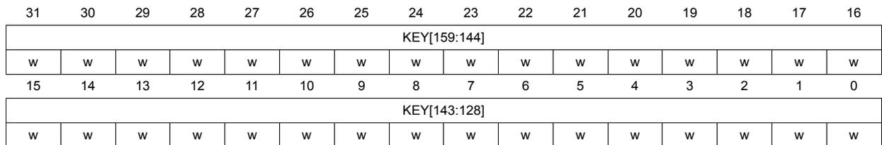
| 31 | 30 | 29 | 28 | 27 | 26 | 25 | 24 | 23 | 22 | 21 | 20 | 19 | 18 | 17 | 16 |
| KEY[159:144] | |||||||||||||||
| w | w | w | w | w | w | w | w | w | w | w | w | w | w | w | w |
| 15 | 14 | 13 | 12 | 11 | 10 | 9 | 8 | 7 | 6 | 5 | 4 | 3 | 2 | 1 | 0 |
| KEY[143:128] | |||||||||||||||
| w | w | w | w | w | w | w | w | w | w | w | w | w | w | w | w |
Bits 31:0 KEY[159:128] : Cryptographic key, bits [159:128]
Refer to the SAES_KEYR0 register for description of the KEY[255:0] bitfield and for information relative to writing SAES_KEYRx registers.
34.8.14 SAES key register 5 (SAES_KEYR5)
Address offset: 0x034
Reset value: 0x0000 0000
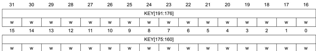
| 31 | 30 | 29 | 28 | 27 | 26 | 25 | 24 | 23 | 22 | 21 | 20 | 19 | 18 | 17 | 16 |
| KEY[191:176] | |||||||||||||||
| w | w | w | w | w | w | w | w | w | w | w | w | w | w | w | w |
| 15 | 14 | 13 | 12 | 11 | 10 | 9 | 8 | 7 | 6 | 5 | 4 | 3 | 2 | 1 | 0 |
| KEY[175:160] | |||||||||||||||
| w | w | w | w | w | w | w | w | w | w | w | w | w | w | w | w |
Bits 31:0 KEY[191:160] : Cryptographic key, bits [191:160]
Refer to the SAES_KEYR0 register for description of the KEY[255:0] bitfield and for information relative to writing SAES_KEYRx registers.
34.8.15 SAES key register 6 (SAES_KEYR6)
Address offset: 0x038
Reset value: 0x0000 0000
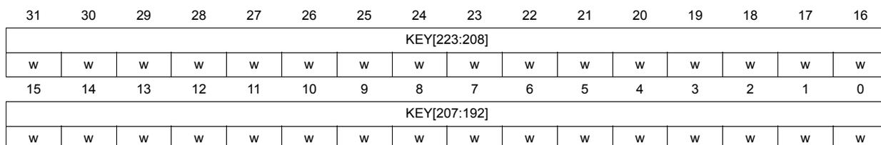
| 31 | 30 | 29 | 28 | 27 | 26 | 25 | 24 | 23 | 22 | 21 | 20 | 19 | 18 | 17 | 16 |
| KEY[223:208] | |||||||||||||||
| w | w | w | w | w | w | w | w | w | w | w | w | w | w | w | w |
| 15 | 14 | 13 | 12 | 11 | 10 | 9 | 8 | 7 | 6 | 5 | 4 | 3 | 2 | 1 | 0 |
| KEY[207:192] | |||||||||||||||
| w | w | w | w | w | w | w | w | w | w | w | w | w | w | w | w |
Bits 31:0 KEY[223:192] : Cryptographic key, bits [223:192]
Refer to the SAES_KEYR0 register for description of the KEY[255:0] bitfield and for information relative to writing SAES_KEYRx registers.
34.8.16 SAES key register 7 (SAES_KEYR7)
Address offset: 0x03C
Reset value: 0x0000 0000
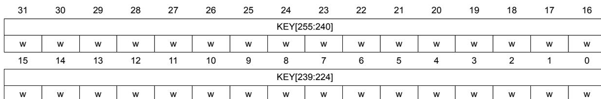
| 31 | 30 | 29 | 28 | 27 | 26 | 25 | 24 | 23 | 22 | 21 | 20 | 19 | 18 | 17 | 16 |
| KEY[255:240] | |||||||||||||||
| w | w | w | w | w | w | w | w | w | w | w | w | w | w | w | w |
| 15 | 14 | 13 | 12 | 11 | 10 | 9 | 8 | 7 | 6 | 5 | 4 | 3 | 2 | 1 | 0 |
| KEY[239:224] | |||||||||||||||
| w | w | w | w | w | w | w | w | w | w | w | w | w | w | w | w |
Bits 31:0 KEY[255:224] : Cryptographic key, bits [255:224]
Refer to the SAES_KEYR0 register for description of the KEY[255:0] bitfield and for information relative to writing SAES_KEYRx registers.
34.8.17 SAES suspend registers (SAES_SUSPRx)
Address offset: 0x040 + 0x4 * x, (x = 0 to 7)
Reset value: 0x0000 0000
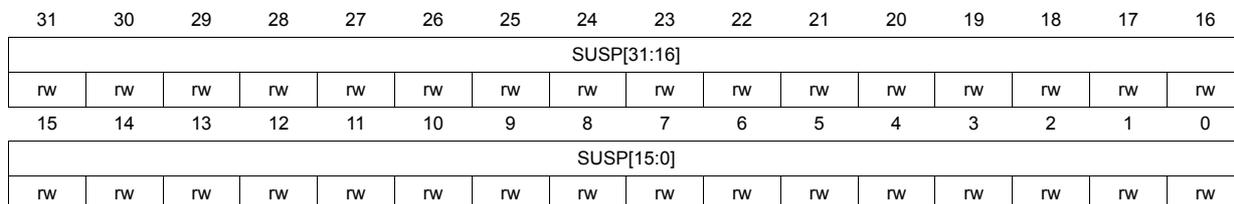
| 31 | 30 | 29 | 28 | 27 | 26 | 25 | 24 | 23 | 22 | 21 | 20 | 19 | 18 | 17 | 16 |
| SUSP[31:16] | |||||||||||||||
| rw | rw | rw | rw | rw | rw | rw | rw | rw | rw | rw | rw | rw | rw | rw | rw |
| 15 | 14 | 13 | 12 | 11 | 10 | 9 | 8 | 7 | 6 | 5 | 4 | 3 | 2 | 1 | 0 |
| SUSP[15:0] | |||||||||||||||
| rw | rw | rw | rw | rw | rw | rw | rw | rw | rw | rw | rw | rw | rw | rw | rw |
Bits 31:0 SUSP[31:0] : Suspend data
SAES_SUSPRx registers contain the complete internal register states of the SAES when the CCM processing of the current task is suspended to process a higher-priority task. Refer to Section 34.4.8: SAES suspend and resume operations for more details.
Clearing EN bit of the SAES_CR register clears this register to zero.
SAES_SUSPRx registers are not used in other chaining modes than CCM.
34.8.18 SAES interrupt enable register (SAES_IER)
Address offset: 0x300
Reset value: 0x0000 0000
| 31 | 30 | 29 | 28 | 27 | 26 | 25 | 24 | 23 | 22 | 21 | 20 | 19 | 18 | 17 | 16 |
|---|---|---|---|---|---|---|---|---|---|---|---|---|---|---|---|
| Res. | Res. | Res. | Res. | Res. | Res. | Res. | Res. | Res. | Res. | Res. | Res. | Res. | Res. | Res. | Res. |
| 15 | 14 | 13 | 12 | 11 | 10 | 9 | 8 | 7 | 6 | 5 | 4 | 3 | 2 | 1 | 0 |
| Res. | Res. | Res. | Res. | Res. | Res. | Res. | Res. | Res. | Res. | Res. | Res. | RNGEIE | KEIE | RWEIE | CCFIE |
| rw | rw | rw | rw |
Bits 31:4 Reserved, must be kept at reset value.
Bit 3 RNGEIE : RNG error interrupt enable
This bit enables or disables (masks) the SAES interrupt generation when RNGEIF (RNG error flag) is set.
0: Disabled (masked)
1: Enabled (not masked)
Bit 2 KEIE : Key error interrupt enable
This bit enables or disables (masks) the SAES interrupt generation when KEIF (key error flag) is set.
0: Disabled (masked)
1: Enabled (not masked)
Bit 1 RWEIE : Read or write error interrupt enable
This bit enables or disables (masks) the SAES interrupt generation when RWEIF (read and/or write error flag) is set.
0: Disabled (masked)
1: Enabled (not masked)
Bit 0 CCFIE : Computation complete flag interrupt enable
This bit enables or disables (masks) the SAES interrupt generation when CCF (computation complete flag) is set.
0: Disabled (masked)
1: Enabled (not masked)
34.8.19 SAES interrupt status register (SAES_ISR)
Address offset: 0x304
Reset value: 0x0000 0000
| 31 | 30 | 29 | 28 | 27 | 26 | 25 | 24 | 23 | 22 | 21 | 20 | 19 | 18 | 17 | 16 |
|---|---|---|---|---|---|---|---|---|---|---|---|---|---|---|---|
| Res. | Res. | Res. | Res. | Res. | Res. | Res. | Res. | Res. | Res. | Res. | Res. | Res. | Res. | Res. | Res. |
| 15 | 14 | 13 | 12 | 11 | 10 | 9 | 8 | 7 | 6 | 5 | 4 | 3 | 2 | 1 | 0 |
| Res. | Res. | Res. | Res. | Res. | Res. | Res. | Res. | Res. | Res. | Res. | Res. | RNGEIF | KEIF | RWEIF | CCF |
| r | r | r | r |
Bits 31:4 Reserved, must be kept at reset value.
Bit 3 RNGEIF : RNG error interrupt flag
This read-only bit is set by hardware when an error is detected on RNG bus interface (for example bad entropy).
0: RNG bus is functional
1: Error detected on RNG bus interface (random seed fetching error)
The flag setting generates an interrupt if the RNGEIF bit of the SAES_IER register is set.
The flag is cleared by setting the corresponding bit of the SAES_ICR register. The clear action triggers the reload of a new random number from the RNG peripheral.
Bit 2 KEIF : Key error interrupt flag
This read-only bit is set by hardware when the key information fails to load into key registers or when the key register use is forbidden.
0: No key error detected
1: Key information failed to load into key registers or the key register use is forbidden
The flag setting generates an interrupt if the KEIF bit of the SAES_IER register is set. It also clears the key registers and the KEYVALID flag in the SAES_SR register.
The flag is cleared by setting the corresponding bit of the SAES_ICR register.
KEIF is raised upon any of the following events:
- –SAES fails to load the DHUK (KEYSEL[2:0] = 0x1 or 0x4).
- –SAES fails to load the BHK (KEYSEL[2:0] = 0x2 or 0x4).
- –AES fails to load the key shared by SAES peripheral (KMOD[1:0] = 0x2).
- –KEYVALID is set and either KEYPROT is set or KEYSEL[2:0] is other than 0x0. The security context of the application that loads the key (secure or nonsecure) does not match the security attribute of the access to SAES_CR or SAES_DOUT. In this case, KEYVALID and EN bits are cleared.
- –SAES_KEYRx register write does not respect the correct order. (For KEYSIZE cleared, SAES_KEYR0 then SAES_KEYR1 then SAES_KEYR2 then SAES_KEYR3 register, or reverse. For KEYSIZE set, SAES_KEYR0 then SAES_KEYR1 then SAES_KEYR2 then SAES_KEYR3 then SAES_KEYR4 then SAES_KEYR5 then SAES_KEYR6 then SAES_KEYR7, or reverse).
KEIF must be cleared by the application software, otherwise KEYVALID cannot be set.
Bit 1 RWEIF : Read or write error interrupt flagThis read-only bit is set by hardware when a RDERRF or a WRERRF error flag is set in the SAES_SR register.
0: No read or write error detected
1: Read or write error detected
The flag setting generates an interrupt if the RWEIF bit of the SAES_IER register is set.
The flag is cleared by setting the corresponding bit of the SAES_ICR register.
The flag has no meaning when key derivation mode is selected.
See the SAES_SR register for details.
Bit 0 CCF : Computation complete flagThis flag indicates whether the computation is completed. It is significant only when the DMAOUTEN bit is cleared, and it may stay high when DMAOUTEN is set.
0: Not completed
1: Completed
The flag setting generates an interrupt if the CCFIF bit of the SAES_IER register is set.
The flag is cleared by setting the corresponding bit of the SAES_ICR register.
34.8.20 SAES interrupt clear register (SAES_ICR)
Address offset: 0x308
Reset value: 0x0000 0000
| 31 | 30 | 29 | 28 | 27 | 26 | 25 | 24 | 23 | 22 | 21 | 20 | 19 | 18 | 17 | 16 |
|---|---|---|---|---|---|---|---|---|---|---|---|---|---|---|---|
| Res. | Res. | Res. | Res. | Res. | Res. | Res. | Res. | Res. | Res. | Res. | Res. | Res. | Res. | Res. | Res. |
| 15 | 14 | 13 | 12 | 11 | 10 | 9 | 8 | 7 | 6 | 5 | 4 | 3 | 2 | 1 | 0 |
| Res. | Res. | Res. | Res. | Res. | Res. | Res. | Res. | Res. | Res. | Res. | Res. | RNGEIF | KEIF | RWEIF | CCF |
| w | w | w | w |
Bits 31:4 Reserved, must be kept at reset value.
Bit 3 RNGEIF : RNG error interrupt flag clearApplication must set this bit to clear the RNGEIF status bit in SAES_ISR register.
Bit 2 KEIF : Key error interrupt flag clearSetting this bit clears the KEIF status bit of the SAES_ISR register.
Bit 1 RWEIF : Read or write error interrupt flag clearSetting this bit clears the RWEIF status bit of the SAES_ISR register, and clears both RDERRF and WRERRF flags in the SAES_SR register.
Bit 0 CCF : Computation complete flag clearSetting this bit clears the CCF status bit of the SAES_ISR register.
34.8.21 SAES register map
Table 343. SAES register map and reset values| Offset | Register name | 31 | 30 | 29 | 28 | 27 | 26 | 25 | 24 | 23 | 22 | 21 | 20 | 19 | 18 | 17 | 16 | 15 | 14 | 13 | 12 | 11 | 10 | 9 | 8 | 7 | 6 | 5 | 4 | 3 | 2 | 1 | 0 |
|---|---|---|---|---|---|---|---|---|---|---|---|---|---|---|---|---|---|---|---|---|---|---|---|---|---|---|---|---|---|---|---|---|---|
| 0x000 | SAES_CR | IPRST | KEYSEL[2:0] | KSHAREID[1:0] | KMOD[1:0] | NPBLB[3:0] | KEYPROT | KEYSIZE | Res. | CHMOD[2] | Res. | GCMPH[1:0] | DMAOUTEN | DMAINEN | Res. | Res. | Res. | Res. | CHMOD[1] | CHMOD[0] | MODE[1:0] | DATATYPE[1:0] | EN | ||||||||||
| Reset value | 0 | 0 | 0 | 0 | 0 | 0 | 0 | 0 | 0 | 0 | 0 | 0 | 0 | 0 | 0 | 0 | 0 | 0 | 0 | 0 | 0 | 0 | 0 | 0 | 0 | 0 | |||||||
| 0x004 | SAES_SR | Res. | Res. | Res. | Res. | Res. | Res. | Res. | Res. | Res. | Res. | Res. | Res. | Res. | Res. | Res. | Res. | Res. | Res. | Res. | Res. | Res. | Res. | Res. | Res. | KEYVALID | Res. | Res. | Res. | BUSY | WRERRF | RDERRF | Res. |
| Reset value | 0 | 0 | 0 | 0 | |||||||||||||||||||||||||||||
| 0x008 | SAES_DINR | DIN[31:0] | |||||||||||||||||||||||||||||||
| Reset value | 0 | 0 | 0 | 0 | 0 | 0 | 0 | 0 | 0 | 0 | 0 | 0 | 0 | 0 | 0 | 0 | 0 | 0 | 0 | 0 | 0 | 0 | 0 | 0 | 0 | 0 | 0 | 0 | 0 | 0 | 0 | 0 | |
| 0x00C | SAES_DOUTR | DOUT[31:0] | |||||||||||||||||||||||||||||||
| Reset value | 0 | 0 | 0 | 0 | 0 | 0 | 0 | 0 | 0 | 0 | 0 | 0 | 0 | 0 | 0 | 0 | 0 | 0 | 0 | 0 | 0 | 0 | 0 | 0 | 0 | 0 | 0 | 0 | 0 | 0 | 0 | 0 | |
| 0x010 | SAES_KEYR0 | KEY[31:0] | |||||||||||||||||||||||||||||||
| Reset value | 0 | 0 | 0 | 0 | 0 | 0 | 0 | 0 | 0 | 0 | 0 | 0 | 0 | 0 | 0 | 0 | 0 | 0 | 0 | 0 | 0 | 0 | 0 | 0 | 0 | 0 | 0 | 0 | 0 | 0 | 0 | 0 | |
| 0x014 | SAES_KEYR1 | KEY[63:32] | |||||||||||||||||||||||||||||||
| Reset value | 0 | 0 | 0 | 0 | 0 | 0 | 0 | 0 | 0 | 0 | 0 | 0 | 0 | 0 | 0 | 0 | 0 | 0 | 0 | 0 | 0 | 0 | 0 | 0 | 0 | 0 | 0 | 0 | 0 | 0 | 0 | 0 | |
| 0x018 | SAES_KEYR2 | KEY[95:64] | |||||||||||||||||||||||||||||||
| Reset value | 0 | 0 | 0 | 0 | 0 | 0 | 0 | 0 | 0 | 0 | 0 | 0 | 0 | 0 | 0 | 0 | 0 | 0 | 0 | 0 | 0 | 0 | 0 | 0 | 0 | 0 | 0 | 0 | 0 | 0 | 0 | 0 | |
| 0x01C | SAES_KEYR3 | KEY[127:96] | |||||||||||||||||||||||||||||||
| Reset value | 0 | 0 | 0 | 0 | 0 | 0 | 0 | 0 | 0 | 0 | 0 | 0 | 0 | 0 | 0 | 0 | 0 | 0 | 0 | 0 | 0 | 0 | 0 | 0 | 0 | 0 | 0 | 0 | 0 | 0 | 0 | 0 | |
| 0x020 | SAES_IVR0 | IVI[31:0] | |||||||||||||||||||||||||||||||
| Reset value | 0 | 0 | 0 | 0 | 0 | 0 | 0 | 0 | 0 | 0 | 0 | 0 | 0 | 0 | 0 | 0 | 0 | 0 | 0 | 0 | 0 | 0 | 0 | 0 | 0 | 0 | 0 | 0 | 0 | 0 | 0 | 0 | |
| 0x024 | SAES_IVR1 | IVI[63:32] | |||||||||||||||||||||||||||||||
| Reset value | 0 | 0 | 0 | 0 | 0 | 0 | 0 | 0 | 0 | 0 | 0 | 0 | 0 | 0 | 0 | 0 | 0 | 0 | 0 | 0 | 0 | 0 | 0 | 0 | 0 | 0 | 0 | 0 | 0 | 0 | 0 | 0 | |
| 0x028 | SAES_IVR2 | IVI[95:64] | |||||||||||||||||||||||||||||||
| Reset value | 0 | 0 | 0 | 0 | 0 | 0 | 0 | 0 | 0 | 0 | 0 | 0 | 0 | 0 | 0 | 0 | 0 | 0 | 0 | 0 | 0 | 0 | 0 | 0 | 0 | 0 | 0 | 0 | 0 | 0 | 0 | 0 | |
| 0x02C | SAES_IVR3 | IVI[127:96] | |||||||||||||||||||||||||||||||
| Reset value | 0 | 0 | 0 | 0 | 0 | 0 | 0 | 0 | 0 | 0 | 0 | 0 | 0 | 0 | 0 | 0 | 0 | 0 | 0 | 0 | 0 | 0 | 0 | 0 | 0 | 0 | 0 | 0 | 0 | 0 | 0 | 0 | |
| 0x030 | SAES_KEYR4 | KEY[159:128] | |||||||||||||||||||||||||||||||
| Reset value | 0 | 0 | 0 | 0 | 0 | 0 | 0 | 0 | 0 | 0 | 0 | 0 | 0 | 0 | 0 | 0 | 0 | 0 | 0 | 0 | 0 | 0 | 0 | 0 | 0 | 0 | 0 | 0 | 0 | 0 | 0 | 0 | |
| 0x034 | SAES_KEYR5 | KEY[191:160] | |||||||||||||||||||||||||||||||
| Reset value | 0 | 0 | 0 | 0 | 0 | 0 | 0 | 0 | 0 | 0 | 0 | 0 | 0 | 0 | 0 | 0 | 0 | 0 | 0 | 0 | 0 | 0 | 0 | 0 | 0 | 0 | 0 | 0 | 0 | 0 | 0 | 0 | |
| 0x038 | SAES_KEYR6 | KEY[223:192] | |||||||||||||||||||||||||||||||
| Reset value | 0 | 0 | 0 | 0 | 0 | 0 | 0 | 0 | 0 | 0 | 0 | 0 | 0 | 0 | 0 | 0 | 0 | 0 | 0 | 0 | 0 | 0 | 0 | 0 | 0 | 0 | 0 | 0 | 0 | 0 | 0 | 0 | |
| 0x03C | SAES_KEYR7 | KEY[255:224] | |||||||||||||||||||||||||||||||
| Reset value | 0 | 0 | 0 | 0 | 0 | 0 | 0 | 0 | 0 | 0 | 0 | 0 | 0 | 0 | 0 | 0 | 0 | 0 | 0 | 0 | 0 | 0 | 0 | 0 | 0 | 0 | 0 | 0 | 0 | 0 | 0 | 0 | |
Table 343. SAES register map and reset values (continued)
| Offset | Register name | 31 | 30 | 29 | 28 | 27 | 26 | 25 | 24 | 23 | 22 | 21 | 20 | 19 | 18 | 17 | 16 | 15 | 14 | 13 | 12 | 11 | 10 | 9 | 8 | 7 | 6 | 5 | 4 | 3 | 2 | 1 | 0 |
|---|---|---|---|---|---|---|---|---|---|---|---|---|---|---|---|---|---|---|---|---|---|---|---|---|---|---|---|---|---|---|---|---|---|
| 0x040 | SAES_SUSPR0 | SUSP[31:0] | |||||||||||||||||||||||||||||||
| Reset value | 0 | 0 | 0 | 0 | 0 | 0 | 0 | 0 | 0 | 0 | 0 | 0 | 0 | 0 | 0 | 0 | 0 | 0 | 0 | 0 | 0 | 0 | 0 | 0 | 0 | 0 | 0 | 0 | 0 | 0 | 0 | 0 | |
| 0x044 | SAES_SUSPR1 | SUSP[31:0] | |||||||||||||||||||||||||||||||
| Reset value | 0 | 0 | 0 | 0 | 0 | 0 | 0 | 0 | 0 | 0 | 0 | 0 | 0 | 0 | 0 | 0 | 0 | 0 | 0 | 0 | 0 | 0 | 0 | 0 | 0 | 0 | 0 | 0 | 0 | 0 | 0 | 0 | |
| 0x048 | SAES_SUSPR2 | SUSP[31:0] | |||||||||||||||||||||||||||||||
| Reset value | 0 | 0 | 0 | 0 | 0 | 0 | 0 | 0 | 0 | 0 | 0 | 0 | 0 | 0 | 0 | 0 | 0 | 0 | 0 | 0 | 0 | 0 | 0 | 0 | 0 | 0 | 0 | 0 | 0 | 0 | 0 | 0 | |
| 0x04C | SAES_SUSPR3 | SUSP[31:0] | |||||||||||||||||||||||||||||||
| Reset value | 0 | 0 | 0 | 0 | 0 | 0 | 0 | 0 | 0 | 0 | 0 | 0 | 0 | 0 | 0 | 0 | 0 | 0 | 0 | 0 | 0 | 0 | 0 | 0 | 0 | 0 | 0 | 0 | 0 | 0 | 0 | 0 | |
| 0x050 | SAES_SUSPR4 | SUSP[31:0] | |||||||||||||||||||||||||||||||
| Reset value | 0 | 0 | 0 | 0 | 0 | 0 | 0 | 0 | 0 | 0 | 0 | 0 | 0 | 0 | 0 | 0 | 0 | 0 | 0 | 0 | 0 | 0 | 0 | 0 | 0 | 0 | 0 | 0 | 0 | 0 | 0 | 0 | |
| 0x054 | SAES_SUSPR5 | SUSP[31:0] | |||||||||||||||||||||||||||||||
| Reset value | 0 | 0 | 0 | 0 | 0 | 0 | 0 | 0 | 0 | 0 | 0 | 0 | 0 | 0 | 0 | 0 | 0 | 0 | 0 | 0 | 0 | 0 | 0 | 0 | 0 | 0 | 0 | 0 | 0 | 0 | 0 | 0 | |
| 0x058 | SAES_SUSPR6 | SUSP[31:0] | |||||||||||||||||||||||||||||||
| Reset value | 0 | 0 | 0 | 0 | 0 | 0 | 0 | 0 | 0 | 0 | 0 | 0 | 0 | 0 | 0 | 0 | 0 | 0 | 0 | 0 | 0 | 0 | 0 | 0 | 0 | 0 | 0 | 0 | 0 | 0 | 0 | 0 | |
| 0x05C | SAES_SUSPR7 | SUSP[31:0] | |||||||||||||||||||||||||||||||
| Reset value | 0 | 0 | 0 | 0 | 0 | 0 | 0 | 0 | 0 | 0 | 0 | 0 | 0 | 0 | 0 | 0 | 0 | 0 | 0 | 0 | 0 | 0 | 0 | 0 | 0 | 0 | 0 | 0 | 0 | 0 | 0 | 0 | |
| 0x060-0x2FF | Reserved | Res. | Res. | Res. | Res. | Res. | Res. | Res. | Res. | Res. | Res. | Res. | Res. | Res. | Res. | Res. | Res. | Res. | Res. | Res. | Res. | Res. | Res. | Res. | Res. | Res. | Res. | Res. | Res. | Res. | Res. | Res. | Res. |
| 0x300 | SAES_IER | Res. | Res. | Res. | Res. | Res. | Res. | Res. | Res. | Res. | Res. | Res. | Res. | Res. | Res. | Res. | Res. | Res. | Res. | Res. | Res. | Res. | Res. | Res. | Res. | Res. | Res. | Res. | Res. | Res. | Res. | Res. | Res. |
| Reset value | |||||||||||||||||||||||||||||||||
| 0x304 | SAES_ISR | Res. | Res. | Res. | Res. | Res. | Res. | Res. | Res. | Res. | Res. | Res. | Res. | Res. | Res. | Res. | Res. | Res. | Res. | Res. | Res. | Res. | Res. | Res. | Res. | Res. | Res. | Res. | Res. | Res. | Res. | Res. | Res. |
| Reset value | |||||||||||||||||||||||||||||||||
| 0x308 | SAES_ICR | Res. | Res. | Res. | Res. | Res. | Res. | Res. | Res. | Res. | Res. | Res. | Res. | Res. | Res. | Res. | Res. | Res. | Res. | Res. | Res. | Res. | Res. | Res. | Res. | Res. | Res. | Res. | Res. | Res. | Res. | Res. | Res. |
| Reset value | |||||||||||||||||||||||||||||||||
| 0x309-0x3FF | Reserved | Res. | Res. | Res. | Res. | Res. | Res. | Res. | Res. | Res. | Res. | Res. | Res. | Res. | Res. | Res. | Res. | Res. | Res. | Res. | Res. | Res. | Res. | Res. | Res. | Res. | Res. | Res. | Res. | Res. | Res. | Res. | Res. |
Refer to Section 2.3: Memory organization for the register boundary addresses.