31. Parallel synchronous slave interface (PSSI)
The PSSI peripheral and the DCMI (digital camera interface) use the same circuitry. As a result, these two peripherals cannot be used at the same time: when using the PSSI, the DCMI registers cannot be accessed, and vice-versa.
In addition, the PSSI and the DCMI share the same alternate functions and interrupt vector (see Section 31.3.2: PSSI pins and internal signals ).
31.1 PSSI introduction
The PSSI is a generic synchronous 8/16-bit parallel data input/output slave interface. It enables the transmitter to send a data valid signal that indicates when the data is valid, and the receiver to output a flow control signal that indicates when it is ready to sample the data.
31.2 PSSI main features
The PSSI peripheral main features are the following:
- • Slave mode operation
- • 8-bit or 16-bit parallel data input or output
- • 8-word (32-byte) FIFO
- • Data enable (PSSI_DE) and Ready (PSSI_RDY) alternate function
When selected, these signals can either enable the transmitter to indicate when the data is valid, allow the receiver to indicate when it is ready to sample the data, or both.
31.3 PSSI functional description
The PSSI is a synchronous parallel slave interface that can send or receive high-speed data flows. It consists of up to 16 data lines (PSSI_D[15:0]) plus a clock line (PSSI_PDCK). The clock polarity can be configured so that data can be captured or transmitted on either the clock rising or falling edge.
Usually, a general-purpose DMA channel is used to pass 32-bit packed data via the data register (PSSI_DR).
The data flow can either be continuous or synchronized by hardware using the optional PSSI_DE (Data enable), and PSSI_RDY (Ready) signals.
Figure 287 shows the PSSI block diagram.
31.3.1 PSSI block diagram
Figure 287. PSSI block diagram
![Figure 287. PSSI block diagram showing internal components: DMA interface, Control/Status Register, FIFO/Data formatter, Data extraction, and Synchronizer connected to the AHB interface and external pins (PSSI_PDCK, PSSI_D[15:0], PSSI_DE, PSSI_RDY).](/RM0481-STM32H523-33-562-63-573/7a1ee76d8a16dd88ca7549fb497ff0a1_img.jpg)
The block diagram shows the internal architecture of the PSSI. On the left, an 'AHB interface' connects to a 'FIFO/Data formatter'. Above the FIFO are two blocks: 'DMA interface' and 'Control/Status Register', both connected to the AHB interface. The 'FIFO/Data formatter' is connected to 'Data extraction', which in turn connects to a 'Synchronizer'. The 'Control/Status Register' is connected to both the 'DMA interface' and the 'Synchronizer'. The 'Synchronizer' has three output pins on the right: 'PSSI_D[15:0]' (data bus), 'PSSI_DE' (data enable), and 'PSSI_RDY' (ready). An input pin 'PSSI_PDCK' (parallel data clock) is also shown on the right, connected to the 'Synchronizer'. A small label 'MSV48844V4' is in the bottom right corner.
Figure 288. Top-level block diagram
![Figure 288. Top-level block diagram showing the PSSI block connected to an Interrupt controller (pssi_it, pssi_dma) and an External interface (PSSI_D[15:0], PSSI_DE, PSSI_RDY, PSSI_PDCK).](/RM0481-STM32H523-33-562-63-573/6db9fa49b5870a6ab35242727f194983_img.jpg)
The top-level block diagram shows the 'PSSI' block in the center. On the left, an 'Interrupt controller' is connected to the PSSI via two signals: 'pssi_it' (interrupt) and 'pssi_dma' (DMA). A signal 'pssi_hclk' (high-speed clock) is shown entering the PSSI block from the top left. On the right, an 'External interface' is connected to the PSSI via four signals: 'PSSI_D[15:0]' (data bus), 'PSSI_DE' (data enable), 'PSSI_RDY' (ready), and 'PSSI_PDCK' (parallel data clock). A small label 'MSV48845V5' is in the bottom right corner.
31.3.2 PSSI pins and internal signals
The PSSI interface is composed of 19 pins, though nine signals are enough to transfer parallel data. Table 304 shows the PSSI pins.
When the PSSI ENABLE bit (bit 14 of PSSI_CR) is set to 1, the alternate functions and the interrupt vector are associated with the PSSI. Otherwise, they are associated with the DCMI. The DCMI ENABLE bit (bit 15 of DCMI_CR) and the PSSI ENABLE bit (bit 14 of PSSI_CR) must not be set to 1 at the same time. As an example, if a GPIO is configured to use the alternate function PSSI_PDCK/DCMI_PIXCK, it is the PSSI_PDCK function which becomes active if PSSI_CR/ENABLE is set to 1.
Table 304. PSSI input/output pins
| PSSI signal name | DCMI signal it is shared with | Signal type | Description |
|---|---|---|---|
| PSSI_PDCK | DCMI_PIXCK | Input | Parallel data clock input |
| PSSI_D[15:0] | DCMI_D[13:0] | Input/output | Data output when transmitting, data input when receiving |
| PSSI_DE | DCMI_HSYNC | Input/output | Data enable signal |
| PSSI_RDY | DCMI_VSYNC | Input/output | Ready signal |
Table 305 shows the PSSI internal input/output signals.
Table 305. PSSI internal input/output signals
| Internal signal name | Signal type | Description |
|---|---|---|
| pssi_it | Output | Interrupt |
| pssi_dma | Output | DMA request |
| pssi_hclk | Input | AHB clock |
31.3.3 PSSI clock
The AHB clock frequency must be at least 2.5 times higher than the PSSI_PDCK frequency. At frequency ratios lower than 2.5, data might be corrupted or lost during transfers.
Data transfers are synchronous with PSSI_PDCK. The PSSI_PDCK polarity can be configured as follows, through CKPOL bit (bit 5 of PSSI_CR):
- • When CKPOL = 0
- – Input pins are sampled on PSSI_PDCK falling edge
- – Output pins are driven on PSSI_PDCK rising edge
- • When CKPOL = 1
- – Input pins are sampled on PSSI_PDCK rising edge
- – Output pins are driven on PSSI_PDCK falling edge
31.3.4 PSSI data management
Data direction
The direction of data transfers is configured through the OUTEN control bit (bit 31 of PSSI_CR):
- • When OUTEN is cleared to 0 (default setting), the PSSI operates in receive mode and the data is input on the data pins.
- • When OUTEN is set to 1, the peripheral operates in transmit mode and the data is output on the data pins.
OUTEN can be modified only when the ENABLE bit is cleared to 0.
Data register and DMA
Data are transferred from/to the FIFO using the PSSI_DR data register:
- • In receive mode, data must be read from the FIFO by reading PSSI_DR.
- • In transmit mode, data must be written to the FIFO by writing into PSSI_DR.
Word (32-bit) accesses to PSSI_DR and half-word (16-bit) accesses to PSSI_DR[15:0] are permitted in all modes. Byte (8-bit) accesses to PSSI_DR[7:0] are permitted only when the PSSI is configured to transfer 8 bits at a time (EDM=00 in the PSSI_CR register).
To reduce the load on the CPU, it is recommended to use the DMA to transfer data from/to the PSSI FIFO. When it is used, the DMA must be configured to transfer data via the PSSI_DR register. Using 32-bit transfers optimizes bandwidth and reduces the bus load. However, 8-bit and 16-bit transfers are also permitted.
To use the DMA, set the PSSI DMA enable bit (DMAEN in PSSI_CR) to 1 (default setting). When DMAEN is set to 1, a DMA transfer is initiated when the FIFO is ready for a 32-bit transfer (four valid bytes in receive mode or four empty bytes in transmit mode). As a result, in receive mode, no DMA transfers are initiated if there are three bytes or fewer in the FIFO, even if the DMA is configured to perform 8-bit transfers.
The RTT4B and RTT1B status bits (PSSI_SR) are useful when the CPU directly perform transfers to and from the FIFO. RTT4B set to 1 indicates that the FIFO is ready to transfer four bytes: at least four valid bytes in the FIFO in receive mode or at least four free bytes in transmit mode. RTT1B set to 1 indicates that the FIFO is ready to transfer one byte: at least one valid byte in the FIFO in receive mode or at least one free byte in transmit mode.
8-bit data
The PSSI parallel interface can transfer either 8-bit (using D[7:0]) or 16-bit data (using D[15:0]) depending on the EDM[1:0] control bits (bits 11:10 of PSSI_CR). If the 8-bit configuration is selected (EDM[1:0] set to 00), the unused D[15:0] pins can be used for GPIO or other functions.
When EDM[1:0] in PSSI_CR are programmed to 00, the interface transfers 8 bits using the D[7:0] pins. In this case, D[15:8] are not used and four PSSI_PDCK cycles are required to transfer a 32-bit word.
The least-significant byte (bits 7:0) correspond to the first byte transferred, and the most-significant byte (bits 31:28) corresponds to the forth byte transferred. Table 306 illustrates the positioning of the data bytes in two 32-bit words.
Table 306. Positioning of captured data bytes in 32-bit words (8-bit width)
| Byte address | 31:24 | 23:16 | 15:8 | 7:0 |
|---|---|---|---|---|
| 0 | D n+3 [7:0] | D n+2 [7:0] | D n+1 [7:0] | D n [7:0] |
| 4 | D n+7 [7:0] | D n+6 [7:0] | D n+5 [7:0] | D n+4 [7:0] |
16-bit data
When EDM[1:0] in PSSI_CR are programmed to 11, the interface transfers 16 bits using the D[15:0] pins. In this case, two PSSI_PDCK cycles are required to transfer a 32-bit word.
The least-significant half word (bits 15:0) correspond to the first half word transferred, and the most-significant half-word (bits 31:16) corresponds to the second half word transferred. Table 307 illustrates the positioning of the data in two 32-bit words.
Table 307. Positioning of captured data bytes in 32-bit words (16-bit width)
| Byte address | 31:16 | 15:0 |
|---|---|---|
| 0 | D n+1 [15:0] | D n [15:0] |
| 4 | D n+3 [15:0] | D n+2 [15:0] |
FIFO data buffer and error conditions
An eight-word FIFO helps improving performance and avoids overruns and underruns.
If the ready signal (PSSI_RDY) is disabled in receive mode, an overrun error is generated when a clock active edge occurs when the FIFO is full. In this case, the input data is lost.
If the data enable signal (PSSI_DE) is disabled in transmit mode, an underrun error is generated when a clock active edge occurs when the FIFO is empty. In this case, unpredictable data are output.
The OVR_RIS status bit indicates that either an overrun or an underrun occurred. An interrupt can be generated when these events occur.
31.3.5 PSSI optional control signals
Data Enable (PSSI_DE) alternate function input
The data enable signal, PSSI_DE, is an optional signal. It is driven by the data source/transmitter in order to indicate that the data is valid to be transferred during the current cycle. When PSSI_DE is inactive, it means that the data must not be sampled by the receiver at the next clock edge.
This alternate function signal can be enabled using the DERDYCFG (bits 20:18 of PSSI_CR) control bits. PSSI_DE polarity is configured through DEPOL control bit (bit 6 of PSSI_CR). PSSI_DE is active low when DEPOL is cleared to 0, and high when DEPOL is set to 1.
The direction of the PSSI_DE signal is defined by the OUTEN value. It is the same as the data direction.
If the PSSI_DE alternate function input is enabled (through DERDYCFG) in receive mode (OUTEN cleared to 0), the PSSI samples PSSI_DE on the same PSSI_PDCK edge as the one used for sampling the data (D[15:0]). If PSSI_DE is active, the sampled data is saved in the FIFO. Otherwise, the sampled data is considered invalid and discarded. The transmitting device can use PSSI_DE as a data valid signal, driving it inactive when the data in the current cycle is not valid. This flow control function allows avoiding underrun errors.
Figure 289. Data enable in receive mode waveform diagram (CKPOL=0)
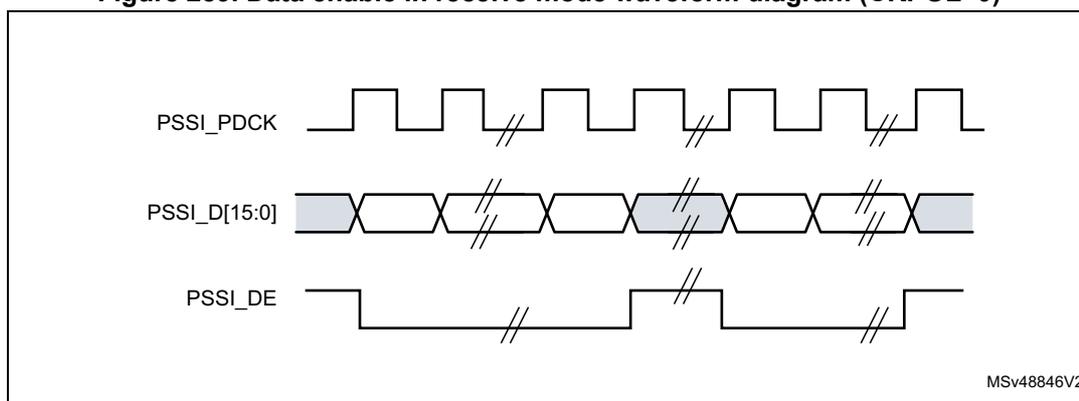
The diagram illustrates the timing relationship between three signals in receive mode with CKPOL=0:
- PSSI_PDCK : The clock signal, which is normally low and pulses high.
- PSSI_D[15:0] : The 16-bit data bus. Data transitions are aligned with the rising edges of PSSI_PDCK. Shaded areas represent valid data.
- PSSI_DE : The data enable signal. It is active-low, dropping to a low state to indicate valid data on the bus.
Double slashes on the signal lines indicate breaks in the time axis.
If the PSSI_DE alternate output function is enabled (through DERDYCFG) in transmit mode (OUTEN=1), the PSSI drives PSSI_DE on the same PSSI_PDCK edge that the one used to drive the data (D[15:0]). If a new 8 or 16-bit data (as programmed in the EDM[1:0] control bits in PSSI_CR) is available for transmission in the internal FIFO, this data is output on the data outputs (D[15:0]) and the PSSI_DE output becomes active on the current PSSI_PDCK edge. Otherwise (if the TX FIFO is empty), the D[15:0] outputs remains unchanged on the next clock edge and the PSSI_DE output becomes inactive.
Figure 290. Data enable waveform diagram in transmit mode (CKPOL=1)
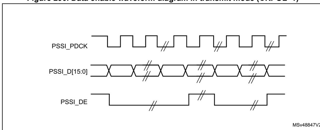
The diagram shows the timing for transmit mode with CKPOL=1:
- PSSI_PDCK : The clock signal, which is normally high and pulses low.
- PSSI_D[15:0] : The data bus. Data changes are synchronized with the falling edges of the clock.
- PSSI_DE : The active-low data enable signal, which transitions in sync with the data and clock.
Double slashes indicate time gaps in the waveform representation.
Ready (PSSI_RDY) alternate function output
The ready signal, PSSI_RDY, is an optional signal. It is driven by the receiving device and indicates whether data is being accepted in the current cycle. When PSSI_RDY is inactive, it means that the data must not be sampled by the receiver at the next clock edge.
This alternate function signal can be enabled using the DERDYCFG control bits (bits 20:18 of PSSI_CR). PSSI_RDY polarity is configured through the RDYPOL control bit (bit 6 of PSSI_CR). PSSI_RDY is active low when RDYPOL is cleared to 0, and high when RDYPOL set to 1.
The direction of the PSSI_RDY signal is defined by the OUTEN (bit 31 of PSSI_CR). It is set in the opposite direction compared to the PSSI_DE and data signals.
If the PSSI_RDY alternate output function is enabled (through DERDYCFG) in receive mode (OUTEN=0), the PSSI drives PSSI_RDY one PSSI_PDCK half cycle after it samples
the data (D[15:0]). If the FIFO has enough free space to receive more data, the PSSI drives the PSSI_RDY signal active. Otherwise, if the FIFO is full and cannot accept more data, the PSSI drives the PSSI_RDY signal inactive. The transmitting device must repeat the current data in the next cycle when it detects that PSSI_RDY is inactive. This flow control function allows the PSSI to avoid overrun errors when the system (via the DMA) is unable to keep up with the data flow.
Figure 291. Ready in receive mode waveform diagram (CKPOL=0)
![Figure 291. Ready in receive mode waveform diagram (CKPOL=0). The diagram shows four signals over time: PSSI_PDCK (clock), PSSI_D[15:0] (data bus), PSSI_DE (data enable), and PSSI_RDY (ready). PSSI_PDCK is a periodic square wave. PSSI_D[15:0] shows data being driven onto the bus, with some cycles marked as invalid or inactive. PSSI_DE is a signal that goes high when data is valid. PSSI_RDY is a signal that goes low when the receiver is ready to accept more data. The diagram illustrates the timing relationship between these signals in receive mode.](/RM0481-STM32H523-33-562-63-573/4d93f3fe48d68d0f100e67b6630ff103_img.jpg)
The waveform diagram shows four signals over time. The top signal, PSSI_PDCK, is a periodic square wave representing the clock. The second signal, PSSI_D[15:0], represents the data bus, showing various data values (represented by different shades of gray) being driven onto the bus. The third signal, PSSI_DE, is the data enable signal, which is high when valid data is present on the bus. The bottom signal, PSSI_RDY, is the ready signal, which is low when the receiver is ready to accept more data. The diagram shows that the PSSI_RDY signal is active (low) when the FIFO has space, and inactive (high) when the FIFO is full. The data on the bus is repeated when the PSSI_RDY signal is inactive.
MSV48848V2
If the PSSI_RDY alternate input function is enabled (through DERDYCFG) in transmit mode (OUTEN=1), the PSSI samples the PSSI_RDY signal on the opposite PSSI_PDCK edge to the one at which D[15:0] are driven. If the PSSI_RDY signal is inactive, the PSSI keeps the same data (D[15:0]) and PSSI_DE signals that valid data are available during the next PSSI_PDCK clock cycle. Otherwise, if PSSI_RDY signal is sampled as active, the next data from the TX FIFO (if available) is output on the data outputs (D[15:0]). If no new data are available in the TX FIFO, the PSSI keeps the data output values and outputs the PSSI_DE signal as inactive (if enabled).
The receiving device uses the PSSI_RDY to control the data flow and avoid overrun errors when the system (via the DMA) is unable to keep up with the data flow.
Bidirectional PSSI_DE/PSSI_RDY signal
A single pin can be used for both data enable (PSSI_DE) and ready (PSSI_RDY) functions if DEPOL and RDYPOL are both set to 1 and DERDYCFG is set to 111 or 100 in the PSSI_CR register. In this case, the GPIO corresponding to selected alternate function (PSSI_DE when DERDYCFG=111 or PSSI_RDY when DERDYCFG=100) must be configured as open-drain. The other device must also be configured to drive the line as open-drain, and a weak pull-up must be applied to the line.
The signal thus becomes bidirectional. If either the sender drives the line low (to indicate that the data is not valid) or the receiver drives the line low (to indicate that it is not sampling the current data), then both devices know that the data is not being transferred in the current cycle.
Figure 292. Bidirectional PSSI_DE/PSSI_RDY waveform
![Timing diagram showing signals PSSI_PDCK, PSSI_D[15:0], and PSSI_DE/PSSI_RDY over time. PSSI_PDCK is a periodic clock signal. PSSI_D[15:0] is a 16-bit data bus with data segments. PSSI_DE and PSSI_RDY are active-low signals that go low during data transmission periods.](/RM0481-STM32H523-33-562-63-573/4a1e69304ed332339e7df3cf86f3387b_img.jpg)
Figure 293. Bidirectional PSSI_DE/PSSI_RDY connection diagram
![Block diagram showing a PSSI block connected to a Master transmitter. The PSSI block has pins for PSSI_D[15:0], PSSI_PDCK, and PSSI_DE_RDY. The Master transmitter has corresponding pins. The PSSI_DE_RDY line is shown with a pull-up resistor.](/RM0481-STM32H523-33-562-63-573/6731e52bce03ce4eb95044b18ebac45b_img.jpg)
31.4 PSSI interrupts
The PSSI generates only one interrupt (IT_OVR). It is consequently equivalent to the global interrupt (pssi_it). Refer to Table 308 for the list of interrupts.
The PSSI and the DCMI share the same interrupt vector. When the PSSI ENABLE bit (bit 14 of PSSI_CR) is set to 1, these interrupts are triggered by the PSSI. Otherwise, they are controlled by the DCMI.
The DCMI ENABLE bit (bit 14 of DCMI_CR) and PSSI ENABLE bit must not be set to 1 at the same time.
Table 308. PSSI interrupt requests
| Interrupt acronym | Shared with DCMI | Interrupt event | Event flag | Enable control bit | Interrupt clear method | Exit from low-power mode |
|---|---|---|---|---|---|---|
| IT_OVR | IT_OVR | indicates overrun in receive mode or underrun in transmit mode | OVR_RIS | OVR_IE | OVR_ISC | NA |
31.5 PSSI registers
An 8-bit write or a 16-bit write operation to any PSSI register besides PSSI_DR, results in a bus error. 32-bit read and write operations are permitted.
31.5.1 PSSI control register (PSSI_CR)
Address offset: 0x00
Reset value: 0x4000 0000
| 31 | 30 | 29 | 28 | 27 | 26 | 25 | 24 | 23 | 22 | 21 | 20 | 19 | 18 | 17 | 16 |
|---|---|---|---|---|---|---|---|---|---|---|---|---|---|---|---|
| OUTEN | DMAEN | Res. | Res. | Res. | Res. | Res. | Res. | Res. | Res. | Res. | DERDYCFG[2:0] | Res. | |||
| rw | rw | rw | rw | rw | |||||||||||
| 15 | 14 | 13 | 12 | 11 | 10 | 9 | 8 | 7 | 6 | 5 | 4 | 3 | 2 | 1 | 0 |
|---|---|---|---|---|---|---|---|---|---|---|---|---|---|---|---|
| Res. | ENBLE | Res. | Res. | EDM[1:0] | Res. | RDYPOL | Res. | DEPOL | CKPOL | Res. | Res. | Res. | Res. | Res. | |
| rw | rw | rw | rw | rw | rw | ||||||||||
Bit 31 OUTEN : Data direction selection bit
0: Receive mode: data is input synchronously with PSSI_PDCK
1: Transmit mode: data is output synchronously with PSSI_PDCK
Bit 30 DMAEN : DMA enable bit
0: DMA transfers are disabled. The user application can directly access the PSSI_DR register when DMA transfers are disabled.
1: DMA transfers are enabled (default configuration). A DMA channel in the general-purpose DMA controller must be configured to perform transfers from/to PSSI_DR.
Bits 29:21 Reserved, must be kept at reset value.
Bits 20:18 DERDYCFG[2:0] : Data enable and ready configuration
000: PSSI_DE and PSSI_RDY both disabled
001: Only PSSI_RDY enabled
010: Only PSSI_DE enabled
011: Both PSSI_RDY and PSSI_DE alternate functions enabled
100: Both PSSI_RDY and PSSI_DE features enabled - bidirectional on PSSI_RDY pin (see Bidirectional PSSI_DE/PSSI_RDY signal on page 1239 )
101: Only PSSI_RDY function enabled, but mapped to PSSI_DE pin
110: Only PSSI_DE function enabled, but mapped to PSSI_RDY pin
111: Both PSSI_RDY and PSSI_DE features enabled - bidirectional on PSSI_DE pin (see Bidirectional PSSI_DE/PSSI_RDY signal on page 1239 )
When the PSSI_RDY function is mapped to the PSSI_DE pin (settings 101 or 111), it is still the RDYPOL bit which determines its polarity. Similarly, when the PSSI_DE function is mapped to the PSSI_RDY pin (settings 110 or 111), it is still the DEPOL bit which determines its polarity.
Bits 17:15 Reserved, must be kept at reset value.
Bit 14 ENABLE : PSSI enable
0: PSSI disabled
1: PSSI enabled
The contents of the FIFO are flushed when ENABLE is cleared to 0.
Note: When ENABLE=1, the content of PSSI_CR must not be changed, except for the ENABLE bit itself. All configuration bits can change as soon as ENABLE changes from 0 to 1.
The DMA controller and all PSSI configuration registers must be programmed correctly before setting the ENABLE bit to 1.
The ENABLE bit and the DCMI ENABLE bit (bit 15 of DCMI_CR) must not be set to 1 at the same time.
Bits 13:12 Reserved, must be kept at reset value.
Bits 11:10 EDM[1:0] : Extended data mode
00: Interface captures 8-bit data on every parallel data clock
01: Reserved, must not be selected
10: Reserved, must not be selected
11: The interface captures 16-bit data on every parallel data clock
Bit 9 Reserved, must be kept at reset value.
Bit 8 RDYPOL : Ready (PSSI_RDY) polarity
This bit indicates the level on the PSSI_RDY pin when the data are not valid on the parallel interface.
0: PSSI_RDY active low (0 indicates that the receiver is ready to receive)
1: PSSI_RDY active high (1 indicates that the receiver is ready to receive)
Bit 7 Reserved, must be kept at reset value.
Bit 6 DEPOL : Data enable (PSSI_DE) polarity
This bit indicates the level on the PSSI_DE pin when the data are not valid on the parallel interface.
0: PSSI_DE active low (0 indicates that data is valid)
1: PSSI_DE active high (1 indicates that data is valid)
Bit 5 CKPOL : Parallel data clock polarity
This bit configures the capture edge of the parallel clock or the edge used for driving outputs, depending on OUTEN.
0: Falling edge active for inputs or rising edge active for outputs
1: Rising edge active for inputs or falling edge active for outputs.
Bits 4:0 Reserved, must be kept at reset value.
31.5.2 PSSI status register (PSSI_SR)
Address offset: 0x04
Reset value: 0x0000 0000
| 31 | 30 | 29 | 28 | 27 | 26 | 25 | 24 | 23 | 22 | 21 | 20 | 19 | 18 | 17 | 16 |
|---|---|---|---|---|---|---|---|---|---|---|---|---|---|---|---|
| Res. | Res. | Res. | Res. | Res. | Res. | Res. | Res. | Res. | Res. | Res. | Res. | Res. | Res. | Res. | Res. |
| 15 | 14 | 13 | 12 | 11 | 10 | 9 | 8 | 7 | 6 | 5 | 4 | 3 | 2 | 1 | 0 |
| Res. | Res. | Res. | Res. | Res. | Res. | Res. | Res. | Res. | Res. | Res. | Res. | RTT1B | RTT4B | Res. | Res. |
| r | r |
Bits 31:4 Reserved, must be kept at reset value.
Bit 3 RTT1B : FIFO is ready to transfer one byte
1: FIFO is ready for a one byte transfer. In receive mode, this means that at least one valid data byte is in the FIFO. In transmit mode, this means that there is at least one byte free in the FIFO.
0: FIFO is not ready for a 1-byte transfer
Bit 2 RTT4B : FIFO is ready to transfer four bytes
1: FIFO is ready for a four-byte (32-bit) transfer. In receive mode, this means that at least four valid data bytes are in the FIFO. In transmit mode, this means that there are at least four bytes free in the FIFO.
0: FIFO is not ready for a four-byte transfer
Bits 1:0 Reserved, must be kept at reset value.
31.5.3 PSSI raw interrupt status register (PSSI_RIS)
Address offset: 0x08
Reset value: 0x0000 0000
PSSI_RIS gives the raw interrupt status. This register is read-only. When read, it returns the status of the corresponding interrupt before masking with the PSSI_IER register value.
| 31 | 30 | 29 | 28 | 27 | 26 | 25 | 24 | 23 | 22 | 21 | 20 | 19 | 18 | 17 | 16 |
|---|---|---|---|---|---|---|---|---|---|---|---|---|---|---|---|
| Res. | Res. | Res. | Res. | Res. | Res. | Res. | Res. | Res. | Res. | Res. | Res. | Res. | Res. | Res. | Res. |
| 15 | 14 | 13 | 12 | 11 | 10 | 9 | 8 | 7 | 6 | 5 | 4 | 3 | 2 | 1 | 0 |
| Res. | Res. | Res. | Res. | Res. | Res. | Res. | Res. | Res. | Res. | Res. | Res. | Res. | Res. | OVR_R IS | Res. |
| r |
Bits 31:2 Reserved, must be kept at reset value.
Bit 1 OVR_RIS : Data buffer overrun/underrun raw interrupt status
0: No overrun/underrun occurred
1: An overrun/underrun occurred: overrun in receive mode, underrun in transmit mode.
This bit is cleared by writing a 1 to the OVR_ISC bit in PSSI_ICR.
Bit 0 Reserved, must be kept at reset value.
31.5.4 PSSI interrupt enable register (PSSI_IER)
Address offset: 0x0C
Reset value: 0x0000 0000
The PSSI_IER register is used to enable interrupts. When one of the PSSI_IER bits is set, the corresponding interrupt is enabled. This register is accessible both in read and write modes.
| 31 | 30 | 29 | 28 | 27 | 26 | 25 | 24 | 23 | 22 | 21 | 20 | 19 | 18 | 17 | 16 |
|---|---|---|---|---|---|---|---|---|---|---|---|---|---|---|---|
| Res. | Res. | Res. | Res. | Res. | Res. | Res. | Res. | Res. | Res. | Res. | Res. | Res. | Res. | Res. | Res. |
| 15 | 14 | 13 | 12 | 11 | 10 | 9 | 8 | 7 | 6 | 5 | 4 | 3 | 2 | 1 | 0 |
| Res. | Res. | Res. | Res. | Res. | Res. | Res. | Res. | Res. | Res. | Res. | Res. | Res. | Res. | OVR_IE | Res. |
| rw |
Bits 31:2 Reserved, must be kept at reset value.
Bit 1 OVR_IE : Data buffer overrun/underrun interrupt enable
0: No interrupt generation
1: An interrupt is generated if either an overrun or an underrun error occurred.
Bit 0 Reserved, must be kept at reset value.
31.5.5 PSSI masked interrupt status register (PSSI_MIS)
This PSSI_MIS register is read-only. When read, it returns the current masked status value of the corresponding interrupt (depending on the value in PSSI_IER). A bit in this register is set if the corresponding enable bit in PSSI_IER is set and the corresponding bit in PSSI_RIS is set.
Address offset: 0x10
Reset value: 0x0000 0000
| 31 | 30 | 29 | 28 | 27 | 26 | 25 | 24 | 23 | 22 | 21 | 20 | 19 | 18 | 17 | 16 |
|---|---|---|---|---|---|---|---|---|---|---|---|---|---|---|---|
| Res. | Res. | Res. | Res. | Res. | Res. | Res. | Res. | Res. | Res. | Res. | Res. | Res. | Res. | Res. | Res. |
| 15 | 14 | 13 | 12 | 11 | 10 | 9 | 8 | 7 | 6 | 5 | 4 | 3 | 2 | 1 | 0 |
| Res. | Res. | Res. | Res. | Res. | Res. | Res. | Res. | Res. | Res. | Res. | Res. | Res. | Res. | OVR_MIS | Res. |
| r |
Bits 31:2 Reserved, must be kept at reset value.
Bit 1 OVR_MIS : Data buffer overrun/underrun masked interrupt status
This bit is set to 1 only when PSSI_IER/OVR_IE and PSSI_RIS/OVR_RIS are both set to 1.
0: No interrupt is generated when an overrun/underrun error occurs
1: An interrupt is generated if there is either an overrun or an underrun error and the OVR_IE bit is set in PSSI_IER.
Bit 0 Reserved, must be kept at reset value.
31.5.6 PSSI interrupt clear register (PSSI_ICR)
Address offset: 0x14
Reset value: 0x0000 0000
The PSSI_ICR register is write-only. Writing a 1 into a bit of this register clears the corresponding bit in the PSSI_RIS and PSSI_MIS registers. Writing a 0 has no effect. Reading this register always gives zeros.
| 31 | 30 | 29 | 28 | 27 | 26 | 25 | 24 | 23 | 22 | 21 | 20 | 19 | 18 | 17 | 16 |
|---|---|---|---|---|---|---|---|---|---|---|---|---|---|---|---|
| Res. | Res. | Res. | Res. | Res. | Res. | Res. | Res. | Res. | Res. | Res. | Res. | Res. | Res. | Res. | Res. |
| 15 | 14 | 13 | 12 | 11 | 10 | 9 | 8 | 7 | 6 | 5 | 4 | 3 | 2 | 1 | 0 |
| Res. | Res. | Res. | Res. | Res. | Res. | Res. | Res. | Res. | Res. | Res. | Res. | Res. | Res. | OVR_I SC | Res. |
| w |
Bits 31:2 Reserved, must be kept at reset value.
Bit 1
OVR_ISC
: Data buffer overrun/underrun interrupt status clear
Writing this bit to 1 clears the OVR_RIS bit in PSSI_RIS.
Bit 0 Reserved, must be kept at reset value.
31.5.7 PSSI data register (PSSI_DR)
Address offset: 0x28
Reset value: 0x0000 0000
In receive mode (OUTEN = 0), the DMA controller must read the received data from this register. Write operations to PSSI_DR result in an error response. When more bytes than the number of valid bytes are read in the FIFO, the invalid bytes return zeros.
In transmit mode (OUTEN = 1), the DMA controller must write the data to be transmitted into this register. Read operations to PSSI_DR result in an error response.
32-bit, 16-bit, and 8-bit accesses are all supported for PSSI_DR. For instance, 16-bit read/write operations remove/add two bytes from/to the FIFO. However, 8-bit accesses are permitted only when the PSSI is configured to transfer 8 data bits at a time (EDM=00 in PSSI_CR). 8-bit accesses to PSSI_DR when EDM is not set to 0 result in an error response.
All accesses must include byte 0: 8-bit accesses must be performed to bits 7 to 0 and 16-bit accesses from bits 15 to 0. Accesses that do not include byte 0 results in an error response.
Accessing PSSI_DR when ENABLE bit in PSSI_CR is set to 0 results in an error response.
| 31 | 30 | 29 | 28 | 27 | 26 | 25 | 24 | 23 | 22 | 21 | 20 | 19 | 18 | 17 | 16 |
|---|---|---|---|---|---|---|---|---|---|---|---|---|---|---|---|
| BYTE3[7:0] | BYTE2[7:0] | ||||||||||||||
| rw | rw | rw | rw | rw | rw | rw | rw | rw | rw | rw | rw | rw | rw | rw | rw |
| 15 | 14 | 13 | 12 | 11 | 10 | 9 | 8 | 7 | 6 | 5 | 4 | 3 | 2 | 1 | 0 |
| BYTE1[7:0] | BYTE0[7:0] | ||||||||||||||
| rw | rw | rw | rw | rw | rw | rw | rw | rw | rw | rw | rw | rw | rw | rw | rw |
Bits 31:24 BYTE3[7:0] : Data byte 3
Bits 23:16 BYTE2[7:0] : Data byte 2
Bits 15:8 BYTE1[7:0] : Data byte 1
Bits 7:0 BYTE0[7:0] : Data byte 0
31.5.8 PSSI register map
Table 309. PSSI register map and reset values
| Offset | Register name | 31 | 30 | 29 | 28 | 27 | 26 | 25 | 24 | 23 | 22 | 21 | 20 | 19 | 18 | 17 | 16 | 15 | 14 | 13 | 12 | 11 | 10 | 9 | 8 | 7 | 6 | 5 | 4 | 3 | 2 | 1 | 0 |
|---|---|---|---|---|---|---|---|---|---|---|---|---|---|---|---|---|---|---|---|---|---|---|---|---|---|---|---|---|---|---|---|---|---|
| 0x00 | PSSI_CR | OUTEN | DMAEN | Res. | Res. | Res. | Res. | Res. | Res. | Res. | Res. | Res. | DERDYCFG | Res. | Res. | Res. | ENABLE[2:0] | Res. | Res. | EDM | Res. | RDYPOL | Res. | DEPOL | CKPOL | Res. | Res. | Res. | Res. | Res. | |||
| Reset value | 0 | 1 | 0 | 0 | 0 | 0 | 0 | 0 | 0 | 0 | 0 | ||||||||||||||||||||||
| 0x04 | PSSI_SR | Res. | Res. | Res. | Res. | Res. | Res. | Res. | Res. | Res. | Res. | Res. | Res. | Res. | Res. | Res. | Res. | Res. | Res. | Res. | Res. | Res. | Res. | Res. | Res. | Res. | Res. | Res. | Res. | RTT1B | RTT4B | Res. | Res. |
| Reset value | 0 | 0 | |||||||||||||||||||||||||||||||
| 0x08 | PSSI_RIS | Res. | Res. | Res. | Res. | Res. | Res. | Res. | Res. | Res. | Res. | Res. | Res. | Res. | Res. | Res. | Res. | Res. | Res. | Res. | Res. | Res. | Res. | Res. | Res. | Res. | Res. | Res. | Res. | Res. | Res. | Res. | OVR_RIS |
| Reset value | 0 | ||||||||||||||||||||||||||||||||
| 0x0C | PSSI_IER | Res. | Res. | Res. | Res. | Res. | Res. | Res. | Res. | Res. | Res. | Res. | Res. | Res. | Res. | Res. | Res. | Res. am | Res. | Res. | Res. | Res. | Res. | Res. | Res. | Res. | Res. | Res. | Res. | Res. | Res. | Res. | OVR_IE |
| Reset value | 0 | ||||||||||||||||||||||||||||||||
| 0x10 | PSSI_MIS | Res. | Res. | Res. | Res. | Res. | Res. | Res. | Res. | Res. | Res. | Res. | Res. | Res. | Res. | Res. | Res. | Res. | Res. | Res. | Res. | Res. | Res. | Res. | Res. | Res. | Res. | Res. | Res. | Res. | Res. | Res. | OVR_MIS |
| Reset value | 0 | ||||||||||||||||||||||||||||||||
| 0x14 | PSSI_ICR | Res. | Res. | Res. | Res. | Res. | Res. | Res. | Res. | Res. | Res. | Res. | Res. | Res. | Res. | Res. | Res. | Res. | Res. | Res. | Res. | Res. | Res. | Res. | Res. | Res. | Res. | Res. | Res. | Res. | Res. | Res. | OVR_ISC |
| Reset value | 0 | ||||||||||||||||||||||||||||||||
| 0x18-0x24 | Reserved | Res. | |||||||||||||||||||||||||||||||
| 0x28 | PSSI_DR | BYTE3[7:0] | BYTE2[7:0] | BYTE1[7:0] | BYTE0[7:0] | ||||||||||||||||||||||||||||
| Reset value | 0 | 0 | 0 | 0 | 0 | 0 | 0 | 0 | 0 | 0 | 0 | 0 | 0 | 0 | 0 | 0 | 0 | 0 | 0 | 0 | 0 | 0 | 0 | 0 | 0 | 0 | 0 | 0 | 0 | 0 | 0 | ||
Refer to Section 2.3: Memory organization for the register boundary addresses.