18. Extended interrupts and event controller (EXTI)
The extended interrupts and event controller (EXTI) manages the individual CPU and system wake-up through configurable and direct event inputs. It provides wake-up requests to the power control and generates an interrupt request to the CPU NVIC and events to the CPU event input. For the CPU, an additional event generation block (EVG) is needed to generate the CPU event signal.
The EXTI wake-up requests allow the system to be woken up from Stop modes.
The interrupt request and event request generation can be used also in Run modes.
The EXTI also includes the EXTI mux IO port selection.
18.1 EXTI main features
The EXTI main features are the following:
- • Up to 59 input events supported
- • All event inputs allow the possibility to wake up the system.
- • Events that do not have an associated wake-up flag in the peripheral, have a flag in the EXTI and generate an interrupt to the CPU from the EXTI.
- • Events can be used to generate a CPU wake-up event.
The asynchronous event inputs are classified in two groups:
- • Configurable events (signals from I/Os or peripherals able to generate a pulse), with the following features
- – Selectable active trigger edge
- – Interrupt pending status register bits independent for the rising and falling edge
- – Individual interrupt and event generation mask, used for conditioning the CPU wake-up, interrupt and event generation
- – Software trigger possibility
- – Secure events: The access to control and configuration bits of secure input events can be made secure and or privilege.
- – EXTI IO port selection
- • Direct events (interrupt and wake-up sources from peripherals having an associated flag which requires to be cleared in the peripheral), with the following features:
- – Fixed rising edge active trigger
- – No interrupt pending status register bit in the EXTI (the interrupt pending status flag is provided by the peripheral generating the event)
- – Individual interrupt and event generation mask, used to condition the CPU wake-up and event generation
- – No software trigger possibility
18.2 EXTI block diagram
The EXTI consists of a register block accessed via an AHB interface, the event input trigger block, the masking block and EXTI mux as shown in Figure 91 .
The register block contains all the EXTI registers.
The event input trigger block provides event input edge trigger logic.
The masking block provides the event input distribution to the different wake-up, interrupt and event outputs, and their masking.
The EXTI mux provides the IO port selection on to the EXTI event signal.
Figure 91. EXTI block diagram
![Figure 91. EXTI block diagram. The diagram shows the internal architecture of the EXTI block. On the left, GPIO and Peripherals are connected to the EXTI block. GPIOs provide IOPort signals to an EXTI mux. Peripherals provide Configurable event(y) and Wake-up signals to an Event trigger. The EXTI block contains Registers, an EXTI mux, an Event trigger, and a Masking block. The Registers are connected to an AHB interface and hclk. The EXTI mux selects between IOPort and Configurable event(15:0) signals. The Event trigger generates events from Configurable event(y) and Wake-up signals. The Masking block receives events from the Event trigger and generates output signals: sys_wake-up, c_wake-up, it_exti_per(y), c_evt_exti, and c_evt_rst. The output signals sys_wake-up and c_wake-up are sent to the PWR block. The output signals it_exti_per(y), c_evt_exti, and c_evt_rst are sent to the CPU block via an EVG (Event Generator) block. The EVG block contains a Pulse block and generates c_event and c_folk signals. The CPU block receives rxev and nvic(x) signals. The output signal exti_ilac is generated by the Registers. The output signal exti[15:0] is sent to an interconnect. The diagram is labeled MSv62642V1.](/RM0481-STM32H523-33-562-63-573/895e442fe943dfe7dda2fb39373d5e8e_img.jpg)
Table 148. EXTI signals
| Pin name | I/O | Description |
|---|---|---|
| AHB interface | I/O | EXTI register bus interface. When one event is configured to enable security, the AHB interface supports secure accesses. |
| hclk | I | AHB bus clock and EXTI system clock |
| Configurable event(y) | I | Asynchronous wake-up events from peripherals without an associated interrupt and flag |
| Direct event(x) | I | Synchronous and asynchronous wake-up events from peripherals with an associated interrupt and flag |
| exti_ilac | O | Illegal access event |
| IOPort(n) | I | GPIOs block IO ports[15:0] |
| exti[15:0] | O | EXTI GPIO output port to trigger other peripherals |
| it_exti_per (y) | O | Interrupts to the CPU associated with configurable event (y) |
| c_evt_exti | O | High-level sensitive event output for CPU, synchronous to hclk |
| c_evt_rst | I | Asynchronous reset input to clear c_evt_exti |
| sys_wakeup | O | Asynchronous system wake-up request to PWR for ck_sys and hclk |
| c_wakeup | O | Wake-up request to PWR for CPU, synchronous to hclk |
Table 149. EVG signals
| Pin name | I/O | Description |
|---|---|---|
| c_fclk | I | CPU free running clock |
| c_evt_in | I | High-level sensitive events input from EXTI, asynchronous to CPU clock |
| c_event | O | Event pulse, synchronous to CPU clock |
| c_evt_rst | O | Event reset signal, synchronous to CPU clock |
18.2.1 EXTI connections between peripherals and CPU
Some peripherals able to generate wake-up or interrupt events when the system is in Stop mode, are connected to the EXTI.
- • Peripheral wake-up signals that generate a pulse or do not have an interrupt status bits in the peripheral, are connected to an EXTI configurable event input. For these events, the EXTI provides a status pending bit to be cleared. It is the EXTI interrupt, associated with the status bit, that interrupts the CPU.
- • Peripheral interrupt and wake-up signals with a status bit in the peripheral to be cleared are connected to an EXTI direct event input. There is no status pending bit within the EXTI. The interrupt or wake-up is cleared by the CPU in the peripheral. It is the peripheral interrupt that interrupts the CPU directly.
All GPIO ports input to the EXTI multiplexer allow the selection of a port pin to wake up the system via a configurable event.
The EXTI configurable event interrupts are connected to the NVIC.
The dedicated EXTI/EVG CPU event is connected to the CPU rxev input.
The EXTI CPU wake-up signals are connected to the PWR and are used to wake up the system and the CPU sub-system bus clocks.
18.2.2 EXTI interrupt/event mapping
The EXTI lines are connected as shown in the following table.
Table 150. EXTI line connections
| EXTI Line | Line source | Line type |
|---|---|---|
| 0-15 | GPIO | Configurable |
| 16 | PVD/AVD output | Configurable |
| 17 | RTC non-secure | - |
| 18 | RTC secure | - |
| 19 | TAMP non-secure | - |
| 20 | TAMP secure | - |
| 21 | I2C1 wake-up | - |
| 22 | I2C2 wake-up | - |
| 23 | I2C3 wake-up | - |
| 24 | I3C1 wake-up | - |
Table 150. EXTI line connections (continued)
| EXTI Line | Line source | Line type |
|---|---|---|
| 25 | USART1 wake-up | - |
| 26 | USART2 wake-up | - |
| 27 | USART3 wake-up | - |
| 28 | UART4 wake-up | - |
| 29 | UART5 wake-up | - |
| 30 | USART6 wake-up | - |
| 31 | UART7 wake-up (1) | - |
| 32 | UART8 wake-up (1) | - |
| 33 | UART9 wake-up (1) | - |
| 34 | USART10 wake-up (1) | - |
| 35 | USART11 wake-up (1) | - |
| 36 | UART12 wake-up (1) | - |
| 37 | LPUART1 wake-up | - |
| 38 | LPTIM1 | - |
| 39 | LPTIM2 | - |
| 40 | SPI1 wake-up | - |
| 41 | SPI2 wake-up | - |
| 42 | SPI3 wake-up | - |
| 43 | SPI4 wake-up | - |
| 44 | SPI5 wake-up (1) | - |
| 45 | SPI6 wake-up (1) | - |
| 46 | ETH wake-up (1) | Configurable |
| 47 | USB FS wake-up | - |
| 48 | USBPD1 wake-up | - |
| 49 | LPTIM2 CH1 | - |
| 50 | DTS wake-up | Configurable |
| 51 | HDMI-CEC wake-up | - |
| 52 | I2C4 wake-up (1) | - |
| 53 | V DDIO2 monitoring | Configurable |
| 54 | LPTIM3 (1) | - |
| 55 | LPTIM4 (1) | - |
| 56 | LPTIM5 (1) | - |
| 57 | LPTIM6 (1) | - |
| 58 | I3C2 (2) | - |
1. Not available on STM32H523/33xx devices.
- Available only on STM32H523/33xx devices.
18.3 EXTI functional description
The events features are controlled from register bits as follows:
- Active trigger edge enable
- by rising edge selection in the EXTI rising trigger selection register (EXTI_RTSR1) and EXTI rising trigger selection register 2 (EXTI_RTSR2)
- by falling edge selection in the EXTI falling trigger selection register (EXTI_FTSR1) and EXTI falling trigger selection register 2 (EXTI_FTSR2)
- Software trigger in the EXTI software interrupt event register (EXTI_SWIER1) and EXTI software interrupt event register 2 (EXTI_SWIER2)
- Interrupt pending flag in the
- EXTI rising edge pending register (EXTI_RPR1) and EXTI rising edge pending register 2 (EXTI_RPR2)
- EXTI falling edge pending register (EXTI_FPR1) and EXTI falling edge pending register 2 (EXTI_FPR2)
- CPU wake-up and interrupt enable in the
- EXTI CPU wake-up with interrupt mask register (EXTI_IMR1) and EXTI CPU wake-up with interrupt mask register 2 (EXTI_IMR2)
- CPU wake-up and event enable
- EXTI CPU wake-up with event mask register (EXTI_EMR1) and EXTI CPU wake-up with event mask register 2 (EXTI_EMR2)
18.3.1 EXTI configurable event input wake-up
The figure below is a detailed representation of the logic associated with configurable event inputs that wake up the CPU sub-system bus clocks and generate an EXTI pending flag and interrupt to the CPU, and/or a CPU wake-up event.
Figure 92. Configurable event trigger logic CPU wake-up
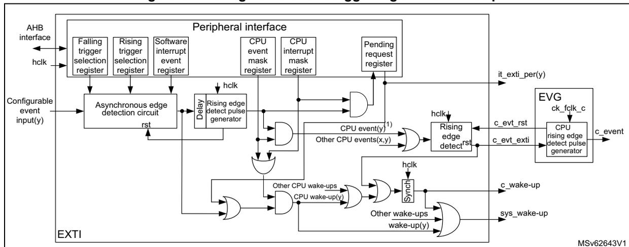
- Only for the input events that support CPU rxeu generation c_event.
The software interrupt event register allows configurable events to be triggered by software, writing the corresponding register bit, whatever the edge selection setting.
The configurable event active trigger edge (or both edges) is selected and enabled in the rising/falling edge selection registers.
The CPU has its dedicated wake-up (interrupt) mask register and a dedicated event mask registers. When the event is enabled, it is generated to the CPU. All events for the CPU are ORed together into a single CPU event signal. The event pending registers (EXTI_RPR and EXTI_FPR) are not set for an unmasked CPU event.
The configurable events have unique interrupt pending request registers. The pending register is only set for an unmasked interrupt. Each configurable event provides a common interrupt to the CPU. The configurable event interrupts must be acknowledged by software in the EXTI_RPR and/or EXTI_FPR registers.
When a CPU wake-up (interrupt) or CPU event is enabled, the asynchronous edge detection circuit is reset by the clocked delay and rising edge detect pulse generator. This guarantees that the EXTI hclk clock is woken up before the asynchronous edge detection circuit is reset.
Note: A detected configurable event interrupt pending request can be cleared by the CPU with the correct access permission. The system is not able to enter into low-power modes as long as an interrupt pending request is active.
18.3.2 EXTI direct event input wake-up
The direct events do not have an associated EXTI interrupt. The EXTI only wakes up the system and CPU subsystem clocks, and can generate a CPU wake-up event. The peripheral synchronous interrupt, associated with the direct wake-up event, wakes up the CPU.
The EXTI direct event is able to generate a CPU event that wakes up the CPU. The CPU event may occur before the associated peripheral interrupt flag is set.
Figure 93. EXTI direct events
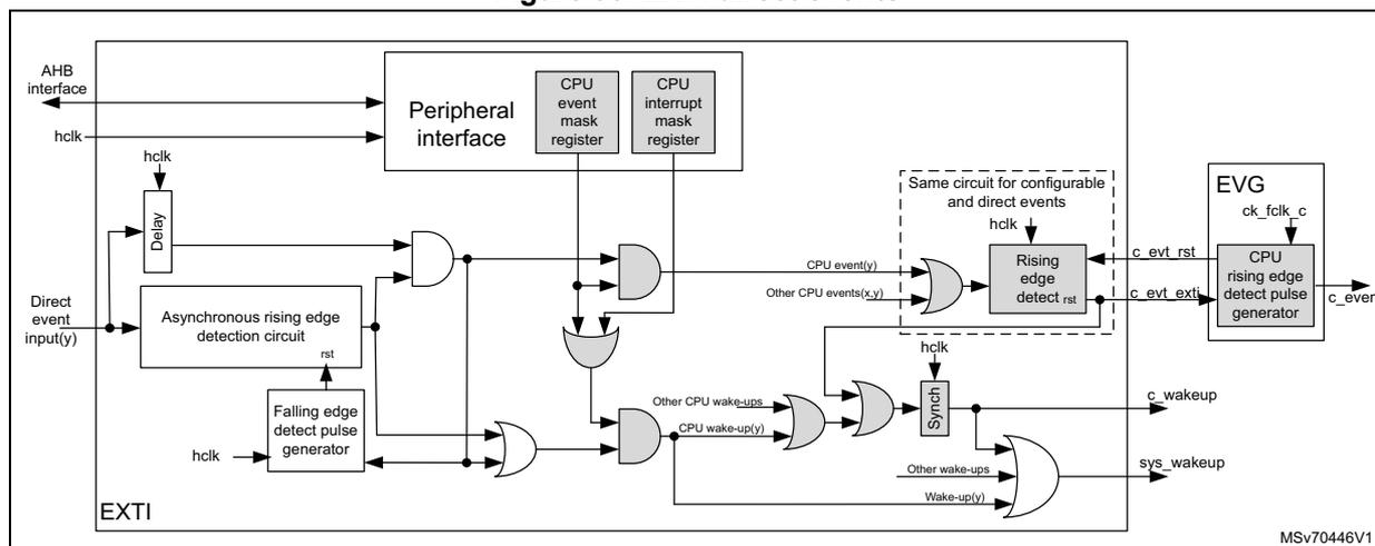
The diagram illustrates the internal logic of the EXTI for direct events. On the left, a 'Direct event input(y)' is shown. This input is connected to an 'Asynchronous rising edge detection circuit' and a 'Falling edge detect pulse generator'. Both are also connected to a 'Delay' block. The 'Delay' block is connected to the 'AHB interface' and 'hclk' clock. The 'Asynchronous rising edge detection circuit' output is connected to an OR gate. The 'Falling edge detect pulse generator' output is connected to another OR gate. These OR gates are connected to a 'Peripheral interface' block, which contains 'CPU event mask register' and 'CPU interrupt mask register'. The outputs of these registers are connected to a series of AND and OR gates. The 'CPU event mask register' output is connected to an AND gate, which also receives input from the 'Asynchronous rising edge detection circuit'. The output of this AND gate is connected to an OR gate. The 'CPU interrupt mask register' output is connected to another AND gate, which also receives input from the 'Falling edge detect pulse generator'. The output of this AND gate is connected to another OR gate. The outputs of these OR gates are connected to a 'Same circuit for configurable and direct events' block, which contains a 'Rising edge detect rst' block. This block is connected to 'hclk' and 'c_evt_rst'. The output of this block is connected to an 'EVG' (Event Generator) block, which contains a 'CPU rising edge detect pulse generator'. The output of this block is 'c_event'. The 'c_event' signal is also connected to a 'Synch' (Synchronizer) block, which is connected to 'hclk'. The output of the 'Synch' block is 'c_wakeup'. The 'c_wakeup' signal is also connected to an OR gate, which also receives input from 'Other CPU wake-ups' and 'Wake-up(y)'. The output of this OR gate is 'sys_wakeup'.
18.3.3 EXTI mux selection
The EXTI mux allows the selection of GPIOs as interrupts and wake-up. GPIOs are connected via 16 EXTI mux lines to the first 16 EXTI events as configurable event. The selection of GPIO port as EXTI mux output is controlled in the EXTI external interrupt selection register (EXTI_EXTICR1) .
Figure 94. EXTI mux GPIO selection
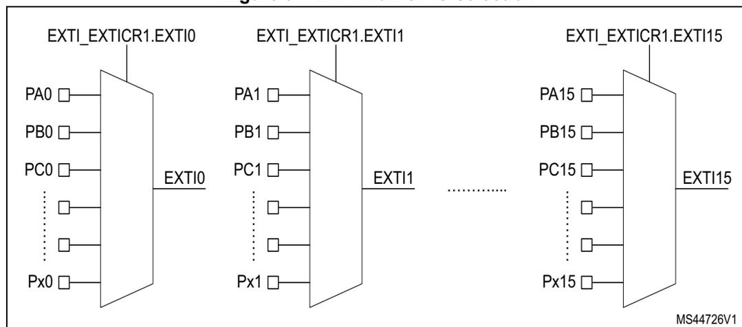
The EXTI mux outputs are available as output signals from the EXTI to trigger other peripherals, whatever the masking in EXTI_IMR and EXTI_EMR registers.
18.4 EXTI functional behavior
The configurable events are enabled by enabling at least one of the trigger edges.
Once an event input is enabled, the CPU wake-up generation is conditioned by the CPU interrupt mask and CPU event mask.
Table 151. Masking functionality
| CPU interrupt enable (in EXTI_IMR.IMn) | CPU event enable (in EXTI_EMR.EMn) | Configurable event inputs (in EXTI_RPR.RPIFn and EXTI_FPR.FPIFn) | Exti(n) interrupt (1) | CPU event | CPU wake-up |
|---|---|---|---|---|---|
| 0 | 0 | No | Masked | Masked | Masked |
| 1 | No | Masked | Yes | Yes | |
| 1 | 0 | Status latched | Yes | Masked | Yes (2) |
| 1 | Status latched | Yes | Yes | Yes |
1. The single exti(n) interrupt goes to the CPU. If no interrupt is required for CPU(m), the exti(n) interrupt must be masked in the CPU NVIC.
2. Only if CPU interrupt is enabled in EXTI_IMR.IMn.
For configurable event inputs, when the enabled edges occur on the event input, an event request is generated. When the associated CPU interrupt is unmasked, the corresponding pending bits EXTI_RPR.RPIFn and/or EXTI_FPR.FPIFn is/are set: the CPU sub-system is woken up and the CPU interrupt signal is activated. The EXTI_RPR.RPIFn and/or
EXTI_FPR.FPIFn pending bits must be cleared by software writing it to 1. This action clears the CPU interrupt.
For the configurable event inputs, an event request can be generated by software when writing a 1 in the software interrupt/event register EXTI_SWIER, allowing the generation of a rising edge on the event. The rising edge event pending bit is set in EXTI_RPR, whatever the setting in EXTI_RTSR.
18.5 EXTI event protection
The EXTI is able to protect event register bits from being modified by non-secure and unprivileged accesses. The protection is individually activated per input event via the register bits in EXTI_SECCFGR and EXTI_PRIVCFGR. At EXTI level, the protection consists in preventing the following unauthorized write access:
- • Change the settings of the secure and/or privileged configurable events.
- • Change the masking of the secure and/or privileged input events.
- • Clear pending status of the secure and/or privileged input events.
Table 152. Register protection overview
| Register name | Access type | Protection (1)(2) |
|---|---|---|
| EXTI_RTSR | RW | Security and privilege can be bit-wise enabled in EXTI_SECCFGR and EXTI_PRIVCFGR. |
| EXTI_FTSR | RW | |
| EXTI_SWIER | RW | |
| EXTI_RPR | RW | |
| EXTI_FPR | RW | |
| EXTI_SECCFGR | RW | Always secure. Privilege can be bit-wise enabled in EXTI_PRIVCFGR. |
| EXTI_PRIVCFGR | RW | Always privilege. Security can be bit-wise enabled in EXTI_SECCFGR. |
| EXTI_EXTICRn | RW | Security and privilege can be bit-wise enabled in EXTI_SECCFGR and EXTI_PRIVCFGR. |
| EXTI_LOCKR | RW | Always secure |
| EXTI_IM | RW | Security and privilege can be bit-wise enabled in EXTI_SECCFGR and EXTI_PRIVCFGR. |
| EXTI_EMR | RW |
1. Security is enabled with the individual input event (EXTI_SECCFGR register).
2. Privilege is enabled with the individual Input event (EXTI_PRIVCFGR register).
18.5.1 EXTI security protection
When security is enabled for an input event, the associated input event configuration and control bits can only be modified and read by a secure access. A non-secure write access is discarded and a read returns 0.
When input events are non-secure, the security is disabled. The associated input event configuration and control bits can be modified and read by a secure access and non-secure access.
The security configuration in registers EXTI_SECCFGR can be globally locked after reset by EXTI_LOCKR.LOCK.
18.5.2 EXTI privilege protection
When privilege is enabled for an input event, the associated input event configuration and control bits can only be modified and read by a privileged access. An unprivileged write access is discarded and a read returns 0.
When input events are unprivileged, the privilege is disabled. The associated input event configuration and control bits can be modified and read by a privileged access and unprivileged access.
The privileged configuration in registers EXTI_PRIVCFGR can be globally locked after reset by EXTI_LOCKR.LOCK.
18.6 EXTI registers
Table 153. EXTI register map sections
| Address offset | Description |
|---|---|
| 0x000 - 0x01C | General configurable event [31:0] configuration |
| 0x020 - 0x03C | General configurable event [57:32] configuration |
| 0x060 - 0x06C | EXTI IO port mux selection |
| 0x070 | EXTI protection lock configuration |
| 0x080 - 0x0BC | CPU input event configuration |
All registers can be accessed with word (32-bit), half-word (16-bit) and byte (8-bit) access.
18.6.1 EXTI rising trigger selection register (EXTI_RTSR1)
Address offset: 0x000
Reset value: 0x0000 0000
Contains only register bits for configurable events.
| 31 | 30 | 29 | 28 | 27 | 26 | 25 | 24 | 23 | 22 | 21 | 20 | 19 | 18 | 17 | 16 |
|---|---|---|---|---|---|---|---|---|---|---|---|---|---|---|---|
| Res. | Res. | Res. | Res. | Res. | Res. | Res. | Res. | Res. | Res. | Res. | Res. | Res. | Res. | Res. | RT16 |
| 15 | 14 | 13 | 12 | 11 | 10 | 9 | 8 | 7 | 6 | 5 | 4 | 3 | 2 | 1 | 0 |
| RT15 | RT14 | RT13 | RT12 | RT11 | RT10 | RT9 | RT8 | RT7 | RT6 | RT5 | RT4 | RT3 | RT2 | RT1 | RT0 |
| rw | rw | rw | rw | rw | rw | rw | rw | rw | rw | rw | rw | rw | rw | rw | rw |
Bits 31:17 Reserved, must be kept at reset value.
Bits 16:0 RTx : Rising trigger event configuration bit of configurable event input x (1) (x = 16 to 0)
When EXTI_SECCFGR.SECx is disabled, RTx can be accessed with non-secure and secure access.
When EXTI_SECCFGR.SECx is enabled, RTx can be accessed only with secure access. Non-secure write to this bit x is discarded and non-secure read returns 0.
When EXTI_PRIVCFGR.PRIVx is disabled, RTx can be accessed with unprivileged and privileged access.
When EXTI_PRIVCFGR.PRIVx is enabled, RTx can be accessed only with privileged access. Unprivileged write to this bit x is discarded, unprivileged read returns 0.
0: Rising trigger disabled (for event and interrupt) for input line
1: Rising trigger enabled (for event and interrupt) for input line
- The configurable event inputs are edge triggered, no glitch must be generated on these inputs. If a rising edge on the configurable event input occurs during writing of the register, the associated pending bit is not set. Rising and falling edge triggers can be set for the same configurable event input. In this case, both edges generate a trigger.
18.6.2 EXTI falling trigger selection register (EXTI_FTSR1)
Address offset: 0x004
Reset value: 0x0000 0000
Contains only register bits for configurable events.
| 31 | 30 | 29 | 28 | 27 | 26 | 25 | 24 | 23 | 22 | 21 | 20 | 19 | 18 | 17 | 16 |
|---|---|---|---|---|---|---|---|---|---|---|---|---|---|---|---|
| Res. | Res. | Res. | Res. | Res. | Res. | Res. | Res. | Res. | Res. | Res. | Res. | Res. | Res. | Res. | FT16 |
| 15 | 14 | 13 | 12 | 11 | 10 | 9 | 8 | 7 | 6 | 5 | 4 | 3 | 2 | 1 | 0 |
| FT15 | FT14 | FT13 | FT12 | FT11 | FT10 | FT9 | FT8 | FT7 | FT6 | FT5 | FT4 | FT3 | FT2 | FT1 | FT0 |
| rw | rw | rw | rw | rw | rw | rw | rw | rw | rw | rw | rw | rw | rw | rw | rw |
Bits 31:17 Reserved, must be kept at reset value.
Bits 16:0 FTx : Falling trigger event configuration bit of configurable event input x (1) (x = 16 to 0)
When EXTI_SECCFGR.SECx is disabled, FTx can be accessed with non-secure and secure access.
When EXTI_SECCFGR.SECx is enabled, FTx can be accessed only with secure access.
Non-secure write to this FTx is discarded, non-secure read returns 0.
When EXTI_PRIVCFGR.PRIVx is disabled, FTx can be accessed with unprivileged and privileged access.
When EXTI_PRIVCFGR.PRIVx is enabled, FTx can be accessed only with privileged access. Unprivileged write to this FTx is discarded, unprivileged read returns 0.
0: Falling trigger disabled (for event and Interrupt) for input line
1: Falling trigger enabled (for event and Interrupt) for input line.
- 1. The configurable event inputs are edge triggered, no glitch must be generated on these inputs.
If a falling edge on the configurable event input occurs during writing of the register, the associated pending bit is not set.
Rising and falling edge triggers can be set for the same configurable event input. In this case, both edges generate a trigger.
18.6.3 EXTI software interrupt event register (EXTI_SWIER1)
Address offset: 0x008
Reset value: 0x0000 0000
Contains only register bits for configurable events.
| 31 | 30 | 29 | 28 | 27 | 26 | 25 | 24 | 23 | 22 | 21 | 20 | 19 | 18 | 17 | 16 |
|---|---|---|---|---|---|---|---|---|---|---|---|---|---|---|---|
| Res. | Res. | Res. | Res. | Res. | Res. | Res. | Res. | Res. | Res. | Res. | Res. | Res. | Res. | Res. | SWI16 |
| 15 | 14 | 13 | 12 | 11 | 10 | 9 | 8 | 7 | 6 | 5 | 4 | 3 | 2 | 1 | 0 |
| SWI15 | SWI14 | SWI13 | SWI12 | SWI11 | SWI10 | SWI9 | SWI8 | SWI7 | SWI6 | SWI5 | SWI4 | SWI3 | SWI2 | SWI1 | SWI0 |
| rw | rw | rw | rw | rw | rw | rw | rw | rw | rw | rw | rw | rw | rw | rw | rw |
Bits 31:17 Reserved, must be kept at reset value.
Bits 16:0 SWIx : Software interrupt on event x (x = 16 to 0)
When EXTI_SECCFGR.SECx is disabled, SWIx can be accessed with non-secure and secure access.
When EXTI_SECCFGR.SECx is enabled, SWIx can be accessed only with secure access.
Non-secure write to this SWIx is discarded, non-secure read returns 0.
When EXTI_PRIVCFGR.PRIVx is disabled, SWIx can be accessed with unprivileged and privileged access.
When EXTI_PRIVCFGR.PRIVx is enabled, SWIx can be accessed only with privileged access. Unprivileged write to this SWIx is discarded, unprivileged read returns 0.
A software interrupt is generated independent from the setting in EXTI_RTSR and EXTI_FTSR. It always returns 0 when read.
0: Writing 0 has no effect.
1: Writing 1 triggers a rising edge event on event x. This bit is auto cleared by hardware.
18.6.4 EXTI rising edge pending register (EXTI_RPR1)
Address offset: 0x00C
Reset value: 0x0000 0000
Contains only register bits for configurable events.
| 31 | 30 | 29 | 28 | 27 | 26 | 25 | 24 | 23 | 22 | 21 | 20 | 19 | 18 | 17 | 16 |
|---|---|---|---|---|---|---|---|---|---|---|---|---|---|---|---|
| Res. | Res. | Res. | Res. | Res. | Res. | Res. | Res. | Res. | Res. | Res. | Res. | Res. | Res. | Res. | RPIF16 |
| 15 | 14 | 13 | 12 | 11 | 10 | 9 | 8 | 7 | 6 | 5 | 4 | 3 | 2 | 1 | 0 |
| RPIF15 | RPIF14 | RPIF13 | RPIF12 | RPIF11 | RPIF10 | RPIF9 | RPIF8 | RPIF7 | RPIF6 | RPIF5 | RPIF4 | RPIF3 | RPIF2 | RPIF1 | RPIF0 |
| rw | rw | rw | rw | rw | rw | rw | rw | rw | rw | rw | rw | rw | rw | rw | rw |
Bits 31:17 Reserved, must be kept at reset value.
Bits 16:0 RPIFx : configurable event inputs x rising edge pending bit (x = 16 to 0)
When EXTI_SECCFGR.SECx is disabled, RPIFx can be accessed with non-secure and secure access.
When EXTI_SECCFGR.SECx is enabled, RPIFx can be accessed only with secure access.
Non-secure write to this RPIFx is discarded, non-secure read returns 0.
When EXTI_PRIVCFGR.PRIVx is disabled, RPIFx can be accessed with unprivileged and privileged access.
When EXTI_PRIVCFGR.PRIVx is enabled, RPIFx can be accessed only with privileged access. Unprivileged write to this RPIFx is discarded, unprivileged read returns 0.
0: No rising edge trigger request occurred
1: Rising edge trigger request occurred
This bit is set when the rising edge event or an EXTI_SWIER software trigger arrives on the configurable event line. This bit is cleared by writing 1 to it.
18.6.5 EXTI falling edge pending register (EXTI_FPR1)
Address offset: 0x010
Reset value: 0x0000 0000
Contains only register bits for configurable events.
| 31 | 30 | 29 | 28 | 27 | 26 | 25 | 24 | 23 | 22 | 21 | 20 | 19 | 18 | 17 | 16 |
|---|---|---|---|---|---|---|---|---|---|---|---|---|---|---|---|
| Res | Res | Res | Res | Res | Res | Res | Res | Res | Res | Res | Res | Res | Res | Res | FPIF16 |
| 15 | 14 | 13 | 12 | 11 | 10 | 9 | 8 | 7 | 6 | 5 | 4 | 3 | 2 | 1 | 0 |
| FPIF15 | FPIF14 | FPIF13 | FPIF12 | FPIF11 | FPIF10 | FPIF9 | FPIF8 | FPIF7 | FPIF6 | FPIF5 | FPIF4 | FPIF3 | FPIF2 | FPIF1 | FPIF0 |
| rw | rw | rw | rw | rw | rw | rw | rw | rw | rw | rw | rw | rw | rw | rw | rw |
Bits 31:17 Reserved, must be kept at reset value.
Bits 16:0 FPIFx : configurable event inputs x falling edge pending bit (x = 16 to 0)
When EXTI_SECCFGR.SECx is disabled, FPIFx can be accessed with non-secure and secure access.
When EXTI_SECCFGR.SECx is enabled, FPIFx can be accessed only with secure access.
Non-secure write to this FPIFx is discarded, non-secure read returns 0.
When EXTI_PRIVCFGR.PRIVx is disabled, FPIFx can be accessed with unprivileged and privileged access.
When EXTI_PRIVCFGR.PRIVx is enabled, FPIFx can be accessed only with privileged access. Unprivileged write to this FPIFx is discarded, unprivileged read returns 0.
0: No falling edge trigger request occurred
1: Falling edge trigger request occurred
This bit is set when the falling edge event arrives on the configurable event line. This bit is cleared by writing 1 to it.
18.6.6 EXTI security configuration register (EXTI_SECCFGR1)
Address offset: 0x014
Reset value: 0x0000 0000
This register provides write access security, a non-secure write access is ignored and causes the generation of an illegal access event. A non-secure read returns the register data.
Contains only register bits for security capable input events.
| 31 | 30 | 29 | 28 | 27 | 26 | 25 | 24 | 23 | 22 | 21 | 20 | 19 | 18 | 17 | 16 |
|---|---|---|---|---|---|---|---|---|---|---|---|---|---|---|---|
| SEC31 | SEC30 | SEC29 | SEC28 | SEC27 | SEC26 | SEC25 | SEC24 | SEC23 | SEC22 | SEC21 | SEC20 | SEC19 | SEC18 | SEC17 | SEC16 |
| 15 | 14 | 13 | 12 | 11 | 10 | 9 | 8 | 7 | 6 | 5 | 4 | 3 | 2 | 1 | 0 |
| SEC15 | SEC14 | SEC13 | SEC12 | SEC11 | SEC10 | SEC9 | SEC8 | SEC7 | SEC6 | SEC5 | SEC4 | SEC3 | SEC2 | SEC1 | SEC0 |
| rw | rw | rw | rw | rw | rw | rw | rw | rw | rw | rw | rw | rw | rw | rw | rw |
Bits 31:0 SECx : Security enable on event input x (x = 31 to 0)
When EXTI_PRIVCFGR.PRIVx is disabled, SECx can be accessed with privileged and unprivileged access.
When EXTI_PRIVCFGR.PRIVx is enabled, SECx can only be written with privileged access.
Unprivileged write to this SECx is discarded.
0: Event security disabled (non-secure)
1: Event security enabled (secure)
18.6.7 EXTI privilege configuration register (EXTI_PRIVCFG1)
Address offset: 0x018
Reset value: 0x0000 0000
This register provides privileged write access protection. An unprivileged read returns the register data.
Contains only register bits for privilege capable input events.
| 31 | 30 | 29 | 28 | 27 | 26 | 25 | 24 | 23 | 22 | 21 | 20 | 19 | 18 | 17 | 16 |
|---|---|---|---|---|---|---|---|---|---|---|---|---|---|---|---|
| PRIV31 | PRIV30 | PRIV29 | PRIV28 | PRIV27 | PRIV26 | PRIV25 | PRIV24 | PRIV23 | PRIV22 | PRIV21 | PRIV20 | PRIV19 | PRIV18 | PRIV17 | PRIV16 |
| rw | rw | rw | rw | rw | rw | rw | rw | rw | rw | rw | rw | rw | rw | rw | rw |
| 15 | 14 | 13 | 12 | 11 | 10 | 9 | 8 | 7 | 6 | 5 | 4 | 3 | 2 | 1 | 0 |
| PRIV15 | PRIV14 | PRIV13 | PRIV12 | PRIV11 | PRIV10 | PRIV9 | PRIV8 | PRIV7 | PRIV6 | PRIV5 | PRIV4 | PRIV3 | PRIV2 | PRIV1 | PRIV0 |
| rw | rw | rw | rw | rw | rw | rw | rw | rw | rw | rw | rw | rw | rw | rw | rw |
Bits 31:0 PRIVx : Security enable on event input x (x = 31 to 0)
When EXTI_SECCFGR.SECx is disabled, PRIVx can be accessed with secure and non-secure access.
When EXTI_SECCFGR.SECx is enabled, PRIVx can only be written with secure access.
Non-secure write to this PRIVx is discarded.
0: Event privilege disabled (unprivileged)
1: Event privilege enabled (privileged)
18.6.8 EXTI rising trigger selection register 2 (EXTI_RTSR2)
Address offset: 0x020
Reset value: 0x0000 0000
Contains only register bits for configurable events.
| 31 | 30 | 29 | 28 | 27 | 26 | 25 | 24 | 23 | 22 | 21 | 20 | 19 | 18 | 17 | 16 |
|---|---|---|---|---|---|---|---|---|---|---|---|---|---|---|---|
| Res. | Res. | Res. | Res. | Res. | Res. | Res. | Res. | Res. | Res. | RT53 | Res. | Res. | RT50 | Res. | Res. |
| rw | rw | ||||||||||||||
| 15 | 14 | 13 | 12 | 11 | 10 | 9 | 8 | 7 | 6 | 5 | 4 | 3 | 2 | 1 | 0 |
| Res. | RT46 | Res. | Res. | Res. | Res. | Res. | Res. | Res. | Res. | Res. | Res. | Res. | Res. | Res. | Res. |
| rw |
Bits 31:22, 20:19, 17:15, 13:0 Reserved, must be kept at reset value.
Bit 21 RT53 : Rising trigger event configuration bit of configurable event input x (1)
When EXTI_SECCFGR.SECx is disabled, RTx can be accessed with non-secure and secure access.
When EXTI_SECCFGR.SECx is enabled, RTx can be accessed only with secure access.
Non-secure write to this bit x is discarded and non-secure read returns 0.
When EXTI_PRIVCFGR.PRIVx is disabled, RTx can be accessed with unprivileged and privileged access.
When EXTI_PRIVCFGR.PRIVx is enabled, RTx can be accessed only with privileged access. Unprivileged write to this bit x is discarded, unprivileged read returns 0.
0: Rising trigger disabled (for event and interrupt) for input line
1: Rising trigger enabled (for event and interrupt) for input line
Bit 18 RT50 : Rising trigger event configuration bit of configurable event input x (1)
When EXTI_SECCFGR.SECx is disabled, RTx can be accessed with non-secure and secure access.
When EXTI_SECCFGR.SECx is enabled, RTx can be accessed only with secure access.
Non-secure write to this bit x is discarded and non-secure read returns 0.
When EXTI_PRIVCFGR.PRIVx is disabled, RTx can be accessed with unprivileged and privileged access.
When EXTI_PRIVCFGR.PRIVx is enabled, RTx can be accessed only with privileged access. Unprivileged write to this bit x is discarded, unprivileged read returns 0.
0: Rising trigger disabled (for event and interrupt) for input line
1: Rising trigger enabled (for event and interrupt) for input line
Bit 14 RT46 : Rising trigger event configuration bit of configurable event input x (1)
When EXTI_SECCFGR.SECx is disabled, RTx can be accessed with non-secure and secure access.
When EXTI_SECCFGR.SECx is enabled, RTx can be accessed only with secure access.
Non-secure write to this bit x is discarded and non-secure read returns 0.
When EXTI_PRIVCFGR.PRIVx is disabled, RTx can be accessed with unprivileged and privileged access.
When EXTI_PRIVCFGR.PRIVx is enabled, RTx can be accessed only with privileged access. Unprivileged write to this bit x is discarded, unprivileged read returns 0.
0: Rising trigger disabled (for event and interrupt) for input line
1: Rising trigger enabled (for event and interrupt) for input line
- 1. The configurable event inputs are edge triggered, no glitch must be generated on these inputs.
If a rising edge on the configurable event input occurs during writing of the register, the associated pending bit is not set.
Rising and falling edge triggers can be set for the same configurable event input. In this case, both edges generate a trigger.
18.6.9 EXTI falling trigger selection register 2 (EXTI_FTSR2)
Address offset: 0x024
Reset value: 0x0000 0000
Contains only register bits for configurable events.
| 31 | 30 | 29 | 28 | 27 | 26 | 25 | 24 | 23 | 22 | 21 | 20 | 19 | 18 | 17 | 16 |
|---|---|---|---|---|---|---|---|---|---|---|---|---|---|---|---|
| Res. | Res. | Res. | Res. | Res. | Res. | Res. | Res. | Res. | Res. | FT53 | Res. | Res. | FT50 | Res. | Res. |
| rw | rw | ||||||||||||||
| 15 | 14 | 13 | 12 | 11 | 10 | 9 | 8 | 7 | 6 | 5 | 4 | 3 | 2 | 1 | 0 |
| Res. | FT46 | Res. | Res. | Res. | Res. | Res. | Res. | Res. | Res. | Res. | Res. | Res. | Res. | Res. | Res. |
| rw |
Bits 31:22, 20:19,
17:15, 13:0 Reserved, must be kept at reset value.
Bit 21 FT53 : Falling trigger event configuration bit of configurable event input x (1)
When EXTI_SECCFGR.SECx is disabled, FTx can be accessed with non-secure and secure access.
When EXTI_SECCFGR.SECx is enabled, FTx can be accessed only with secure access.
Non-secure write to this FTx is discarded, non-secure read returns 0.
When EXTI_PRIVCFGR.PRIVx is disabled, FTx can be accessed with unprivileged and privileged access.
When EXTI_PRIVCFGR.PRIVx is enabled, FTx can be accessed only with privileged access. Unprivileged write to this FTx is discarded, unprivileged read returns 0.
0: Falling trigger disabled (for event and Interrupt) for input line
1: Falling trigger enabled (for event and Interrupt) for input line.
Bit 18 FT50 : Falling trigger event configuration bit of configurable event input x (1)
When EXTI_SECCFGR.SECx is disabled, FTx can be accessed with non-secure and secure access.
When EXTI_SECCFGR.SECx is enabled, FTx can be accessed only with secure access.
Non-secure write to this FTx is discarded, non-secure read returns 0.
When EXTI_PRIVCFGR.PRIVx is disabled, FTx can be accessed with unprivileged and privileged access.
When EXTI_PRIVCFGR.PRIVx is enabled, FTx can be accessed only with privileged access. Unprivileged write to this FTx is discarded, unprivileged read returns 0.
0: Falling trigger disabled (for event and Interrupt) for input line
1: Falling trigger enabled (for event and Interrupt) for input line.
Bit 14 FT46 : Falling trigger event configuration bit of configurable event input x (1)
When EXTI_SECCFGR.SECx is disabled, FTx can be accessed with non-secure and secure access.
When EXTI_SECCFGR.SECx is enabled, FTx can be accessed only with secure access.
Non-secure write to this FTx is discarded, non-secure read returns 0.
When EXTI_PRIVCFGR.PRIVx is disabled, FTx can be accessed with unprivileged and privileged access.
When EXTI_PRIVCFGR.PRIVx is enabled, FTx can be accessed only with privileged access. Unprivileged write to this FTx is discarded, unprivileged read returns 0.
0: Falling trigger disabled (for event and Interrupt) for input line
1: Falling trigger enabled (for event and Interrupt) for input line.
- 1. The configurable event inputs are edge triggered, no glitch must be generated on these inputs.
If a falling edge on the configurable event input occurs during writing of the register, the associated pending bit is not set.
Rising and falling edge triggers can be set for the same configurable event input. In this case, both edges generate a trigger.
18.6.10 EXTI software interrupt event register 2 (EXTI_SWIER2)
Address offset: 0x028
Reset value: 0x0000 0000
Contains only register bits for configurable events.
| 31 | 30 | 29 | 28 | 27 | 26 | 25 | 24 | 23 | 22 | 21 | 20 | 19 | 18 | 17 | 16 |
|---|---|---|---|---|---|---|---|---|---|---|---|---|---|---|---|
| Res. | Res. | Res. | Res. | Res. | Res. | Res. | Res. | Res. | Res. | SWI53 | Res. | Res. | SWI50 | Res. | Res. |
| rw | rw | ||||||||||||||
| 15 | 14 | 13 | 12 | 11 | 10 | 9 | 8 | 7 | 6 | 5 | 4 | 3 | 2 | 1 | 0 |
| Res. | SWI46 | Res. | Res. | Res. | Res. | Res. | Res. | Res. | Res. | Res. | Res. | Res. | Res. | Res. | Res. |
| rw |
Bits 31:22, 20:19, 17:15, 13:0 Reserved, must be kept at reset value.
Bit 21 SWI53: Software interrupt on event x
When EXTI_SECCFGR.SECx is disabled, SWIx can be accessed with non-secure and secure access.
When EXTI_SECCFGR.SECx is enabled, SWIx can be accessed only with secure access. Non-secure write to this SWI x is discarded, non-secure read returns 0.
When EXTI_PRIVCFGR.PRIVx is disabled, SWIx can be accessed with unprivileged and privileged access.
When EXTI_PRIVCFGR.PRIVx is enabled, SWIx can be accessed only with privileged access. Unprivileged write to this SWIx is discarded, unprivileged read returns 0.
A software interrupt is generated independent from the setting in EXTI_RTSR and EXTI_FTSR. It always returns 0 when read.
0: Writing 0 has no effect.
1: Writing 1 triggers a rising edge event on event x. This bit is auto cleared by hardware.
Bit 18 SWI50: Software interrupt on event x
When EXTI_SECCFGR.SECx is disabled, SWIx can be accessed with non-secure and secure access.
When EXTI_SECCFGR.SECx is enabled, SWIx can be accessed only with secure access. Non-secure write to this SWI x is discarded, non-secure read returns 0.
When EXTI_PRIVCFGR.PRIVx is disabled, SWIx can be accessed with unprivileged and privileged access.
When EXTI_PRIVCFGR.PRIVx is enabled, SWIx can be accessed only with privileged access. Unprivileged write to this SWIx is discarded, unprivileged read returns 0.
A software interrupt is generated independent from the setting in EXTI_RTSR and EXTI_FTSR. It always returns 0 when read.
0: Writing 0 has no effect.
1: Writing 1 triggers a rising edge event on event x. This bit is auto cleared by hardware.
Bit 14 SWI46: Software interrupt on event x
When EXTI_SECCFGR.SECx is disabled, SWIx can be accessed with non-secure and secure access.
When EXTI_SECCFGR.SECx is enabled, SWIx can be accessed only with secure access. Non-secure write to this SWI x is discarded, non-secure read returns 0.
When EXTI_PRIVCFGR.PRIVx is disabled, SWIx can be accessed with unprivileged and privileged access.
When EXTI_PRIVCFGR.PRIVx is enabled, SWIx can be accessed only with privileged access. Unprivileged write to this SWIx is discarded, unprivileged read returns 0.
A software interrupt is generated independent from the setting in EXTI_RTSR and EXTI_FTSR. It always returns 0 when read.
0: Writing 0 has no effect.
1: Writing 1 triggers a rising edge event on event x. This bit is auto cleared by hardware.
18.6.11 EXTI rising edge pending register 2 (EXTI_RPR2)
Address offset: 0x02C
Reset value: 0x0000 0000
Contains only register bits for configurable events.
| 31 | 30 | 29 | 28 | 27 | 26 | 25 | 24 | 23 | 22 | 21 | 20 | 19 | 18 | 17 | 16 |
|---|---|---|---|---|---|---|---|---|---|---|---|---|---|---|---|
| Res. | Res. | Res. | Res. | Res. | Res. | Res. | Res. | Res. | Res. | RPIF53 | Res. | Res. | RPIF50 | Res. | Res. |
| 15 | 14 | 13 | 12 | 11 | 10 | 9 | 8 | 7 | 6 | 5 | 4 | 3 | 2 | 1 | 0 |
| Res. | RPIF46 | Res. | Res. | Res. | Res. | Res. | Res. | Res. | Res. | Res. | Res. | Res. | Res. | Res. | Res. |
| rw |
Bits 31:22, 20:19, 17:15, 13:0 Reserved, must be kept at reset value.
Bit 21 RPIF53: configurable event inputs x rising edge pending bit
When EXTI_SECCFGR.SECx is disabled, RPIFx can be accessed with non-secure and secure access.
When EXTI_SECCFGR.SECx is enabled, RPIFx can be accessed only with secure access.
Non-secure write to this RPIFx is discarded, non-secure read returns 0.
When EXTI_PRIVCFGR.PRIVx is disabled, RPIFx can be accessed with unprivileged and privileged access.
When EXTI_PRIVCFGR.PRIVx is enabled, RPIFx can be accessed only with privileged access. Unprivileged write to this RPIFx is discarded, unprivileged read returns 0.
0: No rising edge trigger request occurred
1: Rising edge trigger request occurred
This bit is set when the rising edge event or an EXTI_SWIER software trigger arrives on the configurable event line. This bit is cleared by writing 1 to it.
Bit 18 RPIF50: configurable event inputs x rising edge pending bit
When EXTI_SECCFGR.SECx is disabled, RPIFx can be accessed with non-secure and secure access.
When EXTI_SECCFGR.SECx is enabled, RPIFx can be accessed only with secure access.
Non-secure write to this RPIFx is discarded, non-secure read returns 0.
When EXTI_PRIVCFGR.PRIVx is disabled, RPIFx can be accessed with unprivileged and privileged access.
When EXTI_PRIVCFGR.PRIVx is enabled, RPIFx can be accessed only with privileged access. Unprivileged write to this RPIFx is discarded, unprivileged read returns 0.
0: No rising edge trigger request occurred
1: Rising edge trigger request occurred
This bit is set when the rising edge event or an EXTI_SWIER software trigger arrives on the configurable event line. This bit is cleared by writing 1 to it.
Bit 14 RPIF46 : configurable event inputs x rising edge pending bit
When EXTI_SECCFGR.SECx is disabled, RPIFx can be accessed with non-secure and secure access.
When EXTI_SECCFGR.SECx is enabled, RPIFx can be accessed only with secure access.
Non-secure write to this RPIFx is discarded, non-secure read returns 0.
When EXTI_PRIVCFGR.PRIVx is disabled, RPIFx can be accessed with unprivileged and privileged access.
When EXTI_PRIVCFGR.PRIVx is enabled, RPIFx can be accessed only with privileged access. Unprivileged write to this RPIFx is discarded, unprivileged read returns 0.
0: No rising edge trigger request occurred
1: Rising edge trigger request occurred
This bit is set when the rising edge event or an EXTI_SWIER software trigger arrives on the configurable event line. This bit is cleared by writing 1 to it.
18.6.12 EXTI falling edge pending register 2 (EXTI_FPR2)
Address offset: 0x030
Reset value: 0x0000 0000
Contains only register bits for configurable events.
| 31 | 30 | 29 | 28 | 27 | 26 | 25 | 24 | 23 | 22 | 21 | 20 | 19 | 18 | 17 | 16 |
|---|---|---|---|---|---|---|---|---|---|---|---|---|---|---|---|
| Res. | Res. | Res. | Res. | Res. | Res. | Res. | Res. | Res. | Res. | FPIF53 | Res. | Res. | FPIF50 | Res. | Res. |
| rw | rw | ||||||||||||||
| 15 | 14 | 13 | 12 | 11 | 10 | 9 | 8 | 7 | 6 | 5 | 4 | 3 | 2 | 1 | 0 |
| Res. | FPIF46 | Res. | Res. | Res. | Res. | Res. | Res. | Res. | Res. | Res. | Res. | Res. | Res. | Res. | Res. |
| rw |
Bits 31:22, 20:19, 17:15, 13:0 Reserved, must be kept at reset value.
Bit 21 FPIF53 : configurable event inputs x falling edge pending bit
When EXTI_SECCFGR.SECx is disabled, FPIFx can be accessed with non-secure and secure access.
When EXTI_SECCFGR.SECx is enabled, FPIFx can be accessed only with secure access.
Non-secure write to this FPIFx is discarded, non-secure read returns 0.
When EXTI_PRIVCFGR.PRIVx is disabled, FPIFx can be accessed with unprivileged and privileged access.
When EXTI_PRIVCFGR.PRIVx is enabled, FPIFx can be accessed only with privileged access. Unprivileged write to this FPIFx is discarded, unprivileged read returns 0.
0: No falling edge trigger request occurred
1: Falling edge trigger request occurred
This bit is set when the falling edge event arrives on the configurable event line. This bit is cleared by writing 1 to it.
Bit 18 FPIF50 : configurable event inputs x falling edge pending bit
When EXTI_SECCFGR.SECx is disabled, FPIFx can be accessed with non-secure and secure access.
When EXTI_SECCFGR.SECx is enabled, FPIFx can be accessed only with secure access.
Non-secure write to this FPIFx is discarded, non-secure read returns 0.
When EXTI_PRIVCFGR.PRIVx is disabled, FPIFx can be accessed with unprivileged and privileged access.
When EXTI_PRIVCFGR.PRIVx is enabled, FPIFx can be accessed only with privileged access. Unprivileged write to this FPIFx is discarded, unprivileged read returns 0.
0: No falling edge trigger request occurred
1: Falling edge trigger request occurred
This bit is set when the falling edge event arrives on the configurable event line. This bit is cleared by writing 1 to it.
Bit 14 FPIF46 : configurable event inputs x falling edge pending bit
When EXTI_SECCFGR.SECx is disabled, FPIFx can be accessed with non-secure and secure access.
When EXTI_SECCFGR.SECx is enabled, FPIFx can be accessed only with secure access.
Non-secure write to this FPIFx is discarded, non-secure read returns 0.
When EXTI_PRIVCFGR.PRIVx is disabled, FPIFx can be accessed with unprivileged and privileged access.
When EXTI_PRIVCFGR.PRIVx is enabled, FPIFx can be accessed only with privileged access. Unprivileged write to this FPIFx is discarded, unprivileged read returns 0.
0: No falling edge trigger request occurred
1: Falling edge trigger request occurred
This bit is set when the falling edge event arrives on the configurable event line. This bit is cleared by writing 1 to it.
18.6.13 EXTI security configuration register 2 (EXTI_SECCFGR2)
Address offset: 0x034
Reset value: 0x0000 0000
This register provides write access security, a non-secure write access is ignored and causes the generation of an illegal access event. A non-secure read returns the register data.
Contains only register bits for privilege capable input events.
| 31 | 30 | 29 | 28 | 27 | 26 | 25 | 24 | 23 | 22 | 21 | 20 | 19 | 18 | 17 | 16 |
|---|---|---|---|---|---|---|---|---|---|---|---|---|---|---|---|
| Res. | Res. | Res. | Res. | Res. | Res. | SEC57 | SEC56 | SEC55 | SEC54 | SEC53 | SEC52 | SEC51 | SEC50 | SEC49 | SEC48 |
| rw | rw | rw | rw | rw | rw | rw | rw | rw | rw |
| 15 | 14 | 13 | 12 | 11 | 10 | 9 | 8 | 7 | 6 | 5 | 4 | 3 | 2 | 1 | 0 |
|---|---|---|---|---|---|---|---|---|---|---|---|---|---|---|---|
| SEC47 | SEC46 | SEC45 | SEC44 | SEC43 | SEC42 | SEC41 | SEC40 | SEC39 | SEC38 | SEC37 | SEC36 | SEC35 | SEC34 | SEC33 | SEC32 |
| rw | rw | rw | rw | rw | rw | rw | rw | rw | rw | rw | rw | rw | rw | rw | rw |
Bits 31:26 Reserved, must be kept at reset value.
Bits 25:0
SECx
: Security enable on event input x (x = 57 to 32)
When EXTI_PRIVCFG.PRIVx is disabled, SECx can be accessed with privileged and unprivileged access.
When EXTI_PRIVCFG.PRIVx is enabled, SECx can only be written with privileged access.
Unprivileged write to this SECx is discarded.
0: Event security disabled (non-secure)
1: Event security enabled (secure)
18.6.14 EXTI privilege configuration register 2 (EXTI_PRIVCFG2)
Address offset: 0x038
Reset value: 0x0000 0000
This register provides privileged write access protection. An unprivileged read returns the register data.
Contains only register bits for security capable input events.
| 31 | 30 | 29 | 28 | 27 | 26 | 25 | 24 | 23 | 22 | 21 | 20 | 19 | 18 | 17 | 16 |
|---|---|---|---|---|---|---|---|---|---|---|---|---|---|---|---|
| Res. | Res. | Res. | Res. | Res. | Res. | PRIV57 | PRIV56 | PRIV55 | PRIV54 | PRIV53 | PRIV52 | PRIV51 | PRIV50 | PRIV49 | PRIV48 |
| rw | rw | rw | rw | rw | rw | rw | rw | rw | rw | ||||||
| 15 | 14 | 13 | 12 | 11 | 10 | 9 | 8 | 7 | 6 | 5 | 4 | 3 | 2 | 1 | 0 |
| PRIV47 | PRIV46 | PRIV45 | PRIV44 | PRIV43 | PRIV42 | PRIV41 | PRIV40 | PRIV39 | PRIV38 | PRIV37 | PRIV36 | PRIV35 | PRIV34 | PRIV33 | PRIV32 |
| rw | rw | rw | rw | rw | rw | rw | rw | rw | rw | rw | rw | rw | rw | rw | rw |
Bits 31:26 Reserved, must be kept at reset value.
Bits 25:0
PRIVx
: Security enable on event input x (x = 57 to 32)
When EXTI_SECCFG.SECx is disabled, PRIVx can be accessed with secure and non-secure access.
When EXTI_SECCFG.SECx is enabled, PRIVx can only be written with secure access.
Non-secure write to this PRIVx is discarded.
0: Event privilege disabled (unprivileged)
1: Event privilege enabled (privileged)
18.6.15 EXTI external interrupt selection register (EXTI_EXTICR1)
Address offset: 0x060
(EXTI mux 0, 1, 2, 3)
Reset value: 0x0000 0000
| 31 | 30 | 29 | 28 | 27 | 26 | 25 | 24 | 23 | 22 | 21 | 20 | 19 | 18 | 17 | 16 |
|---|---|---|---|---|---|---|---|---|---|---|---|---|---|---|---|
| EXTI3[7:0] | EXTI2[7:0] | ||||||||||||||
| rw | rw | rw | rw | rw | rw | rw | rw | rw | rw | rw | rw | rw | rw | rw | rw |
| 15 | 14 | 13 | 12 | 11 | 10 | 9 | 8 | 7 | 6 | 5 | 4 | 3 | 2 | 1 | 0 |
| EXTI1[7:0] | EXTI0[7:0] | ||||||||||||||
| rw | rw | rw | rw | rw | rw | rw | rw | rw | rw | rw | rw | rw | rw | rw | rw |
These bits are written by software to select the source input for EXTI3 external interrupt. When EXTI_SECCFGR1.SEC3 is disabled, EXTI3 can be accessed with non-secure and secure access.
When EXTI_SECCFGR1.SEC3 is enabled, EXTI3 can be accessed only with secure access. Non-secure write is discarded and non-secure read returns 0.
When EXTI_PRIVCFGR1.PRIV3 is disabled, EXTI3 can be accessed with privileged and unprivileged access.
When EXTI_PRIVCFGR1.PRIV3 is enabled, EXTI3 can be accessed only with privileged access. Unprivileged write to this bit is discarded.
0x00: PA3 pin
0x01: PB3 pin
0x02: PC3 pin
0x03: PD3 pin
0x04: PE3 pin
0x05: PF3 pin
0x06: PG3 pin
0x07: PH3 pin
0x08: PI3 pin
Others: reserved
Bits 23:16 EXTI2[7:0] : EXTI2 GPIO port selectionThese bits are written by software to select the source input for EXTI2 external interrupt.
When EXTI_SECCFGR1.SEC2 is disabled, EXTI2 can be accessed with non-secure and secure access.
When EXTI_SECCFGR1.SEC2 is enabled, EXTI2 can be accessed only with secure access. Non-secure write is discarded and non-secure read returns 0.
When EXTI_PRIVCFGR1.PRIV2 is disabled, EXTI2 can be accessed with privileged and unprivileged access.
When EXTI_PRIVCFGR1.PRIV2 is enabled, EXTI2 can be accessed only with privileged access. Unprivileged write to this bit is discarded.
0x00: PA2 pin
0x01: PB2 pin
0x02: PC2 pin
0x03: PD2 pin
0x04: PE2 pin
0x05: PF2 pin
0x06: PG2 pin
0x07: PH2 pin
0x08: PI2 pin
Others: reserved
Bits 15:8 EXTI1[7:0] : EXTI1 GPIO port selectionThese bits are written by software to select the source input for EXTI1 external interrupt. When EXTI_SECCFGR1.SEC1 is disabled, EXTI1 can be accessed with non-secure and secure access.
When EXTI_SECCFGR1.SEC1 is enabled, EXTI1 can be accessed only with secure access. Non-secure write is discarded and non-secure read returns 0.
When EXTI_PRIVCFGR1.PRIV1 is disabled, EXTI1 can be accessed with privileged and unprivileged access.
When EXTI_PRIVCFGR1.PRIV1 is enabled, EXTI1 can be accessed only with privileged access. Unprivileged write to this bit is discarded.
0x00: PA1 pin
0x01: PB1 pin
0x02: PC1 pin
0x03: PD1 pin
0x04: PE1 pin
0x05: PF1 pin
0x06: PG1 pin
0x07: PH1 pin
0x08: PI1 pin
Others: reserved
Bits 7:0 EXTI0[7:0] : EXTI0 GPIO port selectionThese bits are written by software to select the source input for EXTI0 external interrupt.
When EXTI_SECCFGR1.SEC0 is disabled, EXTI0 can be accessed with non-secure and secure access.
When EXTI_SECCFGR1.SEC0 is enabled, EXTI0 can be accessed only with secure access. Non-secure write is discarded and non-secure read returns 0.
When EXTI_PRIVCFGR1.PRIV0 is disabled, EXTI0 can be accessed with privileged and unprivileged access.
When EXTI_PRIVCFGR1.PRIV0 is enabled, EXTI0 can be accessed only with privileged access. Unprivileged write to this bit is discarded.
0x00: PA0 pin
0x01: PB0 pin
0x02: PC0 pin
0x03: PD0 pin
0x04: PE0 pin
0x05: PF0 pin
0x06: PG0 pin
0x07: PH0 pin
0x08: PI0 pin
Others: reserved
18.6.16 EXTI external interrupt selection register (EXTI_EXTICR2)
Address offset: 0x064
(EXTI mux 4, 5, 6, 7)
Reset value: 0x0000 0000
| 31 | 30 | 29 | 28 | 27 | 26 | 25 | 24 | 23 | 22 | 21 | 20 | 19 | 18 | 17 | 16 |
|---|---|---|---|---|---|---|---|---|---|---|---|---|---|---|---|
| EXTI7[7:0] | EXTI6[7:0] | ||||||||||||||
| rw | rw | rw | rw | rw | rw | rw | rw | rw | rw | rw | rw | rw | rw | rw | rw |
| 15 | 14 | 13 | 12 | 11 | 10 | 9 | 8 | 7 | 6 | 5 | 4 | 3 | 2 | 1 | 0 |
| EXTI5[7:0] | EXTI4[7:0] | ||||||||||||||
| rw | rw | rw | rw | rw | rw | rw | rw | rw | rw | rw | rw | rw | rw | rw | rw |
Bits 31:24 EXTI7[7:0] : EXTI7 GPIO port selection
These bits are written by software to select the source input for EXTI7 external interrupt. When EXTI_SECCFGR1.SEC7 is disabled, EXTI7 can be accessed with non-secure and secure access.
When EXTI_SECCFGR1.SEC7 is enabled, EXTI7 can be accessed only with secure access. Non-secure write is discarded and non-secure read returns 0.
When EXTI_PRIVCFGR1.PRIV7 is disabled, EXTI7 can be accessed with privileged and unprivileged access.
When EXTI_PRIVCFGR1.PRIV7 is enabled, EXTI7 can be accessed only with privileged access. Unprivileged write to this bit is discarded.
0x00: PA7 pin
0x01: PB7 pin
0x02: PC7 pin
0x03: PD7 pin
0x04: PE7 pin
0x05: PF7 pin
0x06: PG7 pin
0x07: PH7 pin
0x08: PI7 pin
Others: reserved
Bits 23:16 EXTI6[7:0] : EXTI6 GPIO port selection
These bits are written by software to select the source input for EXTI6 external interrupt. When EXTI_SECCFGR1.SEC6 is disabled, EXTI6 can be accessed with non-secure and secure access.
When EXTI_SECCFGR1.SEC6 is enabled, EXTI6 can be accessed only with secure access. Non-secure write is discarded and non-secure read returns 0.
When EXTI_PRIVCFGR1.PRIV6 is disabled, EXTI6 can be accessed with privileged and unprivileged access.
When EXTI_PRIVCFGR1.PRIV6 is enabled, EXTI6 can be accessed only with privileged access. Unprivileged write to this bit is discarded.
0x00: PA6 pin
0x01: PB6 pin
0x02: PC6 pin
0x03: PD6 pin
0x04: PE6 pin
0x05: PF6 pin
0x06: PG6 pin
0x07: PH6 pin
0x08: PI6 pin
Others: reserved
Bits 15:8 EXTI5[7:0] : EXTI5 GPIO port selectionThese bits are written by software to select the source input for EXTI5 external interrupt. When EXTI_SECCFGR1.SEC5 is disabled, EXTI5 can be accessed with non-secure and secure access.
When EXTI_SECCFGR1.SEC5 is enabled, EXTI5 can be accessed only with secure access. Non-secure write is discarded and non-secure read returns 0.
When EXTI_PRIVCFGR1.PRIV5 is disabled, EXTI5 can be accessed with privileged and unprivileged access.
When EXTI_PRIVCFGR1.PRIV5 is enabled, EXTI5 can be accessed only with privileged access. Unprivileged write to this bit is discarded.
0x00: PA5 pin
0x01: PB5 pin
0x02: PC5 pin
0x03: PD5 pin
0x04: PE5 pin
0x05: PF5 pin
0x06: PG5 pin
0x07: PH5 pin
0x08: PI5 pin
Others: reserved
Bits 7:0 EXTI4[7:0] : EXTI4 GPIO port selectionThese bits are written by software to select the source input for EXTI4 external interrupt.
When EXTI_SECCFGR1.SEC4 is disabled, EXTI4 can be accessed with non-secure and secure access.
When EXTI_SECCFGR1.SEC4 is enabled, EXTI4 can be accessed only with secure access. Non-secure write is discarded and non-secure read returns 0.
When EXTI_PRIVCFGR1.PRIV4 is disabled, EXTI4 can be accessed with privileged and unprivileged access.
When EXTI_PRIVCFGR1.PRIV4 is enabled, EXTI4 can be accessed only with privileged access. Unprivileged write to this bit is discarded.
0x00: PA4 pin
0x01: PB4 pin
0x02: PC4 pin
0x03: PD4 pin
0x04: PE4 pin
0x05: PF4 pin
0x06: PG4 pin
0x07: PH4 pin
0x08: PI4 pin
Others: reserved
18.6.17 EXTI external interrupt selection register (EXTI_EXTICR3)
Address offset: 0x068
(EXTI mux 8, 9, 10, 11)
Reset value: 0x0000 0000
| 31 | 30 | 29 | 28 | 27 | 26 | 25 | 24 | 23 | 22 | 21 | 20 | 19 | 18 | 17 | 16 |
| EXTI11[7:0] | EXTI10[7:0] | ||||||||||||||
| rw | rw | rw | rw | rw | rw | rw | rw | rw | rw | rw | rw | rw | rw | rw | rw |
| 15 | 14 | 13 | 12 | 11 | 10 | 9 | 8 | 7 | 6 | 5 | 4 | 3 | 2 | 1 | 0 |
| EXTI9[7:0] | EXTI8[7:0] | ||||||||||||||
| rw | rw | rw | rw | rw | rw | rw | rw | rw | rw | rw | rw | rw | rw | rw | rw |
Bits 31:24 EXTI11[7:0] : EXTI11 GPIO port selection
These bits are written by software to select the source input for EXTI11 external interrupt. When EXTI_SECCFGR1.SEC11 is disabled, EXTI11 can be accessed with non-secure and secure access.
When EXTI_SECCFGR1.SEC11 is enabled, EXTI11 can be accessed only with secure access. Non-secure write is discarded and non-secure read returns 0.
When EXTI_PRIVCFGR1.PRIV11 is disabled, EXTI11 can be accessed with privileged and unprivileged access.
When EXTI_PRIVCFGR1.PRIV11 is enabled, EXTI11 can be accessed only with privileged access. Unprivileged write to this bit is discarded.
0x00: PA11 pin
0x01: PB11 pin
0x02: PC11 pin
0x03: PD11 pin
0x04: PE11 pin
0x05: PF11 pin
0x06: PG11 pin
0x07: PH11 pin
0x08: PI11 pin
Others: reserved
Bits 23:16 EXTI10[7:0] : EXTI10 GPIO port selection
These bits are written by software to select the source input for EXTI10 external interrupt.
When EXTI_SECCFGR1.SEC10 is disabled, EXTI10 can be accessed with non-secure and secure access.
When EXTI_SECCFGR1.SEC10 is enabled, EXTI10 can be accessed only with secure access. Non-secure write is discarded and non-secure read returns 0.
When EXTI_PRIVCFGR1.PRIV10 is disabled, EXTI10 can be accessed with privileged and unprivileged access.
When EXTI_PRIVCFGR1.PRIV10 is enabled, EXTI10 can be accessed only with privileged access. Unprivileged write to this bit is discarded.
0x00: PA10 pin
0x01: PB10 pin
0x02: PC10 pin
0x03: PD10 pin
0x04: PE10 pin
0x05: PF10 pin
0x06: PG10 pin
0x07: PH10 pin
0x08: PI10 pin
Others: reserved
Bits 15:8 EXTI9[7:0] : EXTI9 GPIO port selectionThese bits are written by software to select the source input for EXTI9 external interrupt. When EXTI_SECCFGR1.SEC9 is disabled, EXTI9 can be accessed with non-secure and secure access.
When EXTI_SECCFGR1.SEC9 is enabled, EXTI9 can be accessed only with secure access. Non-secure write is discarded and non-secure read returns 0.
When EXTI_PRIVCFGR1.PRIV9 is disabled, EXTI9 can be accessed with privileged and unprivileged access.
When EXTI_PRIVCFGR1.PRIV9 is enabled, EXTI9 can be accessed only with privileged access. Unprivileged write to this bit is discarded.
0x00: PA9 pin
0x01: PB9 pin
0x02: PC9 pin
0x03: PD9 pin
0x04: PE9 pin
0x05: PF9 pin
0x06: PG9 pin
0x07: PH9 pin
0x08: PI9 pin
Others: reserved
Bits 7:0 EXTI8[7:0] : EXTI8 GPIO port selectionThese bits are written by software to select the source input for EXTI8 external interrupt.
When EXTI_SECCFGR1.SEC8 is disabled, EXTI8 can be accessed with non-secure and secure access.
When EXTI_SECCFGR1.SEC8 is enabled, EXTI8 can be accessed only with secure access. Non-secure write is discarded and non-secure read returns 0.
When EXTI_PRIVCFGR1.PRIV8 is disabled, EXTI8 can be accessed with privileged and unprivileged access.
When EXTI_PRIVCFGR1.PRIV8 is enabled, EXTI8 can be accessed only with privileged access. Unprivileged write to this bit is discarded.
0x00: PA8 pin
0x01: PB8 pin
0x02: PC8 pin
0x03: PD8 pin
0x04: PE8 pin
0x05: PF8 pin
0x06: PG8 pin
0x07: PH8 pin
0x08: PI8 pin
Others: reserved
18.6.18 EXTI external interrupt selection register (EXTI_EXTICR4)Address offset: 0x06C
(EXTI mux 12, 13, 14, 15)
Reset value: 0x0000 0000
| 31 | 30 | 29 | 28 | 27 | 26 | 25 | 24 | 23 | 22 | 21 | 20 | 19 | 18 | 17 | 16 |
|---|---|---|---|---|---|---|---|---|---|---|---|---|---|---|---|
| EXTI15[7:0] | EXTI14[7:0] | ||||||||||||||
| rw | rw | rw | rw | rw | rw | rw | rw | rw | rw | rw | rw | rw | rw | rw | rw |
| 15 | 14 | 13 | 12 | 11 | 10 | 9 | 8 | 7 | 6 | 5 | 4 | 3 | 2 | 1 | 0 |
| EXTI13[7:0] | EXTI12[7:0] | ||||||||||||||
| rw | rw | rw | rw | rw | rw | rw | rw | rw | rw | rw | rw | rw | rw | rw | rw |
Bits 31:24 EXTI15[7:0] : EXTI15 GPIO port selection
These bits are written by software to select the source input for EXTI15 external interrupt. When EXTI_SECCFGR1.SEC15 is disabled, EXTI15 can be accessed with non-secure and secure access.
When EXTI_SECCFGR1.SEC15 is enabled, EXTI15 can be accessed only with secure access. Non-secure write is discarded and non-secure read returns 0.
When EXTI_PRIVCFGR1.PRIV15 is disabled, EXTI15 can be accessed with privileged and unprivileged access.
When EXTI_PRIVCFGR1.PRIV15 is enabled, EXTI15 can be accessed only with privileged access. Unprivileged write to this bit is discarded.
0x00: PA15 pin
0x01: PB15 pin
0x02: PC15 pin
0x03: PD15 pin
0x04: PE15 pin
0x05: PF15 pin
0x06: PG15 pin
0x07: PH15 pin
Others: reserved
Bits 23:16 EXTI14[7:0] : EXTI14 GPIO port selection
These bits are written by software to select the source input for EXTI14 external interrupt.
When EXTI_SECCFGR1.SEC14 is disabled, EXTI14 can be accessed with non-secure and secure access.
When EXTI_SECCFGR1.SEC14 is enabled, EXTI14 can be accessed only with secure access. Non-secure write is discarded and non-secure read returns 0.
When EXTI_PRIVCFGR1.PRIV14 is disabled, EXTI14 can be accessed with privileged and unprivileged access.
When EXTI_PRIVCFGR1.PRIV14 is enabled, EXTI14 can be accessed only with privileged access. Unprivileged write to this bit is discarded.
0x00: PA14 pin
0x01: PB14 pin
0x02: PC14 pin
0x03: PD14 pin
0x04: PE14 pin
0x05: PF14 pin
0x06: PG14 pin
0x07: PH14 pin
Others: reserved
Bits 15:8 EXTI13[7:0] : EXTI13 GPIO port selectionThese bits are written by software to select the source input for EXTI13 external interrupt. When EXTI_SECCFGR1.SEC13 is disabled, EXTI13 can be accessed with non-secure and secure access.
When EXTI_SECCFGR1.SEC13 is enabled, EXTI13 can be accessed only with secure access. Non-secure write is discarded and non-secure read returns 0.
When EXTI_PRIVCFGR1.PRIV13 is disabled, EXTI13 can be accessed with privileged and unprivileged access.
When EXTI_PRIVCFGR1.PRIV13 is enabled, EXTI13 can be accessed only with privileged access. Unprivileged write to this bit is discarded.
0x00: PA13 pin
0x01: PB13 pin
0x02: PC13 pin
0x03: PD13 pin
0x04: PE13 pin
0x05: PF13 pin
0x06: PG13 pin
0x07: PH13 pin
Others: reserved
Bits 7:0 EXTI12[7:0] : EXTI12 GPIO port selectionThese bits are written by software to select the source input for EXTI12 external interrupt.
When EXTI_SECCFGR1.SEC12 is disabled, EXTI12 can be accessed with non-secure and secure access.
When EXTI_SECCFGR1.SEC12 is enabled, EXTI12 can be accessed only with secure access. Non-secure write is discarded and non-secure read returns 0.
When EXTI_PRIVCFGR1.PRIV12 is disabled, EXTI12 can be accessed with privileged and unprivileged access.
When EXTI_PRIVCFGR1.PRIV12 is enabled, EXTI12 can be accessed only with privileged access. Unprivileged write to this bit is discarded.
0x00: PA12 pin
0x01: PB12 pin
0x02: PC12 pin
0x03: PD12 pin
0x04: PE12 pin
0x05: PF12 pin
0x06: PG12 pin
0x07: PH12 pin
Others: reserved
18.6.19 EXTI lock register (EXTI_LOCKR)
Address offset: 0x070
Reset value: 0x0000 0000
This register provides write access security: a non-secure write access is ignored, a read access returns zero data, and both generate an illegal access event.
| 31 | 30 | 29 | 28 | 27 | 26 | 25 | 24 | 23 | 22 | 21 | 20 | 19 | 18 | 17 | 16 |
|---|---|---|---|---|---|---|---|---|---|---|---|---|---|---|---|
| Res. | Res. | Res. | Res. | Res. | Res. | Res. | Res. | Res. | Res. | Res. | Res. | Res. | Res. | Res. | Res. |
| 15 | 14 | 13 | 12 | 11 | 10 | 9 | 8 | 7 | 6 | 5 | 4 | 3 | 2 | 1 | 0 |
| Res. | Res. | Res. | Res. | Res. | Res. | Res. | Res. | Res. | Res. | Res. | Res. | Res. | Res. | Res. | LOCK |
| rs |
Bits 31:1 Reserved, must be kept at reset value.
Bit 0 LOCK : Global security and privilege configuration registers (EXTI_SECCFGR and EXTI_PRIVCFGR) lock
This bit is written once after reset.
0: Security and privilege configuration open, can be modified.
1: Security and privilege configuration locked, can no longer be modified.
18.6.20 EXTI CPU wake-up with interrupt mask register (EXTI_IMR1)
Address offset: 0x080
Reset value: 0xFFFFE 0000
Contains register bits for configurable events.
| 31 | 30 | 29 | 28 | 27 | 26 | 25 | 24 | 23 | 22 | 21 | 20 | 19 | 18 | 17 | 16 |
|---|---|---|---|---|---|---|---|---|---|---|---|---|---|---|---|
| IM31 | IM30 | IM29 | IM28 | IM27 | IM26 | IM25 | IM24 | IM23 | IM22 | IM21 | IM20 | IM19 | IM18 | IM17 | IM16 |
| rw | rw | rw | rw | rw | rw | rw | rw | rw | rw | rw | rw | rw | rw | rw | rw |
| 15 | 14 | 13 | 12 | 11 | 10 | 9 | 8 | 7 | 6 | 5 | 4 | 3 | 2 | 1 | 0 |
| IM15 | IM14 | IM13 | IM12 | IM11 | IM10 | IM9 | IM8 | IM7 | IM6 | IM5 | IM4 | IM3 | IM2 | IM1 | IM0 |
| rw | rw | rw | rw | rw | rw | rw | rw | rw | rw | rw | rw | rw | rw | rw | rw |
Bits 31:0 IMx : CPU wake-up with interrupt mask on event input x (1) (x = 31 to 0)
When EXTI_SECCFGR.SECx is disabled, IMx can be accessed with non-secure and secure access.
When EXTI_SECCFGR.SECx is enabled, IMx can be accessed only with secure access.
Non-secure write to this bit is discarded and non-secure read returns 0.
When EXTI_PRIVCFGR.PRIVx is disabled, IMx can be accessed with privileged and unprivileged access.
When EXTI_PRIVCFGR.PRIVx is enabled, IMx can be accessed only with privileged access. Unprivileged write to this bit is discarded.
0: Wake-up with interrupt request from input event x is masked.
1: Wake-up with interrupt request from input event x is unmasked.
Bit IM31 is not available on all devices, refer to Table 150 . If not present, consider this bit as reserved, and keep it at reset value.
- 1. The reset value for configurable event inputs is set to 0 in order to disable the interrupt by default.
18.6.21 EXTI CPU wake-up with event mask register (EXTI_EMR1)
Address offset: 0x084
Reset value: 0x0000 0000
| 31 | 30 | 29 | 28 | 27 | 26 | 25 | 24 | 23 | 22 | 21 | 20 | 19 | 18 | 17 | 16 |
|---|---|---|---|---|---|---|---|---|---|---|---|---|---|---|---|
| EM31 | EM30 | EM29 | EM28 | EM27 | EM26 | EM25 | EM24 | EM23 | EM22 | EM21 | EM20 | EM19 | EM18 | EM17 | EM16 |
| rw | rw | rw | rw | rw | rw | rw | rw | rw | rw | rw | rw | rw | rw | rw | rw |
| 15 | 14 | 13 | 12 | 11 | 10 | 9 | 8 | 7 | 6 | 5 | 4 | 3 | 2 | 1 | 0 |
| EM15 | EM14 | EM13 | EM12 | EM11 | EM10 | EM9 | EM8 | EM7 | EM6 | EM5 | EM4 | EM3 | EM2 | EM1 | EM0 |
| rw | rw | rw | rw | rw | rw | rw | rw | rw | rw | rw | rw | rw | rw | rw | rw |
Bits 31:0 EMx : CPU wake-up with event generation mask on event input x (x = 31 to 0)
When EXTI_SECCFGR.SECx is disabled, EMx can be accessed with non-secure and secure access.
When EXTI_SECCFGR.SECx is enabled, EMx can be accessed only with secure access.
Non-secure write to this bit x is discarded and non-secure read returns 0.
When EXTI_PRIVCFGR.PRIVx is disabled, EMx can be accessed with privileged and unprivileged access.
When EXTI_PRIVCFGR.PRIVx is enabled, EMx can be accessed only with privileged access. Unprivileged write to this bit is discarded.
0: Wake-up with event generation from Line x is masked.
1: Wake-up with event generation from Line x is unmasked.
Bit EM31 is not available on all devices, refer to Table 150 . If not present, consider this bit as reserved, and keep it at reset value.
18.6.22 EXTI CPU wake-up with interrupt mask register 2 (EXTI_IMR2)
Address offset: 0x090
Reset value: 0x07DB BFFF
Contains register bits for configurable events.
| 31 | 30 | 29 | 28 | 27 | 26 | 25 | 24 | 23 | 22 | 21 | 20 | 19 | 18 | 17 | 16 |
|---|---|---|---|---|---|---|---|---|---|---|---|---|---|---|---|
| Res. | Res. | Res. | Res. | Res. | IM58 | IM57 | IM56 | IM55 | IM54 | IM53 | IM52 | IM51 | IM50 | IM49 | IM48 |
| rw | rw | rw | rw | rw | rw | rw | rw | rw | rw | rw | |||||
| 15 | 14 | 13 | 12 | 11 | 10 | 9 | 8 | 7 | 6 | 5 | 4 | 3 | 2 | 1 | 0 |
| IM47 | IM46 | IM45 | IM44 | IM43 | IM42 | IM41 | IM40 | IM39 | IM38 | IM37 | IM36 | IM35 | IM34 | IM33 | IM32 |
| rw | rw | rw | rw | rw | rw | rw | rw | rw | rw | rw | rw | rw | rw | rw | rw |
Bits 31:27 Reserved, must be kept at reset value.
Bits 26:0 IMx : CPU wake-up with interrupt mask on event input x (1) (x = 58 to 0)
When EXTI_SECCFGR.SECx is disabled, IMx can be accessed with non-secure and secure access.
When EXTI_SECCFGR.SECx is enabled, IMx can be accessed only with secure access.
Non-secure write to this bit is discarded and non-secure read returns 0.
When EXTI_PRIVCFGR.PRIVx is disabled, IMx can be accessed with privileged and unprivileged access.
When EXTI_PRIVCFGR.PRIVx is enabled, IMx can be accessed only with privileged access. Unprivileged write to this bit is discarded.
0: Wake-up with interrupt request from input event x is masked.
1: Wake-up with interrupt request from input event x is unmasked.
Bits IM[58:54], IM[46:44], and IM[36:32] are not available on all devices, refer to Table 150 . If not present, consider these bits as reserved, and keep them at reset value.
- 1. The reset value for configurable event inputs is set to 0 in order to disable the interrupt by default.
18.6.23 EXTI CPU wake-up with event mask register 2 (EXTI_EMR2)
Address offset: 0x094
Reset value: 0x0000 0000
| 31 | 30 | 29 | 28 | 27 | 26 | 25 | 24 | 23 | 22 | 21 | 20 | 19 | 18 | 17 | 16 |
|---|---|---|---|---|---|---|---|---|---|---|---|---|---|---|---|
| Res. | Res. | Res. | Res. | Res. | EM58 | EM57 | EM56 | EM55 | EM54 | EM53 | EM52 | EM51 | EM50 | EM49 | EM48 |
| rw | rw | rw | rw | rw | rw | rw | rw | rw | rw | rw | |||||
| 15 | 14 | 13 | 12 | 11 | 10 | 9 | 8 | 7 | 6 | 5 | 4 | 3 | 2 | 1 | 0 |
| EM47 | EM46 | EM45 | EM44 | EM43 | EM42 | EM41 | EM40 | EM39 | EM38 | EM37 | EM36 | EM35 | EM34 | EM33 | EM32 |
| rw | rw | rw | rw | rw | rw | rw | rw | rw | rw | rw | rw | rw | rw | rw | rw |
Bits 31:27 Reserved, must be kept at reset value.
Bits 26:0 EMx : CPU wake-up with event generation mask on event input x (x = 58 to 32)
When EXTI_SECCFGR.SECx is disabled, EMx can be accessed with non-secure and secure access.
When EXTI_SECCFGR.SECx is enabled, EMx can be accessed only with secure access.
Non-secure write to this bit x is discarded and non-secure read returns 0.
When EXTI_PRIVCFGR.PRIVx is disabled, EMx can be accessed with privileged and unprivileged access.
When EXTI_PRIVCFGR.PRIVx is enabled, EMx can be accessed only with privileged access. Unprivileged write to this bit is discarded.
0: Wake-up with event generation from Line x is masked.
1: Wake-up with event generation from Line x is unmasked.
Bits EM[58:54], EM[46:44], and EM[36:32] are not available on all devices, refer to Table 150 . If not present, consider these bits as reserved, and keep them at reset value.
18.6.24 EXTI register map
Table 154. EXTI register map and reset values
| Offset | Register | 31 | 30 | 29 | 28 | 27 | 26 | 25 | 24 | 23 | 22 | 21 | 20 | 19 | 18 | 17 | 16 | 15 | 14 | 13 | 12 | 11 | 10 | 9 | 8 | 7 | 6 | 5 | 4 | 3 | 2 | 1 | 0 | |
|---|---|---|---|---|---|---|---|---|---|---|---|---|---|---|---|---|---|---|---|---|---|---|---|---|---|---|---|---|---|---|---|---|---|---|
| 0x000 | EXTI_RTSR1 | Res | Res | Res | Res | Res | Res | Res | Res | Res | Res | Res | Res | Res | Res | Res | RT16 | RT15 | RT14 | RT13 | RT12 | RT11 | RT10 | |||||||||||
| Reset value | 0 | 0 | 0 | 0 | 0 | 0 | 0 | |||||||||||||||||||||||||||
| 0x004 | EXTI_FTSR1 | Res | Res | Res | Res | Res | Res | Res | Res | Res | Res | Res | Res | Res | Res | Res | FT16 | FT15 | FT14 | FT13 | FT12 | FT11 | FT10 | |||||||||||
| Reset value | 0 | 0 | 0 | 0 | 0 | 0 | 0 | |||||||||||||||||||||||||||
| 0x008 | EXTI_SWIER1 | Res | Res | Res | Res | Res | Res | Res | Res | Res | Res | Res | Res | Res | Res | Res | SW16 | SW15 | SW14 | SW13 | SW12 | SW11 | SW10 | |||||||||||
| Reset value | 0 | 0 | 0 | 0 | 0 | 0 | 0 | |||||||||||||||||||||||||||
| 0x00C | EXTI_RPR1 | Res | Res | Res | Res | Res | Res | Res | Res | Res | Res | Res | Res | Res | Res | Res | RPIF1 | RPIF1 | RPIF1 | RPIF1 | RPIF1 | RPIF1 | RPIF1 | |||||||||||
| Reset value | 0 | 0 | 0 | 0 | 0 | 0 | 0 | |||||||||||||||||||||||||||
| 0x010 | EXTI_FPR1 | Res | Res | Res | Res | Res | Res | Res | Res | Res | Res | Res | Res | Res | Res | Res | FFPIF16 | FFPIF15 | FFPIF14 | FFPIF13 | FFPIF12 | FFPIF11 | FFPIF10 | |||||||||||
| Reset value | 0 | 0 | 0 | 0 | 0 | 0 | 0 | |||||||||||||||||||||||||||
| 0x014 | EXTI_SECCFGR1 | SEC31 | SEC30 | SEC29 | SEC28 | SEC27 | SEC26 | SEC25 | SEC24 | SEC23 | SEC22 | SEC21 | SEC20 | SEC19 | SEC18 | SEC17 | SEC16 | SEC15 | SEC14 | SEC13 | SEC12 | SEC11 | SEC10 | SEC9 | SEC8 | SEC7 | SEC6 | SEC5 | SEC4 | SEC3 | SEC2 | SEC1 | SEC0 | |
| Reset value | 0 | 0 | 0 | 0 | 0 | 0 | 0 | 0 | 0 | 0 | 0 | 0 | 0 | 0 | 0 | 0 | 0 | 0 | 0 | 0 | 0 | 0 | 0 | 0 | 0 | 0 | 0 | 0 | 0 | 0 | 0 | 0 | ||
| 0x018 | EXTI_PRIVCFGR1 | PRIV31 | PRIV30 | PRIV29 | PRIV28 | PRIV27 | PRIV26 | PRIV25 | PRIV24 | PRIV23 | PRIV22 | PRIV21 | PRIV20 | PRIV19 | PRIV18 | PRIV17 | PRIV16 | PRIV15 | PRIV14 | PRIV13 | PRIV12 | PRIV11 | PRIV10 | PRIV9 | PRIV8 | PRIV7 | PRIV6 | PRIV5 | PRIV4 | PRIV3 | PRIV2 | PRIV1 | PRIV0 | |
| Reset value | 0 | 0 | 0 | 0 | 0 | 0 | 0 | 0 | 0 | 0 | 0 | 0 | 0 | 0 | 0 | 0 | 0 | 0 | 0 | 0 | 0 | 0 | 0 | 0 | 0 | 0 | 0 | 0 | 0 | 0 | 0 | 0 | ||
| 0x020 | EXTI_RTSR2 | Res | Res | Res | Res | Res | Res | Res | Res | Res | Res | RT53 | Res | Res | RT50 | Res | Res | Res | Res | RT46 | Res | Res | Res | Res | Res | Res | Res | Res | Res | Res | Res | Res | Res | Res |
| Reset value | 0 | 0 | 0 | |||||||||||||||||||||||||||||||
| 0x024 | EXTI_FTSR2 | Res | Res | Res | Res | Res | Res | Res | Res | Res | Res | FT53 | Res | Res | FT50 | Res | Res | Res | Res | FT46 | Res | Res | Res | Res | Res | Res | Res | Res | Res | Res | Res | Res | Res | Res |
| Reset value | 0 | 0 | 0 | |||||||||||||||||||||||||||||||
| 0x028 | EXTI_SWIER2 | Res | Res | Res | Res | Res | Res | Res | Res | Res | Res | SW53 | Res | Res | SW50 | Res | Res | Res | Res | SW46 | Res | Res | Res | Res | Res | Res | Res | Res | Res | Res | Res | Res | Res | Res |
| Reset value | 0 | 0 | 0 | |||||||||||||||||||||||||||||||
| 0x02C | EXTI_RPR2 | Res | Res | Res | Res | Res | Res | Res | Res | Res | Res | RPIF53 | Res | Res | RPIF50 | Res | Res | Res | Res | RPIF46 | Res | Res | Res | Res | Res | Res | Res | Res | Res | Res | Res | Res | Res | Res |
| Reset value | 0 | 0 | 0 | |||||||||||||||||||||||||||||||
| 0x030 | EXTI_FPR2 | Res | Res | Res | Res | Res | Res | Res | Res | Res | Res | FFPIF53 | Res | Res | FFPIF50 | Res | Res | Res | Res | FFPIF46 | Res | Res | Res | Res | Res | Res | Res | Res | Res | Res | Res | Res | Res | Res |
| Reset value | 0 | 0 | 0 | |||||||||||||||||||||||||||||||
| 0x034 | EXTI_SECCFGR2 | Res | Res | Res | Res | Res | Res | SEC57 | SEC56 | SEC55 | SEC54 | SEC53 | SEC52 | SEC51 | SEC50 | SEC49 | SEC48 | SEC47 | SEC46 | SEC45 | SEC44 | SEC43 | SEC42 | SEC41 | SEC40 | SEC39 | SEC38 | SEC37 | SEC36 | SEC35 | SEC34 | SEC33 | SEC32 | |
| Reset value | 0 | 0 | 0 | 0 | 0 | 0 | 0 | 0 | 0 | 0 | 0 | 0 | 0 | 0 | 0 | 0 | 0 | 0 | 0 | 0 | 0 | 0 | 0 | 0 | 0 | 0 | ||||||||
| 0x038 | EXTI_PRIVCFGR2 | Res | Res | Res | Res | Res | Res | PRIV57 | PRIV56 | PRIV55 | PRIV54 | PRIV53 | PRIV52 | PRIV51 | PRIV50 | PRIV49 | PRIV48 | PRIV47 | PRIV46 | PRIV45 | PRIV44 | PRIV43 | PRIV42 | PRIV41 | PRIV40 | PRIV39 | PRIV38 | PRIV37 | PRIV36 | PRIV35 | PRIV34 | PRIV33 | PRIV32 | |
| Reset value | 0 | 0 | 0 | 0 | 0 | 0 | 0 | 0 | 0 | 0 | 0 | 0 | 0 | 0 | 0 | 0 | 0 | 0 | 0 | 0 | 0 | 0 | 0 | 0 | 0 | 0 | ||||||||
| 0x03C to 0x05C | Reserved | Reserved | ||||||||||||||||||||||||||||||||
Table 154. EXTI register map and reset values (continued)
| Offset | Register | 31 | 30 | 29 | 28 | 27 | 26 | 25 | 24 | 23 | 22 | 21 | 20 | 19 | 18 | 17 | 16 | 15 | 14 | 13 | 12 | 11 | 10 | 9 | 8 | 7 | 6 | 5 | 4 | 3 | 2 | 1 | 0 |
|---|---|---|---|---|---|---|---|---|---|---|---|---|---|---|---|---|---|---|---|---|---|---|---|---|---|---|---|---|---|---|---|---|---|
| 0x060 | EXTI_EXTICR1 | EXTI3[7:0] | EXTI2[7:0] | EXTI1[7:0] | EXTI0[7:0] | ||||||||||||||||||||||||||||
| Reset value | 0 | 0 | 0 | 0 | 0 | 0 | 0 | 0 | 0 | 0 | 0 | 0 | 0 | 0 | 0 | 0 | 0 | 0 | 0 | 0 | 0 | 0 | 0 | 0 | 0 | 0 | 0 | 0 | 0 | 0 | 0 | 0 | |
| 0x064 | EXTI_EXTICR2 | EXTI7[7:0] | EXTI6[7:0] | EXTI5[7:0] | EXTI4[7:0] | ||||||||||||||||||||||||||||
| Reset value | 0 | 0 | 0 | 0 | 0 | 0 | 0 | 0 | 0 | 0 | 0 | 0 | 0 | 0 | 0 | 0 | 0 | 0 | 0 | 0 | 0 | 0 | 0 | 0 | 0 | 0 | 0 | 0 | 0 | 0 | 0 | 0 | |
| 0x068 | EXTI_EXTICR3 | EXTI11[7:0] | EXTI10[7:0] | EXTI9[7:0] | EXTI8[7:0] | ||||||||||||||||||||||||||||
| Reset value | 0 | 0 | 0 | 0 | 0 | 0 | 0 | 0 | 0 | 0 | 0 | 0 | 0 | 0 | 0 | 0 | 0 | 0 | 0 | 0 | 0 | 0 | 0 | 0 | 0 | 0 | 0 | 0 | 0 | 0 | 0 | 0 | |
| 0x06C | EXTI_EXTICR4 | EXTI15[7:0] | EXTI14[7:0] | EXTI13[7:0] | EXTI12[7:0] | ||||||||||||||||||||||||||||
| Reset value | 0 | 0 | 0 | 0 | 0 | 0 | 0 | 0 | 0 | 0 | 0 | 0 | 0 | 0 | 0 | 0 | 0 | 0 | 0 | 0 | 0 | 0 | 0 | 0 | 0 | 0 | 0 | 0 | 0 | 0 | 0 | 0 | |
| 0x070 | EXTI_LOCKR | Res. | Res. | Res. | Res. | Res. | Res. | Res. | Res. | Res. | Res. | Res. | Res. | Res. | Res. | Res. | Res. | Res. | Res. | Res. | Res. | Res. | Res. | Res. | Res. | Res. | Res. | Res. | Res. | Res. | Res. | Res. | LOCK |
| Reset value | 0 | ||||||||||||||||||||||||||||||||
| 0x074 to 0x07C | Reserved | Reserved | |||||||||||||||||||||||||||||||
| 0x080 | EXTI_IMR1 (1) | IM31 | IM30 | IM29 | IM28 | IM27 | IM26 | IM25 | IM24 | IM23 | IM22 | IM21 | IM20 | IM19 | IM18 | IM17 | IM16 | IM15 | IM14 | IM13 | IM12 | IM11 | IM10 | IM9 | IM8 | IM7 | IM6 | IM5 | IM4 | IM3 | IM2 | IM1 | IM0 |
| Reset value | 1 | 1 | 1 | 1 | 1 | 1 | 1 | 1 | 1 | 1 | 1 | 1 | 1 | 1 | 1 | 0 | 0 | 0 | 0 | 0 | 0 | 0 | 0 | 0 | 0 | 0 | 0 | 0 | 0 | 0 | 0 | 0 | |
| 0x084 | EXTI_EMR1 (1) | EM31 | EM30 | EM29 | EM28 | EM27 | EM26 | EM25 | EM24 | EM23 | EM22 | EM21 | EM20 | EM19 | EM18 | EM17 | EM16 | EM15 | EM14 | EM13 | EM12 | EM11 | EM10 | EM9 | EM8 | EM7 | EM6 | EM5 | EM4 | EM3 | EM2 | EM1 | EM0 |
| Reset value | 0 | 0 | 0 | 0 | 0 | 0 | 0 | 0 | 0 | 0 | 0 | 0 | 0 | 0 | 0 | 0 | 0 | 0 | 0 | 0 | 0 | 0 | 0 | 0 | 0 | 0 | 0 | 0 | 0 | 0 | 0 | 0 | |
| 0x090 | EXTI_IMR2 (1) | Res. | Res. | Res. | Res. | Res. | IM58 | IM57 | IM56 | IM55 | IM54 | IM53 | IM52 | IM51 | IM50 | IM49 | IM48 | IM47 | IM46 | IM45 | IM44 | IM43 | IM42 | IM41 | IM40 | IM39 | IM38 | IM37 | IM36 | IM35 | IM34 | IM33 | IM32 |
| Reset value | 1 | 1 | 1 | 1 | 1 | 0 | 1 | 1 | 0 | 1 | 1 | 1 | 0 | 1 | 1 | 1 | 1 | 1 | 1 | 1 | 1 | 1 | 1 | 1 | 1 | 1 | 1 | ||||||
| 0x094 | EXTI_EMR2 (1) | Res. | Res. | Res. | Res. | Res. | EM58 | EM57 | EM56 | EM55 | EM54 | EM53 | EM52 | EM51 | EM50 | EM49 | EM48 | EM47 | EM46 | EM45 | EM44 | EM43 | EM42 | EM41 | EM40 | EM39 | EM38 | EM37 | EM36 | EM35 | EM34 | EM33 | EM32 |
| Reset value | 1 | 0 | 0 | 0 | 0 | 0 | 0 | 0 | 0 | 0 | 0 | 0 | 0 | 0 | 0 | 0 | 0 | 0 | 0 | 0 | 0 | 0 | 0 | 0 | 0 | 0 | 0 | ||||||
- Some bits in this register are not available on some devices, refer to Table 150 . If not present, consider these bits as reserved, and keep them at reset value.
Refer to Section 2.3 for the register boundary addresses.