14. System configuration, boot, and security (SBS)
14.1 SBS introduction
The devices feature a set of configuration registers located in the SBS. On top of various device configurations, this peripheral controls key boot and security features, including debug control and secure storage control.
14.2 SBS main features
- • System configuration
- – Manage safety feature
- – Enable/disable the FMP (Fast-mode Plus) high-drive capability of some I/Os and voltage booster for I/O analog switches
- – Manage the I/O compensation cell
- – Configure register security access
- • Boot control
- – Upon system reset, configure the Cortex-M33 boot address and the temporal isolation level depending on the current configuration such as PRODUCT_STATE (sbs_product_state), BOOT_UBE (sbs_irot_select), or TZEN (sbs_tzen).
- – Manage the temporal isolation feature implemented thanks to the hide protect level (HDPL) monotonic counter
- • Debug control
- – Control the opening of the device debug interface, ensuring the sequencing of events that guarantee the device security
- • Hardware secure storage control
- – Control the secure storage selections: OBK-HDPL selection (selects the area of secure storage of the flash memory and selects the corresponding DHUK in SAES), EPOCH selection
14.3 SBS functional description
14.3.1 SBS block diagram
Figure 64 shows the SBS block diagram, including the four main functions:
- • System configuration
- • Boot control
- • Debug control
- • Hardware secure storage control
Figure 64. SBS block diagram
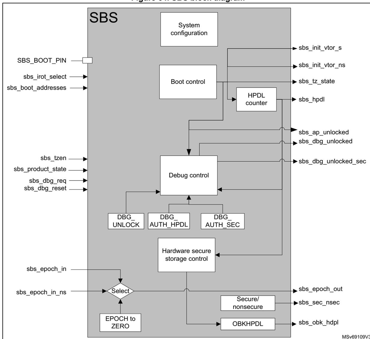
The block diagram illustrates the internal architecture of the SBS (System configuration, boot, and security) block. The main components and their connections are as follows:
- SBS Block: The overall container for all internal components.
- System configuration:
Outputs
sbs_init_vtor_sandsbs_init_vtor_ns. - Boot control:
Outputs
sbs_tz_state. It is connected toSBS_BOOT_PIN,sbs_irot_select, andsbs_boot_addresses(external inputs). - HPDL counter:
Outputs
sbs_hpdl. It receives input from the Boot control block. - Debug control:
Outputs
sbs_ap_unlocked,sbs_dbg_unlocked, andsbs_dbg_unlocked_sec. It is connected tosbs_tzen,sbs_product_state,sbs_dbg_req, andsbs_dbg_reset(external inputs). - DBG_UNLOCK, DBG_AUTH_HPDL, DBG_AUTH_SEC: These three blocks provide input to the Debug control block.
- Hardware secure storage control:
Outputs
sbs_epoch_out,sbs_sec_nsec, andsbs_obk_hdpl. It is connected to a Select block, an EPOCH to ZERO block, and an OBKHPDL block. - Select:
A multiplexer that receives
sbs_epoch_inandsbs_epoch_in_ns(external inputs) and outputs to the Hardware secure storage control block. - EPOCH to ZERO: Provides input to the Select block.
- Secure/nonsecure: Provides input to the OBKHPDL block, which in turn provides input to the Hardware secure storage control block.
MSV69109V3
14.3.2 SBS signals
Table 128 details the user relevant internal signals that interface the SBS.
Table 128. SBS internal input/output signals
| Signal name | Type | Description |
|---|---|---|
| BOOT0 | Input | Select booting on user flash memory or Bootloader when TrustZone is disabled (TZEN = 0xC3), or on RSS when TrustZone is enabled (TZEN = 0xB4). |
| sbs_irot_select | Signal based on BOOT_UBE option byte to select the iROT between ST-iROT and user flash memory (OEM-iROT) | |
| sbs_tzen | Signal based on TZEN option byte to activate/deactivate the TrustZone | |
| sbs_boot_addresses | List of addresses defined by the flash memory: – NSBOOTADD: nonsecure boot address – SECBOOTADD: secure boot address | |
| sbs_product_state | Signal based on PRODUCT_STATE option byte to activate the different security mechanisms depending on the product use. Expected values are described in Section 7: Embedded flash memory (FLASH) . | |
| sbs_dbg_req | Launch the debug authentication protocol when booting. | |
| sbs_init_vtor_s | Output | Vector address for Cortex-M33 secure entry point |
| sbs_init_vtor_ns | Vector address for Cortex-M33 nonsecure entry point | |
| sbs_tz_state | Inform the Cortex-M33 on the secure state of the core. | |
| sbs_hdpl | HDPL (temporal isolation level, ID of the boot level, used to isolate boot levels) This signal reflects a monotonic counter that can be incremented from 0 to 3, and that is reset to zero only on software reset or POR. | |
| sbs_ap_unlocked | Control the Cortex-M33 access port. | |
| sbs_dbg_unlocked | Unlock the debug (when set to 1) for the Cortex-M33 nonsecure part. | |
| sbs_dbg_unlocked_sec | Unlock the debug (when set to 1) for the Cortex-M33 secure part. | |
| sbs_dbg_reset | This signal is used to control the reset of the debug authentication configuration to be done with a system reset or a power-on reset. The configuration is done through the DBGMCU using the DCRT bitfield of DBGMCU_CR register. | |
| sbs_obk_hdpl | Select secure storage domain (OBK-HDPL) for current HDPL, or greater ones (to allow provisioning). | |
| sbs_epoch_out | Output | EPOCH counters (NS_EPOCH and SEC_EPOCH, inputs from flash memory) are used to manage the REPLAY protection. |
| sbs_sec_nsec | Reflect secure/nonsecure selection for the secure storage. |
14.3.3 SBS reset and clocks
The SBS configuration port is clocked by the AHB bus clock. There is a general reset and a debug configuration reset controlled in DBGMCU.
14.3.4 SBS system configuration
SBS I/O compensation cell management
The I/O compensation cell generates an 8-bit value for the I/O buffer (4 bits for N-MOS and 4 bits for P-MOS), that depends on PVT operating conditions (process, voltage, temperature). These bits are used to control the output impedance in the I/O buffer, and the slew rate of the I/O commutation ( \( t_{fall} \) and \( t_{rise} \) ), to reduce the I/O noise on power supply.
As shown in Figure 65 , the compensation cell is split in two blocks, one to provide an optimal code for the current PVT, and another to drive the block controlled by the software.
Figure 65. Compensation cell management
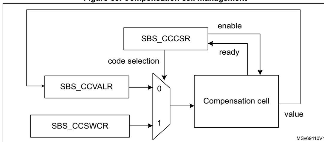
The compensation cell value can be read when the READY flag is set in SBS_CCCSR. With CODESEL in SBS_CCCSR, the application can select the value to apply between two options: the code from the cell or the code from SBS_CCSWCR.
Two compensation cells are embedded in STM32H5 devices, one for the I/Os supplied by \( V_{DDIO} \) power rail, another for the I/Os supplied by \( V_{DDIO2} \) power rail.
By default, the compensation cells are disabled, and a fixed code is applied to all the I/Os.
Note: The compensation cell can be used only when \( 2.7\text{ V} \leq V_{DDIOx} \leq 3.6\text{ V} \) or \( 1.62\text{ V} \leq V_{DDIOx} \leq 2\text{ V} \) (see Figure 66 ).
Note: The compensation cell can be used only when the CSI oscillator is enabled, see Section 11: Reset and clock control (RCC) for more details on CSI oscillator.
Figure 66. Compensation cell usage
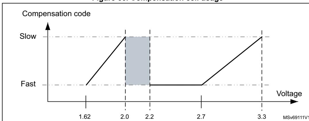
The graph illustrates the relationship between 'Compensation code' (y-axis, with 'Slow' at the top and 'Fast' at the bottom) and 'Voltage' (x-axis). The x-axis has tick marks at 1.62, 2.0, 2.2, 2.7, and 3.3. The y-axis has tick marks for 'Slow' and 'Fast'. A solid line represents the compensation curve. It starts at (1.62, Fast), rises linearly to (2.0, Slow), stays horizontal at 'Slow' until (2.2, Slow), then drops vertically to (2.2, Fast), stays horizontal at 'Fast' until (2.7, Fast), and finally rises linearly to (3.3, Slow). A shaded rectangular area is shown between x=2.0 and x=2.2, spanning from the 'Fast' level to the 'Slow' level. The text 'MSV69111V1' is in the bottom right corner.
SBS TrustZone security and privilege
- • SBS TrustZone security
When the TrustZone security is activated, the SBS is able to protect secure registers from being modified by nonsecure accesses.
The TrustZone security is activated by the TZEN option byte in FLASH_OPTSR2_PRG.
A nonsecure read/write access to a secured register is RAZ/WI and generates an illegal access event. An illegal access interrupt is generated if the SBS illegal access event is enabled in the GTZC.
- • Privileged/unprivileged mode
The SBS registers can be read and written by privileged and unprivileged accesses except the SBS registers for CPU configuration:
- – SBS_CSLCKR, SBS_FPUIMR and SBS_CNSLCKR
- – FPUSEC in SBS_SECCFGR
An unprivileged access to a privileged register is RAZ/WI.
14.3.5 SBS boot control
The SBS can be used to control the boot entry points considering the product settings. The main boot control actions are listed below:
- • Run product with or without TrustZone enabled.
- • Select between ST-iROT or OEM-iROT.
- • Boot when launching a debug authentication sequence.
- • Select boot between the bootloader or the user flash memory boot.
- • Initialize the HDPL boot value.
Figure 67. SBS boot control
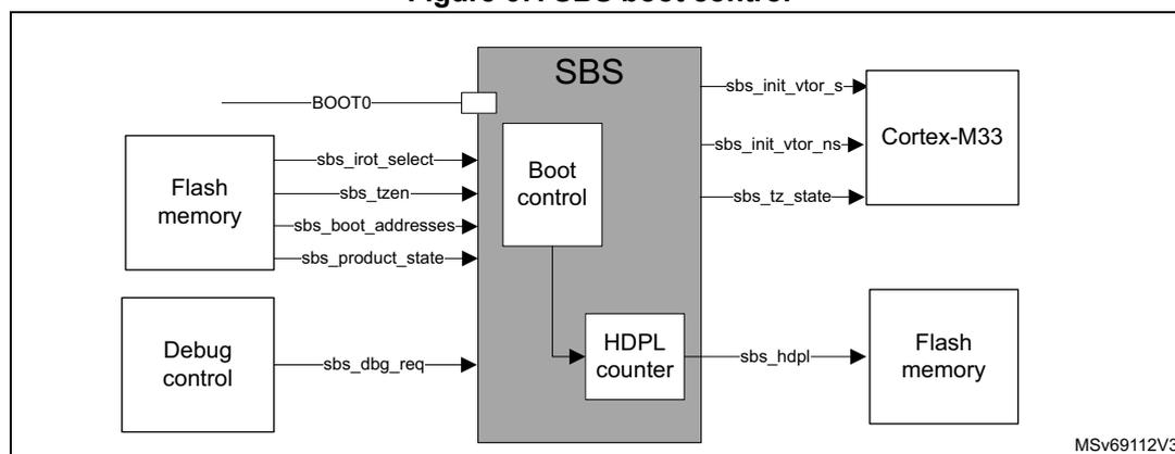
The diagram illustrates the SBS boot control system. A central grey box labeled 'SBS' contains two sub-components: 'Boot control' and 'HDPL counter'.
Inputs to the SBS include:
- BOOT0 : An external input to the Boot control.
- sbs_irot_select , sbs_tzen , sbs_boot_addresses , and sbs_product_state : Signals from 'Flash memory' to the Boot control.
- sbs_dbg_req : A signal from 'Debug control' to the Boot control.
- sbs_init_vtor_s , sbs_init_vtor_ns , and sbs_tz_state : Signals from the Boot control to 'Cortex-M33'.
- sbs_hdpl : A signal from the HDPL counter to 'Flash memory'.
The boot configurations are selected considering the product settings:
- • BOOT0: to select booting on user flash memory or RSS (root secure services)
- • BOOT_UBE option byte to select the iROT between ST-iROT and OEM-iROT
- • TZEN option byte to activate/deactivate the Trust Zone
- • sbs_boot_addresses: list of addresses defined by the flash memory:
- – NSBOOTADD: nonsecure boot address
- – SECBOOTADD: secure boot address
- • PRODUCT_STATE: option byte to activate the different security mechanisms depending on the product use. Expected values are described in Section 7: Embedded flash memory (FLASH) .
- • sbs_dbg_req: used to launch the debug authentication protocol when booting
The boot control logic sets the following data:
- • sbs_init_vtor_s: vector address for Cortex-M33 secure entry point
- • sbs_init_vtor_ns: vector address for Cortex-M33 nonsecure entry point
- • sbs_tz_state (secure/nonsecure): informs the Cortex-M33 on the secure state of the core.
- • HDPL (see the description below)
SBS HDPL (temporal isolation level) management
The HDPL is a monotonic counter incremented during the boot stages. The HDPL is reset to its default value only after a power-on or a system reset. This default value (0 or 1) depends on the device life cycle, as defined in boot logic.
The devices use HDPL information to automatically isolate code and its associated secrets (like keys) during the boot process. Incrementing HDPL ensures that private code and data for one boot stage cannot be directly accessible from later boot stages.
The HDPL is used by the user flash memory, see Section 7: Embedded flash memory (FLASH) for more details. The HDPL can take values from 0 to 3. When reaching 3, HDPL keeps this value until reset. The current HDPL value is readable in HDPL bitfield in SBS_HDPLSR.
To increment the HDPL by one, the application must write 0x6A to INCR_HDPL in SBS_HDPLCR. After such increment, and before doing any subsequent action, the user must check that the HDPL has effectively been incremented, by reading SBS_HDPLSR.
Table 129. HDPL encoded values
| HDPL | Code |
|---|---|
| 0 | 0xB4 |
| 1 | 0x51 |
| 2 | 0x8A |
| 3 | 0x6F |
| All other values |
Table 130. SBS boot logic
| sbs_product_state | Inputs | Outputs | |||||||
|---|---|---|---|---|---|---|---|---|---|
| sbs_dbg_req | sbs_tzen | sbs_irotselect | BOOT0 | sbs_boot_addresses | sbs_init_vtor_s | sbs_init_vtor_ns | sbs_hdpl | sbs_tz_state | |
| Any except Locked | 1 | x | x | x | BOOT_DBG_AUTH_ADD | BOOT_DBG_AUTH_ADD | x | 1 | Secure |
| Open | 0 | 0 | x | 0 | NSBOOT_ADD | x | NSBOOT_ADD | 1 | Nonsecure |
| 0 | 0 | x | 1 | BOOT_ST_RSS_ADD | BOOT_ST_RSS_ADD | x | 0 | Secure | |
| 0 | 1 | x | 0 | SECBOOT_ADD | SECBOOT_ADD | x | 1 | secure | |
| 0 | 1 | x | 1 | BOOT_ST_RSS_ADD | BOOT_ST_RSS_ADD | x | 0 | Secure | |
| Provisioning | 0 | x | x | x | BOOT_ST_RSS_ADD | BOOT_ST_RSS_ADD | x | 0 | Secure |
| iROT-Provisioned | 0 | 0 | x | x | NSBOOT_ADD | x | NSBOOT_ADD | 1 | Nonsecure |
| 0 | 1 | 0 | x | BOOT_ST_iROT_ADD | BOOT_ST_iROT_ADD | x | 1 | Secure | |
| 0 | 1 | 1 | x | SECBOOT_ADD | x | SECBOOT_ADD | 1 | Secure | |
| TZ-closed | - | 1 | 0 | x | BOOT_ST_iROT_ADD | BOOT_ST_iROT_ADD | x | 1 | Secure |
| - | 1 | 1 | x | SECBOOT_ADD | x | SECBOOT_ADD | 1 | Secure | |
Table 130. SBS boot logic (continued)
| sbs_product_state | Inputs | Outputs | |||||||
|---|---|---|---|---|---|---|---|---|---|
| sbs_dbg_req | sbs_tzen | sbs_irotselect | BOOT0 | sbs_boot_addresses | sbs_init_vtor_s | sbs_init_vtor_ns | sbs_hdpl | sbs_tz_state | |
| Closed | 0 | 0 | x | x | NSBOOT ADD | x | NSBOOT ADD | 1 | Nonsecure |
| 0 | 1 | 0 | x | BOOT_ST_iROT_ADD | BOOT_ST_iROT_ADD | x | 1 | Secure | |
| 0 | 1 | 1 | x | SECBOOT ADD | x | SECBOOT ADD | 1 | Secure | |
| Locked | 0 | 0 | x | x | NSBOOT ADD | x | NSBOOT ADD | 1 | Nonsecure |
| 0 | 1 | 0 | x | BOOT_ST_iROT_ADD | BOOT_ST_iROT_ADD | x | 1 | Secure | |
| 0 | 1 | 1 | x | SECBOOT ADD | x | SECBOOT ADD | 1 | Secure | |
| Regression | 0 | 0 | x | x | BOOT_DBG_AUTH_ADD | BOOT_DBG_AUTH_ADD | x | 0 | Secure |
| 0 | 1 | x | x | BOOT_DBG_AUTH_ADD | BOOT_DBG_AUTH_ADD | x | 0 | Secure | |
| NS-Regression | 0 | 1 | x | x | BOOT_DBG_AUTH_ADD | BOOT_DBG_AUTH_ADD | x | 0 | Secure |
14.3.6 SBS debug control
The SBS debug control is used to manage debug opening, taking care on the product context (PRODUCT_STATE, TZEN, HDPL) on register settings, or through a debug authentication control.
When the debug is forbidden, the mailbox access port, Cortex-M33 access port and CPU debug interface are locked. In this situation, the debugger cannot access the CPU and no effective debug can be done. Refer to the Section 59: Debug support (DBG) for more details.
Authenticated debug sequence
- 1. The external host requests to launch the debug authentication protocol, via the DBGMCU access port mailbox. The rest of the device is kept under reset.
- 2. SBS selects the STMicroelectronics RSS-DA (debug authentication library) boot address, and requests the CPU to be released from reset.
- 3. The CPU running RSS-DA library executes the debug authentication protocol in the system flash memory. If the device is closed, the access port mailbox is closed until RSS-DA acknowledges the authentication sequence start request.
- 4. The authentication method depends on TrustZone activation:
- – When TrustZone is activated (TZEN = 0xB4), the authentication method is based on certificates. As soon as a debug certificate chain is fully verified by the device, if the certificate concerns a debug permission, the RSS-DA programs the debug opening of the Cortex-M33. Alternatively, the certificate can authorize partial or full regression, allowing debug on a regressed part.
- – When TrustZone is disabled (TZEN = 0xC3), the authentication method is based on password. This method only allows the full regression of the product to be controlled.
- 5. Above reopenings are effective only when HDPL in SBS_HDPLSR has a value equal or superior to the value programmed in DBG_AUTH_HDPL in SBS_DBGCR. In case of authentication failure, the user is informed through the host interface.
Note: The debug authentication library in system flash memory is available only when HDPL = 0 or 1 in SBS_HDPLSR. Only this library can perform the steps 3 and 4 described above.
Debug reset
The debug opening can have the configuration to be reset by system or power-on reset, depending on a DBGMCU register field.
Debug locking
The debug configuration can be locked thanks to DBGCFG_LOCK in SBS_DBGLOCKR. SBS_DBGCR is then no longer writable.
When DBGCFG_LOCK is set to 1, it can be reset only by system or power-on reset. The configuration is done through the DBGMCU using the DCRT field of DBGMCU_CR.
Figure 68. SBS debug control
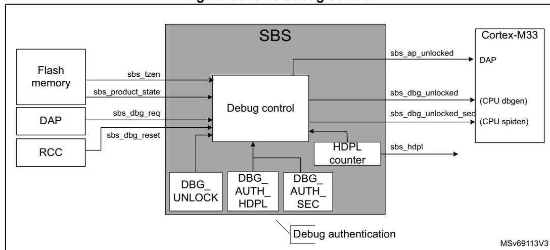
The diagram illustrates the SBS (System Boot and Security) block architecture. On the left, external components 'Flash memory', 'DAP', and 'RCC' are connected to the SBS block. 'Flash memory' provides 'sbs_tzen' and 'sbs_product_state' signals. 'DAP' provides 'sbs_dbg_req'. 'RCC' provides 'sbs_dbg_reset'. Inside the SBS block, these signals enter a 'Debug control' unit. Below it are three modules: 'DBG_UNLOCK', 'DBG_AUTH_HDPL', and 'DBG_AUTH_SEC', collectively labeled 'Debug authentication'. An 'HDPL counter' is also present. The 'Debug control' unit outputs several signals to the 'Cortex-M33' on the right: 'sbs_ap_unlocked' to the DAP, 'sbs_dbg_unlocked' to (CPU dbgen), 'sbs_dbg_unlocked_sec' to (CPU spiden), and 'sbs_hdpl' to the Cortex-M33. The diagram is labeled 'MSv69113V3' in the bottom right corner.
Inputs used to control the debug opening:
- • sbs_dbg_req: input signal that a host requests to launch the debug authentication protocol. When this signal is set, the boot address is set to launch the debug authentication library.
- • sbs_tzen: inform on the selected platform configuration related to TrustZone activation. When TZEN value is set to zero (0xC3), the platform does not support TrustZone and the simplified life cycle is proposed. See Section 7: Embedded flash memory (FLASH) for more details.
- • sbs_product_state: provide the current PRODUCT_STATE (from flash memory). See Section 7: Embedded flash memory (FLASH) for more details.
- • sbs_dbg_reset: reset information coming from the RCC, and reset SBS_DBGCR if this register is configured to be reset.
Configuration
- • DBG_UNLOCK in SBS_DBGCR: debug unlock when DBG_AUTH_HDPL is reached
- • AP_UNLOCK in SBS_DBGCR: access port unlock
- • DBG_AUTH_HDPL in SBS_DBGCR: authenticated debug temporal isolation level. Define the HDPL value from which the debug can be opened. Value can only be from 1 to 3.
- • DBG_AUTH_SEC in SBS_DBGCR: specify if the debug reopening is for nonsecure only or for both (secure and nonsecure).
- • DBG_LOCK in SBS_DBGLOCKR: lock the current debug configuration (released only by a reset).
Outputs
- • sbs_ap_unlocked: signal controlling the Cortex-M33 access port
- – 1: 0xB4
- – 0: all other codes
- • sbs_dbg_unlocked: unlock the debug (when set to 1) for the Cortex-M33 nonsecure.
- – 1: 0xB4
- – 0: all other codes
- • sbs_dbg_unlocked_sec: unlock the debug (when set to 1) for the Cortex-M33 secure.
- – 1: 0xB4
- – 0: all other codes
14.3.7 SBS hardware secure storage control
This feature ensures the isolation of keys and data related to ROT (root-of-trust) when re-opening the debug (when product in the field).
This includes a dedicated area called OB-Keys in the flash memory (see Section 7: Embedded flash memory (FLASH) for more details), and the key derivation (DHUK) mechanism protecting data using a hardware key different for the identified domains.
Figure 69. SBS hardware secure storage control
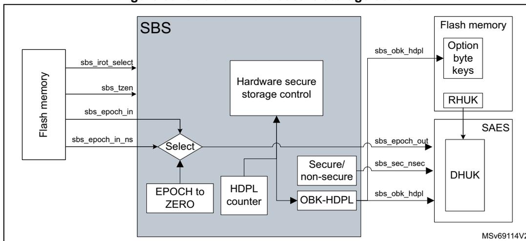
- • sbs_obk_hdpl: select secure storage context for current HDPL, or greater ones (to allow provisioning). This signal is set thanks to the SBS_NEXTHDPLCR register. This information is used by the flash memory to select the right area, and by the SAES when processing the derived key to generate a key derived related to HDPL context.
- • sbs_epoch_out: EPOCH counters are used to manage the REPLAY protection. These counters are incremented when regressions are done. Injecting the EPOCH in the DHUK (in the SAES) ensures that all information encrypted with the DHUK cannot be replayed after a regression.
- • sbs_sec_nsec: apply a different protection DHUK for secure and nonsecure assets.
All keys encrypted using the SAES/DHUK inherit of the RHUK property: unique per device.
All data encrypted thanks to the SAES using the DHUK are specific to a combination of [sbs_obk_hdpl + sbs_epoch_out + sbs_sec_nsec].
Inputs used to control the hardware secure storage control
sbs_epoch_in and sbs_epoch_in_ns: 24-bit values coming from the flash memory and representing regression counters respectively for secure and nonsecure.
Configuration
- • NEXTHDPL in SBS_NEXTHDPLCR: access to next HDPL secure storage areas.
- • EPOCH_SEL in SBS_EPOCHSELCCR: select the EPOCH source related to the secure storage under control (SEC_EPOCH, NS_EPOCH, or FORCED_To_Zero).
Table 131. OBK-HDPL logic
| HDPL[7:0] in SBS_HDPLSR | NEXTHDPL[1:0] | |||
|---|---|---|---|---|
| 0x0 | 0x1 | 0x2 | 0x3 | |
| 0 (0xB4) | 0xB4 | 0x51 | 0x8A | |
| 1 (0x51) | 0x51 | 0x8A | ||
| 2 (0x8A) | 0x8A | 0x6F | 0x6F | |
| 3 (0x6F) | 0x6F | |||
| Others | 0x6F | |||
14.4 SBS interrupts
SBS does not support interrupts.
14.5 SBS registers
14.5.1 SBS temporal isolation control register (SBS_HDPLCR)
Address offset: 0x010
Reset value: 0x0000 00B4
Reset: system reset
Register security: no restriction
| 31 | 30 | 29 | 28 | 27 | 26 | 25 | 24 | 23 | 22 | 21 | 20 | 19 | 18 | 17 | 16 |
|---|---|---|---|---|---|---|---|---|---|---|---|---|---|---|---|
| Res. | Res. | Res. | Res. | Res. | Res. | Res. | Res. | Res. | Res. | Res. | Res. | Res. | Res. | Res. | Res. |
| 15 | 14 | 13 | 12 | 11 | 10 | 9 | 8 | 7 | 6 | 5 | 4 | 3 | 2 | 1 | 0 |
| Res. | Res. | Res. | Res. | Res. | Res. | Res. | Res. | INCR_HDPL[7:0] | |||||||
| rw | rw | rw | rw | rw | rw | rw | rw | ||||||||
Bits 31:8 Reserved, must be kept at reset value.
Bits 7:0 INCR_HDPL[7:0] : increment HDPL value
0xB4: no increment
0x6A: recommended value to increment HDPL level by one
Others: all other values allow a HDPL level increment.
14.5.2 SBS temporal isolation status register (SBS_HDPLSR)
Address offset: 0x014
Reset value: 0xXXXX XXXX
The reset value depends on boot case: booting with HDPL0 for ST code, or HDPL1 for all other cases. See Table 130 for more details.
Reset: system reset
Register security: no restriction
| 31 | 30 | 29 | 28 | 27 | 26 | 25 | 24 | 23 | 22 | 21 | 20 | 19 | 18 | 17 | 16 |
|---|---|---|---|---|---|---|---|---|---|---|---|---|---|---|---|
| Res. | Res. | Res. | Res. | Res. | Res. | Res. | Res. | Res. | Res. | Res. | Res. | Res. | Res. | Res. | Res. |
| 15 | 14 | 13 | 12 | 11 | 10 | 9 | 8 | 7 | 6 | 5 | 4 | 3 | 2 | 1 | 0 |
| Res. | Res. | Res. | Res. | Res. | Res. | Res. | Res. | HDPL[7:0] | |||||||
| r | r | r | r | r | r | r | r | ||||||||
Bits 31:8 Reserved, must be kept at reset value.
Bits 7:0 HDPL[7:0] : temporal isolation level
This bitfield returns the current temporal isolation level.
0xB4: HDPL0, RSS
0x51: HDPL1, iRoT
0x8A: HDPL2, uRoT
0x6F: HDPL3, application (secure/nonsecure)
14.5.3 SBS next HDPL control register (SBS_NEXTHDPLCR)
Address offset: 0x018
Reset value: 0x0000 0000
Reset: system reset
Register security: no restriction
| 31 | 30 | 29 | 28 | 27 | 26 | 25 | 24 | 23 | 22 | 21 | 20 | 19 | 18 | 17 | 16 |
|---|---|---|---|---|---|---|---|---|---|---|---|---|---|---|---|
| Res. | Res. | Res. | Res. | Res. | Res. | Res. | Res. | Res. | Res. | Res. | Res. | Res. | Res. | Res. | Res. |
| 15 | 14 | 13 | 12 | 11 | 10 | 9 | 8 | 7 | 6 | 5 | 4 | 3 | 2 | 1 | 0 |
| Res. | Res. | Res. | Res. | Res. | Res. | Res. | Res. | Res. | Res. | Res. | Res. | Res. | Res. | NEXTHDPL[1:0] | |
| rw | rw |
Bits 31:2 Reserved, must be kept at reset value.
Bits 1:0 NEXTHDPL[1:0] : index to point to a higher HDPL than the current one
Index to add to the current HDPL to point (through OBK-HDPL) to the next secure storage areas (OBK-HDPL = HDPL + NEXTHDPL). See Table 131: OBK-HDPL logic for more details.
14.5.4 SBS debug control register (SBS_DBGCR)
Address offset: 0x020
Reset value: 0x0000 0000
Reset: debug reset (system reset or power-on reset)
Register security: HDPL0/1, RAZ/WI otherwise
| 31 | 30 | 29 | 28 | 27 | 26 | 25 | 24 | 23 | 22 | 21 | 20 | 19 | 18 | 17 | 16 |
|---|---|---|---|---|---|---|---|---|---|---|---|---|---|---|---|
| DBG_AUTH_SEC[7:0] | DBG_AUTH_HDPL[7:0] | ||||||||||||||
| rw | rw | rw | rw | rw | rw | rw | rw | rw | rw | rw | rw | rw | rw | rw | rw |
| 15 | 14 | 13 | 12 | 11 | 10 | 9 | 8 | 7 | 6 | 5 | 4 | 3 | 2 | 1 | 0 |
| DBG_UNLOCK[7:0] | AP_UNLOCK[7:0] | ||||||||||||||
| rw | rw | rw | rw | rw | rw | rw | rw | rw | rw | rw | rw | rw | rw | rw | rw |
Bits 31:24 DBG_AUTH_SEC[7:0] : control debug opening secure/nonsecure
Write 0xB4 to this bitfield to open debug for secure and any other values only opens nonsecure
Bits 23:16 DBG_AUTH_HDPL[7:0] : authenticated debug temporal isolation level
Writing to this bitfield defines at which HDPL the authenticated debug opens.
0x51: HDPL1
0x8A: HDPL2
0x6F: HDPL3
Note: Writing any other values is ignored. Reading any other value means the debug never opens.
Bits 15:8 DBG_UNLOCK[7:0] : debug unlock when DBG_AUTH_HDPL is reached
Write 0xB4 to this bitfield to open the debug when HDPL in SBS_HDPLSR equals to DBG_AUTH_HDPL in this register.
Bits 7:0 AP_UNLOCK[7:0] : access port unlock
Write 0xB4 to this bitfield to open the device access port.
14.5.5 SBS debug lock register (SBS_DBGLOCKR)
Address offset: 0x024
Reset value: 0x0000 00B4
Reset: debug reset (system reset or power-on reset)
Register security: HDPL0/1, RAZ/WI otherwise
| 31 | 30 | 29 | 28 | 27 | 26 | 25 | 24 | 23 | 22 | 21 | 20 | 19 | 18 | 17 | 16 |
|---|---|---|---|---|---|---|---|---|---|---|---|---|---|---|---|
| Res. | Res. | Res. | Res. | Res. | Res. | Res. | Res. | Res. | Res. | Res. | Res. | Res. | Res. | Res. | Res. |
| 15 | 14 | 13 | 12 | 11 | 10 | 9 | 8 | 7 | 6 | 5 | 4 | 3 | 2 | 1 | 0 |
| Res. | Res. | Res. | Res. | Res. | Res. | Res. | Res. | DBGCFG_LOCK[7:0] | |||||||
| rw | rw | rw | rw | rw | rw | rw | rw | ||||||||
Bits 31:8 Reserved, must be kept at reset value.
Bits 7:0 DBGCFG_LOCK[7:0] : debug configuration lock
Reading this bitfield returns 0x6A if the bitfield value is different from 0xB4.
0xC3 is the recommended value to lock the debug configuration using this bitfield.
0xB4: Writes to SBS_DBGCR allowed (default)
Others: Writes to SBS_DBGCR ignored
14.5.6 SBS RSS command register (SBS_RSSCMDR)
Address offset: 0x034
Reset value: 0x0000 0000
Reset: power-on reset
Register security: always secure (RAZ/WI if nonsecure)
| 31 | 30 | 29 | 28 | 27 | 26 | 25 | 24 | 23 | 22 | 21 | 20 | 19 | 18 | 17 | 16 |
|---|---|---|---|---|---|---|---|---|---|---|---|---|---|---|---|
| Res. | Res. | Res. | Res. | Res. | Res. | Res. | Res. | Res. | Res. | Res. | Res. | Res. | Res. | Res. | Res. |
| 15 | 14 | 13 | 12 | 11 | 10 | 9 | 8 | 7 | 6 | 5 | 4 | 3 | 2 | 1 | 0 |
| RSSCMD[15:0] | |||||||||||||||
| rw | rw | rw | rw | rw | rw | rw | rw | rw | rw | rw | rw | rw | rw | rw | rw |
Bits 31:16 Reserved, must be kept at reset value.
Bits 15:0 RSSCMD[15:0] : RSS command
The application can use this bitfield to pass on a command to the RSS, executed at the next reset.
When RSSCMD \( \neq \) 0 and PRODUCT_STATE is in Open, then the system always boots on RSS whatever is the boot pin value.
14.5.7 SBS EPOCH selection control register (SBS_EPOCHSELCR)
Address offset: 0x0A0
Reset value: 0x0000 0000
Reset: system reset
Register security: Secure when TZ_STATE = 1 (RAZ, WI in nonsecure access). Nonsecure protection when TZ_STATE = 0. This register is protected by privileged whatever is TZ_STATE, RAZ/WI if non privileged access.
| 31 | 30 | 29 | 28 | 27 | 26 | 25 | 24 | 23 | 22 | 21 | 20 | 19 | 18 | 17 | 16 |
|---|---|---|---|---|---|---|---|---|---|---|---|---|---|---|---|
| Res. | Res. | Res. | Res. | Res. | Res. | Res. | Res. | Res. | Res. | Res. | Res. | Res. | Res. | Res. | Res. |
| 15 | 14 | 13 | 12 | 11 | 10 | 9 | 8 | 7 | 6 | 5 | 4 | 3 | 2 | 1 | 0 |
| Res. | Res. | Res. | Res. | Res. | Res. | Res. | Res. | Res. | Res. | Res. | Res. | Res. | Res. | EPOCH_SEL [1:0] | |
| rw | rw |
Bits 31:2 Reserved, must be kept at reset value.
Bits 1:0 EPOCH_SEL[1:0] : select EPOCH value to be sent to the SAES
00: NS_EPOCH (nonsecure) counter input selected
01: SEC_EPOCH counter input selected
1x: EPOCH forced to zero (value used to retrieve PUF reference value at boot time)
14.5.8 SBS security mode configuration control register (SBS_SECCFGR)
Address offset: 0x0C0
Reset value: 0x0000 0000
Reset: system reset
Register security: always secure. RAZ/WI if nonsecure transaction and TZ_STATE = 1.
RAZ/WI if TZ_STATE = 0.
This register is programmed by secure software if the user wants functions configurable through system registers to be secure or not.
| 31 | 30 | 29 | 28 | 27 | 26 | 25 | 24 | 23 | 22 | 21 | 20 | 19 | 18 | 17 | 16 |
|---|---|---|---|---|---|---|---|---|---|---|---|---|---|---|---|
| Res. | Res. | Res. | Res. | Res. | Res. | Res. | Res. | Res. | Res. | Res. | Res. | Res. | Res. | Res. | Res. |
| 15 | 14 | 13 | 12 | 11 | 10 | 9 | 8 | 7 | 6 | 5 | 4 | 3 | 2 | 1 | 0 |
| Res. | Res. | Res. | Res. | Res. | Res. | Res. | Res. | Res. | Res. | Res. | Res. | FPUSEC | Res. | CLASSBSEC | SBSSEC |
| rw | rw | rw |
Bits 31:4 Reserved, must be kept at reset value.
Bit 3 FPUSEC : FPU security enable
0: SBS_FPUIMP register accessible through secure or nonsecure transaction
1: SBS_FPUIMP register accessible only through secure transaction
Note: This bit can be written only through privilege transaction.
Bit 2 Reserved, must be kept at reset value.
Bit 1 CLASSBSEC : ClassB security enable
0: SBS_CFGR2 register accessible through secure or nonsecure transaction
1: SBS_CFGR2 register accessible only through secure transaction
Bit 0 SBSSEC : SBS clock control, memory-erase status register and compensation cell register security enable
0: SBS_MESR, SBS_CCCSR, SBS_CCVALR, SBS_CCSWCR registers accessible through secure or nonsecure transaction
1: SBS_MESR, SBS_CCCSR, SBS_CCVALR, SBS_CCSWCR registers accessible only through secure transaction
14.5.9 SBS product mode and configuration register (SBS_PMCR)
Address offset: 0x100
Reset value: 0x0000 0000
Reset: system reset
Register security:
- • When TrustZone is activated (TZEN = 0xB4):
- – depending on I/O PBx_SEC_EN secure input for PBx_FMP configuration bits
- – depending on Ethernet ETHSEC secure input for ETH_SEL_PHY configuration bits
- • When TrustZone is disabled (TZEN = 0xC3) there is no access restriction.
| 31 | 30 | 29 | 28 | 27 | 26 | 25 | 24 | 23 | 22 | 21 | 20 | 19 | 18 | 17 | 16 |
|---|---|---|---|---|---|---|---|---|---|---|---|---|---|---|---|
| Res. | Res. | Res. | Res. | Res. | Res. | Res. | Res. | ETH_SEL_PHY[2:0] | Res. | PB9_FMP | PB8_FMP | PB7_FMP | |||
| rw | rw | rw | rw | rw | rw | PB6_FMP | |||||||||
| 15 | 14 | 13 | 12 | 11 | 10 | 9 | 8 | 7 | 6 | 5 | 4 | 3 | 2 | 1 | 0 |
| Res. | Res. | Res. | Res. | Res. | Res. | Res. | Res. | Res. | Res. | Res. | Res. | Res. | Res. | Res. | Res. |
Bits 31:24 Reserved, must be kept at reset value.
Bits 23:21 ETH_SEL_PHY[2:0] : Ethernet PHY interface selection
000: GMII or MII
001: reserved (RGMII)
100: RMII
Others: reserved
Refer to the product datasheet for the availability of Ethernet. If not present, consider the associated bits as reserved, and keep them at reset value.
Bit 20 Reserved, must be kept at reset value.
Bit 19 PB9_FMP : Fast-mode Plus driving capability activation on PB9
This bit can be read and written only with secure access if PB9 is secure in GPIOB. This bit enables the Fm+ driving mode for PB9 when PB9 is not used by I2C peripheral. This can be used to drive a LED for instance.
0: PB9 pin operates in standard mode.
1: Fm+ mode is enabled on PB9 pin and the speed control is bypassed.
Bit 18 PB8_FMP : Fast-mode Plus driving capability activation on PB8
This bit can be read and written only with secure access if PB8 is secure in GPIOB. This bit enables the Fm+ driving mode for PB8 when PB8 is not used by I2C peripheral. This can be used to drive a LED for instance.
0: PB8 pin operates in standard mode.
1: Fm+ mode is enabled on PB8 pin and the speed control is bypassed.
Bit 17 PB7_FMP : Fast-mode Plus driving capability activation on PB7
This bit can be read and written only with secure access if PB7 is secure in GPIOB. This bit enables the Fm+ driving mode for PB7 when PB7 is not used by I2C peripheral. This can be used to drive a LED for instance.
0: PB7 pin operates in standard mode.
1: Fm+ mode is enabled on PB7 pin and the speed control is bypassed.
Bit 16 PB6_FMP : Fast-mode Plus driving capability activation on PB6
This bit can be read and written only with secure access if PB6 is secure in GPIOB. This bit enables the Fm+ driving mode for PB6 when PB6 is not used by I2C peripheral. This can be used to drive a LED for instance.
0: PB6 pin operates in standard mode.
1: Fm+ mode is enabled on PB6 pin and the speed control is bypassed.
Bits 15:8 Reserved, must be kept at reset value.
Bits 7:0 Reserved, must be kept at reset value.
14.5.10 SBS FPU interrupt mask register (SBS_FPUIMR)
Address offset: 0x104
Reset value: 0x0000 001F
Reset: system reset
Register security: depends on FPUSEC in SBS_SECCFGR
This register is accessible only through privilege transaction.
| 31 | 30 | 29 | 28 | 27 | 26 | 25 | 24 | 23 | 22 | 21 | 20 | 19 | 18 | 17 | 16 |
|---|---|---|---|---|---|---|---|---|---|---|---|---|---|---|---|
| Res. | Res. | Res. | Res. | Res. | Res. | Res. | Res. | Res. | Res. | Res. | Res. | Res. | Res. | Res. | Res. |
| 15 | 14 | 13 | 12 | 11 | 10 | 9 | 8 | 7 | 6 | 5 | 4 | 3 | 2 | 1 | 0 |
| Res. | Res. | Res. | Res. | Res. | Res. | Res. | Res. | Res. | Res. | FPU_IE[5:0] | |||||
| rw | rw | rw | rw | rw | rw | ||||||||||
Bits 31:6 Reserved, must be kept at reset value.
Bits 5:0 FPU_IE[5:0] : FPU interrupt enable
Set and cleared by software to enable the Cortex-M33 FPU interrupts
FPU_IE[5]: inexact interrupt enable (interrupt disabled at reset)
FPU_IE[4]: input abnormal interrupt enable
FPU_IE[3]: overflow interrupt enable
FPU_IE[2]: underflow interrupt enable
FPU_IE[1]: divide-by-zero interrupt enable
FPU_IE[0]: invalid operation interrupt enable
14.5.11 SBS memory erase status register (SBS_MESR)
Address offset: 0x108
Reset value: 0x0000 000X (bit 0 is not affected by system reset)
Register security: depends on SBSSEC in SBS_SECCFGR
| 31 | 30 | 29 | 28 | 27 | 26 | 25 | 24 | 23 | 22 | 21 | 20 | 19 | 18 | 17 | 16 |
|---|---|---|---|---|---|---|---|---|---|---|---|---|---|---|---|
| Res. | Res. | Res. | Res. | Res. | Res. | Res. | Res. | Res. | Res. | Res. | Res. | Res. | Res. | Res. | IPMEE |
| rc_w1 | |||||||||||||||
| 15 | 14 | 13 | 12 | 11 | 10 | 9 | 8 | 7 | 6 | 5 | 4 | 3 | 2 | 1 | 0 |
| Res. | Res. | Res. | Res. | Res. | Res. | Res. | Res. | Res. | Res. | Res. | Res. | Res. | Res. | Res. | MCLR |
| rc_w1 |
Bits 31:17 Reserved, must be kept at reset value.
Bit 16 IPMEE : ICACHE erase status
This bit is set by hardware when ICACHE and PKA RAMs erase is completed after potential tamper detection or a product state regression (refer to Section 47: Tamper and backup registers (TAMP) for more details).
This bit is cleared by software by writing 1 to it.
0: ICACHE and PKA RAM erase on going
1: ICACHE and PKA SRAM erase done
Bits 15:1 Reserved, must be kept at reset value.
Bit 0 MCLR : device memories erase status
This bit is set by hardware when SRAM2, BKPSRAM, ICACHE, DCACHE and PKA RAMs erase is completed after power-on reset or tamper detection or product state regression (refer to Section 47: Tamper and backup registers (TAMP) ).
This bit is not reset by system reset and is cleared by software by writing 1 to it.
0: memory erase on going if not yet cleared by software
1: Memory erase done
14.5.12 SBS compensation cell for I/Os control and status register (SBS_CCCSR)
Address offset: 0x110
Reset value: 0x0000 0000
Reset: system reset
Register security: depends on SBSSEC in SBS_SECCFGR
| 31 | 30 | 29 | 28 | 27 | 26 | 25 | 24 | 23 | 22 | 21 | 20 | 19 | 18 | 17 | 16 |
|---|---|---|---|---|---|---|---|---|---|---|---|---|---|---|---|
| Res. | Res. | Res. | Res. | Res. | Res. | Res. | Res. | Res. | Res. | Res. | Res. | Res. | Res. | Res. | Res. |
| 15 | 14 | 13 | 12 | 11 | 10 | 9 | 8 | 7 | 6 | 5 | 4 | 3 | 2 | 1 | 0 |
| Res. | Res. | Res. | Res. | Res. | Res. | RDY2 | RDY1 | Res. | Res. | Res. | Res. | CS2 | EN2 | CS1 | EN1 |
| r | r | rw | rw | rw | rw |
Bits 31:10 Reserved, must be kept at reset value.
Bit 9 RDY2 : VDDIO2 compensation cell ready flag
This bit provides the status of the VDDIO2 compensation cell.
0: VDDIO2 compensation cell not ready
1: VDDIO2 compensation cell ready (code value provided by the cell can be used)
Bit 8 RDY1 : VDDIO compensation cell ready flag
This bit provides the status of the compensation cell.
0: VDDIO compensation cell not ready
1: VDDIO compensation cell ready (code value provided by the cell can be used)
Bits 7:4 Reserved, must be kept at reset value.
Bit 3 CS2 : code selection for VDDIO2 power rail (reset value set to 1)
This bit selects the code to be applied for the I/O compensation cell.
0: Code from the cell (available in SBS_CCVR)
1: Code from SBS_CCCR
Bit 2 EN2 : enable compensation cell for VDDIO2 power rail
This bit enables the I/O compensation cell.
0: I/O compensation cell disabled
1: I/O compensation cell enabled
Bit 1 CS1 : code selection for VDDIO power rail (reset value set to 1)
This bit selects the code to be applied for the I/O compensation cell.
0: Code from the cell (available in the SBS_CCVR)
1: Code from SBS_CCCR
Bit 0 EN1 : enable compensation cell for VDDIO power rail
This bit enables the I/O compensation cell.
0: I/O compensation cell disabled
1: I/O compensation cell enabled
14.5.13 SBS compensation cell for I/Os value register (SBS_CCVLR)
Address offset: 0x114
Reset value: 0x0000 0088
Reset: system reset
Register security: depends on SBSSEC in SBS_SECCFGR
| 31 | 30 | 29 | 28 | 27 | 26 | 25 | 24 | 23 | 22 | 21 | 20 | 19 | 18 | 17 | 16 |
|---|---|---|---|---|---|---|---|---|---|---|---|---|---|---|---|
| Res. | Res. | Res. | Res. | Res. | Res. | Res. | Res. | Res. | Res. | Res. | Res. | Res. | Res. | Res. | Res. |
| 15 | 14 | 13 | 12 | 11 | 10 | 9 | 8 | 7 | 6 | 5 | 4 | 3 | 2 | 1 | 0 |
| APSRC2[3:0] | ANSRC2[3:0] | APSRC1[3:0] | ANSRC1[3:0] | ||||||||||||
| r | r | r | r | r | r | r | r | r | r | r | r | r | r | r | r |
Bits 31:16 Reserved, must be kept at reset value.
Bits 15:12 APSRC2[3:0] : compensation value for the PMOS transistor
This value is provided by the cell and must be interpreted by the processor to compensate the slew rate in the functional range.
Bits 11:8 ANSRC2[3:0] : Compensation value for the NMOS transistor
This value is provided by the cell and must be interpreted by the processor to compensate the slew rate in the functional range.
Bits 7:4 APSRC1[3:0] : compensation value for the PMOS transistor
This value is provided by the cell and must be interpreted by the processor to compensate the slew rate in the functional range.
Bits 3:0 ANSRC1[3:0] : compensation value for the NMOS transistor
This value is provided by the cell and must be interpreted by the processor to compensate the slew rate in the functional range.
14.5.14 SBS compensation cell for I/Os software code register (SBS_CCSWCR)
Address offset: 0x118
Reset value: 0x0000 7878
Reset: system reset
Register security: depends on SBSSEC in SBS_SECCFGR
| 31 | 30 | 29 | 28 | 27 | 26 | 25 | 24 | 23 | 22 | 21 | 20 | 19 | 18 | 17 | 16 |
|---|---|---|---|---|---|---|---|---|---|---|---|---|---|---|---|
| Res. | Res. | Res. | Res. | Res. | Res. | Res. | Res. | Res. | Res. | Res. | Res. | Res. | Res. | Res. | Res. |
| 15 | 14 | 13 | 12 | 11 | 10 | 9 | 8 | 7 | 6 | 5 | 4 | 3 | 2 | 1 | 0 |
| SW_APSRC2[3:0] | SW_ANSRC2[3:0] | SW_APSRC1[3:0] | SW_ANSRC1[3:0] | ||||||||||||
| rw | rw | rw | rw | rw | rw | rw | rw | rw | rw | rw | rw | rw | rw | rw | rw |
Bits 31:16 Reserved, must be kept at reset value.
Bits 15:12 SW_APSRC2[3:0] : PMOS compensation code for the V DDIO power railsThis bitfield is written by software to define an I/O compensation cell code for PMOS transistors of the VDDIO power rail. This code is applied to the I/O when CS2 is set in SBS_CCSR.
Bits 11:8 SW_ANSRC2[3:0] : NMOS compensation code for VDDIO power railsThis bitfield is written by software to define an I/O compensation cell code for NMOS transistors of the VDD power rail. This code is applied to the I/O when CS2 is set in SBS_CCSR.
Bits 7:4 SW_APSRC1[3:0] : PMOS compensation code for the VDD power railsThis bitfield is written by software to define an I/O compensation cell code for PMOS transistors of the VDDIO power rail. This code is applied to the I/O when CS1 is set in SBS_CCSR.
Bits 3:0 SW_ANSRC1[3:0] : NMOS compensation code for VDD power railsThis bitfield is written by software to define an I/O compensation cell code for NMOS transistors of the VDD power rail. This code is applied to the I/O when CS1 is set in SBS_CCSR.
14.5.15 SBS Class B register (SBS_CFGR2)
Address offset: 0x120
Reset value: 0x0000 0000
Reset: system reset
Register security: depends on CLASSBSEC in SBS_SECCFGR
| 31 | 30 | 29 | 28 | 27 | 26 | 25 | 24 | 23 | 22 | 21 | 20 | 19 | 18 | 17 | 16 |
|---|---|---|---|---|---|---|---|---|---|---|---|---|---|---|---|
| Res. | Res. | Res. | Res. | Res. | Res. | Res. | Res. | Res. | Res. | Res. | Res. | Res. | Res. | Res. | Res. |
| 15 | 14 | 13 | 12 | 11 | 10 | 9 | 8 | 7 | 6 | 5 | 4 | 3 | 2 | 1 | 0 |
| Res. | Res. | Res. | Res. | Res. | Res. | Res. | Res. | Res. | Res. | Res. | Res. | ECCL | PVDL | SEL | CLL |
| rs | rs | rs | rs |
Bits 31:4 Reserved, must be kept at reset value.
Bit 3 ECCL : ECC lock
This bit is set and cleared by software. It can be used to enable and lock the flash memory double ECC error with break input of TIM1/8/15/6/17.
0: double ECC error flag disconnected to timer break inputs
1: double ECC error flag connected to timer break inputs
Bit 2 PVDL : PVD lock
This bit is set by software and cleared only by a system reset. It can be used to enable and lock the PVD connection with TIM1/8/15/16/17 break inputs.
0: PVD interrupt disconnected from timer break inputs. PVD_EN and PVD_SEL[2:0] in the PWR registers are read/write.
1: PVD interrupt is connected to timer break inputs. PVD_EN and PVD_SEL[2:0] in the PWR registers are read only
Bit 1 SEL : SRAM ECC error lock
This bit is set by software and cleared only by a system reset. It can be used to enable and lock the SRAM double ECC error signal with break input of TIM1/8/15/16/17.
0: SRAM double ECC error flag disconnected from timer break inputs
1: SRAM double ECC error flag connected to timer break inputs
Bit 0 CLL : core lockup lock
This bit is set by software and cleared only by a system reset. It can be used to enable and lock the lockup (HardFault) output of Cortex-M33 with TIM1/8/15/16/17 break inputs.
0: lockup output disconnected from timer break inputs
1: lockup output connected to timer break inputs
14.5.16 SBS CPU nonsecure lock register (SBS_CNSLCKR)
Address offset: 0x144
Reset value: 0x0000 0000
Reset: system reset
Register security: This register can be read and written by privileged access only. Unprivileged access is RAZ/WI.
This register is used to lock the configuration of nonsecure MPU and VTOR_NS registers of the Cortex-M33.
| 31 | 30 | 29 | 28 | 27 | 26 | 25 | 24 | 23 | 22 | 21 | 20 | 19 | 18 | 17 | 16 |
|---|---|---|---|---|---|---|---|---|---|---|---|---|---|---|---|
| Res. | Res. | Res. | Res. | Res. | Res. | Res. | Res. | Res. | Res. | Res. | Res. | Res. | Res. | Res. | Res. |
| 15 | 14 | 13 | 12 | 11 | 10 | 9 | 8 | 7 | 6 | 5 | 4 | 3 | 2 | 1 | 0 |
| Res. | Res. | Res. | Res. | Res. | Res. | Res. | Res. | Res. | Res. | Res. | Res. | Res. | Res. | LOCKNSMPU rs | LOCKNSVTOR rs |
Bits 31:2 Reserved, must be kept at reset value.
Bit 1 LOCKNSMPU : nonsecure MPU register lock
This bit is set by software and cleared only by a system reset. When set, this bit disables write access to nonsecure MPU_CTRL_NS, MPU_RNR_NS and MPU_RBAR_NS registers.
0: nonsecure MPU registers write enabled
1: nonsecure MPU registers write disabled
Bit 0 LOCKNSVTOR : VTOR_NS register lock
This bit is set by software and cleared only by a system reset.
0: VTOR_NS register write enabled
1: VTOR_NS register write disabled
14.5.17 SBS CPU secure lock register (SBS_CSLCKR)
Address offset: 0x148
Reset value: 0x0000 0000
Reset: system reset
Register security: This register can be written only when the access is secure/privilege.
A nonsecure read/write access is RAZ/WI and generates an illegal access event. When the system is not secure (TZ_STATE = 0), this register is RAZ/WI.
This register is used to lock the configuration of PRIS and BFHFNMINS in the AIRCR, SAU, secure MPU and VTOR_S registers of the Cortex-M33.
| 31 | 30 | 29 | 28 | 27 | 26 | 25 | 24 | 23 | 22 | 21 | 20 | 19 | 18 | 17 | 16 |
|---|---|---|---|---|---|---|---|---|---|---|---|---|---|---|---|
| Res. | Res. | Res. | Res. | Res. | Res. | Res. | Res. | Res. | Res. | Res. | Res. | Res. | Res. | Res. | Res. |
| 15 | 14 | 13 | 12 | 11 | 10 | 9 | 8 | 7 | 6 | 5 | 4 | 3 | 2 | 1 | 0 |
| Res. | Res. | Res. | Res. | Res. | Res. | Res. | Res. | Res. | Res. | Res. | Res. | Res. | LOCKSAU | LOCKNSMPU | LOCKNSVTOR |
| rs | rs | rs |
Bits 31:3 Reserved, must be kept at reset value.
Bit 2 LOCKSAU : SAU registers lock
This bit is set by software and cleared only by a system reset. When set, this bit disables write access to SAU_CTRL, SAU_RNR, SAU_RBAR and SAU_RLAR registers.
0: SAU registers write enabled
1: SAU registers write disabled
Bit 1 LOCKNSMPU : secure MPU registers lock
This bit is set by software and cleared only by a system reset. When set, this bit disables write access to secure MPU_CTRL, MPU_RNR and MPU_RBAR registers.
0: Secure MPU registers writes enabled
1: Secure MPU registers writes disabled
Bit 0 LOCKSVT AIRCR : VTOR_S and AIRCR register lock
This bit is set by software and cleared only by a system reset. When set, this bit disables write access to VTOR_S register, PRIS and BFHFNMINS bits in the AIRCR register.
0: VTOR_S register PRIS and BFHFNMINS bits in the AIRCR register write enabled
1: VTOR_S register PRIS and BFHFNMINS bits in the AIRCR register write disabled
14.5.18 SBS flitf ECC NMI mask register (SBS_ECCNMIR)
Address offset: 0x14C
Reset value: 0x0000 0000
Reset: system reset
Register security: secure access only when TZ_STATE = 1 (RAZ/WI in nonsecure access).
No security protection if TZ_STATE = 0.
This register is accessible only through privilege transaction.
This register sets up the expected behavior on NMI regarding double ECC errors from the flash memory.
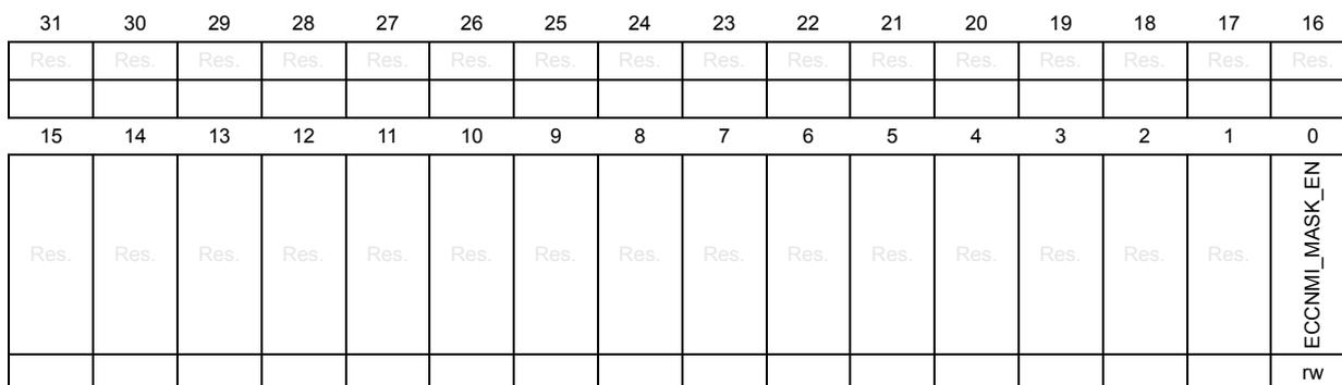
| 31 | 30 | 29 | 28 | 27 | 26 | 25 | 24 | 23 | 22 | 21 | 20 | 19 | 18 | 17 | 16 |
|---|---|---|---|---|---|---|---|---|---|---|---|---|---|---|---|
| Res. | Res. | Res. | Res. | Res. | Res. | Res. | Res. | Res. | Res. | Res. | Res. | Res. | Res. | Res. | Res. |
| 15 | 14 | 13 | 12 | 11 | 10 | 9 | 8 | 7 | 6 | 5 | 4 | 3 | 2 | 1 | 0 |
| Res. | Res. | Res. | Res. | Res. | Res. | Res. | Res. | Res. | Res. | Res. | Res. | Res. | Res. | Res. | ECCNMI_MASK_EN |
| RW |
Bits 31:1 Reserved, must be kept at reset value.
Bit 0 ECCNMI_MASK_EN : NMI behavior setup when a double ECC error occurs on flitf data part
0: NMI generated if a double ECC error in the flitf data part
1: NMI not generated if a double ECC error in the flitf data part
14.5.19 SBS register map
Table 132. SBS register map and reset values
| Offset | Register | 31 | 30 | 29 | 28 | 27 | 26 | 25 | 24 | 23 | 22 | 21 | 20 | 19 | 18 | 17 | 16 | 15 | 14 | 13 | 12 | 11 | 10 | 9 | 8 | 7 | 6 | 5 | 4 | 3 | 2 | 1 | 0 |
|---|---|---|---|---|---|---|---|---|---|---|---|---|---|---|---|---|---|---|---|---|---|---|---|---|---|---|---|---|---|---|---|---|---|
| 0x010 | SBS_HDPLCR | Res | Res | Res | Res | Res | Res | Res | Res | Res | Res | Res | Res | Res | Res | Res | Res | Res | Res | Res | Res | Res | Res | Res | Res | Res | INCR_HDPL[7:0] | ||||||
| Reset value | 1 | 0 | 1 | 1 | 0 | 1 | 0 | 0 | |||||||||||||||||||||||||
| 0x014 | SBS_HDPLSR | Res | Res | Res | Res | Res | Res | Res | Res | Res | Res | Res | Res | Res | Res | Res | Res | Res | Res | Res | Res | Res | Res | Res | Res | Res | HDPL[7:0] | ||||||
| Reset value | x | x | x | x | x | x | x | ||||||||||||||||||||||||||
| 0x018 | SBS_NEXTHDPLCR | Res | Res | Res | Res | Res | Res | Res | Res | Res | Res | Res | Res | Res | Res | Res | Res | Res | Res | Res | Res | Res | Res | Res | Res | Res | Res | Res | Res | Res | Res | Res | NEXTHDPL[1:0] |
| Reset value | 0 | 0 | |||||||||||||||||||||||||||||||
| 0x020 | SBS_DBGCR | DBG_AUTH_SEC[7:0] | DBG_AUTH_HDPL[7:0] | DBG_UNLOCK[7:0] | AP_UNLOCK[7:0] | ||||||||||||||||||||||||||||
| Reset value | 0 | 0 | 0 | 0 | 0 | 0 | 0 | 0 | 0 | 0 | 0 | 0 | 0 | 0 | 0 | 0 | 0 | 0 | 0 | 0 | 0 | 0 | 0 | 0 | 0 | 0 | 0 | 0 | 0 | 0 | 0 | 0 | |
| 0x024 | SBS_DBGLOCKR | DBGCFG_LOCK[7:0] | |||||||||||||||||||||||||||||||
| Reset value | 1 | 0 | |||||||||||||||||||||||||||||||
| 0x028 to 0x030 | Reserved | Reserved | |||||||||||||||||||||||||||||||
| 0x034 | SBS_RSSCMDR | Res | Res | Res | Res | Res | Res | Res | Res | Res | Res | Res | Res | Res | Res | Res | Res | RSSCMD[15:0] | |||||||||||||||
| Reset value | 0 | 0 | 0 | 0 | 0 | 0 | 0 | 0 | 0 | 0 | 0 | 0 | 0 | 0 | 0 | ||||||||||||||||||
| 0x038 to 0x09C | Reserved | Reserved | |||||||||||||||||||||||||||||||
| 0x0A0 | SBS_EPOCHSELCR | Res | Res | Res | Res | Res | Res | Res | Res | Res | Res | Res | Res | Res | Res | Res | Res | Res | Res | Res | Res | Res | Res | Res | Res | Res | Res | Res | Res | Res | Res | Res | EPOCH_SEL[1:0] |
| Reset value | 0 | 0 | |||||||||||||||||||||||||||||||
| 0x0A4 to 0x0BC | Reserved | Reserved | |||||||||||||||||||||||||||||||
| 0x0C0 | SBS_SECCFGR | Res | Res | Res | Res | Res | Res | Res | Res | Res | Res | Res | Res | Res | Res | Res | Res | Res | Res | Res | Res | Res | Res | Res | Res | Res | Res | Res | Res | Res | Res | Res | CLASSSEC SBSSEC |
| Reset value | 0 | 0 | |||||||||||||||||||||||||||||||
| 0x0C4 to 0x0FC | Reserved | Reserved | |||||||||||||||||||||||||||||||
| 0x100 | SBS_PMCR | Res | Res | Res | Res | Res | Res | Res | Res | ETH_SEL_PHY [2:0] (1) | Res | Res | Res | PB9_FMP | PB8_FMP | PB7_FMP | PB6_FMP | Res | Res | Res | Res | Res | Res | Res | Res | Res | Res | Res | Res | Res | Res | Res | Res |
| Reset value | 0 | 0 | 0 | 0 | 0 | 0 | 0 | ||||||||||||||||||||||||||
| 0x104 | SBS_FPUIMR | Res | Res | Res | Res | Res | Res | Res | Res | Res | Res | Res | Res | Res | Res | Res | Res | Res | Res | Res | Res | Res | Res | Res | Res | Res | FPU_IE[5:0] | ||||||
| Reset value | 1 | 1 | 1 | 1 | 1 | 1 | 1 | ||||||||||||||||||||||||||
| 0x108 | SBS_MESR | Res | Res | Res | Res | Res | Res | Res | Res | Res | Res | Res | Res | Res | Res | Res | Res | Res | Res | Res | Res | Res | Res | Res | Res | Res | Res | Res | Res | Res | Res | Res | MCLR |
| Reset value | 0 | ||||||||||||||||||||||||||||||||
| 0x110 | SBS_CCCSR | Res | Res | Res | Res | Res | Res | Res | Res | Res | Res | Res | Res | Res | Res | Res | Res | Res | Res | Res | Res | Res | Res | RDY2 | RDY1 | Res | Res | Res | CS2 | EN2 | CS1 | EN1 | |
| Reset value | 0 | 0 | 0 | 0 | 0 | 0 | |||||||||||||||||||||||||||
Table 132. SBS register map and reset values (continued)
| Offset | Register | 31 | 30 | 29 | 28 | 27 | 26 | 25 | 24 | 23 | 22 | 21 | 20 | 19 | 18 | 17 | 16 | 15 | 14 | 13 | 12 | 11 | 10 | 9 | 8 | 7 | 6 | 5 | 4 | 3 | 2 | 1 | 0 | |
|---|---|---|---|---|---|---|---|---|---|---|---|---|---|---|---|---|---|---|---|---|---|---|---|---|---|---|---|---|---|---|---|---|---|---|
| 0x114 | SBS_CCVALR | Res. | Res. | Res. | Res. | Res. | Res. | Res. | Res. | Res. | Res. | Res. | Res. | Res. | Res. | Res. | Res. | APSRC2 [3:0] | ANSRC2 [3:0] | APSRC1 [3:0] | ANSRC1 [3:0] | |||||||||||||
| Reset value | 0 | 0 | 0 | 0 | 0 | 0 | 0 | 0 | 1 | 0 | 0 | 0 | 1 | 0 | 0 | 0 | ||||||||||||||||||
| 0x118 | SBS_CCSWCR | Res. | Res. | Res. | Res. | Res. | Res. | Res. | Res. | Res. | Res. | Res. | Res. | Res. | Res. | Res. | Res. | SW_APSRC2 [3:0] | SW_ANSRC2 [3:0] | SW_APSRC1 [3:0] | SW_ANSRC1 [3:0] | |||||||||||||
| Reset value | 0 | 1 | 1 | 1 | 1 | 0 | 0 | 0 | 0 | 1 | 1 | 1 | 1 | 0 | 0 | 0 | ||||||||||||||||||
| 0x120 | SBS_CFGR2 | Res. | Res. | Res. | Res. | Res. | Res. | Res. | Res. | Res. | Res. | Res. | Res. | Res. | Res. | Res. | Res. | Res. | Res. | Res. | Res. | Res. | Res. | Res. | Res. | Res. | Res. | Res. | Res. | Res. | ECCL | PVDL | SEL | CLL |
| Reset value | 0 | 0 | 0 | 0 | ||||||||||||||||||||||||||||||
| 0x124 to 0x140 | Reserved | Reserved | ||||||||||||||||||||||||||||||||
| 0x144 | SBS_CNSLCKR | Res. | Res. | Res. | Res. | Res. | Res. | Res. | Res. | Res. | Res. | Res. | Res. | Res. | Res. | Res. | Res. | Res. | Res. | Res. | Res. | Res. | Res. | Res. | Res. | Res. | Res. | Res. | Res. | Res. | Res. | LOCKNSMPU | LOCKNSVTOR | |
| Reset value | 0 | 0 | ||||||||||||||||||||||||||||||||
| 0x148 | SBS_CSLCKR | Res. | Res. | Res. | Res. | Res. | Res. | Res. | Res. | Res. | Res. | Res. | Res. | Res. | Res. | Res. | Res. | Res. | Res. | Res. | Res. | Res. | Res. | Res. | Res. | Res. | Res. | Res. | Res. | Res. | Res. | LOCKSAU | LOCKSMUPU | LOCKSVT AIRCR |
| Reset value | 0 | 0 | 0 | |||||||||||||||||||||||||||||||
| 0x14C | SBS_ECCNMIR | Res. | Res. | Res. | Res. | Res. | Res. | Res. | Res. | Res. | Res. | Res. | Res. | Res. | Res. | Res. | Res. | Res. | Res. | Res. | Res. | Res. | Res. | Res. | Res. | Res. | Res. | Res. | Res. | Res. | Res. | Res. | Res. | ECNMIMASK_EN |
| Reset value | 0 | |||||||||||||||||||||||||||||||||
1. Refer to the product datasheet for the availability of Ethernet. If not present, consider the associated bits as reserved, and keep them at reset value.
Refer to Section 2.3 for the register boundary addresses.