11. Reset and clock control (RCC)
11.1 Introduction
The reset and clock control (RCC) manages the different resets, and generates the clocks for the bus and peripherals.
11.2 RCC pins and internal signals
Table 111 lists the RCC inputs and output signals connected to package pins or balls.
Table 111. RCC input/output signals connected to package pins or balls
| Signal name | Signal type | Description |
|---|---|---|
| NRST | I/O | System reset, can be used to provide reset to external devices |
| OSC32_IN | I | 32 kHz oscillator input |
| OSC32_OUT | O | 32 kHz oscillator output |
| OSC_IN | I | System oscillator input |
| OSC_OUT | O | System oscillator output |
| MCO | O | Output clock for external devices |
| LSCO | O | Low-speed output clock for external devices |
| AUDIOCLK | I | External kernel clock input for SAI1, SAI2, I2S1, I2S2, and I2S3 |
11.3 RCC reset functional description
There are three types of reset:
- • a system reset
- • a power reset
- • a Backup domain reset
11.3.1 Power reset
A power reset is generated when one of the following events occurs:
- • a brownout reset (BOR)
- • when exiting Standby mode
A brownout reset, including power-on or power-down reset (POR/PDR), sets all registers to their reset values except the ones in the Backup domain.
When exiting Standby mode, all registers in the core domain are set to their reset value. Registers outside the core domain (RTC, WKUP, IWDG, and GPIO pullup/pulldown configuration during Standby and Standby mode exit) are not impacted.
11.3.2 System reset
A system reset sets all registers to their reset values except the reset flags in RCC reset status register (RCC_RSR) and the registers in the Backup domain.
A system reset is generated when one of the following events occurs:
- • a low level on the NRST pin (external reset)
- • a window watchdog event (WWDG reset)
- • an independent watchdog event (IWDG reset)
- • a software reset (SW reset) (see Software reset )
- • a low-power mode security reset (see Low-power mode security reset )
- • a brownout reset
The reset source can be identified by checking the reset flags in RCC reset status register (RCC_RSR) .
These sources act on the NRST pin and this pin is always kept low during the delay phase. The reset service routine vector is selected depending on product state, on Boot option bytes or on both.
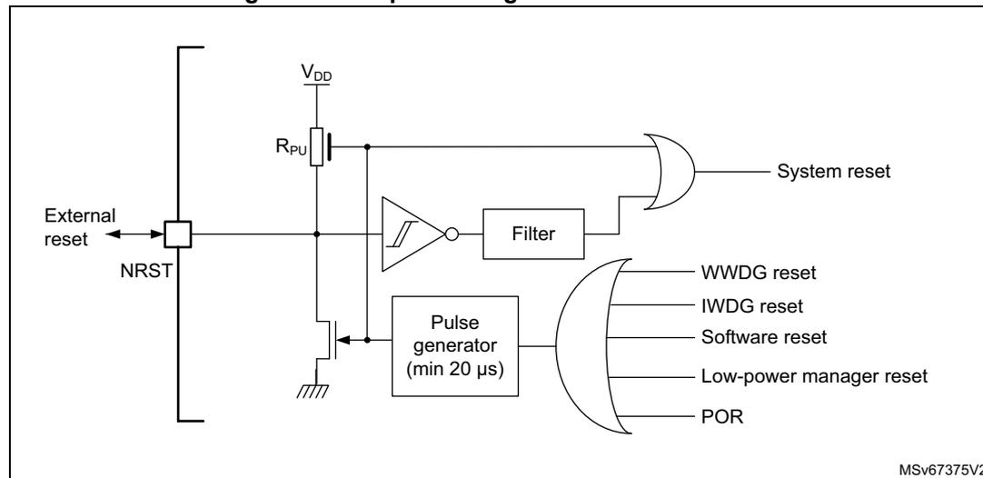
The system reset signal provided to the device is output on the NRST pin. The pulse generator guarantees a minimum reset pulse duration of 20 µs for each internal reset source. In case of an external reset, the reset pulse is generated while the NRST pin is asserted low.
In case of an internal reset, the internal pull-up \( R_{PU} \) is deactivated to save the power consumption through the pull-up resistor.
Figure 51. Simplified diagram of the reset circuit
Software reset
The SYSRESETREQ bit in Cortex-M33 application interrupt and reset control register must be set to force a software reset on the device.
Low-power mode security reset
To avoid that critical applications mistakenly enter a low-power mode, the following low-power mode security resets are available. If enabled in option bytes, the resets are generated in any of the following conditions:
- • Entering Standby mode: this type of reset is enabled by resetting nRST_STDBY bit in user option bytes. In this case, whenever a Standby mode entry sequence is successfully executed, the device is reset instead of entering Standby mode.
- • Entering Stop mode: this type of reset is enabled by resetting nRST_STOP bit in user option bytes. In this case, whenever a Stop mode entry sequence is successfully executed, the device is reset instead of entering Stop mode.
For further information on the user option bytes, refer to Section 7.4.1: Option bytes description .
11.3.3 Backup domain reset
The Backup domain has two specific resets, generated after one of the following events:
- • a software reset, triggered by setting the VSWRST bit in the RCC Backup domain control register (RCC_BDCR) . Write access to this domain must be enabled before setting VSWRST bit to perform the reset.
- • a V DD or V BAT power on, if both supplies have previously been powered off
A Backup domain reset affects the LSE oscillator, the RTC, the backup registers, the backup SRAM, and the RCC_BDCR register.
11.3.4 Reset source identification
The application can identify the reset source by checking the reset flags in the RCC_RSR register. The software can reset the flags by setting the RMVF bit.
Table 112 shows how the status bits of the RCC_RSR register behave according to the situation that generated the reset. For example, when an IWDG timeout occurs, if the CPU is reading the RCC_RSR register during the boot phase, both PINRSTF and IWDGRSTF bits are set, indicating that the IWDG also generated a pin reset.
Table 112. Reset source identification (RCC_RSR) (1)
| Reset | LPWRRSTF | WWDGRSTF | IWDGRSTF | SFTRSTF | BORRSTF | PINRSTF | |
|---|---|---|---|---|---|---|---|
| 1 | Power-on reset | 0 | 0 | 0 | 0 | 1 | 1 |
| 2 | Pin/pad reset | 0 | 0 | 0 | 0 | 0 | 1 |
| 3 | Brownout (low or high) reset | 0 | 0 | 0 | 0 | 1 | 1 |
| 4 | System reset generated by CPU | 0 | 0 | 0 | 1 | 0 | 1 |
| 5 | WWDG reset | 0 | 1 | 0 | 0 | 0 | 1 |
| 6 | IWDG reset | 0 | 0 | 1 | 0 | 0 | 1 |
| 7 | Illegal stop entry reset | 1 | 0 | 0 | 0 | 0 | 1 |
1. Gray cells highlight the register bits that are set.
11.4 RCC clocks functional description
Four different clock sources can be used to drive the system clock (SYSCLK):
- • HSI: high-speed internal up to 64 MHz RC oscillator clock
- • CSI: low power internal RC oscillator clock
- • HSE: high-speed external crystal or clock, from 4 to 50 MHz
- • PLL1 clock
The HSI is used as system clock source after startup from reset, configured at 32 MHz.
The device has the following additional clock sources:
- • LSI: 32 kHz low-speed internal RC that drives the independent watchdog and optionally the RTC used for auto-wakeup from Stop and Standby modes
- • LSE: 32.768 kHz low-speed external crystal or clock that optionally drives the real-time clock (rtc_ck)
- • HSI48: internal 48 MHz RC that potentially drives the USB FS and the RNG
- • PLL2 and PLL3 clocks
Each clock source can be switched on or off independently when it is not used, to optimize power consumption.
Several prescalers can be used to configure the AHB frequency, the APB1 and APB2 domains. The maximum frequency of the AHB and APB domains is 250 MHz.
The peripheral clocks are derived from their bus clock (HCLK, PCLK1, PCLK2 or PCLK3), except those that receive an independent kernel clock. This kernel clock can be selected by software between several sources thanks to RCC_CCIPRx registers (x = 1,2,3,4,5).
In addition, the RTC kernel clock is selected by software in RCC_BDCR. The IWDG clock is always the LSI 32 kHz clock.
The RCC feeds the Cortex system timer (SysTick) external clock with the AHB clock (HCLK) divided by eight, or LSE or LSI. The SysTick can work either with this clock or directly with the Cortex clock (HCLK), configurable in the SysTick control and status register.
FCLK acts as Cortex-M33 free-running clock.
Figure 52. Clock tree
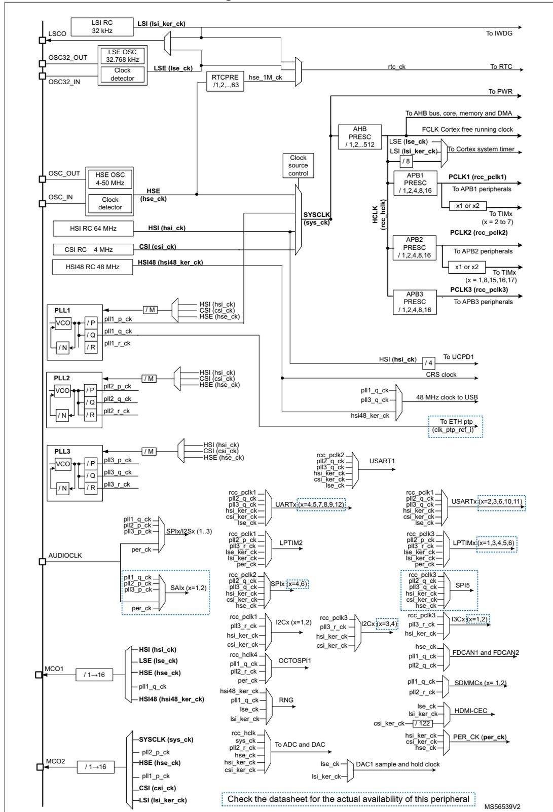
The diagram illustrates the internal clock architecture of an STM32 microcontroller. It shows the following components and paths:
- External Oscillators:
- LSI RC 32 kHz: Connected to LSI (lsi_ker_ck), which feeds into the IWDG and RTC.
- LSE OSC 32.768 kHz: Connected via OSC32_IN and OSC32_OUT pins. It feeds into the RTC (via RTCPRE) and the Clock detector.
- HSE OSC 4-50 MHz: Connected via OSC_IN and OSC_OUT pins. It feeds into the HSE (hse_ck) input of the Clock source control.
- Internal Oscillators:
- HSI RC 64 MHz: Feeds into HSI (hsi_ck).
- CSI RC 4 MHz: Feeds into CSI (csi_ck).
- HSI48 RC 48 MHz: Feeds into HSI48 (hsi48_ker_ck).
- PLLs (Phase-Locked Loops):
- PLL1: Input can be HSI (hsi_ck) or HSE (hse_ck). It has VCO, /P, /Q, and /R dividers, producing pll1_p_ck, pll1_q_ck, and pll1_r_ck outputs.
- PLL2: Input can be HSI (hsi_ck), CSI (csi_ck), or HSE (hse_ck). It has VCO, /P, /Q, and /R dividers, producing pll2_p_ck, pll2_q_ck, and pll2_r_ck outputs.
- PLL3: Input can be HSI (hsi_ck), CSI (csi_ck), or HSE (hse_ck). It has VCO, /P, /Q, and /R dividers, producing pll3_p_ck, pll3_q_ck, and pll3_r_ck outputs.
- Clock Source Control: A central block that selects the system clock (SYSCLK) from HSE, HSI, LSI, or PLL1_r_ck. It also controls the AHB prescaler (1, 2, ..., 512).
- System Clock (SYSCLK):
The main clock for the CPU and AHB bus. It is distributed to:
- AHB bus, core, memory and DMA.
- FCLK Cortex free running clock.
- APB1, APB2, and APB3 prescalers.
- USB 48 MHz clock (derived from PLL1_q_ck or PLL3_q_ck).
- UCPD1 (derived from HSI via /4).
- CRS clock.
- APB Prescalers:
- APB1: Prescaler (1, 2, 4, 8, 16) produces PCLK1 (rcc_pclk1) for APB1 peripherals and TIMx (x = 2 to 7).
- APB2: Prescaler (1, 2, 4, 8, 16) produces PCLK2 (rcc_pclk2) for APB2 peripherals and TIMx (x = 1, 8, 15, 16, 17).
- APB3: Prescaler (1, 2, 4, 8, 16) produces PCLK3 (rcc_pclk3) for APB3 peripherals.
- Peripherals:
Various peripherals are connected to specific clock lines:
- USART1: Connected to rcc_pclk2, pll2_q_ck, pll3_q_ck, hsi_ker_ck, csi_ker_ck, and lse_ck.
- UARTx (x=4,5,7,8,9,12): Connected to rcc_pclk1, pll2_q_ck, hsi_ker_ck, csi_ker_ck, and lse_ck.
- UARTx (x=2,3,6,10,11): Connected to rcc_pclk1, pll2_q_ck, hsi_ker_ck, csi_ker_ck, and lse_ck.
- LPTIM2: Connected to rcc_pclk1, lse_ck, and per_ck.
- LPTIMx (x=1,3,4,5,6): Connected to rcc_pclk3, lse_ck, and per_ck.
- SPIx (x=4,6): Connected to rcc_pclk2, hsi_ker_ck, csi_ker_ck, and hse_ck.
- SPI5: Connected to rcc_pclk3, hsi_ker_ck, csi_ker_ck, and hse_ck.
- I2Cx (x=1,2): Connected to rcc_pclk1, hsi_ker_ck, csi_ker_ck, and lse_ck.
- I2Cx (x=3,4): Connected to rcc_pclk3, hsi_ker_ck, csi_ker_ck, and lse_ck.
- I3Cx (x=1,2): Connected to rcc_pclk3, hsi_ker_ck, csi_ker_ck, and lse_ck.
- OCTOSPI1: Connected to rcc_hclk4, hse_ck, csi_ker_ck, and per_ck.
- FDCAN1 and FDCAN2: Connected to hse_ck, pll1_q_ck, and pll2_q_ck.
- SDMMCx (x=1,2): Connected to pll1_q_ck and pll2_r_ck.
- RNG: Connected to hsi48_ker_ck, pll1_q_ck, lse_ck, and lsi_ker_ck.
- HDMI-CEC: Connected to lse_ck, lsi_ker_ck, and csi_ker_ck (via /7/122).
- PER_CK (per_ck): Derived from hsi_ker_ck, csi_ker_ck, and hse_ck.
- ADC and DAC: Connected to rcc_hclk, sys_ck, pll2_p_ck, hse_ck, hsi_ker_ck, and csi_ker_ck.
- DAC1 sample and hold clock: Derived from lse_ck and lsi_ker_ck.
- Other Connections:
- AUDIOCLK: Derived from HSI (hsi_ck), LSE (lse_ck), HSE (hse_ck), pll1_q_ck, and HSI48 (hsi48_ker_ck). It feeds into SPIx/I2Sx (1..3) and SAIx (x=1,2).
- MCO1: Output clock derived from HSI, LSE, HSE, pll1_q_ck, or HSI48 via a /1 to /16 divider.
- MCO2: Output clock derived from SYSCLK, pll2_p_ck, HSE, pll1_p_ck, CSI, or LSI via a /1 to /16 divider.
Check the datasheet for the actual availability of this peripheral!
MS56539V2
1. For details on the internal/external clock source, refer to the Electrical characteristics in the datasheet.
11.4.1 HSE clock
The HSE block can generate a clock from an external crystal/ceramic resonator, or from an external clock source.
Figure 53. HSE/LSE clock sources
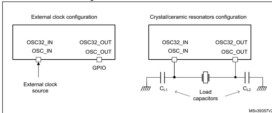
External clock source (HSE bypass)
In this mode, an external clock source must be provided to OSC_IN pin. The external clock can be low swing (analog) or digital. If this clock is directly used by a peripheral, the duty cycle requirement is defined by the peripheral and the application (refer to datasheet for more details).
In case of an analog clock (low swing) the HSEBYP and HSEON bits must be set to 1 in the RCC clock control register (RCC_CR) .
In case of a digital clock, the HSEBYP and the HSEEXT bits must be set to 1 followed by setting the HSEON bit to 1 in the RCC clock control register (RCC_CR) .
External crystal/ceramic resonator
The oscillator is enabled by setting the HSEBYP bit to 0 and HSEON bit to 1.
The HSE can be used when the product requires a very accurate high-speed clock.
The associated hardware configuration is shown in Figure 53 : the resonator and the load capacitors must be placed as close as possible to the oscillator pins to minimize output distortion and startup stabilization time. The loading capacitance values must be adjusted according to the selected crystal or ceramic resonator. Refer to the electrical characteristics section of the datasheet for more details.
The HSERDY flag of the RCC clock control register (RCC_CR) indicates whether the HSE oscillator is stable or not. At startup, the hse_ck clock is not released until this bit is set by hardware. An interrupt can be generated if enabled in the RCC clock source interrupt enable register (RCC_CIER) .
The HSE can be switched ON and OFF through the HSEON bit. Note that the HSE cannot be switched OFF if one of the following two conditions is met:
- • the HSE is used directly (via software mux) as system clock
- • the HSE is selected as reference clock for PLL1, with PLL1 enabled and selected to provide the system clock (via software mux).
In that case the hardware does not allow programming the HSEON bit to 0.
The HSE is automatically disabled by hardware, when the system enters Stop or Standby mode.
In addition, the HSE clock can be driven to the MCO1 and MCO2 outputs and used as clock source for other application components.
11.4.2 HSI clock
The HSI block provides the default clock to the product.
The HSI is a high-speed internal RC oscillator that can be used directly as system clock, peripheral clock, or as PLL input. A predivider allows the application to select an HSI output frequency of 8, 16, 32 or 64 MHz. This predivider is controlled by the HSIDIV.
The HSI advantages are the following:
- • low-cost clock source, as no external crystal is required
- • faster startup time than HSE (a few microseconds)
The HSI frequency, even with frequency calibration, is less accurate than an external crystal oscillator or ceramic resonator.
The HSI can be switched ON and OFF using the HSION bit. Note that the HSI cannot be switched OFF if one of the two conditions is met:
- • the HSI is used directly (via software mux) as system clock
- • the HSI is selected as reference clock for PLL1, with PLL1 enabled and selected to provide the system clock (via software mux).
In that case the hardware does not allow programming the HSION bit to 0. Note that the HSIDIV cannot be changed if the HSI is selected as reference clock for at least one enabled PLL (PLLxON bit set to 1). In that case the hardware does not update the HSIDIV with the new value. However it is possible to change the HSIDIV if the HSI is used directly as system clock.
The HSIRDY flag indicates if the HSI is stable or not. At startup, the HSI output clock is not released until this bit is set by hardware.
The HSI clock can also be used as a backup source (auxiliary clock) if the HSE fails (refer to Section 11.4.10: Clock security system (CSS) ). The HSI can be disabled or not when the system enters Stop mode.
In addition, the HSI clock can be driven to the MCO1 output and used as clock source for other application components.
Care must be taken when the HSI is used as kernel clock for communication peripherals, the application must take into account the following parameters:
- • the time interval between the moment where the peripheral generates a kernel clock request and the moment where the clock is really available
- • the frequency accuracy.
Note: The HSI can remain enabled when the system is in Stop mode.
HSI calibration
RC oscillator frequencies can vary from one chip to another due to manufacturing process variations. That is why each device is factory calibrated by STMicroelectronics to achieve an accuracy of ACCHSI (refer to the product datasheet for more information).
After a power-on reset, the factory calibration value is loaded in the HSICAL[11:0] bits. If the application is subject to voltage or temperature variations, this may affect the RC oscillator frequency. The user application can trim the HSI frequency using the HSITRIM[6:0] bits.
Note: HSICAL[11:0] and HSITRIM[6:0] are located in the RCC CSI calibration register (RCC_CSI/CFGR) .
11.4.3 CSI oscillator
The CSI is a low-power RC oscillator that can be used directly as system clock, peripheral clock, or PLL input.
The CSI advantages are the following:
- • low-cost clock source since no external crystal is required
- • faster startup time than HSE (a few microseconds)
- • very low-power consumption,
The CSI provides a clock frequency of about 4 MHz, while the HSI is able to provide a clock up to 64 MHz.
CSI frequency, even with frequency calibration, is less accurate than an external crystal oscillator or ceramic resonator.
The CSI can be switched ON and OFF through the CSION bit. The CSIRDY flag indicates whether the CSI is stable or not. At startup, the CSI output clock is not released until this bit is set by hardware.
The CSI cannot be switched OFF if one of the two conditions is met:
- • The CSI is used directly (via software mux) as system clock.
- • The CSI is selected as reference clock for PLL1, with PLL1 enabled and selected to provide the system clock (via software mux).
In that case the hardware does not allow programming the CSION bit to 0.
The CSI can be disabled or not when the system enters Stop mode.
In addition, the CSI clock can be driven to the MCO2 output and used as clock source for other application components.
Even if the CSI settling time is faster than the HSI, care must be taken when the CSI is used as kernel clock for communication peripherals: the application must take into account the following parameters:
- • the time interval between the moment where the peripheral generates a kernel clock request and the moment where the clock is really available,
- • the frequency precision.
Note: CSION and CSIRDY bits are located in the RCC clock control register (RCC_CR) .
CSI calibration
RC oscillator frequencies can vary from one chip to another due to manufacturing process variations, this is why each device is factory calibrated to achieve ACC CSI accuracy (refer to the product datasheet for more information). After reset, the factory calibration value is loaded in the CSICAL[7:0] bits.
Voltage and/or temperature variations affect the RC oscillator frequency. The user application can trim the CSI frequency using the CSITRIM[5:0] bits.
Note: Bits CSICAL[7:0] and CSITRIM[5:0] are located into the RCC CSI calibration register (RCC_CSICFGR) .
Figure 54. CSI calibration flow
![Figure 54. CSI calibration flow diagram. The diagram shows the flow of calibration data from Engineering option bytes (factory calibration) through the RCC block to the CSI block. Inside the RCC block, the data from FLASH_CSI_opt[7:0] is added to CSITRIM[5:0] (unsigned) to produce csi_cal[7:0]. This value is then stored in the CSICAL[7:0] (unsigned) register within the RCC_CSICFGR. The CSI block then reads the CAL[7:0] register.](/RM0481-STM32H523-33-562-63-573/98f92f79b14fa055e8bc8db8bab650ec_img.jpg)
graph LR
    subgraph RCC
        direction TB
        CSICFGR[RCC_CSICFGR]
        CSICAL[CSICAL[7:0] unsigned]
        CSITRIM[CSITRIM[5:0] unsigned]
        Adder((+))
        csi_cal[csi_cal[7:0]]
        CSICFGR -- CSICAL --> CSICAL
        CSICFGR -- CSITRIM --> CSITRIM
        CSITRIM --> Adder
        FLASH_CSI_opt[FLASH_CSI_opt[7:0]] --> Adder
        Adder --> csi_cal
        csi_cal --> CSICAL
    end
    EOB[Engineering option bytes factory calibration] -- FLASH_CSI_opt --> FLASH_CSI_opt
    CSICAL -- CSICAL --> CSI
    subgraph CSI
        CAL[CAL[7:0]]
    end
    CAL --> CSICAL
11.4.4 HSI48 clock
The HSI48 clock signal is generated from an internal 48 MHz RC oscillator, and can be used directly for USB and for random number generator (RNG).
The internal 48 MHz RC oscillator is mainly dedicated to provide a high-precision clock to the USB peripheral by means of a special clock recovery system (CRS) circuitry. The CRS can use the USB SOF signal, the LSE, or an external signal to automatically and quickly adjust the oscillator frequency on-the-fly. It is disabled as soon as the system enters Stop or Standby mode. When the CRS is not used, the HSI48 RC oscillator runs on its default frequency, subject to manufacturing process variations.
For more details on how to configure and use the CRS peripheral, refer to Section 12: Clock recovery system (CRS) .
The HSI48RDY flag in the RCC_CR register indicates whether the HSI48 RC oscillator is stable or not. At startup, the HSI48 RC oscillator output clock is not released until this bit is set by hardware.
The HSI48 can be switched on and off using the HSI48ON bit in the RCC_CR register.
11.4.5 PLL description
The RCC features three PLLs:
- • a main PLL (PLL1), generally used to provide clocks to the CPU and some peripherals
- • two dedicated PLLs (PLL2 and PLL3), used to generate the kernel clock for peripherals
The PLLs integrated into the RCC are completely independent. They offer the following features:
- • A VCO supporting two modes:
- – a wide-range
- – a low-range used, for instance, in audio applications
- • Input frequency range:
- – 2 to 16 MHz for the VCO in wide-range mode
- – 1 to 2 MHz for the VCO in low-range mode
- • Capability to work either in integer or fractional mode
- • 13-bit sigma-delta modulator, to fine-tune the VCO frequency by 11 to 0.3 ppm steps
- • The sigma-delta modulator can be updated on-the-fly without generating frequency overshoots on PLLs outputs
- • Each PLL offers three outputs with post-dividers
Figure 55. PLL block diagram
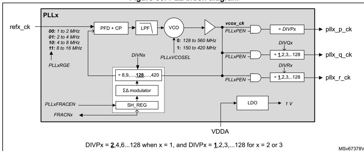
DIVPx = 2,4,6...128 when x = 1, and DIVPx = 1,2,3,...128 for x = 2 or 3
MSv67378V2
The PLLs are controlled via RCC_PLLxDIVR, RCC_PLLxFRACR, RCC_PLLCFGR, and RCC_CR registers.
The frequency of the reference clock provided to the PLLs ( refx_ck ) must range from 1 to 16 MHz. The PLLxM dividers of the RCC PLLx clock source selection register (RCC_PLLxCFGR) must be properly programmed to match this condition. In addition, the PLLxRGE[1:0] field of the RCC PLLx clock source selection register (RCC_PLLxCFGR) must be set according to the reference input frequency to optimize performance.
The user application can then configure the VCO. The smaller range (150 to 420 MHz) must be chosen when the reference clock frequency is lower than 2 MHz.
To reduce the power consumption, it is recommended to configure the VCO output to the smaller range.
DIVNx loop divider must be programmed to achieve the expected frequency at VCO output. In addition, the VCO output range must be respected.
The PLLs operate in integer mode when the value of SH_REG bit of the FRACNx shadow register is set to 0. The SH_REG bit is updated with the FRACNx value when PLLxFRACEN
bit goes from 0 to 1. The sigma-delta modulator is designed to minimize the jitter impact, while allowing very small frequency steps.
The PLLs can be enabled by setting PLLxON to 1. The PLLxRDY bits indicate that the PLL is ready (locked).
Note: Before enabling the PLLs, make sure that the reference frequency ( refx_ck ) provided to it is stable, so the hardware does not allow changing PLLxM when the PLLx is ON, and it is also not possible to change PLLSRC when one of the PLLs is ON.
The hardware prevents writing PLL1ON to 0 if the PLL1 is currently used to deliver the system clock. There are other hardware protections on the clock generators (refer to HSE clock , HSI clock , and CSI oscillator ).
The following PLL parameters cannot be changed once the PLL is enabled: DIVNx, PLLxRGE, PLLxVCOSEL, PLLxP (DIVP), PLLxQ (DIVQ), and PLLxR (DIVR).
For optimal behavior of the PLL when one of the post-divider (DIVP, DIVQ or DIVR) is not used, the application must set the enable bit (DIVyEN) as well as the corresponding post-divider bits (DIVP, DIVQ or DIVR) to 0.
If the above rules are not respected, the PLL output frequency is not guaranteed.
Output frequency computation
When the PLL is configured in integer mode (SH_REG = 0), the VCO frequency ( \( F_{VCO} \) ) is given by the following expression:
When the PLL is configured in fractional mode (SH_REG different from 0), the DIVN divider must be initialized before enabling the PLLs. However, it is possible to change the value of FRACNx on-the-fly without disturbing the PLL output.
This feature can be used either to generate a specific frequency from any crystal value with a good accuracy, or to fine-tune the frequency on-the-fly.
For each PLL, the VCO frequency is given by the following formula:
Note: For PLL1, DIVP can only take odd values.
The PLLs are disabled by hardware when:
- • the system enters Stop or Standby mode
- • an HSE failure occurs when HSE or PLL (clocked by HSE) are used as system clock
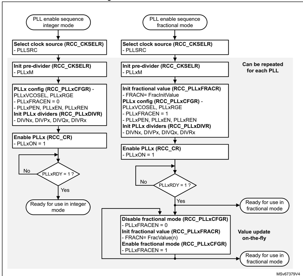
PLL initialization phase
Figure 56 shows the recommended PLL initialization sequence in integer and fractional mode. The PLLx are supposed to be disabled at the start of the initialization sequence:
- 1. Initialize the PLLs registers according to the required frequency.
- – Set PLLxFRACEN of RCC PLLx clock source selection register (RCC_PLLxCFGR) to 0 for integer mode.
- – For fractional mode, set FRACN to the required initial value (FracInitValue) and then set PLLxFRACEN to 1.
- 2. Once the PLLxON bit is set to 1, the user application must wait until PLLxRDY bit is set to 1. If the PLLx is in fractional mode, the PLLxFRACEN bit must not be set back to 0 as long as PLLxRDY = 0.
- 3. Once the PLLxRDY bit is set to 1, the PLLx is ready to be used.
- 4. If the application intends to tune the PLLx frequency on-the-fly (possible only in fractional mode), then:
- a) PLLxFRACEN must be set to 0. When PLLxFRACEN = 0, the sigma-delta modulator is still operating with the value latched into SH_REG. The application must wait for three clock periods of refx_ck (PLLxFRACEN bit propagation delay).
- b) A new value must be uploaded into PLLxFRACR (FracValue(n)).
- c) PLLxFRACEN must be set to 1, to latch the content of PLLxFRACR into its shadow register. The new value is considered after three clock periods of refx_ck (PLLxFRACEN bit propagation delay).
Note: When the PLLxRDY goes to 1 the difference between the PLLx output frequency and the target value is lower than \( \pm 2\% \) .
Figure 56. PLLs initialization flow
graph TD
    subgraph IntegerMode [PLL enable sequence integer mode]
        I1([PLL enable sequence integer mode]) --> I2[Select clock source (RCC_CKSELR)
- PLLSRC]
        I2 --> I3[Init pre-divider (RCC_CKSELR)
- PLLxM]
        I3 --> I4[PLLx config (RCC_PLLxCFGR) -
PLLxVCOSEL, PLLxRGE
- PLLxFRACEN = 0
- PLLxPEN, PLLxEN, PLLxREN
Init PLLx dividers (RCC_PLLxDIVR)
- DIVNx, DIVPx, DIVQx, DIVRx]
        I4 --> I5[Enable PLLx (RCC_CR)
- PLLxON = 1]
        I5 --> I6{PLLxRDY = 1 ?}
        I6 -- No --> I5
        I6 -- Yes --> I7([Ready for use in integer mode])
    end

    subgraph FractionalMode [PLL enable sequence fractional mode]
        F1([PLL enable sequence fractional mode]) --> F2[Select clock source (RCC_CKSELR)
- PLLSRC]
        F2 --> F3[Init pre-divider (RCC_CKSELR)
- PLLxM]
        F3 --> F4[Init fractional value (RCC_PLLxFRACR)
- FRACN= FracInitValue
PLLx config (RCC_PLLxCFGR) -
PLLxVCOSEL, PLLxRGE
- PLLxFRACEN = 1
- PLLxPEN, PLLxEN, PLLxREN
Init PLLx dividers (RCC_PLLxDIVR)
- DIVNx, DIVPx, DIVQx, DIVRx]
        F4 --> F5[Enable PLLx (RCC_CR)
- PLLxON = 1]
        F5 --> F6{PLLxRDY = 1 ?}
        F6 -- No --> F5
        F6 -- Yes --> F7([Ready for use in fractional mode])
    end

    F3 -.-> G[Can be repeated for each PLL]
    G -.-> F3

    I7 --> F8[Disable fractional mode (RCC_PLLxCFGR)
- PLLxFRACEN = 0
Init fractional value (RCC_PLLxFRACR)
- FRACN= FracValue(n)
Enable fractional mode (RCC_PLLxCFGR)
- PLLxFRACEN = 1]
    F8 --> F9([Ready for use in fractional mode])
    F8 -.-> H[Value update on-the-fly]
    H -.-> F9
The flowchart illustrates the initialization process for PLLs in two modes: integer and fractional. Both modes start with a 'PLL enable sequence' (integer or fractional). The integer mode steps are: Select clock source (RCC_CKSELR) - PLLSRC, Init pre-divider (RCC_CKSELR) - PLLxM, PLLx config (RCC_PLLxCFGR) - PLLxVCOSEL, PLLxRGE, - PLLxFRACEN = 0, - PLLxPEN, PLLxEN, PLLxREN, Init PLLx dividers (RCC_PLLxDIVR) - DIVNx, DIVPx, DIVQx, DIVRx, Enable PLLx (RCC_CR) - PLLxON = 1, and a loop until PLLxRDY = 1. The fractional mode steps are: Select clock source (RCC_CKSELR) - PLLSRC, Init pre-divider (RCC_CKSELR) - PLLxM, Init fractional value (RCC_PLLxFRACR) - FRACN= FracInitValue, PLLx config (RCC_PLLxCFGR) - PLLxVCOSEL, PLLxRGE, - PLLxFRACEN = 1, - PLLxPEN, PLLxEN, PLLxREN, Init PLLx dividers (RCC_PLLxDIVR) - DIVNx, DIVPx, DIVQx, DIVRx, Enable PLLx (RCC_CR) - PLLxON = 1, and a loop until PLLxRDY = 1. A note indicates that the 'Init pre-divider' step can be repeated for each PLL. A transition from the integer mode 'Ready' state to the fractional mode 'Ready' state involves: Disable fractional mode (RCC_PLLxCFGR) - PLLxFRACEN = 0, Init fractional value (RCC_PLLxFRACR) - FRACN= FracValue(n), Enable fractional mode (RCC_PLLxCFGR) - PLLxFRACEN = 1, with a note 'Value update on-the-fly'.
MSV67379V4
11.4.6 LSE clock
The LSE can generate a clock from an external crystal/ceramic resonator, or from an external user clock.
External clock source (LSE bypass)
In this mode, an external clock source must be provided to OSC32_IN pin (see Figure 53). The input clock can have a frequency up to 1 MHz, and be low swing (analog) or digital. A duty cycle close to 50% is recommended.
In case of an analog clock (low swing), the LSEBYP and LSEON bits must be set to 1 ( RCC Backup domain control register (RCC_BDCR) ).
In case of a digital clock, the LSEBYP and the LSEEXT bits must be set to 1 followed by setting the LSEON bit to 1 ( RCC Backup domain control register (RCC_BDCR) ). If the RTC
is used, the LSE bypass must not be configured in digital mode, but in low swing analog mode (default value after reset).
External crystal/ceramic resonator (LSE crystal)
The LSE clock is generated from a 32.768 kHz crystal or ceramic resonator. It has the advantage to provide a low-power, highly accurate clock source to the real-time clock (RTC) for clock/calendar or other timing functions.
The LSERDY flag of the RCC Backup domain control register (RCC_BDCR) indicates whether the LSE crystal is stable or not. At startup, the LSE crystal output clock signal is not released until this bit is set by hardware. An interrupt can be generated if enabled in the RCC clock source interrupt enable register (RCC_CIER) .
The LSE oscillator is switched ON and OFF using the LSEON bit. The LSE remains enabled when the system enters Stop or Standby mode.
In addition, the LSE clock can be driven to the MCO1 output and used as clock source for other application components.
The LSE also offers a programmable driving capability (LSEDRV[1:0]), which can be used to modulate the amplifier driving capability. This driving capability is chosen according to the external crystal/ceramic component requirement to ensure a stable oscillation.
The driving capability must be set before enabling the LSE oscillator.
11.4.7 LSI clock
The LSI acts as a low-power clock source that can be kept running when the system is in Stop or Standby mode for the independent watchdog (IWDG) and auto-wakeup unit (AWU).
The clock frequency is around 32 kHz. For more details, refer to the electrical characteristics section of the datasheet.
The LSI can be switched ON and OFF using the LSION bit. The LSIRDY flag indicates whether the LSI oscillator is stable or not. If an independent watchdog is started either by hardware or software, the LSI is forced ON and cannot be disabled.
The LSI remains enabled when the system enters Stop or Standby mode.
At LSI startup, the clock is not provided until the hardware sets the LSIRDY bit. An interrupt can be generated if enabled in the RCC clock source interrupt enable register (RCC_CIER) .
In addition, the LSI clock can be driven to the MCO2 output, and used as a clock source for other application components.
Note: Bits LSION and LSIRDY are located in the RCC Backup domain control register (RCC_BDCR).
11.4.8 System clock (SYSCLK) selection
Four different clock sources can be used to drive the system clock (SYSCLK):
- • HSI oscillator
- • CSI oscillator
- • HSE oscillator
- • PLL
The system clock maximum frequency is 250 MHz. After a system reset (or after leaving Standby mode), the HSI oscillator, at 32 MHz, is selected as system clock. When a clock source is used directly or through the PLL as a system clock, it is not possible to stop it.
A switch from one clock source to another occurs only if the target clock source is ready (clock stable after startup delay or PLL locked). If a clock source not yet ready is selected, the switch occurs when the clock source becomes ready. Status bits in the RCC clock control register (RCC_CR) indicate which clocks are ready, and which clock is currently used as a system clock.
11.4.9 Handling clock generators in stop and standby modes
When the whole system enters Stop mode, all the clocks (system and kernel clocks) are stopped, as well as the following clock sources:
- • CSI, HSI (depending on HSIKERON and CSIKERON bits)
- • HSE
- • PLL1, PLL2, and PLL3
- • HSI48
The content of the RCC registers is not altered except for PLL1ON, PLL2ON, PLL3ON, HSEON, and HSI48ON, set to 0.
Exiting Stop mode
When the system exits this mode via a wake-up event, the application can select which oscillator (HSI and/or CSI) is used to restart. The STOPWUCK bit selects the oscillator used as system clock. The STOPKERWUCK bit selects the oscillator used as kernel clock for peripherals. The STOPKERWUCK bit is useful if after a system Stop, a peripheral needs a kernel clock generated by an oscillator different from the one used for the system clock.
These bits belong to the RCC clock configuration register1 (RCC_CFGR1)
Table 113. STOPWUCK and STOPKERWUCK description
| STOPWUCK | STOPKERWUCK | Activated oscillator(s) when the system exits Stop mode | Distributed clocks when the system exits Stop mode | |
|---|---|---|---|---|
| System clock | Kernel clock | |||
| 0 | 0 | HSI | HSI | HSI |
| 1 | HSI and CSI | HSI and/or CSI | ||
| 1 | 0 | CSI | ||
| 1 | CSI | CSI | ||
During Stop mode
There are two specific cases where the HSI or CSI can be enabled during this mode.
- • When a dedicated peripheral requests the kernel clock the peripheral receives the HSI or CSI according to the kernel clock source selected for this peripheral (via CKPERSEL[1:0]).
- • When the HSIKERON or CSIKERON bits of the RCC clock control register (RCC_CR) are set, the HSI and CSI are kept running, but the outputs are gated. The clock is then
available immediately when the system exits Stop mode, or when a peripheral requests the kernel clock (see Table 111 for details).
Table 114. HSIKERON and CSIKERON behavior
| HSIKERON (CSIKERON) | HSI (CSI) state during Stop mode | HSI (CSI) state setting time |
|---|---|---|
| 0 | OFF | \( t_{su(HSI)} \) \( t_{su(CSI)} \) (1) |
| 1 | Running and gated | Immediate |
- 1. \( t_{su(HSI)} \) and \( t_{su(CSI)} \) are the startup times of, respectively, the HSI and CSI oscillators (refer to the product datasheet for the values of these parameters).
When the microcontroller exists system standby mode, the HSI is selected as system and kernel clock. The RCC registers are reset to their initial values except for the RCC_RSR and RCC_BDCR registers.
Note: The HSI and CSI outputs provide two clock paths:
- • one path for the system clock (hsi_ck or csi_ck)
- • one path for the peripheral kernel clock (hsi_ker_ck or csi_ker_ck).
When a peripheral requests the kernel clock in system stop mode, only the path providing the hsi_ker_ck or csi_ker_ck is activated.
11.4.10 Clock security system (CSS)
Clock security system on HSE
The clock security system can be enabled by software via the HSECSSON bit, which can be enabled even when the HSEON is set to 0.
The CSS on HSE is enabled by the hardware when the HSE is enabled and ready, and HSECSSON set to 1.
The CSS on HSE is disabled when the HSE is disabled. As a result, this function does not work when the system is in Stop mode.
It is not possible to clear directly the HSECSSON bit by software.
The HSECSSON bit is cleared by hardware when a system reset occurs or when the system enters Standby mode.
If a failure is detected on the HSE clock, the system automatically switches to the HSI or CSI, depending on STOPWUCK bit configuration in RCC clock configuration register1 (RCC_CFGR1) , to provide a safe clock. The HSE is then automatically disabled, a clock failure event is sent to the break inputs of the advanced-control timers (TIM1, TIM8), and an NMI is automatically generated to inform the application about the failure, allowing the MCU to perform rescue operations. If the HSE output was used as clock source for PLLs when the failure occurred, the PLLs are also disabled.
If an HSE clock failure occurs when the CSS is enabled, the CSS generates an interrupt that causes the automatic generation of an NMI. The HSECSSF flag in RCC clock source interrupt flag register (RCC_CIFR) is set to 1 to allow the application to identify the failure source. The NMI routine is executed indefinitely until the HSECSSF bit is cleared. As a consequence, the application must clear the HSECSSF flag in the NMI ISR by setting the HSECSSC bit in the RCC clock source interrupt clear register (RCC_CICR) .
Clock security system on LSE
A clock security system on LSE can be activated by software writing the LSECSSON bit in the RCC Backup domain control register (RCC_BDCR) . This bit can be disabled only by a hardware or RTC software reset, or after a failure detection on LSE. LSECSSON must be written after LSE is enabled (LSEON enabled) and ready (LSERDY set by hardware), and after the RTC clock has been selected by RTCSEL.
The CSS operates in all modes, including VBAT. It works also under system reset (excluding power-on reset). The system detects when the LSE disappears, or if it is over frequency.
If a failure is detected on the external 32 kHz oscillator, the LSE clock is no longer supplied to the RTC, but no hardware action is made to the registers.
The CSS on LSE detection event is connected to the internal tamper 3 of the TAMP peripheral. The internal tamper 3 must be enabled (ITAMP3E = 1 in TAMP_CR1 register) and the associated interrupt enabled (ITAMP3IE in TAMP_IER) to wake up from the low-power modes. This erases also the TAMP backup registers and backup SRAM unless the ITAMP3NOER = 1 in the TAMP_CR3 (see Section 47: Tamper and backup registers (TAMP) for more details).
In case of CSS on LSE detection event (LSECSSD = 1 in the RCC_BDCR), the software must disable the LSECSSON bit, stop the defective 32 kHz oscillator (disabling LSEON), and change the RTC clock source (no clock or LSI or HSE, with RTCSEL), or take actions to secure the application.
Refer to datasheet for CSS on LSE electrical characteristics.
11.4.11 Clock output generation (MCO1/MCO2)
Two microcontroller clock output pins (MCO1 and MCO2) are available. A clock source can be selected for each output. The selected clock can be divided thanks to configurable prescaler (refer to Figure 52 for additional information on signal selection).
MCO1 and MCO2 outputs are controlled via MCO1PRE[3:0], MCO1[2:0], MCO2PRE[3:0], and MCO2[2:0], located in the RCC clock configuration register1 (RCC_CFGR1) .
The GPIO port corresponding to each MCO pin must be programmed in alternate function mode.
The clock provided to the MCOs outputs must not exceed the maximum pin speed (refer to the product datasheet for information on the supported speed).
Another output (LSCO) allows one of the low-speed clocks (LSI, LSE) to be output onto the external LSCO pin. This output is available in Stop mode, not available in Standby and VBAT modes. The selection is controlled by the LSCOSEL bit, and enabled by the LSCOEN bit in the RCC Backup domain control register (RCC_BDCR) .
The MCO clock output requires the corresponding alternate function selected on the MCO pin. The LSCO pin must be left in default POR state.
11.4.12 Kernel clock selection
Some peripherals are designed to work with two different clock domains that operate asynchronously:
- • a clock domain synchronous with the register and bus interface ( ckg_bus_perx clock)
- • a clock domain generally synchronous with the peripheral (kernel clock)
The benefit of having peripherals supporting these two clock domains is that the user application has more freedom to choose optimized clock frequency for the CPU, bus matrix and for the kernel part of the peripheral. The user application can thus change the bus frequency without reprogramming the peripherals. As an example, an ongoing transfer with UART is not disturbed if its APB clock is changed on-the-fly.
Table 115 shows the kernel clock that the RCC can deliver to the peripherals. Each row represents a multiplexer and the peripherals connected to its output.
Table 115. Kernel clock distribution overview
| Peripherals (1) | Clock multiplexer control bits | pll1_q_ck | pll2_p_ck | pll2_q_ck | pll2_r_ck | pll3_p_ck | pll3_q_ck | pll3_r_ck | sys_ck | bus clocks (2) | hse_ck | hsi_ker_ck | csi_ker_ck | hsi48_ck | lse_ck | lsi_ck | per_ck (3) | AUDIOCLK | Disabled |
|---|---|---|---|---|---|---|---|---|---|---|---|---|---|---|---|---|---|---|---|
| OCTOSPI | OSPSEL | 1 | - | - | 2 | - | - | - | - | 0 | - | - | - | - | - | - | 3 | - | - |
| SDMMC1 (4) | SDMMC1SEL | 0 | - | - | 1 | - | - | - | - | - | - | - | - | - | - | - | - | - | - |
| SDMMC2 (4) | SDMMC2SEL | 0 | - | - | 1 | - | - | - | - | - | - | - | - | - | - | - | - | - | - |
| FDCAN | FDCANSEL | 1 | - | 2 | - | - | - | - | - | - | 0 | - | - | - | - | - | - | - | - |
| CEC | CECSEL | - | - | - | - | - | - | - | - | - | - | - | 2 (5) | - | 0 | 1 | - | - | - |
| I2C1 | I2C1SEL | - | - | - | - | - | - | 1 | - | 0 | - | 2 | 3 | - | - | - | - | - | - |
| I2C2 | I2C2SEL | - | - | - | - | - | - | 1 | - | 0 | - | 2 | 3 | - | - | - | - | - | - |
| I2C3 | I2C3SEL | - | - | - | - | - | - | 1 | - | 0 | - | 2 | 3 | - | - | - | - | - | - |
| I2C4 | I2C4SEL | - | - | - | - | - | - | 1 | - | 0 | - | 2 | 3 | - | - | - | - | - | - |
| I3C1 | I3C1SEL | - | - | - | - | - | - | 1 | - | 0 | - | 2 | - | - | - | - | - | - | - |
| I3C2 | I3C2SEL | - | - | - | - | - | - | 1 | - | 0 | - | 2 | - | - | - | - | - | - | - |
| LPTIM1 | LPTIM1SEL | - | 1 | - | - | - | - | 2 | - | 0 | - | - | - | - | 3 | 4 | 5 | - | - |
| LPTIM2 | LPTIM2SEL | - | 1 | - | - | - | - | 2 | - | 0 | - | - | - | - | 3 | 4 | 5 | - | - |
| LPTIM3 | LPTIM3SEL | - | 1 | - | - | - | - | 2 | - | 0 | - | - | - | - | 3 | 4 | 5 | - | - |
| LPTIM4 | LPTIM4SEL | - | 1 | - | - | - | - | 2 | - | 0 | - | - | - | - | 3 | 4 | 5 | - | - |
| LPTIM5 | LPTIM5SEL | - | 1 | - | - | - | - | 2 | - | 0 | - | - | - | - | 3 | 4 | 5 | - | - |
| LPTIM6 | LPTIM6SEL | - | 1 | - | - | - | - | 2 | - | 0 | - | - | - | - | 3 | 4 | 5 | - | - |
| TIM[8:1], | - | - | - | - | - | - | - | - | - | x | - | - | - | - | - | - | - | - | - |
| TIM[17:12] | - | - | - | - | - | - | - | - | - | x | - | - | - | - | - | - | - | - | - |
| TIM16/17 | TIMICSEL | - | - | - | - | - | - | - | - | - | - | 1 | 1 | - | - | - | - | - | 0 |
| RNG | RNGSEL | 1 | - | - | - | - | - | - | - | - | - | - | - | 0 | 2 | 3 | - | - | - |
| SAI1 | SAI1SEL | 0 | 1 | - | - | 2 | - | - | - | - | - | - | - | - | - | - | 4 | 3 | - |
| SAI2 | SAI2SEL | 0 | 1 | - | - | 2 | - | - | - | - | - | - | - | - | - | - | 4 | 3 | - |
| SPI(I2S)1 | SPI1SEL | 0 | 1 | - | - | 2 | - | - | - | - | - | - | - | - | - | - | 4 | 3 | - |
| SPI(I2S)2 | SPI2SEL | 0 | 1 | - | - | 2 | - | - | - | - | - | - | - | - | - | - | 4 | 3 | - |
| SPI(I2S)3 | SPI3SEL | 0 | 1 | - | - | 2 | - | - | - | - | - | - | - | - | - | - | 4 | 3 | - |
Table 115. Kernel clock distribution overview (continued)
| Peripherals (1) | Clock multiplexer control bits | pll1_q_ck | pll2_p_ck | pll2_q_ck | pll2_r_ck | pll3_p_ck | pll3_q_ck | pll3_r_ck | sys_ck | bus clocks (2) | hse_ck | hsi_ker_ck | csi_ker_ck | hsi48_ck | lse_ck | lsi_ck | per_ck (3) | AUDIOCLK | Disabled |
|---|---|---|---|---|---|---|---|---|---|---|---|---|---|---|---|---|---|---|---|
| SPI4 | SPI4SEL | - | - | 1 | - | - | 2 | - | - | 0 | 5 | 3 | 4 | - | - | - | - | - | - |
| SPI5 | SPI5SEL | - | - | 1 | - | - | 2 | - | - | 0 | 5 | 3 | 4 | - | - | - | - | - | - |
| SPI6 | SPI6SEL | - | - | 1 | - | - | 2 | - | - | 0 | 5 | 3 | 4 | - | - | - | - | - | - |
| USARTx | USARTxSEL | - | - | 1 | - | - | 2 | - | - | 0 | - | 3 | 4 | - | 5 | - | - | - | - |
| UARTx | UARTxSEL | - | - | 1 | - | - | 2 | - | - | 0 | - | 3 | 4 | - | 5 | - | - | - | - |
| LPUART1 | LPUART1SEL | - | - | 1 | - | - | 2 | - | - | 0 | - | 3 | 4 | - | 5 | - | - | - | - |
| USB | USBSEL | 1 | - | - | - | - | 2 | - | - | - | - | - | - | 3 | - | - | - | - | 0 |
| ADC DAC (6) | ADC DACSEL | - | - | - | 2 | - | - | - | 1 | 0 | 3 | 4 | 5 | - | - | - | - | - | - |
| DAC | DACSEL | - | - | - | - | - | - | - | - | - | - | - | - | - | 0 | 1 | - | - | - |
| UCPD1 | - | - | - | - | - | - | - | - | - | - | - | x (7) | - | - | - | - | - | - | - |
| ETH (ptp) | - | x | - | - | - | - | - | - | - | - | - | - | - | - | - | - | - | - | - |
| RTC/AWU | RTCSEL | - | - | - | - | - | - | - | - | - | 3 (8) | - | - | - | 1 | 2 | - | - | 0 |
| All | CKPERSEL | - | - | - | - | - | - | - | - | - | 2 | 0 | 1 | - | - | - | - | - | 3 |
1. For the actual availability of the peripheral refer to the device datasheet.
2. The bus (APB or AHB) clocks are the bus interface clocks to whom the peripherals are connected.
3. The per_ck clock can be hse_ck, hsi_ker_ck, or csi_ker_ck, according to CKPERSEL selection.
4. With a duty cycle close to 50%, meaning that PLL1Q or PLL2R values must be even. For SDMMCx the duty cycle must be 50% when supporting DDR.
5. Clock CSI divided by 122.
6. With a duty cycle close to 50%, meaning that PLL2R values must be even
7. Clock HSI divided by 4.
8. Clock HSE divided by RTCPRE.
To reduce the number of switches, some peripherals share the same kernel clock source, but all have their dedicated enable signal.
Peripherals dedicated to audio applications
The audio peripherals generally need specific accurate frequencies, the kernel clock of the SAIs or SPI(I2S)s can be generated by:
- • PLL1 when the amount of active PLLs must be reduced (for SAIs and SPI1 to 3)
- • APB2 peripheral clock (for SPI4 and 5)
- • APB3 peripheral clock (for SPI6)
- • PLL2 or 3 for optimal flexibility in frequency generation
- • HSE, HSI, or CSI when the current consumption is critical
- • AUDIOCLK when an external clock reference must be used
Peripherals dedicated to control and data transfer
Peripherals such as SPIs, I2Cs, UARTs do not need a specific kernel clock frequency but a clock fast enough to generate the correct baud rate, or the required bit clock on the serial interface. For that purpose the source can be selected among the following ones:
- • PLL1 when the amount of active PLLs must be reduced
- • PLL2 or PLL3 if better flexibility is required. As an example, this solution allows changing the frequency bus via PLL1 without affecting the speed of some serial interfaces.
- • HSI or CSI for low-power use-cases or when the peripheral must quickly wake up from Stop mode (such as UART or I2C)
Note: UARTs also need the LSE clock when high baud rates are not required.
The OCTOSPI and SDMMC1/2 can also use a clock different from the bus interface one for more flexibility.
RTC/AWU clock
The rtc_ck clock source can be one of the following:
- • the hse_1M_ck ( hse_ck divided by a programmable prescaler)
- • the lse_ck
- • the lsi_ck clock
The source clock is selected by programming the RTCSEL[1:0] bits in the RCC Backup domain control register (RCC_BDCR) and the RTCPRE[5:0] bits in the RCC clock configuration register1 (RCC_CFGR1) .
This selection cannot be modified without resetting the Backup domain.
If the LSE is selected as RTC clock, the RTC works normally even if the backup or the \( V_{DD} \) supply disappears.
The LSE clock is in the Backup domain, whereas the other oscillators are not. As a consequence:
- • If LSE is selected as RTC clock, the RTC continues working even if the \( V_{DD} \) supply is switched OFF, provided the \( V_{BAT} \) supply is maintained.
- • If LSI is selected as the RTC clock, the AWU state is not guaranteed if the \( V_{DD} \) supply is powered off.
- • If the HSE clock is used as RTC clock, the RTC state is not guaranteed if the \( V_{DD} \) supply is powered off or if the \( V_{CORE} \) supply is powered off.
The rtc_ck clock is enabled through RTCEN bit located in the RCC Backup domain control register (RCC_BDCR) .
The RTC bus interface clock (APB clock) is enabled through RTCAPBEN and RTCAPBLPEN bits located in RCC_APB3ENR/LPENR registers.
Note: To read the RTC calendar register when the APB clock frequency is less than seven times the RTC clock frequency ( \( F_{APB} < 7 \times F_{RTCLK} \) ), the software must read the calendar time and date registers twice. The data are correct if the second read access to RTC_TR gives the same result than the first one. Otherwise a third read access must be performed.
Watchdog clocks
The RCC provides the clock for the two watchdog blocks available on the circuit. The independent watchdog (IWDG) is connected to the LSI. The window watchdog (WWDG) is connected to the APB clock.
If an independent watchdog is started by either hardware option or software access, the LSI is forced ON and cannot be disabled. After the LSI oscillator setup delay, the clock is provided to the IWDG.
Clock frequency measurement using TIMx
Most of the clock source generator frequencies can be measured by means of the input capture of TIMx.
- • Calibrating the HSI or CSI with the LSE:
The primary purpose of having the LSE connected to a TIMx input capture is to be able to accurately measure the HSI or CSI. This requires to use the HSI or CSI as system clock source either directly or via PLL1. The number of system clock counts between consecutive edges of the LSE signal gives a measurement of the internal clock period. Taking advantage of the high precision of LSE crystals (typically a few tens of ppm) we can determine the internal clock frequency with the same resolution, and trim the source to compensate for manufacturing-process and/or temperature- and voltage-related frequency deviations.
The basic concept consists in providing a relative measurement (e.g. HSI/LSE ratio). The precision is therefore tightly linked to the ratio between the two clock sources. The greater the ratio is, the more accurate the measurement is.
The HSI and CSI oscillators have dedicated user-accessible calibration bits for this purpose (see RCC CSI calibration register (RCC_CSICFGR) ). When HSI or CSI is used via the PLLx, the system clock can also be fine-tuned by using the fractional divider of the PLLs.
- • Calibrating the LSI with the HSI:
The LSI frequency can also be measured: this is useful for applications that do not have a crystal. The ultra-low-power LSI oscillator has a large manufacturing process deviation. The LSI clock frequency can be measured using the more precise HSI clock source. Using this measurement, a more accurate RTC time base timeouts (when LSI is used as the RTC clock source) and/or an IWDG timeout with an acceptable accuracy can be obtained.
11.4.13 RTC and TAMP clock
The RTCCLK clock source is used by RTC and TAMP, and can be either the HSE / 32, LSE or LSI clock. It is selected by programming the RTCSEL[1:0] bits in the RCC Backup domain control register (RCC_BDCR) . This selection cannot be modified without resetting the Backup domain. The system must always be configured so as to get a PCLK frequency greater than or equal to the RTCCLK frequency for a proper operation of the RTC. The TAMP does not require any kernel clock if only the backup registers are used, with tamper in edge detection mode. All other tamper detection modes require a kernel clock (refer to Section 47: Tamper and backup registers (TAMP) for more details).
The LSE is in the Backup domain, whereas the HSE and LSI clocks are not. Consequently:
- • If LSE is selected as RTC and TAMP clock, these peripherals continue to work even if the \( V_{DD} \) supply is switched off, provided the \( V_{BAT} \) supply is maintained.
- • If the HSE clock divided by a prescaler is used as the RTC or TAMP clock, the RTC state is not guaranteed if the \( V_{DD} \) supply is powered off or if the internal voltage regulator is powered off (removing power from the core domain). Depending on the TAMP configuration, this one can remain functional if used in a mode that does not need any kernel clock.
- • If the LSI is used as the RTC or TAMP clock, the RTC state is not guaranteed if the \( V_{DD} \) supply is powered off. Depending on the TAMP configuration, this one can remain functional if used in a mode that does not need any kernel clock.
When the RTC and TAMP clock is LSE or LSI, the RTC remains clocked and functional under system reset.
11.4.14 Timer clock
The timer clock frequencies are automatically defined by hardware.
There are two cases:
- • If the APB prescaler equals 1, the timer clock frequencies are set to the APB domain frequency.
- • Otherwise, they are set to twice ( \( \times 2 \) ) the APB domain frequency.
11.4.15 Watchdog clock
If the independent watchdog (IWDG) is started by either hardware option or software access, the LSI oscillator is forced on and cannot be disabled. After the LSI oscillator temporization, the LSI 32 kHz clock is provided to the IWDG.
11.4.16 Peripherals clock gating and autonomous mode
Peripherals clock gating in Run mode
Each peripheral clock can be enabled by the corresponding EN bit in the RCC_AHBxENR and RCC_APBxENR registers.
When the peripheral clock is not active, read or write accesses to the peripheral registers are not supported.
The enable bit has a synchronization mechanism to create a glitch-free clock for the peripheral. After the enable bit is set, there the clock is active after 2 cycles of the peripheral bus clock.
Caution: Just after enabling the clock for a peripheral, the software must wait for these 2 clock cycles before accessing the peripheral registers.
Peripherals clock gating in Sleep mode
When a peripheral is enabled, its clock can be automatically gated off when the device is in Sleep mode, by clearing the peripheral LPEN bit in the RCC_AHBxLPENR and RCC_APBxLPENR registers. Both EN and LPEN bit of the peripheral must be set to keep the clock on in Sleep mode.
11.5 RCC security and privilege functional description
11.5.1 RCC TrustZone security protection modes
When the TrustZone security is activated by the TZEN option byte in the Flash option byte configuration register, the RCC is able to secure RCC configuration and status bits from being modified by non-secure accesses.
This is configured through the RCC secure configuration register (RCC_SECCFGR) to prevent non-secure access to read or modify the following features:
- • HSE, HSE-CSS, HSI, CSI, LSI, LSE, LSE-CSS, LSCO, HSI48 configuration and status bits
- • PLL1, PLL2, PLL3, AHB and APB prescalers configuration and status bits
- • system clock (SYSCLK) and ICLK source clock selection and status bits
- • MCO clock output configuration and STOPWUCK and STOPKERWUCK bit
- • Remove reset flag RMVF configuration
If SPRIV is set in the RCC privilege configuration register (RCC_PRIVCFGR) , the RCC_SECCFGR register can be written only by secure and privileged access. If SPRIV is cleared in RCC_PRIVCFGR, RCC_SECCFGR can be written only by secure access, privileged or unprivileged.
RCC_SECCFGR can be read by secure, non-secure, privileged and unprivileged access.
When a peripheral is configured as secure, its related clock, reset, clock source selection and clock enable during low-power modes control bits, are also secure in the RCC_AHBxENR, RCC_APBxENR, RCC_CCIPRx and RCC_BDCR registers.
A peripheral is secure when:
- • For securable peripherals by TZSC (see Section 5.4.3: TrustZone security controller (TZSC) ), the SEC security bit corresponding to this peripheral is set in the GTZC TZSC secure configuration registers.
- • For TrustZone ® -aware peripherals, a security feature of this peripheral is enabled through its dedicated bits.
Table 116 summarizes the RCC secured bits following the security configuration bit in the RCC_SECCFGR register.
When one security configuration bit is set, some configuration and status bits are secured. The RCC registers may contain secure and non-secure bits:
- • Secured bits: read and write operations are only allowed by a secure access. Non-secure read returns 0 and write accesses are ignored. No illegal access event is generated.
- • Non-secure bits: no restriction. Read and write operations are allowed by both secure and non-secure accesses.
- • A non-secure write access to RCC_SECCFGR is ignored and generates an illegal access event. An illegal access interrupt is generated if the RCC illegal access interrupt is enabled in the GTZC TZIC registers. RCC_SECCFGR can be read by secure or non-secure access.
When the TrustZone security is disabled (TZEN = 0xC3), all registers are non-secure. RCC_SECCFGR write accesses are ignored.
Table 116. RCC security configuration summary
| Configuration bit in RCC_SECCFGR | Secured bits | Corresponding register |
|---|---|---|
| HSISEC | HSION, HSIKERON, HSIRDY | RCC_CR |
| HSICAL[11:0], HSITRIM[6:0] | RCC_HSICFGR | |
| HSIRDYIE | RCC_CIER | |
| HSIRDYIF | RCC_CIFR | |
| HSIRDYC | RCC_CICR | |
| HSESEC | HSEON, HSERDY, HSEBYP, HSECSSON, HSEEXT | RCC_CR |
| HSERDYIE, HSECSSF | RCC_CIER | |
| HSERDYIF, HSECSSF | RCC_CIFR | |
| HSERDYC, HSECSSC | RCC_CICR | |
| CSISEC | CSISON, CSIKERON, CSISRDY | RCC_CR |
| CSICAL[7:0], CSITRIM[5:0] | RCC_CSICFGR | |
| CSISRDYIE | RCC_CIER | |
| CSISRDYIF | RCC_CIFR | |
| CSISRDYC | RCC_CICR | |
| LSISEC | LSION, LSIRDY, LSIPREDIV, LSCOSEL, LSCOEN | RCC_BDCR |
| LSIRDYIE | RCC_CIER | |
| LSIRDYIF | RCC_CIFR | |
| LSIRDYC | RCC_CICR | |
| LSESEC | LSECSSON, LSECSSD, LSEDRV[1:0], LSEBYP, LSERDY, LSEON, LSEEXT, LSCOSEL, LSCOEN | RCC_BDCR |
| LSERDYIE | RCC_CIER | |
| LSERDYF | RCC_CIFR | |
| LSERDYC | RCC_CICR | |
| SYSCLKSEC | SW[1:0], SWS[1:0], STOPWUCK, STOPKERWUCK, MCO1SEL[3:0], MCO1PRE[2:0], MCO2SEL[3:0], MCO2PRE[2:0] | RCC_CFGR1 |
| SYSTICKSEL[1:0] | RCC_CCIPR4 | |
| VOS[1:0] | PWR_VOSR | |
| TIMPRE | RCC_CFGR1 | |
| PRESCSEC | HPRE[3:0], PPRE1[2:0], PPRE2[2:0], PPRE3[2:0] | RCC_CFGR2 |
Table 116. RCC security configuration summary (continued)
| Configuration bit in RCC_SECCFGR | Secured bits | Corresponding register |
|---|---|---|
| PLL1SEC | PLL1SRC[1:0], PLL1RGE[1:0], PLL1FRACEN, PLL1M[3:0], PLL1VCOSEL, PLL1PEN, PLL1QEN, PLL1REN | RCC_PLL1CFGR |
| PLL1N[8:0], PLL1P[6:0], PLL1Q[6:0], PLL1R[6:0] | RCC_PLL1DIVR | |
| PLL1FRACN[12:0] | RCC_PLL1FRACR | |
| PLL1RDY, PLL1ON | RCC_CR | |
| PLL1RDYIE | RCC_CIER | |
| PLL1RDYF | RCC_CIFR | |
| PLL1RDYC | RCC_CICR | |
| PLL2SEC | PLL2SRC[1:0], PLL2RGE[1:0], PLL2FRACEN, PLL2M[3:0], PLL2PEN, PLL2QEN, PLL2REN, PLL2VCOSEL | RCC_PLL2CFGR |
| PLL2N[8:0], PLL2P[6:0], PLL2Q[6:0], PLL2R[6:0] | RCC_PLL2DIVR | |
| PLL2FRACN[12:0] | RCC_PLL2FRACR | |
| PLL2RDY, PLL2ON | RCC_CR | |
| PLL2RDYIE | RCC_CIER | |
| PLL2RDYF | RCC_CIFR | |
| PLL2RDYC | RCC_CICR | |
| PLL3SEC | PLL3SRC[1:0], PLL3RGE[1:0], PLL3FRACEN, PLL3M[3:0], PLL3PEN, PLL3QEN, PLL3REN, PLL3VCOSEL | RCC_PLL3CFGR |
| PLL3N[8:0], PLL3P[6:0], PLL3Q[6:0], PLL3R[6:0] | RCC_PLL3DIVR | |
| PLL3FRACN[12:0] | RCC_PLL3FRACR | |
| PLL3RDY, PLL3ON | RCC_CR | |
| PLL3RDYIE | RCC_CIER | |
| PLL3RDYF | RCC_CIFR | |
| PLL3RDYC | RCC_CICR | |
| HSI48SEC (1) | HSI48ON, HSI48RDY | RCC_CR |
| HSI48CAL[9:0] | RCC_CRRRCR | |
| HSI48RDYE | RCC_CIER | |
| HSI48RDYF | RCC_CIFR | |
| HSI48RDYC | RCC_CICR | |
| IPKERSECCFG | CKERPSEL[1:0] | RCC_CCIPR5 |
| RMVFSEC | RMVF | RCC_CSR |
1. TRIM field of the HSI48 is located in CRS peripheral. Be sure to secure it using CRSSEC bit in GTZC1 TZSC secure configuration register 1.
11.5.2 RCC privilege protection modes
By default, after reset, all RCC registers can be read or written with both privileged and unprivileged access except RCC privilege configuration register (RCC_PRIVCFGR) that can be written with privileged access only. RCC_PRIVCFGR can be read by secure and non secure, privileged and unprivileged access.
The SPRIV bit in RCC_PRIVCFGR can be written with secure privileged access only. This bit configures the privileged access of all RCC secure functions (as defined by RCC secure configuration register (RCC_SECCFGR) or by the GTZC for securable peripherals, or by the peripheral itself in case of TrustZone-aware peripherals).
When the SPRIV bit is set in RCC_PRIVCFGR:
- • Writing the RCC secure bits is possible only with privileged access, including RCC_SECCFGR.
- • The RCC secure bits can be read only with privileged access except RCC_SECCFGR and RCC_PRIVCFGR that can be read by privileged or unprivileged access.
- • An unprivileged access to a privileged RCC bit or register is discarded: the bits are read as zero and the write to these bits is ignored (RAZ/WI).
The NSPRIV bit in RCC_PRIVCFGR can be written with privileged access only, secure or non-secure. This bit configures the privileged access of all RCC non-secure functions (as defined by RCC_SECCFGR, or by the GTZC for securable peripherals, or by the peripheral itself in case of TrustZone-aware peripherals).
When the NSPRIV bit is set in RCC_PRIVCFGR:
- • Writing the RCC non-secure bits is possible only with privileged access.
- • The RCC non-secure bits can be read only with privileged access except RCC_PRIVCFGR that can be read by privileged or unprivileged access.
- • An unprivileged access to a privileged RCC bit or register is discarded: the bits are read as zero and the write to these bits is ignored (RAZ/WI).
11.6 RCC low-power modes
- • AHB and APB peripheral clocks, including DMA clock, can be disabled by software.
- • Sleep mode stops the CPU clock. The memory interface clocks (flash memory, caches and all SRAM interfaces) can be stopped by software during Sleep mode. The AHB to APB bridge clocks are disabled by hardware during Sleep mode when all the clocks of the peripherals connected to them are disabled.
- • Stop mode stops all the clocks in the core domain and disable the PLLs, HSI, HSI48, CSI and HSE oscillators. However, HSI or CSI can be switched ON to generate a wakeup interrupt. LSI and LSE remain active in Stop mode.
- • Standby mode stops all the clocks in the core domain and disable the PLLs, HSI, HSI48, CSI and HSE oscillators.
The CPU DeepSleep mode can be overridden for debugging by setting the DBG_STOP or DBG_STANDBY bit in the DBGMCU_CR register.
When exiting Stop mode, the system clock is either HSI or CSI, depending on the software configuration of STOPWUCK in the RCC CPU domain clock configuration register 2 (RCC_CFGR2) . The frequency (range and user trim) of the HSI is the one configured before entering Stop mode.
The other internal oscillator can be automatically woken up in addition to the one used by the system clock, to avoid waiting for the other oscillator wake-up time when the device is back in Run mode. This is done thanks to STOPKERWUCK in RCC_CFGR1.
When leaving the Standby mode, the system clock is HSI (32 MHz). The user trim is lost.
If a flash memory programming operation is ongoing, Stop or Standby mode entry is delayed until the flash memory interface access is finished. If an access to the APB domain is ongoing, Stop or Standby mode entry is delayed until the APB access is finished.
11.7 RCC interrupts
Table 117 summarizes the interrupt sources and the way to control them.
Table 117. Interrupt sources and control
| Interrupt vector | Interrupt event flag | Description | Enable control bits | Interrupt clear method | Exit from Sleep mode | Exit from Stop and Standby modes |
|---|---|---|---|---|---|---|
| RCC | LSIRDYF | LSI ready | LSIRDYIE and LSISEC = 0 | Set LSIRDYC to 1 | Yes | No |
| LSERDYF | LSE ready | LSERDYIE and LSESEC = 0 | Set LSERDYC to 1 | Yes | No | |
| HSIDRYF | HSI ready | HSIDRYIE and HSISEC = 0 | Set HSIRDYC to 1 | Yes | No | |
| HSERDYF | HSE ready | HSERDYIE and HSESEC = 0 | Set HSERDYC to 1 | Yes | No | |
| CSISRDYF | CSIS ready | CSISRDYIE and CSISEC = 0 | Set CSISRDYC to 1 | Yes | No | |
| HSI48RDYF | HSI48 ready | HSI48RDYIE and HSI48SEC = 0 | Set HSI48RDYC to 1 | Yes | No | |
| PLL1RDYF | PLL1 ready | PLL1RDYIE and PLL1SEC = 0 | Set PLL1RDYC to 1 | Yes | No | |
| PLL2RDYF | PLL2 ready | PLL2RDYIE and PLL2SEC = 0 | Set PLL2RDYC to 1 | Yes | No | |
| PLL3RDYF | PLL3 ready | PLL3RDYIE and PLL3SEC = 0 | Set PLL3DYC to 1 | Yes | No | |
| RCC_S (1) | LSIRDYF | LSI ready | LSIRDYIE and LSISEC = 1 | Set LSIRDYC to 1 | Yes | No |
| LSERDYF | LSE ready | LSERDYIE and LSESEC = 1 | Set LSERDYC to 1 | Yes | No | |
| HSIDRYF | HSI ready | HSIDRYIE and HSISEC = 1 | Set HSIRDYC to 1 | Yes | No | |
| HSERDYF | HSE ready | HSERDYIE and HSESEC = 1 | Set HSERDYC to 1 | Yes | No | |
| CSISRDYF | CSIS ready | CSISRDYIE and CSISEC = 1 | Set CSISRDYC to 1 | Yes | No | |
| HSI48RDYF | HSI48 ready | HSI48RDYIE and HSI48SEC = 1 | Set HSI48RDYC to 1 | Yes | No | |
| PLL1RDYF | PLL1 ready | PLL1RDYIE and PLL1SEC = 1 | Set PLL1RDYC to 1 | Yes | No | |
| PLL2RDYF | PLL2 ready | PLL2RDYIE and PLL2SEC = 1 | Set PLL2RDYC to 1 | Yes | No | |
| PLL3RDYF | PLL3 ready | PLL3RDYIE and PLL3SEC = 1 | Set PLL3RDYC to 1 | Yes | No |
Table 117. Interrupt sources and control (continued)
| Interrupt vector | Interrupt event flag | Description | Enable control bits | Interrupt clear method | Exit from Sleep mode | Exit from Stop and Standby modes |
|---|---|---|---|---|---|---|
| TAMP | ITAMP3F (2) | LSE CSS failure | LSECSSON and ITAMP3E (2) and ITAMP3IE (2) | Set CITAMP3F (2) to 1 | Yes | Yes |
| NMI | HSECSSF | HSE CSS failure | (3) | Set HSECSSC to 1 | Yes | No |
- 1. The RCC secure interrupt vector is used only when TrustZone is enabled.
- 2. The LSE CSS failure event (LSECSSD) is connected to TAMP internal tamper 3. to get the interrupt associated to this event, the internal tamper 3 must be enabled, and the internal tamper 3 interrupt must be enabled. The ITAMP3F, ITAMP3E, ITAMP3IE, and CITAMP3F bits are in the TAMP peripheral.
- 3. It is not possible to mask this interrupt when the security system feature is enabled (HSECSSON = 1).
11.8 RCC registers
11.8.1 RCC clock control register (RCC_CR)
Address offset: 0x000
Reset value: 0x0000 002B
| 31 | 30 | 29 | 28 | 27 | 26 | 25 | 24 | 23 | 22 | 21 | 20 | 19 | 18 | 17 | 16 |
|---|---|---|---|---|---|---|---|---|---|---|---|---|---|---|---|
| Res. | Res. | PLL3 RDY | PLL3 ON | PLL2 RDY | PLL2 ON | PLL1 RDY | PLL1 ON | Res. | Res. | Res. | HSE EXT | HSE CSSON | HSE BYP | HSE RDY | HSE ON |
| r | rw | r | rw | r | rw | rw | rs | rw | r | rw | |||||
| 15 | 14 | 13 | 12 | 11 | 10 | 9 | 8 | 7 | 6 | 5 | 4 | 3 | 2 | 1 | 0 |
| Res. | Res. | HSI48 RDY | HSI48 ON | Res. | CSI KERON | CSI RDY | CSI ON | Res. | Res. | HSI DIVF | HSIDIV[1:0] | HSI KERON | HSI RDY | HSI ON | |
| r | rw | rw | r | rw | r | rw | rw | rw | r | rw | |||||
Bits 31:30 Reserved, must be kept at reset value.
Bit 29 PLL3RDY : PLL3 clock ready flag
Set by hardware to indicate that the PLL3 is locked.
0: PLL3 unlocked (default after reset)
1: PLL3 locked
Bit 28 PLL3ON : PLL3 enable
Set and cleared by software to enable PLL3.
Cleared by hardware when entering Stop or Standby mode.
0: PLL3 OFF (default after reset)
1: PLL3 ON
Bit 27 PLL2RDY : PLL2 clock ready flag
Set by hardware to indicate that the PLL is locked.
0: PLL2 unlocked
1: PLL2 locked
Bit 26 PLL2ON : PLL2 enable
Set and cleared by software to enable PLL2.
Cleared by hardware when entering Stop or Standby mode.
0: PLL2 OFF (default after reset)
1: PLL2 ON
Bit 25 PLL1RDY : PLL1 clock ready flag
Set by hardware to indicate that the PLL1 is locked.
0: PLL1 unlocked (default after reset)
1: PLL1 locked
Bit 24 PLL1ON : PLL1 enable
Set and cleared by software to enable PLL1.
Cleared by hardware when entering Stop or Standby mode. Note that the hardware prevents writing this bit to 0, if the PLL1 output is used as the system clock.
0: PLL1 OFF (default after reset)
1: PLL1 ON
Bits 23:21 Reserved, must be kept at reset value.
Bit 20 HSEEXT : external high speed clock type in Bypass mode
Set and reset by software to select the external clock type (analog or digital).
The external clock must be enabled with the HSEON bit to be used by the device. The HSEEXT bit can be written only if the HSE oscillator is disabled.
0: HSE in analog mode (default after reset)
1: HSE in digital mode
Bit 19 HSECSSON : HSE clock security system enable
Set by software to enable clock security system on HSE.
This bit is “set only” (disabled by a system reset or when the system enters in Standby mode). When HSECSSON is set, the clock detector is enabled by hardware when the HSE is ready and disabled by hardware if an oscillator failure is detected.
0: CSS on HSE OFF (clock detector OFF) (default after reset)
1: CSS on HSE ON (clock detector ON if the HSE oscillator is stable, OFF if not).
Bit 18 HSEBYP : HSE clock bypass
Set and cleared by software to bypass the oscillator with an external clock. The external clock must be enabled with the HSEON bit to be used by the device.
The HSEBYP bit can be written only if the HSE oscillator is disabled.
0: HSE oscillator not bypassed (default after reset)
1: HSE oscillator bypassed with an external clock
Bit 17 HSERDY : HSE clock ready flag
Set by hardware to indicate that the HSE oscillator is stable.
0: HSE clock is not ready (default after reset)
1: HSE clock is ready
Bit 16 HSEON : HSE clock enable
Set and cleared by software.
Cleared by hardware to stop the HSE when entering Stop or Standby mode.
This bit cannot be cleared if the HSE is used directly (via SW mux) as system clock, or if the HSE is selected as reference clock for PLL1 with PLL1 enabled (PLL1ON bit set to 1).
0: HSE is OFF (default after reset)
1: HSE is ON
Bits 15:14 Reserved, must be kept at reset value.
Bit 13 HSI48RDY : HSI48 clock ready flag
Set by hardware to indicate that the HSI48 oscillator is stable.
0: HSI48 clock is not ready (default after reset)
1: HSI48 clock is ready
Bit 12 HSI48ON : HSI48 clock enable
Set by software and cleared by software or by the hardware when the system enters to Stop or Standby mode.
0: HSI48 is OFF (default after reset)
1: HSI48 is ON
Bit 11 Reserved, must be kept at reset value.
Bit 10 CSIKERON : CSI clock enable in Stop mode
Set and reset by software to force the CSI to ON, even in Stop mode, to be quickly available as kernel clock for some peripherals. This bit has no effect on the value of CSION.
0: no effect on CSI (default after reset)
1: CSI is forced to ON even in Stop mode
Bit 9 CSIRDY: CSI clock ready flagSet by hardware to indicate that the CSI oscillator is stable. This bit is activated only if the RC is enabled by CSION (it is not activated if the CSI is enabled by CSIKERON or by a peripheral request).
0: CSI clock is not ready (default after reset)
1: CSI clock is ready
Bit 8 CSION: CSI clock enableSet and reset by software to enable/disable CSI clock for system and/or peripheral.
Set by hardware to force the CSI to ON when the system leaves Stop mode, if STOPWUCK = 1 or STOPKERWUCK = 1.
This bit cannot be cleared if the CSI is used directly (via SW mux) as system clock, or if the CSI is selected as reference clock for PLL1 with PLL1 enabled (PLL1ON bit set to 1).
0: CSI is OFF (default after reset)
1: CSI is ON
Bits 7:6 Reserved, must be kept at reset value.
Bit 5 HSIDIVF: HSI divider flagSet and reset by hardware.
As a write operation to HSIDIV has not an immediate effect on the frequency, this flag indicates the
current status of the HSI divider. HSIDIVF goes immediately to 0 when HSIDIV value is changed, and is set back to 1 when the output frequency matches the value programmed into HSIDIV.
0: new division ratio not yet propagated to hsi_ck, hsi_ker_ck (default after reset)
1: hsi_ck, hsi_ker_ck clock frequency reflects the new HSIDIV value (default register value when the clock setting is completed).
Bits 4:3 HSIDIV[1:0]: HSI clock dividerSet and reset by software.
These bits allow selecting a division ratio to configure the wanted HSI clock frequency. The HSIDIV cannot be changed if the HSI is selected as reference clock for at least one enabled PLL (PLLxON bit set to 1). In that case, the new HSIDIV value is ignored.
00: division by 1, hsi_ck, hsi_ker_ck = 64 MHz
01: division by 2, hsi_ck, hsi_ker_ck = 32 MHz (default after reset)
10: division by 4, hsi_ck, hsi_ker_ck = 16 MHz
11: division by 8, hsi_ck, hsi_ker_ck = 8 MHz
Bit 2 HSIKERON: HSI clock enable in Stop modeSet and reset by software to force the HSI to ON, even in Stop mode, to be quickly available as kernel clock for peripherals. This bit has no effect on the value of HSION.
0: no effect on HSI (default after reset)
1: HSI is forced to ON even in Stop mode
Bit 1 HSIRDY: HSI clock ready flagSet by hardware to indicate that the HSI oscillator is stable.
0: HSI clock is not ready (default after reset)
1: HSI clock is ready
Bit 0 HSION : HSI clock enable
Set and cleared by software.
Set by hardware to force the HSI to ON when the product leaves Stop mode, if STOPWUCK = 1 or STOPKERWUCK = 1.
Set by hardware to force the HSI to ON when the product leaves Standby mode or in case of a failure of the HSE which is used as the system clock source.
This bit cannot be cleared if the HSI is used directly (via SW mux) as system clock, or if the HSI is selected as reference clock for PLL1 with PLL1 enabled (PLL1ON bit set to 1).
0: HSI is OFF
1: HSI is ON (default after reset)
11.8.2 RCC HSI calibration register (RCC_HSICFGR)
Address offset: 0x010
Reset value: 0x0040 0XXX
Reset value depends on the flash memory option bytes setting.
| 31 | 30 | 29 | 28 | 27 | 26 | 25 | 24 | 23 | 22 | 21 | 20 | 19 | 18 | 17 | 16 |
|---|---|---|---|---|---|---|---|---|---|---|---|---|---|---|---|
| Res. | Res. | Res. | Res. | Res. | Res. | Res. | Res. | Res. | HSITRIM[6:0] | ||||||
| rw | rw | rw | rw | rw | rw | rw | |||||||||
| 15 | 14 | 13 | 12 | 11 | 10 | 9 | 8 | 7 | 6 | 5 | 4 | 3 | 2 | 1 | 0 |
| Res. | Res. | Res. | Res. | HSICAL[11:0] | |||||||||||
| r | r | r | r | r | r | r | r | r | r | r | r | ||||
Bits 31:23 Reserved, must be kept at reset value.
Bits 22:16 HSITRIM[6:0] : HSI clock trimming
Set by software to adjust calibration.
HSITRIM field is added to the engineering option bytes loaded during reset phase (FLASH_HSI_OPT) to form the calibration trimming value.
HSICAL = HSITRIM + FLASH_HSI_OPT.
After a change of HSITRIM it takes one system clock cycle before the new HSITRIM value is updated
Note: The reset value of the field is 0x40.
Bits 15:12 Reserved, must be kept at reset value.
Bits 11:0 HSICAL[11:0] : HSI clock calibration
Set by hardware by option byte loading during system reset. Adjusted by software through trimming bits HSITRIM.
This field represents the sum of engineering option byte calibration and HSITRIM bits values.
11.8.3 RCC clock recovery RC register (RCC_CRRRCR)
Address offset: 0x014
Reset value: 0x0000 0XXX
Reset value depends on the flash option bytes setting
| 31 | 30 | 29 | 28 | 27 | 26 | 25 | 24 | 23 | 22 | 21 | 20 | 19 | 18 | 17 | 16 |
|---|---|---|---|---|---|---|---|---|---|---|---|---|---|---|---|
| Res. | Res. | Res. | Res. | Res. | Res. | Res. | Res. | Res. | Res. | Res. | Res. | Res. | Res. | Res. | Res. |
| 15 | 14 | 13 | 12 | 11 | 10 | 9 | 8 | 7 | 6 | 5 | 4 | 3 | 2 | 1 | 0 |
| Res. | Res. | Res. | Res. | Res. | Res. | HSI48CAL[9:0] | |||||||||
| r | r | r | r | r | r | r | r | r | r | ||||||
Bits 31:10 Reserved, must be kept at reset value.
Bits 9:0 HSI48CAL[9:0] : Internal RC 48 MHz clock calibration
Set by hardware by option-byte loading during system reset NRESET. Read-only.
11.8.4 RCC CSI calibration register (RCC_CSICFGR)
Address offset: 0x018
Reset value: 0x0020 0XXX
Reset value depends on the flash option bytes setting
| 31 | 30 | 29 | 28 | 27 | 26 | 25 | 24 | 23 | 22 | 21 | 20 | 19 | 18 | 17 | 16 |
|---|---|---|---|---|---|---|---|---|---|---|---|---|---|---|---|
| Res. | Res. | Res. | Res. | Res. | Res. | Res. | Res. | Res. | Res. | CSITRIM[5:0] | |||||
| rw | rw | rw | rw | rw | rw | ||||||||||
| 15 | 14 | 13 | 12 | 11 | 10 | 9 | 8 | 7 | 6 | 5 | 4 | 3 | 2 | 1 | 0 |
| Res. | Res. | Res. | Res. | Res. | Res. | Res. | Res. | CSICAL[7:0] | |||||||
| rw | rw | rw | rw | rw | rw | rw | rw | ||||||||
Bits 31:22 Reserved, must be kept at reset value.
Bits 21:16 CSITRIM[5:0] : CSI clock trimming
Set by software to adjust calibration.
CSITRIM field is added to the engineering option bytes loaded during reset phase (FLASH_CSI_OPT) to form the calibration trimming value.
CSICAL = CSITRIM + FLASH_CSI_OPT.
Note: The reset value of the field is 0x20.
Bits 15:8 Reserved, must be kept at reset value.
Bits 7:0 CSICAL[7:0] : CSI clock calibration
Set by hardware by option byte loading during system reset NRESET. Adjusted by software through trimming bits CSITRIM.
This field represents the sum of engineering option byte calibration value and CSITRIM bits value.
11.8.5 RCC clock configuration register1 (RCC_CFGR1)
Address offset: 0x01C
Reset value: 0x0000 0000
Access: 0 ≤ wait state ≤ 2; word, half-word and byte access
One or two wait states are inserted only if the access occurs during clock source switch.
| 31 | 30 | 29 | 28 | 27 | 26 | 25 | 24 | 23 | 22 | 21 | 20 | 19 | 18 | 17 | 16 |
|---|---|---|---|---|---|---|---|---|---|---|---|---|---|---|---|
| MCO2SEL[2:0] | MCO2PRE[3:0] | MCO1SEL[2:0] | MCO1PRE[3:0] | Res. | Res. | ||||||||||
| rw | rw | rw | rw | rw | rw | rw | rw | rw | rw | rw | rw | rw | rw | ||
| 15 | 14 | 13 | 12 | 11 | 10 | 9 | 8 | 7 | 6 | 5 | 4 | 3 | 2 | 1 | 0 |
| TIM PRE | Res. | RTCPRE[5:0] | STOP KER WUCK | STOP WUCK | Res. | SWS[1:0] | Res. | SW[1:0] | |||||||
| rw | rw | rw | rw | rw | rw | rw | rw | rw | r | r | rw | rw | |||
Bits 31:29 MCO2SEL[2:0] : microcontroller clock output 2
Set and cleared by software. Clock source selection may generate glitches on MCO2.
It is highly recommended to configure these bits only after reset, before enabling the external oscillators and the PLLs.
000: system clock selected ( sys_ck ) (default after reset)
001: PLL2 oscillator clock selected ( pll2_p_ck )
010: HSE clock selected ( hse_ck )
011: PLL1 clock selected ( pll1_p_ck )
100: CSI clock selected ( csi_ck )
101: LSI clock selected ( lsi_ck )
Others: reserved
Bits 28:25 MCO2PRE[3:0] : MCO2 prescaler
Set and cleared by software to configure the prescaler of the MCO2. Modification of this prescaler may generate glitches on MCO2. It is highly recommended to change this prescaler only after reset, before enabling the external oscillators and the PLLs.
0000: prescaler disabled (default after reset)
0001: division by 1 (bypass)
0010: division by 2
0011: division by 3
0100: division by 4
...
1111: division by 15
Bits 24:22 MCO1SEL[2:0] : Microcontroller clock output 1
Set and cleared by software. Clock source selection may generate glitches on MCO1.
It is highly recommended to configure these bits only after reset, before enabling the external oscillators and the PLLs.
000: HSI clock selected ( hsi_ck ) (default after reset)
001: LSE oscillator clock selected ( lse_ck )
010: HSE clock selected ( hse_ck )
011: PLL1 clock selected ( pll1_q_ck )
100: HSI48 clock selected ( hsi48_ck )
Others: reserved
Bits 21:18 MCO1PRE[3:0] : MCO1 prescalerSet and cleared by software to configure the prescaler of the MCO1. Modification of this prescaler may generate glitches on MCO1. It is highly recommended to change this prescaler only after reset, before enabling the external oscillators and the PLLs.
0000: prescaler disabled (default after reset)
0001: division by 1 (bypass)
0010: division by 2
0011: division by 3
0100: division by 4
...
1111: division by 15
Bits 17:16 Reserved, must be kept at reset value.
Bit 15 TIMPRE : timers clocks prescaler selectionThis bit is set and reset by software to control the clock frequency of all the timers connected to APB1 and APB2 domains.
0: The timers kernel clock is equal to rcc_hclk1 if PPRE1 or PPRE2 corresponds to a division by 1 or 2, else it is equal to \( 2 \times F_{\text{rcc\_pclk1}} \) or \( 2 \times F_{\text{rcc\_pclk2}} \) (default after reset)
1: The timers kernel clock is equal to \( 2 \times F_{\text{rcc\_pclk1}} \) or \( 2 \times F_{\text{rcc\_pclk2}} \) if PPRE1 or PPRE2 corresponds to a division by 1, 2 or 4, else it is equal to \( 4 \times F_{\text{rcc\_pclk1}} \) or \( 4 \times F_{\text{rcc\_pclk2}} \)
Bit 14 Reserved, must be kept at reset value.
Bits 13:8 RTCPRE[5:0] : HSE division factor for RTC clockSet and cleared by software to divide the HSE to generate a clock for RTC.
Caution: The software must set these bits correctly to ensure that the clock supplied to the RTC is lower than 1 MHz. These bits must be configured if needed before selecting the RTC clock source.
000000: no clock (default after reset)
000001: no clock
000010: HSE/2
000011: HSE/3
000100: HSE/4
...
111110: HSE/62
111111: HSE/63
Set and reset by software to select the kernel wakeup clock from system Stop.
0: HSI selected as wakeup clock from system Stop (default after reset)
1: CSI selected as wakeup clock from system Stop
Set and reset by software to select the system wakeup clock from system Stop.
The selected clock is also used as emergency clock for the clock security system (CSS) on HSE.
0: HSI selected as wakeup clock from system Stop (default after reset)
1: CSI selected as wakeup clock from system Stop
Caution: STOPWUCK must not be modified when CSS is enabled (by HSECSSON bit) and the system clock is HSE (SWS = 10) or a switch on HSE is requested (SW =10).
Bit 5 Reserved, must be kept at reset value.
Bits 4:3 SWS[1:0] : system clock switch status
Set and reset by hardware to indicate which clock source is used as system clock. 000: HSI used as system clock ( hsi_ck ) (default after reset).
01: CSI used as system clock ( csi_ck )
10: HSE used as system clock ( hse_ck )
11: PLL1 used as system clock ( pll1_p_ck )
Others: reserved
Bit 2 Reserved, must be kept at reset value.
Bits 1:0 SW[1:0] : system clock and trace clock switch
Set and reset by software to select system clock and trace clock sources ( sys_ck ).
Set by hardware to force the selection of the HSI or CSI (depending on STOPWUCK selection) when leaving a system Stop mode, and to force the selection of the HSI in case of failure of the HSE when used directly or indirectly as system clock
00: HSI selected as system clock ( hsi_ck ) (default after reset)
01: CSI selected as system clock ( csi_ck )
10: HSE selected as system clock ( hse_ck )
11: PLL1 selected as system clock ( pll1_p_ck for sys_ck )
Others: reserved
11.8.6 RCC CPU domain clock configuration register 2 (RCC_CFGR2)
Address offset: 0x020
Reset value: 0x0000 0000
1 or 2 wait states are inserted only if the access occurs during clock source switch.
From 0 to 15 wait states are inserted if the access occurs when the APB or AHB prescalers values update is ongoing.
| 31 | 30 | 29 | 28 | 27 | 26 | 25 | 24 | 23 | 22 | 21 | 20 | 19 | 18 | 17 | 16 |
|---|---|---|---|---|---|---|---|---|---|---|---|---|---|---|---|
| Res. | Res. | Res. | Res. | Res. | Res. | Res. | Res. | Res. | APB3 DIS | APB2 DIS | APB1 DIS | AHB4 DIS | Res. | AHB2 DIS | AHB1 DIS |
| rw | rw | rw | rw | rw | rw | ||||||||||
| 15 | 14 | 13 | 12 | 11 | 10 | 9 | 8 | 7 | 6 | 5 | 4 | 3 | 2 | 1 | 0 |
| Res. | PPRE3[2:0] | Res. | PPRE2[2:0] | Res. | PPRE1[2:0] | HPRE[3:0] | |||||||||
| rw | rw | rw | rw | rw | rw | rw | rw | rw | rw | rw | rw | rw | |||
Bits 31:23 Reserved, must be kept at reset value.
Bit 22 APB3DIS : APB3 clock disable value. Set and cleared by software
This bit can be set to further reduce power consumption, when none of the APB3 peripherals are used and when their clocks are disabled in RCC_APB3ENR. When this bit is set, all the APB3 peripherals clocks are off.
0: APB3 clock enabled, distributed to peripherals according to their dedicated clock enable control bits
1: APB3 clock disabled
Bit 21 APB2DIS : APB2 clock disable valueThis bit can be set to further reduce power consumption, when none of the APB2 peripherals are used and when their clocks are disabled in RCC_APB2ENR. When this bit is set, all the APB2 peripherals clocks are off.
0: APB2 clock enabled, distributed to peripherals according to their dedicated clock enable control bits
1: APB2 clock disabled
Bit 20 APB1DIS : APB1 clock disable valueThis bit can be set to further reduce power consumption, when none of the APB1 peripherals (except IWDG) are used and when their clocks are disabled in RCC_APB1ENR. When this bit is set, all the APB1 peripherals clocks are off, except for IWDG.
0: APB1 clock enabled, distributed to peripherals according to their dedicated clock enable control bits
1: APB1 clock disabled
Bit 19 AHB4DIS : AHB4 clock disableThis bit can be set to further reduce power consumption, when none of the AHB4 peripherals from RCC_AHB4ENR are used and when their clocks are disabled in RCC_AHB4ENR. When this bit is set, all the AHB4 peripherals clocks from RCC_AHB4ENR are off.
0: AHB4 clock enabled, distributed to peripherals according to their dedicated clock enable control bits
1: AHB4 clock disabled
Bit 18 Reserved, must be kept at reset value.
Bit 17 AHB2DIS : AHB2 clock disableThis bit can be set to further reduce power consumption, when none of the AHB2 peripherals from RCC_AHB2ENR are used and when their clocks are disabled in RCC_AHB2ENR.
When this bit is set, all the AHB2 peripherals clocks are off, except for SRAM2 and SRAM3.
0: AHB2 clock enabled, distributed to peripherals according to their dedicated clock enable control bits
1: AHB2 clock disabled
Bit 16 AHB1DIS : AHB1 clock disableThis bit can be set to further reduce power consumption, when none of the AHB1 peripherals from RCC_AHB1ENR are used and when their clocks are disabled in RCC_AHB1ENR.
When this bit is set, all the AHB1 peripherals clocks are off, except for FLASH, BKPSRAM, ICACHE, DCACHE1 and SRAM1.
0: AHB1 clock enabled, distributed to peripherals according to their dedicated clock enable control bits
1: AHB1 clock disabled
Bit 15 Reserved, must be kept at reset value.
Bits 14:12 PPRE3[2:0] : APB low-speed prescaler (APB3)Set and reset by software to control APB low-speed clocks division factor.
The clocks are divided with the new prescaler factor from 1 to 16 APB cycles after PPRE3 write.
0xx: rcc_pclk3 = rcc_hclk1
100: rcc_pclk3 = rcc_hclk1 / 2
101: rcc_pclk3 = rcc_hclk1 / 4
110: rcc_pclk3 = rcc_hclk1 / 8
111: rcc_pclk3 = rcc_hclk1 / 16
Bit 11 Reserved, must be kept at reset value.
Bits 10:8 PPRE2[2:0] : APB high-speed prescaler (APB2)
Set and reset by software to control APB high-speed clocks division factor.
The clocks are divided with the new prescaler factor from 1 to 16 APB cycles after PPRE2 write.
0xx: rcc_pclk2 = rcc_hclk1
100: rcc_pclk2 = rcc_hclk1 / 2
101: rcc_pclk2 = rcc_hclk1 / 4
110: rcc_pclk2 = rcc_hclk1 / 8
111: rcc_pclk2 = rcc_hclk1 / 16
Bit 7 Reserved, must be kept at reset value.
Bits 6:4 PPRE1[2:0] : APB low-speed prescaler (APB1)
Set and reset by software to control the division factor of rcc_pclk1.
The clock is divided by the new prescaler factor from 1 to 16 cycles of rcc_hclk after PPRE write.
0xx: rcc_pclk1 = rcc_hclk1 (default after reset)
100: rcc_pclk1 = rcc_hclk1 / 2
101: rcc_pclk1 = rcc_hclk1 / 4
110: rcc_pclk1 = rcc_hclk1 / 8
111: rcc_pclk1 = rcc_hclk1 / 16
Bits 3:0 HPRE[3:0] : AHB prescaler
Set and reset by software to control the division factor of rcc_hclk. Changing this division ratio has an impact on the frequency of all bus matrix clocks
0xxx: rcc_hclk = sys_ck (default after reset)
1000: rcc_hclk = sys_ck / 2
1001: rcc_hclk = sys_ck / 4
1010: rcc_hclk = sys_ck / 8
1011: rcc_hclk = sys_ck / 16
1100: rcc_hclk = sys_ck / 64
1101: rcc_hclk = sys_ck / 128
1110: rcc_hclk = sys_ck / 256
1111: rcc_hclk = sys_ck / 512
Caution: Be careful when using the voltage scaling. Due to the propagation delay of the new division factor, after a prescaler factor change, and before lowering the \( V_{CORE} \) voltage, this register must be read to check that the new prescaler value has been taken into account.
Depending upon the clock source frequency and the voltage range, the software application must program a correct value in HPRE to make sure that the system frequency does not exceed the maximum frequency.
11.8.7 RCC PLL clock source selection register (RCC_PLL1CFGR)
Address offset: 0x028
Reset value: 0x0000 0000
Access: no wait state, word, half-word and byte access
| 31 | 30 | 29 | 28 | 27 | 26 | 25 | 24 | 23 | 22 | 21 | 20 | 19 | 18 | 17 | 16 |
|---|---|---|---|---|---|---|---|---|---|---|---|---|---|---|---|
| Res. | Res. | Res. | Res. | Res. | Res. | Res. | Res. | Res. | Res. | Res. | Res. | Res. | PLL1REN | PLL1QEN | PLL1PEN |
| rw | rw | rw | |||||||||||||
| 15 | 14 | 13 | 12 | 11 | 10 | 9 | 8 | 7 | 6 | 5 | 4 | 3 | 2 | 1 | 0 |
| Res. | Res. | PLL1M[5:0] | Res. | Res. | PLL1VCOSEL | PLL1FRACEN | PLL1RGE[1:0] | PLL1SRC[1:0] | |||||||
| rw | rw | rw | rw | rw | rw | rw | rw | rw | rw | rw | rw | ||||
Bits 31:19 Reserved, must be kept at reset value.
Bit 18 PLL1REN : PLL1 DIVR divider output enable
Set and reset by software to enable the pll1_r_ck output of the PLL1.
To save power, DIVR1EN and DIVR1 bits must be set to 0 when the pll1_r_ck is not used.
This bit can be written only when the PLL1 is disabled (PLL1ON = 0 and PLL1RDY = 0).
0: pll1_r_ck output disabled (default after reset)
1: pll1_r_ck output enabled
Bit 17 PLL1QEN : PLL1 DIVQ divider output enable
Set and reset by software to enable the pll1_q_ck output of the PLL1.
To save power, when the pll1_q_ck output of the PLL1 is not used, the pll1_q_ck must be disabled.
This bit can be written only when the PLL1 is disabled (PLL1ON = 0 and PLL1RDY = 0).
0: pll1_q_ck output disabled (default after reset)
1: pll1_q_ck output enabled
Bit 16 PLL1PEN : PLL1 DIVP divider output enable
Set and reset by software to enable the pll1_p_ck output of the PLL1.
This bit can be written only when the PLL1 is disabled (PLL1ON = 0 and PLL1RDY = 0).
To save power, when the pll1_p_ck output of the PLL1 is not used, the pll1_p_ck must be disabled.
0: pll1_p_ck output disabled (default after reset)
1: pll1_p_ck output enabled
Bits 15:14 Reserved, must be kept at reset value.
Bits 13:8 PLL1M[5:0] : prescaler for PLL1
Set and cleared by software to configure the prescaler of the PLL1.
The hardware does not allow any modification of this prescaler when PLL1 is enabled (PLL1ON = 1 or PLL1RDY = 1).
To save power when PLL1 is not used, the value of PLL1M must be set to 0.
000000: prescaler disabled (default after reset)
000001: division by 1 (bypass)
000010: division by 2
000011: division by 3
...
100000: division by 32
...
111111: division by 63
Bits 7:6 Reserved, must be kept at reset value.
Bit 5 PLL1VCOSEL : PLL1 VCO selectionSet and reset by software to select the proper VCO frequency range used for PLL1. This bit must be written before enabling the PLL1.
0: wide VCO range: 192 to 836 MHz (default after reset)
1: medium VCO range: 150 to 420 MHz
Bit 4 PLL1FRACEN : PLL1 fractional latch enableSet and reset by software to latch the content of FRACN1 into the sigma-delta modulator.
To latch the FRACN1 value into the sigma-delta modulator, PLL1FRACEN must be set to 0, then set to 1. The transition 0 to 1 transfers the content of FRACN1 into the modulator.
Bits 3:2 PLL1RGE[1:0] : PLL1 input frequency rangeSet and reset by software to select the proper reference frequency range used for PLL1.
This bit must be written before enabling the PLL1.
00: PLL1 input (ref1_ck) clock range frequency between 1 and 2 MHz (default after reset)
01: PLL1 input (ref1_ck) clock range frequency between 2 and 4 MHz
10: PLL1 input (ref1_ck) clock range frequency between 4 and 8 MHz
11: PLL1 input (ref1_ck) clock range frequency between 8 and 16 MHz
Bits 1:0 PLL1SRC[1:0] : PLL1M and PLLs clock source selectionSet and reset by software to select the PLL clock source. These bits can be written only when all PLLs are disabled.
To save power, when no PLL is used, the value of PLL1SRC must be set to '00'.
00: no clock send to PLL1M divider and PLLs (default after reset).
01: HSI selected as PLL clock (hsi_ck)
10: CSI selected as PLL clock (csi_ck)
11: HSE selected as PLL clock (hse_ck)
11.8.8 RCC PLL clock source selection register (RCC_PLL2CFGR)
Address offset: 0x02C
Reset value: 0x0000 0000
Access: no wait state, word, half-word and byte access
| 31 | 30 | 29 | 28 | 27 | 26 | 25 | 24 | 23 | 22 | 21 | 20 | 19 | 18 | 17 | 16 |
|---|---|---|---|---|---|---|---|---|---|---|---|---|---|---|---|
| Res. | Res. | Res. | Res. | Res. | Res. | Res. | Res. | Res. | Res. | Res. | Res. | Res. | PLL2REN | PLL2QEN | PLL2PEN |
| rw | rw | rw | |||||||||||||
| 15 | 14 | 13 | 12 | 11 | 10 | 9 | 8 | 7 | 6 | 5 | 4 | 3 | 2 | 1 | 0 |
| Res. | Res. | PLL2M[5:0] | Res. | Res. | PLL2VCOSEL | PLL2FRACEN | PLL2RGE[1:0] | PLL2SRC[1:0] | |||||||
| rw | rw | rw | rw | rw | rw | rw | rw | rw | rw | rw | rw | ||||
Bits 31:19 Reserved, must be kept at reset value.
Bit 18 PLL2REN : PLL2 DIVR divider output enableSet and reset by software to enable the pll2_r_ck output of the PLL2.
To save power, DIVR2EN and DIVR2 bits must be set to 0 when the pll2_r_ck is not used.
0: pll2_r_ck output disabled (default after reset)
1: pll2_r_ck output enabled
Bit 17 PLL2QEN : PLL2 DIVQ divider output enable
Set and reset by software to enable the pll2_q_ck output of the PLL2.
To save power, when the pll2_q_ck output of the PLL2 is not used, the pll2_q_ck must be disabled.
0: pll2_q_ck output disabled (default after reset)
1: pll2_q_ck output enabled
Bit 16 PLL2PEN : PLL2 DIVP divider output enable
Set and reset by software to enable the pll2_p_ck output of the PLL2.
To save power, when the pll2_p_ck output of the PLL2 is not used, the pll2_p_ck must be disabled.
0: pll2_p_ck output disabled (default after reset)
1: pll2_p_ck output enabled
Bits 15:14 Reserved, must be kept at reset value.
Bits 13:8 PLL2M[5:0] : prescaler for PLL2
Set and cleared by software to configure the prescaler of the PLL2.
The hardware does not allow any modification of this prescaler when PLL2 is enabled (PLL2ON = 1 or PLL2RDY = 1).
To save power when PLL2 is not used, the value of PLL2M must be set to 0.
000000: prescaler disabled (default after reset)
000001: division by 1 (bypass)
000010: division by 2
000011: division by 3
...
100000: division by 32
...
111111: division by 63
Bits 7:6 Reserved, must be kept at reset value.
Bit 5 PLL2VCOSEL : PLL2 VCO selection
Set and reset by software to select the proper VCO frequency range used for PLL2.
This bit must be written before enabling the PLL2.
0: wide VCO range 192 to 836 MHz (default after reset)
1: medium VCO range 150 to 420 MHz
Bit 4 PLL2FRACEN : PLL2 fractional latch enable
Set and reset by software to enable the pll2_p_ck output of the PLL2.
To save power, when the pll2_p_ck output of the PLL2 is not used, the pll2_p_ck must be disabled.
0: pll2_p_ck output disabled (default after reset)
1: pll2_p_ck output enabled
Bits 3:2 PLL2RGE[1:0] : PLL2 input frequency range
Set and reset by software to select the proper reference frequency range used for PLL2.
These bits must be written before enabling the PLL2.
00: PLL2 input (ref2_ck) clock range frequency between 1 and 2 MHz (default after reset)
01: PLL2 input (ref2_ck) clock range frequency between 2 and 4 MHz
10: PLL2 input (ref2_ck) clock range frequency between 4 and 8 MHz
11: PLL2 input (ref2_ck) clock range frequency between 8 and 16 MHz
Bits 1:0 PLL2SRC[1:0] : PLL2M and PLLs clock source selection
Set and reset by software to select the PLL clock source.
These bits can be written only when all PLLs are disabled.
To save power, when no PLL is used, the value of PLL2SRC must be set to '00'.
00: no clock send to PLL2M divider and PLLs (default after reset)
01: HSI selected as PLL clock (hsi_ck)
10: CSI selected as PLL clock (csi_ck)
11: HSE selected as PLL clock (hse_ck)
11.8.9 RCC PLL clock source selection register (RCC_PLL3CFGR)
Address offset: 0x030
Reset value: 0x0000 0000
Access: no wait state, word, half-word and byte access
| 31 | 30 | 29 | 28 | 27 | 26 | 25 | 24 | 23 | 22 | 21 | 20 | 19 | 18 | 17 | 16 |
|---|---|---|---|---|---|---|---|---|---|---|---|---|---|---|---|
| Res. | Res. | Res. | Res. | Res. | Res. | Res. | Res. | Res. | Res. | Res. | Res. | Res. | PLL3R EN | PLL3Q EN | PLL3P EN |
| rw | rw | rw | |||||||||||||
| 15 | 14 | 13 | 12 | 11 | 10 | 9 | 8 | 7 | 6 | 5 | 4 | 3 | 2 | 1 | 0 |
| Res. | Res. | PLL3M[5:0] | Res. | Res. | PLL3 VCOSEL | PLL3 FRACEN | PLL3RGE[1:0] | PLL3SRC[1:0] | |||||||
| rw | rw | rw | rw | rw | rw | rw | rw | rw | rw | rw | rw | ||||
Bits 31:19 Reserved, must be kept at reset value.
Bit 18 PLL3REN : PLL3 DIVR divider output enable
Set and reset by software to enable the pll3_r_ck output of the PLL3.
To save power, DIVR2EN and DIVR2 bits must be set to 0 when the pll3_r_ck is not used.
0: pll3_r_ck output disabled (default after reset)
1: pll3_r_ck output enabled
Bit 17 PLL3QEN : PLL3 DIVQ divider output enable
Set and reset by software to enable the pll3_q_ck output of the PLL3.
To save power, when the pll3_q_ck output of the PLL3 is not used, the pll3_q_ck must be disabled.
0: pll3_q_ck output disabled (default after reset)
1: pll3_q_ck output enabled
Bit 16 PLL3PEN : PLL3 DIVP divider output enable
Set and reset by software to enable the pll3_p_ck output of the PLL3.
To save power, when the pll3_p_ck output of the PLL3 is not used, the pll3_p_ck must be disabled.
0: pll3_p_ck output disabled (default after reset)
1: pll3_p_ck output enabled
Bits 15:14 Reserved, must be kept at reset value.
Bits 13:8 PLL3M[5:0] : prescaler for PLL3
Set and cleared by software to configure the prescaler of the PLL3.
The hardware does not allow any modification of this prescaler when PLL3 is enabled (PLL3ON = 1 or PLL3RDY = 1).
To save power when PLL3 is not used, the value of PLL3M must be set to 0.
000000: prescaler disabled (default after reset)
000001: division by 1 (bypass)
000010: division by 2
000011: division by 3
...
100000: division by 32
...
111111: division by 63
Bits 7:6 Reserved, must be kept at reset value.
Bit 5 PLL3VCOSEL : PLL3 VCO selection
Set and reset by software to select the proper VCO frequency range used for PLL3.
This bit must be written before enabling the PLL3.
0: wide VCO range 192 to 836 MHz (default after reset)
1: medium VCO range 150 to 420 MHz
Bit 4 PLL3FRACEN : PLL3 fractional latch enable
Set and reset by software to latch the content of FRACN3 into the sigma-delta modulator.
To latch the FRACN3 value into the sigma-delta modulator, PLL3FRACEN must be set to 0, then set to 1. The transition 0 to 1 transfers the content of FRACN3 into the modulator.
Bits 3:2 PLL3RGE[1:0] : PLL3 input frequency range
Set and reset by software to select the proper reference frequency range used for PLL3.
This bit must be written before enabling the PLL3.
00: PLL3 input (ref3_ck) clock range frequency between 1 and 2 MHz (default after reset)
01: PLL3 input (ref3_ck) clock range frequency between 2 and 4 MHz
10: PLL3 input (ref3_ck) clock range frequency between 4 and 8 MHz
11: PLL3 input (ref3_ck) clock range frequency between 8 and 16 MHz
Bits 1:0 PLL3SRC[1:0] : PLL3M and PLLs clock source selection
Set and reset by software to select the PLL clock source. These bits can be written only when all PLLs are disabled.
To save power, when no PLL is used, the value of PLL3SRC must be set to '00'.
00: no clock send to PLL3M divider and PLLs (default after reset)
01: HSI selected as PLL clock (hsi_ck)
10: CSI selected as PLL clock (csi_ck)
11: HSE selected as PLL clock (hse_ck)
11.8.10 RCC PLL1 dividers register (RCC_PLL1DIVR)
Address offset: 0x034
Reset value: 0x0101 0280
Access: no wait state, word, half-word and byte access
| 31 | 30 | 29 | 28 | 27 | 26 | 25 | 24 | 23 | 22 | 21 | 20 | 19 | 18 | 17 | 16 |
|---|---|---|---|---|---|---|---|---|---|---|---|---|---|---|---|
| Res | PLL1R[6:0] | Res | PLL1Q[6:0] | ||||||||||||
| rw | rw | rw | rw | rw | rw | rw | rw | rw | rw | rw | rw | rw | rw | ||
| 15 | 14 | 13 | 12 | 11 | 10 | 9 | 8 | 7 | 6 | 5 | 4 | 3 | 2 | 1 | 0 |
| PLL1P[6:0] | PLL1N[8:0] | ||||||||||||||
| rw | rw | rw | rw | rw | rw | rw | rw | rw | rw | rw | rw | rw | rw | rw | rw |
Bit 31 Reserved, must be kept at reset value.
Bits 30:24 PLL1R[6:0] : PLL1 DIVR division factor
Set and reset by software to control the frequency of the pll1_r_ck clock.
These bits can be written only when the PLL1 is disabled (PLL1ON = 0 and PLL1RDY = 0).
0000000: pll1_r_ck = vco1_ck / 1
0000001: pll1_r_ck = vco1_ck / 2 (default after reset)
0000010: pll1_r_ck = vco1_ck / 3
0000011: pll1_r_ck = vco1_ck / 4
...
1111111: pll1_r_ck = vco1_ck / 128
Bit 23 Reserved, must be kept at reset value.
Bits 22:16 PLL1Q[6:0] : PLL1 DIVQ division factor
Set and reset by software to control the frequency of the pll1_q_ck clock.
These bits can be written only when the PLL1 is disabled (PLL1ON = 0 and PLL1RDY = 0).
0000000: pll1_q_ck = vco1_ck
0000001: pll1_q_ck = vco1_ck / 2 (default after reset)
0000010: pll1_q_ck = vco1_ck / 3
0000011: pll1_q_ck = vco1_ck / 4
...
1111111: pll1_q_ck = vco1_ck / 128
Bits 15:9 PLL1P[6:0] : PLL1 DIVP division factor
Set and reset by software to control the frequency of the pll1_p_ck clock.
These bits can be written only when the PLL1 is disabled (PLL1ON = 0 and PLL1RDY = 0).
Note that odd division factors are not allowed.
0000000: Not allowed
0000001: pll1_p_ck = vco1_ck / 2 (default after reset)
0000010: Not allowed
0000011: pll1_p_ck = vco1_ck / 4
...
1111111: pll1_p_ck = vco1_ck / 128
Bits 8:0 PLL1N[8:0] : Multiplication factor for PLL1VCO
Set and reset by software to control the multiplication factor of the VCO.
These bits can be written only when the PLL is disabled (PLL1ON = 0 and PLL1RDY = 0).
0x003: PLL1N = 4
0x004: PLL1N = 5
0x005: PLL1N = 6
...
0x080: PLL1N = 129 (default after reset)
...
0x1FF: PLL1N = 512
Others: reserved
11.8.11 RCC PLL1 fractional divider register (RCC_PLL1FRACR)
Address offset: 0x038
Reset value: 0x0000 0000
Access: no wait state; word and half-word access
| 31 | 30 | 29 | 28 | 27 | 26 | 25 | 24 | 23 | 22 | 21 | 20 | 19 | 18 | 17 | 16 |
|---|---|---|---|---|---|---|---|---|---|---|---|---|---|---|---|
| Res. | Res. | Res. | Res. | Res. | Res. | Res. | Res. | Res. | Res. | Res. | Res. | Res. | Res. | Res. | Res. |
| 15 | 14 | 13 | 12 | 11 | 10 | 9 | 8 | 7 | 6 | 5 | 4 | 3 | 2 | 1 | 0 |
| PLL1FRACN[12:0] | Res. | Res. | Res. | ||||||||||||
| rw | rw | rw | rw | rw | rw | rw | rw | rw | rw | rw | rw | rw | |||
Bits 31:16 Reserved, must be kept at reset value.
Bits 15:3 PLL1FRACN[12:0] : fractional part of the multiplication factor for PLL1 VCO
Set and reset by software to control the fractional part of the multiplication factor of the VCO. These bits can be written at any time, allowing dynamic fine-tuning of the PLL1 VCO.
Caution: The software must set correctly these bits to insure that the VCO output frequency is in the valid frequency range, that is:
- * 128 to 560 MHz if PLL1VCOSEL = 0
- * 150 to 420 MHz if PLL1VCOSEL = 1
VCO output frequency = \( F_{ref1\_ck} \times (PLL1N + (PLL1FRACN / 2^{13})) \) , with
- * PLL1N between 8 and 420
- * PLL1FRACN between 0 and \( 2^{13} - 1 \)
- * The input frequency \( F_{ref1\_ck} \) must be between 1 and 16 MHz.
To change the PLL1FRACN value on-the-fly even if the PLL is enabled, the application must proceed as follows:
- * Set the bit PLL1FRACEN to 0
- * Write the new fractional value into PLL1FRACN
- * Set the bit PLL1FRACEN to 1
Bits 2:0 Reserved, must be kept at reset value.
11.8.12 RCC PLL1 dividers register (RCC_PLL2DIVR)
Address offset: 0x03C
Reset value: 0x0101 0280
Access: no wait state, word, half-word and byte access
| 31 | 30 | 29 | 28 | 27 | 26 | 25 | 24 | 23 | 22 | 21 | 20 | 19 | 18 | 17 | 16 |
|---|---|---|---|---|---|---|---|---|---|---|---|---|---|---|---|
| Res. | PLL2R[6:0] | Res. | PLL2Q[6:0] | ||||||||||||
| rw | rw | rw | rw | rw | rw | rw | rw | rw | rw | rw | rw | rw | rw | ||
| 15 | 14 | 13 | 12 | 11 | 10 | 9 | 8 | 7 | 6 | 5 | 4 | 3 | 2 | 1 | 0 |
| PLL2P[6:0] | PLL2N[8:0] | ||||||||||||||
| rw | rw | rw | rw | rw | rw | rw | rw | rw | rw | rw | rw | rw | rw | rw | rw |
Bit 31 Reserved, must be kept at reset value.
Bits 30:24 PLL2R[6:0] : PLL2 DIVR division factorSet and reset by software to control the frequency of the pll2_r_ck clock.
These bits can be written only when the PLL1 is disabled (PLL2ON = 0 and PLL2RDY = 0).
0000000: pll2_r_ck = vco2_ck
0000001: pll2_r_ck = vco2_ck / 2 (default after reset)
0000010: pll2_r_ck = vco2_ck / 3
0000011: pll2_r_ck = vco2_ck / 4
...
1111111: pll2_r_ck = vco2_ck / 128
Bit 23 Reserved, must be kept at reset value.
Bits 22:16 PLL2Q[6:0] : PLL2 DIVQ division factorSet and reset by software to control the frequency of the pll2_q_ck clock.
These bits can be written only when the PLL2 is disabled (PLL2ON = 0 and PLL2RDY = 0).
0000000: pll2_q_ck = vco2_ck
0000001: pll2_q_ck = vco2_ck / 2 (default after reset)
0000010: pll2_q_ck = vco2_ck / 3
0000011: pll2_q_ck = vco2_ck / 4
...
1111111: pll2_q_ck = vco2_ck / 128
Bits 15:9 PLL2P[6:0] : PLL2 DIVP division factorSet and reset by software to control the frequency of the pll2_p_ck clock.
These bits can be written only when the PLL2 is disabled (PLL2ON = 0 and PLL2RDY = 0).
0000000: pll2_p_ck = vco2_ck
0000001: pll2_p_ck = vco2_ck / 2 (default after reset)
0000010: pll2_p_ck = vco2_ck / 3
0000011: pll2_p_ck = vco2_ck / 4
...
1111111: pll2_p_ck = vco2_ck / 128
Bits 8:0 PLL2N[8:0] : Multiplication factor for PLL2VCOSet and reset by software to control the multiplication factor of the VCO.
These bits can be written only when the PLL is disabled (PLL2ON = 0 and PLL2RDY = 0).
0x003: PLL2N = 4
0x004: PLL2N = 5
0x005: PLL2N = 6
...
0x080: PLL2N = 129 (default after reset)
...
0x1FF: PLL2N = 512
Others: reserved
11.8.13 RCC PLL2 fractional divider register (RCC_PLL2FRACR)
Address offset: 0x040
Reset value: 0x0000 0000
Access: no wait state; word and half-word access
| 31 | 30 | 29 | 28 | 27 | 26 | 25 | 24 | 23 | 22 | 21 | 20 | 19 | 18 | 17 | 16 |
|---|---|---|---|---|---|---|---|---|---|---|---|---|---|---|---|
| Res. | Res. | Res. | Res. | Res. | Res. | Res. | Res. | Res. | Res. | Res. | Res. | Res. | Res. | Res. | Res. |
| 15 | 14 | 13 | 12 | 11 | 10 | 9 | 8 | 7 | 6 | 5 | 4 | 3 | 2 | 1 | 0 |
| PLL2FRACN[12:0] | Res. | Res. | Res. | ||||||||||||
| rw | rw | rw | rw | rw | rw | rw | rw | rw | rw | rw | rw | rw | |||
Bits 31:16 Reserved, must be kept at reset value.
Bits 15:3 PLL2FRACN[12:0] : fractional part of the multiplication factor for PLL2 VCO
Set and reset by software to control the fractional part of the multiplication factor of the VCO. These bits can be written at any time, allowing dynamic fine-tuning of the PLL2 VCO.
Caution: The software must set correctly these bits to insure that the VCO output frequency is between its valid frequency range, that is:
- * 128 to 560 MHz if PLL2VCOSEL = 0
- * 150 to 420 MHz if PLL2VCOSEL = 1
VCO output frequency = \( F_{ref2\_ck} \times (PLL2N + (PLL2FRACN / 2^{13})) \) , with
- * PLL2N between 8 and 420
- * PLL2FRACN can be between 0 and \( 2^{13} - 1 \)
- * The input frequency \( F_{ref2\_ck} \) must be between 1 and 16 MHz.
To change the PLL2FRACN value on-the-fly even if the PLL is enabled, the application must proceed as follows:
- * Set the bit PLL2FRACEN to 0
- * Write the new fractional value into PLL2FRACN
- * Set the bit PLL2FRACEN to 1
Bits 2:0 Reserved, must be kept at reset value.
11.8.14 RCC PLL3 dividers register (RCC_PLL3DIVR)
Address offset: 0x044
Reset value: 0x0101 0280
Access: no wait state; word, half-word and byte access
| 31 | 30 | 29 | 28 | 27 | 26 | 25 | 24 | 23 | 22 | 21 | 20 | 19 | 18 | 17 | 16 |
|---|---|---|---|---|---|---|---|---|---|---|---|---|---|---|---|
| Res. | PLL3R[6:0] | Res. | PLL3Q[6:0] | ||||||||||||
| rw | rw | rw | rw | rw | rw | rw | rw | rw | rw | rw | rw | rw | rw | ||
| 15 | 14 | 13 | 12 | 11 | 10 | 9 | 8 | 7 | 6 | 5 | 4 | 3 | 2 | 1 | 0 |
| PLL3P[6:0] | PLL3N[8:0] | ||||||||||||||
| rw | rw | rw | rw | rw | rw | rw | rw | rw | rw | rw | rw | rw | rw | rw | rw |
Bit 31 Reserved, must be kept at reset value.
Bits 30:24 PLL3R[6:0] : PLL3 DIVR division factor
Set and reset by software to control the frequency of the pll3_r_ck clock.
These bits can be written only when the PLL1 is disabled (PLL3ON = 0 and PLL3RDY = 0).
0000000: pll3_r_ck = vco3_ck
0000001: pll3_r_ck = vco3_ck / 2 (default after reset)
0000010: pll3_r_ck = vco3_ck / 3
0000011: pll3_r_ck = vco3_ck / 4
...
1111111: pll3_r_ck = vco3_ck / 128
Bit 23 Reserved, must be kept at reset value.
Bits 22:16 PLL3Q[6:0] : PLL3 DIVQ division factor
Set and reset by software to control the frequency of the pll3_q_ck clock.
These bits can be written only when the PLL3 is disabled (PLL3ON = 0 and PLL3RDY = 0).
0000000: pll3_q_ck = vco3_ck
0000001: pll3_q_ck = vco3_ck / 2 (default after reset)
0000010: pll3_q_ck = vco3_ck / 3
0000011: pll3_q_ck = vco3_ck / 4
...
1111111: pll3_q_ck = vco3_ck / 128
Bits 15:9 PLL3P[6:0] : PLL3 DIVP division factor
Set and reset by software to control the frequency of the pll3_p_ck clock.
These bits can be written only when the PLL3 is disabled (PLL3ON = 0 and PLL3RDY = 0).
0000000: pll3_p_ck = vco3_ck
0000001: pll3_p_ck = vco3_ck / 2 (default after reset)
0000010: pll3_p_ck = vco3_ck / 3
0000011: pll3_p_ck = vco3_ck / 4
...
1111111: pll3_p_ck = vco3_ck / 128
Bits 8:0 PLL3N[8:0] : Multiplication factor for PLL3VCO
Set and reset by software to control the multiplication factor of the VCO.
These bits can be written only when the PLL is disabled (PLL3ON = 0 and PLL3RDY = 0).
0x003: PLL3N = 4
0x004: PLL3N = 5
0x005: PLL3N = 6
...
0x080: PLL3N = 129 (default after reset)
...
0x1FF: PLL3N = 512
Others: reserved
11.8.15 RCC PLL3 fractional divider register (RCC_PLL3FRAGR)
Address offset: 0x048
Reset value: 0x0000 0000
Access: no wait state; word and half-word access
| 31 | 30 | 29 | 28 | 27 | 26 | 25 | 24 | 23 | 22 | 21 | 20 | 19 | 18 | 17 | 16 |
|---|---|---|---|---|---|---|---|---|---|---|---|---|---|---|---|
| Res. | Res. | Res. | Res. | Res. | Res. | Res. | Res. | Res. | Res. | Res. | Res. | Res. | Res. | Res. | Res. |
| 15 | 14 | 13 | 12 | 11 | 10 | 9 | 8 | 7 | 6 | 5 | 4 | 3 | 2 | 1 | 0 |
| PLL3FRACN[12:0] | Res. | Res. | Res. | ||||||||||||
| rw | rw | rw | rw | rw | rw | rw | rw | rw | rw | rw | rw | rw | |||
Bits 31:16 Reserved, must be kept at reset value.
Bits 15:3 PLL3FRACN[12:0] : fractional part of the multiplication factor for PLL3 VCO
Set and reset by software to control the fractional part of the multiplication factor of the VCO. These bits can be written at any time, allowing dynamic fine-tuning of the PLL3 VCO.
Caution: The software must set correctly these bits to insure that the VCO output frequency is between its valid frequency range, that is:
- * 128 to 560 MHz if PLL3VCOSEL = 0
- * 150 to 420 MHz if PLL3VCOSEL = 1
VCO output frequency = Fref3_ck x (PLL3N + (PLL3FRACN / 213)), with
- * PLL3N between 8 and 420
- * PLL3FRACN can be between 0 and 213 - 1
- * The input frequency Fref3_ck must be between 1 and 16 MHz.
To change the PLL3FRACN value on-the-fly even if the PLL is enabled, the application must proceed as follows:
- * Set the bit PLL3FRACEN to 0
- * Write the new fractional value into PLL3FRACN
- * Set the bit PLL3FRACEN to 1
Bits 2:0 Reserved, must be kept at reset value.
11.8.16 RCC clock source interrupt enable register (RCC_CIER)
Address offset: 0x050
Reset value: 0x0000 0000
| 31 | 30 | 29 | 28 | 27 | 26 | 25 | 24 | 23 | 22 | 21 | 20 | 19 | 18 | 17 | 16 |
|---|---|---|---|---|---|---|---|---|---|---|---|---|---|---|---|
| Res. | Res. | Res. | Res. | Res. | Res. | Res. | Res. | Res. | Res. | Res. | Res. | Res. | Res. | Res. | Res. |
| 15 | 14 | 13 | 12 | 11 | 10 | 9 | 8 | 7 | 6 | 5 | 4 | 3 | 2 | 1 | 0 |
| Res. | Res. | Res. | Res. | Res. | Res. | Res. | PLL3R DYIE | PLL2R DYIE | PLL1R DYIE | HSI48R DYIE | HSERD YIE | HSIRD YIE | CSIRD YIE | LSERD YIE | LSIRD YIE |
| rw | rw | rw | rw | rw | rw | rw | rw | rw |
Bits 31:9 Reserved, must be kept at reset value.
Bit 8 PLL3RDYIE : PLL3 ready interrupt enable
Set and reset by software to enable/disable interrupt caused by PLL3 lock.
0: PLL3 lock interrupt disabled (default after reset)
1: PLL3 lock interrupt enabled
Bit 7 PLL2RDYIE : PLL2 ready interrupt enable
Set and reset by software to enable/disable interrupt caused by PLL2 lock.
0: PLL2 lock interrupt disabled (default after reset)
1: PLL2 lock interrupt enabled
Bit 6 PLL1RDYIE : PLL1 ready interrupt enable
Set and reset by software to enable/disable interrupt caused by PLL1 lock.
0: PLL1 lock interrupt disabled (default after reset)
1: PLL1 lock interrupt enabledBit 5 HSI48RDYIE : HSI48 ready interrupt enable
Set and reset by software to enable/disable interrupt caused by the HSI48 oscillator stabilization.
0: HSI48 ready interrupt disabled (default after reset)
1: HSI48 ready interrupt enabledBit 4 HSERDYIE : HSE ready interrupt enable
Set and reset by software to enable/disable interrupt caused by the HSE oscillator stabilization.
0: HSE ready interrupt disabled (default after reset)
1: HSE ready interrupt enabledBit 3 HSIRDYIE : HSI ready interrupt enable
Set and reset by software to enable/disable interrupt caused by the HSI oscillator stabilization.
0: HSI ready interrupt disabled (default after reset)
1: HSI ready interrupt enabledBit 2 CSIRDYIE : CSI ready interrupt enable
Set and reset by software to enable/disable interrupt caused by the CSI oscillator stabilization.
0: CSI ready interrupt disabled (default after reset)
1: CSI ready interrupt enabledBit 1 LSERDYIE : LSE ready interrupt enable
Set and reset by software to enable/disable interrupt caused by the LSE oscillator stabilization.
0: LSE ready interrupt disabled (default after reset)
1: LSE ready interrupt enabledBit 0 LSIRDYIE : LSI ready interrupt enable
Set and reset by software to enable/disable interrupt caused by the LSI oscillator stabilization.
0: LSI ready interrupt disabled (default after reset)
1: LSI ready interrupt enabled
11.8.17 RCC clock source interrupt flag register (RCC_CIFR)
Address offset: 0x054
Reset value: 0x0000 0000
| 31 | 30 | 29 | 28 | 27 | 26 | 25 | 24 | 23 | 22 | 21 | 20 | 19 | 18 | 17 | 16 |
|---|---|---|---|---|---|---|---|---|---|---|---|---|---|---|---|
| Res. | Res. | Res. | Res. | Res. | Res. | Res. | Res. | Res. | Res. | Res. | Res. | Res. | Res. | Res. | Res. |
| 15 | 14 | 13 | 12 | 11 | 10 | 9 | 8 | 7 | 6 | 5 | 4 | 3 | 2 | 1 | 0 |
| Res. | Res. | Res. | Res. | Res. | HSECS SF | Res. | PLL3R DYF | PLL2R DYF | PLL1R DYF | HSI48R DYF | HSERD YF | HSIRD YF | CSIRD YF | LSERD YF | LSIRD YF |
| r | r | r | r | r | r | r | r | r | r |
Bits 31:11 Reserved, must be kept at reset value.
Bit 10 HSECSSF : HSE clock security system interrupt flag
Reset by software by writing HSECSSC bit.
Set by hardware in case of HSE clock failure.
0: no clock security interrupt caused by HSE clock failure (default after reset)
1: clock security interrupt caused by HSE clock failure
Bit 9 Reserved, must be kept at reset value.
Bit 8 PLL3RDYF : PLL3 ready interrupt flag
Reset by software by writing PLL3RDYC bit.
Set by hardware when the PLL3 locks and PLL3RDYIE is set.
0: no clock ready interrupt caused by PLL3 lock (default after reset)
1: clock ready interrupt caused by PLL3 lock
Bit 7 PLL2RDYF : PLL2 ready interrupt flag
Reset by software by writing PLL2RDYC bit.
Set by hardware when the PLL2 locks and PLL2RDYIE is set.
0: no clock ready interrupt caused by PLL2 lock (default after reset)
1: clock ready interrupt caused by PLL2 lock
Bit 6 PLL1RDYF : PLL1 ready interrupt flag
Reset by software by writing PLL1RDYC bit.
Set by hardware when the PLL1 locks and PLL1RDYIE is set.
0: no clock ready interrupt caused by PLL1 lock (default after reset)
1: clock ready interrupt caused by PLL1 lock
Bit 5 HSI48RDYF : HSI48 ready interrupt flag
Reset by software by writing HSI48RDYC bit.
Set by hardware when the HSI48 clock becomes stable and HSI48RDYIE is set.
0: no clock ready interrupt caused by the HSI48 oscillator (default after reset)
1: clock ready interrupt caused by the HSI48 oscillator
Bit 4 HSERDYF : HSE ready interrupt flag
Reset by software by writing HSERDYC bit.
Set by hardware when the HSE clock becomes stable and HSERDYIE is set.
0: no clock ready interrupt caused by the HSE (default after reset)
1: clock ready interrupt caused by the HSE
Bit 3 HSIRDYF : HSI ready interrupt flag
Reset by software by writing HSIRDYC bit.
Set by hardware when the HSI clock becomes stable and HSIRDYIE is set.
0: no clock ready interrupt caused by the HSI (default after reset)
1: clock ready interrupt caused by the HSI
Bit 2 CSIRDYF : CSI ready interrupt flag
Reset by software by writing CSIRDYC bit.
Set by hardware when the CSI clock becomes stable and CSIRDYIE is set.
0: no clock ready interrupt caused by the CSI (default after reset)
1: clock ready interrupt caused by the CSI
Bit 1 LSERDYF : LSE ready interrupt flag
Reset by software by writing LSERDYC bit.
Set by hardware when the LSE clock becomes stable and LSERDYIE is set.
0: no clock ready interrupt caused by the LSE (default after reset)
1: clock ready interrupt caused by the LSE
Bit 0 LSIRDYF : LSI ready interrupt flag
Reset by software by writing LSIRDYC bit.
Set by hardware when the LSI clock becomes stable and LSIRDYIE is set.
0: no clock ready interrupt caused by the LSI (default after reset)
1: clock ready interrupt caused by the LSI
11.8.18 RCC clock source interrupt clear register (RCC_CICR)
Address offset: 0x058
Reset value: 0x0000 0000
| 31 | 30 | 29 | 28 | 27 | 26 | 25 | 24 | 23 | 22 | 21 | 20 | 19 | 18 | 17 | 16 |
|---|---|---|---|---|---|---|---|---|---|---|---|---|---|---|---|
| Res. | Res. | Res. | Res. | Res. | Res. | Res. | Res. | Res. | Res. | Res. | Res. | Res. | Res. | Res. | Res. |
| 15 | 14 | 13 | 12 | 11 | 10 | 9 | 8 | 7 | 6 | 5 | 4 | 3 | 2 | 1 | 0 |
| Res. | Res. | Res. | Res. | Res. | HSECSSC | Res. | PLL3RDYC | PLL2RDYC | PLL1RDYC | HSI48RDYC | HSERD | HSIRD | CSIRD | LSERD | LSIRD |
| rc_w1 | rc_w1 | rc_w1 | rc_w1 | rc_w1 | rc_w1 | rc_w1 | rc_w1 | rc_w1 | rc_w1 |
Bits 31:11 Reserved, must be kept at reset value.
Bit 10 HSECSSC : HSE clock security system interrupt clear
Set by software to clear HSECSSF.
Reset by hardware when clear done.
0: HSECSSF no effect (default after reset)
1: HSECSSF cleared
Bit 9 Reserved, must be kept at reset value.
Bit 8 PLL3RDYC : PLL3 ready interrupt clear
Set by software to clear PLL3RDYF.
Reset by hardware when clear done.
0: PLL3RDYF no effect (default after reset)
1: PLL3RDYF cleared
Bit 7 PLL2RDYC : PLL2 ready interrupt clear
Set by software to clear PLL2RDYF.
Reset by hardware when clear done.
0: PLL2RDYF no effect (default after reset)
1: PLL2RDYF cleared
Bit 6 PLL1RDYC : PLL1 ready interrupt clear
Set by software to clear PLL1RDYF.
Reset by hardware when clear done.
0: PLL1RDYF no effect (default after reset)
1: PLL1RDYF cleared
Bit 5 HSI48RDYC : HSI48 ready interrupt clear
Set by software to clear HSI48RDYF.
Reset by hardware when clear done.
0: HSI48RDYF no effect (default after reset)
1: HSI48RDYF cleared
- Bit 4
HSERDYC
: HSE ready interrupt clear
Set by software to clear HSERDYF.
Reset by hardware when clear done.
0: HSERDYF no effect (default after reset)
1: HSERDYF cleared - Bit 3
HSIRDYC
: HSI ready interrupt clear
Set by software to clear HSIRDYF.
Reset by hardware when clear done.
0: HSIRDYF no effect (default after reset)
1: HSIRDYF cleared - Bit 2
CSIRDYC
: HSI ready interrupt clear
Set by software to clear CSIRDYF.
Reset by hardware when clear done.
0: CSIRDYF no effect (default after reset)
1: CSIRDYF cleared - Bit 1
LSERDYC
: LSE ready interrupt clear
Set by software to clear LSERDYF.
Reset by hardware when clear done.
0: LSERDYF no effect (default after reset)
1: LSERDYF cleared - Bit 0
LSIRDYC
: LSI ready interrupt clear
Set by software to clear LSIRDYF.
Reset by hardware when clear done.
0: LSIRDYF no effect (default after reset)
1: LSIRDYF cleared
11.8.19 RCC AHB1 reset register (RCC_AHB1RSTR)
Address offset: 0x060
Reset value: 0x0000 0000
| 31 | 30 | 29 | 28 | 27 | 26 | 25 | 24 | 23 | 22 | 21 | 20 | 19 | 18 | 17 | 16 |
|---|---|---|---|---|---|---|---|---|---|---|---|---|---|---|---|
| Res. | Res. | Res. | Res. | Res. | Res. | Res. | Res. | Res. | Res. | Res. | Res. | ETH RST | Res. | RAMCFG RST | Res. |
| 15 | 14 | 13 | 12 | 11 | 10 | 9 | 8 | 7 | 6 | 5 | 4 | 3 | 2 | 1 | 0 |
| FMAC RST | CORDIC RST | Res. | CRC RST | Res. | Res. | Res. | Res. | Res. | Res. | Res. | Res. | Res. | Res. | GPDMA2 RST | GPDMA1 RST |
| rw | rw | rw | rw | rw |
Bits 31:20 Reserved, must be kept at reset value.
Bit 19 ETHRST : ETHRST block reset
Set and reset by software. For the actual availability of this bit refer to the datasheet. If not present, consider it as reserved, and keep it at reset value.
0: does not reset ETHRST block (default after reset)
1: resets the ETHRST block
Bit 18 Reserved, must be kept at reset value.
Bit 17 RAMCFG_RST : RAMCFG block reset
Set and reset by software.
0: does not reset RAMCFG block (default after reset)
1: resets RAMCFG block
Bit 16 Reserved, must be kept at reset value.
Bit 15 FMAC_RST : FMAC block reset
Set and reset by software. For the actual availability of this bit refer to the datasheet. If not present, consider it as reserved, and keep it at reset value.
0: does not reset FMAC block (default after reset)
1: resets FMAC block
Bit 14 CORDIC_RST : CORDIC block reset
Set and reset by software. For the actual availability of this bit refer to the datasheet. If not present, consider it as reserved, and keep it at reset value.
0: does not reset CORDIC block (default after reset)
1: resets CORDIC block
Bit 13 Reserved, must be kept at reset value.
Bit 12 CRCCRST : CRC block reset
Set and reset by software.
0: does not reset CRC block (default after reset)
1: resets CRC block
Bits 11:2 Reserved, must be kept at reset value.
Bit 1 GPDMA2_RST : GPDMA2 block reset
Set and reset by software.
0: does not reset GPDMA2 block (default after reset)
1: resets GPDMA2 block
Bit 0 GPDMA1_RST : GPDMA1 block reset
Set and reset by software.
0: does not reset GPDMA1 block (default after reset)
1: resets GPDMA1 block
11.8.20 RCC AHB2 peripheral reset register (RCC_AHB2RSTR)
Address offset: 0x064
Reset value: 0x0000 0000
| 31 | 30 | 29 | 28 | 27 | 26 | 25 | 24 | 23 | 22 | 21 | 20 | 19 | 18 | 17 | 16 |
|---|---|---|---|---|---|---|---|---|---|---|---|---|---|---|---|
| Res. | Res. | Res. | Res. | Res. | Res. | Res. | Res. | Res. | Res. | Res. | SAES RST | PKA RST | RNG RST | HASH RST | AES RST |
| rw | rw | rw | rw | rw |
| 15 | 14 | 13 | 12 | 11 | 10 | 9 | 8 | 7 | 6 | 5 | 4 | 3 | 2 | 1 | 0 |
|---|---|---|---|---|---|---|---|---|---|---|---|---|---|---|---|
| Res. | Res. | Res. | DCMI_PSSI RST | DAC1 RST | ADC RST | Res. | GPIOI RST | GPIOH RST | GPIOG RST | GPIOF RST | GPIOE RST | GPIO_D RST | GPIOC RST | GPIOB RST | GPIOA RST |
| rw | rw | rw | rw | rw | rw | rw | rw | rw | rw | rw | rw |
Bits 31:21 Reserved, must be kept at reset value.
Bit 20 SAESRST : SAES block reset
Set and reset by software.
0: does not reset SAES block (default after reset)
1: resets SAES block
Bit 19 PKARST : PKA block reset
Set and reset by software.
0: does not reset PKA block (default after reset)
1: resets PKA block
Bit 18 RNGRST : RNG block reset
Set and reset by software.
0: does not reset RNG block (default after reset)
1: resets RNG block
Bit 17 HASHRST : HASH block reset
Set and reset by software.
0: does not reset HASH block (default after reset)
1: resets HASH block
Bit 16 AESRST : AES block reset
Set and reset by software.
0: does not reset AES block (default after reset)
1: resets AES block
Bits 15:13 Reserved, must be kept at reset value.
Bit 12 DCMI_PSSIRST : digital camera interface block reset (DCMI or PSSI depending which interface is active)
Set and reset by software.
0: does not reset the DCMI/PSSI block (default after reset)
1: resets the DCMI/PSSI block
Bit 11 DAC1RST : DAC block reset
Set and reset by software.
0: does not reset DAC block (default after reset)
1: resets DAC block
Bit 10 ADCRST : ADC1 and 2 blocks reset
Set and reset by software.
0: does not reset ADC1 and 2 blocks (default after reset)
1: resets ADC1 and 2 blocks
Bit 9 Reserved, must be kept at reset value.
Bit 8 GPIOIRST : GPIOI block reset
Set and reset by software. Set and reset by software. For the actual availability of this bit refer to the datasheet. If not present, consider it as reserved, and keep it at reset value.
0: does not reset the GPIOI block (default after reset)
1: resets the GPIOI block
Bit 7 GPIOHRST : GPIOH block reset
Set and reset by software.
0: does not reset the GPIOH block (default after reset)
1: resets the GPIOH block
- Bit 6
GPIOGRST
: GPIOG block reset
Set and reset by software.
0: does not reset the GPIOG block (default after reset)
1: resets the GPIOG block - Bit 5
GPIOFRST
: GPIOF block reset
Set and reset by software.
0: does not reset the GPIOF block (default after reset)
1: resets the GPIOF block - Bit 4
GPIOERST
: GPIOE block reset
Set and reset by software.
0: does not reset the GPIOE block (default after reset)
1: resets the GPIOE block - Bit 3
GPIODRST
: GPIOD block reset
Set and reset by software.
0: does not reset the GPIOD block (default after reset)
1: resets the GPIOD block - Bit 2
GPIOCRST
: GPIOC block reset
Set and reset by software.
0: does not reset the GPIOC block (default after reset)
1: resets the GPIOC block - Bit 1
GPIOBRST
: GPIOB block reset
Set and reset by software.
0: does not reset the GPIOB block (default after reset)
1: resets the GPIOB block - Bit 0
GPIOARST
: GPIOA block reset
Set and reset by software.
0: does not reset the GPIOA block (default after reset)
1: resets the GPIOA block
11.8.21 RCC AHB4 peripheral reset register (RCC_AHB4RSTR)
Address offset: 0x06C
Reset value: 0x0000 0000
| 31 | 30 | 29 | 28 | 27 | 26 | 25 | 24 | 23 | 22 | 21 | 20 | 19 | 18 | 17 | 16 |
|---|---|---|---|---|---|---|---|---|---|---|---|---|---|---|---|
| Res. | Res. | Res. | Res. | Res. | Res. | Res. | Res. | Res. | Res. | Res. | OCTOSPI1 RST | Res. | Res. | Res. | FMC RST |
| rw | rw | ||||||||||||||
| 15 | 14 | 13 | 12 | 11 | 10 | 9 | 8 | 7 | 6 | 5 | 4 | 3 | 2 | 1 | 0 |
| Res. | Res. | Res. | SDMMC2 RST | SDMMC1 RST | Res. | Res. | Res. | OTFDEC1 RST | Res. | Res. | Res. | Res. | Res. | Res. | Res. |
| rw | rw | rw |
Bits 31:21 Reserved, must be kept at reset value.
Bit 20 OCTOSPI1RST : OCTOSPI1 block reset
Set and reset by software.
0: does not reset OCTOSPI1 block (default after reset)
1: resets OCTOSPI1 block
Bits 19:17 Reserved, must be kept at reset value.
Bit 16 FMCRST : FMC block reset
Set and reset by software.
0: does not reset FMC block (default after reset)
1: resets FMC block
Bits 15:13 Reserved, must be kept at reset value.
Bit 12 SDMMC2RST : SDMMC2 and SDMMC2 delay blocks reset
Set and reset by software. For the actual availability of this bit refer to the datasheet. If not present, consider it as reserved, and keep it at reset value.
0: does not reset SDMMC2 and SDMMC2 delay blocks (default after reset)
1: resets SDMMC2 and SDMMC2 delay blocks
Bit 11 SDMMC1RST : SDMMC1 and SDMMC1 delay blocks reset
Set and reset by software.
0: does not reset SDMMC1 and SDMMC1 delay blocks (default after reset)
1: resets SDMMC1 and SDMMC1 delay blocks
Bits 10:8 Reserved, must be kept at reset value.
Bit 7 OTFDEC1RST : OTFDEC1 block reset
Set and reset by software.
0: does not reset OTFDEC1 block (default after reset)
1: resets OTFDEC1 block
Bits 6:0 Reserved, must be kept at reset value.
11.8.22 RCC APB1 peripheral low reset register (RCC_APB1LRSTR)
Address offset: 0x074
Reset value: 0x0000 0000
| 31 | 30 | 29 | 28 | 27 | 26 | 25 | 24 | 23 | 22 | 21 | 20 | 19 | 18 | 17 | 16 |
|---|---|---|---|---|---|---|---|---|---|---|---|---|---|---|---|
| UART8 RST | UART7 RST | Res. | CEC RST | USART11 RST | USART10 RST | USART6 RST | CRS RST | I3C1 RST | I2C2 RST | I2C1 RST | UART5 RST | UART4 RST | USART3 RST | USART2 RST | Res. |
| rw | rw | rw | rw | rw | rw | rw | rw | rw | rw | rw | rw | rw | rw |
| 15 | 14 | 13 | 12 | 11 | 10 | 9 | 8 | 7 | 6 | 5 | 4 | 3 | 2 | 1 | 0 |
|---|---|---|---|---|---|---|---|---|---|---|---|---|---|---|---|
| SPI3 RST | SPI2 RST | Res. | Res. | Res. | Res. | Res. | TIM14 RST | TIM13 RST | TIM12 RST | TIM7 RST | TIM6 RST | TIM5 RST | TIM4 RST | TIM3 RST | TIM2 RST |
| rw | rw | rw | rw | rw | rw | rw | rw | rw | rw | rw |
Bit 31 UART8RST : UART8 block reset
Set and reset by software. For the actual availability of this bit refer to the datasheet. If not present, consider it as reserved, and keep it at reset value.
0: does not reset the UART8 block (default after reset)
1: resets the UART8 block
Bit 30 UART7RST : UART7 block resetSet and reset by software. For the actual availability of this bit refer to the datasheet. If not present, consider it as reserved, and keep it at reset value.
0: does not reset the UART7 block (default after reset)
1: resets the UART7 block
Bit 29 Reserved, must be kept at reset value.
Bit 28 CECRST : HDMI-CEC block resetSet and reset by software.
0: does not reset the HDMI-CEC block (default after reset)
1: resets the HDMI-CEC block
Bit 27 USART11RST : USART11 block resetSet and reset by software. For the actual availability of this bit refer to the datasheet. If not present, consider it as reserved, and keep it at reset value.
0: does not reset the USART11 block (default after reset)
1: resets the USART11 block
Bit 26 USART10RST : USART10 block resetSet and reset by software. For the actual availability of this bit refer to the datasheet. If not present, consider it as reserved, and keep it at reset value.
0: does not reset the USART10 block (default after reset)
1: resets the USART10 block
Bit 25 USART6RST : USART6 block resetSet and reset by software.
0: does not reset the USART6 block (default after reset)
1: resets the USART6 block
Bit 24 CRSRST : CRS block resetSet and reset by software.
0: does not reset the CRS block (default after reset)
1: resets the CRS block
Bit 23 I3C1RST : I3C1 block resetSet and reset by software.
0: does not reset the I3C1 block (default after reset)
1: resets the I3C1 block
Bit 22 I2C2RST : I2C2 block resetSet and reset by software.
0: does not reset the I2C2 block (default after reset)
1: resets the I2C2 block
Bit 21 I2C1RST : I2C1 block resetSet and reset by software.
0: does not reset the I2C1 block (default after reset)
1: resets the I2C1 block
Bit 20 UART5RST : UART5 block resetSet and reset by software.
0: does not reset the UART5 block (default after reset)
1: resets the UART5 block
Bit 19 UART4RST : UART4 block reset
Set and reset by software.
0: does not reset the UART4 block (default after reset)
1: resets the UART4 block
Bit 18 USART3RST : USART3 block reset
Set and reset by software.
0: does not reset the USART3 block (default after reset)
1: resets the USART3 block
Bit 17 USART2RST : USART2 block reset
Set and reset by software.
0: does not reset the USART2 block (default after reset)
1: resets the USART2 block
Bit 16 Reserved, must be kept at reset value.
Bit 15 SPI3RST : SPI3 block reset
Set and reset by software.
0: does not reset the SPI3 block (default after reset)
1: resets the SPI3 block
Bit 14 SPI2RST : SPI2 block reset
Set and reset by software.
0: does not reset the SPI2 block (default after reset)
1: resets the SPI2 block
Bits 13:9 Reserved, must be kept at reset value.
Bit 8 TIM14RST : TIM14 block reset
Set and reset by software. For the actual availability of this bit refer to the datasheet. If not present, consider it as reserved, and keep it at reset value.
0: does not reset the TIM14 block (default after reset)
1: resets the TIM14 block
Bit 7 TIM13RST : TIM13 block reset
Set and reset by software. For the actual availability of this bit refer to the datasheet. If not present, consider it as reserved, and keep it at reset value.
0: does not reset the TIM13 block (default after reset)
1: resets the TIM13 block
Bit 6 TIM12RST : TIM12 block reset
Set and reset by software.
0: does not reset the TIM12 block (default after reset)
1: resets the TIM12 block
Bit 5 TIM7RST : TIM7 block reset
Set and reset by software.
0: does not reset the TIM7 block (default after reset)
1: resets the TIM7 block
Bit 4 TIM6RST : TIM6 block reset
Set and reset by software.
0: does not reset the TIM6 block (default after reset)
1: resets the TIM6 block
Bit 3 TIM5RST : TIM5 block reset
Set and reset by software.
0: does not reset the TIM5 block (default after reset)
1: resets the TIM5 block
Bit 2 TIM4RST : TIM4 block reset
Set and reset by software.
0: does not reset the TIM4 block (default after reset)
1: resets the TIM4 block
Bit 1 TIM3RST : TIM3 block reset
Set and reset by software. For the actual availability of this bit refer to the datasheet. If not present, consider it as reserved, and keep it at reset value.
0: does not reset the TIM3 block (default after reset)
1: resets the TIM3 block
Bit 0 TIM2RST : TIM2 block reset
Set and reset by software. For the actual availability of this bit refer to the datasheet. If not present, consider it as reserved, and keep it at reset value.
0: does not reset the TIM2 block (default after reset)
1: resets the TIM2 block
11.8.23 RCC APB1 peripheral high reset register (RCC_APB1HRSTR)
Address offset: 0x078
Reset value: 0x0000 0000
| 31 | 30 | 29 | 28 | 27 | 26 | 25 | 24 | 23 | 22 | 21 | 20 | 19 | 18 | 17 | 16 |
|---|---|---|---|---|---|---|---|---|---|---|---|---|---|---|---|
| Res. | Res. | Res. | Res. | Res. | Res. | Res. | Res. | UCPD1 RST | Res. | Res. | Res. | Res. | Res. | Res. | Res. |
| rw | |||||||||||||||
| 15 | 14 | 13 | 12 | 11 | 10 | 9 | 8 | 7 | 6 | 5 | 4 | 3 | 2 | 1 | 0 |
| Res. | Res. | Res. | Res. | Res. | Res. | FDCAN RST | Res. | Res. | Res. | LPTIM2 RST | Res. | DTS RST | Res. | UART12 RST | UART9 RST |
| rw | rw | rw | rw | rw |
Bits 31:24 Reserved, must be kept at reset value.
Bit 23 UCPD1RST : UCPD1 block reset
Set and reset by software.
0: does not reset the UCPD block (default after reset)
1: resets the UCPD block
Bits 22:10 Reserved, must be kept at reset value.
Bit 9 FDCANRST : FDCAN1 and FDCAN2 blocks reset
Set and reset by software.
0: does not reset the FDCAN1 and FDCAN2 blocks (default after reset)
1: resets the FDCAN1 and FDCAN2 blocks
Bits 8:6 Reserved, must be kept at reset value.
- Bit 5
LPTIM2RST
: LPTIM2 block reset
Set and reset by software.
0: does not reset the LPTIM2 block (default after reset)
1: resets the LPTIM2 block - Bit 4 Reserved, must be kept at reset value.
- Bit 3
DTSRST
: DTS block reset
Set and reset by software.
0: does not reset the DTS block (default after reset)
1: resets the DTS block - Bit 2 Reserved, must be kept at reset value.
- Bit 1
UART12RST
: UART12 block reset
Set and reset by software.
0: does not reset the UART12 block (default after reset)
1: resets the UART12 block - Bit 0
UART9RST
: UART9 block reset
Set and reset by software.
0: does not reset UART9 block (default after reset)
1: resets UART9 block
11.8.24 RCC APB2 peripheral reset register (RCC_APB2RSTR)
Address offset: 0x07C
Reset value: 0x0000 0000
| 31 | 30 | 29 | 28 | 27 | 26 | 25 | 24 | 23 | 22 | 21 | 20 | 19 | 18 | 17 | 16 |
|---|---|---|---|---|---|---|---|---|---|---|---|---|---|---|---|
| Res. | Res. | Res. | Res. | Res. | Res. | Res. | USB RST | Res. | SAI2 RST | SAI1 RST | SPI6 RST | SPI4 RST | TIM17 RST | TIM16 RST | TIM15 RST |
| rw | rw | rw | rw | rw | rw | rw | rw | ||||||||
| 15 | 14 | 13 | 12 | 11 | 10 | 9 | 8 | 7 | 6 | 5 | 4 | 3 | 2 | 1 | 0 |
| Res. | USART1 RST | TIM8 RST | SPI1 RST | TIM1 RST | Res. | Res. | Res. | Res. | Res. | Res. | Res. | Res. | Res. | Res. | Res. |
| rw | rw | rw | rw |
Bits 31:25 Reserved, must be kept at reset value.
- Bit 24
USBRST
: USB block reset
Set and reset by software.
0: does not reset the USB block (default after reset)
1: resets the USB block - Bit 23 Reserved, must be kept at reset value.
- Bit 22
SAI2RST
: SAI2 block reset
Set and reset by software. For the actual availability of this bit refer to the datasheet. If not present, consider it as reserved, and keep it at reset value.
0: does not reset the SAI2 block (default after reset)
1: resets the SAI2 block
Bit 21 SAI1RST : SAI1 block reset
Set and reset by software. For the actual availability of this bit refer to the datasheet. If not present, consider it as reserved, and keep it at reset value.
0: does not reset the SAI1 (default after reset)
1: resets the SAI1
Bit 20 SPI6RST : SPI6 block reset
Set and reset by software. For the actual availability of this bit refer to the datasheet. If not present, consider it as reserved, and keep it at reset value.
0: does not reset the SPI6 block (default after reset)
1: resets the SPI6 block
Bit 19 SPI4RST : SPI4 block reset
Set and reset by software.
0: does not reset the SPI4 block (default after reset)
1: resets the SPI4 block
Bit 18 TIM17RST : TIM17 block reset
Set and reset by software. For the actual availability of this bit refer to the datasheet. If not present, consider it as reserved, and keep it at reset value.
0: does not reset the TIM17 block (default after reset)
1: resets the TIM17 block
Bit 17 TIM16RST : TIM16 block reset
Set and reset by software. For the actual availability of this bit refer to the datasheet. If not present, consider it as reserved, and keep it at reset value.
0: does not reset the TIM16 block (default after reset)
1: resets the TIM16 block
Bit 16 TIM15RST : TIM15 block reset
Set and reset by software.
0: does not reset the TIM15 block (default after reset)
1: resets the TIM15 block
Bit 15 Reserved, must be kept at reset value.
Bit 14 USART1RST : USART1 block reset
Set and reset by software.
0: does not reset the USART1 block (default after reset)
1: resets the USART1 block
Bit 13 TIM8RST : TIM8 block reset
Set and reset by software.
0: does not reset the TIM8 block (default after reset)
1: resets the TIM8 block
Bit 12 SPI1RST : SPI1 block reset
Set and reset by software.
0: does not reset the SPI1 block (default after reset)
1: resets the SPI1 block
Bit 11 TIM1RST : TIM1 block reset
Set and reset by software.
0: does not reset the TIM1 block (default after reset)
1: resets the TIM1 block
Bits 10:0 Reserved, must be kept at reset value.
11.8.25 RCC APB3 peripheral reset register (RCC_APB3RSTR)
Address offset: 0x080
Reset value: 0x0000 0000
| 31 | 30 | 29 | 28 | 27 | 26 | 25 | 24 | 23 | 22 | 21 | 20 | 19 | 18 | 17 | 16 |
|---|---|---|---|---|---|---|---|---|---|---|---|---|---|---|---|
| Res. | Res. | Res. | Res. | Res. | Res. | Res. | Res. | Res. | Res. | Res. | VREF RST | Res. | Res. | Res. | Res. |
| rw | |||||||||||||||
| 15 | 14 | 13 | 12 | 11 | 10 | 9 | 8 | 7 | 6 | 5 | 4 | 3 | 2 | 1 | 0 |
| LPTIM6 RST | LPTIM5 RST | LPTIM4 RST | LPTIM3 RST | LPTIM1 RST | Res. | I3C2 RST | I2C4 RST | I2C3 RST | LPUART1 RST | SPI5 RST | Res. | Res. | Res. | Res. | Res. |
| rw | rw | rw | rw | rw | rw | rw | rw | rw | rw |
Bits 31:21 Reserved, must be kept at reset value.
Bit 20 VREFRST : VREFBUF block reset
Set and reset by software.
0: does not reset the VREFBUF block (default after reset)
1: resets the VREFBUF block
Bits 19:16 Reserved, must be kept at reset value.
Bit 15 LPTIM6RST : LPTIM6 block reset
Set and reset by software. For the actual availability of this bit refer to the datasheet. If not present, consider it as reserved, and keep it at reset value.
0: does not reset the LPTIM6 block (default after reset)
1: resets the LPTIM6 block
Bit 14 LPTIM5RST : LPTIM5 block reset
Set and reset by software. For the actual availability of this bit refer to the datasheet. If not present, consider it as reserved, and keep it at reset value.
0: does not reset the LPTIM5 block (default after reset)
1: resets the LPTIM5 block
Bit 13 LPTIM4RST : LPTIM4 block reset
Set and reset by software. For the actual availability of this bit refer to the datasheet. If not present, consider it as reserved, and keep it at reset value.
0: does not reset the LPTIM4 block (default after reset)
1: resets the LPTIM4 block
Bit 12 LPTIM3RST : LPTIM3 block reset
Set and reset by software. For the actual availability of this bit refer to the datasheet. If not present, consider it as reserved, and keep it at reset value.
0: does not reset the LPTIM3 block (default after reset)
1: resets the LPTIM3 block
Bit 11 LPTIM1RST : LPTIM1 block reset
Set and reset by software.
0: does not reset the LPTIM1 block (default after reset)
1: resets the LPTIM1 block
Bit 10 Reserved, must be kept at reset value.
Bit 9 I3C2RST : I3C2 block reset
Set and reset by software. For the actual availability of this bit refer to the datasheet. If not present, consider it as reserved, and keep it at reset value.
0: does not reset the I3C2 block (default after reset)
1: resets the I3C2 block
Bit 8 I2C4RST : I2C4 block reset
Set and reset by software.
0: does not reset the I2C4 block (default after reset)
1: resets the I2C4 block
Bit 7 I2C3RST : I2C3 block reset
Set and reset by software.
0: does not reset the I2C3 block (default after reset)
1: resets the I2C3 block
Bit 6 LPUART1RST : LPUART1 block reset
Set and reset by software.
0: does not reset the LPUART1 block (default after reset)
1: resets the LPUART1 block
Bit 5 SPI5RST : SPI5 block reset
Set and reset by software. For the actual availability of this bit refer to the datasheet. If not present, consider it as reserved, and keep it at reset value.
0: does not reset the SPI5 block (default after reset)
1: resets the SPI5 block
Bits 4:0 Reserved, must be kept at reset value.
11.8.26 RCC AHB1 peripherals clock register (RCC_AHB1ENR)
Address offset: 0x088
Reset value: 0xD000 0100
| 31 | 30 | 29 | 28 | 27 | 26 | 25 | 24 | 23 | 22 | 21 | 20 | 19 | 18 | 17 | 16 |
|---|---|---|---|---|---|---|---|---|---|---|---|---|---|---|---|
| SRAM1 EN | DCACHEEN | Res. | BKPRAMEN | Res. | Res. | Res. | TZSC1 EN | Res. | Res. | ETHRX EN | ETH TX EN | ETHEN | Res. | RAMCFG EN | Res. |
| rw | rw | rw | rw | rw | rw | rw | rw | ||||||||
| 15 | 14 | 13 | 12 | 11 | 10 | 9 | 8 | 7 | 6 | 5 | 4 | 3 | 2 | 1 | 0 |
| FMAC EN | CORDICEN | Res. | CRCE N | Res. | Res. | Res. | FLITF EN | Res. | Res. | Res. | Res. | Res. | Res. | GPDM A2EN | GPDM A1EN |
| rw | rw | rw | rw | rw | rw |
Bit 31 SRAM1EN : SRAM1 clock enable
Set and reset by software.
0: SRAM1 clock disabled
1: SRAM1 clock enabled (default after reset)
Bit 30 DCACHEEN : DCACHE clock enable
Set and reset by software
0: DCACHE peripheral clock disabled (default after reset)
1: DCACHE peripheral clock enabled
Bit 29 Reserved, must be kept at reset value.
Bit 28 BKPRAMEN : BKPRAM clock enable
Set and reset by software.
0: BKPRAM peripheral clock disabled (default after reset)
1: BKPRAM peripheral clock enabled
Bits 27:25 Reserved, must be kept at reset value.
Bit 24 TZSC1EN : TZSC1 clock enable
Set and reset by software.
0: TZSC1 peripheral clock disabled (default after reset)
1: TZSC1 peripheral clock enabled
Bits 23:22 Reserved, must be kept at reset value.
Bit 21 ETHRXEN : ETHRX clock enable
Set and reset by software. For the actual availability of this bit refer to the datasheet. If not present, consider it as reserved, and keep it at reset value.
0: ETHRX clock disabled (default after reset)
1: ETHRX clock enabled
Bit 20 ETH TXEN : ETHTX clock enable
Set and reset by software. For the actual availability of this bit refer to the datasheet. If not present, consider it as reserved, and keep it at reset value.
0: ETHTX clock disabled (default after reset)
1: ETHTX clock enabled
Bit 19 ETHEN : ETH clock enable
Set and reset by software. For the actual availability of this bit refer to the datasheet. If not present, consider it as reserved, and keep it at reset value.
0: ETH peripheral clock disabled (default after reset)
1: ETH peripheral clock enabled
Bit 18 Reserved, must be kept at reset value.
Bit 17 RAMCFGEN : RAMCFG clock enable
Set and reset by software.
0: RAMCFG peripheral clock disabled (default after reset)
1: RAMCFG peripheral clock enabled
Bit 16 Reserved, must be kept at reset value.
Bit 15 FMACEN : FMAC clock enable
Set and reset by software. For the actual availability of this bit refer to the datasheet. If not present, consider it as reserved, and keep it at reset value.
0: FMAC peripheral clock disabled (default after reset)
1: FMAC peripheral clock enabled
Bit 14 CORDICEN : CORDIC clock enable
Set and reset by software. For the actual availability of this bit refer to the datasheet. If not present, consider it as reserved, and keep it at reset value.
0: CORDIC peripheral clock disabled (default after reset)
1: CORDIC peripheral clock enabled
Bit 13 Reserved, must be kept at reset value.
Bit 12 CREN : CRC clock enable
Set and reset by software.
0: CRC peripheral clock disabled (default after reset)
1: CRC peripheral clock enabled
Bits 11:9 Reserved, must be kept at reset value.
Bit 8 FLITFEN : Flash interface clock enable
Set and reset by software.
0: FLASH interface clock disabled
1: FLASH interface clock enabled (default after reset)
Bits 7:2 Reserved, must be kept at reset value.
Bit 1 GPDMA2EN : GPDMA2 clock enable
Set and reset by software.
0: GPDMA2 peripheral clock disabled (default after reset)
1: GPDMA2 peripheral clock enabled
Bit 0 GPDMA1EN : GPDMA1 clock enable
Set and reset by software.
0: GPDMA1 peripheral clock disabled (default after reset)
1: GPDMA1 peripheral clock enabled
11.8.27 RCC AHB2 peripheral clock register (RCC_AHB2ENR)
Address offset: 0x08C
Reset value: 0xC000 0000
| 31 | 30 | 29 | 28 | 27 | 26 | 25 | 24 | 23 | 22 | 21 | 20 | 19 | 18 | 17 | 16 |
|---|---|---|---|---|---|---|---|---|---|---|---|---|---|---|---|
| SRAM3 EN | SRAM2 EN | Res. | Res. | Res. | Res. | Res. | Res. | Res. | Res. | Res. | SAES EN | PKA EN | RNG EN | HASH EN | AES EN |
| rw | rw | rw | rw | rw | rw | rw | |||||||||
| 15 | 14 | 13 | 12 | 11 | 10 | 9 | 8 | 7 | 6 | 5 | 4 | 3 | 2 | 1 | 0 |
| Res. | Res. | Res. | DCML_P SSIE N | DAC1 EN | ADC EN | Res. | GPIOI EN | GPIOH EN | GPIOG EN | GPIOF EN | GPIOE EN | GPIO D EN | GPIOC EN | GPIOB EN | GPIOA EN |
| rw | rw | rw | rw | rw | rw | rw | rw | rw | rw | rw | rw |
Bit 31 SRAM3EN : SRAM3 clock enable
Set and reset by software.
0: SRAM3 clock disabled
1: SRAM3 clock enabled (default after reset)
Bit 30 SRAM2EN : SRAM2 clock enable
Set and reset by software.
0: SRAM2 clock disabled
1: SRAM2 clock enabled (default after reset)
Bits 29:21 Reserved, must be kept at reset value.
Bit 20 SAESEN : SAES clock enable
Set and reset by software.
0: SAES peripheral clock disabled (default after reset)
1: SAES peripheral clock enabled
Bit 19 PKAEN : PKA clock enable
Set and reset by software.
0: PKA peripheral clock disabled (default after reset)
1: PKA peripheral clock enabled
Bit 18
RNGEN
: RNG clock enable
Set and reset by software.
0: RNG peripheral clock disabled (default after reset)
1: RNG peripheral clock enabled
Bit 17
HASHEN
: HASH clock enable
Set and reset by software.
0: HASH peripheral clock disabled (default after reset)
1: HASH peripheral clock enabled
Bit 16
AESEN
: AES clock enable
Set and reset by software.
0: AES peripheral clock disabled (default after reset)
1: AES peripheral clock enabled
Bits 15:13 Reserved, must be kept at reset value.
Bit 12
DCMI_PSSIEN
: digital camera interface clock enable (DCMI or PSSI, depending which interface is active)
Set and reset by software.
0: DCMI/PSSI peripheral clock disabled (default after reset)
1: DCMI/PSSI peripheral clock enabled
Bit 11
DAC1EN
: DAC clock enable
Set and reset by software.
0: DAC peripheral clock disabled (default after reset)
1: DAC peripheral clock enabled
Bit 10
ADCEN
: ADC1 and 2 peripherals clock enable
Set and reset by software.
0: ADC1 and 2 peripherals clock disabled (default after reset)
1: ADC1 and 2 peripherals clock enabled
Bit 9 Reserved, must be kept at reset value.
Bit 8
GPIOIEN
: GPIOI clock enable
Set and reset by software. For the actual availability of this bit refer to the datasheet. If not present, consider it as reserved, and keep it at reset value.
0: GPIOI peripheral clock disabled (default after reset)
1: GPIOI peripheral clock enabled
Bit 7
GPIOHEN
: GPIOH clock enable
Set and reset by software.
0: GPIOH peripheral clock disabled (default after reset)
1: GPIOH peripheral clock enabled
Bit 6
GPIOGEN
: GPIOG clock enable
Set and reset by software.
0: GPIOG peripheral clock disabled (default after reset)
1: GPIOG peripheral clock enabled
Bit 5
GPIOFEN
: GPIOF clock enable
Set and reset by software.
0: GPIOF peripheral clock disabled (default after reset)
1: GPIOF peripheral clock enabled
- Bit 4
GPIOEEN
: GPIOE clock enable
Set and reset by software.
0: GPIOE peripheral clock disabled (default after reset)
1: GPIOE peripheral clock enabled - Bit 3
GPIODEN
: GPIOD clock enable
Set and reset by software.
0: GPIOD peripheral clock disabled (default after reset)
1: GPIOD peripheral clock enabled - Bit 2
GPIOCEN
: GPIOC clock enable
Set and reset by software.
0: GPIOC peripheral clock disabled (default after reset)
1: GPIOC peripheral clock enabled - Bit 1
GPIOBEN
: GPIOB clock enable
Set and reset by software.
0: GPIOB peripheral clock disabled (default after reset)
1: GPIOB peripheral clock enabled - Bit 0
GPIOAEN
: GPIOA clock enable
Set and reset by software.
0: GPIOA peripheral clock disabled (default after reset)
1: GPIOA peripheral clock enabled
11.8.28 RCC AHB4 peripheral clock register (RCC_AHB4ENR)
Address offset: 0x094
Reset value: 0x0000 0000
| 31 | 30 | 29 | 28 | 27 | 26 | 25 | 24 | 23 | 22 | 21 | 20 | 19 | 18 | 17 | 16 |
|---|---|---|---|---|---|---|---|---|---|---|---|---|---|---|---|
| Res. | Res. | Res. | Res. | Res. | Res. | Res. | Res. | Res. | Res. | Res. | OCTOSPI1 EN | Res. | Res. | Res. | FMC EN |
| rw | rw | ||||||||||||||
| 15 | 14 | 13 | 12 | 11 | 10 | 9 | 8 | 7 | 6 | 5 | 4 | 3 | 2 | 1 | 0 |
| Res. | Res. | Res. | SDMMC2 EN | SDMMC1 EN | Res. | Res. | Res. | OTFDEC1 EN | Res. | Res. | Res. | Res. | Res. | Res. | Res. |
| rw | rw | rw |
Bits 31:21 Reserved, must be kept at reset value.
- Bit 20
OCTOSPI1EN
: OCTOSPI1 clock enable
Set and reset by software.
0: OCTOSPI1 peripheral clock disabled (default after reset)
1: OCTOSPI1 peripheral clock enabled
Bits 19:17 Reserved, must be kept at reset value.
- Bit 16
FMCEN
: FMC clock enable
Set and reset by software.
0: FMC peripheral clock disabled (default after reset)
1: FMC peripheral clock enabled
Bits 15:13 Reserved, must be kept at reset value.
Bit 12 SDMMC2EN : SDMMC2 and SDMMC2 delay peripheral clock enable
Set and reset by software. For the actual availability of this bit refer to the datasheet. If not present, consider it as reserved, and keep it at reset value.
0: SDMMC2 and SDMMC2 delay peripherals clock disabled (default after reset)
1: SDMMC2 and SDMMC2 delay peripherals clock enabled
Bit 11 SDMMC1EN : SDMMC1 and SDMMC1 delay peripheral clock enable reset
0: SDMMC1 and SDMMC1 delay peripherals clock disabled (default after reset)
1: SDMMC1 and SDMMC1 delay peripherals clock enabled
Bits 10:8 Reserved, must be kept at reset value.
Bit 7 OTFDEC1EN : OTFDEC1 clock enable
Set and reset by software.
0: OTFDEC1 peripheral clock disabled (default after reset)
1: OTFDEC1 peripheral clock enabled
Bits 6:0 Reserved, must be kept at reset value.
11.8.29 RCC APB1 peripheral clock register (RCC_APB1LENR)
Address offset: 0x09C
Reset value: 0x0000 0000
| 31 | 30 | 29 | 28 | 27 | 26 | 25 | 24 | 23 | 22 | 21 | 20 | 19 | 18 | 17 | 16 |
|---|---|---|---|---|---|---|---|---|---|---|---|---|---|---|---|
| UART8 EN | UART7 EN | Res. | CEC EN | USART11 EN | USART10 EN | USART6 EN | CRS EN | I3C1 EN | I2C2 EN | I2C1 EN | UART5 EN | UART4 EN | USART3 EN | USART2 EN | Res. |
| rw | rw | rw | rw | rw | rw | rw | rw | rw | rw | rw | rw | rw | rw |
| 15 | 14 | 13 | 12 | 11 | 10 | 9 | 8 | 7 | 6 | 5 | 4 | 3 | 2 | 1 | 0 |
|---|---|---|---|---|---|---|---|---|---|---|---|---|---|---|---|
| SPI3 EN | SPI2 EN | Res. | Res. | WWDG EN | Res. | Res. | TIM14 EN | TIM13 EN | TIM12 EN | TIM7 EN | TIM6 EN | TIM5 EN | TIM4 EN | TIM3 EN | TIM2 EN |
| rw | rw | rw | rw | rw | rw | rw | rw | rw | rw | rw | rw |
Bit 31 UART8EN : UART8 clock enable
Set and reset by software. For the actual availability of this bit refer to the datasheet. If not present, consider it as reserved, and keep it at reset value.
0: UART8 peripheral clock disabled (default after reset)
1: UART8 peripheral clock enabled
Bit 30 UART7EN : UART7 clock enable
Set and reset by software. For the actual availability of this bit refer to the datasheet. If not present, consider it as reserved, and keep it at reset value.
0: UART7 peripheral clock disabled (default after reset)
1: UART7 peripheral clock enabled
Bit 29 Reserved, must be kept at reset value.
Bit 28 CECEN : HDMI-CEC clock enable
Set and reset by software.
0: HDMI-CEC peripheral clock disabled (default after reset)
1: HDMI-CEC peripheral clock enabled
Bit 27 USART11EN : USART11 clock enable
Set and reset by software. For the actual availability of this bit refer to the datasheet. If not present, consider it as reserved, and keep it at reset value.
0: USART11 peripheral clock disabled (default after reset)
1: USART11 peripheral clock enabled
Bit 26 USART10EN : USART10 clock enable
Set and reset by software. For the actual availability of this bit refer to the datasheet. If not present, consider it as reserved, and keep it at reset value.
0: USART10 peripheral clock disabled (default after reset)
1: USART10 peripheral clock enabled
Bit 25 USART6EN : USART6 clock enable
Set and reset by software.
0: USART6 peripheral clock disabled (default after reset)
1: USART6 peripheral clock enabled
Bit 24 CRSEN : CRS clock enable
Set and reset by software.
0: CRS peripheral clock disabled (default after reset)
1: CRS peripheral clock enabled
Bit 23 I3C1EN : I3C1 clock enable
Set and reset by software.
0: I3C1 peripheral clock disabled (default after reset)
1: I3C1 peripheral clock enabled
Bit 22 I2C2EN : I2C2 clock enable
Set and reset by software.
0: I2C2 peripheral clock disabled (default after reset)
1: I2C2 peripheral clock enabled
Bit 21 I2C1EN : I2C1 clock enable
Set and reset by software.
0: I2C1 peripheral clock disabled (default after reset)
1: I2C1 peripheral clock enabled
Bit 20 UART5EN : UART5 clock enable
Set and reset by software.
0: UART5 peripheral clock disabled (default after reset)
1: UART5 peripheral clock enabled
Bit 19 UART4EN : UART4 clock enable
Set and reset by software.
0: UART4 peripheral clock disabled (default after reset)
1: UART4 peripheral clock enabled
Bit 18 USART3EN : USART3 clock enable
Set and reset by software.
0: USART3 peripheral clock disabled (default after reset)
1: USART3 peripheral clock enabled
Bit 17 USART2EN : USART2 clock enable
Set and reset by software.
0: USART2 peripheral clock disabled (default after reset)
1: USART2 peripheral clock enabled
Bit 16 Reserved, must be kept at reset value.
Bit 15 SPI3EN : SPI3 clock enable
Set and reset by software.
0: SPI3 peripheral clock disabled (default after reset)
1: SPI3 peripheral clock enabled
Bit 14 SPI2EN : SPI2 clock enable
Set and reset by software.
0: SPI2 peripheral clock disabled (default after reset)
1: SPI2 peripheral clock enabled
Bits 13:12 Reserved, must be kept at reset value.
Bit 11 WWDGEN : WWDG clock enable
Set and reset by software.
0: WWDG peripheral clock disabled (default after reset)
1: WWDG peripheral clock enabled
Bits 10:9 Reserved, must be kept at reset value.
Bit 8 TIM14EN : TIM14 clock enable
Set and reset by software. For the actual availability of this bit refer to the datasheet. If not present, consider it as reserved, and keep it at reset value.
0: TIM14 peripheral clock disabled (default after reset)
1: TIM14 peripheral clock enabled
Bit 7 TIM13EN : TIM13 clock enable
Set and reset by software. For the actual availability of this bit refer to the datasheet. If not present, consider it as reserved, and keep it at reset value.
0: TIM13 peripheral clock disabled (default after reset)
1: TIM13 peripheral clock enabled
Bit 6 TIM12EN : TIM12 clock enable
Set and reset by software.
0: TIM12 peripheral clock disabled (default after reset)
1: TIM12 peripheral clock enabled
Bit 5 TIM7EN : TIM7 clock enable
Set and reset by software.
0: TIM7 peripheral clock disabled (default after reset)
1: TIM7 peripheral clock enabled
Bit 4 TIM6EN : TIM6 clock enable
Set and reset by software.
0: TIM6 peripheral clock disabled (default after reset)
1: TIM6 peripheral clock enabled
Bit 3 TIM5EN : TIM5 clock enable
Set and reset by software.
0: TIM5 peripheral clock disabled (default after reset)
1: TIM5 peripheral clock enabled
Bit 2 TIM4EN : TIM4 clock enable
Set and reset by software.
0: TIM4 peripheral clock disabled (default after reset)
1: TIM4 peripheral clock enabled
Bit 1 TIM3EN : TIM3 clock enable
Set and reset by software.
0: TIM3 peripheral clock disabled (default after reset)
1: TIM3 peripheral clock enabled
Bit 0 TIM2EN : TIM2 clock enable
Set and reset by software.
0: TIM2 peripheral clock disabled (default after reset)
1: TIM2 peripheral clock enabled
11.8.30 RCC APB1 peripheral clock register (RCC_APB1HENR)
Address offset: 0x0A0
Reset value: 0x0000 0000
| 31 | 30 | 29 | 28 | 27 | 26 | 25 | 24 | 23 | 22 | 21 | 20 | 19 | 18 | 17 | 16 |
|---|---|---|---|---|---|---|---|---|---|---|---|---|---|---|---|
| Res. | Res. | Res. | Res. | Res. | Res. | Res. | Res. | UCPD1 EN | Res. | Res. | Res. | Res. | Res. | Res. | Res. |
| rw | |||||||||||||||
| 15 | 14 | 13 | 12 | 11 | 10 | 9 | 8 | 7 | 6 | 5 | 4 | 3 | 2 | 1 | 0 |
| Res. | Res. | Res. | Res. | Res. | Res. | FDCAN EN | Res. | Res. | Res. | LPTIM2 EN | Res. | DTS EN | Res. | UART12 EN | UART9 EN |
| rw | rw | rw | rw | rw |
Bits 31:24 Reserved, must be kept at reset value.
Bit 23 UCPD1EN : UCPD1 clock enable
Set and reset by software.
0: UCPD peripheral clock disabled (default after reset)
1: UCPD peripheral clock enabled
Bits 22:10 Reserved, must be kept at reset value.
Bit 9 FDCANEN : FDCAN1 and FDCAN2 peripheral clock enable
Set and reset by software.
0: FDCAN1 and FDCAN2 peripheral clock disabled (default after reset)
1: FDCAN1 and FDCAN2 peripheral clock enabled
Bits 8:6 Reserved, must be kept at reset value.
Bit 5 LPTIM2EN : LPTIM2 clock enable
Set and reset by software.
0: LPTIM2 peripheral clock disabled (default after reset)
1: LPTIM2 peripheral clock enabled
Bit 4 Reserved, must be kept at reset value.
Bit 3 DTSSEN : DTS clock enable
Set and reset by software.
0: DTS peripheral clock disabled (default after reset)
1: DTS peripheral clock enabled
Bit 2 Reserved, must be kept at reset value.
Bit 1 UART12EN : UART12 clock enable
Set and reset by software. For the actual availability of this bit refer to the datasheet. If not present, consider it as reserved, and keep it at reset value.
0: UART12 peripheral clock disabled (default after reset)
1: UART12 peripheral clock enabled
Bit 0 UART9EN : UART9 clock enable
Set and reset by software. For the actual availability of this bit refer to the datasheet. If not present, consider it as reserved, and keep it at reset value.
0: UART9 peripheral clock disabled (default after reset)
1: resets UART9 peripheral clock enabled
11.8.31 RCC APB2 peripheral clock register (RCC_APB2ENR)
Address offset: 0x0A4
Reset value: 0x0000 0000
| 31 | 30 | 29 | 28 | 27 | 26 | 25 | 24 | 23 | 22 | 21 | 20 | 19 | 18 | 17 | 16 |
|---|---|---|---|---|---|---|---|---|---|---|---|---|---|---|---|
| Res. | Res. | Res. | Res. | Res. | Res. | Res. | USBEN | Res. | SAI2EN | SAI1EN | SPI6EN | SPI4EN | TIM17EN | TIM16EN | TIM15EN |
| rw | rw | rw | rw | rw | rw | rw | rw | ||||||||
| 15 | 14 | 13 | 12 | 11 | 10 | 9 | 8 | 7 | 6 | 5 | 4 | 3 | 2 | 1 | 0 |
| Res. | USART1EN | TIM8EN | SPI1EN | TIM1EN | Res. | Res. | Res. | Res. | Res. | Res. | Res. | Res. | Res. | Res. | Res. |
| rw | rw | rw | rw |
Bits 31:25 Reserved, must be kept at reset value.
Bit 24 USBEN : USB clock enable
Set and reset by software.
0: USB peripheral clock disabled (default after reset)
1: USB peripheral clock enabled
Bit 23 Reserved, must be kept at reset value.
Bit 22 SAI2EN : SAI2 clock enable
Set and cleared by software. For the actual availability of this bit refer to the datasheet. If not present, consider it as reserved, and keep it at reset value.
0: SAI2 clock disabled
1: SAI2 clock enabled
Bit 21 SAI1EN : SAI1 clock enable
Set and reset by software. For the actual availability of this bit refer to the datasheet. If not present, consider it as reserved, and keep it at reset value.
0: SAI1 peripheral clock disabled (default after reset)
1: SAI1 peripheral clock enabled
Bit 20 SPI6EN : SPI6 clock enable
Set and reset by software. For the actual availability of this bit refer to the datasheet. If not present, consider it as reserved, and keep it at reset value.
0: SPI6 peripheral clock disabled (default after reset)
1: SPI6 peripheral clock enabled
Bit 19 SPI4EN : SPI4 clock enable
Set and reset by software.
0: SPI4 peripheral clock disabled (default after reset)
1: SPI4 peripheral clock enabled
Bit 18 TIM17EN : TIM17 clock enable
Set and reset by software. For the actual availability of this bit refer to the datasheet. If not present, consider it as reserved, and keep it at reset value.
0: TIM17 peripheral clock disabled (default after reset)
1: TIM17 peripheral clock enabled
Bit 17 TIM16EN : TIM16 clock enable
Set and reset by software. For the actual availability of this bit refer to the datasheet. If not present, consider it as reserved, and keep it at reset value.
0: TIM16 peripheral clock disabled (default after reset)
1: TIM16 peripheral clock enabled
Bit 16 TIM15EN : TIM15 clock enable
Set and reset by software.
0: TIM15 peripheral clock disabled (default after reset)
1: TIM15 peripheral clock enabled
Bit 15 Reserved, must be kept at reset value.
Bit 14 USART1EN : USART1 clock enable
Set and reset by software.
0: USART1 peripheral clock disabled (default after reset)
1: USART1 peripheral clock enabled
Bit 13 TIM8EN : TIM8 clock enable
Set and reset by software.
0: TIM8 peripheral clock disabled (default after reset)
1: TIM8 peripheral clock enabled
Bit 12 SPI1EN : SPI1 clock enable
Set and reset by software.
0: SPI1 peripheral clock disabled (default after reset)
1: SPI1 peripheral clock enabled
Bit 11 TIM1EN : TIM1 clock enable
Set and reset by software.
0: TIM1 peripheral clock disabled (default after reset)
1: TIM1 peripheral clock enabled
Bits 10:0 Reserved, must be kept at reset value.
11.8.32 RCC APB3 peripheral clock register (RCC_APB3ENR)
Address offset: 0x0A8
Reset value: 0x0000 0000
| 31 | 30 | 29 | 28 | 27 | 26 | 25 | 24 | 23 | 22 | 21 | 20 | 19 | 18 | 17 | 16 |
|---|---|---|---|---|---|---|---|---|---|---|---|---|---|---|---|
| Res. | Res. | Res. | Res. | Res. | Res. | Res. | Res. | Res. | Res. | RTCAPBEN | VREFBUFEN | Res. | Res. | Res. | Res. |
| rw | rw |
| 15 | 14 | 13 | 12 | 11 | 10 | 9 | 8 | 7 | 6 | 5 | 4 | 3 | 2 | 1 | 0 |
|---|---|---|---|---|---|---|---|---|---|---|---|---|---|---|---|
| LPTIM6EN | LPTIM5EN | LPTIM4EN | LPTIM3EN | LPTIM1EN | Res. | I3C2EN | I2C4EN | I2C3EN | LPUART1EN | SPI5EN | Res. | Res. | Res. | SBS EN | Res. |
| rw | rw | rw | rw | rw | rw | rw | rw | rw | rw | rw |
Bits 31:22 Reserved, must be kept at reset value.
Bit 21 RTCAPBEN : RTC APB interface clock enable
Set and reset by software.
0: RTC APB interface clock disabled (default after reset)
1: RTC APB interface clock enabled
Bit 20 VREFBUFEN : VREFBUF clock enable
Set and reset by software.
0: VREFBUF peripheral clock disabled (default after reset)
1: VREFBUF peripheral clock enabled
Bits 19:16 Reserved, must be kept at reset value.
Bit 15 LPTIM6EN : LPTIM6 clock enable
Set and reset by software. For the actual availability of this bit refer to the datasheet. If not present, consider it as reserved, and keep it at reset value.
0: LPTIM6 peripheral clock disabled (default after reset)
1: LPTIM6 peripheral clock enabled
Bit 14 LPTIM5EN : LPTIM5 clock enable
Set and reset by software. For the actual availability of this bit refer to the datasheet. If not present, consider it as reserved, and keep it at reset value.
0: LPTIM5 peripheral clock disabled (default after reset)
1: LPTIM5 peripheral clock enabled
Bit 13 LPTIM4EN : LPTIM4 clock enable
Set and reset by software. For the actual availability of this bit refer to the datasheet. If not present, consider it as reserved, and keep it at reset value.
0: LPTIM4 peripheral clock disabled (default after reset)
1: LPTIM4 peripheral clock enabled
Bit 12 LPTIM3EN : LPTIM3 clock enable
Set and reset by software. For the actual availability of this bit refer to the datasheet. If not present, consider it as reserved, and keep it at reset value.
0: LPTIM3 peripheral clock disabled (default after reset)
1: LPTIM3 peripheral clock enabled
Bit 11 LPTIM1EN : LPTIM1 clock enable
Set and reset by software.
0: LPTIM1 peripheral clock disabled (default after reset)
1: LPTIM1 peripheral clock enabled
Bit 10 Reserved, must be kept at reset value.
Bit 9 I3C2EN : I3C2 clock enableSet and reset by software. For the actual availability of this bit refer to the datasheet. If not present, consider it as reserved, and keep it at reset value.
0: I3C2 peripheral clock disabled (default after reset)
1: I3C2 peripheral clock enabled
Set and reset by software. For the actual availability of this bit refer to the datasheet. If not present, consider it as reserved, and keep it at reset value.
0: I2C4 peripheral clock disabled (default after reset)
1: I2C4 peripheral clock enabled
Set and reset by software.
0: I2C3 peripheral clock disabled (default after reset)
1: I2C3 peripheral clock enabled
Set and reset by software.
0: LPUART1 peripheral clock disabled (default after reset)
1: LPUART1 peripheral clock enabled
Set and reset by software. For the actual availability of this bit refer to the datasheet. If not present, consider it as reserved, and keep it at reset value.
0: SPI5 peripheral clock disabled (default after reset)
1: SPI5 peripheral clock enabled
Bits 4:2 Reserved, must be kept at reset value.
Bit 1 SBSEN : SBS clock enableSet and reset by software.
0: SBS peripheral clock disabled (default after reset)
1: SBS peripheral clock enabled
Bit 0 Reserved, must be kept at reset value.
11.8.33 RCC AHB1 sleep clock register (RCC_AHB1LPENR)
Address offset: 0x0B0
Reset value: 0xF13A D103 (for STM32H562/563/573xx)
Reset value: 0xF102 1103 (for STM32H523/533xx)
| 31 | 30 | 29 | 28 | 27 | 26 | 25 | 24 | 23 | 22 | 21 | 20 | 19 | 18 | 17 | 16 |
|---|---|---|---|---|---|---|---|---|---|---|---|---|---|---|---|
| SRAM1 LPEN | DCAC HELPE N | ICACH ELPEN | BKPRA MLPEN | Res. | Res. | Res. | TZSC1 LPEN | Res. | Res. | ETHRX LPEN | ETHTX LPEN | ETHLP EN | Res. | RAMC FGLPE N | Res. |
| rw | rw | rw | rw | rw | rw | rw | rw | rw | |||||||
| 15 | 14 | 13 | 12 | 11 | 10 | 9 | 8 | 7 | 6 | 5 | 4 | 3 | 2 | 1 | 0 |
| FMACL PEN | CORDI CLPEN | Res. | CRCLP EN | Res. | Res. | Res. | FLITFL PEN | Res. | Res. | Res. | Res. | Res. | Res. | GPDM A2LPE N | GPDM A1LPE N |
| rw | rw | rw | rw | rw | rw |
Bit 31 SRAM1LPEN : SRAM1 clock enable during Sleep mode
Set and reset by software
0: SRAM1 peripheral clock disabled during Sleep mode
1: SRAM1 peripheral clock enabled during Sleep mode (default after reset)
Bit 30 DCACHELPEN : DCACHE clock enable during Sleep mode
Set and reset by software
0: DCACHE peripheral clock disabled during Sleep mode
1: DCACHE peripheral clock enabled during Sleep mode (default after reset)
Bit 29 ICACHELPEN : ICACHE clock enable during Sleep mode
Set and reset by software.
0: ICACHE peripheral clock disabled during Sleep mode
1: ICACHE peripheral clock enabled during Sleep mode (default after reset)
Bit 28 BKPRAMLPEN : BKPRAM clock enable during Sleep mode
Set and reset by software.
0: BKPRAM peripheral clock disabled during Sleep mode
1: BKPRAM peripheral clock enabled during Sleep mode (default after reset)
Bits 27:25 Reserved, must be kept at reset value.
Bit 24 TZSC1LPEN : TZSC1 clock enable during Sleep mode
Set and reset by software.
0: TZSC1 peripheral clock disabled during Sleep mode
1: TZSC1 peripheral clock enabled during Sleep mode (default after reset)
Bits 23:22 Reserved, must be kept at reset value.
Bit 21 ETHRXLPEN : ETHRX clock enable during Sleep mode
Set and reset by software. For the actual availability of this bit refer to the datasheet. If not present, consider it as reserved, and keep it at reset value.
0: ETHRX clock disabled during Sleep mode
1: ETHRX clock enabled during Sleep mode (default after reset)
Bit 20 ETHTXLPEN : ETHTX clock enable during Sleep mode
Set and reset by software. For the actual availability of this bit refer to the datasheet. If not present, consider it as reserved, and keep it at reset value.
0: ETHTX clock disabled during Sleep mode
1: ETHTX clock enabled during Sleep mode (default after reset)
Bit 19 ETHLPEN : ETH clock enable during Sleep mode
Set and reset by software. For the actual availability of this bit refer to the datasheet. If not present, consider it as reserved, and keep it at reset value.
0: ETH peripheral clock disabled during Sleep mode
1: ETH peripheral clock enabled during Sleep mode (default after reset)
Bit 18 Reserved, must be kept at reset value.
Bit 17 RAMCFG LPEN : RAMCFG clock enable during Sleep mode
Set and reset by software.
0: RAMCFG peripheral clock disabled during Sleep mode
1: RAMCFG peripheral clock enabled during Sleep mode (default after reset)
Bit 16 Reserved, must be kept at reset value.
Bit 15 FMACLPEN : FMAC clock enable during Sleep mode
Set and reset by software. For the actual availability of this bit refer to the datasheet. If not present, consider it as reserved, and keep it at reset value.
0: FMAC peripheral clock disabled during Sleep mode
1: FMAC peripheral clock enabled during Sleep mode (default after reset)
Bit 14 CORDICLPEN : CORDIC clock enable during Sleep mode
Set and reset by software. For the actual availability of this bit refer to the datasheet. If not present, consider it as reserved, and keep it at reset value.
0: CORDIC peripheral clock disabled during Sleep mode
1: CORDIC peripheral clock enabled during Sleep mode (default after reset)
Bit 13 Reserved, must be kept at reset value.
Bit 12 CRCLPEN : CRC clock enable during Sleep mode
Set and reset by software.
0: CRC peripheral clock disabled during Sleep mode
1: CRC peripheral clock enabled during Sleep mode (default after reset)
Bits 11:9 Reserved, must be kept at reset value.
Bit 8 FLITFLPEN : Flash interface (FLITF) clock enable during Sleep mode
Set and reset by software.
0: FLITF peripheral clock disabled during Sleep mode
1: FLITF peripheral clock enabled during Sleep mode (default after reset)
Bits 7:2 Reserved, must be kept at reset value.
Bit 1 GPDMA2LPEN : GPDMA2 clock enable during Sleep mode
Set and reset by software.
0: GPDMA2 peripheral clock disabled during Sleep mode
1: GPDMA2 peripheral clock enabled during Sleep mode (default after reset)
Bit 0 GPDMA1LPEN : GPDMA1 clock enable during Sleep mode
Set and reset by software.
0: GPDMA1 peripheral clock disabled during Sleep mode
1: GPDMA1 peripheral clock enabled during Sleep mode (default after reset)
11.8.34 RCC AHB2 sleep clock register (RCC_AHB2LPENR)
Address offset: 0x0B4
Reset value: 0xC01F 1DFF (for STM32H562/563/573xx)
Reset value: 0xC01F 1CFF (for STM32H523/533xx)
| 31 | 30 | 29 | 28 | 27 | 26 | 25 | 24 | 23 | 22 | 21 | 20 | 19 | 18 | 17 | 16 |
|---|---|---|---|---|---|---|---|---|---|---|---|---|---|---|---|
| SRAM3 LPEN | SRAM2 LPEN | Res. | Res. | Res. | Res. | Res. | Res. | Res. | Res. | Res. | SAES LPEN | PKA LPEN | RNG LPEN | HASH LPEN | AES LPEN |
| rw | rw | rw | rw | rw | rw | rw | |||||||||
| 15 | 14 | 13 | 12 | 11 | 10 | 9 | 8 | 7 | 6 | 5 | 4 | 3 | 2 | 1 | 0 |
| Res. | Res. | Res. | DCMI_ PSSI LPEN | DAC1 LPEN | ADC LPEN | Res. | GPIOI LPEN | GPIOH LPEN | GPIOG LPEN | GPIOF LPEN | GPIOE LPEN | GPIOD LPEN | GPIOC LPEN | GPIOB LPEN | GPIOA LPEN |
| rw | rw | rw | rw | rw | rw | rw | rw | rw | rw | rw | rw |
- Bit 31
SRAM3LPEN
: SRAM3 clock enable during Sleep mode
Set and reset by software.
0: SRAM3 peripheral clock disabled during Sleep mode
1: SRAM3 peripheral clock enabled during Sleep mode (default after reset) - Bit 30
SRAM2LPEN
: SRAM2 clock enable during Sleep mode
Set and reset by software.
0: SRAM2 peripheral clock disabled during Sleep mode
1: SRAM2 peripheral clock enabled during Sleep mode (default after reset) - Bits 29:21 Reserved, must be kept at reset value.
- Bit 20
SAESLPEN
: SAES clock enable during Sleep mode
Set and reset by software.
0: SAES peripheral clock disabled during Sleep mode
1: SAES peripheral clock enabled during Sleep mode (default after reset) - Bit 19
PKALPEN
: PKA clock enable during Sleep mode
Set and reset by software.
0: PKA peripheral clock disabled during Sleep mode
1: PKA peripheral clock enabled during Sleep mode (default after reset) - Bit 18
RNGLPEN
: RNG clock enable during Sleep mode
Set and reset by software.
0: RNG peripheral clock disabled during Sleep mode
1: RNG peripheral clock enabled during Sleep mode (default after reset) - Bit 17
HASHPEN
: HASH clock enable during Sleep mode
Set and reset by software.
0: HASH peripheral clock disabled during Sleep mode
1: HASH peripheral clock enabled during Sleep mode (default after reset) - Bit 16
AESLPEN
: AES clock enable during Sleep mode
Set and reset by software.
0: AES peripheral clock disabled during Sleep mode
1: AES peripheral clock enabled during Sleep mode (default after reset) - Bits 15:13 Reserved, must be kept at reset value.
- Bit 12
DCMI_PSSILPEN
: digital camera interface clock enable during Sleep mode (DCMI or PSSI, depending which interface is active)
Set and reset by software.
0: DCMI/PSSI peripheral clock disabled during Sleep mode
1: DCMI/PSSI peripheral clock enabled during Sleep mode (default after reset) - Bit 11
DAC1LPEN
: DAC clock enable during Sleep mode
Set and reset by software.
0: DAC peripheral clock disabled during Sleep mode
1: DAC peripheral clock enabled during Sleep mode (default after reset) - Bit 10
ADCLPEN
: ADC1 and 2 peripherals clock enable during Sleep mode
Set and reset by software.
0: ADC1 and 2 peripherals clock disabled during Sleep mode
1: ADC1 and 2 peripherals clock enabled during Sleep mode (default after reset) - Bit 9 Reserved, must be kept at reset value.
Bit 8 GPIOILPEN : GPIOI clock enable during Sleep mode
Set and reset by software. For the actual availability of this bit refer to the datasheet. If not present, consider it as reserved, and keep it at reset value.
0: GPIOI peripheral clock disabled during Sleep mode
1: GPIOI peripheral clock enabled during Sleep mode (default after reset)
Bit 7 GPIOHPEN : GPIOH clock enable during Sleep mode
Set and reset by software. For the actual availability of this bit refer to the datasheet. If not present, consider it as reserved, and keep it at reset value.
0: GPIOH peripheral clock disabled during Sleep mode
1: GPIOH peripheral clock enabled during Sleep mode (default after reset)
Bit 6 GPIOGLPEN : GPIOG clock enable during Sleep mode
Set and reset by software.
0: GPIOG peripheral clock disabled during Sleep mode
1: GPIOG peripheral clock enabled during Sleep mode (default after reset)
Bit 5 GPIOFLPEN : GPIOF clock enable during Sleep mode
Set and reset by software.
0: GPIOF peripheral clock disabled during Sleep mode
1: GPIOF peripheral clock enabled during Sleep mode (default after reset)
Bit 4 GPIOELPEN : GPIOE clock enable during Sleep mode
Set and reset by software.
0: GPIOE peripheral clock disabled during Sleep mode
1: GPIOE peripheral clock enabled during Sleep mode (default after reset)
Bit 3 GPIODPEN : GPIOD clock enable during Sleep mode
Set and reset by software.
0: GPIOD peripheral clock disabled during Sleep mode
1: GPIOD peripheral clock enabled during Sleep mode (default after reset)
Bit 2 GPIOCPEN : GPIOC clock enable during Sleep mode
Set and reset by software.
0: GPIOC peripheral clock disabled during Sleep mode
1: GPIOC peripheral clock enabled during Sleep mode (default after reset)
Bit 1 GPIOBLPEN : GPIOB clock enable during Sleep mode
Set and reset by software.
0: GPIOB peripheral clock disabled during Sleep mode
1: GPIOB peripheral clock enabled during Sleep mode (default after reset)
Bit 0 GPIOALPEN : GPIOA clock enable during Sleep mode
Set and reset by software.
0: GPIOA peripheral clock disabled during Sleep mode
1: GPIOA peripheral clock enabled during Sleep mode (default after reset)
11.8.35 RCC AHB4 sleep clock register (RCC_AHB4LPENR)
Address offset: 0x0BC
Reset value: 0x0011 1880 (for STM32H562/563/573xx)
Reset value: 0x0011 0880 (for STM32H523/533xx)
| 31 | 30 | 29 | 28 | 27 | 26 | 25 | 24 | 23 | 22 | 21 | 20 | 19 | 18 | 17 | 16 |
|---|---|---|---|---|---|---|---|---|---|---|---|---|---|---|---|
| Res. | Res. | Res. | Res. | Res. | Res. | Res. | Res. | Res. | Res. | Res. | OCTOSPI1LPEN | Res. | Res. | Res. | FMC LPEN |
| rw | rw | ||||||||||||||
| 15 | 14 | 13 | 12 | 11 | 10 | 9 | 8 | 7 | 6 | 5 | 4 | 3 | 2 | 1 | 0 |
| Res. | Res. | Res. | SDMMC2LPEN | SDMMC1LPEN | Res. | Res. | Res. | OTFDEC1LPEN | Res. | Res. | Res. | Res. | Res. | Res. | Res. |
| rw | rw | rw |
Bits 31:21 Reserved, must be kept at reset value.
Bit 20 OCTOSPI1LPEN : OCTOSPI1 clock enable during Sleep mode
Set and reset by software.
0: OCTOSPI1 peripheral clock disabled during Sleep mode
1: OCTOSPI1 peripheral clock enabled during Sleep mode (default after reset)
Bits 19:17 Reserved, must be kept at reset value.
Bit 16 FMCLPEN : FMC clock enable during Sleep mode
Set and reset by software.
0: FMC peripheral clock disabled during Sleep mode
1: FMC peripheral clock enabled during Sleep mode (default after reset)
Bits 15:13 Reserved, must be kept at reset value.
Bit 12 SDMMC2LPEN : SDMMC2 and SDMMC2 delay peripheral clock enable during Sleep mode
Set and reset by software. For the actual availability of this bit refer to the datasheet. If not present, consider it as reserved, and keep it at reset value.
0: SDMMC2 and SDMMC2 delay peripherals clock disabled during Sleep mode
1: SDMMC2 and SDMMC2 delay peripherals clock enabled during Sleep mode (default after reset)
Bit 11 SDMMC1LPEN : SDMMC1 and SDMMC1 delay peripheral clock enable during Sleep mode
Set and reset by software
0: SDMMC1 and SDMMC1 delay peripherals clock disabled during Sleep mode
1: SDMMC1 and SDMMC1 delay peripherals clock enabled during Sleep mode (default after reset)
Bits 10:8 Reserved, must be kept at reset value.
Bit 7 OTFDEC1LPEN : OTFDEC1 clock enable during Sleep mode
Set and reset by software.
0: OTFDEC1 peripheral clock disabled during Sleep mode
1: OTFDEC1 peripheral clock enabled during Sleep mode (default after reset)
Bits 6:0 Reserved, must be kept at reset value.
11.8.36 RCC APB1 sleep clock register (RCC_APB1LLPENR)
Address offset: 0x0C4
Reset value: 0xDFE C9FF (for STM32H562/563/573xx)
Reset value: 0x13FE C87F (for STM32H523/533xx)
| 31 | 30 | 29 | 28 | 27 | 26 | 25 | 24 | 23 | 22 | 21 | 20 | 19 | 18 | 17 | 16 |
|---|---|---|---|---|---|---|---|---|---|---|---|---|---|---|---|
| UART8 LPEN | UART7 LPEN | Res. | CEC LPEN | USART11 LPEN | USART10 LPEN | USART6 LPEN | CRS LPEN | I3C1 LPEN | I2C2 LPEN | I2C1 LPEN | UART5 LPEN | UART4 LPEN | USART3 LPEN | USART2 LPEN | Res. |
| rw | rw | rw | rw | rw | rw | rw | rw | rw | rw | rw | rw | rw | rw |
| 15 | 14 | 13 | 12 | 11 | 10 | 9 | 8 | 7 | 6 | 5 | 4 | 3 | 2 | 1 | 0 |
|---|---|---|---|---|---|---|---|---|---|---|---|---|---|---|---|
| SPI3 LPEN | SPI2 LPEN | Res. | Res. | WWDG LPEN | Res. | Res. | TIM14 LPEN | TIM13 LPEN | TIM12 LPEN | TIM7 LPEN | TIM6 LPEN | TIM5 LPEN | TIM4 LPEN | TIM3 LPEN | TIM2 LPEN |
| rw | rw | rw | rw | rw | rw | rw | rw | rw | rw | rw | rw |
Bit 31 UART8LPEN : UART8 clock enable during Sleep mode
Set and reset by software. For the actual availability of this bit refer to the datasheet. If not present, consider it as reserved, and keep it at reset value.
0: UART8 peripheral clock disabled during Sleep mode
1: UART8 peripheral clock enabled during Sleep mode (default after reset)
Bit 30 UART7LPEN : UART7 clock enable during Sleep mode
Set and reset by software. For the actual availability of this bit refer to the datasheet. If not present, consider it as reserved, and keep it at reset value.
0: UART7 peripheral clock disabled during Sleep mode
1: UART7 peripheral clock enabled during Sleep mode (default after reset)
Bit 29 Reserved, must be kept at reset value.
Bit 28 CECLPEN : HDMI-CEC clock enable during Sleep mode
Set and reset by software.
0: HDMI-CEC peripheral clock disabled during Sleep mode
1: HDMI-CEC peripheral clock enabled during Sleep mode (default after reset)
Bit 27 USART11LPEN : USART11 clock enable during Sleep mode
Set and reset by software. For the actual availability of this bit refer to the datasheet. If not present, consider it as reserved, and keep it at reset value.
0: USART11 peripheral clock disabled during Sleep mode
1: USART11 peripheral clock enabled during Sleep mode (default after reset)
Bit 26 USART10LPEN : USART10 clock enable during Sleep mode
Set and reset by software. For the actual availability of this bit refer to the datasheet. If not present, consider it as reserved, and keep it at reset value.
0: USART10 peripheral clock disabled during Sleep mode
1: USART10 peripheral clock enabled during Sleep mode (default after reset)
Bit 25 USART6LPEN : USART6 clock enable during Sleep mode
Set and reset by software.
0: USART6 peripheral clock disabled during Sleep mode
1: USART6 peripheral clock enabled during Sleep mode (default after reset)
Bit 24 CRSLPEN : CRS clock enable during Sleep mode
Set and reset by software.
0: CRS peripheral clock disabled during Sleep mode
1: CRS peripheral clock enabled during Sleep mode (default after reset)
Bit 23 I3C1LPEN : I3C1 clock enable during Sleep mode
Set and reset by software.
0: I3C1 peripheral clock disabled during Sleep mode
1: I3C1 peripheral clock enabled during Sleep mode (default after reset)
- Bit 22
I2C2LPEN
: I2C2 clock enable during Sleep mode
Set and reset by software.
0: I2C2 peripheral clock disabled during Sleep mode
1: I2C2 peripheral clock enabled during Sleep mode (default after reset) - Bit 21
I2C1LPEN
: I2C1 clock enable during Sleep mode
Set and reset by software.
0: I2C1 peripheral clock disabled during Sleep mode
1: I2C1 peripheral clock enabled during Sleep mode (default after reset) - Bit 20
UART5LPEN
: UART5 clock enable during Sleep mode
Set and reset by software.
0: UART5 peripheral clock disabled during Sleep mode
1: UART5 peripheral clock enabled during Sleep mode (default after reset) - Bit 19
UART4LPEN
: UART4 clock enable during Sleep mode
Set and reset by software.
0: UART4 peripheral clock disabled during Sleep mode
1: UART4 peripheral clock enabled during Sleep mode (default after reset) - Bit 18
USART3LPEN
: USART3 clock enable during Sleep mode
Set and reset by software.
0: USART3 peripheral clock disabled during Sleep mode
1: USART3 peripheral clock enabled during Sleep mode (default after reset) - Bit 17
USART2LPEN
: USART2 clock enable during Sleep mode
Set and reset by software.
0: USART2 peripheral clock disabled during Sleep mode
1: USART2 peripheral clock enabled during Sleep mode (default after reset) - Bit 16 Reserved, must be kept at reset value.
- Bit 15
SPI3LPEN
: SPI3 clock enable during Sleep mode
Set and reset by software.
0: SPI3 peripheral clock disabled during Sleep mode
1: SPI3 peripheral clock enabled during Sleep mode (default after reset) - Bit 14
SPI2LPEN
: SPI2 clock enable during Sleep mode
Set and reset by software.
0: SPI2 peripheral clock disabled during Sleep mode
1: SPI2 peripheral clock enabled during Sleep mode (default after reset) - Bits 13:12 Reserved, must be kept at reset value.
- Bit 11
WWDGLPEN
: WWDG clock enable during Sleep mode
Set and reset by software.
0: WWDG peripheral clock disabled during Sleep mode
1: WWDG peripheral clock enabled during Sleep mode (default after reset) - Bits 10:9 Reserved, must be kept at reset value.
- Bit 8
TIM14LPEN
: TIM14 clock enable during Sleep mode
Set and reset by software. For the actual availability of this bit refer to the datasheet. If not present, consider it as reserved, and keep it at reset value.
0: TIM14 peripheral clock disabled during Sleep mode
1: TIM14 peripheral clock enabled during Sleep mode (default after reset)
Bit 7 TIM13LPEN : TIM13 clock enable during Sleep mode
Set and reset by software. For the actual availability of this bit refer to the datasheet. If not present, consider it as reserved, and keep it at reset value.
0: TIM13 peripheral clock disabled during Sleep mode
1: TIM13 peripheral clock enabled during Sleep mode (default after reset)
Bit 6 TIM12LPEN : TIM12 clock enable during Sleep mode
Set and reset by software. For the actual availability of this bit refer to the datasheet. If not present, consider it as reserved, and keep it at reset value.
0: TIM12 peripheral clock disabled during Sleep mode
1: TIM12 peripheral clock enabled during Sleep mode (default after reset)
Bit 5 TIM7LPEN : TIM7 clock enable during Sleep mode
Set and reset by software.
0: TIM7 peripheral clock disabled during Sleep mode
1: TIM7 peripheral clock enabled during Sleep mode (default after reset)
Bit 4 TIM6LPEN : TIM6 clock enable during Sleep mode
Set and reset by software.
0: TIM6 peripheral clock disabled during Sleep mode
1: TIM6 peripheral clock enabled during Sleep mode (default after reset)
Bit 3 TIM5LPEN : TIM5 clock enable during Sleep mode
Set and reset by software.
0: TIM5 peripheral clock disabled during Sleep mode
1: TIM5 peripheral clock enabled during Sleep mode (default after reset)
Bit 2 TIM4LPEN : TIM4 clock enable during Sleep mode
Set and reset by software.
0: TIM4 peripheral clock disabled during Sleep mode
1: TIM4 peripheral clock enabled during Sleep mode (default after reset)
Bit 1 TIM3LPEN : TIM3 clock enable during Sleep mode
Set and reset by software. For the actual availability of this bit refer to the datasheet. If not present, consider it as reserved, and keep it at reset value.
0: TIM3 peripheral clock disabled during Sleep mode
1: TIM3 peripheral clock enabled during Sleep mode (default after reset)
Bit 0 TIM2LPEN : TIM2 clock enable during Sleep mode
Set and reset by software.
0: TIM2 peripheral clock disabled during Sleep mode
1: TIM2 peripheral clock enabled during Sleep mode (default after reset)
11.8.37 RCC APB1 sleep clock register (RCC_APB1HLPENR)
Address offset: 0x0C8
Reset value: 0x4080 022B (for STM32H562/563/573xx)
Reset value: 0x4080 0228 (for STM32H523/533xx)
| 31 | 30 | 29 | 28 | 27 | 26 | 25 | 24 | 23 | 22 | 21 | 20 | 19 | 18 | 17 | 16 |
|---|---|---|---|---|---|---|---|---|---|---|---|---|---|---|---|
| Res. | Res. | Res. | Res. | Res. | Res. | Res. | Res. | UCPD1 LPEN | Res. | Res. | Res. | Res. | Res. | Res. | Res. |
| rw | |||||||||||||||
| 15 | 14 | 13 | 12 | 11 | 10 | 9 | 8 | 7 | 6 | 5 | 4 | 3 | 2 | 1 | 0 |
| Res. | Res. | Res. | Res. | Res. | Res. | FDCAN LPEN | Res. | Res. | Res. | LPTIM2 LPEN | Res. | DTS LPEN | Res. | UART12 LPEN | UART9 LPEN |
| rw | rw | rw | rw | rw |
Bits 31:24 Reserved, must be kept at reset value.
Bit 23 UCPD1LPEN : UCPD1 clock enable during Sleep mode
Set and reset by software.
0: UCPD peripheral clock disabled during Sleep mode
1: UCPD peripheral clock enabled during Sleep mode (default after reset)
Bits 22:10 Reserved, must be kept at reset value.
Bit 9 FDCANLPEN : FDCAN1 and FDCAN2 peripheral clock enable during Sleep mode
Set and reset by software.
0: FDCAN1 and FDCAN2 peripheral clock disabled during Sleep mode
1: FDCAN1 and FDCAN2 peripheral clock enabled during Sleep mode (default after reset)
Bits 8:6 Reserved, must be kept at reset value.
Bit 5 LPTIM2LPEN : LPTIM2 clock enable during Sleep mode
Set and reset by software.
0: LPTIM2 peripheral clock disabled during Sleep mode
1: LPTIM2 peripheral clock enabled during Sleep mode (default after reset)
Bit 4 Reserved, must be kept at reset value.
Bit 3 DTS LPEN : DTS clock enable during Sleep mode
Set and reset by software.
0: DTS peripheral clock disabled during Sleep mode
1: DTS peripheral clock enabled during Sleep mode (default after reset)
Bit 2 Reserved, must be kept at reset value.
Bit 1 UART12LPEN : UART12 clock enable during Sleep mode
Set and reset by software. For the actual availability of this bit refer to the datasheet. If not present, consider it as reserved, and keep it at reset value.
0: UART12 peripheral clock disabled during Sleep mode
1: UART12 peripheral clock enabled during Sleep mode (default after reset)
Bit 0 UART9LPEN : UART9 clock enable during Sleep mode
Set and reset by software. For the actual availability of this bit refer to the datasheet. If not present, consider it as reserved, and keep it at reset value.
0: UART9 peripheral clock disabled during Sleep mode
1: resets UART9 peripheral clock enabled during Sleep mode (default after reset)
11.8.38 RCC APB2 sleep clock register (RCC_APB2LPENR)
Address offset: 0x0CC
Reset value: 0x017F 7800 (for STM32H562/563/573xx)
Reset value: 0x0109 7800 (for STM32H523/533xx)
| 31 | 30 | 29 | 28 | 27 | 26 | 25 | 24 | 23 | 22 | 21 | 20 | 19 | 18 | 17 | 16 |
|---|---|---|---|---|---|---|---|---|---|---|---|---|---|---|---|
| Res. | Res. | Res. | Res. | Res. | Res. | Res. | USB LPEN | Res. | SAI2 LPEN | SAI1 LPEN | SPI6 LPEN | SPI4 LPEN | TIM17 LPEN | TIM16 LPEN | TIM15 LPEN |
| rw | rw | rw | rw | rw | rw | rw | rw |
| 15 | 14 | 13 | 12 | 11 | 10 | 9 | 8 | 7 | 6 | 5 | 4 | 3 | 2 | 1 | 0 |
|---|---|---|---|---|---|---|---|---|---|---|---|---|---|---|---|
| Res. | USART1 LPEN | TIM8 LPEN | SPI1 LPEN | TIM1 LPEN | Res. | Res. | Res. | Res. | Res. | Res. | Res. | Res. | Res. | Res. | Res. |
| rw | rw | rw | rw |
Bits 31:25 Reserved, must be kept at reset value.
Bit 24 USBLPEN : USB clock enable during Sleep mode
Set and reset by software.
0: USB peripheral clock disabled during Sleep mode
1: USB peripheral clock enabled during Sleep mode (default after reset)
Bit 23 Reserved, must be kept at reset value.
Bit 22 SAI2LPEN : SAI2 clock enable during Sleep mode
Set and reset by software. For the actual availability of this bit refer to the datasheet. If not present, consider it as reserved, and keep it at reset value.
0: SAI2 peripheral clock disabled during Sleep mode
1: SAI2 peripheral clock enabled during Sleep mode (default after reset)
Bit 21 SAI1LPEN : SAI1 clock enable during Sleep mode
Set and reset by software. For the actual availability of this bit refer to the datasheet. If not present, consider it as reserved, and keep it at reset value.
0: SAI1 peripheral clock disabled during Sleep mode
1: SAI1 peripheral clock enabled during Sleep mode (default after reset)
Bit 20 SPI6LPEN : SPI6 clock enable during Sleep mode
Set and reset by software. For the actual availability of this bit refer to the datasheet. If not present, consider it as reserved, and keep it at reset value.
0: SPI6 peripheral clock disabled during Sleep mode
1: SPI6 peripheral clock enabled during Sleep mode (default after reset)
Bit 19 SPI4LPEN : SPI4 clock enable during Sleep mode
Set and reset by software. For the actual availability of this bit refer to the datasheet. If not present, consider it as reserved, and keep it at reset value.
0: SPI4 peripheral clock disabled during Sleep mode
1: SPI4 peripheral clock enabled during Sleep mode (default after reset)
Bit 18 TIM17LPEN : TIM17 clock enable during Sleep mode
Set and reset by software. For the actual availability of this bit refer to the datasheet. If not present, consider it as reserved, and keep it at reset value.
0: TIM17 peripheral clock disabled during Sleep mode
1: TIM17 peripheral clock enabled during Sleep mode (default after reset)
Bit 17 TIM16LPEN : TIM16 clock enable during Sleep mode
Set and reset by software. For the actual availability of this bit refer to the datasheet. If not present, consider it as reserved, and keep it at reset value.
0: TIM16 peripheral clock disabled during Sleep mode
1: TIM16 peripheral clock enabled during Sleep mode (default after reset)
Bit 16 TIM15LPEN : TIM15 clock enable during Sleep mode
Set and reset by software.
0: TIM15 peripheral clock disabled during Sleep mode
1: TIM15 peripheral clock enabled during Sleep mode (default after reset)
Bit 15 Reserved, must be kept at reset value.
Bit 14 USART1LPEN : USART1 clock enable during Sleep mode
Set and reset by software.
0: USART1 peripheral clock disabled during Sleep mode
1: USART1 peripheral clock enabled during Sleep mode (default after reset)
Bit 13 TIM8LPEN : TIM8 clock enable during Sleep mode
Set and reset by software.
0: TIM8 peripheral clock disabled during Sleep mode
1: TIM8 peripheral clock enabled during Sleep mode (default after reset)
Bit 12 SPI1LPEN : SPI1 clock enable during Sleep mode
Set and reset by software.
0: SPI1 peripheral clock disabled during Sleep mode
1: SPI1 peripheral clock enabled during Sleep mode (default after reset)
Bit 11 TIM1LPEN : TIM1 clock enable during Sleep mode
Set and reset by software.
0: TIM1 peripheral clock disabled during Sleep mode
1: TIM1 peripheral clock enabled during Sleep mode (default after reset)
Bits 10:0 Reserved, must be kept at reset value.
11.8.39 RCC APB3 sleep clock register (RCC_APB3LPENR)
Address offset: 0x0D0
Reset value: 0x0030 F9E2 (for STM32H562/563/573xx)
Reset value: 0x0030 FAE2 (for STM32H523/533xx)
| 31 | 30 | 29 | 28 | 27 | 26 | 25 | 24 | 23 | 22 | 21 | 20 | 19 | 18 | 17 | 16 |
|---|---|---|---|---|---|---|---|---|---|---|---|---|---|---|---|
| Res. | Res. | Res. | Res. | Res. | Res. | Res. | Res. | Res. | Res. | RTCAPB LPEN | VREF LPEN | Res. | Res. | Res. | Res. |
| rw | rw |
| 15 | 14 | 13 | 12 | 11 | 10 | 9 | 8 | 7 | 6 | 5 | 4 | 3 | 2 | 1 | 0 |
|---|---|---|---|---|---|---|---|---|---|---|---|---|---|---|---|
| LPTIM6 LPEN | LPTIM5 LPEN | LPTIM4 LPEN | LPTIM3 LPEN | LPTIM1 LPEN | Res. | I3C2 LPEN | I2C4 LPEN | I2C3 LPEN | LPUART1 LPEN | SPI5 LPEN | Res. | Res. | Res. | SBS LPEN | Res. |
| rw | rw | rw | rw | rw | rw | rw | rw | rw | rw | rw |
Bits 31:22 Reserved, must be kept at reset value.
Bit 21 RTCAPB LPEN : RTC APB interface clock enable during Sleep mode
Set and reset by software.
0: RTC APB interface clock disabled during Sleep mode
1: RTC APB interface clock enabled during Sleep mode (default after reset)
Bit 20 VREFLPEN : VREFBUF clock enable during Sleep mode
Set and reset by software.
0: VREFBUF peripheral clock disabled during Sleep mode
1: VREFBUF peripheral clock enabled during Sleep mode (default after reset)
Bits 19:16 Reserved, must be kept at reset value.
Bit 15 LPTIM6LPEN : LPTIM6 clock enable during Sleep mode
Set and reset by software. For the actual availability of this bit refer to the datasheet. If not present, consider it as reserved, and keep it at reset value.
0: LPTIM6 peripheral clock disabled during Sleep mode
1: LPTIM6 peripheral clock enabled during Sleep mode (default after reset)
Bit 14 LPTIM5LPEN : LPTIM5 clock enable during Sleep mode
Set and reset by software. For the actual availability of this bit refer to the datasheet. If not present, consider it as reserved, and keep it at reset value.
0: LPTIM5 peripheral clock disabled during Sleep mode
1: LPTIM5 peripheral clock enabled during Sleep mode (default after reset)
Bit 13 LPTIM4LPEN : LPTIM4 clock enable during Sleep mode
Set and reset by software. For the actual availability of this bit refer to the datasheet. If not present, consider it as reserved, and keep it at reset value.
0: LPTIM4 peripheral clock disabled during Sleep mode
1: LPTIM4 peripheral clock enabled during Sleep mode (default after reset)
Bit 12 LPTIM3LPEN : LPTIM3 clock enable during Sleep mode
Set and reset by software. For the actual availability of this bit refer to the datasheet. If not present, consider it as reserved, and keep it at reset value.
0: LPTIM3 peripheral clock disabled during Sleep mode
1: LPTIM3 peripheral clock enabled during Sleep mode (default after reset)
Bit 11 LPTIM1LPEN : LPTIM1 clock enable during Sleep mode
Set and reset by software.
0: LPTIM1 peripheral clock disabled during Sleep mode
1: LPTIM1 peripheral clock enabled during Sleep mode (default after reset)
Bit 10 Reserved, must be kept at reset value.
Bit 9 I3C2LPEN : I3C2 clock enable during Sleep mode
Set and reset by software.
0: I3C2 peripheral clock disabled during Sleep mode
1: I3C2 peripheral clock enabled during Sleep mode (default after reset)
Bit 8 I2C4LPEN : I2C4 clock enable during Sleep mode
Set and reset by software. For the actual availability of this bit refer to the datasheet. If not present, consider it as reserved, and keep it at reset value.
0: I2C4 peripheral clock disabled during Sleep mode
1: I2C4 peripheral clock enabled during Sleep mode (default after reset)
Bit 7 I2C3LPEN : I2C3 clock enable during Sleep mode
Set and reset by software.
0: I2C3 peripheral clock disabled during Sleep mode
1: I2C3 peripheral clock enabled during Sleep mode (default after reset)
Bit 6 LPUART1LPEN : LPUART1 clock enable during Sleep mode
Set and reset by software.
0: LPUART1 peripheral clock disabled during Sleep mode
1: LPUART1 peripheral clock enabled during Sleep mode (default after reset)
Bit 5 SPI5LPEN : SPI5 clock enable during Slsleepeep mode
Set and reset by software. For the actual availability of this bit refer to the datasheet. If not present, consider it as reserved, and keep it at reset value.
0: SPI5 peripheral clock disabled during Sleep mode
1: SPI5 peripheral clock enabled during Slsleepeep mode (default after reset)
Bits 4:2 Reserved, must be kept at reset value.
Bit 1 SBSLPEN : SBS clock enable during Sleep mode
Set and reset by software.
0: SBS peripheral clock disabled during Sleep mode
1: SBS peripheral clock enabled during Sleep mode (default after reset)
Bit 0 Reserved, must be kept at reset value.
11.8.40 RCC kernel clock configuration register (RCC_CCIPR1)
Address offset: 0x0D8
Reset value: 0x0000 0000
| 31 | 30 | 29 | 28 | 27 | 26 | 25 | 24 | 23 | 22 | 21 | 20 | 19 | 18 | 17 | 16 |
|---|---|---|---|---|---|---|---|---|---|---|---|---|---|---|---|
| TIMIC SEL | Res. | USART10SEL[2:0] | UART9SEL[2:0] | UART8SEL[2:0] | UART7SEL[2:0] | USART6SEL [2:1] | |||||||||
| rw | rw | rw | rw | rw | rw | rw | rw | rw | rw | rw | rw | rw | rw | rw | |
| 15 | 14 | 13 | 12 | 11 | 10 | 9 | 8 | 7 | 6 | 5 | 4 | 3 | 2 | 1 | 0 |
|---|---|---|---|---|---|---|---|---|---|---|---|---|---|---|---|
| USART6 SEL[0] | UART5SEL[2:0] | UART4SEL[2:0] | USART3SEL[2:0] | USART2SEL[2:0] | USART1SEL[2:0] | ||||||||||
| rw | rw | rw | rw | rw | rw | rw | rw | rw | rw | rw | rw | rw | rw | rw | rw |
Bit 31 TIMICSEL : TIM12, TIM15 and LPTIM2 input capture source selection
Set and reset by software.
0: No internal clock available for timers input capture (default after reset)
1: hsi_ker_ck/1024, hsi_ker_ck/8 and csi_ker_ck/128 selected for timers input capture
Bit 30 Reserved, must be kept at reset value.
Bits 29:27 USART10SEL[2:0] : USART10 kernel clock source selection
For the actual availability of these bits refer to the datasheet. If not present, consider them as reserved, and keep them at reset value.
000: rcc_pclk1 selected as kernel clock (default after reset)
001: pll2_q_ck selected as kernel clock
010: pll3_q_ck selected as kernel clock
011: hsi_ker_ck selected as kernel clock
100: csi_ker_ck selected as kernel clock
101: lse_ck selected as kernel clock
Others: reserved, the kernel clock is disabled
Bits 26:24 UART9SEL[2:0] : UART9 kernel clock source selectionFor the actual availability of these bits refer to the datasheet. If not present, consider them as reserved, and keep them at reset value.
000: rcc_pclk1 selected as kernel clock (default after reset)
001: pll2_q_ck selected as kernel clock
010: pll3_q_ck selected as kernel clock
011: hsi_ker_ck selected as kernel clock
100: csi_ker_ck selected as kernel clock
101: lse_ck selected as kernel clock
Others: reserved, the kernel clock is disabled
Bits 23:21 UART8SEL[2:0] : UART8 kernel clock source selectionFor the actual availability of these bits refer to the datasheet. If not present, consider them as reserved, and keep them at reset value.
000: rcc_pclk1 selected as kernel clock (default after reset)
001: pll2_q_ck selected as kernel clock
010: pll3_q_ck selected as kernel clock
011: hsi_ker_ck selected as kernel clock
100: csi_ker_ck selected as kernel clock
101: lse_ck selected as kernel clock
Others: reserved, the kernel clock is disabled
Bits 20:18 UART7SEL[2:0] : UART7 kernel clock source selectionFor the actual availability of these bits refer to the datasheet. If not present, consider them as reserved, and keep them at reset value.
000: rcc_pclk1 selected as kernel clock (default after reset)
001: pll2_q_ck selected as kernel clock
010: pll3_q_ck selected as kernel clock
011: hsi_ker_ck selected as kernel clock
100: csi_ker_ck selected as kernel clock
101: lse_ck selected as kernel clock
Others: reserved, the kernel clock is disabled
Bits 17:15 USART6SEL[2:0] : USART6 kernel clock source selection000: rcc_pclk1 selected as kernel clock (default after reset)
001: pll2_q_ck selected as kernel clock
010: pll3_q_ck selected as kernel clock
011: hsi_ker_ck selected as kernel clock
100: csi_ker_ck selected as kernel clock
101: lse_ck selected as kernel clock
Others: reserved, the kernel clock is disabled
Bits 14:12 UART5SEL[2:0] : UART5 kernel clock source selection000: rcc_pclk1 selected as kernel clock (default after reset)
001: pll2_q_ck selected as kernel clock
010: pll3_q_ck selected as kernel clock
011: hsi_ker_ck selected as kernel clock
100: csi_ker_ck selected as kernel clock
101: lse_ck selected as kernel clock
Others: reserved, the kernel clock is disabled
Bits 11:9 UART4SEL[2:0] : UART4 kernel clock source selection
000: rcc_pclk1 selected as kernel clock (default after reset)
001: pll2_q_ck selected as kernel clock
010: pll3_q_ck selected as kernel clock
011: hsi_ker_ck selected as kernel clock
100: csi_ker_ck selected as kernel clock
101: lse_ck selected as kernel clock
Others: reserved, the kernel clock is disabled
Bits 8:6 USART3SEL[2:0] : USART3 kernel clock source selection
Set and reset by software.
000: rcc_pclk1 selected as kernel clock (default after reset)
001: pll2_q_ck selected as kernel clock
010: pll3_q_ck selected as kernel clock
011: hsi_ker_ck selected as kernel clock
100: csi_ker_ck selected as kernel clock
101: lse_ck selected as kernel clock
Others: reserved, the kernel clock is disabled
Bits 5:3 USART2SEL[2:0] : USART2 kernel clock source selection
Set and reset by software.
000: rcc_pclk1 selected as kernel clock (default after reset)
001: pll2_q_ck selected as kernel clock
010: pll3_q_ck selected as kernel clock
011: hsi_ker_ck selected as kernel clock
100: csi_ker_ck selected as kernel clock
101: lse_ck selected as kernel clock
Others: reserved, the kernel clock is disabled
Bits 2:0 USART1SEL[2:0] : USART1 kernel clock source selection
Set and reset by software.
000: rcc_pclk2 selected as kernel clock (default after reset)
001: pll2_q_ck selected as kernel clock
010: pll3_q_ck selected as kernel clock
011: hsi_ker_ck selected as kernel clock
100: csi_ker_ck selected as kernel clock
101: lse_ck selected as kernel clock
Others: reserved, the kernel clock is disabled
11.8.41 RCC kernel clock configuration register (RCC_CCIPR2)
Address offset: 0x0DC
Reset value: 0x0000 0000
| 31 | 30 | 29 | 28 | 27 | 26 | 25 | 24 | 23 | 22 | 21 | 20 | 19 | 18 | 17 | 16 |
|---|---|---|---|---|---|---|---|---|---|---|---|---|---|---|---|
| Res. | LPTIM6SEL[2:0] | Res. | LPTIM5SEL[2:0] | Res. | LPTIM4SEL[2:0] | Res. | LPTIM3SEL[2:0] | ||||||||
| rw | rw | rw | rw | rw | rw | rw | rw | rw | rw | rw | rw | ||||
| 15 | 14 | 13 | 12 | 11 | 10 | 9 | 8 | 7 | 6 | 5 | 4 | 3 | 2 | 1 | 0 |
| Res. | LPTIM2SEL[2:0] | Res. | LPTIM1SEL[2:0] | Res. | UART12SEL[2:0] | Res. | USART11SEL[2:0] | ||||||||
| rw | rw | rw | rw | rw | rw | rw | rw | rw | rw | rw | rw | ||||
Bit 31 Reserved, must be kept at reset value.
Bits 30:28 LPTIM6SEL[2:0] : LPTIM6 kernel clock source selectionFor the actual availability of these bits refer to the datasheet. If not present, consider them as reserved, and keep them at reset value.
000: rcc_pclk3 selected as kernel clock (default after reset)
001: pll2_p_ck selected as kernel clock
010: pll3_r_ck selected as kernel clock
011: lse_ker_ck selected as kernel clock
100: lsi_ker_ck selected as kernel clock
101: per_ck selected as kernel clock
Others: reserved, the kernel clock is disabled
Bit 27 Reserved, must be kept at reset value.
Bits 26:24 LPTIM5SEL[2:0] : LPTIM5 kernel clock source selectionFor the actual availability of these bits refer to the datasheet. If not present, consider them as reserved, and keep them at reset value.
000: rcc_pclk3 selected as kernel clock (default after reset)
001: pll2_p_ck selected as kernel clock
010: pll3_r_ck selected as kernel clock
011: lse_ker_ck selected as kernel clock
100: lsi_ker_ck selected as kernel clock
101: per_ck selected as kernel clock
Others: reserved, the kernel clock is disabled
Bit 23 Reserved, must be kept at reset value.
Bits 22:20 LPTIM4SEL[2:0] : LPTIM4 kernel clock source selectionFor the actual availability of these bits refer to the datasheet. If not present, consider them as reserved, and keep them at reset value.
000: rcc_pclk3 selected as kernel clock (default after reset)
001: pll2_p_ck selected as kernel clock
010: pll3_r_ck selected as kernel clock
011: lse_ker_ck selected as kernel clock
100: lsi_ker_ck selected as kernel clock
101: per_ck selected as kernel clock
Others: reserved, the kernel clock is disabled
Bit 19 Reserved, must be kept at reset value.
Bits 18:16 LPTIM3SEL[2:0] : LPTIM3 kernel clock source selectionFor the actual availability of these bits refer to the datasheet. If not present, consider them as reserved, and keep them at reset value.
000: rcc_pclk3 selected as kernel clock (default after reset)
001: pll2_p_ck selected as kernel clock
010: pll3_r_ck selected as kernel clock
011: lse_ker_ck selected as kernel clock
100: lsi_ker_ck selected as kernel clock
101: per_ck selected as kernel clock
Others: reserved, the kernel clock is disabled
Bit 15 Reserved, must be kept at reset value.
Bits 14:12 LPTIM2SEL[2:0] : LPTIM2 kernel clock source selection
- 000: rcc_pclk1 selected as kernel clock (default after reset)
- 001: pll2_p_ck selected as kernel clock
- 010: pll3_r_ck selected as kernel clock
- 011: lse_ker_ck selected as kernel clock
- 100: lsi_ker_ck selected as kernel clock
- 101: per_ck selected as kernel clock
- Others: reserved, the kernel clock is disabled
Bit 11 Reserved, must be kept at reset value.
Bits 10:8 LPTIM1SEL[2:0] : LPTIM1 kernel clock source selection
- 000: rcc_pclk3 selected as kernel clock (default after reset)
- 001: pll2_p_ck selected as kernel clock
- 010: pll3_r_ck selected as kernel clock
- 011: lse_ker_ck selected as kernel clock
- 100: lsi_ker_ck selected as kernel clock
- 101: per_ck selected as kernel clock
- Others: reserved, the kernel clock is disabled
Bit 7 Reserved, must be kept at reset value.
Bits 6:4 UART12SEL[2:0] : UART12 kernel clock source selection
Set and reset by software. For the actual availability of these bits refer to the datasheet. If not present, consider them as reserved, and keep them at reset value.
- 000: rcc_pclk1 selected as kernel clock (default after reset)
- 001: pll2_q_ck selected as kernel clock
- 010: pll3_q_ck selected as kernel clock
- 011: hsi_ker_ck selected as kernel clock
- 100: csi_ker_ck selected as kernel clock
- 101: lse_ck selected as kernel clock
- Others: reserved, the kernel clock is disabled
Bit 3 Reserved, must be kept at reset value.
Bits 2:0 USART11SEL[2:0] : USART11 kernel clock source selection
Set and reset by software. For the actual availability of these bits refer to the datasheet. If not present, consider them as reserved, and keep them at reset value.
- 000: rcc_pclk1 selected as kernel clock (default after reset)
- 001: pll2_q_ck selected as kernel clock
- 010: pll3_q_ck selected as kernel clock
- 011: hsi_ker_ck selected as kernel clock
- 100: csi_ker_ck selected as kernel clock
- 101: lse_ck selected as kernel clock
- Others: reserved, the kernel clock is disabled
11.8.42 RCC kernel clock configuration register (RCC_CCIPR3)
Address offset: 0x0E0
Reset value: 0x0000 0000
| 31 | 30 | 29 | 28 | 27 | 26 | 25 | 24 | 23 | 22 | 21 | 20 | 19 | 18 | 17 | 16 | |
|---|---|---|---|---|---|---|---|---|---|---|---|---|---|---|---|---|
| Res. | Res. | Res. | Res. | Res. | LPUART1SEL[2:0] | Res. | Res. | Res. | Res. | Res. | Res. | Res. | SPI6SEL[2:1] | |||
| rw | rw | rw | rw | rw | ||||||||||||
| 15 | 14 | 13 | 12 | 11 | 10 | 9 | 8 | 7 | 6 | 5 | 4 | 3 | 2 | 1 | 0 | |
| SPI6SEL[0] | SPI5SEL[2:0] | SPI4SEL[2:0] | SPI3SEL[2:0] | SPI2SEL[2:0] | SPI1SEL[2:0] | |||||||||||
| rw | rw | rw | rw | rw | rw | rw | rw | rw | rw | rw | rw | rw | rw | rw | rw | |
Bits 31:27 Reserved, must be kept at reset value.
Bits 26:24 LPUART1SEL[2:0] : LPUART1 kernel clock source selection
000: rcc_pclk3 selected as kernel clock (default after reset)
001: pll2_q_ck selected as kernel clock
010: pll3_q_ck selected as kernel clock
011: hsi_ker_ck selected as kernel clock
100: csi_ker_ck selected as kernel clock
101: lse_ck selected as kernel clock
Others: reserved, the kernel clock is disabled
Bits 23:18 Reserved, must be kept at reset value.
Bits 17:15 SPI6SEL[2:0] : SPI6 kernel clock source selection
For the actual availability of these bits refer to the datasheet. If not present, consider them as reserved, and keep them at reset value.
000: rcc_pclk2 selected as kernel clock (default after reset)
001: pll2_q_ck selected as kernel clock
010: pll3_q_ck selected as kernel clock
011: hsi_ker_ck selected as kernel clock
100: csi_ker_ck selected as kernel clock
101: hse_ck selected as kernel clock
Others: reserved, the kernel clock is disabled
Bits 14:12 SPI5SEL[2:0] : SPI5 kernel clock source selection
For the actual availability of these bits refer to the datasheet. If not present, consider them as reserved, and keep them at reset value.
000: rcc_pclk3 selected as kernel clock (default after reset)
001: pll2_q_ck selected as kernel clock
010: pll3_q_ck selected as kernel clock
011: hsi_ker_ck selected as kernel clock
100: csi_ker_ck selected as kernel clock
101: hse_ck selected as kernel clock
Others: reserved, the kernel clock is disabled
Bits 11:9 SPI4SEL[2:0] : SPI4 kernel clock source selection
000: rcc_pclk2 selected as kernel clock (default after reset)
001: pll2_q_ck selected as kernel clock
010: pll3_q_ck selected as kernel clock
011: hsi_ker_ck selected as kernel clock
100: csi_ker_ck selected as kernel clock
101: hse_ck selected as kernel clock
Others: reserved, the kernel clock is disabled
Bits 8:6 SPI3SEL[2:0] : SPI3 kernel clock source selection
Set and reset by software.
000: pll1_q_ck selected as kernel clock (default after reset)
001: pll2_p_ck selected as kernel clock
010: pll3_p_ck selected as kernel clock
011: AUDIOCLK selected as kernel clock
100: per_ck selected as kernel clock
Others: reserved, the kernel clock is disabled
Bits 5:3 SPI2SEL[2:0] : SPI2 kernel clock source selection
Set and reset by software.
000: pll1_q_ck selected as kernel clock (default after reset)
001: pll2_p_ck selected as kernel clock
010: pll3_p_ck selected as kernel clock
011: AUDIOCLK selected as kernel clock
100: per_ck selected as kernel clock
Others: reserved, the kernel clock is disabled
Bits 2:0 SPI1SEL[2:0] : SPI1 kernel clock source selection
Set and reset by software.
000: pll1_q_ck selected as kernel clock (default after reset)
001: pll2_p_ck selected as kernel clock
010: pll3_p_ck selected as kernel clock
011: AUDIOCLK selected as kernel clock
100: per_ck selected as kernel clock
Others: reserved, the kernel clock is disabled
11.8.43 RCC kernel clock configuration register (RCC_CCIPR4)
Address offset: 0x0E4
Reset value: 0x0000 0000
| 31 | 30 | 29 | 28 | 27 | 26 | 25 | 24 | 23 | 22 | 21 | 20 | 19 | 18 | 17 | 16 |
|---|---|---|---|---|---|---|---|---|---|---|---|---|---|---|---|
| Res. | Res. | Res. | Res. | I3C2SEL[1:0] | I3C1SEL[1:0] | I2C4SEL[1:0] | I2C3SEL[1:0] | I2C2SEL[1:0] | I2C1SEL[1:0] | ||||||
| rw | rw | rw | rw | rw | rw | rw | rw | rw | rw | rw | rw | ||||
| 15 | 14 | 13 | 12 | 11 | 10 | 9 | 8 | 7 | 6 | 5 | 4 | 3 | 2 | 1 | 0 |
| Res. | Res. | Res. | Res. | Res. | Res. | Res. | Res. | SDMMC2 SEL | SDMMC1 SEL | USBSEL[1:0] | SYSTICKSEL [1:0] | OCTOSP1SEL [1:0] | |||
| rw | rw | rw | rw | rw | rw | rw | rw | ||||||||
Bits 31:28 Reserved, must be kept at reset value.
Bits 27:26 I3C2SEL[1:0] : I3C2 kernel clock source selection
- 00: rcc_pclk1 selected as kernel clock (default after reset)
- 01: pll3_r_ck selected as kernel clock
- 10: hsi_ker_ck selected as kernel clock
- 11: no clock selected
Bits 25:24 I3C1SEL[1:0] : I3C1 kernel clock source selection
- 00: rcc_pclk1 selected as kernel clock (default after reset)
- 01: pll3_r_ck selected as kernel clock
- 10: hsi_ker_ck selected as kernel clock
- 11: no clock selected
Bits 23:22 I2C4SEL[1:0] : I2C4 kernel clock source selection
For the actual availability of these bits refer to the datasheet. If not present, consider them as reserved, and keep them at reset value.
- 00: rcc_pclk3 selected as kernel clock (default after reset)
- 01: pll3_r_ck selected as kernel clock
- 10: hsi_ker_ck selected as kernel clock
- 11: csi_ker_ck selected as kernel clock
Bits 21:20 I2C3SEL[1:0] : I2C3 kernel clock source selection
- 00: rcc_pclk3 selected as kernel clock (default after reset)
- 01: pll3_r_ck selected as kernel clock
- 10: hsi_ker_ck selected as kernel clock
- 11: csi_ker_ck selected as kernel clock
Bits 19:18 I2C2SEL[1:0] : I2C2 kernel clock source selection
- 00: rcc_pclk1 selected as kernel clock (default after reset)
- 01: pll3_r_ck selected as kernel clock
- 10: hsi_ker_ck selected as kernel clock
- 11: csi_ker_ck selected as kernel clock
Bits 17:16 I2C1SEL[1:0] : I2C1 kernel clock source selection
- 00: rcc_pclk1 selected as kernel clock (default after reset)
- 01: pll3_r_ck selected as kernel clock
- 10: hsi_ker_ck selected as kernel clock
- 11: csi_ker_ck selected as kernel clock
Bits 15:8 Reserved, must be kept at reset value.
Bit 7 SDMMC2SEL : SDMMC2 kernel clock source selection
For the actual availability of these bits refer to the datasheet. If not present, consider them as reserved, and keep them at reset value.
- 0: pll1_q_ck selected as kernel clock (default after reset)
- 1: pll2_r_ck selected as kernel clock
Bit 6 SDMMC1SEL : SDMMC1 kernel clock source selection
- 0: pll1_q_ck selected as kernel clock (default after reset)
- 1: pll2_r_ck selected as kernel clock
Bits 5:4 USBSEL[1:0] : USB kernel clock source selection
- 00: no clock is selected as kernel clock (default after reset)
- 01: pll1_q_ck selected as kernel clock
- 10: pll3_q_ck selected as kernel clock
- 11: hsi48_ker_ck selected as kernel clock
Bits 3:2 SYSTICKSEL[1:0] : SYSTICK clock source selection
- 00: rcc_hclk/8 selected as clock source (default after reset)
- 01: lsi_ker_ck[1] selected as clock source
- 10: lse_ck[1] selected as clock source
- 11: reserved, the kernel clock is disabled
Note: rcc_hclk frequency must be four times higher than lsi_ker_ck/lse_ck, that is, period (LSI/LSE) \( \geq 4 \times \) period (HCLK).
Bits 1:0 OCTOSPI1SEL[1:0] : OCTOSPI1 kernel clock source selection
Set and reset by software.
- 00: rcc_hclk4 selected as kernel clock (default after reset)
- 01: pll1_q_ck selected as kernel clock
- 10: pll2_r_ck selected as kernel clock
- 11: per_ck selected as kernel clock
11.8.44 RCC kernel clock configuration register (RCC_CCIPR5)
Address offset: 0x0E8
Reset value: 0x0000 0000
| 31 | 30 | 29 | 28 | 27 | 26 | 25 | 24 | 23 | 22 | 21 | 20 | 19 | 18 | 17 | 16 |
|---|---|---|---|---|---|---|---|---|---|---|---|---|---|---|---|
| CKPERSEL[1:0] | Res. | Res. | Res. | Res. | Res. | Res. | Res. | Res. | SAI2SEL[2:0] | SAI1SEL[2:0] | |||||
| rw | rw | rw | rw | rw | rw | rw | rw | ||||||||
| 15 | 14 | 13 | 12 | 11 | 10 | 9 | 8 | 7 | 6 | 5 | 4 | 3 | 2 | 1 | 0 |
|---|---|---|---|---|---|---|---|---|---|---|---|---|---|---|---|
| Res. | Res. | Res. | Res. | Res. | Res. | FDCANSEL[1:0] | CECSEL[1:0] | RNGSEL[1:0] | DACSEL | ADCDACSEL[2:0] | |||||
| rw | rw | rw | rw | rw | rw | rw | rw | rw | rw | ||||||
Bits 31:30 CKPERSEL[1:0] : per_ck clock source selection
- 00: hsi_ker_ck selected as kernel clock (default after reset)
- 01: csi_ker_ck selected as kernel clock
- 10: hse_ck selected as kernel clock
- 11: reserved, the per_ck clock is disabled
Bits 29:22 Reserved, must be kept at reset value.
Bits 21:19 SAI2SEL[2:0] : SAI2 kernel clock source selection
For the actual availability of these bits refer to the datasheet. If not present, consider them as reserved, and keep them at reset value.
- 000: pll1_q_ck selected as kernel clock (default after reset)
- 001: pll2_p_ck selected as kernel clock
- 010: pll3_p_ck selected as kernel clock
- 011: AUDIOCLK selected as kernel clock
- 100: per_ck selected as kernel clock
- Others: reserved, the kernel clock is disabled
For the actual availability of these bits refer to the datasheet. If not present, consider them as reserved, and keep them at reset value.
000: pll1_q_ck selected as kernel clock (default after reset)
001: pll2_p_ck selected as kernel clock
010: pll3_p_ck selected as kernel clock
011: AUDIOCLK selected as kernel clock
100: per_ck selected as kernel clock
Others: reserved, the kernel clock is disabled
Bits 15:10 Reserved, must be kept at reset value.
Bits 9:8 FDCANSEL[1:0] : FDCAN1 and FDCAN2 kernel clock source selection00: hse_ck selected as kernel clock (default after reset)
01: pll1_q_ck selected as kernel clock
10: pll2_q_ck selected as kernel clock
11: reserved, the kernel clock is disabled
Bits 7:6 CECSEL[1:0] : HSMI-CEC kernel clock source selection00: lse_ck selected as kernel clock (default after reset)
01: lsi_ker_ck selected as kernel clock
10: csi_ker_ck/122 selected as kernel clock
11: reserved, the kernel clock is disabled
Bits 5:4 RNGSEL[1:0] : RNG kernel clock source selection00: hsi48_ker_ck selected as kernel clock (default after reset)
01: pll1_q_ck selected as kernel clock
10: lse_ck selected as kernel clock
11: lsi_ker_ck selected as kernel clock
Bit 3 DACSEL : DAC sample and hold clock source selectionThis bit is used to select the DAC sample and hold clock source (dac_hold_ck)
0: LSE selected
1: LSI selected
Bits 2:0 ADCDACSEL[2:0] : ADC and DAC kernel clock source selection000: rcc_hclk selected as kernel clock (default after reset)
001: sys_ck selected as kernel clock
010: pll2_r_ck selected as kernel clock
011: hse_ck selected as kernel clock
100: hsi_ker_ck selected as kernel clock
101: csi_ker_ck selected as kernel clock
Others: reserved, the kernel clock is disabled
11.8.45 RCC Backup domain control register (RCC_BDCR)
Address offset: 0x0F0
Reset value: 0x0000 0000
Reset by Backup domain reset.
Access: 0 ≤ wait state ≤ 3, word, half-word and byte access.
Wait states are inserted in case of successive accesses to this register.
Note: After a system reset, this register is write-protected (except bits 27:24 and bit 16). To modify the backup domain bits, the DBP bit in the PWR Backup domain control register (PWR_DBPCR) must be set to 1. All bits (except bits 27:24 and bit 16) are reset only after a Backup domain reset (see Section 11.3.3 ). Other resets do not have effect on these bits.
| 31 | 30 | 29 | 28 | 27 | 26 | 25 | 24 | 23 | 22 | 21 | 20 | 19 | 18 | 17 | 16 |
|---|---|---|---|---|---|---|---|---|---|---|---|---|---|---|---|
| Res. | Res. | Res. | Res. | LSI RDY | LSI ON | LSCO SEL | LSCO EN | Res. | Res. | Res. | Res. | Res. | Res. | Res. | VSW RST |
| rw | rw | rw | rw | rw | |||||||||||
| 15 | 14 | 13 | 12 | 11 | 10 | 9 | 8 | 7 | 6 | 5 | 4 | 3 | 2 | 1 | 0 |
| RTC EN | Res. | Res. | Res. | Res. | Res. | RTCSEL[1:0] | LSE EXT | LSE CSSD | LSE CSSON | LSEDRV[1:0] | LSE BYP | LSE RDY | LSE ON | ||
| rw | rw | rw | rw | rw | rw | rw | rw | rw | |||||||
Bits 31:28 Reserved, must be kept at reset value.
Bit 27 LSIRDY : LSI oscillator ready
Set and cleared by hardware to indicate when the LSI oscillator is stable. After the LSION bit is cleared, LSIRDY goes low after three internal low-speed oscillator clock cycles.
This bit is set when the LSI is used by IWDG or RTC, even if LSION = 0.
0: LSI oscillator not ready
1: LSI oscillator ready
Bit 26 LSION : LSI oscillator enable
Set and cleared by software.
0: LSI oscillator off
1: LSI oscillator on
Bit 25 LSCOSEL : Low-speed clock output selection
Set and cleared by software.
0: LSI clock selected
1: LSE clock selected
Bit 24 LSCOEN : Low-speed clock output (LSCO) enable
Set and cleared by software.
0: LSCO output disabled
1: LSCO output enabled
Bits 23:17 Reserved, must be kept at reset value.
Bit 16 VSWRST : VSwitch domain software reset
Set and reset by software.
0: reset not activated (default after Backup domain reset)
1: resets the entire VSW domain
Bit 15 RTCEN : RTC clock enable
Set and reset by software.
0: rtc_ck disabled (default after Backup domain reset)
1: rtc_ck enabled
Bits 14:10 Reserved, must be kept at reset value.
Bits 9:8 RTCSEL[1:0] : RTC clock source selection
Set by software to select the clock source for the RTC.
These bits can be written only one time (except in case of failure detection on LSE).
These bits must be written before LSECSSON is enabled.
The VSWRST bit can be used to reset them, then it can be written one time again.
If HSE is selected as RTC clock, this clock is lost when the system is in Stop mode or in case of a pin reset (NRST).
00: no clock (default after Backup domain reset)
01: LSE selected as RTC clock
10: LSI selected as RTC clock
11: HSE divided by RTCPRE value selected as RTC clock
Bit 7 LSEEXT : low-speed external clock type in bypass mode
Set and reset by software to select the external clock type (analog or digital).
The external clock must be enabled with the LSEON bit, to be used by the device.
The LSEEXT bit can be written only if the LSE oscillator is disabled.
0: LSE in analog mode (default after Backup domain reset)
1: LSE in digital mode (do not use if RTC is active).
Bit 6 LSECSSD : LSE clock security system failure detection
Set by hardware to indicate when a failure has been detected by the clock security system on the external 32 kHz oscillator.
0: no failure detected on 32 kHz oscillator (default after Backup domain reset)
1: failure detected on 32 kHz oscillator
Bit 5 LSECSSON : LSE clock security system enable
Set by software to enable the clock security system on 32 kHz oscillator.
LSECSSON must be enabled after LSE is enabled (LSEON enabled) and ready (LSERDY set by hardware) and after RTCSEL is selected.
Once enabled, this bit cannot be disabled, except after a LSE failure detection (LSECSSD = 1). In that case the software must disable LSECSSON.
0: CSS on 32 kHz oscillator OFF (default after Backup domain reset)
1: CSS on 32 kHz oscillator ON
Bits 4:3 LSEDRV[1:0] : LSE oscillator driving capability
Set by software to select the driving capability of the LSE oscillator.
These bits can be written only if LSE oscillator is disabled (LSEON = 0 and LSERDY = 0).
00: lowest drive (default after Backup domain reset)
01: medium-low drive
10: medium-high drive
11: highest drive
Bit 2 LSEBYP : LSE oscillator bypass
Set and reset by software to bypass oscillator in debug mode. This bit must not be written when the LSE is enabled (by LSEON) or ready (LSERDY = 1)
0: LSE oscillator not bypassed (default after Backup domain reset)
1: LSE oscillator bypassed
Bit 1 LSERDY : LSE oscillator ready
Set and reset by hardware to indicate when the LSE is stable.
This bit needs 6 cycles of lse_ck clock to fall down after LSEON has been set to 0.
0: LSE oscillator not ready (default after Backup domain reset)
1: LSE oscillator ready
Bit 0 LSEON : LSE oscillator enabled
Set and reset by software.
0: LSE oscillator OFF (default after Backup domain reset)
1: LSE oscillator ON
11.8.46 RCC reset status register (RCC_RSR)
Address offset: 0x0F4
Reset value: 0x0C00 0000
Reset by power-on reset only.
Access: 0 ≤ wait state ≤ 3, word, half-word and byte access.
Wait states are inserted in case of successive accesses to this register.
| 31 | 30 | 29 | 28 | 27 | 26 | 25 | 24 | 23 | 22 | 21 | 20 | 19 | 18 | 17 | 16 |
|---|---|---|---|---|---|---|---|---|---|---|---|---|---|---|---|
| LPWR RSTF | WWDG RSTF | IWDG RSTF | SFT RSTF | BOR RSTF | PIN RSTF | Res. | Res. | RMVF | Res. | Res. | Res. | Res. | Res. | Res. | Res. |
| r | r | r | r | r | r | rw | |||||||||
| 15 | 14 | 13 | 12 | 11 | 10 | 9 | 8 | 7 | 6 | 5 | 4 | 3 | 2 | 1 | 0 |
| Res. | Res. | Res. | Res. | Res. | Res. | Res. | Res. | Res. | Res. | Res. | Res. | Res. | Res. | Res. | Res. |
Bit 31 LPWRRSTF : Low-power reset flag
Set by hardware when a reset occurs due to Stop or Standby mode entry, whereas the corresponding nRST_STOP, nRST_STBY option bit is cleared.
Cleared by writing to the RMVF bit.
0: No illegal low-power mode reset occurred
1: Illegal low-power mode reset occurred
Bit 30 WWDGRSTF : window watchdog reset flag
Reset by software by writing the RMVF bit.
Set by hardware when a window watchdog reset occurs.
0: no window watchdog reset occurred from WWDG (default after power-on reset)
1: window watchdog reset occurred from WWDG
Bit 29 IWDGRSTF : independent watchdog reset flag
Reset by software by writing the RMVF bit.
Set by hardware when an independent watchdog reset occurs.
0: no independent watchdog reset occurred (default after power-on reset)
1: independent watchdog reset occurred
Bit 28 SFTRSTF : system reset from CPU reset flag
Reset by software by writing the RMVF bit.
Set by hardware when the system reset is due to CPU. The CPU can generate a system reset by writing SYSRESETREQ bit of AIRCR register of the core M33.
0: no CPU software reset occurred (default after power-on reset)
1: a system reset has been generated by the CPU
Bit 27 BORRSTF : BOR reset flag
Reset by software by writing the RMVF bit.
Set by hardware when a BOR reset occurs (pwr_bor_rst).
0: no BOR reset occurred
1: BOR reset occurred (default after power-on reset)
Bit 26 PINRSTF : pin reset flag (NRST)
Reset by software by writing the RMVF bit.
Set by hardware when a reset from pin occurs.
0: no reset from pin occurred
1: reset from pin occurred (default after power-on reset)
Bits 25:24 Reserved, must be kept at reset value.
Bit 23 RMVF : remove reset flag
Set and reset by software to reset the value of the reset flags.
0: reset of the reset flags not activated (default after power-on reset)
1: resets the value of the reset flags
Bits 22:0 Reserved, must be kept at reset value.
11.8.47 RCC secure configuration register (RCC_SECCFGR)
Address offset: 0x110
Reset value: 0x0000 0000
Access: no wait state; word, half-word and byte access
When the system is secure (TZEN = 0xB4), this register can be written only by a secure privileged access if SPRIV = 1, and by a secure privileged or unprivileged access if SPRIV = 0. A non-secure write access generates an illegal access event and data is not written. This register can be read by secure or non-secure, privilege or unprivileged access. When the system is not secure (TZEN = 0xC3), this register is read as 0 and the register write is ignored.
| 31 | 30 | 29 | 28 | 27 | 26 | 25 | 24 | 23 | 22 | 21 | 20 | 19 | 18 | 17 | 16 |
|---|---|---|---|---|---|---|---|---|---|---|---|---|---|---|---|
| Res. | Res. | Res. | Res. | Res. | Res. | Res. | Res. | Res. | Res. | Res. | Res. | Res. | Res. | Res. | Res. |
| 15 | 14 | 13 | 12 | 11 | 10 | 9 | 8 | 7 | 6 | 5 | 4 | 3 | 2 | 1 | 0 |
| Res. | Res. | CKPER SELSEC | RMVF SEC | HSI48 SEC | Res. | PLL3 SEC | PLL2 SEC | PLL1 SEC | PRESC SEC | SYSCLK SEC | LSE SEC | LSI SEC | CSI SEC | HSE SEC | HSI SEC |
| rw | rw | rw | rw | rw | rw | rw | rw | rw | rw | rw | rw | rw |
Bits 31:14 Reserved, must be kept at reset value.
- Bit 13
CKPERSELSEC
: per_ck selection security
Set and reset by software.
0: non secure
1: secure - Bit 12
RMVFSEC
: Remove reset flag security
Set and reset by software.
0: non secure
1: secure - Bit 11
HSI48SEC
: HSI48 clock configuration and status bits security
Set and reset by software.
0: non secure
1: secure - Bit 10 Reserved, must be kept at reset value.
- Bit 9
PLL3SEC
: PLL3 clock configuration and status bits security
Set and reset by software.
0: non secure
1: secure - Bit 8
PLL2SEC
: PLL2 clock configuration and status bits security
Set and reset by software.
0: non secure
1: secure - Bit 7
PLL1SEC
: PLL1 clock configuration and status bits security
Set and reset by software.
0: non secure
1: secure - Bit 6
PRESCSEC
: AHBx/APBx prescaler configuration bits security
Set and reset by software.
0: non secure
1: secure - Bit 5
SYSCLKSEC
: SYSCLK clock selection, STOPWUCK bit, clock output on MCO configuration security
Set and reset by software.
0: non secure
1: secure - Bit 4
LSESEC
: LSE clock configuration and status bits security
Set and reset by software.
0: non secure
1: secure - Bit 3
LSISEC
: LSI clock configuration and status bits security
Set and reset by software.
0: non secure
1: secure - Bit 2
CSISEC
: CSI clock configuration and status bits security
Set and reset by software.
0: non secure
1: secure
Bit 1 HSESEC : HSE clock configuration bits, status bits and HSE_CSS security
Set and reset by software.
0: non secure
1: secure
Bit 0 HSISEC : HSI clock configuration and status bits security
Set and reset by software.
0: non secure
1: secure
11.8.48 RCC privilege configuration register (RCC_PRIVCFGR)
Address offset: 0x114
Reset value: 0x0000 0000
Access: no wait state; word, half-word and byte access
This register can be written only by a privileged access. It can be read by privileged or unprivileged access.
| 31 | 30 | 29 | 28 | 27 | 26 | 25 | 24 | 23 | 22 | 21 | 20 | 19 | 18 | 17 | 16 |
|---|---|---|---|---|---|---|---|---|---|---|---|---|---|---|---|
| Res. | Res. | Res. | Res. | Res. | Res. | Res. | Res. | Res. | Res. | Res. | Res. | Res. | Res. | Res. | Res. |
| 15 | 14 | 13 | 12 | 11 | 10 | 9 | 8 | 7 | 6 | 5 | 4 | 3 | 2 | 1 | 0 |
| Res. | Res. | Res. | Res. | Res. | Res. | Res. | Res. | Res. | Res. | Res. | Res. | Res. | Res. | NSPRIV V | SPRIV |
| rw | rw |
Bits 31:2 Reserved, must be kept at reset value.
Bit 1 NSPRIV : RCC non-secure functions privilege configuration
Set and reset by software. This bit can be written only by privileged access, secure or non-secure.
0: Read and write to RCC non-secure functions can be done by privileged or unprivileged access.
1: Read and write to RCC non-secure functions can be done by privileged access only
Bit 0 SPRIV : RCC secure functions privilege configuration
Set and reset by software. This bit can be written only by a secure privileged access.
0: Read and write to RCC secure functions can be done by privileged or unprivileged access.
1: Read and write to RCC secure functions can be done by privileged access only
11.9 RCC register map
Table 118. RCC register map and reset values
| Offset | Register name | 31 | 30 | 29 | 28 | 27 | 26 | 25 | 24 | 23 | 22 | 21 | 20 | 19 | 18 | 17 | 16 | 15 | 14 | 13 | 12 | 11 | 10 | 9 | 8 | 7 | 6 | 5 | 4 | 3 | 2 | 1 | 0 | |||
|---|---|---|---|---|---|---|---|---|---|---|---|---|---|---|---|---|---|---|---|---|---|---|---|---|---|---|---|---|---|---|---|---|---|---|---|---|
| 0x000 | RCC_CR | Res. | Res. | PLL3RDY | PLL3ON | PLL2RDY | PLL2ON | PLL1RDY | PLL1ON | Res. | Res. | Res. | HSEEXT | HSECSSON | HSEBYP | HSERDY | HSEON | Res. | Res. | HSI48RDY | HSI48ON | Res. | CSIKERON | CSIRDY | CSION | Res. | Res. | HSIDVF | HSIDIV [1:0] | Res. | HSIKERON | HSIRDY | HSION | |||
| Reset value | 0 | 0 | 0 | 0 | 0 | 0 | 0 | 0 | 0 | 0 | 0 | 0 | 0 | 0 | 0 | 0 | 1 | 0 | 1 | 0 | 1 | 1 | ||||||||||||||
| 0x010 | RCC_HSICFG | Res. | Res. | Res. | Res. | Res. | Res. | Res. | Res. | Res. | Res. | HSITRIM[6:0] | Res. | Res. | Res. | Res. | HSICAL[11:0] | |||||||||||||||||||
| Reset value | 1 | 0 | 0 | 0 | 0 | 0 | 0 | X | X | X | X | X | X | X | X | X | X | X | X | |||||||||||||||||
| 0x014 | RCC_CRRCR | Res. | Res. | Res. | Res. | Res. | Res. | Res. | Res. | Res. | Res. | Res. | Res. | Res. | Res. | Res. | Res. | Res. | Res. | Res. | Res. | Res. | Res. | HSI48CAL[9:0] | ||||||||||||
| Reset value | X | X | X | X | X | X | X | X | X | X | ||||||||||||||||||||||||||
| 0x018 | RCC_CSICFG | Res. | Res. | Res. | Res. | Res. | Res. | Res. | Res. | Res. | Res. | CSITRIM[5:0] | Res. | Res. | Res. | Res. | Res. | CSICAL[7:0] | ||||||||||||||||||
| Reset value | 1 | 0 | 0 | 0 | 0 | 0 | X | X | X | X | X | X | X | X | ||||||||||||||||||||||
| 0x01C | RCC_CFGR1 | MCO2SEL[2:0] | MCO2PRE[3:0] | MCO1SEL[2:0] | MCO1PRE[3:0] | Res. | Res. | TIMPRE | Res. | RTCPRE[5:0] | STOPKERWUCK | STOPWUCK | Res. | SWS [1:0] | Res. | SW [1:0] | ||||||||||||||||||||
| Reset value | 0 | 0 | 0 | 0 | 0 | 0 | 0 | 0 | 0 | 0 | 0 | 0 | 0 | 0 | 0 | 0 | 0 | 0 | 0 | 0 | 0 | 0 | 0 | 0 | 0 | 0 | 0 | |||||||||
| 0x020 | RCC_CFGR2 | Res. | Res. | Res. | Res. | Res. | Res. | Res. | Res. | Res. | Res. | APB3DIS | APB2DIS | APB1DIS | AHB4DIS | Res. | Res. | AHB2DIS | AHB1DIS | Res. | PPRE3 [2:0] | Res. | PPRE2 [2:0] | Res. | Res. | PPRE1 [2:0] | HPRE [3:0] | |||||||||
| Reset value | 0 | 0 | 0 | 0 | 0 | 0 | 0 | 0 | 0 | 0 | 0 | 0 | 0 | 0 | 0 | 0 | 0 | 0 | 0 | |||||||||||||||||
| 0x028 | RCC_PLL1CFG | Res. | Res. | Res. | Res. | Res. | Res. | Res. | Res. | Res. | Res. | Res. | Res. | Res. | PLL1REN | PLL1QEN | PLL1PEN | Res. | Res. | PLL1M[5:0] | Res. | Res. | PLL1VCOSEL | PLL1FRACEN | PLL1RGE [1:0] | Res. | PLL1SRC [1:0] | |||||||||
| Reset value | 0 | 0 | 0 | 0 | 0 | 0 | 0 | 0 | 0 | 0 | 0 | 0 | 0 | 0 | 0 | |||||||||||||||||||||
| 0x02C | RCC_PLL2CFG | Res. | Res. | Res. | Res. | Res. | Res. | Res. | Res. | Res. | Res. | Res. | Res. | Res. | PLL2REN | PLL2QEN | PLL2PEN | Res. | Res. | PLL2M[5:0] | Res. | Res. | PLL2VCOSEL | PLL2FRACEN | PLL2RGE [1:0] | Res. | PLL2SRC [1:0] | |||||||||
| Reset value | 0 | 0 | 0 | 0 | 0 | 0 | 0 | 0 | 0 | 0 | 0 | 0 | 0 | 0 | 0 | |||||||||||||||||||||
| 0x030 | RCC_PLL3CFG | Res. | Res. | Res. | Res. | Res. | Res. | Res. | Res. | Res. | Res. | Res. | Res. | Res. | PLL3REN | PLL3QEN | PLL3PEN | Res. | Res. | PLL3M[5:0] | Res. | Res. | PLL3VCOSEL | PLL3FRACEN | PLL3RGE [1:0] | Res. | PLL3SRC [1:0] | |||||||||
| Reset value | 0 | 0 | 0 | 0 | 0 | 0 | 0 | 0 | 0 | 0 | 0 | 0 | 0 | 0 | 0 | |||||||||||||||||||||
| 0x034 | RCC_PLL1DIVR | Res. | PLL1R[6:0] | Res. | PLL1Q[6:0] | PLL1P[6:0] | PLL1N[8:0] | |||||||||||||||||||||||||||||
| Reset value | 0 | 0 | 0 | 0 | 0 | 0 | 1 | 0 | 0 | 0 | 0 | 0 | 0 | 1 | 0 | 0 | 0 | 0 | 0 | 0 | 1 | 0 | 1 | 0 | 0 | 0 | 0 | 0 | 0 | 0 | ||||||
| 0x038 | RCC_PLL1FRACR | Res. | Res. | Res. | Res. | Res. | Res. | Res. | Res. | Res. | Res. | Res. | Res. | Res. | Res. | Res. | Res. | PLL1FRACN[12:0] | Res. | Res. | Res. | |||||||||||||||
| Reset value | 0 | 0 | 0 | 0 | 0 | 0 | 0 | 0 | 0 | 0 | 0 | 0 | 0 | |||||||||||||||||||||||
Table 118. RCC register map and reset values (continued)
| Offset | Register name | 31 | 30 | 29 | 28 | 27 | 26 | 25 | 24 | 23 | 22 | 21 | 20 | 19 | 18 | 17 | 16 | 15 | 14 | 13 | 12 | 11 | 10 | 9 | 8 | 7 | 6 | 5 | 4 | 3 | 2 | 1 | 0 |
|---|---|---|---|---|---|---|---|---|---|---|---|---|---|---|---|---|---|---|---|---|---|---|---|---|---|---|---|---|---|---|---|---|---|
| 0x03C | RCC_PLL2DIVR | Res. | PLL2R[6:0] | Res. | PLL2Q[6:0] | PLL2P[6:0] | PLL2N[8:0] | ||||||||||||||||||||||||||
| Reset value | 0 | 0 | 0 | 0 | 0 | 1 | 0 | 0 | 0 | 0 | 0 | 0 | 1 | 0 | 0 | 0 | 0 | 0 | 0 | 1 | 0 | 1 | 0 | 0 | 0 | 0 | 0 | 0 | 0 | 0 | |||
| 0x040 | RCC_PLL2FRACR | Res. | Res. | Res. | Res. | Res. | Res. | Res. | Res. | Res. | Res. | Res. | Res. | Res. | Res. | Res. | PLL2FRACN[12:0] | Res. | Res. | Res. | |||||||||||||
| Reset value | 0 | 0 | 0 | 0 | 0 | 0 | 0 | 0 | 0 | 0 | 0 | 0 | 0 | 0 | 0 | 0 | |||||||||||||||||
| 0x044 | RCC_PLL3DIVR | Res. | PLL3R[6:0] | Res. | PLL3Q[6:0] | PLL3P[6:0] | PLL3N[8:0] | ||||||||||||||||||||||||||
| Reset value | 0 | 0 | 0 | 0 | 0 | 1 | 0 | 0 | 0 | 0 | 0 | 0 | 1 | 0 | 0 | 0 | 0 | 0 | 0 | 1 | 0 | 1 | 0 | 0 | 0 | 0 | 0 | 0 | 0 | ||||
| 0x048 | RCC_PLL3FRACR | Res. | Res. | Res. | Res. | Res. | Res. | Res. | Res. | Res. | Res. | Res. | Res. | Res. | Res. | Res. | PLL3FRACN[12:0] | Res. | Res. | Res. | |||||||||||||
| Reset value | 0 | 0 | 0 | 0 | 0 | 0 | 0 | 0 | 0 | 0 | 0 | 0 | 0 | 0 | 0 | 0 | |||||||||||||||||
| 0x050 | RCC_CIER | Res. | Res. | Res. | Res. | Res. | Res. | Res. | Res. | Res. | Res. | Res. | Res. | Res. | Res. | Res. | Res. | Res. | Res. | Res. | Res. | Res. | Res. | Res. | PLL3RDYIE | PLL2RDYIE | PLL1RDYIE | HSI48RDYIE | HSERDYIE | HSIRDYIE | CSIRDYIE | LSERDYIE | LSIRDYIE |
| Reset value | 0 | 0 | 0 | 0 | 0 | 0 | 0 | 0 | 0 | ||||||||||||||||||||||||
| 0x054 | RCC_CIFR | Res. | Res. | Res. | Res. | Res. | Res. | Res. | Res. | Res. | Res. | Res. | Res. | Res. | Res. | Res. | Res. | Res. | Res. | Res. | Res. | Res. | HSECSSF | Res. | PLL3RDYF | PLL2RDYF | PLL1RDYF | HSI48RDYF | HSERDYF | HSIRDYF | CSIRDYF | LSERDYF | LSIRDYF |
| Reset value | 0 | 0 | 0 | 0 | 0 | 0 | 0 | 0 | 0 | ||||||||||||||||||||||||
| 0x058 | RCC_CICR | Res. | Res. | Res. | Res. | Res. | Res. | Res. | Res. | Res. | Res. | Res. | Res. | Res. | Res. | Res. | Res. | Res. | Res. | Res. | Res. | Res. | HSECSSC | Res. | PLL3RDYC | PLL2RDYC | PLL1RDYC | HSI48RDYC | HSERDYC | HSIRDYC | CSIRDYC | LSERDYC | LSIRDYC |
| Reset value | 0 | 0 | 0 | 0 | 0 | 0 | 0 | 0 | 0 | ||||||||||||||||||||||||
| 0x060 | RCC_AHB1RSTR | Res. | Res. | Res. | Res. | Res. | Res. | Res. | Res. | Res. | Res. | Res. | Res. | ETHRST (1) | Res. | RAMCFGRST | Res. | FMACRST (1) | CORDICRST (1) | Res. | Res. | Res. | Res. | Res. | Res. | Res. | Res. | Res. | Res. | Res. | Res. | Res. | GPDMA2RST |
| Reset value | 0 | 0 | 0 | 0 | 0 | ||||||||||||||||||||||||||||
| 0x064 | RCC_AHB2RSTR | Res. | Res. | Res. | Res. | Res. | Res. | Res. | Res. | Res. | Res. | Res. | Res. | SAESRST | PKARST | RNGRST | HASHRST | AESRST | Res. | Res. | Res. | Res. | DCMI_PSSIRST | DAC1RST | ADCIRST | Res. | GPIOIRST (1) | GPIOHRST | GPIOGRST | GPIOFRST | GPIOERST | GPIOIRST | GPIOBRST |
| Reset value | 0 | 0 | 0 | 0 | 0 | 0 | 0 | 0 | 0 | 0 | 0 | 0 | 0 | 0 | |||||||||||||||||||
| 0x06C | RCC_AHB4RSTR | Res. | Res. | Res. | Res. | Res. | Res. | Res. | Res. | Res. | Res. | Res. | Res. | OCTOSPIRST | Res. | Res. | Res. | Res. | Res. | Res. | Res. | Res. | SDMMC2RST (1) | SDMMC1RST | Res. | Res. | Res. | OTFDECIRST | Res. | Res. | Res. | Res. | Res. |
| Reset value | 0 | 0 | 0 | 0 | |||||||||||||||||||||||||||||
| 0x074 | RCC_APB1LRSTR | UART8RST (1) | UART7RST (1) | Res. | CECRST | USART11 (1) | USART10RST (1) | CRSRST | I3C1RST | I2C2RST | I2C1RST | UART5RST | UART4RST | USART3RST | USART2RST | Res. | Res. | SPI3RST | SPI2RST | Res. | Res. | Res. | Res. | Res. | Res. | Res. | TIM14RST (1) | TIM13RST (1) | TIM12RST | TIM7RST | TIM6RST | TIM5RST | TIM4RST |
| Reset value | 0 | 0 | 0 | 0 | 0 | 0 | 0 | 0 | 0 | 0 | 0 | 0 | 0 | 0 | 0 | 0 | 0 | 0 | 0 | 0 | 0 | 0 | |||||||||||
Table 118. RCC register map and reset values (continued)
| Offset | Register name | 31 | 30 | 29 | 28 | 27 | 26 | 25 | 24 | 23 | 22 | 21 | 20 | 19 | 18 | 17 | 16 | 15 | 14 | 13 | 12 | 11 | 10 | 9 | 8 | 7 | 6 | 5 | 4 | 3 | 2 | 1 | 0 | |
|---|---|---|---|---|---|---|---|---|---|---|---|---|---|---|---|---|---|---|---|---|---|---|---|---|---|---|---|---|---|---|---|---|---|---|
| 0x078 | RCC_APB1HRSTR | Res. | Res. | Res. | Res. | Res. | Res. | Res. | Res. | UCPD1RST | Res. | Res. | Res. | Res. | Res. | Res. | Res. | Res. | Res. | Res. | Res. | Res. | Res. | FDCANRST | Res. | Res. | Res. | LPTIM2RST | Res. | Res. | DTSRST | Res. | UART12RST (1) | |
| Reset value | 0 | 0 | 0 | 0 | 0 | |||||||||||||||||||||||||||||
| 0x07C | RCC_APB2RSTR | Res. | Res. | Res. | Res. | Res. | Res. | Res. | USBRST | Res. | SAI2RST (1) | SAI1RST (1) | SPI6RST (1) | SPI4RST | TIM17RST (1) | TIM16RST (1) | TIM15RST | Res. | Res. | USART1RST | TIM8RST | SPI1RST | TIM1RST | Res. | Res. | Res. | Res. | Res. | Res. | Res. | Res. | Res. | Res. | |
| Reset value | 0 | 0 | 0 | 0 | 0 | 0 | 0 | 0 | 0 | 0 | 0 | 0 | ||||||||||||||||||||||
| 0x080 | RCC_APB3RSTR | Res. | Res. | Res. | Res. | Res. | Res. | Res. | Res. | Res. | Res. | Res. | VREFRST | Res. | Res. | Res. | Res. | LPTIM6RST (1) | LPTIM5RST (1) | LPTIM4RST (1) | LPTIM3RST (1) | LPTIM1RST | Res. | Res. | I3C2RST (1) | I2C4RST (1) | I2C3RST | LPUART1RST | SPI5RST (1) | Res. | Res. | Res. | Res. | |
| Reset value | 0 | 0 | 0 | 0 | 0 | 0 | 0 | 0 | 0 | 0 | 0 | |||||||||||||||||||||||
| 0x088 | RCC_AHB1ENR | SRAM1EN | DCACHEEN | Res. | BKPRAMEN | Res. | Res. | Res. | TZSC1EN | Res. | Res. | ETHRXEN (1) | ETHTXEN (1) | ETHEN (1) | RAMCFGEN | Res. | Res. | FMACEN (1) | CORDICEN (1) | Res. | CRCEN | Res. | Res. | Res. | FLITFEN | Res. | Res. | Res. | Res. | Res. | Res. | GPDMA2EN | GPDMA1EN | |
| Reset value | 1 | 1 | 1 | 0 | 0 | 0 | 0 | 0 | 0 | 0 | 0 | 1 | 0 | 0 | ||||||||||||||||||||
| 0x08C | RCC_AHB2ENR | SRAM3EN | SRAM2EN | Res. | Res. | Res. | Res. | Res. | Res. | Res. | Res. | Res. | SAESEN | PKAEN | RNGEN | HASHEN | AESEN | Res. | Res. | Res. | Res. | DCMI_PSSIEN | DAC1EN | ADCEN | Res. | GPIOIEN (1) | GPIOHEN | GPIOGEN | GPIOFEN | GPIOEEN | GPIODEN | GPIOCEN | GPIOBEN | GPIOAEN |
| Reset value | 1 | 1 | 0 | 0 | 0 | 0 | 0 | 0 | 0 | 0 | 0 | 0 | 0 | 0 | 0 | 0 | 0 | 0 | 0 | |||||||||||||||
| 0x094 | RCC_AHB4ENR | Res. | Res. | Res. | Res. | Res. | Res. | Res. | Res. | Res. | Res. | Res. | OCTOSPI1EN | Res. | Res. | Res. | FMCEN | Res. | Res. | Res. | Res. | SDMMC2EN (1) | SDMMC1EN | Res. | Res. | Res. | OTFDEC1EN | Res. | Res. | Res. | Res. | Res. | Res. | |
| Reset value | 0 | 0 | 0 | 0 | 0 | |||||||||||||||||||||||||||||
| 0x09C | RCC_APB1LENR | UART8EN (1) | UART7EN (1) | Res. | CECEN | USART11EN (1) | USART10EN (1) | USART6EN | CRSEN | I3C1EN | I2C2EN | I2C1EN | UART5EN | UART4EN | USART3EN | USART2EN | Res. | SPI3EN | SPI2EN | Res. | Res. | WWDGEN | Res. | Res. | Res. | TIM14EN (1) | TIM13EN (1) | TIM12EN | TIM7EN | TIM6EN | TIM5EN | TIM4EN | TIM3EN | TIM2EN |
| Reset value | 0 | 0 | 0 | 0 | 0 | 0 | 0 | 0 | 0 | 0 | 0 | 0 | 0 | 0 | 0 | 0 | 0 | 0 | 0 | 0 | 0 | 0 | 0 | 0 | 0 | 0 | ||||||||
| 0x0A0 | RCC_APB1HENR | Res. | Res. | Res. | Res. | Res. | Res. | Res. | Res. | UCPD1EN | Res. | Res. | Res. | Res. | Res. | Res. | Res. | Res. | Res. | Res. | Res. | Res. | Res. | FDCANEN | Res. | Res. | Res. | Res. | LPTIM2EN | Res. | DTSEN | Res. | UART12EN (1) | UART9EN (1) |
| Reset value | 0 | 0 | 0 | 0 | 0 | 0 | ||||||||||||||||||||||||||||
| 0x0A4 | RCC_APB2ENR | Res. | Res. | Res. | Res. | Res. | Res. | Res. | USBEN | Res. | SAI2EN (1) | SAI1EN (1) | SPI6EN (1) | SPI4EN | TIM17EN (1) | TIM16EN (1) | TIM15EN | Res. | USART1EN | TIM8EN | SPI1EN | TIM1EN | Res. | Res. | Res. | Res. | Res. | Res. | Res. | Res. | Res. | Res. | Res. | |
| Reset value | 0 | 0 | 0 | 0 | 0 | 0 | 0 | 0 | 0 | 0 | 0 | 0 |
Table 118. RCC register map and reset values (continued)
| Offset | Register name | 31 | 30 | 29 | 28 | 27 | 26 | 25 | 24 | 23 | 22 | 21 | 20 | 19 | 18 | 17 | 16 | 15 | 14 | 13 | 12 | 11 | 10 | 9 | 8 | 7 | 6 | 5 | 4 | 3 | 2 | 1 | 0 |
|---|---|---|---|---|---|---|---|---|---|---|---|---|---|---|---|---|---|---|---|---|---|---|---|---|---|---|---|---|---|---|---|---|---|
| 0x0A8 | RCC_APB3ENR | Res. | Res. | Res. | Res. | Res. | Res. | Res. | Res. | Res. | Res. | RTCAPBEN | VREFEN | Res. | Res. | Res. | Res. | 0 | 0 | 0 | 0 | 0 | 0 | 0 | 0 | 0 | 0 | 0 | 0 | 0 | 0 | 0 | 0 |
| Reset value | 0 | 0 | |||||||||||||||||||||||||||||||
| 0x0B0 | RCC_AHB1LPENR | SRAM1LPEN | DCACHELPEN | ICACHELPEN | BKPRAMLPEN | Res. | Res. | Res. | TZSC1LPEN | Res. | Res. | ETHRXLPEN (2) | ETHYLPEN (2) | ETHLPEN (2) | Res. | RAMCFG LPEN | Res. | 1 | 1 | 1 | 1 | 1 | 1 | 1 | 1 | 1 | 1 | 1 | 1 | 1 | 1 | 1 | 1 |
| Reset value | 1 | 1 | 1 | 1 | 1 | 1 | 1 | 1 | 1 | 1 | 1 | 1 | 1 | 1 | 1 | 1 | 1 | 1 | 1 | 1 | 1 | 1 | 1 | 1 | 1 | ||||||||
| 0x0B4 | RCC_AHB2LPENR | SRAM3LPEN | SRAM2LPEN | Res. | Res. | Res. | Res. | Res. | Res. | Res. | Res. | Res. | SAESLPEN | PKALPEN | RNGLPEN | HASHLPEN | AESLPEN | Res. | Res. | Res. | DCMI_PSSLPEN | DAC1LPEN | ADCLPEN | Res. | GPIOILPEN | GPIOHLPEN | GPIOGLPEN | GPIOFLPEN | GPIOELPEN | GPIODLPEN | GPIOCLPEN | GPIOB LPEN | GPIOA LPEN |
| Reset value | 1 | 1 | 1 | 1 | 1 | 1 | 1 | 1 | 1 | 1 | 1 | 1 | 1 | 1 | 1 | 1 | 1 | 1 | 1 | ||||||||||||||
| 0x0BC | RCC_AHB4LPENR | Res. | Res. | Res. | Res. | Res. | Res. | Res. | Res. | Res. | Res. | Res. | OCTOSP1LPEN | Res. | Res. | Res. | FMCLPEN | Res. | Res. | Res. | SDMMC2LPEN (2) | SDMMC1LPEN | Res. | Res. | Res. | OTFDEC1LPEN | Res. | Res. | Res. | Res. | Res. | Res. | Res. |
| Reset value | 1 | 1 | 1 | 1 | 1 | ||||||||||||||||||||||||||||
| 0x0C4 | RCC_APB1LLPENR | UART8LPEN (2) | UART7LPEN (2) | Res. | CECLPEN | USART11LPEN (2) | USART10LPEN (2) | USART9LPEN | CRSLPEN | I3C1LPEN | I2C2LPEN | I2C1LPEN | UART5LPEN | UART4LPEN | USART3LPEN | USART2LPEN | Res. | SPI3LPEN | SPI2LPEN | Res. | Res. | WWDGLPEN | Res. | Res. | TIM14LPEN (2) | TIM13LPEN (2) | TIM12LPEN | TIM7LPEN | TIM6LPEN | TIM5LPEN | TIM4LPEN | TIM3LPEN | TIM2LPEN |
| Reset value | 1 | 1 | 1 | 1 | 1 | 1 | 1 | 1 | 1 | 1 | 1 | 1 | 1 | 1 | 1 | 1 | 1 | 1 | 1 | 1 | 1 | 1 | 1 | 1 | 1 | 1 | |||||||
| 0x0C8 | RCC_APB1HLPENR | Res. | Res. | Res. | Res. | Res. | Res. | Res. | Res. | UCPD1LPEN | Res. | Res. | Res. | Res. | Res. | Res. | Res. | Res. | Res. | Res. | Res. | Res. | Res. | FDCANLPEN | Res. | Res. | Res. | LPTIM2LPEN | Res. | DTSLPEN | Res. | UART12LPEN (2) | UART9LPEN (2) |
| Reset value | 1 | 1 | 1 | 1 | 1 | 1 | |||||||||||||||||||||||||||
| 0x0CC | RCC_APB2LPENR | Res. | Res. | Res. | Res. | Res. | Res. | Res. | USBLPEN | Res. | SA2LPEN (2) | SA1LPEN (2) | SPI6LPEN (2) | SPI4LPEN | TIM17LPEN (2) | TIM16LPEN (2) | TIM15LPEN | Res. | USART1LPEN | TIM8LPEN | SPI1LPEN | TIM1LPEN | Res. | Res. | Res. | Res. | Res. | Res. | Res. | Res. | Res. | Res. | Res. |
| Reset value | 1 | 1 | 1 | 1 | 1 | 1 | 1 | 1 | 1 | 1 | 1 | 1 | |||||||||||||||||||||
| 0x0D0 | RCC_APB3LPENR | Res. | Res. | Res. | Res. | Res. | Res. | Res. | Res. | Res. | Res. | RTCAPBLPEN | VREFLPEN | Res. | Res. | Res. | Res. | 1 | 1 | 1 | 1 | 1 | Res. | 1 | 1 | 1 | 1 | 1 | 1 | 1 | 1 | 1 | 1 |
| Reset value | 1 | 1 | 1 | 1 | 1 | 1 | 1 | 0 | 1 | 1 | 1 | 1 | 1 | 1 | 1 | 1 |
Table 118. RCC register map and reset values (continued)
| Offset | Register name | 31 | 30 | 29 | 28 | 27 | 26 | 25 | 24 | 23 | 22 | 21 | 20 | 19 | 18 | 17 | 16 | 15 | 14 | 13 | 12 | 11 | 10 | 9 | 8 | 7 | 6 | 5 | 4 | 3 | 2 | 1 | 0 | |
|---|---|---|---|---|---|---|---|---|---|---|---|---|---|---|---|---|---|---|---|---|---|---|---|---|---|---|---|---|---|---|---|---|---|---|
| 0x0D8 | RCC_CCIPR1 | TIM1CSEL | Res | USART10SEL [2:0] (4) | UART9SEL [2:0] (4) | UART8SEL [2:0] (4) | UART7SEL [2:0] (4) | USART6SEL [2:0] | UART5SEL [2:0] | UART4SEL [2:0] | USART3SEL [2:0] | USART2SEL [2:0] | USART1SEL [2:0] | |||||||||||||||||||||
| Reset value | 0 | 0 | 0 | 0 | 0 | 0 | 0 | 0 | 0 | 0 | 0 | 0 | 0 | 0 | 0 | 0 | 0 | 0 | 0 | 0 | 0 | 0 | 0 | 0 | 0 | 0 | 0 | 0 | 0 | 0 | 0 | |||
| 0x0DC | RCC_CCIPR2 | Res | LPTIM6SEL [2:0] (4) | Res | LPTIM5SEL [2:0] (4) | Res | LPTIM4SEL [2:0] (4) | Res | LPTIM3SEL [2:0] (4) | Res | LPTIM2SEL [2:0] | Res | LPTIM1SEL [2:0] | Res | LPTIM1SEL [2:0] | Res | UART12SEL [2:0] (4) | Res | USART11SEL [2:0] (4) | |||||||||||||||
| Reset value | 0 | 0 | 0 | 0 | 0 | 0 | 0 | 0 | 0 | 0 | 0 | 0 | 0 | 0 | 0 | 0 | 0 | 0 | 0 | 0 | 0 | 0 | 0 | 0 | 0 | 0 | 0 | 0 | 0 | 0 | ||||
| 0x0E0 | RCC_CCIPR3 | Res | Res | Res | Res | Res | LPUART1SEL [2:0] | Res | Res | Res | Res | Res | Res | Res | Res | SPI6SEL [2:0] (4) | SPI5SEL [2:0] (4) | SPI4SEL [2:0] | SPI3SEL [2:0] | SPI2SEL [2:0] | SPI1SEL [2:0] | |||||||||||||
| Reset value | 0 | 0 | 0 | 0 | 0 | 0 | 0 | 0 | 0 | 0 | 0 | 0 | 0 | 0 | 0 | 0 | 0 | 0 | 0 | 0 | ||||||||||||||
| 0x0E4 | RCC_CCIPR4 | Res | Res | Res | Res | Res | Res | I3C1SEL [1:0] | I2C4SEL [1:0] (4) | I2C3SEL [1:0] | I2C2SEL [1:0] | I2C1SEL [1:0] | Res | Res | Res | Res | Res | Res | Res | Res | Res | Res | Res | Res | SDMMC2SEL (1) | SDMMC1SEL | Res | USBSEL [1:0] | SYSTICKSEL [1:0] | OCTOSPI [1:0] | ||||
| Reset value | 0 | 0 | 0 | 0 | 0 | 0 | 0 | 0 | 0 | 0 | 0 | 0 | 0 | 0 | 0 | 0 | 0 | 0 | 0 | 0 | 0 | 0 | 0 | 0 | 0 | 0 | ||||||||
| 0x0E8 | RCC_CCIPR5 | CKPERSSEL [1:0] | Res | Res | Res | Res | Res | Res | Res | Res | SAI2SEL [2:0] (4) | SAI1SEL [2:0] (4) | Res | Res | Res | Res | Res | Res | Res | Res | Res | Res | Res | FDCANSEL [1:0] | CECSEL [1:0] | Res | RNGSEL [1:0] | DACSEL | ADCDCANSEL [2:0] | |||||
| Reset value | 0 | 0 | 0 | 0 | 0 | 0 | 0 | 0 | 0 | 0 | 0 | 0 | 0 | 0 | 0 | 0 | 0 | 0 | 0 | 0 | 0 | 0 | 0 | |||||||||||
| 0x0F0 | RCC_BDCR | Res | Res | Res | Res | LSIRDY | LSION | LSCOSEL | LSCOEN | Res | Res | Res | Res | Res | Res | VSWRST | RTCEN | Res | Res | Res | Res | Res | Res | Res | RTCCSEL [1:0] | LSEEXT | LSECCSON | LSEDRV [1:0] | LSEBYP | LSEBYP | LSEON | |||
| Reset value | 0 | 0 | 0 | 0 | 0 | 0 | 0 | 0 | 0 | 0 | 0 | 0 | 0 | 0 | 0 | |||||||||||||||||||
| 0x0F4 | RCC_RSR | LPWRRSTF | WWDGRSTF | IWDGRSTF | SFTRSTF | BORRSTF | PINRSTF | Res | Res | RMVF | Res | Res | Res | Res | Res | Res | Res | Res | Res | Res | Res | Res | Res | Res | Res | Res | Res | Res | Res | Res | Res | Res | Res | |
| Reset value | 0 | 0 | 0 | 0 | 1 | 1 | 0 | |||||||||||||||||||||||||||
| 0x110 | RCC_SECCFGR | Res | Res | Res | Res | Res | Res | Res | Res | Res | Res | Res | Res | Res | Res | Res | Res | Res | Res | CKPERSSELSEC | RMVFSEC | HSI48SEC | Res | PLL3SEC | PLL2SEC | PLL1SEC | PRESCSEC | SYSCLOCKSEC | LSESEC | LSISEC | CSISEC | HSESEC | HSISEC | |
| Reset value | 0 | 0 | 0 | 0 | 0 | 0 | 0 | 0 | 0 | 0 | 0 | 0 | 0 | |||||||||||||||||||||
| 0x114 | RCC_PRIVCFGR | Res | Res | Res | Res | Res | Res | Res | Res | Res | Res | Res | Res | Res | Res | Res | Res | Res | Res | Res | Res | Res | Res | Res | Res | Res | Res | Res | Res | Res | Res | Res | Res | |
| Reset value | 0 | 0 |
1. For the actual availability of this bit check the datasheet. If not present, consider it as reserved, and keep it at reset value.
2. Reset value = 0 for STM32H523/533xx devices.
3. Reset value = 1 for STM32H523/533xx devices.

- 4. For the actual availability of these bits check the datasheet. If not present, consider them as reserved, and keep them at reset value.
Refer to Section 2.3 for the register boundary addresses.