10. Power control (PWR)
10.1 Introduction
The power controller manages the device power supplies and power modes transitions.
10.2 PWR main features
The power controller (PWR) main features are:
- • Power supplies and supply domains
- – Core domain ( \( V_{\text{CORE}} \) )
- – \( V_{\text{DD}} \) domain
- – Backup domain ( \( V_{\text{SW}} \) )
- – Analog domain ( \( V_{\text{DDA}} \) )
- – Supply for the SMPS power stage (available on SMPS packages)
- – \( V_{\text{DDIO2}} \) supply for ten I/Os (PD6, PD7, PG9:14, PB8, PB9)
- – \( V_{\text{DDUSB}} \) for USB transceiver
- • System supply voltage regulation
- – SMPS step-down converter (STM32H563/573xx devices only)
- – Linear voltage regulator (LDO)
- • Power supply supervision
- – POR/PDR monitor
- – BOR monitor
- – PVD monitor
- – AVD monitor
- – Out of functional range temperature monitor
- – Out of functional range Backup domain voltage monitor
- • Power management
- – Operating modes
- – Voltage scaling control
- – Low-power modes
- • \( V_{\text{BAT}} \) battery charging
- • TrustZone security and privileged protection
10.3 PWR pins and internal signals
Table 99. PWR input/output pins
| Pin name | Signal type | Description |
|---|---|---|
| VDD | Supply | Main supply |
| GND | Supply | Main ground |
| VDDA | Supply | Analog peripherals supply |
| VSSA | Supply | Analog peripherals ground |
| VDDIO2 | Supply | Independent I/O supply |
| VDDUSB | Supply | USB supply |
| VCAP | Supply | Logic supply ( \( V_{CORE} \) ) |
| VBAT | Supply | Backup domain supply |
| VDDSMPS (1) | Supply | SMPS supply |
| VSSSMPS (1) | Supply | SMPS ground |
| VLXSMPS (1) | Supply | SMPS output |
| VREF+ | Supply | ADC/DAC high reference voltage |
| VREF- | Supply | ADC/DAC low reference voltage |
| WKUPx (x = 1 to 8) | Input | Wake-up pins |
| CSLEEP | Output | MCU in Sleep mode |
| CDSTOP | Output | CPU in Stop modes |
1. STM32H563/573xx devices only.
Table 100. PWR internal input/output signals
| Internal signal name | Signal type | Description |
|---|---|---|
| WKUPx (x = 1 to 8) | Input | Wake-up event source |
10.4 PWR power supplies and supply domains
Figure 40. Power supply with SMPS (STM32H563/573xx devices only)
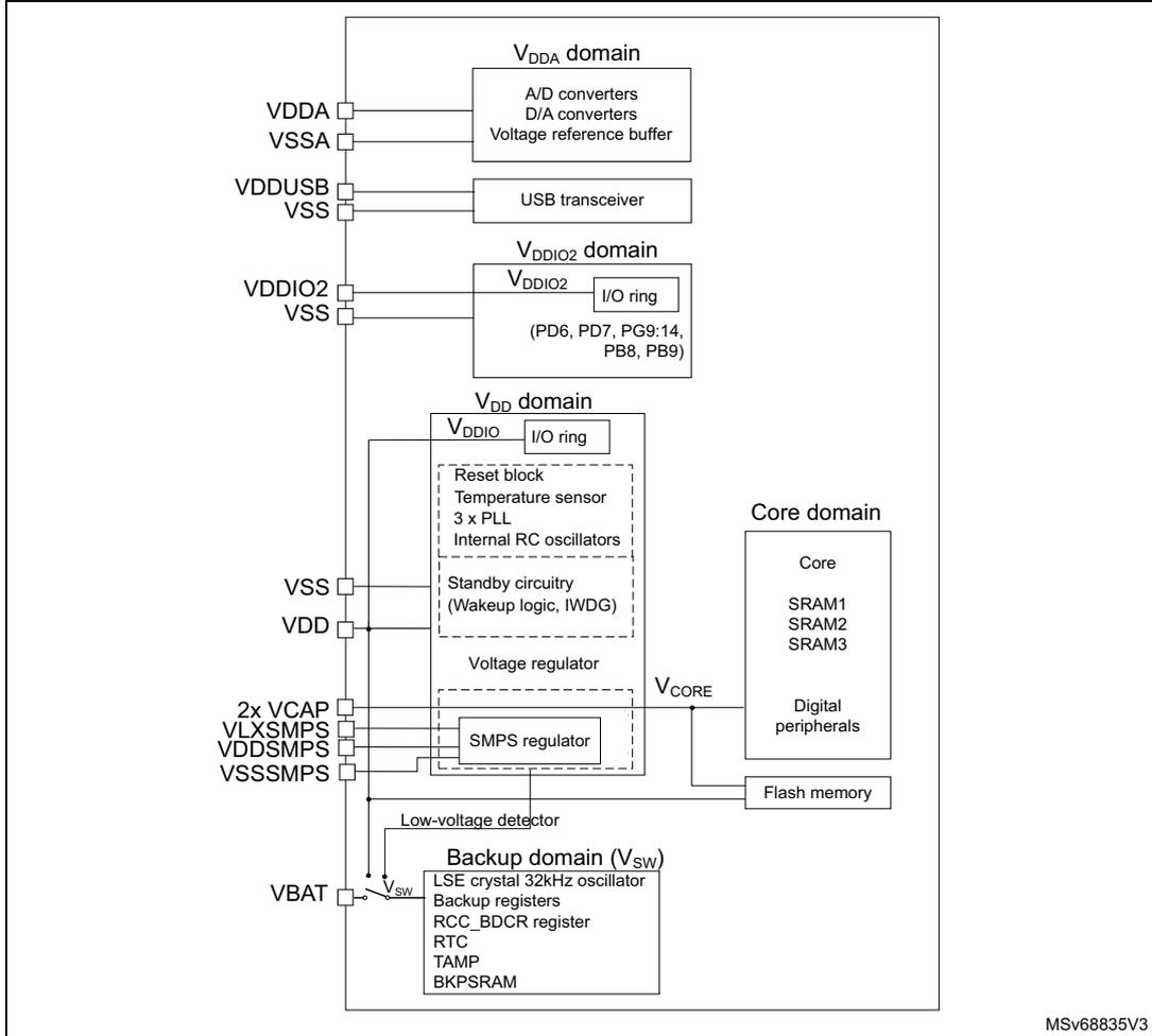
The diagram illustrates the power architecture of STM32H563/573xx devices. On the left, power pins are listed: VDDA, VSSA, VDDUSB, VSS, VDDIO2, VSS, VSS, VDD, 2x VCAP, VLXSMPS, VDDSMPS, VSSSMPS, and VBAT. These pins connect to various internal blocks: VDDA and VSSA connect to the V DDA domain containing A/D converters, D/A converters, and a voltage reference buffer. VDDUSB and VSS connect to a USB transceiver. VDDIO2 and VSS connect to the V DDIO2 domain containing an I/O ring for pins PD6, PD7, PG9:14, PB8, and PB9. VSS and VDD connect to the V DD domain, which includes an I/O ring, a Reset block, Temperature sensor, 3 x PLL, Internal RC oscillators, Standby circuitry (Wakeup logic, IWDG), and a Voltage regulator. The V DD domain also connects to the Core domain (Core, SRAM1, SRAM2, SRAM3, Digital peripherals) via V CORE . The Core domain connects to Flash memory. The VBAT pin connects to the Backup domain (V sw ) via a Low-voltage detector. The Backup domain contains an LSE crystal 32kHz oscillator, Backup registers, RCC_BDCR register, RTC, TAMP, and BKPSRAM. The SMPS regulator is connected to the V DD domain and the Core domain.
MSV68835V3
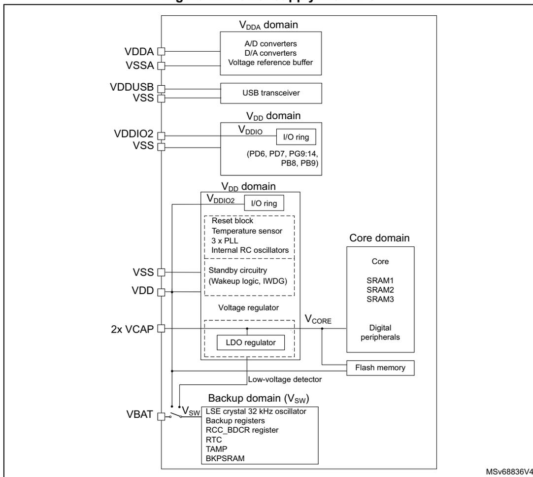
Figure 41. Power supply with LDO
10.4.1 External power supplies
The devices require a 1.71 to 3.6 V \( V_{DD} \) operating voltage supply. Several independent supplies can be provided for specific peripherals, but must not be provided without a valid operating supply on the \( V_{DD} \) pin:
- • \( V_{DD} = 1.71 \) to \( 3.6 \) V
\( V_{DD} \) is the external power supply for the I/Os, the internal regulator, and the system analog (such as reset, power management, and internal clocks). It is provided externally through the \( V_{DD} \) pins.
- • \( V_{DDA} = 1.62 \) V (ADCs, DACs) / \( 2.1 \) (VREFBUF) to \( 3.6 \) V
\( V_{DDA} \) is the external analog power supply for A/D converters, D/A converters, and voltage reference buffer. The \( V_{DDA} \) voltage level is independent from the \( V_{DD} \) voltage, and must preferably be connected to \( V_{DD} \) when these peripherals are not used.
- • \( V_{DDSMPS} = 1.71 \) to \( 3.6 \) V
\( V_{DDSMPS} \) is the external power supply for the SMPS step-down converter. It is provided externally through the \( V_{DDSMPS} \) supply pin, and must be connected to the same supply as the \( V_{DD} \) pin.
- • \( V_{LXSMPS} \) is the switched SMPS step-down converter output.
Note: The SMPS power supply pins are available only on specific packages, with SMPS step-down converter option.
- • \( V_{DDUSB} = 3.0 \) to \( 3.6 \) V
\( V_{DDUSB} \) is the external independent power supply for USB transceivers. The \( V_{DDUSB} \) voltage level is independent from the \( V_{DD} \) voltage and must preferably be connected to \( V_{DD} \) when the USB is not used.
- • \( V_{DDIO2} = 1.08 \) to \( 3.6 \) V
\( V_{DDIO2} \) is the external power supply for ten I/Os (PD6, PD7, PG9:14, PB8, PB9). The \( V_{DDIO2} \) voltage level is independent from the \( V_{DD} \) voltage and must preferably be connected to \( V_{DD} \) when those pins are not used.
- • \( V_{CAP} = 1.0 \) to \( 1.35 \) V: digital core domain supply
This power supply is independent from all the other power supplies:
- – When the voltage regulator is enabled, \( V_{CORE} \) is delivered by the internal voltage regulator.
- – When the voltage regulator is disabled, \( V_{CORE} \) is delivered by an external power supply through \( V_{CAP} \) pin, or by the SMPS
- • \( V_{BAT} = 1.2 \) to \( 3.6 \) V
\( V_{BAT} \) is the power supply when \( V_{DD} \) is not present (through power switch) for RTC, external clock 32 kHz oscillator, backup registers, and, optionally, backup SRAM.
- • \( V_{REF-} \) , \( V_{REF+} \)
\( V_{REF+} \) is the input reference voltage for ADCs and DACs. It is also the output of the internal voltage reference buffer when enabled.
\( V_{REF+} \) can be grounded when ADC and DAC are not active.
The internal voltage reference buffer supports four output voltages, configured with \( VRS \) bit in the \( VREFBUF\_CSR \) register:
- – \( V_{REF+} \sim 1.8 \) V. (requires \( V_{DDA} \geq 2.1 \) V)
- – \( V_{REF+} \sim 2.048 \) V (requires \( V_{DDA} \geq 2.4 \) V)
- – \( V_{REF+} \sim 2.5 \) V (requires \( V_{DDA} \geq 2.8 \) V)
\( V_{REF-} \) and \( V_{REF+} \) pins are not available on all packages. When not available, they are bonded to \( V_{SSA} \) and \( V_{DDA} \) , respectively.
When the \( V_{REF+} \) is double-bonded with \( V_{DDA} \) in a package, the internal voltage reference buffer is not available and must be kept disabled.
\( V_{REF-} \) must always be equal to \( V_{SSA} \) .
10.4.2 Internal regulators
The devices embed two regulators: one LDO and one SMPS (a) to provide the \( V_{CORE} \) supply for digital peripherals, SRAMs (except BKPSRAM), and embedded flash memory.
The SMPS generates this voltage on \( V_{CAP} \) (two pins), with a total external capacitor of \( 10 \mu\text{F} \) (typical), and requires an external coil of \( 2.2 \mu\text{H} \) (typical). The LDO generates this voltage on \( V_{CAP} \) , with a total external capacitance of \( 4.7 \mu\text{F} \) (typical).
Both regulators can provide four different voltages (voltage scaling), and can operate in Stop modes.
a. STM32H563/573xx devices only.
Depending on the package configuration (SMPS or LDO), the regulator is selected by hardware. SMPS and LDO regulator are exclusively selected. The supply configurations shown in Figure 38 are supported for the \( V_{CORE} \) domain supply.
Figure 42. System supply configurations
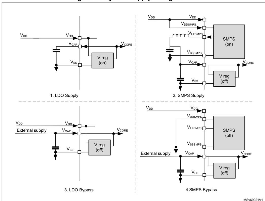
Startup with \( V_{CORE} \) provided from an external supply (Bypass)
When supplied in Bypass mode, \( V_{CORE} \) must first settle at default level ( \( \geq 1.1 \) V), before \( V_{DD} \) reaches POR threshold level.
Due to the LDO default state after power-up (enabled by default), the external \( V_{CORE} \) voltage must remain higher than 1.1 V until the LDO is disabled by software. When the LDO is disabled, the external \( V_{CORE} \) voltage can be adjusted according to the user application needs (refer to section General operating conditions of the datasheet for details on \( V_{CORE} \) level versus the maximum operating frequency).
When operating in Bypass mode, the application must adjust VOS, using bits VOS[1:0] in PWR_VOSCR register. VOS[1:0] must be set according to the external provided core voltage level and related performance.
To adjust the VOS level, the software must select sequentially the intermediate levels.
- • When increasing the performance:
- – First, voltage scaling must be incremented (for example when changing from VOS3 to VOS0, lower levels must be selected in the VOS[1:0] bits: VOS2, VOS1, and then VOS0).
- – The external voltage can be increased
- – The system frequency can be increased
- • When decreasing the performance:
- – The system frequency must be decreased
- – The external voltage must be decreased
- – The voltage scaling can be decremented (for example when changing from VOS1 to VOS3, lower levels must be selected in the VOS[1:0] bits: VOS2, and then VOS3)
10.4.3 Power-up and power-down power sequences
During power-up and power-down phases, the following power sequence requirements must be respected:
- • When V DD is below 1 V, other power supplies (V DDA , V DDIO2 , V DDUSB ) must remain below V DD + 300 mV.
- • When V DD is above 1 V, all power supplies are independent.
During the power-down phase, V DD can temporarily become lower than other supplies only if the energy provided to the MCU remains below 1 mJ. This allows external decoupling capacitors to be discharged with different time constants during the power-down transient phase.
10.4.4 Independent analog peripherals supply
To improve ADC and DAC conversion accuracy and to extend the supply flexibility, the analog peripherals have an independent power supply that can be separately filtered and shielded from noise on the PCB:
- • The voltage supply input of the analog peripherals is available on a separate V DDA pin.
- • An isolated supply ground connection is provided on the V SSA pin.
The V DDA supply voltage can be different from V DD . The presence of V DDA must be checked before enabling any of the analog peripherals supplied by V DDA (A/D converter, D/A converter, voltage reference buffer).
Power supply level monitoring is available on V DDA via AVDO bit in PWR_VMSR register.
When a single supply is used, V DDA can be externally connected to V DD through the external filtering circuit to ensure a noise-free V DDA reference voltage.
ADC and DAC reference voltage
To ensure a better accuracy on low-voltage inputs and outputs, the user can connect to V REF+ , a separate reference voltage lower than V DDA . V REF+ is the highest voltage, represented by the full scale value, for an analog input (ADC) or output (DAC) signal.
V REF+ can be provided either by an external reference or by an internal buffered voltage reference (VREFBUF). The internal voltage reference can output a configurable voltage,
namely 1.8, 2.048 or 2.4 V. The internal voltage reference can also provide the voltage to external components through VREF+ pin. Refer to the device datasheet and to Section 16: Voltage reference buffer (VREFBUF) for further information.
Note: The VREF+ and VREF- pins are not available on all packages (internally connected, respectively, to VDDA and VSSA). Do not enable the internal voltage reference buffer when an external power supply is applied to the VREF+ pin.
10.4.5 Independent I/O supply rail
Some I/Os (PD6, PD7, PG9:14, PB8, PB9) are supplied from a separate supply rail. The power supply for this rail can range from 1.08 to 3.6 V, and is provided externally through the VDDIO2 pin. The V DDIO2 voltage level is completely independent from V DD or V DDA . The VDDIO2 pin is available only for some packages. Refer to the pinout diagrams or tables in the related device datasheet(s) for the I/O list(s).
Power supply level monitoring is available on VDDIO2 via VDDIO2RDY bit in PWR_VMSR register.
10.4.6 Independent USB transceivers supply
The USB transceivers are supplied from a separate VDDUSB power supply pin. V DDUSB range is from 3.0 to 3.6 V, and is completely independent from V DD or V DDA .
Power supply level monitoring is available on VDDUSB via the USB33RDY bit in PWR_VMSR register.
Before setting USB33SV bit in PWR USB supply control register (PWR_USBSCR), check that V DDUSB is available by monitoring USB33RDY bit in PWR voltage monitor status register (PWR_VMSR). The V DD33USB supply level detector must be enabled through USB33DEN bit in PWR USB supply control register (PWR_USBSCR).
Setting USB33SV bit is mandatory to use the USB peripheral. It is used to validate the V DDUSB supply for electrical and logical isolation purposes.
10.4.7 Backup domain
To retain the content of the backup registers and to supply the RTC function when V DD is turned off, the VBAT pin can be connected to an optional backup voltage supplied by a battery or by another source.
The VBAT pin powers the RTC unit, the LSE oscillator, PI8 (a) , and PC13 to PC15 I/Os, allowing the RTC to operate even when the main power supply is turned off. The backup SRAM is optionally powered by VBAT pin when the BREN bit is set in the PWR Backup domain control register (PWR_BDCR) . The switch to the V BAT supply is controlled by the power-down reset embedded in the Reset block.
Warning:
During
\(
t_{RSTTEMPO}
\)
(temporization at V
DD
startup) or after a PDR has been detected, the power switch between V
BAT
and V
DD
remains connected to V
BAT
.
During the startup phase, if V
DD
is established in less than
a. Not available on all devices, check the datasheet.
\( t_{RSTTEMPO} \) (refer to the datasheet for its value) and \( V_{DD} > V_{BAT} + 0.6\text{ V} \) , a current may be injected into \( V_{BAT} \) through an internal diode connected between \( V_{DD} \) and the power switch ( \( V_{BAT} \) ).
If the power supply/battery connected to the VBAT pin cannot support this current injection, it is strongly recommended to connect an external low-drop diode between this power supply and the VBAT pin.
If no external battery is used in the application, it is recommended to connect \( V_{BAT} \) externally to \( V_{DD} \) with a 100 nF external ceramic decoupling capacitor.
When the Backup domain is supplied by \( V_{BAT} \) (analog switch connected to \( V_{BAT} \) ), the following pins are available:
- • PC13, PI8 (a) , PC14, and PC15, which can be configured by RTC or LSE (refer to Section 30.3: RTC functional description )
- • PC13, PI8 (a) , PA0, PA1, and PA2 when they are configured by TAMP peripheral as tamper pins.
Note: The analog switch can transfer only a limited amount of current, hence the use of GPIOs PC13 to PC15 and PI8 (a) in output mode is restricted: the frequency must be limited (check the datasheet) with a maximum load of 30 pF, and these I/Os cannot be used as a current source (for example to drive a LED).
Backup domain access
After a system reset, the Backup domain (RCC Backup domain control register RCC_BDCR, RTC registers, TAMP registers, backup registers, and backup SRAM) is protected against possible unwanted write accesses. To enable access to the Backup domain, set the DBP bit in the PWR Backup domain control register (PWR_BDCR) to enable access to the Backup domain.
Backup RAM
The Backup domain includes up to 4 Kbytes of backup RAM accessible in 32-, 16-, or 8-bit data mode. The backup RAM is supplied from the backup regulator in the Backup domain. When the backup regulator is enabled through BREN bit in the PWR_BDCR, the backup RAM content is retained in Standby and/or VBAT mode (it can be considered as an internal EEPROM if VBAT is always present).
The backup regulator can be ON or OFF, depending on if the application needs the backup RAM function in Standby or VBAT modes.
The backup RAM is read protected and mass erased when a tamper event occurs, this is to prevent confidential data (such as a cryptographic private key) from being accessed.
The backup RAM can be erased in the following ways:
- • through the flash interface after a full product state regression
- • after a tamper event
- • after a Backup domain reset
a. Not available on all devices, check the datasheet.
V BAT battery charging
When V DD is present, it is possible to charge the external battery on V BAT through an internal resistance.
The V BAT charging is done either through a 5 or a 1.5 kΩ resistor, depending upon the VBRS bit value in the PWR_BDCR register.
The battery charging is enabled by setting VBE bit in the PWR_BDCR register. It is automatically disabled in V BAT mode.
10.5 PWR system supply voltage regulation
10.5.1 SMPS and LDO embedded regulators
The devices embed two internal regulators (a) , exclusively enabled by hardware on power-on reset, depending upon package configuration. To supply the V CORE from an external source, it is possible to disable the regulator by setting the BYPASS bit in the PWR_SCCR register.
The BYPASS bit is written once after power-on reset. Written-once mechanism locks the register and any further write access is ignored. The system must be power cycled before writing a new value.
When V CORE is supplied from an external source the externally applied voltage level must be reflected in the VOSx bits in the PWR_VOSCR register refer to Startup with V CORE provided from an external supply (Bypass) .
Both regulators can provide four different voltages (voltage scaling) and can operate in Stop modes.
10.5.2 V CORE supply versus reset, voltage scaling, and low-power modes
After reset, the V CORE is in VOS3.
When exiting the Stop or Standby mode, the voltage range is the VOS3.
10.5.3 Embedded voltage regulator operating modes
There are three different power modes: Run, Stop, and Standby modes.
Run mode
The voltage regulator provides full power to the V CORE domain (core, memories, and digital peripherals). The regulator output voltage can be scaled by software to different voltage levels (VOS0, VOS1, VOS2, and VOS3) that are configured through the VOS bits in the PWR voltage scaling control register (PWR_VOSCR).
The VOS voltage scaling allows optimization of the power consumption when the system is clocked below the maximum frequency. By default, VOS3 is selected after system reset.
VOSx bits can be changed on-the-fly to adapt to the required system performance.
a. STM32H563/573xx devices only.
Stop mode
The voltage regulator supplies the \( V_{CORE} \) domain to retain the content of registers and internal memories. The regulator mode is selected through the SVOS bits in the PWR power mode control register (PWR_PMCR).
Stop mode power consumption can be further reduced using SVO4 (lower voltage level than VOS3) and even further with SVOS5.
Standby mode
The regulator is OFF and the \( V_{CORE} \) domains are powered down. The content of the registers and memories is lost except for the Standby circuitry and the Backup domain.
10.6 PWR power supply and temperature supervision
Power supply level monitoring is available on the following supplies:
- • \( V_{DD} \) via POR/PDR (see Section 10.6.1 ), BOR (see Section 10.6.2 ), and PVD monitor (see Section 10.6.3 )
- • \( V_{DDA} \) via AVD monitor see ( Section 10.6.4 )
- • \( V_{BAT} \) via \( V_{BAT} \) threshold (see Section 10.6.6 )
- • \( V_{DDIO2} \) via VDDIO2RDY bit (see Section 10.11.10 )
- • Temperature monitoring (see Section 10.6.7 )
10.6.1 Power-on reset (POR)/power-down reset (PDR)
The system has an integrated POR/PDR circuitry that ensures proper startup operation.
The system remains in reset mode when \( V_{DD} \) is below a specified \( V_{POR} \) threshold, without the need for an external reset circuit. Once the supply level is above the \( V_{POR} \) threshold, the system is taken out of reset (see Figure 39 ). For more details concerning the reset thresholds refer to the electrical characteristics section of the datasheets.
Figure 43. Power-on (POR) / power-down (PDR) reset waveform
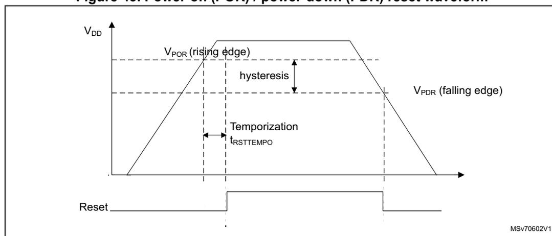
- 1. For thresholds and hysteresis values refer to the datasheets.
10.6.2 Brownout reset (BOR)
During power-on, the brownout reset (BOR) keeps the system under reset until the \( V_{DD} \) supply voltage reaches the specified \( V_{BOR} \) threshold.
The \( V_{BOR} \) threshold is configured through system option bytes:
- • BOR OFF ( \( BORH\_EN = 0 \) )
- • BOR level 1 ( \( V_{BOR1} \) )
- • BOR level 2 ( \( V_{BOR2} \) )
- • BOR level 3 ( \( V_{BOR3} \) )
By default, BOR is OFF, it can be enabled by setting BORH_EN option bit.
For more details on the brownout reset thresholds, refer to the section “ Electrical characteristics ” of the product datasheets.
A system reset is generated when the BOR is enabled and \( V_{DD} \) supply voltage drops below the selected \( V_{BOR} \) threshold.
BOR can be disabled by programming the BORH_EN option bit to 0. To disable the BOR function, \( V_{DD} \) must have been higher than the POR threshold to start the system option byte programming sequence. Once BOR is disabled, the power-down is monitored by the PDR.
Figure 44. BOR thresholds
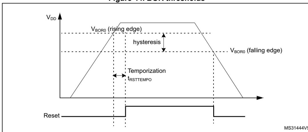
The figure is a timing diagram illustrating the Brownout Reset (BOR) function. The top graph shows the supply voltage \( V_{DD} \) over time. It features a rising edge where the voltage reaches a threshold labeled \( V_{BOR0} \) (rising edge), and a falling edge where it drops below a lower threshold labeled \( V_{BOR0} \) (falling edge). The vertical difference between these two thresholds is labeled 'hysteresis'. The bottom graph shows the 'Reset' signal. It is initially low (active reset). When \( V_{DD} \) rises and crosses the \( V_{BOR0} \) (rising edge) threshold, the Reset signal goes high (inactive) after a delay. This time interval is labeled 'Temporization \( t_{RSTTEMPO} \) '. When \( V_{DD} \) falls below the \( V_{BOR0} \) (falling edge) threshold, the Reset signal returns to low (active). The diagram is labeled with 'MS31444V5' in the bottom right corner.
10.6.3 Programmable voltage detector (PVD)
The PVD can be used to monitor the \( V_{DD} \) power supply by comparing it to a threshold selected by the PLS[2:0] bits in the PWR voltage monitor control register (PWR_VMCR) . The PVD can also be used to monitor a voltage level on the PVD_IN pin. In this case PVD_IN voltage is compared to the internal VREFINT level.
The PVD is enabled by setting the PVDE bit in PWR voltage monitor control register (PWR_VMCR) .
A PVDO flag is available in the PWR voltage monitor status register (PWR_VMSR) to indicate if \( V_{DD} \) or PVD_IN voltage is higher or lower than the PVD threshold. This event is internally connected to the EXTI and can generate an interrupt, provided it has been enabled through the EXTI registers. The rising/falling edge sensitivity of the EXTI line must be configured according to PVD output behavior. As an example, if the EXTI line is configured to rising edge sensitivity, the interrupt is generated when \( V_{DD} \) or PVD_IN voltage drops below the PVD threshold. The service routine can then start an emergency shutdown.
Figure 45. PVD thresholds
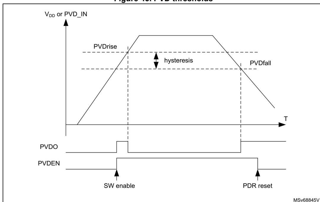
The figure is a timing diagram illustrating the PVD thresholds and hysteresis. The top graph shows the voltage level of \( V_{DD} \) or PVD_IN over time (T). It features a rising edge followed by a plateau and then a falling edge. Two horizontal dashed lines represent the threshold levels: \( PVD_{rise} \) for the rising edge and \( PVD_{fall} \) for the falling edge. The vertical gap between these two lines is labeled 'hysteresis'. Below the voltage graph, the PVDO output signal is shown. It is initially low and transitions to high when the voltage drops below \( PVD_{fall} \) . The PVDEN control signal is shown at the bottom, with a 'SW enable' pulse that goes high to enable the PVD and a 'PDR reset' pulse that goes high to reset it.
1. For thresholds and hysteresis values, refer to the datasheets.
10.6.4 Analog voltage detector (AVD)
The AVD can be used to monitor the \( V_{DDA} \) supply by comparing it to a threshold selected by the ALS[1:0] bits in the PWR voltage monitor control register (PWR_VMCR) .
The AVD is enabled by setting the AVDEN bit in PWR voltage monitor control register (PWR_VMCR) .
An AVDO flag is available in the PWR voltage monitor status register (PWR_VMSR) to indicate whether \( V_{DDA} \) is higher or lower than the AVD threshold. This event is internally connected to the EXTI and can generate an interrupt if enabled through the EXTI registers. The AVDO interrupt can be generated when \( V_{DDA} \) drops below the AVD threshold and/or
when \( V_{DDA} \) rises above the AVD threshold, depending on EXTI rising/falling edge configuration. As an example, the service routine can indicate when the \( V_{DDA} \) supply drops below a minimum level.
Figure 46. AVD thresholds
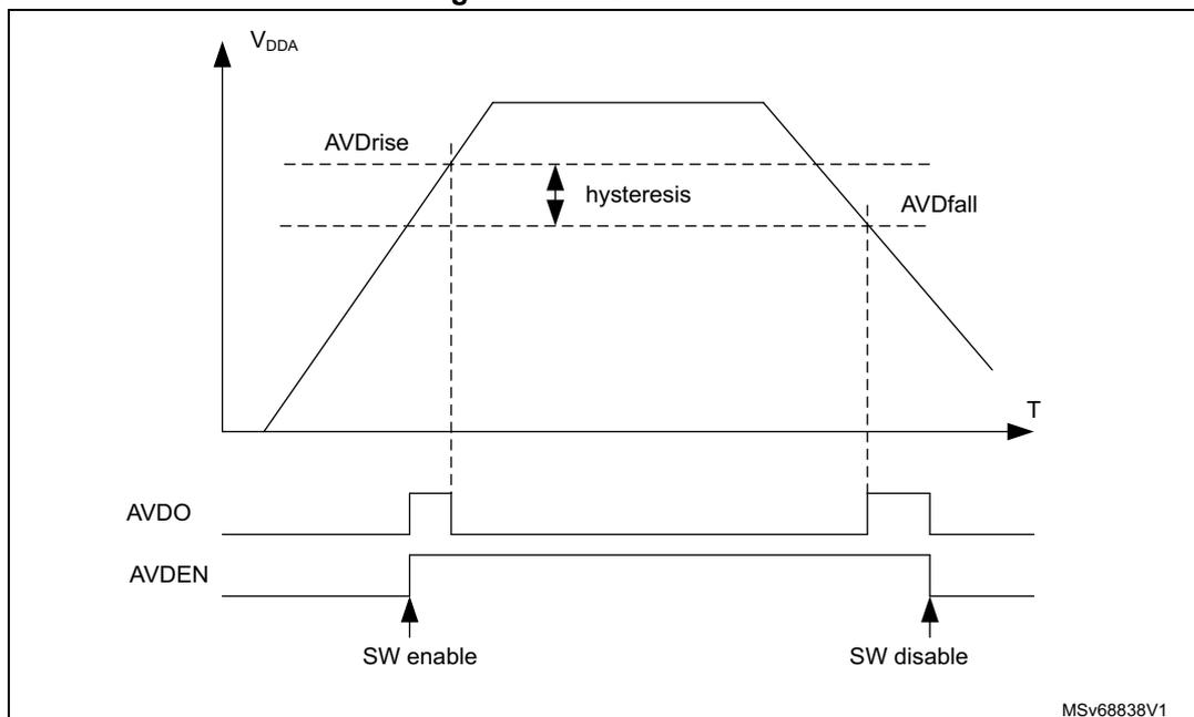
1. For thresholds and hysteresis values, refer to the datasheets.
10.6.5 \( V_{DDIO2} \) voltage monitor (IO2VM)
The IO2VM monitors the independent supply voltage \( V_{DDIO2} \) to ensure that the peripheral is in its functional supply range. The VDDIO2RDY flag (see PWR voltage monitor control register (PWR_VMCR) ) indicates whether a valid supply is present or not.
10.6.6 Backup domain voltage monitoring
In VBAT mode, the battery voltage supply (backup domain) can be monitored by comparing it with two threshold levels: \( V_{BAThigh} \) and \( V_{BATlow} \) . The VBAT supply monitoring can be enabled/disabled via MONEN bit in PWR Backup domain control register (PWR_BDCR) . When it is enabled, the battery voltage thresholds increase power consumption.
If the Backup domain voltage monitoring internal tamper is enabled in the TAMP peripheral ( \( ITAMP1E = 1 \) in the TAMP_CR1 register), a tamper event is generated when the battery voltage is above the functional range.
Note: The Backup domain voltage is \( V_{DD} \) when present, \( V_{BAT} \) otherwise.
Figure 47. VBAT thresholds
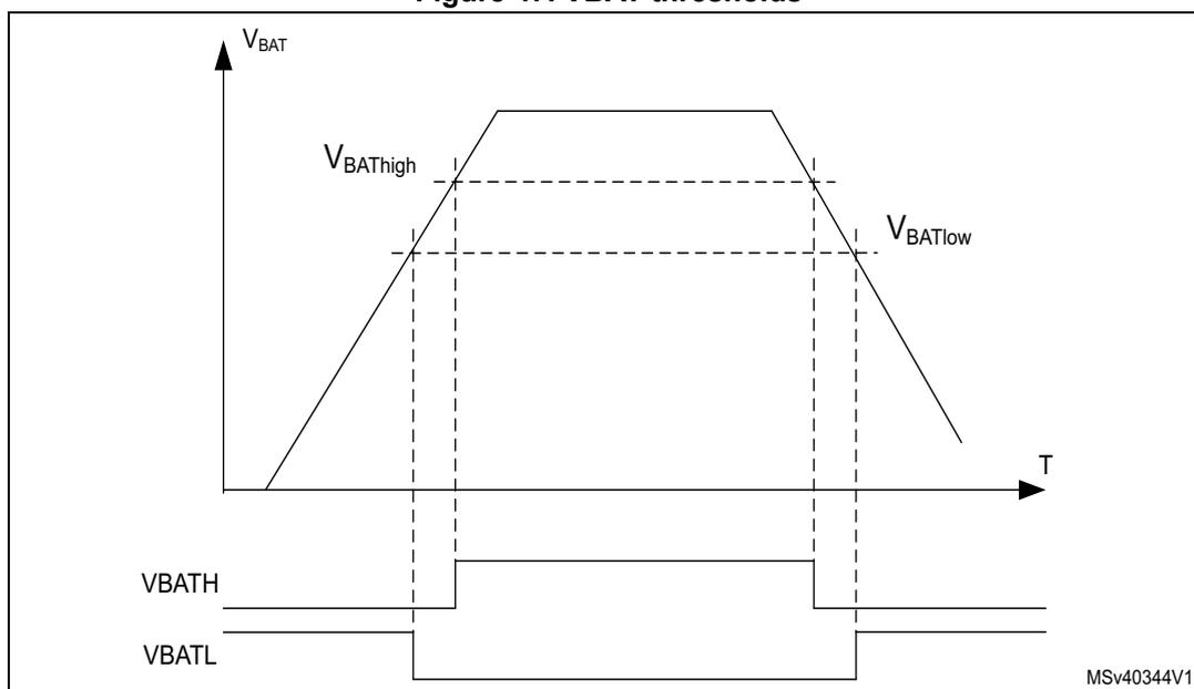
The figure illustrates the relationship between VBAT (Battery Voltage) and Temperature (T). The top graph shows VBAT on the y-axis and T on the x-axis. The VBAT curve is a trapezoid, starting at a low voltage, rising to a peak voltage (VBATHigh), and then falling back to a low voltage (VBATlow). The graph includes two horizontal dashed lines representing threshold levels: VBATH (higher threshold) and VBATL (lower threshold). The VBATH threshold is shown as a horizontal line that is high when the temperature is low and drops to a lower level when the temperature is high. The VBATL threshold is shown as a horizontal line that is low when the temperature is low and rises to a higher level when the temperature is high. The graph is labeled MSv40344V1 in the bottom right corner.
1. For thresholds and hysteresis values, refer to the datasheets.
10.6.7 Temperature monitoring
A dedicated temperature sensor cell is embedded in the power control. The junction temperature can be monitored by comparing it with two threshold levels, TEMPHigh and TEMPLow. TEMPH and TEMPL flags in the PWR Backup domain status register (PWR_BDSR) , which indicates whether the device temperature is higher or lower than the threshold. The temperature monitoring can be enabled/disabled via MONEN bit in PWR Backup domain control register (PWR_BDCR) .
When enabled, the temperature thresholds increase power consumption. As an example the levels may be used to trigger a routine to perform temperature control tasks.
If the temperature monitoring internal tamper is enabled in the TAMP peripheral (ITAMP2E = 1 in the TAMP_CR1 register), a tamper event is generated when the temperature is above or below the functional range.
TEMPH and TEMPL wake-up interrupts are available on the RTC tamper signals (see Section 24: Tamper and backup registers (TAMP) ).
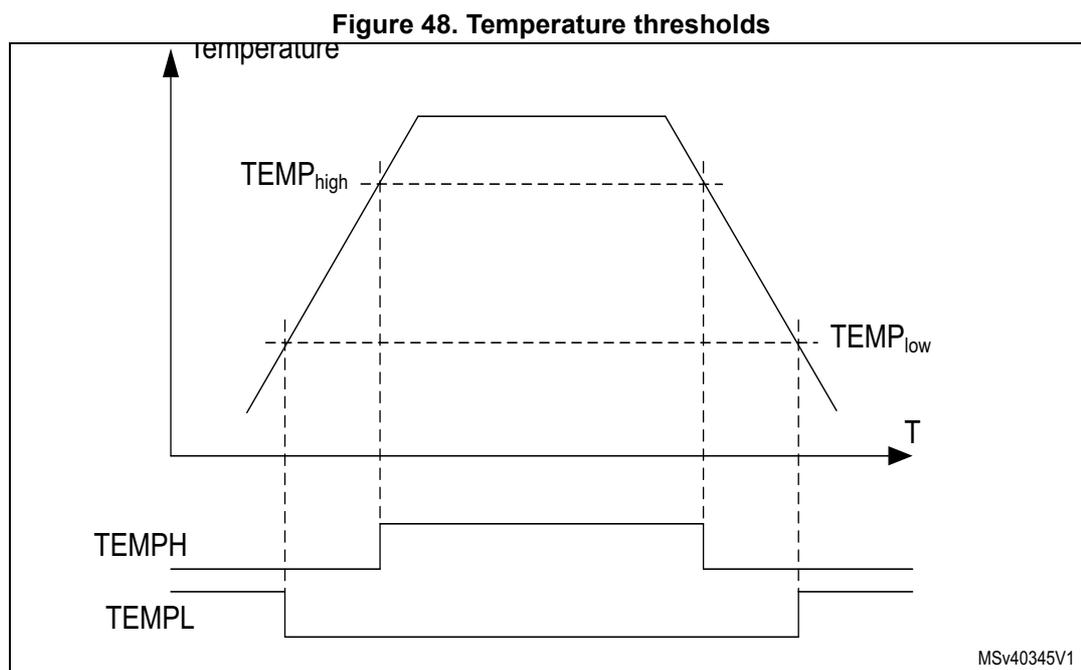
Figure 48. Temperature thresholds
1. For thresholds and hysteresis values, refer to the datasheets.
10.7 PWR management
10.7.1 Voltage scaling
The voltage regulator supporting voltage scaling with the following features:
- • Run mode voltage scaling
- – VOS0: scale 0
- – VOS1: scale 1
- – VOS2: scale 2
- – VOS3: scale 3
- • Stop mode voltage scaling
- – SVOS3: scale 3
- – SVOS4: scale 4
- – SVOS5: scale 5
For more details on voltage scaling values, refer to the product datasheets.
After reset, the system starts on the lowest Run mode voltage scaling (VOS3). The voltage scaling can be changed on-the-fly by software by programming VOS bits in PWR_VOSCR register, according to the required system performance. When exiting from the Stop mode or Standby mode, the Run mode voltage scaling is reset to the default VOS3 value.
Before entering Stop mode, the software must preselect the SVOS level in the PWR_PMCR registers. The Stop mode voltage scaling for SVOS4 and SVOS5 also sets the voltage regulator in Low-power mode, to further reduce power consumption.
10.7.2 Power management examples
Figure 49. Dynamic voltage scaling in Run mode
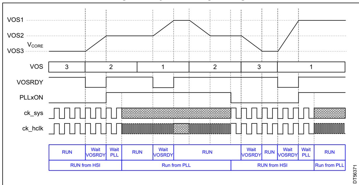
The diagram shows the following signals and states over time:
- VOS1, VOS2, VOS3: Voltage scaling levels. VOS3 is initially selected, then VOS2, then VOS1, then VOS2 again, then VOS3, and finally VOS1.
- V CORE : The supply voltage, which follows the selected VOS level.
- VOSRDY: A flag that goes high when the V CORE supply reaches the required level for the selected VOS.
- PLLxON: A signal that is high when the PLL is enabled.
- ck_sys: The system clock. It is initially the HSI clock, then switches to the PLL clock when PLLxON is high and VOSRDY is high. It switches back to the HSI clock when PLLxON is low.
- ck_hclk: The high-speed clock, which is always active.
- System States:
- RUN: Initial state with HSI clock and VOS3.
- Wait VOSRDY: Entered when VOS is changed to VOS2.
- Wait PLL: Entered when PLL is enabled.
- RUN: State with PLL clock and VOS2.
- Wait VOSRDY: Entered when VOS is changed to VOS1.
- RUN: State with PLL clock and VOS1.
- Wait VOSRDY: Entered when VOS is changed to VOS2.
- RUN: State with PLL clock and VOS2.
- Wait VOSRDY: Entered when VOS is changed to VOS3.
- Wait PLL: Entered when PLL is disabled.
- RUN: Final state with HSI clock and VOS3.
- Bottom Labels:
- RUN from HSI: Corresponds to the initial RUN state.
- Run from PLL: Corresponds to the RUN states with PLL clock.
- RUN from HSI: Corresponds to the state after PLL is disabled.
- Run from PLL: Corresponds to the final RUN state.
Figure 45 illustrates the following system operation sequence example:
- 1. After reset, the system starts from HSI with VOS3.
- 2. The system performance is increased to a medium-speed clock from the PLL with voltage scaling VOS2. To do this:
- a) Program the voltage scaling to VOS2.
- b) Once the V CORE supply has reached the required level indicated by VOSRDY, increase the clock frequency by enabling the PLL.
- c) Once the PLL is locked, switch the system clock.
- 3. The system performance is increased to high-speed clock from the PLL with voltage scaling VOS1. To do this:
- a) Program the voltage scaling to VOS1.
- b) Once the V CORE supply has reached the required level indicated by VOSRDY, increase the clock frequency.
- 4. The system performance is reduced to a medium-speed clock with voltage scaling VOS2. To do this:
- a) First decrease the system frequency.
- b) Then decrease the voltage scaling to VOS2.
- 5. The next step is to reduce the system performance to the HSI clock with voltage scaling VOS3. To do this:
- a) Switch the clock to HSI.
- b) Disable the PLL.
- c) Decrease the voltage scaling to VOS3.
- 6. The system performance can then be increased to high-speed clock from the PLL. To do this:
- a) Program the voltage scaling to VOS1.
- b) Once the \( V_{CORE} \) supply has reached the required level indicated by VOSRDY, increase the clock frequency by enabling the PLL.
- c) Once the PLL is locked, switch the system clock.
When the system performance (clock frequency) is changed, VOS must be set accordingly, otherwise the system can be unreliable.
10.8 Power modes
By default, the microcontroller is in Run mode after a system or a power reset. Several low-power modes are available to reduce consumption when there is no need to keep the CPU running, for example when waiting for an external event. The user can select the mode that gives the best compromise between low-power consumption, short startup time, and wake-up sources.
The device features the following low-power modes:
- • Sleep mode
CPU clock off, peripherals such as NVIC and SysTick can run and wake-up the CPU when an interrupt or an event occurs. Refer to Section 10.8.4 .
- • Stop mode
Achieves the lowest power consumption, while retaining the content of SRAM and registers. All clocks in the core domain are stopped. The PLL, the HSE crystal oscillators, HSI (except if HSIKERON is set), HSI48 and CSI RC (except if CSIKERON is set) are disabled. The LSE or LSI is still running.
The RTC can remain active (Stop mode with RTC, Stop mode without RTC).
The system clock when exiting from Stop mode can be either HSI up to 64 MHz or CSI, depending on software configuration.
Refer to Section 10.8.5 .
- • Standby mode
This mode achieves the lowest power consumption with BOR. The internal regulator is switched off so that the core domain is powered off. The PLL, the HSI RC, HSI48, the CSI RC, and the HSE crystal oscillators are also switched off.
The RTC can remain active (Standby mode with RTC, Standby mode without RTC).
The brownout reset (BOR) remains active.
The state of the I/O (except I/Os used by standby mode) during Standby mode can be retained.
After entering Standby mode, SRAMs and register contents are lost except for registers and backup SRAM in the Backup domain and Standby circuitry.
The device exits Standby mode when an external reset (NRST pin), an IWDG reset, WKUP pin event (configurable rising or falling edge), an RTC event occurs (alarm, periodic wake-up, timestamp), or a tamper detection. The tamper detection can be
raised either due to external pins or due to an internal failure detection.
The system clock after wake-up is HSI at 32 MHz.
Refer to Section 10.8.6 .
Table 97 shows the power modes overview.
Table 101. Low-power mode summary
| Mode name | Entry | Wake-up source (1) | Wake-up system clock | Effect on clocks | Voltage regulators |
|---|---|---|---|---|---|
| Sleep (Sleep-now or Sleep-on-exit) | WFI or Return from ISR | Any interrupt | Same as before entering Sleep mode | – CPU clock OFF – No effect on other clocks or analog clock sources | VOS3, VOS2, VOS1, or VOS0 |
| WFE | Wake-up event | ||||
| Stop | LPMS = 0 + SLEEPDEEP bit + WFI or Return from ISR or WFE | – Any EXTI line (configured in the EXTI registers) – Specific peripherals events (2) | – CSI when STOPWUCK = 1 in RCC_CFGR – HSI with the frequency before entering Stop mode, up to 64 MHz, when STOPWUCK = 0 | – All clocks OFF except LSI and LSE – HSI or CSI can be enabled temporarily when requested by software | SVOS3, SVOS4, or SVOS5 |
| Standby | LPMS = 1 + SLEEPDEEP bit + WFI or Return from ISR or WFE | WKUP pin edge, RTC event, IWDG reset, external reset in NRST pin | HSI clock at 64 MHz | All clocks OFF except LSI and LSE | OFF |
1. Refer to Table 98 .
2. Peripherals able to wake-up the system from Stop mode (possible only when SVOS3 is selected before entering Stop mode).
Table 102. Functionalities depending on the working mode (1)
| Peripheral | Run | Sleep | Stop | Standby | VBAT | ||||
|---|---|---|---|---|---|---|---|---|---|
| Available | Wake-up capability | Available | Wake-up capability | ||||||
| SVOS3 | SVOS4 | SVOS5 | |||||||
| CPU | Y | - | - | - | - | - | - | - | - |
| Flash memory | O | O | (2) | - | - | - | - | - | - |
| SRAM1 | Y (3) | Y (3) | O (4) | - | - | - | - | - | - |
| SRAM2 | Y (3) | Y (3) | O (4) | - | - | - | - | - | - |
| SRAM3 | Y (3) | Y (3) | O (4) | - | - | - | - | - | - |
| BKPSRAM | O | O | O | - | - | - | O | - | O |
| FMC | O | O | - | - | - | - | - | - | - |
| OCTOSPI1 | O | O | - | - | - | - | - | - | - |
| Backup registers | Y | Y | Y | - | - | - | Y | - | Y |
| Brownout reset (BOR) | Y | Y | Y | - | - | - | Y | - | - |
| Peripheral | Run | Sleep | Stop | Standby | VBAT | ||||
|---|---|---|---|---|---|---|---|---|---|
| Available | Wake-up capability | Available | Wake-up capability | ||||||
| SVOS3 | SVOS4 | SVOS5 | |||||||
| Programmable voltage detector (PVD) | O | O | O | O | O | O | - | - | - |
| Analog voltage detector (AVD) | O | O | O | O | O | O | - | - | - |
| GPDMA | O | O | - | - | - | - | - | - | - |
| High-speed internal (HSI) | O | O | - | - | - | - | - | - | - |
| Oscillator HSI48 | O | O | - | - | - | - | - | - | - |
| High-speed external (HSE) | O | O | - | - | - | - | - | - | - |
| Low-speed internal (LSI) | O | O | O | O | - | - | O | - | - |
| Low-speed external (LSE) | O | O | O | - | - | - | O | - | O |
| Low-power RC oscillator (CSI) | O | O | - | - | - | - | - | - | - |
| Clock security system (CSS) | O | O | - | - | - | - | - | - | - |
| Clock security system on LSE | O | O | O | O | O (5) | O (5) | O | O | - |
| Backup domain voltage and temperature monitoring | O | O | O | O | O (5) | O (5) | O | O | O |
| RTC/TAMP | O | O | O | O | O | O | O | O | O |
| Number of TAMP tamper pins | 8 | 8 | 8 | - | - | - | 4 | - | 2 |
| USB FS, UCPD | O | O | O | O | - | - | - | - | - |
| USARTx | O | O | O | O | - | - | - | - | - |
| Low-power UART (LPUART) | O | O | O | O | - | - | - | - | - |
| I2Cx | O | O | O | O | - | - | - | - | - |
| I3Cx | O | O | O | O | - | - | - | - | - |
| HDMI_CEC | O | O | O | O | - | - | - | - | - |
| SPIx | O | O | O | O | - | - | - | - | - |
| FDCANx | O | O | - | - | - | - | - | - | - |
| SDMMCx | O | O | - | - | - | - | - | - | - |
| Ethernet | O | O | O | O | - | - | - | - | - |
| SAIx | O | O | - | - | - | - | - | - | - |
| ADCx (x = 1,2) | O | O | - | - | - | - | - | - | - |
| DAC1 (2 converters) | O | O | O | - | - | - | - | - | - |
| VREFBUF | O | O | O | - | - | - | - | - | - |
| Temperature sensor (DTS) | O | O | O | O | - | - | - | - | - |
| Timers (TIMx) | O | O | - | - | - | - | - | - | - |
| Low-power timer LPTIMx | O | O | O | O | - | - | - | - | - |
Table 102. Functionalities depending on the working mode (1) (continued)
| Peripheral | Run | Sleep | Stop | Standby | VBAT | ||||
|---|---|---|---|---|---|---|---|---|---|
| Available | Wake-up capability | Available | Wake-up capability | ||||||
| SVOS3 | SVOS4 | SVOS5 | |||||||
| Independent watchdog (IWDG) | O | O | O | O | O (5) | O (5) | O | O | - |
| Window watchdog (WWDG) | O | O | - | - | - | - | - | - | - |
| SysTick timer (SYSTICK) | O | O | O | - | - | - | - | - | - |
| Digital camera interface (DCMI) | O | O | - | - | - | - | - | - | - |
| Parallel synchronous slave interface (PSSI) | O | O | - | - | - | - | - | - | - |
| CORDIC coprocessor (CORDIC) | O | O | - | - | - | - | - | - | - |
| Filter mathematical accelerator (FMAC) | O | O | - | - | - | - | - | - | - |
| Random number generator (RNG) | O | O | - | - | - | - | - | - | - |
| AES and secure AES (AES, SAES) | O | O | - | - | - | - | - | - | - |
| Public key accelerator (PKA) | O | O | - | - | - | - | - | - | - |
| On-the-fly decryption (OTFDEC) | O | O | - | - | - | - | - | - | - |
| HASH accelerator | O | O | - | - | - | - | - | - | - |
| CRC calculation unit | O | O | - | - | - | - | - | - | - |
| GPIOs | O | O | - | - | - | - | O (6) | O (7) | - |
| EXTI | O | O | O | O | O | O | - | - | - |
- 1. Y = yes (enabled). O = optional (disabled by default, can be enabled by software). - = not available.
HSI or CSI are available as kernel clock for peripherals only in SVOS3. - 2. The memory can be configured in Low-power mode. By default, it is not in Low-power mode during Stop (SVOS3, SVOS4).
- 3. The SRAM clock can be gated on or off independently. By default clock is enabled in Run and Sleep modes.
- 4. The SRAMs can be powered on or off independently. By default, they are not in Power-off mode during Stop.
- 5. Wake-up with internal tamper.
- 6. GPIOs state can be retained during Standby mode. By default GPIOs states are not retained.
- 7. 8 pins are capable of wake-up from Standby mode: PA0, PA2, PB7, PC1, PC13, PD2, PD3 and PI8 (not available on all devices, check the datasheet).
In addition, the power consumption in Run mode can be reduced by slowing down the system clocks, configuring voltage scaling to lower power ranges, and by gating the clocks to the APB and AHB peripherals when they are not used.
Debug mode
By default, the debug connection is lost if the application puts the MCU in Stop or Standby mode while the debug features are used. This is due to the fact that the Cortex-M33 core is no longer clocked.
However, by setting some configuration bits in the DBGMCU control registers, the software can be debugged even when using the low-power modes extensively. For more details, refer to Section 75.2.5: Debug and low-power modes .
10.8.1 Slowing down system clocks
In Run mode, the speed of the system clocks (SYSCLK, HCLK, PCLK) can be reduced by programming the prescaler registers. These prescalers can also be used to slow down the peripherals before entering the Sleep mode.
For more details, refer to Section 11: Reset and clock control (RCC) .
10.8.2 Peripheral clock gating
In Run mode, the HCLK and PCLK for individual peripherals and memories can be stopped at any time to reduce the power consumption.
To further reduce the power consumption in Sleep mode, the peripheral clocks can be disabled before executing the WFI or WFE instructions.
The peripheral clock gating is controlled by the RCC_AHBxENR and RCC_APBxENR registers.
Disabling the peripherals clocks in Sleep mode can be performed automatically by resetting the corresponding bit in the RCC_AHBxLPENR and RCC_APBxLPENR registers.
10.8.3 Low-power modes
Entering into a low-power mode
The MCU enters in low-power modes by executing the WFI (wait for interrupt), or WFE (wait for event) instructions, or when the SLEEPONEXIT bit in the Cortex-M33 system control register is set on Return from ISR.
Entering into a low-power mode through WFI or WFE is executed only if no interrupt is pending or no event is pending.
Exiting a low-power mode
The MCU exits the Sleep or Stop mode according to how the low-power mode was entered:
- • If the WFI instruction or Return from ISR was used to enter the low-power mode, any peripheral interrupt acknowledged by the NVIC can wake up the device.
- • If the WFE instruction is used to enter the low-power mode, the MCU exits the low-power mode as soon as an event occurs. The wake-up event can be generated either by:
- – an NVIC IRQ interrupt:
- > When SEVONPEND = 0 in the Cortex-M33 system control register
By enabling an interrupt in the peripheral control register and in the NVIC. When the MCU resumes from WFE, the peripheral interrupt pending bit and the NVIC peripheral IRQ channel pending bit (in the NVIC interrupt clear pending register) must be cleared. Only NVIC interrupts with high enough priority can wake up and interrupt the MCU. - > When SEVONPEND = 1 in the Cortex-M33 system control register
By enabling an interrupt in the peripheral control register and optionally in the NVIC. When the MCU resumes from WFE, the peripheral interrupt pending bit and when enabled the NVIC peripheral IRQ channel pending bit (in the NVIC interrupt clear pending register) must be cleared. All NVIC interrupts
- > When SEVONPEND = 0 in the Cortex-M33 system control register
- – an NVIC IRQ interrupt:
wake up the MCU, even the disabled ones. Only enabled NVIC interrupts with high enough priority can wake up and interrupt the MCU.
- – an event:
- > Configuring an EXTI line in event mode. When the CPU resumes from WFE, it is not necessary to clear the EXTI peripheral interrupt pending bit or the NVIC IRQ channel pending bit, as the pending bits corresponding to the event line are not set. It may be necessary to clear the interrupt flag in the peripheral.
The MCU exits Standby mode through an external reset (NRST pin), an IWDG reset, a rising edge on one of the enabled WKUPx pins or a RTC/TAMP event (see Figure 624: RTC block diagram ).
After waking up from Standby mode, the program execution restarts in the same way as after a reset (boot pin sampling, option bytes loading, reset vector is fetched).
Caution: When the device is in Stop mode, a peripheral interrupt powers on an internal oscillator. The corresponding NVIC interrupt channel must be enabled to allow the interrupt to exit the device from Stop mode. It is not allowed to disable a peripheral interrupt by disabling only the NVIC channel while keeping the peripheral interrupt enable, as the device could remain in Stop mode with clock ON.
10.8.4 Sleep mode
I/O states in Sleep mode
In Sleep mode, all I/O pins keep the same state as in Run mode.
Entering the Sleep mode
The MCU enters the Sleep mode as described in Entering into a low-power mode , when the SLEEPDEEP bit in the Cortex-M33 system control register is clear (see the table below for details on how to enter the Sleep mode).
Exiting the Sleep mode
The MCU exits the Sleep mode as described in Exiting a low-power mode (see the table below for details on how to exit the Sleep mode).
Table 103. Sleep mode
| Sleep mode | Description |
|---|---|
| Mode entry | WFI (wait for interrupt) or WFE (wait for event) while:
On return from ISR while:
|
| Sleep mode | Description |
|---|---|
| Mode exit | If WFI or Return from ISR was used for entry Interrupt (see Table 146: STM32H562/563/573xx vector table ) If WFE was used for entry and SEVONPEND = 0: Wake-up event (see Section 18.3: EXTI functional description ) If WFE was used for entry and SEVONPEND = 1: Interrupt even when disabled in NVIC (see Table 146: STM32H562/563/573xx vector table ) or wake-up event (see Section 18.3: EXTI functional description ) |
| Wake-up latency | None |
10.8.5 Stop mode
The Stop mode is based on the Cortex-M33 DeepSleep mode combined with the peripheral clock gating. The voltage regulator is configured by SVOSx bits (the selected SVOS4 and SVOS5 levels add an additional startup delay when exiting from system Stop mode). In Stop mode, all clocks in the core domain are stopped. The PLL, HSI, HSI48, CSI and HSE oscillators are disabled.
It is possible to keep the HSI or CSI clock enabled during Stop mode, to be quickly available as kernel clock for peripherals.
All SRAMs and register contents are preserved, but the SRAMs can be totally or partially switched off to further reduced consumption. The user can select which memory is discarded during Stop mode by means of xxSO bits in PWR_PMCR registers.
Table 104. Memory shut-off block selection| Selection bit | Shut-off block in Stop mode | STM32H523/533xx | STM32H562/563/573xx |
|---|---|---|---|
| SRAM1SO | AHB SRAM1 | X | X |
| SRAM2_48SO | AHB SRAM2 48-Kbyte | X | X |
| SRAM2_16SO | AHB SRAM2 16-Kbyte | - | X |
| SRAM2_H16SO | AHB SRAM2 16-Kbyte | X | - |
| SRAM2_L16SO | AHB SRAM2 16-Kbyte | X | - |
| SRAM3SO | AHB SRAM3 | X | |
| ETHERNETSO | ETHERNET RAM | - | X |
The BOR is always available in Stop mode.
I/O states in Stop mode
In the Stop mode, all I/O pins keep the same state as in the Run mode.
Entering the Stop mode
The MCU enters the Stop mode as described in Entering into a low-power mode , when the SLEEPDEEP bit in the Cortex-M33 system control register is set (see Table 101 for details on how to enter the Stop mode).
If the flash memory programming is ongoing, the Stop mode entry is delayed until the memory access is finished.
If an access to the APB domain is ongoing, the Stop mode entry is delayed until the APB access is finished.
In Stop mode, the following features can be selected by programming the individual control bits:
- • The independent watchdog (IWDG) is started by writing to its key register or by hardware option. Once started, it can be stopped only by a reset (see Section 44.4: IWDG functional description ).
- • The real-time clock (RTC) is configured by the RTCEN bit in the RCC backup domain control register (RCC_BDCR) .
- • The internal RC oscillator LSI clock is configured by the LSION bit in RCC_BDCR.
- • The external 32.768 kHz oscillator (LSE) is configured by the LSEON bit in RCC_BDCR.
The AVD and the PVD can be used in Stop mode. If they are not needed, they must be disabled by software to save their power consumptions.
The ADCx (x = 1, 2), the DAC1 (two channels), the temperature sensor, and the VREFBUF can consume power during the Stop mode, unless they are disabled before entering this mode.
Exiting the Stop mode
The MCU exits Stop mode by enabling an EXTI interrupt or event depending on how the low-power mode was entered. Some peripherals are able to wake up the system (refer to Table 138: EXTI line connections ) from Stop mode, this is only possible when SVOS3 is selected before entering Stop mode.
Note: When wake-up from Stop with peripherals is needed, SVOS3 must be selected.
When exiting Stop mode by issuing an interrupt or a wake-up event, CSI is selected as system clock if bit STOPWUCK is set in RCC clock configuration register 1 (RCC_CFGR). The HSI oscillator is selected as system clock if STOPWUCK is cleared. The wake-up time is shorter when CSI is selected as wake-up system clock. The HSI selection allows a wake-up at higher frequency (up to 64 MHz).
The MCU exits Stop mode by enabling an EXTI interrupt or event depending on how the low-power mode was entered.
When exiting the Stop mode, the MCU is in Run mode, VOS3.
Table 105. Stop mode
| Stop mode | Description |
|---|---|
| Mode entry | WFI (wait for interrupt) or WFE (wait for event) while:
On Return from ISR while:
Note: To enter Stop mode, all EXTI line pending bits (in the EXTI rising edge pending register 2 (EXTI_RPR2)), and the peripheral flags generating wake-up interrupts must be cleared. Otherwise, the Stop mode entry procedure is ignored and the program execution continues. |
| Mode exit | If WFI or Return from ISR was used for entry:
If WFE was used for entry and SEVONPEND = 0:
If WFE was used for entry and SEVONPEND = 1:
Note: All peripheral clocks must be enabled to allow this peripheral to generate a wake-up from Stop interrupt ([PERIPH]JEN and [PERIPH]LPEN bits must be set in the RCC, and a functional independent clock must be selected). |
| Wake-up latency | Longest wake-up time between: HSI or CSI wake-up time and flash memory wake-up time from Stop mode. |
10.8.6 Standby mode
The lowest power mode in which the BOR is active is the Standby mode. It is based on the Cortex-M33 DeepSleep mode, with the voltage regulators disabled. The PLL, HSI, HSI48, CSI, and HSE oscillators are also switched off.
The SRAMs and register contents are lost except for registers in the Backup domain and Standby circuitry (see Figure 36 ).
The BOR is always available in Standby mode.
I/O states in Standby mode
In the Standby mode, the I/Os are by default in floating state. If the IORETEN bit in the
PWR_IORETR
register is set, the I/Os output state is retained. I/O retention mode is enabled for all I/Os except those supporting the standby functionality and JTAG I/Os (PA13, PA14, PA15, and PB4). When entering into Standby mode, the state of the output is sampled, and pull-up or pull-down resistor are set to maintain the I/O output during Standby mode.
If the JTAGIORETEN bit in the
PWR_IORETR
register is set, the I/Os output state is retained. I/O retention mode is enabled for PA13, PA14, PA15, and PB4 (default JTAG pull-up/pull-down after wake-up is not enabled).
Figure 50. I/O states in Standby mode
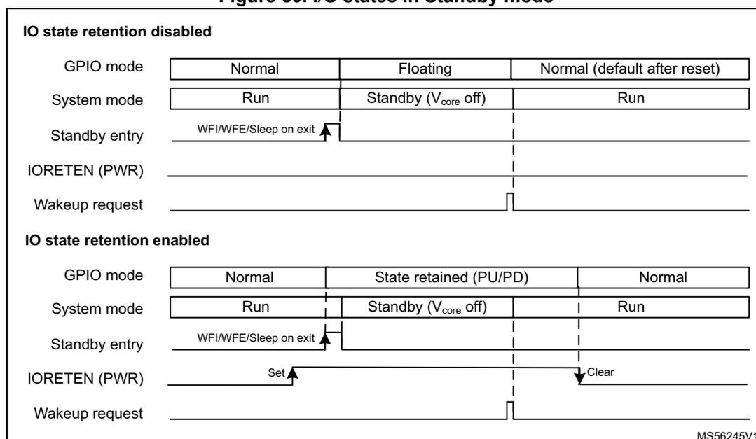
IO state retention disabled
| GPIO mode | Normal | Floating | Normal (default after reset) |
| System mode | Run | Standby (V core off) | Run |
| Standby entry | WFI/WFE/Sleep on exit (rising edge at entry) | ||
| IORETEN (PWR) | Low | ||
| Wakeup request | Pulse (at end of Standby) | ||
IO state retention enabled
| GPIO mode | Normal | State retained (PU/PD) | Normal |
| System mode | Run | Standby (V core off) | Run |
| Standby entry | WFI/WFE/Sleep on exit (rising edge at entry) | ||
| IORETEN (PWR) | Set (rising edge) | High | Clear (falling edge) |
| Wakeup request | Pulse (at end of Standby) | ||
MS56245V1
After wake-up from Standby mode, as long as IORETEN (or JTAGIORETEN for JTAG I/Os) is set, the retained stated (pull-up/pull-down) remains applied.
The GPIO pin state before standby can be identified with
GPIO_IDR
register (when both GPIO port clock and input buffer are enabled).
The application can release the I/O state (clear the retained Pull-up/Pull-down) by clearing the IORETEN (or JTAGIORETEN for JTAG IOs) bit, before or after reconfiguring the GPIOs and related peripherals. The GPIOs can then be configured in a known state before releasing the retained state.
The RTC outputs on PC13 and PI8 (a) are functional in Standby mode. PC14 and PC15 used for LSE are also functional. Eight wake-up (WKUPx, x = 1 to 8) and four RTC tamper pins are available.
Entering Standby mode
The MCU enters the Standby mode as described in Entering into a low-power mode , when
- a. Not available on all devices, check the datasheet.
the SLEEPDEEP bit in the Cortex-M33 system control register is set (see Table 102 for details on how to enter Standby mode).
In Standby mode, the following features can be selected by programming individual control bits:
- • The independent watchdog (IWDG) is started by writing to its Key register or by hardware option. Once started, it can be stopped only by a reset (see Section 44.4: IWDG functional description ).
- • The real-time clock (RTC) is configured by the RTCEN bit in RCC backup domain control register (RCC_BDCR) .
- • The internal RC oscillator LSI clock, is configured by the LSION bit in RCC_BDCR.
- • The external 32.768 kHz oscillator (LSE) is configured by the LSEON bit in RCC_BDCR.
- • The I/Os retention is configured by the IORETEN bit in the PWR_IORETR register.
Exiting Standby mode
The MCU exits the Standby mode as described in Exiting a low-power mode . The SBF status flag in the PWR status register (PWR_PMSR) indicates that the MCU was in Standby mode. All registers are reset after wake-up from Standby except for PWR Backup domain control register (PWR_BDCR) and PWR I/O retention register (PWR_IORETR) (see Table 106 for more details on how to exit Standby mode).
When exiting Standby mode, I/Os output state that were retained during Standby through IORETEN bit, keep this configuration upon exiting Standby mode until the IORETEN bit in PWR_IORETR register is cleared. Once IORETEN is cleared, the I/Os are configured to their reset values, or to the pull-up/pull-down state according to the GPIOx_PUPDR registers.
For I/Os, with a pull-up or pull-down predefined after reset (some JTAG/SWD I/Os), in case those pull-up or pull-down are different from the retained values during Standby, both a pull-down and pull-up are applied until IORETEN is cleared, releasing the retained value.
Also in case the GPIOx_PUPDR values programmed after exiting from Standby are different from the retained values during Standby, both a pull-down and pull-up are applied until IORETEN is cleared, releasing the retained value.
Table 106. Standby mode
| Standby mode | Description |
|---|---|
| Mode entry | WFI (wait for interrupt) or WFE (wait for event) while:
|
| Mode exit | WKUPx pin edge, RTC event, external Reset in NRST pin, IWDG Reset, BOR reset |
| Wake-up latency | Reset phase |
10.8.7 Power modes output pins
In order to help the debug, three signals are available as device pins alternate functions:
- •
CSLEEP
When set, CSLEEP indicates that the system is in Sleep mode: WFI or WFE has been executed.
When cleared, CSLEEP indicates that the system is in Run mode. - •
CDSTOP
When set, CDSTOP indicates that the system is in CStop mode, meaning that the following conditions are fulfilled:- – WFI or WFE has been executed with CPU SLEEPDEEP = 1.
- – No AHB/APB clock is running.
The table below explains the MCU power mode depending on these signals states.
Table 107. Power modes output states versus MCU power modes
| CSLEEP | CDSTOP | MCU power modes (1) |
|---|---|---|
| 0 | 0 | Run mode |
| 1 | 0 | Sleep mode or Stop mode, with AHB/APB clocks running |
| 1 | 1 | Stop mode |
- 1. CSLEEP and CDSTOP are generated in core domain, consequently they are not driven in Standby mode.
10.9 PWR security and privileged protection
10.9.1 PWR security protection
When the TrustZone security is activated by the TZEN option byte in the flash memory option byte configuration register, some PWR register fields can be secured against non-secure access.
The PWR TrustZone security allows the following features to be secured through the PWR_SECCFGR register:
- • Low-power mode
- • Wake-up (WKUP) pins
- • Voltage detection and monitoring
- • VBAT mode
- • I/Os retention configuration
Other PWR configuration bits are secure when:
- • The system clock selection is secure in RCC: the voltage scaling (VOS) configuration is secure.
- • The UCPD1 is secure in the GTZC: the PWR_UCPDR register is secure.
Table 108 gives a summary of the PWR secured bits following the security configuration bit in PWR_SECCFGR.
A non-secure access to a secure-protected register bit is denied:
- • The secured bits are not written (WI) with a non-secure write access.
- • The secured bits are read as 0 (RAZ) with a non-secure read access.
A non-secure write access to PWR_SECCFGR is WI and generates an illegal access event and an interrupt if enabled in the GTZC. It can be read with a non-secure read access.
When the TrustZone security is disabled (TZEN = 0xC3), PWR_SECCFGR is RAZ/WI and all other registers are non-secure.
Table 108. PWR security configuration summary
| Secure configuration register | Security configuration bit | Register name | Secured bits | Non-secure access on secure bits |
|---|---|---|---|---|
| PWR_SECCFGR | Not applicable (1) | PWR_SECCFGR | All bits | Read OK. WI and illegal access event |
| PWR_SECCFGR | At least one bit is set | PWR_PRIVCFGR | SPRIV | Read OK. WI |
| PWR_SECCFGR | LPMSEC | PWR_PMCR | All bits | WI |
| PWR_SECCFGR | VUSBSEC | PWR_USBSCR | All bits | WI |
| PWR_SECCFGR | VBSEC | PWR_BDCR | All bits | WI |
| PWR_DBPCR | All bits | WI | ||
| PWR_SECCFGR | RETSEC | PWR_IORETR | All bits | WI |
Table 108. PWR security configuration summary (continued)
| Secure configuration register | Security configuration bit | Register name | Secured bits | Non-secure access on secure bits |
|---|---|---|---|---|
| PWR_SECCFGR | WUPxSEC (x = 1 to 8) | PWR_WUCR | WUPENx | RAZ/WI |
| WUPPx | RAZ/WI | |||
| WUPPUPD | RAZ/WI | |||
| PWR_WUSCR | CWUFX | WI | ||
| GTZC_TZSC_SECCFGR | UCPD1SEC | PWR_UCPDR | All bits | RAZ/WI |
| RCC_SECCFGR | SYSCLKSEC | PWR_VOSCR | VOS[1:0] | RAZ/WI |
| RCC_SECCFGR | SCMSEC | PWR_SCCR | All bits | WI |
| RCC_SECCFGR | SCMSEC | PWR_VMCR | All bits | WI |
1. PWR_SECCFGR is always secure.
10.9.2 PWR privileged protection
By default, after a reset, all registers can be read or written with both privileged and unprivileged accesses, except PWR_PRIVCFGR, which can be written only with privileged access. PWR_PRIVCFGR can be read by secure and non secure, privileged and unprivileged accesses.
The SPRIV bit in PWR_PRIVCFGR can be written only with secure privileged access. This bit configures the privileged access of all PWR secure functions (defined by PWR_SECCFGR, GTZC, RCC, or GPIO, as shown in Table 108 ).
When the SPRIV bit is set in PWR_PRIVCFGR:
- • The PWR secure bits can be written only with privileged access, including PWR_SECCFGR.
- • The PWR secure bits can be read only with privileged access except PWR_SECCFGR and PWR_PRIVCFGR that can be read by privileged or unprivileged access.
- • An unprivileged access to a privileged PWR bit or register is discarded: the bits are read as 0 and the write to these bits is ignored (RAZ/WI).
The NSPRIV bit of PWR_PRIVCFGR can be written only with privileged access, secure or non-secure. It configures the privileged access of all PWR securable functions configured as non-secure (defined by PWR_SECCFGR, GTZC, RCC, or GPIO, see Table 104 ).
When the NSPRIV bit is set in PWR_PRIVCFGR:
- • The PWR securable bits configured as non-secure can be written only with privileged access.
- • The PWR securable bits configured as non-secure can be read only with privileged access except PWR_PRIVCFGR, which can be read by privileged or unprivileged accesses.
- • The VOSRDY and BOOSTRDY bits in PWR_VOSR, PWR_SR, PWR_SVMSR, PWR_BDSR and PWR_WUSR can be read with privileged or unprivileged accesses.
- • An unprivileged access to a privileged PWR bit or register is discarded: the bits are read as 0, and the write to these bits is ignored (RAZ/WI).
10.10 PWR interrupts
Table 109 gives a summary of the interrupt sources and the way to control them.
Table 109. PWR interrupt requests
| Interrupt vector | Interrupt event | Event flag | Enable control bit | Interrupt clear method | Exit Sleep, Stop modes | Exit Standby modes |
|---|---|---|---|---|---|---|
| PVD/AVD output | Programmable voltage detector through EXTI line 16 | PVDO/AVDO | EXTI line 16 enabled | Write EXTI PIF16 = 1 | Yes | No |
10.11 PWR registers
The PWR registers can be accessed in word, half-word and byte format, unless otherwise specified.
10.11.1 PWR power mode control register (PWR_PMCR)
STM32H562/572/573xx devices only.
This register is protected against non-secure access when LPMSEC = 1 in the PWR_SECCFGR register, and against unprivileged access when LPMSEC = 1 and SPRIV = 1 in the PWR_PRIVCFGR register, or when LPMSEC = 0 and NSPRIV = 1.
Address offset: 0x000
Reset value: 0x0000 000C
| 31 | 30 | 29 | 28 | 27 | 26 | 25 | 24 | 23 | 22 | 21 | 20 | 19 | 18 | 17 | 16 |
|---|---|---|---|---|---|---|---|---|---|---|---|---|---|---|---|
| Res. | Res. | Res. | Res. | Res. | SRAM1 SO | SRAM2 _48SO | SRAM2 _16SO | SRAM3 SO | Res. | Res. | Res. | Res. | Res. | Res. | ETHER NETSO |
| rw | rw | rw | rw | rw | |||||||||||
| 15 | 14 | 13 | 12 | 11 | 10 | 9 | 8 | 7 | 6 | 5 | 4 | 3 | 2 | 1 | 0 |
| Res. | Res. | AVD READY | BOOST E | Res. | Res. | FLPS | Res. | CSSF | Res. | Res. | Res. | SVOS[1:0] | Res. | LPMS | |
| rw | rw | rw | rw | rw | rw | rw |
Bits 31:27 Reserved, must be kept at reset value.
Bit 26 SRAM1SO : AHB SRAM1 shut-off in Stop mode
0: AHB RAM1 content is kept in Stop mode.
1: AHB RAM1 content is lost in Stop mode.
Bit 25 SRAM2_48SO : AHB SRAM2 48-Kbyte shut-off in Stop mode.
0: AHB RAM2 48-Kbyte content is kept in Stop mode.
1: AHB RAM2 48-Kbyte content is lost in Stop mode.
Bit 24 SRAM2_16SO : AHB SRAM2 16-Kbyte shut-off in Stop mode.
0: AHB RAM2 16-Kbyte content is kept in Stop mode.
1: AHB RAM2 16-Kbyte content is lost in Stop mode.
Bit 23 SRAM3SO : AHB SRAM3 shut-off in Stop mode.
0: AHB RAM3 content is kept in Stop mode.
1: AHB RAM3 content is lost in Stop mode.
Bits 22:17 Reserved, must be kept at reset value.
Bit 16 ETHERNETSO : ETHERNET RAM shut-off in Stop mode.
0: ETHERNET RAM content is kept in Stop mode.
1: ETHERNET RAM content is lost in Stop mode.
Bits 15:14 Reserved, must be kept at reset value.
Bit 13 AVD_READY : analog voltage ready
This bit is used only when the analog switch boost must be enabled (see BOOSTE bit).
It must be set by software when the expected \( V_{DDA} \) analog supply level is available.
The correct analog supply level is indicated by the AVDO bit (PWR_VMSR register) after setting the AVDEN bit (PWR_VMCR register) and selecting the supply level to be monitored (ALS bits).
0: peripheral analog voltage \( V_{DDA} \) not ready (default)
1: peripheral analog voltage \( V_{DDA} \) ready.
Bit 12 BOOSTE : analog switch \( V_{BOOST} \) control
This bit enables the booster to guarantee the analog switch AC performance when the \( V_{DD} \) supply voltage is below 2.7 V (reduction of the total harmonic distortion to have the same switch performance over the full supply voltage range) The \( V_{DD} \) supply voltage can be monitored through the PVD and the PLS bits.
0: booster disabled (default)
1: booster enabled if analog voltage ready (AVD_READY = 1)
Bits 11:10 Reserved, must be kept at reset value.
Bit 9 FLPS : flash memory low-power mode in Stop mode
This bit is used to obtain the best trade-off between low-power consumption and restart time when exiting from Stop mode.
When it is set, the flash memory enters low-power mode when the system is in Stop mode.
0: flash memory remains in normal mode when the system enters Stop mode (quick restart time).
1: flash memory enters low-power mode when the system enters Stop mode (low-power consumption).
Note: When system enters Stop mode with SVOS5 enabled, flash memory is automatically forced in low-power mode.
Bit 8 Reserved, must be kept at reset value.
Bit 7 CSSF : clear Standby and Stop flags (always read as 0)
This bit is cleared to 0 by hardware.
0: no effect
1: STOPF and SBF flags cleared
Bits 6:4 Reserved, must be kept at reset value.
Bits 3:2 SVOS[1:0] : system Stop mode voltage scaling selection
These bits control the \( V_{CORE} \) voltage level in system Stop mode, to obtain the best trade-off between power consumption and performance.
00: reserved
01: SVOS5 scale 5
10: SVOS4 scale 4
11: SVOS3 scale 3 (default)
Bit 1 Reserved, must be kept at reset value.
Bit 0 LPMS : low-power mode selection
This bit defines the DeepSleep mode.
0: keeps Stop mode when entering DeepSleep.
1: allows Standby mode when entering DeepSleep.
10.11.2 PWR power mode control register [alternate] (PWR_PMCR)
STM32H523/533xx devices only.
This register is protected against non-secure access when LPMSEC = 1 in the PWR_SECCFGR register, and against unprivileged access when LPMSEC = 1 and SPRIV = 1 in the PWR_PRIVCFGR register, or when LPMSEC = 0 and NSPRIV = 1.
Address offset: 0x000
Reset value: 0x0000 000C
| 31 | 30 | 29 | 28 | 27 | 26 | 25 | 24 | 23 | 22 | 21 | 20 | 19 | 18 | 17 | 16 |
|---|---|---|---|---|---|---|---|---|---|---|---|---|---|---|---|
| Res. | Res. | Res. | Res. | SRAM1 SO | SRAM2 _48SO | SRAM2 _16HSO | SRAM2 _16LSO | SRAM3 SO | Res. | Res. | Res. | Res. | Res. | Res. | Res. |
| rw | rw | rw | rw | rw |
| 15 | 14 | 13 | 12 | 11 | 10 | 9 | 8 | 7 | 6 | 5 | 4 | 3 | 2 | 1 | 0 | |
|---|---|---|---|---|---|---|---|---|---|---|---|---|---|---|---|---|
| Res. | Res. | AVD_ READY | BOOST _E | Res. | Res. | FLPS | Res. | CSSF | Res. | Res. | Res. | SVOS[1:0] | Res. | LPMS | ||
| rw | rw | rw | rw | rw | rw | rw | ||||||||||
Bits 31:28 Reserved, must be kept at reset value.
Bit 27 SRAM1SO : AHB SRAM1 shut-off in Stop mode
0: AHB RAM1 content is kept in Stop mode.
1: AHB RAM1 content is lost in Stop mode.
Bit 26 SRAM2_48SO : AHB SRAM2 48-Kbyte shut-off in Stop mode.
0: AHB RAM2 48-Kbyte content is kept in Stop mode.
1: AHB RAM2 48-Kbyte content is lost in Stop mode.
Bit 25 SRAM2_16HSO : AHB SRAM2 high 16-Kbyte shut-off in Stop mode.
0: AHB RAM2 high 16-Kbyte content is kept in Stop mode.
1: AHB RAM2 high 16-Kbyte content is lost in Stop mode.
Bit 24 SRAM2_16LSO : AHB SRAM2 low 16-Kbyte shut-off in Stop mode.
0: AHB RAM2 low 16-Kbyte content is kept in Stop mode.
1: AHB RAM2 low 16-Kbyte content is lost in Stop mode.
Bit 23 SRAM3SO : AHB SRAM3 shut-off in Stop mode.
0: AHB RAM3 content is kept in Stop mode.
1: AHB RAM3 content is lost in Stop mode.
Bits 22:14 Reserved, must be kept at reset value.
Bit 13 AVD_READY : analog voltage ready
This bit is used only when the analog switch boost must be enabled (see BOOSTE bit).
It must be set by software when the expected \( V_{DDA} \) analog supply level is available.
The correct analog supply level is indicated by the AVDO bit (PWR_VMSR register) after setting the AVDEN bit (PWR_VMCR register) and selecting the supply level to be monitored (ALS bits).
0: peripheral analog voltage \( V_{DDA} \) not ready (default)
1: peripheral analog voltage \( V_{DDA} \) ready.
Bit 12 BOOSTE : analog switch \( V_{\text{BOOST}} \) control
This bit enables the booster to guarantee the analog switch AC performance when the \( V_{\text{DD}} \) supply voltage is below 2.7 V (reduction of the total harmonic distortion to have the same switch performance over the full supply voltage range) The \( V_{\text{DD}} \) supply voltage can be monitored through the PVD and the PLS bits.
0: booster disabled (default)
1: booster enabled if analog voltage ready ( \( \text{AVD\_READY} = 1 \) )
Bits 11:10 Reserved, must be kept at reset value.
Bit 9 FLPS : flash memory low-power mode in Stop mode
This bit is used to obtain the best trade-off between low-power consumption and restart time when exiting from Stop mode.
When it is set, the flash memory enters low-power mode when the system is in Stop mode.
0: flash memory remains in normal mode when the system enters Stop mode (quick restart time).
1: flash memory enters low-power mode when the system enters Stop mode (low-power consumption).
Note: When system enters Stop mode with SVOS5 enabled, flash memory is automatically forced in low-power mode.
Bit 8 Reserved, must be kept at reset value.
Bit 7 CSSF : clear Standby and Stop flags (always read as 0)
This bit is cleared to 0 by hardware.
0: no effect
1: STOPF and SBF flags cleared
Bits 6:4 Reserved, must be kept at reset value.
Bits 3:2 SVOS[1:0] : system Stop mode voltage scaling selection
These bits control the \( V_{\text{CORE}} \) voltage level in system Stop mode, to obtain the best trade-off between power consumption and performance.
00: reserved
01: SVOS5 scale 5
10: SVOS4 scale 4
11: SVOS3 scale 3 (default)
Bit 1 Reserved, must be kept at reset value.
Bit 0 LPMS : low-power mode selection
This bit defines the DeepSleep mode.
0: keeps Stop mode when entering DeepSleep.
1: allows Standby mode when entering DeepSleep.
10.11.3 PWR status register (PWR_PMSR)
Address offset: 0x004
Reset value: 0x0000 0000
| 31 | 30 | 29 | 28 | 27 | 26 | 25 | 24 | 23 | 22 | 21 | 20 | 19 | 18 | 17 | 16 |
|---|---|---|---|---|---|---|---|---|---|---|---|---|---|---|---|
| Res. | Res. | Res. | Res. | Res. | Res. | Res. | Res. | Res. | Res. | Res. | Res. | Res. | Res. | Res. | Res. |
| 15 | 14 | 13 | 12 | 11 | 10 | 9 | 8 | 7 | 6 | 5 | 4 | 3 | 2 | 1 | 0 |
| Res. | Res. | Res. | Res. | Res. | Res. | Res. | Res. | Res. | SBF | STOPF | Res. | Res. | Res. | Res. | Res. |
| r | r |
Bits 31:7 Reserved, must be kept at reset value.
Bit 6 SBF : System standby flag
This bit is set by hardware and cleared only by a POR or by setting the CSSF bit.
0: system has not been in Standby mode.
1: system has been in Standby mode.
Bit 5 STOPF : Stop flag
This bit is set by hardware and cleared only by any reset or by setting the CSSF bit.
0: system has not been in Stop mode.
1: system has been in Stop mode.
Bits 4:0 Reserved, must be kept at reset value.
10.11.4 PWR voltage scaling control register (PWR_VOSCR)
Some register fields are protected against non-secure access, depending on RCC_SECCFGR register. These fields can be protected against unprivileged access, depending on PWR_PRIVCFGR register configuration.
Address offset: 0x0010
Reset value: 0x0000 0000
| 31 | 30 | 29 | 28 | 27 | 26 | 25 | 24 | 23 | 22 | 21 | 20 | 19 | 18 | 17 | 16 |
|---|---|---|---|---|---|---|---|---|---|---|---|---|---|---|---|
| Res. | Res. | Res. | Res. | Res. | Res. | Res. | Res. | Res. | Res. | Res. | Res. | Res. | Res. | Res. | Res. |
| 15 | 14 | 13 | 12 | 11 | 10 | 9 | 8 | 7 | 6 | 5 | 4 | 3 | 2 | 1 | 0 |
| Res. | Res. | Res. | Res. | Res. | Res. | Res. | Res. | Res. | Res. | VOS[1:0] | Res. | Res. | Res. | Res. | |
| rw | rw |
Bits 31:6 Reserved, must be kept at reset value.
Bits 5:4 VOS[1:0] : voltage scaling selection according to performance
These bits control the V CORE voltage level and allow to obtain the best trade-off between power consumption and performance:
- - In bypass mode, these bits must also be set according to the external provided core voltage level and related performance.
- - When increasing the performance, the voltage scaling must be changed before increasing the system frequency.
- - When decreasing performance, the system frequency must first be decreased before changing the voltage scaling.
00: scale 3 (default)
01: scale 2
10: scale 1
11: scale 0
Bits 3:0 Reserved, must be kept at reset value.
10.11.5 PWR voltage scaling status register (PWR_VOSSR)
Address offset: 0x0014
Reset value: 0x0000 2008
| 31 | 30 | 29 | 28 | 27 | 26 | 25 | 24 | 23 | 22 | 21 | 20 | 19 | 18 | 17 | 16 |
|---|---|---|---|---|---|---|---|---|---|---|---|---|---|---|---|
| Res. | Res. | Res. | Res. | Res. | Res. | Res. | Res. | Res. | Res. | Res. | Res. | Res. | Res. | Res. | Res. |
| 15 | 14 | 13 | 12 | 11 | 10 | 9 | 8 | 7 | 6 | 5 | 4 | 3 | 2 | 1 | 0 |
| ACTVOS[1:0] | ACTVOS RDY | Res. | Res. | Res. | Res. | Res. | Res. | Res. | Res. | Res. | VOS RDY | Res. | Res. | Res. | |
| r | r | r | r | ||||||||||||
Bits 31:16 Reserved, must be kept at reset value.
Bits 15:14 ACTVOS[1:0] : voltage output scaling currently applied to \( V_{CORE} \)
- This field provides the last VOS value.
- 00: VOS3 (lowest power)
- 01: VOS2
- 10: VOS1
- 11: VOS0 (highest frequency)
Bit 13 ACTVOSRDY : Voltage level ready for currently used VOS
- 0: \( V_{CORE} \) is above or below the current voltage scaling provided by ACTVOS[1:0]
- 1: \( V_{CORE} \) is equal to the current voltage scaling provided by ACTVOS[1:0]
Bits 12:4 Reserved, must be kept at reset value.
Bit 3 VOSRDY : Ready bit for \( V_{CORE} \) voltage scaling output selection.
- 0: Not ready, voltage level below VOS selected level
- 1: Ready, voltage level at or above VOS selected level
- The VOSRDY flag must be used only when switching from low to high-voltage scale (like switching from VOS3 to VOS0).
Bits 2:0 Reserved, must be kept at reset value.
10.11.6 PWR Backup domain control register (PWR_BDCR)
This register is protected against non-secure access when VBSEC = 1 in the PWR_SECCFGR register, and against unprivileged access when VBSEC = 1 and SPRIV = 1 in the PWR_PRIVCFGR register, or when VBSEC = 0 and NSPRIV = 1.
This register is not reset by wake-up from Standby mode, RESET signal and V DD POR. It is reset only by VSW POR and VSWRST reset. This register must not be accessed when VSWRST bit in RCC_BDCR register resets the VSW domain.
MONEN and BREN bits must not be accessed when VSWRST bit in RCC_BDCR register resets the VSW domain. After reset, MONEN and BREN of this register are write-protected.
Prior to modifying their content, the DBP bit in PWR_DBPCR register must be set to disable the write protection.
Address offset: 0x20
Power-on reset value: 0x0000 0000
| 31 | 30 | 29 | 28 | 27 | 26 | 25 | 24 | 23 | 22 | 21 | 20 | 19 | 18 | 17 | 16 |
|---|---|---|---|---|---|---|---|---|---|---|---|---|---|---|---|
| Res. | Res. | Res. | Res. | Res. | Res. | Res. | Res. | Res. | Res. | Res. | Res. | Res. | Res. | Res. | Res. |
| 15 | 14 | 13 | 12 | 11 | 10 | 9 | 8 | 7 | 6 | 5 | 4 | 3 | 2 | 1 | 0 |
| Res. | Res. | Res. | Res. | Res. | Res. | VBRS | VBE | Res. | Res. | Res. | Res. | Res. | Res. | MONEN | BREN |
| rw | rw | rw | rw | ||||||||||||
Bits 31:10 Reserved, must be kept at reset value.
Bit 9
VBRS
:
\(
V_{BAT}
\)
charging resistor selection
0: Charge
\(
V_{BAT}
\)
through a 5 k
\(
\Omega
\)
resistor.
1: Charge
\(
V_{BAT}
\)
through a 1.5 k
\(
\Omega
\)
resistor.
Bit 8
VBE
:
\(
V_{BAT}
\)
charging enable
0:
\(
V_{BAT}
\)
battery charging disabled.
1:
\(
V_{BAT}
\)
battery charging enabled.
Note: Reset only by POR.
Bits 7:2 Reserved, must be kept at reset value.
Bit 1
MONEN
: Backup domain voltage and temperature monitoring enable
0: Backup domain voltage and temperature monitoring disabled
1: Backup domain voltage and temperature monitoring enabled
Bit 0 BREN : Backup RAM retention in Standby and \( V_{BAT} \) modes
When this bit set, the backup regulator (used to maintain the backup RAM content in Standby and \( V_{BAT} \) modes) is enabled.
If BREN is cleared, the backup regulator is switched off. The backup RAM can still be used in Run and Stop modes. However its content is lost in Standby and \( V_{BAT} \) modes.
If BREN is set, the application must wait till the backup regulator ready flag (BRRDY) is set to indicate that the data written into the SRAM is maintained in Standby and \( V_{BAT} \) modes.
0: Backup RAM content lost in Standby and
\(
V_{BAT}
\)
modes.
1: Backup RAM content preserved in Standby and
\(
V_{BAT}
\)
modes
10.11.7 PWR Backup domain control register (PWR_DBPCR)
This register is protected against non-secure access when VBSEC = 1 in the PWR_SECCFGR register, and against unprivileged access when VBSEC = 1 and SPRIV = 1 in the PWR_PRIVCFGR register, or when VBSEC = 0 and NSPRIV = 1.
Address offset: 0x24
Reset value: 0x0000 0000
| 31 | 30 | 29 | 28 | 27 | 26 | 25 | 24 | 23 | 22 | 21 | 20 | 19 | 18 | 17 | 16 |
|---|---|---|---|---|---|---|---|---|---|---|---|---|---|---|---|
| Res. | Res. | Res. | Res. | Res. | Res. | Res. | Res. | Res. | Res. | Res. | Res. | Res. | Res. | Res. | Res. |
| 15 | 14 | 13 | 12 | 11 | 10 | 9 | 8 | 7 | 6 | 5 | 4 | 3 | 2 | 1 | 0 |
| Res. | Res. | Res. | Res. | Res. | Res. | Res. | Res. | Res. | Res. | Res. | Res. | Res. | Res. | Res. | DBP |
| rw |
Bits 31:1 Reserved, must be kept at reset value.
Bit 0 DBP : Disable Backup domain write protection
In reset state, all registers and SRAM in Backup domain are protected against parasitic write access. This bit must be set to enable write access to these registers.
0: Write access to Backup domain disabled
1: Write access to Backup domain enabled
10.11.8 PWR Backup domain status register (PWR_BDSR)
This register is not reset by wake-up from Standby mode, RESET signal and VDD POR. It is reset only by VSW POR and VSWRST reset.
Address offset: 0x28
Reset value: 0x0000 0000
| 31 | 30 | 29 | 28 | 27 | 26 | 25 | 24 | 23 | 22 | 21 | 20 | 19 | 18 | 17 | 16 |
|---|---|---|---|---|---|---|---|---|---|---|---|---|---|---|---|
| Res. | Res. | Res. | Res. | Res. | Res. | Res. | Res. | TEMPH | TEMPL | VBATH | VBATL | Res. | Res. | Res. | BRRDY |
| r | r | r | r | r | |||||||||||
| 15 | 14 | 13 | 12 | 11 | 10 | 9 | 8 | 7 | 6 | 5 | 4 | 3 | 2 | 1 | 0 |
| Res. | Res. | Res. | Res. | Res. | Res. | Res. | Res. | Res. | Res. | Res. | Res. | Res. | Res. | Res. | Res. |
Bits 31:24 Reserved, must be kept at reset value.
Bit 23 TEMPH : temperature level monitoring versus high threshold
0: temperature below high threshold level
1: temperature equal or above high threshold level
Bit 22 TEMPL : temperature level monitoring versus low threshold
0: temperature above low threshold level
1: temperature equal or below low threshold level
Bit 21 VBATH : \( V_{BAT} \) level monitoring versus high threshold
0: \( V_{BAT} \) level below high threshold level
1: \( V_{BAT} \) level equal or above high threshold level
Bit 20 VBATL : V BAT level monitoring versus low threshold
0: V BAT level above low threshold level
1: V BAT level equal or below low threshold level
Bits 19:17 Reserved, must be kept at reset value.
Bit 16 BRRDY : backup regulator ready
This bit is set by hardware to indicate that the backup regulator is ready.
0: backup regulator not ready
1: backup regulator ready
Bits 15:0 Reserved, must be kept at reset value.
10.11.9 PWR USB Type-C power delivery register (PWR_UCPDR)
This register is protected against non-secure access when UCPD1SEC = 1 in the TZSC_SECCFGR register, and against unprivileged access when UCPD1SEC = 1 and SPRIV = 1 in the PWR_PRIVCFGR register, or when UCPD1SEC = 0 and NSPRIV = 1.
Address offset: 0x02C
Reset value: 0x0000 0000
Not affected by exit Standby mode.
| 31 | 30 | 29 | 28 | 27 | 26 | 25 | 24 | 23 | 22 | 21 | 20 | 19 | 18 | 17 | 16 |
|---|---|---|---|---|---|---|---|---|---|---|---|---|---|---|---|
| Res. | Res. | Res. | Res. | Res. | Res. | Res. | Res. | Res. | Res. | Res. | Res. | Res. | Res. | Res. | Res. |
| 15 | 14 | 13 | 12 | 11 | 10 | 9 | 8 | 7 | 6 | 5 | 4 | 3 | 2 | 1 | 0 |
| Res. | Res. | Res. | Res. | Res. | Res. | Res. | Res. | Res. | Res. | Res. | Res. | Res. | Res. | UCPD_STBY | UCPD_DBDIS |
| rw | rw |
Bits 31:2 Reserved, must be kept at reset value.
Bit 1 UCPD_STBY : USB Type-c and Power delivery Standby mode
When set, this bit is used to memorize the UCPD configuration in Standby mode. This bit must be written to 1 just before entering Standby mode when using UCPD, and it must be written to 0 after exiting the standby mode and before writing any UCPD register.
Bit 0 UCPD_DBDIS : USB Type-C and power delivery dead battery disable
After exiting reset, the USB Type-C “dead battery” behavior is enabled, which may have a pull-down effect on CC1 and CC2 pins. It is recommended to disable it in all case, either to stop this pull-down or to hand over control to the UCPD (which should therefore be initialized before doing the disable).
0: Enable USB Type-C dead battery pull-down behavior on UCPDx_CC1 and UCPDx_CC2 pins.
1: Disable USB Type-C dead battery pull-down behavior on UCPDx_CC1 and UCPDx_CC2 pins.
10.11.10 PWR supply configuration control register (PWR_SCCR)
This register is protected against non-secure access when SCMSEC = 1 in the PWR_SECCFGR register, and against unprivileged access when SCMSEC = 1 and SPRIV = 1 in the PWR_PRIVCFGR register, or when SCMSEC = 0 and NSPRIV = 1.
Address offset: 0x030
Reset value: 0x0000 0X00 (STM32H562/563/573xx devices)
Reset value: 0x0000 0100 (STM32H523/533xx devices)
The reset value of this register changes according to the package. Bits 9 and 8 indicate the power configuration. Their values are exclusive.
Reset by POR only, not reset by wake-up from Standby mode and RESET pad. The BYPASS bit of this register is written once after POR. Written-once mechanism locks the register and any further write access is ignored. The system must be power cycled before writing a new value.
| 31 | 30 | 29 | 28 | 27 | 26 | 25 | 24 | 23 | 22 | 21 | 20 | 19 | 18 | 17 | 16 |
|---|---|---|---|---|---|---|---|---|---|---|---|---|---|---|---|
| Res. | Res. | Res. | Res. | Res. | Res. | Res. | Res. | Res. | Res. | Res. | Res. | Res. | Res. | Res. | Res. |
| 15 | 14 | 13 | 12 | 11 | 10 | 9 | 8 | 7 | 6 | 5 | 4 | 3 | 2 | 1 | 0 |
| Res. | Res. | Res. | Res. | Res. | Res. | SMPSEN | LDOEN | Res. | Res. | Res. | Res. | Res. | Res. | Res. | BYPASS |
| r | r | rwo |
Bits 31:10 Reserved, must be kept at reset value.
Bit 9 SMPSEN : SMPS enable
The value is set by hardware when the package uses the SMPS regulator.
Note: Check the actual availability of this bit on the datasheet. If not available, consider it as reserved, and keep it at reset value.
Bit 8 LDOEN : LDO enable
The value is set by hardware when the package uses the LDO regulator.
Bits 7:1 Reserved, must be kept at reset value.
Bit 0 BYPASS : power management unit bypass
0: Power management unit normal operation. Use the internal regulator.
1: Power management unit bypassed. Use the external power (voltage monitoring still active)
10.11.11 PWR voltage monitor control register (PWR_VMCR)
This register is protected against non-secure access when SCMSEC = 1 in the PWR_SECCFGR register, and against unprivileged access when SCMSEC = 1 and SPRIV = 1 in the PWR_PRIVCFGR register, or when SCMSEC = 0 and NSPRIV = 1.
The PVDE and PLS bits are protected by lock mechanism. The lock control is in the SBS module controlled by PVDL bit in SBS_CFGR2 register. By default, the PVDE and PLS are unlocked.
Address offset: 0x034
Reset value: 0x0000 0000
| 31 | 30 | 29 | 28 | 27 | 26 | 25 | 24 | 23 | 22 | 21 | 20 | 19 | 18 | 17 | 16 |
|---|---|---|---|---|---|---|---|---|---|---|---|---|---|---|---|
| Res. | Res. | Res. | Res. | Res. | Res. | Res. | Res. | Res. | Res. | Res. | Res. | Res. | Res. | Res. | Res. |
| 15 | 14 | 13 | 12 | 11 | 10 | 9 | 8 | 7 | 6 | 5 | 4 | 3 | 2 | 1 | 0 |
| Res. | Res. | Res. | Res. | Res. | ALS[1:0] | AVDEN | Res. | Res. | Res. | Res. | PLS[2:0] | PVDE | |||
| rw | rw | rw | rw | rw | rw | rw |
Bits 31:11 Reserved, must be kept at reset value.
Bits 10:9 ALS[1:0] : analog voltage detector (AVD) level selection
These bits select the analog voltage detector (AVD) thresholds.
00: AVD level0 ( \( V_{AVD0} \sim 1.7\text{ V} \) )
01: AVD level1 ( \( V_{AVD1} \sim 2.1\text{ V} \) )
10: AVD level2 ( \( V_{AVD2} \sim 2.5\text{ V} \) )
11: AVD level3 ( \( V_{AVD3} \sim 2.8\text{ V} \) )
Bit 8 AVDEN : peripheral voltage monitor on \( V_{DDA} \) enable
0: peripheral voltage monitor on \( V_{DDA} \) disabled
1: peripheral voltage monitor on \( V_{DDA} \) enabled
Bits 7:4 Reserved, must be kept at reset value.
Bits 3:1 PLS[2:0] : programmable voltage detector (PVD) level selection
These bits select the programmable voltage detector (PVD) thresholds.
000: PVD level0 ( \( VPVD0 \sim 1.95\text{ V} \) )
001: PVD level1 ( \( VPVD1 \sim 2.10\text{ V} \) )
010: PVD level2 ( \( VPVD2 \sim 2.25\text{ V} \) )
011: PVD level3 ( \( VPVD3 \sim 2.40\text{ V} \) )
100: PVD level4 ( \( VPVD4 \sim 2.55\text{ V} \) )
101: PVD level5 ( \( VPVD5 \sim 2.70\text{ V} \) )
110: PVD level6 ( \( VPVD6 \sim 2.85\text{ V} \) )
111: PVD_IN pin
Bit 0 PVDE : PVD enable
0: PVD disabled
1: PVD enabled
10.11.12 PWR USB supply control register (PWR_USBSCR)
This register is protected against non-secure access when VUSBSEC = 1 in the PWR_SECCFGR register, and against unprivileged access when VUSBSEC = 1 and SPRIV = 1 in the PWR_PRIVCFGR register, or when VUSBSEC = 0 and NSPRIV = 1.
Address offset: 0x038
Reset value: 0x0000 0000
| 31 | 30 | 29 | 28 | 27 | 26 | 25 | 24 | 23 | 22 | 21 | 20 | 19 | 18 | 17 | 16 |
|---|---|---|---|---|---|---|---|---|---|---|---|---|---|---|---|
| Res. | Res. | Res. | Res. | Res. | Res. | USB33 SV | USB33 DEN | Res. | Res. | Res. | Res. | Res. | Res. | Res. | Res. |
| rw | rw | ||||||||||||||
| 15 | 14 | 13 | 12 | 11 | 10 | 9 | 8 | 7 | 6 | 5 | 4 | 3 | 2 | 1 | 0 |
| Res. | Res. | Res. | Res. | Res. | Res. | Res. | Res. | Res. | Res. | Res. | Res. | Res. | Res. | Res. | Res. |
Bits 31:26 Reserved, must be kept at reset value.
Bit 25 USB33SV : independent USB supply valid
This bit is used to validate the \( V_{DDUSB} \) supply for electrical and logical isolation purpose.
Setting this bit is mandatory to use the USBFS peripheral. If \( V_{DDUSB} \) is not always present in the application, the \( V_{DDUSB} \) voltage monitor can be used to determine whether this supply is ready or not.
0: \( V_{DDUSB} \) is not present. Logical and electrical isolation is applied to ignore this supply.
1: \( V_{DDUSB} \) is valid.
Bit 24 USB33DEN : \( V_{DDUSB} \) voltage level detector enable
0: \( V_{DDUSB} \) voltage level detector disabled
1: \( V_{DDUSB} \) voltage level detector enabled
Bits 23:0 Reserved, must be kept at reset value.
10.11.13 PWR voltage monitor status register (PWR_VMSR)
Address offset: 0x03C
Reset value: 0x00X0 0000
| 31 | 30 | 29 | 28 | 27 | 26 | 25 | 24 | 23 | 22 | 21 | 20 | 19 | 18 | 17 | 16 |
|---|---|---|---|---|---|---|---|---|---|---|---|---|---|---|---|
| Res. | Res. | Res. | Res. | Res. | Res. | Res. | USB33RDY | Res. | PVDO | Res. | VDDIO2RDY | AVDO | Res. | Res. | Res. |
| r | r | r | r | ||||||||||||
| 15 | 14 | 13 | 12 | 11 | 10 | 9 | 8 | 7 | 6 | 5 | 4 | 3 | 2 | 1 | 0 |
| Res. | Res. | Res. | Res. | Res. | Res. | Res. | Res. | Res. | Res. | Res. | Res. | Res. | Res. | Res. | Res. |
Bits 31:25 Reserved, must be kept at reset value.
Bit 24 USB33RDY : \( V_{DDUSB} \) ready
0: \( V_{DDUSB} \) is below the threshold of the \( V_{DDUSB} \) voltage monitor.
1: \( V_{DDUSB} \) is equal or above the threshold of the \( V_{DDUSB} \) voltage monitor.
Bit 23 Reserved, must be kept at reset value.
Bit 22 PVDO : programmable voltage detect output
This bit is set and cleared by hardware. It is valid only if the PVD has been enabled by the PVDE bit.
0: \( V_{DD} \) is equal or higher than the PVD threshold selected through the PLS[2:0] bits.
1: \( V_{DD} \) is lower than the PVD threshold selected through the PLS[2:0] bits.
Note: Since the PVD is disabled in Standby mode, this bit is equal to 0 after Standby or reset until the PVDE bit is set.
Bit 21 Reserved, must be kept at reset value.
Bit 20 VDDIO2RDY : voltage detector output on \( V_{DDIO2} \)
This bit is set and cleared by hardware.
0: \( V_{DDIO2} \) is below 1.2 V.
1: \( V_{DDIO2} \) is above or equal to 1.2 V.
Bit 19 AVDO : analog voltage detector output on V DDA
This bit is set and cleared by hardware. It is valid only if AVD on V DDA is enabled by the AVDEN bit.
0: V DDA is equal or higher than the AVD threshold selected with the ALS[2:0] bits.
1: V DDA is lower than the AVD threshold selected with the ALS[2:0] bits.
Note: Since the AVD is disabled in Standby mode, this bit is equal to 0 after standby or reset until the AVDEN bit is set.
Bits 18:0 Reserved, must be kept at reset value.
10.11.14 PWR wake-up status clear register (PWR_WUSCR)
Each register bit CWUFX (x = 1 to 8) is protected against non-secure access when WUPxSEC = 1 in the PWR_SECCFGR register, and against unprivileged access when WUPxSEC = 1 in PWR_SECCFGR and SPRIV = 1 in PWR_PRIVCFGR, or when WUPxSEC 0 and NSPRIV = 1.
Address offset: 0x040
Reset value: 0x0000 0000
| 31 | 30 | 29 | 28 | 27 | 26 | 25 | 24 | 23 | 22 | 21 | 20 | 19 | 18 | 17 | 16 |
|---|---|---|---|---|---|---|---|---|---|---|---|---|---|---|---|
| Res. | Res. | Res. | Res. | Res. | Res. | Res. | Res. | Res. | Res. | Res. | Res. | Res. | Res. | Res. | Res. |
| 15 | 14 | 13 | 12 | 11 | 10 | 9 | 8 | 7 | 6 | 5 | 4 | 3 | 2 | 1 | 0 |
| Res. | Res. | Res. | Res. | Res. | Res. | Res. | Res. | CWUF8 | CWUF7 | CWUF6 | CWUF5 | CWUF4 | CWUF3 | CWUF2 | CWUF1 |
| w | w | w | w | w | w | w | w |
Bits 31:8 Reserved, must be kept at reset value.
Bits 7:0 CWUFX : clear wake-up pin flag for WUFX (x = 8 to 1)
These bits are always read as 0.
0: no effect
1: writing 1 clears the WUFX wake-up pin flag (bit is cleared to 0 by hardware).
10.11.15 PWR wake-up status register (PWR_WUSR)
Address offset: 0x044
Reset value: 0x0000 0000
| 31 | 30 | 29 | 28 | 27 | 26 | 25 | 24 | 23 | 22 | 21 | 20 | 19 | 18 | 17 | 16 |
|---|---|---|---|---|---|---|---|---|---|---|---|---|---|---|---|
| Res. | Res. | Res. | Res. | Res. | Res. | Res. | Res. | Res. | Res. | Res. | Res. | Res. | Res. | Res. | Res. |
| 15 | 14 | 13 | 12 | 11 | 10 | 9 | 8 | 7 | 6 | 5 | 4 | 3 | 2 | 1 | 0 |
| Res. | Res. | Res. | Res. | Res. | Res. | Res. | Res. | WUF8 | WUF7 | WUF6 | WUF5 | WUF4 | WUF3 | WUF2 | WUF1 |
| r | r | r | r | r | r | r | r |
Bits 31:8 Reserved, must be kept at reset value.
Bits 7:0 WUFx : wake-up pin WUFx flag (x = 8 to 1)
This bit is set by hardware and cleared only by a RESET pin or by setting the CWUFx bit in PWR_WUSCR register.
0: no wake-up event occurred.
1: wake-up event received from WUFx pin.
10.11.16 PWR wake-up configuration register (PWR_WUCR)
Each WUPPUPDx (x = 1 to 8), WUPPx (x = 1 to 8), and WUPENx (x = 1 to 8) bit is protected against non-secure access when WUPxSEC = 1 (x = 1 to 8) in the PWR_SECCFGR register. Each WUPENx bit is protected against unprivileged access when WUPxSEC = 1 in PWR_SECCFGR and SPRIV = 1 in PWR_PRIVCFGR, or when WUPxSEC = 0 and NSPRIV = 1.
Address offset: 0x048
Reset value: 0x0000 0000
| 31 | 30 | 29 | 28 | 27 | 26 | 25 | 24 | 23 | 22 | 21 | 20 | 19 | 18 | 17 | 16 |
|---|---|---|---|---|---|---|---|---|---|---|---|---|---|---|---|
| WUPPUPD8[1:0] | WUPPUPD7[1:0] | WUPPUPD6[1:0] | WUPPUPD5[1:0] | WUPPUPD4[1:0] | WUPPUPD3[1:0] | WUPPUPD2[1:0] | WUPPUPD1[1:0] | ||||||||
| rw | rw | rw | rw | rw | rw | rw | w | rw | rw | rw | rw | rw | rw | rw | rw |
| 15 | 14 | 13 | 12 | 11 | 10 | 9 | 8 | 7 | 6 | 5 | 4 | 3 | 2 | 1 | 0 |
| WUP P8 | WUP P7 | WUP P6 | WUP P5 | WUP P4 | WUP P3 | WUP P2 | WUP P1 | WUP EN8 | WUP EN7 | WUP EN6 | WUP EN5 | WUP EN4 | WUP EN3 | WUP EN2 | WUP EN1 |
| rw | rw | rw | rw | rw | rw | rw | rw | rw | rw | rw | rw | rw | rw | rw | rw |
Bits 31:16 WUPPUPDx[1:0] : wake-up pin pull configuration for WKUPx (x = 8 to 1)
These bits define the I/O pad pull configuration used when WUPENx = 1. The associated GPIO port pull configuration must be set to the same value or to 00. The wake-up pin pull configuration is kept in Standby mode.
00: no pull-up
01: pull-up
10: pull-down
11: reserved
Bits 15:8 WUPPx : wake-up pin polarity bit for WUPx (x = 8 to 1)
These bits define the polarity used for event detection on WUPx external wake-up pin.
0: detection on high level (rising edge)
1: detection on low level (falling edge)
Bits 7:0 WUPENx : enable wake-up pin WUPx (x = 8 to 1)
These bits are set and cleared by software.
0: an event on WUPx pin does not wake-up the system from Standby mode.
1: a rising or falling edge on WUPx pin wakes up the system from Standby mode.
Note: An additional wake-up event is detected if WUPx pin is enabled (by setting the WUPENx bit) when WUPx pin level is already high when WUPPx selects rising edge, or low when WUPPx selects falling edge.
10.11.17 PWR I/O retention register (PWR_IORETR)
This register is protected against non-secure access when RETSEC = 1 in the PWR_SECCFGR register, and against unprivileged access when RETBSEC = 1 and SPRIV = 1 in the PWR_PRIVCFGR register, or when RETSEC = 0 and NSPRIV = 1.
Address offset: 0x050
Reset value: 0x0000 0000
| 31 | 30 | 29 | 28 | 27 | 26 | 25 | 24 | 23 | 22 | 21 | 20 | 19 | 18 | 17 | 16 |
|---|---|---|---|---|---|---|---|---|---|---|---|---|---|---|---|
| Res. | Res. | Res. | Res. | Res. | Res. | Res. | Res. | Res. | Res. | Res. | Res. | Res. | Res. | Res. | JTAGIO RETEN |
| rw | |||||||||||||||
| 15 | 14 | 13 | 12 | 11 | 10 | 9 | 8 | 7 | 6 | 5 | 4 | 3 | 2 | 1 | 0 |
| Res. | Res. | Res. | Res. | Res. | Res. | Res. | Res. | Res. | Res. | Res. | Res. | Res. | Res. | Res. | IOTRET EN |
| rw |
Bits 31:17 Reserved, must be kept at reset value.
Bit 16 JTAGIORETEN : IO retention enable for JTAG IOs0: IO Retention mode is disabled.
1: IO Retention mode is enabling for PA13, PA14, PA15, and PB4.
When entering into standby mode, the output is sampled, and apply to the output IO during the standby power mode
Bits 15:1 Reserved, must be kept at reset value.
Bit 0 IOTRETEN : IO retention enable0: IO Retention mode is disabled.
1: IO Retention mode is enabling for all IO except the IO support the standby functionality and PA13, PA14, PA15, and PB4.
When entering into standby mode, the output is sampled, and apply to the output IO during the standby power mode.
Note: The IO state is not retained if the DBG_STANDBY bit is set in DBGMCU_CR register.10.11.18 PWR security configuration register (PWR_SECCFGR)
This register can be written only when the access is secure. It can be read by secure or non-secure access. The register is write-protected against unprivileged write access when SPRIV = 1 in the PWR_PRIVCFGR.
Address offset: 0x100
Reset value: 0x0000 0000
| 31 | 30 | 29 | 28 | 27 | 26 | 25 | 24 | 23 | 22 | 21 | 20 | 19 | 18 | 17 | 16 |
|---|---|---|---|---|---|---|---|---|---|---|---|---|---|---|---|
| Res. | Res. | Res. | Res. | Res. | Res. | Res. | Res. | Res. | Res. | Res. | Res. | Res. | Res. | Res. | Res. |
| 15 | 14 | 13 | 12 | 11 | 10 | 9 | 8 | 7 | 6 | 5 | 4 | 3 | 2 | 1 | 0 |
| VUSB SEC | VB SEC | SCM SEC | LPM SEC | RET SEC | Res. | Res. | Res. | WUP8 SEC | WUP7 SEC | WUP6 SEC | WUP5 SEC | WUP4 SEC | WUP3 SEC | WUP2 SEC | WUP1 SEC |
| rw | rw | rw | rw | rw | rw | rw | rw | rw | rw | rw | rw | rw |
Bits 31:16 Reserved, must be kept at reset value.
Bit 15 VUSBSEC : voltage USB secure protection0: PWR_USBSCR can be read and written with secure or non-secure access.
1: PWR_USBSCR can be read and written only with secure access..
Bit 14 VBSEC : Backup domain secure protection
0: PWR_BDCR, PWR_DBPCR can be read and written with secure or non-secure access.
1: PWR_BDCR, PWR_DBPCR can be read and written only with secure access.
Bit 13 SCMSEC : supply configuration and monitoring secure protection.
0: PWR_SCCR and PWR_VMCR can be read and written with secure or non-secure access.
1: PWR_SCCR and PWR_VMCR can be read and written only with secure access.
Bit 12 LPMSEC : low-power modes secure protection
0: PWR_PMCR can be read and written with secure or non-secure access.
1: PWR_PMCR can be read and written only with secure access.
Bit 11 RETSEC : retention secure protection
0: PWR_IORETR can be read and written with secure or non-secure access.
1: PWR_IORETR can be read and written only with secure access.
Bits 10:8 Reserved, must be kept at reset value.
Bits 7:0 WUPxSEC : WUPx secure protection (x = 8 to 1)
0: The bits related to the WKUPx wake-up pin in PWR_WUSCR and PWR_WUCR can be read and written with secure or non-secure access.
1: The bits related to the WKUPx wake-up pin in PWR_WUSCR and PWR_WUCR can be read and written only with secure access.
10.11.19 PWR privilege configuration register (PWR_PRIVCFGR)
This register can be written only when the access is privileged. It can be read by privileged or unprivileged access.
Address offset: 0x104
Reset value: 0x0000 0000
| 31 | 30 | 29 | 28 | 27 | 26 | 25 | 24 | 23 | 22 | 21 | 20 | 19 | 18 | 17 | 16 |
|---|---|---|---|---|---|---|---|---|---|---|---|---|---|---|---|
| Res. | Res. | Res. | Res. | Res. | Res. | Res. | Res. | Res. | Res. | Res. | Res. | Res. | Res. | Res. | Res. |
| 15 | 14 | 13 | 12 | 11 | 10 | 9 | 8 | 7 | 6 | 5 | 4 | 3 | 2 | 1 | 0 |
| Res. | Res. | Res. | Res. | Res. | Res. | Res. | Res. | Res. | Res. | Res. | Res. | Res. | Res. | NSPRIV | SPRIV |
| rw | rw |
Bits 31:2 Reserved, must be kept at reset value.
Bit 1 NSPRIV : PWR non-secure functions privilege configuration
Set and reset by software. This bit can be written only by privileged access, secure or non-secure.
0: Read and write to PWR non-secure functions can be done by privileged or unprivileged access.
1: Read and write to PWR non-secure functions can be done by privileged access only.
Bit 0 SPRIV : PWR secure functions privilege configuration
Set and reset by software. This bit can be written only by a secure privileged access.
0: Read and write to PWR secure functions can be done by privileged or unprivileged access.
1: Read and write to PWR secure functions can be done by privileged access only.
10.11.20 PWR register map
Table 110. PWR register map and reset values
| Offset | Register | 31 | 30 | 29 | 28 | 27 | 26 | 25 | 24 | 23 | 22 | 21 | 20 | 19 | 18 | 17 | 16 | 15 | 14 | 13 | 12 | 11 | 10 | 9 | 8 | 7 | 6 | 5 | 4 | 3 | 2 | 1 | 0 | |
|---|---|---|---|---|---|---|---|---|---|---|---|---|---|---|---|---|---|---|---|---|---|---|---|---|---|---|---|---|---|---|---|---|---|---|
| 0x00 | PWR_PMCR (1) | Res. | Res. | Res. | Res. | Res. | SRAM1SO | SRAM2_48SO | SRAM2_16SO | SRAM3SO | Res. | Res. | Res. | Res. | Res. | Res. | ETHERNETSO | Res. | Res. | AVD_READY | BOOSTE | Res. | Res. | FLPS | Res. | CSSF | Res. | Res. | Res. | SVOS[1:0] | Res. | LPMS | ||
| Reset value | 0 | 0 | 0 | 0 | 0 | 0 | 0 | 0 | 0 | 1 | 1 | 0 | ||||||||||||||||||||||
| 0x00 | PWR_PMCR (2) | Res. | Res. | Res. | Res. | SRAM1SO | SRAM2_48SO | SRAM2_16HSO | SRAM2_16LO | SRAM3SO | Res. | Res. | Res. | Res. | Res. | Res. | Res. | Res. | Res. | AVD_READY | BOOSTE | Res. | Res. | FLPS | Res. | CSSF | Res. | Res. | Res. | SVOS[1:0] | Res. | LPMS | ||
| Reset value | 0 | 0 | 0 | 0 | 0 | 0 | 0 | 0 | 0 | 1 | 1 | 0 | ||||||||||||||||||||||
| 0x04 | PWR_PMSR | Res. | Res. | Res. | Res. | Res. | Res. | Res. | Res. | Res. | Res. | Res. | Res. | Res. | Res. | Res. | Res. | Res. | Res. | Res. | Res. | Res. | Res. | Res. | Res. | Res. | SBF | STOPF | Res. | Res. | Res. | Res. | Res. | |
| Reset value | 0 | 0 | ||||||||||||||||||||||||||||||||
| 0x008 to 0x00F | Reserved | Res. | Res. | Res. | Res. | Res. | Res. | Res. | Res. | Res. | Res. | Res. | Res. | Res. | Res. | Res. | Res. | Res. | Res. | Res. | Res. | Res. | Res. | Res. | Res. | Res. | Res. | Res. | Res. | Res. | Res. | Res. | Res. | |
| 0x10 | PWR_VOSCR | Res. | Res. | Res. | Res. | Res. | Res. | Res. | Res. | Res. | Res. | Res. | Res. | Res. | Res. | Res. | Res. | Res. | Res. | Res. | Res. | Res. | Res. | Res. | Res. | Res. | VOS [1:0] | Res. | Res. | Res. | Res. | Res. | ||
| Reset value | 0 | 0 | ||||||||||||||||||||||||||||||||
| 0x14 | PWR_VOSSR | Res. | Res. | Res. | Res. | Res. | Res. | Res. | Res. | Res. | Res. | Res. | Res. | Res. | Res. | Res. | Res. | ACTVOS [1:0] | ACTVOSRDY | Res. | Res. | Res. | Res. | Res. | Res. | Res. | Res. | Res. | Res. | VOSRDY | Res. | Res. | Res. | |
| Reset value | 0 | 0 | 1 | 1 | ||||||||||||||||||||||||||||||
| 0x018 to 0x01F | Reserved | Res. | Res. | Res. | Res. | Res. | Res. | Res. | Res. | Res. | Res. | Res. | Res. | Res. | Res. | Res. | Res. | Res. | Res. | Res. | Res. | Res. | Res. | Res. | Res. | Res. | Res. | Res. | Res. | Res. | Res. | Res. | Res. | |
| 0x20 | PWR_BDCR | Res. | Res. | Res. | Res. | Res. | Res. | Res. | Res. | Res. | Res. | Res. | Res. | Res. | Res. | Res. | Res. | Res. | Res. | Res. | Res. | Res. | Res. | VBRS | VBE | Res. | Res. | Res. | Res. | Res. | MONEN | BREN | Res. | |
| Reset value | 0 | 0 | 0 | 0 | ||||||||||||||||||||||||||||||
| 0x24 | PWR_DBPCR | Res. | Res. | Res. | Res. | Res. | Res. | Res. | Res. | Res. | Res. | Res. | Res. | Res. | Res. | Res. | Res. | Res. | Res. | Res. | Res. | Res. | Res. | Res. | Res. | Res. | Res. | Res. | Res. | Res. | Res. | DBP | Res. | |
| Reset value | 0 | |||||||||||||||||||||||||||||||||
| 0x28 | PWR_BDSR | Res. | Res. | Res. | Res. | Res. | Res. | Res. | Res. | TEMPH | TEMPL | VBATH | VBATL | Res. | Res. | Res. | BRDY | Res. | Res. | Res. | Res. | Res. | Res. | Res. | Res. | Res. | Res. | Res. | Res. | Res. | Res. | Res. | Res. | |
| Reset value | 0 | 0 | 0 | 0 | 0 | |||||||||||||||||||||||||||||
| 0x2C | PWR_UCPDR | Res. | Res. | Res. | Res. | Res. | Res. | Res. | Res. | Res. | Res. | Res. | Res. | Res. | Res. | Res. | Res. | Res. | Res. | Res. | Res. | Res. | Res. | Res. | Res. | Res. | Res. | Res. | Res. | Res. | UCPD_STBY | UCPD_DBDIS | Res. | |
| Reset value | 0 | 0 | ||||||||||||||||||||||||||||||||
| 0x30 | PWR_SCCR | Res. | Res. | Res. | Res. | Res. | Res. | Res. | Res. | Res. | Res. | Res. | Res. | Res. | Res. | Res. | Res. | Res. | Res. | Res. | Res. | Res. | Res. | SMPSEN (3) | LDOEN | Res. | Res. | Res. | Res. | Res. | Res. | Res. | BYPASS | |
| Reset value | x | x | 0 | |||||||||||||||||||||||||||||||

Table 110. PWR register map and reset values (continued)
| Offset | Register | 31 | 30 | 29 | 28 | 27 | 26 | 25 | 24 | 23 | 22 | 21 | 20 | 19 | 18 | 17 | 16 | 15 | 14 | 13 | 12 | 11 | 10 | 9 | 8 | 7 | 6 | 5 | 4 | 3 | 2 | 1 | 0 | |
|---|---|---|---|---|---|---|---|---|---|---|---|---|---|---|---|---|---|---|---|---|---|---|---|---|---|---|---|---|---|---|---|---|---|---|
| 0x34 | PWR_VMCR | Res. | Res. | Res. | Res. | Res. | Res. | Res. | Res. | Res. | Res. | Res. | Res. | Res. | Res. | Res. | Res. | Res. | Res. | Res. | Res. | Res. | ALS [1:0] | AVDEN | Res. | Res. | Res. | Res. | Res. | Res. | PLS [2:0] | Res. | Res. | PVDE |
| Reset value | 0 0 | 0 | 0 | 0 | ||||||||||||||||||||||||||||||
| 0x38 | PWR_USBCR | Res. | Res. | Res. | Res. | Res. | Res. | Res. | USB33SV USB33DEN | Res. | Res. | Res. | Res. | Res. | Res. | Res. | Res. | Res. | Res. | Res. | Res. | Res. | Res. | Res. | Res. | Res. | Res. | Res. | Res. | Res. | Res. | Res. | Res. | |
| Reset value | 0 0 | |||||||||||||||||||||||||||||||||
| 0x3C | PWR_VMSR | Res. | Res. | Res. | Res. | Res. | Res. | Res. | USB33RDY | Res. | PVDD | Res. | Res. | Res. | Res. | Res. | Res. | Res. | Res. | Res. | Res. | Res. | Res. | Res. | Res. | Res. | Res. | Res. | Res. | Res. | Res. | Res. | Res. | Res. |
| Reset value | 0 | 0 | × | 0 | ||||||||||||||||||||||||||||||
| 0x40 | PWR_WUSCR | Res. | Res. | Res. | Res. | Res. | Res. | Res. | Res. | Res. | Res. | Res. | Res. | Res. | Res. | Res. | Res. | Res. | Res. | Res. | Res. | Res. | Res. | Res. | Res. | CWUF8 | CWUF7 | CWUF6 | CWUF5 | CWUF4 | CWUF3 | CWUF2 | CWUF1 | |
| Reset value | 0 | 0 | 0 | 0 | 0 | 0 | 0 | 0 | ||||||||||||||||||||||||||
| 0x44 | PWR_WUSR | Res. | Res. | Res. | Res. | Res. | Res. | Res. | Res. | Res. | Res. | Res. | Res. | Res. | Res. | Res. | Res. | Res. | Res. | Res. | Res. | Res. | Res. | Res. | Res. | WUF8 | WUF7 | WUF6 | WUF5 | WUF4 | WUF3 | WUF2 | WUF1 | |
| Reset value | 0 | 0 | 0 | 0 | 0 | 0 | 0 | 0 | ||||||||||||||||||||||||||
| 0x48 | PWR_WUCR | WUPPUPD8 [1:0] | WUPPUPD7 [1:0] | WUPPUPD6 [1:0] | WUPPUPD5 [1:0] | WUPPUPD4 [1:0] | WUPPUPD3 [1:0] | WUPPUPD2 [1:0] | WUPPUPD1 [1:0] | WUPP8 | WUPP7 | WUPP6 | WUPP5 | WUPP4 | WUPP3 | WUPP2 | WUPP1 | WUPEN8 | WUPEN7 | WUPEN6 | WUPEN5 | WUPEN4 | WUPEN3 | WUPEN2 | WUPEN1 | Res. | Res. | Res. | Res. | Res. | Res. | Res. | Res. | |
| Reset value | 0 0 | 0 0 | 0 0 | 0 0 | 0 0 | 0 0 | 0 0 | 0 0 | 0 | 0 | 0 | 0 | 0 | 0 | 0 | 0 | 0 | 0 | 0 | 0 | 0 | 0 | 0 | 0 | Res. | Res. | Res. | Res. | Res. | Res. | Res. | Res. | ||
| 0x04C | Reserved | Res. | Res. | Res. | Res. | Res. | Res. | Res. | Res. | Res. | Res. | Res. | Res. | Res. | Res. | Res. | Res. | Res. | Res. | Res. | Res. | Res. | Res. | Res. | Res. | Res. | Res. | Res. | Res. | Res. | Res. | Res. | Res. | |
| 0x50 | PWR_IORETR | Res. | Res. | Res. | Res. | Res. | Res. | Res. | Res. | Res. | Res. | Res. | Res. | Res. | Res. | Res. | Res. | Res. | Res. | Res. | Res. | Res. | Res. | Res. | Res. | Res. | Res. | Res. | Res. | Res. | Res. | Res. | Res. | |
| Reset value | 0 | |||||||||||||||||||||||||||||||||
| 0x054 to 0x0FF | Reserved | Res. | Res. | Res. | Res. | Res. | Res. | Res. | Res. | Res. | Res. | Res. | Res. | Res. | Res. | Res. | Res. | Res. | Res. | Res. | Res. | Res. | Res. | Res. | Res. | Res. | Res. | Res. | Res. | Res. | Res. | Res. | Res. | |
| 0x100 | PWR_SECCFGR | Res. | Res. | Res. | Res. | Res. | Res. | Res. | Res. | Res. | Res. | Res. | Res. | Res. | Res. | Res. | Res. | Res. | Res. | Res. | Res. | Res. | Res. | Res. | Res. | Res. | Res. | Res. | Res. | Res. | Res. | Res. | Res. | |
| Reset value | ||||||||||||||||||||||||||||||||||
| 0x104 | PWR_PRIVCFGR | Res. | Res. | Res. | Res. | Res. | Res. | Res. | Res. | Res. | Res. | Res. | Res. | Res. | Res. | Res. | Res. | Res. | Res. | Res. | Res. | Res. | Res. | Res. | Res. | Res. | Res. | Res. | Res. | Res. | Res. | Res. | Res. | |
| Reset value |
- 1. STM32H562/572/573xx devices only.
- 2. STM32H523/533xx devices only.
- 3. This bit is reserved on STM32H523/533xx devices, keep it at reset value.
Refer to Section 2.3 for the register boundary addresses.