7. Embedded flash memory (FLASH)
7.1 Introduction
The embedded flash memory (FLASH) manages the accesses of any master to the up to 2 Mbytes of embedded nonvolatile memory. It implements read, program, and erase operations, error corrections, as well as various integrity and confidentiality protection mechanisms.
FLASH manages the automatic loading of nonvolatile user option bytes at power-on reset, and implements the dynamic update of these options. It also features a high-cycle data area, a one-time-programmable (OTP) area, a secure key storage area (OBKeys), and a read-only area configured by STMicroelectronics during manufacturing.
7.2 FLASH main features
- • Up to 2 Mbytes of nonvolatile memory, divided into two 1-Mbyte banks
- • Flash memory read operations supporting multiple lengths: 128 bits, 64 bits, 32 bits, 16 bits, or one byte
- • Flash memory programming by 128 (user area, OBKeys) and by 16 bits (OTP and flash high-cycle data area)
- • 8-Kbyte sector erase, bank erase and dual-bank mass erase
- • Dual-bank organization supporting:
- – Simultaneous operations: read-while-write (program and erase) is supported, including flash high-cycle data area. The two banks share the same interface, hence write and erase cannot be performed in parallel (write-while-write is not supported).
- – Bank swapping: the address mapping of the user memory of each bank can be swapped, along with the corresponding registers. Security flags remain valid for the physical bank, so the data are not revealed by swapping to a bank with lower security configuration.
- • Error code correction (ECC): one error detection/correction, or two errors detection per 128-bit flash word using nine ECC bits, on 16-bit words with six bits within configurable flash high-cycle data area.
- • User configurable nonvolatile option bytes
- • Flash memory enhanced protections, activated by option bytes
- – different product states for protecting memory content from debug access
- – sector group write-protection (WRPSG), protecting up to 32 groups of four sectors (32 Kbytes) per bank
- – two secure-only areas (one per user flash bank): when enabled, these areas are accessible only if the microcontroller operates in Secure access mode
- – HDP protection, providing temporal isolation for startup code
- • 2-Kbyte one-time programmable (OTP) area
- • Read-only area configured by STMicroelectronics
- • Prefetch reads the next sequential instruction from flash memory
- • Up to 48 Kbytes per bank supporting high-cycling capability (100 kcycles), to be used for data (EEPROM emulation)
7.3 FLASH functional description
7.3.1 FLASH block diagram
Figure 22 shows the embedded flash memory block diagram.
Figure 22. FLASH block diagram (simplified)
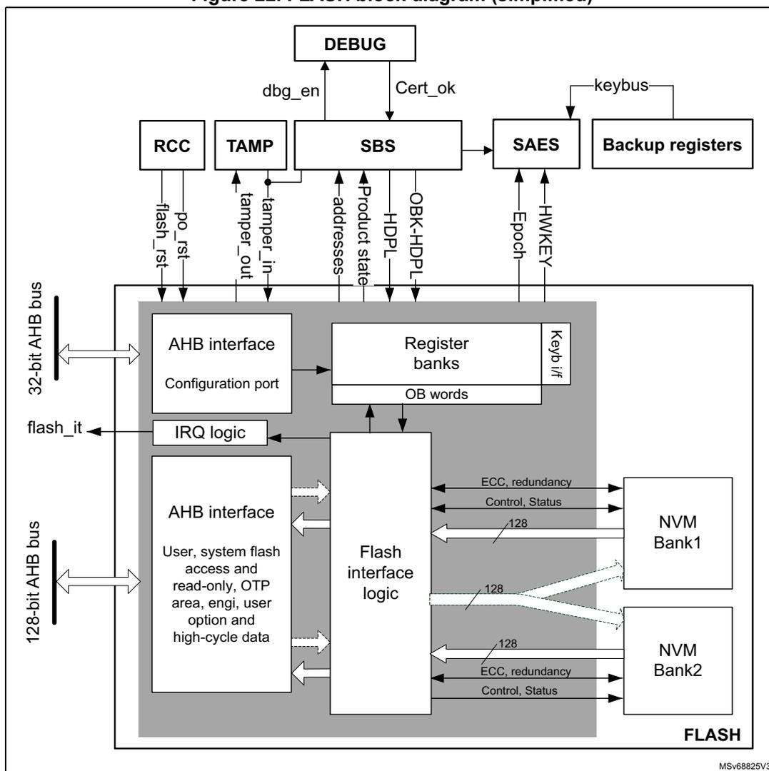
This block diagram illustrates the internal architecture of the FLASH memory system. At the top, a
DEBUG
block connects to the
SBS
(System Bus Security) block via
dbg_en
and
Cert_ok
signals. The
SBS
block is central, receiving
addresses
,
Product state
,
HDPL
, and
OBK-HDPL
. It interfaces with
RCC
(Reset and Clock Control) via
po_rst
and
flash_rst
, and with
TAMP
(Tamper) via
tamper_in
and
tamper_out
. The
SAES
(Secure AES) block receives
keybus
from
Backup registers
and provides
Epoch
and
HWKEY
to the
SBS
.
The main FLASH block contains two AHB interfaces. A
32-bit AHB bus
connects to an
AHB interface
for the
Configuration port
, which leads to
Register banks
(including
OB words
) and a
Keyb i/f
. A
128-bit AHB bus
connects to another
AHB interface
for
User, system flash access and read-only, OTP area, engi, user option and high-cycle data
. Both interfaces connect to the
Flash interface logic
. The
IRQ logic
outputs a
flash_it
signal.
The
Flash interface logic
manages two memory banks:
NVM Bank1
and
NVM Bank2
. Each bank is connected via a
128
-bit data bus and control lines for
ECC, redundancy
and
Control, Status
. The entire system is labeled
FLASH
at the bottom right.
7.3.2 FLASH signals
The flash memory has two AHB connections, namely the flash AHB register interface and the main AHB interface.
Flash AHB register interface
- • Data size is 32 bits
- • Except for some registers (FLASH_NS/SECKEYR, FLASH_NS/SECOBKKEYR and FLASH_OPTKEYR, used to insert unlock sequences for control, and option registers that can be written by 32 bits), it is possible to read and write all registers by 8, 16 and 32 bits.
- • When unlock sequence for control and option registers is wrong, a bus error is raised, otherwise no read or write errors are generated on the bus.
Main AHB interface
The AHB data bus size is 128 bits. This interface is used to handle three different targets:
- • Code placed in user and system memory, protected by 9 bits of ECC.
- • Secure keys placed in OBKey sectors, protected by 9 bits of ECC.
- • OTP, read-only and flash memory high-cycle data area, protected by 6 bits of ECC.
The main AHB interface is implemented as follows:
- • User and system memory, OBKeys storage:
- – Supports multiple length: 128-, 64-, 32-, 16- and 8-bit data width.
- – There is a read buffer of 128 bits for each bank where the last data read is stored. If data are available in the read buffer, no read access is given to the flash memory. Buffer is flushed when write access, OTP access, OBK swap, OBK alternate sector erase, high-cycle data area access, user option change request or erase operation occur.
- – There is a prefetch of the same size as the read buffer.
- – A 9-bit ECC is associated to each 128-bit data flash memory word.
- • OTP, read-only and flash high-cycle data
- – Two dedicated data buffer of 137 bits are used to manage 16-bit data with 6-bit ECC
- – Reading two times the same address triggers two flash read accesses.
- – During a read access, two wait states are added in addition to the memory wait states. These wait states are necessary to parse the data buffer.
- – Each write access triggers a write in the flash memory.
- – 6-bit ECC is associated to each 16-bit data.
By default, all the AHB memory range is cacheable. For regions where caching is not practical (OTP, RO, data area), MPU must be used to disable local cacheability.
7.3.3 Flash memory architecture and usage
Flash memory architecture
Figure 23 shows the organization supported by the embedded flash memory. By default, all the AHB memory range is cacheable. For regions where caching is unpractical (OTP, read-only, data) use MPU to disable local cacheability.
Figure 23. Embedded flash memory organization (2-Mbyte devices)
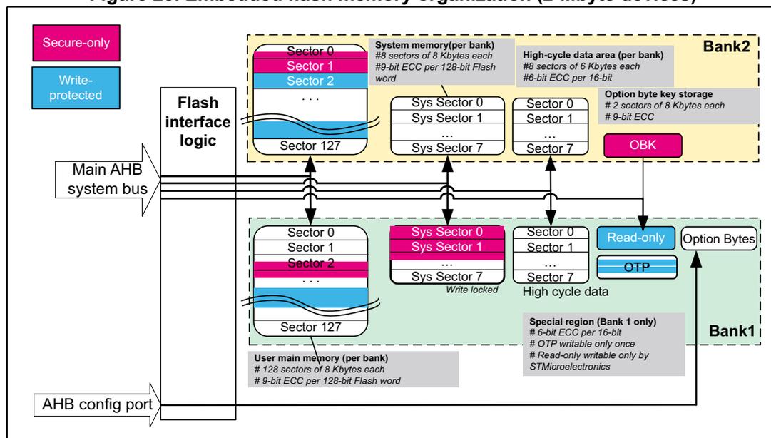
The diagram illustrates the internal organization of a 2-Mbyte embedded flash memory device. It is divided into two banks, Bank1 and Bank2, each containing different types of memory sectors. Bank1 includes user main memory (128 sectors of 8 Kbytes), system memory (8 sectors of 8 Kbytes), high-cycle data area (8 sectors of 6 Kbytes), and option byte key storage (2 sectors of 8 Kbytes). Bank2 includes user main memory (128 sectors of 8 Kbytes), system memory (8 sectors of 8 Kbytes), high-cycle data area (8 sectors of 6 Kbytes), and option bytes. The diagram also shows the Flash interface logic, Main AHB system bus, and AHB config port. Special regions like Read-only, OTP, and OBK are also indicated.
The embedded flash nonvolatile memory is composed of:
- • A main memory block, organized in two banks. Each bank is divided in sectors of 8 Kbytes each, and features flash-word rows of 128 bits + 9 bits of ECC per word (see Table 48 ).
- • A system memory block of 128 Kbytes, divided into two 64-Kbyte banks. Each bank is divided in eight 8-Kbyte sectors. The system flash memory is ECC protected (9-bit ECC per 128-bit word).
- • A set of nonvolatile option bytes loaded at reset by the embedded flash memory and accessible by the application software only through the AHB configuration register interface.
- • A 2-Kbyte one-time-programmable (OTP) area that can be written only once by the application software.
- • A 2-Kbyte read-only area. It contains a unique device ID and product information.
- • Two memory sectors (2 x 8 Kbytes) of secure key storage, OBKeys.
- • Up to 16 sectors of user flash memory with high cycling capability (100 K cycles) for data, 8 sectors per bank.
The overall flash memory architecture and its corresponding access interface is summarized in Table 48 .
Partition usage
Figure 24 shows how the embedded flash memory is used by STMicroelectronics and by the application software.
Figure 24. Embedded flash memory usage
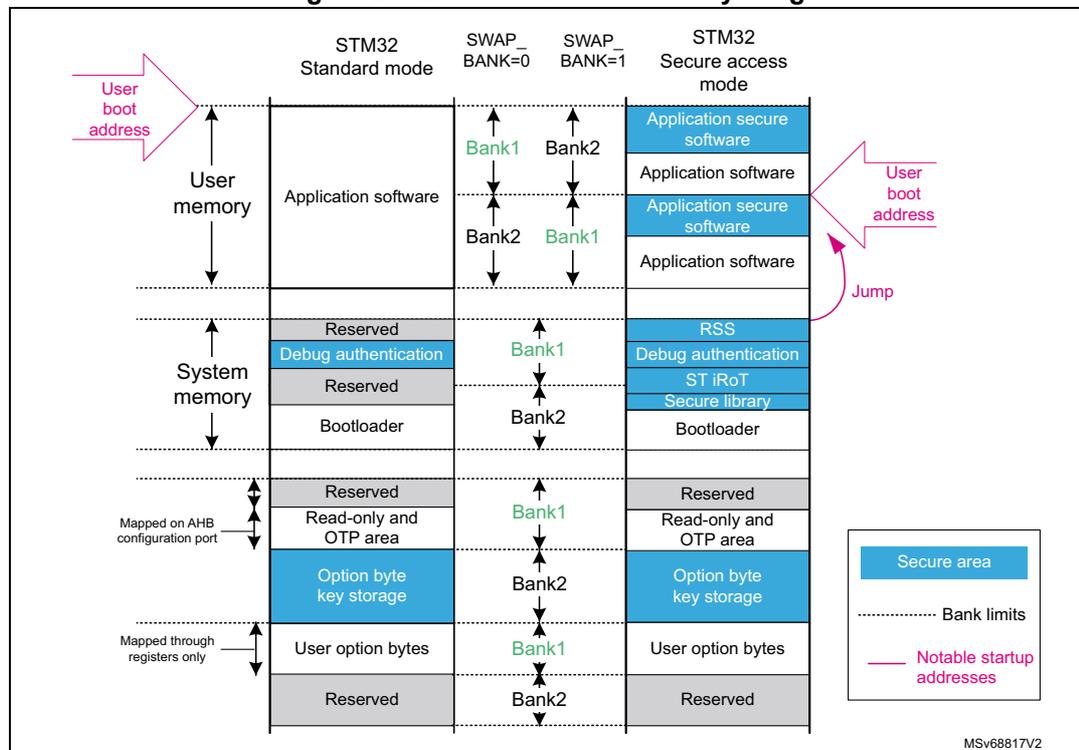
The diagram illustrates the memory layout for different STM32 modes. The columns represent: STM32 Standard mode, SWAP_BANK=0, SWAP_BANK=1, and STM32 Secure access mode. The rows represent different memory sections: User memory (Application software, Reserved, Debug authentication, Reserved, Bootloader, Reserved, Read-only and OTP area, Option byte key storage, User option bytes, Reserved), System memory (Application secure software, Application software, RSS, Debug authentication, ST iRoT, Secure library, Bootloader), and Mapped on AHB configuration port (Reserved, Read-only and OTP area, Option byte key storage, User option bytes, Reserved). The diagram also shows Bank1 and Bank2 labels, a 'Jump' arrow, and a legend for Secure area, Bank limits, and Notable startup addresses. The code MSV68817V2 is visible in the bottom right corner.
User and system memories are used differently, according to product state and other option bytes settings:
- • The user memory contains the application code and data, while the system memory is used with root secure services (RSS), the debug authentication code, and the STM32 bootloader. When a reset occurs, the core jumps to the boot address configured through the BOOT pin, the (SEC/NS)BOOTADD option bytes, and the product state.
- • The unique boot entry (BOOT_UBE) is set to either ST iRoT located in the system flash memory, or iRoT in the user flash memory. This feature is available only on cryptography enabled devices.
- • Secure service library in system flash memory is available in secure mode.
- • If the debugger is attached to the product, the entry point is the debug authentication policy, used to unlock the device via the SBS when attached to debugger. A digital signature must be provided to perform a regression to product state, where debug is allowed.
- • If (SEC/NS)BOOTADD is not yet configured, dedicated libraries can be used for secure boot. They are located in the system flash memory:
- – ST libraries in system flash memory assist the application software boot with special features, such as secure boot and secure firmware install (SFI-RSS)
- – ST iROT (immutable root of trust) secure software in user flash memory is used for secure firmware update and provisioning (SFU)
Note: For more information on option byte setup for boot, refer to Section 7.4.6 .
7.3.4 FLASH read operations
Read operation overview
Read access to main and system flash memory operates as follows:
- • There is a 128-bit read data buffer associated to each bank, which stores the last data read. If several consecutive read accesses request data belonging to the same flash data word (128 bits), data are read directly from the current data read buffer, without triggering additional flash read operations. This mechanism occurs each time a read access is granted. When a read access is rejected for security reasons, the corresponding read error response is issued by the embedded flash memory and no read operation to flash memory is triggered.
- • The read data buffer is disabled when write access or OTP access, user option change request, OBK swap, OBK erase or other erase operation occur.
Read access to OTP, RO and flash high-cycle data operates as follows:
- 1. Flash data word of 137 bits is read and stored in a temporary buffer.
- 2. The interface parses the 137-bit data word, and selects the 16- or 32-bit data requested.
- 3. While parsing the 137-bit data word, (two) wait states are added, and the AHB bus is stalled.
- 4. If the application reads an OTP data or flash high-cycle data not previously written, a double ECC error is reported and only a word full of set bits is returned (see Section 7.3.9 for details). The read data (in 16 bits) is stored in FLASH_ECCDR register, so that the user can identify if the double ECC error is due to a virgin data or a real ECC error.
- 5. Reading two times the same address triggers two reads in the flash memory.
- 6. For 8-bit accesses, an AHB bus error is generated.
Note: The embedded flash memory can perform single-error correction and double-error detection while read operations are being executed (see Section 7.3.8 ).
Instruction prefetch
The Cortex-M33 fetches instructions and literal pools (constants/data) over the C-Bus and through the instruction cache, if it is enabled. The prefetch block aims at increasing the efficiency of C-Bus accesses when the instruction cache is enabled, by reducing the cache refill latency.
Prefetch is efficient in case of sequential code; prefetch in the flash memory allows the next sequential instruction line to be read from the memory, while the current instruction line is being filled in instruction cache and executed by the CPU.
Prefetch is enabled by setting the PRFTEN bit in the FLASH access control register (FLASH_ACR). PRFTEN must be set only if at least one wait state is needed to access the flash memory.
Adjusting read timing constraints
The embedded clock must be enabled and running before reading data from a nonvolatile memory.
To correctly read data from the memory, the number of wait states (LATENCY) must be correctly programmed in the access control register (FLASH_ACR), according to the main AHB interface clock frequency, and the internal voltage range of the device ( \( V_{core} \) ).
Table 45 shows the correspondence between the number of wait states (LATENCY), the programming delay parameter (WRHIGHFREQ), the embedded flash memory clock frequency, and the supply voltage range.
Table 45. Recommended number of wait states and programming delay
| Number of wait states (LATENCY) | Programming delay (WRHIGHFREQ) | Interface clock frequency vs. \( V_{CORE} \) range (1) | |||
|---|---|---|---|---|---|
| VOS3 range 0.95 to 1.05 V | VOS2 range 1.05 to 1.15 V | VOS1 range 1.15 to 1.26 V | VOS0 range 1.30 to 1.40 V | ||
| 0 WS (1 FLASH clock cycle) | 00 | 0 to 20 MHz | 0 to 30 MHz | 0 to 34 MHz | 0 to 42 MHz |
| 1 WS (2 FLASH clock cycles) | 20 to 40 MHz | 30 to 60 MHz | 34 to 68 MHz | 42 to 84 MHz | |
| 2 WS (3 FLASH clock cycles) | 01 | 40 to 60 MHz | 60 to 90 MHz | 68 to 102 MHz | 84 to 126 MHz |
| 3 WS (4 FLASH clock cycles) | 60 to 80 MHz | 90 to 120 MHz | 102 to 136 MHz | 126 to 168 MHz | |
| 4 WS (5 FLASH clock cycles) | 10 | 80 to 100 MHz | 120 to 150 MHz | 136 to 170 MHz | 168 to 210 MHz |
| 5 WS (6 FLASH clock cycles) | N/A | N/A | 170 to 200 MHz | 210 to 250 MHz | |
1. Voltage range from 1.26 to 1.30 V is not supported.
Adjusting system frequency
After power-on, the embedded flash memory is clocked by the 64 MHz high-speed internal oscillator (HSI), with a voltage range set at a scaled value of VOS3: a conservative 3 wait-state latency is specified in FLASH_ACR register (see Table 45 ).
When changing the bus frequency, the application software must follow the sequence described below, to tune the number of wait states required to access the memory.
To increase the CPU frequency:
- 1. If necessary, program the LATENCY and WRHIGHFREQ bits to the right value in the FLASH_ACR register, as described in Table 45 .
- 2. Check that the new number of wait states is taken into account by reading back the FLASH_ACR register.
- 3. Modify the embedded flash memory clock source and/or the clock prescaler in the RCC_CFGR register of the reset and clock controller (RCC).
- 4. Check that the new embedded flash memory clock source and/or the new AHB clock prescaler value are taken in account by reading back the embedded flash memory clock source status and/or the prescaler value in the RCC_CFGR register of the reset and clock controller (RCC).
To decrease the CPU frequency:
- 1. Modify the embedded flash memory clock source and/or the clock prescaler in the RCC_CFGR register of reset and clock controller (RCC).
- 2. Check that the embedded flash memory new clock source and/or the new clock prescaler value are taken into account by reading back the embedded flash memory clock source status and/or the AHB interface prescaler value in the RCC_CFGR register of reset and clock controller (RCC).
- 3. If necessary, program the LATENCY and WRHIGHFREQ bits to the right value in FLASH_ACR register, as described in Table 45 .
- 4. Check that the new number of wait states has been taken into account by reading back the FLASH_ACR register.
Error code correction (ECC)
The memory embeds an error correction mechanism. Single-error correction and double-error detection are performed for each read operation. For more details, refer to Section 7.3.8 .
Read errors
When the ECC mechanism is unable to correct the read operation, the memory reports read errors, as described in Section 7.9.10 .
Read interrupts
See Section 7.10 for details.
7.3.5 FLASH program operations
Program operation overview
Program operation consists in issuing write commands. The memory supports the execution of only one write-command at a time. Write-while-write is not supported. Nothing prevents overwriting a non-virgin flash word, but this is not recommended. The result may lead to invalid data and inconsistent ECC code.
User flash, OBK storage and system flash memories sectors
For the user and system flash memories, 9-bit ECC is associated to each 128-bit data flash word. In this case, the embedded flash memory must always perform write operations to nonvolatile memory with a 128-bit word granularity. Once the write buffer is full (128 bits), the Busy flag is set, and a programming operation is triggered.
There is a write buffer common to Bank1 and 2, which supports multiple write-access types (128, 64, 32, 16 or 8 bits). The application can decide to write from 8 bits to 128 words. In this case, a force-write mechanism to the 128 bits + ECC is used (see FW bit of FLASH_NS/SECCR register).
When the write request is issued to the memory, any new write request stalls the main AHB bus. Moreover, while a write operation is ongoing, any new read request to the same bank stalls the main AHB bus.
OTP, RO, flash high-cycle data
When the target memory is OTP, RO and flash high-cycle data sectors, 6-bits ECC code is associated to each 16-bit data flash word. The embedded flash memory supports 16- or 32-bit write operations (8-bit write operations are not supported). For 8-bit accesses, write accesses are ignored. There is no write data buffer. Each write access triggers a write in the flash memory.
Note: The OTP area is typically write-protected on the final product, as described in Section 7.3.9 .
The write protection check is performed at the reception of the write request (during address phase). Write protection is not checked anymore at the output of the write buffer. If a write protection violation is detected, the write operation is canceled, and write protection error (WRPERR) is raised in FLASH_NS/SECSR register.
Note: For write protections of main flash, ICP, and OTP see Section 7.6 .
Monitoring ongoing write operations
The application software can use a status flag located in FLASH_NS/SECSR to monitor ongoing write operations. Since only one operation is possible at a time, this flag indicates if any operation (write, erase, option change) is ongoing, whatever the bank.
- •
BSY
: indicates that an effective write, erase, option byte change, OBK swap, OBK alt sector erase is ongoing in the nonvolatile memory. This flag is not dedicated to a specific bank. It is set when an operation is starting on the memory, whatever the bank. An operation is triggered by:
- – An erase (FLASH_NS/SECCR.STRT)
- – A write (FLASH_NS/SECCR.PG + AHB write)
- – An option modification (FLASH_OPTCR.OPTSTRT)
- – OBKeys sector swap and OBKeys sector erase (FLASH_NS/SECOBKCFGR.SWAP_SECT_REQ and FLASH_NS/SECOBKCFGR.ALT_SECT_ERASE)
They are cleared when the current operation ends, or in case of error.
- • WBNE : this bit indicates that the embedded flash memory is waiting for new data to complete the 128-bit write buffer. In this state the write buffer is not empty. It is reset as soon as the application software fills the write buffer, or forces the writes by using FW bit in FLASH_NS/SECCR, or an error is detected. When WBNE is high, it is not possible to launch an erase, an option modification, an OBK swap or OBK alternate sector erase operation on flash memory.
- •
DBNE
: this bit indicates that the data buffer for parsing 16-bits data is not empty:
- – 16-bit data write access is received, and the data buffer is being filled. It is set at the receipt of a valid write access, and reset as soon as the write request preparation has been processed.
Note: If the memory is busy at the receipt of the AHB write request, the CPU execution is stalled.
Enabling write operations
Before programming the user flash memory in Bank1 or in Bank2, the application software must ensure that the PG bit is set to 1 in FLASH_NS/SECCR. If not, an unlock sequence must be used (see Section 7.6.7 ), and the PG bit must be set.
When an option byte or an option byte key must be modified, or a mass erase must be started, the application software must ensure that FLASH_OPTCR is unlocked. If this is not the case, an unlock sequence must be used (see Section 7.6.7 ).
A separate mechanism with similar use exists for FLASH_NS/SECOBKCFGR. The control register must be unlocked prior to the start of any OBKeys storage modification. Writing the correct sequence to the FLASH_NSOBKKEYR unlocks FLASH_NSOBKCFGR. FLASH_SECOBKKEYR is linked to FLASH_SECOBKCFGR, as described in Section 7.6.7 .
Note: The application software must not unlock an already unlocked register, otherwise this register remains locked until the next system reset.
If needed, the application software can update the programming delay, as described in Adjusting programming timing constraints .
Writing to the FLASH control register FLASH_NS/SECCR and FLASH_OPTCR
The FLASH_NS/SECCR, FLASH_OPTCR and FLASH_NS/SECOBKCFGR registers are not accessible in write mode when the BSY bit is set. Any attempt to write these registers while the BSY bits is set causes the AHB bus to stall until SEC/NSBSY bit is cleared.
Single-write sequence
The recommended single-write sequence is the following:
- 1. Make sure protection mechanism does not prevent programming
- 2. Check that no memory operations are ongoing by checking the BSY bit in the FLASH_NS/SECSR register and CDBNE bits in the FLASH_NS/SECSR register. Check that the write buffer is empty by checking the WBNE bit in the FLASH_NS/SECSR register
- 3. Check and clear all the error flags due to previous programming/erase operation
- 4. Unlock the FLASH_NS/SECCR register, as described in Section 7.6.7 (only if this register is not already unlocked)
- 5. Enable write operations by setting PG bit in the FLASH_NS/SECCR register
- 6. Write one flash-word at aligned address
Note: NS/SECWBNE flag indicates if the 128-bit write buffer is waiting for new data.
Note: No erase request, options change request, OBK operation is allowed between the first write and the completion of the write operation.
- 7. Wait for the BSY bit to be cleared in the corresponding FLASH_NS/SECSR register
- 8. Clear PG bit in FLASH_NS/SECCR register if there are not any more programming requests
If step 6 is executed incrementally (for example byte per byte), the write buffer can become partially filled. In this case the application software can decide to force-write what is stored in the write buffer by using FW bit in FLASH_NS/SECCR register. In this particular case, the unwritten bits are automatically set to 1. If no bit in the write buffer is cleared to 0, the FW bit has no effect.
Note: The usage of a force-write operation prevents the application from updating, in a later stage, the missing bits with a value different from 1. This can lead to unexpected or inconsistent data, or ECC.
Adjusting programming timing constraints
Program operation timing constraints depend of the memory clock frequency, which directly impacts the performance. If timing constraints are too tight, the nonvolatile memory does not operate correctly, if they are too lax, the programming speed is not optimal.
The user must therefore trim the optimal programming delay through the WRHIGHFREQ parameter in the FLASH_ACR register. Refer to Table 45 for the recommended programming delay, depending upon the memory clock frequency.
FLASH_ACR configuration register is common to both banks.
The application software must check that no program/erase operation is ongoing before modifying WRHIGHFREQ.
Caution: Modifying WRHIGHFREQ while programming/erasing the memory can corrupt its content.
Programming errors
When a program operation fails, an error is reported, as described in Section 7.9 .
Programming interrupts
See Section 7.10: FLASH interrupts for details.
7.3.6 FLASH erase operations
Erase operation overview
The memory can perform erase operations on 8-Kbyte user sectors, on one user flash memory bank, or on two user flash memory banks (for example mass erase). For more details in user flash memory, ICP, user options and OTP erase protection, see Section 7.6 .
Erase commands are issued through the AHB configuration interface. The memory supports one operation at a time, if it receives simultaneously a write and an erase request an error flag is raised, and both operations are canceled. See Section 7.9 for details.
After successful completion of erase, all the bytes in the erased flash sectors are set to the flash default 0xFF value.
Erase and WRP
If the application software attempts to erase a write-protected user sector, the sector erase operation is aborted, and the WRPERR flag is raised in the FLASH_NS/SECSR register, as described in Section 7.9.2 .
Flash busy
Busy signals is described in Monitoring ongoing write operations .
Writing to the FLASH control register FLASH_NS/SECCR and FLASH_OPTCR
Refer to Writing to the FLASH control register FLASH_NS/SECCR and FLASH_OPTCR .
Enabling erase operations
Before erasing a sector, the application software must make sure that FLASH_NS/SECCR is unlocked. If this is not the case, an unlock sequence must be used (see Section 7.6.7 ).
Note: The application software must not unlock a register that is already unlocked, otherwise this register remains locked until next system reset. This can be used to deliberately lock-out a register from further accesses.
Similar constraints apply to bank erase requests.
Standard flash sector erase sequence
To erase an 8- or 6-Kbyte data user sector without security protections, proceed as follows:
- 1. Make sure protection mechanism does not prevent sector erase (WRP, secure flag, HDP).
- 2. Check that no memory operations are ongoing by checking the BSY and DBNE bits in the FLASH_NSSR register, and that the write buffer is empty by checking the WBNE bit in the FLASH_NSSR register.
- 3. Check and clear all the non-secure error flags due to previous programming/erase operation. Refer to Section 7.9 for details.
- 4. Unlock the FLASH_NSCR register, as described in Section 7.6.7 (only if this register is not already unlocked).
- 5. Set the BKSEL bit, the SER bit and SNB bitfield in the FLASH_NSCR register. BKSEL indicates in which physical bank sector must be erased, then SER indicates a sector erase operation, while SNB contains the target sector number. In case of data sector, use the number of the corresponding regular sector.
- 6. Set the STRT bit in the FLASH_NSCR register.
- 7. Wait for the BSY bit to be cleared in the FLASH_NSSR register.
- 8. STRT bit is automatically cleared at the end of the sector erase, or in case of error.
- 9. Clear SER in FLASH_NSCR register if there are not anymore sector erase request to be issued.
Note: If another erase flag is requested simultaneously to the sector erase, a PGSERR error is generated.
Secure flash memory sector erase sequence
To erase an 8- or 6-Kbyte data secure configured user sector, proceed as follows:
- 1. Make sure write protection or HDP mechanism does not prevent sector erase.
- 2. Ensure that no memory operations are ongoing (by checking the BSY and DBNE bits in the FLASH_SECSR register), and that the write buffer is empty (by checking the WBNE bit in the FLASH_SECSR register).
- 3. Check and clear all the secure error flags due to previous programming/erase operations. Refer to Section 7.9 for details.
- 4. Unlock the FLASH_SECCR register, as described in Section 7.6.7 (only if this register is not already unlocked).
- 5. Set the BKSEL bit, the SER bit and SNB bitfield in the FLASH_SECCR register. BKSEL indicates in which physical bank sector must be erased, then SER indicates a sector erase operation, while SNB contains the target secure sector number. In case of data sector, use the number of the corresponding regular sector.
- 6. Set the STRT bit in the FLASH_SECCR register.
- 7. Wait for the BSY bit to be cleared in the FLASH_SECSR register.
- 8. STRT bit is automatically cleared at the end of the sector erase or in case of error.
- 9. Clear SER in FLASH_SECCR register if there are not any secure sector erase request to be issued.
Note: If another erase flag is requested simultaneously to the sector erase, a PGSERR error is generated.
Standard flash memory bank erase sequence
To erase bank where no sector is configured as secure:
- 1. Make sure protection mechanism does not prevent sector erase.
- 2. Check that no memory operations are ongoing by checking the BSY and DBNE bits in the FLASH_NSSR register and that the write buffer is empty by checking the WBNE bit in the same register.
- 3. Check and clear all the non-secure error flags due to previous programming/erase operation. Refer to Section 7.9 for details.
- 4. Unlock the FLASH_NSCR register, as described in Section 7.6.7 (only if this register is not already unlocked).
- 5. Set the BKSEL bit and the BER bit in the FLASH_NSCR register to the targeted physical bank (swap setting is ignored).
- 6. Set the STRT bit in the FLASH_NSCR register to start the bank erase operation. Then wait until the BSY bit is cleared in the FLASH_NSSR register.
- 7. STRT bit is automatically cleared at the end of erase sequence or in case of error.
- 8. Clear BER in FLASH_NSCR register if there is not other bank erase request to be issued.
Secure flash memory bank erase sequence
To erase bank where all sectors are configured with secure flag:
- 1. Make sure protection mechanism does not prevent sector erase (for mass erase the HDP is also considered, it cannot be fully executed from HDPL= 2, 3 if HDP is defined).
- 2. Check that no memory operations are ongoing by checking the BSY and DBNE bits in the FLASH_SECSR register and that the write buffer is empty by checking the WBNE bit in the same register.
- 3. Check and clear all the secure error flags due to previous programming/erase operation. Refer to Section 7.9 for details.
- 4. Unlock the FLASH_SECCR register, as described in Section 7.6.7 (only if this register is not already unlocked).
- 5. Set the BKSEL bit and the BER bit in the FLASH_SECCR register to the targeted physical bank (swap setting is ignored).
- 6. Set the STRT bit in the FLASH_SECCR register to start the bank erase operation. Then wait until the BSY bit is cleared in the FLASH_SECSR register.
- 7. STRT bit is automatically cleared at the end of erase sequence or in case of error.
- 8. Clear BER in FLASH_SECCR register if there is not other bank erase request to be issued.
Flash mass erase sequence
To erase all sectors of both banks, using non-secure access, all sectors must be configured as non-secure. The application software can set the MER bit to 1 in FLASH_NSCR register, as described below:
- 1. Make sure protection mechanisms do not prevent mass erase ( Section 7.6 ).
- 2. Check that no memory operations are ongoing by checking the BSY and DBNE bits in the FLASH_NSSR register and that the write buffer is empty by checking the WBNE bit in the FLASH_NSSR register.
- 3. Check and clear all the non-secure error flags due to previous programming/erase operation. Refer to Section 7.9 for details.
- 4. Unlock the FLASH_NSCR register as described in Section 7.6.7 (only if the registers are not already unlocked).
- 5. Set the MER bit to 1 in FLASH_NSCR register.
- 6. Set the STRT bit in the FLASH_NSCR register. Then wait until BSY bit is cleared in the FLASH_NSSR register.
- 7. STRT bit is cleared automatically at the end of the erase sequence, or in case of error.
- 8. Clear MER in FLASH_NSCR register.
Secure flash memory mass erase sequence
To erase all sectors of both banks simultaneously, using secure access, all sectors must be configured as secure. The application software can set the MER bit to 1 in FLASH_SECCR register, as described below:
- 1. Make sure protection mechanisms do not prevent mass erase ( Section 7.6 ).
- 2. Check that no memory operations are ongoing by checking the BSY and DBNE bits in the FLASH_SECSR register and that the write buffer is empty by checking the WBNE bit in the FLASH_SECSR register.
- 3. Check and clear all the secure error flags due to previous programming/erase operation. Refer to Section 7.9 for details.
- 4. Unlock the FLASH_SECCR register as described in Section 7.6.7 (only if the registers are not already unlocked).
- 5. Set the MER bit to 1 in FLASH_SECCR register.
- 6. Set the STRT bit in the FLASH_SECCR register. Then wait until BSY bit is cleared in the FLASH_SECSR register.
- 7. STRT bit is cleared automatically at the end of the erase sequence, or in case of error.
- 8. Clear MER in FLASH_SECCR register.
Note: Mass and bank erase also erase high-cycle data sectors aliased from the erased bank.
7.3.7 FLASH parallel operations
As the memory is divided into two independent banks, the embedded flash memory interface supports a read in one bank while a write (RWW: read while write) or an erase is executed in the other bank. It does not support write-while-write, nor read-while-read. Same is valid for the high-cycle data area, system flash libraries, or the OBK (located on Bank2).
In all cases, the sequences described in Section 7.3.4 , Section 7.3.5 and Section 7.3.6 apply.
7.3.8 FLASH error protections
Error correction codes (ECC)
The embedded flash memory supports an error correction code (ECC) mechanism, based on the SECDED algorithm, to correct single errors and detect double errors.
This mechanism uses nine ECC bits per 128-bit flash word, and applies to user and system memory. For read-only, OTP, flash high-cycle data, a stronger six ECC bits per 16-bit word is used. A double ECC error is generated for an OTP or flash high-cycle data virgin word (for example a word with 22 bits at 1). When this OTP or flash high-cycle data word is no more virgin, the ECC error disappears.
More specifically, during each read operation from a 128-bit flash word, the embedded flash memory retrieves the 9-bit ECC information, computes the ECC of the flash word, and compares the result with the reference value. If they do not match, the corresponding ECC error is raised, as described in Section 7.9.10 .
During each program operation, a 9-bit ECC code is associated to each 128-bit data flash word, and the resulting 137-bit flash word information is written in nonvolatile memory.
A similar mechanism applies to read-only and OTP areas, but with 6-bit ECC for 16-bit data.
7.3.9 OTP and RO memory access
OTP and RO memory are accessed through main AHB interface. The OTP is accessible at addresses 0x08FF_F000 to 0x08FF_F7FF, and the read-only section is accessible from 0x08FF_F800 to 0x08FF_FFFF.
FLASH one-time programmable area
The embedded flash memory offers a 2048-byte memory area dedicated to application non-confidential, one-time programmable data (OTP). This area is composed by 1024 words of 16 bits (plus 6 bits of ECC). It cannot be erased, and can be written only once. The OTP area can be accessed through the main AHB interface from address 0x08FF_F000 to 0x08FF_F7FE.
OTP data can be programmed by the application software by 16-bit chunks. Overwriting an already programmed 16-bit half-word can lead to data and ECC errors, and is therefore not supported.
Note: The OTP area is virgin when the device is delivered by STMicroelectronics.
When reading OTP data with a single error corrected or a double error detected, the embedded flash memory reports read errors, as described in Section 7.9.10 .
When reading OTP data not written by the application software (such as virgin OTP), the ECC correction reports a double-error detection (ECCD), and the data are to be found in the FLASH_ECCDR register. ECCD implies an NMI raised.
OTP write protection
OTP data are organized as 32 blocks of 32 OTP words, as shown in Table 46 . An entire OTP block can be protected (locked) from write accesses by setting the LOCKBLi bit (i = 0 to 31) corresponding to each OTP block in the FLASH_OTPBLR register. A block can be write-protected, if it has been programmed (even partially) or not.
The OTP block locking operation is irreversible, and independent from the product life state.
Note: The OTP area can be accessed only in read mode.
Table 46. Flash memory OTP organization
| OTP block | AHB address | AHB word | Lock bit | |
|---|---|---|---|---|
| [31:16] | [15:0] | |||
| Block 0 | 0x08FF F000 | OTP001 | OTP000 | LOCKBL0 |
| 0x08FF F004 | OTP003 | OTP002 | ||
| ... | ||||
| 0x08FF F03C | OTP031 | OTP030 | ||
| Block 1 | 0x08FF F040 | OTP033 | OTP032 | LOCKBL1 |
| 0x08FF F044 | OTP035 | OTP034 | ||
| ... | ||||
| 0x08FF F07C | OTP063 | OTP062 | ||
| Block 2 | 0x08FF F080 | OTP065 | OTP064 | LOCKBL2 |
| 0x08FF F084 | OTP067 | OTP066 | ||
| ... | ||||
| 0x08FF F0BC | OTP95 | OTP94 | ||
| ... | ||||
| Block 31 | 0x08FF F7C0 | OTP993 | OTP992 | LOCKBL31 |
| 0x08FF F7C4 | OTP995 | OTP994 | ||
| ... | ||||
| 0x08FF F7FC | OTP1023 | OTP1022 | ||
OTP write sequence
Follow the sequence below to write an OTP word:
- 1. Check that no memory operations are ongoing by checking the BSY bit in the FLASH_NSSR register and that the data buffer is empty by checking the DBNE bit in the FLASH_NSSR register.
- 2. Check and clear all the error flags due to previous programming/erase operation.
- 3. Set PG bit in the FLASH_NSCR register.
- 4. Check the protection status of the target OTP word (see Table 46 ). The corresponding LOCKBLi bit must not be set to 1.
- 5. Write two OTP words (32 bits) corresponding to the 4-byte aligned address shown in Table 46 . Alternatively, the application software can program separately the 16-bit MSB or 16-bit LSB. In this case the first 16-bit write operation starts immediately, without waiting for the second one.
- 6. Wait for the BSY bit to be cleared in the FLASH_NSSR register.
- 7. Clear PG bit in FLASH_NSCR register if there is not any programming request anymore in the bank.
- 8. Optionally, lock the OTP block using LOCKBLi to prevent further data changes.
Note:
Do not write twice an OTP 16-bit word, otherwise an ECC error is generated.
Writing OTP data at byte level is not supported, and generates a bus error.
To avoid data corruption, it is important to complete the OTP write process (for example by reading back the OTP value), before starting an option change.
Flash read-only area
The embedded flash memory offers a 2-Kbyte area to store read-only data. This area can be accessed through the AHB main port, and is protected by a robust ECC scheme, as detailed in Section 7.3.8 .
The read-only information (programmed by STMicroelectronics) that can be used by the application software is detailed in Table 47 .
Table 47. Read-only public data organization
| Read-only data name | Address | Comment |
|---|---|---|
| Unique device ID | 0x08FF F800 | U_ID[31:0] |
| 0x08FF F804 | U_ID[63:32] | |
| 0x08FF F808 | U_ID[96:64] | |
| Flash memory size/ package | 0x08FF F80C | Flash memory size[15:0] / Package code[15:0] |
| Reserved | 0x08FF F810 to 0x08FF FFFF | Reserved information |
7.3.10 Flash high-cycle data
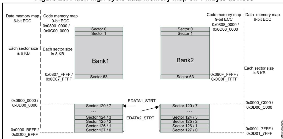
The embedded flash memory offers up to 96 Kbytes (maximum) memory area with high-cycling capability (100 kcycles) to store data and emulate EEPROM. It can be accessed through the AHB system port from address 0x0900_0000 to 0x0901_7FFF (see Figure 25 ). It is mapped in the 8 (or 4) last sectors of Bank 1 and 2. This area is protected by a robust 6-bit ECC, enabling a 16-bit read and write granularity, at the expense of having sector size shrunk to 6 Kbytes.
A threshold per bank (EDATA(1/2)_STRT) is programmable to determine the beginning of the data flash area. By default, the whole memory is used for code.
For example, if 48 Kbytes of data are needed in Bank 1, set EDATA1_EN to 1, and EDATA1_STRT to 7. If no data are needed in Bank2, set EDATA2_EN to 0. In this case the data are accessible from address 0x0900_0000 to 0x0900_BFFF for Bank 1.
For greater efficiency, it is recommended to use sector on the other bank for flash high-cycle data, so that the application benefits from RWW capability of the dual-bank arrangement.
When SWAP_BANK feature is enabled, the banks are swapped: the flash high-cycle data in Bank 2 are accessible from 0x0900_000 to 0x0900_BFFF, and the data in Bank 1 are accessible from 0x0900_C000 to 0x0901_7FFF.
A bus error is generated on:
- • Attempt to access an address between 0x0900_0000 to 0x0901_7FFF and this address is not valid (EDATA(1/2)_EN not enabled or EDATA(1/2)_STRT not correct).
- • Attempt to fetch instructions from flash high-cycle data area.
Erasing the data area sector is possible by normal erase request for the corresponding user flash sector (120-127 for the STM32H562/563/573xx devices, 24-31 for the STM32H523/33xx devices).
Protections and security of high-cycle area are detailed in Section 7.6.9 .
Figure 25. Flash high-cycle data memory map on 2-Mbyte devices
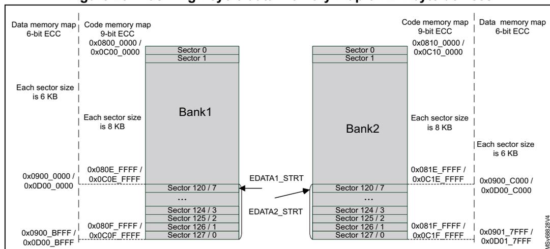
The diagram illustrates the flash memory map for 2-Mbyte devices, divided into two banks, Bank1 and Bank2. Each bank contains 128 sectors. Bank1 sectors 0 and 1 have a size of 6 KB, while sectors 2 through 127 have a size of 8 KB. Bank2 sectors 0 and 1 have a size of 6 KB, while sectors 2 through 127 have a size of 8 KB. The data memory map for Bank1 starts at 0x0900_0000 and ends at 0x0D00_0000. The data memory map for Bank2 starts at 0x0900_C000 and ends at 0x0D01_7FFF. The code memory map for Bank1 starts at 0x0800_0000 and ends at 0x0C00_0000. The code memory map for Bank2 starts at 0x0810_0000 and ends at 0x0C10_0000. The EDATA1_STRT and EDATA2_STRT markers are indicated between the banks.
Figure 26. Flash high-cycle data memory map on 1-Mbyte devices
The diagram illustrates the flash memory map for 1-Mbyte devices, divided into two banks, Bank1 and Bank2. Each bank contains 64 sectors. Bank1 sectors 0 and 1 have a size of 6 KB, while sectors 2 through 63 have a size of 8 KB. Bank2 sectors 0 and 1 have a size of 6 KB, while sectors 2 through 63 have a size of 8 KB. The data memory map for Bank1 starts at 0x0900_0000 and ends at 0x0D00_0000. The data memory map for Bank2 starts at 0x0900_C000 and ends at 0x0D01_7FFF. The code memory map for Bank1 starts at 0x0800_0000 and ends at 0x0C00_0000. The code memory map for Bank2 starts at 0x0808_0000 and ends at 0x0C08_0000. The EDATA1_STRT and EDATA2_STRT markers are indicated between the banks.
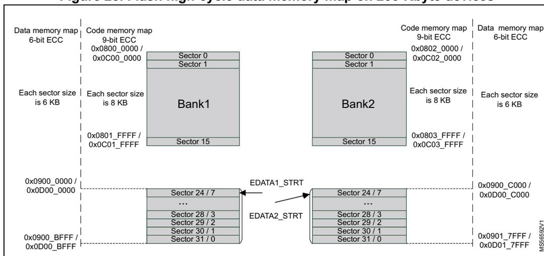
Figure 27. Flash high-cycle data memory map on 512-Kbyte devices
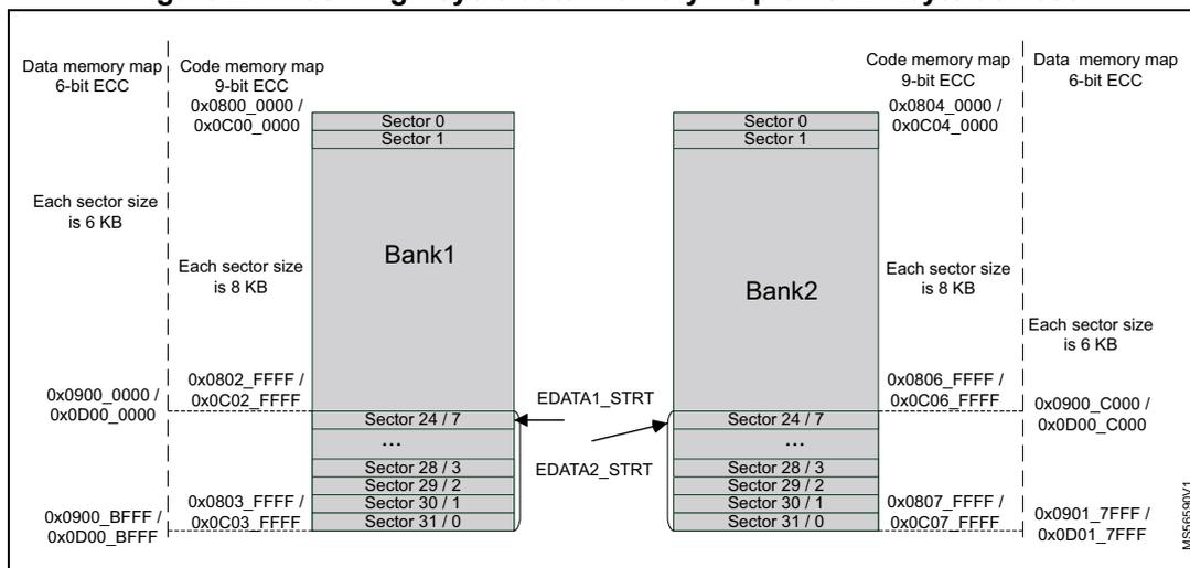
Figure 28. Flash high-cycle data memory map on 256-Kbyte devices
Note: When flash high-cycle data area on Bank1 is enabled, the code memory map is not continuous from Bank1 to Bank2 on 2M- and 512K-byte devices.
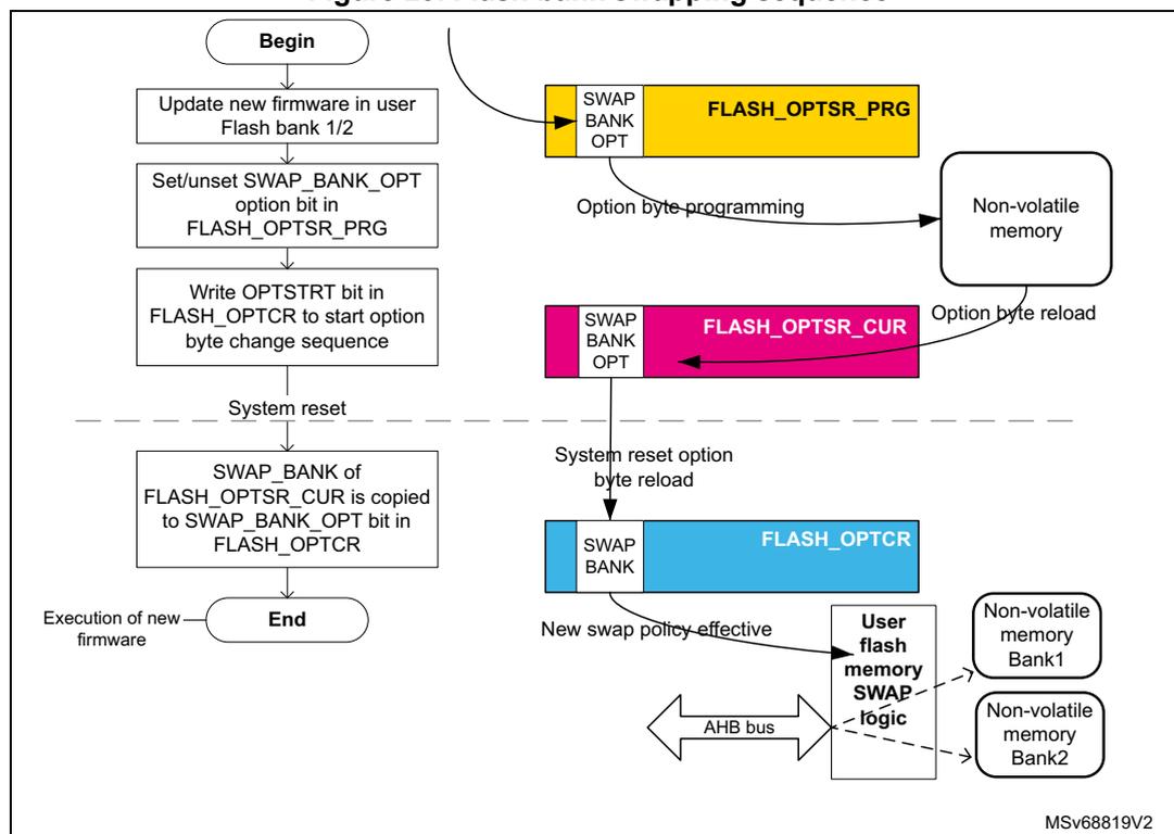
7.3.11 Flash bank swapping
Bank1 and Bank2 can be swapped for the user flash. This feature can be used after a firmware upgrade to restart the device on the new firmware. Bank swapping is an user option byte flag controlled by the SWAP_BANK bit of the FLASH_OPTCR register.
Bank specific settings for data area and security attributes follow the original bank and its contents. Control bit BKSEL always refers to physical bank, not the SWAP_BANK setting.
Table 48 shows the accessible memory, depending upon the SWAP_BANK bit value.
Table 48. Memory map and swapping options (STM32H562/563/573xx devices)
| Area | Corresponding bank | Start address | End address | Size (bytes) | Region name | |
|---|---|---|---|---|---|---|
| SWAP_BANK = 0 | SWAP_BANK = 1 | |||||
| User main memory | Bank1 | Bank2 | 0x0800 0000 | 0x0800 1FFF | 8 K | Sector 0 |
| 0x0800 2000 | 0x0800 3FFF | 8 K | Sector 1 | |||
| ... | ... | ... | ... | |||
| 0x080F E000 | 0x080F FFFF | 8 K | Sector 127 | |||
| Bank2 | Bank1 | 0x0810 0000 | 0x0810 1FFF | 8 K | Sector 0 | |
| 0x0810 2000 | 0x0810 3FFF | 8 K | Sector 1 | |||
| ... | ... | ... | ... | |||
| 0x081F E000 | 0x081F FFFF | 8 K | Sector 127 | |||
| System memory | Bank1 | 0x0BF8 0000 | 0x0BF8 1FFF | 8 K | System 1 Sector 0 | |
| 0x0BF8 2000 | 0x0BF8 3FFF | 8 K | System 1 Sector 1 | |||
| ... | ... | ... | ... | |||
| 0x0BF8 E000 | 0x0BF8 FFFF | 8 K | System 1 Sector 7 | |||
| Bank2 | 0x0BF9 0000 | 0x0BF9 1FFF | 8 K | System 2 Sector 0 | ||
| 0x0BF9 2000 | 0x0BF9 3FFF | 8 K | System 2 Sector 1 | |||
| ... | ... | ... | ... | |||
| 0x0BF9 E000 | 0x0BF9 FFFF | 8 K | System 2 Sector 7 | |||
Table 49. Memory map and swapping options (STM32H523/533xx devices)
| Area | Corresponding bank | Start address | End address | Size (bytes) | Region name | |
|---|---|---|---|---|---|---|
| SWAP_BANK = 0 | SWAP_BANK = 1 | |||||
| User main memory | Bank1 | Bank2 | 0x0800 0000 | 0x0800 1FFF | 8 K | Sector 0 |
| 0x0800 2000 | 0x0800 3FFF | 8 K | Sector 1 | |||
| ⋮ | ⋮ | ⋮ | ⋮ | |||
| 0x0803 E000 | 0x0803 FFFF | 8 K | Sector 31 | |||
| Bank2 | Bank1 | 0x0804 0000 | 0x0804 1FFF | 8 K | Sector 0 | |
| 0x0804 2000 | 0x0804 3FFF | 8 K | Sector 1 | |||
| ⋮ | ⋮ | ⋮ | ⋮ | |||
| 0x0807 E000 | 0x0807 FFFF | 8 K | Sector 31 | |||
Table 49. Memory map and swapping options (STM32H523/533xx devices) (continued)
| Area | Corresponding bank | Start address | End address | Size (bytes) | Region name | |
|---|---|---|---|---|---|---|
| SWAP_BANK = 0 | SWAP_BANK = 1 | |||||
| System memory | Bank1 | 0x0BF8 0000 | 0x0BF8 1FFF | 8 K | System 1 Sector 0 | |
| 0x0BF8 2000 | 0x0BF8 3FFF | 8 K | System 1 Sector 1 | |||
| ... | ... | ... | ... | |||
| 0x0BF8 E000 | 0x0BF8 FFFF | 8 K | System 1 Sector 7 | |||
| Bank2 | 0x0BF9 0000 | 0x0BF9 1FFF | 8 K | System 2 Sector 0 | ||
| 0x0BF9 0000 | 0x0BF9 3FFF | 8 K | System 2 Sector 1 | |||
| ... | ... | ... | ... | |||
| 0x0BF9 E000 | 0x0BF9 FFFF | 8 K | System 2 Sector 7 | |||
The SWAP_BANK bit in FLASH_OPTCR register is loaded from the SWAP_BANK option bit only after system reset or POR.
To change the SWAP_BANK bit (for example to apply a new firmware update), follow the sequence below:
- 1. Check that no memory operations are ongoing by checking the BSY and DBNE bits in the FLASH_NS/SECSR register and that the write buffer is empty by checking the WBNE bit in the FLASH_NS/SECSR register.
- 2. Clear all error flags due to a previous operation.
- 3. Unlock OPTLOCK bit, if not already unlocked.
- 4. Set the new desired SWAP_BANK value in the FLASH_OPTSR_PRG register.
- 5. Start the option byte change sequence by setting the OPTSTRT bit in the FLASH_OPTCR register.
- 6. Once the option byte change has completed, FLASH_OPTSR_CUR contains the expected SWAP_BANK value, but SWAP_BANK bit in FLASH_OPTCR has not yet been modified and the bank swapping is not yet effective.
- 7. Force a system reset or a POR. When the reset rises up, the bank swapping is effective (SWAP_BANK value updated in FLASH_OPTCR) and the new firmware shall be executed.
Note: The SWAP_BANK bit in FLASH_OPTCR is read-only, and cannot be modified by the application software.
The SWAP_BANK option bit in FLASH_OPTSR_PRG can be modified whatever the product state. Instead of being locked by PRODUCT_STATE, it is locked by (NS/SEC)BOOT_LOCK User OB.
Figure 29 gives an overview of the bank swapping sequence.
Figure 29. Flash bank swapping sequence
graph TD
    Begin([Begin]) --> Step1[Update new firmware in user Flash bank 1/2]
    Step1 --> Step2[Set/unset SWAP_BANK_OPT option bit in FLASH_OPTSR_PRG]
    Step2 --> Step3[Write OPTSTRT bit in FLASH_OPTCR to start option byte change sequence]
    Step3 --> Reset[System reset]
    Reset -.-> Step4[SWAP_BANK of FLASH_OPTSR_CUR is copied to SWAP_BANK_OPT bit in FLASH_OPTCR]
    Step4 --> End([End])
    End --> Firmware[Execution of new firmware]

    subgraph Registers
        PRG[FLASH_OPTSR_PRG: SWAP BANK OPT]
        CUR[FLASH_OPTSR_CUR: SWAP BANK OPT]
        CR[FLASH_OPTCR: SWAP BANK]
    end

    Step2 -- "Option byte programming" --> NV[Non-volatile memory]
    NV -- "Option byte reload" --> CUR
    Reset -- "System reset option byte reload" --> CR
    CR -- "New swap policy effective" --> Logic[User flash memory SWAP logic]
    Logic --> Bank1[Non-volatile memory Bank1]
    Logic --> Bank2[Non-volatile memory Bank2]
    Bus[AHB bus] --> Logic
MSv68819V2
7.3.12 FLASH reset and clocks
Reset management
The embedded flash memory can be reset by a core domain reset, driven by the reset and clock control (RCC). The main effects of this reset are the following:
- • All registers, except for option byte registers, are cleared, including read and write latencies. If the bank swapping option is changed, it is applied.
- • Most control registers are automatically protected against write operations. To unprotect them, new unlock sequences must be used as described in Section 7.6.7 .
The memory can be reset by a power-on core domain reset, driven by the reset and clock control (RCC). When the reset falls, all option byte registers are reset. When the reset rises up, the option bytes are loaded, potentially applying new features. During this loading sequence, the device remains under reset, and the memory is not accessible.
The reset signal can have a critical impact on the memory: the content is not guaranteed if a device reset occurs during a write or erase operation.
Reset occurring during flash operation
If a reset occurs during a flash operation (programming, erase or option change), the content of the memory is not guaranteed. It is mandatory for integrity to restart the operation. The status register FLASH_OPSR gives information about operations interrupted by a reset.
FLASH_OPSR.CODE_OP gives opcode of operation. Table 50 indicates how to use FLASH_OPSR, and which operation is required.
Table 50. Recommended reactions to FLASH_OPSR contents
| CODE_OP | Operation interrupted | OTP_OP | SYSF_OP | BK_OP | DATA_OP | Flash area | ADDR_OP min | ADDR_OP max | Recommended action |
|---|---|---|---|---|---|---|---|---|---|
| 0x000 | No operation ongoing while reset | 0 | 0 | 0 | 0 | _( 1 ) | - | - | No extra action |
| 0x001 | Write operation | 0 | 0 | 0/1 | 0 | User flash | 0x0000 | 0xFFFF | Erase sector and rewrite |
| 0 | 1 | 0/1 | 0 | System flash | 0x0000 | 0x0FFF | |||
| 1 | 0 | 0 | 0 | OTP | 0x0600 | 0x07FF | |||
| 1 | 0 | 1 | 0 | OBKeys (2) | 0x0000 | 0x03FF | |||
| 0 | 0 | 0/1 | 1 | Data area (3) | 0xF000 | 0xFFFF | |||
| 0x010 | OBK alternate sector erase | 0 | 0 | 1 | 0 | OBKeys | 0 | 0 | Relaunch the alternate sector erase |
| 0x011 | Sector erase (4) | 0 | 0 | 0/1 | 0 | User flash | 0x0000 | 0xFFFF | Relaunch sector erase |
| 0 | 1 | 0/1 | 0 | System flash | 0x0000 | 0x0FFF | |||
| 0x100 | Bank erase | 0 | 0 | 0/1 | 0 | User flash | - | - | Relaunch bank erase |
| 0x101 | Mass erase | 0 | 0 | 0 | 0 | - | - | Relaunch mass erase | |
| 0x110 | Option change | 0 | 0 | 0 | 0 | User configuration | - | - | New attempt on option change |
| 0x111 | OBK swap sector | 0 | 0 | 1 | 0 | OBKeys | - | - | Erase alternate sector, reprogram new OBKeys and relaunch swap |
1. Dash represents "does not matter".
2. Depends on current OBK sector.
3. Depends on EDATA setting in the OB.
4. Addresses indicated are aligned to sector start, data area sectors are erased by erase request to corresponding user flash memory sector.
Clock management
The memory uses the microcontroller system clock (sys_ck), here the AHB interface clock.
7.4 FLASH option bytes
7.4.1 About option bytes
The memory includes a set of nonvolatile option bytes. They are loaded at power-on reset and can be read and modified only through configuration registers. This section details:
- • when option bytes are loaded
- • how application software can modify them
- • their detailed list, together with their initial values (before the first option byte change, user default configuration).
7.4.2 Option bytes loading
There are multiple ways of loading the option bytes:
- • Power-on wake-up
When the device is first powered, the embedded flash memory automatically loads all the option bytes. During the option byte loading sequence, the device remains under reset and the embedded flash memory cannot be accessed.
- • Wake-up from system Standby
When the core power domain, which contains the embedded flash memory, is switched from Standby mode to Run mode, the embedded flash memory behaves as during a power-on sequence. During loading time the device is not under reset, unlike power-on sequence.
- • Dedicated option byte reloading by the application
When the user application successfully modifies the option byte content through the memory registers, the nonvolatile option bytes are programmed and the memory automatically reloads all option bytes to update the option registers.
Note: The option byte read sequence is protected by error correction code. In case of error, the option bytes are loaded with default values (see Section 7.4.3 ), different from the initial values (user default configuration), and more restrictive.
7.4.3 Option bytes modification
Changing user option bytes
A user option byte change operation can be used to modify the configuration and the protection settings saved in the nonvolatile option byte area.
There are several rules enforced when attempting to change a user option byte, they are summarized in Section 7.4.7 . Failing to stick to those rules usually results in errors, described in Section 7.9.12 .
The embedded flash memory features two sets of option byte registers:
- • The first register set contains the current values of the option bytes. Their names have the _CUR extension. All these registers are read-only. Their values are automatically loaded from the nonvolatile memory after power-on reset, wake-up from system standby or after an option byte change operation.
- • The second register set allows the modification of the option bytes. Their names contain the _PRG extension. All “_PRG” registers can be accessed in read/write mode.
When the OPTLOCK bit in FLASH_OPTCR register is set, it is not possible to modify the FLASH_XXX_PRG registers.
When OPTSTRT bit is set to 1, the memory checks the programming sequence (PGSERR) and the conditions described in Section 7.4.7 (OPTCHANGEERR). If no error has been detected (PGSERR/OPTCHANGEERR), the flash interface launches the option byte modification, and updates the option byte registers with _CUR extension.
If one of the condition described in Section 7.4.7 , Section 7.9.12 or Section 7.9.5 , alternatively Section 7.9.4 is not respected, the memory aborts the option byte change operation. In this case, the FLASH_XXX_PRG registers are not overwritten by the current option value. The user application can check what was wrong in their configuration.
Unlocking the option byte modification
After reset, the OPTLOCK bit is set to 1 and the FLASH_OPTCR is locked. As a result, the application software must unlock the option configuration register before attempting to change the option bytes. The FLASH_OPTCR unlock sequence is described in Section 7.6.7 .
Option bytes modification sequence
To modify user option bytes, follow the sequence below:
- 1. Check that no memory operations are ongoing by checking the BSY bit in the FLASH_NS/SECSR register and that the write buffer is empty by checking the WBNE bit in the FLASH_NS/SECSR register.
- 2. Check the data buffer is empty (DBNE = 0) in FLASH_NS/SECSR register.
- 3. Clear all error flags due to a previous operation.
- 4. Unlock FLASH_OPTCR register as described in Section 7.6.7 , unless the register is already unlocked.
- 5. Write the desired new option byte values in the corresponding option registers (FLASH_XXX_PRG).
- 6. Set the option byte start change OPTSTRT bit to 1 in the FLASH_OPTCR register.
- 7. Wait until BSY bit is cleared in FLASH_NS/SECSR register.
- 8. OPTSTRT bit is cleared automatically at the end of the sequence (or in case of error).
- 9. Reset the device. This step is always recommended, becomes mandatory when one of the following option bytes is impacted:
- a) SECBOOTADDR
- b) NSBOOTADDR
- c) TZEN
- d) BOOT_UBE
Note: If a reset or a power-down occurs while the option byte modification is ongoing, the original option byte value is kept. A new option byte modification sequence is required to program it.
Option bytes overview
Table 51 lists all the user option bytes managed through the memory registers, as well as the initial values before the first option byte change (user default configuration).
Table 51. Option bytes organization
| Register | 31 | 30 | 29 | 28 | 27 | 26 | 25 | 24 | 23 | 22 | 21 | 20 | 19 | 18 | 17 | 16 | 15 | 14 | 13 | 12 | 11 | 10 | 9 | 8 | 7 | 6 | 5 | 4 | 3 | 2 | 1 | 0 |
|---|---|---|---|---|---|---|---|---|---|---|---|---|---|---|---|---|---|---|---|---|---|---|---|---|---|---|---|---|---|---|---|---|
| FLASH_OPTSR | SWAP BANK | BOOT_UBE | IWDG_STDBY | IWDG_STOP | Res. | Res. | IO_VDDIO2_HSLV | IO_VDD_HSLV | PRODUCT_STATE | NRST_STDBY | NRST_STOP | Res. | WWDG_SW | IWDG_SW | BORH_EN | BOR_LEV | ||||||||||||||||
| 0 | 0 | 1 | 0 | 1 | 1 | 0 | 1 | 0 | 0 | 1 | 1 | 0 | 0 | 0 | 0 | 1 | 1 | 1 | 0 | 1 | 1 | 0 | 1 | 1 | 1 | 0 | 1 | 1 | 0 | 0 | 0 | |
| FLASH_OPTSR2 | TZEN | Res. | Res. | Res. | Res. | Res. | Res. | Res. | Res. | Res. | Res. | Res. | Res. | Res. | USBPD_DIS | Res. | SRAM2_ECC | SRAM3_ECC | BKPRAM_ECC | SRAM2_RST | SRAM13_RST | Res. | Res. | |||||||||
| 1 | 1 | 0 | 0 | 0 | 0 | 1 | 1 | 0 | 0 | 0 | 0 | 0 | 0 | 0 | 0 | 0 | 0 | 0 | 0 | 0 | 0 | 0 | 1 | 0 | 1 | 1 | 1 | 1 | 1 | 0 | 0 | |
| FLASH_BOOTR | SECBOOTADD[23:8] | SECBOOTADD[7:0] | SECBOOT_LOCK | |||||||||||||||||||||||||||||
| 0x0C00 | 0x00 | 0xC3 | ||||||||||||||||||||||||||||||
| FLASH_NSBOOTR | NSBOOTADD[23:8] | NSBOOTADD[7:0] | NSBOOT_LOCK | |||||||||||||||||||||||||||||
| 0x0800 | 0x00 | 0xC3 | ||||||||||||||||||||||||||||||
| FLASH_SECWM1R | Res. | Res. | Res. | Res. | Res. | Res. | Res. | Res. | Res. | SECWM1_END | Res. | Res. | Res. | Res. | Res. | Res. | Res. | Res. | Res. | Res. | SECWM1_STRT | |||||||||||
| 0 | 0 | 0 | 0 | 0 | 0 | 0 | 0 | 0 | 0 | 0 | 0 | 0 | 0 | 0 | 0 | 0 | 0 | 0 | 0 | 0 | 0 | 0 | 0 | 0 | 0 | 1 | 1 | 1 | 1 | 1 | 1 | |
| FLASH_SECWM2R | Res. | Res. | Res. | Res. | Res. | Res. | Res. | Res. | Res. | SECWM2_END | Res. | Res. | Res. | Res. | Res. | Res. | Res. | Res. | Res. | Res. | SECWM2_STRT | |||||||||||
| 0 | 0 | 0 | 0 | 0 | 0 | 0 | 0 | 0 | 0 | 0 | 0 | 0 | 0 | 0 | 0 | 0 | 0 | 0 | 0 | 0 | 0 | 0 | 0 | 0 | 0 | 1 | 1 | 1 | 1 | 1 | 1 | |
| FLASH_WRPSGN1R | WRPSG[127:124] | WRPSG[123:120] | ... | WRPSG[71:68] | WRPSG[67:64] | WRPSG[63:60] | WRPSG[59:56] | ... | WRPSG[7:4] | WRPSG[3:0] | ||||||||||||||||||||||
| 1 | 1 | 1 | 1 | 1 | 1 | 1 | 1 | 1 | 1 | 1 | 1 | 1 | 1 | 1 | 1 | 1 | 1 | 1 | 1 | 1 | 1 | 1 | 1 | 1 | 1 | 1 | 1 | 1 | 1 | 1 | 1 | |
| FLASH_WRPSGN2R | WRPSG[127:124] | WRPSG[123:120] | ... | WRPSG[71:68] | WRPSG[67:64] | WRPSG[63:60] | WRPSG[59:56] | ... | WRPSG[7:4] | WRPSG[3:0] | ||||||||||||||||||||||
| 1 | 1 | 1 | 1 | 1 | 1 | 1 | 1 | 1 | 1 | 1 | 1 | 1 | 1 | 1 | 1 | 1 | 1 | 1 | 1 | 1 | 1 | 1 | 1 | 1 | 1 | 1 | 1 | 1 | 1 | 1 | 1 | |
Table 51. Option bytes organization (continued)
| Register | 31 | 30 | 29 | 28 | 27 | 26 | 25 | 24 | 23 | 22 | 21 | 20 | 19 | 18 | 17 | 16 | 15 | 14 | 13 | 12 | 11 | 10 | 9 | 8 | 7 | 6 | 5 | 4 | 3 | 2 | 1 | 0 |
|---|---|---|---|---|---|---|---|---|---|---|---|---|---|---|---|---|---|---|---|---|---|---|---|---|---|---|---|---|---|---|---|---|
| FLASH_OTPBLR | LOCKBL | |||||||||||||||||||||||||||||||
| 0 | 0 | 0 | 0 | 0 | 0 | 0 | 0 | 0 | 0 | 0 | 0 | 0 | 0 | 0 | 0 | 0 | 0 | 0 | 0 | 0 | 0 | 0 | 0 | 0 | 0 | 0 | 0 | 0 | 0 | 0 | 0 | |
| FLASH_EDATA1R | Res. | Res. | Res. | Res. | Res. | Res. | Res. | Res. | Res. | Res. | Res. | Res. | Res. | Res. | Res. | DATA_EN1 | Res. | Res. | Res. | Res. | Res. | Res. | Res. | Res. | Res. | Res. | Res. | Res. | Res. | Res. | Res. | SECTOR_START_1 |
| 0 | 0 | 0 | 0 | 0 | 0 | 0 | 0 | 0 | 0 | 0 | 0 | 0 | 0 | 0 | 0 | 0 | 0 | 0 | 0 | 0 | 0 | 0 | 0 | 0 | 0 | 0 | 0 | 0 | 0 | 0 | 0 | |
| FLASH_EDATA2R | Res. | Res. | Res. | Res. | Res. | Res. | Res. | Res. | Res. | Res. | Res. | Res. | Res. | Res. | Res. | DATA_EN1 | Res. | Res. | Res. | Res. | Res. | Res. | Res. | Res. | Res. | Res. | Res. | Res. | Res. | Res. | Res. | SECTOR_START_2 |
| 0 | 0 | 0 | 0 | 0 | 0 | 0 | 0 | 0 | 0 | 0 | 0 | 0 | 0 | 0 | 0 | 0 | 0 | 0 | 0 | 0 | 0 | 0 | 0 | 0 | 0 | 0 | 0 | 0 | 0 | 0 | 0 | |
| FLASH_NSEPOCHR | Res. | Res. | Res. | Res. | Res. | Res. | Res. | Res. | Res. | NS_EPOCH | 1 | |||||||||||||||||||||
| 0 | 0 | 0 | 0 | 0 | 0 | 0 | 0 | 0 | 0 | 0 | 0 | 0 | 0 | 0 | 0 | 0 | 0 | 0 | 0 | 0 | 0 | 0 | 0 | 0 | 0 | 0 | 0 | 0 | 0 | 0 | 1 | |
| FLASH_SECEPOCHR | Res. | Res. | Res. | Res. | Res. | Res. | Res. | Res. | Res. | SEC_EPOCH | 1 | |||||||||||||||||||||
| 0 | 0 | 0 | 0 | 0 | 0 | 0 | 0 | 0 | 0 | 0 | 0 | 0 | 0 | 0 | 0 | 0 | 0 | 0 | 0 | 0 | 0 | 0 | 0 | 0 | 0 | 0 | 0 | 0 | 0 | 0 | 1 | |
| FLASH_HDP1R | Res. | Res. | Res. | Res. | Res. | Res. | Res. | Res. | Res. | Res. | Res. | Res. | Res. | Res. | Res. | HDP1_END | HDP1_STRT | 1 | ||||||||||||||
| 0 | 0 | 0 | 0 | 0 | 0 | 0 | 0 | 0 | 0 | 0 | 0 | 0 | 0 | 0 | 0 | 0 | 0 | 0 | 0 | 0 | 0 | 0 | 0 | 0 | 0 | 0 | 0 | 0 | 0 | 0 | 1 | |
| FLASH_HDP2R | Res. | Res. | Res. | Res. | Res. | Res. | Res. | Res. | Res. | Res. | Res. | Res. | Res. | Res. | Res. | HDP2_END | HDP2_STRT | 1 | ||||||||||||||
| 0 | 0 | 0 | 0 | 0 | 0 | 0 | 0 | 0 | 0 | 0 | 0 | 0 | 0 | 0 | 0 | 0 | 0 | 0 | 0 | 0 | 0 | 0 | 0 | 0 | 0 | 0 | 0 | 0 | 0 | 0 | 1 | |
7.4.4 Description of user and system option bytes
The general-purpose option bytes that can be used by the application are listed below:
- Watchdog management
- IWDG_STOP: independent watchdog IWDG (also known as WDGLS_CD) counter active in Stop mode if 1 (stop counting or freeze if 0)
- IWDG_STDBY: independent watchdog IWDG (also known as WDGLS_CD) counter active in Standby mode if 1 (stop counting or freeze if 0)
- IWDG_SW: hardware (0) or software (1) IWDG (also known as WDGLS_CD) watchdog control selection
Note: If the hardware watchdog “control selection” feature is enabled (set to 0), the watchdog is automatically enabled at power-on, thus generating a reset unless the watchdog key register is written to or the down-counter is reloaded before the end-of-count is reached. Depending on the configuration of IWDG_STOP and IWDG_STDBY options, the IWDG can continue counting (1) or not (0) when the device is, respectively, in Stop or Standby mode.
When the IWDG is kept running during Stop or Standby mode, it can wake up the device from these modes.
- • Reset management
- – BOR_LEV: Brownout level option, indicating the supply level threshold that activates/releases the reset
- – BORH_EN: enabling a high BOR level
- – NRST_STDBY: generates a reset when entering Standby mode if cleared to 0
- – NRST_STOP: generates a reset when entering Stop mode if cleared to 0.
Note: Whenever a Standby (Stop) mode entry sequence is successfully executed, the device is reset instead of entering Standby (Stop) mode if NRST_STDBY (NRST_STOP) is cleared to 0.
- • Device options
- – IO_VDDIO2_HSLV: enables the configuration of pads below 2.7 V for VDDIO2 power rail if set to 1
- – IO_VDD_HSLV: enables the configuration of pads below 2.7 V for VDD power rail if set to 1
- – USBPD_DIS: bit to disable USB PD
At delivery, the values programmed in the user option bytes are the following:
- • Watchdog management
- – IWDG (also known as WDGLS_CD) active in Standby and Stop modes: 0x1
- – IWDG (also known as WDGLS_CD) not automatically enabled at power-on: 0x1
- • Reset management
- – BOR: brownout level option (reset level = 2.1 V): 0x0. A reset is not generated when the device enters Standby, Stop low-power mode (value = 0x1)
- • Device working in the full voltage range with I/O speed optimization at low-voltage disabled (IO_VDDIO2_HSLV = 0 and IO_VDD_HSLV = 0)
Refer to Section 7.11 for details.
7.4.5 Description of data protection option bytes
The option bytes that can be used to enhance data protection are listed below:
- • PRODUCT_STATE[7:0]: A product life cycle state (see Section 7.6.11 for details).
- • WRPSGn1/2: write protection option of the corresponding group of four consecutive sectors in Bank1 (respectively Bank2). It is active low. Refer to
Section 7.6.8
for details.
- – Bit N: Group embedding sectors \( 4 \times N \) to \( 4 \times N + 3 \)
- • SECWMx: TrustZone® secure only watermark area definition (refer to
Section 7.6.1
for details).
- – SECWM1_STRT (respectively SECWM1_END) contains the first (respectively last) sector of the secure access only zone in Bank1
- – SECWM2_STRT (respectively SECWM2_END) contains the first (respectively last) sector of the secure access only zone in Bank2.
- • TZEN: this nonvolatile option can be used by the application to activate the secure access mode, as described in Section 7.6 . For security reasons the TZEN is stored with redundancy on 8 bits. While the TZEN OB value is set immediately after
programming, to actually use TZ features, reset is required to set the TZ_STATE in SBS.
When TZEN is activated, secure watermark settings and secure boot address can be reset to default to prevent a deadlock in case the previous values were not correct.
- • HDPx: Secure hide protection - HDPL exclusive area control in the user flash memory.
When factory programmed values of the data protection option bytes are the following:
- • Product state depends on sales type
- • Flash bank erase operations do not impact watermarked secure data areas
- • Secure watermark areas protections disabled (start addresses higher than end addresses)
- • Write protection disabled (all option byte bits set to 1)
- • TrustZone Secure access mode disabled (TZEN option byte value = 0xC3)
Refer to Section 7.11 for details.
7.4.6 Description of boot address option bytes
Below the list of option bytes that can be used to configure the appropriate boot address for an application:
- • PRODUCT_STATE
- • BOOT_UBE: Selects either ST-iRoT or User flash as default boot address. Also used by RSS(SFI) to choose either Bootloader or ST-iRoT as next stage. Available only on products embedding cryptographic acceleration (STM32H533/573xx).
- • NSBOOTADD: Selects default boot address when TZ is disabled.
- • SECBOOTADD: Selects default boot address when TZ is enabled.
- • (NS/SEC)BOOT_LOCK: Protects the boot configuration from further modification attempts.
- • SWAP_BANK: bank swapping option, set to 1 to swap user flash banks after boot (see Section 7.3.11 ). If BOOT_LOCK corresponding to TZEN state (SEC/NS) is active, the value in SWAP_BANK is fixed, read-only.
When STMicroelectronics delivers the device, the PRODUCT_STATE is Open, BOOT_LOCK is not set (0xC3) and the BOOT_UBE is set to user flash (0xB4). Addresses are SECBOOTADD = 0x0C00 0000, NSBOOTADD = 0x0800 0000.
Refer to Section 7.11 for details.
7.4.7 Specific rules for modifying option bytes
On top of OPTLOCK bit and register access rules, there are other protections for selected security-sensitive option byte fields.
Different option bytes can be modified simultaneously, but if they rely on each other for protection, both states are checked. For example, when trying to modify PRODUCT_STATE and TZEN simultaneously, resulting state must be coherent with the rules. With few exceptions, listed in this section, failing to uphold the rules results in raising OPTCHANGEERR flag ( Section 7.9.12 for additional details).
Table 52. Specific modifying rules
| Option byte | HDPL | TZ secure | Value | Product state |
|---|---|---|---|---|
| PRODUCT_STATE | 1 (1) | Some values only when TZ is enabled | Set of possible transitions | Set of possible transitions ( Table 45 ) |
| HDP | 1 (2) | (3) | - | Refer to Table 53 |
| TZEN | - | - | - | Regression, Open or Provisioning |
| EPOCH | - | - | PRG > CUR | Regression |
| EPOCH_NS | - | - | PRG > CUR | NS-Regression, Regression |
| SECWM | - | Secure mode only (2) | - | Refer to Table 53 |
| BOOT_UBE | - | - | - | Open or Provisioning, SECBOOT_LOCK disabled |
| SECBOOTADD | - | Secure mode only (2) | - | |
| NSBOOTADD | - | - | - | Open or Provisioning, NSBOOT_LOCK disabled |
| LOCKBL | - | - | One way switch (2) | - |
| SWAP_BANK | - | Fixed if BOOT_LOCK corresponding to TZEN is set | - | - |
| SECBOOT_LOCK | - | Secure mode only (2) | - | Open, Regression or Provisioning to unlock |
| NSBOOT_LOCK | - | - | - |
- 1. Most transitions are possible regardless of HDPL, only a few require specific HDPL, see text below.
- 2. No OPTCHANGEERR raised in violation of this.
- 3. Dash means there is no limitation from this side.
Even in the closed PRODUCT_STATE progression, some OBs can still be modified, if all the other constraints are satisfied. An overview is presented in Table 53 .
Table 53. OB modifiable in closed product
| PRODUCT_STATE | OBs that can be modified |
|---|---|
| TZ-Closed | SWAP_BANK, LOCKBL, PRODUCT_STATE, SECWM, HDP |
| Closed | SWAP_BANK, LOCKBL, PRODUCT_STATE |
| Locked | SWAP_BANK, LOCKBL |
Specific rules must be respected to update the following OB:
- • PRODUCT_STATE
PRODUCT_STATE transitions follow a state machine with two types of transitions. Locking down the product is allowed without restriction. Opening the product is possible only using a debug interface and following a digital signature verification. The regression to a less secure state results in the erase of the protected content. More details are given in Section 7.6.11 .
Summary: Selected changes are possible only in HDPL1. Some states are accessible only when TZEN is enabled.
- •
HDP
Can be modified only in HDPL1. Do not set it to overlap with flash high-cycle data area. - •
TrustZone access mode (TZEN)
Can be changed only in Open, Regression and Provisioning. - •
SEC_EPOCH and NS_EPOCH
The value programmed must be greater than current value. The increment is done in specific product states: Regression and NS-Regression. - •
Secure watermark area (SECWM1/2_STRT and SECWM1/2_END)
Can be changed only in secure mode (TZ_state = 0xB4). Automatically reset to default value when TZEN is enabled. Do not set it to overlap with flash high-cycle data area. - •
BOOT_UBE
Available only on cryptography enabled devices. Can be changed only in product states open for debug like Open and also in Provisioning. SECBOOT_LOCK must be disabled to change. - •
SECBOOTADD
Can be changed only in Open and Provisioning. Locked by SECBOOT_LOCK. Automatically reset to default value when TZEN is enabled. - •
NSBOOTADD
Can be changed only in Open and Provisioning. Locked by NSBOOT_LOCK. - •
LOCKBL
Can be changed freely only in one direction. A permanent irreversible switch. - •
SWAP_BANK
Not modifiable when both TZEN and SECBOOT_LOCK are 0xB4 (set) or when TZEN = 0xC3 (disabled) and NSBOOT_LOCK is active (0xB4). - •
SECBOOT_LOCK
Can be changed only freely in locking direction. Unlock is possible in Open, Provisioning and Regression. - •
NSBOOT_LOCK
Can be changed only freely in locking direction. Unlock is possible in Open, Provisioning and Regression.
Note: For all user option bytes above: default values are loaded and Tamper is signaled when a double ECC error occurs during OBL.
7.5 Option bytes key (OBK) management
This section describes the key storage tied with SAES and OBK-HDPL value set by the SBS (refer to Section 14.3.7: SBS hardware secure storage control ). The OBKs are stored in 128 bits and protected by 9-bit ECC (SEC/DED). They are written alternatively in two sectors.
7.5.1 OBK loading
OBKs are memory mapped, and accessible through the main AHB bus (C-Bus), starting from address 0x0FFD 0000. A 9-bit ECC is associated to each 128-bit data flash word.
Note: Read access is allowed in the current and alternate sector, except for the last address of the current and alternate sector. In case of read access, no error is reported but the read data is always 0x0 (see Section 7.6.12 ).
7.5.2 OBK access per HDPL level
Table 54 describes the option byte key areas. The key storage is not dedicated to a particular key, and the usage is defined by the application.
An option byte key can be accessed only if the OBK-HDPL (set in SBS) matches the HDPL associated to the storage offset, indicated below (refer to Section 14.3.7: SBS hardware secure storage control ). If this is not the case, an OBKERR error is raised.
Table 54. Option bytes key area
| OBK-HDPL | Address offset start | Address offset end | Comment |
|---|---|---|---|
| - | 0x0000 | 0x00FF | Reserved |
| 1 | 0x0100 | 0x08FF | OEM iRoT keys |
| 2 | 0x0900 | 0x0BFF | uRoT, OS or secure application |
| 3 | 0x0C00 | 0x17FF | HDPL 3 secure keys |
| 3 | 0x1800 | 0x1FEF | HDPL 3 non-secure keys |
7.5.3 OBK programming sequence
The sequence to write OBK is the same as a write to main flash except that the “alternate sector” (ALT_SECT) bit must be set to write in the alternate OBK sector. The ALT_SECT bit is checked each time a write access is received. If it does not match the one stored in the write buffer, an error is raised.
Note:
Before writing in the alternate OBK sector the user must ensure that the whole key space (128, 256, or 512 bits) is free, by reading the alternate OBK sector.
If the alternate sector is not free, erase the sector using the command ALT_SECT_ERASE.
Secure programming method
Using the secure register if TrustZone is active (TZ_STATE = 0xB4):
- 1. Program the ALT_SECT bit.
- 2. Make sure protection mechanism does not prevent programming (TZ, PRIV and OBK-HDPL).
- 3. Check that no memory operations are ongoing by checking the BSY and DBNE bits in the FLASH_SECSR register and that the write buffer is empty by checking the WBNE bit in the FLASH_SECSR register.
- 4. Check and clear all the secure error flags due to previous operation.
- 5. Unlock the FLASH_SECCR register only if this register is not already unlocked, as described in Section 7.6.7 .
- 6. Enable write operations by setting the SECPG bit in the FLASH_SECCR register.
- 7. Write one flash-word corresponding to 16-byte data starting at 16-byte aligned address.
Note: WBNE flag indicates if the 128-bit write buffer is waiting for new data.
Note: No erase request, options change request, OBK swap sector or OBK alternate sector erase is allowed between first write and the completion of flash write operation.
- 8. Wait for the BSY bit to be cleared in the corresponding FLASH_SECSR register.
- 9. Clear PG bit in FLASH_SECCR register if there is not any programming request anymore in the bank.
If step 7 is executed incrementally (byte per byte), the write buffer can become partially filled. In this case the application software can decide to force-write what is stored in the write buffer by using FW bit in FLASH_SECCR register. In this particular case, the unwritten bits are automatically set to 1. If no bit in the write buffer is cleared to 0, the FW bit has no effect.
Figure 30. OBK protection checks
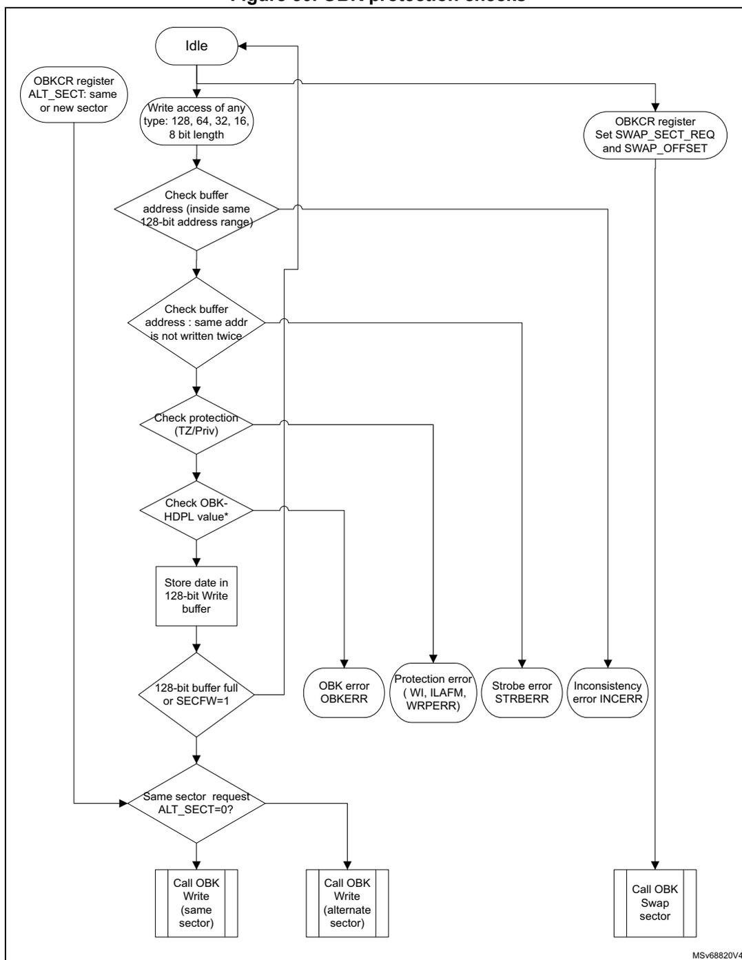
graph TD
    Idle([Idle]) --> Write[Write access of any type:
type: 128, 64, 32, 16,
8 bit length]
    Write --> Check1{Check buffer
address (inside same
128-bit address range)}
    Check1 --> Check2{Check buffer
address : same addr
is not written twice}
    Check2 --> Check3{Check protection
(TZ/Priv)}
    Check3 --> Check4{Check OBK-
HDPL value*}
    Check4 --> Store[Store date in
128-bit Write
buffer]
    Store --> Check5{128-bit buffer full
or SECFW=1}
    Check5 --> Check6{Same sector request
ALT_SECT=0?}

    Check1 --> Inconsistency((Inconsistency
error INCERR))
    Check2 --> Strobe((Strobe error
STRBERR))
    Check3 --> Protection((Protection error
( WI, ILAFM,
WRPERR)))
    Check4 --> OBKError((OBK error
OBKERR))
    Check5 --> OBKError

    Check6 --> WriteSame[Call OBK
Write
(same
sector)]
    Check6 --> WriteAlt[Call OBK
Write
(alternate
sector)]

    OBKCR1[OBKCR register
ALT_SECT: same
or new sector] --> Check6
    Idle --> OBKCR2[OBKCR register
Set SWAP_SECT_REQ
and SWAP_OFFSET]
    OBKCR2 --> Swap[Call OBK
Swap
sector]

    WriteSame --> Idle
    WriteAlt --> Idle
    Swap --> Idle
    Inconsistency --> Idle
    Strobe --> Idle
    Protection --> Idle
    OBKError --> Idle
7.5.4 OBK programming finite state machine
When the OBK write buffer is filled, the OBK programming is launched automatically in the current OBK sector or in the alternate OBK sector, depending upon the ALT_SECT bit.
If the address is not virgin, the OBKWRERR is raised.
Figure 31. Key writing flow
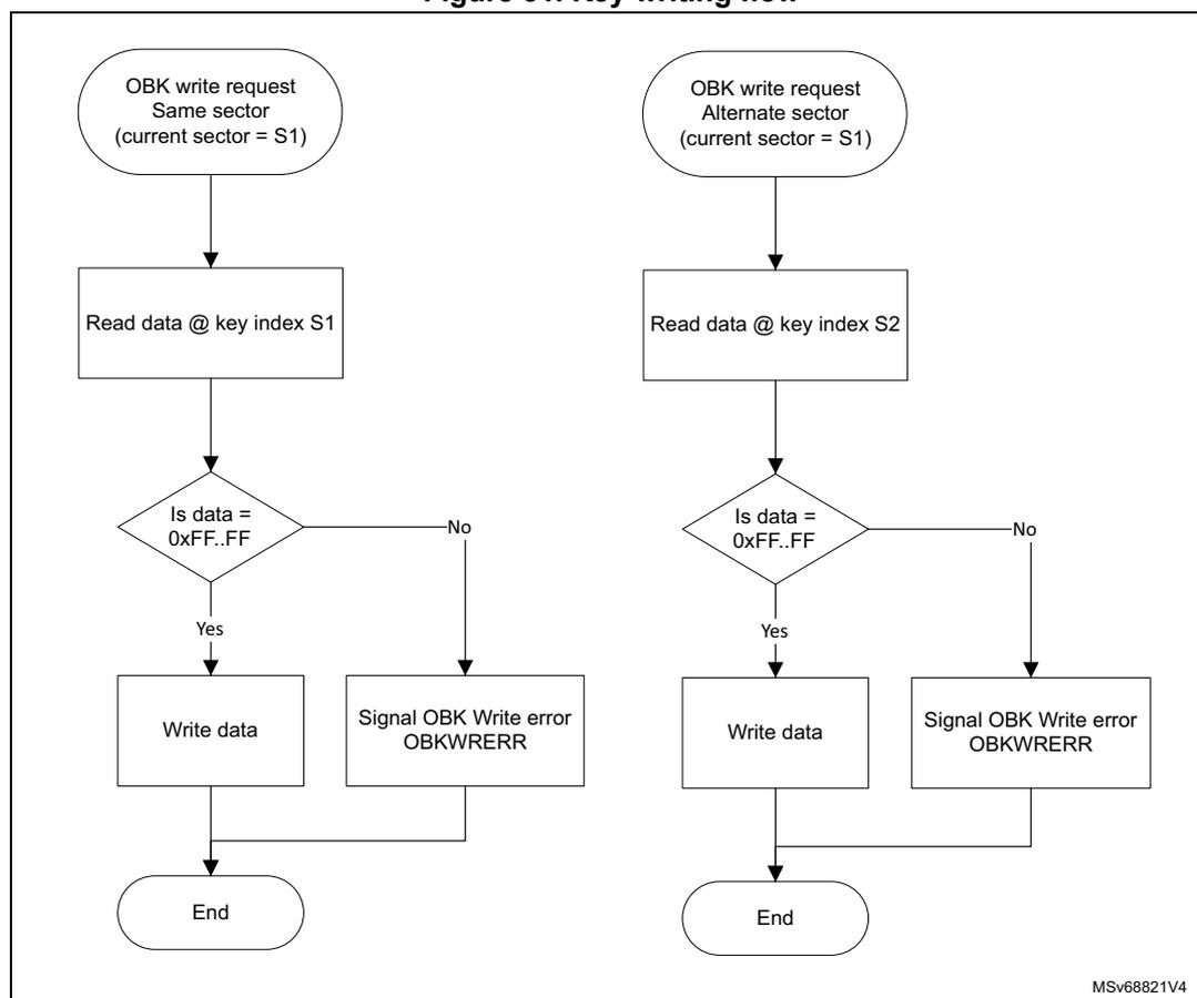
graph TD
    subgraph SameSector [Same sector (current sector = S1)]
        S1_1([OBK write request
Same sector
(current sector = S1)]) --> S1_2[Read data @ key index S1]
        S1_2 --> S1_3{Is data =
0xFF..FF}
        S1_3 -- Yes --> S1_4[Write data]
        S1_3 -- No --> S1_5[Signal OBK Write error
OBKWRERR]
        S1_4 --> S1_6([End])
        S1_5 --> S1_6
    end
    subgraph AlternateSector [Alternate sector (current sector = S1)]
        S2_1([OBK write request
Alternate sector
(current sector = S1)]) --> S2_2[Read data @ key index S2]
        S2_2 --> S2_3{Is data =
0xFF..FF}
        S2_3 -- Yes --> S2_4[Write data]
        S2_3 -- No --> S2_5[Signal OBK Write error
OBKWRERR]
        S2_4 --> S2_6([End])
        S2_5 --> S2_6
    end
The flowchart shows two parallel paths for key writing. The left path is for a 'Same sector (current sector = S1)' request, which involves reading data at key index S1, checking if it equals 0xFF..FF, and then either writing data or signaling an error. The right path is for an 'Alternate sector (current sector = S1)' request, which involves reading data at key index S2, checking if it equals 0xFF..FF, and then either writing data or signaling an error. Both paths end at an 'End' state. A small code 'MSv68821V4' is visible in the bottom right corner of the diagram.
7.5.5 OBK swap sector
The user can request a swap of the option byte keys by setting the bit SWAP_SECT_REQ in the NS/SECOBKCFGR register. The number of keys swapped is defined by the SWAP_OFFSET in NS/SECOBKCFGR register.
Swap is limited by OBK-HDPL value, the following SWAP_OFFSET values are permitted:
- • OBK_HDPL1_OFFSET = 144
- • OBK_HDPL2_OFFSET = 192
- • OBK_HDPL3SEC_OFFSET = 384
- • OBK_HDPL3NS_OFFSET = 511
The programming sequence is the following:
- 1. Check that no memory operations are ongoing by checking the BSY and DBNE bit in the FLASH_SEC/NSSR register and that the write buffer is empty by checking the WBNE bit in the FLASH_SEC/NSSR register.
- 2. Check and clear all the secure/non-secure error flags due to previous operation.
- 3. Unlock NS/SECOBKCFGR register if not unlocked already thanks to FLASH_NS/SECOBKKEYR.
- 4. Define the numbers of keys to be swapped thanks to SWAP_OFFSET field in NS/SECOBKCFGR. SWAP_OFFSET must be equal to or greater than OBK_HDPL<N-1>_OFFSET.
- 5. Set bit SWAP_SECT_REQ in NS/SECOBKCFGR.
- 6. Wait for BSY bit to be cleared. In case of error OBKERR flag is set.
- 7. SWAP_SECT_REQ is cleared automatically at the end of the operation or in case of error.
Figure 32. Swap workflow
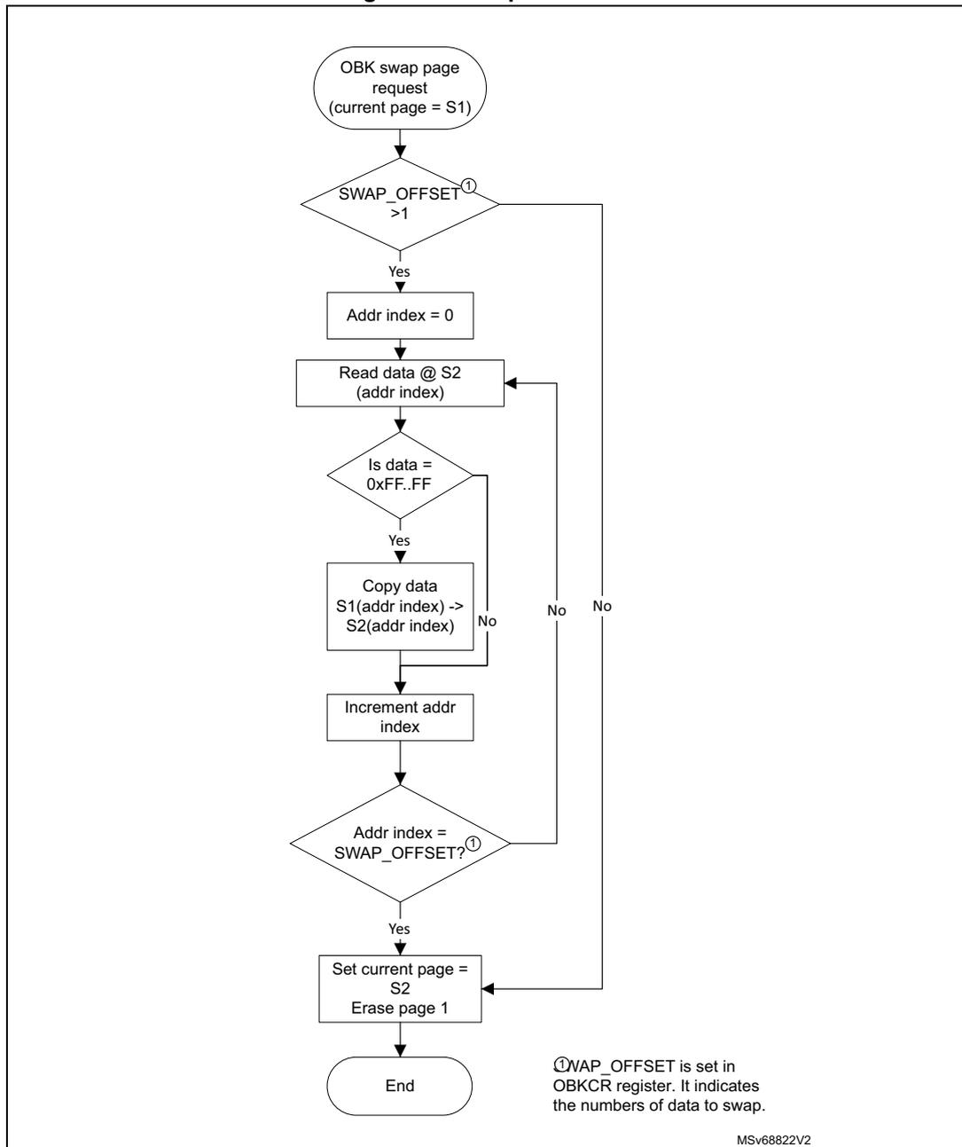
graph TD; Start([OBK swap page request
(current page = S1)]) --> Decision1{SWAP_OFFSET > 1}; Decision1 -- Yes --> Init[Addr index = 0]; Init --> Read[Read data @ S2
(addr index)]; Read --> Decision2{Is data = 0xFF..FF}; Decision2 -- Yes --> Copy[Copy data S1(addr index) -> S2(addr index)]; Copy --> Increment[Increment addr index]; Decision2 -- No --> Increment; Increment --> Decision3{Addr index = SWAP_OFFSET?}; Decision3 -- Yes --> EndPage[Set current page = S2
Erase page 1]; EndPage --> End([End]); Decision3 -- No --> Read; Note[①SWAP_OFFSET is set in OBKCR register. It indicates the numbers of data to swap.]
While the OBK SWAP operation is ongoing, the BSY flag is set and no other operation (write, erase, user opt change) can be launched in parallel.
7.5.6 OBK alternate sector erase
The user can request the erase of the alternate OBK sector by setting the bit ALT_SECT_ERASE in the FLASH_NS/SECOBKCFGR register.
The programming sequence must be:
- 1. Check that no memory operations are ongoing by checking the BSY and DBNE bits in the FLASH_SEC/NSSR register and that the write buffer is empty by checking the WBNE bit in the FLASH_SEC/NSSR register.
- 2. Check and clear all the secure/non-secure error flags due to previous operation.
- 3. Set bit ALT_SECT_ERASE in NS/SECOBKCFGR.
- 4. Wait for BSY bit to be cleared.
- 5. ALT_SECT_ERASE is cleared automatically at the end of the operation or in case of error.
7.6 FLASH security and protections
To protect sensitive information against unwanted operations (such as reading confidential areas, illegal programming of immutable sectors, or malicious flash memory erasing), the FLASH implements the following protection mechanisms:
- • TrustZone backed watermark and block security protection
- • Temporal isolation protection (HDP)
- • Configuration protection
- • User flash write protection
- • Device nonvolatile security life cycle and application boot state management
- • OTP locking
The microcontroller can have TrustZone active (TZ_STATE = 0xB4) or not (TZ_STATE = 0xC3).
While TrustZone is active the flash memory can be accessed in four basic modes:
- – non-secure and unprivileged
- – non-secure and privileged
- – secure and privileged
- – secure and unprivileged
While TrustZone is disabled, only two modes are possible:
- – non-secure and unprivileged
- – non-secure and privileged
The flash interface evaluates the access restrictions in the following order:
- 1. TrustZone security
- 2. Write protection (for write access)
- 3. HDP
- 4. Privilege
7.6.1 TrustZone security protection
The global TrustZone system security is activated by setting the TZEN option in the FLASH_OPTSR2_PRG register. The actual state of TZ is however determined by the SBS and the setting of TZ_STATE (refer to Section 14.3.5: SBS boot control ).
When TrustZone is active (TZ_STATE = 0xB4), additional security features are available:
- • Secure watermark-based user options bytes defining secure areas
- • Secure or non-secure block-based areas can be configured on-the-fly after reset. This is a volatile secure area
- • Additional product states associated with closed_secure provide protection of secure domain against external access (debug or bootloader)
- • Erase or program operation can be performed in secure or non-secure mode with associated configuration bit. When the TrustZone is disabled (TZ_STATE = 0xC3), the above features are deactivated and all secure registers are RAZ/WI.
Activating TrustZone security
When the TrustZone is activated (TZ_STATE = 0xB4), the SECBOOTADD and the secure watermark areas are set to a secure default value. Default settings are also used in case of corrupted configuration. In this default state, user flash memory is secure (see Table 55 ).
Table 55. Default secure watermark
| Secure watermark in case of configuration error | Security attribute |
|---|---|
| SECWMx_STRT = 0 SECWMx_END = 0x7F (1) | All flash memory is secure |
1. Default and maximum values depend upon the total number of sectors in the user flash memory.
Illegal access generation
A non-secure access to a secure flash memory area is RAZ/WI, it generates an illegal access event. An illegal access interrupt is generated if the FLASHIE illegal access interrupt is enabled in the TZIC_IER2 register.
A non-secure access to a secure flash register generates an illegal access event. An illegal access interrupt is generated if the FLASH_REGIE illegal access interrupt is enabled in the TZIC_IER2 register.
Table 56. Flash memory TZ protection summary
| TZ protection (TZ_STATE = 0xB4) | Main flash | ||
|---|---|---|---|
| Non-secure sector | Secure sector | ||
| Secure | Fetch | BUS ERROR | OK |
| Read | RAZ, ILAFM | ||
| Write | WI, WRPERR, ILAFM | If not WRP: OK else: WI, WRPERR | |
| Erase | |||
Table 56. Flash memory TZ protection summary (continued)
| TZ protection (TZ_STATE = 0xB4) | Main flash | ||
|---|---|---|---|
| Non-secure sector | Secure sector | ||
| Non-secure | Fetch | OK | BUS ERROR |
| Read | RAZ, ILAFM | ||
| Write | If not WRP: OK else: WI, WRPERR | WI, WRPERR, ILAFM | |
| Erase | |||
Table 57. TZ protection and bank or mass erase summary
| TZ protection (TZ_STATE = 0xB4) | Main flash | ||
|---|---|---|---|
| Non-secure flash | Secure flash | Mix of secure and non-secure | |
| MES | WI, WRPERR, ILAFM | OK | WI, WRPERR, ILAFM |
| MENS | OK | WI, WRPERR, ILAFM | WI, WRPERR, ILAFM |
Deactivate TrustZone security
Reversing of the TZ setting in OB (TZEN) is possible when the product state is ST-RoT-Ready or Provisioning. Deactivating TZEN from other states requires full regression (Regression state).
When the TrustZone is deactivated (TZ_STATE = 0xC3) after option bytes loading, the following security features are deactivated:
- • Watermark-based secure area (refer to Watermark-based secure flash area protection )
- • block-based secure area (refer to Section 7.6.3 )
- • Secure interrupts (refer to Section 7.9.11 )
- • All secure registers are RAZ/WI.
Watermark-based secure flash area protection
When TrustZone security is active (TZ_STATE = 0xB4), a part of the flash memory can be protected against non-secure read and write accesses. Up to two different nonvolatile secure areas can be defined by option bytes and can be read or written by a secure access only: one area per bank can be selected with a sector granularity.
The secure areas are defined by a start sector offset and end sector offset using the SECWMx_STRT and SECWMx_END option bytes. These offsets are defined in the secure watermark registers address registers FLASH security watermark for Bank1 (FLASH_SECWM1R_CUR) , FLASH security watermark for Bank2 (FLASH_SECWM2R_CUR) and modified by corresponding FLASH_XXX_PRG registers.
The SECWMx_STRT and SECWMx_END option bytes can be modified only by secure firmware.
Table 58. Secure watermark-based area
| Secure watermark option bytes values (x = 1, 2) | Secure watermark protection area |
|---|---|
| SECWMx_STRT > SECWMx_END | Nonsecure area |
| SECWMx_STRT = SECWMx_END | One sector defined by SECWMx_STRT is secure watermark-based protected |
| SECWMx_STRT < SECWMx_END | The area between SECWMx_STRT and SECWMx_END is secure watermark-based protected |
Caution: Switching a memory area from secure to nonsecure does not erase its content. The user secure software must perform the needed operation to erase the secure area before switching an area to non-secure attribute whenever is needed. It is also recommended to flush the instruction cache.
7.6.2 Hide protection (HDP)
The HDP area is independent of the flash watermark-based secure area. One nonvolatile secure hide protection (HDP) area per bank can be defined with a sector granularity. Access to the hide protection area can be denied by progressing the HDPL level in the SBS.
When the HDPL = 1, no user flash is protected by the HDP. With HDPL \( \geq \) 2 the user OB defined HDP area in each bank is closed. No read, write, fetch or erase is allowed in the HDP area.
The HDP area can be extended, the extension setting is only a register value, not stored in OB. With HDPL = 3 the HDP area remains activated and the extension is added. If extension is added while the base user OB defined area is not active, the extension covers one more sector, because HDPx_END sector is also protected.
The HDPL level can be only cleared by a system reset, there is no means to deactivate the HDP area.
The protected HDP area is defined by setting its size using start and end sectors in a similar way as the secure watermark.
The size of the inaccessible area can be extended using register FLASH_HDPEXTR values HDPx_EXT, representing the number of sectors added to the HDP area (past the HDPx_END sector). The volatile HDPx_EXT value can be increased, but cannot decrement.
If HDPx_STRT > HDPx_END the extension covers (HDPx_EXT + 1) size area between sectors marked by HDPx_END and HDPx_END + HDPx_EXT.
By default HDPx_END is set to 0 and HDPx_STRT is set to 1. This means that the HDP area in user flash has a 0 size, and extends from the flash start address (first sector).
For example, to protect area by HDP from the address 0x0801 4000 (included) to the address 0x0804 FFFF (included):
- • For physical Bank1, the option byte registers must be programmed with:
- – HDP1_STRT = 0x0A
- – HDP1_END = 0x27
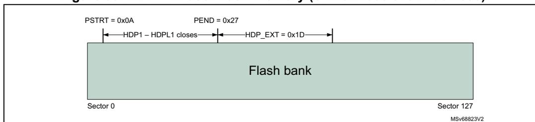
- Once the HDPL is incremented to 2, the marked area becomes inaccessible. The HDPL = 2 code then sets the extension size to 29. Once the HDPL is incremented to 3, even the extension area becomes inaccessible.
- Alternatively, if:
- HDP1_END = 0, HDP1_START = 1, HDPx_EXT = 1: Sector 0 and Sector 1 are HDP protected.
- HDP1_END = 2, HDP1_START = 7, HDPx_EXT = 3 (a rather unusual example): Sectors 2 to 5 are HDP protected.
- If the two banks are swapped, the protection defined to physical Bank1 remains on the physical Bank1, unaffected by swapping. Separate protection applies to physical Bank2 and the option bytes registers must also be programmed with:
- HDP2_STRT = 0x0A
- HDP2_END = 0x27
Note: For more details on the bank swapping mechanism, refer to Section 7.6.6 . The values have an upper limit, 127 for STM32H562/63/73xx devices, 31 for STM32H523/33xx devices.
Table 59. Secure hide protection
| HDPx watermark option byte values (x = 1, 2) | Hide protection area | |
|---|---|---|
| HDPL ≤ 1 | - | No inaccessible HDP area in user flash memory |
| HDPL = 2 | HDPx_END < HDPx_STRT | No inaccessible HDP area in user flash memory |
| HDPx_END = HDPx_STRT | Exactly one sector is protected by HDP | |
| HDPx_END > HDPx_STRT | The area between HDPx_STRT and HDPx_END is HDP protected. | |
| HDPL = 3 | HDPx_END < HDPx_STRT and HDPx_EXT = 0 | No inaccessible HDP area in user flash memory |
| HDPx_END ≥ HDPx_STRT or HDPx_EXT > 0 | The area between min (HDPx_STRT, HDPx_END) and (HDPx_END + HDPx_EXT) is HDP protected | |
a. The HDP works analogically, the number of sectors is the only differentiator.
Table 60. HDP protections summary
| HDP protection | User flash | |||
|---|---|---|---|---|
| Access to OB HDP area | Access to EXT HDP area | |||
| HDPL 2 or 3 | HDPL1 | HDPL3 | HDPL1 or HDPL 2 | |
| Fetch | BUS ERROR | OK | BUS ERROR | OK |
| Read | RAZ | RAZ | ||
| Write | WI, WRPERR | If not WRP: OK Else: WI, WRPERR | WI, WRPERR | If not WRP: OK Else: WI, WRPERR |
| Erase (mass erase) | ||||
7.6.3 Block-based secure flash memory area protection
Any sector can be programmed on-the-fly as secure or non-secure using the block-based configuration registers. FLASH_SECB1x/FLASH_SECB2x registers are used to configure the security attribute for, respectively, sectors in Bank1/Bank2.
When the sector security attribute bit SECBByx[i] is set, the security attribute is the same as the secure watermark-based area. The secure sector is accessible only by a secure access.
If the SECBBy[i] bit is set or reset for a sector already included in a secure watermark-based area, the sector keeps the watermark-based protection security attributes.
To modify a block-based sector security attribute, it is recommended to:
- • Check that no flash operation is ongoing on the related sector.
- • Add an ISB instruction after modifying the sector security attribute SECBByx[i].
Caution: Switching a sector from secure to non-secure does not erase the content of the associated sector. User secure software must perform the needed operations before switching to non-secure attribute:
- • Erase sector content.
- • Invalidate the instruction cache.
Note: For SECBByx[i] access control, refer to Table 61.
Execute protection for S-Bus (AHB register bus) is done in AHB decoder, not in flash memory interface itself.
Table 61. Secure configuration block-based registers access conditions
| Access | Corresponding sector privilege status | Sector setting in SECBByx | ||
|---|---|---|---|---|
| Fetch | Secure/ non-secure | Privilege/ unprivilege | - | BUS ERROR |
| Read | - | OK | ||
| Write | Secure | Privilege | - | OK |
| Unprivilege | 0 | OK | ||
| 1 | WI | |||
| Non-secure | Privilege/ unprivilege | - | WI, ILAP | |
7.6.4 Block-based privileged flash memory area protection
Any sector can be programmed on-the-fly as privileged or unprivileged using the block-based configuration registers. FLASH_PRIVBB1x and FLASH_PRIVBB2x registers are used to configure the privilege attribute for, respectively, sectors in Bank1 and Bank2.
When the sector privilege attribute PRIVBBx[i] bit is set, the sector is accessible only by a privileged access. An unprivileged sector is accessible by a privileged or unprivileged access.
To modify a block-based privilege attribution, it is recommended to:
- • Check that no flash operation is ongoing on the related sector.
- • Add an ISB instruction after modifying the sector security attribute PRIVBBx[i].
Caution: Switching a sector from privileged to unprivileged does not erase the content of the associated sector.
Table 62. Privilege protection summary
| Access (TZ not relevant) | Main flash | ||
|---|---|---|---|
| Unprivileged sector | Privileged sector | ||
| Privilege | Fetch | OK | |
| Read | |||
| Write | |||
| Erase | |||
| Unprivilege | Fetch | OK | RAZ |
| Read | |||
| Write | WI, WRPERR | ||
| Erase | |||
Table 63. Privilege and mass or bank erase
| Access (TZ state not relevant) | Main flash | ||
|---|---|---|---|
| Unprivileged FLASH | Privileged FLASH | Mix unprivileged and privileged FLASH | |
| MEP | OK | ||
| MENP | OK | WI, WRPERR | |
Note: For PRIVBBx[i] access control, refer to Table 64 and Table 65.
Table 64. Privilege configuration register access conditions (TZ enabled)
| Access | Corresponding sector secure status (1) | Sector setting access in PRIVBBx | ||
|---|---|---|---|---|
| Fetch | Privileged/ unprivileged | Secure/ non-secure | - | BUS ERROR |
| Read | - | OK (all sectors) | ||
| Access | Corresponding sector secure status (1) | Sector setting access in PRIVBBxy | ||
|---|---|---|---|---|
| Write | Privileged | Secure | - | OK (all sectors) |
| Non-secure | NS | OK (only the sector corresponding to the bit) | ||
| S | WI (only the sector corresponding to the bit) | |||
| Unprivileged | Secure/non-secure | - | WI | |
1. Either watermark or block-based.
Table 65. Privilege configuration register access conditions (TZ disabled)| Access | Sector setting access in PRIVBBRxy | |
|---|---|---|
| Fetch | Privileged/unprivileged | BUS ERROR |
| Read | OK | |
| Write | Privileged | OK |
| Unprivileged | WI | |
7.6.5 Flash memory register privileged and unprivileged modes
The flash registers can be read and written by privileged and unprivileged accesses depending on the SPRIV and NSPRIV bits in FLASH privilege configuration register (FLASH_PRIVCFGR) :
- • When the SPRIV (respectively NSPRIV) bit is reset, all secure (respectively non-secure) flash registers can be read and written by both privileged or unprivileged access.
- • When the SPRIV (respectively NSPRIV) bit is set, all secure (respectively non-secure) flash registers can be read and written by privileged access only. Unprivileged access to a privileged registers is RAZ/WI.
The registers related to key storage (FLASH_NSOBKCFGR, FLASH_SECOBKCFGR, FLASH_NSOBKKEYR, FLASH_SECOBKKEYR) are exceptions to this rule and can be only accessed in privilege, regardless of other settings.
The next table summarizes flash registers access control.
Table 66. Flash register accesses (1)| Access | Non-secure register | Secure register | ||||
|---|---|---|---|---|---|---|
| NSPRIV = 1 | NSPRIV = 0 | SPRIV = 1 | SPRIV = 0 | |||
| X | Secure/non-secure | Privileged/unprivileged | Bus error | |||
| R/W | Secure | Privileged | OK | |||
| R/W | Unprivileged | RAZ, WI | OK | RAZ, WI | OK | |
| Access | Non-secure register | Secure register | ||||
|---|---|---|---|---|---|---|
| NSPRIV = 1 | NSPRIV = 0 | SPRIV = 1 | SPRIV = 0 | |||
| R/W | Non-secure | Privileged | OK | RAZ, WI, ILAP | ||
| R/W | Unprivileged | RAZ, WI | OK | |||
1. Some registers are privilege only, not configurable.
7.6.6 Flash memory banks attributes in case of bank swap
The SWAP_BANK option bit modifies the address of each bank in the memory map. When SWAP_BANK is reset, flash Bank1 is mapped at the lower address range. When SWAP_BANK is set, flash Bank1 is mapped at the higher address range. flash bank attributes follow their bank contents so there is no need to modify their setting registers when swapping banks:
- • Flash secure watermark x FLASH_SECWMx
- • Flash write protection sector group FLASH_WRPSG (refer to Section 7.6.8 )
- • Hide protection in FLASH_HDPx registers
- • Flash secure block based bank x register y FLASH_SECBBxy
- • Flash privilege block based bank x register y FLASH_PRIVBBxy
- • The data area configuration FLASH_EDATA
The SWAP_BANK is rendered immutable by setting BOOT_LOCK in the user OB. If TZEN is enabled, then SECBOOT_LOCK locks the option. If TZEN is disabled, then NSBOOT_LOCK locks the SWAP_BANK option.
Note: The BK_ECC bit in the FLASH ECC detection register (FLASH_ECCDETR) and FLASH ECC correction register (FLASH_ECCCORR) , BKSEL bit in FLASH non-secure control register (FLASH_NSCR) and BKSEL bit in FLASH secure control register (FLASH_SECCR) always refers to Bank1 (respectively Bank2) when it is low (respectively high), regardless of the SWAP_BANK value.
Figure 34 shows how security attributes and protections behave in case of bank swap.
Figure 34. Protection attributes in case of bank swap illustration
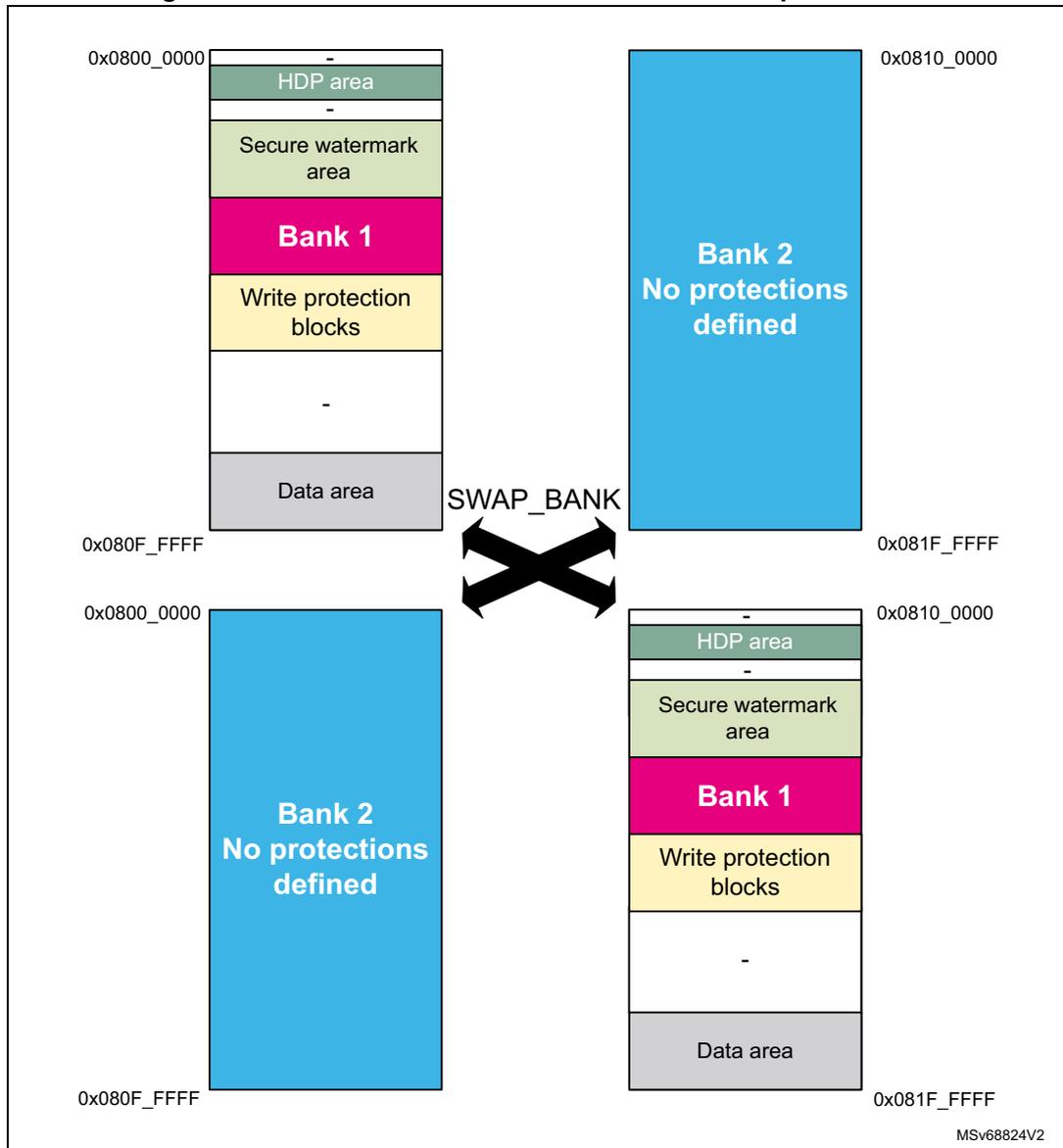
The diagram illustrates the effect of a bank swap on flash memory protection attributes. It shows two states: the initial state and the state after a SWAP_BANK operation.
Initial State (Top):
- Address range: 0x0800_0000 to 0x080F_FFFF
- Memory layout (from top to bottom):
- HDP area
- -
- Secure watermark area
- Bank 1
- Write protection blocks
- -
- Data area
Initial State (Bottom):
- Address range: 0x0810_0000 to 0x081F_FFFF
- Memory layout: Bank 2 No protections defined
After SWAP_BANK operation:
- Top (Address range: 0x0800_0000 to 0x080F_FFFF): Bank 2 No protections defined
- Bottom (Address range: 0x0810_0000 to 0x081F_FFFF):
Memory layout (from top to bottom):
- HDP area
- -
- Secure watermark area
- Bank 1
- Write protection blocks
- -
- Data area
A large 'X' with the label 'SWAP_BANK' is positioned between the two states, indicating the swap operation.
7.6.7 Flash memory configuration protection
The memory uses hardware mechanisms to protect the following assets against unwanted or spurious modifications (such as software bugs):
- • Option bytes change
- • Write operations
- • Erase commands
- • Interrupt masking
The memory configuration registers protection is summarized in Table 67 . Registers not present in this table are not protected by a key.
Table 67. Flash interface register protection summary
| Register name | Unlocking register | Protected asset |
|---|---|---|
| FLASH_NSCR | FLASH_NSKEYR | Write/erase control |
| FLASH_SECCR | FLASH_SECKEYR | Secure write/erase control |
| FLASH_OPTCR + all_PRG registers | FLASH_OPTKEYR | Flash bank option byte words change |
| FLASH_NSOBKFGR | FLASH_NSOBKKEYR | Flash OBKey storage manipulation |
| FLASH_SECOBKCFGR | FLASH_SECOBKKEYR |
7.6.8 Write protection
The purpose of the write protection is to prevent unwanted modifications to code and/or data.
Any group of four consecutive 8-Kbyte sectors can be independently write-protected or unprotected by clearing/setting the corresponding WRPSGn1/2 bit in the FLASH_WRPSG1/2 register (see FLASH write sector group protection for Bank1 (FLASH_WRP1R_CUR) and FLASH write sector group protection for Bank2 (FLASH_WRP2R_CUR) ).
A write-protected group of sectors cannot be erased nor programmed. As a result, a bank erase cannot be performed if one group of sectors is write-protected, unless a NVSTATE transition to OPEN is triggered (erasing the whole user flash memory).
Note: Write protection errors are documented in Section 7.9 .
7.6.9 Flash high-cycle data protections
The memory can be configured to have 96-Kbyte memory area with high-cycling capability (100 kcycles) to store data and emulate EEPROM, see Section 7.3.10 .
Option byte controlled security features for user flash memory prevent sectors from being used as high-cycle data area. No OPTCHANGEERR is raised in case of setting conflict, it only makes the sectors unusable. Details are listed in Table 68 .
Volatile settings using FLASH_SECBxx and FLASH_PRIVBBxx can be applied. In this case the security setting of user flash sector 127 applies to flash high-cycle data sector 0 and so on, as indicated in Figure 25 , Figure 26 , and Figure 29 .
Volatile settings of HDP extension that extends into sectors of data area cause the data area to be inaccessible.
Table 68. High-cycle area protection summary: access to data area address range
| TZ protection (when TZ_STATE = 0xB4) (1) | Data sector enabled | Data sector not enabled | ||||||
|---|---|---|---|---|---|---|---|---|
| HDP protected | OB secure area | SecBB protected | NS sector | |||||
| 16/32 bits access | Other | 16/32 bits access | Other | |||||
| Secure | Fetch | BUS ERROR | BUS ERROR | |||||
| Read | OK | BUS ERROR | RAZ, ILAC | |||||
| Write | If not WRP: OK else WI, WRPERR | WI, WRPERR, ILAFM | ||||||
| Erase | Same protection as in corresponding classic user flash sector | |||||||
| Non-secure | Fetch | BUS ERROR | BUS ERROR | |||||
| Read | RAZ, ILAC | OK | BUS ERROR | |||||
| Write | WI, WRPERR, ILAFM | If not WRP: OK else WI, WRPERR | ||||||
| Erase | Same protection as in corresponding classic user flash sector | |||||||
- 1. If TZ_STATE = 0xC3, there is no secure state access, no SecBB, and no Secure Area. For HDP and NS access the rules remain the same.
Table 69. HDP protected definition
| User flash | OB HDP area enabled | HDP extension enabled |
|---|---|---|
| HDPL1 | HDP protected = 0 | HDP protected = 0 |
| HDPL2 | HDP protected = 1 | HDP protected = 0 |
| HDPL3 | HDP protected = 1 | HDP protected = 1 |
Table 70. Privileged sectors and data area - Access to data area address range
| Access | Data area address range access | ||
|---|---|---|---|
| Unprivileged sector | Privileged sector | ||
| Privileged | Fetch | BUS ERROR | |
| Read | OK | OK | |
| Write | OK | OK | |
| Unprivileged | Fetch | BUS ERROR | |
| Read | OK | RAZ, ILAC | |
| Write | OK | WI, WRPERR | |
7.6.10 Life cycle management
Non-volatile or debug states are determined by the product state set by user option bytes. Debug possibility and possibility to change selected security settings are related to it. While the state is stored in the OB, it is the SBS that controls the debug policy.
OBK storage access conditions are unaffected by the PRODUCT_STATE, but keys can be evicted in regression transitions.
HDP works regardless of the debug state. Even in debug the HDP area is hidden when HDPL increments.
The following states are defined:
Table 71. Product states, debug states and debug policy
| PRODUCT_STATE | Code in OB | Description |
|---|---|---|
| Open | 0xED | User flash open (TZ secure and non-secure open). External access (debug) N and NS enabled (~RDP0). |
| Provisioning | 0x17 | Provisioning - Immutable root of trust is being installed. Open if TZEN = 0xC3. The debug is opened in HDPL3-NS. |
| iROT-Provisioned | 0x2E | The immutable root of trust is installed (~RDP 0.5). |
| TZ-Closed | 0xC6 | State for debugging the NS application. Debug is restrained to non-secure areas. |
| Closed | 0x72 | State for running a secure application. Debug disabled, regression is possible. |
| Locked | 0x5C | Transition to other state, policy change or debug not permitted (1) . |
| Regression | 0x9A | The temporary state initiated by the debug authentication system in transition to Open. |
| NS-Regression | 0xA3 | The temporary state initiated by the debug authentication system in transition to TZ-Closed. |
1. The same situation is Closed state with incorrect or not defined debug certificates.
1. No debug protection
Read, program and erase operations into the flash main memory area are possible. Least restriction on the option bytes.
2. Non-secure debug only
All read and write operations (if no write protection is set) from/to the non-secure flash memory are possible. The debug access to secure area is prohibited. Debug access to non-secure area remains possible.
The following rules are enforced:
- • User mode: code executing in user mode (boot flash) can access flash main memory and option bytes with all operations (read, erase, program).
- • Non-secure debug mode: The secure flash memory areas are inaccessible; the non-secure flash memory areas remain accessible for debug purpose.
- • Boot RAM mode: boot from SRAM is not possible.
- • Transition to Open state is possible with the consequence of flash mass erase and key slots revocation. Depends on debug unlock policy (see below).
3. Full product protection
All debug features are disabled and following rules enforced:
- • User mode: code executing in user mode (boot flash) can access flash main memory and selected option bytes with all operations (read, erase, program).
- • Boot RAM mode: boot from SRAM is not possible.
- • Transition to TZ-Closed or Open state is possible with the consequence of flash mass erase and key slots revocation. Depends on debug unlock policy (see below).
7.6.11 Product state transitions
Progressing towards a more closed state is the normal product life cycle, that does not require security measures. Transition towards Open state is a regression, controlled by the debug authentication control. If debug unlock policy is set to “locked”, no regression is accepted. Locked state can be reinforced by invalidating the debug authentication certificates.
All transitions not listed in this chapter are invalid.
There is no restriction on reading the current product state.
Transitions in progress direction
Transition from Open to any of the closed states is matter of correct product configuration and provisioning. The transitions must be done in correct order.
The normal progression is:
- • Open to Provisioning or iRoT-Provisioned
- • Provisioning to iRoT-Provisioned
- • Provisioning or iRoT-Provisioned to TZ-Closed, Locked or Closed
- • TZ-Closed to Locked or Closed
Transition is managed either by a software running on the device, or directly, using a debug interface. Transitions from Closed are only possible by software running on the device. By software it is assumed that transitions are triggered by bootloader, or root-of-trust services, but generally any software running on the device can do a progress transition.
Transition to Open state
This transition is a full regression. The starting state is any except Open and Locked. The debug tools are used to authenticate debug regression access rights with the debug authentication library, running on the device in HDPL1 (refer to Section 14.3.6: SBS debug control ). After verifying the credentials, it puts the device into intermediate state Regression. From this state the device regresses securely in HDPL0 to Open.
The transition has the following consequence:
- • Epoch secure counter is incremented
- • Key slots revocation
- • Product state updated
- • User options updated (security settings reset, TZEN reset)
- • Flash memory mass erase
- • Backup RAM erase is requested
Transition from closed to closed-secure debug state
This transition opens the device to authorize the debug of the non-secure application software without compromising the security of the ROT functions.
The starting state is Closed. The debug tools are used to authenticate debug regression access rights with the debug authentication library, running on the device in the HDPL1 (refer to Section 14.3.6: SBS debug control ). After verifying the credentials, it puts the device into intermediate state NS-Regression. From this state, the device regresses securely in HDPL0 to Closed.
The transition has the following consequence:
- • Epoch non-secure counter is incremented
- • Non-secure slots revocation
- • Product state updated
- • Flash memory sectors not covered by the secure watermark are erased
- • Backup RAM erase is requested
Table 72. PRODUCT_STATE transitions
| From | To (1) | |||||||
|---|---|---|---|---|---|---|---|---|
| Open | Provisioning | iROT-Provisioned | TZ-Closed (2) | Closed | Locked | Regression | NS-Regression (2) | |
| Open | - | OK | OK | X | X | X | X | X |
| Provisioning | X | - | OK | OK | OK | OK | OK (HDPL1) | X |
| iRoT-Provisioned | X | X | - | OK | OK | OK | OK (HDPL1) | X |
| TZ-Closed | X | X | X | - | OK | OK | OK (HDPL1) | X |
| Closed | X | X | X | X | - | X | OK (HDPL1) | OK (HDPL1) |
| Locked | X | X | X | X | X | - | X | X |
Table 72. PRODUCT_STATE transitions (continued)
| From | To (1) | |||||||
|---|---|---|---|---|---|---|---|---|
| Open | Provisioning | iROT-Provisioned | TZ-Closed (2) | Closed | Locked | Regression | NS-Regression (2) | |
| Regression | OK (HDPL0) | X | X | X | X | X | - | X |
| NS-Regression | X | X | X | OK (HDPL0) | X | X | X | - |
1. X = transitions not permitted (OPTCHANGEERR raised), - = no change, OK = valid transitions.
2. To transition into this state, both the current and programmed values of TZEN must be enabled (TZEN = 0xB4), otherwise the change is ignored with OPTCHANGEERR.
In Table 72 , X indicates transitions that are not permitted, a dash indicates no change, OK indicates valid transitions. Some transitions are possible only in correct HDPL provided in parenthesis. Attempts to do an illegal transition result in OPTCHANGEERR.
Incorrect PRODUCT_STATE (no OBL) is interpreted as Locked.
7.6.12 OBK protection
At the receipt of an OBK access (read/write/execute), secure and privilege attributes are first checked, followed by OBK-HDPL. The OBK-HDPL value must exactly match the HDPL assigned to the key location, otherwise OBKERROR flag is raised. Flash interface response is described in Table 73 .
Table 73. TZ OBK protection summary
| TZ protection (when TZ_STATE = 0xB4) | OBK access | Tamper | |
|---|---|---|---|
| No tamper | |||
| HDPL0/1/2/3 | OBK selector | ||
| XS | BUS ERROR | BUS ERROR | RAZ, WI |
| RS | OK if privilege, otherwise RAZ | RAZ | |
| WS | OK if privilege, otherwise WI, WRPERR | WI, if not privilege also WRPERR | |
| XNS | BUS ERROR | BUS ERROR | |
| RNS | RAZ, ILAFM | RAZ, ILAFM | |
| WNS | WI, WRPERR, ILAFM | WI, WRPERR, ILAFM | |
| Erase | NA | NA | NA |
Table 74. OBK protection summary with TZ disabled
| TZ protection (when TZ_STATE = 0xC3) | OBK access | Tamper | |
|---|---|---|---|
| No tamper | |||
| HDPL1/2/3 | OBK selector | ||
| XNS | BUS ERROR | BUS ERROR | |
| RNS | OK if privileged, otherwise RAZ | RAZ | RAZ, WI |
| WNS | OK if privilege, otherwise WI, WRPERR | WI if privileged, otherwise WI, WRPERR | |
| Erase | NA | NA | NA |
Note: Cacheable access is managed at system level and not in the flash interface. The MPU must be configured to disable cache where it is not desirable.
In case of tamper, all keys are read as 0x00s.
There are also rules for accessing the OBKFGCR and OBKKEYR registers.
Table 75. Access conditions to secure control register
| - | S/NS | P/NP | TZ state | SECOBKCFGR and SECOBKKEYR access |
|---|---|---|---|---|
| X | - | - | - | Bus error |
| R/W | S | P | Active | OK |
| R/W | S | NP | Active | RAZ, WI |
| R/W | NS | P | Active | RAZ, WI, ILAP |
| R/W | NS | NP | Active | RAZ, WI, ILAP |
| R/W | - | - | Deactivated | RAZ, WI |
Table 76. Access conditions to non-secure control register
| S/NS | P/NP | TZ state | NSOBKCFGR and NSOBKKEYR access | |
|---|---|---|---|---|
| X | - | - | - | Bus error |
| R/W | - | - | Active | RAZ, WI |
| R/W | - | P | Deactivated | OK |
| R/W | - | NP | Deactivated | RAZ, WI |
7.6.13 One-time-programmable and read-only memory protections
Sections of OTP/RO in the flash memory are described in details in Section 7.3.9 . There is no protection provided by the flash memory interface other than the dedicated write protection.
No write is possible to the RO area, once it was established in manufacturing. The OTP write protection describes a method of locking out the OTP area.
The access conditions are summarized in Table 77 .
Table 77. OTP/RO access constraints
| - | 8 Kbytes sector dedicated to RO/OTP | |||
|---|---|---|---|---|
| 0x08FF_E000 - E7FF | 0x08FF_E800 - EFFF Reserved | 0x08FF_F000 - F7FF OTP | 0x08FF_F800 - FFFF RO | |
| XS | BUS ERROR | BUS ERROR | ||
| RS | RAZ, ILAC | |||
| WS | WI, WRPERR, ILAFM | |||
| XNS | BUS ERROR | BUS ERROR | ||
| RNS | If correct size
(1)
RAZ, else BUS ERROR | If correct size OK, else BUS ERROR | ||
| WNS | If correct size WI, else BUS ERROR | BUS ERROR if incorrect size. WRPERR if block is protected by LOCKBL, else OK. | If correct size WI, else BUS ERROR | |
| Erase | WI | |||
1. Word size is 16 bits. 32-bit access is possible. Other access attempt leads to bus error.
7.7 System memory
7.7.1 Introduction
System memory stores RSS (root secure services) firmware programmed by ST during production. The RSS provides runtime services to user firmware.
When TrustZone is enabled (user sets TZEN bitfield to 0xB4) then RSS provides secure services to secure user firmware only; when TrustZone is disabled (user sets TZEN bitfield to 0xC3), RSS provides services to user firmware.
7.7.2 RSS user functions
The RSS provides runtime services thanks to RSS library, whose functions are exposed to user within the CMSIS device header file provided by the STM32CubeH5 firmware package (see UM3065 “ Getting started with STM32CubeH5 for STM32H5 Series ” for more details).
RSS provides services through two different libraries, RSSLIB and NSSLIB.
Table 78. RSSLIB/NSSLIB accesses
| TZEN configuration | User FW Non-Secure | User FW Secure | Bootloader/JTAG/SWD (1) |
|---|---|---|---|
| Enabled (0xB4) | N/A | RSSLIB | RSSLIB |
| Disabled (0xC3) | NSSLIB | N/A |
1. When the devices boot in bootloader, that is, in product state OPEN (with BOOT pin set to 1 and UBE set to 0xB4), or PROVISIONING.
Table 79. RSSLIB/NSSLIB entry point access| C defined macro | Location in flash memory |
|---|---|
| RSSLIB_PFUNC | 0xBF9FB68 |
| NSSLIB_PFUNC | 0xBF9FB6C |
RSSLIB
The secure user firmware calls RSSLIB functions using RSSLIB_PFUNC C defined macro, which points to a location within non-secure system memory. Before calling RSSLIB functions, the secure user firmware must define a non-secure region above this location within SAU of the Cortex®-M33, starting from RSSLIB_SYS_FLASH_NS_PFUNC_START (0xBF9FB78), up to RSSLIB_SYS_FLASH_NS_PFUNC_END (0xBF9FB84). These last addresses are provided within the CMSIS device header file.
The user can set this non-secure region either by using the CMSIS system partition header file, or by implementing its own code for SAU setup. The CMSIS system partition header file is part of the STM32CubeH5 firmware package.
Table 80. RSS lib interface functions| Library | Function | Attributes |
|---|---|---|
| RSSLIB_PFUNC | JumpHDPLvl2 | Secure callable function |
| JumpHDPLvl3 | ||
| JumpHDPLvl3NS | ||
| DataProvisioning | Non-secure callable function |
DataProvisioning
Secure attribute: Non-secure callable function.
Prototype:
uint32_t_ DataProvisioning (RSSLIB_DataProvisioningConf_t *pConfig)
User code function call example:
RSSLIB_PFUNC->NSC.DataProvisioning(&pConfig)
Arguments:
pConfig: input parameter. RSSLIB_DataProvisioningConf_t
C structure definition is described below:
typedef struct
{
    uint32_t_ *pSource;
    uint32_t_ *pDestination;
    uint32_t_ Size;
    uint32_t_ DoEncryption;
    uint32_t_ Crc;
} RSSLIB_DataProvisioningConf_t;
Structure elements
| pSource | Provides the address of data to be provisioned. Must be within SRAM3 address range (non-secure aliases). |
| pDestination | Provides the address where to store data to be provisioned. Must be within OBKeys address range. To be aligned on 16 bytes. |
| Size | Provides the size of data to be provisioned (the number of bytes, must be a multiple of 16). |
| DoEncryption | Notifies RSSLIB_DataProvisioning function if it must encrypt or not data within OBKeys. DoEncrypt can be either 0xF5F5A0AAU or 0xCACA0AA0U (the only one allowed on STM32H563xx devices)
|
| Crc | CRC over full source data buffer,
pConfig->pDestination
value,
pConfig->Size
value and finally
pConfig->DoEncryption
value. CRC computation uses CRC-32 (Ethernet):
|
Returned values
| 0xEA EA EA EA EA | Success |
| 0xF5F5E0E0U | Error:
|
| 0xF5F50E0EU | Error: Size is not a multiple of 16 |
| 0xF5F58080U | Error: computed CRC is not the expected one provided within pConfig->CRC |
| 0xF5F58008U | Error: cannot program data within OBKeys destination section |
| 0xF5F5E00EU | Error: wrong DoEncryption parameter value |
| 0xF5F50880U | Error: encryption requested, butw platform does not support it |
| 0xF5F50EE0U | Error: encryption error |
| 0xF5F50808U | Error: OBKeys programming error |
RSSLIB_DataProvisioning receives in input a data buffer and programs it within OBKeys. A CRC prevents any data and parameters tampering issue.
The destination address ( pDestination ) added to the size ( Size ) of the data to be provisioned must not cross the OBKeys section boundaries, listed below.
| OBKeys Level1 | Start address: 0x0FFD0100UL |
| End address: 0x0FFD08FFUL |
| OBKeys Level2 | Start address: 0x0FFD0900UL |
| End address: 0x0FFD0BFFUL | |
| OBKeys Level3 secure | Start address: 0x0FFD0C00UL |
| End address: 0x0FFD17FFUL | |
| OBKeys Level3 non-secure | Start address: 0x0FFD1800UL |
| End address: 0x0FFD1FEFUL |
When requested through pConfig->DoEncryption parameter, RSSLIB_DataProvisioning encrypts data before programming them within OBKeys.
RSSLIB_DataProvisioning uses AES CBC 128 bits with:
- • IV: defined as (using C definition format)
uint32_t IV = {0x8001D1CEU, 0xD1CED1CEU, 0xD1CE8001U, 0xCED1CED1U}; - • Key: DHUK corresponding to the targeted OBKeys section defined by pConfig->pDestination parameter.
Note: Data encryption within OBKeys is supported only by STM32H533/573xx devices.
JumpHDPLvl2
Secure attribute: Secure callable function.
Prototype:
uint32_t JumpHDPLvl2(uint32_t VectorTableAddr, uint32_t MPUIndex)
User code function call example:
RSSLIB_PFUNC->S.JumpHDPLvl2((uint32_t)NextVectorTableAddr, 1U );
Arguments:
- •
VectorTableAddr
:
- – Input parameter, address of the next vector table to apply.
- – The vector table format is the one used by the Cortex-M33 core.
- •
MPUIndex
:
- – Input parameter, MPU region index. Caller function must define (but keep disabled) the corresponding MPU region before calling JumpHDPLvl2 . The function enables the MPU region before jumping to the reset handler of the vector table. The vector table reset handler function belongs to the MPU region.
User calls JumpHDPLvl2 to close user Flash HDPL1 area by incrementing HDPL to 2, then jump to the reset handler embedded within the vector table, whose address is passed as input parameter.
After closing HDPL1, JumpHDPLvl2 enables the MPU region provided as input parameter. Once the MPU is enabled, the function sets the SP to the address provided by the passed vector table, and jumps to the reset handler function supported by it. JumpHDPLvl2 does not set the new vector table.
On successful execution, the function does not return and does not push LR onto the stack.
In case of failure (bad input parameter value), RSSLIB_Sec_JumpHDPLvl2 returns 0xF5F5F5F5.
JumpHDPLvl3
Secure attribute: Secure callable function.
Prototype:
uint32_t JumpHDPLvl3(uint32_t VectorTableAddr, uint32_t MPUIndex)
User code function call example:
RSSLIB_PFUNC->S.JumpHDPLvl3((uint32_t)NextVectorTableAddr, 1U );
Arguments:
- • VectorTableAddr:
- – Input parameter, address of the next vector table to apply.
- – The vector table format is the one used by the Cortex-M33 core.
- • MPUIndex:
- – Input parameter, MPU region index. Caller function must define but keep disabled the corresponding MPU region before calling JumpHDPLvl3. The function enables the MPU region before jumping to the reset handler of the vector table, whose function belongs to the MPU region.
User calls JumpHDPLvl3 to close user Flash HDPL1 and HDPL2 areas by incrementing HDPL up to 3, then jump to the reset handler embedded within the vector table, whose address is passed as input parameter.
After closing HDPL1/2, JumpHDPLvl3 enables the MPU region provided as input parameter. Once the MPU is enabled, the function sets the SP to the address provided by the passed vector table, and jumps to the reset handler function supported by the vector table. JumpHDPLvl3 does not set the new vector table.
On successful execution, the function does not return and does not push LR onto the stack.
In case of failure (bad input parameter value), JumpHDPLvl3 returns 0xF5F5F5F5.
JumpHDPLvl3NS
Secure attribute: Secure callable function.
Prototype:
uint32_t JumpHDPLvl3NS(uint32_t VectorTableAddr)
User code function call example:
NSSLIB_PFUNC->S.JumpHDPLvl3NS((uint32_t)NextVectorTableAddr, 1U );
Arguments:
- • VectorTableAddr:
- – Input parameter, address of the next vector table to apply.
- – The vector table format is the one used by the Cortex-M33 core.
User calls JumpHDPLvl3NS to close user flash HDPL1 and HDPL2 areas by incrementing HDPL up to 3, to move from secure to non-secure domain, then jump to the non-secure reset handler embedded within the vector table, whose address is passed as input parameter.
After closing HDPL1/2, JumpHDPLvl3 jumps to the non-secure reset handler function supported by the vector table. JumpHDPLvl3NS does not set the new vector table.
On successful execution, the function does not return and does not push LR onto the stack.
In case of failure (bad input parameter value), JumpHDPLvl3NS returns 0xF5F5F5F5.
NSSLIB
The user firmware calls only the NSSLIB function when TrustZone is disabled (TZEN bitfield is set to 0xC3).
The user firmware calls NSSLIB functions using NSSLIB_PFUNC C defined macro, which points to a location within system memory.
Table 81. NSS lib interface functions
| Library | Function | Attributes |
|---|---|---|
| NSSLIB_PFUNC | JumpHDPLvl2 | Non-secure function |
| JumpHDPLvl3 |
JumpHDPLvl2
Prototype:
uint32_t JumpHDPLvl2(uint32_t VectorTableAddr, uint32_t MPUIndex)
User code function call example:
NSSLIB_PFUNC->JumpHDPLvl2((uint32_t)NextVectorTableAddr, 1U );
Arguments:
- • VectorTableAddr:
- – Input parameter, address of the next vector table to apply.
- – The vector table format is the one used by the Cortex-M33 core.
- • MPUIndex:
- – Input parameter, MPU region index. Caller function shall define but keep disable the corresponding MPU region before calling JumpHDPLvl2. The function enables
the MPU region before jumping to the reset handler of the vector table. The vector table reset handler function belongs to the MPU region.
User calls JumpHDPLvl2 to close user Flash HDPL1 area by incrementing HDPL to 2, and to jump to the reset handler embedded within the vector table which address is passed as input parameter
After closing HDPL1, JumpHDPLvl2 enables the MPU region provided as input parameter. Once the MPU is enabled, the function sets the SP to the address provided by the passed vector table and jumps to the reset handler function supported by the vector table too. JumpHDPLvl2 does not set the new vector table.
On successful execution, the function does not return and does not push LR onto the stack.
In case of failure (bad input parameter value), RSSLIB_Sec_JumpHDPLvl2 returns 0xF5F5F5F5.
JumpHDPLvl3
Prototype:
uint32_t JumpHDPLvl3(uint32_t VectorTableAddr, uint32_t MPUIndex)
User code function call example:
NSSLIB_PFUNC->JumpHDPLvl3((uint32_t)NextVectorTableAddr, 1U );
Arguments:
- • VectorTableAddr:
- – Input parameter, address of the next vector table to apply.
- – The vector table format is the one used by the Cortex-M33 core.
- • MPUIndex:
- – Input parameter, MPU region index. Caller function shall define but keep disable the corresponding MPU region before calling JumpHDPLvl3. The function enables the MPU region before jumping to the reset handler of the vector table. The vector table reset handler function belongs to the MPU region.
User calls JumpHDPLvl3 to close user Flash HDPL1 and HDPL2 areas by incrementing HDPL up to 3, and then jump to the reset handler embedded within the vector table, whose address is passed as input parameter
After closing HDPL1/2, JumpHDPLvl3 enables the MPU region provided as input parameter. Once the MPU is enabled, the function sets the SP to the address provided by the passed vector table, and jumps to the reset handler function supported by it. JumpHDPLvl3 does not set the new vector table.
On successful execution, the function does not return and does not push LR onto the stack.
In case of failure (bad input parameter value), JumpHDPLvl3 returns 0xF5F5F5F5.
7.8 FLASH low-power modes
Table 82 summarizes the memory behavior in STM32 low-power modes. Embedded flash memory belongs to the core domain.
Table 82. Effect of low-power modes on the embedded flash memory
| Power mode | Core domain voltage range | Allowed if FLASH busy | FLASH power mode |
|---|---|---|---|
| Run | VOS0/1/2/3 | Yes | Run |
| Stop1 (clock stopped) | SVOS3/4/5 | No | Clock gated or stopped in case of SVOS5 |
| Standby | Off | No | Off |
When the system state changes or within a given system state, the memory can operate with a different voltage supply range (VOS), according to the application. The procedure to switch the memory into power modes (run, clock gated, stopped, off) is described hereafter.
Note: For more information on the microcontroller power states, refer to Section 10: Power control (PWR) .
Managing the FLASH domain switching to Stop or Standby
As explained in Table 82 , if the memory informs the reset and clock controller (RCC) that it is busy (BSY, DBNE, WBNE is set), the microcontroller cannot switch the core domain to Stop or Standby mode.
There are two ways to release the memory:
- • Reset the WBNE busy flag in FLASH_NS/SECSR register by any of the following actions:
- – Complete the write buffer with missing data.
- – Force the write operation without filling the missing data by activating the FW bit in FLASH_NS/SECCR register. This forces all missing data “high”.
- • Poll BSY busy bits in FLASH_NS/SECSR register until they are cleared. This indicates that all recorded write, erase and option change operations are complete.
The microcontroller can then switch the domain to Stop or Standby mode.
7.9 FLASH error management
7.9.1 Introduction
The memory automatically reports when an error occurs during a read, program or erase operation. A wide range of errors are reported:
- • Non-secure write protection error (WRPERR)
- • Secure write protection error (WRPERR)
- • Non secure programming sequence error (PGSERR)
- • Secure programming sequence error (PGSERR)
- • Secure strobe error (STRBERR)
- • Error correction code error (ECCC, ECCD)
- • Illegal access (ILAFM/ILAP)
- • Option byte change error (OPTCHANGEERR)
- • OBK non-secure general error (OBKERR)
- • OBK secure general error (OBKERR)
- • OBK non-secure write error (OBKWERR)
- • OBK secure write error (OBKWERR)
The application software can individually enable the interrupt for each error, as detailed in Section 7.10 .
The flash memory interface uses different interrupt lines to trigger the event. There are two direct lines to NVIC, one for secure interrupts, other for non secure. Third line leads to TZIC, for the ILAFM interrupt.
Note: For all errors, the application software must clear the error flag before attempting a new modify operation.
Since there is just one write buffer and only one operation is allowed at a time, the write control bits and status bits are shared by both banks:
- • Write control bits (PG, FW, EOPIE, WRPERRIE, PGSERRIE, STRBERRIE, INCERRIE, CLR_EOP, CLR_WRPERR, CLR_STRBERR, CLR_INCERR, CLR_PGSERR) controls Bank1 and 2 at the same time.
- • Write status flag reports (WBNE, DBNE, EOP, WRPERR, PGSERR, STRBERR, INCERR, BSY) error for Bank1 and 2 at the same time.
7.9.2 Non-secure write protection error (WRPERR)
When an illegal non-secure erase/program operation is attempted to the nonvolatile memory, the flash interface sets the write protection error flag WRPERR in FLASH_NSSR register.
An erase operation is rejected and flagged as illegal if it targets one of the following memory areas:
- • A sector write-protected with WRPSGn
- • An HDP area while the HDPL has made it inaccessible
- • Secure (TZ) state not matching the erased memory attribute
- • Attempt to erase privilege sector within unprivileged mode
A program operation is ignored and flagged as illegal if it targets one of the following memory areas:
- • System flash memory
- • A user sector write-protected with WRPSGn
- • An OTP block, locked with LOCKBL
- • A read-only section
- • A reserved area
- • Secure area
- • Privileged area from within unprivileged mode
- • OBK access conditions check error
When WRPERR flag is raised, the operation is rejected and nothing is changed in the corresponding bank. If this error is detected, the write buffer is invalidated.
Note: WRPERR flag must be cleared before any erase/program operation.
WRPERR flag is cleared by setting CLR_WRPERR bit to 1 in FLASH_NSCCR register.
If WRPERRIE bit in FLASH_NSCR register is set to 1, an interrupt is generated when WRPERR flag is raised (see Section 7.10 for details).
7.9.3 Secure write protection error (WRPERR)
When an illegal secure erase/program operation is attempted to the nonvolatile memory, the flash interface sets the write protection error flag WRPERR in FLASH_SECSR register.
An erase operation is rejected and flagged as illegal if it targets one of the following memory areas:
- • A sector write-protected with WRPSGn
- • An HDP area while the HDPL has made it inaccessible
- • Secure (TZ) state not matching the erased memory attribute
- • Attempt to erase privilege sector within unprivileged mode
A program operation is ignored and flagged as illegal if it targets one of the following memory areas:
- • System flash memory
- • A user sector write-protected with WRPSGn
- • An OTP block, locked with LOCKBL
- • A read-only section
- • A reserved area
- • Non-secure area
- • Privileged area from within unprivileged mode
- • OBK access condition check error
When WRPERR flag is raised, the operation is rejected and nothing is changed in the corresponding bank.
If this error is detected the write buffer is invalidated.
Note: WRPERR flag must be cleared before any erase/program operation.
WRPERR flag is cleared by setting CLR_WRPERR bit to 1 in FLASH_SECCR register.
If WRPERRIE bit in FLASH_SECCR register is set to 1, an interrupt is generated when WRPERR flag is raised (see Section 7.10 for details).
7.9.4 Non secure programming sequence error (PGSERR)
When the non-secure programming sequence is incorrect, the flash interface sets the programming sequence error flag PGSERR in FLASH_NSSR register.
More specifically, PGSERR flag is set when one of below conditions is met:
- • An error like INCERR, WRPERR, PGSERR, STRBERR, OPTCHANGEERR, OBKERR or OBKWERR have not been cleared before requesting a new write or erase operation, OBK operation or options change.
- • For erase, PGSERR is set if:
- – missing erase operation (FLASH_NSCR): STRT = 1 with (MER = 0, SER = 0 and BER = 0)
- – sector and bank erase requested at the same time (NSSTRT and more than one of MER, SER and BER)
- – PG set during erase operation (it ensures that no erase req and write req happen at the same time): (STRT = 1) with (PG = 1)
- – Erase operation is started while write buffer is waiting for next data: (STRT = 1) with WBNE = 1.
- – STRT = 1 set by secure access.
- – Erase operation is started while DBNE = 1.
- • For programming, PGSERR is set if:
- – missing write flag: A write operation is requested but the program enable bit PG has not been set in FLASH_NSCR register prior to the request.
- – write operation to flash high-cycle data is requested but PG = 0.
- – AHB write request is received and (SER = 1, BER = 1 or MER = 1)
- – 16 bit data access requested while WBNE = 1
- • For options change, PGSERR is set if:
- – option change is started while write buffer is waiting for next data: OPTSTRT = 1 with WBNE = 1
- – OPTSTRT set with non-secure DBNE = 1.
- • For options byte key storage access, PGSERR is set if:
- – error flags from previous operation not cleared
- – ALT_SECT_ERASE and SWAP_SECT_REQ in FLASH_NSOBKCFGR are set at the same time
- – SWAP_OFFSET value is wrong: when SWAP_SECT_REQ is set to 1, the SWAP_OFFSET should be equal or greater than OBK_HDPL < N - 1 > _SWAP_OFFSET
- – ALT_SECT_ERASE or OBK_SWAP set while DBNE = 1
- – OBK-HDPL is incorrect and non-secure OBK_SWAP is requested
- – If OBKSWAP or OBK alternate erase is started while write buffer is waiting for new data (WBNE = 1).
When PGSERR flag is raised as consequence of failed write attempt (flash programming), the current program operation is aborted and nothing is changed in the corresponding bank. The write data buffer is also invalidated.
Note: When PGSERR flag is raised, there is a risk that the last write operation performed by the application has been lost because of the above protection mechanism. It is recommended to generate interrupts on PGSERR and verify in the interrupt handler if the last write operation has been successful, by reading back the value in the flash memory.
The PGSERR flag also blocks any new program operation. This means that PGSERR must be cleared before starting a new program operation.
PGSERR flag is cleared by setting CLR_PGSERR bit to 1 in FLASH_NSCCR register.
If PGSERRIE bit in FLASH_NSCR register is set to 1, an interrupt is generated when PGSERR flag is raised. See Section 7.10 for details.
7.9.5 Secure programming sequence error (PGSERR)
When the secure programming sequence is incorrect, the flash interface sets the programming sequence error flag PGSERR in FLASH_SECSR register.
More specifically, PGSERR flag is set when one of below conditions is met:
- • An error like INCERR, WRPERR, PGSERR, STRBERR, OBKERR, or OBKWERR has not been cleared before requesting a new write or erase operation, OBK operation or options change.
- • For erase, PGSERR is set if:
- – missing erase operation (FLASH_SECCR): STRT = 1 with (SER = 0 and BER = 0, MER = 0)
- – sector and bank erase requested at the same time (SECSTRT and more than one of MER, SER, and BER)
- – PG set during erase operation (it ensures that no erase request and write request happen at the same time): (STRT = 1) with (PG = 1)
- – erase operation is started while write buffer is waiting for next data: (STRT = 1) with WBNE = 1.
- – operation started while secure DBNE = 1.
- • For programming, PGSERR is set if:
- – missing write flag: a write operation is requested but the program enable bit PG has not been set in FLASH_SECCR register prior to the request
- – write operation to flash high-cycle data is requested but PG = 0
- – AHB write request is received and (SER = 1, SER = 1, or MER = 1)
- – 16 bit data access requested while WBNE = 1
- • For options change, PGSERR is set if:
- – Option change is started while write buffer is waiting for next data: OPTSTRT = 1 with WBNE = 1
- – OPTSTRT set with secure DBNE = 1
- • For options byte key storage access, SECPGSERR is set if:
- – error flags from previous operation not cleared
- – ALT_SECT_ERASE and SWAP_SECT_REQ are set at the same time
- – SWAP_OFFSET value is wrong: when SWAP_SECT_REQ = 1, SWAP_OFFSET must be equal or greater than OBK_HDPL<N-1>_SWAP_OFFSET.
- – SWAP_SECT_REQ or OBK_SWAP set while DBNE = 1
- – OBK-HDPL is incorrect and secure OBK_SWAP is requested
- – If OBKSWAP or OBK alternate erase is started while write buffer is waiting for new data (WBNE = 1)
When PGSERR flag is raised as consequence of failed write attempt (flash programming), the current program operation is aborted and nothing is changed in the corresponding bank. The write data buffer is also invalidated.
Note: When PGSERR flag is raised, there is a risk that the last write operation performed by the application has been lost because of the above protection mechanism. It is recommended to generate interrupts on PGSERR and verify in the interrupt handler if the last write operation has been successful by reading back the value in the flash memory.
The PGSERR flag also blocks any new program operation. This means that PGSERR must be cleared before starting a new program operation.
PGSERR flag is cleared by setting CLR_SECPGSERR bit to 1 in FLASH_SECCCR register.
If PGSERRIE bit in FLASH_SECCR register is set to 1, an interrupt is generated when PGSERR flag is raised. See Section 7.10 for details.
7.9.6 Non-secure strobe error (STRBERR)
When the non-secure application software writes several times to the same byte in the write buffer, the flash interface sets the strobe error flag STRBERR (FLASH_NSSR) whatever the target bank of the write access.
When STRBERR flag is raised, the current program operation is aborted and the write buffer is invalidated.
STRBERR flag is cleared by setting CLR_STRBERR bit to 1 in FLASH_NSCCR register.
If STRBERRIE bit in FLASH_NSCR register is set to 1, an interrupt is generated when STRBERR flag is raised. See Section 7.10 for details.
7.9.7 Secure strobe error (STRBERR)
When the secure application software writes several times to the same byte in the write buffer, the memory sets the strobe error flag STRBERR (FLASH_SECSR) whatever the target bank of the write access.
When STRBERR flag is raised, the current program operation is aborted and the write buffer is invalidated.
STRBERR flag is cleared by setting CLR_STRBERR bit to 1 in FLASH_SECCR register.
If STRBERRIE bit in FLASH_SECCR register is set to 1, an interrupt is generated when STRBERR flag is raised. See Section 7.10 for details.
7.9.8 Non-secure inconsistency error (INCERR)
When a programming inconsistency in non-secure access is detected, the flash interface sets the inconsistency error flag INCERR in register FLASH_NSSR.
More specifically, INCERR flag is set when one of the following conditions is met:
- • A write operation is attempted before completion of the previous write operation, for example:
- – The application software starts a write operation to fill the 128-bit write buffer, but sends a new write burst request to a different flash memory address before the buffer is full.
- – One master starts a write operation, but before the buffer is full, another master starts a new write operation to the same address or to a different address.
- – ALT_SECT in FLASH_NSOBKCFGR changed while filling the write buffer.
Note: INCERR flag must be cleared before starting a new write operation, otherwise a sequence error (PGSERR) is raised.
It is recommended to follow the following sequence to avoid losing data when an inconsistency error occurs:
- 1. Execute a handler routine when INCERR flag is raised.
- 2. Stop all write requests to the memory.
- 3. Clear INCERR bit.
- 4. Restart the write operations from where they have been interrupted.
INCERR flag is cleared by setting CLR_INCERR bit to 1 in FLASH_NSCCR register.
If INCERRIE bit in FLASH_NSCR register is set to 1, an interrupt is generated when INCERR flag is raised (see Section 7.10 for details).
7.9.9 Secure inconsistency error (INCERR)
When a programming inconsistency is detected, the flash interface sets the inconsistency error flag INCERR in register FLASH_SECSR.
More specifically, INCERR flag is set when one of the following conditions is met:
- • A write operation is attempted before completion of the previous write operation, for example:
- – The application software starts a write operation to fill the 128-bit write buffer, but sends a new write burst request to a different flash memory address before the buffer is full.
- – One master starts a write operation, but before the buffer is full, another master starts a new write operation to the same address or to a different address.
Note: INCERR flag must be cleared before starting a new write operation, otherwise a sequence error (PGSERR) is raised.
It is recommended to follow the sequence below to avoid losing data when an inconsistency error occurs:
- 1. Execute a handler routine when INCERR flag is raised.
- 2. Stop all write requests to the flash memory.
- 3. Clear INCERR bit.
- 4. Restart the write operations from where they have been interrupted.
INCERR flag is cleared by setting CLR_INCERR bit to 1 in FLASH_SECCR register.
If INCERRIE bit in FLASH_SECCR register is set to 1, an interrupt is generated when INCERR flag is raised (see Section 7.10 for details).
7.9.10 Error correction code error (ECCC, ECCD)
When a single-error correction is detected during a read, the flash interface sets the single-error correction flag ECCC in FLASH_ECCCORR register.
When two ECC errors are detected during a read, the flash interface sets the double error detection flag ECCD in FLASH_ECCDETR register.
When the ECCC flag is raised, the corrected read data are returned. The application can ignore the error, and request new read operations. When the ECCD the flag is raised, an NMI is generated, it can be masked in SBS registers ( SBS flit ECC NMI mask register (SBS_ECCNMIR) ) for data access (OTP, data area, RO data). Software must invalidate the instruction cache (CACHEINV = 1) in the NMI interrupt service routine when the ECCD flag is set.
When ECCC or ECCD flag is raised, the address of the flash word that generated the error is saved in the FLASH_ECCCORR (FLASH_ECCDETR) register. If the address corresponds to a read-only area or to an OTP area or flash high-cycle data, the OTP_ECC bit is also set to 1 in the FLASH_ECCCORRR (FLASH_ECCDETR) register. This register is automatically cleared when the associated flag that generated the error is reset.
A BK_ECC flag indicates in which flash bank the error occurred.
A SYSF_ECC flag indicates an error detected in the system flash area.
Table 83. Locating ECC failure
| OTP_ECC | SYSF_ECC | BK_ECC | EDATA_ECC | OBK_ECC | Flash area | ADDR_ECC min | ADDR_ECC max |
|---|---|---|---|---|---|---|---|
| 0 | 0 | 0/1 | 0 | 0 | User flash | 0x0000 | 0xFFFF |
| 0 | 1 | 0/1 | 0 | 0 | System flash | 0x0000 | 0x0FFF |
| 1 | 0 | 0 | 0 | 0 | OTP | 0x0600 | 0x07FF |
| 0 | 0 | 1 | 0 | 1 | OBKeys | 0x0000 | 0x03FF |
| 0 | 0 | 0/1 | 1 | 0 | Data area sector 7 | 0xF000 | 0xF1FF |
| 0 | 0 | 0/1 | 1 | 0 | Data area sector 6 | 0xF200 | 0xF3FF |
| 0 | 0 | 0/1 | 1 | 0 | Data area sector 5 | 0xF400 | 0xF5FF |
| 0 | 0 | 0/1 | 1 | 0 | Data area sector 4 | 0xF600 | 0xF7FF |
| 0 | 0 | 0/1 | 1 | 0 | Data area sector 3 | 0xF800 | 0xF9FF |
| 0 | 0 | 0/1 | 1 | 0 | Data area sector 2 | 0xFA00 | 0xFBFF |
| 0 | 0 | 0/1 | 1 | 0 | Data area sector 1 | 0xFC00 | 0xFDFF |
| 0 | 0 | 0/1 | 1 | 0 | Data area sector 0 | 0xFE00 | 0xFFFF |
Note: In case of successive single correction or double detection errors, only the address corresponding to the first error is stored in FLASH_ECCCORR (FLASH_ECCDETR) register.
It is mandatory to clear ECCC or ECCD flags before starting a new read operation.
As the ECC interface is shared by the two banks, if the same error is registered simultaneously, a physical Bank1 error is registered. Both errors are registered if one bank reports ECCD and the other bank ECCC.
ECCC (respectively ECCD) flag is cleared by setting to 1 ECCC bit (respectively ECCD bit) in FLASH_ECCCORR (FLASH_ECCDETR) register.
If ECCC bit in FLASH_ECCCORR register is set to 1, an interrupt is generated when ECCC flag is raised. Only NMI is generated for the ECCD. See Section 7.10 for details.
7.9.11 Illegal access (ILAFM/ILAP)
Illegal access is a signal to the TZIC, triggering a secure interrupt in there. It is complementary to the other interrupts and only generated when the TZ is enabled (TZ_STATE = 0xB4).
It can be masked only on GTZC level.
ILAFM is generated when rules on secure flash memory access are violated:
- • Attempt to access secure memory location in non-secure mode.
- • Attempt to access non-secure memory location in secure mode.
ILAP is generated on:
- • Attempt to access secure register in non-secure mode.
If ILAFM is detected during write, the write buffer is invalidated.
Note: ILAFM and ILAP has no flag within the flash memory controller to clear to resume operation. It is dealt within the TZIC.
7.9.12 Option byte change error (OPTCHANGEERR)
When the flash interface finds an error during an option change operation, it aborts the operation and sets the option byte change error flag OPTCHANGEERR in FLASH_NSSR register.
The error is raised after OPTSTRT bit set if:
- • TZEN is not set and transition to TZ-Closed or NS-Regression state is requested. Also any other forbidden PRODUCT_STATE transition ( Table 72 ).
- • SWAP_BANK is locked out by combination of TZEN and BOOT_LOCK.
- • OB modification is attempted in wrong HDPL (selected PRODUCT_STATE transitions)
- • Attempt to modify OB with invalid value
- – New EPOCH value not greater than current
- – Value not recognized by the specification (enumerated magic numbers only)
- • Attempt to modify OB in product state where it is not allowed (usually a state open for debug is required for change).
Note: Exceptions and details provided in the OB description (see Section 7.4.7 and Table 52 ).
OPTCHANGEERR flag is cleared by setting CLR_OPTCHANGEERR bit to 1 in FLASH_NSCCR register.
If OPTCHANGEERRIE bit in FLASH_NSCR register is set to 1, an interrupt is generated when OPTCHANGEERR flag is raised (see Section 7.10 for details).
It is mandatory to clean the OPTCHANGEERR flag before starting a new operation (option change, erase or write).
7.9.13 Miscellaneous HardFault errors
The following events generate a bus error on the corresponding bus interface:
- • On main AHB system bus for access targeting code and data with 9 bits ECC.
- – Fetching from secure user flash memory in non-secure mode.
- – Fetching from non-secure user flash memory in secure mode.
- – Access to invalid address (including data addresses forbidden for code use).
- – Fetching from HDP area with incorrect HDPL value.
- – Fetching from privilege area in unprivilege mode.
- • On AHB configuration or system bus for accesses targeting OTP/RO (all addresses using 6bits ECC):
- – wrong key input to FLASH_NS/SECKEYR or FLASH_OPTKEYR.
- – 8-bit accesses to system AHB interface.
- – Wrong unlock sequence on a register.
7.9.14 OBK error cases (OBKERR, OBKWERR)
Four error types can be detected while filling the OBK write buffer: STRBERR, INCERR, WRPERR or OBKERR. The OBKERR is specific to the OBK access and cannot be raised by access to any other flash memory asset.
Note: For STRBERR, INCERR and WRPERR, non-secure or secure flags are used depending on the AHB access type (sec or non-secure). If a non-secure access is received, the non-secure error flags are used. If a secure access is received, the secure error flags are used. For OBKERR and OBKWERR, non-secure or secure flags are used depending on the value of the secure state. If the SOC is in secure state (TZ_STATE active), the secure error flags (OBKERR and OBKWERR) are used. Otherwise the non-secure error flags (OBKERR and OBKWERR) are used.
OBKERR is raised when:
- • the OBK-HDPL (input signal from SBS) does not match the HDPL associated to the key during a read or write access, and the TZ and PRIV attributes are correct (See Section 7.5.2 for more details).
If OBKERR is raised during write access, the write buffer is flushed. If the OBKERR is raised on read access, the write buffer is intact. In both cases the flag must be cleared to enable write/erase access to flash memory.
OBKWERR is detected after filling the write buffer and raised if:
- • the address is not virgin during a write access.
- • OBK selector in the alternate sector is not virgin during a SWAP operation.
If OBKWERR is raised, the write buffer is flushed. The flag must be cleared to enable write/erase access to flash memory.
7.10 FLASH interrupts
The flash interface can generate a maskable interrupt to signal the following events on a given bank:
- • Read and write errors (see
Section 7.9
)
- – Single ECC error correction during read operation
- – Write inconsistency error
- – Bad programming sequence
- – Strobe error during write operations
- – option change operation error
- • Security errors (see
Section 7.9
)
- – Write protection error
- – Illegal access error - signal to TZIC
- • Miscellaneous events (described below)
- – End of programming
A NMI is raised on double ECC error detection during read operation.
Two interrupt lines gather all the error sources, one for errors in non-secure access and second for errors that happen in secure access.
The user can individually enable or disable flash interface interrupt sources by changing the mask bits in the FLASH_NS/SECCR, FLASH_ECCCORR and FLASH_ECCDETR register. Setting the appropriate mask bit to 1 enables the interrupt.
Note: Prior to writing, FLASH_NS/SECCR register must be unlocked as explained in Section 7.6.7 .
Table 84 gives a summary of the available flash interface interrupt features. As mentioned in the table below, some flags need to be cleared before a new operation is triggered.
Table 84. Flash interrupt request
| Interrupt event Event flag | Error flag label in register | Enable control bit | Clear flag to resume operation |
|---|---|---|---|
| End of operation event | EOP | EOPIE | N/A |
| Write protection error | WRPERR | WRPERRIE | Yes |
| Programming sequence error | PGSERR | PGSERRIE | Yes |
| Strobe error | STRBERR | STRBERRIE | Yes |
| OBK write error | OBKWERR | OBKWERIE | Yes |
| OBK general error | OBKERR | OBKERRIE | Yes |
| Inconsistency error | INCERR | INCERRIE | Yes |
| Illegal access error | ILAFM | TZEN | No |
| Option byte error | OPTCHANGEERR | - | Yes |
| Interrupt event Event flag | Error flag label in register | Enable control bit | Clear flag to resume operation |
|---|---|---|---|
| ECC single error correction event | ECCC | ECCCIE | No |
| ECC double error detection event (1) | ECCD | Disabled | No |
1. NMI.
The status of the individual maskable interrupt sources described in Table 84 (except for option byte error and ECC) can be read from the FLASH_NS/SECSR register. They can be cleared by setting to 1 the adequate bit in FLASH_NS/SECCCR register.
Note: No unlocking mechanism is required to clear an interrupt.
End of operation event
Setting the end of operation interrupt enable bit (EOPIE) in the FLASH_NS/SECCR register enables the generation of an interrupt at the end of an erase operation, a program operation, or an option byte change.
When managing the OBKey storage area, the EOP is associated also with the OBK swap operation and the alternate area erase operation. EOP bit in the FLASH_NS/SECSR register is also set when one of these events occurs.
Setting CLR_EOP bit to 1 in FLASH_NS/SECCCR register clears EOP flag.
7.11 FLASH registers
Each register has an offset address and a reset value. In case of registers representing option bytes, the reset value is determined by the OBL process. In case of success the reset value is loaded from OB, in case of failure, a highly restrictive default value is set.
7.11.1 FLASH access control register (FLASH_ACR)
This register is non-secure. It can be read and written by both secure and non-secure accesses. This register can be protected against unprivileged access when NSPRIV = 1 in the FLASH_PRIVCFG register.
For more details, refer to Section 7.3.4 and Section 7.3.5 .
Address offset: 0x000
Reset value: 0x0000 0013
| 31 | 30 | 29 | 28 | 27 | 26 | 25 | 24 | 23 | 22 | 21 | 20 | 19 | 18 | 17 | 16 |
|---|---|---|---|---|---|---|---|---|---|---|---|---|---|---|---|
| Res. | Res. | Res. | Res. | Res. | Res. | Res. | Res. | Res. | Res. | Res. | Res. | Res. | Res. | Res. | Res. |
| 15 | 14 | 13 | 12 | 11 | 10 | 9 | 8 | 7 | 6 | 5 | 4 | 3 | 2 | 1 | 0 |
| Res. | Res. | Res. | Res. | Res. | Res. | Res. | PRFTEN | Res. | Res. | WRHIGHFREQ [1:0] | LATENCY[3:0] | ||||
| rw | rw | rw | rw | rw | rw | rw | |||||||||
Bits 31:9 Reserved, must be kept at reset value.
Bit 8 PRFTEN : Prefetch enable. When bit value is modified, user must read back ACR register to be sure PRFTEN has been taken into account.
Bits used to control the prefetch.
0: prefetch disabled.
1: prefetch enabled when latency is at least one wait state.
Bits 7:6 Reserved, must be kept at reset value.
Bits 5:4 WRHIGHFREQ[1:0] : Flash signal delay
These bits are used to control the delay between nonvolatile memory signals during programming operations. Application software has to program them to the correct value depending on the memory interface frequency. Please refer to Table 45 for details.
Note: No check is performed to verify that the configuration is correct.
Two WRHIGHFREQ values can be selected for some frequencies.
Bits 3:0 LATENCY[3:0] : Read latency
These bits are used to control the number of wait states used during read operations on both nonvolatile memory banks. The application software has to program them to the correct value depending on the memory interface frequency and voltage conditions.
0000: no wait states used to read a word from nonvolatile memory
0001: one wait state used to read a word from nonvolatile memory
0010: two wait states used to read a word from nonvolatile memory
...
0111: seven wait states used to read a word from nonvolatile memory
1111: 15 wait states used to read a word from nonvolatile memory
Note: No check is performed by hardware to verify that the configuration is correct.
7.11.2 FLASH non-secure key register (FLASH_NSKEYR)
This register is non-secure. It can be written by both secure and non-secure accesses. This register can be protected against unprivileged access when NSPRIV = 1 in the FLASH_PRIVCFG register.
FLASH_NSKEYR is a write-only register. The following values must be programmed consecutively to unlock FLASH_NSCR register and allow programming/erasing it.
- • First key = 0x4567 0123
- • Second key = 0xCDEF 89AB
A wrong sequence locks the FLASH_NSCR register until next system reset.
Address offset: 0x0004
Reset value: 0x0000 0000

| 31 | 30 | 29 | 28 | 27 | 26 | 25 | 24 | 23 | 22 | 21 | 20 | 19 | 18 | 17 | 16 |
| NSKEY[31:16] | |||||||||||||||
| w | w | w | w | w | w | w | w | w | w | w | w | w | w | w | w |
| 15 | 14 | 13 | 12 | 11 | 10 | 9 | 8 | 7 | 6 | 5 | 4 | 3 | 2 | 1 | 0 |
| NSKEY[15:0] | |||||||||||||||
| w | w | w | w | w | w | w | w | w | w | w | w | w | w | w | w |
Bits 31:0 NSKEY[31:0] : Non-volatile memory non-secure configuration access unlock key
7.11.3 FLASH secure key register (FLASH_SECKEYR)
This register is secure. It can be written only by secure access. A non-secure read/write access is RAZ/WI. This register can be protected against unprivileged access when SPRIV = 1 in the FLASH_PRIVCFG register.
FLASH_SECKEYR is a write-only register. The following values must be programmed consecutively to unlock FLASH_SECCR register and allow programming/erasing it. A wrong sequence locks the FLASH_SECCR register until next system reset.
First key = 0x4567 0123
Second key = 0xCDEF 89AB
Address offset: 0x0008
Reset value: 0x0000 0000

| 31 | 30 | 29 | 28 | 27 | 26 | 25 | 24 | 23 | 22 | 21 | 20 | 19 | 18 | 17 | 16 |
| SECKEY[31:16] | |||||||||||||||
| w | w | w | w | w | w | w | w | w | w | w | w | w | w | w | w |
| 15 | 14 | 13 | 12 | 11 | 10 | 9 | 8 | 7 | 6 | 5 | 4 | 3 | 2 | 1 | 0 |
| SECKEY[15:0] | |||||||||||||||
| w | w | w | w | w | w | w | w | w | w | w | w | w | w | w | w |
Bits 31:0 SECKEY[31:0] : Non-volatile memory secure configuration access unlock key
7.11.4 FLASH option key register (FLASH_OPTKEYR)
This write-only register is non-secure. It can be written by both secure and non-secure accesses, and can be protected against unprivileged access when NSPRIV = 1 in the FLASH_PRIVCFG register.
The following values must be programmed consecutively to unlock FLASH_OPTCR register
- • First key = 0x0819 2A3B
- • Second key = 0x4C5D 6E7F
A wrong sequence locks FLASH_OPTCR register until next system reset.
Address offset: 0x00C
Reset value: 0x0000 0000

| 31 | 30 | 29 | 28 | 27 | 26 | 25 | 24 | 23 | 22 | 21 | 20 | 19 | 18 | 17 | 16 |
| OPTKEY[31:16] | |||||||||||||||
| w | w | w | w | w | w | w | w | w | w | w | w | w | w | w | w |
| 15 | 14 | 13 | 12 | 11 | 10 | 9 | 8 | 7 | 6 | 5 | 4 | 3 | 2 | 1 | 0 |
| OPTKEY[15:0] | |||||||||||||||
| w | w | w | w | w | w | w | w | w | w | w | w | w | w | w | w |
Bits 31:0 OPTKEY[31:0] : FLASH option bytes control access unlock key
7.11.5 FLASH non-secure OBK key register (FLASH_NSOBKKEYR)
This is a write-only register. The following values must be programmed consecutively to unlock it register (a wrong sequence locks the register until next system reset).
- • First key = 0x192A 083B
- • Second key = 0x6E7F 4C5D
This register is non-secure. This register can be written only by privileged access.
Address offset: 0x0010
Reset value: 0x0000 0000

| 31 | 30 | 29 | 28 | 27 | 26 | 25 | 24 | 23 | 22 | 21 | 20 | 19 | 18 | 17 | 16 |
| NSOBKKEY[31:16] | |||||||||||||||
| w | w | w | w | w | w | w | w | w | w | w | w | w | w | w | w |
| 15 | 14 | 13 | 12 | 11 | 10 | 9 | 8 | 7 | 6 | 5 | 4 | 3 | 2 | 1 | 0 |
| NSOBKKEY[15:0] | |||||||||||||||
| w | w | w | w | w | w | w | w | w | w | w | w | w | w | w | w |
Bits 31:0 NSOBKKEY[31:0] : FLASH non-secure option bytes keys control access unlock key
7.11.6 FLASH secure OBK key register (FLASH_SECOBKKEYR)
This is a write-only register. The following values must be programmed consecutively to unlock it (a wrong sequence locks the register until the next system reset)
- • First key = 0x192A 083B
- • Second key = 0x6E7F 4C5D
This register is secure, it can be written only by privileged access.
Address offset: 0x0014
Reset value: 0x0000 0000

| 31 | 30 | 29 | 28 | 27 | 26 | 25 | 24 | 23 | 22 | 21 | 20 | 19 | 18 | 17 | 16 |
| SECOBKKEY[31:16] | |||||||||||||||
| w | w | w | w | w | w | w | w | w | w | w | w | w | w | w | w |
| 15 | 14 | 13 | 12 | 11 | 10 | 9 | 8 | 7 | 6 | 5 | 4 | 3 | 2 | 1 | 0 |
| SECOBKKEY[15:0] | |||||||||||||||
| w | w | w | w | w | w | w | w | w | w | w | w | w | w | w | w |
Bits 31:0 SECOBKKEY[31:0] : FLASH secure option bytes keys control access unlock key
7.11.7 FLASH operation status register (FLASH_OPSR)
This register is non-secure. This register can be read by both secure and non-secure accesses. This register can be protected against unprivileged access when NSPRIV = 1 in the FLASH_PRIVCFG register.
Address offset: 0x0018
Reset value: 0xXXXX XXXX
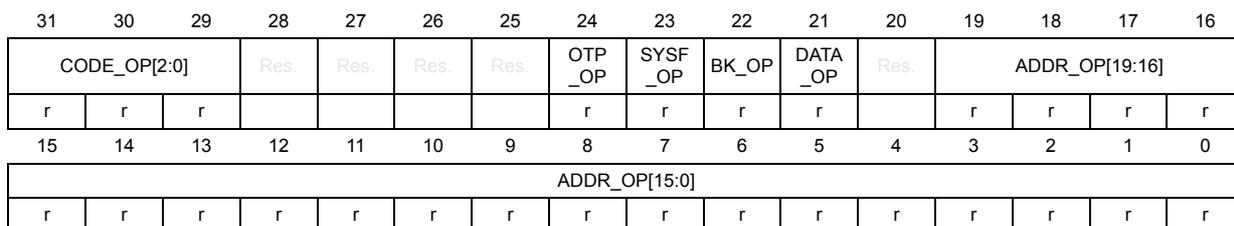
| 31 | 30 | 29 | 28 | 27 | 26 | 25 | 24 | 23 | 22 | 21 | 20 | 19 | 18 | 17 | 16 |
| CODE_OP[2:0] | Res. | Res. | Res. | Res. | OTP_OP | SYSF_OP | BK_OP | DATA_OP | Res. | ADDR_OP[19:16] | |||||
| r | r | r | r | r | r | r | r | r | r | r | |||||
| 15 | 14 | 13 | 12 | 11 | 10 | 9 | 8 | 7 | 6 | 5 | 4 | 3 | 2 | 1 | 0 |
| ADDR_OP[15:0] | |||||||||||||||
| r | r | r | r | r | r | r | r | r | r | r | r | r | r | r | r |
Bits 31:29 CODE_OP[2:0] : Flash memory operation code
- 000: No flash operation on going during previous reset
- 001: Single write operation interrupted
- 010: OBK alternate sector erase
- 011: Sector erase operation interrupted
- 100: Bank erase operation interrupted
- 101: Mass erase operation interrupted
- 110: Option change operation interrupted
- 111: OBK swap sector request
Bits 28:25 Reserved, must be kept at reset value.
Bit 24 OTP_OP : OTP operation interrupted
Indicates that reset interrupted an ongoing operation in OTP area (or OBKeys area).
Bit 23 SYSF_OP : Operation in system flash memory interrupted
Indicates that reset interrupted an ongoing operation in system flash.
Bit 22 BK_OP : Interrupted operation bank
It indicates which bank was concerned by operation.
Bit 21
DATA_OP
: Flash high-cycle data area operation interrupted
It indicates if flash high-cycle data area is concerned by operation.
Bit 20 Reserved, must be kept at reset value.
Bits 19:0 ADDR_OP[19:0] : Interrupted operation address
7.11.8 FLASH option control register (FLASH_OPTCR)
This register is non-secure. It can be read and written by both secure and non-secure access, and protected against unprivileged access when NSPRIV = 1 in the FLASH_PRIVCFG register.
Access: No wait states when no memory operations are ongoing. The FLASH_OPTCR register is not accessible in write mode when the BSY bit is set. Any attempt to write to it while the BSY bit set causes the AHB bus to stall until the BSY bit is cleared.
Address offset: 0x01C
Reset value: 0xX000 0001
| 31 | 30 | 29 | 28 | 27 | 26 | 25 | 24 | 23 | 22 | 21 | 20 | 19 | 18 | 17 | 16 |
|---|---|---|---|---|---|---|---|---|---|---|---|---|---|---|---|
| SWAP_BANK | Res. | Res. | Res. | Res. | Res. | Res. | Res. | Res. | Res. | Res. | Res. | Res. | Res. | Res. | Res. |
| r | |||||||||||||||
| 15 | 14 | 13 | 12 | 11 | 10 | 9 | 8 | 7 | 6 | 5 | 4 | 3 | 2 | 1 | 0 |
| Res. | Res. | Res. | Res. | Res. | Res. | Res. | Res. | Res. | Res. | Res. | Res. | Res. | Res. | OPT STRT | OPT LOCK |
| rw | rs |
Bit 31 SWAP_BANK : Bank swapping option configuration bit
SWAP_BANK controls whether Bank1 and Bank2 are swapped or not. This bit is loaded with the SWAP_BANK bit of FLASH_OPTSR_CUR register only after reset or POR.
0: Bank1 and Bank2 not swapped
1: Bank1 and Bank2 swapped
Bits 30:2 Reserved, must be kept at reset value.
Bit 1 OPTSTRT : Option byte start change option configuration bit
OPTSTRT triggers an option byte change operation. The user can set OPTSTRT only when the OPTLOCK bit is cleared to 0. It is set only by Software and cleared when the option byte change is completed or an error occurs (PGSERR or OPTCHANGEERR). It is reset at the same time as BSY bit.
The user application cannot modify any FLASH_XXX_PRG flash interface register until the option change operation has been completed.
Before setting this bit, the user has to write the required values in the FLASH_XXX_PRG registers. The FLASH_XXX_PRG registers are locked until the option byte change operation has been executed in nonvolatile memory.
Bit 0 OPTLOCK : FLASH_OPTCR lock option configuration bit
The OPTLOCK bit locks the FLASH_OPTCR register as well as all _PRG registers. The correct write sequence to FLASH_OPTKEYR register unlocks this bit. If a wrong sequence is executed, or the unlock sequence to FLASH_OPTKEYR is performed twice, this bit remains locked until next system reset.
It is possible to set OPTLOCK by programming it to 1. When set to 1, a new unlock sequence is mandatory to unlock it. When OPTLOCK changes from 0 to 1, the other bits of FLASH_OPTCR register do not change.
0: FLASH_OPTCR register unlocked
1: FLASH_OPTCR register locked.
7.11.9 FLASH non-secure status register (FLASH_NSSR)
This register is non-secure, can be read by both secure and non-secure accesses. This register can be protected against unprivileged access when NSPRIV = 1 in the FLASH_PRIVCFG register.
Address offset: 0x020
Reset value: 0x0000 000X
| 31 | 30 | 29 | 28 | 27 | 26 | 25 | 24 | 23 | 22 | 21 | 20 | 19 | 18 | 17 | 16 |
|---|---|---|---|---|---|---|---|---|---|---|---|---|---|---|---|
| Res. | Res. | Res. | Res. | Res. | Res. | Res. | Res. | OPT CHANGE ERR | OBKW ERR | OBK ERR | INC ERR | STRB ERR | PGS ERR | WRP ERR | EOP |
| r | r | r | r | r | r | r | r | ||||||||
| 15 | 14 | 13 | 12 | 11 | 10 | 9 | 8 | 7 | 6 | 5 | 4 | 3 | 2 | 1 | 0 |
| Res. | Res. | Res. | Res. | Res. | Res. | Res. | Res. | Res. | Res. | Res. | Res. | DBNE | Res. | WBNE | BSY |
| r | r | r |
Bits 31:24 Reserved, must be kept at reset value.
Bit 23 OPTCHANGEERR : Option byte change error flag
OPTCHANGEERR flag indicates that an error occurred during an option byte change operation. When OPTCHANGEERR is set to 1, the option byte change operation did not successfully complete. An interrupt is generated when this flag is raised if the OPTCHANGEERRIE bit of FLASH_NSCR register is set to 1.
Writing 1 to CLR_OPTCHANGEERR of register FLASH_NSCCR clears OPTCHANGEERR.
0: no option byte change errors occurred
1: one or more errors occurred during an option byte change operation.
Note: The OPTSTRT bit in FLASH_OPTCR cannot be set while OPTCHANGEERR is set.
Bit 22 OBKWERR : OBK write error flag
OBKWERR flag is raised when the address is not virgin on a write access to the OBK storage. Alternatively also when the OBK selector in the alternate sector is not virgin during a swap operation.
0: no OBK write error occurred
1: an OBK write error occurred
- Bit 21
OBKERR
: OBK general error flag
OBKERR flag is raised when the OBK-HDPL signal from the SBS does not match the HDPL value associated with the key slot during access to the key location. Alternatively also when the ALT_SECT is unexpectedly changed while the write buffer is being filled.
0: no OBK general error occurred
1: an OBK general error occurred - Bit 20
INCERR
: inconsistency error flag
NSINCERR flag is raised when a inconsistency error occurs. An interrupt is generated if INCERRIE is set to 1. Writing 1 to CLR_INCERR bit in the FLASH_NSCCR register clears NSINCERR.
0: no inconsistency error occurs
1: a inconsistency error occurs - Bit 19
STRBERR
: strobe error flag
STRBERR flag is raised when a strobe error occurs (when the master attempts to write several times the same byte in the write buffer). An interrupt is generated if the STRBERRIE bit is set to 1. Writing 1 to CLR_STRBERR bit in FLASH_NSCCR register clears STRBERR.
0: no strobe error occurred
1: a strobe error occurred - Bit 18
PGSERR
: programming sequence error flag
PGSERR flag is raised when a sequence error occurs. An interrupt is generated if the PGSERRIE bit is set to 1. Writing 1 to CLR_PGSERR bit in FLASH_NSCCR register clears PGSERR.
0: no sequence error occurred
1: a sequence error occurred - Bit 17
WRPERR
: write protection error flag
WRPERR flag is raised when a protection error occurs during a program operation. An interrupt is also generated if the WRPERRIE is set to 1. Writing 1 to CLR_WRPERR bit in FLASH_NSCCR register clears WRPERR.
0: no write protection error occurred
1: a write protection error occurred - Bit 16
EOP
: end of operation flag
EOP flag is set when a operation (program/erase) completes. An interrupt is generated if the EOPIE is set to 1. It is not necessary to reset EOP before starting a new operation. EOP bit is cleared by writing 1 to CLR_EOP bit in FLASH_NSCCR register.
0: no operation completed
1: a operation completed - Bits 15:4 Reserved, must be kept at reset value.
- Bit 3
DBNE
: data buffer not empty flag
DBNE flag is set when the flash interface is processing 6-bits ECC data in dedicated buffer. This bit cannot be set to 0 by software. The hardware resets it once the buffer is free.
0: data buffer not used
1: data buffer used, wait - Bit 2 Reserved, must be kept at reset value.
Bit 1 WBNE : write buffer not empty flag
WBNE flag is set when the flash interface is waiting for new data to complete the write buffer. In this state, the write buffer is not empty. WBNE is reset by hardware each time the write buffer is complete or the write buffer is emptied following one of the events below:
- – the application software forces the write operation using FW bit in FLASH_NSCR
- – the memory detects an error that involves data loss
This bit cannot be reset by software writing 0 directly. To reset it, clear the write buffer by performing any of the above listed actions, or send the missing data.
0: write buffer empty or full
1: write buffer waiting data to complete
Bit 0 BSY : busy flag
BSY flag indicates that a flash memory is busy by an operation (write, erase, option byte change, OBK operation). It is set at the beginning of a flash memory operation and cleared when the operation finishes, or an error occurs.
0: no programming, erase or option byte change operation being executed
1: programming, erase or option byte change operation being executed
7.11.10 FLASH secure status register (FLASH_SECSR)
This register is secure. It can be read only by secure access. A non-secure read/write access is RAZ/WI. This register can be protected against unprivileged access when SPRIV = 1 in the FLASH_PRIVCFGR register.
Address offset: 0x024
Reset value: 0x0000 000X
| 31 | 30 | 29 | 28 | 27 | 26 | 25 | 24 | 23 | 22 | 21 | 20 | 19 | 18 | 17 | 16 |
|---|---|---|---|---|---|---|---|---|---|---|---|---|---|---|---|
| Res. | Res. | Res. | Res. | Res. | Res. | Res. | Res. | Res. | OBKW ERR | OBK ERR | INC ERR | STRB ERR | PGS ERR | WRP ERR | EOP |
| r | r | r | r | r | r | r | |||||||||
| 15 | 14 | 13 | 12 | 11 | 10 | 9 | 8 | 7 | 6 | 5 | 4 | 3 | 2 | 1 | 0 |
| Res. | Res. | Res. | Res. | Res. | Res. | Res. | Res. | Res. | Res. | Res. | Res. | DBNE | Res. | WBNE | BSY |
| r | r | r |
Bits 31:23 Reserved, must be kept at reset value.
Bit 22 OBKWERR : OBK write error flag
OBKWERR flag is raised when the address is not virgin on a write access to the OBK storage. Alternatively also when the OBK selector in the alternate sector is not virgin during a swap operation.
0: no OBK write error occurred
1: an OBK write error occurred
Bit 21 OBKERR : OBK general error flag
OBKERR flag is raised when the OBK-HDPL signal from the SBS does not match the HDPL value associated with the key slot during access to the key location. Alternatively also when the ALT_SECT is unexpectedly changed while the write buffer is being filled.
0: no OBK general error occurred
1: an OBK general error occurred
Bit 20 INCERR: inconsistency error flagINCERR flag is raised when a inconsistency error occurs. An interrupt is generated if INCERRIE is set to 1. Writing 1 to CLR_INCERR bit in the FLASH_SECCCR register clears INCERR.
0: no inconsistency error occurred
1: a inconsistency error occurred
Bit 19 STRBERR: strobe error flagSTRBERR flag is raised when a strobe error occurs (when the master attempts to write several times the same byte in the write buffer). An interrupt is generated if the STRBERRIE bit is set to 1. Writing 1 to CLR_STRBERR bit in FLASH_SECCCR register clears STRBERR.
0: no strobe error occurred
1: a strobe error occurred
Bit 18 PGSERR: programming sequence error flagPGSERR flag is raised when a sequence error occurs. An interrupt is generated if the PGSERRIE bit is set to 1. Writing 1 to CLR_PGSERR bit in FLASH_SECCCR register clears PGSERR.
0: no sequence error occurred
1: a sequence error occurred
Bit 17 WRPERR: write protection error flagWRPERR flag is raised when a protection error occurs during a program operation. An interrupt is also generated if the WRPERRIE is set to 1. Writing 1 to CLR_WRPERR bit in FLASH_SECCCR register clears WRPERR.
0: no write protection error occurred
1: a write protection error occurred
Bit 16 EOP: end of operation flagEOP flag is set when a operation (program/erase) completes. An interrupt is generated if the EOPIE is set to. It is not necessary to reset EOP before starting a new operation. EOP bit is cleared by writing 1 to CLR_EOP bit in FLASH_SECCCR register.
0: no operation completed
1: a operation completed
Bits 15:4 Reserved, must be kept at reset value.
Bit 3 DBNE: data buffer not empty flagDBNE flag is set when the memory interface is processing 6-bits ECC data in dedicated buffer. This bit cannot be set to 0 by software. The hardware resets it once the buffer is free.
0: data buffer not used
1: data buffer used, wait
Bit 2 Reserved, must be kept at reset value.
Bit 1 WBNE: write buffer not empty flagWBNE flag is set when the flash interface is waiting for new data to complete the write buffer. In this state, the write buffer is not empty. WBNE is reset by hardware each time the write buffer is complete or the write buffer is emptied following one of the events below:
- – the application software forces the write operation using FW bit in FLASH_SECCR
- – the flash interface detects an error that involves data loss
This bit cannot be reset by writing 0 directly by software. To reset it, clear the write buffer by performing any of the above listed actions, or send the missing data.
0: write buffer empty or full
1: write buffer waiting data to complete
Bit 0 BSY : busy flag
BSY flag indicates that a FLASH memory is busy (write, erase, option byte change, OBK operations). It is set at the beginning of a flash memory operation and cleared when the operation finishes or an error occurs.
0: no programming, erase or option byte change operation being executed
1: programming, erase or option byte change operation being executed
7.11.11 FLASH non-secure control register (FLASH_NSCR)
This register is non-secure. It can be read and written by both secure and non-secure accesses, and can be protected against unprivileged access when NSPRIV = 1 in the FLASH_PRIVCFG register.
Access: No wait states when no memory operations are ongoing. The FLASH_NSCR register is not accessible in write mode when the BSY bit is set. Any attempt to write to it with the BSY bit set causes the AHB bus to stall until the BSY bit is cleared.
Address offset: 0x028
Reset value: 0x0000 0001
| 31 | 30 | 29 | 28 | 27 | 26 | 25 | 24 | 23 | 22 | 21 | 20 | 19 | 18 | 17 | 16 |
|---|---|---|---|---|---|---|---|---|---|---|---|---|---|---|---|
| BKSEL | Res. | Res. | Res. | Res. | Res. | Res. | Res. | OPT CHANGE ERRIE | OBKW ERRIE | OBK ERRIE | INC ERRIE | STRB ERRIE | PGS ERRIE | WRP ERRIE | EOPIE |
| rw | rw | rw | rw | rw | rw | rw | rw | rw | |||||||
| 15 | 14 | 13 | 12 | 11 | 10 | 9 | 8 | 7 | 6 | 5 | 4 | 3 | 2 | 1 | 0 |
| MER | Res. | Res. | SNB[6:0] | STRT | FW | BER | SER | PG | LOCK | ||||||
| rw | rw | rw | rw | rw | rw | rw | rw | rs | rw | rw | rw | rw | rs | ||
Bit 31 BKSEL : Bank selector bit
Can be programmed only when LOCK is cleared to 0. The bit selects physical bank, SWAP_BANK setting is ignored.
0: Bank1 is selected for Bank erase / sector erase / interrupt enable
1: Bank2 is selected for BER / SER
Bits 30:24 Reserved, must be kept at reset value.
Bit 23 OPTCHANGEERRIE : Option byte change error interrupt enable bit
This bit controls if an interrupt must be generated when an error occurs during an option byte change. It can be programmed only when LOCK bit is cleared to 0.
0: no interrupt is generated when an error occurs during an option byte change
1: an interrupt is generated when an error occurs during an option byte change.
Bit 22 OBKWERRIE : OBK write error interrupt enable bit
OBKWERRIE enables generation of interrupt in case of OBK specific write error. This bit can be programmed only when LOCK bit is cleared to 0.
0: no interrupt is generated on OBK write error
1: an interrupt is generated on OBK write error
Bit 21 OBKERRIE : OBK general error interrupt enable bit
OBKERRIE enables generating an interrupt in case of OBK specific access error. This bit can be programmed only when LOCK bit is cleared to 0.
0: no interrupt is generated on OBK general access error
1: an interrupt is generated on OBK general access error
Bit 20 INCERRIE : inconsistency error interrupt enable bit
When INCERRIE bit is set to 1, an interrupt is generated when an inconsistency error occurs during a write operation. INCERRIE can be programmed only when LOCK is cleared to 0.
0: no interrupt generated when a inconsistency error occurs
1: interrupt generated when a inconsistency error occurs.
Bit 19 STRBERRIE : strobe error interrupt enable bit
When STRBERRIE bit is set to 1, an interrupt is generated when a strobe error occurs (the master programs several times the same byte in the write buffer) during a write operation. STRBERRIE can be programmed only when LOCK is cleared to 0.
0: no interrupt generated when a strobe error occurs
1: interrupt generated when strobe error occurs.
Bit 18 PGSERRIE : programming sequence error interrupt enable bit
When this bit is set to 1, an interrupt is generated when a sequence error occurs during a program operation. PGSERRIE can be programmed only when LOCK is cleared to 0.
0: no interrupt generated when a sequence error occurs
1: interrupt generated when sequence error occurs
Bit 17 WRPERRIE : write protection error interrupt enable bit
When this bit is set to 1, an interrupt is generated when a protection error occurs during a program operation. WRPERRIE can be programmed only when LOCK is cleared to 0.
0: no interrupt generated when a protection error occurs
1: interrupt generated when a protection error occurs
Bit 16 EOPIE : end of operation interrupt control bit
Setting EOPIE bit to 1 enables the generation of an interrupt at the end of a program or erase operation. EOPIE can be programmed only when LOCK is cleared to 0.
0: no interrupt generated at the end of operation.
1: interrupt enabled when at the end of operation
Bit 15 MER : mass erase request
Setting MER bit to 1 requests a mass erase operation (user flash memory only). MER can be programmed only when LOCK is cleared to 0.
If BER or SER are both set, a PGSERR is raised.
0: mass erase not requested
1: mass erase requested
Note: An error is triggered when a mass erase is required and some sectors are protected.
Bits 14:13 Reserved, must be kept at reset value.
Bits 12:6 SNB[6:0] : sector erase selection number
These bits are used to select the target sector for an erase operation, otherwise they are not used. They can be programmed only when LOCK is cleared to 0.
0x00: Sector 0 selected
0x01: Sector 1 selected
..
0x7F: Sector 127 selected
Note: For STM32H523/33xx devices the maximum value is 0x1F, consider bits [6:5] as reserved, and keep them at reset value.
Bit 5 STRT : erase start control bit
STRT bit is used to start a sector erase or a bank erase operation. STRT can be programmed only when LOCK is cleared to 0.
STRT is reset at the end of the operation or when an error occurs. It cannot be reset by software.
Bit 4 FW: write forcing control bitFW forces a write operation even if the write buffer is not full. In this case all bits not written are set to 1 by hardware. FW can be programmed only when LOCK is cleared to 0.
The memory resets FW when the corresponding operation has been acknowledged.
Note: Using a force-write operation prevents the application from updating later the missing bits with something else than 1, because it is likely that it leads to permanent ECC error.
Write forcing is effective only if the write buffer is not empty and was filled by non-secure access (in particular, FW does not start several write operations when the force-write operations are performed consecutively).
Since there is just one write buffer, FW can force a write in Bank1 or Bank2.
Bit 3 BER: erase requestSetting BER bit to 1 requests a bank erase operation (user flash memory only). BER can be programmed only when LOCK is cleared to 0.
If MER and SER are also set, a PGSERR is raised.
0: bank erase not requested
1: bank erase requested
Note: Write protection error is triggered when a bank erase is required and some sectors are protected.
Bit 2 SER: sector erase requestSetting SER bit to 1 requests a sector erase. SER can be programmed only when LOCK is cleared to 0.
If MER and SER are also set, a PGSERR is raised.
0: sector erase not requested
1: sector erase requested
Bit 1 PG: programming control bitPG can be programmed only when LOCK is cleared to 0.
PG allows programming in Bank1 and Bank2.
0: programming disabled
1: programming enabled
Bit 0 LOCK: configuration lock bitThis bit locks the FLASH_NSCR register. The correct write sequence to FLASH_NSKEYR register unlocks this bit. If a wrong sequence is executed, or if the unlock sequence to FLASH_NSKEYR is performed twice, this bit remains locked until the next system reset.
LOCK can be set by programming it to 1. When set to 1, a new unlock sequence is mandatory to unlock it. When LOCK changes from 0 to 1, the other bits of FLASH_NSCR register do not change.
0: FLASH_NSCR register unlocked
1: FLASH_NSCR register locked
7.11.12 FLASH secure control register (FLASH_SECCR)
This register is secure, can be read and written only by secure access. A non-secure read/write access is RAZ/WI. This register can be protected against unprivileged access when SPRIV = 1 in the FLASH_PRIVCFG register.
Access: No wait states when no memory operations are ongoing. The FLASH_SECCR register is not accessible in write mode when the BSY bit is set. Any attempt to write to it with the BSY bit set causes the AHB bus to stall until the BSY bit is cleared.
Address offset: 0x02C
Reset value: 0x0000 0001
| 31 | 30 | 29 | 28 | 27 | 26 | 25 | 24 | 23 | 22 | 21 | 20 | 19 | 18 | 17 | 16 |
|---|---|---|---|---|---|---|---|---|---|---|---|---|---|---|---|
| BKSEL | Res. | INV | Res. | Res. | Res. | Res. | Res. | Res. | OBKW ERRIE | OBK ERRIE | INC ERRIE | STRB ERRIE | PGS ERRIE | WRP ERRIE | EOPIE |
| rw | rw | rw | rw | rw | rw | rw | rw | rw | |||||||
| 15 | 14 | 13 | 12 | 11 | 10 | 9 | 8 | 7 | 6 | 5 | 4 | 3 | 2 | 1 | 0 |
| MER | Res. | Res. | SNB[6:0] | STRT | FW | BER | SER | PG | LOCK | ||||||
| rw | rw | rw | rw | rw | rw | rw | rw | rs | rw | rw | rw | rw | rs | ||
Bit 31 BKSEL : Bank selector bit
BKSEL can only be programmed when LOCK is cleared to 0. The bit selects physical bank, SWAP_BANK setting is ignored.
0: Bank1 is selected for Bank erase / sector erase / interrupt enable
1: Bank2 is selected for BER / SER
Bit 30 Reserved, must be kept at reset value.
Bit 29 INV : Flash memory security state invert.
This bit inverts the flash memory security state.
Bits 28:23 Reserved, must be kept at reset value.
Bit 22 OBKWERRIE : OBK write error interrupt enable bit
OBKWERRIE enables generation of interrupt in case of OBK specific write error.
OBKWERRIE can be programmed only when LOCK is cleared to 0.
0: no interrupt is generated on OBK write error
1: an interrupt is generated on OBK write error
Bit 21 OBKERRIE : OBK general error interrupt enable bit
OBKERRIE enables generating an interrupt in case of OBK specific access error.
OBKERRIE can be programmed only when LOCK is cleared to 0.
0: no interrupt is generated on OBK general access error
1: an interrupt is generated on OBK general access error
Bit 20 INCERRIE : inconsistency error interrupt enable bit
When INCERRIE bit is set to 1, an interrupt is generated when an inconsistency error occurs during a write operation. INCERRIE can be programmed only when LOCK is cleared to 0.
0: no interrupt generated when a inconsistency error occurs
1: interrupt generated when a inconsistency error occurs.
Bit 19 STRBERRIE : strobe error interrupt enable bit
When STRBERRIE bit is set to 1, an interrupt is generated when a strobe error occurs (the master programs several times the same byte in the write buffer) during a write operation. STRBERRIE can be programmed only when LOCK is cleared to 0.
0: no interrupt generated when a strobe error occurs
1: interrupt generated when strobe error occurs.
Bit 18 PGSERRIE : programming sequence error interrupt enable bit
When PGSERRIE is set to 1, an interrupt is generated when a sequence error occurs during a program operation. PGSERRIE can be programmed only when LOCK is cleared to 0.
0: no interrupt generated when a sequence error occurs
1: interrupt generated when sequence error occurs
Bit 17 WRPERRIE : write protection error interrupt enable bit
When WRPERRIE bit is set to 1, an interrupt is generated when a protection error occurs during a program operation. WRPERRIE can be programmed only when LOCK is cleared to 0.
0: no interrupt generated when a protection error occurs
1: interrupt generated when a protection error occurs
Bit 16 EOPIE : end of operation interrupt control bit
Setting EOPIE bit to 1 enables the generation of an interrupt at the end of a program/erase operation. EOPIE can be programmed only when LOCK is cleared to 0.
0: no interrupt generated at the end of operation.
1: interrupt enabled when at the end of operation
Bit 15 MER : mass erase request
Setting MER bit to 1 requests a mass erase operation (user flash memory only). MER can be programmed only when LOCK is cleared to 0.
If BER or SER are also set, a PGSERR is raised.
0: mass erase not requested
1: mass erase requested
Note: An error is triggered when a mass erase is required and some sectors are protected.
Bits 14:13 Reserved, must be kept at reset value.
Bits 12:6 SNB[6:0] : sector erase selection number
These bits are used to select the target sector for an erase operation, otherwise they are unused. SNB can be programmed only when LOCK is cleared to 0.
0x00: Sector 0 selected
0x01: Sector 1 selected
..
0x7F: Sector 127 selected
Note: For STM32H523/33xx devices the maximum value is 0x1F, consider bits [6:5] as reserved, and keep them at reset value.
Bit 5 STRT : erase start control bit
STRT bit is used to start a sector erase or a bank erase operation. STRT can be programmed only when LOCK is cleared to 0.
STRT is reset at the end of the operation or when an error occurs. It cannot be reset by software.
Bit 4 FW : write forcing control bit
FW forces a write operation even if the write buffer is not full. In this case all bits not written are set to 1 by hardware. FW can be programmed only when LOCK is cleared to 0.
The memory resets FW when the corresponding operation has been acknowledged.
Note: Using a force-write operation prevents the application from updating later the missing bits with something else than 1, because it is likely that it leads to permanent ECC error.
Write forcing is effective only if the write buffer is not empty and was filled by secure access (in particular, FW does not start several write operations when the force-write operations are performed consecutively).
Since there is just one write buffer, FW can force a write in Bank1 or Bank2.
Bit 3 BER : erase requestSetting BER bit to 1 requests a bank erase operation (user flash memory only). BER can be programmed only when LOCK is cleared to 0.
If MER and SER are also set, a PGSERR is raised.
0: bank erase not requested
1: bank erase requested
Note: A write protection error is triggered when a bank erase is required and some sectors are protected.
Bit 2 SER : sector erase requestSetting SER bit to 1 requests a sector erase. SER can be programmed only when LOCK is cleared to 0.
If BER and MER are also set, a PGSERR is raised.
0: sector erase not requested
1: sector erase requested
Bit 1 PG : programming control bitPG can be programmed only when LOCK is cleared to 0.
PG allows programming in Bank1 and Bank2.
0: programming disabled
1: programming enabled
Bit 0 LOCK : configuration lock bitThis bit locks the FLASH_SECCR register. The correct write sequence to FLASH_SECKEYR register unlocks this bit. If a wrong sequence is executed, or if the unlock sequence to FLASH_NSKEYR is performed twice, this bit remains locked until the next system reset.
LOCK can be set by programming it to 1. When set to 1, a new unlock sequence is mandatory to unlock it. When LOCK changes from 0 to 1, the other bits of FLASH_SECCR register do not change.
0: FLASH_SECCR register unlocked
1: FLASH_SECCR register locked
7.11.13 FLASH non-secure clear control register (FLASH_NSCCR)
This register is non-secure. It can be written by both secure and non-secure accesses. This register can be protected against unprivileged access when NSPRIV = 1 in the FLASH_PRIVCFGR register.
Address offset: 0x030
Reset value: 0x0000 0000
| 31 | 30 | 29 | 28 | 27 | 26 | 25 | 24 | 23 | 22 | 21 | 20 | 19 | 18 | 17 | 16 |
|---|---|---|---|---|---|---|---|---|---|---|---|---|---|---|---|
| Res. | Res. | Res. | Res. | Res. | Res. | Res. | Res. | CLR_O PTCHA NGE ERR | CLR_O BKW ERR | CLR_O BK ERR | CLR_ INC ERR | CLR_ STRB ERR | CLR_ PGS ERR | CLR_ WRP ERR | CLR_ EOP 1 |
| w | w | w | w | w | w | w | w | ||||||||
| 15 | 14 | 13 | 12 | 11 | 10 | 9 | 8 | 7 | 6 | 5 | 4 | 3 | 2 | 1 | 0 |
| Res. | Res. | Res. | Res. | Res. | Res. | Res. | Res. | Res. | Res. | Res. | Res. | Res. | Res. | Res. | Res. |
Bits 31:24 Reserved, must be kept at reset value.
Bit 23 CLR_OPTCHANGEERR : Clear the flag corresponding flag in FLASH_NSSR by writing this bit.
Bit 22 CLR_OBKWERR : OBKWERR flag clear bit.
Setting this bit to 1 resets to 0 OBKWERR flag in FLASH_NSSR register.
Bit 21 CLR_OBKERR : OBKERR flag clear bit.
Setting this bit to 1 resets to 0 OBKERR flag in FLASH_NSSR register.
Bit 20 CLR_INCERR : INCERR flag clear bit
Setting this bit to 1 resets to 0 INCERR flag in FLASH_NSSR register.
Bit 19 CLR_STRBERR : STRBERR flag clear bit
Setting this bit to 1 resets to 0 STRBERR flag in FLASH_NSSR register.
Bit 18 CLR_PGSERR : PGSERR flag clear bit
Setting this bit to 1 resets to 0 PGSERR flag in FLASH_NSSR register.
Bit 17 CLR_WRPERR : WRPERR flag clear bit
Setting this bit to 1 resets to 0 WRPERR flag in FLASH_NSSR register.
Bit 16 CLR_EOP : EOP flag clear bit
Setting this bit to 1 resets to 0 EOP flag in FLASH_NSSR register.
Bits 15:0 Reserved, must be kept at reset value.
7.11.14 FLASH secure clear control register (FLASH_SECCCR)
This register is secure. It can be written only by secure access. A non-secure read/write access is RAZ/WI. This register can be protected against unprivileged access when SPRIV = 1 in the FLASH_PRIVCFGR register.
Address offset: 0x034
Reset value: 0x0000 0000
| 31 | 30 | 29 | 28 | 27 | 26 | 25 | 24 | 23 | 22 | 21 | 20 | 19 | 18 | 17 | 16 |
|---|---|---|---|---|---|---|---|---|---|---|---|---|---|---|---|
| Res. | Res. | Res. | Res. | Res. | Res. | Res. | Res. | Res. | CLR_OBKWERR | CLR_OBKERR | CLR_INCERR | CLR_STRBERR | CLR_PGSERR | CLR_WRPERR | CLR_EOP |
| w | w | w | w | w | w | w | |||||||||
| 15 | 14 | 13 | 12 | 11 | 10 | 9 | 8 | 7 | 6 | 5 | 4 | 3 | 2 | 1 | 0 |
| Res. | Res. | Res. | Res. | Res. | Res. | Res. | Res. | Res. | Res. | Res. | Res. | Res. | Res. | Res. | Res. |
Bits 31:23 Reserved, must be kept at reset value.
Bit 22 CLR_OBKWERR : OBKWERR flag clear bit
Setting this bit to 1 resets to 0 OBKWERR flag in FLASH_SECSR register.
Bit 21 CLR_OBKERR : OBKERR flag clear bit
Setting this bit to 1 resets to 0 OBKERR flag in FLASH_SECSR register.
Bit 20 CLR_INCERR : INCERR flag clear bit
Setting this bit to 1 resets to 0 INCERR flag in FLASH_SECSR register.
Bit 19 CLR_STRBERR : STRBERR flag clear bit
Setting this bit to 1 resets to 0 STRBERR flag in FLASH_SECSR register.
Bit 18 CLR_PGSERR : PGSERR flag clear bit
Setting this bit to 1 resets to 0 PGSERR flag in FLASH_SECSR register.
Bit 17 CLR_WRPERR : WRPERR flag clear bit
Setting this bit to 1 resets to 0 WRPERR flag in FLASH_SECSR register.
Bit 16 CLR_EOP : EOP flag clear bit
Setting this bit to 1 resets to 0 EOP flag in FLASH_SECSR register.
Bits 15:0 Reserved, must be kept at reset value.
7.11.15 FLASH privilege configuration register (FLASH_PRIVCFGR)
Address offset: 0x03C
Reset value: 0x0000 0000
This register can be read by both privileged and unprivileged access. NSPRIV is a non-secure bit. SPRIV is a secure bit. It can be written only by privileged mode.
| 31 | 30 | 29 | 28 | 27 | 26 | 25 | 24 | 23 | 22 | 21 | 20 | 19 | 18 | 17 | 16 |
|---|---|---|---|---|---|---|---|---|---|---|---|---|---|---|---|
| Res. | Res. | Res. | Res. | Res. | Res. | Res. | Res. | Res. | Res. | Res. | Res. | Res. | Res. | Res. | Res. |
| 15 | 14 | 13 | 12 | 11 | 10 | 9 | 8 | 7 | 6 | 5 | 4 | 3 | 2 | 1 | 0 |
| Res. | Res. | Res. | Res. | Res. | Res. | Res. | Res. | Res. | Res. | Res. | Res. | Res. | Res. | NSPRIV | SPRIV |
| rw | rw |
Bits 31:2 Reserved, must be kept at reset value.
Bit 1 NSPRIV : privilege attribute for non secure registers
0: access to non secure registers is always granted
1: access to non secure registers is denied in case of unprivileged access.
Bit 0 SPRIV : privilege attribute for secure registers
0: access to secure registers is always granted
1: access to secure registers is denied in case of unprivileged access.
7.11.16 FLASH non-secure OBK configuration register (FLASH_NSOBKCFGR)
Register is only available when TZ_STATE = 0xC3. This register is non-secure. It can be read and written by both secure and non-secure accesses. This register can only be accessed by privilege code. This register is not accessible in write mode when the BSY bit is set. Any attempt to write to it with the BSY bit set causes the AHB bus to stall until the BSY bit is cleared.
Address offset: 0x040
Reset value: 0x01FF 0000
| 31 | 30 | 29 | 28 | 27 | 26 | 25 | 24 | 23 | 22 | 21 | 20 | 19 | 18 | 17 | 16 |
|---|---|---|---|---|---|---|---|---|---|---|---|---|---|---|---|
| Res. | Res. | Res. | Res. | Res. | Res. | Res. | SWAP_OFFSET[8:0] | ||||||||
| rw | rw | rw | rw | rw | rw | rw | rw | rw | |||||||
| 15 | 14 | 13 | 12 | 11 | 10 | 9 | 8 | 7 | 6 | 5 | 4 | 3 | 2 | 1 | 0 |
| Res. | Res. | Res. | Res. | Res. | Res. | Res. | Res. | Res. | Res. | Res. | Res. | ALT_SECT_ERASE | ALT_SECT | SWAP_SECT_REQ | LOCK |
| rw | rw | rw | rw | ||||||||||||
Bits 31:25 Reserved, must be kept at reset value.
Bits 24:16 SWAP_OFFSET[8:0] : Key index (offset /16 bits) pointing for next swap.
0x00: means that no OBK is copied from current to alternate OBK sector during SWAP operation.
0x01 means that only the first OBK data (128 bits) are copied from current to alternate OBK sector
0x02 means that the two first OBK data are copied
...
0x1FF: means that all OBK data (511) are copied
Bits 15:4 Reserved, must be kept at reset value.
Bit 3 ALT_SECT_ERASE : alternate sector erase bit
0: do not touch OBK sector
1: erase the alternate OBK sector
When ALT_SECT bit is set, use this bit to generate an erase command for the OBK alternate sector. It is set only by Software and cleared when the OBK swap operation is completed or an error occurs (PGSERR). It is reset at the same time as BUSY bit.
Bit 2 ALT_SECT : alternate sector bit
0: current OBK sector is mapped to OBK address range for access
1: alternate OBK sector is mapped to OBK address range for access
This bit must not change while filling the write buffer, otherwise an error (OBKERR) is generated
Bit 1 SWAP_SECT_REQ : OBK swap sector request bit
0: no swap requested
1: launch the sector swap
When set, all the OBKs not updated in the alternate sector are copied from current sector to alternate one.
The SWAP_OFFSET must have a minimum value to launched the swap. The minimum value is 16 for OBK-HDPL = 1, 144 for OBK-HDPL = 2, and 192 for OBK-HDPL = 3.
Bit 0 LOCK : OBKCFGR lock option configuration bit
This bit locks the register, the correct write sequence unlocks it. If a wrong sequence is executed, or if the unlock sequence is performed twice, this bit remains locked until the next system reset. LOCK can be set by programming it to 1. When set to 1, a new unlock sequence is mandatory to unlock it. When LOCK changes from 0 to 1, the other bits of FLASH_NSCR register do not change.
0: FLASH_NSOBKCFGR register unlocked
1: FLASH_NSOBKCFGR register locked
7.11.17 FLASH secure OBK configuration register (FLASH_SECOBKCFGR)
This register can be accessed only in secure privileged mode. The FLASH_SECOBKCFGR register is not accessible in write mode when the BSY bit is set. Any attempt to write to it with the BSY bit set causes the AHB bus to stall until the BSY bit is cleared.
Address offset: 0x044
Reset value: 0x01FF 0000
| 31 | 30 | 29 | 28 | 27 | 26 | 25 | 24 | 23 | 22 | 21 | 20 | 19 | 18 | 17 | 16 |
|---|---|---|---|---|---|---|---|---|---|---|---|---|---|---|---|
| Res. | Res. | Res. | Res. | Res. | Res. | Res. | SWAP_OFFSET[8:0] | ||||||||
| rw | rw | rw | rw | rw | rw | rw | rw | rw | |||||||
| 15 | 14 | 13 | 12 | 11 | 10 | 9 | 8 | 7 | 6 | 5 | 4 | 3 | 2 | 1 | 0 |
| Res. | Res. | Res. | Res. | Res. | Res. | Res. | Res. | Res. | Res. | Res. | Res. | ALT_SECT_ERASE | ALT_SECT | SWAP_SECT_REQ | LOCK |
| rw | rw | rw | rw | ||||||||||||
Bits 31:25 Reserved, must be kept at reset value.
Bits 24:16 SWAP_OFFSET[8:0] : key index (offset /16 bits) pointing for next swap.
0x0: no OBK is copied from current to alternate OBK sector during SWAP operation.
0x1: only the first OBK data (128 bits) are copied from current to alternate OBK sector
0x2: the two first OBK data are copied
...
0x1FF: the 511 first OBK data are copied
Bits 15:4 Reserved, must be kept at reset value.
Bit 3 ALT_SECT_ERASE : alternate sector erase bit
0: do not touch OBK sector
1: erase the alternate OBK sector
When ALT_SECT bit is set, use this bit to generate an erase command for the OBK alternate sector. It is set only by Software and cleared when the OBK swap operation is completed or an error occurs (PGSERR). It is reset at the same time as the BUSY bit.
Bit 2 ALT_SECT : alternate sector bit
0: current OBK sector is mapped to OBK address range for access
1: alternate OBK sector is mapped to OBK address range for access
This bit must not change while filling the write buffer, otherwise an error is generated
Bit 1 SWAP_SECT_REQ : OBK swap sector request bit
0: no swap requested
1: launch the sector swap
When set, all the OBKs not updated in the alternate sector are copied from current sector to alternate one.
SWAP_OFFSET must have a minimum value to launch the swap. The minimum value is 16 for OBK-HDPL = 1, 144 for OBK-HDPL = 2, and 192 for OBK-HDPL = 3.
Bit 0 LOCK : OBKCFGR lock option configuration bit
This bit locks the FLASH_OBKCFGR register. The correct write sequence to FLASH_SECOBKKEYR register unlocks this bit. If a wrong sequence is executed, or if the unlock sequence to FLASH_SECOBKKEYR is performed twice, this bit remains locked until the next system reset. LOCK can be set by programming it to 1. When set to 1, a new unlock sequence is mandatory to unlock it. When LOCK changes from 0 to 1, the other bits of FLASH_NSCR register do not change.
0: FLASH_OBKCFGR register unlocked
1: FLASH_OBKCFGR register locked
7.11.18 FLASH HDP extension register (FLASH_HDPEXTR)
All bits in this register are non-secure. It can be read and written by both secure and non-secure accesses. This register can be protected against unprivileged access when NSPRIV = 1 in the FLASH_PRIVCFGR register.
The register can be modified only in HDPL \( \leq 2 \) .
The values in this register cannot be decremented. Attempts to write a value lower than the current one are ignored.
Address offset: 0x048
Reset value: 0x0000 0000
| 31 | 30 | 29 | 28 | 27 | 26 | 25 | 24 | 23 | 22 | 21 | 20 | 19 | 18 | 17 | 16 |
|---|---|---|---|---|---|---|---|---|---|---|---|---|---|---|---|
| Res. | Res. | Res. | Res. | Res. | Res. | Res. | Res. | Res. | HDP2_EXT[6:0] | ||||||
| rw | rw | rw | rw | rw | rw | rw | |||||||||
| 15 | 14 | 13 | 12 | 11 | 10 | 9 | 8 | 7 | 6 | 5 | 4 | 3 | 2 | 1 | 0 |
|---|---|---|---|---|---|---|---|---|---|---|---|---|---|---|---|
| Res. | Res. | Res. | Res. | Res. | Res. | Res. | Res. | Res. | HDP1_EXT[6:0] | ||||||
| rw | rw | rw | rw | rw | rw | rw | |||||||||
Bits 31:23 Reserved, must be kept at reset value.
Bits 22:16 HDP2_EXT[6:0] : HDP area extension in 8 Kbytes sectors in Bank2. Extension is added after the HDP2_END sector (included).
Note: For STM32H523/33xx devices the maximum value is 0x1F, consider bits [6:5] as reserved, and keep them at reset value.
Bits 15:7 Reserved, must be kept at reset value.
Bits 6:0 HDP1_EXT[6:0] : HDP area extension in 8 Kbytes sectors in Bank1. Extension is added after the HDP1_END sector (included).
Note: For STM32H523/33xx devices the maximum value is 0x1F, consider bits [6:5] as reserved, and keep them at reset value.
7.11.19 FLASH option status register (FLASH_OPTSR_CUR)
This register is non-secure, can be read by both secure and non-secure accesses. This register can be protected against unprivileged access when NSPRIV = 1 in the FLASH_PRIVCFG register.
Default value: 0x0030 5CD8 (value in case of double ECC issue during OBL).
This read-only register reflects the current values of the corresponding option bits.
Address offset: 0x050
Reset value: 0xXXXX XXXX
Bits 0 to 31 are loaded with values from the flash memory at OBL.
| 31 | 30 | 29 | 28 | 27 | 26 | 25 | 24 | 23 | 22 | 21 | 20 | 19 | 18 | 17 | 16 |
|---|---|---|---|---|---|---|---|---|---|---|---|---|---|---|---|
| SWAP_BANK | Res. | BOOT_UBE[7:0] | IWDG_STDBY | IWDG_STOP | Res. | Res. | IO_VDDIO2_HSLV | IO_VDD_HSLV | |||||||
| r | r | r | r | r | r | r | r | r | r | r | r | r | |||
| 15 | 14 | 13 | 12 | 11 | 10 | 9 | 8 | 7 | 6 | 5 | 4 | 3 | 2 | 1 | 0 |
|---|---|---|---|---|---|---|---|---|---|---|---|---|---|---|---|
| PRODUCT_STATE[7:0] | NRST_STDBY | NRST_STOP | Res. | WWDG_SW | IWDG_SW | BORH_EN | BOR_LEV[1:0] | ||||||||
| r | r | r | r | r | r | r | r | r | r | r | r | r | r | r | |
- Bit 31
SWAP_BANK
: Bank swapping option status bit
SWAP_BANK reflects whether Bank1 and Bank2 are swapped or not.
SWAP_BANK is loaded to SWAP_BANK of FLASH_OPTCR after a reset.
0: Bank1 and Bank2 not swapped
1: Bank1 and Bank2 swapped - Bit 30 Reserved, must be kept at reset value.
- Bits 29:22
BOOT_UBE[7:0]
: Available only on cryptography enabled devices.
Unique boot entry control, selects either ST or OEM iRoT for secure boot.
0xC3: ST-iRoT (system flash) selected
0xB4: OEM-iRoT (user flash) selected. In Open PRODUCT_STATE this value selects bootloader. Default value. - Bit 21
IWDG_STDBY
: IWDG Standby mode freeze option status bit
When set the independent watchdog IWDG is frozen in system Standby mode.
0: Independent watchdog frozen in Standby mode
1: Independent watchdog keep running in Standby mode. - Bit 20
IWDG_STOP
: IWDG Stop mode freeze option status bit
When set the independent watchdog IWDG is in system Stop mode.
0: Independent watchdog frozen in system Stop mode
1: Independent watchdog keep running in system Stop mode. - Bits 19:18 Reserved, must be kept at reset value.
- Bit 17
IO_VDDIO2_HSLV
: High-speed IO at low V
DDIO2
voltage configuration bit.
This bit can be set only with V DDIO2 below 2.7 V.
0: High-speed IO at low V DDIO2 voltage feature disabled (V DDIO2 can exceed 2.7 V)
1: High-speed IO at low V DDIO2 voltage feature enabled (V DDIO2 remains below 2.7 V) - Bit 16
IO_VDD_HSLV
: High-speed IO at low V
DD
voltage configuration bit.
This bit can be set only with V DD below 2.7 V.
0: High-speed IO at low V DD voltage feature disabled (V DD can exceed 2.7 V)
1: High-speed IO at low V DD voltage feature enabled (V DD remains below 2.7 V) - Bits 15:8 PRODUCT_STATE[7:0] : Life state code (based on Hamming 8,4). See Section 7.6.11 .
- Bit 7
NRST_STDBY
: Core domain Standby entry reset option status bit
0: a reset is generated when entering Standby mode on core domain
1: no reset generated when entering Standby mode on core domain. - Bit 6
NRST_STOP
: Core domain Stop entry reset option status bit
0: a reset is generated when entering Stop mode on core domain
1: no reset generated when entering Stop mode on core domain. - Bit 5 Reserved, must be kept at reset value.
- Bit 4
WWDG_SW
: WWDG control mode option status bit
0: WWDG watchdog is controlled by hardware
1: WWDG watchdog is controlled by software - Bit 3
IWDG_SW
: IWDG control mode option status bit
0: IWDG watchdog is controlled by hardware
1: IWDG watchdog is controlled by software - Bit 2
BORH_EN
: Brownout high enable
0: disable
1: enable
Bits 1:0 BOR_LEV[1:0] : Brownout level option status bit
These bits reflects the power level that generates a system reset.
00 or 11: BOR Level 1, the threshold level is low (~ 2.1 V)
01: BOR Level 2, the threshold level is medium (~ 2.4 V)
10: BOR Level 3, the threshold level is high (~ 2.7 V)
7.11.20 FLASH option status register (FLASH_OPTSR_PRG)
This register is non-secure. It can be read and written by both secure and non-secure accesses. This register can be protected against unprivileged access when NSPRIV = 1 in the FLASH_PRIVCFGR register.
This register is used to program values in corresponding option bits. Values after reset reflects the current values of the corresponding option bits.
Address offset: 0x054
Reset value: 0xXXXX XXXX
Bits 0 to 31 are loaded with values from the flash memory at OBL.
| 31 | 30 | 29 | 28 | 27 | 26 | 25 | 24 | 23 | 22 | 21 | 20 | 19 | 18 | 17 | 16 |
|---|---|---|---|---|---|---|---|---|---|---|---|---|---|---|---|
| SWAP_BANK | Res. | BOOT_UBE[7:0] | IWDG_STDBY | IWDG_STOP | Res. | Res. | IO_VD_DIO2_HSLV | IO_VD_D_HSLV | |||||||
| rw | rw | rw | rw | rw | rw | rw | rw | rw | rw | rw | rw | rw | |||
| 15 | 14 | 13 | 12 | 11 | 10 | 9 | 8 | 7 | 6 | 5 | 4 | 3 | 2 | 1 | 0 |
| PRODUCT_STATE[7:0] | NRST_STDBY | NRST_STOP | Res. | WWDG_SW | IWDG_SW | BORH_EN | BOR_LEV[1:0] | ||||||||
| rw | rw | rw | rw | rw | rw | rw | rw | rw | rw | rw | rw | rw | rw | rw | |
Bit 31 SWAP_BANK : Bank swapping option configuration bit
SWAP_BANK option bit is used to configure whether the Bank1 and Bank2 are swapped or not. This bit is loaded with the SWAP_BANK bit of FLASH_OPTSR_CUR register after a reset.
0: Bank1 and Bank2 not swapped
1: Bank1 and Bank2 swapped
Bit 30 Reserved, must be kept at reset value.
Bits 29:22 BOOT_UBE[7:0] : Available only on cryptography enabled devices.
Unique boot entry control, selects either ST or OEM iRoT for secure boot.
0xC3: ST-iRoT (system flash) selected
0xB4: OEM-iRoT (user flash) selected.
In Open PRODUCT_STATE this value selects bootloader. Default value.
Bit 21 IWDG_STDBY : IWDG Standby mode freeze option status bit
When set the independent watchdog IWDG is frozen in system Standby mode.
0: Independent watchdog frozen in Standby mode
1: Independent watchdog keep running in Standby mode.
Bit 20 IWDG_STOP : IWDG Stop mode freeze option status bit
When set the independent watchdog IWDG is in system Stop mode.
0: Independent watchdog frozen in system Stop mode
1: Independent watchdog keep running in system Stop mode.
Bits 19:18 Reserved, must be kept at reset value.
- Bit 17
IO_VDDIO2_HSLV
: High-speed IO at low V
DDIO2
voltage configuration bit.
This bit can be set only with V DDIO2 below 2.7 V.
0: High-speed IO at low V DDIO2 voltage feature disabled (V DDIO2 can exceed 2.7 V)
1: High-speed IO at low V DDIO2 voltage feature enabled (V DDIO2 remains below 2.7 V) - Bit 16
IO_VDD_HSLV
: High-speed IO at low V
DD
voltage configuration bit.
This bit can be set only with V DD below 2.7 V.
0: High-speed IO at low V DD voltage feature disabled (V DD can exceed 2.7 V)
1: High-speed IO at low V DD voltage feature enabled (V DD remains below 2.7 V) - Bits 15:8 PRODUCT_STATE[7:0] : Life state code (based on Hamming 8,4). See Section 7.6.11 .
- Bit 7
NRST_STDBY
: Core domain Standby entry reset option configuration bit
0: a reset is generated when entering Standby mode on core domain
1: no reset generated when entering Standby mode on core domain. - Bit 6
NRST_STOP
: Core domain Stop entry reset option configuration bit
0: a reset is generated when entering Stop mode on core domain
1: no reset generated when entering Stop mode on core domain. - Bit 5 Reserved, must be kept at reset value.
- Bit 4
WWDG_SW
: WWDG control mode option configuration bit
0: WWDG watchdog is controlled by hardware
1: WWDG watchdog is controlled by software - Bit 3
IWDG_SW
: IWDG control mode option configuration bit
0: IWDG watchdog is controlled by hardware
1: IWDG watchdog is controlled by software - Bit 2
BORH_EN
: Brownout high enable configuration bit
0: disabled
1: enabled - Bits 1:0
BOR_LEV[1:0]
: Brownout level option configuration bit
These bits reflects the power level that generates a system reset.
00 or 11: BOR Level 1, the threshold level is low (~ 2.1 V)
01: BOR Level 2, the threshold level is medium (~ 2.4 V)
10: BOR Level 3, the threshold level is high (~ 2.7 V)
7.11.21 FLASH non-secure EPOCH register (FLASH_NSEPOCHR_CUR)
This register is non-secure, can be read by both secure and non-secure accesses. This register can be protected against unprivileged access when NSPRIV = 1 in the FLASH_PRIVCFG register.
This read-only register reflects the current values of the corresponding option bits.
Address offset: 0x060
Reset value: 0xXXXX XXXX
Bits 0 to 31 are loaded with values from the flash memory at OBL
| 31 | 30 | 29 | 28 | 27 | 26 | 25 | 24 | 23 | 22 | 21 | 20 | 19 | 18 | 17 | 16 |
| Res. | Res. | Res. | Res. | Res. | Res. | Res. | Res. | NS_EPOCH[23:16] | |||||||
| r | r | r | r | r | r | r | r | ||||||||
| 15 | 14 | 13 | 12 | 11 | 10 | 9 | 8 | 7 | 6 | 5 | 4 | 3 | 2 | 1 | 0 |
| NS_EPOCH[15:0] | |||||||||||||||
| r | r | r | r | r | r | r | r | r | r | r | r | r | r | r | r |
Bits 31:24 Reserved, must be kept at reset value.
Bits 23:0 NS_EPOCH[23:0] : Non-volatile non-secure EPOCH counter
7.11.22 FLASH secure EPOCH register (FLASH_SECEPOCHR_CUR)
This register is non-secure, can be read by both secure and non-secure accesses. This register can be protected against unprivileged access when NSPRIV = 1 in the FLASH_PRIVCFGR register.
This read-only register reflects the current values of the corresponding option bits.
Address offset: 0x068
Reset value: 0xXXXX XXXX
| 31 | 30 | 29 | 28 | 27 | 26 | 25 | 24 | 23 | 22 | 21 | 20 | 19 | 18 | 17 | 16 |
| Res. | Res. | Res. | Res. | Res. | Res. | Res. | Res. | SEC_EPOCH[23:16] | |||||||
| r | r | r | r | r | r | r | r | ||||||||
| 15 | 14 | 13 | 12 | 11 | 10 | 9 | 8 | 7 | 6 | 5 | 4 | 3 | 2 | 1 | 0 |
| SEC_EPOCH[15:0] | |||||||||||||||
| r | r | r | r | r | r | r | r | r | r | r | r | r | r | r | r |
Bits 31:24 Reserved, must be kept at reset value.
Bits 23:0 SEC_EPOCH[23:0] : Non-volatile secure EPOCH counter
7.11.23 FLASH option status register 2 (FLASH_OPTSR2_CUR)
This register is non-secure, can be read by both secure and non-secure accesses. This register can be protected against unprivileged access when NSPRIV = 1 in the FLASH_PRIVCFGR register.
Default value: 0xB400 0170
This read-only register reflects the current values of the corresponding option bits.
Address offset: 0x070
Reset value: 0xXXXX XXXX
Bits 0 to 31 are loaded with values from the flash memory at OBL.
| 31 | 30 | 29 | 28 | 27 | 26 | 25 | 24 | 23 | 22 | 21 | 20 | 19 | 18 | 17 | 16 |
|---|---|---|---|---|---|---|---|---|---|---|---|---|---|---|---|
| TZEN[7:0] | Res. | Res. | Res. | Res. | Res. | Res. | Res. | Res. | |||||||
| r | r | r | r | r | r | r | r | ||||||||
| 15 | 14 | 13 | 12 | 11 | 10 | 9 | 8 | 7 | 6 | 5 | 4 | 3 | 2 | 1 | 0 |
| Res. | Res. | Res. | Res. | Res. | Res. | Res. | USBPD _DIS | Res. | SRAM2 _ECC | SRAM3 _ECC | BKPRAM _ECC | SRAM2 _RST | SRAM13 _RST | Res. | Res. |
| r | r | r | r | r | r | ||||||||||
Bits 31:24 TZEN[7:0] : TrustZone enable configuration bits
This bit enables the device is in TrustZone mode during an option byte change.
0xC3: TrustZone disabled
0xB4: TrustZone enabled.
Bits 23:15 Reserved, must be kept at reset value.
Bits 14:9 Reserved, must be kept at reset value.
Bit 8 USBPD_DIS : USB power delivery configuration option bit
0: Enabled
1: Disabled
Bit 7 Reserved, must be kept at reset value.
Bit 6 SRAM2_ECC : SRAM2 ECC detection and correction disable
0: SRAM2 ECC check enabled
1: SRAM2 ECC check disabled
Bit 5 SRAM3_ECC : SRAM3 ECC detection and correction disable
0: SRAM3 ECC check enabled
1: SRAM3 ECC check disabled
Bit 4 BKPRAM_ECC : Backup RAM ECC detection and correction disable
0: BKPRAM ECC check enabled
1: BKPRAM ECC check disabled
Bit 3 SRAM2_RST : SRAM2 erase when system reset
0: SRAM2 erased when a system reset occurs
1: SRAM2 not erased when a system reset occurs.
Bit 2 SRAM13_RST : SRAM1 and SRAM3 erase upon system reset
0: SRAM1 and SRAM3 erased when a system reset occurs
1: SRAM1 and SRAM3 not erased when a system reset occurs
Bits 1:0 Reserved, must be kept at reset value.
7.11.24 FLASH option status register 2 (FLASH_OPTSR2_PRG)
This register is non-secure. It can be read and written by both secure and non-secure accesses. This register can be protected against unprivileged access when NSPRIV = 1 in the FLASH_PRIVCFG register.
This register is used to program values in corresponding option bits. Values after reset reflects the current values of the corresponding option bits.
Address offset: 0x074
Reset value: 0xXXXX XXXX
Bits 0 to 31 are loaded with values from the flash memory at OBL.
| 31 | 30 | 29 | 28 | 27 | 26 | 25 | 24 | 23 | 22 | 21 | 20 | 19 | 18 | 17 | 16 |
|---|---|---|---|---|---|---|---|---|---|---|---|---|---|---|---|
| TZEN[7:0] | Res. | Res. | Res. | Res. | Res. | Res. | Res. | Res. | |||||||
| rw | rw | rw | rw | rw | rw | rw | rw | ||||||||
| 15 | 14 | 13 | 12 | 11 | 10 | 9 | 8 | 7 | 6 | 5 | 4 | 3 | 2 | 1 | 0 |
| Res. | Res. | Res. | Res. | Res. | Res. | Res. | USBPD _DIS | Res. | SRAM2 _ECC | SRAM3 _ECC | BKPRAM _ECC | SRAM2 _RST | SRAM1 _3_RST | Res. | Res. |
| rw | rw | rw | rw | rw | rw | ||||||||||
Bits 31:24 TZEN[7:0] : TrustZone enable configuration bits
This bit enables the device is in TrustZone mode during an option byte change.
0xC3: TrustZone disabled
0xB4: TrustZone enabled
Bits 23:15 Reserved, must be kept at reset value.
Bits 14:9 Reserved, must be kept at reset value.
Bit 8 USBPD_DIS : USB power delivery configuration option bit
0: Enabled
1: Disabled
Bit 7 Reserved, must be kept at reset value.
Bit 6 SRAM2_ECC : SRAM2 ECC detection and correction disable
0: SRAM2 ECC check enabled
1: SRAM2 ECC check disabled
Bit 5 SRAM3_ECC : SRAM3 ECC detection and correction disable
0: SRAM3 ECC check enabled
1: SRAM3 ECC check disabled
Bit 4 BKPRAM_ECC : Backup RAM ECC detection and correction disable
0: BKPRAM ECC check enabled
1: BKPRAM ECC check disabled
Bit 3 SRAM2_RST : SRAM2 erase when system reset
0: SRAM2 erased when a system reset occurs
1: SRAM2 not erased when a system reset occurs.
Note: SRAM erase is triggered by option byte change operation, when enabling this feature.
Bit 2 SRAM1_3_RST : SRAM1 and SRAM3 erase upon system reset
0: SRAM1 and SRAM3 erased when a system reset occurs
1: SRAM1 and SRAM3 not erased when a system reset occurs
Note: SRAM erase is triggered by option byte change operation, when enabling this feature.
Bits 1:0 Reserved, must be kept at reset value.
7.11.25 FLASH non-secure boot register (FLASH_NSBOOTR_CUR)
This register is non-secure, can be read by both secure and non-secure accesses. This register can be protected against unprivileged access when NSPRIV = 1 in the FLASH_PRIVCFG register.
This register reflects the current values of the corresponding option bits.
Address offset: 0x080
Reset value: 0xXXXX XXXX
Bits 0 to 31 are loaded with values from the flash memory at OBL.
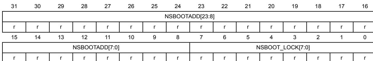
| 31 | 30 | 29 | 28 | 27 | 26 | 25 | 24 | 23 | 22 | 21 | 20 | 19 | 18 | 17 | 16 |
| NSBOOTADD[23:8] | |||||||||||||||
| r | r | r | r | r | r | r | r | r | r | r | r | r | r | r | r |
| 15 | 14 | 13 | 12 | 11 | 10 | 9 | 8 | 7 | 6 | 5 | 4 | 3 | 2 | 1 | 0 |
| NSBOOTADD[7:0] | NSBOOT_LOCK[7:0] | ||||||||||||||
| r | r | r | r | r | r | r | r | r | r | r | r | r | r | r | r |
Bits 31:8 NSBOOTADD[23:0] : Non secure unique boot entry address
These bits reflect the Non secure UBE address
Bits 7:0
NSBOOT_LOCK[7:0]
: Field locking the values of SWAP_BANK, and NSBOOTADD settings.
0xC3: SWAP_BANK and NSBOOTADD can still be modified following their individual rules.
0xB4: NSBOOTADD is frozen. SWAP_BANK can be modified only with TZEN set to 0xB4 (enabled).
7.11.26 FLASH non-secure boot register (FLASH_NSBOOTR_PRG)
This register is non-secure. It can be read and written by both secure and non-secure accesses, and protected against unprivileged access when NSPRIV = 1 in the FLASH_PRIVCFGGR register.
This register is used to program values in corresponding option bits.
Address offset: 0x084
Reset value: 0xXXXX XXXX
Bits 0 to 31 are loaded with values from the flash memory at OBL.
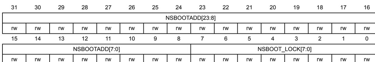
| 31 | 30 | 29 | 28 | 27 | 26 | 25 | 24 | 23 | 22 | 21 | 20 | 19 | 18 | 17 | 16 |
| NSBOOTADD[23:8] | |||||||||||||||
| rw | rw | rw | rw | rw | rw | rw | rw | rw | rw | rw | rw | rw | rw | rw | rw |
| 15 | 14 | 13 | 12 | 11 | 10 | 9 | 8 | 7 | 6 | 5 | 4 | 3 | 2 | 1 | 0 |
| NSBOOTADD[7:0] | NSBOOT_LOCK[7:0] | ||||||||||||||
| rw | rw | rw | rw | rw | rw | rw | rw | rw | rw | rw | rw | rw | rw | rw | rw |
Bits 31:8 NSBOOTADD[23:0] : Non secure unique boot entry address
These bits allow configuring the Non secure BOOT address
Bits 7:0
NSBOOT_LOCK[7:0]
: Field locking the values of SWAP_BANK, and NSBOOTADD settings.
0xC3: SWAP_BANK and NSBOOTADD can still be modified following their individual rules.
0xB4: NSBOOTADD is frozen. SWAP_BANK can be modified only with TZEN set to 0xB4 (enabled).
7.11.27 FLASH secure boot register (FLASH_SECBOOTR_CUR)
This register is secure. It can be read only by secure access. A non-secure read/write access is RAZ/WI. This register can be protected against unprivileged access when SPRIV = 1 in the FLASH_PRIVCFGGR register.
This register reflects the current values of the corresponding option bits.
Address offset: 0x088
Reset value: 0xXXXX XXXX
Bits 0 to 31 are loaded with values from the flash memory at OBL.

| 31 | 30 | 29 | 28 | 27 | 26 | 25 | 24 | 23 | 22 | 21 | 20 | 19 | 18 | 17 | 16 |
| SECBOOTADD[23:8] | |||||||||||||||
| r | r | r | r | r | r | r | r | r | r | r | r | r | r | r | r |
| 15 | 14 | 13 | 12 | 11 | 10 | 9 | 8 | 7 | 6 | 5 | 4 | 3 | 2 | 1 | 0 |
| SECBOOTADD[7:0] | SECBOOT_LOCK[7:0] | ||||||||||||||
| r | r | r | r | r | r | r | r | r | r | r | r | r | r | r | r |
Bits 31:8 SECBOOTADD[23:0] : Unique boot entry secure address
These bits reflect the Secure UBE address
Bits 7:0 SECBOOT_LOCK[7:0] : Field locking the values of UBE, SWAP_BANK, and SECBOOTADD settings.
0xC3: BOOT_UBE, SWAP_BANK and SECBOOTADD can still be modified following their individual rules.
0xB4: BOOT_UBE and SECBOOTADD are frozen. SWAP_BANK can be modified only with TZEN set to 0xC3 (disabled).
7.11.28 FLASH secure boot register (FLASH_BOOTR_PRG)
This register is secure, can be read and written only by secure access. A non-secure read/write access is RAZ/WI. This register can be protected against unprivileged access when SPRIV = 1 in the FLASH_PRIVCFGGR register.
This register is used to program values in corresponding option bits.
Address offset: 0x08C
Reset value: 0xXXXX XXXX
Bits 0 to 31 are loaded with values from the flash memory at OBL.
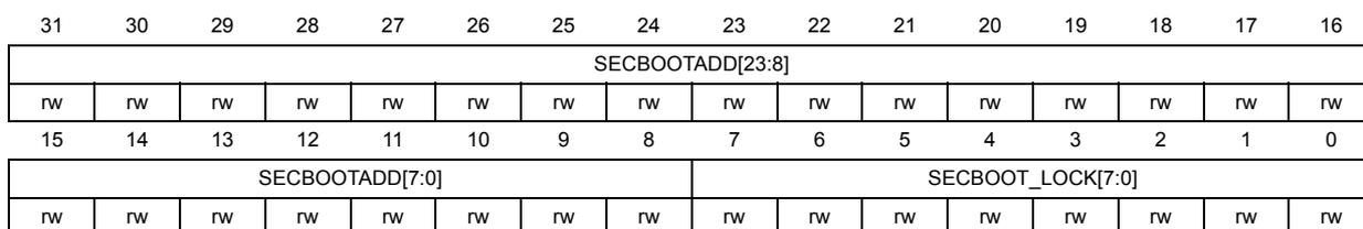
| 31 | 30 | 29 | 28 | 27 | 26 | 25 | 24 | 23 | 22 | 21 | 20 | 19 | 18 | 17 | 16 |
| SECBOOTADD[23:8] | |||||||||||||||
| rw | rw | rw | rw | rw | rw | rw | rw | rw | rw | rw | rw | rw | rw | rw | rw |
| 15 | 14 | 13 | 12 | 11 | 10 | 9 | 8 | 7 | 6 | 5 | 4 | 3 | 2 | 1 | 0 |
| SECBOOTADD[7:0] | SECBOOT_LOCK[7:0] | ||||||||||||||
| rw | rw | rw | rw | rw | rw | rw | rw | rw | rw | rw | rw | rw | rw | rw | rw |
Bits 31:8 SECBOOTADD[23:0] : Secure unique boot entry address.
These bits allow configuring the secure UBE address.
Bits 7:0 SECBOOT_LOCK[7:0] : Field locking the values of UBE, SWAP_BANK, and SECBOOTADD setting.
0xC3: BOOT_UBE, SWAP_BANK and SECBOOTADD can still be modified following their individual rules.
0xB4: BOOT_UBE and SECBOOTADD are frozen. SWAP_BANK can be modified only with TZEN set to 0xC3 (disabled).
7.11.29 FLASH non-secure OTP block lock (FLASH_OTPBLR_CUR)
This register is non-secure, can be read by both secure and non-secure accesses. This register can be protected against unprivileged access when NSPRIV = 1 in the FLASH_PRIVCFG register.
This register reflects the current values of the corresponding option bits.
Address offset: 0x090
Reset value: 0xXXXX XXXX
| 31 | 30 | 29 | 28 | 27 | 26 | 25 | 24 | 23 | 22 | 21 | 20 | 19 | 18 | 17 | 16 |
|---|---|---|---|---|---|---|---|---|---|---|---|---|---|---|---|
| LOCKBL[31:16] | |||||||||||||||
| r | r | r | r | r | r | r | r | r | r | r | r | r | r | r | r |
| 15 | 14 | 13 | 12 | 11 | 10 | 9 | 8 | 7 | 6 | 5 | 4 | 3 | 2 | 1 | 0 |
| LOCKBL[15:0] | |||||||||||||||
| r | r | r | r | r | r | r | r | r | r | r | r | r | r | r | r |
Bits 31:0 LOCKBL[31:0] : OTP block lock
Block n corresponds to OTP 16-bit word \( 32 \times n \) to \( 32 \times n + 31 \) .
LOCKBL[n] = 1 indicates that all OTP 16-bit words in OTP Block n are locked and attempt to program them results in WRPERR.
LOCKBL[n] = 0 indicates that all OTP 16-bit words in OTP Block n are not locked.
When one block is locked, it is not possible to remove the write protection.
Also if not locked, it is not possible to erase OTP words.
7.11.30 FLASH non-secure OTP block lock (FLASH_OTPBLR_PRG)
This register is non-secure. It can be read and written by both secure and non-secure accesses. This register can be protected against unprivileged access when NSPRIV = 1 in the FLASH_PRIVCFG register.
This register is used to program values in corresponding option bits.
Address offset: 0x094
Reset value: 0xXXXX XXXX
| 31 | 30 | 29 | 28 | 27 | 26 | 25 | 24 | 23 | 22 | 21 | 20 | 19 | 18 | 17 | 16 |
|---|---|---|---|---|---|---|---|---|---|---|---|---|---|---|---|
| LOCKBL[31:16] | |||||||||||||||
| rs | rs | rs | rs | rs | rs | rs | rs | rs | rs | rs | rs | rs | rs | rs | rs |
| 15 | 14 | 13 | 12 | 11 | 10 | 9 | 8 | 7 | 6 | 5 | 4 | 3 | 2 | 1 | 0 |
| LOCKBL[15:0] | |||||||||||||||
| rs | rs | rs | rs | rs | rs | rs | rs | rs | rs | rs | rs | rs | rs | rs | rs |
Bits 31:0 LOCKBL[31:0] : OTP block lock
Block \( n \) corresponds to OTP 16-bit word \( 32 \times n \) to \( 32 \times n + 31 \) .
LOCKBL[n] = 1 indicates that all OTP 16-bit words in OTP Block \( n \) are locked and attempt to program them results in WRPERR.
LOCKBL[n] = 0 indicates that all OTP 16-bit words in OTP Block \( n \) are not locked.
When one block is locked, it is not possible to remove the write protection.
LOCKBL bits can be set if the corresponding bit in FLASH_OTPBLR_CUR is cleared.
7.11.31 FLASH secure block based register for Bank1 (FLASH_SECB1Rx)
These registers (only one for STM32H523/33xx devices, as \( x = 1 \) ) are secure. They can be read and written only by secure access. A non-secure read/write access is RAZ/WI.
Address offset: \( 0x0A0 + 0x004 \times (x-1) \) , ( \( x = 1 \) to 4)
Reset value: 0x0000 0000
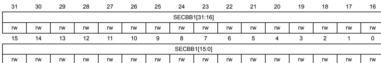
| 31 | 30 | 29 | 28 | 27 | 26 | 25 | 24 | 23 | 22 | 21 | 20 | 19 | 18 | 17 | 16 |
| SECB1[31:16] | |||||||||||||||
| rw | rw | rw | rw | rw | rw | rw | rw | rw | rw | rw | rw | rw | rw | rw | rw |
| 15 | 14 | 13 | 12 | 11 | 10 | 9 | 8 | 7 | 6 | 5 | 4 | 3 | 2 | 1 | 0 |
| SECB1[15:0] | |||||||||||||||
| rw | rw | rw | rw | rw | rw | rw | rw | rw | rw | rw | rw | rw | rw | rw | rw |
Bits 31:0 SECB1[31:0] : Secure/non-secure 8 Kbytes flash Bank1 sector attributes ( \( y = 0 \) to 31)
0: sector ( \( 32 \times (x-1) + y \) ) in Bank1 is non secure.
1: sector ( \( 32 \times (x-1) + y \) ) in Bank1 is secure.
7.11.32 FLASH privilege block based register for Bank1 (FLASH_PRIVB1Rx)
These registers (only one for STM32H523/33xx devices, as \( x = 1 \) ) are privileged. They can be read and written only by a privileged access. This register can be protected against non-secure write access.
Address offset: \( 0x0C0 + 0x004 \times (x-1) \) , ( \( x = 1 \) to 4)
Reset value: 0x0000 0000
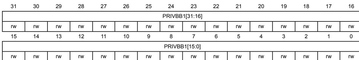
| 31 | 30 | 29 | 28 | 27 | 26 | 25 | 24 | 23 | 22 | 21 | 20 | 19 | 18 | 17 | 16 |
| PRIVB1[31:16] | |||||||||||||||
| rw | rw | rw | rw | rw | rw | rw | rw | rw | rw | rw | rw | rw | rw | rw | rw |
| 15 | 14 | 13 | 12 | 11 | 10 | 9 | 8 | 7 | 6 | 5 | 4 | 3 | 2 | 1 | 0 |
| PRIVB1[15:0] | |||||||||||||||
| rw | rw | rw | rw | rw | rw | rw | rw | rw | rw | rw | rw | rw | rw | rw | rw |
Bits 31:0 PRIVB1[31:0] : Privileged/unprivileged 8-Kbyte flash Bank1 sector attribute ( \( y = 0 \) to 31)
0: sectors ( \( 32 \times (x-1) + y \) ) in Bank1 is unprivileged.
1: sector ( \( 32 \times (x-1) + y \) ) in Bank1 is privileged.
7.11.33 FLASH security watermark for Bank1 (FLASH_SECWM1R_CUR)
This read-only register is non-secure, it can be protected against unprivileged access when NSPRIV = 1 in the FLASH_PRIVCFG register. It reflects the current values of the corresponding option bits.
Address offset: 0x0E0
Reset value: 0x00XX 00XX
Bits 0 to 31 are loaded with values from the flash memory at OBL.
| 31 | 30 | 29 | 28 | 27 | 26 | 25 | 24 | 23 | 22 | 21 | 20 | 19 | 18 | 17 | 16 |
|---|---|---|---|---|---|---|---|---|---|---|---|---|---|---|---|
| Res. | Res. | Res. | Res. | Res. | Res. | Res. | Res. | Res. | SECWM1_END[6:0] | ||||||
| r | r | r | r | r | r | r | |||||||||
| 15 | 14 | 13 | 12 | 11 | 10 | 9 | 8 | 7 | 6 | 5 | 4 | 3 | 2 | 1 | 0 |
| Res. | Res. | Res. | Res. | Res. | Res. | Res. | Res. | Res. | SECWM1_STRT[6:0] | ||||||
| r | r | r | r | r | r | r | |||||||||
Bits 31:23 Reserved, must be kept at reset value.
Bits 22:16 SECWM1_END[6:0] : Bank1 security WM area 1 end sector
Note: For STM32H523/33xx devices the maximum value is 0x1F, consider bits [6:5] as reserved, and keep them at reset value.
Bits 15:7 Reserved, must be kept at reset value.
Bits 6:0 SECWM1_STRT[6:0] : Bank1 security WM area 1 start sector
Note: For STM32H523/33xx devices the maximum value is 0x1F, consider bits [6:5] as reserved, and keep them at reset value.
7.11.34 FLASH security watermark for Bank1 (FLASH_SECWM1R_PRG)
This register is secure, can be read and written only by secure access. A non-secure read/write access is RAZ/WI. This register can be protected against unprivileged access when SPRIV = 1 in the FLASH_PRIVCFG register. This register is used to program values in corresponding option bits.
Address offset: 0x0E4
Reset value: 0x00XX 00XX
Bits 0 to 31 are loaded with values from the flash memory at OBL.
| 31 | 30 | 29 | 28 | 27 | 26 | 25 | 24 | 23 | 22 | 21 | 20 | 19 | 18 | 17 | 16 |
|---|---|---|---|---|---|---|---|---|---|---|---|---|---|---|---|
| Res. | Res. | Res. | Res. | Res. | Res. | Res. | Res. | Res. | SECWM1_END[6:0] | ||||||
| rw | rw | rw | rw | rw | rw | rw | |||||||||
| 15 | 14 | 13 | 12 | 11 | 10 | 9 | 8 | 7 | 6 | 5 | 4 | 3 | 2 | 1 | 0 |
| Res. | Res. | Res. | Res. | Res. | Res. | Res. | Res. | Res. | SECWM1_STRT[6:0] | ||||||
| rw | rw | rw | rw | rw | rw | rw | |||||||||
Bits 31:23 Reserved, must be kept at reset value.
Bits 22:16 SECWM1_END[6:0] : Bank1 security WM area 1 end sector
Note: For STM32H523/33xx devices the maximum value is 0x1F, consider bits [6:5] as reserved, and keep them at reset value.
Bits 15:7 Reserved, must be kept at reset value.
Bits 6:0 SECWM1_STRT[6:0] : Bank1 security WM area 1 start sector
Note: For STM32H523/33xx devices the maximum value is 0x1F, consider bits [6:5] as reserved, and keep them at reset value.
7.11.35 FLASH write sector group protection for Bank1 (FLASH_WRP1R_CUR)
This register is non-secure. It can be read by both secure and non-secure accesses, and can be protected against unprivileged access when NSPRIV = 1 in the FLASH_PRIVCFG register.
This read-only register reflects the current values of the corresponding option bits.
Address offset: 0x0E8
Reset value: 0xXXXX XXXX
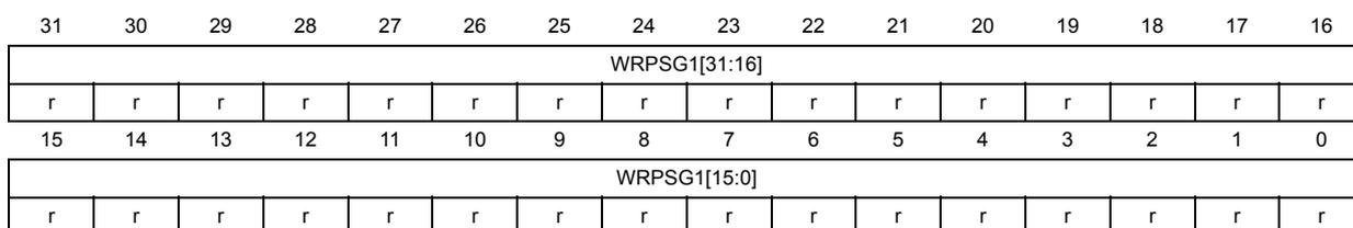
| 31 | 30 | 29 | 28 | 27 | 26 | 25 | 24 | 23 | 22 | 21 | 20 | 19 | 18 | 17 | 16 |
| WRPSG1[31:16] | |||||||||||||||
| r | r | r | r | r | r | r | r | r | r | r | r | r | r | r | r |
| 15 | 14 | 13 | 12 | 11 | 10 | 9 | 8 | 7 | 6 | 5 | 4 | 3 | 2 | 1 | 0 |
| WRPSG1[15:0] | |||||||||||||||
| r | r | r | r | r | r | r | r | r | r | r | r | r | r | r | r |
Bits 31:0 WRPSG1[31:0] : Bank1 sector group protection option status byte
Each FLASH_WRP1R_CUR bit reflects the write protection status of the corresponding group of four consecutive sectors in Bank1 (0: the group is write-protected; 1: the group is not write-protected)
- Bit 0: Group embedding sectors 0 to 3
- Bit 1: Group embedding sectors 4 to 7
- Bit N: Group embedding sectors \( 4 \times N \) to \( 4 \times N + 3 \)
- Bit 31: Group embedding sectors 124 to 127
Note: In STM32H523/33xx devices only bits [7:0] are used. Consider bits [31:8] as reserved, and keep them at reset value.
7.11.36 FLASH write sector group protection for Bank1 (FLASH_WRP1R_PRG)
This register is non-secure. It can be read and written by both secure and non-secure accesses. This register can be protected against unprivileged access when NSPRIV = 1 in the FLASH_PRIVCFG register.
This register is used to program values in corresponding option bits.
Address offset: 0x0EC
Reset value: 0xXXXX XXXX
| 31 | 30 | 29 | 28 | 27 | 26 | 25 | 24 | 23 | 22 | 21 | 20 | 19 | 18 | 17 | 16 |
|---|---|---|---|---|---|---|---|---|---|---|---|---|---|---|---|
| WRPSG1[31:16] | |||||||||||||||
| rw | rw | rw | rw | rw | rw | rw | rw | rw | rw | rw | rw | rw | rw | rw | rw |
| 15 | 14 | 13 | 12 | 11 | 10 | 9 | 8 | 7 | 6 | 5 | 4 | 3 | 2 | 1 | 0 |
| WRPSG1[15:0] | |||||||||||||||
| rw | rw | rw | rw | rw | rw | rw | rw | rw | rw | rw | rw | rw | rw | rw | rw |
Bits 31:0 WRPSG1[31:0] : Bank1 sector group protection option status byte
Setting WRPSG1 bits to 0 write protects the corresponding group of four consecutive sectors in Bank1 (0: the group is write-protected; 1: the group is not write-protected)
Bit 0: Group embedding sectors 0 to 3
Bit 1: Group embedding sectors 4 to 7
Bit N: Group embedding sectors \( 4 \times N \) to \( 4 \times N + 3 \)
Bit 31: Group embedding sectors 124 to 127
Note: In STM32H523/33xx devices only bits [7:0] are used. Consider bits [31:8] as reserved, and keep them at reset value.
7.11.37 FLASH data sector configuration Bank1 (FLASH_EDATA1R_CUR)
This register is non-secure, can be read by both secure and non-secure accesses. The register can be protected against unprivileged access when NSPRIV = 1 in the FLASH_PRIVCFG register.
This read-only register reflects the current values of the corresponding options bits.
Address offset: 0x0F0
Reset value: 0xXXXX XXXX
| 31 | 30 | 29 | 28 | 27 | 26 | 25 | 24 | 23 | 22 | 21 | 20 | 19 | 18 | 17 | 16 |
|---|---|---|---|---|---|---|---|---|---|---|---|---|---|---|---|
| Res. | Res. | Res. | Res. | Res. | Res. | Res. | Res. | Res. | Res. | Res. | Res. | Res. | Res. | Res. | Res. |
| 15 | 14 | 13 | 12 | 11 | 10 | 9 | 8 | 7 | 6 | 5 | 4 | 3 | 2 | 1 | 0 |
| EDATA1_EN | Res. | Res. | Res. | Res. | Res. | Res. | Res. | Res. | Res. | Res. | Res. | Res. | EDATA1_STRT[2:0] | ||
| r | r | r | r | ||||||||||||
Bits 31:16 Reserved, must be kept at reset value.
Bit 15 EDATA1_EN : Bank1 flash high-cycle data enable
0: No flash high-cycle data area
1: Flash high-cycle data is used
Bits 14:3 Reserved, must be kept at reset value.
Bits 2:0 EDATA1_STRT[2:0] :
EDATA1_STRT contains the start sectors of the flash high-cycle data area in Bank1 There is no hardware effect to those bits. They shall be managed by ST tools in Flasher.
000: The last sector of Bank1 is reserved for flash high-cycle data
001: The two last sectors of Bank1 are reserved for flash high-cycle data
010: The three last sectors of Bank1 are reserved for flash high-cycle data
...
111: The eight last sectors of Bank1 are reserved for flash high-cycle data
7.11.38 FLASH data sector configuration Bank1 (FLASH_EDATA1R_PRG)
This register is non-secure. It can be read and written by both secure and non-secure accesses. This register can be protected against unprivileged access when NSPRIV = 1 in the FLASH_PRIVCFGR register.
This register is used to program values in corresponding options bits.
Address offset: 0xF4
Reset value: 0xXXXX XXXX
| 31 | 30 | 29 | 28 | 27 | 26 | 25 | 24 | 23 | 22 | 21 | 20 | 19 | 18 | 17 | 16 |
|---|---|---|---|---|---|---|---|---|---|---|---|---|---|---|---|
| Res. | Res. | Res. | Res. | Res. | Res. | Res. | Res. | Res. | Res. | Res. | Res. | Res. | Res. | Res. | Res. |
| 15 | 14 | 13 | 12 | 11 | 10 | 9 | 8 | 7 | 6 | 5 | 4 | 3 | 2 | 1 | 0 |
| EDATA1_EN | Res. | Res. | Res. | Res. | Res. | Res. | Res. | Res. | Res. | Res. | Res. | Res. | EDATA1_STRT[2:0] | ||
| rw | rw | rw | rw |
Bits 31:16 Reserved, must be kept at reset value.
Bit 15 EDATA1_EN : Bank1 flash high-cycle data enable
0: No flash high-cycle data area
1: Flash high-cycle data is used
Bits 14:3 Reserved, must be kept at reset value.
Bits 2:0 EDATA1_STRT[2:0] :
EDATA1_STRT contains the start sectors of the flash high-cycle data area in Bank1 There is no hardware effect to those bits. They must be managed by ST tools in Flasher.
000: The last sector of Bank1 is reserved for flash high-cycle data
001: The two last sectors of Bank1 are reserved for flash high-cycle data
010: The three last sectors of Bank1 are reserved for flash high-cycle data
...
111: The eight last sectors of Bank1 are reserved for flash high-cycle data
7.11.39 FLASH HDP Bank1 configuration (FLASH_HDP1R_CUR)
This register is non-secure. It can be read by both secure and non-secure accesses, and protected against unprivileged access when NSPRIV = 1 in the FLASH_PRIVCFGR register. This register is initially loaded with the values of the corresponding option bits.
Address offset: 0x0F8
Reset value: 0xXXXX XXXX
| 31 | 30 | 29 | 28 | 27 | 26 | 25 | 24 | 23 | 22 | 21 | 20 | 19 | 18 | 17 | 16 |
|---|---|---|---|---|---|---|---|---|---|---|---|---|---|---|---|
| Res. | Res. | Res. | Res. | Res. | Res. | Res. | Res. | Res. | HDP1_END[6:0] | ||||||
| r | r | r | r | r | r | r | |||||||||
| 15 | 14 | 13 | 12 | 11 | 10 | 9 | 8 | 7 | 6 | 5 | 4 | 3 | 2 | 1 | 0 |
| Res. | Res. | Res. | Res. | Res. | Res. | Res. | Res. | Res. | HDP1_STRT[6:0] | ||||||
| r | r | r | r | r | r | r | |||||||||
Bits 31:23 Reserved, must be kept at reset value.
Bits 22:16 HDP1_END[6:0] : HDPL barrier end set in number of 8-Kbyte sectors
Note: For STM32H523/33xx devices the maximum value is 0x1F, consider bits [6:5] as reserved, and keep them at reset value.
Bits 15:7 Reserved, must be kept at reset value.
Bits 6:0 HDP1_STRT[6:0] : HDPL barrier start set in number of 8-Kbyte sectors
Note: For STM32H523/33xx devices the maximum value is 0x1F, consider bits [6:5] as reserved, and keep them at reset value.
7.11.40 FLASH HDP Bank1 configuration (FLASH_HDP1R_PRG)
This register is non-secure. It can be read and written by both secure and non-secure access, and can be protected against unprivileged access when NSPRIV = 1 in the FLASH_PRIVCFGR register.
The register is accessible only in HDPL1. In HDPL2 or HDPL3 it is WI, RAZ.
This register is used to program values in corresponding option bits.
Address offset: 0x0FC
Reset value: 0xXXXX XXXX
| 31 | 30 | 29 | 28 | 27 | 26 | 25 | 24 | 23 | 22 | 21 | 20 | 19 | 18 | 17 | 16 |
|---|---|---|---|---|---|---|---|---|---|---|---|---|---|---|---|
| Res. | Res. | Res. | Res. | Res. | Res. | Res. | Res. | Res. | HDP1_END[6:0] | ||||||
| rw | rw | rw | rw | rw | rw | rw | |||||||||
| 15 | 14 | 13 | 12 | 11 | 10 | 9 | 8 | 7 | 6 | 5 | 4 | 3 | 2 | 1 | 0 |
| Res. | Res. | Res. | Res. | Res. | Res. | Res. | Res. | Res. | HDP1_STRT[6:0] | ||||||
| rw | rw | rw | rw | rw | rw | rw | |||||||||
Bits 31:23 Reserved, must be kept at reset value.
Bits 22:16 HDP1_END[6:0] : HDPL barrier end set in number of 8-Kbyte sectors
Note: For STM32H523/33xx devices the maximum value is 0x1F, consider bits [6:5] as reserved, and keep them at reset value.
Bits 15:7 Reserved, must be kept at reset value.
Bits 6:0 HDP1_STRT[6:0] : HDPL barrier start set in number of 8-Kbyte sectors
Note: For STM32H523/33xx devices the maximum value is 0x1F, consider bits [6:5] as reserved, and keep them at reset value.
7.11.41 FLASH ECC correction register (FLASH_ECCCORR)
This register is non-secure. It can be read and written by both secure and non-secure accesses. This register can be protected against unprivileged access when NSPRIV = 1 in the FLASH_PRIVCFGR register.
Address offset: 0x100
Reset value: 0x0000 0000
| 31 | 30 | 29 | 28 | 27 | 26 | 25 | 24 | 23 | 22 | 21 | 20 | 19 | 18 | 17 | 16 |
|---|---|---|---|---|---|---|---|---|---|---|---|---|---|---|---|
| Res. | ECCC | Res. | Res. | Res. | Res. | ECCCI E | OTP_E CC | SYSF _ECC | BK _ECC | EDATA _ECC | OBK _ECC | Res. | Res. | Res. | Res. |
| rw | rw | r | r | r | r | r | |||||||||
| 15 | 14 | 13 | 12 | 11 | 10 | 9 | 8 | 7 | 6 | 5 | 4 | 3 | 2 | 1 | 0 |
| ADDR_ECC[15:0] | |||||||||||||||
| r | r | r | r | r | r | r | r | r | r | r | r | r | r | r | r |
Bit 31 Reserved, must be kept at reset value.
Bit 30 ECCC : ECC correction set by hardware when single ECC error has been detected and corrected.
Cleared by writing 1.
Bits 29:26 Reserved, must be kept at reset value.
Bit 25 ECCCI : ECC single correction error interrupt enable bit
When ECCCI bit is set to 1, an interrupt is generated when an ECC single correction error occurs during a read operation.
0: no interrupt generated when an ECC single correction error occurs
1: non-secure interrupt generated when an ECC single correction error occurs
Bit 24 OTP_ECC : OTP ECC error bit
This bit is set to 1 when one single ECC correction occurred during the last successful read operation from the read-only/ OTP area. The address of the ECC error is available in ADDR_ECC bitfield.
Bit 23 SYSF_ECC : ECC fail for corrected ECC error in system flash memory
It indicates if system flash memory is concerned by ECC error.
Bit 22 BK_ECC : ECC fail bank for corrected ECC error
It indicates which bank is concerned by ECC error
Bit 21 EDATA_ECC : ECC fail for corrected ECC error in flash high-cycle data area
It indicates if flash high-cycle data area is concerned by ECC error.
Bit 20 OBK_ECC : Single ECC error corrected in flash OB Keys storage area. It indicates the OBK storage concerned by ECC error.
Bits 19:16 Reserved, must be kept at reset value.
Bits 15:0 ADDR_ECC[15:0] : ECC error address
When an ECC error occurs (for single correction) during a read operation, ADDR_ECC contains the address that generated the error. It is reset when the flag error is reset.
The flash interface programs the address in this register only when no ECC error flags are set. This means that only the first address that generated an ECC error is saved.
The address in ADDR_ECC is relative to the flash memory area where the error occurred (user flash memory, system flash memory, data area, read-only/OTP area).
7.11.42 FLASH ECC detection register (FLASH_ECCDETR)
This register is non-secure. It can be read and written by both secure and non-secure accesses. This register can be protected against unprivileged access when NSPRIV = 1 in the FLASH_PRIVCFGR register.
Address offset: 0x104
Reset value: 0x0000 0000
| 31 | 30 | 29 | 28 | 27 | 26 | 25 | 24 | 23 | 22 | 21 | 20 | 19 | 18 | 17 | 16 |
|---|---|---|---|---|---|---|---|---|---|---|---|---|---|---|---|
| ECCD | Res. | Res. | Res. | Res. | Res. | Res. | OTP_ECC | SYSF_ECC | BK_ECC | EDATA_ECC | OBK_ECC | Res. | Res. | Res. | Res. |
| rw | r | r | r | r | r | ||||||||||
| 15 | 14 | 13 | 12 | 11 | 10 | 9 | 8 | 7 | 6 | 5 | 4 | 3 | 2 | 1 | 0 |
| ADDR_ECC[15:0] | |||||||||||||||
| r | r | r | r | r | r | r | r | r | r | r | r | r | r | r | r |
Bit 31 ECCD : ECC detection
Set by hardware when two ECC error has been detected.
When this bit is set, a NMI is generated.
Cleared by writing 1. Needs to be cleared in order to detect subsequent double ECC errors.
Bits 30:25 Reserved, must be kept at reset value.
Bit 24 OTP_ECC : OTP ECC error bit
This bit is set to 1 when double ECC detection occurred during the last read operation from the read-only/ OTP area. The address of the ECC error is available in ADDR_ECC bitfield.
Bit 23 SYSF_ECC : ECC fail for double ECC error in system flash memory
It indicates if system flash memory is concerned by ECC error.
Bit 22 BK_ECC : ECC fail bank for double ECC error
It indicates which bank is concerned by ECC error
Bit 21 EDATA_ECC : ECC fail double ECC error in flash high-cycle data area
It indicates if flash high-cycle data area is concerned by ECC error.
Bit 20 OBK_ECC : ECC fail double ECC error in flash OB Keys storage area. It indicates the OBK storage concerned by ECC error.
Bits 19:16 Reserved, must be kept at reset value.
Bits 15:0 ADDR_ECC[15:0] : ECC error address
When an ECC error occurs (double detection) during a read operation, the ADDR_ECC contains the address that generated the error. It is reset when the flag error is reset.
The flash interface programs the address in this register only when no ECC error flags are set. This means that only the first address that generated an double ECC error is saved.
The address in ADDR_ECC is relative to the flash memory area where the error occurred (user flash memory, system flash memory, data area, read-only/OTP area).
7.11.43 FLASH ECC data (FLASH_ECCDR)
This register is non-secure. It can be read and written by both secure and non-secure accesses. This register can be protected against unprivileged access when NSPRIV = 1 in the FLASH_PRIVCFGR register.
Address offset: 0x108
Reset value: 0x0000 0000
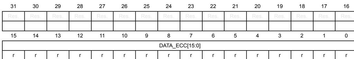
| 31 | 30 | 29 | 28 | 27 | 26 | 25 | 24 | 23 | 22 | 21 | 20 | 19 | 18 | 17 | 16 |
| Res. | Res. | Res. | Res. | Res. | Res. | Res. | Res. | Res. | Res. | Res. | Res. | Res. | Res. | Res. | Res. |
| 15 | 14 | 13 | 12 | 11 | 10 | 9 | 8 | 7 | 6 | 5 | 4 | 3 | 2 | 1 | 0 |
| DATA_ECC[15:0] | |||||||||||||||
| r | r | r | r | r | r | r | r | r | r | r | r | r | r | r | r |
Bits 31:16 Reserved, must be kept at reset value.
Bits 15:0 DATA_ECC[15:0] : ECC error data
When an double detection ECC error occurs on special areas with 6-bit ECC on 16-bit data (data, read-only/OTP), the failing data is read to this register.
By checking if it is possible to determine whether the failure was on a real data, or due to access to uninitialized memory.
7.11.44 FLASH secure block-based register for Bank2 (FLASH_SECB2Rx)
These registers (only one for STM32H523/33xx devices, as \( x = 1 \) ) are secure, they can be read and written only by secure access. A non-secure read/write access is RAZ/WI. The registers can be protected against unprivileged access when SPRIV = 1 in the FLASH_PRIVCFGR register.
Address offset: \( 0x1A0 + 0x004 * (x-1) \) , ( \( x = 1 \) to 4)
Reset value: 0x0000 0000

| 31 | 30 | 29 | 28 | 27 | 26 | 25 | 24 | 23 | 22 | 21 | 20 | 19 | 18 | 17 | 16 |
| SECBB2[31:16] | |||||||||||||||
| rw | rw | rw | rw | rw | rw | rw | rw | rw | rw | rw | rw | rw | rw | rw | rw |
| 15 | 14 | 13 | 12 | 11 | 10 | 9 | 8 | 7 | 6 | 5 | 4 | 3 | 2 | 1 | 0 |
| SECBB2[15:0] | |||||||||||||||
| rw | rw | rw | rw | rw | rw | rw | rw | rw | rw | rw | rw | rw | rw | rw | rw |
Bits 31:0 SECBB2[31:0] : Secure/non-secure flash Bank2 sector attribute ( \( y = 0 \) to 31)
0: sectors \( (32 * (x-1) + y) \) in Bank2 is non secure
1: sector \( (32 * (x-1) + y) \) in Bank2 is secure
7.11.45 FLASH privilege block-based register for Bank2 (FLASH_PRIVBB2Rx)
These registers (only one for STM32H523/33xx devices, as \( x = 1 \) ) are privileged, they can be read and written only by a privileged access, and can be protected against non-secure write access by watermark.
Address offset: \( 0x1C0 + 0x004 * (x-1) \) , ( \( x = 1 \) to 4)
Reset value: 0x0000 0000
| 31 | 30 | 29 | 28 | 27 | 26 | 25 | 24 | 23 | 22 | 21 | 20 | 19 | 18 | 17 | 16 |
|---|---|---|---|---|---|---|---|---|---|---|---|---|---|---|---|
| PRIVBB2[31:16] | |||||||||||||||
| rw | rw | rw | rw | rw | rw | rw | rw | rw | rw | rw | rw | rw | rw | rw | rw |
| 15 | 14 | 13 | 12 | 11 | 10 | 9 | 8 | 7 | 6 | 5 | 4 | 3 | 2 | 1 | 0 |
| PRIVBB2[15:0] | |||||||||||||||
| rw | rw | rw | rw | rw | rw | rw | rw | rw | rw | rw | rw | rw | rw | rw | rw |
Bits 31:0
PRIVBB2[31:0]
: Privileged / non-privileged 8-Kbyte flash Bank2 sector attribute (y = 0 to 31)
0: sectors
\(
(32 * (x-1) + y)
\)
in Bank2 is unprivileged
1: sector
\(
(32 * (x-1) + y)
\)
in Bank2 is privileged
7.11.46 FLASH security watermark for Bank2 (FLASH_SECWM2R_CUR)
This register is non-secure, it can be protected against unprivileged access when NSPRIV = 1 in the FLASH_PRIVCFGR register.
This read-only register reflects the current values of the corresponding option bits.
Address offset: 0x1E0
Reset value: 0x00XX 00XX
Bits 0 to 31 are loaded with values from the flash memory at OBL.
| 31 | 30 | 29 | 28 | 27 | 26 | 25 | 24 | 23 | 22 | 21 | 20 | 19 | 18 | 17 | 16 |
|---|---|---|---|---|---|---|---|---|---|---|---|---|---|---|---|
| Res. | SECWM2_END[6:0] | ||||||||||||||
| r | r | r | r | r | r | r | |||||||||
| 15 | 14 | 13 | 12 | 11 | 10 | 9 | 8 | 7 | 6 | 5 | 4 | 3 | 2 | 1 | 0 |
| Res. | SECWM2_STRT[6:0] | ||||||||||||||
| r | r | r | r | r | r | r | |||||||||
Bits 31:23 Reserved, must be kept at reset value.
Bits 22:16 SECWM2_END[6:0] : Bank2 security WM end sector
Note: For STM32H523/33xx devices the maximum value is 0x1F, consider bits [6:5] as reserved, and keep them at reset value.
Bits 15:7 Reserved, must be kept at reset value.
Bits 6:0 SECWM2_STRT[6:0] : Bank2 security WM area start sector
Note: For STM32H523/33xx devices the maximum value is 0x1F, consider bits [6:5] as reserved, and keep them at reset value.
7.11.47 FLASH security watermark for Bank2 (FLASH_SECWM2R_PRG)
This register is secure, can be read and written only by secure access. A non-secure read/write access is RAZ/WI. The register can be protected against unprivileged accesses when SPRIV = 1 in the FLASH_PRIVCFGR register.
This register is used to program values in corresponding option bits.
Address offset: 0x1E4
Reset value: 0x00XX 00XX
Bits 0 to 31 are loaded with values from the flash memory at OBL.
| 31 | 30 | 29 | 28 | 27 | 26 | 25 | 24 | 23 | 22 | 21 | 20 | 19 | 18 | 17 | 16 |
|---|---|---|---|---|---|---|---|---|---|---|---|---|---|---|---|
| Res. | Res. | Res. | Res. | Res. | Res. | Res. | Res. | Res. | SECWM2_END[6:0] | ||||||
| rw | rw | rw | rw | rw | rw | rw | |||||||||
| 15 | 14 | 13 | 12 | 11 | 10 | 9 | 8 | 7 | 6 | 5 | 4 | 3 | 2 | 1 | 0 |
| Res. | Res. | Res. | Res. | Res. | Res. | Res. | Res. | Res. | SECWM2_STRT[6:0] | ||||||
| rw | rw | rw | rw | rw | rw | rw | |||||||||
Bits 31:23 Reserved, must be kept at reset value.
Bits 22:16 SECWM2_END[6:0] : Bank2 security WM area end sector
Note: For STM32H523/33xx devices the maximum value is 0x1F, consider bits [6:5] as reserved, and keep them at reset value.
Bits 15:7 Reserved, must be kept at reset value.
Bits 6:0 SECWM2_STRT[6:0] : Bank2 security WM area start sector
Note: For STM32H523/33xx devices the maximum value is 0x1F, consider bits [6:5] as reserved, and keep them at reset value.
7.11.48 FLASH write sector group protection for Bank2 (FLASH_WRP2R_CUR)
This register is non-secure, can be read by both secure and non-secure access, and protected against unprivileged access when NSPRIV = 1 in the FLASH_PRIVCFGR register.
This read-only register reflects the current values of the corresponding option bits.
Address offset: 0x1E8
Reset value: 0xFFFF XXXX
| 31 | 30 | 29 | 28 | 27 | 26 | 25 | 24 | 23 | 22 | 21 | 20 | 19 | 18 | 17 | 16 |
|---|---|---|---|---|---|---|---|---|---|---|---|---|---|---|---|
| WRPSG2[31:16] | |||||||||||||||
| r | r | r | r | r | r | r | r | r | r | r | r | r | r | r | r |
| 15 | 14 | 13 | 12 | 11 | 10 | 9 | 8 | 7 | 6 | 5 | 4 | 3 | 2 | 1 | 0 |
| WRPSG2[15:0] | |||||||||||||||
| r | r | r | r | r | r | r | r | r | r | r | r | r | r | r | r |
Bits 31:0 WRPSG2[31:0] : Bank2 sector group protection option status byte
Each bit reflects the write protection status of the corresponding group of four consecutive sectors in Bank2 (0: group is write-protected; 1: group is not write-protected)
Bit 0: Group embedding sectors 0 to 3
Bit 1: Group embedding sectors 4 to 7
Bit N: Group embedding sectors 4 x N to 4 x N + 3
Bit 31: Group embedding sectors 124 to 127
Note: In STM32H523/33xx devices only bits [7:0] are used. Consider bits [31:8] as reserved, and keep them at reset value.
7.11.49 FLASH write sector group protection for Bank2 (FLASH_WRP2R_PRG)
This register is non-secure. It can be read and written by both secure and non-secure accesses. This register can be protected against unprivileged access when NSPRIV = 1 in the FLASH_PRIVCFGR register.
This register is used to program values in corresponding option bits.
Address offset: 0x1EC
Reset value: 0xXXXX XXXX
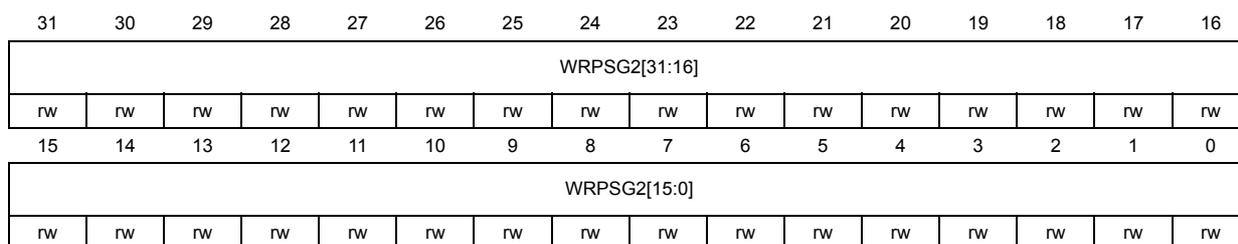
| 31 | 30 | 29 | 28 | 27 | 26 | 25 | 24 | 23 | 22 | 21 | 20 | 19 | 18 | 17 | 16 |
| WRPSG2[31:16] | |||||||||||||||
| rw | rw | rw | rw | rw | rw | rw | rw | rw | rw | rw | rw | rw | rw | rw | rw |
| 15 | 14 | 13 | 12 | 11 | 10 | 9 | 8 | 7 | 6 | 5 | 4 | 3 | 2 | 1 | 0 |
| WRPSG2[15:0] | |||||||||||||||
| rw | rw | rw | rw | rw | rw | rw | rw | rw | rw | rw | rw | rw | rw | rw | rw |
Bits 31:0 WRPSG2[31:0] : Bank2 sector group protection option status byte
Setting WRPSGn2 bits to 0 write protects the corresponding group of four consecutive sectors in Bank2 (0: group is write-protected; 1: group is not write-protected)
Bit 0: Group embedding sectors 0 to 3
Bit 1: Group embedding sectors 4 to 7
Bit N: Group embedding sectors \( 4 \times N \) to \( 4 \times N + 3 \)
Bit 31: Group embedding sectors 124 to 127
Note: In STM32H523/33xx devices only bits [7:0] are used. Consider bits [31:8] as reserved, and keep them at reset value.
7.11.50 FLASH data sectors configuration Bank2 (FLASH_EDATA2R_CUR)
This register is non-secure, can be read by both secure and non-secure accesses. This register can be protected against unprivileged access when NSPRIV = 1 in the FLASH_PRIVCFGR register.
This read-only register reflects the current values of the corresponding options bits.
Address offset: 0x1F0
Reset value: 0xXXXX XXXX
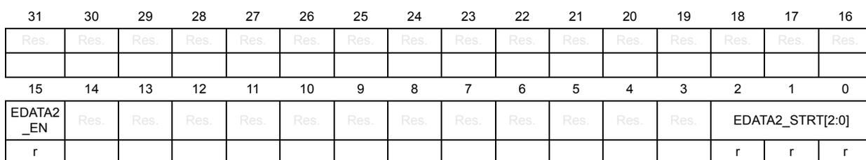
| 31 | 30 | 29 | 28 | 27 | 26 | 25 | 24 | 23 | 22 | 21 | 20 | 19 | 18 | 17 | 16 |
| Res. | Res. | Res. | Res. | Res. | Res. | Res. | Res. | Res. | Res. | Res. | Res. | Res. | Res. | Res. | Res. |
| 15 | 14 | 13 | 12 | 11 | 10 | 9 | 8 | 7 | 6 | 5 | 4 | 3 | 2 | 1 | 0 |
| EDATA2 _EN | Res. | Res. | Res. | Res. | Res. | Res. | Res. | Res. | Res. | Res. | Res. | Res. | EDATA2_STRT[2:0] | ||
| r | r | r | r | ||||||||||||
Bits 31:16 Reserved, must be kept at reset value.
Bit 15 EDATA2_EN : Bank2 flash high-cycle data enable
0: No flash high-cycle data area
1: Flash high-cycle data is used
Bits 14:3 Reserved, must be kept at reset value.
Bits 2:0 EDATA2_STRT[2:0] :
EDATA2_STRT contains the start sectors of the flash high-cycle data area in Bank2 There is no hardware effect to those bits. They shall be managed by ST tools in Flasher.
000: The last sector of Bank2 is reserved for flash high-cycle data
001: The two last sectors of Bank2 are reserved for flash high-cycle data
010: The three last sectors of Bank2 are reserved for flash high-cycle data
...
111: The eight last sectors of Bank2 are reserved for flash high-cycle data
7.11.51 FLASH data sector configuration Bank2 (FLASH_EDATA2R_PRG)
This register is non-secure. It can be read and written by both secure and non-secure accesses, and protected against unprivileged access when NSPRIV = 1 in the FLASH_PRIVCFGR register. It is used to program values in corresponding options bits.
Address offset: 0x1F4
Reset value: 0xXXXX XXXX
| 31 | 30 | 29 | 28 | 27 | 26 | 25 | 24 | 23 | 22 | 21 | 20 | 19 | 18 | 17 | 16 |
|---|---|---|---|---|---|---|---|---|---|---|---|---|---|---|---|
| Res. | Res. | Res. | Res. | Res. | Res. | Res. | Res. | Res. | Res. | Res. | Res. | Res. | Res. | Res. | Res. |
| 15 | 14 | 13 | 12 | 11 | 10 | 9 | 8 | 7 | 6 | 5 | 4 | 3 | 2 | 1 | 0 |
| EDATA2_EN | Res. | Res. | Res. | Res. | Res. | Res. | Res. | Res. | Res. | Res. | Res. | Res. | EDATA2_STRT[2:0] | ||
| rw | rw | rw | rw |
Bits 31:16 Reserved, must be kept at reset value.
Bit 15 EDATA2_EN : Bank2 flash high-cycle data enable
0: No flash high-cycle data area
1: Flash high-cycle data is used
Bits 14:3 Reserved, must be kept at reset value.
Bits 2:0 EDATA2_STRT[2:0] :
EDATA2_STRT contains the start sectors of the flash high-cycle data area in Bank2 There is no hardware effect to those bits. They shall be managed by ST tools in Flasher.
000: The last sector of Bank2 is reserved for flash high-cycle data.
001: The two last sectors of Bank2 are reserved for flash high-cycle data.
010: The three last sectors of Bank2 are reserved for flash high-cycle data.
...
111: The eight last sectors of Bank2 are reserved for flash high-cycle data.
7.11.52 FLASH HDP Bank2 configuration (FLASH_HDP2R_CUR)
This register is initially loaded with the values of the corresponding option bits. This register is non-secure. It can be read by both secure and non-secure accesses, and can be protected against unprivileged access when NSPRIV = 1 in the FLASH_PRIVCFGR register.
Address offset: 0x1F8
Reset value: 0xXXXX XXXX
| 31 | 30 | 29 | 28 | 27 | 26 | 25 | 24 | 23 | 22 | 21 | 20 | 19 | 18 | 17 | 16 |
|---|---|---|---|---|---|---|---|---|---|---|---|---|---|---|---|
| Res. | Res. | Res. | Res. | Res. | Res. | Res. | Res. | Res. | HDP2_END[6:0] | ||||||
| r | r | r | r | r | r | r | |||||||||
| 15 | 14 | 13 | 12 | 11 | 10 | 9 | 8 | 7 | 6 | 5 | 4 | 3 | 2 | 1 | 0 |
| Res. | Res. | Res. | Res. | Res. | Res. | Res. | Res. | Res. | HDP2_STRT[6:0] | ||||||
| r | r | r | r | r | r | r | |||||||||
Bits 31:23 Reserved, must be kept at reset value.
Bits 22:16 HDP2_END[6:0] : HDPL barrier end set in number of 8-Kbyte sectors Note: For STM32H523/33xx devices the maximum value is 0x1F, consider bits [6:5] as reserved, and keep them at reset value.Bits 15:7 Reserved, must be kept at reset value.
Bits 6:0 HDP2_STRT[6:0] : HDPL barrier start set in number of 8-Kbyte sectors Note: For STM32H523/33xx devices the maximum value is 0x1F, consider bits [6:5] as reserved, and keep them at reset value.7.11.53 FLASH HDP Bank2 configuration (FLASH_HDP2R_PRG)
This register is non-secure. It can be read and written only by both secure and non-secure accesses. This register can be protected against unprivileged access when NSPRIV = 1 in the FLASH_PRIVCFGR register.
Register is accessible only in HDPL1. In HDPL2 or HDPL3 it is WI, RAZ.
This register is used to program values in corresponding option bits.
Address offset: 0x1FC
Reset value: 0xXXXX XXXX
| 31 | 30 | 29 | 28 | 27 | 26 | 25 | 24 | 23 | 22 | 21 | 20 | 19 | 18 | 17 | 16 |
|---|---|---|---|---|---|---|---|---|---|---|---|---|---|---|---|
| Res. | Res. | Res. | Res. | Res. | Res. | Res. | Res. | Res. | HDP2_END[6:0] | ||||||
| rw | rw | rw | rw | rw | rw | rw | |||||||||
| 15 | 14 | 13 | 12 | 11 | 10 | 9 | 8 | 7 | 6 | 5 | 4 | 3 | 2 | 1 | 0 |
| Res. | Res. | Res. | Res. | Res. | Res. | Res. | Res. | Res. | HDP2_STRT[6:0] | ||||||
| rw | rw | rw | rw | rw | rw | rw | |||||||||
Bits 31:23 Reserved, must be kept at reset value.
Bits 22:16 HDP2_END[6:0] : HDPL barrier end set in number of 8-Kbyte sectors Note: For STM32H523/33xx devices the maximum value is 0x1F, consider bits [6:5] as reserved, and keep them at reset value.Bits 15:7 Reserved, must be kept at reset value.
Bits 6:0 HDP2_STRT[6:0] : HDPL barrier start set in number of 8-Kbyte sectors Note: For STM32H523/33xx devices the maximum value is 0x1F, consider bits [6:5] as reserved, and keep them at reset value.7.12 FLASH register map and reset values
Table 85. Register map and reset value table
| Offset | Register name | 31 | 30 | 29 | 28 | 27 | 26 | 25 | 24 | 23 | 22 | 21 | 20 | 19 | 18 | 17 | 16 | 15 | 14 | 13 | 12 | 11 | 10 | 9 | 8 | 7 | 6 | 5 | 4 | 3 | 2 | 1 | 0 | |
|---|---|---|---|---|---|---|---|---|---|---|---|---|---|---|---|---|---|---|---|---|---|---|---|---|---|---|---|---|---|---|---|---|---|---|
| 0x000 | FLASH_ACR | Res. | Res. | Res. | Res. | Res. | Res. | Res. | Res. | Res. | Res. | Res. | Res. | Res. | Res. | Res. | Res. | Res. | Res. | Res. | Res. | Res. | Res. | Res. | PRFTEN | Res. | Res. | WRHIGHFREQ [1:0] | LATENCY [3:0] | |||||
| Reset value | 0 | 0 | 1 | 0 | 0 | 1 | 1 | |||||||||||||||||||||||||||
| 0x004 | FLASH_NSKEYR | NSKEY[31:0] | ||||||||||||||||||||||||||||||||
| Reset value | 0 | 0 | 0 | 0 | 0 | 0 | 0 | 0 | 0 | 0 | 0 | 0 | 0 | 0 | 0 | 0 | 0 | 0 | 0 | 0 | 0 | 0 | 0 | 0 | 0 | 0 | 0 | 0 | 0 | 1 | 0 | 0 | ||
| 0x008 | FLASH_SECKEYR | SECKEY[31:0] | ||||||||||||||||||||||||||||||||
| Reset value | 0 | 0 | 0 | 0 | 0 | 0 | 0 | 0 | 0 | 0 | 0 | 0 | 0 | 0 | 0 | 0 | 0 | 0 | 0 | 0 | 0 | 0 | 0 | 0 | 0 | 0 | 0 | 0 | 0 | 0 | 0 | 0 | ||
| 0x00C | FLASH_OPTKEYR | OPTKEY[31:0] | ||||||||||||||||||||||||||||||||
| Reset value | 0 | 0 | 0 | 0 | 0 | 0 | 0 | 0 | 0 | 0 | 0 | 0 | 0 | 0 | 0 | 0 | 0 | 0 | 0 | 0 | 0 | 0 | 0 | 0 | 0 | 0 | 0 | 0 | 0 | 0 | 0 | 0 | ||
| 0x010 | FLASH_NSOBKKEYR | NSOBKKEY[31:0] | ||||||||||||||||||||||||||||||||
| Reset value | 0 | 0 | 0 | 0 | 0 | 0 | 0 | 0 | 0 | 0 | 0 | 0 | 0 | 0 | 0 | 0 | 0 | 0 | 0 | 0 | 0 | 0 | 0 | 0 | 0 | 0 | 0 | 0 | 0 | 0 | 0 | 0 | ||
| 0x014 | FLASH_SECOBKKEYR | SECOBKKEY[31:0] | ||||||||||||||||||||||||||||||||
| Reset value | 0 | 0 | 0 | 0 | 0 | 0 | 0 | 0 | 0 | 0 | 0 | 0 | 0 | 0 | 0 | 0 | 0 | 0 | 0 | 0 | 0 | 0 | 0 | 0 | 0 | 0 | 0 | 0 | 0 | 0 | 0 | 0 | ||
| 0x018 | FLASH_OPSR | CODE_OP [2:0] | Res. | Res. | Res. | Res. | OTP_OP | SYSF_OP | BK_OP | DATA_OP | Res. | ADDR_OP[19:0] | ||||||||||||||||||||||
| Reset value | X | X | X | X | X | X | X | X | X | X | X | X | X | X | X | X | X | X | X | X | X | X | X | X | X | X | X | |||||||
| 0x01C | FLASH_OPTCR | SWAP_BANK | Res. | Res. | Res. | Res. | Res. | Res. | Res. | Res. | Res. | Res. | Res. | Res. | Res. | Res. | Res. | Res. | Res. | Res. | Res. | Res. | Res. | Res. | Res. | Res. | Res. | Res. | Res. | Res. | OPTSTRT | OPTLOCK | ||
| Reset value | 0 | 0 | 1 | |||||||||||||||||||||||||||||||
| 0x020 | FLASH_NSSR | Res. | Res. | Res. | Res. | Res. | Res. | Res. | OPTCHANGERR | OBKWERR | OBKERR | INCERR | STRBERR | PGSERR | WRPERR | EOP | Res. | Res. | Res. | Res. | Res. | Res. | Res. | Res. | Res. | Res. | Res. | Res. | Res. | Res. | SDBNE | Res. | WBNE | BSY |
| Reset value | 0 | 0 | 0 | 0 | 0 | 0 | 0 | 0 | 0 | 0 | 0 | |||||||||||||||||||||||
| 0x024 | FLASH_SECSR | Res. | Res. | Res. | Res. | Res. | Res. | Res. | OPTCHANGERR | OBKWERR | OBKERR | INCERR | STRBERR | PGSERR | WRPERR | EOP | Res. | Res. | Res. | Res. | Res. | Res. | Res. | Res. | Res. | Res. | Res. | Res. | Res. | Res. | DBNE | Res. | WBNE | BSY |
| Reset value | 0 | 0 | 0 | 0 | 0 | 0 | 0 | 0 | X | X | X | |||||||||||||||||||||||
| 0x028 | FLASH_NSCR | BKSEL | Res. | Res. | Res. | Res. | Res. | Res. | OPTCHANGERRIE | OBKWIE | OBKIE | INCERRIE | STRBERRIE | PGSERRIE | WRPERRIE | EOPIE | MER | Res. | Res. | SNB[6:0] | STRT | FW | BER | SER | PG | LOCK | ||||||||
| Reset value | 0 | 0 | 0 | 0 | 0 | 0 | 0 | 0 | 0 | 0 | 0 | 0 | 0 | 0 | 0 | 0 | 0 | 0 | 0 | 0 | 0 | 0 | 0 | 1 | ||||||||||
Table 85. Register map and reset value table (continued)
| Offset | Register name | 31 | 30 | 29 | 28 | 27 | 26 | 25 | 24 | 23 | 22 | 21 | 20 | 19 | 18 | 17 | 16 | 15 | 14 | 13 | 12 | 11 | 10 | 9 | 8 | 7 | 6 | 5 | 4 | 3 | 2 | 1 | 0 | |
|---|---|---|---|---|---|---|---|---|---|---|---|---|---|---|---|---|---|---|---|---|---|---|---|---|---|---|---|---|---|---|---|---|---|---|
| 0x02C | FLASH_SECCR | BKSEL | Res. | Res. | Res. | Res. | Res. | Res. | Res. | Res. | OBKWIE | OBKERRIE | INCERRIE | STRBERRIE | PGSERRIE | WRPERRIE | EOPIE | MER | Res. | Res. | SNB[6:0] | STRT | FW | BER | SER | PG | LOCK | |||||||
| Reset value | 0 | 0 | 0 | 0 | 0 | 0 | 0 | 0 | 0 | 0 | 0 | 0 | 0 | 0 | 0 | 0 | 0 | 0 | 0 | 0 | 0 | 0 | 1 | |||||||||||
| 0x030 | FLASH_NSCCR | Res. | Res. | Res. | Res. | Res. | Res. | Res. | Res. | CLR_OPTCHANGERR | CLR_OBKERR | CLR_OBKERR | CLR_INCERR | CLR_STRBERR | CLR_PGSERR | CLR_WRPERR | CLR_EOP | Res. | Res. | Res. | Res. | Res. | Res. | Res. | Res. | Res. | Res. | Res. | Res. | Res. | Res. | Res. | Res. | Res. |
| Reset value | 0 | 0 | 0 | 0 | 0 | 0 | 0 | 0 | ||||||||||||||||||||||||||
| 0x034 | FLASH_SECCCR | Res. | Res. | Res. | Res. | Res. | Res. | Res. | Res. | CLR_OBKWERR | CLR_OBKERR | CLR_OBKERR | CLR_INCERR | CLR_STRBERR | CLR_PGSERR | CLR_WRPERR | CLR_EOP | Res. | Res. | Res. | Res. | Res. | Res. | Res. | Res. | Res. | Res. | Res. | Res. | Res. | Res. | Res. | Res. | Res. |
| Reset value | 0 | 0 | 0 | 0 | 0 | 0 | 0 | 0 | ||||||||||||||||||||||||||
| 0x03C | FLASH_PRIVCFGR | Res. | Res. | Res. | Res. | Res. | Res. | Res. | Res. | Res. | Res. | Res. | Res. | Res. | Res. | Res. | Res. | Res. | Res. | Res. | Res. | Res. | Res. | Res. | Res. | Res. | Res. | Res. | Res. | Res. | Res. | Res. | NSPRIV | SPRIV |
| Reset value | 0 | 0 | ||||||||||||||||||||||||||||||||
| 0x040 | FLASH_NSOBKCFGR | Res. | Res. | Res. | Res. | Res. | Res. | Res. | Res. | SWAP_OFFSET[8:0] | Res. | Res. | Res. | Res. | Res. | Res. | Res. | Res. | Res. | Res. | Res. | Res. | Res. | ALT_SECT_ERASE | ALT_SECT | SWAP_SECT_REQ | LOCK | |||||||
| Reset value | 1 | 1 | 1 | 1 | 1 | 1 | 1 | 1 | 0 | 0 | 0 | 0 | ||||||||||||||||||||||
| 0x044 | FLASH_SECOBKCFGR | Res. | Res. | Res. | Res. | Res. | Res. | Res. | Res. | SWAP_OFFSET[8:0] | Res. | Res. | Res. | Res. | Res. | Res. | Res. | Res. | Res. | Res. | Res. | Res. | Res. | ALT_SECT_ERASE | ALT_SECT | SWAP_SECT_REQ | LOCK | |||||||
| Reset value | 1 | 1 | 1 | 1 | 1 | 1 | 1 | 1 | 0 | 0 | 0 | 0 | ||||||||||||||||||||||
| 0x048 | FLASH_HDPEXTR | Res. | Res. | Res. | Res. | Res. | Res. | Res. | Res. | HDP2_EXT[6:0] | Res. | Res. | Res. | Res. | Res. | Res. | Res. | Res. | Res. | Res. | HDP1_EXT[6:0] | |||||||||||||
| Reset value | 0 | 0 | 0 | 0 | 0 | 0 | 0 | 0 | 0 | 0 | 0 | 0 | 0 | 0 | ||||||||||||||||||||
| 0x04C | Reserved | Reserved | ||||||||||||||||||||||||||||||||
| 0x050 | FLASH_OPTSR_CUR | SWAP_BANK | Res. | BOOT_UBE[7:0] | IWDG_STDBY | IWDG_STOP | Res. | IO_VDDIO2_HSLV | IO_VDD_HSLV | PRODUCT_STATE[7:0] | NRST_STDBY | NRST_STOP | Res. | WWDG_SW | IWDG_SW | BORH_LEN | BOR_LEV[1:0] | |||||||||||||||||
| Reset value | X | X | X | X | X | X | X | X | X | X | X | X | X | X | X | X | X | X | X | X | X | X | X | X | X | X | X | X | X | |||||
Table 85. Register map and reset value table (continued)
| Offset | Register name | 31 | 30 | 29 | 28 | 27 | 26 | 25 | 24 | 23 | 22 | 21 | 20 | 19 | 18 | 17 | 16 | 15 | 14 | 13 | 12 | 11 | 10 | 9 | 8 | 7 | 6 | 5 | 4 | 3 | 2 | 1 | 0 |
|---|---|---|---|---|---|---|---|---|---|---|---|---|---|---|---|---|---|---|---|---|---|---|---|---|---|---|---|---|---|---|---|---|---|
| 0x054 | FLASH_OPTSR_PRG | SWAP_BANK | Res. | BOOT_UBE[7:0] | IWDG_STDBY | IWDG_STOP | Res. | Res. | IO_VDDIO2_HSLV | IO_VDD_HSLV | PRODUCT_STATE[7:0] | NRST_STDBY | NRST_STOP | Res. | WWDG_SW | IWDG_SW | BORH_EN | BOR_LEV[1:0] | |||||||||||||||
| Reset value | X | X | X | X | X | X | X | X | X | X | X | X | X | X | X | X | X | X | X | X | X | X | X | X | X | X | X | X | |||||
| 0x058 | Reserved | Reserved | |||||||||||||||||||||||||||||||
| 0x05C | Reserved | Reserved | |||||||||||||||||||||||||||||||
| 0x060 | FLASH_NSEPOCHR_CUR | Res. | Res. | Res. | Res. | Res. | Res. | Res. | Res. | NS_EPOCH[23:0] | |||||||||||||||||||||||
| Reset value | X | X | X | X | X | X | X | X | X | X | X | X | X | X | X | X | X | X | X | X | X | X | X | X | |||||||||
| 0x064 | FLASH_NSEPOCHR_PRG | Res. | Res. | Res. | Res. | Res. | Res. | Res. | Res. | NS_EPOCH[23:0] | |||||||||||||||||||||||
| Reset value | X | X | X | X | X | X | X | X | X | X | X | X | X | X | X | X | X | X | X | X | X | X | X | X | |||||||||
| 0x068 | FLASH_SECEPOCHR_CUR | Res. | Res. | Res. | Res. | Res. | Res. | Res. | Res. | SEC_EPOCH[23:0] | |||||||||||||||||||||||
| Reset value | X | X | X | X | X | X | X | X | X | X | X | X | X | X | X | X | X | X | X | X | X | X | X | X | |||||||||
| 0x06C | FLASH_SECEPOCHR_PRG | Res. | Res. | Res. | Res. | Res. | Res. | Res. | Res. | SEC_EPOCH[23:0] | |||||||||||||||||||||||
| Reset value | X | X | X | X | X | X | X | X | X | X | X | X | X | X | X | X | X | X | X | X | X | X | X | X | |||||||||
| 0x070 | FLASH_OPTSR2_CUR | TZEN[7:0] | Res. | Res. | Res. | Res. | Res. | Res. | Res. | Res. | Res. | Res. | Res. | Res. | Res. | Res. | Res. | Res. | USBPD_DIS | SRAM2_ECC | SRAM3_ECC | BKPRAM_ECC | SRAM2_RST | SRAM13_RST | Res. | Res. | |||||||
| Reset value | X | X | X | X | X | X | X | X | X | X | X | X | X | X | |||||||||||||||||||
| 0x074 | FLASH_OPTSR2_PRG | TZEN[7:0] | Res. | Res. | Res. | Res. | Res. | Res. | Res. | Res. | Res. | Res. | Res. | Res. | Res. | Res. | Res. | Res. | USBPD_DIS | SRAM2_ECC | SRAM3_ECC | BKPRAM_ECC | SRAM2_RST | SRAM13_RST | Res. | Res. | |||||||
| Reset value | X | X | X | X | X | X | X | X | X | X | X | X | X | X | |||||||||||||||||||
| 0x080 | FLASH_NSBOOTR_CUR | NSBOOTADD[23:0] | NSBOOT_LOCK[7:0] | ||||||||||||||||||||||||||||||
| Reset value | X | X | X | X | X | X | X | X | X | X | X | X | X | X | X | X | X | X | X | X | X | X | X | X | X | X | X | X | X | X | X | X | |
| 0x084 | FLASH_NSBOOTR_PRG | NSBOOTADD[23:0] | NSBOOT_LOCK[7:0] | ||||||||||||||||||||||||||||||
| Reset value | X | X | X | X | X | X | X | X | X | X | X | X | X | X | X | X | X | X | X | X | X | X | X | X | X | X | X | X | X | X | X | X | |
| 0x088 | FLASH_SECBOOTR_CUR | SECBOOTADD[23:0] | SECBOOT_LOCK[7:0] | ||||||||||||||||||||||||||||||
| Reset value | X | X | X | X | X | X | X | X | X | X | X | X | X | X | X | X | X | X | X | X | X | X | X | X | X | X | X | X | X | X | X | X | |
| 0x08C | FLASH_SECBOOTR_PRG | SECBOOTADD[23:0] | SECBOOT_LOCK[7:0] | ||||||||||||||||||||||||||||||
| Reset value | X | X | X | X | X | X | X | X | X | X | X | X | X | X | X | X | X | X | X | X | X | X | X | X | X | X | X | X | X | X | X | X | |
| 0x090 | FLASH_OTPBLR_CUR | LOCKBL[31:0] | |||||||||||||||||||||||||||||||
| Reset value | X | X | X | X | X | X | X | X | X | X | X | X | X | X | X | X | X | X | X | X | X | X | X | X | X | X | X | X | X | X | X | X | |
Table 85. Register map and reset value table (continued)
| Offset | Register name | 31 | 30 | 29 | 28 | 27 | 26 | 25 | 24 | 23 | 22 | 21 | 20 | 19 | 18 | 17 | 16 | 15 | 14 | 13 | 12 | 11 | 10 | 9 | 8 | 7 | 6 | 5 | 4 | 3 | 2 | 1 | 0 |
|---|---|---|---|---|---|---|---|---|---|---|---|---|---|---|---|---|---|---|---|---|---|---|---|---|---|---|---|---|---|---|---|---|---|
| 0x094 | FLASH_OTPBLR_PRG | LOCKBL[31:0] | |||||||||||||||||||||||||||||||
| Reset value | X | X | X | X | X | X | X | X | X | X | X | X | X | X | X | X | X | X | X | X | X | X | X | X | X | X | X | X | X | X | X | X | |
| 0x0A0 + 0x004 * x (x = 1 to 4) | FLASH_SECB1R_x | SECB1[31:0] | |||||||||||||||||||||||||||||||
| Reset value | 0 | 0 | 0 | 0 | 0 | 0 | 0 | 0 | 0 | 0 | 0 | 0 | 0 | 0 | 0 | 0 | 0 | 0 | 0 | 0 | 0 | 0 | 0 | 0 | 0 | 0 | 0 | 0 | 0 | 0 | 0 | 0 | |
| 0x0C0 + 0x004 * x (x = 1 to 4) | FLASH_PRIVBB1R_x | PRIVBB1[31:0] | |||||||||||||||||||||||||||||||
| Reset value | 0 | 0 | 0 | 0 | 0 | 0 | 0 | 0 | 0 | 0 | 0 | 0 | 0 | 0 | 0 | 0 | 0 | 0 | 0 | 0 | 0 | 0 | 0 | 0 | 0 | 0 | 0 | 0 | 0 | 0 | 0 | 0 | |
| 0x0D0 - 0x0DC | Reserved | Reserved | |||||||||||||||||||||||||||||||
| 0x0E0 | FLASH_SECWM1R_ _CUR | Res. | SECWM1_END[6:0] | Res. | SECWM1_STRT[6:0] | ||||||||||||||||||||||||||||
| Reset value | X X X X X X X | X X X X X X X | |||||||||||||||||||||||||||||||
| 0x0E4 | FLASH_SECWM1R_ _PRG | Res. | SECWM1_END1[6:0] | Res. | SECWM1_STRT[6:0] | ||||||||||||||||||||||||||||
| Reset value | X X X X X X X | X X X X X X X | |||||||||||||||||||||||||||||||
| 0x0E8 | FLASH_WRP1R_ _CUR | WRPSG1[31:0] | |||||||||||||||||||||||||||||||
| Reset value | X | X | X | X | X | X | X | X | X | X | X | X | X | X | X | X | X | X | X | X | X | X | X | X | X | X | X | X | X | X | X | X | |
| 0x0EC | FLASH_WRP1R_ _PRG | WRPSG1[31:0] | |||||||||||||||||||||||||||||||
| Reset value | X | X | X | X | X | X | X | X | X | X | X | X | X | X | X | X | X | X | X | X | X | X | X | X | X | X | X | X | X | X | X | X | |
| 0x0F0 | FLASH_EDATA1R_ _CUR | Res. | EDATA1_EN | Res. | EDATA1_STRT [2:0] | ||||||||||||||||||||||||||||
| Reset value | X | X X X | |||||||||||||||||||||||||||||||
| 0x0F4 | FLASH_EDATA1R_ _PRG | Res. | EDATA1_EN | Res. | EDATA1_STRT [2:0] | ||||||||||||||||||||||||||||
| Reset value | X | X X X | |||||||||||||||||||||||||||||||
| 0x0F8 | FLASH_HDP1R_ _CUR | Res. | HDP1_END[6:0] | Res. | HDP1_STRT[6:0] | ||||||||||||||||||||||||||||
| Reset value | 0 0 0 0 0 0 0 | 0 0 0 0 0 0 1 | |||||||||||||||||||||||||||||||
| 0x0FC | FLASH_HDP1R_ _PRG | Res. | HDP1_END[6:0] | Res. | HDP1_STRT[6:0] | ||||||||||||||||||||||||||||
| Reset value | X X X X X X 0 | X X X X X X X | |||||||||||||||||||||||||||||||
| 0x100 | FLASH_ECCCORR | Res. | ECCC | Res. | ECCIE | OTP_ECC | SYSF_ECC | BK_ECC | EDATA_ECC | OBK_ECC | Res. | ADDR_ECC[15:0] | |||||||||||||||||||||
| 0x0000 0000 | 0 | 0 | 0 | 0 | 0 | 0 | 0 | 0 0 0 0 0 0 0 0 0 0 0 0 0 0 0 0 | |||||||||||||||||||||||||
Table 85. Register map and reset value table (continued)
| Offset | Register name | 31 | 30 | 29 | 28 | 27 | 26 | 25 | 24 | 23 | 22 | 21 | 20 | 19 | 18 | 17 | 16 | 15 | 14 | 13 | 12 | 11 | 10 | 9 | 8 | 7 | 6 | 5 | 4 | 3 | 2 | 1 | 0 |
|---|---|---|---|---|---|---|---|---|---|---|---|---|---|---|---|---|---|---|---|---|---|---|---|---|---|---|---|---|---|---|---|---|---|
| 0x104 | FLASH_ECCDETR | ECCD | Res. | Res. | Res. | Res. | Res. | Res. | OTP_ECC_FAIL | SYSF_ECC | BK_ECC | EDATA_ECC | OBK_ECC | Res. | Res. | Res. | Res. | ADDR_ECC[15:0] | |||||||||||||||
| Reset value | 0 | 0 | 0 | 0 | 0 | 0 | 0 | 0 | 0 | 0 | 0 | 0 | 0 | 0 | 0 | 0 | 0 | 0 | 0 | 0 | 0 | 0 | |||||||||||
| 0x108 | FLASH_ECCDR | Res. | Res. | Res. | Res. | Res. | Res. | Res. | Res. | Res. | Res. | Res. | Res. | Res. | Res. | Res. | Res. | DATA_ECC[15:0] | |||||||||||||||
| Reset value | 0 | 0 | 0 | 0 | 0 | 0 | 0 | 0 | 0 | 0 | 0 | 0 | 0 | 0 | 0 | ||||||||||||||||||
| 0x1A0 + 0x004 * x (x = 1 to 4) | FLASH_SECB2R_x | SECB2[31:0] | |||||||||||||||||||||||||||||||
| Reset value | 0 | 0 | 0 | 0 | 0 | 0 | 0 | 0 | 0 | 0 | 0 | 0 | 0 | 0 | 0 | 0 | 0 | 0 | 0 | 0 | 0 | 0 | 0 | 0 | 0 | 0 | 0 | 0 | 0 | 0 | 0 | 0 | |
| 0x1A0 + 0x004 * x (x = 1 to 4) | FLASH_PRIVB2R_x | PRIVB2[31:0] | |||||||||||||||||||||||||||||||
| Reset value | 0 | 0 | 0 | 0 | 0 | 0 | 0 | 0 | 0 | 0 | 0 | 0 | 0 | 0 | 0 | 0 | 0 | 0 | 0 | 0 | 0 | 0 | 0 | 0 | 0 | 0 | 0 | 0 | 0 | 0 | 0 | 0 | |
| 0x1D0 - 0x1DC | Reserved | Reserved | |||||||||||||||||||||||||||||||
| 0x1E0 | FLASH_SECW2R_CUR | Res. | Res. | Res. | Res. | Res. | Res. | Res. | Res. | SECWM2_END[6:0] | Res. | Res. | Res. | Res. | Res. | Res. | Res. | Res. | Res. | Res. | Res. | Res. | SECWM2_STRT[6:0] | ||||||||||
| Reset value | X | X | X | X | X | X | X | X | X | X | X | X | |||||||||||||||||||||
| 0x1E4 | FLASH_SECW2R_PRG | Res. | Res. | Res. | Res. | Res. | Res. | Res. | Res. | SECWM2_END1[6:0] | Res. | Res. | Res. | Res. | Res. | Res. | Res. | Res. | Res. | Res. | Res. | Res. | SECWM2_STRT[6:0] | ||||||||||
| Reset value | X | X | X | X | X | X | X | X | X | X | X | X | |||||||||||||||||||||
| 0x1E8 | FLASH_WRP2R_CUR | WRPSG2[31:0] | |||||||||||||||||||||||||||||||
| Reset value | X | X | X | X | X | X | X | X | X | X | X | X | X | X | X | X | X | X | X | X | X | X | X | X | X | X | X | X | X | X | X | X | |
| 0x1EC | FLASH_WRP2R_PRG | WRPSG2[31:0] | |||||||||||||||||||||||||||||||
| Reset value | X | X | X | X | X | X | X | X | X | X | X | X | X | X | X | X | X | X | X | X | X | X | X | X | X | X | X | X | X | X | X | X | |
| 0x1F0 | FLASH_EDATA2R_CUR | Res. | Res. | Res. | Res. | Res. | Res. | Res. | Res. | Res. | Res. | Res. | Res. | Res. | Res. | Res. | EDATA2_EN | Res. | Res. | Res. | Res. | Res. | Res. | Res. | Res. | Res. | Res. | Res. | Res. | Res. | Res. | EDATA2_STRT[2:0] | |
| Reset value | X | X | X | ||||||||||||||||||||||||||||||
| 0x1F4 | FLASH_EDATA2R_PRG | Res. | Res. | Res. | Res. | Res. | Res. | Res. | Res. | Res. | Res. | Res. | Res. | Res. | Res. | Res. | EDATA2_EN | Res. | Res. | Res. | Res. | Res. | Res. | Res. | Res. | Res. | Res. | Res. | Res. | Res. | Res. | EDATA2_STRT[2:0] | |
| Reset value | X | X | X | ||||||||||||||||||||||||||||||
| 0x1F8 | FLASH_HDP2R_CUR | Res. | Res. | Res. | Res. | Res. | Res. | Res. | Res. | HDP2_END[6:0] | Res. | Res. | Res. | Res. | Res. | Res. | Res. | Res. | Res. | Res. | Res. | Res. | HDP2_STRT[6:0] | ||||||||||
| Reset value | X | X | X | X | X | X | X | X | X | X | X | X | |||||||||||||||||||||
| 0x1FC | FLASH_HDP2R_PRG | Res. | Res. | Res. | Res. | Res. | Res. | Res. | Res. | HDP2_END[6:0] | Res. | Res. | Res. | Res. | Res. | Res. | Res. | Res. | Res. | Res. | Res. | Res. | HDP2_STRT[6:0] | ||||||||||
| Reset value | X | X | X | X | X | X | X | X | X | X | X | X | |||||||||||||||||||||