6. RAMs configuration controller (RAMCFG)
6.1 Introduction
The RAMCFG configures the features of the internal SRAMs (SRAM1, SRAM2, SRAM3, and BKPSRAM).
6.2 RAMCFG main features
The internal SRAMs support the features listed hereafter, configured in RAMCFG:
- • Error code correction (ECC):
- – Single error detection and correction with interrupt generation
- – Double error detection with interrupt or NMI generation
- – Status with failing address
- • Write protection (1-Kbyte granularity)
- • SRAM software erase
6.3 RAMCFG functional description
6.3.1 Internal SRAMs features
Five SRAMs are embedded in the devices, each with specific features:
- • SRAM1, SRAM2, SRAM3 are the main SRAMs (see Table 39 ), made of several blocks that can be powered down in Stop mode to reduce consumption.
- • The backup SRAM (BKPSRAM) can be retained in all low-power modes and when \( V_{DD} \) is off in VBAT mode. Refer to Section 10: Power control (PWR) for more details.
- • SRAM2 is erased when a system reset occurs if the SRAM2_RST option bit is selected in the flash memory user option bytes. SRAM1 and SRAM3 are erased when a system reset occurs if the SRAM13_RST option bit is selected in the flash memory user option bytes. Refer to Section 7: Embedded flash memory (FLASH) for more details.
- • SRAM2 and (optionally) backup SRAM are protected by the tamper detection circuit, and are erased by hardware in case of tamper detection. Refer to Section 47: Tamper and backup registers (TAMP) for more details.
- • The RAMCFG embeds the registers related to the internal SRAMs ECC, write protection and software erase.
Table 39. SRAMs density (Kbytes)
| Products | SRAM1 | SRAM2 | SRAM3 |
|---|---|---|---|
| STM32H562/63/73xx | 256 | 64 | 320 |
| STM32H523/33xx | 128 | 80 | 64 |
Table 40 summarizes the features supported by each internal SRAM.
Table 40. Internal SRAMs features
| SRAM feature | SRAM1 | SRAM2 | SRAM3 | BKPSRAM |
|---|---|---|---|---|
| Optional retention in Standby mode | - | - | - | X |
| Optional retention in VBAT mode | - | - | - | X |
| Erased with tamper detection and Backup domain reset | - | X | - | X (1) |
| Optionally erased with system reset | X | X | X | - |
| Software erase | X | X | X | X |
| ECC | - | X | X (2) | X |
| Write protection | - | X | - | - |
- 1. Optional: BKPSRAM can be configured to be erased or not on tamper detection.
- 2. Available only on STM32H562/563/573xx devices.
6.3.2 Error code correction (SRAM2, SRAM3, BKPSRAM)
The ECC is supported by SRAM2, SRAM3 (a) and BKPSRAM when enabled with the SRAM2_ECC, SRAM3_ECC (b) and BKPRAM_ECC user option bits. Refer to Section 7: Embedded flash memory (FLASH) for more details.
Seven ECC bits are added per 32 bits of SRAM, allowing two bits error detection and one bit error correction on memory read access.
As the ECC is calculated and checked for a 32-bit word, the byte and half-word write accesses are managed by the SRAM interface by first reading the whole word, then write the word again with the new byte/half-word value. ECC double errors are also detected during these byte or half-word AHB write accesses (read/modify/write done by interface). The byte or half-word write access latency is two AHB clock cycles.
Caution: In case of a byte or half-word write on SRAM with ECC, the read/modify/write operation is done in a buffer. The buffer content is written into the SRAM two AHB clock cycles after the SRAM AHB is released (when SRAM is no more accessed).
Single and double ECC errors
When a single error is detected, it is automatically corrected and the SEDC/CSEDC bits are set, respectively, in the RAMCFG memory interrupt status register (RAMCFG_MxISR) / RAMCFG memory x interrupt clear register x (RAMCFG_MxICR) . An interrupt is generated if enabled by the SEIE bit in the RAMCFG memory x interrupt enable register (RAMCFG_MxIER) . The failing address is stored in the RAMCFG memory x ECC single error address register (RAMCFG_MxSEAR) if the ALE bit is set in the RAMCFG memory x control register (RAMCFG_MxCR) .
Caution: Single errors cannot be detected when the SEDC bit is set.
- a. Available only on STM32H562/563/573xx devices.
- b. Refer to the device datasheet for the actual availability. If not present, consider this bit as reserved, and keep it at reset value.
When a double error is detected, the DED and CDED bits are set in the RAMCFG memory interrupt status register (RAMCFG_MxISR) and RAMCFG memory x interrupt clear register x (RAMCFG_MxICR) respectively. An interrupt or NMI is generated if enabled by the DEIE or ECCNMI bit in the RAMCFG memory x interrupt enable register (RAMCFG_MxIER) . The failing address is stored in the RAMCFG memory x ECC double error address register (RAMCFG_MxDEAR) if the ALE bit is set in the RAMCFG memory x control register (RAMCFG_MxCN) .
Caution: Double errors cannot be detected when the DED bit is set.
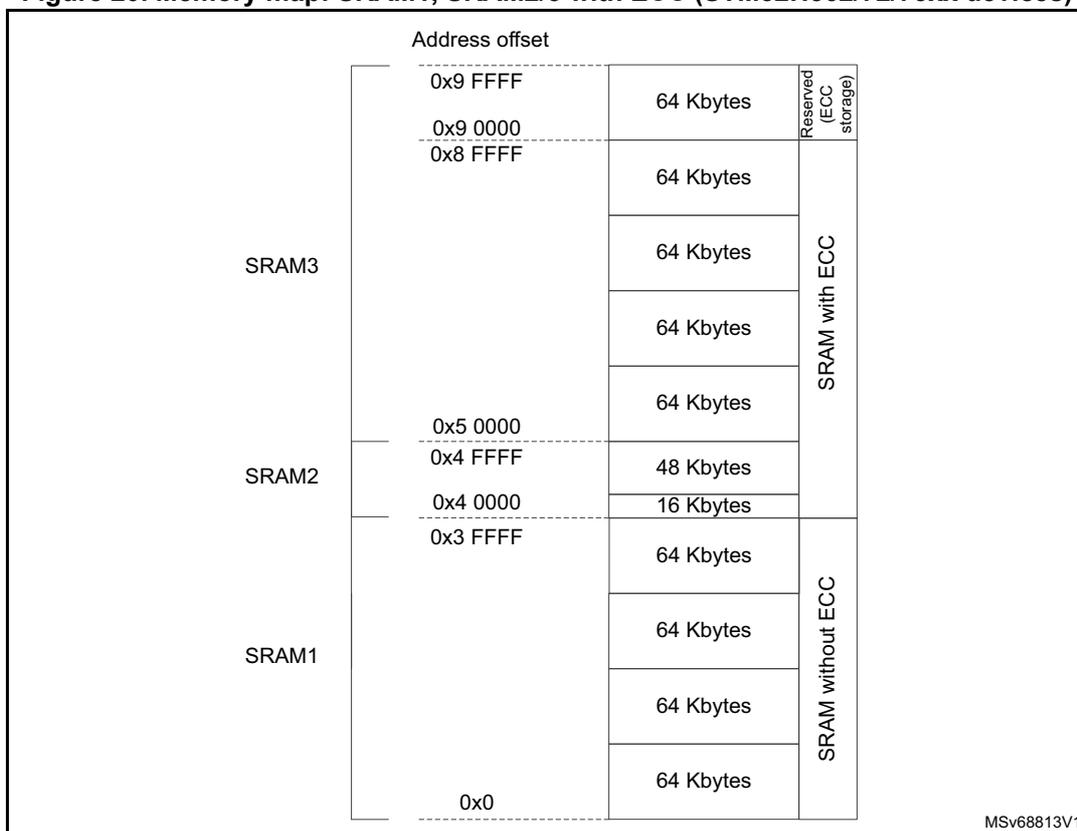
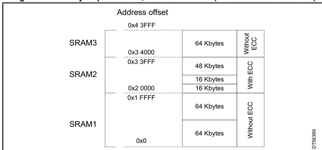
SRAM3 ECC specific management
On STM32H562/563/573xx devices, when the ECC is enabled for SRAM3, only the first 256 Kbytes of SRAM3 are with ECC. The next 64 Kbytes are without ECC, and the last block is used to store the ECC, hence it cannot be used by the application.
Figure 20 shows the SRAM areas, when SRAM2 and SRAM3 ECC are enabled. Figure 21 shows the SRAM areas, when SRAM2 ECC and SRAM3 are enabled.
Figure 20. Memory map: SRAM1, SRAM2/3 with ECC (STM32H562/72/73xx devices)
| Address offset | |||
|---|---|---|---|
| SRAM3 | 0x9 FFFF | 64 Kbytes | Reserved (ECC storage) |
| 0x9 0000 | |||
| 0x8 FFFF | 64 Kbytes | ||
| 64 Kbytes | |||
| 64 Kbytes | |||
| SRAM2 | 0x5 0000 | SRAM with ECC | |
| 0x4 FFFF | 48 Kbytes | ||
| 0x4 0000 | 16 Kbytes | ||
| SRAM1 | 0x3 FFFF | 64 Kbytes | SRAM without ECC |
| 64 Kbytes | |||
| 64 Kbytes | |||
| 0x0 | 64 Kbytes | ||
MSV68813V1
Figure 21. Memory map: SRAM1/3, SRAM2 with ECC (STM32H523/33xx devices)
| Address offset | |||
|---|---|---|---|
| SRAM3 | 0x4 3FFF | 64 Kbytes | Without ECC |
| 0x3 4000 | |||
| SRAM2 | 0x3 3FFF | 48 Kbytes | With ECC |
| 16 Kbytes | |||
| 0x2 0000 | 16 Kbytes | ||
| SRAM1 | 0x1 FFFF | 64 Kbytes | Without ECC |
| 0x0 | 64 Kbytes | ||
DT56369
When ECC is enabled by user option bits, the ECCE bit is automatically set after system reset in the related RAMCFG memory x control register (RAMCFG_MxCR) .
The ECC can be deactivated by executing the following software sequence:
- 1. Write 0xAE in the RAMCFG memory x ECC key register (RAMCFG_MxECCKEYR) .
- 2. Write 0x75 in the RAMCFG memory x ECC key register (RAMCFG_MxECCKEYR) .
- 3. Write 0 in the ECCE bit of the RAMCFG memory x control register (RAMCFG_MxCR) .
When ECC is deactivated (ECCE = 0), the SRAM3 ECC storage area can be read and written for ECC user test purpose. When the ECC is activated (ECCE = 1), this area is reserved for ECC storage purpose and cannot be neither read, nor written.
6.3.3 Write protection (SRAM2)
The SRAM2 is made of 1-Kbyte pages, each of them can be write-protected by setting its corresponding PxWP bit in the RAMCFG memory 2 write protection register 1 (RAMCFG_M2WPR1) , RAMCFG memory 2 write protection register 2 (RAMCFG_M2WPR2) , and RAMCFG memory 2 write protection register 3 (RAMCFG_M2WPR3) (a) .
Table 41. SRAM2 features
| Products | Page size | Number of pages | PxWP bits |
|---|---|---|---|
| STM32H562/63/73xx | 1 Kbyte | 64 | 0 to 63 |
| STM32H523/33xx | 1 Kbyte | 80 | 0 to 79 |
a. This register is available only on STM32H523/533 devices. If not present, consider this register as reserved, and keep its bits at reset value.
6.3.4 Software erase
SRAM erase can be requested by executing this software sequence:
- 1. Write 0xCA in the RAMCFG memory x erase key register (RAMCFG_MxERKEYR) .
- 2. Write 0x53 in the RAMCFG memory x erase key register (RAMCFG_MxERKEYR) .
- 3. Write 1 in the SRAMER bit of the RAMCFG memory x control register (RAMCFG_MxCR) .
SRAMBUSY flag is set in the related SRAM interrupt status register as long as the erase is ongoing.
The total duration of each SRAM erase is N AHB clock cycles, where N is the size of the SRAM in 32-bit words.
If the SRAM is read or written while an erase is ongoing, wait states are inserted on the AHB bus until the end of the operation.
6.4 RAMCFG low-power modes
Table 42. Effect of low-power modes on RAMCFG
| Mode | Description |
|---|---|
| Sleep | No effect. RAMCFG interrupts cause the device to exit the Sleep mode |
| Stop | The content of RAMCFG registers is kept |
| Standby | The RAMCFG peripheral is powered down and must be reinitialized after exiting Standby |
6.5 RAMCFG interrupts
Table 43. RAMCFG interrupt requests
| Interrupt acronym | Interrupt event | Event flag | Enable control bit(s) | Interrupt clear method | Exit Sleep mode | Exit Stop mode | Exit Standby modes |
|---|---|---|---|---|---|---|---|
| RAMCFG | ECC single error detection and correction | SEDC | SEIE | Write 1 in CSEDC | Yes | No | No |
| ECC double error detection | DED | DEIE = 1 and ECCNMI = 0 | Write 1 in CDED | Yes | No | No | |
| NMI | ECC double error detection | DED | ECCNMI | Write 1 in CDED | Yes | No | No |
6.6 RAMCFG registers
In the registers described below, x refers to:
- • SRAM1/2/3 when x = 1/2/3, respectively
- • BKPSRAM when x = 5
6.6.1 RAMCFG memory x control register (RAMCFG_MxCR)
Address offset: \( 0x000 + 0x040 * (x - 1) \) , ( \( x = 1, 2, 3, 5 \) )
Reset value: 0x0000 000X
ECCE reset value depends on ECC enable user option bit.
| 31 | 30 | 29 | 28 | 27 | 26 | 25 | 24 | 23 | 22 | 21 | 20 | 19 | 18 | 17 | 16 |
|---|---|---|---|---|---|---|---|---|---|---|---|---|---|---|---|
| Res. | Res. | Res. | Res. | Res. | Res. | Res. | Res. | Res. | Res. | Res. | Res. | Res. | Res. | Res. | Res. |
| 15 | 14 | 13 | 12 | 11 | 10 | 9 | 8 | 7 | 6 | 5 | 4 | 3 | 2 | 1 | 0 |
| Res. | Res. | Res. | Res. | Res. | Res. | Res. | SRAMER | Res. | Res. | Res. | ALE | Res. | Res. | Res. | ECCE |
| rs | rw | rw |
Bits 31:9 Reserved, must be kept at reset value.
Bit 8 SRAMER : SRAM erase
This bit can be set by software only after writing the unlock sequence in the ERASEKEY field of the RAMCFG_MxERKEYR register. Setting this bit starts the SRAM erase. This bit is automatically cleared by hardware at the end of the erase operation.
0: No erase operation on going
1: Erase operation on going
Bits 7:5 Reserved, must be kept at reset value.
Bit 4 ALE : Address latch enable
0: Failing address not stored in the SRAMx ECC single/double error address registers
1: Failing address stored in the SRAMx ECC single/double error address registers
Note: For SRAM1 and SRAM3 (when ECC is not available) this bit is reserved and must be kept at reset value in control registers.
Bits 3:1 Reserved, must be kept at reset value.
Bit 0 ECCE : ECC enable.
This bit reset value is defined by the user option bit configuration. When set, it can be cleared by software only after writing the unlock sequence in the RAMCFG_MxECCKEYR register.
0: ECC disabled
1: ECC enabled
Note: For SRAM1 and SRAM3 (when ECC is not available) this bit is reserved and must be kept at reset value in control registers.
6.6.2 RAMCFG memory x interrupt enable register (RAMCFG_MxIER)
Address offset: \( 0x004 + 0x040 * (x - 1) \) , ( \( x = 2, 3, 5 \) )
Reset value: 0x0000 0000
| 31 | 30 | 29 | 28 | 27 | 26 | 25 | 24 | 23 | 22 | 21 | 20 | 19 | 18 | 17 | 16 |
|---|---|---|---|---|---|---|---|---|---|---|---|---|---|---|---|
| Res. | Res. | Res. | Res. | Res. | Res. | Res. | Res. | Res. | Res. | Res. | Res. | Res. | Res. | Res. | Res. |
| 15 | 14 | 13 | 12 | 11 | 10 | 9 | 8 | 7 | 6 | 5 | 4 | 3 | 2 | 1 | 0 |
| Res. | Res. | Res. | Res. | Res. | Res. | Res. | Res. | Res. | Res. | Res. | Res. | ECCNMI | Res. | DEIE | SEIE |
| rs | rw | rw |
Bits 31:4 Reserved, must be kept at reset value.
Bit 3 ECCNMI : Double error NMI
This bit is set by software and cleared only by a global RAMCFG reset.
0: NMI not generated in case of ECC double error
1: NMI generated in case of ECC double error
Note: if ECCNMI is set, the RAMCFG maskable interrupt is not generated whatever DEIE bit value.
Bit 2 Reserved, must be kept at reset value.
Bit 1 DEIE : ECC double error interrupt enable
0: Double error interrupt disabled
1: Double error interrupt enabled
Bit 0 SEIE : ECC single error interrupt enable
0: Single error interrupt disabled
1: Single error interrupt enabled
6.6.3 RAMCFG memory interrupt status register (RAMCFG_MxISR)
Address offset: 0x008 + 0x040 * (x - 1), (x = 1, 2, 3, 5)
Reset value: 0x0000 0000
| 31 | 30 | 29 | 28 | 27 | 26 | 25 | 24 | 23 | 22 | 21 | 20 | 19 | 18 | 17 | 16 |
|---|---|---|---|---|---|---|---|---|---|---|---|---|---|---|---|
| Res. | Res. | Res. | Res. | Res. | Res. | Res. | Res. | Res. | Res. | Res. | Res. | Res. | Res. | Res. | Res. |
| 15 | 14 | 13 | 12 | 11 | 10 | 9 | 8 | 7 | 6 | 5 | 4 | 3 | 2 | 1 | 0 |
| Res. | Res. | Res. | Res. | Res. | Res. | Res. | SRAM BUSY | Res. | Res. | Res. | Res. | Res. | Res. | DED | SEDC |
| r | r | r |
Bits 31:9 Reserved, must be kept at reset value.
Bit 8 SRAMBUSY : SRAM busy with erase operation
0: No erase operation on going
1: Erase operation on going
Note: Depending on the SRAM, the erase operation can be performed due to software request, system reset if the option bit is enabled, tamper detection or readout protection regression. Refer to Table 40.
Bits 7:2 Reserved, must be kept at reset value.
Bit 1 DED : ECC double error detected
0: No double error
1: Double error detected
Note: For SRAM1 and SRAM3 (when ECC is not available) this bit is reserved and must be kept at reset value in control registers.
Bit 0 SEDC : ECC single error detected and corrected
0: No single error
1: Single error detected and corrected
Note: For SRAM1 and SRAM3 (when ECC is not available) this bit is reserved and must be kept at reset value in control registers.
6.6.4 RAMCFG memory x ECC single error address register (RAMCFG_MxSEAR)
Address offset: \( 0x00C + 0x040 * (x - 1) \) , ( \( x = 2, 3, 5 \) )
Reset value: 0x0000 0000
| 31 | 30 | 29 | 28 | 27 | 26 | 25 | 24 | 23 | 22 | 21 | 20 | 19 | 18 | 17 | 16 |
|---|---|---|---|---|---|---|---|---|---|---|---|---|---|---|---|
| ESEA[31:16] | |||||||||||||||
| r | r | r | r | r | r | r | r | r | r | r | r | r | r | r | r |
| 15 | 14 | 13 | 12 | 11 | 10 | 9 | 8 | 7 | 6 | 5 | 4 | 3 | 2 | 1 | 0 |
| ESEA[15:0] | |||||||||||||||
| r | r | r | r | r | r | r | r | r | r | r | r | r | r | r | r |
Bits 31:0 ESEA[31:0] : ECC single error address
When the ALE bit is set in the RAMCFG_MxCR register, this field is updated with the address corresponding to the ECC single error.
6.6.5 RAMCFG memory x ECC double error address register (RAMCFG_MxDEAR)
Address offset: \( 0x010 + 0x040 * (x - 1) \) , ( \( x = 2, 3, 5 \) )
Reset value: 0x0000 0000
| 31 | 30 | 29 | 28 | 27 | 26 | 25 | 24 | 23 | 22 | 21 | 20 | 19 | 18 | 17 | 16 |
|---|---|---|---|---|---|---|---|---|---|---|---|---|---|---|---|
| EDEA[31:16] | |||||||||||||||
| r | r | r | r | r | r | r | r | r | r | r | r | r | r | r | r |
| 15 | 14 | 13 | 12 | 11 | 10 | 9 | 8 | 7 | 6 | 5 | 4 | 3 | 2 | 1 | 0 |
| EDEA[15:0] | |||||||||||||||
| r | r | r | r | r | r | r | r | r | r | r | r | r | r | r | r |
Bits 31:0 EDEA[31:0] : ECC double error address
When the ALE bit is set in the RAMCFG_MxCR register, this field is updated with the address corresponding to the ECC double error.
6.6.6 RAMCFG memory x interrupt clear register x (RAMCFG_MxICR)
Address offset: \( 0x014 + 0x040 * (x - 1) \) , ( \( x = 2, 3, 5 \) )
Reset value: 0x0000 0000
| 31 | 30 | 29 | 28 | 27 | 26 | 25 | 24 | 23 | 22 | 21 | 20 | 19 | 18 | 17 | 16 |
|---|---|---|---|---|---|---|---|---|---|---|---|---|---|---|---|
| Res. | Res. | Res. | Res. | Res. | Res. | Res. | Res. | Res. | Res. | Res. | Res. | Res. | Res. | Res. | Res. |
| 15 | 14 | 13 | 12 | 11 | 10 | 9 | 8 | 7 | 6 | 5 | 4 | 3 | 2 | 1 | 0 |
| Res. | Res. | Res. | Res. | Res. | Res. | Res. | Res. | Res. | Res. | Res. | Res. | Res. | Res. | CDED rw | CSEDC rw |
Bits 31:2 Reserved, must be kept at reset value.
Bit 1 CDED : Clear ECC double error detected
Writing 1 to this flag clears the DED bit in the RAMCFG_MxISR register. Reading this flag returns the DED value.
Bit 0 CSEDC : Clear ECC single error detected and corrected
Writing 1 to this flag clears the SEDC bit in the RAMCFG_MxISR register. Reading this flag returns the SEDC value.
6.6.7 RAMCFG memory 2 write protection register 1 (RAMCFG_M2WPR1)
Address offset: 0x058
Reset value: 0x0000 0000
| 31 | 30 | 29 | 28 | 27 | 26 | 25 | 24 | 23 | 22 | 21 | 20 | 19 | 18 | 17 | 16 |
|---|---|---|---|---|---|---|---|---|---|---|---|---|---|---|---|
| P31WP | P30WP | P29WP | P28WP | P27WP | P26WP | P25WP | P24WP | P23WP | P22WP | P21WP | P20WP | P19WP | P18WP | P17WP | P16WP |
| rs | rs | rs | rs | rs | rs | rs | rs | rs | rs | rs | rs | rs | rs | rs | rs |
| 15 | 14 | 13 | 12 | 11 | 10 | 9 | 8 | 7 | 6 | 5 | 4 | 3 | 2 | 1 | 0 |
| P15WP | P14WP | P13WP | P12WP | P11WP | P10WP | P9WP | P8WP | P7WP | P6WP | P5WP | P4WP | P3WP | P2WP | P1WP | P0WP |
| rs | rs | rs | rs | rs | rs | rs | rs | rs | rs | rs | rs | rs | rs | rs | rs |
Bits 31:0 PyWP : SRAM2 1-Kbyte page y write protection (y = 31 to 0)
These bits are set by software and cleared only by a global RAMCFG reset.
0: Write protection of SRAM2 1-Kbyte page y is disabled.
1: Write protection of SRAM2 1-Kbyte page y is enabled.
6.6.8 RAMCFG memory 2 write protection register 2 (RAMCFG_M2WPR2)
Address offset: 0x05C
Reset value: 0x0000 0000
| 31 | 30 | 29 | 28 | 27 | 26 | 25 | 24 | 23 | 22 | 21 | 20 | 19 | 18 | 17 | 16 |
|---|---|---|---|---|---|---|---|---|---|---|---|---|---|---|---|
| P63WP | P62WP | P61WP | P60WP | P59WP | P58WP | P57WP | P56WP | P55WP | P54WP | P53WP | P52WP | P51WP | P50WP | P49WP | P48WP |
| rs | rs | rs | rs | rs | rs | rs | rs | rs | rs | rs | rs | rs | rs | rs | rs |
| 15 | 14 | 13 | 12 | 11 | 10 | 9 | 8 | 7 | 6 | 5 | 4 | 3 | 2 | 1 | 0 |
| P47WP | P46WP | P45WP | P44WP | P43WP | P42WP | P41WP | P40WP | P39WP | P38WP | P37WP | P36WP | P35WP | P34WP | P33WP | P32WP |
| rs | rs | rs | rs | rs | rs | rs | rs | rs | rs | rs | rs | rs | rs | rs | rs |
Bits 31:0 PyWP : SRAM2 1-Kbyte page y write protection (y = 63 to 32)
These bits are set by software and cleared only by a global RAMCFG reset.
0: Write protection of SRAM2 1-Kbyte page y is disabled.
1: Write protection of SRAM2 1-Kbyte page y is enabled.
6.6.9 RAMCFG memory 2 write protection register 3 (RAMCFG_M2WPR3)
Address offset: 0x060
Reset value: 0x0000 0000
This register is available only for STM32H523/33xx devices.
| 31 | 30 | 29 | 28 | 27 | 26 | 25 | 24 | 23 | 22 | 21 | 20 | 19 | 18 | 17 | 16 |
|---|---|---|---|---|---|---|---|---|---|---|---|---|---|---|---|
| Res. | Res. | Res. | Res. | Res. | Res. | Res. | Res. | Res. | Res. | Res. | Res. | Res. | Res. | Res. | Res. |
| 15 | 14 | 13 | 12 | 11 | 10 | 9 | 8 | 7 | 6 | 5 | 4 | 3 | 2 | 1 | 0 |
| P79WP | P78WP | P77WP | P76WP | P75WP | P74WP | P73WP | P72WP | P71WP | P70WP | P69WP | P68WP | P67WP | P66WP | P65WP | P64WP |
| rs | rs | rs | rs | rs | rs | rs | rs | rs | rs | rs | rs | rs | rs | rs | rs |
Bits 31:16 Reserved, must be kept at reset value.
Bits 15:0 PyWP : SRAM2 1-Kbyte page y write protection (y = 79 to 64)
These bits are set by software and cleared only by a global RAMCFG reset.
0: Write protection of SRAM2 1-Kbyte page y is disabled.
1: Write protection of SRAM2 1-Kbyte page y is enabled.
6.6.10 RAMCFG memory x ECC key register (RAMCFG_MxECCKEYR)
Address offset: 0x024 + 0x040 * (x - 1), (x = 2, 3, 5)
Reset value: 0x0000 0000
| 31 | 30 | 29 | 28 | 27 | 26 | 25 | 24 | 23 | 22 | 21 | 20 | 19 | 18 | 17 | 16 |
|---|---|---|---|---|---|---|---|---|---|---|---|---|---|---|---|
| Res. | Res. | Res. | Res. | Res. | Res. | Res. | Res. | Res. | Res. | Res. | Res. | Res. | Res. | Res. | Res. |
| 15 | 14 | 13 | 12 | 11 | 10 | 9 | 8 | 7 | 6 | 5 | 4 | 3 | 2 | 1 | 0 |
| Res. | Res. | Res. | Res. | Res. | Res. | Res. | Res. | w | w | w | w | w | w | w | w |
Bits 31:8 Reserved, must be kept at reset value.
Bits 7:0 ECCKEY[7:0] : ECC write protection key
The following steps are required to unlock the write protection of the ECCE bit in the RAMCFG_MxCR register.
1) Write 0xAE into ECCKEY[7:0].
2) Write 0x75 into ECCKEY[7:0].
Note: Writing a wrong key reactivates the write protection.
6.6.11 RAMCFG memory x erase key register (RAMCFG_MxERKEYR)
Address offset: \( 0x028 + 0x040 * (x - 1) \) , ( \( x = 1 \) to \( 5 \) )
Reset value: 0x0000 0000
| 31 | 30 | 29 | 28 | 27 | 26 | 25 | 24 | 23 | 22 | 21 | 20 | 19 | 18 | 17 | 16 |
|---|---|---|---|---|---|---|---|---|---|---|---|---|---|---|---|
| Res. | Res. | Res. | Res. | Res. | Res. | Res. | Res. | Res. | Res. | Res. | Res. | Res. | Res. | Res. | Res. |
| 15 | 14 | 13 | 12 | 11 | 10 | 9 | 8 | 7 | 6 | 5 | 4 | 3 | 2 | 1 | 0 |
| Res. | Res. | Res. | Res. | Res. | Res. | Res. | Res. | ERASEKEY[7:0] | |||||||
| w | w | w | w | w | w | w | w | ||||||||
Bits 31:8 Reserved, must be kept at reset value.
Bits 7:0 ERASEKEY[7:0] : Erase write protection key
The following steps are required to unlock the write protection of the SRAMER bit in the RAMCFG_MxCR register.
- 1) Write 0xCA into ERASEKEY[7:0].
- 2) Write 0x53 into ERASEKEY[7:0].
Note: Writing a wrong key reactivates the write protection.
6.6.12 RAMCFG register map
Table 44. RAMCFG register map and reset values
| Offset | Register name reset value | 31 | 30 | 29 | 28 | 27 | 26 | 25 | 24 | 23 | 22 | 21 | 20 | 19 | 18 | 17 | 16 | 15 | 14 | 13 | 12 | 11 | 10 | 9 | 8 | 7 | 6 | 5 | 4 | 3 | 2 | 1 | 0 | |
|---|---|---|---|---|---|---|---|---|---|---|---|---|---|---|---|---|---|---|---|---|---|---|---|---|---|---|---|---|---|---|---|---|---|---|
| 0x00 | RAMCFG_M1CR | Res. | Res. | Res. | Res. | Res. | Res. | Res. | Res. | Res. | Res. | Res. | Res. | Res. | Res. | Res. | Res. | Res. | Res. | Res. | Res. | Res. | Res. | Res. | SRAMER | Res. | Res. | Res. | Res. | ALE | Res. | Res. | Res. | ECCE |
| Reset value | 0 | 0 | x | |||||||||||||||||||||||||||||||
| 0x04 | Reserved | Reserved | ||||||||||||||||||||||||||||||||
| 0x08 | RAMCFG_M1ISR | Res. | Res. | Res. | Res. | Res. | Res. | Res. | Res. | Res. | Res. | Res. | Res. | Res. | Res. | Res. | Res. | Res. | Res. | Res. | Res. | Res. | Res. | Res. | SRAMBUSY | Res. | Res. | Res. | Res. | Res. | Res. | Res. | Res. | Res. |
| Reset value | 0 | |||||||||||||||||||||||||||||||||
| 0x0C to 0x24 | Reserved | Reserved | ||||||||||||||||||||||||||||||||
| 0x28 | RAMCFG_M1ERKEYR | Res. | Res. | Res. | Res. | Res. | Res. | Res. | Res. | Res. | Res. | Res. | Res. | Res. | Res. | Res. | Res. | Res. | Res. | Res. | Res. | Res. | Res. | Res. | Res. | ERASEKEY[7:0] | ||||||||
| Reset value | 0 | 0 | 0 | 0 | 0 | 0 | 0 | 0 | ||||||||||||||||||||||||||
| 0x2C to 0x3C | Reserved | Reserved | ||||||||||||||||||||||||||||||||
| 0x40 | RAMCFG_M2CR | Res. | Res. | Res. | Res. | Res. | Res. | Res. | Res. | Res. | Res. | Res. | Res. | Res. | Res. | Res. | Res. | Res. | Res. | Res. | Res. | Res. | Res. | Res. | SRAMER | Res. | Res. | Res. | Res. | ALE | Res. | Res. | Res. | ECCE |
| Reset value | 0 | 0 | x | |||||||||||||||||||||||||||||||
| 0x44 | RAMCFG_M2IER | Res. | Res. | Res. | Res. | Res. | Res. | Res. | Res. | Res. | Res. | Res. | Res. | Res. | Res. | Res. | Res. | Res. | Res. | Res. | Res. | Res. | Res. | Res. | Res. | Res. | Res. | Res. | Res. | Res. | ECCNMI | Res. | DEIE | SEIE |
| Reset value | 0 | 0 | 0 | |||||||||||||||||||||||||||||||
| 0x48 | RAMCFG_M2ISR | Res. | Res. | Res. | Res. | Res. | Res. | Res. | Res. | Res. | Res. | Res. | Res. | Res. | Res. | Res. | Res. | Res. | Res. | Res. | Res. | Res. | Res. | Res. | SRAMBUSY | Res. | Res. | Res. | Res. | Res. | Res. | DED | SEDC | |
| Reset value | 0 | 0 | 0 | |||||||||||||||||||||||||||||||
| 0x04C | RAMCFG_M2SEAR | ESEA[31:0] | ||||||||||||||||||||||||||||||||
| Reset value | 0 | 0 | 0 | 0 | 0 | 0 | 0 | 0 | 0 | 0 | 0 | 0 | 0 | 0 | 0 | 0 | 0 | 0 | 0 | 0 | 0 | 0 | 0 | 0 | 0 | 0 | 0 | 0 | 0 | 0 | 0 | 0 | ||
| 0x050 | RAMCFG_M2DEAR | EDEA[31:0] | ||||||||||||||||||||||||||||||||
| Reset value | 0 | 0 | 0 | 0 | 0 | 0 | 0 | 0 | 0 | 0 | 0 | 0 | 0 | 0 | 0 | 0 | 0 | 0 | 0 | 0 | 0 | 0 | 0 | 0 | 0 | 0 | 0 | 0 | 0 | 0 | 0 | 0 | ||
| 0x054 | RAMCFG_M2ICR | Res. | Res. | Res. | Res. | Res. | Res. | Res. | Res. | Res. | Res. | Res. | Res. | Res. | Res. | Res. | Res. | Res. | Res. | Res. | Res. | Res. | Res. | Res. | Res. | Res. | Res. | Res. | Res. | Res. | Res. | CDED | CSEDC | |
| Reset value | 0 | 0 | ||||||||||||||||||||||||||||||||
| 0x058 | RAMCFG_M2WPR1 | P31WP | P30WP | P29WP | P28WP | P27WP | P26WP | P25WP | P24WP | P23WP | P22WP | P21WP | P20WP | P19WP | P18WP | P17WP | P16WP | P15WP | P14WP | P13WP | P12WP | P11WP | P10WP | P9WP | P8WP | P7WP | P6WP | P5WP | P4WP | P3WP | P2WP | P1WP | P0WP | |
| Reset value | 0 | 0 | 0 | 0 | 0 | 0 | 0 | 0 | 0 | 0 | 0 | 0 | 0 | 0 | 0 | 0 | 0 | 0 | 0 | 0 | 0 | 0 | 0 | 0 | 0 | 0 | 0 | 0 | 0 | 0 | 0 | 0 | ||
| 0x05C | RAMCFG_M2WPR2 | P63WP | P62WP | P61WP | P60WP | P59WP | P58WP | P57WP | P56WP | P55WP | P54WP | P53WP | P52WP | P51WP | P50WP | P49WP | P48WP | P47WP | P46WP | P45WP | P44WP | P43WP | P42WP | P41WP | P40WP | P39WP | P38WP | P37WP | P36WP | P35WP | P34WP | P33WP | P32WP | |
| Reset value | 0 | 0 | 0 | 0 | 0 | 0 | 0 | 0 | 0 | 0 | 0 | 0 | 0 | 0 | 0 | 0 | 0 | 0 | 0 | 0 | 0 | 0 | 0 | 0 | 0 | 0 | 0 | 0 | 0 | 0 | 0 | 0 | ||
| 0x060 | RAMCFG_M2WPR3 (1) | Res. | Res. | Res. | Res. | Res. | Res. | Res. | Res. | Res. | Res. | Res. | Res. | Res. | Res. | Res. | Res. | P79WP | P78WP | P77WP | P76WP | P75WP | P74WP | P73WP | P72WP | P71WP | P70WP | P69WP | P68WP | P67WP | P66WP | P65WP | P64WP | |
| Reset value | 0 | 0 | 0 | 0 | 0 | 0 | 0 | 0 | 0 | 0 | 0 | 0 | 0 | 0 | 0 | 0 | ||||||||||||||||||
| 0x064 | RAMCFG_M2ECCKEYR | Res. | Res. | Res. | Res. | Res. | Res. | Res. | Res. | Res. | Res. | Res. | Res. | Res. | Res. | Res. | Res. | Res. | Res. | Res. | Res. | Res. | Res. | Res. | Res. | ECCKEY[7:0] | ||||||||
| Reset value | 0 | 0 | 0 | 0 | 0 | 0 | 0 | 0 | ||||||||||||||||||||||||||
Table 44. RAMCFG register map and reset values (continued)
| Offset | Register name reset value | 31 | 30 | 29 | 28 | 27 | 26 | 25 | 24 | 23 | 22 | 21 | 20 | 19 | 18 | 17 | 16 | 15 | 14 | 13 | 12 | 11 | 10 | 9 | 8 | 7 | 6 | 5 | 4 | 3 | 2 | 1 | 0 | |
|---|---|---|---|---|---|---|---|---|---|---|---|---|---|---|---|---|---|---|---|---|---|---|---|---|---|---|---|---|---|---|---|---|---|---|
| 0x068 | RAMCFG_M2ERKEYR | Res. | Res. | Res. | Res. | Res. | Res. | Res. | Res. | Res. | Res. | Res. | Res. | Res. | Res. | Res. | Res. | Res. | Res. | Res. | Res. | Res. | Res. | Res. | Res. | ERASEKEY[7:0] | ||||||||
| Reset value | 0 | 0 | 0 | 0 | 0 | 0 | 0 | 0 | ||||||||||||||||||||||||||
| 0x06C to 0x07C | Reserved | Reserved | ||||||||||||||||||||||||||||||||
| 0x080 | RAMCFG_M3CR | Res. | Res. | Res. | Res. | Res. | Res. | Res. | Res. | Res. | Res. | Res. | Res. | Res. | Res. | Res. | Res. | Res. | Res. | Res. | Res. | Res. | Res. | Res. | SRAMER | Res. | Res. | Res. | Res. | ALE | Res. | Res. | Res. | ECCE |
| Reset value | 0 | 0 | 0 | |||||||||||||||||||||||||||||||
| 0x084 | RAMCFG_M3IER | Res. | Res. | Res. | Res. | Res. | Res. | Res. | Res. | Res. | Res. | Res. | Res. | Res. | Res. | Res. | Res. | Res. | Res. | Res. | Res. | Res. | Res. | Res. | Res. | Res. | Res. | Res. | Res. | Res. | ECCNMI | Res. | DEIE | SEIE |
| Reset value | 0 | 0 | 0 | |||||||||||||||||||||||||||||||
| 0x088 | RAMCFG_M3ISR | Res. | Res. | Res. | Res. | Res. | Res. | Res. | Res. | Res. | Res. | Res. | Res. | Res. | Res. | Res. | Res. | Res. | Res. | Res. | Res. | Res. | Res. | Res. | SRAMBUSY | Res. | Res. | Res. | Res. | Res. | Res. | DED | SEDC | |
| Reset value | 0 | 0 | 0 | |||||||||||||||||||||||||||||||
| 0x08C | RAMCFG_M3SEAR | ESEA[31:0] | ||||||||||||||||||||||||||||||||
| Reset value | 0 | 0 | 0 | 0 | 0 | 0 | 0 | 0 | 0 | 0 | 0 | 0 | 0 | 0 | 0 | 0 | 0 | 0 | 0 | 0 | 0 | 0 | 0 | 0 | 0 | 0 | 0 | 0 | 0 | 0 | 0 | 0 | ||
| 0x090 | RAMCFG_M3DEAR | EDEA[31:0] | ||||||||||||||||||||||||||||||||
| Reset value | 0 | 0 | 0 | 0 | 0 | 0 | 0 | 0 | 0 | 0 | 0 | 0 | 0 | 0 | 0 | 0 | 0 | 0 | 0 | 0 | 0 | 0 | 0 | 0 | 0 | 0 | 0 | 0 | 0 | 0 | 0 | 0 | ||
| 0x094 | RAMCFG_M3ICR | Res. | Res. | Res. | Res. | Res. | Res. | Res. | Res. | Res. | Res. | Res. | Res. | Res. | Res. | Res. | Res. | Res. | Res. | Res. | Res. | Res. | Res. | Res. | Res. | Res. | Res. | Res. | Res. | Res. | Res. | Res. | CDED | CSEDC |
| Reset value | 0 | 0 | ||||||||||||||||||||||||||||||||
| 0x098 to 0x0A0 | Reserved | Reserved | ||||||||||||||||||||||||||||||||
| 0x0A4 | RAMCFG_M3ECCKEYR | Res. | Res. | Res. | Res. | Res. | Res. | Res. | Res. | Res. | Res. | Res. | Res. | Res. | Res. | Res. | Res. | Res. | Res. | Res. | Res. | Res. | Res. | Res. | Res. | ECCKEY[7:0] | ||||||||
| Reset value | 0 | 0 | 0 | 0 | 0 | 0 | 0 | 0 | ||||||||||||||||||||||||||
| 0x0A8 | RAMCFG_M3ERKEYR | Res. | Res. | Res. | Res. | Res. | Res. | Res. | Res. | Res. | Res. | Res. | Res. | Res. | Res. | Res. | Res. | Res. | Res. | Res. | Res. | Res. | Res. | Res. | Res. | ERASEKEY[7:0] | ||||||||
| Reset value | 0 | 0 | 0 | 0 | 0 | 0 | 0 | 0 | ||||||||||||||||||||||||||
| 0x0AC to 0x0FC | Reserved | Reserved | ||||||||||||||||||||||||||||||||
| 0x100 | RAMCFG_M5CR | Res. | Res. | Res. | Res. | Res. | Res. | Res. | Res. | Res. | Res. | Res. | Res. | Res. | Res. | Res. | Res. | Res. | Res. | Res. | Res. | Res. | Res. | Res. | SRAMER | Res. | Res. | Res. | Res. | ALE | Res. | Res. | Res. | ECCE |
| Reset value | 0 | 0 | x | |||||||||||||||||||||||||||||||
| 0x104 | RAMCFG_M5IER | Res. | Res. | Res. | Res. | Res. | Res. | Res. | Res. | Res. | Res. | Res. | Res. | Res. | Res. | Res. | Res. | Res. | Res. | Res. | Res. | Res. | Res. | Res. | Res. | Res. | Res. | Res. | Res. | Res. | ECCNMI | Res. | DEIE | SEIE |
| Reset value | 0 | 0 | 0 | |||||||||||||||||||||||||||||||
| 0x108 | RAMCFG_M5ISR | Res. | Res. | Res. | Res. | Res. | Res. | Res. | Res. | Res. | Res. | Res. | Res. | Res. | Res. | Res. | Res. | Res. | Res. | Res. | Res. | Res. | Res. | Res. | SRAMBUSY | Res. | Res. | Res. | Res. | Res. | Res. | DED | SEDC | |
| Reset value | 0 | 0 | 0 | |||||||||||||||||||||||||||||||
| 0x10C | RAMCFG_M5SEAR | ESEA[31:0] | ||||||||||||||||||||||||||||||||
| Reset value | 0 | 0 | 0 | 0 | 0 | 0 | 0 | 0 | 0 | 0 | 0 | 0 | 0 | 0 | 0 | 0 | 0 | 0 | 0 | 0 | 0 | 0 | 0 | 0 | 0 | 0 | 0 | 0 | 0 | 0 | 0 | 0 | ||
| 0x110 | RAMCFG_M5DEAR | EDEA[31:0] | ||||||||||||||||||||||||||||||||
| Reset value | 0 | 0 | 0 | 0 | 0 | 0 | 0 | 0 | 0 | 0 | 0 | 0 | 0 | 0 | 0 | 0 | 0 | 0 | 0 | 0 | 0 | 0 | 0 | 0 | 0 | 0 | 0 | 0 | 0 | 0 | 0 | 0 | ||
Table 44. RAMCFG register map and reset values (continued)
| Offset | Register name reset value | 31 | 30 | 29 | 28 | 27 | 26 | 25 | 24 | 23 | 22 | 21 | 20 | 19 | 18 | 17 | 16 | 15 | 14 | 13 | 12 | 11 | 10 | 9 | 8 | 7 | 6 | 5 | 4 | 3 | 2 | 1 | 0 |
|---|---|---|---|---|---|---|---|---|---|---|---|---|---|---|---|---|---|---|---|---|---|---|---|---|---|---|---|---|---|---|---|---|---|
| 0x114 | RAMCFG_M5ICR | Res | Res | Res | Res | Res | Res | Res | Res | Res | Res | Res | Res | Res | Res | Res | Res | Res | Res | Res | Res | Res | Res | Res | Res | Res | Res | Res | Res | Res | Res | Res | 0 1 CDED |
| Reset value | 0 CSEDC | ||||||||||||||||||||||||||||||||
| 0x118 to 0x120 | Reserved | Reserved | |||||||||||||||||||||||||||||||
| 0x124 | RAMCFG M5ECCKEYR | Res | Res | Res | Res | Res | Res | Res | Res | Res | Res | Res | Res | Res | Res | Res | Res | Res | Res | Res | Res | Res | Res | Res | Res | Res | ECCKEY[7:0] | ||||||
| Reset value | 0 | 0 | 0 | 0 | 0 | 0 | |||||||||||||||||||||||||||
| 0x128 | RAMCFG M5ERKEYR | Res | Res | Res | Res | Res | Res | Res | Res | Res | Res | Res | Res | Res | Res | Res | Res | Res | Res | Res | Res | Res | Res | Res | Res | Res | ERASEKEY[7:0] | ||||||
| Reset value | 0 | 0 | 0 | 0 | 0 | 0 | |||||||||||||||||||||||||||
1. Available only on STM32H523/33xx devices.
Refer to Section 2.3 for the register boundary addresses.