5. Global TrustZone® controller (GTZC)
5.1 GTZC introduction
The global TrustZone controller (GTZC) block that contains the following subblocks:
- •
TZSC:
TrustZone security controller
Defines the secure/privileged state of slave peripherals, and controls the subregion area size and properties for the watermark memory peripheral controller (MPCWM). The TZSC informs some peripherals (such as RCC or GPIOs) about the secure status of each securable peripheral, by sharing with RCC and I/O logic. - •
MPCBB:
memory protection controller - block based
Configures the internal RAM in a TrustZone-system product having segmented SRAM (pages of 512 bytes) with programmable-security and privileged attributes. - •
TZIC:
TrustZone illegal access controller
Gathers all illegal access events in the system, and generates secure interrupts towards NVIC.
These subblocks are used to configure TrustZone system security in a product having bus agents with programmable-security and privileged attributes such as:
- • on-chip RAM with programmable secure and/or privileged blocks (pages)
- • AHB and APB peripherals with programmable security and/or privileged access
- • off-chip memories with secure and/or privileged areas
5.2 GTZC main features
- • Three independent 32-bit AHB interfaces for TZSC, TZIC, and MPCBB
- • TZIC accessible only with secure transactions
- • Secure and non-secure access supported for privileged and unprivileged parts of TZSC and MPCBB
- • Set of registers to define product security settings:
- – Secure/privileged blocks for internal SRAMs
- – Secure/privileged regions for external memories and internal backup SRAM
- – Secure/privileged access mode for securable peripherals
- – Secure/privileged access mode for securable masters
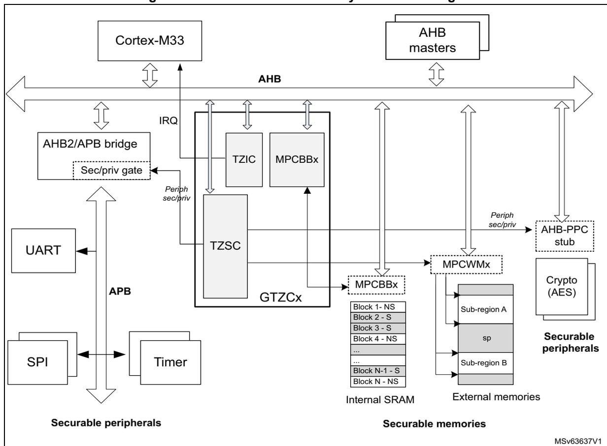
GTZC TrustZone system architecture
The Armv8-M supports security per TrustZone-M model with isolation between:
- • a secure world, where usually security sensitive applications are run and critical resources are located
- • a non-secure or public world (such as the usual non secure operating system and user space)
The TrustZone architecture is extended beyond AHB and Armv8-M with:
- • AHB/APB bridge used as secure gate to block or propagate secure/non-secure and privileged/unprivileged transaction towards APB agents
- • PPC (peripheral protection controller) used as secure gate to block or propagate secure/non-secure and privileged/unprivileged transaction towards AHB agents
- • TrustZone block-based MPC firewalls used as secure gate to filter secure/non-secure, privileged/unprivileged access towards internal SRAMs
- • TrustZone watermark MPC firewalls used as secure gate to filter secure/non-secure, privileged/unprivileged access towards external memories
AHB and APB peripherals can be categorized as:
- • privileged: peripherals protected by an AHB/APB firewall stub controlled from TZSC to define privilege properties
- • secure: peripherals always protected by an AHB/APB firewall stub, always secure (such as TZIC)
- • securable: peripherals protected by an AHB/APB firewall stub that is controlled from TZSC to define security properties (optional)
- • non-secure and unprivileged: peripherals connected directly to AHB/APB interconnect without any secure gate
- • TrustZone-aware: peripherals connected directly to the AHB or APB bus and implementing a specific TrustZone behavior (such as a subset of registers being secure). TrustZone-aware AHB masters always drive HNONSEC signal according to their security mode (such as Armv8-M core or DMA)
AHB securable masters can be configured in the TZSC to be secure/non-secure and/or privileged/unprivileged.
Application information
The TZSC, MPCBB, and TZIC can be used in one of the following ways:
- • programmed only during secure boot, locked and not changed afterwards
- • dynamically re-programmed when using specific application code or secure kernel (microvisor). When not locked, MPC secure blocks or region size can be changed by secure software executing from the secure FLASH region or secure SRAM. The same applies to the GTZC1_TZSC_SECCFGRx/PRIVCFGRx registers that define the secure/privileged state of each peripheral.
The Armv8-M security architecture with secure, securable, and TrustZone-aware peripherals is shown in Figure 16.
Figure 16. GTZC in Armv8-M subsystem block diagram
5.3 GTZC implementation
The STM32H5 devices embed one instance of GTZC.
Table 27. GTZC features
| GTZC sub-blocks | GTZC1 |
|---|---|
| TZSC | X |
| TZIC | X |
| MPCBB sub-block (number of MPCBBs) | X (3) |
Table 28 shows the address offset of GTZC subblocks versus GTZC base address (refer to Section 2.3 for GTZC1 base address).
Table 28. GTZC1 sub-block address offset
| GTZC1 sub-block | Address offset |
|---|---|
| GTZC1_TZSC | 0x0 |
| GTZC1_TZIC | 0x400 |
| GTZC1_MPCBB1 | 0x800 |
| GTZC1_MPCBB2 | 0xC00 |
| GTZC1_MPCBB3 | 0x1000 |
Table 29 and Table 30 describe the characteristics of the available MPCWMs.
Table 29. MPCWM resource assignment
| GTZC | MPC | Target memory interface | Number of sec/non-sec and priv/unpriv regions | Watermark granularity (bytes) |
|---|---|---|---|---|
| GTZC1 | MPCWM1 | OCTOSPI1 | 2 | 128 K |
| MPCWM2 | FMC_NOR bank | 2 | 128 K | |
| MPCWM3 | FMC_NAND bank | 1 | 128 K | |
| FMC_SDRAM bank 1 (1) | 1 | 128 K | ||
| MPCWM4 | BKPSRAM | 1 | 32 | |
| FMC_SDRAM_bank 2 (1) | 1 | 128 K |
1. Not available on STM32H523/33xx devices.
Table 30. MPCWM3 and MPCWM4 (subregions A and B)
| GTZ | MPC | Target memory interface | Subregion |
|---|---|---|---|
| GTZC1 | MPCWM3 | FMC_NAND bank | A |
| FMC_SDRAM bank 1 (1) | B | ||
| MPCWM4 | BKPSRAM | A | |
| FMC_SDRAM_bank 2 (1) | B |
1. Not available on STM32H523/33xx devices.
Table 31 and Table 32 describe the characteristics of the available MPCBBs.
Table 31. MPCBB resource assignment (STM32H562/63/73xx devices)
| GTZC | MPC | Resource | Memory size (Kbytes) | Block size (bytes) | Number of blocks | Number of super-blocks |
|---|---|---|---|---|---|---|
| GTZC1 | MPCBB1 | SRAM1 | 256 | 512 | 512 | 16 |
| MPCBB2 | SRAM2 | 64 | 128 | 4 | ||
| MPCBB3 | SRAM3 | 320 | 640 | 20 |
Table 32. MPCBB resource assignment (STM32H523/33xx devices)
| GTZC | MPC | Resource | Memory size (Kbytes) | Block size (bytes) | Number of blocks | Number of super-blocks |
|---|---|---|---|---|---|---|
| GTZC1 | MPCBB1 | SRAM1 | 128 | 512 | 256 | 8 |
| MPCBB2 | SRAM2 | 80 | 160 | 5 | ||
| MPCBB3 | SRAM3 | 64 | 128 | 4 |
5.4 GTZC functional description
5.4.1 GTZC block diagram
Figure 17 describes the combined feature of TZSC, MPCBB, and TZIC. Each sub-block is controlled by its own AHB configuration port.
The TZSC defines which peripheral is secure and/or privileged. The privileged configuration bit of a peripheral can be modified by a secure privileged transaction when the peripheral is configured as secure. Otherwise, a privileged transaction (non-secure) is sufficient.
On the opposite, the secure configuration bit of a peripheral can be modified only with a secure privileged transaction if the peripheral is configured as privileged. Otherwise, a secure transaction (unprivileged) is sufficient.
The secure configuration bit of a given RAM block can be modified only with a secure privileged transaction if the same block is configured as privileged. Otherwise, a secure transaction (unprivileged) is sufficient.
The TZIC gathers illegal events generated within the system when an illegal access is detected. TZIC can then generate a secure interrupt towards the CPU if needed.
Figure 17. GTZC block diagram
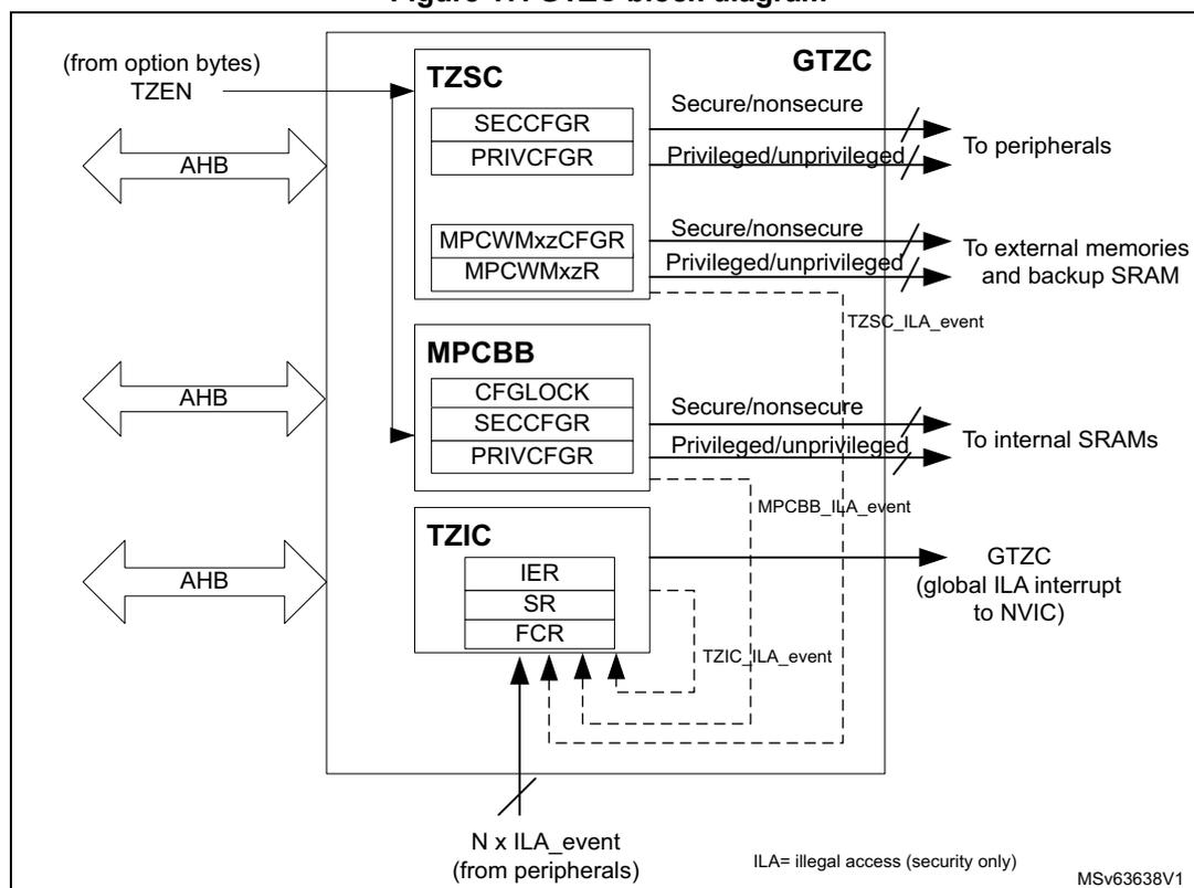
The diagram illustrates the internal structure of the Global TrustZone controller (GTZC). It is composed of three primary functional blocks:
- TZSC (TrustZone Security Controller): Manages security settings for peripherals and external memories. It includes registers for security (SECCFGR), privilege (PRIVCFGR), and memory protection (MPCWMxzCFGR, MPCWMxzR). It generates 'TZSC_ILA_event' signals.
- MPCBB (Memory Protection Controller for Block-based SRAM): Manages security settings for internal SRAMs. It includes registers for configuration (CFGLOCK), security (SECCFGR), and privilege (PRIVCFGR). It generates 'MPCBB_ILA_event' signals.
- TZIC (TrustZone Interrupt Controller): Handles illegal access (ILA) events. It includes registers for interrupt enable (IER), status (SR), and fault control (FCR). It generates 'TZIC_ILA_event' signals.
5.4.2 Illegal access definition
Three different types of illegal access exist:
- • Illegal non-secure access
Any non-secure transaction trying to write a secure resource is considered as illegal, hence the addressed resource generates an illegal access interrupt for illegal write access and a bus error for illegal fetch access. There are some exceptions on secure and privileged configuration registers: the latter ones authorize non secure read access to secure registers (see GTZC1_TZSC_SECCFGRx/GTZC1_TZSC_PRIVCFGRx).
- • Illegal secure access
Any secure transaction trying to access non-secure block in internal block-based SRAM or watermarked memory is considered as illegal.
A correct TZIC setting allows the capture of the associated event and then generates the GTZC_IRQn interrupt to the NVIC. This applies for read, write, and execute access.
Concerning the MPCBB controller, there is an option to ignore secure data read/write access on non-secure SRAM blocks, by setting the SRWILADIS bit in the GTZC1_MPCBBz_CR register. Secure read and write data transactions are then
allowed on non-secure SRAM blocks, while secure execution access remains not allowed.
Any secure execute transaction trying to access a non-secure peripheral register is considered as illegal and generates a bus error.
- • Illegal unprivileged access
Any unprivileged transaction trying to access a privileged resource is considered as illegal. There is no illegal access event generated for illegal read and write accesses. The addressed resource follows a silent-fail behavior, returning all 0 data for read and ignoring any write. No bus error is generated. A bus error is generated when an unprivileged execute transaction tries to access a privileged memory.
5.4.3 TrustZone security controller (TZSC)
The TZSC is composed of a configurable set of registers, providing the following features:
- • Control of secure and privileged state for all peripherals, done through:
- – GTZC1_TZSC_SECCFGRx registers to control AHB/APB firewall stubs for the securable peripherals
- – GTZC1_TZSC_PRIVCFG Rx registers to control AHB/APB firewall stubs for the privileged peripherals
- • For watermark memory protection controller (external memories and backup SRAM), two independent regions can be defined and the following fields are used to program:
- – the start of the first protected subregion on the external memory/backup SRAM: SUBA_START[10:0]
- – the length of the first protected subregion on the external memory/backup SRAM: SUBA_LENGTH[11:0]
- – the start of the second protected subregion on the external memory/backup SRAM: SUBB_START[10:0]
- – the length of the second protected subregion on the external memory/backup SRAM: SUBB_LENGTH[11:0]
A control register for each subregion can be used to enable/disable the watermark memory protection controller, and to define the right attributes of each subregion.
Figure 18. Watermark memory protection controller (region x/subregions A and B)
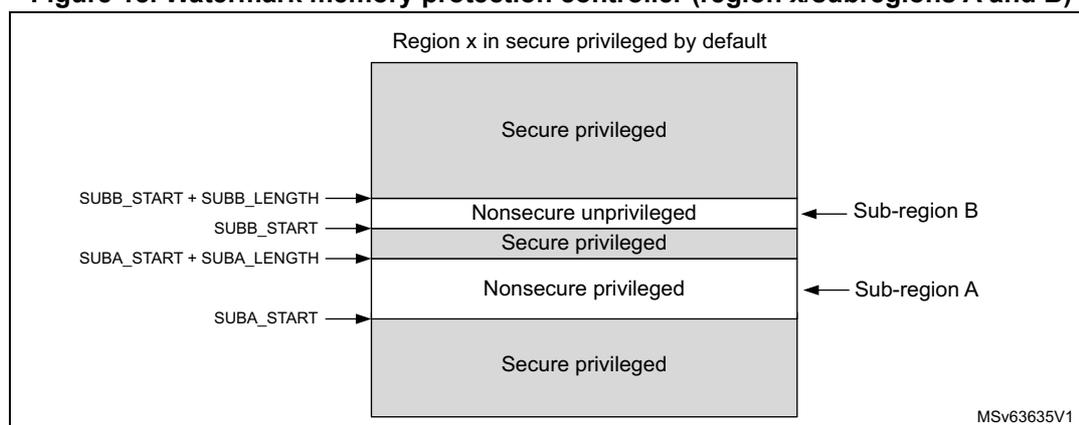
The diagram illustrates the memory protection configuration for Region x. The region is initially 'Secure privileged by default'. It is divided into sub-regions based on start and length registers. Sub-region B is defined by SUBB_START and SUBB_LENGTH, and Sub-region A is defined by SUBA_START and SUBA_LENGTH. The diagram shows the following memory layout from top to bottom:
- Secure privileged (default state)
- Nonsecure unprivileged (top part of Sub-region B)
- Secure privileged (bottom part of Sub-region B)
- Nonsecure privileged (top part of Sub-region A)
- Secure privileged (bottom part of Sub-region A)
- Secure privileged (bottom of Region x)
Memory addresses and registers are indicated on the left and right:
- Left side: SUBB_START + SUBB_LENGTH, SUBB_START, SUBA_START + SUBA_LENGTH, SUBA_START.
- Right side: Sub-region B, Sub-region A.
- Bottom right: MSV63635V1.
In Figure 18, region x represents the external memory or backup SRAM region (such as FMC bank, OCTOSPI1, or BKPSRAM). Secure and privileged attributes of subregions A
and B are independently configurable. When no subregions are defined or enabled on the region x, the default attribute of the region x is set as secure-privileged.
The following tables describe the secure/privileged properties of the common area of subregions A and B, when an overlap exists.
Table 33. Secure properties of subregions A and B
| Subregion A | Subregion B | Properties of overlapped region A and B |
|---|---|---|
| Non-secure | Non-secure | Non-secure |
| Non-secure | Secure | Non-secure |
| Secure | Non-secure | Non-secure |
| Secure | Secure | Secure |
Table 34. Privileged properties of subregions A and B
| Subregion A | Subregion B | Properties of overlapped region A and B |
|---|---|---|
| Unprivileged | Unprivileged | Unprivileged |
| Unprivileged | Privileged | Unprivileged |
| Privileged | Unprivileged | Unprivileged |
| Privileged | Privileged | Privileged |
5.4.4 Memory protection controller - block based (MPCBB)
The MPCBB is composed of a configurable set of registers allowing to define security and privileged policy for internal SRAMs. The security and privileged policy can be individually configured per each 512-byte block.
Figure 19. MPCBB block diagram
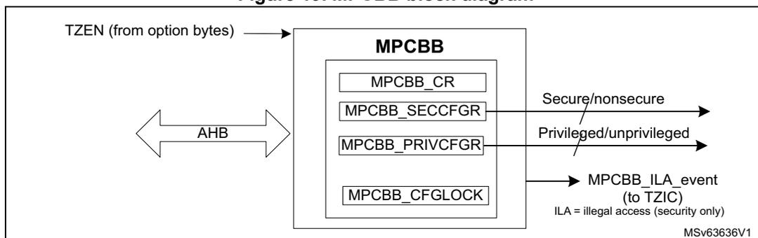
To set up the MPCBB, the following actions are needed (for example at boot time):
- • Secure firmware must define which memory blocks are secure by setting the correct bits in GTZC1_MPCBBz_SECCFGRx.
- • Privileged firmware must define which memory blocks are privileged by setting the correct bits in GTZC1_MPCBBz_PRIVCFGRx.
An MPCBB super-block is made of 32 consecutive blocks. For each super-block, secure application can lock all related security/privileged bits using the correct bits in GTZC1_MPCBBz_CFGLOCK. This lock remains active until the next system reset.
Note: The block size is 512 bytes. The super-block size is 512 * 32 = 16 Kbytes.
5.4.5 TrustZone illegal access controller (TZIC)
The TZIC concentrates all illegal access source events. It is used only when the system is TrustZone enabled (TZEN = 0xB4).
TZIC allows to trace (flag) the event that triggered the secure illegal access interrupt. Register masks (GTZC1_TZIC_IERx) are available to filter unwanted event. On an unmasked illegal event, TZIC generates the GTZC_IRQn interrupt to the NVIC.
For each illegal event source, a status flag and a clear bit exist (respectively within GTZC1_TZIC_SRx and GTZC1_TZIC_FCRx). The reset value of mask registers (GTZC1_TZIC_IERx) is such that all events are masked.
5.4.6 Power-on/reset state
The power-on and reset state of the TZSC clear to 0 all bits of GTZC1_TZSC_SECCFGRx and GTZC1_TZSC_PRIVCFGRx, meaning that all securable peripherals are respectively set to non-secure and unprivileged.
For internal SRAMx (x = 1 to 3), all GTZC1_MPCBBz_SECCFGRx and GTZC1_MPCBBz_PRIVCFGRx are set:
- to 0xFFFF FFFF, making these internal memories block secure and privileged by default when TrustZone security is enabled at system level (TZEN = 0xB4)
- to 0x0000 0000, making these internal memories block non-secure and unprivileged by default when TrustZone security is disabled at system level (TZEN = 0xC3)
For external memories and backup SRAM, GTZC1_TZSC_MPCWMxzR registers are set:
- to 0x0000 0000, making these memories secure and privileged by default when TrustZone security is enabled a system level (TZEN = 0xB4).
- to 0x0800 0000, making these memories non-secure and non-privileged by default when TrustZone security is disabled at system level (TZEN = 0xC3)
Secure boot code can then program the security settings, making components secure or not as needed.
5.5 GTZC interrupts
TZIC is a secure peripheral, thus it systematically generates an illegal access event when accessed by a non-secure access. The MPCBB and TZSC are TrustZone-aware peripherals, meaning that secure and non-secure registers coexist within the peripheral.
Table 35. GTZC interrupt request
| Interrupt acronym | Interrupt event | Event flag | Enable control bit | Interrupt clear method | Exit Sleep mode | Exit Stop mode | Exit Standby mode |
|---|---|---|---|---|---|---|---|
| GTZC | Illegal access | All flags in GTZC1_TZIC_SRx | All bits in GTZC1_TZIC_IERx | Write 1 in the bit GTZC1_TZIC_FCRx | Yes | Yes | No |
5.6 GTZC1 TZSC registers
All registers are accessed only by words (32-bit).
5.6.1 GTZC1 TZSC control register (GTZC1_TZSC_CR)
Address offset: 0x000
Reset value: 0x0000 0000
Secure privileged access only.
| 31 | 30 | 29 | 28 | 27 | 26 | 25 | 24 | 23 | 22 | 21 | 20 | 19 | 18 | 17 | 16 |
|---|---|---|---|---|---|---|---|---|---|---|---|---|---|---|---|
| Res. | Res. | Res. | Res. | Res. | Res. | Res. | Res. | Res. | Res. | Res. | Res. | Res. | Res. | Res. | Res. |
| 15 | 14 | 13 | 12 | 11 | 10 | 9 | 8 | 7 | 6 | 5 | 4 | 3 | 2 | 1 | 0 |
| Res. | Res. | Res. | Res. | Res. | Res. | Res. | Res. | Res. | Res. | Res. | Res. | Res. | Res. | Res. | LCK |
| rs |
Bits 31:1 Reserved, must be kept at reset value.
Bit 0 LCK : lock the configuration of GTZC1_TZSC_SECCFGRx and GTZC1_TZSC_PRIVCFGRx until next reset
This bit is cleared by default, and once set, it cannot be reset until system reset.
0: configuration of all GTZC1_TZSC_SECCFGRx and GTZC1_TZSC_PRIVCFGRx not locked
1: configuration of all GTZC1_TZSC_SECCFGRx and GTZC1_TZSC_PRIVCFGRx locked
5.6.2 GTZC1 TZSC secure configuration register 1 (GTZC1_TZSC_SECCFGR1)
Address offset: 0x010
Reset value: 0x0000 0000
Write-secure access only.
This register can be written only by a secure privileged transaction when the corresponding GTZC1_TZSC_PRIVCFGR signal is set to 1. If a given PRIV bit is not set, the equivalent SEC bit can be written by secure unprivileged transaction.
Read accesses are authorized for any type of transactions, secure or not, privileged or not.
Refer to the device datasheet for the peripheral availability. If not present, consider the associated bit as reserved, and keep it at reset value.
| 31 | 30 | 29 | 28 | 27 | 26 | 25 | 24 | 23 | 22 | 21 | 20 | 19 | 18 | 17 | 16 |
|---|---|---|---|---|---|---|---|---|---|---|---|---|---|---|---|
| LPTIM2 SEC | DTSSEC | UART12 SEC | UART9 SEC | UART8 SEC | UART7 SEC | DAC1SEC | HDMIC ECSEC | USART 11SEC | USART 10SEC | USART 6SEC | CRSSEC | I3C1SEC | I2C2SEC | I2C1SEC | UART5 SEC |
| rw | rw | rw | rw | rw | rw | rw | rw | rw | rw | rw | rw | rw | rw | rw | rw |
| 15 | 14 | 13 | 12 | 11 | 10 | 9 | 8 | 7 | 6 | 5 | 4 | 3 | 2 | 1 | 0 |
| UART4 SEC | USART 3SEC | USART 2SEC | SPI3SEC | SPI2SEC | IWDGSEC | WWDG SEC | TIM14S EC | TIM13S EC | TIM12S EC | TIM7SEC | TIM6SEC | TIM5SEC | TIM4SEC | TIM3SEC | TIM2SEC |
| rw | rw | rw | rw | rw | rw | rw | rw | rw | rw | rw | rw | rw | rw | rw | rw |
- Bit 31
LPTIM2SEC
: secure access mode for LPTIM2
0: non-secure
1: secure - Bit 30
DTSSEC
: secure access mode for DTS
0: non-secure
1: secure - Bit 29
UART12SEC
: secure access mode for UART12
0: non-secure
1: secure - Bit 28
UART9SEC
: secure access mode for UART9
0: non-secure
1: secure - Bit 27
UART8SEC
: secure access mode for UART8
0: non-secure
1: secure - Bit 26
UART7SEC
: secure access mode for UART7
0: non-secure
1: secure - Bit 25
DAC1SEC
: secure access mode for DAC1
0: non-secure
1: secure - Bit 24
HDMICESEC
: secure access mode for HDMICEC
0: non-secure
1: secure - Bit 23
USART11SEC
: secure access mode for USART11
0: non-secure
1: secure - Bit 22
USART10SEC
: secure access mode for USART10
0: non-secure
1: secure - Bit 21
USART6SEC
: secure access mode for USART6
0: non-secure
1: secure - Bit 20
CRSSEC
: secure access mode for CRS
0: non-secure
1: secure - Bit 19
I3C1SEC
: secure access mode for I3C1
0: non-secure
1: secure - Bit 18
I2C2SEC
: secure access mode for I2C2
0: non-secure
1: secure
- Bit 17
I2C1SEC
: secure access mode for I2C1
0: non-secure
1: secure - Bit 16
UART5SEC
: secure access mode for UART5
0: non-secure
1: secure - Bit 15
UART4SEC
: secure access mode for UART4
0: non-secure
1: secure - Bit 14
USART3SEC
: secure access mode for USART3
0: non-secure
1: secure - Bit 13
USART2SEC
: secure access mode for USART2
0: non-secure
1: secure - Bit 12
SPI3SEC
: secure access mode for SPI3
0: non-secure
1: secure - Bit 11
SPI2SEC
: secure access mode for SPI2
0: non-secure
1: secure - Bit 10
IWDGSEC
: secure access mode for IWDG
0: non-secure
1: secure - Bit 9
WWDGSEC
: secure access mode for WWDG
0: non-secure
1: secure - Bit 8
TIM14SEC
: secure access mode for TIM14
0: non-secure
1: secure - Bit 7
TIM13SEC
: secure access mode for TIM13
0: non-secure
1: secure - Bit 6
TIM12SEC
: secure access mode for TIM12
0: non-secure
1: secure - Bit 5
TIM7SEC
: secure access mode for TIM7
0: non-secure
1: secure - Bit 4
TIM6SEC
: secure access mode for TIM6
0: non-secure
1: secure - Bit 3
TIM5SEC
: secure access mode for TIM5
0: non-secure
1: secure
Bit 2 TIM4SEC : secure access mode for TIM4
0: non-secure
1: secure
Bit 1 TIM3SEC : secure access mode for TIM3
0: non-secure
1: secure
Bit 0 TIM2SEC : secure access mode for TIM2
0: non-secure
1: secure
5.6.3 GTZC1 TZSC secure configuration register 2 (GTZC1_TZSC_SECCFGR2)
Address offset: 0x014
Reset value: 0x0000 0000
Write-secure access only.
This register can be written only by a secure privileged transaction when the corresponding GTZC1_TZSC_PRIVCFGR signal is set to 1. If a given PRIV is not set, the equivalent SEC bit can be written by a secure unprivileged transaction.
Read accesses are authorized for any type of transactions, secure or not, privileged or not.
Refer to the device datasheet for the peripheral availability. If not present, consider the associated bit as reserved, and keep it at reset value.
| 31 | 30 | 29 | 28 | 27 | 26 | 25 | 24 | 23 | 22 | 21 | 20 | 19 | 18 | 17 | 16 |
|---|---|---|---|---|---|---|---|---|---|---|---|---|---|---|---|
| LPTIM5 SEC | LPTIM4 SEC | LPTIM3 SEC | LPTIM1 SEC | I2C4 SEC | I2C3 SEC | LPUART1 SEC | SPI5 SEC | Res. | Res. | Res. | Res. | USB SEC | SAI2 SEC | SAI1 SEC | SPI6 SEC |
| rw | rw | rw | rw | rw | rw | rw | rw | rw | rw | rw | rw | ||||
| 15 | 14 | 13 | 12 | 11 | 10 | 9 | 8 | 7 | 6 | 5 | 4 | 3 | 2 | 1 | 0 |
| SPI4 SEC | TIM17 SEC | TIM16 SEC | TIM15 SEC | USART 1SEC | TIM8 SEC | SPI1 SEC | TIM1 SEC | Res. | Res. | Res. | Res. | Res. | UCPD SEC | FDCAN2 SEC | FDCAN1 SEC |
| rw | rw | rw | rw | rw | rw | rw | rw | rw | rw | rw |
Bit 31 LPTIM5SEC : secure access mode for LPTIM5
0: non-secure
1: secure
Bit 30 LPTIM4SEC : secure access mode for LPTIM4
0: non-secure
1: secure
Bit 29 LPTIM3SEC : secure access mode for LPTIM3
0: non-secure
1: secure
Bit 28 LPTIM1SEC : secure access mode for LPTIM1
0: non-secure
1: secure
Bit 27 I2C4SEC : secure access mode for I2C4
0: non-secure
1: secure
Bit 26 I2C3SEC : secure access mode for I2C3
0: non-secure
1: secure
Bit 25 LPUART1SEC : secure access mode for LPUART
0: non-secure
1: secure
Bit 24 SPI5SEC : secure access mode for SPI5
0: non-secure
1: secure
Bits 23:20 Reserved, must be kept at reset value.
Bit 19 USBSEC : secure access mode for USB
0: non-secure
1: secure
Bit 18 SAI2SEC : secure access mode for SAI2
0: non-secure
1: secure
Bit 17 SAI1SEC : secure access mode for SAI1
0: non-secure
1: secure
Bit 16 SPI6SEC : secure access mode for SPI6
0: non-secure
1: secure
Bit 15 SPI4SEC : secure access mode for SPI4
0: non-secure
1: secure
Bit 14 TIM17SEC : secure access mode for TIM17
0: non-secure
1: secure
Bit 13 TIM16SEC : secure access mode for TIM16
0: non-secure
1: secure
Bit 12 TIM15SEC : secure access mode for TIM15
0: non-secure
1: secure
Bit 11 USART1SEC : secure access mode for USART1
0: non-secure
1: secure
Bit 10 TIM8SEC : secure access mode for TIM8
0: non-secure
1: secure
Bit 9 SPI1SEC : secure access mode for SPI1
0: non-secure
1: secure
Bit 8 TIM1SEC : secure access mode for TIM1
0: non-secure
1: secure
Bits 7:3 Reserved, must be kept at reset value.
Bit 2 UCPDSEC : secure access mode for UCPD
0: non-secure
1: secure
Bit 1 FDCAN2SEC : secure access mode for FDCAN2
0: non-secure
1: secure
Bit 0 FDCAN1SEC : secure access mode for FDCAN1
0: non-secure
1: secure
5.6.4 GTZC1 TZSC secure configuration register 3 (GTZC1_TZSC_SECCFGR3)
Address offset: 0x018
Reset value: 0x0000 0000
Write-secure access only.
This register can be written only by a secure privileged transaction when the corresponding GTZC1_TZSC_PRIVCFGR is set to 1. If a given PRIV is not set, the equivalent SEC bit can be written by a secure unprivileged transaction.
Read accesses are authorized for any type of transactions, secure or not, privileged or not.
Refer to the device datasheet for the peripheral availability. If not present, consider the associated bit as reserved, and keep it at reset value.
| 31 | 30 | 29 | 28 | 27 | 26 | 25 | 24 | 23 | 22 | 21 | 20 | 19 | 18 | 17 | 16 |
|---|---|---|---|---|---|---|---|---|---|---|---|---|---|---|---|
| Res. | Res. | Res. | Res. | Res. | RAMCFGSEC | Res. | OCTOSPI1SEC | FMCSEC | SDMMC2SEC | SDMMC1SEC | PKASEC | SAESSSEC | RNGSEC | HASHSEC | AESSEC |
| rw | rw | rw | rw | rw | rw | rw | rw | rw | rw | ||||||
| 15 | 14 | 13 | 12 | 11 | 10 | 9 | 8 | 7 | 6 | 5 | 4 | 3 | 2 | 1 | 0 |
| DCMISEC | ADC12SEC | DCACHESEC | ICACHESEC | ETHSEC | FMACSEC | CORDICSEC | CRCSEC | Res. | Res. | Res. | Res. | Res. | I3C2SEC | VREFBUFSEC | LPTIM6SEC |
| rw | rw | rw | rw | rw | rw | rw | rw | rw | rw | rw |
Bits 31:27 Reserved, must be kept at reset value.
Bit 26 RAMCFGSEC : secure access mode for RAMSCFG
0: non-secure
1: secure
Bit 25 Reserved, must be kept at reset value.
- Bit 24
OCTOSPI1SEC
: secure access mode for OCTOSPI1
0: non-secure
1: secure - Bit 23
FMCSEC
: secure access mode for FMC
0: non-secure
1: secure - Bit 22
SDMMC2SEC
: secure access mode for SDMMC2
0: non-secure
1: secure - Bit 21
SDMMC1SEC
: secure access mode for SDMMC1
0: non-secure
1: secure - Bit 20
PKASEC
: secure access mode for PKA
0: non-secure
1: secure - Bit 19
SAESSEC
: secure access mode for SAES
0: non-secure
1: secure - Bit 18
RNGSEC
: secure access mode for RNG
0: non-secure
1: secure - Bit 17
HASHSEC
: secure access mode for HASH
0: non-secure
1: secure - Bit 16
AESSEC
: secure access mode for AES
0: non-secure
1: secure - Bit 15
DCMISEC
: secure access mode for DCMI
0: non-secure
1: secure - Bit 14
ADC12SEC
: secure access mode for ADC1 and ADC2
0: non-secure
1: secure - Bit 13
DCACHESEC
: secure access mode for DCACHE
0: non-secure
1: secure - Bit 12
ICACHESEC
: secure access mode for ICACHE
0: non-secure
1: secure - Bit 11
ETHSEC
: secure access mode for register of ETH
0: non-secure
1: secure - Bit 10
FMACSEC
: secure access mode for FMAC
0: non-secure
1: secure
Bit 9 CORDICSEC : secure access mode for CORDIC
0: non-secure
1: secure
Bit 8 CRCSEC : secure access mode for CRC
0: non-secure
1: secure
Bits 7:3 Reserved, must be kept at reset value.
Bit 2 I3C2SEC : secure access mode for I3C2
0: non-secure
1: secure
Bit 1 VREFBUFSEC : secure access mode for VREFBUF
0: non-secure
1: secure
Bit 0 LPTIM6SEC : secure access mode for LPTIM6
0: non-secure
1: secure
5.6.5 GTZC1 TZSC privilege configuration register 1 (GTZC1_TZSC_PRIVCFGR1)
Address offset: 0x020
Reset value: 0x0000 0000
Write-privileged access only.
This register can be read or written only by a secure privileged transaction when the corresponding GTZC1_TZSC_SECCFGR signal is set to 1. If a given SEC bit is not set, the equivalent PRIV bit can be read/written by a non-secure privileged transaction.
Read accesses are authorized for any type of transactions, secure or not, privileged or not.
Refer to the device datasheet for the peripheral availability. If not present, consider the associated bit as reserved, and keep it at reset value.
| 31 | 30 | 29 | 28 | 27 | 26 | 25 | 24 | 23 | 22 | 21 | 20 | 19 | 18 | 17 | 16 |
|---|---|---|---|---|---|---|---|---|---|---|---|---|---|---|---|
| LPTIM2 PRIV | DTSPR IV | UART1 2PRIV | UART9 PRIV | UART8 PRIV | UART7 PRIV | DAC1P RIV | HDMIC ECPRI V | USART 11PRIV | USART 10PRIV | USART 6PRIV | CRSPR IV | I3C1PR IV | I2C2PR IV | I2C1PR IV | UART5 PRIV |
| rw | rw | rw | rw | rw | rw | rw | rw | rw | rw | rw | rw | rw | rw | rw | rw |
| 15 | 14 | 13 | 12 | 11 | 10 | 9 | 8 | 7 | 6 | 5 | 4 | 3 | 2 | 1 | 0 |
| UART4 PRIV | USART 3PRIV | USART 2PRIV | SPI3P RIV | SPI2P RIV | IWDGP RIV | WWDG PRIV | TIM14P RIV | TIM13P RIV | TIM12P RIV | TIM7P RIV | TIM6P RIV | TIM5P RIV | TIM4P RIV | TIM3P RIV | TIM2P RIV |
| rw | rw | rw | rw | rw | rw | rw | rw | rw | rw | rw | rw | rw | rw | rw | rw |
Bit 31 LPTIM2PRIV : privileged access mode for LPTIM2
0: unprivileged
1: privileged
Bit 30 DTSPRIV : privileged access mode for DTS
0: unprivileged
1: privileged
- Bit 29
UART12PRIV
: privileged access mode for UART12
0: unprivileged
1: privileged - Bit 28
UART9PRIV
: privileged access mode for UART9
0: unprivileged
1: privileged - Bit 27
UART8PRIV
: privileged access mode for UART8
0: unprivileged
1: privileged - Bit 26
UART7PRIV
: privileged access mode for UART7
0: unprivileged
1: privileged - Bit 25
DAC1PRIV
: privileged access mode for DAC1
0: unprivileged
1: privileged - Bit 24
HDMICECPRIV
: privileged access mode for HDMICEC
0: unprivileged
1: privileged - Bit 23
USART11PRIV
: privileged access mode for USART11
0: unprivileged
1: privileged - Bit 22
USART10PRIV
: privileged access mode for USART10
0: unprivileged
1: privileged - Bit 21
USART6PRIV
: privileged access mode for USART6
0: unprivileged
1: privileged - Bit 20
CRSPRIV
: privileged access mode for CRS
0: unprivileged
1: privileged - Bit 19
I3C1PRIV
: privileged access mode for I3C1
0: unprivileged
1: privileged - Bit 18
I2C2PRIV
: privileged access mode for I2C2
0: unprivileged
1: privileged - Bit 17
I2C1PRIV
: privileged access mode for I2C1
0: unprivileged
1: privileged - Bit 16
UART5PRIV
: privileged access mode for UART5
0: unprivileged
1: privileged - Bit 15
UART4PRIV
: privileged access mode for UART4
0: unprivileged
1: privileged
- Bit 14
USART3PRIV
: privileged access mode for USART3
0: unprivileged
1: privileged - Bit 13
USART2PRIV
: privileged access mode for USART2
0: unprivileged
1: privileged - Bit 12
SPI3PRIV
: privileged access mode for SPI3
0: unprivileged
1: privileged - Bit 11
SPI2PRIV
: privileged access mode for SPI2
0: unprivileged
1: privileged - Bit 10
IWDGPRIV
: privileged access mode for IWDG
0: unprivileged
1: privileged - Bit 9
WWDGPRIV
: privileged access mode for WWDG
0: unprivileged
1: privileged - Bit 8
TIM14PRIV
: privileged access mode for TIM14
0: unprivileged
1: privileged - Bit 7
TIM13PRIV
: privileged access mode for TIM13
0: unprivileged
1: privileged - Bit 6
TIM12PRIV
: privileged access mode for TIM12
0: unprivileged
1: privileged - Bit 5
TIM7PRIV
: privileged access mode for TIM7
0: unprivileged
1: privileged - Bit 4
TIM6PRIV
: privileged access mode for TIM6
0: unprivileged
1: privileged - Bit 3
TIM5PRIV
: privileged access mode for TIM5
0: unprivileged
1: privileged - Bit 2
TIM4PRIV
: privileged access mode for TIM4
0: unprivileged
1: privileged - Bit 1
TIM3PRIV
: privileged access mode for TIM3
0: unprivileged
1: privileged - Bit 0
TIM2PRIV
: privileged access mode for TIM2
0: unprivileged
1: privileged
5.6.6 GTZC1 TZSC privilege configuration register 2 (GTZC1_TZSC_PRIVCFG2)
Address offset: 0x024
Reset value: 0x0000 0000
Write-privileged access only.
This register can be read or written only by a secure privileged transaction when the corresponding GTZC1_TZSC_SECCFGR signal is set to 1. If a given SEC bit is not set, the equivalent PRIV bit can be read/written by a non-secure privileged transaction.
Read accesses are authorized for any type of transactions, secure or not, privileged or not.
Refer to the device datasheet for the peripheral availability. If not present, consider the associated bit as reserved, and keep it at reset value.
| 31 | 30 | 29 | 28 | 27 | 26 | 25 | 24 | 23 | 22 | 21 | 20 | 19 | 18 | 17 | 16 |
|---|---|---|---|---|---|---|---|---|---|---|---|---|---|---|---|
| LPTIM5 PRIV | LPTIM4 PRIV | LPTIM3 PRIV | LPTIM1 PRIV | I2C4PR IV | I2C3PR IV | LPUART 1PRIV | SPI5P RIV | Res. | Res. | Res. | Res. | USBPR IV | SAI2P RIV | SAI1P RIV | SPI6P RIV |
| rw | rw | rw | rw | rw | rw | rw | rw | rw | rw | rw | rw | ||||
| 15 | 14 | 13 | 12 | 11 | 10 | 9 | 8 | 7 | 6 | 5 | 4 | 3 | 2 | 1 | 0 |
| SPI4P RIV | TIM17P RIV | TIM16P RIV | TIM15P RIV | USART 1PRIV | TIM8P RIV | SPI1P RIV | TIM1P RIV | Res. | Res. | Res. | Res. | Res. | UCPDP RIV | FDCAN 2PRIV | FDCAN 1PRIV |
| rw | rw | rw | rw | rw | rw | rw | rw | rw | rw | rw |
Bit 31 LPTIM5PRIV : privileged access mode for LPTIM5
0: unprivileged
1: privileged
Bit 30 LPTIM4PRIV : privileged access mode for LPTIM4
0: unprivileged
1: privileged
Bit 29 LPTIM3PRIV : privileged access mode for LPTIM3
0: unprivileged
1: privileged
Bit 28 LPTIM1PRIV : privileged access mode for LPTIM1
0: unprivileged
1: privileged
Bit 27 I2C4PRIV : privileged access mode for I2C4
0: unprivileged
1: privileged
Bit 26 I2C3PRIV : privileged access mode for I2C3
0: unprivileged
1: privileged
Bit 25 LPUART1PRIV : privileged access mode for LPUART
0: unprivileged
1: privileged
Bit 24 SPI5PRIV : privileged access mode for SPI5
0: unprivileged
1: privileged
Bits 23:20 Reserved, must be kept at reset value.
Bit 19 USBPRIV : privileged access mode for USB
0: unprivileged
1: privileged
Bit 18 SAI2PRIV : privileged access mode for SAI2
0: unprivileged
1: privileged
Bit 17 SAI1PRIV : privileged access mode for SAI1
0: unprivileged
1: privileged
Bit 16 SPI6PRIV : privileged access mode for SPI6
0: unprivileged
1: privileged
Bit 15 SPI4PRIV : privileged access mode for SPI4
0: unprivileged
1: privileged
Bit 14 TIM17PRIV : privileged access mode for TIM17
0: unprivileged
1: privileged
Bit 13 TIM16PRIV : privileged access mode for TIM16
0: unprivileged
1: privileged
Bit 12 TIM15PRIV : privileged access mode for TIM15
0: unprivileged
1: privileged
Bit 11 USART1PRIV : privileged access mode for USART1
0: unprivileged
1: privileged
Bit 10 TIM8PRIV : privileged access mode for TIM8
0: unprivileged
1: privileged
Bit 9 SPI1PRIV : privileged access mode for SPI1
0: unprivileged
1: privileged
Bit 8 TIM1PRIV : privileged access mode for TIM1
0: unprivileged
1: privileged
Bits 7:3 Reserved, must be kept at reset value.
Bit 2 UCPDPRIV : privileged access mode for UCPD
0: unprivileged
1: privileged
Bit 1 FDCAN2PRIV : privileged access mode for FDCAN2
0: unprivileged
1: privileged
Bit 0 FDCAN1PRIV : privileged access mode for FDCAN1
0: unprivileged
1: privileged
5.6.7 GTZC1 TZSC privilege configuration register 3 (GTZC1_TZSC_PRIVCFGR3)
Address offset: 0x028
Reset value: 0x0000 0000
Write-privileged access only.
This register can be read or written only by a secure privileged transaction when the corresponding GTZC1_TZSC_SECCFGR signal is set to 1. If a given SEC bit is not set, the equivalent PRIV bit can be read/written by a non-secure privileged transaction.
Read accesses are authorized for any type of transactions, secure or not, privileged or not.
Refer to the device datasheet for the peripheral availability. If not present, consider the associated bit as reserved, and keep it at reset value.
| 31 | 30 | 29 | 28 | 27 | 26 | 25 | 24 | 23 | 22 | 21 | 20 | 19 | 18 | 17 | 16 |
|---|---|---|---|---|---|---|---|---|---|---|---|---|---|---|---|
| Res. | Res. | Res. | Res. | Res. | RAMCFG PRIV | Res. | OCTO SPI1 PRIV | FMC PRIV | SDMMC C2 PRIV | SDMMC C1 PRIV | PKA PRIV | SAES PRIV | RNG PRIV | HASH PRIV | AES PRIV |
| rw | rw | rw | rw | rw | rw | rw | rw | rw | rw | ||||||
| 15 | 14 | 13 | 12 | 11 | 10 | 9 | 8 | 7 | 6 | 5 | 4 | 3 | 2 | 1 | 0 |
| DCMI PRIV | ADC12 PRIV | DCACHE PRIV | ICACHE PRIV | ETH PRIV | FMAC PRIV | CORDIC PRIV | CRC PRIV | Res. | Res. | Res. | Res. | Res. | I3C2 PRIV | VREFBUF PRIV | LPTIM6 PRIV |
| rw | rw | rw | rw | rw | rw | rw | rw | rw | rw | rw |
Bits 31:27 Reserved, must be kept at reset value.
Bit 26 RAMCFGPRIV : privileged access mode for RAMSCFG
0: unprivileged
1: privileged
Bit 25 Reserved, must be kept at reset value.
Bit 24 OCTOSPI1PRIV : privileged access mode for OCTOSPI1
0: unprivileged
1: privileged
Bit 23 FMCPRIV : privileged access mode for FMC
0: unprivileged
1: privileged
Bit 22 SDMMC2PRIV : privileged access mode for SDMMC2
0: unprivileged
1: privileged
Bit 21 SDMMC1PRIV : privileged access mode for SDMMC1
0: unprivileged
1: privileged
- Bit 20
PKAPRIV
: privileged access mode for PKA
0: unprivileged
1: privileged - Bit 19
SAESPRIV
: privileged access mode for SAES
0: unprivileged
1: privileged - Bit 18
RNGPRIV
: privileged access mode for RNG
0: unprivileged
1: privileged - Bit 17
HASHPRIV
: privileged access mode for HASH
0: unprivileged
1: privileged - Bit 16
AESPRIV
: privileged access mode for AES
0: unprivileged
1: privileged - Bit 15
DCMIPRIV
: privileged access mode for DCMI
0: unprivileged
1: privileged - Bit 14
ADC12PRIV
: privileged access mode for ADC1 and ADC2
0: unprivileged
1: privileged - Bit 13
DCACHEPRIV
: privileged access mode for DCACHE
0: unprivileged
1: privileged - Bit 12
ICACHEPRIV
: privileged access mode for ICACHE
0: unprivileged
1: privileged - Bit 11
ETHPRIV
: privileged access mode for register of ETH
0: unprivileged
1: privileged - Bit 10
FMACPRIV
: privileged access mode for FMAC
0: unprivileged
1: privileged - Bit 9
CORDICPRIV
: privileged access mode for CORDIC
0: unprivileged
1: privileged - Bit 8
CRCPRIV
: privileged access mode for CRC
0: unprivileged
1: privileged - Bits 7:3 Reserved, must be kept at reset value.
- Bit 2
I3C2PRIV
: privileged access mode for I3C2
0: unprivileged
1: privileged
Bit 1 VREFBUFPRIV : privileged access mode for VREFBUF
0: unprivileged
1: privileged
Bit 0 LPTIM6PRIV : privileged access mode for LPTIM6
0: unprivileged
1: privileged
5.6.8 GTZC1 TZSC memory x subregion A watermark configuration register (GTZC1_TZSC_MPCWMxACFGR)
Address offset: 0x40 + 0x10 *(x - 1) (x = 1 to 4)
Reset value: 0x0000 0000
Secure privilege access only.
| 31 | 30 | 29 | 28 | 27 | 26 | 25 | 24 | 23 | 22 | 21 | 20 | 19 | 18 | 17 | 16 |
|---|---|---|---|---|---|---|---|---|---|---|---|---|---|---|---|
| Res. | Res. | Res. | Res. | Res. | Res. | Res. | Res. | Res. | Res. | Res. | Res. | Res. | Res. | Res. | Res. |
| 15 | 14 | 13 | 12 | 11 | 10 | 9 | 8 | 7 | 6 | 5 | 4 | 3 | 2 | 1 | 0 |
| Res. | Res. | Res. | Res. | Res. | Res. | PRIV | SEC | Res. | Res. | Res. | Res. | Res. | Res. | SRLOCK | SREN |
| rw | rw | rs | rw |
Bits 31:10 Reserved, must be kept at reset value.
Bit 9 PRIV : Privileged subregion A of base region x
This bit is taken into account only if SREN is set.
0: Privileged and unprivileged accesses are granted in subregion A.
1: Only privileged accesses are granted in subregion A of region x.
Bit 8 SEC : Secure subregion A of base region x
This bit is taken into account only if SREN is set.
0: Only non-secure data accesses are granted to subregion A of region x.
1: Only secure data accesses are granted to subregion A of region x.
Bits 7:2 Reserved, must be kept at reset value.
Bit 1 SRLOCK : Subregion A lock
This bit, once set, can be cleared only by a system reset.
0: GTZC1_TZSC_MPCWMxCFGR, GTZC1_TZSC_MPCWMxAR and GTZC1_TZSC_MPCWMxBR can be written.
1: Writes to GTZC1_TZSC_MPCWMxCFGR, GTZC1_TZSC_MPCWMxAR and GTZC1_TZSC_MPCWMxBR are ignored.
Bit 0 SREN : Subregion A enable
0: subregion A is disabled. Access control of base region x applies to any access between this subregion start- and end-addresses.
1: subregion A of region x is enabled. Access control defined in GTZC1_TZSC_MPCWMxCFGR applies to any access between this subregion start- and end-addresses, defined in GTZC1_TZSC_MPCWMxAR and GTZC1_TZSC_MPCWMxBR.
Note: Watermark controlled external memories start fully non-secure/unprivileged at reset when TZEN = 0xC3. When TZEN = 0xB4, they start fully secure/fully privileged (inverted reset-value).
5.6.9 GTZC1 TZSC memory x subregion A watermark register (GTZC1_TZSC_MPCWMxAR)
Address offset: \( 0x44 + 0x10 \times (x - 1) \) ( \( x = 1 \) to \( 4 \) )
Reset value: 0x0000 0000
The given reset value is valid when TZEN = 0xB4. The reset value is 0x0800 0000 when TZEN = 0xC3.
Secure privilege access only.
When SUBA_START + SUBA_LENGTH is higher than the maximum size allowed for the memory, a saturation of SUBA_LENGTH is applied automatically.
When an overlap of subregion A and B exists, secure/privileged attributes of both subregions apply on the common section (see Section 5.4.3 )
| 31 | 30 | 29 | 28 | 27 | 26 | 25 | 24 | 23 | 22 | 21 | 20 | 19 | 18 | 17 | 16 |
| Res. | Res. | Res. | Res. | SUBA_LENGTH[11:0] | |||||||||||
| rw | rw | rw | rw | rw | rw | rw | rw | rw | rw | rw | rw | ||||
| 15 | 14 | 13 | 12 | 11 | 10 | 9 | 8 | 7 | 6 | 5 | 4 | 3 | 2 | 1 | 0 |
| Res. | Res. | Res. | Res. | Res. | SUBA_START[10:0] | ||||||||||
| rw | rw | rw | rw | rw | rw | rw | rw | rw | rw | rw | |||||
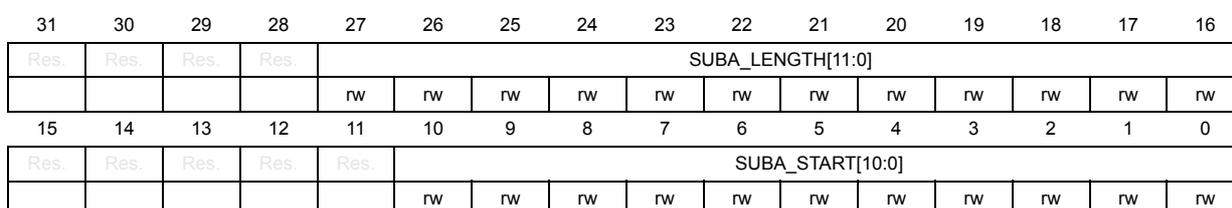
Bits 31:28 Reserved, must be kept at reset value.
Bits 27:16 SUBA_LENGTH[11:0] : Length of subregion A in region x
This field defines the length of the subregion A, to be multiplied by the granularity defined in Table 29 .
When SUBA_START + SUBA_LENGTH is higher than the maximum size allowed for the memory, a saturation of SUBA_LENGTH is applied automatically. If SUBA_LENGTH = 0, subregion A is disabled (SREN bit in GTZC1_TZSC_MPCMWxACFGR is cleared).
Bits 15:11 Reserved, must be kept at reset value.
Bits 10:0 SUBA_START[10:0] : Start of subregion A in region x
This field defines the address offset of the subregion A, to be multiplied by the granularity defined in Table 29 , versus the start of the region x.
Watermark controlled external memories start fully non-secure at reset when TZEN = 0xC3. When TZEN = 0xB4, they start fully secure (inverted reset value).
5.6.10 GTZC1 TZSC memory x subregion B watermark configuration register (GTZC1_TZSC_MPCWMxBCFGR)
Address offset: \( 0x48 + 0x10 \times (x - 1) \) ( \( x = 1 \) to \( 4 \) )
Reset value: 0x0000 0000
Secure privilege access only.
| 31 | 30 | 29 | 28 | 27 | 26 | 25 | 24 | 23 | 22 | 21 | 20 | 19 | 18 | 17 | 16 |
|---|---|---|---|---|---|---|---|---|---|---|---|---|---|---|---|
| Res. | Res. | Res. | Res. | Res. | Res. | Res. | Res. | Res. | Res. | Res. | Res. | Res. | Res. | Res. | Res. |
| 15 | 14 | 13 | 12 | 11 | 10 | 9 | 8 | 7 | 6 | 5 | 4 | 3 | 2 | 1 | 0 |
| Res. | Res. | Res. | Res. | Res. | Res. | PRIV | SEC | Res. | Res. | Res. | Res. | Res. | Res. | SRLOCK | SREN |
| rw | rw | rs | rw |
Bits 31:10 Reserved, must be kept at reset value.
Bit 9 PRIV : Privileged subregion B of base region x
This bit is taken into account only if SREN is set.
0: Privileged and unprivileged accesses are granted in subregion A.
1: Only privileged accesses are granted in subregion A of region x.
Bit 8 SEC : Secure subregion B of base region x
This bit is taken into account only if SREN is set.
0: Only non-secure data accesses are granted to subregion A of region x.
1: Only secure data accesses are granted to subregion A of region x.
Bits 7:2 Reserved, must be kept at reset value.
Bit 1 SRLOCK : Subregion B lock
This bit, once set, can be cleared only by a system reset.
0: GTZC1_TZSC_MPCWMxCFGR, GTZC1_TZSC_MPCWMxAR and GTZC1_TZSC_MPCWMxBR can be written.
1: Writes to GTZC1_TZSC_MPCWMxCFGR, GTZC1_TZSC_MPCWMxAR and GTZC1_TZSC_MPCWMxBR are ignored.
Bit 0 SREN : Subregion B enable
0: subregion B is disabled. Access control of base region x applies to any access between this subregion start- and end-addresses.
1: subregion B of region x is enabled. Access control defined in GTZC1_TZSC_MPCWMx_CFGR applies to any access between this subregion start- and end-addresses, defined in GTZC1_TZSC_MPCWMxAR and GTZC1_TZSC_MPCWMxBR.
Note: Watermark controlled external memories start fully non-secure/unprivileged at reset when TZEN = 0xC3. When TZEN = 0xB4, they start fully secure/fully privileged (inverted reset-value).
5.6.11 GTZC1 TZSC memory x subregion B watermark register (GTZC1_TZSC_MPCWMxBR)
Address offset: 0x4C + 0x10 *(x - 1) (x = 1 to 4)
Reset value: 0x0000 0000
The given reset value is valid when TZEN = 0xB4. The reset value is 0x0800 0000 when TZEN = 0xC3.
Secure privilege access only.
When SUBB_START + SUBB_LENGTH is higher than the maximum size allowed for the memory, a saturation of SUBB_LENGTH is applied automatically.
When an overlap of subregion A and B exists, secure/privileged attributes of both subregions apply on the common section (see Section 5.4.3 )
| 31 | 30 | 29 | 28 | 27 | 26 | 25 | 24 | 23 | 22 | 21 | 20 | 19 | 18 | 17 | 16 |
|---|---|---|---|---|---|---|---|---|---|---|---|---|---|---|---|
| Res. | Res. | Res. | Res. | SUBB_LENGTH[11:0] | |||||||||||
| rw | rw | rw | rw | rw | rw | rw | rw | rw | rw | rw | rw | ||||
| 15 | 14 | 13 | 12 | 11 | 10 | 9 | 8 | 7 | 6 | 5 | 4 | 3 | 2 | 1 | 0 |
| Res. | Res. | Res. | Res. | Res. | SUBB_START[10:0] | ||||||||||
| rw | rw | rw | rw | rw | rw | rw | rw | rw | rw | rw | |||||
Bits 31:28 Reserved, must be kept at reset value.
Bits 27:16 SUBB_LENGTH[11:0] : Length of subregion B in region x
This field defines the length of the subregion B, to be multiplied by the granularity defined in Table 29 .
When SUBB_START + SUBB_LENGTH is higher than the maximum size allowed for the memory, a saturation of SUBB_LENGTH is applied automatically.
If SUBB_LENGTH = 0, the subregion B is disabled (SREN bit in GTZC1_TZSC_MPCMWxBCFGR is cleared).
Bits 15:11 Reserved, must be kept at reset value.
Bits 10:0 SUBB_START[10:0] : Start of subregion B in region x
This field defines the address offset of the subregion B, to be multiplied by the granularity defined in Table 29 , versus the start of the region x.
Wtermark controlled external memories start fully non-secure at reset when TZEN = 0xC3.
When TZEN = 0xB4, they start fully secure (inverted reset value).
5.6.12 GTZC1 TZSC register map
Table 36. GTZC1 TZSC register map and reset values
| Offset | Register | 31 | 30 | 29 | 28 | 27 | 26 | 25 | 24 | 23 | 22 | 21 | 20 | 19 | 18 | 17 | 16 | 15 | 14 | 13 | 12 | 11 | 10 | 9 | 8 | 7 | 6 | 5 | 4 | 3 | 2 | 1 | 0 | |
|---|---|---|---|---|---|---|---|---|---|---|---|---|---|---|---|---|---|---|---|---|---|---|---|---|---|---|---|---|---|---|---|---|---|---|
| 0x000 | GTZC1_TZSC_CR | Res | Res | Res | Res | Res | Res | Res | Res | Res | Res | Res | Res | Res | Res | Res | Res | Res | Res | Res | Res | Res | Res | Res | Res | Res | Res | Res | Res | Res | Res | Res | 0 | LCK |
| Reset value | ||||||||||||||||||||||||||||||||||
| 0x004-0x00C | Reserved | Reserved | ||||||||||||||||||||||||||||||||
| 0x010 | GTZC1_TZSC_SECCFGGR1 | LPTIM25SEC | DTSSEC | UART12SEC | UART95SEC | UART85SEC | UART75SEC | DAC15SEC | HDMI2CEC5SEC | USART115SEC | USART110SEC | USART65SEC | CRSSEC | I3C15SEC | I2C25SEC | I2C15SEC | UART55SEC | UART45SEC | USART35SEC | USART25SEC | SPI35SEC | SPI25SEC | IWDG5SEC | WWDG5SEC | TIM145SEC | TIM135SEC | TIM1125SEC | TIM75SEC | TIM65SEC | TIM55SEC | TIM45SEC | TIM35SEC | TIM25SEC | |
| Reset value | 0 | 0 | 0 | 0 | 0 | 0 | 0 | 0 | 0 | 0 | 0 | 0 | 0 | 0 | 0 | 0 | 0 | 0 | 0 | 0 | 0 | 0 | 0 | 0 | 0 | 0 | 0 | 0 | 0 | 0 | 0 | 0 | ||
| 0x014 | GTZC1_TZSC_SECCFGGR2 | LPTIM55SEC | LPTIM45SEC | LPTIM35SEC | LPTIM15SEC | I2C45SEC | I2C35SEC | LPUART15SEC | SPI55SEC | Res | Res | Res | Res | USB5SEC | SAI25SEC | SAI15SEC | SPI65SEC | SPI45SEC | TIM175SEC | TIM165SEC | TIM155SEC | USART15SEC | TIM85SEC | SPI15SEC | TIM15SEC | Res. | Res. | Res. | Res. | Res. | Res. | UCPD5SEC | FDCAN25SEC | |
| Reset value | 0 | 0 | 0 | 0 | 0 | 0 | 0 | 0 | 0 | 0 | 0 | 0 | 0 | 0 | 0 | 0 | 0 | 0 | 0 | 0 | 0 | 0 | ||||||||||||
| 0x018 | GTZC1_TZSC_SECCFGGR3 | Res | Res | Res | Res | Res | RAMCFG5SEC | Res | OCTOSPI15SEC | FMC5SEC | SDMMC25SEC | SDMMC15SEC | PKASEC | SAES5SEC | RNG5SEC | HASH5SEC | AES5SEC | DCMI5SEC | ADC125SEC | DCACHEHE5SEC | ICACHEHE5SEC | ETH5SEC | FMAC5SEC | CORDIC5SEC | CRC5SEC | Res. | Res. | Res. | Res. | Res. | Res. | ICG25SEC | VREFBUF5SEC | |
| Reset value | 0 | 0 | 0 | 0 | 0 | 0 | 0 | 0 | 0 | 0 | 0 | 0 | 0 | 0 | 0 | 0 | 0 | 0 | 0 | 0 | ||||||||||||||
| 0x01C | Reserved | Reserved | ||||||||||||||||||||||||||||||||
| 0x020 | GTZC1_TZSC_PRIVCFGGR1 | LPTIM2PRIV | DTSPRIV | UART12PRIV | UART9PRIV | UART8PRIV | UART7PRIV | DAC1PRIV | HDMI2CECPRIV | USART11PRIV | USART10PRIV | USART6PRIV | CRSPRIV | I3C1PRIV | I2C2PRIV | I2C1PRIV | UART5PRIV | UART4PRIV | USART3PRIV | USART2PRIV | SPI3PRIV | SPI2PRIV | IWDGPRIV | WWDGPRIV | TIM14PRIV | TIM13PRIV | TIM112PRIV | TIM7PRIV | TIM6PRIV | TIM5PRIV | TIM4PRIV | TIM3PRIV | TIM2PRIV | |
| Reset value | 0 | 0 | 0 | 0 | 0 | 0 | 0 | 0 | 0 | 0 | 0 | 0 | 0 | 0 | 0 | 0 | 0 | 0 | 0 | 0 | 0 | 0 | 0 | 0 | 0 | 0 | 0 | 0 | 0 | 0 | 0 | |||
| 0x024 | GTZC1_TZSC_PRIVCFGGR2 | LPTIM5PRIV | LPTIM4PRIV | LPTIM3PRIV | LPTIM1PRIV | I2C4PRIV | I2C3PRIV | LPUART1PRIV | SPI5PRIV | Res | Res | Res | Res | USBPRIV | SAI2PRIV | SAI1PRIV | SPI6PRIV | SPI4PRIV | TIM17PRIV | TIM16PRIV | TIM15PRIV | USART1PRIV | TIM8PRIV | SPI1PRIV | TIM1PRIV | Res. | Res. | Res. | Res. | Res. | Res. | UCPDPRIV | FDCAN2PRIV | |
| Reset value | 0 | 0 | 0 | 0 | 0 | 0 | 0 | 0 | 0 | 0 | 0 | 0 | 0 | 0 | 0 | 0 | 0 | 0 | 0 | 0 | 0 | 0 | ||||||||||||
| 0x028 | GTZC1_TZSC_PRIVCFGGR3 | Res | Res | Res | Res | Res | RAMCFGPRIV | Res | OCTOSPI1PRIV | FMCPRIV | SDMMC2PRIV | SDMMC1PRIV | PKAPRIV | SAESPRIV | RNGPRIV | HASHPRIV | AESPRIV | DCMIPRIV | ADC12PRIV | DCACHEPRIV | ICACHEPRIV | ETHPRIV | FMACPRIV | CORDICPRIV | CRCPRIV | Res. | Res. | Res. | Res. | Res. | Res. | ICG2PRIV | VREFBUFPRIV | |
| Reset value | 0 | 0 | 0 | 0 | 0 | 0 | 0 | 0 | 0 | 0 | 0 | 0 | 0 | 0 | 0 | 0 | 0 | 0 | 0 | 0 | ||||||||||||||
| 0x02C-0x03C | Reserved | Reserved | ||||||||||||||||||||||||||||||||
| 0x040 | GTZC1_TZSC_MPCWM1ACFGGR | Res | Res | Res | Res | Res | Res | Res | Res | Res | Res | Res | Res | Res | Res | Res | Res | Res | Res | Res | Res | Res | Res | PRIV | SEC | Res. | Res. | Res. | Res. | Res. | Res. | Res. | SRLOCK | |
| Reset value | 0 | 0 | 0 | 0 | ||||||||||||||||||||||||||||||
| 0x044 | GTZC1_TZSC_MPCWM1AR | Res | Res | Res | Res | SUBA_LENGTH[11:0] | Res | Res | Res | Res | Res | SUBA_START[10:0] | ||||||||||||||||||||||
| Reset value | 0 | 0 | 0 | 0 | 0 | 0 | 0 | 0 | 0 | 0 | 0 | 0 | 0 | 0 | 0 | 0 | 0 | 0 | 0 | 0 | 0 | 0 | ||||||||||||
| 0x048 | GTZC1_TZSC_MPCWM1BCFGGR | Res | Res | Res | Res | Res | Res | Res | Res | Res | Res | Res | Res | Res | Res | Res | Res | Res | Res | Res | Res | Res | Res | PRIV | SEC | Res. | Res. | Res. | Res. | Res. | Res. | Res. | SRLOCK | |
| Reset value | 0 | 0 | 0 | 0 | ||||||||||||||||||||||||||||||
Table 36. GTZC1 TZSC register map and reset values (continued)
| Offset | Register | 31 | 30 | 29 | 28 | 27 | 26 | 25 | 24 | 23 | 22 | 21 | 20 | 19 | 18 | 17 | 16 | 15 | 14 | 13 | 12 | 11 | 10 | 9 | 8 | 7 | 6 | 5 | 4 | 3 | 2 | 1 | 0 | |
|---|---|---|---|---|---|---|---|---|---|---|---|---|---|---|---|---|---|---|---|---|---|---|---|---|---|---|---|---|---|---|---|---|---|---|
| 0x04C | GTZC1_TZSC_MPCWM1BR | Res | Res | Res | Res | SUBB_LENGTH[11:0] | Res | Res | Res | Res | Res | SUBB_START[10:0] | ||||||||||||||||||||||
| Reset value | 0 | 0 | 0 | 0 | 0 | 0 | 0 | 0 | 0 | 0 | 0 | 0 | 0 | 0 | 0 | 0 | 0 | 0 | 0 | 0 | 0 | 0 | 0 | 0 | ||||||||||
| 0x050 | GTZC1_TZSC_MPCWM2ACFGGR | Res | Res | Res | Res | Res | Res | Res | Res | Res | Res | Res | Res | Res | Res | Res | Res | Res | Res | Res | Res | Res | Res | PRIV | SEC | Res | Res | Res | Res | Res | Res | Res | SRLOCK | SREN |
| Reset value | 0 | 0 | 0 | 0 | ||||||||||||||||||||||||||||||
| 0x054 | GTZC1_TZSC_MPCWM2AR | Res | Res | Res | Res | SUBA_LENGTH[11:0] | Res | Res | Res | Res | Res | SUBA_START[10:0] | ||||||||||||||||||||||
| Reset value | 0 | 0 | 0 | 0 | 0 | 0 | 0 | 0 | 0 | 0 | 0 | 0 | 0 | 0 | 0 | 0 | 0 | 0 | 0 | 0 | 0 | 0 | 0 | 0 | ||||||||||
| 0x058 | GTZC1_TZSC_MPCWM2BCFGGR | Res | Res | Res | Res | Res | Res | Res | Res | Res | Res | Res | Res | Res | Res | Res | Res | Res | Res | Res | Res | Res | Res | PRIV | SEC | Res | Res | Res | Res | Res | Res | Res | SRLOCK | SREN |
| Reset value | 0 | 0 | 0 | 0 | ||||||||||||||||||||||||||||||
| 0x05C | GTZC1_TZSC_MPCWM2BR | Res | Res | Res | Res | SUBB_LENGTH[11:0] | Res | Res | Res | Res | Res | SUBB_START[10:0] | ||||||||||||||||||||||
| Reset value | 0 | 0 | 0 | 0 | 0 | 0 | 0 | 0 | 0 | 0 | 0 | 0 | 0 | 0 | 0 | 0 | 0 | 0 | 0 | 0 | 0 | 0 | 0 | 0 | ||||||||||
| 0x060 | GTZC1_TZSC_MPCWM3ACFGGR | Res | Res | Res | Res | Res | Res | Res | Res | Res | Res | Res | Res | Res | Res | Res | Res | Res | Res | Res | Res | Res | Res | PRIV | SEC | Res | Res | Res | Res | Res | Res | Res | SRLOCK | SREN |
| Reset value | 0 | 0 | 0 | 0 | ||||||||||||||||||||||||||||||
| 0x064 | GTZC1_TZSC_MPCWM3AR | Res | Res | Res | Res | SUBA_LENGTH[11:0] | Res | Res | Res | Res | Res | SUBA_START[10:0] | ||||||||||||||||||||||
| Reset value | 0 | 0 | 0 | 0 | 0 | 0 | 0 | 0 | 0 | 0 | 0 | 0 | 0 | 0 | 0 | 0 | 0 | 0 | 0 | 0 | 0 | 0 | 0 | 0 | ||||||||||
| 0x068 | GTZC1_TZSC_MPCWM3BCFGGR | Res | Res | Res | Res | Res | Res | Res | Res | Res | Res | Res | Res | Res | Res | Res | Res | Res | Res | Res | Res | Res | Res | PRIV | SEC | Res | Res | Res | Res | Res | Res | Res | SRLOCK | SREN |
| Reset value | 0 | 0 | 0 | 0 | ||||||||||||||||||||||||||||||
| 0x06C | GTZC1_TZSC_MPCWM3BR | Res | Res | Res | Res | SUBB_LENGTH[11:0] | Res | Res | Res | Res | Res | SUBB_START[10:0] | ||||||||||||||||||||||
| Reset value | 0 | 0 | 0 | 0 | 0 | 0 | 0 | 0 | 0 | 0 | 0 | 0 | 0 | 0 | 0 | 0 | 0 | 0 | 0 | 0 | 0 | 0 | 0 | 0 | ||||||||||
| 0x070 | GTZC1_TZSC_MPCWM4ACFGGR | Res | Res | Res | Res | Res | Res | Res | Res | Res | Res | Res | Res | Res | Res | Res | Res | Res | Res | Res | Res | Res | Res | PRIV | SEC | Res | Res | Res | Res | Res | Res | Res | SRLOCK | SREN |
| Reset value | 0 | 0 | 0 | 0 | ||||||||||||||||||||||||||||||
| 0x074 | GTZC1_TZSC_MPCWM4AR | Res | Res | Res | Res | SUBA_LENGTH[11:0] | Res | Res | Res | Res | Res | SUBA_START[10:0] | ||||||||||||||||||||||
| Reset value | 0 | 0 | 0 | 0 | 0 | 0 | 0 | 0 | 0 | 0 | 0 | 0 | 0 | 0 | 0 | 0 | 0 | 0 | 0 | 0 | 0 | 0 | 0 | 0 | ||||||||||
| 0x078 | GTZC1_TZSC_MPCWM4BCFGGR | Res | Res | Res | Res | Res | Res | Res | Res | Res | Res | Res | Res | Res | Res | Res | Res | Res | Res | Res | Res | Res | Res | PRIV | SEC | Res | Res | Res | Res | Res | Res | Res | SRLOCK | SREN |
| Reset value | 0 | 0 | 0 | 0 | ||||||||||||||||||||||||||||||
| 0x07C | GTZC1_TZSC_MPCWM4BR | Res | Res | Res | Res | SUBB_LENGTH[11:0] | Res | Res | Res | Res | Res | SUBB_START[10:0] | ||||||||||||||||||||||
| Reset value | 0 | 0 | 0 | 0 | 0 | 0 | 0 | 0 | 0 | 0 | 0 | 0 | 0 | 0 | 0 | 0 | 0 | 0 | 0 | 0 | 0 | 0 | 0 | 0 | ||||||||||
5.7 GTZC1 TZIC registers
All registers are accessed only by words (32-bit).
5.7.1 GTZC1 TZIC interrupt enable register 1 (GTZC1_TZIC_IER1)
Address offset: 0x000
Reset value: 0x0000 0000
Secure privileged access only.
This register is used to enable interrupt of illegal access.
Refer to the device datasheet for the peripheral availability. If not present, consider the associated bit as reserved, and keep it at reset value.
| 31 | 30 | 29 | 28 | 27 | 26 | 25 | 24 | 23 | 22 | 21 | 20 | 19 | 18 | 17 | 16 |
|---|---|---|---|---|---|---|---|---|---|---|---|---|---|---|---|
| LPTIM2 IE | DTSIE | UART1 2IE | UART9 IE | UART8 IE | UART7 IE | DAC1 IE | HDMICE IE | USART 11IE | USART 10IE | USART 6IE | CRSIE | I3C1IE | I2C2IE | I2C1IE | UART5 IE |
| rw | rw | rw | rw | rw | rw | rw | rw | rw | rw | rw | rw | rw | rw | rw | rw |
| 15 | 14 | 13 | 12 | 11 | 10 | 9 | 8 | 7 | 6 | 5 | 4 | 3 | 2 | 1 | 0 |
|---|---|---|---|---|---|---|---|---|---|---|---|---|---|---|---|
| UART4 IE | USART 3IE | USART 2IE | SPI3IE | SPI2IE | IWDG IE | WWDG IE | TIM14 IE | TIM13 IE | TIM12 IE | TIM7 IE | TIM6 IE | TIM5 IE | TIM4 IE | TIM3 IE | TIM2 IE |
| rw | rw | rw | rw | rw | rw | rw | rw | rw | rw | rw | rw | rw | rw | rw | rw |
Bit 31 LPTIM2IE : illegal access interrupt enable for LPTIM2
0: interrupt disabled
1: interrupt enabled
Bit 30 DTSIE : illegal access interrupt enable for DTS
0: interrupt disabled
1: interrupt enabled
Bit 29 UART12IE : illegal access interrupt enable for UART12
0: interrupt disabled
1: interrupt enabled
Bit 28 UART9IE : illegal access interrupt enable for UART9
0: interrupt disabled
1: interrupt enabled
Bit 27 UART8IE : illegal access interrupt enable for UART8
0: interrupt disabled
1: interrupt enabled
Bit 26 UART7IE : illegal access interrupt enable for UART7
0: interrupt disabled
1: interrupt enabled
Bit 25 DAC1IE : illegal access interrupt enable for DAC1
0: interrupt disabled
1: interrupt enabled
Bit 24 HDMICEIE : illegal access interrupt enable for HDMICE
0: interrupt disabled
1: interrupt enabled
- Bit 23
USART11IE
: illegal access interrupt enable for USART11
0: interrupt disabled
1: interrupt enabled - Bit 22
USART10IE
: illegal access interrupt enable for USART10
0: interrupt disabled
1: interrupt enabled - Bit 21
USART6IE
: illegal access interrupt enable for USART6
0: interrupt disabled
1: interrupt enabled - Bit 20
CRSIE
: illegal access interrupt enable for CRS
0: interrupt disabled
1: interrupt enabled - Bit 19
I3C1IE
: illegal access interrupt enable for I3C1
0: interrupt disabled
1: interrupt enabled - Bit 18
I2C2IE
: illegal access interrupt enable for I2C2
0: interrupt disabled
1: interrupt enabled - Bit 17
I2C1IE
: illegal access interrupt enable for I2C1
0: interrupt disabled
1: interrupt enabled - Bit 16
UART5IE
: illegal access interrupt enable for UART5
0: interrupt disabled
1: interrupt enabled - Bit 15
UART4IE
: illegal access interrupt enable for UART4
0: interrupt disabled
1: interrupt enabled - Bit 14
USART3IE
: illegal access interrupt enable for USART3
0: interrupt disabled
1: interrupt enabled - Bit 13
USART2IE
: illegal access interrupt enable for USART2
0: interrupt disabled
1: interrupt enabled - Bit 12
SPI3IE
: illegal access interrupt enable for SPI3
0: interrupt disabled
1: interrupt enabled - Bit 11
SPI2IE
: illegal access interrupt enable for SPI2
0: interrupt disabled
1: interrupt enabled - Bit 10
IWDGIE
: illegal access interrupt enable for IWDG
0: interrupt disabled
1: interrupt enabled - Bit 9
WWDGIE
: illegal access interrupt enable for WWDG
0: interrupt disabled
1: interrupt enabled
- Bit 8
TIM14IE
: illegal access interrupt enable for TIM14
0: interrupt disabled
1: interrupt enabled - Bit 7
TIM13IE
: illegal access interrupt enable for TIM13
0: interrupt disabled
1: interrupt enabled - Bit 6
TIM12IE
: illegal access interrupt enable for TIM12
0: interrupt disabled
1: interrupt enabled - Bit 5
TIM7IE
: illegal access interrupt enable for TIM7
0: interrupt disabled
1: interrupt enabled - Bit 4
TIM6IE
: illegal access interrupt enable for TIM6
0: interrupt disabled
1: interrupt enabled - Bit 3
TIM5IE
: illegal access interrupt enable for TIM5
0: interrupt disabled
1: interrupt enabled - Bit 2
TIM4IE
: illegal access interrupt enable for TIM4
0: interrupt disabled
1: interrupt enabled - Bit 1
TIM3IE
: illegal access interrupt enable for TIM3
0: interrupt disabled
1: interrupt enabled - Bit 0
TIM2IE
: illegal access interrupt enable for TIM2
0: interrupt disabled
1: interrupt enabled
5.7.2 GTZC1 TZIC interrupt enable register 2 (GTZC1_TZIC_IER2)
Address offset: 0x004
Reset value: 0x0000 0000
Secure privileged access only.
This register is used to enable interrupt of illegal access.
Refer to the device datasheet for the peripheral availability. If not present, consider the associated bit as reserved, and keep it at reset value.
| 31 | 30 | 29 | 28 | 27 | 26 | 25 | 24 | 23 | 22 | 21 | 20 | 19 | 18 | 17 | 16 |
|---|---|---|---|---|---|---|---|---|---|---|---|---|---|---|---|
| LPTIM5 IE | LPTIM4 IE | LPTIM3 IE | LPTIM1 IE | I2C4IE | I2C3IE | LPUART1IE | SPI5IE | Res. | Res. | Res. | Res. | USBIE | SAI2IE | SAI1IE | SPI6IE |
| rw | rw | rw | rw | rw | rw | rw | rw | rw | rw | rw | rw | ||||
| 15 | 14 | 13 | 12 | 11 | 10 | 9 | 8 | 7 | 6 | 5 | 4 | 3 | 2 | 1 | 0 |
| SPI4IE | TIM17IE | TIM16IE | TIM15IE | USART1IE | TIM8IE | SPI1IE | TIM1IE | Res. | Res. | Res. | Res. | Res. | UCPDI E | FDCAN2IE | FDCAN1IE |
| rw | rw | rw | rw | rw | rw | rw | rw | rw | rw | rw |
Bit 31 LPTIM5IE : illegal access interrupt enable for LPTIM5
0: interrupt disabled
1: interrupt enabled
Bit 30 LPTIM4IE : illegal access interrupt enable for LPTIM4
0: interrupt disabled
1: interrupt enabled
Bit 29 LPTIM3IE : illegal access interrupt enable for LPTIM3
0: interrupt disabled
1: interrupt enabled
Bit 28 LPTIM1IE : illegal access interrupt enable for LPTIM1
0: interrupt disabled
1: interrupt enabled
Bit 27 I2C4IE : illegal access interrupt enable for I2C4
0: interrupt disabled
1: interrupt enabled
Bit 26 I2C3IE : illegal access interrupt enable for I2C3
0: interrupt disabled
1: interrupt enabled
Bit 25 LPUART1IE : illegal access interrupt enable for LPUART
0: interrupt disabled
1: interrupt enabled
Bit 24 SPI5IE : illegal access interrupt enable for SPI5
0: interrupt disabled
1: interrupt enabled
Bits 23:20 Reserved, must be kept at reset value.
Bit 19 USBIE : illegal access interrupt enable for USB
0: interrupt disabled
1: interrupt enabled
Bit 18 SAI2IE : illegal access interrupt enable for SAI2
0: interrupt disabled
1: interrupt enabled
Bit 17 SAI1IE : illegal access interrupt enable for SAI1
0: interrupt disabled
1: interrupt enabled
Bit 16 SPI6IE : illegal access interrupt enable for SPI6
0: interrupt disabled
1: interrupt enabled
Bit 15 SPI4IE : illegal access interrupt enable for SPI4
0: interrupt disabled
1: interrupt enabled
Bit 14 TIM17IE : illegal access interrupt enable for TIM17
0: interrupt disabled
1: interrupt enabled
- Bit 13
TIM16IE
: illegal access interrupt enable for TIM16
0: interrupt disabled
1: interrupt enabled - Bit 12
TIM15IE
: illegal access interrupt enable for TIM15
0: interrupt disabled
1: interrupt enabled - Bit 11
USART1IE
: illegal access interrupt enable for USART1
0: interrupt disabled
1: interrupt enabled - Bit 10
TIM8IE
: illegal access interrupt enable for TIM8
0: interrupt disabled
1: interrupt enabled - Bit 9
SPI1IE
: illegal access interrupt enable for SPI1
0: interrupt disabled
1: interrupt enabled - Bit 8
TIM1IE
: illegal access interrupt enable for TIM1
0: interrupt disabled
1: interrupt enabled - Bits 7:3 Reserved, must be kept at reset value.
- Bit 2
UCPDIE
: illegal access interrupt enable for UCPD
0: interrupt disabled
1: interrupt enabled - Bit 1
FDCAN2IE
: illegal access interrupt enable for FDCAN2
0: interrupt disabled
1: interrupt enabled - Bit 0
FDCAN1IE
: illegal access interrupt enable for FDCAN1
0: interrupt disabled
1: interrupt enabled
5.7.3 GTZC1 TZIC interrupt enable register 3 (GTZC1_TZIC_IER3)
Address offset: 0x008
Reset value: 0x0000 0000
Secure privileged access only.
This register is used to enable interrupt of illegal access.
Refer to the device datasheet for the peripheral availability. If not present, consider the associated bit as reserved, and keep it at reset value.
| 31 | 30 | 29 | 28 | 27 | 26 | 25 | 24 | 23 | 22 | 21 | 20 | 19 | 18 | 17 | 16 |
|---|---|---|---|---|---|---|---|---|---|---|---|---|---|---|---|
| Res. | Res. | Res. | Res. | Res. | RAMCFGIE | Res. | OCTOSPI1IE | FMICIE | SDMMC2IE | SDMMC1IE | PKAIE | SAESIE | RNGIE | HASHIE | AESIE |
| rw | rw | rw | rw | rw | rw | rw | rw | rw | rw | ||||||
| 15 | 14 | 13 | 12 | 11 | 10 | 9 | 8 | 7 | 6 | 5 | 4 | 3 | 2 | 1 | 0 |
| DCMIIIE | ADC12IE | DCACHEIE | ICACHEIE | ETHIE | FMACIE | CORDICIE | CRCIE | Res. | Res. | Res. | Res. | Res. | I3C2IE | VREFBUFIE | LPTIM6IE |
| rw | rw | rw | rw | rw | rw | rw | rw | rw | rw | rw |
Bits 31:27 Reserved, must be kept at reset value.
Bit 26 RAMCFGIE : illegal access interrupt enable for RAMSCFG
0: interrupt disabled
1: interrupt enabled
Bit 25 Reserved, must be kept at reset value.
Bit 24 OCTOSPI1IE : illegal access interrupt enable for OCTOSPI1
0: interrupt disabled
1: interrupt enabled
Bit 23 FMICIE : illegal access interrupt enable for FMC
0: interrupt disabled
1: interrupt enabled
Bit 22 SDMMC2IE : illegal access interrupt enable for SDMMC2
0: interrupt disabled
1: interrupt enabled
Bit 21 SDMMC1IE : illegal access interrupt enable for SDMMC1
0: interrupt disabled
1: interrupt enabled
Bit 20 PKAIE : illegal access interrupt enable for PKA
0: interrupt disabled
1: interrupt enabled
Bit 19 SAESIE : illegal access interrupt enable for SAES
0: interrupt disabled
1: interrupt enabled
Bit 18 RNGIE : illegal access interrupt enable for RNG
0: interrupt disabled
1: interrupt enabled
Bit 17 HASHIE : illegal access interrupt enable for HASH
0: interrupt disabled
1: interrupt enabled
Bit 16 AESIE : illegal access interrupt enable for AES
0: interrupt disabled
1: interrupt enabled
Bit 15 DCMIIIE : illegal access interrupt enable for DCMI
0: interrupt disabled
1: interrupt enabled
- Bit 14
ADC12IE
: illegal access interrupt enable for ADC1 and ADC2
0: interrupt disabled
1: interrupt enabled - Bit 13
DCACHEIE
: illegal access interrupt enable for DCACHE
0: interrupt disabled
1: interrupt enabled - Bit 12
ICACHEIE
: illegal access interrupt enable for ICACHE
0: interrupt disabled
1: interrupt enabled - Bit 11
ETHIE
: illegal access interrupt enable for register of ETH
0: interrupt disabled
1: interrupt enabled - Bit 10
FMACIE
: illegal access interrupt enable for FMAC
0: interrupt disabled
1: interrupt enabled - Bit 9
CORDICIE
: illegal access interrupt enable for CORDIC
0: interrupt disabled
1: interrupt enabled - Bit 8
CRCEIE
: illegal access interrupt enable for CRC
0: interrupt disabled
1: interrupt enabled - Bits 7:3 Reserved, must be kept at reset value.
- Bit 2
I3C2IE
: illegal access interrupt enable for I3C2
0: interrupt disabled
1: interrupt enabled - Bit 1
VREFBUFIE
: illegal access interrupt enable for VREFBUF
0: interrupt disabled
1: interrupt enabled - Bit 0
LPTIM6IE
: illegal access interrupt enable for LPTIM6
0: interrupt disabled
1: interrupt enabled
5.7.4 GTZC1 TZIC interrupt enable register 4 (GTZC1_TZIC_IER4)
Address offset: 0x00C
Reset value: 0x0000 0000
Secure privileged access only.
This register is used to enable interrupt of illegal access.
Refer to the device datasheet for the peripheral availability. If not present, consider the associated bit as reserved, and keep it at reset value.
| 31 | 30 | 29 | 28 | 27 | 26 | 25 | 24 | 23 | 22 | 21 | 20 | 19 | 18 | 17 | 16 |
|---|---|---|---|---|---|---|---|---|---|---|---|---|---|---|---|
| Res. | Res. | MPCBB3_RE GIE | SRAM3 IE | MPCBB2_RE GIE | SRAM2 IE | MPCBB1_RE GIE | SRAM1 IE | Res. | Res. | Res. | BKPSR AMIE | FMC_ MEMIE | OCTOSPI1_M EMIE | TZIC1I E | TZSC1I E |
| rw | rw | rw | rw | rw | rw | rw | rw | rw | rw | rw |
| 15 | 14 | 13 | 12 | 11 | 10 | 9 | 8 | 7 | 6 | 5 | 4 | 3 | 2 | 1 | 0 |
|---|---|---|---|---|---|---|---|---|---|---|---|---|---|---|---|
| Res. | Res. | Res. | Res. | EXTIIE | CCIE | PWRIE | TAMPI E | RTCIE | SBSIE | Res. | OTFDE C1IE | FLASHI E | FLASH _REGI E | GPDM A2IE | GPDM A1IE |
| rw | rw | rw | rw | rw | rw | rw | rw | rw | rw | rw |
Bits 31:30 Reserved, must be kept at reset value.
Bit 29 MPCBB3_REGIE : illegal access interrupt enable for MPCBB3 registers
0: interrupt disabled
1: interrupt enabled
Bit 28 SRAM3IE : illegal access interrupt enable for SRAM3
0: interrupt disabled
1: interrupt enabled
Bit 27 MPCBB2_REGIE : illegal access interrupt enable for MPCBB2 registers
0: interrupt disabled
1: interrupt enabled
Bit 26 SRAM2IE : illegal access interrupt enable for SRAM2
0: interrupt disabled
1: interrupt enabled
Bit 25 MPCBB1_REGIE : illegal access interrupt enable for MPCBB1 registers
0: interrupt disabled
1: interrupt enabled
Bit 24 SRAM1IE : illegal access interrupt enable for SRAM1
0: interrupt disabled
1: interrupt enabled
Bits 23:21 Reserved, must be kept at reset value.
Bit 20 BKPSRAMIE : illegal access interrupt enable for MPCWM4 (BKPSRAM) memory bank
0: interrupt disabled
1: interrupt enabled
Bit 19 FMC_MEMIE : illegal access interrupt enable for MPCWM2 (FMC_NOR bank), MPCWM3 (FMC_NAND bank and FMC_SDRAM bank 1), and MPCWM4 (FMC_SDRAM bank 2)
0: interrupt disabled
1: interrupt enabled
Bit 18 OCTOSPI1_MEMIE : illegal access interrupt enable for MPCWM1 (OCTOSPI1) memory bank
0: interrupt disabled
1: interrupt enabled
Bit 17 TZIC1IE : illegal access interrupt enable for GTZC1 TZIC registers
0: interrupt disabled
1: interrupt enabled
Bit 16 TZSC1IE : illegal access interrupt enable for GTZC1 TZSC registers
0: interrupt disabled
1: interrupt enabled
Bits 15:12 Reserved, must be kept at reset value.
Bit 11 EXTIE : illegal access interrupt enable for EXTI
0: interrupt disabled
1: interrupt enabled
Bit 10 RCCIE : illegal access interrupt enable for RCC
0: interrupt disabled
1: interrupt enabled
Bit 9 PWRIE : illegal access interrupt enable for PWR
0: interrupt disabled
1: interrupt enabled
Bit 8 TAMPIE : illegal access interrupt enable for TAMP
0: interrupt disabled
1: interrupt enabled
Bit 7 RTCIE : illegal access interrupt enable for RTC
0: interrupt disabled
1: interrupt enabled
Bit 6 SBSIE : illegal access interrupt enable for SBS
0: interrupt disabled
1: interrupt enabled
Bit 5 Reserved, must be kept at reset value.
Bit 4 OTFDEC1IE : illegal access interrupt enable for OTFDEC1
0: interrupt disabled
1: interrupt enabled
Bit 3 FLASHIE : illegal access interrupt enable for FLASH memory
0: interrupt disabled
1: interrupt enabled
Bit 2 FLASH_REGIE : illegal access interrupt enable for FLASH registers
0: interrupt disabled
1: interrupt enabled
Bit 1 GPDMA2IE : illegal access interrupt enable for GPDMA2
0: interrupt disabled
1: interrupt enabled
Bit 0 GPDMA1IE : illegal access interrupt enable for GPDMA1
0: interrupt disabled
1: interrupt enabled
5.7.5 GTZC1 TZIC status register 1 (GTZC1_TZIC_SR1)
Address offset: 0x010
Reset value: 0x0000 0000
Secure privileged access only.
Refer to the device datasheet for the peripheral availability. If not present, consider the associated bit as reserved, and keep it at reset value.
| 31 | 30 | 29 | 28 | 27 | 26 | 25 | 24 | 23 | 22 | 21 | 20 | 19 | 18 | 17 | 16 |
|---|---|---|---|---|---|---|---|---|---|---|---|---|---|---|---|
| LPTIM2 F | DTSF | UART1 2F | UART9 F | UART8 F | UART7 F | DAC1F | HDMIC ECF | USART 11F | USART 10F | USART 6F | CRSF | I3C1F | I2C2F | I2C1F | UART5 F |
| r | r | r | r | r | r | r | r | r | r | r | r | r | r | r | r |
| 15 | 14 | 13 | 12 | 11 | 10 | 9 | 8 | 7 | 6 | 5 | 4 | 3 | 2 | 1 | 0 |
| UART4 F | USART 3F | USART 2F | SPI3F | SPI2F | IWDGF | WWDG F | TIM14F | TIM13F | TIM12F | TIM7F | TIM6F | TIM5F | TIM4F | TIM3F | TIM2F |
| r | r | r | r | r | r | r | r | r | r | r | r | r | r | r | r |
Bit 31 LPTIM2F : illegal access flag for LPTIM2
0: no illegal access event
1: illegal access event
Bit 30 DTSF : illegal access flag for DTS
0: no illegal access event
1: illegal access event
Bit 29 UART12F : illegal access flag for UART12
0: no illegal access event
1: illegal access event
Bit 28 UART9F : illegal access flag for UART9
0: no illegal access event
1: illegal access event
Bit 27 UART8F : illegal access flag for UART8
0: no illegal access event
1: illegal access event
Bit 26 UART7F : illegal access flag for UART7
0: no illegal access event
1: illegal access event
Bit 25 DAC1F : illegal access flag for DAC1
0: no illegal access event
1: illegal access event
Bit 24 HDMICECF : illegal access flag for HDMICEC
0: no illegal access event
1: illegal access event
Bit 23 USART11F : illegal access flag for USART11
0: no illegal access event
1: illegal access event
Bit 22 USART10F : illegal access flag for USART10
0: no illegal access event
1: illegal access event
Bit 21 USART6F : illegal access flag for USART6
0: no illegal access event
1: illegal access event
- Bit 20
CRSF
: illegal access flag for CRS
0: no illegal access event
1: illegal access event - Bit 19
I3C1F
: illegal access flag for I3C1
0: no illegal access event
1: illegal access event - Bit 18
I2C2F
: illegal access flag for I2C2
0: no illegal access event
1: illegal access event - Bit 17
I2C1F
: illegal access flag for I2C1
0: no illegal access event
1: illegal access event - Bit 16
UART5F
: illegal access flag for UART5
0: no illegal access event
1: illegal access event - Bit 15
UART4F
: illegal access flag for UART4
0: no illegal access event
1: illegal access event - Bit 14
USART3F
: illegal access flag for USART3
0: no illegal access event
1: illegal access event - Bit 13
USART2F
: illegal access flag for USART2
0: no illegal access event
1: illegal access event - Bit 12
SPI3F
: illegal access flag for SPI3
0: no illegal access event
1: illegal access event - Bit 11
SPI2F
: illegal access flag for SPI2
0: no illegal access event
1: illegal access event - Bit 10
IWDGF
: illegal access flag for IWDG
0: no illegal access event
1: illegal access event - Bit 9
WWDGF
: illegal access flag for WWDG
0: no illegal access event
1: illegal access event - Bit 8
TIM14F
: illegal access flag for TIM14
0: no illegal access event
1: illegal access event - Bit 7
TIM13F
: illegal access flag for TIM13
0: no illegal access event
1: illegal access event - Bit 6
TIM12F
: illegal access flag for TIM12
0: no illegal access event
1: illegal access event
- Bit 5
TIM7F
: illegal access flag for TIM7
0: no illegal access event
1: illegal access event - Bit 4
TIM6F
: illegal access flag for TIM6
0: no illegal access event
1: illegal access event - Bit 3
TIM5F
: illegal access flag for TIM5
0: no illegal access event
1: illegal access event - Bit 2
TIM4F
: illegal access flag for TIM4
0: no illegal access event
1: illegal access event - Bit 1
TIM3F
: illegal access flag for TIM3
0: no illegal access event
1: illegal access event - Bit 0
TIM2F
: illegal access flag for TIM2
0: no illegal access event
1: illegal access event
5.7.6 GTZC1 TZIC status register 2 (GTZC1_TZIC_SR2)
Address offset: 0x014
Reset value: 0x0000 0000
Secure privileged access only.
Refer to the device datasheet for the peripheral availability. If not present, consider the associated bit as reserved, and keep it at reset value.
| 31 | 30 | 29 | 28 | 27 | 26 | 25 | 24 | 23 | 22 | 21 | 20 | 19 | 18 | 17 | 16 |
|---|---|---|---|---|---|---|---|---|---|---|---|---|---|---|---|
| LPTIM5F | LPTIM4F | LPTIM3F | LPTIM1F | I2C4F | I2C3F | LPUART1F | SPI5F | Res. | Res. | Res. | Res. | USBF | SAI2F | SAI1F | SPI6F |
| r | r | r | r | r | r | r | r | r | r | r | r | ||||
| 15 | 14 | 13 | 12 | 11 | 10 | 9 | 8 | 7 | 6 | 5 | 4 | 3 | 2 | 1 | 0 |
| SPI4F | TIM17F | TIM16F | TIM15F | USART1F | TIM8F | SPI1F | TIM1F | Res. | Res. | Res. | Res. | Res. | UCPDF | FDCAN2F | FDCAN1F |
| r | r | r | r | r | r | r | r | r | r | r |
- Bit 31
LPTIM5F
: illegal access flag for LPTIM5
0: no illegal access event
1: illegal access event - Bit 30
LPTIM4F
: illegal access flag for LPTIM4
0: no illegal access event
1: illegal access event - Bit 29
LPTIM3F
: illegal access flag for LPTIM3
0: no illegal access event
1: illegal access event
Bit 28 LPTIM1F : illegal access flag for LPTIM1
0: no illegal access event
1: illegal access event
Bit 27 I2C4F : illegal access flag for I2C4
0: no illegal access event
1: illegal access event
Bit 26 I2C3F : illegal access flag for I2C3
0: no illegal access event
1: illegal access event
Bit 25 LPUART1F : illegal access flag for LPUART
0: no illegal access event
1: illegal access event
Bit 24 SPI5F : illegal access flag for SPI5
0: no illegal access event
1: illegal access event
Bits 23:20 Reserved, must be kept at reset value.
Bit 19 USBF : illegal access flag for USB
0: no illegal access event
1: illegal access event
Bit 18 SAI2F : illegal access flag for SAI2
0: no illegal access event
1: illegal access event
Bit 17 SAI1F : illegal access flag for SAI1
0: no illegal access event
1: illegal access event
Bit 16 SPI6F : illegal access flag for SPI6
0: no illegal access event
1: illegal access event
Bit 15 SPI4F : illegal access flag for SPI4
0: no illegal access event
1: illegal access event
Bit 14 TIM17F : illegal access flag for TIM17
0: no illegal access event
1: illegal access event
Bit 13 TIM16F : illegal access flag for TIM16
0: no illegal access event
1: illegal access event
Bit 12 TIM15F : illegal access flag for TIM15
0: no illegal access event
1: illegal access event
Bit 11 USART1F : illegal access flag for USART1
0: no illegal access event
1: illegal access event
Bit 10 TIM8F : illegal access flag for TIM8
0: no illegal access event
1: illegal access event
Bit 9 SPI1F : illegal access flag for SPI1
0: no illegal access event
1: illegal access event
Bit 8 TIM1F : illegal access flag for TIM1
0: no illegal access event
1: illegal access event
Bits 7:3 Reserved, must be kept at reset value.
Bit 2 UCPDF : illegal access flag for UCPD
0: no illegal access event
1: illegal access event
Bit 1 FDCAN2F : illegal access flag for FDCAN2
0: no illegal access event
1: illegal access event
Bit 0 FDCAN1F : illegal access flag for FDCAN1
0: no illegal access event
1: illegal access event
5.7.7 GTZC1 TZIC status register 3 (GTZC1_TZIC_SR3)
Address offset: 0x018
Reset value: 0x0000 0000
Secure privileged access only.
Refer to the device datasheet for the peripheral availability. If not present, consider the associated bit as reserved, and keep it at reset value.
| 31 | 30 | 29 | 28 | 27 | 26 | 25 | 24 | 23 | 22 | 21 | 20 | 19 | 18 | 17 | 16 |
|---|---|---|---|---|---|---|---|---|---|---|---|---|---|---|---|
| Res. | Res. | Res. | Res. | Res. | RAMCFGF | Res. | OCTOSPI1F | FMCF | SDMM C2F | SDMM C1F | PKAF | SAESF | RNGF | HASHF | AESF |
| r | r | r | r | r | r | r | r | r | r | ||||||
| 15 | 14 | 13 | 12 | 11 | 10 | 9 | 8 | 7 | 6 | 5 | 4 | 3 | 2 | 1 | 0 |
| DCMIF | ADC12 F | DCAC HEF | ICACH EF | ETHF | FMACF | CORDI CF | CRCF | Res. | Res. | Res. | Res. | Res. | I3C2F | VREFB UFF | LPTIM6 F |
| r | r | r | r | r | r | r | r | r | r | r |
Bits 31:27 Reserved, must be kept at reset value.
Bit 26 RAMCFGF : illegal access flag for RAMSCFG
0: no illegal access event
1: illegal access event
Bit 25 Reserved, must be kept at reset value.
Bit 24 OCTOSPI1F : illegal access flag for OCTOSPI1
0: no illegal access event
1: illegal access event
- Bit 23
FMCF
: illegal access flag for FMC
0: no illegal access event
1: illegal access event - Bit 22
SDMMC2F
: illegal access flag for SDMMC2
0: no illegal access event
1: illegal access event - Bit 21
SDMMC1F
: illegal access flag for SDMMC1
0: no illegal access event
1: illegal access event - Bit 20
PKAF
: illegal access flag for PKA
0: no illegal access event
1: illegal access event - Bit 19
SAESF
: illegal access flag for SAES
0: no illegal access event
1: illegal access event - Bit 18
RNGF
: illegal access flag for RNG
0: no illegal access event
1: illegal access event - Bit 17
HASHF
: illegal access flag for HASH
0: no illegal access event
1: illegal access event - Bit 16
AESF
: illegal access flag for AES
0: no illegal access event
1: illegal access event - Bit 15
DCMIF
: illegal access flag for DCMI
0: no illegal access event
1: illegal access event - Bit 14
ADC12F
: illegal access flag for ADC1 and ADC2
0: no illegal access event
1: illegal access event - Bit 13
DCACHEF
: illegal access flag for DCACHE
0: no illegal access event
1: illegal access event - Bit 12
ICACHEF
: illegal access flag for ICACHE
0: no illegal access event
1: illegal access event - Bit 11
ETHF
: illegal access flag for register of ETH
0: no illegal access event
1: illegal access event - Bit 10
FMACF
: illegal access flag for FMAC
0: no illegal access event
1: illegal access event - Bit 9
CORDICF
: illegal access flag for CORDIC
0: no illegal access event
1: illegal access event
Bit 8 CRCF : illegal access flag for CRC
0: no illegal access event
1: illegal access event
Bits 7:3 Reserved, must be kept at reset value.
Bit 2 I3C2F : illegal access flag for I3C2
0: no illegal access event
1: illegal access event
Bit 1 VREFBUF : illegal access flag for VREFBUF
0: no illegal access event
1: illegal access event
Bit 0 LPTIM6F : illegal access flag for LPTIM6
0: no illegal access event
1: illegal access event
5.7.8 GTZC1 TZIC status register 4 (GTZC1_TZIC_SR4)
Address offset: 0x01C
Reset value: 0x0000 0000
Secure privileged access only.
Refer to the device datasheet for the peripheral availability. If not present, consider the associated bit as reserved, and keep it at reset value.
| 31 | 30 | 29 | 28 | 27 | 26 | 25 | 24 | 23 | 22 | 21 | 20 | 19 | 18 | 17 | 16 |
|---|---|---|---|---|---|---|---|---|---|---|---|---|---|---|---|
| Res. | Res. | MPCB B3_RE GF | SRAM3 F | MPCB B2_RE GF | SRAM2 F | MPCB B1_RE GF | SRAM1 F | Res. | Res. | Res. | BKPSR AMF | FMC MEMF | OCTOS PI1_M EMF | TZIC1F | TZSC1 F |
| r | r | r | r | r | r | r | r | r | r | r | |||||
| 15 | 14 | 13 | 12 | 11 | 10 | 9 | 8 | 7 | 6 | 5 | 4 | 3 | 2 | 1 | 0 |
| Res. | Res. | Res. | Res. | EXTIF | RCCF | PWRF | TAMPF | RTCF | SBSF | Res. | OTFDE C1F | FLASH F | FLASH _REGF | GPDM A2F | GPDM A1F |
| r | r | r | r | r | r | r | r | r | r | r |
Bits 31:30 Reserved, must be kept at reset value.
Bit 29 MPCBB3_REGF : illegal access flag for MPCBB3 registers
0: no illegal access event
1: illegal access event
Bit 28 SRAM3F : illegal access flag for SRAM3
0: no illegal access event
1: illegal access event
Bit 27 MPCBB2_REGF : illegal access flag for MPCBB2 registers
0: no illegal access event
1: illegal access event
Bit 26 SRAM2F : illegal access flag for SRAM2
0: no illegal access event
1: illegal access event
- Bit 25
MPCBB1_REGF
: illegal access flag for MPCBB1 registers
0: no illegal access event
1: illegal access event - Bit 24
SRAM1F
: illegal access flag for SRAM1
0: no illegal access event
1: illegal access event - Bits 23:21 Reserved, must be kept at reset value.
- Bit 20
BKPSRAMF
: illegal access flag for MPCWM4 (BKPSRAM) memory bank
0: no illegal access event
1: illegal access event - Bit 19
FMC_MEMF
: illegal access flag for MPCWM2 (FMC_NOR bank), MPCWM3 (FMC_NAND bank and FMC_SDRAM bank 1), and MPCWM4 (FMC_SDRAM bank 2)
0: no illegal access event
1: illegal access event - Bit 18
OCTOSPI1_MEMF
: illegal access flag for MPCWM1 (OCTOSPI1) memory bank
0: no illegal access event
1: illegal access event - Bit 17
TZIC1F
: illegal access flag for GTZC1 TZIC registers
0: no illegal access event
1: illegal access event - Bit 16
TZSC1F
: illegal access flag for GTZC1 TZSC registers
0: no illegal access event
1: illegal access event - Bits 15:12 Reserved, must be kept at reset value.
- Bit 11
EXTIF
: illegal access flag for EXTI
0: no illegal access event
1: illegal access event - Bit 10
RCCF
: illegal access flag for RCC
0: no illegal access event
1: illegal access event - Bit 9
PWRF
: illegal access flag for PWR
0: no illegal access event
1: illegal access event - Bit 8
TAMPF
: illegal access flag for TAMP
0: no illegal access event
1: illegal access event - Bit 7
RTCF
: illegal access flag for RTC
0: no illegal access event
1: illegal access event - Bit 6
SBSF
: illegal access flag for SBS
0: no illegal access event
1: illegal access event - Bit 5 Reserved, must be kept at reset value.
Bit 4 OTFDEC1F : illegal access flag for OTFDEC1
0: no illegal access event
1: illegal access event
Bit 3 FLASHF : illegal access flag for FLASH memory
0: no illegal access event
1: illegal access event
Bit 2 FLASH_REGF : illegal access flag for FLASH registers
0: no illegal access event
1: illegal access event
Bit 1 GPDMA2F : illegal access flag for GPDMA2
0: no illegal access event
1: illegal access event
Bit 0 GPDMA1F : illegal access flag for GPDMA1
0: no illegal access event
1: illegal access event
5.7.9 GTZC1 TZIC flag clear register 1 (GTZC1_TZIC_FCR1)
Address offset: 0x020
Reset value: 0x0000 0000
Secure privileged access only.
Refer to the device datasheet for the peripheral availability. If not present, consider the associated bit as reserved, and keep it at reset value.
| 31 | 30 | 29 | 28 | 27 | 26 | 25 | 24 | 23 | 22 | 21 | 20 | 19 | 18 | 17 | 16 |
|---|---|---|---|---|---|---|---|---|---|---|---|---|---|---|---|
| CLPTI M2F | CDTSF | CUART 12F | CUART 9F | CUART 8F | CUART 7F | CDAC1 F | CHDMI CECF | CUSAR T11F | CUSAR T10F | CUSAR T6F | CCRSF | CI3C1F | CI2C2F | CI2C1F | CUART 5F |
| w | w | w | w | w | w | w | w | w | w | w | w | w | w | w | w |
| 15 | 14 | 13 | 12 | 11 | 10 | 9 | 8 | 7 | 6 | 5 | 4 | 3 | 2 | 1 | 0 |
| CUART 4F | CUSAR T3F | CUSAR T2F | CSPI3F | CSPI2F | CIWDG F | CWWD GF | CTIM1 4F | CTIM1 3F | CTIM1 2F | CTIM7 F | CTIM6 F | CTIM5 F | CTIM4 F | CTIM3 F | CTIM2 F |
| w | w | w | w | w | w | w | w | w | w | w | w | w | w | w | w |
Bit 31 CLPTIM2F : clear the illegal access flag for LPTIM2
0: no action
1: status flag cleared
Bit 30 CDTSF : clear the illegal access flag for DTS
0: no action
1: status flag cleared
Bit 29 CUART12F : clear the illegal access flag for UART12
0: no action
1: status flag cleared
Bit 28 CUART9F : clear the illegal access flag for UART9
0: no action
1: status flag cleared
- Bit 27
CUART8F
: clear the illegal access flag for UART8
0: no action
1: status flag cleared - Bit 26
CUART7F
: clear the illegal access flag for UART7
0: no action
1: status flag cleared - Bit 25
CDAC1F
: clear the illegal access flag for DAC1
0: no action
1: status flag cleared - Bit 24
CHDMICECF
: clear the illegal access flag for HDMICEC
0: no action
1: status flag cleared - Bit 23
CUSART11F
: clear the illegal access flag for USART11
0: no action
1: status flag cleared - Bit 22
CUSART10F
: clear the illegal access flag for USART10
0: no action
1: status flag cleared - Bit 21
CUSART6F
: clear the illegal access flag for USART6
0: no action
1: status flag cleared - Bit 20
CCRSF
: clear the illegal access flag for CRS
0: no action
1: status flag cleared - Bit 19
CI3C1F
: clear the illegal access flag for I3C1
0: no action
1: status flag cleared - Bit 18
CI2C2F
: clear the illegal access flag for I2C2
0: no action
1: status flag cleared - Bit 17
CI2C1F
: clear the illegal access flag for I2C1
0: no action
1: status flag cleared - Bit 16
CUART5F
: clear the illegal access flag for UART5
0: no action
1: status flag cleared - Bit 15
CUART4F
: clear the illegal access flag for UART4
0: no action
1: status flag cleared - Bit 14
CUSART3F
: clear the illegal access flag for USART3
0: no action
1: status flag cleared - Bit 13
CUSART2F
: clear the illegal access flag for USART2
0: no action
1: status flag cleared
- Bit 12
CSPI3F
: clear the illegal access flag for SPI3
0: no action
1: status flag cleared - Bit 11
CSPI2F
: clear the illegal access flag for SPI2
0: no action
1: status flag cleared - Bit 10
CIWDGF
: clear the illegal access flag for IWDG
0: no action
1: status flag cleared - Bit 9
CWWDGF
: clear the illegal access flag for WWDG
0: no action
1: status flag cleared - Bit 8
CTIM14F
: clear the illegal access flag for TIM14
0: no action
1: status flag cleared - Bit 7
CTIM13F
: clear the illegal access flag for TIM13
0: no action
1: status flag cleared - Bit 6
CTIM12F
: clear the illegal access flag for TIM12
0: no action
1: status flag cleared - Bit 5
CTIM7F
: clear the illegal access flag for TIM7
0: no action
1: status flag cleared - Bit 4
CTIM6F
: clear the illegal access flag for TIM6
0: no action
1: status flag cleared - Bit 3
CTIM5F
: clear the illegal access flag for TIM5
0: no action
1: status flag cleared - Bit 2
CTIM4F
: clear the illegal access flag for TIM4
0: no action
1: status flag cleared - Bit 1
CTIM3F
: clear the illegal access flag for TIM3
0: no action
1: status flag cleared - Bit 0
CTIM2F
: clear the illegal access flag for TIM2
0: no action
1: status flag cleared
5.7.10 GTZC1 TZIC flag clear register 2 (GTZC1_TZIC_FCR2)
Address offset: 0x024
Reset value: 0x0000 0000
Secure privileged access only.
Refer to the device datasheet for the peripheral availability. If not present, consider the associated bit as reserved, and keep it at reset value.
| 31 | 30 | 29 | 28 | 27 | 26 | 25 | 24 | 23 | 22 | 21 | 20 | 19 | 18 | 17 | 16 |
|---|---|---|---|---|---|---|---|---|---|---|---|---|---|---|---|
| CLPTI M5F | CLPTI M4F | CLPTI M3F | CLPTI M1F | CI2C4F | CI2C3F | CLPUA RT1F | CSP15F | Res. | Res. | Res. | Res. | CUSBF | CSAI2F | CSAI1F | CSPI6F |
| w | w | w | w | w | w | w | w | w | w | w | w | ||||
| 15 | 14 | 13 | 12 | 11 | 10 | 9 | 8 | 7 | 6 | 5 | 4 | 3 | 2 | 1 | 0 |
| CSPI4F | CTIM1 7F | CTIM1 6F | CTIM1 5F | CUSAR T1F | CTIM8 F | CSPI1F | CTIM1 F | Res. | Res. | Res. | Res. | Res. | CUCP DF | CFDCA N2F | CFDCA N1F |
| w | w | w | w | w | w | w | w | w | w | w |
Bit 31 CLPTIM5F : clear the illegal access flag for LPTIM5
0: no action
1: status flag cleared
Bit 30 CLPTIM4F : clear the illegal access flag for LPTIM4
0: no action
1: status flag cleared
Bit 29 CLPTIM3F : clear the illegal access flag for LPTIM3
0: no action
1: status flag cleared
Bit 28 CLPTIM1F : clear the illegal access flag for LPTIM1
0: no action
1: status flag cleared
Bit 27 CI2C4F : clear the illegal access flag for I2C4
0: no action
1: status flag cleared
Bit 26 CI2C3F : clear the illegal access flag for I2C3
0: no action
1: status flag cleared
Bit 25 CLPUART1F : clear the illegal access flag for LPUART
0: no action
1: status flag cleared
Bit 24 CSP15F : clear the illegal access flag for SPI5
0: no action
1: status flag cleared
Bits 23:20 Reserved, must be kept at reset value.
Bit 19 CUSBF : clear the illegal access flag for USB
0: no action
1: status flag cleared
Bit 18 CSAI2F : clear the illegal access flag for SAI2
0: no action
1: status flag cleared
Bit 17 CSAI1F : clear the illegal access flag for SAI1
0: no action
1: status flag cleared
- Bit 16
CSPI6F
: clear the illegal access flag for SPI6
0: no action
1: status flag cleared - Bit 15
CSPI4F
: clear the illegal access flag for SPI4
0: no action
1: status flag cleared - Bit 14
CTIM17F
: clear the illegal access flag for TIM17
0: no action
1: status flag cleared - Bit 13
CTIM16F
: clear the illegal access flag for TIM16
0: no action
1: status flag cleared - Bit 12
CTIM15F
: clear the illegal access flag for TIM15
0: no action
1: status flag cleared - Bit 11
CUSART1F
: clear the illegal access flag for USART1
0: no action
1: status flag cleared - Bit 10
CTIM8F
: clear the illegal access flag for TIM8
0: no action
1: status flag cleared - Bit 9
CSPI1F
: clear the illegal access flag for SPI1
0: no action
1: status flag cleared - Bit 8
CTIM1F
: clear the illegal access flag for TIM1
0: no action
1: status flag cleared - Bits 7:3 Reserved, must be kept at reset value.
- Bit 2
CUCPDF
: clear the illegal access flag for UCPD
0: no action
1: status flag cleared - Bit 1
CFDCAN2F
: clear the illegal access flag for FDCAN2
0: no action
1: status flag cleared - Bit 0
CFDCAN1F
: clear the illegal access flag for FDCAN1
0: no action
1: status flag cleared
5.7.11 GTZC1 TZIC flag clear register 3 (GTZC1_TZIC_FCR3)
Address offset: 0x028
Reset value: 0x0000 0000
Secure privilege access only.
Refer to the device datasheet for the peripheral availability. If not present, consider the associated bit as reserved, and keep it at reset value.
| 31 | 30 | 29 | 28 | 27 | 26 | 25 | 24 | 23 | 22 | 21 | 20 | 19 | 18 | 17 | 16 |
|---|---|---|---|---|---|---|---|---|---|---|---|---|---|---|---|
| Res. | Res. | Res. | Res. | Res. | CRAM CFGF | Res. | COCT OSPI1 F | CFMCF | CSDM MC2F | CSDM MC1F | CPKAF | CSAES F | CRNG F | CHASH F | CAESF |
| w | w | w | w | w | w | w | w | w | w | ||||||
| 15 | 14 | 13 | 12 | 11 | 10 | 9 | 8 | 7 | 6 | 5 | 4 | 3 | 2 | 1 | 0 |
| CDCMI F | CADC1 2F | CDCA CHEF | CICAC HEF | CETHF | CFMA CF | CCOR DICF | CCRCF | Res. | Res. | Res. | Res. | Res. | CI3C2F | CVREF BUFF | CLPTI M6F |
| w | w | w | w | w | w | w | w | w | w | w |
Bits 31:27 Reserved, must be kept at reset value.
Bit 26 CRAMCFGF : clear illegal access flag for RAMSCFG
0: no action
1: status flag cleared
Bit 25 Reserved, must be kept at reset value.
Bit 24 COCTOSPI1F : clear illegal access flag for OCTOSPI1
0: no action
1: status flag cleared
Bit 23 CFMCF : clear illegal access flag for FMC
0: no action
1: status flag cleared
Bit 22 CSDMMC2F : clear illegal access flag for SDMMC2
0: no action
1: status flag cleared
Bit 21 CSDMMC1F : clear illegal access flag for SDMMC1
0: no action
1: status flag cleared
Bit 20 CPKAF : clear illegal access flag for PKA
0: no action
1: status flag cleared
Bit 19 CSAESF : clear illegal access flag for SAES
0: no action
1: status flag cleared
Bit 18 CRNGF : clear illegal access flag for RNG
0: no action
1: status flag cleared
Bit 17 CHASHF : clear illegal access flag for HASH
0: no action
1: status flag cleared
Bit 16 CAESF : clear illegal access flag for AES
0: no action
1: status flag cleared
- Bit 15
CDCMIF
: clear illegal access flag for DCMI
0: no action
1: status flag cleared - Bit 14
CADC12F
: clear illegal access flag for ADC1 and ADC2
0: no action
1: status flag cleared - Bit 13
CDCACHEF
: clear illegal access flag for DCACHE
0: no action
1: status flag cleared - Bit 12
CICACHEF
: clear illegal access flag for ICACHE
0: no action
1: status flag cleared - Bit 11
CETHF
: clear illegal access flag for register of ETH
0: no action
1: status flag cleared - Bit 10
CFMACF
: clear illegal access flag for FMAC
0: no action
1: status flag cleared - Bit 9
CCORDICF
: clear illegal access flag for CORDIC
0: no action
1: status flag cleared - Bit 8
CCRCF
: clear illegal access flag for CRC
0: no action
1: status flag cleared - Bits 7:3 Reserved, must be kept at reset value.
- Bit 2
CI3C2F
: clear illegal access flag for I3C2
0: no action
1: status flag cleared - Bit 1
CVREFBUF
: clear illegal access flag for VREFBUF
0: no action
1: status flag cleared - Bit 0
CLPTIM6F
: clear illegal access flag for LPTIM6
0: no action
1: status flag cleared
5.7.12 GTZC1 TZIC flag clear register 4 (GTZC1_TZIC_FCR4)
Address offset: 0x02C
Reset value: 0x0000 0000
Secure privilege access only.
Refer to the device datasheet for the peripheral availability. If not present, consider the associated bit as reserved, and keep it at reset value.
| 31 | 30 | 29 | 28 | 27 | 26 | 25 | 24 | 23 | 22 | 21 | 20 | 19 | 18 | 17 | 16 |
|---|---|---|---|---|---|---|---|---|---|---|---|---|---|---|---|
| Res. | Res. | CMPCC BB3_R EGF | CSRA M3F | CMPCC BB2_R EGF | CSRA M2F | CMPCC BB1_R EGF | CSRA M1F | Res. | Res. | Res. | CBKPS RAMF | CFMC _MEMF | COCT OSPI1_ MEMF | CTZIC1 F | CTZSC 1F |
| w | w | w | w | w | w | w | w | w | w | w | |||||
| 15 | 14 | 13 | 12 | 11 | 10 | 9 | 8 | 7 | 6 | 5 | 4 | 3 | 2 | 1 | 0 |
| Res. | Res. | Res. | Res. | CEXTI F | CRCCF | CPWR F | CTAMP F | CRTCF | CSBSF | Res. | COTFD EC1F | CFLAS HF | CFLAS H_REG F | CGPD MA2F | CGPD MA1F |
| w | w | w | w | w | w | w | w | w | w | w |
Bits 31:30 Reserved, must be kept at reset value.
Bit 29 CMPCCBB3_REGF : clear the illegal access flag for MPCBB3 registers
0: no action
1: status flag cleared
Bit 28 CSRAM3F : clear the illegal access flag for SRAM3
0: no action
1: status flag cleared
Bit 27 CMPCCBB2_REGF : clear the illegal access flag for MPCBB2 registers
0: no action
1: status flag cleared
Bit 26 CSRAM2F : clear the illegal access flag for SRAM2
0: no action
1: status flag cleared
Bit 25 CMPCCBB1_REGF : clear the illegal access flag for MPCBB1 registers
0: no action
1: status flag cleared
Bit 24 CSRAM1F : clear the illegal access flag for SRAM1
0: no action
1: status flag cleared
Bits 23:21 Reserved, must be kept at reset value.
Bit 20 CBKPSRAMF : clear the illegal access flag for MPCWM4 (BKPSRAM) memory bank
0: no action
1: status flag cleared
Bit 19 CFMC_MEMF : clear the illegal access flag for MPCWM2 (FMC_NOR bank), MPCWM3 (FMC_NAND bank and FMC_SDRAM bank 1), and MPCWM4 (FMC_SDRAM bank 2)
0: no action
1: status flag cleared
Bit 18 COCTOSPI1_MEMF : clear the illegal access flag for MPCWM1 (OCTOSPI1) memory bank
0: no action
1: status flag cleared
Bit 17 CTZIC1F : clear the illegal access flag for GTZC1 TZIC registers
0: no action
1: status flag cleared
Bit 16 CTZSC1F : clear the illegal access flag for GTZC1 TZSC registers
0: no action
1: status flag cleared
Bits 15:12 Reserved, must be kept at reset value.
Bit 11 CEXTIF : clear the illegal access flag for EXTI
0: no action
1: status flag cleared
Bit 10 CRCCF : clear the illegal access flag for RCC
0: no action
1: status flag cleared
Bit 9 CPWRF : clear the illegal access flag for PWR
0: no action
1: status flag cleared
Bit 8 CTAMPF : clear the illegal access flag for TAMP
0: no action
1: status flag cleared
Bit 7 CRTCF : clear the illegal access flag for RTC
0: no action
1: status flag cleared
Bit 6 CSBSF : clear the illegal access flag for SBS
0: no action
1: status flag cleared
Bit 5 Reserved, must be kept at reset value.
Bit 4 COTFDEC1F : clear the illegal access flag for OTFDEC1
0: no action
1: status flag cleared
Bit 3 CFLASHF : clear the illegal access flag for FLASH memory
0: no action
1: status flag cleared
Bit 2 CFLASH_REGF : clear the illegal access flag for FLASH registers
0: no action
1: status flag cleared
Bit 1 CGPDMA2F : clear the illegal access flag for GPDMA2
0: no action
1: status flag cleared
Bit 0 CGPDMA1F : clear the illegal access flag for GPDMA1
0: no action
1: status flag cleared
5.7.13 GTZC1 TZIC register map
Table 37. GTZC1 TZIC register map and reset values
| Offset | Register | 31 | 30 | 29 | 28 | 27 | 26 | 25 | 24 | 23 | 22 | 21 | 20 | 19 | 18 | 17 | 16 | 15 | 14 | 13 | 12 | 11 | 10 | 9 | 8 | 7 | 6 | 5 | 4 | 3 | 2 | 1 | 0 |
|---|---|---|---|---|---|---|---|---|---|---|---|---|---|---|---|---|---|---|---|---|---|---|---|---|---|---|---|---|---|---|---|---|---|
| 0x000 | GTZC1_TZIC_IER1 | LPTIM2IE | DTSIE | UART12IE | UART9IE | UART8IE | UART7IE | DAC1IE | HDMICEIE | USART11IE | USART10IE | USART6IE | CRSIE | I3C1IE | I2C2IE | I2C1IE | UART5IE | UART4IE | USART3IE | USART2IE | SPI3IE | SPI2IE | IWDGIE | WWDGIE | TIM14IE | TIM13IE | TIM112IE | TIM7IE | TIM6IE | TIM5IE | TIM4IE | TIM3IE | TIM2IE |
| Reset value | 0 | 0 | 0 | 0 | 0 | 0 | 0 | 0 | 0 | 0 | 0 | 0 | 0 | 0 | 0 | 0 | 0 | 0 | 0 | 0 | 0 | 0 | 0 | 0 | 0 | 0 | 0 | 0 | 0 | 0 | 0 | 0 | |
| 0x004 | GTZC1_TZIC_IER2 | LPTIM5IE | LPTIM4IE | LPTIM3IE | LPTIM1IE | I2C4IE | I2C3IE | LPUART1IE | SPI5IE | Res. | Res. | Res. | Res. | USBIE | SAI2IE | SAI1IE | SPI6IE | SPI4IE | TIM17IE | TIM16IE | TIM15IE | USART1IE | TIM8IE | SPI1IE | TIM1IE | Res. | Res. | Res. | Res. | Res. | Res. | UCPDIE | FDCAN2IE |
| Reset value | 0 | 0 | 0 | 0 | 0 | 0 | 0 | 0 | 0 | 0 | 0 | 0 | 0 | 0 | 0 | 0 | 0 | 0 | 0 | 0 | 0 | 0 | |||||||||||
| 0x008 | GTZC1_TZIC_IER3 | Res. | Res. | Res. | Res. | Res. | RAMCFGIE | Res. | OCTOSPI1IE | FMCIE | SDMMC2IE | SDMMC1IE | PKAIE | SAESIE | RNGIE | HASHIE | AESIE | DCMIIE | ADC12IE | DCACHEIE | ICACHEIE | ETHIE | FMACIE | CORDICIE | CRCIE | Res. | Res. | Res. | Res. | Res. | Res. | I3C2IE | VREFBUFIE |
| Reset value | 0 | 0 | 0 | 0 | 0 | 0 | 0 | 0 | 0 | 0 | 0 | 0 | 0 | 0 | 0 | 0 | 0 | 0 | 0 | 0 | |||||||||||||
| 0x00C | GTZC1_TZIC_IER4 | Res. | Res. | MPCCB3_REGIE | SRAM3IE | MPCCB2_REGIE | SRAM2IE | MPCCB1_REGIE | SRAM1IE | Res. | Res. | Res. | BKPSRAMIE | FMC_MEMIE | OCTOSPI1_MEMIE | TZIC1IE | TZSC1IE | Res. | Res. | Res. | Res. | EXTIIE | RCCIE | PWRIE | TAMPIE | RTCIE | SBSIE | Res. | OTFDEC1IE | FLASHIE | FLASH_REGIE | GPDMA2IE | GPDMA1IE |
| Reset value | 0 | 0 | 0 | 0 | 0 | 0 | 0 | 0 | 0 | 0 | 0 | 0 | 0 | 0 | 0 | 0 | 0 | 0 | 0 | 0 | 0 | 0 | |||||||||||
| 0x010 | GTZC1_TZIC_SR1 | LPTIM2F | DTSF | UART12F | UART9F | UART8F | UART7F | DAC1F | HDMICEF | USART11F | USART10F | USART6F | CRSF | I3C1F | I2C2F | I2C1F | UART5F | UART4F | USART3F | USART2F | SPI3F | SPI2F | IWDGF | WWDGF | TIM14F | TIM13F | TIM112F | TIM7F | TIM6F | TIM5F | TIM4F | TIM3F | TIM2F |
| Reset value | 0 | 0 | 0 | 0 | 0 | 0 | 0 | 0 | 0 | 0 | 0 | 0 | 0 | 0 | 0 | 0 | 0 | 0 | 0 | 0 | 0 | 0 | 0 | 0 | 0 | 0 | 0 | 0 | 0 | 0 | 0 | 0 | |
| 0x014 | GTZC1_TZIC_SR2 | LPTIM5F | LPTIM4F | LPTIM3F | LPTIM1F | I2C4F | I2C3F | LPUART1F | SPI5F | Res. | Res. | Res. | Res. | USBF | SAI2F | SAI1F | SPI6F | SPI4F | TIM17F | TIM16F | TIM15F | USART1F | TIM8F | SPI1F | TIM1F | Res. | Res. | Res. | Res. | Res. | Res. | UCPDF | FDCAN2F |
| Reset value | 0 | 0 | 0 | 0 | 0 | 0 | 0 | 0 | 0 | 0 | 0 | 0 | 0 | 0 | 0 | 0 | 0 | 0 | 0 | 0 | 0 | 0 | |||||||||||
| 0x018 | GTZC1_TZIC_SR3 | Res. | Res. | Res. | Res. | Res. | RAMCFGF | Res. | OCTOSPI1F | FMCF | SDMMC2F | SDMMC1F | PKAF | SAESF | RNGF | HASHF | AESF | DCMIF | ADC12F | DCACHEF | ICACHEF | ETHF | FMACF | CORDICF | CRCF | Res. | Res. | Res. | Res. | Res. | Res. | I3C2F | VREFBUFF |
| Reset value | 0 | 0 | 0 | 0 | 0 | 0 | 0 | 0 | 0 | 0 | 0 | 0 | 0 | 0 | 0 | 0 | 0 | 0 | 0 | 0 | |||||||||||||
| 0x01C | GTZC1_TZIC_SR4 | Res. | Res. | MPCCB3_REGF | SRAM3F | MPCCB2_REGF | SRAM2F | MPCCB1_REGF | SRAM1F | Res. | Res. | Res. | BKPSRAMF | FMC_MEMF | OCTOSPI1_MEMF | TZIC1F | TZSC1F | Res. | Res. | Res. | Res. | EXTIF | RCCF | PWRF | TAMPF | RTCF | SBSF | Res. | OTFDEC1F | FLASHF | FLASH_REGF | GPDMA2F | GPDMA1F |
| Reset value | 0 | 0 | 0 | 0 | 0 | 0 | 0 | 0 | 0 | 0 | 0 | 0 | 0 | 0 | 0 | 0 | 0 | 0 | 0 | 0 | 0 | 0 | |||||||||||
| 0x020 | GTZC1_TZIC_FCR1 | CLPTIM2F | CDTSF | CUART12F | CUART9F | CUART8F | CUART7F | CDAC1F | CHDMICEF | CUSART11F | CUSART10F | CUSART6F | CCRSF | CI3C1F | CI2C2F | CI2C1F | CUART5F | CUART4F | CUSART3F | CUSART2F | CSPI3F | CSPI2F | CIWDGF | CWWDGF | CTIM14F | CTIM13F | CTIM112F | CTIM7F | CTIM6F | CTIM5F | CTIM4F | CTIM3F | CTIM2F |
| Reset value | 0 | 0 | 0 | 0 | 0 | 0 | 0 | 0 | 0 | 0 | 0 | 0 | 0 | 0 | 0 | 0 | 0 | 0 | 0 | 0 | 0 | 0 | 0 | 0 | 0 | 0 | 0 | 0 | 0 | 0 | 0 | 0 |
Table 37. GTZC1 TZIC register map and reset values (continued)
| Offset | Register | 31 | 30 | 29 | 28 | 27 | 26 | 25 | 24 | 23 | 22 | 21 | 20 | 19 | 18 | 17 | 16 | 15 | 14 | 13 | 12 | 11 | 10 | 9 | 8 | 7 | 6 | 5 | 4 | 3 | 2 | 1 | 0 |
|---|---|---|---|---|---|---|---|---|---|---|---|---|---|---|---|---|---|---|---|---|---|---|---|---|---|---|---|---|---|---|---|---|---|
| 0x024 | GTZC1_TZIC_FCR2 | CLPTIM5F | CLPTIM4F | CLPTIM3F | CLPTIM1F | CI2C4F | CI2C3F | CLPUART1F | CSPI5F | Res. | Res. | Res. | Res. | CUSBF | CSAI2F | CSAI1F | CSPI6F | CSPI4F | CTIM17F | CTIM16F | CTIM15F | CUSART1F | CTIM8F | CSPI1F | CTIM1F | Res. | Res. | Res. | Res. | Res. | Res. | Res. | Res. |
| Reset value | 0 | 0 | 0 | 0 | 0 | 0 | 0 | 0 | 0 | 0 | 0 | 0 | 0 | 0 | 0 | 0 | 0 | 0 | 0 | 0 | |||||||||||||
| 0x028 | GTZC1_TZIC_FCR3 | Res. | Res. | Res. | Res. | Res. | CRAMCFGF | Res. | COCTOSP11F | CFMCF | CSDMMC2F | CSDMMC1F | CPKAF | CSAESF | CRNGF | CHASHF | CAESF | CDCMIF | CADC12F | CDCACHEF | CIACACHEF | CETHF | CFMACF | CCORDICF | CCRCF | Res. | Res. | Res. | Res. | Res. | Res. | Res. | Res. |
| Reset value | 0 | 0 | 0 | 0 | 0 | 0 | 0 | 0 | 0 | 0 | 0 | 0 | 0 | 0 | 0 | 0 | 0 | 0 | |||||||||||||||
| 0x02C | GTZC1_TZIC_FCR4 | Res. | Res. | CMP CBB3_REGF | CSRAM3F | CMP CBB2_REGF | CSRAM2F | CMP CBB1_REGF | CSRAM1F | Res. | Res. | Res. | OBKPSRAMF | CFMC_MEMF | COCTOSP11_MEMF | CTZIC1F | CTZSC1F | Res. | Res. | Res. | Res. | CEXTIF | CRCOF | CPWRF | CTAMPF | CRTCF | CSBSF | Res. | COTFDEC1F | CFLASHF | CFLASH_REGF | CGPDMA2F | CGPDMA1F |
| Reset value | 0 | 0 | 0 | 0 | 0 | 0 | 0 | 0 | 0 | 0 | 0 | 0 | 0 | 0 | 0 | 0 | 0 | 0 | 0 | 0 | 0 | 0 |
5.8 GTZC1 MPCBBz registers (z = 1 to 3)
All registers are accessed only by words (32-bit).
5.8.1 GTZC1 SRAMz MPCBB control register (GTZC1_MPCBBz_CR) (z = 1 to 3)
Address offset: 0x000
Reset value: 0x0000 0000
Secure privileged access only.
| 31 | 30 | 29 | 28 | 27 | 26 | 25 | 24 | 23 | 22 | 21 | 20 | 19 | 18 | 17 | 16 |
|---|---|---|---|---|---|---|---|---|---|---|---|---|---|---|---|
| SRWILADIS | INVSECSTATE | Res. | Res. | Res. | Res. | Res. | Res. | Res. | Res. | Res. | Res. | Res. | Res. | Res. | Res. |
| rw | rw | ||||||||||||||
| 15 | 14 | 13 | 12 | 11 | 10 | 9 | 8 | 7 | 6 | 5 | 4 | 3 | 2 | 1 | 0 |
| Res. | Res. | Res. | Res. | Res. | Res. | Res. | Res. | Res. | Res. | Res. | Res. | Res. | Res. | Res. | GLOCK |
| rs |
Bit 31 SRWILADIS : secure read/write illegal access disable
This bit disables the detection of an illegal access when a secure read/write transaction access a non-secure blocks of the block-based SRAM (secure fetch on non-secure block is always considered illegal).
0: enabled, secure read/write access not allowed on non-secure SRAM block
1: disabled, secure read/write access allowed on non-secure SRAM block
Bit 30 INVSECSTATE : SRAMx clocks security state
This bit is used to define the internal SRAMs clocks control in RCC as secure or not.
0: SRAMs clocks are secure if a secure area exists in the MPCBB. It is non secure if there is no secure area.
1: SRAMs clocks are non-secure even if a secure area exists in the MPCBB, and secure even if no secure block is set in the MPCBB.
Bits 29:1 Reserved, must be kept at reset value.
Bit 0 GLOCK : lock the control register of the MPCBB until next reset
This bit is cleared by default, and once set, it cannot be reset until system reset.
0: control register not locked
1: control register locked
5.8.2 GTZC1 SRAMz MPCBB configuration lock register 1 (GTZC1_MPCBBz_CFGLOCK1) (z = 1 to 3)
Address offset: 0x010
Reset value: 0x0000 0000
Secure privileged access only.
| 31 | 30 | 29 | 28 | 27 | 26 | 25 | 24 | 23 | 22 | 21 | 20 | 19 | 18 | 17 | 16 |
|---|---|---|---|---|---|---|---|---|---|---|---|---|---|---|---|
| SPLCK 31 | SPLCK 30 | SPLCK 29 | SPLCK 28 | SPLCK 27 | SPLCK 26 | SPLCK 25 | SPLCK 24 | SPLCK 23 | SPLCK 22 | SPLCK 21 | SPLCK 20 | SPLCK 19 | SPLCK 18 | SPLCK 17 | SPLCK 16 |
| rs | rs | rs | rs | rs | rs | rs | rs | rs | rs | rs | rs | rs | rs | rs | rs |
| 15 | 14 | 13 | 12 | 11 | 10 | 9 | 8 | 7 | 6 | 5 | 4 | 3 | 2 | 1 | 0 |
| SPLCK 15 | SPLCK 14 | SPLCK 13 | SPLCK 12 | SPLCK 11 | SPLCK 10 | SPLCK 9 | SPLCK 8 | SPLCK 7 | SPLCK 6 | SPLCK 5 | SPLCK 4 | SPLCK 3 | SPLCK 2 | SPLCK 1 | SPLCK 0 |
| rs | rs | rs | rs | rs | rs | rs | rs | rs | rs | rs | rs | rs | rs | rs | rs |
Bits 31:0 SPLCKy : Security/privilege configuration lock for super-block (y = 31 to 0)
This bit is set by software and can be cleared only by system reset.
0: GTZC1_MPCBBz_SECCFG Ry and GTZC1_MPCBBz_PRIVCFG Ry can be written.
1: Writes to GTZC1_MPCBBz_SECCFG Ry and GTZC1_MPCBBz_PRIVCFG Ry are ignored
5.8.3 GTZC1 SRAMz MPCBB security configuration for super-block x register (GTZC1_MPCBBz_SECCFG Rx) (z = 1 to 3)
Address offset: 0x100 + 0x4 * x, (x = 0 to 31)
Reset value: 0xFFFF FFFF
The given reset value is valid when TZEN = 0xB4. The reset value is 0x0000 0000 when TZEN = 0xC3.
Write access to this register is secure only. Any read is allowed.
| 31 | 30 | 29 | 28 | 27 | 26 | 25 | 24 | 23 | 22 | 21 | 20 | 19 | 18 | 17 | 16 |
|---|---|---|---|---|---|---|---|---|---|---|---|---|---|---|---|
| SEC31 | SEC30 | SEC29 | SEC28 | SEC27 | SEC26 | SEC25 | SEC24 | SEC23 | SEC22 | SEC21 | SEC20 | SEC19 | SEC18 | SEC17 | SEC16 |
| rw | rw | rw | rw | rw | rw | rw | rw | rw | rw | rw | rw | rw | rw | rw | rw |
| 15 | 14 | 13 | 12 | 11 | 10 | 9 | 8 | 7 | 6 | 5 | 4 | 3 | 2 | 1 | 0 |
| SEC15 | SEC14 | SEC13 | SEC12 | SEC11 | SEC10 | SEC9 | SEC8 | SEC7 | SEC6 | SEC5 | SEC4 | SEC3 | SEC2 | SEC1 | SEC0 |
| rw | rw | rw | rw | rw | rw | rw | rw | rw | rw | rw | rw | rw | rw | rw | rw |
Bits 31:0 SECy : Security configuration for block y (y = 31 to 0)
0: Non-secure access only to block y, belonging to super-block x. Secure access is also allowed if the SRWILADIS bit is set in GTZC1_MPCBBz_CR.
1: Secure access only to block y, belonging to super-block x.
Unprivileged write to this bit is ignored if PRIVy bit is set in GTZC1_MPCBBz_PRIVCFG Rx.
Writes are ignored if SPLCKx bit is set in GTZC1_MPCBBz_CFGLOCK.
5.8.4 GTZC1 SRAMz MPCBB privileged configuration for super-block x register (GTZC1_MPCBBz_PRIVCFG Rx) (z = 1 to 3)
Address offset: 0x200 + 0x4 * x, (x = 0 to 31)
Reset value: 0xFFFF FFFF
The given reset value is valid when TZEN = 0xB4. The reset value is 0x0000 0000 when TZEN = 0xC3. Write access to this register is privileged only. Any read is allowed.
| 31 | 30 | 29 | 28 | 27 | 26 | 25 | 24 | 23 | 22 | 21 | 20 | 19 | 18 | 17 | 16 |
|---|---|---|---|---|---|---|---|---|---|---|---|---|---|---|---|
| PRIV31 | PRIV30 | PRIV29 | PRIV28 | PRIV27 | PRIV26 | PRIV25 | PRIV24 | PRIV23 | PRIV22 | PRIV21 | PRIV20 | PRIV19 | PRIV18 | PRIV17 | PRIV16 |
| 15 | 14 | 13 | 12 | 11 | 10 | 9 | 8 | 7 | 6 | 5 | 4 | 3 | 2 | 1 | 0 |
| PRIV15 | PRIV14 | PRIV13 | PRIV12 | PRIV11 | PRIV10 | PRIV9 | PRIV8 | PRIV7 | PRIV6 | PRIV5 | PRIV4 | PRIV3 | PRIV2 | PRIV1 | PRIV0 |
| rw | rw | rw | rw | rw | rw | rw | rw | rw | rw | rw | rw | rw | rw | rw | rw |
Bits 31:0 PRIVy : Privileged configuration for block y, belonging to super-block x (y = 31 to 0).
0: Privileged and unprivileged access to block y, belonging to super-block x
1: Only privileged access to block y, belonging to super-block x
Non-secure write to this bit is ignored if SECy bit is set in GTZC1_MPCBBz_SECCFGRx.
Writes are ignored if SPLCKx bit is set in GTZC1_MPCBBz_CFGLOCK.
5.8.5 GTZC1 MPCBBz register map (z = 1 to 3)
Table 38. GTZC1 MPCBBz register map and reset values (z = 1 to 3)
| Offset | Register | 31 | 30 | 29 | 28 | 27 | 26 | 25 | 24 | 23 | 22 | 21 | 20 | 19 | 18 | 17 | 16 | 15 | 14 | 13 | 12 | 11 | 10 | 9 | 8 | 7 | 6 | 5 | 4 | 3 | 2 | 1 | 0 |
|---|---|---|---|---|---|---|---|---|---|---|---|---|---|---|---|---|---|---|---|---|---|---|---|---|---|---|---|---|---|---|---|---|---|
| 0x000 | GTZC1_MPCBBz_CR | SRWILADIS | INVSECSTATE | Res. | Res. | Res. | Res. | Res. | Res. | Res. | Res. | Res. | Res. | Res. | Res. | Res. | Res. | Res. | Res. | Res. | Res. | Res. | Res. | Res. | Res. | Res. | Res. | Res. | Res. | Res. | Res. | GLCK | |
| Reset value | 0 | 0 | 0 | ||||||||||||||||||||||||||||||
| 0x004- 0x00C | Reserved | Reserved | |||||||||||||||||||||||||||||||
| 0x010 | GTZC1_MPCBBz_CFGLOCK1 | SPLCK31 | SPLCK30 | SPLCK29 | SPLCK28 | SPLCK27 | SPLCK26 | SPLCK25 | SPLCK24 | SPLCK23 | SPLCK22 | SPLCK21 | SPLCK20 | SPLCK19 | SPLCK18 | SPLCK17 | SPLCK16 | SPLCK15 | SPLCK14 | SPLCK13 | SPLCK12 | SPLCK11 | SPLCK10 | SPLCK9 | SPLCK8 | SPLCK7 | SPLCK6 | SPLCK5 | SPLCK4 | SPLCK3 | SPLCK2 | SPLCK1 | SPLCK0 |
| Reset value | 0 | 0 | 0 | 0 | 0 | 0 | 0 | 0 | 0 | 0 | 0 | 0 | 0 | 0 | 0 | 0 | 0 | 0 | 0 | 0 | 0 | 0 | 0 | 0 | 0 | 0 | 0 | 0 | 0 | 0 | 0 | 0 | |
| 0x014- 0x0FC | Reserved | Reserved | |||||||||||||||||||||||||||||||
| 0x100 + 0x04 *x (x = 0 to 31) | GTZC1_MPCBBz_SECCFGRx | SEC31 | SEC30 | SEC29 | SEC28 | SEC27 | SEC26 | SEC25 | SEC24 | SEC23 | SEC22 | SEC21 | SEC20 | SEC19 | SEC18 | SEC17 | SEC16 | SEC15 | SEC14 | SEC13 | SEC12 | SEC11 | SEC10 | SEC9 | SEC8 | SEC7 | SEC6 | SEC5 | SEC4 | SEC3 | SEC2 | SEC1 | SEC0 |
| Reset value | 1 | 1 | 1 | 1 | 1 | 1 | 1 | 1 | 1 | 1 | 1 | 1 | 1 | 1 | 1 | 1 | 1 | 1 | 1 | 1 | 1 | 1 | 1 | 1 | 1 | 1 | 1 | 1 | 1 | 1 | 1 | 1 | |
| 0x180- 0x1FC | Reserved | Reserved | |||||||||||||||||||||||||||||||
| 0x200 + 0x04 *x (x = 0 to 31) | GTZC1_MPCBBz_PRIVCFGRx | PRIV31 | PRIV30 | PRIV29 | PRIV28 | PRIV27 | PRIV26 | PRIV25 | PRIV24 | PRIV23 | PRIV22 | PRIV21 | PRIV20 | PRIV19 | PRIV18 | PRIV17 | PRIV16 | PRIV15 | PRIV14 | PRIV13 | PRIV12 | PRIV11 | PRIV10 | PRIV9 | PRIV8 | PRIV7 | PRIV6 | PRIV5 | PRIV4 | PRIV3 | PRIV2 | PRIV1 | PRIV0 |
| Reset value | 1 | 1 | 1 | 1 | 1 | 1 | 1 | 1 | 1 | 1 | 1 | 1 | 1 | 1 | 1 | 1 | 1 | 1 | 1 | 1 | 1 | 1 | 1 | 1 | 1 | 1 | 1 | 1 | 1 | 1 | 1 | 1 | |
Refer to Table 28: GTZC1 sub-block address offset .