3. System security
The STM32H5 devices are designed with a comprehensive set of security features, some of them based on the standard Arm TrustZone® technology.
These security features simplify the process of evaluating IoT devices against security standards. They also significantly reduce the cost and complexity of software development for OEM and third-party developers, by facilitating the reuse, improving the interoperability, and minimizing the API fragmentation.
This section explains the different security features available on the devices.
3.1 Key security features
- • Resource isolation using privilege mode and Armv8-M mainline security extension of Cortex-M33, extended to securable I/Os, memories, and peripherals
- • Secure firmware installation (SFI) with device unique cryptographic key pair
- – Leveraging the on-chip immutable bootloader that supports the image download through USART, USB, I 2 C, I 3 C, SPI, FDCAN, and JTAG
- • Boot entry: the platform makes it possible to select between native immutable root of trust or proprietary boot entry (in user flash memory).
- • Security services (in system flash): the platform comes with native security services, embedded in the system memory to manage the root of trust services. Native root of trust services takes care of: platform security, including secure boot, secure updates of next boot level (uROT: updatable root of trust), secure debug control (debug reopening, regression control). The services can be personalized for each OEM, using the provisioning tools.
- • Temporal isolation: boot levels are isolated thanks to HDPL (hide protect level) monotonic counter.
- • Secure storage, featuring:
- – Five nonvolatile areas dedicated to secure storage, protected with HDPL and TrustZone.
- – Battery-powered volatile secure storage, automatically erased in case of tamper
- – Write-only key registers in the AES engines
- – Device 96-bit unique ID and JTAG 32-bit device-specific ID
- – Secure storage can rely upon the SAES engine to encrypt the stored data, to the benefit of DHUK properties. All data encrypted with the DHUK benefit of temporal and runtime isolation (HDPL and TrustZone), RHUK, EPOCH (version counter) properties.
- a) Data are isolated: all data encrypted/decrypted relying upon SAES+DHUK benefit of the variation of the DHUK for each different isolated area (HDPL0, HDPL1, HDPL2, HDPL3S, HDPL3NS).
- b) RHUK: hardware secret nonvolatile, unique per device keys (copy protection).
- c) EPOCH: counter incremented each time a regression is done (antirollback).
- • General purpose cryptographic acceleration
- – AES 256-bit engine, supporting ECB, CBC, CTR, GCM, and CCM chaining modes
- – Secure AES 256-bit security coprocessor, supporting ECB, CBC, CTR, GCM, and CCM chaining modes with side-channel countermeasures and mitigations
- – HASH processor, supporting SHA-1 checksums and SHA-2 secure hash (SHA2, SHA2-384, SHA2-512)
- – Public key accelerator (PKA) for RSA/DH (up to 4096 bits) and ECC (up to 640 bits), implementing side-channel counter measures, and mitigations when manipulating secrets
- – True random number generator (RNG), NIST SP800-90B precertified
- • On-the-fly decryption of encrypted image stored on external flash memory connected through the OCTOSPI
- – Almost-zero latency with standard NOR flash memories
- – Can be used to encrypt the image using the device unique secret keys
- – Automatic key-erase in case of tamper
- • New flexible life cycle scheme
- – Allows product maintenance in-the-field (debug reopening or regressions)
- – Allows protected firmware distribution in up to three steps: immutable root of trust, secure and nonsecure application
- • Active tamper and protection against temperature, voltage, and frequency attacks
- – Up to eight active inputs, eight active output tamper pins, available in different power modes (refer to TAMP low-power modes)
3.2 Secure install
The secure firmware install (SFI) is an immutable secure service embedded by STMicroelectronics in the devices. The SFI allows secure and counted installation of OEM firmware in an untrusted production environment (such as OEM contract manufacturer).
The confidentiality of the installed images written in the internal flash memory or encrypted in an external flash memory, is also protected, using the AES.
The SFI native service leverages the following hardware security features:
- • secure boot (see Section 3.3 )
- • resource isolation using TrustZone (see Section 3.6 )
- • temporal isolation using hide protection (see Section 3.7.1 )
- • secure execution (see Section 3.8 )
- • secure storage, with associated cryptographic engines (see Section 3.9 and Section 3.10 ) and flash memory dedicated areas
Further information can be found in AN4992 “ Overview secure firmware install (SFI) ”.
3.3 Secure boot
Secure boot is an immutable code that is always executed after a system reset. As a root of trust, this code checks the device static protections and activates available device runtime protections, reducing the risk of invalid or malicious code running on the platform. As root of trust, the secure boot also checks the integrity and authenticity of the next level firmware before executing it.
The STM32H533/73xx offer two options (using BOOT_UBE) to execute the immutable code after a reset:
- • Security services when ST-iROT (code natively present in the system memory) is selected managing the secure boot of the next boot level. ST-iROT takes care of the next level integrity, authenticity using configuration done by OEMs. The next stage can be an ST updatable service (ST-uROT), or a proprietary one (uROT)
- • Proprietary boot entry when the OEM manages the full chain (OEM-iROT), to be installed in user flash memory with proper security activation.
The actual functions of the secure boot depend on the availability of TrustZone features, and on the firmware stored in the device. The secure boot typically initializes the secure storage, and installs on-the-fly decryption keys in the OTFDEC, to be able to use encrypted firmware stored in an external flash memory.
TrustZone application, supported by the STM32 ecosystem, provides a root of trust solution, including secure boot functions.
In the devices, the secure boot benefits of hardware security features:
- • resource isolation using TrustZone (see Section 3.6 )
- • temporal isolation using hide protection levels (HDPL) (see Section 3.7.1 )
- • secure execution (see Section 3.8 )
- • secure install and update (see Section 3.2 and Section 3.4 )
- • per domain secure storage, with associated cryptographic engines if available (see Section 3.9 and Section 3.10 )
This section describes the features specifically designed for secure boot.
3.3.1 Unique boot entry
Thanks to the unique boot entry (BOOT_UBE), it is possible to select the boot entry point between security services in system flash (ST-iROT) and proprietary boot entry (OEM-iROT). This selection is possible only for products embedding cryptographic acceleration (STM32H533/73xx), when TrustZone is enabled (TZEN = 0xB4).
When TrustZone is enabled and SECBOOT_LOCK secure option bit is cleared, the application selects a boot entry point located either in the system flash memory (see the next section), or in the secure user flash memory, at the address defined by SECBOOTADD option bytes.
When TrustZone is enabled and SECBOOT_LOCK secure option bit is set, the device unique boot entry is the unmodifiable secure address defined by SECBOOTADD option bytes. The application cannot modify these option bytes when SECBOOT_LOCK is set.
When TrustZone is disabled (TZEN = 0xC3) and NSBOOT_LOCK option bit is cleared, the application selects a boot entry point located in the nonsecure user flash memory, at the address defined by NSBOOTADD option bytes.
When TrustZone is disabled and NSBOOT_LOCK option bit is set, the device unique boot entry is the unmodifiable nonsecure address defined by NSBOOTADD option bytes. The application cannot modify these option bytes when NSBOOT_LOCK is set.
Note: SECBOOT_LOCK and NSBOOT_LOCK can be changed only when PRODUCT_STATE = Open, Provisioning, or Regression.
For more information on the boot mechanisms, refer to Section 4: Boot modes .
3.3.2 Immutable root of trust in system flash memory
The immutable root-of-trust code stored in the system flash memory is first used to perform SFI, allowing secure and counted installation of OEM firmware in untrusted production environments (such as OEM contract manufacturer).
The immutable code also includes secure runtime services that can be called at runtime, when a secure application sets the SBS_RSSCMR register to a non-null value, before triggering a system reset. This runtime feature is deactivated when the BOOT_LOCK secure option bit is set or when the PRODUCT_STATE is different from “Open”.
The STM32H5 products feature ST-DA (debug authentication), to manage the debug authentication control feature, allowing to control the debug reopening and regressions of the product for after sales (field return) of the product.
The products embedding cryptographic acceleration feature ST-iROT (immutable root of trust), to handle the secure provisioning, secure boot, secure updates of the first updatable level of the platform.
3.4 Secure update
The secure firmware update is a secure service that runs after a secure boot. Its actual functions depend on the availability of the TrustZone features, and on the firmware stored in the device.
Cortex-M based application processors is commonly used to run trusted boot and a trusted OS to create a Trusted Execution Environment (TEE). The trusted boot and TEE application, supported by the STM32 ecosystem, allow the update of the microcontroller built-in program with new firmware versions, adding new features and correcting potential issues. The update process is performed in a secure way, to prevent unauthorized updates and access to confidential on-device data.
A firmware update can be done either on a single firmware image including both secure and nonsecure parts, or on the secure (respectively nonsecure) part of the firmware image, independently.
In the devices, the secure update application leverages the same hardware security as the firmware install described in Section 3.2 .
3.5 Resource isolation using hide protection levels
The hardware and software resources used to boot can be isolated. This is called temporal isolation, based on a monotonic counter, taking care of incrementing the levels. When the counter is incremented, the resources (code and data) of the previous levels are hidden.
3.6 Resource isolation using TrustZone
The hardware and software resources can be partitioned so that they exist in the secure or in the nonsecure world, as shown in Figure 4 .
Figure 4. Secure/nonsecure partitioning using TrustZone technology
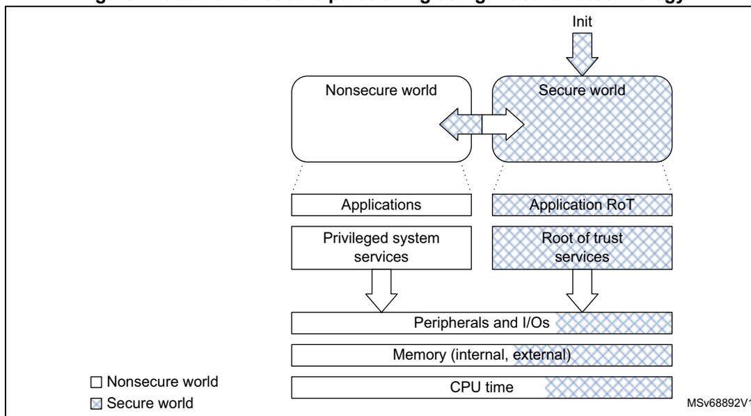
The diagram illustrates the secure/nonsecure partitioning using TrustZone technology. It is divided into two main columns: the Nonsecure world (left) and the Secure world (right). At the top, an 'Init' signal points to the Secure world. The Nonsecure world contains 'Applications' and 'Privileged system services'. The Secure world contains 'Application RoT' and 'Root of trust services'. Both worlds share a common stack of resources at the bottom: 'Peripherals and I/Os', 'Memory (internal, external)', and 'CPU time'. A double-headed arrow connects the Nonsecure world and the Secure world. A legend at the bottom left shows a white square for 'Nonsecure world' and a hatched square for 'Secure world'. The diagram is labeled 'MSv68892V1' in the bottom right corner.
Note: The initial partitioning of the platform is under the responsibility of the secure firmware executed after device reset.
Thanks to this resource isolation technology, the secure world can be used to protect critical code against intentional or unintentional tampering from the more exposed code running in the nonsecure world.
Note: The secure code is typically small and rarely modified, while the nonsecure code is more exposed, and prone to firmware updates.
3.6.1 TrustZone security architecture
The Armv8-M TrustZone technology is a comprehensive hardware architecture that proposes to developers a comprehensive, holistic protection across the entire processor and system. The device TrustZone hardware features include:
- • The Armv8-M mainline security extension of Cortex-M33, enabling a new processor secure state, with its associated secure interrupts
- • The dynamic allocation of memory and peripherals to TrustZone using eight security attribution unit (SAU) regions of Cortex-M33
- • A global TrustZone framework (GTZC), extending the TrustZone protection against transactions coming from masters in the system different from Cortex-M33
- • TrustZone-aware embedded flash memory and peripherals
Note: The TZEN option bit in the FLASH_OPTSR2_PRG register activates TrustZone security.
3.6.2 Armv8-M security extension of Cortex-M33
The Arm security extension of the Cortex-M33 is an evolution, not a revolution. It uses the programmer model from earlier Cortex-M subfamilies like Cortex-M4. Indeed, Armv8-M is architecturally similar to Armv7-M, using the same 32-bit architecture, the same memory mapped resources protected with an MPU. Armv8-M also uses the nested vectored interrupt controller (NVIC).
The implementation on STM32H5 devices is composed of the following features:
- • A new processor state, with almost no additional code/cycle overhead (as opposed to Armv8-A TrustZone) that uses a dedicated exception routine to trigger a secure/nonsecure world change
- • Two memory map views of a shared 4-Gbyte address space
- • A low interrupt latency for both secure and nonsecure domains, and a new interrupt configuration for security grouping and priority setting
- • Separated exception vector tables for the secure and nonsecure exceptions
- • Micro-coded context preservation
- • Banking of specific registers across secure/nonsecure states, including stack pointers with stack-limit checkers
- • Banking of the following Cortex-M33 programmable components (two separate units for secure and nonsecure):
- – SysTick timer
- – MPU configuration registers (12 MPU regions in secure, eight in nonsecure)
- – some of the system control block (SCB) registers
- • New system exception (SecureFault) for handling of security violations
- • Configurable debug support, as defined in Section 3.12
For more information, refer to the Cortex-M33 programming manual (PM0264).
3.6.3 Memory and peripheral allocation using IDAU/SAU
Security attributes
As illustrated in Figure 5 , the Armv8-M nonsecure memory view is similar to Armv7-M (found in Cortex-M4), with the difference that the secure memory is hidden. The secure memory view shows the flash memory, SRAM and peripherals that are accessible only while the Cortex processor executes in Secure state.
Note: Figure 5 shows the 32-bit address space after SAU configuration, as viewed by the secure code.
Figure 5. Sharing memory map between CPU in secure and nonsecure state
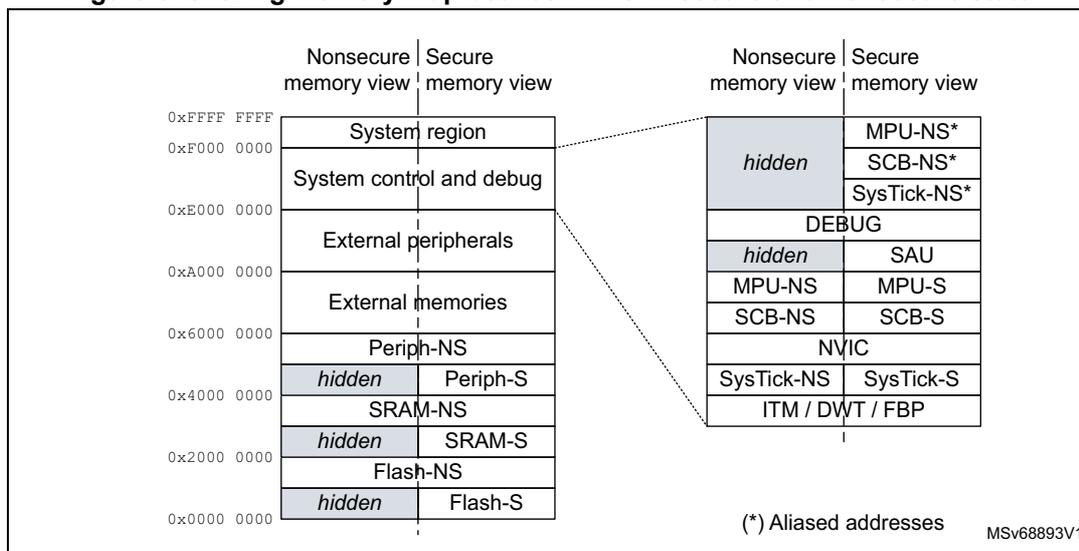
| Nonsecure memory view | Secure memory view | Nonsecure memory view | Secure memory view |
|---|---|---|---|
| 0xFFFF FFFF | System region | hidden | MPU-NS* |
| 0xF000 0000 | System control and debug | SCB-NS* | |
| 0xE000 0000 | External peripherals | SysTick-NS* | |
| 0xA000 0000 | External memories | DEBUG | |
| 0x6000 0000 | Periph-NS | hidden | SAU |
| 0x4000 0000 | hidden Periph-S | MPU-NS | MPU-S |
| SRAM-NS | SCB-NS | SCB-S | |
| 0x2000 0000 | hidden SRAM-S | NVIC | |
| Flash-NS | SysTick-NS | SysTick-S | |
| 0x0000 0000 | hidden Flash-S | ITM / DWT / FBP | |
(*) Aliased addresses MSV68893V1
The Cortex processor state (and the associated rights) depends upon the security attribute assigned to the memory region where it is executed:
- • A processor in a nonsecure/secure state executes only from nonsecure (NS)/secure (S) program memory.
- • When running in secure state, the processor can access data from both S and NS memories. When running in nonsecure state, the CPU is limited to nonsecure memories.
To manage transitions to the secure world, developers must create nonsecure callable (NSC) regions containing valid entry points to the secure libraries. The first instruction in these entry points must be the new secure gate (SG) instruction, used by the nonsecure code to call a secure function (see Figure 6).
Figure 6. Secure world transition and memory partitioning
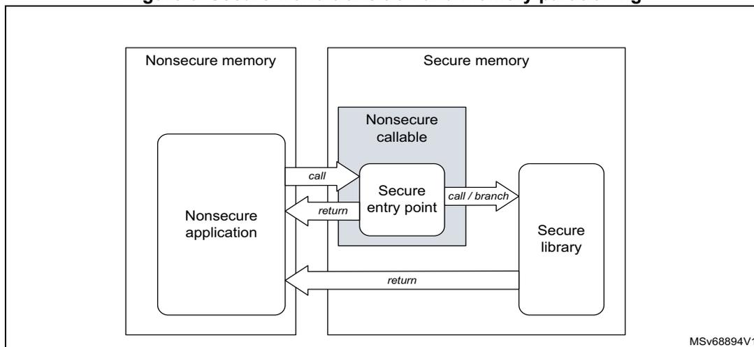
The diagram illustrates the memory partitioning and transition mechanism. On the left, 'Nonsecure memory' contains a 'Nonsecure application'. On the right, 'Secure memory' contains a 'Nonsecure callable' region with a 'Secure entry point', and a 'Secure library'. Arrows show the flow: 'call' from Nonsecure application to Secure entry point, 'return' from Secure entry point to Nonsecure application, 'call / branch' from Secure entry point to Secure library, and 'return' from Secure library to Nonsecure application.
MSV68894V1
Programming security attributes
In Cortex-M33, the static implementation defined attribution unit (IDAU) works with the programmable security attribution unit (SAU) to assign a specific security attribute (S, NS, or NSC) to a specific address, as shown in Table 7 .
Table 7. Configuring security attributes with IDAU and SAU
| IDAU security attribution | SAU security attribution (1) | Final security attribution |
|---|---|---|
| Nonsecure | Secure | Secure |
| Secure-NSC | Secure-NSC | |
| Nonsecure | Nonsecure | |
| Secure-NSC | Secure | Secure |
| Nonsecure | Secure-NSC |
1. Defined regions are aligned to 32-byte boundaries.
The Cortex-M33 can configure the SAU only in the secure-privilege state. When the TrustZone is enabled, the SAU defaults all addresses as secure (S). A secure boot application can then program the SAU to create NSC or NS regions, as shown in Table 7 .
Note: The SAU/IDAU settings are applicable only to the Cortex-M33. The other masters, like DMA, are not affected by these policies.
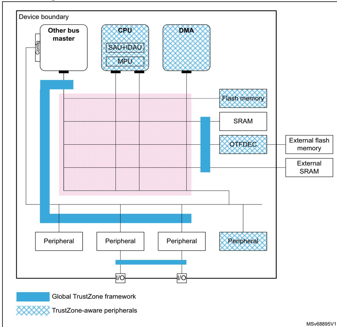
3.6.4 Memory and peripheral allocation using GTZC
Global TrustZone framework architecture
On top of the Armv8-M TrustZone security extension in Cortex-M33, the devices embed complementary security features that reinforce, in a flexible way, the isolation between secure and nonsecure worlds. Unlike the SAU/IDAU, the GTZC can protect legacy memories and peripherals against nonsecure transactions coming from other masters than the Cortex-M33.
Figure 7. Global TrustZone framework and TrustZone awareness
Securing peripherals with TZSC
When the TrustZone security is active, a peripheral is either securable through the GTZC, or is natively TrustZone-aware, as shown in the previous figure:
- • A securable peripheral or memory is protected by an AHB/APB firewall gate, controlled by the TrustZone security controller (TZSC).
- • A TrustZone-aware peripheral or memory is connected directly to AHB or APB interconnect, implementing a specific TrustZone behavior, such as a subset of secure registers or a secure memory area.
When a securable peripheral is made secure-only with the GTZC, if this peripheral is master on the interconnect, it automatically issues secure transactions. The SDMMC is an example of securable master. TrustZone-aware AHB masters like Cortex-M33 or DMAs, drive a secure signal in the AHB interconnect, according to their security mode, independently to the GTZC.
Note: Like with TrustZone, a peripheral can be made privileged-only with TZSC (see Section 3.7.2 ). In this case, if this peripheral is master on the interconnect, it automatically issues privileged transactions.
Securing memories with TZSC and MPCBB
The TZSC block in GTZC provides the capability to manage the security and privilege for all securable external memories, programming the MPCWM resources as defined in Table 8 .
Table 8. MPCWMx resources
| Memory | MPC resource | Type of filtering | Number of regions | Default security | On-the-fly decryption (1) |
|---|---|---|---|---|---|
| OCTOSPI1 | MPCWM1 | Nonsecure | 2 | Yes | |
| FMC_NOR bank | MPCWM2 | privileged or unprivileged region (watermarks) | 2 | Secure privileged (2) | No |
| FMC_NAND / FMC_SDRAM (3) bank | MPCWM3 | 1 | |||
| Backup SRAM (BKPSRAM)/FMC_SDRAM (3) | MPCWM4 | 1 |
- Using the OTFDEC.
- Assuming TrustZone is activated on the device, nonsecure unprivileged otherwise.
- FMC_SDRAM is not available on STM32H523/33xx devices.
The MPCBB resources in GTZC provide the capability to configure the security and privilege of embedded SRAM blocks, as defined in Table 9 and Table 10 .
Table 9. MPCBBx resources (STM32H562/63/73xx devices)
| Memory | MPC resource | Type of filtering | Memory size | Block size | Number of super-blocks | Default security |
|---|---|---|---|---|---|---|
| SRAM1 | GTZC1_MPCBB1 | Block based, managing security and privilege | 256 KB | 512 (1) bytes | 16 | Secure privileged (2) |
| SRAM2 | GTZC1_MPCBB2 | 64 KB | 4 | |||
| SRAM3 | GTZC1_MPCBB3 | 320 KB | 20 |
- Blocks are grouped in super-blocks of 32 consecutive blocks, to manage the configuration locking.
- Assuming TrustZone is activated on the device, nonsecure unprivileged otherwise.
Table 10. MPCBBx resources (STM32H523/33xx devices)
| Memory | MPC resource | Type of filtering | Memory size | Block size | Number of super-blocks | Default security |
|---|---|---|---|---|---|---|
| SRAM1 | GTZC1_MPCBB1 | Block based, managing security and privilege | 128 KB | 512 (1) bytes | 8 | Secure privileged (2) |
| SRAM2 | GTZC1_MPCBB2 | 80 KB | 5 | |||
| SRAM3 | GTZC1_MPCBB3 | 64 KB | 4 |
- Blocks are grouped in super-blocks of 32 consecutive blocks, to manage the configuration locking.
- Assuming TrustZone is activated on the device, nonsecure unprivileged otherwise.
Applying GTZC configurations
The TZSC and MPCBB blocks can be used in one of the following ways:
- • statically programmed during the secure boot, locked and not changed afterwards
- • dynamically reprogrammed using a specific application code or real-time kernel
When the dynamic option is selected and the configuration is not locked:
- • MPCBB secure blocks or MPCWM nonsecure region size can be changed by a secure software. This software must be privileged for MPCWM, can be unprivileged if the particular block is not privileged-only.
- • The secure (respectively privilege) state of each peripheral can be changed writing to GTZC_TZSC_SECCFRGx (respectively GTZC_TZSC_PRIVCFGx) registers.
Securing peripherals with TZSC
The TZSC block in GTZC provides the capability to manage the security and the privilege for all securable peripherals. The list of these peripherals can be found in Section 5: Global TrustZone® controller (GTZC) .
Note: When the TrustZone is deactivated, the resource isolation hardware GTZC can still be used to isolate peripherals to privileged code only (see Section 3.7.2 ).
When the TrustZone is activated, peripherals are set as nonsecure and unprivileged after reset.
TrustZone-aware peripherals
The devices include the following TrustZone-aware peripherals:
- • GPIOA to GPIOI
- • GTZCx_MPCBB, GTZCx_TZIC and GTZCx_TZSC (GTZC blocks)
- • OTFDEC1, writable only in secure if TZEN is enabled
- • EXTI
- • Flash memory
- • RCC and PWR
- • GPDMA1 and GPDMA2
- • SBS registers
- • RTC and TAMP
- • MCU debug unit DBGMCU
The way illegal accesses to those peripherals are monitored through the TZIC registers is described in Section 5: Global TrustZone® controller (GTZC) .
For more details, refer to Section 3.6.5 .
TrustZone illegal access controller (TZIC)
The TZIC block in GTZC gathers all illegal access events originated from sources either protected by GTZC or TrustZone-aware, generating one global secure interrupt towards the NVIC.
TZIC is available only when the system is TrustZone enabled (TZEN = 0xB4). All accesses to TZIC registers must be secured.
For each illegal event source, a status flag and a clear bit exist. Each illegal event can be masked, not generating an interrupt toward the NVIC.
Note: By default, all events are masked.
3.6.5 Managing security in TrustZone-aware peripherals
This section gives more details on how the security is implemented in the TrustZone-aware peripherals listed in the previous section.
Embedded flash memory
When the TrustZone security is enabled through option bytes (TZEN = 0xB4), the whole memory is secure after reset. The following protections, shown in Figure 8 , are available to the application:
- • nonvolatile user secure areas, defined with nonvolatile secure user option bytes
- – watermark-based secure only area (x2)
- – secure hide protection (HDP) area, stickily hidden after boot (x2)
- • volatile user secure pages, defined with volatile secure registers (lost after reset)
- – Any page set as nonsecure (example: outside watermark-based secure only area), can be set as secure on-the-fly using the block-based configuration registers.
Note: All areas are aligned on the page granularity of the flash memory, which can be configured as secure while it is tagged as nonsecure in Cortex-M33 IDAU/SAU. In this case, nonsecure accesses by the CPU to the flash memory are denied.
Erase or program operations can be available to secure/nonsecure code only for secure/nonsecure pages or memory. A flash memory is considered secure if at least one page is secure.
Figure 8. Flash memory TrustZone protections
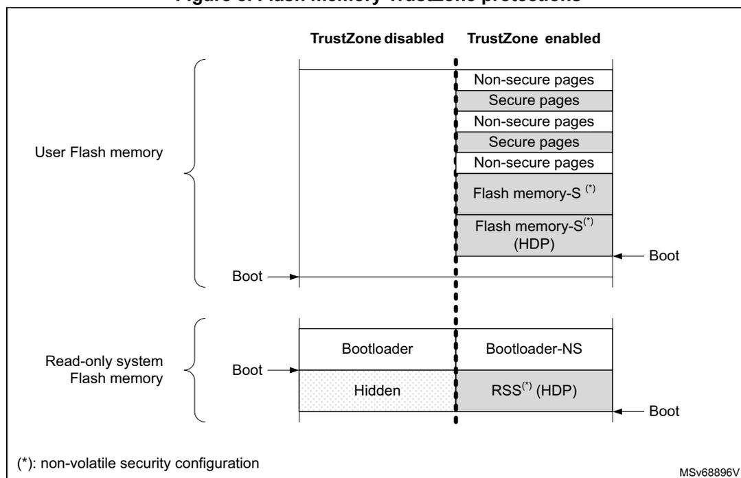
(*): non-volatile security configuration
MSV68896V1
As shown above, when TrustZone is enabled (TZEN = 0xB4), the application code can use the HDP area that is part of the flash memory watermark-based secure area. Indeed, when the application sets the HDPx_ACCDIS bit, data read, write, and instruction fetch on this HDP area is denied until the next system reset.
For example, the software code in the secure flash memory HDP area can be executed only once, with any further access to this area denied until the next system reset. Additionally, any flash memory page belonging to an active HDP area cannot be erased anymore.
When the TrustZone is disabled (TZEN = 0xC3), the volatile/non-volatile secure area features are deactivated and all secure registers are RAZ/WI.
See Section 7: Embedded flash memory (FLASH) for more details.
On-the-fly encryption/decryption (OTFDEC)
When the TrustZone security is enabled (TZEN = 0xB4), the OTFDEC can be initialized only by secure applications. Each of the four encrypted regions, once the configuration is confirmed, can be write-locked until the next power-on-reset.
Note: Any application (secure or nonsecure) can verify the initialization context of each OTFDEC region (including CRC of the keys), by reading the peripheral registers.
Key registers in each OTFDEC are write-only.
See Section 3.10.3 for more details on this cryptographic engine.
Direct memory access controllers (GPDMAx)
When a DMA channel x is defined as secure (SECx = 1 in GPDMA_SECCFGR), the source and destination transfers can be independently set as secure or nonsecure by a secure application using SSEC and DSEC bits in GPDMA_CxTR1. Table 11 summarizes these security options available in each DMA channel.
Table 11. DMA channel use (security) (1)| Destination type | Secure DMA channel x (SECx = 1) | Nonsecure DMA channel y (SECy = 0) | ||
|---|---|---|---|---|
| Secure source | Nonsecure source | Secure source | Nonsecure source | |
| Secure destination | OK | OK (2) | Transfer blocked | |
| Nonsecure destination | OK (3) | OK (4) | Transfer blocked | OK |
- 1. When a transfer is blocked, the transfer completes but the corresponding writes are ignored, and reads return 0s. An illegal access event to TZIC is automatically triggered by the memory/peripheral used as source or destination.
- 2. If the source is a memory, the transfer is possible only if SSEC = 0, otherwise the transfer is blocked.
- 3. If the destination is a memory, the transfer is possible only if DSEC = 0, otherwise the transfer is blocked.
- 4. If the transfer is memory-to-memory, it is possible only if SSEC = 0 and DSEC = 0, otherwise it is blocked.
When a channel is configured as secure:
- • Registers allocated to this channel (excluding GPDMA_SECCFGR, GPDMA_PRIVCFGR and GPDMA_RCFGLOCKR) are read as 0. Writes are ignored for nonsecure accesses. A secure illegal access event may also be triggered towards the TZIC peripheral.
- – Writes to GPDMA_SECCFGR and GPDMA_RCFGLOCKR must be secure. For each bit in GPDMA_PRIVCFGR, write must be secure if the corresponding bit in GPDMA_SECCFGR is set.
- • In linked-list mode, the loading of the next linked-list data structure from memory is performed with secure transfers.
- • When switching to a nonsecure state, the secure application must abort the channel or wait until the secure channel is completed before doing the switch.
Note: DMA secure channels are not available when TrustZone is deactivated. When a channel is configured as nonsecure, in linked-list mode, the loading of the next linked-list data structure from memory is performed with nonsecure transfers.
See Section 16: General purpose direct memory access controller (GPDMA) for more details.
Power control (PWR)
When the TrustZone security is enabled (TZEN = 0xB4), the selected PWR registers can be secured through PWR_SECCFGR, protecting the following PWR features:
- • low power mode setup
- • wake-up (WKUP) pins definition
- • voltage detection and monitoring
- • backup domain control
Other PWR configuration bits become secure:
- • when the system clock selection is secure in the RCC: the voltage scaling (VOS) becomes secure.
- • when a GPIO is configured as secure: its corresponding bit for pull-up/pull-down configuration in Standby mode becomes secure.
- • when the USB Type-C/USB power delivery interface (UCPD) is configured as secure in TZSC: PWR_UCPDR register becomes secure.
See Section 10: Power control (PWR) for details.
Secure clock and reset (RCC)
When the TrustZone security is enabled (TZEN = 0xB4) and security is enabled in the RCC, the bits controlling the peripheral clocks and resets become TrustZone-aware:
- • If the peripheral is securable and programmed as secure in the TZSC, the peripheral clock and reset bits become secure.
- • If the peripheral is TrustZone-aware, the peripheral clock and reset bits become secure when at least one function is configured as secure inside the peripheral.
Note: Refer to Section 3.6.4 for the list of securable and TrustZone-aware peripherals.
Additionally, the following configurations can be made secure-only using RCC_SECCFGR:
- • external clock (such as HSE or LSE), internal oscillator (such as HSI, CSI, or LSI)
- • main PLL and AHB prescaler
- • system clock source selection
- • MCO clock output
- • reset flag
- • automatic internal oscillator waking up configuration
See Section 11: Reset and clock control (RCC) for details.
Real-time clock (RTC)
Like all TrustZone-aware peripherals, a nonsecure read/write access to a secured RTC register is RAZ/WI. It also generates an illegal access event that triggers a secure illegal access interrupt if the RTC illegal access event is enabled in the TZIC.
After a backup domain power-on reset, all RTC registers can be read or written in both secure and nonsecure modes. The secure boot code can then change the security setup, making registers Alarm A, Alarm B, wakeup timer, and timestamp secure or not, using RTC_SECCFGR.
When the SEC bit is set in secure-only RTC_SECCFGR:
- • Writing the RTC registers is possible only in secure mode.
- • Reading RTC_SECCFGR, RTC_PRIVCFGR, RTC_MISR, RTC_TR, RTC_DR, RTC_SSR, RTC_PRER, and RTC_CALR is always possible in secure and nonsecure modes. All the other RTC registers can be read only in secure mode.
When SEC is cleared in secure-only RTC_SECCFGR, it is still possible to restrict access in secure mode to some RTC registers by setting dedicated control bits: INITSEC, CALSEC, TSSEC, WUTSEC, ALRASEC, and ALRBSEC.
Note: The RTC security configuration is not affected by a system reset.
See Section 46: Real-time clock (RTC) for more details.
Tamper and backup registers (TAMP)
Like all TrustZone-aware peripherals, a nonsecure read/write access to a secured TAMP register is RAZ/WI. It also generates an illegal access event that triggers a secure illegal access interrupt if the TAMP illegal access event is enabled in the TZIC.
After a backup domain power-on reset, all TAMP registers can be read or written in both secure and nonsecure modes. The secure boot code can change this security setup, making some registers secure or not as needed, using TAMP_SECCFGR register.
When TAMPSEC is set in TAMP_SECCFGR:
- • Writing the TAMP registers is possible only in secure mode. Backup registers have their own write protection (see below).
- • Reading the TAMP registers (exception TAMP_SECCFGR, TAMP_PRIVCFGR, and TAMP_MISR) returns 0 if the access is nonsecure. Backup registers have their own read protection (see below).
The application can also:
- • make TAMP_COUNTR register read and write secure-only by setting the CNT1SEC bit in TAMP_SECCFGR secure register
- • increase security in backup registers for two of the three protection zones configured using BKPRWSEC[7:0] and BKPWSEC[7:0] bitfields in TAMP_SECCFGR:
- – protection zone 1 is read nonsecure, write nonsecure
- – protection zone 2 is read nonsecure, write secure
- – protection zone 3 is read secure, write secure
Note: The TAMP security configuration is not affected by a system reset.
See Section 47: Tamper and backup registers (TAMP) for more details.
General-purpose I/Os (GPIO)
When the TrustZone security is enabled (TZEN = 0xB4), each I/O pin of the GPIO ports can be individually configured as secure through the GPIOx_SECCFGR registers. Only a secure application can write to GPIOx_SECCFGR registers. After boot, each I/O pin is set as secure.
When an I/O pin is configured as secure, its corresponding configuration bits for alternate function (AF), mode selection (MODE), and I/O data are RAZ/WI in case of nonsecure access.
When a digital alternate function is used (input/output mode) to protect data transiting from/to the I/O managed by a secure peripheral, the devices add a secure alternate function gate on the path between the peripheral and its allocated I/Os:
- • if the peripheral is secure, the I/O pin must also be secure to allow input/output of data
- • if the peripheral is not secure, the connection is allowed regardless of the I/O pin state.
The TrustZone-aware logic around GPIO ports, used as alternate functions, is summarized in Table 12 .
Table 12. Secure alternate function between peripherals and allocated I/Os
| Security configuration | Alternate function logic | Comment | ||
|---|---|---|---|---|
| Peripheral | Allocated I/O pin | Input | Output | |
| Secure | Secure | I/O data | Peripheral data | - |
| Nonsecure | Out of reset configuration | |||
| Secure | Nonsecure | 0 | 0 | - |
| Nonsecure | I/O data | Peripheral data | ||
When an analog function with an analog switch is used, the connection to the peripherals listed in Table 13 is blocked by hardware when the peripheral is nonsecure and the I/O is secure.
Table 13. Nonsecure peripheral functions that cannot be connected to secure I/Os
| Peripheral | Analog function (1) | Input | Output |
|---|---|---|---|
| ADC12 | ADC12_INy (y = 1 to 17) | X | - |
1. Used to find the I/O corresponding to the signal/function on the package (refer to the product datasheet).
Finally, regarding GPIO and security, Table 14 summarizes the list of I/Os without any hardware protection linked to TrustZone. The listed signals (input and/or outputs) are not blocked when the I/O is set as secure, and the associated peripheral is non secure.
For example, when a secure application sets PA4 as secure to be used as LPTIM2_CH1, if the DAC is nonsecure, it can be programmed to output data to PA4, potentially causing malfunction to the secure application.
Similarly, when a secure application sets PA0 as secure to be used as UART4_TX, if TAMP is nonsecure, it can be programmed to capture the USART input traffic through the TAMP_IN signal.
It is important that, for each case described in Table 14 , the secure application decides if a potential effect on data integrity or confidentiality is critical or not. For example, if the USART situation described above is not acceptable (data transiting on secure USART is confidential), then the secure application must configure the TAMP as secure even if not used by the secure application.
Table 14. Nonsecure peripheral functions that can be connected to secure I/Os
| Peripheral | Signal (1) | Input | Output | How to set the peripheral or function as secure |
|---|---|---|---|---|
| DAC | DAC1_OUTx (x = 1, 2) | - | X | Set DAC1SEC in GTZC1_TZSC_SECCFGR1. |
| UCPD | UCPD1_CCx (x = 1, 2) | X | X | Set UCPD1SEC in GTZC1_TZSC_SECCFGR1. |
| UCPD1_DBx (x = 1, 2) | X | - | ||
| TAMP | TAMP_INx (x = 1 to 8) | X | - | Set TAMPSEC in TAMP_SECCFGR |
| TAMP_OUTx (x = 1 to 8) | - | X | ||
| RTC | RTC_OUTx (x = 1, 2) | - | X | Set SEC in RTC_SECCFGR. |
| RTC_TS | X | - | Set TSSEC in RTC_SECCFGR. | |
| PWR | WKUPx (x = 1 to 8) | X | - | Set WUPxSEC in PWR_SECCFGR. |
| RCC | LSCO | - | X | Set LSESEC in RCC_SECCFGR. |
| EXTI | EXTIx (x= 0 to 58) | X | - | Set SECx bit in EXTI_SECCFGR. |
1. To find the I/O corresponding to the signal/function on the package, refer to the product datasheet.
Refer to Section 13: General-purpose I/Os (GPIO) for more details.
Extended interrupts and event controller (EXTI)
When the TrustZone security is enabled, the EXTI is able to protect event register bits from being modified by nonsecure accesses. The protection can individually be activated per
input event via the register bits in EXTI_SECCFGRx. When an input event is configured as secure, only a secure application can change the configuration (including security), change the masking or clear the status of this input event.
The security configuration in EXTI_SECCFGR1 and EXTI_SECCFGR2 can be globally locked after reset in EXTI_LOCKR.
See Section 18: Extended interrupts and event controller (EXTI) for more details.
System configuration, boot, and security (SBS)
Like all TrustZone-aware peripherals, when the TrustZone security is enabled, a nonsecure read/write access to a secured SBS register is RAZ/WI. Such access also generates an illegal access event that triggers a secure illegal access interrupt if the SBS illegal access event is not masked in the TZIC.
See Section 14: System configuration, boot, and security (SBS) for more details.
Microcontroller debug unit (DBGMCU)
The MCU debug component (DBGMCU) helps the debugger, providing support for:
- • low-power modes behavior during debug
- • peripheral freeze during debug, applicable to I2Cs, IWDG, WWDG, timers, low-power timers, and GPDMA channels
The DBGMCU is a TrustZone-aware peripheral, managing accesses to its control registers as described in Table 15 .
Table 15. TrustZone-aware DBGMCU nonsecure accesses management
| Debug profile | Peripheral status (1) | DBG_xx_STOP control bits | |
|---|---|---|---|
| Write access | Read access | ||
| Nonsecure invasive (SPIDEN = 0) | NS | Yes (S (2) or NS) | Yes (S or NS) |
| S | None (S or NS) | ||
| Secure invasive (SPIDEN = 1) | NS | Yes (S or NS) | Yes (S or NS) |
| S | Yes (S only) | ||
1. As reported by the GTZC, the TrustZone-aware peripheral or the DMA channel.
2. Secure access from debugger is converted to nonsecure access in the device.
Refer to Section 59.12: Microcontroller debug unit (DBGMCU) for more details.
3.6.6 Activating TrustZone security
The TrustZone is deactivated by default in all devices. It can be activated by setting the TZEN option bit in FLASH_OPTSR2_PRG when PRODUCT_STATE is Open. Once TZEN has changed from disabled to enabled (0xC3 to 0xB4), the default security state, after reset, is always the following:
- • CPU subsystem
- – Cortex-M33 exits reset in secure state, hence the boot address must point toward a secure memory area.
- – All interrupt sources are secure (in NVIC).
- – The memory mapped viewed by the CPU through IDAU/SAU is fully secure.
- • Embedded flash memory
- – Flash memory nonvolatile secure areas (with their HDP zone), are defined with nonvolatile registers FLASH_SECWMxR (x = 1, 2). Default secure option bytes setup is all user flash secure, without HDP area defined.
- – Volatile block-based security attributions of the flash memory are nonsecure.
- • Embedded SRAMs
- – All SRAMs are secure, as defined in GTZC/MPCBB (see Section 3.6.4 ). The secure boot code can change this security setup, making blocks secure or not.
- • External memories
- – All memory devices connected to the FMC and OCTOSPI are secure, as defined in GTZC/MPCWM (see Section 3.6.4 ). The secure-boot code can change this security setup, making components secure or not.
- • All GPIOs are secure.
- • All GPDMA channels are nonsecure.
- • Backup registers are nonsecure.
- • Peripherals and GTZC:
- – Securable peripherals are nonsecure and unprivileged.
- – TrustZone-aware peripherals are nonsecure, with their secure configuration registers being secure.
- – All illegal access interrupts in GTZC/TZIC are disabled.
Note: Refer to Section 3.6.4 for the list of securable and TrustZone-aware peripherals.
3.6.7 Deactivating TrustZone security
Once TrustZone is activated, it can only be deactivated during a PRODUCT_STATE regression to Open.
Note: Such PRODUCT_STATE regression triggers the erasing of embedded memories (SRAM2, flash), and the reset of all peripherals, including the OTFDEC and all crypto engines.
After the TrustZone deactivation, most of the features mentioned in Section 3.6 are no longer available:
- • The nonvolatile secure area of the embedded flash memory is deactivated, including the HDP area.
- • Only the NVIC manages nonsecure interrupts.
- • All secure registers in TrustZone-aware peripherals are RAZ/WI.
Note: When the TrustZone is deactivated, the resource isolation using privilege remains available (see Section 3.7.2 for details).
3.7 Other resources isolation
These are hardware mechanisms offering an additional level of isolation on top of the TrustZone technology.
3.7.1 Temporal isolation using secure hide protection (HDP)
The embedded flash memory allows to define an HDP area per watermarked-secure area of each bank (8-Kbyte page granularity). The code executed in this HDP area, with its related data and keys, can be hidden after boot, until the next system reset. The hide protection principle is shown in Figure 9 .
Figure 9. Flash memory secure HDP area
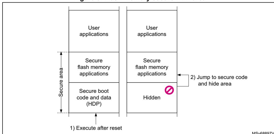
Activation of HDP area in user flash memory is related to HDPL1: as soon as \( HDPL \geq 2 \) , data read, write, and instruction fetch (on the area defined by HDPx_PSTART and HDPxPEND in FLASH_HDPxR_PRG option bytes), are denied until the next device reset.
The END of the HDPx areas can be extended (dynamically by the application) thanks to FLASH_HDPEXTR flash memory register.
Note: Bank erase aborts when it contains a write-protected area (WRP or HDP area).
3.7.2 Resource isolation using Cortex privileged mode
In parallel to the TrustZone isolation described in Section 3.6 , the hardware and software resources can be partitioned so that they are restricted to software running in Cortex privileged mode.
Thanks to this hardware isolation technology, available even if TrustZone is disabled, critical code or data can be protected against intentional or unintentional tampering from the more exposed unprivileged code.
Memory and peripheral privileged allocation using MPU
The Cortex-M33 MPU divides the unified memory into eight regions in nonsecure and twelve in TrustZone, each aligned to a multiple of 32 bytes. Each memory region can be programmed to generate faults when accessed inappropriately by unprivileged software.
Memory and peripheral privileged allocation using GTZC
For the Cortex-M33 master, to complement the coarse isolation provided by the MPU, the GTZC reinforces, in a flexible way, the isolation between privileged and unprivileged tasks, for peripherals and selected memories.
For masters other than the Cortex-M33, the GTZC can assign them as unprivileged initiators, automatically protecting resources defined as privileged against this master.
- • Securing peripherals with TZSC (privileged-only)
In the devices, a peripheral is either securable privileged-only through GTZC, or is natively privileged-aware:
- – A securable privileged-only peripheral or memory is protected by an AHB/APB firewall gate controlled by the TZSC.
- – A privileged-aware peripheral or memory is connected directly to AHB or APB interconnect, implementing a specific behavior (for example, a subset of registers or a memory area is privilege-only).
When such a peripheral is made privileged-only with GTZC, if it is master on the interconnect (SDMMC), it automatically issues privileged transactions. Privileged-aware masters like GPDMA1 and GPDMA2, drive privileged signal in the AHB interconnect according to their internal privileged mode, independently to the GTZC.
The list of securable peripherals can be found in Section 5: Global TrustZone® controller (GTZC) .
- • Securing memories with TZSC and MPCBB (privileged-only)
The TZSC logic in GTZC provides the capability to manage the privilege level for all securable external memories, programming the MPCWM resources defined in Section 3.6.4 .
Similarly, the TZSC logic in GTZC provides the capability to configure the privilege level of embedded SRAM blocks, programming the MPCBB resources defined in Section 3.6.4 .
- • Error management (privileged-only)
- – Any unprivileged transaction trying to access a privileged resource is considered as illegal. There is no illegal access event generated for illegal unprivileged read and write accesses.
- – The addressed resource follows a silent-fail behavior, returning all-0 data for read and ignoring any write.
- – When an illegal unprivileged access occurs, no bus error is generated, except when this is an instruction fetch, accessing a privileged memory or a peripheral register.
Managing security in privileged-aware peripherals
TrustZone-aware peripherals also implement privileged-only access mode. The privileged protection is valid even if TrustZone is disabled (TZEN = 0xC3):
- • Embedded flash memory
By default, all registers can be read or programmed in both privileged and unprivileged modes.
When secure privileged bit SPRIV is set in FLASH_PRIVCFGGR, reading and writing the secure registers is possible only in privileged mode. Write access to this bit is ignored if TrustZone is disabled (TZEN = 0xC3).
When nonsecure privileged bit NSPRIV is set in FLASH_PRIVCFGGR, reading and writing the flash memory nonsecure registers is possible only in privileged mode.
Regarding privileged protection, the devices offer the following features:
- – The system flash memory can be accessed in both privileged and unprivileged modes.
- – Each watermark-based secure area, including its secure HDP area, is accessible in secure-privileged and secure-unprivileged mode, if applicable.
- – Each 8-Kbyte page of the embedded flash memory can be programmed on-the-fly as privileged only, using the block-based privileged configuration registers FLASH_PRIV1BBRx and FLASH_PRIV2BBRx. An unprivileged page is accessible by privileged or unprivileged access.
Note: Switching a page from privileged to unprivileged does not erase its content.
When applicable, an erase or program operation is always available to privileged code, and is available to unprivileged code only for unprivileged pages or unprivileged memory.
- • On-the-fly encryption/decryption (OTFDEC)
When privileged bit PRIV is set in OTFDEC_PRIVCFGGR, only a privileged application can initialize the OTFDEC.
Note: OTFDEC_PRIVCFGGR can be read by both privileged and unprivileged code.
- • Direct memory access controllers (GPDMAx)
When a DMA channel x is defined as privileged (PRIVx = 1 in GPDMA_PRIVCFGGR), special rules (see Table 16 ) apply when accessing privileged/unprivileged source or destination.
Table 16. DMA channel use (privilege)
| Destination | Privileged DMA channel x (PRIVx = 1) | Unprivileged DMA channel y (PRIVy = 0) | ||
|---|---|---|---|---|
| Privileged source | Unprivileged source | Privileged source | Unprivileged source | |
| Privileged | OK | Transfer blocked (1) | ||
| Unprivileged | Transfer blocked | OK | ||
1. When a transfer is blocked, the transfer completes but the corresponding writes are ignored, and reads return 0s.
- • Power control (PWR)
By default, after a power-on or a system reset, all PWR registers except PWR_PRIVCFGGR, can be read or written in both privileged and unprivileged modes.
When secure privileged bit SPRIV is set in PWR_PRIVCFGGR, reading and writing the PWR securable registers are possible only in privileged mode. Write access to this bit is ignored if TrustZone is disabled (TZEN = 0xC3).
When nonsecure privileged bit NSPRIV is set in PWR_PRIVCFGGR, reading and writing the PWR nonsecure registers are possible only in privileged mode.
See Section 10: Power control (PWR) for details.
- • Secure clock and reset (RCC)
By default, after a power-on or a system reset, all RCC registers except RCC_PRIVCFGGR can be read or written in both privileged and unprivileged modes.
When secure privileged bit SPRIV is set in RCC_PRIVCFGGR, reading and writing the RCC securable bits are possible only in privileged mode. Write access to this bit is ignored if TrustZone is disabled (TZEN = 0xC3).
When nonsecure privileged bit NSPRIV is set in RCC_PRIVCFGGR, reading and writing the RCC nonsecure bits are possible only in privileged mode.
See Section 11: Reset and clock control (RCC) for details.
- • Real time clock (RTC)
By default after any backup domain reset, all RTC registers except RTC_PRIVCFGGR, can be read or written in both privileged and unprivileged modes.
When PRIV bit is set in privileged-only RTC_PRIVCFGGR:
- – Writing the RTC registers is possible only in privileged mode.
- – Reading the RTC_SECCFGR, RTC_PRIVCFGGR, RTC_TR, RTC_DR, RTC_SSR, RTC_PRER and RTC_CALR is always possible in privileged and unprivileged modes.
All the other RTC registers can be read only in privileged mode.
When PRIV bit is cleared in privileged-only RTC_PRIVCFGGR register, it is still possible to restrict access to privileged mode to some RTC registers by setting dedicated control bits: INITPRIV, CALPRIV, TSPRIV, WUTPRIV, ALRAPRV, or ALRBPRIV.
See Section 46: Real-time clock (RTC) for details.
- • Tamper and backup registers (TAMP)
By default after any backup domain reset, all TAMP registers except TAMP_PRIVCFGGR can be read or written in both privileged and unprivileged modes.
When PRIV bit is set in privileged-only TAMP_PRIVCFGGR:
- – Writing the TAMP registers is possible only in privileged mode, except for the backup registers and the monotonic counters that have their own protection setting.
- – Reading the TAMP_SECCFGR or TAMP_PRIVCFGGR is always possible in privilege and unprivilege modes. All the other TAMP registers can be read only in privilege mode, except for the backup registers and the monotonic counters that have their own protection setting.
The application can also:
- – make TAMP_COUNT1R register read and write privileged-only by setting the CNTPRIV bit in TAMP_PRIVCFG
- – increase security for two of the three protection zones in backup registers, using BKPRWPRIV and BKPWPRIV bits in TAMP_PRIVCFG:
- – Make protection zone 1 read privileged, write privileged.
- – Make protection zone 2 read privileged or unprivileged, write privileged.
- – Protection zone 3 is always read and write privileged or unprivileged.
- • General-purpose I/Os (GPIO)
All GPIO registers can be read and written by privileged and unprivileged accesses, whatever the security state (secure or nonsecure).
- • Extended interrupts and event controller (EXTI)
The EXTI peripheral is able to protect event register bits from being modified by unprivileged accesses. The protection is individually activated per input event via the register bits in the privileged-only EXTI_PRIVCFGx registers. When an input event is configured as privileged, only a privileged application can change the configuration (including security if applicable), change the masking or clear the status of this input event.
The security configuration in EXTI_PRIVCFG1 and EXTI_PRIVCFG2 can be globally locked after reset in EXTI_LOCKR.
See Section 18: Extended interrupts and event controller (EXTI) for more details.
- • System configuration boot and security (SBS)
All SBS registers can be read and written in both privileged and unprivileged modes, except:
- – FPUSEC bit in SBS_SECCFG registers (privileged only)
- – SBS registers for CPU configuration: SBS_CSLOCKR, SBS_FPUIMR, and SBS_CNSLCKR
See Section 14: System configuration, boot, and security (SBS) for more details.
3.8 Secure execution
Through a mix of special software and hardware features, the devices ensure the correct operation of their functions against abnormal situations caused by programmer errors, software attacks through network access or local attempt for tampering code execution.
This section describes the hardware features specifically designed for secure execution.
3.8.1 Memory protection unit (MPU)
The Cortex-M33 includes a memory protection unit (MPU) that can restrict the read and write accesses to Each memory region (including those mapped to peripherals), based on one or more of the following parameters
- • Cortex-M33 operating mode (privileged, unprivileged)
- • data/instruction fetch
The memory map and the programming of the nonsecure and secure MPUs split memory into regions (up to eight for the nonsecure, and up to twelve for the TrustZone). Secure MPU is only available when TrustZone is activated.
3.8.2 Embedded flash memory write protection
The embedded flash memory write protection (WRP) prevents illegal or unwanted write/erase to special sections of the embedded flash memory user area (system area is permanently write protected).
Write protected area is defined through the option bytes, writing the start and end addresses: two write-protected areas can be defined in each bank, with the granularity of a 32-Kbyte page.
WRP areas can be modified through option byte changes unless the corresponding FLASH_WRPSGNxR has its UNLOCK option bit cleared (meaning ROM emulation). UNLOCK can be set only when regressing to PRODUCT_STATE = Open.
Note: Bank erase aborts when it contains a write-protected area (WRP or HDP area).
3.8.3 Tamper detection and response
Principle
The devices include active protection of critical security assets against temperature, voltage and frequency attacks, with the following features:
- • erasure of device secrets upon tamper detection
- • improved guarantee of safe execution for the CPU and its associated security peripherals, including:
- – out-of-range voltage (example: \( V_{BAT} \) , \( V_{DDA} \) ), temperature and clocking (LSE) detection
- – security watchdog IWDG clocked by the internal oscillator LSI
- – possible selection of internal oscillator HSI as system clock
- • power supply protection
- – RTC/TAMP domain powered automatically with \( V_{DD} \) or \( V_{BAT} \)
See Section 47: Tamper and backup registers (TAMP) for more details.
Tamper detection sources
The devices support eight active input/output pins, allowing four independent active-tamper meshes, or up to seven meshes if the same output pin is shared by several input pins (for a total of eight active-tamper I/Os). The active-tamper balls are mapped in the center of packages that can be used in the POS market (such as WLCSP80).
The active pins are clocked by the LSE, and are functional in different system operating modes (Run, Sleep, Stop, or Standby), and in VBAT mode. Refer to TAMP pins functionality over modes for list of tamper pins and their availability across power modes
Detection time is programmable, and a digital filtering is available (tamper triggered after two false comparisons in four consecutive comparison samples).
Note: Timestamps are automatically generated when a tamper event occurs.
The internal tamper sources are listed in Table 17 .
Table 17. Internal tampers in TAMP
| Tamper input | NOER bit number in TAMP_CR3 | Tamper source |
|---|---|---|
| itamp1 | 0 | Backup domain voltage continuous monitoring, functional in VBAT mode |
| itamp2 | 1 | Temperature monitoring, functional in VBAT mode |
| itamp3 | 2 | LSE monitoring (1) , functional in VBAT mode |
| itamp4 | 3 | HSE monitoring |
| itamp5 | 4 | RTC calendar overflow (rtc_calovf) |
| itamp6 | 5 | JTAG/SWD access |
| itamp7, 12, 13 | 6, 11, 12 | Voltage monitoring ( \( V_{CORE} \) , \( V_{REF+} \) ), through ADC analog watchdog |
| itamp8 | 7 | Monotonic counter overflow (generated internally) |
| itamp9 | 8 | Fault generation for cryptographic peripherals (SAES, PKA, AES, RNG) |
| itamp11 | 10 | IWDG timeout and potential tamper (IWDG reset when at least one enabled tamper flag is set) |
| itamp15 | 14 | System fault detection |
1. LSE missing or over frequency detection (> 2 MHz), Glitch filter (> 2 MHz).
Response to tampers
Each source of tamper in the device can be configured to trigger the following events:
- • Generate an interrupt, capable of waking up the device from Stop and Standby modes (see TAMPxMSK bits in TAMP_CR2 register).
- • Generate a hardware trigger for the low-power timers.
- • Erase device secrets if the corresponding TAMPxNOER bit is cleared in TAMP_CR2 (for tamper pins) or TAMP_CR3 (for internal tamper). These erasable secrets are:
- – symmetric keys stored in backup registers (x32), in AES, HASH, and OTFDEC (encrypted flash memory regions are read as 0)
- – asymmetric keys stored in PKA SRAM, erased when \( V_{DD} \) is present
- – other secrets stored in SRAM2 and CPU instruction cache memory (SRAM2 erased when \( V_{DD} \) is present)
- – nonvolatile information used to derive the DHUK in SAES is 0-ed until complete SRAM2 erase
- – Backup SRAM (depending on configuration bit), erased when \( V_{DD} \) is present
Read/write accesses by software to all these secrets can be blocked, by setting the BKBLOCK bit in TAMP_CR2 . The device secrets access is possible only when BKBLOCK is cleared, and no tamper flag is set for any enabled tamper source.
If \( V_{DD} \) is not present, the secrets that are erased when \( V_{DD} \) is present are erased only at the next \( V_{DD} \) power on.
Note: Device secret erase is also triggered by setting the BKERASE bit in TAMP_CR2, or by performing a PRODUCT_STATE regression as defined in Section 3.11.2 . Device secrets are not reset by a system reset or when the device wakes up from Standby mode.
Software filtering mechanism
Each tamper source can be configured not to launch an immediate erase, by setting the corresponding TAMPxNOER bit in TAMP_CR2 (for external tamper pin) or TAMP_CR3 (for internal tamper).
In such situation, when the tamper flag is raised, access to below secrets is blocked until all tamper flags are cleared:
- • DHUK in SAES: fixed to a dummy value
- • Backup registers, backup SRAM, SRAM2: read as 0, write-ignored
- • AES, SAES, and HASH peripherals: automatically reset by RCC
- • PKA peripheral: reset, with memory use blocked (meaning PKA not usable)
Once the application, notified by the tamper event, analyzes the situation, there are two possible cases:
- • The application launches secrets erase with a software command (confirmed tamper).
- • The application clears the flags to release secrets blocking (false tamper).
Note: If the tamper software fails to react to such a tamper flag, an IWDG reset triggers an automatic erasing of secrets.
Tamper detection and low-power modes
The effect of low-power modes on a tamper detection are summarized in Table 18 .
Table 18. Effect of low-power modes on TAMP
| Mode | Description |
|---|---|
| Sleep | No effect on tamper detection features. TAMP interrupts cause the device to exit the Sleep mode. |
| Stop | No effect on tamper detection features, except for level detection with filtering and active tamper modes that remain active only when the clock source is LSE or LSI. Tamper events cause the device to exit the Stop mode. |
| Standby | No effect on tamper detection features, except for level detection with filtering and active tamper modes which remain active only when the clock source is LSE or LSI. Tamper events cause the device to exit the Standby mode. |
3.9 Secure storage
A critical feature of security systems is how long-term keys are stored, protected, and provisioned. Such keys are typically used for loading a boot image, or handling of critical user data.
Figure 10 shows how key management service application can use the AES engine, for example, to compute external image decryption keys. Non-volatile keys are stored in the flash memory in a dedicated area including access control (see Section 3.7.1 ), while volatile
key storage consists in the battery-powered, tamper-protected SRAM or registers in TrustZone-aware TAMP.
Figure 10 also shows keys that are manipulated by software (like OTFDEC keys), or keys that are managed only by hardware (like DHUK). More information on those hardware keys can be found in Section 3.9.1 .
Figure 10. Key management principle
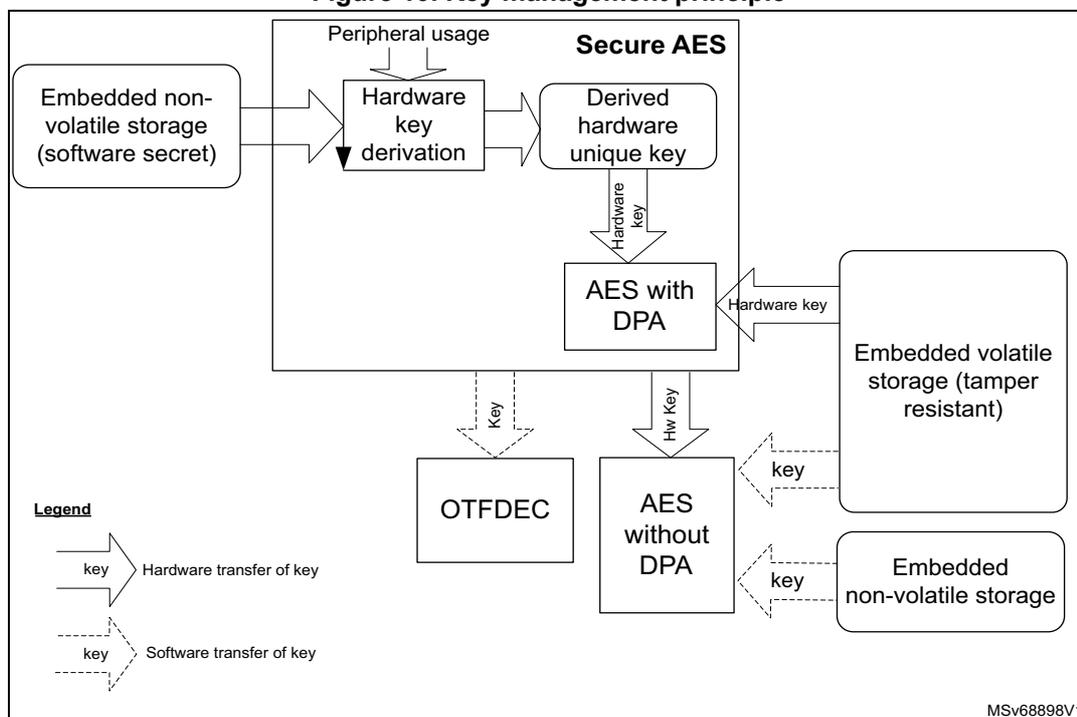
The diagram illustrates the key management principle. It shows the flow of keys between various components:
- Embedded non-volatile storage (software secret) provides input to Hardware key derivation .
- Peripheral usage also provides input to Hardware key derivation .
- Hardware key derivation outputs to Derived hardware unique key .
- Derived hardware unique key is used by Secure AES to generate a Hardware key .
- The Hardware key is used by AES with DPA .
- AES with DPA outputs a key to OTFDEC .
- AES with DPA also outputs a Hw key to AES without DPA .
- OTFDEC outputs a key to AES without DPA .
- AES without DPA outputs a key to Embedded volatile storage (tamper resistant) .
- AES without DPA also outputs a key to Embedded non-volatile storage .
Legend:
- Hardware transfer of key: Represented by a solid arrow with a key icon.
- Software transfer of key: Represented by a dashed arrow with a key icon.
MSV68898V1
Details on tamper protection is found in Section 3.8.3 , while TAMP TrustZone features are briefly described in Section 3.6.5 .
3.9.1 Hardware secret key management
As shown in the previous figure, the devices propose a better protection for application keys, using hardware secret keys. These AES keys can be made usable to the application, without exposing them in clear-text (unencrypted). Such keys also become immediately unusable in case of tamper.
There are three different sources of hardware secret keys:
- • DHUK: derived keys based on 256-bit nonvolatile device unique secret in flash memory. The flash memory provides value provisioned during product manufacturing (called RHUK). The generation of DHUK key takes into account the TrustZone state, the OBK-HDPLx (temporal isolation counter), the EPOCH (regression counter allowing antireplay protection) and key use state (KMOD).
- • BHK: 256-bit application key stored in tamper-resistant volatile storage in TAMP. This key is written at boot time, then read/write locked to the application until the next reset.
- • XORK: result of an XOR of BHK and DHUK
Those keys can be used in the following modes:
- • as a normal key, loading in write-only key registers (software key mode)
- • as an encryption/decryption key for another key, to be used in the DPA-resistant SAES (wrapped key mode)
- • as an encryption/decryption key for another key, to be used in a faster AES engine (shared key mode)
3.9.2 Unique ID
The devices store a 96-bit ID that is unique to each device (see Section 60.1: Unique device ID register (96 bits) ).
Application services can use this unique identity key to identify the product in the cloud network, or make it difficult for counterfeit devices or clones to inject untrusted data into the network.
Alternatively, the 256-bit device unique key (DHUK) can be used (see Section 3.9.1 ).
3.10 Crypto engines
The devices implement state-of-the-art cryptographic algorithms featuring key sizes and computing protection as recommended by national security agencies such as NIST for the U.S.A, BSI for Germany or ANSSI for France. Those algorithms are used to support privacy, authentication, integrity, entropy and identity attestation.
The embedded crypto engines reduce weaknesses on the implementation of critical cryptographic functions, preventing, for example, the use of weak cryptographic algorithms and key sizes. They also enable lower processing times and lower power consumption when performing cryptographic operations, offloading those computations from Cortex-M33. This is especially true for asymmetric cryptography.
For product certification purposes, ST can provide certified device information on how these security functions are implemented and validated.
For more information on crypto engine processing times, refer to their respective sections in the reference manual.
3.10.1 Crypto engines features
Table 19 lists the accelerated cryptographic operations available in the devices. Two AES accelerators are available (both can be reserved to secure application only).
Note: Additional operations can be added using firmware. The PKA can accelerate asymmetric crypto operations (like key pair generation, ECC scalar multiplication, point on curve check). See Section 36: Public key accelerator (PKA) for more details.
Table 19. Accelerated cryptographic operations
| Operations | Algorithm | Specification | Length of keys (in bit) | Modes |
|---|---|---|---|---|
| Get entropy | RNG | NIST SP800-90B (1) | N/A | Software and hardware (2) modes running in parallel |
| Encryption, decryption | AES | FIPS PUB 197 NIST SP800-38A | 128, 256 | ECB, CBC, CTR (3) |
| Authenticated encryption or decryption | NIST SP800-38C NIST SP800-38D | 128, 256 | GCM, CCM | |
| Cipher-based message authentication code | NIST SP800-38D | 128, 256 | GMAC | |
| Checksum | SHA-1 | FIPS PUB 180-4 | N/A | Digest 160-bit |
| Cryptographic hash | SHA-2 | - | SHA-224, SHA-256 SHA2-384, SHA2-512 | |
| Keyed-hashing for message authentication | HMAC | FIPS PUB 198-1 IETF RFC 2104 | Short, long (>64 bytes) | - |
| Encryption/decryption key-pair generation (4) | RSA | IETF RFC 8017 NIST SP800-56B | Up to 4160 | RSAES-OAEP |
| Signature (4) with hashing | RSA | IETF RFC 8017 FIPS PUB 186-4 | Up to 4160 | PKCS1-v1_5, PSS |
| Signature verification | ECDSA | ANSI X9.62 IETF RFC 7027 FIPS PUB 186-4 | Up to 640 | Refer to table 'Family of supported curves for ECC operations' in PKA section for details |
| Key agreement | ECDH | ANSI X9.42 |
- 1. Certifiable using STMicroelectronics reviewed documents.
- 2. Random numbers distribution to SAES and PKA using a dedicated hardware bus.
- 3. ECB and CBC chaining modes protected against side-channel and timing attacks in SAES (see Section 3.10.2 ).
- 4. Private key cryptography protected against side-channel and timing attacks.
Note: Binary curves, Edwards curves and Curve25519 are not supported by the PKA.
3.10.2 Secure AES co-processor (SAES)
The devices provide an additional on-chip hardware AES encryption and decryption engine, implementing countermeasures and mitigations against power and electromagnetic side-channel attacks.
Clocked by the system clock the SAES results in very good performance for a dpa resistant hardware accelerator. The SAES engine supports 128-bit or 256-bit key in electronic code book (ECB), cipher block chaining (CBC), (CTR), (GCM), (CCM), (GMAC) modes.
As shown in Section 3.9 , the SAES can be used for extra-secure on-chip storage for sensitive information. It can also be made secure-only.
For more information, refer to Section 34: Secure AES coprocessor (SAES) .
3.10.3 On-the-fly decryption engine (OTFDEC)
The OTFDEC TrustZone-aware peripheral proposes on-the-fly decryption of encrypted images stored on external flash memory, connected through the OCTOSPI. This decryption process introduces almost no additional cycle overhead when the standard NOR flash memory is used. The OTFDEC can also be used to encrypt flash memory images on the device (for example to encrypt with a device unique secret key).
When a tamper event is confirmed in TAMP, all OTFDEC keys are erased and encrypted regions are read as 0 until the OTFDEC is properly initialized again.
An OTFDEC typical use is detailed in Section 3.12.2 . For more details on the peripheral programming, refer to Section 37: On-the-fly decryption engine (OTFDEC) .
3.11 Product life cycle
A typical IoT device life cycle is summarized in Figure 11 . For each step, the devices propose secure life cycle management mechanisms embedded in the hardware.
Figure 11. Device life cycle security
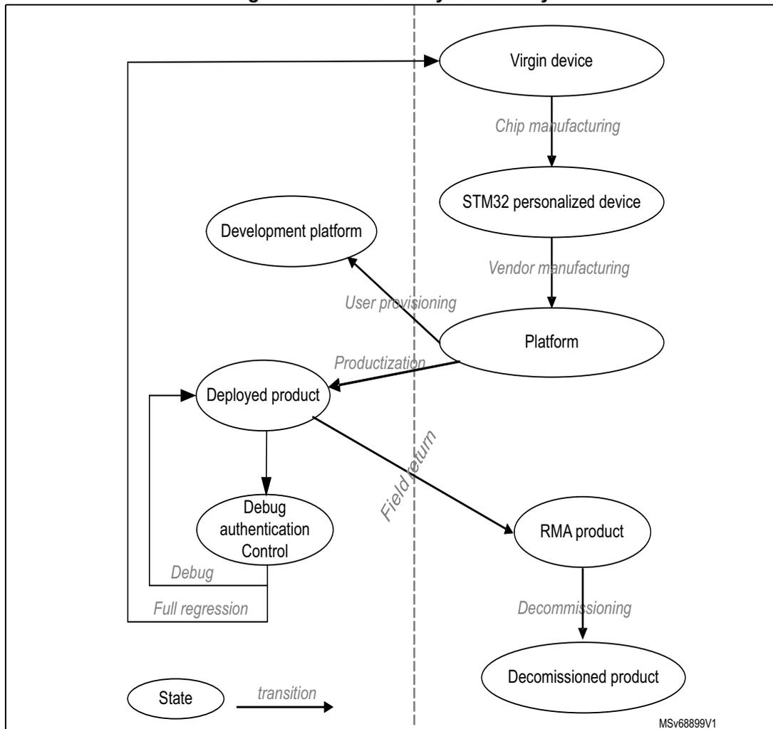
graph TD; subgraph Manufacturing; A([Virgin device]) -- "Chip manufacturing" --> B([STM32 personalized device]); B -- "Vendor manufacturing" --> C([Platform]); end; subgraph Development; C -- "User provisioning" --> D([Development platform]); C -- "Productization" --> E([Deployed product]); E -- "Debug" --> F([Debug authentication Control]); F -- "Full regression" --> E; end; subgraph Field; E -- "Field return" --> G([RMA product]); G -- "Decommissioning" --> H([Decommissioned product]); end; style A fill:none,stroke:none; style B fill:none,stroke:none; style C fill:none,stroke:none; style D fill:none,stroke:none; style E fill:none,stroke:none; style F fill:none,stroke:none; style G fill:none,stroke:none; style H fill:none,stroke:none;
The diagram illustrates the device life cycle security, divided into three main phases by vertical dashed lines: Manufacturing, Development, and Field. The states are represented by ovals, and transitions by arrows. Manufacturing includes Virgin device, STM32 personalized device, and Platform. Development includes Development platform, Deployed product, and Debug authentication Control. Field includes RMA product and Decommissioned product. Transitions include Chip manufacturing, Vendor manufacturing, User provisioning, Productization, Debug, Full regression, Field return, and Decommissioning. A legend at the bottom left shows an oval labeled 'State' and an arrow labeled 'transition'.
Additional details on the various phases and associated transitions, found either at the vendor or end-user premises, are summarized in Table 20 .
Table 20. Main product life cycle transitions
| Transitions | Description |
|---|---|
| Device manufacturing | ST creates new STM32 devices, always checking for manufacturing defects. During this process, the device is provisioned with ROM firmware, secure firmware install (SFI) unique key pair, and a public ID. |
| Vendor manufacturing | One (or more) vendor is responsible for the platform assembly, initialization, and provisioning before delivery to the end user. This end user can use the final product (“productization” transition) or he/she can use the platform for software development (“user provisioning” transition). |
| Productization | The end user gets a product ready for use. All security functions of the platform are enabled, the debugging/testing features are restricted/disabled, and unique boot entry to immutable code is enforced. |
| User provisioning | Platform vendor prepares an individual platform for development, not to be connected to a production cloud network. |
| Field return | The product is returned for analysis to field return centers. Analysis is possible by opening it partially, or by launching a partial or a full regression. Such accesses require provisioning, including certificates provided by the vendor. |
The features described hereafter contribute to secure the device life cycle.
3.11.1 Product configurations and security services
The product is provisioned with ST security services in system flash, but can be configured to let the full control of the boot chain to OEMs. This is done thanks to the unique boot entry (FLASH_OPTSR: BOOT_UBE) option byte, allowing to select between the security services (ST-iROT: ST immutable root of trust), or OEM boot implementation (OEM-iROT: OEM immutable root of trust) to be installed in the user part of the flash memory.
Security services are provisioned by ST in system flash (immutable). They provide the root of trust of the platform managing the verification and the update of the first updatable code (uROT).
3.11.2 Life cycle management
The product life cycle allows to control access to different assets (code and data) of the product, including during development, manufacturing, and after sales. It allows to provision the product with different distribution models, taking care of the code and data provisioned.
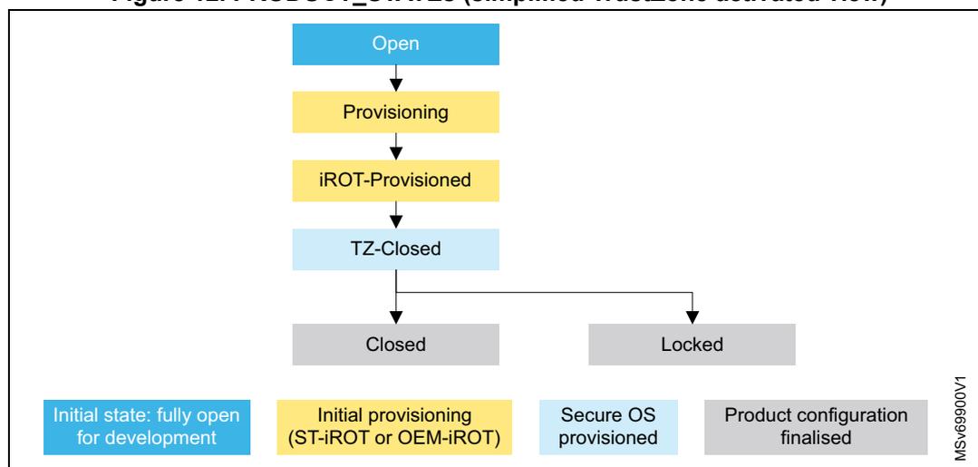
Table 21. Typical product life cycle phases
| PRODUCT_STATE + DebugState | Debug (default configuration) | Comments | |
|---|---|---|---|
| Open | Device open | Secure (1) and nonsecure | Allows to develop the product, as it provides the debug of the code. Boot address must target a secure area when TrustZone is enabled. Using the boot pin allows to launch the bootloader. Using boot pin and BOOT_UBE allows to launch user flash code through ST-iROT. |
| Provisioning | Debug partially opened (only nonsecure) | HDPL3 + Nonsecure only | Allows to manage the provisioning of the product (partial or full). It allows to launch secure firmware Install, or bootloader to provision the product. Boot address must target a secure area when TrustZone is enabled. Boot on SRAM is not permitted. |
| iROT-Provisioned | Debug partially opened (only nonsecure) | HDPL3 + Nonsecure only | Assumes that immutable root of trust is installed, including its configuration (code, option bytes, secure storage). Boot address must target a secure area when TrustZone is enabled. Boot on SRAM is not permitted. |
| TZ-Closed | Debug partially opened (only nonsecure) | HDPL3 + Nonsecure only | Assumes that the Secure OS is installed in TrustZone (this state exist only if TZEN = 0xB4). Debug is opened for nonsecure applications |
| Closed | Debug closed | NoDebug + debug authentication control | Assumes the product configuration as finalized. It allows to support debug authentication for in-the-field repair (read the dedicated application note). |
| Locked | Debug locked | None | Assumes the product configuration as finalized. The debug authentication is not permitted. The product is definitively in this state. |
| NS-Regression | Debug closed | NoDebug | This is a temporal (but nonvolatile) state to manage the partial regression to the TZ-Closed, removing all nonsecure code and data including in secure storage. |
| Regression | Debug closed | NoDebug | This is a temporal state (but nonvolatile) to manage the full regression to Open state, removing all user flash code and data including in secure storage (HDPL1 to HDPL3). |
| Debug Constrained | Debug opened following debug authentication permissions | Depends upon permissions | This is a temporal state (until power-on-reset) to manage debug based on the permissions acquired by the debug authentication protocol. |
- 1. Debug is not available when executing RSS code.
STMicroelectronics does not perform analysis on defective parts in closed or locked states.
The supported transitions, summarized in Figure 12 , can be requested (when available) through the debug interface or via the system bootloader.
Figure 12. PRODUCT_STATES (simplified TrustZone activated view)
graph TD; Open[Open] --> Provisioning[Provisioning]; Provisioning --> iROTP[iROT-Provisioned]; iROTP --> TZClosed[TZ-Closed]; TZClosed --> Closed[Closed]; TZClosed --> Locked[Locked];
The diagram illustrates the sequence of PRODUCT_STATES. It begins with 'Open' (Initial state: fully open for development), followed by 'Provisioning' (Initial provisioning (ST-iROT or OEM-iROT)), then 'iROT-Provisioned' (Secure OS provisioned), and 'TZ-Closed' (Secure OS provisioned). From 'TZ-Closed', the state can transition to either 'Closed' or 'Locked' (Product configuration finalised). A legend at the bottom identifies the color coding for each state: blue for the initial state, yellow for provisioning, light blue for secure OS provisioned, and grey for product configuration finalised. The identifier MSv69900V1 is present in the bottom right corner.
Figure 13. PRODUCT_STATES (full TrustZone activated view)
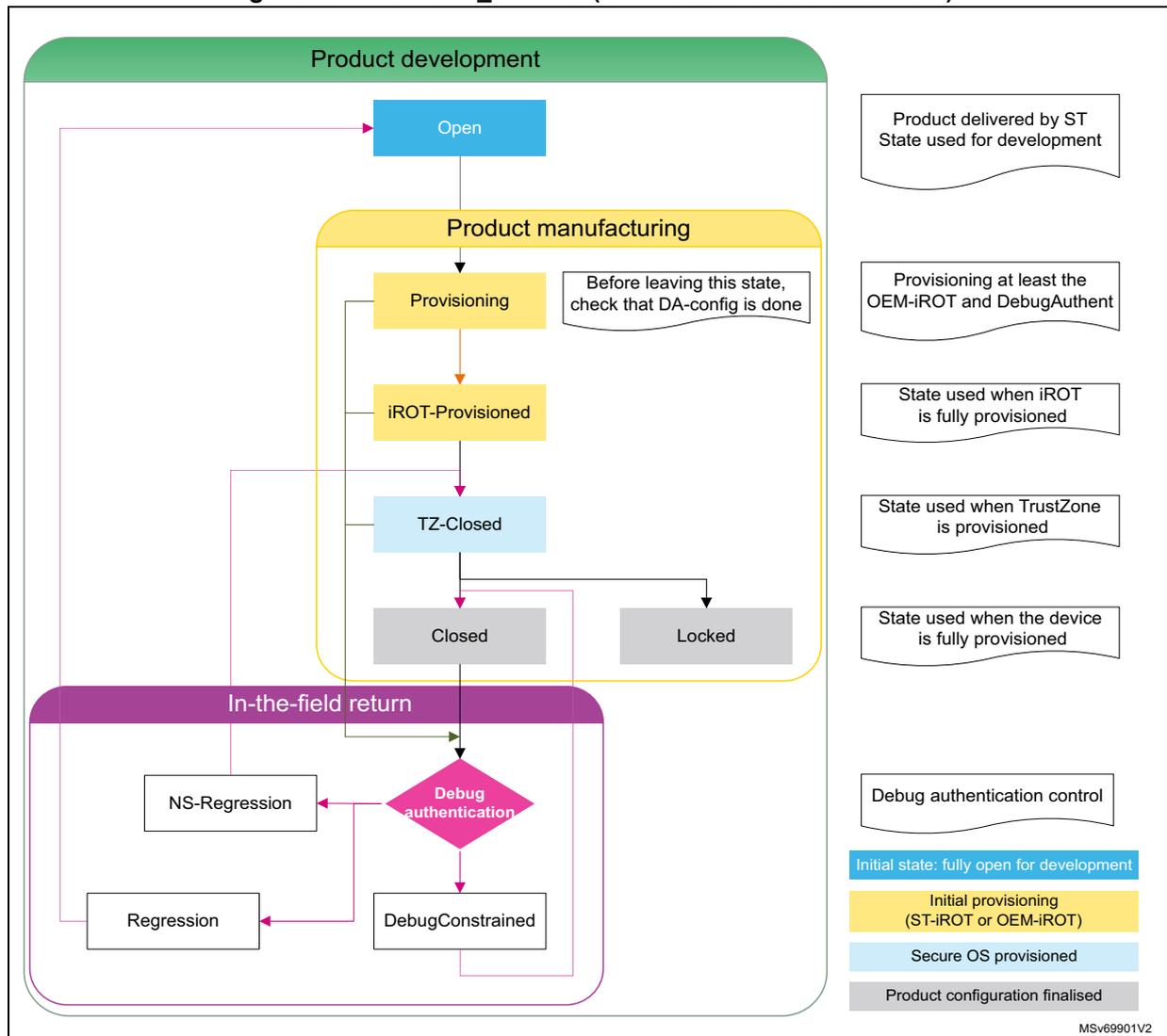
The diagram illustrates the product lifecycle states for a device with full TrustZone activated. It is divided into three main phases: Product development, Product manufacturing, and In-the-field return.
- Product development: The initial state is Open . A callout indicates this is the "Product delivered by ST State used for development".
- Product manufacturing:
This phase includes the states
Provisioning
,
iROT-Provisioned
,
TZ-Closed
,
Closed
, and
Locked
.
- Provisioning: A callout indicates "Before leaving this state, check that DA-config is done". Another callout states "Provisioning at least the OEM-iROT and DebugAuthent".
- iROT-Provisioned: A callout states "State used when iROT is fully provisioned".
- TZ-Closed: A callout states "State used when TrustZone is provisioned".
- Closed: A callout states "State used when the device is fully provisioned".
- Locked: This state is reached from TZ-Closed .
- In-the-field return:
This phase starts with
Debug authentication
(a decision diamond).
- If NS-Regression is selected, the flow goes to Regression .
- If DebugConstrained is selected, the flow goes to DebugConstrained .
- Both Regression and DebugConstrained lead back to the Open state in Product development.
Legend:
- Initial state: fully open for development (Open)
- Initial provisioning (ST-iROT or OEM-iROT) (Provisioning)
- Secure OS provisioned (TZ-Closed)
- Product configuration finalised (Closed)
Debug authentication control
MSv69901V2
The full view of the life cycle includes the debug authentication part, to help product maintenance to manage field returns (in-the-field centers). The debug authentication control is ensured thanks to a protocol based on Arm PSA ADAC specification. It allows controlling that the host has a trusted certificate with permissions. Permissions definition allows a lot of flexibility, in our default model we consider: Full or Partial regression, or to open the debug for nonsecure.
When TrustZone is disabled, the state TZ-Closed does not exist, and the debug authentication is based on a password authentication method. For details on the debug authentication feature, refer to the corresponding application note.
The protocol includes a “DISCOVER” command allowing to get basic informations of the target: manufacturer, product name, device identifier, protocol version supported and crypto scheme for authentication (this help selecting between certificates and password).
3.11.3 Recommended product settings
To ease the product maintenance (in-the-field), we recommend to take benefit of the feature called debug authentication control. This enables the maintenance of product activating the debug and makes possible to manage regressions while considering the security of the sensible information.
This implies the following actions:
- • set the PRODUCT_STATE in Closed state when the product has been configured
- • When debug authentication control is based on certificates (when TrustZone enabled), provision the OEM-PublicKey and the SOC-Mask . Setting the SOC-Mask to propose only the nonsecure-debug and partial and full regression guaranty to be compliant with the Arm PSA security model.
- • When debug authentication control is based on password (when TrustZone is disabled), only the HASH of the password must be provisioned.
A dedicated application note is available to help configuring the platform, the host tools and to generate certificates.
3.12 Software intellectual property protection and collaborative development
Thanks to software intellectual property protection and collaborative model, the devices allow the design of solutions integrating innovative third-party libraries.
Collaborative development is summarized in Figure 14 . Starting from a personalized device sold by STMicroelectronics, a vendor A can integrate a portion of hardware and software on a platform A, which can then be used by a vendor B, who does the same before deploying a final product to the end users.
Note: Each platform vendor can provision individual platforms for development not to be connected to a production cloud network (“Development Platform X”).
Figure 14. Collaborative development principle
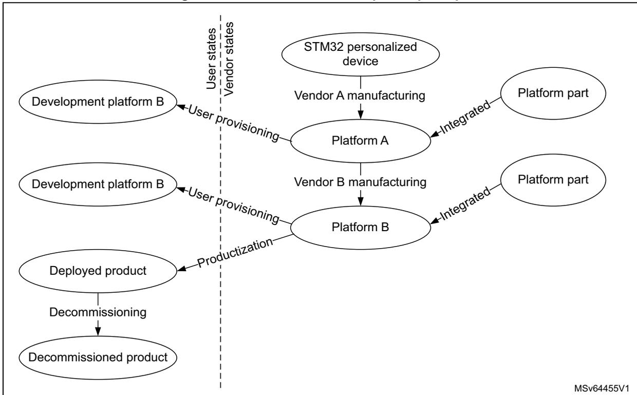
The diagram illustrates the collaborative development principle, divided into two vertical sections by a dashed line: 'User states' on the left and 'Vendor states' on the right. The flow starts in the Vendor states with 'STM32 personalized device', which leads to 'Platform A' via 'Vendor A manufacturing'. 'Platform A' is 'Integrated' with a 'Platform part' and receives 'User provisioning' from 'Development platform B' in the User states. 'Platform A' then leads to 'Platform B' via 'Vendor B manufacturing'. 'Platform B' is 'Integrated' with another 'Platform part' and receives 'User provisioning' from another 'Development platform B' in the User states. 'Platform B' leads to 'Deployed product' via 'Productization' in the User states. Finally, 'Deployed product' leads to 'Decommissioned product' via 'Decommissioning' in the User states. A label 'MSv64455V1' is present in the bottom right corner of the diagram area.
The features described hereafter contribute to securing the software intellectual property within such a collaborative development.
3.12.1 Software intellectual property protection
As described in Section 3.11.2 , the hardware PRODUCT_STATE mechanism automatically controls the accesses to secrets provisioned in the device. The protection of these secrets are defined in Table 22 .
Table 22. Software intellectual property protection with PRODUCT_STAT
| PRODUCT_STATE protection level | Secrets protection | |
|---|---|---|
| Open | Device open | No special protections. |
| Provisioning | Debug partially opened (only nonsecure) | All areas protected with HDPL1 cannot be dumped, debugged or traced. The iROT can setup a higher level of protection. |
| iROT-Provisioned | Debug partially opened (only nonsecure) | All areas protected with HDPL1 cannot be dumped, debugged or traced. The iROT can setup a higher level of protection. |
| TZ-Closed | Debug partially opened (only nonsecure) | All peripherals and memories mapped as secure during secure boot cannot be dumped, debugged or traced |
| Closed | No debug | No debug possible except through debug authentication. |
| Locked | No debug | All data and code stored in the device or encrypted in external flash memory cannot be dumped clear-text, debugged or traced. |
3.12.2 Software intellectual property protection with OTFDEC
As described in Section 3.10.3 , the OTFDEC associated with the OCTOSPI is able to decrypt on the fly, the encrypted images stored in external SPI flash memories.
Thanks to this feature, the devices allow the installation of intellectual properties, in one of the following ways:
- • over the air, with the image already encrypted with a key provisioned in the device
- • through a provisioning host located in a trusted or a non-trusted environment/facility
Figure 15 illustrates this last case, with the provisioning, in a non-trusted environment, of software intellectual properties both in the embedded flash memory and in an external SPI flash memory (encrypted).
Note: Since the OTFDEC uses the AES in counter mode (CTR) to achieve the lowest possible latency, each time the content of one encrypted region is changed, the corresponding cryptographic context (key or initialization vector) must be changed. This constraint makes OTFDEC suitable to decrypt read-only data or code, stored in external NOR flash memory.
Figure 15. External flash memory protection using SFI
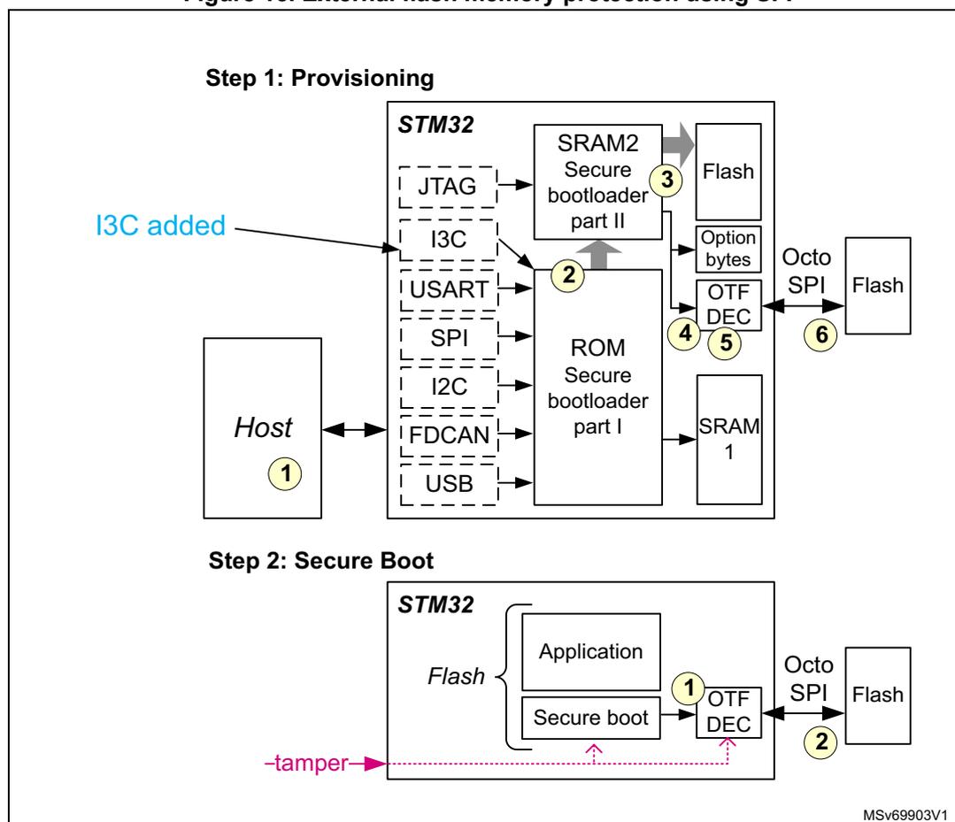
Step 1: Provisioning
The diagram shows a Host (1) connected to an STM32 microcontroller. The STM32 has several communication interfaces: JTAG, I3C (highlighted with a blue arrow labeled "I3C added"), USART, SPI, I2C, FDCAN, USB, and SRAM 1 (5). The STM32 contains SRAM2 (Secure bootloader part II) (3) and ROM (Secure bootloader part I) (2). The ROM is connected to the SRAM2. The SRAM2 is connected to the Flash (internal) and Option bytes. The Option bytes are connected to the OTFDEC (4). The OTFDEC is connected to an external Flash via Octo SPI (6). The Host (1) is connected to the STM32 via the I3C interface.
Step 2: Secure Boot
The diagram shows the STM32 microcontroller during secure boot. It contains an Application (1) and Secure boot (2) in Flash. The Secure boot is connected to the OTFDEC (1), which is connected to an external Flash via Octo SPI (2). A tamper signal is shown entering the STM32 from the left.
MSv69903V1
Provisioning
Assuming the device is virgin, the first step is to provision both flash memories, as detailed below:
- 1. The user creates a SFI image, composed of:
- – encrypted internal firmware and data (including external flash memory drivers)
- – encrypted external firmware and data AES key (up to 4)
- – encrypted external firmware and data image
- 2. The secure bootloader stored in the system memory, loads the second part of the secure bootloader in SRAM2, through the supported communication ports (USART, SPI, I2C, FDCAN, USB, I3C, and JTAG). This second part runs in the secure SRAM2 and is responsible for executing the SFI process, applying the SFI protocol thanks to the commands received through the above mentioned supported communication ports.
- 3. The internal flash memory is programmed with decrypted option bytes, internal firmware and data, and external firmware and data AES keys. Alternatively, device unique external firmware AES keys can be used instead of such global keys.
- 4. The OTFDEC is properly initialized with encrypted region information, including the corresponding external firmware and data AES key.
- 5. Running the SFI process, chunks of encrypted external firmware and data image are decrypted in the device, then re-encrypted in the OTFDEC.
- 6. After a chunk OTFDEC re-encryption, the user external flash memory programmer is responsible for programming the last encrypted chunks to the external SPI flash memories through the OCTOSPI.
Secure boot
After provisioning, each time the device initializes on a trusted firmware, the following actions are required:
- 1. Secure-boot firmware executes, programming the external firmware and data AES keys to the OTFDEC write-only key registers, along with the other needed information.
- 2. The application reads or executes the encrypted external firmware and data through the OCTOSPI in memory mapped mode, unless a tamper event is detected. In this case, all OTFDEC keys are erased and encrypted regions are read as 0 until the OTFDEC is properly initialized.
For more information on SFI solutions for the devices, refer to the AN4992 “ STM32 MCUs secure firmware install (SFI) overview ”.
3.12.3 Other software intellectual property protections
The device additional protections to software intellectual property are:
- • Invasive attacks such as physical tampering or perturbation are countered by detection then decommissioning of the device before the detected attack succeeds.
- • Noninvasive attacks, such as side channel attacks, are countered by not leaking secret information via side channels (such as timing, power, and EM emissions).