2. Memory and bus architecture
2.1 System architecture
The architecture relies on a Arm Cortex-M33 core optimized for execution thanks to an instruction cache having a direct access to the embedded flash memory.
This architecture also features a 32-bit multilayer AHB bus matrix with the interconnections detailed in Table 1 and Table 2 .
Table 1. Implementation of masters
| Master | Comments | STM32H523/533xx | STM32H562/563/573xx |
|---|---|---|---|
| Cortex-M33 Fast C-bus | Connecting Cortex-M33 (with Arm TrustZone® mainline and FPU) to the internal SRAMs and flash memory through ICACHE | X | X |
| Cortex-M33 Slow C-bus | Connecting Cortex-M33 (with Arm TrustZone mainline and FPU) to the external memories through ICACHE | X | X |
| Cortex-M33 S-bus | Connecting the Cortex-M33 (with Arm TrustZone mainline and FPU) to internal SRAMs without latency | 3 masters | |
| Connecting Cortex-M33 (with Arm TrustZone mainline and FPU) to the external memories through DCACHE | X | X | |
| GPDMA1 | - | 2 masters | |
| GPDMA2 | - | 2 masters | |
| SDMMC1 | - | X | X |
| SDMMC2 | - | - | X |
| Ethernet MAC | - | - | X (1) |
1. Not available on STM32H562xx devices.
Table 2. Implementation of slaves
| Slave | Comments | STM32H523/533xx | STM32H562/563/573xx |
|---|---|---|---|
| Flash memory | - | X | X |
| SRAM1 | - | X | X |
| SRAM2 | - | X | |
| SRAM3 | - | X | X |
| AHB1 | Peripherals and BKPSRAM including AHB to APB bridge, and APB peripherals (connected to APB1 and APB2) | X | X |
| AHB2 | Peripherals | X | X |
| FMC | - | X (1) | X |
| OCTOSPI1 | - | X | X |
Table 2. Implementation of slaves (continued)
| Slave | Comments | STM32H523/533xx | STM32H562/563/573xx |
|---|---|---|---|
| AHB3 | Including AHB to APB bridge, and APB peripherals (connected to APB3) | X | X |
| AHB4 | Peripherals | X | X |
1. STM32H523/533xx devices do not support SDRAM.
The bus matrix provides access from a master to a slave, enabling concurrent accesses and efficient operation even when several high-speed peripherals work simultaneously. This architecture is shown in Figure 1 .
Figure 1. System architecture
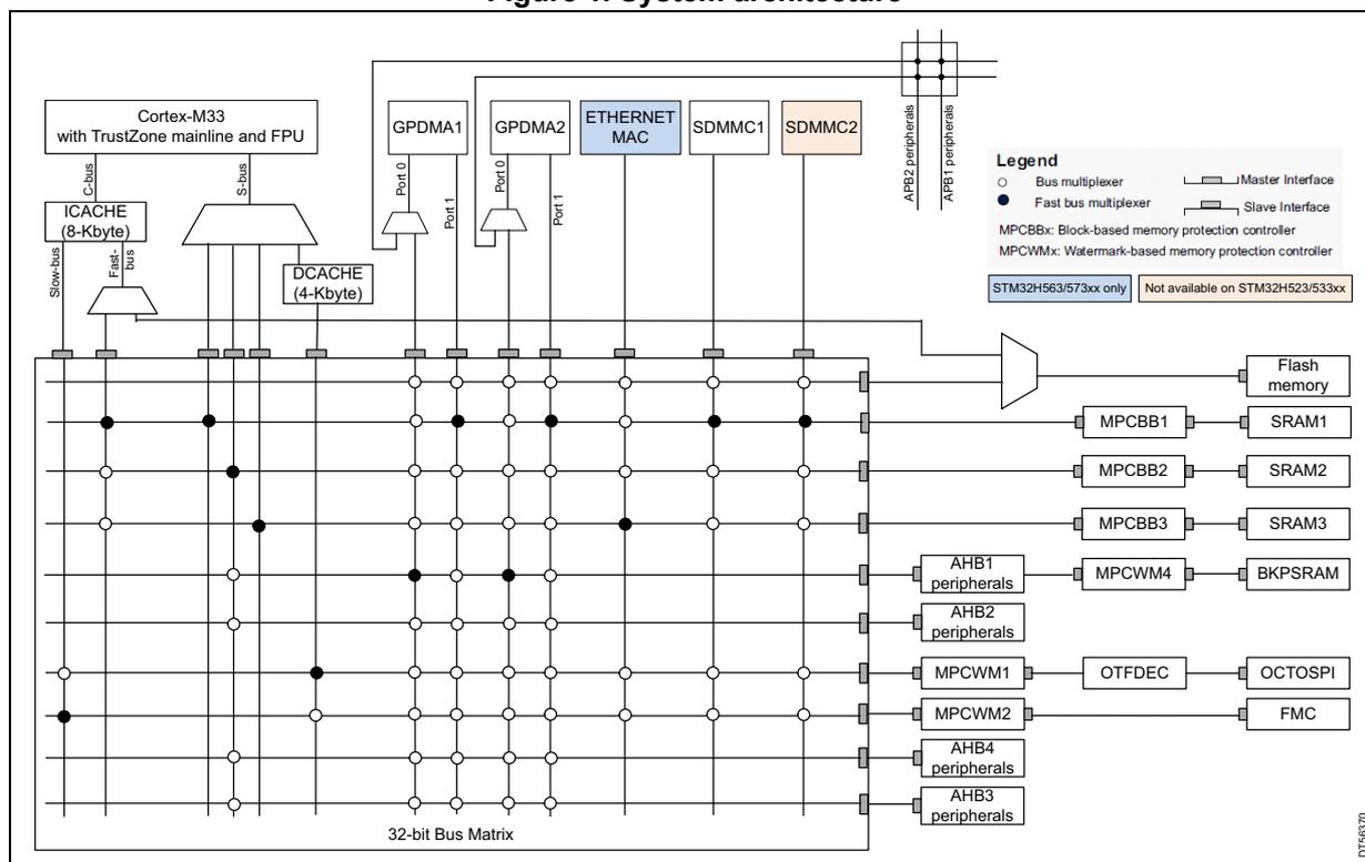
The diagram illustrates the system architecture of an STM32 microcontroller. At the top, the Cortex-M33 core with TrustZone mainline and FPU is connected to a 32-bit Bus Matrix via its C-bus and S-bus. The C-bus connects to the ICACHE (8-Kbyte) and the DCACHE (4-Kbyte). The DCACHE is connected to the Bus Matrix via a Fast Bus. The Bus Matrix is a grid of horizontal and vertical lines with switches (represented by dots) that allow masters to access slaves. Masters connected to the matrix include the Cortex-M33 core, GP DMA1, GP DMA2, ETHERNET MAC, SDMMC1, and SDMMC2. Slaves connected to the matrix include Flash memory, SRAM1, SRAM2, SRAM3, BKPSRAM, OCTOSPI, and FMC. The matrix also connects to various peripheral groups: AHB1 peripherals, AHB2 peripherals, AHB3 peripherals, and AHB4 peripherals. Some slaves are protected by memory protection controllers: MPCBB1, MPCBB2, MPCBB3, and MPCWM4. A legend indicates that open circles represent bus multiplexers and solid black dots represent fast bus multiplexers. It also shows symbols for master and slave interfaces. A note indicates that some features are available only on STM32H563/573xx and not on STM32H523/533xx.
2.1.1 Fast C-bus
This bus connects the C-bus of the Cortex-M33 core to the internal flash memory and to the BusMatrix via the instruction cache. This bus is used for instruction fetch and data access to the internal memories mapped in code region. This bus targets the internal flash memory and the internal SRAMs (SRAM1, SRAM2 and SRAM3).
SRAM1, SRAM2 and SRAM3 are accessible on this bus with a continuous mapping.
2.1.2 Slow C-bus
This bus connects the C-bus of the Cortex-M33 core to the BusMatrix via the instruction cache. This bus is used for instruction fetch and data access to the external memories mapped in code region. This bus targets the external memories (FMC and OCTOSPI).
2.1.3 S-bus
This bus connects the system bus of the Cortex-M33 core to the BusMatrix. This bus is used by the core to access data located in a peripheral or SRAM area. This bus targets the internal SRAMs (SRAM1, SRAM2, SRAM3, and BKPSRAM), the AHB1 peripherals including the APB1, APB2, AHB2, AHB3 and AHB4 peripherals.
SRAM1, SRAM2 and SRAM3 are accessible on this bus with a continuous mapping.
Note: The Bus Matrix has a zero latency when accessing SRAM1, SRAM2 and SRAM3.
2.1.4 DCache S-bus
This bus connects the system bus of the Cortex-M33 core to the BusMatrix via the data cache. This bus is used for instruction fetch and data access to the external memories mapped in data region. This bus targets the external memories (FMC and OCTOSPI).
Note: Fetching instructions through this bus is less efficient than fetching instructions through the slow C-bus.
2.1.5 GPDMA1 and GPDMA2 buses
These buses connect the four AHB master interfaces of the GPDMA1 and GPDMA2 to the BusMatrix. These buses target the internal flash memory, the internal SRAMs (SRAM1, SRAM2, SRAM3, and BKPSRAM), the AHB1 peripherals including the APB1 and APB2 peripherals, the AHB2 peripherals, the AHB3 peripherals, AHB4 peripherals and the external memories through FMC or OCTOSPI.
2.1.6 SDMMC1 and SDMMC2 (a) controllers DMA buses
These buses connect the SDMMC1 and SDMMC2 DMA master interfaces to the BusMatrix. They are used only by the SDMMC1 and SDMMC2 DMA to load/store data from/to the memory. These buses target the data memories: internal flash memory, internal SRAMs (SRAM1, SRAM2 and SRAM3), and external memories through FMC or OCTOSPI.
2.1.7 BusMatrix
The BusMatrix manages the access arbitration between masters. The arbitration uses a round-robin algorithm. This BusMatrix features a fast bus multiplexer used to connect each master to a given slave without latency (see Figure 1 ). For the same master, other slaves undergo a latency of at least one cycle at each new access.
a. SDMMC2 is not available on STM32H523/533xx devices.
2.1.8 AHB/APB bridges
The three AHB/APB bridges provide full synchronous connections between the AHB and the APB buses, allowing flexible selection of the peripheral frequency.
Refer to Section 2.3.2: Memory map and register boundary addresses for the address mapping of the peripherals connected to these bridges.
After each device reset, all peripheral clocks are disabled (except for the internal SRAMs and flash memory interfaces). Before using a peripheral, its clock must be enabled in the RCC_AHBxENR and RCC_APBxENR registers.
Note: When a 8- or 16-bit access is performed on an APB register, the access is transformed into a 32-bit access: the bridge duplicates the 8- or 16-bit data to feed the 32-bit vector.
2.1.9 Ethernet MAC (a)
The Ethernet MAC uses a 32-bit bus, connected to the AHB bus matrix. Through the system bus matrices, it can access the internal flash memory, the internal memories, and the external memories through the OCTOSPI and the FMC.
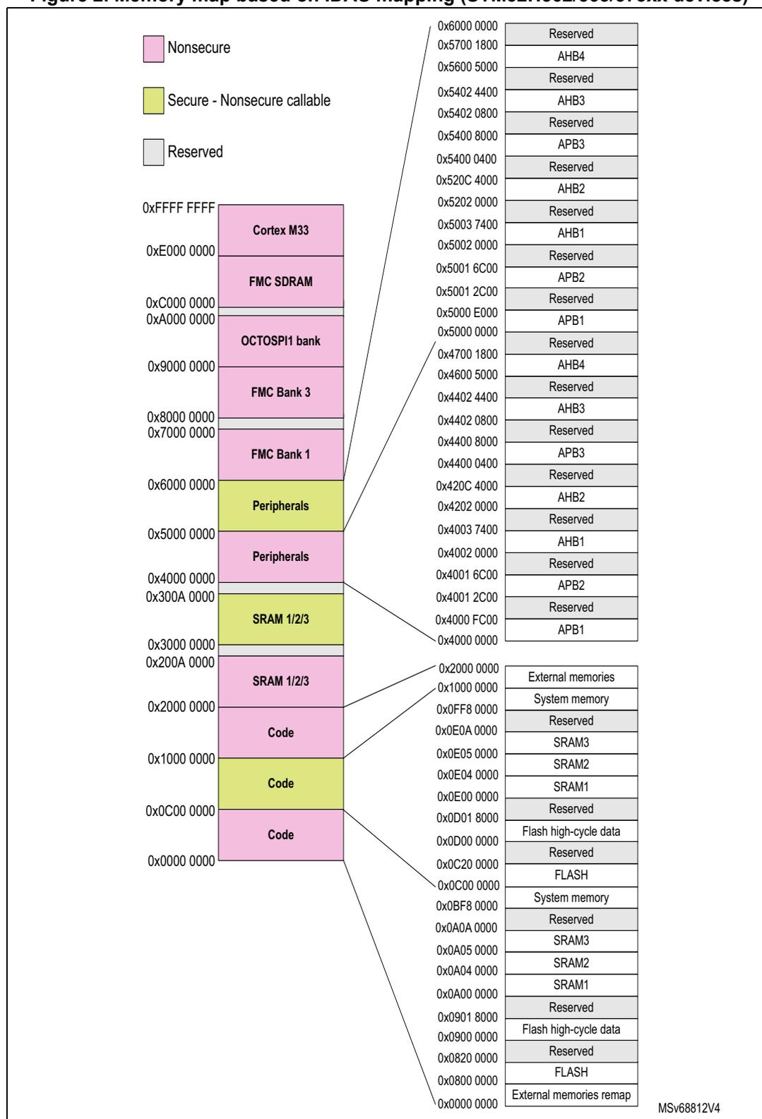
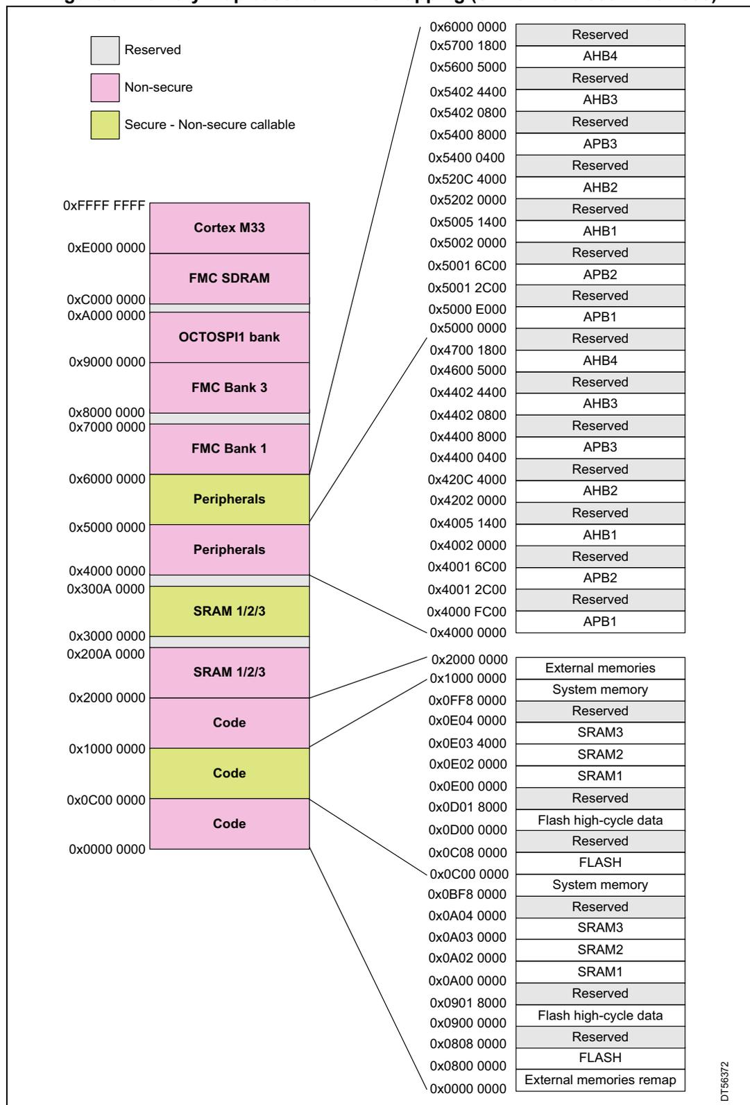
2.2 TrustZone security architecture
The security architecture is based on Arm TrustZone with the Armv8-M mainline extension.
The TrustZone security is activated by the TZEN option bit in the FLASH_OPTR register.
When the TrustZone is enabled, the SAU (security-attribution unit) and IDAU (implementation-defined-attribution unit) defines the access permissions based on secure and non-secure states.
- • SAU: Up to eight SAU configurable regions are available for security attribution.
- • IDAU: provides a first memory partition as non-secure or non-secure callable attributes. The IDAU memory map partition is not configurable, it is fixed by hardware implementation (refer to Figure 2: Memory map based on IDAU mapping (STM32H562/563/573xx devices) and Figure 3: Memory map based on IDAU mapping (STM32H523/533xx devices) ). It is then combined with the results from the SAU security attribution, and the higher security state is selected.
Based on IDAU security attribution, the flash memory, system SRAMs and peripherals memory spaces are aliased twice for secure and non-secure states. However, the external memories space is not aliased.
2.2.1 Default TrustZone security state
When the TrustZone security is activated by the TZEN option bit in the FLASH_OPTR, the default system security state is detailed below:
- • CPU:
- – Cortex-M33 is in secure state after reset. The boot address must be at a secure address.
- • Memory map:
a. Not available on STM32H523/533xx and STM32H562xx devices.
- – SAU is fully secure after reset. Consequently, all memory map is fully secure. Up to eight SAU configurable regions are available for security attribution.
- • Flash memory:
- – The flash memory security area is defined by watermark user options.
- – Block-based security attributions are non-secure after reset.
- • SRAMs:
- – All SRAMs are secure after reset. MPCBBx (block-based memory protection controller) are secure.
- • External memories:
- – FMC and OCTOSPI banks are secure after reset. MPCWMx (watermark-based memory protection controller) are secure.
- • Peripherals (see
Table 3
and
Table 4
for a list of securable and TrustZone-aware peripherals)
- – Securables peripherals are non-secure after reset.
- – TrustZone-aware peripherals are non-secure after reset. Their secure configuration registers are secure.
- • All GPIO are secure after reset.
- • Interrupts:
- – NVIC: All interrupts are secure after reset. NVIC is banked for secure and non-secure state.
- – TZIC: All illegal access interrupts are disabled after reset (see GTZC TrustZone system architecture ).
2.2.2 TrustZone peripheral classification
When the TrustZone security is active, a peripheral can be either securable or TrustZone-aware type as follows:
- • Securables: peripheral protected by an AHB/APB firewall gate that is controlled from TZSC controller to define security properties
- • TrustZone-aware: peripheral connected directly to AHB or APB bus and implementing a specific TrustZone behavior such as a subset of registers being secure.
Refer to GTZC TrustZone system architecture for more details.
The following tables list the securable and TrustZone-aware peripherals within the system.
Table 3. Securables peripherals by TZSC
| Bus | Peripheral | STM32H523/533xx | STM32H562/563/573xx |
|---|---|---|---|
| AHB4 | OCTOSPI | X | X |
| FMC | X | X | |
| SDMMC2 | - | X (1) | |
| SDMMC1 | X | X |
Table 3. Securables peripherals by TZSC (continued)
| Bus | Peripheral | STM32H523/533xx | STM32H562/563/573xx |
|---|---|---|---|
| AHB2 | PKA | X | X |
| SAES (2) | X | X | |
| RNG | X | X | |
| HASH | X | X | |
| AES (2) | X | X | |
| DCMI/PSSI | X | X | |
| ADC1 / ADC2 | X | X | |
| DAC 1 | X | X | |
| AHB1 | DCACHE registers | X | X |
| ICACHE registers | X | X | |
| ETHERNET | - | X (1) | |
| RAMCFG | X | X | |
| FMAC | - | X | |
| CORDIC | - | X | |
| CRC | X | X | |
| APB3 | VREFBUF | X | X |
| LPTIM1 | X | X | |
| LPTIM3 | - | X | |
| LPTIM4 | - | X | |
| LPTIM5 | - | X | |
| LPTIM6 | - | X | |
| I2C4 | - | X | |
| I2C3 | X | X | |
| LPUART1 | X | X | |
| SPI5 | - | X |
Table 3. Securable peripherals by TZSC (continued)
| Bus | Peripheral | STM32H523/533xx | STM32H562/563/573xx |
|---|---|---|---|
| APB2 | USB FS | X | X |
| SAI2 | - | X | |
| SAI1 | - | X | |
| SPI6 | - | X | |
| SPI4 | X | X | |
| TIM17 | - | X | |
| TIM16 | - | X | |
| TIM15 | X | X | |
| USART1 | X | X | |
| TIM8 | X | X | |
| SPI1 | X | X | |
| TIM1 | X | X |
Table 3. Securable peripherals by TZSC (continued)
| Bus | Peripheral | STM32H523/533xx | STM32H562/563/573xx |
|---|---|---|---|
| APB1 | UCPD | X | X |
| FDCAN2 | X | X (1) | |
| FDCAN1 | X | X | |
| LPTIM2 | X | X | |
| DTS | X | X | |
| UART12 | - | X | |
| UART9 | - | X | |
| UART8 | - | X | |
| UART7 | - | X | |
| HDMI-CEC | X | X | |
| USART11 | - | X | |
| USART10 | - | X | |
| USART6 | X | X | |
| CRS | X | X | |
| I3C1 | X | X | |
| I2C2 | X | X | |
| I2C1 | X | X | |
| UART5 | X | X | |
| UART4 | X | X | |
| USART3 | X | X | |
| USART2 | X | X | |
| SPI3/I2S3 | X | X | |
| SPI2/I2S2 | X | X | |
| IWDG | X | X | |
| WWDG | X | X | |
| TIM14 | - | X | |
| TIM13 | - | X | |
| TIM12 | X | X | |
| TIM7 | X | X | |
| TIM6 | X | X | |
| TIM5 | X | X | |
| TIM4 | X | X | |
| TIM3 | X | X | |
| TIM2 | X | X |
1. Not available on STM32H562xx devices.
- 2. Available only on devices with cryptography (STM32H533/573xx)
Table 4. TrustZone-aware peripherals
| Bus | Peripheral | STM32H523/533xx | STM32H562/563/573xx |
|---|---|---|---|
| AHB4 | OTFDEC1 | X | X |
| AHB3 | EXTI | X | X |
| RCC | X | X | |
| PWR | X | X | |
| AHB2 | GPIOI | - | X |
| GPIOH | X | X | |
| GPIOG | X | X | |
| GPIOF | X | X | |
| GPIOE | X | X | |
| GPIO D | X | X | |
| GPIO C | X | X | |
| GPIO B | X | X | |
| GPIO A | X | X | |
| AHB1 | GTZC | X | X |
| DCACHE | X | X | |
| ICACHE | X | X | |
| FLASH | X | X | |
| GPDMA2 | X | X | |
| GPDMA1 | X | X | |
| APB3 | TAMP | X | X |
| RTC | X | X | |
| SBS | X | X |
2.3 Memory organization
2.3.1 Introduction
Program memory, data memory, registers and I/O ports are organized within the same linear address space.
The bytes are coded in memory in Little Endian format. The lowest numbered byte in a word is considered the word's least significant byte and the highest numbered byte the most significant.
2.3.2 Memory map and register boundary addresses
Figure 2. Memory map based on IDAU mapping (STM32H562/563/573xx devices)
Legend:
- Nonsecure (Pink)
- Secure - Nonsecure callable (Yellow)
- Reserved (Grey)
Memory Map:
| Address Range | Memory Region | Security Status |
|---|---|---|
| 0x0000 0000 - 0x00800 0000 | External memories remap | Nonsecure |
| 0x00800 0000 - 0x00820 0000 | FLASH | Nonsecure |
| 0x00820 0000 - 0x00900 0000 | Reserved | Reserved |
| 0x00900 0000 - 0x00901 8000 | Flash high-cycle data | Nonsecure |
| 0x00901 8000 - 0x00A00 0000 | Reserved | Reserved |
| 0x00A00 0000 - 0x00A04 0000 | SRAM1 | Nonsecure |
| 0x00A04 0000 - 0x00A05 0000 | SRAM2 | Nonsecure |
| 0x00A05 0000 - 0x00A0A 0000 | SRAM3 | Nonsecure |
| 0x00A0A 0000 - 0x00BF8 0000 | Reserved | Reserved |
| 0x00BF8 0000 - 0x00C00 0000 | System memory | Nonsecure |
| 0x00C00 0000 - 0x00C20 0000 | FLASH | Nonsecure |
| 0x00C20 0000 - 0x00D00 0000 | Reserved | Reserved |
| 0x00D00 0000 - 0x00D01 8000 | Flash high-cycle data | Nonsecure |
| 0x00D01 8000 - 0x00E00 0000 | Reserved | Reserved |
| 0x00E00 0000 - 0x00E04 0000 | SRAM1 | Nonsecure |
| 0x00E04 0000 - 0x00E05 0000 | SRAM2 | Nonsecure |
| 0x00E05 0000 - 0x00E0A 0000 | SRAM3 | Nonsecure |
| 0x00E0A 0000 - 0x00FF8 0000 | Reserved | Reserved |
| 0x00FF8 0000 - 0x01000 0000 | System memory | Nonsecure |
| 0x01000 0000 - 0x01000 0000 | External memories | Nonsecure |
| 0x0000 0000 - 0x00C00 0000 | Code | Nonsecure |
| 0x00C00 0000 - 0x01000 0000 | Code | Secure - Nonsecure callable |
| 0x01000 0000 - 0x02000 0000 | Code | Nonsecure |
| 0x02000 0000 - 0x0200A 0000 | SRAM 1/2/3 | Nonsecure |
| 0x0200A 0000 - 0x0300A 0000 | SRAM 1/2/3 | Secure - Nonsecure callable |
| 0x0300A 0000 - 0x04000 0000 | Peripherals | Nonsecure |
| 0x04000 0000 - 0x05000 0000 | Peripherals | Nonsecure |
| 0x05000 0000 - 0x06000 0000 | Peripherals | Secure - Nonsecure callable |
| 0x06000 0000 - 0x07000 0000 | FMC Bank 1 | Nonsecure |
| 0x07000 0000 - 0x08000 0000 | FMC Bank 3 | Nonsecure |
| 0x08000 0000 - 0x09000 0000 | OCTOSPI1 bank | Nonsecure |
| 0x09000 0000 - 0x0A000 0000 | FMC SDRAM | Nonsecure |
| 0x0A000 0000 - 0x0C000 0000 | Cortex M33 | Nonsecure |
| 0x0C000 0000 - 0xE000 0000 | Cortex M33 | Nonsecure |
| 0xE000 0000 - 0xFFFF FFFF | Cortex M33 | Nonsecure |
Peripheral Address Map:
| Address Range | Peripheral |
|---|---|
| 0x0000 0000 - 0x00800 0000 | External memories remap |
| 0x00800 0000 - 0x00820 0000 | FLASH |
| 0x00820 0000 - 0x00900 0000 | Reserved |
| 0x00900 0000 - 0x00901 8000 | Flash high-cycle data |
| 0x00901 8000 - 0x00A00 0000 | Reserved |
| 0x00A00 0000 - 0x00A04 0000 | SRAM1 |
| 0x00A04 0000 - 0x00A05 0000 | SRAM2 |
| 0x00A05 0000 - 0x00A0A 0000 | SRAM3 |
| 0x00A0A 0000 - 0x00BF8 0000 | Reserved |
| 0x00BF8 0000 - 0x00C00 0000 | System memory |
| 0x00C00 0000 - 0x00C20 0000 | FLASH |
| 0x00C20 0000 - 0x00D00 0000 | Reserved |
| 0x00D00 0000 - 0x00D01 8000 | Flash high-cycle data |
| 0x00D01 8000 - 0x00E00 0000 | Reserved |
| 0x00E00 0000 - 0x00E04 0000 | SRAM1 |
| 0x00E04 0000 - 0x00E05 0000 | SRAM2 |
| 0x00E05 0000 - 0x00E0A 0000 | SRAM3 |
| 0x00E0A 0000 - 0x00FF8 0000 | Reserved |
| 0x00FF8 0000 - 0x01000 0000 | System memory |
| 0x01000 0000 - 0x01000 0000 | External memories |
| 0x4000 0000 - 0x4000 0000 | APB1 |
| 0x4000 FC00 - 0x4001 2C00 | Reserved |
| 0x4001 2C00 - 0x4001 6C00 | APB2 |
| 0x4001 6C00 - 0x4002 0000 | Reserved |
| 0x4002 0000 - 0x4003 7400 | AHB1 |
| 0x4003 7400 - 0x4020 C400 | Reserved |
| 0x4020 C400 - 0x4022 0000 | AHB2 |
| 0x4022 0000 - 0x4040 0400 | Reserved |
| 0x4040 0400 - 0x4040 8000 | APB3 |
| 0x4040 8000 - 0x4042 0800 | Reserved |
| 0x4042 0800 - 0x4042 4400 | AHB3 |
| 0x4042 4400 - 0x4060 5000 | Reserved |
| 0x4060 5000 - 0x4070 1800 | AHB4 |
| 0x4070 1800 - 0x4700 0000 | Reserved |
| 0x5000 0000 - 0x5000 0000 | APB1 |
| 0x5000 E000 - 0x5001 2C00 | Reserved |
| 0x5001 2C00 - 0x5001 6C00 | APB2 |
| 0x5001 6C00 - 0x5002 0000 | Reserved |
| 0x5002 0000 - 0x5003 7400 | AHB1 |
| 0x5003 7400 - 0x5202 0000 | Reserved |
| 0x5202 0000 - 0x520C 4000 | AHB2 |
| 0x520C 4000 - 0x5400 0400 | Reserved |
| 0x5400 0400 - 0x5400 8000 | APB3 |
| 0x5400 8000 - 0x5402 0800 | Reserved |
| 0x5402 0800 - 0x5402 4400 | AHB3 |
| 0x5402 4400 - 0x5600 5000 | Reserved |
| 0x5600 5000 - 0x5700 1800 | AHB4 |
| 0x5700 1800 - 0x6000 0000 | Reserved |
MSv68812V4
Figure 3. Memory map based on IDAU mapping (STM32H523/533xx devices)
Legend:
- Reserved (Grey)
- Non-secure (Pink)
- Secure - Non-secure callable (Green)
Memory Map:
| Address Range | Memory Type |
|---|---|
| 0x0000 0000 - 0x0000 0000 | External memories remap |
| 0x0000 0000 - 0x0800 0000 | FLASH |
| 0x0800 0000 - 0x0900 0000 | Reserved |
| 0x0900 0000 - 0x0901 8000 | Flash high-cycle data |
| 0x0901 8000 - 0x0A00 0000 | Reserved |
| 0x0A00 0000 - 0x0A02 0000 | SRAM1 |
| 0x0A02 0000 - 0x0A03 0000 | SRAM2 |
| 0x0A03 0000 - 0x0A04 0000 | SRAM3 |
| 0x0A04 0000 - 0x0BF8 0000 | Reserved |
| 0x0BF8 0000 - 0x0C00 0000 | System memory |
| 0x0C00 0000 - 0x0C08 0000 | FLASH |
| 0x0C08 0000 - 0x0D00 0000 | Reserved |
| 0x0D00 0000 - 0x0D01 8000 | Flash high-cycle data |
| 0x0D01 8000 - 0x0E00 0000 | Reserved |
| 0x0E00 0000 - 0x0E02 0000 | SRAM1 |
| 0x0E02 0000 - 0x0E03 4000 | SRAM2 |
| 0x0E03 4000 - 0x0E04 0000 | SRAM3 |
| 0x0E04 0000 - 0x0FF8 0000 | Reserved |
| 0x0FF8 0000 - 0x1000 0000 | System memory |
| 0x1000 0000 - 0x2000 0000 | External memories |
| 0x2000 0000 - 0x4000 0000 | APB1 |
| 0x4000 0000 - 0x4001 2C00 | Reserved |
| 0x4001 2C00 - 0x4001 6C00 | APB2 |
| 0x4001 6C00 - 0x4002 0000 | Reserved |
| 0x4002 0000 - 0x4005 1400 | AHB1 |
| 0x4005 1400 - 0x4202 0000 | Reserved |
| 0x4202 0000 - 0x420C 4000 | AHB2 |
| 0x420C 4000 - 0x4400 0400 | Reserved |
| 0x4400 0400 - 0x4400 8000 | APB3 |
| 0x4400 8000 - 0x4402 0800 | Reserved |
| 0x4402 0800 - 0x4402 4400 | AHB3 |
| 0x4402 4400 - 0x4600 5000 | Reserved |
| 0x4600 5000 - 0x4700 1800 | AHB4 |
| 0x4700 1800 - 0x5000 0000 | Reserved |
| 0x5000 0000 - 0x5001 E000 | APB1 |
| 0x5001 E000 - 0x5001 2C00 | Reserved |
| 0x5001 2C00 - 0x5001 6C00 | APB2 |
| 0x5001 6C00 - 0x5002 0000 | Reserved |
| 0x5002 0000 - 0x5005 1400 | AHB1 |
| 0x5005 1400 - 0x5202 0000 | Reserved |
| 0x5202 0000 - 0x520C 4000 | AHB2 |
| 0x520C 4000 - 0x5400 0400 | Reserved |
| 0x5400 0400 - 0x5400 8000 | APB3 |
| 0x5400 8000 - 0x5402 0800 | Reserved |
| 0x5402 0800 - 0x5402 4400 | AHB3 |
| 0x5402 4400 - 0x5600 5000 | Reserved |
| 0x5600 5000 - 0x5700 1800 | AHB4 |
| 0x5700 1800 - 0x6000 0000 | Reserved |
Left Column Memory Map:
| Address Range | Memory Type |
|---|---|
| 0x0000 0000 - 0x0C00 0000 | Code |
| 0x0C00 0000 - 0x1000 0000 | Code |
| 0x1000 0000 - 0x2000 0000 | Code |
| 0x2000 0000 - 0x200A 0000 | SRAM 1/2/3 |
| 0x200A 0000 - 0x3000 0000 | SRAM 1/2/3 |
| 0x3000 0000 - 0x4000 0000 | Peripherals |
| 0x4000 0000 - 0x5000 0000 | Peripherals |
| 0x5000 0000 - 0x6000 0000 | Peripherals |
| 0x6000 0000 - 0x7000 0000 | FMC Bank 1 |
| 0x7000 0000 - 0x8000 0000 | FMC Bank 3 |
| 0x8000 0000 - 0x9000 0000 | OCTOSPI1 bank |
| 0x9000 0000 - 0xA000 0000 | FMC SDRAM |
| 0xA000 0000 - 0xE000 0000 | Cortex M33 |
| 0xE000 0000 - 0xFFFF FFFF | Cortex M33 |
DT56372
All the memory map areas not allocated to on-chip memories and peripherals are reserved.
Table 5
and
Table 6
give the boundary addresses of the available peripherals.
Table 5. Memory map and peripheral register addresses (STM32H562/563/573xx)
| Bus | Secure boundary address | Non-secure boundary address | Peripheral | Register map |
|---|---|---|---|---|
| AHB4 | 0x5700 1800 - 0x57FF FFFF | 0x4700 1800 - 0x47FF FFFF | Reserved | - |
| 0x5700 1400 - 0x5700 17FF | 0x4700 1400 - 0x4700 17FF | OCTOSPI1 | OCTOSPI | |
| 0x5700 0800 - 0x5700 13FF | 0x4700 0800 - 0x4700 13FF | Reserved | - | |
| 0x5700 0400 - 0x5700 07FF | 0x4700 0400 - 0x4700 07FF | FMC | FMC | |
| 0x5600 F800 - 0x5700 03FF | 0x4600 F800 - 0x4700 03FF | Reserved | - | |
| 0x5600 F000 - 0x5600 F3FF | 0x4600 F000 - 0x4600 F3FF | DLYBOS1 | DLYB | |
| 0x5600 9000 - 0x5600 EFFF | 0x4600 9000 - 0x4600 EFFF | Reserved | - | |
| 0x5600 8C00 - 0x5600 8FFF | 0x4600 8C00 - 0x4600 8FFF | SDMMC2 (1) | SDMMC | |
| 0x5600 8800 - 0x5600 8BFF | 0x4600 8800 - 0x4600 8BFF | DLYBSD2 | DLYB | |
| 0x5600 8400 - 0x5600 87FF | 0x4600 8400 - 0x4600 87FF | DLYBSD1 | ||
| 0x5600 8000 - 0x5600 83FF | 0x4600 8000 - 0x4600 83FF | SDMMC1 | SDMMC | |
| 0x5600 5400 - 0x5600 7FFF | 0x4600 5400 - 0x4600 7FFF | Reserved | - | |
| 0x5600 5000 - 0x5600 53FF | 0x4600 5000 - 0x4600 53FF | OTFDEC1 | OTFDEC | |
| 0x5600 0000 - 0x5600 4FFF | 0x4600 0000 - 0x4600 4FFF | Reserved | - | |
| AHB3 | 0x5402 4400 - 0x54FF FFFF | 0x4402 4400 - 0x44FF FFFF | Reserved | - |
| 0x5402 4000 - 0x5402 43FF | 0x4402 4000 - 0x4402 43FF | DEBUG | DEBUG | |
| 0x5402 3000 - 0x5402 3FFF | 0x4402 3000 - 0x4402 3FFF | Reserved | - | |
| 0x5402 2000 - 0x5402 23FF | 0x4402 2000 - 0x4402 23FF | EXTI | EXTI | |
| 0x5402 1000 - 0x5402 1FFF | 0x4402 1000 - 0x4402 1FFF | Reserved | - | |
| 0x5402 0C00 - 0x5402 0FFF | 0x4402 0C00 - 0x4402 0FFF | RCC | RCC | |
| 0x5402 0800 - 0x5402 0BFF | 0x4402 0800 - 0x4402 0BFF | PWR | PWR | |
| 0x5402 0000 - 0x5402 07FF | 0x4402 0000 - 0x4402 07FF | Reserved | - | |
| APB3 | 0x5400 8000 - 0x5400 FFFF | 0x4400 8000 - 0x4400 FFFF | Reserved | - |
| 0x5400 7C00 - 0x5400 7FFF | 0x4400 7C00 - 0x4400 7FFF | TAMP | TAMP | |
| 0x5400 7800 - 0x5400 7BFF | 0x4400 7800 - 0x4400 7BFF | RTC | RTC | |
| 0x5400 7400 - 0x5400 77FF | 0x4400 7400 - 0x4400 77FF | VREFBUF | VREFBUF | |
| 0x5400 5800 - 0x5400 73FF | 0x4400 5800 - 0x4400 73FF | Reserved | - |
Table 5. Memory map and peripheral register addresses (STM32H562/563/573xx) (continued)
| Bus | Secure boundary address | Non-secure boundary address | Peripheral | Register map |
|---|---|---|---|---|
| APB3 (continued) | 0x5400 5400 - 0x5400 57FF | 0x4400 5400 - 0x4400 57FF | LPTIM6 | LPTIM |
| 0x5400 5000 - 0x5400 53FF | 0x4400 5000 - 0x4400 53FF | LPTIM5 | ||
| 0x5400 4C00 - 0x5400 4FFF | 0x4400 4C00 - 0x4400 4FFF | LPTIM4 | ||
| 0x5400 4800 - 0x5400 4BFF | 0x4400 4800 - 0x4400 4BFF | LPTIM3 | ||
| 0x5400 4400 - 0x5400 47FF | 0x4400 4400 - 0x4400 47FF | LPTIM1 | ||
| 0x5400 3000 - 0x5400 43FF | 0x4400 3000 - 0x4400 43FF | Reserved | - | |
| 0x5400 2C00 - 0x5400 2FFF | 0x4400 2C00 - 0x4400 2FFF | I2C4 | I2C | |
| 0x5400 2800 - 0x5400 2BFF | 0x4400 2800 - 0x4400 2BFF | I2C3 | ||
| 0x5400 2400 - 0x5400 27FF | 0x4400 2400 - 0x4400 27FF | LPUART1 | LPUART | |
| 0x5400 2000 - 0x5400 23FF | 0x4400 2000 - 0x4400 23FF | SPI5 | SPI | |
| 0x5400 0800 - 0x5400 1FFF | 0x4400 0800 - 0x4400 1FFF | Reserved | - | |
| 0x5400 0400 - 0x5400 07FF | 0x4400 0400 - 0x4400 07FF | SBS | SBS | |
| AHB2 | 0x5400 0000 - 0x5400 03FF | 0x4400 0000 - 0x4400 03FF | Reserved | - |
| 0x520C 4000 - 0x53FF FFFF | 0x420C 4000 - 0x43FF FFFF | Reserved | - | |
| 0x520C 2000 - 0x520C 3FFF | 0x420C 2000 - 0x420C 3FFF | PKA +RAM | PKA | |
| 0x520C 1000 - 0x520C 1FFF | 0x420C 1000 - 0x420C 1FFF | Reserved | - | |
| 0x520C 0C00 - 0x520C 0FFF | 0x420C 0C00 - 0x420C 0FFF | SAES | SAES | |
| 0x520C 0800 - 0x520C 0BFF | 0x420C 0800 - 0x420C 0BFF | RNG | RNG | |
| 0x520C 0400 - 0x520C 07FF | 0x420C 0400 - 0x420C 07FF | HASH | HASH | |
| 0x520C 0000 - 0x520C 03FF | 0x420C 0000 - 0x420C 03FF | AES | AES | |
| 0x5202 C800 - 0x520B FFFF | 0x4202 C800 - 0x420B FFFF | Reserved | - | |
| 0x5202 C400 - 0x5202 C7FF | 0x4202 C400 - 0x4202 C7FF | PSSI | PSSI | |
| 0x5202 C000 - 0x5202 C3FF | 0x4202 C000 - 0x4202 C3FF | DCMI | DCMI | |
| 0x5202 8800 - 0x5202 BFFF | 0x4202 8800 - 0x4202 BFFF | Reserved | - | |
| 0x5202 8400 - 0x5202 87FF | 0x4202 8400 - 0x4202 87FF | DAC1 | DAC | |
| 0x5202 8000 - 0x5202 83FF | 0x4202 8000 - 0x4202 83FF | ADC1 / ADC2 | ADC | |
| 0x5202 2400 - 0x5202 7FFF | 0x4202 2400 - 0x4202 7FFF | Reserved | - |
Table 5. Memory map and peripheral register addresses (STM32H562/563/573xx) (continued)
| Bus | Secure boundary address | Non-secure boundary address | Peripheral | Register map |
|---|---|---|---|---|
| AHB2 (continued) | 0x5202 2000 - 0x5202 23FF | 0x4202 2000 - 0x4202 23FF | GPIOI | GPIO |
| 0x5202 1C00 - 0x5202 1FFF | 0x4202 1C00 - 0x4202 1FFF | GPIOH | ||
| 0x5202 1800 - 0x5202 1BFF | 0x4202 1800 - 0x4202 1BFF | GPIOG | ||
| 0x5202 1400 - 0x5202 17FF | 0x4202 1400 - 0x4202 17FF | GPIOF | ||
| 0x5202 1000 - 0x5202 13FF | 0x4202 1000 - 0x4202 13FF | GPIOE | ||
| 0x5202 0C00 - 0x5202 0FFF | 0x4202 0C00 - 0x4202 0FFF | GPIO_D | ||
| 0x5202 0800 - 0x5202 0BFF | 0x4202 0800 - 0x4202 0BFF | GPIOC | ||
| 0x5202 0400 - 0x5202 07FF | 0x4202 0400 - 0x4202 07FF | GPIOB | ||
| 0x5202 0000 - 0x5202 03FF | 0x4202 0000 - 0x4202 03FF | GPIOA | ||
| AHB1 | 0x5003 7400 - 0x51FF FFFF | 0x4003 7400 - 0x41FF FFFF | Reserved | - |
| 0x5003 6400 - 0x5003 73FF | 0x4003 6400 - 0x4003 73FF | MPC_WM_BKPRAM | GTZC1 TZSC | |
| 0x5003 3800 - 0x5003 63FF | 0x4003 3C00 - 0x4003 63FF | Reserved | - | |
| 0x5003 2400 - 0x5003 37FF | 0x4003 2400 - 0x4003 37FF | GTZC1 | GTZC1 | |
| 0x5003 1800 - 0x5003 23FF | 0x4003 1800 - 0x4003 23FF | Reserved | - | |
| 0x5003 1400 - 0x5003 17FF | 0x4003 1400 - 0x4003 17FF | DCACHE | DCACHE | |
| 0x5003 0800 - 0x5003 13FF | 0x4003 0800 - 0x4003 13FF | Reserved | - | |
| 0x5003 0400 - 0x5003 07FF | 0x4003 0400 - 0x4003 07FF | ICACHE | ICACHE | |
| 0x5002 9400 - 0x5003 03FF | 0x4002 9400 - 0x4003 03FF | Reserved | - | |
| 0x5002 8000 - 0x5002 93FF | 0x4002 8000 - 0x4002 93FF | ETHERNET MAC (1) | ETHERNET | |
| 0x5002 7000 - 0x5002 7FFF | 0x4002 7000 - 0x4002 7FFF | Reserved | - | |
| 0x5002 6000 - 0x5002 6FFF | 0x4002 6000 - 0x4002 6FFF | RAMCFG | RAMCFG | |
| 0x5002 4000 - 0x5002 5FFF | 0x4002 4000 - 0x4002 5FFF | Reserved | - | |
| 0x5002 3C00 - 0x5002 3FFF | 0x4002 3C00 - 0x4002 3FFF | FMAC | FMAC | |
| 0x5002 3800 - 0x5002 3BFF | 0x4002 3800 - 0x4002 3BFF | CORDIC | CORDIC | |
| 0x5002 3400 - 0x5002 37FF | 0x4002 3400 - 0x4002 37FF | Reserved | - | |
| 0x5002 3000 - 0x5002 33FF | 0x4002 3000 - 0x4002 33FF | CRC | CRC | |
| 0x5002 2400 - 0x5002 2FFF | 0x4002 2400 - 0x4002 2FFF | Reserved | - | |
| 0x5002 2000 - 0x5002 23FF | 0x4002 2000 - 0x4002 23FF | FLASH | FLASH | |
| 0x5002 1000 - 0x5002 1FFF | 0x4002 1000 - 0x4002 1FFF | DMA2 | DMA | |
| 0x5002 0000 - 0x5002 0FFF | 0x4002 0000 - 0x4002 0FFF | DMA1 |
Table 5. Memory map and peripheral register addresses (STM32H562/563/573xx) (continued)
| Bus | Secure boundary address | Non-secure boundary address | Peripheral | Register map |
|---|---|---|---|---|
| APB2 | 0x5001 6C00 - 0x5001 FFFF | 0x4001 6C00 - 0x4001 FFFF | Reserved | - |
| 0x5001 6400 - 0x5001 6BFF | 0x4001 6400 - 0x4001 6BFF | USB_FS RAM | USB | |
| 0x5001 6000 - 0x5001 63FF | 0x4001 6000 - 0x4001 63FF | USB_FS | ||
| 0x5001 5C00 - 0x5001 5FFF | 0x4001 5C00 - 0x4001 5FFF | Reserved | - | |
| 0x5001 5800 - 0x5001 5BFF | 0x4001 5800 - 0x4001 5BFF | SAI2 | SAI | |
| 0x5001 5400 - 0x5001 57FF | 0x4001 5400 - 0x4001 57FF | SAI1 | ||
| 0x5001 5000 - 0x5001 53FF | 0x4001 5000 - 0x4001 53FF | SPI6 | SPI | |
| 0x5001 4C00 - 0x5001 4FFF | 0x4001 4C00 - 0x4001 4FFF | SPI4 | ||
| 0x5001 4800 - 0x5001 4BFF | 0x4001 4800 - 0x4001 4BFF | TIM17 | TIM16 / TIM17 | |
| 0x5001 4400 - 0x5001 47FF | 0x4001 4400 - 0x4001 47FF | TIM16 | ||
| 0x5001 4000 - 0x5001 43FF | 0x4001 4000 - 0x4001 43FF | TIM15 | TIM15 | |
| 0x5001 3C00 - 0x5001 3FFF | 0x4001 3C00 - 0x4001 3FFF | Reserved | - | |
| 0x5001 3800 - 0x5001 3BFF | 0x4001 3800 - 0x4001 3BFF | USART1 | USART | |
| 0x5001 3400 - 0x5001 37FF | 0x4001 3400 - 0x4001 37FF | TIM8 | TIMx | |
| 0x5001 3000 - 0x5001 33FF | 0x4001 3000 - 0x4001 33FF | SPI1 / I2S1 | SPI | |
| 0x5001 2C00 - 0x5001 2FFF | 0x4001 2C00 - 0x4001 2FFF | TIM1 | TIMx | |
| 0x5001 0000 - 0x5001 2BFF | 0x4001 0000 - 0x4001 2BFF | Reserved | - | |
| APB1 | 0x5000 E000 - 0x5000 FFFF | 0x4000 E000 - 0x4000 FFFF | Reserved | - |
| 0x5000 DC00 - 0x5000 DFFF | 0x4000 DC00 - 0x4000 DFFF | UCPD1 | UCPD | |
| 0x5000 B400 - 0x5000 DBFF | 0x4000 B400 - 0x4000 DBFF | Reserved | - | |
| 0x5000 AC00 - 0x5000 B3FF | 0x4000 AC00 - 0x4000 B3FF | FDCAN SRAM | FDCAN | |
| 0x5000 A800 - 0x5000 ABFF | 0x4000 A800 - 0x4000 ABFF | FDCAN2 (1) | ||
| 0x5000 A400 - 0x5000 A7FF | 0x4000 A400 - 0x4000 A7FF | FDCAN1 (1) | ||
| 0x5000 9800 - 0x5000 A3FF | 0x4000 9800 - 0x4000 A3FF | Reserved | - | |
| 0x5000 9400 - 0x5000 97FF | 0x4000 9400 - 0x4000 97FF | LPTIM2 | LPTIM | |
| 0x5000 9000 - 0x5000 93FF | 0x4000 9000 - 0x4000 93FF | Reserved | - | |
| 0x5000 8C00 - 0x5000 8FFF | 0x4000 8C00 - 0x4000 8FFF | DTS | DTS | |
| 0x5000 8800 - 0x5000 8BFF | 0x4000 8800 - 0x4000 8BFF | Reserved | - | |
| 0x5000 8400 - 0x5000 87FF | 0x4000 8400 - 0x4000 87FF | UART12 | USART | |
| 0x5000 8000 - 0x5000 83FF | 0x4000 8000 - 0x4000 83FF | UART9 | ||
| 0x5000 7C00 - 0x5000 7FFF | 0x4000 7C00 - 0x4000 7FFF | UART8 | ||
| 0x5000 7800 - 0x5000 7BFF | 0x4000 7800 - 0x4000 7BFF | UART7 | ||
| 0x5000 7400 - 0x5000 77FF | 0x4000 7400 - 0x4000 77FF | Reserved | - |
Table 5. Memory map and peripheral register addresses (STM32H562/563/573xx) (continued)
| Bus | Secure boundary address | Non-secure boundary address | Peripheral | Register map |
|---|---|---|---|---|
| APB1 (continued) | 0x5000 7000 - 0x5000 73FF | 0x4000 7000 - 0x4000 73FF | HDMI-CEC | HDMI |
| 0x5000 6C00 - 0x5000 6FFF | 0x4000 6C00 - 0x4000 6FFF | USART11 | USART | |
| 0x5000 6800 - 0x5000 6BFF | 0x4000 6800 - 0x4000 6BFF | USART10 | ||
| 0x5000 6400 - 0x5000 67FF | 0x4000 6400 - 0x4000 67FF | USART6 | ||
| 0x5000 6000 - 0x5000 63FF | 0x4000 6000 - 0x4000 63FF | CRS | CRS | |
| 0x5000 5C00 - 0x5000 5FFF | 0x4000 5C00 - 0x4000 5FFF | I3C1 | I3C | |
| 0x5000 5800 - 0x5000 5BFF | 0x4000 5800 - 0x4000 5BFF | I2C2 | I2C | |
| 0x5000 5400 - 0x5000 57FF | 0x4000 5400 - 0x4000 57FF | I2C1 | ||
| 0x5000 5000 - 0x5000 53FF | 0x4000 5000 - 0x4000 53FF | UART5 | USART | |
| 0x5000 4C00 - 0x5000 4FFF | 0x4000 4C00 - 0x4000 4FFF | UART4 | ||
| 0x5000 4800 - 0x5000 4BFF | 0x4000 4800 - 0x4000 4BFF | USART3 | ||
| 0x5000 4400 - 0x5000 47FF | 0x4000 4400 - 0x4000 47FF | USART2 | ||
| 0x5000 4000 - 0x5000 43FF | 0x4000 4000 - 0x4000 43FF | Reserved | - | |
| 0x5000 3C00 - 0x5000 3FFF | 0x4000 3C00 - 0x4000 3FFF | SPI3 / I2S3 | SPI | |
| 0x5000 3800 - 0x5000 3BFF | 0x4000 3800 - 0x4000 3BFF | SPI2 / I2S2 | ||
| 0x5000 3400 - 0x5000 37FF | 0x4000 3400 - 0x4000 37FF | Reserved | - | |
| 0x5000 3000 - 0x5000 33FF | 0x4000 3000 - 0x4000 33FF | IWDG | IWDG | |
| 0x5000 2C00 - 0x5000 2FFF | 0x4000 2C00 - 0x4000 2FFF | WWDG | WWDG | |
| 0x5000 2400 - 0x5000 2BFF | 0x4000 2400 - 0x4000 2BFF | Reserved | - | |
| 0x5000 2000 - 0x5000 23FF | 0x4000 2000 - 0x4000 23FF | TIM14 | TIMx | |
| 0x5000 1C00 - 0x5000 1FFF | 0x4000 1C00 - 0x4000 1FFF | TIM13 | ||
| 0x5000 1800 - 0x5000 1BFF | 0x4000 1800 - 0x4000 1BFF | TIM12 | ||
| 0x5000 1400 - 0x5000 17FF | 0x4000 1400 - 0x4000 17FF | TIM7 | ||
| 0x5000 1000 - 0x5000 13FF | 0x4000 1000 - 0x4000 13FF | TIM6 | ||
| 0x5000 0C00 - 0x5000 0FFF | 0x4000 0C00 - 0x4000 0FFF | TIM5 | ||
| 0x5000 0800 - 0x5000 0BFF | 0x4000 0800 - 0x4000 0BFF | TIM4 | ||
| 0x5000 0400 - 0x5000 07FF | 0x4000 0400 - 0x4000 07FF | TIM3 | ||
| 0x5000 0000 - 0x5000 03FF | 0x4000 0000 - 0x4000 03FF | TIM2 |
1. Not available on STM32H562xx devices.
Table 6. Memory map and peripheral register addresses (STM32H523/533xx)
| Bus | Secure boundary address | Non-secure boundary address | Peripheral | Register map |
|---|---|---|---|---|
| AHB4 | 0x5700 1800 - 0x57FF FFFF | 0x4700 1800 - 0x47FF FFFF | Reserved | - |
| 0x5700 1400 - 0x5700 17FF | 0x4700 1400 - 0x4700 17FF | OCTOSPI1 | OCTOSPI | |
| 0x5700 0800 - 0x5700 13FF | 0x4700 0800 - 0x4700 13FF | Reserved | - | |
| 0x5700 0400 - 0x5700 07FF | 0x4700 0400 - 0x4700 07FF | FMC | FMC | |
| 0x5600 F800 - 0x5700 03FF | 0x4600 F800 - 0x4700 03FF | Reserved | - | |
| 0x5600 F000 - 0x5600 F3FF | 0x4600 F000 - 0x4600 F3FF | DLYBOS1 | DLYB | |
| 0x5600 8800 - 0x5600 EFFF | 0x4600 8800 - 0x4600 EFFF | Reserved | - | |
| 0x5600 8400 - 0x5600 87FF | 0x4600 8400 - 0x4600 87FF | DLYBSD1 | DLYB | |
| 0x5600 8000 - 0x5600 83FF | 0x4600 8000 - 0x4600 83FF | SDMMC1 | SDMMC | |
| 0x5600 5400 - 0x5600 7FFF | 0x4600 5400 - 0x4600 7FFF | Reserved | - | |
| 0x5600 5000 - 0x5600 53FF | 0x4600 5000 - 0x4600 53FF | OTFDEC1 | OTFDEC | |
| 0x5600 0000 - 0x5600 4FFF | 0x4600 0000 - 0x4600 4FFF | Reserved | - | |
| AHB3 | 0x5402 4400 - 0x54FF FFFF | 0x4402 4400 - 0x44FF FFFF | Reserved | - |
| 0x5402 4000 - 0x5402 43FF | 0x4402 4000 - 0x4402 43FF | DEBUG | DEBUG | |
| 0x5402 3000 - 0x5402 3FFF | 0x4402 3000 - 0x4402 3FFF | Reserved | - | |
| 0x5402 2000 - 0x5402 23FF | 0x4402 2000 - 0x4402 23FF | EXTI | EXTI | |
| 0x5402 1000 - 0x5402 1FFF | 0x4402 1000 - 0x4402 1FFF | Reserved | - | |
| 0x5402 0C00 - 0x5402 0FFF | 0x4402 0C00 - 0x4402 0FFF | RCC | RCC | |
| 0x5402 0800 - 0x5402 0BFF | 0x4402 0800 - 0x4402 0BFF | PWR | PWR | |
| 0x5402 0000 - 0x5402 07FF | 0x4402 0000 - 0x4402 07FF | Reserved | - | |
| APB3 | 0x5400 8000 - 0x5400 FFFF | 0x4400 8000 - 0x4400 FFFF | Reserved | - |
| 0x5400 7C00 - 0x5400 7FFF | 0x4400 7C00 - 0x4400 7FFF | TAMP | TAMP | |
| 0x5400 7800 - 0x5400 7BFF | 0x4400 7800 - 0x4400 7BFF | RTC | RTC | |
| 0x5400 7400 - 0x5400 77FF | 0x4400 7400 - 0x4400 77FF | VREFBUF | VREFBUF | |
| 0x5400 4800 - 0x5400 73FF | 0x4400 4800 - 0x4400 73FF | Reserved | - | |
| 0x5400 4400 - 0x5400 47FF | 0x4400 4400 - 0x4400 47FF | LPTIM1 | LPTIM | |
| 0x5400 3400 - 0x5400 43FF | 0x4400 3400 - 0x4400 43FF | Reserved | - | |
| 0x5400 3000 - 0x5400 33FF | 0x4400 3000 - 0x4400 33FF | I3C2 | I3C | |
| 0x5400 2C00 - 0x5400 2FFF | 0x4400 2C00 - 0x4400 2FFF | Reserved | - | |
| 0x5400 2800 - 0x5400 2BFF | 0x4400 2800 - 0x4400 2BFF | I2C3 | I2C | |
| 0x5400 2400 - 0x5400 27FF | 0x4400 2400 - 0x4400 27FF | LPUART1 | LPUART | |
| 0x5400 0800 - 0x5400 23FF | 0x4400 0800 - 0x4400 23FF | Reserved | - | |
| 0x5400 0400 - 0x5400 07FF | 0x4400 0400 - 0x4400 07FF | SBS | SBS | |
| 0x5400 0000 - 0x5400 03FF | 0x4400 0000 - 0x4400 03FF | Reserved | - |
Table 6. Memory map and peripheral register addresses (STM32H523/533xx) (continued)
| Bus | Secure boundary address | Non-secure boundary address | Peripheral | Register map |
|---|---|---|---|---|
| AHB2 | 0x520C 4000 - 0x53FF FFFF | 0x420C 4000 - 0x43FF FFFF | Reserved | - |
| 0x520C 2000 - 0x520C 3FFF | 0x420C 2000 - 0x420C 3FFF | PKA + RAM | PKA | |
| 0x520C 1000 - 0x520C 1FFF | 0x420C 1000 - 0x420C 1FFF | Reserved | - | |
| 0x520C 0C00 - 0x520C 0FFF | 0x420C 0C00 - 0x420C 0FFF | SAES | SAES | |
| 0x520C 0800 - 0x520C 0BFF | 0x420C 0800 - 0x420C 0BFF | RNG | RNG | |
| 0x520C 0400 - 0x520C 07FF | 0x420C 0400 - 0x420C 07FF | HASH | HASH | |
| 0x520C 0000 - 0x520C 03FF | 0x420C 0000 - 0x420C 03FF | AES | AES | |
| 0x5202 C800 - 0x520B FFFF | 0x4202 C800 - 0x420B FFFF | Reserved | - | |
| 0x5202 C400 - 0x5202 C7FF | 0x4202 C400 - 0x4202 C7FF | PSSI | PSSI | |
| 0x5202 C000 - 0x5202 C3FF | 0x4202 C000 - 0x4202 C3FF | DCMI | DCMI | |
| 0x5202 8800 - 0x5202 BFFF | 0x4202 8800 - 0x4202 BFFF | Reserved | - | |
| 0x5202 8400 - 0x5202 87FF | 0x4202 8400 - 0x4202 87FF | DAC1 | DAC | |
| 0x5202 8000 - 0x5202 83FF | 0x4202 8000 - 0x4202 83FF | ADC1 / ADC2 | ADC | |
| 0x5202 2000 - 0x5202 7FFF | 0x4202 2400 - 0x4202 7FFF | Reserved | - | |
| 0x5202 1C00 - 0x5202 1FFF | 0x4202 1C00 - 0x4202 1FFF | GPIOH | GPIO | |
| 0x5202 1800 - 0x5202 1BFF | 0x4202 1800 - 0x4202 1BFF | GPIOG | ||
| 0x5202 1400 - 0x5202 17FF | 0x4202 1400 - 0x4202 17FF | GPIOF | ||
| 0x5202 1000 - 0x5202 13FF | 0x4202 1000 - 0x4202 13FF | GPIOE | ||
| 0x5202 0C00 - 0x5202 0FFF | 0x4202 0C00 - 0x4202 0FFF | GPIO D | ||
| 0x5202 0800 - 0x5202 0BFF | 0x4202 0800 - 0x4202 0BFF | GPIOC | ||
| 0x5202 0400 - 0x5202 07FF | 0x4202 0400 - 0x4202 07FF | GPIOB | ||
| 0x5202 0000 - 0x5202 03FF | 0x4202 0000 - 0x4202 03FF | GPIOA |
Table 6. Memory map and peripheral register addresses (STM32H523/533xx) (continued)
| Bus | Secure boundary address | Non-secure boundary address | Peripheral | Register map |
|---|---|---|---|---|
| AHB1 | 0x5003 7400 - 0x51FF FFFF | 0x4003 7400 - 0x41FF FFFF | Reserved | - |
| 0x5003 6400 - 0x5003 73FF | 0x4003 6400 - 0x4003 73FF | MPC_WM_BKPRAM | GTZC1 TZSC | |
| 0x5003 3800 - 0x5003 63FF | 0x4003 3C00 - 0x4003 63FF | Reserved | - | |
| 0x5003 2400 - 0x5003 37FF | 0x4003 2400 - 0x4003 37FF | GTZC1 | GTZC1 | |
| 0x5003 1800 - 0x5003 23FF | 0x4003 1800 - 0x4003 23FF | Reserved | - | |
| 0x5003 1400 - 0x5003 17FF | 0x4003 1400 - 0x4003 17FF | DCACHE | DCACHE | |
| 0x5003 0800 - 0x5003 13FF | 0x4003 0800 - 0x4003 13FF | Reserved | - | |
| 0x5003 0400 - 0x5003 07FF | 0x4003 0400 - 0x4003 07FF | ICACHE | ICACHE | |
| 0x5002 7000 - 0x5003 03FF | 0x4002 7000 - 0x4003 03FF | Reserved | - | |
| 0x5002 6000 - 0x5002 6FFF | 0x4002 6000 - 0x4002 6FFF | RAMCFG | RAMCFG | |
| 0x5002 3400 - 0x5002 5FFF | 0x4002 3400 - 0x4002 5FFF | Reserved | - | |
| 0x5002 3000 - 0x5002 33FF | 0x4002 3000 - 0x4002 33FF | CRC | CRC | |
| 0x5002 2400 - 0x5002 2FFF | 0x4002 2400 - 0x4002 2FFF | Reserved | - | |
| 0x5002 2000 - 0x5002 23FF | 0x4002 2000 - 0x4002 23FF | FLASH | FLASH | |
| 0x5002 1000 - 0x5002 1FFF | 0x4002 1000 - 0x4002 1FFF | DMA2 | DMA | |
| APB2 | 0x5002 0000 - 0x5002 0FFF | 0x4002 0000 - 0x4002 0FFF | DMA1 | |
| 0x5001 6C00 - 0x5001 FFFF | 0x4001 6C00 - 0x4001 FFFF | Reserved | - | |
| 0x5001 6400 - 0x5001 6BFF | 0x4001 6400 - 0x4001 6BFF | USB_FS RAM | USB | |
| 0x5001 6000 - 0x5001 63FF | 0x4001 6000 - 0x4001 63FF | USB_FS | ||
| 0x5001 5000 - 0x5001 5FFF | 0x4001 5000 - 0x4001 5FFF | Reserved | - | |
| 0x5001 4C00 - 0x5001 4FFF | 0x4001 4C00 - 0x4001 4FFF | SPI4 | SPI | |
| 0x5001 4400 - 0x5001 4BFF | 0x4001 4400 - 0x4001 4BFF | Reserved | - | |
| 0x5001 4000 - 0x5001 43FF | 0x4001 4000 - 0x4001 43FF | TIM15 | TIM15 | |
| 0x5001 3C00 - 0x5001 3FFF | 0x4001 3C00 - 0x4001 3FFF | Reserved | - | |
| 0x5001 3800 - 0x5001 3BFF | 0x4001 3800 - 0x4001 3BFF | USART1 | USART | |
| 0x5001 3400 - 0x5001 37FF | 0x4001 3400 - 0x4001 37FF | TIM8 | TIMx | |
| 0x5001 3000 - 0x5001 33FF | 0x4001 3000 - 0x4001 33FF | SPI1 / I2S1 | SPI | |
| 0x5001 2C00 - 0x5001 2FFF | 0x4001 2C00 - 0x4001 2FFF | TIM1 | TIMx | |
| 0x5001 0000 - 0x5001 2BFF | 0x4001 0000 - 0x4001 2BFF | Reserved | - |
Table 6. Memory map and peripheral register addresses (STM32H523/533xx) (continued)
| Bus | Secure boundary address | Non-secure boundary address | Peripheral | Register map |
|---|---|---|---|---|
| APB1 | 0x5000 E000 - 0x5000 FFFF | 0x4000 E000 - 0x4000 FFFF | Reserved | - |
| 0x5000 DC00 - 0x5000 DFFF | 0x4000 DC00 - 0x4000 DFFF | UCPD1 | UCPD | |
| 0x5000 B400 - 0x5000 DBFF | 0x4000 B400 - 0x4000 DBFF | Reserved | - | |
| 0x5000 AC00 - 0x5000 B3FF | 0x4000 AC00 - 0x4000 B3FF | FDCAN SRAM | FDCAN | |
| 0x5000 A800 - 0x5000 ABFF | 0x4000 A800 - 0x4000 ABFF | FDCAN2 | ||
| 0x5000 A400 - 0x5000 A7FF | 0x4000 A400 - 0x4000 A7FF | FDCAN1 | ||
| 0x5000 9800 - 0x5000 A3FF | 0x4000 9800 - 0x4000 A3FF | Reserved | - | |
| 0x5000 9400 - 0x5000 97FF | 0x4000 9400 - 0x4000 97FF | LPTIM2 | LPTIM | |
| 0x5000 9000 - 0x5000 93FF | 0x4000 9000 - 0x4000 93FF | Reserved | - | |
| 0x5000 8C00 - 0x5000 8FFF | 0x4000 8C00 - 0x4000 8FFF | DTS | DTS | |
| 0x5000 7400 - 0x5000 8BFF | 0x4000 7400 - 0x4000 8BFF | Reserved | - | |
| 0x5000 7000 - 0x5000 73FF | 0x4000 7000 - 0x4000 73FF | HDMI-CEC | HDMI | |
| 0x5000 6800 - 0x5000 6FFF | 0x4000 6800 - 0x4000 6FFF | Reserved | - | |
| 0x5000 6400 - 0x5000 67FF | 0x4000 6400 - 0x4000 67FF | USART6 | USART | |
| 0x5000 6000 - 0x5000 63FF | 0x4000 6000 - 0x4000 63FF | CRS | CRS | |
| 0x5000 5C00 - 0x5000 5FFF | 0x4000 5C00 - 0x4000 5FFF | I3C1 | I3C | |
| 0x5000 5800 - 0x5000 5BFF | 0x4000 5800 - 0x4000 5BFF | I2C2 | I2C | |
| 0x5000 5400 - 0x5000 57FF | 0x4000 5400 - 0x4000 57FF | I2C1 | ||
| 0x5000 5000 - 0x5000 53FF | 0x4000 5000 - 0x4000 53FF | UART5 | USART | |
| 0x5000 4C00 - 0x5000 4FFF | 0x4000 4C00 - 0x4000 4FFF | UART4 | ||
| 0x5000 4800 - 0x5000 4BFF | 0x4000 4800 - 0x4000 4BFF | USART3 | ||
| 0x5000 4400 - 0x5000 47FF | 0x4000 4400 - 0x4000 47FF | USART2 | ||
| 0x5000 4000 - 0x5000 43FF | 0x4000 4000 - 0x4000 43FF | Reserved | - | |
| 0x5000 3C00 - 0x5000 3FFF | 0x4000 3C00 - 0x4000 3FFF | SPI3 / I2S3 | SPI | |
| 0x5000 3800 - 0x5000 3BFF | 0x4000 3800 - 0x4000 3BFF | SPI2 / I2S2 | ||
| 0x5000 3400 - 0x5000 37FF | 0x4000 3400 - 0x4000 37FF | Reserved | - | |
| 0x5000 3000 - 0x5000 33FF | 0x4000 3000 - 0x4000 33FF | IWDG | IWDG | |
| 0x5000 2C00 - 0x5000 2FFF | 0x4000 2C00 - 0x4000 2FFF | WWDG | WWDG | |
| 0x5000 1C00 - 0x5000 2BFF | 0x4000 1C00 - 0x4000 2BFF | Reserved | - | |
| 0x5000 1800 - 0x5000 1BFF | 0x4000 1800 - 0x4000 1BFF | TIM12 | TIMx | |
| 0x5000 1400 - 0x5000 17FF | 0x4000 1400 - 0x4000 17FF | TIM7 | ||
| 0x5000 1000 - 0x5000 13FF | 0x4000 1000 - 0x4000 13FF | TIM6 | ||
| 0x5000 0C00 - 0x5000 0FFF | 0x4000 0C00 - 0x4000 0FFF | TIM5 | ||
| 0x5000 0800 - 0x5000 0BFF | 0x4000 0800 - 0x4000 0BFF | TIM4 | ||
| 0x5000 0400 - 0x5000 07FF | 0x4000 0400 - 0x4000 07FF | TIM3 | ||
| 0x5000 0000 - 0x5000 03FF | 0x4000 0000 - 0x4000 03FF | TIM2 |
2.3.3 Embedded SRAMs
The STM32H562/563/573xx devices feature up to 644-Kbyte SRAMs:
- • 256-Kbyte SRAM1
- • 64-Kbyte SRAM2 with ECC
- • 320-Kbyte SRAM3 with optional ECC
- • 4-Kbyte BKPSRAM with ECC
The STM32H523/533xx devices feature up to 274-Kbyte SRAMs:
- • 128-Kbyte SRAM1
- • 80-Kbyte SRAM2 with ECC
- • 64-Kbyte SRAM3
- • 2-Kbyte BKPSRAM with ECC
The SRAMs can be accessed by byte, half-word (16 bits), or full word (32 bits).
The memories can be addressed both by CPU and DMAs. The CPU can access the SRAM1, SRAM2 and SRAM3 through the system bus or through the C-bus, depending on the selected address. The CPU can access the BKPSRAM only through the system bus.
When the TrustZone security is enabled, all SRAMs are secure after reset. The SRAMs can be programmed as non-secure with a block granularity. For more details, refer to Section 5: Global TrustZone® controller (GTZC) .
SRAM features are detailed in Section 6.3.1: Internal SRAMs features .
2.3.4 Flash memory overview
The flash memory is composed of two distinct physical areas:
- • The main memory block, which contains the application program and user data.
- • The information block, composed of the following parts:
- – option bytes for hardware and memory protection user configuration
- – system memory, with the ST proprietary code
- – OTP (one-time programmable) area
The flash interface implements instruction and data access based on the AHB protocol. It also implements the logic necessary to carry out the program/erase operations controlled through the FLASH registers plus security access control features. Refer to Section 7: Embedded flash memory (FLASH) for more details.
2.3.5 Boot modes
At startup, the core jumps to the boot address configured through the BOOT0 pin, the BOOT_ADDR option bytes, the TZEN option bit, debug request and the product state.
If BOOT_ADDR is not yet configured, dedicated libraries (programmed during ST production), can be used for secure boot. They are located in system flash memory:
- • ST libraries in system flash memory assist the application software boot with special features such as secure boot and secure firmware install (SFI-RSS).
- • ST iROT (immutable root of trust) secure software in user flash memory are used for secure firmware update and provisioning (SFU).
If a debugger is attached to the product, the entry point is a debug authentication policy, used to unlock the device when attached to debugger. Digital signature must be provided to perform a regression to product state, where debug is allowed.
Embedded bootloader
The embedded bootloader is located in the system memory, programmed by ST during production. Refer to AN2606 “ STM32 microcontroller system memory boot mode ”.