32. Device electronic signature
The device electronic signature is stored in the System memory area of the Flash memory module, and can be read using the debug interface or by the CPU. It contains factory-programmed identification and calibration data that allow the user firmware or other external devices to automatically match the characteristics of the microcontroller.
32.1 Unique device ID register (96 bits)
The unique device identifier is ideally suited:
- • for use as serial number
- • for use as part of the security keys, to increase the security of code in Flash memory while using and combining this unique ID with software cryptographic primitives and protocols before programming the memory
- • to activate processes such as secure boot.
The 96-bit unique device identifier provides a reference number, unique for a given device and in any context. These bits cannot be altered by the user.
Base address: 0x1FFF 7590
Address offset: 0x00
Read only = 0xXXXX XXXX, where X is factory-programmed
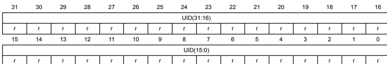
| 31 | 30 | 29 | 28 | 27 | 26 | 25 | 24 | 23 | 22 | 21 | 20 | 19 | 18 | 17 | 16 |
| UID(31:16) | |||||||||||||||
| r | r | r | r | r | r | r | r | r | r | r | r | r | r | r | r |
| 15 | 14 | 13 | 12 | 11 | 10 | 9 | 8 | 7 | 6 | 5 | 4 | 3 | 2 | 1 | 0 |
| UID(15:0) | |||||||||||||||
| r | r | r | r | r | r | r | r | r | r | r | r | r | r | r | r |
Bits 31:0 UID[31:0] : X and Y coordinates on the wafer expressed in BCD format
Address offset: 0x04
Read only = 0xXXXX XXXX, where X is factory-programmed
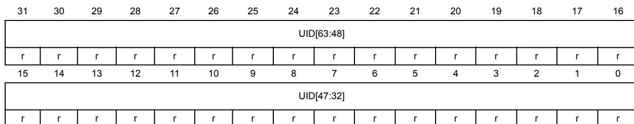
| 31 | 30 | 29 | 28 | 27 | 26 | 25 | 24 | 23 | 22 | 21 | 20 | 19 | 18 | 17 | 16 |
| UID[63:48] | |||||||||||||||
| r | r | r | r | r | r | r | r | r | r | r | r | r | r | r | r |
| 15 | 14 | 13 | 12 | 11 | 10 | 9 | 8 | 7 | 6 | 5 | 4 | 3 | 2 | 1 | 0 |
| UID[47:32] | |||||||||||||||
| r | r | r | r | r | r | r | r | r | r | r | r | r | r | r | r |
Lot number (ASCII encoded)
Bits 7:0 UID[39:32]: WAF_NUM[7:0]Wafer number (8-bit unsigned number)
Address offset: 0x08
Read only = 0xXXXX XXXX, where X is factory-programmed
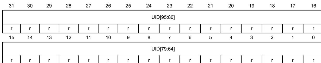
| 31 | 30 | 29 | 28 | 27 | 26 | 25 | 24 | 23 | 22 | 21 | 20 | 19 | 18 | 17 | 16 |
| UID[95:80] | |||||||||||||||
| r | r | r | r | r | r | r | r | r | r | r | r | r | r | r | r |
| 15 | 14 | 13 | 12 | 11 | 10 | 9 | 8 | 7 | 6 | 5 | 4 | 3 | 2 | 1 | 0 |
| UID[79:64] | |||||||||||||||
| r | r | r | r | r | r | r | r | r | r | r | r | r | r | r | r |
Lot number (ASCII encoded)
32.2 Memory size data register
32.2.1 Flash size data register
Base address: 0x1FFF 75E0
Address offset: 0x00
Read only = 0xXXXX, where X is factory-programmed

| 15 | 14 | 13 | 12 | 11 | 10 | 9 | 8 | 7 | 6 | 5 | 4 | 3 | 2 | 1 | 0 |
| FLASH_SIZE | |||||||||||||||
| r | r | r | r | r | r | r | r | r | r | r | r | r | r | r | r |
Indicates the size of the device Flash memory, expressed in Kbytes.
As an example, 0x040 corresponds to 64 Kbytes.
32.3 Package data register
Base address: 0x1FFF 7500
Address offset: 0x00
Read only = 0xXXXX, where X is factory-programmed

| 15 | 14 | 13 | 12 | 11 | 10 | 9 | 8 | 7 | 6 | 5 | 4 | 3 | 2 | 1 | 0 |
| Res. | Res. | Res. | Res. | Res. | Res. | Res. | Res. | Res. | Res. | PKG[5:0] | |||||
| r | r | r | r | r | r | ||||||||||
Bits 15:6 Reserved, must be kept at reset value.
Bits 5:0 PKG[5:0] : Package type
001010: UFQFPN48
Others: reserved
32.4 Part number codification register
Base address: 0x1FFF 77DC
Address offset: 0x00
Read only = 0xXXXX XXXX, where X is factory-programmed
| 31 | 30 | 29 | 28 | 27 | 26 | 25 | 24 | 23 | 22 | 21 | 20 | 19 | 18 | 17 | 16 |
|---|---|---|---|---|---|---|---|---|---|---|---|---|---|---|---|
| CODIFICATION[31:16] | |||||||||||||||
| r | r | r | r | r | r | r | r | r | r | r | r | r | r | r | r |
| 15 | 14 | 13 | 12 | 11 | 10 | 9 | 8 | 7 | 6 | 5 | 4 | 3 | 2 | 1 | 0 |
| CODIFICATION[15:0] | |||||||||||||||
| r | r | r | r | r | r | r | r | r | r | r | r | r | r | r | r |
Bits 31:0 CODIFICATION[31:0] : Part number codification
0x0000 3031 STMicroelectronics STM32WB10xx part number codification