8. Reset and clock control (RCC)
8.1 Reset
There are three types of reset, namely:
- 1. a system reset
- 2. a power reset
- 3. a backup domain reset
8.1.1 Power reset
A power reset is generated when one of the following events occurs:
- 1. a brown-out reset (BOR)
- 2. when exiting from Standby mode
- 3. when exiting from Shutdown mode
A brown-out reset, including power-on or power-down reset (POR/PDR), sets all registers to their reset values except the Backup domain.
When exiting Standby mode, all registers in the V CORE domain are set to their reset value. Registers outside the V CORE domain (RTC, WKUP, IWDG, and Standby/Shutdown modes control) are not impacted.
When exiting Shutdown mode, a Brown-out reset is generated, resetting all registers except those in the Backup domain.
8.1.2 System reset
A system reset sets all registers to their reset values, unless specified otherwise in the register description.
A system reset is generated when one of the following events occurs:
- 1. A low level on the NRST pin (external reset)
- 2. Window watchdog event (WWDG reset)
- 3. Independent watchdog event (IWDG reset)
- 4. A software (SW) reset (see Software reset )
- 5. Low-power mode security reset (see Low-power mode security reset )
- 6. Option byte loader reset (see Option byte loader reset )
- 7. A brown-out reset
The reset source can be identified by checking the reset flags in the RCC control/status register (RCC_CSR) .
These sources act on the NRST pin, always kept low during the delay phase. The CPU1 RESET service routine vector is selected via the BOOT0 and BOOT1.
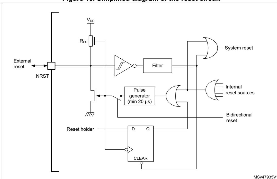
Through specific option bits, the NRST (external reset) pin is configurable to operate as:
- • Reset input/output (default at device delivery)
Valid reset signal on the pin is propagated to the internal logic, and each internal reset source is led to a pulse generator, whose output drives this pin. The GPIO functionality (PB11) is not available. The pulse generator guarantees a minimum reset pulse
duration of 20 \( \mu\text{s} \) for each internal reset source to be output on the NRST pin. An internal reset holder option can be used, if enabled in the option bytes, to ensure that the pin is pulled low until its voltage reaches the \( V_{IL} \) threshold. This function makes it possible the detection of internal reset sources by external components when there is a significant capacitive load.
- •
Reset input
In this mode any valid reset signal on the NRST pin is propagated to the device internal logic, but resets generated internally by the device are not visible on the pin. In this configuration, GPIO functionality (PB11) is not available. - •
GPIO
In this mode the pin can be used as PB11 standard GPIO. The reset function of the pin is not available. Reset is only possible from device internal reset sources and it is not propagated to the pin.
In case of an internal reset, the internal pull-up \( R_{PU} \) is deactivated to reduce power consumption through the pull-up resistor.
Figure 13. Simplified diagram of the reset circuit
Caution: Upon power reset or wake-up from shutdown mode, the NRST pin is configured as Reset input/output and driven low by the system until it is reconfigured to the expected mode (when the option bytes are loaded, in the fourth clock cycle after the end of \( t_{rstempo} \) ).
Software reset
The SYSRESETREQ bit in CPU1 application interrupt and reset control register may be set to force a software reset on the device (refer to PM0214 “ STM32 Cortex®-M4 MCUs and MPUs programming manual ”, available on www.st.com ).
The SYSRESETREQ bit in CPU2 application interrupt and reset control register may be set to force a software reset on the device.
Low-power mode security reset
To prevent that critical applications enter a low-power mode by mistake, two low-power mode security resets are available. If enabled in option bytes, the resets are generated in the following conditions:
- 1. When entering Standby mode: reset is enabled by resetting nRST_STDBY bit in User option Bytes. In this case, whenever a Standby mode entry sequence is successfully executed, the device is reset instead of entering Standby mode.
- 2. When entering Stop mode: reset is enabled by resetting nRST_STOP bit in User option bytes. In this case, whenever a Stop mode entry sequence is successfully executed, the device is reset instead of entering Stop mode.
- 3. When entering Shutdown mode: reset is enabled by resetting nRST_SHDW bit in User option bytes. In this case, whenever a Shutdown mode entry sequence is successfully executed, the device is reset instead of entering Shutdown mode.
For further information on the User option bytes refer to Section 3.4.1: Option bytes description .
Option byte loader reset
The option byte loader reset is generated when the OBL_LAUNCH bit is set in the FLASH_CR register. This bit is used to launch the option byte loading by software.
8.1.3 Backup domain reset
The backup domain has two specific resets.
A backup domain reset is generated when one of the following events occurs:
- 1. Software reset, triggered by setting the BDRST bit in the RCC backup domain control register (RCC_BDCR) .
- 2. V DD or V BAT power on, if both supplies have previously been powered off.
A backup domain reset only affects the LSE oscillator, the RTC, the Backup registers and the RCC Backup domain control register.
8.2 Clocks
Four different clock sources can be used to drive the system clock (SYSCLK):
- • HSI16 (high speed internal) 16 MHz RC oscillator clock
- • MSI (multispeed internal) RC oscillator clock from 100 kHz to 48 MHz.
- • HSE 32 MHz oscillator clock
- • PLL clock
The MSI is used as system clock source after startup from Reset, configured at 4 MHz.
The devices have the following additional clock sources:
- • LSI1: 32 kHz low speed internal RC, which may drive the independent watchdog and optionally the RTC used for Auto-wake-up from Stop and Standby modes (do not use for RF system Auto-wake-up).
- • LSI2: 32 kHz low speed low drift internal RC, which may drive the independent watchdog and optionally the RTC used for Auto-wake-up from Stop and Standby modes.
- • LSE: 32.768 kHz low speed external crystal, which optionally drives the RTC used for Auto-wake-up or the RF system Auto-wake-up from Stop and Standby modes, or the real-time clock (RTCCLK).
Each clock source can be switched on or off independently when it is not used, to optimize power consumption.
Several prescalers can be used to configure the AHB frequencies (HCLK1, HCLK2 and HCLK4) the high speed APB (PCLK2) and the low speed APB (PCLK1) domains. The maximum frequency of the AHB (HCLK1 and HCLK4), and of the PCLK1 and PCLK2 domains is 64 MHz. The maximum frequency of the AHB (HCLK2) domain is 32 MHz.
Most peripheral clocks are derived from their bus clock (HCLK, PCLK) except:
- • The RNG clock, which is derived (selected by software) from one of the following sources:
- – LSE clock
- – LSI clock (LSI1 or LSI2)
- – MSI or PLLQCLK clock divided by 3
- • The ADCs clock, which is derived (selected by software) from one of the three following sources:
- – system clock (SYSCLK only available in Run mode)
- – PLL VCO (PLLAPCLK only available in Run mode)
- – HSI clock (HSI only available in Run mode)
- • The U(S)ARTs clocks, which are derived (selected by software) from one of the four following sources:
- – system clock (SYSCLK only available in Run mode)
- – HSI16 clock (only available in Run and Stop modes)
- – LSE clock ( only available in Run and Stop modes)
- – APB clock (PCLK depending on which APB is mapped the U(S)ART only available in CRun when enabled in U(S)ARTxEN and CSleep when also enabled in U(S)ARTxSMEN)
The wake-up from Stop mode is supported only when the clock is HSI16 or LSE.
- • The I
2
C clock, derived (selected by software) from one of the three following sources:
- – system clock (SYSCLK only available in Run mode)
- – HSI16 clock (only available in Run and Stop modes)
- – APB clock (PCLK depending on which APB is mapped the I 2 C only available in CRun when enabled in I2C1EN and CSleep when also enabled in I2C1SMEN)
The wake-up from Stop mode is supported only when the clock is HSI.
- • The low-power timer (LPTIMx) clocks, which are derived (selected by software) from one of the five following sources:
- – LSI clock (LSI1 or LSI2 only available in Run and Stop modes)
- – LSE clock (only available in Run and Stop modes)
- – HSI16 clock (only available in Run mode)
- – APB clock (PCLK depending on which APB is mapped the LPTIMx only available in CRun when enabled in LPTIMxEN and CSleep when also enabled in LPTIMxSMEN)
- – External clock mapped on LPTIMx_IN1 (only available in Run and Stop modes)
The functionality in Stop mode (including wake-up) is supported only when the clock is LSI or LSE, or in external clock mode.
- • The RTC clock, which is derived (selected by software) from one of the three following sources:
- – LSE clock
- – LSI clock (LSI1 or LSI2)
- – HSE clock divided by 32
The functionality in Stop mode (including wake-up) is supported only when the clock is LSI or LSE.
- • The IWDG clock, which is always the LSI clock (LSI1 or LSI2).
- • The RF system wake-up clock, which is derived (selected by software) from one of the three following sources:
- – LSE clock
- – LSI clock (LSI2, LSI1 shall not be used for RF system Auto-wake-up)
- – HSE clock divided by 1024
The functionality in Stop mode (including wake-up) is supported only when the clock is LSI or LSE. When HSE/1024 is selected as RF system wake-up source HSEON bit must be set by the application.
- • The RF system clock is derived (selected by hardware) from one of the two following sources:
- – HSI16 clock
- – HSE clock
The functionality in Stop mode is supported only when the clock is HSI16 is selected as wake-up clock by STOPWUCK.
The RCC feeds the CPU1 system timer (SysTick) external clock with the AHB clock (HCLK1) divided by 8. The SysTick can work either with this clock or directly with the CPU1 clock (HCLK1), configurable in the SysTick Control and status register.
FCLK1 acts as CPU1 free-running clock. For more details refer to PM0214.
The RCC feeds the CPU2 system timer (SysTick) external clock with the AHB clock (HCLK2) divided by 8. The SysTick can work either with this clock or directly with the CPU2 clock (HCLK2), configurable in the SysTick Control and status Register.
FCLK2 acts as CPU2 free-running clock.
The clock tree is detailed in Figure 14 .
Figure 14. Clock tree
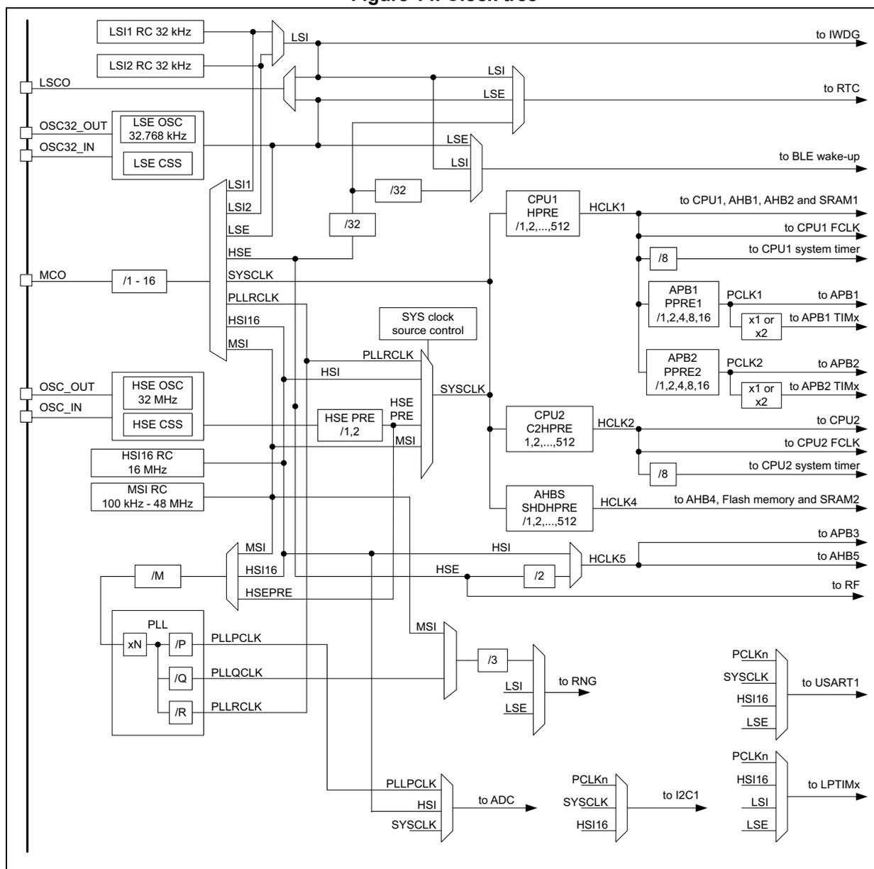
The diagram illustrates the clock tree architecture. On the left, various clock sources are shown:
- LSI1 RC 32 kHz and LSI2 RC 32 kHz connected to an LSI multiplexer.
- LSCO input.
- OSC32_OUT and OSC32_IN connected to LSE OSC 32.768 kHz and LSE CSS , which then connect to an LSE multiplexer.
- MCO output with a /1 - 16 prescaler.
- OSC_OUT and OSC_IN connected to HSE OSC 32 MHz and HSE CSS , which then connect to an HSE multiplexer via an HSE PRE /1,2 prescaler.
- HSI16 RC 16 MHz and MSI RC 100 kHz - 48 MHz connected to an MSI multiplexer.
- A PLL block with inputs xN , /P , /Q , and /R , producing PLLPCLK , PLLQCLK , and PLLCLK outputs.
- Through a /32 prescaler to LSI and LSE multiplexers, which then connect to to IWDG and to RTC respectively.
- Through a /32 prescaler to to BLE wake-up .
- Directly to CPU1 HPRE /1,2,...,512 , which produces HCLK1 for to CPU1, AHB1, AHB2 and SRAM1 . HCLK1 is also divided by /8 for to CPU1 FCLK and to CPU1 system timer .
- Directly to CPU2 C2HPRE /1,2,...,512 , which produces HCLK2 for to CPU2 . HCLK2 is also divided by /8 for to CPU2 FCLK and to CPU2 system timer .
- Directly to AHBS SHDHPRE /1,2,...,512 , which produces HCLK4 for to AHB4, Flash memory and SRAM2 .
- Through an HSE multiplexer and a /2 prescaler to produce HCLK5 for to APB3 , to AHB5 , and to RF .
- Through an MSI multiplexer and a /3 prescaler to to RNG .
- Through an MSI multiplexer to to ADC , which then connects to a multiplexer producing PCLKn , SYSCLK , and HSI16 for to I2C1 .
- Through a PLL block (inputs MSI , HSI16 , SYSCLK ) to produce PCLKn , SYSCLK , HSI16 , and LSE for to USART1 .
- Through a PLL block (inputs MSI , HSI16 , SYSCLK ) to produce PCLKn , HSI16 , LSI , and LSE for to LPTIMx .
2. For full details about the internal and external clock source characteristics refer to the “Electrical characteristics” section in the device datasheet.
3. The ADC clock can be derived from the APB2 clock of the ADC bus interface, divided by a programmable factor (1, 2 or 4). When the programmable factor is 1, the APB2 prescaler must be equal to 1.
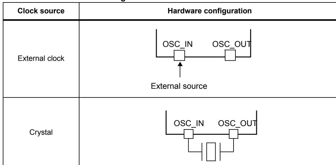
8.2.1 HSE clock
The high speed external clock signal (HSE) can be generated from two possible clock sources (see Figure 15):
- • HSE external crystal
- • HSE user external clock
The crystal has to be placed as close as possible to the oscillator pins to minimize output distortion and startup stabilization time. The loading capacitance are integrated and can be adjusted according to Frequency tuning .
Figure 15. HSE clock sources
| Clock source | Hardware configuration |
|---|---|
| External clock | |
| Crystal |
External crystal (HSE crystal)
The 32 MHz external oscillator has the advantage of producing a very accurate rate on the main clock, and is mandatory for any Radio operation.
The associated hardware configuration is shown in Figure 15 . Refer to the electrical characteristics section of the datasheet for more details.
The HSERDY flag in the RCC clock control register (RCC_CR) indicates if the HSE oscillator is stable or not. At startup, the clock is not released until this bit is set by hardware. An interrupt can be generated if enabled in the RCC clock interrupt enable register (RCC_CIER) .
The HSE Crystal can be switched on and off using the HSEON bit in the RCC clock control register (RCC_CR) .
External source
In this mode, selectable by setting the HSEON bit in the RCC clock control register (RCC_CR) , an external clock source must be provided, with a frequency of 32 MHz. The external clock signal (sinus) with ~45 to 55 % duty cycle (refer to the datasheet ) has to drive the OSC_IN pin, while the OSC_OUT pin must be left not connected (see Figure 15 ).
Note: For details on pin availability, refer to the pinout section in the corresponding device datasheet .
Frequency tuning
The HSE oscillator frequency can vary from one chip to another due to manufacturing process variations and used crystal. User can tune the HSE frequency in the application by
writing the HSETUNE bits in RCC clock HSE register (RCC_HSECR) . The HSE frequency can be measured by outputting the HSE clock on the MCO.
HSE oscillator gain and sense can be controlled by HSEGM and HSES bits in RCC clock HSE register (RCC_HSECR) . Refer to AN5042 for the HSE trimming procedure.
8.2.2 HSI16 clock
The HSI16 clock signal is generated from an internal 16 MHz oscillator.
The HSI16 oscillator has the advantage of providing a clock source at low cost. It also has a faster startup time than the HSE crystal oscillator however, even with calibration the frequency is less accurate than an external crystal oscillator or ceramic resonator.
The HSI16 clock can be selected as system clock after wake-up from Stop modes (Stop0 or Stop1), see Section 8.3: Low-power modes . It can also be used as a backup clock source (auxiliary clock) if the HSE crystal oscillator fails, see Section 8.2.10 .
When the RF system is enabled the HSI16 must be selected as system clock after wake-up from Stop modes.
The HSI16 clock is used as system clock after restart wake-up from Standby.
Calibration
RC oscillator frequencies can vary from one chip to another because of manufacturing process variations, this is why each device is factory calibrated by ST for 1 % accuracy at \( T_A = 25\text{ }^\circ\text{C} \) .
After reset, the factory calibration value is loaded in the HSICAL[7:0] bits in the RCC internal clock sources calibration register (RCC_ICSCR) .
The RC oscillator speed can be affected by voltage or temperature variations, the user can trim the HSI16 frequency in the application using the HSITRIM bits in the RCC internal clock sources calibration register (RCC_ICSCR) .
The HSIRDY flag in the RCC clock control register (RCC_CR) indicates if the HSI16 RC is stable or not. At startup, the HSI16 RC output clock is not released until this bit is set by hardware.
The HSI16 RC can be switched on and off using the HSION bit in the RCC clock control register (RCC_CR) .
The HSI16 signal can also be used as a backup source (auxiliary clock) if the HSE crystal oscillator fails. Refer to Section 8.2.10 .
8.2.3 MSI clock
The MSI clock signal is generated from an internal RC oscillator. Its frequency range can be adjusted by software by using the MSIRANGE[3:0] bits in the RCC clock control register (RCC_CR) . Twelve frequency ranges are available: 100 kHz, 200 kHz, 400 kHz, 800 kHz, 1 MHz, 2 MHz, 4 MHz (default value), 8 MHz, 16 MHz, 24 MHz, 32 MHz and 48 MHz.
The MSI clock is used as system clock after restart from Reset, wake-up from Shutdown low-power modes. After restart from Reset, the MSI frequency is set to its default value 4 MHz. Refer to Section 8.3: Low-power modes .
The MSI clock can be selected as system clock after a wake-up from Stop modes (Stop 0, Stop 1). Refer to Section 8.3: Low-power modes . It can also be used as a backup clock source (auxiliary clock) if the HSE crystal oscillator fails. Refer to Section 8.2.10 .
In addition, when used in PLL-mode with the LSE, it provides a very accurate clock source which can be used by the PLL to run the system at the maximum speed 64 MHz.
The MSIRDY flag in the RCC clock control register (RCC_CR) indicates if the MSI RC is stable or not. At startup, the MSI RC output clock is not released until this bit is set by hardware. The MSI RC can be switched on and off by using the MSION bit in the RCC clock control register (RCC_CR) .
Hardware auto calibration with LSE (PLL-mode)
When a 32.768 kHz external oscillator is present in the application, it is possible to configure the MSI in a PLL-mode by setting the MSIPLEN bit in the RCC clock control register (RCC_CR) . When configured in PLL-mode, the MSI automatically calibrates itself thanks to the LSE. This mode is available for all MSI frequency ranges.
Software calibration
The MSI RC oscillator frequency can vary from one chip to another due to manufacturing process variations, this is why each device is factory calibrated by ST for 1 % accuracy at 25 °C ambient temperature ( \( T_A \) ). After reset, the factory calibration value is loaded in the MSICAL[7:0] bits in the RCC internal clock sources calibration register (RCC_ICSCR) . If the application is subject to voltage or temperature variations, this may affect the RC oscillator speed. The MSI frequency in the application can be trimmed by using the MSITRIM[7:0] bits in the RCC_ICSCR register.
8.2.4 PLL
The device embeds a PLL providing three independent outputs. The internal PLL can be used to multiply the HSI, HSE or MSI output clock frequency. The PLL input frequency must be between 2.66 and 16 MHz. The selected clock source is divided by a programmable factor PLLM from 1 to 8 to provide a clock frequency in the requested input range. Refer to Figure 14: Clock tree and RCC PLL configuration register (RCC_PLLCFGR) .
The PLL configuration (selection of the input clock and multiplication factor) must be done before enabling the PLL. Once the PLL is enabled, these parameters cannot be changed.
To modify the PLL configuration, proceed as follows:
- 1. Disable the PLL by setting PLLON to 0 in RCC clock control register (RCC_CR) .
- 2. Wait until PLLRDY is cleared. The PLL is now fully stopped.
- 3. Change the desired parameter.
- 4. Enable the PLL again by setting PLLON to 1.
- 5. Enable the desired PLL outputs by configuring PLLPEN, PLLQEN, PLLREN in RCC PLL configuration register (RCC_PLLCFGR) .
An interrupt can be generated when the PLL is ready, if enabled in the RCC clock interrupt enable register (RCC_CIER) .
The PLL output frequency must not exceed 64 MHz.
The enable bit of the PLL output clock (PLLPEN, PLLQEN, PLLREN) can be modified at any time without stopping the corresponding PLL. PLLREN cannot be cleared if PLLRCLK is used as system clock.
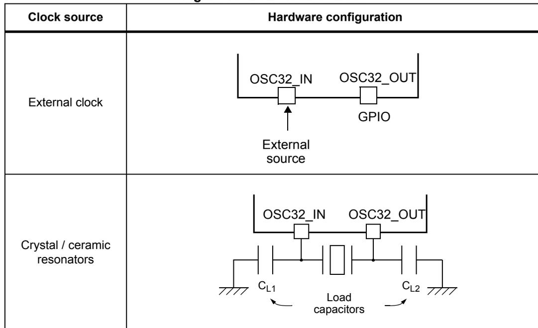
8.2.5 LSE clock
The LSE crystal is a 32.768 kHz low-speed external crystal or ceramic resonator. It has the advantage of providing a low-power but highly accurate clock source to the real-time clock peripheral (RTC) for clock/calendar or other timing functions.
The resonator and the load capacitors have to be placed as close as possible to the oscillator pins in order to minimize output distortion and startup stabilization time. The loading capacitance values must be adjusted according to the selected oscillator.
Figure 16. LSE clock sources
| Clock source | Hardware configuration |
|---|---|
| External clock |
  OSC32_IN    OSC32_OUT
     |           |
     ^           |
  External      GPIO
   source
|
| Crystal / ceramic resonators |
      OSC32_IN    OSC32_OUT
         |           |
    +----+-----------+----+
    |    |           |    |
   ---  ---         ---  ---
   CL1  | |         | |  CL2
   ---  ---         ---  ---
    |    |           |    |
   ===  Load capacitors  ===
|
The LSE crystal is switched on and off using the LSEON bit in RCC backup domain control register (RCC_BDCR) . The crystal oscillator driving strength can be changed at runtime using the LSEDRV[1:0] bits in the RCC backup domain control register (RCC_BDCR) to obtain the best compromise between robustness and short start-up time on one side and low-power-consumption on the other side. The LSE drive can be decreased to the lower drive capability (LSEDRV = 00) when the LSE is ON. However, once LSEDRV is selected, the drive capability cannot be increased if LSEON = 1.
The LSERDY flag in the RCC backup domain control register (RCC_BDCR) indicates whether the LSE crystal is stable or not. At startup, the LSE crystal output clock signal is not released until this bit is set by hardware. An interrupt can be generated if enabled in the RCC clock interrupt enable register (RCC_CIER) .
External source (LSE bypass)
In this mode, selectable by setting the LSEBYP and LSEON bits in the RCC AHB1 peripheral clocks enable in Sleep modes register (RCC_AHB1SMENR) an external clock source must be provided, with a frequency of up to 1 MHz. The external clock signal (square, sinus or triangle) with ~50 % duty cycle has to drive the OSC32_IN pin while the OSC32_OUT pin can be used as GPIO, see Figure 16 .
8.2.6 LSI1 clock
The LSI1 RC acts as a low-power clock source that can be kept running in Stop and Standby mode for the independent watchdog (IWDG), RTC and RF wake-up. The clock frequency is 32 kHz. For more details refer to the electrical characteristics section of the datasheet.
The LSI1 RC can be switched on and off using the LSI1ON bit in the RCC control/status register (RCC_CSR) .
The LSI1RDY flag in the RCC control/status register (RCC_CSR) indicates if the LSI1 oscillator is stable or not. At startup, the clock is not released until this bit is set by hardware. An interrupt can be generated if enabled in the RCC clock interrupt enable register (RCC_CIER) .
8.2.7 LSI2 clock
The LSI2 RC acts as a low drift low-power clock source that can be kept running in Stop and Standby mode for the independent watchdog (IWDG), and RTC wake-up. The clock frequency is ~ 32 kHz. For more details refer to the electrical characteristics section of the datasheet.
The LSI2 RC can be switched on and off using the LSI2ON bit in the RCC control/status register (RCC_CSR) .
The LSI2RDY flag in the RCC control/status register (RCC_CSR) indicates if the LSI2 oscillator is stable or not. At startup, the clock is not released until this bit is set by hardware. An interrupt can be generated if enabled in the RCC clock interrupt enable register (RCC_CIER) .
8.2.8 System clock (SYSCLK) selection
Four different clock sources can be used to drive the system clock (SYSCLK):
- • MSI oscillator
- • HSI16 oscillator
- • HSE oscillator
- • PLLRCLK
The system clock maximum frequency is 64 MHz. After a system reset, the MSI oscillator, at 4 MHz, is selected as system clock. When a clock source is used directly or through the PLL as a system clock, it is not possible to stop it.
A switch from one clock source to another occurs only if the target clock source is ready (clock stable after startup delay or PLL locked). If a clock source which is not yet ready is selected, the switch will occur when the clock source becomes ready. Status bits in the RCC internal clock sources calibration register (RCC_ICSCR) indicate which clock(s) is (are) ready and which clock is currently used as a system clock.
When waking up from Standby mode the HSI16 is selected as system clock.
8.2.9 Clock source frequency
Table 34 gives the different clock source frequencies.
Table 34. Maximum clock source frequency| MSI | HSI | HSE | PLL |
|---|---|---|---|
| 48 MHz | 16 MHz | 32 MHz | 64 MHz (VCO max = 344 MHz) |
8.2.10 Clock security system (CSS) on HSE
The clock security system can be activated by software. In this case, the clock detector is enabled after the HSE oscillator startup delay, and disabled when this oscillator is stopped.
If a failure is detected on the HSE clock, the HSE oscillator is automatically disabled, a clock failure event is sent to the break input of the advanced-control timer (TIM1) and an interrupt is generated to inform the software about the failure (clock security system interrupt CSSI), allowing the MCU to perform rescue operations. The CSSI is linked to the CPU1 and CPU2 NMI (non-maskable interrupt) exception vector.
Note: Once the HSE CSS is enabled and if the HSE clock fails, the CSS interrupt occurs and a NMI is automatically generated. The NMI is executed indefinitely unless the CSS interrupt pending bit is cleared. As a consequence, in the NMI ISR user must clear the CSS interrupt by setting the CSSC bit in the RCC clock interrupt clear register (RCC_CICR) .
If the HSE oscillator is used directly or indirectly as the system clock (indirectly means: it is used as PLL input clock, and the PLL clock is used as system clock), a detected failure causes a switch of the system clock to the MSI or the HSI16 oscillator depending on the STOPWUCK configuration in the RCC clock configuration register (RCC_CFGR) , and the disabling of the HSE oscillator. If the HSE clock (divided or not) is the clock entry of the PLL used as system clock when the failure occurs, the PLL is disabled too.
8.2.11 Clock security system on LSE (LSECSS)
The clock security system on LSE can be activated by software writing the LSECSSON bit in the RCC control/status register (RCC_CSR) . This bit can be disabled only by a hardware reset or RTC software reset, or after a failure detection on LSE. LSECSSON must be written after LSE and LSI are enabled (LSEON and LSI1ON enabled) and ready (LSERDY and LSIRDY set by hardware), and after the RTC clock has been selected by RTCSEL.
The CSS on LSE is working in all modes except VBAT. It is working also under system reset (excluding power on reset). If a failure is detected on the external 32 kHz oscillator, the LSE clock is no longer supplied to the RTC but no hardware action is made to the registers. If the MSI was in PLL-mode, this mode is disabled.
In Standby mode a wake-up is generated. In other modes an interrupt can be sent to wake up the software (see RCC clock interrupt enable register (RCC_CIER) , RCC clock interrupt flag register (RCC_CIFR) , RCC clock interrupt clear register (RCC_CICR) ).
The software MUST then disable the LSECSSON bit, stop the defective 32 kHz oscillator (disabling LSEON), and change the RTC clock source (no clock or LSI or HSE, with RTCSEL), or take any required action to secure the application.
8.2.12 LSI source selection
The LSI used in the system can be selected to come either from LSI1 or LSI2. Whenever LSI2 is turned on by LSI2ON register bit, the LSI2 (when ready) is selected as LSI source.
To switch from LSI2 to LSI1 without interrupting the LSI clock, the LSI1 must first be switched on by LSI1ON register bit. The FW must verify that the LSI1 is ready by LSI1RDY register bit before disabling LSI2 in LSI2ON register bit.
8.2.13 ADC clock
The ADC clock is derived from the system clock, from HSI or from the PLL output. It can reach 64 MHz and can be divided by the prescaler values 1, 2, 4, 6, 8, 10, 12, 16, 32, 64, 128 or 256 by configuring the ADC1_CCR register. It is asynchronous to the AHB clock. Alternatively, the ADC clock can be derived from the AHB clock of the ADC bus interface, divided by a programmable factor (1, 2 or 4). This programmable factor is configured using the CKMODE bit fields in the ADC1_CCR.
If the programmed factor is '1', the APB2 prescaler must be set to '1'.
8.2.14 RTC clock
The RTCCLK clock source can be either the HSE/32, LSE or LSI clock. It is selected by programming the RTCSEL[1:0] bits in the RCC backup domain control register (RCC_BDCR) . This selection cannot be modified without resetting the Backup domain. The system must always be configured so as to get a PCLK frequency greater than or equal to the RTCCLK frequency for a proper operation of the RTC.
The LSE clock is in the Backup domain, whereas the HSE and LSI clocks are not. Consequently:
- • If LSE is selected as RTC clock the RTC continues to work even if the \( V_{DD} \) supply is switched off, provided the \( V_{BAT} \) supply is maintained.
- • If LSI is selected as the RTC clock the RTC state is not guaranteed if the \( V_{DD} \) supply is powered off.
- • If the HSE clock divided by a prescaler is used as the RTC clock the RTC state is not guaranteed if the \( V_{DD} \) supply is powered off or if the internal voltage regulator is powered off (removing power from the \( V_{CORE} \) domain).
When the RTC clock is LSE or LSI, the RTC remains clocked and functional under system reset.
8.2.15 Timer clock
The timer clock frequencies are automatically defined by hardware. There are two cases:
- 1. If the APB prescaler equals 1, the timer clock frequencies are set to the same frequency as that of the APB domain.
- 2. Otherwise, they are set to twice ( \( \times 2 \) ) the frequency of the APB domain.
8.2.16 Watchdog clock
If the Independent watchdog (IWDG) is started by either hardware option or software access, the LSI clock is forced on.
When neither the LSI1 oscillator nor the LSI2 oscillator is enabled when starting the IWDG, the LSI1 oscillator is forced on. After the LSI1 oscillator temporization, the clock is provided to the IWDG.
When LSI2 is switched on with the LSI2ON bit, the LSI clock is switched from LSI1 to LSI2.
When LSI2 is disabled by LSI2ON (when the IWDG is running), the LSI1 oscillator is forced on. The LSI clock is switched to LSI1 when ready, and only then LSI2 is stopped.
8.2.17 True RNG clock
The true random number generator (RNG) seed clock is derived from the LSE clock, LSI clock (LSI1 or LSI2), MSI or PLLQCLK clock divided by 3.
8.2.18 Clock-out capability
- • MCO
The microcontroller clock output (MCO) capability enables the clock to be output on the external MCO pin. One of the following clock signals can be selected as MCO clock:
- – LSI1 (available in Run and Stop modes)
- – LSI2 (available in Run and Stop modes)
- – LSE (available in Run and Stop modes)
- – MSI (available in Run mode)
- – HSI (available in Run mode, when enabled by HSION)
- – HSE (available in Run mode)
- – PLLRCLK (available in Run mode)
- – SYSCLK (available in Run mode)
The selection is controlled by the MCOSEL[3:0] bits of the RCC clock configuration register (RCC_CFGR) . The selected clock can be divided with the MCOPRE[2:0] field of the RCC clock configuration register (RCC_CFGR) .
The clock on MCO is available in Run down to Stop1 modes. Low frequency clocks (LSIx, LSE) are available down to Stop1 mode.
- • LSCO
The LSCO output enables a low speed clock to be output on the external LSCO pin:
- – LSI (LSI1 or LSI2)
- – LSE
The selection is controlled by the LSCOSEL, and enabled with the LSCOEN in the RCC backup domain control register (RCC_BDCR) .
The clock on LSCO is available in Run, Stop, and on one GPIO in Standby and Shutdown modes.
The configuration registers of the corresponding GPIO port must be programmed in alternate function mode.
8.2.19 Peripheral clocks enable
Most peripheral bus and kernel clocks can individually be enabled per CPU. The RCC_AHBxENR, and RCC_APBxENRy enable peripheral clocks for CPU1 and RCC_C2_AHBxENR, and RCC_C2_APBxENR for CPU2. The peripheral clocks will follow the CPU(s) state for which they are enabled, see Table 35 .
Peripheral bus clock activity during the CPU Sleep mode is controlled by the peripheral clock CPU sleep mode enable bit of the RCC_AHBxSMENR, and RCC_APBxSMENRy for CPU1 and RCC_C2_AHBxSMENR, and RCC_C2_APBxSMENRy for CPU2 registers. The
peripheral bus clock during Sleep mode will follow the CPU(s) state for which is it enabled, see Table 35 .
Table 35. Peripheral clock enable
| Peripheral | |||||
|---|---|---|---|---|---|
| xxxEN | xxxSMEN | CPU mode | System mode | Bus clock | Kernel clock (1) |
| 0 | x | Any | Any | Stopped | Stopped |
| 1 | x | CRun | Run | Clocked | Clocked |
| CSleep and CStop | Run | Stopped | Clocked | ||
| 1 | CSleep | Run | Clocked | Clocked | |
| CStop | Run | Stopped | Clocked | ||
| Stop | Stopped | Clocked when selected from – HSI16 – LSI – LSE. Stopped when selected from – bus clock – SYSCLK – PLL clocks – MSI | |||
| Standby or Shutdown | Stopped | Stopped | |||
1. Only the peripherals I2C, LPTIM, USART, true RNG and ADC have a kernel clock.
When the peripheral bus clock is not active, the peripheral registers read or write accesses are not supported.
When the peripheral bus clock is active the peripheral can be accessed by both CPUs regardless of which CPU has enabled the peripheral bus clock in its CPU xxxEN bit. However, when the peripheral bus clock is enabled by only one CPU, and this CPU enters low power mode, the peripheral bus clock is stopped (also depending on this CPUs xxxSMEN setting) and peripheral access for the other CPU is no longer supported. It is therefor good practice to enable the peripheral bus clock with the CPU dedicated clock enable.
When the peripheral kernel clock is not active, the peripheral functionality is stopped.
The enable bit has a synchronization mechanism to create a glitch free clock for the peripheral. After the enable bit is set, there is a two clock cycles delay before the clock becomes active.
Caution: Just after enabling the clock for a peripheral, software must wait for a delay before accessing the peripheral registers.
Note: The BLE-IP when active, will activate the BLE bus and SRAM2 bus interface clocks.
8.3 Low-power modes
- • AHB and APB peripheral clocks, including DMA clock, can be disabled by software.
- • Sleep and Low-power sleep modes stop the CPU clock. The memory interface clocks (Flash and SRAM1 and SRAM2 interfaces) can be stopped by software during Sleep mode. The AHB to APB bridge clocks are disabled by hardware during Sleep mode when all the clocks of the peripherals connected to them are disabled.
- • Stop modes (Stop 0 and Stop 1) stops most clocks in the \( V_{CORE} \) domain and disables the PLL, the MSI and the HSE oscillators. The HSI16 may be kept running when requested by the IPs (USART1, I2C1) that make it possible to wake up from Stop modes.
U(S)ART and I 2 C have the capability to enable the HSI16 oscillator even when the MCU is in Stop mode (if HSI16 is selected as the clock source for that peripheral).
U(S)ART and LPTIM can also be driven by the LSE oscillator when the system is in Stop mode (if LSE is selected as clock source for that peripheral) and the LSE oscillator is enabled (LSEON). In that case the LSE remains always ON in Stop mode (they do not have the capability to turn on the LSE oscillator).
The LPTIM can also be driven by the LSI oscillator when the system is in Stop mode (if LSI is selected as clock source for that peripheral) and the LSI oscillator is enabled (LSI1ON or LSI2ON).
- • Standby and Shutdown modes stops all the clocks in the \( V_{CORE} \) domain and disables the PLL, the HSI, the MSI and the HSE oscillators.
The low power modes mode can be overridden for debugging by setting the DBG_SLEEP, DBG_STOP or DBG_STANDBY bits in the DBGMCU_CR register. In addition the EXTI CDBGPWRUPREQ events can be used to allow debugging in Stop modes (see Table 36 ).
Table 36. Single core Low power debug configurations (1)
| Mode | CDBGPWRUPREQ | DBGMCU | Debug | ||
|---|---|---|---|---|---|
| CPU1 | DBG_STANDBY | DBG_STOP | DBG_SLEEP | CPU1 | |
| Sleep | X | X | X | X | Enabled |
| Stop0 and Stop1 | Disabled | X | Disabled | - | Disabled |
| Enabled | Enabled | ||||
| Stop0 and Stop1 | X | X | Enabled | Enabled | |
| Standby | X | Disabled | - | - | Disabled |
| Enabled | Enabled | ||||
1. X = Do not use.
When leaving the Stop modes (Stop0 and Stop1), the system clock is either MSI or HSI, depending on the software configuration of the STOPWUCK bit in the RCC_CFGR register. When the RF system is enabled the HSI16 shall be selected as in STOPWUCK. When STOPWUCK select the HSI16 clock when leaving Stop mode, the C2HPRE is reset. to select divide by 1. The frequency (range and user trim) of the MSI oscillator is the one configured before entering Stop mode. The user trim of HSI16 is kept. If the MSI was in PLL-mode before entering Stop mode, the PLL-mode stabilization time must be waited for after wake-up even if the LSE was kept ON during the Stop mode.
When leaving the Standby mode, the system clock is HSI.
When leaving the Shutdown modes, the system clock is MSI. The MSI frequency at wake-up from Shutdown mode is 4 MHz. The user trim is lost.
If a Flash memory programming operation is on going, Stop, Standby and Shutdown modes entry is delayed until the Flash memory interface access is finished. If an access to the APB domain is ongoing, Stop, Standby and Shutdown modes entry is delayed until the APB access is finished.
8.4 RCC registers
8.4.1 RCC clock control register (RCC_CR)
Address offset: 0x000
Reset value: 0x0000 0061 (after POR reset), 0x0000 0160 (after wake-up from Standby reset)
Access: No wait state, word, half-word and byte access
| 31 | 30 | 29 | 28 | 27 | 26 | 25 | 24 | 23 | 22 | 21 | 20 | 19 | 18 | 17 | 16 |
|---|---|---|---|---|---|---|---|---|---|---|---|---|---|---|---|
| Res. | Res. | Res. | Res. | Res. | Res. | PLL RDY | PLL ON | Res. | Res. | Res. | HSEPRE | CSS ON | Res. | HSE RDY | HSE ON |
| r | rw | rw | rs | r | rw | ||||||||||
| 15 | 14 | 13 | 12 | 11 | 10 | 9 | 8 | 7 | 6 | 5 | 4 | 3 | 2 | 1 | 0 |
| Res. | Res. | Res. | HSIKE RDY | HSI ASFS | HSI RDY | HSIKER ON | HSI ON | MSIRANGE[3:0] | Res. | MSI PLLEN | MSI RDY | MSI ON | |||
| r | rw | r | rw | rw | rw | rw | rw | rw | rw | r | rw | ||||
Bits 31:26 Reserved, must be kept at reset value.
Bit 25 PLL RDY : System PLL clock ready flag
Set by hardware to indicate that the system PLL is locked.
0: PLL unlocked
1: PLL locked
Bit 24 PLL ON : System PLL enable
Set and cleared by software to enable the PLL.
Cleared by hardware when entering Stop, Standby or Shutdown mode. This bit cannot be reset if the PLL clock is used as the system clock.
0: PLL OFF
1: PLL ON
Bits 23:21 Reserved, must be kept at reset value.
Bit 20 HSEPRE : HSE system clock and PLL M divider prescaler
Set and cleared by software to control the division factor of the system clock and PLL M divider input when selecting HSE clock.
0: SYSCLK and PLL M divider input clocks are not divided (HSE)
1: SYSCLK and PLL M divider input clocks are divided by 2 (HSE/2)
Bit 19 CSSON : HSE clock security system enable
Set by software to enable the clock security system. When CSSON is set, the HSE lock detector is enabled by hardware when the HSE oscillator is ready, and disabled by hardware if a HSE clock failure is detected. This bit is set only and is cleared by reset.
0: HSE clock security system OFF (clock detector OFF)
1: HSE clock security system ON (clock detector ON if the HSE oscillator is stable, OFF if not).
Bit 18 Reserved, must be kept at reset value.
Bit 17 HSERDY: HSE clock ready flagSet by hardware to indicate that the HSE oscillator is stable.
0: HSE oscillator not ready
1: HSE oscillator ready
Note: Once the HSEON bit is cleared, HSERDY goes low after six HSE clock cycles.
Regardless of the value of the HSEON bit, the HSE oscillator starts on RF demand when needed. It is possible to have HSEON = 0 and HSERDY = 1.
Bit 16 HSEON: HSE clock enableSet and cleared by software.
Cleared by hardware to stop the HSE oscillator when entering Stop, Standby or Shutdown mode. This bit cannot be reset if the HSE oscillator is used directly or indirectly as the system clock.
0: HSE oscillator OFF
1: HSE oscillator ON
Bits 15:13 Reserved, must be kept at reset value.
Bit 12 HSIKERDY: HSI16 kernel clock ready flag for peripherals requests.Set by hardware to indicate that HSI16 oscillator is stable when enabled by HSIKERON or a peripheral kernel clock request. Not set when HSI16 is enabled by software by setting HSION, or by wake-up from Standby.
0: HSI16 oscillator not ready
1: HSI16 oscillator ready
Bit 11 HSIASFS: HSI16 automatic start from StopSet and cleared by software. When the system wake-up clock is MSI, this bit is used to wake up the HSI16 in parallel of the system wake-up.
0: HSI16 oscillator is not enabled by hardware when exiting Stop mode with MSI as wake-up clock.
1: HSI16 oscillator is enabled by hardware when exiting Stop mode with MSI as wake-up clock.
Bit 10 HSIRDY: HSI16 clock ready flag. (After wake-up from Standby this bit is read 'b1 once the HSI16 is ready)Set by hardware to indicate that HSI16 oscillator is stable. This bit is set only when HSI16 is enabled by software by setting HSION, or by wake-up from Standby. Not set when HSI16 is enabled by HSIKERON or by IP request.
0: HSI16 oscillator not ready
1: HSI16 oscillator ready
Note: Once the HSION bit is cleared, HSIRDY goes low after 6 HSI16 clock cycles.
Bit 9 HSIKERON: HSI16 always enable for peripheral kernel clocks.Set and cleared by software to force HSI16 ON even in Stop modes. The HSI16 enabled by HSIKERON can only feed USART and I 2 C peripherals configured with HSI16 as kernel clock. Keeping the HSI16 ON in Stop mode avoids slowing down the communication speed because of the HSI16 startup time. This bit has no effect on HSION value.
0: No effect on HSI16 oscillator.
1: HSI16 oscillator is forced ON even in Stop mode.
Bit 8 HSION: HSI16 clock enableSet and cleared by software.
Cleared by hardware to stop the HSI16 oscillator when entering Stop, Standby or Shutdown mode.
Set by hardware to force the HSI16 oscillator ON when STOPWUCK = 1 or HSIASFS = 1 when leaving Stop modes, or in case of failure of the HSE crystal oscillator.
This bit is set by hardware if the HSI16 is used directly or indirectly as system clock.
0: HSI16 oscillator OFF
1: HSI16 oscillator ON
Bits 7:4 MSIRANGE[3:0]: MSI clock rangesThese bits are configured by software to choose the frequency range of MSI when MSIRANGE is set. Twelve frequency ranges are available:
0000: range 0, ~100 kHz
0001: range 1, ~200 kHz
0010: range 2, ~400 kHz
0011: range 3, ~800 kHz
0100: range 4, ~1M Hz
0101: range 5, ~2 MHz
0110: range 6, ~4 MHz (reset value)
0111: range 7, ~8 MHz
1000: range 8, ~16 MHz
1001: range 9, ~24 MHz
1010: range 10, ~32 MHz
1011: range 11, ~48 MHz
others: not allowed (hardware write protection)
Note: MSIRANGE can be modified when MSI is OFF (MSION = 0) or when MSI is ready (MSIRDY = 1). MSIRANGE must NOT be modified when MSI is ON and NOT ready (MSION = 1 and MSIRDY = 0).
Bit 3 Reserved, must be kept at reset value. Bit 2 MSIPPLEN: MSI clock PLL enableSet and cleared by software to enable/ disable the PLL part of the MSI clock source.
MSIPPLEN must be enabled after LSE is enabled (LSEON enabled) and ready (LSERDY set by hardware). There is a hardware protection to avoid enabling MSIPPLEN if LSE is not ready.
This bit is cleared by hardware when LSE is disabled (LSEON = 0) or when the clock security system on LSE detects a LSE failure (refer to RCC_CSR register).
0: MSI PLL OFF
1: MSI PLL ON
Bit 1 MSIRDY: MSI clock ready flag (After reset this bit is read 'b1 once the MSI is ready)This bit is set by hardware to indicate that the MSI oscillator is stable.
0: MSI oscillator not ready
1: MSI oscillator ready
Note: Once the MSION bit is cleared, MSIRDY goes low after 6 MSI clock cycles.
Bit 0 MSION : MSI clock enable
This bit is set and cleared by software.
Cleared by hardware to stop the MSI oscillator when entering Stop, Standby or Shutdown mode.
Set by hardware to force the MSI oscillator ON when exiting Standby or Shutdown mode.
Set by hardware to force the MSI oscillator ON when STOPWUCK = 0 when exiting from Stop modes, or in case of a failure of the HSE oscillator
Set by hardware when used directly or indirectly as system clock.
0: MSI oscillator OFF
1: MSI oscillator ON
8.4.2 RCC internal clock sources calibration register (RCC_ICSCR)
Address offset: 0x004
Reset value: 0x40XX 00XX (X is factory-programmed)
Access: No wait state, word, half-word and byte access
| 31 | 30 | 29 | 28 | 27 | 26 | 25 | 24 | 23 | 22 | 21 | 20 | 19 | 18 | 17 | 16 |
|---|---|---|---|---|---|---|---|---|---|---|---|---|---|---|---|
| Res. | HSITRIM[6:0] | HSICAL[7:0] | |||||||||||||
| rw | rw | rw | rw | rw | rw | rw | r | r | r | r | r | r | r | r | |
| 15 | 14 | 13 | 12 | 11 | 10 | 9 | 8 | 7 | 6 | 5 | 4 | 3 | 2 | 1 | 0 |
| MSITRIM[7:0] | MSICAL[7:0] | ||||||||||||||
| rw | rw | rw | rw | rw | rw | rw | rw | r | r | r | r | r | r | r | r |
Bit 31 Reserved, must be kept at reset value.
Bits 30:24 HSITRIM[6:0] : HSI16 clock trimming
These bits provide an additional user-programmable trimming value that is added to the HSICAL[7:0] bits. It can be programmed to adjust to variations in voltage and temperature that influence the frequency of the HSI16.
The default value is 64, which, when added to the HSICAL value, should trim the HSI16 to 16 MHz \( \pm \) 1 %.
Bits 23:16 HSICAL[7:0] : HSI16 clock calibration
These bits are initialized at startup with the factory-programmed HSI16 calibration trim value. When HSITRIM is written, HSICAL is updated with the sum of HSITRIM and the factory trim value.
Bits 15:8 MSITRIM[7:0] : MSI clock trimming
These bits provide an additional user-programmable trimming value that is added to the MSICAL[7:0] bits. It can be programmed to adjust to variations in voltage and temperature that influence the frequency of the MSI.
The default value is 0, which, when added to the MSICAL value, should trim the MSI to its mid frequency.
Bits 7:0 MSICAL[7:0] : MSI clock calibration
These bits are initialized at startup with the factory-programmed MSI calibration trim value. When MSITRIM is written, MSICAL is updated with the sum of MSITRIM and the factory trim value.
8.4.3 RCC clock configuration register (RCC_CFGR)
Address offset: 0x008
Reset value: 0x0007 0000 (after POR reset), 0x0007 0001 (after wake-up from Standby)
Access: \( 0 \leq \text{wait state} \leq 2 \) , word, half-word and byte access
One or two wait states inserted only if the access occurs during clock source switch.
From 0 to 15 wait states inserted if the access occurs when the APB or AHB prescalers values update is on going.
| 31 | 30 | 29 | 28 | 27 | 26 | 25 | 24 | 23 | 22 | 21 | 20 | 19 | 18 | 17 | 16 |
|---|---|---|---|---|---|---|---|---|---|---|---|---|---|---|---|
| Res. | MCOPRE[2:0] | MCOSEL[3:0] | Res. | PPRE2F | PPRE1F | HPREF | |||||||||
| rw | rw | rw | rw | rw | rw | rw | r | r | r | ||||||
| 15 | 14 | 13 | 12 | 11 | 10 | 9 | 8 | 7 | 6 | 5 | 4 | 3 | 2 | 1 | 0 |
| STOP WUCK | Res. | PPRE2[2:0] | PPRE1[2:0] | HPRE[3:0] | SWS[1:0] | SW[1:0] | |||||||||
| rw | rw | rw | rw | rw | rw | rw | rw | rw | rw | rw | r | r | rw | rw | |
Bit 31 Reserved, must be kept at reset value.
Bits 30:28 MCOPRE[2:0] : Microcontroller clock output prescaler
- These bits are set and cleared by software.
- It is highly recommended to change this prescaler before MCO output is enabled.
- 000: MCO is divided by 1
- 001: MCO is divided by 2
- 010: MCO is divided by 4
- 011: MCO is divided by 8
- 100: MCO is divided by 16
- Others: not allowed
Bits 27:24 MCOSEL[3:0] : Microcontroller clock output
Set and cleared by software.
- 0000: MCO output disabled, no clock on MCO
- 0001: SYSCLK system clock selected
- 0010: MSI clock selected.
- 0011: HSI16 clock selected.
- 0100: HSE clock selected (after stabilization, after HSERDY = 1)
- 0101: Main PLLRCLK clock selected
- 0110: LSI1 clock selected
- 0111: LSI2 clock selected
- 1000: LSE clock selected
- 1001: Reserved
- 1100: HSE clock selected (before stabilization, after HSEON = 1)
- Others: Reserved
Note: This clock output may have some truncated cycles at startup or during MCO clock source switching.
Bits 23:19 Reserved, must be kept at reset value.
Bit 18 PPRE2F : PCLK2 prescaler flag (APB2)
Set and reset by hardware to acknowledge PCLK2 prescaler programming
Reset when a new prescaler value is programmed in PPRE2. set when the programmed value is actually applied.
0: PCLK2 prescaler value not yet applied
1: PCLK2 prescaler value applied
Bit 17 PPRE1F : PCLK1 prescaler flag (APB1)
Set and reset by hardware to acknowledge PCLK1 prescaler programming
Reset when a new prescaler value is programmed in PPRE1. set when the programmed value is actually applied.
0: PCLK1 prescaler value not yet applied
1: PCLK1 prescaler value applied
Bit 16 HPREF : HCLK1 prescaler flag (CPU1, AHB1, AHB2 and SRAM1)
Set and reset by hardware to acknowledge HCLK1 prescaler programming
Reset when a new prescaler value is programmed in HPRE. set when the programmed value is actually applied.
0: HCLK1 prescaler value not yet applied
1: HCLK1 prescaler value applied
Bit 15 STOPWUCK : Wakeup from Stop and CSS backup clock selection
Set and cleared by software to select the system clock used when exiting Stop mode.
The selected clock is also used as emergency clock for the clock security system on HSE.
Warning: STOPWUCK must not be modified when the HSE clock security system is enabled by CSSON in RCC clock control register (RCC_CR) register and the system clock is HSE (SWS = 10) or a switch on HSE is requested (SW= 10).
0: MSI oscillator selected as wake-up from stop clock and CSS backup clock.
1: HS16 oscillator selected as wake-up from stop clock and CSS backup clock
Bit 14 Reserved, must be kept at reset value.
Bits 13:11 PPRE2[2:0] : PCLK2 high-speed prescaler (APB2)
Set and cleared by software to control the division factor of the PCLK2 clock (APB2).
The PPRE2F flag can be checked to know if the programmed PPRE2 prescaler value is applied.
0xx: HCLK1 not divided
100: HCLK1 divided by 2
101: HCLK1 divided by 4
110: HCLK1 divided by 8
111: HCLK1 divided by 16
Bits 10:8 PPRE1[2:0] : PCLK1 low-speed prescaler (APB1)
Set and cleared by software to control the division factor of the PCLK1 clock (APB1).
The PPRE1F flag can be checked to know if the programmed PPRE1 prescaler value is applied.
0xx: HCLK1 not divided
100: HCLK1 divided by 2
101: HCLK1 divided by 4
110: HCLK1 divided by 8
111: HCLK1 divided by 16
Bits 7:4 HPRE[3:0] : HCLK1 prescaler (CPU1, AHB1, AHB2 and SRAM1.)
Set and cleared by software to control the division factor of the HCLK1 clock (CPU1, AHB1, AHB2 and SRAM1).
The HPREF flag can be checked to know if the programmed HPRE prescaler value is applied.
Caution: The software must set correctly these bits to ensure that the system frequency does not exceed the maximum allowed frequency. After a write operation to these bits the register bit HPREF must be read to be sure that the new value has been taken into account.
0001: SYSCLK divided by 3
0010: SYSCLK divided by 5
0101: SYSCLK divided by 6
0110: SYSCLK divided by 10
0111: SYSCLK divided by 32
1000: SYSCLK divided by 2
1001: SYSCLK divided by 4
1010: SYSCLK divided by 8
1011: SYSCLK divided by 16
1100: SYSCLK divided by 64
1101: SYSCLK divided by 128
1110: SYSCLK divided by 256
1111: SYSCLK divided by 512
Others: SYSCLK not divided
Bits 3:2 SWS[1:0] : System clock switch status
Set and cleared by hardware to indicate which clock source is used as system clock.
00: MSI oscillator used as system clock
01: HSI16 oscillator used as system clock
10: HSE used as system clock
11: PLL used as system clock
Bits 1:0 SW[1:0] : System clock switch
Set and cleared by software to select system clock source (SYSCLK).
Configured by HW to force MSI oscillator selection when exiting Shutdown mode.
Configured by HW to force HSI16 oscillator selection when exiting Standby mode.
Configured by HW to force MSI or HSI16 oscillator selection when exiting Stop mode or in case of failure of the HSE oscillator, depending on STOPWUACK value.
00: MSI selected as system clock
01: HSI16 selected as system clock
10: HSE selected as system clock
11: PLL selected as system clock
Note: The latency when changing SW and SWS bits is set according to the new configuration when switching the SYSCLK clock source, in a maximum of three cycles of the previous clock.
8.4.4 RCC PLL configuration register (RCC_PLLCFGR)
Address offset: 0x00C
Reset value: 0x2204 0100
Access: No wait state, word, half-word and byte access
This register is used to configure the PLL clock outputs according to the following formulas:
- • \( f(\text{VCO clock}) = f(\text{PLL clock input}) \times (\text{PLLN} / \text{PLLM}) \)
- • \( f(\text{PLL\_P}) = f(\text{VCO clock}) / \text{PLLP} \)
- • \( f(\text{PLL\_Q}) = f(\text{VCO clock}) / \text{PLLQ} \)
- • \( f(\text{PLL\_R}) = f(\text{VCO clock}) / \text{PLLR} \)
| 31 | 30 | 29 | 28 | 27 | 26 | 25 | 24 | 23 | 22 | 21 | 20 | 19 | 18 | 17 | 16 |
|---|---|---|---|---|---|---|---|---|---|---|---|---|---|---|---|
| PLLR[2:0] | PLLREN | PLLQ[2:0] | PLLQEN | Res. | Res. | PLLP[4:0] | PLLPEN | ||||||||
| rw | rw | rw | rw | rw | rw | rw | rw | rw | rw | rw | rw | rw | rw | ||
| 15 | 14 | 13 | 12 | 11 | 10 | 9 | 8 | 7 | 6 | 5 | 4 | 3 | 2 | 1 | 0 |
| Res. | PLLN[6:0] | Res. | PLLM[2:0] | Res. | Res. | PLLSRC[1:0] | |||||||||
| rw | rw | rw | rw | rw | rw | rw | rw | rw | rw | rw | rw | ||||
Bits 31:29 PLLR[2:0] : Main PLL division factor for PLLRCLK
Set and cleared by software to control the frequency of the main PLL output clock PLLRCLK. This output can be selected as system clock. These bits can be written only if the PLL is disabled.
PLLRCLK output clock frequency = VCO frequency / PLLR with PLLR = 2, 3, 4,... or 8 [VCO frequency / (N + 1)]
000: reserved
001: PLLR = 2
010: PLLR = 3
011: PLLR = 4
100: PLLR = 5
101: PLLR = 6
110: PLLR = 7
111: PLLR = 8
The software must set these bits so that 64 MHz is not exceeded on this domain.
Bit 28 PLLREN : Main PLL PLLRCLK output enable
Set and reset by software to enable the PLLRCLK output of the main PLL (used as system clock).
This bit cannot be written when PLLRCLK output of the PLL is used as System clock.
To save power, when the PLLRCLK output of the PLL is not used, the value of PLLREN should be 0.
0: PLLRCLK output disabled
1: PLLRCLK output enabled
Bits 27:25 PLLQ[2:0] : Main PLL division factor for PLLQCLK
Set and cleared by software to control the frequency of the main PLL output clock PLLQCLK. This output can be selected for true RNG clock. These bits can be written only if PLL is disabled.
PLLQCLK output clock frequency = VCO frequency / PLLQ with PLLQ = 2, 3, 4,... or 8 [VCO frequency / (N + 1)]
000: reserved
001: PLLQ = 2
010: PLLQ = 3
011: PLLQ = 4
100: PLLQ = 5
101: PLLQ = 6
110: PLLQ = 7
111: PLLQ = 8
The software must set these bits so that 64 MHz is not exceeded on this domain.
Bit 24 PLLQEN : Main PLL PLLQCLK output enable
Set and reset by software to enable the PLLQCLK output of the main PLL (used as system clock).
In order to save power, when the PLLQCLK output of the PLL is not used, the value of PLLQEN should be 0.
0: PLLQCLK output disable
1: PLLQCLK output enable
Bits 23:22 Reserved, must be kept at reset value.
Bits 21:17 PLLP[4:0] : Main PLL division factor for PLLPCLK.
Set and cleared by software to control the frequency of the main PLL output clock PLLPCLK.
This output can be selected for ADC. These bits can be written only if PLL is disabled.
PLLPCLK output clock frequency = VCO frequency / PLLP with PLLP = 2, 3, 4, ... or 32 [VCO frequency / (N + 1)]
0000: reserved
00001: PLLP = 2
00010: PLLP = 3
00011: PLLP = 4
00100: PLLP = 5
...
11111: PLLP = 32
The software must set these bits so that 64 MHz is not exceeded on this domain.
Bit 16 PLLPEN : Main PLL PLLPCLK output enable
Set and reset by software to enable the PLLPCLK output of the main PLL.
In order to save power, when the PLLPCLK output of the PLL is not used, the value of PLLPEN should be 0.
0: PLLPCLK output disable
1: PLLPCLK output enable
Bit 15 Reserved, must be kept at reset value.
Bits 14:8 PLLN[6:0] : Main PLL multiplication factor for VCO
Set and cleared by software to control the multiplication factor of the VCO. These bits can be written only when the PLL is disabled.
VCO output frequency = VCO input frequency x PLLN with \( 6 \leq PLLN \leq 127 \)
0000000: PLLN = 0 reserved (must not be used)
0000001: PLLN = 1 reserved (must not be used)
...
0000101: PLLN = 5 reserved (must not be used)
0000110: PLLN = 6
1111111: PLLN = 127
The software must set these bits to ensure that the VCO output frequency is between 96 and 344 MHz.
Bit 7 Reserved, must be kept at reset value.
Bits 6:4 PLLM[2:0] : Division factor for the main PLL
Set and cleared by software to divide the PLL input clock before the VCO. These bits can be written only when the PLL is disabled.
VCO input frequency = PLL input clock frequency / PLLM with \( 1 \leq \text{PLLM} \leq 8 \)
000: PLLM = 1
001: PLLM = 2
010: PLLM = 3
011: PLLM = 4
100: PLLM = 5
101: PLLM = 6
110: PLLM = 7
111: PLLM = 8
The software must set these bits to ensure that the VCO input frequency ranges from 2.66 to 16 MHz.
Bits 3:2 Reserved, must be kept at reset value.
Bits 1:0 PLL SRC[1:0] : Main PLL entry clock source
Set and cleared by software to select PLL clock source. These bits can be written only when PLL is disabled.
In order to save power, when no PLL is used, the value of PLL SRC should be 00.
00: No clock sent to PLL
01: MSI clock selected as PLL clock entry
10: HSI16 clock selected as PLL clock entry
11: HSE clock selected as PLL clock entry
8.4.5 RCC clock interrupt enable register (RCC_CIER)
Address offset: 0x018
Reset value: 0x0000 0000
Access: No wait state, word, half-word and byte access
| 31 | 30 | 29 | 28 | 27 | 26 | 25 | 24 | 23 | 22 | 21 | 20 | 19 | 18 | 17 | 16 |
|---|---|---|---|---|---|---|---|---|---|---|---|---|---|---|---|
| Res. | Res. | Res. | Res. | Res. | Res. | Res. | Res. | Res. | Res. | Res. | Res. | Res. | Res. | Res. | Res. |
| 15 | 14 | 13 | 12 | 11 | 10 | 9 | 8 | 7 | 6 | 5 | 4 | 3 | 2 | 1 | 0 |
| Res. | Res. | Res. | Res. | LSI2 RDYIE | Res. | LSE CSSIE | Res. | Res. | Res. | PLL RDYIE | HSE RDYIE | HSI RDYIE | MSI RDYIE | LSE RDYIE | LSI1 RDYIE |
| rw | rw | rw | rw | rw | rw | rw | rw |
Bits 31:12 Reserved, must be kept at reset value.
Bit 11 LSI2RDYIE : LSI2 ready interrupt enable
Set and cleared by software to enable/disable interrupt caused by the LSI2 oscillator stabilization.
0: LSI2 ready interrupt disabled
1: LSI2 ready interrupt enabled
Bit 10 Reserved, must be kept at reset value.
Bit 9 LSECSSIE : LSE clock security system interrupt enable
Set and cleared by software to enable/disable interrupt caused by the clock security system on LSE.
0: Clock security interrupt caused by LSE clock failure disabled
1: Clock security interrupt caused by LSE clock failure enabled
Bits 8:6 Reserved, must be kept at reset value.
Bit 5 PLLRDYIE : PLL ready interrupt enable
Set and cleared by software to enable/disable interrupt caused by PLL lock.
0: PLL lock interrupt disabled
1: PLL lock interrupt enabled
Bit 4 HSERDYIE : HSE ready interrupt enable
Set and cleared by software to enable/disable interrupt caused by the HSE oscillator stabilization.
0: HSE ready interrupt disabled
1: HSE ready interrupt enabled
Bit 3 HSIRDYIE : HSI16 ready interrupt enable
Set and cleared by software to enable/disable interrupt caused by the HSI16 oscillator stabilization.
0: HSI16 ready interrupt disabled
1: HSI16 ready interrupt enabled
Bit 2 MSIRDYIE : MSI ready interrupt enable
Set and cleared by software to enable/disable interrupt caused by the MSI oscillator stabilization.
0: MSI ready interrupt disabled
1: MSI ready interrupt enabled
Bit 1 LSERDYIE : LSE ready interrupt enable
Set and cleared by software to enable/disable interrupt caused by the LSE oscillator stabilization.
0: LSE ready interrupt disabled
1: LSE ready interrupt enabled
Bit 0 LSI1RDYIE : LSI1 ready interrupt enable
Set and cleared by software to enable/disable interrupt caused by the LSI1 oscillator stabilization.
0: LSI1 ready interrupt disabled
1: LSI1 ready interrupt enabled
8.4.6 RCC clock interrupt flag register (RCC_CIFR)
Address offset: 0x01C
Reset value: 0x0000 0000
Access: No wait state, word, half-word and byte access
| 31 | 30 | 29 | 28 | 27 | 26 | 25 | 24 | 23 | 22 | 21 | 20 | 19 | 18 | 17 | 16 |
|---|---|---|---|---|---|---|---|---|---|---|---|---|---|---|---|
| Res. | Res. | Res. | Res. | Res. | Res. | Res. | Res. | Res. | Res. | Res. | Res. | Res. | Res. | Res. | Res. |
| 15 | 14 | 13 | 12 | 11 | 10 | 9 | 8 | 7 | 6 | 5 | 4 | 3 | 2 | 1 | 0 |
| Res. | Res. | Res. | Res. | LSI2 RDYF | Res. | LSE CSSF | CSSF | Res. | Res. | PLL RDYF | HSE RDYF | HS1 RDYF | MSI RDYF | LSE RDYF | LSI1 RDYF |
| r | r | r | r | r | r | r | r | r |
Bits 31:12 Reserved, must be kept at reset value.
Bit 11 LSI2RDYF : LSI2 ready interrupt flag
Set by hardware when the LSI2 clock becomes stable and LSI2RDYDIE is set.
Cleared by software setting the LSI2RDYC bit.
0: No clock ready interrupt caused by the LSI2 oscillator
1: Clock ready interrupt caused by the LSI2 oscillator
Bit 10 Reserved, must be kept at reset value.
Bit 9 LSECSSF : LSE clock security system interrupt flag
Set by hardware when a failure is detected in the LSE oscillator.
Cleared by software setting the LSECSSC bit.
0: No clock security interrupt caused by LSE clock failure
1: Clock security interrupt caused by LSE clock failure
Bit 8 CSSF : HSE clock security system interrupt flag
Set by hardware when a failure is detected in the HSE oscillator.
Cleared by software setting the CSSC bit.
0: No clock security interrupt caused by HSE clock failure
1: Clock security interrupt caused by HSE clock failure
Bit 7 Reserved, must be kept at reset value.
Bit 5 PLL RDYF : PLL ready interrupt flag
Set by hardware when the PLL locks and PLLRDYDIE is set.
Cleared by software setting the PLLRDYC bit.
0: No clock ready interrupt caused by PLL lock
1: Clock ready interrupt caused by PLL lock
Bit 4 HSERDYF : HSE ready interrupt flag
Set by hardware when the HSE clock becomes stable and HSERDYDIE is set.
Cleared by software setting the HSERDYC bit.
0: No clock ready interrupt caused by the HSE oscillator
1: Clock ready interrupt caused by the HSE oscillator
Bit 3 HSIRDYF : HS16 ready interrupt flag
Set by hardware when the HS16 clock becomes stable and HSIRDYDIE is set in a response to setting the HSION (refer to RCC clock control register (RCC_CR) ). When HSION is not set but the HS16 oscillator is enabled by the peripheral through a clock request, this bit is not set and no interrupt is generated.
Cleared by software setting the HSIRDYC bit.
0: No clock ready interrupt caused by the HS16 oscillator
1: Clock ready interrupt caused by the HS16 oscillator
Bit 2 MSIRDYF : MSI ready interrupt flag
Set by hardware when the MSI clock becomes stable and MSIRDYDIE is set.
Cleared by software setting the MSIRDYC bit.
0: No clock ready interrupt caused by the MSI oscillator
1: Clock ready interrupt caused by the MSI oscillator
Bit 1 LSERDYF : LSE ready interrupt flag
Set by hardware when the LSE clock becomes stable and LSERDYDIE is set.
Cleared by software setting the LSERDYC bit.
0: No clock ready interrupt caused by the LSE oscillator
1: Clock ready interrupt caused by the LSE oscillator
Bit 0 LSI1RDYF : LSI1 ready interrupt flag
Set by hardware when the LSI1 clock becomes stable and LSI1RDYDIE is set.
Cleared by software setting the LSI1RDYC bit.
0: No clock ready interrupt caused by the LSI1 oscillator
1: Clock ready interrupt caused by the LSI1 oscillator
8.4.7 RCC clock interrupt clear register (RCC_CICR)
Address offset: 0x020
Reset value: 0x0000 0000
Access: No wait state, word, half-word and byte access
| 31 | 30 | 29 | 28 | 27 | 26 | 25 | 24 | 23 | 22 | 21 | 20 | 19 | 18 | 17 | 16 |
|---|---|---|---|---|---|---|---|---|---|---|---|---|---|---|---|
| Res. | Res. | Res. | Res. | Res. | Res. | Res. | Res. | Res. | Res. | Res. | Res. | Res. | Res. | Res. | Res. |
| 15 | 14 | 13 | 12 | 11 | 10 | 9 | 8 | 7 | 6 | 5 | 4 | 3 | 2 | 1 | 0 |
| Res. | Res. | Res. | Res. | LSI2 RDYC | Res. | LSE CSSC | CSSC | Res. | Res. | PLL RDYC | HSE RDYC | HSI RDYC | MSI RDYC | LSE RDYC | LSI1 RDYC |
| w | w | w | w | w | w | w | w | w |
Bits 31:12 Reserved, must be kept at reset value.
Bit 11 LSI2RDYC : LSI2 ready interrupt clear
This bit is set by software to clear the LSI2RDYF flag.
0: No effect
1: LSI2RDYF cleared
Bit 10 Reserved, must be kept at reset value.
Bit 9 LSECSSC : LSE clock security system interrupt clear
This bit is set by software to clear the LSECSSF flag.
0: No effect
1: Clear LSECSSF flag
Bit 8 CSSC : HSE clock security system interrupt clear
This bit is set by software to clear the HSE CSSF flag.
0: No effect
1: Clear HSE CSSF flag
Bits 7:6 Reserved, must be kept at reset value.
Bit 5 PLLRDYC : PLL ready interrupt clearThis bit is set by software to clear the PLLRDYF flag.
0: No effect
1: Clear PLLRDYF flag
Bit 4 HSERDYC : HSE ready interrupt clearThis bit is set by software to clear the HSERDYF flag.
0: No effect
1: Clear HSERDYF flag
Bit 3 HSIRDYC : HSI16 ready interrupt clearThis bit is set software to clear the HSIRDYF flag.
0: No effect
1: Clear HSIRDYF flag
Bit 2 MSIRDYC : MSI ready interrupt clearThis bit is set by software to clear the MSIRDYF flag.
0: No effect
1: MSIRDYF cleared
Bit 1 LSERDYC : LSE ready interrupt clearThis bit is set by software to clear the LSERDYF flag.
0: No effect
1: LSERDYF cleared
Bit 0 LSI1RDYC : LSI1 ready interrupt clearThis bit is set by software to clear the LSI1RDYF flag.
0: No effect
1: LSI1RDYF cleared
8.4.8 RCC AHB1 peripheral reset register (RCC_AHB1RSTR)
Address offset: 0x028
Reset value: 0x00000 0000
Access: No wait state, word, half-word and byte access
| 31 | 30 | 29 | 28 | 27 | 26 | 25 | 24 | 23 | 22 | 21 | 20 | 19 | 18 | 17 | 16 |
|---|---|---|---|---|---|---|---|---|---|---|---|---|---|---|---|
| Res. | Res. | Res. | Res. | Res. | Res. | Res. | Res. | Res. | Res. | Res. | Res. | Res. | Res. | Res. | TSC RST |
| rw | |||||||||||||||
| 15 | 14 | 13 | 12 | 11 | 10 | 9 | 8 | 7 | 6 | 5 | 4 | 3 | 2 | 1 | 0 |
| Res. | Res. | Res. | CRC RST | Res. | Res. | Res. | Res. | Res. | Res. | Res. | Res. | Res. | DMAMUX1 RST | Res. | DMA1 RST |
| rw | rw | rw |
Bits 31:17 Reserved, must be kept at reset value.
Bit 16 TSCRST : Touch sensing controller resetSet and cleared by software.
0: No effect
1: Reset TSC
Bits 15:13 Reserved, must be kept at reset value.
Bit 12 CRCCRST : CRC reset
Set and cleared by software.
0: No effect
1: Reset CRC
Bits 11:3 Reserved, must be kept at reset value.
Bit 2 DMAMUX1RST : DMAMUX reset
Set and cleared by software.
0: No effect
1: Reset DMAMUX1
Bit 1 Reserved, must be kept at reset value.
Bit 0 DMA1RST : DMA1 reset
Set and cleared by software.
0: No effect
1: Reset DMA1
8.4.9 RCC AHB2 peripheral reset register (RCC_AHB2RSTR)
Address offset: 0x02C
Reset value: 0x00000 0000
Access: No wait state, word, half-word and byte access
| 31 | 30 | 29 | 28 | 27 | 26 | 25 | 24 | 23 | 22 | 21 | 20 | 19 | 18 | 17 | 16 |
|---|---|---|---|---|---|---|---|---|---|---|---|---|---|---|---|
| Res. | Res. | Res. | Res. | Res. | Res. | Res. | Res. | Res. | Res. | Res. | Res. | Res. | Res. | Res. | Res. |
| 15 | 14 | 13 | 12 | 11 | 10 | 9 | 8 | 7 | 6 | 5 | 4 | 3 | 2 | 1 | 0 |
| Res. | Res. | Res. | Res. | Res. | Res. | Res. | Res. | GPIOH RST | Res. | Res. | GPIOE RST | GPIOC RST | GPIOB RST | GPIOA RST | |
| rw | rw | rw | rw | rw |
Bits 31:8 Reserved, must be kept at reset value.
Bit 7 GPIOHRST : IO port H reset
Set and cleared by software.
0: No effect
1: Reset IO port H
Bits 6:5 Reserved, must be kept at reset value.
Bit 4 GPIOERST : IO port E reset
Set and cleared by software.
0: No effect
1: Reset IO port E
Bit 3 Reserved, must be kept at reset value.
Bit 2 GPIOCRST : IO port C reset
Set and cleared by software.
0: No effect
1: Reset IO port C
- Bit 1
GPIOBRST
: IO port B reset
Set and cleared by software.
0: No effect
1: Reset IO port B - Bit 0
GPIOARST
: IO port A reset
Set and cleared by software.
0: No effect
1: Reset IO port A
8.4.10 RCC AHB4 peripheral reset register (RCC_AHB4RSTR)
Address offset: 0x030
Reset value: 0x00000 0000
Access: No wait state, word, half-word and byte access
| 31 | 30 | 29 | 28 | 27 | 26 | 25 | 24 | 23 | 22 | 21 | 20 | 19 | 18 | 17 | 16 |
|---|---|---|---|---|---|---|---|---|---|---|---|---|---|---|---|
| Res. | Res. | Res. | Res. | Res. | Res. | FLASH RST | Res. | Res. | Res. | Res. | IPCC RST | HSEM RST | RNG RST | AES2 RST | PKA RST |
| rw | rw | rw | rw | rw | rw | ||||||||||
| 15 | 14 | 13 | 12 | 11 | 10 | 9 | 8 | 7 | 6 | 5 | 4 | 3 | 2 | 1 | 0 |
| Res. | Res. | Res. | Res. | Res. | Res. | Res. | Res. | Res. | Res. | Res. | Res. | Res. | Res. | Res. | Res. |
Bits 31:26 Reserved, must be kept at reset value.
Bit 25 FLASHRST : Flash interface reset
This bit can only be set when the Flash memory is in power-down. Set and cleared by software.
- 0: No effect
- 1: Reset Flash interface.
Bits 24:21 Reserved, must be kept at reset value.
Bit 20 IPCCRST : IPCC interface reset
- Set and cleared by software.
- 0: No effect
- 1: Reset IPCC
Bit 19 HSEMRST : HSEM reset
- Set and cleared by software.
- 0: No effect
- 1: Reset HSEM
Bit 18 RNGRST : True RNG reset
- Set and cleared by software.
- 0: No effect
- 1: Reset true RNG
Bit 17 AES2RST : AES2 hardware accelerator reset
- Set and cleared by software.
- 0: No effect
- 1: Reset AES2
Bit 16 PKARST : PKA hardware accelerator reset
Set and cleared by software.
0: No effect
1: Reset PKA
Bits 15:0 Reserved, must be kept at reset value.
8.4.11 RCC APB1 peripheral reset register 1 (RCC_APB1RSTR1)
Address offset: 0x038
Reset value: 0x0000 0000
Access: No wait state, word, half-word and byte access
| 31 | 30 | 29 | 28 | 27 | 26 | 25 | 24 | 23 | 22 | 21 | 20 | 19 | 18 | 17 | 16 |
|---|---|---|---|---|---|---|---|---|---|---|---|---|---|---|---|
| LPTIM1 RST | Res. | Res. | Res. | Res. | Res. | Res. | .Res. | Res. | Res. | I2C1 RST | Res. | Res. | Res. | Res. | Res. |
| rw | rw | ||||||||||||||
| 15 | 14 | 13 | 12 | 11 | 10 | 9 | 8 | 7 | 6 | 5 | 4 | 3 | 2 | 1 | 0 |
| Res. | Res. | Res. | Res. | Res. | Res. | Res. | Res. | Res. | Res. | Res. | Res. | Res. | Res. | Res. | TIM2 RST |
| rw |
Bit 31 LPTIM1RST : Low power timer 1 reset
Set and cleared by software.
0: No effect
1: Reset LPTIM1
Bits 30:22 Reserved, must be kept at reset value.
Bit 21 I2C1RST : I2C1 reset
Set and cleared by software.
0: No effect
1: Reset I2C1
Bits 20:1 Reserved, must be kept at reset value.
Bit 0 TIM2RST : TIM2 timer reset
Set and cleared by software.
0: No effect
1: Reset TIM2
8.4.12 RCC APB1 peripheral reset register 2 (RCC_APB1RSTR2)
Address offset: 0x03C
Reset value: 0x00000 0000
Access: No wait state, word, half-word and byte access
| 31 | 30 | 29 | 28 | 27 | 26 | 25 | 24 | 23 | 22 | 21 | 20 | 19 | 18 | 17 | 16 |
|---|---|---|---|---|---|---|---|---|---|---|---|---|---|---|---|
| Res. | Res. | Res. | Res. | Res. | Res. | Res. | Res. | Res. | Res. | Res. | Res. | Res. | Res. | Res. | Res. |
| 15 | 14 | 13 | 12 | 11 | 10 | 9 | 8 | 7 | 6 | 5 | 4 | 3 | 2 | 1 | 0 |
| Res. | Res. | Res. | Res. | Res. | Res. | Res. | Res. | Res. | Res. | LPTIM2 RST | Res. | Res. | Res. | Res. | Res. |
| rw |
Bits 31:6 Reserved, must be kept at reset value.
Bit 5 LPTIM2RST : Low-power timer 2 reset
Set and cleared by software.
0: No effect
1: Reset LPTIM2
Bits 4:0 Reserved, must be kept at reset value.
8.4.13 RCC APB2 peripheral reset register (RCC_APB2RSTR)
Address offset: 0x040
Reset value: 0x00000 0000
Access: No wait state, word, half-word and byte access
| 31 | 30 | 29 | 28 | 27 | 26 | 25 | 24 | 23 | 22 | 21 | 20 | 19 | 18 | 17 | 16 |
|---|---|---|---|---|---|---|---|---|---|---|---|---|---|---|---|
| Res. | Res. | Res. | Res. | Res. | Res. | Res. | Res. | Res. | Res. | Res. | Res. | Res. | Res. | Res. | Res. |
| 15 | 14 | 13 | 12 | 11 | 10 | 9 | 8 | 7 | 6 | 5 | 4 | 3 | 2 | 1 | 0 |
| Res. | USART1 RST | Res. | SPI1 RST | TIM1 RST | Res. | ADC RST | Res. | Res. | Res. | Res. | Res. | Res. | Res. | Res. | Res. |
| rw | rw | rw | rw |
Bits 31:15 Reserved, must be kept at reset value.
Bit 14 USART1RST : USART1 reset
Set and cleared by software.
0: No effect
1: Reset USART1
Bit 13 Reserved, must be kept at reset value.
Bit 12 SPI1RST : SPI1 reset
Set and cleared by software.
0: No effect
1: Reset SPI1
Bit 11 TIM1RST : TIM1 timer reset
Set and cleared by software.
0: No effect
1: Reset TIM1 timer
Bit 10 Reserved, must be kept at reset value.
Bit 9 ADCRST : ADC reset
Set and cleared by software.
0: No effect
1: Reset ADC
Bits 8:0 Reserved, must be kept at reset value.
8.4.14 RCC APB3 peripheral reset register (RCC_APB3RSTR)
Address offset: 0x044
Reset value: 0x0000 0000
Access: No wait state, word, half-word and byte access
| 31 | 30 | 29 | 28 | 27 | 26 | 25 | 24 | 23 | 22 | 21 | 20 | 19 | 18 | 17 | 16 |
|---|---|---|---|---|---|---|---|---|---|---|---|---|---|---|---|
| Res. | Res. | Res. | Res. | Res. | Res. | Res. | Res. | Res. | Res. | Res. | Res. | Res. | Res. | Res. | Res. |
| 15 | 14 | 13 | 12 | 11 | 10 | 9 | 8 | 7 | 6 | 5 | 4 | 3 | 2 | 1 | 0 |
| Res. | Res. | Res. | Res. | Res. | Res. | Res. | Res. | Res. | Res. | Res. | Res. | Res. | Res. | Res. | RFRST |
| rw |
Bits 31:1 Reserved, must be kept at reset value.
Bit 0 RFRST : Radio system BLE reset.
Set and cleared by software.
0: No effect
1: Reset radio system BLE. The reset status of the radio system can be obtained from RFRSTS in RCC control/status register (RCC_CSR) .
8.4.15 RCC AHB1 peripheral clock enable register (RCC_AHB1ENR)
Address offset: 0x048
Reset value: 0x0000 0000
Access: No wait state, word, half-word and byte access
Note: When the peripheral clock is not active, the peripheral registers read or write access from CPU1 is not supported.
| 31 | 30 | 29 | 28 | 27 | 26 | 25 | 24 | 23 | 22 | 21 | 20 | 19 | 18 | 17 | 16 |
|---|---|---|---|---|---|---|---|---|---|---|---|---|---|---|---|
| Res. | Res. | Res. | Res. | Res. | Res. | Res. | Res. | Res. | Res. | Res. | Res. | Res. | Res. | Res. | TSCEN |
| 15 | 14 | 13 | 12 | 11 | 10 | 9 | 8 | 7 | 6 | 5 | 4 | 3 | 2 | 1 | 0 |
| Res. | Res. | Res. | CRCEN | Res. | Res. | Res. | Res. | Res. | Res. | Res. | Res. | Res. | DMAMUX1EN | Res. | DMA1EN |
| rw | rw | rw |
Bits 31:17 Reserved, must be kept at reset value.
Bit 16 TSCEN : CPU1 Touch sensing controller clock enable
Set and cleared by software.
0: TSC clock disable for CPU1
1: TSC clock enable for CPU1
Bits 15:13 Reserved, must be kept at reset value.
Bit 12 CRCEN : CPU1 CRC clock enable
Set and cleared by software.
0: CRC clock disable for CPU1
1: CRC clock enable for CPU1
Bits 11:3 Reserved, must be kept at reset value.
Bit 2 DMAMUX1 : CPU1 DMAMUX1 clock enable
Set and cleared by software.
0: DMAMUX1 clock disable for CPU1
1: DMAMUX1 clock enable for CPU1
Bit 1 Reserved, must be kept at reset value.
Bit 0 DMA1EN : CPU1 DMA1 clock enable
Set and cleared by software.
0: DMA1 clock disable for CPU1
1: DMA1 clock enable for CPU1
8.4.16 RCC AHB2 peripheral clock enable register (RCC_AHB2ENR)
Address offset: 0x04C
Reset value: 0x0000 0000
Access: No wait state, word, half-word and byte access
Note: When the peripheral clock is not active, the peripheral registers read or write access from CPU1 is not supported.
| 31 | 30 | 29 | 28 | 27 | 26 | 25 | 24 | 23 | 22 | 21 | 20 | 19 | 18 | 17 | 16 |
|---|---|---|---|---|---|---|---|---|---|---|---|---|---|---|---|
| Res. | Res. | Res. | Res. | Res. | Res. | Res. | Res. | Res. | Res. | Res. | Res. | Res. | Res. | Res. | Res. |
| 15 | 14 | 13 | 12 | 11 | 10 | 9 | 8 | 7 | 6 | 5 | 4 | 3 | 2 | 1 | 0 |
| Res. | Res. | Res. | Res. | Res. | Res. | Res. | Res. | GPIOH EN | Res. | Res. | GPIOE EN | Res. | GPIOC EN | GPIOB EN | GPIOA EN |
| rw | rw | rw | rw | rw |
Bits 31:8 Reserved, must be kept at reset value.
Bit 7 GPIOHEN : CPU1 IO port H clock enable
Set and cleared by software.
0: IO port H clock disabled for CPU1
1: IO port H clock enabled for CPU1
Bits 6:5 Reserved, must be kept at reset value.
Bit 4 GPIOEEN : CPU1 IO port E clock enable
Set and cleared by software.
0: IO port E clock disabled for CPU1
1: IO port E clock enabled for CPU1
Bit 3 Reserved, must be kept at reset value.
Bit 2 GPIOCEN : CPU1 IO port C clock enable
Set and cleared by software.
0: IO port C clock disabled for CPU1
1: IO port C clock enabled for CPU1
Bit 1 GPIOBEN : CPU1 IO port B clock enable
Set and cleared by software.
0: IO port B clock disabled for CPU1
1: IO port B clock enabled for CPU1
Bit 0 GPIOAEN : CPU1 IO port A clock enable
Set and cleared by software.
0: IO port A clock disabled for CPU1
1: IO port A clock enabled for CPU1
8.4.17 RCC AHB4 peripheral clock enable register (RCC_AHB4ENR)
Address offset: 0x050
Reset value: 0x0208 0000
Access: No wait state, word, half-word and byte access
Note: When the peripheral clock is not active, the peripheral registers read or write access from CPU1 is not supported.
| 31 | 30 | 29 | 28 | 27 | 26 | 25 | 24 | 23 | 22 | 21 | 20 | 19 | 18 | 17 | 16 |
|---|---|---|---|---|---|---|---|---|---|---|---|---|---|---|---|
| Res. | Res. | Res. | Res. | Res. | Res. | FLASH EN | Res. | Res. | Res. | Res. | IPCC EN | HSEM EN | RNG EN | AES2 EN | PKA EN |
| rw | rw | rw | rw | rw | rw | ||||||||||
| 15 | 14 | 13 | 12 | 11 | 10 | 9 | 8 | 7 | 6 | 5 | 4 | 3 | 2 | 1 | 0 |
| Res. | Res. | Res. | Res. | Res. | Res. | Res. | Res. | Res. | Res. | Res. | Res. | Res. | Res. | Res. | Res. |
Bits 31:26 Reserved, must be kept at reset value.
Bit 25 FLASHEN CPU1 Flash memory interface clock enable
This bit can only be cleared when the Flash memory is in Power down. Set and cleared by software.
0: Flash interface clock disable for CPU1
1: Flash interface clock enable for CPU1
Bits 24:21 Reserved, must be kept at reset value.
Bit 20 IPCCEN CPU1 IPCC interface clock enable
Set and cleared by software.
0: IPCC clock disable for CPU1
1: IPCC clock enable for CPU1
Bit 19 HSEMEN CPU1 HSEM clock enable
Set and cleared by software.
0: HSEM clock disable for CPU1
1: HSEM clock enable for CPU1
Bit 18
RNGEN
CPU1 true RNG clocks enable
Set and cleared by software.
0: True RNG bus and kernel clocks disable for CPU1
1: True RNG bus and kernel clocks enable for CPU1
Bit 17
AES2EN
CPU1 AES2 accelerator clock enable
Set and cleared by software.
0: AES2 clock disable for CPU1
1: AES2 clock enable for CPU1
Bit 16
PKAEN
CPU1 PKA accelerator clock enable
Set and cleared by software.
0: PKA clock disable for CPU1
1: PKA clock enable for CPU1
Bits 15:0 Reserved, must be kept at reset value.
8.4.18 RCC APB1 peripheral clock enable register 1 (RCC_APB1ENR1)
Address: 0x058
Reset value: 0x0000 0400
Access: No wait state, word, half-word and byte access
Note: When the peripheral clock is not active, the peripheral registers read or write access from CPU1 is not supported.
| 31 | 30 | 29 | 28 | 27 | 26 | 25 | 24 | 23 | 22 | 21 | 20 | 19 | 18 | 17 | 16 |
|---|---|---|---|---|---|---|---|---|---|---|---|---|---|---|---|
| LPTIM1 EN | Res. | Res. | Res. | Res. | Res. | Res. | Res. | Res. | Res. | I2C1 EN | Res. | Res. | Res. | Res. | Res. |
| rw | rw | ||||||||||||||
| 15 | 14 | 13 | 12 | 11 | 10 | 9 | 8 | 7 | 6 | 5 | 4 | 3 | 2 | 1 | 0 |
| Res. | Res. | Res. | Res. | WWDG EN | RTCPAB EN | Res. | Res. | Res. | Res. | Res. | Res. | Res. | Res. | Res. | TIM2 EN |
| rs | rw | rw |
Bit 31
LPTIM1EN
: CPU1 Low power timer 1 clocks enable
Set and cleared by software.
0: LPTIM1 bus and kernel clocks disabled for CPU1
1: LPTIM1 bus and kernel clocks enabled for CPU1
Bits 30:22 Reserved, must be kept at reset value.
Bit 21
I2C1EN
: CPU1 I2C1 clocks enable
Set and cleared by software.
0: I2C1 bus and kernel clocks disabled for CPU1
1: I2C1 bus and kernel clocks enabled for CPU1
Bits 20:12 Reserved, must be kept at reset value.
Bit 11
WWDGEN
: CPU1 Window watchdog clock enable
Set by software to enable the window watchdog clock. Reset by hardware system reset.
This bit can also be set by hardware if the WWDG_SW option bit is reset.
0: Window watchdog clock disabled for CPU1
1: Window watchdog clock enabled for CPU1
Bit 10 RTCAPBEN : CPU1 RTC APB clock enable
Set and cleared by software
0: RTC APB clock disabled for CPU1
1: RTC APB clock enabled for CPU1
Bits 9:1 Reserved, must be kept at reset value.
Bit 0 TIM2EN : CPU1 TIM2 timer clock enable
Set and cleared by software.
0: TIM2 clock disabled for CPU1
1: TIM2 clock enabled for CPU1
8.4.19 RCC APB1 peripheral clock enable register 2 (RCC_APB1ENR2)
Address offset: 0x05C
Reset value: 0x00000 0000
Access: No wait state, word, half-word and byte access
Note: When the peripheral clock is not active, the peripheral registers read or write access from CPU1 is not supported.
| 31 | 30 | 29 | 28 | 27 | 26 | 25 | 24 | 23 | 22 | 21 | 20 | 19 | 18 | 17 | 16 |
|---|---|---|---|---|---|---|---|---|---|---|---|---|---|---|---|
| Res. | Res. | Res. | Res. | Res. | Res. | Res. | Res. | Res. | Res. | Res. | Res. | Res. | Res. | Res. | Res. |
| 15 | 14 | 13 | 12 | 11 | 10 | 9 | 8 | 7 | 6 | 5 | 4 | 3 | 2 | 1 | 0 |
| Res. | Res. | Res. | Res. | Res. | Res. | Res. | Res. | Res. | Res. | LPTIM2 EN rw | Res. | Res. | Res. | Res. | Res. |
Bits 31:6 Reserved, must be kept at reset value.
Bit 5 LPTIM2EN CPU1 Low power timer 2 clocks enable
Set and cleared by software.
0: LPTIM2 bus and kernel clocks disabled for CPU1
1: LPTIM2 bus and kernel clocks enabled for CPU1
Bits 4:0 Reserved, must be kept at reset value.
8.4.20 RCC APB2 peripheral clock enable register (RCC_APB2ENR)
Address: 0x060
Reset value: 0x0000 0000
Access: word, half-word and byte access
Note: When the peripheral clock is not active, the peripheral registers read or write access from CPU1 is not supported.
| 31 | 30 | 29 | 28 | 27 | 26 | 25 | 24 | 23 | 22 | 21 | 20 | 19 | 18 | 17 | 16 |
|---|---|---|---|---|---|---|---|---|---|---|---|---|---|---|---|
| Res. | Res. | Res. | Res. | Res. | Res. | Res. | Res. | Res. | Res. | Res. | Res. | Res. | Res. | Res. | Res. |
| 15 | 14 | 13 | 12 | 11 | 10 | 9 | 8 | 7 | 6 | 5 | 4 | 3 | 2 | 1 | 0 |
| Res. | USART1 EN | Res. | SPI1 EN | TIM1 EN | Res. | ADC EN | Res. | Res. | Res. | Res. | Res. | Res. | Res. | Res. | Res. |
| rw | rw | rw | rw |
Bits 31:15 Reserved, must be kept at reset value.
Bit 14
USART1EN
: CPU1 USART1 clocks enable
Set and cleared by software.
0: USART1 bus and kernel clocks disabled for CPU1
1: USART1 bus and kernel clocks enabled for CPU1
Bit 13 Reserved, must be kept at reset value.
Bit 12
SPI1EN
: CPU1 SPI1 clock enable
Set and cleared by software.
0: SPI1 clock disabled for CPU1
1: SPI1 clock enabled for CPU1
Bit 11
TIM1EN
: CPU1 TIM1 timer clock enable
Set and cleared by software.
0: TIM1 timer clock disabled for CPU1
1: TIM1P timer clock enabled for CPU1
Bit 10 Reserved, must be kept at reset value.
Bit 9
ADCEN
: CPU1 ADC clock enable
Set and cleared by software.
0: ADC bus and kernel clocks disabled for CPU1
1: ADC bus and kernel clocks enabled for CPU1
Bits 8:0 Reserved, must be kept at reset value.
8.4.21 RCC AHB1 peripheral clocks enable in Sleep modes register (RCC_AHB1SMENR)
Address offset: 0x068
Reset value: 0x0001 1207
Access: No wait state, word, half-word and byte access
| 31 | 30 | 29 | 28 | 27 | 26 | 25 | 24 | 23 | 22 | 21 | 20 | 19 | 18 | 17 | 16 |
|---|---|---|---|---|---|---|---|---|---|---|---|---|---|---|---|
| Res. | Res. | Res. | Res. | Res. | Res. | Res. | Res. | Res. | Res. | Res. | Res. | Res. | Res. | Res. | TSC SMEN |
| rw | |||||||||||||||
| 15 | 14 | 13 | 12 | 11 | 10 | 9 | 8 | 7 | 6 | 5 | 4 | 3 | 2 | 1 | 0 |
| Res. | Res. | Res. | CRC SMEN | Res. | Res. | SRAM1 SMEN | Res. | Res. | Res. | Res. | Res. | Res. | DMAMUX1 SMEN | Res. | DMA1 SMEN |
| rw | rw | rw | rw |
Bits 31:17 Reserved, must be kept at reset value.
Bit 16 TSCSMEN : Touch sensing controller clock enable during CPU1 CSleep mode
Set and cleared by software.
0: TSC clock disabled by the clock gating during CPU1 Csleep and CStop modes
1: TSC clock enabled by the clock gating during CPU1 CSleep mode, disabled during CPU1 CStop mode
Bits 15:13 Reserved, must be kept at reset value.
Bit 12 CRCSMEN : CRC clock enable during CPU1 CSleep mode
Set and cleared by software.
0: CRC clock disabled by the clock gating during CPU1 Csleep and CStop modes
1: CRC clock enabled by the clock gating during CPU1 CSleep mode, disabled during CPU1 CStop mode
Bits 11:10 Reserved, must be kept at reset value.
Bit 9 SRAM1SMEN : SRAM1 interface clock enable during CPU1 CSleep mode
Set and cleared by software.
0: SRAM1 interface clock disabled by the clock gating during CPU1 Csleep and CStop modes
1: SRAM1 interface clock enabled by the clock gating during CPU1 CSleep mode, disabled during CPU1 CStop mode
Bits 8:3 Reserved, must be kept at reset value.
Bit 2 DMAMUX1SMEN : DMAMUX1 clock enable during CPU1 CSleep mode
Set and cleared by software during Sleep mode.
0: DMAMUX1 clock disabled by the clock gating during CPU1 Csleep and CStop modes
1: DMAMUX1 clock enabled by the clock gating during CPU1 CSleep mode, disabled during CPU1 CStop mode
Bit 1 Reserved, must be kept at reset value.
Bit 0 DMA1SMEN : DMA1 clock enable during CPU1 CSleep mode
Set and cleared by software.
0: DMA1 clock disabled by the clock gating during CPU1 Csleep and CStop modes
1: DMA1 clock enabled by the clock gating during CPU1 CSleep mode, disabled during CPU1 CStop mode.
8.4.22 RCC AHB2 peripheral clocks enable in Sleep modes register (RCC_AHB2SMENR)
Address offset: 0x06C
Reset value: 0x0001 009F
Access: No wait state, word, half-word and byte access
| 31 | 30 | 29 | 28 | 27 | 26 | 25 | 24 | 23 | 22 | 21 | 20 | 19 | 18 | 17 | 16 |
|---|---|---|---|---|---|---|---|---|---|---|---|---|---|---|---|
| Res. | Res. | Res. | Res. | Res. | Res. | Res. | Res. | Res. | Res. | Res. | Res. | Res. | Res. | Res. | Res. |
| 15 | 14 | 13 | 12 | 11 | 10 | 9 | 8 | 7 | 6 | 5 | 4 | 3 | 2 | 1 | 0 |
| Res. | Res. | Res. | Res. | Res. | Res. | Res. | Res. | GPIOH SMEN | Res. | Res. | GPIOE SMEN | Res. | GPIOC SMEN | GPIOB SMEN | GPIOA SMEN |
| rw | rw | rw | rw | rw |
Bits 31:8 Reserved, must be kept at reset value.
Bit 7 GPIOHSMEN : IO port H clock enable during CPU1 CSleep mode
Set and cleared by software.
0: IO port H clock disabled by the clock gating during CPU1 Csleep and CStop modes
1: IO port H clock enabled by the clock gating during CPU1 CSleep mode, disabled during CPU1 CStop mode.
Bits 6:5 Reserved, must be kept at reset value.
Bit 4 GPIOESMEN : IO port E clock enable during CPU1 CSleep mode
Set and cleared by software.
0: IO port E clock disabled by the clock gating during CPU1 Csleep and CStop modes
1: IO port E clock enabled by the clock gating during CPU1 CSleep mode, disabled during CPU1 CStop mode
Bit 3 Reserved, must be kept at reset value.
Bit 2 GPIOCSMEN : IO port C clock enable during CPU1 CSleep mode
Set and cleared by software.
0: IO port C clock disabled by the clock gating during CPU1 Csleep and CStop modes
1: IO port C clock enabled by the clock gating during CPU1 CSleep mode, disabled during CPU1 CStop mode
Bit 1 GPIOBSMEN : IO port B clock enable during CPU1 CSleep mode
Set and cleared by software.
0: IO port B clock disabled by the clock gating during CPU1 Csleep and CStop modes
1: IO port B clock enabled by the clock gating during CPU1 CSleep mode, disabled during CPU1 CStop mode
Bit 0 GPIOASMEN : IO port A clock enable during CPU1 CSleep mode
Set and cleared by software.
0: IO port A clock disabled by the clock gating during CPU1 Csleep and CStop modes
1: IO port A clock enabled by the clock gating during CPU1 CSleep mode, disabled during CPU1 CStop mode.
8.4.23 RCC AHB4 peripheral clocks enable in Sleep and Stop modes register (RCC_AHB4SMENR)
Address offset: 0x070
Reset value: 0x0307 0100
Access: No wait state, word, half-word and byte access
| 31 | 30 | 29 | 28 | 27 | 26 | 25 | 24 | 23 | 22 | 21 | 20 | 19 | 18 | 17 | 16 |
|---|---|---|---|---|---|---|---|---|---|---|---|---|---|---|---|
| Res. | Res. | Res. | Res. | Res. | Res. | FLASH SMEN | SRAM2S MEN | Res. | Res. | Res. | Res. | Res. | RNG SMEN | AES2 SMEN | PKA SMEN |
| rw | rw | rw | rw | rw | |||||||||||
| 15 | 14 | 13 | 12 | 11 | 10 | 9 | 8 | 7 | 6 | 5 | 4 | 3 | 2 | 1 | 0 |
| Res. | Res. | Res. | Res. | Res. | Res. | Res. | Res. | Res. | Res. | Res. | Res. | Res. | Res. | Res. | Res. |
Bits 31:26 Reserved, must be kept at reset value.
Bit 25
FLASHSMEN
: Flash memory interface clock enable during CPU1 CSleep mode
Set and cleared by software.
0: Flash interface clock disabled by the clock gating during CPU1 Csleep and CStop modes
1: Flash interface clock enabled by the clock gating during CPU1 CSleep mode, disabled during CPU1 CStop mode.
Bit 24 SRAM2SMEN : SRAM2a and SRAM2b memory interface clock enable during CPU1 CSleep mode
Set and cleared by software.
0: SRAM2 clock disabled by the clock gating during CPU1 Csleep and CStop modes
1: SRAM2 clock enabled by the clock gating during CPU1 CSleep mode, disabled during CPU1 CStop mode.
Bits 23:19 Reserved, must be kept at reset value.
Bit 18 RNGSMEN : True RNG clock enable during CPU1 Csleep and CStop modes
Set and cleared by software.
0: True RNG bus clock disabled by the clock gating during CPU1 Csleep and CStop modes
1: True RNG bus clock enabled by the clock gating during CPU1 CSleep mode, disabled during CPU1 CStop mode.
Bit 17 AES2SMEN : AES2 accelerator clock enable during CPU1 CSleep mode
Set and cleared by software.
0: AES2 clock disabled by the clock gating during CPU1 Csleep and CStop modes
1: AES2 clock enabled by the clock gating during CPU1 CSleep mode, disabled during CPU1 CStop mode
Bit 16 PKASMEN : PKA accelerator clock enable during CPU1 CSleep mode
Set and cleared by software.
0: PKA clock disabled by the clock gating during CPU1 Csleep and CStop modes
1: PKA clock enabled by the clock gating during CPU1 CSleep mode, disabled during CPU1 CStop mode.
Bits 15:0 Reserved, must be kept at reset value.
8.4.24 RCC APB1 peripheral clocks enable in Sleep mode register 1 (RCC_APB1SMENR1)
Address: 0x078
Reset value: 0x85A0 4E01
Access: No wait state, word, half-word and byte access
| 31 | 30 | 29 | 28 | 27 | 26 | 25 | 24 | 23 | 22 | 21 | 20 | 19 | 18 | 17 | 16 |
|---|---|---|---|---|---|---|---|---|---|---|---|---|---|---|---|
| LPTIM1 SMEN | Res. | Res. | Res. | Res. | Res. | Res. | Res. | Res. | Res. | I2C1 SMEN | Res. | Res. | Res. | Res. | Res. |
| rw | rw | ||||||||||||||
| 15 | 14 | 13 | 12 | 11 | 10 | 9 | 8 | 7 | 6 | 5 | 4 | 3 | 2 | 1 | 0 |
| Res. | Res. | Res. | Res. | WWDG SMEN | RTCAPB SMEN | Res. | Res. | Res. | Res. | Res. | Res. | Res. | Res. | Res. | TIM2 SMEN |
| rw | rw | rw |
Bit 31 LPTIM1SMEN : Low power timer 1 clock enable during CPU1 Csleep and CStop mode
Set and cleared by software.
0: LPTIM1 bus clock disabled by the clock gating during CPU1 Csleep and CStop modes
1: LPTIM1 bus clock enabled by the clock gating during CPU1 Csleep mode, disabled during CPU1 CStop mode.
Bits 30:22 Reserved, must be kept at reset value.
Bit 21 I2C1SMEN : I2C1 clock enable during CPU1 Csleep and CStop modes
Set and cleared by software.
0: I2C1 bus clock disabled by the clock gating during CPU1 Csleep and CStop modes
1: I2C1 bus clock enabled by the clock gating during CPU1 Csleep mode, disabled during CPU1 CStop mode.
Bits 20:12 Reserved, must be kept at reset value.
Bit 11 WWDGSMEN : Window watchdog clocks enable during CPU1 Csleep mode
Set and cleared by software. This bit is forced to '1' by hardware when the hardware WWDG_SW option is reset.
0: Window watchdog clock disabled by the clock gating during CPU1 Csleep and CStop modes
1: Window watchdog clocks enabled by the clock gating during CPU1 Csleep mode, disabled during CPU1 CStop mode.
Bit 10 RTCAPBSMEN : RTC bus clock enable during CPU1 Csleep mode
Set and cleared by software
0: RTC bus clock disabled during by the clock gating during CPU1 Csleep and CStop modes.
1: RTC bus clock enabled during by the clock gating during CPU1 Csleep mode, disabled during CPU1 CStop mode.
Bits 9:1 Reserved, must be kept at reset value.
Bit 0 TIM2SMEN : TIM2 timer clock enable during CPU1 Csleep mode
Set and cleared by software.
0: TIM2 clock disabled by the clock gating during CPU1 Csleep and CStop modes
1: TIM2 clock enabled by the clock gating during CPU1 Csleep mode, disabled during CPU1 CStop mode.
8.4.25 RCC APB1 peripheral clocks enable in Sleep mode register 2 (RCC_APB1SMENR2)
Address offset: 0x07C
Reset value: 0x0000 0020
Access: No wait state, word, half-word and byte access
| 31 | 30 | 29 | 28 | 27 | 26 | 25 | 24 | 23 | 22 | 21 | 20 | 19 | 18 | 17 | 16 |
|---|---|---|---|---|---|---|---|---|---|---|---|---|---|---|---|
| Res. | Res. | Res. | Res. | Res. | Res. | Res. | Res. | Res. | Res. | Res. | Res. | Res. | Res. | Res. | Res. |
| 15 | 14 | 13 | 12 | 11 | 10 | 9 | 8 | 7 | 6 | 5 | 4 | 3 | 2 | 1 | 0 |
| Res. | Res. | Res. | Res. | Res. | Res. | Res. | Res. | Res. | Res. | LPTIM2 SMEN | Res. | Res. | Res. | Res. | Res. |
| rw |
Bits 31:6 Reserved, must be kept at reset value.
Bit 5 LPTIM2SMEN Low power timer 2 clock enable during CPU1 Csleep and CStop modes
Set and cleared by software.
0: LPTIM2 bus clock disabled by the clock gating during CPU1 Csleep and CStop modes.
1: LPTIM2 bus clock enabled by the clock gating during CPU1 Csleep mode, disabled during CPU1 CStop mode.
Bits 4:0 Reserved, must be kept at reset value.
8.4.26 RCC APB2 peripheral clocks enable in Sleep mode register (RCC_APB2SMENR)
Address: 0x080
Reset value: 0x0026 5A00
Access: word, half-word and byte access
| 31 | 30 | 29 | 28 | 27 | 26 | 25 | 24 | 23 | 22 | 21 | 20 | 19 | 18 | 17 | 16 |
|---|---|---|---|---|---|---|---|---|---|---|---|---|---|---|---|
| Res. | Res. | Res. | Res. | Res. | Res. | Res. | Res. | Res. | Res. | Res. | Res. | Res. | Res. | Res. | Res. |
| 15 | 14 | 13 | 12 | 11 | 10 | 9 | 8 | 7 | 6 | 5 | 4 | 3 | 2 | 1 | 0 |
| Res. | USART1 SMEN | Res. | SPI1 SMEN | TIM1 SMEN | Res. | ADC SMEN | Res. | Res. | Res. | Res. | Res. | Res. | Res. | Res. | Res. |
| rw | rw | rw | rw |
Bits 31:15 Reserved, must be kept at reset value.
Bit 14 USART1SMEN : USART1 clock enable during CPU1 Csleep and CStop modes.
Set and cleared by software.
0: USART1 bus clock disabled by the clock gating during CPU1 Csleep and CStop mode
1: USART1 bus clock enabled by the clock gating during CPU1 Csleep mode, disabled during CPU1 CStop mode.
Bit 13 Reserved, must be kept at reset value.
Bit 12 SPI1SMEN : SPI1 clock enable during CPU1 Csleep mode
Set and cleared by software.
0: SPI1 clock disabled by the clock gating during CPU1 Csleep and CStop mode
1: SPI1 clock enabled by the clock gating during CPU1 Csleep mode, disabled during CPU1 CStop mode.
Bit 11 TIM1SMEN : TIM1 timer clock enable during CPU1 Csleep mode
Set and cleared by software.
0: TIM1 timer clock disabled by the clock gating during CPU1 Csleep and CStop mode
1: TIM1 timer clock enabled by the clock gating during CPU1 Csleep mode, disabled during CPU1 CStop mode.
Bit 10 Reserved, must be kept at reset value.
Bit 9 ADC SMEN : ADC clock enable during CPU1 Csleep mode.
Set and cleared by software.
0: ADC clock disabled by the clock gating during CPU1 Csleep and CStop mode
1: ADC clock enabled by the clock gating during CPU1 Csleep mode, disabled during CPU1 CStop mode.
Bits 8:0 Reserved, must be kept at reset value.
8.4.27 RCC peripherals independent clock configuration register (RCC_CCIPR)
Address: 0x088
Reset value: 0x0000 0000
Access: no wait states, word, half-word and byte access
| 31 | 30 | 29 | 28 | 27 | 26 | 25 | 24 | 23 | 22 | 21 | 20 | 19 | 18 | 17 | 16 |
|---|---|---|---|---|---|---|---|---|---|---|---|---|---|---|---|
| RNGSEL[1:0] | ADCSEL[1:0] | CLK48SEL[1:0] | Res. | Res. | Res. | Res. | LPTIM2SEL[1:0] | LPTIM1SEL[1:0] | Res. | Res. | |||||
| rw | rw | rw | rw | rw | rw | rw | rw | rw | rw | ||||||
| 15 | 14 | 13 | 12 | 11 | 10 | 9 | 8 | 7 | 6 | 5 | 4 | 3 | 2 | 1 | 0 |
| Res. | Res. | I2C1SEL[1:0] | Res. | Res. | Res. | Res. | Res. | Res. | Res. | Res. | Res. | Res. | USART1SEL[1:0] | ||
| rw | rw | rw | rw | ||||||||||||
Bits 31:30 RNGSEL[1:0] : RNG clock source selection
These bits are set and cleared by software to select the clock source used by the true RNG.
00: Use clock as selected by CLK48SEL
01: Select LSI clock
10: Select LSE clock
11: Reserved
Bits 29:28 ADCSEL[1:0] : ADC clock source selection
These bits are set and cleared by software to select the clock source used by the ADC interface.
00: No clock selected
01: HSI clock selected as ADC clock
10: PLL “P” clock (PLL PCLK) selected as ADC clock
11: System clock (SYSCLK) selected as ADC clock
Bits 27:26 CLK48SEL[1:0] : 48 MHz clock source selection
These bits are set and cleared by software to select the 48 MHz clock source used by true RNG. The true RNG clock source selection is furthermore selected by RNGSEL.
00: Reserved
01: Reserved
10: PLL “Q” clock (PLL QCLK) selected as 48 MHz clock
11: MSI clock selected as 48 MHz clock
Bits 25:22 Reserved, must be kept at reset value.
Bits 21:20 LPTIM2SEL[1:0] : Low power timer 2 clock source selection
These bits are set and cleared by software to select the LPTIM2 clock source.
00: PCLK selected as LPTIM2 clock
01: LSI clock selected as LPTIM2 clock
10: HSI16 clock selected as LPTIM2 clock
11: LSE clock selected as LPTIM2 clock
Bits 19:18 LPTIM1SEL[1:0] : Low power timer 1 clock source selection
These bits are set and cleared by software to select the LPTIM1 clock source.
00: PCLK selected as LPTIM1 clock
01: LSI clock selected as LPTIM1 clock
10: HSI16 clock selected as LPTIM1 clock
11: LSE clock selected as LPTIM1 clock
Bits 17:14 Reserved, must be kept at reset value.
Bits 13:12 I2C1SEL[1:0] : I2C1 clock source selection
These bits are set and cleared by software to select the I2C1 clock source.
00: PCLK selected as I2C1 clock
01: System clock (SYSCLK) selected as I2C1 clock
10: HSI16 clock selected as I2C1 clock
11: reserved
Bits 11:2 Reserved, must be kept at reset value.
Bits 1:0 USART1SEL[1:0] : USART1 clock source selection
This bit is set and cleared by software to select the USART1 clock source.
00: PCLK selected as USART1 clock
01: System clock (SYSCLK) selected as USART1 clock
10: HSI16 clock selected as USART1 clock
11: LSE clock selected as USART1 clock
8.4.28 RCC backup domain control register (RCC_BDCR)
Address offset: 0x090
Reset value: 0x0000 0000, (reset by Backup domain reset, except LSCOSEL, LSCOEN and BDRST, which are reset only by Backup domain power-on reset, not reset by wake-up from Standby and System reset)
Access: 0 ≤ wait state ≤ 3, word, half-word and byte access.
Wait states are inserted in case of successive accesses to this register.
Note: The bits of the RCC backup domain control register (RCC_BDCR) are outside of the V CORE domain. As a result, after Reset, these bits are write-protected and the DBP bit in the PWR control register 1 (PWR_CR1) has to be set before these can be modified. Refer to Section 6.1.2: Battery backup domain for further information. These bits (except LSCOSEL, LSCOEN and BDRST) are only reset after a Backup domain reset . Any internal or external Reset will not have any effect on these bits.
| 31 | 30 | 29 | 28 | 27 | 26 | 25 | 24 | 23 | 22 | 21 | 20 | 19 | 18 | 17 | 16 |
|---|---|---|---|---|---|---|---|---|---|---|---|---|---|---|---|
| Res. | Res. | Res. | Res. | Res. | Res. | LSCO SEL | LSCO EN | Res. | Res. | Res. | Res. | Res. | Res. | Res. | BDRST |
| rw | rw | rw | |||||||||||||
| 15 | 14 | 13 | 12 | 11 | 10 | 9 | 8 | 7 | 6 | 5 | 4 | 3 | 2 | 1 | 0 |
| RTCEN | Res. | Res. | Res. | Res. | Res. | RTCSEL[1:0] | Res. | LSE CSSD | LSE CSSON | LSEDRV[1:0] | LSE BYP | LSE RDY | LSEON | ||
| rw | rw | r | rw | rw | rw | r | rw | ||||||||
Bits 31:26 Reserved, must be kept at reset value.
Bit 25 LSCOSEL : Low speed clock output selection
Set and cleared by software.
0: LSI clock selected
1: LSE clock selected
Bit 24 LSCOEN : Low speed clock output enable
Set and cleared by software.
0: Low speed clock output (LSCO) disable
1: Low speed clock output (LSCO) enable
Bits 23:17 Reserved, must be kept at reset value.
Bit 16 BDRST : Backup domain software reset
Set and cleared by software.
0: Reset not activated
1: Resets the entire Backup domain
Bit 15 RTCEN : RTC clock enable
Set and cleared by software.
0: RTC clock disabled
1: RTC clock enabled
Bits 14:10 Reserved, must be kept at reset value.
Bits 9:8 RTCSEL[1:0] : RTC clock source selection
Set by software to select the clock source for the RTC. Once the RTC clock source has been selected, it cannot be changed anymore unless the Backup domain is reset, or unless a failure is detected on LSE (LSECSSD is set). The BDRST bit can be used to reset them.
00: No clock
01: LSE oscillator clock used as RTC clock
10: LSI oscillator clock used as RTC clock
11: HSE oscillator clock divided by 32 used as RTC clock
Bit 7 Reserved, must be kept at reset value.
Bit 6 LSECSSD CSS on LSE failure detection
Set by hardware to indicate when a failure has been detected by the clock security system on the external 32 kHz oscillator (LSE).
0: No failure detected on LSE (32 kHz oscillator)
1: Failure detected on LSE (32 kHz oscillator)
Bit 5 LSECSSON CSS on LSE enable
Set by software to enable the clock security system on LSE (32 kHz oscillator).
LSECSSON must be enabled after the LSE oscillator is enabled (LSEON bit enabled) and ready (LSERDY flag set by hardware), and after the RTCSEL bit is selected.
Once enabled this bit cannot be disabled, except after a LSE failure detection (LSECSSD = 1). In that case the software MUST disable the LSECSSON bit.
0: CSS on LSE (32 kHz external oscillator) OFF
1: CSS on LSE (32 kHz external oscillator) ON
Bits 4:3 LSEDRV[1:0] LSE oscillator drive capability
Set by software to modulate the LSE oscillator drive capability.
00: 'Xtal mode' lower driving capability
01: 'Xtal mode' medium low driving capability
10: 'Xtal mode' medium high driving capability
11: 'Xtal mode' higher driving capability
The oscillator is in Xtal mode when it is not in bypass mode.
Bit 2 LSEBYP : LSE oscillator bypass
Set and cleared by software to bypass oscillator. This bit can be written only when the external 32 kHz oscillator is disabled (LSEON = 0 and LSERDY = 0).
0: LSE oscillator not bypassed
1: LSE oscillator bypassed
Bit 1 LSERDY : LSE oscillator ready
Set and cleared by hardware to indicate when the external 32 kHz oscillator is stable. After the LSEON bit is cleared, LSERDY goes low after six external low-speed oscillator clock cycles.
0: LSE oscillator not ready
1: LSE oscillator ready
Bit 0 LSEON : LSE oscillator enable
Set and cleared by software.
0: LSE oscillator OFF
1: LSE oscillator ON
8.4.29 RCC control/status register (RCC_CSR)
Address: 0x0094
Reset value: 0x0C00 0000 (reset by System reset, except reset flags by POR only, not reset by wake-up from Standby)
Access: 0 ≤ wait state ≤ 3, word, half-word and byte access
Wait states are inserted in case of successive accesses to this register.
| 31 | 30 | 29 | 28 | 27 | 26 | 25 | 24 | 23 | 22 | 21 | 20 | 19 | 18 | 17 | 16 |
|---|---|---|---|---|---|---|---|---|---|---|---|---|---|---|---|
| LPWR RSTF | WWDG RSTF | IWWG RSTF | SFT RSTF | BOR RSTF | PIN RSTF | OBL RSTF | Res. | RMVF | Res. | Res. | Res. | Res. | Res. | Res. | RF RSTS |
| r | r | r | r | r | r | r | rw | r | |||||||
| 15 | 14 | 13 | 12 | 11 | 10 | 9 | 8 | 7 | 6 | 5 | 4 | 3 | 2 | 1 | 0 |
| RFWK PSEL[1:0] | Res. | Res. | LSI2TRIM[3:0] | Res. | Res. | Res. | Res. | LSI2 RDY | LSI2 ON | LSI1 RDY | LSI1 ON | ||||
| rw | rw | rw | rw | rw | rw | r | rw | r | rw | ||||||
Bit 31 LPWRRSTF : Low-power reset flag
Set by hardware when a reset occurs due to illegal Stop, Standby or Shutdown mode entry.
Cleared by writing to the RMVF bit.
0: No illegal mode reset occurred
1: Illegal mode reset occurred
Bit 30 WWDGGRSTF : Window watchdog reset flag
Set by hardware when a window watchdog reset occurs.
Cleared by writing to the RMVF bit.
0: No window watchdog reset occurred
1: Window watchdog reset occurred
Bit 29 IWDGRSTF : Independent window watchdog reset flag
Set by hardware when an independent watchdog reset domain occurs.
Cleared by writing to the RMVF bit.
0: No independent watchdog reset occurred
1: Independent watchdog reset occurred
Bit 28 SFTRSTF : Software reset flag
Set by hardware when a software reset occurs.
Cleared by writing to the RMVF bit.
0: No software reset occurred
1: Software reset occurred
Bit 27 BORRSTF : BOR flag
Set by hardware when a BOR occurs.
Cleared by writing to the RMVF bit.
0: No BOR occurred
1: BOR occurred
Bit 26 PINRSTF : Pin reset flag
Set by hardware when a reset from the NRST pin occurs.
Cleared by writing to the RMVF bit.
0: No reset from NRST pin occurred
1: Reset from NRST pin occurred
Bit 25 OBLRSTF : Option byte loader reset flag
Set by hardware when a reset from the Option Byte loading occurs.
Cleared by writing to the RMVF bit.
0: No reset from Option Byte loading occurred
1: Reset from Option Byte loading occurred
Bit 24 Reserved, must be kept at reset value.
Bit 23 RMVF : Remove reset flag
Set by software to clear the reset flags.
0: No effect
1: Clear the reset flags
Bits 22:17 Reserved, must be kept at reset value.
Bit 16 RFRSTS : Radio system BLE reset status
Set and cleared by hardware
0: Radio system BLE not in reset, radio system can be accessed
1: Radio system BLE under reset, radio system cannot be accessed
Bits 15:14 RFWKPSEL[1:0] : RF system wake-up clock source selection
Set by software to select the clock source for RF system wake-up logic.
00: No clock
01: LSE oscillator clock used as RF system wake-up clock
10: LSI oscillator clock used as RF system wake-up clock
11: HSE oscillator clock divided by 1024 used as RF system wake-up clock
Bits 13:12 Reserved, must be kept at reset value.
Bits 11:8 LSI2TRIM[3:0] : LSI2 oscillator bias trim.
Note: LSI2TRIM must be changed only when LSI2 is disabled (LSI2ON = 0).
Bits 7:4 Reserved, must be kept at reset value.
Bit 3 LSI2RDY : LSI2 oscillator ready
Set and cleared by hardware to indicate when the LSI2 oscillator is stable. After the LSI2ON bit is cleared, LSI2RDY goes low after three LSI2 oscillator clock cycles.
0: LSI2 oscillator not ready
1: LSI2 oscillator ready
Bit 2 LSI2ON : LSI2 oscillator enable and selection
Set and cleared by software.
0: LSI2 oscillator OFF (LSI1 selected on LSI)
1: LSI2 oscillator ON(LSI2 when ready selected on LSI)
Bit 1 LSI1RDY : LSI1 oscillator ready
Set and cleared by hardware to indicate when the LSI1 oscillator is stable. After the LSI1ON bit is cleared, LSI1RDY goes low after three LSI1 oscillator clock cycles. This bit can be set even if LSI1ON = 0 if the LSI1 is requested by the clock security system on LSE, by the Independent watchdog or by the RTC.
0: LSI1 oscillator not ready
1: LSI1 oscillator ready
Bit 0 LSI1ON : LSI1 oscillator enable
Set and cleared by software.
0: LSI1 oscillator OFF
1: LSI1 oscillator ON
8.4.30 RCC clock HSE register (RCC_HSECR)
Address: 0x09C
Reset value: 0x0000 0030 (reset by System reset, not reset by wake-up from Standby)
Access: Write access is protected and software must write a KEY (0xCAFE CAFE) as a word access in this register to unlock the register. Once unlocked a single write access (word, half-word or byte) can be performed to the register. It is then locked again. No wait states.
| 31 | 30 | 29 | 28 | 27 | 26 | 25 | 24 | 23 | 22 | 21 | 20 | 19 | 18 | 17 | 16 |
|---|---|---|---|---|---|---|---|---|---|---|---|---|---|---|---|
| Res. | Res. | Res. | Res. | Res. | Res. | Res. | Res. | Res. | Res. | Res. | Res. | Res. | Res. | Res. | Res. |
| 15 | 14 | 13 | 12 | 11 | 10 | 9 | 8 | 7 | 6 | 5 | 4 | 3 | 2 | 1 | 0 |
| Res. | Res. | HSETUNE[5:0] | Res. | HSEGMC[2:0] | HSES | Res. | Res. | UNLOCKED | |||||||
| r | r | r | r | r | r | rw | rw | rw | rw | r | |||||
Bits 31:14 Reserved, must be kept at reset value
Bits 13:8 HSETUNE[5:0] : HSE capacitor tuning
Can be changed by software. Do not change when HSE is on.
0x00: minimum load capacitance
0x3F maximum load capacitance
Bits 7 Reserved, must be kept at reset value
Bits 6:4 HSEGM[C2:0] : HSE current control
Can be changed by software. Do not change when HSE is on.
000: current max limit 0.18 mA/V
001: current max limit 0.57 mA/V
010: current max limit 0.78 mA/V
011: current max limit 1.13 mA/V
100: current max limit 0.61 mA/V
101: current max limit 1.65 mA/V
110: current max limit 2.12 mA/V
111: current max limit 2.84 mA/V
Note: The HSEGM[C2:0] value must be greater than \( g_{crit} \) , whose value must be calculated according to AN2867 “Oscillator design guide for STM8S, STM8A and STM32 microcontrollers”, available on www.st.com .
Bit 3 HSSES : HSE Sense amplifier threshold
Can be changed by software. Do not change when HSE is on.
0: HSE bias current factor 1/2
1: HSE bias current factor 3/4
Bits 2:1 Reserved, must be kept at reset value
Bit 0 UNLOCKED : HSE clock control register unlocked
Set and cleared by hardware.
0: register locked, the key has not been programmed, or a write access has been performed to the register
1: Register unlocked. Key 0xCAFE CAFE has been written to unlock this register, enabling a single data write
8.4.31 RCC extended clock recovery register (RCC_EXTCFGR)
Address: 0x108
Reset value: 0x0003 0000.
Access: No wait state, word, half-word and byte access
| 31 | 30 | 29 | 28 | 27 | 26 | 25 | 24 | 23 | 22 | 21 | 20 | 19 | 18 | 17 | 16 |
|---|---|---|---|---|---|---|---|---|---|---|---|---|---|---|---|
| Res. | Res. | Res. | Res. | Res. | Res. | Res. | Res. | Res. | Res. | Res. | RFCSS | Res. | Res. | C2HPREF | SHDHPREF |
| r | r | r | |||||||||||||
| 15 | 14 | 13 | 12 | 11 | 10 | 9 | 8 | 7 | 6 | 5 | 4 | 3 | 2 | 1 | 0 |
| Res. | Res. | Res. | Res. | Res. | Res. | Res. | Res. | C2HPRE[3:0] | SHDHPRE[3:0] | ||||||
| rw | rw | rw | rw | rw | rw | rw | rw | ||||||||
Bits 31:21 Reserved, must be kept at reset value
Bit 20 RFCSS : Radio system HCLK5 and APB3 selected clock source indication
Set and reset by hardware to indicate which clock source is selected for the Radio system HCLK5 and APB3 clock.
0: HSI16 used for Radio system HCLK5 and APB3 clock
1: HSE divided by 2 used for Radio system HCLK5 and APB3 clock
Bits 19:18 Reserved, must be kept at reset value
Bit 17 C2HPREF : HCLK2 prescaler flag (CPU2)
Set and reset by hardware to acknowledge HCLK2 prescaler programming
Reset when a new prescaler value is programmed in C2HPRE. set when the programmed value is actually applied.
0: HCLK2 prescaler value not yet applied
1: HCLK2 prescaler value applied
Bit 16 SHDHPREF : HCLK4 shared prescaler flag (AHB4, Flash memory and SRAM2)
Set and reset by hardware to acknowledge Shared HCLK4 prescaler programming
Reset when a new prescaler value is programmed in SHDHPRE. set when the programmed value is actually applied.
0: HCLK4 prescaler value not yet applied
1: HCLK4 prescaler value applied
Bits 15:8 Reserved, must be kept at reset value
Bits 7:4 C2HPRE[3:0] : HCLK2 prescaler (CPU2)
Set and cleared by software to control the division factor of the HCLK2 clock (CPU2).
The C2HPREF flag can be checked to know if the programmed C2HPRE prescaler value is applied.
Caution: The software must set correctly these bits to ensure that the system frequency does not exceed the maximum allowed frequency. After a write operation to these bits the register bit C2HPREF must be read to be sure that the new value has been taken into account.
0001: SYSCLK divided by 3
0010: SYSCLK divided by 5
0101: SYSCLK divided by 6
0110: SYSCLK divided by 10
0111: SYSCLK divided by 32
1000: SYSCLK divided by 2
1001: SYSCLK divided by 4
1010: SYSCLK divided by 8
1011: SYSCLK divided by 16
1100: SYSCLK divided by 64
1101: SYSCLK divided by 128
1110: SYSCLK divided by 256
1111: SYSCLK divided by 512
Others: SYSCLK not divided
Bit 3:0 SHDHPRE[3:0] : HCLK4 shared prescaler (AHB4, Flash memory and SRAM2)
Set and cleared by software to control the division factor of the Shared HCLK4 clock (AHB4, Flash memory and SRAM2).
The SHDHPREF flag can be checked to know if the programmed SHDHPRE prescaler value is applied.
Caution: The software must set correctly these bits to ensure that the system frequency does not exceed the maximum allowed frequency. After a write operation to these bits and before decreasing the voltage range the register bit SHDHPRE must be read to be sure that the new value has been taken into account.
0001: SYSCLK divided by 3
0010: SYSCLK divided by 5
0101: SYSCLK divided by 6
0110: SYSCLK divided by 10
0111: SYSCLK divided by 32
1000: SYSCLK divided by 2
1001: SYSCLK divided by 4
1010: SYSCLK divided by 8
1011: SYSCLK divided by 16
1100: SYSCLK divided by 64
1101: SYSCLK divided by 128
1110: SYSCLK divided by 256
1111: SYSCLK divided by 512
Others: SYSCLK not divided
8.4.32 RCC CPU2 AHB1 peripheral clock enable register (RCC_C2AHB1ENR)
Address offset: 0x148
Reset value: 0x0000 0000
Access: No wait state, word, half-word and byte access
Note: When the peripheral clock is not active, the peripheral registers read or write access from CPU2 is not supported.
| 31 | 30 | 29 | 28 | 27 | 26 | 25 | 24 | 23 | 22 | 21 | 20 | 19 | 18 | 17 | 16 |
|---|---|---|---|---|---|---|---|---|---|---|---|---|---|---|---|
| Res. | Res. | Res. | Res. | Res. | Res. | Res. | Res. | Res. | Res. | Res. | Res. | Res. | Res. | Res. | TSCEN |
| rw | |||||||||||||||
| 15 | 14 | 13 | 12 | 11 | 10 | 9 | 8 | 7 | 6 | 5 | 4 | 3 | 2 | 1 | 0 |
| Res. | Res. | Res. | CRCEN | Res. | Res. | SRAM1EN | Res. | Res. | Res. | Res. | Res. | Res. | DMAMUX1EN | Res. | DMA1EN |
| rw | rw | rw | rw |
Bits 31:17 Reserved, must be kept at reset value.
Bit 16 TSCEN : CPU2 Touch sensing controller clock enable
Set and cleared by software.
0: TSC clock disable for CPU2
1: TSC clock enable for CPU2
Bits 15:13 Reserved, must be kept at reset value.
Bit 12 CRCEN : CPU2 CRC clock enable
Set and cleared by software.
0: CRC clock disable for CPU2
1: CRC clock enable for CPU2
Bits 11:10 Reserved, must be kept at reset value.
Bit 9 SRAM1EN : CPU2 SRAM1 clock enable
Set and cleared by software.
0: SRAM1 clock disabled for CPU2
1: SRAM1 clock enabled for CPU2
Bits 8:3 Reserved, must be kept at reset value.
Bit 2 DMAMUX1 : CPU2 DMAMUX1 clock enable
Set and cleared by software.
0: DMAMUX1 clock disable for CPU2
1: DMAMUX1 clock enable for CPU2
Bit 1 Reserved, must be kept at reset value.
Bit 0 DMA1EN : CPU2 DMA1 clock enable
Set and cleared by software.
0: DMA1 clock disable for CPU2
1: DMA1 clock enable for CPU2
8.4.33 RCC CPU2 AHB2 peripheral clock enable register (RCC_C2AHB2ENR)
Address offset: 0x14C
Reset value: 0x0000 0000
Access: No wait state, word, half-word and byte access
Note: When the peripheral clock is not active, the peripheral registers read or write access from CPU2 is not supported.
| 31 | 30 | 29 | 28 | 27 | 26 | 25 | 24 | 23 | 22 | 21 | 20 | 19 | 18 | 17 | 16 |
|---|---|---|---|---|---|---|---|---|---|---|---|---|---|---|---|
| Res. | Res. | Res. | Res. | Res. | Res. | Res. | Res. | Res. | Res. | Res. | Res. | Res. | Res. | Res. | Res. |
| 15 | 14 | 13 | 12 | 11 | 10 | 9 | 8 | 7 | 6 | 5 | 4 | 3 | 2 | 1 | 0 |
| Res. | Res. | Res. | Res. | Res. | Res. | Res. | Res. | GPIOH EN | Res. | Res. | GPIOE EN | Res. | GPIOC EN | GPIOB EN | GPIOA EN |
| rw | rw | rw | rw | rw |
Bits 31:8 Reserved, must be kept at reset value.
Bit 7 GPIOHEN : CPU2 IO port H clock enable
Set and cleared by software.
0: IO port H clock disabled for CPU2
1: IO port H clock enabled for CPU2
Bits 6:5 Reserved, must be kept at reset value.
- Bit 4
GPIOEEN
: CPU2 IO port E clock enable
Set and cleared by software.
0: IO port E clock disabled for CPU2
1: IO port E clock enabled for CPU2 - Bit 3 Reserved, must be kept at reset value.
- Bit 2
GPIOCEN
: CPU2 IO port C clock enable
Set and cleared by software.
0: IO port C clock disabled for CPU2
1: IO port C clock enabled for CPU2 - Bit 1
GPIOBEN
: CPU2 IO port B clock enable
Set and cleared by software.
0: IO port B clock disabled for CPU2
1: IO port B clock enabled for CPU2 - Bit 0
GPIOAEN
: CPU2 IO port A clock enable
Set and cleared by software.
0: IO port A clock disabled for CPU2
1: IO port A clock enabled for CPU2
8.4.34 RCC CPU2 AHB4 peripheral clock enable register (RCC_C2AHB4ENR)
Address offset: 0x150
Reset value: 0x0208 0000
Access: No wait state, word, half-word and byte access
Note: When the peripheral clock is not active, the peripheral registers read or write access from CPU2 is not supported.
| 31 | 30 | 29 | 28 | 27 | 26 | 25 | 24 | 23 | 22 | 21 | 20 | 19 | 18 | 17 | 16 |
|---|---|---|---|---|---|---|---|---|---|---|---|---|---|---|---|
| Res. | Res. | Res. | Res. | Res. | Res. | FLASH EN | Res. | Res. | Res. | Res. | IPCC EN | HSEM EN | RNG EN | AES2 EN | PKA EN |
| rw | rw | rw | rw | rw | rw | ||||||||||
| 15 | 14 | 13 | 12 | 11 | 10 | 9 | 8 | 7 | 6 | 5 | 4 | 3 | 2 | 1 | 0 |
| Res. | Res. | Res. | Res. | Res. | Res. | Res. | Res. | Res. | Res. | Res. | Res. | Res. | Res. | Res. | Res. |
Bits 31:26 Reserved, must be kept at reset value.
- Bit 25
FLASHEN
CPU2 Flash interface clock enable
This bit can only be cleared when the Flash is in Power down. Set and cleared by software.
0: Flash interface clock disable for CPU2
1: Flash interface clock enable for CPU2
Bits 24:21 Reserved, must be kept at reset value.
- Bit 20
IPCCEN
CPU2 IPCC interface clock enable
Set and cleared by software.
0: IPCC clock disable for CPU2
1: IPCC clock enable for CPU2
Bit 19 HSEMEN CPU2 HSEM clock enable
Set and cleared by software.
0: HSEM clock disable for CPU2
1: HSEM clock enable for CPU2
Bit 18 RNGEN CPU2 true RNG clocks enable
Set and cleared by software.
0: True RNG bus and kernel clocks disable for CPU2
1: True RNG bus and kernel clocks enable for CPU2
Bit 17 AES2EN CPU2 AES2 accelerator clock enable
Set and cleared by software.
0: AES2 clock disable for CPU2
1: AES2 clock enable for CPU2
Bit 16 PKAEN CPU2 PKA accelerator clock enable
Set and cleared by software.
0: PKA clock disable for CPU2
1: PKA clock enable for CPU2
Bits 15:0 Reserved, must be kept at reset value.
8.4.35 RCC CPU2 APB1 peripheral clock enable register 1 (RCC_C2APB1ENR1)
Address: 0x158
Reset value: 0x0000 0400
Access: No wait state, word, half-word and byte access
Note: When the peripheral clock is not active, the peripheral registers read or write access from CPU2 is not supported.
| 31 | 30 | 29 | 28 | 27 | 26 | 25 | 24 | 23 | 22 | 21 | 20 | 19 | 18 | 17 | 16 |
|---|---|---|---|---|---|---|---|---|---|---|---|---|---|---|---|
| LPTIM1 EN | Res. | Res. | Res. | Res. | Res. | Res. | Res. | Res. | Res. | I2C1 EN | Res. | Res. | Res. | Res. | Res. |
| rw | rw | ||||||||||||||
| 15 | 14 | 13 | 12 | 11 | 10 | 9 | 8 | 7 | 6 | 5 | 4 | 3 | 2 | 1 | 0 |
| Res. | Res. | Res. | Res. | Res. | RTCAPB EN | Res. | Res. | Res. | Res. | Res. | Res. | Res. | Res. | Res. | TIM2 EN |
| rw | rw |
Bit 31 LPTIM1EN : CPU2 Low power timer 1 clocks enable
Set and cleared by software.
0: LPTIM1 bus and kernel clocks disabled for CPU2
1: LPTIM1 bus and kernel clocks enabled for CPU2
Bits 30:22 Reserved, must be kept at reset value.
Bit 21 I2C1EN : CPU2 I2C1 clocks enable
Set and cleared by software.
0: I2C1 bus and kernel clocks disabled for CPU2
1: I2C1 bus and kernel clocks enabled for CPU2
Bits 20:11 Reserved, must be kept at reset value.
Bit 10 RTCAPBEN : CPU2 RTC APB clock enable
Set and cleared by software
0: RTC APB clock disabled for CPU2
1: RTC APB clock enabled for CPU2
Bits 9:1 Reserved, must be kept at reset value.
Bit 0 TIM2EN : CPU2 TIM2 timer clock enable
Set and cleared by software.
0: TIM2 clock disabled for CPU2
1: TIM2 clock enabled for CPU2
8.4.36 RCC CPU2 APB1 peripheral clock enable register 2 (RCC_C2APB1ENR2)
Address offset: 0x15C
Reset value: 0x00000 0000
Access: No wait state, word, half-word and byte access
Note: When the peripheral clock is not active, the peripheral registers read or write access from CPU2 is not supported.
| 31 | 30 | 29 | 28 | 27 | 26 | 25 | 24 | 23 | 22 | 21 | 20 | 19 | 18 | 17 | 16 |
|---|---|---|---|---|---|---|---|---|---|---|---|---|---|---|---|
| Res. | Res. | Res. | Res. | Res. | Res. | Res. | Res. | Res. | Res. | Res. | Res. | Res. | Res. | Res. | Res. |
| 15 | 14 | 13 | 12 | 11 | 10 | 9 | 8 | 7 | 6 | 5 | 4 | 3 | 2 | 1 | 0 |
| Res. | Res. | Res. | Res. | Res. | Res. | Res. | Res. | Res. | Res. | LPTIM2EN rw | Res. | Res. | Res. | Res. |
Bits 31:6 Reserved, must be kept at reset value.
Bit 5 LPTIM2EN CPU2 Low power timer 2 clocks enable
Set and cleared by software.
0: LPTIM2 bus and kernel clocks disable for CPU2
1: LPTIM2 bus and kernel clocks enable for CPU2
Bits 4: Reserved, must be kept at reset value.
8.4.37 RCC CPU2 APB2 peripheral clock enable register (RCC_C2APB2ENR)
Address: 0x160
Reset value: 0x0000 0000
Access: word, half-word and byte access
Note: When the peripheral clock is not active the peripheral registers read or write access from CPU2 is not supported.
| 31 | 30 | 29 | 28 | 27 | 26 | 25 | 24 | 23 | 22 | 21 | 20 | 19 | 18 | 17 | 16 |
|---|---|---|---|---|---|---|---|---|---|---|---|---|---|---|---|
| Res. | Res. | Res. | Res. | Res. | Res. | Res. | Res. | Res. | Res. | Res. | Res. | Res. | Res. | Res. | Res. |
| 15 | 14 | 13 | 12 | 11 | 10 | 9 | 8 | 7 | 6 | 5 | 4 | 3 | 2 | 1 | 0 |
| Res. | USART1 EN | Res. | SPI1 EN | TIM1 EN | Res. | ADC EN | Res. | Res. | Res. | Res. | Res. | Res. | Res. | Res. | Res. |
| rw | rw | rw | rw |
Bits 31:15 Reserved, must be kept at reset value.
Bit 14 USART1EN : CPU2 USART1 clock enable
Set and cleared by software.
0: USART1 bus and kernel clocks disabled for CPU2
1: USART1 bus and kernel clocks enabled for CPU2
Bit 13 Reserved, must be kept at reset value.
Bit 12 SPI1EN : CPU2 SPI1 clock enable
Set and cleared by software.
0: SPI1 clock disabled for CPU2
1: SPI1 clock enabled for CPU2
Bit 11 TIM1EN : CPU2 TIM1 timer clock enable
Set and cleared by software.
0: TIM1 timer clock disabled for CPU2
1: TIM1P timer clock enabled for CPU2
Bit 10 Reserved, must be kept at reset value.
Bit 9 ADCEN : CPU2 ADC clock enable
Set and cleared by software.
0: ADC bus and kernel clocks disabled for CPU2
1: ADC bus and kernel clocks enabled for CPU2
Bits 8:0 Reserved, must be kept at reset value.
8.4.38 RCC CPU2 APB3 peripheral clock enable register (RCC_C2APB3ENR)
Address offset: 0x164
Reset value: 0x0000 0000
Access: No wait state, word, half-word and byte access
Note: When the peripheral clock is not active, the peripheral registers read or write access from CPU2 is not supported.
| 31 | 30 | 29 | 28 | 27 | 26 | 25 | 24 | 23 | 22 | 21 | 20 | 19 | 18 | 17 | 16 |
|---|---|---|---|---|---|---|---|---|---|---|---|---|---|---|---|
| Res. | Res. | Res. | Res. | Res. | Res. | Res. | Res. | Res. | Res. | Res. | Res. | Res. | Res. | Res. | Res. |
| 15 | 14 | 13 | 12 | 11 | 10 | 9 | 8 | 7 | 6 | 5 | 4 | 3 | 2 | 1 | 0 |
| Res. | Res. | Res. | Res. | Res. | Res. | Res. | Res. | Res. | Res. | Res. | Res. | Res. | Res. | Res. | BLEEN |
| rw |
Bits 31:1 Reserved, must be kept at reset value.
Bit 0 BLEEN : CPU2 BLE interface clock enable
Set and cleared by software.
0: BLE clock disable for CPU2
1: BLE clock enable for CPU2
8.4.39 RCC CPU2 AHB1 peripheral clocks enable in Sleep modes register (RCC_C2AHB1SMENR)
Address offset: 0x168
Reset value: 0x0001 1007
Access: No wait state, word, half-word and byte access
| 31 | 30 | 29 | 28 | 27 | 26 | 25 | 24 | 23 | 22 | 21 | 20 | 19 | 18 | 17 | 16 |
|---|---|---|---|---|---|---|---|---|---|---|---|---|---|---|---|
| Res. | Res. | Res. | Res. | Res. | Res. | Res. | Res. | Res. | Res. | Res. | Res. | Res. | Res. | Res. | TSC SMEN |
| 15 | 14 | 13 | 12 | 11 | 10 | 9 | 8 | 7 | 6 | 5 | 4 | 3 | 2 | 1 | 0 |
| Res. | Res. | Res. | CRC SMEN | Res. | Res. | SRAM1 SMEN | Res. | Res. | Res. | Res. | Res. | Res. | DMAMUX1 SMEN | Res. | DMA1 SMEN |
| rw | rw | rw | rw |
Bits 31:17 Reserved, must be kept at reset value.
Bit 16 TSCSMEN : Touch sensing controller clock enable during CPU2 CSleep mode
Set and cleared by software.
0: TSC clock disabled by the clock gating during CPU2 CSleep and CStop modes
1: TSC clock enabled by the clock gating during CPU2 CSleep mode, disabled during CPU2 CStop mode
Bits 15:13 Reserved, must be kept at reset value.
Bit 12 CRCSMEN : CRC clock enable during CPU2 CSleep mode
Set and cleared by software.
0: CRC clock disabled by the clock gating during CPU2 CSleep and CStop modes
1: CRC clock enabled by the clock gating during CPU2 CSleep mode, disabled during CPU2 CStop mode
Bits 11:10 Reserved, must be kept at reset value.
Bit 9 SRAM1SMEN : SRAM1 interface clock enabled during CPU2 CSleep mode
Set and cleared by software
0: SRAM1 interface clock disabled by the clock gating during CPU2 CSleep and CStop modes
1: SRAM1 interface clock enabled by the clock gating during CPU2 CSleep mode, disabled during CStop mode
Bits 8:3 Reserved, must be kept at reset value.
Bit 2 DMAMUX1SMEN : DMAMUX1 clock enable during CPU2 CSleep mode
Set and cleared by software during Sleep mode.
0: DMAMUX1 clock disabled by the clock gating during CPU2 CSleep and CStop modes
1: DMAMUX1 clock enabled by the clock gating during CPU2 CSleep mode, disabled during CPU2 CStop mode
Bit 1 Reserved, must be kept at reset value.
Bit 0 DMA1SMEN : DMA1 clock enable during CPU2 CSleep mode
Set and cleared by software.
0: DMA1 clock disabled by the clock gating during CPU2 CSleep and CStop modes
1: DMA1 clock enabled by the clock gating during CPU2 CSleep mode, disabled during CPU2 CStop mode
8.4.40 RCC CPU2 AHB2 peripheral clocks enable in Sleep modes register (RCC_C2AHB2SMENR)
Address offset: 0x16C
Reset value: 0x0001 009F
Access: No wait state, word, half-word and byte access
| 31 | 30 | 29 | 28 | 27 | 26 | 25 | 24 | 23 | 22 | 21 | 20 | 19 | 18 | 17 | 16 |
|---|---|---|---|---|---|---|---|---|---|---|---|---|---|---|---|
| Res. | Res. | Res. | Res. | Res. | Res. | Res. | Res. | Res. | Res. | Res. | Res. | Res. | Res. | Res. | Res. |
| 15 | 14 | 13 | 12 | 11 | 10 | 9 | 8 | 7 | 6 | 5 | 4 | 3 | 2 | 1 | 0 |
| Res. | Res. | Res. | Res. | Res. | Res. | Res. | Res. | GPIOH SMEN | Res. | Res. | GPIOE SMEN | Res. | GPIOC SMEN | GPIOB SMEN | GPIOA SMEN |
| rw | rw | rw | rw | rw |
Bits 31:8 Reserved, must be kept at reset value.
Bit 7 GPIOHSMEN : IO port H clock enable during CPU2 CSleep mode
Set and cleared by software.
0: IO port H clock disabled by the clock gating during CPU2 CSleep and CStop modes
1: IO port H clock enabled by the clock gating during CPU2 CSleep mode, disabled during CPU2 CStop mode
Bits 6:5 Reserved, must be kept at reset value.
Bit 4 GPIOESMEN : IO port E clock enable during CPU2 CSleep mode
Set and cleared by software.
0: IO port E clock disabled by the clock gating during CPU2 CSleep and CStop modes
1: IO port E clock enabled by the clock gating during CPU2 CSleep mode, disabled during CPU2 CStop mode
Bit 3 Reserved, must be kept at reset value.
Bit 2 GPIOCSMEN : IO port C clock enable during CPU2 CSleep mode
Set and cleared by software.
0: IO port C clock disabled by the clock gating during CPU2 CSleep and CStop modes
1: IO port C clock enabled by the clock gating during CPU2 CSleep mode, disabled during CPU2 CStop mode
Bit 1 GPIOBSMEN : IO port B clock enable during CPU2 CSleep mode
Set and cleared by software.
0: IO port B clock disabled by the clock gating during CPU2 CSleep and CStop modes
1: IO port B clock enabled by the clock gating during CPU2 CSleep mode, disabled during CPU2 CStop mode
Bit 0 GPIOASMEN : IO port A clock enable during CPU2 CSleep mode
Set and cleared by software.
0: IO port A clock disabled by the clock gating during CPU2 CSleep and CStop modes
1: IO port A clock enabled by the clock gating during CPU2 CSleep mode, disabled during CPU2 CStop mode
8.4.41 RCC CPU2 AHB4 peripheral clocks enable in Sleep mode register (RCC_C2AHB4SMENR)
Address offset: 0x170
Reset value: 0x0307 0000
Access: No wait state, word, half-word and byte access
| 31 | 30 | 29 | 28 | 27 | 26 | 25 | 24 | 23 | 22 | 21 | 20 | 19 | 18 | 17 | 16 |
|---|---|---|---|---|---|---|---|---|---|---|---|---|---|---|---|
| Res. | Res. | Res. | Res. | Res. | Res. | FLASH SMEN | SRAM2 SMEN | Res. | Res. | Res. | Res. | Res. | RNG SMEN | AES2 SMEN | PKA SMEN |
| rw | rw | rw | rw | rw | |||||||||||
| 15 | 14 | 13 | 12 | 11 | 10 | 9 | 8 | 7 | 6 | 5 | 4 | 3 | 2 | 1 | 0 |
| Res. | Res. | Res. | Res. | Res. | Res. | Res. | Res. | Res. | Res. | Res. | Res. | Res. | Res. | Res. | Res. |
Bits 31:26 Reserved, must be kept at reset value.
Bit 25 FLASHSMEN Flash memory interface clock enable during CPU2 CSleep mode
Set and cleared by software.
0: Flash memory interface clock disabled by the clock gating during CPU2 CSleep and CStop modes.
1: Flash memory interface clock enabled by the clock gating during CPU2 CSleep mode, disabled during CPU2 CStop mode.
Bit 24 SRAM2SMEN : SRAM2a and SRAM2b interface clock enable during CPU2 CSleep mode
Set and cleared by software.
0: SRAM2 clock disabled by the clock gating during CPU2 CSleep and CStop modes
1: SRAM2 clock enabled by the clock gating during CPU2 CSleep mode, disabled during CPU2 CStop mode
Bits 23:19 Reserved, must be kept at reset value.
Bit 18 RNGSMEN True RNG clock enable during CPU2 CSleep and CStop mode
Set and cleared by software.
0: True RNG bus clock disabled by the clock gating during CPU2 CSleep and CStop modes
1: True RNG bus clock enabled by the clock gating during CPU2 CSleep mode, disabled during CPU2 CStop mode
Bit 17 AES2SMEN AES2 accelerator clock enable during CPU2 CSleep mode
Set and cleared by software.
0: AES2 clock disabled by the clock gating during CPU2 CSleep and CStop modes
1: AES2 clock enabled by the clock gating during CPU2 CSleep mode, disabled during CPU2 CStop mode
Bit 16 PKASMEN : PKA accelerator clock enable during CPU2 CSleep mode
Set and cleared by software.
0: PKA clock disabled by the clock gating during CPU2 CSleep and CStop modes
1: PKA clock enabled by the clock gating during CPU2 CSleep mode, disabled during CPU2 CStop mode
Bits 15:0 Reserved, must be kept at reset value.
8.4.42 RCC CPU2 APB1 peripheral clocks enable in Sleep mode register 1 (RCC_C2APB1SMENR1)
Address: 0x178
Reset value: 0x85A0 4601
Access: No wait state, word, half-word and byte access
| 31 | 30 | 29 | 28 | 27 | 26 | 25 | 24 | 23 | 22 | 21 | 20 | 19 | 18 | 17 | 16 |
|---|---|---|---|---|---|---|---|---|---|---|---|---|---|---|---|
| LPTIM1 SMEN | Res. | Res. | Res. | Res. | Res. | Res. | Res. | Res. | Res. | I2C1 SMEN | Res. | Res. | Res. | Res. | Res. |
| rw | rw | ||||||||||||||
| 15 | 14 | 13 | 12 | 11 | 10 | 9 | 8 | 7 | 6 | 5 | 4 | 3 | 2 | 1 | 0 |
| Res. | Res. | Res. | Res. | Res. | RTCAPB SMEN | Res. | Res. | Res. | Res. | Res. | Res. | Res. | Res. | Res. | TIM2 SMEN |
| rw | rw |
Bit 31 LPTIM1SMEN : Low power timer 1 clock enable during CPU2 CSleep and CStop mode
Set and cleared by software.
0: LPTIM1 bus clock disabled by the clock gating during CPU2 CSleep and CStop modes
1: LPTIM1 bus clock enabled by the clock gating during CPU2 CSleep mode, disabled during CPU2 CStop mode
Bits 30:22 Reserved, must be kept at reset value.
Bit 21 I2C1SMEN : I2C1 clock enable during CPU2 CSleep and CStop modes
Set and cleared by software.
0: I2C1 bus clock disabled by the clock gating during CPU2 CSleep and CStop modes
1: I2C1 bus clock enabled by the clock gating during CPU2 CSleep modes disabled during CPU2 CStop mode
Bits 20:11 Reserved, must be kept at reset value.
Bit 10 RTCAPBSMEN : RTC bus clock enable during CPU2 CSleep mode
Set and cleared by software
0: RTC bus clock disabled during by the clock gating during CPU2 CSleep and CStop modes
1: RTC bus clock enabled during by the clock gating during CPU2 CSleep mode, disabled during CPU2 CStop mode
Bits 9:1 Reserved, must be kept at reset value.
Bit 0 TIM2SMEN : TIM2 timer clock enable during CPU2 CSleep mode
Set and cleared by software.
0: TIM2 clock disabled by the clock gating during CPU2 CSleep and CStop modes
1: TIM2 clock enabled by the clock gating during CPU2 CSleep mode, disabled during CPU2 CStop mode
8.4.43 RCC CPU2 APB1 peripheral clocks enable in Sleep mode register 2 (RCC_C2APB1SMENR2)
Address offset: 0x17C
Reset value: 0x0000 0021
Access: No wait state, word, half-word and byte access
| 31 | 30 | 29 | 28 | 27 | 26 | 25 | 24 | 23 | 22 | 21 | 20 | 19 | 18 | 17 | 16 |
|---|---|---|---|---|---|---|---|---|---|---|---|---|---|---|---|
| Res. | Res. | Res. | Res. | Res. | Res. | Res. | Res. | Res. | Res. | Res. | Res. | Res. | Res. | Res. | Res. |
| 15 | 14 | 13 | 12 | 11 | 10 | 9 | 8 | 7 | 6 | 5 | 4 | 3 | 2 | 1 | 0 |
| Res. | Res. | Res. | Res. | Res. | Res. | Res. | Res. | Res. | Res. | LPTIM2 SMEN | Res. | Res. | Res. | Res. | Res. |
| rw |
Bits 31:6 Reserved, must be kept at reset value.
Bit 5 LPTIM2SMEN Low power timer 2 clock enable during CPU2 CSleep and CStop modes.
Set and cleared by software.
0: LPTIM2 bus clock disabled by the clock gating during CPU2 CSleep and CStop modes.
1: LPTIM2 bus clock enabled by the clock gating during CPU2 CSleep mode, disabled during CPU2 CStop mode.
Bits 4:0 Reserved, must be kept at reset value.
8.4.44 RCC CPU2 APB2 peripheral clocks enable in Sleep mode register (RCC_C2APB2SMENR)
Address: 0x180
Reset value: 0x0026 5A00
Access: word, half-word and byte access
| 31 | 30 | 29 | 28 | 27 | 26 | 25 | 24 | 23 | 22 | 21 | 20 | 19 | 18 | 17 | 16 |
|---|---|---|---|---|---|---|---|---|---|---|---|---|---|---|---|
| Res. | Res. | Res. | Res. | Res. | Res. | Res. | Res. | Res. | Res. | Res. | Res. | Res. | Res. | Res. | |
| 15 | 14 | 13 | 12 | 11 | 10 | 9 | 8 | 7 | 6 | 5 | 4 | 3 | 2 | 1 | 0 |
| Res. | USART1 SMEN | Res. | SPI1 SMEN | TIM1SM EN | Res. | ADC SMEN | Res. | Res. | Res. | Res. | Res. | Res. | Res. | Res. | Res. |
| rw | rw | rw | rw |
Bits 31:15 Reserved, must be kept at reset value.
Bit 14 USART1SMEN : USART1 clock enable during CPU2 CSleep and CStop mode
Set and cleared by software.
0: USART1 bus clock disabled by the clock gating during CPU2 CSleep and CStop modes
1: USART1 bus clock enabled by the clock gating during CPU2 CSleep mode, disabled during CPU2 CStop mode
Bit 13 Reserved, must be kept at reset value.
Bit 12 SPI1SMEN : SPI1 clock enable during CPU2 CSleep mode
Set and cleared by software.
0: SPI1 clock disabled by the clock gating during CPU2 CSleep and CStop modes
1: SPI1 clock enabled by the clock gating during CPU2 CSleep mode, disabled during CPU2 CStop mode
Bit 11 TIM1SMEN : TIM1 timer clock enable during CPU2 CSleep mode
Set and cleared by software.
0: TIM1 timer clock disabled by the clock gating during CPU2 CSleep and CStop modes
1: TIM1 timer clock enabled by the clock gating during CPU2 CSleep mode, disabled during CPU2 CStop mode
Bit 10 Reserved, must be kept at reset value.
Bit 9 ADC SMEN : ADC clock enable during CPU2 CSleep mode
Set and cleared by software.
0: ADC bus disabled by the clock gating during CPU2 CSleep and CStop modes
1: ADC bus enabled by the clock gating during CPU2 CSleep mode, disabled during CPU2 CStop mode
Bits 8:0 Reserved, must be kept at reset value.
8.4.45 RCC CPU2 APB3 peripheral clock enable in Sleep mode register (RCC_C2APB3SMENR)
Address offset: 0x184
Reset value: 0x00000 0003
Access: word, half-word and byte access
| 31 | 30 | 29 | 28 | 27 | 26 | 25 | 24 | 23 | 22 | 21 | 20 | 19 | 18 | 17 | 16 |
|---|---|---|---|---|---|---|---|---|---|---|---|---|---|---|---|
| Res. | Res. | Res. | Res. | Res. | Res. | Res. | Res. | Res. | Res. | Res. | Res. | Res. | Res. | Res. | Res. |
| 15 | 14 | 13 | 12 | 11 | 10 | 9 | 8 | 7 | 6 | 5 | 4 | 3 | 2 | 1 | 0 |
| Res. | Res. | Res. | Res. | Res. | Res. | Res. | Res. | Res. | Res. | Res. | Res. | Res. | Res. | Res. | BLESMEN |
| rw |
Bits 31:1 Reserved, must be kept at reset value.
Bit 0 BLESMEN : BLE interface bus clock enable during CPU2 CSleep mode
Set and cleared by software.
0: BLE bus clock disabled by the clock gating during CPU2 CSleep and CStop modes
1: BLE bus clock enabled by the clock gating during CPU2 CSleep mode, disabled during CPU2 CStop mode
Note: The BLE interface bus clock is also enabled by the BLE IP itself.
8.4.46 RCC register map
The following table gives the RCC register map and the reset values.
Table 37. RCC register map and reset values
| Offset | Register | 31 | 30 | 29 | 28 | 27 | 26 | 25 | 24 | 23 | 22 | 21 | 20 | 19 | 18 | 17 | 16 | 15 | 14 | 13 | 12 | 11 | 10 | 9 | 8 | 7 | 6 | 5 | 4 | 3 | 2 | 1 | 0 |
|---|---|---|---|---|---|---|---|---|---|---|---|---|---|---|---|---|---|---|---|---|---|---|---|---|---|---|---|---|---|---|---|---|---|
| 0x000 | RCC_CR | Res | Res | Res | Res | Res | Res | PLL RDY | PLL ON | Res | Res | Res | HSE PRE | CSS ON | Res | HSE RDY | HSE ON | Res | Res | Res | HSI KER RDY | HSI AS F S | HSI RDY | HSI KER ON | HSI ON | MSI RANGE [3:0] | Res | MSI PLL EN | MSI RDY | MSI ON | |||
| Reset value | 0 | 0 | 0 | 0 | 0 | 0 | 0 | 0 | 0 | 0 | 0 | 0 | 1 | 1 | 0 | 0 | 0 | 1 | |||||||||||||||
| 0x004 | RCC_ICSCR | Res | HSITRIM[6:0] | HSICAL[7:0] | MSITRIM[7:0] | MSICAL[7:0] | |||||||||||||||||||||||||||
| Reset value | 1 | 0 | 0 | 0 | 0 | 0 | 0 | x | x | x | x | x | x | x | x | 0 | 0 | 0 | 0 | 0 | 0 | 0 | 0 | x | x | x | x | x | x | x | x | x | |
| 0x008 | RCC_CFGR | Res | MCOPRE [2:0] | MCOSEL[3:0] | Res | Res | Res | Res | Res | Res | PPRE2F | PPRE1F | HPREF | STOPWUCK | Res | PPRE2 [2:0] | PPRE1 [2:0] | HPRE[3:0] | SWS [1:0] | SW [1:0] | |||||||||||||
| Reset value | 0 | 0 | 0 | 0 | 0 | 0 | 0 | 1 | 1 | 1 | 0 | 0 | 0 | 0 | 0 | 0 | 0 | 0 | 0 | 0 | 0 | 0 | 0 | 0 | 0 | 0 | |||||||
| 0x00C | RCC_PLLCFGR | PLL R[2:0] | PLL REN | PLL Q[2:0] | PLL Q EN | Res | Res | PLL P[4:0] | PLL P EN | Res | PLL N[6:0] | Res | PLL M[2:0] | Res | Res | Res | Res | PLL SRC | [1:0] | ||||||||||||||
| Reset value | 0 | 0 | 1 | 0 | 0 | 0 | 1 | 0 | 0 | 0 | 0 | 1 | 0 | 0 | 0 | 0 | 0 | 0 | 0 | 0 | 0 | 0 | 0 | 0 | 0 | 0 | 0 | 0 | |||||
| 0x010 | Reserved | Res | Res | Res | Res | Res | Res | Res | Res | Res | Res | Res | Res | Res | Res | Res | Res | Res | Res | Res | Res | Res | Res | Res | Res | Res | Res | Res | Res | Res | Res | Res | Res |
| 0x018 | RCC_CIER | Res | Res | Res | Res | Res | Res | Res | Res | Res | Res | Res | Res | Res | Res | Res | Res | Res | Res | Res | LSI2 RDY IE | Res | LSE CSS IE | Res | Res | Res | PLL RDY IE | HSE RDY IE | HSI RDY IE | MSI RDY IE | LSE RDY IE | LSI1 RDY IE | |
| Reset value | 0 | 0 | 0 | 0 | 0 | 0 | 0 | 0 | |||||||||||||||||||||||||
| 0x01C | RCC_CIFR | Res | Res | Res | Res | Res | Res | Res | Res | Res | Res | Res | Res | Res | Res | Res | Res | Res | Res | Res | LSI2 RDY F | Res | LSE CSS F | Res | Res | Res | PLL RDY F | HSE RDY F | HSI RDY F | MSI RDY F | LSE RDY F | LSI1 RDY F | |
| Reset value | 0 | 0 | 0 | 0 | 0 | 0 | 0 | 0 | |||||||||||||||||||||||||
| 0x020 | RCC_CICR | Res | Res | Res | Res | Res | Res | Res | Res | Res | Res | Res | Res | Res | Res | Res | Res | Res | Res | Res | LSI2 RDY C | Res | LSE CSS C | Res | Res | Res | PLL RDY C | HSE RDY C | HSI RDY C | MSI RDY C | LSE RDY C | LSI1 RDY C | |
| Reset value | 0 | 0 | 0 | 0 | 0 | 0 | 0 | 0 | |||||||||||||||||||||||||
| 0x024 | Reserved | Res | Res | Res | Res | Res | Res | Res | Res | Res | Res | Res | Res | Res | Res | Res | Res | Res | Res | Res | Res | Res | Res | Res | Res | Res | Res | Res | Res | Res | Res | Res | Res |
| 0x028 | RCC_AHB1RSTR | Res | Res | Res | Res | Res | Res | Res | Res | Res | Res | Res | Res | Res | Res | Res | TSC RST | Res | Res | Res | CRC RST | Res | Res | Res | Res | Res | Res | Res | Res | Res | DMAMUX1 RST | Res | |
| Reset value | 0 | 0 | 0 | 0 | |||||||||||||||||||||||||||||
| 0x02C | RCC_AHB2RSTR | Res | Res | Res | Res | Res | Res | Res | Res | Res | Res | Res | Res | Res | Res | Res | Res | Res | Res | Res | Res | Res | Res | Res | Res | Res | Res | Res | Res | Res | Res | Res | Res |
| Reset value | 0 | 0 | 0 | 0 | 0 | 0 | 0 | ||||||||||||||||||||||||||
Table 37. RCC register map and reset values (continued)
| Offset | Register | 31 | 30 | 29 | 28 | 27 | 26 | 25 | 24 | 23 | 22 | 21 | 20 | 19 | 18 | 17 | 16 | 15 | 14 | 13 | 12 | 11 | 10 | 9 | 8 | 7 | 6 | 5 | 4 | 3 | 2 | 1 | 0 |
|---|---|---|---|---|---|---|---|---|---|---|---|---|---|---|---|---|---|---|---|---|---|---|---|---|---|---|---|---|---|---|---|---|---|
| 0x030 | RCC_AHB4RSTR | Res | Res | Res | Res | Res | Res | FLASHRST | Res | Res | Res | Res | IPCCRST | HSEMRST | RNGRST | AES2RST | PKARST | Res | Res | Res | Res | Res | Res | Res | Res | Res | Res | Res | Res | Res | Res | Res | Res |
| Reset value | 0 | 0 | 0 | 0 | 0 | 0 | |||||||||||||||||||||||||||
| 0x034 | Reserved | Res | Res | Res | Res | Res | Res | Res | Res | Res | Res | Res | Res | Res | Res | Res | Res | Res | Res | Res | Res | Res | Res | Res | Res | Res | Res | Res | Res | Res | Res | Res | Res |
| 0x038 | RCC_APB1RSTR1 | LPTIM1RST | Res | Res | Res | Res | Res | Res | Res | Res | Res | I2C1RST | Res | Res | Res | Res | Res | Res | Res | Res | Res | Res | Res | Res | Res | Res | Res | Res | Res | Res | Res | Res | TIM2RST |
| Reset value | 0 | 0 | 0 | ||||||||||||||||||||||||||||||
| 0x03C | RCC_APB1RSTR2 | Res | Res | Res | Res | Res | Res | Res | Res | Res | Res | Res | Res | Res | Res | Res | Res | Res | Res | Res | Res | Res | Res | Res | Res | Res | Res | LPTIM2RST | Res | Res | Res | Res | Res |
| Reset value | 0 | ||||||||||||||||||||||||||||||||
| 0x040 | RCC_APB2RSTR | Res | Res | Res | Res | Res | Res | Res | Res | Res | Res | Res | Res | Res | Res | Res | Res | Res | Res | USART1RST | Res | SPI1RST | TIM1RST | ADCIRST | Res | Res | Res | Res | Res | Res | Res | Res | Res |
| Reset value | 0 | 0 | 0 | 0 | |||||||||||||||||||||||||||||
| 0x044 | RCC_APB3RSTR | Res | Res | Res | Res | Res | Res | Res | Res | Res | Res | Res | Res | Res | Res | Res | Res | Res | Res | Res | Res | Res | Res | Res | Res | Res | Res | Res | Res | Res | Res | Res | IFRST |
| Reset value | 0 | ||||||||||||||||||||||||||||||||
| 0x048 | RCC_AHB1ENR | Res | Res | Res | Res | Res | Res | Res | Res | Res | Res | Res | Res | Res | Res | Res | TSCEN | Res | Res | Res | Res | CRCEN | Res | Res | Res | Res | Res | Res | Res | Res | Res | DMAMUX1EN | DMA1EN |
| Reset value | 0 | 0 | 0 | 0 | |||||||||||||||||||||||||||||
| 0x04C | RCC_AHB2ENR | Res | Res | Res | Res | Res | Res | Res | Res | Res | Res | Res | Res | Res | Res | Res | Res | Res | Res | Res | Res | Res | Res | Res | Res | Res | Res | Res | Res | Res | Res | Res | Res |
| Reset value | 0 | Res | Res | 0 | 0 | 0 | 0 | 0 | |||||||||||||||||||||||||
| 0x050 | RCC_AHB4ENR | Res | Res | Res | Res | Res | Res | Res | Res | Res | Res | Res | Res | Res | Res | Res | Res | Res | Res | Res | Res | Res | Res | Res | Res | Res | Res | Res | Res | Res | Res | Res | Res |
| Reset value | 1 | 0 | 1 | 0 | 0 | 0 | |||||||||||||||||||||||||||
| 0x054 | Reserved | Res | Res | Res | Res | Res | Res | Res | Res | Res | Res | Res | Res | Res | Res | Res | Res | Res | Res | Res | Res | Res | Res | Res | Res | Res | Res | Res | Res | Res | Res | Res | Res |
| 0x058 | RCC_APB1ENR1 | LPTIM1EN | Res | Res | Res | Res | Res | Res | Res | Res | Res | I2C1EN | Res | Res | Res | Res | Res | Res | Res | Res | Res | Res | WWDGEN | RTCAPBEN | Res | Res | Res | Res | Res | Res | Res | Res | TIM2EN |
| Reset value | 0 | 0 | 0 | 1 | 0 | ||||||||||||||||||||||||||||
| 0x05C | RCC_APB1ENR2 | Res | Res | Res | Res | Res | Res | Res | Res | Res | Res | Res | Res | Res | Res | Res | Res | Res | Res | Res | Res | Res | Res | Res | Res | Res | Res | Res | LPTIM2EN | Res | Res | Res | Res |
| Reset value | 0 |
Table 37. RCC register map and reset values (continued)
| Offset | Register | 31 | 30 | 29 | 28 | 27 | 26 | 25 | 24 | 23 | 22 | 21 | 20 | 19 | 18 | 17 | 16 | 15 | 14 | 13 | 12 | 11 | 10 | 9 | 8 | 7 | 6 | 5 | 4 | 3 | 2 | 1 | 0 | |||||||
|---|---|---|---|---|---|---|---|---|---|---|---|---|---|---|---|---|---|---|---|---|---|---|---|---|---|---|---|---|---|---|---|---|---|---|---|---|---|---|---|---|
| 0x060 | RCC_APB2ENR | Res. | Res. | Res. | Res. | Res. | Res. | Res. | Res. | Res. | Res. | Res. | Res. | Res. | Res. | Res. | Res. | Res. | USART1EN | Res. | SPI1EN | TIM1EN | Res. | ADCEN | Res. | Res. | Res. | Res. | Res. | Res. | Res. | Res. | Res. | |||||||
| Reset value | 0 | 0 | 0 | 0 | ||||||||||||||||||||||||||||||||||||
| 0x064 | Reserved | Res. | Res. | Res. | Res. | Res. | Res. | Res. | Res. | Res. | Res. | Res. | Res. | Res. | Res. | Res. | Res. | Res. | Res. | Res. | Res. | Res. | Res. | Res. | Res. | Res. | Res. | Res. | Res. | Res. | Res. | Res. | Res. | |||||||
| 0x068 | RCC_AHB1SMENR | Res. | Res. | Res. | Res. | Res. | Res. | Res. | Res. | Res. | Res. | Res. | Res. | Res. | Res. | Res. | TSCSMEN | Res. | Res. | Res. | CRCSMEN | Res. | Res. | SRAM1SMEN | Res. | Res. | Res. | Res. | Res. | Res. | Res. | DMAMUX1SMEN | Res. | |||||||
| Reset value | 1 | 1 | 1 | 1 | ||||||||||||||||||||||||||||||||||||
| 0x06C | RCC_AHB2SMENR | Res. | Res. | Res. | Res. | Res. | Res. | Res. | Res. | Res. | Res. | Res. | Res. | Res. | Res. | Res. | Res. | Res. | Res. | Res. | Res. | Res. | Res. | Res. | Res. | GPIOHSMEN | Res. | Res. | GPIOESMEN | Res. | Res. | GPIOCSMEN | GPIOBSMEN | GPIOASMEN | ||||||
| Reset value | 1 | 1 | 1 | 1 | 1 | |||||||||||||||||||||||||||||||||||
| 0x070 | RCC_AHB4SMENR | Res. | Res. | Res. | Res. | Res. | Res. | FLASH SMEN | SRAM2 SMEN | Res. | Res. | Res. | Res. | Res. | Res. | RNGSMEN | AES2SMEN | PKASMEN | Res. | Res. | Res. | Res. | Res. | Res. | Res. | Res. | Res. | Res. | Res. | Res. | Res. | Res. | Res. | |||||||
| Reset value | 1 | 1 | 1 | 1 | 1 | |||||||||||||||||||||||||||||||||||
| 0x074 | Reserved | Res. | Res. | Res. | Res. | Res. | Res. | Res. | Res. | Res. | Res. | Res. | Res. | Res. | Res. | Res. | Res. | Res. | Res. | Res. | Res. | Res. | Res. | Res. | Res. | Res. | Res. | Res. | Res. | Res. | Res. | Res. | Res. | |||||||
| 0x078 | RCC_APB1SMENR1 | LPTIM1SMEN | Res. | Res. | Res. | Res. | Res. | Res. | Res. | Res. | Res. | Res. | I2C1SMEN | Res. | Res. | Res. | Res. | Res. | Res. | Res. | Res. | WWDGSMEN | RTCAPBSMEN | Res. | Res. | Res. | Res. | Res. | Res. | Res. | Res. | Res. | TIM2SMEN | |||||||
| Reset value | 1 | 1 | 1 | 1 | 1 | |||||||||||||||||||||||||||||||||||
| 0x07C | RCC_APB1SMENR2 | Res. | Res. | Res. | Res. | Res. | Res. | Res. | Res. | Res. | Res. | Res. | Res. | Res. | Res. | Res. | Res. | Res. | Res. | Res. | Res. | Res. | Res. | Res. | Res. | Res. | Res. | Res. | LPTIM2SMEN | Res. | Res. | Res. | Res. | |||||||
| Reset value | 1 | |||||||||||||||||||||||||||||||||||||||
| 0x080 | RCC_APB2SMENR | Res. | Res. | Res. | Res. | Res. | Res. | Res. | Res. | Res. | Res. | Res. | Res. | Res. | Res. | Res. | Res. | Res. | USART1SMEN | Res. | SPI1SMEN | TIM1SMEN | Res. | ADCSMEN | Res. | Res. | Res. | Res. | Res. | Res. | Res. | Res. | Res. | |||||||
| Reset value | 1 | 1 | 1 | 1 | ||||||||||||||||||||||||||||||||||||
| 0x084 | Reserved | Res. | Res. | Res. | Res. | Res. | Res. | Res. | Res. | Res. | Res. | Res. | Res. | Res. | Res. | Res. | Res. | Res. | Res. | Res. | Res. | Res. | Res. | Res. | Res. | Res. | Res. | Res. | Res. | Res. | Res. | Res. | Res. | |||||||
| 0x088 | RCC_CCIPR | RNGSEL [1:0] | ADCSEL [1:0] | CLK48SEL [1:0] | Res. | Res. | Res. | Res. | Res. | Res. | Res. | Res. | LPTIM2SEL [1:0] | LPTIM1SEL [1:0] | Res. | Res. | Res. | Res. | Res. | Res. | Res. | I2C1SEL [1:0] | Res. | Res. | Res. | Res. | Res. | Res. | Res. | Res. | Res. | Res. | USART1SEL [1:0] | |||||||
| Reset value | 0 | 0 | 0 | 0 | 0 | 0 | 0 | 0 | 0 | 0 | 0 | 0 | 0 | 0 | ||||||||||||||||||||||||||
| 0x08C | Reserved | Res. | Res. | Res. | Res. | Res. | Res. | Res. | Res. | Res. | Res. | Res. | Res. | Res. | Res. | Res. | Res. | Res. | Res. | Res. | Res. | Res. | Res. | Res. | Res. | Res. | Res. | Res. | Res. | Res. | Res. | Res. | Res. | |||||||
Table 37. RCC register map and reset values (continued)
| Offset | Register | 31 | 30 | 29 | 28 | 27 | 26 | 25 | 24 | 23 | 22 | 21 | 20 | 19 | 18 | 17 | 16 | 15 | 14 | 13 | 12 | 11 | 10 | 9 | 8 | 7 | 6 | 5 | 4 | 3 | 2 | 1 | 0 |
|---|---|---|---|---|---|---|---|---|---|---|---|---|---|---|---|---|---|---|---|---|---|---|---|---|---|---|---|---|---|---|---|---|---|
| 0x090 | RCC_BDCR | Res | Res | Res | Res | Res | Res | LSCOSEL | LSCOEN | Res | Res | Res | Res | Res | Res | Res | BDRST | RTCEN | Res | Res | Res | Res | Res | RTCOSEL [1:0] | Res | Res | LSECCSSD | LSECCSSON | LSEDRV [1:0] | Res | Res | LSEBYP | LSEON |
| Reset value | 0 | 0 | 0 | 0 | 0 | 0 | 0 | 0 | 0 | 0 | 0 | 0 | 0 | ||||||||||||||||||||
| 0x094 | RCC_CSR | LPWRRSTF | WWDGRSTF | IWDGRSTF | SFTRSTF | BORRSTF | PINRSTF | OBLRSTF | Res | RMVF | Res | Res | Res | Res | Res | Res | RFRSTS | RFWKPSSEL [1:0] | Res | Res | Res | LSI2TRIM [3:0] | Res | Res | Res | Res | Res | Res | Res | LSI2RDY | LSI2ON | LSI1RDY | LSI1ON |
| Reset value | 0 | 0 | 0 | 0 | 1 | 1 | 0 | 0 | 0 | 0 | 0 | 0 | 0 | 0 | 0 | 0 | 0 | 0 | 0 | 0 | |||||||||||||
| 0x098 | Reserved | Res | Res | Res | Res | Res | Res | Res | Res | Res | Res | Res | Res | Res | Res | Res | Res | Res | Res | Res | Res | Res | Res | Res | Res | Res | Res | Res | Res | Res | Res | Res | Res |
| 0x09C | RCC_HSECR | Res | Res | Res | Res | Res | Res | Res | Res | Res | Res | Res | Res | Res | Res | Res | Res | Res | Res | HSETUNE[5:0] | Res | Res | HSEGMCC [2:0] | HSE | Res | Res | Res | Res | Res | UNLOCKED | |||
| Reset value | 0 | 0 | 0 | 0 | 0 | 0 | 0 | 1 | 1 | 0 | 0 | 0 | 0 | 0 | |||||||||||||||||||
| 0x0A0 to 0x104 | Reserved | Res | Res | Res | Res | Res | Res | Res | Res | Res | Res | Res | Res | Res | Res | Res | Res | Res | Res | Res | Res | Res | Res | Res | Res | Res | Res | Res | Res | Res | Res | Res | Res |
| 0x108 | RCC_EXTCFGR | Res | Res | Res | Res | Res | Res | Res | Res | Res | Res | Res | RFCS | Res | Res | Res | C2HPREF | SHDPREF | Res | Res | Res | Res | Res | Res | C2HPRE[3:0] | SHDPRE [3:0] | Res | Res | |||||
| Reset value | 0 | 1 | 1 | 0 | 0 | 0 | 0 | 0 | 0 | 0 | 0 | 0 | |||||||||||||||||||||
| 0x10C to 0x144 | Reserved | Res | Res | Res | Res | Res | Res | Res | Res | Res | Res | Res | Res | Res | Res | Res | Res | Res | Res | Res | Res | Res | Res | Res | Res | Res | Res | Res | Res | Res | Res | Res | Res |
| 0x148 | RCC_C2AHB1ENR | Res | Res | Res | Res | Res | Res | Res | Res | Res | Res | Res | Res | Res | Res | Res | TSCEN | Res | Res | Res | ORCEN | Res | Res | SRAMEN | Res | Res | Res | Res | Res | Res | DMAMUX1EN | Res | DMA1EN |
| Reset value | 0 | 0 | 0 | 0 | 0 | 0 | |||||||||||||||||||||||||||
| 0x14C | RCC_C2AHB2ENR | Res | Res | Res | Res | Res | Res | Res | Res | Res | Res | Res | Res | Res | Res | Res | Res | Res | Res | Res | Res | Res | Res | Res | Res | Res | Res | Res | Res | Res | Res | Res | Res |
| Reset value | 0 | 0 | 0 | 0 | 0 | ||||||||||||||||||||||||||||
| 0x150 | RCC_C2AHB4ENR | Res | Res | Res | Res | Res | Res | FLASHEN | Res | Res | Res | Res | Res | Res | Res | Res | Res | Res | Res | Res | Res | Res | Res | Res | Res | Res | Res | Res | Res | Res | Res | Res | Res |
| Reset value | 1 | 0 | 1 | 0 | 0 | 0 | |||||||||||||||||||||||||||
| 0x154 | Reserved | Res | Res | Res | Res | Res | Res | Res | Res | Res | Res | Res | Res | Res | Res | Res | Res | Res | Res | Res | Res | Res | Res | Res | Res | Res | Res | Res | Res | Res | Res | Res | Res |
| 0x158 | RCC_C2APB1ENR1 | LPTIM1EN | Res | Res | Res | Res | Res | Res | Res | Res | Res | I2C1EN | Res | Res | Res | Res | Res | Res | Res | Res | Res | Res | Res | RTCAPBEN | Res | Res | Res | Res | Res | Res | Res | Res | TIM2EN |
| Reset value | 0 | 0 | 1 | 0 | |||||||||||||||||||||||||||||
Table 37. RCC register map and reset values (continued)
| Offset | Register | 31 | 30 | 29 | 28 | 27 | 26 | 25 | 24 | 23 | 22 | 21 | 20 | 19 | 18 | 17 | 16 | 15 | 14 | 13 | 12 | 11 | 10 | 9 | 8 | 7 | 6 | 5 | 4 | 3 | 2 | 1 | 0 |
|---|---|---|---|---|---|---|---|---|---|---|---|---|---|---|---|---|---|---|---|---|---|---|---|---|---|---|---|---|---|---|---|---|---|
| 0x15C | RCC_C2APB1ENR2 | Res. | Res. | Res. | Res. | Res. | Res. | Res. | Res. | Res. | Res. | Res. | Res. | Res. | Res. | Res. | Res. | Res. | Res. | Res. | Res. | Res. | Res. | Res. | Res. | Res. | Res. | Res. | LPTIM2EN | Res. | Res. | Res. | Res. |
| Reset value | 0 | ||||||||||||||||||||||||||||||||
| 0x160 | RCC_C2APB2ENR | Res. | Res. | Res. | Res. | Res. | Res. | Res. | Res. | Res. | Res. | Res. | Res. | Res. | Res. | Res. | Res. | Res. | Res. | USART1EN | Res. | SPI1EN | TIM1EN | Res. | ADCEN | Res. | Res. | Res. | Res. | Res. | Res. | Res. | Res. |
| Reset value | 0 | 0 | 0 | 0 | |||||||||||||||||||||||||||||
| 0x164 | RCC_C2APB3ENR | Res. | Res. | Res. | Res. | Res. | Res. | Res. | Res. | Res. | Res. | Res. | Res. | Res. | Res. | Res. | Res. | Res. | Res. | Res. | Res. | Res. | Res. | Res. | Res. | Res. | Res. | Res. | Res. | Res. | Res. | Res. | BLEEN |
| Reset value | 0 | ||||||||||||||||||||||||||||||||
| 0x168 | RCC_C2AHB1SMENR | Res. | Res. | Res. | Res. | Res. | Res. | Res. | Res. | Res. | Res. | Res. | Res. | Res. | Res. | Res. | TSOCSMEN | Res. | Res. | Res. | CRCSMEN | Res. | Res. | SRAM1SMEN | Res. | Res. | Res. | Res. | Res. | Res. | Res. | DMAMUX1SMEN | DMA1SMEN |
| Reset value | 1 | 1 | 0 | 1 | 1 | ||||||||||||||||||||||||||||
| 0x16C | RCC_C2AHB2SMENR | Res. | Res. | Res. | Res. | Res. | Res. | Res. | Res. | Res. | Res. | Res. | Res. | Res. | Res. | Res. | Res. | Res. | Res. | Res. | Res. | Res. | Res. | Res. | Res. | GPIOHSMEN | Res. | Res. | GPIOESMEN | Res. | GPIOCSMEN | GPIOBSMEN | GPIOASMEN |
| Reset value | 1 | 1 | 1 | 1 | 1 | ||||||||||||||||||||||||||||
| 0x170 | RCC_C2AHB34MENR | Res. | Res. | Res. | Res. | Res. | Res. | Res. | Res. | Res. | Res. | Res. | Res. | Res. | Res. | Res. | Res. | Res. | Res. | Res. | Res. | Res. | Res. | Res. | Res. | Res. | Res. | Res. | Res. | Res. | Res. | Res. | Res. |
| Reset value | |||||||||||||||||||||||||||||||||
| 0x174 | Reserved | Res. | Res. | Res. | Res. | Res. | Res. | Res. | Res. | Res. | Res. | Res. | Res. | Res. | Res. | Res. | Res. | Res. | Res. | Res. | Res. | Res. | Res. | Res. | Res. | Res. | Res. | Res. | Res. | Res. | Res. | Res. | Res. |
| 0x178 | RCC_C2APB1SMENR1 | LPTIM1SMEN | Res. | Res. | Res. | Res. | Res. | Res. | Res. | Res. | Res. | Res. | Res. | Res. | Res. | Res. | Res. | Res. | Res. | Res. | Res. | Res. | Res. | RTCAPBSMEN | Res. | Res. | Res. | Res. | Res. | Res. | Res. | TIM2SMEN | |
| Reset value | 1 | 1 | 1 | ||||||||||||||||||||||||||||||
| 0x17C | RCC_C2APB1SMENR2 | Res. | Res. | Res. | Res. | Res. | Res. | Res. | Res. | Res. | Res. | Res. | Res. | Res. | Res. | Res. | Res. | Res. | Res. | Res. | Res. | Res. | Res. | Res. | Res. | Res. | Res. | LPTIM2SMEN | Res. | Res. | Res. | Res. | |
| Reset value | 1 | ||||||||||||||||||||||||||||||||
| 0x180 | RCC_C2APB2SMENR | Res. | Res. | Res. | Res. | Res. | Res. | Res. | Res. | Res. | Res. | Res. | Res. | Res. | Res. | Res. | Res. | Res. | Res. | USART1SMEN | Res. | SPI1SMEN | TIM1SMEN | Res. | ADCSMEN | Res. | Res. | Res. | Res. | Res. | Res. | Res. | Res. |
| Reset value | 1 | 1 | 1 | 1 |
Table 37. RCC register map and reset values (continued)
| Offset | Register | 31 | 30 | 29 | 28 | 27 | 26 | 25 | 24 | 23 | 22 | 21 | 20 | 19 | 18 | 17 | 16 | 15 | 14 | 13 | 12 | 11 | 10 | 9 | 8 | 7 | 6 | 5 | 4 | 3 | 2 | 1 | 0 |
|---|---|---|---|---|---|---|---|---|---|---|---|---|---|---|---|---|---|---|---|---|---|---|---|---|---|---|---|---|---|---|---|---|---|
| 0x184 | RCC_C2 APB3SMENR | Res. | Res. | Res. | Res. | Res. | Res. | Res. | Res. | Res. | Res. | Res. | Res. | Res. | Res. | Res. | Res. | Res. | Res. | Res. | Res. | Res. | Res. | Res. | Res. | Res. | Res. | Res. | Res. | Res. | Res. | Res. | BLESMEN |
| Reset value | 1 | ||||||||||||||||||||||||||||||||
| 0x188 to 03FC | Reserved | Res. | Res. | Res. | Res. | Res. | Res. | Res. | Res. | Res. | Res. | Res. | Res. | Res. | Res. | Res. | Res. | Res. | Res. | Res. | Res. | Res. | Res. | Res. | Res. | Res. | Res. | Res. | Res. | Res. | Res. | Res. |
Refer to Section 2.2 on page 54 for the register boundary addresses.