4. Radio system
4.1 Introduction
The system is ultra low power compliant with the Bluetooth® core specification BLE5.4 standard.
The radio system consists of a 2.4 GHz RF front end and a Bluetooth® Low Energy (BLE) physical layer controller. The system is controlled from the CPU2 that contains the radio lower protocol software layers. Interface to the application running on the CPU2 is provided via mailbox message system.
4.2 Main features
- • 2.4 GHz RF transceiver supporting:
- – Bluetooth® BLE5.4 (1 Mbps) standard support
- • Programmable output power
- • RSSI
- • Integrated balun
- • Bluetooth® BLE5.4 features:
- – GAP: central, peripheral, observer and broadcaster roles
- – Simultaneous multiple role support
- – Master / slave support
- – ATT / GATT: client and server
- • Standby mode is not supported when the radio is operational
4.3 Radio system functional description
4.3.1 General description
The block diagram of the Radio system is shown in Figure 5 .
Figure 5. Radio system block diagram
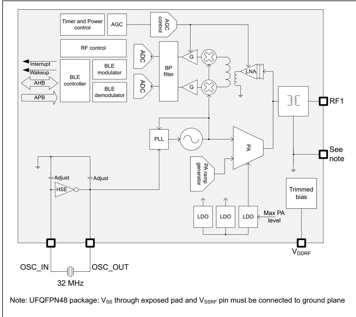
The block diagram illustrates the internal architecture of the radio system. On the left, a 'Timer and Power control' block is connected to an 'AGC' block, which in turn connects to an 'AGC control' block. Below the 'Timer and Power control' is an 'RF control' block. Further down is a 'BLE controller' block, which is connected to 'Interrupt', 'Wakeup', 'AHB', and 'APB' interfaces. The 'BLE controller' is also connected to a 'BLE modulator' and a 'BLE demodulator'. The 'BLE modulator' output goes to an 'ADC' block, which then connects to a 'BP filter' block. The 'BP filter' output is connected to two 'G' (gain) blocks, which are then connected to two 'X' (mixer) blocks. The 'X' blocks are connected to an 'LNA' (Low Noise Amplifier) block. The 'LNA' output is connected to a 'PA' (Power Amplifier) block. The 'PA' output is connected to an 'RF1' pin. A 'PLL' (Phase Locked Loop) block is connected to a 'PA ramp generator' block, which is also connected to the 'PA'. The 'PLL' is connected to an 'HSE' (High Speed External) oscillator circuit, which includes 'OSC_IN' and 'OSC_OUT' pins and a '32 MHz' crystal. The 'HSE' circuit also has 'Adjust' pins. The 'PA' is connected to three 'LDO' (Low Dropout Regulator) blocks, which are connected to a 'Trimmed bias' block. The 'Trimmed bias' block is connected to a 'Max PA level' input and a 'VDDRF' pin. A 'See note' label is present near the 'RF1' pin.
Note: UFQFPN48 package: V SS through exposed pad and V SSRF pin must be connected to ground plane