67. Device electronic signature
The electronic signature is stored in the Flash memory area. It can be read using the JTAG/SWD or the CPU. It contains factory-programmed identification data that allow the user firmware or other external devices to automatically match its interface to the characteristics of the STM32H7Rx/7Sx microcontrollers.
67.1 Unique device ID register (96 bits)
The unique device identifier is ideally suited:
- • for use as serial numbers (for example USB string serial numbers or other end applications)
- • for use as security keys in order to increase the security of code in Flash memory while using and combining this unique ID with software cryptographic primitives and protocols before programming the internal Flash memory
- • to activate secure boot processes, etc.
The 96-bit unique device identifier provides a reference number which is unique for any device and in any context. These bits can never be altered by the user.
The 96-bit unique device identifier can also be read in single bytes/half-words/words in different ways and then be concatenated using a custom algorithm.
Base address: 0x08FF F800
Address offset: 0x00
Read only = 0xXXXX XXXX where X is factory-programmed
| 31 | 30 | 29 | 28 | 27 | 26 | 25 | 24 | 23 | 22 | 21 | 20 | 19 | 18 | 17 | 16 |
|---|---|---|---|---|---|---|---|---|---|---|---|---|---|---|---|
| U_ID[31:16] | |||||||||||||||
| r | r | r | r | r | r | r | r | r | r | r | r | r | r | r | r |
| 15 | 14 | 13 | 12 | 11 | 10 | 9 | 8 | 7 | 6 | 5 | 4 | 3 | 2 | 1 | 0 |
| U_ID[15:0] | |||||||||||||||
| r | r | r | r | r | r | r | r | r | r | r | r | r | r | r | r |
Bits 31:0 U_ID[31:0] : X and Y coordinates on the wafer
Address offset: 0x04
Read only = 0xXXXX XXXX where X is factory-programmed
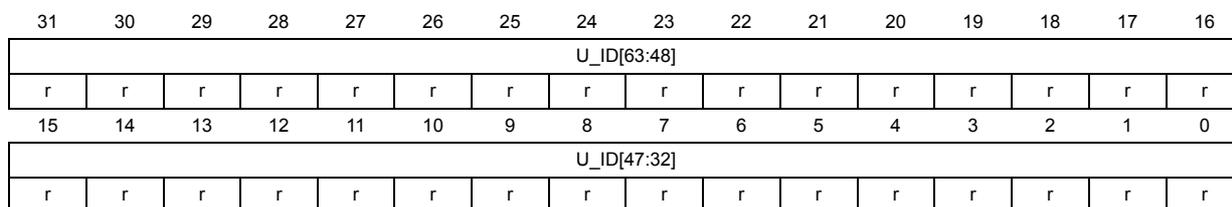
| 31 | 30 | 29 | 28 | 27 | 26 | 25 | 24 | 23 | 22 | 21 | 20 | 19 | 18 | 17 | 16 |
| U_ID[63:48] | |||||||||||||||
| r | r | r | r | r | r | r | r | r | r | r | r | r | r | r | r |
| 15 | 14 | 13 | 12 | 11 | 10 | 9 | 8 | 7 | 6 | 5 | 4 | 3 | 2 | 1 | 0 |
| U_ID[47:32] | |||||||||||||||
| r | r | r | r | r | r | r | r | r | r | r | r | r | r | r | r |
Bits 31:8 U_ID[63:40] : LOT_NUM[23:0]
Lot number (ASCII encoded)
Bits 39:32 U_ID[63:32] : 63:32 unique ID bits
Wafer number (8-bit unsigned number)
Address offset: 0x08
Read only = 0xXXXX XXXX where X is factory-programmed
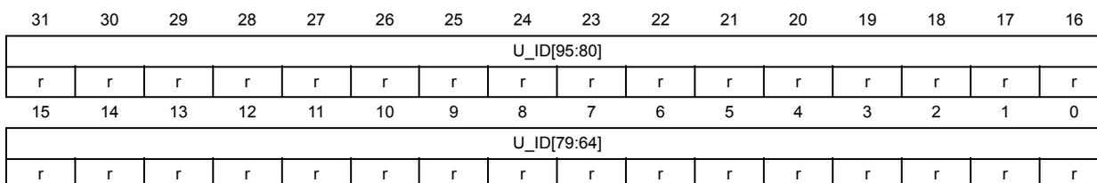
| 31 | 30 | 29 | 28 | 27 | 26 | 25 | 24 | 23 | 22 | 21 | 20 | 19 | 18 | 17 | 16 |
| U_ID[95:80] | |||||||||||||||
| r | r | r | r | r | r | r | r | r | r | r | r | r | r | r | r |
| 15 | 14 | 13 | 12 | 11 | 10 | 9 | 8 | 7 | 6 | 5 | 4 | 3 | 2 | 1 | 0 |
| U_ID[79:64] | |||||||||||||||
| r | r | r | r | r | r | r | r | r | r | r | r | r | r | r | r |
Bits 31:0 U_ID[95:64] : LOT_NUM[55:24]
Lot number (ASCII encoded)
67.2 Package data register
Base address: 0x08FF F80C
Address offset: 0x00
Read only = 0xXXXX where X is factory-programmed
| 31 | 30 | 29 | 28 | 27 | 26 | 25 | 24 | 23 | 22 | 21 | 20 | 19 | 18 | 17 | 16 |
|---|---|---|---|---|---|---|---|---|---|---|---|---|---|---|---|
| Res. | Res. | Res. | Res. | Res. | Res. | Res. | Res. | Res. | Res. | Res. | Res. | PKG_CODE | |||
| r | r | r | r | ||||||||||||
| 15 | 14 | 13 | 12 | 11 | 10 | 9 | 8 | 7 | 6 | 5 | 4 | 3 | 2 | 1 | 0 |
| Res. | Res. | Res. | Res. | Res. | Res. | Res. | Res. | Res. | Res. | Res. | Res. | Res. | Res. | Res. | Res. |
Bits 31:20 Reserved, must be kept at reset value.
Bits 19:16 PKG_CODE[3:0] : Package information code
This bitfield indicates the device package type.
GP device package:
0000: VFQFPN68 GP
0001: TFBGA100 SMPS GP
0010: LQFP100 GP
0011: LQFP144 GP
0100: UFBGA144 SMPS GP
0111: UFBGA169 SMPS GP
1000: UFBGA176+25 SMPS GP
1001: LQFP176 SMPS GP
1100: TFBGA225 OCTO
1101: TFBGA225 HEXA
1110: WLCSP SMPS GP
Graphics device package:
0101: UFBGA144 SMPS GFX
0110: UFBGA169 SMPS GFX
1010: LQFP176 SMPS GFX
1011: UFBGA176+25 SMPS GFX
1100: TFBGA225 OCTO
1101: TFBGA225 HEXA
Bits 15:0 Reserved, must be kept at reset value.
The SBS clock should be enabled first in the RCC_APB4ENR register.