31. Digital camera interface pixel pipeline (DCMIPP)
31.1 DCMIPP introduction
The DCMIPP is the pixel pipeline section of a high-resolution camera subsystem: it gets pixels from a parallel interface, and after some processing (such as decimation, cropping) dumps them to the memory.
DCMIPP supports multiple types of external sensors, among others:
- • dumb sensors (without internal ISP), which output raw Bayer pixels
- • smart sensors (with an internal ISP), which usually output RGB or YUV pixels
- • smart sensors with internal compression, which output a bit-stream (such as JPEG, or H264)
The DCMIPP input interface integrates a parallel interface (up to 16 bits at 120 MHz, with internal/external synchronization).
A first common part of the DCMIPP selects the input exclusively from the parallel interface. Data go to dedicated pipeline(s) before they are sent to memory for further processing or display purposes.
Table 275. Available pipeline
| ID | Function | Description |
|---|---|---|
| Pipe0 | Dump pipe | Used to dump the received data as-is, without any processing (for example, without pixel extraction, no formatting), with an exception: it formats the 10/12/14-bit raw Bayer components mapped unpacked into 16-bit memory words, to ease the job of a downstream application. 2D crop operation and basic decimation can be performed within this pipe. |
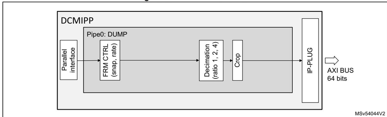
Figure 332 shows the DCMIPP main functions, namely the integrated parallel interface, the applicative post-processing pipeline with its crop, downsize, and pixel formatting.
Figure 332. DCMIPP overview
graph LR
    subgraph DCMIPP
        direction LR
        PI[Parallel interface] --> P0DUMP
        subgraph P0DUMP [Pipe0: DUMP]
            direction LR
            FC[FRM CTRL<br/>(snap, rate)] --> DEC[Decimation<br/>(ratio 1, 2, 4)]
            DEC --> C[Crop]
        end
        C --> IP_PLUG[IP_PLUG]
    end
    IP_PLUG --> AXI[AXI BUS<br/>64 bits]
MSv54044V2
Table 276. Glossary
| Item | Definition |
|---|---|
| A | Alpha component, used to define transparency, opaque = 0xFF, for example ARGB. |
| BPC | Bits per component (for example, RGB565 has five bits for the red component, hence 5 bpc) |
| BPP | Bits per pixel (for example, RGB565 has 16 bits per pixel, hence 16 bpp) |
| DCMIPP_ | Digital camera interface - Pixel pipeline |
| Interlaced | Interlaced video: the field with odd lines is transmitted first, followed, after the last odd line, by the field with even lines. The two fields are thus consecutive but exclusive. |
| NPU | Neural network processing engine (also known as NN, neural network). |
| Planar | Defines in how many sub-buffers a pixel buffer is split into: 1 (coplanar). |
| YUV444 | Pixel format, YUV color reference, all three components (Y, U, V) given per pixel. |
| YUV422 | Pixel format, YUV color reference, chroma component (U, V) sub-sampled 1/2 in X |
| YUV420 | Pixel format, YUV color reference, chroma component (U, V) sub-sampled 1/2 in X and Y. |
31.2 DCMIPP main features
- • Parallel input interface:
- – Pixel rate: up to 16 bits in parallel, 100 Mpixel/s (typically 1080p30, maximum 2048x2048 on processing pipelines after decimation).
- – Pixel format: RGB565, RGB888, YUV422, raw Bayer/Mono 8/10/12/14, and ByteStream (JPEG)
- • Pipeline maximum resolution:
- – Dimensioned for 5 Mpixel (typically 2560 x 2048 or 2688 x 1944) before decimation
- – Maximum pipe resolution: 4094 x 4094
- • Maximum frame per second (fps): typical examples are defined with 30 fps, it is possible to reach higher rates (for example 120 fps) by decreasing image resolution to guarantee the maximum pixel rate constraints.
- • Flow selection and frame control:
- – Capture mode in Continuous vs. Snapshot mode
- • Decimation on Pipe0 (dump pipe)
- – Pure sub-sampling, ratio 1 vs. 1, 2, 4 in X and ratio 1 vs. 1, 2 in Y
- • Parallel pipelines for parallel applications:
- – Pipe0 (for data dump) for a direct dump without processing
- • Single Pipe0 (for data dump) for a direct dump from the camera to the memory (with only few operations like crop and basic decimation).
- • Output pixel format:
- – Pipe0: any data as-is, Y/Rb: 8/10/12/14 statistics, bit streams
- • AXI master:
- – Output FIFOs to drain pixel/data to the memory (linked to the memory latency) from the pipe(s)
- – The unique AXI-Master interface implements one client per pipe
- – Double buffer mode capability per pipe
- • Overrun detection:
- – Notification in case of frame impacted by pixel congestion (no impact on the following frame if the congestion cause is solved)
31.3 DCMIPP functional description
31.3.1 DCMIPP block diagram
The block diagram of the DCMIPP is shown in Figure 333 .
Figure 333. DCMIPP block diagram
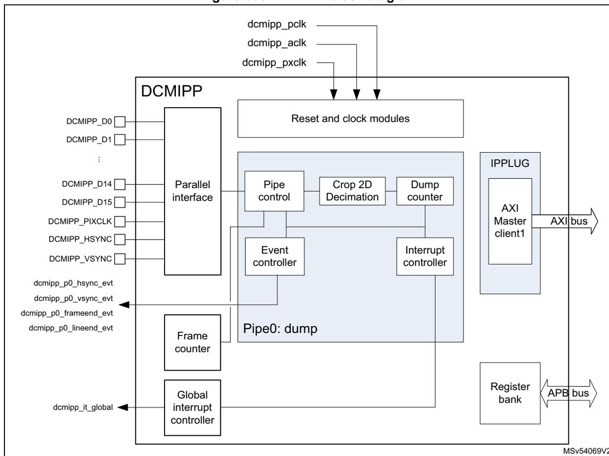
The block diagram illustrates the internal architecture of the DCMIPP. At the top, three external clock signals (dcmipp_pclk, dcmipp_aclk, and dcmipp_pxclk) are connected to the 'Reset and clock modules'. On the left, a 'Parallel interface' block receives 16-bit data (DCMIPP_D0 to DCMIPP_D15), a pixel clock (DCMIPP_PIXCLK), and synchronization signals (DCMIPP_HSYNC, DCMIPP_VSYNC). This interface is connected to a 'Pipe control' block. The 'Pipe control' block is part of a larger 'Pipe0: dump' section which also includes 'Crop 2D Decimation', 'Dump counter', 'Event controller', and 'Interrupt controller'. Below the 'Pipe control' block is a 'Frame counter', which in turn connects to a 'Global interrupt controller'. The 'Global interrupt controller' outputs a global interrupt signal (dcmipp_it_global). To the right, an 'IPPLUG' block contains an 'AXI Master client1' connected to an 'AXI bus'. Below this, a 'Register bank' is connected to an 'APB bus'. Output signals from the 'Event controller' and 'Frame counter' include dcmipp_p0_hsync_evt, dcmipp_p0_vsync_evt, dcmipp_p0_frameend_evt, and dcmipp_p0_lineend_evt. The diagram is labeled with MSv54069V2 at the bottom right.
31.3.2 DCMIPP pads and internal signals
Table 277. DCMIPP input/output pads
| Pin name | Signal type | Description |
|---|---|---|
| DCMIPP_Dn (n = 0 to 15) | Input | Bit n of the parallel data bus coming from the camera sensor |
| DCMIPP_PIXCLK | Input | Pixel clock sent by the master (parallel camera sensor module) |
| DCMIPP_VSYNC | Input | VSYNC signal (vertical synchronization) coming from the camera sensor |
| DCMIPP_HSYNC | Input | HSYNC signal (horizontal synchronization) coming from the camera sensor |
Table 278. DCMIPP input/output pins
| Internal signal name | Signal type | Description |
|---|---|---|
| dcmipp_pclk | Input | DCMIPP APB clock (APB bus) |
| dcmipp_aclk | Input | DCMIPP AXI clock (AXI bus) |
| dcmipp_it_global | Output | DCMIPP interrupts (refer to Table 296 for the full list of interrupt sources) |
| dcmipp_p0_hsync_evt | Output | Pipe0 Hsync event |
| dcmipp_p0_vsync_evt | Pipe0 Vsync event | |
| dcmipp_p0_frameend_evt | Pipe0 frame end event | |
| dcmipp_p0_lineend_evt | Pipe0 line event |
31.3.3 DCMIPP reset and clocks
Table 279. DCMIPP clocks
| Domain | Clock | Maximum frequency | Comments |
|---|---|---|---|
| Parallel | dcmipp_pxclk | 120 MHz | Up to 2x 120 MB/s in 16-bit mode |
| AXI bus | dcmipp_aclk | 266 MHz | SoC AXI frequency |
| APB bus | dcmipp_pclk | 133 MHz | SoC APB frequency |
Table 280. DCMIPP resets
| Domain | Reset type | Comments |
|---|---|---|
| Parallel + Pipeline | Asynchronous | Resynchronized internally on dcmipp_pxclk |
| AXI bus | Synchronous | Resets directly the dcmipp_aclk domain |
| APB bus | Synchronous | Resets directly the dcmipp_pclk domain |
Clocks and pixel rate limitations
This paragraph lists the DCMIPP limitations and bottlenecks:
- • The target is to sustain an average pixel rate (PixRateAvg):
- – A 5 Mpixel sensor at 15 fps requires 75 Mpixel/s
- • Vertical and horizontal blanking:
- – The full system (sensor, interface, pipe, AXI) embeds limited capacity FIFOs. The idle times that the sensor inserts during its blanking periods impact all the downstream elements, including interface, pipe, and AXI. A pixel rate (PixRatePeak) higher than average must be used. The idle time due to the blanking can reach 33% of the frame duration, sometimes more (check sensor specification).
- – \( PixRatePeak = 1.33 * PixRateAvg \)
- • Parallel interface clock (dcmipp_pxclk):
- – On the parallel interface, pixels are received sequentially, in one, two or three cycles. The maximum implemented clock (120 MHz) constrains the peak pixel rate, depending on the ratio of cycles per pixel.
- – \( PixRatePeak \leq dcmipp\_pxclk / (1, 2 \text{ or } 3) = 120 / (1, 2 \text{ or } 3) \)
- – Clock frequency:
- > \( \leq dcmipp\_pxclk \leq dcmipp\_aclk \)
- – Consequences: see Table 281 .
Table 281. Parallel interface maximum resolution (80 MHz)
| Pixel | Transmission on the interface | Resolution (30 fps), including blanking | ||||
|---|---|---|---|---|---|---|
| Format | Width (bpp) | Width | Cycles/pixel | Pixel rate | Mpixel/frame | Example |
| Mono/raw | 8 | 8 | 1 | 80 | 2.15 | 1080 p |
| 14 | 14 | 1 | 80 | 2.15 | 1080 p | |
| RGB565 | 16 | 8 | 2 | 40 | 1.08 | 720 p |
| 16 | 1 | 80 | 2.15 | 1080 p | ||
| RGB888 | 24 | 8 | 3 | 27 | 0.72 | qHD |
| 12 | 2 | 40 | 1.08 | 720 p | ||
| YUV422 | 16 | 16 | 1 | 80 | 2.15 | 1080 p |
| 16 | 2 | 40 | 1.08 | 720 p | ||
| YUV444 | 24 | 12 | 2 | 40 | 1.08 | 720 p |
| 16 | 2 | 40 | 1.08 | 720 p | ||
- – Clock setting: \( dcmipp\_pxclk \geq PixRatePeak * Ratio(1,2,3) \)
31.3.4 DCMIPP maximum resolution
The limitations related to the maximum resolution supported by the DCMIPP are:
- • Maximum width and height across pipes: 4094 x 4094 pixels
- – Registers and counters are limited to 12 bits
- • Maximum performance: 266 Mpixel/s
- – Larger pixel rate can be used, but with lower memory latency
- – Maximum pixel rate on each pipe must remain below the pixel clock
- • Max line stride: 32767 bytes
- – Registers and counters, to handle 4094 pixels x 32 bits x 2 (provision for interleaving)
31.3.5 DCMIPP minimum requirements for frame structure
DCMIPP imposes the following minimum requirements for the frame architecture:
Blanking phase
- • Dump pipe
- – The minimal duration of the blanking between two frames must be an equivalent of 666 datawords of 32 bits
Data image area
- • Vertical image area: minimum one line
- • Horizontal image area: minimum two pixels
- • The minimum total frame size is fixed to 36 pixels
31.3.6 Description of DCMIPP pixel format support
Table 282 lists the supported pixel formats in the input interfaces (parallel interface), and in the output Pipe0.
Table 282. Supported pixel formats
| Index (1) | Pixel format | BPP | Parallel input (clk/pix) (2) | Pipe0 output (dump) |
|---|---|---|---|---|
| 13 (3) | Byte stream (JPEG, compressed video) | 8 | Y, 1 | Y |
| 14 (4) | Other data | 8 to 16 (4) | Y, 1 | Y |
| 5 | Raw6 | 6 | (5) | Y |
| 5 | Raw7 | 7 | (5) | Y |
| 5 | Raw8 | 8 | Y, 1 | Y |
| 6 | Raw10 | 10 | Y, 1 | To 16 bpc |
| 7 | Raw12 | 12 | Y, 1 | To 16 bpc |
| 8 | Raw14 | 14 | Y, 1 | To 16 bpc |
| 9 | Mono8 | 8 | Y, 1 | Y |
| 10 | Mono10 | 10 | Y, 1 | To 16 bpc |
| 11 | Mono12 | 12 | Y, 1 | To 16 bpc |
| 12 | Mono14 | 14 | Y, 1 | To 16 bpc |
Table 282. Supported pixel formats (continued)
| Index (1) | Pixel format | BPP | Parallel input (clk/pix) (2) | Pipe0 output (dump) |
|---|---|---|---|---|
| 2 | RGB444 | 12 | (5) | (5) |
| 2 | RGB555 | 15 | (5) | (5) |
| 2 | RGB565 | 16 | Y, 1 and 2 | Y |
| 3 | RGB666 | 18 | (5) | (5) |
| 4 | RGB888 / YUV444 (a) | 24 | Y, 2 and 3 | Y |
| 1 | YUV422-1 (YUYV) | 16 | Y, 1 and 2 | Y |
- Index is used to link the input pixel format to the DCMIPP_PRCR register. The index has a meaning only for camera connected with the parallel interface
- Pixel formats on 16 bpp (like RGB565 or YUV422-1) can be received either on an 8-bit interface (using 2 cycles), or on a 16-bit input interface (using one cycle). Pixel formats on 24 bpp (like RGB888) can be received either on an 8-bit interface (using three cycles), or on a 12-bit input interface (using two cycles).
- In Byte stream mode the bytes are dumped consecutively with only a 32-bit padding (if needed) at the end of the frame (or JPEG stream). There is no 32-bit padding operation inside the stream until the VSYNC deassertion (end of frame, or end of JPEG stream).
- If the data format is different from those in this table, user can choose "others" configuration into bit field FORMAT in the DCMIPP_PRCR register, using bit-field EDM to select how many data bits must be captured in one pixel clock. It is possible to capture two 8-bit data mapped on 16-bit parallel input data in a single cycle (for instance FORMAT = Others, EDM = 100, i.e. 16-bit capture on each pixel clock). Data are 32-bit padded at the end of a line to have a complete line aligned on 32-bit width.
- On the parallel interface input, some sensor pixel formats are supported by the DCMIPP, by selecting a wider pixel format in DCMIPP, by mapping the sensor wires onto the MSB of the DCMIPP interface. On the input missing pins, it is recommended to replicate the sensor MSB pins onto the missing input LSB pins. This helps achieving full dynamic on the extended pixel format. The work-around can be applied on the following formats (sensor output on left, mapping on DCMIPP format on right):
- - Raw6: Raw8 with 1-cycle input, processed as an 8 bpp
- - Raw7: Raw8 with 1-cycle input, processed as an 8 bpp
- - RGB444: RGB565 with 1-cycle input, processed as a 16 bpp
- - RGB555: RGB565 with 1-cycle input, processed as a 16 bpp
- - RGB666: RGB888 with 3-cycle input, processed as a 24 bpp
31.4 DCMIPP input and flow control
This section describes the functional elements of the DCMIPP. For each, it details the features, the software configuration, and provides a software configuration example (when needed).
31.4.1 DCMIPP common configuration
The DCMIPP common configuration register (DCMIPP_CMCR) enables the selection of the input interface—either parallel DCMI or serial CSI-2—from which to fetch the input pixels. It also allows swapping the R/B color components of the incoming pixels and selecting the pipe used by the frame counter.
Table 283. DCMIPP_CMCR bit function
| Bit ID | Function | Comments |
|---|---|---|
| CFC | Clear frame counter | Clear the frame counter when set. |
31.4.2 Parallel input interface
The parallel interface is a flexible pixel interface that clocks in a bus of 8- to 16-bit in parallel, with an externally provided clock, and adds vertical and horizontal synchronization, provided either with specific pins (external sync) or flagged via specific data (as in CCIR601).
Interface (all inputs)
- • Clk: clock up to 120 MHz, internally named dcmipp_pxclk
- • Data: 16 IO pins, up to 120 Mbps/pin, 8- to 16-bit, pixels potentially serialized
- • HSync, VSync, but no enable (EN)
Features
- • Horizontal and vertical synchronization:
- – External, via the HSync and VSync pins.
- – Internal, via the CCIR601 flagging.
- • Input pixel format (see
Section 31.3.6
)
- – Binary stream like JPG
- – Single cycle data:
- > Raw Bayer and monochrome: 8/10/12/14 bits in parallel
- > YUV422, RGB565: 16 bpp on 16 bits in parallel
- – Double-cycle data:
- > YUV422, RGB565: 16 bpp on 8 bits in parallel
- > RGB888/YUV444: 24 bpp on 12 bits in parallel
- – Triple-cycle data:
- > RGB888/YUV444: 24 bpp on 8 bits in parallel
- • Flexible input:
- – MSB-vs-LSB bits can be swapped to ease PCB placement
- – Cycle0-vs-Cycle1 can be swapped (for 2-cycle long pixels).
Hardware synchronization mode
In this mode two synchronization signals (DCMIPP_HSYNC and DCMIPP_VSYNC) are used.
Depending on the camera module/mode, data can be transmitted during horizontal/vertical synchronization periods. DCMIPP_HSYNC/DCMIPP_VSYNC act as blanking signals, as all data received during DCMIPP_HSYNC/DCMIPP_VSYNC active periods are ignored.
To correctly transfer images in the RAM buffer, data transfer is synchronized with the DCMIPP_HSYNC/DCMIPP_VSYNC signals. When the hardware synchronization mode is selected, and capture is enabled (CPTREQ bit set in DCMIPP_PxFCTCR), data transfer is synchronized with the deassertion of the DCMIPP_VSYNC signal (next start of frame).
Transfer can then be continuous, with successive frames transferred by the IP-Plug to successive buffers or the same/circular buffer.
Embedded data synchronization mode
In this synchronization mode, the data flow is synchronized using embedded 32-bit codes, using the 0x00/0xFF values not used in data anymore. There are four types of codes, all with 0xFF00 00XY format. The embedded synchronization codes are supported only in 8-bit parallel data capture (in the DCMIPP_PRCR register, the EDM[2:0] bits must be programmed to "000"). For other data widths, this mode generates unpredictable results.
Note: Camera modules generate up to eight synchronization codes when in interleaved mode, while the DCMIPP reacts to one single code. As a consequence, an interleaved flow with an embedded synchronization has one every other frame discarded as not detected.
Mode 2
Four embedded codes signal the following events:
- • Frame start (FS)
- • Frame end (FE)
- • Line start (LS)
- • Line end (LE)
The XY values in the 0xFF00 00XY format of these codes are programmable (see Section 31.10.9 ).
A 0xFF value programmed as a frame end means that all the unused codes are interpreted as valid frame end codes.
In this mode, once the camera interface has been enabled, the frame capture starts after the first occurrence of the frame end (FE) code followed by a frame start (FS) code.
Mode 1
An alternative coding is the camera mode 1. This mode is ITU656 compatible.
The codes signal another set of events:
- • SAV (active line) - Line start
- • EAV (active line) - Line end
- • SAV (blanking) - Start of line during interframe blanking period
- • EAV (blanking) - End of line during interframe blanking period
This mode can be supported by programming the following codes:
- • FS ≤ 0xFF
- • FE ≤ 0xFF
- • LS ≤ SAV (active)
- • LE ≤ EAV (active)
An embedded unmask code is also implemented for frame/line start and frame/line end codes. Using it, it is possible to compare only the selected unmasked bits with the programmed code. User can therefore select a bit to compare in the embedded code and detect a frame/line start or frame/line end. This means that there can be different codes for the frame/line start and frame/line end with the unmasked bit position remaining the same.
Example:
- • FS = 0xA5
- • Unmask code for FS = 0x10
In this case the frame start code is embedded in bit 4 of the frame start code.
Note: FEC sequence must be sent before the transfer of the first frame, otherwise other codes are not decoded and the first frame can be lost after the DCMIPP has been enabled. After the first FE sequence, the following frame is captured based on FS sequence.
Error conditions
Error conditions can be detected when using the embedding synchronization data modes. Flags PRERRF in DCMIPP_CMSR2 and ERRF in DCMIPP_PSR are used for this function. An interruption can be triggered based on error detection if bit PRERRIE in DCMIPP_CMIER is set for the global interrupt (or bit ERRIE in DCMIPP_PRIER for a local interrupt line).
For instance, such kind of wrong sequences or values generate an error:
- – FF 00 00 XY sequence detected with XY value different from the one set for FS/LS/FE/LE
- – LS = 0xFF or LE = 0xFF
- – If an LS or FS sequence follows an LS sequence
Software configuration
Table 284. DCMIPP_PRCR bit function
| Bit ID | Function | Comments |
|---|---|---|
| ENABLE | Enables the parallel interface | Low-power mode when disabled. |
| PCKPOL | Defines clock polarity | – 0: Falling edge – 1: Rising edge |
| ESS | Defines if VSync and HSync synchronizations are provided by sideband (specific hardware IO) or by in-band (specific embedded codes) signals | – 0: Hardware (external) synchronization: using DCMIPP_HSYNC and DCMIPP_VSYNC pins. – 1: Embedded (internal) synchronization: using codes FSC, FEC, LSC, LEC and masks in registers DCMIPP_PRESR and DCMIPP_PRESURy. |
| VSPOL, HSPOL | Defines the polarity of the IO DCMIPP_VSYNC and DCMIPP_HSYNC used for, respectively, the vertical and horizontal synchronization | – 0: Active low – 1: Active high |
| FORMAT | Defines the pixel format used on the IO DCMIPP_Dx | From 0 to 15 |
| EDM | Defines the amount of valid bits received per cycle The duration of a pixel is extracted by the bit-per-pixel (given by FORMAT) and bit-per-cycle (given by EDM) ratios | 8/10/12/14/16 bits 1, 2 or 3 cycles |
| SWAPBITS | Swaps the 16 bits of the parallel interface | 15:0 becomes 0:15 |
| SWAPCYCLES | Swaps, when a pixel is received in two cycles, the data from the first cycle with the data from the second cycle | Software must not activate it when a pixel is received in one or three cycles. |
The embedded synchronization codes are configured by means of DCMIPP_PRESQR and DCMIPP_PRESUR registers (see Table 285 ).
Table 285. DCMIPP_PRESQR and DCMIPP_PRESUR bit function
| Bit ID | Function |
|---|---|
| FSC, FEC | Frame-start and frame-end synchronization, when embedded synchronization ESS = 1 |
| FSU, FEU | Masks for FSC and FEC codes |
| LSC, LEC | Line-start and line-end synchronization, when embedded synchronization ESS = 1 |
| LSU, LEU | Masks for LSC and LEC codes |
31.4.3 Frame counter
A frame counter is available for a tag purpose and counts all the frame received on the selected pipe.
The counter is 32-bit, read-only. It is active at least when bit PIPEN of the pipe is enabled (PIPEN = 1).
It provides an (almost) unique frame number, with a loop time of 4.5 years (if 30 fps).
The counter can be incremented at the FrameStart event of the pipe when the camera sensor module is connected with parallel interface.
The frame counter is cleared by setting CFC in the DCMIPP_CMCR register.
Software configuration
The frame counter must be configured before it is used for the pipe. Software action(s) must be performed in the DCMIPP_CMCR register:
- – Frame counter runs as soon as the selected pipe is active (PIPEN = 1)
Note: It is possible to have the Frame counter run on a pipe, while having the pipe not flowing any pixel: this is achieved with pipe enable active (PIPEN = 1) to have the frame counter run, but with CPTREQ = 0 to avoid any pixel flow.
31.4.4 Frame control
The module is replicated for the dump pipe. It handles the frame control and the capture of the pipe, grouping data into frames, and capturing them when requested.
Definitions
There are two notions of frame events
- • Event used inside the hardware (provided by the input interfaces):
- – FrameStart: when a frame starts at the input of the pipe (at frame control)
- > Parallel interface with VSync fall
- – FrameEnd: when a frame finishes at the input of pipes (at frame control)
- > Parallel interface: VSync rise (End-of-Frame)
- – FrameStart: when a frame starts at the input of the pipe (at frame control)
- • Events exposed to software via DCMIPP events and interrupts:
- – VSYNC
- > When a frame starts, observed at the input of the pipe (at frame control)
- > It indicates that the current frame has started and has sampled its shadow registers, and that the software can start to configure the next frame
- > It is recommended to use that interrupt to trigger the software that reconfigures the DCMIPP.
- – FRAME END
- > When a frame finishes, observed at the output of pipe (when the last pixel has been written on the AXI)
- > It indicates that the current frame has finished writing all its data to memory, and that the application can immediately start using them
- > It is recommended to use that interrupt to trigger the software that forwards the memory buffer to other applications
- – VSYNC
Features
- • Frame delineation: allows to dump data with the required frame granularity.
- – Extracts the FrameStart and FrameEnd event, based on the input Start-of-Frame and End-of-Frame.
- > The FrameStart immediately generates a VSYNC event.
- > The FrameEnd ripples till the end of the pipe, at the pixel packer level, where it generates the FRAME event.
- – Based on the algorithm detailed in Extraction algorithm for FrameStart and FrameEnd .
- – Extracts the FrameStart and FrameEnd event, based on the input Start-of-Frame and End-of-Frame.
- • Capture mode: can capture a frame snapshot, or capture continuously.
- • Capture rate: can capture all frames, or one out of 2, 4, 8. It is only active when the Capture mode is in Continuous mode.
Extraction algorithm for FrameStart and FrameEnd
The extraction of the FrameStart and FrameEnd is straightforward.
Use cases
The Continuous mode is typically used to send to display or to software-analysis a continuous stream of frames.
The Snapshot mode is typically used to dump a high-resolution frame.
The Frame rate mode is typically used for a low-power continuous analysis, where only one frame every eight is dumped and analyzed.
The frame informations are typically used for interlaced video use cases, where the sensors transmit alternatively odd and even fields (top vs. bottom), and where software must be able to retrieve the type of field. Depending on the sensor, it can be retrieved from:
- the LSB of the counted number of lines in that frame (indicates if the number is odd or even)
Software configuration
The frame control supports two different capture modes:
- Snapshot mode: the software captures single frames
- Continuous mode: the software captures a continuous sequence.
The timing diagram of these two modes is shown in Figure 334 .
Figure 334. Snapshot (CPTMODE = 1) and Continuous (CPTMODE = 0) capture modes
The diagram illustrates two capture modes over a timeline of VSYNC and EndOfFrame signals.
Top Section: Snapshot Mode (Static CPTMODE = 1)
- VSYNC (StartOfFrame): The first vertical dashed line.
- SW CPTREQ = 1: A software request is made after the first VSYNC.
- CPTREQ = 1: The request signal is shown as a pulse.
- CPTACT = 1: The capture activity starts at the second VSYNC signal.
- CAPTURE to AXI: Data is transferred to AXI during the capture activity.
- EndOfFrame (capture complete): The capture completes at the third vertical dashed line.
- Subsequent VSYNC: Two more VSYNC signals follow, but no further capture occurs as it's snapshot mode.
Bottom Section: Continuous Mode (Static CPTMODE = 0)
- VSYNC (StartOfFrame): The first vertical dashed line.
- SW CPTREQ = 1: A software request is made after the first VSYNC.
- CPTREQ = 1: The request signal is shown as a pulse.
- CPTACT = 1: The capture activity starts at the second VSYNC signal.
- CAPTURE to AXI: Data is transferred to AXI during the capture activity.
- EndOfFrame (capture complete): The first capture completes at the third vertical dashed line.
- VSYNC: A VSYNC signal occurs at the fourth vertical dashed line.
- CPTACT = 1: A second capture activity starts at this VSYNC.
- CAPTURE to AXI: Data is transferred to AXI during the second capture activity.
- EndOfFrame (capture complete): The second capture completes at the fifth vertical dashed line.
- SW CPTREQ = 0: A software request to stop is made after the second EndOfFrame.
- VSYNC (StartOfFrame): A final VSYNC signal occurs at the sixth vertical dashed line.
Table 286. DCMIPP_PxFCTCR bit function
| Bit ID | Function | Values |
|---|---|---|
| CPTMODE | Capture mode |
|
| CPTREQ | Capture request |
|
Table 286. DCMIPP_PxFCTCR bit function (continued)
| Bit ID | Function | Values |
|---|---|---|
| FRATE | Frame rate |
|
| CPTACT (1) | Capture status |
|
- 1. Bit read from the DCMIPP_PxSR register.
Configuration example
The software operations when using the Snapshot mode are the following:
- 1. Software sets CPTMODE = 1, to use the Snapshot mode.
- 2. Software sets PIPEN = 1, to let the flow selection send data to PipeN.
- 3. Software sets CPTREQ = 1, to request the capture of one frame.
- 4. At the first following VSync, the HW samples CPTREQ at 1, with the following impact:
- a) The capture effectively starts: pixels flow into the pipe and are dumped in memory.
- b) CPTACT is set to 1, to mention that a capture is currently ongoing, and that it is best to not modify the configuration of the pipe operators, unless shadowed.
- c) CPTREQ is reset to 0, so that only a single frame is dumped.
- 5. At the following capture complete interrupt
- a) CPTACT is reset to 0, to signal that the capture is over.
- b) The capture is complete, no more pixels are flowing, hence software can restart to update the configuration of non-shadowed registers without any issue, and use the captured pixels in memory. Depending upon the sensor blanking, this period can be short.
- 6. At the next VSync, CPTREQ usually is sampled at 0, so that no more frames are captured
- – As soon as CPTREQ is reset to 0 the software can set it again to 1, to request a capture at the following frame. It means that a continuous sequence of frame can be captured by setting again CPTREQ to 1, continuously frame after frame.
The software operations when using the Continuous mode are the following:
- 1. Software sets CPTMODE = 0, to use the Continuous mode.
- 2. Software sets PIPEN = 1, to let the flow selection send data to PipeN.
- 3. Software sets CPTREQ = 1, to request the continuous capture of frames.
- 4. At the first following VSync, CPTREQ is sampled at 1, with the following impact:
- – As in Snapshot mode, the capture starts, and CPTACT is set at 1.
- – Unlike the Snapshot mode, CPTREQ is not modified and remains at 1.
- 5. At the following capture complete interrupt:
- – As in Snapshot mode, CPTACT is reset to 0, capture stops, software can shortly reconfigure the pipes, and software can use the captured pixels.
- 6. At the next VSync, and as long as CPTREQ remains at 1, the capture restarts, similarly as described above.
- 7. To stop capturing later frames, software resets CPTREQ to 0.
- – An ongoing capture continues until completion.
- 8. At the next VSync, CPTREQ is sampled at 0, and the next capture does not restart.
31.4.5 Pipe deactivation
It is possible to abort a pipe to stop any frame acquisition and to potentially offer a mean to reprogram it completely (including non-shadowed registers), or to let it fully disabled for some time. The following operating mode has to be considered to correctly stop the pipe:
- 1. Disable the CPTREQ bit of the DCMIPP_PxFCTCR register of the corresponding pipe
- 2. Poll CPTACT = 0 status bit in the DCMIPP_CMSR1 register to check if the pipe is no longer active (idle state)
- 3. Disable PIPEN in the DCMIPP_PxFCTCR register.
When disabling the pipe, the last frame is processed completely by respecting the above operating mode.
Note: To disable the parallel interface (PREN = 0 in the DCMIPP_PxFSCR), it is recommended to first disable the pipe considering the above operation mode, before switching off the parallel interface.
31.5 Pipe0 (dump pipe)
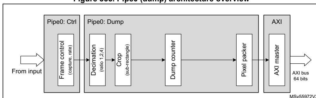
31.5.1 Overview
Pipe0 works as a dump pipe: it extracts data from the camera sensor module and dumps them (as-is) to the targeted memory, with some basic decimation and cropping 2D operations in between.
Figure 335. Pipe0 (dump) architecture overview
graph LR
    Input[From input] --> Ctrl[Pipe0: Ctrl
Frame control
(capture, rate)]
    Ctrl --> Dump[Pipe0: Dump]
    subgraph Dump
        direction LR
        D1[Decimation
(ratio 1:2,4)] --> D2[Crop
(sub-rectangle)]
        D2 --> D3[Dump counter]
        D3 --> D4[Pixel packer]
    end
    D4 --> AXI[AXI
AXI master]
    AXI --> Output[AXI bus
64 bits]
Pipe0 retrieves data from the camera sensor module connected to the DCMIPP through the 16-bit parallel interface.
The frame controller handles mainly the camera acquisition mode (continuous or snapshot, frame rate), see Section 31.4.4 .
When the input data from the camera is valid and supposed to be processed by Pipe0, 2D-cropping and decimation operations can be configured by the software. A dump counter combining with a limit amount of data to be set is offered to handle unknown length of data or to avoid the amount of data to be too wide within a frame.
31.5.2 Decimation
The decimation allows to cheaply downsize a frame.
Based on parallel interface camera module:
- – Factor 1x, 2x, 4x at data/byte level depending on the configuration of bit field BSM[1:0] of the DCMIPP_P0PPCR register. The decimation is not working directly at pixel level, but it is based on either byte or 16-bit word granularity (for padded
raw 10, for instance) to make equivalent decimation to one pixel out of two. Bit OEBS is used to start from the odd or even byte (or data) to capture first.
- – The decimation can also be based on entire line, by capturing all the lines, or one line out of two thanks to bit LSM. Here, again, choice is given to the software to reject odd or even lines within the frame by configuring bit OELS.
Table 287. DCMIPP_P0PPCR bit function
| Bit ID | Function |
|---|---|
| BSM[1:0] | To select how much byte/data have to be captured within a line. This feature is available only for a parallel interface camera module. |
| OEBS | Allows the user to choose if the filtering starts from the odd or the even byte. |
| LSM | Possibility to filter out one line out of two. |
| OELS | The software can select if the filtering rejects the odd or even lines. |
31.5.3 Crop/statistics selection/suppression
The dump pipe (Pipe0) has the capability to handle 2-D crop processing. The vertical cropping is based on line, thanks to HSYNC event (from the physical IOs or the embedded code detection if selected).
The horizontal area on which the crop is applied is based on data (32-bit wide), and not on pixels since this pipe is not directly considering the pixels. It handles the data flow with 32-bit granularity. The CROP functionality is not supported when the pipe is conveying JPEG format. The ENABLE bit must be kept cleared into DCMIPP_P0SCSZR to avoid any unpredictable behavior.
The area to be captured within the frame has to be specified configuring the registers DCMIPP_P0SCSTR and DCMIPP_P0SCSZR. The starting point on the two axis are set accordingly as well as the width in both directions. It is possible to take the data inside or outside this area by means of bit POSNEG in the DCMIPP_P0SCSZR register. Some sensors can send sensor configuration data and statistics (histogram) on the very first and last lines of a frame. By specifying active the area outside of this window selection (POSNEG = 1), only statistic data are extracted by the way, and the software can decide to apply some processing on the data to correct, such as contrast or exposure.
Features
- • 2D-Crop operation with granularity:
- – Lines in the vertical axis
- – 32-bit data in the horizontal axis
- • Possibility to capture data inside or outside the defined window (valid image data or statistic data)
- • Cropping with 0 value for HSIZE[11:0] or VSIZE[11:0] has no crop effect to the dimension for which the 0 value has been applied (vertical or horizontal axis).
Software configuration
Registers DCMIPP_P0SCSTR and DCMIPP_P0SCSZR have to be configured to set the crop feature into the dump pipe:
- 1. Configure the cropped horizontal starting point with HSTART[11:0] and the width with HSIZE[11:0] (both with a 32-bit data granularity).
- 2. Configure the cropped lines, starting at line VSTART[11:0] and with a height of VSIZE[11:0] (both with a line granularity)
- 3. If any value HSIZE or VSIZE is set to 0, the hardware does not consider crop operation in the vertical or horizontal dimension for which the 0 value has been applied, so that all the pixels in that dimension are sampled.
- 4. Select the inner or the outer part of the window for the data capture by configuring POSNEG bit.
- 5. Enable the crop feature setting ENABLE bit. This bit must be cleared when JPEG is selected as the input format for Pipe0.
Note: Cropping out the picture size (with too large HSTART or VSTART) leads to a not guaranteed processed frame.
31.5.4 Dump counter
The dump counter is present on dump pipe. It is used to count the amount of data that are dumped in that frame, and to potentially limit the amount dumped if too large. It allows the software to know the size of dumped buffer, and to make sure that no dump is made out of a preallocated buffer.
It is specifically useful when dumping a content whose length is unknown prior to reception, like an encoded JPG stream. When dumping a pixel frame, the size is known thanks to the configured width and height of the frame.
The counter is counting 32-bit data for almost all the input formats, even if the value is expressed in number of bytes. The counter increment is 4-bytes granularity for all formats except the JPEG byte stream input mode, for which the counter granularity is 8-bit because the application does not know the amount of dumped data.
Features
- • Dump counter, counting the amount of bytes dumped. It counts the amount of dumped 32-bit words (the increment is 4), except when connected to a parallel interface camera and dumping a 8-bit data in byte stream mode (see FORMAT bit field in the DCMIPP_PRCR register), where it counts per byte (the increment is 1).
- – The counter saturates at 0x03FF_FFFF.
- – At FrameEnd, the counter value is recopied in a readable shadow register and the counter itself is reset to start the count of the next frame.
- • Dump limit, that clamps the dumped words below a maximum limit:
- – If the counter reaches the limit, all following bytes are deleted until the next VSync.
- – The counter continues to count over the limit, to indicate how many bytes have been received and must have been dumped if not deleted.
- • Interrupt limit is triggered when some bytes are deleted due to dump limit crossed.
- • Monochrome or raw Bayer padding (alignment of 10/12/14 bpp to 16 bpp) is also taken into account in data volumes.
Software configuration
Table 288. DCMIPP_P0DCCNTR and DCMIPP_P0DCLMTR bit function
| Bit ID | Function |
|---|---|
| ENABLE | 1: Enables the limit check. |
| CNT | Read-only, counts the amount of data with a 4-byte granularity for most of the input formats or with an 8-bit data granularity in JPEG byte stream mode selected into DCMIPP_PRCR.FORMAT). The counter increment is based on dumped data at the pipe output standpoint. The value is expressed in bytes, whatever the input format. |
| LIMIT | Gives the maximum amount of 32-bit data that can be dumped. Limit value 0 is inconsistent and the processed frame is not guaranteed if ENABLE bit is set. |
| LIMITIE | DCMIPP_PxIER.LIMITIE bit enables the interrupt. |
Note: Raw Bayer and monochrome pixels on 10/12/14 bpc are padded onto 16 bits, and are thus slightly larger than their 10/12/14 bit size.
31.5.5 Double buffer mode
The dump pipe uses an AXI master interface to dump the data from the internal FIFO to the external memory. In the application, it is possible to handle frame data swapping memory area frame by frame. The double buffer mode fills up this function. There are two memory address registers set to initialize the base addresses of these memories areas. Each start of captured frame event swaps the memory base address to handle double buffering mode.
The double buffer mode can be used to allow post-processing on a buffer (frame buffer) while the other buffer is read to be displayed (display buffer).
Software configuration
Double buffering mode requires an activation, as well as addresses configuration, to define the two memory areas in which data are consecutively stored frame by frame at the output of the pipeline:
- • DCMIPP_PxPPM0AR1 and DCMIPP_PxPPM0AR2 must be filled with the memory addresses associated to the double buffer memory locations.
- • Bit DBM in the DCMIPP_PxPPCR register(s) is set to enable the double buffer mode.
31.5.6 Pixel packing
This module works on the dump pipe (Pipe0), setting the arriving pixels in memory words.
Features
- • DBM addresses: double buffer mode with their associated address locations if the application need to swap memory address for one frame to the next one.
- • Pixel format: all usual formats, as indicated in Section 31.3.6 .
- • Padding: MSB vs. LSB padding of 10/12/14 bit onto 16 bit.
- • Multi-line event: event generated (for DMA and INT) at each multiple of sent lines.
Table 289. DCMIPP_PxPPCR bit function
| Bit ID | Function | Value | Comments |
|---|---|---|---|
| M0A | Base address of pixel buffer in memory, 32-bit wide, aligned on 16 bytes | - | The line alignment of the pixel buffers in memory is assumed on 16 bytes. Therefore the buffer base address (i.e. M0A) must be a multiple of 16 bytes. |
| FORMAT | Output pixel format | - | – Pipe0: not defined as default input format used for dump. It allows unique formats ByteData, ByteHeader and Mono/raw Bayer 8/10/12/14. |
| LINEMULT | Periodicity of the line (HSync) interrupt and event, as power of 2 of LINEMULT configuration (i.e. every 1, 2, ..., 128 lines). | - | - |
31.5.7 Overrun detection
This logic handles flow-control hazards: the DCMIPP is provided a continuous flow of data (via parallel interface) without any wait/hold capability, while downstream of DCMIPP, the access to memory can be temporarily stuck.
In some cases the internal FIFOs of the DCMIPP get full and pixels may be deleted. The overrun detection logic handles such hazard at best.
Features
- • Software gets warned in case of an hazard:
- – Interrupt OVR is triggered at the first deletion of a pixel, repeated at every frame, as long as the overrun hazard is present.
- – It is recommended to skip / trash the impacted frame:
- > Overflowing pixels are deleted, so that when the access to memory resumes, the remaining of the line is discarded (not written out). The normal processing resumes at the start of the next line. Potentially, several full lines can get discarded.
- • No Frame-to-Frame impact in case of an hazard:
- – VSync resets what is needed in the DCMIPP, so that any hazard on a previous frame has no impact at all on the pixels dumped in next frames.
Software configuration
- • Interrupt DCMIPP_PxSR.OVRF is warned in case of hazard.
31.6 Pixel format description
This section describes the pixel formats used in the parallel interface and dump pipe.
The support for the pixel formats, per interface (parallel, dump output) are summarized in Table 290 .
Note: In the following tables the components are represented with their symbolic color: red and Cr (= V) in red, blue and Cb (= U) in blue, green in green, and Y, monochrome, and all raw Bayer components in gray.
31.6.1 Parallel interface formats
This paragraph describes the input pixel format as supported by the parallel interface of the DCMIPP and the possible swap combinations.
Note: The parallel interface does not input specifically RGB444/RGB555 (and RGB666). However, a sensor with these output can connect them onto the DCMIPP, by selecting RGB565 (and RGB888), and by either connecting the missing bits with the MSB of the sensor output or by strapping them.
Table 290. Parallel interface input pixel formats
| Index | IO pin | 15 | 14 | 13 | 12 | 11 | 10 | 9 | 8 | 7 | 6 | 5 | 4 | 3 | 2 | 1 | 0 | |
|---|---|---|---|---|---|---|---|---|---|---|---|---|---|---|---|---|---|---|
| 13 | Byte | Cycle 1/1 | - | - | - | - | - | - | - | - | 7 | 6 | 5 | 4 | 3 | 2 | 1 | 0 |
| 5 | Raw Bayer 8 | Cycle 1/1 | - | - | - | - | - | - | - | - | 7 | 6 | 5 | 4 | 3 | 2 | 1 | 0 |
| 6 | Raw Bayer 10 | Cycle 1/1 | - | - | - | - | - | - | 9 | 8 | 7 | 6 | 5 | 4 | 3 | 2 | 1 | 0 |
| 7 | Raw Bayer 12 | Cycle 1/1 | - | - | - | - | 11 | 10 | 9 | 8 | 7 | 6 | 5 | 4 | 3 | 2 | 1 | 0 |
| 8 | Raw Bayer 14 | Cycle 1/1 | - | - | 13 | 12 | 11 | 10 | 9 | 8 | 7 | 6 | 5 | 4 | 3 | 2 | 1 | 0 |
| 9 | Monochrome 8 | Cycle 1/1 | - | - | - | - | - | - | - | - | 7 | 6 | 5 | 4 | 3 | 2 | 1 | 0 |
| 10 | Monochrome 10 | Cycle 1/1 | - | - | - | - | - | - | 9 | 8 | 7 | 6 | 5 | 4 | 3 | 2 | 1 | 0 |
| 11 | Monochrome 12 | Cycle 1/1 | - | - | - | - | 11 | 10 | 9 | 8 | 7 | 6 | 5 | 4 | 3 | 2 | 1 | 0 |
| 12 | Monochrome 14 | Cycle 1/1 | - | - | 13 | 12 | 11 | 10 | 9 | 8 | 7 | 6 | 5 | 4 | 3 | 2 | 1 | 0 |
| 2-1 | RGB565 - 8 bits | Cycle 1/2 | - | - | - | - | - | - | - | - | R4 | R3 | R2 | R1 | R0 | G5 | G4 | G3 |
| Cycle 2/2 | - | - | - | - | - | - | - | - | G2 | G1 | G0 | B4 | B3 | B2 | B1 | B0 | ||
| 2-2 | RGB565 - 16 bits | Cycle 1/1 | R4 | R3 | R2 | R1 | R0 | G5 | G4 | G3 | G2 | G1 | G0 | B4 | B3 | B2 | B1 | B0 |
| 2-2 | PCB: Sensor444 to DCMIPP-RGB565 | Cycle 1/1 | R3 | R2 | R1 | R0 | R3 | G3 | G2 | G1 | G0 | G3 | G2 | B3 | B2 | B1 | B0 | B3 |
| 2-2 | PCB: Sensor555 to DCMIPP-RGB565 | Cycle 1/1 | R4 | R3 | R2 | R1 | R0 | G4 | G3 | G2 | G1 | G0 | G4 | B4 | B3 | B2 | B1 | B0 |
| 4-1 | RGB888 - 12 bits | Cycle 1/2 | - | - | - | - | R7 | R6 | R5 | R4 | R3 | R2 | R1 | R0 | G7 | G6 | G5 | G4 |
| Cycle 2/2 | - | - | - | - | G3 | G2 | G1 | G0 | B7 | B6 | B5 | B4 | B3 | B2 | B1 | B0 | ||
| YUV444 - 12 bits | Cycle 1/2 | - | - | - | - | V7 | V6 | V5 | V4 | V3 | V2 | V1 | V0 | Y7 | Y6 | Y5 | Y4 | |
| Cycle 2/2 | - | - | - | - | Y3 | Y2 | Y1 | Y0 | U7 | U6 | U5 | U4 | U3 | U2 | U1 | U0 |
Table 290. Parallel interface input pixel formats (continued)
| Index | IO pin | 15 | 14 | 13 | 12 | 11 | 10 | 9 | 8 | 7 | 6 | 5 | 4 | 3 | 2 | 1 | 0 | |
|---|---|---|---|---|---|---|---|---|---|---|---|---|---|---|---|---|---|---|
| 4-2 | RGB888 - 8 bits | Cycle 1/3 | - | - | - | - | - | - | - | - | R7 | R6 | R5 | R4 | R3 | R2 | R1 | R0 |
| Cycle 2/3 | - | - | - | - | - | - | - | - | G7 | G6 | G5 | G4 | G3 | G2 | G1 | G0 | ||
| Cycle 3/3 | - | - | - | - | - | - | - | - | B7 | B6 | B5 | B4 | B3 | B2 | B1 | B0 | ||
| YUV444 - 8 bits | Cycle 1/3 | - | - | - | - | - | - | - | - | V7 | V6 | V5 | V4 | V3 | V2 | V1 | V0 | |
| Cycle 2/3 | - | - | - | - | - | - | - | - | Y7 | Y6 | Y5 | Y4 | Y3 | Y2 | Y1 | Y0 | ||
| Cycle 3/3 | - | - | - | - | - | - | - | - | U7 | U6 | U5 | U4 | U3 | U2 | U1 | U0 | ||
| 3 | PCB: Sensor 666 to RGB888 | Cycle 1/3 | - | - | - | - | - | - | - | - | R5 | R4 | R3 | R2 | R1 | R0 | R5 | R4 |
| Cycle 2/3 | - | - | - | - | - | - | - | - | G5 | G4 | G3 | G2 | G1 | G0 | G5 | G4 | ||
| Cycle 3/3 | - | - | - | - | - | - | - | - | B5 | B4 | B3 | B2 | B1 | B0 | B5 | B4 | ||
| 1-1 | YUV422 - 8 bits (YUY'V) | Cycle 1/4 | - | - | - | - | - | - | - | - | Y7 | Y6 | Y5 | Y4 | Y3 | Y2 | Y1 | Y0 |
| Cycle 2/4 | - | - | - | - | - | - | - | - | U7 | U6 | U5 | U4 | U3 | U2 | U1 | U0 | ||
| Cycle 3/4 | - | - | - | - | - | - | - | - | Y7' | Y6' | Y5' | Y4' | Y3' | Y2' | Y1' | Y0' | ||
| Cycle 4/4 | - | - | - | - | - | - | - | - | V7 | V6 | V5 | V4 | V3 | V2 | V1 | V0 | ||
| 1-2 | YUV422 - 16 bits (YUY'V) | Cycle 1/2 | Y7 | Y6 | Y5 | Y4 | Y3 | Y2 | Y1 | Y0 | U7 | U6 | U5 | U4 | U3 | U2 | U1 | U0 |
| Cycle 2/2 | Y7' | Y6' | Y5' | Y4' | Y3' | Y2' | Y1' | Y0' | V7 | V6 | V5 | V4 | V3 | V2 | V1 | V0 |
Table 291. Correspondence between index and DCMIPP_PRCR register values
| Index | FORMAT[7:0] | EDM[2:0] |
|---|---|---|
| 1-1 | 0x1E | 0x00 |
| 1-2 | 0x1E | 0x04 |
| 2 | 0x22 | 0x04 |
| 3 | 0x23 | 0x00 |
| 4-1 | 0x24 | 0x02 |
| 4-2 | 0x24 | 0x00 |
| 5 | 0x2A | 0x00 |
| 6 | 0x2B | 0x01 |
| 7 | 0x2C | 0x02 |
| 8 | 0x2D | 0x03 |
| 9 | 0x4A | 0x00 |
| 10 | 0x4B | 0x01 |
| 11 | 0x4C | 0x02 |
| 12 | 0x4D | 0x03 |
| 13 | Other values | 0x00 |
To adapt to non-standard sensors, the parallel interface is flexible and allows to swap bits, cycles, components, namely:
- • Bits: LSB-vs.-MSB bits are swapped, across the whole 16-bit IO pins.
- • Cycles: cycle 1/2 and cycle 2/2 are swapped. No impact for 1 or 3 cycles.
Table 292 shows these permutations, based on the RGB565 format. It lists the sampled bits of cycles 1 and 2, on pins 0 to 7, and for each of them returns the assignation of the RGB output components.
Table 292. Parallel interface input pixel formats
| IO pin | 15 | 14 | 13 | 12 | 11 | 10 | 9 | 8 | 7 | 6 | 5 | 4 | 3 | 2 | 1 | 0 | |
|---|---|---|---|---|---|---|---|---|---|---|---|---|---|---|---|---|---|
| NATIVE RGB565 8 bits | Cycle 1/2 | - | - | - | - | - | - | - | - | R4 | R3 | R2 | R1 | R0 | G5 | G4 | G3 |
| Cycle 2/2 | - | - | - | - | - | - | - | - | G2 | G1 | G0 | B4 | B3 | B2 | B1 | B0 | |
| SWAP LSB-MSB RGB565 - 8 bits | Cycle 1/2 | G3 | G4 | G5 | R0 | R1 | R2 | R3 | R4 | - | - | - | - | - | - | - | - |
| Cycle 2/2 | B0 | B1 | B2 | B3 | B4 | G0 | G1 | G2 | - | - | - | - | - | - | - | - | |
| SWAP cycles RGB565 8 bits | Cycle 1/2 | - | - | - | - | - | - | - | - | G2 | G1 | G0 | B4 | B3 | B2 | B1 | B0 |
| Cycle 2/2 | - | - | - | - | - | - | - | - | R4 | R3 | R2 | R1 | R0 | G5 | G4 | G3 | |
31.6.2 Dump pipe formats
The dump pipe, thanks to its capability to dump, supports:
- • Monochrome and raw Bayer pixels on 10/12/14 bits, padded on 16 bpp.
Table 293 details the support for these additional pixel formats. Other formats are assumed to be pixels with the same width.
Table 293. Dump pipe OUTPUT pixel formats (1)
| Bits | 31 | 30 | 29 | 28 | 27 | 26 | 25 | 24 | 23 | 22 | 21 | 20 | 19 | 18 | 17 | 16 | 15 | 14 | 13 | 12 | 11 | 10 | 9 | 8 | 7 | 6 | 5 | 4 | 3 | 2 | 1 | 0 |
|---|---|---|---|---|---|---|---|---|---|---|---|---|---|---|---|---|---|---|---|---|---|---|---|---|---|---|---|---|---|---|---|---|
| Byte/ mono/raw 8 bpp | 7 | 6 | 5 | 4 | 3 | 2 | 1 | 0 | 7 | 6 | 5 | 4 | 3 | 2 | 1 | 0 | 7 | 6 | 5 | 4 | 3 | 2 | 1 | 0 | 7 | 6 | 5 | 4 | 3 | 2 | 1 | 0 |
| PN + 3 | PN + 2 | PN + 1 | PN + 0 | |||||||||||||||||||||||||||||
| PAD = 0 Mono/raw 10 bpp | 0 | 9 | 8 | 7 | 6 | 5 | 4 | 3 | 2 | 1 | 0 | 0 | 0 | 0 | 0 | 0 | 0 | 0 | 0 | 0 | 0 | 0 | 0 | 0 | 0 | 0 | 0 | 0 | 0 | 0 | 0 | 0 |
| PN + 1 | ||||||||||||||||||||||||||||||||
| PAD = 0 Mono/raw 12 bpp | 0 | 11 | 10 | 9 | 8 | 7 | 6 | 5 | 4 | 3 | 2 | 1 | 0 | 0 | 0 | 0 | 0 | 0 | 0 | 0 | 0 | 0 | 0 | 0 | 0 | 0 | 0 | 0 | 0 | 0 | 0 | 0 |
| PN + 1 | ||||||||||||||||||||||||||||||||
| PAD = 0 Mono/raw 14 bpp | 0 | 13 | 12 | 11 | 10 | 9 | 8 | 7 | 6 | 5 | 4 | 3 | 2 | 1 | 0 | 0 | 0 | 0 | 0 | 0 | 0 | 0 | 0 | 0 | 0 | 0 | 0 | 0 | 0 | 0 | 0 | 0 |
| PN + 1 | ||||||||||||||||||||||||||||||||
| PAD = 1 Mono/raw 10 bpp | 9 | 8 | 7 | 6 | 5 | 4 | 3 | 2 | 1 | 0 | 0 | 0 | 0 | 0 | 0 | 0 | 0 | 0 | 0 | 0 | 0 | 0 | 0 | 0 | 0 | 0 | 0 | 0 | 0 | 0 | 0 | 0 |
| PN + 1 | ||||||||||||||||||||||||||||||||
| PAD = 1 Mono/raw 12 bpp | 11 | 10 | 9 | 8 | 7 | 6 | 5 | 4 | 3 | 2 | 1 | 0 | 0 | 0 | 0 | 0 | 0 | 0 | 0 | 0 | 0 | 0 | 0 | 0 | 0 | 0 | 0 | 0 | 0 | 0 | 0 | 0 |
| PN + 1 | ||||||||||||||||||||||||||||||||
Table 293. Dump pipe OUTPUT pixel formats (1) (continued)
| Bits | 31 | 30 | 29 | 28 | 27 | 26 | 25 | 24 | 23 | 22 | 21 | 20 | 19 | 18 | 17 | 16 | 15 | 14 | 13 | 12 | 11 | 10 | 9 | 8 | 7 | 6 | 5 | 4 | 3 | 2 | 1 | 0 |
|---|---|---|---|---|---|---|---|---|---|---|---|---|---|---|---|---|---|---|---|---|---|---|---|---|---|---|---|---|---|---|---|---|
| PAD = 1 Mono/raw 14 bpp | 13 | 12 | 11 | 10 | 9 | 8 | 7 | 6 | 5 | 4 | 3 | 2 | 1 | 0 | 0 | 0 | 13 | 12 | 11 | 10 | 9 | 8 | 7 | 6 | 5 | 4 | 3 | 2 | 1 | 0 | 0 | 0 |
| PN + 1 | PN + 0 | |||||||||||||||||||||||||||||||
| RGB 16 bpp | 15 | 14 | 13 | 12 | 11 | 10 | 9 | 8 | 7 | 6 | 5 | 4 | 3 | 2 | 1 | 0 | 15 | 14 | 13 | 12 | 11 | 10 | 9 | 8 | 7 | 6 | 5 | 4 | 3 | 2 | 1 | 0 |
| PN + 1 | PN + 0 | |||||||||||||||||||||||||||||||
| R4 | R3 | R2 | R1 | R0 | G5 | G4 | G3 | G2 | G1 | G0 | B4 | B3 | B2 | B1 | B0 | R4 | R3 | R2 | R1 | R0 | G5 | G4 | G3 | G2 | G1 | G0 | B4 | B3 | B2 | B1 | B0 | |
| RGB 24 bpp (words 0 to 2) | 7 | 6 | 5 | 4 | 3 | 2 | 1 | 0 | 23 | 22 | 21 | 20 | 19 | 18 | 17 | 16 | 15 | 14 | 13 | 12 | 11 | 10 | 9 | 8 | 7 | 6 | 5 | 4 | 3 | 2 | 1 | 0 |
| PN + 1 | PN + 0 | |||||||||||||||||||||||||||||||
| B7 | B6 | B5 | B4 | B3 | B2 | B1 | B0 | R7 | R6 | R5 | R4 | R3 | R2 | R1 | R0 | G7 | G6 | G5 | G4 | G3 | G2 | G1 | G0 | B7 | B6 | B5 | B4 | B3 | B2 | B1 | B0 | |
| 15 | 14 | 13 | 12 | 11 | 10 | 9 | 8 | 7 | 6 | 5 | 4 | 3 | 2 | 1 | 0 | 23 | 22 | 21 | 20 | 19 | 18 | 17 | 16 | 15 | 14 | 13 | 12 | 11 | 10 | 9 | 8 | |
| PN + 2 | PN + 1 | |||||||||||||||||||||||||||||||
| G7 | G6 | G5 | G4 | G3 | G2 | G1 | G0 | B7 | B6 | B5 | B4 | B3 | B2 | B1 | B0 | R7 | R6 | R5 | R4 | R3 | R2 | R1 | R0 | G7 | G6 | G5 | G4 | G3 | G2 | G1 | G0 | |
| 23 | 22 | 21 | 20 | 19 | 18 | 17 | 16 | 15 | 14 | 13 | 12 | 11 | 10 | 9 | 8 | 7 | 6 | 5 | 4 | 3 | 2 | 1 | 0 | 23 | 22 | 21 | 20 | 19 | 18 | 17 | 16 | |
| PN + 3 | ||||||||||||||||||||||||||||||||
| R7 | R6 | R5 | R4 | R3 | R2 | R1 | R0 | G7 | G6 | G5 | G4 | G3 | G2 | G1 | G0 | B7 | B6 | B5 | B4 | B3 | B2 | B1 | B0 | R7 | R6 | R5 | R4 | R3 | R2 | R1 | R0 | |
| YUV422-1 (1 word) | 31 | 30 | 29 | 28 | 27 | 26 | 25 | 24 | 23 | 22 | 21 | 20 | 19 | 18 | 17 | 16 | 15 | 14 | 13 | 12 | 11 | 10 | 9 | 8 | 7 | 6 | 5 | 4 | 3 | 2 | 1 | 0 |
| PN + 1 | PN + 0 | |||||||||||||||||||||||||||||||
| Y7 | Y6 | Y5 | Y4 | Y3 | Y2 | Y1 | Y0 | V7 | V6 | V5 | V4 | V3 | V2 | V1 | V0 | Y7 | Y6 | Y5 | Y4 | Y3 | Y2 | Y1 | Y0 | U7 | U6 | U5 | U4 | U3 | U2 | U1 | U0 | |
1. PN indicates Pixel N.
31.6.3 AXI IP-Plug
The AXI IP-Plug dumps the data of the pipe to the memory via the AXI.
Features
- • Pipe ID: single ID, as a unique pipe dump (Pipe0) is deployed
- • FIFOs: sized to handle external SDRAM
- – Pipe0: 200 MB/s, thus 256 bytes
- • Burst length: 64 or 128 bytes for all pipes
- • Outstanding capability: four, on 128-byte bursts
- • Bandwidth limiter (via an outstanding limitation per pipe):
- – avoids a last-line dump to overload the memory bandwidth
- • Unique AXI-QOS: unique QOS for the DCMIPP
- • The total FIFO size is 256 bytes
Common software configuration
The AXI IP-Plug has a common configuration in the DCMIPP_IPGR1/2/3/8 registers.
The common registers R1 and R3 are writable only when the IP-Plug is in Idle mode.
- • MEMORYPAGE: for efficient handling of DRAM (bursts do not cross this module).
- • PSTART: request to freeze the plug, to reconfigure it safely.
- • IDLE: status to mention the plug is frozen, to reconfigure it safely.
- • IPPID[7:0], ARCHIID[4:0], REVID[4:0], DID[5:0]: version IDs of the IP-Plug.
Per-client software configuration
The AXI IP-Plug has a per-client configuration in registers DCMIPP_IPC0R1/2/3.
The client registers R1 and R3 are writable only when the IP-Plug is in Idle mode (see PSTART in common registers above to lock it, or below for an example).
- • Client1 = Pipe0
The configurable per-client features are the following:
- • OTR: Outstanding transactions per client ( \( Oustd = OTR + 1 \) )
- • TRAFFIC[2:0]: Burst size: best select 128 bytes, thus TRAFFIC = 4
- • WLRU[3:0]: Proportion of total bandwidth: \( WLRU = BWi / \sum (\text{all BW}) \)
- • SVC: System virtual channel. Keep SVC = 0
- • DPREGSTART: Local base-address of start of FIFO for this client.
- • DPREGEND: Local base-address of end of FIFO (included word) for this client.
Configuration computations
IP-Plug common configuration:
- • PSTART: set to 1, to put IP-Plug idle and configure its registers G1/3, R1/3.
- • IDLE: read and wait till = 1, to get it idle.
- • MEMORYPAGE: 4 to optimize for memory pages of 256 bytes.
IP-Plug per-client configuration:
- • OTR (client): Outstanding per client, among a total of four outstandings.
- – The provided value, OTR, is the outstanding amount minus 1.
- • DPREG size (client): RAM shared size, 256 bytes
- – DPREGSTART = 0 (or after another client location)
- – DPREGEND = 2 for \( ((2 - 0) + 1) \times 128 \text{ B} = 256 \text{ bytes} \) for this client. The value to be programmed is 1 because the word is included.
It results with the Client1 assigned to Pipe0:
- • IP-Plug common registers:
- – DCMIPP_IPGR1.MEMORYPAGE = 2 (default, 256 bytes)
- – DCMIPP_IPGR2.PSTART = 1 (locks IP-Plug for reconfiguration)
- – DCMIPP_IPGR3.IDLE to wait until = 1 (wait before continuing)
- • Video statically mapped onto IP-Plug Client1:
- – DCMIPP_IPC1R1.OTR = 4
- – DCMIPP_IPC1R1.TRAFFIC = 4 (default)
- – DCMIPP_IPC1R3.DPREGSTART = 0
- – DCMIPP_IPC1R3.DPREGEND = 4
- • IP-Plug common registers:
- – DCMIPP_IPGR2.PSTART= 0 (unlocks IP-Plug after configuration)
31.7 Shadow registers
A dump pipe must have the capability to be reconfigured without stopping it. Some registers can be written in the middle of a frame without impacting the actual frame acquisition. The values are stored into some shadow registers before being written in their corresponding physical registers, based on a trigger event like described in Table 294 .
Each physical register in the register map has its address increased by 0x200 respect to its own shadow register address.
Table 294. Shadow and physical registers
| Shadow register | Physical register | Trigger event |
|---|---|---|
| DCMIPP_P0FCTCR | DCMIPP_P0CFCTCR | Vsync boundaries |
| DCMIPP_P0SCSTR | DCMIPP_P0CSCSTR | Vsync boundaries |
| DCMIPP_P0SCSZR | DCMIPP_P0CSCSZR | Vsync boundaries |
| DCMIPP_P0PPCR | DCMIPP_P0CPPCR | Vsync boundaries |
| DCMIPP_P0PPM0AR1 | DCMIPP_P0CPPM0AR1 | Vsync boundaries |
| DCMIPP_P0PPM0AR2 | DCMIPP_P0CPPM0AR2 | Vsync boundaries |
It is mandatory to refresh the shadow registers within a frame to prepare the context to be ready for the next start of frame, to avoid any unpredictable behavior during the acquisition. The software must then react to the following interrupt sources to launch the shadow registers accesses:
- • At VSYNC interrupt (FrameStart at start of pipe) an interrupt is generated, and the software can update the shadow registers loaded into the physical registers at the end of the current frame (so active for the next frame). The software has an entire frame period to complete the update.
- • At LINE interrupt line selection can be used also to trigger the software to update the physical registers with the new frame context to consider. The application code must ensure that the update takes place before the end of frame event (current frame). If not, the context can be partially considered from the next frame, dealing with inconsistent settings.
In any case, the software must ensure that the shadow registers are updated before the end of the current frame, to be active from the next frame. Updates started and not completed before the end of current frame result in inconsistent frame acquisition for the next frame (mixing old and new configurations).
It is recommended to change non-shadowed registers when the corresponding pipe is disabled and in an idle state (refer to Section 31.4.5: Pipe deactivation ).
31.8 DCMIPP low power modes
This section describes the behavior of the DCMIPP versus the modes listed in Table 295 .
Table 295. DCMIPP low power modes
| Mode | Description |
|---|---|
| Stop | Peripheral content is kept. It is recommended to follow the pipe(s) disabling procedure before entering it. |
| Standby | Powered-down. The peripherals must be reinitialized after exiting this mode. |
| Sleep | No effect. DCMIPP is still working in this mode, peripheral interrupts cause the device to exit it. |
31.9 DCMIPP interrupts
This section describes the DCMIPP interrupts, and more globally, the features that are related to real-time, namely:
- • Free-running: DCMIPP can run without CPU involvement
- • Shadow registers: relieve timing constraints from the software
- • Interrupts: source of interrupt
- • Event pins: to drive external IPs, like a DMA
31.9.1 Free-running DCMIPP
After a camera flow has been configured and established, it is able to run permanently, without any software involvement. The following features are available:
- • Permanent pipe activation, for Pipe0: when set, the pipe dumps frame data, for an unlimited amount of frames.
- – DCMIPP_PxFCTCR.CPTMODE = 0
- – DCMIPP_PxSR.CPTACT = 1
- – DCMIPP_PxFCTCR.FRATE = xx (depending on desired frame subsampling rate)
- • Double buffered frames: the DCMIPP can be defined with two BaseAddress pointers for the output buffers:
- – Software can set up the two BaseAddress pointers to let the hardware reacting to the VSYNC event to change from one buffer BaseAddress to the other one, and this alternatively.
31.9.2 Interrupts
The DCMIPP handles three interrupts pins, the third being the OR of the first two.
A register set is associated to each interrupt to provide the following functionality:
- • Unmasked events: reports an event that occurred and has not yet been cleared
- • Masks: to mask unwanted events
- • Masked events: not readable, any active unmasked bit triggers the interrupt pin
- • Clear register: write to clear any active event
The interrupt pins are active when high: they go high when triggered by an unmasked event, and remain high until all the masked events of that interrupt are cleared.
The interrupts lines and registers are:
- 1. Parallel interface, with the next interrupt events handled:
- – ERR: bad embedded synchronization detected.
- > Unexpected behavior in the parallel interface, usually not triggered if no issues.
- > It is due to an unexpected sensor behavior, or to a transmission error.
- – ERR: bad embedded synchronization detected.
- 2. Pipe0 (dump), with the next interrupt events handled:
- – OVR: data overflow: the memory was too slow vs. received pixels.
- > Unexpected behavior in Pipe0, usually not triggered if no issues.
- > Same recommendation as for above OVR: skip the impacted frame.
- – LIMIT: received volume is larger than the maximum allowed dump volume.
- > Unexpected behavior in Pipe0, usually not triggered if no issues.
- > The transmitted flow is too long. More space must be allocated in memory to store the transmission of a next frame.
- – VSYNC: main interrupt, where most software can sit.
- > Trigger: at VSync (mid blanking), permanent (even if no dump active).
- > Typically to reconfigure slowly the pipes (at least shadow registers) for next frame
- > Typically to trigger usage of the previously captured frame.
- – FRAME: secondary interrupt, as backup for fast-software
- > Trigger: after last data dump of this pipe, inactive if no capture has occurred.
- > Typically to quickly reconfigure non-shadow registers (during only vertical blanking)
- > Typically to trigger usage of the previously captured frame.
- – LINE: interruption for stripe-based operators trigger: after every 1/2/4/8/16/32/64/128 dumped lines and last line. It is measured and extracted at end of pipe, close to output to memory.
- > Typically to trigger fast/reactive software or hardware stripe-based operators.
- – OVR: data overflow: the memory was too slow vs. received pixels.
Note: The LINE flag (LINEF bit) is set at the end of frame, to trigger out software event when the frame height is not a multiple of the selected number of lines for which the LINEF event is triggered. The last part of the frame can, in such case, have a lower number of lines than the selection. The event/interrupt is generated even if the number of lines is incomplete. The software must consider that this last event has a lower than expected number of lines when reaching the end of frame (FRAME event).
- 3. Common interrupt: groups the events of the above interrupts in a single register set and drives its own interrupt line.
- – The third interrupt is designed for systems where a single driver handles the whole DCMIPP: a single access to this interrupt status allows to retrieve the status of the whole DCMIPP.
- – The first two interrupts are designed for systems where a driver handles a pipe and (potentially) another one drives the parallel interface. In that case, each driver handles its own individual interrupt register set, without need for semaphores to arbitrate conflicting accesses.
There is also a common interrupt that can be generated if enabled, when a transfer error is detected during an AXI transfer from the IP-Plug to memories. Error flag
ATXERR in the DCMIPP_CMSR2 register is set and an interrupt can be generated to inform the software about this error status. There is no specific hardware action linked to this error, it is up to software to handle the transfer error situation.
The DCMIPP interrupts are summarized in Table 296 . An event that generates an interrupt does it at two locations:
- – once in the common interrupt register set (when driven by a single CPU)
- – once in the local interrupt register set (when driven by multiple CPUs).
Table 296 provides the local (register and bit) and global (bit only, as all bits are in the same DCMIPP_CMSR2 register) locations.
Table 296. DCMIPP interrupts
| Interrupt event | Local register | Local bit | Common bit in DCMIPP_CMSR2 | Event flag/interrupt clearing method | Interrupt enable control bit local/common register |
|---|---|---|---|---|---|
| Synchronization error in parallel interface | DCMIPP_PRRSR | ERRF | PRERRF | Write CERRF = 1 / CPRERRF = 1 | ERRIE/PRERRFIE |
| AXI transfer error | - | - | ATXERR | Write CATXERRF = 1 | ATXERRIE |
| Overflow in Pipe0 | DCMIPP_P0SR | OVRF | P0OVRF | Write COVRF = 1 / CP0OVRF = 1 | OVRIE/P0OVRIE |
| Limit violation in Pipe0 | LIMITF | P0LIMITF | Write CLIMITF = 1 / CP0LIMITF = 1 | LIMITIE/P0LIMITIE | |
| Frame start (VSYNC) in Pipe0 | VSYNC | P0VSYNC | Write CVSYNCF = 1 / CP0VCSYNCF = 1 | VSYNCIE/P0VSYNCIE | |
| Frame end (FRAME) in Pipe0 | FRAMEF | P0FRAMEF | Write CFRAMEF = 1 / CP0FRAMEF = 1 | FRAMEIE/P0FRAMIE | |
| Multi-line (LINE) in Pipe0 | LINEF | P0LINEF | Write CLINEF = 1 / CP0LINEF = 1 | LINEFIE/P0LINEFIE |
31.9.3 Event pins
Event pins are exposed to let an ancillary HW IP, like a central DMA, to synchronize with them. The event pins are the unmasked synchronization events (VSYNC, FRAME, LINE, HSYNC) of the pipes.
An internal events generates a pulse (15 APB cycles long) on its pin.
Table 297. Event connection
| Pipe | Event name | Internal signal |
|---|---|---|
| Pipe0 | HSYNC | dcmipp_p0_hsync_evt |
| VSYNC | dcmipp_p0_vsync_evt | |
| Frame | dcmipp_p0_frameend_evt | |
| Line | dcmipp_p0_lineend_evt |
31.10 DCMIPP registers
The registers are split into groups with a same prefix, as shown in Table 298 .
Table 298. DCMIPP registers organization
| Register name | Offset | Function |
|---|---|---|
| DCMIPP_IP | 0x000 | IP-Plug registers |
| DCMIPP_PR | 0x100 | Parallel interface |
| DCMIPP_CM | 0x200 | Common registers |
| DCMIPP_P0 | 0x500 | Pipe0 (dump pipe) with shadow registers |
| 0x700 | Pipe0 (dump pipe) with physical registers | |
| DCMIPP_ | 0xFF0 | IP version and configuration (without prefix) |
31.10.1 DCMIPP IP-Plug global register 1 (DCMIPP_IPGR1)
Address offset: 0x000
Reset value: 0x0000 0002
| 31 | 30 | 29 | 28 | 27 | 26 | 25 | 24 | 23 | 22 | 21 | 20 | 19 | 18 | 17 | 16 |
|---|---|---|---|---|---|---|---|---|---|---|---|---|---|---|---|
| Res. | Res. | Res. | Res. | Res. | Res. | Res. | QOS_MODE | Res. | Res. | Res. | Res. | Res. | Res. | Res. | Res. |
| 15 | 14 | 13 | 12 | 11 | 10 | 9 | 8 | 7 | 6 | 5 | 4 | 3 | 2 | 1 | 0 |
| Res. | Res. | Res. | Res. | Res. | Res. | Res. | Res. | Res. | Res. | Res. | Res. | Res. | MEMORYPAGE[2:0] | ||
| rw | rw | rw | rw |
Bits 31:25 Reserved, must be kept at reset value.
Bit 24 QOS_MODE : Quality of service
Set of functions enabling to build and configure an architecture meeting bandwidth and latency requirements.
Bits 23:3 Reserved, must be kept at reset value.
Bits 2:0 MEMORYPAGE[2:0] : Memory page size, as power of 2 of 64-byte units:
- 0x0: 64 bytes
- 0x1: 128 bytes
- 0x2: 256 bytes
- 0x3: 512 bytes
- 0x4: 1K bytes
- 0x5: 2K bytes
- 0x6: 4K bytes
- 0x7: 8K bytes
31.10.2 DCMIPP IP-Plug global register 2 (DCMIPP_IPGR2)
Address offset: 0x004
Reset value: 0x0000 0000
| 31 | 30 | 29 | 28 | 27 | 26 | 25 | 24 | 23 | 22 | 21 | 20 | 19 | 18 | 17 | 16 |
|---|---|---|---|---|---|---|---|---|---|---|---|---|---|---|---|
| Res. | Res. | Res. | Res. | Res. | Res. | Res. | Res. | Res. | Res. | Res. | Res. | Res. | Res. | Res. | Res. |
| 15 | 14 | 13 | 12 | 11 | 10 | 9 | 8 | 7 | 6 | 5 | 4 | 3 | 2 | 1 | 0 |
| Res. | Res. | Res. | Res. | Res. | Res. | Res. | Res. | Res. | Res. | Res. | Res. | Res. | Res. | Res. | PSTART |
| r/w |
Bits 31:1 Reserved, must be kept at reset value.
Bit 0 PSTART : Request to lock the IP-Plug, to allow reconfiguration.
0: No lock requested, IP-Plug runs on demand by background HW.
1: Lock requested: IP-Plug freezes shortly (see IDLE bit when lock is active).
PSTART must be reset to 0 after configuration is completed, to restart the IP-Plug.
31.10.3 DCMIPP IP-Plug global register 3 (DCMIPP_IPGR3)
Address offset: 0x008
Reset value: 0x0000 0001
| 31 | 30 | 29 | 28 | 27 | 26 | 25 | 24 | 23 | 22 | 21 | 20 | 19 | 18 | 17 | 16 |
|---|---|---|---|---|---|---|---|---|---|---|---|---|---|---|---|
| Res. | Res. | Res. | Res. | Res. | Res. | Res. | Res. | Res. | Res. | Res. | Res. | Res. | Res. | Res. | Res. |
| 15 | 14 | 13 | 12 | 11 | 10 | 9 | 8 | 7 | 6 | 5 | 4 | 3 | 2 | 1 | 0 |
| Res. | Res. | Res. | Res. | Res. | Res. | Res. | Res. | Res. | Res. | Res. | Res. | Res. | Res. | Res. | IDLE |
| r |
Bits 31:1 Reserved, must be kept at reset value.
Bit 0 IDLE : Status of IP-Plug
0: IP-Plug is running (on demand by background HW)
1: IP-Plug is currently locked and can be reconfigured
IDLE is set after a request by setting PSTART at 1, and reset by resetting PSTART at 0.
31.10.4 DCMIPP IP-Plug identification register (DCMIPP_IPGR8)
Address offset: 0x01C
Reset value: 0xAA04 0314
| 31 | 30 | 29 | 28 | 27 | 26 | 25 | 24 | 23 | 22 | 21 | 20 | 19 | 18 | 17 | 16 |
|---|---|---|---|---|---|---|---|---|---|---|---|---|---|---|---|
| IPPID[7:0] | Res. | Res. | Res. | ARCHIID[4:0] | |||||||||||
| r | r | r | r | r | r | r | r | r | r | r | r | r | |||
| 15 | 14 | 13 | 12 | 11 | 10 | 9 | 8 | 7 | 6 | 5 | 4 | 3 | 2 | 1 | 0 |
| Res. | Res. | Res. | REVID[4:0] | Res. | Res. | DID[5:0] | |||||||||
| r | r | r | r | r | r | r | r | r | r | r | |||||
- Bits 31:24 IPPID[7:0] : IP identifier (0xAA)
- Bits 23:21 Reserved, must be kept at reset value.
- Bits 20:16 ARCHIID[4:0] : Architecture identifier (0x04)
- Bits 15:13 Reserved, must be kept at reset value.
- Bits 12:8 REVID[4:0] : Revision identifier (0x03)
- Bits 7:6 Reserved, must be kept at reset value.
- Bits 5:0 DID[5:0] : Division identifier (0x14)
31.10.5 DCMIPP IP-Plug Clientx register 1 (DCMIPP_IPCxR1)
Address offset: 0x020 + 0x10 * (x - 1), (x = 1 to 1)
Reset value: 0x0000 0003
| 31 | 30 | 29 | 28 | 27 | 26 | 25 | 24 | 23 | 22 | 21 | 20 | 19 | 18 | 17 | 16 |
|---|---|---|---|---|---|---|---|---|---|---|---|---|---|---|---|
| Res. | Res. | Res. | Res. | Res. | Res. | Res. | Res. | Res. | Res. | Res. | Res. | Res. | Res. | Res. | Res. |
| 15 | 14 | 13 | 12 | 11 | 10 | 9 | 8 | 7 | 6 | 5 | 4 | 3 | 2 | 1 | 0 |
| Res. | Res. | Res. | Res. | Res. | Res. | OTR[1:0] | Res. | Res. | Res. | Res. | Res. | Res. | TRAFFIC[2:0] | ||
| rw | rw | rw | rw | rw |
Bits 31:10 Reserved, must be kept at reset value.
Bits 9:8 OTR[1:0] : Maximum outstanding transactions
0: Disabled. No outstanding transaction limitation (except via FIFO size)
1: Maximum two outstanding transactions ongoing.
...
3: Maximum four outstanding transactions ongoing.
Other values are not allowed.
Bits 7:3 Reserved, must be kept at reset value.
Bits 2:0 TRAFFIC[2:0] : Burst size as power of 2 of 8-byte units
0x0: 8 bytes
0x1: 16 bytes
0x2: 32 bytes
0x3: 64 bytes
0x4: 128 bytes
Other values: Reserved
31.10.6 DCMIPP IP-Plug Clientx register 2 (DCMIPP_IPCxR2)
Address offset: \( 0x024 + 0x10 * (x - 1) \) , ( \( x = 1 \) to \( 1 \) )
Reset value: 0x0001 0000
| 31 | 30 | 29 | 28 | 27 | 26 | 25 | 24 | 23 | 22 | 21 | 20 | 19 | 18 | 17 | 16 |
|---|---|---|---|---|---|---|---|---|---|---|---|---|---|---|---|
| Res. | Res. | Res. | Res. | Res. | Res. | Res. | Res. | Res. | Res. | Res. | Res. | WLRU[3:0] | |||
| rw | rw | rw | rw | ||||||||||||
| 15 | 14 | 13 | 12 | 11 | 10 | 9 | 8 | 7 | 6 | 5 | 4 | 3 | 2 | 1 | 0 |
| Res. | Res. | Res. | Res. | Res. | Res. | Res. | Res. | Res. | Res. | Res. | Res. | Res. | Res. | Res. | Res. |
Bits 31:20 Reserved, must be kept at reset value.
Bits 19:16 WLRU[3:0] : Ratio for WLRU[3:0] arbitration
A client gets a portion of the total bandwidth = \( \text{Ratio}(\text{client}) / \text{Sum}(\text{all ratios}) \)
0x0: Ratio part = 1
0x1: Ratio part = 2
...
0xF: Ratio part = 16
Bits 15:0 Reserved, must be kept at reset value.
31.10.7 DCMIPP IP-Plug Clientx register 3 (DCMIPP_IPCxR3)
Address offset: \( 0x028 + 0x10 * (x - 1) \) , ( \( x = 1 \) to \( 1 \) )
Reset value: 0x001F 0000
| 31 | 30 | 29 | 28 | 27 | 26 | 25 | 24 | 23 | 22 | 21 | 20 | 19 | 18 | 17 | 16 |
|---|---|---|---|---|---|---|---|---|---|---|---|---|---|---|---|
| Res. | Res. | Res. | Res. | Res. | Res. | Res. | Res. | Res. | Res. | Res. | DPREGEND[4:0] | ||||
| rw | rw | rw | rw | rw | |||||||||||
| 15 | 14 | 13 | 12 | 11 | 10 | 9 | 8 | 7 | 6 | 5 | 4 | 3 | 2 | 1 | 0 |
| Res. | Res. | Res. | Res. | Res. | Res. | Res. | Res. | Res. | Res. | Res. | DPREGSTART[4:0] | ||||
| rw | rw | rw | rw | rw | |||||||||||
Bits 31:21 Reserved, must be kept at reset value.
Bits 20:16 DPREGEND[4:0] : End word (AXI width = 64 bits) of the FIFO of Clientx.
The addressed word is included in the FIFO, so that next DPREGSTART is DPREGEND + 1.
Bits 15:5 Reserved, must be kept at reset value.
Bits 4:0 DPREGSTART[4:0] : Start word (AXI width = 64 bits) of the FIFO of Clientx.
31.10.8 DCMIPP parallel interface control register (DCMIPP_PRCR)
Address offset: 0x104
Reset value: 0x0000 0000
| 31 | 30 | 29 | 28 | 27 | 26 | 25 | 24 | 23 | 22 | 21 | 20 | 19 | 18 | 17 | 16 |
|---|---|---|---|---|---|---|---|---|---|---|---|---|---|---|---|
| Res. | Res. | Res. | Res. | Res. | SWAP BITS | SWAP CYCLES | Res. | FORMAT[7:0] | |||||||
| rw | rw | rw | rw | rw | rw | rw | rw | rw | rw | ||||||
| 15 | 14 | 13 | 12 | 11 | 10 | 9 | 8 | 7 | 6 | 5 | 4 | 3 | 2 | 1 | 0 |
| Res. | ENABLE | Res. | EDM[2:0] | Res. | Res. | VSPOL | HSPOL | PCKPOL | ESS | Res. | Res. | Res. | Res. | ||
| rw | rw | rw | rw | rw | rw | rw | rw | ||||||||
Bits 31:27 Reserved, must be kept at reset value.
Bit 26 SWAPBITS : Swap LSB vs. MSB within each received component
0: As received
1: Swapped MSB vs. LSB
Bit 25 SWAPCYCLES : Swap data (cycle 0 vs. cycle 1) for pixels received on two cycles
0: Default
1: Swap active: the data of cycle 1 is used before the data of cycle 0.
The swap must not be activated by software for pixels received in one or three cycles.
Bit 24 Reserved, must be kept at reset value.
Bits 23:16 FORMAT[7:0] :
0x1E: YUV422
0x22: RGB565
0x24: RGB888 (= YUV444)
0x2A: RAW8
0x2B: RAW10
0x2C: RAW12
0x2D: RAW14
0x4A: monochrome 8-bit
0x4B: monochrome 10-bit
0x4C: monochrome 12-bit
0x4D: monochrome 14-bit
0x5A: byte stream (JPEG, compressed video)
Other values: data are captured and output as-is only through the data/dump pipeline (for example JPEG or byte input format).
The monochrome Y input is inserted in the pipe as YUV pixels, with the U and V components set to neutral, to represent a gray color.
Bit 15 Reserved, must be kept at reset value.
Bit 14 ENABLE : Parallel interface enable
0: Parallel interface disabled to lower power consumption
1: Parallel interface enabled
The parallel interface configuration registers must be correctly programmed before enabling this bit.
Bit 13 Reserved, must be kept at reset value.
Bits 12:10 EDM[2:0] : Extended data mode
- 0x0: Interface captures 8-bit data on every pixel clock
- 0x1: Interface captures 10-bit data on every pixel clock
- 0x2: Interface captures 12-bit data on every pixel clock
- 0x3: Interface captures 14-bit data on every pixel clock
- 0x4: Interface captures 16-bit data on every pixel clock
- Other values: Reserved
Bits 9:8 Reserved, must be kept at reset value.
Bit 7 VSPOL : Vertical synchronization polarity
This bit indicates the level on the VSYNC pin when the data are not valid on the parallel interface.
- 0: VSYNC active low
- 1: VSYNC active high
Bit 6 HSPOL : Horizontal synchronization polarity
This bit indicates the level on the HSYNC pin when the data are not valid on the parallel interface.
- 0: HSYNC active low
- 1: HSYNC active high
Bit 5 PCKPOL : Pixel clock polarity
This bit configures the capture edge of the pixel clock
- 0: Falling edge active
- 1: Rising edge active
Bit 4 ESS : Embedded synchronization select
0: Hardware synchronization data capture (frame/line start/stop) is synchronized with the HSYNC/VSYNC signals.
1: Embedded synchronization data capture is synchronized with synchronization codes embedded in the data flow.
Valid only for 8-bit parallel data. HSPOL/VSPOL are ignored when this bit is set.
Bits 3:0 Reserved, must be kept at reset value.
31.10.9 DCMIPP parallel interface embedded synchronization code register (DCMIPP_PRESCR)
Address offset: 0x108
Reset value: 0x0000 0000
| 31 | 30 | 29 | 28 | 27 | 26 | 25 | 24 | 23 | 22 | 21 | 20 | 19 | 18 | 17 | 16 |
|---|---|---|---|---|---|---|---|---|---|---|---|---|---|---|---|
| FEC[7:0] | LEC[7:0] | ||||||||||||||
| rw | rw | rw | rw | rw | rw | rw | rw | rw | rw | rw | rw | rw | rw | rw | rw |
| 15 | 14 | 13 | 12 | 11 | 10 | 9 | 8 | 7 | 6 | 5 | 4 | 3 | 2 | 1 | 0 |
| LSC[7:0] | FSC[7:0] | ||||||||||||||
| rw | rw | rw | rw | rw | rw | rw | rw | rw | rw | rw | rw | rw | rw | rw | rw |
Bits 31:24 FEC[7:0] : Frame end delimiter code
This byte specifies the code of the frame end delimiter. The code consists of four bytes in the form of 0xFF, 0x00, 0x00, FEC.
If FEC is programmed to 0xFF, all the unused codes (0xFF00 00XY) are interpreted as frame end delimiters.
Bits 23:16 LEC[7:0] : Line end delimiter code
This byte specifies the code of the line end delimiter. The code consists of four bytes in the form of 0xFF, 0x00, 0x00, LEC.
Bits 15:8 LSC[7:0] : Line start delimiter code
This byte specifies the code of the line start delimiter. The code consists of four bytes in the form of 0xFF, 0x00, 0x00, LSC.
Bits 7:0 FSC[7:0] : Frame start delimiter code
This byte specifies the code of the frame start delimiter. The code consists of four bytes in the form of 0xFF, 0x00, 0x00, FSC.
If FSC is programmed to 0xFF, no frame start delimiter is detected, but the first occurrence of LSC after an FEC code is interpreted as the start of frame delimiter.
31.10.10 DCMIPP parallel interface embedded synchronization unmask register (DCMIPP_PRESUR)
Address offset: 0x10C
Reset value: 0x0000 0000
| 31 | 30 | 29 | 28 | 27 | 26 | 25 | 24 | 23 | 22 | 21 | 20 | 19 | 18 | 17 | 16 |
|---|---|---|---|---|---|---|---|---|---|---|---|---|---|---|---|
| FEU[7:0] | LEU[7:0] | ||||||||||||||
| rw | rw | rw | rw | rw | rw | rw | rw | rw | rw | rw | rw | rw | rw | rw | rw |
| 15 | 14 | 13 | 12 | 11 | 10 | 9 | 8 | 7 | 6 | 5 | 4 | 3 | 2 | 1 | 0 |
| LSU[7:0] | FSU[7:0] | ||||||||||||||
| rw | rw | rw | rw | rw | rw | rw | rw | rw | rw | rw | rw | rw | rw | rw | rw |
Bits 31:24 FEU[7:0] : Frame end delimiter unmask
This byte specifies the mask to be applied to the code of the frame end delimiter.
0: The corresponding bit in the FEC byte in DCMIPP_ESCR is masked while comparing the frame end delimiter with the received data.
1: The corresponding bit in the FEC byte in DCMIPP_ESCR is compared while comparing the frame end delimiter with the received data
Bits 23:16 LEU[7:0] : Line end delimiter unmask
This byte specifies the mask to be applied to the code of the line end delimiter.
0: The corresponding bit in the LEC byte in DCMIPP_ESCR is masked while comparing the line end delimiter with the received data
1: The corresponding bit in the LEC byte in DCMIPP_ESCR is compared while comparing the line end delimiter with the received data
Bits 15:8 LSU[7:0] : Line start delimiter unmask
This byte specifies the mask to be applied to the code of the line start delimiter.
0: The corresponding bit in the LSC byte in DCMIPP_ESCR is masked while comparing the line start delimiter with the received data
1: The corresponding bit in the LSC byte in DCMIPP_ESCR is compared while comparing the line start delimiter with the received data
Bits 7:0 FSU[7:0] : Frame start delimiter unmask
This byte specifies the mask to be applied to the code of the frame start delimiter.
0: The corresponding bit in the FSC byte in DCMIPP_ESCR is masked while comparing the frame start delimiter with the received data
1: The corresponding bit in the FSC byte in DCMIPP_ESCR is compared while comparing the frame start delimiter with the received data
31.10.11 DCMIPP parallel interface interrupt enable register (DCMIPP_PRIER)
Address offset: 0x1F4
Reset value: 0x0000 0000
| 31 | 30 | 29 | 28 | 27 | 26 | 25 | 24 | 23 | 22 | 21 | 20 | 19 | 18 | 17 | 16 |
|---|---|---|---|---|---|---|---|---|---|---|---|---|---|---|---|
| Res. | Res. | Res. | Res. | Res. | Res. | Res. | Res. | Res. | Res. | Res. | Res. | Res. | Res. | Res. | Res. |
| 15 | 14 | 13 | 12 | 11 | 10 | 9 | 8 | 7 | 6 | 5 | 4 | 3 | 2 | 1 | 0 |
| Res. | Res. | Res. | Res. | Res. | Res. | Res. | Res. | Res. | ERRIE rw | Res. | Res. | Res. | Res. | Res. | Res. |
Bits 31:7 Reserved, must be kept at reset value.
Bit 6 ERRIE : Synchronization error interrupt enable
0: No interrupt generation
1: An interrupt is generated if the embedded synchronization codes are not received in the correct order.
This bit is available only in embedded synchronization mode.
Bits 5:0 Reserved, must be kept at reset value.
31.10.12 DCMIPP parallel interface status register (DCMIPP_PSR)
Address offset: 0x1F8
Reset value: 0x0003 0000
| 31 | 30 | 29 | 28 | 27 | 26 | 25 | 24 | 23 | 22 | 21 | 20 | 19 | 18 | 17 | 16 |
|---|---|---|---|---|---|---|---|---|---|---|---|---|---|---|---|
| Res. | Res. | Res. | Res. | Res. | Res. | Res. | Res. | Res. | Res. | Res. | Res. | Res. | Res. | VSYNC r | HSYNC r |
| 15 | 14 | 13 | 12 | 11 | 10 | 9 | 8 | 7 | 6 | 5 | 4 | 3 | 2 | 1 | 0 |
| Res. | Res. | Res. | Res. | Res. | Res. | Res. | Res. | Res. | ERRF r | Res. | Res. | Res. | Res. | Res. | Res. |
Bits 31:18 Reserved, must be kept at reset value.
Bit 17 VSYNC:This bit gives the state of the VSYNC pin with the correct programmed polarity if ENABLE bit is set into the DCMIPP_PRCR register and if the pixel clock is received. It is set during the blanking period whatever the polarity selected in VPOL bit, and cleared otherwise.
When embedded synchronization codes are used:
0: Active frame
1: Synchronization between frames
In case of embedded synchronization, this bit is meaningful only if the CAPTURE bit in DCMIPP_CR is set.
Bit 16 HSYNC:This bit gives the state of the HSYNC pin with the correct programmed polarity if ENABLE bit is set into the DCMIPP_PRCR register and if the pixel clock is received. It is set during the blanking period whatever the polarity selected in HPOL bit, and cleared otherwise.
When embedded synchronization codes are used:
0: Active line
1: Synchronization between lines
In case of embedded synchronization, this bit is meaningful only if the CAPTURE bit in DCMIPP_CR is set.
Bits 15:7 Reserved, must be kept at reset value.
Bit 6 ERRF: Synchronization error raw interrupt status0: No synchronization error detected
1: Embedded synchronization characters are not received in the correct order.
This bit is valid only in the embedded synchronization mode. It is cleared by writing 1 to the CERRF bit in DCMIPP_PRFCR.
This bit is available only in embedded synchronization mode.
Bits 5:0 Reserved, must be kept at reset value.
31.10.13 DCMIPP parallel interface interrupt clear register (DCMIPP_PRFCR)
Address offset: 0x1FC
Reset value: 0x0000 0000
| 31 | 30 | 29 | 28 | 27 | 26 | 25 | 24 | 23 | 22 | 21 | 20 | 19 | 18 | 17 | 16 |
|---|---|---|---|---|---|---|---|---|---|---|---|---|---|---|---|
| Res. | Res. | Res. | Res. | Res. | Res. | Res. | Res. | Res. | Res. | Res. | Res. | Res. | Res. | Res. | Res. |
| 15 | 14 | 13 | 12 | 11 | 10 | 9 | 8 | 7 | 6 | 5 | 4 | 3 | 2 | 1 | 0 |
| Res. | Res. | Res. | Res. | Res. | Res. | Res. | Res. | Res. | CERRF | Res. | Res. | Res. | Res. | Res. | Res. |
| w |
Bits 31:7 Reserved, must be kept at reset value.
Bit 6 CERRF: Synchronization error interrupt status clearWriting a 1 into this bit clears the ERRF bit in DCMIPP_PSR.
This bit is available only in embedded synchronization mode.
Bits 5:0 Reserved, must be kept at reset value.
31.10.14 DCMIPP common configuration register (DCMIPP_CMCR)
Address offset: 0x204
Reset value: 0x0000 0000
| 31 | 30 | 29 | 28 | 27 | 26 | 25 | 24 | 23 | 22 | 21 | 20 | 19 | 18 | 17 | 16 |
|---|---|---|---|---|---|---|---|---|---|---|---|---|---|---|---|
| Res. | Res. | Res. | Res. | Res. | Res. | Res. | Res. | Res. | Res. | Res. | Res. | Res. | Res. | Res. | Res. |
| 15 | 14 | 13 | 12 | 11 | 10 | 9 | 8 | 7 | 6 | 5 | 4 | 3 | 2 | 1 | 0 |
| Res. | Res. | Res. | Res. | Res. | Res. | Res. | Res. | Res. | Res. | Res. | CFC | Res. | Res. | Res. | Res. |
| w |
Bits 31:8 Reserved, must be kept at reset value.
Bit 7 Reserved, must be kept at reset value.
Bits 6:5 Reserved, must be kept at reset value.
Bit 4 CFC : Clear frame counter
When this bit is set, the frame counter associated to a pipe is cleared. It resets DCMIPP_CMFRCR register. This bit is always read at 0.
Bit 3 Reserved, must be kept at reset value.
Bits 2:1 Reserved, must be kept at reset value.
Bit 0 Reserved, must be kept at reset value.
31.10.15 DCMIPP common frame counter register (DCMIPP_CMFRCR)
Address offset: 0x208
Reset value: 0x0000 0000
| 31 | 30 | 29 | 28 | 27 | 26 | 25 | 24 | 23 | 22 | 21 | 20 | 19 | 18 | 17 | 16 |
|---|---|---|---|---|---|---|---|---|---|---|---|---|---|---|---|
| FRMCNT[31:16] | |||||||||||||||
| r | r | r | r | r | r | r | r | r | r | r | r | r | r | r | r |
| 15 | 14 | 13 | 12 | 11 | 10 | 9 | 8 | 7 | 6 | 5 | 4 | 3 | 2 | 1 | 0 |
| FRMCNT[15:0] | |||||||||||||||
| r | r | r | r | r | r | r | r | r | r | r | r | r | r | r | r |
Bits 31:0 FRMCNT[31:0] : Frame counter, read-only, loops around.
Incremented following VSYNC detection mapped to the pipe configured into bits PSFC[1:0] of the DCMIPP_CMCR register. The counter is cleared using clear frame counter (CFC) bit of DCMIPP_CMCR register.
31.10.16 DCMIPP common interrupt enable register (DCMIPP_CMIER)
Address offset: 0x3F0
Reset value: 0x0000 0000
| 31 | 30 | 29 | 28 | 27 | 26 | 25 | 24 | 23 | 22 | 21 | 20 | 19 | 18 | 17 | 16 |
|---|---|---|---|---|---|---|---|---|---|---|---|---|---|---|---|
| Res. | Res. | Res. | Res. | Res. | Res. | Res. | Res. | Res. | Res. | Res. | Res. | Res. | Res. | Res. | Res. |
| 15 | 14 | 13 | 12 | 11 | 10 | 9 | 8 | 7 | 6 | 5 | 4 | 3 | 2 | 1 | 0 |
| P0 OVR IE | P0 LIMIT IE | Res. | Res. | Res. | P0 VSYNC IE | P0 FRAME IE | P0 LINE IE | Res. | PR ERR IE | ATX ERR IE | Res. | Res. | Res. | Res. | Res. |
| rw | rw | rw | rw | rw | rw | rw |
Bit 31 Reserved, must be kept at reset value.
Bits 30:28 Reserved, must be kept at reset value.
Bit 27 Reserved, must be kept at reset value.
Bits 26:24 Reserved, must be kept at reset value.
Bit 23 Reserved, must be kept at reset value.
Bits 22:20 Reserved, must be kept at reset value.
Bit 19 Reserved, must be kept at reset value.
Bits 18:16 Reserved, must be kept at reset value.
Bit 15 P0OVRIE : Overrun interrupt enable for Pipe0
0: No interrupt generation
1: An interrupt is generated
Bit 14 P0LIMITIE : Limit interrupt enable for Pipe0
0: No interrupt generation
1: An interrupt is generated
Bits 13:11 Reserved, must be kept at reset value.
Bit 10 P0VSYNCIE : Vertical sync interrupt enable for Pipe0
0: No interrupt generation
1: An interrupt is generated
Bit 9 P0FRAMEIE : Frame capture complete interrupt enable for Pipe0
0: No interrupt generation
1: An interrupt is generated
Bit 8 P0LINEIE : Multi-line capture complete interrupt enable for Pipe0
0: No interrupt generation
1: An interrupt is generated
Bit 7 Reserved, must be kept at reset value.
Bit 6 PRERRIE : Limit interrupt enable for the parallel Interface
0: No interrupt generation
1: An interrupt is generated
Bit 5 ATXERRIE : AXI transfer error interrupt enable for IP-Plug
0: No interrupt generation
1: An interrupt is generated
Bits 4:0 Reserved, must be kept at reset value.
31.10.17 DCMIPP common status register 1 (DCMIPP_CMSR1)
Address offset: 0x3F4
Reset value: 0x0000 0003
| 31 | 30 | 29 | 28 | 27 | 26 | 25 | 24 | 23 | 22 | 21 | 20 | 19 | 18 | 17 | 16 |
|---|---|---|---|---|---|---|---|---|---|---|---|---|---|---|---|
| Res. | Res. | Res. | Res. | Res. | Res. | Res. | Res. | Res. | Res. | Res. | Res. | Res. | Res. | Res. | Res. |
| 15 | 14 | 13 | 12 | 11 | 10 | 9 | 8 | 7 | 6 | 5 | 4 | 3 | 2 | 1 | 0 |
| POCPT ACT | Res. | Res. | Res. | Res. | Res. | Res. | Res. | Res. | Res. | Res. | Res. | Res. | Res. | PRV SYNC | PRH SYNC |
| r | r | r |
Bits 31:24 Reserved, must be kept at reset value.
Bits 23:16 Reserved, must be kept at reset value.
Bit 15 POCPTACT : Active frame capture (active from start-of-frame to frame complete) for Pipe0
0: No capture currently active
1: Capture currently active
Bits 14:12 Reserved, must be kept at reset value.
Bits 11:10 Reserved, must be kept at reset value.
Bits 9:2 Reserved, must be kept at reset value.
Bit 1 PRVSYNC :
This bit gives the state of the VSYNC pin with the correct programmed polarity on the parallel interface if ENABLE bit is set into the DCMIPP_PRCR register and if the pixel clock is received. It is set during the blanking period whatever the polarity selected in VPOL bit of the DCMIPP_PRCR register, and cleared otherwise.
When embedded synchronization codes are used, the meaning of this bit is the following:
0: Active frame
1: Synchronization between frames
In case of embedded synchronization, this bit is meaningful only if the CAPTURE bit in the DCMIPP_PRCR register is set.
Bit 0 PRHSYNC :
This bit gives the state of the HSYNC pin with the correct programmed polarity on the parallel interface if ENABLE bit is set into the DCMIPP_PRCR register and if the pixel clock is received. It is set during the blanking period whatever the polarity selected in HPOL bit of the DCMIPP_PRCR register, and cleared otherwise.
When embedded synchronization codes are used the meaning of this bit is the following:
0: Active line
1: Synchronization between lines
In case of embedded synchronization, this bit is meaningful only if the CAPTURE bit in the DCMIPP_PRCR register is set.
31.10.18 DCMIPP common status register 2 (DCMIPP_CMSR2)
Address offset: 0x3F8
Reset value: 0x0000 0000
| 31 | 30 | 29 | 28 | 27 | 26 | 25 | 24 | 23 | 22 | 21 | 20 | 19 | 18 | 17 | 16 |
|---|---|---|---|---|---|---|---|---|---|---|---|---|---|---|---|
| Res. | Res. | Res. | Res. | Res. | Res. | Res. | Res. | Res. | Res. | Res. | Res. | Res. | Res. | Res. | Res. |
| 15 | 14 | 13 | 12 | 11 | 10 | 9 | 8 | 7 | 6 | 5 | 4 | 3 | 2 | 1 | 0 |
| P0 OVR | P0 LIMIT | Res. | Res. | Res. | P0 VSYNC F | P0 FRAME F | P0 LINEF | Res. | PR ERR | ATX ERR | Res. | Res. | Res. | Res. | Res. |
| r | r | r | r | r | r | r |
Bits 31:28 Reserved, must be kept at reset value.
Bit 27 Reserved, must be kept at reset value.
Bits 26:24 Reserved, must be kept at reset value.
Bit 23 Reserved, must be kept at reset value.
Bits 22:20 Reserved, must be kept at reset value.
Bit 19 Reserved, must be kept at reset value.
Bits 18:16 Reserved, must be kept at reset value.
Bit 15 P0OVR : Overrun raw interrupt status for Pipe0
0: No data buffer overrun occurred
1: A data buffer overrun occurred and this frame data are corrupted
This bit is cleared by writing 1 to the CP0OVR bit in the DCMIPP_CMFCR register.
Bit 14 P0LIMIT : Limit raw interrupt status for Pipe0
This bit is set when the data counter DCMIPP_P0DCNT reaches its maximum value DCMIPP_P0DLIMIT. It is cleared by writing 1 to the CP0LIMIT bit in the DCMIPP_CMFCR register.
Bits 13:11 Reserved, must be kept at reset value.
Bit 10 P0VSYNC : VSYNC raw interrupt status for Pipe0
This bit is set when the VSYNC signal changes from the inactive state to the active state. In the case of embedded synchronization, this bit is set only if the CAPTURE bit is set in DCMIPP_CR. It is cleared by writing 1 to the CP0VSYNC bit in the DCMIPP_CMFCR register.
Bit 9 P0FRAME : Frame capture completed raw interrupt status for Pipe0
0: No capture or ongoing capture
1: All data of a frame have been captured
This bit is set when all data of a frame or window have been captured.
In case of a cropped window, this bit is set at the end of line of the last line in the crop, even if the captured frame is empty (for example window cropped outside the frame).
This bit is cleared by writing 1 to the CP0FRAME bit in the DCMIPP_CMFCR register.
Bit 8 POLINEF : Multi-line capture completed raw interrupt status for Pipe0
This bit is set when one/more lines have been completed. The periodicity of LINEF event is configured by LINEMULT bits into DCMIPP_P0PPCR register. When reaching end of frame, this event is triggered out to allow software action even if the LINEMULT value set is not a multiple of the total lines frame.
In the case of embedded synchronization, this bit is set only if the CAPTURE bit in the DCMIPP_CR register is set. It is cleared by writing 1 to the CP0LINEF bit in the DCMIPP_CMFCR register.Bit 7 Reserved, must be kept at reset value.
Bit 6 PRERRF : Synchronization error raw interrupt status for the parallel interface.
0: No synchronization error detected
1: Embedded synchronization characters are not received in the correct order.
This bit is valid only in the embedded synchronization mode. It is cleared by writing 1 to the CPRERRF bit in the DCMIPP_CMFCR register.
This bit is available only in embedded synchronization mode.Bit 5 ATXERRF : AXI transfer error interrupt status flag for the IP-Plug.
0: No AXI transfer error detected
1: AXI transfer error occurred on an AXI client. This bit signals an error on a client without any specific hardware action, the software must handle the situation (normally used when debugging software application code).
This bit is cleared by writing 1 to CATXERRF bit in the DCMIPP_CMFCR register.Bits 4:0 Reserved, must be kept at reset value.
31.10.19 DCMIPP common interrupt clear register (DCMIPP_CMFCR)
Address offset: 0x3FC
Reset value: 0x0000 0000
| 31 | 30 | 29 | 28 | 27 | 26 | 25 | 24 | 23 | 22 | 21 | 20 | 19 | 18 | 17 | 16 |
|---|---|---|---|---|---|---|---|---|---|---|---|---|---|---|---|
| Res. | Res. | Res. | Res. | Res. | Res. | Res. | Res. | Res. | Res. | Res. | Res. | Res. | Res. | Res. | Res. |
| 15 | 14 | 13 | 12 | 11 | 10 | 9 | 8 | 7 | 6 | 5 | 4 | 3 | 2 | 1 | 0 |
| CP0 OVR F | CP0 LIMIT F | Res. | Res. | Res. | CP0 VSYNC F | CP0 FRAME F | CP0 LINE F | Res. | CPR ERR F | CATX ERR F | Res. | Res. | Res. | Res. | Res. |
| w | w | w | w | w | w | w |
Bit 31 Reserved, must be kept at reset value.
Bits 30:28 Reserved, must be kept at reset value.
Bit 27 Reserved, must be kept at reset value.
Bits 26:24 Reserved, must be kept at reset value.
Bit 23 Reserved, must be kept at reset value.
Bits 22:20 Reserved, must be kept at reset value.
Bits 19:16 Reserved, must be kept at reset value.
Bit 15 CP0OVRF : Overrun interrupt status clear
Writing 1 into this bit clears the P0OVRF bit in the DCMIPP_CMSR2 register
Bit 14 CP0LIMITF : limit interrupt status clear
Writing 1 into this bit clears P0LIMITF in the DCMIPP_CMSR2 register
Bits 13:11 Reserved, must be kept at reset value.
Bit 10 CP0VSYNCF : Vertical synchronization interrupt status clear
Writing 1 into this bit clears the P0VSYNCF bit in the DCMIPP_CMSR2 register.
Bit 9 CP0FRAMEF : Frame capture complete interrupt status clear
Writing 1 into this bit clears the P0FRAMEF bit in the DCMIPP_CMSR2 register.
Bit 8 CP0LINEF : Multi-line capture complete interrupt status clear
Writing 1 into this bit clears P0LINEF in the DCMIPP_CMSR2 register
Bit 7 Reserved, must be kept at reset value.
Bit 6 CPRERRF : Synchronization error interrupt status clear
Writing 1 into this bit clears the PRERRF bit in the DCMIPP_CMSR2 register.
This bit is available only in embedded synchronization mode.
Bit 5 CATXERRF : AXI transfer error interrupt status clear
Writing 1 into this bit clears the ATXERRF bit in the DCMIPP_CMSR2 register.
Bits 4:0 Reserved, must be kept at reset value.
31.10.20 DCMIPP Pipe0 flow selection configuration register (DCMIPP_P0FSCR)
Address offset: 0x404
Reset value: 0x0000 0000
| 31 | 30 | 29 | 28 | 27 | 26 | 25 | 24 | 23 | 22 | 21 | 20 | 19 | 18 | 17 | 16 |
|---|---|---|---|---|---|---|---|---|---|---|---|---|---|---|---|
| PIPEN | Res. | Res. | Res. | Res. | Res. | Res. | Res. | Res. | Res. | Res. | Res. | Res. | Res. | Res. | Res. |
| rw | |||||||||||||||
| 15 | 14 | 13 | 12 | 11 | 10 | 9 | 8 | 7 | 6 | 5 | 4 | 3 | 2 | 1 | 0 |
| Res. | Res. | Res. | Res. | Res. | Res. | Res. | Res. | Res. | Res. | Res. | Res. | Res. | Res. | Res. | Res. |
Bit 31 PIPEN : Activation of PipeN
0: Pipe disabled
1: Pipe enabled, can start capturing with CPTMODE, CPTREQ, CPTACK
Note: This bit is not shadowed, differently from all other bits in this register.
Bits 30:0 Reserved, must be kept at reset value.
31.10.21 DCMIPP Pipe0 flow control configuration register (DCMIPP_P0FCTCR)
Address offset: 0x500
Reset value: 0x0000 0000
| 31 | 30 | 29 | 28 | 27 | 26 | 25 | 24 | 23 | 22 | 21 | 20 | 19 | 18 | 17 | 16 |
|---|---|---|---|---|---|---|---|---|---|---|---|---|---|---|---|
| Res. | Res. | Res. | Res. | Res. | Res. | Res. | Res. | Res. | Res. | Res. | Res. | Res. | Res. | Res. | Res. |
| 15 | 14 | 13 | 12 | 11 | 10 | 9 | 8 | 7 | 6 | 5 | 4 | 3 | 2 | 1 | 0 |
| Res. | Res. | Res. | Res. | Res. | Res. | Res. | Res. | Res. | Res. | Res. | Res. | CPT REQ | CPT MODE | FRATE[1:0] | |
| rw | rw | rw | rw | ||||||||||||
Bits 31:4 Reserved, must be kept at reset value.
Bit 3 CPTREQ : Capture requested
0: Capture not requested for next frame
1: Capture requested for next frame
When PIPEN = 1 and CPTREQ = 1, the pipe waits for the first VSync, automatically starts a capture, and sets CPTACT = 1 to mention it.
In Snapshot mode the CPTREQ bit is cleared at the start of the first received frame.
In Continuous grab mode, the capture remains active and CPTREQ = 1 until the software clears CPTREQ: the capture stops and CPTACT is reset at the end of the ongoing frame.
The DCMI and pipe configuration registers must be correctly programmed before enabling this bit.
Bit 2 CPTMODE : Capture mode
0: Continuous grab mode - The received data are transferred into the destination memory through the AXI master.
1: Snapshot mode (single frame) - Once activated, the interface waits for the start of frame, and then transfers a single frame through the AXI master. At the end of the frame, the CPTACT bit is automatically reset.
Bits 1:0 FRATE[1:0] : Frame capture rate control
These bits define the frequency of frame capture. They are meaningful only in Continuous grab mode, ignored in Snapshot mode.
00: All frames are captured
01: one out of two frames captured (50% bandwidth reduction)
10: one out of four frames captured (75% bandwidth reduction)
11: one out of eight frames captured (87% bandwidth reduction)
31.10.22 DCMIPP Pipe0 statistic/crop start register (DCMIPP_P0SCSTR)
Address offset: 0x504
Reset value: 0x0000 0000
| 31 | 30 | 29 | 28 | 27 | 26 | 25 | 24 | 23 | 22 | 21 | 20 | 19 | 18 | 17 | 16 |
|---|---|---|---|---|---|---|---|---|---|---|---|---|---|---|---|
| Res. | Res. | Res. | Res. | VSTART[11:0] | |||||||||||
| rw | rw | rw | rw | rw | rw | rw | rw | rw | rw | rw | rw | ||||
| 15 | 14 | 13 | 12 | 11 | 10 | 9 | 8 | 7 | 6 | 5 | 4 | 3 | 2 | 1 | 0 |
| Res. | Res. | Res. | Res. | HSTART[11:0] | |||||||||||
| rw | rw | rw | rw | rw | rw | rw | rw | rw | rw | rw | rw | ||||
Bits 31:28 Reserved, must be kept at reset value.
Bits 27:16 VSTART[11:0] : Vertical start, from 0 to 4094 pixels high
Bits 15:12 Reserved, must be kept at reset value.
Bits 11:0 HSTART[11:0] : Horizontal start, from 0 to 4094 words wide
31.10.23 DCMIPP Pipe0 statistic/crop size register (DCMIPP_P0SCSZR)
Address offset: 0x508
Reset value: 0x0000 0000
| 31 | 30 | 29 | 28 | 27 | 26 | 25 | 24 | 23 | 22 | 21 | 20 | 19 | 18 | 17 | 16 |
|---|---|---|---|---|---|---|---|---|---|---|---|---|---|---|---|
| ENABLE | POSNEG | Res. | Res. | VSIZE[11:0] | |||||||||||
| rw | rw | rw | rw | rw | rw | rw | rw | rw | rw | rw | rw | rw | rw | ||
| 15 | 14 | 13 | 12 | 11 | 10 | 9 | 8 | 7 | 6 | 5 | 4 | 3 | 2 | 1 | 0 |
| Res. | Res. | Res. | Res. | HSIZE[11:0] | |||||||||||
| rw | rw | rw | rw | rw | rw | rw | rw | rw | rw | rw | rw | ||||
Bit 31 ENABLE :
This bit is set and cleared by software.
0: Bypass. All the data are computed, if the statistic data are sent within the frame, they are sent to the processing pipe as pixels data.
1: Enable. Depending on bit POSNEG value, the rectangle defined by VSIZE, HSIZE, VSTART and HSTART can be used to extract or to remove some data (statistical extraction or removal, or basic 2D crop features).
if POSNEG = 0, the data inside the rectangle area are transmitted (it can correspond to a statistical data removal, or as a crop feature in a data valid image area).
if POSNEG = 1, the data outside of the rectangle area are transmitted (it can correspond to a statistical data extraction, rejecting all data inside the window).
This bit must be kept cleared if the input format is JPEG, to avoid unpredictable behavior of the pipe.
Bit 30 POSNEG :
This bit is set and cleared by software. It has a meaning only if ENABLE bit is set.
0: Positive area, the rectangle defined by VSIZE, HSIZE, and VSTART, HSTART
1: Negative area, the area excluding the rectangle defined by VSIZE, HSIZE, and VSTART, HSTART
Bits 29:28 Reserved, must be kept at reset value.
Bits 27:16 VSIZE[11:0] : Vertical size, from 0 to 4094 pixels high
If the value is maintained at 0 when enabling the crop by means of ENABLE bit, the crop operation is not performed on vertical direction.
Bits 15:12 Reserved, must be kept at reset value.
Bits 11:0 HSIZE[11:0] : Horizontal size, from 0 to 4094 word wide (data 32-bit)
If the value is maintained at 0 when enabling the crop by means of ENABLE bit, the crop operation is not performed on horizontal direction.
31.10.24 DCMIPP Pipe0 dump counter register (DCMIPP_P0DCCNTR)
Address offset: 0x5B0
Reset value: 0x0000 0000
| 31 | 30 | 29 | 28 | 27 | 26 | 25 | 24 | 23 | 22 | 21 | 20 | 19 | 18 | 17 | 16 |
|---|---|---|---|---|---|---|---|---|---|---|---|---|---|---|---|
| Res. | Res. | Res. | Res. | Res. | Res. | CNT[25:16] | |||||||||
| r | r | r | r | r | r | r | r | r | r | ||||||
| 15 | 14 | 13 | 12 | 11 | 10 | 9 | 8 | 7 | 6 | 5 | 4 | 3 | 2 | 1 | 0 |
| CNT[15:0] | |||||||||||||||
| r | r | r | r | r | r | r | r | r | r | r | r | r | r | r | r |
Bits 31:26 Reserved, must be kept at reset value.
Bits 25:0 CNT[25:0] : Number of data dumped during the frame.
The size of the data is expressed in bytes. It counts only the data selected by means of the CROP 2D function. The counter saturates at 0x3FFFFFF. Granularity is 32-bit for all the formats except for the byte stream formats (for example JPEG) having byte granularity.
31.10.25 DCMIPP Pipe0 dump limit register (DCMIPP_P0DCLMTR)
Address offset: 0x5B4
Reset value: 0x00FF FFFF
| 31 | 30 | 29 | 28 | 27 | 26 | 25 | 24 | 23 | 22 | 21 | 20 | 19 | 18 | 17 | 16 |
|---|---|---|---|---|---|---|---|---|---|---|---|---|---|---|---|
| ENABLE | Res. | Res. | Res. | Res. | Res. | Res. | Res. | LIMIT[23:16] | |||||||
| rw | rw | rw | rw | rw | rw | rw | rw | rw | |||||||
| 15 | 14 | 13 | 12 | 11 | 10 | 9 | 8 | 7 | 6 | 5 | 4 | 3 | 2 | 1 | 0 |
| LIMIT[15:0] | |||||||||||||||
| rw | rw | rw | rw | rw | rw | rw | rw | rw | rw | rw | rw | rw | rw | rw | rw |
Bit 31 ENABLE :
0: Disabled, no check on the amount of 32-bit words transmitted
1: Enabled, check done versus limit
Bits 30:24 Reserved, must be kept at reset value.
Bits 23:0 LIMIT[23:0] : Maximum number of 32-bit data that can be dumped during a frame, after the crop 2D operation.
31.10.26 DCMIPP Pipe0 pixel packer configuration register (DCMIPP_P0PPCR)
Address offset: 0x5C0
Reset value: 0x0000 0000
| 31 | 30 | 29 | 28 | 27 | 26 | 25 | 24 | 23 | 22 | 21 | 20 | 19 | 18 | 17 | 16 |
|---|---|---|---|---|---|---|---|---|---|---|---|---|---|---|---|
| Res. | Res. | Res. | Res. | Res. | Res. | Res. | Res. | Res. | Res. | Res. | Res. | Res. | Res. | Res. | DBM |
| rw | |||||||||||||||
| 15 | 14 | 13 | 12 | 11 | 10 | 9 | 8 | 7 | 6 | 5 | 4 | 3 | 2 | 1 | 0 |
| LINEMULT[2:0] | Res. | OELS | LSM | OEBS | BSM[1:0] | Res. | PAD | Res. | Res. | Res. | Res. | Res. | |||
| rw | rw | rw | rw | rw | rw | rw | rw | rw | |||||||
Bits 31:17 Reserved, must be kept at reset value.
Bit 16 DBM : Double buffer mode
This bit is set and cleared by software.
0: No double buffer mode activated. Pipe0 always dumps to memory address set by DCMIPP_P0PPM0AR1.
1: Double buffer mode activated. Dump address location switches from DCMIPP_P0PPM0AR1 to DCMIPP_P0PPM0AR2 alternatively on each frame.
Bits 15:13 LINEMULT[2:0] : Amount of capture completed lines for LINE event and interrupt
0x0: Event after one line
0x1: Event after two lines
0x2: Event after four lines
0x3: Event after eight lines
0x4: Event after sixteen lines
0x5: Event after 32 lines
0x6: Event after 64 lines
0x7: Event after 128 lines
Bit 12 Reserved, must be kept at reset value.
Bit 11 OELS : Odd/even line select (line select start)
This bit works in conjunction with LSM field (LSM = 1).
0: Interface captures first line after the frame start, second one is dropped
1: Interface captures second line from the frame start, first one is dropped
Bit 10 LSM : Line select mode
0: Interface captures all received lines
1: Interface captures one line out of two
Bit 9 OEBS : Odd/even byte select (byte select start)
This bit works in conjunction with BSM field (BSM ≠ 00)
0: Interface captures the first data (byte or double byte) from the frame/line start, the second one is dropped
1: Interface captures the second data (byte or double byte) from the frame/line start, the first one is dropped
Bits 8:7 BSM[1:0] : Byte select mode
00: Interface captures all received data
01: Interface captures 1 data out of 2
10: Interface captures one byte out of four
11: Interface captures two bytes out of four
Modes 10 and 11 work only with EDM [2:0] = 000 into the DCMIPP_PRCR register.
Bit 6 Reserved, must be kept at reset value.
Bit 5 PAD : Pad mode for monochrome and raw Bayer 10/12/14 bpp (MSB vs. LSB alignment)
0: Aligns on LSB (and pads null bits on MSB), for backward compatibility with former DCMI.
1: Aligns on MSB (and pads null bits on LSB), for better ease of software or GPU.
Bits 4:0 Reserved, must be kept at reset value.
31.10.27 DCMIPP Pipe0 pixel packer Memory0 address register 1 (DCMIPP_P0PPM0AR1)
Address offset: 0x5C4
Reset value: 0x0000 0000
| 31 | 30 | 29 | 28 | 27 | 26 | 25 | 24 | 23 | 22 | 21 | 20 | 19 | 18 | 17 | 16 |
| M0A[31:16] | |||||||||||||||
| rw | rw | rw | rw | rw | rw | rw | rw | rw | rw | rw | rw | rw | rw | rw | rw |
| 15 | 14 | 13 | 12 | 11 | 10 | 9 | 8 | 7 | 6 | 5 | 4 | 3 | 2 | 1 | 0 |
| M0A[15:0] | |||||||||||||||
| rw | rw | rw | rw | rw | rw | rw | rw | rw | rw | rw | rw | r | r | r | r |
Bits 31:0 M0A[31:0] : Memory0 address
Base address of memory area 0, to whom data are written. It is assumed to be a multiple of 16, hence its bits 3:0 are always at 0x0.
31.10.28 DCMIPP Pipe0 pixel packer Memory0 address register 2 (DCMIPP_P0PPM0AR2)
Address offset: 0x5C8
Reset value: 0x0000 0000
| 31 | 30 | 29 | 28 | 27 | 26 | 25 | 24 | 23 | 22 | 21 | 20 | 19 | 18 | 17 | 16 |
| M0A[31:16] | |||||||||||||||
| rw | rw | rw | rw | rw | rw | rw | rw | rw | rw | rw | rw | rw | rw | rw | rw |
| 15 | 14 | 13 | 12 | 11 | 10 | 9 | 8 | 7 | 6 | 5 | 4 | 3 | 2 | 1 | 0 |
| M0A[15:0] | |||||||||||||||
| rw | rw | rw | rw | rw | rw | rw | rw | rw | rw | rw | rw | r | r | r | r |
Bits 31:0 M0A[31:0] : Memory0 address
Base address of memory area 0, to whom data are written. It is assumed to be a multiple of 16, hence its bits 3:0 are always at 0x0.
31.10.29 DCMIPP Pipe0 interrupt enable register (DCMIPP_P0IER)
Address offset: 0x5F4
Reset value: 0x0000 0000
| 31 | 30 | 29 | 28 | 27 | 26 | 25 | 24 | 23 | 22 | 21 | 20 | 19 | 18 | 17 | 16 |
| Res. | Res. | Res. | Res. | Res. | Res. | Res. | Res. | Res. | Res. | Res. | Res. | Res. | Res. | Res. | Res. |
| 15 | 14 | 13 | 12 | 11 | 10 | 9 | 8 | 7 | 6 | 5 | 4 | 3 | 2 | 1 | 0 |
| Res. | Res. | Res. | Res. | Res. | Res. | Res. | Res. | OVR IE | LIMIT IE | Res. | Res. | Res. | VSYNC IE | FRAME IE | LINE IE |
| rw | rw | rw | rw | rw |
Bits 31:8 Reserved, must be kept at reset value.
Bit 7 OVR IE : Overrun interrupt enable
0: No interrupt generation
1: An interrupt is generated if the AXI master is unable to transfer the last data before new data (32-bit) are received.
Bit 6 LIMITIE : Limit interrupt enable
0: No interrupt generation when the limit is reached
1: An interrupt is generated when the limit is reached
Bits 5:3 Reserved, must be kept at reset value.
Bit 2 VSYNCIE : VSYNC interrupt enable
0: No interrupt generation
1: An interrupt is generated on each VSYNC (captured or not)
Bit 1 FRAMEIE : Frame capture completed interrupt enable
0: No interrupt generation
1: An interrupt is generated after the full capture of a cropped frame
Bit 0 LINEIE : Multi-line capture completed interrupt enable
0: No interrupt generation when the line is received
1: An interrupt is generated after the full capture of a group of lines (or last line reached)
31.10.30 DCMIPP Pipe0 status register (DCMIPP_P0SR)
Address offset: 0x5F8
Reset value: 0x0000 0000
| 31 | 30 | 29 | 28 | 27 | 26 | 25 | 24 | 23 | 22 | 21 | 20 | 19 | 18 | 17 | 16 |
|---|---|---|---|---|---|---|---|---|---|---|---|---|---|---|---|
| Res. | Res. | Res. | Res. | Res. | Res. | Res. | Res. | CPTACT | Res. | Res. | Res. | Res. | Res. | Res. | Res. |
| r | |||||||||||||||
| 15 | 14 | 13 | 12 | 11 | 10 | 9 | 8 | 7 | 6 | 5 | 4 | 3 | 2 | 1 | 0 |
| Res. | Res. | Res. | Res. | Res. | Res. | Res. | Res. | OVR F | LIMIT F | Res. | Res. | Res. | VSYNC F | FRAME F | LINE F |
| r | r | r | r | r |
Bits 31:24 Reserved, must be kept at reset value.
Bit 23 CPTACT : Capture immediate status
0: Capture currently inactive
1: Capture currently active
This bit is automatically reset at the end of frame capture complete event (after all the data of that frame have been captured and the IP-Plug has started to emit the last burst on the AXI, usually before the next VSync).
Bits 22:17 Reserved, must be kept at reset value.
Bits 16:8 Reserved, must be kept at reset value.
Bit 7 OVRF : Overrun raw interrupt status
0: No data buffer overrun occurred
1: A data buffer overrun occurred and this frame data are corrupted
This bit is cleared by writing 1 to the COVRF bit in the DCMIPP_P0FCR register.
Bit 6 LIMITF : Limit raw interrupt status
This bit is set when the data counter DCMIPP_PxDCCNTR reaches its maximum value DCMIPP_PxDCLIMITR.
It is cleared by writing 1 to the CLIMITF bit in the DCMIPP_P0FCR register.
Bits 5:3 Reserved, must be kept at reset value.
Bit 2 VSYNCF : VSYNC raw interrupt status
This bit is set when the VSYNC signal changes from the inactive state to the active state. In case of embedded synchronization, this bit is set only if the CAPTURE bit is set in DCMIPP_CR.
It is cleared by writing 1 to the CVSYNCF bit in the DCMIPP_P0FCR register.
Bit 1 FRAMEF : Frame capture completed raw interrupt status
0: No capture or ongoing capture
1: All data of a frame have been captured
This bit is set when all data of a frame or window have been captured. In case of a cropped window, this bit is set at the end of line of the last line in the crop. It is set even if the captured frame is empty (for example window cropped outside the frame).
This bit is cleared by writing 1 to the CFRAMEF bit in DCMIPP_P0FCR.
Bit 0 LINEF : Multi-line capture completed raw interrupt status
This bit is set when one/more lines have been completed. For the JPEG mode, this bit is raised at the end of the frame.
The periodicity of LINEF event is configured by LINEMULT bits into DCMIPP_P0PPCR register. When reaching end of frame, this event is triggered out to allow software action even if the LINEMULT value set is not a multiple of the total lines frame.
In case of embedded synchronization, this bit is set only if the CAPTURE bit in the DCMIPP_CR register is set. It is cleared by writing 1 to the CLINEF bit in the DCMIPP_P0FCR register.
31.10.31 DCMIPP Pipe0 interrupt clear register (DCMIPP_P0FCR)
Address offset: 0x5FC
Reset value: 0x0000 0000
| 31 | 30 | 29 | 28 | 27 | 26 | 25 | 24 | 23 | 22 | 21 | 20 | 19 | 18 | 17 | 16 |
|---|---|---|---|---|---|---|---|---|---|---|---|---|---|---|---|
| Res. | Res. | Res. | Res. | Res. | Res. | Res. | Res. | Res. | Res. | Res. | Res. | Res. | Res. | Res. | Res. |
| 15 | 14 | 13 | 12 | 11 | 10 | 9 | 8 | 7 | 6 | 5 | 4 | 3 | 2 | 1 | 0 |
| Res. | Res. | Res. | Res. | Res. | Res. | Res. | Res. | COVRF | CLIMITF | Res. | Res. | Res. | CVSYNCF | CFRAMEF | CLINEF |
| w | w | w | w | w |
Bits 31:8 Reserved, must be kept at reset value.
Bit 7 COVRF : Overrun interrupt status clear
Writing 1 into this bit clears the OVRF bit in the DCMIPP_P0SR register.
Bit 6 CLIMITF : limit interrupt status clear
Writing 1 into this bit clears LIMITF in the DCMIPP_P0SR register.
Bits 5:3 Reserved, must be kept at reset value.
Bit 2 CVSYNCF : Vertical synchronization interrupt status clear
Writing 1 into this bit clears the VSYNCF bit in the DCMIPP_P0SR register.
Bit 1 CFRAMEF : Frame capture complete interrupt status clear
Writing 1 into this bit clears the FRAMEF bit in the DCMIPP_P0SR register.
Bit 0 CLINEF : Multi-line capture complete interrupt status clear
Writing 1 into this bit clears LINEF in the DCMIPP_P0SR register.
31.10.32 DCMIPP Pipe0 current flow control configuration register (DCMIPP_P0CFCTCR)
Address offset: 0x700
Reset value: 0x0000 0000
| 31 | 30 | 29 | 28 | 27 | 26 | 25 | 24 | 23 | 22 | 21 | 20 | 19 | 18 | 17 | 16 |
|---|---|---|---|---|---|---|---|---|---|---|---|---|---|---|---|
| Res. | Res. | Res. | Res. | Res. | Res. | Res. | Res. | Res. | Res. | Res. | Res. | Res. | Res. | Res. | Res. |
| 15 | 14 | 13 | 12 | 11 | 10 | 9 | 8 | 7 | 6 | 5 | 4 | 3 | 2 | 1 | 0 |
| Res. | Res. | Res. | Res. | Res. | Res. | Res. | Res. | Res. | Res. | Res. | Res. | CPT REQ | CPT MODE | FRATE[1:0] | |
| r | r | r | r | ||||||||||||
Bits 31:4 Reserved, must be kept at reset value.
Bit 3 CPTREQ : Capture requested
0: Capture not requested for next frame.
1: Capture requested for next frame.
When PIPEN = 1, and when the CPTREQ is set to 1 the pipe waits for the first VSync, and automatically starts a capture and sets CPTACT = 1 to mention it.
In Snapshot mode the CPTREQ bit is automatically cleared at the start of the first frame received.
In continuous grab mode the capture remains active and CPTREQ = 1, until the software clears CPTREQ: the capture stops and CPTACT is reset at the end of the ongoing frame.
The DCMI and pipe configuration registers must be correctly programmed before enabling this bit.
Bit 2 CPTMODE : Capture mode
0: Continuous grab mode - The received data are transferred into the destination memory through the AXI master.
1: Snapshot mode (single frame) - Once activated, the interface waits for the start of frame, and then transfers a single frame through the AXI master. At the end of the frame the CPTACT bit is automatically reset.
Bits 1:0 FRATE[1:0] : Frame capture rate control
These bits define the frequency of frame capture. They are meaningful only in Continuous grab mode, ignored in Snapshot mode.
00: all frames are captured
01: one out of two frames captured (50% bandwidth reduction)
10: one out of four frames captured (75% bandwidth reduction)
11: one out of eight frames captured (87% bandwidth reduction)
31.10.33 DCMIPP Pipe0 current statistic/crop start register (DCMIPP_P0CSCSTR)
Address offset: 0x704
Reset value: 0x0000 0000
| 31 | 30 | 29 | 28 | 27 | 26 | 25 | 24 | 23 | 22 | 21 | 20 | 19 | 18 | 17 | 16 |
|---|---|---|---|---|---|---|---|---|---|---|---|---|---|---|---|
| Res. | Res. | Res. | Res. | VSTART[11:0] | |||||||||||
| r | r | r | r | r | r | r | r | r | r | r | r | ||||
| 15 | 14 | 13 | 12 | 11 | 10 | 9 | 8 | 7 | 6 | 5 | 4 | 3 | 2 | 1 | 0 |
| Res. | Res. | Res. | Res. | HSTART[11:0] | |||||||||||
| r | r | r | r | r | r | r | r | r | r | r | r | ||||
Bits 31:28 Reserved, must be kept at reset value.
Bits 27:16 VSTART[11:0] : Current vertical start, from 0 to 4094 pixels high
Bits 15:12 Reserved, must be kept at reset value.
Bits 11:0 HSTART[11:0] : Current horizontal start, from 0 to 4094 words wide
31.10.34 DCMIPP Pipe0 current statistic/crop size register (DCMIPP_P0CSCSZR)
Address offset: 0x708
Reset value: 0x0000 0000
| 31 | 30 | 29 | 28 | 27 | 26 | 25 | 24 | 23 | 22 | 21 | 20 | 19 | 18 | 17 | 16 |
|---|---|---|---|---|---|---|---|---|---|---|---|---|---|---|---|
| ENABLE | POSNEG | Res. | Res. | VSIZE[11:0] | |||||||||||
| r | r | r | r | r | r | r | r | r | r | r | r | r | r | ||
| 15 | 14 | 13 | 12 | 11 | 10 | 9 | 8 | 7 | 6 | 5 | 4 | 3 | 2 | 1 | 0 |
| Res. | Res. | Res. | Res. | HSIZE[11:0] | |||||||||||
| r | r | r | r | r | r | r | r | r | r | r | r | ||||
Bit 31 ENABLE : Current value of the ENABLE bit
0: Bypass. All data are computed, if the statistics data are sent within the frame, they are sent to the processing pipe as pixels data.
1: Enable: Depending on bit POSNEG value, the rectangle defined by the VSIZE, HSIZE, VSTART, HSTART can be used to extract or to remove certain amount of data (statistical extraction or removal, or basic 2D crop features)
if POSNEG = 0, the data inside the rectangle area are transmitted (can correspond to a statistical data removal, or as a crop feature in a data valid image area).
if POSNEG = 1, the data outside of the rectangle area are transmitted (can correspond to a statistical data extraction, rejecting all data inside the window)
Bit 30 POSNEG : Current value of the POSNEG bit
This bit has a meaning only if ENABLE bit is set.
0: Positive area. The rectangle defined by VSIZE, HSIZE, and VSTART, HSTART is the active area.
1: Negative area. The active area is the area excluding the rectangle defined by VSIZE, HSIZE, and VSTART, HSTART.
Bits 29:28 Reserved, must be kept at reset value.
Bits 27:16 VSIZE[11:0] : Current vertical size, from 0 to 4094 pixels high.
If the value is maintained at 0 when enabling the crop by means of the ENABLE bit, the value is forced internally at 0xFFE which is the maximum value.
Bits 15:12 Reserved, must be kept at reset value.
Bits 11:0 HSIZE[11:0] : Current horizontal size, from 0 to 4094 word wide (data 32-bit).
If the value is maintained at 0 when enabling the crop by means of the ENABLE bit, the value is forced internally at 0xFFE, which is the maximum value.
31.10.35 DCMIPP Pipe0 current pixel packer configuration register (DCMIPP_P0CPPCR)
Address offset: 0x7C0
Reset value: 0x0000 0000
| 31 | 30 | 29 | 28 | 27 | 26 | 25 | 24 | 23 | 22 | 21 | 20 | 19 | 18 | 17 | 16 |
|---|---|---|---|---|---|---|---|---|---|---|---|---|---|---|---|
| Res. | Res. | Res. | Res. | Res. | Res. | Res. | Res. | Res. | Res. | Res. | Res. | Res. | Res. | Res. | DBM |
| 15 | 14 | 13 | 12 | 11 | 10 | 9 | 8 | 7 | 6 | 5 | 4 | 3 | 2 | 1 | 0 |
| LINEMULT[2:0] | Res. | OELS | LSM | OEBS | BSM[1:0] | Res. | PAD | Res. | Res. | Res. | Res. | Res. | |||
| r | r | r | r | r | r | r | r | r | |||||||
Bits 31:17 Reserved, must be kept at reset value.
Bit 16 DBM : Double buffer mode
0: No double buffer mode activated. Pipe0 is always dump to memory address set by DCMIPP_P0PPM0AR1 register
1: Double buffer mode activated. Dump address location switches from DCMIPP_P0PPM0AR1 register to DCMIPP_P0PPM0AR2 register alternatively on each frame.
Bits 15:13 LINEMULT[2:0] : Current amount of capture completed lines for LINE event and interrupt
0x0: Event after every line
0x1: Event after two lines
0x2: Event after four lines
0x3: Event after eight lines
0x4: Event after sixteen lines
0x5: Event after 32 lines
0x6: Event after 64 lines
0x7: Event after 128 lines
Bit 12 Reserved, must be kept at reset value.
Bit 11 OELS : Current odd/even line select (line select start)
This bit works in conjunction with LSM field (LSM = 1)
0: Interface captures the first line after the frame start, the second one is dropped
1: Interface captures the second line from the frame start, the first one is dropped
Bit 10 LSM : Current Line select mode
0: Interface captures all received lines
1: Interface captures one line out of two
Bit 9 OEBS : Current odd/even byte select (byte select start)
This bit works in conjunction with BSM field (BSM ≠ 00)
0: Interface captures the first data (byte or double byte) from the frame/line start, the second one is dropped
1: Interface captures the second data (byte or double byte) from the frame/line start, the first one is dropped
Bits 8:7 BSM[1:0] : Current Byte select mode
00: Interface captures all received data
01: Interface captures one data out of two
10: Interface captures one byte out of four
11: Interface captures two bytes out of four
Modes 10 and 11 work only with EDM [2:0] = 000 into the DCMIPP_PRCR register.
Bit 6 Reserved, must be kept at reset value.
Bit 5 PAD : Current Pad mode for monochrome and raw Bayer 10/12/14 bpp (MSB vs. LSB alignment)
0: Aligns on LSB (and pads null bits on MSB), for backward compatibility with former DCMI
1: Aligns on MSB (and pads null bits on LSB), for better ease of software or GPU
Bits 4:0 Reserved, must be kept at reset value.
31.10.36 DCMIPP Pipe0 current pixel packer Memory0 address register 1 (DCMIPP_P0CPPM0AR1)
Address offset: 0x7C4
Reset value: 0x0000 0000
| 31 | 30 | 29 | 28 | 27 | 26 | 25 | 24 | 23 | 22 | 21 | 20 | 19 | 18 | 17 | 16 |
|---|---|---|---|---|---|---|---|---|---|---|---|---|---|---|---|
| M0A[31:16] | |||||||||||||||
| r | r | r | r | r | r | r | r | r | r | r | r | r | r | r | r |
| 15 | 14 | 13 | 12 | 11 | 10 | 9 | 8 | 7 | 6 | 5 | 4 | 3 | 2 | 1 | 0 |
| M0A[15:0] | |||||||||||||||
| r | r | r | r | r | r | r | r | r | r | r | r | r | r | r | r |
Bits 31:0 M0A[31:0] : Memory0 address
Base address of the current memory area 0, to whom data are written. It is assumed to be a multiple of 16, hence its bits 3:0 are always at 0x0.
31.10.37 DCMIPP Pipe0 current pixel packer Memory0 address register 2 (DCMIPP_P0CPPM0AR2)
Address offset: 0x7C8
Reset value: 0x0000 0000
| 31 | 30 | 29 | 28 | 27 | 26 | 25 | 24 | 23 | 22 | 21 | 20 | 19 | 18 | 17 | 16 |
|---|---|---|---|---|---|---|---|---|---|---|---|---|---|---|---|
| M0A[31:16] | |||||||||||||||
| r | r | r | r | r | r | r | r | r | r | r | r | r | r | r | r |
| 15 | 14 | 13 | 12 | 11 | 10 | 9 | 8 | 7 | 6 | 5 | 4 | 3 | 2 | 1 | 0 |
| M0A[15:0] | |||||||||||||||
| r | r | r | r | r | r | r | r | r | r | r | r | r | r | r | r |
Bits 31:0 M0A[31:0] : Memory0 address
Base address of the current memory area 0, to whom data are written. It is assumed to be a multiple of 16, hence its bits 3:0 are always at 0x0.
31.11 DCMIPP register map
Table 299. DCMIPP register map and reset values
| Offset | Register name | 31 | 30 | 29 | 28 | 27 | 26 | 25 | 24 | 23 | 22 | 21 | 20 | 19 | 18 | 17 | 16 | 15 | 14 | 13 | 12 | 11 | 10 | 9 | 8 | 7 | 6 | 5 | 4 | 3 | 2 | 1 | 0 |
|---|---|---|---|---|---|---|---|---|---|---|---|---|---|---|---|---|---|---|---|---|---|---|---|---|---|---|---|---|---|---|---|---|---|
| 0x000 | DCMIPP_IPGR1 | Res. | Res. | Res. | Res. | Res. | Res. | Res. | QOS_MODE | Res. | Res. | Res. | Res. | Res. | Res. | Res. | Res. | Res. | Res. | Res. | Res. | Res. | Res. | Res. | Res. | Res. | Res. | Res. | Res. | Res. | Res. | MEMORYPAGE [2:0] | |
| Reset value | 0 | 0 1 0 | |||||||||||||||||||||||||||||||
| 0x004 | DCMIPP_IPGR2 | Res. | Res. | Res. | Res. | Res. | Res. | Res. | Res. | Res. | Res. | Res. | Res. | Res. | Res. | Res. | Res. | Res. | Res. | Res. | Res. | Res. | Res. | Res. | Res. | Res. | Res. | Res. | Res. | Res. | Res. | Res. | PSTART |
| Reset value | 0 | ||||||||||||||||||||||||||||||||
| 0x008 | DCMIPP_IPGR3 | Res. | Res. | Res. | Res. | Res. | Res. | Res. | Res. | Res. | Res. | Res. | Res. | Res. | Res. | Res. | Res. | Res. | Res. | Res. | Res. | Res. | Res. | Res. | Res. | Res. | Res. | Res. | Res. | Res. | Res. | Res. | IDLE |
| Reset value | -1 | ||||||||||||||||||||||||||||||||
| 0x00C-0x018 | Reserved | Reserved | |||||||||||||||||||||||||||||||
| 0x01C | DCMIPP_IPGR8 | IPPID[7:0] | Res. | Res. | Res. | ARCHIID[4:0] | Res. | Res. | Res. | Res. | REVID[4:0] | Res. | Res. | DID[5:0] | |||||||||||||||||||
| Reset value | 1 | 0 | 1 | 0 | 1 | 0 | 1 | 0 | 0 | 0 | 1 | 0 | 0 | 0 | 0 | 0 | 1 | 1 | 0 | 1 | 0 | 1 | 0 | 0 | |||||||||
| 0x020 | DCMIPP_IPC1R1 | Res. | Res. | Res. | Res. | Res. | Res. | Res. | Res. | Res. | Res. | Res. | Res. | Res. | Res. | Res. | Res. | Res. | Res. | Res. | Res. | Res. | Res. | OTR[1:0] | Res. | Res. | Res. | Res. | Res. | Res. | Res. | TRAFFIC [2:0] | |
| Reset value | 0 | 0 | 0 1 1 | ||||||||||||||||||||||||||||||
| 0x028 | DCMIPP_IPC1R3 | Res. | Res. | Res. | Res. | Res. | Res. | Res. | Res. | Res. | Res. | Res. | DPREGEND [4:0] | Res. | Res. | Res. | Res. | Res. | Res. | Res. | Res. | Res. | Res. | Res. | Res. | Res. | Res. | DPREGSTART [4:0] | |||||
| Reset value | 1 | 1 | 1 | 1 | 1 | 0 0 0 0 0 | |||||||||||||||||||||||||||
| 0x02C to 0x100 | Reserved | Reserved | |||||||||||||||||||||||||||||||
| 0x100 | DCMIPP_PRHWCGR | PRHWCGR[31:0] | |||||||||||||||||||||||||||||||
| Reset value | 0 | 0 | 0 | 0 | 0 | 0 | 0 | 0 | 0 | 0 | 0 | 0 | 0 | 0 | 0 | 0 | 0 | 0 | 0 | 0 | 0 | 0 | 0 | 0 | 0 | 0 | 0 | 0 | 0 | 0 | 0 | ||
| 0x104 | DCMIPP_PRCR | Res. | Res. | Res. | Res. | Res. | SWAPBITS | SWAPCYCLES | Res. | FORMAT[7:0] | Res. | ENABLE | Res. | EDM [2:0] | Res. | Res. | VSPOL | HSPOL | PCKPOL | ESS | Res. | Res. | Res. | Res. | |||||||||
| Reset value | 0 | 0 | 0 | 0 | 0 | 0 | 0 | 0 | 0 | 0 | 0 | 0 | 0 | 0 | 0 | 0 | 0 | 0 | |||||||||||||||
| 0x108 | DCMIPP_PRESR | FEC[7:0] | LEC[7:0] | LSC[7:0] | |||||||||||||||||||||||||||||
| Reset value | 0 | 0 | 0 | 0 | 0 | 0 | 0 | 0 | 0 | 0 | 0 | 0 | 0 | 0 | 0 | 0 | 0 | 0 | 0 | 0 | 0 | 0 | 0 | 0 | 0 | 0 | 0 | 0 | 0 | 0 | 0 | ||
| 0x10C | DCMIPP_PRESUR | FEU[7:0] | LEU[7:0] | LSU[7:0] | |||||||||||||||||||||||||||||
| Reset value | 0 | 0 | 0 | 0 | 0 | 0 | 0 | 0 | 0 | 0 | 0 | 0 | 0 | 0 | 0 | 0 | 0 | 0 | 0 | 0 | 0 | 0 | 0 | 0 | 0 | 0 | 0 | 0 | 0 | 0 | 0 | ||
| 0x110 to 0x1F0 | Reserved | Reserved | |||||||||||||||||||||||||||||||
| 0x1F4 | DCMIPP_PRIER | Res. | Res. | Res. | Res. | Res. | Res. | Res. | Res. | Res. | Res. | Res. | Res. | Res. | Res. | Res. | Res. | Res. | Res. | Res. | Res. | Res. | Res. | Res. | Res. | Res. | Res. | ERRIE | Res. | Res. | Res. | Res. | Res. |
| Reset value | 0 | ||||||||||||||||||||||||||||||||
| 0x1F8 | DCMIPP_PRSR | Res. | Res. | Res. | Res. | Res. | Res. | Res. | Res. | Res. | Res. | Res. | Res. | Res. | Res. | VSYNC | HSYNC | Res. | Res. | Res. | Res. | Res. | Res. | Res. | Res. | Res. | Res. | ERRF | Res. | Res. | Res. | Res. | Res. |
| Reset value | -1 | -1 | 0 | ||||||||||||||||||||||||||||||
| 0x1FC | DCMIPP_PRFCR | Res. | Res. | Res. | Res. | Res. | Res. | Res. | Res. | Res. | Res. | Res. | Res. | Res. | Res. | Res. | Res. | Res. | Res. | Res. | Res. | Res. | Res. | Res. | Res. | Res. | Res. | CERRF | Res. | Res. | Res. | Res. | Res. |
| Reset value | 0 | ||||||||||||||||||||||||||||||||
| 0x200 | Reserved | Reserved | |||||||||||||||||||||||||||||||
Table 299. DCMIPP register map and reset values (continued)
| Offset | Register name | 31 | 30 | 29 | 28 | 27 | 26 | 25 | 24 | 23 | 22 | 21 | 20 | 19 | 18 | 17 | 16 | 15 | 14 | 13 | 12 | 11 | 10 | 9 | 8 | 7 | 6 | 5 | 4 | 3 | 2 | 1 | 0 | |
|---|---|---|---|---|---|---|---|---|---|---|---|---|---|---|---|---|---|---|---|---|---|---|---|---|---|---|---|---|---|---|---|---|---|---|
| 0x204 | DCMIPP_CMCR | Res. | Res. | Res. | Res. | Res. | Res. | Res. | Res. | Res. | Res. | Res. | Res. | Res. | Res. | Res. | Res. | Res. | Res. | Res. | Res. | Res. | Res. | Res. | Res. | Res. | Res. | Res. | Res. | CFC | Res. | Res. | Res. | Res. |
| Reset value | 0 | |||||||||||||||||||||||||||||||||
| 0x208 | DCMIPP_CMFRCR | FRMCNT[31:0] | ||||||||||||||||||||||||||||||||
| Reset value | 0 | 0 | 0 | 0 | 0 | 0 | 0 | 0 | 0 | 0 | 0 | 0 | 0 | 0 | 0 | 0 | 0 | 0 | 0 | 0 | 0 | 0 | 0 | 0 | 0 | 0 | 0 | 0 | 0 | 0 | 0 | 0 | 0 | |
| 0x20C-0x3EC | Reserved | Reserved | ||||||||||||||||||||||||||||||||
| 0x3F0 | DCMIPP_CMIER | Res. | Res. | Res. | Res. | Res. | Res. | Res. | Res. | Res. | Res. | Res. | Res. | Res. | Res. | Res. | Res. | P0OVRIE | P0LIMITE | Res. | Res. | Res. | Res. | P0VSYNCIE | P0FRAMEIE | P0LINEIE | Res. | PRERIE | ATXERRIE | Res. | Res. | Res. | Res. | Res. |
| Reset value | 0 | 0 | 0 | 0 | 0 | 0 | 0 | |||||||||||||||||||||||||||
| 0x3F4 | DCMIPP_CMSR1 | Res. | Res. | Res. | Res. | Res. | Res. | Res. | Res. | Res. | Res. | Res. | Res. | Res. | Res. | Res. | Res. | P0CPTACT | Res. | Res. | Res. | Res. | Res. | Res. | Res. | Res. | Res. | Res. | Res. | Res. | Res. | PRVSYNC | PRHSYNC | |
| Reset value | 0 | 1 | 1 | |||||||||||||||||||||||||||||||
| 0x3F8 | DCMIPP_CMSR2 | Res. | Res. | Res. | Res. | Res. | Res. | Res. | Res. | Res. | Res. | Res. | Res. | Res. | Res. | Res. | Res. | P0OVRIF | P0LIMITF | Res. | Res. | Res. | Res. | P0VSYNCF | P0FRAMEF | P0LINEF | Res. | PRERF | ATXERRF | Res. | Res. | Res. | Res. | Res. |
| Reset value | 0 | 0 | 0 | 0 | 0 | 0 | 0 | |||||||||||||||||||||||||||
| 0x3FC | DCMIPP_CMFRC | Res. | Res. | Res. | Res. | Res. | Res. | Res. | Res. | Res. | Res. | Res. | Res. | Res. | Res. | Res. | Res. | CP0OVRIF | CP0LIMITF | Res. | Res. | Res. | Res. | CP0VSYNCF | CP0FRAMEF | CP0LINEF | Res. | CP0RERRF | CATXERRF | Res. | Res. | Res. | Res. | |
| Reset value | 0 | 0 | 0 | 0 | 0 | 0 | 0 | |||||||||||||||||||||||||||
| 0x400 | Reserved | Reserved | ||||||||||||||||||||||||||||||||
| 0x404 | DCMIPP_P0FSCR | PIPEN | Res. | Res. | Res. | Res. | Res. | Res. | Res. | Res. | Res. | Res. | Res. | Res. | Res. | Res. | Res. | Res. | Res. | Res. | Res. | Res. | Res. | Res. | Res. | Res. | Res. | Res. | Res. | Res. | Res. | Res. | Res. | |
| Reset value | 0 | |||||||||||||||||||||||||||||||||
| 0x408-0x4FC | Reserved | Reserved | ||||||||||||||||||||||||||||||||
| 0x500 | DCMIPP_P0FCTCR | Res. | Res. | Res. | Res. | Res. | Res. | Res. | Res. | Res. | Res. | Res. | Res. | Res. | Res. | Res. | Res. | Res. | Res. | Res. | Res. | Res. | Res. | Res. | Res. | Res. | Res. | Res. | Res. | CPTREQ | CPTMODE | FRATE | [1:0] | |
| Reset value | 0 | 0 | 0 | 0 | ||||||||||||||||||||||||||||||
| 0x504 | DCMIPP_P0SCSTR | Res. | Res. | Res. | Res. | VSTART[11:0] | Res. | Res. | Res. | Res. | HSTART[11:0] | |||||||||||||||||||||||
| Reset value | 0 | 0 | 0 | 0 | 0 | 0 | 0 | 0 | 0 | 0 | 0 | 0 | 0 | 0 | 0 | 0 | 0 | 0 | 0 | 0 | 0 | 0 | 0 | 0 | ||||||||||
| 0x508 | DCMIPP_P0SCSZR | ENABLE | POSNEG | Res. | Res. | VSIZE[11:0] | Res. | Res. | Res. | Res. | HSIZE[11:0] | |||||||||||||||||||||||
| Reset value | 0 | 0 | 0 | 0 | 0 | 0 | 0 | 0 | 0 | 0 | 0 | 0 | 0 | 0 | 0 | 0 | 0 | 0 | 0 | 0 | 0 | 0 | 0 | 0 | 0 | 0 | ||||||||
| 0x50C-0x5AC | Reserved | Reserved | ||||||||||||||||||||||||||||||||
| 0x5B0 | DCMIPP_P0DCNTR | Res. | Res. | Res. | Res. | Res. | CNT[25:0] | |||||||||||||||||||||||||||
| Reset value | 0 | 0 | 0 | 0 | 0 | 0 | 0 | 0 | 0 | 0 | 0 | 0 | 0 | 0 | 0 | 0 | 0 | 0 | 0 | 0 | 0 | 0 | 0 | 0 | 0 | 0 | 0 | |||||||
| 0x5B4 | DCMIPP_P0DCLMTR | ENABLE | Res. | Res. | Res. | Res. | Res. | Res. | LIMIT[23:0] | |||||||||||||||||||||||||
| Reset value | 0 | 1 | 1 | 1 | 1 | 1 | 1 | 1 | 1 | 1 | 1 | 1 | 1 | 1 | 1 | 1 | 1 | 1 | 1 | 1 | 1 | 1 | 1 | 1 | 1 | |||||||||
| 0x5B8-0x5BC | Reserved | Reserved | ||||||||||||||||||||||||||||||||
Table 299. DCMIPP register map and reset values (continued)
| Offset | Register name | 31 | 30 | 29 | 28 | 27 | 26 | 25 | 24 | 23 | 22 | 21 | 20 | 19 | 18 | 17 | 16 | 15 | 14 | 13 | 12 | 11 | 10 | 9 | 8 | 7 | 6 | 5 | 4 | 3 | 2 | 1 | 0 |
|---|---|---|---|---|---|---|---|---|---|---|---|---|---|---|---|---|---|---|---|---|---|---|---|---|---|---|---|---|---|---|---|---|---|
| 0x5C0 | DCMIPP_P0PPCR | Res. | Res. | Res. | Res. | Res. | Res. | Res. | Res. | Res. | Res. | Res. | Res. | Res. | Res. | Res. | DBM | LINEMULT [2:0] | Res. | Res. | Res. | OELS | LSM | OELS | BSM[1:0] | Res. | Res. | PAD | Res. | Res. | Res. | Res. | Res. |
| Reset value | 0 | 0 | 0 | 0 | 0 | ||||||||||||||||||||||||||||
| 0x5C4 | DCMIPP_P0PPM0AR1 | M0A[31:0] | |||||||||||||||||||||||||||||||
| Reset value | 0 | 0 | 0 | 0 | 0 | 0 | 0 | 0 | 0 | 0 | 0 | 0 | 0 | 0 | 0 | 0 | 0 | 0 | 0 | 0 | 0 | 0 | 0 | 0 | 0 | 0 | 0 | 0 | 0 | 0 | 0 | 0 | |
| 0x5C8 | DCMIPP_P0PPM0AR2 | M0A[31:0] | |||||||||||||||||||||||||||||||
| Reset value | 0 | 0 | 0 | 0 | 0 | 0 | 0 | 0 | 0 | 0 | 0 | 0 | 0 | 0 | 0 | 0 | 0 | 0 | 0 | 0 | 0 | 0 | 0 | 0 | 0 | 0 | 0 | 0 | 0 | 0 | 0 | 0 | |
| 0x5CC- 0x5F0 | Reserved | Reserved | |||||||||||||||||||||||||||||||
| 0x5F4 | DCMIPP_P0IER | Res. | Res. | Res. | Res. | Res. | Res. | Res. | Res. | Res. | Res. | Res. | Res. | Res. | Res. | Res. | Res. | Res. | Res. | Res. | Res. | Res. | Res. | Res. | OVRIE | LIMITE | Res. | Res. | Res. | Res. | Res. | Res. | |
| Reset value | 0 | 0 | |||||||||||||||||||||||||||||||
| 0x5F8 | DCMIPP_P0SR | Res. | Res. | Res. | Res. | Res. | Res. | Res. | Res. | CPTACT | Res. | Res. | Res. | Res. | Res. | Res. | Res. | Res. | Res. | Res. | Res. | Res. | Res. | OVRF | LIMITF | Res. | Res. | Res. | Res. | Res. | Res. | ||
| Reset value | 0 | 0 | 0 | ||||||||||||||||||||||||||||||
| 0x5FC | DCMIPP_P0FCR | Res. | Res. | Res. | Res. | Res. | Res. | Res. | Res. | Res. | Res. | Res. | Res. | Res. | Res. | Res. | Res. | Res. | Res. | Res. | Res. | Res. | Res. | COVRF | CLIMITF | Res. | Res. | Res. | Res. | Res. | Res. | ||
| Reset value | 0 | 0 | |||||||||||||||||||||||||||||||
| 0x600- 0x6FC | Reserved | Reserved | |||||||||||||||||||||||||||||||
| 0x700 | DCMIPP_P0CFCTR | Res. | Res. | Res. | Res. | Res. | Res. | Res. | Res. | Res. | Res. | Res. | Res. | Res. | Res. | Res. | Res. | Res. | Res. | Res. | Res. | Res. | Res. | Res. | Res. | Res. | Res. | Res. | Res. | CPTREQ | CPTMODE | ||
| Reset value | 0 | 0 | |||||||||||||||||||||||||||||||
| 0x704 | DCMIPP_P0CSCSTR | Res. | Res. | Res. | VSTART[11:0] | ||||||||||||||||||||||||||||
| Reset value | 0 | 0 | 0 | 0 | 0 | 0 | 0 | 0 | 0 | 0 | 0 | 0 | 0 | 0 | 0 | 0 | 0 | 0 | 0 | 0 | 0 | 0 | 0 | 0 | 0 | 0 | 0 | 0 | |||||
| 0x708 | DCMIPP_P0CSCSZR | ENABLE | POSNEG | Res. | VSIZE[11:0] | ||||||||||||||||||||||||||||
| Reset value | 0 | 0 | 0 | 0 | 0 | 0 | 0 | 0 | 0 | 0 | 0 | 0 | 0 | 0 | 0 | 0 | 0 | 0 | 0 | 0 | 0 | 0 | 0 | 0 | 0 | 0 | 0 | 0 | 0 | 0 | |||
| 0x70C- 0x7BC | Reserved | Reserved | |||||||||||||||||||||||||||||||
| 0x7C0 | DCMIPP_P0CPPCR | Res. | Res. | Res. | Res. | Res. | Res. | Res. | Res. | Res. | Res. | Res. | Res. | Res. | Res. | Res. | DBM | LINEMULT [2:0] | Res. | Res. | Res. | OELS | LSM | OELS | BSM[1:0] | Res. | Res. | PAD | Res. | Res. | Res. | ||
| Reset value | 0 | 0 | 0 | 0 | 0 | ||||||||||||||||||||||||||||
| 0x7C4 | DCMIPP_P0CPPM0AR1 | M0A[31:0] | |||||||||||||||||||||||||||||||
| Reset value | 0 | 0 | 0 | 0 | 0 | 0 | 0 | 0 | 0 | 0 | 0 | 0 | 0 | 0 | 0 | 0 | 0 | 0 | 0 | 0 | 0 | 0 | 0 | 0 | 0 | 0 | 0 | 0 | 0 | 0 | |||
| 0x7C8 | DCMIPP_P0CPPM0AR2 | M0A[31:0] | |||||||||||||||||||||||||||||||
| Reset value | 0 | 0 | 0 | 0 | 0 | 0 | 0 | 0 | 0 | 0 | 0 | 0 | 0 | 0 | 0 | 0 | 0 | 0 | 0 | 0 | 0 | 0 | 0 | 0 | 0 | 0 | 0 | 0 | 0 | 0 | |||