29. Voltage reference buffer (VREFBUF)
29.1 VREFBUF introduction
The devices embed a voltage reference buffer which can be used as voltage reference for the on-chip ADCs, and also as voltage reference for external components through the VREF+ pin.
29.2 VREFBUF implementation
The table below describes the VREFBUF voltages typical values:
Table 251. VREFBUF typical values
| Symbol | Value |
|---|---|
| VREFBUF0 | 2.5 V |
| VREFBUF1 | 2.048 V |
| VREFBUF2 | 1.8 V |
Note: Refer to the product datasheet for more details.
29.3 VREFBUF functional description
Figure 300. VREFBUF block diagram
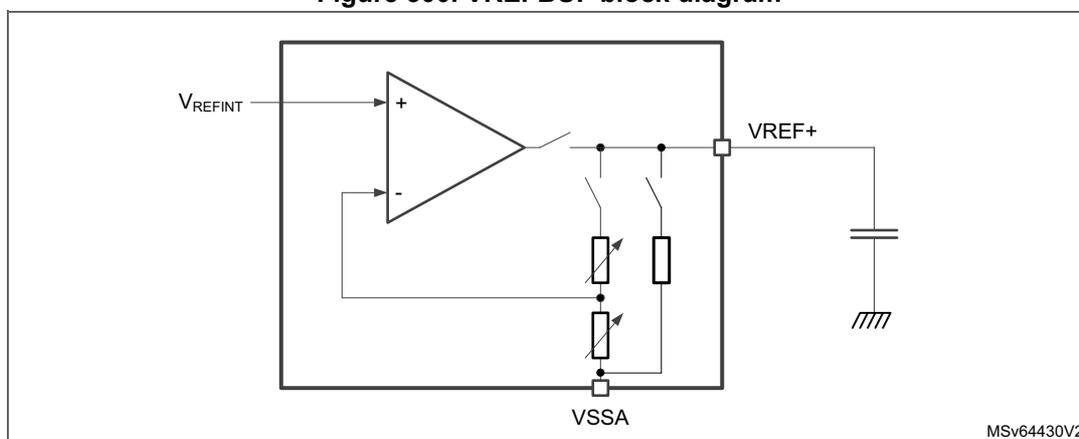
The diagram shows a voltage reference buffer (VREFBUF) block. Inside the block, an operational amplifier (op-amp) is shown with its non-inverting input (+) connected to V REFINT . The inverting input (-) is connected to a node that is also connected to the output of the op-amp through a feedback loop. This feedback loop contains two variable resistors (potentiometers) connected in series between the output node and V SSA . The output node is connected to the VREF+ pin, which is also connected to a capacitor and ground. The V SSA pin is shown at the bottom of the block.
The internal voltage reference buffer is an operational amplifier, with programmable gain. The amplifier input is connected to the internal voltage reference \( V_{REFINT} \) . The VREFBUF supports three voltages (a) , which are configured with VRS bits in the VREFBUF_CSR register:
- • VRS = 000: VREFBUF0 voltage selected
- • VRS = 001: VREFBUF1 voltage selected
- • VRS = 010: VREFBUF2 voltage selected
The internal voltage reference can be configured in four different modes depending on ENVR and HIZ bits configuration. These modes are provided in the table below:
Table 252. VREF buffer modes
| ENVR | HIZ | VREF buffer configuration |
|---|---|---|
| 0 | 0 | VREFBUF buffer off mode: – \( V_{REF+} \) pin pulled-down to \( V_{SSA} \) |
| 0 | 1 | External voltage reference mode (default value): – VREFBUF buffer off – \( V_{REF+} \) pin input mode |
| 1 | 0 | Internal voltage reference mode: – VREFBUF buffer on – \( V_{REF+} \) pin connected to VREFBUF buffer output |
| 1 | 1 | Hold mode: – VREF is enable without output buffer, \( V_{REF+} \) pin voltage is hold with the external capacitor – VRR detection disabled and VRR bit keeps last state |
After enabling the VREFBUF by setting ENVR bit and clearing HIZ bit in the VREFBUF_CSR register, the user must wait until VRR bit is set, meaning that the voltage reference output has reached its expected value.
29.4 VREFBUF trimming
The VREFBUF output voltage is factory-calibrated by ST. At reset, and each time the VRS setting is changed, the calibration data is automatically loaded to the TRIM register.
Optionally user can trim the output voltage by changing the TRIM register bits directly. In this case, the VRS setting has no more effect on the TRIM register until the device is reset.
a. The minimum \( V_{DDA} \) voltage depends on VRS setting, refer to the product datasheet.
29.5 VREFBUF registers
29.5.1 VREFBUF control and status register (VREFBUF_CSR)
Address offset: 0x00
Reset value: 0x0000 0002
| 31 | 30 | 29 | 28 | 27 | 26 | 25 | 24 | 23 | 22 | 21 | 20 | 19 | 18 | 17 | 16 |
|---|---|---|---|---|---|---|---|---|---|---|---|---|---|---|---|
| Res. | Res. | Res. | Res. | Res. | Res. | Res. | Res. | Res. | Res. | Res. | Res. | Res. | Res. | Res. | Res. |
| 15 | 14 | 13 | 12 | 11 | 10 | 9 | 8 | 7 | 6 | 5 | 4 | 3 | 2 | 1 | 0 |
| Res. | Res. | Res. | Res. | Res. | Res. | Res. | Res. | Res. | VRS[2:0] | VRR | Res. | HIZ | ENVR | ||
| rw | rw | rw | r | rw | rw | ||||||||||
Bits 31:7 Reserved, must be kept at reset value.
Bits 6:4 VRS[2:0] : Voltage reference scale
These bits select the value generated by the voltage reference buffer.
VRS = 000: VREFBUF0 voltage selected.
VRS = 001: VREFBUF1 voltage selected.
VRS = 010: VREFBUF2 voltage selected.
Others: Reserved
Note: Refer to the product datasheet for each VREFBUFx voltage setting value.
The software can program this bitfield only when the VREFBUF is disabled (ENVR=0).
Bit 3 VRR : Voltage reference buffer ready
0: the voltage reference buffer output is not ready.
1: the voltage reference buffer output reached the requested level.
Bit 2 Reserved, must be kept at reset value.
Bit 1 HIZ : High impedance mode
This bit controls the analog switch to connect or not the V REF+ pin.
0: V REF+ pin is internally connected to the voltage reference buffer output.
1: V REF+ pin is high impedance.
Refer to Table 252: VREF buffer modes for the mode descriptions depending on ENVR bit configuration.
Bit 0 ENVR : Voltage reference buffer mode enable
This bit is used to enable the voltage reference buffer mode.
0: Internal voltage reference mode disable (external voltage reference mode).
1: Internal voltage reference mode (reference buffer enable or hold mode) enable.
29.5.2 VREFBUF calibration control register (VREFBUF_CCR)
Address offset: 0x04
Reset value: 0x0000 00XX
| 31 | 30 | 29 | 28 | 27 | 26 | 25 | 24 | 23 | 22 | 21 | 20 | 19 | 18 | 17 | 16 |
|---|---|---|---|---|---|---|---|---|---|---|---|---|---|---|---|
| Res. | Res. | Res. | Res. | Res. | Res. | Res. | Res. | Res. | Res. | Res. | Res. | Res. | Res. | Res. | Res. |
| 15 | 14 | 13 | 12 | 11 | 10 | 9 | 8 | 7 | 6 | 5 | 4 | 3 | 2 | 1 | 0 |
| Res. | Res. | Res. | Res. | Res. | Res. | Res. | Res. | Res. | Res. | TRIM[5:0] | |||||
| rw | rw | rw | rw | rw | rw | ||||||||||
Bits 31:6 Reserved, must be kept at reset value.
Bits 5:0 TRIM[5:0] : Trimming code
The TRIM code is a 6-bit unsigned data (minimum 000000, maximum 111111) that is set and updated according the mechanism described below.
Reset:
TRIM[5:0] is automatically initialized with the VRS = 0 trimming value stored in the flash memory during the production test.
Write in TRIM[5:0]:
User can modify the TRIM[5:0] with an arbitrary value. This is permanently disabling the control of the trimming value (until the device is reset).
Note: If the user application performs the trimming, the trimming code must start from 000000 to 111111 in ascending order.
29.5.3 VREFBUF register map
The following table gives the VREFBUF register map and the reset values.
Table 253. VREFBUF register map and reset values
| Offset | Register name | 31 | 30 | 29 | 28 | 27 | 26 | 25 | 24 | 23 | 22 | 21 | 20 | 19 | 18 | 17 | 16 | 15 | 14 | 13 | 12 | 11 | 10 | 9 | 8 | 7 | 6 | 5 | 4 | 3 | 2 | 1 | 0 |
|---|---|---|---|---|---|---|---|---|---|---|---|---|---|---|---|---|---|---|---|---|---|---|---|---|---|---|---|---|---|---|---|---|---|
| 0x00 | VREFBUF_CSR | Res. | Res. | Res. | Res. | Res. | Res. | Res. | Res. | Res. | Res. | Res. | Res. | Res. | Res. | Res. | Res. | Res. | Res. | Res. | Res. | Res. | Res. | Res. | Res. | Res. | VRS[2:0] | VRR | Res. | HIZ | ENVR | ||
| Reset value | 0 | 0 | 0 | 0 | 1 | 0 | |||||||||||||||||||||||||||
| 0x04 | VREFBUF_CCR | Res. | Res. | Res. | Res. | Res. | Res. | Res. | Res. | Res. | Res. | Res. | Res. | Res. | Res. | Res. | Res. | Res. | Res. | Res. | Res. | Res. | Res. | Res. | Res. | Res. | TRIM[5:0] | ||||||
| Reset value | x | x | x | x | x | x | x | ||||||||||||||||||||||||||
Refer to Section 2.3: Memory organization for the register boundary addresses.