28. Digital temperature sensor (DTS)
28.1 DTS introduction
The device embeds a sensor that converts the temperature into a square wave which frequency is proportional to the temperature. The frequency is measured either with the PCLK or the LSE clock.
28.2 DTS main features
The temperature sensor block main features are the following:
- • Start of measurement triggered by software or 4 hardware sources
- • Programmable sampling time to increase temperature measurement precision
- • Counter synchronized on LSE or PCLK clock
- • Temperature watchdog on low and high threshold
- • Interrupt generation when the temperature is lower or higher than predefined thresholds and at the end of measurement.
- • Asynchronous wake-up signal generation when the temperature is higher/lower than a predefined threshold (LSE mode only)
- • Quick measurement using LSE clock
28.3 DTS functional description
28.3.1 DTS block diagram
The temperature sensor block diagram is shown in Figure 296 .
Figure 296. Temperature sensor functional block diagram
![Figure 296. Temperature sensor functional block diagram. The diagram shows the internal architecture of the Digital Temperature Sensor (DTS). On the left, external inputs dts_lse and dts_pclk enter the block. An APB bus is connected to the internal components. The dts_lse input goes to a 'PTAT to FRQ converter'. The dts_pclk input goes to an 'APB interface'. The 'PTAT to FRQ converter' outputs CLK_PTAT and Calibration control signals to a 'Frequency Counter Calibration Control' block. This block also receives LSE and PCLK signals. It has several control inputs: START, SMP_TIME, REFCLK_SEL, Q_MEAS_opt, and HSREF_CLK_DIV. It also has a series of trigger inputs: ts1_trg0, ts1_trg1, ts1_trg2, ..., ts1_trgx, and INTRIG[3:0]. The 'Frequency Counter Calibration Control' block outputs TS1_MFREQ[15:0] to the 'APB interface' and a signal to a 'Comparator'. The 'Comparator' also receives HITTHD[15:0] and LITTHD[15:0] inputs. The 'APB interface' block contains a list of signals: RDY, ITEF, ITLF, ITHF, AITEF, AITLF, AITHF, TO, FMT0, and RAMP_COEFF. It outputs dts_it and dts_wkup signals. The diagram is labeled MSV69530V2 at the bottom right.](/RM0477-STM32H7Rx-7Sx/a93182e7667e36a5128ab71931d512b5_img.jpg)
28.3.2 DTS internal signals
Table 245. DTS internal input/output signals
| Signal name | Signal type | Description |
|---|---|---|
| dts_lse | Digital input | LSE clock |
| dts_pclk | Digital input | APB clock |
| dts_it | Digital output | Temperature sensor interrupt |
| dts_wkup | Digital output | Temperature sensor wake-up |
28.3.3 DTS block operation
The analog part of the temperature sensor outputs a frequency that is proportional to the absolute temperature (CLK_PTAT). The frequency measurement is based on the PCLK or the LSE clock.
Before each measurement, the temperature sensor performs a calibration of the frequency generation blocks.
28.3.4 Operating modes
Several operating modes can be selected by setting the REFCLK_SEL bit in Temperature sensor configuration register 1 (DTS_CFGR1) :
- • PCLK only (REFCLK_SEL = 0)
The temperature sensor registers can be accessed. The interface can consequently be reconfigured and the measurement sequence is performed using PCLK clock
- • PCLK and LSE (REFCLK_SEL = 1)
The temperature sensor registers can be accessed. The interface can consequently be reconfigured and the measurement sequence is performed using the LSE clock.
- • LSE only (REFCLK_SEL = 1) and PCLK OFF
The registers cannot be accessed. The measurement can be performed using the LSE clock. This mode is used to exit from Sleep mode by using hardware triggers and the asynchronous interrupt line.
28.3.5 Calibration
The temperature sensor must run the calibration prior to any frequency measurement. The calibration is performed automatically when the temperature measurement is triggered except for quick measurement mode (Q_MEAS_OPT set to 1 in DTS_CFGR1).
28.3.6 Prescaler
When a calibration is ongoing, the counter clock must be slower than 1 MHz. This is achieved by the PCLK clock prescaler embedded in the temperature sensor.
During the temperature measurement period, the prescaler is bypassed.
- • When PCLK is used as reference clock (REFCLK_SEL set to 0 in DTS_CFGR1), a prescaler is used. Its division ratio must be configured up to 127 (refer to the HSREF_CLK_DIV[6:0] register definition for the divider setting).
- • When LSE is used as reference clock (REFCLK_SEL set to 1 in DTS_CFGR1), the timebase is equal to 2 LSE periods. In this case, no prescaler is used.
28.3.7 Temperature measurement principles
The analog part of temperature sensor outputs a signal (CLK_PTAT) which FM(T) frequency is temperature-dependent.
Either PCLK or LSE can be selected as reference clock (REF_CLK) through the REFCLK_SEL bit in DTS_CFGR1.
The counting method depends on the REF_CLK frequency. This is due to the fact that two counters are implemented in the temperature sensor block:
- • For low REF_CLK frequencies, a counting of FM(T) cycles is performed during one or several REF_CLK cycles.
- • For high REF_CLK frequencies, a counting of REF_CLK cycles is performed during one or several FM(T) cycles.
This counter behavior is shown in Figure 297 and Figure 298 .
Figure 297. Method for low REF_CLK frequencies
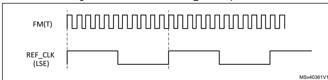
- 1. To increase the precision, FM(T) measurement can be done on several LSE periods.
Figure 298. Method for high REF_CLK frequencies
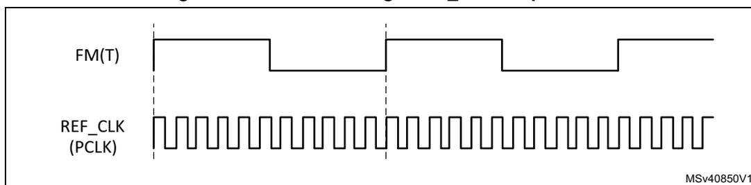
- 1. To increase the precision, PCLK measurement can be done on several FM(T) periods.
The counting result is stored in the DTS_DR register (see Temperature sensor data register (DTS_DR) ).
Once the FM(T) frequency has been obtained, the corresponding temperature can be calculated by software using the following formula:
- • When PCLK is used:
where
T 0 (factory calibration temperature) is equal to 30 °C.
TS1_FMT0 is measured and stored in the DTS_T0VALR1 register. It is expressed in hundreds of Hertz.
TS1_RAMP_COEFF is measured during tests in factory and stored in DTS_RAMPVALR register. This value is expressed in Hz/°C.
- • When the LSE clock is used
28.3.8 Sampling time
The sampling period can be increased to improve measurement accuracy. This is useful when the reference frequency (REF_CLK) is close to the FM(T) frequency. The default value is one REF_CLK cycle in LSE mode, and one FM(T) cycle in PCLK mode.
The sampling time is configured through TS1_SMP_TIME bits in DTS_CFGR1 register (see Table 246 ).
Table 246. Sampling time configuration
| TS1_SMP_TIME[3:0] | LSE or FM(T) clock cycle(s) |
|---|---|
| 0000 | 1 |
| 0001 | 1 |
| 0010 | 2 |
| 0011 | 3 |
| 0100 | 4 |
| 0101 | 5 |
| 0110 | 6 |
| 0111 | 7 |
| 1000 | 8 |
| 1001 | 9 |
| 1010 | 10 |
| 1011 | 11 |
| 1100 | 12 |
| 1101 | 13 |
| 1110 | 14 |
| 1111 | 15 |
28.3.9 Quick measurement mode
If a high precision is not required, the calibration step included in each measurement sequence can be skipped by setting Q_MEAS_OPT to 1 in the DTS_CFGR1 register. This method must be used only when the LSE clock is selected as reference clock (LSREF_CLK set to 1). This mode can reduce the measurement time.
28.3.10 Trigger input
The temperature measurement can be triggered either by software or by an external event. The trigger source can be selected through TS1_INTRIG[3:0] bits in DTS_CFGR1.
Table 247. Trigger configuration
| Name | TS1_INTRIG[3:0] | Comment | |||
|---|---|---|---|---|---|
| N.A | 0 | 0 | 0 | 0 | No hardware trigger |
| ts1_trg0 | 0 | 0 | 0 | 1 | lptim4_out |
| ts1_trg1 | 0 | 0 | 1 | 0 | lptim2_ch1 |
| ts1_trg2 | 0 | 0 | 1 | 1 | lptim3_ch1 |
| ts1_trg3 | 0 | 1 | 0 | 0 | exti13 |
| ts1_trg4 | 0 | 1 | 0 | 1 | Reserved |
| ts1_trg5 | 0 | 1 | 1 | 0 | |
| ts1_trg6 | 0 | 1 | 1 | 1 | |
| ts1_trg7 | 1 | 0 | 0 | 0 | |
| ts1_trg8 | 1 | 0 | 0 | 1 | |
| ts1_trg9 | 1 | 0 | 1 | 0 | |
| ts1_trg10 | 1 | 0 | 1 | 1 | |
| ts1_trg11 | 1 | 1 | 0 | 0 | |
| ts1_trg12 | 1 | 1 | 0 | 1 | |
| ts1_trg13 | 1 | 1 | 1 | 0 | |
| ts1_trg14 | 1 | 1 | 1 | 1 | |
Note:
Hardware triggers are active only on the rising edge.
The temperature sensor can only capture a hardware trigger rising edge when TS1_RDY bit is set (see Section 28.3.11: On-off control and ready flag ), otherwise the trigger is ignored.
If a trigger source changes on-the-fly, the new trigger source signal must be low. If the new source signal is high, the temperature sensor detects a rising edge and start the measurement sequence.
28.3.11 On-off control and ready flag
The DTS block can be enabled by setting TS1_EN bit in DTS_CFGR1 register. The TS1_RDY flag in the Temperature sensor status register (DTS_SR) indicate that the DTS block is ready for temperature measurement: when TS1_RDY bit is set to 1, the measurement can be started. Once a measurement has started, TS1_RDY bit is reset. New measurement requests are then ignored. Once the measurement is finished, TS1_RDY bit is set again to indicate the sensor is ready to start a new measurement.
28.3.12 Temperature measurement sequence
Start of measurement can be triggered by software or hardware.
Software trigger
The software trigger is selected when TS1_INTRIG_SEL[3:0] is set to '0000' in DTS_CFGR1.
If TS1_RDY is set to 1, writing TS1_START bit to 1 in DTS_CFGR1 starts the measurement.
If TS1_RDY equals 0, the software trigger does not start until TS1_RDY is set.
If TS1_START bit is kept at 1 once the measurement is finished, then the TS1_RDY flag become 1 and the measurement restarts.
Hardware trigger
TS1_INTRIG_SEL[3:0] bits allow selecting one hardware trigger out of 4. If TS1_RDY is set to 1, a rising edge on the trigger signal starts the measurement. When TS1_RDY is 0, the rising edge is ignored.
Temperature measurement sequence
One measurement contains two steps: the calibration of the analog blocks and the measurement. The calibration automatically starts when the measurement is triggered (see Section 28.3.5: Calibration ). The measurement period depends on the following DTS_CFGR1 bits:
- • the reference clock selected through REFCLK_SEL bit
- • the divider ratio configured by HSREF_CLK_DIV bits
- • the sampling time defined by TS1_SMP_TIME bits.
Figure 299. Temperature sensor sequence
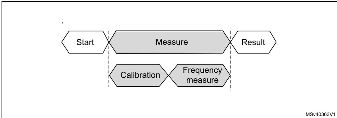
The diagram illustrates the sequence of operations for a temperature measurement. It is divided into three main stages by vertical dashed lines: 'Start', 'Measure', and 'Result'. The 'Start' stage is represented by a hexagonal block. The 'Measure' stage is a large rectangular block containing two sub-steps in a row: 'Calibration' and 'Frequency measure', each in its own hexagonal block. The 'Result' stage is represented by another hexagonal block. The sequence flows from left to right: Start → Measure (Calibration and Frequency measure) → Result. A small code 'MSV40363V1' is visible in the bottom right corner of the diagram area.
28.4 DTS low-power modes
Table 248. Temperature sensor behavior in low-power modes
| Mode | Description |
|---|---|
| Sleep | Only works in LSE mode. DTS interrupt causes the device to exit from Sleep mode. |
| Stop | Only works in LSE mode. DTS interrupt cause the device to exit from Stop mode. |
28.5 DTS interrupts
There are two ways to use the DTS block as an interrupt source. The DTS interrupt line can be connected to the EXTI controller (see Section 28.5.3: Asynchronous wake-up ) or to the CPU NVIC (see Section 28.5.2: Synchronous interrupt ).
28.5.1 Temperature window comparator
The DTS_ITR1 register allows defining the high and low threshold that are used for temperature comparison. If the temperature data is equal or higher than TS1_HITTHD, or equal or lower than TS1_LITTHD bit, an interrupt is generated and the corresponding flag, TS1_ITLF, TS1_ITHF, TS1_AITLF and TS1_AITHF, is set in the DTS_SR register (see Section 28.6.6 ).
28.5.2 Synchronous interrupt
A global interrupt output line is available on the DTS block. The interrupt can be generated at the end of measurement and/or when the measurement result is equal/higher or equal/lower than a predefined threshold (see Section 28.5.1: Temperature window comparator ).
Three interrupt events can be select via 3 bits in DTS_ITENR register (see Section 28.6.7 ). All combinations of interrupts are allowed.
The TS1_ITEF, TS1_ITLF and TS1_ITHF flags in the DTS_SR register reflect the interrupt event. They can be reset with the correspond bits of the DTS_ICIFR register (see Section 28.6.8 ).
28.5.3 Asynchronous wake-up
The DTS block also provides an asynchronous interrupt line. It is used only when the LSE is selected as reference clock (REFCLK_SEL=1).
This line can generate a signal that wakes up the system from Sleep mode at the end of measurement and/or when the measurement result is equal/higher or equal/lower than a predefined threshold (see Section 28.5.1: Temperature window comparator ).
Three asynchronous wake-up events can be selected via 3 bits in DTS_ITENR register. All combination of interrupts are allowed.
The TS1_AITEF, TS1_AITLF and TS1_AITHF flags in the DTS_SR register reflect the interrupt status. They can be reset with the correspond bits of the DTS_ICIFR register.
The following table shows the interrupt bits an the their description.
Table 249. Interrupt control bits
| Interrupt event | Interrupt flag | Enable control bit | Interrupt clear bit | Exit from Sleep mode | Synchronous/ Asynchronous |
|---|---|---|---|---|---|
| At the end of measurement | TS1_ITEF in DTS_SR | TS1_ITEEN in DTS_ITENR | TS1_CITEF in DTS_ICIFR | NO | Synchronous on PCLK |
| When the measure is equal or exceeds the low threshold | TS1_ITLF in DTS_SR | TS1_ITLEN in DTS_ITENR | TS1_CITLF in DTS_ICIFR | NO | |
| When the measure is equal or exceeds the high threshold | TS1_ITHF in DTS_SR | TS1_ITHEN in DTS_ITENR | TS1_CITHF in DTS_ICIFR | NO | |
| At the end of measurement | TS1_AITEF in DTS_SR | TS1_AITEEN in DTS_ITENR | TS1_CAITEF in DTS_ICIFR | YES | Asynchronous |
| When the measure is equal or exceeds the low threshold | TS1_AITLF in DTS_SR | TS1_AITLEN in DTS_ITENR | TS1_CAITLF in DTS_ICIFR | YES | |
| When the measure is equal or exceeds the high threshold | TS1_AITHF in DTS_SR | TS1_AITHEN in DTS_ITENR | TS1_CAITHF in DTS_ICIFR | YES |
28.6 DTS registers
The registers of this peripheral can only be accessed by-word (32-bit).
28.6.1 Temperature sensor configuration register 1 (DTS_CFGR1)
DTS_CFGR1 is the configuration register for temperature sensor 1.
Address offset: 0x00
Reset value: 0x0000 0000
| 31 | 30 | 29 | 28 | 27 | 26 | 25 | 24 | 23 | 22 | 21 | 20 | 19 | 18 | 17 | 16 |
|---|---|---|---|---|---|---|---|---|---|---|---|---|---|---|---|
| Res. | HSREF_CLK_DIV[6:0] | Res. | Res. | Q_MEAS_OPT | REFCLK_SEL | TS1_SMP_TIME[3:0] | |||||||||
| rw | rw | rw | rw | rw | rw | rw | rw | rw | rw | rw | rw | rw | |||
| 15 | 14 | 13 | 12 | 11 | 10 | 9 | 8 | 7 | 6 | 5 | 4 | 3 | 2 | 1 | 0 |
| Res. | Res. | Res. | Res. | TS1_INTRIG_SEL[3:0] | Res. | Res. | Res. | TS1_START | Res. | Res. | Res. | TS1_EN | |||
| rw | rw | rw | rw | rw | rw | ||||||||||
- Bit 31 Reserved, must be kept at reset value.
- Bits 30:24
HSREF_CLK_DIV[6:0]
: High speed clock division ratio
These bits are set and cleared by software. They can be used to define the division ratio for the main clock in order to obtain the internal frequency lower than 1 MHz required for the calibration. They are applicable only for calibration when PCLK is selected as reference clock (REFCLK_SEL=0).
0000000: No divider
0000001: No divider
0000010: 1/2 division ratio
...
1111111: 1/127 division ratio - Bits 23:22 Reserved, must be kept at reset value.
- Bit 21
Q_MEAS_OPT
: Quick measurement option bit
This bit is set and cleared by software. It is used to increase the measurement speed by suppressing the calibration step. It is effective only when the LSE clock is used as reference clock (REFCLK_SEL=1).
0: Measurement with calibration
1: Measurement without calibration - Bit 20
REFCLK_SEL
: Reference clock selection bit
This bit is set and cleared by software. It indicates whether the reference clock is the high speed clock (PCLK) or the low speed clock (LSE).
0: High speed reference clock (PCLK)
1: Low speed reference clock (LSE) - Bits 19:16
TS1_SMP_TIME[3:0]
: Sampling time for temperature sensor 1
These bits allow increasing the sampling time to improve measurement precision.
When the PCLK clock is selected as reference clock (REFCLK_SEL = 0), the measurement is performed at TS1_SMP_TIME period of CLK_PTAT.
When the LSE is selected as reference clock (REFCLK_SEL = 1), the measurement is performed at TS1_SMP_TIME period of LSE. - Bits 15:12 Reserved, must be kept at reset value.
- Bits 11:8
TS1_INTRIG_SEL[3:0]
: Input trigger selection bit for temperature sensor 1
These bits are set and cleared by software. They select which input triggers a temperature measurement. Refer to Section 28.3.10: Trigger input . - Bits 7:5 Reserved, must be kept at reset value.
- Bit 4
TS1_START
: Start frequency measurement on temperature sensor 1
This bit is set and cleared by software.
0: No software trigger.
1: Software trigger for a frequency measurement. (only if TS1 is ready). - Bits 3:1 Reserved, must be kept at reset value.
- Bit 0
TS1_EN
: Temperature sensor 1 enable bit
This bit is set and cleared by software.
0: Temperature sensor 1 disabled
1: Temperature sensor 1 enabled
Note: Once enabled, the temperature sensor is active after a specific delay time. The TS1_RDY flag is set when the sensor is ready.
28.6.2 Temperature sensor T0 value register 1 (DTS_T0VALR1)
DTS_T0VALR1 contains the value of the factory calibration temperature (T0) for temperature sensor 1. The reset value is factory trimmed.
Address offset: 0x08
Reset value: 0x000X XXXX
| 31 | 30 | 29 | 28 | 27 | 26 | 25 | 24 | 23 | 22 | 21 | 20 | 19 | 18 | 17 | 16 |
|---|---|---|---|---|---|---|---|---|---|---|---|---|---|---|---|
| Res. | Res. | Res. | Res. | Res. | Res. | Res. | Res. | Res. | Res. | Res. | Res. | Res. | Res. | TS1_T0[1:0] | |
| r | r | ||||||||||||||
| 15 | 14 | 13 | 12 | 11 | 10 | 9 | 8 | 7 | 6 | 5 | 4 | 3 | 2 | 1 | 0 |
| TS1_FMT0[15:0] | |||||||||||||||
| r | r | r | r | r | r | r | r | r | r | r | r | r | r | r | r |
Bits 31:18 Reserved, must be kept at reset value.
Bits 17:16 TS1_T0[1:0] : Engineering value of the T0 temperature for temperature sensor 1.
00: 30 °C
01: 130 °C
Others: Reserved, must not be used.
Bits 15:0 TS1_FMT0[15:0] : Engineering value of the frequency measured at T0 for temperature sensor 1
This value is expressed in 0.1 kHz.
28.6.3 Temperature sensor ramp value register (DTS_RAMPVALR)
The DTS_RAMPVALR is the ramp coefficient for the temperature sensor. The reset value is factory trimmed.
Address offset: 0x10
Reset value: 0xXXXX XXXX
| 31 | 30 | 29 | 28 | 27 | 26 | 25 | 24 | 23 | 22 | 21 | 20 | 19 | 18 | 17 | 16 |
|---|---|---|---|---|---|---|---|---|---|---|---|---|---|---|---|
| Res. | Res. | Res. | Res. | Res. | Res. | Res. | Res. | Res. | Res. | Res. | Res. | Res. | Res. | Res. | Res. |
| 15 | 14 | 13 | 12 | 11 | 10 | 9 | 8 | 7 | 6 | 5 | 4 | 3 | 2 | 1 | 0 |
| TS1_RAMP_COEFF[15:0] | |||||||||||||||
| r | r | r | r | r | r | r | r | r | r | r | r | r | r | r | r |
Bits 31:16 Reserved, must be kept at reset value.
Bits 15:0 TS1_RAMP_COEFF[15:0] : Engineering value of the ramp coefficient for the temperature sensor 1.
This value is expressed in Hz/°C.
28.6.4 Temperature sensor interrupt threshold register 1 (DTS_ITR1)
DTS_ITR1 contains the threshold values for sensor 1.
Address offset: 0x14
Reset value: 0x0000 0000
| 31 | 30 | 29 | 28 | 27 | 26 | 25 | 24 | 23 | 22 | 21 | 20 | 19 | 18 | 17 | 16 |
|---|---|---|---|---|---|---|---|---|---|---|---|---|---|---|---|
| TS1_HITTHD[15:0] | |||||||||||||||
| rw | rw | rw | rw | rw | rw | rw | rw | rw | rw | rw | rw | rw | rw | rw | rw |
| 15 | 14 | 13 | 12 | 11 | 10 | 9 | 8 | 7 | 6 | 5 | 4 | 3 | 2 | 1 | 0 |
| TS1_LITTHD[15:0] | |||||||||||||||
| rw | rw | rw | rw | rw | rw | rw | rw | rw | rw | rw | rw | rw | rw | rw | rw |
Bits 31:16 TS1_HITTHD[15:0] : High interrupt threshold for temperature sensor 1
These bits are set and cleared by software. They indicate the highest value than can be reached before raising an interrupt signal.
Bits 15:0 TS1_LITTHD[15:0] : Low interrupt threshold for temperature sensor 1
These bits are set and cleared by software. They indicate the lowest value than can be reached before raising an interrupt signal.
28.6.5 Temperature sensor data register (DTS_DR)
The DTS_DR contains the number of REF_CLK cycles used to compute the FM(T) frequency.
Address offset: 0x1C
Reset value: 0x0000 0000
| 31 | 30 | 29 | 28 | 27 | 26 | 25 | 24 | 23 | 22 | 21 | 20 | 19 | 18 | 17 | 16 |
|---|---|---|---|---|---|---|---|---|---|---|---|---|---|---|---|
| Res. | Res. | Res. | Res. | Res. | Res. | Res. | Res. | Res. | Res. | Res. | Res. | Res. | Res. | Res. | Res. |
| 15 | 14 | 13 | 12 | 11 | 10 | 9 | 8 | 7 | 6 | 5 | 4 | 3 | 2 | 1 | 0 |
| TS1_MFREQ[15:0] | |||||||||||||||
| rw | rw | rw | rw | rw | rw | rw | rw | rw | rw | rw | rw | rw | rw | rw | rw |
Bits 31:16 Reserved, must be kept at reset value.
Bits 15:0 TS1_MFREQ[15:0] : Value of the counter output value for temperature sensor 1
28.6.6 Temperature sensor status register (DTS_SR)
Address offset: 0x20
Reset value: 0x0000 0000
| 31 | 30 | 29 | 28 | 27 | 26 | 25 | 24 | 23 | 22 | 21 | 20 | 19 | 18 | 17 | 16 |
|---|---|---|---|---|---|---|---|---|---|---|---|---|---|---|---|
| Res. | Res. | Res. | Res. | Res. | Res. | Res. | Res. | Res. | Res. | Res. | Res. | Res. | Res. | Res. | Res. |
| 15 | 14 | 13 | 12 | 11 | 10 | 9 | 8 | 7 | 6 | 5 | 4 | 3 | 2 | 1 | 0 |
| TS1_RDY | Res. | Res. | Res. | Res. | Res. | Res. | Res. | Res. | TS1_AITHF | TS1_AITLF | TS1_AITEF | Res. | TS1_ITHF | TS1_ITLF | TS1_ITEF |
| r | r | r | r | r | r | r |
Bits 31:16 Reserved, must be kept at reset value.
Bit 15 TS1_RDY : Temperature sensor 1 ready flag
This bit is set and reset by hardware.
It indicates that a measurement is ongoing.
0: Temperature sensor 1 busy
1: Temperature sensor 1 ready
Bits 14:7 Reserved, must be kept at reset value.
Bit 6 TS1_AITHF : Asynchronous interrupt flag for high threshold on temperature sensor 1
This bit is set by hardware when the high threshold is reached.
It is cleared by software by writing 1 to the TS1_CAITHF bit in the DTS_ICIFR register.
0: High threshold not reached on temperature sensor 1
1: High threshold reached on temperature sensor 1
Note: This bit is active only when the TS1_AITHFEN bit is set
Bit 5 TS1_AITLF : Asynchronous interrupt flag for low threshold on temperature sensor 1
This bit is set by hardware when the low threshold is reached.
It is cleared by software by writing 1 to the TS1_CAITLF bit in the DTS_ICIFR register.
0: Low threshold not reached on temperature sensor 1
1: Low threshold reached on temperature sensor 1
Note: This bit is active only when the TS1_AITLFEN bit is set
Bit 4 TS1_AITEF : Asynchronous interrupt flag for end of measure on temperature sensor 1
This bit is set by hardware when a temperature measure is done.
It is cleared by software by writing 1 to the TS1_CAITEF bit in the DTS_ICIFR register.
0: End of measure not detected on temperature sensor 1
1: End of measure detected on temperature sensor 1
Note: This bit is active only when the TS1_AITEFEN bit is set
Bit 3 Reserved, must be kept at reset value.
Bit 2 TS1_ITHF : Interrupt flag for high threshold on temperature sensor 1, synchronized on PCLK
This bit is set by hardware when the high threshold is set and reached.
It is cleared by software by writing 1 to the TS1_CITHF bit in the DTS_ICIFR register.
0: High threshold not reached on temperature sensor 1
1: High threshold reached on temperature sensor 1
Note: This bit is active only when the TS1_ITHFEN bit is set
Bit 1 TS1_ITLF : Interrupt flag for low threshold on temperature sensor 1, synchronized on PCLK.
This bit is set by hardware when the low threshold is set and reached.
It is cleared by software by writing 1 to the TS1_CITLF bit in the DTS_ICIFR register.
0: Low threshold not reached on temperature sensor 1
1: Low threshold reached on temperature sensor 1
Note: This bit is active only when the TS1_ITLFEN bit is set
Bit 0 TS1_ITEF : Interrupt flag for end of measurement on temperature sensor 1, synchronized on PCLK.
This bit is set by hardware when a temperature measure is done.
It is cleared by software by writing 1 to the TS2_CITEF bit in the DTS_ICIFR register.
0: No end of measurement detected on temperature sensor 1
1: End of measure detected on temperature sensor 1
Note: This bit is active only when the TS1_ITEFEN bit is set
28.6.7 Temperature sensor interrupt enable register (DTS_ITENR)
Address offset: 0x24
Reset value: 0x0000 0000
| 31 | 30 | 29 | 28 | 27 | 26 | 25 | 24 | 23 | 22 | 21 | 20 | 19 | 18 | 17 | 16 |
|---|---|---|---|---|---|---|---|---|---|---|---|---|---|---|---|
| Res. | Res. | Res. | Res. | Res. | Res. | Res. | Res. | Res. | Res. | Res. | Res. | Res. | Res. | Res. | Res. |
| 15 | 14 | 13 | 12 | 11 | 10 | 9 | 8 | 7 | 6 | 5 | 4 | 3 | 2 | 1 | 0 |
| Res. | Res. | Res. | Res. | Res. | Res. | Res. | Res. | Res. | TS1_AITHEN | TS1_AITLEN | TS1_AITEEN | Res. | TS1_ITHEN | TS1_ITLEN | TS1_ITEEN |
| rw | rw | rw | rw | rw | rw |
Bits 31:7 Reserved, must be kept at reset value.
Bit 6 TS1_AITHEN : Asynchronous interrupt enable flag on high threshold for temperature sensor 1.
This bit are set and cleared by software.
It enables the asynchronous interrupt when the temperature is above the high threshold (only when REFCLK_SEL= 1")
0: Asynchronous interrupt on high threshold disabled for temperature sensor 1
1: Asynchronous interrupt on high threshold enabled for temperature sensor 1
Bit 5 TS1_AITLEN : Asynchronous interrupt enable flag for low threshold on temperature sensor 1.
This bit are set and cleared by software.
It enables the asynchronous interrupt when the temperature is below the low threshold (only when REFCLK_SEL= 1)
0: Asynchronous interrupt on low threshold disabled for temperature sensor 1
1: Asynchronous interrupt on low threshold enabled for temperature sensor 1
Bit 4 TS1_AITEEN : Asynchronous interrupt enable flag for end of measurement on temperature sensor 1
This bit are set and cleared by software.
It enables the asynchronous interrupt for end of measurement (only when REFCLK_SEL = 1).
0: Asynchronous interrupt for end of measurement disabled on temperature sensor 1
1: Asynchronous interrupt for end of measurement enabled on temperature sensor 1
Bit 3 Reserved, must be kept at reset value.
Bit 2 TS1_ITHEN : Interrupt enable flag for high threshold on temperature sensor 1, synchronized on PCLK.
This bit are set and cleared by software.
It enables the interrupt when the measure reaches or is above the high threshold.
0: Synchronous interrupt for high threshold disabled on temperature sensor 1
1: Synchronous interrupt for high threshold enabled on temperature sensor 1
Bit 1 TS1_ITLEN : Interrupt enable flag for low threshold on temperature sensor 1, synchronized on PCLK.
This bit are set and cleared by software.
It enables the synchronous interrupt when the measure reaches or is below the low threshold.
0: Synchronous interrupt for low threshold disabled on temperature sensor 1
1: Synchronous interrupt for low threshold enabled on temperature sensor 1
Bit 0 TS1_ITEEN : Interrupt enable flag for end of measurement on temperature sensor 1, synchronized on PCLK.
This bit are set and cleared by software.
It enables the synchronous interrupt for end of measurement.
0: Synchronous interrupt for end of measurement disabled on temperature sensor 1
1: Synchronous interrupt for end of measurement enabled on temperature sensor 1
28.6.8 Temperature sensor clear interrupt flag register (DTS_ICIFR)
DTS_ICIFR is the control register for the interrupt flags.
Address offset: 0x28
Reset value: 0x0000 0000
| 31 | 30 | 29 | 28 | 27 | 26 | 25 | 24 | 23 | 22 | 21 | 20 | 19 | 18 | 17 | 16 |
|---|---|---|---|---|---|---|---|---|---|---|---|---|---|---|---|
| Res. | Res. | Res. | Res. | Res. | Res. | Res. | Res. | Res. | Res. | Res. | Res. | Res. | Res. | Res. | Res. |
| 15 | 14 | 13 | 12 | 11 | 10 | 9 | 8 | 7 | 6 | 5 | 4 | 3 | 2 | 1 | 0 |
| Res. | Res. | Res. | Res. | Res. | Res. | Res. | Res. | Res. | TS1_ CAITHF | TS1_ CAITLF | TS1_ CAITEF | Res. | TS1_ CITHF | TS1_ CITLF | TS1_ CITEF |
| rc_w1 | rc_w1 | rc_w1 | rc_w1 | rc_w1 | rc_w1 | ||||||||||
Bits 31:7 Reserved, must be kept at reset value.
Bit 6
TS1_CAITHF
: Asynchronous interrupt clear flag for high threshold on temperature sensor 1
Writing 1 to this bit clears the TS1_AITHF flag in the DTS_SR register.
Bit 5
TS1_CAITLF
: Asynchronous interrupt clear flag for low threshold on temperature sensor 1
Writing 1 to this bit clears the TS1_AITLF flag in the DTS_SR register.
Bit 4 TS1_CAITEF : Write once bit. Clear the asynchronous IT flag for End Of Measure for thermal sensor 1.
Writing 1 clears the TS1_AITEF flag of the DTS_SR register.
Bit 3 Reserved, must be kept at reset value.
Bit 2 TS1_CITHF : Interrupt clear flag for high threshold on temperature sensor 1
Writing this bit to 1 clears the TS1_ITHF flag in the DTS_SR register.
Bit 1 TS1_CITLF : Interrupt clear flag for low threshold on temperature sensor 1
Writing 1 to this bit clears the TS1_ITLF flag in the DTS_SR register.
Bit 0 TS1_CITEF : Interrupt clear flag for end of measurement on temperature sensor 1
Writing 1 to this bit clears the TS1_ITEF flag in the DTS_SR register.
28.6.9 Temperature sensor option register (DTS_OR)
The DTS_OR contains general-purpose option bits.
Address offset: 0x2C
Reset value: 0x0000 0000
| 31 | 30 | 29 | 28 | 27 | 26 | 25 | 24 | 23 | 22 | 21 | 20 | 19 | 18 | 17 | 16 |
|---|---|---|---|---|---|---|---|---|---|---|---|---|---|---|---|
| TS_OP 31 | TS_OP 30 | TS_OP 29 | TS_OP 28 | TS_OP 27 | TS_OP 26 | TS_OP 25 | TS_OP 24 | TS_OP 23 | TS_OP 22 | TS_OP 21 | TS_OP 20 | TS_OP 19 | TS_OP 18 | TS_OP 17 | TS_OP 16 |
| rw | rw | rw | rw | rw | rw | rw | rw | rw | rw | rw | rw | rw | rw | rw | rw |
| 15 | 14 | 13 | 12 | 11 | 10 | 9 | 8 | 7 | 6 | 5 | 4 | 3 | 2 | 1 | 0 |
| TS_OP 15 | TS_OP 14 | TS_OP 13 | TS_OP 12 | TS_OP 11 | TS_OP 10 | TS_OP 9 | TS_OP 8 | TS_OP 7 | TS_OP 6 | TS_OP 5 | TS_OP 4 | TS_OP 3 | TS_OP 2 | TS_OP 1 | TS_OP 0 |
| rw | rw | rw | rw | rw | rw | rw | rw | rw | rw | rw | rw | rw | rw | rw | rw |
Bits 31:0 TS_OP[31:0] : general purpose option bits
28.6.10 DTS register map
The following table summarizes the temperature sensor registers.
Table 250. DTS register map and reset values
| Offset | Register name | 31 | 30 | 29 | 28 | 27 | 26 | 25 | 24 | 23 | 22 | 21 | 20 | 19 | 18 | 17 | 16 | 15 | 14 | 13 | 12 | 11 | 10 | 9 | 8 | 7 | 6 | 5 | 4 | 3 | 2 | 1 | 0 | |
|---|---|---|---|---|---|---|---|---|---|---|---|---|---|---|---|---|---|---|---|---|---|---|---|---|---|---|---|---|---|---|---|---|---|---|
| 0x00 | DTS_CFGR1 | Res. HSREF_CLK_DIV [6:0] | Res. | Q_MEAS_OPT | REFCLK_SEL | TS1_SMP_TIME [3:0] | Res. | Res. | Res. | Res. | TS1_INTRIG_SEL [3:0] | Res. | Res. | Res. | TS1_START | Res. | Res. | Res. | TS1_EN | |||||||||||||||
| Reset value | 0 0 0 0 0 0 0 0 0 0 | 0 | 0 | 0 0 0 0 | 0 0 0 0 0 | 0 | 0 | |||||||||||||||||||||||||||
| 0x04 | Reserved | |||||||||||||||||||||||||||||||||
| 0x08 | DTS_TOVALR1 | Res. | Res. | Res. | Res. | Res. | Res. | Res. | Res. | Res. | Res. | Res. | Res. | Res. | Res. | Res. | TS1_T0[1:0] | TS1_FMT0[15:0] | ||||||||||||||||
| Reset value | X | X | X | X | X | X | X | X | X | X | X | X | X | X | X | X | X | |||||||||||||||||
| 0x0C | Reserved | |||||||||||||||||||||||||||||||||
| 0x10 | DTS_RAMPVALR | Res. | Res. | Res. | Res. | Res. | Res. | Res. | Res. | Res. | Res. | Res. | Res. | Res. | Res. | Res. | Res. | TS1_RAMP_COEFF[15:0] | ||||||||||||||||
| Reset value | X | X | X | X | X | X | X | X | X | X | X | X | X | X | X | |||||||||||||||||||
| 0x14 | DTS_ITR1 | TS1_HITTHD[15:0] | TS1_LITTHD[15:0] | |||||||||||||||||||||||||||||||
| Reset value | 0 0 0 0 0 0 0 0 0 0 0 0 0 0 0 0 | 0 0 0 0 0 0 0 0 0 0 0 0 0 0 0 0 | ||||||||||||||||||||||||||||||||
| 0x18 | Reserved | |||||||||||||||||||||||||||||||||
| 0x1C | DTS_DR | Res. | Res. | Res. | Res. | Res. | Res. | Res. | Res. | Res. | Res. | Res. | Res. | Res. | Res. | Res. | Res. | TS1_MFREQ[15:0] | ||||||||||||||||
| Reset value | 0 | 0 | 0 | 0 | 0 | 0 | 0 | 0 | 0 | 0 | 0 | 0 | 0 | 0 | 0 | |||||||||||||||||||
| 0x20 | DTS_SR | Res. | Res. | Res. | Res. | Res. | Res. | Res. | Res. | Res. | Res. | Res. | Res. | Res. | Res. | Res. | Res. | TS1_RDY | Res. | Res. | Res. | Res. | Res. | Res. | Res. | Res. | Res. | TS1_AITHF | TS1_AITLF | TS1_AITEF | Res. | TS1_ITHF | TS1_ITLF | TS1_ITEF |
| Reset value | 0 | 0 | 0 | 0 | 0 | 0 | 0 | |||||||||||||||||||||||||||
| 0x24 | DTS_ITENR | Res. | Res. | Res. | Res. | Res. | Res. | Res. | Res. | Res. | Res. | Res. | Res. | Res. | Res. | Res. | Res. | Res. | Res. | Res. | Res. | Res. | Res. | Res. | Res. | Res. | Res. | TS1_AITHEN | TS1_AITLEN | TS1_AITEEN | Res. | TS1_ITHEN | TS1_ITLEN | TS1_ITEEN |
| Reset value | 0 | 0 | 0 | 0 | 0 | 0 | ||||||||||||||||||||||||||||
| 0x28 | DTS_ICIFR | Res. | Res. | Res. | Res. | Res. | Res. | Res. | Res. | Res. | Res. | Res. | Res. | Res. | Res. | Res. | Res. | Res. | Res. | Res. | Res. | Res. | Res. | Res. | Res. | Res. | Res. | TS1_CATHF | TS1_CATLF | TS1_CATEF | Res. | TS1_CITHF | TS1_CITLF | TS1_CITEF |
| Reset value | 0 | 0 | 0 | 0 | 0 | 0 | ||||||||||||||||||||||||||||
Table 250. DTS register map and reset values (continued)
| Offset | Register name | 31 | 30 | 29 | 28 | 27 | 26 | 25 | 24 | 23 | 22 | 21 | 20 | 19 | 18 | 17 | 16 | 15 | 14 | 13 | 12 | 11 | 10 | 9 | 8 | 7 | 6 | 5 | 4 | 3 | 2 | 1 | 0 |
|---|---|---|---|---|---|---|---|---|---|---|---|---|---|---|---|---|---|---|---|---|---|---|---|---|---|---|---|---|---|---|---|---|---|
| 0x2C | DTS_OR | TS_OP31 | TS_OP30 | TS_OP29 | TS_OP28 | TS_OP27 | TS_OP26 | TS_OP25 | TS_OP24 | TS_OP23 | TS_OP22 | TS_OP21 | TS_OP20 | TS_OP19 | TS_OP18 | TS_OP17 | TS_OP16 | TS_OP15 | TS_OP14 | TS_OP13 | TS_OP12 | TS_OP11 | TS_OP10 | TS_OP9 | TS_OP8 | TS_OP7 | TS_OP6 | TS_OP5 | TS_OP4 | TS_OP3 | TS_OP2 | TS_OP1 | TS_OP0 |
| Reset value | 0 | 0 | 0 | 0 | 0 | 0 | 0 | 0 | 0 | 0 | 0 | 0 | 0 | 0 | 0 | 0 | 0 | 0 | 0 | 0 | 0 | 0 | 0 | 0 | 0 | 0 | 0 | 0 | 0 | 0 | 0 | 0 | 0 |
Refer to Section 2.3: Memory organization for the register boundary addresses.