26. Delay block (DLYB)
26.1 DLYB introduction
The delay block (DLYB) is used to generate an output clock that is dephased from the input clock. The phase of the output clock must be programmed by the user application. The output clock is then used to clock the data received by another peripheral such as an SDMMC interface.
The delay is voltage- and temperature-dependent, that may require the application to re-configure and recenter the output clock phase with the receive data.
26.2 DLYB main features
The delay block has the following features:
- • Input clock frequency ranging from 25 MHz to the maximum frequency supported by the communication interface (see datasheet)
- • Up to 12 oversampling phases.
26.3 DLYB functional description
26.3.1 DLYB diagram
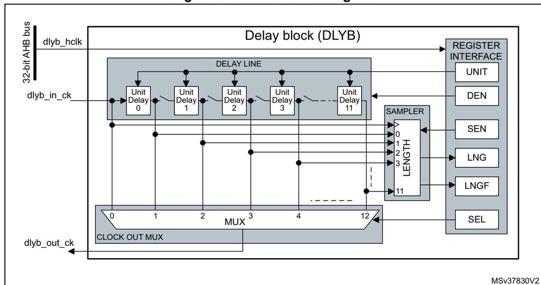
The delay block includes the following sub-blocks (shown in the figure below):
- • register interface block providing AHB access to the DLYB registers
- • delay line supporting the unit delays
- • delay line length sampling
- • output clock selection multiplexer
Figure 223. DLYB block diagram
26.3.2 DLYB pins and internal signals
Table 220 lists the DLYB internal signals.
Table 220. DLYB internal input/output signals
| Signal name | Signal type | Description |
|---|---|---|
| dlyb_hclk | Digital input | Delay block register interface clock |
| dlyb_in_ck | Digital input | Delay block input clock |
| dlyb_out_ck | Digital output | Delay block output clock |
Table 221. DLYB interconnection
| Signal name | Source/destination | |
|---|---|---|
| SDMMC1 | SDMMC2 | |
| dlyb_in_ck | sdmmc_io_in_ck | |
| dlyb_out_ck | sdmmc_fb_ck | |
26.3.3 General description
The delay block is enabled by setting the DEN bit in the DLYB control register (DLYB_CR). The length sampler is enabled through the SEN bit in DLYB_CR register.
When the delay block is enabled, the delay added by a unit delay is defined by the UNIT[6:0] field in the DLYB configuration register (DLYB_CFGR).
Note: UNIT[6:0] can be programmed only when the output clock is disabled (SEN = 1).
When the delay block is enabled, the output clock phase is selected through the SEL[3:0] field in DLYB_CFGR register.
Note: SEL can be programmed only when the output clock is disabled (SEN = 1).
The output clock can be de-phased over one input clock period by configuring the delay line length to span one period. The delay line length can be configured by enabling the length sampler through the SEN bit, that gives access to the delay line length (LNG[11:0]) and length valid flag (LNGF) in DLYB_CFGR.
If an output clock delay smaller than one input clock period is needed the delay line length can be reduced. This allows a smaller unit delay providing higher resolution.
Once the delay line length is configured, a dephased output clock can be selected by the output clock multiplexer. This is done through SEL[3:0]. The output clock is only available on the selected phase when SEN is set to 0.
The table below gives a summary of the delay block control.
Table 222. Delay block control
| DEN | SEN | UNIT | SEL | LNG | LNGF | Output clock |
|---|---|---|---|---|---|---|
| 0 | 0 | Don't care | Don't care | Don't care | Don't care | Enabled (= Input clock) |
Table 222. Delay block control
| DEN | SEN | UNIT | SEL | LNG | LNGF | Output clock |
|---|---|---|---|---|---|---|
| x | 1 | Unit delay | Output clock phase | Length | Length flag | Disabled |
| 1 | 0 | Unit delay (1) | Output clock phase (2) | Don't care | Don't care | Enabled (= selected phase) |
1. The unit delay can only be changed when SEN = 1.
2. The output clock phase can only be changed when SEN = 1.
26.3.4 Delay line length configuration procedure
LNG[11:0] is used to determine the delay line length with respect to the input clock period. The length must be configured so that one full input clock period is covered by the delay line length.
Note that despite the delay line has 12 unit delay elements, the following procedure description returns a length between 0 and 10, as the upper delay output value is used to ensure that the delay is calibrated over one full input clock cycle. Depending on the clock frequency and UNIT value, unit delay element 10 may also be truncated from the clock cycle length.
A clock input (free running clock) must be present during the whole tuning procedure.
To configure the delay line length to one period of the Input clock, follow the sequence below:
- 1. Enable the delay block by setting DEN bit to 1.
- 2. Enable the length sampling by setting SEN bit to 1.
- 3. Enable all delay cells by setting SEL[3:0] to 12.
- 4. For UNIT[6:0] = 0 to 127 (this step must be repeated until the delay line length is configured):
- a) Update the UNIT[6:0] value and wait till the length flag LNGF is set to 1.
- b) Read LNG[11:0].
- 5. Determine how many unit delays (N) span one input clock period: for N = 0 to 10, if LNG[N] = 1, the number of unit delays spanning the input clock period = N.
- 6. Disable the length sampling by clearing SEN to 0.
If an output clock delay smaller than one input clock period is needed the delay line length can be reduced smaller than one input clock period. This allows a smaller unit delay, providing a higher resolution spanning a shorter time interval.
26.3.5 Output clock phase configuration procedure
When the delay line length is configured to one input clock period, the output clock phase can be selected between the unit delays spanning one Input clock period.
Follow the steps below to select the output clock phase:
- 1. Disable the output clock and enable the access to the phase selection SEL[3:0] bits by setting SEN bit to 1.
- 2. Program SEL[3:0] with the desired output clock phase value.
- 3. Enable the output clock on the selected phase by clearing SEN to 0.
SDMMC use case:
The delay block is used in conjunction with SDMMC interface variable delay. For correct sampling point tuning the delay value must cover a whole SDMMC_CK clock period. After having tuned the delay line length the individual delays are used in the sampling point tuning to find the optimal sampling point.
26.4 DLYB registers
All registers can be accessed in word, half-word and byte access.
26.4.1 DLYB control register (DLYB_CR)
Address offset: 0x000
Reset value: 0x0000 0000
| 31 | 30 | 29 | 28 | 27 | 26 | 25 | 24 | 23 | 22 | 21 | 20 | 19 | 18 | 17 | 16 |
|---|---|---|---|---|---|---|---|---|---|---|---|---|---|---|---|
| Res. | Res. | Res. | Res. | Res. | Res. | Res. | Res. | Res. | Res. | Res. | Res. | Res. | Res. | Res. | Res. |
| 15 | 14 | 13 | 12 | 11 | 10 | 9 | 8 | 7 | 6 | 5 | 4 | 3 | 2 | 1 | 0 |
| Res. | Res. | Res. | Res. | Res. | Res. | Res. | Res. | Res. | Res. | Res. | Res. | Res. | Res. | SEN | DEN |
| rw | rw |
Bits 31:2 Reserved, must be kept at reset value.
Bit 1 SEN : Sampler length enable bit
0: Sampler length and register access to UNIT[6:0] and SEL[3:0] disabled, output clock enabled.
1: Sampler length and register access to UNIT[6:0] and SEL[3:0] enabled, output clock disabled.
Bit 0 DEN : Delay block enable bit
0: DLYB disabled.
1: DLYB enabled.
26.4.2 DLYB configuration register (DLYB_CFGR)
Address offset: 0x004
Reset value: 0x0000 0000
| 31 | 30 | 29 | 28 | 27 | 26 | 25 | 24 | 23 | 22 | 21 | 20 | 19 | 18 | 17 | 16 |
|---|---|---|---|---|---|---|---|---|---|---|---|---|---|---|---|
| LNGF | Res. | Res. | Res. | LNG[11:0] | |||||||||||
| r | r | r | r | r | r | r | r | r | r | r | r | r | |||
| 15 | 14 | 13 | 12 | 11 | 10 | 9 | 8 | 7 | 6 | 5 | 4 | 3 | 2 | 1 | 0 |
| Res. | UNIT[6:0] | Res. | Res. | Res. | Res. | SEL[3:0] | |||||||||
| rw | rw | rw | rw | rw | rw | rw | rw | rw | rw | rw | |||||
Bit 31 LNGF : Length valid flag
This flag indicates when the delay line length value contained in LNG[11:0] is valid after UNIT[6:0] bits changed.
0: Length value in LNG is not valid.
1: Length value in LNG is valid.
Bits 30:28 Reserved, must be kept at reset value.
Bits 27:16 LNG[11:0] : Delay line length value
These bits reflect the 12 unit delay values sampled at the rising edge of the input clock.
The value is only valid when LNGF = 1.
Bit 15 Reserved, must be kept at reset value.
Bits 14:8 UNIT[6:0] : Delay of a unit delay cell.
These bits can only be written when SEN = 1.
Unit delay = initial delay + UNIT[6:0] x delay step
Bits 7:4 Reserved, must be kept at reset value.
Bits 3:0 SEL[3:0] : Phase for the output clock.
These bits can only be written when SEN = 1.
Output clock phase = input clock + SEL[3:0] x unit delay
26.4.3 DLYB register map
Table 223. DLYB register map and reset values
| Offset | Register name | 31 | 30 | 29 | 28 | 27 | 26 | 25 | 24 | 23 | 22 | 21 | 20 | 19 | 18 | 17 | 16 | 15 | 14 | 13 | 12 | 11 | 10 | 9 | 8 | 7 | 6 | 5 | 4 | 3 | 2 | 1 | 0 |
|---|---|---|---|---|---|---|---|---|---|---|---|---|---|---|---|---|---|---|---|---|---|---|---|---|---|---|---|---|---|---|---|---|---|
| 0x000 | DLYB_CR | Res. | Res. | Res. | Res. | Res. | Res. | Res. | Res. | Res. | Res. | Res. | Res. | Res. | Res. | Res. | Res. | Res. | Res. | Res. | Res. | Res. | Res. | Res. | Res. | Res. | Res. | Res. | Res. | Res. | Res. | SEN | DEN |
| Reset value | 0 | 0 | |||||||||||||||||||||||||||||||
| 0x004 | DLYB_CFGR | LNGF | Res. | Res. | Res. | LNG[11:0] | Res. | UNIT[6:0] | Res. | Res. | Res. | Res. | SEL[3:0] | ||||||||||||||||||||
| Reset value | 0 | 0 | 0 | 0 | 0 | 0 | 0 | 0 | 0 | 0 | 0 | 0 | 0 | 0 | 0 | 0 | 0 | 0 | 0 | 0 | 0 | 0 | 0 | 0 | 0 | 0 | |||||||
Refer to Section 2.3: Memory organization for the register boundary addresses.